15EC32T - DIGITAL ELECTRONICS
22
15EC32T - DIGITAL ELECTRONICS
-
Upload
khangminh22 -
Category
Documents
-
view
0 -
download
0
Transcript of 15EC32T - DIGITAL ELECTRONICS

15EC32T - DIGITAL ELECTRONICS
15EC32T-DIGITAL ELECTRONICS
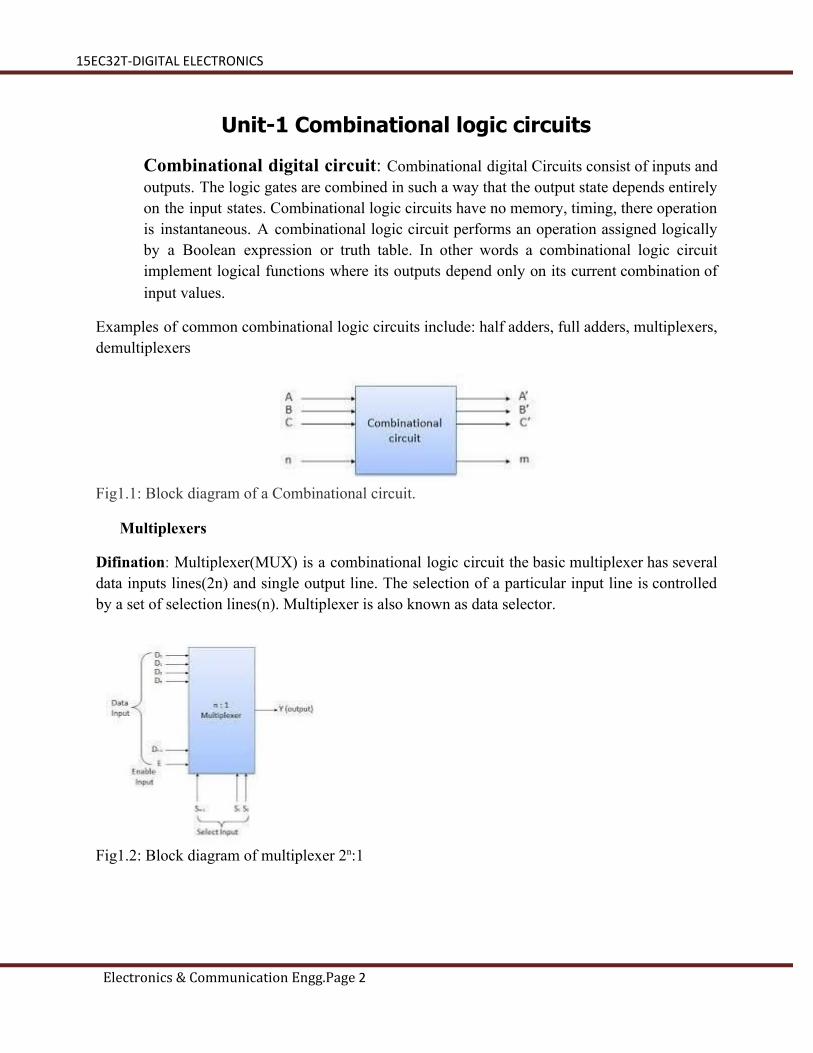
Unit-1 Combinational logic circuits
Combinational digital circuit: Combinational digital Circuits consist of inputs and outputs. The logic gates are combined in such a way that the output state depends entirely on the input states. Combinational logic circuits have no memory, timing, there operation is instantaneous. A combinational logic circuit performs an operation assigned logically by a Boolean expression or truth table. In other words a combinational logic circuit implement logical functions where its outputs depend only on its current combination of input values.
Examples of common combinational logic circuits include: half adders, full adders, multiplexers, demultiplexers
Fig1.1: Block diagram of a Combinational circuit.
Multiplexers
Difination: Multiplexer(MUX) is a combinational logic circuit the basic multiplexer has several data inputs lines(2n) and single output line. The selection of a particular input line is controlled by a set of selection lines(n). Multiplexer is also known as data selector.
Fig1.2: Block diagram of multiplexer 2n:1
Electronics & Communication Engg.Page 2

15EC32T-DIGITAL ELECTRONICS
2:1 Multiplexer: 2:1 multiplexer is a combinational circuit that uses one control line (S) to connect one of two input data lines (D0 or D1) to a single output (Y). Only one of the input data lines can be connected to the output of the multiplexer at any given time.
Truth table:
Logic Diagram:
Fig1.3: Logic Diagram for 2:1 MUX
Fig1.3 shows the logic diagram for2:1 multiplexer. The logic circuit consists of two And gates A1 and A2, an OR gate O1 and a Not gate N1. D0 and D1 are input lines and S is the select line. If select line S=0 then input D0 will be selected to output Y else S=1 then input D1 will be selected to output Y.
Refer: https://www.youtube.com/watch?v=KGcyS1lE6KQ
Applications:
● Data selection. ● Data routing. ● Waveform generation. ● Parallel to serial conversion.
Electronics & Communication Engg.Page 3
Select input(S) Output(Y)
0 D0
1 D1
15EC32T-DIGITAL ELECTRONICS
● Frequency multiplexing system. ● Logic function generation.
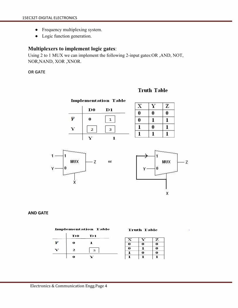
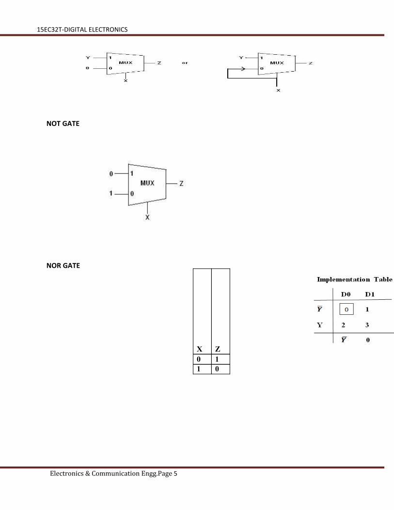
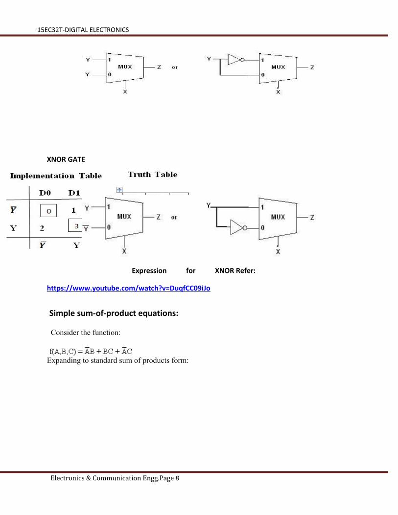
Multiplexers to implement logic gates: Using 2 to 1 MUX we can implement the following 2-input gates:OR ,AND, NOT, NOR,NAND, XOR ,XNOR.
OR GATE
AND GATE
Electronics & Communication Engg.Page 4
15EC32T-DIGITAL ELECTRONICS
NOT GATE
NOR GATE
Electronics & Communication Engg.Page 5
X Z 0 1 1 0

15EC32T-DIGITAL ELECTRONICS
Electronics & Communication Engg.Page 6

15EC32T-DIGITAL ELECTRONICS
NAND GATE
XOR GATE
Electronics & Communication Engg.Page 7
15EC32T-DIGITAL ELECTRONICS
XNOR GATE
Expression for XNOR Refer:
https://www.youtube.com/watch?v=DuqfCC09iJo
Simple sum-of-product equations:
Consider the function:
Expanding to standard sum of products form:
Electronics & Communication Engg.Page 8

15EC32T-DIGITAL ELECTRONICS
Note: In the above e e i i ed
The resulting multiplexer implementation is:
TRUTH TABLE
I e e he f c i F ∑ , ,3,6,8, , , , 3, 4 i g 8 .
Truth table
Electronics & Communication Engg.Page 9
INPUTS OUTPUT
A B C F 0 0 0 0
0 0 1 1 0 1 0 1
0 1 1 0 1 0 0 0
1 0 1 1 1 1 0 0
1 1 1 1
INPUTS OUTPUT A B C D F
0 0 0 0 1 0 0 0 1 0

15EC32T-DIGITAL ELECTRONICS
Electronics & Communication Engg.Page 10
0 0 1 0 1

15EC32T-DIGITAL ELECTRONICS
Fig: Implementation table and block diagram
Video Link: https://youtu.be/1Q9-XXrn03A
Electronics & Communication Engg.Page 11
0 0 1 1 1
0 1 0 0 0 0 1 0 1 0
0 1 1 0 1 0 1 1 1 0
1 0 0 0 1 1 0 0 1 0
1 0 1 0 1
1 0 1 1 1 1 1 0 0 1
1 1 0 1 1 1 1 1 0 1
1 1 1 1 0

15EC32T-DIGITAL ELECTRONICS
List of IC multiplexers and their features:
Realization of higher-order multiplexer using lower-order multiplexer ICs:
1. Realization of 4:1 mux using 2:1 mux given below
Fig1.4: 4:1 MUX using 2:1MUX
Fig1.4 shows the implementation of 4:1 multiplexer by using three 2:1 multiplexer, 2 select lines S0 and S1 they are connected in parallel, 4 inputs I0,I1,I2,I3 are connected to two 2:1 multiplexer and the outputs of this multiplexers are connected as input to the next 2:1 multiplexer.
Electronics & Communication Engg.Page 12
S.No.
IC No.
Function
Output State
1
74157
Quad 2:1 mux.
Output same as input given
2
74158
Quad 2:1 mux.
Output is inverted input
3
74153
Dual 4:1 mux.
Output same as input
4
74352
Dual 4:1 mux.
Output is inverted input
5
74151A
8:1 mux.
Both outputs available (i.e., complementary outputs)
6
74151
8:1 mux.
Output is inverted input
7
74150
16:1 mux.
Output is inverted input

15EC32T-DIGITAL ELECTRONICS
2. Realization of 16:1 mux using two 8:1 mux and one 2:1mux given below
Fig 1.5: 16:1 mux using two 8:1 mux and one 2:1 mux Refer: https://www.youtube.com/watch?v=_nd77x1ooGQ
https://www.youtube.com/watch?v=uoBZZ53Okvo
Demultiplexer: The demultiplexer is a combinational logic circuit which takes one single input data line and then connects it to any one of the output lines one at a time depending on select lines.
Fig1.6: Block diagram of Demultiplexer
1:2 Demultiplexer: 1:2 demultiplexer consists of one input line, two output lines and one select line. The signal on the select line helps to connects the input to one of the two outputs. The figure below shows the block diagram of a 1:2 demultiplexer.
Electronics & Communication Engg.Page 13

15EC32T-DIGITAL ELECTRONICS Fig 1.7: Block diagram of 1:2 demultiplexer
In the above figure, there are only two possible ways to connect the input to output lines, When the select input is low, then the input will be passed to Y0 and if the select input is high then the input will be passed to Y1.
Truth Table:
Expression: The e e e i f e i e e i d
Realization:
From the above truth table, the logic diagram of this demultiplexer can be designed by using two AND gates and one NOT gate as shown in below figure. When the select lines S=0, AND gate A1 is enabled while A2 is disabled.
Then, the data from the input flows to the output line Y1. Similarly, when S=1, AND gate A2 is enabled and AND gate A1 is disabled, thus data is passed to the Y0 output.
Fig 1.8: Logic diagram of 1:2 demultiplexer Refer: https://www.youtube.com/watch?v=DccmuatsHgU
https://www.youtube.com/watch?v=t3Ed13z9uz8 List the IC’s of demultiplexers and their features:
Electronics & Communication Engg.Page 14
S.No. IC No. Function

15EC32T-DIGITAL ELECTRONICS
Demultiplexer applications:
● Serial to Parallel Converter. ● Arithmetic Logic Unit. ● Decoder. ● Data distributer. ● Time division multiplexing at the receiving end as a data separator. ● Implement Boolean expressions.
Decoders and encoders:
Decoder: Decoders are circuits with two or more inputs and one or more outputs, resulting by combining various types of gates. Their basic function is to accept a binary word (code) as an input and create a different binary word as an output. Decoder has n- input lines and 2n output lines.
Fig1.9(a): Block diagram of encoder
Encoder: An encoder is a digital circuit that performs inverse operation of a decoder. An encoder has 2n input lines and n- output lines.
Electronics & Communication Engg.Page 15
1 74139 Dual 1:4 demux. 3 74156 Dual 1:4 demux. 4 74138 1:8 demux. 5 74238 1:8 demux.
15EC32T-DIGITAL ELECTRONICS
Fig1.9(b): Block diagram of encoder
Refer: https://www.youtube.com/watch?v=feBvhLFQEDk
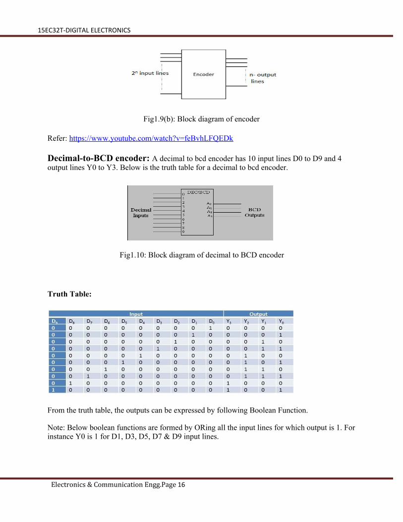
Decimal-to-BCD encoder: A decimal to bcd encoder has 10 input lines D0 to D9 and 4 output lines Y0 to Y3. Below is the truth table for a decimal to bcd encoder.
Fig1.10: Block diagram of decimal to BCD encoder
Truth Table:
From the truth table, the outputs can be expressed by following Boolean Function.
Note: Below boolean functions are formed by ORing all the input lines for which output is 1. For instance Y0 is 1 for D1, D3, D5, D7 & D9 input lines.
Electronics & Communication Engg.Page 16
15EC32T-DIGITAL ELECTRONICS
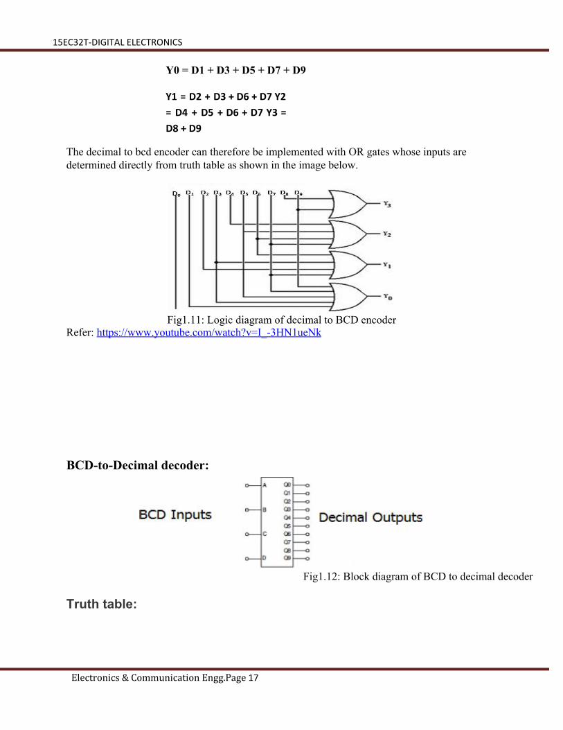
Y0 = D1 + D3 + D5 + D7 + D9
Y1 = D2 + D3 + D6 + D7 Y2
= D4 + D5 + D6 + D7 Y3 =
D8 + D9
The decimal to bcd encoder can therefore be implemented with OR gates whose inputs are determined directly from truth table as shown in the image below.
Fig1.11: Logic diagram of decimal to BCD encoder Refer: https://www.youtube.com/watch?v=I_-3HN1ueNk
BCD-to-Decimal decoder:
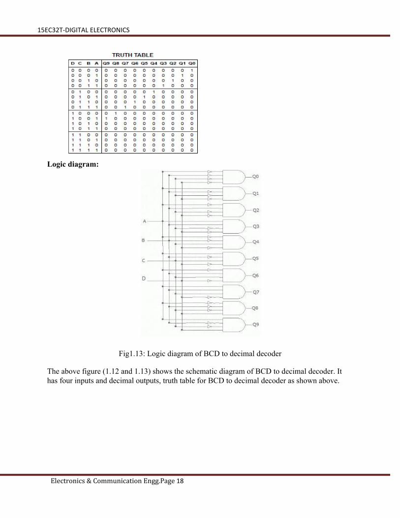
Truth table:
Fig1.12: Block diagram of BCD to decimal decoder
Electronics & Communication Engg.Page 17
15EC32T-DIGITAL ELECTRONICS
Logic diagram:
Fig1.13: Logic diagram of BCD to decimal decoder
The above figure (1.12 and 1.13) shows the schematic diagram of BCD to decimal decoder. It has four inputs and decimal outputs, truth table for BCD to decimal decoder as shown above.
Electronics & Communication Engg.Page 18
15EC32T-DIGITAL ELECTRONICS
Identification of different decoder and encoder ICs:
BCD to 7-segment decoder: 7-segment LED (Light Emitting Diode) or LCD (Liquid Crystal Display) type displays, provide a very convenient way of displaying information or digital data in the form of numbers, letters or even alpha-numerical characters.
Typically 7-segment displays consist of seven individual colored L ’ (called the segments), within one single display package. In order to produce the required numbers from 0 to 9 on the display the correct combination of LED segments need to be illuminated.
A standard 7-segment display generally has 8 input connections, one for each segment and one that acts as a common terminal. some single displays have also have an additional input pin to display a decimal point in their lower right or left hand corner.
In electronics there are two important types of 7-segment LED digital display.
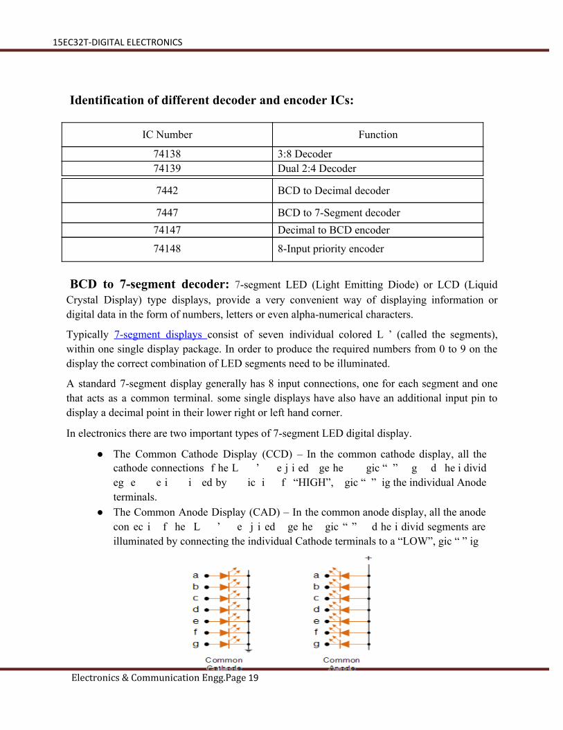
● The Common Cathode Display (CCD) – In the common cathode display, all the cathode connections f he L ’ e j i ed ge he gic “ ” g d he i divid eg e e i i ed by ic i f “HIGH”, gic “ ” ig the individual Anode terminals.
● The Common Anode Display (CAD) – In the common anode display, all the anode con ec i f he L ’ e j i ed ge he gic “ ” d he i divid segments are illuminated by connecting the individual Cathode terminals to a “LOW”, gic “ ” ig
Electronics & Communication Engg.Page 19
IC Number Function
74138 3:8 Decoder 74139 Dual 2:4 Decoder
7442 BCD to Decimal decoder
7447 BCD to 7-Segment decoder 74147 Decimal to BCD encoder
74148 8-Input priority encoder

15EC32T-DIGITAL ELECTRONICS
Fig 1.14: Common cathode and common anode
The above figure 1.14 shows the electrical connection of the individual diodes for a common cathode display and a common anode display and by illuminating each light emitting diode individually, they can be made to display a variety of numbers or characters.
7-Segment Display Format:
Fig1.15: Seven segment display format
Truth table:
From the above truth table using K-map simplified expression for each segment is given below.
b c
d e
f
g
Electronics & Communication Engg.Page 20

15EC32T-DIGITAL ELECTRONICS
Logic Diagram:
Fig 1.16: Logic diagram
Refer: https://www.youtube.com/watch?v=HHQFI8R1iZc https://www.youtube.com/watch?v=smeUN1Bxj3M
4- bit priority encoder: A priority encoder is a circuit or algorithm that compresses
multiple binary inputs into a smaller number of outputs. The output of a priority encoder is the binary representation of the ordinal number starting from zero of the most significant input bit. They are often used to control interrupt requests by acting on the highest priority request. It includes priority function. If 2 or more inputs are equal to 1 at the same time, the input having the highest priority will take precedence.
Electronics & Communication Engg.Page 21
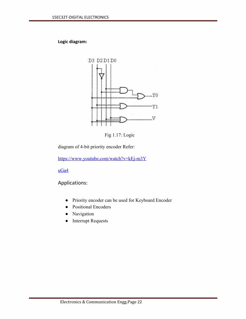
15EC32T-DIGITAL ELECTRONICS
Logic diagram:
Fig 1.17: Logic
diagram of 4-bit priority encoder Refer:
https://www.youtube.com/watch?v=kEj-m3Y
uGa4
Applications:
● Priority encoder can be used for Keyboard Encoder ● Positional Encoders ● Navigation ● Interrupt Requests
Electronics & Communication Engg.Page 22