DIGITAL ELECTRONICS (WLE-102) UNIT-IV
32
DIGITAL ELECTRONICS (WLE-102) UNIT-IV: SEQUENTIAL LOGIC CIRCUITS
-
Upload
khangminh22 -
Category
Documents
-
view
0 -
download
0
Transcript of DIGITAL ELECTRONICS (WLE-102) UNIT-IV

DIGITAL ELECTRONICS (WLE-102)
UNIT-IV: SEQUENTIAL LOGIC CIRCUITS

Periods / Week = 04 Total No. of Periods Reqd. = 45 Assignment + Mid Sem. = 15+25
End Sem Exam
Marks = 60 Total Marks = 100 Duration of End Sem Exam = 2.5 Hrs
WLE-102: Digital Electronics
I NUMBER SYSTEMS & CODES
Number systems and their conversion, Signed numbers, 1’s and 2’s complements of binary numbers. Binary
Arithmetic: Addition, Subtraction, 1’s Complement Subtraction, 2’s Complement Subtraction,
Multiplication, Division, Binary Coded Decimal (BCD), 8421 Code, Digital Codes: Gray Code, Excess-3
Code & their conversion to Binary & vice versa, Alpha-Numeric Codes - ASCII code.
II BOOLEAN ALGEBRA AND COMBINATIONAL LOGIC
Rules & Laws of Boolean Algebra, Boolean addition & Subtraction, Logic Expressions, Demorgan’s law,
Simplification of Boolean Expressions, Karnaugh Map (up to 4-variables), SOP and POS form, NOT
(Inverter), AND, OR, NAND and NOR Gates, Universal Property of NAND and NOR Gates, NAND and
NOR implementation, EXOR and EXNOR gates.
III COMBINATIONAL LOGIC CIRCUITS
Design of combinational circuits, Half Adder and Full Adder & their realization using combination of AND,
OR, Exclusive - OR and NAND gates, Half and full subtractors, Magnitude comparators, Decoders and
Encoders, Multiplexers and Demultiplexers, Parity Generators/Checkers.
IV SEQUENTIAL LOGIC CIRCUITS
Introduction, Flip Flops: RS, clocked RS, D, JK and T flip flops, Triggering of flip flops, Design of simple
sequential circuits.
BOOKS RECOMMENDED:
•Digital Fundamentals by Thomas L. Floyd
•Digital Logic & Computer Design by M. Morris Mano
Digital Computer Fundamentals by BARTEE T.

Floyd, Digital Fundamentals, 10th ed Slide 3
A latch is a temporary storage device that has two stable
states (bistable). It is a basic form of memory.
Summary
Latches
The S-R (Set-Reset) latch is the most basic type. It can be constructed
from NOR gates or NAND gates. With NOR gates, the latch responds
to active-HIGH inputs; with NAND gates, it responds to active-LOW
inputs.
NOR Active-HIGH Latch NAND Active-LOW Latch
R
S
Q Q
Q
S
R Q
Floyd, Digital Fundamentals, 10th ed Slide 4
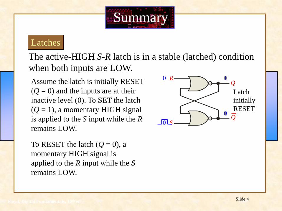
The active-HIGH S-R latch is in a stable (latched) condition
when both inputs are LOW.
Summary
Latches
R
S
Q
Q
Assume the latch is initially RESET
(Q = 0) and the inputs are at their
inactive level (0). To SET the latch
(Q = 1), a momentary HIGH signal
is applied to the S input while the R
remains LOW.
0 1
0
R
S
Q
Q
1
0
0
To RESET the latch (Q = 0), a
momentary HIGH signal is
applied to the R input while the S
remains LOW.
0
0
1
0 1
0
Latch
initially
RESET
Latch
initially
SET

Floyd, Digital Fundamentals, 10th ed Slide 5
S
R
The active-LOW S-R latch is in a stable (latched) condition
when both inputs are HIGH.
Summary
Latches
Q
Q
1 1
0 1
0
1
Latch
initially
RESET
Q
Q
1
1
0 1
0
1
Latch
initially
SET
S
R
Assume the latch is initially RESET
(Q = 0) and the inputs are at their
inactive level (1). To SET the latch
(Q = 1), a momentary LOW signal
is applied to the S input while the R
remains HIGH.
To RESET the latch a momentary
LOW is applied to the R input
while S is HIGH.
Never apply an active set and
reset at the same time (invalid).

Floyd, Digital Fundamentals, 10th ed Slide 6
The active-LOW S-R latch is available as the 74LS279A IC.
Summary
Latches
(5)
1S1(2)
(1)
(6)
1R
2S
2R
1S2(4)
(9)
(13)
(7)
(3)
(14)
3S1(11)
(10)
(15)
3R
4S
4R
3S2(12)
1Q
2Q
3Q
4Q
74LS279A
It features four internal latches with
two having two S inputs. To SET any
of the latches, the S line is pulsed low.
It is available in several packages.
1
2
Position
1 to 2
Position
2 to 1
S
R
Q
VCC
S-R latches are frequently used for
switch debounce circuits as shown:
S
R

Floyd, Digital Fundamentals, 10th ed Slide 7
A gated latch is a variation on the basic latch.
Summary
Latches
The gated latch has an additional
input, called enable (EN) that must
be HIGH in order for the latch to
respond to the S and R inputs.
R
S Q
Q
EN
Show the Q output with
relation to the input signals.
Assume Q starts LOW.
Keep in mind that S and R are only active when EN is HIGH.
S
R
EN
Q

Floyd, Digital Fundamentals, 10th ed Slide 8
Summary
Latches
The D latch is an variation of the S-R latch but combines
the S and R inputs into a single D input as shown:
A simple rule for the D latch is:
Q follows D when the Enable is active.
D
EN
Q
Q Q
Q D
EN
Floyd, Digital Fundamentals, 10th ed Slide 9
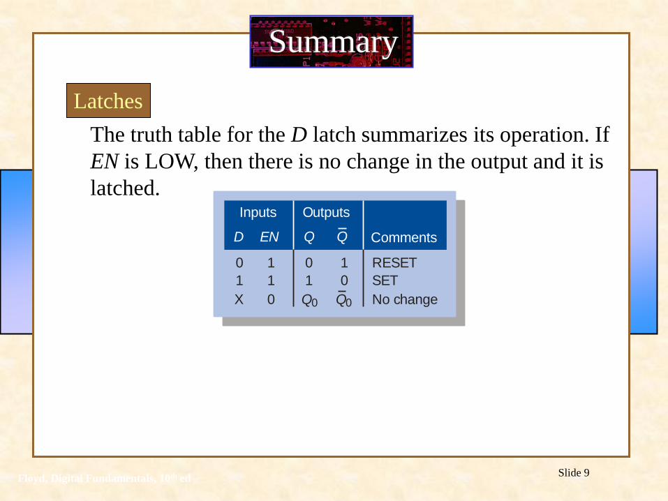
Summary
Latches
The truth table for the D latch summarizes its operation. If
EN is LOW, then there is no change in the output and it is
latched. Inputs
Comments
0
1
X
END
1
1
0
Outputs
0
1
Q0
1
0
Q0
RESET
SET
No change
Floyd, Digital Fundamentals, 10th ed Slide 10
Summary
Latches
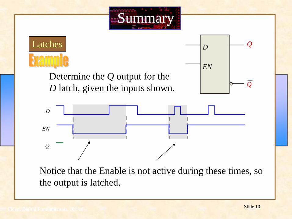
Determine the Q output for the
D latch, given the inputs shown.
EN
Q
D
Notice that the Enable is not active during these times, so
the output is latched.
Q
Q D
EN

Floyd, Digital Fundamentals, 10th ed Slide 11
Summary
Flip-flops
A flip-flop differs from a latch in the manner it changes
states. A flip-flop is a clocked device, in which only the
clock edge determines when a new bit is entered.
The active edge can be positive or negative.
D Q
C
Q
(a) Positive edge-triggered
D Q
C
Q
(b) Negative edge-triggered
Dynamic
input
indicator

Floyd, Digital Fundamentals, 10th ed Slide 12
Summary
Flip-flops
The truth table for a positive-edge triggered D flip-flop
shows an up arrow to remind you that it is sensitive to its
D input only on the rising edge of the clock; otherwise it is
latched. The truth table for a negative-edge triggered D
flip-flop is identical except for the direction of the arrow.
Inputs
Comments
1
CLKD
Outputs
1
0 SET
0 0 1 RESET
Inputs
Comments
1
CLKD
Outputs
1
0 SET
0 0 1 RESET
(a) Positive-edge triggered (b) Negative-edge triggered
Floyd, Digital Fundamentals, 10th ed Slide 13
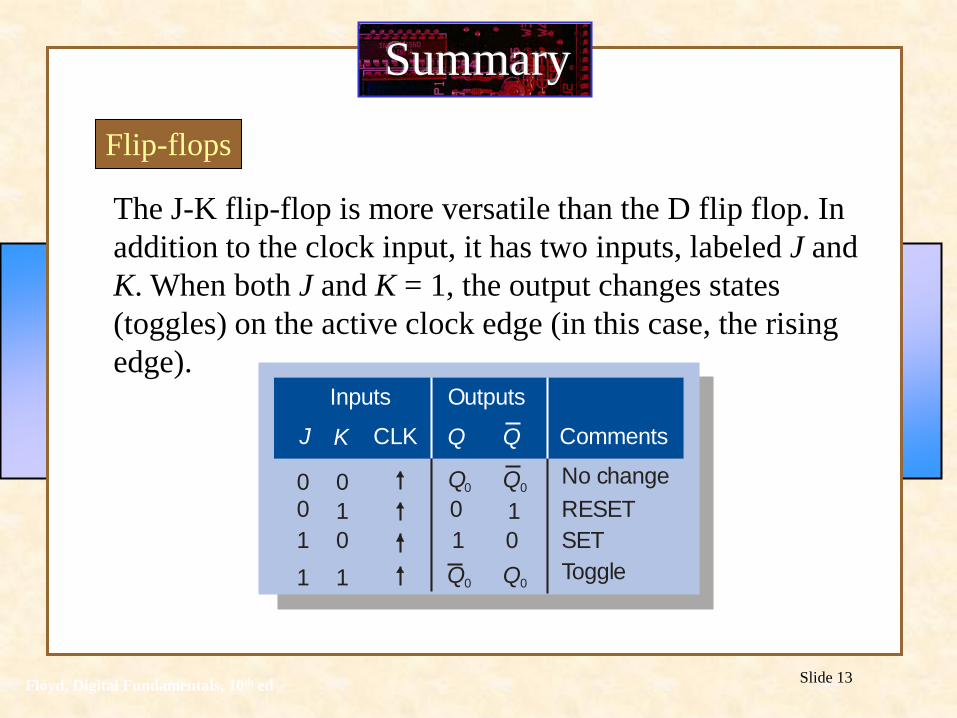
Summary
Flip-flops
The J-K flip-flop is more versatile than the D flip flop. In
addition to the clock input, it has two inputs, labeled J and
K. When both J and K = 1, the output changes states
(toggles) on the active clock edge (in this case, the rising
edge). Inputs
Comments
1
1 1
1
CLKKJ
Outputs
1
Q0
Q0
Q0
Q0
0 SET
Toggle
0
0
00 0 1 RESET
No change

Floyd, Digital Fundamentals, 10th ed Slide 14
Summary
Flip-flops
Determine the Q output for the J-K
flip-flop, given the inputs shown.
CLK
Q
K
J
CLK
K
J
Q
Q
Notice that the outputs change on the leading edge of the clock.
Set Toggle Set Latch

Floyd, Digital Fundamentals, 10th ed Slide 15
Summary
Flip-flops
CLK
D
CLK
Q
Q
A D-flip-flop does not have a toggle mode like the J-K flip-
flop, but you can hardwire a toggle mode by connecting Q
back to D as shown. This is useful in some counters as you
will see in Chapter 8.
For example, if Q is LOW, Q is
HIGH and the flip-flop will toggle
on the next clock edge. Because the
flip-flop only changes on the active
edge, the output will only change
once for each clock pulse. D flip-flop hardwired for
a toggle mode

Floyd, Digital Fundamentals, 10th ed Slide 16
Summary
Flip-flops
Synchronous inputs are transferred in the triggering edge
of the clock (for example the D or J-K inputs). Most flip-
flops have other inputs that are asynchronous, meaning
they affect the output independent of the clock.
Two such inputs are normally labeled
preset (PRE) and clear (CLR). These
inputs are usually active LOW. A J-K
flip flop with active LOW preset and
CLR is shown. CLK
K
J
Q
Q
PRE
CLR

Floyd, Digital Fundamentals, 10th ed Slide 17
Summary
Flip-flops Flip-flops
Determine the Q output for the J-K
flip-flop, given the inputs shown.
CLK
K
J
Q
Q
PRE
CLR
Set Toggle Reset Toggle
Set
Set
Reset
Latch
CLK
K
J
Q
PRE
CLR

Floyd, Digital Fundamentals, 10th ed Slide 18
Propagation delay time is specified for the rising and
falling outputs. It is measured between the 50% level of the
clock to the 50% level of the output transition.
Summary
Flip-flop Characteristics
50% point on triggering edge
50% point
50% point on LOW-to-
HIGH transition of Q
tPLH tPHL
CLK CLK
Q Q 50% point on HIGH-to-
LOW transition of Q
The typical propagation delay time for the 74AHC family (CMOS) is
4 ns. Even faster logic is available for specialized applications.

Floyd, Digital Fundamentals, 10th ed Slide 19
Another propagation delay time specification is the time
required for an asynchronous input to cause a change in the
output. Again it is measured from the 50% levels. The
74AHC family has specified delay times under 5 ns.
Summary
Flip-flop Characteristics
50% point
tPLH tPHL
Q 50% point 50% point
50% point
Q
PRE CLR
Floyd, Digital Fundamentals, 10th ed Slide 20
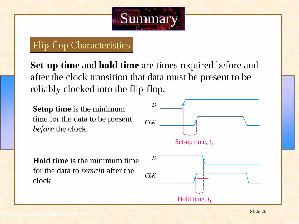
Set-up time and hold time are times required before and
after the clock transition that data must be present to be
reliably clocked into the flip-flop.
Summary
Flip-flop Characteristics
Setup time is the minimum
time for the data to be present
before the clock.
Hold time is the minimum time
for the data to remain after the
clock.
CLK
D
CLK
D
Set-up time, ts
Hold time, tH

Floyd, Digital Fundamentals, 10th ed Slide 21
Summary
Flip-flop Applications
Principal flip-flop applications are for
temporary data storage, as frequency
dividers, and in counters (which are
covered in detail in Chapter 8).
Typically, for data storage applications,
a group of flip-flops are connected to
parallel data lines and clocked together.
Data is stored until the next clock pulse.
D
C
R
D
C
R
D
C
R
D
C
R
Parallel data
input lines
Clock
Clear
Output
lines
Q0
Q1
Q2
Q3

Floyd, Digital Fundamentals, 10th ed Slide 22
Summary
Flip-flop Applications
For frequency division, it is simple to use a flip-flop in
the toggle mode or to chain a series of toggle flip flops to
continue to divide by two.
One flip-flop will divide fin
by 2, two flip-flops will
divide fin by 4 (and so on).
A side benefit of frequency
division is that the output
has an exact 50% duty
cycle.
HIGH HIGH
CLK
K
J QA
CLK
K
J
fin
QB fout
Waveforms:
fin
fout

Selected Key Terms
Latch
Bistable
Clock
D flip-flop
J-K flip-flop
A bistable digital circuit used for storing a bit.
Having two stable states. Latches and flip-flops are
bistable multivibrators.
A triggering input of a flip-flop.
A type of bistable multivibrator in which the output
assumes the state of the D input on the triggering
edge of a clock pulse.
A type of flip-flop that can operate in the SET,
RESET, no-change, and toggle modes.

Selected Key Terms
Propagation
delay time
Set-up time
Hold time
Timer
The interval of time required after an input signal
has been applied for the resulting output signal to
change.
The time interval required for the input levels to be
on a digital circuit.
The time interval required for the input levels to
remain steady to a flip-flop after the triggering
edge in order to reliably activate the device.
A circuit that can be used as a one-shot or as an
oscillator.

Floyd, Digital Fundamentals, 10th ed Slide 25
Propagation delay time is specified for the rising and
falling outputs. It is measured between the 50% level of the
clock to the 50% level of the output transition.
Summary
Flip-flop Characteristics
50% point on triggering edge
50% point
50% point on LOW-to-
HIGH transition of Q
tPLH tPHL
CLK CLK
Q Q 50% point on HIGH-to-
LOW transition of Q
The typical propagation delay time for the 74AHC family (CMOS) is
4 ns. Even faster logic is available for specialized applications.

Floyd, Digital Fundamentals, 10th ed Slide 26
Another propagation delay time specification is the time
required for an asynchronous input to cause a change in the
output. Again it is measured from the 50% levels. The
74AHC family has specified delay times under 5 ns.
Summary
Flip-flop Characteristics
50% point
tPLH tPLH
Q 50% point 50% point
50% point
Q
PRE CLR

Floyd, Digital Fundamentals, 10th ed Slide 27
Set-up time and hold time are times required before and
after the clock transition that data must be present to be
reliably clocked into the flip-flop.
Summary
Flip-flop Characteristics
Setup time is the minimum
time for the data to be present
before the clock.
Hold time is the minimum time
for the data to remain after the
clock.
CLK
D
CLK
D
Set-up time, ts
Hold time, tH

Floyd, Digital Fundamentals, 10th ed Slide 28
Other specifications include maximum clock frequency,
minimum pulse widths for various inputs, and power
dissipation. The power dissipation is the product of the
supply voltage and the average current required.
Summary
Flip-flop Characteristics
A useful comparison between logic families is the speed-power product
which uses two of the specifications discussed: the average propagation
delay and the average power dissipation. The unit is energy.
What is the speed-power product for 74AHC74A? Use
the data from Table 7-5 to determine the answer.
From Table 7-5, the average propagation delay is 4.6 ns.
The quiescent power dissipated is 1.1 mW. Therefore, the
speed-power product is 5 pJ

Floyd, Digital Fundamentals, 10th ed Slide 29
Summary
Flip-flop Applications
Principal flip-flop applications are for
temporary data storage, as frequency
dividers, and in counters (which are
covered in detail in Chapter 8).
Typically, for data storage applications,
a group of flip-flops are connected to
parallel data lines and clocked together.
Data is stored until the next clock pulse.
D
C
R
D
C
R
D
C
R
D
C
R
Parallel data
input lines
Clock
Clear
Output
lines
Q0
Q1
Q2
Q3

Floyd, Digital Fundamentals, 10th ed Slide 30
Summary
Flip-flop Applications
For frequency division, it is simple to use a flip-flop in
the toggle mode or to chain a series of toggle flip flops to
continue to divide by two.
One flip-flop will divide fin
by 2, two flip-flops will
divide fin by 4 (and so on).
A side benefit of frequency
division is that the output
has an exact 50% duty
cycle.
HIGH HIGH
CLK
K
J QA
CLK
K
J
fin
QB fout
Waveforms:
fin
fout

Selected Key Terms
Latch
Bistable
Clock
D flip-flop
J-K flip-flop
A bistable digital circuit used for storing a bit.
Having two stable states. Latches and flip-flops are
bistable multivibrators.
A triggering input of a flip-flop.
A type of bistable multivibrator in which the output
assumes the state of the D input on the triggering
edge of a clock pulse.
A type of flip-flop that can operate in the SET,
RESET, no-change, and toggle modes.

Selected Key Terms
Propagation
delay time
Set-up time
Hold time
Timer
The interval of time required after an input signal
has been applied for the resulting output signal to
change.
The time interval required for the input levels to be
on a digital circuit.
The time interval required for the input levels to
remain steady to a flip-flop after the triggering
edge in order to reliably activate the device.
A circuit that can be used as a one-shot or as an
oscillator.