jagatpur ashram unoshotturpara, raojan, chittagong, bangladesh
Upload
khangminh22Category
view
0download
0
For ALLAHABAD STATE UNIVERSITY Students
Digital
Electronics
BCA– IInd Sem
Prepared By
Mr. SUSHANT SRIVASTAVA
(Assistant Professor) Kulbhaskar Ashram Post Graduate College, Allahabad

2
BCA IInd Sem, Course Code - BCA-S109 (Digital Electronics),
Prepared By : SUSHANT SRIVASTAVA (Assistant Professor), Kulbhashkar Ashram PG College
Contents UNIT-I
Logic gates and circuit Gates (OR, AND, NOR, NAND, XOR & XNOR); Demogran’s laws; Boolean laws, Circuit designing techniques (SOP, POS, K-Map).
UNIT 1
Q1: What is Logic Gates? Explain types of gates (OR, AND, NOR,
NAND, XOR & XNOR)? Answer:
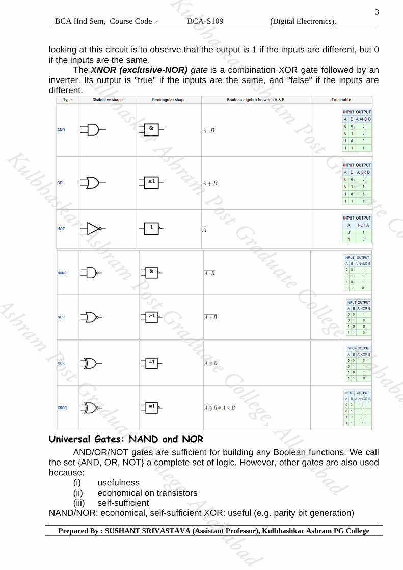
A logic gate is an idealized or physical device implementing a Boolean function, that is, it performs a logical operation on one or more logical inputs, and produces a single logical output. Depending on the context, the term may refer to an ideal logic gate, it has two state 0 or 1, all gates perform on this input and generate result according to input.
Logic gates A logic gate is an elementary building block of a digital circuit. Most logic gates
have two inputs and one output. At any given moment, every terminal is in one of the two binary conditions low (0) or high (1), represented by different voltage levels. The logic state of a terminal can, and generally does, change often, as the circuit processes data. In most logic gates, the low state is approximately zero volts (0 V), while the high state is approximately five volts positive (+5 V).
There are seven basic logic gates: AND, OR, NOT, NAND, NOR, XOR and XNOR. The AND gate is so named because, if 0 is called "false" and 1 is called "true," the gate acts in the same way as the logical "and" operator. The following illustration and table show the circuit symbol and logic combinations for an AND gate. (In the symbol, the input terminals are at left and the output terminal is at right.) The output is "true" when both inputs are "true." Otherwise, the output is "false."
The OR gate gets its name from the fact that it behaves after the fashion of the logical inclusive "or." The output is "true" if either or both of the inputs are "true." If both inputs are "false," then the output is "false." A logical inverter , sometimes called a NOT gate to differentiate it from other types of electronic inverter devices, has only one input. It reverses the logic state.
The NAND gate operates as an AND gate followed by a NOT gate. It acts in the manner of the logical operation "and" followed by negation. The output is "false" if both inputs are "true." Otherwise, the output is "true."
The NOR gate is a combination OR gate followed by an inverter. Its output is "true" if both inputs are "false." Otherwise, the output is "false."
The XOR ( exclusive-OR ) gate acts in the same way as the logical "either/or." The output is "true" if either, but not both, of the inputs are "true." The output is "false" if both inputs are "false" or if both inputs are "true." Another way of
3
BCA IInd Sem, Course Code - BCA-S109 (Digital Electronics),
Prepared By : SUSHANT SRIVASTAVA (Assistant Professor), Kulbhashkar Ashram PG College
looking at this circuit is to observe that the output is 1 if the inputs are different, but 0 if the inputs are the same.
The XNOR (exclusive-NOR) gate is a combination XOR gate followed by an inverter. Its output is "true" if the inputs are the same, and "false" if the inputs are different.
Universal Gates: NAND and NOR
AND/OR/NOT gates are sufficient for building any Boolean functions. We call the set {AND, OR, NOT} a complete set of logic. However, other gates are also used because:
(i) usefulness (ii) economical on transistors (iii) self-sufficient
NAND/NOR: economical, self-sufficient XOR: useful (e.g. parity bit generation)

4
BCA IInd Sem, Course Code - BCA-S109 (Digital Electronics),
Prepared By : SUSHANT SRIVASTAVA (Assistant Professor), Kulbhashkar Ashram PG College
Boolean algebra
The term "Boolean algebra" honors George Boole (1815–1864), a self-educated English mathematician. He introduced the algebraic system initially in a small pamphlet, The Mathematical Analysis of Logic, published in 1847 in response to an ongoing public controversy between Augustus De Morgan and William Hamilton, and later as a more substantial book, The Laws of Thought, published in 1854. Boole's formulation differs from that described above in some important respects. For example, conjunction and disjunction in Boole were not a dual pair of operations. Boolean algebra emerged in the 1860s, in papers written by William Jevons and Charles Sanders Peirce. The first systematic presentation of Boolean algebra and distributive lattices is owed to the 1890 Vorlesungen of Ernst Schröder Boolean Function A Boolean function defined as an algebraic expression formed with the binary variables, the logic operation symbols, parenthesis and equal to sign. Ex. F = A.B+C A Boolean function can be broken into logic diagram, and vice versa. Logic Gates Logic gate is an electronic circuit, which produces a typical output signal depending on its input signal. The output signal of a gate is a simple Boolean operation of its input signal. Gates are the basic logic elements. Any Boolean function can be represented in the form of gates. In general we can represent gates in three ways. These are:
• Graphic symbols
• Algebraic notation
• Truth table AND : Anyone input is zero then output is always zero.
OR : Anyone input is one then output is always one.
NOT : Output is always reverse of input
NAND : Anyone input is zero then output is always one
NOR : Anyone input is one then output is always zero
XOR : If both input are same then output is zero.
Q2: Explain Demogran’s laws; Boolean laws, Circuit designing techniques (SOP, POS, K-Map). Answer:
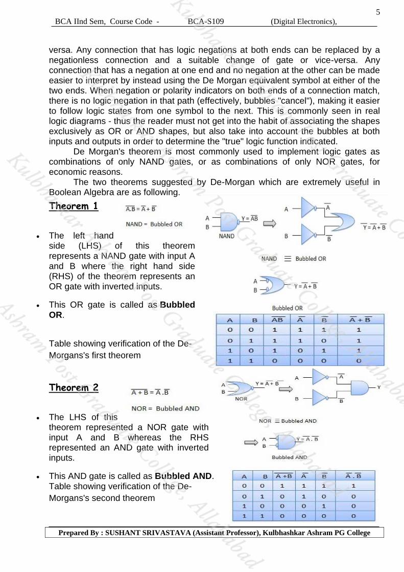
De-Morgan’s theorem
By use of De Morgan's theorem, an AND function is identical to an OR function with negated inputs and outputs. Likewise, an OR function is identical to an AND function with negated inputs and outputs. A NAND gate is equivalent to a OR gate with negated inputs, and a NOR gate is equivalent to a AND gate with negated inputs.
This leads to an alternative set of symbols for basic gates that use the opposite core symbol (AND or OR) but with the inputs and outputs negated. Use of these alternative symbols can make logic circuit diagrams much clearer and help to show accidental connection of an active high output to an active low input or vice-
5
BCA IInd Sem, Course Code - BCA-S109 (Digital Electronics),
Prepared By : SUSHANT SRIVASTAVA (Assistant Professor), Kulbhashkar Ashram PG College
versa. Any connection that has logic negations at both ends can be replaced by a negationless connection and a suitable change of gate or vice-versa. Any connection that has a negation at one end and no negation at the other can be made easier to interpret by instead using the De Morgan equivalent symbol at either of the two ends. When negation or polarity indicators on both ends of a connection match, there is no logic negation in that path (effectively, bubbles "cancel"), making it easier to follow logic states from one symbol to the next. This is commonly seen in real logic diagrams - thus the reader must not get into the habit of associating the shapes exclusively as OR or AND shapes, but also take into account the bubbles at both inputs and outputs in order to determine the "true" logic function indicated.
De Morgan's theorem is most commonly used to implement logic gates as combinations of only NAND gates, or as combinations of only NOR gates, for economic reasons.
The two theorems suggested by De-Morgan which are extremely useful in Boolean Algebra are as following.
Theorem 1
• The left hand side (LHS) of this theorem represents a NAND gate with input A and B where the right hand side (RHS) of the theorem represents an OR gate with inverted inputs.
• This OR gate is called as Bubbled OR.
Table showing verification of the De-
Morgans's first theorem
Theorem 2
• The LHS of this theorem represented a NOR gate with input A and B whereas the RHS represented an AND gate with inverted inputs.
• This AND gate is called as Bubbled AND. Table showing verification of the De-
Morgans's second theorem

6
BCA IInd Sem, Course Code - BCA-S109 (Digital Electronics),
Prepared By : SUSHANT SRIVASTAVA (Assistant Professor), Kulbhashkar Ashram PG College
Formal Proof of DeMorgan's Theorems
DeMorgan's Theorems:
a. (A + B) = A* B
b. A*B = A + B
Note: * = AND operation
Proof of DeMorgan's Theorem (b):
For any theorem X=Y, if we can show that X Y = 0, and that X + Y = 1, then
by the complement postulates, A A = 0 and A + A = 1,
X = Y. By the uniqueness of the complement, X = Y.
Thus the proof consists of showing that (A*B)*( A + B) = 0; and also that (A*B) + ( A + B) = 1.
Prove: (A*B)*( A + B) = 0
(A*B)*( A + B) = (A*B)*A + (A*B)*B) by distributive postulate = (A*A)*B + A*(B*B) by associativity postulate = 0*B + A*0 by complement postulate = 0 + 0 by nullity theorem = 0 by identity theorem (A*B)*( A + B) = 0 Q.E.D.
Prove: (A*B) + ( A + B) =1
(A*B) + ( A + B) =(A + A + B))*(B + A + B) by distributivity B*C + A = (B + A)*(C + A) (A*B) + ( A + B) =(A + A + B))*(B + B + A) by associativity postulate =(1 + B)*(1 + A) by complement postulate =1*1 by nullity theorem =1 by identity theorem (A*B) + ( A + B) =1 Q.E.D.
Since (A*B)*( A + B) = 0, and (A*B) + ( A + B) =1,
A*B is the complement of A + B, meaning that A*B=(A + B)';
(note that ' = complement or NOT - double bars don't show in HTML)
Thus A*B= (A + B)''.
The involution theorem states that A'' = A. Thus by the involution theorem, (A + B)'' = A + B.
This proves DeMorgan's Theorem (b).
DeMorgan's Theorem (a) may be proven using a similar approach.

7
BCA IInd Sem, Course Code - BCA-S109 (Digital Electronics),
Prepared By : SUSHANT SRIVASTAVA (Assistant Professor), Kulbhashkar Ashram PG College
SOP & POS forms Minterms are called products because they are the logical AND of a set of
variables, and maxterms are called sums because they are the logical OR of a set
of variables. These concepts are dual because of their complementary-symmetry
relationship as expressed by De Morgan's laws.
Two dual canonical forms of any Boolean function are a "sum of minterms" and a "product of maxterms." The term "Sum of Products" or "SoP" is widely used for the canonical form that is a disjunction (OR) of minterms. Its De Morgan dual is a "Product of Sums" or "PoS" for the canonical form that is a conjunction (AND) of maxterms. These forms allow for greater analysis into the simplification of these functions, which is of great importance in the minimization or other optimization of Boolean formulas in general and digital circuits in particular.
Sum of Product (minterm) and Product of sum (Maxterm)
minterm Maxterm
Variable Term designation Term designation
X Y Z 0 0 0 X Y Z m0 X+Y+Z M0
0 0 1 X Y Z m1 X+Y+Z M1
0 1 0 X Y Z m2 X+Y+Z M2
0 1 1 X Y Z m3 X+Y+Z M3
1 0 0 X Y Z m4 X+Y+Z M4
1 0 1 X Y Z m5 X+Y+Z M5
1 1 0 X Y Z m6 X+Y+Z M6
1 1 1 X Y Z m7 X+Y+Z M7
Circuit Simplification Technique The simplification of circuit is very useful for combinational circuit design the following three methods are used.
1. Algebraic simplification 2. Karnaugh Maps 3. Quine Mc Cluskey Methods
Karnaugh Maps Karnaugh map is a convenient way of representing and simplification Boolean
function of 4 to 6 variables. Karnaugh map can be used to construct a circuit when input and output to that proposed circuit are defined.
The Karnaugh map, also known as a Veitch diagram (K-map or KV-map for
short), is a tool to facilitate management of Boolean algebraic expressions. A Karnaugh map is unique in that only one variable changes value between squares; in other words, the rows and columns are ordered according to the principles of
Gray code. A Karnaugh map may have any number of variables, If variable is 1 then no. of box is 21=2

8
BCA IInd Sem, Course Code - BCA-S109 (Digital Electronics),
Prepared By : SUSHANT SRIVASTAVA (Assistant Professor), Kulbhashkar Ashram PG College
If variable is 2 then no. of box is 22=4 If variable is 3 then no. of box is 23=8 The stepwise procedure for Karnaugh maps is to create a simple map depending
on the number of variables in the function show the map of 2,3,4 variable. A map of 2 variable contains 4 value position or element, while for 3 variable it has 23 = 8 elements similarly for 4 variable it is 24 = 16 element and so on. Special care is taken to represent variables in the map. Value of only 1 variable changes into adjacent columns and rows.
Each square in a Karnaugh map corresponds to a minterm (and maxterm). Often it is desired to simplify a Boolean function. A quick graphical approach is
to use Karnaugh maps.
This ordering allows for grouping of minterms/maxterms for simplification. Implicant Bubble covering only 1s (size of bubble must be a power of 2). Prime implicant Bubble that is expanded as big as possible (but increases in size by powers of 2). Essential prime implicant Bubble that contains a 1 covered only by itself and no other prime implicant bubble. Non-essential prime implicant A 1 that can be bubbled by more then one prime implicant bubble. Procedure for finding the SOP from a Karnaugh map • Step 1:
Form the 2-, 3-, or 4-variable Karnaugh map as appropriate for the Boolean function.
• Step 2: Identify all essential prime implicants for 1s in the Karnaugh map
• Step 3:

9
BCA IInd Sem, Course Code - BCA-S109 (Digital Electronics),
Prepared By : SUSHANT SRIVASTAVA (Assistant Professor), Kulbhashkar Ashram PG College
Identify non-essential prime implicants for 1s in the Karnaugh map. • Step 4:
For each essential and one selected non-essential prime implicant from each set, determine the corresponding product term.
• Step 5: Form a sum-of-products with all product terms from previous step.
Standard forms
a. A product term is a term with ANDed literals*. Thus, AB, A’B, A’CD are all product terms.
b. A minterm is a special case of a product term where all input variables appear in the product term either in the true or complement form.
c. A sum term is a term with ORed literals*. Thus, (A+B), (A’+B), (A’+C+D) are all sum terms.
d. A maxterm is a special case of a sum term where all input variables, either in the true or complement form, are ORed together.
e. Boolean functions can generally be expressed in the form of a Sum of Products (SOP) or in the form of a Product of Sums (POS).
f. The sum of minterms form is a special case of the SOP form where all product terms are minterms.
g. The product of maxterms form is a special case of the POS form where all sum terms are maxterms.
h. The SOP and POS forms are Standard forms for representing Boolean functions.
POS and SOP notations
• Boolean expressions can be manipulated into many forms.
• Some standardized forms are required for Boolean expressions to simplify communication of the expressions.
• The following table gives the minterms for a three-input system
• Sum-of-minterms standard form expresses the Boolean or switching expression in the form of a sum of products using minterms.
• For instance, the following Boolean expression using minterms

10
BCA IInd Sem, Course Code - BCA-S109 (Digital Electronics),
Prepared By : SUSHANT SRIVASTAVA (Assistant Professor), Kulbhashkar Ashram PG College
• The following table gives the maxterms for a three-input system
• Product-of-maxterms standard form expresses the Boolean or switching expression in the form of product of sums using maxterms.
• For instance, the following Boolean expression using maxterms
Simplification of Boolean expression

11
BCA IInd Sem, Course Code - BCA-S109 (Digital Electronics),
Prepared By : SUSHANT SRIVASTAVA (Assistant Professor), Kulbhashkar Ashram PG College
Quine Mc Cluskey Methods
For better understanding of this procedure. What will happen if we have more than 4-6 variables? As the number of the variable increases karnough map becomes more and more cumbersome as the number of possible combination of inputs on increasing. A method was suggested to deal with the increasing number of variables. This is a tabular approach and is know as Quine Mc Cluskey method. This method is suitable for programming and hence provides a tool for automating design in the form of minimized Boolean expressions.
Model Question
• Explain Universal gate with diagram
• De-Morgan theorem
• Given that F (a, b, c, d) = Σ(0, 1, 2, 4, 5, 7), derive the product of maxterms expression of F and the 2 standard form expressions of F`

12
BCA IInd Sem, Course Code - BCA-S109 (Digital Electronics),
Prepared By : SUSHANT SRIVASTAVA (Assistant Professor), Kulbhashkar Ashram PG College
BOOLEAN ALGEBRA SUMMARY
Operations with 0 and 1:
1. X + 0 = X 1D. X • 1 = X
2. X + 1 = 1 2D. X • 0 = 0
Idempotent laws:
3. X + X = X 3D. X • X = X
Involution law:
4. (X')' = X
Laws of complementarity:
5. X + X' = 1 5D. X • X' = 0
Commutative laws:
6. X + Y = Y + X 6D. XY = YX
Associative laws:
7. (X + Y) + Z = X + (Y + Z) 7D. (XY)Z = X(YZ) = XYZ
= X + Y + Z
Distributive laws:
8. X(Y + Z) = XY + XZ 8D. X + YZ = (X + Y)(X + Z)
Simplification theorems:
9. XY + XY' = X 9D. (X + Y)(X + Y') = X
10. X + XY = X 10D. X(X + Y) = X
11. (X + Y')Y = XY 11D. XY' + Y = X + Y
DeMorgan's laws:
12. (X + Y + Z +...)' = X'Y'Z'...
12D. (XYZ...)' = X' + Y' + Z' +...
The duality principle states that every algebraic expression deducible from the postulates of Boolean algebra remains valid if the operators and identity elements are interchanged.

13
BCA IInd Sem, Course Code - BCA-S109 (Digital Electronics),
Prepared By : SUSHANT SRIVASTAVA (Assistant Professor), Kulbhashkar Ashram PG College
Contents UNIT-II
Combinational Building Blocks Multiplexes; Decoder; Encoder; Adder and Subtracter.
UNIT 2
Q1: What is Combinational Circuit? Answer:
Combinational circuits
Combinational circuits are interconnected circuits of gates according to certain rule to produce an output depending on its input value. A well-formed combinational circuit should not have feedback loops. A combinational circuit can be represented as a network of gates and, therefore, can be expressed by a truth table or Boolean expression. The outputs of Combinational Logic Circuits are only determined by the logical function of their current input state, logic "0" or logic "1", at any given instant in time as they have no feedback, and any changes to the signals being applied to their inputs will immediately have an effect at the output. In other words, in a Combinational Logic Circuit, the output is dependant at all times on the combination of its inputs and if one of its inputs condition changes state so does the output as combinational circuits have "no memory", "timing" or "feedback loops". Circuits in which all outputs at any given time depend only on the inputs at that time are called combinational logic circuits shown in figure 1
A X Multiple inputs
B
C Y
Figure 1: Block diagram of Combinational Circuit
Design procedure of combinational circuits
Combinational Logic Circuits are made up from basic logic NAND, NOR or NOT gates that are "combined" or connected together to produce more complicated switching circuits. These logic gates are the building blocks of combinational logic circuits. An example of a combinational circuit is a decoder, which converts the binary code data present at its input into a number of different output lines, one at a time producing an equivalent decimal code at its output. The three main ways of specifying the function of a combinational logic circuit are:
COMBINATIONAL
LOGIC
CIRCUIT
one or
more
outputs

14
BCA IInd Sem, Course Code - BCA-S109 (Digital Electronics),
Prepared By : SUSHANT SRIVASTAVA (Assistant Professor), Kulbhashkar Ashram PG College
1. Boolean Algebra – This forms the algebraic expression showing the operation of the logic circuit for each input variable either True or False that results in a logic "1" output. 2. Truth Table – A truth table defines the function of a logic gate by providing a concise list that shows all the output states in tabular form for each possible combination of input variable that the gate could encounter. 3. Logic Diagram – This is a graphical representation of a logic circuit that shows the wiring and connections of each individual logic gate, represented by a specific graphical symbol, that implements the logic circuit.
TRUTH TABLE A B C Q
0 0 0 0
0 0 1 0
0 1 0 0
0 1 1 0
1 0 0 1
1 0 1 0
1 1 0 0
1 1 1 0
Q2: Explain Adder and Subtracter.
Answer: 2
Adders
Digital Computers perform a variety of information processing tasks. Among the basic functions encountered are the various arithmetic operations. The most basic arithmetic operation, no doubt is the addition of two binary digits. This simple addition consists of four possible elementary operations, namely, 0 + 0 = 0, 0+1 = 1,1+0=1, and 1 + 1 = 10. The first three operations produce a sum whose length is one digit, but when both augend and addend bits are equal to 1, the binary sum consists of two digits. The higher significant bit of this result is called a carry. When the augend and addend numbers contain more significant digits, the carry obtained from the addition of two bits is added to the next higher-order pair of significant bits. A combinational circuit that performs the addition of two bits is called a half-adder. There are two types of adders. 1. Half Adder 2. Full Adder
15
BCA IInd Sem, Course Code - BCA-S109 (Digital Electronics),
Prepared By : SUSHANT SRIVASTAVA (Assistant Professor), Kulbhashkar Ashram PG College
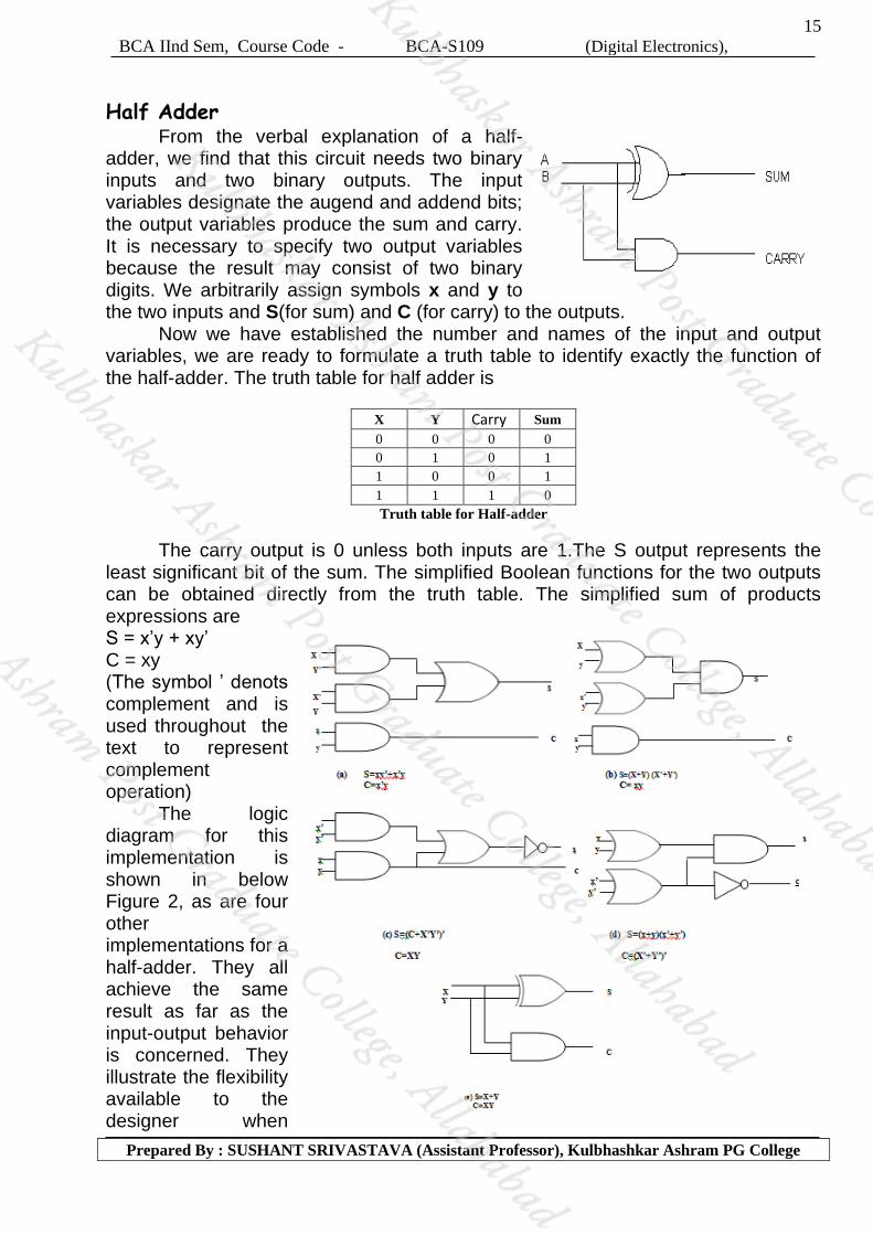
Half Adder From the verbal explanation of a half-
adder, we find that this circuit needs two binary inputs and two binary outputs. The input variables designate the augend and addend bits; the output variables produce the sum and carry. It is necessary to specify two output variables because the result may consist of two binary digits. We arbitrarily assign symbols x and y to the two inputs and S(for sum) and C (for carry) to the outputs.
Now we have established the number and names of the input and output variables, we are ready to formulate a truth table to identify exactly the function of the half-adder. The truth table for half adder is
X Y Carry Sum
0 0 0 0
0 1 0 1
1 0 0 1
1 1 1 0
Truth table for Half-adder
The carry output is 0 unless both inputs are 1.The S output represents the least significant bit of the sum. The simplified Boolean functions for the two outputs can be obtained directly from the truth table. The simplified sum of products expressions are S = x’y + xy’ C = xy (The symbol ’ denots complement and is used throughout the text to represent complement operation)
The logic diagram for this implementation is shown in below Figure 2, as are four other implementations for a half-adder. They all achieve the same result as far as the input-output behavior is concerned. They illustrate the flexibility available to the designer when

16
BCA IInd Sem, Course Code - BCA-S109 (Digital Electronics),
Prepared By : SUSHANT SRIVASTAVA (Assistant Professor), Kulbhashkar Ashram PG College
implementing even a simple combinational logic function such as this. Figure (a), as mentioned before, is the implementation of the half-adder in sum of Products. Figure (b) shows the implementation in product of sums:
S = (x + y)(x’ + y’) C = xy
To obtain the implementation of Figure (c), we note that S is the exclusive-OR of x and y. The complement of S is the equivalence of x and y.
S1= xy + x’y’ but C = xy and therefore, we have S=(C+x’y’)’
Full-Adder in Figure (d), uses the product of sums implementation with C derived as follows:
C =(xy)’’ = (x’ + y’)’ The half-adder can be implemented with an exclusive-OR and an AND gate, as shown in Figure 2(e). This form is used later to show that two half-adder circuits are needed to construct a full-adder circuit.
Full Adder: A full-adder is a combinational circuit that forms the arithmetic sum of three
input bits. It consists of three inputs and two outputs. Two of the input variables, denoted by x and y, represent the two significant bits to be added. The third input, z, represents the carry from the previous lower significant position. Two outputs are necessary because the arithmetic sum of three binary digits ranges in value from 0 to 3, and binary 2 or 3 needs two digits. The two outputs are designated by the symbols S for sum and C for carry. The binary variable S gives the value of the least significant bit of the sum. The binary variable C gives the output carry. The truth table of the full adder is
Input Output
X Y Z C S
0 0 0 0 0
0 0 1 0 1
0 1 0 0 1
0 1 1 1 0
1 0 0 0 1
1 0 1 1 0
1 1 0 1 0
1 1 1 1 1
Truth table for Full-Adder
The eight rows under the input variables designate all possible combinations of 1’s and (Zero)0’s that these variables may have. The 1’s and (Zero)0’s for the output variables are determined from the arithmetic sum of the input bits. When all input bits are (Zero)0’s, the output is 0. The S output is equal to 1 when only one input is equal to 1 or when all three inputs are equal to 1. The C output has a carry of 1 if two or three inputs are equal to 1. The input and output bits of the
S=X’Y’Z+X’YZ’+XY’Z’+XYZ
C=XY+XZ+Y
Z

17
BCA IInd Sem, Course Code - BCA-S109 (Digital Electronics),
Prepared By : SUSHANT SRIVASTAVA (Assistant Professor), Kulbhashkar Ashram PG College
combinational circuit have different interpretations at various stages of the problem. Physically, the binary signals of the input wires are considered binary digits
added arithmetically to form a two-digit sum at the output wires. On the other hand, the same binary values are considered variables of Boolean functions when expressed in the truth table or when the circuit is implemented with logic gates. It is important to realize that two different interpretations are given to the values of the bits encountered in this circuit. The input-output logical relationship of the full-adder circuit may be expressed in two Boolean functions, one for each output variable. Each output Boolean function requires a unique map for its simplification. Each map must have eight squares, since each output is a function of three input variables.
The maps of above Figure 3 are used for simplifying the two output functions. The 1’s in the squares for the maps of S and C are determined directly from the truth table. The squares with 1’s for the S output do not combine in adjacent squares to give a simplified expression in sum of products. The C output can be simplified to a six-literal expression. The logic diagram for the full-adder implemented in sum of products is shown in Figure 2 This implementation uses the following Boolean expressions:
S= x’y’z + x’yz’ + xy’z’ + xyz C = xy + xz + yz
The logic circuit for full adder is shown in figure 4
Other configurations for a full-adder may be developed. The product of sums implementation requires the same number of gates as in Figure 4, with the number of AND and OR gates interchanged. A full-adder can be implemented with two half adders and one OR gate, shown in Figure 5

18
BCA IInd Sem, Course Code - BCA-S109 (Digital Electronics),
Prepared By : SUSHANT SRIVASTAVA (Assistant Professor), Kulbhashkar Ashram PG College
The S output from the second half-adder is the exclusive-OR of z and the output of the first half-adder, giving S = z (x y)
= z’(xy’ + x’y) + z(xy’ + x’y)’
= z’(xy’ + x’y) + z(xy + x’y’)
= xy’z’ + x’yz’ + xyz + x’y’z
and the carry output is
C = z(xy’ + x’y) + xy
= xy’z + x’yz + xy
= xy+yx+zx (after applying Boolean rules)
Subtractors
Half Subtractor: A half subtractor is a
combinational logic circuit which is used to find the difference between two binary digits. A B BORROW(Br) DIFFERENCE(D)
0 0 0 0
0 1 1 1
1 0 0 1
1 1 0 0
Truth table for half subtractor Thus Br = A'B, and D=A’B+AB’
Using the above Boolean expressions, the logic circuit for half subtractor is shown in Figure 6
Full Subtractor: A full subtractor is a combinational circuit
that performs a subtraction between two bits taking into account that a 1 may have been
borrowed by a lower significant stage.
This circuit has three inputs and two outputs. The three inputs X, Y and Z denote the minuend, subtrahend and previous borrow respectively. The two outputs D and B represent the difference and borrow, respectively. The truth table for the circuit is as follows.
Input Output
X Y Z B D
0 0 0 0 0
0 0 1 1 1
0 1 0 1 1
0 1 1 1 0
1 0 0 0 1
1 0 1 0 0
1 1 0 0 0
1 1 1 1 1
X Y
Z

19
BCA IInd Sem, Course Code - BCA-S109 (Digital Electronics),
Prepared By : SUSHANT SRIVASTAVA (Assistant Professor), Kulbhashkar Ashram PG College
Q 3: What is Multiplexer. Design 4x1 Multiplexer. Answer:
Multiplexer A Multiplexer is combinational circuits that receives binary information from
one of 2n input data lines and direct it to a single output line. It connects multiple input lines to a single output lines. The following diagram is 4x1 multiplexer. The selection of a particular input data lines and direct into a single output line is made by using selection lines, whose bit combination determines which bit combination are selected for output.
Multiplexer is one of the basic building units of a computer system, which allows sharing of a common line by more than one input line. It connects multiple input lines to a single output line. At a specific time of the input line is selected and the selected input is passed the output line.
I0
I1 O
I2
I3
4x1 Multiplexer
A multiplexer or mux is a device that selects one of several analog or digital input signals and forwards the selected input into a single line. A multiplexer of 2n inputs has n select lines, which are used to select which input line to send to the output.”Multiplexers can be used for the implementation of Boolean functions or combinational circuits. They can also used for parallel to serial conversion.
1. Multiplexer is also called data selector or universal circuit. 2. All three variable Boolean equations can be implemented by using 8X1
multiplexer without using any additional gates. Some but not all three variable Boolean equations can also be implemented with 4X1 mux without using any additional gates
4 x 1
MUX
Figure 15 : Multiplexer

20
BCA IInd Sem, Course Code - BCA-S109 (Digital Electronics),
Prepared By : SUSHANT SRIVASTAVA (Assistant Professor), Kulbhashkar Ashram PG College
Demultiplexer
Demultiplexer: A decoder with enable input, acts as demultiplexer. Demultiplexer is a logical circuit that takes a single input source and sends it to one
of several 2n
possible output lines. The selection of specific output line is controlled by the bit values of ‘n’ selection lines.
Binary Demultiplexer The demultiplexer shown in figure 16 three input lines and one data input and
produse 8 output lines It is instructive to compare this demultiplexer circuit with the multiplexer circuit for the same number of control (select) inputs, there are the same number of AND gates. But now each AND gate output is a circuit output. Rather than each gate having its own eparate data input, the single data line now forms one of the inputs to each AND gate, the other AND inputs being control inputs.
Demultiplexer
Q 4: Explain Decoder and Encoder; Answer:
Encoder and Decoders
A combinational circuit accepts n inputs (not necessarily 1, but a small number) and causes data to be routed to one of many, say up to 2n, outputs. Such circuits have the generic name decoder. Semantically, at least, if something is to be decoded, it must have previously been encoded, the reverse operation from decoding. An encoding circuit must accept data from a large number of input lines and convert it to data on a smaller number of output lines (not necessarily just one). It encodes given information into a more compact form.
Binary Encoder A binary encoder encodes information from
2n inputs into an n-bit code, as indicated in Figure Exactly one of the input signals should have a value

21
BCA IInd Sem, Course Code - BCA-S109 (Digital Electronics),
Prepared By : SUSHANT SRIVASTAVA (Assistant Professor), Kulbhashkar Ashram PG College
of 1, and the outputs present the binary number that identifies which input is equal to 1. The truth table for a 4-to-2 encoder is provided in Figure 12. Observe that the output y0 is 1 when either input w1 or w3 is 1, and output y1 is 1 when input w2 or w3 is 1. Hence these outputs can be generated by the circuit in Figure b. Note that we assume that the inputs are one-hot encoded. All input patterns that have multiple inputs set to 1 are not shown in the truth table, and they are treated as don’t-care conditions. Encoders are used to reduce the number of bits needed to represent given information.
A practical use of encoders is for transmitting information in a digital system. Encoding the information allows the transmission link to be built using fewer wires. Encoding is also useful if information is to be stored for later use because fewer bits need to be stored.
8x3 ENCODER:- 8 x 3 encoder encodes 8 bit information and produces 3 outputs corresponding to binary numbers. This type of encoder is also called octal-to- binary encoder. The truth table of encoder is shown in figure 13
I0
I1 o1 I2
I3 o2
I4
I5 o3
I6
I7
8X3 Truth table and Block Digram
Decoders
A decoder is a combinational circuit that converts binary information from ‘n’ input lines to a maximum of 2n unique output lines. The circuit in Figure represents a 2-to-4 line decoder. The two inputs are decoded into 4 outputs each output represents one of the minterms of the 2-input variables. The two inverters provide the complement of inputs and each of the four AND gates generate one of the minterms. The following is the truth table of the 2-to-4 line decoder with two inputs and 4 outputs.
Input Outputs
A B D1 D1 D1 D1
0 0 1 0 0 0
0 1 0 1 0 0
1 0 0 0 1 0
1 1 0 0 0 1
8x3
Encoder

22
BCA IInd Sem, Course Code - BCA-S109 (Digital Electronics),
Prepared By : SUSHANT SRIVASTAVA (Assistant Professor), Kulbhashkar Ashram PG College
Contents UNIT-III
Sequential Building Blocks Flip-Flop (RS, D, JK, Master-slave & T flip-flops); Registers & Shift registers; Counters; Synchronous and Asynchronous Designing method.
UNIT 3
Q 1: Explain Synchronous and Asynchronous with Designing method.
Answer: So far you have encountered with combinatorial logic, i.e. circuits for which the
output depends only on the inputs. In many instances it is desirable to have the next output depending on the current output. A simple example is a counter, where the next number to be output is determined by the current number stored. Circuits that remember their current output or state are often called sequential logic circuits. Clearly, sequential logic requires the ability to store the current state. In other words, memory is required by sequential logic circuits, which can be created with boolean gates. If you arrange the gates correctly, they will remember an input value. This simple concept is the basis of RAM (random access memory) in computers, and also makes it possible to create a wide variety of other useful circuits. Memory relies on a concept called feedback. That is, the output of a gate is fed back into the input. The simplest possible feedback circuit using two inverters is shown in figure 1.
Input Output
Figure 1 : Simplest realization of feedback circuit
If you follow the feedback path, you can see that if Q happens to be 1 (or 0), it
will always be 1 (or 0). Since it's nice to be able to control the circuits we create, this one doesn't have much use -- but it does let you see how feedback works. It turns out that in "real" sequential circuits, you can actually use this sort of simple inverter feedback approach. The memory elements in these circuits are called flip-flops. A flip-flop circuit has two outputs, one for the normal value and one for the complement value of the stored bit. Binary information can enter a flip-flop in a variety of ways and gives rise to different types of flip-flops.
Synchronous & Asynchronous Sequential Circuits The sequential circuits are broadly classified, depending upon the time at which these are observed and their internal state changes. The two broad classifications of sequential circuits are:

23
BCA IInd Sem, Course Code - BCA-S109 (Digital Electronics),
Prepared By : SUSHANT SRIVASTAVA (Assistant Professor), Kulbhashkar Ashram PG College
• Synchronous Sequential Circuit
• Asynchronous Sequential Circuit Synchronous Sequential Circuit: Synchronous circuits uses flip-flops and their status can change only at discrete intervals. The synchronization in a sequential circuit is achieved by a clock pulse generator, which gives continuous clock pulse. Figure 2 shows the form of a clock pulse. A clock pulse can have two states: 0 or 1 i.e disabled (0) or active state (1). The storage elements can change their state only when a clock pulse occurs. Sequential circuits that have clock pulses as input to flip-flops are called clocked sequential circuit. Asynchronous Sequential Circuit: Asynchronous sequential circuits may be regarded as combinational circuit with feedback path. Since the propagation delays of output to input are small, they may tend to become unstable at times. Thus, complex asynchronous circuits are difficult to design.
Figure 2 : Synchronous Sequential Circuit
Concept of Sequential circuit Definition: A sequential circuit is an interconnection of combinational circuits and storage elements. The storage elements, called flip-flops, store binary information that indicates the state of sequential circuit at that time. The block diagram of a sequential circuit is shown below. As shown in the diagram, the present output depends upon the past Input states.The sequential circuits are time dependent.
Figure 2 : Block Diagram Sequential Circuit
0
1
24
BCA IInd Sem, Course Code - BCA-S109 (Digital Electronics),
Prepared By : SUSHANT SRIVASTAVA (Assistant Professor), Kulbhashkar Ashram PG College
Q 2: What is Flip-Flop? Explain RS, D, JK, Master-slave & T flip-flops.
Answer:
Latches and Flip-Flop Latches and flip-flops are the basic elements for storing information. One latch or flip-flop can store one bit of information. The main difference between latches and flip-flops is:
(a) In latches, their outputs are constantly affected by their inputs as long as the enable signal is asserted. In other words, when they are enabled, their content changes immediately when their inputs change.
(b) Flip-flops, on the other hand, have their content change only either at the rising or falling edge of the enable signal. This enable signal is usually the controlling clock signal. After the rising or falling edge of the clock, the flip-flop content remains constant even if the input changes.
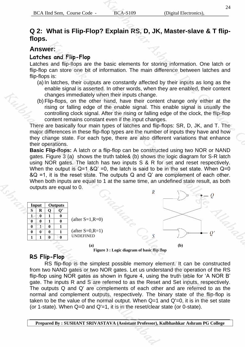
There are basically four main types of latches and flip-flops: SR, D, JK, and T. The major differences in these flip-flop types are the number of inputs they have and how they change state. For each type, there are also different variations that enhance their operations. Basic Flip-flops: A latch or a flip-flop can be constructed using two NOR or NAND gates. Figure 3 (a) shows the truth table& (b) shows the logic diagram for S-R latch using NOR gates. The latch has two inputs S & R for set and reset respectively. When the output is Q=1 &Q’ =0, the latch is said to be in the set state. When Q=0 &Q =1, it is the reset state. The outputs Q and Q’ are complement of each other. When both inputs are equal to 1 at the same time, an undefined state result, as both outputs are equal to 0.
(after S=1,R=0)
(after S=0,R=1)
UNDEFINED
(a) (b)
Figure 3 : Logic diagram of basic flip flop
RS Flip-Flop RS flip-flop is the simplest possible memory element. It can be constructed
from two NAND gates or two NOR gates. Let us understand the operation of the RS flip-flop using NOR gates as shown in figure 4, using the truth table for ‘A NOR B’ gate. The inputs R and S are referred to as the Reset and Set inputs, respectively. The outputs Q and Q' are complements of each other and are referred to as the normal and complement outputs, respectively. The binary state of the flip-flop is taken to be the value of the normal output. When Q=1 and Q'=0, it is in the set state (or 1-state). When Q=0 and Q'=1, it is in the reset/clear state (or 0-state).
Input Outputs S R Q Q’
1 0 1 0
0 0 1 0
0 1 0 1
0 0 0 1
1 1 0 0

25
BCA IInd Sem, Course Code - BCA-S109 (Digital Electronics),
Prepared By : SUSHANT SRIVASTAVA (Assistant Professor), Kulbhashkar Ashram PG College
Figure 4 : SR flip flop
With R & S inputs, 4 possible conditions may occur as given below
• When S=1 and R=0: The output of the bottom NOR gate is equal to zero, Q'=0. Hence both inputs to the top NOR gate are equal to 0, thus, Q=1. Hence, the input combination S=1 and R=0 leads to the flip-flop being set to Q=1.
• When S=0 and R=1: Similar to the arguments above, the outputs become Q=0 and Q'=1. We say that the flip-flop is reset.
• When S=0 and R=0 and assume that the flip-flop was previously in set (S=1 and R=0) condition. Now changing S to 0 results Q' still at 0 and Q=1. Similarly, when the flip-flop was previously in a reset state (S=0 and R=1), the outputs do not change. Therefore, with inputs S=0 and R=0, the flip-flop holds its state.
• When S=1 and R=1, This condition violates the fact that both outputs are complements of each other since each of them tries to go to 0, which is not a stable configuration. It is impossible to predict which output will go to 1 and which will stay at 0. Such condition is called race condition. In normal operation this condition must be avoided by making sure that 1's are not applied to both inputs simultaneously, thus making it one of the main disadvantages of RS flip-flop. All the above conditions are summarized in the characteristic table below:
Debounce circuit: An elementary example using this flip-flop is the debounce circuit. Suppose a piece of electronics is to change state under the action of a mechanical switch. When this switch is moved from position S to R (S=0, R=1), the contacts make and break several times at R before settling to good contact. It is desirable that the electronics should respond to the first contact and then remain stable, rather than switching back and forth as the circuit makes and breaks. This is achieved by RS flip-flop which is reset to Q=0 by the first signal R=1 and remains in a fixed state until the switch is moved back to position S, when the signal S=1 sets the flip-flop to Q=1.

26
BCA IInd Sem, Course Code - BCA-S109 (Digital Electronics),
Prepared By : SUSHANT SRIVASTAVA (Assistant Professor), Kulbhashkar Ashram PG College
Gated or Clocked RS Flip-Flop
It is sometimes desirable in sequential logic circuits to have a bistable RS flip-flop that only changes state when certain conditions are met regardless of the condition of either the Set or the Reset inputs. By connecting a 2-input AND gate in series with each input terminal of the RS NOR Flip-flop a Gated RS Flip-flop can be created. This extra conditional input is called an "Enable" input and is given the prefix of "EN" as shown below. When the Enable input "EN" = 0, the outputs of the two AND gates are also at logic level 0, regardless of the condition of the two inputs S and R, latching the two outputs Q and Q’ into their last known state. When the enable input "EN" = 1, the circuit responds as a normal RS bistable flip-flop with the two AND gates becoming transparent to the Set and Reset signals. This Enable input can also be connected to a clock timing signal adding clock synchronisation to the flip-flop creating what is sometimes called a "Clocked SR Flip-flop".
So a Gated/Clocked RS Flip-flop operates as a standard bistable latch but the outputs are only activated when a logic "1" is applied to its EN input and deactivated by a logic "0". The property of this flip-flop is summarized in its characteristic table where Qn is the logic state of the previous output and Qn+1 is that of the next output and the clock input being at logic 1 for all the R and S input combinations.
Figure 5: Characteristic table & Circuit diagram of clocked SR flip flop
D Flip Flop An RS flip-flop is rarely used in actual sequential logic because of its
undefined outputs for inputs R= S= 1. It can be modified to form a more useful circuit called D flip-flop, where D stands for data. The D flip-flop has only a single data input D as shown in the circuit diagram. The data input is connected to the S input of an RS flip-flop, while the inverse of D is connected to the R input. To allow the flip-flop to be in a holding state, a D-flip flop has a second input called Enable, EN. The Enable input is AND-ed with the D-input.
• When EN=0, irrespective of D-input, the R = S = 0 and the state is held.
• When EN= 1, the S input of the RS flip-flop equals the D input and R is the inverse of D. Hence, output Q follows D, when EN= 1.
• When EN returns to 0, the most recent input D is ‘remembered'. The circuit operation is summarized in the characteristic table for EN=1

27
BCA IInd Sem, Course Code - BCA-S109 (Digital Electronics),
Prepared By : SUSHANT SRIVASTAVA (Assistant Professor), Kulbhashkar Ashram PG College
Figure 6: Characteristic table & Circuit diagram of D flip flop
JK Flip Flop The JK flip flop (JK means Jack Kilby, a Texas instrument engineer, who
invented it) is the most versatile flip-flop, and the most commonly used flip flop. Like the RS flip-flop, it has two data inputs, J and K, and an EN/clock pulse input (CP). Note that in the following circuit diagram NAND gates are used instead of NOR gates. It has no undefined states, however. The fundamental difference of this device is the feedback paths to the AND gates of the input, i.e. Q is AND-ed with K and CP and Q’ with J and CP
Figure 7: Characteristic table & Circuit diagram of JK flip flop
The JK flip-flop has the following characteristics:
• If one input (J or K) is at logic 0, and the other is at logic 1, then the output is set or reset (by J and K respectively), just like the RS flip-flop.
• If both inputs are 0, then it remains in the same state as it was before the clock pulse occurred; again like the RS flip flop. CP has no effect on the output.
• If both inputs are high, however the flip-flop changes state whenever a clock pulse occurs; i.e., the clock pulse toggles the flip-flop again and again until the CP goes back to 0 as shown in the shaded rows of the characteristic table above.
• Since this condition is undesirable, it should be eliminated by an improvised form of this flip-flop as discussed in the next section.
Master-Slave JK Flip-Flop Although JK flip-flop is an improvement on the clocked SR flip-flop it still
suffers from timing problems called "race" if the output Q changes state before the timing pulse of the clock input has time to go "OFF", so the timing pulse period (T)

28
BCA IInd Sem, Course Code - BCA-S109 (Digital Electronics),
Prepared By : SUSHANT SRIVASTAVA (Assistant Professor), Kulbhashkar Ashram PG College
must be kept as short as possible (high frequency). As this is sometimes not possible with modern TTL IC's the much improved Master-Slave J-K Flip-Flop was developed. This eliminates all the timing problems by using two SR flip-flops connected together in series, one for the "Master" circuit, which triggers on the leading edge of the clock pulse and the other, the "Slave" circuit, which triggers on the falling edge of the clock pulse. The master-slave JK flip flop consists of two flip flops arranged so that when the clock pulse enables the first, or master, it disables the second, or slave. When the clock changes state again (i.e., on its falling edge) the output of the master latch is transferred to the slave latch. Again, toggling is accomplished by the connection of the output with the input AND gates.
Figure 8: Characteristic table & Circuit diagram of Master Slave flip flop
T Flip Flop The T flip-flop is a single input version of the JK flip-flop. The T flip-flop is obtained from the JK type if both inputs are tied together.
• Same as Master-Slave JK flip-flop with J=K=1
• The toggle, or T, flip-flop is a bistable device, where the output of the T flip-flop "toggles" with each clock pulse.
• Till CP=0, the output is in hold state (three input AND gate principle).
• When CP=1, for T=0, previous output is memorized by the circuit. When T=1 along with the clock pulse, the output toggles from the previous value as given in the characteristic table below.
Characteristic Table:
Figure 9: Characteristic table & Circuit diagram of T flip flop
Q 3: Explain Registers & Shift registers and Counters.

29
BCA IInd Sem, Course Code - BCA-S109 (Digital Electronics),
Prepared By : SUSHANT SRIVASTAVA (Assistant Professor), Kulbhashkar Ashram PG College
Answer:
Register
A register is a memory device that can be used to store more than one bit of information. They usually realized by several flip-flops with common control signals that control the movement of data to and from the register. Common refers to the property that the control signals apply to all flip-flops in the same way. A register is a generalization of a flip-flop. Where a flip-flop stores one bit, a register stores several bits. Register is a group of flip-flops. Each flip-flop is capable of storing one bit of information. An n-bit register consists of a group of n flip-flops. Register is a group of binary cells suitable for holding binary information. The main operations on a register are the same as for any storage devices, namely
• Load or Store: Put new data into the register
• Read: Retrieve the data stored in the register (usually without changing the stored data)
There are two basic types of registers. They are:
1. Parallel registers 2. Shift registers
Parallel registers:
A parallel register is one of the simplest registers, consisting of a set of flip-flops that can be read or written simultaneously. figure 1 shows a 4-bit register with parallel input-output. The signal lines I0, to I3 inputs to flip-flops, which may be output of other arithmetic circuits like multipliers, so that data from different sources can be loaded into the register. The outputs variable at A0 t A3, It has one additional line called clear line, which can clears the register completely. This register is called a parallel register as all the bits of the register can be loaded in a single clock pulse. Register with Parallel Load: Synchronous digital systems have a master clock generator that supplies a continuous train of clock pulses. The transfer of new information into a register is referred to as loading the register. If all the bits of the register are loaded simultaneously with a common clock pulse, we say that the loading is done in parallel. The load input determines whether the next pulse will accept new information or leave the information in the register intact.

30
BCA IInd Sem, Course Code - BCA-S109 (Digital Electronics),
Prepared By : SUSHANT SRIVASTAVA (Assistant Professor), Kulbhashkar Ashram PG College
• When Load = 1 ; the I inputs are transferred into the register.
• When Load = 0 ; maintain the content of the register because the D flip-flop does not have a “no change”
Shift Register:
A shift register is used for shifting the data to the left or right. A shift register operates in serial input-output mode i.e. data is entered in the register one bit at a time from one end of the register and can be read from the other end as one bit at a time. Figure 2 shows a 4-bit right shift register using D logical shift functions.
4-BIT RIGHT-SHIFT REGISTER: A register, which shifts data only in one direction, is called unidirectional shift register and a register, which can shift data in both directions, is called M-directional shift register, Shift register can be constructed for bi-directional shift with parallel input-output. A general shift register structure may have parallel data transfer to or from the register along with added facility of left or right shift. This structure will require additional control line for indicating whether parallel or serial output is desired and left or right shift is required, A general symbolic diagram is shown in Fig. for this register.
There are 3 main control lines shown in the below figure. If parallel load enable is active, parallel input-output operation is done otherwise serial input- output shift select line for selecting right or left shilt. If it has value 0 then right shift is performed and for value 1, left shift is done, Shift enable signal indicates when to start shift.
Right shift data input Parallel data input Left shift data input
Enable for
Parallel load
Shift select
Shift enable
Clear
Output Right shift data
output
Parallel data input
Figure 1 : Register with Parallel Load
Figure 2 : 4 bit shift register
4-BIT REGISTER

31
BCA IInd Sem, Course Code - BCA-S109 (Digital Electronics),
Prepared By : SUSHANT SRIVASTAVA (Assistant Professor), Kulbhashkar Ashram PG College
Counters
Counting is frequently required in digital computers and digital systems to record the number of events occurring in a specified interval f time. Normally electronic counter is used for counting the number of pulses coming at the input lines in a specified time period. The counter must possess memory since it has to remember its past states. As with other sequential logic circuits can be divided into two parts
• Asynchronous counters (Ripple counters)
• Synchronous counters
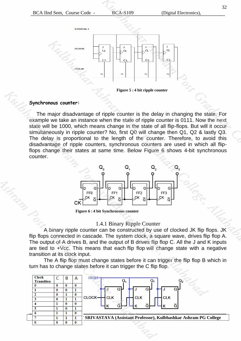
Asynchronous counters:
This is more often referred to as ripple counter, as the change, which occurs in order to increment the counter ripples through it from one end to the other. Figure 5 shows an implementation of 4-bit ripple counter using J-K flip-flops. This counter is incremental on the occurrence of each clock pulse and counts from 0000 to 1111 (i.e. 0 to 15).
The input line to J & K of all flip-flops is kept high i.e. logic 1. Each time a clock pulse occurs the value of flip-flop is complemented. The clock pulse is given only to first flip-flop, so first FF changes rate at trailing edge of each dark pulse, but record FF changes rate at trailing of Q output of first flip flop, this continues to the next flip flops. This implies that these flip-flops will be complemented if the previous flip-flop has a value 1. Thus, the effect of complement will ripple through these flip-flops.
COUNTER
Figure 3 : bit right shift register with
parallel load
Figure 4 : Counters
32
BCA IInd Sem, Course Code - BCA-S109 (Digital Electronics),
Prepared By : SUSHANT SRIVASTAVA (Assistant Professor), Kulbhashkar Ashram PG College
Synchronous counter:
The major disadvantage of ripple counter is the delay in changing the state. For example we take an instance when the state of ripple counter is 0111. Now the next state will be 1000, which means change in the state of all flip-flops. But will it occur simultaneously in ripple counter? No, first Q0 will change then Q1, Q2 & lastly Q3. The delay is proportional to the length of the counter. Therefore, to avoid this disadvantage of ripple counters, synchronous counters are used in which all flip-flops change their states at same time. Below Figure 6 shows 4-bit synchronous counter.
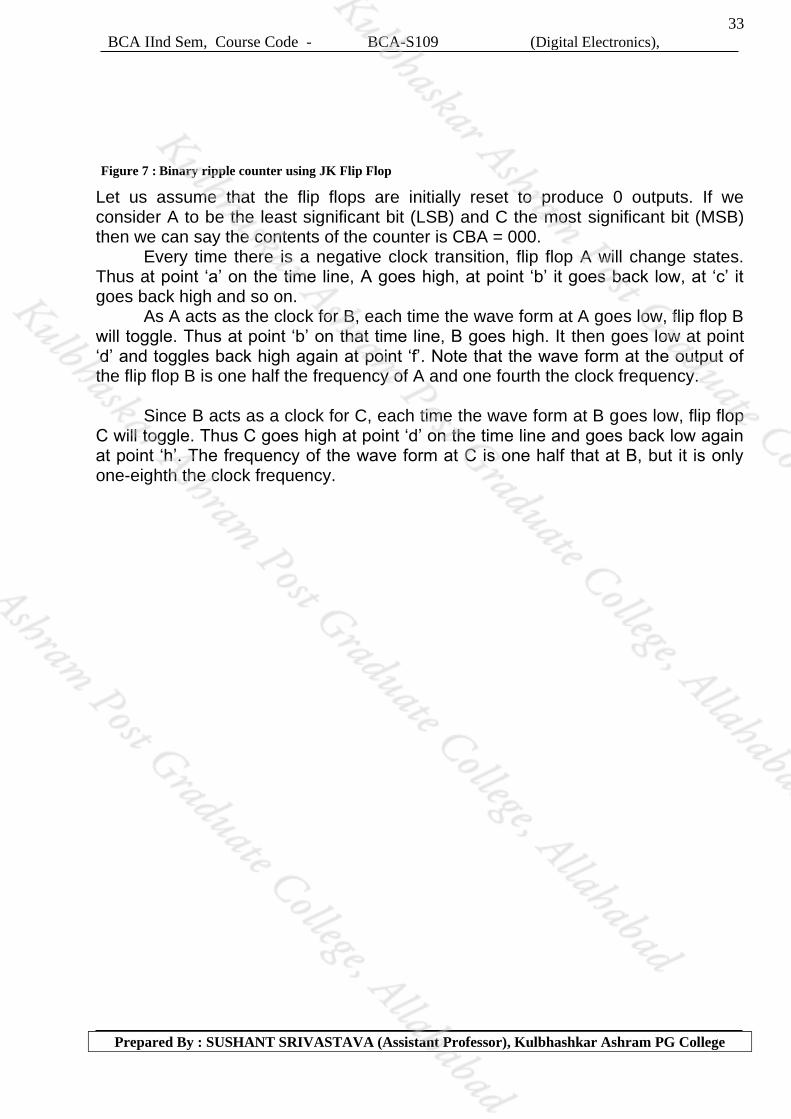
1.4.1 Binary Ripple Counter A binary ripple counter can be constructed by use of clocked JK flip flops. JK
flip flops connected in cascade. The system clock, a square wave, drives flip flop A. The output of A drives B, and the output of B drives flip flop C. All the J and K inputs are tied to +Vcc. This means that each flip flop will change state with a negative transition at its clock input.
The A flip flop must change states before it can trigger the flip flop B which in turn has to change states before it can trigger the C flip flop.
Figure 5 : 4 bit ripple counter
Figure 6 : 4 bit Synchronous counter
33
BCA IInd Sem, Course Code - BCA-S109 (Digital Electronics),
Prepared By : SUSHANT SRIVASTAVA (Assistant Professor), Kulbhashkar Ashram PG College
Let us assume that the flip flops are initially reset to produce 0 outputs. If we consider A to be the least significant bit (LSB) and C the most significant bit (MSB) then we can say the contents of the counter is CBA = 000.
Every time there is a negative clock transition, flip flop A will change states. Thus at point ‘a’ on the time line, A goes high, at point ‘b’ it goes back low, at ‘c’ it goes back high and so on.
As A acts as the clock for B, each time the wave form at A goes low, flip flop B will toggle. Thus at point ‘b’ on that time line, B goes high. It then goes low at point ‘d’ and toggles back high again at point ‘f’. Note that the wave form at the output of the flip flop B is one half the frequency of A and one fourth the clock frequency.
Since B acts as a clock for C, each time the wave form at B goes low, flip flop C will toggle. Thus C goes high at point ‘d’ on the time line and goes back low again at point ‘h’. The frequency of the wave form at C is one half that at B, but it is only one-eighth the clock frequency.
Figure 7 : Binary ripple counter using JK Flip Flop
Copyright © 2022 FDOKUMEN