Power Electronics - SelfStudys
17
180 CHAPTER 8 Power Electronics CHAPTER 8 Power Electronics In this chapter, the students can understand about the following topics in Power Electronics Conversion of power from one way to other say AC to DC and vice versa. Regulator power suppliers Uninterrupted power supply Voltage controller Switching circuits learning objective CONTENT 8.1 Converter classification 8.2 AC to DC converters 8.3 DC to AC – inverters 8.4 UPS (Uninterrupted Power Supply) 8.5 DC to DC – converters 8.6 AC to AC converters 8.7 Switching circuits 8.8 SMPS XII EE_English version CHAPTER 08.indd 180 1/17/2020 12:01:47 PM
-
Upload
khangminh22 -
Category
Documents
-
view
1 -
download
0
Transcript of Power Electronics - SelfStudys

1 8 0 CHAPTER 8 Power Electronics
CHAPTER 8
Power Electronics
In this chapter, the students can understand about the following topics in Power Electronics Conversion of power from one way to other say AC to DC and
vice versa. Regulator power suppliers Uninterrupted power supply Voltage controller Switching circuits
learning objective
CONTENT 8.1 Converter classification 8.2 AC to DC converters 8.3 DC to AC – inverters 8.4 UPS (Uninterrupted Power Supply) 8.5 DC to DC – converters 8.6 AC to AC converters 8.7 Switching circuits 8.8 SMPS
XII EE_English version CHAPTER 08.indd 180 1/17/2020 12:01:47 PM

1 8 1CHAPTER 8 Power Electronics
8Applications of power electronics
range in size from a switched mode power supply in an AC adapter, battery chargers, audio amplifiers, fluorescent lamp ballasts, through variable frequency drives and DC motor drives used to operate pumps, fans, and manufacturing machinery, up to gigawatt-scale high voltage direct current power transmission systems used to interconnect electrical grids. Power electronic systems are found in virtually every electronic device. For example:
Motor drives are found in pumps, blowers and mill drives for textile, paper, cement and other such facilities. Drives may be used for power conversion and for motion control. For AC motors, applications include variable-frequency drives, motor soft starters and excitation systems.
In hybrid electric vehicles (HEVs), power electronics are used in two formats: series hybrid and parallel hybrid. The difference between a series hybrid and a parallel hybrid is the relationship of the electric motor to the internal combustion engine (ICE). Devices used in electric vehicles consist mostly of dc/dc converters for battery charging and dc/ac converters to power the propulsion motor. Electric trains use power electronic devices to obtain power, as well as for vector control using pulse width modulation (PWM) rectifiers. The trains obtain their power from power lines. Another new usage for power electronics is in elevator systems. These systems may use thyristors, inverters, permanent magnet motors or various hybrid systems that incorporate PWM systems and standard motors.
The design of power conversion equipment includes many disciplines from electrical engineering. Power electronics includes applications of circuit theory, control theory, electronics, electromagnetics, microprocessors (for
Introduction
Power Electronics is the study of switching electronic circuits in order to control the flow of electrical energy. Power Electronics is the technology behind switching power supplies, power converters, power inverters, motor drives, and motor soft starters.
Power electronics circuits convert electric power from one form to another using electronic devices. Power electronics circuits function by using semiconductor devices as switches, thereby controlling or modifying a voltage or current.
Applications of power electronics range from high-power conversion equipment such as dc power transmission to everyday appliances, such as power supplies for computers, cell phone chargers, and hybrid automobiles. Power electronics includes applications in which circuits process milliwatts or even megawatts.
Importance of Power Electronics
As the trend towards electrification and renewable energies increases, enabling technologies such as power electronics are becoming ever more important. Power electronics is an umbrella term that encompasses the systems and products involved in converting and controlling the flow of electrical energy.
Applications of power electronics include conversion of 1. AC to DC (rectifier) 2. Conversion of dc to AC (inverter) 3. Conversion of an unregulated DC
voltage to a regulated dc voltage (DC to dc converter)
4. Conversion of an ac power source from one amplitude and frequency to another amplitude and frequency. (AC to ac converter)
XII EE_English version CHAPTER 08.indd 181 1/17/2020 12:01:47 PM
1 8 2 CHAPTER 8 Power Electronics
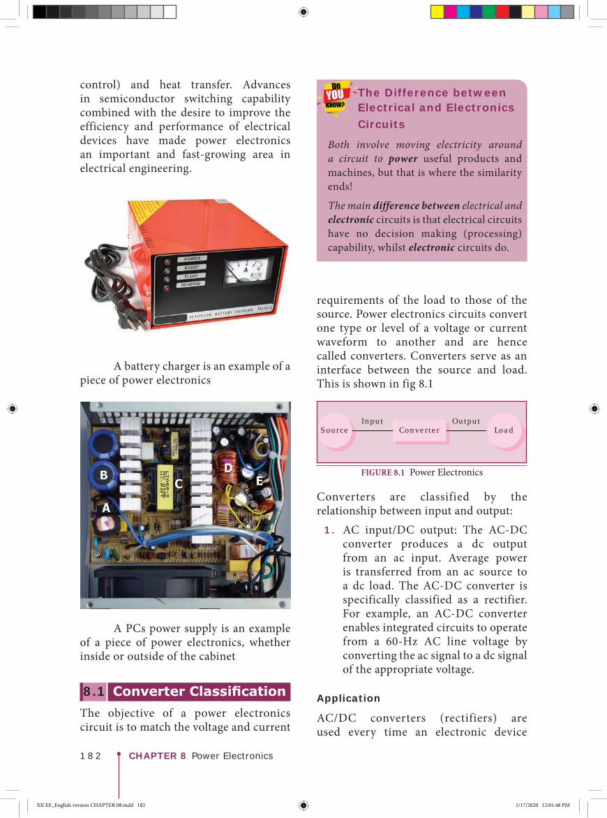
requirements of the load to those of the source. Power electronics circuits convert one type or level of a voltage or current waveform to another and are hence called converters. Converters serve as an interface between the source and load. This is shown in fig 8.1
ConverterSource LoadOutputInput
FIGURE 8.1 Power Electronics
Converters are classified by the relationship between input and output: 1. AC input/DC output: The AC-DC
converter produces a dc output from an ac input. Average power is transferred from an ac source to a dc load. The AC-DC converter is specifically classified as a rectifier. For example, an AC-DC converter enables integrated circuits to operate from a 60-Hz AC line voltage by converting the ac signal to a dc signal of the appropriate voltage.
Application
AC/DC converters (rectifiers) are used every time an electronic device
control) and heat transfer. Advances in semiconductor switching capability combined with the desire to improve the efficiency and performance of electrical devices have made power electronics an important and fast-growing area in electrical engineering.
A battery charger is an example of a piece of power electronics
A PCs power supply is an example of a piece of power electronics, whether inside or outside of the cabinet
8.1 Converter Classification The objective of a power electronics circuit is to match the voltage and current
The Difference between Electrical and Electronics Circuits
Both involve moving electricity around a circuit to power useful products and machines, but that is where the similarity ends!
The main difference between electrical and electronic circuits is that electrical circuits have no decision making (processing) capability, whilst electronic circuits do.
XII EE_English version CHAPTER 08.indd 182 1/17/2020 12:01:48 PM

1 8 3CHAPTER 8 Power Electronics
DC/DC converter developed to maximize the energy harvest from solar photovoltaic or wind turbine systems. 4. AC input/AC output: The AC-AC
converter may be used to change the level and/or frequency of an AC signal. Examples include a common light-dimmer circuit and speed control of an induction motor.
Application
AC/AC converters are used to change either the voltage level or the frequency (international power adapters, light dimmer). In power distribution networks AC/AC converters may be used to exchange power between utility frequency 50 Hz and 60 Hz power grids.
Some converter circuits can operate in different modes, depending on circuit and control parameters. For example, some rectifier circuits can be operated as inverters by modifying the control on the semiconductor devices. In such cases, it is the direction of average power flow that determines the converter classification. In Fig. 8-2, if the battery is charged from the ac power source, the converter is classified as a rectifier. If the operating parameters of the converter are changed and the battery acts as a source supplying power to the ac system, the converter is then classified as an inverter.
Converter
Rectifier
Inverter
+
–
+
–
P
P
FIGURE 8.2 A converter can operate as a rectifier or an inverter, depending on the direction of average power P.
is connected to the mains (computer, television etc.). These may simply change AC to DC or can also change the voltage level as part of their operation.
2. DC Input/AC Output: The DC-AC converter is specifically classified as an inverter. In the inverter, average power flows from the dc side to the AC side. Examples of inverter applications include producing a 120-V rms 60-Hz voltage from a 12-V battery and interfacing an alternative energy source such as an array of solar cells to an electric utility.
Application
DC/AC converters (inverters) are used primarily in UPS or renewable energy systems or emergency lighting systems. Mains power charges the DC battery. If the mains fails, an inverter produces AC electricity at mains voltage from the DC battery. Solar inverter, both smaller string and larger central inverters, as well as solar micro-inverter are used in photovoltaics as a component of a PV system. 3. DC input/DC output: The DC-
DC converter is useful when a load requires a specified (often regulated) dc voltage or current but the source is at a different or unregulated DC value. For example, 5V may be obtained from a 12-V source via a DC-DC converter.
Application
DC/DC converters are used in most mobile devices (mobile phones, PDA etc.) to maintain the voltage at a fixed value whatever the voltage level of the battery is. These converters are also used for electronic isolation and power factor correction. A power optimizer is a type of
XII EE_English version CHAPTER 08.indd 183 1/17/2020 12:01:48 PM
1 8 4 CHAPTER 8 Power Electronics
rectifier has inherently less ripple than the half-wave rectifier.
In this chapter, uncontrolled and controlled single-phase and three-phase full-wave converters used as rectifiers are analysed for various types of loads. Also included are examples of controlled converters operating as inverters, where power flow is from the DC side to the AC side.
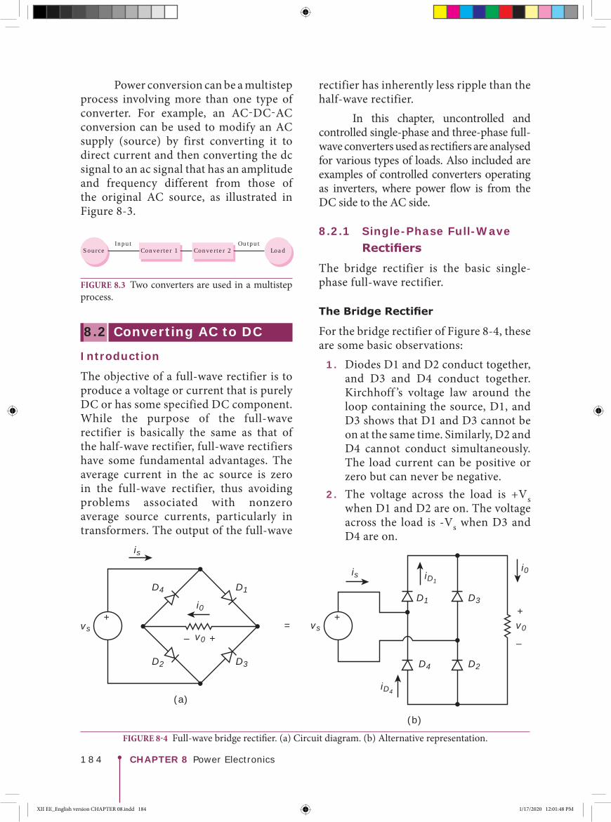
8.2.1 Single-Phase Full-Wave Rectifiers
The bridge rectifier is the basic single-phase full-wave rectifier.
The Bridge Rectifier
For the bridge rectifier of Figure 8-4, these are some basic observations: 1. Diodes D1 and D2 conduct together,
and D3 and D4 conduct together. Kirchhoff ’s voltage law around the loop containing the source, D1, and D3 shows that D1 and D3 cannot be on at the same time. Similarly, D2 and D4 cannot conduct simultaneously. The load current can be positive or zero but can never be negative.
2. The voltage across the load is +Vs when D1 and D2 are on. The voltage across the load is -Vs when D3 and D4 are on.
Power conversion can be a multistep process involving more than one type of converter. For example, an AC-DC-AC conversion can be used to modify an AC supply (source) by first converting it to direct current and then converting the dc signal to an ac signal that has an amplitude and frequency different from those of the original AC source, as illustrated in Figure 8-3.
Converter 1 Converter 2Source LoadOutputInput
FIGURE 8.3 Two converters are used in a multistep process.
8.2 Converting AC to DC
Introduction
The objective of a full-wave rectifier is to produce a voltage or current that is purely DC or has some specified DC component. While the purpose of the full-wave rectifier is basically the same as that of the half-wave rectifier, full-wave rectifiers have some fundamental advantages. The average current in the ac source is zero in the full-wave rectifier, thus avoiding problems associated with nonzero average source currents, particularly in transformers. The output of the full-wave
is i0
iD4
iD1
is
vs vs
D4
D4D2 D2
– +
+
D1D1
D3
D3
v0 –
+v0
i0+
=
(a)
(b)
FIGURE 8-4 Full-wave bridge rectifier. (a) Circuit diagram. (b) Alternative representation.
XII EE_English version CHAPTER 08.indd 184 1/17/2020 12:01:48 PM

1 8 5CHAPTER 8 Power Electronics
3. The maximum voltage across a reverse-biased diode is the peak value of the source. This can be shown by Kirchhoff’s voltage law around the loop containing the source, D1, and D3. With D1 on, the voltage across D3 is -Vs.
4. The current entering the bridge from the source is iD1 - iD4, which is symmetric about zero. Therefore, the average source current is zero.
5. The rms source current is the same as the rms load current. The source current is the same as the load current for one-half of the source period and is the negative of the load current for the other half. The squares of the load and source currents are the same, so the rms currents are equal.
6. The fundamental frequency of the output voltage is 2ω, where ω is the frequency of the AC input since two periods of the output occur for every period of the input.
8.3 DC TO AC - InverterInverter is an electronic circuit, which converts direct current (DC) into alternating current (AC). The input voltage, output voltage and frequency, and all power handling depend upon the DC source. A simple 12 V DC to 220 V AC inverter circuit shown in Figure 8.5 produces an
AC output of 220 V AC at line frequency. In this circuit, the 555 is configured as a low-frequency oscillator, which is tuneable over the frequency range of 50 to 60 Hz by the potentiometer R4. The output of the 555 (amplified by Q1 and Q2) is fed into the input of transformer T1 (a reverse-connected filament transformer with the necessary step-up turns ratio). Capacitor C4 and inductance coil L1 are used to filter the high frequency noise and dc components in order to assure a sine wave output. The power output (in watts) of this circuit depends on the selection of required power rating of different components, especially for the transistor and the transformer.
Types of Inverters
There are three different types of outputs from inverters and hence the inverters can be classified into three primary types viz. Square Wave inverter Modified Sine wave inverter or quasi
sine wave inverter Pure sine wave inverter
Square Wave Inverter
The input power source for the inverter is a battery and the output is a square AC waveform, which can be used to drive less-sensitive AC devices. The output from the square wave inverter can result
vs
is
v0
vD1,vD2
vD3,vD4
Vm
–Vm
–Vm
Vm
Vm
0
0
0
0
iD1,iD2
0
iD3,iD4
0
00
2
(c)
2
2
2t
2t
t
i0
2 t
2 t
2 t
t
t
FIGURE 8.4(c) Full–Wave Bridge Rectifier Voltage & Current Wave forms
XII EE_English version CHAPTER 08.indd 185 1/17/2020 12:01:48 PM

1 8 6 CHAPTER 8 Power Electronics
waveform. It is used to give supply to sensitive AC devices. The output is a sine-wave with very low harmonic distortion.
8.4 UPS (Uninterrupted Power Supply)
An Uninterruptible Power Supply (UPS) is a device that allows an electrical/electronic gadget to keep in operation for at least a short time when the primary mains power source is lost. It also provides protection from power surge.
Figure 8.6 shows the circuit diagram of a simple UPS circuit that can deliver 12 V unregulated and 5 V regulated DC outputs. The transformer T1 step-downs
in noise. The output voltage, frequency, and waveform of the inverter depend on the design of the inverter.
Quasi sine wave inverter
The first electronic inverters to be introduced were basic square wave inverters. As time and technology progressed, a second generation power inverter became popular and was called a “modified square wave” or “quasi-sine wave” inverter. It could be more accurately called a modified-square wave.
Sine Wave Inverter
In a sine wave inverter, the input is from a battery and output is a pure sine AC
R110K
555
Timeoscillator
3
Gnd.
C30.01μF0.1μF
C1 C2
R450K
R2100K R3
100
Q2TIP42A
Tony van roon
Q1TIP41A
L11μH
2700μF
+5V to +15V
DC to AC inverter with the 555
(seetest)
T1
Neutral
Phase
AC
AC
PNP
NPN
+
FREQ
51
2
6
847
Output120 to 230V50 to 60Hz
FIGURE 8.5 12 V DC to 220 V AC inverter using 555
12V
5V
C3100nF
C2100nF
B112V
D2LED
R21K
R1220
Ohms
C12200uF
2A
F1
B112
T1
0
230V AC
Simple UPS
+
1N4007 1N4007
1N4007
D5
D3 D4
+2
31 IC17805
2A
F2
FIGURE 8.6 Simple UPS circuit
XII EE_English version CHAPTER 08.indd 186 1/17/2020 12:01:48 PM
1 8 7CHAPTER 8 Power Electronics
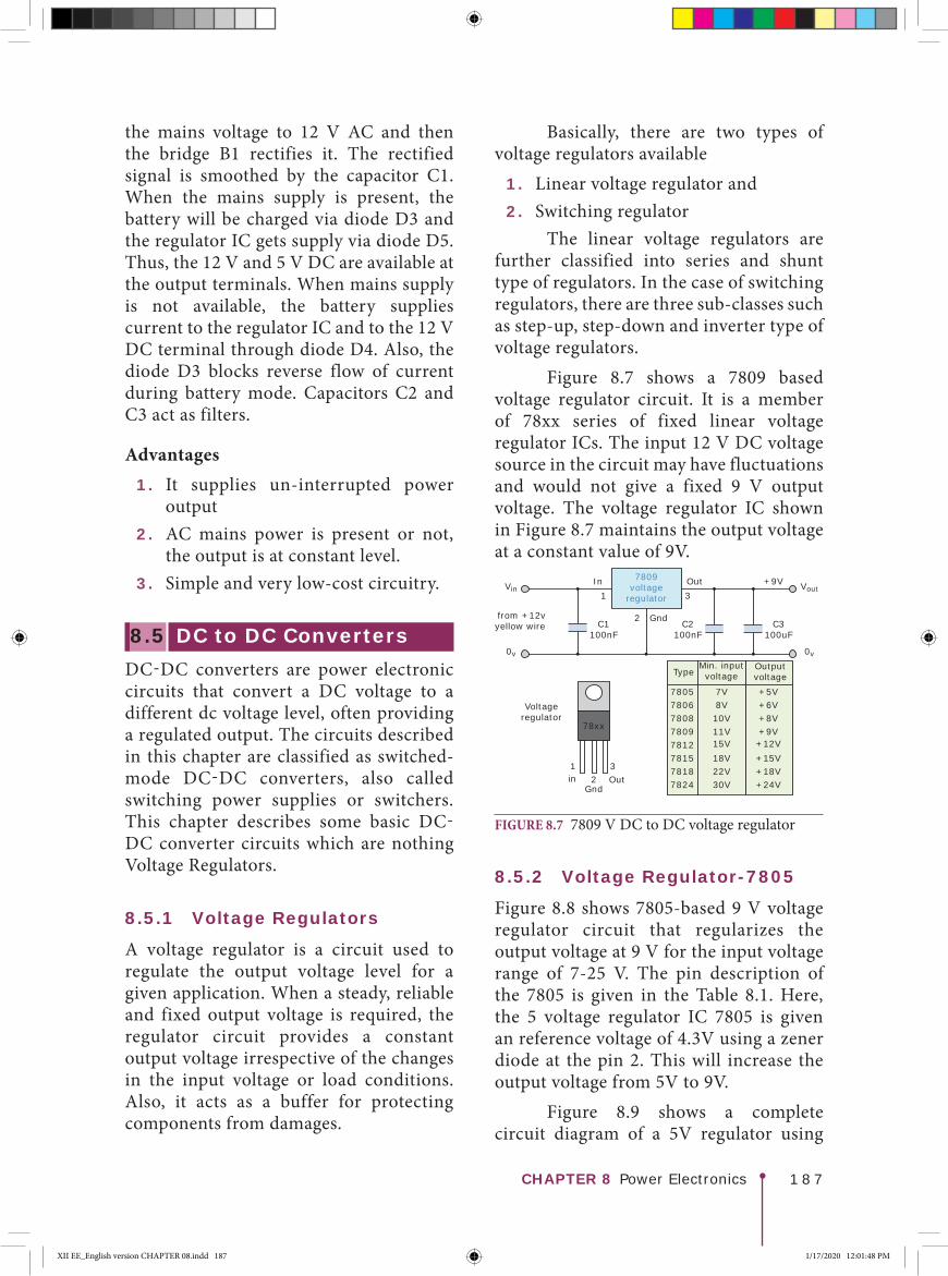
Basically, there are two types of voltage regulators available 1. Linear voltage regulator and 2. Switching regulator
The linear voltage regulators are further classified into series and shunt type of regulators. In the case of switching regulators, there are three sub-classes such as step-up, step-down and inverter type of voltage regulators.
Figure 8.7 shows a 7809 based voltage regulator circuit. It is a member of 78xx series of fixed linear voltage regulator ICs. The input 12 V DC voltage source in the circuit may have fluctuations and would not give a fixed 9 V output voltage. The voltage regulator IC shown in Figure 8.7 maintains the output voltage at a constant value of 9V.
Vin
0v 0v
from +12vyellow wire
Voltageregulator
78xx
inGnd
Out
TypeMin. inputvoltage
Outputvoltage
21 3
Vout+9VOut7809
voltageregulator
In1 3
C2100nF
C3100uF
C1100nF
2 Gnd
7805 7V8V10V11V15V18V22V30V
+5V+6V+8V+9V+12V+15V+18V+24V
7806780878097812781578187824
FIGURE 8.7 7809 V DC to DC voltage regulator
8.5.2 Voltage Regulator-7805
Figure 8.8 shows 7805-based 9 V voltage regulator circuit that regularizes the output voltage at 9 V for the input voltage range of 7-25 V. The pin description of the 7805 is given in the Table 8.1. Here, the 5 voltage regulator IC 7805 is given an reference voltage of 4.3V using a zener diode at the pin 2. This will increase the output voltage from 5V to 9V.
Figure 8.9 shows a complete circuit diagram of a 5V regulator using
the mains voltage to 12 V AC and then the bridge B1 rectifies it. The rectified signal is smoothed by the capacitor C1. When the mains supply is present, the battery will be charged via diode D3 and the regulator IC gets supply via diode D5. Thus, the 12 V and 5 V DC are available at the output terminals. When mains supply is not available, the battery supplies current to the regulator IC and to the 12 V DC terminal through diode D4. Also, the diode D3 blocks reverse flow of current during battery mode. Capacitors C2 and C3 act as filters.
Advantages 1. It supplies un-interrupted power
output 2. AC mains power is present or not,
the output is at constant level. 3. Simple and very low-cost circuitry.
8.5 DC to DC ConvertersDC-DC converters are power electronic circuits that convert a DC voltage to a different dc voltage level, often providing a regulated output. The circuits described in this chapter are classified as switched-mode DC-DC converters, also called switching power supplies or switchers. This chapter describes some basic DC-DC converter circuits which are nothing Voltage Regulators.
8.5.1 Voltage Regulators
A voltage regulator is a circuit used to regulate the output voltage level for a given application. When a steady, reliable and fixed output voltage is required, the regulator circuit provides a constant output voltage irrespective of the changes in the input voltage or load conditions. Also, it acts as a buffer for protecting components from damages.
XII EE_English version CHAPTER 08.indd 187 1/17/2020 12:01:48 PM

1 8 8 CHAPTER 8 Power Electronics
is generated, which is fed to the input terminal (pin 1) of the 7805 regulator. The reference terminal (pin 2) is connected to the ground terminal of the power supply. At pin 3, 5V regulated DC voltage is obtained, which is further filtered for high frequency noise. The diode IN 4007 in the output terminal of 7805 provides over-voltage protection.
7805. In this circuit the mains 230 AC is converted into 12V AC using a step-down transformer. The voltage at the secondary of the transformer is connected to a bridge rectifier circuits, which converts the 12V AC into a fluctuating DC. The capacitors 1000 µF and 0.22 µF are used to filter-out the 50 Hz and high frequency noises, respectively. Now, 12V pure DC voltage
Vin
0v 0v
from +12vyellow wire
Vout+9V7805
regulator1 3
C2100nF
4.3Zener
BZX55-C4V3 Zener diode
R1
C3100uF
C1100nF
D1
2 5.5mA
FIGURE 8.8 7805 dc to dc voltage regulator circuit
TABLE 8.1 Pin Description of 7805Pin No Pin Description
1 INPUT Pin 1 is the INPUT Pin. A positive unregulated voltage is given as input to this pin. Voltage range 7-25 V.
2 GROUND Pin 2 is the GROUND Pin. It is common to both Input and Output.
3 OUTPUT Pin 3 is the OUTPUT Pin. The output is regulated at 5 V and the maximum current supplied is 1.5 A.
230V@50Hz
230V – 12VStep down transformer
1A fuse
Bridge rectifier
1000F 0.22F 0.1F 1N4007
5VRegulatedoutput
+
FIGURE 8.9 5 V regulator circuit using 7805
XII EE_English version CHAPTER 08.indd 188 1/17/2020 12:01:49 PM

1 8 9CHAPTER 8 Power Electronics
TABLE 8.2 Negative Voltage Regulators and their output voltage
IC Number Output Voltage7905 -05 Volts7912 -12 Volts7915 -15 Volts7918 -18 Volts
Variable Voltage Power Supply: LM317T Variable Voltage Regulator
LM317 is a popular adjustable positive linear voltage regulator. It was designed by Robert C Dobkin in the year 1976 at National Semiconductor. LM337 (negative voltage counterpart of LM317) is used to regulate negative voltages. LM317 is an adjustable 3−terminal positive voltage regulator capable of supplying in excess of 1.5A over an output voltage range of 1.2V to 37V. This voltage regulator is used two external resistors to set the output voltage. Figure 8.11 shows a variable voltage regulator circuit.
8.6 AC to AC Converters
Introduction
An ac voltage controller is a converter that controls the voltage, current, and average power delivered to an ac load from an ac source. Electronic switches connect and disconnect the source and the load at regular intervals. In a switching scheme called phase control, switching takes place during every cycle of the source, in effect removing some of the source waveform before it reaches the load. Another type of control is integral-cycle control, whereby the source is connected and disconnected for several cycles at a time.
The phase-controlled ac voltage controller has several practical uses
Important Points on 7805 Voltage Regulator IC
The input voltage should always be greater than the output voltage (7 to 25 V).
The input current and output current are almost identical. This means that when a 7.5 V, 1 A supply is given at input, the output will be 5 V, 1 A.
The remaining power is dissipated as heat and hence a heat sink should be provided to limit the working temperature of the 7805 IC.
8.5.3 Negative Voltage Regulator- IC 79Xx (7905, 7912, 7915, 7918)
The 79xx voltage regulator series is designed to obtain negative power supply voltage required in some of the op-amp circuits. The input to these negative regulators should be a negative voltage, which 2.5V greater than the required output voltage. The pin diagram of the 79xx series is shown in Figure 8.10. Pin 1 is given a reference voltage, usually the ground voltage. Pin 2 is input terminal where the input negative voltage is given. Pin 3 is the output terminal, where the output negative is drawn. The various negative voltage regulators and their output voltages are listed in Table 8.2.
Output
InputGround
FIGURE 8.10 Pin diagram of Negative Voltage Regulators
XII EE_English version CHAPTER 08.indd 189 1/17/2020 12:01:49 PM

1 9 0 CHAPTER 8 Power Electronics
switches are shown as parallel thyristors (SCRs). This SCR arrangement makes it possible to have current in either direction in the load. This SCR connection is called antiparallel or inverse parallel because the SCRs carry current in opposite directions. A triac is equivalent to the antiparallel SCRs. Other controlled switching devices can be used instead of SCRs.
The principle of operation for a single-phase ac voltage controller using phase control is quite similar to that of
including light-dimmer circuits and speed control of induction motors. The input voltage source is ac, and the output is ac (although not sinusoidal), so the circuit is classified as an AC-AC converter.
8.6.1 The Single-Phase AC Voltage Controller
Basic Operation
A basic single-phase voltage controller is shown in Figure 8.12. The electronic
Vin
0v 0v
Inputvoltage
OutputVoltage LM317T
inGnd
Out21 3
VoutOut
R1
R2
Adj
LM317Tvoltage
regulator
In3 2
100uA
1V ref
FIGURE 8.11 Variable Voltage Regulator using LM317
+
+
+
+
VT1
VT2Vs =Vm sin ωt
Vm sin ωt
ωt
ωt
ωt
Is
Vo
io
T1
2
T2
Vs
Vm
Vm/R
0Io
R
T1
T2
–
–
–
–
FIGURE 8.12 Single-phase AC voltage controller with a resistive load; (b) Waveforms.
XII EE_English version CHAPTER 08.indd 190 1/17/2020 12:01:49 PM

1 9 1CHAPTER 8 Power Electronics
8.7 Switching CircuitsSwitching is an electronic circuit used to electrically switch-on or switch-off an electronic circuit used for power conversion circuits. An electrical switch is any device used to interrupt the flow of electrons in a circuit. Switches are binary devices: either it is in “ON” (“closed”) state or “OFF” (“open”) state using timing pulses. Transistor in a simple electronic switch, which conducts current across the collector-emitter terminals, when a voltage is applied to the base, i.e. the switch is ON or supress the flow of current across the collector-emitter terminal, when there is no base voltage, i. e., the switch is OFF.
8.7.1 NPN Relay Switch Circuit
Relays are electromechanical devices employing an electromagnet to operate a pair of movable contacts from an open position to a closed position. A relay switch circuit shown in Figure 8.13 consists of a NPN transistor (TR1) configured as a switch drive the coil of the relay when switching pulse is applied at the base of the transistor. When the base voltage of the transistor is zero (or negative), the transistor is cut-off and acts as an open switch. In this condition, no collector current flows and the relay coil
the controlled half-wave rectifier. Here, load current contains both positive and negative half-cycles. An analysis identical to that done for the controlled half-wave rectifier can be done on a half-cycle for the voltage controller. Then, by symmetry, the result can be extrapolated to describe the operation for the entire period.
Some basic observations about the circuit of Fig 8.12 are as follows: 1. The SCRs cannot conduct
simultaneously. 2. The load voltage is the same as the
source voltage when either SCR is on. The load voltage is zero when both SCRs are off.
3. The switch voltage Vsw is zero when either SCR is on and is equal to the source voltage when neither is on.
4. The average current in the source and load is zero if the SCRs are on for equal time intervals. The average current in each SCR is not zero because of unidirectional SCR current.
5. The rms current in each SCR is times the rms load current if the SCRs are on for equal time intervals.
For the circuit of Fig. 8.12, S1 conducts if a gate signal is applied during the positive half-cycle of the source. Just as in the case of the SCR in the controlled half-wave rectifier, S1 conducts until the current in it reaches zero. Where this circuit differs from the controlled half-wave rectifier is when the source is in its negative half-cycle. A gate signal is applied to S2 during the negative half-cycle of the source, providing a path for negative load current. If the gate signal for S2 is a half period later than that of S1, analysis for the negative half-cycle is identical to that for the positive half, except for algebraic sign for the voltage and current.
Outputports
10kΩ
1kΩ01
Flywheeldiode
+Vcc
NC
Relay
NO
C
NPNBC109
0v
B
C
ETR1
FIGURE 8.13 NPN Relay Switching Circuit
XII EE_English version CHAPTER 08.indd 191 1/17/2020 12:01:49 PM
1 9 2 CHAPTER 8 Power Electronics
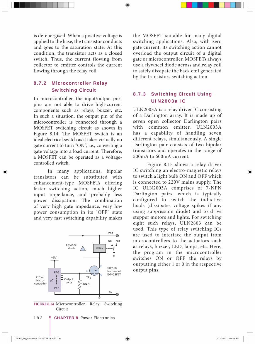
the MOSFET suitable for many digital switching applications. Also, with zero gate current, its switching action cannot overload the output circuit of a digital gate or microcontroller. MOSFETs always use a flywheel diode across and relay coil to safely dissipate the back emf generated by the transistors switching action.
8.7.3 Switching Circuit Using UIN2003a IC
ULN2003A is a relay driver IC consisting of a Darlington array. It is made up of seven open collector Darlington pairs with common emitter. ULN2003A has a capability of handling seven different relays, simultaneously. A single Darlington pair consists of two bipolar transistors and operates in the range of 500mA to 600mA current.
Figure 8.15 shows a relay driver IC switching an electro-magnetic relays to switch a light bulb ON and OFF which is connected to 220V mains supply. The IC ULN2003A comprises of 7-NPN Darlington pairs, which is typically configured to switch the inductive loads (dissipates voltage spikes if any using suppression diode) and to drive stepper motors and lights. For switching eight such relays, ULN2803 can be used. This type of relay switching ICs are used to interface the output from microcontrollers to the actuators such as relays, buzzer, LED, lamps, etc. Here, the program in the microcontroller switches ON or OFF the relays by outputting either 1 or 0 in the respective output pins.
is de-energised. When a positive voltage is applied to the base, the transistor conducts and goes to the saturation state. At this condition, the transistor acts as a closed switch. Thus, the current flowing from collector to emitter controls the current flowing through the relay coil.
8.7.2 Microcontroller Relay Switching Circuit
In microcontroller, the input/output port pins are not able to drive high-current components such as relays, buzzer, etc. In such a situation, the output pin of the microcontroller is connected through a MOSFET switching circuit as shown in Figure 8.14. The MOSFET switch is an ideal electrical switch as it takes virtually no gate current to turn “ON”, i.e., converting a gate voltage into a load current. Therefore, a MOSFET can be operated as a voltage-controlled switch.
In many applications, bipolar transistors can be substituted with enhancement-type MOSFETs offering faster switching action, much higher input impedance, and probably less power dissipation. The combination of very high gate impedance, very low power consumption in its “OFF” state and very fast switching capability makes
PIC or Micro-
controller
+5V
Outputports
PA0
PA7
μC10kΩ
Flywheeldiode
+Vdd
NC
Relay
NO
C
IRF610N-channelE-MOSFET
0v
G
D
STR1
FIGURE 8.14 Microcontroller Relay Switching Circuit
XII EE_English version CHAPTER 08.indd 192 1/17/2020 12:01:49 PM

1 9 3CHAPTER 8 Power Electronics
8.8 Switch Mode Power Supply (SMPS)
A switched-mode power supply (SMPS) is an electronic circuit that converts power using switching devices that are turned on and off at high frequencies, and storage components such as inductors or capacitors to supply power when the switching device is in its non-conduction state.
They are used in many places in a computer. In a modern computer, there is a SMPS that takes rectified AC input from the wall, performs power factor correction and then converts the output into one or more lower voltage DC outputs.
The Figure 8.16 shows the externel structure of SMPS and Figure 8.17 shows the internal structure of SMPS.
SMPS is a power supply that uses a switching regulator to control and stabilize the output voltage by switching the load current on and off. These power supplies offer a greater power conversion and reduce the overall power loss.
FIGURE 8.16 Externel structure of SMPS
FIGURE 8.17 Internal structure of SMPS
1
2
3
4
5
6
7
8
16
+24VDC
AC NEU
AC HOT
LAMP1
RELAY1
ULN2003A
RELAY2
RELAY3
RELAY4
LAMP2
LAMP3
LAMP4
15
14
13
12
11
10
9
IN1
IN2
IN3
IN4
IN5
IN6
IN7
FIGURE 8.15 ULN2003A Relay Switching Circuit
XII EE_English version CHAPTER 08.indd 193 1/17/2020 12:01:49 PM

1 9 4 CHAPTER 8 Power Electronics
Voltage regulation is achieved by varying the ratio of on-to-off time. In contrast, a linear power supply regulates the output voltage by continually dissipating power in the pass transistor. This higher power conversion efficiency is an important advantage of a switched-mode power supply. Switched-mode power supplies may also be substantially smaller and lighter than a linear supply due to the smaller transformer size and weight.
Switching regulators are used as replacements for linear regulators when higher efficiency, smaller size or lighter weight are required. They are, however, more complicated; their switching currents can cause electrical noise problems if not carefully suppressed, and simple designs may have a poor power factor. Figure 8.18 shows the block diagram of SMPS
Mainsinput input
rectifierand filter
Outputrectifierand filter
DCoutputOutput
transformerInverter
“Chopper”
Choppercontroller
Converter 2Source LoadOutputInput
FIGURE 8.18 Block diagram of SMPS
Input Rectifier stage
If the SMPS has an AC input, then the first stage is to convert the input to DC. This is called rectification. An SMPS with a DC input does not require this stage. In some power supplies (mostly computer ATX power supplies), the rectifier circuit can be configured as a voltage doubler by the addition of a switch operated either manually or automatically. This feature permits operation from power sources that are normally at 115 V or at 230 V.
The rectifier produces an unregulated DC voltage which is then sent to a large filter capacitor. The current drawn from the mains supply by this
rectifier circuit occurs in short pulses around the AC voltage peaks.
Inverter stage
This section refers to the block marked chopper in the diagram.
The inverter stage converts DC, whether directly from the input or from the rectifier stage described above, to AC by running it through a power oscillator, whose output transformer is very small with few windings at a frequency of tens or hundreds of kilohertz. The frequency is usually chosen to be above 20 kHz, to make it inaudible to humans. The switching is implemented as a multistage (to achieve high gain) MOSFET amplifier. MOSFETs are a type of transistor with a low on-resistance and a high current-handling capacity.
Regulation
This charger for a small device such as a mobile phone is a simple off-line switching power supply with a European plug. The simple circuit has just two transistors, an opto-coupler and rectifier diodes as active components.
A feedback circuit monitors the output voltage and compares it with a reference voltage, as shown in the block diagram above. Depending on design and safety requirements, the controller may contain an isolation mechanism (such as an opto-coupler) to isolate it from the DC output. Switching supplies in computers, TVs and VCRs have these opto-couplers to tightly control the output voltage.
Transformer design
Any switched-mode power supply that gets its power from an AC power line (called an “off-line” converter) requires
XII EE_English version CHAPTER 08.indd 194 1/17/2020 12:01:49 PM
1 9 5CHAPTER 8 Power Electronics
additional design trade offs. The skin effect is exacerbated by the harmonics present in the high speed PWM switching waveforms. The appropriate skin depth is not just the depth at the fundamental, but also the skin depths at the harmonics. In addition to the skin effect, there is also a proximity effect, which is another source of power loss.
a transformer for galvanic isolation. Some DC-to-DC converters may also include a transformer, although isolation may not be critical in these cases. SMPS transformers run at high frequency. Most of the cost savings (and space savings) in off-line power supplies result from the smaller size of the high frequency transformer compared to the 50/60 Hz transformers formerly used. There are
QUESTIONSPart – A (1 Mark) I Multiple choice
Questions
1. Conversion of AC power to DC power is _____
a. Inversion b. Rectification c. Voltage doubler d. Regulation 2. The objective of a power electronics
circuit is _____ a. To reduce power consumption
At the end of this chapter students would come to know about The basic principles of power Electronics Conversion process of Power supply Voltage regulation Switching circuits and applications.
learning outcome
b. To avoid current shock c. Match the voltage and current
required of the load d. To minimize expenditure 3. The fundamental frequency of the
output voltage is __________ a. 4 V b. 8 V c. 2 V d. 6 V 4. A DC to DC converters __________ a. Converts AC to DC b. Converts a DC voltage to different
DC voltage level c. Converts DC to AC d. Reduce AC
GLOSSARY
Rectifier Conversion of AC to DC
Inverters Conversion of DC to AC
UPS Uninterrupted power supply
DC to DC to maintain different DC Voltages
AC to AC to maintain different AC Voltages
SMPS Switch Mode Power Supply
XII EE_English version CHAPTER 08.indd 195 1/17/2020 12:01:50 PM
1 9 6 CHAPTER 8 Power Electronics
Part – B (3 Marks) II Answer in one or two sentences 1. Define the term power electronics 2. Write the applications of Power
Electronics 3. What is the objective of power
electronics? 4. Write down the three primary types
of inverters 5. What is the purpose of UPS? 6. Write about DC to DC converters 7. Write down the advantages of SMPS 8. Write the advantages of UPS. 9. Draw the Pin details of 7805 IC 10. What is switching circuits?
Part – C (5 Marks) III Answer in a paragraph 1. Write down the converter relationship
between DC input/DC output and its application.
2. Draw the single phase full-wave rectifier
3. Write short notes on DC to AC- Inverter
4. Write down the important points on 7805 voltage regulator IC
Part – D (10 Marks) IV Answer in One Page (Essay type Question) 1. Draw the circuit diagram of UPS and
define its working 2. Explain the working of voltage
regulator using IC 7805 3. Draw the circuit diagram of switching
circuit using ULN 2003 A –IC 4. Draw the block diagram of SMPS
and explain each block briefly.
5. A voltage regulator _____________ a. Gives a steady, reliable and fixed
output voltage b. Unregulated voltage c. Unregulated current d. Low power output 6. In IC voltage regulators the way of
excess power is dissipated by _____ a. Earthing circuits b. Employing a heat sink c. Connecting a load d. None of the above 7. In single phase AC voltage controller
the SCR connection is called as ___________.
a. Series connection b. Parallel connection c. Anti-parallel or inverse parallel
connection d. Series and Parallel connection 8. The purpose of connecting a
MOSFET at the output pin of the microcontroller is _____.
a. To switch off the relay b. To drive high-current components c. To drive low-voltage components d. To drive low-current components 9. In ULN 2003A IC the number of
Darlington pairs used are_______. a. 3 b. 4 c. 5 d. 7 10. The function of SMPS is __________. a. Rectification b. Inversion c. Voltage regulation d. All the above
ANSWERS
1. (b) 2. (c) 3. (c) 4. (b) 5. (a)6. (b) 7. (c) 8. (a) 9. (d) 10. (d)
XII EE_English version CHAPTER 08.indd 196 1/17/2020 12:01:50 PM