
Asian Power Electronics Journal - PolyU
38
Asian Power Electronics Journal, Vol. 11, No. 1, July 2017 i Asian Power Electronics Journal PERC, HK PolyU
-
Upload
khangminh22 -
Category
Documents
-
view
0 -
download
0
Transcript of Asian Power Electronics Journal - PolyU

Asian Power Electronics Journal, Vol. 11, No. 1, July 2017
i
Asian Power
Electronics
Journal
PERC, HK PolyU

Asian Power Electronics Journal, Vol. 11, No. 1, July 2017
ii
Copyright © The Hong Kong Polytechnic University 2017. All right reserved.
No part of this publication may be reproduced or transmitted in any form or by any means, electronic or
mechanical, including photocopying recording or any information storage or retrieval system, without
permission in writing form the publisher.
First edition July. 2017 Printed in Hong Kong by Reprographic Unit
The Hong Kong Polytechnic University
Published by
Power Electronics Research Centre
The Hong Kong Polytechnic University
Hung Hom, Kowloon, Hong Kong
ISSN 1995-1051
Disclaimer
Any opinions, findings, conclusions or recommendations expressed in this material/event do not
reflect the views of The Hong Kong Polytechnic University
ii

Asian Power Electronics Journal, Vol. 11, No. 1, July 2017
iii
Editorial board
Honorary Editor
Prof. Fred C. Lee Electrical and Computer Engineering, Virginia Polytechnic Institute and State University
Editor
Prof. Yim-Shu Lee
Victor Electronics Ltd.
Associate Editors and Advisors
Prof. Philip T. Krien
Department of Electrical and Computer Engineering, University of Illinois
Prof. Keyue Smedley
Department of Electrcial and Computer Engineering, University of California
Prof. Muhammad H. Rashid
Department of Electrical and Computer Engineering, University of West Florida
Prof. Dehong Xu
College of Electrical Engineering, Zhejiang University
Prof. Hirofumi Akagi
Department of Electrical Engineering, Tokyo Institute of Technology
Prof. Xiao-zhong Liao
Department of Automatic Control, Beijing Institute of Technology
Prof. Hao Chen
Dept. of Automation, China University of Mining and Technology
Prof. Danny Sutanto
Integral Energy Power Quality and Reliability Centre, University of Wollongong
Prof. S.L. Ho
Department of Electrical Engineering, The Hong Kong Polytechnic University
Prof. Eric K.W. Cheng
Department of Electrical Engineering, The Hong Kong Polytechnic University
Dr. Norbert C. Cheung
Department of Electrical Engineering, The Hong Kong Polytechnic University
Dr. Edward W.C. Lo
Department of Electrical Engineering, The Hong Kong Polytechnic University
Dr. Martin H.L. Chow
Department of Electronic and Information Engineering, The Hong Kong Polytechnic University
Dr. Chi Kwan Lee
Department of Electrical and Electronic Engineering, The University of Hong Kong

Asian Power Electronics Journal, Vol. 11, No. 1, July 2017
iv
Publishing Director:
Prof. Eric K.W. Cheng, Department of Electrical Engineering, The Hong Kong Polytechnic University
Communications and Development Director: Dr. James H.F. Ho, Department of Electrical Engineering, The Hong Kong Polytechnic University
Production Coordinator: Ms. Xiaolin Wang and Mr. Yongquan Nie, Power Electronics Research Centre, The Hong Kong Polytechnic
University
Secretary: Ms. Kit Chan, Department of Electrical Engineering, The Hong Kong Polytechnic University

33
Asian Power Electronics Journal, Vol. 11, No. 1, July 2017
v
Table of Content
Phase Disposition PWM Technique for Eleven Level Cascaded
Multilevel Inverter with Reduced Number of Carriers
G. Sridhar , P. Satish Kumar and M. Sushama
1
Mitigation of PQ Disturbances using Unit-Template Control Algorithm
based DSTATCOM
J.Bangarraju, V.Rajagopal and A.Jayalaxmi
6
Load Conductance Estimation Based Control Algorithm for Shunt
Connected Custom Power Devices
Vishal E. Puranik and Sabha Raj Arya
14
Efficiency Improvement in VSI-fed SPMSM Drive
Chandan Dutta and S. M. Tripathi
21
A Simple Control of STATCOM for Non-linear Load Compensation
Prakash Ji Barnawal and S. M. Tripathi
28
Author Index

Asian Power Electronics Journal, Vol. 11, No. 1, July 2017
1
Phase Disposition PWM Technique for Eleven Level
Cascaded Multilevel Inverter with Reduced Number of
Carriers
G. Sridhar1 P. Satish Kumar2 M. Sushama3
Abstract– Applying pulse width modulation (PWM)
techniques for cascaded multilevel inverters are very complex
for topologies with reduced number of switches. In this paper
phase disposition (PD) pulse width modulation technique is
implemented with lesser carrier signals and implemented on
eleven levels cascaded multilevel inverter under reduced
switches topology. The required number of switching pulses
generated by considering number of carrier signals is equal to
number of switches instead of N-1 carrier signals. This
technique allows lower switching transition and it leads to
reduced switching losses for topologies utilize minimum
number of switches. 1.2 KHz carrier frequency is used to
generate switching pulses and verified up to 100 kHz. The
Total harmonic distortion is observed for various switching
frequencies. The obtained output voltage levels using PD PWM
technique proved mathematically. The performance of
proposed algorithm is evaluated using Matlab/Simulink.
Keywords– Cascaded Multilevel Inverters, Diagonal dc source,
Phase Disposition (PD) PWM Technique.
I. INTRODUCTION
In recent years several topologies are presented for
cascaded multilevel inverter under reducing switches
concept, some of them are symmetrical and asymmetrical
[1]-[10], The advantages of above all structures is the low
variety of dc voltage sources, which is the most important
feature in determining cost of the inverter [1],Multilevel
converters have some particular disadvantages. They need a
large number of power semiconductor switches, which
increase the cost and control complexity and reduce the
overall reliability and efficiency [2].To minimize above
mentioned disadvantages number of voltage levels are
increased with minimum dc voltage sources and switches.
In multilevel inverters the power quality is improved as the
number of levels increases at the output voltage and can
sustain the operation in case of internal fault [4].Using
series and parallel operation of dc voltage sources for
eleven levels of output voltage topology presented in [5]
utilizes 10switches and 3 dc voltage sources and bus voltage
THD is 13.1% but with the topology presented in figure1,
11 voltage levels are obtained using only 9switches and 2 dc
voltage sources, therefore the topology presented in Fig1 is
smaller because the number of switching devices are
reduced .
The paper first received 23 Jan 2015 and in revised form 20 March 2017.
Digital Ref: APEJ-2015-01-0457 1 Department of Electrical Engineering, Jyothishmathi Institute of
Technology and Science, Karimnagar
E-mail: [email protected] 2 Electrical Engineering Department Osmania University, E-mail:
[email protected] 3 Electrical and Electronics Department, JNTUH, Hyderabad.
Email: [email protected]
PV cells, batteries, capacitors etc. can be used as voltage
sources for the presented diagonal dc source cascaded MLI,
The phase disposition technique produces fewer harmonic
because it puts harmonic energy directly into a common
mode carrier component which cancels across line to line
output [6].
In this paper Phase disposition modulation technique is
implemented with new algorithm to generate switching
pulses to turn on S1, S2, S3, S4, S5 which connects dc
voltage sources in series and parallel and the output voltage
collected across RL load. In the proposed phase disposition
algorithm N-6 carrier signals(equal to switches present in
polarity generation circuit) are taken and are compared
with sinusoidal reference to achieve gate pulses for
generating eleven levels output. It allows lower switching
transitions leads to reduced losses in the circuit. The total
harmonic distortion observed for varying switching
frequencies from1.2kHz to 100 kHz.
II. DIAGONAL DC SOURCE CASCADED MULTI LEVEL
INVERTER
S4
S5
T1
T2
T3
T4
O/PPh N
V1
V2
S2
S3
S1
P
Q
n
Fig1. Diagonal DC Source Cascaded MLI
Volts
V1
V2
V1+V2
0
2
2
2
V22
V1+
V2 V12
Time (Sec)
+
Fig2.Output Voltage across PQ

G. Sridhar et. al: Phase Disposition PWM Technique for Eleven…
2
Volts
V1
V2
V1+V2
0
2
2
2
V22
V1+
V2 V12
Time (Sec)
+
Fig3. Output Voltage across Load
The diagonal dc source cascaded multilevel inverter consist
of two circuits (i) Polarity generation is used for generating
only positive voltage levels as shown in Fig2. (ii) Polarity
conversion circuit is used for converting positive polarity
into both positive and negative polarity voltage levels. The
output of the polarity conversion circuit is shown in Fig3.
The operation of diagonal dc source cascaded MLI divided
into six modes i.e. mode0, mode1, mode2, mode3, mode4,
mode5, the switching sequence in every mode and
corresponding voltages listed in Table I. The major
advantage with the algorithm applied in phase disposition
pwm is that the selected switching sequence allows half of
the applied voltages across polarity generation circuit, this
gives reduced voltage stresses across the switches.
Table 1: Switching Sequence for Eleven Level Diagonal Dc
Source Cascaded MLI Level
Mode 0 1 2 3 4 5
1 S3,
S5
S1,S3
,S5
S1,S2,
S3 ,S5
S1,S2,S5 S1,S2,S4 ,
S5
S1,S2,S4
Output
Voltage (Volts)
0
𝑉1
2
𝑉2
2
𝑉1 + 𝑉2
2
𝑉1 +𝑉2
2
𝑉1
2+ 𝑉2
III. MATHEMATICAL ANALYSIS OF DIAGONAL DC SOURCE
CASCADED MLI
During each mode of operation the expected output voltages
are calculated by taking each switch resistance 1mΩ using
Kirchhoff’s laws.
Mode0: When s3 and s5 are switched on the voltage across
PQ
0Vpq (1)
Mode1: When the switches s1, s3, and s5 are turned on
the following equations can be written
1 2
1..... ni x i x i x V (2)
1 2 i x i x ia (3)
1
2a
Vi
(4)
During this interval the voltage available across Pn is
1
2
V
Mode2: When s1, s2, s3 and s5are switched on the
following equation can be written
1 2 1.. i x i x inx V
(5)
1 2 bi x i x i
(6)
1
2b
Vi
(7)
The voltage present across Pn is
1
2
V
and
3 4 2 1 -ni x i x i x V V
(8)
3 4i x i x ic
(9)
2 1-
2c
V Vi
(10)
From above equation the voltage present across PQ is
1 2 1 2
-
2 2 2P Q
V V V VV n Vn
(11)
Mode4: When switches s1, s2 and s5 are switched on, the
following equation can be written
5 6 2 1... -ni x i x i x V V
(12)
5 6 di x i x i
(13)
2 1-
2d
V Vi
(14)
The voltage present across PQ is
2 1 1 2
1
-
2 2
V V V VV
(15)
Mode5: When switches s1, s2, s4, and s5 are switched on
7 8 12i x i x V (16)
7 8 22 i x i x V (17)
Solving above equation we get voltage across PQ is
21
2PQ
VV V
(18)
Mode6: when s1,s2 and s4 are turned on the voltage
across PQ is
12
2PQ
VV V
(19)
where i1x, i2x, i3x ,…inx are respective loop currents,
V1,V2, …Vn voltages applied across respective cell
IV. PROPOSED PHASE DISPOSITION PWM TECHNIQUE
ALGORITHM
In this paper the target is to generate switching pulses for
switches S1, S2, S3, and S4and S5 shown in Fig1 at the
desired time intervals. First time attempt was made to
generate switching pulses using phase disposition pulse
width modulation technique, an algorithm is proposed for
reducing switches topologies.

Asian Power Electronics Journal, Vol. 11, No. 1, July 2017
3
In Phase disposition PWM technique N-1 carrier waves are
used to generate N level output in conventional cascaded H
bridge topologies. But with the proposed algorithm for
generation of eleven level cascaded MLI under reduced
switches topology the number of triangular carrier signals
are equal to number of switches in polarity generation
circuit, for generating eleven level only five triangular
carrier signals are used.
Five triangular carrier signals are compared with sinusoidal
reference signal at their respective time of intervals as
shown in Fig4. The selection of triangular carrier frequency
plays key role for obtaining required width of pulses. The
generated pulses shown in Fig5.This technique greatly
reduce the complexity in PWM circuit because of less
number of carriers.
Fig4. Reference and carrier signals in Proposed Phase
Disposition PWM Technique for Eleven level Diagonal DC source
Cascaded MLI
V. SWITCHING PULSES GENERATION WITH THE PROPOSED
PHASE DISPOSITION PWM TECHNIQUE ALGORITHM
The design of the inverter is done using various factors;
these factors are obtained from various parameters that
contribute the efficiency of inverter
The switching frequency is estimated using frequency
modulation index is given by
r
c
f
f
fM
where fc and fr are carrier wave and reference wave
frequency.
The amplitude modulation index is defined as
( 1)
mVM
n Vc
where the Vm peak to peak value of the reference wave and
Vc are the amplitude of the carrier wave.
The THD is measured as the ratio of all the harmonics in a
switching system to the fundamental unit.
2
n
ii
ATHD
A
where, Ai is the ith voltage/current harmonic value. Pulse
width modulated systems are usually characterized with
power and harmonic losses which result from the switching
and conduction losses of the switches/transistors/thyristors
that are sed. The losses in the modulation techniques cause the
average reduction in phase-phase voltages at each switching
frequencies [12].
Fig5. Switching Pulses in Proposed Phase Disposition PWM
Technique
During each switching interval the magnitude of voltages
present across PQ is represented below.
Voltstt 00 1
Switches S3, S5 are turned ON
VoltsV
ttt2
1
21
Switches S1, S3, S5 are turned ON
VoltsV
ttt2
2
32
Switches S1, S2, S3, and S5 are turned ON
VoltsVV
ttt2
21
43
Switches S1, S2, S5 are turned ON
VoltsV
Vttt2
2
154
Switches S1, S2, S4, and S5 are switched ON
VoltsVV
ttt 2
1
65
2
Switches S1, S2, S4 are switched ON
The above obtained voltage magnitudes during each interval
are verified mathematically in section III and obtained
voltage magnitudes matching with the simulated results.
VI. SIMULATION CIRCUIT
The diagonal dc source cascaded multilevel inverter circuit
shown in Fig1. To generate switching pulses Phase
disposition PWM technique is employed. For generating
required number of switching pulses under proposed
algorithm the below Matlab/Simulink circuit is designed. To

G. Sridhar et. al: Phase Disposition PWM Technique for Eleven…
4
generate five switching pulses, five carrier signals
compared with the positive peak of the sinusoidal signal. All carrier signals switching frequency is selected as 1.2
kHz and 50 Hz reference signal is compared with the carrier
signals as shown in Fig6. The wave forms observed for a
modulation index unity.
Fig6. Phase Disposition PWM Circuit for generating switching
pulses with the proposed algorithm
VII. SIMULATION RESULTS
The proposed algorithm for Phase Disposition PWM
technique simulated using Matlab /Simulink R2013 version.
For observing proposed algorithm to generate required
switching pulses eleven level diagonal dc source cascaded
multilevel inverter is considered with RL load as R=45Ω
and L=55mH. It was observed that with the proposed
algorithm the THD is reduced. For the voltage wave the
THD is 14,21% and the current THD is 9.66%. It is
observed that the voltage THD is slightly increasing with
the switching frequency at 100 kHz and the current THD is
reducing with the switching frequency at 100 kHz switching
frequency its value is only 0.73%. Results obtained with
proposed algorithm are shown with their THD in Fig7, Fig8,
Fig9 and Fig10.
Fig7. 11 level Output voltage with proposed Phase Disposition
(PD) algorithm
Fig8. Output Current with proposed Phase Disposition (PD)
algorithm
Fig9. 11 level Output voltage THD with proposed Phase
Disposition (PD) algorithm
Fig8. Output Current THD with proposed Phase Disposition (PD)
algorithm
VIII. CONCLUSION
In this paper new algorithm was proposed to Phase
Disposition PWM technique and implemented on diagonal
dc source cascaded multilevel inverter under reduced
switches topology and it was verified for switching
frequencies of 1.2kHz, 5kHz, 10kHz and 100kHz at unity
modulation index using Matlab/Simulink. The proposed
modulation technique increase the number of levels with
reduction of carrier signals. In the future the Simulink
results are verified with hardware prototype.
ACKNOWLEDGMENT
We thank the University Grants Commission (UGC), New
Delhi for providing the major research project to carry out
the research in the area of Cascaded multilevel inverter.

Asian Power Electronics Journal, Vol. 11, No. 1, July 2017
5
REFERENCES
[1] Ebrahimi, Babaei, Somayeh Alilu and Sara laali “A new
general topology for cascaded multi level inverter with
reduced number of components based on developed H
bridge,”IEEE Trans. Ind. Electron., vol. 61, no. 8, pp. 3932–
3939, August 2014.
[2] J. Ebrahimi, E. Babaei, and G. B. Gharehpetian, “A new
topology of cascaded multilevel converters with reduced
number of components for high-voltage applications,” IEEE
Trans. Power Electron., vol. 26, no. 11,pp. 3109–3118, Nov.
2011.
[3] E. Babaei, “A cascade multilevel converter topology with
reduced number of switches,” IEEE Trans. Power Electron.,
vol. 23, no. 6, pp. 2657–2664,Nov. 2008.
[4] J. Ebrahimi, E. Babaei, and G. B. Gharehpetian, “A new
multilevel converter topology with reduced number of power
electronic components,”IEEE Trans. Ind. Electron., vol. 59,
no. 2, pp. 655–667, Feb. 2012.
[5] Y. Hinago and H. Koizumi, “A single-phase multilevel
inverter using switched series/parallel dc voltage sources,”
IEEE Trans. Ind. Electron., vol. 57, no. 8, pp. 2643–2650,
Aug. 2010.
[6] Olusola A.Komolafe And Olufemi I,Olaviwola “Gapped
Alternate Phased Opposite Disposition Pulse Width
Modulation Control For Multilevel Inverters” ARPN Journal
Of Engineering And Applied Sciences Vol9,No 4,pp.560-567
April 2014
[7] E. Babaei, M. Farhadi Kangarlu, and F. Najaty
Mazgar,“Symmetric and asymmetric multilevel inverter
topologies with reduced switching devices,” Elect. Power
Syst. Res., vol. 86 pp. 122–130, May 2012.
[8] S. Laali, K. Abbaszades, and H. Lesani, “A new algorithm to
determine the magnitudes of dc voltage sources in
asymmetrical cascaded multilevel converters capable of using
charge balance control methods,” in Proc.ICEMS, Incheon,
Korea, 2010, pp. 56–61.
[9] J. Ebrahimi, E. Babaei, and G. B. Gharehpetian, “A new
multilevel converter topology with reduced number of power
electronic components,”IEEE Trans. Ind. Electron., vol. 59
no. 2, pp. 655–667, Feb. 2012.
[10] E. Babaei, S. H. Hosseini, G. B. Gharehpetian, M. Tarafdar
Haque, and M. Sabahi, “Reduction of DC voltage sources and
switches in asymmetrical multilevel converters using a novel
topology,” Elect. Power Syst. Res.,vol. 77, no. 8, pp. 1073–
1085, Jun. 2007
[11] E. Babaei and S. H. Hosseini, “New cascaded multilevel
inverter topology with minimum number of switches,”
Energy Convers. Manage, vol. 50,No. 11, pp. 2761–2767,
Nov. 2009
[12] Napaphat Lekgamheng and Yuttana Kumsuwan “Phase-
shifted PWM Strategy of a Seven-level Single-phase Current
Source Inverter for Grid-connection Systems” IEEE Trans.
Ind. Electron Vol 13. No4. pp 1025-1028.
BIOGRAPHIES
G.Sridhar was born in Karimnagar, Telangana,
India in 1978. He obtained B.Tech degree in
Electrical Engineering from University of
Madras in 2000 and M.Tech in Power Systems
with emphasis on High Voltage Engineering in
2005from JNTU Kakinada. He is pursing PhD
degree in the area of multilevel inverter. He is
working as associate professor in the department
of Electrical Engineering. Jyothishmathi institute of technology and
science, karimnagar. His research interest includes power electronics and
multilevel inverters and has 17 years of teaching experience.
P. Satish Kumar was born in Karimnagar,
Andhra Pradesh, INDIA in 1974. He obtained
the B.Tech. degree in Electrical and Electronics
Engineering from JNTU College of
Engineering, Kakinada, INDIA in 1996. He
obtained M.Tech degree in Power Electronics in 2003 and Ph.D. in 2011 from JNTUH,
Hyderabad. He has more than 19 years of
teaching experience and at present he is an Assistant Professor in the Department of Electrical Engineering,
University College of Engineering, Osmania University, and Hyderabad,
INDIA. His research interests include Power Electronics, Special Machines, Drives and Multilevel inverters and guiding seven research
scholars. He presented many research papers in various national and
international conferences and published many papers in various international journals. He is the Editorial Board member of many
international journals. At present he is actively engaging in two Research
Projects in the area of multilevel inverters funded by University Grants Commission (UGC), New Delhi, and Science and Engineering Research
Board (SERB), New Delhi. India. He received “Best Young Teacher
Award-2014” from the state Government of Telangana. He also received the “Award for Research Excellence”. He is guiding 8 PhD scholars in
the area of power electronics and drives.
M.Sushama was born in 1973, in Nalgonda
district, Telangana state. India. Obtained
B.Tech degree in 1993 and M.Tech degree in
2003, specialization in Electrical Power
Systems from JNTU, INDIA. She obtained her
Ph.D. from JNTU Hyderabad, in 2009 in the
area of “Power Quality” using Wavelet
Transforms. She has more than 22 years of
teaching experience and at present she is working as head and professor
in the department of electrical and electronics engineering, JNTUH,
Hyderabad, India. Her research interests includes green energy, power
systems, power electronics, facts controllers and power quality and
harmonics.

Asian Power Electronics Journal, Vol. 11, No. 1, July 2017
6
Mitigation of PQ Disturbances using Unit-Template
Control Algorithm based DSTATCOM
J.Bangarraju1 V.Rajagopal2 A.Jayalaxmi3
Abstract–This paper presents unit-template based control
algorithm for Distributed Static Compensator (DSTATCOM)
to mitigate Power Quality (PQ) disturbances in the three phase
distribution system. The proposed DSTATCOM can be
operated in Power Factor Correction (PFC) and Zero Voltage
Regulation (ZVR) modes to mitigate PQ disturbances such as
elimination harmonics, load balancing, unity power factor at
the source and terminal voltage regulation. The main feature
of this unit template control Algorithm is it requires only five
sensors whereas conventional control algorithm requires ten
sensors which reduces the cost of DSTATCOM. In this paper,
four-leg VSC based DSTATCOM is used for neutral current
compensation. The main advantage of four-leg VSC is
eliminating transformer at Point of Common Coupling (PCC)
which also reduces cost of DSTATCOM. The unit template
based control algorithm for DSTATCOM is modeled in
MATLAB environment using Simulink and Sim Power System
(SPS) toolboxes and results are validated.
Keywords–DSTATCOM, Unit Template Control Algorithm,
Power Quality, neutral current compensation.
I. INTRODUCTION
The use of power electronic converters is increasing in day
to day life because they are energy efficient, compact and
reliability compared to other systems [1]-[2].But main
disadvantage of these power electronic converter are
generates harmonic currents at source as well as load which
effects performance of distribution system. These harmonic
currents are responsible for drawing more reactive power
from AC source and which causes voltage distortion and loss
in the three-phase distribution system [3]. Power Quality (PQ)
problems are defined in terms of deviation in voltage/current
waveforms, unbalance, distortion, reactive power drawn
[4].Many standards and guidelines are used in the design of
power systems with nonlinear loads [5]-[6].
The performance of shunt connected device namely
DSTATCOM depends upon control algorithm and design of
its power circuit [7]-[9]. The performance of DSTATCOM
depends on the selection of interfacing of ac inductor, DC
bus capacitor and IGBTs [10].The various control algorithms
reported in the literature are sinusoid-tracking algorithm [11],
parallel neural network based algorithm [12],ABC theory
based control algorithm [13],repetitive control algorithm
[14],delta modulation based control [15], Icosφ control
________________________________________________ The paper first received 13 February 2015 and in revised form 08 April 2017.
Digital Ref: APEJ-2015-02-0461 1Department of Electrical Engineering, B V Raju Institute of
Technology, Narsapur, Medak(Dist),Telangana,India,Pin-502313.
E-mail: [email protected] 2Department of Electrical Engineering, Stanley College of Engineering
and Technology for Women, Abids, Hyderabad, Telangana, India,Pin-
500001.
E-mail: [email protected] 3Department of Electrical Engineering, Jawaharlal Nehru Technical
University College of Engineering, Kukatpally, Hyderabad, Telangana,
India,Pin-500085 E-mail: [email protected]
algorithm[16] and simulation study of EPLL-based control
has been reported for power factor correction in single phase
ac system[17].These control algorithms require ten feedback
sensors whereas proposed unit-template control algorithm
requires five feedback sensors. Kasal et al [18] proposed
voltage and frequency controller for isolated asynchronous
generators feeding three-phase four-wire loads using
reduced feedback sensors.
In this paper, a unit-template control algorithm is proposed
for the control of a four-leg VSC based DSTATCOM for
Power Factor Correction (PFC) and Zero Voltage Regulation
(ZVR) modes of operation. During PFC and ZVR modes of
proposed algorithm PQ problems such as elimination of
harmonics, load balancing, and unity power factor at source,
reactive power control and neutral current compensation are
mitigated [19]. The proposed algorithm reduces the number
of feedback sensors which reduces cost of DSTATCOM.
The four-leg VSC based DSTATCOM is used for neutral
current compensation which eliminates transformer
connection at PCC. The computer simulation results of unit-
template control algorithm for four-leg VSC based
DSTATCOM are validated under MATLAB environment
using Simulink and Simpower System (SPS) toolboxes.
II. SYSTEM CONFIGURATION AND PRINCIPLE
OF OPERATION
The schematic diagram of four-leg VSC based
DSTATCOM feeding three-phase four-wire linear/non-
linear load along with unit-template control algorithm is
shown in Fig.1.The distribution system linear loads consist
of three- phase star-connected resistive load and non-linear
loads consist of three single-phase diode bridge rectifiers
with R-C load. These non-linear loads in the distribution
system will create PQ problems at the source without
DSTATCOM. To mitigate PQ problems a DSTATCOM is
connected at Point of Common Coupling (PCC). The
proposed DSTATCOM consists of four-leg IGBT based
voltage source converter (VSC), four interface inductors
and a dc bus capacitor. The four-leg VSC based
DSTATCOM will inject compensating currents (ica, icb, icc)
in such a way that source current (isa, isb, isc) is pure
sinusoidal and maintains unity power factor at source. A
ripple of Resistance (Rf) and Capacitor (Cf) is connected at
PCC to filter voltage harmonics at three phase source
voltages (vsa, vsb, vsc).
III. PROPOSED UNIT-TEMPLATE CONTROL ALGORITHM
The performance of DSTATCOM depends upon quick and
accurate extraction of fundamental of source current
harmonic components. All basic control algorithms of
custom power devices require ten feedback sensors whereas
proposed control algorithm requires only five feedback
sensors. The basic control algorithms require three feedback

J.Bangarraju et. al: Mitigation of PQ Disturbances using Unit-Template…
7
sensors for load currents, three feedback sensors for source
voltages, one feedback sensor for dc bus voltage and three
feedback sensors for source currents. The unit-template
control algorithm requires two feedback sensors for source
voltages (vsa, vsb), one feedback sensor for dc bus voltage
(vdc) , two feedback sensors for source currents(isa,isb) and
the third phase voltage vsc(-(vsa+vsb)) & current isc(-
(isa+isb)).The main feature of unit template control algorithm
is to reduce number of feedback sensors which will improve
performance of DSTATCOM. The proposed unit-template
control algorithm based DSTATCOM is the effective
solution to mitigate harmonics, power factor correction,
load unbalancing, reactive power control and neutral current
compensation.
The supply voltages (vsa, vsb, vsc) of three-phase system can
be represented as
sin( )sa mpv v wt
sin( 120 )o
sb mpv v wt (2)
sin( 240 )o
sc mpv v wt
(3)
The magnitude of three phase voltages (vsa, vsb, vsc) at PCC
is given by
2 2 22( )
3
sa sb scp
v v vv
(4)
A. Power Factor Correction operation of Unit Template
based DSTATCOM
The in-phase component of unit templates (usa,usb,usc) are
calculated from (vsa,vsb,vsc) which are given by
vsa RS LS
n
A
vsb RS LS
B
vscR
SLS
C
DC
PI Controller+
-
LPF
idls
vdc*
Current controlled PWM
Controller
For three-leg
1
2 2 2 2(2 / 3)( )p sa sb scv v v v
vsb
vsc
Three Phase
Linear/Non-
Linear loads
isa
isb
isc
iLa
iLb
iLc
ica
icb
icc
Cdc
; ; ;sa sb scsa sb sc
p p p
v v vu u u
v v v
vp
3 3
3 (u )2 2 3
3 (u )2 2 3
sb sc
sa sb sc
sa sb sc
u usa
u usb
u usc
w
w
w
sau sbuscu
AC
PI Controller
+
-
LPF
vp*
vp+
vsa
i*sa
isn*
ids*
iqs*
isn
icn
iLn
Ripple filter
RfCf
i*sb
i*sc
isn isa isb isc
vdc
iqls
Gating Signals for
VSC
+-
Fig.1Unit-template control algorithm of four-leg VSC based DSTATCOM

Asian Power Electronics Journal, Vol. 11, No. 1, July 2017
8
; ; ;sa sb scsa sb sc
p p p
v v vu u u
v v v
(5)
The dc bus voltage error (vedc) is the difference between
reference dc bus voltage (vdc*) and sensed dc bus voltage
(vdc) under PFC mode. This dc voltage error is given to dc
bus Proportional Integral (PI) controller and its output of PI
is considered as active component of current loss (idls).
(k) (k 1) (k) (k 1) edc(k)( )dls dls dp edc edc dii i K v v K v
(6)
where Kdp and Kdi are proportional and integral gain
constants of DC bus PI controller.
The reference active component source currents
(idsa*,idsb
*,idsc*) are determined as
* * *; ; ;dsa sa dls dsb sb dls dsc sc dlsi u i i u i i u i (7)
B. Zero Voltage Regulation operation of Unit Template
based DSTATCOM
The quadrature phase component of unit templates
(wsa,wsb,wsc) are calculated from (usa, usb, usc) which are
given by
( );
3
sb scsa
u uw
(8)
( 3 );
2 3
sb sb scsb
u u uw
(9)
( 3 );
2 3
sa sb scsc
u u uw
(10)
The ac bus voltage error (vep) is the difference between
reference ac bus voltage (vp*) and sensed ac bus voltage at
PCC (vp) under ZVR mode. This ac voltage error is given to
ac bus Proportional Integral (PI) controller and its output of
PI is considered as reactive component of current loss (iqls).
(k) (k 1) (k) (k 1) ep(k)( )qls qls qp ep ep qii i K v v K v
(11)
where Kqp and Kqi are proportional and integral gain
constants of AC bus PI controller.
The reference reactive component source currents
(iqsa*,iqsb
*,iqsc*) are determined as
* * *; ; ;qsa sa qls qsb sb dls qsc sc qlsi w i i w i i w i
(12)
C. Generation of Reference source currents
The total reference source currents (isa*,isb
*,isc*) are the sum
of the reference in-phase source current (idsa*,idsb
*,idsc*) and
reference quadrature source currents(iqsa*,iqsb
*,iqsc*)are
* * *
sa dsa qsai i i
(13)
* * *
sb dsb qsbi i i (14)
* * *
sc dsc qsci i i (15)
D. Current Controlled PWM Generator
In a current controlled PWM Generator, the difference
between reference source currents (isa*, isb
*, isc*) and sensed
source currents (isa, isb, isc) are taken as error source currents
in each of the three phases. In addition to error source
currents in three phases, the source neutral currents(isn) are
compared with triangular waveform to generate switching
pulses for four-leg VSC based DSTATCOM.
IV. RESULTS AND DISCUSSION
MATLAB/SIMULINK is used for development of proposed
DSTATCOM and results are carried out with ode23tb solver
(stiff/TR-BDF-2) in discrete mode at fixed step size of 4 ×
10−6.The performance of unit-template control algorithm
based DSTATCOM is simulated in PFC and ZVR modes of
operation at three phase time-varying linear/nonlinear loads.
A. Performance of unit template control algorithm
Fig.2shows the various intermediate signals of unit
template control algorithm which include three phase source
voltage (vs), three phase load current (iL), three phase
reference source current (is*), reference active component
source currents (idsa), reference reactive component source
currents (iqsa), active component of current loss (idls),
reactive component of current loss (iqls), DC bus voltage
error (vedc), AC bus voltage error (vep) and three phase
sensed source (is) respectively. The waveforms of unit
template control algorithm shows that fast and accurate
extraction of control signals occurs at three phase non-linear
loads in ZVR mode.
B. Performance of DSTATCOM in PFC Mode
The performance of four-leg VSC based DSTATCOM for
PFC mode with three phase linear load is shown in
Fig.3.The dynamic performance of DSTATCOM is
analyzed on the basis of three phase source voltages (vs),
three phase source currents (is), three phase load currents (iLa,
iLb, iLc), three phase compensating currents (ic), load neutral
current (iLn), source neutral current (isn), sensed dc link
voltage (vdc) & reference dc link voltage (vdc*) and sensed
terminal voltage at PCC(vp) and reference terminal voltage
at PCC (vp*) are shown in Fig.3 under a time varying load
at t=0.62sec to 0.78 sec condition. The waveforms show that
satisfactory operation of DSTATCOM in PFC mode
operation under linear loads.

J.Bangarraju et. al: Mitigation of PQ Disturbances using Unit-Template…
9
Similarly the performance of four-leg VSC based
DSTATCOM for PFC mode with three phase non-linear
loads/(diode bridge rectifier with parallel connected
resistive and capacitive load) considered in the distribution
system is shown in Fig.4. The waveforms of three phase
source voltages (vs), three phase source current (is), three
phase load currents(iLa, iLb, iLc), three phase compensating
currents (ic), load neutral current (iLn), source neutral current
(isn), sensed dc link voltage(vdc) & reference dc link
voltage(vdc*) and sensed terminal voltage at PCC(vp) and
reference terminal voltage at PCC(vp*) are shown in Fig.4.
The harmonic spectra waveforms of phase ‘a’ source
voltage(vsa), source current (isa) and load current
harmonic(iLa) with three phase non-linear R-C loads are
shown in Fig.5(a)-5(c).The waveforms shows that
the %THD of phase ‘a’ load current (iLa) is 70.74%
whereas %THD of source voltage(vsa) and source current(isa)
are 2.23%,4.96% respectively. The performance results of
DSTATCOM in PFC modes operation are shown in Table.1.
It is observed that the proposed DSTATCOM shows give
satisfactory results in PFC mode operations under non-
linear loads.
C. Performance of DSTATCOM in ZVR Mode
In ZVR modes operation, the amplitude of reference
terminal voltage at PCC is regulated to the reference
terminal voltage by injecting extra reactive power. The
dynamic performance of DSTATCOM is analyzed on the
basis of three phase source voltages(vs), three phase source
current (is),three phase load currents(iLa, iLb, iLc), three phase
compensating currents(ic), load neutral current (iLn), source
Fig. 2.Various intermediate signals of unit template control
algorithm
Fig. 3.Dynamic performance of DSTATCOM under linear loads
in PFC mode
Fig.4 Dynamic performance of DSTATCOM under non-linear
loads in PFC mode

Asian Power Electronics Journal, Vol. 11, No. 1, July 2017
10
Fig. 5(a) Harmonic Spectrum of phase ‘a’ source voltage in PFC
mode
Fig. 5(b) Harmonic Spectrum of phase ‘a’ source current in PFC
mode
Fig. 5(c) Harmonic Spectrum of phase ‘a’ load current in PFC
mode
Fig.6.Dynamic performance of DSTATCOM under linear loads in
ZVR mode
Fig.7.Dynamic performance of DSTATCOM under non-linear
loads in ZVR mode

J.Bangarraju et. al: Mitigation of PQ Disturbances using Unit-Template…
11
neutral current (isn), sensed dc link voltage (vdc) & reference
dc link voltage (vdc*) and sensed terminal voltage at PCC(vp)
and reference terminal voltage at PCC(vp*) are shown in
Fig.6 under a time varying load at t=0.62sec to 0.78 sec
conditions. The waveforms show that satisfactory operation
of DSTATCOM in ZVR mode operation under three phase
linear loads.
The performance of four-leg VSC based DSTATCOM for
PFC mode with three phase non-linear load is shown in
Fig.7. The waveforms of three phase source voltages (vs),
three phase source current (is), three phase load currents (iLa,
iLb, iLc), three phase compensating currents(ic), load neutral
current (iLn), source neutral current(isn), sensed dc link
voltage(vdc) &reference dc link voltage(vdc*) and sensed
terminal voltage at PCC(vp) and reference terminal voltage
at PCC(vp*) are shown in Fig.7.The harmonic spectra
waveforms of phase ‘a’ source voltage (vsa) ,source
current(isa) and load current harmonic(iLa) are shown in
Fig.8(a)-8(c).The waveforms shows that the %THD of
phase ‘a’ load current (iLa) is 70.85% whereas %THD
ofsource voltage (vsa) and source current (isa) are 2.22%,
4.66% respectively. The performance results of
DSTATCOM in ZVR modes operation are shown in Table.1.
It is observed that the proposed DSTATCOM shows give
satisfactory results in ZVR mode operations under three
phase non-linear loads. The DSTATCOM is able to regulate
reference terminal voltage at PCC of 339V.
Table.1.Performance of DSTATCOM at PFC and ZVR
modes of operations
Operating
Mode
Performance
Parameters
Non-Linear R-C Load
PFC Mode
Source voltage(vsa),
%THD
334.9V, 2.23%
Source current (isa),
%THD
36.38A, 4.96%
Load current (iLa),
%THD
31.44A, 70.74%
ZVR Mode
Source voltage(vsa),
%THD
340.7V, 2.22%
Source current (isa),
%THD
37.49A, 4.66%
Load current (iLa),
%THD
31.99A, 70.85%
V. CONCLUSION
The proposed unit template control algorithm for four-leg
VSC based DSTATCOM has been found to provide
acceptable characteristics in PFC and ZVR modes of
operation. During the PFC and ZVR modes of operations,
the dynamic performance of DSTATCOM shows
satisfactory results for harmonic elimination, reactive power
control, load balancing, and neutral current compensation
Fig.8(a) Harmonic Spectrum of phase ‘a’ source voltage in ZVR
mode
Fig. 8(b) Harmonic Spectrum of phase ‘a’ source current in ZVR
mode
Fig. 8(c) Harmonic Spectrum of phase ‘a’ load current in ZVR
mode

Asian Power Electronics Journal, Vol. 11, No. 1, July 2017
12
under linear and non-linear loads. The DC link voltage and
terminal voltage at PCC of proposed DSTATCOM has been
also regulated without overshoot to reference value under
various load conditions. It is observed that the %THD of
source current and source voltage is within IEEE519
standard.
APPENDIX
Three phase supply voltage=415V, 50Hz.
Supply Impedance: Rs=0.05Ω, Ls=5mH
Loads: Linear Loads R=15Ω and L=25mH
Non-Linear R-C Loads: three single phase diode
bridge rectifier with R=15Ω and C=500µF
DC bus Capacitor Cdc=3000 µF
PWM switching frequency fs=10 KHz
DC bus PI Controller: Kdp=2.36 Kdi=4.1
AC bus PI Controller: Kqp=1.02 Kqi=2.41
REFERENCES
[1] R. C. Dugan, M. F. Mc Granaghan and H. W. Beaty, Electric
Power Systems Quality, 2ed Edition, McGraw Hill, New
York, 2006.
[2] T. A. Short, Distribution Reliability And Power Quality,CRC
Press,New York, 2006.
[3] C. PredragPejovi, Three-Phase Diode Rectifiers with Low
Harmonics Current Injection Methods, Springer Verlag,
London, 2007.
[4] Angelo Baggini, Handbook on Power Quality,John Wiley and
Sons,New Jersey, 2008.
[5] SurajitChattopadhyay,MadhuchhandaMitra and
SamarjitSengupta, Electric Power Quality, Springer Verlag,
London, 2011.
[6] IEEE Recommended Practices and Requirements for
Harmonics Control in Electrical Power Systems, IEEE
Std.519, 1992.
[7] T. Narongrit, K. L. Areerak and K. N. Areerak,“The
comparison study of current control techniques for active
power filters,” Journal of World Academy of Science, Engg.
& Technology, vol. 60 ,pp. 471-476, 2011
[8] Bhim Singh and JitendraSolanki,“A comparison of control
algorithms for DSTATCOM,”IEEE Transactions on
Industrial Electronics, vol. 56, no. 7, pp. 2738-2745, July
2009.
[9] A. Terciyanli, T. Avci, I. Yilmaz, C. Ermis, K. Kose, A. Acik,
A. Kalay-cioglu, Y. Akkaya, I. Cadirci, and M. Ermis, “A
current source converter based active power filter for
mitigation of harmonics at the interface of distribution and
transmission systems,” IEEE Trans. Ind. Appl., vol. 48, no. 4,
pp. 1374–1386, Jul./Aug. 2012.
[10] Bhimsingh, Jayaprakash, P., and Kothari, D.P.: “A T-
Connected Transformer and Three leg VSC based
DSTATCOM for Power Quality Improvement,”IEEE Trans.
on Power Electronics, 2008, vol.23,no.6, pp.2710-2718.
[11] S. Rahmani, N. Mendalek and K. Al-Haddad,“Experimental
design of a nonlinear control technique for three-phase shunt
active power filter,” IEEE Transactions on Industrial
Electronics, vol. 57, no.10, pp.33643375,Oct.2010.
[12] Claudionor Francisco do Nascimento, Azauri Albano de
Oliveira Jr, Alessandro Goedtel, Paulo Jose and Amaral
Serni,“Harmonic identification using parallel neural networks
in single-phase systems,” Journal of Applied Soft Computing,
vol. 11, pp. 2178-2185, 2011.
[13] Alejandro Garces, Marta Molinas and Pedro Rodriguez,“A
generalized compensation theory for active filters based on
mathematical optimization in ABC frame,”Journal of Electric
Power Systems Research, vol. 90, pp. 1-10, 2012.
[14] R. Bayer and M. Brejcha, “Simple adaptive control for a
single phase shunt active filter,” in Proc. of International
Conference on Applied Electronics, 2011, pp. 1-4.
[15] R.Zahira and A. Peer Fathima,“A technical survey on control
strategies of active filter for harmonic suppression,”in Proc.
of International Conference on Communication Technology
and System Design, 2011,pp.686-693.
[16] G. Bhuvaneswari and M.G. Nair, “Design, Simulation, and
Analog Circuit Implementation of a Three-Phase Shunt
Active Filter Using the IcosΦ Algorithm,” IEEE Trans. Power
Delivery, Vol. 23, No. 2, pp. 1222–1235,Apr.2008.
[17] M. K. Ghartemani, H. Mokhtari, M. R. Iravani, and M.
Sedighy, “A signal processing system for extraction of
harmonics and reactive current of single-phase systems,”
IEEE Trans. Power Delivery, vol. 19, no. 3,pp. 979–986, Jul.
2004.
[18] Kasal, G.K., Singh, B.: ‘Decoupled voltage and frequency
controller for isolated asynchronous generators feeding three-
phase four-wire loads’, IEEE Trans. Power Delivery., vol.23,
no.2, pp. 966–973,Mar.2008.
[19] Bhimsingh and V.Rajagopal, “Design of a Star-Hexagon
Transformer Based Electronic Load Controller for Isolated
Pico Hydro Generating System,” in Proc of Third
International Conference on Power Systems, 2009, pp. 1-6.
BIOGRAPHIES .
J.Bangarraju was born in Tanuku, India,in
1982.He received the B.Tech. degree in Electrical and Electronics Engineering from A.S.R College of
Engineering, Tanuku in 2004 and the M.Tech
degree from JNTU, Hyderabad in 2007. Presently working as Associate Professor in B V Raju
Institute of Technology, Narsapur, Telangana, India.
His area of interest includes power electronics and
drives, power quality, FACTS and Artificial neural
networks. He is currently working towards Ph D
degree at the Department of Electrical Engineering, JNTU Hyderabad, India. He is a life member of the Indian Society for Technical Education (ISTE)
and Member of the Institute of Electrical and Electronics Engineers (IEEE).
V.Rajagopal was born in Kazipet, Warangal, India
in 1969. He received the AMIE (Electrical) degree
from The Institution of Engineers (India), in 1999, M.Tech. Degree from the Uttar Pradesh Technical
University India in 2004 and Ph D degree in Indian
Institute of Technology (IIT) Delhi India , in 2012. Presently working as Professor and HOD in
Stanley College of Engineering and Technology for Women, Hyderabad, Telangana, India. His area
of interest includes power electronics and drives,
renewable energy generation and applications, FACTS, and power quality.
He is a life member of the Indian Society for Technical Education (ISTE)
and the Institution of Engineers (India) (IE (I)) and a Member of the Institute
of Electrical and Electronics Engineers (IEEE).
A. Jaya Laxmi was born in Mahaboob Nagar
District, Andhra Pradesh, on 07-11-1969. She completed her B.Tech. (EEE) from Osmania
University College of Engineering, Hyderabad in
1991, M. Tech.(Power Systems) from REC Warangal, Andhra Pradesh in 1996 and completed
Ph.D.(Power Quality) from Jawaharlal Nehru
Technological University, Hyderabad in 2007. She has five years of Industrial experience and 14 years
of teaching experience. Presently, working as
Professor, Electrical & Electronics Engg., and Coordinator, Centre for Energy Studies, JNTUH College of Engineering, Jawaharlal Nehru
Technological University Hyderabad, Kukatpally, and Hyderabad. She has
45 International Journals to her credit and also has 100 International and
National papers published in various conferences held at India and also
abroad. Her research interests are Neural Networks, Power Systems &
Power Quality. She was awarded “Best Technical Paper Award” in Electrical Engineering from Institution of Electrical Engineers in the year
2006. Dr. A. Jaya laxmi is a Member of IEEE, Member of International
Accreditation Organization (M.I.A.O), Fellow of Institution of Electrical Engineers Calcutta (F.I.E), Life Member of System Society of India

J.Bangarraju et. al: Mitigation of PQ Disturbances using Unit-Template…
13
(M.S.S.I), Life Member of Indian Society of Technical Education
(M.I.S.T.E), Life Member of Electronics & Telecommunication
Engineering (M.I.E.T.E), Life Member of Indian Science Congress (M.I.S.C)

Asian Power Electronics Journal, Vol. 11, No. 1, July 2017
14
Abstract-In this paper, a control algorithm is developed for
three phase DSTATCOM (Distribution Static Compensator).
It is based on load conductance estimation through the
fundamental load power calculation using second order
generalized integrator (SOGI). Developed three phase system
is simulated in power factor correction (PFC) and zero voltage
regulation (ZVR) modes. In PFC mode, it provides
compensation for reactive power, harmonics and load
balancing whereas in ZVR mode it regulates the PCC voltage
along with the harmonics elimination and load balancing. The
simulation results are found satisfactory with the proposed
control algorithm under dynamic loading conditions.
Keywords-Conductance, Susceptance, SOGI, Unit templates,
ZVR.
I. INTRODUCTION
Power quality disturbances like harmonics, unbalanced load,
voltage dips, flicker, etc are increasing every year [1]. It
affects not only the performance of various power system
components but also economy of electricity market [2].
Improved power quality is an important demand of
distribution system [3-5]. Power quality issues are generated
in distribution side by consumers, so it is desired to
attenuate them at distribution side and this is achieved by
custom power devices [6,7]. DSTATCOM is a shunt
connected device which can be operated in PFC as well as
ZVR mode [8]. It provides compensation for reactive power,
harmonics as well as balances load and regulates voltage.
Various topologies of DSTATCOM has been proposed in
literature for three phase three wire and three phase four
wire distribution system[9]. Effective use of DSTATCOM
depends on its parameter design as per system requirement
[10]. The dynamic and steady performance of DSTATCOM
is decided by control algorithm used for generation of
compensation currents.
Mindykowski et al. [11] have reported new concept based
on instantaneous reactive power theory in ship electrical
power system. It is based on mean value instead of
traditional low pass filter under non-ideal ac mains. Singh et
al. [12] have discussed basic control algorithm based on
peak detection in four wire system. The implementation of
SRF theory based in hybrid active filter is reported in the
literature [13,14]. Massoud et al. [15] have reported a
review on control algorithm used for shunt active
compensation. In this paper control algorithms are divided
in time domain and frequency domain. Again, in time
The paper first received 5 August 2015 and in revised form 15 June 2017.
Digital Ref: APEJ-2015-06-463 1Authors are with the Department of Electrical Engineering, S.V.
National Institute of Technology, Dumas Road, Surat-395007, INDIA,
Ph. No: +918511034177
(Email: [email protected] and [email protected])
domain control algorithm, various control algorithms are
reported using different classical approaches. Detailed
configuration, control and various topologies are reported in
the literature [16, 19]. Kunjumuhammed and Mishra [20]
have reported a new control algorithm in non stiff supply
source with detailed synchronizing circuit of active filter
during operation. It is based on power calculations in signal
phase circuit. Shu et al. [21] have reported field-
programmable gate array (FPGA) plated form for
implementation of active filter. This platform has integrated
whole procedure related to signal processing. Second order
generalized integrator based extraction of fundamental line
voltage under distorted condition algorithm for a single
phase shunt active power filter has been proposed.
Ciobotaru et al. [22] have proposed single phase SOGI-PLL
with simple structure. It is able to provide information
related to phase, amplitude and frequency of supply source
for converter application. It can generate orthogonal
system voltage without any delay. It is also adaptive with
respect to frequency variations. Golestan et al. [23] have
discussed structure, analysis and application of SOGI PLL
in single phase active filter. Another application of SOGI
[24] is reported in grid synchronization system where it is
cable of providing desire response for the estimation of
symmetrical components of PCC voltage under non ideal
condition.
In this paper, Second order generalized integrator (SOGI)
[22-24] is used in three phase three wire system for
extraction of active and reactive component of load currents.
Further, load physical parameters (conductance and
susceptance) are estimated by calculating the fundamental
power flowing from PCC to load. This algorithm presents a
simpler way of calculating the load conductance and the
generation of supply reference current. All parameters of
control algorithm has physical meaning, it does not involve
any assumption of parameters. Good detection accuracy,
fast dynamic performance, simpler calculations are features
of this control algorithm.
II. SYSTEM CONFIGURATION
Fig.1 shows schematic of 3 leg VSC-based DSTATCOM
connected to a three phase three wire distribution system,
where an ac source with impedance (Zs) is feeding a non
linear load. The Lf are an interfacing inductors connected on
ac side of VSC, used for reducing the ripples in the current.
A series combination of Rf-Cf are connected at point of
common coupling (PCC) in parallel with the load circuit. It
is a first order high pass passive filter used for filtering
higher order switching harmonics produced by VSC. The
Cdc is a DC link capacitor with voltage Vdc , which is
regulated by PI regulator in DC link. The phase PCC
voltages (vsa,vsb,vsc), load currents (iLa.iLb,iLc) and supply
currents (isa,isb,isc) are sensed and fed to control algorithm.
Load Conductance Estimation Based Control Algorithm
for Shunt Connected Custom Power Devices
Vishal E. Puranik1 Sabha Raj Arya1

Vishal E. Puranik et. al: Load Conductance Estimation Based…
15
The DSTATCOM currents (ifa,ifb,ifc) are injected to
compensate the reactive and harmonic components present
in the load current.
AC
N
Zs
Lf
Signal Processing
Circuit
isa
isb
isc
iLa
iLb
iLc
Vdc
Vdc
ifa ifb ifc
Cdc
Ripple Filter
vsa
vsb
vsc
cf
Rf
vsa
vsb
vsc
isa isb isc iLa iLb iLc
Non linear load
Rl
Ll
Gating signals
Fig.1. Schematic diagram of 3 Leg VSC-based DSTATCOM
III. CONTROL ALGORITHM
Fig. 2 shows the block diagram of estimation of reference
supply currents based on conductance factor. In this
algorithm PCC voltages (vsa,vsb,vsc), load currents (iLa.iLb,iLc)
and supply currents (isa,isb,isc) are required for the extraction
of reference supply currents (isa*,isb
*,isc*).Mathematical
expressions used in control algorithm for the extraction of
various control parameters are discussed as follows.
A. Extraction of Fundamental Active and Reactive
Component from Distorted Load Current Using SOGI
Fig. 3 indicates block diagram of SOGI where load current
is given as an input to SOGI. Ir and Iq are the fundamental
in phase and quadrature components of currents. Transfer
function of SOGI block is written as [22-24],
1
2 2
( ). .
( )L
i s k sT F
i s s k s
(1)
where k is gain parameter, ω is the frequency of the desired
frequency component to be extracted, in this case it is 314
rad/sec.
Ir-
+
+
-IL
Iq
k ω 1/S
1/S ω
Fig.3 Second Order Generalized Integrator
Performance of SOGI totally depends on value of k.
Changing load condition like increase or decrease in load
current or harmonic contents causes some delay to stabilize
output of SOGI. Dynamic response of SOGI is observed
with a step input by putting various values of gain (k) in
time domain.
Fig.4 shows the response of SOGI to unit step input. It is
found that for higher values of ‘k’ dynamics of SOGI is
faster. Similarly filtering performance of SOGI also
depends on value of ‘k’. It is found that more the lower
values of ‘k’, bandwidth hence better filtering performance.
Another side larger value of k is not able to give require
bandwidth and the quality of extracted frequency
component gets deteriorated. From the above analysis, it is
found that there is a tradeoff between dynamic performance
and filtering performance. Here the value of k is selected as
1, so that dynamic is quite fast and filtering performance is
also satisfactory.
Fig.4 Step response of second order generalized integrator (SOGI)
After putting value of ‘k’ and w transfer function of SOGI
becomes
1
2 2
( ). .
( )L
i s k sT F
i s s k s
(2)
It is second order system, its characteristic equation can be
written as,
2 2314 314 0s s (3)
Poles of transfer function come out to be (-157+j271.93)
and (-157-j271.93), which are located on left half of ‘s’
plane hence for the selected value of k and w response of
SOGI is stable.
The various calculations of SOGI based control algorithm is
given below.
The PCC voltages (vsa,vsb,vsc) are sensed to calculate in
phase and quadrature unit templates as follows [12].
2 2 22( )
3
sa sb sc
t
v v vv
(4)

Asian Power Electronics Journal, Vol. 11, No. 1, July 2017
16
In phase Unit templates with phase voltages (wpa,wpb,wpc)
are calculated as,
, ,sa sb sc
pa pb pc
t t t
v v vw w w
v v v (5)
Similarly, the quadrature unit templates (wqa,wqb,wqc) are
calculated as,
( ) (3 ), ,
3 2 3
( 3 )
pb pc pa pb pc
qa qb
pa pb pc
qc
t
w w w w ww w
w w ww
v
(6)
Quadrature components of PCC voltages are calculated as,
, ,saq t qa sbq t qb scq t qcv v w v v w v v w (7)
C. Estimation of Average Conductance (GA), Susceptance
(BA) and Reference Supply Currents
The sensed PCC phase voltages (vsa,vsb,vsc) are passed
through band pass filter and these values are calculated as
(vsa1,vsb1,vsc1). The load current contains undesirable
components like fundamental reactive component,
harmonics and DC component along with the fundamental
active component because of nonlinear loading. It is desired
that source should supply only fundamental component of
active current and rest of the components should be
compensated by DSTATCOM. A second order generalized
integrator is used for the extraction of active and reactive
components of the three phase load current. The
fundamental active and reactive components of load
currents are represented as ir and iq respectively. The
Fundamental active and reactive power are calculated as,
1 1 1 1,a sa ra a sa qap v i q v i (8)
Similarly it can be calculated for phase B and C as,
1 1 1 1,b sb rb b sb qbp v i q v i (9)
1 1 1 1,c sc rc c sc qcp v i q v i (10)
The value of the conductances and susceptances observed
from PCC are calculated as,
1 12 2,a a
sa sa
p qG B
v v (11)
2 22 2,b b
sb sb
p qG B
v v (12)
3 32 2,c c
sc sc
p qG B
v v (13)
The average amplitude of conductances (GA) and
susceptances (BA) are calculated as [19],
1 2 3
3A
G G GG
and 1 2 3
3A
B B BB
(14)
Averaging is done for load balancing operation under
unbalanced loading. The reference DC voltage (Vdc*) is
compared with the measured DC bus voltage (Vdc) and the
error voltage at rth sampling instant is calculated as, *( ) ( ) ( )de dc dcv r v r v r (15)
The DC link voltage is regulated by using PI controller. The
output of PI controller (Pcd) at rth sampling instant is
expressed as
( ) ( 1) [ ( ) ( 1)] ( )cp cp dp de de di dep r p r k v r v r k v r (16)
Where pcp(r) is considered as the per phase active current
component drawn from ac mains. kdp and kdi are the
proportional and integral gain constants of DC link PI
voltage controller. The conductance corresponding to DC
link (Gdc) is calculated as,
2
2
3
cp
dc
t
pG
v (17)
(.)2
LPF
+
-
Calculation of G and
B for b phase
Calculation of G and B
for c phase
iLa
iLb
iLc
vsa +
+
+1/3
+
+
1/3
LPF
+
-
-
+
PI Regulator
PI Regulator
+
++
++
+
Generation of
Gating Pulses
Estimation of Amplitude
and unit Templates
Vdc*
Vdc
3vt2/2
pdc
vsb
vsc
Vt*
Vtvsa vsb vsc
vsaq vsbq vscq
vsa vsb vsc
isa*
isb*
isc*
isa isb isc
G1
B1
G2
B2
G3
B3
isaq isbq iscq
isap isbp iscp
qac
pa
qa
RMS
SOGI
RMS
RMS
LPF
LPF
+
+
+
Gdc
GAGt1
Bac
BA
Bt1
Conductance Estimation
for ‘a’ phase
Gating
Signals
To VSC
3vt2/2
ira1
iqa1
BPF
vsa1
Fig. 2 SOGI based control algorithm for DSTATCOM

Vishal E. Puranik et. al: Load Conductance Estimation Based…
17
Total conductance (Gt1) corresponding to the fundamental
active power of source is calculated as,
1t A dcG G G (18)
Similarly in ZVR mode, PCC voltage is regulated by AC
bus PI controller. Output of this PI controller (qac) at rth
sampling instant is expressed as,
( ) ( 1) [ ( ) ( 1)] ( )ac ac tp te te ti teq r q r k v r v r k v r (19)
Where considered as per phase active current component
drawn from ac mains. ktp and kti are the proportional and
integral gain constants of AC bus PI controller.
Corresponding value of susceptance (Bac) is calculated as,
2
2
3
ac
ac
t
qB
v (20)
Total susceptance corresponding to the fundamental
reactive power of source is calculated as,
1t A acB B B (21)
In phase and quadrature components of reference supply
current are calculated as,
1 1 1, , ,sap t sa sbp t sb scp t sci G v i G v i G v (22)
1 1 1, , ,saq t sa sbq t sb scq t sci B v i B v i B v (23)
Total supply reference currents are calculated as,
* * *, ,sa sap saq sb sbp sbq sc scp scqi i i i i i i i i (24)
Sensed supply currents (isa, isb, isc) are compared with
reference supply currents (isa*, isb
*, isc*) of respective phases
and gating signals for six IGBTs are generated
IV. SIMULATION RESULTS AND DISCUSSION
MATLAB environment with simulink and sim power
system tool boxes are used for developing model of
DSTATCOM connected to three phase with conductance
factor based estimation of reference supply currents. The
performance of given control algorithm is observed by
simulating it in time domain. The given model is simulated
in PFC and ZVR mode with non linear load. Three phase
diode based rectifier with R-L load is considered as
nonlinear load. Data related to simulation is given in the
APPENDIX.
A. Performance of the Control Algorithm
Fig. (5) shows the various parameters including PCC phase
voltages (vpcc), load currents (iL), supply currents (is), output
of DC link voltage controller (Gdc), total conductance (Gt1),
output of ac bus voltage controller (Bac), total susceptance
(Bt1) and extracted three phase reference supply currents
(iabc*). These waveforms demonstrate the extraction of
control variables under varying non linear load in the ZVR
mode of operation. At time (t) = 2.6s, phase ‘a’ load is
injected and it results a small dip into DC link voltage. The
‘Gdc’ represents the active power as a loss component VSC
as demands from supply to recover the DC link voltage. It is
adjustable during load dynamics as shown in Fig. (5).
Fig. 5 Variation of internal control parameters under varying
nonlinear loads in ZVR mode
B. Performance of DSTATCOM in PFC Mode
The performance of DSTATCOM in PFC mode under
varying loading condition is shown in Fig. 6. The
performance variables are PCC phase voltages (vs), supply
currents (is), load currents (iLa,iLb,iLc), shunt currents (ifa,ifb,ifc)
and DC link voltage (Vdc) which are shown under load
variations (t =2.6s). Before period (t =2.6 s) load is
unbalanced but the l supply current remains balanced. At
this time, load is connected in phase ‘a’ which causes
momentary dip in DC link voltage. Moreover, it is
recovered within some cycles. It is also observed that THD
in phase voltages (vs) and the supply currents are found to
be 4.63% and 1.62% respectively where load current THD
is 28.31%.
C. Performance of DSTATCOM in ZVR Mode
In ZVR mode, DSTATCOM regulates the PCC voltage by
injecting extra leading reactive power through the local loop.
It is desired to regulating PCC voltage under dynamic
loading conditions. Fig. 8, shows dynamic performance of
DSTATCOM which is regulating the PCC voltage. After
inserting the load at t = 2.6s, DC link voltage is recovered
within some cycles. Another side, The PCC voltage is
regulated between 325V to 335.5V. In ZVR mode, apart
from voltage regulation DSTATCOM also eliminates the
harmonics and balances load which can be observed from
Fig. 8. In both mode of operation, the voltage and current
THD are within 5% as per the guidelines of IEEE standard
519.

Asian Power Electronics Journal, Vol. 11, No. 1, July 2017
18
Fig.6 Performance of DSTATCOM in PFC mode
(a)
(b)
(c)
Fig. 7 Waveform Distortion (THDs) (a) PCC phase voltage (b)
Load current (c) Supply current.
Fig 8 Performance of DSTATCOM in ZVR mode.
(a)

Vishal E. Puranik et. al: Load Conductance Estimation Based…
19
(b)
(c)
Fig 9. Waveform Distortion (THDs) (a) PCC phase voltage (b)
Load current (c) Supply current.
V. CONCLUSION
Three phase DSTATCOM has been simulated after the
estimation of load physical parameters through SOGI under
nonlinear loads. The performances are obtained by the
conductance and susceptance estimation of the load circuit.
After application of band pass filter, this algorithm can also
able to extract desired supply reference currents under
distorted voltage conditions. Some functions of
DSTATCOM such as harmonic elimination and load
balancing are verified in PFC and ZVR mode under time
varying nonlinear load. Source voltage and current are
satisfying guidelines of IEEE Std.519-1992 with regulated
DC and AC bus voltage. The structure of this algorithm is
simple and does not involve any complex calculations or
stability issues.
APPENDIX
AC supply: Three phase, 400 V(L-L), 50 Hz; source
impedance: Rs=0.08Ω, Ls=1.8 mH; Load-three phase diode
rectifier with RL load (current fed type): 5Ω, L=200mH;
Ripple filter: Rf=6 Ω,Cf=10µf; DC bus capacitance (Cdc)
=8000 µf; Reference DC bus voltage (Vdc) =700V;
Interfacing inductors (Lf) =2mH; DC bus PI controller kdp =
0.4 ,kdi = 0.35 ; PCC voltage PI controller kpt =7.2, kit =5.5,
Frequency band for band pass filter = 30-70Hz, Cut off
frequency of low pass filter = 10 Hz.
REFERENCES
[1] C. Sankaran, Power Quality, CRC Press, New York, 2001.
[2] J. Arrillaga and N. R. Watson, Power System Harmonics:
John Wiley and Sons, 2004.
[3] Hirofumi Akagi, Edson Hirokazu Watanabe and Mauricio
Aredes, Instantaneous Power Theory and Applications to
Power Conditioning, Willey Interscience, New Jersey, 2007.
[4] IEEE Recommended Practices and Requirement for
Harmonic Control on Electric Power System, IEEE Std.519,
1992.
[5] IEEE Recommended Practice for Monitoring Electric Power
Quality, IEEE Std.1159, 1995.
[6] B. Singh, G. Bhuvaneswari and S.R. Arya,“Review on power
quality solution technology,” Journal of Asian Power
Electronics, vol. 6, no. 2, pp. 19-27, Dec 2012.
[7] Arindam Ghosh and Gerard Ledwich, Power Quality
Enhancement Using Custom Power Devices, Springer
International Edition, Delhi, 2009.
[8] Bhim Singh and Sabha Raj Arya, “Design and control of a
DSTATCOM for power quality improvement using cross
correlation function approach,”International Journal of
Engineering, Science and Technology, vol. 4, no. 1, pp. 74-
86, 2012.
[9] B. Singh, P. Jayaprakash, D. P.Kothari, A. Chandra and K.
Al-Haddad, “Comprehensive Study of Three Phase
DSTATCOM Configurations,”Accepted for publication in
IEEE Transactions on Industrial Informatics.
[10] S. K. Khadem, M. Basu, and M. F. Conlon, “Harmonic
power compensation capacity of shunt active power filter and
its relationship with design parameters,” IET Power
Electronics, vol. 7, pp. 418-430.
[11] Janusz Mindykowski, Xiaoyan Xu and Tomasz Tarasiuk,“A
new concept of harmonic current detection for shunt active
power filters control,”Journal of Measurement, vol. 46, pp.
4334–4341, 2013.
[12] B. Singh, S.R. Arya and C. Jain,“ Simple peak detection
control algorithm of distribution static compensator for
power quality improvement,”IET Power Electronics, vol.7,
no.7, pp.1736-1746, July 2014.
[13] S. Bhattacharya and D. Divan,“Synchronous frame based
controller implementation for a hybrid series active filter
system,”in Proc. of Thirtieth IAS Annual Meeting, 1995, pp.
2531-2540.
[14] N. Mendalek and K. Al-Haddad,“Modelling and nonlinear
control of shunt active power filter in the synchronous
reference frame,”in Proc. of Ninth International Conference
on Harmonics and Quality of Power, 2000, pp. 30-35.
[15] A. M. Massoud, S. J. Finney, and B. W. Williams,“Review of
harmonic current extraction techniques for an active power
filter,”in Proc. of 11th International Conference on
Harmonics and Quality of Power, 2004, pp. 154-159.
[16] B. Singh, K. Al-Haddad, and A. Chandra, “A review of
active filters for power quality improvement,”IEEE
Transactions on Industrial Electronics, vol. 46, No. 5, pp.
960-971, 1999.
[17] M. I. M. Montero, E. R. Cadaval and F. N. B.
Gonzailez,“Comparison of control strategies for shunt active
power filters in three-phase four-wire systems,”IEEE
Transactions on Power Electronics, vol. 22, No. 1, pp. 229-
236, 2007.
[18] Naimish Zaveri and Ajitsinh Chudasama,“Control strategies
for harmonic mitigation and power factor correction using
shunt active filter under various source voltage conditions,”
Journal of Electrical Power and Energy Systems, vol. 42, pp.
661–671, 2012.
[19] S.R. Arya and Bhim Singh,“Power quality improvement
under nonideal AC mains in distribution system, Journal of
Electric Power Systems Research, vol. 106, pp. 86– 94, 2014.
[20] L.P. Kunjumuhammed and M.K. Mishra,“A control
algorithm for single-phase active power filter under non-stiff
voltage source,” IEEE Transactions on Power Electronics,
vol.21, no.3, pp.822-825, May 2006.

Asian Power Electronics Journal, Vol. 11, No. 1, July 2017
20
[21] Zeliang Shu, Yuhua Guo and Jisan Lian,“Steady-state and
dynamic study of active power filter with efficient FPGA-
based control algorithm,”IEEE Transactions on Industrial
Electronics, vol.55, no.4, pp.1527-1536, April 2008.
[22] M. Ciobotaru, R. Teodorescu, and F. Blaabjerg,“A new
single-phase PLL structure based on second order
generalized integrator,”in Proc. of Power Electronics
Specialists Conference, 18-22 June 2006, pp.1-6.
[23] S. Golestan, M. Monfared, and J. M. Guerrero,“Second order
generalized integrator based reference current generation
method for single-phase shunt active power filters under
adverse grid conditions,” in Proc. of Power Electronics,
Drive Systems and Technologies Conference (PEDSTC), 13-
14 Feb. 2013, pp. 510-517.
[24] P. Rodriguez, A. Luna, R. l. S. Munoz-Aguilar, I. Etxeberria
Otadui, R. Teodorescu, and F. Blaabjerg,“A stationary
reference frame grid synchronization system for three-phase
grid-connected power converters under adverse grid
conditions,”IEEE Transactions on Power Electronics, vol. 27,
No. 1, pp. 99-112, January 2012.
BIOGRAPHIES
Vishal. E. Puranik received B. Tech degree in
electrical engineering from Dr. Babasaheb
Ambedkar Technological University, Lonere,
India in 2012.He has completed M.Tech from
Sardar Vallabhbhai National Institute of
Technology (SVNIT) Surat in specialization of
Power Electronics and Electric Drive in 2015.In
August 2015 he joined Aquadiam Technologies,
Surat and worked there in the area of embedded
DC power supply. In July 2016 he joined SKH college of Engineering,
Nashik as a lecturer.His area of research includes Power Electronics,
Power Quality and Electric Drives.
Sabha Raj Arya received Bachelor of
Engineering (Electrical Engineering) degree from
Government Engineering College Jabalpur, in
2002, Master of Technology (Power Electronics)
from Motilal National Institute of Technology,
Allahabad, in 2004 and Ph.D. degree from Indian
Institute of Technology (I.I.T) Delhi, New Delhi,
India, in 2014. He is joined as Assistant Professor,
Department of Electrical Engineering, Sardar Vallabhbhai National
Institute of Technology, Surat. His fields of interest include power quality,
design of power filters and distributed power generation.
He received Two National Awards namely INAE Young Engineer Award
from Indian National Academy of Engineering, POSOCO Power System
Award from Power Grid Corporation of India in the year of 2014 for his
research work. He is also received Amit Garg Memorial Research Award-
2014 from I.I.T Delhi from the high impact publication in a quality journal
during the session 2013-2014. He is a Senior Member of the Institute of
Electrical and Electronics Engineers (IEEE).

Asian Power Electronics Journal, Vol. 11, No. 1, July 2017
21
Efficiency Improvement in VSI-fed SPMSM Drive
Chandan Dutta 1 S. M. Tripathi 2
Abstract–A model-based loss minimization control strategy is
presented which reduces the total power loss in a surface-
mounted permanent magnet synchronous motor (SPMSM)
drive without reducing its dynamic performance. A modified
dynamic model of SPMSM (incorporating core loss
resistance) is considered. The d-axis armature current is
utilized to reduce the total power loss in a closed-loop field
oriented controlled SPMSM drive. It is found through
detailed computer simulations that efficiency of the drive is
improved with model-based loss minimization algorithm as
compared to the conventional zero d-axis current control
strategy.
Keywords–Efficiency improvement, field-oriented control
(FOC), surface-mounted permanent magnet synchronous
motor (SPMSM), loss minimization algorithm (LMA).
NOMENCLATURE
id , iq d-q axes stator current components
icd , icq d-q axes iron loss current components
iod , ioq d-q axes magnetizing current components vd , vq d-q axes stator voltage components
Ld , Lq d-q axes stator winding inductances Rs , Rc Stator winding and iron loss resistances ωe Angular electrical frequency
ωm Rotor mechanical speed
J Moment of inertia
Te Electromagnetic torque
Tm Load torque
Ψ Flux linkage due to rotor magnets
ϴ Rotor electrical position
P Number of pole pairs
F Damping coefficient
Wcu Stator winding copper losses
Wfe Iron losses
Pin Input power
Pout Output power
W Total power losses
η Efficiency
I. INTRODUCTION
Roughly 58% of the total absorbed electrical energy is
used in electric motors. Therefore, minimizing the losses
and hence efficiency optimization is an important concern
in the industry [1–3].
The paper first received 10 Sep 2016 and in revised form 15 June 2017.
Digital Ref: APEJ-2016-09-0479 1 M. Tech. Scholar, Department of Electrical Engineering, Kamla
Nehru Institute of Technology, Sultanpur, India, E-mail:
[email protected] 2 Assistant Professor, Department of Electrical Engineering, Kamla
Nehru Institute of Technology, Sultanpur, India, E-mail:
The widely utilized induction motors exhibit poor
efficiency due to copper losses in the rotor circuit [4–6].
Therefore, nowadays permanent magnet synchronous
motors (PMSM) are used in variable-speed drive systems
due to its high torque-inertia ratio, high power factor, low
maintenance cost and robustness.
The motor losses consist of copper losses, iron losses and
mechanical losses. Copper losses and iron losses are
controllable whereas mechanical losses depend on speed
and are not controllable. Copper losses can be reduced by
maximum torque-per ampere control (MTPA) and iron
losses can be minimized by flux-weakening control [7–8].
Several control techniques have been proposed for loss
minimization and efficiency enhancement. Zhou et al. [9]
increased the efficiency of PMSM drive by incorporating
MTPA with fuzzy logic for searching the optimum point.
Solutions for MTPA equations were obtained by Newton’s
method. Lee et al. [10] applied Lagrangian to the loss
function and numerical techniques were used to obtain the
solutions of the fourth order polynomial formed. Also a
look-up table was used in the current control loop which
was obtained by loss minimizing current sets for given
torque and speed. Cho et al. [11] used precise parameter
estimation for maximizing efficiency of IPMSM drive.
Then current phase angles were utilized to determine
maximum efficiency point.
In this paper, a control method is presented which reduces
the total controllable losses (both iron and copper losses)
through the insertion of most optimal d-axis current. The
results obtained are compared to those obtained with
conventional zero d-axis current control strategy for a
field-oriented controlled SPMSM drive.
II. MODELING EQUATIONS
Conventional PMSM models found in literature do not
take iron losses into account. Therefore, in order to obtain
a more realistic model, an iron loss resistance Rc aimed for
accounting iron losses is inserted in parallel to the
magnetizing branch [12–15]. The d-q axes stator current
components (id, iq) are thus divided into the iron loss
current components (icd, icq) and magnetizing current
components (iod, ioq) as shown in Fig.1.
The steady-state modeling equations of the SPMSM in
synchronous reference frame taking into account the iron
losses are given by
oq
od
c
s
oq
od
s
q
d
v
v
R
R
i
iR
v
v1 (1)
eoq
od
de
de
oq
od
i
i
L
L
v
v 0
0
0 (2)

Chandan Dutta et. al: Efficiency Improvement in VSI-fed…
22
sR
sR
dL
qL
cR
cR
oqqe iL
odde iL
dv
di odi
cdi
qi
oqicqi
qv
e
Fig.1. d-q axes equivalent circuits for SPMSM model taking iron losses into account under steady-state.
c
qoqe
cdR
Lii
;
c
dodecq
R
Lii
(3)
cddod iii ; cqqoq iii (4)
mmem FTT
dt
dJ
(5)
The electromagnetic torque is given by
] [ 5.1 odoqqdoqe iiLLiPT (6)
For a surface mounted PMSM: qd LL , so the torque
equation becomes
oqe iPT 5.1 (7)
Fig.2. Sinusoidal back e.m.f. waveform of SPMSM.
The back e.m.f. waveform of a SPMSM is induced by the
flux coupled with the stator winding and depends on the
distribution of the stator winding. The SPMSM block in
motoring mode with a closed-loop control system is
modeled in MATLAB / Simulink platform which assumes
that the stator winding is distributed in a manner that the
flux established by the permanent magnets in the stator is
sinusoidal and hence, induction of the sinusoidal back
e.m.f. as can be seen in Fig.2.
III. FIELD-ORIENTED CONTROLLED SPMSM DRIVE
The proposed schematic is shown in Fig.3. Practically, the
actual rotor speed of the SPMSM is measured using a
shaft encoder or a resolver and is then compared with the
reference rotor speed. The speed error is passed through a
speed PI controller to generate the reference stator q-axis
current. Reference stator d-axis current is first set to zero
and secondly, it is obtained through model-based loss
minimization algorithm. Using inverse Park’s
transformation, the reference stator d-q axes currents are
transformed into reference stator a-b-c currents. The errors
between reference stator a-b-c currents and actual stator
a-b-c currents are regulated through the hysteresis current
controllers so as to generate the control signals for the
voltage source inverter (VSI) feeding the SPMSM.
PMSM
ENCODER
PI
Controller
Vector
Rotation
LMA
Hysteresis
Current
ControllerVSI
Hall-effect
Current
Sensor
d/dt
*e
e
*qi
*di
*ai
*bi
*ci
aibi
ci
Fig.3. Block-diagram of proposed LMA based SPMSM drive
The values of Kp and Ki are chosen as per the symmetric
optimum PI tuning criterion (thoroughly discussed in [16])
and are listed in Appendix.
IV. MODEL-BASED LOSS MINIMIZATION ALGORITHM
Based on (1)–(4), the controllable copper losses can be
expressed as
22
2
3qdscu iiRW (8)
22
2
3
c
dodeoq
c
oqqe
odcuR
Lii
R
iLiW
(9)
22
2
3cqcdcfe iiRW (10)
c
dodee
c
oqqe
feR
Li
R
iLW
22
2
3 (11)
The total electrical losses are
eoqodfeeoqodcueoqod iiWiiWiiW ,,,,,, (12)

Asian Power Electronics Journal, Vol. 11, No. 1, July 2017
23
0.7 0.75 0.8 0.85 0.9 0.95 11700
1720
1740
1760
1780
1800
Time[sec]
Ro
tor
Sp
ee
d[r
pm
]
Speed
Speed*
(a)
0.7 0.75 0.8 0.85 0.9 0.95 1-8
-6
-4
-2
0
2
4
6
8
10
Time[sec]
DQ
Axi
s C
urre
nt[A
]
id
id*
iq
iq*
(b)
0.7 0.75 0.8 0.85 0.9 0.95 1
80
100
120
140
160
180
200
220
240
Time[sec]
Pow
er L
oss[
Wat
ts]
(c)
0.7 0.75 0.8 0.85 0.9 0.95 10.9
0.91
0.92
0.93
0.94
0.95
0.96
0.97
0.98
Time[sec]
Eff
icie
ncy
(d)
Fig.4. Different responses when rotor accelerates from 0 to 1750 rpm at
constant load torque of 12 N-m with conventional id = 0 approach––(a) rotor speed (b) stator d-q axes currents (c) Power
loss (d) efficiency.
0.7 0.75 0.8 0.85 0.9 0.95 11700
1720
1740
1760
1780
1800
Time[sec]
Rot
or S
peed
[rpm
]
Speed
Speed*
(a)
0.7 0.75 0.8 0.85 0.9 0.95 1-8
-6
-4
-2
0
2
4
6
8
10
Time[sec]
DQ
Axi
s C
urre
nt[A
]
id
id*
iq
iq*
(b)
0.7 0.75 0.8 0.85 0.9 0.95 1
80
100
120
140
160
180
200
220
240
Time[sec]
Pow
er L
oss[
Wat
ts]
(c)
0.7 0.75 0.8 0.85 0.9 0.95 10.9
0.91
0.92
0.93
0.94
0.95
0.96
0.97
0.98
Time[sec]
Eff
icie
ncy
(d)
Fig.5. Different responses when rotor accelerates from 0 to 1750 rpm at
constant load torque of 12 N-m with proposed model-based
LMA––(a) rotor speed (b) stator d-q axes currents (c) Power loss (d) efficiency.

Chandan Dutta et. al: Efficiency Improvement in VSI-fed…
24
0.9 1 1.1 1.2 1.3 1.4 1.51730
1740
1750
1760
1770
1780
1790
Time[sec]
Roto
r S
peed[r
pm
]
Speed
Speed*
(a)
0.9 1 1.1 1.2 1.3 1.4 1.5-8
-6
-4
-2
0
2
4
6
8
10
Time[sec]
DQ
Axi
s C
urr
en
t[A
]
id
id*
iq
iq*
(b)
0.9 1 1.1 1.2 1.3 1.4 1.5
50
100
150
200
Time[sec]
Po
we
r L
oss
[Wa
tts]
(c)
0.9 1 1.1 1.2 1.3 1.4 1.50.8
0.82
0.84
0.86
0.88
0.9
0.92
0.94
0.96
Time[sec]
Eff
icie
ncy
(d)
Fig.6. Different responses when load torque is reduced from 12 to 6 N-m at constant rotor speed of 1750 rpm with conventional id = 0
approach––(a) rotor speed (b) stator d-q axes currents (c) Power
loss (d) efficiency.
0.9 1 1.1 1.2 1.3 1.4 1.51730
1740
1750
1760
1770
1780
1790
Time[sec]
Roto
r S
peed[r
pm
]
Speed
Speed*
(a)
0.9 1 1.1 1.2 1.3 1.4 1.5-8
-6
-4
-2
0
2
4
6
8
Time[sec]
DQ
Axi
s C
urr
en
t[A
]
id
id*
iq
iq*
(b)
0.9 1 1.1 1.2 1.3 1.4 1.5
50
100
150
200
Time[sec]
Pow
er
Loss
[Watt
s]
(c)
0.9 1 1.1 1.2 1.3 1.4 1.50.8
0.82
0.84
0.86
0.88
0.9
0.92
0.94
0.96
Time[sec]
Eff
icie
ncy
(d)
Fig.7. Different responses when load torque is reduced from 12 to 6 N-m
at constant rotor speed of 1750 rpm with proposed model-based
LMA––(a) rotor speed (b) stator d-q axes currents (c) Power loss (d) efficiency.

Asian Power Electronics Journal, Vol. 11, No. 1, July 2017
25
By differentiating (12) with respect to iod and equating it to
zero, we get the optimum d-axis current for which losses
are minimum i.e. 0
odi
W (assuming Te and ωe constant).
csdecs
csedod
RRLRR
RRLi
222
2
*
(13)
The output power Pout and efficiency of the motor is
expressed as follows:
eeout TP (14)
WP
P
out
out
(15)
V. PERFORMANCE COMPARISON
The drive is simulated using MATLAB / Simulink
platform. The drive performance for efficiency
enhancement is tested for various transient conditions.
However, keeping in view the page constraint, only two
transient cases viz. (a) start-up at rated load and
(b) reduction in load torque are included in this paper so as
to provide a glimpse of the effectiveness of the proposed
approach for efficiency improvement in the SPMSM drive.
At first, the motor is at standstill. A speed command of
rated value (1750 rpm) at rated load (12 N-m) is given.
The speed of the rotor sets in 0.858 seconds with
conventional control approach (id = 0) and efficiency is
recorded as 92.40%, while 0.854 seconds with model-
based LMA and efficiency is recorded as 93.25%. From
the curves of Figs. 4–5, it is seen that total loss is
minimized and the efficiency is improved.
Table 1: Summary of different transient cases presented
Performance
parameters
Conventional id=0
approach
Model-based
LMA
Case 1- Speed: 0 rpm to 1750 rpm
at Load Torque: 12 N-m
Maximum
overshoot (%) 0.510 0.570
Drive settling
time (s) 0.858 0.854
Efficiency (%) 92.40 93.25
Case 2- Load Torque: 12 N-m to 6 N-m
at Speed: 1750 rpm
Maximum
overshoot (%) 2.070 2.060
Drive settling
time (s) 0.098 0.096
Efficiency (%) 91.60 92.95
Further, the load torque on the motor running at 1750 rpm
is decreased from 12 N-m to 6 N-m at time t = 1 sec. As a
result, the rotor speed tends to increase however, it again
settles to 1750 rpm in 0.098 seconds with conventional
control approach and efficiency is recorded 91.60% while
0.096 sec. with model-based LMA and efficiency is noted
as 92.95%. From the curves of Fig.6 and Fig.7 it is seen
that losses are minimized and efficiency is improved for
this case also.
From Table–1, it can be seen that the drive settling time
and maximum overshoot is nearly the same for both
control strategies. From this a conclusion can be made that
the dynamic performance of the drive is not affected and
still the efficiency is improved.
VI. CONCLUSIONS
A model-based LMA scheme for SPMSM drive was
presented. The d-axis armature current was utilized and
optimally controlled for loss minimization and hence
maximizing the efficiency. To compare the performance
of the drive, field-oriented control strategy, firstly with
conventional zero d-axis current control and secondly with
model-based loss minimization algorithm was adopted.
Results of simulation show that the dynamic performance
of the drive is not affected and efficiency of the drive is
improved with model-based loss minimization algorithm.
APPENDIX
Parameters of the SPMSM used in simulation model are as
follows: Power Po = 2.2 kW; Number of pole pairs P = 5;
J = 0.007 Kg-m2; Rs = 1.72 Ω; Rc = 700 Ω; ψ = 0.244 Wb;
Ld = 20.5 mH; Lq = 20.5 mH; PI Controller parameters:
Kp = 0.7876; Ki = 271.5862
REFERENCES
[1] Mukhtar Ahmed, “High performance AC drives: modeling,
analysis and control”, Springer, 2010.
[2] Chunting Chris Mi, Gordon R. Slemon and Richard Bonert,
“Minimization of iron losses of permanent magnet
synchronous machines”, IEEE Trans. on Energy Convers.,
Vol. 20, No. 1, March 2005, pp. 121-127.
[3] Rajendra Aparnathi and Ved Vyas Dwivedi, “Electrical
machine and drive (Introduce to advance control)”, Lulu
Engineering Academic Publication, USA, 2013.
[4] R.D. Findlay, N. Stranges and D.K. MacKay, “Losses due
to rotational flux in three-phase induction motors”, IEEE
Trans. Energy Convers., Vol. 9, No. 3, Sep. 1994, pp. 543-
549.
[5] S. Lim and K. Nam, “Loss-minimizing control scheme for
induction motors”, Proc. Inst. Elect. Eng., Vol. 151, No. 4,
Jul. 2004, pp. 385-397.
[6] F. Abrahamsen, F. Blaabjerg, J.K. Pedersen and P.B.
Thoegersen, “Efficiency-optimized control of medium-size
induction motor drives”, IEEE Trans. Ind. Appl., Vol. 37,
No. 6, Nov./Dec. 2001, pp. 1761-1767.
[7] S.D. Wee, M.H. Shin and D.S. Hyun, “Stator-flux-oriented
control of induction motor considering iron loss”, IEEE
Trans. Ind. Electron., Vol. 48, No. 3, Jun. 2001, pp. 602-608.
[8] T.M. Jhans, “Flux-weakening regime operation of an
interior permanent magnet synchronous motor drive”, IEEE
Trans. Ind. Appl., Vol. 1A-23, No. 4, Jul./Aug. 1987, pp.
681-689.
[9] Guangxu Zhou and Jin-Woo Ahn, “A novel efficiency
optimization strategy of IPMSM for pump application”,
Journal of Electrical Engineering & Technology, Vol. 4, No.
4, 2009, pp. 515-520.

Chandan Dutta et. al: Efficiency Improvement in VSI-fed…
26
[10] Jung-Gi Lee, Kwang-Hee Nam, Sun-Ho Lee, Soe-Ho Choi,
and Soon-Woo Kwon, “A look-up table based loss
minimizing control for FCEV permanent magnet
synchronous motors”, Journal of Electrical Engineering &
Technology, Vol. 4, No. 2, 2009, pp. 201-210.
[11] Gyu-Won Cho, Cheol-Min Kim, and Gyu-Tak Kim, “The
maximum efficiency driving in IPMSM by precise
estimation of current phase angle,” Journal of Electrical
Engineering & Technology, Vol. 8, No. 5, 2013, pp. 1221-
1226.
[12] C. Dutta and S.M. Tripathi, “Comparison between
conventional and loss d-q model of PMSM”, International
Conf. on Emerging Trends in Electrical, Electronics and
Sustainable Energy Systems, Sultanpur, India, 2016, Vol. 2,
pp. 160-164.
[13] M. Nasir Uddin, HonBin Zou and F. Azevedo, “Online loss
minimization based adaptive flux observer for direct torque
and flux control of PMSM drive”, IEEE Trans. on Ind.
Appl., Vol. 52, No. 1, Jan.-Feb 2016, pp. 425-431.
[14] M. Nasir Uddin and Ronald S. Rebeiro, “Online efficiency
optimization of a fuzzy-logic-controller-based IPMSM
drive”, IEEE Trans. on Ind. Appl., Vol. 47, No. 2,
March/April 2011, pp. 1043-1050.
[15] Waleed Hassan and Bingsen Wang, “Efficiency
optimization of PMSM based drive system”, 7th
International Power Electronics and Motion Control
Conference (IPEMC), Harbin, 2012, pp. 1027-1033.
[16] S.M. Tripathi, A.N. Tiwari and D. Singh, “Optimum design
of propotional-integral controllers in grid-integrated PMSG-
based wind energry conversion system”, Int. Trans. Electr.
Energy Syst., Vol. 26, Issue 5, May 2016, pp. 1006-1031.
ACKNOWLEDGEMENT
The work is supported by the World Bank assisted
TEQIP–II at KNIT, Sultanpur by providing seed money
grant for P.G. Project under ‘Research Promotion Scheme’
(No. 369 / WBTEQIP / 2015).
BIOGRAPHIES
Chandan Dutta received his B.Tech. degree
from Uttar Pradesh Technical University, Lucknow, India in the year 2013 and completed
his M.Tech. degree in Power Electronics &
Drives from Kamla Nehru Institute of Technology, (U.P.) India in the year 2016. His
fields of current interest include power electronics and electric drives.
Saurabh Mani Tripathi was born in Amethi (U.P.), India and is presently working as Assistant
Professor of Electrical Engineering at Kamla
Nehru Institute of Technology, Sultanpur (U.P.) India. He obtained his B.Tech. degree in Electrical
& Electronics Engineering and did his M.Tech. in
Electrical Engineering with specialization in Power Electronics & Drives from Uttar Pradesh
Technical University, Lucknow, India in the years
2006 and 2009, respectively. He obtained his Ph.D. degree in Electrical Engineering from Dr. A.P.J. Abdul Kalam
Technical University, Lucknow, India in the year 2016. He has authored
three engineering books and has published over 35 research papers in reputed international / national journals and conferences as well. He has
also concluded two research projects successfully. He was honored
‘Author of the Month’ in January–2009 issue of ‘The Librarian Journal’ published by Laxmi Publications, New Delhi, India. He also got
recognition in Marquis Who’s Who in the World (A Who’s Who in
America Publication). He has supervised over 16 dissertations of M. Tech. students. He is the Member of the IE(I), IAENG, ISEE, WASET as well
as the Life Member of the ISTE. His areas of current interest include
electrical drives, renewable energy systems and power quality.

Asian Power Electronics Journal, Vol. 11, No. 1, July 2017
28
A Simple Control of STATCOM for Non-linear Load
Compensation
Prakash Ji Barnawal 1 S. M. Tripathi 2
Abstract–This paper presents a simple controller for non-
linear load compensation by using a three-phase voltage
source converter (VSC) based static synchronous
compensator (STATCOM). The PI tuning criteria ‘modulus
optimum (MO)’ and ‘symmetric optimum (SO)’ are used in
order to make the system faster, robust and disturbance free.
The controller forces the source quadrature current to be
zero so that the source supplies only real power to the load.
The proposed scheme is simulated in MATLAB environment.
Keywords–DC voltage control, modulus optimum criterion,
static synchronous compensator, symmetric optimum
criterion, voltage source converter.
NOMENCLATURE
MO Modulus optimum
PCC Point of common coupling
SO Symmetric optimum
VSC Voltage source converter
VLL PCC line-line voltage
iabc Three-phase source current
Vdc DC capacitor voltage
L AC inductor
R Resistance of AC inductor
Kpi Proportional gain of current PI controller
Ki Integral gain of current PI controller
Ti Integral time constant of current PI controller
Kpo Proportional gain of DC voltage PI controller
Kio Integral gain of DC voltage PI controller
To Integral time constant of DC voltage PI controller
I. INTRODUCTION
The power quality has always been a matter of concern for
any electrical distribution system. It involves the
consideration not only from the source side but also from
the load side. Since last few decades, the use of power
electronic interfaces has been increased to a great extent
that allows the consumer to use the power in the required
way. The use of such interfaces distorts the system
waveforms and causes a poor power quality. The IEEE
100 (authoritative dictionary of IEEE standard terms)
acknowledges the definition of the power quality [1].
IEEE 519-1992 standards prescribe the power practices
and requirements for limiting the harmonics in the power
system [2].
The paper first received 13 Sep 2016 and in revised form 15 June 2017.
Digital Ref: APEJ-2016-09-0480 1 M. Tech. Scholar, Department of Electrical Engineering, Kamla
Nehru Institute of Technology, Sultanpur, India, E-mail:
[email protected] 2 Assistant Professor, Department of Electrical Engineering, Kamla
Nehru Institute of Technology, Sultanpur, India, E-mail:
Reactive power arises due to the energy storing elements
viz. inductor and capacitor in the electrical network and
refers to the portion of power which does not contribute to
the energy conversion / transformation but circulates back
and forth in each cycle in the power system [3–4]. It is
primarily responsible for maintaining the voltages for the
normal operation of the electrical power system and is
required for the magnetization of the electric machines as
well [5]. With the reactive load connected in the electrical
network the power factor becomes worsen. As a
consequence, the reactive power demanded by the load
from the source should be kept a minimum.
It is possible to improve the power factor by means of a
compensator which generates the reactive power equal and
opposite to the load reactive power and does not affect the
active power of the load. Active compensators based on
the custom power devices are nowadays common in
industry applications for both reactive power
compensation (power factor correction) as well as
harmonic mitigation. However, the reactive power
compensation should be provided as close as possible to
the consumer / load point.
The STATCOM is the second generation shunt connected
FACTS device that works as a static VAR compensator.
The choice of STATCOM lies behind its property of faster
and better transient / dynamic responses, and enhanced
capability to exchange power [6]. However, the proper
working of the STATCOM is dependent on the switching
signals generated by its controller [7]. This paper basically
focuses on the design of a controller for STATCOM.
Many literatures [7–12] have already proposed the
designing of controller for STATCOM. Singh et al. [7]
presented control algorithm based on correlation and cross
correlation function approach for power quality
improvement. Schauder et al. [8] presented two advanced
static VAR compensator inverter for control of the output
voltage magnitude and phase angle. Chen et al. [9]
presented a novel STATCOM controller with a fixed
modulation index reference to minimize the voltage and
current harmonics. Cheng et al. [10] presented an
integrated model of energy storage system and
STATCOM. Escobar et al. [11] presented a passivity-
based controller for a STATCOM for the compensation of
reactive power and harmonics. Ledwich et al. [12]
presented a paper where a discussion on voltage and
current control of STATCOM is given.
In this paper, a brief description of the STATCOM system
and its control scheme is discussed. The control scheme is
developed such that the controller forces the source
current to be sinusoidal. The performance results of the
control scheme are shown with the help of the harmonic
spectra and waveforms.

Prakash Ji Barnawal et. al: A Simple Control of STATCOM…
29
II. SYSTEM DESCRIPTION AND PROPOSED
CONTROLLER SCHEME
The configuration of the system is represented as shown in
Fig.1. An AC supply is acting as a source of magnitude V
and frequency f. Here, the STATCOM is represented as a
three-phase VSC empowered by a large DC capacitor.
STATCOM
Non-linear
Load
Three phase AC
source R
L
C
Fig.1. The configuration of the proposed system.
The proposed control schematic for the STATCOM is
illustrated in Fig.2. The objective of the controller is to
generate the switching pulses in such a way so that it could
compensate the non-linear load and force the source
currents to be sinusoidal. It is achieved by voltage oriented
control wherein two loops (viz. inner current control loop
and outer DC voltage control loop are involved) and the
source quadrature component is forced to be zero so that
only real power is supplied by the source to the non-linear
load.
For the conversion from the a-b-c reference frame to
synchronously rotating d-q reference frame, two
transformations are required. Clark’s transformation is
used to convert three-phase AC quantities from a-b-c
reference frame into α-β reference frame and Park’s
transformation is applied for converting α-β reference
frame into d-q reference frame. The reason behind
choosing d-q reference frame is its ability to decouple both
the real and reactive powers and making them independent
of each other.
Fig.2. Proposed control schematic for STATCOM.
The involved PI controllers can be tuned by means of
different tuning methods. However, tuning of the PI
controller parameters is always a challenging job to
engineers because of uncertain plant. Every tuning method
has its own constraints and limitations as thoroughly
discussed in [13]. The ‘modulus optimum (MO)’ and
‘symmetric optimum (SO)’ criteria are identified as one of
the straightforward optimum PI tuning criteria offering
satisfactory set-point response of the closed-loop system
without requiring complete plant model [13–14]. In order
to make the inner current control loop work faster and
oscillation free, the tuning of the inner loop current PI
controller is carried out with the MO criterion wherein, the
dominant pole of the plant is cancelled with the controller
zero. On the other hand, the tuning of the outer-loop DC
voltage PI controller is carried out with the SO criterion
[15] in order to achieve optimum regulation and system
stability along with better rejection to the disturbance and
maximized phase margin. A modus operandi is presented
in the upcoming sub-sections so as to calculate the PI
controller gains for the inner current as well as outer DC
voltage control loops.
A. Current control loop
The block-diagram of the current control loop is shown in
Fig.3. The PWM converter acts as a transformer with a
time-lag converting the reference voltage to a different
voltage level. The average time-lag wT for the control
delay and PWM converter blocks as shown in Fig.3 is 1.5
times the sampling time sampleT of the current control loop
[13].
samplew TT 5.1 (1)
PI
Controller
PWM
ConverterSystem
i*d
i*q
id
iq
Control
Delay
Fig.3. Block-diagram of the inner current control loop.
The open-loop transfer function for the current control
loop is given as
sRsTsT
sTK
i
i
i
isG
wi
ipi
q
q
d
dOLC
1
1.
1.
1
1.
1.)(, (2)
where, )/( ipii KKT and RL / .
In order to make the current control loop work faster and
oscillation free, tuning of the PI controller is carried out
with MO criterion. After applying the MO tuning criterion,
the closed-loop transfer function of the current control
loop is found to be as
1.2.2
1)(
22,
sTsT
sGww
CLC
(3)
It can easily be deduced from the transfer function
mentioned above that the damping ratio is 707.0 . The
estimated values of the proportional and integral gains of
the current PI controller are
w
piT
RK
2
and iT (4)

Asian Power Electronics Journal, Vol. 11, No. 1, July 2017
30
B. DC voltage control loop
The block-diagram of the DC voltage control loop is
shown in Fig.4. The open-loop transfer function of the
outer control loop may be given as
sTsT
sT
sT
KKsG
e
po
OLO1
1.
1.)(
0
0, (5)
where, dcd VvK / and 3/2CT samplewe TTT 102 .
Inner Current
Control LoopSystem
PI
Controller
Vdc*
VdcControl
Delay
Fig.4. Block-diagram representation of the outer DC voltage
control loop.
The tuning of the DC voltage control loop is carried out
with SO criterion. After applying the SO tuning criterion,
the closed-loop transfer function for the DC voltage
control loop is given as
1..1...1..
..1)(
222
2
,
sTaasTasTa
sTasG
eee
eCLO
(6)
The estimated values of the proportional and integral gains
of the DC voltage PI controller are
e
poTKa
TK
.. and eo TaT .2
(7)
where, the value of parameter ‘a’ may vary from 2 to 4
[13]. The calculated values of the controller parameters are
listed in Table–1.
Table.1: System parameters
Parameters Value Controller
Parameters Value
VLL 415 V Kpi 26.06
*dcV 800 V Ki 12000
R 1.8Ω Kpo 2.5829
L 3.91 mH Kio 445.3274
III. SIMULATION RESULTS
An unbalanced non-linear inductive load is connected at
the PCC. The non-linear loads drawing harmonic currents
from the AC source result in the distortion in the voltage
waveforms at the PCC, the magnitude of which mainly
depends on the source impedance [16]. However, in this
paper, the stiff AC supply system with negligible (almost
zero) impedance is considered between the AC source and
the PCC. In simulation model, three single-phase diode
bridge rectifiers connected in delta configuration and
feeding the impedances of values 12+j120e-3, 24+j12e-3
and 36+j1.2e-3, respectively at the DC side constitute an
unbalanced non-linear load connected at the PCC.
(a)
(b)
(c)
(d)
(e)
Fig.5. Performance of the proposed STATCOM control—(a) DC
capacitor voltage (b) voltages at PCC, (c) load currents for
phases a, b and c, respectively (d) inverter (STATCOM)
currents for phases a, b and c, respectively (e) source
currents.

Prakash Ji Barnawal et. al: A Simple Control of STATCOM…
31
The waveforms for the different currents and voltages are
presented along with current harmonic spectra as shown in
Figs. 5–6. From Fig.5 (a) it can be seen that the DC
voltage is settled at its reference value of 800 volts. Fig.5
(b) shows the voltages at the PCC which is completely
sinusoidal. The load currents profile is shown in Fig.5 (c).
The inverter (STATCOM) current compensation is shown
in Fig.5 (d) and the three-phase source currents are shown
in Fig.5 (e). Further, Fig.6 shows the harmonic spectra of
the load and the source currents for all three phases. The
THDs of the load and the source currents are listed in
Table–2.
(a)
(b)
(c)
Fig.6. Load and source current waveforms and their harmonic
spectra––(a) phase ‘a’ (b) phase ‘b’ (c) phase ‘c’.
It is worth noticeable that for a standard single-phase
bridge rectifier (which is used here in constituting the non-
linear load), the number of pulses p = 2 in one cycle of the
line frequency and, therefore, the characteristic harmonics
are h = 2n ± 1 viz. 1 (fundamental), 3, 5, 7, 9, 11… etc.
wherein, the lower order harmonics such as 3rd, 5th and 7th
are dominant [17]. This is also apparent in the current
harmonic spectra shown in Fig.6. It can be concluded that
the STATCOM controller forces the source current to be
sinusoidal by compensating the non-linearity in the load-
currents. Further, the THDs of the source currents are
within 5% as per IEEE-519 standard.
Table.2: THDs of the source and load currents
Phase
Source Current Load Current
Magnitude
(A)
THD
(%)
Magnitude
(A)
THD
(%)
a 39.63 2.91 31.94 29.05
b 37.95 3.81 34.64 30.43
c 39.22 3.57 26.17 21.05
IV. CONCLUSIONS
A simple control of a three-phase VSC based STATCOM
was presented and studied. For obtaining oscillation and
delay free response, two different tuning criteria i.e. MO
and SO were applied. These tuning criteria were found to
be responding very well. The voltage and current
waveforms corresponding to the case of unbalanced non-
linear load were observed and the controller was found
functioning well. The THDs of the source currents were
found to be under the limit of 5% as per IEEE-519
standard.
REFERENCES
[1] IEEE 100, The Authoritative Dictionary of IEEE Standard
Terms, Seventh Edition, 2000, p. 234.
[2] IEEE recommended practices and requirements for
harmonic control in electrical power systems, IEEE
Standard 519-1992, New York/USA, IEEE, 1992.
[3] R. Nagaraja, “An insight into reactive power”, Power
Research and Development Consultants Newsletter, Vol. 4,
Issue 3 & 4, Jul.-Dec. 2014, pp. 4-9.
[4] Shekhar M. Kelapure, “Reactive power management – an
overview”, Power Research and Development Consultants
Newsletter, Vol. 4, Issue 3 & 4, Jul.-Dec. 2014, pp. 14-15.
[5] Rakesha H.S. and K. Balaraman, “Reactive power market in
select countries”, Power Research and Development
Consultants Newsletter, Vol. 4, Issue 3 & 4, Jul.-Dec. 2014,
pp. 16-18.
[6] N. Hingorani and L. Gyugyi, Understanding FACTS—
Concepts and Technology of Flexible AC Transmission
Systems. Piscataway, NJ: IEEE Press/Wiley, 2000.
[7] Bhim Singh and Sabha Raj Arya, “Design and contol of a
DSTATCOM for power quality improvement using croos-
correlation function approach”, Int. Journal of Engineering
Science and Technology, Vol. 4, No.1, 2012, pp. 74-86.
[8] C. Schauder and H. Mehta, “Vector analysis and control of
advanced static VAr compensators”, Proc. Inst. Electr. Eng.
Generation, Transmission, Distribution, Vol. 140, No. 4, Jul.
1993, pp. 299–306.
[9] B.-S. Chen and Y.Y. Hsu, “An analytical approach to
harmonic analysis and controller design of a STATCOM”,
IEEE Trans. Power Del., Vol. 22, No. 1, Jan. 2007, pp. 423–
432.
[10] Y. Cheng, C. Qian, M.L. Crow, S. Pekarek and S. Atcitty,
“A comparison of diode clamped and cascaded multilevel
converters for a STATCOM with energy storage”, IEEE
Trans. Ind. Electron., Vol. 53, No. 5, Oct. 2006, pp. 1512-
1521.
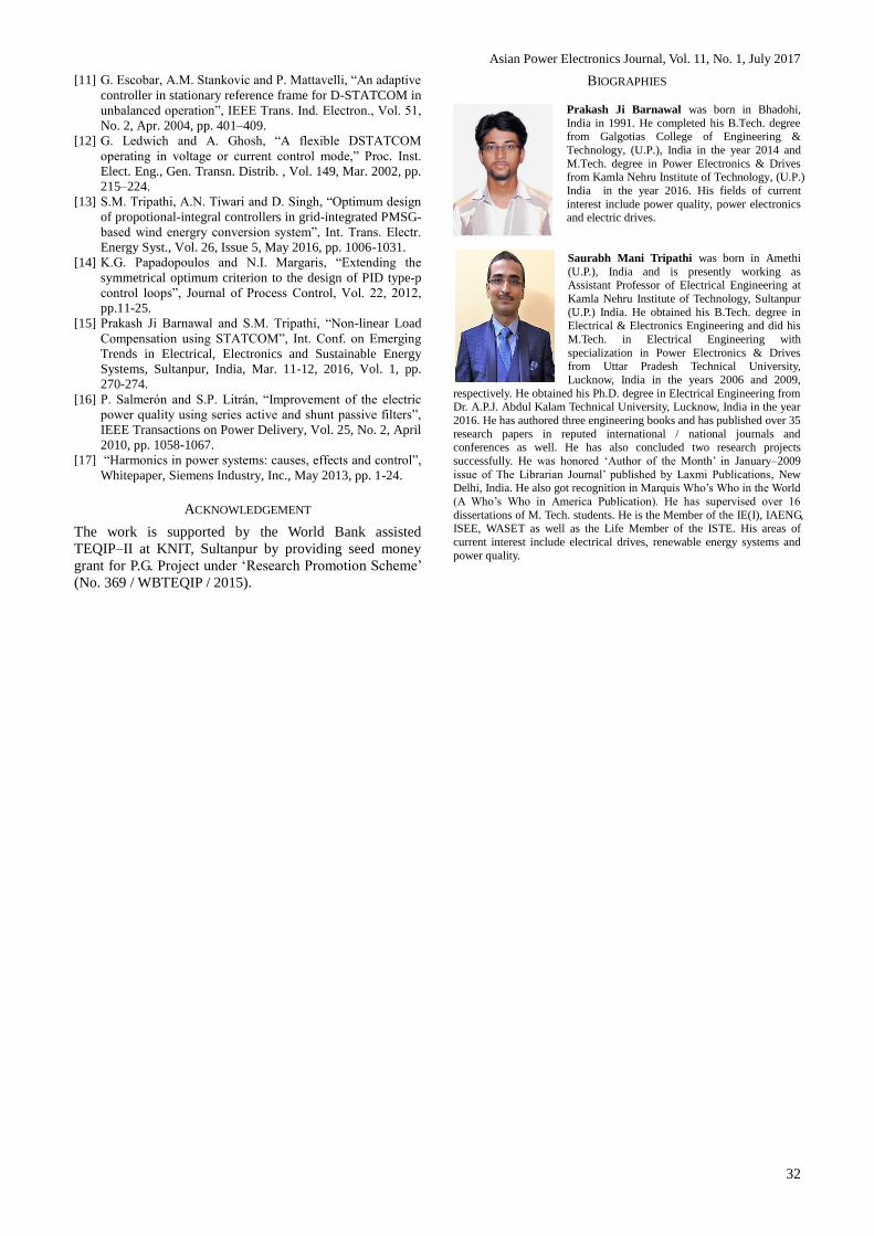
Asian Power Electronics Journal, Vol. 11, No. 1, July 2017
32
[11] G. Escobar, A.M. Stankovic and P. Mattavelli, “An adaptive
controller in stationary reference frame for D-STATCOM in
unbalanced operation”, IEEE Trans. Ind. Electron., Vol. 51,
No. 2, Apr. 2004, pp. 401–409.
[12] G. Ledwich and A. Ghosh, “A flexible DSTATCOM
operating in voltage or current control mode,” Proc. Inst.
Elect. Eng., Gen. Transn. Distrib. , Vol. 149, Mar. 2002, pp.
215–224.
[13] S.M. Tripathi, A.N. Tiwari and D. Singh, “Optimum design
of propotional-integral controllers in grid-integrated PMSG-
based wind energry conversion system”, Int. Trans. Electr.
Energy Syst., Vol. 26, Issue 5, May 2016, pp. 1006-1031.
[14] K.G. Papadopoulos and N.I. Margaris, “Extending the
symmetrical optimum criterion to the design of PID type-p
control loops”, Journal of Process Control, Vol. 22, 2012,
pp.11-25.
[15] Prakash Ji Barnawal and S.M. Tripathi, “Non-linear Load
Compensation using STATCOM”, Int. Conf. on Emerging
Trends in Electrical, Electronics and Sustainable Energy
Systems, Sultanpur, India, Mar. 11-12, 2016, Vol. 1, pp.
270-274.
[16] P. Salmerón and S.P. Litrán, “Improvement of the electric
power quality using series active and shunt passive filters”,
IEEE Transactions on Power Delivery, Vol. 25, No. 2, April
2010, pp. 1058-1067.
[17] “Harmonics in power systems: causes, effects and control”,
Whitepaper, Siemens Industry, Inc., May 2013, pp. 1-24.
ACKNOWLEDGEMENT
The work is supported by the World Bank assisted
TEQIP–II at KNIT, Sultanpur by providing seed money
grant for P.G. Project under ‘Research Promotion Scheme’
(No. 369 / WBTEQIP / 2015).
BIOGRAPHIES
Prakash Ji Barnawal was born in Bhadohi,
India in 1991. He completed his B.Tech. degree from Galgotias College of Engineering &
Technology, (U.P.), India in the year 2014 and
M.Tech. degree in Power Electronics & Drives from Kamla Nehru Institute of Technology, (U.P.)
India in the year 2016. His fields of current
interest include power quality, power electronics and electric drives.
Saurabh Mani Tripathi was born in Amethi
(U.P.), India and is presently working as Assistant Professor of Electrical Engineering at
Kamla Nehru Institute of Technology, Sultanpur
(U.P.) India. He obtained his B.Tech. degree in Electrical & Electronics Engineering and did his
M.Tech. in Electrical Engineering with
specialization in Power Electronics & Drives from Uttar Pradesh Technical University,
Lucknow, India in the years 2006 and 2009,
respectively. He obtained his Ph.D. degree in Electrical Engineering from Dr. A.P.J. Abdul Kalam Technical University, Lucknow, India in the year
2016. He has authored three engineering books and has published over 35
research papers in reputed international / national journals and conferences as well. He has also concluded two research projects
successfully. He was honored ‘Author of the Month’ in January–2009
issue of The Librarian Journal’ published by Laxmi Publications, New Delhi, India. He also got recognition in Marquis Who’s Who in the World
(A Who’s Who in America Publication). He has supervised over 16
dissertations of M. Tech. students. He is the Member of the IE(I), IAENG, ISEE, WASET as well as the Life Member of the ISTE. His areas of
current interest include electrical drives, renewable energy systems and
power quality.

33
Asian Power Electronics Journal, Vol. 11, No. 1, July 2017
Author Index
A Page
A.Jayalaxmi 6
C
Chandan Dutta 21
G G. Sridhar
J J.Bangarraju
1
6
M M. Sushama
P Prakash Ji Barnawal
P. Satish Kumar
S S. M. Tripathi
Sabha Raj Arya
V V.Rajagopal
1
28
1
21, 28
14
6
Vishal E. Puranik 14

34
Asian Power Electronics Journal, Vol. 11, No. 1, July 2017
Submission Details
Only online submission will be accepted. Please first register and submit online. The paper is in double column and is
similar to most IET or IEEE journal format. There is no page limit. Any number of pages of more than 6 will be subject to
additional charge.
The paper guidelines can be downloaded using the link: http://perc.polyu.edu.hk/apejournal/
Any queries, please contact Prof. Eric Cheng, Publishing Director of APEJ, Dept. of Electrical Engineering, The Hong
Kong Polytechnic University, Hung Hom, Hong Kong. Email: [email protected] Fax: +852-2330 1544
Any secretarial support and production related matters, please contact Dr. James Ho, Power Electronics Research Centre,
The Hong Kong Polytechnic University, Hung Hom, Hong Kong. Email: [email protected] Tel: +852-3400 3348 Fax:
+852-3400 3343
Publication Details
The Journal will be published 2-3 times a year. The first issue was published in 2007. Response time for paper acceptance
is within 3 months.
Financial Charge
All the accepted papers will be printed without charge for 6 or less pages. An additional page charge is HK$100 per page.
A hardcopy of the journal will be posted to the corresponding author free of charge. Additional copies of the journal can be
purchased at HK$200 each. The charge includes postage and packing.
All Chinese Papers will be subjected to a translational fee of HK$350 per page. It will be charged when the paper is accepted
for publication.
Advertising
Advertisement is welcome. Full page advertisement is HK$1000. For colour advertisement, the amount is doubled. All the
advertisement will be both posted online in the journal website and hardcopy of the journal.
For advertising enquiries and details, please contact Ms. Anna Chang, [email protected] .
Tel: +852-3400 3348 Fax: +852-3400 3343
For payment, please send your cheque, payable to ‘The Hong Kong Polytechnic University, address to Ms. Kit Chan,
Secretary of APEJ, Dept. of Electrical Engineering, The Hong Kong Polytechnic University, Hung Hom, Hong Kong.