POWER ELECTRONICS AND SIMULATION LABORATORY ...
51
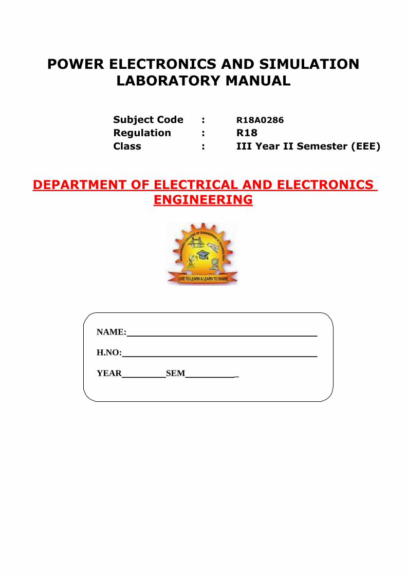
NAME: H.NO: YEAR SEM _ POWER ELECTRONICS AND SIMULATION LABORATORY MANUAL Subject Code : R18A0286 Regulation : R18 Class : III Year II Semester (EEE) DEPARTMENT OF ELECTRICAL AND ELECTRONICS ENGINEERING
-
Upload
khangminh22 -
Category
Documents
-
view
3 -
download
0
Transcript of POWER ELECTRONICS AND SIMULATION LABORATORY ...
NAME:
H.NO:
YEAR SEM _
POWER ELECTRONICS AND SIMULATION
LABORATORY MANUAL
Subject Code : R18A0286
Regulation : R18
Class : III Year II Semester (EEE)
DEPARTMENT OF ELECTRICAL AND ELECTRONICS ENGINEERING

POWER ELECTRONICS AND SIMULATION
LABORATORY MANUAL
Subject Code : R18A0286
Regulations : R18
Class : III Year II Semester (EEE)
DEPARTMENT OF ELECTRICAL AND ELECTRONICS
ENGINEERING
MALLA REDDY COLLEGE OF ENGINEERING & TECHNOLOGY
(Autonomous Institution – UGC, Govt. of India)
Recognized under 2(f) and 12 (B) of UGC ACT 1956
(Affiliated to JNTUH, Hyderabad, Approved by AICTE - Accredited by NBA & NAAC – ‘A’ Grade - ISO 9001:2015 Certified) Maisammaguda, Dhulapally (Post Via. Kompally),
Secunderabad – 500100, Telangana State, India

PROGRAM OUTCOMES (POs)
Engineering Graduates will be able to:
1. Engineering knowledge: Apply the knowledge of mathematics, science,
engineering fundamentals, and an engineering specialization to the solution of complex engineering problems.
2. Problem analysis: Identify, formulate, review research literature, and analyze complex engineering problems reaching substantiated
conclusions using first principles of mathematics, natural sciences, and engineering sciences.
3. Design / development of solutions: Design solutions for complex
engineering problems and design system components or processes that meet the specified needs with appropriate consideration for the public
health and safety, and the cultural, societal, and environmental considerations.
4. Conduct investigations of complex problems: Use research-based knowledge and research methods including design of experiments,
analysis and interpretation of data, and synthesis of the information to provide valid conclusions.
5. Modern tool usage: Create, select, and apply appropriate techniques, resources, and modern engineering and IT tools including prediction and
modeling to complex engineering activities with an understanding of the
limitations. 6. The engineer and society: Apply reasoning informed by the contextual
knowledge to assess societal, health, safety, legal and cultural issues and
the consequent responsibilities relevant to the professional engineering practice.
7. Environment and sustainability: Understand the impact of the professional engineering solutions in societal and environmental contexts,
and demonstrate the knowledge of, and need for sustainable development.
8. Ethics: Apply ethical principles and commit to professional ethics and responsibilities and norms of the engineering practice.
9. Individual and team work: Function effectively as an individual, and as
a member or leader in diverse teams, and in multidisciplinary settings. 10. Communication: Communicate effectively on complex engineering
activities with the engineering community and with society at large, such as, being able to comprehend and write effective reports and design
documentation, make effective presentations, and give and receive clear instructions.
11. Project management and finance: Demonstrate knowledge and
understanding of the engineering and management principles and apply these to one’s own work, as a member and leader in a team, to manage
projects and in multi disciplinary environments.
12. Life- long learning: Recognize the need for, and have the preparation
and ability to engage in independent and life-long learning in the
broadest context of technological change.

MALLA REDDY COLLEGE OF ENGINEERING AND TECHNOLOGY
III B.Tech EEE II SEM L T/P /D C - / 3 / - 1.5
(R18A0286) POWER ELECTRONICS AND SIMULATION LABORATORY
COURSE OBJECTIVES:
The student will understand: The characteristics of power electronic devices.
The operation of single-phase voltage controller, converters and Inverters circuits
with R and RL loads. Analyze the TPS7A4901, TPS7A8300 and TPS54160 buck
regulators.
Part - A
The following experiments are required to be conducted compulsory experiments:
1. Study the Characteristics of SCR, MOSFET & IGBT
2. Single Phase half controlled converter with R load and RL loads
3. Single Phase fully controlled bridge converter with R and RL loads 4. Three Phase half controlled bridge converter with R‐load
5. Single Phase AC Voltage Controller with R and RL Loads 6. Single Phase Cycloconverter with R and RL loads
7. Single Phase series inverter with R and RL loads 8. DC Jones chopper with R and RL Loads
In addition to the above experiments, at least any two of the following
experiments are required to be conducted from the following list. Part - B
1. Single-phase full converter using RLE loads and single-phase AC voltage
controller using RLE loads using PSPICE. 2. Resonant pulse commutation circuit and Buck chopper using PSPICE. 3. Single phase Inverter with PWM control using PSPICE.
4. Single Phase Mc-Murray converter with R and RL loads
5. Single Phase dual converter with RL loads
COURSE OUTCOMES:
After completion of this course, the student is able to
Understand the operating principles of various power electronic converters.
Use power electronic simulation packages& hardware to develop the power
converters.
Analyze and choose the appropriate converters for various applications.
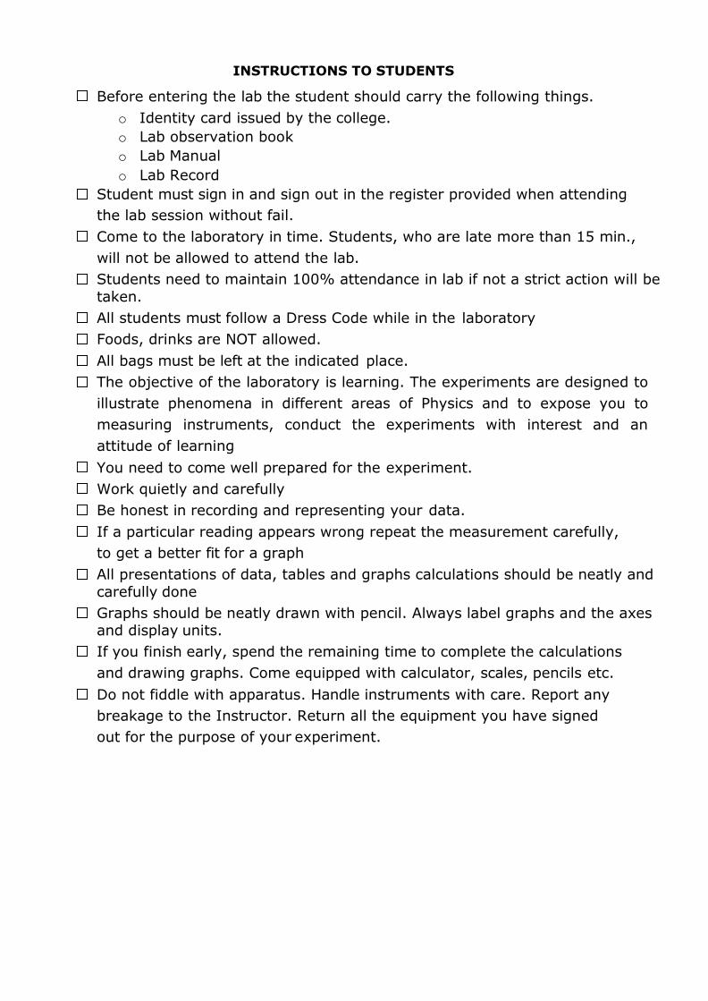
INSTRUCTIONS TO STUDENTS
Before entering the lab the student should carry the following things.
o Identity card issued by the college.
o Lab observation book
o Lab Manual
o Lab Record
Student must sign in and sign out in the register provided when attending
the lab session without fail.
Come to the laboratory in time. Students, who are late more than 15 min.,
will not be allowed to attend the lab.
Students need to maintain 100% attendance in lab if not a strict action will be
taken.
All students must follow a Dress Code while in the laboratory
Foods, drinks are NOT allowed.
All bags must be left at the indicated place.
The objective of the laboratory is learning. The experiments are designed to
illustrate phenomena in different areas of Physics and to expose you to
measuring instruments, conduct the experiments with interest and an
attitude of learning
You need to come well prepared for the experiment.
Work quietly and carefully
Be honest in recording and representing your data.
If a particular reading appears wrong repeat the measurement carefully,
to get a better fit for a graph
All presentations of data, tables and graphs calculations should be neatly and
carefully done
Graphs should be neatly drawn with pencil. Always label graphs and the axes and display units.
If you finish early, spend the remaining time to complete the calculations
and drawing graphs. Come equipped with calculator, scales, pencils etc.
Do not fiddle with apparatus. Handle instruments with care. Report any
breakage to the Instructor. Return all the equipment you have signed
out for the purpose of your experiment.

SPECIFIC SAFETY RULES FOR POWER
ELECTRONICS AND SIMULATION LABORATORY
You must not damage or tamper with the equipment or leads.
You should inspect laboratory equipment for visible damage before using it.
If there is a problem with a piece of equipment, report it to the technician or
lecturer. DONOT return equipment to a storage area
You should not work on circuits where the supply voltage exceeds 40 volts
without very specific approval from your lab supervisor. If you need to work
on such circuits, you should contact your supervisor for approval and
instruction on how to do this safely before commencing the work.
Always use an appropriate stand for holding your soldering iron.
Turn off your soldering iron if it is unlikely to be used for more than 10 minutes.
Never leave a hot soldering iron unattended.
Never touch a soldering iron element or bit unless the iron has been
disconnected from the mains and has had adequate time to cool down.
Never strip insulation from a wire with your teeth or a knife, always use
an appropriate wire stripping tool.
Shield wire with your hands when cutting it with a pliers to prevent bits of
wire flying about the bench.
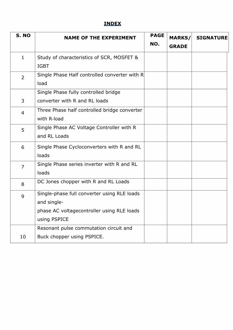
INDEX
S. NO NAME OF THE EXPERIMENT
PAGE
NO.
MARKS/
GRADE
SIGNATURE
1 Study of characteristics of SCR, MOSFET &
IGBT
2 Single Phase Half controlled converter with R
load
3
Single Phase fully controlled bridge
converter with R and RL loads
4 Three Phase half controlled bridge converter
with R‐load
5 Single Phase AC Voltage Controller with R
and RL Loads
6 Single Phase Cycloconverters with R and RL
loads
7 Single Phase series inverter with R and RL
loads
8 DC Jones chopper with R and RL Loads
9 Single-phase full converter using RLE loads
and single-
phase AC voltagecontroller using RLE loads
using PSPICE
10
Resonant pulse commutation circuit and
Buck chopper using PSPICE.

EXPERIMENT – 1 Date:
STUDY OF CHARACTERISTICS OF SCR, MOSFET & IGBT
1(A) SCR CHARACTERISTICS
AIM:
To plot V-I Characteristics of SCR
APPARATUS:
S. No Name of the Apparatus Type Range Quantity
1 SCR characteristics Trainer - - 1
2 Patch chords - -
3 DC Voltmeter Digital 2
4 DC Ammeter Digital 2
CIRCUIT DIAGRAM:
Study of Characteristics of SCR
PROCEDURE:
V - I CHARACTERISTICS:
1. Make all connections as per the circuit diagram.
2. Initially keep VG & VA at minimum position and R1 & R2 maximum position.
3. Adjust Gate current Ig to some constant by varying the VG or RG.
4. Now slowly vary VAand observe Anode to Cathode voltage VAK and Anode current IA.
5. Tabulate the readings of Anode to Cathode voltage VAK and Anode current IA.
6. Repeat the above procedure for different Gate current Ig.

GATE TRIGGRING AND FINDING VG AND IG:-
1. Keep all positions at minimum.
2. Set Anode to Cathode voltage VAK to some volts say 15V.
3. Now slowly vary the VG voltage till the SCR triggers and note down the
reading of gate current(IG) and Gate Cathode voltage(VGK) and rise of anode
current IA.
4. Repeat the same for different Anode to Cathode voltage and find VAK and IG
values.
TO FIND LATCHING CURRENT:
1. Keep R2 at middle position.
2. Apply 20V to the Anode to cathode by varying V2.
3. Raise the Vg voltage by varying VG till the device turns ON indicated by sudden
rise in IA. At what current SCR trigger it is the minimum gate current required
to turn ON the SCR.
4. Now set RA at maximum position, then SCR turns OFF, if it is not turned off reduce
VA up to turn off the device and put the gate voltage.
5. Now decrease the RA slowly, to increase the Anode current gradually in steps.
6. At each and every step, put OFF and ON the gate voltage switches VG. If the
Anode current is greater than the latching current of the device, the device says
ON even after switch OFF S1, otherwise device goes to blocking mode as soon
as the gate switch is put OFF.
7. If IA>IL then, the device remains in ON state and note that anode current as latching
current.
8. Take small steps to get accurate latching current value.
TO FIND HOLDING CURRENT:
1. Now increase load current from latching current level by varying RA & VA.
2. Switch OFF the gate voltage switch S1 permanently (now the device is in ON state).
3. Now increase load resistance(R2), so that anode current reducing, at some
anode current the device goes to turn off .Note that anode current as holding
current.
4. Take small steps to get accurate holding current value.
5. Observe that IH<IL.

TABULAR COLUMN:
S. No
IG=
S. No
IG=
VAK
IA
VAK
IA
1 1
2 2
3 3
4 4
5 5
MODEL GRAPHS:
RESULT:
SIGNATURE OF FACULTY
S. No VAK =
S. No VAK =
VGK
IG
VGK IG
1 1
2 2
3 3
4 4
5 5

EXPERIMENT – 1(B) Date:
MOSFET CHARACTERISTICS
AIM:
To study the output and transfer characteristics of MOSFET
APPARATUS:
S. No Equipment Type Range Quantity
1 MOSFET characteristics Trainer
2 Patch chords
3 DC Voltmeter
4 DC Ammeter
CIRCUIT DIAGRAM:
Study of Characteristics of MOSFET
PROCEDURE:
TRANSFER CHARACTERISTICS:
1. Make all connections as per the circuit diagram.
2. Initially keep V1 & V2 at minimum position and R1 & R2 middle position.
3. Set VDS to some say 10V.
4. Slowly vary Gate source voltage VGS by varying V1.
5. Note down ID and VGS readings for each step.
6. Repeat above procedure for 20V & 30V of VDS. Draw Graph between ID & VGS.
13 | P a g e

23 | P a g e
OUTPUT CHARACTERISTICS:
1. Initially set VGS to some value say 3V by varying V1.
2. Slowly vary V2 and note down ID and VDS.
3. At particular value of VGS there a pinch off voltage between drain and source.
4. If VDS< VP device works in the constant resistance region and IO is directly proportional to VDS.
If VDS>VP device works in the constant current region.
5. Repeat above procedure for different values of VGS and draw graph between ID VS VDS. TABULAR COLUMN:
S.No VDS= (Volts)
S. No VDS = (Volts)
VGS (V) ID(A) VGS (V) ID(A)
1 1
2 2
3 3
4 4
5 5
MODEL GRAPH:
Transfer Characteristic of MOSFET Output Characteristics of MOSFE
RESULT:
SIGNATURE OF FACULTY
S.No.
VGS = VOLTS S. No
VGS = VOLTS VDS
(Volts)
ID
(Amps)
VDS
(Volts)
ID
(Amps)
1 1
2 2
3 3
4 4
5 5

24 | P a g e
EXPERIMENT – 1(C) Date:
IGBT CHARACTERISTICS
AIM: To study the output and transfer characteristics of IGBT.
APPARATUS:
S. No Equipment Type Range Quantity
1 IGBT characteristics Trainer Kit
2 Patch chords
3 DC Voltmeter
4 DC Ammeter
CIRCUIT DIAGRAM:
Study of Characteristics IGBT
PROCEDURE:
TRANSFER CHARACTERISTICS:
1. Make all connections as per the circuit diagram.
2. Initially keep V1 & V2 at minimum position and R1 & R2 middle position.
3. Set VCE to some say 10V.
4. Slowly vary Gate Emitter voltage VGE by varying V1.
5. Note down IC and VGE readings for each step.
6. Repeat above procedure for 20V & 25V of VDS. Draw Graph between ID & VGS.

25 | P a g e
OUTPUT CHARACTERISTICS:
1. Initially set VGE to some value say 5V by varying V1.
2. Slowly vary V2 and note down IC and VCE readings.
3. At particular value of VGS there is a pinch off voltage VP between Collector and Emitter.
4. If VCE< VP device works in the constant resistance region and IC is directly proportional
to VCE. If VCE>VP device works in the constant current region.
5. Repeat above procedure for different values of VGE and draw graph between IC VS VGE. TABULAR COLUMN:
S. No
VGE= S. No
VGE
VCE
IC VCE
IC
1 1
2 2
3 3
4 4
5 5
MODEL GRAPH:
Transfer Characteristics of IGBT Output Characteristics of IGBT
RESULT:
SIGNATURE OF FACULTY
S. No
VCE
S. No
VCE
VGE
IC VGE
IC
1 1
2 2
3 3
4 4
5 5

26 | P a g e
EXPERIMENT – 2 Date:
SINGLE PHASE HALF CONTROLLED BRIDGE CONVERTER
AIM:
To study the single phase half controlled bridge converter with R & RL Load.
APPARATUS:
SNo Equipment Range Type Quantity
1 Single phase half controlled bridge converter power circuit and firing circuit
2 CRO with deferential MODEL
3 Patch chords and probes
4 Isolation Transformer
5 Variable Rheostat
6 Inductor
7 DC Voltmeter
8 DC Ammeter
CIRCUIT DIAGRAM:
Circuit Diagram of Single Phase Half Controlled Bridge Converter
PROCEDURE:
1. Make all connections as per the circuit diagram.
2. Connect first 30V AC supply from Isolation Transformer to circuit.
3. Connect firing pulses from firing circuit to Thyristors as indication in circuit.
4. Connect resistive load 200Ω / 5A to load terminals and switch ON the MCB and
IRS switch and trigger output ON switch.

27 | P a g e
5. Connect CRO probes and observe waveforms in CRO, Ch-1 or Ch-2, across load
and device in single phase half controlled bridge converter.
6. By varying firing angle gradually up to 1800 and observe related waveforms.
7. Measure output voltage and current by connecting AC voltmeter & Ammeter.
8. Tabulate all readings for various firing angles.
9. For RL Load connect a large inductance load in series with Resistance and observe
all waveforms and readings as same as above.
10. Observe the various waveforms at different points in circuit by varying the Resistive
Load and Inductive Load.
11. Calculate the output voltage and current by theoretically and compare with it
practically obtained values.
TABULAR COLUMN:
S. No
Input Voltage
(V in)
Firing angle in Degrees
Output voltage (V0) Output Current (I0)
Theoretical Practical Theoretical Practical
1
2
3
4
5
6
MODEL CALCULATIONS:
V0= (√2V / ∏))* (1+Cos α) I0= (√2V / ∏R) * (1+Cos α)
α= Firing Angle
V= RMS Value across transformer output

28 | P a g e
MODEL GRAPH:
Output Wave Forms of Single Phase Half Controlled Bridge Converter
RESULT
SIGNATURE OF FACULTY
29 | P a g e
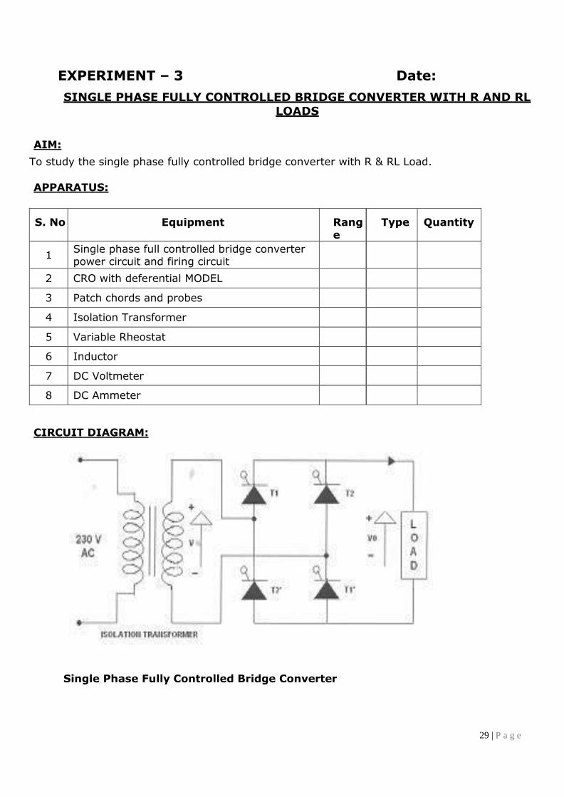
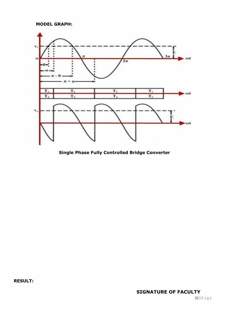
EXPERIMENT – 3 Date:
SINGLE PHASE FULLY CONTROLLED BRIDGE CONVERTER WITH R AND RL
LOADS
AIM:
To study the single phase fully controlled bridge converter with R & RL Load.
APPARATUS:
S. No Equipment Range
Type Quantity
1 Single phase full controlled bridge converter power circuit and firing circuit
2 CRO with deferential MODEL
3 Patch chords and probes
4 Isolation Transformer
5 Variable Rheostat
6 Inductor
7 DC Voltmeter
8 DC Ammeter
CIRCUIT DIAGRAM:
Single Phase Fully Controlled Bridge Converter

30 | P a g e
PROCEDURE:
1. Make all connections as per the circuit diagram.
2. Connect firstly 30V AC supply from Isolation Transformer to circuit.
3. Connect firing pulses from firing circuit to Thyristors as indication in circuit.
4. Connect resistive load 200Ω / 5A to load terminals and switch ON the MCB and
IRS switch and trigger output ON switch.
5. Connect CRO probes and observe waveforms in CRO across load and device in
single phase fully controlled bridge converter.
6. By varying firing angle gradually up to 1800 and observe related waveforms.
7. Measure output voltage and current by connecting AC voltmeter & Ammeter.
8. Tabulate all readings for various firing angles.
9. For RL Load connect a large inductance load in series with Resistance and
observe all waveforms and readings as same as above.
10. Observe the various waveforms at different points in circuit by varying the Resistive
Load and Inductive Load.
11. Calculate the output voltage and current by theoretically and compare with it
practically obtained values.
TABULAR COLUMN:
MODEL CALCULATIONS:
V0
For R-L Load:
= (2√2V/∏) * Cos α;
For R Load:
V0 = (√2V/∏) * (1+Cos α)
I0
α
= (2√2V/∏R) * Cos α;
= Firing Angle
I0 = (√2V /∏R) * (1+Cosα)
V = RMS Value across transformer output
S.No Input Voltage
(Vin)
Firing angle in Degrees
Output voltage (V0) Output Current (I0)
Theoretical Practical Theoretical Practical
1
2
3
4
5
6

31 | P a g e
32 | P a g e
MODEL GRAPH:
Single Phase Fully Controlled Bridge Converter
RESULT:
SIGNATURE OF FACULTY
33 | P a g e
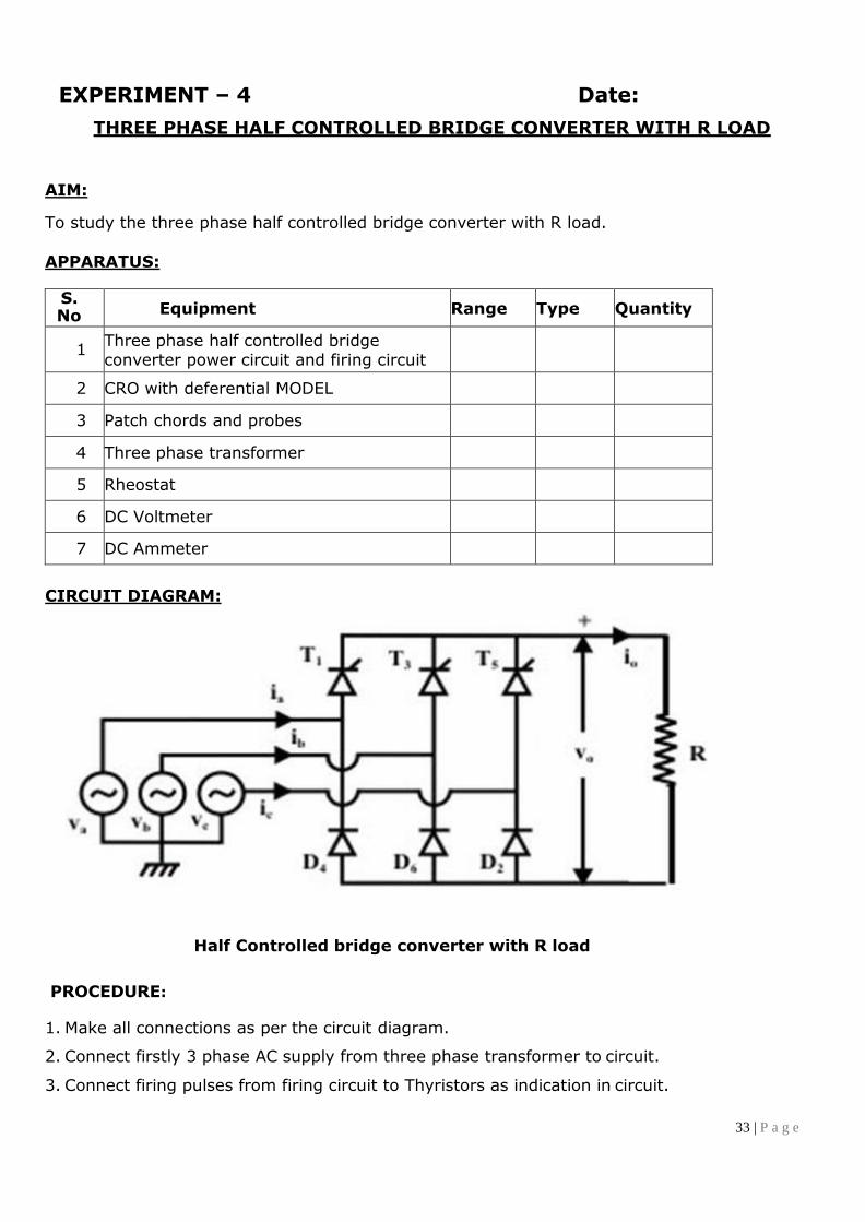
EXPERIMENT – 4 Date:
THREE PHASE HALF CONTROLLED BRIDGE CONVERTER WITH R LOAD
AIM:
To study the three phase half controlled bridge converter with R load.
APPARATUS:
S. No Equipment Range Type Quantity
1 Three phase half controlled bridge converter power circuit and firing circuit
2 CRO with deferential MODEL
3 Patch chords and probes
4 Three phase transformer
5 Rheostat
6 DC Voltmeter
7 DC Ammeter
CIRCUIT DIAGRAM:
Half Controlled bridge converter with R load
PROCEDURE:
1. Make all connections as per the circuit diagram.
2. Connect firstly 3 phase AC supply from three phase transformer to circuit.
3. Connect firing pulses from firing circuit to Thyristors as indication in circuit.

34 | P a g e
4. Connect resistive load 200Ω / 5A to load terminals and switch ON the MCB and IRS
switch and trigger output ON switch.
5. Connect CRO probes and observe waveforms in CRO across load and device in three
phase half controlled bridge converter.
6. By varying firing angle gradually up to 1800 and observe related waveforms.
7. Measure output voltage and current by connecting DC voltmeter & Ammeter.
8. Tabulate all readings for various firing angles.
9. Calculate the output voltage and current by theoretically and compare with it
practically obtained values.
TABULAR COLUMN:
S. No Input
Voltage
(Vin)
Firing
Angle in Degrees
Output voltage (V0) Output Current (I0)
Theoretical Practical Theoretical Practical
1
2
3
4
5
6
MODEL CALCULATIONS:
Vo = 3 Vml*(1+cosα)/2π Io = 3 Vml*(1+cosα)/2πR α=
firing angle
Vml = line to line voltage
MODEL GRAPHS:
Input and output wave forms of a three phase half controlled bridge converter

37 | P a g e
RESULT:
SIGNATURE OF FACULTY
38 | P a g e
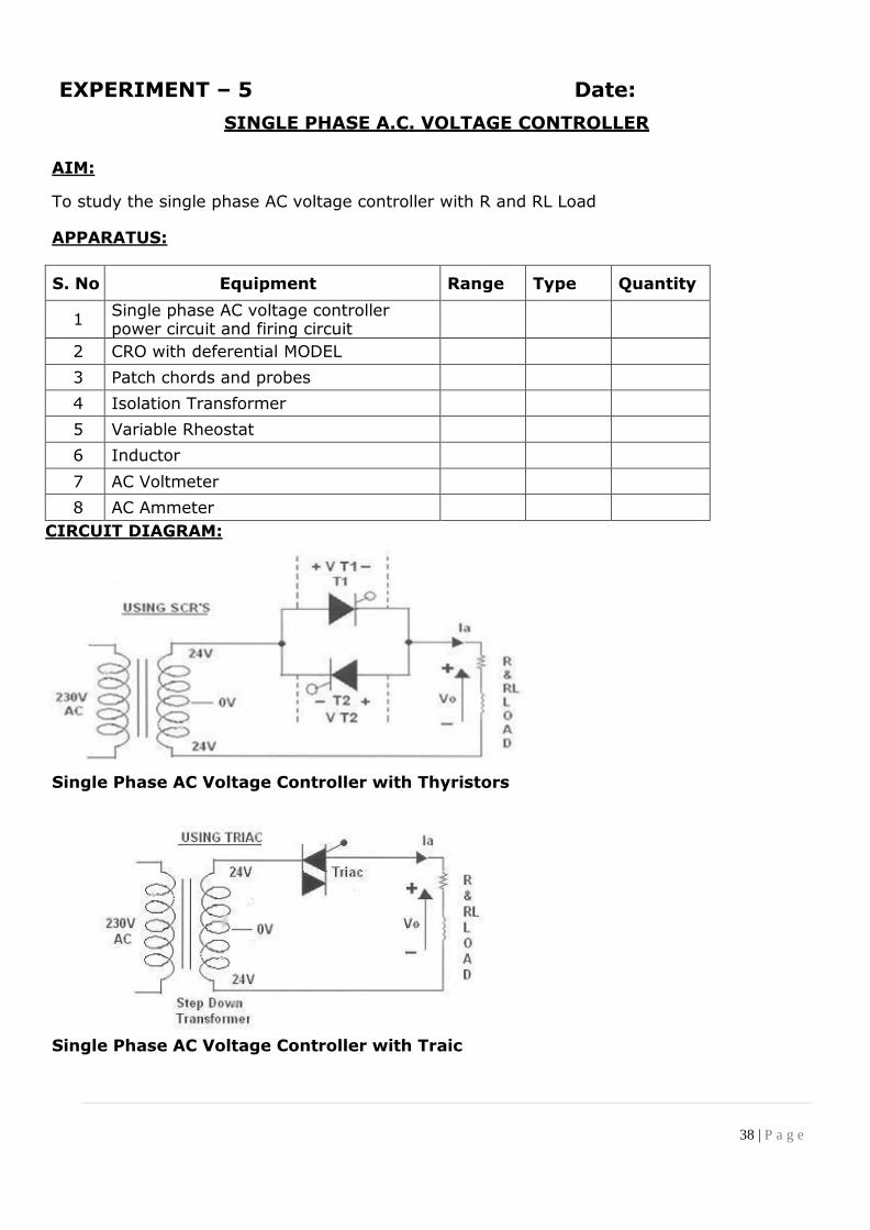
EXPERIMENT – 5 Date:
SINGLE PHASE A.C. VOLTAGE CONTROLLER
AIM:
To study the single phase AC voltage controller with R and RL Load
APPARATUS:
S. No Equipment Range Type Quantity
1 Single phase AC voltage controller power circuit and firing circuit
2 CRO with deferential MODEL
3 Patch chords and probes
4 Isolation Transformer
5 Variable Rheostat
6 Inductor
7 AC Voltmeter
8 AC Ammeter
CIRCUIT DIAGRAM:
Single Phase AC Voltage Controller with Thyristors
Single Phase AC Voltage Controller with Traic
39 | P a g e
PROCEDURE:
AC VOLTAGE CONTROLLER WITH TWO THYRISTORS:
1. Make all connections as per the circuit diagram.
2. Connect firstly 30V AC supply from Isolation Transformer to circuit.
3. Connect firing pulses from firing circuit to Thyristors as indication in circuit.
4. Connect resistive load 200Ω / 5A to load terminals and switch ON the MCB and
IRS switch and trigger output ON switch.
5. Observe waveforms in CRO, across load by varying firing angle gradually up to 1800.
6. Measure output voltage and current by connecting AC voltmeter & Ammeter.
7. Tabulate all readings for various firing angles.
8. For RL Load connect a large inductance load in series with Resistance and
observe all waveforms and readings as same as above.
9. Observe the various waveforms at different points in circuit by varying the Resistive
Load and Inductive Load.
10.Calculate the output voltage and current by theoretically and compare with it
practically obtained values.
A.C. VOLTAGE CONTROLLER WITH TRIAC:
1. Make all connections as per the circuit diagram.
2. Connect firstly 30V AC supply from Isolation Transformer to circuit.
3. Connect firing pulse from firing circuit to TRIAC as indication in circuit.
4. Connect resistive load 200Ω / 5A to load terminals and switch ON the MCB and
IRS switch and trigger output ON switch.
5. Observe waveforms in CRO, across load by varying firing angle gradually up to 1800.
6. Measure output voltage and current by connecting AC voltmeter & Ammeter.
7. Tabulate all readings for various firing angles.
8. For RL Load connect a large inductance load in series with Resistance and
observe all waveforms and readings as same as above.
9. Observe the various waveforms at different points in circuit by varying the Resistive
Load and Inductive Load.
10.Calculate the output voltage and current by theoretically and compare with it
practically obtained values.

40 | P a g e
TABULAR COLUMN:
S.No. Input Voltage
(Vin)
Firing angle in Degrees
Output voltage (V0r) Output Current (I0r)
Theoretical Practical Theoretical Practical
1
2
3
4
5
6
MODEL CALCULATIONS:
I0r = V0r / R
α = Firing Angle
V = RMS Value across transformer output
MODEL GRAPH:
Single Phase AC Voltage controller with R - Load

41 | P a g e
Single Phase AC voltage controller with RL Load
RESULT:
SIGNATURE OF FACULTY

42 | P a g e
EXPERIMENT – 6 Date:
SINGLE PHASE CYCLO - CONVERTER WITH R AND RL LOADS
AIM:
To study the single - phase Cyclo Converter with R & RL Load.
APPARATUS:
S. No Equipment Range Type Quantity
1 Single phase Cycloconverter power circuit and firing circuit
2 CRO with deferential MODEL
3 Patch chords and probes
4 Isolation Transformer (Centre - Tapped )
5 Variable Rheostat
6 Inductor
7 AC Voltmeter
8 AC Ammeter
CIRCUIT DIAGRAM:
Circuit Diagram of Single Phase Cyclo Converter
43 | P a g e
PROCEDURE:
1. Make all connections as per the circuit diagram.
2. Connect firstly (30V-0-30V) AC supply from Isolation Transformer to circuit.
3. Connect firing pulses from firing circuit to Thyristors as indication in circuit.
4. Connect resistive load 200Ω / 5A to load terminals.
5. Set the frequency division switch to (2, 3, 4,…, 9) your required output frequency.
6. Switch ON the MCB and IRS switch and trigger output ON switch.
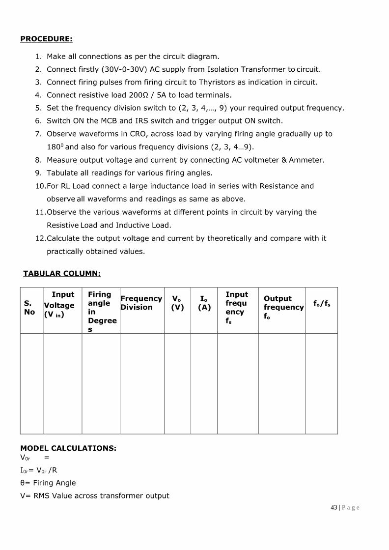
7. Observe waveforms in CRO, across load by varying firing angle gradually up to
1800 and also for various frequency divisions (2, 3, 4…9).
8. Measure output voltage and current by connecting AC voltmeter & Ammeter.
9. Tabulate all readings for various firing angles.
10.For RL Load connect a large inductance load in series with Resistance and
observe all waveforms and readings as same as above.
11.Observe the various waveforms at different points in circuit by varying the
Resistive Load and Inductive Load.
12.Calculate the output voltage and current by theoretically and compare with it
practically obtained values.
TABULAR COLUMN:
S. No
Input
Voltage
(V in)
Firing angle in
Degrees
Frequency Division
Vo
(V) Io
(A)
Input frequency
fs
Output frequency
fo
fo/fs
MODEL CALCULATIONS:
V0r =
I0r= V0r /R
θ= Firing Angle
V= RMS Value across transformer output

44 | P a g e
45 | P a g e
MODEL GRAPH:
Output Wave Forms of Single Phase Cyclo Converter
RESULT:
SIGNATURE OF FACULTY
46 | P a g e
EXPERIMENT – 7 Date:
SINGLE PHASE SERIES INVERTER WITH R AND RL LOADS
AIM:
To obtain the performance characteristics of a single phase series inverter
APPARATUS:
S. No Equipment Range Type Quantity
1 Series inverter power circuit and firing circuit
2 CRO with deferential MODEL
3 Patch chords and probes
4 Regulated dc power supply
5 Variable Rheostat
6 Inductor
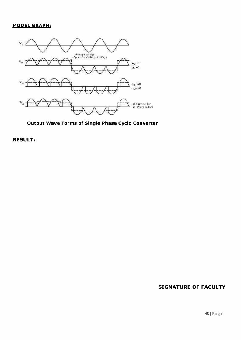
CIRCUIT DIAGRAM:
Circuit Diagram Single Phase Series Inverter
PROCEDURE:
1. Make all connections as per the circuit diagram.
2. Give the DC power supply 30V to the terminal pins located in the power circuit.
3. Connect firing pulses from firing circuit to Thyristors as indication in circuit.
4. Connect resistive load 200Ω / 5A to load terminals and switch ON the MCB and
IRS switch and trigger output ON switch.
5. By varying the frequency pot, observe related waveforms.
If the inverter frequency is increases above the resonant frequency of the power circuit

47 | P a g e
commutation fails. Then switch OFF the DC supply, reduce the inverter frequency and try again.
6. Repeat the above same procedure for different value of L,C load and also above the
wave forms with and without fly wheel diodes.
7. Total output wave forms entirely depends on the load, and after getting the perfect
wave forms increase the input supply voltage up to 30V and follow the above
procedure.
8. Switch OFF the DC supply first and then Switch OFF the inverter.( Switch OFF the
trigger pulses will lead to short circuit)
MODEL WAVEFORMS:
Output Wave Forms of Single Phase Series Inverter
RESULT:
SIGNATURE OF FACULTY

48 | P a g e
EXPERIMENT – 8 Date:
DC JONE’S CHOPPER
AIM:
To study the characteristics of DC Jone’s Chopper.
APPARATUS:
S. No Equipment Range Type Quantity
1 DC chopper power MODEL
2 Triggering circuit (DC chopper)
3 Rheostat
4 Digital multimeter
5 CRO
6 Patch Cards
CIRCUIT DIAGRAM:
Circuit Diagram of Jones Chopper
49 | P a g e
PROCEDURE:
For R – Load: 1. Connections are made as shown in the figure. Use 50Ώ Rheostat for R -
Load (Freewheeling diode ( DM ) is to be connected only for RL load ).
2. Adjust VRPS output to 10v and connect to DC chopper MODEL.
3. Switch on DC toggle switch of chopper MODEL.
4. Switch on the trigger input by pushing- in pulse switch.
5. Observe the output waveform across load on CRO.
6. Keep the duty cycle at mid position and vary the frequency from minimum to
maximum and record the output voltage readings.
7. Note down the output waveform for mid value of frequency and duty cycle.
R - L Load:
1. Connections are made as shown in fig. Load is 50Ώ Rheostat in series with inductor L
2. =25mH or 50mH.
3. Follow the same procedure as listed in steps 2 to 8 above.3. Readings and output
waveform is to be recorded with and without freewheeling diode. [NOTE: In both
switching on / switching off of the equipment. First use DC toggle switch and then
the pulsar].
TABULAR COLUMN:
Constant Duty Cycle
Duty Cycle: 50%, VIN=10 to 15 V S.
No Frequency(Hz) V0(Volts)
1
2
3
4
5
6
7
8
9
10

50 | P a g e
Constant Frequency, Frequency Control
S.
No TON(sec) TOFF(sec)
Duty Cycle (%)
VO
(Volts)
1
2
3
4
5
6
7
8
9
MODEL GRAPH:
Output Characteristics of DC Jones Chopper
RESULT:
SIGNATURE OF FACULTY

EXPERIMENT – 9(A) Date:
PSPICE SIMULATION OF SINGLE PHASE FULL WAVE RECTIFIER USING RLE
LOADS
AIM:
To obtain the performance characteristics of Single Phase Semi converter for R, RL, RLE Loads
Using MATLAB / Simulink
APPARATUS:
S. No. Name of the Equipment
1. PC With Desktop
2. Matlab / Simulink
CIRCUIT DIAGRAM:
Circuit Diagram of PSPICE Simulation of Single Phase Full Wave Rectifier PROCEDURE:
1. Represent the nodes for a given circuit.
2. Write spice program by initializing all the circuit parameter as per given flow chart.
3. From desktop of your computer click on “START” menu followed by “programs” and
then clicking appropriate program group as “DESIGN LAB EVAL8 followed by “DESIGN
MANAGER”.
4. Open the run text editor from microsim window & start writing pspice program.

5. Save the program with .cir extension.
6. Open the run spice A / D window from microsim window.
7. Open file menu from run spice A / D window then open saved circuit file.
8. If there are any errors, simulates will be displayed with statement as “simulation
error occurred”.
9. To see the errors click on o/p file icon and open examine o / p.
10. To make changes in the program open the circuit file, modify, save & Run the program.
11. If there are no errors, simulation will be completed & it will be displayed with a
statement as “simulation completed”.
12. To see the o / p click on o / p file icon & open examine o / p then note down the values.
13. If probe command is used in the program, click on o / p file icon &open run probe.
Select variables to plot on graphical window and observe the o / p plots then take
print outs of that.
PROGRAM CODE:
CLC
VS 10 0 SIN (0 325V 50HZ)
VG1 6 2 PULSE (0V 10V 2500US 1NS 1NS 100US 20000US)
VG2 7 0 PULSE (0V 10V 2500US 1NS 1NS100US 20000US)
VG3 8 2 PULSE (0V 10V 12500US 1NS 1NS 100US 20000US)
VG4 9 1 PULSE (0V 10V 12500US 1NS 1NS 100US 20000US)
R 2 4 10
L 4 5 20MH
VX 5 3 DC 10V
VY 10 1 DC 10V
C 2 11 793UF
RX 11 3 0.1
XT1 1 2 6 2 SCR
XT2 3 0 7 0 SCR
XT3 0 2 8 2 SCR
XT4 3 1 9 1 SCR
.SUBCKT SCR 1 2 3 2
S1 1 5 6 2 SMOD
RG 3 4 50
VX 4 2 DC 0V

VY 5 7 DC 0V
DT 7 2 DMOD
RT 6 2 1
CT 6 2 10UF
F1 2 6 POLY (2) VX VY 0 50 11
.MODEL SMOD VSWITCH (RON=0.0105 ROFF=10E+5 VON=0.5V VOFF=0V)
.MODEL DMOD D (IS=2.2E-15 BV=1200V TT=0 CJO=0)
.ENDS SCR
.TRAN 50US 100MS 50MS 50US
.PROBE
.OPTIONS ABSTOL=1.00N RELTOL=1.0M VNTOL=0.1 ITL5=20000
.FOUR 50HZ I(VY)
.END
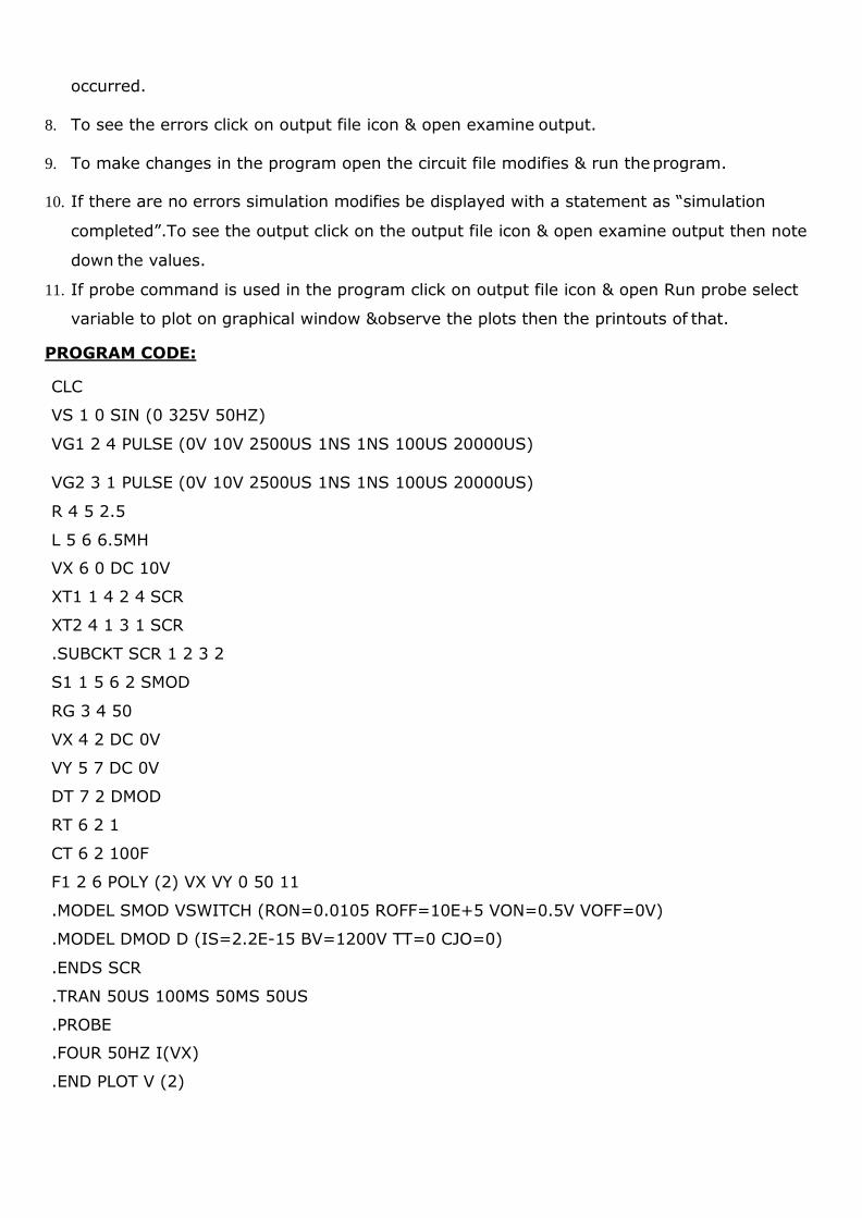
Plot v (2) MODEL WAVEFORMS:
Output Wave Forms of PSPICE Simulation of Single Phase Full Wave Rectifier
RESULT:
SIGNATURE OF FACULTY

EXPERIMENT – 9(B) Date:
PSPICE SIMULATION OF SINGLE PHASE AC VOLTAGE CONTROLLER
USING RLE LOADS
AIM:
To obtain the performance characteristics of Single Phase for R, RL, RLE Loads Using
MATLAB / Simulink
APPARATUS:
CIRCUIT DIAGRAM:
Circuit Diagram of PSPICE Simulation of Single Phase Ac Voltage Controller
PROCEDURE:
1. Represent the nodes for again circuit.
2. Write PSPICE program by initializing all the circuit parameters as per given flow chart From
desktop of your computer click “start” menu followed “PROGRAMS” & then clicking
appropriate program group as “DESIGN LAB tv 218” followed by design manager.
3. Open the Run text editor from microsim window & start writing PSPICE program.
4. Save the program with .cir extension. (Ex: DA.cir).
5. Open the RUN SPICE A / D window from microsim window.
6. Open file menu from RUN SPICE A / D window then open saved circuit file.
7. If there are any errors, simulation will be displayed with statement as “simulation error
S. No. Name of the Equipment
1. PC With Desktop
2. MATLAB / Simulink
occurred.
8. To see the errors click on output file icon & open examine output.
9. To make changes in the program open the circuit file modifies & run the program.
10. If there are no errors simulation modifies be displayed with a statement as “simulation
completed”.To see the output click on the output file icon & open examine output then note
down the values.
11. If probe command is used in the program click on output file icon & open Run probe select
variable to plot on graphical window &observe the plots then the printouts of that.
PROGRAM CODE:
CLC
VS 1 0 SIN (0 325V 50HZ)
VG1 2 4 PULSE (0V 10V 2500US 1NS 1NS 100US 20000US)
VG2 3 1 PULSE (0V 10V 2500US 1NS 1NS 100US 20000US)
R 4 5 2.5
L 5 6 6.5MH
VX 6 0 DC 10V
XT1 1 4 2 4 SCR
XT2 4 1 3 1 SCR
.SUBCKT SCR 1 2 3 2
S1 1 5 6 2 SMOD
RG 3 4 50
VX 4 2 DC 0V
VY 5 7 DC 0V
DT 7 2 DMOD
RT 6 2 1
CT 6 2 100F
F1 2 6 POLY (2) VX VY 0 50 11
.MODEL SMOD VSWITCH (RON=0.0105 ROFF=10E+5 VON=0.5V VOFF=0V)
.MODEL DMOD D (IS=2.2E-15 BV=1200V TT=0 CJO=0)
.ENDS SCR
.TRAN 50US 100MS 50MS 50US
.PROBE
.FOUR 50HZ I(VX)
.END PLOT V (2)
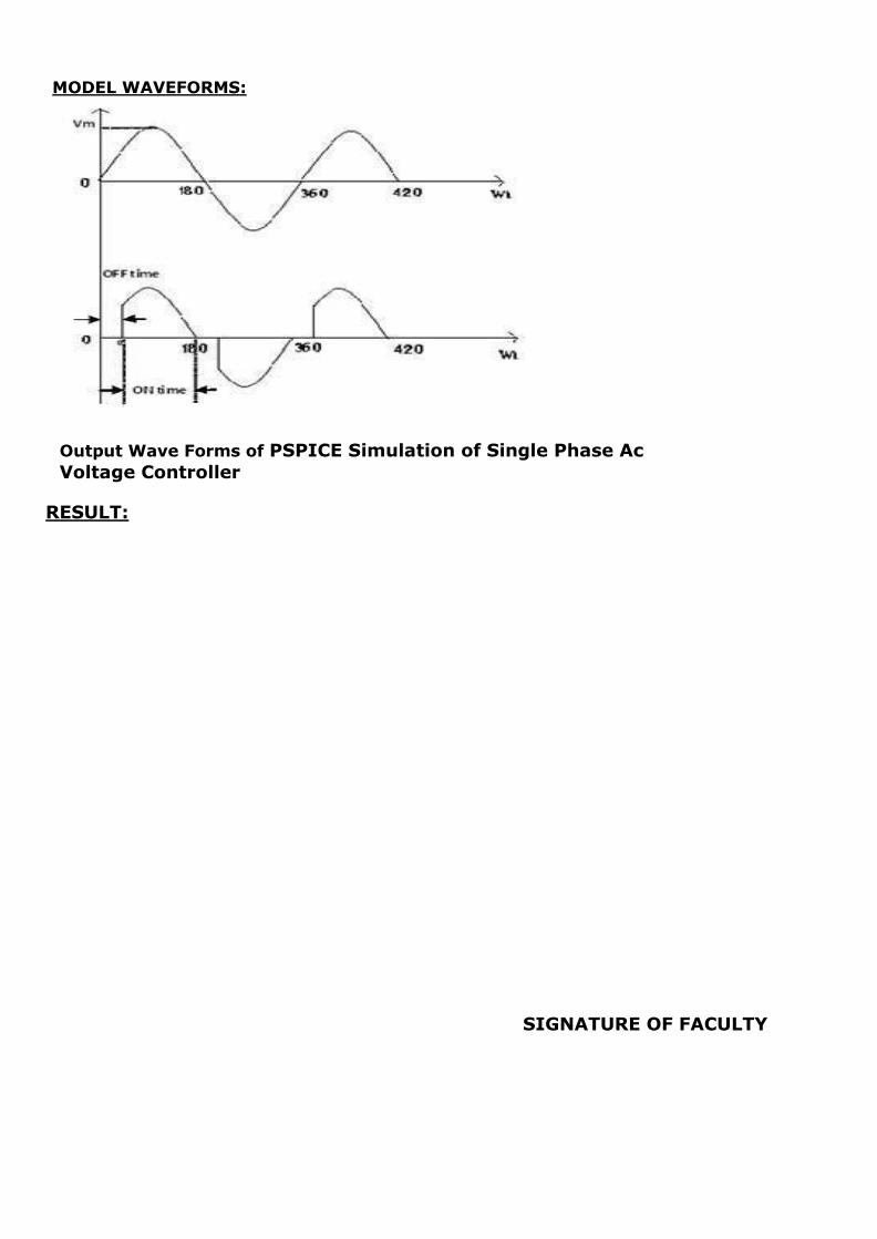
MODEL WAVEFORMS:
Output Wave Forms of PSPICE Simulation of Single Phase Ac
Voltage Controller
RESULT:
SIGNATURE OF FACULTY
73 | P a g e
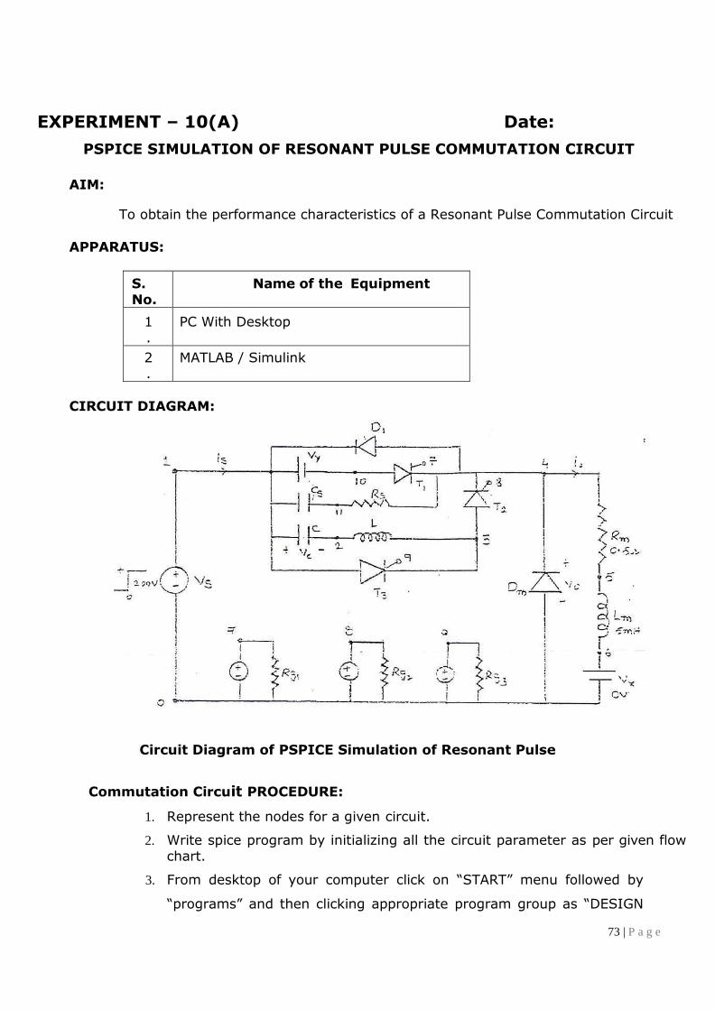
EXPERIMENT – 10(A) Date:
PSPICE SIMULATION OF RESONANT PULSE COMMUTATION CIRCUIT
AIM:
To obtain the performance characteristics of a Resonant Pulse Commutation Circuit
APPARATUS:
S. No.
Name of the Equipment
1.
PC With Desktop
2.
MATLAB / Simulink
CIRCUIT DIAGRAM:
Circuit Diagram of PSPICE Simulation of Resonant Pulse
Commutation Circuit PROCEDURE:
1. Represent the nodes for a given circuit.
2. Write spice program by initializing all the circuit parameter as per given flow chart.
3. From desktop of your computer click on “START” menu followed by
“programs” and then clicking appropriate program group as “DESIGN

74 | P a g e
LAB EVAL8 followed by “DESIGN MANAGER.”
4. Open the run text editor from microsim window & start writing pspice
program.
5. Save the program with .cir extension.
6. Open the run spice A / D window from microsim window.
7. Open file menu from run spice A / D window then open saved circuit file.
8. If there are any errors, simulates will be displayed with statement
as “simulation error occurred”.
9. To see the errors click on o/p file icon and open examine o / p.
10. To make changes in the program open the circuit file, modify, save & Run the program.
11. If there are no errors, simulation will be completed & it will be
displayed with a statement as “simulation completed”.
12. To see the o / p click on o / p file icon & open examine o / p then note down
the values.
13. If .probe command is used in the program, click on o / p file icon
&open run probe. Select variables to plot on graphical window and
observe the o / p plots then take print outs of that.
PROGRAM CODE:
CLC
VS 1 0 DC 200V
VG1 7 0 PULSE (0V 100V 0 1US 1US
0.4MS 1MS) VG2 8 0 PULSE (0V 100V
0.4MS 1US 1US 0.6MS 1MS) VG3 9 0
PULSE (0V 100V 0.1US 1US 1US
0.2MS 1MS) RG1 7 0 10MEG
RG2 8 0 10MEG
RG3 9 0 10MEG
CS 10 11 0.1UF
RS 11 4 750
C 1 2 31.2UF IC=200V
L 2 3 6.4UH
D1 4 1 DMOD
DM 0 4 DMOD

75 | P a g e
.MODEL DMOD
D(IS=1E-25 BV=1000V)
RM 4 5 0.5
LM 5 6 5MH
VX 6 0 DC 0V
VY 1 10 DC 0V
XT1 10 4 7 0 DCSCR
XT2 3 4 8 0 DCSCR
XT3 1 3 9 0 DCSCR
.SUBCKT DCSCR 1 2 3 4
DT 5 2 DMOD
ST 1 5 3 4 SMOD
.MODEL DMOD D (IS=1E-25 BV=1000V)
.MODEL SMOD VSWITCH (RON=0.1 ROFF=10E+6 VON=10 VOFF=5V)
.ENDS DCSCR
.TRAN 0.5US 3MS 1.5MS 0.5US
.PROBE
.END
PLOT I (C ) AND V(2)
RESULT:
SIGNATURE OF FACULTY

EXPERIMENT – 10(B) Date:
PSPICE SIMULATION OF BUCK CHOPPER
AIM:
To obtain the performance characteristics of BUCK CHOPPER
APPARTUS:
S. No. Name of the Equipment
1.
PC With Desktop
2.
PSPICE
CIRCUIT DIAGRAM:
Circuit Diagram of PSPICE Simulation of Buck Chopper
PROCEDURE:
1. Represent the nodes for a given circuit.
2. Write spice program by initializing all the circuit parameter as per given flow chart.
3. From desktop of your computer click on “ START ” menu followed by “
programs ” and then clicking appropriate program group as “ DESIGN
LAB EVAL8 followed by “ DESIGN MANAGER.”
4. Open the run text editor from microsim window & start writing pspice
program.
5. Save the program with .cir extension.
6. Open the run spice A / D window from microsim window.
7. Open file menu from run spice A / D window then open saved circuit file.
8. If there are any errors, simulates will be displayed with statement
as “simulation error occurred”.
9. To see the errors click on o / p file icon and open examine o / p.
10. To make changes in the program open the circuit file, modify, save & Run the program.
11. If there are no errors, simulation will be completed & it will be
displayed with a statement as “simulation completed”.
12. To see the o / p click on o / p file icon & open examine o / p then note down the values.
13. If .probe command is used in the program, click on o / p file icon
&open run probe. Select variables to plot on graphical window and
observe the o / p plots then take print outs of that.
PROGARM CODE:
CLC
VS 1 0 DC 110V
VY 1 2 DC 0V
VG 7 3 PULSE (0V 20V 0 0.1NS 0.1NS
27.28US 50US) RB 7 6 250
LE 3 4 681.82UH
CE 4 0 8.33UF IC=60V
L 4 8 40.91UH
R 8 5 3
VX 5 0 DC 0V
DM 0 3 DMOD
.MODEL DMOD D (IS=2.2E-15
BV=1800V TT=0) Q1 2 6 3 QMOD
.MODEL QMOD NPN (IS=6.734F BF=416.4 BR=0.7371
CJC=3.638P CJE=4.493P TR=239.5N TF=301.2P)
.TRAN 1US 1.6MS 1.5MS 1US UIC
.PROBE
.FOUR 20KHZ I (VY)
.END
PLOT I (LE) I(VX) V4 RESULT:
SIGNATURE OF FACULTY

EXPERIMENT – 11 Date:
PSPICE SIMULATION OF SINGLE PHASE INVERTER WITH PWM CONTROL
AIM:
To obtain the performance characteristics of single phase inverter with PWM control.
APPARATUS:
S. No Name of the Equipment
1.
PC With Desktop
2.
PSPICE
CIRCUIT DIAGRAM:
Fig - 17.1 Circuit Diagram of PSPICE Simulation of Single Phase Inverter
PROCEDURE:
1. Represent the nodes for a given circuit.
2. Write spice program by initializing all the circuit parameter as per given flow chart.
3. From desktop of your computer click on “ START ” menu followed by “
programs ” and then clicking appropriate program group as “ DESIGN
LAB EVAL8 followed by “ DESIGN MANAGER.”
4. Open the run text editor from microsim window & start writing PSPICE program.
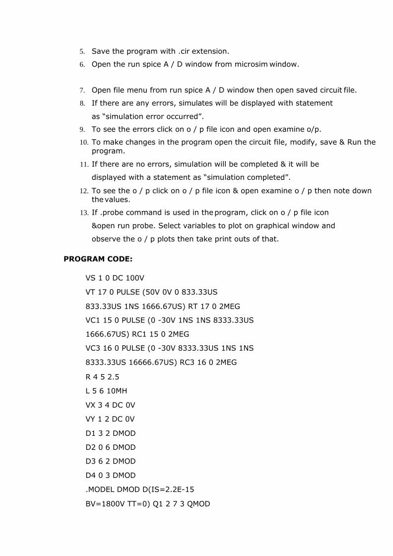
5. Save the program with .cir extension.
6. Open the run spice A / D window from microsim window.
7. Open file menu from run spice A / D window then open saved circuit file.
8. If there are any errors, simulates will be displayed with statement
as “simulation error occurred”.
9. To see the errors click on o / p file icon and open examine o/p.
10. To make changes in the program open the circuit file, modify, save & Run the program.
11. If there are no errors, simulation will be completed & it will be
displayed with a statement as “simulation completed”.
12. To see the o / p click on o / p file icon & open examine o / p then note down the values.
13. If .probe command is used in the program, click on o / p file icon
&open run probe. Select variables to plot on graphical window and
observe the o / p plots then take print outs of that.
PROGRAM CODE:
VS 1 0 DC 100V
VT 17 0 PULSE (50V 0V 0 833.33US
833.33US 1NS 1666.67US) RT 17 0 2MEG
VC1 15 0 PULSE (0 -30V 1NS 1NS 8333.33US
1666.67US) RC1 15 0 2MEG
VC3 16 0 PULSE (0 -30V 8333.33US 1NS 1NS
8333.33US 16666.67US) RC3 16 0 2MEG
R 4 5 2.5
L 5 6 10MH
VX 3 4 DC 0V
VY 1 2 DC 0V
D1 3 2 DMOD
D2 0 6 DMOD
D3 6 2 DMOD
D4 0 3 DMOD
.MODEL DMOD D(IS=2.2E-15
BV=1800V TT=0) Q1 2 7 3 QMOD
Q2 6 9 0 QMOD
Q3 2 11 6 QMOD
Q4 3 13 0 QMOD
.MODEL QMOD NPN(IS=6.74F BF=416.5
CJC=3.638P CJE=4.451P) RG1 8 7 100
RG2 10 9 100
RG3 12 11 100
RG4 14 13 100
*SUBCKT CALL FOR PWM
CONTROL XPW1 17 15 8 3
PWM
XPW2 17 15 10 0 PWM
XPW3 17 16 12 6 PWM
XPW4 17 16 14 0 PWM
.SUBCKT PWM 1 2 3 4
*model ref carrier
+control - control R1
1 5 1K
R2 2 5 1K
RIN 5 0 2MEG
RF 5 3 100K
R0 6 3 75
C0 3 4 10PF
E1 6 4 0 5 2E+5
.ENDS PWM
.TRAN 10US 16.67MS 0 10US
.PROBE
.options abstol=1.00n reltol=0.01 vntol=0.1 itl5=20000
.FOUR 60HZ V(3,6)
.END
PLOT V (14) I(VX) I (vy)V(10) RESULT:
SIGNATURE OF FACULTY