SG6521 — PC Power Supply Supervisors - Mouser Electronics
13
September 2008 © 2007 Fairchild Semiconductor Corporation www.fairchildsemi.com SG6521 • Rev. 1.0.0 SG6521 — PC Power Supply Supervisors SG6521 — PC Power Supply Supervisors Features Two 12V Sense Input Pins: VS12 and VS12B Over-Voltage Protection (OVP) for 3.3V, 5V, and two 12V Over-Current Protection (OCP) for 3.3V, 5V, and two 12V Under-Voltage Protection (UVP) for 3.3V, 5V, and two 12V Open-Drain Output for PGO and FPO Pins 300ms Power-Good Delay 2.8ms PSON Control to FPO Turn-off Delay 48ms PSON Control Delay No Lock-up During the Fast AC Power On/Off Wide Supply Voltage Range: 4V to 15V Over-Temperature Protection (OTP) Additional Protection Input (Pext) Applications Switch-Mode Power Supplies with Active PFC Servo System Power Supplies PC-ATX Power Supplies Description The SG6521 is designed to provide the supply voltage, current supervisor, remote on/off (PSON), power good (PGO) indicator, and fault protection (FPO) functions for switching power systems. For supervisory functions, it provides the over-voltage protection (OVP) for 3.3V, 5V, and two 12V; over- current protection (OCP) for 3.3V, 5V, and two 12V; under-voltage protection (UVP) for 3.3V, 5V, and two 12V. When 3.3V, 5V, or 12V voltage decreases to 2.3V, 3.5V, and 9V, respectively, the under-voltage protection function is enabled. FPO is set HIGH to turn off the PWM controller IC. The voltage difference across external current shunt is used for OCP functions. An external resistor can be used to adjust protection threshold. An additional protection input pin provides the flexibility for designing protection circuits. The power supply is turned on after a 48ms delay when PSON signal is set from HIGH to LOW. To turn off the power supply, the PSON signal is set from LOW to HIGH with a delay of 48ms. The PGI circuitry provides a power-down warning signal for PGO. When PGI input is lower than the internal 1.25V reference voltage, PGO signal is pulled LOW. Ordering Information Part Number Operating Temperature Range Eco Status Package Packing Method SG6521DZ -40°C to +85°C RoHS 16-pin Dual In-Line Package (DIP) Rail SG6521SZ -40°C to +85°C RoHS 16-pin Small Outline Package (SOP) Tape & Reel For Fairchild’s definition of “green” Eco Status, please visit: http://www.fairchildsemi.com/company/green/rohs_green.html .
-
Upload
khangminh22 -
Category
Documents
-
view
3 -
download
0
Transcript of SG6521 — PC Power Supply Supervisors - Mouser Electronics

September 2008
© 2007 Fairchild Semiconductor Corporation www.fairchildsemi.com SG6521 • Rev. 1.0.0
SG6521 —
PC Pow
er Supply Supervisors
SG6521 — PC Power Supply Supervisors
Features Two 12V Sense Input Pins: VS12 and VS12B
Over-Voltage Protection (OVP) for 3.3V, 5V, and two 12V
Over-Current Protection (OCP) for 3.3V, 5V, and two 12V
Under-Voltage Protection (UVP) for 3.3V, 5V, and two 12V
Open-Drain Output for PGO and FPO Pins
300ms Power-Good Delay
2.8ms PSON Control to FPO Turn-off Delay
48ms PSON Control Delay
No Lock-up During the Fast AC Power On/Off
Wide Supply Voltage Range: 4V to 15V
Over-Temperature Protection (OTP)
Additional Protection Input (Pext)
Applications Switch-Mode Power Supplies with Active PFC
Servo System Power Supplies
PC-ATX Power Supplies
Description The SG6521 is designed to provide the supply voltage, current supervisor, remote on/off (PSON), power good (PGO) indicator, and fault protection (FPO) functions for switching power systems.
For supervisory functions, it provides the over-voltage protection (OVP) for 3.3V, 5V, and two 12V; over-current protection (OCP) for 3.3V, 5V, and two 12V; under-voltage protection (UVP) for 3.3V, 5V, and two 12V. When 3.3V, 5V, or 12V voltage decreases to 2.3V, 3.5V, and 9V, respectively, the under-voltage protection function is enabled. FPO is set HIGH to turn off the PWM controller IC. The voltage difference across external current shunt is used for OCP functions. An external resistor can be used to adjust protection threshold. An additional protection input pin provides the flexibility for designing protection circuits.
The power supply is turned on after a 48ms delay when PSON signal is set from HIGH to LOW. To turn off the power supply, the PSON signal is set from LOW to HIGH with a delay of 48ms. The PGI circuitry provides a power-down warning signal for PGO. When PGI input is lower than the internal 1.25V reference voltage, PGO signal is pulled LOW.
Ordering Information
Part Number
Operating Temperature Range
Eco Status
Package Packing Method
SG6521DZ -40°C to +85°C RoHS 16-pin Dual In-Line Package (DIP) Rail SG6521SZ -40°C to +85°C RoHS 16-pin Small Outline Package (SOP) Tape & Reel
For Fairchild’s definition of “green” Eco Status, please visit: http://www.fairchildsemi.com/company/green/rohs_green.html.

© 2007 Fairchild Semiconductor Corporation www.fairchildsemi.com SG6521 • Rev. 1.0.0 2
SG6521 —
PC Pow
er Supply Supervisors Application Diagram
Figure 1. Typical Application

© 2007 Fairchild Semiconductor Corporation www.fairchildsemi.com SG6521 • Rev. 1.0.0 3
SG6521 —
PC Pow
er Supply Supervisors
Block Diagram
Figure 2. Function Block Diagram
© 2007 Fairchild Semiconductor Corporation www.fairchildsemi.com SG6521 • Rev. 1.0.0 4
SG6521 —
PC Pow
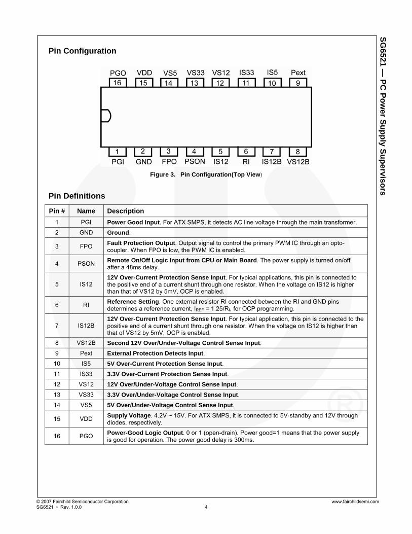
er Supply Supervisors Pin Configuration
Figure 3. Pin Configuration(Top View)
Pin Definitions
Pin # Name Description 1 PGI Power Good Input. For ATX SMPS, it detects AC line voltage through the main transformer. 2 GND Ground.
3 FPO Fault Protection Output. Output signal to control the primary PWM IC through an opto-coupler. When FPO is low, the PWM IC is enabled.
4 PSON Remote On/Off Logic Input from CPU or Main Board. The power supply is turned on/off after a 48ms delay.
5 IS12 12V Over-Current Protection Sense Input. For typical applications, this pin is connected to the positive end of a current shunt through one resistor. When the voltage on IS12 is higher than that of VS12 by 5mV, OCP is enabled.
6 RI Reference Setting. One external resistor RI connected between the RI and GND pins determines a reference current, IREF = 1.25/RI, for OCP programming.
7 IS12B 12V Over-Current Protection Sense Input. For typical application, this pin is connected to the positive end of a current shunt through one resistor. When the voltage on IS12 is higher than that of VS12 by 5mV, OCP is enabled.
8 VS12B Second 12V Over/Under-Voltage Control Sense Input. 9 Pext External Protection Detects Input.
10 IS5 5V Over-Current Protection Sense Input. 11 IS33 3.3V Over-Current Protection Sense Input. 12 VS12 12V Over/Under-Voltage Control Sense Input. 13 VS33 3.3V Over/Under-Voltage Control Sense Input. 14 VS5 5V Over/Under-Voltage Control Sense Input.
15 VDD Supply Voltage. 4.2V ~ 15V. For ATX SMPS, it is connected to 5V-standby and 12V through diodes, respectively.
16 PGO Power-Good Logic Output. 0 or 1 (open-drain). Power good=1 means that the power supply is good for operation. The power good delay is 300ms.

© 2007 Fairchild Semiconductor Corporation www.fairchildsemi.com SG6521 • Rev. 1.0.0 5
SG6521 —
PC Pow
er Supply Supervisors
Absolute Maximum Ratings Stresses exceeding the absolute maximum ratings may damage the device. The device may not function or be operable above the recommended operating conditions and stressing the parts to these levels is not recommended. In addition, extended exposure to stresses above the recommended operating conditions may affect device reliability. The absolute maximum ratings are stress ratings only.
Symbol Parameter Min. Max. Unit VDD DC Supply Voltage 16 V
PSON, PGI, VS5, IS5, VS33, IS33, Pext -0.3 7.0 V VIN Input Voltage
VS12, VS12B, IS12, IS12B -0.3 15.0 V VOUT Output Voltage FPO, PGO -0.3 8.0 V
TJ Operating Junction Temperature -40 +125 °C TSTG Storage Temperature Range -55 +150 °C TL Lead Temperature (Soldering) +260 °C
Human Body Model: JESD22-A114 3.0 KV
ESD Electrostatic Discharge Capability Machine Model: JESD22-A115 200 V
Recommended Operating Conditions The Recommended Operating Conditions table defines the conditions for actual device operation. Recommended operating conditions are specified to ensure optimal performance to the datasheet specifications. Fairchild does not recommend exceeding them or designing to Absolute Maximum Ratings.
Symbol Parameter Min. Typ. Max. Unit TA Operating Ambient Temperature -40 +85 °C

© 2007 Fairchild Semiconductor Corporation www.fairchildsemi.com SG6521 • Rev. 1.0.0 6
SG6521 —
PC Pow
er Supply Supervisors
Electrical Characteristics VDD = 5V, and TA = 25°C unless otherwise noted.
Symbol Parameter Conditions Min. Typ. Max. UnitsVDD Section
VDD DC Supply Voltage 4.2 15.0 V IDD1 Supply Current PSON = LOW 1.7 2.6 mA IDD2 Supply Current PSON = HIGH 1.0 1.5 mA tR Supply Voltage Rising Time 1 ms
VST VDD Start Threshold Voltage 4.2 V Over-Voltage (OVP) and Over-Current (OCP) Protections
VS33 3.7 3.9 4.1 VS5 5.7 6.1 6.5 VOVP Over-Voltage Protection VS12, VS12B 13.2 13.8 14.4
V
IREF Ratio of Current Sense Sink Current to Current Sense Setting Pin (RI) Source Current
RI = 18.5kΩ ~75kΩ 7.6 8.0 8.4
VOFFSET OCP Comparator Input Offset Voltage -3 3 mV ILKG-FPO Leakage Current (FPO) FPO = 5V 5 µA VOL-FPO Low-Level Output Voltage (FPO) ISINK 20mA 0.4 V
tOVP OVP Delay Time 33 75 110 µs tOCP OCP Delay Time 12.5 20.0 27.5 ms VRI RI Pin Voltage 0.98•Typ. 1.25 1.01•Typ. V IRI Output Current RI 12.5 62.5 µA
tST-OCP Startup OCP / UVP Protection Time 0.6V < PGI < 1.25V; FPO = Low 49 75 114 ms
Under-Voltage Protection and PGI, PGO VPGI_1 Input Threshold Voltage PGI 1 0.98•Typ. 1.25 1.02•Typ. V VPGI_2 Input Threshold Voltage PGI 2 0.96•Typ. 0.60 1.03•Typ. V
VS33 2.1 2.3 2.5 VS5 3.3 3.5 3.7 VUVP Under-Voltage Protection VS12, VS12B 8.5 9.0 9.5
V
tOND Under-Voltage Turn-on Delay PGI>0.6V 49 75 114 ms tUVP UVP Delay PGI>1.25V 2.4 3.2 4.0 ms
ILKG-PGO Leakage Current (PGO) PGO = 5V 5 µA
VOL-PGO Low-Level Output Voltage (PGO) VDD = 12V; ISINK 10mA 0.4 V
tPG Timing PG Delay 200 300 450 ms tND1 Noise Deglitch Time 90 150 210 µs
PSON Control IPSON Input Pull-up Current PSON = 0V 120 µA VIH High-Level Input Voltage 2 V VIL Low-Level Input Voltage 0.8 V
PSON LOW to FPO LOW 34 48 67
tPSON Timing PSON to On/Off PSON HIGH to PGO LOW 34 48 67
ms
tPSOFF Timing PGO LOW to FPO HIGH 1.6 2.8 4.5 ms External Protection Detect Section
VTH Pext Threshold 1.20 1.25 1.30 V tPext Pext Delay Time 2.4 3.2 4.0 ms

© 2007 Fairchild Semiconductor Corporation www.fairchildsemi.com SG6521 • Rev. 1.0.0 7
SG6521 —
PC Pow
er Supply Supervisors
Functional Description The SG6521 is designed to provide the supply voltage, current supervisor, remote on/off (PSON), power-good (PGO) indicator, and fault protection (FPO) functions for switching power systems.
For supervisory functions, it provides the over-voltage protection (OVP) for 3.3V, 5V, and two 12V; over-current protection (OCP) for 3.3V, 5V, and two 12V; under-voltage protection (UVP) for 3.3V, 5V, and two 12V. When 3.3V, 5V, or 12V voltage decreases to 2.3V, 3.5V, and 9V, respectively, the under-voltage protection function is enabled. FPO is set HIGH to turn off the PWM controller IC. The voltage difference across external current shunt is used for OCP functions. An external resistor can be used to adjust protection threshold. An additional protection input pin provides the flexibility for designing protection circuits.
The power supply is turned on after a 48ms delay when PSON signal is set from HIGH to LOW. To turn off the power supply, the PSON signal is set from LOW to HIGH with a delay of 48ms. The PGI circuitry provides a power-down warning signal for PGO. When PGI input is lower than the internal 1.25V reference voltage, PGO signal is pulled LOW.
The SG6521 provides over-current protection for the 3.3V, 5V, and two 12V rails. Whenever an OCP condition occurs at any of the voltage rails, PGO is LOW and FPO is open. The internal OCP comparators
have a very small offset voltage (±3mV). The sink currents of IS33, IS5, and IS12 are eight times the current at the RI pin. The current at the RI pin is VRI/RI.
Here is an example demonstrating how to set the over current protection. If I1×R1 > IRI×R2, OCP is active. If R1=5mΩ, RI=30KΩ, and the OCP active level is 35A, then the R2 resistor is:
Ω=×
×= 525
8IRI
RRI
112
(1)
where C is bypass noise, suggested value is between 1µF ~ 2.2µF
Figure 4. OCP Setup
© 2007 Fairchild Semiconductor Corporation www.fairchildsemi.com SG6521 • Rev. 1.0.0 8
SG6521 —
PC Pow
er Supply Supervisors
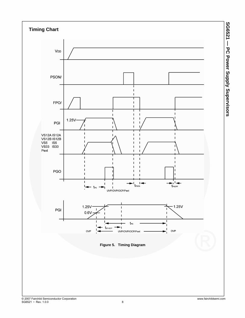
Timing Chart
Figure 5. Timing Diagram

© 2007 Fairchild Semiconductor Corporation www.fairchildsemi.com SG6521 • Rev. 1.0.0 9
SG6521 —
PC Pow
er Supply Supervisors
Typical Performance Characteristics
7.500
7.700
7.900
8.100
8.300
8.500
-40 -25 -10 5 20 35 50 65 80 95 110 125Temperature ()
IRE
F
1.500
1.600
1.700
1.800
1.900
2.000
-40 -25 -10 5 20 35 50 65 80 95 110 125Temperature ()
IDD
1 (m
A)
Figure 6. IREF vs. TA Figure 7. IDD1 vs. TA
-2.000
-1.200
-0.400
0.400
1.200
2.000
-40 -25 -10 5 20 35 50 65 80 95 110 125Temperature ()
VO
FFSE
T (m
V)
16.000
18.000
20.000
22.000
24.000
26.000
28.000
-40 -25 -10 5 20 35 50 65 80 95 110 125Temperature ()
Tocp
(mS
)
Figure 8. VOFFSET vs. TA Figure 9. TOCP vs. TA
1.20
1.22
1.24
1.26
1.28
1.30
-40 -25 -10 5 20 35 50 65 80 95 110 125Temperature ()
VR
I (V
)
1.20
1.22
1.24
1.26
1.28
1.30
-40 -25 -10 5 20 35 50 65 80 95 110 125Temperature ()
VPG
I (V
)
Figure 10. VRI vs. TA Figure 11. VPGI vs. TA

© 2007 Fairchild Semiconductor Corporation www.fairchildsemi.com SG6521 • Rev. 1.0.0 10
SG6521 —
PC Pow
er Supply Supervisors
Physical Dimensions
16 9
81
NOTES: UNLESS OTHERWISE SPECIFIED A THIS PACKAGE CONFORMS TO JEDEC MS-001 VARIATION BB
B) ALL DIMENSIONS ARE IN MILLIMETERS.
D) CONFORMS TO ASME Y14.5M-1994E) DRAWING FILE NAME: N16EREV1
19.6818.66
6.606.09
C) DIMENSIONS ARE EXCLUSIVE OF BURRS, MOLD FLASH, AND TIE BAR PROTRUSIONS
3.423.17
3.812.92
(0.40)
2.54
17.78
0.580.35
1.781.14
5.33 MAX0.38 MIN 8.13
7.62
0.350.20
150
8.69
A
A
TOP VIEW
SIDE VIEW
Figure 12. 16-Lead, Dual Inline Package (DIP)
Package drawings are provided as a service to customers considering Fairchild components. Drawings may change in any manner without notice. Please note the revision and/or date on the drawing and contact a Fairchild Semiconductor representative to verify or obtain the most recent revision. Package specifications do not expand the terms of Fairchild’s worldwide terms and conditions, specifically the warranty therein, which covers Fairchild products. Always visit Fairchild Semiconductor’s online packaging area for the most recent package drawings: http://www.fairchildsemi.com/packaging/.

© 2007 Fairchild Semiconductor Corporation www.fairchildsemi.com SG6521 • Rev. 1.0.0 11
SG6521 —
PC Pow
er Supply Supervisors
Physical Dimensions (Continued)
X 45°
DETAIL ASCALE: 2:1
8°0°
NOTES: UNLESS OTHERWISE SPECIFIED
A) THIS PACKAGE CONFORMS TO JEDEC MS-012, VARIATION AC, ISSUE C. B) ALL DIMENSIONS ARE IN MILLIMETERS. C) DIMENSIONS ARE EXCLUSIVE OF BURRS, MOLD
FLASH AND TIE BAR PROTRUSIONS D) CONFORMS TO ASME Y14.5M-1994 E) LANDPATTERN STANDARD: SOIC127P600X175-16AM F) DRAWING FILE NAME: M16AREV12.
SEATING PLANE
GAGE PLANE
C
C0.10
SEE DETAIL A
LAND PATTERN RECOMMENDATION
PIN ONENDICATOR
1
16
8
M0.25
9
C B A
B
A
5.6
1.27 0.65
1.75
10.009.80
8.89
6.00
1.27
(0.30)
0.510.35
1.75 MAX1.501.25
0.250.10
0.250.19
(1.04)
0.900.50
0.36
(R0.10)
(R0.10)
0.500.25
4.003.80
Figure 13. 16-Lead, Small Outline Integrated Circuit (SOIC)
Package drawings are provided as a service to customers considering Fairchild components. Drawings may change in any manner without notice. Please note the revision and/or date on the drawing and contact a Fairchild Semiconductor representative to verify or obtain the most recent revision. Package specifications do not expand the terms of Fairchild’s worldwide terms and conditions, specifically the warranty therein, which covers Fairchild products. Always visit Fairchild Semiconductor’s online packaging area for the most recent package drawings: http://www.fairchildsemi.com/packaging/.

© 2007 Fairchild Semiconductor Corporation www.fairchildsemi.com SG6521 • Rev. 1.0.0 12
SG6521 —
PC Pow
er Supply Supervisors

Mouser Electronics
Authorized Distributor
Click to View Pricing, Inventory, Delivery & Lifecycle Information: Fairchild Semiconductor:
SG6521DZ SG6521SZ