Superconducting single photon detectors for ultrasensitive visible and IR detection
12
Superconducting single photon detectors for ultrasensitive visible and IR detection Roch Espiau de Lamaestre a , Laurent Maingault b , Laurent Frey a , Christophe Constancias a , Paul Cavalier b , Jean Claude Vill´ egier b , Philippe Odier c and Jean Philippe Poizat c a CEA, LETI, MINATEC, 17 rue des martyrs, 38054 Grenoble, France; b CEA, INAC, MINATEC, 17 rue des martyrs, 38054 Grenoble, France; c Institut N´ eel, CNRS/UJF, 25 rue des martyrs, 38042 Grenoble, France; ABSTRACT Superconducting single photons detectors (SSPDs) have emerged in recent years as a promising alternative for fast and sensitive infrared detectors working in the photon counting mode. In particular, those detectors combine very low dark count rates (below 1 Hz), high speed (above 1GHz ), photon number resolution and reasonable quantum efficiency (10% at telecom wavelengths). They already found applications in quantum cryptography systems and integrated circuit failure analysis, but could also be used as ultimate sensors in matrix configurations. We show here the optimization of SSPD fabrication and their optical metrology at CEA. SSPD are fabricated by patterning a 80 nm wide nanowire in a very thin (4 nm) NbN film on sapphire, forming a pixel of several microns size. A cryogenic all-fibered optoelectronic system has been developed and allows precise metrology of the optical performances of SSPD. When biasing near the critical current of the nanowire, we demonstrate a detection quantum efficiency of 8% at 1.55 μm, which is also found to be strongly polarization dependent. This quantum efficiency being limited by optical absorption, we propose a prism coupling based absorption enhancing structure that allows reaching 100% quantum efficiency. Keywords: SSPD, superconductor, NbN, visible, IR, photon polarization, quantum efficiency, prism coupling, epitaxy 1. INTRODUCTION Detectors based on superconducting materials have recently attracted attention for their outstanding perfor- mances in single photon detection. 1 Ultrathin superconducting NbN nanowires are indeed very sensitive to moderately energetic radiations brought by photons but also electrons. Such detectors, commonly referred to as Superconducting Single Photon Detector (SSPD), are able to discriminate incoming single photons at rates above 1GHz, 2 with good quantum efficiency (10 − 60%), 3 and very low dark count rate (< 1 Hz ), 4 noise equivalent power as well as jitter (< 20 ps). 5 Moreover those detectors operate in ”geiger mode” with a reset time one order of magnitude lower than semiconductor counterparts, like avalanche photodiodes. Their spectral range is wide ranging from UV to far infrared, 6 and state of the art fabrication techniques have shown that no degradation of the detection efficiency occurs for wavelength shorter than about 1μm. 7 SSPD are particularly interesting for near infrared applications, where usual detectors like Si or InGaAs avalanche photodiodes can be of limited use because of high dark count rates and larger dead time. 8 Those performances are at the cost of a cryogenic cooling system: although not easily portable, modern cryogenfree coolers nevertheless allow cooling of the devices at the required temperature range (2 − 4 K) with a sufficient stability, all that in a limited volume (typ. 1 m 3 ) linked to the power supply. Those constraints limits the SSPD use in niche applications where outstanding detection performances are required. They already brought major achievements in quantum optics 9 and especially quantum key distribution over long distances. 10 They are also considered in other applications fields such as astronomy, 11 CMOS integrated circuits failure detection, 12 and time of flight spectroscopy. 13 Send correspondence to R. Espiau de Lamaestre or L. Frey: R. Espiau de Lamaestre: E-mail: [email protected], Telephone: +33 (0)4 38 78 03 65 L. Frey: E-mail: [email protected], Telephone: +33 (0)4 38 78 33 37 Sensors, Cameras, and Systems for Industrial/Scientific Applications X, edited by Erik Bodegom, Valérie Nguyen, Proc. of SPIE-IS&T Electronic Imaging, SPIE Vol. 7249, 72490Q © 2009 SPIE-IS&T · CCC code: 0277-786X/09/$18 · doi: 10.1117/12.806198 SPIE-IS&T Vol. 7249 72490Q-1
Transcript of Superconducting single photon detectors for ultrasensitive visible and IR detection

Superconducting single photon detectors for ultrasensitivevisible and IR detection
Roch Espiau de Lamaestrea, Laurent Maingaultb, Laurent Freya, Christophe Constanciasa,Paul Cavalierb, Jean Claude Villegierb, Philippe Odierc and Jean Philippe Poizatc
a CEA, LETI, MINATEC, 17 rue des martyrs, 38054 Grenoble, France;b CEA, INAC, MINATEC, 17 rue des martyrs, 38054 Grenoble, France;
c Institut Neel, CNRS/UJF, 25 rue des martyrs, 38042 Grenoble, France;
ABSTRACT
Superconducting single photons detectors (SSPDs) have emerged in recent years as a promising alternative forfast and sensitive infrared detectors working in the photon counting mode. In particular, those detectors combinevery low dark count rates (below 1 Hz), high speed (above 1GHz), photon number resolution and reasonablequantum efficiency (10% at telecom wavelengths). They already found applications in quantum cryptographysystems and integrated circuit failure analysis, but could also be used as ultimate sensors in matrix configurations.We show here the optimization of SSPD fabrication and their optical metrology at CEA. SSPD are fabricatedby patterning a 80 nm wide nanowire in a very thin (4 nm) NbN film on sapphire, forming a pixel of severalmicrons size. A cryogenic all-fibered optoelectronic system has been developed and allows precise metrology ofthe optical performances of SSPD. When biasing near the critical current of the nanowire, we demonstrate adetection quantum efficiency of 8% at 1.55 μm, which is also found to be strongly polarization dependent. Thisquantum efficiency being limited by optical absorption, we propose a prism coupling based absorption enhancingstructure that allows reaching 100% quantum efficiency.
Keywords: SSPD, superconductor, NbN, visible, IR, photon polarization, quantum efficiency, prism coupling,epitaxy
1. INTRODUCTION
Detectors based on superconducting materials have recently attracted attention for their outstanding perfor-mances in single photon detection.1 Ultrathin superconducting NbN nanowires are indeed very sensitive tomoderately energetic radiations brought by photons but also electrons. Such detectors, commonly referred to asSuperconducting Single Photon Detector (SSPD), are able to discriminate incoming single photons at rates above1GHz,2 with good quantum efficiency (10 − 60%),3 and very low dark count rate (< 1 Hz),4 noise equivalentpower as well as jitter (< 20 ps).5 Moreover those detectors operate in ”geiger mode” with a reset time one orderof magnitude lower than semiconductor counterparts, like avalanche photodiodes. Their spectral range is wideranging from UV to far infrared,6 and state of the art fabrication techniques have shown that no degradation ofthe detection efficiency occurs for wavelength shorter than about 1μm.7 SSPD are particularly interesting fornear infrared applications, where usual detectors like Si or InGaAs avalanche photodiodes can be of limited usebecause of high dark count rates and larger dead time.8
Those performances are at the cost of a cryogenic cooling system: although not easily portable, moderncryogenfree coolers nevertheless allow cooling of the devices at the required temperature range (2 − 4 K) witha sufficient stability, all that in a limited volume (typ. 1 m3) linked to the power supply. Those constraintslimits the SSPD use in niche applications where outstanding detection performances are required. They alreadybrought major achievements in quantum optics9 and especially quantum key distribution over long distances.10
They are also considered in other applications fields such as astronomy,11 CMOS integrated circuits failuredetection,12 and time of flight spectroscopy.13
Send correspondence to R. Espiau de Lamaestre or L. Frey:R. Espiau de Lamaestre: E-mail: [email protected], Telephone: +33 (0)4 38 78 03 65L. Frey: E-mail: [email protected], Telephone: +33 (0)4 38 78 33 37
Sensors, Cameras, and Systems for Industrial/Scientific Applications X,edited by Erik Bodegom, Valérie Nguyen, Proc. of SPIE-IS&T Electronic Imaging, SPIE Vol. 7249, 72490Q
© 2009 SPIE-IS&T · CCC code: 0277-786X/09/$18 · doi: 10.1117/12.806198
SPIE-IS&T Vol. 7249 72490Q-1

(a) SSPD (b) (c)
010
006
0.04
0024
= 2
time. is
R
VSSPD
SSPD
t
2. DETECTOR OPERATION BASICS
In SSPD, photon detection relies on the transient voltage generation by a photon induced local breaking ofsuperconductivity, in a current biased superconducting nanowire. In darkness, the nanowire is superconductingso that the voltage across the wire is zero. When illuminated, a single photon can be absorbed by the nanowire,which in some conditions generates a resistive volume on the whole section of the wire, leading to a nonzerovoltage across the wire. Then Joule heating within this resistive portion makes it grow in size, in a self suppliedway, and resistance reaches several kΩ. In order to reset the whole wire back into its superconducting state, aload resistor (Rl, typically 50 Ω) is therefore placed in parallel to the nanowire to shunt this resistive growingvolume. After some time, called the reset time, the nanowire is again ready to generate another detection event.A simple vision of the detection event is that of an emptying of the kinetic superconducting energy stored intothe wire triggered by a photon. Using this configuration, a single pulse is generated for each single photonabsorption. The reader is referred to the several contributions2, 7, 14, 15 giving more details about the conditionsrequired for the generation and shaping of detection. In the following, we discuss the basic parameters governingthe detection.
Figure 1. (a) Equivalent electrical circuit of the detector showing the bias current Ib generator, the kinetic inductanceLk and eventually shunted normal resistance Rn of the superconducting wire, and the load resistance Rl. (b) shows thevariations of Rn, voltage and current flowing across the SSPD during a detection event; and (c) is a measure of timeresponse of a SSPD, showing a GHz range bandwidth.
2.1 Single photon detection
For the wire to be superconducting, its temperature has to be set below the critical temperature of the film TC
and the supercurrent flowing into the nanowire has to be below a critical density value JC(T ) (TC ≈ 11 − 13Kand JC(4K) ≈ 5 − 10 MA.cm−2 for NbN films considered here). In the following we discard any considerationover temperature dependance, i.e. we conduct estimations in the limit T � Tc.
We first examine the conditions of generation of the resistive volume across the wire. In an oversimplifiedview (the ”hot spot model”7), the absorbed photon creates a normal volume whose size is smaller than that ofthe wire. The current flowing into the wire then tends to flow apart from this section, and the current densityis increasing. The photon can be generated if the current density overcomes the critical one JC : this conditionleads to a characteristic wire width wc below which the photon detection can be triggered. Using an estimationof the size of the ”hotspot”, one derives:
wc ∝ Ic
Ic − Ib
1√λ0t
, (1)
where λ0 is the wavelength of impinging photons and t the thickness of the wire. The closer from the criticalcurrent (small Ic − Ib) and the thinner the NbN layer, the larger the width of the nanowire could be. Howeverbeing too close to the critical current leads to high dark count rates, which originate from thermal fluctuations,15
and this limits the interesting bias regime to the range 0.9 − 0.95 Ic. Therefore, both very low thicknesses,typically in the range 3− 5 nm, and the lowest possible width, typically in the range 50− 100 nm, are requiredfor optimal behavior in the mid IR. The effect of the wire width will be examined in more details in section 4.3.
SPIE-IS&T Vol. 7249 72490Q-2

2.2 Detection kinetics
Both the detection sensitivity (see above) and the height of the voltage pulse signal (∝ RlIb) are maximized nearthe critical current, which scales roughly as:
Ic ∝ wt
√T 3
c
ρ20K, (2)
where w is the width of the nanowire, ρ20K its resistivity at T = 20 K and Tc its superconductive criticaltemperature. The reset time of the detector is determined by Rl and the inductance of the nanowire, which isdominated by a superconducting term called kinetic inductance Lk.2 The latter scales as:
Lk ∝ l
wt
ρ20K
Tc, (3)
The equivalent electrical circuit is shown in Fig.1(a) and a typical temporal response in Fig.1(c). The reset timeis the main limitation to the maximum photon counting rate. The first stage of thermal growth of the resistivesection is about one to two orders of magnitude faster (it scales as Lk/Rn, with Rn the resistance of the resistivesection).
2.3 Dimensioning SSPD
Eq. 3 and Eq. 2 purposely separates geometrical (length l, section wt) from material (Tc and ρ20K) parametersgoverning the temporal response of the detector. We will see below that variation of critical temperature Tc
from one material to the other are negligible with respect to those of the resistivity ρ20K , which is then thedeterminant material property for SSPD. The lower the resistivity of the layer, the higher and the shorter willbe the pulsed detection signal. In addition, from the geometrical point of view, the length l of the wire has tobe minimized to reach the highest counting rates. Similarly, the section wt has to be as big as possible to getan intense and fast signal. Nevertheless, discussion of Eq. 1 has shown that this increase of w and t is limitedto the values derived above, for single photon sensitivity reasons.
This article will review the developments of SSPD fabrication and characterization at CEA, insisting on theparameters governing the detection in a user oriented view, as already started above. We will address the issuesof the quantum / detection efficiency (QE and DE), the dark count, and the reset time with particular attentionto material, device geometry and photon polarization influence on those performances.
3. FABRICATION TECHNOLOGY
Thanks to the strong resistance of its superconducting properties to the usual technological processes, niobiumnitride (NbN) is a material of choice for single photon detection applications. Other superconductor havebeen attempted,16, 17 without comparable success. Resistance to technological process also explains why nodemonstration of single photon detection has ever been published using high temperature superconductor, e.g.YBaCuO. Up to now SSPD are made of ultrathin (typically 3−5 nm) NbN films deposited on sapphire or MgO,before patterning under the form of a nanowire of about 100 nm wide, that becomes sensitive to visible-infraredsingle photons when biased near its critical current. Optimization of their fabrication at CEA is reviewed below,concentrating on the most critical steps.
3.1 Superconducting layer deposition
Choice of growth conditions and nature of substrate are crucial for minimizing the resistivity ρ20K and maximizingTc, as discussed in section 2.3. Superconductive ultrathin NbN films are sputtered using a Nb target in a DC-magnetron reactive Ar/N2 plasma on a sapphire substrate heated at temperature of the order of 600◦C.18, 19
The plasma sputtering conditions (total pressure, N2 partial pressure and cathode current) are tuned so as theNbN composition is close to stoichiometry of nitrogen, which is the optimal condition for superconductivity ofthe layer.20, 21 We reached typical value for critical supercurrent of 5− 10 MA.cm−2 and critical temperature ofabout 11 − 13 K for a 4 nm thick film. For such low thicknesses, NbN has been shown to epitaxially grow on
SPIE-IS&T Vol. 7249 72490Q-3

9O
(a) (b) (c)
27O
x
9O
27O
Figure 2. Pole figure of 10 nm thick NbN layers on various orientations of sapphire base plane using the cubic NbN (200)Bragg reflection. (a) Usual R-plane orientation, where NbN growth direction is [135], (b) M-plane orientation, where NbNgrowth direction is [110], and (c) A-plane orientation, where NbN growth direction is [111]. Twinning of layers is evidencedby a twice more diffraction peaks than as expected and the respective contribution of the two variants are indexed NbN1
and NbN2. We refer to χ as the tilt angle of the sample with respect to X-ray diffusion vector (horizontal) and ϕ as theazimuthal rotation angle (around the normal to the sample). Pole figures were acquired using RayfleX software. TheX-Ray diffraction measurements were performed using a high resolution Seifert XRD 3003 PTS-HR diffractometer.
several substrates such as MgO,21, 22 SiC23 and sapphire.18, 22, 24 MgO has long been considered as the preferredchoice, thanks to a low lattice mismatch with NbN , leading to good superconducting properties (TC ≈ 12K andρ20K = 120μΩ.cm−1 for 4 nm thick film).
However, we have shown that the proper choice of the orientation of the sapphire substrate helps improvingthe crystalline quality of the NbN layer to a level comparable to that obtained for MgO. We have investigatedthe microstructure of 5 − 10 nm NbN thick films grown on A-, M- and R-plane orientation of the sapphiresubstrate. Fig.2 shows the corresponding pole figures: the heteroepitaxial NbN films on R plane and A planeare twinned, in contrast to the one on M plane. The improved microstructure of NbN on M-plane correlates withits improved transport properties. In equal growth conditions, the latter film is indeed 30% less resistive, withno significant change in the critical temperature, than the one classically grown on R-plane.24 The detectionsignals are then expected to be 30% shorter because of reduced kinetics inductance (see Eq. 3), and 20% moreintense (see Eq. 2). Performances of SSPD grown on that orientation are therefore expected to be comparableto that of NbN grown on MgO, with the advantage that sapphire substrates are less sensitive to moisture andavailable in large sizes (up to 8-12 inches substrates). The latter point is considered favorably for integratedfabrication of SSPD.
In addition such ultrathin NbN films are particularly sensitive to oxidation into an oxynitride by the oxygenof the atmosphere or a process chemical.25 It can progressively decrease the NbN thickness and potentiallydegrade the detector performances. To protect the NbN layer, we deposited various passivating layers andmeasured their resistance to room temperature storage, as well as SSPD processing (see below). We found thatAlN thin layers deposited in situ after the NbN layer epitaxy19 meet this goal, and preserve the possibility toelectrically contact the layer for detector operation.
3.2 Detector patterning
Following the discussion of section 2, the geometrical section of the nanowire has to be limited in size. Experi-mentally, nowadays performance of e-beam lithography (typically 100 nm wide wires can be patterned with therequired reproducibility) requires the NbN film to be ultrathin (below 5 nm) for optimal SSPD performances.As the size of such a wire is very small compared to the usual mode size of monomodal optical fibers (severalmicrons), the nanowire is commonly patterned under the form of a meander (see section 4.3 for a detailed dis-cussion of the optical optimization of the detectors). Interestingly, NbN SSPD technology comprises a verylimited number of steps (Fig.3 (a)) : (i) electron lithography of the meander using a negative resist; (ii) etchingof uncovered NbN and stripping of remaining resist; (iii) Au/Ti contact electrodes lift off.
SPIE-IS&T Vol. 7249 72490Q-4

(b)J!J!!IH!!J! !I!J
!JLIIJ
IiiiIiI1IIIii
RIRmax1.0
1(c)
10 T(K) 100
(d) 12
2 8 I
0012345Voltage (V
(e)
0.8
0.6 NbN I M-%D3* 4.4nm
0.4 Tc13.3K
0.2 Tc=7.8K
0.0
Figure 3. (a) schematic view of the process (b) SEM image of the active part of the detector (emphasized by tireted whiteline), and details of nanowire lithography: the SSPD consists here in a 10× 10μm pixel, where the 100 nm wide nanowireof is folded back under the form of a meander. (c) is a typical measurement of the superconducting transition where R isthe resistance of the wire. Note that layers as thin as 2.6 nm have a still high critical temperature of 8 K. (d) TypicalDC I(V ) curve of a meander nanowire, evidencing the superconducting current peak at zero voltage followed by Ohmiccharacteristics of the subsequently transiting branches of the nanowire. (e) Picture showing full 4-inches wafer SSPDfabrication.
Electron-beam exposure has been performed under 100 kV accelerating voltage on a VISTEC UHR VB6 tool.The samples were spin coated with NEB22A2 negative tone resist from Sumitomo to a thickness of 150 nm andbaked at 110 ◦C for 120 s. This resist has been chosen because of its high sensitivity allowing a large amount ofpatterning exposure on large samples (up to 4 inches diameter sapphire wafer, see Fig.3 (e)), its high resolution(40 nm as iso-dense pattern ) and its good etching selectivity versus NbN . The patterns were exposed with adose of 105 μC.cm2 optimized for 100 nm lines with 50 % fill factor. Figure 2 shows the critical dimension (CD)observed by SEM on NEB22 iso-dense 100 nm width lines, after development (Fig. 3 (b)). The samples weredeveloped after a Post Exposure Bake of 90 ◦C for 60 s in Rohm and Haas MF702 for 45 s, then rinsed in waterfor 180 s. Attention was paid to achieve a great homogeneity of the width of the wire. It has indeed been shownthat constriction of the latter severely affect the overall detection efficiency of the device,26, 27 by limiting thecritical current of the wire to a value below the one of the unconstricted area.
Reactive Ion Etching in a SF6/O2 plasma was used to transfer resist pattern into NbN , followed by a strippingstep to remove resist residue. Standard stripping chemicals have been tested in order to avoid any degradationof the electrical transport properties of the layer.28 One has to avoid any oxidizing conditions (O2 plasma,wet solutions of EKC265 or sulfuric peroxide mixture) that can efficiently lead to total destruction of the NbNphase. Wet stripping by EKCLE has conversely been found to leave Tc and especially ρ20K unchanged and isthe preferred choice for this step.
For lift off, a reversible resist AZ 5214-E from Hoechst Celanese was used to obtain an undercut resist profilesuitable for lift off. Ti layer (10 nm) is required for the subsequent Au layer (65 nm) adherence on NbN .
Detectors were electrically characterized by (i) four points R(T ) using PPMS (Fig. 3 (c)); (ii) two contactingpoints current-voltage I(V ) measurement (Fig. 3 (d)). For the latter, the SSPD was biased with a variablevoltage source (YOKOGAWA) in series with a 1 Ω resistor across which the current passing trough the SSPDis measured (Keithley). The SSPD is held at 4.2 K in a liquid He bath. Electrical connections to the SSPDare filtered with a combination of RC low pass filters. This experiment allows fast monitoring of the criticalcurrent and resistance of the wires, which in turn determine the performance of the SSPD fabrication, beforethe electrooptical characterization. Using the process above, nanowires with widths down to 70 − 80 nm havebeen fabricated and shown electrical transport properties in agreement with the ones of the pristine NbN film.
SPIE-IS&T Vol. 7249 72490Q-5
Allu ut iii
Polarization coritrollor
Optical Spectrom Analtrer
Iii 106
,-i05
102
Piezo actuotora 1 01
aser
-9
1 --T;;. "t:
10-14 10-12P. (W
10
4. ELECTROOPTICAL CHARACTERIZATION
In the following, we refer to the detection efficiency (DE) as the ratio between the detection pulse rate and thephoton flux introduced in the optical fiber. More generally, the optimization of the DE strongly depends on theability to couple the light to the active part of the SSPD, by optical engineering (couplers, waveguides...). Thequantum efficiency (QE) is calculated by normalizing the DE by the fraction of photons really impinging theactive part of the detector. It reflects the intrinsic efficiency of the active pixel. We show below a method toprecisely evaluate the QE of our SSPD using cryogenic positioning elements, and show a way to increase the QEof the detectors up to 100% by using a prism coupling method.
4.1 Electro-optical metrology
Figure 4. Left: Experimental set up for electrooptical characterization, the picture showing the details within the cryogenicinsert. Right: plot of the count rate as a function of the power of the source. Straight black line is the linear fit to thedata. Detector is a 80 nm wide nanowire.
Fig. 4 left shows a scheme of the experimental set up, together with a picture of the bottom of the cryogenicinsert used for maintaining the SSPD in the liquid He bath (T = 4.2 K). The SSPD is electrically connected witha coaxial cable (load resistance Rl = 50 Ω) simultaneously allowing a high bandwidth (10 GHz) for detectionpulses collection and DC biasing of the nanowire, through a room temperature bias tee. Voltage pulses (of aboutRlIc ≈ 50ω × 25μA = 1.25mV are amplified (40 dB/20 GHz) and sent to an oscilloscope(3 Ghz real time) or apulse counter (SR400, 200 MHz bandwidth). As fluctuations of the DC bias current can induce detrimental darkcounts and precludes increasing the bias close to the critical current, we used strongly filtered (τ = 1 s) batteriesto bias the SSPD. Samples are illuminated by a superluminescent diode at a wavelength around λ = 1550 nm,whose spectrum is about 100 nm large. All the light is guided with single-mode optical fibers (normal orpolarization maintaining) to the SSPD. The very low input power needed to obtain single photon regime∗ areobtained with both a manual and a HP variable attenuator. Control of incoming light polarization is achievedthanks to a fibered polarization controller classically consisting in a polarizer, a quarter-wave and a half-waveplates. Each of these elements can have any angle with respect to the others, thus generating any possiblepolarization state from the diode unpolarized light. Note that the fiber in-between the polarization controllerand the sample may be slightly birefringent.
Achieving a precise metrology of the QE of the SSPD requires the knowledge of the photon flux impingingon its active surface. We chose to use piezoelectric actuators that accurately control the fiber position in3 dimensions. This allows us to finely tune the alignment of the fiber with respect to the SSPD.29 Lateralpositioning of the fiber with respect to the SSPD is made by maximizing the detection signal whereas the distancebetween the two is measured using the reflected signal from the sapphire substrate or contacting electrodes. TheFabry-Perot cavity between the SSPD and the fiber end modulates the reflected signal, that is real time monitored
∗A 1 GHz single photon counting bandwidth means limiting optical power below 100 pW , assuming a 100% efficiency.
SPIE-IS&T Vol. 7249 72490Q-6
(a)
900 (?J4) 180° 00
(b)
90° e(2/4)18o°
by an optical spectrum analyzer. As the LED source is spectrally wide, its spectrum is modulated with a periodΔλ that corresponds to distance d = Δλ/2λ2, with an uncertainty below 1%. The incoming photon flux onthe SSPD can then be calculated by assuming that the light coming out of the fiber has a gaussian waveformwith a waist of 5 μm (1550 nm single mode fiber). In standard experiments, we positioned the fiber just beforephysical contact with the sample, i.e. at distances below 10 μm, for which the divergence of the gaussian beamis negligible.
After such an alignment, we can check the single photon sensitivity of the SSPD (Fig. 4 right) by monitoringthe counting rate as a function of the input power for a 80 nm wide nanowire (Ic = 33 μA, pixel 2.8 × 2.8 μm)biased at varying distance from its critical current. One can note the perfect linearity of the pulse rate as afunction of light source power on several decades, till 0.1 pW . Moreover, a decrease of detection efficiency withdecreasing bias current manifests itself by a downward shift of the count rate, and finally, the effect of dark countis visible at low power and increasing bias current. In the remaining of this article, we take advantage of thisoptical measurement set up and address the crucial issues of photon polarization dependance and enhancementof QE of those detectors.
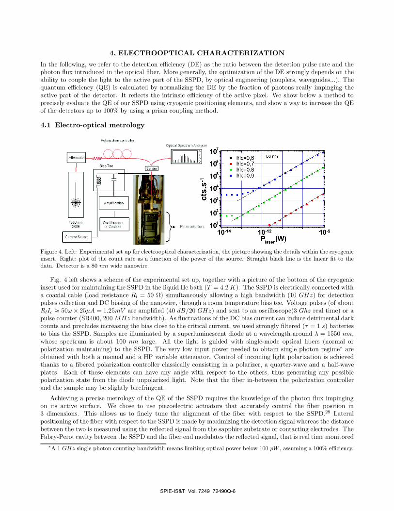
4.2 Polarization issue
Figure 5. (a) measurement of polarization dependance of the detection efficiency on the polarization state of the detectedphoton. θ(λ/4) and θ(λ/2) are the angle of the λ/4 and λ/2 plates of the polarization controller. (b) Simulation of thepolarization dependant efficiency using basic assumption explained in the text,
As expected by the asymmetric shape of the meander, and already reported,30 we found out that the DE ofSSPD is strongly light polarization dependent. This dependency can be characterized by R, ratio of highest DEfor a given polarization to the lowest. Detectors with lines between 90 and 300 nm and filling factor around 50%were polarization characterized, and we found that R is between 2 and 4 at 4.2 K, with no clear dependency onthe aforementioned parameters. Figure 5 shows a typical graph of DE dependency with respect to wave-plateangles. Areas with high DE correspond to a linear photon polarization parallel to the meander lines. On theopposite, the lowest DE is observed when electric field is orthogonal to the meander lines, that is for the half-waveplate rotated by 45◦ from the previous described position. We simulated this effect by considering 2 differentDE for each polarization: DEx and DEy, and adjusting the optical fiber birefringence, which is usually quite lowif the fiber is not twisted (dephasing below π/12).
This effect can be understood if we consider that absorption of NbN is very different for an electric fieldparallel or perpendicular to the nanowires. To explain this DE difference, Finite Difference Time Domaincalculations were performed and proved that absorption is more efficient when electric field is parallel to thewires. Quantitatively, simulations give an absorption of 21% for polarized light along x compared to 10% alongy for a 100 nm SSPD and filling factor of 50%. However, the uncertainty of NbN ultrathin film optical indexmakes it hard to clearly quantify this difference. The polarization dependance of the DE can be lowered toalmost zero by patterning the nanowire under a spiral form,31 but at the cost of a decrease of the overall QE, asthe polarization dependance is not locally suppressed.
SPIE-IS&T Vol. 7249 72490Q-7

lpWlOpWlOOpW
80 nm
A
.v,UA
.S
A.'
28 29 30 31
'bias
32 33
I O (b) 101D
110 ç 100
101o3
101
34I
- Lase/'2 8m (SE)
spotlOom
(bE)
-r I
U
I I t-
100 200 300width w (nm)
I ' I .1
DE(%)U QE(%)
U
.1.
U
U
Figure 6. (a) Measurement of the DE and dark counts rate of a 80 nm wide detector as a function of the bias current.(b) Measurement of DE of same length detector as a function of their width. The inset graphically explains how the QEis calculated from the measurement of the DE.
4.3 Quantum efficiency issue
Dark counts measurement is reported on Fig. 6 (a), evidencing a steep exponential dependance as a function ofthe bias current. This dependance involves thermal fluctuations of the current circulating within the wire, so itdecreases when measurement are done at 2 K. The quantitative prediction of dark counts is still an object ofcontroversy.15, 32, 33 If low dark count are needed (like in quantum optics), these dark counts severely limits theinteresting range of QE.
Fig. 6(a) also shows a typical measurement of detection efficiency of a detector. We checked that DE isidentical for all power, as we are in the single photon regime. It reaches a maximum DE ≈ 0.7% near thecritical current of the wire. This DE is exponentially decreasing with the width of the nanowire (Fig. 6(b)).The latter experiment has been conducted on identical length nanowire, i.e. on increasing pixel size. To discussthese results we have to compare QE instead of DE. The narrowest wire (80 nm) is 2.8 × 2.8μm size, whereasthe fiber output placed at a distance below 10 μm is a circle of about 10 μm diameter: the QE of this SSPD isthen of about 8.5%. Other QE were calculated in a similar way (Fig. 6(b)).
Now we note that the QE have two contributions: one coming from pure electromagnetic considerationsgoverning photon absorption, and the second one originating from internal efficiency of generation of the voltagepulse, once the photon has been absorbed. The latter has been shortly discussed in section 2.1. The very lowthickness of the NbN layer limits the photon absorption to 22% for t = 4.4 nm thick plain film. Consequentlythe QE of a 50% filling factor meander made of that film will be equal to 11% at maximum, as checked by FiniteDifference Time Domain numerical solution to the electromagnetic problem. For these calculations, the NbNrefractive index at 1550 nm was assumed to be 3.5 + j5.2 from ellipsometric measurements. From Fig. 6(b), wecan now see that only the 80 nm wide SSPD is reaching this optically limited QE: in other words, we find thatthe critical wire width wc in Eq. 1 for λ0 = 1.55 μm photon is of about 80 nm. On the contrary, larger wirewidth SSPD are in a regime limited by the efficiency of ”hot spot” generation, and there QE is exponentiallydecreasing as w < wc.†
This good result also puts light on a major drawback of those detector, viz. the low QE of the standardconfiguration of SSPD. The QE is limited by the low thickness of the NbN film that preclude any major absorption(< 22%). This motivated the investigation of optical coupling structure. First demonstration involves the designof a cavity3 enhancing the electromagnetic field at the nanowire position: measured QE reaches mean values of45%, up to 57%. Here we propose a novel optical coupling scheme that allows reaching a (theoretical) absorptionof 100%. It is based on prism coupling into a waveguide (Fig.7(a)). Light enters the high index prism through
†The ”hot spot model” rigourously predict a zero QE below the critical width, but contributions of fluctuations makeit non zero.7
SPIE-IS&T Vol. 7249 72490Q-8

optical fibre
(a)S102Si Siwaveguide
40 NbN stripes, l5Onm wide,sapphire 4nm thick, 50% filling factor
x(pm)
destructiveSi
sapphire NbN contact
R, T, A (%)
100
80
60
40
20
pl00% absorption
6.5© FWHMin Si
- reflexion- transmission- absorption
0 1
25 30 35 40 45
angle of incidence on Si02 layer (©)
Figure 7. (a) Principle of the QE-enhanced structure (b) FDTD simulation of the structure.
a standard anti-reflection coating to avoid Fresnel reflection onto the input face. It undergoes total internalreflection at the interface with a low index layer, generating an evanescent wave, enabling coupling into a highindex waveguide layer lying below. The waveguide is by nature leaky: some part of the coupled light is re-radiatedinto the prism but destructively interferes with light directly reflected at the upper interface of the low-indexlayer, suppressing the resulting reflection on the device (Fig.7(b)). There is no transmitted light through thedevice as the angle of incidence is larger than the critical angle defined by the prism and the substrate. Theonly possible loss is absorption by the NbN layer in close vicinity with the waveguide, provided the propagationlength in the waveguide is smaller than the meander. The device is optimized for a given linear polarization.Two such structures and a polarizing beam splitter can be used if detection of all polarizations is needed.
Figure 8. Calculated dependance of absorption (A), reflection (R) and transmission (T) of the structure, as a function ofthe coupling angle.
A preliminary example of such realistic implementation of this advanced optical structure on standard SSPD(NbN meander, sapphire substrate) in the near-infrared domain uses silicon and silica as high and low refractiveindex materials is given in Fig.8. The thickness of the deposited layers is in the 100 nm range. For a givenwavelength, e.g. 1550 nm, the theoretical quantum efficiency calculated by 2D RCWA (Rigorous Couped WaveAnalysis) reaches 100% with a plane wave at resonance, with angle of incidence 35◦, on an infinite meander. It isstill 95% with a focused 2D Gaussian beam with 10μm diameter, at the exit of a standard telecom single opticalfiber, and a 10 × 10μm meander, assuming the quantum efficiency is limited by optical coupling. The spectralrange is several hundred nanometers. These data were calculated assuming a 4 nm-thick NbN layer on sapphirewith only 50% filling factor, and usual stripe widths (100 − 150 nm).
Moreover, we stress that this QE-enhanced structure relies on standard technological steps. The proposedmaterials (Si and SiO2) are widespread within standard (CMOS) foundries, and the technological stack is onlymade of two unstructured layers with standard thicknesses for deposition machines. Finally, the micro-prismcan be bonded onto the stack by molecular bonding using well-mastered microelectronic techniques.
SPIE-IS&T Vol. 7249 72490Q-9

5. CONCLUSION
We have demonstrated important improvements of SSPD by a work on materials, fabrication process, opticalmetrology and QE-enhancing structures. Using M-plane sapphire to grow NbN will help meet the goal of a largescale integration of SSPD fabrication benefiting from state of the art layer quality. Moreover demonstratinga 8.5% quantum efficiency at 1.5 μm, close to the maximum efficiency expected from optical simulation, hasopened the way to optically optimized structures. We propose such a design, using a high index planar waveguidein which light is evanescently coupled through a high index prism. The latter structure allows reaching a 100%quantum efficiency, which compares favorably with previously proposed structures.
ACKNOWLEDGMENTS
We thank J.L. Thomassin for technical assistance for e beam lithography and the ”Plateforme TechnologiqueAmont” (PTA) for fabrication equipments. This work was partially supported by the STREP ’Sinphonia’ fundedby the European Commission under contract number NMP4-CT-2005-16433.
REFERENCES1. G. N. Gol’tsman, O. Okunev, G. Chulkova, A. Lipatov, A. Semenov, K. Smirnov, B. Voronov, A. Dzardanov,
C. Williams, and R. Sobolewski, “Picosecond superconducting single-photon optical detector,” AppliedPhysics Letters 79(6), pp. 705–707, 2001.
2. A. J. Kerman, E. A. Dauler, W. E. Keicher, J. K. W. Yang, K. K. Berggren, G. Gol’tsman, and B. Voronov,“Kinetic-inductance-limited reset time of superconducting nanowire photon counters,” Applied Physics Let-ters 88(11), p. 111116, 2006.
3. K. M. Rosfjord, J. K. W. Yang, E. A. Dauler, A. J. Kerman, V. Anant, B. M. Voronov, G. N. Gol’tsman,and K. K. Berggren, “Nanowire single-photon detector with an integrated optical cavity and anti-reflectioncoating,” Opt. Express 14(2), pp. 527–534, 2006.
4. A. Korneev, V. Matvienko, O. Minaeva, I. Milostnaya, I. Rubtsova, G. Chulkova, K. Smirnov, V. Voronov,G. Gol’tsman, W. Slysz, A. Pearlman, A. Verevkin, and R. Sobolewski, “Quantum efficiency and noiseequivalent power of nanostructured, nbn, single-photon detectors in the wavelength range from visible toinfrared,” Applied Superconductivity, IEEE Transactions on 15, pp. 571–574, June 2005.
5. A. Pearlman, A. Cross, W. Slysz, J. Zhang, A. Verevkin, M. Currie, A. Korneev, P. Kouminov, K. Smirnov,B. Voronov, G. Gol’tsman, and R. Sobolewski, “Gigahertz counting rates of nbn single-photon detectors forquantum communications,” Applied Superconductivity, IEEE Transactions on 15, pp. 579–582, June 2005.
6. G. Gol’tsman, O. Minaeva, A. Korneev, M. Tarkhov, I. Rubtsova, A. Divochiy, I. Milostnaya, G. Chulkova,N. Kaurova, B. Voronov, D. Pan, J. Kitaygorsky, A. Cross, A. Pearlman, I. Komissarov, W. Slysz, M. We-grzecki, P. Grabiec, and R. Sobolewski, “Middle-infrared to visible-light ultrafast superconducting single-photon detectors,” Applied Superconductivity, IEEE Transactions on 17, pp. 246–251, June 2007.
7. A. Semenov, A. Engel, H. Hubers, K. Il’in, and M. Siegel, “Spectral cut-off in the efficiency of the resistivestate formation caused by absorption of a single-photon in current-carrying superconducting nano-strips,”Eur. Phys. J. B 47, p. 495, 2005.
8. P. Eraerds, M. Legre, A. Rochas, H. Zbinden, and N. Gisin, “Sipm for fast photon-counting and multiphotondetection,” Opt. Express 15(22), pp. 14539–14549, 2007.
9. M. Halder, A. Beveratos, N. Gisin, V. Scarani, C. Simon, and H. Zbinden, “Entangling independent photonsby time measurement,” Nature Physics 3, p. 692, 2007.
10. H. Takesue, S. Nam, Q. Zhang, R. Hadfield, T. Honjo, K. Tamaki, and Y. Yamamoto, “Quantum keydistribution over a 40-db channel loss using superconducting single-photon detectors,” Nature Photonics 1,p. 343, 2007.
11. E. L. Coarer, S. Blaize, P. Benech, I. Stefanon, A. Morand, G. Lerondel, G. Leblond, P. Kern, J. Fedeli,and P. Royer, “Wavelength-scale stationary-wave integrated fourier-transform spectrometry,” Nature Pho-tonics 1, p. 473, 2007.
SPIE-IS&T Vol. 7249 72490Q-10

12. J. Zhang, N. Boiadjieva, G. Chulkova, H. Deslandes, G. Gol’tsman, A. Korneev, P. Kouminov, M. Leibowitz,W. Lo, R. Malinsky, O. Okunev, A. Pearlman, W. Slysz, K. Smirnov, C. Tsao, A. Verevkin, B. Voronov,K. Wilsher, and R. Sobolewski, “Noninvasive cmos circuit testing with nbn superconducting single-photondetectors,” Electronics Letters 39, pp. 1086–1088, July 2003.
13. K. Suzuki, S. Miki, S. Shiki, Y. Kobayashi, K. Chiba, Z. Wang, and M. Ohkubo, “Ultrafast ion detectionby superconducting nbn thin-film nanowire detectors for time-of-flight mass spectrometry,” Physica C:Superconductivity 468(15-20), pp. 2001 – 2003, 2008. Proceedings of the 20th International Symposium onSuperconductivity (ISS 2007), Proceedings of the 20th International Symposium on Superconductivity (ISS2007).
14. J. Yang, A. Kerman, E. Dauler, V. Anant, K. Rosfjord, and K. Berggren, “Modeling the electrical andthermal response of superconducting nanowire single-photon detectors,” Applied Superconductivity, IEEETransactions on 17, pp. 581–585, June 2007.
15. J. Kitaygorsky, J. Zhang, A. Verevkin, A. Sergeev, A. Korneev, V. Matvienko, P. Kouminov, K. Smirnov,B. Voronov, G. Gol’tsman, and R. Sobolewski, “Origin of dark counts in nanostructured nbn single-photondetectors,” Applied Superconductivity, IEEE Transactions on 15, pp. 545–548, June 2005.
16. H. Shibata, T. Maruyama, T. Akazaki, H. Takesue, T. Honjo, and Y. Tokura, “Photon detection andfabrication of mgb2 nanowire,” Physica C 468, p. 1992, 2008.
17. G. Gol’tsman, A. Korneev, M. Tarkhov, V. Seleznev, A. Divochiy, O. Minaeva, N. Kaurova, B. Voronov,O. Okunev, G. Chulkova, I. Milostnaya, and K. Smirnov, “Middle-infrared ultrafast superconducting singlephoton detector,” Infrared and Millimeter Waves, 2007 and the 2007 15th International Conference onTerahertz Electronics. IRMMW-THz. Joint 32nd International Conference on , pp. 115–116, Sept. 2007.
18. R. E. de Lamaestre, P. Odier, E. Bellet-Amalric, P. Cavalier, S. Pouget, and J.-C. Villegier, “High quality ul-trathin nbn layers on sapphire for superconducting single photon detectors,” Journal of Physics: ConferenceSeries 97, p. 012046 (6pp), 2008.
19. J. Villegier, S. Bouat, P. Cavalier, R. Setzu, R. E. de Lamaestre, C. Jorel, P. Odier, P. Guillet, L. Mechin,M. Chauvat, and P. Ruterana, “Epitaxial growth of sputtered ultrathin nbn layers and junctions on sap-phire.” to be published in IEEE Trans. Appl. Supercond.
20. T. Akune, N. Sakamoto, and Y. Shibuya, “Nbn films prepared by magnetron sputtering,” Japanese Journalof Applied Physics 21(Part 1, No. 5), pp. 772–775, 1982.
21. Z. Wang, A. Kawakami, Y. Uzawa, and B. Komiyama, “Superconducting properties and crystal structuresof single-crystal niobium nitride thin films deposited at ambient substrate temperature,” Journal of AppliedPhysics 79(10), pp. 7837–7842, 1996.
22. A. Braginski and J. Talvacchio, Superconducting Devices, Academic, Boston, 1990.23. J. R. Gao, M. Hajenius, F. D. Tichelaar, T. M. Klapwijk, B. Voronov, E. Grishin, G. Gol’tsman, C. A.
Zorman, and M. Mehregany, “Monocrystalline nbn nanofilms on a 3c-sic/si substrate,” Applied PhysicsLetters 91(6), p. 062504, 2007.
24. R. E. de Lamaestre, P. Odier, and J.-C. Villegier, “Microstructure of nbn epitaxial ultrathin films grown ona-, m-, and r-plane sapphire,” Applied Physics Letters 91(23), p. 232501, 2007.
25. P. K. Gallagher, W. R. Sinclair, D. D. Bacon, and G. W. Kammlott, “Oxidation of sputtered niobiumnitride films,” Journal of The Electrochemical Society 130(10), pp. 2054–2056, 1983.
26. A. J. Kerman, E. A. Dauler, J. K. W. Yang, K. M. Rosfjord, V. Anant, K. K. Berggren, G. N. Gol’tsman,and B. M. Voronov, “Constriction-limited detection efficiency of superconducting nanowire single-photondetectors,” Applied Physics Letters 90(10), p. 101110, 2007.
27. R. H. Hadfield, P. A. Dalgarno, J. A. O’Connor, E. Ramsay, R. J. Warburton, E. J. Gansen, B. Baek, M. J.Stevens, R. P. Mirin, and S. W. Nam, “Submicrometer photoresponse mapping of nanowire superconductingsingle-photon detectors,” Applied Physics Letters 91(24), p. 241108, 2007.
28. C. Constancias, R. E. de Lamaestre, O. Louveau, P. Cavalier, and J.-C. Villegier, “Patterning issues insuperconducting nanowire single photon detector fabrication,” 25(6), pp. 2041–2044, AVS, 2007.
29. L. Maingault, P. Cavalier, R. E. de Lamaestre, L. Frey, and J. Villegier, “Quantum efficiency and polarizationeffects in nbn superconducting single photon detectors.” to be published in IEEE Trans. Appl. Supercond.
SPIE-IS&T Vol. 7249 72490Q-11
30. V. Anant, A. J. Kerman, E. A. Dauler, J. K. W. Yang, K. M. Rosfjord, and K. K. Berggren, “Opticalproperties of superconducting nanowire single-photon detectors,” Opt. Express 16(14), pp. 10750–10761,2008.
31. S. N. Dorenbos, E. M. Reiger, N. Akopian, U. Perinetti, V. Zwiller, T. Zijlstra, and T. M. Klapwijk,“Superconducting single photon detectors with minimized polarization dependence,” Applied Physics Let-ters 93(16), p. 161102, 2008.
32. A. D. Semenov, P. Haas, H.-W. Hbers, K. Ilin, M. Siegel, A. Kirste, T. Schurig, and A. Engel, “Vortex-based single-photon response in nanostructured superconducting detectors,” Physica C: Superconductiv-ity 468(7-10), pp. 627 – 630, 2008. Proceedings of the Fifth International Conference on Vortex Matter inNanostructured Superconductors, Proceedings of the Fifth International Conference on Vortex Matter inNanostructured Superconductors.
33. J. Kitaygorsky, I. Komissarov, A. Jukna, D. Pan, O. Minaeva, N. Kaurova, A. Divochiy, A. Korneev,M. Tarkhov, B. Voronov, I. Milostnaya, G. Gol’tsman, and R. Sobolewski, “Dark counts in nanostructurednbn superconducting single-photon detectors and bridges,” Applied Superconductivity, IEEE Transactionson 17, pp. 275–278, June 2007.
SPIE-IS&T Vol. 7249 72490Q-12