Unbiased estimation of linewidth roughness
10
Copyright 2005 Society of Photo-Optical Instrumentation Engineers This paper was published in Proc. SPIE 5752, 480 (2005) and is made available as an electronic reprint with permission of SPIE. One print or electronic copy may be made for personal use only. Systematic or multiple reproduction, distribution to multiple locations via electronic or other means, duplication of any material in this paper for a fee or for commercial purposes, or modifica- tion of the content of the paper are prohibited.
-
Upload
independent -
Category
Documents
-
view
1 -
download
0
Transcript of Unbiased estimation of linewidth roughness
Copyright 2005 Society of Photo-Optical Instrumentation Engineers
This paper was published in Proc. SPIE 5752, 480 (2005) and is made available as an electronic reprint with permission of SPIE. One print or electronic copy may be made for personal use only. Systematic or multiple reproduction, distribution to multiple locations via electronic or other means, duplication of any material in this paper for a fee or for commercial purposes, or modifica-tion of the content of the paper are prohibited.

Unbiased Estimation of Linewidth Roughness
J. S. Villarrubiaa and B. D. BundaybaNational Institute of Standards and Technology,† Gaithersburg, MD, 20899
bInternational SEMATECH Manufacturing Initiative (ISMI), Austin, TX 78741, USA
ABSTRACT
Linewidth roughness (LWR) is usually estimated simply as three standard deviations of the linewidth. The effect of image noise upon this metric includes a positive nonrandom component. The metric is therefore subject to a bias or “systematic error” that we have estimated can be comparable in size to the roughness itself for samples as smooth as required by the industry roadmap. We illustrate the problem using scanning electron microscope images of rough lines. We propose simple changes to the measurement algorithm that, if adopted by metrology instrument suppliers, would permit estimation of LWR without bias caused by image noise.
Keywords: line edge roughness (LER), linewidth roughness (LWR), measurement algorithms, measurement bias, scanning electron microscopy (SEM)
1. INTRODUCTION
Linewidth roughness (LWR, sometimes expressed in terms of its single-edge counterpart, line edge roughness or LER) is an emerging concern in semiconductor electronics manufacturing. Roughness at wavelengths long compared to the tran-sistor gate size manifests itself principally in variation of performance from one transistor to another. Short wavelength roughness means that the length of a transistor’s conducting channel is not uniform across the transistor. When gates were wider, a few nanometers of roughness represented a tiny fraction of the width. With the gate critical dimension (CD) now approaching 30 nm, the same roughness may begin to have a noticeable impact upon device performance, affecting off-state leakage currents, device drive currents, dopant distributions after diffusion, etc., as a number of recent studies are beginning to indicate.1-6
For this reason the International Technology Roadmap for Semiconductors (ITRS) recognizes a need to measure and con-trol LWR during production.7 Its most recent full edition in 2003 contains specifications for LWR control and metrology in Table 117 of its Metrology section. The ITRS quantifies LWR as 3 standard deviations of the CD variation. Stated in terms of this metric, the specifications call for LWR control of 2.6 nm this year, improving to 1.6 nm by 2009. To support this control, the ITRS specifies that the metrology tool that measures LWR should have a CD precision (i.e., 3 standard deviation static CD repeatability) of better than about 0.5 nm this year, improving to approximately 0.3 nm by 2009.
Emergence of LWR is much more recent than CD as a process control and metrology concern. The earliest editions of the ITRS, and the National Technology Roadmap for Semiconductors before it, contained specifications for CD metrology. As recently as 1999, however, the Metrology section of the ITRS contained only a single instance of the word “rough-ness” (and no mention of LER or LWR at all). Specifications for LER were first added in 2001, but the document noted that there was then no standard method of determining LER. For example, if available CD-SEM (critical dimension scan-ning electron microscope) tools offer a measure of LER or LWR, that measure is likely to be a standard deviation metric, but the number and spacing of the CD measurements from which the standard deviation is computed vary from tool to tool, and there has generally been no accepted means of determining what length of line to sample for each measurement, how many measurements of such samples should be performed, whether the same segment of line should be sampled mul-tiple times or whether each sample should come from a different area of the specimen, etc. We addressed many of these metrology issues a year ago.8
The subject of the present paper is one of the issues to which we called attention in that report, measurement bias. Bias is a nonrandom component of measurement error, sometimes referred to as a “systematic” error. Metrics designed to mea-
†. Official contributions by the National Institute of Standards and Technology are not subject to copyright.
Proc. of SPIE Vol 5752 480Metrology, Inspection, and Process Control for Microlithography XIX, edited by Rich-ard M. Silver, Proc. of SPIE Vol. 5752 (SPIE, Bellingham, WA, 2005) 0277-786X/05/$15 · doi: 10.1117/12.599981. This copy corrects formatting errors in the original printed version.

sure roughness are necessarily designed to measure randomness, since roughness is essentially a random phenomenon. Any such metric is subject to error if there are sources of randomness in measured widths that are not associated with the actual roughness of the line—and of course there are. The most obvious is random error in edge assignments caused by noise in the image, noise that in turn arises from limited counting statistics, vibration, varying electric and magnetic fields, any number of noise sources in signal processing electronics, etc. In the presence of such noise, the LWR, measured as it is usually done today, consists of the quadrature sum of the true roughness and a false “noise roughness.” It therefore tends to overestimate the roughness, perhaps significantly. For example, imagine a LWR measurement on dense lines that have an actual LWR of 1.7 nm, well within the ITRS’s specified limit of 2.6 nm for this year. The measurement uses a CD-SEM that meets the precision specification of 2 nm for CD measurements on such lines. The measured LWR under these circumstances will be just a bit over the ITRS limit. Thus, even though this sample’s roughness is almost 35 % better than required by the specification, it would be rejected. Bias has implications, too, for tool to tool matching. CD-SEMs operating in different environments or under different operating conditions may have different amounts of noise. Not only will one tool have a larger random error than the other, as is to be expected, but additionally and perhaps less expectedly, such tools would on average yield different values of LWR.
In this paper we describe an alternative LWR metric that includes a bias correction, thereby avoiding the worst of the above problem. In Sec. 2 we describe the usual metric and an alternative one that uses repeated measurements to measure and correct for bias. Under reasonable assumptions, the alternative metric avoids noise-related bias. In Sec. 3 we describe an experiment designed to compare the two metrics under conditions where the noise level in images was changing but the actual LWR was not. Under such circumstances, any differences in measured LWR can be attributed to measurement error. In Sec. 4 we describe how these data were analyzed, and exhibit results that demonstrate the expected bias in the existing metric and its absence in the alternative one.
2. TWO LWR METRICS
2.1 The Current LWR metricIn the semiconductor industry, linewidth roughness is typically quantified using the standard deviation (or a multiple thereof, usually 3) of the widths of lines. If we knew the true widths, , at N equally spaced positions along a line, we could compute the true value of the linewidth variance (the square of the standard deviation) according to the definition,
with (1)
Here the subscript “t” denotes the true value of a quantity. Currently, the usual practice in CD-SEMs measuring LWR is to replace the true widths in the above expression with their measured values, Wi . In this report we will call this metric, R0
2 . That is,
with (2)
2.2 Bias in the current metricReal SEM images have noise in them from a variety of sources. This noise creates errors in edge detection and therefore in the measured widths. We model the error as . That is, the measured width at the ith location differs from the true width by an error that we write as the sum of a bias term, b, and a random error term, εi. (Do not confuse b, which is bias in the width measurement, with the bias in LWR measurement that is the subject of this paper.) Without loss of generality we assume that has a mean value of 0. That is, we are assuming that all of the width measurement bias is included in b. We also assume is uncorrelated from one measurement to another and has standard deviation σε. That is,
when and 0 otherwise. The angle brackets represent the operation of taking the expectation value, which is defined as the average of repeated measurements in the limit that the number of repeats goes to infinity.
Wti
Rt2 1
N 1–------------- Wti Wt–( )
2
i 1=
N
∑= Wt1N---- Wti
i 1=
N
∑=
R02 1
N 1–------------- Wi W–( )
2
i 1=
N
∑= W 1N---- Wi
i 1=
N
∑=
Wi Wti b ε+ i+=
εiεi
εiεj⟨ ⟩ σε2= i j=
Proc. of SPIE Vol 5752 481

When Wi Wti b ε+ i+= is substituted into Eq. 2, b appears in both Wi and W , so it cancels, leaving only the random error. This leads8 to the following relationship between the measured roughness and the actual roughness:
. (3)
Equation 3 says that the standard LWR metric actually is measuring the quadrature sum of the LWR and a false “noise roughness,” σε . This is an example of the rule that the variances induced by uncorrelated random sources add. Since the noise roughness is positive definite, the expected measured roughness is always higher than the true roughness.
Whatever measurement algorithm is to be used for LWR, it is therefore good practice to minimize σε to the extent possi-ble. One way to do this is to reduce the noise in the image as much as possible before line edge positions and linewidths are determined. This can be done by increasing the total electron dose on each pixel of the image. The electron dose is the product of the beam current, dwell time per pixel in each frame, and number of frames. Thus, for a given beam current the dose can be increased either by using a slow-scan strategy or by frame-averaging. In the SEM, there is generally an upper limit to the dose that is set by the onset of contamination, shrinkage, or charging of the sample (due to electron beam exposure) or by measurement throughput requirements. Once the maximum allowable pixel integration time is being used, σε can be further minimized by choosing an edge assignment algorithm that is less sensitive to noise than the aver-age. It has previously been observed that edge assignment algorithms that fit a model function to the intensity profile tend to be less sensitive to noise than those that rely upon finding the maximum slope or a threshold crossing point.9 These strategies reduce σε , but they cannot reduce it to zero. The remaining bias may still be significant. In demonstration mea-surements a year ago our values of σε were only a bit better than 1 nm.8 (If this result seems a bit high compared to cus-tomary performance of CD-SEMs in CD measurements, keep in mind that CD measurements benefit from averaging over some interval of line. Spatial averaging like this has the side effect of filtering out short-wavelength components of LWR. Such filtering is of limited consequence for CD measurements, but for LWR measurements where these wavelength com-ponents may be part of the intended measurement, the length of line that can be averaged may be severely limited.) This makes 3σε comparable to the ITRS roughness specification mentioned above. If measurement instruments do not per-form better than this, then a substantial part of the measured roughness on samples that meet the ITRS roughness specifi-cation will be a measurement artifact (i.e., false noise roughness) rather than true roughness.
2.3 Alternative metricWe therefore propose the following alternative measurement procedure:
1. As with the existing procedure, make all reasonable efforts to improve the edge detection repeatability, . These efforts should include appropriate choice of edge detection algorithm and use of the largest electron dose that is consistent with required measurement throughput and avoiding sample damage, charging, or contamination.
2. After the allowable pixel integration time has been decided in step 1, instead of taking a single image as is the current practice, acquire M images, each at of the pixel integration time.
3. Determine the linewidths, , , , at each of N positions in each of
the M images. Figure 1 illustrates how W is indexed.
R02⟨ ⟩ Rt
2 σε2+=
FIG. 1. Example illustrating how widths in repeated measurements are indexed in this paper. Repeated measurements, Wij, of the linewidth in the circumscribed region of the image on the left are plotted on the right. The first index, i, indexes the location along the line. It is the vertical axis in the graph. The second index, j,indexes the repeat number. For example the widths at one location ( ) shown within the ellipse all have different j. In the plot on the right, with the excep-tion of one repeat shown by the jagged line, points were plotted only for every 5th value of i for clarity
i 310=
i
σε
1 M⁄
Wij i 1 N,=j 1 M,=
Proc. of SPIE Vol 5752 482
4. Wij is a 2-dimensional array. Determine the average widths independently for each of the dimensions. We will denote the average over the first index by placing a bar over the variable name and an “a” (for “average”) in the first index position:
. Similarly the average over the second index is . So
and . (4)
5. At each of the N measurement positions determine the variance of the widths. That is, determine the variance of the group of widths within the ellipse in Fig. 1 and within the other analogous groups along the length of the line. Average these to determine the “noise variance,” Vn.
. (5)
6. Determine the corrected mean square roughness for each of the M images:
(6)
7. Average the squared roughnesses from these images to obtain the overall estimated roughness:
. (7)
We can summarize this procedure in a single expression by combining Eq. 5, Eq. 6, and Eq. 7.
(8)
2.4 Absence of bias in the alternative metricWe assume the following error model:
. (9)
The random errors have 0 mean and are uncorrelated. That is
(10)
with δii ′ equal to 1 when i i′= and 0 otherwise. These are the same assumptions we made in Sec. 2.2, just re-expressed for our double-index algorithm.
By leading up to Eq. 8 step by step as we did in the last section, we seek to make plain what this otherwise somewhat complicated-looking expression means. The sum over i in the first pair of sums in Eq. 8 along with the leading is simply the variance of the widths in the jth image. It is, in other words, simply the existing LWR metric (compare Eq. 2), applied to one of the repeated images. Then 1/M times the sum over j forms the average of this metric over the Mimages. Unsurprisingly, then, and easily shown, when the errors obey Eq. 9 and Eq. 10, the first pair of sums has an expectation value that is the same as the existing LWR metric: the true roughness variance plus as in Eq. 3. The sec-ond pair of sums in Eq. 8 is a correction term. It is the average of N independent estimates of the noise variance, one for
Waj Wia
Waj1N---- Wij
i 1=
N
∑≡ Wia1M----- Wij
j 1=
M
∑≡
N 1–
Vn1N---- 1
M 1–-------------- Wij Wia–( )
2
j 1=
M
∑i 1=
N
∑=
Rqj2 1
N 1–------------- Wij Waj–( )
2
i 1=
N
∑ Vn–=
Rq2 1
M----- Rqj
2
j 1=
M
∑=
Rq2 1
M----- 1
N 1–------------- Wij Waj–( )
2
i 1=
N
∑1N---- 1
M 1–-------------- Wij Wia–( )
2
j 1=
M
∑i 1=
N
∑–
j 1=
M
∑=
Wij Wti b εij+ +=
εij⟨ ⟩ 0=
εijεi ′j ′⟨ ⟩ σε2δii ′δjj ′=
1 N 1–( )⁄
σε2
Proc. of SPIE Vol 5752 483
Rq2
each position along the line. It is easy to show that its expectation value is . Thus, it corrects for the overestimate made by the first pair of sums. Summarizing these remarks algebraically:
. (11)
therefore does not contain bias that arises due to random errors in edge assignment. An experimental test to demon-strate this is described in the next section.
3. EXPERIMENTAL
We report here a series of measurements intended to demonstrate the performance of the two metrics, R02 (Eq. 2) and Rq
2 (Eq. 8) described in the previous section. The rationale for the measurement is this: We obtain multiple images with vary-ing noise. These images all come from the same location on a particular sample, so the true value of the LWR must be the same in all the images. Any differences in measured LWR must therefore be attributed to measurement error. We can arrange for different amounts of noise in the images by using different amounts of averaging. Images that are the sum of few frames will have more noise than images that are summed from many frames. Repeated measurements at each noise level will permit us to ascertain both an average measured value and the amount of random scatter around this value. Nat-urally, we expect repeatability to suffer as the noise level increases. However, we expect that for a reasonable LWR met-ric, this increased scatter would be centered on the same average value of LWR.
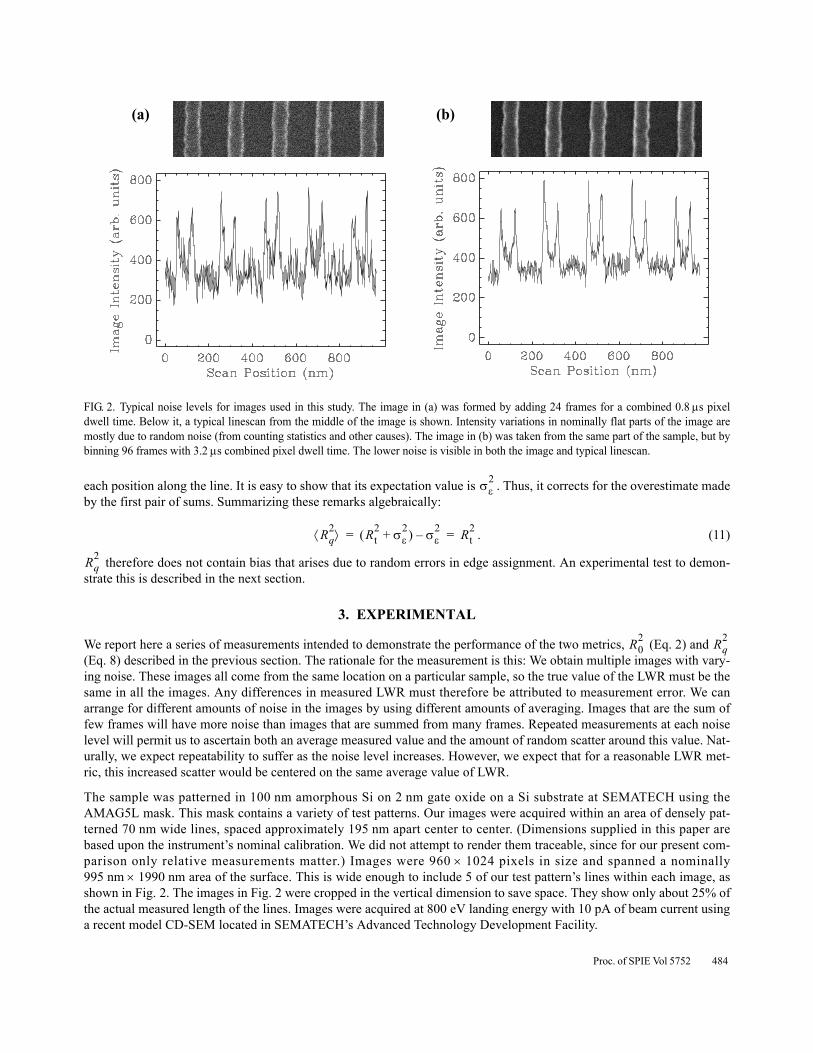
The sample was patterned in 100 nm amorphous Si on 2 nm gate oxide on a Si substrate at SEMATECH using the AMAG5L mask. This mask contains a variety of test patterns. Our images were acquired within an area of densely pat-terned 70 nm wide lines, spaced approximately 195 nm apart center to center. (Dimensions supplied in this paper are based upon the instrument’s nominal calibration. We did not attempt to render them traceable, since for our present com-parison only relative measurements matter.) Images were 960 × 1024 pixels in size and spanned a nominally 995 nm × 1990 nm area of the surface. This is wide enough to include 5 of our test pattern’s lines within each image, as shown in Fig. 2
FIG. 2. Typical noise levels for images used in this study. The image in (a) was formed by adding 24 frames for a combined 0.8 µs pixel dwell time. Below it, a typical linescan from the middle of the image is shown. Intensity variations in nominally flat parts of the image are mostly due to random noise (from counting statistics and other causes). The image in (b) was taken from the same part of the sample, but by binning 96 frames with 3.2 µs combined pixel dwell time. The lower noise is visible in both the image and typical linescan.
(a) (b)
. The images in Fig. 2 were cropped in the vertical dimension to save space. They show only about 25% of the actual measured length of the lines. Images were acquired at 800 eV landing energy with 10 pA of beam current using a recent model CD-SEM located in SEMATECH’s Advanced Technology Development Facility.
σε2
Rq2⟨ ⟩ Rt
2 σε2+( ) σε
2– Rt2= =
Proc. of SPIE Vol 5752 484
All images were acquired in frames with 0.033 µs dwell time per pixel in each frame. We acquired 64 images, each of which was formed by summing 6 frames within the CD-SEM, after which the image was saved. For this reason, our nois-iest images correspond to a total pixel integration time of 0.2 µs (6 frames × 0.033 µs/frame). Images with reduced noise were formed by summing images off-line during post-acquisition data analysis. So, for example, by binning and summing the images, we could form 64 images with 0.2 µs total pixel integration time (bin size = 1 image), 32 images with 0.4 µs (bin size = 2), 16 images with 0.8 µs (bin size = 4), and so on, up to a limit of 1 image with 12.8 µs pixel integration time. Examples of the amount of noise in images with two different bin sizes are shown in Fig. 2. Doing our own post-acquisi-tion frame averaging in this way has one disadvantage. The measurement must pause 64 times to save raw images to disk, a process that significantly slows the measurement and allows more sample drift than would be encountered in an ordi-nary measurement. However, there are two advantages that more than compensate: (1) Images with many different pixel integration times are essentially all acquired with the amount of beam exposure needed for the single longest exposure image. This maximizes the amount of data for a given amount of contamination and charging of the sample. (2) When comparing, for example, a metric that requires 2 images at 0.2 µs/pixel each to a metric that requires a single 0.4 µs/pixel image, if the images were acquired separately there would be random differences in the data. By combining the two 0.2 µs/pixel images to make the 0.4 µs/pixel image, both techniques analyze exactly the same data set. Even the random errors built (by noise) into these data are the same for both methods, so the comparison becomes a pure comparison of the metrics.
4. DATA ANALYSIS AND RESULTS
To determine the LWR it is first necessary to determine widths of the line from the image. To do this it is in turn necessary to ascertain the edge positions. We assigned edge positions using the sigmoidal fit method, which we have described previously10 and found to be less sensitive to image noise than either the maximum derivative or regression to baseline methods. Once left and right edge positions are determined for the ith linescan in the jth image, the difference is Wij. We did not average linescans. Our sampling interval was therefore a single linescan (approximately 1.9 nm spacing).
We observed a significant amount of drift between our first and last images due to the cause mentioned at the end of the last section. If uncorrected, this would have resulted in more blurring of edges in our binned images than in a normal mea-surement, where the binning is performed by the instrument without delays for off-loading intermediate images for analy-sis. To compensate, after edge assignments were made to the 64 images, we determined the amount by which each image must be shifted in order to align its edges with those of the first image. The result of this operation was a shift vector (in xand y, i.e., both coordinates in the plane of the image) that produced the maximum correlation between the edge curves. These shift vectors were subsequently used to shift images to compensate for drift between them.
The edge assignment by sigmoidal fit described above deter-mined the widths, Wij, versus position for a bin size of 1. For a bin size of 2, images were treated in pairs. Images 1 and 2 were shifted to remove drift, then added, after which edge assign-ments were made as before. This was repeated for images 3 and 4, 5 and 6, and so on, until all of the 32 sequential pairs that comprise the 64 image data set were processed. In general, for a bin size of s, images were summed in sets of s before the edge positions were assigned, and there were 64/s such sets. This operation was performed for bin sizes of 1, 2, 4, 8, 16, and 32.
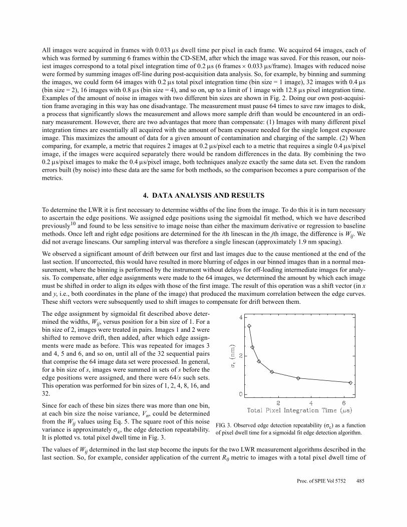
FIG. 3. Observed edge detection repeatability (σε) as a function of pixel dwell time for a sigmoidal fit edge detection algorithm.
Since for each of these bin sizes there was more than one bin, at each bin size the noise variance, Vn, could be determined from the Wij values using Eq. 5. The square root of this noise variance is approximately σε, the edge detection repeatability. It is plotted vs. total pixel dwell time in Fig. 3.
The values of Wij determined in the last step become the inputs for the two LWR measurement algorithms described in the last section. So, for example, consider application of the current R0 metric to images with a total pixel dwell time of
Proc. of SPIE Vol 5752 485
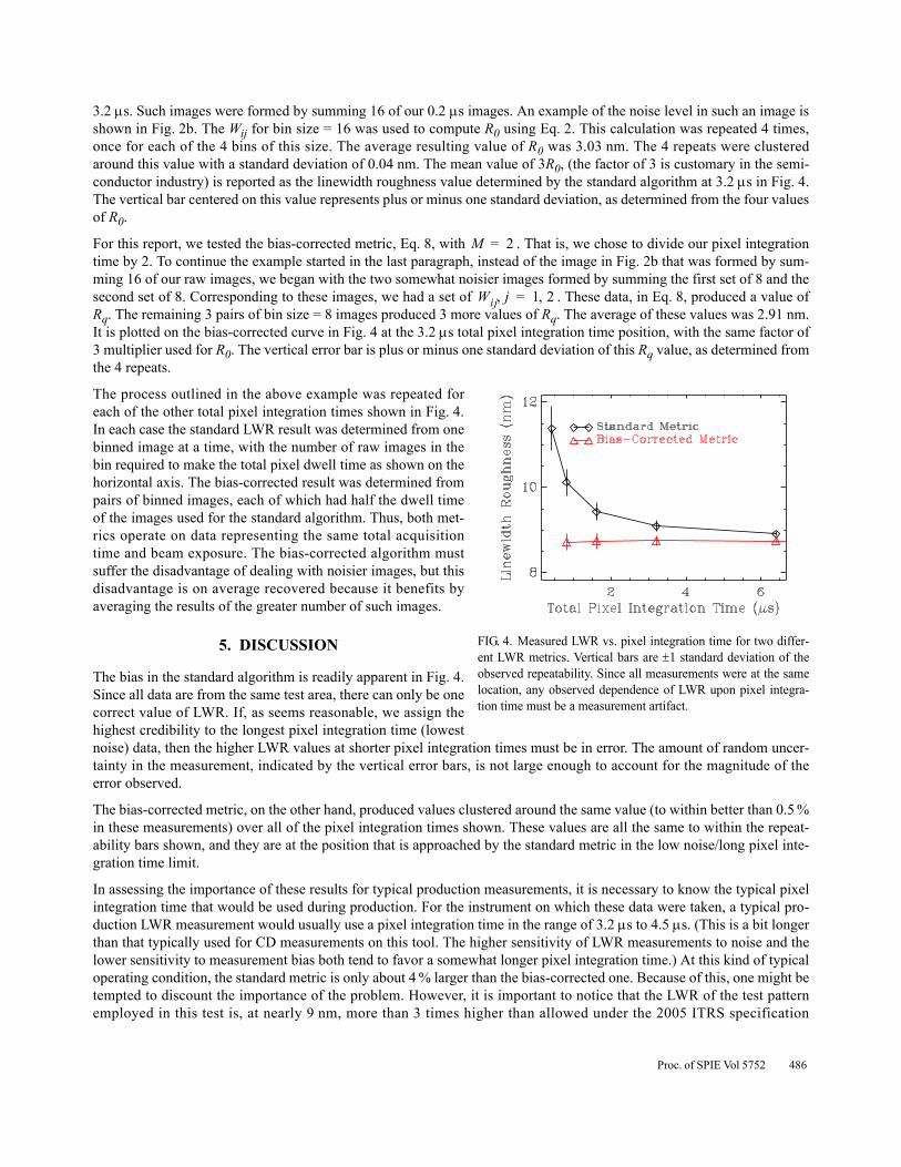
3.2 µs. Such images were formed by summing 16 of our 0.2 µs images. An example of the noise level in such an image is shown in Fig. 2b. The Wij for bin size = 16 was used to compute R0 using Eq. 2. This calculation was repeated 4 times, once for each of the 4 bins of this size. The average resulting value of R0 was 3.03 nm. The 4 repeats were clustered around this value with a standard deviation of 0.04 nm. The mean value of 3R0, (the factor of 3 is customary in the semi-conductor industry) is reported as the linewidth roughness value determined by the standard algorithm at 3.2 µs in Fig. 4. The vertical bar centered on this value represents plus or minus one standard deviation, as determined from the four values of R0.
For this report, we tested the bias-corrected metric, Eq. 8, with M 2= . That is, we chose to divide our pixel integration time by 2. To continue the example started in the last paragraph, instead of the image in Fig. 2b that was formed by sum-ming 16 of our raw images, we began with the two somewhat noisier images formed by summing the first set of 8 and the second set of 8. Corresponding to these images, we had a set of Wij j, 1 2,= . These data, in Eq. 8, produced a value of Rq. The remaining 3 pairs of bin size = 8 images produced 3 more values of Rq. The average of these values was 2.91 nm. It is plotted on the bias-corrected curve in Fig. 4 at the 3.2 µs total pixel integration time position, with the same factor of 3 multiplier used for R0. The vertical error bar is plus or minus one standard deviation of this Rq value, as determined from the 4 repeats.
The process outlined in the above example was repeated for each of the other total pixel integration times shown in Fig. 4
FIG. 4. Measured LWR vs. pixel integration time for two differ-ent LWR metrics. Vertical bars are ±1 standard deviation of the observed repeatability. Since all measurements were at the same location, any observed dependence of LWR upon pixel integra-tion time must be a measurement artifact.
. In each case the standard LWR result was determined from one binned image at a time, with the number of raw images in the bin required to make the total pixel dwell time as shown on the horizontal axis. The bias-corrected result was determined from pairs of binned images, each of which had half the dwell time of the images used for the standard algorithm. Thus, both met-rics operate on data representing the same total acquisition time and beam exposure. The bias-corrected algorithm must suffer the disadvantage of dealing with noisier images, but this disadvantage is on average recovered because it benefits by averaging the results of the greater number of such images.
5. DISCUSSION
The bias in the standard algorithm is readily apparent in Fig. 4. Since all data are from the same test area, there can only be one correct value of LWR. If, as seems reasonable, we assign the highest credibility to the longest pixel integration time (lowest noise) data, then the higher LWR values at shorter pixel integration times must be in error. The amount of random uncer-tainty in the measurement, indicated by the vertical error bars, is not large enough to account for the magnitude of the error observed.
The bias-corrected metric, on the other hand, produced values clustered around the same value (to within better than 0.5 % in these measurements) over all of the pixel integration times shown. These values are all the same to within the repeat-ability bars shown, and they are at the position that is approached by the standard metric in the low noise/long pixel inte-gration time limit.
In assessing the importance of these results for typical production measurements, it is necessary to know the typical pixel integration time that would be used during production. For the instrument on which these data were taken, a typical pro-duction LWR measurement would usually use a pixel integration time in the range of 3.2 µs to 4.5 µs. (This is a bit longer than that typically used for CD measurements on this tool. The higher sensitivity of LWR measurements to noise and the lower sensitivity to measurement bias both tend to favor a somewhat longer pixel integration time.) At this kind of typical operating condition, the standard metric is only about 4 % larger than the bias-corrected one. Because of this, one might be tempted to discount the importance of the problem. However, it is important to notice that the LWR of the test pattern employed in this test is, at nearly 9 nm, more than 3 times higher than allowed under the 2005 ITRS specification
Proc. of SPIE Vol 5752 486

(2.6 nm). The bias scales with σε (i.e., with the noise), not with the roughness. If our sample’s true roughness had been within the specification, the standard and the bias-corrected metrics would have been 3.6 nm vs. 2.6 nm respectively, a difference of more than 38 %, even under currently typical operating conditions.
The bias correction produced by the proposed LWR metric assumes edge assignment errors follow the model given by Eq. 9 and Eq. 10. This model assumes errors consist of a fixed bias plus a random error that is uncorrelated from one mea-surement to the next. Under these assumptions, the LWR metric given in Eq. 8 will be unbiased. These assumptions also constitute the main limitation on the validity of our conclusion that the Eq. 8 metric is unbiased. It is possible to imagine circumstances in which there is a position-dependent bias. It is known, for example, that the error in many edge assign-ment algorithms is a function of the shape of the physical feature’s edge.9,11 This error may, for example, be a nanometer or two for each 1° change in sidewall angle. If the sidewall angle or other relevant aspect of edge shape varies along the length of the line, there will be a component of bias that varies from position to position. Do we expect this to happen? Under usual circumstances, LWR is measured over line lengths on the order of 1 µm or so. Over such short distances, one may hope, at least until stronger evidence is available one way or the other, that etch conditions are relatively uniform and that the edge shape would therefore not vary much. This would not be expected to hold, however, for LWR measured over lines with other spatially varying structure in the neighborhood (e.g., neighboring lines in some places, no neighbors in others) since there are known proximity effects for lithography, etch, and metrology that could create position dependent biases under these circumstances. It also might not hold for polycrystalline materials that have a natural grain size small compared to the line length. If such effects were important, we would need to write Eq. 9 with Wij Wti bi εij+ += instead of Wij Wti b εij+ += , the i subscript on b indicating the position dependence. In this case, the average of bi over the length of the line would still have no effect on the measured LWR by either of the metrics covered in this report. How-ever, the randomly varying part of bi would produce a false “shape roughness.” This “shape roughness” would not be compensated by the correction method employed in Eq. 8 because it does not vary randomly during repeated measure-ments. Therefore, neither of the roughness metrics covered here is immune to this source of error. To minimize such error it would be necessary to employ an edge assignment algorithm12 that is insensitive to changes in sidewall angle or other aspects of edge shape that are deemed irrelevant to device performance.
The possibility of additional measurement errors should not, however, prevent us from making corrections for those that we already know how to make. Although the bias-corrected metric is somewhat more complicated than the simple stan-dard deviation, the small increase in complexity need not trouble the end user. CD-SEMs are highly automated already. No new hardware is required; it is only a matter of programming to implement the metric proposed here.
ACKNOWLEDGEMENTS
This project was funded by the NIST Office of Microelectronic Programs and the NIST Manufacturing Engineering Laboratory. Measurements performed at SEMATECH were funded by the ISMI Lithometrology Program. Michael Gostkowski and Gabriel Gebara of SEMATECH ATDF fabricated the sample.
REFERENCES
1. C. Diaz, H.-J. Tao, Y.-C. Ku, A. Yen, and K. Young, “An Experimentally Validated Analytical Model for Gate Line-Edge Roughness (LER) Effects on Technology Scaling.” IEEE Electron Device Letters, 22(6), 287-289 (2001).
2. S. Xiong, and J. Bokor “Study of Gate Line Edge Roughness Effects in 50 nm Bulk MOSFET Devices.” Proc. SPIE 4689, 733-741 (2002).
3. M. Ercken, G. Storms, C. Delvaux, N. Vandenbroeck, P. Leunissen, and I. Pollentier, “Line Edge Roughness and its Increasing Importance.” Proceedings of ARCH Interface 2002.
4. A. Asenov, S. Kaya, and A. R. Brown, “Intrinsic Parameter Fluctuations in Decananometer MOSFETs Introduced by Gate Line Edge Roughness,” IEEE Trans. Electron. Devices 50(5), 1254-1260 (2003).
5. A. Yamaguchi, R. Tsuchiya, H. Fukuda, O. Komuro, H. Kawada, and T. Iizumi, “Characterization of Line-Edge Roughness in Resist Patterns and Estimation of its Effect on Device Performance,” Proc. SPIE 5038, 689-698 (2003).
Proc. of SPIE Vol 5752 487
6. A. Yamaguchi, K. Ichinose, S. Shimamoto, H. Fukuda, R. Tsuchiya, K. Ohnishi, H. Kawada, and T. Iizumi, “Metrology of LER: influence of line-edge roughness (LER) on transistor performance,” Proc. SPIE 5375, 468-476 (2004).
7. International Technology Roadmap for Semiconductors (ITRS), 2003 Edition, http://public.itrs.net.
8. B. D. Bunday, M. Bishop, D. McCormack, J. S. Villarrubia, A. E. Vladar, R. Dixson, T. Vorburger, and N. G. Orji, “Determination of Optimal Parameters for CD-SEM Measurement of Line Edge Roughness,” Proc. SPIE 5375, 515-533 (2004).
9. J. S. Villarrubia, A. E. Vladár, M. T. Postek, “A simulation study of repeatability and bias in the CD-SEM,” Proc. SPIE 5038, 138-149, 2003.
10. B. D. Bunday, M. Bishop, J. S. Villarrubia, and A. E. Vladár, “CD-SEM Measurement of Line Edge Roughness Test Patterns for 193 nm Lithography,” Proc. SPIE 5038, 2003, pp. 674-688
11. V.A. Ukraintsev, “Effect of Bias Variation on Total Uncertainty of CD Measurements,” Proc. SPIE 5038, 644-650(2003).
12. J. S. Villarrubia, A. E. Vladár, and M. T. Postek, “Scanning electron microscope dimensional metrology using a model-based library,” submitted to Surface and Interface Analysis.
SEMATECH, the SEMATECH logo, International SEMATECH Manufacturing Initiative (ISMI), and the ISMI logo are regis-tered servicemarks of SEMATECH, Inc. All other servicemarks and trademarks are the property of their respective owners.
Proc. of SPIE Vol 5752 488