Lattice effects and current reversal in superconducting ratchets
Upload
khangminh22Category
view
1download
0
Carbon nanofibers addition on transport
and superconducting properties of bulk YBa2Cu3O72d
material prepared via co-precipitation
Nurul Auni Khalid1, Mohd Mustafa Awang Kechik1,* , Nur Atikah Baharuddin1,Chen Soo Kien1, Hussein Baqiah1, Lim Kean Pah1, Abdul Halim Shaari1, Zainal Abidin Talib1,Azhan Hashim2, Masato Murakami3, and Muralidhar Miryala3
1Department of Physics, Faculty of Science, Universiti Putra Malaysia, 43400 UPM Serdang, Selangor, Malaysia2Faculty of Applied Sciences, Universiti Teknologi MARA Pahang, 26400 Jengka, Pahang, Malaysia3Shibaura Institute of Technology, 3 Chome-7-5 Toyosu, Koto, Tokyo 135-8548, Japan
Received: 31 March 2020
Accepted: 12 August 2020
Published online:
5 September 2020
� The Author(s) 2020
ABSTRACT
The effects of carbon nanofibers addition on transport and superconducting
properties of YBa2Cu3O7-d (Y-123) superconductor were studied. Y-123 was
prepared using co-precipitation method for good quality bulk of high temper-
ature superconducting material. Carbon nanofibers with 0.2–0.8 wt% were
added into Y-123 superconductors. The samples were characterized using
electrical resistance measurement for critical temperature (Tc) and critical cur-
rent density (Jc), powder X-ray diffraction, scanning electron microscopy and
energy-dispersive X-ray analysis. Most of the samples indicated a dominant
Y-123 phase of an orthorhombic structure with a minor phase of BaCO3 and
Y-124. Onset critical temperature was found to decrease from 90.5 to 80 K with
increasing of carbon nanofibers concentration. The Jc for pure sample is 11
A/cm2 at 30 K while the Jc of sample with 0.4 wt% carbon nanofibers is 830
A/cm2 at 30 K. Introduction of carbon nanofibers enhanced Jc significantly.
However, further addition of carbon nanofibers in Y-123 superconductor caused
degradation in Jc.
1 Introduction
A revolutionary discovery of YBCO or Y-123 with
chemical formula of YBa2Cu3O7-d was the first ever
material discovered to show Tc above the boiling
point of liquid nitrogen (77 K) [1, 2]. This simply
means that superconductors would no longer require
a complex cooling system for their applications
unlike other materials that rely on liquid helium for
their operation which is rather costly. Due to its high
Tc, Y-123 system may become potential supercon-
ducting materials for future applications. The mate-
rial has been recognized as second generation high
temperature superconductors (HTS) and gave huge
impacts to the market penetration for technology and
power applications [3]. However, the weak flux pin-
ning and granularity of Y-123 especially at tempera-
tures above 20–30 K seems to limit the value of Jc [4].
Many groups claim that the improvement of Jc in
high temperature superconductor can be obtained by
https://doi.org/10.1007/s10854-020-04255-0
J Mater Sci: Mater Electron (2020) 31:16983–16990

the introduction of nanoparticle addition. The addi-
tion of Fe3O4, Zn and Zr nanoparticles acted as
effective flux pinning centers in Y-123 superconduc-
tor and improved the Jc [5–7]. Also the improvement
of Jc and suppression of Tc were observed by the
addition of nano-Ag in (Bi,Pb)-2223 superconductor
[8]. The effective artificial pinning centers will further
enhance Jc at higher fields [9] and higher tempera-
ture. This could be achieved when the flux lines are
pinned and their movement are prevented [10]. In
high temperature superconductor (HTS), the effects
on the vortex movements, determination of Jc, and
other superconducting properties are depend on the
engineering artificial pinning centers which pin flux
lines through crystal imperfections [11] or so-called
defects [12] such as low-angle grain boundaries, twin
boundaries, dislocations and non-superconducting
phases [13, 14]. The route of artificially introducing
inhomogeneity or second-phase materials as flux
pinning sites in the processing of bulk YBCO is a long
standing issue [15].
Other flux pinning approach can be done by
applying high pressure onto superconductors [12]. It
has been found that by using 1 GPa hydrostatic
pressure, more effective point pinning centers, can be
introduced in NaFe0.97Co0.03As single crystal in
comparison with that at 0 GPa [13]. An enhancement
of critical current density of (Ba,K)Fe2As2 single
crystals up to fivefold in low and high magnetic field
through improvement of flux pinning was obtained
by applying 1.2 GPa hydrostatic pressure [14].
A technique of doping and addition of impurities
including metal and non-metal elements, nanoparti-
cles, carbon sources and other compounds have
shown significant effect on the superconducting
properties. Various forms of oxides can be considered
for selection of dopant [16–19]. Carbon nanotubes
have been widely used as a filler for nanocomposites
by the virtue of their structural, electrical, magnetic
properties and exhibit a great potential application to
enhance current-carrying capability of superconduc-
tors and as a wide-band electromagnetic wave
absorber [20, 21]. It has been shown that of the choice
of the type and amount of chemical compound and
impurities could improve both inter-granular and
intra-granular Jc in different high temperature
superconductors [4, 22]. Moreover, doping of YBCO
samples with another suitable compounds with a
right proportion is a reliable method in order to
achieve highly qualified complex structures [23] with
improved grain boundary superconducting proper-
ties [24]. In our previous research we have shown
that the Jc can be significantly enhanced by adding
small amount of carbon nanotube (CNTs) indicating
the formation of pinning centers in YBCO matrix [25].
Following up the same motivation, the aim of this
work is to investigate the impact of carbon nanofibers
(CNFs) on the structural and transport properties of
YBCO and compared it with those obtained via CNTs
addition. Co-precipitation method was used to pre-
pare the samples which we believed that the powders
obtained by this technique have good homogeneity
and fine grain. The method is a relatively low cost
method as it is cheaper over other ‘‘solution’’ meth-
ods, such as sol gel, spray drying and freeze drying
[26, 27].
2 Experimental details
Metal acetate (Yttrium, Barium, and Copper) and
oxalic acid (high purity powders C 99.9% supplied
by Alfa Aesar) were weighed in appropriate molar
ratios with the required stoichiometric ratios of Y3?,
Ba2?, and Cu3? (1:2:3, respectively). The cations were
mixed in solution added with 0.5 M oxalic acid and
then dissolved in 2-propanol and distilled water until
became precipitate of a mixed oxalate system. As a
result, blue precipitate slurry was obtained. The
powders were calcined for 36 h at 900 �C. The cal-
cined powders were ground into fine particulates
and mixed thoroughly with CNFs (CNFs, Nanos-
tructured & Amorphous Materials ‘‘NanoAmor’’,
Diameter 39–50 nm, length[ 1 lm) of different
weight percentages (0, 0.2, 0.4, 0.6 and 0.8 wt%)
before being pressed into pellets. Those concentra-
tions were selected due to their optimal value which
is in range with the improvement in their supercon-
ducting properties later. The pellets were then sin-
tered at 920 �C for 45 h in air.
Electrical resistance measurements were carried
out using standard four-probe method, in a closed
cycle helium cryostat at temperature between 25 and
300 K. Silver paint was used as contact points
between the four tiny wires and the sample. From the
measurement, the value of onset critical temperature
(Tc-onset) and offset critical temperature (Tc-offset) were
determined. Transport critical current density (Jc)
was measured on bar-shaped samples at the tem-
perature of 30 K in self-fields (zero magnetic fields).
16984 J Mater Sci: Mater Electron (2020) 31:16983–16990
Crystal structure and phase formation were identi-
fied via X-ray diffraction using Philips 1710 diffrac-
tometer with CuKa radiation source. Morphology
and grain size were identified by scanning electron
microscope for each sample.
3 Results and discussion
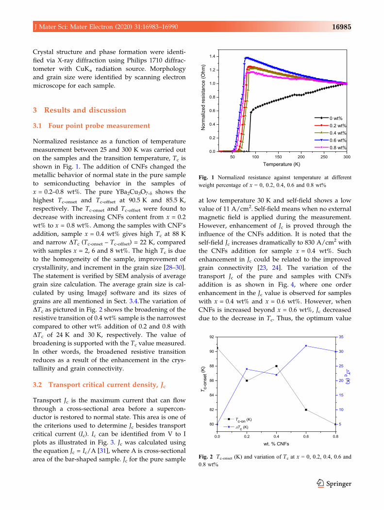
3.1 Four point probe measurement
Normalized resistance as a function of temperature
measurement between 25 and 300 K was carried out
on the samples and the transition temperature, Tc is
shown in Fig. 1. The addition of CNFs changed the
metallic behavior of normal state in the pure sample
to semiconducting behavior in the samples of
x = 0.2–0.8 wt%. The pure YBa2Cu3O7-d shows the
highest Tc-onset and Tc-offset at 90.5 K and 85.5 K,
respectively. The Tc-onset and Tc-offset were found to
decrease with increasing CNFs content from x = 0.2
wt% to x = 0.8 wt%. Among the samples with CNF’s
addition, sample x = 0.4 wt% gives high Tc at 88 K
and narrow DTc (Tc-onset – Tc-offset) = 22 K, compared
with samples x = 2, 6 and 8 wt%. The high Tc is due
to the homogeneity of the sample, improvement of
crystallinity, and increment in the grain size [28–30].
The statement is verified by SEM analysis of average
grain size calculation. The average grain size is cal-
culated by using ImageJ software and its sizes of
grains are all mentioned in Sect. 3.4.The variation of
DTc as pictured in Fig. 2 shows the broadening of the
resistive transition of 0.4 wt% sample is the narrowest
compared to other wt% addition of 0.2 and 0.8 with
DTc of 24 K and 30 K, respectively. The value of
broadening is supported with the Tc value measured.
In other words, the broadened resistive transition
reduces as a result of the enhancement in the crys-
tallinity and grain connectivity.
3.2 Transport critical current density, Jc
Transport Jc is the maximum current that can flow
through a cross-sectional area before a supercon-
ductor is restored to normal state. This area is one of
the criterions used to determine Jc besides transport
critical current (Ic). Ic can be identified from V to I
plots as illustrated in Fig. 3. Jc was calculated using
the equation Jc = Ic/A [31], where A is cross-sectional
area of the bar-shaped sample. Jc for the pure sample
at low temperature 30 K and self-field shows a low
value of 11 A/cm2. Self-field means when no external
magnetic field is applied during the measurement.
However, enhancement of Jc is proved through the
influence of the CNFs addition. It is noted that the
self-field Jc increases dramatically to 830 A/cm2 with
the CNFs addition for sample x = 0.4 wt%. Such
enhancement in Jc could be related to the improved
grain connectivity [23, 24]. The variation of the
transport Jc of the pure and samples with CNFs
addition is as shown in Fig. 4, where one order
enhancement in the Jc value is observed for samples
with x = 0.4 wt% and x = 0.6 wt%. However, when
CNFs is increased beyond x = 0.6 wt%, Jc decreased
due to the decrease in Tc. Thus, the optimum value
50 100 150 200 250 3000.0
0.2
0.4
0.6
0.8
1.0
1.2
1.4
Temperature (K)
0 wt% 0.2 wt% 0.4 wt% 0.6 wt% 0.8 wt%
Nor
mal
ized
resi
stan
ce (O
hm)
Fig. 1 Normalized resistance against temperature at different
weight percentage of x = 0, 0.2, 0.4, 0.6 and 0.8 wt%
0.0 0.2 0.4 0.6 0.8
80
82
84
86
88
90
92
wt. % CNFs
T c-o
nset
(K)
5
10
15
20
25
30
35
Δ Tc (K)
Tc-on (K)
ΔTc (K)
Fig. 2 Tc-onset (K) and variation of Tc at x = 0, 0.2, 0.4, 0.6 and
0.8 wt%
J Mater Sci: Mater Electron (2020) 31:16983–16990 16985

for impurities concentration was verified with the
small percentage. The limited addition of impurities
in YBCO superconductors enhances its optimal
superconductivity by expanding the superconduct-
ing grain size [32] and upgraded the current-carrying
capacity of Y-123 [7, 33]. Nevertheless, the value of Jc
decreases above 0.4 wt% of addition, due to the
diminishment of Tc suggesting that CNFs addition
destroys the superconducting state [34].
0.000
0.001
0.002
0.003
0.004
0.005
0.006
Volta
ge, V
(V)
Current, I (A)
Ic = 0.27A
(a)
0.0000
0.0002
0.0004
0.0006
0.0008
Volta
ge, V
(V)
Current, I (A)
Ic = 0.55A
(b)
0.00000
0.00002
0.00004
0.00006
0.00008
Volta
ge, V
(V)
Current, I (A)
Ic = 0.54A
(c)
0.0 0.1 0.2 0.3 0.4 0.0 0.1 0.2 0.3 0.4 0.60.5 0.7
0.0 0.1 0.2 0.3 0.4 0.5 0.6 0.0 0.1 0.2 0.3 0.4
0.000
0.001
0.002
0.003
0.004
0.005
0.006
0.007
Volta
ge, V
(V)
Current, I (A)
Ic = 0.16A
(d)
Fig. 3 V–I curve in self-field at 30 K of a x = 0.2 wt% b x = 0.4 wt% c x = 0.6 wt% d x = 0.8 wt%
16986 J Mater Sci: Mater Electron (2020) 31:16983–16990

3.3 Structural analysis
XRD spectra of all five samples are presented in
Fig. 5. The highest intensity diffraction peaks are
recorded at approximately 32.91� and 32.94� belong-ing to the indices of (103) and (110) respectively, for
orthorhombic perovskite Y-123 phase. By analyzing
the patterns, the orthorhombic structure (Pmmm)
space group of Y-123 phase (ICDD file: 98-002-4641)
is dominant for all samples with the existence of
some impurity peaks. Some of the peaks were
indexed to YBa2Cu4O8 or Y-124 (ICDD file: 98-004-
0146). The presence of (202) peaks at 68.24�, 68.59�,68.49� and 68.46� respectively confirmed the forma-
tion of Y-124 in the CNFs added samples (x = 0.2, 0.4,
0.6 and 0.8 wt%). Reflections of CNFs were not
observed in the patterns due to the fact that the
amount of CNFs addition (x values) could be too
small. In other words, there is no peak from CNFs as
observed in the XRD patterns of the added samples,
showing that those they could have diffused into the
crystal structure of the bulk Y-123 [24]. The lattice
parameter c-axis decreased with increasing amount
of CNFs addition. The percentage of Y-123 phase
reduced and the volume of unit cell decreased
slightly with the increasing of CNFs concentration.
The percentage of Y-124 phase for all added samples
is tabulated in Table 1. It is also clear from Table 1
that the formation of BaCO3 vanished with CNFs
addition. However, the crystallographic structure
remains in the orthorhombic form. The orthorhom-
bicity factor which is defined as (b - a)/(a ? b),
where a and b are lattice parameters of Y-123, was
0.0 0.2 0.4 0.6 0.8
0.0
2.0x10²
4.0x10²
6.0x10²
8.0x10²
J c (A/
cm2 )
wt. % CNFs
Fig. 4 The variation of transport Jc against CNFs content
20 30 40 50 60 70 80
♣
♣
♣
♣
201
206
220
018
Inte
nsity
(a.u
)
2 theta (degree)
21312
311
6
20002
000
6
11301
400
5
110
103
013
♣: Y124♦: BaCO3
♣
♣
♣
♣x=0.8
x=0.6
x=0.4
x=0.2
x=0 ♦
Fig. 5 XRD spectra of YBa2Cu3O7-d with varying CNFs content
(x = 0, 0.2, 0.4, 0.6, and 0.8 wt%)
Table 1 Lattice parameter a, b, c, volume of unit cell, volume fraction of all phases and grain size
x
(wt%)
a (A) b (A) c (A) Orthorhombicity
factor
Volume of
unit cell
(A3)
Volume
fraction of
Y-123 (%)
Volume
fraction of
Y-124 (%)
Volume
fraction of
BaCO3 (%)
Grain
size (nm)
0.0 3.8277
± 0.0003
3.8864
± 0.0004
11.6813
± 0.0015
0.0076 173.770 96.2 – 3.8 545 ± 11
0.2 3.8271
± 0.0002
3.8851
± 0.0003
11.6783
± 0.0012
0.0075 173.645 97.6 2.4 – 514 ± 13
0.4 3.8314
± 0.0004
3.8860
± 0.0005
11.6781
± 0.0019
0.0071 173.875 96.3 3.7 – 666 ± 14
0.6 3.8315
± 0.0004
3.8876
± 0.0005
11.6775
± 0.0019
0.0074 173.942 94.5 5.5 – 740 ± 10
0.8 3.8315
± 0.0005
3.8874
± 0.0008
11.6752
± 0.0029
0.0073 173.899 92.7 7.3 – 664 ± 12
J Mater Sci: Mater Electron (2020) 31:16983–16990 16987

calculated and shown in Table 1. The orthorhombic-
ity factor decreased with the 0.2–0.8 wt% CNFs
addition. The crystallinity of the sample with x = 0.2
wt% CNFs addition improved as indicated by the
intensity of XRD peaks and orthorhombicity factor.
3.4 Microstructural analysis
To further understand the role of CNFs addition,
SEM images of surface morphology for the samples
as shown in Fig. 6a–e were investigated. The surface
morphology of CNFs added samples (0.2–0.8 wt%) as
shown in Fig. 6a–d respectively were closely imaged
with resolution of 10 lm and magnification of 9
5000. As the nanoparticles of carbon source were
increasingly added into the pure sample, the grain
size seems to increase within the range of
514–740 nm. The average grain size of 0.8 wt% of
CNFs addition was measured to be 664 nm. Sample
x = 0.4 wt%, (Fig. 6b) shows good homogeneity as
well as the increment in the grain size in comparing
with sample lower wt% which result in enhanced Tc
Fig. 6 SEM images of a Y-
123 ? CNFs (x = 0.2 wt%)
b Y-123 ? CNFs (x = 0.4
wt%) c Y-123 ? CNFs
(x = 0.6 wt%) d Y-
123 ? CNFs (x = 0.8 wt%)
Fig. 7 EDX analysis of
sample x = 0.2 and 0.8 wt%
Table 2 The atomic percentage of C, Y, Ba, Cu element of
samples x = 0.2 wt% and x = 0.8 wt% from EDX analysis
Sample Atomic %
C Y Ba Cu
x = 0.2 wt% 56.69 7.07 14.61 21.63
x = 0.8 wt% 63.96 5.90 12.42 17.72
16988 J Mater Sci: Mater Electron (2020) 31:16983–16990

and Jc. This addition level of CNFs might act as
columnar defects that were proven to be very strong
pinning centers in high temperature superconductor
compounds [4].
Figure 7 shows the EDX analysis of the samples
x = 0.2 and 0.8 wt%. The EDX spots of were per-
formed over white regions distributed in Y-123
matrix. Quantitative analysis of the EDX data was
summarized in Table 2. The result revealed that those
spots were enriched with C element which proved
that CNFs was well distributed in the Y-123 samples.
The atomic percentage of carbon in the selected spots
increased with increasing x (see Table 2). The ele-
mental composition ratio of the spots being investi-
gated was very close to the nominal composition of
YBa2Cu3O7-d which is approximately 1:2:3. These
results give a probability that the major phase is
Y-123. The EDX elemental analysis confirmed the
increment of carbon element with CNFs addition
although they were not detected from the XRD pat-
terns. This might be due to the too small amount of
carbon needed to detect by the latter technique.
4 Conclusions
This study shows experimentally that the addition of
nanoparticles CNFs can significantly enhance the
critical current density, Jc of bulk YBa2Cu3O7-d. The
increase of Jc using suitable impurities as the artificial
pinning centers demonstrates a promising route for
the enhancement of the flux pinning properties. Thus,
the x = 0.4 wt% CNFs added sample shows the
optimum amount of addition as it exhibits the highest
Tc and Jc among the added samples. Furthermore, the
sample has the biggest average grain size and highest
percentage of Y-123 phase respectively. Finally, all
the samples are proved to be shown the major phase
of YBa2Cu3O7-d as supported by the elemental EDX
analysis.
Acknowledgements
This work was supported by the Ministry of Higher
Education, Malaysia (MOHE) under the ERGS
(ERGS/1-2013/5527174), and also partly supported
by Sakura Science Program (aPBL), Shibaura Institute
of Technology (SIT) under the Top Global University
Project, Designed by Ministry of Education, Culture,
Sports, Science and Technology in Japan.
Open Access This article is licensed under a Crea-
tive Commons Attribution 4.0 International License,
which permits use, sharing, adaptation, distribution
and reproduction in any medium or format, as long
as you give appropriate credit to the original
author(s) and the source, provide a link to the Crea-
tive Commons licence, and indicate if changes were
made. The images or other third party material in this
article are included in the article’s Creative Commons
licence, unless indicated otherwise in a credit line to
the material. If material is not included in the article’s
Creative Commons licence and your intended use is
not permitted by statutory regulation or exceeds the
permitted use, you will need to obtain permission
directly from the copyright holder. To view a copy of
this licence, visit http://creativecommons.org/licen
ses/by/4.0/.
References
1. M.K. Wu, J.R. Ashburn, C.J. Torng, P.H. Hor, R.L. Meng, L.
Gao, Z.J. Huang, Y.Q. Wang, C.W. Chu, Phys. Rev. Lett. 58,
908–910 (1987)
2. P.H. Hor, L. Gao, R.L. Meng, Z.J. Huang, Y.Q. Wang, K.M.
Forster, J. Vassilious, C.W. Chu, M.K. Wu, J.R. Ashburn, C.J.
Torng, Phys. Rev. Lett. 58, 911–912 (1987)
3. R.A. Hawsey, D.K. Christen, Phys. C (2006). https://doi.org/
10.1016/j.physc.2006.04.062
4. S. Dadras, Y. Liu, Y.S. Chai, V. Daadmehr, K.H. Kim, Phys.
C 469, 55–59 (2009)
5. S.N. Abd-Ghani, R. Abd-Shukor, K. Wei, Advanced Mate-
rials Research. (2012). https://doi.org/10.4028/www.scientifi
c.net/AMR.501.309
6. S. Gupta, R.S. Yadav, B. Das, ISST J. Appl. Phys. 2, 1–5
(2011)
7. S.B. Guner, O. Gorur, S. Celik, M. Dogruer, G. Yildirim, A.
Varilci, C. Terzioglu, J. Alloys Compd. 540, 260–266 (2012)
8. R. Mawassi, S. Marhaba, M. Roumie, R. Awad, M. Korek, I.
Hassan, J. Supercond. Novel Magn. 27, 1131–1142 (2014)
9. P. Mikheenko, J.S. Abell, V.S. Dang, M.M.A. Kechik, J.L.
Tanner, P. Paturi, H. Huhtinen, N. Hari Babu, D.A. Cardwell,
A. Crisan, J. Phys. Conf. Ser. 234, 1–10 (2010)
10. M.M.A. Kechik, Improvement of Critical Current Density in
YBa2Cu3O7-d Films with Nano-inclusions (University of
Birmingham, Birmingham, 2010), pp. 21–26
11. A. Sarkar, V.S. Dang, P. Mikheenko, M.M.A. Kechik, J.S.
Abell, A. Crisan, Thin Solid Films 519, 876–879 (2010)
J Mater Sci: Mater Electron (2020) 31:16983–16990 16989

12. S.K. Pathak, N.H. Babu, K. Iida, T. Denis, L. Matthews, M.
Strasik, D.A. Cardwell, Mater. Sci. Eng. B 151, 40–46 (2008)
13. V.S. Dang, Nanotechnology of Pinning Centres in High
Temperature Superconducting YBa2Cu3O7 Films (Univer-
sity of Birmingham, Birmingham, 2010), p. 29
14. L. Zhou, S.K. Chen, K.G. Wang, X.Z. Wu, P.X. Zhang, Y.
Feng, H.H. Wen, S.L. Li, Phys. C 371, 62–68 (2002)
15. A. Hamrita, Y. Slimani, M.K. Ben Salem, E. Hannachi, L.
Bessais, F. Ben Azzouz, M. Ben Salem, Ceram. Int. 40,
1461–1470 (2014)
16. R. Abd-Shukor, M.M.A. Kechik, S.A. Halim, J. Phys.: Conf.
Ser. 97, 012050 (2008)
17. A. Ramli, A.H. Shaari, H. Baqiah, C.S. Kean, M.M.A.
Kechik, J. Rare Earths 34, 895 (2016)
18. S.E. Shirsath, C. Cazorla, T. Lu, L. Zhang, Y. Yan Tay, X.
Lou, Y. Liu, S. Li, D. Wang, Nano Lett. 20(2), 1262–1271
(2020)
19. N.N. Mohd Yusuf, M.M.A. Kechik, H. Baqiah, S.K. Chen,
K.P. Lim, A.H. Shaari, W.N.W. Wan Jusoh, S.I. Mousa
Dihom, Z.A. Talib, R. Abd-Shukor, Materials 12, 92 (2019)
20. A. Ghasemi, S.E. Shirsath, X. Liu, A. Morisako, J. Appl.
Phys. 109, 07A507 (2011)
21. A. Ghasemi, S.E. Shirsath, X. Liu, A. Morisako, J. Appl.
Phys. 111, 07B543 (2012)
22. N.M. Hapipi, S.K. Chen, A.H. Shaari, M.M.A. Kechik, K.B.
Tan, K.P. Lim, J. Mater. Sci.: Mater. Electron. 29,
18684–18692 (2018)
23. M. Tepe, Y. Uzun, U.S. Gokay, J. Supercond. Novel Magn.
28, 541–544 (2015)
24. J.Y. Xiang, C. Fleck, D.P. Hampshire, J. Phys. Conf. Ser. 97,
1–7 (2008)
25. N.A. Khalid, M.M.A. Kechik, N.A. Baharuddin, S.K. Chen,
H. Baqiah, N.N.M. Yusuf, A.H. Shaari, A. Hashim, Z.A.
Talib, Ceram. Int. 44, 9568–9573 (2018)
26. S.E. Shirsath, D. Wang, S.S. Jadhav, M.L. Mane, S. Li,
Ferrites Obtained by Sol–Gel Method (Springer International
Publishing, Cham, 2018), pp. 695–735
27. E.A. Duarte, N.G. Rudawski, P.A. Quintero, M.W. Meisel,
J.C. Nino, Supercond. Sci. Technol. 28(1), 015006 (2015)
28. K. Sato, S. Ohara, Trans. JWRI 38(1), 85–88 (2009)
29. I. Schildermans, M. Van Bael, E. Knaepen, J. Yperman, J.
Mullens, L.C. Van Poucke, Phys. C 278, 55–61 (1997)
30. N.J. Azman, H. Abdullah, R. Abd-Shukor, Adv. Condens.
Matter Phys. (2014). https://doi.org/10.1155/2014/498747
31. W. Gao, Z. Li, N.M. Sammes, Introduction to Electronic
Materials for Engineers, 2nd edn. (World Scientific Pub-
lishing Company, Singapore, 2011), p. 309
32. P. Rani, R. Jha, V. Awana, J. Supercond. Novel Magn 26,
2347–2352 (2013)
33. H. Salamati, A.A. Babaei-Brojeny, M. Safa, Supercond. Sci.
Technol. (2001). https://doi.org/10.1088/0953-2048/14/10/
302
34. S. Xu, A. Yu, Y. Gu, X. Wu, J. Rare Earths 28, 434–436
(2010)
Publisher’s Note Springer Nature remains neutral with
regard to jurisdictional claims in published maps and
institutional affiliations.
16990 J Mater Sci: Mater Electron (2020) 31:16983–16990
Copyright © 2022 FDOKUMEN