
Quantum simulation experiments with superconducting circuits
155
Quantum simulation experiments with superconducting circuits Zur Erlangung des akademischen Grades Doktors der Naturwissenschaften der Fakult¨ at f¨ ur Physik des Karlsruher Instituts f¨ ur Technologie (KIT) genehmigte Dissertation von M. Sc. Jochen Braum¨ uller Tag der m¨ undlichen Pr¨ ufung: 08. Dezember 2017 Referent: Prof. Dr. Alexey V. Ustinov Korreferent: Prof. Dr. Gerd Sch¨ on
-
Upload
khangminh22 -
Category
Documents
-
view
0 -
download
0
Transcript of Quantum simulation experiments with superconducting circuits

Quantum simulation experiments withsuperconducting circuits
Zur Erlangung des akademischen GradesDoktors der Naturwissenschaften
der Fakultat fur Physik desKarlsruher Instituts fur Technologie (KIT)
genehmigteDissertation
von
M. Sc. Jochen Braumuller
Tag der mundlichen Prufung: 08. Dezember 2017Referent: Prof. Dr. Alexey V. UstinovKorreferent: Prof. Dr. Gerd Schon


Contents
1 Introduction . . . . . . . . . . . . . . . . . . . . . . . . . . . . . . . . . 1
2 Quantum devices based on superconducting circuits . . . . . . . . . . 72.1 The quantum bit . . . . . . . . . . . . . . . . . . . . . . . . . . . . . . 7
2.1.1 Bloch sphere representation . . . . . . . . . . . . . . . . . . . . 82.1.2 Qubit dynamics . . . . . . . . . . . . . . . . . . . . . . . . . . . 92.1.3 Rabi oscillations . . . . . . . . . . . . . . . . . . . . . . . . . . 11
2.2 Superconductivity . . . . . . . . . . . . . . . . . . . . . . . . . . . . . 132.2.1 Cooper instability and BCS-Theory . . . . . . . . . . . . . . . . 142.2.2 Flux quantization . . . . . . . . . . . . . . . . . . . . . . . . . . 16
2.3 The Josephson effect . . . . . . . . . . . . . . . . . . . . . . . . . . . . 172.4 The transmon qubit . . . . . . . . . . . . . . . . . . . . . . . . . . . . 202.5 Cavity quantum electrodynamics . . . . . . . . . . . . . . . . . . . . . 24
2.5.1 Jaynes-Cummings Hamiltonian . . . . . . . . . . . . . . . . . . 242.5.2 Dispersive limit . . . . . . . . . . . . . . . . . . . . . . . . . . . 26
3 Microwave theory . . . . . . . . . . . . . . . . . . . . . . . . . . . . . . 293.1 Transmission lines . . . . . . . . . . . . . . . . . . . . . . . . . . . . . 293.2 Circuit implementation of transmission lines . . . . . . . . . . . . . . . 313.3 Microwave network characterization with the scattering matrix . . . . . 323.4 Microwave resonators . . . . . . . . . . . . . . . . . . . . . . . . . . . . 32
3.4.1 Definition of quality factors . . . . . . . . . . . . . . . . . . . . 333.4.2 Impedance of a capacitively coupled resonant circuit . . . . . . . 353.4.3 Scattering matrix elements for relevant resonator networks . . . 37
4 Experimental methods . . . . . . . . . . . . . . . . . . . . . . . . . . . 454.1 Sample fabrication . . . . . . . . . . . . . . . . . . . . . . . . . . . . . 45
4.1.1 Josephson junction fabrication . . . . . . . . . . . . . . . . . . . 454.1.2 Film deposition . . . . . . . . . . . . . . . . . . . . . . . . . . . 464.1.3 Optical lithography . . . . . . . . . . . . . . . . . . . . . . . . . 46
4.2 Cryogenic setup . . . . . . . . . . . . . . . . . . . . . . . . . . . . . . . 464.3 Microwave setup . . . . . . . . . . . . . . . . . . . . . . . . . . . . . . 48
4.3.1 Bias tee calibration for fast qubit pulsing . . . . . . . . . . . . . 504.3.2 Spectroscopy . . . . . . . . . . . . . . . . . . . . . . . . . . . . 514.3.3 Time resolved measurements . . . . . . . . . . . . . . . . . . . . 52
4.4 Measurement software . . . . . . . . . . . . . . . . . . . . . . . . . . . 52
i

Contents
5 The concentric transmon qubit . . . . . . . . . . . . . . . . . . . . . . 555.1 Motivation . . . . . . . . . . . . . . . . . . . . . . . . . . . . . . . . . 555.2 Design and architecture . . . . . . . . . . . . . . . . . . . . . . . . . . 565.3 Circuit quantization . . . . . . . . . . . . . . . . . . . . . . . . . . . . 585.4 Fabrication . . . . . . . . . . . . . . . . . . . . . . . . . . . . . . . . . 635.5 Dissipative dynamics . . . . . . . . . . . . . . . . . . . . . . . . . . . . 63
5.5.1 Purcell decay . . . . . . . . . . . . . . . . . . . . . . . . . . . . 645.5.2 Dielectric loss . . . . . . . . . . . . . . . . . . . . . . . . . . . . 665.5.3 Radiation loss . . . . . . . . . . . . . . . . . . . . . . . . . . . . 68
5.6 Frequency tunability . . . . . . . . . . . . . . . . . . . . . . . . . . . . 705.7 Coupling mechanisms . . . . . . . . . . . . . . . . . . . . . . . . . . . . 705.8 Conclusion . . . . . . . . . . . . . . . . . . . . . . . . . . . . . . . . . 72
6 The quantum Rabi model at ultra-strong coupling . . . . . . . . . . . 736.1 Motivation . . . . . . . . . . . . . . . . . . . . . . . . . . . . . . . . . 736.2 Simulation Scheme . . . . . . . . . . . . . . . . . . . . . . . . . . . . . 756.3 Device . . . . . . . . . . . . . . . . . . . . . . . . . . . . . . . . . . . . 78
6.3.1 Fabrication . . . . . . . . . . . . . . . . . . . . . . . . . . . . . 786.3.2 Measurement technique . . . . . . . . . . . . . . . . . . . . . . 79
6.4 Sample characterization . . . . . . . . . . . . . . . . . . . . . . . . . . 806.5 Master equation simulations . . . . . . . . . . . . . . . . . . . . . . . . 806.6 Verification of the simulation scheme . . . . . . . . . . . . . . . . . . . 826.7 Quantum state collapse and revival . . . . . . . . . . . . . . . . . . . . 83
6.7.1 Protocol for extracting the qubit population . . . . . . . . . . . 876.7.2 Parasitic driving of the bosonic mode . . . . . . . . . . . . . . . 896.7.3 Phase dependent qubit response . . . . . . . . . . . . . . . . . . 92
6.8 Simulation of the full quantum Rabi model . . . . . . . . . . . . . . . . 936.9 Efficient generation of non-classical cavity states . . . . . . . . . . . . . 956.10 Conclusion . . . . . . . . . . . . . . . . . . . . . . . . . . . . . . . . . 97
7 Towards quantum simulation of the spin boson model . . . . . . . . . 997.1 The spin boson model . . . . . . . . . . . . . . . . . . . . . . . . . . . 997.2 Bath spectral density J(ω) . . . . . . . . . . . . . . . . . . . . . . . . . 1017.3 Bath spectral function S(ω) . . . . . . . . . . . . . . . . . . . . . . . . 101
7.3.1 1/f noise . . . . . . . . . . . . . . . . . . . . . . . . . . . . . . 1037.3.2 Relation to a circuit impedance . . . . . . . . . . . . . . . . . . 103
7.4 Experimental concept . . . . . . . . . . . . . . . . . . . . . . . . . . . 1047.5 Flip-chip approach . . . . . . . . . . . . . . . . . . . . . . . . . . . . . 1057.6 Engineering of the bosonic bath . . . . . . . . . . . . . . . . . . . . . . 106
7.6.1 Circuit quantization . . . . . . . . . . . . . . . . . . . . . . . . 1097.6.2 Alternative approaches . . . . . . . . . . . . . . . . . . . . . . . 110
7.7 Preliminary spin boson simulator . . . . . . . . . . . . . . . . . . . . . 1117.8 Conclusion and Outlook . . . . . . . . . . . . . . . . . . . . . . . . . . 114
ii

Contents
8 Conclusion . . . . . . . . . . . . . . . . . . . . . . . . . . . . . . . . . . 117
Bibliography . . . . . . . . . . . . . . . . . . . . . . . . . . . . . . . . . . . 121
List of publications . . . . . . . . . . . . . . . . . . . . . . . . . . . . . . . 137
Appendix . . . . . . . . . . . . . . . . . . . . . . . . . . . . . . . . . . . . . 139
Acknowledgements . . . . . . . . . . . . . . . . . . . . . . . . . . . . . . . 143
iii


1 Introduction
Understanding basic principles and phenomena in nature has been a perpetual moti-vation for researchers since the beginning of mankind. Classical computers, acting asuniversal computational devices in the sense of deterministic Turing machines [Tur37],provide a powerful tool to efficiently simulate the dynamics of physical systems obeyingNewtonian physics. With the advent of quantum mechanics, it became however ap-parent that the properties and dynamics of microscopic systems in particular are notcaptured by classical physics in general. A quantum mechanical treatment is typicallyrequired on atomic scales, for instance in order to treat single molecules or proteinsof biological systems or general quantum models in condensed matter physics. Thesequantum problems have been proven incompatible with the original Turing hypothesis[Deu85] and resilient to be efficiently simulated with classical computers. However,it was proposed [Fey82; Deu85] and verified [Llo96] that any physical system can besimulated by a universal quantum computer.
In quantum information processing, the classical bit with possible states 0, 1, is replacedby the quantum bit or qubit that can assume any superposition state |ψ〉 = α |g〉+β |e〉,with qubit eigenstates |g〉 and |e〉. Due to the fundamental principle of quantumentanglement, the quantum state of N interacting qubits must be described by acommon state in their joint Hilbert space of 2N dimensions and in general cannotbe decomposed into a product state of N single qubit states. In solving a quantumproblem with classical hardware, the computer needs to keep track of all probabilityamplitudes for any possible configuration of the system at any time [GAN14], leadingto an exponential explosion of the required computational power and memory.
A quantum state collapses to one of its eigenstates during a measurement processwith probabilities dependent on the initial quantum state. The output of a quantumcomputer is therefore always classical. Many identical successive computations howeveryield a probability distribution that allows for the estimation of expectation values.During the computation process, several qubits interacting with each other can makeuse of their intrinsic quantumness. Since a quantum system can be in exponentiallymany states at the same time, as imposed by the superposition principle, a quantumcomputation is performed for all these possible configurations at once. This massiveparallelism provides quantum computers with their enormous power and enables themto outperform classical computers by an exponential speed-up for some problems [Fey82;Llo96; Lan+10]. In this context, the term quantum supremacy was introduced, denotingthe superiority of a quantum computation over a classical approach. Even the simulationof a quantum computer containing about 50 physical qubits, as it was announced forthe near future by Google, is already at the limit of the capabilities of today’s classicalsupercomputers [Boi+17; CZ03].
1

1 Introduction
A prominent example for an exponential speed-up of quantum computers is primefactorization based on the Shor algorithm [Sho94]. This is known to be a hard problemfor classical computers and it is fundamental to the RSA cryptosystem. Several proof-of-principle implementations of a compiled version of Shor’s algorithm with a pre-definedsmall number have been demonstrated in nuclear magnetic resonance [Van+01], withcold atoms [Gil+08], on a photonic chip [PMO09], and with superconducting circuits[Luc+12].
However, the implementation of a universal quantum computer capable of performinguseful calculations is very challenging since it requires many error-corrected logicalqubits that in turn involve a large overhead of physical qubits. In order to obtain asingle logical qubit of reasonable error rate, on the order of 103 to 104 physical qubitsof present coherence rates are necessary. For factorizing a 15 bit number using Shor’salgorithm, a quantum computer would require up to ∼ 107 physical qubits, dependenton the tolerated error rate and the time of the computation [Fow+12].
One of the most anticipated applications of quantum computation is the simulationof quantum chemistry [Bab+15; Lan+10]. As an example, protein complexes such asferredoxin Fe2S2 or the Fenna-Matthews-Olson (FMO) complex are known to mediateenergy transfer in many metabolic reactions but are intractable on a classical computer[Svo14; Mos+12]. Based on the FMO complex, the efficiency of light harvesting inphotosynthesis has been found to notably exceed the expectation based on classicalmodels, such that a quantum description is likely to be required in order to understandthe mechanism [Eng+07]. Astonishingly, quantum effects seem to be relevant eventhough these biological reactions occur at ambient temperatures. Within the electronicstructure problem [Bab+15], relevant spin orbitals of active molecules are mappedto qubits, such that more than 100 logical qubits need to be taken into account in aquantum simulation solving for the ground state of Fe2S2 [Svo14]. Further prominentapplications of quantum simulation in chemistry are the elucidation of nitrogen fixationby bacterial catalysis, the carbon capture process and material research [Rei+17].
While the universal quantum computer is yet to be demonstrated, the concept ofquantum simulation in the spirit of Feynman’s original proposal [Fey82] may provide amore feasible approach to achieve quantum supremacy in the near future.
”Let the computer itself be built of quantum mechanical elements which obeyquantum mechanical laws.” Feynman 1982 [Fey82]
It is the key idea to implement quantum computation by using hardware that itself obeysthe laws of quantum mechanics in order to avoid an exponential scaling in computationalresources.
The main simplification of a quantum simulator as compared to a universal quantumcomputer is that the simulator is very problem-specific [GAN14]. On the other hand,this allows for the investigation of interesting quantum problems already today bycombining few elements such as single qubits and resonators that are available onvarious experimental platforms [BN09].
2

1 Introduction
quantum system
quantum simulator
preparation measurement
map
U
U'
Figure 1.1: Analog quantum simulation A quantum system of interest (red), artistically depictedas a protein complex, is mapped onto an artificial quantum simulator (blue). In this thesis thequantum simulator is a superconducting circuit. By preparing and reading out quantum states |ψ〉of the simulator system, the time evolution U of the underlying quantum problem, described bythe state |Ψ〉, can be inferred [GAN14].
The quest in quantum simulation, which comes in two flavours, is to solve the timeevolution of a certain quantum system of interest.
The framework of analog quantum simulation, used in this thesis, is schematicallydepicted in Fig. 1.1. A quantum system of interest is mapped onto a tailored and wellcontrollable artificial quantum system, striving to mimic the dynamics of the investiga-ted quantum system. In the setting of this thesis, the simulator is a superconductingquantum circuit. When approximately the same equations of motion hold for both sys-tems, the solution of the underlying quantum problem can be inferred from observingthe time evolution of the artificially built model system.
The alternative approach, named digital quantum simulation, is a gate-based schemethat is in much closer resemblance to the universal quantum computer. Here, thecomplex unitary transformation U in Fig. 1.1 is decomposed into many single- andtwo-qubit gates [GAN14]. The error induced by such a Trotter decomposition arisesfrom non-vanishing commutators of the Hamiltonians in different Trotter steps andscales with the size of individual Trotter steps [Bab+15]. As a consequence, manygates are typically required to obtain a useful result, which again can require an errorcorrection scheme and thereby entail an overhead in resources.
First experiments on quantum simulation have been performed on various experimentalplatforms. Examples of analog quantum simulation are the study of fermionic transport[Sch+12], magnetism [Gre+13] and a quantum phase transition in the Bose-Hubbardmodel [Gre+02] with cold atoms. A simulation of the Fermi-Hubbard model wasperformed with an array of semiconductor quantum dots [Byr+08; Hen+17] and thesimulation of a quantum magnet and the Dirac equation was demonstrated with trappedions [Fri+08; Ger+10]. Digital simulation schemes with superconducting devices weredemonstrated for fermionic models [Bar+15] and spin systems [Sal+15]. Furtherexperiments following a digital approach are the simulation of frustrated magnets bya nuclear magnetic resonance quantum processor [Zha+12] and the dynamics of spinsystems with trapped ions [Lan+11].
3

1 Introduction
In this thesis, we make use of superconducting circuits that have proven to be a suitableexperimental platform to implement quantum hardware [Par14; HTK12; YN11]. Thenon-linearity of the Josephson junction, forming the key element of all superconductingqubits, allows one to isolate two excitation levels in a quantum circuit to form a computa-tional qubit basis [CW08; SG08]. Superconducting circuits operate at frequencies in thefew gigahertz regime, much below the typical energy scale of the superconducting gap.Therewith, individual transitions are well protected from quasi-particle excitations. Bycooling the quantum circuits to milli-Kelvin temperatures, thermal excitations are ad-ditionally suppressed. Superconducting qubits feature individual control, readout andfrequency tunability and their properties are rather straightforward to tailor by circuitdesign. During almost two decades, superconducting qubits experienced a rapid impro-vement of their coherence properties [DS13]. This has allowed for the demonstration ofseveral major milestones in the pursuit of scalable quantum computation, such as thecontrol and entanglement of multiple qubits [Ste+06; Bar+14], the implementation of aquantum error correction scheme [Ree+12], the demonstration of quantum algorithms[Luc+12] and encoding quantum information in complex cavity states [Vla+13].
Here, we realize an analog quantum simulation scheme using few elements from thequantum toolbox available in superconducting circuits. This allows us to investigatequantum models that provide intriguing non-classical physics and are closely related tofundamental processes in nature. We focus in particular on the quantum Rabi modeland the spin boson model that describe the interaction between matter and light on aquantum level. More specifically, the quantum Rabi model describes the interaction ofa two-level atom or qubit with a quantized oscillator mode [Rab36; Rab37], while thespin boson model involves a bath of bosonic oscillator modes forming a dissipative qubitenvironment [Leg+87]. The more general spin boson model is ubiquitous in nature andallows one to study critical phenomena and quantum phase transitions, while finding itssolution by classical means is very challenging [ABV07]. In particular for a sub-ohmicshape of the spectral function, which describes the effect of the bosonic bath on thequbit, predictions of the model dynamics at finite temperature are contradictory and anumerically exact solution does not exist [ABV07]. In addition, the spin boson modelin the context of quantum simulations provides a route to experimentally study openquantum systems, for instance by engineering the dissipative vibrational environmentof the electronic degrees of freedom in a biomolecule [Mos+12; Mos+16]. Recently,the spin boson model has attracted large experimental interest [Hae+15; For+16a;Mag+17; Pot+17].
The spin boson model and related quantum models exhibit their most fascinatingphysics in a regime where the energy associated with the coupling strength betweenqubit and oscillator modes becomes comparable to the subsystem energies, the so-calledultra-strong coupling regime [Cas+10]. While it is experimentally challenging to achieveultra-strong coupling merely by sample design [Nie+10; Yos+16], and some types ofqubits even seem to refuse to be pushed into such a regime [Jaa+16], we demonstratean analog quantum simulation scheme that creates an effective quantum Rabi modelin the ultra-strong coupling regime [Bal+12; Bra+17]. This simplified version of thespin boson model, involving only one single quantized oscillator mode that couples
4

1 Introduction
to the qubit, already reveals remarkable quantum features such as distinct collapse-revival dynamics. With this proof-of-principle experiment, we validate the experimentalfeasibility of simulating non-trivial quantum models with superconducting qubits.
In this thesis, I first provide the theoretical concepts necessary to understand howto operate superconducting qubits in the coherent quantum regime. The followingchapter briefly elucidates the basic methods and techniques that we use to carry outthe experiments in the microwave regime. In the subsequent chapter I introduce theconcentric transmon qubit [Bra+16], which was conceived in collaboration with co-workers from the National Institute of Standards and Technology (NIST) in Boulder,Colorado as a robust and versatile building block for quantum simulation experiments.Thereafter, the quantum simulation of the Rabi model in the ultra-strong couplingregime is presented [Bra+17]. The last chapter details our efforts and first steps instudying the spin boson model [Lep+17]. We validate the experimental feasibility of amodular approach where qubit and bosonic bath are fabricated on two separate chips.By making use of the specific symmetry properties of the concentric transmon, wedemonstrate the interaction between a single qubit and a bosonic environment that isformed by 20 individual resonators with a tailored non-trivial spectral function.
5


2 Quantumdevicesbasedonsuperconductingcircuits
In this chapter, I provide the main building blocks of superconducting quantum circuits.The quantum bit as the basic unit cell of quantum devices is introduced, together with abriefdiscussionof its fundamentalbehaviourand itsdissipativedynamics. Subsequently,I provide the basic concepts of superconductivity and the Josephson effect, which arethe key ingredients to all superconducting quantum circuits. Hereafter, I present theworking principle and the main properties of the transmon qubit, which is the type ofqubit used in this thesis. The chapter concludes with an overview on cavity quantumelectrodynamics and its circuit implementation.
2.1 The quantum bit
The quantum bit or qubit is a quantum mechanical two-level system with logical states|g〉, |e〉, in analogy to a classical bit. While a classical bit can be in only one of itsfundamental states, a qubit can be in any superposition state
|ψ〉 = α |g〉+ β |e〉 (2.1)
prior to a quantum measurement. α and β are normalized complex coefficients and|g〉, |e〉 denote the qubit groundstate and excited state, respectively. Since |g〉, |e〉 spana two-dimensional basis, they can be represented in terms of eigenvectors of the Paulimatrix σz,
|g〉 =(
01
)|e〉 =
(10
), (2.2)
with σz |g〉 = − |g〉 and σz |e〉 = |e〉.
7

2 Quantum devices based on superconducting circuits
x
y
z
Figure 2.1: Representation of a qubit state on the Bloch sphere An arbitrary pure qubit state|ψ〉 is represented as a point on the surface of the Bloch sphere, defining the Bloch vector. It isunambiguously defined by the Euler angles φ and θ. The logical basis states |g〉 and |e〉 of thequbit are located on the poles of the Bloch sphere and are eigenvectors of σz . Since |g〉 and |e〉form a basis, |〈ψ|ψ〉|2 = 1 and the Bloch sphere is of radius 1.
2.1.1 Bloch sphere representation
It is intuitive to represent a single pure qubit state |ψ〉 as a point on the surface of theBloch sphere, see Fig. 2.1. Here, a general qubit state is characterized by a Bloch vectorwith the Euler angles φ and θ [WS06] and Eq. (2.1) takes the form
|ψ〉 = cos θ2 |g〉+ sin θ2eiφ |e〉 . (2.3)
The time evolution of a general pure qubit state can be found according to
|ψ(t)〉 = U(t− t0) |ψ(t0〉 , (2.4)
with U = exp−iH(t− t0)/~ the time evolution operator and
H = ~ε
2 σz (2.5)
the time-independent qubit Hamiltonian, quantized along the z-axis. ε denotes thequbit energy splitting, or transition frequency. Evaluating Eq. (2.4) for t0 = 0 yields
|ψ(t)〉 = cos θ2 |g〉+ sin θ2ei(φ−εt) |e〉 (2.6)
8
2.1 The quantum bit
where the global phase was chosen arbitrarily. Equation 2.6 implies a phase evolutionwith constant angular frequency ε, corresponding to a steady Larmor precession aroundthe quantization axis (z-axis). For an intuitive visualization of qubit states on the Blochsphere, this Larmor precession is often disregarded by looking at the qubit Bloch vectorfrom a frame rotating with the Larmor frequency ε.
The Bloch sphere representation can also capture mixed states, denoting a statisticalmixture of several quantum states. In practice, this is used to describe an ensemble ofspins interacting with a noisy environment. In qubit experiments, a mixed state cancontain the statistical state of a single qubit subject to decoherence that is successivelymeasured multiple times after a certain equal preparation and evolution. The mixedstate of an ensemble is described by the density matrix [Sak94]
ρ =∑i
pi |ψi〉 〈ψi|∑i
pi = 1, (2.7)
where pi is the non-negative probability to find the ensemble in the pure state |ψi〉.Mixed states are represented by points located inside the Bloch sphere.
2.1.2 Qubit dynamics
The dynamical behaviour of a mixed qubit state is most evidently described by themaster equation in Lindblad form [Lin76; HR06; BCR11],
ddt ρ = − i
~
[H, ρ
]+
3∑j=1
Γj(Lj ρL
†j −
12
[L†jLj , ρ
]+
)(2.8)
Equation (2.8) yields the time evolution of the density matrix ρ in the presence ofdecoherence, quantified by the Lindblad or collapse operators Lj and the respectiverate Γj for decoherence channel j. We also made use of the anticommutator notation[a, b]+ = ab + ba. The set of Lindblad operators Lj are required to be traceless andorthonormal [BCR11].
The relevant decoherence mechanisms are energy relaxation at a rate Γ1 via the qubitdecay operator L1 = σ− and pure dephasing at a rate Γτ via L2 = σz/
√2, inducing
rotations around the z-axis. We define σ− = 1/2 (σx − iσy) with σx, σy Pauli operatorsand σ− |e〉 = |g〉. The third decoherence channel describes qubit excitation via σ+ andcan be neglected at very cold temperatures. Since tr ρ = 1, we can rewrite the densitymatrix in its generic form
ρ =(ρ11 ρ10ρ∗10 1− ρ11
)(2.9)
9

2 Quantum devices based on superconducting circuits
with only two independent components [Gra13]. The Lindblad equation, Eq. (2.8),becomes
ddt
(ρ11 ρ10ρ∗10 1− ρ11
)=− i
~
[H, ρ
]+(
−Γ1ρ11 −(Γ1/2 + Γτ )ρ10−(Γ1/2 + Γτ )ρ∗10 Γ1ρ11
)=− i
~
[H, ρ
]+(−Γ1ρ11 −Γ∗2ρ10−Γ∗2ρ∗10 Γ1ρ11
). (2.10)
In the last step we introduced the dephasing rate
Γ∗2 = 12Γ1 + Γτ (2.11)
according to the common convention with an asterisk. The symbol Γ2 without theasterisk usually denotes the dephasing rate acquired with a Hahn echo pulse in themeasurement sequence that eliminates low-frequency noise [Hah50], see Sec. 5.5.
In the absence of pure dephasing where 1/Γτ ≡ τ = ∞, it is apparent from Eq. (2.11)that the dephasing time T ∗2 = 1/Γ∗2 is relaxation limited,
T ∗2 = 2T1. (2.12)
Using the qubit Hamiltonian defined in Eq. (2.5) but transformed into the frame rotatingat a frequency ω1,
Hrf = ~ε− ω1
2 σz = ~∆ω2 σz, (2.13)
allows us to solve Eq. (2.10) for ρ(t), which yields
ρ(t) =(
c0e−Γ1t c1e
−Γ∗2te−i∆ωt
c∗1e−Γ∗2tei∆ωt 1− c0e−Γ1t
)(2.14)
with integration constants ci. ∆ω denotes the detuning frequency between qubittransition frequency ε and drive frequency ω1.
Setting the initial condition ρ11(t = 0) = 1, the diagonal entries in Eq. (2.14) implythat a qubit that was prepared in its excited state |e〉 will relax exponentially to itsgroundstate |g〉 at a rate Γ1.
The dephasing of a qubit is measured in a Ramsey experiment [Ram49]. The qubitdynamics in the equatorial plane is experimentally acquired by rotating its Bloch vectorto the equator. At the end of a measurement sequence, the Bloch vector is rotatedback to the quantization axis of the qubit prior to state readout, see Sec. 2.5. Bothrotations are achieved by applying π/2 pulses that wind the qubit Bloch vector arounda fixed axis in the equatorial plane. By preparing the qubit along the x-axis in a state
10

2.1 The quantum bit
|x〉 = 1/√
2(|g〉+|e〉) such that ρ(0) = |x〉 〈x|, we obtain c0 = c1 = 1/2. From Eq. (2.14),the probability to find the qubit in state |x〉, corresponding to the probability of findingthe qubit in |e〉 after the final π/2-rotation, is
〈x| ρ(t) |x〉 = 12 + 1
2e−Γ∗2t cos ∆ωt. (2.15)
For zero detuning, ∆ω = 0, Eq. (2.15) describes an exponential damping of the qubitstate at the dephasing rate Γ∗2 to a randomized state in the equatorial plane of the Blochsphere where all phase information is lost. For ∆ω > 0, we observe oscillations at thedetuning frequency ∆ω, which are referred to as Ramsey fringes.
2.1.3 Rabi oscillations
The coherent oscillations between two states of a qubit in the presence of an externaldriving field are called Rabi oscillations. It is therefore a first check experiment to verifyqubit behaviour and is used to calibrate pulses required for qubit excitation and gateoperations.
The Hamiltonian of a driven qubit reads
H
~= ε
2 σz + ΩRσx cosωt, (2.16)
with drive amplitude ΩR denoting the Rabi frequency and a drive frequencyω. The drivecouples transversally and therefore via Pauli’s operator σx. The unitary transformationU for changing into the frame rotating at the drive frequency ω reads
U = exp
iω2 σzt
. (2.17)
From the definition of a state transformation |ψ〉 = U |ψ〉 we find the transformedHamiltonian H according to
H = UHU† − iU ˙U†. (2.18)
11

2 Quantum devices based on superconducting circuits
This can be directly seen by plugging into the time dependent Schrodinger equation
H |ψ〉 = i ∂∂t|ψ〉
HU†∣∣ψ⟩ = i ∂
∂t
(U†∣∣ψ⟩)
= i ˙U†∣∣ψ⟩+ U†i ∂
∂t
∣∣ψ⟩⇒ UHU†
∣∣ψ⟩− iU ˙U†∣∣ψ⟩ = i ∂
∂t
∣∣ψ⟩ = H. (2.19)
Applying the transformation in Eq. (2.17) to the driven Hamiltonian, Eq. (2.16) yields
H
~= ε− ω
2 σz + ΩR2 σx = ∆ω
2 σz + ΩR2 σx, (2.20)
with detuning frequency ∆ω = ε−ω. Diagonalization of the Hamiltonian in Eq. (2.20)yields the eigenenergies
E± = ±12
√Ω2
R + ∆ω2 = ±12Ω′R, (2.21)
defining the generalized Rabi frequency Ω′R =√
Ω2R + ∆ω2. The corresponding eigen-
vectors forming the new basis states become
(|+〉|−〉
)=
Ω′R−∆ω√2Ω2
R−2Ω′R∆ωΩR√
2Ω2R−2Ω′R∆ω
−Ω′R−∆ω√2Ω2
R+2Ω′R∆ωΩR√
2Ω2R+2Ω′R∆ω
( |g〉|e〉
). (2.22)
The time evolution operator in the |±〉 basis reads
U(t) = exp−iΩ
′Rt
2 (|−〉 〈−| − |+〉 〈+|)
(2.23)
and the probability to find the qubit in state |g〉 becomes [Sak94]
p|g〉 =∣∣∣〈g| U(t) |g〉
∣∣∣2 (2.24)
12

2.2 Superconductivity
for initial qubit state |g〉. In order to evaluate Eq. (2.24), the original qubit basis state|g〉must be expressed in terms of the new basis states |+〉, |−〉. By inverting the matrixin Eq. (2.22), we obtain
|g〉 =
√Ω′R −∆ω
2Ω′R|+〉 −
√Ω′R + ∆ω
2Ω′R|−〉 . (2.25)
Plugging into Eq. (2.24) yields
p|g〉 =∣∣∣∣Ω′R −∆ω
2Ω′ReiΩ′Rt/2 + Ω′R + ∆ω
2Ω′Re−iΩ′Rt/2
∣∣∣∣2=1
2
(1 +
(∆ωΩ′R
)2)
+ 12
(1−
(∆ωΩ′R
)2)
cos Ω′Rt (2.26)
and accordingly we find p|e〉 = | 〈e| U(t) |g〉 |2 = 1− p|g〉.
For a resonant Rabi drive, ∆ω = 0, Eq. (2.26) describes harmonic oscillations betweenthe qubit states |g〉, |e〉 with a Rabi frequency ΩR, corresponding to the applieddrive amplitude. For departing from the resonance condition, ∆ω 6= 0, we obtain anincreased generalized Rabi frequency Ω′R > ΩR. Additionally, the oscillation amplitudeis decreased such that the state |e〉 is never reached. The reason is an effective tilt of therotation axis with respect to the Bloch sphere coordinate system, which is reflected bythe principle axis transformation during diagonalization of Eq. (2.20).
2.2 Superconductivity
The coherent quantum properties of superconductors render them a valuable basicresource for quantum circuits. Apart from their intriguing microscopic characteristics,superconductors reveal remarkable macroscopic phenomena. The most striking oneis the absolute disappearance of electrical resistivity below a critical temperatureTc, first observed in 1911 in mercury [Kam11]. When increasing the temperature,superconductors undergo a second-order phase transition at Tc to become a normalmetal. Another hallmark property of superconductivity is the Meissner-Ochsenfeldeffect [MO33]. It denotes the property of superconductors to exclude magnetic fields,similar to perfect conductors, but additionally to expel a magnetic field that wasoriginally penetrating the normal conductor before cooling below Tc. Due to thisscreening field that precisely cancels the external field, superconductors behave asperfect diamagnets [AM76]. In addition, this implies that superconductivity is destroyedat a certain critical magnetic field [Tin04].
13

2 Quantum devices based on superconducting circuits
−~k − ωµ
~k ωµ
−~k ′ − ω′µ
~k − ~k ′ ωµ − ω′µ
~k ′ ω′µ
−~k − ωµ
~k ωµ
−~k ′ − ω′µ
~k ′ ω′µ
Λ
Figure 2.2: Diagrammatic representation of electron-phonon scattering (a) Single scatteringevent between electrons with momenta ~k and −~k. (b) Cooperon diagram picturing repeatedscattering events of a pair of electrons with momenta ~k and −~k. Multiple scattering events areencapsulated in the scattering vertex Λ.
2.2.1 Cooper instability and BCS-Theory
The microscopic theory of superconductivity by Bardeen, Cooper and Schrieffer (BCS)captures and explains all basic phenomena of conventional superconductivity [BCS57].It allows for a quantitative prediction of the relevant macroscopic parameters of super-conductors that were phenomenologically found within the Ginzburg-Landau theory[GL50].
The BCS theory requires a net attractive interaction between electrons close to theFermi surface of a metal. While the bare Coulomb interaction between two isolatedelectrons is repulsive, it is predominantly the ion cores that move in response to theelectronic motion, leading to a screening of the actual charge of the electron as seenfrom far away [AM76; Tim12; Tin04]. For electron energies smaller than the Debyefrequency ωD, which denotes the typical phonon energy scale, this leads to an effectiveattraction between electrons and to the formation of Cooper pairs at the Fermi surface.
The Green’s function formalism provides an elegant method to swiftly arrive at theCooper instability equation. A single scattering event due to an effective attractivepotential
Veff = (2.27)
is diagrammatically depicted in Fig. 2.2(a).
14

2.2 Superconductivity
Multiple scattering events are captured by the Cooperon diagram, see Fig. 2.2(b). Thescattering vertex Λ only contains the dominant diagrams without crossings,
Λ = + + ...(2.28)
= + Λ . (2.29)
Evaluating Eq. (2.29) with mathematical expressions yields
Λ = V + V
β
∑~k,ωµ
G(~k,ωµ)G(−~k,−ωµ)Λ (2.30)
⇒ Λ = V
1− Vβ
∑~k,ωµ G(~k,ωµ)G(−~k,−ωµ)
, (2.31)
where we set Veff = V under the condition that |ωµ| < ωD and Veff = 0 otherwise. ωµdenotes the energy of an unpaired electron relative to the Fermi energy and the sign ofV is chosen such that the interaction is attractive.
The scattering instability, known as Cooper instability, manifests in a diverging scatte-ring vertex Λ at β = βc = (kBTc)−1, where
1 = V
βc
∑~k,ωµ
G(~k,ωµ)G(−~k,−ωµ). (2.32)
Using explicit forms of the Green’s functions yields the Cooper instability equation
1 = V
βcN(0)
∑|ωµ|<ωD
∫ ∞−∞
dε 1ω2µ + ε2 = 2V
βcN(0)π
β~ωD/2π∑n=0
βc(2n+ 1)π , (2.33)
with N(0) the constant quasi-particle density of states at the Fermi energy. In the laststep of Eq. (2.33) we make use of the residue theorem and employ fermionic Matsubarafrequencies ωµ. Assuming β~ωD 1 and using the Euler constant γE yields
kBTc = 2eγEπ
~ωD exp(− 1V N(0)
). (2.34)
15

2 Quantum devices based on superconducting circuits
At Tc, the scattering becomes infinitely strong, indicating that the equilibrium statecannot be obtained by perturbation theory applied to the Fermi liquid. This is affirmedmathematically by the lack of an analytic Taylor expansion in the interaction potentialV of the Cooper instability equation, Eq. (2.34) [Tim12]. The criticality condition issatisfied regardless of how small the attractive interaction is.
Due to the bosonic nature of a Cooper pair, consisting of two electrons with opposite spinand momentum, each pair can occupy the same quantum mechanical state. The Cooperpairs condensate into a common BCS groundstate, described by a single macroscopicwave function [Ann11]
Ψ(~r) = |Ψ|eiϕ(~r), (2.35)
with a collective phase ϕ(~r) dependent on the coordinate ~r. Its absolute square |Ψ(~r)|2is related to the Cooper pair density.
The absolute value |Ψ| of the wave function appears as an order parameter in theGinzburg-Landau theory, which was later identified with the superconducting gap∆ that opens in the quasi-particle density of states of a superconductor. For aspatial inhomogeneity in the gap parameter ∆ = ∆(~r), the BCS theory becomesvery complicated and the Ginzburg -Landau theory can provide much more reliablepredictions [Tin04].
2.2.2 Flux quantization
A key phenomenon that is widely used in superconducting quantum devices is magneticflux quantization in a closed superconducting loop [Sch97]. The second London equationin its local gauge invariant form reads
~j ∝ ~A− ~2e∇ϕ, (2.36)
where ~j denotes the current density and ~A the vector potential. Choosing a closedintegration path well within the superconductor, where screening currents vanish, weobtain
0 =∮
~A · d~r − ~2e
∮∇ϕ · d~r. (2.37)
From the definition of external flux Φ through a surface S with a contour parametrizedby d~r and using Stokes’ theorem we obtain
Φ =∫
~B · d~S =∫∇× ~A · d~S =
∮~A · d~r = ~
2e
∮∇ϕ · d~r. (2.38)
16

2.3 The Josephson effect
baC
Figure 2.3: Schematic diagram of a Josephson junction (a) Two superconducting electrodes(blue) are separated by a weak link (red). In thermal equilibrium, the amplitudes |Ψ | of theGinzburg-Landau wave functions of the adjacent superconductors are equal, while their relativephase difference ∆ϕ = ϕA−ϕB determines the behaviour of the Josephson junction. (b) Schematiccircuit diagram of a Josephson junction. The cross symbolizes the weak link while a square aroundthe cross accounts for the intrinsic capacitance C of the Josephson junction.
In order to render the wave function single-valued, the change in phase ϕ must be aninteger multiple of 2π after integrating along the closed contour in Eq. (2.37), such that
Φ = ~2e2πn = nΦ0, n ∈ Z (2.39)
which defines the magnetic flux quantum Φ0 = h/2e. The charge 2e in the definition ofthe flux quantum reflects the fact that the supercurrent is carried by pairs of electrons.
2.3 The Josephson effect
The Josephson tunnel junction is the key building block for non-linear superconductingquantum circuits. It consists of two superconducting electrodes that are separated by aweak link [Sch97; Tin04]. The wave functions of the adjacent superconductors overlapand interfere within the barrier region, leading to phase coherent effects determined bythe relative phase of the two wave functions. In experiments, a weak link is typicallyformed by a thin insulating oxide barrier, see Fig. 2.3(a).
As depicted in Fig. 2.3(b), the Josephson junction can be regarded as an ideal tunnelelement connected in parallel to a capacitor, accounting for the intrinsic capacitance Cof the superconducting electrodes. Tunneling of Cooper pairs through the Josephsonjunction is described by the Hamiltonian [Dev97]
HJ = −EJ2
∞∑N=−∞
|N〉 〈N + 1|+ |N + 1〉 〈N | (2.40)
with the Josephson energy EJ, denoting a macroscopic parameter characteristic for thetunneling rate of a Josephson junction. N counts the number of Cooper pairs on one ofthe electrodes of the Josephson junction, which allows us to define a charge operator
Q = −2eN (2.41)
17

2 Quantum devices based on superconducting circuits
and a Cooper pair number operator
N =∑N
N |N〉 〈N | . (2.42)
The tunneling Hamiltonian HJ in Eq. (2.40) couples states that differ by one Cooper pairthat has tunnelled across the barrier. By defining a phase operator φ as the conjugateof the Cooper pair number operator N ,[
φ, N]
= i, (2.43)
and corresponding basis states
|φ〉 =∞∑
N=∞eiNφ |N〉 , (2.44)
we can express the state |N〉 via Fourier transformation as
|N〉 = 12π
∫ 2π
0dφe−iNφ |φ〉 . (2.45)
Plugging into Eq. (2.40) yields
HJ = −EJ2
12π
∫ 2π
0dφ(eiφ + e−iφ) |φ〉 〈φ| . (2.46)
The periodicity of φ motivates to introduce an operator [Dev97]
eiφ = 12π
∫ 2π
0dφeiφ |φ〉 〈φ| (2.47)
and Eq. (2.46) becomes
HJ = −EJ cos φ. (2.48)
The capacitive energy term accounting for the intrinsic Josephson junction capacitanceC can be written as
HC = Q2
2C = 4e2
2C N2 = 4ECN
2, (2.49)
18

2.3 The Josephson effect
where we introduced the charging energy EC = e2/2C. This results in a total Hamilto-nian
HJJ = HC +HJ = 4ECN2 − EJ cos φ (2.50)
for the Josephson junction.
We now can extract both Josephson relations by evaluating
I = ddt Q = −2e
i~
[N , HJJ
]= −2e
~∂HJJ
∂φ=2e
~EJ sin φ = Ic sin φ (2.51)
∂
∂tφ = 1
i~
[φ, HJJ
]= −1
~∂HJJ
∂N=2e
~U = Q
C= 2e
~V , (2.52)
where we defined the critical current Ic = 2eEJ/~ of the Josephson junction. Ic dependson the superconducting properties of its electrodes as well as on the sheet resistanceof the barrier. The phase φ in the above equations is the gauge-invariant equivalentto the phase difference ∆ϕ = ϕA − ϕB of the wave functions of the two adjacentsuperconductors forming the Josephson junction, see Fig. 2.3(a).
It was the remarkable prediction by Josephson [Jos62] that a zero-voltage supercurrentof Cooper pairs can be sustained below the critical current Ic, before the Josephsonjunction becomes resistive, see Eq. (2.51). In addition, the phase difference φ willevolve in time according to Eq. (2.52) when a voltage V is applied across the Josephsonjunction.
The hysteretic current-voltage characteristic of a Josephson junction can be understoodwithin the Resistively and Capacitively Shunted Junction (RCSJ) model. It describesa parallel connection of an ideal Josephson junction, a resistance R and a capacitanceC. The RCSJ model can explain the non-vanishing voltage across a Josephson junctionafter reducing the drive current below Ic by the finite inertia of a virtual phase particletravelling down the ’tilted washboard potential’ [Tin04]. In addition, the model yieldsa plasma frequency
ωp =√
2πIcΦ0C
(2.53)
of the Josephson junction, which yields a non-linear Josephson inductance
LJ = Φ02πIc cosφ . (2.54)
This non-linear current-phase relation is the basis for the anharmonicity in supercon-ducting circuits and allows for the definition of a computational qubit basis [CW08;SG08]. The damping of a Josephson junction is quantified by the Stewart-McCumber
19

2 Quantum devices based on superconducting circuits
a EJ/EC = 0.5
0
20
0 1 2-2 -12 1 0 1 20
2
3
1
0
2
1
00 1 2-2 -1 0 1 2-2 -1
10
ng ng ng
Ej/E
01
b EJ/EC = 5 c EJ/EC = 50
Figure 2.4: Qubit energy dispersions for various ratios of EJ/EC The plots show the eigenenergiesEj of the Hamiltonian, Eq. (2.56), normalized to the fundamental transition energy E01 and as afunction of the offset charge ng. E01 is evaluated at half integer ng and an energy offset is subtractedin each plot. The coloured energy bands correspond to the first three energy levels in the harmonicapproximation, see Eq. (2.61), denoted as |g〉, |e〉 and |f〉 for j = 1, 2, 3, respectively. (a) Energydispersion for the Cooper pair box regime. The parabolas from the electrostatic energy term canstill be identified while the degeneracy at half integer ng (dashed lines) is lifted by the Josephsoncoupling term. (b) Intermediate regime, where En is well approximated by a tight-binding treatment[Koc+07]. (c) Transmon regime with EJ/EC & 50 revealing and flat energy levels. As can be seenfrom the scale, the anharmonicity for the transmon qubit is negative. The plots are similarly givenin Ref. [Koc+07].
parameter βc [McC68; Ste68], defined as the square of the quality factor Q of a parallelLCR resonator,
β1/2c = Q = ωpRC. (2.55)
2.4 The transmon qubit
The qubit of choice for this thesis is the transmon qubit. Its architecture is closelyrelated to the one of the single Cooper pair box (CPB) [Bou+98; NPT99]. The CPBconsists of a superconducting island that is connected via a Josephson junction to alarge superconducting reservoir. The gate potential and thereby the offset charge ng onthe island is controlled via a gate electrode that capacitively couples to the island. TheCPB operates in a regime where EJ EC. Assuming an intrinsic Josephson junctioncapacitance C = 1 fF and an experimental temperature T = 25 mK , the chargingenergy EC = e2/2C = 80 µeV required to add a single electron on the CPB island ismuch bigger than the thermal energy kBT ∼ 2 µeV [CW08].
Up to an additional term accounting for the offset charge ng, the Hamiltonian of theCPB is identical to the one of a single Josephson junction, Eq. (2.50),
H = 4EC(N − ng)2 − EJ cos φ. (2.56)
20

2.4 The transmon qubit
In analogy to the definition in Sec. 2.3, N counts the number of excess Cooper pairs onthe island. The eigenenergies of the Cooper pair box are depicted in Fig. 2.4(a). Thestate of the CPB is encoded in N , corresponding to different parabolas visible. It isoperated at half integer ng, where the energy degeneracy is lifted by the weak Josephsoncoupling term and a coherent superposition of different charge states is present [NPT99].
The transmon qubit was proposed in Ref. [Koc+07] as a ’transmission line shuntedplasma oscillation qubit’ and is since then the most promising type of qubit employedto advance scalable quantum computation based on superconducting circuits. Itdiffers from the CPB by an additional large shunt capacitance in parallel to theJosephson junction and is therefore described by the identical Hamiltonian, Eq. (2.56),with a decreased charging energy EC ∝ C−1. Due to the strongly increased ratioof EJ/EC & 50, the Josephson term is dominant, which causes the transmon tooperate in the phase regime. Here, the charge is not well-defined, according to thecommutation relation provided in Eq. (2.43). The key advantage of the transmon qubitis its exponentially decreased sensitivity to charge noise, as apparent in Fig. 2.4 by aflattening of the energy dispersion for increasing the ratio EJ/EC. This comes at theexpense of an algebraic decrease in qubit anharmonicity
α = E12 − E01 (2.57)
whereEij = Ej−Ei andEj denoting the transmon eigenenergies as visible in Fig. 2.4(c).Figure 2.4(b) shows the dispersion for an intermediate regime, while a complete sup-pression of substructure is found in Fig. 2.4(c), which suggests that a biasing of thetransmon is no longer required since the charge has no meaning in the phase regime.
In fact, the transmon is a multi-level quantum circuit that operates in a regime that isvery similar to the simple LC-oscillator, with the inductance replaced by a Josephsonjunction. The non-linearity of the Josephson junction renders the potential energy ofthe transmon weakly anharmonic, which enables to address individual transitions, seeFig. 2.5(a).
The close resemblance of the transmon qubit to a slightly anharmonic resonator becomesapparent in the harmonic approximation of the transmon Hamiltonian, Eq. (2.56). Tothis end we expand the potential energy term−EJ cos φ up to fourth order in φ, yielding
− EJ cos φ ≈ EJ2 φ2 − EJ
4! φ4 + const. (2.58)
In order to cast Eq. (2.56) into the standard form of the harmonic oscillator for termsof order O(φ2), we identify 4EC ≡ ~2
2m and EJ/2 ≡ 12mω
2, where m is the mass of theparticle described by the quantum harmonic oscillator at angular frequency ω. Thisallows us to define the conjugate operators satisfying Eq. (2.43)
φ =(
2ECEJ
)1/4(a† + a), N = i
(EJ
32EC
)1/4(a† − a) (2.59)
21

2 Quantum devices based on superconducting circuits
-20
-10
0
4.3 4.4 4.5 4.6 4.7 4.8
exp.sim.
4.2 4.4 4.6 4.8
e
f
g
1
0
h
0.1
1.0
-15
dBm
-6dB
m0
dBm
+3
dBm
1
01
01
0
2EJ
Epotab
Ωdr
ivepo
werP
(dBm
)
disp
ersiv
esh
ift
0
01
1
1234j=51234j=5
c
d
n
n
Figure 2.5: Multiphoton transitions in the weakly anharmonic transmon circuit (a) Josephsonpotential Epot from the Hamiltonian in Eq. (2.56) with indicated approximation as a harmonicpotential (red). Transmon levels only up to level |5〉 are properly bound in the Josephson potentialand were experimentally observed. Harmonic oscillator wave functions are schematically indicatedin blue. (b) Energy diagram illustrating the observed multiphoton transitions. (c) Spectroscopicallymeasured power spectrum for multiphoton transition with frequency ε0j/j. We plot the transmissionmagnitude of a dispersively coupled readout resonator in colours with respect to an applied driveof frequency ω1 and the drive power P. (d) Respective master equation simulation with theRabi frequency ΩR on the vertical axis, corresponding to the drive amplitude. The expectationvalue 〈n〉 = 〈a†a〉 of the qubit population is plotted in colours. (e)-(h) Detailed comparison ofexperimental and simulated data for horizontal cuts of the power spectrum. Please refer to Sec. 4and Ref. [Bra+15] for experimental details.
22

2.4 The transmon qubit
in the representation of bosonic creation (annihilation) operators a† (a) [Koc+07].The expansion in Eq. (2.58) is justified since φ is small in the transmon regime whereEJ EC. Plugging into Eq. (2.56) and taking into account the bosonic commutationrelation [a, a†] = 1 yields
Hp =√
8ECEJa†a− EC
2((a†a)2 + a†a
)+ const. (2.60)
and we can find the transmon eigenenergies Ej to be
Ej =√
8ECEJj −EC2 (j2 + j) + const. (2.61)
The transmon excitation number operator a†a =∑j j |j〉 〈j| in the harmonic approx-
imation should be distinguished from the Cooper pair number operator N . FromEq. (2.61), we obtain the approximate fundamental transmon transition frequencyε01 = E01/~ =
√8ECEJ/~− EC/~ and the anharmonicity α ∼ −EC.
A typical relative anharmonicity ofαr = α/E01 ∼ 0.05 suppresses unwanted excitationsof higher transmon levels and thereby allows one to use the transmon as a two-levelsystem by defining a computational qubit basis using the two lowest energy levels,denoted as |g〉, |e〉 in Fig. 2.4.
The exact eigenenergies of the Hamiltonian in Eq. (2.56) can be found by writing thecorresponding Schrodinger equation in the phase basis and casting it in the form ofMathieu’s differential equation [Ast64; Koc+07; Bra13]. The Schrodinger equationreads [
4EC
(−i d
dφ − ng
)2− EJ cosφ
]ψ(φ) = Eψ(φ) (2.62)
which is equivalent to
d2
dx2 g(x) +(E
EC+ EJEC
cos(2x))g(x) = 0 (2.63)
with φ = 2x and introducing g(x) = e−2ingxψ(2x). The eigenenergies Ej for transmonlevels j can be expressed at half integer flux in terms of Mathieu’s characteristic valuesaccording to
Ej = EC
MA
(k + 1,− EJ
2EC
)for k = 2j
MB
(k,− EJ
2EC
)for k = 2j + 1
, j = 1, 2, 3, ... (2.64)
MA and MB denote the even and odd Mathieu characteristic values.
23

2 Quantum devices based on superconducting circuits
By evaluating Eq. (2.64) for an experimentally investigated transmon qubit ofEJ/EC ∼80, we find the existence of five bound states in the Josephson potential [Bra+15], seeFig. 2.5(a). A numerical diagonalization in the Cooper pair number basis |N〉 yieldsa groundstate energy of E0/h = 2.4 GHz which equals the vacuum energy ~ε01/2 withfundamental transition frequency ε01/2π = 4.78 GHz. Due to the small anharmonicityαr ∼ 0.045 in the transmon circuit, multiphoton transitions of frequency ε0j/j canbe observed up to j = 5 in spectroscopy [Bra+15]. See Fig. 2.5(b) for a schematicillustration and Fig. 2.5(c-h) for a comparison between experimental measurement andmaster equation simulation.
2.5 Cavity quantum electrodynamics
The field of cavity quantum electrodynamics (cQED) studies the fundamental inte-raction between matter and light at the archetype system of a quantized harmonicoscillator mode coupled to a two-level atom. The two quantum states of the atom aredescribed via a spin-1/2 degree of freedom, recovering the Bloch sphere descriptionintroduced in Sec. 2.1.1 for a qubit.
With the emergence of superconducting circuits as a versatile platform for cQEDexperiments, the termcircuitQEDwas introduced, standing foracircuit implementationof cQED. It typically involves a transmission line resonator of low internal loss rate thatcouples to a superconducting qubit [Bla+04; Wal+04].
2.5.1 Jaynes-Cummings Hamiltonian
The coupling in cQED systems is induced by a dipole interaction of the qubit with theoscillating field of a cavity or a circuit resonator. For a capacitive coupling of a transmonqubit, having a dipole moment ~d ∝ ~d0σx, to the electric field ~E ∝ b† + b of a quantumharmonic oscillator, we find a coupling term
Hc = ~gσx(b† + b
)∝ ~E · ~d (2.65)
with coupling strength g. The complete quantum Rabi Hamiltonian [Rab37; Rab36]describing a generic cQED system therefore reads
H
~= ε
2 σz + ωb†b+ gσx
(b† + b
), (2.66)
with ε the qubit energy splitting and ω the resonator frequency. σi are Pauli matricesand b† (b) are creation (annihilation) operators in the Fock space of the bosonic oscillatormode, such that [b, b†] = 1. The described type of interaction is often referred to as
24

2.5 Cavity quantum electrodynamics
transversal coupling, since it appears on the off-diagonals of both the qubit and theresonator Hamiltonians.
In many applications of quantum optics and cQED, the system described by Eq. (2.66)is in a regime where g ε,ω. This enables to apply a rotating wave approximation(RWA), which reduces the quantum Rabi Hamiltonian in Eq. (2.66) to the Jaynes-Cummings Hamiltonian HJC [JC63]. In the approximation, so called counter-rotatingterms of the form σ+a
† + σ−a are neglected, such that
HJC~
= ε
2 σz + ωb†b+ g(σ+b+ σ−b
†)
, (2.67)
with σ± = 1/2 (σx ± iσy). Applying the RWA renders the resulting Jaynes-Cummingsmodel exactly solvable since it can be expressed in terms of infinitely many equivalentand disconnected subspaces that allow for trivial diagonalization individually [Bra11;HR06]. At the same time, this motivates the investigation of the exact quantum Rabimodel in the framework of quantum simulations, revealing non-classical and novelphysics, see Sec. 6.
In order to verify the RWA, we follow the formal text book approach of time-independentperturbation theory [Sak94]. The diagonal Hamiltonian H0 of the problem with trivialsolution is given by the subsystem energy terms
H0~
= ε
2 σz + ωa†a. (2.68)
We consider the counter rotating terms of the coupling term in Eq. (2.66) as a pertur-bation,
H1~
= g(σ+a
† + σ−a)
. (2.69)
SinceH1 couples unperturbed eigenstates of non-degenerate eigenenergies, we can applynon-degenerate perturbation theory. This yields an energy correction
∆En,e = ~2g2∑m,s
| 〈n, e| σ+a† + σ−a |m, s〉 |2
En,e − Em,s(2.70)
= ~2g2
En,e − En−1,g= ~
g2
ε+ ω(2.71)
and analogously ∆En,g = −~g2/(ε + ω). The RWA is therefore valid in the regimewhere g/(ε+ ω) 1, which is true in typical scenarios of cavity and circuit QED.
The Jaynes-Cummings Hamiltonian reveals its most remarkable features and becomesmost relevant in quantum optics and various cQED platforms in the strong coupling
25

2 Quantum devices based on superconducting circuits
limit, where the energy decay rates of the subsystems are smaller than the mutualcoupling strength. It is one of the major benefits of circuit QED that the strongcoupling condition can straightforwardly be achieved [Wal+04].
Since the interaction term of the Jaynes-Cummings Hamiltonian in Eq. (2.67) conservesthe total excitation number and couples only neighbouring qubit and resonator levels,the Hamiltonian takes a block diagonal shape in matrix form, consisting of a setof disconnected two-dimensional sub-matrices for any resonator excitation number n[Sch07]. This allows for an exact diagonalization of the n-th sub-matrix
Hn
~=(
(n+ 1)ω g√n+ 1
g√n+ 1 nω + ε
). (2.72)
Its eigenenergies are
En,±(∆)~
= ω
(n+ 1
2
)+ ε
2 ±12√
4g2(n+ 1) + ∆2 (2.73)
with a mutual detuning ∆ = ε− ω.
The significance of strong coupling in the Jaynes-Cummings model becomes most appa-rent in the case where the transition frequencies of atom and resonator are degenerate.Equation (2.73) reduces to
En,±(∆ = 0)~
= ω(n+ 1)± g√n+ 1, (2.74)
illustrating that the frequencies of the new eigenstates are split by 2g√n+ 1 [Bla+04].
An analogy to a classical treatment, the levels of the new eigenstates repel each other andare clearly distinguishable when the strong coupling condition is met. The frequencysplitting in the single-photon regime therefore becomes 2g, which is a property that iscommonly exploited for characterization purposes in qubit spectroscopy experiments.
The eigenstates of the coupled system are no longer of tensor product form |n, g〉, |n, e〉,but are superposition states of the form
|n,±〉 = 1√2
(|n+ 1, g〉 ± |n, e〉) . (2.75)
2.5.2 Dispersive limit
The regime where the detuning between qubit and resonator is large compared tothe coupling strength, g/∆ 1, is called the dispersive limit [Bla+04]. In thiscase, qubit and resonator maintain their individual character while the coupling ismerely a perturbation that leads to a dressing of the respective energy levels. In the
26

2.5 Cavity quantum electrodynamics
dispersive limit, the Jaynes-Cummings Hamiltonian in Eq. (2.67) can be diagonalizedapproximately by applying the canonical transformation
U = exp g
∆(σ+a− σ−a†
). (2.76)
Expanding up to order (g/∆)2 yields [Bla+04]
UHJCU†
~≈(ω + g2
∆ σz
)a†a+ 1
2
(ε+ g2
∆
)σz (2.77)
≈ (ω + χσz) a†a+ 12 (ε+ χ) σz. (2.78)
Hence, the dressing in the dispersive regime leads to a shift of the qubit and resonatorfrequencies by the dispersive shift χ = g2/∆. In particular, the effective resonatorfrequency ω ± χ is dependent on the qubit state, which enables perform a projectivequantum non-demolition measurement of the qubit state along its quantization axis.When populating the resonator, that acts as the qubit readout device with photons, thequbit Bloch vector collapses into one of its basis states |g〉, |e〉. Since the qubit stateand the measured outcome are equal, the measurement is referred to as non-demolition[Sch07]. This is an essential feature of the dispersive readout scheme, enabling complexgate sequences conditional on a measured qubit state by using a fast quantum feedback.
The dispersive shift obtained in Eq. (2.77) is in agreement with the exact result inEq. (2.73) which takes the form
En=0,±~
= ω + ε
2 ± ∆2
√1 + 4g2
∆2 ≈ω + ε
2 ±(
∆2 + g2
∆
)(2.79)
in the limit where g/∆ 1. Equation (2.79) yields the dispersively shifted energies ofqubit and resonator as
E+/~ = ε+ χ E−/~ = ω − χ. (2.80)
When using the transmon as an effective two-level qubit, we typically plot the qubitpopulation on a scale from 0 to 1, where 0 corresponds to the dispersive resonator shiftwhen the qubit is in |g〉 and 1 corresponds to the dispersive shift when the qubit is in|e〉. The qubit population is therefore a probability for finding the qubit in |e〉, based onthe previously calibrated qubit basis.
27

2 Quantum devices based on superconducting circuits
The presented concepts remain valid when treating the transmon qubit as a many-levelcircuit [Koc+07; Nee+09]. The approximately diagonalized Hamiltonian, Eq. (2.78)takes the form
H ′
~=∑j
ωj |j〉〈j|+∑j=1
χj−1,j |j〉〈j|
+a†a
ω − χ01|0〉〈0|+∑j=1
(χj−1,j − χj,j+1) |j〉〈j|
, (2.81)
where ωj are the eigenenergies of the transmon qubit and the dispersive shift χj,j+1 =g2j,j+1/(εj,j+1−ω) induced by transitions between neighbouring transmon levels j, j+1
with εj,j+1 = εj+1 − εj and εj = Ej/~. We experimentally analysed the back-actionof higher order multiphoton transitions on the readout resonator in a regular Jaynes-Cummings system and demonstrated quantitative accordance with the theoreticalexpectation from Eq. (2.81). With a pump-probe setup in addition to the readouttone, we could achieve a multiphoton dressing of the transmon circuit and were able toobserve the emerging Rabi-sidebands and Autler-Townes like splittings involving up tofive levels of the circuit. These results are published in Ref. [Bra+15].
28

3 Microwavetheory
This chapter provides the fundamentals of microwave theory necessary for evaluatingand characterising quantum circuits. I give a brief summary of transmission line theoryand its circuit implementation which is followed by some network analysis techniques.The description of microwave resonators is carried out in more detail. Despite of itsimportance for a large community of microwave engineers as well as to the field of circuitbased quantum information processing, I find a lack of a comprehensive treatment ofrespective fitting models in literature. To this end, I derive relevant formulas relatingthe experimentally accessible scattering matrix elements with the frequency responseof microwave resonators, providing the mathematical framework for extracting qualityfactors of resonating networks based on circuit impedances.
3.1 Transmission lines
In contrast to dc electronics, where a conducting wire equalizes the respective potentialsat its two ends, a transmission line must be considered as a distributed element network.This is caused by the fact that the size of a transmission line can be similar to thewavelength of the propagating wave, such that spatial inhomogeneities in voltage andcurrent need to be considered [Poz12]. An equivalent circuit for a generic transmissionline is depicted in Fig. 3.1(a). Kirchhoff’s rules yield the telegrapher equations [Poz12]
dV (z)dz =− (R′ + iωL′)I(z) (3.1)
dI(z)dz =− (G′ + iωC ′)V (z), (3.2)
a R' L'
G' C' ZLZ0
z
l 0
bV0-
V0+
Figure 3.1: Circuit model for a transmission line (a) Lumped-element circuit model for aninfinitesimal piece of a transmission line. The resistance R ′, inductance L′, conductance G ′ andcapacitance C ′ are given per unit length. (b) A transmission line of characteristic impedance Z0terminated in a load impedance ZL.
29

3 Microwave theory
with resistance R′, inductance L′, conductance G′ and capacitance C ′ given per unitlength. Equations (3.1), (3.2) are solved by a plane wave ansatz, yielding
V (z) =V +0 e−γz + V −0 eγz (3.3)
I(z) =V +0Z0
e−γz − V −0Z0
eγz. (3.4)
V +0 (V −0 ) denote the voltage of the wave travelling to the right (left) and we define a
propagation constant γ =√
(R′ + iωL′)(G′ + iωC ′). In Eq. (3.4) we introduced thecharacteristic impedance Z0 of the transmission line, which can be found as
Z0 =√R+ iωLG+ iωC (3.5)
by using Eq. (3.1), (3.2) and Eq. (3.4).
Terminating a transmission line of characteristic impedance Z0 in a load impedanceZL amounts to wave reflection dependent on the boundary condition given by ZL, seeFig. 3.1(b). The total voltage V (z) on a transmission line at position z is given by thesum of right and left travelling waves and the total current I(z) flowing in the positivedirection is the difference between current flowing to the right and current flowing tothe left. Evaluating Eq. (3.3), (3.4) at z = 0 yields
ZL = V (z = 0)I(z = 0) = V +
0 + V −0V +
0 − V−0Z0 (3.6)
and we obtain the voltage reflection coefficient
Γ ≡ V −0V +
0= ZL − Z0ZL + Z0
. (3.7)
It is apparent from Eq. (3.7) that the input impedance of a transmission line terminatedwith a load ZL = Z0 does not cause any reflections.
The superposition of incident and reflected waves leads to a spatially varying lineimpedance [Poz12]. Using Eq. (3.3), (3.4) allows us to evaluate
Z(l) = V (−l)I(−l) = Z0
ZL + Z0 tanh γlZ0 + ZL tanh γl (3.8)
for a lossless line with a purely imaginary propagation constant γ. l denotes the spatialdistance relative to the position of the load, see Fig. 3.1(b).
30

3.2 Circuit implementation of transmission lines
ba
ws
wd
Figure 3.2: Planar implementations of transmission lines (a) Coplanar line with central conductorof width w and ground reference in the device plane at a spacing s. The substrate has a dielectricconstant ε ∼ 11 for intrinsic silicon and sapphire, which are substrate materials commonly used forfabricating superconducting quantum circuits. (b) Microstrip line with single conductor of widthw and a ground plane on the backside of the substrate. The thickness d of the substrate gives thedistance to the ground reference.
3.2 Circuit implementation of transmission lines
In practice, transmission lines are realized by coaxial lines, where a central conductor ata potential V0 is surrounded by a concentric shield connected to ground. The distancebetween inner and outer conductors together with the dielectric constant ε of the gapmaterial defines all the quantities sketched in Fig. 3.1(a) and therefore the characteristicimpedance Z0 of the coaxial line.
In order to incorporate transmission lines in planar circuit designs, it is the goal tomimic the properties of a coaxial line as good as possible in a planar geometry. Amongothers, the coplanar line and the microstrip line are the most popular types of planartransmission lines since they can be easily fabricated by lithography [Poz12].
Figure 3.2(a) shows a schematic of a coplanar transmission line of width w and spacings to its ground reference on either side. The ratio w/s and the dielectric constant ε ofthe substrate material defines the impedance of the line. A characteristic impedanceof 50 Ω can be achieved for w/s ∼ 5/3 and εr ∼ 11 [Sim01], as is the case for intrinsicsilicon and sapphire. For a substrate thickness that is much larger than the scaled gapsize sε, a ground plane on the backside of the substrate has no influence since the fieldsare mainly confined within the gap region in the device plane. The scaling with ε is dueto the change of the electric displacement field in a dielectric. A substrate of thicknessd and dielectric constant ε therefore corresponds to a vacuum equivalent substrate ofthickness d/ε.
In contrast, a transmission line in microstrip geometry does not have its ground referencein the device plane but at the backside of the substrate at a distance d. The characteristicimpedance is dependent the ratio w/d. For a substrate dielectric constant εr ∼ 11, acharacteristic impedance of 50 Ω can be achieved for w ∼ d [Poz12].
The microstrip geometry features an increased mode volume due to the larger dimensionsbetween centre conductor and ground plane such that electric fields are smaller whichpotentially decreases loss from surface and interface defects. Since field are less confined,as compared to the coplanar architecture, radiative loss is favoured. Due to the strongfieldconfinement incoplanar lines, crosstalkbetweenadjacent circuit elements is reducedwhich benefits the scalability of circuits. Both geometries are employed in this work.
31

3 Microwave theory
3.3 Microwave network characterization with thescattering matrix
A complete description of a microwave network with an arbitrary number of ports isprovided by the scattering matrix S [Poz12]. The matrix element Sij relates the waveof voltage V −i reflected from port i to the incident wave of voltage V +
j travelling intoport j,
Sij = V −iV +j
∣∣∣∣∣V +k
=0 ∀k 6=j
. (3.9)
The incident waves on all other ports must be set to zero. The scattering matrix will beused in this thesis to characterise single-port and two-port networks. For a single-portnetwork, we obtain the reflection matrix element
S11 ≡ Γ = V −1V +
1(3.10)
as defined in Eq. (3.7). For two-port networks we can write S in matrix form(V −1V −2
)=(S11 S12S21 S22
)(V +
1V +
2
). (3.11)
If a microwave network does not contain any active devices or ferrites, the network iscalled reciprocal and the scattering matrix S is symmetric such that S11 = S22 andS12 = S21 [Poz12].
Experimentally, a vector network analyser (VNA) allows us to characterise any multi-port network. By using two VNA ports, all scattering matrix elements Sij of a networkcan be measured successively while terminating all ports k 6= i, l in loads matched tothe characteristic impedances of the respective lines at ports k.
3.4 Microwave resonators
Microwave resonators are used to implement harmonic oscillator modes in supercon-ducting circuits and therewith form an integral building block in circuit QED. Theytypically appear as transmission line resonators with a fixed characteristic impedanceZ0 and length l between two boundary conditions defining the transmission line. Con-tinuous reflections at both ends of the resonator gives rise to the formation of standingwaves. The resonance frequency ω0 is dependent on the length l, with l ∝ λ and λ the
32

3.4 Microwave resonators
wavelength of the resonating microwave. For λ/2 resonators, which are used in thisthesis, the two boundary conditions are identical and the resonance frequency is
ω0/2π = vpλ
= mc√εeff2l , (3.12)
with the phase velocity vp = c/√εeff in the medium of effective dielectric constant εeff
and the speed of light c in vacuum. m counts the mode number of the transmission lineresonator with l = mλ/2, m ∈ N+, yielding an infinite number of modes spaced by theresonance frequency ω0.
The treatment of transmission line resonators is analogous to the one for lumped-elementLCR resonators of circuit theory [Poz12]. In the following, we will therefore ratheruse lumped-element equivalent parameters for resonator characterization instead ofreferring to the quantities per unit length introduced in Fig. 3.1(a). L denotes theimpedance, C the capacitance and R the resistance of an equivalent lumped-elementcircuit.
3.4.1 Definition of quality factors
Quality factors are a measure for the losses a resonator of resonance frequency ω0experiences. A generic quality factor Q is defined as
Q = ω0EtotPloss
= ω0κ
, (3.13)
where Etot is the total energy stored in the resonator and Ploss is the dissipated poweror energy loss rate [Poz12]. According to the common convention, κ denotes the inversephoton lifetime of a linear resonator, defined as the full width at half maximum of aLorentzian response in frequency space. Via Fourier transformation one can see thatthis means the cavity relaxes to its groundstate at a rate of κ/2. In the following we willrefer to κ as a decay rate.
Loaded quality factor
The loaded quality factor QL accounts for the total loss of a resonating circuit [Poz12].It is defined as the reciprocal sum of internal quality factor Qi and coupling qualityfactor Qc, as defined below.
Q−1L = Q−1
i +Q−1c (3.14)
Accordingly, the respective decay rates for internal loss κi and for external loss κc addup to the total loaded decay rate κ, see Fig. 3.3(a).
33

3 Microwave theory
b
ZRZL
Cc
a
Figure 3.3: Illustration of quality factors and decay rates (a) The coupling decay rate κc = ω0/Qcand the internal decay rate κi = ω0/Qi in a resonating cavity yield the total decay rate κ = κi +κc.κc is defined separately for each single port of the network and adds to the total decay. (b)Schematic circuit for the derivation of the coupling quality factor Qc.
Table 3.1: Summary of coupling regimes
over-coupled Qc < Qi
critical coupling Qc = Qi
under-coupled Qc > Qi
The relative contributions of dissipation due to internal loss and due to coupling toexternal parts of the circuit define the coupling regime of the resonating circuit. Table 3.1summarizes the different coupling regimes. In case Qi Qc, we find QL ∼ Qc, whichis a common scenario in superconducting quantum circuits.
In the following, we present formulas for resonant circuits formed by a series networkof lumped-element components. Formulas for the parallel lumped-element resonantcircuit can be obtained in analogy.
Internal quality factor
The internal quality factor Qi describes intrinsic losses of a resonator for instance viadipole radiation into the vacuum or dielectric and paramagnetic loss at surface andinterface defects of metal films. For the series resonant LCR circuit, it is defined as
Qi = ω0EtotPloss
= ω0L
R= 1ω0RC
. (3.15)
Ploss here only accounts for dissipated power via the internal resistor R.
Microwave resonators built with superconducting metals are appealing in particularsince they feature very small intrinsic loss. Due to the superconducting gap that opens inthe quasi-particle density of states, Cooper pair conduction is dissipation free, renderingthe internal quality limited by geometric or surface properties of the resonator. In orderto avoid quasi-particle excitations, the superconducting gap must be much larger thanthe resonance frequency ω0 of the resonator.
34

3.4 Microwave resonators
Coupling quality factor
The external quality factor, or coupling quality factor Qc accounts for the dissipationof a resonator via its coupling to external circuit components. Qc is therefore closelyrelated to the coupling strength of the resonator to its environment.
In the following we restrict our analysis to the case where resonators are capacitivelycoupled to external circuitry. Using the definition
Qc = ω0EtotPdiss
, (3.16)
whereEtot = 12 CV
2 = 14 C|V |
2 is the total energy stored in the resonator with maximumvoltage |V | and root-mean-square voltage 1√
2 |V |. The total capacitance C = π(ωZR)−1
of an open-ended λ/2 resonator can be found from circuit quantization [Pal10], withresonator characteristic impedance ZR. Pdiss = V I = 1
2 |V |2<[Z−1
ex ] denotes thedissipated power at a single port of the resonator via the coupling capacitance Cc into aload of impedance ZL, summarized in an external impedance Zex = 1/iωCc + ZL. SeeFig. 3.3(b) for a schematic sketch of the considered circuit. With the approximationZL (ωCc)−1, Eq. (3.16) becomes [Maz04; Sch07]
Qc = π
2ZR<[Z−1ex ]
= π
2ZR
Z2L + (ωCc)−2
ZL≈ π
2ZRZLω2C2c
. (3.17)
Employing the definition of the normalized susceptance [Poz12]
bc =√ZRZLωCc (3.18)
of the coupling capacitor, Eq. (3.17) can be rewritten as
Qc = π
2b2c. (3.19)
It is important to point out that the definition of the coupling quality factor Qc isdependent on the load impedance ZL that is connected to the resonator. In particular,it is convenient to define a separate coupling quality factor for each external port viawhich the resonator couples to its environment.
3.4.2 Impedance of a capacitively coupled resonant circuit
Calculating the total impedance of a capacitively coupled resonator to a external loadprovides a very elegant method to relate scattering matrix elements to the frequencyresponse of many frequently used resonator networks. To this end, we derive the input
35

3 Microwave theory
ZR
la Cc b
ZinZL
Z
I1 I2
IZ
c d
ZZ0Z0 Z0
ZL
Figure 3.4: Schematics yielding impedance formulas (a) An open-ended λ/2 resonator withimpedance ZR and of length l that couples to a transmission line of impedance ZL via a capacitorCc at one of its ends. Resonator impedance and the coupling are summarized in an effectiveinput impedance Zin as seen by the transmission line, see (b). The blue rectangles in (a), (b) aretherewith equivalent. (c) Notch type configuration. An impedance Z couples to a transmissionline of characteristic impedance Z0 as a parallel scatterer. (d) Single-port reflection scenario. Animpedance Z couples to an open-ended transmission line of characteristic impedance Z0.
impedanceZin of an open-ended λ/2 transmission line resonator of length l, that couplesto an external load of impedance ZL through a capacitor Cc at one of its ends. SeeFig. 3.4(a) for a schematic sketch of the circuit. Our goal is to summarize the resonatorand its coupling capacitor to an input impedance Zin that is seen by the transmissionline. The resulting effective circuit is depicted in Fig. 3.4(b).
Following the treatment in Ref. [Poz12], we can write the input impedance Zin usingEq. (3.8) as
Zin(ω) =(
1iωCc
+ ZRtan γl
)∝ −i (tan γl + ZRωCc) . (3.20)
Requesting=Zin = 0 for the resonance condition, performing a Taylor expansion aroundresonance ω ≈ ω0 and inserting l = λ/2 for a λ/2 resonator yields
Zin(ω) = ZR
(π
2QiZ2Rω
2C2c
+ i π∆ωω0Z2
Rω2C2
c
), (3.21)
valid in the vicinity of the resonance frequency ω0, ∆ω = ω − ω0 ω0. The inputimpedance is stated relative to the characteristic impedance ZR of the resonator.
The input impedance in Eq. (3.21) takes the form of a series LCR circuit [Poz12] nearresonance
Zser = R
(1 + 2iQi
∆ωω0
)(3.22)
36

3.4 Microwave resonators
noting the relations Qc = ω0L/ZL and Qi = ω0L/R.
3.4.3 Scattering matrix elements for relevant resonator networks
In this section we provide relations between scattering matrix elements and responsefunctions of microwave resonators in one- and two-port networks. These allow us tofit experimental data and to extract characteristic resonator properties. We focus thepresented derivations on the notch type configuration and single-port reflection froma resonator, since these scenarios are used in this thesis. A complete summary of theobtained results including the in-line configuration is given in Table 3.2 at the end of thissection. We base our treatment on the input impedance of the investigated resonatingcircuit rather than applying input-output theory [Pal10], which is an equivalent appro-ach. Our results are in agreement with literature [Gop+08; Gao08; Kha+12; Kra16;Pal10; PA98; Poz12; Pro+15; Sha+11].
Notch type configuration
In order to calculate reflection Sn11 and transmission Sn
21 scattering matrix elementsfor a notch type configuration, we consider the circuit depicted in Fig. 3.4(c). In thisscenario, an impedance Z couples to a continuous transmission line of characteristicimpedance Z0 as a parallel scatterer. The impedance Z sees a load ZL = Z0/2 due tothe two branches of the transmission line such that we can rewrite Eq. (3.21) in termsof Qc = π/ZRZ0ω
20C
2c as
Zin(ω) = Z0
(Qc2Qi
+ i∆ωω0
Qc
). (3.23)
Inorder tofindrelationsbetweenthescatteringmatrixelementsandthe input impedanceZin we make use of the table provided in Ref. [Poz12], p. 190, 192 on conversions betweenthe scattering matrix elements and the transmission (ABCD) matrix elements for two-port networks. Exemplarily, we derive the relation between the transmission scatteringmatrix element Sn
21 to the input impedance of a notch type resonator [Lep+17]. Wedenote V +
i (V −i ) the voltage contribution of a wave propagating from left to right (rightto left) on site i = 1, 2, where 1 is left of the scatterer and 2 is right of the scatterer,according to Fig. 3.4(c). Net currents Ii are labelled accordingly and IZ denotes thecurrent flowing in the branch of the scatterer. From Kirchhoff’s rules, we obtain therelations
V +1 + V −1 = V +
2 + V −2 (3.24)I1 = I2 + IZ (3.25)
⇔ 1Z 0
(V +
1 − V−1)
= 1Z 0
(V +
2 − V−2)
+ 1Z
(V +
1 − V−1)
(3.26)
37

3 Microwave theory
and therefore the scattering parameter
Sn21 ≡
V +2V +
1= 1
1 + Z02Z
= 2Z2Z + Z0
(3.27)
where Z0 is the characteristic impedance of the transmission line. This result is inagreement with Ref. [Poz12]. In analogy, we find
Sn11 = Z0
Z0 + 2Z , (3.28)
such that we obtain the relation Sn11 +Sn
21 = 1. Note that this is a result specific for thenotch configuration.
Inserting Eq. (3.23) into Eq. (3.27) yields the complex transmission scattering parameter[Gao08; Kha+12; Pro+15]
Sn21(ω) = 1− QL/Qc
1 + 2iQL∆ωω0
. (3.29)
The absolute square
|Sn21|2(ω) = (<[Sn
21])2 + (=[Sn21])2 = 1− 1− (QL −Qc)2/Q2
c
1 + 4Q2L
(∆ωω0
)2 (3.30)
takes the form of an inverse Lorentzian distribution of full width at half maximumκ = ω0/QL, reflecting the dip structure in the transmitted magnitude response. Thephase of the complex scattering parameter in Eq. (3.29) becomes
argSn21(ω) = arctan
(=[Sn
21]<[Sn
21]
)= arctan
2QL∆ω/ω0
QcQL− 1 + 4QLQc
(∆ωω0
)2
(3.31)
= − arctan(
2QL∆ωω0
)− arctan
(2 QLQcQL −Qc
∆ωω0
). (3.32)
We used arctan’s addition theorem
arctan(u) + arctan(v) = arctan(u+ v
1− uv
), (3.33)
38

3.4 Microwave resonators
valid for uv < 1. 4Q2LQc(QL−Qc)−1(∆ω/ω0)2 < 1 is fulfilled since ∆ω/ω0 1. Phase
data can be used to fit purely QL for inverting Sn21 and shifting the coordinate system
by 1 on the real axis, Sn21 → 1− Sn
21, as pointed out in [Pro+15].
arg(1− Sn21) = arctan
(=[1− Sn
21]<[1− Sn
21]
)= − arctan
(2QL
∆ωω0
), (3.34)
and its derivative with respect to ω becomes
ddω arg(1− S21)(ω) = −2QL/ω0
1 + 4Q2L
(∆ωω0
)2 =κ2(
κ2)2 + ∆ω2
, (3.35)
which recovers an analog Lorentzian distribution as derived in Eq. (3.30). As we pointout in Sec. 3.4.3, this provides a robust method to extract resonator characteristics.
From Eq. (3.28) and using Eq. 3.23 we can immediately write down the reflection matrixelement
Sn11 = QL/Qc
1 + 2iQL∆ωω0
(3.36)
and therewith
|Sn11| =
(QL/Qc)2
1 + 4Q2L
(∆ωω0
)2 , argSn11 = − arctan
(2QL
∆ωω0
). (3.37)
Single-port reflection
In the single-port scenario, we have ZL = Z0 according to the circuit in Fig. 3.4(d) andcan identify Qc = π/2ZRZ0ω
20C
2c . The input impedance becomes
Zin(ω) = Z0
(QcQi
+ i∆ωω0
2Qc
). (3.38)
The single-port reflection coefficient Ss11 for looking into a transmission line of charac-
teristic impedance Z0, terminated in a load Z = Zin can be found to be
Ss11 = V −0
V +0
= Z − Z0Z + Z0
(3.39)
39

3 Microwave theory
S
S
S
S
-10
-5
0
8.80 8.84 8.88
-4
-2
0
8.84 8.88
c d
a b
2
QL= QL=
Qi<QcQi=QcQi>QcQi=
-1 0 1 2-1
0
1
S
-1
0
1
-1 0 1S
Figure 3.5: Single port reflection from a resonator. (a) Plot of the scattering parameter Ss11 in the
complex plane. The off-resonance point is marked with a black star and different colours correspondto various values of Qi relative to a fixed Qc. (b) Shifted and inverted complex data 1− Ss
11 (solidcircles) with the original circles (dashed) as shown in (b). The off-resonance point (black star) isshifted to the origin of the complex plane and circles are in the right half plane such that arg Ss
11covers a range of only π irrespective of the coupling regime. (c) Lorentzian fit of the phase data∂/∂ω arg Ss
11(ω) differentiated with respect to frequency ω, yielding a QL = 0.71× 10³. (d) SimilarLorentzian fit of the argument of the normalized and shifted reflection data ∂/∂ω arg(1 − Ss
11),yielding a QL = 0.80× 10³. For the fit in in (e), only points in the grey area are considered.
40

3.4 Microwave resonators
such that
Ss11(ω) = 1− 2QL/Qc
1 + 2iQL∆ωω0
. (3.40)
Correspondingly, find
|Ss11|2 = 1−
1− (2QL−Qc)2
Q2c
1 + 4Q2L
(∆ωω0
)2 , (3.41)
argSs11 = − arctan
(2QL
∆ωω0
)− arctan
(2 QLQc
2QL −Qc
∆ωω0
). (3.42)
For a coupling limited resonator with QL = Qc and Qi → ∞ we find |Ss11|2(ω) = 1,
which is intuitively clear since all the energy put into the resonator will come backeventually in the absence of internal loss. In the complex plane, this corresponds to acircle that is centred around the origin, see Fig. 3.5(a). In the same limit, Qi → ∞,Eq. (3.42) reduces to
argSs11 = −2 arctan
(2QL
∆ωω0
), (3.43)
accounting for a 2π phase roll-off. The respective circle in the complex plane enclosesthe origin of the coordinate system. These results are in agreement with Ref. [Pal10].Note that we can recover a similar formula as Eq. (3.43) for all coupling regimes whenevaluating
arg(1− Ss11) = arctan
(=[1− Ss
11]<[1− Ss
11]
)= − arctan
(2QL
∆ωω0
). (3.44)
The shift along the real axis can be motivated as follows: Since the co-domain of thearctan function is only π, the scattering data needs to be shifted into the positivecomplex half-plane such that the phase range of scattering data is limited to π forall coupling regimes. Since the magnitude is normalized to unity, a shift by unity isrequired. The additional factor of 2 in Eq. (3.43) reflects the 2π co-domain of Ss
11, as theorigin lies within the circle in the over-coupled regime. This is illustrated in Fig. 3.5(b).
Given that the magnitude signal |Ss11|2 is very small for strongly over-coupled resonators,
a robust method to extract resonator characteristics is provided by fitting the frequencyderivative of the phase to a Lorentzian distribution. In Fig. (3.5)(c), (d) we compareLorentzian fits to the derivative of the phase quadrature∂/∂ω argSs
11 and to the invertedand shifted phase quadrature, ∂/∂ω arg(1 − Ss
11). While the latter is the analyticallyexact procedure, it requires an elaborate post-processing of measured data, such as anormalization and a slope subtraction in the phase signal, which is physically hard to
41

3 Microwave theory
justify. Comparing the extracted loaded quality factors demonstrates the reliability ofthe straightforward method. The internal quality factor in the example is ∼ 20× 103.
42

3.4M
icrowave
resonators
Table 3.2: Summary of relations between scattering matrix elements and frequency response of relevant one- and two-port resonatornetworks In the in-line configuration, a resonator is defined by introducing two gaps in a continuous transmission line. The reflection case isanalog to single-port reflection, with individual coupling quality factors Qc,i for port i = 1, 2, respectively. For equal coupling capacitors at eitherport, we can recover S il,i
11 = Ss11 for Qc = Qc,i/2. The in-line transmission matrix element S il
21 is provided with respect to a the total couplingquality factor Q−1
c,Σ = Q−1c,1 + Q−1
c,2 .
scattering matrix elem. magnitude squared phase
notch Sn21 = 1− QL/Qc
1+2iQL∆ωω0
|Sn21|2 = 1− 1−(QL−Qc)2/Q2
c
1+4Q2L
(∆ωω0
)2 argSn21 = − arctan
(2QL
∆ωω0
)− arctan
(2 QLQc
QL−Qc∆ωω0
)Sn
11 = QL/Qc1+2iQL
∆ωω0
|Sn11|2 = (QL/Qc)2
1+4Q2L
(∆ωω0
)2 argSn11 = − arctan
(2QL
∆ωω0
)single port Ss
11 = 1− 2QL/Qc1+2iQL
∆ωω0
|Ss11|2 = 1− 1−(2QL−Qc)2/Q2
c
1+4Q2L
(∆ωω0
)2 argSs11 = − arctan
(2QL
∆ωω0
)− arctan
(2 QLQc
2QL−Qc∆ωω0
)in-line Sil
21 = QL/Qc,Σ1+2iQL
∆ωω0
|Sil21|2 = (QL/Qc,Σ)2
1+4Q2L
(∆ωω0
)2 argSil21 = − arctan
(2QL
∆ωω0
)Sil,i
11 = 1− 2QL/Qc,i1+2iQL
∆ωω0
|Sil,i11 |
2 = 1− 1−(2QL−Qc,i)2/Q2c,i
1+4Q2L
(∆ωω0
)2 argSil,i11 = − arctan
(2QL
∆ωω0
)− arctan
(2 QLQc,i
2QL−Qc,i∆ωω0
)
43


4 Experimentalmethods
This chapter presents the experimental methods used in the experiments carried outduring this thesis. We provide the basic concepts employed in sample fabricationwith a focus on patterning Josephson tunnel junctions. A detailed list of parametersused during fabrication can be found in the Appendix. In order to reveal quantumeffects with the fabricated samples, they are cooled to millikelvin temperatures, whereclassical noise that destroys quantum coherence is strongly suppressed. We describethe utilized cryogenic setup and discuss the working principle of a dilution refrigerator.Qubit measurements are carried out in the microwave regime either by spectroscopyor by applying time-resolved pulses. The basic framework of the microwave setup andequipment used is described in the following. Specific techniques and adaptations indifferent experiments are discussed in the subsequent result chapters.
4.1 Sample fabrication
Experiments in this thesis were carried out with samples that were in-house fabricated atthe Nanostructure Service Laboratory (NSL) of the Karlsruhe Institute of Technology.
We make use of intrinsic silicon substrates of 380 µm thickness and dielectric constantεr = 11.5 for all qubit samples and use sapphire substrates at a thickness of 440 µm andεr = 10. The substrate is rinsed in piranha solution to remove organic residues andthe surface is plasma cleaned prior to metal deposition in a ’descum’ process using amixture of argon and oxygen.
4.1.1 Josephson junction fabrication
Josephson tunnel junctions with an overlap area of about 100 nm × 220 nm werefabricated by making use of electron beam lithography and shadow angle evaporation.In order to achieve a clean oxide interlayer between two aluminium (Al) electrodes, itis advantageous to performed the deposition in-situ, without breaking the vacuum forthe secondary lithography step. This is facilitated by the shadow angle evaporationtechnique. Here, an overhanging bridge is formed by making use of a double resiststack and the two electrodes are deposited at two different angles relative to the samplesurface. We make use of the Dolan bridge technique [Dol77], where a free standing resistbridge is created by a stack of LOR/PMMA resists. After evaporation of the first metallayer, a controlled amount of oxygen is allowed into the chamber for a fixed amount oftime and given partial pressure, where the pressure is adjusted by a continuous oxygen
45

4 Experimental methods
flow rate and dynamical pumping. The oxygen exposure leads to the formation of a∼ 1 nm thin layer of AlOx, later on used as the tunnel barrier of the Josephson junction.We use electrode film thicknesses of 30 nm and 50 nm, respectively, resulting in a totalAl film thickness of 80 nm across the entire chip. In a final lift-off process, the resiststack is removed.
4.1.2 Film deposition
Film deposition is primarily performed by evaporation of Al from a thermal source 1 ata background chamber pressure of about 3× 10⁻⁸ mbar.
4.1.3 Optical lithography
For optical lithography, we use the photo resist AZ5214E. It is applied with a spincoater by first covering the complete chip homogeneously at a low spinning frequencyand subsequently adjusting its thickness to ∼ 1 µm with a higher spinning frequency.Mechanical stability is provided by a successive baking step.
Optical resist structuring is performed by using a chrome mask that is previously writtenwith direct laser lithography. The photo mask is aligned on top of the resist layer witha Carl Suss mask aligner and exposed at a wavelength of 365 nm in hard contact mode.Resist development is carried out by immersing into the TMAH based solvent MIF726,which dissolves exposed regions of resist.
Throughout this thesis, we made use of negative lithography in combination with alift-off process. In this process, resist is structured on a clean substrate prior to coveringthe complete chip with a metal film. Thereby, metal is deposited on regions of thesubstrate that are not covered with resist. In the subsequent lift-off process, resistresidues are stripped such that unwanted metallizations are removed.
4.2 Cryogenic setup
Samples hosting the fabricated quantum circuits are fixed inside an Al sample box withsilver glue and electronically connected by Al wire bonds to a 50 Ω matched microstriptransmission line on a printed circuit board element. The transmission line is thensoldered to SMA plugs that connect to the coaxial wiring in the cryostat. See Fig. 4.1(a)for a photograph of the sample box. The Al sample box is thermally anchored to thebase plate of a cryostat reaching a temperature of ∼ 30 mK and enclosed in a cryopermcase for additional magnetic shielding, see Fig. 4.1(b).
We operated a wet dilution refrigerator manufactured partially by High PrecisionDevices (HPD) and in parts by the in-house workshop, see Fig. 4.1(c).1 Plassys Bestec, model MEB550S
46

4.2 Cryogenic setup
20 mm
c
30mK
0.1K
4K
1K
0.6K
b
samplecirculators
a
Figure 4.1: Cryogenic setup and sample box (a) Aluminium sample box and lid as used in thisthesis. (b) View of the base stage of the cryostat, reaching a temperature of typically 30 mK.Samples are enclosed in a cryoperm shield for magnetic shielding (dark box). To the left, thecryogenic circulators are visible. (c) Wet dilution refrigerator without thermal radiation shields. Asindicated, the temperature of the stages decreases from top to bottom.
47

4 Experimental methods
Liquid 4He at a temperature of 4.2 K can be cooled to about 1.5 K by continuouspumping at its surface and hence reducing its boiling temperature. For this purposethe cryostat contains a reservoir of liquid 4He.
In order to cool below 1.5 K, we make use of a standard technique employing a heliumisotope mixture of 4He/3He. The fraction of ∼ 25% of 3He is continuously circulatedin a closed cycle by means of a room temperature pump. Warm 3He gas is pre-cooledin a condenser which is thermally connected to a temperature stage of ∼ 1.5 K. Theliquefied 3He is passed through a set of high-impedance capillaries and further cooled by3He coming from the base stage via heat exchangers. It enters the mixing chamber thatis thermally anchored to the base plate of the cryostat. Below a critical temperature,the helium isotope mixture in the mixing chamber undergoes a spontaneous phaseseparation into a 3He rich phase and a dilute phase of ∼ 7% 3He admixture [CL04].Due to the negative pressure created by the pump at room temperature, 3He from therich phase is evaporated into the dilute phase such that the cooling power at the phaseboundary originates from the latent heat. The 3He leaves the mixing chamber at thedilute phase and enters the still, where it is thermally evaporated and thereby separatedfrom the 4He.
4.3 Microwave setup
Microwave tones and pulses are fed to the cryostat at room temperature TRT = 300 Kand are strongly attenuated at stages with temperatures T4K = 4 K, Tim = 0.1 K andTbase = 30 mK. Since the resistors in the attenuators are thermally anchored, theelectronic noise temperature Tn at the base plate is decreased according to
Tn = Tbase + Timk1
+ T4Kk1k2
+ TRTk1k2k3
= 31.7 mK = 1.057 · Tbase (4.1)
with attenuations k1 = k2 = k3 = 100 corresponding to a 20 dB reduction of Johnson-Nyquist noise power, see the lower part in Fig. 4.2. The resulting noise temperatureis therefore only about 6% above the base plate temperature such that the signal andin particular thermal noise from the microwave sources and signal generators at roomtemperature is strongly damped.
In most experiments in this thesis we measure the microwave reflection signal at a single-ended 50 Ω matched transmission line that capacitively couples to further circuitry of theinvestigated sample. We achieve a splitting of in- and out-going signals by making useof a cryogenic microwave circulator in front of the sample, such that the measurementappears to be transmission type from outside the cryostat.
The measurement signal coming from the sample passes several isolation and filteringstages and is amplified at the 4 K stage by a high electron mobility transistor (HEMT)
48

4.3 Microwave setup
I Q
LO
ADC
ADC
ACDC
coppersample powder LP
readout
I Q
LORF
LP
LORF
I Q
qubi
tman
ipul
atio
n/
drive
RF
bias tee
z
DAC
DAC
DAC
DAC
DAC
VNA
time
dom
ainse
tup
spec
trosc
opy
setu
pIdc
Figure 4.2: Schematic microwave setup used for qubit measurements Dependent on the typeof measurement we either connect a spectroscopy setup or a time domain setup (red boxes) to thecryostat (blue box). Circuit elements in between the boxes sit at room temperature and are usedin both assemblies. The qubit manipulation and drive part inside the grey box is aptly upgradedfor the experiment described in Ch. 6.
49

4 Experimental methods
bias teeRI
Vex
flux bias line
z
C
readoutqubit control,readout
Vex
a
b
Δt
freq.exc. 6.03
6.04
100 200 300
c
Δt (ns)
readoutx
z
Δt
0.6µs
0.7µs
0.8µs
0.9µs
1.0µs
dcL
Figure 4.3: Calibration of the bias tee (a) Simplified schematic circuit diagram motivating therequired compensation strategy for the finite time constant τ = (RC)−1 in the bias tee. Microwavepulses of amplitude Vex pass a resistor R and charge the capacitor of capacitance C which is partof the bias tee. (b) We apply voltage pulses of amplitude Vex following the blue line to the inputof the bias tee such that the resulting current admitted to the on-chip flux bias line follows thedesired pulse sequence depicted in red. (c) Typical calibration measurement. The qubit frequencyε is measured after increasing detuning times ∆t before applying the excitation pulse. We find aconstant qubit frequency for choosing τ = 0.7 µs using a bias tee operated at base temperature.
amplifier 2 with an added noise equivalent temperature of 5.8 K. The HEMT amplifierband is 4 GHz to 16 GHz while the experimentally usable band from 8 GHz to 12 GHzis limited by the cryogenic circulators.
The qubit transition frequency is adjusted by a dc current applied to the on-chip fluxcoil. High frequency noise is filtered at the 4 K stage with RCR type π-filters at about25 kHz and on the base plate via a copper powder low pass filter [LU08].
4.3.1 Bias tee calibration for fast qubit pulsing
Current pulses for fast Z pulsing of the qubit are sent through a separate microwave lineand combined with the dc bias component by means of a bias tee located at the baseplate. It conserves the 50 Ω impedance matching of the microwave line but containsa decoupling capacitor that is only transparent for the ac component in the appliedsignal, see the schematic circuit diagram in Fig. 4.3(a). The discharge at a finite timeconstant τ = (RC)−1 requires a continuous compensation of the applied voltage inorder to maintain a constant current that is applied to the flux bias line.
Vex denotes the amplitude of the voltage pulse, R is the line resistance in front of thebias tee and C is the capacitance of the bias tee. From Kirchhoff’s law we can write
RI + Q
C= Vex, (4.2)
2 Low Noise Factory LNF-LNC4 16a sn013b
50

4.3 Microwave setup
with I the constant current that is admitted to the flux bias line. The condition ofconstant current follows from requesting
dIdt = 1
R
ddtVex −
1RC
I!= 0, (4.3)
which yields
ddtVex = I
C. (4.4)
Integrating Eq. (4.4) yields
Vex = 1CIt+ const. ∝ t. (4.5)
This shows that the required correction of the externally applied voltage Vex is linearin time t with a slope proportional to the time constant 1/τ . See the pulse sequenceapplied (blue) and the resulting pattern (red) in Fig. 4.3(b). During pulse-off timewhere I = 0, Vex has to be kept constant and no further correction is required.
The described compensation cannot be performed for longer than approximately 1 µswithin one continuous pulse sequence, since the output stage of the pulse generatoreventually saturates or high currents heat the cryostat. We therefore typically utilizea scheme where fast Z pulsing is only required during excitation and readout of ameasurement sequence, which scales nicely for perspectively longer recording times ∆t.
We calibrated the time constant of the bias tee 3 used in the experiment to be τ = 0.7 µs.
4.3.2 Spectroscopy
The spectroscopy setup consists of a vector network analyser (VNA) 4 that measuresthe complex transmission scattering matrix element S21. A continuous microwave toneis admitted to the sample and the dispersive resonator shift can be extracted from therespective response signal. By means of a continuous drive from a separate microwavesource, specific resonant transitions in a qubit circuit can be excited. In spectroscopy,the qubit assumes an equal superposition state between its ground state and the drivenstate which induces a specific dispersive shift on the readout resonator. The mentionedcomponents of the spectroscopy setup are schematically depicted in the top part ofFig. 4.2.
3 Tektronix PSPL55474 Anritsu MS4642B
51

4 Experimental methods
4.3.3 Time resolved measurements
In order to perform time resolved measurements, a phase sensitive setup that generatesand records microwave pulses is required. Figure 4.2 schematically shows the basicstructure of the time domain setup used in the experiments of this thesis.
Readout of the qubit state is performed by recording the dispersive shift of a readoutresonator that couples to the qubit. We apply a strong projective measurement ofthe qubit σz operator with a readout pulse of 400 ns duration, leading to a circulatingphoton number in the resonator in excess of the single photon regime. Readout pulsesare generated via heterodyne single sideband mixing of a local oscillator (LO) carrierfrequency by an IQ frequency of 30 MHz. The shift in resonance frequency of the readoutresonator is extracted by acquiring the reflected microwave pulse after down-conversionwith the same LO frequency in a second IQ mixer. A complex value for the measuredscattering parameter can be reconstructed from the measured signals in I and Q acquiredat the IQ frequency after Fourier transformation. This heterodyne frequency conversionscheme eliminates parasitic population of the readout resonator during pulse-off timewhich would cause photon induced qubit decay.
Data acquisition is performed by recording full time traces of the readout pulsesreflected from the sample, which are∼ 2×10³ fold pre-averaged per trace on an analog-to-digital conversion (ADC) acquisition card. Successively, the data is sent to themeasurement computer where we extract the IQ quadratures by Fourier transformation.In measurements of the qubit lifetime, its dephasing rate or its time evolution, wetypically average over ∼ 30 complete traces to obtain a reasonable signal to noiseratio. Due to the single-port reflection scheme, most information is stored in the phasequadrature of the recorded signal since Qi Qc for the readout resonator, see Sec. 3.Error bars are calculated from pre-averaged data points and represent the standarddeviation of the mean.
Qubit manipulation pulses are equally generated by heterodyne single sideband mixingand combined in a directional coupler to be applied to the same transmission line usedfor readout. See Fig. 4.2 for a detailed schematics of the microwave setup.
We use Anritsu MG37022A and Agilent E8257D signal generators as well as TektronixAWG7062B and Tabor WX1284C arbitrary waveform generators (DAC). The IQmixers are Marki IQ0618LXP for the readout and IQ4509LXP, IQ0307LXP for qubitmanipulation. All devices in the setup are phase-locked to a common 10 MHz clockreference and triggers are generated by an Agilent 81130A pulse generator.
4.4 Measurement software
The measurement software utilized in this thesis is written in Python 2.7 and is basedon the QTLab measurement software mainly written by R. Heeres [Hee]. In 2015,we merged and extended existing measurement scripts at KIT and collected them
52

4.4 Measurement software
in a software framework called qkit [qkit15], which was later uploaded to a publicrepository of the GitHub development platform. Qkit now provides a measurementsuite for quantum microwave measurements that is typically controlled via an IPythonnotebook interface. It features data acquisition and analysis including robust fittingtools, intelligent data storage and visualization as well as server based data monitoringand logging.
53


5 Theconcentrictransmonqubit
We present a planar qubit design based on a superconducting circuit that we call concentrictransmon. While employing a straightforward fabrication process using Al evaporationand lift-off lithography, we reproducibly observe qubit lifetimes and coherence times upto 15 µs. We systematically characterize loss channels such as incoherent dielectricloss, Purcell decay and radiative losses. The implementation of a gradiometric SQUIDloop allows for a fast tuning of the qubit transition frequency and therefore for fulltomographic control of the quantum circuit. Due to the large loop size, the presentedqubit architecture features a strongly increased magnetic dipole moment as comparedto conventional transmon designs. This renders the concentric transmon a promisingcandidate to establish a site-selective direct Z coupling between neighbouring qubits, beinga pending quest in the field of quantum simulation. [Bra+16]
5.1 Motivation
Over the last decade there has been a two order of magnitude increase in coherencetimes of superconducting qubits, which allowed for several major achievements in thepursuit of scalable quantum computation, such as the control and entanglement ofmultiple qubits [Ste+06; Bar+14]. Further increases in coherence times will eventuallyallow for building a fault tolerant quantum computer with a reasonable overhead interms of error correction, as well as implementing novel quantum simulation schemesby accessing wider experimental parameter ranges [Par14]. Apart from the demandfor advancing qubit lifetimes and coherence times, other properties become more andmore important, such as the scalability of quantum circuits and the coupling versatilitybetween qubits.
The motivation for building the concentric transmon qubit is to add a building block tothe quantum toolbox that features sufficient coherence properties for many experimentsin the emerging field of quantum simulations while making use of a straightforward androbust fabrication technique. It is the goal to achieve a compact planar device with aconfined field distribution that suppresses unwanted crosstalk to spurious modes. Thisaddresses the issue of scalability which was reported as a weakness of superconductingcircuits in general [GAN14]. Additionally, we aim for a device featuring a longitudinalmagnetic coupling.
While superconducting qubits embedded in a 3D cavity [Pai+11] have shown coherencetimes in excess of 100 µs [Rig+12] and even 1 ms [Pop+14], this approach imposes someconstraints on the tunability and the mutual coupling of individual circuit elements.
55

5 The concentric transmon qubit
readout resonator
flux bias line
concentric transmon
340
µm
35µm
200 µm
C/2Ic,1
Ic,2
L1L2
M1
M2
I
a b
Figure 5.1: Architecture of the concentric transmon qubit (a) Optical micrograph of thefabricated sample. The dark grey colour corresponds to the intrinsic silicon substrate, while thecoloured and brighter areas are covered with an Al film. The transmon consists of a central islandwith holes for flux trapping, that is surrounded by a concentric ring electrode. The electrodesare interconnected by two Josephson junctions, forming a gradiometric dc SQUID. The open endof a microstrip λ/2-resonator (coloured in blue) capacitively couples to the concentric transmonfor dispersive qubit readout. An on-chip flux bias coil (yellow) allows for fast tuning of the qubittransition frequency since it couples asymmetrically to the two SQUID loops. It is designed incoplanar geometry in order to match its impedance to 50 Ω. The flux bias line is grounded at oneof its ends on chip. A superconducting groundplane is applied to the backside of the substrate. (b)Simplified lumped-element circuit diagram. The black dot in the middle corresponds to the centralqubit island. One can recognize two closed loops (L1, L2) sharing the two Josephson junctions.The large loop size in the geometry amounts to a geometric inductance contribution, as indicatedin the circuit. Since the mutual inductances to the flux bias line are not equal, M1 6= M2, theeffective critical current of the SQUID can be tuned.
Since the Josephson junction itself does not limit qubit coherence [Pai+11], comparablylong lifetimes can also be achieved in a planar geometry by careful circuit engineering.
5.2 Design and architecture
The design and architecture of the concentric transmon qubit is depicted in Fig. 5.1(a).The two capacitor pads forming the large shunt capacitance of the transmon areimplemented by a central disk island and a concentrically surrounding ring. The twoislands are interconnected by two Josephson junctions forming a gradiometric SQUID.The transmon islands act as coplanar electrodes [San+13] giving rise to the total qubitcapacitance C = 81 fF, including the contribution by the ground plane and couplingcapacitances.
For readout and control purposes we embed the qubit in a microstrip resonator circuit,forming a familiar cQED system. The λ/2 readout resonator has a net capacitivecoupling to the concentric transmon since it couples more strongly to the ring electrodethan to the central disk. The coupling strength is in first order independent of theorientation of the concentric transmon due to the lumped-element nature of the qubit.
56

5.2 Design and architecture
A 50 Ω impedance matched on-chip flux bias line located next to the qubit allows forfast flux tuning of the qubit frequency due to the imposed asymmetry. This guaranteeshigh experimental flexibility and enables full tomographic control. The gradiometricflux loop renders the qubit insensitive to external uniform magnetic fields and thussuppresses external flux noise.
A simplified lumped-element circuit diagram of the concentric transmon is schematicallydepicted in Fig. 5.1(b). Considering loop L1 as the primary transmon loop, thegradiometric dc-SQUID architecture can be recognized. The kinetic inductance of thesuperconducting aluminum wire can be neglected due to its finite thickness and thewidth of the Josephson junction leads. The effective critical current Ic,eff of the SQUIDis tuned by applying an inhomogeneous magnetic field supplied by the on-chip flux biasline. From flux quantization in both closed loops L1, L2,
φ1 − φ2 =2πΦ1Φ0
, (5.1)
−φ1 + φ2 =2πΦ2Φ0
(5.2)
we obtain
φ1 − φ2 = πΦ1 − Φ2
Φ0= π
∆ΦΦ0
, (5.3)
such that the effective critical current of the primary loop L1 becomes
Ic,eff = 2Ic∣∣∣∣cos
(π∆Φ2Φ0
)∣∣∣∣ (5.4)
and is therefore 2Φ0-periodic in the flux asymmetry ∆Φ = |Φ1 − Φ2| between theloops. Φ0 = h/2e denotes the magnetic flux quantum. We analytically calculate thenet mutual inductance to the flux bias line to be 2.3 pH by applying the double integralNeumann formula [Jac62]. The calculation yields a flux bias current of 1.8 mA, requiredto induce 2Φ0 in the primary transmon loop. This is confirmed in qubit spectroscopyshown in Fig. 5.3(b), where we observe a periodicity of ∼ 1.7 mA.
The position of the flux sweet spot with maximum transmon frequency is dependent onthe number of trapped flux quanta in the two SQUID loops. The dispersion maximumappears at zero externally applied flux, ∆Φ = 0, if the difference in number of trappedfluxes in the two loops, respectively, is an even number. This corresponds to the familiarscenario for conventional tunable transmon qubits. If the difference in trapped fluxquanta is an odd number when cooling through Tc, the dispersion is shifted by Φ0 andhas its minimum frequency at ∆Φ = 0. We confirmed this behaviour by more thanten cool-downs where we found the dispersion located symmetrically either around itsmaximum or its minimum frequency. A further small horizontal offset of the qubitspectrum is due to asymmetric flux trapping in the electrode areas.
57

5 The concentric transmon qubit
Lg=
L/4
Ic,1
Ic,2
Ic,1
Ic,2
L/2
L/2
C
C/n
Ic,1
Ic,2
Lg/n
Ic*
C
L
a bc d
Figure 5.2: Schematic circuit diagrams for the concentric transmon qubit (a) Exact lumped-element representation of the qubit circuit accounting for the distribution of capacitance andinductance per unit length. (b) Simplified effective circuit diagram used for circuit quantization.The dc SQUID is treated as a single effective Josephson junction with critical current I∗c , connectedin series with an effective inductance L and the qubit capacitance C . It is suggestive to identifyL with the inductance of the complete qubit ring electrode. (c) Geometric representation of thecircuit. The qubit capacitance is centre symmetrically dispersed. (d) Diagram motivating thechoice of effective inductance L. Two half rings with inductance L/2, respectively, are connectedin parallel, forming the geometric inductance Lg = L/4.
We operate the device at a fundamental qubit transition frequency ε/2π = 6.85 GHz,far detuned from the readout resonator at ω/2π = 8.79 GHz in order to reduce Purcelldissipation. The Josephson energy EJ/h = 29 GHz dominates the charging energyEC/h = 0.24 GHz, rendering a EJ/EC = 120 well within the transmon regime. Thisassures the circuit to be inherently insensitive to charge noise and features an intrinsicself-biasing [Koc+07]. For the operation point we extract a relative anharmonicity ofαr = −3.4%.
5.3 Circuit quantization
The geometric inductance of the large loops in the concentric transmon architectureconstitutes a notable contribution to the total qubit inductance. To account for this, wederive a generalized system Hamiltonian to model our circuit. An exact lumped elementrepresentation of the qubit circuit is depicted in Fig. 5.2(a). The qubit capacitance isdistributed centre symmetrically into n small parallel capacitances C/n and the totalinductanceLg is split into a series ofn inductors of inductanceLg/n. In order to simplifythe analytic treatment, we approximate this exact circuit by the effective simplifiedcircuit diagram depicted in Fig. 5.2(b), consisting of a single capacitor of capacitanceC connected in series with an effective inductance L and a single Josephson junctionof effective critical current I∗c . The total critical current of the SQUID is treated asan effective parameter I∗c = 1.5Ic to account for model inaccuracies. The geometricinductance Lg we extract in this analysis is related to the effective inductance L viaLg = L/4. This can be motivated since Lg is formed by two half rings in parallel, seeFig. 5.2(c), (d). This semi-quantitative treatment is justified by a good agreement ofthe presented model with measured data and simulation results. In the following wepresent a detailed derivation of the system Hamiltonian based on the simplified circuitdiagram depicted in Fig. 5.2(b).
58

5.3 Circuit quantization
From current conservation at the two independent active nodes we get
~2eCφ1 = I∗c sinφ2 = ~
2e1Lφ3. (5.5)
The phases φi in Fig. 5.2(b) correspond to the respective voltage drop across each of thecomponents of the circuit according to
~2eφi =
∫ t
t0
dt′Ui(t′). (5.6)
The directed voltage drops in a closed network add up to zero according to Kirchhoff’srule. In a closed loop, the integration constant in Eq. (5.6) is the total magnetic fluxpenetrating the loop. Since the network in Fig. 5.2(b) is an open loop in the sense ofthe flux quantization law, we can write
φ1 + φ2 + φ3 = 0. (5.7)
We eliminate φ2 using Eq. (5.5) and insert in Eq. (5.7)
φ3 + arcsin(cφ3) = −φ1, (5.8)
introducing the notation
c = ~2e
1I∗cL
. (5.9)
An approximate solution to Eq. (5.8) can be written as
φ3 = − 1(1 + c)2φ1 −
c
(1 + c)2 sinφ1 (5.10)
which is exact when φ1 1 or c 1. Plugging into Eq. (5.5) and writing φ1 ≡ φ, wereduce the set of equations to a single equation of motion,
~2eCφ = − ~
2e1L
1(1 + c)2φ−
~2e
1L
c
(1 + c)2 sinφ. (5.11)
With the Euler-Lagrange equation
ddt
∂L∂( ~
2e φ) = ∂L
∂( ~
2eφ) (5.12)
59

5 The concentric transmon qubit
we obtain the Lagrange function
L = C
2
(~2e φ
)2− 1
2L1
(1 + c)2
(~2eφ
)2+(
~2e
)2 1L
c
(1 + c)2 cosφ. (5.13)
Employing the definitions of the Josephson energy EJ = ~Ic/2e, and the inductiveenergy EL = (~/2e)2(2Lg)−1, the parameter c becomes
c = 2e~
11.5Ic
(~2e
)2 28Lg
= EL3EJ
. (5.14)
Using the conjugated variable for the charge number N = C ~(2e)2 φ, we arrive at the
Hamiltonian
H = 4EC(N − ng)2 − EJ6E2
L(6EJ + 2EL)2 cos φ+ EL
9E2J
(6EJ + 2EL)2 φ2 (5.15)
with charging energy EC = e2/2C.
The constructed system Hamiltonian reads
H = 4EC(N − ng)2 − EJ cos φ+ ELφ2, (5.16)
introducing the quantities
EJ = EJ6E2
L(6EJ + 2EL)2 , EL = EL
9E2J
(6EJ + 2EL)2 . (5.17)
Note that EL = 0 in the limit EL →∞, such that the original transmon Hanmiltonianis recovered up to a factor of 3/2 in the Josephson term that comes from the effectivenessof the critical current in the model.
Expanding the cosine in Eq. (5.16) up to fourth order in φ yields
H = 4EC(N − ng)2 +(EJ2 + EL
)φ2 − EJ
4! φ4 + const. (5.18)
We identify 4EC ≡ ~2/2m and EJ/2+EL ≡ mω2/2 to cast the Hamiltonian in Eq. (5.18)into the standard form of the harmonic oscillator for terms of order O(φ2). This yieldsthe phase operator
φ =(
EC
EJ/2 + EL
)1/4(a† + a) (5.19)
60

5.3 Circuit quantization
Table 5.1: Summary of extracted parameters of the investigated concentric transmon qubitErrors ∆ in EC and C are assumed, other errors are standard deviations as extracted from the fit. Icdenotes the total critical current of both Josephson junctions. The contribution of the geometricinductance relative to the total qubit inductance Lg + Lj at 6.85 GHz is Lg/(Lg + Lj) ∼ 10%, whereLj is the kinetic inductance of the Josephson junctions.
EJ Ic EC C EL Lg
sweet spot6.85 GHz
45 GHz29 GHz
90 nA58 nA 0.24 GHz 81 fF 128 GHz 0.64 nH
∆ ±12 GHz ±23 nA ±0.03 GHz ±10 fF ±30 GHz ±0.16 nH
in the representation of creation (annihilation) operators a† (a). Plugging into Eq. (5.18)and taking into account the bosonic commutation relation, [a, a†] = 1, yields
H = 4√EC(EJ/2 + EL) a†a− EJEC
4(EJ/2 + EL)((a†a)2 + a†a
)+ const. (5.20)
and we can find the energiesE0j of concentric transmon levels |j〉 relative to the groundstate to be
E0j = 4√EC(EJ/2 + EL)j − EJEC
4(EJ/2 + EL)(j2 + j). (5.21)
For the concentric transmon under investigation, Fig. 5.3(a) shows the fundamentalqubit transition ε01 and the lowest order multi-photon transitions 1/2ε02 and 1/3ε03,measured close to the current sweet spot of the spectrum, see the arrow in Fig. 5.3(b).Equating Eq. (5.21) for j = 1, 2, 3 and using fitted transition data as depicted inFig. 5.3(a) yields three equations for the transmon parameters EC, EJ and EL. In aniterative approach using this transition data and by fitting measured spectroscopy data,we can extract a set of parameters which are in good agreement with both data sets.The spectrum fit is carried out using Eq. (5.21) evaluated for j = 1, see Fig. 5.3(b) and
EJ(∆Φ) = ~2eI
mc
∣∣∣∣cos(π
∆ΦΦ0
)∣∣∣∣√
1 + d2 tan2(π
∆ΦΦ0
). (5.22)
Imc denotes the total critical current of the concentric transmon at the flux sweet spot,
where ∆Φ = 0 and we omitted a phase offset used for fitting purposes. The square rootterm in Eq. (5.22) accounts for a relative asymmetry between the Josephson junctions[Koc+07], specified by the asymmetry parameter d = (Ic,1 − Ic,2)/(Ic,1 + Ic,2). Aseparate fit of the qubit spectrum indicates an asymmetry parameter of d = 0.32,causing a decrease in tunability range of the circuit. The minimum qubit frequency ofthe investigated sample is 6.3 GHz.
61

5 The concentric transmon qubit
1.6
7.55 7.60 7.65
arg(
S 11)
(rad)
a
Lorentzian fitdata
1.5 7.56
7 7.65
0
7.60
9
0.5 1.0 1.56.0
6.5
7.0
7.5
8.0
0
1
a
6.85 GHz
theory fit
I (mA)
b
disp
ersiv
esh
ift
Figure 5.3: Concentric transmon spectroscopy (a) Fundamental qubit transition and lowestorder multi-photon transitions. From the extracted transition frequencies ε01/2π = 7.6496 GHz,12 ε02/2π = 7.6094 GHz and 1
3 ε03/2π = 7.5673 GHz we obtain three equations using Eq. (5.21).The transition peaks were recorded at different excitation powers (blue data points) and fittedto Lorentzians. (b) Frequency dispersion of the concentric transmon qubit with a dc current Iapplied to the flux bias line. The thick blue line denotes the measured qubit transition frequencyε01 which is fitted to our theory model (red). Good agreement is obtained for taking into accounta geometric inductance contribution. The faint blue line visible close to the flux sweet spot showsthe two-photon transition 1
2 ε02. We performed a normalization of each individual column, sichthat a weaker signal close to the points of minimum frequency leads to a enhancement of relativebackground noise. Qubit measurements presented in Sec. 5.5, 5.6 are taken at a qubit frequencyε01/2π = 6.85 GHz.
62

5.4 Fabrication
0
1
0 10 20 30
qubi
tpop
ulat
ion readoutx
a
40 0
1
0 10 20 30
qubi
tpop
ulat
ion readout
b
40
exp. fitdata
exp. fitdata
Δt (µs)Δt (µs)
Δt Δt/2 Δt/2x
x x
T1 = 9.6 µsT2 = 10 µs
tt
Figure 5.4: Measurement of the dissipative dynamics (a) By exciting the qubit with a previsouslycalibrated π pulse and reading out the qubit state after a varying time ∆t, we record a relaxationtime T1 = 9.6 µs. Relaxation times up to ∼ 15 µs were measured for later sample generations. (b)Echo dephasing time T2 = 10 µs, measured with a Ramsey pulse sequence and one additional Hahnecho, as shown in the inset. The qubit operation frequency was ε/2π = 6.85 GHz, correspondingto a detuning of 1.9 GHz below the readout resonator frequency.
Table 5.1 summarizes the parameters extracted from the described fitting method basedon measured data shown in Fig. 5.3. Microwave simulations indicate a shunt capacitanceofCsh = 58 fF, yielding a capacitance of∼ 20 fF between the disk electrode and ground,which contributes to the effective transmon capacitance. A separate geometric finiteelements simulation yields Lg ∼ 0.2 nH, deviating by a factor of three from the fittedvalue.
5.4 Fabrication
The fabrication process consists of two subsequent deposition and lithography steps.The feedline, the microstrip resonator and the flux bias line are structured by opticallithography in a lift-off process of a 50 nm thick Al film. In a successive step, theconcentric transmon including the Josephson junctions are patterned using electronbeam lithography. The Josephson junctions are formed by shadow angle evaporationas described in Sec. 4.1. A 50 nm thick Al film is applied on the backside of the intrinsicsilicon substrate.
5.5 Dissipative dynamics
The dissipative dynamics of the investigated concentric transmon is depicted in Fig. 5.4.At a qubit operation frequency of ε/2π = 6.85 GHz we extract T1 = 9.6 µs by excitingthe qubit with a previously calibratedπ pulse and measuring its population after varyingtimes ∆t. We engineered the concentric transmon to have a reduced sensitivity to itsmajor loss channels, namely spontaneous Purcell emission, dielectric loss, and radiativedecay. Losses due to quasi-particle tunneling processes typically impose a T1 limitationat around ∼ 1 ms [Ris+13], having no considerable effect on the lifetime of our circuit.
63
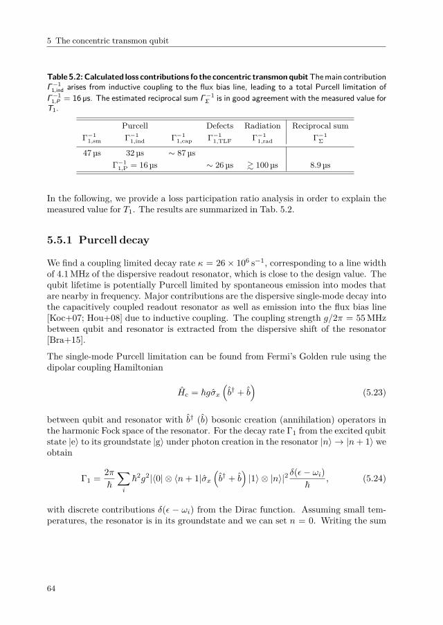
5 The concentric transmon qubit
Table 5.2: Calculated loss contributions fo the concentric transmon qubit The main contributionΓ−1
1,ind arises from inductive coupling to the flux bias line, leading to a total Purcell limitation ofΓ−1
1,P = 16 µs. The estimated reciprocal sum Γ−1Σ is in good agreement with the measured value for
T1.
Purcell Defects Radiation Reciprocal sumΓ−1
1,sm Γ−11,ind Γ−1
1,cap Γ−11,TLF Γ−1
1,rad Γ−1Σ
47 µs 32 µs ∼ 87 µsΓ−1
1,P = 16 µs ∼ 26 µs & 100 µs 8.9 µs
In the following, we provide a loss participation ratio analysis in order to explain themeasured value for T1. The results are summarized in Tab. 5.2.
5.5.1 Purcell decay
We find a coupling limited decay rate κ = 26× 106 s−1, corresponding to a line widthof 4.1 MHz of the dispersive readout resonator, which is close to the design value. Thequbit lifetime is potentially Purcell limited by spontaneous emission into modes thatare nearby in frequency. Major contributions are the dispersive single-mode decay intothe capacitively coupled readout resonator as well as emission into the flux bias line[Koc+07; Hou+08] due to inductive coupling. The coupling strength g/2π = 55 MHzbetween qubit and resonator is extracted from the dispersive shift of the resonator[Bra+15].
The single-mode Purcell limitation can be found from Fermi’s Golden rule using thedipolar coupling Hamiltonian
Hc = ~gσx(b† + b
)(5.23)
between qubit and resonator with b† (b) bosonic creation (annihilation) operators inthe harmonic Fock space of the resonator. For the decay rate Γ1 from the excited qubitstate |e〉 to its groundstate |g〉 under photon creation in the resonator |n〉 → |n+ 1〉 weobtain
Γ1 = 2π~∑i
~2g2|〈0| ⊗ 〈n+ 1|σx(b† + b
)|1〉 ⊗ |n〉|2 δ(ε− ωi)
~, (5.24)
with discrete contributions δ(ε − ωi) from the Dirac function. Assuming small tem-peratures, the resonator is in its groundstate and we can set n = 0. Writing the sum
64

5.5 Dissipative dynamics
in Eq. (5.24) as an integral introduces the spectral density function ρ(ω,ωr) of theresonator mode. Applying a normalized Lorentzian shape
ρ(ω′,ω) = 1π
κ/2(κ/2)2 + (ω′ − ω)2 , 1
π
∫ ∞−∞
dω′ κ/2(κ/2)2 + ω′2
= 1 (5.25)
with full width at half maximum κ yields
Γ1 = 2πg2∫
dω′ρ(ω′,ω)δ(ε−ω′) = 2g2 κ/2(κ/2)2 + (ε− ω)2 = 2g2 κ/2
(κ/2)2 + ∆2 , (5.26)
where ∆ = ε − ω is the detuning between qubit and resonator. In the dispersive limit∆ κ, we calculate a single-mode Purcell limitation induced by the readout resonatorof ΓΓ1,sm = κ (g/∆)2 = 1/47 (µs)−1 at a detuning ∆ = 1.94 GHz. While the formulaprovided in Eq. (5.26) is exact in the dispersive limit, it can reproduce the expectedenvelope of the decay rate on resonance, where Γ1(∆ = 0) ∝ g2/κ.
For a qubit being capacitively coupled to an environment of impedance Z0(ω) via acapacitance Cc, the total impedance seen by the qubit becomes
Z(ω) = − i
ωCc+ Z0(ω). (5.27)
The decay rate Γ1 due to classical zero-point noise [Hou+08; Mar+03] can be written as
ΓZ = <Y (ε)C
, (5.28)
where C is the total qubit capacitance and Y (ε) denotes the admittance of the envi-ronment at the qubit frequency ε. Since the effective qubit resistance takes the formR = 1/<Y (ε), the decay rate in Eq. (5.28) is the inverse time constant of the RCelement. Using Eq. (5.27) we can write
<Y (ε) = <1/Z(ε) = <Z(ε)<Z(ε)2 + =Z(ε)2 = Z0(ε)
Z0(ε)2 + 1/(εCc)2 = Z0(ε)ε2C2c . (5.29)
The last step in Eq. (5.29) is valid for 1/(εCc) Z0(ε). Substituting Eq. (5.29) intoEq. (5.28) yields the multi-mode decay rate
ΓZ = Z0ε2C2
c
C. (5.30)
65

5 The concentric transmon qubit
In analogy to this result, one can write down the decay rate Γ for a qubit being inductivelycoupled to an arbitrary impedance:
ΓZ = ε2M2
Z0LΣ, (5.31)
with M the mutual inductance between qubit and impedance load and LΣ the totalqubit inductance.
The multi-mode Purcell limitation due to inductive coupling of the concentric transmonto the flux bias line of impedance Z0 = 50 Ω is Γ1,ind = 1/32 (µs)−1, with mutualinductance M = 2.3 pH. The total qubit inductance LΣ = 6.3 nH includes the kineticinductance of the Josephson junctions and the geometric inductance contribution.
In analogy, we find a Purcell decay rate due to capacitive coupling (∼ 0.1 fF) to the fluxbias line, we estimate Γ1,cap ∼ 1/87 (µs)−1. The presented values are approximationsand give a rough estimate of the expected Purcell loss. A more stringent analysis wouldrequire a full 3D electromagnetic simulation of the circuit for instance by the blackboxquantization technique [Nig+12; SAD14].
5.5.2 Dielectric loss
The coplanar concentric transmon is embedded in a microstrip geometry, where theground reference on the device side of the substrate is substituted by a backsidemetallization. The largest fraction of the electric field energy is stored in the substrate,and the field strength at incoherent and weakly coupled defects residing in surface andinterface oxides of the sample is reduced due to an increased mode volume. Highestfields in the geometry appear in the gap between the centre island and the ring of theconcentric transmon within the substrate. The smallest dimension in the geometry isgiven by the electrode spacing of 35 µm, see Fig. 5.1, which roughly corresponds to theequivalent substrate thickness in vacuum of 380 µm/εr ∼ 33 µm. While electric fieldsbetween the transmon electrodes are enhanced by the dielectric substrate, we providea microscopic analysis of the defect loss based on the dimensions in our geometry. Theestimate is demonstrated to be in good agreement with a finite element simulation.
Microscopic treatment
From the vacuum energy of the transmon we extract a weighted mean electrical fieldstrength | ~E| = 2.3 Vm−1 in the surface and interface oxide of an estimated effectivevolume ofV = 50× 10−18 m3, compare Fig. 5.5. We assume a maximum dipole moment|~d0| = 1.6 eA of dielectric defects, reported in literature [Mar+05; Col+10; MCL17] asthehighestdipolemomentobserved inJosephson junctionbarriersandthereforeyieldinga worst case estimation. The maximum coupling strength to a single TLF therewithis | ~E||~d0| ∼ 90 kHz. We employ a normalized dipole moment distribution [Mar+05]
66

5.5 Dissipative dynamics
10 µm
ring electrodecentral island
E(V
/m)
2
0
Figure 5.5: Finite element simulation of defect loss The schematic shows a side view of theconcentric transmon qubit. The rotational symmetry axis is in the centre of the central transmonisland and indicated with the arrow to the left. The electric field distribution is depicted in colours.Maximum values occur at the edges of the transmon electrodes and exceed the maximum valueof the scale bar, such that these results are in reasonable agreement with the stated value for themean electrical field strength in the oxide volume of |~E | = 2.3 Vm−1.
P (p) = A√
1− p2/p, with relative dipole moment p = |~d|/|~d0|. Taking into account anormalized defect probability distribution [Mul+15] P (ω, θ) = Bωα cosα θ/ sin θ allowsus to estimate the mean relaxation rate Γ1,TLF due to a single incoherent two levelfluctuator (TLF) with averaged parameters to be
∫ d0
0dpP (p)p
2| ~E|2
~2
∫ ωTLF
0dω∫ π/2
0dθP (ω, θ)S(ε). (5.32)
ω denotes the TLF frequency that we integrate to a maximum of ωTLF/2π = 15 GHz,and the angle θ accounts for the dipole coupling matrix element. The spectral functionS(ωq) = sin2 θ γ2/(γ2
2 + (ω − ωq)2) is essentially the Fourier transform of the couplingcorrelation function [Mul+15], with an assumed TLF dephasing rate γ2/2π = 10 MHz.The averaged rate induced by a single TLF, given in Eq. (5.32), is multiplied by thenumber N = ρ0V ~ωTLF of defect TLF interacting with the qubit. With a distributionparameterα ∼ 0.3 [FI15]andaconstructeddefectdensityρ0 = 4× 10² (µm)−3(GHz)−1we compute a T1 limitation due to the quasi-static bath of incoherent TLF to beΓ1,TLF ∼ 1/26 (µs)−1. The choice of ρ0 is consistent with literature [Bar+13; Mar+05]and is justified by a good agreement with a loss participation ratio analysis carried outvia a finite element simulation, see the next paragraph. The calculated decay rate showsa very weak dependence on the employed parameters γ2, α and integration cut-offs.Due to the small size of the Josephson junction, the defect density in the Josephsonbarrier itself is discrete and therefore highly reduced [Wei+11a; Wei+11b].
67

5 The concentric transmon qubit
Finite element simulation of defect loss
To validate the above microscopic analysis, we conduct a finite element simulationof the concentric transmon geometry 1. The simulation layout with the electric fielddistribution is depicted in Fig. 5.5. We model the sample by assuming an oxide layerthickness of 3 nm, formed by AlOx (εr = 11.5), surrounding the central island and theconcentric ring electrode of the qubit. For the interface between substrate and aluminumwe assume an effective dielectric constant of εr = 6, accounting for the contributionof SiO2 (εr = 4) in the interface oxide. The simulation yields an electric field energyfraction of 2.8× 10⁻⁴ residing in the oxide volume. With a phenomenological losstangent [PO10] δAlOx = 3 · 10−3 of AlOx, this leads to a total effective loss tangentδTLF = 8.4× 10⁻⁷ which we attribute to dissipation by surface and interface oxidedefects. Due to uncertainties in δAlOx , the oxide layer thickness and εr, this value isto be considered exact within a factor of two. δTLF can be calculated to limit T1 atΓ−1
1,TLF = 28 µs which is in good agreement with the microscopically extracted value.
In the same spirit we can extract a relative electric field energy ratio in the siliconsubstrate of 0.92. With an intrinsic silicon loss tangent δSi < 1× 10⁻⁷, dissipation inthe substrate can be neglected. This is confirmed by very high quality factors measuredfor TiN resonators on intrinsic silicon [San+12].
5.5.3 Radiation loss
Aspointedout inRef. [San+13], radiative loss intothemediumfarfieldbecomesapparentfor qubits with a large electric dipole moment. In conventional pad geometries, radiativedecay is reduced since the dipole of the mirror image, induced by the ground plane of themicrostrip geometry, radiates in anti-phase, leading to destructive interference. Thecircular geometry investigated here brings about an additional decrease in radiatedpower by a strongly reduced electric dipole moment of the concentric electrodes. Weanalyse the effect by simulating the dissipated power in a conductive plane placed 1.5 mmabove our geometry in the medium far field and compare the result to a conventional padarchitecture. The internal quality factor of the qubit eigenmode indicates a radiativecontribution of Γ−1
1,rad & 100 µs. The radiative dissipation of a comparable qubit in padgeometry exceeds this value by more than an order of magnitude.
As compared to Purcell loss, the radiative decay rate is a measure for the confinementof electric fields inside the geometry and can be understood as the coupling strengthto spurious modes in the imperfect electromagnetic environment of the qubit. In oursample box with an engineered lower mode cut-off frequency of 12 GHz, loss may beinduced by bond wires, glue or the PCB. In addition, reduced dipole radiation allows
1 Finite Element Method Magnetics (FEMM), version 4.2
68

5.5 Dissipative dynamics
for a closer packaging of qubits that can be advantageous in complex chip layouts, andlooses the requirements on the utilized sample box.
To verify the presented loss participation ratio analysis, T1 was measured close tothe flux sweet spot and the associated Purcell contribution is calculated to be 4.7 µs,reducing the overall dissipation estimate to Γ−1
Σ = 3.7 µs, while the measured value wasT1 = Γ−1
1 = 1.8 µs [Bra+16]. The enhanced reduction in T1 at the sweet spot is not fullyunderstood. A possible explanation is the disregard of losses related to the geometricinductance such as quasi particles or magnetic vortices.
In continuous lifetime measurements, we observe temporal fluctuations in T1 down to∼ 2 µs for the operation point in Fig. 5.4. We conjecture that this is attributed to thediscrete dynamics of two-level fluctuators (TLF), located in the small oxide volume atthe leads of the Josephson junctions, where the electric field strength is enhanced. Thetemporal fluctuations decreased in later generations of the concentric transmon, whichwas fabricated in a single lithography step. A possible reason is a decreased TLF densitydue to a cleaner substrate prior to deposition of the concentric transmon.
In Fig. 5.4(b), we present a measurement of the spin echo dephasing time T2 = 10 µsby making use of a Ramsey sequence with one additional Hahn echo pulse. The twoπ/2 pulses rotate the qubit Bloch vector into the equatorial plane and back to thequantization axis of the qubit prior to state readout such that the final qubit state issensitive to phase rotations that are acquired during the time ∆t. The echo π pulsein the middle of the two π/2 pulses mirrors the Bloch sphere and therefore revertsthe drift direction of the qubit Bloch vector. Therewith, the technique compensateslow-frequency fluctuations in the qubit transition frequency and renders the qubitinsensitive to noise below ∼ 1/max(∆t) = 25 kHz. We measure a Ramsey dephasingtimeT ∗2 ∼ 2 µs without echo pulse. We want to point out that a rather highT2 is achievedin spite of the large loop size in the geometry. The transmon was detuned by ∼ 1 GHzfrom its flux sweet spot, such that the slope in the dispersion is finite and flux noise causesdephasing. Apart from noise from the current bias source, dephasing is presumablyinduced by local magnetic fluctuators that sit on the surface of the metallizations. Weshow in Ref. [Bra+16] that the Ramsey dephasing time T ∗2 = 2.2 µs is slightly increasedat the flux sweet spot, where T1 = 1.8 µs, indicating a pure dephasing time of τ ∼ 6 µsbeing increasingly relaxation limited. The Purcell contribution at the flux sweet spot iscalculated to be 4.7 µs, reducing the overall dissipation estimate to ∼ 3.7 µs.
In a non-tunable titanium nitride (TiN) version of the concentric transmon with a singleJosephson junction and an opening in the outer ring, we find lifetimes of T1 ∼ 50 µs andRamsey dephasing times up to T ∗2 ∼ 60 µs. Similar lifetimes have been reported forTiN transmon qubits in the conventional capacitor pad design [Cha+13]. We expectan increase in coherence times also for the tunable concentric design by implementingit in a TiN material system due to a suppression of defect loss in surface and interfaceoxides.
69

5 The concentric transmon qubit
a
0
1
0 10 20 30
qubi
tpop
ulat
ion
b
40fitdata
50Δt (ns)
readoutΔt
x xz
z
t
Figure 5.6: Demonstration of fast frequency tunability of the concentric transmon (a) Pulsesequence applied in the experiment. Between two projecting π/2 pulses we apply a Z -rotation Rz
ϕ
of amplitude η = 32 µA and length ∆t. (b) The expectation value of the qubit state oscillatesbetween its basis states |g〉, |e〉 with a relative Larmor frequency ωL/2π = 65 MHz, according tothe sinusoidal fit. A correction for the finite time constant in the bias tee was not performed as itcan be neglected for such short pulse lengths.
The measured coherence times compare with other planar transmon geometries such asa non-tunable Al based transmon with decreased finger gap size [Cho+12] (T1 = 9.7 µs,T ∗2 = 10 µs) and the cross shaped transmon [Bar+13] (T1 = 40 µs, T2 = 20 µs),fabricated via molecular beam epitaxy deposition [Meg+12].
5.6 Frequency tunability
Figure 5.6 demonstrates fast frequency control of the concentric transmon. This iscommonly referred to as Z control since Pauli’s spin operator σz appears in the drivingHamiltonian. In the utilized pulse sequence shown in Fig. 5.6(a) we apply a Z-rotationpulse of amplitude η in between a Ramsey sequence consisting of two projective π/2pulses. We record the equatorial precession of the qubit Bloch vector at a relativeLarmor frequency ωL = 65 MHz in Fig. 5.6(b). The Z-pulse amplitude η translates intomagnetic flux applied to the flux bias line. In the laboratory frame, this correspondsto a shift in qubit frequency by ωL ∝ η, which is confirmed in a quasi-spectroscopicmeasurement by exciting the detuned qubit and measuring its transition frequency, seeRef. [Bra+16]. By increasing η, we demonstrated a fast frequency detuning of up to200 MHz.
5.7 Coupling mechanisms
We propose the concentric transmon as a suitable candidate to establish a directinductive longitudinal coupling between neighbouring qubits. This is referred to as Zcoupling because the coupling Hamiltonian is proportional to σz. Since the area ofthe magnetic flux loop is large, the magnetic dipole moment of our qubit is stronglyenhanced as compared to conventional transmon designs where it is typically negligible.
70

5.7 Coupling mechanisms
Figure 5.7: Possible implementation of the Fermi-Hubbard emulator with a double chain ofconcentric transmon qubits Within the two horizontal chains, qubits couple via a swap interactionproportional to σx ,j σx ,j+1. The linear chains form a ladder and adjacent qubits from different chainsare coupled through a z type interaction proportional to σz,j σz,j . z interactions within chains vanishdue to a π/2-rotation of neighbouring concentric transmons, while the swap interaction betweenthe ladders can be suppressed by a mutual frequency detuning.
For two concentric transmon qubits separated by ∼ 50 µm, we estimate an inductivecoupling in the range of gz/2π ∼ 1 MHz for an operation point where the flux dependentqubit spectrum has a large slope. This value is estimated by taking into accountthe full inductance matrix of a all four loops of a two-qubit unit cell [Ste16] and byapplying the double integral Neumann formula [Jac62] to calculate individual mutualinductances Mij . The technique considers the direction of currents flowing. Weexpect a longitudinal Z coupling in the range of few megahertz between two concentrictransmon qubits sharing a fraction of their ring electrodes, which is currently exploredin experiment.
At the given qubit distance, the conventional dipolar capacitive coupling, also referredto as a swap interaction, was simulated and experimentally confirmed to be 13 MHz[Ste16]. To further increase gz, the mutual inductance in the two-qubit geometry must beincreased. In a current experimental approach we galvanically connect the outer loopsof two concentric transmon qubits in order to maximizeMij . In an alternative approach,the mutual inductance of loops of adjacent qubits can be enhanced by arranging qubitson top of each other but transversally shifted in a flip chip approach [Ste16].
For a mutual frequency detuning of neighbouring qubits, the dipolar coupling caneffectively suppressed, while the longitudinal coupling strength gz does not dependon the qubit frequencies. The longitudinal coupling vanishes completely for adjacentqubits in plane arranged at a relative rotation angle of π/2, such that the concentrictransmon geometry allows for a site-selective Z coupling. Figure 5.7 shows a schematicimplementation of a quantum simulator of the Fermi-Hubbard model [Rei+16]. Itconsists of two linear chains of concentric transmons that are dipole coupled but withthe Z coupling switched off along the two chains. This is achieved by alternatingrotation angles and using the symmetry properties of the Z coupling. Adjacent qubitsbelonging to different chains are Z coupled while the dipole coupling is suppressed by astrong mutual frequency detuning.
71

5 The concentric transmon qubit
The Z coupling scheme is highly promising for the field of quantum simulation in general,for instance in the context of implementing Ising spin models. Patterning an array ofconcentric transmon qubits featuring dipolar and Z coupling along two orthogonaldirections while exploiting the strongly reduced off-site inductive interaction may bea route to implement a quantum neural network, which is a powerful tool in quantumcomputation [SSP14].
5.8 Conclusion
We have designed, fabricated and experimentally investigated a planar tunable qubitbased on superconducting circuits that we call concentric transmon. With measuredlifetimes and coherence times of up to 15 µs, the qubit design is competitive withconventional transmon geometries. The main limitations of the qubit lifetime are thePurcell effect induced by the readout resonator and the flux bias line, as well as lossfrom dielectric defects. Radiative loss was demonstrated to be suppressed due to thesmall electric dipole moment. A major advantage of our approach is the straightforwardAl evaporation based fabrication process. The strong decrease in qubit lifetime due todefect loss in AlOx is circumvented by a large mode volume in particular in the gapregion between the transmon electrodes. We demonstrated full tomographic control ofour quantum circuit and discuss the high potential of the presented qubit design forthe implementation of a direct site-selective Z coupling between neighbouring qubits,rendering it a flexible building block for quantum simulation experiments.
72

6 ThequantumRabimodelatultra-strongcoupling
The quantum Rabi model describes the fundamental mechanism of light-matter inte-raction. It consists of a two-level atom or qubit coupled to a quantized harmonicoscillator mode via a transversal interaction. In the small coupling regime, a rotatingwave approximation can be applied and it reduces to the well-known Jaynes-Cummingsmodel. The rotating wave approximation breaks down in the ultra-strong coupling regime,where the effective coupling strength g is comparable to the energy ω of the bosonic mode,and remarkable features in the system dynamics are revealed. We demonstrate an analogquantum simulation of an effective quantum Rabi model in the ultra-strong couplingregime, achieving a relative coupling ratio of g/ω ∼ 0.6. The quantum hardware of thesimulator is a superconducting circuit embedded in a cavity quantum electrodynamics(cQED) setup. We observe fast and periodic quantum state collapses and revivals of theinitial qubit state, being the most distinct signature of the synthesized model. [Bra+17]
6.1 Motivation
The quantum Rabi model in quantum optics describes the interaction between a two-level atom and a single quantized harmonic oscillator mode [Rab36; Rab37]. In the smallcoupling regime, which may still be strong in the sense of quantum electrodynamics(QED), a rotating wave approximation (RWA) can be applied and the quantum Rabimodel reduces to the Jaynes-Cummings model [JC63], which captures most relevantscenarios in cavity and circuit QED. In the ultra-strong coupling (USC) and deep strongcoupling regimes, where the coupling strength is comparable to or even exceeds thesubsystem energies [Cas+10], the counter rotating terms in the interaction Hamiltoniancan no longer be neglected and the RWA breaks down. As a consequence, the totalexcitation number is not conserved in the quantum Rabi model. Except for one recentparadigm of finding an exact solution [Bra11], an analytically closed solution of thequantum Rabi model does not exist due to the lack of a second conserved quantity,which renders it non-integrable. It is therefore appealing to investigate the non-classical features that emerge in the USC regime and beyond in the context of quantumsimulations. The dynamics of the quantum Rabi model is well reproduced by standardmaster equation approaches, such that it provides an ideal test bed for experimentalsimulation techniques.
Apart from its intrinsic quantumness, rising interest in the Rabi model is inspired bystrong advances of experimental capabilities [Cas+10; AN10; BGB11; AR16]. The
73

6 The quantum Rabi model at ultra-strong coupling
specific spectral features of the USC regime and the consequent breakdown of the RWAwere previously observed with a superconducting circuit by implementing an increasedphysical coupling strength [Nie+10; For+10; For+16b]. A similar approach involving aflux qubit coupled to a single-mode resonator allowed to access the deep strong couplingregime in a closed system [Yos+16]. The USC regime was reached before by dynamicallymodulating the flux bias of a superconducting qubit, reaching a coupling strength ofabout 0.1 of the effective resonator frequency [Li+13].
In our approach, we create an effective quantum Rabi Hamiltonian in the USC regime byapplying an analog quantum simulation scheme based on the application of microwaveRabi drive tones. By a decrease of the subsystem energies, the USC condition is satisfiedin the effective rotating frame, which allows us to observe the distinct model dynamics.The scheme may be a route to efficiently generate non-classical cavity states [Leg+15;Kir+13; Vla+13], see Sec. 6.9, and may be extended to explore relevant physical modelssuch as the Dirac equation in (1+1) dimensions. Its characteristic dynamics is expectedto display a Zitterbewegung in the spacial quadrature of the bosonic mode [Bal+12].This dynamics has been observed with trapped ions [Ger+10], likewise based on aHamiltonian that is closely related to the USC Rabi model.
It has been shown recently that a quantum phase transition, typically requiring acontinuum of modes, can appear already in the quantum Rabi model under appropriateconditions [HPP15]. The experimental challenge is projected onto the coupling require-ments in the model which may be accomplished with the simulation scheme presented.This can be a starting point to experimentally investigate critical phenomena in a smalland well-controlled quantum system [HP16]. By using a digital simulation approach,the dynamics of the quantum Rabi model at USC conditions was similarly studied veryrecently [Lan+17].
In our experiment we first simulate the USC quantum Rabi model in the absence of aqubit energy term, achieving a relative coupling strength of up to 0.6. This is achievedby applying a single Rabi drive. We observe periodically recurring quantum statecollapses and revivals in the qubit dynamics as one of the characteristic signatures ofUSC. The collapse-revival dynamics appears most clearly in the absence of the qubitenergy term in the quantum Rabi Hamiltonian. In a second step, we use our device tosimulate the full quantum Rabi model and are able to observe the onset of an additionalsubstructure in the qubit time evolution. With this proof of principle experiment wevalidate the experimental feasibility of the proposed analog quantum simulation schemeand demonstrate the potential of superconducting circuits for the field of quantumsimulation.
74

6.2 Simulation Scheme
Table 6.1: Designation of coupling regimes in the quantum Rabi model The coupling strengthg must exceed the decay rates Γ1, κ of the coupled subsystems for the strong coupling conditionfrom cavity QED to be fulfilled, see Fig. 6.3. For USC and deep strong coupling, the figure of meritis the coupling strength relative to the bosonic mode frequency, g/ω.
coupling regime conditionstrong coupling g > Γ1, κ
USC 0.1 < g/ω < 1deep strong g/ω > 1
6.2 Simulation Scheme
The quantum Rabi Hamiltonian reads
H
~= ε
2 σz + ωb†b+ gσx
(b† + b
), (6.1)
with ε the qubit energy splitting, ω the bosonic mode frequency and g the transversalcoupling strength. σi are Pauli matrices with σz |g〉 = − |g〉 and σz |e〉 = |e〉, where|g〉, |e〉 denote the eigenstates of the computational qubit basis. b† (b) are creation(annihilation) operators in the Fock space of the bosonic mode. Both elements of themodel are physically implemented in the experiment, with a small geometric couplingg ε, ω. In order to access the USC regime, we follow the scheme proposed inRef. [Bal+12]. It is based on the application of two transversal microwave Rabi drivetones coupling to the qubit. The effective USC quantum Rabi Hamiltonian is created inthe frame rotating with the dominant drive frequency. In the engineered Hamiltonian,the effective mode energies are adjusted by the Rabi drive parameters.
The driven laboratory frame Hamiltonian takes the form
Hd~
= ε
2 σz + ωb†b+ gσx
(b† + b
)+ σxη1 cos(ω1t+ ϕ1) + σxη2 cos(ω2t+ ϕ2). (6.2)
ηi denote the amplitude and ωi the frequency of drive i. ϕi is the relative phase of drivei in the coordinate system of the qubit Bloch sphere in the laboratory frame. Withinthe RWA where ηi/ωi 1, the ϕi enter as relative phases of the transversal couplingoperators e−iϕi σ+ + h.c., where σ± = 1/2 (σx ± iσy) denote Pauli’s ladder operators.In the following, we set ϕi = 0 to recover the familiar σx coupling without loss ofgenerality.
75

6 The quantum Rabi model at ultra-strong coupling
By applying the unitary transformation
U = exp
iω1t
(b†b+ 1
2 σz)
(6.3)
we move into the frame rotating with ω1 and the transformed Hamiltonian becomes
H1~
= ε
2 σz + ωb†b+ g(σ+e
iω1t + σ−iω1t−
) (eiω1tb† + e−iω1tb
)+ η1
(σ+e
iω1t + σ−e−iω1t
)cosω1t+ η2
(σ+e
iω1t + σ−e−iω1t
)cosω2t
− ω1
(b†b+ 1
2 σz)
(6.4)
=12 (ε− ω1) σz + (ω − ω1) b†b+ g
(σ−b
† + σ+b)
+ η12 (σ+ + σ−)
+ η22
(σ+e
i(ω1−ω2)t + σ−e−i(ω1−ω2)t
)+ g
(σ+e
2iω1tb† + σ−e−2iω1tb
)+ η1
2(σ+e
2iω1t + σ−e−2iω1t
)+ η2
2
(σ+e
i(ω1+ω2)t + σ−ei(−ω1−ω2)t
)(6.5)
≈ (ε− ω1) σz2 + (ω − ω1) b†b+ g(σ−b
† + σ+b)
+ η12 σx + η2
2
(σ+e
i(ω1−ω2)t + σ−e−i(ω1−ω2)t
). (6.6)
Terms of the form eXY e−X are calculated using the power series expansion of theexponential function, also called Hadamard lemma. For X = iω1tb
†b, Y = b†,
eiω1tb†bb†e−iω1tb
†b = eiω1tb† (6.7)
eiω1tb†bbe−iω1tb
†b = e−iω1tb (6.8)
since
∞∑m=0
1m!
[iω1tb
†b, b†]m
= b†∞∑m=0
1m! (iω1t)m = b†eiω1t. (6.9)
ei2ω1tσz and σz clearly commute, while
ei2ω1tσz σxe
− i2ω1tσz = σ+e
iω1t + σ−e−iω1t (6.10)
using ediag(a,b) = diag(ea, eb). Terms rotating at e±2iω1t were omitted in Eq. (6.6) inthe spirit of a RWA, valid for η1/2ω1 1. This is a good approximation as η1 is boundin the experiment by the qubit anharmonicity.
76

6.2 Simulation Scheme
The η1-term is now the significant term and we move into its interaction picture via thetransformation
ei η12 σxt
[H1~− η1
2 σx
]e−i η1
2 σxt. (6.11)
Satisfying the requirement ω1 − ω2 = η1 and performing a time averaging in the spiritof a RWA yields the effective Hamiltonian in the ω1 frame
Heff~
= η22σz2 + ωeff b
†b+ g
2 σx(b† + b
). (6.12)
We define the effective bosonic mode energy ωeff ≡ ω − ω1, which is the parametergoverning the system dynamics. Noting that η1 η2, which is a necessary condition forthe above approximation to hold, the effective qubit frequency η2 and effective bosonicmode frequency ωeff can be chosen as experimental parameters in the simulation. InEq. (6.12), the complete coupling term of the quantum Rabi Hamiltonian is recovered,valid in the USC regime and beyond, while the geometric coupling strength is onlymodified by a factor of two, resulting in geff = g/2. It is therewith feasible to tunethe system into a regime where the coupling strength is comparable to the energies ofthe subsystems. This is achieved by leaving the geometric coupling strength essentiallyunchanged in the synthesized Hamiltonian, while slowing down the system dynamicsby effectively decreasing the mode frequencies to . 8 MHz.
Thermal excitations of these effective transitions can be neglected since they couple tothe thermal bath excitation frequency of the cryostat, corresponding to ∼ 1 GHz, viatheir laboratory frame equivalent frequency of ω/2π ∼ 6 GHz. We want to point outthat the coupling regime is defined by geff/ωeff , rather than by the Rabi frequency η1,which does not enter the synthesized Hamiltonian. See Tab. 6.1 for an overview on thedesignation of coupling regimes.
While the simulation scheme requires |ε−ω1| η1, the qubit frequency ε does not enterthe effective Hamiltonian. The time evolution of the qubit measured in the laboratoryframe is subject to fast oscillations corresponding to the Rabi frequency η1. Accordingly,the qubit dynamics in the engineered quantum Rabi Hamiltonian Eq. (6.12), valid in theω1 frame, can be inferred from the envelope of the evolution in the laboratory frame. Thederivation of Eq. (6.12) can be found in Ref. [Bal+12] and is detailed in SupplementaryNote 1 of Ref. [Bra+17]. A similar drive scheme based on a Rabi tone was previouslyused in experiment to synthesize an effective Hamiltonian with a rotated qubit basis[Voo+16]. For the qubit and the bosonic mode degenerate in the laboratory frame, adistinct collapse-revival signature appears in the dynamics of the quantum Rabi modelunder USC conditions, which is observed and investigated in this experiment.
77

6 The quantum Rabi model at ultra-strong coupling
TL
bosonic mode spin
readoutb
TL g
boso
nic
mod
e
flux bias
readouta
Figure 6.1: Quantum simulation device (a) Optical micrograph with the atomic spin representedby a concentric transmon qubit, highlighted in red and the λ/2 microstrip resonator (blue)constituting the bosonic oscillator mode. The readout resonator couples to the qubit capacitivelyand its frequency is measured with an open transmission line (TL) via the reflection signal of anapplied microwave tone or pulse. The second resonator visible on chip is not used in the currentexperiment and is detuned in frequency from the relevant bosonic mode by∼ 0.5 GHz. (b) Effectivecircuit diagram of the device.
6.3 Device
The physical implementation of the quantum simulator is based on a superconductingcircuit embedded in a typical circuit QED setup [Bla+04; Wal+04], see Fig. 6.1. Theatomic spin of the quantum Rabi model is mapped to a concentric transmon qubit[Koc+07; Bra+16]. It is operated at a ratio of Josephson energy to charging energyEJ/EC = 50 and an anharmonicity α/h = ε12/2π − ε01/2π = −0.36 GHz ∼ −EC/h =−0.31 GHz, and tuned on resonance with the bosonic mode at 5.948 GHz. εij denotethe transition frequencies between transmon levels i, j. The energy relaxation rate Γ1of the qubit at the operation point is measured to be Γ1 = 1/T1 = 0.2 × 10⁶ s−1. Anon-chip flux bias line allows for a fast tuning of the qubit transition frequency, see Ch. 5.The bosonic mode of the model is represented by a harmonic λ/2 resonator with aninverse lifetime κ ∼ 3.9× 10⁶ s−1 that is limited by internal loss.
6.3.1 Fabrication
Sample fabrication was carried out in one single electron beam lithography step. TheJosephson junctions are formed by shadow angle evaporation and the Dolan bridgetechnique, as detailed in Ch. 4. The area of the Josephson junctions is designed tobe 100 nm × 220 nm, resulting in a critical current Ic = 45 nA for a single junction.
78

6.3 Device
LORF
I Q
qubi
tman
ipul
atio
n/
driveDA
C
DAC
LORF
I Q
DAC
DAC
Figure 6.2: Qubit manipulation and drive microwave setup Modification of the qubit manipulationsetup, see the grey box in Fig. 4.2. Two drive pulses with amplitudes η1, η2, respectively, aregenerated in separate IQ mixers, sharing a common local oscillator (LO) input, and combinedsubsequently.
We applied an Al metallization on the backside of the double-side polished intrinsic Sisubstrate as a ground reference for the microstrip elements on chip.
6.3.2 Measurement technique
Qubit excitation and Rabi driving are performed by heterodyne mixing with twoindividual IQ frequencies and amplitudes, respectively. In the experiment with onlythe dominant Rabi drive applied, we use one single microwave source and one IQ mixeraccording to the setup shown in Fig. 4.2 in Ch. 4. This allows for the required phasecontrol on the phase ϕ1 of the dominant Rabi drive with respect to the qubit Blochsphere coordinate system fixed by the first excitation pulse. In particular, we fix theidling time between initial excitation pulse and the onset of the Rabi drive, such that theacquired phase during that time is constant. The Rabi drive is therefore applied with aconstant relative phase ϕ1 with respect to the phase used for the excitation pulse. Wechose an LO frequency located 20 MHz or 65 MHz above the qubit control frequency,located at about ω/2π + 95 MHz.
In the experiment with the second Rabi drive added, both drive tones are up-convertedin two separate IQ mixers while sharing a common local oscillator input to preserve theirrelative phase relation, see Fig. 6.2(a). Qubit excitation and drive pulses are appliedvia the same transmission line used for readout.
The bosonic mode resonator is located far away from the transmission line in space,which reduces unwanted parasitic driving. It is strongly detuned from the readoutresonator located at ωr/2π = 8.86 GHz.
79

6 The quantum Rabi model at ultra-strong coupling
Table 6.2: Summary of device and simulation parameters Errors are extracted from the fit ofthe vacuum Rabi oscillations in Fig. 6.3.
ω/2π EJ/EC α/h Γ1 = 1/T1 κ
5.948 GHz 50 −0.36 GHz (0.2± 0.12)× 106 s−1 (3.9± 0.14)× 106 s−1
ωr/2π ωeff/2π η1/2π η2/2π8.86 GHz < 8 MHz ∼ 50 MHz ∼ 3 MHz
6.4 Sample characterization
The quantum state collapse followed by a quantum revival is the most striking signatureof the ultra-strong coupling regime of the quantum Rabi model. It emerges for qubitand bosonic mode degenerate in the laboratory frame. We calibrate this resonancecondition by minimizing the periodic swap rate of a single excitation between qubit andbosonic mode for the simple Jaynes-Cummings model in the absence of additional Rabidrives. Figures 6.3(a), (b) show the measured vacuum Rabi oscillations in the resonantcase (a) and dependent on the qubit transition frequency (b). For qubit preparationand readout we detune the qubit by 95 MHz up in frequency and therewith out ofresonance. This corresponds to switching off the resonant interaction with the bosonicmode. Experimental details on flux pulse generation are described in Sec. 4.3. VacuumRabi oscillations can be observed during the interaction time ∆t and yield a couplingstrength g/2π = 4.3 MHz.
This is in good agreement with the spectroscopically obtained result, see Fig. 6.3. A two-tone spectroscopy measurement yields a minimum line separation of 2g/2π = 8.0 MHz,corresponding to a coupling strength of g/2π = 4.0 MHz. The dispersive readoutresonator shift is measured with a continuous microwave probe tone and an additionalmicrowave drive tone is applied through the same transmission line to excite the qubittransition.
The relevant experimental device and simulation parameters are summarized in Tab. 6.2.
6.5 Master equation simulations
Master equation simulations of the quantum Rabi model are based on the masterequation solver provided by the QuTiP package [JNN12; JNN13] for Python. Here,the time evolution of a given initial state or density matrix is calculated by solving thevon Neumann equation associated with the given system Hamiltonian in the absence ofdissipation. Dissipation is taken into account by solving the Lindblad master equation.
80

6.5 Master equation simulations
0.40.2 0.6 0.8 1.0
qubi
tpop
ulat
ion
1.044
0
1
0
1
1.040
1.036
1.032
0 0.5 1.0 1.5
qubi
tpop
ulat
ion
0
readout qubit control,readout
damped sine
b
a freq.
I(m
A)
Δt (µs)
Δt
x
z
Δt (µs)
1.101.09 1.11
disp
ersiv
esh
ift(a
.u.)theory fit
5.92
5.96
5.94
I (mA)
c
2g
Figure 6.3: Calibration of the coupling strength g between qubit and bosonic mode (a) Thequbit is initially dc-biased on resonance with the bosonic mode, while it is detuned for statepreparation and readout. The solid black line in the inset depicts the fast flux pulses applied to theflux bias line and indicates the qubit frequency on the given axis. After preparing the qubit in |e〉,qubit and bosonic mode are on resonance during an interaction time ∆t. A frequency fit (red) of thevacuum Rabi oscillations yields 2g/2π = 8.5 MHz. With the decay rate Γ = (2.08±0.03)×106 s−1
of the envelope and the qubit decay rate 1/T1 = (0.2 ± 0.12) × 106 s−1 we extract the bosonicmode decay rate κ = (3 9 ± 0.13) × 106 s−1. Error bars denote a statistical standard deviation.(b) Typical calibration measurement for the resonance condition (blue line) between qubit andbosonic mode. By varying the dc bias current I, we can tune out of resonance and observe theexpected decrease in excitation swap efficiency and an increase in the vacuum Rabi frequency. Thequbit population is given in colours and we applied a numerical interpolation of data points. (c)Spectroscopic measurement of the avoided crossing between qubit and bosonic mode. The qubittransition frequency is tuned by a dc current applied to the flux bias line. The dispersive shift of thereadout resonator is proportional to the excitation number of the qubit and is depicted in colours.A fit yields a minimum line separation of 2g/2π = 8.0 MHz.
81

6 The quantum Rabi model at ultra-strong coupling
The decay terms in the underlying Liouvillian are based on the experimentally foundparameters, summarized in Tab. 6.2. In addition we use a qubit dephasing time ofT ∗2 ∼ 0.5 µs. The Hilbert space of the bosonic mode is truncated at a photon numberof 25 to 35, while higher Fock states were found to be insignificant. The transmonqubit is treated as a three-level system with the experimentally found anharmonicityα/h = −0.36 GHz. To account for the |f〉 level in the transmon, we use a transversalqubit coupling operator ∑
ij
gij |i〉 〈j| . (6.13)
The coupling matrix elements gij are found by evaluating the matrix elements of theCooper pair number operator N in the charge basis [Koc+07; Bra+15], according to
gij ∝ |〈i|N |j〉|. (6.14)
In analogy, we can define a general annihilation operator at that reflects the transmonanharmonicity in the simulation according to
a =∑i<j
gijg01|i〉 〈j| . (6.15)
Master equation simulations of the effective USC quantum Rabi model in the rotatingframe are performed in the two-level approximation.
6.6 Verification of the simulation scheme
Since a rotating frame is not an inertial system, the laws of physics may be drasticallyaltered when describing a physical system in a rotating frame. In the framework of analogquantum simulation, this allows us to access intriguing effective parameter regimes thatare hard or impossible to tread in the laboratory frame. For the simulation schemeapplied here, it is therefore not a priori clear that the bosonic mode population evolutionof the quantum Rabi model is well reflected by the laboratory frame simulation. To verifythe simulation scheme for the ideal system we compare the bosonic mode population inthe driven laboratory frame, and the expected evolution of the ideal effective quantumRabi model via master equation simulations. Here, we neglect dissipation and anyparasitic drive terms in the Hamiltonian. Figure 6.4(a) demonstrates good agreementwhen comparing the time evolutions of the ideal (solid line) and the constructed (dashedline) Hamiltonians for various choices of the bosonic mode frequency ωeff in the effectiveframe.
For ωeff/2π = 5 MHz we demonstrate that the photon population in the bosonic modeis independent of the applied drive amplitude η1, despite of it forming a large energy
82

6.7 Quantum state collapse and revival
0 0.05 0.15 0.250.1 0.2
abo
soni
cm
ode
popu
latio
n
0
1
3
2
driven (lab frame)ideal
0 0.05 0.15 0.250.1 0.2
b
boso
nic
mod
epo
pulat
ion
0
160
200
Δt (µs) Δt (µs)
Figure 6.4: Verification of the simulation scheme and effect of the parasitic drive (a) Timeevolution of the bosonic mode population for a simulation sequence with η2 = 0. We compare itspopulation in the ideal quantum Rabi Hamiltonian (solid line) with the population of the bosonicmode in the laboratory frame with the drive applied (dashed line). Despite the fact that an infiniteenergy reservoir is supplied by the drive, the population follows the expected one rather well. Thisremains also true for varying the drive amplitude η1. Different colours correspond to a varying ωeff .(b) Bosonic mode population for ωeff/2π = 5 MHz and a varying drive amplitude η1. The evolutionand maximum population is confirmed to be independent of η1 in first order. Master equationsimulations here are performed without taking into account dissipation and neglect parasitic drivingof the bosonic mode.
reservoir that is provided to the circuit. Simulations for various η1 in the drivenlaboratory frame are depicted in Fig. 6.4(b).
6.7 Quantum state collapse and revival
The collapse-revival signature of the quantum Rabi model in USC conditions manifestsmost clearly for a vanishing qubit term. We therefore initially perform a simulationwith η2 = 0, yielding an effective Hamiltonian in the qubit frame
H
~= ωeff b
†b+ g
2 σx(b† + b
). (6.16)
Figure 6.5(a) shows the applied measurement sequence which is based on the one inFig. 6.3(a) but extended by a drive tone of amplitude η1. The bosonic mode is initiallyin the vacuum state and the qubit is prepared in one of its basis states |g〉, |e〉, whichare thermally impure. Qubit and bosonic mode are on resonance during the simulationtime ∆t. The effective bosonic mode frequency ωeff in the rotating frame is set by thedetuning of the Rabi drive at a frequency ω1 from the common resonance frequencyω. Measured data for ωeff/2π = 8 MHz is displayed in Fig. 6.5(b), corresponding togeff/ωeff ∼ 0.3. Data points show the experimentally simulated time evolution of thequbit prepared in |e〉. A fast quantum state collapse followed by periodically returningquantum revivals can be observed. The ground state of the qubit subspace in the drivensystem as well as in the synthesized Hamiltonian, Eq. (6.16), is in the equatorial plane
83

6 The quantum Rabi model at ultra-strong coupling
master equation simulation
rotating framelaboratory frame
boso
nic
mod
epo
pulat
ion
b
0 0.1 0.30.2 0.4
a
rotating frame
0 0.05 0.15 0.250.1 0.2
d
c 1
qubi
tpop
ulat
ion
0
e
0
1
rotating framelaboratory frame
qubitcontrol
freq.
1
effe
ctive
qubi
tpop
.
0
quantum simulationrotating frame
0.5
qubi
tpop
ulat
ion
1
0.5
quantum simulation
0
1
effe
ctive
qubi
tpop
.
Δt (µs)
Δt (µs)
readoutz
prep.
time
Δt
Figure 6.5: Quantum state collapse and revival with only the dominant Rabi drive applied (a)Schematic pulse sequence and overview on the relative frequencies used in the experiment. (b)Quantum simulation of the periodic recurrence of quantum state revivals for ωeff/2π = 8 MHz.The blue line corresponds to a master equation simulation of the qubit evolution in the rotatingframe. (c), (d) Master equation and quantum simulation of the qubit time evolution for initialqubit states |g〉, |e〉 and ωeff/2π = 5 MHz, corresponding to geff/ωeff ∼ 0.5. The red line showsthe qubit population evolution of the driven system in the laboratory frame, Eq. (6.2), while theblue lines follow the qubit evolution in the synthesized Hamiltonian Eq. (6.12), likewise extractedfrom a master equation simulation. The deviation between the envelope of the laboratory framedata and the rotating frame data in (c) reflects the approximations of the simulation scheme.Experimental data shows the difference between two measurements for the qubit prepared in |g〉,|e〉, respectively, in order to isolate the qubit signal. (e) Measured population evolution of thebosonic mode, extracted from the sum of the two successive measurements and fitted to simulateddata. Error bars throughout the figure denote a statistical standard deviation of the mean and arepropagated according to Gauss.
84

6.7 Quantum state collapse and revival
of the qubit Bloch sphere and is occupied after a time ∆t T1, 1/κ. It is diagonal inthe |±〉 basis, with |±〉 = 1/
√2(|e〉 ± |g〉).
The revival dynamics can be understood with an intuitive picture in the laboratoryframe. The eigenenergies in the |±〉 subspaces take the form of displaced vacuum
ωeff
(b† ± g
2ωeff
)(b± g
2ωeff
)+ const., (6.17)
which is a coherent state that is not diagonal in the Fock basis. The prepared initialstate in the experiment is therefore not an eigenstate in the effective basis of the drivensystem. Consequently, many terms that correspond to the relevant Fock states n ofthe bosonic mode participate in the dynamics with phase factors expinωefft, n ∈ N+.While contributing terms get out of phase during the state collapse, they rephase afteran idling period of 2π/ωeff to form the quantum revival. The underlying physics ofthis phenomenon is fundamentally different from the origin of state revivals that wereproposed for the Jaynes-Cummings model [ENS80]. Here, the preparation of the bosonicmode in a large coherent state with α & 10 is required and non-periodic revivals areexpected at times ∝ 1/geff rather than ∝ 1/ωeff [HR06], as demonstrated in Fig. 6.6.
The blue line in Fig. 6.5(b) corresponds to a master equation simulation of the qubitdynamics in the effective frame, Eq. (6.16).
Figures 6.5(c),(d) show a master equation simulation and the quantum simulation forωeff/2π = 5 MHz, respectively, with the qubit prepared in one of its eigenstates |g〉, |e〉.The population of the bosonic mode takes a maximum during the idling period andadopts its initial population at 2π/ωeff in the absence of dissipation, see Fig. 6.5(e). Thefast oscillations in Fig. 6.5(c), (d) correspond to the Rabi frequency η1/2π ∼ 50 MHz.This value is chosen such that the requirement η1/ωeff 1 is fulfilled while staying wellbelow the transmon anharmonicity, avoiding higher level populations.
Deviations in the laboratory frame simulation traces are due to an uncertainty inthe Rabi frequency that is extracted from Fourier transformation of measured data,see Fig 6.7(c). The broadening in frequency space is mainly caused by the beatingin experimental data, which is an experimental artefact, potentially originating frompulse imperfections. The relevant dynamics of the USC quantum Rabi Hamiltoniancorresponds to the envelope of measured data.
Since the laboratory frame dissipation is enhanced for a larger ratio of photon populationin the bosonic mode, the accessible coupling regime is bound by the limited coherence ofthe bosonic mode, in particular. This is demonstrated by a dependence of the coherenceenvelope of the quantum revivals on the ratio g/ωeff , see Fig. 6.6. The dependencereflects that the excitation number is no longer a conserved quantity in the quantumRabi model at USC conditions. Figure 6.6 further demonstrates that the maximumposition of the first quantum revival appears at to 2π/ωeff , which can be well controlledby choosing ωeff in the quantum simulation.
85

6 The quantum Rabi model at ultra-strong coupling
0
rot. frame (class.)
0 0.30.1 0.2
c
b
0 0.05 0.15 0.250.1 0.20
0
0
2
1
0 0.30.1 0.2
effe
ctive
qubi
tpop
.
a
d
0.30.1 0.2
1
effe
ctive
qubi
tpop
.
1 1
0
1
boso
nic
mod
epo
p.
0
2
1
boso
nic
mod
epo
p.
0
2
1
0
2
1
lab frame (exp.)
Δt (µs) Δt (µs)
Δt (µs) Δt (µs)
0
Figure 6.6: Quantum collapse and revival signatures for various ωeff The qubit is prepared in itsgroundstate |g〉 and the bosonic mode is initially in the vacuum state |0〉. The first revival appearsat 2π/ωeff , respectively, and the different plots correspond to a varying ωeff . The blue line shows amaster equation simulation of the ideal effective Hamiltonian in the rotating frame, while the reddata points are the qubit population evolution in the effective qubit frame. The black line showsthe bosonic mode population in the rotating frame according to a master equation simulation,which increases with decreasing ωeff . Note that the scale on the horizontal axis is not equal foreach plot. The depicted qubit signal is extracted from measured data with the protocol describedin Sec.6.7.1, based on the master equation simulation (black) in the absence of a parasitic drive ofthe bosonic mode.
Table 6.3: Geometric coupling g/2π between qubit and bosonic mode. Experimental valuesare obtained from the spectroscopic measurement and the vacuum Rabi experiment in Fig. 6.3.The value used in master equation simulations differs slightly.
spectroscopy vacuum Rabi master eq. simulation4.0 MHz 4.3 MHz 5.5 MHz
86

6.7 Quantum state collapse and revival
We find a better agreement of experimental data with master equation simulations fora slightly increased geometric coupling g/2π ∼ 5.5 MHz as compared to the measuredvalue in Fig. 6.3 of g/2π = 4.3 MHz. This may be explained by an excess population ofthe bosonic mode due to a parasitic coupling of the Rabi drives, see Sec. 6.7.2. This caneffectively increase the coupling strength between qubit and bosonic mode. The effectmay be additionally enhanced by a population of higher transmon levels.
We checked that master equation simulations with increased decay and decoherencerates, accounting for a changed environmental spectral density in the rotating frame,cannot reproduce the correct dynamics. Simulations performed with g/2π = 4.3 MHzshow a ∼ 30% decrease in the maximum population of the bosonic mode with noqualitative consequences. With the measured geometric coupling we approach an USCregime with geff/ωeff ∼ 0.6 for the experiment depicted in Fig. 6.6(d). Based on theeffectively increased value for geff , we reach a relative coupling ratio of 0.7. Measuredvalues of geff and the effective value used in the presented master equation simulationsare summarized in 6.3.
6.7.1 Protocol for extracting the qubit population
In the simulation experiments presented in Fig. 6.5, we note a modulated low-frequencybulge in the recorded dispersive readout resonator shift that does not agree with theexpected qubit population evolution, see Fig. 6.7(a). By comparing with the masterequation simulation, we can recognize the population evolution of the bosonic modewhich reflects the governing fundamental frequency ωeff of the effective Hamiltonian.By simulating the full circuit Hamiltonian including qubit, bosonic mode and readoutresonator, we find that the effect is induced by an additional photon exchange couplingf between the bosonic mode and the readout resonator. The coupling is facilitatedby the electric fields of the resonators and is potentially mediated by the qubit. Byinheriting non-linearity from the qubit, the bosonic mode can induce a cross-Kerr likephoton number dependent shift ∝ f2 on the harmonic readout resonator.
The complete Hamiltonian including the readout resonator of resonance frequency ωrwith creation (annihilation) operator a† (a) and with the RWA applied takes the form
H
~= ε
2 σz + ωb†b+ ωra†a+ g
(σ−b
† + σ+b)
+ gr(σ−a
† + σ+a)
+ f(ab† + a†b
)+ σxη1 cos(ω1t+ ϕ1) + σxη2 cos(ω2t+ ϕ2). (6.18)
gr/2π ∼ 55 MHz denotes the coupling strength between qubit and readout resonator.The conjecture is verified by comparing master equation simulations with the photonexchange coupling f switched on and off, respectively, see 6.7(d). As visible in 6.7(e), thedifference of both master equation simulations (grey) follows the evolution of the bosonicmode population (red) in the rotating frame as obtained from the same simulation. Theexperimentally extracted bosonic mode population (blue) likewise agrees with the trend
87

6 The quantum Rabi model at ultra-strong coupling
mas
tere
q.sim
.re
adou
tpop
ulat
ion
0.9995
1
0 0.05 0.15 0.250.1 0.2
diffe
renc
eΔ
inre
adou
tpo
pulat
ion
from
(a)
boso
nic
mod
epo
pulat
ion
1
0
1e-4
d
e
disp
ersiv
esh
ift(a
.u.)
0 0.05 0.15 0.250.1 0.2
fitc
50 100
a
b
raw data
1
0
2
0.4
1
qubi
tpop
ulat
ion
0.6
0.8
boso
nic
mod
epo
pulat
ion
exp.
0
Δt (µs)
Δt (µs)
Figure 6.7: Verification of the photon exchange coupling between the bosonic mode and thereadout resonator (a) Dispersive shift of the readout resonator including both the shifts inducedby qubit and bosonic mode. The red line depicts the bosonic mode population according to amaster equation simulation. (b) Extracted qubit signal in the original qubit basis after subtractingthe additional shift induced by the bosonic mode. The analysis is based on the expectation fromthe master equation simulation as depicted in (a). The qubit was prepared in |e〉. From Fouriertransformation (c) we obtain η1/2π ∼ 52 MHz. (d) Master equation simulation of the vacuumprojection |0〉 〈0| of the readout resonator state for vanishing photon exchange coupling f = 0(blue) and for f /2π = 12 MHz (red), disregarding dissipation. The blue dashed line denotes themean value of the f = 0 simulation as a guide to the eye. Orange and green traces show thesame master equation simulations in the presence of dissipation and are shifted for better visibility.The additional bulge in the presence of the photon exchange coupling f > 0 is apparent. (e) Thedifference (grey) between both master equation simulations from (d) including dissipation followsthe experimentally measured bosonic mode population (blue). Both data sets are fitted to thetime evolution of the bosonic mode population (red), as obtained from the same master equationsimulation.
88

6.7 Quantum state collapse and revival
from the master equation simulation. The photon exchange coupling assumes the formof a cross-Kerr interaction after diagonalization in the subspace spanned by the bosonicmode and the readout resonator. Comparison with measured data suggests f ∼ MHz.
In Fig. 6.5(d) we made use of the topological symmetry of simulations with initial qubitstates |g〉, |e〉. In order to cancel out the additional dispersive shift induced by thebosonic mode, we subtract two successive measurements with the qubit prepared inits eigenstates |g〉, |e〉, respectively. The population evolution of the bosonic mode,depicted in Fig. 6.5(e), is obtained by summing two successive measurements with thequbit prepared in |g〉, |e〉, respectively. The extracted bosonic mode population is fittedto the expectation according to master equation simulations in the laboratory frameand in the effective frame. Since the maximum population is around unity while thequbit is in the equatorial state, the non-conservation of the total excitation number isapparent.
This measurement protocol is based on the symmetry of the qubit signal for preparingeigenstates, while the bosonic mode induced shift is always repulsive and does notchange its sign. The photon exchange coupling f therefore provides indirect accessto the population of the bosonic mode without a dedicated readout device available.Specifically monitoring the population of the bosonic mode and performing a Wignertomography would highlight another hallmark signature of the USC regime, namely theefficient generation of non-classical cavity states [Lan+17]. The protocol for generatingcat states in the bosonic mode with the presented scheme is elaborated in Sec. 6.9.
In the absence of such a symmetry, the qubit population can be retrieved from measuredraw data based on the master equation simulation of the bosonic mode population.In this procedure, the dispersive shift ∝ f2 remains as the only free fit parameter.Figure 6.7(b) shows the extracted qubit signal after subtracting the additional shiftinduced by the bosonic mode. The mentioned symmetry is absent when the relativephases of the Rabi drives are relevant or when we apply the second Rabi drive.
6.7.2 Parasitic driving of the bosonic mode
In the experiment we face a parasitic coupling of the Rabi drive tones to the bosonicmode that is degenerate with the qubit and spatially close by in the circuit. This leadsto an excess population of the bosonic mode, however without disturbing the functionalevolution of its population.
In our circuit, the effect is accounted for by an additional drive term
ηr
(b† + b
)cos(ω1t) (6.19)
89

6 The quantum Rabi model at ultra-strong coupling
entering the laboratory frame Hamiltonian, Eq. (6.2). ηr denotes the effective amplitudeof the parasitic drive and we take into account the effect of only the dominant Rabi drivefrequency ω1. Under the unitary transformation U from Eq. (6.3), Eq. (6.19) becomes
ηr2
(b† + b
)+ ηr
2
(e2iω1tb† + e−2iω1tb
). (6.20)
Terms rotating with e±2iω1t are omitted, resulting in a time independent drive term thatis added to the Hamiltonian (6.12) in the rotating frame. The effective Hamiltonianincluding the parasitic drive term reads
Heff,p~
= η22σz2 + ωeff b
†b+ g
2σx(b† + b
)+ ηr
2
(b† + b
). (6.21)
By applying the unitary displacement transformation
D = exp− ηr
2ωeff
(b† − b
)(6.22)
the additional term translates into a qubit tunneling term ∝ σx, giving rise to a sub-rotation of the effective frame. We obtain the quantum Rabi Hamiltonian in its originalform
D†Heff,p~
D = η22σz2 + ωeff
(b† − ηr
2ωeff
)(b− ηr
2ωeff
)+ g
2σx(b† + b− ηr
ωeff
)+ ηr
2
(b† + b− ηr
2ωeff
)(6.23)
= η22σz2 − g
ηr2ωeff
σx + ωeff b†b+ g
2σx(b† + b
)+ const., (6.24)
using
D†b†bD = D†b†DD†bD =(b† − ηr
2ωeff
)(b− ηr
2ωeff
). (6.25)
The resulting dynamics complies with the envelope defined by the ideal Hamiltonianwith the tunneling term absent and therefore maps to the ideal quantum Rabi model,leaving its dynamics qualitatively unaffected. Master equation simulations supportingthese statements are depicted in Fig. 6.8(a), (b). The thick black line in Fig. 6.8(a)shows a master equation simulation of the qubit population according to the effectiveHamiltonian, Eq. (6.12), for ηr = 0. When switching on the parasitic driving, ηr 6= 0,the qubit is subject to a sub-rotation that however adheres with the envelope definedby the pure Hamiltonian. The dynamics of the bosonic mode remains unchanged by
90

6.7 Quantum state collapse and revival
1
0 0.1 0.2
a
0.3-1Δt (µs)
b
0 0.1 0.2 0.3
boso
nic
mod
epo
pulat
ion
0
2
1
0.15
0
Δt (µs)
qubi
tpop
ulat
ion
z
Figure 6.8: Effect of parasitic driving of the bosonic mode (a) Master equation simulation ofthe qubit population for the effective Hamiltonian, Eq. (6.24), without the qubit tunneling termηr = 0 (black) in comparison with simulations for ηr 6= 0, plotted in colours. One can see that theadditional qubit tunneling term ∝ σx introduces a rotation while complying with the envelope ofthe ideal Hamiltonian, see Eq. (6.12). We demonstrate this by plotting the evolution for variousvalues of ηr and ωeff/2π = 5 MHz. (b) Bosonic mode population based on a master equationsimulation for a harmonic oscillator under a static transversal drive. The periodicity of the evolutionin the quantum Rabi model is reproduced up to a scaling factor.
the parasitic drive, as the displacement transformation defined in Eq. (6.22) leaves theeigenenergies of the isolated harmonic oscillator unchanged,
D†(ωeff b
†b+ 12ηr(b† + b)
)D = ωeff b
†b+ const. (6.26)
The time evolution of the driven harmonic oscillator Hamiltonian in the rotating frame,
Hh~
= ωeff b†b+ 1
2ηr(b† + b) (6.27)
is depicted in Fig. 6.8(b) for varying ηr.
The qubit tunneling term emerging in Eq. (6.24) appears as a correction of the dominantRabi frequency η1 after the transformation into the ω1-rotating frame, see Eq. (6.6).The resulting effective Rabi frequency becomes
η1,eff = η1 − gηr
2ωeff(6.28)
and the transformation into the interaction picture, Eq. (6.11), is performed withrespect to η1,eff . This amounts to an effective decrease of the dominant Rabi frequency,which can be observed in the laboratory frame dynamics by a decrease in the fastoscillation frequency of the qubit population. We find quantitative agreement betweenthe analytical expectation in Eq. (6.28) and the observed oscillation frequencies inmaster equation simulations of the driven laboratory frame Hamiltonian with andwithout parasitic drive term, see Sec. 6.8.
91

6 The quantum Rabi model at ultra-strong coupling
0
1
0 0.1 0.20
1
qubi
tpop
ulat
ion
0 0.1 0.2
master equation simulation quantum simulation
a b
c d
Δt (µs)Δt (µs)
Figure 6.9: Qubit time evolution for a varying relative phase ϕ1 of the applied drive The initialqubit state is prepared on the equator of the Bloch sphere |g〉±|e〉. Dispersive shifts induced by thebosonic mode are subtracted based on its population evolution as obtained in a master equationsimulation.
For a realistic parasitic coupling ηr ∼ 0.1η1 and ωeff/2π = 5 MHz, we obtain an effectivequbit tunneling term
− g ηr2ωeff
σx ∼ −2π × 2.2 MHz× σx ∼ −0.4ωeff × σx. (6.29)
The effective change in the dominant Rabi frequency is on the order of 5%. Therewith,only a small modification to the frequency constraint ω1 − ω2 = η1,eff is necessary dueto the parasitic driving of the bosonic mode.
6.7.3 Phase dependent qubit response
While the phase of the qubit Bloch vector is not well defined for initial states |g〉, |e〉,the qubit state carries phase information when prepared on the equatorial plane of theBloch sphere via a π/2 pulse. Figure 6.9 shows the qubit time evolution with varyingrelative phase ϕ1. The plots are given in the original qubit basis, as calibrated in a Rabioscillation experiment. Experimentally, the orientation of the coordinate system is setby the first microwave pulse and we apply the Rabi drive with a varying relative phaseϕ1, corresponding to the angle between qubit Bloch vector and rotation axis of thedrive in the equatorial plane. When both are perpendicular, ϕ1 = ±π/2 in Fig. 6.9(a),(b), we record a similar dynamics as observed in Fig. 6.5. The steady state at longsimulation times is in the equatorial plane. For the case where ϕ1 = 0,π in Fig. 6.9(c),(d), qubit oscillations in the laboratory frame are suppressed while the baseline is shiftedup or down, dependent on the choice of ϕ1. The remaining substructure emerges fromthe swap interaction term between qubit and bosonic mode in the laboratory frameHamiltonian and may be regarded as a perturbation since η1 g.
92

6.8 Simulation of the full quantum Rabi model
Master equation simulations confirm that the basis shift, dependent on the preparedinitial qubit state, is enhanced by the presence of the second excited transmon leveland by a spectral broadening of the applied Rabi drive. The experimentally observedshift is not entirely captured by the master equation simulation which we attribute tomissing terms in the master equation that may be related to qubit tuning pulses andare unknown at present. We conjecture that the basis shifts are caused by an effectivetilt of the qubit Bloch sphere as an artefact of the frequency tuning in experiment priorto applying the Rabi drives. We isolate the effect as an initialization issue since thebasis shift cancels out in good approximation when averaging the mutually anti-parallelsimulation sequences in Fig. 6.9. Dependent on ϕ1, we observe a varying maximumphoton population of the bosonic mode in master equation simulations. This is alsoindicated in raw data of the measured dispersive shift of the readout resonator.
The qubit population as depicted in Fig. 6.9 is retrieved from measured raw data bysubtracting the contribution of the bosonic mode as described in Sec. 6.7.1. A deviationof the effective qubit basis is likewise observed for preparing the qubit in one of itseigenstates |g〉, |e〉, see Fig. 6.5, 6.6. The calibration of the original qubit basis ispresented in the Supplementary Material of Ref. [Bra+17].
6.8 Simulation of the full quantum Rabi model
In order to simulate the full quantum Rabi model including a non-vanishing qubit energyterm we switch on the second drive, η2 6= 0, see the pulse sequence in Fig. 6.10(a).Quantum simulations are performed with the qubit prepared in |g〉, subject to a thermalexcess population. For the simulation scheme to be valid, we need to fulfil the parameterconstraint ω2 = ω1−η1, according to the schematics in Fig. 6.10(b). We initially recorda simulation sequence with η2 = 0 and extract the Rabi frequency η1 from a fit to theFourier transformation of the qubit time evolution. Subsequently, we apply the samesequence including the second drive, η2 > 0 and ω2 based on the extracted value for η1in order to obey the constraint ω2 = ω1 − η1. By sweeping the relative phase ϕ1 − ϕ2between the two drives we calibrate the condition where ϕ1 = ϕ2.
Figure 6.10(c) shows a master equation simulation of the complete quantum Rabi modelfor η2 = 0 (grey) and η2 6= 0 (red), respectively. The main difference is an emergingsubstructure between quantum revivals and a slight increase of the revival amplitude inthe presence of the qubit energy term. In measured data, see Fig. 6.10(d), the additionalsubstructure could not be fully reproduced. We attribute this to pulse imperfectionscaused by ring up dynamics of the rectangular drive pulses. The frequency of the shortpulses is thereby not well defined such that the frequency constraint of the simulationscheme is not sufficiently well satisfied. In particular, the frequency beating in measureddata leads to a broadening of the Rabi frequency η1 in Fourier space. One can observein Fig. 6.10(d) that more pronounced oscillations are better visible at regions of smalleroscillation frequency, namely during the collapse and around the revival. An increasedrevival amplitude is likewise indicated.
93

6 The quantum Rabi model at ultra-strong coupling
00 0.1 0.2
g0
00 0.1 0.2
f
h
1
1
effe
ctive
qubi
tpop
.
e
qubi
tpop
ulat
ion
Δt (µs) Δt (µs)
b
a
qubitcontrol
freq.
readout
z
time
Δt
master equation sim. master equation sim.
c
rotating frame
0 0.05 0.15 0.250.1 0.2
1
effe
ctive
qubi
tpop
.
0
qubi
tpop
ulat
ion
1
0
d
0
0.5
qubi
tpop
ulat
ion
master equation sim.
quantum simulation
Δt (µs)
Figure 6.10: Simulation of the full quantum Rabi model (a) Schematic pulse sequence used in theexperiment. (b) Overview on the relative frequencies of the bosonic mode and the applied drives.The constraint η1 = ω1 − ω2 is sketched. (c) Master equation simulations for a vanishing qubitterm η2 = 0 (grey) and with non-vanishing qubit term η2 > 0 (red). The blue line corresponds tothe master equation simulation in the effective frame for η2/2π = 3 MHz. (d) Quantum simulationfor equal parameters. The dispersive shift of the readout resonator induced by the bosonic modeis subtracted based on a master equation simulation and we added a small offset between thetraces for better visibility. (e)-(h) Dependence on the relative phase ϕ1 − ϕ2 in the presence ofa parasitic drive, ηr = 0.05η1. Panels (e) and (f) show master equation simulations for ϕ1 = ϕ2(e) and ϕ1 6= ϕ2 (f). The respective experimental traces are given in (g), (h). The trends arereproduced in measured data, in particular with respect to the position of the first revival and theoscillation amplitude before the revival. The decrease in the Rabi frequency due to the parasiticdrive is indicated in (c) and (e) by arrows.
94

6.9 Efficient generation of non-classical cavity states
In principle, pulses of higher fidelity can be achieved in experiment by using Gaussianshaped envelopes, since high frequency Fourier components are suppressed. This ishowever incompatible with the simulation scheme, which requires rectangular pulses ofconstant Rabi frequency. These limitations of the simulation scheme become visible inparticular in the presented experiment including two Rabi drives.
In addition, the parasitic drive of the bosonic mode contributes to a suppression ofthe expected signatures, which is suggested by master equation simulations. In ourexperimental scheme, we in fact extract the effective Rabi frequency η1,eff from Fouriertransformation, since the shift induced by the parasitic drive is included in the fastoscillation frequency, as discussed in Sec. 6.7.2. The frequency constraint is thereforecorrectly calibrated. The change in the effective Rabi frequency η1,eff can be observedby comparing the frequencies of the red lines in Fig. 6.10(c), (e). Figure 6.10(e) shows amaster equation simulation in the presence of parasitic driving, which leads to a decreasein the Rabi frequency. The frequency shift is indicated by arrows close to ∆t = 0.15 µsas a guide to the eye.
By performing master equation simulations with a varying parasitic drive strength, wenote a qualitative dependence of the bosonic mode population. We conjecture that thisis due to the induced sub-rotation discussed in Sec. 6.7.2 and similar to the observationsin Sec. 6.7.3 for varying the initial qubit phase.
In order to further demonstrate the effect of the second Rabi drive, we sweep itsrelative phase ϕ1−ϕ2. Figures 6.10(e), (f) show master equation simulations includingthe parasitic coupling to the bosonic mode, while the associated experimental tracesare depicted in Fig. 6.10(g), (h), respectively. While deviations between theory andexperiment are present, we observe the trend that the revival is shifted to later times fora violated phase condition ϕ1 6= ϕ2 and the oscillation amplitude before the first revivalis suppressed. The correct scenario is depicted in Fig. 6.10(g), being the identical dataset as in Fig. 6.10(d).
We estimate η2/2π ∼ 3 MHz by comparing the relative peak heights of both drivetones with a spectrum analyser. With ωeff/2π = 6 MHz we approach a regime where2geff/
√ωeffη2/2 > 1, marking the quantum critical point in the related Dicke model
[NC10].
6.9 Efficient generation of non-classical cavity states
The presented simulation scheme provides an efficient technique to generate non-classical states in the Fock space of the bosonic mode. We demonstrate this in Fig. 6.11by plotting the time evolution of the Wigner function W (X,P ) of the bosonic mode
95

6 The quantum Rabi model at ultra-strong coupling
a
X
P
0 ns 50 ns 100 ns 150 ns 200 ns
250 ns 300 ns 350 ns 400 ns 450 ns
X
P
0 ns 50 ns 100 ns 150 ns 200 ns
250 ns 300 ns 350 ns 400 ns 450 ns
b
-0.1 0.1W(X,P)
Figure 6.11: Wigner function evolution of the bosonic mode for the quantum Rabi Hamiltonianat USC conditions The plots show the time evolution of the Wigner function W (X , P) in theabsence of dissipation as calculated from a master equation simulation. The qubit state is post-selected either in state |g〉 (a) or |e〉 (b). Depending on the qubit state one can observe theformation of even |α〉+ |−α〉 (a) and odd |α〉 − |−α〉 (b) cat states, respectively, which differ intheir unique interference patterns. |α〉 denotes a coherent state. X ∝ b† + b and P ∝ i(b† − b)refer to the conjugate variables of the bosonic mode.
96

6.10 Conclusion
after post-selecting the qubit in either of its basis states. We use the Wigner functionrepresentation
W (X,P , t) = 1π~
∫ ∞−∞
dY ψ∗(X + Y , t)ψ(X − Y , t)e2iPY , (6.30)
whereX ∝ b†+ b and P ∝ i(b†− b) refer to the conjugate variables of the bosonic modeand ψ(X, t) denotes the pure state wavefunction of the bosonic mode after an evolutiontime t. Post-selection is performed numerically by projecting the evolved state |Ψ(t)〉of the joint Hilbert space according to
|Ψ(t)〉|g〉 = (1b ⊗ |g〉 〈g|) |Ψ(t)〉|Ψ(t)〉|e〉 = (1b ⊗ |e〉 〈e|) |Ψ(t)〉 . (6.31)
The Wigner function is evaluated using the bosonic mode state |ψ(t)〉. It is obtained bytaking the partial trace in the qubit Hilbert space,
|ψ(t)〉|g〉 = trq |Ψ(t)〉|g〉|ψ(t)〉|e〉 = trq |Ψ(t)〉|e〉 . (6.32)
Experimentally, the post-selection requires a single-shot qubit readout that is feasiblewith parametric quantum amplifiers. This allows for a correct allocation of the measuredresonator state according to the qubit state. In order to perform a full Wignertomography protocol, projection measurements with the help of an ancillary qubit needto be repeated multiple times in order to record every pixel of the Wigner plot. Thementioned experimental techniques are sophisticated and were not available when theabove experiment was performed. However, the simulations demonstrate the eligibilityof the presented simulation scheme for fast and efficient creation of non-classical cavitystates.
The master equation simulation underlying Fig. 6.11 was performed for the effectivequantum Rabi Hamiltonian at USC conditions in the absence of a qubit term, seeEq. (6.16). Simulation parameters orientate at the presented experiment withωeff/2π =2 MHz and g/2π = 5 MHz and we neglected dissipation.
6.10 Conclusion
We have demonstrated an analog quantum simulation of the quantum Rabi modelin the ultra-strong coupling regime. A quantum state collapse and revival as thedistinct signatures of this regime were observed in the qubit dynamics, validatingthe experimental feasibility of the proposed simulation scheme [Bal+12]. While theaccessible coupling regime is fundamentally not limited by the scheme, we could
97

6 The quantum Rabi model at ultra-strong coupling
experimentally observe quantum revivals up to a coupling regime where geff/ωeff ∼ 0.6due to the finite coherence and unwanted cross-talk in our circuit. A limitation of thescheme is an effective slowing down of the system dynamics, while the laboratory framedissipation rates are maintained in the synthesized frame. In analogy to the measure ofcooperativity in standard QED, we find the ratio geff/
√κ/T1 ∼ 30, rendering the qubit
and bosonic mode decay rates an ultimate limitation for the simulation quality. Thedecelerated system dynamics in the effective frame however allows for the observation ofquantum revivals on a time-scale of∼ 100 ns, while the repetition time of revivals in thelaboratory frame USC quantum Rabi model is on a time scale of 2πω−1 ∼ 0.2 ns, beingexperimentally hard to resolve. A major limitation of the simulation scheme emerged insimulating the full quantum Rabi model with two Rabi drives applied. Presumably dueto the rectangular shape of the drive pulses, as required by the simulation scheme, weobserved a frequency beating in the experimental simulations. As a consequence, theparameter constraints required by the scheme were satisfied only to a limited extend,which explains the encountered deviations from master equation simulations. Theparasitic coupling of the dominant Rabi drive to the bosonic mode further limits thesimulation quality.
98

7 Towardsquantumsimulationofthespinbosonmodel
By substituting the single harmonic oscillator mode of the quantum Rabi model by aset of oscillator modes that form a bosonic bath, we can engineer the spin boson model.Similar to the quantum Rabi model, the spin boson model is described by an infinitelylarge Hilbert space and the model exhibits non-classical ground state properties anddynamics in certain parameter regimes. The spin boson model can capture basicbiological phenomena in a more realistic way than the simplified quantum Rabi modelinvestigated in the previous chapter.
In principle one can integrate the spin boson model numerically by truncating theHilbert spaces of the resonator modes at a large enough maximum Fock number in orderto recover a finite problem. However, it turns out that numerical solutions are verysensitive on the choice of the truncation, such that they regularly diverge [FG96]. Severalnumerical methods have been devised to study the dynamics of the spin boson model,such as the non-interacting blip approximation (NIBA) [Leg+87], non-Markovianmaster equations [Koc+08], Monte Carlo methods [Gul+11], renormalization groupapproaches [AS06] and several others [OIL13]. For specific parameter regimes, theresults of these techniques have been shown to be of questionable validity and are notalways numerically exact [ABV07; OIL13]. The vision of the present approach is toexperimentally quantum simulate the dynamics of the spin boson model in variousregimes and thereby provide indications which of the presented solutions obtained innumerical approaches are most promising.
In this chapter we present an on-chip implementation of the spin boson model based ona modular flip-chip approach and show experimental evidence that the dissipative qubitdynamics is governed by the engineered bosonic bath. This can be a starting point toobserve a variety of interesting phenomena in the spin boson model [Lep+17].
7.1 The spin boson model
The spin boson model generically describes the effect of a dissipative environment on thedynamics of a quantum mechanical two-level system, or qubit [Leg+87; FVN10]. Whilethe dynamics of an isolated qubit can be obtained analytically, solving the completespin boson model becomes non-trivial for an open quantum system in an arbitraryenvironment. In order to access and exploit the quantum properties of a qubit or a morecomplex quantum circuit, a finite interaction with its environment is required.
99

7 Towards quantum simulation of the spin boson model
The quantum impurity couples to the electromagnetic field of the bosonic environmentvia its electric dipole moment. Provided that the interaction strength is sufficientlyweak, the environment can be represented as a set of harmonic oscillators with a couplingstrength that is linear in the oscillator coordinates. In addition, it was argued that it isadequate and sufficiently general to treat the effect of the environment on the qubit withan interaction term only proportional to one qubit degree of freedom, say σx [Leg+87].
The general spin boson Hamiltonian, a variant of the Caldeira-Legget model [CL83],reads
H
~= ε
2 σz + ∆2 σx +
∑i
ωib†i bi + σx
∑i
gi
(b†i + bi
), (7.1)
with ε the qubit transition frequency, ∆ a qubit tunneling matrix element, ωi thefrequencies of the oscillator modes and gi the individual coupling strengths between thequbit and bosonic mode i. σi are Pauli matrices with σz |g〉 = − |g〉 and σz |e〉 = |e〉,where |g〉, |e〉denote the eigenstates of the computational qubit basis. b†i (bi) are creation(annihilation) operators in the Fock space of the i-th oscillator mode. In quantizing theharmonic oscillator, we obtain bosonic commutation relations
[bi, b†j
]= bib
†j − b
†j bi = δij , δij =
1 if i = j
0 if i 6= j, (7.2)
with δij the Kronecker delta. The oscillator modes are therefore referred to as bosonicmodes and we call the collective of the bosonic modes the bosonic bath. The fact thatthe qubit Hamiltonian represents a particle with spin-1/2 in a constant and parallelmagnetic field, motivates the name spin boson model.
The spin boson Hamiltonian (7.1) becomes non-diagonal and therefore non-trivial forε 6= 0, rendering it an appealing testbed for quantum simulations. Since the effects ofthe tunneling term are negligible in many scenarios of practical interest, we focus onthe case where ∆ = 0.
The notation in Eq. (7.1) is equivalent to the literature notation, where the σz-operatortypically appears in the coupling term and the σx-operator in the qubit term. Ournotation is motivated by considering the spin boson model as a many-mode extension ofthe quantum Rabi model. Besides, it allows for a direct mapping onto a cQED systeminvolving a single qubit, transversally coupled to a set of harmonic oscillator modes. Forthe transmon qubit in particular, the tunneling matrix element vanishes, since hoppingbetween wells in the Josephson potential are suppressed due to its periodicity. For asmall inductive term in the transmon Hamiltonian this argument remains valid in thespirit of the WKB approximation.
100

7.2 Bath spectral density J(ω)
7.2 Bath spectral density J(ω)
In thermal equilibrium, the properties of the bosonic bath as experienced by the qubitare encapsulated in the bath spectral density J(ω) [Leg+87; VEA12], defined as
J(ω) ≡ π~∑i
g2i δ(ω − ωi). (7.3)
By considering only positive bosonic mode frequencies ωi > 0, J(ω) is non-zero only forω > 0. By assuming that J(ω) is a smooth function and can be written as a power lawup to a cut-off frequency ωc, we obtain
J(ω) = π
2α~ωsω−s+1
c C(ω,ωc). (7.4)
α denotes the dimensionless Kondo parameter, which is interpreted as a dissipationstrength [SMS02] and C(ω,ωc) is a cut-off function.
The exponent s describes the shape of the spectral function. s = 1 corresponds to alinear spectral function, also called ohmic, where J(ω) ∝ ω, as is the case for a 50 Ωmatched transmission line. The regime where s < 1 is called sub-ohmic and turns outto be particularly appealing to study in the framework of quantum simulations, sincenumerical exact solutions are scarce.
The bath spectral density, as defined in Eq. (7.3), corresponds to the density of states
ρ(ω) = 1~∑i
δ(ω − ωi), (7.5)
with single mode contributions weighted by the square of the individual couplingstrengths gi. The effect of the bosonic environment on the qubit is entirely capturedby the bath spectral density J(ω) [FVN10], since any correlator of more than two bathoperators can be split into a product of correlators of only two bath operators. This isdue to the underlying Gaussian statistics of the bosonic modes [Lep+17].
7.3 Bath spectral function S(ω)
In order to account for a finite temperature, we introduce the spectral function S(ω).It is defined as the Fourier transform of the bath correlator [VEA12],
S(ω) =∫ ∞−∞
dτeiωτ 〈X(τ)X(0)〉, (7.6)
101

7 Towards quantum simulation of the spin boson model
with the bath operator [Hau15; Paz+16]
X =∑i
~gi(b†i + bi
). (7.7)
Sometimes, only the symmetrized version of the bath correlator 〈[X(τ), X(0)]+〉 entersthe definition of S(ω), referred to as the classical component of the spectral function[Paz+16]. From
〈[X(τ), X(0)]+〉+ 〈[X(τ), X(0)]−〉 = 〈X(τ)X(0)〉, (7.8)
we can see that the complete form of S(ω) is obtained from the sum of the anti-commutator [, ]+ and the commutator [, ]− representation of the bath operator products.
We can evaluate Eq. (7.6) by inserting the definition of X in Eq. (7.7),
S(ω) =∫ ∞−∞
dτeiωτ∑i,j
~2gigj
⟨(b†i (τ) + bi(τ)
)(b†j + bj
)⟩(7.9)
= ~2∑i
g2i
∫ ∞−∞
dτeiωτ[〈b†i bi〉e
iωiτ + 〈bib†i 〉e−iωiτ]
(7.10)
= ~2∑i
g2i
∫ ∞−∞
dωδ(ω − ωi)∫ ∞−∞
dτ[n(ω)eiωτ + (1 + n(ω))e−iωτ ] (7.11)
= ~π
∫ ∞0
dωJ(ω)∫ ∞−∞
dτeiωτ [n(ω)eiωτ + (1 + n(ω))e−iωτ ]= ~π
∫ ∞−∞
dτeiωτ[∫ 0
−∞dωJ(−ω)n(−ω)e−iωτ +
∫ ∞0
dωJ(ω)(1 + n(ω))e−iωτ]
= ~π
∫ ∞−∞
dτeiωτ[∫ ∞−∞
dωJ(|ω|)sgn(ω)(1 + n(ω))e−iωτ]
(7.12)
= 2~J(|ω|)sgn(ω)(1 + n(ω))
= ~J(|ω|)sgn(ω)(
1 + coth(β~ω
2
)). (7.13)
Inorder toarriveatEq. (7.10), weemployedthe timeevolutionoperator U(τ) = e−iHbτ/~
of the bosonic bath Hamiltonian Hb =∑i ~ωib
†i bi, and the identities
b†i (τ) = U†(τ)b†i U(τ) = eiHbτ b†ie−iHbτ = b†ie
iωiτ (7.14)
bi(τ) = U†(τ)biU(τ) = eiHbτ bie−iHbτ = bie
−iωiτ . (7.15)
102

7.3 Bath spectral function S(ω)
Additionally, we introduced the Bose-Einstein statistics
n(ω) = 1eβ~ω − 1 = 1
2
(coth
(β~ω
2
)− 1)
(7.16)
in Eq. (7.11), with β−1 ≡ kBT . In order to account for negative frequencies ω we usethe relation n(−ω) = −(n(ω) + 1) and the sign function sgn(ω) to arrive at Eq. (7.12).
The close relation between the spectral function S(ω) and the bath spectral densityJ(ω) is revealed most clearly at T = 0,
S(ω)|T=0 = 2~J(|ω|)sgn(ω). (7.17)
Likewise, S(ω) agrees with J(ω) up to a constant factor for ω T , while S(ω = 0) ∝ Tfor an ohmic spectral density.
7.3.1 1/f noise
As an example, the spectral function reduces to
S(ω) = π~2αωcC(ω,ωc) coth(β~ω
2
)(7.18)
in the case where s = 0 in the bath spectral density, Eq. (7.4). In the limit β~ω 1, wecan expand coth(β~ω/2) ≈ 2(β~ω)−1 and Eq. (7.18) becomes
S(ω β−1) = π~αωcC(ω,ωc) 2βω
, (7.19)
yielding 1/f noise that is incessantly present in experiment and in general of unclearorigin.
7.3.2 Relation to a circuit impedance
From the fluctuation dissipation theorem, we can derive a formula connecting thespectral function S(ω) of a bosonic environment to its equivalent impedance Z(ω)[SMS02; Lep+17],
S(ω)|T=0 ∝ ω<Z(ω). (7.20)
The proportionality factor contains information on how voltage fluctuations in theenvironment characterized byZ(ω) influence the qubit. It is apparent from this relation
103

7 Towards quantum simulation of the spin boson model
dc laboratory frame rotating frame,S S
Zb
a
CJ
Cg
Ic
Zb
Cint
b
Figure 7.1: Generic spin boson circuit diagram and schematic principle of our approach (a)Transmon qubit coupled to an environment with impedance Zb = Zb(ω). (b) The effective qubitcapacitance as seen by the bath becomes Cint. (c) Spectral function S(ω) of a bosonic bath withrestricted frequency range in the laboratory frame. (d) In the frame rotating at ωr , the bosonicbath has a sharp onset at zero frequency, corresponding to the case T = 0. In the rotating frame,we therewith avoid a finite value of the spectral function at ω = 0.
that a 50 Ω matched transmission line with Z(ω) = const yields an ohmic spectralfunction with a linear frequency dependence as pointed out in Sec. 7.2,
S(ω) ∝ ω. (7.21)
For completeness, we note thatS(ω) corresponds to the expected Lorentzian distributionfor a parallel LCR resonator. With lumped-element resistance R, capacitance C,inductance L, and internal quality factor Qi, as defined in Ch. 3, we obtain [Poz12]
Z(ω) =(
1R
+ iωC + 1iωL
)−1≈ R
1 + 2iQi∆ω/ω0(7.22)
and therefore
S(ω)T=0 ∝ ω<Z(ω) ∝ ω
1 + 4Q2i
(∆ωω0
)2 ≈ω0
1 + 4Q2i
(∆ωω0
)2 . (7.23)
7.4 Experimental concept
It is our goal to engineer a tailored bosonic bath that influences the dissipative qubitdynamics in a controlled way. We want to achieve a scenario where the qubit dissipationinto the bosonic bath is dominating the total decay rate of the qubit. As a consequence,the effect of unwanted and possibly unknown decay channels can be neglected.
Figure 7.1(a) shows the generic circuit diagram of a transmon qubit coupled to anenvironment characterized by the equivalent bosonic bath impedance Zb(ω). In ourexperiment, we use a frequency tunable concentric transmon qubit with identicalgeometric parameters as detailed in Ch. 5. At a fundamental qubit frequency ε/2π =
104

7.5 Flip-chip approach
b
22 mmqubit sample
bosonic batha
Figure 7.2: Flip-chip sample box (a) A schematic side view shows how the two samples areattached on top of each other. Their distance is adjusted by the hight of machined spacers insidethe sample box. (b) Photograph of the flip-chip sample box with two samples mounted on top ofeach other. Samples are fixed by using CuBe clamps.
7.412 GHz we measure a transmon anharmonicity of α/h = −0.30 GHz. The relevantcapacitance accounting for the qubit is Cint = CJCg/(CJ + Cg), given as the seriescapacitance of CJ and Cg, see Fig. 7.1(b). The effective impedance Z(ω) that maps tothe spectral function S(ω) therewith becomes
Z(ω)−1 = iωCint + Zb(ω)−1. (7.24)
In the experiment, we engineer a bosonic bath in a restricted frequency band of about0.5 GHz, see the schematic in Fig. 7.1(c). This allows us to effectively switch off theinfluence of the bosonic bath by detuning the qubit from the spectral location of thebosonic bath, for instance during state preparation and readout. In addition, we canlook at the qubit-bath system in a frame rotating with the lower cut-off frequency ω0of the bosonic bath, see Fig. 7.1(d). In the rotating frame, we obtain a natural shapeof the spectral function with S(ω = 0) ≈ 0. Additionally, we can create an effectivespectral function with a finite zero-frequency value S(ω = 0) > 0 by moving into aframe rotating at a frequency ω > ω0. In such a way, we can choose the effective systemtemperature by selecting the appropriate rotating frame. In bath implementations withtransmission lines, the finite temperature behaviour of the spectral function is knownas the infrared cut-off problem.
7.5 Flip-chip approach
In our experimental realization of the spin boson model, we distribute the relevantelements of the spin boson model on two physically different chips. The qubit withits readout and control circuitry is fabricated on an intrinsic silicon substrate, using asingle electron beam lithography step and Al evaporation as detailed in Sec. 4.1. Thebosonic bath is fabricated on a separate sapphire chip in an optical lift-off lithography
105

7 Towards quantum simulation of the spin boson model
Table 7.1: Relevant parameters of the lumped element resonators constituting the bosonicbath We summarize the individual resonance frequencies ωi/2π, spectral widths ∆ωi/2π, internalquality factors Qi,i and lumped-element parameters Li , C and resonator impedance Zi .
ωi/2π (GHz) ∆ωi/2π (MHz) Qi,i (103) Li (nH) C (pF) Zi (Ω)7.5 .. 8.0 36 .. 40 0.21 .. 0.20 2.15 .. 1.9 0.21 101 ..95
process. Both samples are mounted inside a specifically designed sample box on top ofeach other in a flip-chip fashion. The qubit sample at the bottom is mounted on theground level of the sample box, which allows for the required bond connections to thePCB. The bosonic bath sample is mounted on top of two pedestals that are machinedinside the sample box, see Fig. 7.2(a). It is flipped upside down and therefore facing thequbit chip, facilitating a coupling via electric fields.
The distance between the two chips is adjusted via the height of the spacers. Wedesigned boxes that yield a sample spacing of 35 µm to 80 µm, at a precision of ±3 µm,given by the precision of the CNC mill in our machine shop. The experiment presentedin Sec. 7.7 is carried out for a sample spacing of 35 µm.
Instead of using glue that would potentially lift the samples due to the capillary effect,we hold both chips with CuBe clamps that are known to maintain their elasticity at lowtemperatures. See Fig. 7.2(b) for a photograph of the two samples mounted inside thebox.
A main advantage of this flip-chip technique is its modularity. It allows us to measurethe qubit dynamics in the presence of different bosonic baths with varying spectralfunctions S(ω). In addition, we can pre-characterize the qubit sample without bosonicbath attached. Moreover, fabricated bosonic bath chips can be tested by measuringmicrowave transmission through a separate probe sample, which is mounted as thelower chip inside an identical sample box.
7.6 Engineering of the bosonic bath
There are various approaches to engineer a specific spectral function with supercon-ducting circuits. They have in common that the equivalent impedance Z(ω) of the bathis tailored, which is connected to its spectral function, see Eq. (7.20).
The most intuitive approach to synthesize the bath Hamiltonian from Eq. (7.1) is tofabricate many individual resonators that individually couple to the qubit. In order toachieve a continuous spectral function in a fixed frequency band, the number of requiredresonators depends on the spectral width of the individual resonators. Since the numberof resonators that can couple to a single qubit is experimentally limited, we deliberatelyincrease their line widths.
106

7.6 Engineering of the bosonic bath
c d
e
a
C
R
Li
b
Cc,1
Z1
Cc,2
Z2Cp,1
Cc,3
Z3Cp,2 Cp,3
Cc,N
ZN Cp,N
ZiCint
V
I
f
Figure 7.3: Tailored bosonic bath (a) Lumped-element circuit diagram of one of the 20 bathresonators, showing a series LCR circuit. (b) Circuit diagram of the bath impedance Z built outof many individual resonators of impedance Zi . The bath capacitively couples to the transmonqubit which is represented by its effective capacitance Cint. Parasitic coupling between individualresonators is represented by capacitances Cp,i . (c) Optical micrograph of a fabricated bosonic bath.The variation of the individual coupling capacitances Cc,i is visible by various lengths of the couplerarms. Resonators that are adjacent in frequency are also spatially neighbouring. (d), (e) Theinsets show the lumped-elements of the resonators. The resistive copper metallization is visible inred. (f) Version of the bosonic bath, with resonators that are adjacent in frequency arranged atmaximum distance. The resistive element used here is an AuPd metallization, as described in thetext.
107

7 Towards quantum simulation of the spin boson model
a
micr
owav
etra
nsm
issio
n(a
.u.)
7.482
L (nH)13.54 13.55 13.56
theory fit
7.484
7.486
7.488b
0 0.5 1.00
0.5
Δl(µ
m)
Cc,i (fF)
Δl
Figure 7.4: Microwave simulations for designing the bosonic bath (a) The figure shows thecoupling capacitance Cc,i of a single resonator of the bosonic bath to the concentric transmon qubitbased on a microwave simulation. The distance between the two chips is 50 µm in the simulation.We plot the shortening ∆l of the coupler arm with respect to the maximal length that yields amaximum coupling capacitance of 1.1 fF. The simulated geometry is schematically depicted inthe inset. The concentric transmon (red) is located on the lower chip in the simulation, while asingle resonator (blue) is on the bottom layer of the upper chip. Maximum coupling is achievedwhen the coupler arm touches the ring electrode of the qubit in the projection. The blue linecorresponds to a spline fit of simulated data points. (b) Simulated maximum coupling strengthgi ,max/2π = 1.0 MHz for ∆l = 0 at a chip spacing of 35 µm.
We use 20 superconducting series lumped-element resonators that are equipped witha resistive element. With a designed line width in the range of ∼ 40 MHz, we canachieve a rather smooth filling of a 0.5 GHz wide frequency band. See Fig. 7.3(a) for acircuit diagram of a single resonator. The inductance Li of resonator i is linearly varied,resulting in a linear distribution of the bare resonator frequencies in good approximation.
Since the frequency band where the bath has non-zero J(ω) is small, the effectiveenvironment impedance Z(ω) must reflect the desired form of the bath spectral density.We achieve a shaping of Z(ω) by adjusting the coupling strengths gi between qubitand the individual lumped-element resonators forming the bosonic bath. Since thecoupling strengths and therefore the coupling capacitances Cc,i ∼ gi appear in firstorder linear in Z(ω) [Lep+17], we linearly vary Cc,i = 0.17 fF to 1.1 fF in order torecover an approximately ohmic spectral function. See Fig. 7.3(b) for a complete circuitdiagram of the bosonic bath.
From microwave simulations 1, we obtain a relation between the length of the couplingantenna and the coupling capacitance Cc,i between qubit and bosonic mode i. SeeFig. 7.4(a) for the simulated data and a schematic illustration of the simulation layout.In the simulation we use three microwave ports, located on the central qubit island,the qubit ring electrode, and on the coupling antenna of the lumped-element resonatoron the upper chip. We deduce the effective coupling capacitance from the simulatedadmittance matrix. In a separate simulation, we find that the coupling strength is equalfor various positions at the ring electrode of the concentric transmon qubit. This can be1 Sonnet Software Inc., Sonnet Professional 13.52
108

7.6 Engineering of the bosonic bath
understood by the lumped-element nature of the concentric transmon qubit, see Ch. 5.By simulating the level repelling between the qubit and a bosonic mode resonator, weextract a maximum coupling strength gi,max/2π = 1.0 MHz for ∆l = 0 at a chip spacingof 35 µm, see Fig. 7.4(b).
The resistive elements for the bosonic bath resonators are formed by a gold-palladiumAuPd film, which does not become superconducting at low temperatures. The internalquality factorQi,i = Zi/R of bosonic mode i can be calculated from the series resistanceR of the normal metal piece.
On a silicon substrate we measure a room temperature square resistance R = 2.6 Ωfor a AuPd film thickness of 85 nm. With a designed square resistance of 0.25 in thebosonic bath resonators, we obtain a target resistance of 0.51 Ω at base temperature,taking into account a decrease in the sheet resistance by 20% [Kle15].
Micrographs of fabricated bosonic baths are depicted in Fig. 7.3(c)-(f). The individualresonators are radially arranged around the centre of the concentric transmon on thelower chip, making use of its rotational symmetry. We either arrange the resonatorsin a spiral configuration such that adjacent ones are also neighbouring in frequency,Fig. 7.3(c), or with a respective maximum distance of resonators that are neighbouringin frequency, see Fig. 7.3(f). The motivation for distributing the single resonatorsis to minimize the parasitic coupling Cp,i. Figures 7.3(c)-(e) show a bosonic bathversion with a resistive copper circuit element, which was not measured during thisthesis. Measurement data with the spiral configuration is not shown here. Table 7.1summarizes the relevant design parameters of the bosonic bath.
7.6.1 Circuit quantization
We can find the environment impedance Zb(ω) with the schematic circuit depicted inFig. 7.3(b). Following Ref. [Lep+17] and evaluating Kirchhoff’s current conservationlaw at the nodes above the single resonator impedances Zi with potential difference Viyields
V − ViZCi
= Vi − Vi−1Zp,i−1
+ Vi − Vi+1Zp,i
+ ViZi
(7.25)
for i = 1..N withN the number of resonators. Zp,i = 1/iωCp,i denotes the impedance ofthe parasitic capacitive couplingCp,i between node i and node i+1, andZCi = 1/iωCc,iis the impedance of the coupling capacitor with capacitance Cc,i. Diagonalization ofEq. (7.25) yields
Z−1b = I
V= 1V
∑i
V − ViZC,i
. (7.26)
assuming a voltage drop V across the bath impedance [Lep+17].
109

7 Towards quantum simulation of the spin boson model
7.6.2 Alternative approaches
During the course of this thesis, we investigated and evaluated different approaches forbosonic bath engineering. In the following, some efforts in alternative directions areoutlined.
Fano resonance
A similar approach as the one described involves a single primary resonator of lowinternal quality factor Qi, that couples to the qubit. Its frequency response is alteredby introducing one or many secondary resonators that only couple to the primaryresonator but not to the qubit and ideally do not couple mutually. By this, the initiallyLorentzian frequency response of the primary resonator is reshaped in a controlled way,in order to recover the desired bath spectral density J(ω) within a defined frequencyband [Hau15]. Numerical simulations were carried out within an undergraduate theses[Fri15], revealing promising results of the approach. However, microwave simulationsand initial experiments [Pis15] showed that the frequency response is very sensitive onexperimental uncertainties and crosstalk between single resonators. In addition, thespectral width of the primary resonator needs to be as large as the desired spectralwidth of the bath, which renders it extremely dissipative and therefore its coupling tothe quantum circuit becomes very small.
By adjusting the couplings between qubit and primary resonator and between primaryand secondary resonators, a dedicated shaping of the joint frequency response can beachieved by making use of Fano dynamics. In a system of two coupled oscillators withone of them being subject to a driving force, one can observe an asymmetric profile inthe frequency response of the driven oscillator [MFK10].
Bath shaping via the introduction of an impedance mismatch
An elegant approach to engineer the spectral function of a bosonic bath is to use a50 Ω transmission line and tailor its J(ω) by the introduction of controlled impedancemismatches ∆Z. Two such discontinuities can define a spacially restricted area of theline with a reduced number of modes.
A large enough ∆Z, yields an in-line resonator with a single fundamental mode. Thisallows one to tune between a very sharp frequency response (for a strong impedancemismatch) and the ohmic spectral function of a 50 Ω transmission line. Choosingasymmetric coupling ∆Z1 6= ∆Z2, where ∆Z1,2 are the two impedance mismatchesdefining the resonating region, allows for an asymmetric shaping of the resonator’sfrequency response.
The coupling of transmission lines to a qubit and the frequency selection of the bathis however challenging. One approach can be to capacitively couple a half opentransmission line to the qubit. The transmission line however would not have a tailored
110

7.7 Preliminary spin boson simulator
cut-off at small and large frequencies, respectively. In order to suppress the couplingbetween qubit and transmission line within a defined region, an additional microwavefilter may be used, which renders the approach rather challenging.
7.7 Preliminary spin boson simulator
For the preliminary spin boson experiment, we couple a concentric transmon qubit tothe bosonic bath including resistive AuPd elements in the configuration where frequencyadjacent resonators are arranged at maximum distance, see Fig. 7.3(f). Figure 7.5(a)shows a micrograph of both samples mounted inside the sample box and a magnifiedview of the aligned chips is depicted in Fig. 7.5(b). Manual alignment was performedunder the optical microscope.
The coupling between qubit and readout resonator is measured by spectroscopicallyrecording their avoided crossing when tuning them on resonance, see Fig. 7.5(c). Thefit yields a coupling strength of g/2π = 63.5 MHz.
Figure 7.5(d) shows the measured qubit decay rate Γ1 with respect to the qubit transitionfrequency ε. As depicted by the grey area in Fig 7.5(d), we calculate a lower bound ofthe qubit decay rate induced by the single-mode Purcell effect of the readout resonator,based on its measured line width κ = κ(ε). At frequencies smaller than 7 GHz andlarger than 7.8 GHz, the decay rate roughly follows the single-mode Purcell limitation.
In a frequency band of ∼ 0.5 GHz we observe an increased decay rate induced by thebosonic bath. Apart from a region at 7.3 GHz, the decay rate is enhanced by morethan one order of magnitude within the spectral location of the bosonic bath. Thethree-peak substructure is qualitatively reproduced by a numerical simulation of thequantized circuit. Numerical data of the real part of the bath impedance<Z(ω) ∼ S(ω)is shown as a green line in Fig. 7.5(d). The simulation takes into account the exact circuitdesign of the bosonic bath and includes accordingly varying mutual capacitive couplingsCp,i between individual bosonic bath resonators. Deviations between measured dataand the numerical simulation are attributed to fabrication tolerances and an imprecisealignment of the two chips.
From varying the spectral width in numerical simulations, we can observe a frequencybunching of the bosonic bath resonators due to their mutual coupling, leading to theformation of three peaks in the resulting spectral function. This indicates that theobserved shape in the measured qubit decay rate originates from the response of manyindividual resonators that form the bosonic bath, rather than being induced by threeindividual resonators.
Blue and orange data points in Fig. 7.5(d) were acquired in two successive measurementtraces. Since both traces reproduce the same substructure in Γ1, we can excludetemporal fluctuations in measured data. A frequency offset in the bosonic bath responseon the order of∼ 400 MHz is attributed to an unconsidered capacitance coupling of theindividual resonators to the sample box ground or a lithography bias.
111

7 Towards quantum simulation of the spin boson model
4
3
2
1
0
deca
yra
teΓ
1(1
06 s-1)
7.0 7.2 7.4 7.6 7.8 8.0
dPurcell limittrace 1trace 2
7.0-0.4 0
I (mA)0.4
e8.0
trace 1
trace 2
0
100
200
300
numericalsimulation
Z
a b c
5
disp
.sh.
(a.u
.)
8.8
I (mA)6 7
8.7theory fit
8
Figure 7.5: Spin boson experiment (a) Micrograph showing the qubit sample and the AuPdbosonic bath sample mounted in the sample box. (b) Closer view of the chip stack. The lower qubitsample is coloured in orange while the bosonic bath sample is coloured in blue. The bosonic bathis aligned in the centre symmetric projection of the concentric transmon qubit. (c) Avoided levelcrossing between qubit and readout resonator, yielding a coupling strength of g/2π = 63.5 MHz.(d) Measured qubit decay rate Γ1 = 1/T1 dependent on the qubit transition frequency ε. In a bandof ∼ 0.5 GHz we observe a strong increase in the decay rate due to the presence of the bosonicbath. The three-peak structure qualitatively agrees with a numerical simulation of the quantizedcircuit and is attributed to the parasitic coupling of individual bosonic bath resonators. The greyarea on the bottom of the figure shows the expected qubit decay rate only taking into accountthe single-mode Purcell effect of the readout resonator based on the coupling strength extractedin panel (c). Blue and orange points correspond to successive measurement traces as indicatesin the inset (e), demonstrating that the measured signature is not due to temporal fluctuationsin Γ1. Error bars are scaled up by a factor of ten for better visibility. (e) Qubit dispersion versusthe applied bias current I. Blue and orange data points again correspond to the consecutivelymeasured traces.
112

7.7 Preliminary spin boson simulator
0
1
0 10 20 30
qubi
tpop
ulat
ionreadoutx
c
40
fitdata
Δt (µs)
Δt
T1 = 15 µs
0
1
0 0.1 0.3 0.4
qubi
tpop
ulat
ion
readout
a
0.5
0
1
0 10
qubi
tpop
ulat
ion
b
20Δt (µs)
Δt (µs)
Δt
T1 = 4.7 µs
0.2t
t
Figure 7.6: Rabi and decay time measurements during the spin boson experiment (a) IllustrativeRabi driving of the qubit during the measurement depicted in Fig. 7.5. The qubit was located at7.085 GHz. We apply pulses with a rectangular envelope, and use π-pulses of ∼ 50 ns duration.(b) Respective lifetime measurement yielding T1 = 4.7 µs and Γ1 = 0.21× 10⁶ s−1. The windowsize for the lifetime measurement in Fig. 7.5 was 20 µs. (c) The maximum lifetime for the qubit ismeasured at a frequency below the spectral location of the bosonic bath. With the qubit biased to6.739 GHz, we find T1 = 15 µs and Γ1 = 0.065× 10⁶ s−1.
113

7 Towards quantum simulation of the spin boson model
Figure 7.5(e) shows the qubit transition frequency ε with respect to the dc bias currentI applied to the flux bias coil. Data points correspond to fits of the qubit transitionfrequency, as measured during acquisition of the measurement sequence in Fig. 7.5(d).
For every data point depicted in Fig. 7.5(d), we record the qubit frequency ε, calibratethe π-pulse in a Rabi measurement and measure the inverse decay rate in a qubit lifetimemeasurement. As visible in Fig. 7.6(a), we use rectangular π-pulses of∼ 50 ns duration.The window size ∆t in the qubit lifetime measurements presented in Fig. 7.5(d) was20 µs, see Fig. 7.6(b). In a separate measurement, we validate the increased lifetime ofthe qubit state outside of the spectral band of the bosonic bath, see Fig. 7.6(c).
In a separate experiment, we probed purely superconducting versions of fabricatedbosonic baths by measuring microwave transmission through a line that couples to thebosonic bath. We find the response of∼ 10 individual resonators within a spectral regionof 0.5 GHz, which supports the above indicated multi-mode response. Via the relationbetween the transmission matrix element Sn
21 and the impedance of the scatterer, seeEq. (3.23) in Sec. 3.4.3, we can map the acquired transmission data to the spectralfunction S(ω) of the environment.
7.8 Conclusion and Outlook
We have presented an experimental approach that allows for the circuit implementationof the spin boson model. We engineered a dissipative bosonic environment using aset of 20 lumped-element resonators. By equipping the individual bosonic modes withresistive circuit elements, their line width is increased, such that they overlap and forma bosonic bath of continuous spectral function.
In our experiment, we fabricated the bosonic bath and the qubit on two separate chips.They are attached on top of each other at a spacing of 35 µm in a specifically designedsample box. The upper chip, holding the bosonic bath, is flipped upside down andtherefore facing the qubit sample on the bottom. The approach makes use of therotational symmetry of the concentric transmon qubit, which allows to couple manyindividual resonators.
In the preliminary spin boson experiment, we observe a strong increase in the qubitdecay rate induced by the engineered bosonic bath within a spectral band of 0.5 GHzwidth. We observed a pronounced substructure that is caused by a frequency bunchingof individual resonators, in qualitative agreement with a numerical simulation of thequantized circuit. While a frequency bunching tendency has been found theoreticallyin disordered systems [KMS16], we attribute the effect to the mutual couplings inthe bosonic bath circuit. The simulations therewith indicate the desired many-moderesponse, validating our approach.
The presented experiment is a starting point to tailor specific shapes of spectral functionsin successive experiments. We are confident that the described frequency bunching canbe avoided by taking into account the parasitic mode couplings in circuit design.
114

7.8 Conclusion and Outlook
There is an ongoing discussion whether the spectral function of the bosonic bath mustbe a smooth continuum of modes in order to recover the spin boson model. A bosonicbath formed by distinct sharp modes with a separation comparable to the couplingstrength of the single modes to the qubit may equally map to the spin boson model inthe thermodynamic limit [Roc17]. While this being a pending question, the modularapproach presented here can also be applied for bosonic baths of high internal quality.This furthermore allows us to make use of the pre-characterisation scheme using aseparate probe sample.
The spin boson model exhibits its critical phenomena in a regime where the effectiveKondo parameter of the bosonic environment is close to unity [Lep+17]. This can beachieved by creating ultra-strong coupling in the spin boson model, corresponding to aregime where the energy decay rate of the two-level system is comparable to its effectivetransition frequency [For+16a; Lep+17]. For this purpose, we are currently exploringthe feasibility of applying a similar driving scheme as presented in Ch. 6.
115


8 Conclusion
It was the goal of this thesis to apply few basic elements from the toolbox of super-conducting quantum circuits and demonstrate that useful manipulations in the spiritof analog quantum simulations can be performed. The presented proof-of-principleexperiments demonstrate the large potential of superconducting circuits for buildingquantum hardware that is capable of efficiently simulating physical phenomena.
In the course of this thesis we have started with designing a planar tunable qubit thatwe call concentric transmon [Bra+16]. It stands out by forming a robust buildingblock for quantum information experiments with a straightforward fabrication processand is competitive in coherence with conventional transmon geometries. We couldreproducibly measure quantum excitation lifetimes of up to 15 µs in our fabricateddevices. The qubit lifetimes are limited by the Purcell effect and loss induced byinterface and surface defects. As compared to conventional transmon designs, fieldsare more confined in the concentric layout, which reduces coupling to spurious modesin the electromagnetic environment of the sample. The versatility of the concentrictransmon in particular for quantum simulation experiments becomes most evidentgiven its potential for the implementation of a direct site-selective Z coupling betweenadjacent qubits. The presence of a longitudinal Z coupling is under current experimentalinvestigation [Ste16].
Quantum simulations that were performed in this thesis are based on the quantumRabi model and the spin boson model that generically describe the fundamental light-matter interaction on a quantum level. These were the models of choice because theyare ubiquitous in nature and provide non-trivial physics that can be studied withinthe framework of quantum simulation at a small experimental expense. They requireonly few technological and hardware resources that are available in the toolbox ofsuperconducting circuits, namely a single qubit and several harmonic resonator modes,as in our approach.
The main achievement of this thesis is the analog quantum simulation of the quantumRabi model in the ultra-strong coupling regime [Bra+17]. While this extreme couplingregime is very challenging to access geometrically by sample design, we achieved ultra-strong coupling (USC) in an effective quantum Rabi model with decreased sub-systemenergies. The applied simulation scheme is based on the application of two microwaveRabi drives that couple to the qubit. In the effective frame, the synthesized modelis operated at a relative coupling regime of up to geff/ωeff ∼ 0.6, approaching thedeep strong coupling regime. As the hallmark signature of USC in the quantum Rabimodel we have observed quantum state collapses and revivals in the qubit dynamics.The non-conservation of the total excitation number in the circuit, imposed by thecounter-rotating terms in the Hamiltonian, has been indirectly observed. Limitations
117

8 Conclusion
of the simulation scheme became apparent for a finite qubit energy term in the effectiveHamiltonian. However, we could obtain experimental evidence of the desired signaturesin our quantum simulation. The accessible coupling regime was not fundamentallylimited by the applied scheme, but rather by the finite coherence in our circuit. Whilethe system dynamics in the effective frame is slowed down, the laboratory framedissipation rates are maintained in the synthesized frame. This comes at the expense ofa small cooperativity measure which is an ultimate limitation of the simulation scheme.The decelerated system dynamics however allowed us to observe quantum revivals ata rate that is compatible with our experimental resolution. Revivals in the laboratoryframe USC quantum Rabi model would occur on a time scale of 2πω−1 ∼ 0.2 ns and aretherewith impossible to resolve with conventional experimental equipment.
In the final experimental chapter of this thesis I presented first steps in extendingthe quantum Rabi model by substituting the single quantized oscillator mode withan engineered bosonic bath, recovering the spin boson model. In our experimentalapproach, we coupled a concentric transmon qubit to a set of 20 resonators thatform a dissipative environment. The individual series lumped-element resonators areequipped with a resistive element that increases their spectral width such that theyoverlap and form a continuous spectral function. A shaping of the spectral functionis achieved by varying the coupling between individual resonators to the qubit. Thequbit and the bosonic bath were fabricated on two separate chips in a modular flip-chipapproach. They are attached on top of each other by making use of a specificallydesigned sample box, while both chips are facing each other to enhance their mutualcoupling. The bosonic bath is therewith physically separated from the qubit and itsreadout and control circuitry, in contrast to previous experiments [Hae+15; For+16a].We presented experimental evidence of a strong increase in the qubit decay rate due toan engineered bosonic environment. The shape of the spectral function in the initialexperiment was dominated by a three-peak structure, in qualitative agreement witha numerical simulation of the quantized circuit. Simulations have shown that thesubstructure is caused by a frequency bunching of bosonic bath resonators, therebyindicating the desired many-mode response. The presented experiment is a startingpoint to tailor specific shapes of spectral functions by taking into account the parasiticmode couplings in circuit design.
In conclusion, we have succeeded to perform several proof-of-principle experimentssimulating interesting quantum models of relevance in nature, and demonstrated thepotential of superconducting circuits for the field of quantum simulation.
118

8 Conclusion
Outlook
An experimental implementation of the spin boson model at arbitrary coupling and witha tailored spectral function would be a rich platform to study interesting phenomenaand dynamics of the model. A similar drive scheme as applied to create USC in thequantum Rabi model can be a route to achieve coupling conditions with a Kondoparameter approaching unity also in the spin boson model [Lep+17]. By again creatingan effective model in a rotating frame with decreased subsystem energies, the zero-frequency properties of the spectral function can additionally be well controlled. Thiscorresponds to choosing the effective system temperature [Lep+17].
In general, the spin boson model exhibits a multitude of interesting phenomena [OIL13].At sufficiently large coupling to the bosonic environment, the spin undergoes a quantumphase transition from a de-localized to a localized phase, which manifests itself in newground state properties of the two-level system, similar to the dynamics we observedin the quantum Rabi model at USC. The corresponding dynamics is accessible inexperiment and appears as a finite expectation value of the well population function[FVN10; Leg+87; Lep+17].
For an ohmic spectral density, the spin boson model can be exactly mapped to theanisotropic Kondo model via bosonization, which describes a procedure valid in onedimension where a set of non-interacting bosons is transformed to a system of interactingfermions in the spirit of Luttinger liquid theory [BEL70; Le 12]. This opens up thepossibility to experimentally access and simulate a range of impurity models relevantin condensed matter physics, such as the Kondo problem itself, the Anderson impuritymodel or the one-dimensional Ising model [OIL13], as well as the paradigmatic Mott-insulator transition in the Hubbard model [HTK12].
The main impediment to advance an implementation of the universal quantum com-puter with superconducting circuits is energy dissipation and decoherence due to anuncontrolled bosonic environment [OIL13]. A spin boson simulator therefore mayprovide a generic tool to study and address these limitations.
It remains as one of the open questions to the field how to properly quantify or benchmarkthe performance of a quantum simulation in general. Assessing the result of a quantumcomputation that cannot be reproduced and checked by classical means is evidentlydifficult. Even the benchmarking of analog quantum simulators that are still withinreach of the capabilities of classical computers is not entirely obvious. Stating thestandard deviation between the experimental result and a numerical calculation maynot do justice to a quantum simulator suffering from experimental errors and noise butis capable of providing qualitative signatures of the investigated quantum system.
While this thesis focussed on the approach of analog quantum simulation, it is anongoing debate how to first reach quantum supremacy in a useful computation. Thedigital simulation approach may be considered to be more exact in the sense thatquantum hardware is exploited to provide fault-tolerant logical quantum elements.Error monitoring and correction however comes at the cost of requiring massive hardware
119

8 Conclusion
resources that exceed the capabilities of present technologies. Given the finite coherencein present superconducting circuits and other quantum hardware platforms of similarcontrollability, the number of gates within one computational step is strongly limited inthe digital approach. The consequence is a very restricted level of error-correction anda coarse Trotter decomposition that comes at the expense of poor accuracy in mappinga complex quantum evolution.
The analog approach equally suffers from the finite coherence in an engineered circuit.Onecanhowever conceivea scenariowhereanoisyenvironment that leads todecoherenceof physical qubits may be considered as part of the simulator. This appears to beparticularly appealing when emulating complex mechanisms of protein complexes ormolecules in quantum chemistry that are naturally coupling to a lossy environment.
It is my conviction that the universal quantum computer will be a truly digital devicewhile meaningful computations with quantum hardware in the near future will bebased on analog simulation schemes. This thesis presents a small contribution in thisdirection.
120

Bibliography
[AR16] C. H. Alderete and B. M. Rodrıguez-Lara: Cross-cavity quantumRabi model. J. Phys. A: Math. Theor. 49.41 (2016), p. 414001. url:http://stacks.iop.org/1751-8121/49/i=41/a=414001 (cit. onp. 73).
[ABV07] F. B. Anders, R. Bulla, and M. Vojta: Equilibrium and NonequilibriumDynamics of the Sub-Ohmic Spin-Boson Model. Phys. Rev. Lett. 98(2007), p. 210402. doi: 10.1103/PhysRevLett.98.210402 (cit. onpp. 4, 99).
[AS06] F. B. Anders and A. Schiller: Spin precession and real-time dynamics inthe Kondo model: Time-dependent numerical renormalization-groupstudy. Phys. Rev. B 74 (2006), p. 245113. doi: 10.1103/PhysRevB.74.245113 (cit. on p. 99).
[Ann11] J. F. Annett: Supraleitung, Suprafluiditat und Kondensate. Olden-bourg Verlag, 2011 (cit. on p. 16).
[AM76] N. W. Ashcroft and N. D. Mermin: Solid State Physics. SaundersCollege Philadelphia, 1976 (cit. on pp. 13, 14).
[AN10] S. Ashhab and F. Nori: Qubit-oscillator systems in the ultrastrong-coupling regime and their potential for preparing nonclassical states.Phys. Rev. A 81.4 (2010), p. 042311. doi: 10.1103/physreva.81.042311 (cit. on p. 73).
[Ast64] A. V. Astin: Handbook of Mathematical Functions with Formulas,Graphs, and Mathematical Tables. Ed. by M. Abramowitz and I. A.Stegun. National Bureau of Standards, Washington, D.C., 1964 (cit.on p. 23).
[Bab+15] R. Babbush, J. McClean, D. Wecker, A. Aspuru-Guzik, and N. Wiebe:Chemical basis of Trotter-Suzuki errors in quantum chemistry simu-lation. Phys. Rev. A 91 (2015), p. 022311. doi: 10.1103/PhysRevA.91.022311 (cit. on pp. 2, 3).
[Bal+12] D. Ballester, G. Romero, J. J. Garcıa-Ripoll, F. Deppe, and E. Solano:Quantum Simulation of the Ultrastrong-Coupling Dynamics in CircuitQuantum Electrodynamics. Phys. Rev. X 2.2 (2012), p. 021007. doi:10.1103/physrevx.2.021007 (cit. on pp. 4, 74, 75, 77, 97).
[BCS57] J. Bardeen, L. N. Cooper, and J. R. Schrieffer: Theory of Supercon-ductivity. Phys. Rev. 108.5 (1957). doi: 10.1103/PhysRev.108.1175(cit. on p. 14).
121

Bibliography
[Bar+13] R. Barends, J. Kelly, A. Megrant, D. Sank, E. Jeffrey, Y. Chen, Y. Yin,B. Chiaro, J. Mutus, C. Neill, P. O’Malley, P. Roushan, J. Wenner, T.White, A. N. Cleland, and J. M. Martinis: Coherent Josephson QubitSuitable for Scalable Quantum Integrated Circuits. Phys. Rev. Lett.111.8 (2013), p. 080502. doi: 10.1103/physrevlett.111.080502(cit. on pp. 67, 70).
[Bar+14] R. Barends, J. Kelly, A. Megrant, A. Veitia, D. Sank, E. Jeffrey, T. C.White, J. Mutus, A. G. Fowler, B. Campbell, Y. Chen, B. Chiaro,A. Dunsworth, C. Neill, P. O’Malley, P. Roushan, A. Vainsencher,J. Wenner, A. N. Korotkov, A. N. Cleland, and J. M. Martinis:Superconducting quantum circuits at the surface code threshold forfault tolerance. Nature 508.7497 (2014), pp. 500–503. doi: 10.1038/nature13171 (cit. on pp. 4, 55).
[Bar+15] R. Barends, L. Lamata, J. Kelly, L. Garcıa-Alvarez, A. G. Fowler, A.Megrant, E. Jeffrey, T. C. White, D. Sank, J. Y. Mutus, B. Campbell,Y. Chen, Z. Chen, B. Chiaro, A. Dunsworth, I.-C. Hoi, C. Neill, P. J. J.O’Malley, C. Quintana, P. Roushan, A. Vainsencher, J. Wenner, E.Solano, and J. M. Martinis: Digital quantum simulation of fermionicmodels with a superconducting circuit.Nat.Commun.6 (2015),p. 7654.doi: 10.1038/ncomms8654 (cit. on p. 3).
[BGB11] F.Beaudoin,J.M.Gambetta,andA.Blais:Dissipation and ultrastrongcoupling in circuit QED. Phys. Rev. A 84.4 (2011), p. 043832. doi:10.1103/physreva.84.043832 (cit. on p. 73).
[Bla+04] A. Blais, R.-S. Huang, A. Wallraff, S. M. Girvin, and R. J. Schoel-kopf: Cavity quantum electrodynamics for superconducting electricalcircuits: An architecture for quantum computation. Phys. Rev. A 69.6(2004), p. 062320. doi: 10.1103/physreva.69.062320 (cit. on pp. 24,26, 27, 78).
[BEL70] M. Blume, V. J. Emery, and A. Luther: Spin-Boson Systems: One-Dimensional Equivalents and the Kondo Problem. Phys. Rev. Lett.25 (1970), pp. 450–453. doi: 10.1103/PhysRevLett.25.450 (cit. onp. 119).
[Boi+17] S. Boixo, S. V. Isakov, V. N. Smelyanskiy, R. Babbush, N. Ding, Z.Jiang, M. J. Bremner, J. M. Martinis, and H. Neven: Characterizingquantum supremacy in near-term devices. Preprint at https : / /arxiv.org/abs/1608.00263v3. (2017) (cit. on p. 1).
[Bou+98] V.Bouchiat,D.Vion,P.Joyez,D.Esteve,andM.H.Devoret:Quantumcoherence with a single Cooper pair.Phys.Scr.1998.T76(1998),p. 165.url: http://stacks.iop.org/1402-4896/1998/i=T76/a=024(cit. on p. 20).
[Bra11] D. Braak: Integrability of the Rabi Model. Phys. Rev. Lett. 107.10(2011), p. 100401. doi: 10.1103/physrevlett.107.100401 (cit. onpp. 25, 73).
122

Bibliography
[Bra+15] J. Braumuller, J. Cramer, S. Schlor, H. Rotzinger, L. Radtke, A.Lukashenko, P. Yang, S. T. Skacel, S. Probst, M. Marthaler, L. Guo,A. V. Ustinov, and M. Weides: Multiphoton dressing of an anharmonicsuperconducting many-level quantum circuit.Phys.Rev.B91.5 (2015),p. 054523. doi: 10.1103/physrevb.91.054523 (cit. on pp. 22, 24,28, 64, 82).
[Bra+17] J. Braumuller, M. Marthaler, A. Schneider, A. Stehli, H. Rotzinger,M. Weides, and A. V. Ustinov: Analog quantum simulation of the Rabimodel in the ultra-strong coupling regime. Nat. Commun. 8.1 (2017),p. 779. doi: 10.1038/s41467-017-00894-w (cit. on pp. 4, 5, 73, 77,93, 117).
[Bra+16] J. Braumuller, M. Sandberg, M. R. Vissers, A. Schneider, S. Schlor, L.Grunhaupt, H. Rotzinger, M. Marthaler, A. Lukashenko, A. Dieter,A. V. Ustinov, M. Weides, and D. P. Pappas: Concentric transmonqubit featuring fast tunability and an anisotropic magnetic dipolemoment. Appl. Phys. Lett. 108.3 (2016), p. 032601. doi: 10.1063/1.4940230 (cit. on pp. 5, 55, 69, 70, 78, 117).
[Bra13] J. Braumuller: Development of a tunable transmon qubit in microstripgeometry. MA thesis. Karlsruher Institut fur Technologie, 2013 (cit.on p. 23).
[BCR11] C. Brif, R. Chakrabarti, and H. Rabitz: Advances in Chemical Physics.Ed. by S. A. Rice and A. R. Dinner. Vol. 148. Wiley, 2011. Chap. Con-trol of quantum phenomena. doi: 10.1002/9781118158715.ch1 (cit.on p. 9).
[BN09] I. Buluta and F. Nori: Quantum Simulators. Science 326.5949 (2009),pp. 108–111. doi: 10.1126/science.1177838 (cit. on p. 2).
[Byr+08] T. Byrnes, N. Kim, K. Kusudo, and Y. Yamamoto: Quantum simula-tion of Fermi-Hubbard models in semiconductor quantum-dot arrays.Phys. Rev. B 78.7 (2008). doi: 10.1103/physrevb.78.075320 (cit.on p. 3).
[CL83] A. Caldeira and A. Leggett: Quantum tunnelling in a dissipativesystem. Ann. Phys. 149.2 (1983), pp. 374–456. doi: 10.1016/0003-4916(83)90202-6 (cit. on p. 100).
[Cas+10] J. Casanova, G. Romero, I. Lizuain, J. J. Garcıa-Ripoll, and E. Solano:Deep Strong Coupling Regime of the Jaynes-Cummings Model. Phys.Rev. Lett. 105.26 (2010), p. 263603. doi: 10.1103/physrevlett.105.263603 (cit. on pp. 4, 73).
[Cha+13] J. B. Chang, M. R. Vissers, A. D. Corcoles, M. Sandberg, J. Gao,D. W. Abraham, J. M. Chow, J. M. Gambetta, M. Beth Rothwell,G. A. Keefe, M. Steffen, and D. P. Pappas: Improved superconductingqubit coherence using titanium nitride. Appl. Phys. Lett. 103.1 (2013),p. 012602. doi: 10.1063/1.4813269 (cit. on p. 69).
123

Bibliography
[Cho+12] J.M.Chow,J.M.Gambetta,A.D.Corcoles,S.T.Merkel, J.A.Smolin,C. Rigetti, S. Poletto, G. A. Keefe, M. B. Rothwell, J. R. Rozen, M. B.Ketchen, and M. Steffen: Universal Quantum Gate Set ApproachingFault-Tolerant Thresholds with Superconducting Qubits. Phys. Rev.Lett. 109.6 (2012), p. 060501. doi: 10.1103/physrevlett.109.060501 (cit. on p. 70).
[CZ03] J. I. Cirac and P. Zoller: How to Manipulate Cold Atoms. Science301.5630 (2003), pp. 176–177. doi: 10.1126/science.1085130 (cit.on p. 1).
[CW08] J. Clarke and F. K. Wilhelm: Superconducting quantum bits. Nature453 (2008). doi: 10.1038/nature07128 (cit. on pp. 4, 19, 20).
[Col+10] J. H. Cole, C. Muller, P. Bushev, G. J. Grabovskij, J. Lisenfeld, A.Lukashenko, A. V. Ustinov, and A. Shnirman: Quantitative evaluationof defect-models in superconducting phase qubits. Appl. Phys. Lett.97.25 (2010), p. 252501. doi: 10.1063/1.3529457 (cit. on p. 66).
[CL04] N. Craig and T. Lester: Hitchhiker’s guide to the dilution refrigerator.Harward University, 2004 (cit. on p. 48).
[Deu85] D. Deutsch: Quantum Theory, the Church-Turing Principle and theUniversal Quantum Computer. Proc. R. Soc. Lond. A. Vol. 400. 1818.The Royal Society, 1985, pp. 97–117. doi: 10.1098/rspa.1985.0070(cit. on p. 1).
[Dev97] M. H. Devoret: Quantum fluctuations. Les Houches, Session LXIII.Ed. by E. G. S. Reynaud and J. Zinn-Justin. Elsevier Science B.V., 1997. Chap. Quantum fluctuations in electrical circuits, pp. 351–386. url: http://qulab.eng.yale.edu/documents/reprints/Houches_fluctuations.pdf (cit. on pp. 17, 18).
[DS13] M. H. Devoret and R. J. Schoelkopf: Superconducting ciruits forquantum information: an outlook. Science 339.6124 (2013), pp. 1169–1174. doi: 10.1126/science.1231930 (cit. on p. 4).
[Dol77] G. J. Dolan: Offset masks for lift-off photoprocessing. Appl. Phys.Lett. 31.5 (1977), pp. 337–339. doi: 10.1063/1.89690 (cit. on p. 45).
[ENS80] J. H. Eberly, N. B. Narozhny, and J. J. Sanchez-Mondragon: PeriodicSpontaneous Collapse and Revival in a Simple Quantum Model. Phys.Rev. Lett. 44.20 (1980), pp. 1323–1326. doi: 10.1103/physrevlett.44.1323 (cit. on p. 85).
[Eng+07] G. S. Engel, T. R. Calhoun, E. L. Read, T.-K. Ahn, T. Mancal, Y.-C.Cheng, R. E. Blankenship, and G. R. Fleming: Evidence for wavelikeenergy transfer through quantum coherence in photosynthetic systems.Nature 446.7137 (2007), pp. 782–786. url: http://dx.doi.org/10.1038/nature05678 (cit. on p. 2).
124

Bibliography
[FI15] L. Faoro and L. B. Ioffe: Interacting tunneling model for two-levelsystems in amorphous materials and its predictions for their dephasingand noise in superconducting microresonators. Phys. Rev. B 91.1(2015), p. 014201. doi: 10 . 1103 / physrevb . 91 . 014201 (cit. onp. 67).
[Fey82] R. P. Feynman: Simulating physics with computers. Int. J. Theor.Phys. 21.6-7 (1982), pp. 467–488. doi: 10.1007/BF02650179 (cit. onpp. 1, 2).
[FG96] G. A. Finney and J. Gea-Banacloche: Quantum suppression of chaosin the spin-boson model. Phys. Rev. E 54 (1996), pp. 1449–1456. doi:10.1103/PhysRevE.54.1449 (cit. on p. 99).
[FVN10] S. Florens, D. Venturelli, and R. Narayanan: Quantum Phase Tran-sition in the Spin Boson Model. Quantum Quenching, Annealing andComputation. Ed. by A. K. Chandra, A. Das, and B. K. Chakra-barti. Springer Berlin Heidelberg, 2010. Chap. 6, pp. 145–162. doi:10.1007/978-3-642-11470-0_6 (cit. on pp. 99, 101, 119).
[For+16a] P. Forn-Dıaz, J. Garcıa-Ripoll, B. Peropadre, J.-L. Orgiazzi, M. Yur-talan, R. Belyansky, C. Wilson, and A. Lupascu: Ultrastrong cou-pling of a single artificial atom to an electromagnetic continuum inthe nonperturbative regime. Nat. Phys. 13.1 (2016), pp. 39–43. doi:10.1038/nphys3905 (cit. on pp. 4, 115, 118).
[For+10] P. Forn-Dıaz, J. Lisenfeld, D. Marcos, J. J. Garcıa-Ripoll, E. Solano,C. J. P. M. Harmans, and J. E. Mooij: Observation of the Bloch-SiegertShift in a Qubit-Oscillator System in the Ultrastrong Coupling Regime.Phys. Rev. Lett. 105 (2010), p. 237001. doi: 10.1103/PhysRevLett.105.237001 (cit. on p. 74).
[For+16b] P. Forn-Dıaz, G. Romero, C. J. P. M. Harmans, E. Solano, and J. E.Mooij: Broken selection rule in the quantum Rabi model. Sci. Rep. 6.1(2016), p. 26720. doi: 10.1038/srep26720 (cit. on p. 74).
[Fow+12] A. G. Fowler, M. Mariantoni, J. M. Martinis, and A. N. Cleland:Surface codes: Towards practical large-scale quantum computation.Phys. Rev. A 86 (2012), p. 032324. doi: 10.1103/PhysRevA.86.032324 (cit. on p. 2).
[Fri+08] A. Friedenauer, H. Schmitz, J. T. Glueckert, D. Porras, and T. Schaetz:Simulating a quantum magnet with trapped ions. Nat. Phys. 4.10(2008), pp. 757–761. doi: 10.1038/nphys1032 (cit. on p. 3).
[Fri15] L. Fritz: Modellierung eines Bosonischen Bades. Bachelor thesis.(2015) (cit. on p. 110).
[Gao08] J. Gao: The physics of superconducting microwave resonators. PhDthesis. California Institute of Technology, 2008 (cit. on pp. 37, 38).
125

Bibliography
[GAN14] I. M. Georgescu, S. Ashhab, and F. Nori: Quantum simulation. Rev.Mod. Phys. 86.1 (2014), pp. 153–185. doi: 10.1103/revmodphys.86.153 (cit. on pp. 1–3, 55).
[Ger+10] R. Gerritsma, G. Kirchmair, F. Zahringer, E. Solano, R. Blatt,and C. F. Roos: Quantum simulation of the Dirac equation. Na-ture 463.7277 (2010), pp. 68–71. doi: 10.1038/nature08688 (cit. onpp. 3, 74).
[Gil+08] M. Gilowski, T. Wendrich, T. Muller, C. Jentsch, W. Ertmer, E. M.Rasel, and W. P. Schleich: Gauss Sum Factorization with Cold Atoms.Phys. Rev. Lett. 100 (2008), p. 030201. doi: 10.1103/PhysRevLett.100.030201 (cit. on p. 2).
[GL50] V. L. Ginzburg and L. D. Landau: To the Theory of Superconductivity.Zh. Eksp. Teor. Fiz 20.1064 (1950) (cit. on p. 14).
[Gop+08] M. Goppl, A. Fragner, M. Baur, R. Bianchetti, S. Filipp, J. M. Fink,P. J. Leek, G. Puebla, L. Steffen, and A. Wallraff: Coplanar waveguideresonators for circuit quantum electrodynamics. J. Appl. Phys. 104.11(2008), p. 113904. doi: 10.1063/1.3010859 (cit. on p. 37).
[Gra13] G. J. Grabovskij: Investigation of coherent microscopic defects insidethe tunneling barrier of a Josephson junction. PhD thesis. KarlsruheInstitute of Technology (KIT), Physikaisches Institut, 2013 (cit. onp. 10).
[Gre+13] D. Greif, T. Uehlinger, G. Jotzu, L. Tarruell, and T. Esslinger: Short-Range Quantum Magnetism of Ultracold Fermions in an Optical Lat-tice. Science340.6138 (2013), pp. 1307–1310. doi: 10.1126/science.1236362 (cit. on p. 3).
[Gre+02] M. Greiner, O. Mandel, T. Esslinger, T. W. Hansch, and I. Bloch:Quantum phase transition from a superfluid to a Mott insulator ina gas of ultracold atoms. Nature 415.6867 (2002), pp. 39–44. doi:10.1038/415039a (cit. on p. 3).
[Gul+11] E. Gull, A. J. Millis, A. I. Lichtenstein, A. N. Rubtsov, M. Troyer,and P. Werner: Continuous-time Monte Carlo methods for quantumimpurity models. Rev. Mod. Phys. 83 (2011), pp. 349–404. doi: 10.1103/RevModPhys.83.349 (cit. on p. 99).
[Hae+15] M. Haeberlein, F. Deppe, A. Kurcz, J. Goetz, A. Baust, P. Eder, K.Fedorov, M. Fischer, E. P. Menzel, M. J. Schwarz, F. Wulschner, E.Xie, L. Zhong, E. Solano, A. Marx, J.-J. Garcıa-Ripoll, and R. Gross:Spin-boson model with an engineered reservoir in circuit quantumelectrodynamics. Preprint at https://arxiv.org/abs/arXiv1506.09114. (2015) (cit. on pp. 4, 118).
[Hah50] E. L. Hahn: Spin Echoes. Phys. Rev. 80 (1950), pp. 580–594. doi:10.1103/PhysRev.80.580 (cit. on p. 10).
126

Bibliography
[HR06] S. Haroche and J.-M. Raimond: Exploring the Quantum - Atoms,Cavities, and Photons. Oxford University Press, 2006 (cit. on pp. 9,25, 85).
[Hau15] M. Hauck: Emulation des Spin-Boson Modells in supraleitendenSchaltkreisen. MA thesis. Karlsruhe Institute of Technology, 2015(cit. on pp. 102, 110).
[Hen+17] T. Hensgens, T. Fujita, L. Janssen, X. Li, C. J. Van Diepen, C.Reichl, W. Wegscheider, S. Das Sarma, and L. M. K. Vandersypen:Quantum simulation of a Fermi-Hubbard model using a semiconductorquantum dot array. Nature 548.7665 (2017), pp. 70–73. doi: 10.1038/nature23022 (cit. on p. 3).
[Hou+08] A. A. Houck, J. A. Schreier, B. R. Johnson, J. M. Chow, J. Koch,J. M. Gambetta, D. I. Schuster, L. Frunzio, M. H. Devoret, S. M.Girvin, and R. J. Schoelkopf: Controlling the Spontaneous Emissionof a Superconducting Transmon Qubit. Phys. Rev. Lett. 101.8 (2008),p. 080502. doi: 10.1103/physrevlett.101.080502 (cit. on pp. 64,65).
[HTK12] A. A. Houck, H. E. Tureci, and J. Koch: On-chip quantum simulationwith superconducting circuits. Nat. Phys. 8.4 (2012), pp. 292–299. doi:10.1038/nphys2251 (cit. on pp. 4, 119).
[HP16] M.-J. Hwang and M. B. Plenio: Quantum Phase Transition in the Fi-nite Jaynes-Cummings Lattice Systems. Phys. Rev. Lett. 117 (2016),p. 123602. doi: 10.1103/PhysRevLett.117.123602 (cit. on p. 74).
[HPP15] M.-J. Hwang, R. Puebla, and M. B. Plenio: Quantum Phase Transitionand Universal Dynamics in the Rabi Model. Phys. Rev. Lett. 115.18(2015), p. 180404. doi: 10.1103/physrevlett.115.180404 (cit. onp. 74).
[Jaa+16] T. Jaako, Z.-L. Xiang, J. J. Garcia-Ripoll, and P. Rabl: Ultrastrong-coupling phenomena beyond the Dicke model. Phys. Rev. A 94 (2016),p. 033850. doi: 10.1103/PhysRevA.94.033850 (cit. on p. 4).
[Jac62] J. Jackson: Classical Electrodynamics. New York: John Wiley & Sons,Inc., 1962 (cit. on pp. 57, 71).
[JC63] E.JaynesandF.Cummings:Comparison of quantum and semiclassicalradiation theories with application to the beam maser. Proc. IEEE 51.1(1963), pp. 89–109. doi: 10.1109/proc.1963.1664 (cit. on pp. 25,73).
[JNN12] J. Johansson, P. Nation, and F. Nori: QuTiP: An open-source Pythonframework for the dynamics of open quantum systems. Comp. Phys.Comm. 183.8 (2012), pp. 1760–1772. doi: 10.1016/j.cpc.2012.02.021 (cit. on p. 80).
127

Bibliography
[JNN13] J. Johansson, P. Nation, and F. Nori: QuTiP 2: A Python frameworkfor the dynamics of open quantum systems. Comp. Phys. Comm. 184.4(2013), pp. 1234–1240. doi: 10.1016/j.cpc.2012.11.019 (cit. onp. 80).
[Jos62] B. D. Josephson: Possible new effects in superconductive tunnelling.Phys. Lett. 1 1.7 (1962), pp. 251–253. doi: 10.1016/0031-9163(62)91369-0 (cit. on p. 19).
[Kam11] H. Kammerlingh-Onnes: The resistance of pure mercury at heliumtemperatures. Commun. Phys. Lab. Univ. Leiden 12 (1911), p. 120(cit. on p. 13).
[Kha+12] M. S. Khalil, M. J. A. Stoutimore, F. C. Wellstood, and K. D. Osborn:An analysis method for asymmetric resonator transmission applied tosuperconducting devices. J. Appl. Phys. 111.5 (2012), p. 054510. doi:10.1063/1.3692073 (cit. on pp. 37, 38).
[Kir+13] G. Kirchmair, B. Vlastakis, Z. Leghtas, S. E. Nigg, H. Paik, E. Gi-nossar, M. Mirrahimi, L. Frunzio, S. M. Girvin, and R. J. Schoel-kopf: Observation of quantum state collapse and revival due to thesingle-photon Kerr effect. Nature 495.7440 (2013), pp. 205–209. doi:10.1038/nature11902 (cit. on p. 74).
[Kle15] K. Kleindienst: Development and Design of a Bosonic Bath. Bachelorthesis. (2015) (cit. on p. 109).
[Koc+07] J. Koch, T. M. Yu, J. Gambetta, A. A. Houck, D. I. Schuster, J. Majer,A. Blais, M. H. Devoret, S. M. Girvin, and R. J. Schoelkopf: Charge-insensitive qubit design derived from the Cooper pair box. Phys. Rev.A 76 (2007), p. 042319. doi: 10.1103/PhysRevA.76.042319 (cit. onpp. 20, 21, 23, 28, 58, 61, 64, 78, 82).
[Koc+08] W. Koch, F. Großmann, J. T. Stockburger, and J. Ankerhold: Non-Markovian Dissipative Semiclassical Dynamics. Phys. Rev. Lett. 100(2008), p. 230402. doi: 10.1103/PhysRevLett.100.230402 (cit. onp. 99).
[KMS16] M. Koppenhofer, M. Marthaler, and G. Schon: Superconducting quan-tum metamaterials as an active lasing medium: Effects of disorder.Phys. Rev. A 93 (2016), p. 063808. doi: 10.1103/PhysRevA.93.063808 (cit. on p. 114).
[Kra16] P. Krantz: The Josephson parametric oscillator – From microscopicstudies to single-shot qubit readout. PhD thesis. Quantum Device Phy-sics Laboratory, Department of Microtechnology and Nanoscience,Chalmers University of Technology, 2016 (cit. on p. 37).
128

Bibliography
[Lan+17] N. K. Langford, R. Sagastizabal, M. Kounalakis, C. Dickel, A. Bruno,F. Luthi, D. J. Thoen, A. Endo, and L. DiCarlo: Experimentallysimulating the dynamics of quantum light and matter at deep-strongcoupling. Nat. Commun. 8.1 (2017), p. 1715. doi: 10.1038/s41467-017-01061-x (cit. on pp. 74, 89).
[Lan+11] B. P. Lanyon, C. Hempel, D. Nigg, M. Muller, R. Gerritsma, F.Zahringer, P. Schindler, J. T. Barreiro, M. Rambach, G. Kirchmair,M. Hennrich, P. Zoller, R. Blatt, and C. F. Roos: Universal DigitalQuantum Simulation with Trapped Ions. Science 334.6052 (2011),pp. 57–61. doi: 10.1126/science.1208001 (cit. on p. 3).
[Lan+10] B. P. Lanyon, J. D. Whitfield, G. G. Gillett, M. E. Goggin, M. P.Almeida, I. Kassal, J. D. Biamonte, M. Mohseni, B. J. Powell, M.Barbieri, A. Aspuru-Guzik, and A. G. White: Towards quantum che-mistry on a quantum computer. Nat. Chem. 2.2 (2010), pp. 106–111.doi: 10.1038/nchem.483 (cit. on pp. 1, 2).
[Le 12] K. Le Hur: Kondo resonance of a microwave photon. Phys. Rev. B85 (2012), p. 140506. doi: 10.1103/PhysRevB.85.140506 (cit. onp. 119).
[Leg+87] A. Leggett, S. Chakravarty, A. Dorsey, M. Fisher, A. Garg, and W.Zwerger: Dynamics of the dissipative two-state system. Rev. Mod.Phys. 59.1 (1987), pp. 1–85. doi: 10.1103/revmodphys.59.1 (cit. onpp. 4, 99–101, 119).
[Leg+15] Z. Leghtas, S. Touzard, I. M. Pop, A. Kou, B. Vlastakis, A. Petrenko,K. M. Sliwa, A. Narla, S. Shankar, M. J. Hatridge, M. Reagor, L.Frunzio, R. J. Schoelkopf, M. Mirrahimi, and M. H. Devoret: Confiningthe state of light to a quantum manifold by engineered two-photon loss.Science 347.6224 (2015), pp. 853–857. doi: 10 . 1126 / science .aaa2085 (cit. on p. 74).
[Lep+17] J. Leppakangas, J. Braumuller, A. V. Ustinov, M. Weides, and M.Marthaler: Quantum simulation of the spin-boson model in a micro-wave circuit. Preprint at https://arxiv.org/abs/1711.07463.(2017) (cit. on pp. 5, 37, 99, 101, 103, 108, 109, 115, 119).
[Li+13] J. Li, M. Silveri, K. Kumar, J.-M. Pirkkalainen, A. Vepsalainen, W.Chien, J. Tuorila, M. Sillanpaa, P. Hakonen, E. Thuneberg, and etal.: Motional averaging in a superconducting qubit. Nat. Commun. 4(2013), p. 1420. doi: 10.1038/ncomms2383 (cit. on p. 74).
[Lin76] G. Lindblad: On the generators of quantum dynamical semigroups.Commun. Math. Phys. 48.2 (1976), pp. 119–130. doi: 10.1007/BF01608499 (cit. on p. 9).
[Llo96] S.Lloyd:UniversalQuantumSimulators. Science273 (1996),pp.1073–1078. doi: 10.1126/science.273.5278.1073 (cit. on p. 1).
129

Bibliography
[Luc+12] E. Lucero, R. Barends, Y. Chen, J. Kelly, M. Mariantoni, A. Megrant,P. O’Malley, D. Sank, A. Vainsencher, J. Wenner, T. White, Y. Yin,A. N. Cleland, and J. M. Martinis: Computing prime factors with aJosephson phase qubit quantum processor. Nat. Phys. 8.10 (2012),pp. 719–723. doi: 10.1038/nphys2385 (cit. on pp. 2, 4).
[LU08] A. Lukashenko and A. V. Ustinov: Improved powder filters for qubitmeasurements. Rev. Sci. Instrum. 79.1 (2008), p. 014701. doi: 10.1063/1.2827515 (cit. on p. 50).
[Mag+17] L. Magazzu, P. Forn-Dıaz, R. Belyansky, J.-L. Orgiazzi, M. A. Yurta-lan, M. R. Otto, A. Lupascu, C. M. Wilson, and M. Grifoni: Probingthe strongly driven spin-boson model in a superconducting quantumcircuit. Preprint at https://arxiv.org/abs/1709.01157. (2017)(cit. on p. 4).
[Mar+05] J. M. Martinis, K. B. Cooper, R. McDermott, M. Steffen, M. Ans-mann, K. D. Osborn, K. Cicak, S. Oh, D. P. Pappas, R. W. Sim-monds, and C. Y. Clare: Decoherence in Josephson Qubits from Die-lectric Loss. Phys. Rev. Lett. 95.21 (2005), p. 210503. doi: 10.1103/physrevlett.95.210503 (cit. on pp. 66, 67).
[Mar+03] J. M. Martinis, S. Nam, J. Aumentado, K. M. Lang, and C. Urbina:Decoherence of a superconducting qubit due to bias noise. Phys. Rev. B67.9 (2003), p. 094510. doi: 10.1103/physrevb.67.094510 (cit. onp. 65).
[Maz04] B. A. Mazin: Microwave Kinetic inductance Detectors. PhD thesis.California Institute of Technology, Pasadena, California, 2004 (cit. onp. 35).
[McC68] D. E. McCumber: Effect of ac Impedance on dc Voltage-Current Cha-racteristics of Superconductor Weak-Link Junctions. J. Appl. Phys.39.7 (1968), pp. 3113–3118. doi: 10.1063/1.1656743 (cit. on p. 20).
[Meg+12] A. Megrant, C. Neill, R. Barends, B. Chiaro, Y. Chen, L. Feigl, J. Kelly,E. Lucero, M. Mariantoni, P. J. J. O’Malley, D. Sank, J. Vainsencher,J. Wenner, T. C. White, Y. Yin, J. Zhao, C. J. Palmstrom, J. M.Martinis, and A. N. Cleland: Planar superconducting resonators withinternal quality factors above one million. Appl. Phys. Lett. 100.11(2012), p. 113510. doi: 10.1063/1.3693409 (cit. on p. 70).
[MO33] W. Meissner and R. Ochsenfeld: Ein neuer Effekt bei Eintritt derSupraleitfahigkeit. Naturwiss. 21.44 (1933), pp. 787–788. doi: 10.1007/BF01504252 (cit. on p. 13).
[MFK10] A. E. Miroshnichenko, S. Flach, and Y. S. Kivshar: Fano resonancesin nanoscale structures. Rev. Mod. Phys. 82 (2010), pp. 2257–2298.doi: 10.1103/RevModPhys.82.2257 (cit. on p. 110).
130

Bibliography
[Mos+16] S. Mostame, J. Huh, C. Kreisbeck, A. J. Kerman, T. Fujita, A. Eisfeld,and A. Aspuru-Guzik: Emulation of complex open quantum systemsusing superconducting qubits. Quantum Inf. Process. 16.2 (2016),p. 44. doi: 10.1007/s11128-016-1489-3 (cit. on p. 4).
[Mos+12] S. Mostame, P. Rebentrost, A. Eisfeld, A. J. Kerman, D. I. Tsomo-kos, and A. Aspuru-Guzik: Quantum simulator of an open quantumsystem using superconducting qubits: exciton transport in photosynt-hetic complexes. New J. Phys. 14.10 (2012), p. 105013. url: http://stacks.iop.org/1367-2630/14/i=10/a=105013 (cit. on pp. 2,4).
[MCL17] C. Muller, J. H. Cole, and J. Lisenfeld: Towards understanding two-level-systems in amorphous solids - Insights from quantum devices.Preprint at https://arxiv.org/abs/1705.01108. (2017) (cit. onp. 66).
[Mul+15] C. Muller, J. Lisenfeld, A. Shnirman, and S. Poletto: Interactingtwo-level defects as sources of fluctuating high-frequency noise insuperconducting circuits. Phys. Rev. B 92.3 (2015), p. 035442. doi:10.1103/physrevb.92.035442 (cit. on p. 67).
[NPT99] Y. Nakamura, Y. A. Pashkin, and J. S. Tsai: Coherent control ofmacroscopic quantum states in a single-Cooper-pair box. Nature 398(1999), pp. 786–788. doi: 10.1038/19718 (cit. on pp. 20, 21).
[NC10] P. Nataf and C. Ciuti: No-go theorem for superradiant quantum phasetransitions in cavity QED and counter-example in circuit QED. Nat.Commun. 1.6 (2010), pp. 1–6. doi: 10.1038/ncomms1069 (cit. onp. 95).
[Nee+09] M. Neeley, M. Ansmann, R. C. Bialczak, M. Hofheinz, E. Lucero,A. D. O’Connell, D. Sank, H. Wang, J. Wenner, A. N. Cleland, andet al.: Emulation of a Quantum Spin with a Superconducting PhaseQudit. Science 325.5941 (2009), pp. 722–725. doi: 10.1126/science.1173440 (cit. on p. 28).
[Nie+10] T. Niemczyk, F. Deppe, H. Huebl, E. P. Menzel, F. Hocke, M. J.Schwarz, J. J. Garcia-Ripoll, D. Zueco, T. Hummer, E. Solano,A. Marx, and R. Gross: Circuit quantum electrodynamics in theultrastrong-coupling regime. Nat. Phys. 6.10 (2010), pp. 772–776.doi: 10.1038/nphys1730 (cit. on pp. 4, 74).
[Nig+12] S. E. Nigg, H. Paik, B. Vlastakis, G. Kirchmair, S. Shankar, L.Frunzio, M. H. Devoret, R. J. Schoelkopf, and S. M. Girvin: Black-BoxSuperconducting Circuit Quantization. Phys. Rev. Lett. 108 (2012),p. 240502. doi: 10.1103/PhysRevLett.108.240502 (cit. on p. 66).
[OIL13] P. Orth, A. Imambekov, and K. Le Hur: Nonperturbative stochas-tic method for driven spin-boson model. Phys. Rev. B 87.1 (2013),p. 014305. doi: 10.1103/physrevb.87.014305 (cit. on pp. 99, 119).
131

Bibliography
[PO10] H. Paik and K. D. Osborn: Reducing quantum-regime dielectric lossof silicon nitride for superconducting quantum circuits. Appl. Phys.Lett. 96.7 (2010), p. 072505. doi: 10.1063/1.3309703 (cit. on p. 68).
[Pai+11] H. Paik, D. I. Schuster, L. S. Bishop, G. Kirchmair, G. Catelani,A. P. Sears, B. R. Johnson, M. J. Reagor, L. Frunzio, L. I. Glaz-man, S. M. Girvin, M. H. Devoret, and R. J. Schoelkopf: Obser-vation of High Coherence in Josephson Junction Qubits Measuredin a Three-Dimensional Circuit QED Architecture. Phys. Rev. Lett.107.24 (2011). doi: 10.1103/PhysRevLett.107.240501 (cit. onpp. 55, 56).
[Pal10] A. Palacios-Laloy: Superconducting qubit in a resonator: Test of theLeggett-Garg inequality and single-shot readout. PhD thesis. Quantumelectronics group, CEA Saclay, 2010 (cit. on pp. 35, 37, 41).
[Par14] G. S. Paraoanu: Recent Progress in Quantum Simulation Using Super-conducting Circuits. J. Low Temp. Phys. 175.5-6 (2014), pp. 633–654.doi: 10.1007/s10909-014-1175-8 (cit. on pp. 4, 55).
[Paz+16] G. A. Paz-Silva, S.-W. Lee, T. J. Green, and L. Viola: Dynamicaldecoupling sequences for multi-qubit dephasing suppression and long-time quantum memory. New J. Phys. 18.7 (2016), p. 073020. doi:10.1088/1367-2630/18/7/073020 (cit. on p. 102).
[PA98] P. J. Petersan and S. M. Anlage: Measurement of resonant frequencyand quality factor of microwave resonators: Comparison of methods.J. Appl. Phys. 84.6 (1998), pp. 3392–3402. doi: 10.1063/1.368498(cit. on p. 37).
[Pis15] T. Piskor: Design, Simulation and Development of a Bosonic Bath.Bachelor thesis. (2015) (cit. on p. 110).
[PMO09] A. Politi, J. C. F. Matthews, and J. L. O’Brien: Shors quantumfactoring algorithm on a photonic chip. Science 325.5945 (2009),p. 1221. doi: 10.1126/science.1173731 (cit. on p. 2).
[Pop+14] I. M. Pop, K. Geerlings, G. Catelani, R. J. Schoelkopf, L. I. Glaz-man, and M. H. Devoret: Coherent suppression of electromagneticdissipation due to superconducting quasiparticles. Nature 508 (2014),pp. 369–372. doi: 10.1038/nature13017 (cit. on p. 55).
[Pot+17] A. Potocnik, A. Bargerbos, F. A. Y. N. Schroder, S. A. Khan, M. C.Collodo, S. Gasparinetti, Y. Salathe, C. Creatore, C. Eichler, H. E.Tureci,A.W.Chin, andA.Wallraff:Studying Light-Harvesting Modelswith Superconducting Circuits. Preprint at https://arxiv.org/abs/1710.07466. (2017) (cit. on p. 4).
[Poz12] D. M. Pozar: Microwave Engineering. 4th ed. Wiley, 2012. url: http://www.worldcat.org/isbn/0470631554 (cit. on pp. 29–33, 35–38,104).
132

Bibliography
[Pro+15] S. Probst, F. B. Song, P. A. Bushev, A. V. Ustinov, and M. Weides:Efficient and robust analysis of complex scattering data under noise inmicrowave resonators. Rev. Sci. Instrum. 86.2 (2015), p. 024706. doi:10.1063/1.4907935 (cit. on pp. 37–39).
[qkit15] Qkit – a quantum measurement and evaluation suite in python.Karlsruhe Institute of Technology. url: https : / / github . com /qkitgroup/qkit (cit. on p. 53).
[Hee] QT Lab environment. url: https://github.com/heeres/qtlab(cit. on p. 52).
[Rab36] I. I. Rabi: On the Process of Space Quantization. Phys. Rev. 49.4(1936), pp. 324–328. doi: 10.1103/physrev.49.324 (cit. on pp. 4,24, 73).
[Rab37] I. I. Rabi: Space Quantization in a Gyrating Magnetic Field. Phys. Rev.51.8 (1937), pp. 652–654. doi: 10.1103/physrev.51.652 (cit. onpp. 4, 24, 73).
[Ram49] N. F. Ramsey: A new molecular beam resonance method. Phys. Rev.76.7 (1949), p. 996. doi: 10.1103/PhysRev.76.996 (cit. on p. 10).
[Ree+12] M.D.Reed,L.DiCarlo,S.E.Nigg,L.Sun,L.Frunzio,S.M.Girvin, andR. J. Schoelkopf: Realization of three-qubit quantum error correctionwith superconducting circuits. Nature 482.7385 (2012), pp. 382–385.doi: 10.1038/nature10786 (cit. on p. 4).
[Rei+17] M. Reiher, N. Wiebe, K. M. Svore, D. Wecker, and M. Troyer: Elu-cidating reaction mechanisms on quantum computers. Proc. Natl.Acad. Sci. USA 114.29 (2017), pp. 7555–7560. doi: 10.1073/pnas.1619152114 (cit. on p. 2).
[Rei+16] J.-M. Reiner, M. Marthaler, J. Braumuller, M. Weides, and G. Schon:Emulating the one-dimensional Fermi-Hubbard model by a doublechain of qubits. Phys. Rev. A 94.3 (2016), p. 032338. doi: 10.1103/physreva.94.032338 (cit. on p. 71).
[Rig+12] C. Rigetti, J. M. Gambetta, S. Poletto, B. L. T. Plourde, J. M. Chow,A. D. Corcoles, J. A. Smolin, S. T. Merkel, J. R. Rozen, G. A. K. Keefe,M. B. Rothwell, M. B. Ketchen, and S. M.: Superconducting qubit ina waveguide cavity with a coherence time approaching 0.1 ms. Phys.Rev. B 86.10 (2012), p. 100506. doi: 10.1103/physrevb.86.100506(cit. on p. 55).
[Ris+13] D. Riste, C. C. Bultink, M. J. Tiggelman, R. N. Schouten, K. W.Lehnert, and L. DiCarlo: Millisecond charge-parity fluctuations andinduced decoherence in a superconducting transmon qubit. Nat. Com-mun. 4 (2013), p. 1913. doi: 10.1038/ncomms2936 (cit. on p. 63).
[Roc17] Private discussion with N. Roch, October 2017. (Cit. on p. 115).
133

Bibliography
[Sak94] J. J. Sakurai: Modern Quantum Mechanics, Revised Edition. Ed. byS. F. Tuan. Addison-Wesley Publishing Company, 1994 (cit. on pp. 9,12, 25).
[Sal+15] Y. Salathe, M. Mondal, M. Oppliger, J. Heinsoo, P. Kurpiers, A.Potocnik, A. Mezzacapo, U. Las Heras, L. Lamata, E. Solano, S.Filipp, and A. Wallraff: Digital Quantum Simulation of Spin Modelswith Circuit Quantum Electrodynamics. Phys. Rev. X 5.2 (2015),p. 021027. doi: 10.1103/physrevx.5.021027 (cit. on p. 3).
[San+12] M. Sandberg, M. R. Vissers, J. S. Kline, M. Weides, J. Gao, D. S.Wisbey, and D. P. Pappas: Etch induced microwave losses in titaniumnitride superconducting resonators. Appl. Phys. Lett. 100.26 (2012),p. 262605. doi: 10.1063/1.4729623 (cit. on p. 68).
[San+13] M. Sandberg, M. R. Vissers, T. A. Ohki, J. Gao, J. Aumentado,M. Weides, and D. P. Pappas: Radiation-suppressed superconductingquantum bit in a planar geometry. Appl. Phys. Lett. 102.7 (2013),p. 072601. doi: 10.1063/1.4792698 (cit. on pp. 56, 68).
[Sch97] V. V. Schmidt: The Physics of Superconductors. Ed. by P. Muller andA. Ustinov. Springer, 1997 (cit. on pp. 16, 17).
[Sch+12] U. Schneider, L. Hackermuller, J. P. Ronzheimer, S. Will, S. Braun, T.Best, I.Bloch,E.Demler,S.Mandt,D.Rasch,andA.Rosch:Fermionictransport and out-of-equilibrium dynamics in a homogeneous Hubbardmodel with ultracold atoms. Nat. Phys. 8.3 (2012), pp. 213–218. doi:10.1038/nphys2205 (cit. on p. 3).
[SG08] R. J. Schoelkopf and S. M. Girvin: Wiring up quantum systems. Nature451 (2008), pp. 664–669. doi: 10.1038/451664a (cit. on pp. 4, 19).
[SSP14] M. Schuld, I. Sinayskiy, and F. Petruccione: The quest for a QuantumNeural Network. Quantum Inf. Process. 13.11 (2014), pp. 2567–2586.doi: 10.1007/s11128-014-0809-8 (cit. on p. 72).
[Sch07] D. I. Schuster: Circuit Quantum Electrodynamics. PhD thesis. YaleUniversity, 2007 (cit. on pp. 26, 27, 35).
[Sha+11] S. Shahid, J. A. R. Ball, C. G. Wells, and P. Wen: Reflection type Q-factor measurement using standard least squares methods. IETMicrow.Antennas Propag. 5.4 (2011), pp. 426–432. doi: 10 . 1049 / iet -map.2010.0395 (cit. on p. 37).
[SMS02] A. Shnirman, Y. Makhlin, and G. Schon: Noise and Decoherence inQuantum Two-Level Systems. Phys. Scr. 2002.T102 (2002), p. 147.url: http://stacks.iop.org/1402-4896/2002/i=T102/a=024(cit. on pp. 101, 103).
[Sho94] P. W. Shor: Algorithms for quantum computation: discrete logarithmsand factoring. Proceedings 35th Annual Symposium on Foundationsof Computer Science. 1994, pp. 124–134. doi: 10.1109/SFCS.1994.365700 (cit. on p. 2).
134
Bibliography
[Sim01] R. N. Simons: Coplanar waveguide circuits, components, and systems.Ed. by K. Chang. Wiley series in microwave and optical engineering.John Wiley & Sons, 2001 (cit. on p. 31).
[SAD14] F. Solgun, D. W. Abraham, and D. P. DiVincenzo: Blackbox quantiza-tion of superconducting circuits using exact impedance synthesis. Phys.Rev. B 90.13 (2014), p. 134504. doi: 10.1103/physrevb.90.134504(cit. on p. 66).
[Ste+06] M. Steffen, M. Ansmann, R. C., N. Bialczak, E. L. Katz, R. McDer-mott, M. Neeley, E. M. Weig, A. N. Cleland, and J. M. Martinis:Measurement of the Entanglement of Two Superconducting Qubitsvia State Tomography. Science 313.5792 (2006), pp. 1423–1425. doi:10.1126/science.1130886 (cit. on pp. 4, 55).
[Ste16] A. Stehli: Experiments with coupled concentric transmons. MA thesis.Karlsruhe InstituteofTechnology (KIT),Physikalisches Institut, 2016(cit. on pp. 71, 117).
[Ste68] W. C. Stewart: Current voltage characteristics of Josephson junctions.Appl. Phys. Lett. 12.8 (1968), pp. 277–280. doi: 10.1063/1.1651991(cit. on p. 20).
[Svo14] K. Svore: Quantum Computing: Transforming the digital age. 2014.url: http://archive2.cra.org/uploads/documents/events/snowbird/2014slides/Quantum_Computing-Krysta_Svore.pdf(cit. on p. 2).
[Tim12] C. Timm: Theory of Superconductivity. Lecture notes, TU Dres-den. (2012). url: https://www.physik.tu-dresden.de/˜timm/personal/teaching/thsup_w11/Theory_of_Superconductivity.pdf (cit. on pp. 14, 16).
[Tin04] M. Tinkham: Introduction to Superconductivity, 2nd edition. Dover,2004 (cit. on pp. 13, 14, 16, 17, 19).
[Tur37] A. M. Turing: On Computable Numbers, with an Application to theEntscheidungsproblem. Proc. Lond. math. Soc. Ser. 2. Vol. s2-42. 1.1937, pp. 230–265. doi: 10.1112/plms/s2-42.1.230 (cit. on p. 1).
[VEA12] S. Valleau, A. Eisfeld, and A. Aspuru-Guzik: On the alternatives forbath correlators and spectral densities from mixed quantum-classicalsimulations. J. Chem. Phys. 137.22 (2012), p. 224103. doi: 10.1063/1.4769079 (cit. on p. 101).
[Van+01] L. M. K. Vandersypen, M. Steffen, G. Breyta, C. S. Yannoni, M. H.Sherwood, and I. L. Chuang: Experimental realization of Shors quan-tum factoring algorithm using nuclear magnetic resonance. Nature414.6866 (2001), pp. 883–887. doi: 10.1038/414883a (cit. on p. 2).
135

Bibliography
[Vla+13] B. Vlastakis, G. Kirchmair, Z. Leghtas, S. E. Nigg, L. Frunzio, S. M.Girvin, M. Mirrahimi, M. H. Devoret, and R. J. Schoelkopf: De-terministically Encoding Quantum Information Using 100-PhotonSchrodinger Cat States. Science 342.6158 (2013), pp. 607–610. doi:10.1126/science.1243289 (cit. on pp. 4, 74).
[Voo+16] U. Vool, S. Shankar, S. O. Mundhada, N. Ofek, A. Narla, K. Sliwa,E. Zalys-Geller, Y. Liu, L. Frunzio, R. J. Schoelkopf, S. M. Girvin, andM. H. Devoret: Continuous Quantum Nondemolition Measurement ofthe Transverse Component of a Qubit. Phys. Rev. Lett. 117.13 (2016),p. 133601. doi: 10.1103/physrevlett.117.133601 (cit. on p. 77).
[Wal+04] A. Wallraff, D. I. Schuster, A. Blais, L. Frunzio, R.-. S. Huang,J. Majer, S. Kumar, S. M. Girvin, and R. J. Schoelkopf: Strongcoupling of a single photon to a superconducting qubit using circuitquantum electrodynamics. Nature 431.7005 (2004), pp. 162–167. doi:10.1038/nature02851 (cit. on pp. 24, 26, 78).
[Wei+11a] M. Weides, R. C. Bialczak, M. Lenander, E. Lucero, M. Mariantoni, M.Neeley, A. D. O’Connell, D. Sank, H. Wang, J. Wenner, Y. Yamamoto,Y. Yin, A. N. Cleland, and J. M. Martinis: Phase qubits fabricated withtrilayer junctions. Supercond. Sci. Technol. 24.5 (2011), p. 055005.doi: 10.1088/0953-2048/24/5/055005 (cit. on p. 67).
[Wei+11b] M. P. Weides, J. S. Kline, M. R. Vissers, M. O. Sandberg, D. S. Wisbey,B. R. Johnson, T. A. Ohki, and D. P. Pappas: Coherence in a transmonqubit with epitaxial tunnel junctions. Appl. Phys. Lett. 99.26 (2011),p. 262502. doi: 10.1063/1.3672000 (cit. on p. 67).
[WS06] G. Wendin and V. Shumeiko: Handbook of Theoretical and Computa-tional Nanotechnology. Ed. by M. Rieth and W. Schommers. Vol. 3.American Scientific Publishers, Los Angeles, 2006. Chap. QuantumCircuits, Qubits and Computing, pp. 223–309 (cit. on p. 8).
[Yos+16] F. Yoshihara, T. Fuse, S. Ashhab, K. Kakuyanagi, S. Saito, and K.Semba:Superconductingqubit–oscillatorcircuit beyondtheultrastrong-coupling regime. Nat. Phys. 13.1 (2016), pp. 44–47. doi: 10.1038/nphys3906 (cit. on pp. 4, 74).
[YN11] J. Q. You and F. Nori: Atomic physics and quantum optics usingsuperconducting circuits. Nature 474 (2011), p. 589. doi: 10.1038/nature10122 (cit. on p. 4).
[Zha+12] J. Zhang, M.-H. Yung, R. Laflamme, A. Aspuru-Guzik, and J. Baugh:Digital quantum simulation of the statistical mechanics of a frustratedmagnet. Nat. Commun. 3 (2012), p. 880. doi: 10.1038/ncomms1860(cit. on p. 3).
136

Listofpublications
[Bra+15] J. Braumuller, J. Cramer, S. Schlor, H. Rotzinger, L. Radtke, A.Lukashenko, P. Yang, S. T. Skacel, S. Probst, M. Marthaler, L. Guo,A. V. Ustinov, and M. Weides: Multiphoton dressing of an anharmonicsuperconducting many-level quantum circuit.Phys.Rev.B91.5 (2015),p. 054523. doi: 10.1103/physrevb.91.054523.
[Bra+17] J. Braumuller, M. Marthaler, A. Schneider, A. Stehli, H. Rotzinger,M. Weides, and A. V. Ustinov: Analog quantum simulation of the Rabimodel in the ultra-strong coupling regime. Nat. Commun. 8.1 (2017),p. 779. doi: 10.1038/s41467-017-00894-w.
[Bra+16] J. Braumuller, M. Sandberg, M. R. Vissers, A. Schneider, S. Schlor, L.Grunhaupt, H. Rotzinger, M. Marthaler, A. Lukashenko, A. Dieter,A. V. Ustinov, M. Weides, and D. P. Pappas: Concentric transmonqubit featuring fast tunability and an anisotropic magnetic dipolemoment. Appl. Phys. Lett. 108.3 (2016), p. 032601. doi: 10.1063/1.4940230.
[Lep+17] J. Leppakangas, J. Braumuller, A. V. Ustinov, M. Weides, and M.Marthaler: Quantum simulation of the spin-boson model in a micro-wave circuit. Preprint at https://arxiv.org/abs/1711.07463.(2017).
[Rei+16] J.-M. Reiner, M. Marthaler, J. Braumuller, M. Weides, and G. Schon:Emulating the one-dimensional Fermi-Hubbard model by a doublechain of qubits. Phys. Rev. A 94.3 (2016), p. 032338. doi: 10.1103/physreva.94.032338.
137


Appendix
Fabrication parameters
Table 1: Substrate cleaning
solvent ultrasonic bath IPA H2O hot plate piranha rinseNEP 10 min yes yes 145 C, 1 min yes
Electron beam lithography
Table 2: Application of the resist stack
resist pre spin hotplateLOR 500nm 300 rpm, 10 s 3000 rpm, 60 s 180 C, 5 minPMMA 950KAR-P672.03 300 rpm, 10 s 6000 rpm, 60 s 145 C, 5 min
Table 3: Lithography with a 10 keV Jeol electron beam writer
write current doselarge structures, qubit electrodes 6 nA 350 µCcm−2
junction leads, bridge 100 pA 300 µCcm−2
139

Appendix
Table 4: Development
developer time rinse dryMIBK/IPA 1:3, 25 C 65 s IPA 30 s, H2O 60 s spin coater, 7500 rpm, 120 s
MIF 726/H2O 3:2 150 s H2O 60 s spin coater, 7500 rpm, 120 s
Table 5: Plasma clean with the Kaufman source, Plassys
plasma voltage current gas time200 V 10 mA 4 sccm Ar, 0.5 sccm O2 10 s
Table 6: Al Shadow angle evaporation, Plassys
thickness rate angleAl layer 1 30 nm 0.2 nm/s 8
Al layer 2 50 nm 0.2 nm/s −8
Table 7: Dynamic oxidation between Al layers 1,2
O2 flow rate pressure time12.75 sccm 0.021 mbar 45 min
Table 8: Lift-off
solvent hotplate timeNEP 75 C ∼ 1 h
140

Appendix
Optical lithography
Table 9: Primer application as sticking layer for photo-resist
agent hotplate pump in desiccatorHMDS 180 C 2 min + 5 min
Table 10: Resist application
resist pre spin hotplateAZ 5214E 500 rpm, 5 s 6000 rpm, 60 s 110 C, 50 s
Table 11: Lithography at a Carl Suß mask aligner, 500 W XeHg lamp
dose exposure time mask type13 mW(cm)−2 5 s soda lime, hard contact mode
Table 12: Development
developer time rinseMIF 726 35 s H2O
AZ developer, H2O 1:1 33 s H2O
Table 13: Plasma clean with the Kaufman source, Plassys
plasma voltage current gas time200 V 10 mA 4 sccm Ar, 0.5 sccm O2 10 s
141

Appendix
Table 14: AuPd evaporation, Plassys
thickness rate contact layer75 nm ∼ 0.2 nm/s 5 nm titanium
Table 15: Plasma clean in Plasma 1
plasma power voltage gas time comment20 W 80 V 10 sccm Ar 2 min prior to Cu deposition
Table 16: Sputter deposition, Plasma 1
target sputter power Ar flow rate main chamber pressure timeCu 130 W 30 sccm 1.9× 10⁻³ mbar 105 s
Table 17: Lift-off
solvent ultrasonic bath timeNEP power 5/9 ∼ 5 min to 15 min
142

Acknowledgements
I want to express my gratitude to Prof. Alexey Ustinov for giving me the opportunityto perform this Ph.D. work under his supervision. Throughout my time in his group hegenerously provided me with the possibility to attend several conferences, schools andworkshops. These have significantly helped me to become familiar with the scientificcommunity in the field of superconducting quantum circuits and have led to thedevelopment of fruitful collaborations and good friendships. I appreciate the scientificfreedom I had, which allowed me to pursue and realize own ideas. I want to thankAlexey for making possible the annual winter group seminars at cold temperatures andfor the two amazing (sailing) seminars on high frequency waves.
My gratitude goes to Prof. Gerd Schon for accepting to be my co-examiner. I amthankful for constructive criticism and theoretical input in particular during the lastweeks before my defence. Additionally, I appreciate his valuable and helpful commentson this thesis.
I am thankful to Dr. Martin Weides for advising me during this thesis. He wasoriginally fostering the project of quantum simulation and established the contact toProf. Dave Pappas’ group at NIST which largely influenced this thesis. I am gratefulfor many sessions of brainstorming and the financial means he provided. Thank youalso for initiating and enabling the research exchange with Prof. Arkadi Fedorov’s labin Brisbane.
I want to thank Dr. Michael Marthaler for our very close collaboration throughout thecourse of my thesis. He provided crucial advice and suggestions not only from the theoryside that decisively influenced the direction of this thesis. We have an ongoing bet onthe coherence of concentric transmon qubits, which made me swim in the Fermi lakeby the physics building already some time ago. It is a pending achievement to furtherenhance the coherence (by few microseconds) and have Michael try the refreshing lake.
I am thankful to Dr. Juha Leppakangas for being an extremely valuable theory supportduring the last part of my thesis. He helped me to become acquainted with thebasic theoretical concepts of the spin boson model and provided important numericalsimulations.
My thanks go to Dr. Hannes Rotzinger for his everyday help with any possible problemon physics and beyond. My acquired knowledge about the linux kernel and Pythoncoding skills is largely due to him.
I want to thank Dr. Ioan Pop for very valuable support in optimizing my talks, inparticular for the APS spring meeting 2017. In addition, I am thankful for variousstimulating physics discussions.
143

Acknowledgements
I want to thank Dr. Jurgen Lisenfeld for a critical proof reading of parts of this thesis andfor valuable expert opinions and advice on qubit measurements and two-level systemsin general.
A big thanks goes to Dr. Sasha Lukashenko for his invaluable support operating the’UFO’ cryostat. He was taking night and weekend shifts when a blocked capillary waspreventing us from cooling down and could solve the problem by an incredible solderjob.
I want to thank Lucas Radtke for his constant support in sample fabrication and his helpwith any question arising in the clean room. He continuously pushed the levels in opticallithography, making it very reliably working. My thanks also go to Dr. Silvia Diewaldfor operating the electron beam writer and for an efficient cooperation in optimizingthe dose pattern for proximity correction.
Many thanks go to Prof. Arkadi Fedorov for supervising my research exchange atten-dance in his group in Brisbane, Australia. I could learn a lot about two-level fluctuatorsand superconducting circuits from Dr. Markus Jerger, Dr. Clemens Muller and Dr.Pascal Macha.
I want to acknowledge financial support by the Landesgraduiertenforderung (LGF) ofthe federal state Baden-Wurttemberg and by the Helmholtz International ResearchSchool for Teratronics (HIRST).
Ich mochte mich bei der großartigen Unterstutzung durch die Werkstatten des Physika-lischen Instituts bedanken. Die Zusammenarbeit mit Roland Jehle und Michael Meyerwar stets sehr effektiv und lehrreich. Des Weiteren gilt mein Dank Hans-Willi Pensl furimmer ausreichenden Helium-Nachschub und ein unkompliziertes spontanes Befullenfast leerer Kannen. Ich bedanke mich außerdem bei Dr. Christoph Surgers fur Rat undTat wann immer notig.
Mein Dank geht auch an Steffi Baatz, Ilona Brosch und Birgit Schelske fur Ihre Hilfe beijeder organisatorischen Frage und Ihrer Geduld bei komplizierten Urlaubsantragen.
Ein besonderer Dank gilt den Studenten die ich wahrend meiner Promotion betreuthabe und die Ihren Teil zum Gelingen dieser Arbeit beigetragen haben. Dies warenBachelorarbeiten von Kai Kleindienst und Tomislav Piskor, sowie studentische Praktikavon Clark Baker und Laith Meti. Insbesondere mochte ich mich fur die großartigeZusammenarbeit mit Alexander Stehli im Zuge seiner Masterarbeit bedanken. Uberdiesschatze ich unsere zahlreichen physikalischen Diskussionen und andere Momente indenen ’Vollgas’ gegeben wurde.
Ich mochte mich bei Dr. Markus Jerger bedanken fur Bau und Programmierung des’Time domain setup’. Dies war eine wertvolle Grundlage fur Weiterentwicklungen undMessungen in dieser Arbeit. Mein Dank gilt auch Dr. Sebastian Probst fur seine Hilfeund Expertise insbesondere zu Mikrowellenmessungen und dem ’Cricle fit’. Ich mochtemich außerdem bedanken bei Sebastian Skacel fur wertvolle Ratschlage vor allem bei
144

Acknowledgements
Fabrikationsfragen und der Erstellung von Vortragen. Mein Dank geht auch an PatrickWinkel fur professionelle Photografien und deren graphische Nachbearbeitung.
Mein Dank gilt dem ’UFO Team’ fur erfolgreiche Zusammenarbeit beim Betrieb desKryostats. Neben Dr. Sasha Lukashenko sind dies Steffen Schlor und Andre Schneider,sowie Alexander Stehli, Ping Yang, Tim Wolz und Jan Brehm. Außerdem bedankeich mich bei meinen Buro-Kollegen Sebastian Skacel, Marco Pfirrmann und AlexanderBilmes fur eine stets heitere Atmosphare und fachliche Hilfsbereitschaft. Ich danke dergesamten Arbeitsgruppe einschließlich Untergruppen fur die positive Stimmung sowietolle Erlebnisse auf Konferenzen.
Mein Dank geht an Andre Schneider, Alexander Stehli, Dr. Jurgen Lisenfeld, Dr. MartinWeides, Dr. HannesRotzingerundDr. MichaelMarthaler furdasKorrekturlesenmeinerArbeit.
Schließlichmochte ichmichbeimeinerMutterbedanken fur IhreUnterstutzungwahrenddieser Arbeit. Mein besonderer Dank geht an Christina, die immer zu meiner Seitestand. Sie hatte ein offenes Ohr fur allerlei Probleme und es gelang Ihr stets michaufzuheitern wenn notig.
Karlsruhe, November 2017 Jochen Braumuller
145