
ANALOG INTEGRATED CIRCUITS – SECA1502
144
1 SCHOOL OF ELECTRICAL AND ELECTRONICS DEPARTMENT OF ELECTRONICS AND COMMMUNICATION ENGINEERING ANALOG INTEGRATED CIRCUITS – SECA1502 UNIT - I INTRODUCTION TO OP- AMP AND ITS APPLICATIONS.
-
Upload
khangminh22 -
Category
Documents
-
view
0 -
download
0
Transcript of ANALOG INTEGRATED CIRCUITS – SECA1502

1
SCHOOL OF ELECTRICAL AND ELECTRONICS
DEPARTMENT OF ELECTRONICS AND COMMMUNICATION ENGINEERING
ANALOG INTEGRATED CIRCUITS – SECA1502
UNIT - I
INTRODUCTION TO OP- AMP AND ITS APPLICATIONS.

2
1.1 INTRODUCTION TO OPERATIONAL AMPLIFIER
1.1.1 Integrated Circuit
An Integrated circuit is a miniature electronic circuit comprising of active and passive components
irreparably (impossible to rectify or repair) joined together on a single chip of Silicon.
Possible question: Define Integrated Circuit.
1.1.2 Advantages of Integrated circuits over discrete component circuits
The integrated circuits are advantageous than that of discrete component circuit with some advantages listed
below.
1. Miniaturization and hence density of equipment increased. (Since they are of small size, equipment can hold
more components within a same area)
2. Cost is reduced when manufactured in batch processing.
3. Improvised system reliability due to elimination of soldered joints.
4. Complex circuits can be fabricated with better characteristics and thus functional performance is improvised.
5. Increased operating speeds due to minimized parasitic capacitance
6. Power consumption minimized.
Possible question: List the advantages of IC over discrete circuits.
1.1.3 Building Blocks of an Operational Amplifier
An operational amplifier is internally built by four blocks namely
1. Unbalanced differential amplifier,
2. Balanced differential amplifier,
3. Buffer and level translator and
4. Output stage (Push-pull Amplifier) as shown in the figure, fig. 1.4.
Stage 1
Fig.1.1.3. Building blocks of an OP AMP
This stage offers high impedance to the input terminals. Since it is an unbalanced amplifier, it amplifies the
inputs individually with high impedance and the output shall be fed into next stage of balanced amplifier. (Reference
figure, fig.1.1.3.1)

3
Stage 2
Since it is a balanced amplifier, it gives differential output with high gain. This is the stage where high gain is
provided and the output is difference between the input signals with low common mode signal. (Reference figure,
fig.1.1.3.2)
The above differential amplifiers provide high gain and input impedance with less input current entering into it.
Stage 3
This stage comprises of buffer and level shifter circuits.
Level shifter circuit shifts the reference level of a signal. As shown in figure, fig.1.1.3.3, the input reference level
0.0 is shifted to 2.5 in output signal. Thus this circuit can shift the reference level of the input.
Buffer circuit matches an input circuit of impedance low (or high) with an output load of high (or low)
impedance. If they both are connected without this buffer matching circuit, the load drains more current from the
input circuit leading to shift of operating point which in turn induces unwanted effect.
Stage 4
Stage four (output stage) is for improvising current, thus a push-pull complementary symmetry amplifier as
shown in figure, fig.1.1.3.4. The amplifier separately amplifies positive and negative cycle with NPN and PNP
resistors respectively. During positive cycle, current flows into load resistance RL, but in negative cycle current flows
from RL in opposite direction. Thus by carefully choosing the value of load resistance, RL, the output amplitude can be
varied.
Fig.1.1.3.1. Unbalanced Differential Amplifier Fig.1.1.3.2. Unbalanced Differential Amplifier

4
Fig.1.1.3.3. Buffer and Level translator Fig.1.1.3.4. Push-pull Amplifier
Possible question: Elaborately explain the building blocks of an operational amplifier with neat sketches.
1.1.4 Ideal operational amplifier
An Ideal operational amplifier is shown in the figure, fig. 1.1.4.a.
In an ideal op amp,
1. The currents entering the input terminals 1 and 2, i1 and i2 respectively, shall be zero. i1=i2=0.
2. The voltages between reference and the input terminals 1 and 2, V1 and V2 respectively, shall be equal. V1=V2.
3. The difference between input terminal voltages, Vd shall be zero. Vd=V2 - V1.
As per the figure shown as equivalent circuit, fig. 1.1.4.b, input resistance Ri, output resistance Ro and open loop
gain AOL shall be explained further.
4. Input resistance Ri shall be very high (Ideally Ri=∞)
5. Output resistance Ro shall be very low (Ideally Ro=0)
6. Open loop gain AOL shall be very high (Ideally AOL=∞)
Fig.1.1.4.a. Ideal OP AMP Fig. 1.1.4.b. OP AMP equivalent circuit

5
Thus ideal op amp shall be an infinite gain amplifier with zero input currents, infinite input resistance and
zero output resistance.
Possible question: What are all the characteristics of Ideal operational amplifier?
1.2 DC AND AC CHARACTERISITCS
The two main categories of op amp characteristics are DC and AC Characterisitics.
1.2.1 DC Characteristics
DC characteristics are analyzed when input of the op amp is dc signal. The dc characteristics of op amp and thus
it shall be discussed in following section.
1.2.1.1 Input offset voltage (VIOS)
The dc voltage connected any one of the input terminal to make the output offset voltage.
When output offset voltage is more than zero, the non-inverting terminal is supposed to have higher
potential than that of inverting terminal due to internal imbalance. So input offset voltage is connected to inverting
terminal to compensate the offset and the output voltage to zero.
When output offset voltage is less than zero, the inverting terminal is supposed to have higher potential than that
of non-inverting terminal due to internal imbalance. So input offset voltage is connected to non-inverting terminal to
compensate the offset and the output voltage to zero.
Thus this dc input offset voltage is known as compensating voltage for output offset voltage.
Possible question: Define Input offset voltage, input offset current, input bias current and output offset voltage.
1.2.1.2 Input bias current (IB)
For an ideal op amp, the dc currents entering the input terminals shall be zero. But practically a minimum
amount of current enters the terminals and they are termed as bias currents.
Fig. 1.2.1.2.a. Input bias currents
The bias current entering non-inverting terminal is Ib1 and entering inverting terminal is Ib2. These currents
flow into the respective terminals when both input terminals are grounded. The total input bias current is the average
currents entering into both the terminals.

6
𝐼𝐵 = 𝐼𝑏 1 + 𝐼𝑏 2
2 (Eq.1.2.1.2)
1.2.1.3 Input offset current (IIOS)
Input dc offset current is the difference between the magnitudes of bias currents Ib1 and Ib2 as shown in the
equation 1.2.1.3. Practically this current is very small in magnitude in the order of nano-amperes.
𝐼𝑏 = 𝐼𝑏1 − 𝐼𝑏2 (Eq.1.2.1.3)
1.2.1.4 Total Output offset voltage (VOOS)
As shown in the figure, fig.1.2.1.2.a, when both the inputs are connected to ground potential, the output dc
voltage Vo should be zero ideally. But practically the output voltage is not zero. The value of this output voltage is
termed as Total output offset voltage.
1.2.2 AC characteristics
AC characteristics are analyzed when input of the op amp is ac signal. Slew rate is a major ac characteristic of op
amp and thus it shall be discussed in next section.
1.2.2.1 Slew rate
Slew rate is defined as the maximum rate of change of output voltage with time.
For this, a voltage follower circuit is chosen where output is fed-back directly to inverting terminal and the
inverting terminal is connected to a rectangular pulse of 50% duty cycle (Square wave) as shown in figure,
fig.1.2.2.1.a.
Fig. 1.2.2.1.a Measurement of slew rate of OP AMP
The output Vo is to follow the input. But as shown in figure, fig.1.2.2.1.b, the output wave is distorted and not a
rectangular wave as input. Thus the variation of output is denoted by dVo, change in voltage with change in time dt. Thus
maximum change in output voltage with change in time is

7
This is due to charging and discharging rate of an internal capacitance C of the op amp. The capacitor
charges to maximum current Imax due to the input voltage fed in the capacitor. The sudden change in input voltage
from low to high, allows the capacitor to charge to its maximum. Thus change in output voltage dVo/dt mainly
depends upon charging current Imax and the capacitance C.
Fig. 1.2.2.1.b. slew rate waveforms
Thus slew rate in terms of internal capacitance C is
Slew Rate Equation
Let the input voltage Vs is purely sinusoidal. In this case the output voltage Vo will be also purely sinusoidal, as
the circuit used to derive the equation is voltage follower circuit as shown in the fig.1.2.2.1 (a). in such circuit output
voltage follows input voltage.
So
And
𝑉𝑠 = 𝑉𝑚 𝑠𝑖𝑛𝜔𝑡
𝑉𝑜 = 𝑉𝑚 𝑠𝑖𝑛𝜔𝑡 𝑑𝑉𝑜
𝑑𝑡 = 𝑉𝑚 (𝜔𝑐𝑜𝑠𝜔𝑡)

8
But 𝑑𝑉𝑜
maximum is nothing but the slew rate S. For maximum 𝒅
, in the equation above cos( t) must be
𝑑𝑡
maximum. i.e.1.
This is required slew-rate equation.
For the distortion free output, the maximum allowable frequency of operation fm can be decided by the slew rate.
Methods of improving Slew rate
It is known that the slew rate is given by,
For understanding the methods of improving slew rate consider the op-amp model for the analysis of the slew rate as
shown in the Fig. 1.2.2.3.
Fig.1.2.2.3 Op-amp model for slew rate analysis
The op-amp used is in voltage follower mode in which the output Vo = Vi. The circuit is similar to that used
earlier to derive slew rate equation, only the op-amp is replaced by its model.
When input overdrives the input stage then Imax = ± I01 (sat) which are saturation current levels of the input
stage. Under this condition, op-amp is said to be operating under large-signal conditions.

9
The saturation of the input stage limits the slew rate because under saturation condition, the rate at which
capacitor C can charge or discharge, according to the input overdrive is at its maximum.
From the fig.1.2.2.3, we can write,
𝐼01(𝑠𝑎𝑡) = 𝐶 𝑑𝑉02
𝑑𝑡
𝑑𝑉02 ∴
𝑑𝑡
𝐼01(𝑠𝑎𝑡) =
𝐶
This rate of change of V02 is maximum, due to the saturation effect. Now
the gain of the third stage a3≈1, hence V0 = V02,
𝑑𝑉02 ∴
𝑑𝑡 𝑚𝑎𝑥
𝑑𝑉02 =
𝑑𝑡
𝐼01(𝑠𝑎𝑡) =
𝐶
But maximum rate of change of output voltage is the slew rate.
𝐼01(𝑠𝑎𝑡)
Analyzing the op-amp model used, we can write,
𝑆 = 𝐶
𝑉02 = 𝑑𝑟𝑜𝑝 𝑎𝑐𝑟𝑜𝑠𝑠 𝐶 = 𝐼01𝑍𝐶
The input stage is a transconductance amplifier. i.e. voltage input, current output amplifier. For sufficiently small
differential input voltage the relation between input voltage and output current for such an amplifier is,
𝑂𝑢𝑡𝑝𝑢𝑡 𝐶𝑢𝑟𝑟𝑒𝑛𝑡 = 𝑔𝑚 (𝑑𝑖𝑓𝑓𝑒𝑟𝑒𝑛𝑡𝑖𝑎𝑙 𝐼𝑛𝑝𝑢𝑡)
or input stage
But,
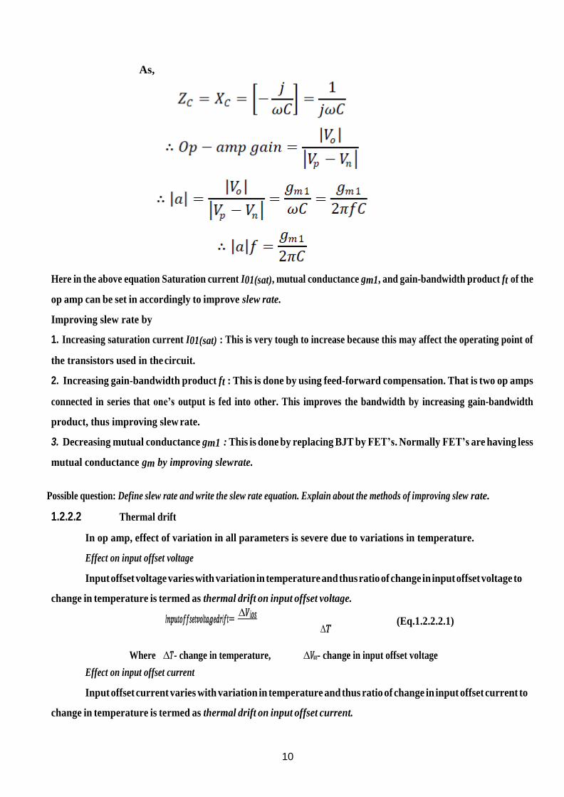
10
As,
Here in the above equation Saturation current I01(sat), mutual conductance gm1, and gain-bandwidth product ft of the
op amp can be set in accordingly to improve slew rate.
Improving slew rate by
1. Increasing saturation current I01(sat) : This is very tough to increase because this may affect the operating point of
the transistors used in the circuit.
2. Increasing gain-bandwidth product ft : This is done by using feed-forward compensation. That is two op amps
connected in series that one’s output is fed into other. This improves the bandwidth by increasing gain-bandwidth
product, thus improving slew rate.
3. Decreasing mutual conductance gm1 : This is done by replacing BJT by FET’s. Normally FET’s are having less
mutual conductance gm by improving slew rate.
Possible question: Define slew rate and write the slew rate equation. Explain about the methods of improving slew rate.
1.2.2.2 Thermal drift
In op amp, effect of variation in all parameters is severe due to variations in temperature.
Effect on input offset voltage
Input offset voltage varies with variation in temperature and thus ratio of change in input offset voltage to
change in temperature is termed as thermal drift on input offset voltage.
𝐼𝑛𝑝𝑢𝑡 𝑜𝑓𝑓𝑠𝑒𝑡 𝑣𝑜𝑙𝑡𝑎𝑔𝑒 𝑑𝑟𝑖𝑓𝑡 = ∆𝑉𝑖𝑜𝑠
∆𝑇 (Eq.1.2.2.2.1)
Where ∆𝑇 - change in temperature, ∆𝑉𝑖𝑜𝑠 - change in input offset voltage
Effect on input offset current
Input offset current varies with variation in temperature and thus ratio of change in input offset current to
change in temperature is termed as thermal drift on input offset current.

11
𝐼𝑛𝑝𝑢𝑡 𝑜𝑓𝑓𝑠𝑒𝑡 𝑐𝑢𝑟𝑟𝑒𝑛𝑡 𝑑𝑟𝑖𝑓𝑡 = ∆𝑇
(Eq.1.2.2.2.2)
Where ∆𝑇 - change in temperature, ∆𝐼𝑖𝑜𝑠 - change in input offset current
Effect on input bias current
Input bias current varies with variation in temperature and thus ratio of change in input bias current to
change in temperature is termed as thermal drift on input bias current.
𝐼𝑛𝑝𝑢𝑡 𝑏𝑖𝑎𝑠 𝑐𝑢𝑟𝑟𝑒𝑛𝑡 𝑑𝑟𝑖𝑓𝑡 = ∆𝐼𝑖𝑏
∆𝑇 (Eq.1.2.2.2.3)
Where ∆𝑇 - change in temperature, ∆𝐼𝑖𝑏 - change in input bias current
Effect on slew rate
Slew rate varies with variation in temperature and thus ratio of change in slew rate to change in temperature is
termed as thermal drift on slew rate.
𝑠𝑙𝑒𝑤 𝑟𝑎𝑡𝑒 𝑑𝑟𝑖𝑓𝑡 = ∆𝑆 /
∆𝑇 (Eq.1.2.2.2.4)
Where ∆𝑇 - change in temperature, ∆𝑆- change in slew rate
Possible question: Explain Thermal drift on various parameters of op amp.
1.2.2.3 Common Mode Rejection Ratio -CMRR
When the same voltage is applied to both the terminals of op amp, then the op amp is said to be operated in
common mode configuration. Op amp is to be operated only in differential mode and common mode signals shall be noise
or disturbance signal. The ability of differential amplifier is to reject the common mode signal and expressed as a ratio
termed as Common mode rejection ratio (CMRR).
It is defined as ratio of the differential voltage gain (Ad) to common
Practically CMRR should be larger and ideally it shall be ∞.
Possible questions: Define CMRR.

12
Open loop and closed loop configurations
Fig.1.2.3.a Open loop configuration Fig.1.2.3.b Closed loop configuration
Open loop configuration
As shown in figure, fig.1.2.3.a, Vin is the input given between input terminals and Vout is the output derived.
The open loop gain Aol is ratio of the output voltage (Vout)to the input voltage (Vin).
The open loop gain, 𝐴𝑜𝑙 = 𝑉𝑜𝑢𝑡
𝑉𝑖𝑛 (Eq.1.2.3.1)
As stated above in eq.1.2.3.1, the gain cannot be controlled or changed. Thus this gain is implicit (in-built) and
never be changed explicitly. This gain is very large in terms of 10000.
Closed loop configuration
As shown in figure, fig.1.2.3.b, Vin is the input given into inverting terminal through a resistance Ri and a
feed-back resistor Rf connected between output terminal and inverting terminal. Vout is the output derived. The open
loop gain Acl is ratio of the feed-back resistor (Rf) to the resistance (Ri). The feedback is negative.
The closed loop gain, 𝐴𝑐𝑙 = − 𝑅𝑓
𝑅𝑖 (Eq.1.2.3.2)
As stated above in eq.1.2.3.2, the gain now can be controlled or changed. Thus this gain is explicit and by
changing the resistor values, gain can be altered.
Thus closed loop gain is advantageous over open loop gain because it can be changed by changing resistor
values.
Possible question: Elaborately explain open loop and closed loop configurations of an op amp with neat sketches.

13
1.3.1 OP-AMP used in mathematical operations
1.3.1 Inverting Amplifier
The amplifier in which the output is inverted i.e. having 180o phase shift with respect to the input is called an
inverting amplifier.
This is possibly the most widely used of all the op-amp circuits. The circuit is shown in Fig. 1.3.1.The output
voltage Vo is fed back to the inverting input terminal through the Rf – R1 network where Rf is the feedback resistor.
Input signal vi is applied to the inverting input terminal through R1 and non-inverting input terminal of op-amp is
grounded.
Assume an ideal op-amp. As Vd = 0, node 'a' is at ground potential and the current i1 through R1 is
Fig. 1.3.1. Inverting amplifier
Also since op-amp draws no current, all the current flowing through R1 must flow through Rf. The output
voltage is given by
Hence, the gain of the inverting amplifier (also referred as closed loop gain) is given by
Alternatively, the nodal equation at the node 'a' in Fig. 1.3.1 is given by

14
where va is the voltage at node 'a'. Since node 'a' is at virtual ground va=0. Therefore, we get,
1.3.2 Non-Inverting Amplifier
The amplifier in which the output is amplified without any phase shift in between input and output is
called non inverting amplifier.
If the signal is applied to the non-inverting input terminal and feedback is given as shown in Fig. 1.3.2.
The circuit which amplifies without inverting the input signal. It may be noted that it is also a negative feed-back
system as output is being fed back to the inverting input terminal.
As the differential voltage Vd at the input terminal of op-amp is zero, the voltage at node 'a' in Fig. 1.3.
2. is Vi same as the input voltage applied to non-inverting input terminal. Now Rf and R1 form a potential divider.
Hence
Fig. 1.3.2 Non-inverting amplifier
As no current flows into the op-amp.
Thus, for non-inverting amplifier the voltage gain,

15
The gain can be adjusted to unity or more, by proper selection of resistors Rf and R1. Compared to the
inverting amplifier, the input resistance of the non-inverting amplifier is extremely large (= ) as the op-amp draws
negligible current from the signal source.
1.3.3 Voltage Follower
In the non-inverting amplifier of Fig. 1.3.1, if Rf = 0 and R1 = , we get the modified circuit of Fig. 1.3.3.
The voltage equation becomes
Fig. 1.3.3. Voltage follower
That is, the output voltage is equal to input voltage, both in magnitude and phase. In other words, we can also
say that the output voltage follows the input voltage exactly. Hence, the circuit is called a voltage follower. The use of the
unity gain circuit lies in the fact that its input impedance is very high (i.e. MΩ order) and output impedance is zero.
Therefore, it draws negligible current from the source. Thus a voltage follower may be used as buffer for impedance
matching, that is, to connect a high impedance source to a low impedance load.
1.3.4 SUMMING AMPLIFIER
Op-amp may be used to design a circuit whose output is the sum of several input signals. Such a circuit is called
a summing amplifier or a summer. An inverting summer or a non-inverting summer may be obtained as discussed
now.
1.3.4.1 Inverting summing amplifier
A typical summing amplifier with three input voltages V1, V2 and V3, three input resistors R1, R2, R3 and a
feedback resistor Rf is shown in Fig. 1.3.4.1. The following analysis is carried out assuming that the op-amp is an ideal

16
one, that is, AOL= and Ri = .Since the input bias current is assumed to be zero, there is no voltage drop across
the resistor RComp and hence the non-inverting input terminal is at ground potential.
Fig. 1.3.4.1 Inverting Summing Amplifier
The voltage at node 'a' is zero as the non-inverting input terminal is grounded. The nodal equation by KCL at
node 'a' is
Thus the output is an inverted, weighted sum of the inputs. In the special case, when R1 =R2 = R3 =Rf , we
have
in which case the output Vo. is the inverted sum of the input signals. We may also set
R1 = R2 = R3 = 3Rf,
in which case
Thus the output is the average of the input signals (inverted). In a practical circuit, input bias current is
compensated by using resistor Rcomp. To find Rcomp, make all inputs V1 = V2 = V3 = 0. So the effective input
resistance Ri =R1IIR2IIR3.Therefore Rcomp= RiIIRf = R1IIR2IIR3IIRf.

17
1.3.4.2 Non-inverting Summing Amplifier
A summer that gives a non-inverted sum is the non-inverting summing amplifier and is shown in fig.1.3.4.2. Let
the voltage at the (-) input terminal be Va. The voltage at (+) input terminal will also be Va. The nodal equation at node
'a' is given by
From which we have
Fig. 1.3.4.2 Non-inverting summing amplifier
The op-amp and two resistors Rf and R constitute a non-inverting amplifier with

18
Therefore, the output voltage is
which is a non-inverted weighted sum of inputs.
Let R1 = R2 = R3 = R = Rf / 2. Then, Vo = VI + V2 + V3
1.3.5 Differential Amplifier (Subtracting Amplifier)
The basic difference amplifier can be used as a subtractor or subtracting amplifier as shown in below
fig.1.3.5
If all resistors are equal in value, then the output voltage can be derived by using superposition principle. To find the
output V01 due to V1 alone, make V2=0. Then the circuit of fig.1.3.5 becomes a non-inverting amplifier having
input voltage V1/2 at the non-inverting input terminal and the output becomes
𝑉1 𝑅 𝑉 = 1 + = 𝑉
01 2 𝑅
1
Fig.1.3.5 Subtractor or Subtracting Op-amp
Similarly the output V02 due to V2 alone (with V1 grounded) can be written simply for an inverting amplifier
as
𝑉02 = −𝑉2
Thus the output voltage V0 due to both the inputs can be written as
𝑉0 = 𝑉01 + 𝑉02 = 𝑉1 − 𝑉2
Hence the output voltage Vo is subtraction of input voltages V1 and V2.

19
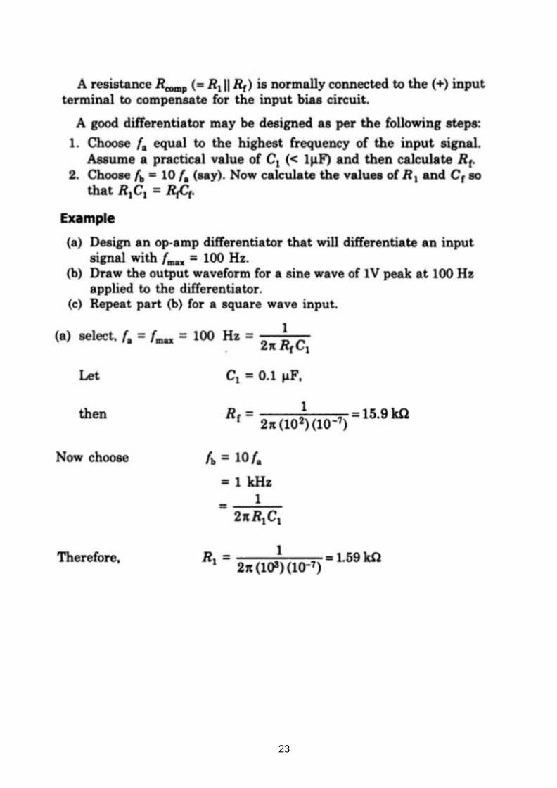
1.3.6 DIFFERENTIATOR
One of the simplest of the op-amp circuits that contain capacitor is the differentiating amplifier, or
differentiator. As the name suggests, the circuit performs the mathematical operation of differentiation, that is, the
output waveform is the derivative of input waveform. A differentiator circuit is shown in Fig. 1.3.6.
Fig. 1.3.6 Differentiator

20

21
1.3.6.1 Practical DifferentiatorFig. 1.3.6.1 Practical Differentiator
Fig. 1.3.6.2 Frequency response of Differentiator

22
23

24

25
Fig. 1.3.6.3 (a) Sine-wave input and cosine output (b) Square wave input and spike output
1.3.7 INTEGRATOR
If we interachange the resistor and capactior of the differenetiator of Fig 1.3.6 (Differentiator), we have the
circuit of Fig.1.3.7 which as we will see, is an integrator. The nodal equation at node N is,
Fig. 1.3.7 Integrator

26
The frequency response or Bode Plot of this basic integrator is shown in the fig.1.3.7. The bode plot is a straight line of
slope -6 dB/ Octave or equivalently -20 dB/Decade. The frequency fb, in fig.1.3.7 is the frequency at which the gain f the
integrator is 0 dB and is given by
𝟏 𝒇𝒃 =
𝟐𝝅𝑹
𝑪𝒇 𝟏

27
Fig. 1.3.7.1 Frequency response of basic and lossy integrator
1.3.7.1 Practical Integrator (Lossy Integrator)

28
Fig. 1.3.7.2 Practical or lossy integrator The
nodal equation at the inverting input terminal of the op-amp of fig.1.3.7.1 is
The bode plot of the lossy integrator is also shown in fig.1.3.7.1. At low frequencies gain is constant at Rf/R1. The break
frequency (f=fa) at which the gain is 0.707 (Rf/R1) or -3dB below its value of Rf/R1 ) is claculated from Equation below

29
1.3.7.2 Input and output waveforms
Fig. 1.3.7.3 Input and output waveforms integrator
1.3.8 LOGARITHMIC (LOG) AMPLIFIERS
Log-amp can also be used to compress the dynamic range of a signal. The fundamental log-amp circuit is
shown in Fig. 1.3.8 where a grounded base transistor is placed in the feedback path.
Fig. 1.3.8 Log amplifier
Since the collector is held at virtual ground and the base is also grounded, the transistor's voltage-current
relationship becomes that of a diode and is given by

30
Since, IC=IE for a grounded base transistor
Is = emitter saturation current – 10-13 A
k = Boltzmann's Constant
T = absolute temperature (in 0K)
Therefore,
Taking natural log on both sides, we get
Also in Fig. 1.3.8,
The output voltage is thus proportional to the logarithm of input voltage. Although the circuit gives natural log (In),
one can find log10 by proper scaling
log10 X = 0.4343 In X
The circuit however has one problem. The emitter saturation current Is, varies from transistor to transistor
and with temperature. Thus a stable reference voltage Vref cannot be obtained. This is eliminated by the circuit given in
Fig. 1.3.8.1. The input is applied to one log-amp, while a reference voltage is applied to another log.amp. The two
transistors are integrated close together in the same silicon wafer. This provides a close match of saturation currents and
ensures good thermal tracking.

31
Fig.1.3.8.1. Log-amp with saturation current and temperature compensation
Assume,
The voltage V0 is still dependent upon temperature and is directly proportional to T. This is compensated by the
last op-amp stage A4 which provides a non-inverting gain of (1 + R2/RTC). Now, the output voltage is,
where RTC is a temperature-sensitive resistance with a positive coefficient of temperature, so that the slope of
the equation becomes constant as the temperature changes.

32
Fig. 1.3.8.2 Log-amp using two op-amps only
The circuit in Fig. 1.3.8.1 requires four op-amps, and becomes expensive if FET op-amps are used for precision. The same
output can be obtained by the circuit of Fig. 1.3.8.2 using two op-amps only.
1.3.9 ANTILOG AMPLIFIER
The circuit is shown in Fig. 1.3.9. The input Vi for the antilog-amp is fed into the temperature compensating
voltage divider R2 and RTC and then to the base of Q2. The output Vo of the antilog-amp is fed back to the inverting
input of A1 through the resistor R1. The base to emitter voltage of transistors Q1 and Q2 can be written as
Since the base of Q1 is tied to ground, we get
The base voltage VB of Q2 is
The voltage at the emitter of Q2 is

33
Fig. 1.3.9 Antilog amplifier
But the emitter voltage of Q2 is VA, that is
Changing natural log, i.e., in to log10 , we get

34
Where 𝐾′ = 0.4343 𝑞 𝑘𝑇
𝑅𝑇𝐶 𝑅2 +𝑅𝑇𝐶
Hence an increase of input by one volt causes the output to decrease by a decade. The IC755 log/antilog
amplifier IC chip is available as a functional module which may require some external components also to be
connected to it.
1.4 OP-AMP USED AS COMPARATORS
1.4.1 COMPARATOR
A comparator is a circuit which compares a signal voltage applied at one input of an op-amp with a known
reference voltage at the other input. It is basically an open-loop op-amp with output ±Vsat (=Vcc) as shown in the ideal
transfer characteristics of Fig. 1.4.1(a). However, a commercial op-amp has the transfer characteristics of Fig.
1.4.1(b).
Fig. 1.4.1 The transfer characteristics (a) ideal comparator. (b) Practical comparator There
are basically two types of comparators:
Non-inverting comparator
Inverting comparator
The circuit of Fig. 1.4.1.1(a) is called a non-inverting comparator. A fixed reference voltage Vref applied to (-)
input and a time varying signal Vi is applied to (+) input. The output voltage is at -Vsat for Vi<Vref and Vo goes to + Vsat
for Vi>Vref . The output waveform for a Sinusoidal input signal applied to the (+) input is shown in Fig. 1.4.1.1 (b and
c) for positive and negative Vref respectively.

35
Fig. 1.4.1.1(a) Comparator
Fig. 1.4.1.1. Input and output of a Comparator when (a)Vref>0 V (b) Vref< 0V
In a practical circuit Vref is obtained by using a 10KΩ potentiometer which forms a voltage divider with the
supply voltages V+ and V- with the wiper connected to (-) input terminal as shown in Fig. 1.7.4.1 (d).Thus a Vref of
desired amplitude and polarity can be obtained by simply adjusting the 10KΩ potentiometer.

36
Fig. 1.7.1.1 (d) Non-inverting comparator. Input and output waveforms for (b) Vref
Positive (c) Vref negative (d) Practical non-inverting comparator
Figure 1.7.1.2(a) shows a practical inverting comparator in which the reference voltage Vref is applied to the (+) input
and vi is applied to (-) input. For a sinusoidal input signal, the output waveform is shown in Fig. 1.7.1.2(b) and (c) for
Vref positive and negative respectively.
Fig. 1.7.1.2.(a) Inverting comparator. Input and output waveforms for (b) Vref
Positive (c) Vref negative
1.7.2 REGENERATIVE COMPARATOR (SCHMITT TRIGGER)
We have seen that in a basic comparator, a feedback is not used the op-amp is used in the open loop mode. As open
loop gain of op-amp is very large, very small noise voltages also can cause triggering of the comparator, to change its
state. Such a false triggering may cause lot of problems in the applications of comparator as zero- crossing detector.
This may give a wrong indication of zero-crossing due to zero-crossing of noise voltage rather than zero crossing of

37
input wanted signals. Such unwanted noise causes the output to jump between high and low states. The comparator circuit
used to avoid such unwanted triggering is called regenerative comparator or Schmitt trigger, which basically uses a positive
feedback.
The figure 1.4.2 shows the basic Schmitt trigger circuit. As the input is applied to the inverting terminal, it is also
called inverting Schmitt trigger circuit. The inverting mode produces opposite polarity output. This is fed-back to the
non-inverting input which is of same polarity as that of the output. This ensures a positive feedback.
Figure 1.4.2 Schmitt trigger using op amp.(Inverting)
The fig.1.4.2 shows the basic inverting Schmitt trigger circuit.
As the input is applied to the inverting terminal, it is also called inverting Schmitt trigger circuit.
The inverting mode produces opposite polarity output (180 phase shift)
This is fed-back to the non-inverting input which is of same polarity as that of output.
This ensures positive feedback.
Case 1: When Vin is slightly positive than Vref, the output is driven into negative saturation at –Vsat level.
Case 2: When Vin is slightly negative than Vref, the output is driven into positive saturation at +Vsat level.
Thus the output voltage is always at +Vsat or –Vsat but the voltage at which it changes its state now can be
controlled by the resistance R1 and R2. Thus Vref can be obtained as per requirement.
Now R1 and R2 forms a potential divider and we can write,
Positive saturation
Negative saturation
+Vref is for positive saturation when V0 = +Vsat and is called as upper threshold voltage denoted as VUT

38
-Vref is for positive saturation when V0 = -Vsat and is called as lower threshold voltage denoted as VLT

39
The values of these voltages can be determined and adjusted by selecting proper values of R1 and R2. Thus
−𝑽𝑼𝑻 = +𝑽𝒔𝒂𝒕 𝑹𝟐 𝑹𝟏 + 𝑹𝟐
and
−𝑽𝑳𝑻 = −𝑽𝒔𝒂𝒕 𝑹𝟐 𝑹𝟏 + 𝑹𝟐
The output voltage remaains in a given state until the input voltage exceed the threshold volage level either postive or
negative.
The fig.1.4.2.1 shows the graph of output voltage against input voltage. This is called transfer characteristics of
Schmitt trigger.
The graph indicated that once the output changes its state it remains there indefinitely until the input voltage crosses any
of the threshold voltage levels. This is called hysteresis of Schmitt trigger. The hysteresis is also called as dead- zone or dead-
band.
Fig. 1.4.2.1 Hysteresis of Schmitt trigger.
The difference between VUT and VLT is called width of the hysteresis denoted as H.
𝑯 = 𝑽𝑼𝑻 − 𝑽𝑳𝑻

40
𝑯 = +𝑽𝒔𝒂𝒕 𝑹𝟐
𝑹𝟏 + 𝑹𝟐
−𝑽𝒔𝒂𝒕 𝑹𝟐 −
𝑹𝟏 + 𝑹𝟐
𝑯 = 𝟐𝑽𝒔𝒂𝒕 𝑹𝟐
𝑹𝟏 + 𝑹𝟐
The schmitt trigger eliminates the effect of noise voltages less than the hysterisis H, cannot cause triggering. As for postive
Vin greater than VUT, the output becomes –Vsat and for negative Vin less than VLT, the output becomes +Vsat, this is
called inverting schmitt trigger.
In short,
𝑽𝒊𝒏 < 𝑽𝑳𝑻 , 𝑽𝒐 = +𝑽𝒔𝒂𝒕
𝑽𝒊𝒏 > 𝑽𝑼𝑻, 𝑽𝒐 = −𝑽𝒔𝒂𝒕
𝑽𝑳𝑻 < 𝑽𝒊𝒏 < 𝑽𝑼𝑻, 𝑽𝒐 = 𝑷𝒓𝒆𝒗𝒊𝒐𝒖𝒔 𝒔𝒕𝒂𝒕𝒆 𝒂𝒄𝒉𝒊𝒆𝒗𝒆𝒅
If input applied is purely sinusoidal, the input and output waveforms for inverting Schmitt trigger can be shown as in
fig.1.4.2.2.
Fig. 1.4.2.2 Input and output waveforms of Schmitt trigger

41
Text Book References:
1. Ramakant A.Gayakwad, “0P-AMP and Linear ICs”, 4th Edition, Prentice Hall / Pearson Education,
1994.
2. D.Roy Choudary, Shail Jain, “Linear Integrated Circuits”, New Age International Pvt. Ltd., 2000.
3. Grey and Meyer, “Analysis and Design of Analog Integrated Circuits, 4th Edition, Wiley
International, 2001.
4. Michael Jacob, "Applications and Design with Analog Integrated Circuits, 2nd Edition, Prentice Hall of
India, 1993.
5. S. Salivahanan, V.S. Kanchana Bhaaskaran, “Linear integrated circuits”, 3rd Edition, McGraw-Hill,
2011.
6. William D.StaneIy, “Operational Amplifiers with Linear Integrated Circuits”, 4th Edition, Pearson
Education, 2004.
Part-A
1. Define CMRR
2. Draw the equivalent Circuit of opamp
3. Draw the circuit diagram of inverting opamp
4. What is a schmit trigger
5. Draw the circuit diagram of a comparator
6. What is a summing amplifier
7. State the applications of differential amplifier
8. Describe an integrator with its circuit diagram
9. Describe a log amplifier with a circuit diagram
10. List the applications of opamp
Part-B
1. Demonstrate the various DC characteristics of an op-amp
2. Examine the working principle and derive the output voltage of logarithmic amplifier with a
diagram
3. Describe the Working of an Integrator and differentiator
4. Describe the Schmitt trigger and comparator
5. Demonstrate the various AC characteristic of op-amp

1
SCHOOL OF ELECTRICAL AND ELECTRONICS
DEPARTMENT OF ELECTRONICS AND COMMMUNICATION
ENGINEERING
ANALOG INTEGRATED CIRCUITS - SECA1502
UNIT-II
FILTERS AND OSCILLATORS

2
2.1 ACTIVE FILTERS
FILTERS are circuits used for select signal components of required frequencies and
reject other unwanted frequency components. Thus selectivity is one of the main criteria for a
filter circuit in communication engineering.
These filters are actually allowing the required frequency bands and attenuate the
unwanted frequency bands but they are not adaptive and precise. The allowing band is termed
as pass band and attenuating band is termed as stop band. The output gain of the filters in pass
band is high and that in stop band is very low (negligible). For ideal filters, pass band gain is
infinite and stop band gain is zero. The frequency that acts as a barrier between stop and pass
band is termed as cut-off frequency. The design of a filter is based particularly on this cut-off
frequency. It is found that the practical value of the cut-off frequency is 3dB less than the
maximum frequency allowed.
These filters are considered to be passive when passive components like resistors,
capacitors and inductors are used in constructing the circuits. Passive filters are the basic filters
used in communication engineering but they are not adaptive and precise. For a good filter, the
slope of frequency response plot from pass band to stop band or vice versa should be high. But
passive filters sometimes have very low slope for changing input signals and other factors. Even
in pass band the gain is not constant but varies. These problems are minimized by using active
filters which are adaptive (manage the gain to be constant throughout the pass band and slope
to be very high for even a major change in input signals).
Active filters use OP AMP to be adaptive in nature with lager controllable gain value.
Advantages of active filters over passive filters:
1. Reduced size and weight
2. Increased reliability and improved performance
3. Simple design and good voltage gain
4. When fabricated in larger quantities, cheaper than passive filters
Disadvantages of Active Filters:
1. Limited bandwidth only.
2. Quality factor is also limited
3. Require power supply (passive doesn‟t require power supply)

3
4. Changes due to environmental factors.
Possible question: What is an active filter? What are its advantages over passive filters?
2.1.1 Order of Butterworth filters
Butterworth filters were designed by a British engineer Stephen Butterworth as a
maximally flat-response filter. This filter minimizes ripples and manages to maintain a flat
response in pass band.
Order of a filter is the magnitude of voltage transfer function of a filter that decreases by
-(20*n)dB/decade as the order „n‟ increases in stop band and flat in pass band. This is shown in
the fig. 2.1.
Types of filters according to the response:
(a). Low pass filter
response (b).High pass filter
response
(c ). Band pass filter
response (d). Band reject filter
response
Fig. 2.1. Filter Responses of all types.
For example, if the order is 50, then the filter response in stop band decreases by -100
dB/decade. So if order increases
1. The magnitude of voltage transfer function in stop band is very high and slope
decreases by 20 db/decade.
2. but the circuit complexity increases.

4
Fig.2.1.1. A Sample Butterworth Filter Response - Order wise
Note: Butterworth filters have flat response in pass bands and decrease in response of -20dB /per
decade in pass bands.
Possible question: Write short notes on the order of Butterworth filters.
2.1.1.1. Low Pass Filters
A low pass filter allows low frequencies upto a corner frequency (cut-off frequency) and
attenuates (stops) high frequencies above cut-off frequency. This is shown in the frequency
response fig. 2.1.1.1.b.
The circuit is a simple non-inverting amplifier, where a RC low pass filter circuit is
connected to the input. Capacitor allows high frequencies through it and blocks low frequencies.
This characteristic of capacitor is used in these filters.
(a). Filter Circuit (b). Filter Response
Fig. 2.1.1.1. Active Low pass filter- First Order

5
.

6
Here resistor R, smoothens the input signal and the capacitor C allows higher frequencies
to reach the ground. Thus high frequency signals never reach the input terminal and only low
frequency signal reaches the input terminal.
How corner frequency is obtained?
In the response fig. 2.1.1.1.b., a frequency is noted where the response curve point
meets a -3dB line drawn below the maximum gain. The frequency is considered as corner
frequency (fC) above which the filter attenuates the input signal and below which it allows the
signal.
As shown in the fig. 2.1.1.1.b response -20 dB/decade slope is obtained.

7
Second order Low pass filter and its response
c). Filter Circuit (d). Frequency response
Fig. 2.1.1.1.c & d: Second Order Active Low Pass Filter
With first order circuit, another RC circuit is added as shown in the fig. 2.1.1.1.c and the
response is shown in fig. 2.1.1.1.d for second order LPF with a slope of -40 dB/ decade. This is
due to the fact that each RC network introduces -20dB decrease in stop band response slope.
2.1.1.2. High Pass Filters
A high pass filter attenuates low frequencies below corner frequency (cut-off frequency)
and allows high frequencies above cut-off frequency. This is shown in the frequency response
fig. 2.1.1.2.b.
The circuit is a simple non-inverting amplifier, where a RC low pass filter circuit is
connected to the input.
(a). Filter Circuit (b). Frequency response
Fig. 2.1.1.2. First Order Active High Pass Filter

8
As shown in the above fig. 2.1.1.2.(a)., Capacitor C blocks low frequency signals below
the corner frequency fc as shown in fig. 2.1.1.2.(b). The response curve increases 20 dB per decade
at low frequencies below corner frequencies.
2.1.1.3. Band Pass Filters
A Band pass filter allows a band of frequencies and blocks lower and higher frequencies
other than the allowed band as shown in fig. 2.1.1.3.b. As shown in the fig. 2.1.1.3.a, high pass
and low pass filters are connected in series.
Fig. 2.1.1.3. a. Active Band Pass Filter
The corner frequency of low pass filter fL is chosen to be lower than that of high pass filter
fH. Thus the difference between fH and fL is considered to be the pass band. In low frequency stop
band, the response increases 20 dB per decade and in high frequency stop band, the response
decreases by 20 dB per decade.
Fig. 2.1.1.3.b. Response of Active Band Pass Filter

9
2.1.1.4. Band Reject Filters (Notch filter)
A Band pass filter blocks a band of frequencies and allows lower and higher frequencies
other than the blocked band as shown in fig. 2.1.1.4.b. As shown in the fig. 2.1.1.4.a, band pass
filter is connected to a summer circuit. The input and output of the band pass filter is summed
up at the inverting summer input. The bands are inverted by the inverting summer and so pass
band of band pass filter becomes stop band and stop bands becomes pass bands. Thus this filter
only allows particular band above lower corner frequency fL and below upper corner frequency
fH.
Fig. 2.1.1.4.a. Active Band Reject Filter
Fig. 2.1.1.4.b. Response of Active Band Reject Filter
Possible questions:
Write briefly about first and second order Butterworth Low-pass filter with neat sketches.
Write briefly about first and second order Butterworth high-pass filter with neat sketches.
Write briefly about first order Butterworth band-pass filter with neat sketches.

10
Write briefly about first order Butterworth band-reject filter with neat sketches. .
Write briefly about Notch filter with neat sketches.
2.2 OP-AMP OSCILLATORS
In electronics, oscillators are circuits that generate sinusoidal or non-sinusoidal
waveforms used as reference signals in communication engineering. The non-sinusoidal
waveforms are triangular, ramp, saw-tooth, pulse, TTL, rectangular, spike etc.
The oscillator shall have an amplifier with a positive feedback for generating
oscillations. The basic oscillator circuit with feedback is shown below fig. 2.2.a.
Fig.2.2.a. Basic Feedback Oscillator
Fig.2.2.b. Feedback Oscillator Output
But for sustained (continuous and steady) oscillations Barkhausen‟s criteria are to
be satisfied. The criteria states that

11
1. The total gain of the circuit should be equal to or more than one and
2. The overall phase shift in the circuit (amplifier and feedback circuit) shall be
zero. If gain of the amplifier is considered as A and feedback factor is β, then
Criterion 1: A β 1
Modulus of the product of the amplifier gain A and feedback factor of feedback network
β should be equal to or greater than zero.
Criterion 2: A β = 0° or 360° (0 or 2 radians)
Phase angle between the amplifier gain A and feedback factor of feedback network β or
total phase shift in the circuit should be equal to or greater than zero. Criterion 1 and 2 are
Barkhausen‟s criteria for sustained oscillations.
As shown in fig. 2.2.b, a noise voltage introduced by existing imbalances in the circuit is
amplified by the circuit itself. The frequency of noise voltage depends on the design aspects of
the circuit and when multiplication factor of total gain A β =1 and when A β 1, the
amplitude of the generated voltage increases till saturation is reached. Then the oscillation at the
particular frequency is generated and sustained. This is done when the phase shift of the circuit
is 0° or 360° (0 or 2 radians).
In the following sections two such sinusoidal oscillators are being explained. They
are (1). RC phase shift oscillator and
(2). Wien Bridge oscillator

12
2.2.1. RC Phase Shift Oscillators
RC phase shift oscillator generates sinusoidal output and thus categorized under
sinusoidal oscillators. Here in this oscillator the amplifier used is a negative feedback inverting
Operational amplifier connected to a RC feedback network.
Fig.2.2.1.a. RC Phase Shift Oscillator
Construction: As described earlier the oscillator comprising of a negative feedback
inverting operational amplifier whose input resistor is R1 and feedback resistor is R2 as shown
in the fig. 2.2.1.a.
An RC network where one end of the resistor R is connected to the ground, the other end
is connected to a capacitor C and the other end of the capacitor acts as an input terminal. The
combined end of the capacitor and resistor acts as output terminal. Each RC network provides
60° ( /3 radians) phase shift between their input and output terminals. Thus three networks are
connected in series, so as to provide a phase shift of 180° or radians. The feedback RC network
shifts the phase this is termed as RC phase shift oscillator. As said earlier the amplifier is an
inverting amplifier, and so 180° or radians phase shift between input and output. Hence second
Barkhausen‟s criterion is fulfilled.

13
Choosing the value of amplifier voltage gain to be more (nearly 30 or so), we can fulfill
first Barkhausen‟s criterion of having overall gain more than 1.
Working: Practically an OP AMP is not perfect and so imbalances are prevailing between
their input terminals. This imbalance generates a minor sinusoidal noise voltages fed between
the input terminals. This noise voltage is amplified by the amplifier and a sinusoidal output
voltage Vo is generated at the output terminal.
As discussed earlier, the RC network provides 180° or 2 radians where Vo is fed into the
feedback RC network and an inverse voltage of Vf shown in fig. 2.2.1.b. We can understand that
Vf is 180° (or 2 radians) phase shifted Vo. This Vf is fed into the inverting terminal of the
operational amplifier through an input resistor R1. This voltage is phase inverted of 180° (or 2
radians) by the amplifier and the output Vo is inverse of Vf.
Since the circuit fulfills the criteria for sustained oscillations, the circuit continuously
generates sinusoidal output.
Fig.2.2.1.b. RC Phase Shift Oscillator- Feedback network

14
Derivation of frequency of oscillation of RC Phase shift oscillator
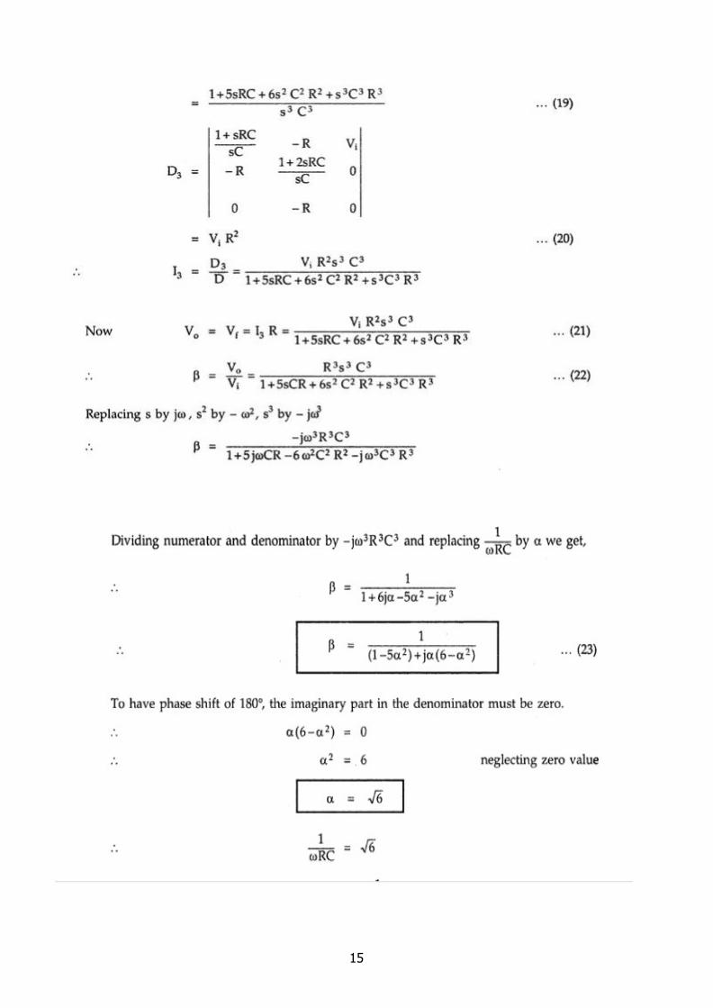
15

16

17
Pblm.2.2.1-Solved Problem:
The capacitor value of an RC phase shift oscillator using OP AMP is 0.01µF and the desired
frequency of oscillation is 25 KHz. The voltage gain of the amplifier should be 30. Thus calculate
the value of R of RC feedback network, input resistor R1 and feedback resistor R2 connected to
the amplifier.
Solution:
Value of R in RC feedback network:
Given C=0.01 µF, and Frequency f= 25 KHz.
Thus Resistor R value in RC network is 260 K .
Value of R1 in amplifier circuit:
Given A=30. R1 or R2 are not given and thus we can assume any one resistor value. If R1 is
assumed to be 1K then R2 can be estimated. Since it is an inverting amplifier
Its gain is,

18
Thus Resistor R2 (acts as a feedback resistor) value in amplifier is 30 K .

19
2.2.2. Wien’s Bridge Oscillators
Unlike RC phase shift oscillator, Wien bridge oscillator never uses phase-shift concept. It
uses balancing concept of lead-lag network.
Construction: Here this oscillator is connected in a bridge fashion. The inverting terminal
is connected to a junction where resistors R3 and RF are connected. The other end of R3 is
grounded and RF is connected to output terminal of the amplifier. This forms a reference voltage
across R3 being fed into inverting terminal as shown in the fig. 2.2.2.a & 2.2.2.b
Fig.2.2.2.a. Wien’s Bridge Oscillator
The non-inverting connected in between two reactance offering components Z1
and Z2 as shown in the fig. 2.2.2.b. Z1 comprises of serially connected resistor R1 and capacitor
C1 whereas Z2 comprises of parallel connected resistor R2 and capacitor C2. This combination of
Z1 and Z2 is termed as lead-lag circuit.
Fig.2.2.2.b. Wien’s Bridge Oscillator-Reconstructed

20
Working: Here the reactive circuits Z1 and Z2 connected to non-inverting terminal at B
as shown in the fig. 3.3.2.b. A noise voltage is generated between the imbalanced input terminals
is amplified by the amplifier and fed in the bridge circuit.
For particular low-frequencies, the capacitors act as open circuit and thus the output
voltage of lead-lag circuit shall be zero and for high frequencies the capacitors cat as short circuit
and thus voltage shall be zero. Only for a particular frequency called resonant frequency,
resistance value equals to capacitive reactance value. Thus maximum current is available at this
frequency only. So the output appears only for resonant frequency.
The other resistor values of R3 and RF of bridge are adjusted to enhance the output to a
maximum level. Thus the oscillation is generated.
The amplifier is a non-inverting amplifier circuit and so no phase shift is introduced.
Phase shift is 0° (or 2 ) for the whole circuit. And the overall gain shall be also more than 1.
Thus the Barkhausen‟s criteria for sustained oscillations are satisfied.
If R1 = R2 = R and C1 = C2 = C then R = XC at resonant frequency where XC is capacitive
reactance of C.
This is the frequency of oscillation
2.3 OP-AMP MULTIVIBRATORS
Multivibrators are square wave oscillators that produce pulse waveforms with various
ON time and OFF time. As shown in fig. 2.3.a, P1, P2 and P3 are ON time of the pulse whose
total time period is 10 ms with TON and TOFF are 3.5 ms and 6.5 ms respectively. TON and TOFF
are two states of the pulse. The place where TON transits to TOFF or TOFF to TON is termed as state
transition.

21
Fig.2.3.a. Pulse waveform - model
The state transition may have slope (with a small time for transition) or infinite slope (No
time for transition-being abrupt).
There are three types of multivibrators available according to their state transition. They
are (a.) astable, (b.) monostable, and (c). bistable multivibrators.
Astable multivibrator is one that generates pulses those transits from one state to another
without any external trigger. It is done by its free-will controlled by the design aspects. Thus this
is called free-running multivibrator. So the states are not stable for a long time, the states can be
termed as Quasi-stable states. Hence this multivibrator generates pulses of no stable states, it is
termed as astable multivibrator.
Monostable multivibrator is one that generates pulses those transits from one state to
another with the help of one external trigger. The multivibrator remains in one state (stable
state) and when an external pulse is applied then it transits state from present Stable state to a
quasi- stable state. It remains at quasi-stable state for a time period of T as it is designed and
then returns to a stable state without any external trigger. Since it changes state from stable to
quasi- stable using one external trigger, it is termed as one-shot multivibrator or monostable
multivibrator.
Bistable multivibrator is one that generates pulses those transits from one state to another
with the help of two external trigger. The multivibrator remains in one state (stable state) and
when an external pulse is applied then it transits state from present Stable state to a next stable
state. It remains at second stable state until another external trigger is applied. Thus this
multivibrator has stable states only and the transitions happen only when triggers are applied,
it is termed as bistable multivibrators.
Other related terminology: Duty cycle means
If TON is 5 ms and TOFF is 10 ms, then Duty cycle D=5/15 ms,
D=33%. D=50%, then TON = TOFF

22
Possible questions:
What is a Multivibrator?
Define the terminology of astable, monostable and bistable multivibrators.
2.3.1. Astable Multivibrators
These multivibrators are termed as “Free Running” multivibrators, and they have only
quasi stable states as seen earlier in introduction.
The circuit diagram of astable multivibrator using Operational amplifier is shown below
fig.
2.3.1.a.
Fig.2.3.1.a. Astable Multivibrator – Circuit Diagram
Construction:
The circuit as simple and resembles like OP AMP Schmitt trigger circuit. One end of a
capacitor C and a resistor R are connected to the inverting terminal. The other end of the resistor
is connected to the output terminal and that of capacitor is connected to ground terminal. This
capacitor C and feedback resistor R decide the period for oscillation of the multivibrator. A
resistor R1 is connected between the output terminal and non-inverting terminal and another
resistor R2 is

23
connected between non-inverting terminal and ground terminals. If the output voltage is
considered as Vo, then the voltage tapped between R2 shall be a reference voltage applied to the
non-inverting terminal with amplitude of βVo where β is feedback factor for comparison.
Working:
Considering fig. 2.3.1.a and 2.3.1.b, the working part of this generator can be explained.
At Time 0: At time 0, assume the output transits from -Vsat to +Vsat. Since the output is
+Vsat at time 0, reference voltage +βVo and capacitor voltage is -βVo.
From Time 0 to Time T1: Since reference is at +βVo, the inverting terminal is also at +βVo
due to virtual ground. Now the capacitor tries to charge till the output voltage +Vo. It reaches
+βVo and tries to charge more, then the inverting terminal go beyond reference voltage +βVo
after time constant RC.
At Time T1: At time T1, since the inverting terminal goes little above than reference
voltage +βVo, the output transits from +Vsat to -Vsat. Now capacitor voltage remains at +βVo. The
reference voltage at non-inverting terminal is at -βVo. The time T1 is decided by RC (time
constant) factor.
After Time T1: Since reference is at -βVo, the inverting terminal is also at -βVo due to
virtual ground. Now the capacitor tries to charge till the output voltage -Vo. It tries to reach -βVo
and tries to charge more, then the inverting terminal go beyond reference voltage -βVo after time
RC (time constant). Now again whatever happened at time 0 happens again. These 3 steps repeat
periodically till power is available for the circuit.
Fig.2.3.1.b. Astable Multivibrator – Output Waveforms

24
DERIVATION OF FREQUENCY OF OSCILLATION FOR OP-AMP ASTABLE MULTIVIBRATOR
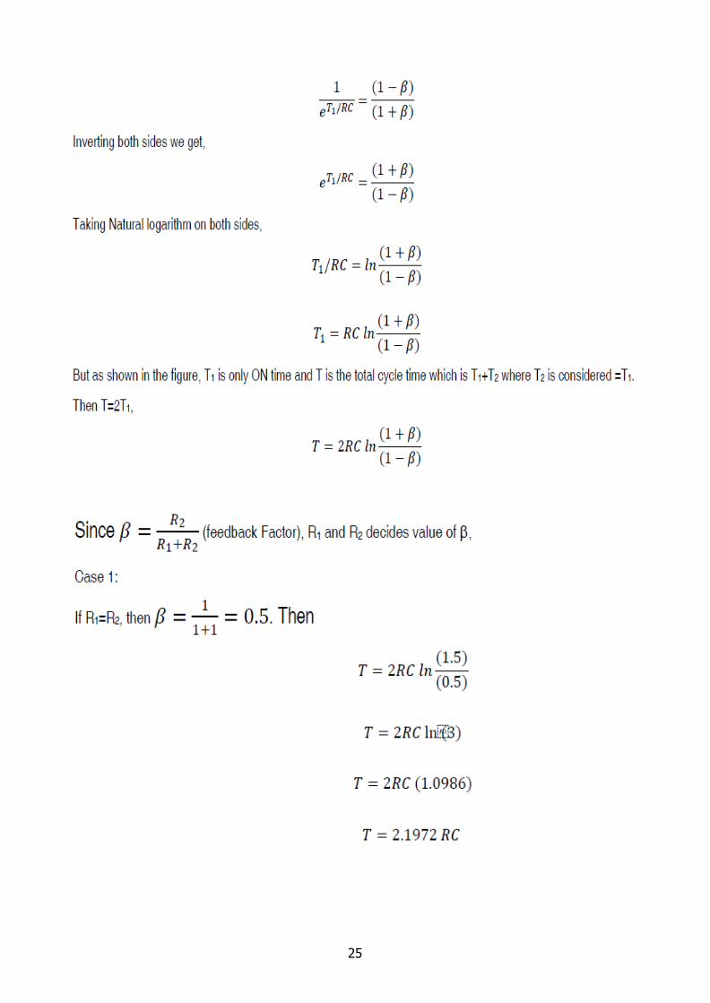
25

26
2.3.2. Monostable Multivibrators
These multivibrators are termed as “one-shot multivibrators” and they have only one
stable state and other is quasi-stable state induced by single external trigger as seen earlier in
introduction.
The circuit diagram of monostable multivibrator using Operational amplifier is shown
below fig. 2.3.2.a.
Fig.2.3.2.a. Monostable Multivibrator Using OP AMP

27
Construction:
The circuit as simple and resembles like OP AMP Schmitt trigger circuit. One end of a
capacitor C and a resistor R are connected to the inverting terminal. The other end of the resistor
is connected to the output terminal and that of capacitor is connected to ground terminal. A
diode D1 is connected parallel to the capacitor C. This capacitor C and feedback resistor R decide
the period for T of the multivibrator. A resistor R1 is connected between the output terminal
and non-inverting terminal and another resistor R2 is connected between non-inverting terminal
and ground terminals. If the output voltage is considered as Vo, then the voltage tapped between
R2 shall be a reference voltage applied to the non-inverting terminal with amplitude of βVo
where β is feedback factor for comparison.
A pulse trigger circuit consisting of diode D2 and a differentiator circuit connected to
pulse generator of negative pulse width Tp. The anode of the diode D2 is connected to non-
inverting terminal
Fig.2.3.2.b. Monostable Multivibrator - Waveforms
Working:
Considering fig.‟s 2.3.2.a and 2.3.2.b, the working part of this generator can be explained.
In fig. 2.3.2.b has three waveforms. Waveform a shows the pulse trigger waveform whose trigger
pulse width is TP, waveform b shows voltage output VC across capacitor C and waveform c shows

28
the monostable output Vo of quasi-stable state of time T.
Before pulse trigger: At time before pulse trigger, assume the output is at +Vsat. Since the
output is at +Vsat, then reference voltage is at +βVo and so capacitor voltage VC tries to charge
towards +Vsat. Due to this the diode D1 gets forward biased when inverting terminal is positive,
and the diode D1 starts conducting beyond 0.7V (Approximate cut-in voltage of Silicon diode).
Thus the diode D1 conducts and provides a short path beyond 0.7V, and hence the capacitor C
which is parallel can charge upto 0.7V only. So now the capacitor voltage VC is 0.7V.This voltage
is shown as VD in the fig. 2.3.2.b waveform (b).
At time of pulse trigger: As shown in fig. 2.3.2.b waveform (a & b), a negative pulse trigger
is applied at non-inverting terminal and its amplitude being –Vin. Hence at the non-inverting
terminal, pulse voltage –Vin and reference voltage +βVsat exists. The total voltage is (+βVsat –Vin).
The amplitude of this voltage is less than 0.7V due to existence of diode D2 which is forward
biased (ON) due to –ive trigger pulse (Cathode of the diode D2 is negative due to -Vin and anode
is positive due to +βVsat).
Now non-inverting terminal acts as reference terminal of an inverting comparator. At
this point inverting terminal is at 0.7V and non-inverting reference voltage is below 0.7V. Hence
inverting terminal is more than reference voltage at non-inverting terminal and the output
transits from +Vsat to –Vsat as shown in fig. 2.3.2.b waveform (c). That is output transited from
stable high state to low state.
The capacitor voltage VC is at 0.7V and output is at –Vsat. Hence the capacitor C starts
charging towards -Vsat through the resistor R. The non-inverting terminal reference voltage is
less than 0.7V.
At Time AFTER pulse trigger: When pulse trigger ends after time TP, it becomes positive.
So the cathode of diode D2 is at positive voltage and anode is at –βVsat. Thus the diode D2 is in
reverse bias condition (OFF). Due to this the non-inverting voltage is affected only by reference
voltage across resistor R2 which is -βVsat.
Now reference voltage is at –βVsat and the charging capacitor is charging towards –Vsat.
but when capacitor voltage VC reaches just above –βVsat, output transits from -Vsat to +Vsat
(Inverting terminal voltage VC is more than reference voltage at non-inverting terminal). This
transition happens at time T from start of pulse trigger where T is decided by RC time constant.
That is capacitor C took time period of T for charging from VD to –βVsat which is through resistor
R. The output stays at a quasi-stable state for a time period of T.
After Time T: Now output voltage Vo is at +Vsat and reference voltage at non-inverting
terminal is at +βVsat. The capacitor starts charging from –βVsat to +Vsat. But when the capacitor
voltage VC increases more than VD, diode D1 is forward biased and starts conducting. Hence the

29
capacitor voltage VC cannot charge beyond VD. The waveform is shown in fig. 2.3.2.b waveform
(a). As seen initially, now the amplitude at inverting terminal is VD due to charge of capacitor,
non-inverting terminal voltage is at +βVsat. The output is a negative pulse voltage whose time
period is T. This negative pulse was generated due to an external negative trigger (one-shot
trigger). The output transit from a stable high state to a low quasi-stable state time T and then
to a stable high state. This is a monostable waveform because it has one stable state and a quasi-
stable state. In next section, discussion about derivation of time period T is done.
DERIVATION OF FREQUENCY OF OSCILLATION FOR OP-AMP MONOSTABLE
MULTIVIBRATOR
Analysis of capacitor voltage VC(across capacitor C)

30

31
Possible question:
Explain the construction and working of monostable multivibrator using OP AMP with neat sketches.
2.4 OP-AMP RECTIFIERS
2.4.1 PRECISION RECTIFIERS
Rectifiers convert bipolar AC signals into unipolar DC signals. The circuit mainly uses
diodes that block signals when reverse biased and allow signals when forward biased. But when
forward biased diode can only allow signals above 0.7V (cut-in voltage of Silicon diode). So the
rectifier cannot precisely rectify ac signals of peak to peak voltages below 0.7V. For eradicating
this disadvantage of not rectifying signals below 0.7V we use operational amplifiers for
rectification.
OP AMP inverting amplifier circuits are added with diodes to function as precision
rectifiers to rectify voltages below 0.7V (cut-in voltages).
2.4.1. Precision Half-wave Rectifiers
As discussed this precision rectifier is used for rectifying ac signals below cut-in voltages.
Circuit construction: An inverting amplifier with input resistor R1 and feedback resistor
R2 is altered by adding two diodes D1 and D2 in series as shown in the fig. 2.4.1.a. D1 is connected
between output terminal of OP AMP and resistor R2 as shown and diode D2 is connected
between input inverting terminal and anode of the diode D1.
Working: An AC signal Vin is applied to the inverting terminal and output Vo is tapped
at the cathode of diode D1 and one end of resistor R2 as shown in the following fig. The analysis
of this circuit in both positive and negative cycle becomes essential.
In positive cycle: The inverting terminal becomes positive in positive input cycle and since
it is an inverting amplifier and output terminal becomes negative. Thus Diode D1 becomes
reverse biased and remains in OFF state but diode D2 becomes forward biased and remains ON.
Since Diode D1 is OFF and diode D2 is ON and D2 provides short circuit between inverting and
non- inverting terminals, so the output Vout is zero.

32
Fig. 2.4.1.a Half-wave precision rectifier
Fig. 2.4.1.b Half-wave precision rectifier-waveforms
In negative cycle: The inverting terminal becomes negative in negative input cycle and
since it is an inverting amplifier and output terminal becomes positive. Thus Diode D1 becomes
forward biased and remains in ON state but diode D2 becomes reverse biased and remains OFF.
Since Diode D1 is ON and diode D2 is OFF and provides high resistance path between inverting
and non-inverting terminals. But resistor R2 provides alternate path between input and output.
Since D1
is ON, it connects Vout with output terminal. Now the circuit becomes normal inverting amplifier
and so output Vout is the input multiplied by scaling factor (-R2/R1).
Thus the rectifier circuit allows one cycle (negative half cycle of the input) but blocks
other cycle (positive half cycle). Since the diode doesn‟t directly involve in rectification and OP
AMP has high gain factor, this circuit rectifies even signals less than cut-in voltage. The
waveforms are shown in the fig. 2.4.1.b.
2.4.2. Precision Full-wave Rectifiers
Circuit construction: Two inverting amplifiers with input resistor R and feedback
resistor R is altered by adding two diodes D1 and D2 in series as shown in the fig. 2.4.2.a. D1 is
connected between output terminal of OP AMP and feedback resistor R as shown and diode D2
is connected between output terminal and other end of the resistor R connected to inverting
terminal of the first OP AMP and also connected to non-inverting terminal of the second OP
AMP.

33
Working: An AC signal Vi is applied to the inverting terminal through the resistor R and
output Vo is tapped at output of second OP AMP as shown in the following fig. The analysis of
this circuit in both positive and negative cycle becomes essential.
Fig. 2.4.2.a Full-wave precision rectifier
In positive cycle: The inverting terminal of first OP AMP becomes positive, in positive
input cycle and diode D1 is forward biased. But diode D2 is reverse biased because output
terminal becomes negative. Now D1 is ON and D2 is OFF. The circuit looks as shown in fig.
2.4.2.b. Thus output voltage Vo is double inverted signal of input voltage Vi. Since gain of both
amplifiers is R/R=1, and Vo = Vi.
Fig. 2.4.2.b Full-wave precision rectifier-during positive half cycle
In negative cycle: The inverting terminal of the first OP AMP becomes negative in
negative input cycle, the Diode D1 becomes reverse biased and remains in OFF state but diode
D2 becomes forward biased and remains ON. Since Diode D1 is OFF and diode D2 is ON as
shown in fig. 2.4.2.c. But resistor R provides alternate path between input and output. In second
amplifier, voltage at inverting terminal is V/2R volts and non-inverting terminal is V/R. thus

34
non-inverting terminal of second amplifier holds two times of voltage than inverting terminal.
Thus output voltage Vo is ((V/R)-(V/2R)=V/2R) and is adjusted by changing the value of
Feedback resistor R of second amplifier. Hence we get output for negative half-cycle too.
Fig. 2.4.2.c Full-wave precision rectifier-during negative half cycle
This is shown in the fig. of waveforms fig. 2.4.2.d. thus this rectifier converts bipolar AC
input to unipolar DC output.
Fig. 2.4.2.d Full-wave precision rectifier waveform

35
Possible questions:
What is the principle behind precision rectification?
Explain the construction and working of half and full wave precision rectifiers with neat sketches
Text Book References:
1. Ramakant A.Gayakwad, “0P-AMP and Linear ICs”, 4th Edition, Prentice Hall / Pearson
Education, 1994.
2. D.Roy Choudary, Shail Jain, “Linear Integrated Circuits”, New Age International
Pvt. Ltd., 2000.
3. Grey and Meyer, “Analysis and Design of Analog Integrated Circuits, 4th Edition, Wiley
International, 2001.
4. Michael Jacob, "Applications and Design with Analog Integrated Circuits, 2nd Edition,
Prentice Hall of India, 1993.
5. S. Salivahanan, V.S. Kanchana Bhaaskaran, “Linear integrated circuits”, 3rd Edition,
McGraw-Hill, 2011.
6. William D.StaneIy, “Operational Amplifiers with Linear Integrated Circuits”, 4th Edition,
Pearson Education, 2004.
Part-A
1. .Draw the circuit diagram of a first order low pass filter and give its cut off frequency
2. Draw the general structure of Sallen Key Filter
3. List out the different types of filters
4. Draw the circuit diagram of RC phase shift oscillator
5. Draw the circuit diagram of Wein Bridge Oscillator
6. Describe one shot multivibrator
7. Describe Astable Multivibrator
8. List out the applications of IC555 Timer
9. Describe precision rectifier
10. Draw the circuit diagram of Full wave rectifier with its graph
Part-B
1. Describe the working of a second order High pass filter and derive its frequency response
2. Describe the working of a second order low pass filter and derive its frequency response
3. Derive the general structure of Sallen Key Filter
4. Describe RC phase shift Oscillator and derive its frequency response
5. Explain the working of Astable multivibrator

36

1
SCHOOL OF ELECTRICAL AND ELECTRONICS
DEPARTMENT OF ELECTRONICS AND COMMMUNICATION ENGINEERING
ANALOG INTEGRATED CIRCUITS – SECA1502 UNIT – III
A/D AND D/A CONVERTERS

2
3.1 INTRODUCTION
• Most of the real world physical quantities such as voltage, current, temperature, pressure and time etc
are available in analog form
• Even though an analog signal represents a real physical parameter with accuracy, it is difficult to
process, store or transmit the analog signal without errors because of the superimposition of noise.
• Therefore for processing, transmission and storage purposes, it is often convenient to express these
variables in digital form it gives better accuracy and reduces noise.
• The operation of any digital communication system is based on A/D conversion or D/A conversion
Figure:3.1: Circuit Showing application of A/D and D/A convertor
Block diagram explanation:
• The analog signal obtained from the transducer is bandlimited by antialiasing filter.
• The signal is then sampled at a frequency rate more than twice the maximum frequency of the band
limited signal.
• The sampled signal has to be held constant while conversion is taking place in A/D converter.
• This requires that ADC should be preceded by a sample and hold (S/H) circuit
• The ADC output is a sequence in binary digit. The micro- computer or Digital signal Processor
performs the numerical calculations of the desired control algorithm.
• The DAC converter is operated at the same frequency of the ADC converter
• The output of DAC converter is usually a staircase. This staircase like digital output is passed through
a smoothing filter to reduce the effect of noise.

3
3.2 Applications of ADC and DAC:
This scheme is used either in full or in part in applications such as
1. Digital audio recording and playback
2. Computer
3. Music and video synthesis
4. Pulse code modulation transmission
5. Data acquisition
6. Digital multimeter
7. Direct digital control
8. Digital signal processing
9. Microprocessor based instrumentation
Both ADC and DAC are known as data convertors and available in IC forms
1.What is the decimal equivalent of 1010?
3.3. Basic DAC Techniques
Figure 3.3.1: Block Diagram of DAC

4
• The input is a n-bit binary word and is combined with a reference voltage VR to give an
analog output signal.
• The output of DAC can be either a voltage or current
• For a voltage output DAC, the mathematical representation of output is given as,
3.3 : Types of DAC
• 1. Weighted Resistor DAC
• 2. R-2R Ladder DAC
3.3.1 Weighted Resistor DAC
Figure 3.3.1:Binary Weighted DAC

5

6
DRAWBACK OF BINARY WEIGHTED DAC
The difference between the resistance values corresponding to LSB & MSB will increase
as the number of bits present in the digital input increases.
It is difficult to design more accurate resistors as the number of bits present in the digital
input increases.
Has problems if bit length is longer than 8 bits For example, if R = 10 k Ohms
R8 = 28-1(10 k Ohms) = 1280 k Ohms If VR = 10 Volts,
I8 = 10V/1280 k Ohms = 7.8 A
Op-amps to handle those currents are expensive because this is usually below the current
noise threshold.
3.3.2 : R-2R ladder Network
Figure 3.3.2: R-2R Ladder Network
• The R-2R Digital to Analog Converter uses only two resistance values R and 2R regardless of
the number of bits of the converter compared to the weighted resistor implementation where
each bit resistor has a different value. The circuit shown is a 3 bit DAC. Typical value of resistors
ranges from 2.5kῼ to 10kῼ
7
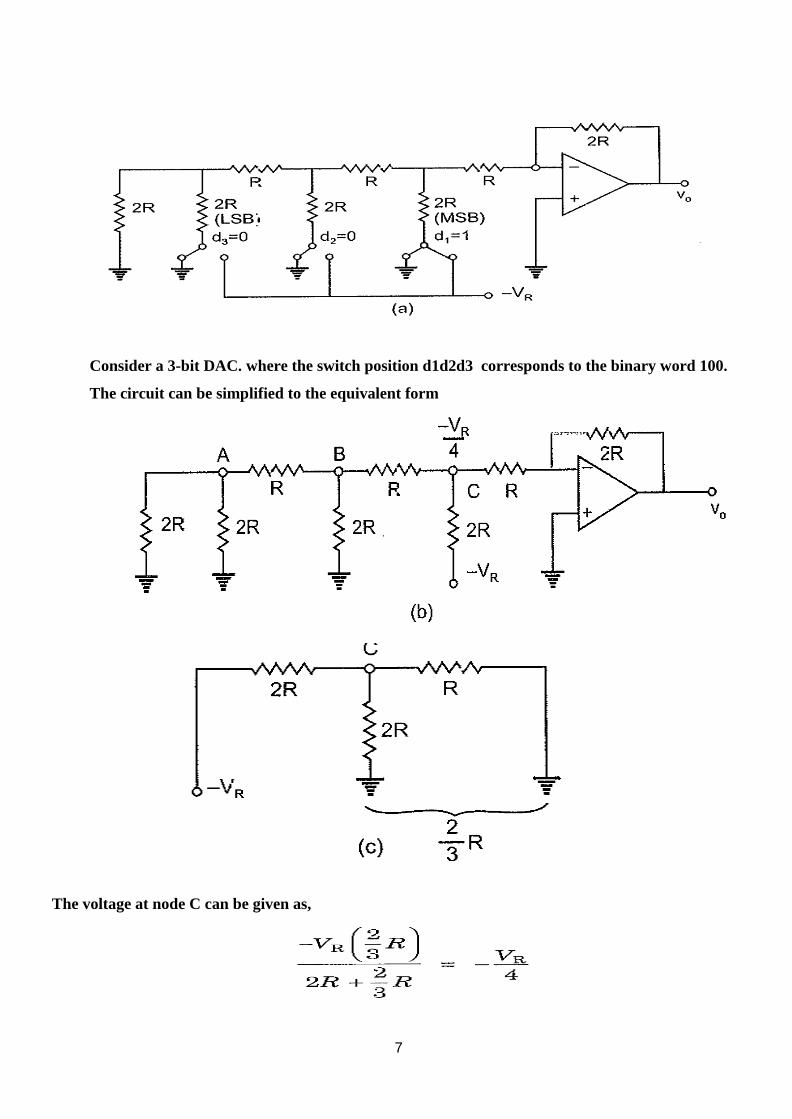
Consider a 3-bit DAC. where the switch position d1d2d3 corresponds to the binary word 100.
The circuit can be simplified to the equivalent form
The voltage at node C can be given as,

8
The output voltage is given as,
PROBLEM:
1. Calculate the Analog value for the binary digit 001

9
The switch position corresponding to the binary word 001 in 3bit DAC is shown. The voltages at the
nodes A, BC formed by the resistor branches are easily calculated in a similar fashion
The output voltage is given as,
2. . The basic step of a 9-bit DAC is 10.3mV.If 0000000 represents 0V. What output is produced
if the input is 101101111?

10
3. What output voltage would be produced by a D/A converter whose output range is 0 to 10V
and whose input binary Number is
(i) 10 ( for a 2-bit D/A Converter
(ii) 0110 ( for a 4-bit DAC)
(iii) 10111100 ( For a 8-bit DAC)
• 4. Calculate the values of the LSB,MSB and full scale output for an 8-bit DAC for the 0-10V
range

11
3.4 A-D Converters:
It accepts analog voltage Va, and produces output binary word d1d2….dn of functional value D
Where d1 is MSB dn is LSB
Figure 3.4.1: Analog to Digital converter
An ADC has two additional control lines,
START input tell the ADC when to start the conversion
EOC ( End of Conversion) to announce when the conversion is completed
ADCs are designed for microprocessor interfacing or to directly Drive LCD or LED displays.
Classification of ADC
• Direct Type ADC
• Integrating Type ADC
DIRECT TYPE OF ADC:
It compare a given analog signal with the internally generated equivalent signal. This group
include
1. Flash Type converter
2. Successive approximation type converter

12
INTEGRATED TYPE ADC:
It performs conversion in an indirect manner by first changing the analog input signal to a
linear function of time or frequency and then to a digital code. The two most widely used
integrating type converters are
1. Charge balancing ADC
2. Dual slope ADC
3.4.1 Parallel Comparator( Flash) A/D Converter
Figure: 3.4.1: Flash Type Converter

13
It is the simplest possible A/D converter
It is at the same time , the fastest and most expensive technique.
The circuit consist of a resistive divider network, 8 op-amp comparator and a 8 line to 3-line
encoder.
At each node of the resistive divider, a comparison voltage is available.
Since all the resistors are of equal value, the voltage levels available at the nodes are equally
divided between the reference voltage VR and the ground.
The purpose of the circuit is to compare the analog input voltage Va with each of the node
voltage.
The circuit has an advantage of high speed, because the conversion take place simultaneously
rather than sequentially.
Typical conversion time is 100ns or less.
Conversion time is limited only by the speed of the comparatorand of the priority encoder.
By using an advanced Micro Devices AMD 686A Comparator and a T1147 priority encoder ,
conversion delays of the order of 20 ns can be obtained.
Figure 3.4.2: Comparator truth table

14
Disadvantages of Flash Type converter:
The number of comparators required almost doubles for each added bit . A 2 bit ADC
requires 3 comparator, 3- bit ADC needs 7, whereas 4-bit requires 15 comparators. In general,
the number of comparator requires are
Where n is the desired number of bits.
Hence the number of comparators approximately doubles for added bits.
Also the larger the value of n, the more complex is the priority encoder.
3.4.2: SUCESSIVE APPROXIMATION ADC:
Figure 3.4.2: Block diagram of Successive Approximation Technique
This method uses a successive approximation register (SAR) to find the required values of
each bit by trial and error.

15
With the arrival of the START command , the SAR sets the MSB d1= 1 with all other bits to
zero so that the trial code is 1000000.
The output Vd of the DAC is now compared with analog input Va. If Va is greater than the
DAC output Vd then 1000000 is less than the correct digital representation.
The MSB is left at 1 and the net lower significant bit is made 1 and further tested
However , if Va is less than the DAC output, then 1000000 is greater than the correct digital
representation.
So reset MSB to ‘0’ and go on to the next lower significant bit as 1,
This procedure is repeated for all subsequent bits, one at a time , until all bit positions have
been tested.
Whenever the DAC output crosses Va, the comparator changes state and this can be taken as
End of conversion(EOC).

16
3.5 : INTEGRATING TYPE ADC
The integrating type of ADC do not reqire S/H circuit at the input.If the inpt changes
during conversion, the ADC output code will be proportional to the value of the input
averaged over the integration period.
Charge Balancing ADC
Dual slope ADC
3.5.1 : DUAL SLOPE ADC
Figure 3.5.1: Dual Slope ADC

17
The circuit consists of a high input impedance bufferA1, precision integratorA2 and a voltage
comparator. The converter first integrates the analog input signal Va for a fixed duration of 2n
clock periods as shown in figure. Then it integrates an internal reference voltage VR of opposite
polarity until the integrator output is zero. The number of clock cycles required to return the
integrator to zero is proportional to the value of Va averaged over the integration period. Hence
N represents the desired output code.
Figure 3.5.2 : Output Waveform

18
3.6 SAMPLE AND HOLD CIRCUIT:
A sample and hold circuit samples an input and holds on to its last sampled value until the
input is sampled again.This type of circuit is very useful in digital interfacing, analog to digital
conversion and pulse code modulation systems.One of the simplest practical sample and hold
circuit is given here.The n-channel E-MOSFET works as a switch and is controlled by the
control voltage Vc and the capacitor C stores the charge. The analog signal Vi to be sampled is
applied to the drain of E-MOSFET and the control voltage Vc is applied to its gate.When Vc is

19
positive , the E-MOSFET turns on and the capacitor C charges to the instantaneous value of the
input Vi with a time constant [R0+rDS]C.
Figure 3.6.1: Sample and Hold Circuit
Thus the input voltage Vi appears across, the capacitor C and then at the output through
the voltage follower A2.The waveforms are shown in figureDuring the time when control voltage
Vc is zero, the E-MOSFET is off. The capacitor C is now facing the high input impedance of the
voltage follower A2 and hence cannot discharge.The capacitor holds the voltage across it. The
time period Ts, the time during which voltage across the capacitor is equal to input voltage is
called sample period.The time period TH of Vc during which the voltage across the capacitor is
held constant is called hold period. The frequency of the control voltage should be kept higher
than the input so as to retrieve the input from output waveform.
Figure 3.6.1: Waveforms of Sample and Hold Circuit
3.7 : DAC/ADC Specifications:
1.Resolutions
2. Linearity
3. Accuracy
4. Monotonicity
5. Settling Time
6. Stability

20
(i).RESOLUTION:
The resolution of a converter is the smallest change in voltage which may be produced at
the output of the converter. For example, an 8-bit D/A converter has 28-1 = 255 equal
intervals.Hence the smallest change in output voltage is (1/255) of the full scale output range. In
short , the resolution is the vale of the LSB.
Resolution is stated in a number of different ways. An 8-bit DAC is said to have
• 8 bit resolution
• a resolution of 0.392 of full scale
• a resolution of 1 part in 255
Similarly, the resolution of an A/D converter is defined as the smallest change in analog input
for a one bit change at the output.
As an example the input range of an 8-bit A/D converter is divided into 255 intervals. So the
resolution for a 10V input range is 39.2mV (=10V/255)
(ii) LINEARITY
The linearity of an A/D or D/A converter is an important measure of its accuracy and tells
us how close the converter output is to its ideal transfer characteristics.In an ideal DAC, equal
increment in the digital input should produce equal increment in the analog output and the transfer
curve should be linear.
However, in an actual DAC, output voltage do not fall on a straight line because of gain and offset
errors as shown by the solid line curve.The static performance of a DAC is determined by fitting
a straight line through the measured output points The linearity error measures the deviation of
the actual output from the fitted line and is given by

21
Figure 3.7.1: Linearity Error
(iii). ACCURACY:
Absolute accuracy is the maximum deviation between the actual converter output and
the ideal converter output. Relative Accuracy is the maximum deviation after gain and offset
errors have been removed. Data sheets normally specify relative accuracy rather than
absolute accuracy.
The accuracy of a converter is also specified in terms of LSB increments or percentage of full
scale voltage.
(iv). MONOTONICITY :
A monotonic DAC is the one whose analog output increases for an increase in
digital input.The figure represents the transfer curve for a non-monotonic DAC, since the
output decreases when input code changes from 001 to 010.A monotonic characteristic is
essential in control applications, otherwise oscillations can results.In successive approximation
ADCs, a non-monotonic characteristic may lead to missing codes .If a DAC has to be monotonic,
the error should be less than
(1/2)LSB

22
Figure 5.7.2: Monotonicity Error
(v). SETTLING TIME:
The most important dynamic parameter is the settling time. It represents the time
it takes for the output to settle within a specified band (1/2) LSB of its final value following a code
change at the input (usually a full scale change).It depends upon the switching time of the logic
circuitry due to internal parasitic capacitances and inductances. Settling time ranges from 100ns
to 10ns depending on word length and type of circuit used.
(vi). STABILITY:
The performance of converter changes with temperature, age and power supply
variations.So all the relevant parameters such as offset , gain, linearity error and monotonicity
must be specified over the full temperature and power supply ranges.
Text Book References:
1. Ramakant A.Gayakwad, “0P-AMP and Linear ICs”, 4th Edition, Prentice Hall / Pearson
Education, 1994.
2. D.Roy Choudary, Shail Jain, “Linear Integrated Circuits”, New Age International Pvt.
Ltd., 2000.

23
3. Grey and Meyer, “Analysis and Design of Analog Integrated Circuits, 4th Edition, Wiley
International, 2001.
4. Michael Jacob, "Applications and Design with Analog Integrated Circuits, 2nd Edition,
Prentice Hall of India, 1993.
5. S. Salivahanan, V.S. Kanchana Bhaaskaran, “Linear integrated circuits”, 3rd Edition,
McGraw-Hill, 2011.
6. William D.StaneIy, “Operational Amplifiers with Linear Integrated Circuits”, 4th Edition,
Pearson Education, 2004.
Part- A
1. What are the types of A/D converter?
2. What are the types of D/A converter?
3. What are the disadvantages of weighted resistor DAC
4. List out the different Characteristics of D/A converters
5. Define sample and hold circuit
6. Define Settling time
7. Define Resolution
8. List out the applications of ADC and DAC
9. Define Linearity error
10. Draw the circuit diagram of the fastest ADC
Part –B
1. Explain the working principle of R-2R Ladder network with an example
2. Demonstrate the working of flash type converter with diagrams
3. Explain successive approximation converter in detail
4. Demonstrate the working of Dual slope ADC in detail
5. Explain the working principle of sample and Hold circuit with a diagram

1
SCHOOL OF ELECTRICAL AND ELECTRONICS
DEPARTMENT OF ELECTRONICS AND COMMMUNICATION ENGINEERING
ANALOG INTEGRATED CIRCUITS – SECA1502 UNIT – IV
PLL AND TIMER CIRCUITS

2
UNIT 4
SYLLABUS
UNIT 4 PLL AND TIMER CIRCUITS 9 Hrs.
Phase Locked Loop IC 565- Block schematic - Applications of PLL: FM demodulator and Frequency
synthesizer-FSK Demodulator- VCO IC LM 566 - Timer IC LM 555 and its applications: Astable and
Monostable multivibrator.
4.1 Phase Locked Loop (PLL)
The phase-locked loop (PLL) is an important building block of linear systems. Electronic phase- locked
loop (PLL) came into vogue in the 1930 when it was used for radar synchronization and communication
applications. Now with the advanced IC technology, PLLs are available as inexpensive monolithic lCs. This
technique for electronic frequency control is used today in satellite communication systems, air borne
navigational systems, FM communication systems, computers etc. The basic principle of PLL, different lCs and
important applications are discussed.
Basic Principles
The basic block schematic of the PLL is shown in Fig. 4.1.1. This feedback system consists of Phase
detector/comparator, low pass filter, error amplifier and Voltage Controlled Oscillator (VCO).
Fig. 4.1.1 Block schematic of the PLL
The VCO is a free running multivibrator and operates at a set frequency fo called free running
frequency. This frequency is determined by an external timing capacitor and an external resistor. It can also be
shifted to either side by applying a dc control voltage vc to an appropriate terminal of the IC. The frequency

3
deviation is directly proportional to the dc control voltage and hence it is called a "Voltage Controlled Oscillator"
or, in short, VCO.If input signal vs of frequency fs is applied to the PLL, the phase detector compares the phase
and frequency of the incoming signal to that of the output vo of the VCO. If the two signals differ in frequency and
/or phase, an error voltage ve is generated.
The phase detector is basically a multiplier and produces the sum (fs+fo) and difference (fs- fo) components at
its output. The high frequency component (fs+fo) is removed by the low pass filter and the difference frequency
component is amplified and then applied as control voltage vc to VCO.The signal vc shifts the VCO frequency in a
direction to reduce the frequency difference between fs and fo.
Once this action starts, we say that the signal is in the capture range. The VCO continues to change frequency
till its output frequency is exactly the same as the input signal frequency. The circuit is then said to be locked. Once
locked, the output frequency fo of VCO is identical to fs except for a finite phase difference ϕ. This phase difference
ϕ generates a corrective control voltage vc to shift the VCO frequency from fo to fs and thereby maintain the lock.
Once locked, PLL tracks the frequency changes of the input signal.
Thus, a PLL goes through three stages (i) free running (ii) capture and (iii) locked or tracking.
Fig. 4.1.2.The capture transient
Figure 4.1.2 shows the capture transient. As capture starts, a small sine wave appears. This is due to the
difference frequency between the VCO and the input signal. The dc component of the beat drives the VCO towards
the lock. Each successive cycle causes the VCO frequency to move closer to the input signal frequency. The difference
in frequency becomes smaller and a large de component is passed by the filter, shifting the VCO frequency
further. The process continues until the VCO locks on to the signal and the difference frequency is dc.

4
The low pass filter controls the capture range. If VCO frequency is far away, the beat frequency will be
too high to pass through the filter and the PLL will not respond. We say that the signal is out of the capture band.
However, once locked, the filter no longer restricts the PLL. The VCO can track the signal well beyond the capture
band. Thus tracking range is always larger than the capture range.
Lock-in Range
Once the PLL is locked, it can track frequency changes in the incoming signals. The range of frequencies over
which the PLL can maintain lock with the incoming signal is called the lock-in range or tracking range. The lock
range is usually expressed as a percentage of fo, the VCO frequency.
Capture Range
The range of frequencies over which the PLL can acquire lock with an input signal is called the capture
range. This parameter is also expressed as percentage of fo.
Pull-in. time
The total time taken by the PLL to establish lock is called pull-in time. This depends on the initial phase and
frequency difference between the two signals as well as on the overall loop gain and loop filter characteristics.
4.2. Phase Locked Loop IC 565
IC565 is available as a 14 pin DIP package and as 10 pin metal can package. The pin configuration and
the block diagram are shown in Fig.4.2.1 (a, b). The output frequency of the VCO (both inputs 2, 3 grounded) is
given by
Fig. 4.2.1(a) Pin diagram

5
Fig. 4.2.1 (b) NE/SE565 PLL block diagram
Where RT and CT are the external resistor and capacitor connected to pin 8 and pin 9. A value between 2
KΩ and 20KΩ is recommended for RT. The VCO free running frequency is adjusted with RT and CT to be at
the centre of the input frequency range. It may be seen that phase locked loop is internally broken between the
VCO output and phase comparator input. A short circuit between pins 4 and 5 connects the VCO output to the
phase comparator so as to compare fo with input signal fs. A capacitor C is connected between pin 7 and pin 10
(supply terminal) to make a low pass filter with the internal resistance of 3.6 KΩ.
The important electrical parameters of 565 PLL are:
Operating frequency range : 0.001 Hz to 500 KHz
Operating voltage range : ±6V to ±12V
Input level : 10 mV rms min. to 3V pp max.
Input impedance 10 KΩ
Triangle wave amplitude : 2.4Vpp at ±6V supply voltage
Square wave amplitude : 5.4Vpp at ±6V supply voltage
4.3 Applications of PLL
The output from a PLL system can be obtained either as the voltage signal vC(t) corresponding to the
error voltage in the feedback loop or as a frequency signal at VCO output terminal. The voltage output is used in

6
frequency discriminator application whereas the frequency output is used in signal conditioning frequency synthesis
or clock recovery applications.
4.3.1 FM demodulator
The PLL can be very easily used as an FM detector or demodulator. Fig 4.3.1 shows the block diagram of
FM detector.
Fig.4.3.1 PLL as a FM Demodulator
When the PLL is locked in on the FM signal the VCO frequency follows the instantaneous frequency of the
FM signal and the error voltage or VCO control voltage is proportional to the deviation of the input frequency
from center frequency. Therefore the ac component of error voltage or control voltage of VCO will represent a
true replica of the modulating voltage that is applied to the FM carrier at the transmitter.
The faithful reproduction of modulating voltage depends on the linearity will represent a true replica of
the modulating voltage depends on the linearity between the instantaneous frequency deviation and the control
voltage of VCO. It is also important to note that the FM frequency deviation and modulating frequency should remain
in the locking range of PLL to get the faithful replica of the modulating signal. If the product of the modulation
frequency fm and the frequency deviation exceeds the (∆fC)2, the VCO will not be able to follow the instantaneous
frequency of the FM signal.

7
4.3.2 Frequency synthesizer
The PLL can be used as the basis for the frequency synthesizer that can produce a precise
series of frequencies that are derived from a stable crystal controlled oscillator. Fig. 4.3.2 shows the block
diagram of frequency synthesizer. It is similar to frequency multiplier circuit except that divided by M
network is added at the input of phase lock loop. The frequency of the crystal-controlled oscillator is divided
by an integer factor M by divider network to produce a frequency fosc/M, where fosc is the frequency of
the crystal controlled oscillator. The VCO frequency fvco is similarly divided by factor N by divider network
to give frequency equal to fvco/N. when the PLL is licked in on the divided-down oscillator frequency we will
have fosc/M= fvco/N, so that fvco= foscN/M).
Fig. 4.3.2 Block diagram of Frequency synthesizer
By adjusting divider counts to desired values large number of frequencies can be produced, all
derived from the crystal controlled oscillator.

8
4.4 VCO IC LM 566
Fig. 4.4.1 Pin configuration of VCO
Fig.4.4.2 Block Diagram of VCO
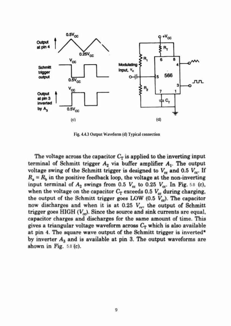
9
Fig. 4.4.3 Output Waveform (d) Typical connection

10

11
4.5 Timer IC LM 555
The 555 is a monolithic timing circuit that can produce accurate & highly stable
time delays or oscillation. The timer basically operates in one of two modes: either
(i) Monostable (one - shot) multivibrator or
(ii) Astable (free running) multivibrator
The important features of the 555 timer are these:
(i) It operates on +5V to +18 V supply voltages
(ii) It has an adjustable duty cycle
(iii) Timing is from microseconds to hours
(iv) It has a current o/p
(v) When the input is low:
The load current flows through the load connected between Pin 3 &
+Vcc in to the output terminal & is called the sink current.
(vi) When the output is high:
The current through the load connected between Pin 3 & +Vcc (i.e.
ON load) is zero. However the output terminal supplies current to the
normally OFF load. This current is called the source current.
PIN CONFIGURATION OF 555 TIMER:
Figure 4.5.1: Pin diagram of IC555 Timer

12
Pin 4: Reset:
The 555 timer can be reset (disabled) by applying a negative pulse to this pin.
When the reset function is not in use, the reset terminal should be connected to
+Vcc to avoid any false triggering.
Pin 5: Control voltage:
An external voltage applied to this terminal changes the threshold as well as trigger
voltage. In other words by connecting a potentiometer between this pin & GND, the
pulse width of the output waveform can be varied. When not used, the control pin
should be bypassed to ground with 0.01 capacitor to prevent any noise problems.
Pin 6: Threshold:
This is the non inverting input terminal of upper comparator which monitors the
voltage across the external capacitor.
Pin 7: Discharge:
This pin is connected internally to the collector of
transistor Q1. When the output is high Q1 is OFF.
When the output is low Q is (saturated) ON.
Pin 8: +Vcc:
The supply voltage of +5V to +18V is applied to this pin with respect to ground.
FUNCTIONAL BLOCK DIAGRAM OF 555 TIMER
Figure: 4.5.2: Functional Block Diagram of 555 Timer

13
From the above figure, three 5k internal resistors act as voltage divider providing
bias voltage of 2/3 Vcc to the upper comparator & 1/3 Vcc to the lower comparator.
It is possible to vary time electronically by applying a modulation voltage to the
control voltage input terminal (5).
(i) In the Stable state:
The output of the control FF is high. This means that the output is low
because of power amplifier which is basically an inverter. Q = 1; Output = 0
(ii) At the Negative going trigger pulse:
The trigger passes through (Vcc/3) the output of the lower comparator goes high
& sets the FF. Q = 1; Q = 0
(iii) At the Positive going trigger pulse: It passes through 2/3Vcc, the
output of the upper comparator goes high and resets the FF. Q = 0; Q = 1
The reset input (pin 4) provides a mechanism to reset the FF in a manner which
overrides the effect of any instruction coming to FF from lower comparator.
4.6 Monostable Operation:
Figure 4.6.1: connected as a Monostable Multivibrator
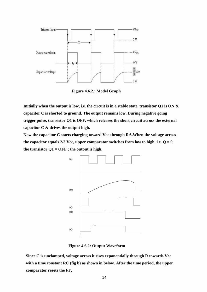
14
Figure 4.6.2.: Model Graph
Initially when the output is low, i.e. the circuit is in a stable state, transistor Q1 is ON &
capacitor C is shorted to ground. The output remains low. During negative going
trigger pulse, transistor Q1 is OFF, which releases the short circuit across the external
capacitor C & drives the output high.
Now the capacitor C starts charging toward Vcc through RA.When the voltage across
the capacitor equals 2/3 Vcc, upper comparator switches from low to high. i.e. Q = 0,
the transistor Q1 = OFF ; the output is high.
Figure 4.6.2: Output Waveform
Since C is unclamped, voltage across it rises exponentially through R towards Vcc
with a time constant RC (fig b) as shown in below. After the time period, the upper
comparator resets the FF,

15
i.e. Q = 1, Q1 = ON; the output is low.[i.e discharging the capacitor C to ground
potential (fig c)]. The voltage across the capacitor as in fig (b) is given by
Vc = Vcc (1-e-t/RC) ......... (1)
Therefore At t = T,
Vc = 2/3 Vcc 2/3 Vcc = Vcc(1-e-
RC)
or
T = RC ln (1/3)
Or
T = 1.1RC seconds .............. (2)
If the reset is applied Q2 = OFF, Q1 = ON, timing capacitor C immediately discharged.
The output now will be as in figure (d & e). If the reset is released output will still remain
low until a negative going trigger pulse is again applied at pin 2.
Applications of Monostable Mode of Operation:
(a).Frequency Divider:
The 555 timer as a monostable mode. It can be used as a frequency divider by adjusting the
length of the timing cycle tp with respect to the time period T of the trigger input. To use
the monostable multivibrator as a divide by 2 circuit, the timing interval tp must be a larger
than the time period of the trigger input. [Divide by 2 tp > T of the trigger]
By the same concept, to use the monostable multivibrator as a divide by 3 circuit, tp must
be slightly larger than twice the period of the input trigger signal & so on, [ divide by 3 tp >
2T of trigger]
Figure 4.6.3: Output Waveform

16
(b).Pulse width modulation:
Figure 4.6.3:Pulse Width Modulation
Figure 4.6.4:OutputWaveform
Pulse width of a carrier wave changes in accordance with the value of a incoming
(modulating signal) is known as PWM. It is basically monostable multivibrator. A modulating
signal is fed in to the control voltage (pin 5). Internally, the control voltage is adjusted to 2/3
Vcc externally applied modulating signal changes the control voltage level of upper
comparator. As a result, the required to change the capacitor up to threshold voltage level
changes, giving PWM output.
(a) Pulse Stretcher:
This application makes use of the fact that the output pulse width (timing interval) of the
monostable multivibrator is of longer duration than the negative pulse width of the input
trigger. As such, the output pulse width of the monostable multivibrator can be viewed as a
stretched version of the narrow input pulse, hence the name ― Pulse stretcher‖. Often,
narrow –pulse width signals are not suitable for driving an LED display, mainly because of
their very narrow pulse widths. In other words, the LED may be flashing but not be visible to

17
the eye because its on time is infinitesimally small compared to its off time. The 55 pulse
stretcher can be used to remedy this problem. The LED will be ON during the timing interval
tp = 1.1RAC which can be varied by
changing the value of RA &C.
Fig: Pulse Stretcher
Figure 4.6.5: Pulse stretcher
4.7 :The 555 timer as an Astable Multivibrator:
An Astable multivibrator, often called a free running multivibrator, is a rectangular wave
generating circuit. Unlike the monostable multivibrator, this circuit does not require an external
trigger to change the state of the output, hence the name free running. However, the time during
which the output is either high or low is determined by 2 resistors and capacitors, which are
externally connected to the 55 timer.
Figure 4.7.1: Astable Multivibrator

18
Figure 4.7.2: Model Graph
The above figure shows the 555 timer connected as an astable multivibrator and its model graph
Initially, when the output is high:Capacitor C starts charging toward Vcc through RA & RB.
However, as soon as voltage across the capacitor equals 2/3 Vcc. Upper comparator triggers the
FF & output switches low.
When the output becomes Low:
Capacitor C starts discharging through RB and transistor Q1, when the voltage across C equals
1/3 Vcc, lower comparator output triggers the FF & the output goes High. Then cycle repeats.
The capacitor is periodically charged & discharged between 2/3 Vcc & 1/3 Vcc respectively.
The time during which the capacitor charges from 1/3 Vcc to 2/3 Vcc equal to the time the
output is high & is given by tc = (RA+RB)C ln 2… (1) Where [ln 2 = 0.69]
= 0.69 (RA+RB)C
Where RA &RB are in ohms. And C is in farads.
Similarly, the time during which the capacitors discharges from 2/3 Vcc to 1/3 Vcc is
equal to the time, the output is low and is given by,
tc = RB C ln 2
td = 0.69 RB C ...................(2)
where RB is in ohms and C is in farads.
Thus the total period of the output
waveform is T = tc + td = 0.69

19
(RA+2RB)C ..................................... (3)
This, in turn, gives the frequency of oscillation as,f 0 = 1/T = 1.45/(RA+2RB)C (4)
Equation 4 indicates that the frequency f 0 is independent of the supply voltage Vcc.
Often the term duty cycle is used in conjunction with the astable multivibrator. The
duty cycle is the ratio of the time tc during which the output is high to the total time
period T. It is generally expressed as a percentage.
%duty cycle = (tc / T )* 100
%DC = [(RA+RB)/ /(RA+2RB)] * 100
Astable Multivibrator Applications:
Square wave oscillator:
Figure 4.7.3: Square wave oscillator
With out reducing RA = 0 ohm, the astable multivibrator can be used to produce square
wave output. Simply by connecting diode D across Resistor RB. The capacitor C charges
through RA &diode D to approximately 2/3 Vcc & discharges through RB & Q1 until the
capacitor voltage equals approximately 1/3 Vcc, then the cycle repeats.
To obtain a square wave output, RA must be a combination of a fixed resistor & potentiometer
so that the potentiometer can be adjusted for the exact square wave.

20
(a) Free-running Ramp generator:
Figure 4.7.4: Free Running Ramp Generator
The astable multivibrator can be used as a free – running ramp generator
when resistor RA &RB are replaced by a current mirror.
The current mirror starts charging capacitor C toward Vcc at a constant rate.
When voltage across C equals to 2/3 Vcc, upper comparator turns transistor
Q1 ON & C rapidly discharges through transistor Q1.
When voltage across C equals to 1/3 Vcc, lower comparator switches
transistor OFF & then capacitor C starts charging up again..
Thus the charge – discharge cycle keeps repeating
The discharging time of the capacitor is relatively negligible compared to its charging time.
The time period of the ramp waveform is equal to the charging time & is
approximately is given by,
T = VccC/3IC .............................. (1) IC = (Vcc - VBE)/R = constant current
Therefore the free-running frequency of ramp generator is f 0 = 3IC/ Vcc C ...... (2)

21
Figure 4.7.5: Pulse Position Modultor
4.8 :SCHMITT TRIGGER
The use of 555 timer as B Sehmitt Trigger ia shown in Fig. 8.24. Here the
two internal coinparators are tied together and externally biased at YJ2
through 2t¿ and B$. Since the upper compazator will trip at !2/3 ) Vq and lower
compsrator at (1/3) Vq, the bias provided by R and RJ is centered within these

22
two thresholds,
Fig. 4.8.1: Timer in Schmitt Trigger Operation
Thus, a sine wave of sufficient amplitude (> V fi6 —- 2f 8 V„ — UJ2) tn
exceed the reference levels causea the internal flip-flop to alternately
set and reset, providing a aquare wave output a8 shown in Fig. 8.25,
Figure 4.8.2: Input output waveforms of Schmitt Tñgger
It may be noted that unlike conventional multivibrator, no frequency
division is taking place and frequency of square w•ve rerriairi6
the same as that of input signal.

23
Comparison of Monostable and astable multivibrator
S. No. Monostable multivibrator Astable multivibrator
1. It has only one stable state and one quasi
stable state
There is no stable state at all
2. Trigger is required for the operation change its
state from stable to quasi stable state
No trigger is required for change of state. Thus
called free-running.
3. Two components R and C are necessary with
IC555.
Three components RA, RB and C are
necessary with IC555.
4. The pulse width of quasi-stable state is given
by,
W=1.1 RC seconds
The frequency is given by,
f=1.44/ (RA+2RB) Hz
5. The frequency of operation is controlled by
frequency of trigger pulse applied.
The frequency of operation is controlled by RA,
RB and C.
6. The applications are, timer, frequency divider,
pulse width modulation etc.
The applications are, square wave generator,
flasher VCO, FSK generator etc.
Text Book References:
1. Ramakant A.Gayakwad, “0P-AMP and Linear ICs”, 4th Edition, Prentice Hall / Pearson
Education, 1994.
2. D.Roy Choudary, Shail Jain, “Linear Integrated Circuits”, New Age International Pvt.
Ltd., 2000.
3. Grey and Meyer, “Analysis and Design of Analog Integrated Circuits, 4th Edition, Wiley
International, 2001.
4. Michael Jacob, "Applications and Design with Analog Integrated Circuits, 2nd Edition,
Prentice Hall of India, 1993.
5. S. Salivahanan, V.S. Kanchana Bhaaskaran, “Linear integrated circuits”, 3rd Edition,
McGraw-Hill, 2011.
6. William D.StaneIy, “Operational Amplifiers with Linear Integrated Circuits”, 4th Edition,
Pearson Education, 2004.

24
Part – A
1. Define phase locked loop
2. Draw the block diagram of PLL
3. List the applications of PLL
4. What is Voltage Controlled Oscillator
5. What are the applications of IC555 Timer
6. Draw the circuit diagram of Astabel multivibrator
7. What is monostable multivibrator
8. Describe Frequency synthesizer
9. Describe FM Demodulator
10. Describe Frequency demodulator
Part –B
1. Explain the applications of PLL in detail
2. Explain the working principle of Voltage Controlled Oscillator
3. Demonstrate Astable multivibrator using IC555 Timer
4. Demonstrate Monostable Multivibrator using IC555 Timer
5. Explain Voltage Controlled Oscillator in detail
1
SCHOOL OF ELECTRICAL AND ELECTRONICS
DEPARTMENT OF ELECTRONICS AND COMMMUNICATION ENGINEERING
ANALOG INTEGRATED CIRCUITS – SECA1502
UNIT-V
SPECIAL FUNCTION ICS

2
5.1. Integrated circuit Tuned amplifier
The circuit shown in this section is an IC tuned amplifier that amplifies a signal over a narrow band of frequencies
centered at fr. here the input signal is applied through the tuned transformer T1 to the base of Q1. The load RL is connected
across the tuned transformer T2 in the collector circuit of Q3. The transistor Q1 and Q3 provides the amplification whereas
Q2 provides the control of magnitude of the gain. The combination of Q1 and Q3 acts as a common-emitter and common-
base cascade (CE-CB) pair. The input resistance and the current gain of a cascade pair are essentially the same as those of a CE
stage the output resistance is the same as that of a CB stage.
Fig. 5.1.Integrated Circuit tuned amplifier.
The voltage VAGC applied to the base of transistor Q2 is used to provide automatic gain control. The variation in VAGC
cause changes in the division of the current between transistors Q2 and Q3. When VAGC is greater than VR Q2 conducts more
than Q3, reducing voltage gain. On the other hand when VR greater than VAGC, Q3 conducts more than Q2, which increases
voltage gain.
VR greater than VAGC, Q2 is cut-off and the collector current of Q1 flows through Q3 providing maximum voltage gain
AV. the change in VAGC causes the change in the division of current and not the collector current of Q1. Thus the input
impedance of Q1 remains constant and the input circuit is not tuned.

3
The voltage V and resistance R establish the dc current ID1 through the diode D1. The voltage VBE1 is nearly equal to
VD1 and the collector current IC1 is within the ± 5% of ID1.
Advantages of tuned amplifiers:
1. Signal to noise ratio is good
2. They are suited for radio transmitters and receivers.
3. Required bandwidth of amplification can be selected
Disadvantages of tuned amplifiers
1. Inductors and capacitors of tuned amplifiers become bulky and costly.
2. As the band of frequency is increased, the design is complex.
3. They are not suitable for amplifying audio frequencies.
5.2 Instrumentation Amplifier
Many instruments use sensors (transducers) for measurement of temperature, pressure, weight, humidity, viscosity
etc. The sensors convert other form of energy to proportional electrical energy. But the sensor outputs are very low-level signals. These low-level signals cannot drive next stages of the system. And other external noises shall still reduce the signal level.
So to enhance such signals to desired level using a special amplifier with high CMRR, high input impedance, and low power
consumption termed Instrumentation amplifier.
The instrumentation amplifier is also called data amplifier and is a difference amplifier basically. The expression for its voltage
gain is in the form shown below,
Where
Vo = The amplifier output Voltage
V2 – V1 = Differential input voltage
oamplifier
Requirements of Instrumentation amplifier
1. Accurate and stable gain is the basic requirement. And the gain shall be finite.
2. Gain shall be easily adjusted and shall be precisely done.
3. High input impedance

4
4. Low output impedance
5. High CMRR
6. Low power consumption
7. Low temperature drifts
8. High Slew Rate
Two-op amp Instrumentation amplifier
The instrumentation amplifier with two op amp is shown below.
Fig. 5.2. Instrumentation amplifier using two op amps
The above circuit consists of two operational amplifiers A1 and A2.
Analysis:
For amplifier A1,
Node voltage at A shall be same as node B.
VA = VB = V2
Similarly for amplifier A2, Node voltage at E shall be same as node D.
VD = VE = V1

5

6
As the resistance R3 is variable, the circuit permits gain variation, precisely.
Advantages of two op amp Instrumentation amplifier
The instrumentation amplifier with two op amp has following advantages.
1. The gain variation is easy and precise
2. The CMRR value is completely independent of the setting of resistance R3. Hence with the precision ratios for
R2/R1, the gain can be changed without degrading the performance of the amplifier.
3. The resistance R3 is separate from the accurately matched resistances R1 and R2, which are required for symmetric
arrangement.
Limitations of two op amp Instrumentation amplifier
1. The problem is resistances R1 and R2 must be accurately matched.
2. The input V1 has to propagate through A2 before reaching A1. Due to this additional delay, common mode components
of the two signals will no longer cancel out with each other, at high frequencies. Thus symmetry of input is not there
where V1 has time delay than V2 to reach A1.
3. CMRR decreases with frequency because of the above asymmetrical input with time delay.
Three-op amp Instrumentation amplifier
The instrumentation amplifier with three op amp is shown below.
Fig. 5.2.2. Instrumentation amplifier using three op amps

7
The above circuit consists of three operational amplifiers A1, A2 and A3.
Since a non-inverting amplifier A3 is added to each of the basic difference amplifier inputs. The op-amps A1 and A2 are non-
inverting amplifiers forming first stage of the amplifier. The op-amp A3 is a difference amplifier forming an output stage of
the amplifier.
Analysis:
Fig. 5.2.3. Analysis of Three op-amp Instrumentation Amplifier
If the output of the op-amp A1
If the output of the op-amp A1 is V01 and op-amp A2 is V02,
Expression for V02, V01 in terms of V1, V2, Rf1, Rf2 and RG: From above Fig. 5.2.3 The node potential of op-amp A1 is
V1 thus node B shall also B and G are V1. The node D potential of op-amp A2 is V2. Node C and H potential is also V2.

8
Input current of Op-amp A1 and A2, are zero. Hence current I remain the same through Rf1, Rf2, and RG.
Applying ohms law between the nodes E and F, we get,

9
Advantages of three op-amp instrumentation amplifier.
Following are the advantages of three op-amp instrumentation amplifier circuit:
1. With the hep of variable resistor RG, the gain of the amplifier can be easily varied.
2. Gain depends on external resistances and hence can be adjusted accurately and made stable by selecting high
quality resistances.
3. The input impedance depends on the input impedace of non-inverting amplifiers which is extremely high.
5.3 Voltage Regulators
The voltage regulator in its simplest form consists of Voltage
reference, VR
Error amplifier
Feedback network
Active series or shunt control element
The voltage reference generates a voltage level which is applied to the comparator circuit, which is generally an error
amplifier. The second input to the error amplifier is obtained through feedback network. Generally using the potential divider,
the feedback signal is derived by sampling the output voltage. The error amplifier converts the difference between the
output sample and the reference voltage into an error signal. This error signal in-turn controls the active element of the
regulator circuit in order to compensate the change in the output voltage. Such an active element is generally a transistor.
5.3.1 Types of voltage regulators
Depending upon where the control element is connected in the regulator circuit, the regulators are basically classified as
Series voltage regulator
Shunt voltage regulator
Each type provides a constant d.c. output voltage which is regulated.
5.3.2 Advantages of IC voltage Regulators
1. Easy to use
2. It greatly simplifies power supply design
3. Due to mass production, low in cost
4. IC voltage regulators are versatile
5. Conveniently used for local regulation
6. These are provided with features lime built-in protection programmable output, current/voltage boosting, internal
short circuit current limiting etc.

10
5.3.3 Classification of IC voltage regulators
The IC voltage regulators are classified as shown in the figure below.
Fig. 5.3.3 Classification of IC regulators
5.3.4 Three terminal fixed voltage regulators
As the name suggest, three terminal voltage regulators have three terminals namely input which is unregulated
(Vin), regulated output (Vo) and common or a ground terminal. These regulators do not require any feedback connections.
The figure below shows the basic three terminal voltage regulators.
Fig.5.3.4. Basic regulator circuit (Three Terminals)
The capacitor Cin is required if regulator is located at appreciable distance more than 5 cm from a power supply
filter. The output capacitor Co may not be needed but if used it improves the transient response of the regulator i.e. regulator
response to the transient changes in the load. This capacitor also reduces the noise present at the output. The difference
between Vin and Vo (Vin – Vo) is called as dropout voltage and it must be typically 2.0V even during the low point on the
input ripple voltage, for the proper functioning of the regulator.

11
5.3.5 IC series of three terminal fixed voltage regulators
The popular IC series of three terminal regulators is A78XX and A79XX. The series A78XX is the series of three
terminal positive voltage regulators while A79XX is the series of three terminal negative voltage regulators. The
last two digits denoted as XX indicate the output voltage rating of the IC.
Such series is available with seven voltage options as indicated in table below.
Device
type
Output
voltage
Device
type
Output voltage
7805 5.0 V 7905 -5.0 V
7806 6.0 V 7906 -6.0 V
7808 8.0 V 7908 -8.0 V
7812 12.0 V 7912 -12.0 V
7815 15.0 V 7915 -15.0 V
7818 18.0 V 7918 -18.0 V
7824 24.0 V 7924 -24.0 V
The 79XX series voltage regulators are available with same seven options as 78XX series, as indicated in the above table.
In addition, two extra voltages – 2 V and – 5.2 V are also available with ICs 7902 and 7905.2 respectively.
These ICs are provided with adequate heat sinking and can deliver output currents more than 1 A. these ICs do not require
external components. These are provided with internal thermal protection, overload and short circuit protection.
The two series are available in various versions like low-power and high-power versions. The low-power versions are
available in plastic or metal packages, like small signal transistors. The higher power versions are packaged in TO-3
type metal cans or in TO-220 type moulded plastic packages like power transistors.
Fig. 5.3.5. Types of IC packages (Voltage Regulators)

12
5.4. Opto-coupler.
The combined package of an LED and a photo diode is termed as an optocoupler. It is otherwise called as opto-
isolator or optically coupled isolator.
Fig. 5.4.1. Basic Opto-coupler.
The source V1 and series resistance R1 decide the forward current I1 through the LED. Hence LED emits the light.
This light is incident on a photodiode. Due to this a reverse current is set up in the output circuit. This current produces a
drop across output resistance R2, the output voltage is the difference between the supply voltage V2 and the drop across
the resistor R2.
𝑉𝑜𝑢𝑡 = 𝑉2 − 𝐼2𝑅2
Now if input voltage is changed the amount of light emitted by LED changes. This varies the reverse current in the output
circuit and hence the output voltage. The output voltage is thus varying in step with the input voltage. This coupling between
LED and photodiode is hence called optocoupler. As the name suggest his device can couple an input signal to the output
circuit.
The figure 5.4.1 (a) shows the typical optoisolator. It consists of LED and phototransistor.
When the input voltage forward biases the LED light transmitted to the phototransistor turns it on resulting current
through the external load as shown in the fig. 5.4.2 (b).
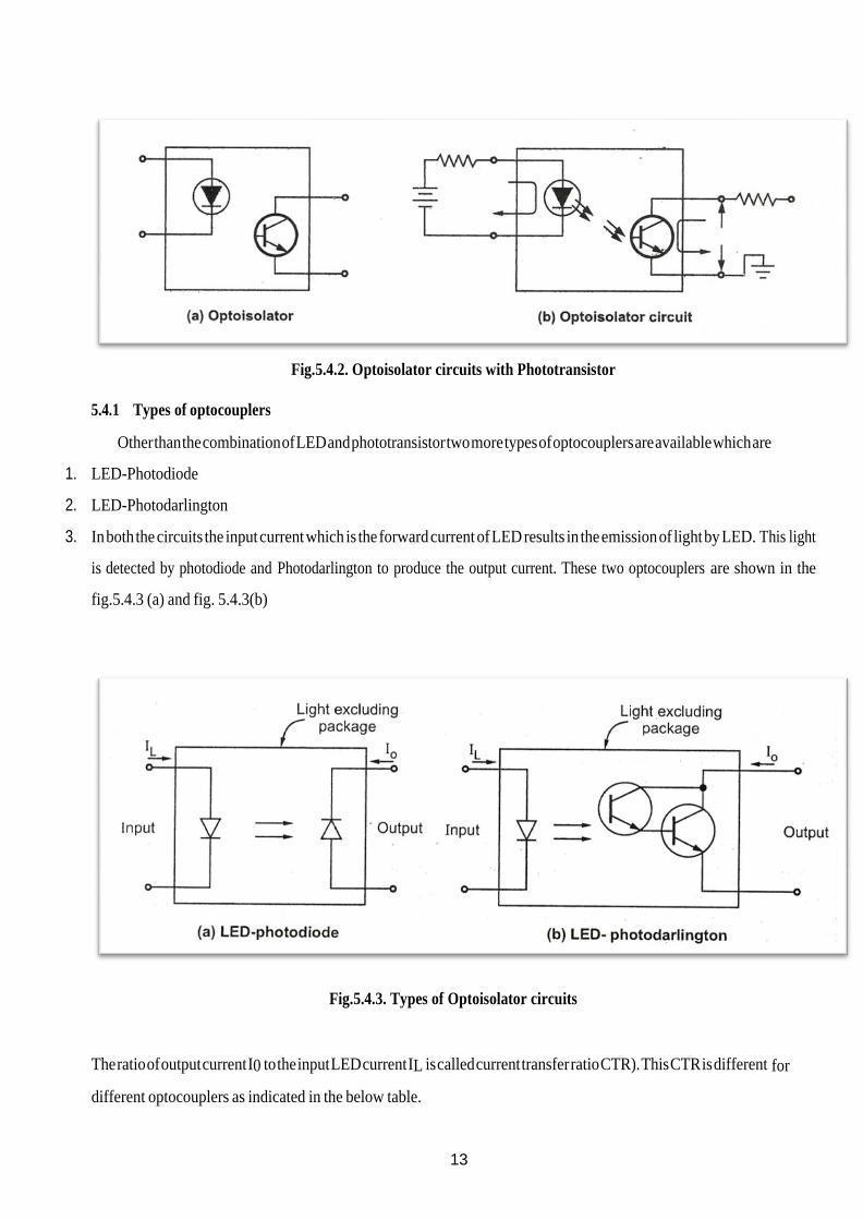
13
Fig.5.4.2. Optoisolator circuits with Phototransistor
5.4.1 Types of optocouplers
Other than the combination of LED and phototransistor two more types of optocouplers are available which are
1. LED-Photodiode
2. LED-Photodarlington
3. In both the circuits the input current which is the forward current of LED results in the emission of light by LED. This light
is detected by photodiode and Photodarlington to produce the output current. These two optocouplers are shown in the
fig.5.4.3 (a) and fig. 5.4.3(b)
Fig.5.4.3. Types of Optoisolator circuits
The ratio of output current I0 to the input LED current IL is called current transfer ratio CTR). This CTR is different for
different optocouplers as indicated in the below table.

14
Table. 5.4.1. Current transfer ratio (CTR) for different detectors
Device CTR
LED-Photodiode 0.01 – 0.03
LED-Transistor 0.1 – 1
LED-Darlington 1 - 5
The most important point of above devices is that a circuit connected to its input can be electrically fully isolated
from the output circuit and that a potential difference of hundreds or thousands of volts can safely exists between two circuits
without adversely influencing the optocoupler action.
5.4.2 Characteristics of optocoupler
Following are important characteristics of an optocoupler:
(i)Current transfer ratio (CTR) (v) Isolation voltage
(ii) Response time (vi)Common mode rejection
(iii)VCE (max) (vii) IL (max)
(iv)Bandwidth
1) Current transfer ratio (CTR):
The current transfer ration refers to the ratio of the output collector current (IC) to the input forward current (IF).
IC Current transfer ratio = × 100%
IF

15
The CTR greatly differs depending on the type of the phototransistor used in photocoupler. The photocoupler using
Darlington phototransistor can provide a relatively large collector current from a small input current the CTR also varies
with ambient temperature.
2) Isolation voltage(Viso) Between input and output:
Isolation voltage (Viso) between input and output is another important factor in choosing a photocoupler. This is
because photocouplers are often used for signal transmission between circuits that have different potentials or as
interfaces with actuator circuits which tend to generate impulsive voltage such as motor controllers or solenoid
driver circuits. Isolation voltage is specified in KVrms with a relative humidity of 40% to 60%.
3) Response time:
The response time of an optocoupler depends mainly on the output phototransistor. The response time also
depends on the input forward current and load resistance. Since load resistance has a greater influence on the
response time, careful setting is required while defining the circuit constant.
4) Common mode rejection:
While the photocouplers output is electrically isolated from its input for relatively low frequency signal an
impulsive input voltage may cause a displacement current (id =Cf. dv / dt) to flow due to the floating capacitance
(Cf) between the input and output of the optocoupler casing noise voltage to appear at the output.
5) VCE (max):
This is the maximum allowable d.c. voltage that can be applied across output transistor or output photodiode.
6) IL (max):
This is the maximum permissible d.c. current that can be allowed to flow in the input LED. Typical values vary
from 40 mA to 100 mA.
7) Bandwidth:
This is the maximum signal frequency that can be usefully passed through the optocoupler when device is
operated in its normal mode. Typical values vary from 20 KHz to 500 KHz.
The various advantages of optocouplers are,
1) The electrical isolation provides electrical insulation between input and output but data is transmitted from
input to output through beam of light.
2) The response time of optocouplers is so small that they transmit data in Megahertz range.
3) It is capable of transmitting wide-band signal.
4) Unidirectional signal transfer means that output does not loop back to the input circuit.
5) Easy interfacing with logic devices.
6) Compact and light weight.

16
7) Must faster than the isolation transformers and relays.
8) As signal transfer is unilateral changing load do not affect input.
5.5 CMOS Operational Amplifier
The bipolar op-amp IC 741 is capable of sourcing and sinking large load currents.
This is facilitated by the emitter-follower output stage which achieves very low output
resistance and this characteristic was used in IC 741 for minimising the loading effects.
The CMOS op-amps are normally designed for particular applications, wherein only a few
picofarads of capacitive load are required to be driven.
Therefore, the most of the CMOS op-amps do not require a low resistance output stage.
When the op-amp input terminals are not connected directly to the IC external terminals,
they do not need electrostatic input protection devices also.
The folded cascade op-amp involving a current mirror CMOS design is presented in this
section.
Op amps are an important component of modern CMOS IC’s. They used to designed as general
purpose amplifiers that can meet a variety of requirements. The main target was extremely high
gain (>1e5), high input impedance and low output impedance (like an ideal amplifier). This was
done (to some extent) at the expense of different aspects of performance (e.g., speed, output voltage
range, power, etc.). Designs these days are much more tailored to have (good enough) performance
w.r.t. the specific needs of particular applications. Within an IC, often use Operation
Transconductance Amplifiers (OTA).
5.5.1 Some performance parameters of op amps
– Gain and Bandwidth
• Want as large as possible
– Output Swing
• Maximize w.r.t. power supply (but supply shrinking in modern processes)
– Linearity
• Combat non-linearity with feedback
– Noise and Offset
• Can minimize by trading off other parameters

17
– Supply Rejection
• Strong dependence on current source output resistance
5.5.2 Simple One-Stage Op Amps Two differential pair amplifiers that we have already seen can be used as op amps.
The low-frequency, small-signal gain of both is gmN(roN||roP). The capacitive loads
(CL) usually determine their bandwidth
Figure 5.5.2: One Stage Op-amps
5.5.3Cascode Op Amps
In order to achieve higher gain, one can use cascoding. These amplifiers are often called
‘telescopic’ cascode amps. While gain increases, the output range of these devices are limited.
Figure:5.5.3: Two stage Op-amps

18
5.5.4 Folded Cascode Circuit
In order to alleviate some of the drawbacks of telescopic op amps (limited output
range), a “folded cascode” can be used (we analyzed this circuit in HW7)
– M1 is common-source transconductance amp and M2 is common-gate transimpedance amp
– Advantage is M2 no longer stacks on top of M1
– Possible for either pMOS or nMOS cascodes
• The output resistance for cascode and folded cascode are roughly equivalent (gmro2)
Figure 5.5.4: Folded Cascode Circuits
5.5.5.OPAMP SMALL SIGNAL AND DC ANALYSIS
The small signal differential voltage gain of the input stage is given by
Where r02 and r04 are the output resistance of transistors M2 and M4 respectively.
The input impedance of the second stage is infinite due to the gate-channel oxide insulator.
Therefore it results in zero loading effect by the second stage. Assuming the channel length
Parameter coefficient λ to be the same for all transistors, we have,
Where ID , the quiescent drain current in M2 and M4 and is given by ID = IQ/2
The gain of the second stage is

19
Text Book References:
1. Ramakant A.Gayakwad, “0P-AMP and Linear ICs”, 4th Edition, Prentice Hall / Pearson
Education, 1994.
2. D.Roy Choudary, Shail Jain, “Linear Integrated Circuits”, New Age International
Pvt. Ltd., 2000.
3. Grey and Meyer, “Analysis and Design of Analog Integrated Circuits, 4th Edition, Wiley
International, 2001.
4. Michael Jacob, "Applications and Design with Analog Integrated Circuits, 2nd Edition,
Prentice Hall of India, 1993.
5. S. Salivahanan, V.S. Kanchana Bhaaskaran, “Linear integrated circuits”, 3rd Edition,
McGraw-Hill, 2011.
6.William D.StaneIy, “Operational Amplifiers with Linear Integrated Circuits”, 4th Edition,
Pearson Education, 2004.

20
Part –A
1. Draw the circuit diagram of Integrated Tuned Amplifier
2. What is an instrumentation amplifier?
3. List out the applications of instrumentation amplifier
4. Define an optocoupler
5. Describe CMOS operational amplifier
6. Draw the circuit diagram of an instrumentation amplifier
7. What is Small signal Analysis?
8. List out the specifications of IC MC 14573.
9. Describe Monolithic voltage regulators
10. What is folded Cascode Circuit?
Part- B
1. Explain Instrumentation Amplifier in detail
2. Demonstrate Integrator Circuits Tuned Amplifier
3. Explain CMOS Operational Amplifier
4. Explain the specifications of IC MC 14573.
5. Explain optocoupler in detail


![Analog Electronic Circuits [15MEC31T ] Question Bank - Jain ...](https://static.fdokumen.com/doc/165x107/63160831aca2b42b580e172e/analog-electronic-circuits-15mec31t-question-bank-jain-.jpg)

