Certain Plastic Encapsulated Integrated Circuits - USITC
360
-
Upload
khangminh22 -
Category
Documents
-
view
0 -
download
0
Transcript of Certain Plastic Encapsulated Integrated Circuits - USITC


UNITED STATES INTERNATIONAL TRADE COMMISSION
COMMISSIONERS
Don E. Newquist, Chairman Peter S. Watson, Vice Chairman
David B. Rohr Anne E. Brunsdale Carol T. Crawford
Janet A. Nuzum
-
/
Address all communications to Secretary to the Commission
United States International Trade Commission Washington, DC 20436

UNITED STATES INTERNATIONAL TRADE COMISSION Washington, DC 20436
In the Hatter o f 1 )
CERTAIN PLASTIC ENCAPSULATED INTEGRATED CIRCUITS 1
1
NOTICE OF ISSUANCE AND C W E
Investigation No. 337-TA-315
OF LIMITED EXCLUSION ORDER AND DESIST ORDERS
AGENCY: U.S. International Trade Commission.
ACTION: Notice
S U W Y : Notice is hereby given that the Commission has issued a limited exclusion order and cease and desist orders in the above-captioned investigation.
FOR FURTHER INFORMTION CONTACT: Andrea C. Casson, Esq . , Office of the General Counsel, U.S. International Trade Commission, 500 E Street, S.W., Washington, D.C. 20436, telephone 202-205-3105.
SUPPLBHBNTARY INFORUTION: is contained in section 337 of the Tariff Act of 1930, as amended (19 U.S.C. g! 13371, and in section 210.58 of the Commission's Interim Rules of Practice and Procedure (19 C.F.R. § 210.58).
The authority for the Commission's determination
On July 9, 1990, Texas Instruments Incorporated (TI) filed a complaint under section 337 of the Tariff Act of 1930 (19 U.S.C. § 1337) alleging that respondents Analog Devices, Inc. (Analog), Integrated Device Technology, Inc. (IDT), LSI Logic Corporation ( L S I ) , VLSI Technology, Inc. (VLSI), and Cypress Semiconductor Corporation (Cypress), had imported and sold within the United States certain plastic encapsulated integrated circuits manufactured by a process covered by certain claims of U.S. Letters Patent 4,043,027 (the '027 patent). The Commission instituted an investigation of the complaint and issued a notice of investigation that was published in the August 15, 1990 (55 Fed. Reg. 33388).
on
On tctober 15, 1991, the presiding administrative law judge (ALJ) issued a final initial determination (ID) finding a violation of section 337 on the ground that certain of respondents' imported plastic encapsulated integratod circuits were manufactured by a procerr covered by claims 12 and 14 of the '027 patent. The ALJ found that the procepses used for manufacturing t h e m products Far not covered by claims 1 and 1Y of the '027 patent. In addition, he found that certain other plastic encapsulated integrated circuits imported by respondents (those encapsulated using a process called "same-side" gating) were not covered by claims 1, 12, 14, or 17 of the '027 patent.

On December 12, 1991, the Commission determined to review the issues of (1) claim construction m d infringement of claim 17 of the '027 patent and (2) whether the claims in controversy o f the '027 patent are invalid as obvious under 35 U.S.C. § 103. The Commission determined not to review the remainder of the ID. government agencies, and other persons concerning the.jssues under review and the issues of remedy, the public interest, and bonding.
The Commission solicited comments from the parties, interested
Complainant, all respondents, and the Commission investigative attorneys
No comments were filed by interested government filed briefs addressing the issues under review and the issues of remedy, the public ir.Lerest, and bonding. agen'.it 2 or other persons.
After review, the Commission affirmed the ALJ's determination that all respondents had violated section 337 in the importation of opposite-side gated plastic encapsulated integrated circuits manufactured by a process covered by claims 12 and 14 of the '027 patent. In addition, the Commission determined that respondents Analog and VLSI had violated section 337 in the importation of opposite-side gated plastic encapsulated integrated circuits manufactured by a process covered by claim 17 of the '027 patent.
Having determined that there is a violation of section 337, the Commission considered the questions of the appropriate remedy, whether the statutory public interest factors preclude the issuance of a remedy, and bonding during the Presidential review period. the appropriate form of relief is a limited exclusion order prohibiting all respondents from importing plastic encapsulated integrated circuits manufactured abroad by a process covered by claims 12 and 14 of the '027 patent, and additionally prohibiting respondents Analog and VLSI from importing plastic encapsulated integrated circuits manufactured abroad by a process covered by claim 17 of the '027 patent. determined to issue cease and desist orders directed to each respondent. Commission also determined that the public interest factors enumerated in 19 U.S.C. § 1337(d) do not preclude the issuance of the aforementioned relief, and that the bond during the Presidential review period covering infringing products imported or sold by respondents Cypress, IDT, L S I , and VLSI shall be in the amount of 2.5 percent of the entered value of the imported articles concerned, not to exceed SO. 50 per plastic encapsulated integrated circuit. The Commission further determined that respondent Analog will not be required during the Presidential review period to post a bond for products imported or sold.
*
The Commission determined that
The'Commission further The
Copies of the Comission's orders and all other nonconfidential documents filed in connection with this investigation are available for inspection during official business hours (8:45 a.m. to 5:15 p.m.1 in the Office of :he Secretary, U.S. International Trade Commission, 500 E Street, S.W., Wash-ngton, D.C. 20436, telephone 202-205-2000. Hearing-impaired
-2-
persons are advised that information on this matter can be obtained by contacting the Commission's TDD terminal on 202-205-1810.
By order of the Commission.
.=, Kenneth R. Mason
Secretary
Issued: February 18, 1992


UNITED STATES INTERNATIONAL TRADE COMMISSION Washington, DC 20436
In the Matter o f 1
INTEGRATED CIRCUITS 1
1 Investigation No. 337-TA-315 CERTAIN PLASTIC ENCAPSULATED 1
ORDER
The Commission, having determined that there is a violation of section
337 of the Tariff Act of 1930 (19 U.S.C. § 1337) in the unlawful importation
and sale of certain plastic encapsulated integrated circuits manufactured
abroad according to a process, which, if practiced in the United States, would
be covered by claims 12, 14, and 17 of U.S. Letters Patent 4,043,027, and
having considered the issues of remedy, the public interest, and bonding,
hereby ORDERS that--
1. according to a process covered by claims 12 or 14 of U.S. Letters Patent 4,043,027, and manufactured o r imported by or on behalf of Analog Devices, Inc. (Analog), Integrated Device Technology, Inc. (IDT), LSI Logic Corporation (LSI), VLSI Technology, Inc. (VLSI), or Cypress Semiconductor Corporation (Cypress) or any of their affiliated companies, parents, subsidiaries, licensees, or other related business entities, or their successors or assigns, are excluded from entry into the United States f o r the remaining term of the patent, except under license of the patent owner or as provided by law.
Plastic encapsulated integrated circuits manufactured abroad
2. Plastic encapsulated integrated circuits manufactured abroad according to a process covered by claim 17 of U.S. Letters Patent 4,043,027, and manufactured or imported by or on behalf of Analog or VLSI, or any of their affiliated companies, parents, subsidiaries, licensees, or other related business entities, or their successors or assigns, are excluded from entry into the United States for the remaining term of the patent, except under license of the patent owner or as provided by law.
3. according to a process covered by claims 12 o r 14 of U.S. Letters Patent 4,043,027, assembled onto circuit boards or other similar carriers, and manufactured or imported by or on behalf of Analog, IDT, LSI, VLSI, or
. . Plastic encapsulated integrated circuits manufactured abroad

Cypress or any of their affiliated companies, parents, subsidiaries, licensees, or other related business entities, or their successors or assigns are excluded from entry into the United States for the remaining term of the patent, except under license of the patent owner or as provided by law.
4 . according to a process covered by claim 17 of U.S. Letters Patent 4,043,027, assembled onto circuit boards o r other similar carriers, and manufactured or imported by or on behalf of Analog or VLSI, or any of their affiliated companies, parents, subsidiaries, licensees, or other related business entities, o r their successors o r assigns are excluded from entry into the United States for the remaining term of the patent, except under license of the patent owner or as provided by law.
5. The provisions of this order do not apply- to downstream products (u., computers, computer peripheral devices, telecommunications equipment, other electronic equipment, or finished components thereof.)
Plastic encapsulated integrated circuits manufactured abroad
6. Texas Instruments, Inc.
The provisions of this order do not apply to products licensed by
7. by a process covered by claims 12, 14, o r 17 of U.S. Letters Patent 4,043,027 and which are manufactured o r imported by or on behalf of Analog, IDT, LSI, VLSI, or Cypress shall be permitted entry into the United States if the manufacturer or importer provides a certification to. accompany the commercial invoice (whether filed electronically or otherwise) stating: [Name of Manufacturer/Importerl certifies that the plastic encapsulated integrated circuits that accompany this invoice either (i) are not made by a process covered by claims 12, 14, or 17 of U.S. Letters Patent 4,043,027, or (ii) are covered by a license.
Plastic encapsulated integrated circuits which are not manufactured
8. and manufactured or imported by or on behalf of IDT, LSI, VLSI, or Cypress are entitled to entry into the United States under bond in the amount of 2.5 percent of the entered value of the article, not to exceed $0.50 per plastic encapsulated integrated circuit, after this Order is received by the President, pursuant to subsection (j) of section 337 of the Tariff Act of 1930, until such time as the President notifies the Commission that he approves or disapproves this action, but no later than 60 days after the date of receipt of this Order by the President.
The plastic encapsulated integrated circuits ordered to be excluded
9. The plastic encapsulated integrated circuits ordered to be excluded and manufactured or imported by or an behalf of Analog are entitled to entry into the United States without bond, after this Order is received by the President, pursuant to subsection Cj) of section 337 of the Tariff Act of 1930, until such time as the President notifies the Commission that he approves or disapproves this action, but no later than 60 days after the date of receipt of this Order by the President.
-2-
10. Products identified in paragraphs (3) and ( 4 ) of this Order are entitled to entry into the United States from the day after this Order is received by the President, pursuant to subsection (j) of section 337 of the Tariff Act of 1930, until such time as the President notifies the Commission that he approves or disapproves this action, but no later than 60 days after the date of receipt of this Order by the President, subject to any bond requirements set forth in paragraph 8. Persons importing such products shall certify to the best of their knowledge the number of plastic encapsulated integrated circuits subject to this Order contained in such products, pursuant to procedures to be specified by the U . S . Customs Service.
11. In accordance with 19 U.S.C. 5 1337(1), the provisions of this Order shall not apply to plastic encapsulated integrated circuits imported by and for the use of the United States, o r imported for, and to be used for, the United States with the authorization or consent of the Government.
12. The Commission may amend this Order in accordance with the procedure described in section 211.57 of the Commission’s Interim Rules of Practice and Procedure (19 C.F.R. § 211 .57) .
13. The Secretary shall serve copies of this.0rder upon each party of record in this investigation and upon the Department of Health and Human Services, the Department of Justice, the Federal Trade Commission, and the U.S. Customs Service.
14. Notice of this Order shall be published in the Federal Register.
By order of the Commission.
Issued: February 18, 1992
Secretary
-3-


UNITED STATES INTERNATIONAL TRADE COHHISSION Washington, DC 20436
1 In the Matter o f )
) Investigation No. 337-TA-315
INTEGRATED CIRCUITS 1 CERTAIN PLASTIC ENCAPSULATED 1
ORDER TO CEASE AND DESIST
IT IS HEREBY ORDERED THAT AnAlog Devices, Inc., One Technology Way,
Norwood, Massachusetts, 02062-4700, cease and desikr'from any unlicensed
importing, selling for importation, assembling, testing, marketing,
distributing, offering f o r sale, selling, or otherwise transferring (except
for exportation) in the United States of imported plastic encapsulated
integrated circuits made by a process covered by claims 12, 14, or 17 of U.S.
Letters Patent 4,043,027, in violation of section 337 of the Tariff Act of
1930, as amended, 19 U.S.C. S 1337.
I.
(Definitions)
As used in this Order:
(A) "Commission" shall mean the United States International Trade
Commission.
(B) "Complainant" shall mean Texas Instruments, Inc., P.O. Box 225474,
13500 North Central Expressway, Dallas, Texas 75265.
(C) "Respondent" shall mean Analog Devices, Inc., One Technology Way,
Norwood, Massachusetts, 02062-4700.
(D) "Person" shall mean an individual, or any non-governmental

partnership, firm, association, corporation, o r other legal o r business entity
other than the above Respondent o r its majority owned and/or controlled
subsidiaries, their successors, cr assigns.
(E) "United States" shall mean che fifty States, the District of
Columbia, and Puerto Rico;
( F ) "Covered product" shall mean any "opposite-side gated" plastic
encapsulated integrated circuit manufactured abroad according to a process
which, if practiced in the United States, would infringe claims 12, 14, o r 17
of U . S . Letters Patent 4,043,027.
I1
(Applicability)
The provisions of this Cease and Desist Order shall apply to Respondent
and to its principals, stockholders, officers, directors, employees, agents,
licensees, distributors, controlled (whether by stock ownership o r otherwise)
and/or majority owned business entities, successor&"and assigns, and to each
of them, in accordance with Section VI1 hereof.
I11
(Conduct Prohibited)
The following conduct of Respondent in the United States is prohibited
by this Order:
to do s o , import o r sell for importation into the United States, assemble,
test, market, distribute, offer for sale, sell, o r otherwise transfer (except
fo r exportation) in the United States covered products, for the remaining term
of U.S. Letters Patent 4,043,027.
Respondent shall not, except to the extent that it is licensed
-2-

IV
(Conduct Permitted)
Notwithstanding any other provision of this Order, specific conduct
otherwise prohibited by the terms of this Order shall be permitted if, In a
written instrument, Complainant licenses o r authorizes such specific conduct,
or suck 52ecific conduct is related to the importation o r sale o f covered
products by or for the United States.
V
(Reporting)
Respondent shall submit quarterly reports during the period commencing
on February 18, 1992, and extending through the remaining term of U.S. Letter
Patent 4,043,027. The first report of Respondent shall be submitted within 60
days of the issuance of this Order. Thereafter, reports shall be submitted
within 21 days of the close of each quarter.
continue in force until the expiration of U.S. Letters Patent 4,043,027 on
This reporting requirement shall
August 23, 1994 unless, pursuant to subsection Cj) of section 337 o f the
Tariff Act of 1930, the President notifies the Commission within 60 days after
the date he receives this Order, that he disapproves this Order. . ... Respondent shall report to the Commission its importation and sales in
the United States, including licensed sales, measured in units, of covered
products, .f any, during the reporting period in question.
Any failure to report shall constitute a violation of this Order.
VI
(Recordkeeping and Inspection)
(A) For the purpose of securing compliance with this Order, Respondent
shall retain any and all records relating to the sale, offer for sale,
-3-

marketing, o r distribution in the United States of covered products, made and
received in the usual and ordinary course of business, whether in detail o r in
summary form, for a period of two years from the close of the fiscal year to
which they pertain. Respondent shall also retain any and all records
regarding licensed importation o r sale of covered products.
(B) For the purposes of determining or securing compliance with this
Order and for no other purpose, and subject to any privilege recognized by the
Federal Courts of the United States, duly authorized representatives of the
Commission shall, upon reasonable written notice by the Commission o r its
staff, be permitted access:;and the right to inspect and copy in Respondent's
principal offices during office hours, and in the presence of counsel or other
representatives if Respondent so chooses, all book;;" ledgers, accounts,
correspondence, memoranda, financial reports, and other records and documents,
both in detail and in summary form, for the purpose of verifying any matter o r
statement contained in the reports required to be retained under subparagraph
VI(A) of this Order.
VI1
(Service of Cease and Desist Order)
Respondent is ordered and directed to:
(A) Serve, within thirty (30) days after the effective date of this
Order, a copy of this Order upon each of its respective officers, directors,
managing agents, agents and employees who have any responsibility for the
marketing, distribution, or sale of covered products in the United States;
(B) Serve, within thirty (30) days after the succession of any persons
referred to in subparagraph VII(A1 o f this Order, a copy of the Order upon
each successor; and
-4-

(C) Maintain such records as will show the name, title, and address of
each person upon whom the Order has been served, as described in subparagraphs
VII(A) and VII(B) of this Order, together with the date on which service was
made.
The obligations sec forth in subparagraphs VII(3) and VII(C) snall
remain in effect until the date of expiration of U.S. Letters Patent
4,043,027.
VI11
(Confidentiality)
Information obtained by means provided for in Sections V and VI of this
Order will be made available only to the Commission and its author zed
representatives, will be entitled to confidential treatment, and will not be
divulged by any authorized representative of the Commission to any person
other than duly authorized representatives of the Commission, except as may be
required in the course of securing compliance with this Order, or as otherwise
required by law.
without ten (10) days prior notice in writing to Respondent.
I ... Disclosure hereunder will not be made by the Commission
(Enforcement)
Violation of this Order may result in any of the actions specified in
section 211.56 of the Commission's Interim Rules of Practice and Procedure, 19
C.F.R. 5 211.56, including an action for civil penalties in accordance with
section 337(f) of the Tariff Act of 1930, 19 U.S.C. 5 1337(f), and any other
action as the Commission may deem appropriate.
Respondent is in violation of this Order , the Commission may infer facts
adverse to Respondent if Respondent fails to provide adequate or timely
information.
In determining whether
-5-

X
(Modification)
The Commission may amend this Order on its own motion or in accordance
with the procedure described in section 211.57 o f the Commission’s Interim
Rules of Practice and Procedure, 19 C . F . R . 5 211.57.
XI
(Bonding 1
The conduct prohibited by Section I11 of this Order may be continued by
Respondent during the period in which this Order is under review by the
President pursuant to section 337 ( j ) of the Tariff Act of 1930 (19 U.S.C. 5
1337 ( j ) ) without the necessity to post a bond.
By order sf the Commission.
2 G L Kenneth R. Mason
Secretary
Issued: February 18, 1992

UNITED STATES INTERNATIONAL TRADE COWHISSIOM Washington, DC 20436
1 In the Matter of 1
1 Investigation No. 337-TA-315
INTEGRATED CIRCUITS 1 CERTAIN PLASTIC ENCAPSULATED )
ORDER TO CEASE AND DESIST
IT IS HEREBY ORDERED THAT Integrated Device Technology, Inc., 2975
Stender Way, Santa Clara, California 95054; LSI Logic Corporation, 1551
McCarthy Boulevard, Milpitas, California 95035: VLSI Technology, Inc., 1109
McKay Drive, San Jose, California 95131; and Cypress Semiconductor
Corporation, 3901 North First Street, San Jose, California 95134-1599, cease
and desist from any unlicensed importing, selling for importation, assembling,
testing, marketing, distributing, offering for sale, selling, or otherwise
transferring (except for exportation) in the United- States of imported plastic
encapsulated integrated circuits made by a process covered by claims 12 or 14
o f U.S. Letters Patent 4,043,027, in violation o f section 337 of the Tariff
Act of 1930, as amended, 19 U.S.C. 5 1337.
IT IS FURTEER ORDERED THAT VLSI Technology, Inc., 1109 McKay
Drive, San Jose, California 95131 cease and desist from any unlicensed
importing, selling for importation, assembling, testing, marketing,
distributing, offering for sale, selling, or otherwise transferring (except
for exportation) in the United States of imported plastic encapsulated
integrated circuits made by a process covered by claim 17 of U.S. Letters

Patent 4,043,027, in violation of section 337 of the Tariff Act of 1930, as
amended, 19 U.S.C. 5 1337.
I.
(Definitions)
As used in this Order:
(A) "Commission" shall mean the United States International Trade
Commission.
(B) "Complainant" shall mean Texas Instruments, Inc., P.O. Box 225474,
13500 North Central Expressway, Dallas, Texas 75265.
(C) "Respondent$" shall mean Integrated Device Technology, Inc., 2975
Stender Way, Santa Clara, California 95054; LSI Logic Corporation, 1551
McCarthy Boulevard, Milpitas, California 95035; VLSI Technology, Inc., 1109
McKay Drive, San Josel California 95131; and Cypress Semiconductor
Corporation, 3901 North First Street, San Jose,
(D) "Person" shall mean an individual, or
partnership, firm, association, corporation, or
California 95134-1599.
any non-governmental
other legal or business entity
other than the above Respondents or their majority owned and/or controlled
subsidiaries, their succgssors, or assigns.
(E) "United State&" shall mean the fifty States, the District of I
Columbia, and Puerto Rico;
(F) "Covered product" shall mean any "opposite-side gated" plastic
encapsulated integrated circuit manufactured abroad according to a process,
which, if practiced in the United States, would infringe claims 12 or 14 of
U.S. Letters Patent 4,043,027. With respect to respondent VLSI Technology,
Inc., "covered product" shall additionally include any "opposite-side gated"
-2-

plastic encapsulated integrated circuit manufactured abroad according to a
process, which, if practiced in the United States, would infringe claim 17 of
U.S. Letters Patent 4,043,027.
I1
(Applicability)
The provisions of this Cease and Desist Order shall apply to Respondents
and to their principals, stockholders, officers, directors, employees, agents,
licensees, distributors, controlled (whether by stock.ownership or otherwise)
and/or majority owned business entities, successors and assigns, and to each
o f them, in accordance with Section VI1 hereof.
I11
(Conduct Prohibited)
The following conduct of Respondents in the United States is prohibited
Respondents shall not.import _ _ I or sell for importation into the by this Order:
United States, assemble, test, market, distribute, offer for sale, sell, or
otherwise transfer (except for exportation) in the United States covered
products, for the remaining term of U.S. Letters Patent 4,043,027.
IV
(Conduct Permitted)
Notwithstanding any other provision of this Order, specific conduct
otherwise prohibited by the terms of this Order shall be.permitted if, in a
written instrument, Complainant licenses or authorizes such specific conduct,
or such specific conduct is related to the importation or sale of covered
products by o r f o r the United States.
-3-

V
(Reporting)
Respondents shall each submit quarterly reports during the period
commencing on February 18, 1992, and extending through the remaining term of
U.S. Letters Patent 4,043,027.
submitted within 60 days of the issuance of this Order.
shall be submitted within 21 days of the close of each quarter.
reporting requirement shall continue in force until the expiration of U.S.
Letters Patent 4,043,027 on August 23, 1994, unless, pursuant to subsection
(j) of section 337 of the Tariff Act of 1930, the President notifies the
Comission within 60 days after the date he receives this Ordw, that he
disapproves this Order.
The first reports Qf Respondents shall be ..
Thereafter, reports
This
Respondents shall scch report to the Commission their importation and
sales in the United States, measured in units, of covered pr!oducts, if any,
during the reporting period in question.
Any failure to repgrt shall constitute a violation o f this Order.
VI
(Recordkeeping and Tnspeqtion)
(AI For the purpose of securing compliance with this order, Respondents
shall retain any and all records relating to the sale, offer for sale,
ma'rketing, or distribution in the United States of covered products, made and
received in the usual and ordinary course of business, whether in detail or in
summary form, for a period of two years from the close of the fiscal year t9
which they pertain.
-4-

(B) For the purposes of determining or securing compliance with this
Order and for no other purpose, and subject to any privilege recognized by the
Federal Courts of the United States, duly authorized representatives of the
Commission shall, upon reasonable written notice by the Commission or its
staff, be permitted access and the right to inspect and copy in the principal
offices of Respondents during office hours, and in the presence o f counsel or
other representatives if Respondents so choose, all books, ledgers, accounts,
correspondence, memoranda, financial reports, and other records and documents,
both in detail and in summary form, for the purpose of verifying any matter or
statement contained in the reports required to be retained under subparagraph
VI(A) of this Order.
VI I
(Service of Cease and Desist Order)
Respondents are ordered and directed to:
(A) Serve, within thirty (30) days after the effective date of this
Order, a copy of this Order upon each of their respective officers, directors,
managing agents, agents, and employees who have any responsibility for the
marketing, distribution, or sale of covered products in the United States;
(B) Serve, within thirty (30) days after the succession of any persons
referred to in subparagraph VII(A) of this Order, a copy of the Order upon
each successor; and
(C) Maintain such records as will show the name, title, and address of
each person upon whom the Order has been served, as described in subparagraphs
VII(A) and VII(B) of this Order, together with the date on which service was
made.
-5-

The obligations set forth in subparagraphs VII(B) and VII(C) shall
remain in effect until the date of expiration of U.'S. Letters Patent
4,043,027.
VI11
(Confidentiality)
Information obtained by means provided for in Sections V and VI of this
Order will be made available only to the Commission and its authorized
representatives, will be entitled to confidential treatment, and will not be
divulged by any authorized representative of the Commission to any person
other than duly authorized representatives of the Commission, except as may be
required in the course of securing compliance with this Order, or as otherwise
required by law. Disclosure hereunder will not be made by the Commission
without ten (10) days prior notice in writing to the Respondent affected.
IX
(Enforcement)
Violation of this Order may result in any of the actions specified in
section 211.56 of the Commission's Interim Rules of Practice and Procedure, 19
C.F.R. 8 211.56, including an action for civil penalties in accordance with
section 337(f) of the Tariff Act of 1930, 19 U.S.C. 8 1337(f), and any other
action as the Commission may deem appropriate. In determining whether a
Respondent is in violation of this Order, the Commission may infer facts
adverse to a Respondent if,the Respondent fails to provide adequate or timely
information.
-6-

X
(Modification)
The Commission may amend this Order on its own motion or in accordance
with the procedure described in section 211.57 of the Commission's Interim
Rules of Practice and Procedure, 19 C.F.R. E 211.57.
XI
( Bonding 1
The conduct prohibited by Section IIT of this Order may be continued
during the period in which this Order is under review by the President
pursuant to section 337(j) of the Tariff Act of 1930 (19 U.S.C. 5 1337(j)),
subject to the posting of a bond in the amount of 2.5 (two and one half)
percent of the entered value of the articles in question, not to exceed $0.50
per plastic encapsulated integrated circuit.
apply to conduct that is otherwise permitted by Section IV of this Ordor.
This bond provision does not
Infringing products imported on or after February 18, 1992, are subject to the
entry bond as set forth in the limited exclusion order issued by the
Commission on February 18, 1992, and are not subjekt to this bond provision.
The bond is to be posted in accordance with the procedures established
by the Commission for the posting of bonds by complainants in connection with
the issuance of temporary exclusion orders.
210.58, 19 C.F.R. 5 210.58. The bond and any accompanying documentation is to
See Commission Interim Rule
be provided to and approved by the Commission prior to the commencement of
conduct which is otherwise prohibited by Section I11 of this Order.
The bond is to be forfeited in the event that the President approves, or
does not disapprove within the Presidential review period, the Commission's
-7-

Orders of February 18, 1992, or any subsequent final order issued after the
completion of Investigation 337-TA-315, unless the U.S. C w r t of Appeals for
the Federal Circuit, in a final judgment, reverses any Commission final
determination and order on appeal, or unless the products subject tg this bond
are exported or destroyed, and certification to that effect satisfactory to
the Commission is provided.
The bond is to be released in the event the President disappFoves this
Order and no subsequent order is issued by the Commission and approved, or not
disapproved, by the President, upon service on Respondents df an Order issued
by the Commission based upon application therefor made to th& Commission.
By order of the Commission. .
Kenneth R. MatWti Secretary
Issued: February 18, 1992
-8-

PUBLIC VERSION
UNITED STATES INTERNATIONAL TRADE COMMISSION Washington, DC 20436
1 In the Matter o f 1
1 CERTAIN PLASTIC ENCAPSULATED INTEGRATED CIRCUITS 1
Investigation No. 337-TA-315
COMMISSION OPINION ON ISSUES UNDER REVIEW AND ON REMEDY, THE PUBLIC INTERBST, AND BONDING'
PROCEDURAL HISTORY
The Commission instituted this investigation on August 7, 1990, in
response to a complaint filed by Texas Instruments, Inc. (TI) of Dallas,
Texas.2
violation of section 337 of the Tariff Act of 1930, as amended (19 U.S.C. §
The investigation was instituted to determine whether there was a
1337), in the importation and sale of certain plastic encapsulated integrated
circuits that are manufactured, produced, and assembled by means of a process
that infringes one or more of claims 12, 14 and 17 of U.S. Letters Patent
4,043,027 (the '027 patent). The patent was issued on August 23, 1977, and
expires on that date in 1994.
The notice of investigation named the following firms as respondents:
(1) Analog Devices, Inc. (Analog), a Massachusetts corporation with its principal place of business in Norwood, Massachusetts;
(2) Integrated Device Technology, Inc. (IDT) , a Delaware corporation with its principal place of business in Santa Clara, California;
Commissioners Nuzum and Watson did not participate. 55 Fed. Reg. 33388 (August 15, 1990).

COW1 DENTI AL 1 NFORM AT1 0 N DELETED
(3)
( 4 )
(5)
PUBLIC VERSION 2
LSI Logic Corporation (LSI), a Delaware corporation with its principal place of business in Milpitas, California;
VLSI Technology, Inc. (VLSI), a Delaware corporation with its principal place of business in San Jose, California: and
Cypress Semiconductor Corporation (Cypress), a Delaware corporation with its principal place of business in San Jose, c ~ I i fornia .
On January 9, 1991, the presiding Commission administrative law judge
(ALJ) issued an initial determination (ID) (Order No. 17) designating the
investigation "more complicated," pursuant to section 337(b) (1) of the Tariff
Act of 1930. In that ID, he also granted TI's motion to amend the complaint
and notice of investigation to include claim 1 of the '027 patent. The
Commission determined not to review the ID.4
The ALJ conducted an evidentiary hearing from May 13 to May 22, 1991.
Respondents defended against TI's complaint on the grounds that the claims o f
the '027 patent are invalid for obviousness, are not infringed, and there is
no domestic industry. In addition, respondent Analog contended that TI was
equitably estopped from maintaining this section 337 action against it in
light of a license agreement between TI and [
] after this investigation was instituted.
On October 15, 1991, the ALJ issued his final ID in the investigation.
He found a violation of section 337 of the Tariff Act of 1930, on the ground
that respondents had imported and sold certain plastic encapsulated circuits
(those encapsulated using a process called "opposite-side" or "bottom" gating)
which infringed claims 12 and 14 of the '027 patent. He found that those
For the purposes of this Opinion, IDT, LSI, VLSI, and Cypress are
56 Fed. Reg. 4851 (Feb. 6, 1991). collectively referred to as "the California respondents."

PUBLIC VERSION 3
imported integrated circuits did not, however, infringe claims 1 or 17 of the
patent. In addition, he found that certain other accused integrated circuits
(those encapsulated using a process called "same-side" or tttoptt gating) did
not infringe claims 1, 12, 14, or 17.
The ALJ concluded that the '027 patent was not invalid for obviousness,
and he further found that there exists a domestic industry which practices the
'027 patent, including claims 12 and 14.
With respect to Analog's license argument, the ALJ found that Analog had
a partial license for part of the period of time during which this
investigation has been pending.'
this license was not grounds for dismissal of the investigation against
He concluded, however, that the existence of
Analog, because Analog did not have a license when the investigation was
instituted and because the license is limited to a certain dollar amount of
sales.
On December 2, 1991, the Commission issued a notice that it had
determined to review the issues of (1) construction and infringement of claim
17 of the '027 patent and (2) obviousness under 35 U.S.C. 8 103.' The
Commission determined not to review the remainder of the ID.'
the portions of the ID to be reviewed, the Commission indicated particular
With regard to . * ..
interest in the following issues:
1. Whether the ALJ erred in construing the language of claim 17, "electrical connections between electrical terminals of the device
' ID at 104. ID at 105. 56 Fed. Reg. 64643 (Dec. 11, 1991).
' The ID'S conclusions with respect to those issues that the Commission determined not to review have become the determinations of the Commission. 19 C.F.R. 8 210.53(h).

PUBLIC VERSION 4
2.
and a plurality of conductors arranged s;ibstantially parallel to one another," as requiring that each of the conductors be substantially parallel to all the other conductors. erred in construing claim 17, what is the correct construction of that claim, and given that construction, (i) is the claim infringed by any of respondents' llopposite-side" gated imported products, and (ii) is the claim practiced by the domestic industry.
If the ALJ
Whether the ALJ erred, as a factual matter, in finding that none of respondents' imported products infringe claim 17 of the '027 patent, as claim 17 was construed by the ALJ. Specifically, the parties are asked to identify any imported products in evidence in which all conductors are arranged substantially parallel to one another, and further, to address whether such products are encapsulated by a process which uses "opposite-side" gating. requested to brief the issue of whether claim 17, as construed by the ALJ, is practiced by the domestic industry.
The parties are also
3. Whether respondents have shown by clear and convincing evidence that the '027 patent is invalid for obviousness under 35 U.S.C. 5 103. In particular, the parties are asked to address: (1) the differences between the claimed invention as a whole and the prior art, as that prior art has been identified by the ALJ, and (2) the objective indicia of nonobviousness, with citations to relevant evidence of record. With respect to commercial success, the parties are requested to brief the issue of whether the ALJ's reliance on pre-1975 information is prejudicial to respondents and, if so, whether the Commission's reliance on pre-1975 information would be prejudicial, in light of this opportunity to readdress commercial success.
The Commission's notice requested that the parties file briefs
discussing the issues under review, and solicited comments from the parties,
interested government agencies, and any other persons concerning the issues of
remedy, the public interest, and bonding.
Complainant, all respondents, and the Commission investigative attorneys
(IAs) filed briefs and reply briefs addressin? both the issues under review

PUBLIC VERSION 5
and remedy, the public interest, and bonding.g No comments were filed by
interested government agencies or other persons.
BACKGROUND
TI is the owner by assignment of the '027 patent, which is entitled
"Process for Encapsulating Electronic Components in Plastic." The patent was
issued on August 23, 1977, and expires on that date in 1994. The history of
the patent, however, dates back to December 16, 1963, when inventors Robert 0.
Birchler and E. W. Williams filed the grandparent patent application. On
October 17, 1968, the inventors filed a divisional application (the parent
application), which was followed by the filing of a continuation application
on July 30, 1973. It is this latter application which matured into the '027
patent on August 23, 1977.
The '027 patent has 17 claims, but TI has alleged infringement of only
four of those claims--claims 1, 12, 14, and 17.'' The patent relates
generally to the manufacture of semiconductors. It claims a process for
encapsulating delicate electrical circuit devices through the use of transfer
molding.
Transfer molding is the rapid injection of liquid plastic under pressure
to encapsulate a product secured in a mold. A thermosetting plastic (h, a
plastic that melts with the application of heat and then hardens upon cooling)
In connection with the review phase, Analog and the California respondents requested oral argument. not believe oral argument was necessary. reply brief at 12, n.16. briefed, and that oral argument was unnecessary. Commissioner voted in favor of granting the requests for oral argument, C.F.R. 9 210.56(a), and the requests therefore have been denied.
determined not to review that finding.
TI and the IAs indicated that they did TI'S reply brief at 25, n.29; IAs'
We believe that the issues involved were thoroughly No participating
19
lo The ALJ found no infringement of claim 1, and the Commission

PUBLIC VERSION 6
is melted in a cylinder and then "transferred1' or forced out of the cylinibr
through pipelike runners into one or more mold cavities. The transfer of the
plastic occurs under controlled pressure and velocity conditions. The device
to be encapsulated is held or supported in the cavity and the plastic is made
to flow around the device and encapsulate it.
encapsulated device is removed from the mold and the process is repeated with
another device.
After hardening, the
Transfer molding was first introduced in 1926.
manufacturers of semiconductors (principally diodes and transistors) had begun
an industry-wide drive to develop low cost, mass-produced transistors that
could be sold inexpensively and used in many applications.
effort, industry leaders sought to improve upon their costly existing method
o f encapsulation, called the "header and can process,1' which contributed
significantly to the selling price of several dollars per transistor.
expense of this encapsulation process was due largely to the need to protect
the delicate "whisker wires" used to connect the terminals of the transistor
with conductor leads to the external circuitry.
According to the claimed process, a semiconductor wafer is attached to
By the early 1960s,
As part of this
The
three conductor wires, and electrical contact is made between an active region
of the wafer and one conductor wire.
between the other active wafer regions and the other conductor wires.
trimming, the wafer, whisker wires, and conductor wires are enclosed in a mold
cavity. One end of the conductor wires is clamped to the exterior of the mold
Whisker wire leads provide contact
After
to prevent movement.
encapsulate the device. The specification of the '027 patent states:
Liquid plastic is then injected into the mold cavity to

PUBLIC VERSION 7
An important aspect of the invention is the manner in which the fluid plastic material is gated into the mold so as to prevent damage to the delicate whisker wire leads and transistor wafer. In general, this entails introducing the material into a portion of the mold cavity remote from the transistor device and whisker wire leads, and generally parallel to the whisker wire leads. l1
Following encapsulation, the conductor wires may be severed or the lead
frame assembly trimmed.12
Some encapsulated integrated circuits are sold individually to
manufacturers of electronic products. Others are used in the fabrication of
circuit boards, which also are sold to manufacturers of electronic equipment.
The integrated circuits accused of being encapsulated by a process that
infringes the '027 patent include a variety of devices, e., static random
access memories ( S W s ) , microprocessors, digital signal processors, logic
devices, erasable programmable read only memories (EPROMs) , programmable l og ic
devices, application specific integrated circuits (ASICs), and cache devices.
DISCUSSION
ISSUES UNDER REVIEW
A. Construction of Claim 17
Claim 17 states that the encapsulation process, inter alia, comprises:
providing electrical connections between electrical terminals of the device and a plurality of conductors arranged substantially parallel to one another
13 . . . .
l1 Patent at column 2 , lines 41-47. l2 Patent at column 8, lines 13-24, figure 10. l3 Col. 14, lines 8-10.

PUBLIC VERSION 8
The ALJ construed the "plain meaning" of this language to require that each of
the conductors be substantially parallel to the other conductors .14
rejected TI's argument that the claim requires only that at least two of the
conductors be substantially parallel to each other.
that TI's construction of the term "plurality" would read out of the claim the
"to one another" limitation, l5
He
In this regard, he noted
Respondents submit that the ALJ correctly construed claim 17 to require
that all the conductors used be parallel to one another.
Analog argues that the ALJ's construction is the only one that is
consistent with the specification and drawings, in which the three conductors
shown are all parallel to one another. Analog argues that the ALJ correctly
found that, in the context of claim 17, "plurality" must refer to all the
conauctors in the lead frame to which an integrated circuit is connected.
Analog agrees with the ALJ that any other interpretation would be inconsistent
with the "parallel to one another" language.
patent's specification and drawings disclose a three-conductor support
Analog also notes that the '027
connected to the three terminals of the transistor, with each conductor
parallel to each of the others.
conductors has to be equal to the number of terminals used in the integrated
Analog agrees with the ALJ that the number of
circuit to which the conductors are connected,16 and that this "plurality@' of
conductors is defined in claim 17 as being arranged "substantially parallel to
one another.
l 4 ID at 15-16. I
l5 Id. According to Analog, if only two of the three transistor terminals
were confiected to conductors, the structure would be inoperative.

PUBLIC VERSION 9
Analog also argues that the plain meaning of the language of claim 17
requires that the conductors be substantially parallel over their entire
lengths, not just over a portion, even a substantial portion, of their
lengths.
Both TI and the IAs seek reversal of the ALJ's finding that the
"plurality" language in claim 17 requires that "all" conductors be arranged
substantially parallel to one another.
covers processes which have at least two conductors that are substantially
parallel to each other.
support their arguments.
llcomprising" in the preface to claim 17. They note that "comprising" is a
term of art used in claim drafting to designate an open-ended claim, which
covers all the elements set forth in the body of the claim while permitting an
unlimited number of additional, unrecited elements. Based on this language,
the IAs argue that the "plain language" indicates that parallelism among all
the conductors used is not required.
another" phrase indicates that the conductors must be parallel to other
conductors, as opposed to being parallel to the lead frame, sides of the mold,
or some other structure.
According to TI and the IAs, claim 17
Both refer to standard patent drafting rules to
The IAs point to the use of the transition word
The IAs further suggest that the "to one
- & ..
According to TI, the term "plurality" is a term of art in patent claims
TI argues that the llsubstantially parallel" that means at "least two."
language "simply describes the basic (and necessary) arrangement of conductors
in all semiconductor devices," b., substantially parallel to one another as
opposed to intersecting one another.
In response to the IAs' argument concerning the use of the phrase
Analog argues that the "comprising" language is open-ended as to

PUBLIC VERSION 10
each of the four process steps set out in claim 17, but for each of these
processes, the elements defining the process constitute structural
limitations.
case in which the Court held that the transitional phrase, "which comprises,"
did not exclude additional unrecited elements of the process claim in that
case, but also did not affect the scope of the particular structural
limitation recited within the process claim's step. l7
process would infringe the claim as long as it followed at least the four
steps of the process, or if it followed the four steps plus additional steps.
But the elements of each of the four processes are explicit and not open-
ended.
a structural limitation essential to the claim.
In support of its argument, Analog cite to a Federal Circuit
Under this analysis, a
As such, according to Analog, the parallelism requirement constitutes
We affirm the ALJ's construction of this claim to require parallelism
Even using TI'S definition of plurality to mean among all conductors used.
"two or more," the claim is worded to provide for electrical connections
between device terminals and ''a plurality of conductors" (not a plurality of
- the conductors) "arranged substantially parallel to one another." The claim
language in question thus allows for use of two or more conductors, but does
not, as TI and the IAs posit, require parallelism only between any two of the
conductors used.
As the ALJ found, it is significant that the claim recites the
requirement that the conductors be parallel to "one another," rather than
recite that any one conductor be parallel to another conductor. The IAs have
argued that the "one another" language sin??,'ly means that the conductor should
l7 Moleculon Research CorD. v. CBS. .inc., 793 F.2d 1261, 1271 (Fed. Cir. 1986).

PUBLIC VERSION 11
be parallel to another conductor, as opposed to another structure such as the
lead frame. That analysis begs the point, because the claim in question does
not address the relationship of the conductors to the lead frames or other
structures.
The ALJ's construction is further buttressed, as Analog suggests, by the
specification and drawings, which show all conductors arranged parallel to one
another.
apparent that the word "plurality" is used to indicate that two or more
conductors may be used, not that only two need meet the parallelism
requirement.
connections are provided between the electrical terminals of the device and
sa plurality of conductors arranged in a substantially common plane."
has argued that only two of the conductors used need be arranged in a common
place, Rather, all of the two or more conductors used must be arranged in a
common plane.
In addition, when the patent is read in its entirety, it becomes
For example, claim 14 claims a process in which electrical
No one
We also agree with Analog that the patent term "comprising,11 as used in
claim 17, is open-ended only as to the four process steps covered by the
claim, and that the requirements within each step constitute structural
limitations. As such, the parallel requirement for the conductors is not met
simply by aligning two (but not all) of the conductors parallel to each other.
Rather, however many conductors are used must be parallel to one another.
The testimony of TI's own witness supports the ALJ's construction of the
term When asked the meaning of "substantially parallel ," TI's
witness, Dr. Seiling, responded:
Substantially parallel is shown U,A che claim chart. Each of the individual conductors as they appear on

PUBLIC VERSION 12
the x-ray are parallel to their closest neighbor. (Emphasis supplied.) Tr. 449
With respect to the meaning of "substantially parallel," no party has
pointed to any testimony or exhibits of record that are particularly helpful
in construing this language.I8 The ALJ did not expressly address this
question, but suggested that the claim requires parallelism among all
conductors "over a significant portion of their lengths ."" Upon review, TI urges that "substantially parallel" be construed to mean
"not perpendicular. While one dictionary definition of "parallel" is "not
perpendicular," that definition is inconsistent with the specification and
drawings of the '027 patent, in which the conductors are at all points
equidistant from one another. Moreover, construing "parallel" to mean "not
perpendicular" would render the modifier '8substantially" meaningless. The use
of "substantially" reasonably contemplates a slight departure from a perfectly
parallel arrangement, u., by a small bend in the conductors or by a small
portion of the structure containing nonparallel (but also nonperpendicular)
conductors. Given the absence of contrary evidence in the record on this
question, the ALJ's construction is the most reasonable. We find, therefore,
As noted above, TI'S witness, Dr. Seiling, was asked to define this term, but gave a response which addressed the "plurality" question rather than the meaning of "substantially" parallel. Tr. 449. When asked to explain the term "substantially parallel," conductors as they appear on the x-ray are parallel to their closest neighbor. '' Tr . 449.
l9 See ID at 30, 36, 137 (FF A 132, 133). It was not necessary for the ALJ to explicitly rule on the meaning of "substantially parallel," because he found as a factual matter that although S O L ~ of respondents' products have a lead arrangement in which many of the leads are parallel over a significant portion of their lengths, none have all of their leads parallel over a significant portion of their lengths. configuration that, the ALJ found that none based of respondents' products infringe claim 17. ID at 30.
he stated that "each of the individual
Thus, it was on the basis of this

PUBLIC VERSION 13
that the term requires that the conductors be parallel over a significant
portion of their lengths.
B. Infringement of claim 17 by respondents' opposite-side gated Droducts
The ALJ found that respondents' --side gated products did not
He found that infringe any of the claims in issue of the '027 patent.
respondents' oDposite-side gated products infringed claims 12 and 14, but not
claims 1 and 17, as those claims were construed by him. Further, as noted, he
found no infringement of claim 17 because "none of the respondents' products"
arrange the conductors so they are all substantially parallel.20
findings of fact,-the ALJ similarly stated that "[rlespondents' products do
not incorporate conductors all of which are substantially parallel to one
another. In making this finding, he referenced numerous exhibits submitted
by Ti illustrating accused products.
physical evidence, that "Cslome products of the California Respondents have a
lead arrangement in which many of the leads are parallel over a significant
portion of their lengths. 1122
In his
The ALJ did find, based upon the
With the exception of the parallelism requirement, the requirements of
claim 17 are all contained in claim 14, which we, in adopting the ALJ's
findings and conclusions regarding construction and infringement of claim 14,
have found was infringed by all respondents. Accordingly, the only remaining
infringement question with respect to claim 17 is whether the respondents'
products are manufactured by a process in which the parallelism requirement,
properly construed, is met,
*O ID at 36. 21 FF A 133 (ID at 137). 22 ID at 30.

PUBLIC VERSION 14
In our notice of review, we requested that the parties brief the
question of whether, as a factual matter, the ALJ erred in the conclusion that
none of respondents' products infringed claim 17, even as that claim was
construed by the ALJ.
pin PDIPs~~ and SOICS~~ imported by at least two of the respondents--Analog and
VLSI--infringe claim 17 as construed by the ALJ.
that these products have all their conductors arranged parallel over a
significant portion of the conductors' length.
requested that the parties "identify any imported products in evidence in
which all conductors are arranged substantially parallel to one another," the
only exhibit specifically identified by TI and the IAs is CX-205, which
illustrates Analog's 8-pin PDIP. Analog expressly concedes that its 8-pin
T C I P illustrated in CX-205 employs a lead frame in which all the leads are
parallel ," and does not disagree that other respondents' low-pin-count
integrated circuits (b., those with less than 8 leads) are manufactured by a
process that infringes claim 17.26
TI and the IAs state that the opposite-side gated 8-
Specifically, it is alleged
Although our notice of review
In light of the uncontested evidence that claim 17 reads on at least the
Analog 8-pin PDIP device depicted in CX-205, we find that Analog has infringed
that claim. In addition, the California respondents have indicated that the
23 PDIP stands for Plastic Dual Inline Package. 24 SOIC stands for Small Outline Integrated Circuit. 25 Analog's main brief at 4. 26 Analog's reply brief at 6.
that they do not use lead frames in which all conductors are arranged substzntially parallel to one another. To show this, they attach drawings (from Exhibits 65-67) of several "representative lead frames." California respondents' main brief'at 38. concerning claim 17, noting that their encapsulation processes, including lead configurations, are "essentially the same" as Analog's. Id. and reply brief at 30.
The California respondents cursorily state
However, they adopt Analog's arguments

CO NFlDENTlAL INFORMATION DELETED
PUBLIC VERSION 15
encapsulation processes used by them, inclading lead configurations, are
essentially the same as analog'^.^' There is uncontested evidence in the
record (the testimony of VLSI’s witness) that respondent VLSI also imports
into the United States an 8-pin PDIP.?’ In light of the California
respondents‘ admission that their processes and leq? configurations are
essentially the same as Analog’s, and the clear evidence of parallel leads in
Analog’s 8-pin PDIP and the evidence that VLSI has also imported an 8-pin
PDIP, we find that VLSI has also violated section 337 by importing plastic
encapsulated integrated circuits that infringe claim 17 of the ‘027 patent.
Given the absence of evidence that Cypress, IDT, or LSI import 8-pin or
lower integrated circuits, we affirm the ALJ’s finding that these respondents
have not infringed claim 17 of the ‘027 patent.
C. Domestic Industry
a. Background
The Omnibus Trade and Competitiveness Act of 1988 (OTCA) amended section
337 of the Tariff Act of 1930 to specify the types of unfair acts covered by
that section.?’ As amended, section 337 explicitly prohibits the importation
and sale of imported articles that -- .-
(i> infringe a valid and enforceable United State: patent . . .; or
” California respondents‘ main brief at 37-38. The parties agree that the types of plastic encapsulated integrated circuits likely to have all conductors parallel to each other are those with low-pin counts. main brief at 9; Analog‘s main brief at 5-6 and reply brief at 6.
See TI‘S
26 CPX-3 (Deposition o f [
29 Under the amended statute, there is no requirement to show injury to ] 1 at 25-27, 32-35 and Ex. 3).
the domestic industry in cases involving alleged infringement of patents (including process patents), copyrights, registered trademarks, or mask works.

PUBLIC VERSION 16
(ii) are made, produced, processed, or mined under, or by means of, a process covered by the claims of a valid and enforceable United States patent.
19 U.S.C. 0 1337 (a)(l)(B).
In order to prove a violation of section 337 in a patent-based case, a
complainant must show that an industry exists in the United States practicing
the patent. Specifically, there can be a violation of section 337 -- only if an industry in the United States, relating to the articles protected by the patent, . . . exists or is in the process of being established.
19 U.S.C. 5 1337(a)(2).
In cases involving alleged infringement of statutory intellectual
property rights, section 337(a) (3) defines domestic industry as follows:
(a) (3) . . . an industry in the United States shall be considered to exist if there is in the United States, with respect to the articles protected by the patent, copyright, [registered] trademark, or mask work concerned--
(A) equipment;
significant investment in plant and
(B) capital; or
significant employment of labor or
(C) substantial investment in its exploitation, including engineering, research and development, or licensing.
19 U . S . C . 5 1337 (aI(3).
Thus, this section 337 investigation requires a determination as to
whether a domestic industry exists, that is, whether the complainant is
exploiting or practicing the patent in controversy. See Certain Doxorubicin
grid Preparations Containine Same, USITC Inv. No. 337-TA-300, Commission
Opinion (Public Version) at 21 (May 2, 1991).

PUBLIC VERSION 17
The ALJ applied the domestic industry criteria set out in section
337(a)(3) to find that TI's domestic activities are sufficient to demonstrate
the existence of a domestic ind~stry.~' He found that TI practices the '027
patent at its domestic facility,"
claims 12 and 14 of the '027 patent at its domestic fa~ility.~'
and that TI is specifically practicing
He based this
finding on the agreement among witnesses that TI and the respondents use the
same or similar processes, coupled with his finding that respondents use an
encapsulation process covered by claims 12 and 14.
infringement of claim 17, he did not make a finding regarding TI's practice of
claim 17.
Because the ALJ found no
As noted, the parties agree that the types of plastic encapsulated
integrated circuits likely to have all conductors parallel to each other are
L ,lid,, a - 4 vith low-pin counts. Respondents argue that because TI did not
introduce into evidence any lead frames produced in the United States which
include parallel leads and "because TI has never manufactured low-pin count
integrated circuits (i.e. less than 8 leads) at its domestic facility," TI
does not practice claim 17.33
manufacture low-pin count package types at its domestic facility. 34
TI admits that it is does not presently
30 ID at 82-92. 31 ID at 93-94. 32 ID at 94. 33 U. Analog incorrectly states that the ALJ found that TI does not
practice claim 17. Analog's reply brief at 6. The ALJ did find that TI's domestic facility currently encapsulates package types consisting of 20 or more pins. ID at 248 (FF E 54).
34 TI's main brief at 9.

PUBLIC VERSION 18
TI and the IAs argue, however, that the Commission's finding that the
domestic industry practices claims 12 and 14 is sufficient for the Commission
to find a violation of section 337 based on infringement of claim 17.
In addressing domestic industry, we are mindful that the statute
requires only that any one of the three criteria set out in section 337(a) (3)
be met in order to satisfy the domestic industry requirement.
respect, we note that we have adopted, inter alia, the ALJ's factual findings
In this
and conclusions regarding the existence of a domestic industry as evidenced by
TI's engineering and research and development efforts.35
"it is difficult in situations such as that presented in this investigation to
As the ALJ found,
draw a bright line dividing those projects which exploit the patent at issue
from those which to not."36 Likewise, it is equally, if not more difficult to
segregate those projects that exploit claims 12 and 14 of the patent, but not
claim 17.
there is no bright line separating the research and development efforts
Given the close similarity and overlap among these three claims,
relating to one of these claims from those relating to the others.
We accordingly find that TI's research and development efforts represent
a substantial investment in exploitation of all claims found infringed,
including claim 17.
specifically whether the claims that are infringed must be the ones that are
practiced by the domestic industry in order for there to be a violation of
section 337 .37
3y virtue of this finding, it is unnecessary to decide
35 & ID at 85-86 and FF E 1- E 257. 36 ID at 86. 37 The IAs argue that the language of section 337 and the legislative
history of the 1988 amendments support the view that where the domestic (continued. . . )

PUBLIC VERSION 19
D. Validity: Obviousness under 35 U.S.C. § 103
a. Legal Standards
A patent is presumed valid. 35 U.S.C. § 282. The burden of proving
invalidity is on the party asserting it and must be met by clear and
convincing evidence. Hvbritech. Inc. v. Monoclonal Antibodies. Inc., 231 USPQ
81 (Fed. Cir: 1986).
" ( , . .continued) industry practices some of the claims of a patent, a respondent's infringement of any of the claims of that patent provides a basis for finding a violation of section 337. The IAs note that the statute emphasizes infringement and practice of the patent, rather than infringement and practice of the individual claims of the patent. the statute referring to infringement of a U.S. patent (19 U.S.C. § 1337(a) (l)(B) (i)); the requirement that an industry exist in the United States "relating to the articles protected by the patent," (Id. at 8 1337(a) (2 ) ) ; and the domestic industry requirements "with respect to the articles protected by the Datent" (Id. at § 1337(a)(3)).
Specifically, the IAs quote the language of
In making this argument, the IAs question several IDS or orders in which Commission ALJs have held that there must be "claim correspondence," u., that a violation of section 337 can be based on a particular claim only if the dcmestic industry practices that claim. ComDositions, Inv. No. 337-TA-285, ID (Order No, 25) (March 22, 1989). See also, Certain Heaw-Dutv Mobile ScraD Shears, Inv. No. 337-TA-252, ID at 44- 45 (Feb. 12, 1990); Certain Concealed Cabinet Hinges and Mounting Plates, Inv. No. 337-TA-289, ID at 108 (Sept. 28, 1989); Certain Scanning Multiple-Beam Eaualization Svstems for Chest Radiographv and Components Thereof, Inv. No. 337-TA-326, Order No. 20 at 3-4 (Aug. 5, 19911, Order No. 23 (Aug. 20, 1991). Only in Chemiluminescent Compositions, however, did the presiding ALJ determine that the lack of claim correspondence failed to provide a sufficient basis for the existence of a domestic industry. 16. and was not appealed to the Federal Circuit. Commission's determination by virtue of the Commission's decision not to review it.
Certain Chemiluminescent
&e Order No. 25 at 90, n.
The ID did, however, become the The claim correspondence requirement was not reviewed by the Commission
In light of our determination that there is a domestic industry meeting each claim at issue we need not determine whether claim correspondence is necessary to establish the existence of a domestic industry. notes, however, that, in a future investigation, it may be necessary to evaluate the propriety of a claim correspondence approach to the domestic industry analysis and fully consider the rationale set forth by the presiding ALJ in Chemiluminescent Compositions.
The Commission

PUBLIC VERSION 20
A patent is invalid if the claimed invention does not satisfy the
requirement for nonobviousness found in 35 U.S.C. 5 103. Section 103 provides
in relevant part that:
A patent may not be obtained though the invention is not identically disclosed or described as set forth in I 102 of this title, if the differences between the subject matter sought to be patented and the prior art are such that the subject matter as a whole would have been obvious at the time the invention was made to a person having ordinary skill in the art to which said subject matter pertains.
The leading decision on obviousness is that of the Supreme Court in
Graham v. John Deere Co., 383 U.S. 1 (19661, which sets out four factors which
must be considered: (1) the scope and content of the prior art; (2) the
differences between the prior art and the claimed invention; (3) the level of
uiillrihry skill in the pertinent art; and (4) objective evidence of
nonobviousness (the so-called "secondary considerations"). With these facts
determined, the ultimate inquiry was described by the Federal Circuit in
Panduit Corporation v. Dennison Manufacturing Co., 1 USPQ2d 1593, 1595-96,
(Fed. Cir. 1987) as follows:
With the involved facts determined, the decisionmaker confronts a ghost, i.e., lra person having ordinary skill in the art," not unlike the "reasonable man" and other ghosts in the law. To reach a proper conclusion under section 103, the decisionmaker must step backward in time and into the shoes worn by that "person" when the invention was unknown and just before it was made. decisionmaker must then determine whether the patent challenger has convincingly established, 35 U.S.C. Q 282, that the claimed invention as a whole would have Seen obvious at that time to that person. 103. nature of law than of fact, for it is an ultimate conclusion based on a foundation formed of all the probative facts.
In light of all the evidence, the
35 U.S.C. Q The answer to that question partakes more of the

PUBLIC VERSION 21
~ When the party asserting invalidity relies upon a combination of prior
art references to establish obviousness, that party bears the burden of
showing some teaching or suggestion in those references which supported their
use in combination to render the claimed invention obvious. Ashland Oil. Inc,
v. Delta Resins and Refractories, 776 F.2d 281, 293, 297; 227 USPQ 657 (Fed.
Cir. 1985), cert. denied, 475 U.S. 1017 (1986). The problem confronted by the
inventor must be considered in determining whether it would have been obvious
I to combine references in order to resolve the problem. Diversitech Con. v.
Century Stew. Inc., 850 F.2d 675, 679 (Fed. Cir. 1988). It is impermissible
to pick and chose from among p r i o r art references to recreate a suggestion of
the claimed invention. SmithKline Diannostics.Inc. v. Helena Labs Corp., 859
F.2d 878, 886-87 (Fed. Cir. 1988).
All evidence, including relevant evidence concerning "secondary
considerations" of nonobviousness, must be considered before reaching a
conclusion on obviousness or nonobviousness. Lindemann Maschinenfabrik GMBH
v , American Hoist and Derrick Co., 730 F.2d 1452, 1461 (Fed. Cir. 1984);
Ashland Oil, 776 F.2d at 306, As stated in Stratoflex. Inc. v. AeroauiD
CorD., 713 F.2d 1530, 1539 (Fed. Cir. 1983):
Enroute to a conclusion on obviousness, a court must not stop until all pieces of evidence on that issue have been fully considered and each has been given its appropriate weight. the way, some pieces will weigh more heavily than others, but decision should be held in abeyance, and doubt maintained, until all the evidence has had its say. . . . It is error to exclude [evidence on "secondary considerations"] from consideration.
Along
Secondary considerations of nonobviousness include commercial success, long-
felt need, the failure of others to solve the problem in question, commercial
acquiescence (u. , licensing) , professional approval , and copying. See
generally, 2 CHISUM, PATENTS, Q 5.05 (1991).

PUBLIC VERSION 22
When a patentee asserts that one or more of the secondary considerations
support its contention of nonobviousness, the patentee bears the burden of
coming forth with evidence sufficient to constitute a prima facie case of
nexus between the merits of the claimed invention and the evidence offered,
Demaco CorD. v. F. Von Langsdorff Licensing Ltd., 851 F.2d 1387, 1392 (Fed.
Cir. 1988); Stratoflex, 713 F.2d at 1539. If the patentee has presented a
prima facie case of nexus, the burden of coming forward with rebuttal evidence
shifts to the party asserting obviousness. Demaco, 851 F.2d at 1393.
b. Discussion
i. Scope and content o f Drior art
As an initial matter, we affirm the ALJ's finding that the operative
date for determining which references constituted prior art is September
i G ( j 5 . 3 8 We also adopt his findings as to which references constitute prior
art. The following references constitute prior art that must be considered in
our obviousness analysis : 39
(a) The Doyle Process
The Doyle process is claimed in U.S. Letters Patent 3,367,025, which was
assigned to M~torola.~' The patent is entitled "Method for Fabricating and
Plastic Encapsulating a Semiconductor Device." It issued on February 6, 1968,
38 The ALJ found that the constructive date of invention for the '027 patent was December 16, 1963, the date on which the grandfather patent application was filed. However, based upon corroborated evidence that TI had used the invention for production in September 1963, the ALJ found that the patent was actually reduced to practice- (h, invented) in that month. 52-53.
ID at
39 In our notice of review, we requested the parties to address "the differences between the claimed invention as a whole and the prior art, that Drior art has been identified bv the ALJ.ll
40 Rx 011.

PUBLIC VERSION 23
based on an application filed in January 15, 1964.
proceeding , 4 1 the U.S. Patent Office's Board of Patent Interferences
determined that Doyle's invention had been conceived and reduced to practice
"well prior" to the filing of the grandparent application of the '027
application.
certain claims (1, 3, 4, and 6) of his patent. Thus, it is Doyle's process,
upon which his patent is based, which is the "prior art" to be compared with
the process claimed in the '027 patent.
In an interference
The Board awarded Doyle priority of invention with respect to
In the process disclosed by the Doyle patent, the plurality of conductor
leads are held in a "pin circle" (k. non-planar) arrangement in a jig. The
semiconductor is electrically and mechanically attached to the flattened head
of one of the conductors, which is positioned slightly lower than the other
L w u ~~iiductors.
"tiny wires."
to a plastics transfer mold, and serves as the lower portion of the mold.
zssembled mold has a cavity which encompasses the semiconductor device, the
tiny wires, and the projecting end section of the conductor leads. During the
encapsulation process, liquid plastic is introduced under pressure into a bore
in the upper portion of the mold, and transferred from the bore through a gate
(entrance) into the cavity into which the lead end section assembly protrudes.
The ALJ found that in the Doyle patent the gate through which the liquid
L-__ The semiconductor is attached to the other two conductors by
The lead heads "protrude from" the jig. The jig is transferred
The
material enters the cavity is at the floor of the cavity and below the lead
41 An interference proceeding is an administrative proceeding conducted at the U.S. Patent Office to determine which of two or more inventors was the first to invent and therefore is entitled to the patent.

PUBLIC VERSION 24
head assembly.42
from, the semiconductor device and whisker wires, and does not directly
impinge upon the whisker wires.43
claims, patent drawings, the hearing testimony of Doyle and others concerning
the distance of the lead heads from the bottom of the mold, samples and x-ray
exhibits of transistors molded by Doyle during the relevant period, and an
invention disclosure that Doyle prepared for the Motorola Patent Committee .44
As such, the liquid plastic enters beneath, or opposite
The ALJ based his findings on the patent
(b) U.S. Letters Patent 3.235.937 (Lanzl)
The Lanzl patent is entitled "Low Cost Transistor." The application was
filed on May 10, 1963, and the patent issued on February 26, 1966. Because
the Lanzl application was filed before the invention of the '027 patent, the
ALJ properly considered it to be prior art under 35 U.S.C. § 102(e).45
Lanzl patent is not a process patent.
The
It does not disclose transfer molding
42 ID at 54, 147 (FF B 56). 43 Id. at 63, 144-147 (FF B 41, 46, 46a, 49, 56, 58, 62.). 44 The IAs contend that no conclusion can be drawn from the patent itself
as to the relative position of the components and gate location. They object to the ALJ's reliance on the invention disclosure that Doyle prepared for the Motorola Patent Committee, arguing that the information contained in the disclosure was not prior art under 35 U.S.C. § 102(g) because it was "suppressed or concealed.
assertion that Doyle's invention disclosure is not prior art or, if it was prior art, was suppressed and concealed. prior invention that meets the requirements of section 102(g) constitutes prior art for purposes of section 103, even if the applicant (or the public generally) did not have knowledge of the invention. Johnson & Johnson, 745 F.2d 1437, 223 U.S.P.Q. 603 (Fed. Cir. 1984). Doyle's patent disclosure accordingly constitutes prior art under section 102(g). eight-month period between Doyle's actual reduction of his invention to practice (May 1963) and the filing of the patent application (January 1964) does not evidence abandonment, suppression, or concealment, particularly since during part of this period the invention was under review by the Motorola Patent Committee, which approved the filing of a patent application in October 1963. Correge v. Murphy, 705 F.2d 1326, 217 USPQ 753 (Fed. Cir. 1983).
On the basis of the information in the record, we disagree with the IAs'
The Federal Circuit has held that a
Kimberly-Clark Corp. v,
The
45 ID at 55.

PUBLIC VERSION 25
or any other specific meihod of encapsulation.
respondents' witness testified that Lanzl transistors were encapsulated by
potting.
At the evidentiary hearing,
The Lanzl patent does disclose a transistor with planar leads. A
silicon transistor is mounted upon one of the leads and is connected by
whisker wires one mil46 in diameter to the other two leads. The semiconductor
device and wires are located on the same side of the plane formed by the three
leads.
product.
The Lanzl transistor utilizes a header which stays on the finished
(c) The Sylvania Transistor/ Carruth and Sussman Article
From mid-1958 through mid-1963, Sylvania Electric Products, Inc.
conducted a program to develop a process for encapsulating germanium
transistors in plastic.
transistors, manufactured about March 1963, were encapsulated by transfer
molding and used a header.47 These transistors were described in an article
by Carruth and Sussman entitled "Epoxy Pellet Encapsulation for Transistors"
(RX 24), which was published in April 1963, and which the ALJ found to
constitute prior art.
were parallel to each other and in a common plane. The germanium device was
mounted on a circular base tab which was then soldered to the center lead in
the header.
perpendicular to the plane formed by the conductors.
The ALJ found that Sylvania's TF-61 and TF-62
The three conductor wires in the Sylvania transistor
The base tab and transistor were mounted in a plane generally
In contrast to the one
mil gold whisker wires utilized in transistors for which the '027 patent was
46 A mil is one thousandth of an inch. 47 ID at 54-55.

PUBLIC VERSION 26
intended, Sylvania'a transistors utilized nickel bond wires with diameters of
5-10 mils. The Carruth and Sussman article stated that the transfer molded
transistors were still in the development stage, but offered the advantages of
reduced costs, better heat dissipation, and the ability to pack closely
together in low power applications.
(d) The Zecher Article
In July 1962, a trade journal published an article by Robert F. Zecher
of the Hull Corporation entitled "High Production Encapsulation of Electronic
. Device." (FX 478). The article broadly discusses transfer molding
techniques, and lists a variety of items, including transistors, that were
being packaged by transfer molding.48
Relevant to the comparison of prior art references, one paragraph of
ihai axticle states as follows:
The single drawback to many other new programs is the inherently poor design of a component for encapsulation. skimming through product development without giving much thought to final packaging are now beginning to wish they had used stiffer leads which could support the device in a mold, that the lead configuration occupied only one plane, so the mold need have only one parting line, that they had not used fiber washers which outgas when heated, and so forth.
Many manufacturers who have been
RX 478 at
(e)
The
August 7,
7 .
U.S. Letters Patent 2.757.439 (Burns)
Burns patent is entitled "Transistor Assemblies."
1956, based on an application filed February 25, 1955.
It issued on - The patent
4a RX 478 at 7; ID at 57.

PUBLIC VERSION 27
does not disclose a process: it discloses a transistor utilizing planar
leads. 49
ii. Obviousness analvsis in the ID
The ALJ noted that the parties do not dispute the level of ordinary
skill in the art in 1963, h., that of an ordinary te~hnician,~' and we agree
with this finding.
In comparing the invention claimed in the '027 patent and the prior art,
the ALJ found that the Doyle patent is like the '027 patent in that it teaches
the utilization of a remote gate to transfer mold a device which has whisker
wires leading from the semiconductors.5' He noted that the difference between
the two patents is that Doyle's leads are not in a common plane. He found,
however, that the two prior art references which he had found were not
considered by the patent examiner, b., the Sylvania transistor and the
Zecher article, used or suggested the use of planar leads.52 On the basis of
Sylvania and Zecher, the ALJ found the requisite suggestion that one could
transfer mold a transistor, as did Doyle, when the transistor had the specific
arrangement of leads described in the claims at issue.53
Before reaching his ultimate conclusion on the question of obviousness, .i .-
however, the ALJ discussed secondary considerations of nonobviousness, and
found that those considerations, particularly commercial success, strongly
supported a conclusion that the invention of the '027 patent was nonobvious.54
49 ID at 62. ID at 67.
51 ID at 63.
52 ID at 63-64, 68.
53 ID at 68.
54 ID at 71.

PUBLIC VERSION 28
In finding commercial success, he relied on statements made in TI's annual
reports for the years 1964-1968,55 which tell of increased sales of
semiconductor devices, particularly those encapsulated in plastic, despite the
competitive nature of the market .56 These reports, although submitted into
evidence by TI without objection from the other parties,57 were not expressly
relied on by TI during discovery, the evidentiary hearing, or in its briefs.
Rather, TI indicated throughout the proceedings that it was attempting to show
commercial success by evidence of commercial sales occurring between 1975 and
1990. 58
The ALJ noted that the excerpts from the 1964-1968 annual reports
reflect an expansion in the use of transistors as low-cost plastic
encapsulated products entered the market.
citicle, which noted the costs and physical advantages of plastic encapsulated
He referred to the Carruth/Sussman
semiconductors, and noted that these advantages allowed the use of plastic
encapsulated semiconductors in an increasing number of applications. He found
that the headerless construction of TI's low-cost plastic encapsulated
transistors would not have been possible without the '027 process. Thus, he
found the requisite nexus between the merits of the '027 patent and the
commercial success of TI's transistors."
55 CX 297.
57 The exhibit list in this investigation is lengthy.
58 Q., Tr. 1143, SPX-7 (deposition of TI's witness Anthony Adams), TI's s9 ID at 66.
ID at 65-66, citing CX 297. The documentary
exhibits alone number over 700.
posthearing memorandum at 29-30, CXs 436-439.

PUBLIC VERSION 29
The ALJ rejected TI's suggestion that TI's granting of licenses under
the '027 patent to over 60 companies is indicative of commercial success. He
found that there was no nexus established between these licenses and the '027
patent because TI's typical licensing agreement did not specify particular
patents but is a ttblankettt license.60
In addressing secondary considerations, the ALJ also found evidence of a
long-felt need for the invention, strong economic incentives to develop a low-
cost transistor,61 and industry recognition of the advantage of a process like
that claimed in the '027 patent.62
iii,
All parties take issue with various aspects of the ALJ's obviousness
TI and the IAs contest the ALJ's finding that a comparison, analysis,
stmzing alone, of the '027 process with the prior art suggests that the
claimed process would have been obvious in 1963 to one of ordinary skill in
the art.
The parties disagree concerning whether the Doyle patent discloses
opposite-side gating. The IAs and TI note that the ALJ did not find that the
Doyle patent itself taught opposite-side gating with respect to a planar
configuration of conductors to avoid dislocation of whisker wires. In this
regard, they further emphasize that there is no "plane" in the Doyle process,
6o ID at 6 7 , n. 3 3 , citing Tr. 852-853 (testimony of TI witness Richard Donaldson). Although the sample cross-licensing agreement referred to (RX 306 , see also, CX 422) does ostensibly cover all TI patents, the witness, whose testimony the ALJ relied on, actually indicated that the negotiations leading to the agreement focused on 50 or fewer selected patents for each company.
61 ID at 6 5 , 69. 62 ID at 65.

PUBLIC VERSION 30
either as disclosed in the invention disclosure or in the patent, and
therefore there can be no opposite side and no opposite-side gating,
Both TI and the IAs also challenge the ALJ's reliance on the Zecher
article.
configuration to address the problems of avoiding damage to delicate whisker
wires.
They note that Zecher does not discuss or teach gate location and
Analog and the California respondents contest the ALJ's reliance on
secondary considerations to find nonobviousness.
the ALJ's findings regarding commercial success and his reliance on TI's 1964-
1968 annual reports. They argue that the reports are self-serving and fail to
link increased sales to the claims in controversy of the '027 patent, thus
failing to establish the required nexus between commercial success and the
patent claims in controversy.
They object particularly to
Respondents further argue that they were prejudiced by the ALJ's
reliance on TI's 1964-1968 annual reports, and would likewise be prejudiced
were the Commission to rely on these reports as evidence of nonobviousness,
because TI indicated during discovery that it was relying only on post-1975
sales to show commercial success.
to the admission of the annual reports into evidence.
TI responds that respondents did not object
The IAs state that the annual reports were properly admitted, but are of
limited probative value. In the IAs' view, the ALJ erred in relying on these
reports to support commercial success because TI did not establish a nexus
between the invention claimed in the '027 patent and TI'S pre-1975 commercial
success. The IAs state, however, that the ALJ's reliance on these reports was
harmless error, since there is other evidence of secondary considerations of
nonobviousness.

PUSLIC VERSION 31
d.
We affirm the ALJ's conclusion that the '027 patent is not invalid for
obviousness. For the purposes of comparing the prior art to the '0.27 Ratent,
it is significant that the patented process resulted from an effort to develop
a low cost (headerless) encapsulation process that would not damage the
fragile whisker wires used in many semiconductor devices. As the ALJ found,
the problem facing inventors Birthler and Williams was to develop a process
for the encapsulation of a low-cost tran~istor.~~ To meet this goal, they
sought to devise a process which eliminated the costly header used in then-
existing encapsulation processes. Another problem facing the inventors was
how to mold their headerless devices in a mass production setting without
damaging the delicate whisker wire components.64 The invention of the '027
patent addressed these problems in claims 12, 14, and 17 by utilizing a
particular arrangement of leads (b., planar) and semiconductor device, and a
remote gate location to achieve the goal of successfully transfer molding a
semiconductor without disturbing the whisker wire connections.
An examination of the Doyle patent appears to show, as the ALJ found,
that the gate (number 52) is located on the floor of the cavity (number 511,
and therefore below the protruding lead heads and assembly. The Doyle patent
claims and specification, which refer to protruding heads and describe the
injection process, support a finding that the fluid in the Doyle process
enters below the lead assembly. There remains, however, a significant
difference between the Doyle process and the '027 process in that there is no
63 ID at 45. 6 4 Ig. at 46.

PUBLIC VERSION 32
well-defined plane in Doyle to equate with the planar division in the '027
patent which allows for the injection of fluid on the "opposite side" of the
lead assembly.
The transfer molding process employed in making the Sylvania transistor
used planar leads, but differed from the '027 process in that Sylvania used a
header, and had 5-10 mil wire bonds rather than I-mil wire bond. We accord
more weight than did the ALJ t o the differences between the Sylvania process
and the '027 process, e., important features of the patented process are not
present in the Sylvania process, particularly, the headerless construction and
the use of fragile and easily-damaged whisker wires. We believe there is
merit to TI's assertion that Sylvania, because it uses a header, actually
"teaches away" from the '027 patent.6s &g Ashland Oil, 776 F.2d at 301.
The Lanzl and Burns references plainly do not teach or suggest the
process of the '027 patent. Indeed, these references do not refer to
processes at all.
While the Zecher article discusses the use of planar leads in transfer
molding, it does not suggest the use of remote gating to protect delicate
whisker wires from damage caused by direct high velocity contact with the
molten plastic. In this respect, we disagree with the ALJ's finding that the
prior art references in combination suggest the process claimed in the '027
patent.
In addition to significant differences b5tween the invention claimed in
the '027 patent and the prior art, secondary considerations of nonobviousness
'' TI's Response to Petitions for Review at 7.

PUBLIC VERSION 33
support a finding of nonobviousness .66
demonstrates a long-felt need for the invention and a problem that was solved
by the inventor^.^' As found by the ALJ, and supported by the evidence, prior
to the invention of the encapsulation process of the '027 patent in 1964,
there were strong economic incentives to develop an inexpensive means of mass
producing transistors.
early 1960s, several transistor manufacturers were actively working on the
development of inexpensive transistors.
used at that time accounted for a significant cost component of the
transistor, many of these manufacturers were looking for less expensive ways
to encapsulate transistors without damaging their fragile electrical
connections.
iiieqsnsive encapsulation means, thereby meeting the long-felt need for a
means of producing inexpensive transistors and solving the problem of doing so
without damaging the fragile wires.
Most significantly, the record
The evidence demonstrates that in the late 1950s and
Because the header and can process
The inventors of the '027 patent were able to develop such an
Far example, the Carruth/Sussman article noted the costs and physical
advantages of plastic encapsulated semiconductors and further noted that these
advantages allowed the use of plastic encapsulated semiconductors in an
increasing number of applications. As the ALJ found, the headerless
66 We agree with the IAs statement that TI's 1960s annual reports were properly admitted, but are of limited probative value. While TI presented evidence of commercial success based on sales after 1975, the 1960s reports cannot be relied on to support commercial success because TI did not establish a nexus between the invention claimed in the '027 patent and TI's pre-1975 commercial success. since, as discussed above, we find that there are appreciable differences between the prior art references and the '027 process and because there is other evidence of secondary considerations of nonobviousness.
The ALJ's reliance on these reports was harmless error,
67 ID at 64-65, 67, 69.

PUBLIC VERSION 34
construction of TI‘S low-cost plastic encapsulated transistors would not have
been possible without the ‘027 process. In this regard, the inventors of the
‘027 process enabled TI to resolve the longstanding problems in producing
long-needed low cost transistors.
Moreover, as the ALJ stated,68 the subsequent production of low cost
transistors by the entire electronics industry is not direct evidence of
copying, but does further demonstrate the industry‘s recognition of an
economic need to produce low cost transistors.
Accordingly, we affirm the ALJ’s conclusion that respondents have not
met their burden of showing by clear and convincing evidence that the claims
in issue of the ‘027 patent are invalid on grounds of obviousness.
REMEDY
Having found a violation of section 337, the Commission must decide the
issues of remedy, the public interest, and bonding. Under the statute, the
Commission may issue an exclusion order, a cease and desist order, or both,
depending on the circumstances. 19 U.S.C. 0 1337(d)-(f).
The Commission has broad discretion in selecting the form, scope, and
extent of the remedy in a section 337 pr~ceeding.~’
Commission has the power to make factual determinations in the remedy phase of
a section 337 investigation, to the extent necessary, to reach its
determination.
evidence of record in the violation phase of the investigation, or on the
In addition, the
These factual determinations may be made on the basis of the
ID at 65. 69 Viscofan. S.A. v. United States International Trade Commission, 787
F.2d 544, 548 (fed. Cir. 1986).

PUBLIC VERSION 35
basis of information submitted by the parties in the remedy phase of the
investigation.
A. Remedv with respect to California respondents
Complainant TI requested that the Commission issue a limited exclusion
order, as well as cease and desist orders, directed to all five respondents
and entities authorized by each respondent. TI proposed that the limited
exclusion order exclude all of respondents' infringing bottom-gated plastic
encapsulated integrated circuits of the various package types.
TI did not seek exclusion of "downstream" products, such as computers
and telecommunications equipment, that contain infringing plastic encapsulated
integrated circuits. TI did, however, request exclusion of integrated
circuits assembled onto a circuit board or incorporated into a carrier, in
order to prevent evasion of the limited exclusion order by importing
integrated circuits in carriers or circuit boards rather than as individual
chips.
TI further requested cease and desist orders directed to each of the
five respondents ordering them to stop all unfair activities regarding
infringing integrated circuits, including but not limited to the following
activities: warehousing, testing, distributing, selling, and advertising
infringing products currently held in inventory in the United States.
The California respondents and the IAs generally agreed with the scope
of the limited exclusion order proposed by TI.
that a cease and desist order directed to the California respondents is
appropriate. With respect to the California respondents, the IAs agreed with
TI that a limited exclusion order and cease and desist orders are appropriate.
In concurring with TI as to the issuance of cease and desist orders, the IAs
The IAs also agreed with TI

CONFIMNTIAL INFORMATION DELETED PUBLIC VERSION
36
noted that the California respondents have advised them that each respondent
currently has U.S. inventories E 1 plastic
encapsulated integrated circuits. 7 0
The California respondents oppose the issuance of cease and desist
orders on public interest grounds. discussion of “Public Interest,lI
infra. We have determined that issuance of a limited exclusion order is an
appropriate remedy in this investigation.
order excluding infringing plastic encapsulated integrated circuits
We have issued a limited exclusion
manufactured by or on behalf of the California respondents. The scope of this
order generally conforms to the scope agreed upon as appropriate by the
parties. To the extent possible, the limited exclusion order is also
consistent with the outstanding limited exclusion order covering DRAMs
manufactured by a process that infringes certain claims of the ’ 027 patent.”
In order to prevent circumvention of the limited exclusion order, the
order, like the outstanding DRAMs order, excludes carriers and circuit boards
that consist merely of groups of plastic encapsulated integrated circuits.
The order specifically does not cover finished downstream products such as
computers, televisions, or telephones.
The limited exclusion order also contains a certification requirement
similar to that contained in the DRAMS exclusion order and consistent with
70 U. at 8. ’’ See Certain Dynamic Random Access Memories. ComDonents Thereof and
Products Containing the Same (DRAMS), Inv. No. 337-TA-242, Commission Opinion on Violation, Remedy, Bonding, and Public Interest, USITC Pub. 2034 (Nov. 1987) and Commission Opinion on Remedy, the Public Interest, and Bonding, Following Remand, (March 1990).

that suggested by the parties.
encapsulated integrated circuits is permitted if the items are accompanied by
a certification that either (1) they are not manufactured by an process found
to infringe the relevant claims of the '027 patent or (2) are covered by a
license.
Under this provision, importation of plastic
We have also determined that it is appropriate to issue a cease and
desist order directing each of the California respondents to cease and desist
from any unlicensed importing, selling for importation, assembling, testing,
marketing, distributing, offering for sale, selling, or otherwise transferring
(except for exportation) in the United States imported plastic encapsulated
integrated circuits which have been determined to be infringing.
this order, we note the evidence submitted by respondents in the remedy phase
of the investigation indicating that each of the California respondents
currently has U.S. inventories of [
integrated circuits.
B.
In issuing
1 plastic encapsulated
Remedv with resDect to Analog
At the time the investigation was instituted, respondent Analog did not
Several months after institution of the hold a license under the '027 patent.
investigation, Analog acquired all of the assets of [
1, a corporation which held a cross-license from TI that covered, in
addition to other patents, the '027 patent.
ID, the ALJ found that Analog obtained [
In an unreviewed portion of the
]license with its acquisition of
The license agreement allows Analog to sell "licensed products" (which [ 1.
include plastic encapsulated integrated circuits manufactured by the '027
process) [
CON Fl DENTIL I NFORM All0 N PUBLIC VERSION
37
DELETED
I

CDNFl DENTIAL 1 NFOR fflATi0 N DELETED . PUBLIC VERSION
38
I 72 As such, Analog holds a limited
license under the '027 patent.
With respect to Analog, TI recommended that Analog's plastic
encapsulated integrated circuits be excluded from entry into the United States
after Analog's sales of plastic encapsulated c.
Analog purchased [
the percentage o f [
*iits, the date on which
TI arrived at this figure based upon
]license,
1
1, total sales of products subject to the TI-[
at the time of Analog's acquisition of
encapsulated integrated circuits.
1 attributable to sales of plastic
Analog argued that no remedy is warranted against it. In making this
assertion, Analog merely reiterated to some extent its arguments on an issue
that the Commission has already determined not to review, &., whether the
investigation should have been dismissed as to Analog because, after
institution of the investigation, Analog acquired a limited license from TI
which Analog allegedly has not exceeded.
after institution, Analog argued that it is now licensed and that therefore
any prior unlicensed importations of infringing plastic encapsulated circuits
cannot be remedied by the Commission,
Assuming unlicensed importation
Analog noted that the ALJ found that its sales of plastic encapsulated
integrated circuits in 1990 [
72 % ID at 94-105.

CONFIDENTIAL INFORMATION DELETED PUBLIC VERSION
39
[
patent.
]held by the Commission not to infringe the claims at issue of the '027
Finally, Analog contended that, because it conducts final testing,
packaging, and sales of its imported chips at its Massachusetts plant (the
former [ ]facility), it is a member of the domestic industry and for this
reason alone should not have a remedy imposed upon it.
The IAs recommended issuance of a cease and desist order to Analog,
regardless of inventory levels, in order to permit monitoring to insure that
Analog does not sell plastic encapsulated integrated circuits manufactured by
the '027 process in excess of the limit of its license with TI.
further recommended that the Commission impose a quarterly reporting
requirement upon Analog to assure that Analog does not exceed its license
limit.
order, but that the exclusion order state that it will only be effective as to
Analog upon further notification to Customs from the Commission.
The IAs
They also recommended that Analog be named in the limited exclusion
The IAs disagreed with TI's contention that the limited exclusion order
should become effective after Analog has sold more than [ I of
licensed products.
the license agreement and the ALJ's finding that Analog is .* licensed for sales
not to exceed the annual sales of licensed products being made by [
[ I ) at the time it was acquired by Analog.
The IAs argued that TI's position contradicts the terms of
](about
The Commission has already rejected Analog's contention that it should
not be a party to this investigation.
issue in the remedy phase of the investigation are likewise rejected.
Analog's efforts to resurrect this
Analog's argument against remedial action ignores the fact that at the
time this investigation was instituted, Analog was not licensed under the '027

PUBLIC VERSION 40
patent and was in fact infringing the patent.
acquisition of a firm previously licensed under the patent, several months
after the investigation was instituted, that it became licensed. Moreover,
Analog possesses only a limited license and is potentially able to exceed the
license ceiling and thereby infringe the '027 patent.
Commission interim rule 210.51 is inapposite because that rule merely permits
the parties to an investigation to terminate the investigation on the basis of
a license agreement.
investigation upon entry into a license agreement.
It was only through Analog's
Analog's citation t o
The rule does not reauire termination of the
Nor can Analog escape remedial action based upon its contention that it
is a member of the domestic industry.
import infringing products because those persons may conduct some operations
domestically.
that infringe claims 12, 14, or 17 of the '027 patent.
violation of section 337 and is subject to remedial action, even if it
conducts some domestic activities.
Section 337 does not exempt persons who
Analog has imported plastic encapsulated integrated circuits
As such, Analog is in
We have determined that it is appropriate that Analog be subject to the
limited exclusion order issued in this investigation.
exclusion order expressly does not cover licensed sales, any sales by Analog
under the license agreement will not be subject to exclusion under the limited
exclusion order.
allows for the importation of plastic encapsulated integrated circuits that
would otherwise be infringing upon certification that the items are covered by
a license.
Because the limited
The certification provision of the limited exclusion order

PUBLIC VERSION 41
We also determine that it is appropriate to issue a cease and desist
order to the extent that Analog‘s imports of plastic encapsulated integrated
circuits are not covered by a license with TI.
We have declined to impose a reporting requirement to monitor Analog’s
compliance with the license. It has been the Commission‘s practice in the
past not to interfere with private licenses between parties, and we see no
reason to deviate from that practice here.
which enforcement is impossible without Commission monitoring.
finding that TI and Analog are cross-licensees to a limited license agreement,
there are presumably mechanisms in place for Analog and TI to keep track of
each others‘ sales under the licence agreement.
the best position to agree between themselves as to the appropriate means for
complying with the terms of the license agreement, and consequently with the
limited exclusion order and cease and desist orders, which only become
operative as to Analog when the scope of the limited license is exceeded.
We note that this is not a case in
Given our
As such, TI and Analog are in
THE PUBLIC INTEREST
Section 337 provides that the Commission shall issue a remedy unless,
after considering the effect of such a remedy upon (1) the public health and
welfare, (2) competitive conditions in the U.S. economy, (3) the U.S.
production of article that are like or directly competitive with those which
are the subject of the investigation, and (4) U.S. consumers, it finds that a
remedy should not be i~sued.’~
Analog argues that the public interest factors preclude issuance of a
limited exclusion order or a cease and desist order against it. In this
” 19 U.S.C. § 1337(d).

PUBLIC VERSION 42
regard, Analog argues that the domestic market cannot be adequately supplied
with integrated circuits if imported integrated circuits are excluded. This
argument is purely hypothetical, because the limited exclusion order is
limited to the named respondents.
TI remain able to manufacture and import plastic encapsulated integrated
circuits that are manufactured according to the '027 process.
TI and the numerous companies licensed by
Analog contends that it manufactures nonsubstitutable proprietary
integrated circuits for use by certain customers in laboratories and
hospitals. According to Analog, the exclusion o f these products would
adversely affect the companies and deprive the American public of state of the
art medical technology.
affidavit of its own chief patent counsel. Analog has not submitted
affidavits from any laboratories or hospitals to support this claim.
Notwithstanding the Commission's solicitation o f comments from members of the
public, no comments were received from the customers who will allegedly be
harmed by the Commission's remedial action. Further, Analog does not contend
that TI or one of the numerous firms licensed by TI could not manufacture the
integrated circuits as specified by the customers, albeit perhaps after some
delay.
To support this contention, Analog offers the
In fact, Analog itself is licensed to produce products under the '027
patent, and has stated that it did not last year, and does not intend in
future years, to exceed the license ceiling. Analog is free under the license
agreement to concentrate its sales of licensed products on integrated circuits
that other companies are less able to produce.
The California respondents do not raise public interest concerns
regarding the issuance of a limited exclusion order of the scope proposed.

CONND€NTIAL
They do, however, assert that
1 NFO R MATI 0 N DELETED PUBLIC VERSION
43
issuance of cease and desist orders is
unwarranted given the public interest concerns.
cumulatively, they are currently holding in inventory opposite-side gated
plastic encapsulated integrated circuits [ I based upon
production cost .74 According to respondents, many of these integrated
circuits are specifically designed for particular customers and cannot be
exported for resale to other customers.
They allege that,
Respondents further argue that issuance of cease and desist orders would . create shortages of integrated circuits essential to the U.S. electronic
industry, would threaten respondents‘ survival and undermine U. S.
competitiveness, and would threaten the jobs of their employees as well as the
those of their customers.
customers to purchase respondents‘ inventoried products would have crippling
effects upon those customers, particularly on leading U.S. computer
manufacturers and defense contractors.
substantiation of these allegations, and none of their customers has filed a
public interest submission in this investigation. Further, respondents’ sales
to or for use by the Defense Department would not be affected, because
articles imported by or for the use of the U . S . government are statutorily
exempt from the cease and desist orders, as well as the limited exclusion
order. ”
Respondents suggest that the inability of their
However, they have not provided
74 California respondents’ reply brief on remedy at 12. 75 19 U.S.C. 5 1337(1).

CONFIDENTIAL INFORMATION DUPTED PUBLIC VERSION
44
As discussed infra, we have set a relatively modest bond during the
Presidential review period.76
prior to the start of the Presidential review period,77 and should make it
The bond will apply t o products in inventory
feasible for respondents to sell their inventoried products during the
Presidential review period without suffering anywhere near the 1
financial loss that they say they will suffer if they are forced to discard
their inventories of opposite-side gated integrated circuits.
BONDING
Under section 337(g) (31, infringing articles are entitled to entry into
the United States during the 60-day Presidential review period only under
bond.78 The Commission is to set the bond at a level sufficient to "offset
any competitive advantages resulting from the unfair method of competition or
unfair act enjoyed by persons benefitting froni the imp~rtation."~~
TI suggested that the Commission set the bond at 100 percent 4 valorea,
because of the difficulty in calculating appropriate bond amounts for the many
different types and sizes of plastic encapsulated integrated circuits.
making this suggestion, TI relied on the fact that the Commission set a bond
of 100 percent bond in the EPROMs investigation."
patents at issue covered the circuitry of the computer chips, whereas the '027
In
In EPROMs, however, the
76 The bond is 2.5 percent of the entered value of the articles concerned, not t6 exceed $0.50 per plastic encapsulated integrated circuit.
77 The bond provisions of the limited exclusion order will apply to articles imported into the United States during the Presidential review period.
'' 19 U.S.C. § 1337(g)(3). 79 S. Rep. No. 1298, 93d Cong., 2d Sess. 198 (1974); Commission interim
go Inv. No. 337-TA-276 (limited exclusion order issued March 16, 1989). rule 210.58(a) (3).

CONFIDENTIAL INFORMATION DELETED
PUBLIC VERSION 45
patent is directed at the packaging for the integrated circuits, not at the
circuitry itself. Thus, the value added by the patented plastic encapsulation
is much less than the value added by the patented circuitry in the EPROM$
case.
The California respondents argued that they should be able to import and
sell the infringing integrated circuits during the Presidential review period
free of any bond. They agreed with TI that it is difficult to calculate the
precise values of the various sizes and types of plastic encapsulated
integrated circuits. The California respondents concluded that in light of
this difficulty, and given the negligible percentage of overall product cost
attributable to the encapsulation process, they should be permitted to import
and sell the products free of any bond during the Presidential review period.
In the limited exclusion order issued at the conclusion of the DRAMs
investigation, the Commission set a bond based on a "reasonable royalty,"
based upon the royalty amounts provided for in the license agreements of the
settling respondents." In keeping with this approach, the IAs recommended a
bond amount here based upon [
] the IAs recommended that the bond be set at
2 . 5 percent of the entered value of the articles, not tcexceed $0.50 per
plastic encapsulated circuit. We believe the IAs recommendation has merit,
and have incorporated their proposed bond in the limited exclusion order and
cease and desist orders .82
DRAMs, Commission Opinion on Violation, Remedy, Bonding, and Public
82 In reviewing the original cead- and desist orders issued in the EPROMS
(continued.. . I
Interest, USITC Pub. 2034 (Nov. 1987) at 95.
investigation, the Federal Circuit held that the statute requires the

PUBLIC VERSION 46
Analog contends that it should not be required to post a bond for
articles it imports or sells during the Presidential review period, in light
of its limited license and the asserted improbability that it will exceed the
license cap during the 60-day Presidential review period. The IAs agree that
Analog should not required to post a bond. We agree with Analog and the IAs,
and have provided in the limited exclusion order and the cease and desist
order for unbonded sales and importation of Analog’s products during the
Presidential review period.
O2 ( . , .continued) inclusion of provisions in cease and desist orders allowing respondents to sell covered products imported during the Presidential review period. In Re Atme1 Corp., No. 89-1382 (Fed. Cir. April 27, 1989) (on petition for writ of mandamus).

PUBLIC a R S I O N
UNITED STATES INTERNATIONAL TRADE COMMISSION Washington, D.C.
In the Matter of 1 1
CERTAIN PLASTIC ENCAPSULATED 1 INTEGRATED CIRCUITS 1
Investigation No. 337-TA-315
- Administrative Law Judge Sidney Harris
APPEARANCES:
For Complainant Texas Instruments Inc.: Hal D. Cooper, Esq. Thomas R. Jackson, Esq. JONES, DAY, REAVIS & POGUE
James F. Davis, Esq. HOWREY & SIMON
For Respondents Integrated Device Technology, Inc., LSI Logic Corporation, VLSI Technology, Inc.:
Philip J, McCabe, Esq. KENYON & KENYON
Peter Detkin, Esq. WILSON, SONSINI, GOODRICH & ROSATI
For Respondent Cypresq Semiconductor Corp.:
Philip J. McCabe, Esq. KENYON & KENYON
Lois W. Abraham, Esq. BROWN & BAIN

For Respondent Analog Devices, Inc.:
John M. Calimafde, Esq. HOPGOOD, CALIMAFDE, ULIL, BLAUSTEIN & JUDLOWE
For Olin Corporation:
Gregory S. Rosenblatt OLIN CORPORATION
For United States International Trade Commission: Thomas L. Jarvis, Esq. Linda C. Odom, Esq.
2

TABLE OF CONTENTS
PAGE OPINION
INITIAL DETERMINATION . . . . . . . . . . . . . . . . . . . . . . . . . . 1
. . . . . . . . . . . . . . . . . . . . . . . . . . . . I INTRODUCTION 2
. . . . . . . . . . . . . . . . . . . . . . . . . . . . . . . . . . . . . . . . . . . . . . . I1 INFRINGEMENT 7 A Law Of Patent Infringement 7
. . . . . . . B Claims At Issue And Construction Of Disputed Terms 7 1 Conductor 7 2 . Conductors ... In A ... Common Plane . . . . . . . . . . . 12 3 . Plurality Of Conductors/Substantially Parallel . . . . . . 15 4 . Intermediate Point . . . . . . . . . . . . . . . . . . . . 16 5 . Injecting .L . Into The Mold On The Other/Opposite Side Of
The Plane/Conductors 18 6. Remote . . . . . . . . . . . . . . . . . . . . . . . . . . 24 7 . "Opposite Ends O f Each O f The Conductors Extending From
26 8 . The "Whereby" Clause . . . . . . . . . . . . . . . . . . . 27
. . . . . . . . . . . . . . . . . . . . . . . . . .
. . . . . . . . . . . . . . . . . .
Generally Opposite Sides O f The Mold Cavity . . . . . . . .
C . The Accused Encapsulation Processes . . . . . . . . . . . . . . 29 1 . Features Common To All Accused Processes . . . . . . . . . 29 2 . Cypress Semiconductor . . . . . . . . . . . . . . . . . . . 31 3 . Integrated Device Technology . . . . . . . . . . . . . . . 3 1 4 . LSI . . . . . . . . . . . . . . . . . . . . . . . . . . . . 32 5 . VLSI . . . . . . . . . . . . . . . . . . . . . . . . . . . 32 6 . Analog . . . . . . . . . . . . . . . . . . . . . . . . . . 32
D . Literal Infringement . . . . . . . . . . . . . . . . . . . . . 33 1 . There Is No Literal Infringement Of Claim 1 . . . . . . . . 33 2 . There Is No Literal Infringement Of Claim 12 . . . . . . . 34 3 . Claim 14 Is Literally Infringed . . . . . . . . . . . . . . 35 4 . There Is No Literal Infringement Of Claim 17 . . . . . . . 36
E . Infringement Under The Doctrine Of Equivalents . . . . . . . . 36 1 . Law Of The Doctrine Of Equivalents . . . . . . . . . . . . 36
12 Under The Doctrine Of Equivalents . . . . . . . . . . . 38 2 . Respondents' Opposite Side Gated Products Infringe Claim
a . Opposite-side Gated Products . . . . . . . . . . . . . 38 b . Same-side Gated Products . . . . . . . . . . . . . . . 39
I11 . The '027 PATENT IS NOT INVALID . . . . . . . . . . . . . . . . . . 42 A . The '027 Patent Is Not Invalid for Obviousness . . . . . . . . 43
1 . Law Of Obviousness . . . . . . . . . . . . . . . . . . . . 43 2 . Scope And Content Of The Prior Art . . . . . . . . . . . . 45
a . Problem Facing The Inventors . . . . . . . . . . . . . 45 b . Date Of Invention . . . . . . . . . . . . . . . . . . . 46
i

TABLE OF CONTENTS
3 . PriorArt . . . . . . . . . . . . . . . . . . . . . . . . . 53 a . U.S. Letters Patent No . 3.367. 025 (Doyle) . . . . . . . 53 b . U . S . Letters Patent No . 3.235. 937 (Lanzl) . . . . . . . 54
d . The Zecher Article . . . . . . . . . . . . . . . . . . 57 f . United States Letters Patent 2.757. 439 (Burns) . . . . 61
c . The Sylvania Transistor/Carruth And Sussman Article . . 55
e . The Helda-Lincoln Approach . . . . . . . . . . . . . . 58
4 . Differences Between The Claimed Invention And The Prior Art . . . . . . . . . . . . . . . . . . . . . . . . . . . . 62
5 . Objective Indicia Of Obviousness . . . . . . . . . . . . . 64 6 . Level Of Ordinary Skill In The Art . . . . . . . . . . . . 67 7 . Conclusion As To Obviousness . . . . . . . . . . . . . . . 67
B . The '027 Patent Is Not Anticipated By Helda.Lincoln . . . . . . 7 1
C . The '027 Patent Discloses The Best Mode Known To The Inventors AtTheTime . . . . . . . . . . . . . . . . . . . . . . . . . . 72
D . The '027 Patent Is Not Invalid For Obviousness-Type Double Patenting . . . . . . . . . . . . . . . . . . . . . . . . . . . 73
IV . THE '027 PATENT IS NOT UNENFORCEABLE . . . . . . . . . . . . . . . 82
V . ALL RESPONDENTS IMPORT ACCUSSED PRODUCTS . . . . . . . . 82
VI . A DOMESTIC INDUSTRY EXISTS WITH RESPECT TO THE '027 PATENT . . . . 82
Demonstrate The Existence Of A Domestic Industry . . . . . . . 82
2 . Engineering And Research And Development . . . . . . . . . 85
A . Texas Instruments' Domestic Activities Are Sufficient To
1 . Plant And Equipment/Labor O r Capital . . . . . . . . . . . 83
3 . Licensing . . . . . . . . . . . . . . . . . . . . . . . . . 86 4 . TI'S Overseas Activities . . . . . . . . . . . . . . . . . 87 5 . Conclusion As To Domestic Industry . . . . . . . . . . . . 91
B . Texas Instruments Practices The '027 Patent . . . . . . . . . . 93
VI1 . ANALOG'S ACQUISITION OF [C] DOES NOT PROVIDE A DEFENSE TO SECTION 337 . . . . . . . . . . . . . . . . . . . . . . . . . . . . . . . . 94
VI11 . ANALOG ' S "GRANDFATHER CLAUSE " DEFENSE IS REJECTED . . . . 106
ii

PUBLIC VERSION
UNITED STATES INTERNATIONAL TRADE COMMISSION Washington, D.C.
In the Matter of 1 1
CERTAIN 2LASTIC ENCAPSULATED 1 INTEG: ,4TED CIRCUITS 1
Investigation No. 337-TA-315
INITIAL DETERMINATION Administrative Law Judge Sidney Harris
Pursuant to the Notice of Investigation, 55 Fed. Reg. 33388 (August 15,
199G), this is the Administrative Law Judge’s Initial Determination in the
Hatter of Plastic Encapsulated Integrated Circuits, U.S . International Trade
Commission Investigation No. 337-TA-315. Commission Interim Rule 210.53(a).
The administrative law judge hereby determines that there is a violation
of section 337 of the Tariff Act of 1930, as amended, 19 U . S . C . 9 1337, in the
importation of plastic encapsulated integrated circuits by reason of
infringement of U.S. Letters Patent No. 4,043,027.

I. INTRODUCTION
By publication in the Federal Register on August 15, 1990, the Commission
gave notice of the institution o f an investigation under section 337 of the
Tariff Act of 1930 as amended (19 U.S.C. § 1337) pursuant to a complaint filed
by Texas Instruments Inc. ("TI"), Dallas, Texas to determine whether there are
violations of section 337 in the importation o f certain plastic encapsulated
integrated circuits into the United States, the sale for importation, o r the
sale within the United States after importation of certain plastic
encapsulated integrated circuits allegedly manufactured produced and assembled
by means of a process that infringes claims 12, 14 and 17 of U.S. Letters
Patent 4,043,027 and that there exists an industry in the United States as
required by subsection (a)(2) Section 337. 55 Fed. Reg. 33388 (August 15,
1990). TI'S complaint requested that the Commission institute an
investigation and, after a full investigation, issue a permanent limited
exclusion order and permanent cease and desist orders.
The Commission named Texas Instruments the Complainant and the following
companies as respondents:
Analog Devices, Inc. ("Analog") Norwood, Massachusetts
Integrated Device Technology ("IDT") Santa Clara, California
LSI Logic Corporation ("LSI") Milpitas, California
VLSI Technology Incorporation (''VLSI") San Jose, California
Cypress Semiconductor Corporation ("Cypress") San Jose, California
Thomas L. Jarvis, Esq. and Linda C. Odom, Esq., Office of Unfair Import
2

Investigations, were designated as the Commission Investigative Attorneys.
Notice of Designation of Additional Commission Investigative Attorney (August
30, 1990).
Chief Administrative Law Judge Janet D. Saxon designated Administrative
Law Judge Sidney Harris to preside over this investigation,
A Freliminary conference in this investigation was conducted on September
19, 1990. Appearances were made on behalf of Complainant Texas Instruments,
Inc., all Respondents and the Commission Investigative Staff.
On November 8, 1990, Respondents Cypress Semiconductor Corporation,
Integrated Device Technology, Inc., LSI Logic Corporation and VLSI Technology,
Inc. (collectively "California Respondents") moved to aiiend Order No. 1:
Protective Order to grant certain in-house counsel access to confidential
business information. Motion Docket No. 315-11. Staff responded in support
on November 15, 1990. No response was received from the Complainants. On
November 9, 1990, Complainants moved to modify the Protective Order to deny
access to licensing documents to certain outside counsel. Motion Docket No.
315-13. Staff responded in support on November 15, 1990. No responses were
received from the Respondents. Both motions were granted in Order No. 13 on
November 30, 1990.
On November 19, 1990, Respondent Analog Devices, Inc. ("Analog") moved
for a sun;:iary determination terminating this investigation with respect to it.
Motion Docket No. 315-16. On November 26, 1990, TI moved for an order
refusing application of Motion 315-16 or, in the alternative, ordering
continuan2e of the motion. Motion Docket No. 315-18. On November 27 , 1990,
Analog responded in opposition. TI filed a reply on November 28, 1990. No
response was received from the Commission Investigative Attorney. This motion
3

was granted in Order No, 12 on November 29, 1991.
On January 2, 1991, Complainant Texas Instruments Incorporated (“TI”)
responded in opposition to Analog’s motion for summary determination and
Analog filed a reply to TI’S opposition on January 9, 1991.
1991, the Commission Investigative Attorney (”Staff”) responded in opposition
to the motion. On January 25, 1991, Analog filed a reply to the Staff’s
opposition. Motion Docket No, 315-16 was granted in part in Order No. 21 on
February 22, 1991.
On January 18,
On December 7 , 1990, California Respondents moved for the entry of an
Initial Determination destpating this investigation “more complicated.”
Motion Docket No. 315-24. On December 17, 1990, TI responded in opposition
and Analog responded in support. On December 19, 1990, the Staff responded in
opposition. Reply memoranda were filed by the California Respondents on
December 19, 1990, and by Analog on December 27, 1990. Surreply memoranda
were filed by TI on January 2, 1991 and by the California Respondents on
January 4, 1991. On December 17, 1990, TI moved for the entry of an Initial
Determination amending Paragraph 36 of the complaint and introducing a revised
Exhibit 49. Motion Docket No. 315-28. On December 27, 1990, the California
Respondents responded in opposition to Motion No. 28 . On January 4, 1991, the
Staff, with leave of the Administrative Law Judge, responded in support of the
motion. On December 31, 1990, TI moved for the entry of an Initial
Determination amending the complaint and notice of investigation by including
Claim 1 of the suit patent, U.S. Letters Patent No. 4,043,027 (the ’027
patent), as one of the claims at issue. Motion Docket No. 315-38. On January
4, 1991, the California Respondents responded in opposition to Motion No. 38,
and Analog responded in opposition on January 7 , 1991. The Staff responded in
4

support of Motion No. 38 on January 4, 1991. in doing so, the Staff revised
its position regarding Motion No. 24 and argued that granting TI's motion to
include infringement allegations pertaining to Claim 1 would necessitate
designating the investigation "more complicated." On January 9, 1991, the
Administrative Law Judge granted TI's Motions Nos. 315-28 and 315-38 and the
California Respondents' Motion No. 315-24 (Order No. 17).
On December 28, 1990, TI moved for a summary determination that a
domestic industry, for purposes of § 337, exists with respect to the patent at
suit (the '027 patent). Motion Docket No. 315-35. On February 8, 1991,
Analog and California Respondents responded in opposition.
1991, the Staff responded in opposition. On January 23, 1991, Analog filed a
cross motion for summary determination on the issue of whether a domestic
industry exists with respect to the '027 patent. Motion Docket No. 315-42.
TI responded in opposition on February 1, 1991. On February 12, 1991, the
Staff responded in opposition.
April 23, 1991 (Order No. 27).
On February 12,
Motions Nos. 315-35 and 315-42 were denied on
The hearing in the matter of Certain Plastic Encapsulated Integrated
Circuits commenced on May 13, 1991 and concluded on May 23, 1991.
This Initial Determination is based on the entire record of this
proceeding.
substance, are rejected as not being supported by the evidence or as involving
immaterial matters.
hereby denied.
Proposed findings not herein adopted, either in form or in
Any motions not specifically ruled upon or withdrawn are
The findings of fact include references to supporting evidentiary items
in the record.
depositions, exhibits, and testimony supporting the findings of fact; they do
Such references are intended to serve as guides to the
5

not necessarily represent complete summaries of the evidence supporting each
finding. Some of the findings of fact are contained only in the opinion.
The following abbreviations are used in this Initial Determination:
CX - Complainant's Exhibit (followed by its number and the reference page(s) 1 .
CPX - Complainant's Physical Exhibit
CRX - Complainant's Rebuttal Exhibit
RX - Respondent's Exhibit (followed by its number and the reference page(s1).
RPX - Respondent's Physical Exhibit
RRX - Respondent's Rebuttal Exhibit
SX - Staff Exhibit
SPX - Staff Physical Exhibit
SRX - Staff Rebuttal Exhibit
ALJX- Administrative Law Judge's Exhibit
FF - Finding of Fact Dep.- Deposition
Tr.- Transcript
6

11. INFRINGEMENT
A. Law O f Patent Infringement
A determination of whether the accused processes infringe the at-issue
claims of the '027 patent requires a two-step analysis. One must construe the
claims, followed by reading them on the accused processes. La Bounty
Manufs?turine. Inc. v. U.S. International Trade Commission, 867 F.2d 1572, 9
U.S.P.Q.2d 1995 (Fed. Cir. 19891, Autogiro Co. of America v. United States,
384 F.2d 391, 155 U.S.P.Q. 697 (Ct. C1. 1967). Claims are construed in light
of the specification, prosecution history, prior art and other claims in the
patent. Specialtv ComDosites v. Cabot Corp,, 845 F.2d 981, 6 U.S.P.Q.2d 1601
(Fed. Cir. 1988). They are interpreted as they would be by one skilled in the
relevant art and are given their usual and customary meaning in that art,
unless it is apparent the inventor meant otherwise. Smithkline Diaenostics,
Inc. v. Helena Laboratories CorD,, 859 F.2d 878, 8 U.S.P.Q.2d 1468 (Fed. Cir.
1988). Ultimately, through this analysis, the scope and extent of the patent
rights intended to be granted by the Patent and Trademark Office is
determined. Autogiro Co. of America v. United States, suDra; SRI
International v. Matsushita Electric Con. of America, 775 F.2d 1107, 227
U.S.P.Q. 577 (Fed. Cir. 1985).
B. Claims At Issue And Construction Of DisDuted Terms
TI alleges that the respondents infringe claims 1, 12, 14 and 17 of the
'027 patent. The parties dispute the meaning o f several terms in the claims
at issue, as follows:
1. "Conductor"
Each o f the relevant claims utilizes the term "conductor." In claim 1,
the'semiconductor device being encapsulated is connected electrically to "an
7

intermediate point of a conductor.” CX 1, C o l . 9, lines 4-6. Claims 1 and 12
state that the device’s components are attached mechanically ”to at least one
of the conductors f o r support” (Id. at Col. 9, lines 6-8, Co l . 12, lines 28-
311, and that each of the device’s terminals are electrically connected to a
conductor. (Id. at Co l . 9, lines 4-6, Co l . 12 line 28). Further, in claim 1,
the device and intermediate portions of the conductors are placed in the mold
cavity “with the opposite ends of each of the conductors extending from
generally opposite sides of the mold cavity.” Id. at Col. 9, lines 4-13.
Claims 14 and 17 are each directed to an encapsulation process wherein one of
the steps is ”providing efectrical connections between electrical terminals of
the device and a plurality of conductors ...”. Id. at Col. 13, lines 5-7, Col. 14, lines 8-10.
In the patent’s specification, the device is electrically connected to
three “conductor wires” which are designated in the drawings by the numbers
10, 12 and 14 (Id. at Col. 3, lines 46-48), or in an alternate embodiment by
the numbers 136, 138, and 140 (Id. at Cols. 7 and 8). The device is bonded to
the collector wire (wire 12) so as to provide an electrical connection between
wire 12 and the device’s collector (42)l.
”Whisker wire leads“ are utilized to provide a low resistivity electrical
connection between the device’s base region2 (44) and wire 14 and its emitter
Id. at Col. 4, lines 27-29.
A collector is the output terminal o f a three-terminal semiconducting device, especially of a transistor, American Heritape Dictionarv (2d Coll. ed.) 291. It i s the semiconductive region through which a primary flow of charge carriers leaves the transistor’s base. Dictionary of Scientific an4 Technical Terms (McGraw Hill, 4th ed.. 19891, 383-384.
‘ a transistor and into which minority carriers are injected. Scientific and Technical Terms (McGraw Hill, 4th ed. 1989) 187
The base is that region that lies between the emitter and the collector of Dictionarv of
8

(4613 and wire 10. Id. at Col. 4, lines 33-40.
support for the device in the mold. (a. at Col. 3, lines 46-48). The center lead also provides
I
I
I The specification also provides that the flattened portions of the
I illustrated conductor wires "serve to increase the quality of the mechanical
l and electrical connections." &J. at Col. 6, lines 52-54. Further, the i specification sets forth that the conductors "may originally be sufficiently
long to extend in both directions from the encapsulating material ... . [Tlhe respective conductor wires can subsequently be cut away to a customer's
specification so that any arrangement of leads from the emitter, collector and I i base can be provided for inteeration into substantiallv any circuit. Id. at
Col. 6, line 67-Col. 7, line 7 (emphasis added).
The three conductor wires designated in the patent are the three
necessary leads for a transistor to properly function in an electrical
circuit. The terms "conductor ( s ) " or "conductor wires" or "leads" are used
interchangeably and consistently throughout the specification and
illustrations to mean only those wires which are used to connect the
semiconductor device into an electrical circuit .4 Further, in the
specification, a clear distinction is made between those elements of the
product that will be used for conducting a current (i.e. "conductors'') and
those that serve a different purpose such as supporting the product during
encapsulation or during mounting the device on a conductor and connecting it I with whisker wire leads to the other conductors. For example, the
The emitter is the region of a transistor from which the charge carriers that are minority carriers in the base are injected into the base. [g (McGraw Hill, 4th ed. 1989) 638.
Whisker wires to conduct electricity between the device and the conductors are also referred to as "whisker wire leads."
9

specification illustrates that the "conductor wires 10, 12 and 14" are "welded
o r otherwise attached to metal tabs 16 and 18." Id. at Co l . 3, lines 47-50.
These tabs provide a handle to keep the conductor wires in proper position and
relationship to each other as the die and whisker wires are attached.
Birchler, Tr. 300. Nowhere in the patent's claims or specification is it
suggested that these metal tabs are intended to carry a current, or that they
are "conductor(s)." Indeed, after the transfer molding process is completed,
the metal tabs are removed from the ends of the conductors. Id. at Col. 6,
lines 14-16.
which four slots are punched into a rectangular piece of metal, forming "a
rectangular support which interconnects with the ends of [the] conductor
wires." a. at Col. 7, lines 39-43; Fig. 9. Again, the specification makes a
clear distinction between the conductors and other metallic elements used for
support o r assembly purposes.
The specification also illustrates a fabrication process in
In argument and through the testimony of its expert witness, Dr. Seiling,
complainant contends that the term "conductor(s)" in the claims means any
material that is capable o f conducting electricity.
"thin metal" lead-frame like device and the metal tabs discussed above.
metal elements were not intended by the inventors to "conduct" electricity
either before o r after encapsulation of the semiconductor device.
specification makes absolutely clear that the inventors' purpose was to
include as "conductor(s)" only the leads from the device to be used in
connecting it in a circuit.
certain wires; namely wires 10, 12 and 14, or alternately, wires 136, 138 and
140.
This would include the
These
The patent
The inventors designated as conductors only
The device shown in detail in the specification is only a preferred
10

embodiment, and other semiconductor devices, such as for example, integrated
circuits, may have a greater number of conductors, and may also present a
different spatial configuration of conductors. However, the inventors'
purpose emerges clearly from the specification that whatever semiconductor
device is used, only the leads (however many they may be) which can be used to
connect st in an outside circuit are included within the term "conductor" as
used in the various claims of the '027 patent.
The '027 patent was previously construed in the prior DRAMS litigation'.
In that litigation, as in this proceeding, TI argued that the term "conductor"
includes all materials that are capable of conducting electricity.
second Initial Determination in Certain Dvnamic Random Access Memories
In the
-2
("DRAMS"), the Administrative Law Judge adopted that view.
(DRAMS Finding o f Fact No. 120, citing Webster's New Collegiate Dictionary.6)
The Commission in reviewing the first Initial Determination construed the term
"conductor strip" in the related '764 patent7, found that the metallic "die
pad" is not a "conductor strip" because it is not electrically connected t o
CX 262 at 43.
outside circuitry.
The Commission decision came prior in time t o the second Initial
CX 262 at 43. (w Initial Determination, FF 120)
None of the parties petitioned the Commission for review of the decision and it became the Commission's decision by operation of law.
U.S. Letters Patent No. 3,716,764 (Birchler et al.)
Although the claims in the '764 patent are different then in the '027 patent, and the prior art relevant to lead frames which is the subject of that patent, is different than the art which is relevant to the '027 patent, both patents stem from the same application, and the specification of each is identical. term "conductor" is identical in both patents.
For all practical purposes the issue of the construction of the
11

Determination, and the latter decision became the decision of the Commission.
However, the second Initial Determination is not considered binding on the
current presiding Administrative Law Judge, since no petition for review was
filed, and Finding of Fact No. 120 was not reviewed by the Commission.
Moreover, since the respondents were not parties in the prior DRAMS
proceeding, they are entitled to a decision which is based upon the
evidentiary record created in this litigation.'
decisions are looked to for relevant guidance, they are not controlling here.
Therefore, the term "conductor(s)" in the claims of the '027 patent will be
Thus, although the prior
construed in accordance wi:kh the intention of the inventors, to mean those
wires emanating from the finished, molded semiconductor, which enable it to be
connected and to function in an electric circuit.
2. "Conductors ... In A ... Common Plane" Claim 12 of the '027 patent calls for "disposing the conductors generally
in a common plane."
between the semiconductor device and "a plurality of conductors arranged in a
Claim 14 requires that electrical connections be provided
substantially common plane."
A term such as "substantially common plane" cannot be defined in the
abstract. This claim limitation is one of relative measurement. When
interpreting a term of relative measurement, a finder of fact must pay
particularly close attention to the relevant art and ascertain the tolerances
the art will accept. &e, Uniroyal. Inc. v. Rudkin-Wilev Corp., 837 F.2d
1044, 1056, 5 U.S.P.Q. 2d 1434, 1442 (Fed. Cir. 19881, on remand, 13 U.S.P.Q.
2d 1192, 1195 (D. Conn. 1989) (proper scope of the term "substantially"
3, 402 U.S. 313 (1971).
12

requires a review of the specification and prosecution history; cases
interpreting the scope of the term "have little applicability apart from the
specific factual circumstances to which those opinions relate.") Two items,
separated by a fraction of an inch, may be in a "substantiaily common plane"
on a large piece of heavy machinery, yet unacceptably distant from each other
on a very small device such as a semiconductor.
The products encapsulated by the process claimed in the '027 patent are
extremely small. The specification of the '027 patent describes
semiconductors as "very small" in general (CX 2, Col . 1, line 17) and planar
transistors as "very small and delicate" (CX 2, Co l . 2, line 1). Dr. Seiling,
TI'S expert witness, testified that the semiconductors with which Messrs.
Birchler and Williams were working when designing the '027 process were
approximately 10 to 15 mils" square. Seiling, Tr. 679. The transistor
exemplified in U.S. Letters Patent No. 3,235,937 (Lanzl) is also informative
regarding the size of transistors extant in the prior art at the time of the
invention of the '027 process."
"transistor constructed in accordance with the present invention includes an
electrically active element ... measuring, for example, 10 to 20 mils on a side and having a thickness of, for example, 5 to 8 mils." RX 7, Co l . 1,
lines 38-44.
are approximately one mil in diameter - less than the diameter of a human
hair. Schroen, Tr. 22-23. Thus, one of ordinary skill in the semiconductor
encapsulation art would know when reading the claims and specification of a
Lanzl's specification states that a
The whisker wires connecting the semiconductor to the conductors
lo One mil is equal to one one-thousandth of an inch.
l 1 The application f o r the Lanzl patent was filed May 10, 1963. RX 7. The application that led to the '027 patent was filed December 16, 1963. CX 2.
13

patent directed towards semiconductors that he was working on an extremely
small scale.
During the prosecution of the application that led to the ’027 patent, TI
added claims copied from the previously issued U.S. Letters Patent No.
3,367,025 (Doyle)’‘ for the purpose of provoking an interference proceeding to
determine the priority of invention. The Board of Patent Interferences
awarded claims 1, 3, 4 and 6 of the Doyle patent priority over the application
that led to the ’027 patent. Dovle v. Birchler, Patent Interference No.
96,896 (RX 61). These claims were subsequently cited as prior art and served
as one of the bases for the examiner‘s 5 103 rejection of claims directed
towards the encapsulation process. CX 2, Paper No. 5.
Doyle’s claims disclose an encapsulation process in which the ends of the
conductors are bent and flattened. RX 11, Co l . 2, lines 59-60. During the
Doyle encapsulation process, two of the conductor ends (flats 31 and 32) are
on a plane “slightly higher” than the flattened end of the third conductor
(flat 30). (RX 11, Co l . 3, lines 4-5; RX 172).
The Doyle claims do not set forth a specific distance by which flats 31
and 32 are above flat 30. The specification makes clear, however, that the
flats are intended to remain in close proximity to each other.
the bends are made so that the span of the thin wires connecting the device to
the leads is kept as short as possible. RX 11, Col. 2 lines 51-55; Col. 3
lines 21-25. Further, in the embodiment illustrated in the patent drawings
the distance is noticeable, but obviously small, about the thickness of the
For example,
semiconductor chip. Mr. Doyle testified at the hearing that flats 31 and 32
l 2
Encapsulating a Semiconductor Device.” The Doyle patent is entitled “Method For Fabrication and Plastic
14

were approximately 10-15 mils above flat 30.
figure is not provided in the Doyle patent, it is consistent with the evidence
regarding the size of encapsulated semiconductors extant in the art at that
time.
distance between the flats was on the order of 10-15 mils.
(Doyle, Tr. 966). While this
Mr. Doyle's testimony illustrates that the examiner was aware that the
In rssolving the appeal from the examiner's rejection,13 the Patent
Office's Board of Appeals distinguished those application claims which issued
as claims 12, 14 and 1714 over Doyle because "the conductors, not part of
them, are defined to be in a parallel or common plane.
32 are described as being in a plane slightly above flat 30.
Doyle's flats 31 and
These appealed
claims when given the broadest reasonable interpretation in light of the
specification, ... are not rendered obvious by the invention of Doyle." 2 , Paper No. 20, Nov. 30, 1976). It is apparent from this portion of the
prosecution history that because of the 10-15 mil difference, the Board of
Appeals did not consider flats 31 and 32 of Doyle's device to be in a common
plane with flat 30.
semiconductor fabrication would construe "substantially in a common plane" as
(CX-
Accordingly, one of ordinary skill in the art of
demanding a tolerance of less than 10 mils.
3. "Pluralitv O f Conductors/Substantiallv Parallel"
Claim 17 contains as a limitation that the process provide "electrical
connectiors between electrical terminals of the device and a plurality of
conductors arranged substantially parallel to one another." FX 11, Co l . 14
lines 8-10.
l3 Ex Parte Birchler, Appeal No. 256-14.
l4
respectively. Application claims 15, 21 and 24 issued as claims 12, 14 and 17
15

The term "plurality" is used in patent claims to indicate the presence of
more than one element, with no absolute upper limit.
10-20.
conductors ... substantially parallel" only requires that at least two conductors be substantially parallel to each other. TI'S construction thus
reads the remainder of the limitation - "to one another" - out of the claim.
The phrase "to one another"- connotes a substantially parallel relationship
among & the conductors, not only between two.
a term connoting a relationship between a conductor and only one other, e.8.
"to an adjacent conductor". or "to one other conductor ."
Kayton 2 Patent Practice
TI asserts that the limitation in claim 17 requiring a "plurality of
The inventor did not utilize
The plain meaning of
this limitation, read in its entirety, requires that each of the conductors
must be substantially parallel to all the other conductors. TI presented no
evidence indicating that the inventors intended the language to mean anything
than its plain meaning. Mr. Plummer, respondents' expert, testified that he
interpreted the claim as requiring that all of the conductors must be
substantially parallel to one another. Tr. 1422-1423.
4. "Intermediate Point"
Claim 1 of the '027 patent calls for electrically connecting each of the
electrical terminals of the device to an "intermediate point" of a conductor.
CX 1, Col. 9, line 5.
Application claim 1 in the '006 grandparent application provided as
follows :
1. A process for encapsulating a miniaturized, semiconductor device having a multiplicity of electrical terminals comprising the steps of:
to an intermediate point of an appropriate conductor,
portions of the conductors in a mold cavity with the opposite ends of each of the conductors extending from generally
connecting each of the electrical terminals of the device
disposing the device and the adjacent intermediate
16

opposite sides of the mold cavity, and
opposite sides of the mold cavity while injecting fluid insulating material into the mold cavity which will subsequently harden thereby embedding said device in said insulating material.
holding the portions o f the conductors extending from
CX 4 at 19.
During the prosecution of the '006 application, the examiner rejected
application claims 1-13 as obvious over U.S. Letters Patent No. 3 ,171 ,167
(Ikeda) considered in light of U.S. Letters Patent Nos. 2 ,757 ,439 (Burns) and
3 , 2 2 1 , 0 8 9 (Cotton). CX 4 at 43.
In appealing the rejection of application claim 1, TI distinguished the
arrangement of the conductors and wires in Ikeda from that disclosed in claim
1. Specifically, TI asserted:
Ikeda et al. show the attachment of the ends of the conductors to the terminals of the semiconductor device. Similarly, Burns shows the securement of the ends of conductors to a semiconductor device. neither of these references in any way show or suggest connecting terminals of the semiconductor device to an intermediate point of an appropriate conductor so that the conductors may be arranged to extend from opposite sides of a mold cavity with the portions of the conductors extending from opposite sides of the cavities being restrained.
It is quite clear that
CX 4 at 83. (original emphasis)
Figure 4A of the Ikeda patent shows the relationship between the
connecting wires leading from the semiconducting element to the conductors.
RX 5 . The three conductors join in a "T" configuration with the
semiconducting element attached to the conductor that serves as the vertical
bar of the T. RX 5 , Figure 4A. Lead wires connect the element's emitter
electrode and base electrode to the other two conductors (each of which serve
as half of the T's crossbar) and are attached at points near the tips of these
two conductors. Rx 5 , Col. 2 , lines 31-34, Figure 4A.
17

The points of attachment in Ikeda are not at the extreme tips of the
conductors. TI argued, and the PTO agreed, that the points of attachment in
Ikeda are sufficiently close to the tips of the conductors to be characterized
as being at the "end" of the conductors, and not at an "intermediate point."
Similarly, in this proceeding, attachments close to the tip of a conductor do
not constitute an "intermediate" point.
5. "Injecting ... Into The Mold On The Other/Opposite Side Of The Plane/Conduc t or s "
Claims 12 and 14 each refer to a plane that is formed by the conductors.
The semiconductor device and its electrical connections to the conductors are
on one side of the plane, and the plastic insulating material is injected into
the mold cavity on the "other" (claim 12) or "opposite" (claim 14) side of the
plane. CX 1, Col. 12, lines 34-43; Col. 13, lines 7-17. Claim 17 does not
make reference to a "plane", claiming only a configuration where the
semiconductor's electrical connections are on one side of the conductors and
the material is injected into a portion of the cavity on the opposite side.
c Id. at Col. 14, lines 11-20,
At the time of their work which resulted in the '027 patent, Messrs.
Birchler and Williams believed that during encapsulation, fluid plastic would
initially flow across the bottom of the mold cavity, filling that portion of
the cavity before filling the upper half.
1471; CX 15, Hull Tr. 1043-45. When Williams conducted the initial
Birchler, Tr. 310; Williams, Tr.
transfer molding experiments at the Dow Corning facility in Midland, Michigan
in May 1963, he performed some of the molding attempts with the semiconductor
device, whisker wires and gate all located in the upper half of the mold
cavity where the gate was located. RX 41. The remainder of the attempts were
performed with the device and whisker wires located in the bottom half of the
18

mold cavity, and the gate in the upper half. RX 41, Birchler, Tr. 281-285.
Williams discovered that all the attempts to mold semiconductors when the
device, wires and gate were located on the same side of the cavity were
failures. RX 41. Williams’ laboratory notebook entry for May 29, 1963
indicates that “better results” were achieved with the latter configuration,
i.e. when the device and wires were located on one side of the conductors and
the gace was located on the opposite side. FF A 23. The May 29 notebook
entry contains two drawings, illustrating ”same side” and “opposite side”
configurations. FF A 23. Mr. Lockhart of Dow Corning who worked with
Mr. Williams at Dow said Mr. Williams was ”elated“ when the opposite side gate
configuration yielded devices in which the electrical continuity remained
intact. RPX 109 Lockhart Dep. Tr. 31.
The feature of opposite side gating was something Williams thought of as
a result of the work at Dow. Williams, Tr. 1463. Upon returning from Dow,
Williams decided to pursue that feature in subsequent molds. Williams, Tr.
1463-1464. A notebook entry dated June 31, 1963 [sic] describes a new two-
cavity mold that was built and tested subsequent to Williams’ work at Dow.
FF B 191. The entry sets forth the “important features” of the mold, one of
which is: The gate is in the bottom half of the mold and the device is ”C.
in the top.” FF B 191. These ”important features” are repeated in an
invention disclosure Messrs. Birchler and Williams submitted to the TI Patent
Department.” RX 51. In the disclosure, the inventors stated:
”In order to transfer mold successfully it was found that the gate location was critical. g.3te in the top of the unit, which is the conventional location for end gating. ...
The first experiment placed the
l 5
indicate the date on which it was submitted. RX 51. The photocopy of the invention disclosure submitted into evidence does not
19

The results were most unsatisfactory with the emitter and base lead being broken as the cavity filled. the same experiment that better results were obtained when the unit was in the top half of the mold so it did not see the plastic as it is initially introduced to the cavity,"
It was found during
RX 51.
Figure 1 of the patent disclosure indicates how the inventors believed
the liquid plastic flowed upon entering the cavity of their opposite side
gated mold. Birchler, Tr. 291-292, 309. In this drawing, arrows indicate
that the liquid plastic enters the mold through a gate which is clearly
located in that portion o f the mold cavity beneath the plane formed by the
conductors and on the oppdgite side from the device and whisker wires. RX 51,
Figure 5,
The inventors' belief regarding how the liquid entered the mold cavity
and the importance of gate location is evident in the '027 patent itself,
Figure 1 of the disclosure appears as Figure 5 of the '027 patent.
2, Birchler, Tr. 292.16
CX 51, CX
In describing the preferred embodiment of the
invention illustrated by Figure 5, the specification sets forth:
"It will also be noted that since the transistor wafer ... and the whisker wire leads ... are connected to the tops of the flattened portions [of the conductorsl, the wafer and whisker wire leads are positioned in the upper mold cavity half. .. On the other hand, the gate ... is located in the lower mold cavity half... and as previously mentioned is off-set from the center of the mold cavity so as to direct material into the mold cavity at a point remote from the transistor device and its
l6
Commission, No. 87-1267 (Fed. Cir., July 12, 1988) the Federal Circuit ruled the Commission committed legal error by incorporating Figure 5 into the claims of the '027 patent, thus erroneously finding the claims invalid for inoperativeness. into claims 12, 14 and 17, but is utilizing the drawing and evidence relating to it to construe the term "injecting ... into the mold on the other/opposite side of the plane/conductors."
In Texas Instruments. Inc. v. United States International Trade
The Administrative Law Judge is not incorporating Figure 5
20

connecting whisker wire leads. Thus, it will be noted that material will be directed through the gate. ..into the lower mold cavitv half.. ."
CX 2, C o l . 5 lines 37-48 (emphasis added)
It is axiomatic that the claims of a patent, not the specification define
the invention. Coleco Industries. Inc. V . United States International Trade
Commission, 197 U.S.P.Q. 472 (C.C.P.A. 1978). However, of the specification
in conjunction with Figure 5, the prosecution history and the testimony of the
inventors clearly illustrate that the proper construction of those claims of
the '027 patent which provide for the injection of the liquid plastic "into
the mold on the other/opposite side of the plane/conductors" means that the
injection of plastic is through a gate located on the other or opposite side
of the plane/conductors.
TI asserts that when the liquid plastic enters the mold cavity, it
immediately commences a flow pattern known as "plug flow" and, as a
consequence, the liquid fills the cavity on both sides of the plane
simultaneously. Therefore, TI concludes, location of the gate is immaterial
to a determination of whether the "opposite side of the plane" limitation is
met because regardless of gate location, the liquid is injected "on the
opposite side of the plane." TI further argues that construing claims 12, 14
and 17 to require gate location on the opposite side of the plane
impermissibly reads a limitation from the specification into the claims.
While it is accepted that today's liquid plastic encapsulating materials
fill mold cavities by "plug flow", there is insufficient evidence to support a
conclusion that in 1963 the inventors believed that the cavity was filled by
"plug flow" rather than as shown in Fig. 5 of the '027 patent. TI'S only
evidence in support of this point is the testimony of Mr. Hull in DRAMS. In
21

the DRAM proceeding Mr. Hull testified as an expert witness that in 1963 it
was known to him that the flow of insulating material in a mold was by "plug
flow,'7" by which is meant that the insulating material occupies both sides of
the plane o r conductors very quickly after entry into the mold cavity, and
that it advances in a broad front until the cavity is filled. CX 15, Hull
DRAMS, Tr. 1044. However, just before his "plug flow" conclusion, Mr. Hull
states that Fig. 5 of the patent shows that the inventors believed the lower
cavity was filled first.18 a. at 1043-44.
The flow diagram which is Fig. 5 of the '027 patent, the inventor's
testimony in this proceeding about their beliefs concerning the flow in the
mold cavity, and their early experimental efforts at Dow Corning, as well as
their descriptions of the important features of their invention in the Patent
Disclosure Form (FU 511, leave no doubt that the inventors' believed that the
flow of insulating material was not plug flow, but was as is depicted in Fig.
5 of the '027 patent. Indeed, claims 12, 14, and 17 of the patent would make
little sense if the term "injecting" insulating material on the "other" or
"opposite" side of the "plane" or "conductors" did not refer to gate location.
l 7
proceeding, the complainant was required to designate those porticns of the DRAMS testimony upon which it wished to rely in this proceeding. were then given the right to cross-examine the witnesses designated by complainant. (See Order No. 3, October 2, 1990). Mr. Hull's testimony was designated by the complainant, but the respondents chose not to cross-examine him. The complainant and the respondents listed him as an expert witness as part of the prehearing procedures, but none of the parties chose to call him as a witness at the hearing.
l8
1963 was made irrelevant in the DRAMS proceeding because both parties stipulated that Fig. 5 is erroneous. proceeding and the respondents contend that the flow depicted in Fig. 5 describes what actually happened in the early days of transfer molding delicate semiconductors.
To minimize duplication in this proceeding with the prior DRAMS
Respondents
It should be noted that Mr. Hull's testimony that plug flow occurred in
There is no such stipulation in this
22

If the gate location is immaterial as complainant contends then the cited
terms in claims 12, 14 and 17 would be entirely surplusage.
TI asserts other claims of the '027 patent, e.e;. claim 4, contain a
specific gate location as a limitation and that it is improper to construe
claims 12, 14 and 17 as claiming a specific gate location. It is proper to
construz claims in light of the other claims in the patent. Specialtv
ComDosite. Inc. v. Cabot Corp., 845 F.2d 981. There is a presumed difference
in meaning and scope when different words or phrases are used in separate
claims. Tandon CorD. v. U.S. International Trade Commission, 831 F.2d 1017, 4
U.S.P.Q.2d 1283 (1987). However, because patent practice has long recognized
that claims may define the metes and bounds of an invention in a variety of
different ways, two claims which read differently can cover the same subject
matter. Id. at 1023-24, 4 U.S.P.Q.2d at 1288.
Claim 4 provides in pertinent part:
[Tlhe fluid insulating material is directed into the mold cavity generally normal to the conductor wires and at a point longitudinally spaced along the conductor wires from the device and on the other side of the plane.
CX 1, Col. 9 line 66 - Col. 10 line 2
TI argues that in claim 4 use of the term "point" specifies a gate
location and the absence of this term from claims 12, 14 and 17 requires they
be construed as not specifying a gate location. There is no substantive
difference between the language of claim 4 and the claims at issue. Each of
the claims at issue is directed to the injection of the encapsulating material
"into a Fortion of the cavity" located "on the other side" (claim 12) or "on
the opposite side" (claims 14 and 17) of the conductors. A claim for
'injecting fluid "into a portion" of the cavity connotes a gate location, just
as much as the words "at a point" connote a gate location. In this case the
23

cited language of all the claims (4, 12, 14 and 17) cover the same subject
matter.
The inventors of the '027 patent believed the liquid plastic initially
filled the bottom half of their mold, and swirled around to fill the entire
cavity.
these claims which are at issue in this investigation.
to expand the construction-of the claims to cover processes which the
inventors had apparently worked to avoid.
Their claims were drafted in accordance with their beliefs, and it is
It would be erroneous
6. "Remote"
Claims 1 and 12 of the '027 patent call for the injection of the fluid
insulating material into a portion of the mold cavity "remote from the
device." The prosecution history of claim 12 provides guidance as to the
proper construction of the term "remote."
Claim 12 was issued as the result of the PTO's decision regarding
application claims 14 and 15 of application Ser. No. 384,768. Application
claim 14 provided:
A process for encapsulating a semiconductor device comprising:
electrically connecting each of the electrical terminals of the device to a conductor and mechanically attaching a portion of said device to at least one of the conductors for support;
disposing the device and portions of the conductors in a mold cavity: and
holding the ends of the conductors extending from the mold cavity while injecting a fluid insulation material into the mold cavity which will subsequently solidify and embed said device, the fluid insulating material being injected into a portion of the cavity remote from the device and the means electrically connecting the terminals of the device to the conductors whereby the fluid will not directly engage the device and electrical connection means at high velocity; and the conductors will be secured against appreciable displacement by the fluid.
CX 2 at 28
24

Application claim 15 was dependent upon application claim 14 and provided:
The process according to claim 14 wherein:
the conductor wires are disposed generally in a common plane;
the device and a major portion of the means making electrical connection between the terminals and the conductor wires are disposed generally on one side of the plane, and;
the fluid insulating material is injected into the mold cavity on the other side of the plane.
CX 2 at 28
The examiner rejected application claims 14 and 15 as obvious over Doyle,
stating "Doyle clearly teaches to have the orifice of his gate 52 remote from
his device." CX 2, Paper No. 9, November 14, 1974.
TI appealed the examiner's decision to the PTO's Board of Appeals.
parte Birchler, CX 2, Paper No. 20, November 30, 1977. The Board of Appeals
found application claim 14 invalid as obvious over the Doyle claims.
&
The
Board found that the Doyle claims expressly required the complete
encapsulation of the semiconductor, a requirement which would lead one to a
configuration where the semiconductor is disposed in the molding cavity
interior. The Board then stated, "This being the case, the fluid material
being injected would be at a point remote from the device and connecting means
so that the fluid material would not directlv impinge uDon the semiconductor
and tiny connectinn wires." CX 2, Paper No. 20 at 4-5 (emphasis added). The
Board further held that even without the benefit of the drawing in Doyle, "it
is merely a matter of common sense to one of ordinary skill in the art to not
inject the full force of the fluid directdy on a fragile semiconductor wafer
and its tiny connecting wires. Thus, one would inject the fluid remote or
offset from the vicinity of the semiconductor assembly." CX 2, Paper No. 20
at 5.
25

The Board further found that application claim 15 would not have been
obvious over Doyle and Otis because it recited a specific arrangement of the
connectors, connections and semiconductor wafer within the cavity. Id. It
was the specific arrangement set forth in application claim 15, i.e. the
placement of the wafer, whisker wires and wire bonds on one side of the plane
described by the conductors, that made application claim 15 patentable.
Application claim 15, written in independent form, was issued as claim 12. CX
2, Amendment After Board Decision, February 14, 1977.
Thus, the Board made a de facto construction of the term "remote" in its
decision to deny application claim 14.
through which the fluid material is injected is "remote" if the material does
not directly impinge upon the semiconductor device or wires.
According to the decision, a gate
The material
must, of course, eventually impinge upon the device and wires at some point
during the encapsulation process. "Remoteness" is achieved if the impingement
does not occur "directly", i.e, "immediately" or "instantly" (American
Heritage Dictionary, 2d ed. at 400).19
7. "Opposite Ends Of Each Of The Conductors Extending From Generallv Opposite Sides O f The Mold Cavitv"
Claim 1 calls for placing the device and conductors into a mold cavity
with the opposite ends of each of the conductors extending from generally
opposite sides of the mold cavity. The process claimed in claim 1 also calls
for holding these opposite ends of the conductors while the encapsulating
fluid is injected into the mold cavity. CX 1, col. 9 lines 9-16.
l9
that "remote" may be construed as "offset". of claim 13 of the '027 patent indicates that the Board intended the two terms to be nonsynonymous. and 18, CX 2, Paper No. 20 at 5.
The Board's opinion contains the phrase "remote or offset", suggesting However, the prosecution history
See, Board's discussion regarding application claims 16
26

The plain meaning of this claim language is unambiguous, particularly
Each of the conductors when read in reference to the patent's drawings.*'
extends in two directions, apparently 180 degrees apart, from the area
containing the die. CX 1, Fig. 2. In the preferred ernbodiment illustrated in
Figure 4, the opposite ends of the conductors are placed in recesses on
opposite sides of the bottom half of the mold, and in recesseg on either side
of the molding cavity to achieve the effect of having the conductors extend
from generally opposite sides of the mold cavity. CX 1, Fig. 4 .
No evidence was adduced suggesting that the inventors intended to utilize
the language in this claim in a manner other than its ordinary and customary
usage. Indeed, the "double-ended" nature of the device was set forth in Mr.
Williams' notebook and invention disclosure as one of the "important features"
of what was to become the '027 process:
D. any movement of leads, thus breaking the connections. See drawings.
The construction of the device was double ended to prevent
RX 41.
The notebook's drawings show the conductors (referred therein as "leads")
extending in a straight line in two directions from opposite sides of the mold
cavity. RX 41. Thus, the inventors intended to utilize the plain meaning of
the words in this claim limitation.
8. The "Wherebv" Clause
A "whereby" clause in a claim is given no weight in an infringement
determination if it expresses only a necessary result of the structure already
2o
limitations, the claims may be interpreted in light of the patent's specification including the drawings. Maize - Products Corp,, 840 F.2d 902, 5 U.S.P.Q.2d 1788 (Fed. Cir. 19881, Crom Cork & Seal Co.. Inc. v. Ethvl CorD L, 11 U.S.P.Q.2d 1577 (E.D. Va. 1989)
While it is impermissible to read a patent's drawings into a claim as
Grain Pr ocessinn CorD. v. America
27

recited in the body of the claim.
Components Thereof, 224 U.S.P.Q. 270, 283 (USJTC Inv. No. 337-TA-140). On the
other hand, when a claim's "whereby" clause defines the relationship of the
components, it imparts a structural limitation on the claim as a whole. In re
Venezia, 530 F.2d 956, 189 U.S.P.Q. 149 (C.C.P.A. 1976). When an accused
In re Certain Personal ComDuters and
product or process is missing an essential feature described by a whereby
Clause,. it does not infringe. g g ,
710 F.Supp. 622, 11 U.S.P.Q.2d 1174 (W.D. La. 19881, aff'd, 903 F.2d 805, 14
U.S.P.Q.2d 1965.(Fed. Cir. 1990).
Each of the claims contains a "whereby"2' clause following the recitation
of the arrangement of the invention's components. The clause in each claim
provides :
... whereby the fluid will not directly engage the device and electrical connection means at a high velocity and the conductors will be secured against appreciable displacement by the fluid.
CX 1, Col. 9 lines 22-25, Col. 12 lines 47-51
This clause describes the result of arranging the components in the
manner recited in the claims. As stated previously, a gate is "remote" as
claimed in claims 1 and 12 if the fluid going through it dOes not directly
impinge upon the semiconductor device and connections. Further, the claims
are for a process wherein the conductors are held by notches in the carrier
and lower mold die. CX 1, Col. 4, lines 2-4, lines 58-68, Col. 9, lines 14-
16, Col. 12, lines 40-42. Clamping the conductors in these notches with the
upper half of the mold die secures them against appreciable displacement. u. Col, 5, lines 54-59.
Thus, the "whereby" o r "to preclude" clauses in each claim does not add
*' Claims 14 and 17 utilize the term "to preclude" instead of "whereby". 28

any structural limitation to the claim, and only express necessary results of
what is already recited therein.
this decision's infringement analysis.
Accordingly, they will be given no weight in
C. The Accused EncaDsulation Processes
1. Features Common To All Accused Processes
Al; respondents' processes share certain common characteristics. Each
employs a rectangular metal frame known as a "lead frame".
provides a structure for mounting, assembling, and handling semiconductor
The lead frame
devices.
piece of metal to create a "spidery" arrangement of slots on its surface.
FF C 2; Schroen, Tr. 21. Some of the thin metal strips between the slots will
serve as electrical leads in the finished product. FF C 2; Schroen, Tr. 21.
(Examples for each of the respondents are illustrated in the following
exhibits: Cypress: CX 40; CX 49-52; IDT: CX 155, 183-185; L S I : CX 55, CX 76-
77; VLSI : CX 107-110, 122-124; Analog: CX 205). After the stamping o r etching
step, metal remains between the leads and serves to connect them to each
other. FF C 2; RX 320-1. This metal is referred to as a "dam bar." FF C 2.
The semiconductor die is attached to the portion of the lead frame known
FF C 1. The frames are formed by stamping or etching a continuous
as the die pad with an adhesive designed to conduct heat. FF C 5; Plummer,
Tr. 1342. Most, but not all, respondents' products have a downset die pad.
FF C 29, 129, 159, 202. The die pad serves t o support the die, and in the
finished product does not conduct electricity. Seiling, Tr. 573. The
terminals on respondents' dice are connected to the leads on the frame with
very fine whisker wires by a process known as "wire bonding".
Respondents typically use [ Cl wire that is [ C I in diameter when wire
bonding.
FF C 4.
FF C 4. The whisker wires are bonded to a point on the leads very
29

close to the particular lead end which will be located in the mold cavity.
(Cypress: CX 49-52; L S I , CX 90-92; V L S I , CX 102-105, 138; IDT, CX 182-185;
Analog, CX 251).
The leads in respondents’ products each have one end resting unsupported
in the space near the die. (Cypress: CX 40, CX 49-52; IDT: CX 155, 183-185;
L S I : CX 55, CX 76-77; V L S I : CX 107-110, 122-124; Analog: CX 205). The leads
radiate outwardly from the-die in patterns which differ according to package
type, but they are generally of a pattern that may be characterized as a
“starburst”.
arrangement in which many%f the leads are parallel over a significant portion
Id. Some products of the California Respondents have a lead
of their lengths (see CX 40 at CYPOOO242, CX 77, CX 122, CX 151 at IDT000085).
With all products, however, those leads situated towards the center of the
side of the device are nearly perpendicular to the longest portion of those
leads which are situated near the ends of the device. CX 40 at
CYPOOO242.
The lead frame and attached die pad are placed in a mold cavity with one
FF C 7. The other end of each end of each lead extending out of the cavity.
lead is cantilevered inside the cavity like a diving board.
(Analog), (Cypress: CX 40, CX 49-52; IDT: CX 155, 183-185; L S I : CX 55, CX 76-
77; V L S I : CX 107-110, 122-124; Analog: CX 205). During encapsulation, the
upper and lower halves of the mold are clamped together and firmly hold one
end of each conductor (which extends from the mold cavity between the halves)
and the dam bar. FF C 8. A fluid insulating material (referred to as a
FF C 218
“molding compound”) is injected into the mold cavity. FF C 9. In the
majority of integrated circuits encapsulated by respondents, the gate through
which the molding compound enters the mold cavity is located on the other side
30

of the lead frame from the semiconductor die and whisker wires. FF C 10.
This is conventionally referred to as an "opposite side gated" or "bottom
gated" mold.
embeds the semiconductor die. FF C 14.
FF C 10. The molding compound subsequently solidifies and
2. Cwress Semiconductor
Cypress Semiconductor has certain of its package types (PDIPs, SOICs and
PLCCs) encapsulated by subcontractors in [ C 1 and [ C 3 FF C 17.
Almost all of Cypress's products were transfer molded in a mold with the gate
located on the opposite side of the lead frame from the die and whisker wires.
FF C 23. The only exception were approximately [ C I PDIPs imported and sold
by Cypress which were encapsulated in a mold with the gate located on the same
side of the leads as the die and whisker wires. FF C 23.
3. Integrated Device Technology
IDT imports plastic integrated circuits (PDIPs, PLCCs, PQFPs and SOICs
(including S O J s ) which are encapsulated in plastic by assemblers and/or
subcontractors in [ C 1 and [ C I FF C 6 5 . Almost all
of IDT's imported products are transfer molded in a mold with the gate located
on the opposite side of the lead frame from the die and whisker wires.
FF C 63, 7 0 .
which were encapsulated in a mold with the gate located on the same side of
the leads as the die and whisker wires. FF C 70. These devices were molded
by placing the lead frames "upside down" in the mold, and they were not sold
to any of IDT's customers. FF C 92, 93. Upon testing, it was demonstrated
that, from a quality and performance standpoint, the devices were the same.
FF C 103.
half of the mold cavity.
The only exception were approximately [Cl PDIPs imported by IDT
IDT has recently purchased a mold with the gate located in the top
FF C 97.
31

4.
LSI imports integrated circuits (PDIPs, PLCCs and PQFPs) which are
plastic encapsulated at facilities in [ C I and [Cl C C
3 FF C 105-106. All of LSI‘s PDIPs and PLCCs were encapsulated in molds
with the gate on the opposite side of the lead frame from the whisker wises
and device. FF C 117, 119. This is also true with respect to all of LSI’s
PQFPs except for [ C 3 PQFPs which were molded in a top
gated mold at LSI’s [ C I facility during the second half of 1990.
FF C 135-137.
LSI’s customer, and changing from a bottom gated process to a top gated
process did not affect product yield. FF C 137, 140. LSI plans to modify its
[ C 3 facility‘s molding operations to top gating. FF C 138.
These devices were not requalified before they were shipped to
5. yLsI
VLSI imports integrated circuits (PDIPs, PLCCs, SOICs (including SOJs and
SOGs) and PQFPs) which are plastic encapsulated at facilities in [ C 3
[ C I FF C 141-143. A l l of VLSI’s devices are
encapsulated in a mold with the gate located on the opposite side of the lead
frame from the whisker wires and die. FF C 148, 150, 152, 154, 170, 176.
6. halos
Analog imports integrated circuits (PDIPs, PLCCs, SOICs and PQFPs) which
are plastic encapsulated overseas at its facilities in Ireland and The
Phillipines.
, subcontractors in South Korea, Japan and Hong Kong to encapsulate its
packages. FF C 183, 193-196.
Processes, the gate was located on the opposite side of the lead frame from
the die and whisker wires. Analog has recently concluded an
FF C 181, 182, 185, 189-192. Analog also employs foreign
In all of Analog’s conventional molding
FF C 221-222.
32

evaluation of 8-pin PDIP and 8-pin SOIC devices encapsulated in a mold with
the gate on the same side of the lead frame. FF C 223-224. Test data did not
show any significant difference between the top-gated products and similar
bottom gated products. FF C 225.
D. Literal Infrinpement
1. There Is No Literal Infringement Of Claim 1,
Several limitations of claim 1 are not present in the respondents'
processes. The semiconductor devices in respondents' products are mounted on
a die pad which does not constitute a "conductor" as that term is construed in
the '027 patent. Thus, respondents' processes do not meet the claim 1
limitation calling for mechanical attachment of the device to one of the
conductors for support.
The electrical connections between the semiconductor devices and the
leads in respondents' products are made between the devices and the very end
of each lead. Indeed, the connecting wires attach to a point on the leads
near the extreme tip of the lead - a connection point almost identical to that illustrated in the Ikeda patent and which TI argued to the PTO did not
constitute an "intermediate point." See discussion, supra. Respondents'
processes do not electrically connect the semiconductor device to an
intermediate point of a conductor.
The leads in respondents' products have one end resting unsupported in
the space near the semiconductor device and the other extending outside of the
molding cavity. Thus, for each lead, only one end extends outside of the
cavity. This is completely unlike the configuration claimed in claim 1, where
.both ends of each lead extend outside of the cavity. Respondents' processes
do not place the device and conductors into a molding cavity with the opposite
33

ends of each conductor extending from opposite sides of the mold cavity.
Similarly, the molds utilized in respondents' processes do not hold the
opposite ends of the conductors as they extend from the cavity f o r the simple
reason that only one end so extends.
The limitation in claim 1 requiring that the fluid be injected into a
portion of the mold Cavity "remote" from the device is present in the
processes that encapsulate respondents' devices. As construed in the '027
patent, injection is "remote" if the encapsulating fluid does not directly
impinge upon the semiconductor device or wires, i.e., impinge upon them
immediately or instantly after injection. See discussion, supra.
In light of the fact that respondents' processes fail to meet claim 1's
limitations regarding mounting the device upon a conductor, electrically
connecting the conductor to intermediate points on the leads, having the
opposite ends of each conductor.extend from opposite sides of the mold cavity,
and holding these opposite ends during encapsulation, there is no literal
infringement of claim 1.
2 . There Is No Literal Infringement Of Claim 12
Claim 12 contains the limitation found in claim 1 of mounting the
semiconductor device upon a conductor f o r support. For the same reason
respondents' processes do not meet this limitation as set forth in claim 1,
their processes do not meet it as set forth in claim 12.
Claim 12 calls, for arranging the conductors "generally" in a common
plane, placing the device and whisker wire connections on one side of the
plane, and injecting the encapsulating fluid into a portion of the mold cavity
on the opposite side of this plane. A l l of the products imported by Analog
and VLSI were encapsulated by a process in which the gate through which the
34

fluid enters the cavity is located on the opposite side of such a plane.
Additionally, the overwhelming majority of products imported by Cypress, IDT
and LSI were encapsulated by a process with a similarly located gate. These
opposite-side gated processes meet this limitation of claim 12. Conversely,
the same side gated products of Cypress, IDT and LSI do not meet this
limitation.
Claim 12 also calls f o r holding "the ends of the conductors extending
from the mold."
the two opposite ends of each conductor.
process during which the mold clamps down and holds one end of e w h of the
conductors. Accordingly, this limitation of claim 12 is met by each of the
Unlike claim 1, there is no requirement that the mold hold
Each of the respondents utilizes a
accused processes.
Because none of the accused processes contain the limitation of mounting
the device to a conductor for support, there is no literal infringement of
claim 12 of the '027 patent.
3. Claim 14 Is Literallv Infringed
Claim 14 contains a limitation relating to gate location which is almost
identical in wording to the gate location limitation in claim 12. Claim 14
requires the arrangement of the conductors in a "substantially" common plane,
with the device and whisker wires mounted on one side of the plane and
injecting the encapsulating fluid into a portion of the mold cavity on the
opposite side of this plane. There is no requirement that the device be
mounted upon a conductor.
Reference to the description of the respondents' processes in the portion
of this opinion regarding claim 12 demonstrates that these processes meet all
the limitations of claim 14. Accordingly, there is literal infringement of
35

claim 14.
4. There Is No Literal Infringement Of Claim 17
Claim 17 calls for arranging the conductors so they are "substantially
parallel to one another", mounting the device and whisker wires on one side of
the conductors, and injecting the encapsulating material into a portion of the
cavity on the opposite side of the conductors.
the conductors be in a common plane.
There is no requirement that
The respondents' processes all place the device and whisker wires on one
side of the conductors and, except for certain processes utilized by Cypress,
IDT and LSI, inject the fluid through a gate located on the opposite side of
the conductors.
However, none of the respondents' products arrange the conductors so they
are "substantially parallel to one another" as that term has been construed.
Indeed, the conductors radiate outwardly from the center of the lead frame,
generally in a starburst pattern.
fact that the limitation requiring substantially parallel conductors is absent
from all respondents' products, there is no literal infringement of claim 17.
See discussion, supra, In light of the
E. Infrineement Under The Doctrine Of Eauivalents
b w Of The Doctrine Of Eauivalents 1.
The purpose of the doctrine of equivalents is to protect a patentee from
losing the benefit of his invention to one who makes minor changes t o a
claimed invention so as to remove it from the literal terms of the claim.
Graver Tank & Manufacturing Co. v. Linde Air Products Co,, 339 U.S. 605, 85
U.S.P.Q. 328 (19501. Under the doctrine, infringement may be found if the
accused product or process performs substantially the same function in
substantially the same way to achieve substantially the same result. Graver
36

- Tank, 339 U.S. at 607, 85 U.S.P.Q. at 330 (19501, Pennwalt Corp. v . Durand-
Wavland. Inc., 833 F.2d 931, 4 U.S.P.Q.2d 1737 (Fed. Cir 1987).
The doctrine does not allow the finder of fact to ignore meaningful
structural limitations in the claim at issue. Perkin-Elmer Corn. v.
Westinnhouse Electric C o m . , 822 F.2d 1528, 3 U.S.P.Q.2d 1321 (Fed. Cir.
1987). While an infringement analysis under the doctrine must consider the
claimed invention as a whole, Hughes Aircraft Co. v. United States, 717 F.2d
1351, 219 U.S.P.Q. 473 (Fed. Cir. 19831, each limitation or its equivalent
must be found in the accused product or process for there to be infringement.
Pennwalt Corp. v. Durand-Wavland. Inc., 833 F.2d 931, 4 U.S.P.Q.2d 1737 (Fed.
Cir 1987). Infringement under the doctrine does not require that a limitation
in a component of the claimed product or process have its equivaient in a
corresponding component of the accused product or process. Corning Glass
Works v. Sumitomo Electric U.S.A., 868 F.2d 1251, 9 U.S.P.Q.2d 1962 (Fed. Cir.
1989).
A patentee's reliance on the doctrine of equivalents is limited by
prosecution history estoppel. Prosecution history estoppel prevents the
patentee from asserting a claim interpretation so broad as to either vitiate
amendments added to overcome an examiner's prior art rejection, o r contrary to
arguments submitted to obtain the patent. Jonsson v. The Stanlev Works, 903
F.2d 812 14 U.S.P.Q.2d 1863 (Fed. Cir. 19901, Townsend Engineering ComDanv v,
HiTec Co.. Ltd., 829 F.2d 1086, 4 U.S.P.Q.2d 1136 (Fed. Cir. 1987). The
prosecution history of a patent includes amendments to the claims and
arguments made to convince the examiner that the invention meets the statutory
requirements for patentability. Standard Oil Co. v. American Cvanamid Co.,
774 F.2d 448, 227 U.S.P.Q. 293 (Fed. Cir. 1985). Claims may not be enlarged
37

by equivalents to encompass the teachings of the prior art. Tandon C O m , - V.
U.S. International Trade Commission, 831 F.2d 1017, 4 U.S.P.Q.2d 1283 (Fed.
Cir. 1987).
2. Respondents' Opposite Side Gated Products Infringe Claim 12 Under The Doctrine Of Equivalents
a. ODDOSite-Side Gated Products
The only limitation of claim 12 not literally found in the processes for
encapsulating respondents' opposite-side gated products is the attachment of
the semiconductor device to a conductor for support. Claim 12's structural
limitation requiring the semiconductor device to be mechanically attached to a
conductor lends itself to ahfairly straightforward function/way/result .
analysis.
supporting the device by being attached thereto so as to hold it in place.
Put simply, one of the conductors is to serve the function of
The die pad in respondents' products is the functional equivalent of the
supporting conductor described in claim 12. Indeed, it goes beyond the
"substantially the same" function/way result test set forth in Graver Tank in
that it performs exactly the same function (support the semiconductor) in
exactly the same way (mechanical attachment) to achieve exactly the same
result (hold the semiconductor in place).
Respondents assert that that the die pad is not the functional equivalent
of the supporting conductor because it does not perform the other function
performed by the supporting conductor, i.e. electrically connecting the
semiconductor to and from an external circuit. Respondents' description of
the two functions served by the supportifig conductor is accurate. &e, CX 1,
Co l . 12, lines 26-31. However, the doctrine of equivalents is concerned with
limitations, not structures. In bL
Inc,, 872 F.2d 978, 10 U.S.P.Q.2d 1338 (Fed. Cir. 19891, the district court
38

had held that the claim at issue, which outlined the steps performed by the
claimed product, required that separate steps must be performed by separate
elements in the accused product to make out a finding of infringement under
the doctrine of equivalents.
reversed the district court’s determination of no infringement under the
doctrine, holding that a claim describing a combination of components does not
require that the function of each component be performed by a separate
structure in the apparatus because both the claimed and accused devices must
be evaluated as a whole. Id., citing Hughes Aircraft Co. v. United States,
suDra.
10 U.S.P.Q.2d at 1347. The Federal Circuit
The present situation is analogous to that in Sun Studs. Here, the
accused processes divide the two functions of the supporting conductor -
support of the die, and electrical connection thereof to an external circuit -
between separate components of their processes. To require that the
functions of the supporting conductor must be performed by a single component
for there to be infringement under the doctrine of equivalents would ignore
the invention as a whole, contrary to the Federal Circuit’s holdings in Hughes
Aircraft, Perkin-Elmer, and Sun Studs. Accordingly, respondents’ argument
must be rejected. There is infringement of claim 12 by respondents’ opposite-
side gated products under the doctrine of equivalents.
b. Same-side Gated Products
TI asserts that respondents’ same-side gated processes also infringe
claim 12 under the doctrine of equivalents because same-side gating is the
equivalent of opposite-side gating.
At the time of their invention, Birchler and Williams believed that the
encapsulating fluid, when injected into an opposite-side gated mold, filled
39

the lower half of the mold first. CX 1, Col. 5, lines 46-50 ("Thus, it will
be noted that material will be directed through the gate ... into the lower mold cavity half..along a path generally parallel to the whisker wire leads ... as indicated by the arrows in Fig. 5."). Williams stated in his laboratory
notebook that one of the "important features" of his new mold was the location
of the gate in the bottom half of the mold, and the device in the top,
opposite-side gating. RX 41.
Dvring the prosecution of the '027 patent's parent application (Ser. No.
331,006), TI filed application claim 22 which, when read with application
claim 21, provides coverage identical to that claimed in claim 12 of the '027
A process f o r encapsulating a semiconductor device comprising:
electrically connecting each of the electrical terminals of the device to a conductor and mechanically attaching a portion of said device to at least one of the conductors for support;
disposing the device and portions of the conductors in a mold cavity;
holding the ends of the conductors extending from the mold cavity while injecting a fluid insulating material into the mold cavity which will subsequently solidify and embed said device the fluid insulating material being injected into a portion of the cavity remote from the device and the means electrically connecting the terminals of the device to the conductors, whereby the fluid will not directly engage the device and electrical connection means, and the conductors will be secured against appreciable displacement by the fluid.
The process according to claim 21 wherein:
the conductor wires are disposed generally in a common plane;
the device and a major portion af the means making electrical connection between the terminals and the conductor wires are disposed generally on one side of the plane, and;
the fluid insulating material is injected into the mold cavity on the other side of the plane.
40

CX 4 at 46 (Amendment dated May 6, 1966)
The examiner rejected application claims 21 and 22 as obvious over the Ikeda
and Burns patents22 and the ”G.E. literature”.23 CX 4 at 73 (Paper No, 2 2 ) .
TI subsequently argued to the examiner that the arrangement of conductors,
device, whisker wires and gate set forth in application claim 22 was not
suggestdd by the cited references:
Claim 22 is dependent upon claim 21 and further specifies that the conductor wires are disposed generally in a common plane, with the device and a major portion of the means making electrical connection between the terminals and the conductor wires being disposed generally on one side of this plane, while the fluid insulating material is injected into the mold cavity on the opposite side of this plane. Consequently, the device and its electrical connections are arranged such that they are not directly engaged by the fluid insulating material injected into the mold cavity. Such an arrangement o f course is in no way shown o r suggested by any of the cited references. ... [Nlone of these references alone o r in combination in any way show or suggest the step of injecting the fluid insulating material into a mold cavity on an opposite side of the common plane defined by the conductor wires from the side on which the device and a major portion of the means making electrical connection between the device and the conductor wires are disposed. It is accordingly respectfully submitted that claims 21 and 22 are clearly patentable over the cited references alone o r in combination.
CX 4 at 93
TI‘S argument in support of the issuance of what was to become claim 12
is part of that claim’s prosecution history. TI explicitly stated in its
argument to the examiner that the feature of injecting encapsulating fluid on
the other side of the plane made the claim patentable over the cited
references which did not describe or suggest such a limitation. TI now seeks
through the doctrine of equivalents to interpret claim 12 so broadly as to
22 U.S. Letters Patent Nos. 3,171,187 and 2,757,439 respectively.
23
”G.E. literature” and none of the parties was able to obtain a copy, The file wrapper of the ’006 application does not contain a copy of the
41

render this distinction a nullity.
what prosecution history estoppel is intended to prevent.
argued to the examiner that the claim is patentable because it calls for
Such a reworking of a claim is exactly
Having successfully
opposite-side gating, TI is estopped from asserting here that a process
utilizing same-side gating is the equivalent of claim 12.
is no infringement of claim 12 under the doctrine of equivalents.
Accordingly, there
111. THE '027 PATENT IS NOT INVALID
The '027 patent is presumed valid pursuant to 35 U.S.C. 5 282. The party
seeking to establish inva4idity thus bears the burden of proof as well as the
burden of going forward with the evidence. Avia GrOUD International. Inc. v, .
L.A. Gear California. Inc,, 853 F.2d 1557, 1562, 7 U.S.P.Q.2d 1548, 1552 (Fed.
Cir. 1988); Stratoflex. Inc. v. AeroauiD CorDoration, 713 F.2d 1530, 1534, 218
U.S.P.Q. 871 (Fed. Cir. 1983). The burden of persuasion is one of clear and
convincing evidence. Uniroval Inc. v. Rudkin-Wilev Corp,, 837 F.2d 1044, 5
U.S.P.Q.2d 1434 (Fed. Cir. 19881, Medtronic. Inc, v. Intermedics. Inc., 799
F.2d 734, 741, 230 U.S.P.Q. 641, 645 (Fed. Cir. 19861, cert. denied, 479 U.S.
1033 (1987).
Respondents have put forward four invalidity contentions: (1) that
claims 12, 14 and 17 of the '027 patent would have been obvious to one of
ordinary skill in the art at the time the invention was made; (2) that claims
12, 14 and 17 were anticipated by Motorola's Helda-Lincoln proposal; (3) that
claims 1, 12, 14 and 17 are invalid for obviousness-type double patenting; and
(4) that the inventors failed to disclose the best mode known to them for
performing the patented process.
42
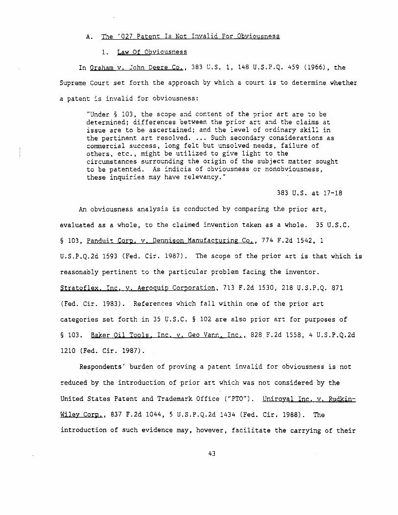
A. The '027 Patent Is Not Invalid For Obviousness
1. Law Of Obviousness
In Graham v. John Deere Co., 383 U.S. 1, 148 U.S.P.Q. 459 (19661, the
Supreme Court set forth the approach by which a court is to determine whether
a patent is invalid for obviousness:
"Under 5 103, the scope and content of the prior art are to be determined; differences between the prior art and the claims at issue are to be ascertained; and the level of ordinary skill in the pertinent art resolved. ... Such secondary considerations as commercial success, long felt but unsolved needs, failure of others, etc., might be utilized to give light to the circumstances surrounding the origin of the subject matter sought to be patented. As indicia of obviousness or nonobviousness, these inquiries may have relevancy."
383 U.S. at 17-18
An obviousness analysis is conducted by comparing the prior art,
evaluated as a whole, to the claimed invention taken as a whole. 35 U.S.C.
5 103, Panduit CorD. v. Dennison Manufacturing Co,, 774 F.2d 1542, 1
U.S.P.Q.2d 1593 (Fed. Cir. 1987). The scope of the prior art is that which is
reasonably pertinent to the particular problem facing the inventor.
Stratoflex. Inc. v. Aeroquip Corporation, 713 F.2d 1530, 218 U.S.P.Q. 871
(Fed. Cir. 1983). References which fall within one of the prior art
categories set forth in 35 U.S.C. 5 102 are also prior art for purposes of
5 103. Baker Oil Tools. Inc. v. Geo Vann. Inc., 828 F.2d 1558, 4 U.S.P.Q.2d
1210 (Fed. Cir. 1987).
Respondents' burden of proving a patent invalid for obviousness is not
reduced by the introduction of prior art which was not considered by the
United States Patent and Trademark Office (''PTO"). Uniroval Inc. v. Rudkin-
Wilev CorD., 837 F.2d 1044, 5 U.S.P.Q.2d 1434 (Fed. Cir, 1988). The
introduction of such evidence may, however, facilitate the carrying of their
43

burden. Id, Conversely, a party is less likely to carry its burden when it
relies solely upon prior art considered by the PTO. Stratoflex. Inc. v,
Aeroauir, Corporation, 713 F.2d 1530, 218 U.S.P.Q. 871 (Fed. Cir. 1983).
The comparison between the prior art and the claims at issue is conducted
with reference to a hypothetical person of ordinary skill in the art.
person is presumed to be aware of all the pertinent prior art, but does not
undertake to innovate. Standard Oil Co. v, American Cvanamid Co., 774 F.2d
448, 227 U.S.P.Q. 293 (Fed. Cir. 1985).
Such a
When a party asserts that a patent is invalid because it would have been
obvious in light of the combined teachings of several prior art references,
that party must establish by clear and convincing evidence that there is some
teaching, suggestion or inference in the prior art which would have led one of
skill in the art to combine the relevant teachings.
Delta Resins & Refractories. Inc., 776 F.2d 281, 227 U.S.P.Q. 657 (Fed. Cir.
1985).
Ashland Oil. Inc. v.
A court must always consider objective evidence such as commercial
success, failure of others, long-felt need, copying, and unexpected results
before reaching a conclusion on whether a patent would have been obvious.
Hvbritech. Inc. v, Monoclonal Antibodies. Inc,, 802 F.2d 1367, 231 U.S.P.Q. 81
(Fed. Cir. 19861, cert. denied, 107 S.Ct. 1606 (1987). Such evidence must be
weighed along with the other factors of a Graham v. John Deere analysis.
Truswal Svstems Corp. v. Hydro-Air Envi neerine In c., 813 F.2d 1207, 1212, 2
U.S.P.Q.2d 1034, 1038 (Fed. Cir. 1987) ("That evidence is 'secondary' in time
a,
does not mean that it is secondary in importance.")
invention will only be indicative of nonobviousness if there is a nexus
between the success and the merits of the invention.
Commercial success of an
Cable Electric Products,
44

Inc. v. Genmark. Inc,, 770 F.2d 1015, 226 U.S.P.Q. 881 (Fed. Cir. 1985).
2. Scope And C ontent Of The Pr ior Art
a. Problem Facine The Inventors
The scope of the prior art is that which is reasonably pertinent to the
particular problem facing the inventor. Stratoflex. Inc. v. Aeroauir,
CorDoration, 713 F.2d 1530, 218 U.S.P.Q. 871 (Fed. Cir. 1983). The problem
facing Messrs. Birchler and Williams at the time of their work which led to
the '027 patent was to develop a process for the encapsulation of a low-cost
transistor. FF B 1.
During the 1950's and early ~O'S, the principal method f o r encapsulating
FF A 13. During this transistors was known as the "header and can" process.
process, the device was mounted on a gold-plated metal foundation ("header")
and connected to conductor leads with thin "whisker wires". The leads were
held in place with a glass filling and came out of the package through the
bottom of the header.
top of the header.
FF A 13. A metal can was then hermetically welded on
FF A 13.
In the early 1960's, manufacturers began searching for a means of mass
producing inexpensive transistors.
manufacturing transistors were undertaken throughout the semiconductor
industry. CX 5 at 2, CX 215 at 1.
Birchler and E . R . Williams commenced working on what eventually became known
as TI'S Low Cost Transistor Project. Early in the project,
they conducted a cost analysis of the header and can process and determined
FF A 15. Efforts to reduce the costs of
In late 1962 or early 1963, Robert 0.
FF A 19, A 20.
that in a3 individual transistor, the header was the second most expensive
component. Birchler, Tr. 369. Accordingly, they attempted to devise a
process which eliminated the header, and assembled the leads on a "handle"
45
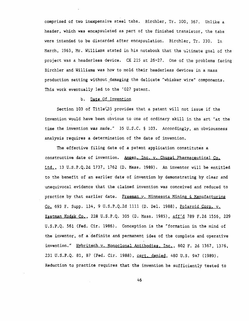
comprised of two inexpensive steel tabs. Birchler, Tr. 300, 367. Unlike a
header, which was encapsulated as part of the finished transistor, the tabs
were intended to be discarded after encapsulation. Birchler, Tr. 330. In
March, 1963, Mr. Williams stated in his notebook that the ultimate goal of the
project was a headerless device.
Birchler and Williams was how to mold their headerless devices in a mass
CX 215 at 26-27. One of the problems facing
production setting without-damaging the delicate "whisker wire" components.
This work eventually led to the '027 patent.
b. Date Of Invention
Section 103 of Title:35 provides that a patent will not issue if the
invention would have been obvious to one of ordinary skill in the art "at the
time the invention was made." 35 U.S.C. 5 103. Accordingly, an obviousness
analysis requires a determination of the date of invention.
The effective filing date of a patent application constitutes a
constructive date of invention. h h L
m, 13 U.S.P.Q.2d 1737, 1762 (D. Mass. 1989). An inventor will be entitled
to the benefit of an earlier date of invention by demonstrating by clear and
unequivocal evidence that the claimed invention was conceived and reduced to
practice by that earlier date. Freeman v. Minnesota Minine & Manufacturing
CO. 693 F. Supp. 134, 9 U.S.P.Q.2d 1111 (D. Del. 19881, Polaroid Con, v.
Eastman Kodak Co, , 228 U.S.P.Q. 305 (D. Mass. 19851, aff'd 789 F.2d 1556, 229
U.S.P.Q. 561 (Fed. Cir. 1986). Conception is the "formation in the mind of
the inventor, of a definite and permanent idea of the complete and operative
invention." Hybritech v. Monoclonal Antibodies. Inc., 802 F. 2d 1367, 1376,
231 U.S.P.Q. 81, 87 (Fed. Cir. 19881, cert. denied, 480 U.S. 947 (1989).
Reduction to practice requires that the invention be sufficiently tested to
46

demonstrate that it will work for its intended purpose. Barmap Bar mer
Maschinenfabrik v. Murata Machinerv. Ltd., 731 F.2d 831, 221 U.S.P.Q. 561
(Fed. Cir. 1984).
In determining the date of invention, a finder of fact utilizes a "rule
of reason" in which all pertinent evidence is examined. Coleman v. Dines, 754
F.2d 353, 224 U.S.P.Q. 857 (Fed. Cir. 19841, Reese v. Hurst, 661 F.2d 1222,
211 U.S.P.Q. 936 (C.C.P.A. 1981). The inventor must produce independent
corroborating evidence in addition to his own statements and documents in
order to establish a date of invention earlier than the date the patent
application was filed. Hahn v. Wong, 892 F.2d 1028, 13 U.S.P.Q.2d 1313 (Fed.
Cir. 1989). However, the rule does not require eye-witness corroboration;
sufficient circumstantial evidence can satisfy the corroboration requirement.
morr v. Pearson, 671 F.2d 1368, 213 U.S.P.Q. 196 (C.C.P.A. 19821, Bernes v,
Gottstein, 618 F.2d 771, 205 U.S.P.Q. 691 (C.C.P.A. 1980).
The '027 patent issued on August 23, 1977 based on Application No.
384,768, filed July 30, 1973, in continuation of Application No. 738,311 filed
October 17, 1968, which was a division of Application No. 331,006 filed on
December 16, 1963. CX 1. Thus, the constructive date of invention for the
'027 patent is December 16, 1963. Whether Birchler and Williams are entitled
to the benefit of an earlier date of invention requires an examination of the
evidence regarding the reduction to practice of the process.
As part of the effort to produce a low cost transistor, Birchler
advocated utilization of a transfer molding encapsulation process because he
believed it might permit high volume production of finished products.
Birchler, Tr. 280.
encapsulating transistors, such as epoxy casting, but eventually settled on
He and Williams considered utilizing other methods for
47

transfer molding for further experimentation. Williams, Tr. 1463, FF 89.
Based on a sketch supplied by Mr. Lockhart of the Dow Corning Corporation
(RPX 109 (Lockhart Dep.) Tr. 141, personnel at TI constructed a small one-
cavity mold for the purpose of testing the viability of transfer molding for
delicate semiconductor devices. Birchler, Tr. 285. One half of the cavity
was situated in the upper half of the mold, and the other half of the cavity
was in the lower mold half.
plastic would flow was located at the end of the bottom half of the cavity.
Id., Birchler, Tr. 360, RX 41.
FF B 160. The ”gate” through which molten
Mr. Williams brought the mold and about one hundred transistors to the
facilities of Dow Corning in Midland, Michigan where he attempted to transfer
mold them on May 29, 1963. RPX 109 (Lockhart Dep.) Tr. 14, 16. The
transistors Williams brought to Midland had three conductms in a planar
arrangement. RX 41.
conductors and thin whisker wires ran from the transistor to each of the other
The transistor chip was mounted upbn one of the
two conductors. RX 41. The transistw and whisker wires were located on one
side of the plane defined by the three conductors.
placed in the cavity with each end of the conductors resting in recesses in
the lower half of the mold. FF B 160.
RX 41. The devices were
Williams’ first attempts to mold the transistors were conducted with the
transistor and whisker wires in the bottom o f the mold cavity, i.e. on the
same side of the conductor plane as the gate. Williams, Tr. 1462-1463, Rx 41.
A l s o , because the mald was end-gated, the encapsulating fluid struck the
whisker wires at right angles. These initial attempts met with failure,
producing no good units. Id., RPX 109 (Lockhart Dep.) Tr. 17. Fifteen or
twenty devices were molded and none passed the electrical continuity test,
48

RPX 109 (Lockhart Dep.) Tr. 17. The devices were thereafter turned over so
that the transistor and whisker wires were on the opposite side of the plane
from the gate. RX 41. Better results, including good units, were obtained
with this arrangement, Rx 41, RPX 109 (Lockhart Dep.) Tr. 17. Mr. Williams
in his invention disclosure form stated: "The better results are obtained
when the unit was in the top half [and the gate was in the bottom half] of the
mold so it [the device and whisker wire connections] did not see the plastic
as it is initially introduced into the cavity." RX 41.24
Birchler and Williams, decided to further investigate manufacture of
semiconductor devices through use of transfer molding. Birchler, Tr. 367;
Williams, Tr. 1462-72. Subsequent to the work at DOW, airchler and Williams
built a two-cavity mold. The gate in this mold was located on the side of the
cavity and the fluid entered in a direction parallel to the whisker wires and
at right angles to the heavier conductor wires. FF B 182a, 186. Further, the
gate was offset from the portion of the cavity where the transistor chip was
located. Birchler, Tr. 294. An entry in Williams' laboratory notebook dated
June 31, 1963 (sic) states that the two cavity mold has been built and tested.
RX 41. The "important features" of the two cavity mold are set forth as
follows: ~~
24 Mr. Williams' co-inventor, Mr. Birchler, testified at the hearing that Mr. Williams molding experiments at Dow were a "catastrophe" and the two of them were "absolutely distraught" with the results. Birchler, Tr., 287, 290. On the other hand, Mr. Lockhart, the Dow employee who worked with Mr. Williams during these encapsulation experiments, stated that every transistor molded in the opposite-side gated configuration passed the electrical continuity test, and described Mr. Williams as "elated" with the results. RPX 109 (Lockhart Dep.) at 31, 35. In light of the lack of testimony from Mr. Williams on this point, the indication in his notebook that "good units" were produced at DOW, the diametrically conflicting testimony of Mr. Lockhart, and the fact that opposite-side gating was included as an important feature in the later- written patent disclosure form (RX 511, the Administrative Law Judge finds Mr. Birchler's testimony on this point lacking in credibility.
49

A. The molding compound is introduced from the side with individual unit gating. the emitter & base connections.
This allows the flow to be parallel to the plane of
B. The gate is off-center with the device.
C. The gate is in the bottom half of the mold, and the device in the top.
D. The construction of the device was double ended to prevent any movement of leads, thus breaking the connections.
Tests of devices from the two cavity mold "yield[edl ... good devices from transfer molding ... high enough [in number] to preclude any further belief that the molding compound is breaking wires." RX 41, p . 8. The entry
also included the statemefit that samples had been placed on "life test."25
- Id.
These entries indicate that delicate transistors have been molded with
the two cavity mold, and might evidence a reduction to practice at whatever
date this occurred. The deposition testimony of Lockhart indicates that
semiconductors were successfully molded in a bottom-gated configuration, but
the single cavity mold did not have features A (side-gating) o r B (off-center
gate).
that Williams successfully transfer molded semiconductors with a mold
containing features A, B and C, and wire arrangements described in feature D
and shown in the entry's drawings (last page), as of the date of this entry.
a, Hahn v. Wong, 13 U.S.P.Q.2d at 1317 (affidavits of co-inventor's
colleagues that they had read and understood entries in a laboratory notebook
TI has not adduced independent evidence corroborating the assertion
25
indicated as the date it was witnessed and understood by a colleague of M r . Williams. RX 41 (last page). It is difficult to ascertain the actual date of this entry. Some of the possibilities are June 30, 1963, July 1, 1963 or July 31, 1963.
The date of this latter entry is given as "6/31/63". The same date is
There was no clarifying testimony.
50

26 did not corroborate a reduction to practice),
On August 1, 1963, M r . Birchler had TI’S Special Projects Group prepare a
series of viewgraphs showing each step in a production line to transfer mold
transistors in accordance with the ’027 patent. CX 270; CX 8, Birchler DRAMs
Tr. 233-34. These viewgraphs were utilized at some subsequent time, probably
in August or September 1963 in a presentation to TI management regarding the
low cost transistor project.
manufacturing lines (the ”Gang Concept” and the ’’Slide Pack Concept”), each of
which incorporates encapsulation by transfer molding. CX 270. The first
viewgraph is captioned ”Carrier Fabrication & Loading” and illustrates that
three conductors have been arranged in a common plane with the semiconductor
device attached to the middle conductor. CX 270 at 2. The third viewgraph,
captioned ”Carrier Transfer”, illustrates the placement of the planar
conductors and die into a transfer molding die that is side-gated with the
gate on the other side of the plane formed by the three conductors, CX 270
at 4. The following viewgraph, captioned ”Molded ’Gang”’, shows the molded
product.
Cost Transistor” illustrate the initial cost estimates of the costs for a
production line incorporating each of the two concepts.
Id, The viewgraphs display two entire proposed
CX 270 at 5. The viewgraphs captioned “Mechanization Proposal Low-
CX 270 at 17, 18.
At a subsequent presentation to management, probably in September 1963,
Birchler and Williams requested the allocation of funds for a commercial
26 In the Initial Determination on remand in DRAMs, it was found that by September 12, 1963, Birchler and Williams had built transistors using their transfer molding process and these transistors had completed a 1,000 hour life test. CX 262 at 28 (Finding No. 82). Because this assertion was based upon the uncorroborated testimony of Mr. Birchler, and TI has not adduced any additional evidence in support of it, the Administrative Law Judge is not adopting this finding.
51

production line for low cost transistors, submitting a document dated
September 12, 1963, entitled "Equipment Requirements".
Birchler DRAMs Tr. 242-3.
for the proposed production line, including transfer dies and a molding press.
CX 270 at 22.
transistors had been received. CX-8, Birchler DRAMs Tr. 243.
CX 270 at 22; CX 8,
This document lists the prices of equipment needed
Birchler claims that by this time life test data on the
Mr, Birchler met with Mr. Lawrence Plummer of the Hull Corporation to
secure transfer molding equipment for commercial production of the
transistors. CX 15, Hull DRAMs Tr. at 1083-1084, 1097. Personnel at Hull
worked a great deal with TI on building dies needed to transform the process
as demonstrated in the two cavity mold to a commercial scale production
process.
Corporation later touted Hull's contributions to TI'S "pioneering" efforts in
encapsulating low cost transistors in plastic.
the September presentation, TI began sending bulletins to its customers
setting forth the technical specifications of its plastic encapsulated SILECT
transistors. CX 268 (dated January, 1964). On February 10, 1964, TI issued a
general news release announcing the first plastic encapsulated transistors for
the consumer market. CX 265.
CX 15, Hull DRAMs Tr. at 1083-1084. An advertisement of the Hull
CX 201. A few months after
Mr. Lockhart's deposition testimony provides independent evidence that
the feature of opposite side gating was conceived on May 29, 1963, and the
viewgraphs described above illustrates all the features of the invention as
described in the '027 patent. TI management's decision to go ahead with a
commercial production line incorporating the '027 process evidences that
management had been convinced that the process worked for the purpose
intended. The management decision to take the '027 process out of the
52

laboratory and place it on a production line constitutes evidence
corroborating Mr. Birchler's testimony that the process was reduced t o
practice in September 1963, but after September 12, 1963.
3. Prior Art
a. U.S. Letters Patent No, 3.367.025 (Doyle)
TI--. Doyle patent is entitled "Method For Fabricating and Plastic
Encapsulating a Semiconductor Device."
pursuant to an application which was filed on January 15, 1964.
During the prosecution of the '027 patent's application, Birchler and Williams
were involved in an interference with the Doyle patent.
Interferences determined that Doyle's invention had been conceived and reduced
to practice "well prior" to the December 16, 1963 filing of the parent
application of the '027 patent.
Doyle priority with respect to claims 1, 3, 4 and 6. FF B 281. These claims
were cited as prior art during the prosecution of the '027 patent's
application.
Office Board of Appeals, Appeal No. 256-14 (RX 49).
It was issued on February 6, 1968
RX 11.
The Board of Patent
RX 60 at 6. The Board therefore awarded
a, Ex parte Birchler, United States Patent and Trademark
In arriving at its decision regarding the reduction to practice of
Doyle's invention, the Board relied upon twelve documentary exhibits, ten of
which predate September 12, 1963. Accordingly, Doyle's date of invention
predates that of the '027 patent, and claims 1, 3, 4 and 6 of Doyle constitute
prior art under 35 U.S.C. 5 102(g) for purposes of this obviousness analysis. 27
27 35 U.S.C. 5 102(g) provides in pertinent part: A person shall be entitled to a patent unless before the applicant's invention thereof the invention was made in this country by another who had not abandoned, suppressed, or concealed it. be considered not only the respective dates of conception and
In determining priority of invention there shall
(continued ... ) 53

The Doyle claims disclose a semiconductor device with a plurality of
conductor leads held in a "pin circle" (b non-planar) arrangement by a jig,
FF B 23, 45.
the device. RX 11. Nail heads are formed on the top of the leads, and these
nail heads are raised above the jig. FF B 44, RX 11, Co l . 4, line 8 (leads
are maintained in the jig, "protruding therefrom"). The semiconductor is
placed on one of the nail heads which is slightly lower than the other two.
RX 11. "Tiny wires" connect the semiconductor to the other two leads. RX 11,
Co l . 6 line 11.
The jig serves as the bottom of a cavity used to transfer mold
During the Doyle prdkess, liquid encapsulation material enters the cavity
through a gate located at the parting line between the jig and the upper
portion of the mold cavity. Doyle, Tr. 968, 973, RX 11. Because the gate is
located on the floor of the mold cavity, and the nail heads (upon which were
the semiconductor and whisker wires) are raised above the floor of the cavity,
so they could be completely encapsulated, the gate is located beneath the
semiconductor and wires. RX 11. Only one end of the leads extends outside
the mold cavity. RX 11.
b. U.S. Letters Patent No. 3.235.937 (Lanzl)
The Lanzl patent is entitled "Low Cost Transistor." The application was
27 ( . . .continued) reduction to practice of the invention, but also the reasonable diligence of one who was first to conceive and last to reduce to practice, from a time prior to conception by the other.
Prior work which satisfies the requirements of this provision can be used as prior art in an obviousness analysis. PhilliDs Petroleum Co,, 849 F.2d 1430, 7 U.S.P.Q.2d 1129 (Fed. Cir. 19881, on remand, 711 F. Supp. 1205, 11 U.S.P.Q. 2d 1081 (D. Del. 1989). See also, Ex parte Birchler at 3 ("The rejection before us is one under 35 USC 103. evidence f o r obviousness is the prior invention of another in this country under section 102(g)")
E.1 du Pont de Nemours & Co. v,
The
CX 2 at 32.
54

filed on May 10, 1963 and the patent was issued on February 22, 1966. RX 7.
Because the application for tk.e Lanzl patent was filed before the invention of
the '027 process, it constitutes prior art under 35 U.S.C. 5 102(e).
Figures 7 and 8 of Lanzl disclose a transistor with planar leads. RX 7.
The silicon transistor is mounted upon one of the leads and one mil whisker
wires connect it to the other two leads. RX 7 , Col. 2 lines 31-42. The
semiconductor device and wires are located on the same side of the plane
formed by the three leads. RX 7 , Figure 8. The Lanzl transistor utilizes a
header which stays on the finished product, RX 7; Plummer, Tr. 1403. The
Lanzl patent does not disclose transfer molding or any other specific method
of encapsulation, stating only that the semiconductor device and wires are
"housed by encapsulation in a suitable non-metallic electrically insulative
protective material." RX 7, Col. 3 lines 39-41. At the hearing, respondents'
expert, Lawrence Plummer, testified that Lanzl transistors were encapsulated
by potting, Plummer, Tr. 1403-1404.
c. The Svlvania Transistor/Carruth And Sussman Article
From mid-1958 through mid-1963, Sylvania Electric Products, Inc.
conducted a program to develop a process f o r encapsulating germanium
transistors in plastic. Russell, Tr. 1117. Its TF-61 and TF-62 transistors,
manufactured in or about March, 1963, were encapsulated by transfer molding
and used a header. Russell, Tr. 1109, 1073-74; RX 127 at 58-69. The three
conductor wires in the Sylvania transistor were in an in-line configuration,
i.e. parallel to each other and in a common plane. FF B 121. The germanium
device was mounted on a circular base tab which was then soldered to the
center lead in the header. FF B 123. The base tab and transistor were
mounted in a plane generally perpendicular to the plane formed by the
55

conductors. Russell, Tr. 1112, 1114. In contrast to the one mil gold whisker
wires utilized in the transistors for which the '027 process was intended,
Sylvania's TF-61 and TF-62 transistors utilized nickel bond wires which were
on the order of 5-10 mils in diameter. Russell, Tr. 1110-11. The structure
of the bqse tab and germanium die assembly used in the Sylvania transistor was
fragile, but it was more rugged than the structure of planar silicon
transistors with one mil gold wires typically used in the industry. Russell,
Tr. 1115-16.
Sylvania's transfer molded germanium transistor was described in an
article by Carruth and Sussman entitled "Epoxy Pellet Encapsulation For
Transistors" (RX 24) which appeared in Electronic PackaginP And Production in
April, 1963 and constitutes prior art under 35 U.S.C. § 102(g). FF 9 111.
Figure 3 of the Carruth/Sussman article depicts a TF-61 transistor. FF B 112.
In the article it is stated that transfer molded transistors were still in the
development stage, but offered the advantages of reduced costs, better heat
dissipation, and the ability to be packed closely together in low power
applications. FF B 116. It is further stated that the moisture resistance of
transfer-molded transistors is not as good as solder sealed transistors, but
the former passed a standardized moisture test. RX 24 at 3.
TI asserts that the Sylvania transistor was known to the examiner at the
time the '027 patent's application was prosecuted. The specification of the
'027 patent provides:
"There have been reports that germanium alloy transistors have been encapsulated using transfer molding techniques, but again with the use of expensive headers. device is not unusually difficult because mechanically it is inherently relatively strong. However, these plastic encapsulated alloy devices have not been generally accepted on the market because of unacceptably high leakage currents."
Encapsulation of an alloy
CX 1, Co l . 1 lines 50-62
56

The specification does not set forth the details of the lead arrangement or
othez characteristics of the Sylvania transistor o r its encapsulation process,
nor does it identify the transistor or process by the manufacturer's name.28
Accordingly, this portion of the '027 patent's specification does not support
the conclusion that the examiner was aware of the details of the work
perforaed by Sylvania.
d. The Zecher Article
In July, 1962, IRE Transactions On Product Engineering And Productioq
published an article by Robert F. Zecher of the Hull Corporation entitled
"High ?reduction Encapsulation of Electronic Devices." RX 478. Zecher's
article discusses the problems and benefits of encapsulating devices by
transfer molding. The article states that various devices, including
transistors, were being encapsulated by transfer molding.
'article also describes reasons manufacturers had not shifted to transfer
molding :
RX 478 at 7 . The
"The single drawback to many other new programs is the inherently Many manufacturers who poor design of a component for encapsulation.
have been skimming through product development without giving much thought to final packaging are now beginning to wish they had used stiffer leads which could support the device in a mold, that the lead configuration occupied only one plane, so the mold need only have one parting line, that they had not used fiber washers which outgas when heated, and so forth."
RX 478 at 7 .
~~
28
of Electrmics Packaging and Production carried an article stating that Sylvania Jas encapsulating a germanium alloy unit by the transfer molding method. This was accomplished with the use of a header. They the conventional header could be replaced with a plastic type,
In his laboratory notebook Williams states as follows: "The April issue
did not consider elimination of same. It should be noted that molding of an alloy device is no more different than molding a is common practice." RX 41
did point out however they trans fer resistor, what
57

e. The Helda-Lincoln ADDroach
During the early 1960's, Robert Helda and Milan Lincoln were involved in
a project at Motorola to develop a low-cost transistor. FF B 66. The work of
Helda and Lincoln led to U.S. Letters Patent 3,444,441. RX 330 at 11. The
'441 patent issued May 13, 1969 and has an effective filing date of June 18,
1965.
The Helda-Lincoln apprpach calls for supporting the die at the end of a
stamped lead frame, FF B 76. The leads are parallel to each other, and the
die and whisker wires are located on one side of the leads. FF B 77. The
gate through which the en6apsulating fluid enters the molding cavity is
located at the end of the cavity opposite to the leads. FF B 76. The fluid
enters at right angles to the whisker wires and the gate is not offset from
the device. FF B 76.
The '441 patent indicates that the gate is located on the opposite side
of the leads from the die and whisker wires. FU 12, fig. 5B. In DRAMs, TI
submitted into evidence a sketch prepared by its counsel which was utilized at
the deposition of Mr. Lehner. RX 111. It clearly shows that the Helda-
Lincoln approach utilized opposite side gating. RX lll.29
29
as an accurate depiction of what it represented to be. DRAMs Order No. 163. It and another exhibit were initially excluded from the DRAMS evidentiary record, but included after TI made an unopposed motion for reconsideration of the rejection. DRAMq, Order No. 163. Order No. 163 states that the exhibits illustrate a point TI wanted to make, but does not state what the point was. Judge Saxon ordered that they not be used "for any purpose that would be inconsistent with the testimony of Mr. Lehner in his deposition." Id. The ALJ takes official notice of the TI Motion for Reconsideration of the Rejection of TI Exhibits 490 and 491, in the DRAMS case, Docket Number 242- 237, and designates it as Exhibit ALJX-1 in this proceeding. motion represented that the only inaccuracy in the sketch is that the gate was offset in the original sketch. Motion at 3. Mr. Lehner corrected the sketch to show that the gate is in-line with the device.
(continued.. . I
Mr. Lehner testified that the sketch was not accurate and did not adopt it
TI in that
TI represented that with
58

Respondents contend that the Helda-Lincoln approach was invented before
the '027 process, and therefore constitutes prior art as to the '027 patent
pursuant to 35 U.S.C. § 102(g).
dated May 13, 1963 contains a drawing in which the semiconductor device is
located upon a lead and connected by wire bonds to two other leads.
An entry from Mr. Helda's laboratory notebook
RX 75.
The entry also contains a notation that the last step in fabricating the
finished product is "Plastic Encapsulation (Molded)". RX 75. The entry does
not in any way show whether Mr. Helda had conceived of any details of the
molding process as of that date.30
On May 17, 1963, Helda and Lincoln submitted a proposal entitled
"Proposal for Inexpensive Entertainment Device Package." FF B 67; RX 76. The
proposal outlines the production steps for fabrication of the Helda-Lincoln
transistor and sets forth that the product will be molded "in a process
similar to that used on Motorola's Surmetic Diode." This reference to the
process used for the Surmetic Diode meant transfer molding.
However, nothing in the proposal discloses gate location o r indicates that
Helda and Lincoln conceived any details of the molding process at that time,
RX 76, Plummer, Tr. 1400.
FF B 7 6 , Rx 76.
By October 4, 1963, at least twenty-five of the Helda-Lincoln devices had
FF B 71. Respondents contend that this been produced and tested by Motorola.
establishes a reduction to practice of the Helda-Lincoln proposal as of that
date. However, a reduction to practice requires clear and convincing evidence
29 ( . . . continued) this correction, the sketch illustrates the relationship between the device, whisker wire connections and the gate. ALJX-1 at 1. Accordingly, RX 111 is admitted into evidence.
30
of the notations accompanying the drawing. The quality of the phdtocopied entry is too poor to allow one to read most
59

that the invention has demonstrated it will work f o r its intended purpose.
5%, armag Barmer Masc 731 F.2d 831, 221
U.S.P.Q. 561 (Fed. Cir. 1984). Respondents have not adduced any evidence that
these twenty-five devices passed such tests, or in any othef way demonstrated
that the Helda-Lincoln molding process worked.
requirements set down by the Federal Circuit f o r proving a reduction to
practice (yahn v. Worg, 892 F.2d 1028, 13 U.S.P.Q.2d 1313 (Fed. Cir. 198911,
the fact that some transistors were fabricated does not, in itself, constitute
a reduction t o practice of the molding process.
In light or the strict
On November 19, 1963, Mr. Donald E. Johnson, an industrial engineer at
Motorola, prepared a memorandum regarding the Helda-Lincoln project. The
memorandum states that as of that date, Helda had manufactured 1,000 plastic
package transistors. PX 108. Another memorandum, written by Mr. R . L .
Pritchard on November 14, 1963 and summarizing a meeting which took place on
NQvember 6, 1963, states that as o f the time of the meeting, transistors had
been transfer molded and "approximately 600-700 p o d devices were fabricated."
RX 109 (emphasis added). Thus, it appears that at least sixty t o seventy
percent of the packages manufactured by Helda by this time were "good
device?" ,31
conceived and reduced to practice on November 6, 1963. Accordingly, it was
invented after the date of invention of the process claimed in the '027
These memoranda are evidence that the Helda-Lincoln approach was
31 If a portion of the 1,000 devices referred to in the Johnson memor8ndum were manufactured during the period between November' 2 and November 19, the percentage of "good devices" would be greater.
60

patent, and does not constitute prior art.32
f. United States Letters Patent 2.757.439 (Burns)
The Burns patent is entitled "Transistor Assemblies". It was issued
August 7, 1956 pursuant to an application filed February 25, 1955. RX 3.
Burns was cited by the examiner during the prosecution of the '027 patent's
parent cpplication as prior art with respect to the claims directed towards
32
the following discussion and finding regarding whether Helda Lincoln was "abandoned, suppressed or concealed":
In the event this issue is reviewed, the Administrative Law Judge includes
Motorola did not apply for a patent directed to the Helda- Lincoln approach until June 18, 1965. RX 16. The respondents contend that the Helda-Lincoln invention is 5 1C2(g) prior art. The party asserting invalidity under 5 102(g) bears the burden of proving that the prior invention was not abandoned, suppressed or concealed. Oak Industries. Inc. v. Zenith Electronics CorD., 14 U.S.P.Q. 2d at 1420-21 and cases cited therein, 3 Chisum Patents 5 10.08[31[c]. A court may find that an invention was abandoned, suppressed or concealed if within a reasonable time after the invention was reduced to practice the inventor took no steps to make the invention publicly known. International Glass Co. v, United States, 408 F.2d 395, 161 U.S.P.Q. 116 (Ct. C1. 1969) (per curiam) (adopting opinion of Davis, Comm'r, 159 U.S.P.Q. 4341, Oak Industries. Inc. v. Zenith Electronics Corp., 726 F. Supp. 1525, 14 U.S.P.Q. 2d 1417 (N.D. Ill. 1989).
The case law on 5 102(g) often refers to the plain language of the statute in addressing the issue of whether an earlier invention had been abandoned, suppressed or concealed. In Allen v. W.H. Bradv, 508 F.2d 64, 184 U.S.P.Q. 385 (7th Cir. 19741, tke court noted that the statute's use of the pluperfect tense - 'nad not abandoned, suppressed, or concealed it" - requires that a determination of abandonment be made with reference to the date of the patentee's invention. See also, Oak Industries, Inc, v. Zenith Electronics CorD., 14 U.S.P.Q. 2d at 1423, 1424 (abandonment must occur prior to the time of the second izvention; determination of suppression or concealment made with reference to date of invention). Because the period between the invention of the Helda-Lincoln approach (November 6, 1963) and the constructive date of invention of the '027 process (December 16, 1963) is only six weeks, Helda-Lincoln was not abandoned, suppressed or concealed for purposes of 5 102(g).
6 1

the Birchler and Williams encapsulation process. CX 4 at 43, 53-54.
The three leads of the transistor set forth as the preferred embodiment
of the Burns patent are inserted into and through a stem base in order to give
mechanical support and rigidity during the encapsulation process.
1, Col. 2 lines 3-8.
embodiment, the holes through which the leads extend are all in the same
plane. Thus, the Burns transistor utilizes planar leads.
RX 3, Fig.
The patent's drawings illustrate that in the preferred
RX 3, Fig. 6.
4. Differences Between The Claimed Invention And The Prior Art
In conducting an obviousness analysis, the claimed invention must be
considered as a whole, 3!?LU.S.C. 9 103. When several prior art references
are utilized in an attempt to show the patent would have been obvious in light
of them, there must be some suggestion in the art to lead one of ordinary
skill to combine the references. Lindenmann Maschinenfabrik GmbH v. American
Hoist and Derrick Co. 730 F.2d 1452, 1462, 221 U.S.P.Q. 481, 488 (Fed. Cir.
1988). The problem confronted by the inventor must be considered in
determining whether it would have been obvious to combine references in order
to solve that problem.
675, 7 U.S.P.Q.2d 1315 (Fed. Cir. 1988). Picking and choosing among the
references until all the features of the claimed invention are unearthed will
piversitech CorD. v. Century Ste~s. Inc, , 850 F.2d
not suffice to invalidate a patent in the absence of such a suggestion.
Smithkline Diagnostics. Inc. v. Helena Laboratories Con,, 859 F.2d 878, 8
U.S.P.Q.2d 1397 (Fed. Cir. 1989).
The invention set forth in claims 12, 14 and 17 utilizes a particular
arrangement of leads, semiconductor device and gate location to achieve the
goal of successfully transfer molding a semiconductor without disturbing the
whisker wire connections.
62

I
The Doyle patent teaches the utilization of a remote gate to transfer
mold a device which has delicate whisker wires leading from the semiconductor
to the leads.
for support and the whisker wires extend to coined ends of the other
conductors which are set in a plane slightly above the semiconductor.
gate is located beneath the device and whisker wires.
circle configuration, Doyle's leads are not ih a common plane; however the
gate is below the plane of the recessed or lower conductor.
The semiconductor is mounted on the coined end of a conductor
Doyle's
Because of their pin-
The Lanzl and Burns references are directed toward semiconductor devices,
not encapsulation. Like the devices encapsulated by the '027 process, the
Lanzl and Burns devices have planar leads with the semiconductor mounted on
one of the leads.
the product by transfer molding.
However, neither patent describes or suggests encapsulating
Zecher discusses in a general sense the utilization of transfer molding
in the electronic devices field.
at that time beginning to wish they had used stiffer leads in their devices
and had designed the devices with planar leads in order to have one parting
line. As evidenced from the prior art, planar lead transistors
(Lanzl and Burns patents, Sylvania transistor) were already well-known in the
art at that time. CX 10 (Schroen DRAMS testimony) at 84. Zecher's article
suggests that one wanting to transfer mold an electronic device should modify
the device so the leads are stronger and "in line", i.e, planar.
Zecher states that device manufacturers were
RX 478 at 7.
*
' 1378-1380.
Plummer, Tr.
The evidence of record establishes that Sylvailia successfully
encapsulated germanium transistors with leads in a common plane by April,
1963. The Sylvania germanium alloy transistors were more rugged than the
63

silicon devices described in the specification of the '927 process,
Sylvania device is made of a germanium alloy with a header, utilizing 5-10 mil
wire bonds, While the Sylvania device is fragile, it is more rugged than the
headerless devices encapsulated by the '027 process which have 1 mil whisker
wires. FF B 114.
The
Claims 12, 14 and 17 of the '027 patent are directed to encapaulqtion of
Semiconductors and are not ltmited to the encapsulation of delicate devices,
One utilizing a process described in one of these claims to encapsulate a
sturdier device would probably be considered an infringer.
sturdiness of the Sylvania transistor neither removes it from the prior art
regarding encapsulation, nor diminishes what Sylvania teaches, namely the
transfer molding of a transistor with planar leads.
Thus, the relative
bviousness 5 . Obiective Indicia Of 0 . .
Objective indicia of obviousness such as satisfaction of a long felt
need, commercial success, copying, and the failure of others mugt always to be
considered in an obviousness analysis. Hvbrit ech. Inc. v . M o n o c k w
Antibodies. Inc,, 802 F.2d 1367, 231 U.S.P.Q. 81 {Fed. Cir. 19861, cert,
denied, 107 S.Ct. 1606 (1987).
From the late 1950's through the early 1960'$, several major transistor
manufacturers were working on the development of an inexpensive transistor.
FF A 15. Texas Instruments, Motorola, Sylvania and others were actively
engaged in improving and reducing the cost of packaging transistors, including
transfer molding semiconductor devices having fragile whisker wires bonded to
the semiconductor and conductor wires. FF A 15, B 1. It was widely
recognized that the header was a major contributor to the cost of a
transistor. See ''Epoxy Pellets Encapsulation for Transistors"
64

(Carruth/Sussman) at 19-20 (RX 2 4 ) . Indeed, both Motorola and TI were working
on a headerless transistor and accompanying encapsulation process during mid-
I 1963. FF A 19-20, B 66-67. Completely doing away with the header increased
the transistor’s I fragility, making it more susceptible to damage during
manufacturing. See Bell Tr. 1002 (leads in Doyle patent use mechanical
strengt? of jig for support during molding). During the early 1960’s, an
increasing number of electronic devices had been encapsulated by transfer
molding, and in 1963 Sylvania transfer molded its germanium alloy transistor.
However, transfer molding was generally recognized as a harsh process, and had
1 not been used on something as delicate as a headerless planar transistor. See
CX 1 5 , Hull DRAMS testimony at 1019-1021.
At the time the ‘027 process was invented, there was a tremendous
economic incentive to develop a low cost transistor. CX 5, 1 yyyy. The ‘027
process met a long felt need in the market fo r a very low cost transistor
because it enabled TI to encapsulate delicate, transistors at a low cost.
report issued by Plastics Technology in May 1964 entitled ”News in
Thermosetting Processing” stated that TI was the first to commercially produce
A
plastic encapsulated transistors and that other major transistor manufacturers
were expected to soon follow suit.
direct copying, a factor which can contribute to a finding of nonobviousness,
but does avidence that the industry recognized the advantages of a process
CX 302. This article is not evidence of
like that claimed in the ‘027 patent.
Further, it is apparent that TI enjoyed considerable commercial success c
in the sale of its plastic-encapsulated transistors in the years following the
invention of the ‘027 patent. CX 297. TI’S annual reports for the years
1964-1968 consistently refer to increased sales of semiconductor devices,
65

particularly those encapsulated in plastic, despite the very competitive
nature of the market. CX 297.
semiconductors established record highs in 1965 and 1966 as its high-volume,
low-cost plastic packaged transistors were utilized in an increasing number o f
industrial and consumer products.
semiconductor market in the U . S . , but TI improved its market position
”[llargely because of Widespread acceptance of its ... digital integrated circuits and addition41 complex-function circuits in low-cost plastic
Indeed, unit and volume sales of TI’s
CX 297. 1967 saw a slight downturn in the
packages”, CX 297. TI‘s 1968 report stated that plastic encapsulated devices
had become “increasingly :important” to the company and that TI’s plastic
packaging had enabled it to produce an inexpensive high-performance silicon
transistor. The 1968 report further states that production of SILECT
transistors for consumer product applications had increased during the year.
CX 297.
The annual reports reflect the expansion in the use of transistors as
low-cost plastic encapsulated products entered the market.
Carruth/Sussman article, plastic encapsulated semiconductors, in addition to
A s noted in the
being less expensive, had certain unique qualities which allowed their use in
a wider array of applications. TI’s 2lastic encapsulation process
made it possible to use transistors in an increasing number of applications,
particularly in the aFea of consumer goods such as televisions and radios.
The commercial success of TI’s low-cost plastic-encapsulated transistors can
FF B 116.
be attributed to its headerless construction, a feature which would not have
been possible without the ’027 process, as well as the unique qualities o f the
product resulting from the use of plastic. Thus, there is the requisite nexus
between the ’027 patent and the commercial success of TI‘s plastic-
66

encapsulated semiconductors. 33
products, their expanding market, and their unique qualities of relative
ruggedness and low cost are strong evidence of nonobviousness.
The expanding sales of plastic-encapsulated
6. Level Of Ordinarv Skill In The Art
. The '027 patent is concerned with the arts of transfer molding and
semiconductor design. FF B 326. The level of skill in these arts is
determined less by educational requirements than by hands-on experience.
FF B 326.
art'in 1963. At the time the '027 process was invented, the level of ordinary
skill' was that of a skilled technician. Plummer, Tr. 1375-1376.
The parties have not disputed the level of ordinary skill in the
7. Conclusion As To Obviousness
The '027 patent resulted from work performed by Birchler and Williams
Which was designed to produce a low cost transistor by eliminating the header
and utilizing transfer molding.
already had been transfer molded, the increased fragility of a headerless
transistor made it particularly susceptible to damage by the in'sulating fluid
during molding.
While other more rugged electronic products
Like others in the electronics industry, TI was seeking to
eliminate the header in order to lower the production cost of a transistor,
and at the same time was working on a complementary encapsulation process.
The Board of Appeals found claims 12, 14 and 17 patentable over Doyle
because of the planar leads. Transistors with leads in a common plane were
33 TI has introduced evidence demonstrating that it has licensed the '027 patent to over [ C 1 CX 421, Donaldson, Tr. 852. Richard Donaldson, a vice-president of TI and its manager ofrpatent licensing, testified that the typical licensing agreement between TI and another did not specify particular patents, but is a [ C 1 license. Donaldson, Tr. 852-853, RX 306. Accordingly, no nexus can be established between TI'S success at negotiating these.licenses and the '027 patent.
67

well known in the art in the early 1960 ' s , as evidenced by the Burns patent
which issued in 1956. RX 3 . Further, the examiner was aware of references
describing such transistors having cited Burns during the prosecution of the
process claims in the parent application. See also, CX 4 at
138 (TI brought the Lanzl patent to the attention of the examiner).34 However,
additional prior art not before the Board of Appeals, particularly the
Sylvania transistor and the Zechet article, suggest that one could transfer
mold a transistor, as did Doyle, when the transistor had the specific
arrangement of leads described in the claims at issue. In reviewing the prior
art in light of the suggestion contained in Zecher, that semiconductors should
be redesigned to have one parting line (i.e., planar leads) and stronger leads
in order to utilize transfer molding,39 the Administrative Law Judge does not
discern any appreciable difference between the claims at issue and the prior
art considered as a whole.
CX 4 at 53, 73.
36
The obviousness analysis does not stop with the description of the
differences between the claimed invention and the prior art, however,
34 Respondents assert that the Board of Appeals was unaware of the Lanzl and Burns references when it ruled on TI'S appeal from the examiner's § 103 rejection because these references were cited in the grandparent application and not mentioned in the ' 768 application. However, the Board stated in its opinion that application claim 25 was limited to the filing date of the '768 application because "such an embodiment is not found in the parent applications. " finding without reference to the parent applications. that, contrary to respondents' assertions, the Board had the parent applications, with their citations to Burns and Lanzl, before it when ruling upon the appeal.
35 See CX 15, Hull DRAMS Tr. 1083-1088. I
Ex D arte Birchler at 6. The Board could not have made such a Thus it is apparent
36
molding semiconductors, if manufacturers of such devices worked with him in designing the products to be suitable for molding conditions, he could transfer mold even delicate semiconductor devices. Plummer, Tr. 1432-1435.
Indeed, Mr. Plummer testified that even in the early days of transfer
68

Concentration upon whether each of the differences between the claimed
invention and the prior art would have been obvious is an improper approach in
light o f the statutory mandate that the invention be considered "as a whole",
and the requirement in Graham v. Deere and its progeny requiring an analysis
of objective indicia of obviousness. 35 U.S.C. § 103,
CO., 333 U.S. 1, 148 U.S.P.Q. 459 (1966).
The objective evidence regarding the '027 patent is very persuasive
I
evidence of its nonobviousness.
industry in the early 1960's indicates that the market was price sensitive.
See RX 109 at 2 (Motorola memorandum describing low price as the "prime
factor" in the transistor market). Several major transistor manufacturers had
been devoting efforts to lowering the cost of manufacturing transistors. CX 5
at 2, CX 215 at 1. Their efforts illustrate that there were strong economic
incentives to develop both such a transistor and an encapsulating process
which could package it.
to grow even when the transistor market was in a downturn and in the apparent
absence of evidence that TI's sold at a price below its competitors,
The evidence regarding the transistor I
However TI's sales of the '027 transistor continued
TI has enjoyed considerable commercial success as a direct result of the
process which is the subject of the '027 patent, thus establishing the
requisite nexus between the commercial success of TI's plastic encapsulated
productc and the patented process. In Akzo N.V. v. U.S. I nternational Trade
Commission, 808 F.2d 1471, 1481, 1 U.S.P.Q.2d 1241, 1246 (Fed. Cir. 19871, the
Federal Circuit noted the commercial success of the patent at issue had been
"enormocs" and its range of uses "substantial".
commercial success in that instance was a "strong factor favoring non-
obviousness. " Ih,
The court further stated that
69

In Alco Standard CorD. v. TVA, 808 F.2d 1490, 1 U.S.PbQ.2d 1337 (Fed.
Cir. 1986), the court addressed a situation analogous to that present in this
investigation. The district court had concluded that the prior art did not
teach the combination of various references. The Federal Circuit found the
court’s conclusion clearly erroneous, first stating that the proper inquiry is
whether the prior art Suggests, not teaches, the desirability o f combining
references.
Circuit ruled that the district court was also clearly erroneous with regard
to the differences between the prior art and the claim at issue and to what
the prior art suggested to one of ordinary skill.
standing alone, the prior art provides significant support for the appellants’
contention that the ‘006 patent would have been obvious.” 808 F.2d at 1499-
After comparing the prior art to the invention, the Federal
The court stated “Thus,
1500, 1 U.S.P.Q.2d at 1344.
The Federal Circuit refrained from reaching a conclusion on obviousness
at this point, however, and reiterated its holdings regarding the importance
of objective indicia in an obviousness analysis.
Prior art, however, cannot be evaluated in isolation, but must be considered in the light of the secondary considerations bearing on obviousness. As we have pointed out:
[Elvidence of secondary considerations may often be the most probative and cogent evidence of record. It may often establish that an invention appearing to have been obvious in light of the prior art was not. It is to be considered as part of all the evidence, not just when the decisionmaker remains in doubt after reviewing the art.
808 F.2d at 1500, 1 U.S.P.Q.2d at 1344, auoting Stratoflex. Im. v. Aeroauip Cor?., 713 F.2d 1530, 1538-39, 218
U.S.P.Q. 871, 879 (Fed. Cir. 1983). ~
The court reviewed the extensive objective evidence of nonobviousness
discussed by the district court and concluded that in light of the district
court’s findings and the evidence in the record, “including the strong
7 0

secondary considerations indicating nonobviousness, which weigh heavily in the
determination of obviousness", the patent would not have been obvious in light
of the prior art. 1 U.S.P.Q.2d at 1345.
Here also, a comparison of the claimed invention to the prior art,
standing alone, would appear to support respondents' contention that the
process claimed by the '027 patent would have been obvious to one of ordinary
skill in the art at the time it was invented.
evidence, particularly of commercial' Success, is strong support of a
conclusion that the invention was nonobvious.
Alco Standard, "[tlhis is one of those cases where evidence of secondary
considerations 'may ... establish that an invention' appearing t o have been
sbvious in light of the prior art was not.' Stratofley, 713 F.2d at 1538 [213
U . S . P . Q . at 8791". 1 U.S.P.Q.2d at 1345.
However, the objective
To quote the Federal Circuit in
Having considered all of the factors required by the test laid down in
Graham v. John DBere, and particularly in light of the strong evidence of
commercial success enjoyed by TI as the result of the '027 patent, the
Administrative Law Judge has concluded that claims 12, 14 and 17 of the '027
patent would not have been obvious to one of ordinary skill in the art in
1963.
B. The '027 Patent Is Not Anticipated BY Helda-Lincolq
Respndents assert that the '027 patent is anticipated pursuant to 35
U.S.C 102(g) by the work performed by Messrs. Helda and Lincoln. Because
the Helda-Lincoln invention was not reduced to practice until November 6,
1963, it -s not prior art and cannot anticipate the '027 patent. Accordingly,
the '027 patent is not invalid for anticipation.
7 1

C. The '027 Patent Discloses The Best Mode Known To The Inventors At
Under 35 U . S . C . 5 112, an applicant f o r a patent must disclose the best
mode for practicing the patented invention known to him at the time the
application was filed. 35 U . S . C . 5 112. A patent will, be found invalid f o r
failure to disclose the best mode if the inventor is auare o f , bvf conceals, a
better mode of practicing the invention than that disclosed in the patent.
Chemcast Corp. v. Ar co Industr ies Coro,, 913 F.2d 923, 16 U.S.P.Q.2d 1033
(Fed. Cir. 1990). The party asserting invalidity for failure to disclose the
best mode must prove by clear and convincing evidence that the applicants were
aware of a better mode gnd concealed it, either intentionally or by accident. .b
*
hie, 860 F.2d 415, 8 W.S.P.Q.2d 1692 (Fed. Dana CorD. v. IPC Limit ed Partners . .
Cir. 1988).
The Federal Circuit in Chemcast described the proper best mode analysis
as consisting of two components. First, it must be deternined whether, at the
time the inventor filed his parent application, he knew o€ a mode of
practicing the invention that he considered better than any other.
patent must then be examined to determine whether its disclosure is adequate
to enable one skilled in the art to practice the preferrd mode.
If s o , the
If the
disclosure is insufficient, the inventor is considered to have concealed his
preferred mode. 16 U.S.P.Q.2d a t 1036-1037.
Respondents assert that the '027 patent is invalid for the inventors'
failure to disclose the molding parameters such as temperature, ram pressure
and transfer speed of the plastic encapsulating fluid, as well as the type of
plastic material best suited for use in the process.
During their experiments in 1963, Messrs. Birchler and Williams utilized
the molding parameters provided by the vendors o f molding compound. FF A 85.
72

These parameters were specific to the equipment and products used and were
supplied by the vendor. FF A 104. It was Williams' belief during the time he
was working on the development of the '027 process that parameters as provided
by the vendors were typically sufficient to utilize the products.
Tr. 1502-1503. He did not set forth these parameters in his laboratory
notebook because they were not "a particular issue." Williams, Tr. 1503.
Williams,
The evidence does not support a conclusion that Birchler and Williams
were aware of any single set of parameters which was a better mode for
practicing their invention than any other.
the process could be utilized with the molding parameters supplied by vendors.
Accordingly, the '027 patent is not invalid for failing to disclose the best
mode.
Williams apparently believed that
D. The '027 Patent Is Not Invalid For Obviousness-Type Double Patenting
The California respondents contend that claims 1, 12, 14 and 17 of the
'027 patent are invalid by reason of obviousness type double patenting in
light of claims 16 and 17 of U.S. Letters Patent 3,716,764 ('764 patent)
because consonance with the examiner's restriction requirements was not
maintained throughout the prosecution of the '764 and '027 patents. If their
contention is correct, 35 U.S.C. § 121 would not protect the '027 patent from
double patenting claims.
The inventors, Birchler and Williams filed patent application serial no.
331,006 ('006 application) on December 16, 1963. FF D 1. On September 18,
1968 the patent examiner determined that the claims of the '006 application,
as amended, described three distinct inventions and required restriction to
one of the following three groups of claims:
73

I. Claims 14 to 20, 23 and 45 to 52 drawn to a semiconductor device with an integrally molded mass of insulating material.
11. Claims 1 tc 13, 21, 22 and 35 to 43 drawn to an injection molding process for semiconductor devices.
111. Claims 24 to 34, 44 and 53 to 55 drawn to a lead frame for semiconductor devices and a method for securing semiconductor crystals to that frame, i.e., an intermediate product for use in producing the final semiconductor device.
FF D 2. The examiner distinguished the three groups as follows:
The claims of group I1 are distinct from those of groups I and I11 because the prodvcts and processes claimed in those groups do not reauire an iniectlon molding Drocess but can be made by other processes. Additionally, such a process as claimed in group I1 has acquired separate status in the art and requires a different field of search. The claims of group I are distinct from those of group I11 because the latter claims in no way involve molded encaDsulatioq and relate to an iptermediate product only.
. .
FF D 3. (Emphasis added).
Complainant elected to continue prosecution of the group I claims which
resulted in patent number 3,439,238 patent. Complainant filed divisional
application serial number 768,325 ('325 application) on October 17, 1968 f o r
the group I11 claims, which resulted in the issuance of the '764 patent on
February 13, 1973. Complainant also filed divisional application number
768,311 ('311 application) on October 17, 1968 6irected to the group I1
claims. The '311 application was abandoned, however, on July 30, 1973
complainant filed application number 384,768 ('768 application), as a
continuation of the '311 application on the group I1 claims, which application
resulted in the issuance of the '027 patent on August 23, 1977. FF D 4 ,
FF D 5 , and FF D 6.
74

At the time of the restriction the '006 application included a claim 2637
which read as follows:
26. A method as defined in claim 24, comprising the further ~ steps of embedding the semiconductor body and the strip
regions to which the body and the semiconductor electrodes are conductively connected in a mass of insulating material prior to separating the strips from one another.
(Emphasis added). FF D 7.
of the '325 application the applicants added claims 16 and 17. FF D 8. These
After the restriction and during the prosecution
claims read, in pertinent part, as follows:
16. A method for providing electrical connections to and encapsulating a semiconductor device comprising the steps of: * * * *
' (d) enclosing the central region of the assembly in plastic insulating material to surround the wafer and lead wires and
' parts of the conductor strips; '
* * * *
% 17. A method according to claim 16 wherein enclosing in encapsulating means includes the step of transfer mol- the plastic insulating material.
(Emphasis added). FF D 9, FF D 10.
The law recognizes two kinds of double patenting. The first, "same
invention" double patenting, i s not at issue in the instant investigation.
The second kind, "obviousness type," has been raised by the California
respondents as an invalidating argument against claims 1, 12, 14 and 17 of the
'027 patent. Obviousness type double patenting is "a judicially created
doctrine grounded in public policy (a policy reflected in the patent statute)
rather than based purely on the precise terms of the statute," the purpose of
37
as claim 3 in the '764 patent. Claim 26 subsequently became claim 3 in the '325 application and appears
75

which is to "prevent the extension of a term of a patent ... by prohibiting the issuance o f the claims in a second patent not patentably distinct from the
claims of the first patent."
645, 648 (Fed. Cir. 1985). Where there has been a restriction pursuant to 35
In re Paolo Lonei, 759 F.2d 887, 892, 225 US?Q
U.S.C. § 121, however, the third sentence o f section 121 provides protection
from double patenting allegations by prohibiting use of a patent of "either
the parent or any divisional application thereof" which adheres to the
requirements of the restrictiqn as a reference against the
Patent Examining Procedure 0 804.01.
apply when "[tlhe claims &i the different applications or patents are not
consonant with the requirement made by the examiner, due to the fact that the
claims have been changed in material respects from the clabf at the time the
requirement was made." u,
Manual of
The protection of section 121 does not
See u, Chisum, Chisum on Patents, 5 12.05.
The Federal Circuit has held that once it is determined that particqlar claims
are not consonant with the restriction requirements, and that the protections
of Section 121 do not apply, one must then determine whether the invention
claimed in the second patent would have been obvious in light of the invention
claimed in the first patent. Svmbol Technologies. Inc. V. ODtlC- , 935
F.2d 1569, 1579 (Fed. Cir. 1991) ("Svmbol Techno1 anies").
38 The third sentence of section 121 reads as follows:
A patent issuing on an application with respect to which a requirement for restricqion under this section has been made, or on an application filed as a result of such a requirement, shall not be used as a reference either in the Patent and Trademark Office or in the courts against a divisional application or against the original application o r any patent issued on either of them, if the divisional application is filed before the issuance of the patent on the other application.
35 U.S.C. § 121.
76

The consonance requirement was extensively discussed in a recent Federal
Circuit case involving obviousness type double patenting, Gerber Garment
Technolow. Inc. v, Lectra Svstems. Inc., 916 F.2d 683, 16 USPQ2d 1436 (Fed.
Cir. 1990) ("Gerber"). The patents in Gerber related to "automated fabric
cutting and disclose the use of a vacuum to hold a stack of multiple layers of
fabric...while a vertically reciprocating cutting blade cuts the fabric."
Id., 916 F.2d at 684, 16 USPQ2d at 1437.
May of 1969 on which a restriction requirement was imposed by the examiner
between claims 1-11 and 16-28 "drawn to a cutting apparatus" and claims 12-15
"drawn to a work holding means."
and 16-28, and patent 3,495,492 ('492 patent) issued on February 17, 1970.
Also in February of 1970 Gerber began prosecution of an application directed
to the remaining group of claims, which resulted in the February 5 , 1974
issuance of patent number 3,790,154 ('154 patent). Id. During its
prosecution of the application leading to the '154 patent "Gerber incorporated
as a limitation the cutting blade o f elected claim 23 of the '492 patent" into
claims 15 and 16 of the '154 patent "and thereby rendered claims 15 and 16
non-consonant with those not elected in its response to the restriction
requirement." u., 916 F.2d at 689, 16 USPQ2d at 1441. In describing the
demands of consonance, the Court held that "consonance requires that the line
of demarcation between the 'independent and distinct inventions' that prompted
the restriction requirement be maintained," that claims may be amended, but
"must not be so amended as to bring them back over the line imposed in the
Gerber filed a patent application in
Id. Gerber elected to pursue claims 1-11
restriction requirement" and that when "that line is crossed the prohibition
of the third sentence of Section 121 does not apply." Id., 916 F.2d at 688,
16 USPQ2d at 1440, citing In re Zievler, 443 F.2d 1211, 1215, 170 USPQ 129,
77

131-32 (CCPA 1971).
blade a limitation of claims 15 and 16 Gerber crossed back over the line of
demarcation between the 'cutting apparatus' claims and 'work holding means'
claims drawn by the examiner in the restriction requirement," and that
"[ilnvalidation of the '154 patent for obviousness-type double patenting was
therefore appropriate." fi., 916 F.2d at 689, 16 USPQ2d at 1441.
Accordingly, the Court held that in making "the cutting
In the instant investigation, it is contended that claims I , 12, 14 and
17 of the '027 patent should be held invalid on the grounds of obviousness
type double patenting,
respondents argue that the "[nlewly added claim 17 of the '764 patent was
directed to a transfer molding process, and thus overlaps with the subject
matter of the '027 pgtent" and that "there is no longer consmance and the
protection of § 121 no longer applies."
respondents at 46-47.
claims "the step of encapsulating by 'transfer molding," together "read
directly on what is shown in Figs. 9 and 10 of both the '027 and '764 patents"
and that, when considered in the light of Doyle o r Sylvania, claims 16 and 17
of the ' 7 64 patent render obvious claims 1, 12, 14 and 17 of the '027 patent.
Posthearing brief of the California respondents at 47-48.
This argument is made in two parts. First,
Posthearing brief of the California
Second, respondents argue that claim 16 and 17, which
At the time of the restriction, claim 26 of the '006 application claimed
the step of "smbedding the semiconductor in a mass of insulating material."
FF D 11.
dated "received May 25, 1967."
Claim 26 of the '006 application was added as part of an amendment
The amendment, which added claims 24 through
34 to the '006 application, specifies that those claims were "submitted under
Rule 116 for the purpose of preparing the application for interference," and
states that the claims were "copied from Patent No. 3,281,628 issued to Bauer
78

et a1 on October 25, 1966." FF D 12.39 In the remarks section of the
amendment, where "the copied claims are specifically applied to the disclosure
of the present invention," claim 3 of the Bauer patent (claim 26 of the '006
application) is described as follows:
z % Fig. 9 shows further that semiconductor body 142 and conductively connected strips 136, 138 and 140 are placed in a mould cavity, insicated by dotted outline 148, and embedded in encapsulating -aterial to form the insulating mass 158 shown in Fig. 10. Page 16, iines 23-26 state that transfer moulding is completed prior to separating the strips from one another along the dotted lines 154 and 156 of Fig. 9.
(emphasis added). FF D 13.
The above-quoted portin of the amendment adding claim 26 to the '006
application, demonstrate that the application associated the terms "embedding"
and "transfer moulding" before the restriction requirement was imposed by the
examiner,.?' Respondents ' argument that transfer molding was introduced to the
group 111 claims only upon addition of claim 17 to the '325 application, after
the restrirtion requirement, is incorrect. The concept of tran,sfer molding
was made part of the group I11 invention when the examiner placed claim 26 in
the third group of claims as part of the restriction requirement,
. _
39
amendment to the '006 application. RPX 87 at 63. Claim 3 o f the Bauer patent was copied and submitted as claim 26 in the
4o Although the term "transfer molding" does not appear in claim 26 itself, but appears in the remarks, the remarks should be considered in determining the scope of the restriction requirements because they are "necessary to give meaning to the claim and properly define <the invention." Perkin Elmer CorD. v. ComDutervision Cow., 732 F.2d 888, 896, 221 USPQ 669,675 (Fed. Cir. 19841, cert. denied, 469 U.S. 857 (1984) (relying on claim limitations appearing in the preamble to define invention). See also, Gerber, 916 F.2d at 689, 16 USPQ2d at 1441 (relying on claim limitations appearing in remarks of an amendment to define invention).
79

Accordingly, the post-restriction addition of claim 17, drawn to a transfer
molding process, should be held to be consonant with the examiner's
restriction requirement, and no double patenting should be found.
Respondents argue that the e)raminer's restriction requirement itself
states that the difference between group I1 and groups I and I11 is that the
latter "do not require an injectiOn molding process, but can be made by other
processes," and that the claims of group 111, in particular, "in no way
involve molded encapsulation." Respondents argue that the addition of claim
17 is therefore contrary to the language of the restriction requirement.
Posthearing brief of the California respondents at 45-46.
As discussed above, the remarks to the May 25, 1967 wendment adding
claim 26 indicate that claim 26 contemplates use of tran$#!et or injection
molding to accomplish encapsulation of the semiGonductor body. Accordingly,
the actual grouping of claim 26 in group I11 apparently conflicts with the
examiner's description of the three groups. There are no cases deciding
whether it is the actual grouping of claims or the examiner's written
description of the restriction that define the requirements of the
restriction.
inventions," and it is clear that it is the claims which derine the invention,
- See, 35 U.S.C. § 120 and Manual of Patent Examining Procedure § § 806.01
Section 121 allows for restriction to "independent and distinct
(claimed subject matter must be compared in questions of double patenting and
restriction) (emphasis in original) and 806.03 (claims define essential
features of an invention). Moreover, the courts have looked only to the
claims of the various groups in the restriction to construe the consonance of
subsequently added claims. See Svmbol,Technoloeies, 935 F.2d at 1579; Gerber,
916 F.2d 688-89, 16 USPQ2d at 1440-41; and Lerner v . Ladd, 216 F. Supp. 81,
80

82-84, 136 USPQ 624, 625-26 (D. D.C. 1962). Accordingly, to the extent that
there is any conflict between the examiner's description of the restriction
requirement and the actual grouping of claims therein, the grouping of claims,
because the claims define the inventions, should be given decisive weight.
In addition, even if added claims 16 and 17 of the '764 patent were not
consonant with the examiner's restriction requirement, claims 1, 12, 14 and 17
of the '024 patent would not be invalid by reason of obviousness type double
patenting because the claims of the '027 patent at issue are "patentably
distinct" from the at issue claims of the '764 patent. Svmbol Techn o l o w ,
935 F.2d at 1569.
"opposite ends of the conductors" are held and extend from the mold cavity
while the insulating material is injected into the mold. This feature of
Claim 1 of the '027 patent discloses a process by which the
claim 1 is nowhere disclosed in either claim 16 or 17 of the '076 patent, nor
is it obvious in light of claims 16 or 17. Similarly, claims 12, 14 and 17 of
the '027 patent disclose the injection of the insulating material from a gate
on the opposite side of the conductors. This opposite side injection is not
disclosed in either claim 16 or 17 of the '764 patent, nor is it obvious in
light of claims 16 or 17 of the '764 patent.
Thus, claims 1, 12, 14 and 17 of the '027 patent are not invalid by
reason of obviousness type double patenting. The post-restriction addition
of claims 16 and 17 t o the '325 application leading to the '764 patent, even
though drawn t o a transfer molding process, was consonant with the examiner's
restriction requirement. Accordingly, the protections of Section 121 apply
and the claims of the later issued '027 patent are protected from a double
patenting allegation. Moreover, even if there was no consonance, claims 1,
12, 14 and 17 of the '027 patent are not rendered obvious in light of claims
81

16 and 17 of the '764 patent.
IV. THE '027 P A T W IS NOT UNENF ORCEABLE
Respondents asserted that the '027 patent is unenforceable f o r
inequitable conduct before the PTO.
respondents must establish by clear and convincing evidence that the
To establish inequitable conduct,
applicants made false material statement or withheld information with intent
to mislead the PTO. &inesdown Medi cal Consultants. Inc. v. Hollister, Inc.,
863 F.2d 867 (Fed. Cir. 19881, cert. denieq, 490 U.S. 1067 (1989); FMC CorD.
v, Manitowac Co, , 835 F.2d 1141 (Fed. Cir. 1987).
Respondents adduced no evidence that the applicants acted in a manner
that would constitute inequitable conduct. Indeed, respondents post hearing
briefs do not address the issue.
the '027 patent is unenforceable.
Accordingly, they have failed to prove that
V. ALL RESPONDENT S IMPORT ACCUSED P RODUCTS
The California Respondents have stipulated that they import into the
United States plastic 'encapsulated integrated circuits which TI alleges
infringe one or more of the claims at issue. CX 400.
Analog has continually imported plastic encapsulated integrated circuits
from its Philippines facility since 1982, and from its Ireland facility since
1976. Hinchey, Tr. 1282, 1280.
VI. A DOMESTIC INBI&$XRY EXISTS WITH RESPECT TO THE '027 PATENT
A. Texas Instf3unents' Domestic Activities Are Sufficient To Demonstrate The Existence Of A Domestic Industry
A complainant in a patent-based investigation is afforded relief under
Section 337 only when there exists a domestic industry devoted to the
82

exploitation of the patent at issue. 19 U.S.C. 5 1337(a)(2). Under
Section 337, a domestic industry exists if one of the three prongs set forth
in the statute is satisfied. Section 337(a)(3) provides:
(3) [Aln industry in the United States shall be considered to exist if there is in the United States, with respect to the articles protected by the patent ...
(A) significant investment in plant and equipment:
(E) significant employment of labor or capital: or
(C) substantial investment in its exploitation, including engineering, research and development, or licensing.
19 U.S.C. 5 1337(a)(3).
ijecause the statute uses the disjunctive term “or”, a complainant can
demonstrate the existence of a domestic industry by satisfying any one of the
three rests set forth therein. TI asserts that it satisfies the criteria
under each of these three tests.
1. P -ipmen t/Labor Or Capital
TI’S only domestic production facility f o r plastic encapsulated
integrated circuits is the Flexible Assembly Module (“FAM”) facility in
Sherman, Texas. FF E 13
start up cost of [ C I FF E 15 When the FAM began operations, the
The FAM was established in 1983 with an initial s: I
thrust of its charter was to compete with offshore encapsulation centers,
which had lower labor costs, by becoming a high-volume, automated
encapsulation center. It was unable to realize this goal and in
1988, TI amended its charter to concentrate on making small lots of high pin
count de.*ices and servicing customers who demanded quick supply of their
product requests. FF E 35, 237-42.
-*
FF E 27-28
Consequently, the annual number of unitg
built at the FAM for the years 1989 and 1990 is less than earlier years.
FF E 75-81. The FAM currently encapsulates 20, 24 and 28 pin DIP, 20, 24 and
83

28 pin SOIC and 2 8 , 48 and 56 pin SSOP packages types.
DIP, 28 pin SOIC and 28 pin SSOP are currently made only at the FAM.
The FAM also has responsibility for large pin type plastic packages.
57. Since January, 1991, average monthly production a t the FAM is a little
FF E 54 . The 28 pin
FF E 58.
FF E 5 5 ,
less than [ C I FF E 74 .
The FAM occupies a total of [ C 1 square.%feet, approximately [ C 1 of
FF E 51. The FAM also utilizes an whiTh i s devoted to the production area.
additional [ C.1 square feet of warehouse space at another location iq Sherman.
FF E 52.
. TI initially owned tfib Sherman facility's buildings and land, but on
December 29, 1986, TI sold'the Sherman facility to Atlantic Properties, Inc.
for [ C J and leased it back. SX-22 (TI'S Amended Resp. Int. Nos. 87
and 88(b)); CX 409. The coqt to TI of the Sherman facility's lease per year
is abqut [ C- 1 is attrtbutable to the FAM.
SX-10 (TI Resp. t o Staff ' s Second Set of Interrogatories, Int. No. 36). The
total capitgl approved for the FAM from 1983 through 1990 was [ C I
FF E 84.
Currently, there are five molding presses and seven molds in operation at
the FAM. FF E 7 0 .
The equipment currently located at the FAM was purchased'by TI at a cost of at
least [ C 3 SX 23, Exhibit A; RX 414; SX 10, Attachment 5 ; SX 103 at
FF E 69. All of these molds and presses are bottom gated.
24.
When TI filed the complaint in this investigation in July, 1990, the FAM
employed [ C I who were directly involved in the plastic encapsulation of
integrated circuits. FF E 59.
during late 1990 and early 1991, employee reductions took place at the FAM as
Because o'f a slow financial period for TI
84

well as at offshore TI facilities. FF E 60-61. Currently, the FAM employs
about [Cl people for the plastic encapsulation of integrated circuits,
although this number may increase if the demand for the 100/120 pin devices
increases. FF E 62-63.
2. Engineering And Research And DeveloDment
From 1976 to 1990, TI expended approximately [ C 1 on research and
development projects which are related t o the '027 patent. FF E 203, 205, CX-
424. The projects which account for the [ C I were all performed within
the United States, and many of them involved the FAM. FF E 208, 209.
The numerous research and development prQjects undertaken by TI during
this time period in support of its exploitation of the '027 patent are set
forth in CX 424.
in that they concerned an aspect of the molding process itself, such as 1)
Many of the projects are directly related to the '027 patent
designing molds for new products (e.g. "44 Pin Plastic Leaded Chip Carrier,
CX 424 at 2); 2) laboratory work for developing plastic molding equipment,
evaluating products and selecting molding materials (e.g. "Assembly Lab",
CX 424 at 12, 1 5 ) ; and 3) evaluating molding materials and the quality of
plastic {roduct (e.g. "Test Structure Fab", CX 424 at 19).
projects are also directly related to the exploitation of the '027 patent
Many other
because they concerned an aspect of an integrated circuit which is closely
related to the molding process such as 1) lead frame design (e.g. "Lead Frame
Design and Finish", CX 424 at 16) and 2) lead conditioning (e.g. "SOIC Lead
Conditioner", CX 424 at 12).
These research and development projects include projects totalling [ C]
I C 3 relating to equipment f o r die mounting and wire bonding. FF E 213,
The patent does not contain any discussion of the techniques of die mounting
85

and wire bonding.
integral part of the manufacturing of a semiconductor, and the location of the
die and the delicate nature of the wire bonds are both nentioned in the '027
patent's specification. CX-1, Col. 4, lines 26-35. It is difficult in
situations such as that presented in this investigation to draw a bright line
dividing those projects which exploit the patent at issue from those which do
not.
somewhat indirectly or remotely related.
could be used in die mounting or wire bonding from manual to highly automated
techniques, evidence of research and development into these areas appears
rather indirect to the exploitation of the '027 patent. Accordingly, the
Administrative Law Judge has not given the evidence of this [ C I as
much weight as that regarding other engineering and research projects which
are more directly related to the patented claims in determining whether a
domestic industry exists.
3. Licensinq
FF E 216. However, both of these operations are an
Some relate more directly to the patented process, and others seem
Since there are many processes which
Texas Instruments has an extensive licensing program with approximately
[ C I in its patent portfolio. FF E 145. TI has spent approximately
[ C ] since 1981 on its licensing activities. FF E 142. TI employs
[ C 3 to work in connection with its
licensing program, and one of its patent attorneys spends essentially all of
his time on licensing the '027 patent. FF E 158, 159. In the last five
years, TI has received approximately [ C 3 in royalties from licenses
that include the '027 patent. FF E 162.
Mr. Donaldson, a Texas Instruments vice president and manager of patent
licensing, testified that the '027 patent plays a "key role" in TI'S licensixg
86

program because it covers a broad range of products. FF E 141. In recent
licensing negotiations with [ C
] Donaldson, Tr. 864-867. However, while TI's overall
licensing program is substantial, the [ C
I FF E 148. All of the TI licenses that involve the '027
patent E C I
FF E 143, 147. TI did not adduce evidence demonstrating the extent of its
licensing investment in the '027 patent individually, nor was documentary
evidence adduced to support Mr. Donaldson's gssertion regarding the importance
of the '027 patent in the negotiation of a [ C 1 cross-license agreement.
In light of the difficulty in segregating TI's licensing activities with
respect to the '027 patent from its overall licensing activities, the
Administrative Law Judge is ascribing little weight to the TI licensing
program as evidence of a domestic industry exploiting the '027 patent.
,.
4. TI ' s Overseas Ac tivities
The respondents assert that TI's domestic operations when compared to i t s
overseas operations, cannot constitute a domestic industry as required by the
statute. Respondents argue that because products encapsulated by the '027
process at the FAM facility account for a small proportion of TI's overall
sales of ::roducts encapsulated by the '027 process, the FAM facility dOes not
satisfy the domestic industry requirement of Section 337.
TI sold almost [ C 1 in plastic encapsulated integrated circuits
in the UnLted States in 1989. FF E 12. Over [Cl of these circuits were
encapsulated overseas.
States at the FAM were encapsulated by a process which practiced the entire
FF E 12. The circuits encapsulated in the United
87

'027 process from staFt to finish.
In investigations where the article protected by the patent was partially
produced abroad and partially produced in the United States, the Commission
has assessed the relative importance o f domestic activities to the total
activities conducted.
Plates, Inv. No. 337-TA-289, the Commisaion examined the complainanf's
domestic finishing operations to complainant's operation3 in Europe to
determine whether there was a domeatic industry with respect to the product
covered by the patent,
of the term "significant"'denoted an assessment of the relative importance of
In Certain Concealed Cabinet Hinges And Mountiu
The Commission stated that the statute's utilization
the two segments of the single manufacturing operation. w n e t H- , Corn.
op, at 22.
at 22-23.
product's finished value, and also consisted of the addition of a feature
which was not covered by the patent's claims. The Commission declined to
adopt what it characterized as the administrative law judge's "heavy reliance"
on domestic value added, but agreed with him that complainant's domestic
operations were insufficient to constitute a domestic industry. Cabinet Hinges, Corn. Op. af 24.
The product as imported was covered by the patent at issue. L The domestic operatiOns contributed only a snqll percentage of the
The circumstances in this investigation are distipguishable from those in
Cabinet Hinges.
patent in the United States.
produced partially in the United States and partially overseas, an integrated
circuit encapsulated by the '027 process is not partially encapsulated
Here, TI practices the entire process claimed in the '027
Unlike the product in Cabinet Hinges which was
overseas and partially encapsulated domestically. Rather, 100% of the value
created by the encapsulation of an integrated circuit at the FAM is created
88

domestically. Accordingly, it is not possible to conduct a relative
assessment of the importance of two segments o f a single operation as was done
in Cabinet Hinges.
Congress enacted 19 U.S.C. § 1337(a)(3) in 1988 as part of the Omnibus
Trade and Competitiveness Act.
the intervening years to apply the statute to a situation analogous to that
The Commission has not had an opportunity in
present in this investigation, i.e. a complainant practices all the steps of a
patented process both domestically and overseas. Language from the statute's
legislative history and the Commission's decision in DRAMS, however, supports
a conclusion that the domestic industry analysis in such a situation is to
focus on the nature and significance o f the domestic operations without
resorting to a mere mathematical calculation.
The report of the House Committee on Ways and Means regarding 19 U.S.C. 5
1337 (a)(3) evidences that the Congress intended to codify existing Commission
practice with respect to the first two factors and expand the definition of
domestic industry by adding the third factor:
The Committee is concerned. however. that in some recent; decisions the Commission has interpreted the domestic industry reauirement in an inconsistent and undulv narrow manner. In order to clarify the industry standard, a definition is included which specifies that an industry exists in the United States with respect to a particular article involving an intellectual property right if there is, in the United States --
significant investment in plant and equipment; significant employment of labor or capital; or substantial investment in the exploitation of the
1. 2 . 3. intellectual property right including engineering, research and development or licensing.
The first two factors in this definition have been relied on in prior Commission decisions finding that an industrv exists in the United States. recent decisions in this area. actual production of the article in the United States if it can be demonstrated that substantial investment and activities of the type enumerated are taking place in the United States.
The third factor, however, goes beyond the ITC's This definition does not require
Marketing and
89

sales in the United States alone would not, however', be sufficient to meet this test. The definition could, however, encompass universities and other intellectual property owners who engage in extensive licensing of their rights to manufacturers.
H.R. Rep. No. 40, 100th Cong., 1st Sess., pt. 1 at 157 (1987). (emphasis added)
The touchstone of the prior Commission decisions referred to in the
legislative history was the nature and significance of the activities alleged
to constitute the domestic industry. D R A M s , Corn. Opn. at 68. The
"significance" half of the test has now been expressly incorporated into
§ 337. Further, as illustrated in Cabinet Hinges where the Commission's
decision was based in part on the fact that the operations performed in the
United States were adding a feature not covered by the patent, the "nature" of
I . a complainant's activities are to also be considered.
The respondents in D R A M s , like the respondents here, argued that TI did
not have a domestic DRAM industry because of its extensive overseas
operations. The Commission addressed this argument, first describing both the
nature and significance of TI's domestic operations:
Complainant TI's operations in the United States cover every aspect of D R A M production, from initial product and process research and development, through prototype development, to commercial wafer fabrication. Although TI's primary assembly operations are conducted in the Far East, TI does prototype assembly, and some assembly of DRAMS for military applications, in the United States. In addition, TI performs substantial service operations such as modification of products for specific customer requirements.
DRAMs, Corn. Opn. at 68-69.
Having established that TI's "primary operations" were conducted
overseas, the Commis.sion nevertheless rejected respondents' argument:
Respondents argue that TI is primarily a Japanese DRAM manufacturer, alleging that TI's Japanese operations are far more significant than its U.S. operations, and that having made the choice to produce in Japan, TI cannot avail itself of section 337. We do not believe that TI's substantial, and to some extent
90

greater, production-related activities at its Japanese DRAM facilities, vitiate the domestic character of its DRAM operations in the United States. ... We have focused solely on the activities which take place in the United States in connection with DRAMs which are at least partially manufactured in the United States. That TI has manufacturing ouerations abroad. and the extent of those activities. are not relevant to the auestion of whether there is a domestic industry.
PRAMS, Comm. Opn. at 71. (emphasis added)
The CL.mission concluded that a domestic DRAM industry existed after examining
both the operations of TI and its licensees which cover every aspect of DRAM
production,as well as those which added value to imported DRAMs. Comm. Opn.
at 66-74.
Nothing in the legislative history of 19 U.S.C. § 1337 (a)(3) or the
Cabinet Hinges opinion suggests that an analytical framework different from
that ucilized in DRAMS should be employed in this investigation. Accordingly,
the question of whether TI’s domestic activities relating to the ’027 patent
constitute a domestic industry will be determined by examining the nature and
significance of the activities.
activities will be a factor in this analysis, but the presence of extensive
The nature and extent of a TI’s oversew
overseas operations will not, taken alone, be dispositive.
5. Conclusion As To Domestic Industry
TI’s Sherman facility is a true manufacturing site, housing not only the
FAM but a wafer fabrication facility as well.
the products the FAM encapsulates are manufactured by Sherman General Purpose
Logic Wafer Fab, one of the larger wafer fab sites in the world.
115. Further, the presence of design engineers, product engineers and
administrative personnel in one location allows the FAM to provide a quick
turnaround time in response to customers’ requests. FF E 116-117. The FAM’s
location in the United States also contributes to its ability to respond to a
FF E 113. The vast majority of
FF E 114,
9 1

customer's requests more rapidly than an overseas facility. FF E 118.
Another important function of the FAM is its work performed on proposed
new products. FF E 125. It tests new packages and devices and is able to
implement laboratory results on a true manufacturing line. FF E 122-131.
In addition to its function as a major test center, the FAM is also
responsible for encapsulating several package types, many of which were all
developed at the FAM. FF E 54, 56. Further, the FAM has responsibility for
packaging large pin type plastic packages and in trying to market them ahead
of the competition. FF E 55. Two such large pin types are currently under
development and are expect$d to be available shortly. FF E 57.
Thus, the FAM is not simply another TI encapsulation faciJity, Unlike
TI's other facilities, the FAM works closely with the Dallas PAC4' on the
design and testing of new equipment and the enc8psulation of new products
which are still in the development stage. Further, several of the already-
developed packages produced by TI are encapsulated at the FAM alone, and not
at any of TI's facilities elsewhere in the world. Finally, the FAM utilizes
its encapsulation facilities as an integral part of its quick turnaround
services to TI's customers.
In addition to the FAM's activities which utilize the '027 process, TI's
Dallas PAC conducts considerable research and development activities which
exploit the '027 patent. While some evidence was adduced that TI conducts
limited research and development at its Singapore PAC (FF E 167-1681, the
majority of TI's research and development activities relating to the '027
'' The PAC is TI's "Process Automation Center" in Dallas where TI performs its research and development activities. FF 164-166.
92

process apparently take place within the United States.42
In light of the important role the FAM plays in TI‘s operations as a
facility for the testing of equipment, processes and devices under fuil
production conditions, as the sole source of certain package types, and as a
source for products f o r domestic customers on short notice, it is of a nature
and significance that belie its relatively small output volume. Because of
its importance to TI’s operations as a whole, TI’s investment in the FAM is
”significant”.
that occur at the PAC are “significant”.
devoted to the exploitation of the ’027 patent exists.
B. Texas Instruments Practices The ’027 Patent
Similarly, the related research and development activities
Consequently, a domestic industry
In a patent-based investigation, a threshold issue of whether a domestic
industry exists is whether the complainant is exploiting the patent at issue
as required by 19 U.S.C. 5 1337(a)(2). Certain Doxorubicin and P reparations
Containing Same, USITC Inv. No. 337-TA-300, Commission Opinion (Public
Version) at 21 (May 2, 1991).
Both TI and respondents presented witnesses to testify on whether TI
practices the ’027 patent at its FAM facility.
testified that he had visited the FAM facility and witnessed molding
TI’s witness, Dr. Seiling,
operations. Seiling, Tr. 392, 693-695. In his witness statement, Dr. Seiling
stated that TI encapsulates PDIP, SOIC and SSOP packages at the FAM.
ll 197. Dr. Seiling sponsored exhibits CPX 489-499, and 505-508 which are
claim charts purporting to demonstrate how TI’s bottom-gated processes are
CX 600,
42 Respondents have adduced evidence regarding TI’s overall investment in research and development activities at home and overseas, but have not provided a breakdown as to how much of this figure is related to the ‘027 process. FF 257.
93

covered by claims 12, 14 and 17. CX 600, T 200-204. He also sponsored
exhibits CPX 500-504 which are claim charts purporting EO demonstrate how TI‘s
top-gated processes are covered by claims 1, 12, 14 and 17. CX 600, 205-208.
Respondents’ witness, Mr. Plwnmer, also testified as to his familiarity
with the molding operations at TI’s FAM facility. Plummer, Tr. 1380. Mr.
Plummer testified that from his review of the TI’s encapsulation operations at
the FAM, it is his conclusion that TI does not practice the ‘027 patent.
Plummer, Tr. 1380-81.
Mr. Plummer and Dr. Seiling utilized identical approaches to their
opposing conclusions - namely, that the issue of whether TI practices the
patent is resolved by the application of an infringement analysis to TI’s
process. In their posthearing brief, respondents admitted that their
processes are essentially the same as TI‘s, citing Mr. Plummer’s testimony and
the witness statement of Dr. Seiling. Analog‘s Posthearing Brief at 32. 43
In light of the respondents’ admission that TI utilizes an essentially
identical process, application of the infringement analysis set forth in this
initial determination to TI’s FAM operations leads to the conclusion that TI
is practicing claims 12 and 14 of the ’027 patent.
VII. ANALOG’S ACOUISITION OF [Cl DOES NOT PROVIDE A DEFENSE TO SECTION 337
Analog argues that it has a complete defense to TI’s allegations of
infringement in this investigation because it is a licensee under the ‘027
patent. Analog claims that it obtained a license under the ‘027 patent when
it acquired [ C 1 a corporation that had
43 The California Respondents stated in their posthearing brief that they were relying upon and adopting Analog’s arguments regarding the existence of a domestic industry. California Respondents’ Posthearing Brief at 3-4.
94

entered into a cross-license agreement with TI.
TI and [C] entered into a cross-license agreement [ C 1 [ C I that had an effective date of April 1, 1974, and that covers the
'027 patent. FF F 1, 4. On August 8 , 1990, Analog acquired all of [ C 3
stock, and [C] became a wholly-owned subsidiary of Analog. On November 3,
1990, Amlog and [Cl formally merged, with articles of merger having been
filed with the Massachusetts Secretary of State on October 31, 1990. FF F 7.
Patent licenses are not assignable or transferable unless they are
expressly made so. PPG Industries. Inc. v. Guardian Indu stries CorD ., 597 F.2d 1090, 1093-1096 (6th Cir.1, cert. denied, 444 U.S. 930 (1979)("=
Industries"); Unarco Industries. Inc. v. Kellev Co., 465 F.2d 1303, 1306 (7th
Cir: 1972), Sert. denied, 410 U . S . 929 (1973). Whether or not Analog is
licensed under the '027 patent depends on how Article VII, Section 3 of the [
C 3 license agreement should be applied to the facts of this case. a PpE ustrieq, 597 F.2d at 1095. Article VII, Section 3 provides in part:
I C
1
AnalGg is a third party that has acquired [ C
J of. [Cl FF F 7. Analog claims that since it has met that condition
under the [ C I license agreement, it is licensed to the extent of the annual
95

sales o f licensed products being made by [C] at the time it was acqyired, and
that even if Analog was required t o obtain the consent of TI, TI has
unreasonably withheld its consent. The staff supports Analogs' position in
this respect,
that it has unreasonably withheld its consent.
TI denies that Analog can be a licensee without its consent or
A contract is unambiguous when it is reasonably open to just one
interpretation given the ruJes of construction and the sdrrounding
circumstances. Technical Consultant Services. Inc. v. Lakewood Pi,De of Texas,
Inc., 861 F.2d 1357, 1362 (5th Cir. 1988). No party has alleged that Article
VII, Section 3 of the [ C:Il liqense agreement is ambiguous, and very little
evidence other than the [ C 1 license agreement itself has been put forth by
any party concerning construction of that provision.
show that the terms a t issue of that provision have anything but their
No party has tried to
ordinary meaning. Awordingly, Article VII, Section 3 of the [ C 3 license
agreement should be construed as a matter of law. Id.; Barsto w v. State , 742
S.W.2d 495, 510 (Tex. App. 1988); Corn unitv DeveloDmen t Services. Inc. V .
ReDlacement Parts M,anufacturine. Inc., 679 S.W.2d 721, 723 (Tex. App. 1984) .44
The intention of the parties should be followed, as it is expressed or as it
is apparent in the writing. Commun itv DeVelODment, 679 S.W.2d at 723. In
this case, the parties have centered their arguments on the plain language of
'' The [ accordance with Texas law. FF F 2. assignability of a patent license are controlled by federal law. Industries, 297 F.2d at 1093; Unarco Industries, 465 F.2d at 1306. However, according to the terms of a license agreement, it can be construed under state law. Southwire Co. v. USITC, 629 F.2d 1332, 1338, 207 U.S.P.Q. 189, 193-94 (C.C.P.A. 1980); Certain Fluidized SupDorting ADD aratuS and Comoonents Thereof, Inv. No. 337-TA-182/188, Commission Opinion at 12 (1984) [225 U.S.P.Q. 1211, 12161.
C I license agreement provides that it is to be construed in Questions with respect to the
96

Article VII, Section 3 itself. The provision at issue should receive a
reasonable construction, and its terms should be given their ordinary meaning.
L.S.S. Leasine CorD. v . United States, 695 F.2d 1359, 1363-64 (Fed. Cir.
1982).
The second sentence [ C 3 clearly addresses the issue
of the [ C 3 in the event that [C]
[ C I were acquired [ C 1
party. The parties in this investigation disagree as to whether the consent
of the licensing (non-acquired) party must be obtained to effect the [ C 1
[ c P5 C 1 TI
contends that the license [ C 1 be transferred, and that thus it [ C I
[ C I. The word [ C I is capable of several meanings in
English. In this case, it is reasonable to ascribe to the word the meaning of
ability o r power (k, "can"), rather than Ithat of possibility, likelihood
or permission as is seemingly urged by TI.46 More importantly, rather than
linking an [ C 1
[ C 1
[ C
under the second sentence to the restrictions found in other parts of the
provision.
[ C
1
C
1
1
'' - See Webster's New World Dictionary 909 (1966).
97

C
the [ C 3 license agreement is found [ C 1
[ C ] The first sentence of the provision addresses [ C 1
[ C ] in a general way. If it stood alone, the first sentence might have
the effect that TI asctibes to it, A, [ C 1
[ C But the first sentence
does not stand alone. C C 1
[ 1
[ C 1
[ C 1 It is not reasonable to suppose that
the second sentence is merely different wording for the same idea expressed in
the first sentence, OF that it is in conflict with the first sentence.
Rather, L: C
[
C
C
1
C
C ' I
If the [ C I required by the first sentence covered the situation
contemplated by the second sentence [ C
1 the restriction imposed by the second sentence upon [ C 1 parties [ C 3 would
be superfluous at best. For example, in this case, inasmuch as Analog would
have E C 1 there would be no need to state that
'' -, that basically prohibits the assignability or transferability of patert licenses absent provisions to the contrary,
This is especially likely given the law as discussed in PPG Industries,
98

[ C 1 [ C ] at the time that it was acquired. In fact, such a construction would
create an ambiguity where there is none now because Analog would be told by
the first sentence that TI had to [ C I [
C
C 1 3 despite the fact that its C
C
1 1
1
48 In its reply, TI cited an August 15, 1990 letter from J.M. Hinchey, senior vice president of Analog, to Thomas R. FitzGerald, patent counsel for TI (CPX-
C j from [Cl to Analog. While TI maintains that this letter shows that 9 (Hinche 7 Deposition), Exh. 2C) * in which Hinchey requested [ C I [ Article.VI1, Section 3 requires that Analog get [ C I [
C ] the letter is itself ambiguous, and it is not convincing evidence of what the provision requires and of Analog's understanding of it, nor of [ C I understanding. Furthermore, it is noted that an exhibit offered by complainant, a September 14, 1990 letter from FitzGerald to Hinchey (CPX-9 (Hinchey Deposition), Exh. 2F), acknowledges an understanding by TI that upon Analog's acquisition of all of [ C I [ C 1 E C I [ C I
99

C
In Article VII, Sectsbn 3, it would not be reasonable to have three
separate sentences and two distipct "provided" clauses expeessing different
restrictions upon [ C I , if all three seofences applied in
fhe same circumstances and created ambiguities and conflicts. Analog's
current position as a licensee is addressed clearly and unambiguously by the
second sentence, which ddes not require [ C I. Analog contends that even if E C I were required in the current
situation, TI E C ] unreasonably. At the time that [C] was
acqvired by Analog, Analog had already been sued for patent infringement in a
U.S. District court. FF F 16. In such circumstances in which TI was already
suing Analog, it is difficult to prove that TI was unreasonable in [C] [
C I , especially when the motive for such licensing seems not
to be settlement of litigation per se but rather Analog's desire to expand its
business and to indemnify itself from T I " s infringement suit .49
'' time that Analog acquired'[Cl. FF F 14; of sales by [Cl and Analog. encapsulation facilities offshore, whereas ECI did not have any offshore
Analog's annual sales were about [ c 1 as [ C 1 sales at the discussion below on amount
Furthermore, Analog has two of its own
(continued ... 1
100

Although Analog is licensed under the [ C 1 license agreement for sales
[ C 1 being made by [Cl at the
time that it was acquired, it must be determined whether Analog's sales are in
fact at or below the amount for which it is licensed. [ C ] total worldwide
sales of all of its products were over [ C I in the twelve months
preceding its merger with Analog.
Analog, [ C ] entire product line was covered by the [ C 1 license agreement.
FF F 10.
FF F 9. At the time that it merged with
Analog's sales of plastic encapsulated integrated circuits for its fiscal
year, which ended at the end of October of 1990, were about [ C 1
FF F 13. The combined sales of Analog's and [ C I plastic encapsulated
integrated circuits for 1990 were about [ C I FF F 17 . The amount of
Analog's [ C 3 is therefore below the amount of
"( . . . continued) encapsulation facilities at the time it was acquired by Analog. These are facts that, along with the existence of the prior litigation against Analog, would explain why TI would not want to negotiate with Analog f o r [
C ] pursuant to the third sentence of Article VII, Section 3. However, Analog did not contend in the post-hearing phase of this investigation that TI failed to negotiate. Rather, its arguments appear
FF F 15.
limited to the issue of whether TI unreasonably [ C I E c I.
101

[ c ] annual sales at the time it was acquired, and thus Analog's sales after
it acquired substantially all of the assets of [Cl have been licensed under
the [ C ] license agree~nent.~'
In addition to that portion of Article VII, Section 3 quoted above, the provision also provides:
1
C
Analog contends that a comparison of the [ C I license agreement with another license agreement entered into by TI supports Analog's position that the [ C I license agreement [ C
C
1
C
C 1
(continued. ..)
1 0 2

Analog argues that inasmuch as it has a fully paid up license under the
patent at issue, this investigation should be dismissed because possession of
a license under the patent in suit is an absolute defense in a section 337
proceeding, relying on Order No. 52 of Order No. 71 in Certain Cardiac
Pacemakers and Components Thereof, Inv. No. 337-TA-162 (May 25 and July 3,
1984).
the Cardiac Pacemakers investigation are not controlling in this
investigation, and they do not state that any previous violation becomes
irrelevant upon acquisition of a license.”
are more analogous to those in Certain Fluidized Sumorting Amaratus and
TI and the staff oppose Analog’s argument. The orders relied on from
The facts in this investigation
ComDonents Thereof, Snv. No. 337-TA-182/188 (19841, in which the Commission
”(. . . ccntinued) C
1
TI contends that Analog’s findings with respect to the [ C 3 are irrelevant and that they ”are in violation” of that Article X of the [ C ] license agreement that states in essence [ C
1 Yet the [Cl agreement serves as an illustration of how a patent license can be written to cover [ C
1 In contrast, it has not been shown that the C I license agreement restricts [ C 1 51 For eximple, the ruling in Order No. 52 was based on the claim of certain respondents that they had acquired a license from those with rights in the patent at issue that were superior to those of the complainant. It was also established that sales of certain products occurred after respondents became licensed and that sales of other products had ceased or would cease. No. 5 2 ; N3tice of Commission Determination Not to Review an Initial Determination Terminating Certain Patent Claims as to Certain Respondents (June 26, 1984) about Order No. 71 was unopposed by the complainant, and was based on a claim to have been licensed before institution of the investigation, and to have rights superior to those of the complainant. Cardiac Pacemakers, Order No. 7: at 1-2.
Order
The motion for termination of another respondent that brought
103

found reason to believe that there was violation of section 337 despite the
fact that the respondents in that investigation may have had a partial license
under the patent in issue and may have made allegedly infringing sales as well
as licensed sales. Commission Opinion at 9, 15, 225 U.S.P.Q. at 1215, 1218.
While Analog is correct that it does not have a partial license in a
geographical sense, as in Fluidized SuDDortine Apparatus, or a partial license
that covers only a certain amount of its current sales of licensed products,s2
Analog has been licensed for only part of the time that it was allegedly
making sales of accused products and for only part of the time during which
this investigation has be& pending.
In Monumental Wood Windows, Inv. No. 337-TA-40, the Commission
investigative attorney filed a motion to terminate the investigation with
prejudice by reason of there being no violation of section 337.
was not opposed by the complainant.
there was no present violation of section 337 and indicated that it would not
The motion
In fact, the complainant admitted that
present any case to prove a past violation.
supported by the respondents.
with a finding that there was no violation of section 337, but stated that the
finding was based on the fact that complainant conceded that there was no
present violation and failed to sustain its burden of proof that a past
violation existed. Coqnission Determination and Action at 2-3 (January 8 ,
1979).
The motion t b terminate was
The Commission granted the motion t o terminate
Thus, the Comission left open the possibility that it would in the
52 Analog, even after acquiring [c] , projects [ C
this projection on C 1 Analog bases
I FF F
104

future find a violation of section 337 based on past conduct even when no
present conduct constituted an unfair act. 53
The Commission instituted this investigation to determine "whether there
is a violation" of section 337, and that is taken to refer at least to the
question of whether there was a violation as of the date of institution.
Notice of Investigation (Aug. 8 , 1990). TI's complaint was filed on July 19,
1990, and this investigation was instituted on August 7, 1990, before Analog
acquired its license under the '027 patent by means of the [ C 1 license
agreement. Even if Analog became licensed as early 8s August 8 , 1990, that is
still a day after institution of the investigation and a considerable period
of time after violation of section 337 is alleged to have begun.
that a violation is found, a decision as to whether, how, and on what basis
the Commission will fashion a remedy in view of the fact that Analog is now
licensed under the '027 patent is not under the jurisdiction of the
In the event
administartive law judge.
basis that Analog has become licensed under the [
This investigation should not be dismissed on the
C I license agreement.54
53 ated Ink Compos it isn, tatus and Comoonents, Inv. Components Thereof. and Systems Cont ainina Said Ama
No. 337-TA-320, Order No. 1 (January 14, 1991)("Neither importation nor sale during the pendency of the investigation is required to support a Section 337 violation, and discontinuance of an unfair practice is not an adequate defense." U. at 1). 54
investigation as concerns Analog should be dismissed now because the dispute between TI and Analog it is at most a contract dispute, is not adopted here. This investigation was instituted to determine whether there is an unfair act in the importation or sale of products made by an allegedly infringing process. The contract to which Analog refers is the I C 1 license agreement that is used as a defense to TI's charge of infringement, which charge is central to the purpose of this investigation, and as discussed at the outset of this opinion, is within the jurisdiction of the Commission.
See also Certain Rotarv Printine ADDaratUS us- He . . -
Analog's brief argument, without citation to authority, that this
105

VIII. ANALOG'S "GRANDFAT HER CLAUSE" DEFENSE IS REJECTED
Part of the Omnibus Trade and Competitiveness Act of 1988, Pub. L. No.
100-418, 102 Stat. 1107 ("the Trade Act") is the Process Patent Amendments Act
of 1988, 2ub. L. No. 100-418, 102 Stat. 1563 (Trade Act, Title IX, Section
9001)("the Patent Amendments"). Subtitle A of the Patent Amendments contains
section 9003 (codified at 35 U.S.C. 5 27l(g))("section 271(g)"), which
provides in part:
Whoever without authority imports into the United States o r sells or uses within the United States a product which is made by a process patented in the United States shall be liable as an infringer, if the importation, sale, or use of the product occurs during the term of such process patent.
Exceptions to thqt liability are specified in section 9006(b) of the same
subtitle of the Patent Amendments, which provides in part:
The amendments made by this subtitle shall not abridge o r affect the right of any person o r any successor in business of such person to continue to use, sell, or import any specific product already in substantial and continuous sale or use by such person in the United States on January 1, 1988, or for which substantial preparation by such person for such sale o r use was made before such date, to the extent equitable for the protection of commercial investments made o r business commenced in the United States before such date. This subsection shall not apply to any person or any successor in business of such person using, selling, or importing a product produced by a patented process that is the subject of a process patent enforcement action commenced before January 1, 1987, before the International Trade Commission, that is pending or in which an order has been entered.
The Commission, and section 337 in particular, is further addressed in
section 9006(c) of the same subtitle, which provides:
The amendments made by this subtitle shall not deprive a patent owner of any remedies available under subsections (a) through (f) of section 27'1: of title 35, United States Code, under section 337 of the Tariff Act of 1930, or under any other provision of law.
Analog takes the position that even if its encapsulation method is
106

covered by the ’027 patent, it cannot be committing an unfair act under
section 337 by importing plastic encapsulated circuits due to equitable rights
that it has to continue its practices pursuant to the “grandfather clause,“
i.e., section 9006(b), o f the Patent Amendments. The staff takes the position
that section 9006(b) does not apply to investigations such as this.
By L988, Analog had already built facilities overseas for plastic
encapsulation, and had begun selling imported plastic encapsulated circuits.
FF G 1-7.
started before 1988, or substantial preparation for use or sale before 1988,
Analog might have substantial and continuous sales o r use that
as contemplated by section 9006(b). But there is a threshold question of law
as to whether the ”grandfather clause,” section 9006(b), can serve as an
affirmative defense to the allegations made by TI that are the subject of this
investigation.
This investigation was instituted to determine, in part, whether there is
a violation of subsection (a)(l)(B) of section 337 in the importation, sale
for importation or sale after importation of certain products that are
manufactured, prodtlced or assembled abroad by a process covered by certain
claims of the ‘ 027 patent.” Even Notice of Investigation (Aug. 8 , 1990).
before section 271(g) was added to extend the powers of the courts, the
55
unlawful : 19 U . S . C . 5 1337(a)(1) provides, among other things, that the following is
(B) The importation into the United States, the sale for importation, or the sale within the United States after importation by the owner, importer, o r consignee, of articles that -
(ii) are made, produced, processed, o r mined under, o r by means of, a process covered by the claims of a valid and enforceable United States patent.
107

Commission, through 19 U.S.C. § § 1337 and 1337a, had the authority to
investigate and issue remedies with respect to certain importations and sales
of articles covered by process patents. 56
The plain language of section 9006(b) of the Patent Amendments ensures
that its exception from liability under section 271(g) does not apply in
certain Commission actions begun before a specified date.57 Section 9006(b) ,
especially when read in conjunction with section 9006(c), does not provide any
exception for acts that are sepuately specified as unlawful under section
337.
addition to any other pro&sion of law."
from the plain language of Section 9006(c) of the Patent Amendments, quoted
Section 337 explicitly states that actions may be taken thereunder "in
19 U.S.C. 5 1337(a) (1). As seen
above, the Patent Amendments recognized section 337 as an independent cause of
action in that the additign of section 271(g) did not deprive a patent owner
of any remedies available under section 337.58 This investigation was not
56 As amended by the Trade Act, subsection (a) of section 337 makes it unlawful to make certain importations and sales of articles that are made, produced or processed under or by a process covered by a valid United States patent. &g Trade Act, $ 1342(a), 102 Stat. at '1212; 19 U.S.C. 3 1337(a)(l)(B)(ii). In amending subsection (a) of section 337, the Trade Act, by means of a conforming amendment, also repealed section 337a which had also provided for coverage under section 337 of articles covered by process patents. See Trade Act, § 1342(c), 102 Stat. at 1215-16; 19 U.S.C.A. 5 1337a (1980).
ST statute itself. United States v. James, 478 U.S. 597, 604 (1986).
The starting point in statutory interpretation is the language of the
58 The fact that section 337 and section 271(g) constitute separate causes of action was recognized by the court in Bristol-Myers Co. v . Erbamont Inc. , 723 F. Supp. 1038 (D. Del. 19891, a case involving a counterclaim based on section 271(g). The court stated upon consideration of a motion f o r summary judgment of non-infringement:
Before passage of the [Trade] Act, the only remedy a patent process holder had in this situation was the International Trade Commission ("ITC") pursuant to 19 U.S.C. 55 1337 and 1337a. The
(continued ... 1
108

instituted to make an infringement determination with respect to section
271(g), but to make a determination as to whether there is a violation of
section 337. Analog cannot rely on section 9006(b) of the Patent Amendments
to defend against allegations that it is in violation o f section 337.
The Commission already made a determination with respect to the
applicability of the “grandfather clause,” section 9006(b) of the Patent
Amendments, to a Commission action taken under section 337(a) (l)(B)(ii), in
Certain Methods of MakinP Carbonated Candv Products, Inv. No. 337-TA-292
(1989)(”Carbonated Candy”). The instant investigation, as explained above, is
also based on that provision of section 337. In Carbonated Candy, the
complainant moved f o r partial summary determination that the Commission deny,
as a matter of law, respondents’ affirmative defenses that even if the
Commission were to determine that there was patent infringement, section
9006(b) of the Patent Amendments would except respondents from a Commission
exclusion order due to their continuous and substantial sales in the United
States prior to January 1, 1988 of products covered by a U.S. process patent.
In granting the motion f o r partial summary determination, and thereby
rejecting the affirmative defenses as a matter of law, the administrative law
judge found that the Patent Amendments did not eliminate any preexisting
process patent remedy found under section 337, but rather that they afford
58(. . . continued) ITC, however, could only grant non-monetary relief in the form of an In exclusion order against goods. 35 U.S.C. § 271(g), by its terms, permits a federal district court to award a patent process holder damages for infringement and issue any other relief against an infringer. 35 U.S.C. § 271(g), therefore, provides an in personam remedy as compared to the in of 19 U.S.C. § § 1337 and 1337a.
remedy
U. at 1041 n.lO.
109

process patent holders an additional remedy against process patent
infringement.
Rejecting As a Matter of Law Respondents Zeta and Confex's Affirmative
Defenses Involving Process Patent Legislation (Oct. 2, 1989) ("Notice Hot to
Review"); Carbonated Candv, Order No. 19 (Sept. 1, 1989) (initial determination
on partial summary determination).
Notice of Commission Not to Review an Initial Determination
The Commission determined not to review the initial determination (Order
No. 19), thus, pursuant to Commission Rule 210.53(h)(19 C.F.R. 5 210.53(h)),
the initial determination became the determination of the Commission. Notice
Not to Review.59 The Commission's determination in Carbonated Candv with
respect to the applicability of the "grandfather clause," section 9006(b) of
the Patent Amendments, is still binding on this investigation, and therefore,
Analog's affirmative defense under section 9006(b) must be rejected.
59
determination (Order No. 191, should not <be interpreted as holding that the Patent Amendments (or "Process Patent Legislation") can never be applicable to section 337 investigations. That statement by the Commission reinforces the finding that the Patent Amendments provide an additional remedy f o r process patent holders, and suggests that the Patent Amendments could play a part in determining the definition o f an unfair act or patent infringement in other actions under section 337. Notice Not to Review.
The Commission stated that its action in not reviewing the initial
110

FINDINGS OF FACT
FF A 1. On July 9, 1990, Texas Instruments, Incorporated ("TI") filed a
complaint with the U.S. International Trade Commission under section 337 of
the Tariff Act of 1930, as amended, 19 U.S.C. 5 1337, alleging that the
importsLion and sale of plastic encapsulated integrated circuits by the
Respondents constituted infringement of claims 12, 14 and 17 of U.S. Letters
Patent No. 4,043,027 ("the '027 patent"). TI's complaint sought permanent
relief in the form of exclusion orders and cease and desist orders.
Complaint, BB 1, 2.
FF A 2. The Commission instituted an investigation of TI'S complaint and
issued a Notice of Investigation on August 7, 1990. 55 Fed. Reg. 33388 (August
15, 1990).
FF A 3. On January 9, 1990, the Administrative Law Judge issued an
initial determination: (1) amending the complaint by revising paragraph 36 of
the complaint and substituting Exhibit 49a for Exhibit 49, (2) adding claim 1
of the '027 patent to the investigation, and (3) designating the investigation
"more complicated" by a full six months.
review the initial determination. Notice of Commission Decision Not to Review
an Initial Determination Amending the Complaint and Notice of Investigation
and Designating the Investigation "More Complicated," 56 Fed. Reg. 4851 (Feb.
6, 1991).
The Commission determined not to
FF A 4. A hearing on TI's complaint was held before the Administrative
Law Judge from May 13 to May 22, 1991. Tr. 1-1579.
FF A 5 . The '027 patent,
by TI before the Commission in
in addition to nine other patents, was asserted
1986 in Certain Dynamic Random Access Memories,
111

ComDonents Thereof and Products Containing Same, Inv. No. 337-TA-242
(I'DRA"'').
invalid, the Federal Circuit reversed the findings of invalidity on the
grounds of 35 U.S.C. 55 101 and 112, vacated the finding of obviousness under
35 U.S.C. 5 103, and remanded. Texas Instruments. Inc. v. U.S. International
Trade Commission, No. 87-1627 (Fed. Cir. July 12, 1988) (unpublished). On
remand, the Commission assigned the investigation to an Administrative Law
Judge for findings on the issues of obviousness and infringement. Notice of
Remand of Investigation to Administrative Law Judge, 53 Fed. Reg. 39159 (Oct.
5, 1988).
On appeal from a Commission determination finding the '027 patent
After a review 'bf the original record, the Administrative Law Judge
found claims 12-15 and 17 of the '027 patent to be nonobvious and infringed.
DRAMS, Initial Determination (March 29, 1989). The Commission determined not
to review.
on Remand, 54 Fed. Reg. 22633 (May 25, 1989).
Notice of Commission Decision Not to Review Initial Determination
FF A 6. On July 9, 1990, Texas Instruments filed a parallel proceeding
in the United States District Court for the Northern District of Texas
asserting that the five respondents named in this investigation have infringed
claims 12, 14 and 17 of the '027 patent.
Devices. Inc. et. al, Civil Action No. 90-1590-H (N.D. Tex. 1990). TI did not
Texas Instruments. Inc. v. Analog
allege infringement of claim 1 of the '027 patent in this proceeding.
FF A 7. Complainant TI is a Delaware corporation having its principal
place of business at 13500 North Central Expressway, Dallas, Texas.
Complaint, 3.
FF A 8. Analog Devices, Inc. is a Massachusetts corporation having its
principal place of business at One Technology Way, Norwood, Massachusetts.
Response of Analog to Complaint, lI 4 .
112

FF A 9. Integrated Device Technology, Inc. ("IDT") is a Delaware
corporation having its principal place of business at 2975 Stender Way, Santa
Clara, California. Complaint, ll 5 ; Response of the California Respondents to
Complaint, B 5.
FF A 10. LSI Logic Corporation ("LSI") is a Delaware corporation having
its principal place of business at 1551 McCarthy Boulevard, Milipitas,
California. Complaint, ll 6, p. 4 ; Exhibit 41. Response of the California
Respondents to Complaint, ll 6.
FF A 11. Cypress Semiconductor Corporation ("Cypress") is a Delaware
corporation having its principal place of business at 3901 North First Street,
San Jose, California. Complaint, TI 8, p. 5; Exhibit 45. Response of the
California Respondents to Complaint, ll 8 .
FF A 12. VLSI Technology, Inc. ("VLSI") is a Delaware corporation having
its principal place of business at 1509 McKay Drive, San Jose, California.
Complaint, B 7, pp. 4-5; Exhibit 43. Response of the California Respondents
to Complaint, i 7.
FF A 13. In the late 1950s and early 1960s, the principal method of
encapsulating transistors was the header and can process. The header and can
method involved placement of a semiconductor chip on a foundation or handle
called a header. After the chip was mounted on top of the header, wire
connections to conductor leads were made. The header was a metal plate on
which the leads of the device were held in place with a glass filling. The
leads came out of the package through the bottom of the header.
was hermetically welded on top of the header.
A metal can
These steps were performed by
hand inside a small environmental chamber and were very labor intensive.
gold-plated header and the can were expensive components.
The
DRAMS Finding No.
113

10: Admitted by Analog and California Respondents.
FF A 14. The primary manufacturing cost of transistors packaged in a
header and can was the cost of defective units.
step was the second largest cost component, and the cost of the gold plated
header was the third largest cost component of manufacturing the finished
product. CX 8, Birchler Wit. Stmt. at 189-191.
The labor-intensive assembly
FF A 15. Beginning in the early 1960s, semiconductor manufacturers began
searching f o r means to mass produce inexpensive transistors.
encapsulation of integrated circuits substantially reduced the component and
labor cost of manufacturing finished products. Russell, Tr. at 1118; Seiling,
Tr. at 421.
Plastic
FF A 16. The semiconductor industry's early attempts to transfer mold
integrated circuits suffered problems with high velocity molding compound
entering the mold cavity and damaging the semiconductor device and whisker
wires.
components in proper position during molding and possible breakage of the
devices and the connection.
became the encapsulation method of choice in the industry. Plummer, Tr. at
1433-1434.
Designers of molding equipment were always concerned with holding the
When the problem was solved, transfer molding
FF A 17. In September of 1959, Robert 0. Birchler was developing a mass
DRAMS production method for encasing transistors in header and can packages.
Finding 7 0 : Admitted by California Respondents and Analog; CPX 11.
FF A 18. While working on mass production techniques for header and can
packaging of transistors, and at least by May 1, 1961, Mr. Birchler designed a
flat metal strip as a header for transistor packaging, CX 5, ll 111; CX 215,
114

FF A 19. Following Mr. Birchler's developmental work on mass production
of inexpensive transistors, he began working with E.R. Williams on means for
packaging transistors without the use of expensive headers and cans, a projecr:
that wo\;ld eventually be called TI's Low Cost Transistor Project.
B nnn, CX 215, B nnn.
CX 5 ,
FF A 20. TI's Low Cost Transistor Project began in late 1962 or early
1963 with the goal of developing an inexpensive process to assemble and
encapsulate transistors. CX 5, a 000; CX 215, B 000.
FF A 21. As a first step in developing low cost transistors, Birchler
and Williams identified the cost of each component and process involved in the
manufacture of header and can packaged transistors.
revealed that the header and can components and the labor required to assemble
those parts were a significant cost of the finished product. They therefore
proposed the development of a headerless transistor assembly encapsulated in
plastic. Birchler, Tr. at 367, 369.
That cost analysis
FF A 22. Prior to the Low Cost Transistor Project, Mr. Birchler had no
"hands-on" experience, and Mr. Williams had no experience at all, with
transfer molding. Mr. Williams therefore began researching the packaging
technology available in the plastic industry. Birchler, Tr. at 279-280; CX 5 ,
B 000; CX 215, B 000.
FF i 23. Mr. Williams' lab notebook contains drawings dated May 29, 1963
of two single cavity mold experiments which he conducted at Dow Chemical in
Midland, Michigan.
labeled "Unit In Top", the semiconductor device, whisker wires and gate were
In the first experiment, as depicted in the drawing
all located in the top of the mold cavity, a
entry describes as "most unsatisfactory with
configuration which the notebook
the .001" emitter and base
115

connection being broken during the transfer operation." In the second
experiment, a3 depicted in the drawing labeled "Unit in Bottom", the
semiconductor device and whisker wires were located in the bottom half of the
mold cavity with the gate located on the opposite side of the conductors in
the top half of the mold cavity, a configuration which the notebook entry
describes as producing "better results (good units)". Rx 041 (enlarged at RPX
34); Birchler, Tr. at 281-285.
FF A 24. In the same-side gated experiment at Dow Chemical, every
transistor failed electrical continuity tests, apparently due to broken bond
wires. RPX 109 (LockhartLDep.1, Tr. 17; CX 8 (Birchler Wit. Stmt.) at 225-
227.
FF A 25. Birchler and Williams's first experiments at Dow Chemical used
a transistor mounted on a plastic header in order to determine whether a
transistor could be successfully transfer molded. Elimination of the header
component was delayed until there was some initial indication of whether
transfer molding operations could be conducted without damaging the bond
wires. CX 8 (Birchler Wit. Stmt.) at 230-231; Birchler, Tr. at 282.
FF A 26. By no later than November 1963, Mr. Birchler made drawings
illustrating the transfer molding process shown in Figure 5 of the '027
Patent. RX 44 (Rule 131 Affidavit); Birchler, Tr. at 297.
FF A 27. United States Letters Patent No. 4,043,027 issued on August 23,
1977 based on Application No. 384,768, filed July 30, 1973, in continuation of
Application No. 738,311 filed October 17, 1968, which was a division of
Application No. 331, 006 filed on December 16, 1963. CX 1.
FF A 28. TI is owner by assignment of the '027 patent. CX 1; CX 2.
FF A 29. A variety of differently shaped and structured plastic packages
116

can be configured by changing the location of the conductors, the geometry of
the conductors outside the plastic package, and the shape and dimensions of
the plastic package. Schroen, Tr. at 40-42.
FF A 30. Common plastic package types include Dual In-line Packages
(DIPS), Plastic Leaded Chip Carriers (PLCC), Small Outline Integrated Circuits
(SOIC) and Quad Flat Packs (QFP). These package types can accommodate a range
of conductors o r pins for conducting electrical signals or loads between the
semiconductor device and the outside circuitry connected to the conductors.
The conductors themselves can be further bent or formed into a variety of
shapes, including J-type leads, gull wing configurations, and surface mounts.
Seiling, Tr. at 416-419; CX 567-A; CX 567-B.
FF A 31. Processes for transfer molding various package types can be
described as "opposite-side gated", where the semiconductor device and bond
wires are located on the opposite side of the lead frame from the portion of
the mold cavity containing the plastic injection gate, or as "same-side
gated", where the semiconductor device, bond wires, and gate are all located
on one side of the mold cavity from the lead frame,
1463; RX 41; Birchler, Tr. at 334-335.
Williams, Tr. at 1461-
FF A 32. TI, Cypress, IDT and LSI have produced both same-side gated and
opposite-side gated plastic encapsulated integrated circuits.
65; CX 400 (Respondent Import Stipulations).
Schroen, Tr. at
FF A 33. Multiple plastic encapsulated integrated circuits are sometimes
combined into assemblies or modules of individually packaged components.
Schroen, Tr. at 37-38.
FF A 34. Claim 1 provides:
1. having a multiplicity of electrical terminals comprising the steps
A process for encapsulating a miniaturized semiconductor device
117

of:
electricallv connecting each of the electrical terminals of the device to an intermediate point of a conductor and mechanically attaching each component of the device to at least one of the conductors for support,
disDosinF the device and the adjacent intermediate Dortions of the conductors in a mold cavitv with the owosite ends of each of the conductors extendine from generally omosite side of the mold cavitv, and
holding the owosite ends of the conductors extending - from the mold cavity while injecting a fluid insulating material into the mold cavity which will subsequently solidify, the fluid insulating material beinp iniected into a Dortion of the mold cavitv remote from the device and the means electricallv connecting the terminals of the device to the conductors,
.i
whereby the fluii will not directly engage the device and electrical connection means at a high velocity and the conductor will be secured against appreciable dimlacement bv the fluid which would be likely to break or displace a connection means in such a manner to cause a failure of the device. identify principal elements where infringement is contested.)
(Emphasis added to
CX 1 (the '027 patent) at Col. 9, lines 1-27.
FF A 35. Claim 1 of the '027 patent requires attachment of the bond
wires at an intermediate point between opposite ends of the conductors, while
Respondents' processes attach bond wires to the ends or tips of cantilevered
conductors. CX 1 (the '027 patent) at Col 9, lines 1-28; Plummer, Tr . at 1335
FF A 36. The "electrical connections" of the '027 patent are described
in the specification as very fine wire leads which provide an electrically
conductive path between the terminals of the semiconductor device and the
relatively larger conductors which extend outside the finished package. CX
(the '027 patent) at Col. 4, lines 34-45.
FF A 37.
used to refer
semiconductor
The terms "whisker wires" and "wire bonds'' are interchangeably
to the means for electrically connecting the terminals of the
device to the conductors. See, Seiling, Tr. at 678.
118

FF A 38. The "leads" described in Birchler and Williams' TI invention
disclosure and in Mr. Williams' laboratory notebook were later described in
the '027 patent as "conductors". RX 51 (Birchler and Williams Invention
Disclosure); RX 41 (Williams Laboratory Notebook); Birchler, Tr. at 318.
FF A 39. The claims at issue refer to "conductors", which are defined in
the '027 patent as a plurality of individual conductors to which the
transistor is mechanically and electrically connected. Williams, Tr. at 1482-
1487.
FF A 40. Claim 1 is literally limited to those processes where the
conductors extend through, and are held by, opposite sides o f the mold cavity
wall, whereby they are secured against displacement by the flow o f molding
compound. CX 1 ('027 patent, Claim 1) at Col. 9, lines 1-27.
FF A 41. The electrical connections between the semiconductor device and
conductors are explained in the specification as "connecting each of the
electrical terminals to a midpoint of a conductor wire . . . I * . CX 1 (the '027
patent) , at Col. 2, lines 19-20.
FF A 42. The conductors described in Claim 1 are illustrated in Figures
1, 2, 3, 4, 9 and 10 of the '027 patent, wherein semiconductor devices and
bond wires are attached to intermediate portions of conductors whose ends
extend through, and are held by, the mold cavity walls. CX 1 (the '027
patent); Birchler, Tr. at 299, 307.
FF A 43. The Claim 1 limitations of "an intermediate point of a
conductor . . . with the opposite ends of each of the conductors extending from generally opposite sides of the mold cavity" refers to the "double-
ended'' conductors which Birchler and Williams produced in their two-cavity
mold and described in their invention disclosure. Birchler, Tr. at 307, 317;

CX 41 (Williams Laboratory Notebook) at page dated 6/31/63; CX 51 (Birchler
and Williams Invention Disclosure) at subparagraph D.
FF A 44. In Respondents' processes one end of each conductor is
cantilevered freely in space near to the die pad, while the other end of each
Conductor extends through, and is held by, the mold. CX 50 (Representative
Lead Frame) at "Step A " ; CX 8 (Seiling Wit. Stmt.) at 7 12; CX 400
(Stipulations Regarding Respondents Commercial Imports) see Seiling, Tr. at
397-398, 529 (equating lead frame fingers with conductors), 603.
FF A 45. Respondents' expert M r . Plummer correctly interpreted the
literal language of Claim 1 of the '027 patent as requiring attachment o f the
bond wires to intermediate points of the conductors whose ends extend through
and are held by the opposite sides of the mold cavity wall$.
processes do not utilize the "double-ended" structure; instead the bond wires
are attached to the ends sf conductors which are cantilevered freely in space
adjacent to the die pad, while the other end of the conductor extends through
and is held by the mold cavity walls. Plummer, Tr. at 1386.
Respondents'
FF A 46. In Claim 1, the "double-ended" conductors are described in the
"whereby" clause as secured against appreciable displacement by the fluid
insulating material, and therefore function as a stabilized support for the
bond wires which otherwise might be broken o r displaced in such a manner as to
cause a failure of the device. CX 1 ('027 Patent) at Col. 9, lines 1-27;
Birchler, Tr. at 317-318, 346; Williams, T r . at 1472-1473; Schroen, Tr. at 98.
The cantilevered conductors used in Respondents' processes have
bond wires attached to an unrestrained end of the conductor. Seiling, Tr. at
596-597.
FF A 47.
FF A 48. The unrestrained epds of cantilevered conductors can be
120

stabilized by attaching around the inside of the cmductor tips a strip of
"lead frame tape".
FF A 49.
Seiling, Tr. at 597.
TI and. its witnesses contend that two or more cantilevered
copquctors, while still attached by dam bars and side rsils during the molding
step, can be read as a single "double-ended" conductos under Claim 1 of the
'027 patent. Seiling, Tr. 6407644.
FF A 50. TJ's expert witness, Dr. Carl Seiling, had not reviewed the
'027 patent prosecution history and art cited therein, and was therefore
unable to construe the '027 patent claims with respect to prior art cited
during prosecution of the patent or with respect to arguments vabe during
prosecution of the patent. The testimony of TJ's expert regarding
construction of the '027 claim language is thus limited to interpreting the
claims, read in light of the specification, as undqrstood by persons skilled
in the relevant arts. Selling, Tr. 543-548.
FF A 51. U.S. Patent No. 3,171,187, issued on March 2 , 1965 to Ikeda,
disclosed and claimed a method of attaching semiconductor device9 t o
conductors formed as "inwardly projecting fingers . 2 , lines 15-30.
RX $ (Ikeda Patent) , Col.
FF A 52. Attachqent of bond wires to the tips of conductors is a
technique disclosed in the Ikeda patent. Plummer, Tr. at 1340.
FF A 53. The Ikeda patent claim? priority from a Japanese application
filed May 4, 1962, and therefore constitutes prior art under 35 U.S.C. 102(e)
over the '027 patent which has a December 17, 1963 filing date. R% 5 ; CX 1;
Williams, Tr. at 1461-1463; RX 41. FF A 54. The Birqhler and Williams '027 patent and '238 patents issued
from divisional applications restricted from the parent application Ser. No.
121

331,006, filed December 1 6 , 1963. CX 1; CX 4.
FF A 55. In reply to the patent examiner's prior art rejection of Claim
1 in the parent application, TI argued
"Applicants' Claim 1 recites a process of encapsulating a miniaturized semiconductor device and recites the steps of connecting each of the electrical terminals of the semiconductor device to an intermediate point of an appropriate semiconductor disposing the device together with adjacent intermediate portions of the conductor in a mold cavity with the opposite end of each of the conductors extending from owosite sides of the mold cavitv and also holding o r restraining -the portion of the conductors extending from opposite sides of the mold cavity while injecting fluid insulating material into the mold cavity. Increased mechanical stability and reduced risk of breakage were achieved since the terminal connection is at an intermediate point of a conductor whose opposite ends are held at the opposite $ides of the mold cavity. Such a process is in no way shown o r suggested by Ikeda et al."
4 (Birchler and Williams '238 patent file wrapper) at 82-83 (emphasis in
original).
FF A 56. Birchler and Williams further distinguished their Claim 1 over
the prior art by arguing:
"Ikeda, et al., show the attachment of the ends of the conductors to the terminals o f the semiconductor device. Similarly, Burnes shows the securement o f the ends o f conductors to a semiconductor device. It is quite clear that neither of these references in any way show o r suggest connecting terminals of the semiconductor device to an intermediate point of an appropriate conductor so that the conductors may be arranged to extend from opposite sides of a mold cavity with the portions of the conductors extending from opposite sides of the cavities being restrained."
CX 4 (Birchler and Williams' '238 patent file wrapper) at 83 (emphasis in
original).
FF A 57. RX 169 is a demonstrative exhibit which illustrates a modern
lead frame comprised of a die pad and surrounding cantilevered conductors,
The bond wires are attached to one end o f the conductors at the tips located
adjacent to the die pad. The conductors are held at the other end by the.dam
bars. Plummer, Tr. at 1343-1344; RX 169.
122

FF A 58. Resppndents' lead frame conductors are more similar to the
Ikeda cantilevered conductors than to the "double-ended" conductors described
in Claim 1 of the '027 patent. Seiling, Tr. at 593.
FF A 59. TI'S SILECT transistors were switched from a "double-ended"
conductor configuration to a more economical single ended, cantilevered
configuration within six months of its introduction into the marketplace.
Birchler, Tr. at 328, 330, 347.
FF A 60. SILECT transistors based on single-ended, cantilevered
conductors did not incorporate the features of "double-ended" conductors
described in the Williams lab notebook, the '027 patent disclosure, or in the
'027 patent, qf securing the conductors against displacement by the injected
plastic fluid. Birchler, Tr. at 331-332; RX 41 (Williams Lab Notebook Entry
Dated 6/31/63); RX 51 (Patent Disclosure), page 2 , subparagraph D. ; RPX 87
(Application maturing as the '027 patent): CX 1 ('027 patent),
FF A 61. Dr. Schroen described bond wires as attached Itto the fingers of
the metallic lead frame" in TI'S DRAM products. CX 10 (Schroen Wit. Stmt.) at
54.
FF A 62. Claim 12 reads:
12. The process for encapsulating a semiconductor device comprising:
electrically connecting each of the electrical terminals of the device to a conductor and mechanicallv attaching a Portion of said device t o at le, ast one of the conductors for sumort;
S l i S P O S ~ the c onductor s Penerallv - in a common Dlane;
disposing the device and a majar portion of the means for making electrical connection between the terminals and the conductors generally on one side of the place;
disposing the device and portion of the conductors in a mold cavity: and
123

holding the ends of the conductors extending from the mold cavity while iniecting a fluid insulating material into the mold cavitv one the other side of the Dlane to subsequently solidify and embed sa$d device, the fluid insulating material being iniected into a portion of the cavitv remote from the device and the means electricallv connecting th,e terminals of the device to the conductors,
wherebv the fluid will not directlv ennape the device and electrical connection means at high velocitv. and the conductors will be secured against appreciable displacement by the fluid. emphasis added to identify principal elements where infringement is contested
CX 1 at Col. 9 , lines 1-27.
FF A 63. Claim 12 of the '027 patent discloses conductors with a
semiconductor device connected by bond wires to the conductors on one side of
the plane, and with the injection of liquid plastic taking place on the other
side of the plane. CX 1, the '027 patent, at C o l . 12, lines 26-51.
FF A 64. In the basic processes used by Respondents to plastic
encapsulate integrated circuits, the semiconductor device is mounted on a lead
frame, the terminals Qf the device are electrically connected to the lead
frame conductors, and the assembly is then encapsulated in plastic via a
transfer molding operqtion. CX (Seiling Witness Stmt,) at 3-4.
FF A 65. The Claim 12 limitation of "electrically connecting each of the
electrical terminals of the device to a conductor and mechanically attachinv a
portion of said device to at least one of the conductors f o r SuDportll
literally requires electrical and mechanical attachment of the semiconductor
to a conductor. CX 1 (the '027 patent) at Col. 12, lines 26-51.
FF A 66. In Respondents' processes the semiconductor device is mounted
on the "die pad" portion of a lead frame rather than to a conductor. Prior to
molding, the die pad is mechanically supported in the mold cavity by "tie
bars" which extend outside the mold cavity to the lead frame rails. After
124

molding, the die pad is supported by the solidified plastic and the tie bars
are then severed at the edge of the plastic package. Seiling, Tr. 430, 441,
5 7 1 , 573.
FF A 67. Figure 3 of the '027 patent shows a transistor 40 attached to a
"conductor wire" 12. Fig. 9 shows an assembly, similar to a modern lead
frame, xith a transistor 142 attached to a "conductor wire" 138. Since
transistors require at least three electrodes, each of the three "conductors"
shown in Figs. 3 and 12 must act as electrically conductive leads. The '027
drawings and specification therefore identify "conductors" as structures which
transmit electrical loads o r impulses in the finished product. CX 1;
Birchler, Tr. 318-320.
FF A 68.
as electrical conductors during manufacture nor during operation of the
In the accused products, the die pads and tie bars do not act
finished product in that they do not conduct electrical loads or impulses.
Seiling, Tr. at 573.
FF A 69. Integrated circuits are commonly attached to die pads by
adhesives which contain silver fillers. Those fillers help dissipate heat
generated by the device. Plummer, Tr. at 1342.
FF A 70. TI uses die attach compounds which glue the semiconductor chip
to the die pad and also contain silver fillers for heat dissipation. Such
compound. have low concentrations of silver filling and would be highly
resistant to electrical conductivity. Schroen, Tr. at 169-174.
FF A 71. Figure 3 of the '027 patent shows a transistor 40 attached to a
"conductcr wire" 12. Fig. 9 shows an assembly, similar to a modern lead
frame, with a transistor 142 attached to a "conductor wire" 138. Each of the
three "conductors" shown in Figs. 3 and 12 must act as an electrically
125

conductive lead. The '027 drawings and specification therefore indicate that
"conductors" are structures which transmit electrical loads o r impulses in the
finished product. "Conductors" in the '027 patent do noc include die pads
which do not conduct electrical loads o r impulses in the finished product.
CX 1; Birchler, Tr. 318-20.
FF A 72. The Claim 12 step o f "mechanically attaching a portion of said
[semiconductor] device to at least one of the conductors for support'' has the
function of mechanically supporting the semiconductor in the mold, thereby
enabling plastic fluid to flow around all sides of the device, and preventing ,:
dislocation of the device'by the plastic fluid flow. Seiling, Tr. 430, 441,
571, 573.
FF A 73. In Respondents' processes the die pad functions to mechanically
suspend the semiconductor in the mold cavity.
accomplished by way of supporting tie bars rigidly extending from the die pad
through the cavity wall and attaching to the lead frame rails. Suspension of
the semiconductor device in the mold cavity results in plastic flow around all
sides of the device, with the result of preventing dislocation of the device
by the plastic flow. Plummer, Tr. at 1341, 1418.
The mechanical suspension is
FF A 74. Claim 12 requires electrical connection and mechanical
attachment of the semiconductor to a conductor, serving a dual function of
suspending the device in the mold cavity and conducting electrical loads and
signals between the device and the conductors. CX 1 (the '027 patent), at
Co l . 12, lines 26-51.
FF A 75. Each of the drawings in the '027 patent depicts the relative
positions of the gate, semiconductor device and whisker wires and all show
opposite-side gated configurations. Plummer, Tr. at 1387-1390; CX 1, Figs. 5,
126

9 and 10.
FF A 76. The '027 patent does not show or explicitly describe any
configuration of the gate, semiconductor device and whisker wires other than
opposite-side gated configurations. Plummer, Tr. at 1390.
FF A 77. Claim 12 is limited to those processes where the conductors are
disposed in a plane, the semiconductor devices and bond wires are attached to
the conductors generally on one side of that plane, and the insulating fluid
is injected through a gate on the opposite side of the plane. CX 1 (the '027
patent), at Col. 1 2 , lines 26-51.
FF A 78. The '027 specification explains that the insulating material is
injected through the gate 88 in Fig. 5 into the lower mold cavity, that the
conductor wires are clamped between the upper and lower molds, and that
attached to the conductors are the semiconductor and bond wires which are
positioned in the upper mold cavity. CX 1 (the '027 patent), Col. 5, lines
34-59.
FF A 79. Respondents manufacture plastic encapsulated integrated
circuits by processes using both same-side gated and
CX 95, CX 145, CX 395, CX 400.
opposite-gated molds.
FF A 80. Figure 10 of the '027 patent shows a gate scar on the opposite
side of the conductors from the semiconductor and whisker wires shown in
corresponding Figure 9. Birchler, Tr. at 293.
FF A 81. Respondents' opposite-side gated processes literally embody the
Claim 12 element of injecting the plastic on the opposite side of the
conductors from the device and bond wires. CX 8 (Seiling Wit. Stmt.), TT 200-
201.
FF A 82. On June 15, 1989, TI argued to the Commission that a DRAM gate
127

scar revealed the "place of injection being below the plane of the lead frame
and, therefore, on the opposite side of the lead frame from the device and the
electrical connections. DRAMS, Brief Of Complainant Texas Instruments
Incorporated On Remedy, Public Interest And Bonding Issues, Exhibit 5
"Affidavit Of John W. Orcutt" (June 15, 1989).
FF A 83. INTENTIONALLY OMITTED
FF A 84. The transfer molding work leading to the invention claimed in
the '027 patent was primarily conducted by Mr. Williams in conjunction with
molding equipment and product vendors. Williams, Tr. at 1460-1461; Birchler,
Tr. at 276, 285, 358
FF A 85. Mr. Williams utilized processing parameters for the Low Cost
Transistor Project experiments, including mold temperature, RAM speed and ram
pressure which were given to him by the vendors of the molding compound.
Williams, Tr. at 1502.
FF A 86. On May 29, 1963, Mr. Williams traveled to Dow Chemical
Corporation in Midland, Michigan to attempt transfer molding of transistors
mounted on a header. In che first set of experiments the semiconductor, the
connecting wires and the gate were in the bottom portion of the mold, a same-
side gated configuration.
successfully encapsulated. In the second set of experiments, the
semiconductor and the connecting wires were in the top portion of the mold
while the gate remained in the bottom portion, an opposite-side gated
configuration.
In these experiments, none of the devices were
These experiments succeeded in producing good, working units.
Williams, Tr. at 1461-1463; Rx 41
FF A 87. Birchler and Williams had not decided how to encapsulate their
low cost transistors prior to Mr. Williams' experiments at Dow Chemical.
128

Williams, Tr. at 1463.
FF A 88. Mr. Williams first conceived of the opposite-side gating _ . ,,..-,guration - -7. - - during his trip to Dow Chemical and, based on those experiments,
Williams and Birchler decided to incorporate that configuration in subsequent
molds. Williams, Tr. at 1463-1464.
I FF A 89. Birchler and Williams decided to pursue transfer molding as the
i packaging means for the Low Cost Transistor Project. Birchler, Tr. at 287,
I 367; Williams, Tr. at 1463.
FF A 90. The invention disclosure statement that "Better results are
obtained when the unit was in the top half of the mold so it did not see the
plastic as it is initially introduced into the mold" reflected Mr. Williams'
belief that the molding compound after entering the mold, went across the
bottom half so as not to initially engage the device located in the top half
of the mold. Williams, Tr. at 1466, 1469-1470.
FF A 91. In 1963 M r . Williams had no direct means of knowing how molding
compound filled his mold cavities.
provided some idea of how the molding compound flowed. He conducted
experiments and tested the damage which results from same-side gated
configurations and opposite-side gated configurations, and he believed that
while some molding compound might directly enter the top half of the mold
cavity, *.le molding compound basically flowed as shown by the arrows in Figure
5 of the '027 patent. Williams, Tr. at 1468, 1466, 1462-1463, 1468, 1471,
1505-1506.
However, he did observe short shots which
FF h 92. While Mr. Birchler has not observed the flow of plastic through
a mold cavity, the flow pattern shown in Figure 5 and the description at
Col. 5, lines 46-50 reflected his understanding that the plastic flow started
129

out across the bottom of the mold cavity and progressed to fill the remaining
portion of the cavity. Birchler, Tr. at 310, 354-355.
FF A 93. Birchler and Williams knew from their experiments that as the
plastic entered the mold cavity there was some substantial region of high
velocity which damaged the whisker wires, which they later avoided by placing
the whisker wires outside the path of that high velocity plastic.
Tr. at 309-310.
Birchler,
FF A 94. Birchler and Williams found that gate location was a critical
element of a successful transfer molding process for transistors. Birchler, 8 .
Tr. at 348-349. . FF A 95. Birchler and Williams did not measure the plastic fluid's flow
velocity during their experiments. Birchler, Tr. at 352.
FF A 96. Mr. Hightower's 28 years of experience in plastic encapsulating
integrated circuits at TI has demonstrated that gate location is a critical
element of successful plastic encapsulation of integrated circuits. CX 12,
(Hightower Wit. Stmt.) at 1828-1829.
FF A 97. Whisker wires will be damaged if the plastic is injected
through a gate which directs the plastic flow against the side of the whisker
wires. CX 12 (Hightower Wit. Stmt.), DRAMs Tr. at 1829.
FF A 98. During the time frame of Birchler and Williams' developmental
work on low cost transistors, there were no automatic transfer speed controls
on the Hull Company presses. CX 12 (Hightower Wit. Stmt.), DRAMs Tr. at 1844-
1845.
FF A 99. During the transfer molding step, several interrelated factors
can result in damaged semiconductors o r wire bonds. Schroen, Tr. at 175.
FF A 100. High speed, high ram pressure, o r high temperatures can cause
130

the molding compound to "squirt" o r "jet" into the mold cavity. Schroen, Tr.
at 182-183, 186.
FF A 101. "Jetting" plastic can damage delicate semiconductor device and
wire bonds. Schroen, Tr. at 188-189.
FF A 102. I f the molding compound "jets" on the same-side of the lead
frame as the side on which the wire bonds are located, there is a good
probability that the jet could cause damage to those wires. Schroen, Tr. at
189.
FF A 103. The relatively high viscosity of current molding compounds at
normal operating temperatures, and the low ram speed and pressure used in
normal molding operations avoid the "jetting" of plastic flow which might
damage the semiconductor device and wire bonds. Schroen, Tr. at 195.
FF A 104. Mr. Williams generally recorded in his laboratory notebook all
information necessary to replicate his experiments, but because molding
process parameters are specific to the particular equipment and products in
use, and because the molding equipment and product vendors supplied process
specifications, Williams felt it was unnecessary to record the process
parameters used in the experiments conducted at Dow Chemical. Williams, Tr.
at 1503.
FF A 105. Mr. Williams selected experimental molding conditions or
parameters based on information he obtained from vendors of transfer molding
equipment and plastic molding compounds. Birchler, Tr. at 276.
FF A 106. Mr. Birchler does not recall knowing the molding temperatures,
ram speeds or ram pressures which Mr. Williams selected for their transfer
molding experiments. Birchler, Tr. at 277, 358.
FF A 107. The primary factors which determine the velocity at which the
13 1

molding compound engages the semiconductor device are ram speed, ram pressure
and the viscosity of the molding compound. Plummer, Tr. at 1334.
FF A 108. Birchler and Williams discovered that transfer moiding
processes for delicate transistors and bond wires could be improved by not
directing the plastic at the bond wires.
locating the gate on the opposite side of the mold cavity from the
They avoided that direct contact by
semiconductor device and bond wires, off-setting the gate from the cgmter line
of the package where the transistor was located, and placing the gate as
remotely as possible from the transistor and bond wires. Birchler, Tr. at
303 -3 04
FF A 109. The arrows shown in Figure 5 of the ' 027 patent illustrate the
inventors' understanding, as of the date of their patent application, of how
the molding compound flowed through the mold cavity. Birchler, Tr. at 308-
309.
FF A 110. To an engineer skilled in the art of transfer molding, the
arrows shown in Figure 5 o f the '027 patent illustrate the flow of molding
compound through the mold cavity. Williams, Tr. at 1499-1500.
FF A 111. Mr. Birchler created the sketch which appears in Figure 5 of
the '027 pgtent. Birchler, Tr. at 308.
FF A 112. Mr. Williams currently does not know how molding compound
moves through mold cavities, therefore he does not know if Respondents'
"jetting" short shot exhibit (RPX 90-A) accurately illustrates how molding
compound moves through an integrated circuit mold cavity. Williams, Tr. at
1501-1502; RPX - 90A; See SF 85, p. 26.
When Hr. Plummer was perforning developmental work in 1963 on FF A 113.
transfer molding of integrated circuits, he observed half-filled molds where
1 3 2

the molding compound had "kicked over" the mold cavity, a process that he now
recognizes as jetting. Plummer, Tr. at 1436-1437.
FF A 114. In Fig. 5 of the '027 patent, the arrows shown in the bottom
half of the mold cavity are consistent with the jetting of molding compound
across the bottom of the mold before migrating to the top half of the mold.
Plummer, Tr. at 1328-1329, 1437-1438.
FF A 115. A major teaching of the '027 patent is that locating the die
and bond wires on the opposite side of the lead frame from the gate avoids
damaging those delicate components by removing them from the pathway of the
injected plastic. Plummer, Tr, at 1438.
FF A 116. Short shots demonstrate that, under TI'S recent processing
conditions, flipping the semiconductor device between the same and opposite
side of the lead frame makes no difference in how the molding compound flows
through the mold cavity. Schroen, Tr. a t 34, 225-226; CPX 568-A; CPX 568-B.
FF A 117. [ C
1 Seiling, Tr. at 489-492.
FF A 118. In his twenty years of experience in plastic encapsulating
integratei circuits, Mr. Hightower has seen short shots which indicated a
range of patterns by which plastic flows through mold cavities. While
simultaneous filling of the top and bottom cavities is very desirable, this is
rarely aciieved. Hightower, Tr. at 257, 3.
FF A 119. Respondents can now inject plastic into the mold on either
side of the lead frame without damaging the semiconductor device and bond
133

wires, a process accomplished by controlling a variety of process parameters,
in particular ram speed, ram pressure and the temperature of the molding
compound. Plummer, Tr. 14.
FF A 120. In the parent application, Ser. No. 331,006, the applicants
distinguished claim 12 over Ikeda in light of Burns and the GE literature by
stating "none of these references alone or in combination in any way show or
suggest the step of injecting fluid insulating material into a mold cavity on
an opposite side of'the common plane defined by the conductor wires from the
side on which the device and.a major portion of the means making electrical
connection between the dekice and the conductor wires are disposed." CX 87,
Amendment, December 16, 1963 at File Wrapper 93.
.FF A 121. TI has stated in the past to the Commission, that opposite-
side gate locations result in "injection on the opposite-side of the plane".
DRAMS, Brief Of Complainant Texas Instruments Incorporated On Remedy, Public
Interest And Bonding Issues, Exhibit 5 (Affidavit Of John W. Orcutt) June 15,
1989.
FF A 122. TI argued to the Commission that a DRAM gate scar revealed the . . "place of inlect ion being below the Dlane of the lead frame and, therefore, on
the oDDosite side of the lead frame from the device and the electrical
connections." DRAMS, Brief Of Complainant Texas Instruments Incorporated On
Remedy, Public Interest And Bonding Issues, Exhibit 5 "Affidavit Of John W.
Orcutt" June 15, 1989 [emphasis added].
FF A 123. When the Patent Office initially rejected Claim 12 as obvious
over certain prior art, TI argued that Claim 12 was limited to processes
injecting the plastic on the opposite side of the conductors from the device
and bond wires, whereas in the prior art the plastic was injected on the same
134

side of the conductors as the semiconductor and bond wires., In che Farent
application of the '027 patent, the applicants distinguished claim 12 over
Ikeda in light of Burns and the GE literature by stating
"none of these references alone or in combination in any way show or suggest the step of injecting fluid insulating material into a zold cavity on an opposite side of the common plane defined by the conductor wires from the side on which the device and a major portion of the means making electrical connection between the device and the conductor wires are disposed."
CX 87 (Amendment, December 16, 1963) at File Wrapper 93.
FF A 124. In both opposite-side gated and same-side gated molds, under
currently employed "normal operating cwditions" the plastic is jnjected
through a gate into the mold cavity and quickly expands to form a plug whiqh
flows across the qavity to the opposing cavity wall. However, at higher
injectiw pressures, at higher injection speeds, and perhaps at higher
temperatures, the plastic can enter the cavity at a higher velocity and
squirts or "jets" in a direct stream across the cavity, only then expandipg to
meet the cavity walls. Plummer, Tr. at 1423-14, 1436; Seiling, Tr. at 490-
491.
FF A 125. In Respondents' current transfer molding operations, molding
compound assumes a plug flow within a very short distance after entering the
mold cavity. That plug flow forms regardless of whether the gate is on the
top or bottom of the mold cavity and before the molding compound reaches the
semiconductor device. Plummer, Tr. at 1423-14.
FF A 126. Under proper process conditions, once the molding compound
assumes a plug flow, it is no longer moving at a high velocity so as to damage
the semiconductor device. Plummer, Tr. at 14.
FF A 127. Claim 14 reads:
14. A process of encapsulating a semiconductor device comprising:
135

providing electrical connections between electrical termingls of the device and a Dlurality of conductors arranped in a Substantially common plane, said device and the thusly provided electrical connections thereto being disposed on one side of said plane,
holding the conductors while injecting a fluid insulating material into the mold cavity for subsequently solidifying and embedding said device,
the fluid insulating material beina iniected into a Dor tion of the cavitv on the opposite said of said Dlane to preclude dgrect high velocity engagement between the fluid and the device and the electrical connections thereto. principal elements where infringement is contested)
(emphasis added to identify
CX 1 at Col. 13, lines 3-21.
FF A 128. Claim 14 is limited to processes in which the semiconductor
device is electrically connected to one side of a plurality of conductors
where the electrical connections are disposed on the side of the plane and
where the conductors are held while insulating fluid is injected into the mold
cavity on the opposite side of the conductors from the device and the bond
wires. CX 1, the '027 patent, at Col. 13, lines 3-20.
FF A 129. Claims 14 and 17 are broader than Claim 12. Claim 12 is
limited to processes where the semiconductor device is mechanically attached
to one of the conductors arranged in substantially the same plane as the other
conductors.
3-20, Co l . 14, lines 6-23.
CX 1 (the '027 patent), at Col. 12, lines 26-51, Col. 13, lines
FF A 130. Respondents' opposite-side gated products embody the claim
limitation of injecting the plastic fluid 03 the opposite side of the plane of
t"he .conductors from the semiconductor device and bond wires, but Respondents'
same-side gated products do not meet that limitation.
Stmt.) %B 200-01; Plummer, T r . 1384.
CX 8 (Seiling Wit.
136

FF A 131. Claim 17 reads:
17. A process of encapsulating a semiconductor device comprising:
providing electrical connections between electrical terminals of the device and a plurality of conductors arranged substantiallv parallel to one another, said device and the thusly provided electrical connections thereto being provided on one side of said conductors,
disposing the device and portions of the conductors in a mold .avity, and
holding the conductors while injecting a fluid insulating material into the mold cavity for subsequently solidifying and embedding said device,
the fluid insulating material beinn iniected into a Dortion oc the cavitv on the omosite side o f said conductors tg preclude direct high velocity engagement between the fluid and the device and the electrical connections thereto. (emphasis added to identify principal elements where infringement is contested).
CX 1 at C o l . 14, lines 6-23.
FF A 132. The plain language of claim 17 is met when all, not only two,
of the conductors are substantially parallel to one another. Plummer, Tr.
1422-1423.
FF A 133. Respondents' products do not incorporate conductors all of
which are substantially parallel to one another. CX 4 0 , 49-52, 55, 76-77,
107-110, 122-124, 155, 183-185, 205.
137

FF B 1. In the late 1950 's and early 1960 's , the principal semiconductor
devices being produced in any quantity were diodes and transistors.
companies,were engaged in the design and manufacture of these devices,
including Texas Instruments, Motorola, Inc., Sylvania Electric Products, Inc.,
Radio Corporation of America, International Business Machines Corporation,
Fairchild, General Electric, Bell Laboratories and Western Electric. CX 5
(admitted Partial Mathias Finding of Fact 9 ) p. 2.'
Yany
FF B 2. RX 32 is a 1962 handbook entitled "ELECTRICAL ENCAPSULATION"
authored by employees of Emerson Cwning. In a section entitled "MOLDING"
(page 81 et sea,), the boa' states:
Direct encapsulation of small components by transfer molding techniques is now possible. has been the development of epoxy powders (Fig. 7.6) and of automatic equipment for low - and moderate - pressure transfer molding (Fig. 7.7) (Emphasis in original).
Sparking this advance
CX 5, p. 8 [admitted Mathias Finding of Fact 231.
FF B 3. Figure 7.6 of the book i s a photograph (courtesy of the Hull
Corporation) with the caption: "Epoxy Transfer Molding Components are
Available in a Variety of Forms." Figure 7.7 entitled "Horizontal Transfer
Molding Press for Small Components" and related photographs from Hull (see
Figs. 7.8A-H) provides:
Extremely delicate elements have been processed successfully at lower plunger head pressures. These include diodes and rectifiers, deposited carbon and metal film resistors, and miniature wire wound devices. Recently developed and now in use on a production basis is processing for encapsulation of fragile diodes using very
' CX 5 is the California Respondents' Response to TI'S First Request for Admissions, which requested the California Respondents to admit or deny many of Judge Mathias' findings of fact from the second Initial Determination in the DRAMS investigation. USITC Investigation No. 337-TA-242. Where only par: of an admitted Mathias Finding is set forth as a Proposed Finding, the citation will read, as here, "admitted partial Mathias Finding # , I t
138

low viscosity epoxy transfer molding compounds at a plunger head pressure of 200 psi.
CX 5, p. 8 [admitted Mathias Finding of Fact 1.
Transfer molding is defined as the "process of forming articles, FF B 4.
in a closed mold, from a thermosetting material that is conveyed under
pressure, in a hot plastic state, from an auxiliary chamber." A thermosetting
plastic (h., a plastic that first melts with the application of heat and
then sets or hardens in an irreversible reaction) is first melted in a
cylinder and then "transferred" or forced out of the cylinder through a pipe-
like runners into one or more mold cavities.
occurs under controlled pressure and velocity conditions and at low plunger
head pressures.
cavity and the plastic is made to follow around the device and encapsulate it.
After hardening, the encapsulated device is removed from the mold and the
process is repeated. CX 5 (admitted Mathias Finding of Fact 28) pp. 11-12.
The transfer of the plastic
The device to be encapsulated is held or supported in the
FF B 5. Transfer molding was introduced by the Shaw Insulator Company in
1926. Following WWII, the introduction of high-frequency dielectric
preheating and steam preheating
molding. The speed of transfer
lower pressures could be used.
12.
greatly accelerated the growth of transfer
and cure times were markedly increased, and
CX 5 (admitted Mathias Finding of Fact 29) p.
FF B 6. In 1957, when Plummer joined the Hull Corporation, Hull had a
line of molding presses for molding thermosetting plastics.
1309.
Plummer, Tr.
FF B 7. Mr. Hull testified [in the DRAMS investigation] that among the
reasons for the acceptance of transfer molding was its ability to mold very
thin parts and to mold around inserts which might be needed in a final molded
139
.

part. In the early days, inserts were often nuts or bolts, so thaq threaded
parts could be available in the molded part f o r the ultimate use of the mqldec
part. This insert molding application of transfer molding was further refined
by the Hull Corporation when it recognized that transfer molding wa$ also a
viable way to encapsulate electrical and electronic devices.
started electrical device encapsulation in the late fifties on fairly simple
items such as resistors and certain types of capacitors.
consulted with manufacturers of electrcmic components to develop plastic
encapsulations for their devices, with the idea that it would provide a
cheaper way to produce such devices in very high production quantities.
(admitted Mathias Finding of Fact 30) pp. 12-13.
Hull Carporation
Hull Corporation
CX 5
FF B 8. During the period between 1957 and 1963, the semiconductor field
embraced quite aggressively the technique of packaging components in plastic
by transfer molding. Plummer, Tr. 1313.
FF B 9. In 1958, Bell Labs approached Hull Corporation to transfer mold
Plummer and Hull told Bell Labs that the part was too a double diode device.
delicate; that it would not survive the transfer molding process.
indicated the importance of attempting to transfer mold the double diode
device, and Hull attempted to transfer mold sixty pieces.
tested positive, beginning a long commercial relationship between the Hull
Corporation and Bell Labs and Western Electric. CX 5 (admitted Mathias
Finding of Fact 31) p. 13. This showed that delicate semiconductor diode
devices could be transfer molded successfully.
Bell Labs
Fifty six pieces
FF B 10. During the period of time from 1958 to 1963, Hull had the
opportunity to work with virtually every manufacturer of semiconductors and
went from transfer molding axial lead diodes to transistors to integrated
140
circuits. Plummer, Tr. 1314.
FF B 11. Robert Zecher was a sales engineer working f o r Mr. Plummer at
the Hull Corporation in 1962. Plummer, Tr. 1379.
FF B 12. Robert Zecher's article, entitled "High Production
Encapsulation of Electronic Devices," published in 1962, refers to the
desirability of planar leads when encapsulating electronic devices by transfer
molding. In the article, Mr. Zecher states om page 7: "Many manufacturers who
have been skimming through product development without giving much thought to
final packaging are now beginning t o wish that they had used stiffer leads
which could support the device in a mold, that the lead configuration occupied
only one plane, so the mold need only have one parting line. . . ' I
1377-79; RX 478.
Plummer, Tr.
FF B 13. In 1962 Dow Corning offered to the industry silicone molding
compounds which it suggested f o r use in transfer molding transistors.
RX 23.
RX 22;
FF B 14. George Doyle, an engineer at Motorola, transfer molded
rectifiers and dicdes as early as 1961 using a twenty-five ton Hull transfer
press, model 359D, at least for experimental purposes. Doyle later constructed
his own transfer press, and by July of 1962, Doyle sought to purchase a
transfer press for his laboratory with better controls such as speed, pressure
and temperature. Doyle, Tr. 954-55; RX 330 (admitted Partial Mathias Finding 2 of Fact 42) p . 7 .
FF B 15. In 1962, after Doyle had developed plastic encapsulated diodes
and rectifiers for Motorola, he became interested in finding out whether
* Admissions, which requested TI to admit or deny many of Judge Mathias' Findings of Fact.
RX 330 is TI'S Response to the California Respondents' First Request for
141

transistors could be transfer molded. Doyle, Tr. 960; U 113.
FF B 16. Doyle decided to attempt to transfer mold the TO-18 transistors
that Motorola was making at that time, which vere enclosed using a steel can
hermetically sealed to a glass header. Doyle, Tr. 957-58.
FF B 17. Doyle built a transfer molding press to transfer mold the TO-
18 transistors. Doyle, Tr. 958.
FF B 18. From the production line at Motorola, Doyle obtained some of
the TO-18 transistors with just the header, u., before the metal can had
been sealed to the header. Doyle, Tr. 957-58.
FF B 19. Between theQime that Doyle first decided to try to transfer
mold a transistor with a header and the time actual transfer molding occurred,
a couple of months elapsed, because Doyle had to build and design the mold and
fixtures to do the actual molding. Doyle, Tr. 963-64.
FF B 20. By the end of 1962, Doyle had successfully transfer molded
these transistors with headers, Doyle, Tr. 958-60; Bell, Tr. 996-98; RPX 67.
FF B 21. These transistors were initially subjected to tests, which they
successfully passed to determine if there were any shorts or opens.
Tr. 958-59; Bell, Tr. 997.
Doyle,
FF B 22. These transistors with headers wera subsequently subjected to
life tests, which they successfully passed. Doyle, Tr. 958-59; Bell, Tr. 997-
98.
FF B 23. The transistors with headers had their leads arranged in a pin
circle configuration, h., the leads were non-planar. Doyle, Tr. 957-58.
FF B 24. In these transistors with headers, two of the terminals of the
device were connected to two of the leads through the use of one-mil diameter
gold wires. Doyle, Tr, 957-58.
142

.FF B 25. Transfer molding was successfully carried out without damage to
these bond or whisker wires. Doyle, Tr. 958-59.
FF B 26. Doyle then designed a transistor to be transfer molded without
a header, and a mold to be used in this project. Doyle, Tr. 961; Bell, Tr.
998.
FF B 27. By May 1963, Doyle successfully transfer molded a transistor
without a header. RX 113.
FF B 28. Between the time that transistors with headers were
successfully molded and the time that headerless transistors were successfully
molded, several months elapsed. During this time Doyle was
designing a mold and a mold press for use in the headerless
Tr. 964.
FF B 29. After his first attempts at transfer molding
building and
project. Doyle,
headerless
transistors, Doyle knew almost immediately that he had a working process,
because when the units came off the press they were tested for continuity and
shorts, and they passed these tests. Doyle, Tr. 963.
FF B 30. This headerless transistor included a semiconductor device
mounted on one lead and fine one-mil bond wires running from the device to two
other leads. Doyle, Tr, 961, 975-76; RPX 83.
FF B 31. Hundreds of transistors were made by this process and subjected
to environmental and life tests.
Doyle, Tr. 962-63, 975-76; RX 113.
The yield of good units was very high.
FF B 32. Doyle submitted an invention disclosure to the Motorola Patent
Committee describing this invention. Doyle, Tr. 962; RX 113.
FF B 33. In Doyle's invention disclosure, dated May 22, 1963, the name
of the invention is given as "Surmetic Headerless Transistor (TO-18) and
143

method of assembling and handling the device without using a header." RX 113.
Between the time in early 1963 when Doyle first transfer molded FF B 34.
transistors without headers, and May, 1953, when he submitted the invention
disclosure on that invention (RX 1131, Doyle made hundreds of headerless units
and put them on life and environmental tests with good results. Doyle, Tr.
962-63.
FF B 35. At the time of submitting the patent disclosure on
May 22, 1963, the transfer molded headerless transistors had been built and
tested and this is indicated in the disclosure. Doyle, Tr. 962-63; RX 113.
FF B 36. The Motorola Patent Committee approved filing of a patent
application on Doyle's invention on October 25, 1963. The patent application
was filed on January 15', 1964. RX 60, pp. 15-16.
I FF B 37. Doyle's invention disclosure indicates that he conceived h i s . idea for transfer molding a transistor ip June, 1962. RX 113.
FF B 38. Doyle's invention disclosure notes that the invention was
disclosed to Harold Bell in June, 1962. RX 113.
FF B 39. INTENTIONALLY OMITTED
FF B 40. Doyle indicated in his invention disclosure that the absence of
header was an important aspect of his invention. In the invention
disclosure, he stated: "The most salient features of this device are: 1. No
header." In the disclosure Doyle also stated that "special gating techniques
permit filling of the cavity without exerting damaging forces on the fragile
wire bonds," but he disclosed no specific technique in his Invention
Disclosure on the '025 patent. RX 113; RX 11.
FF B 41. Mr. Doyle stated that by use of the term "special gating
techniques permit filling of the cavity without exerting damaging forces on
144

the fragile wire bonds" he meant that the gate was placed on the other side of
the plane formed by the device and whisker wires so as to prevent direct
engagement of these fragile parts by the fluid entering the cavity. Doyle,
Tr. 977-78; Bell, Tr. 1003-04; RX 113.
FF B 42. The patent disclosure led to a patent application which became
U . S . Parent No. 3,367,025. Doyle, Tr. 964; RX 11.
i F B 43. The patent accurately describes the mold used by Doyle to make
headerless transistors such as RPX 83. Doyle, Tr. 964; Bell, Tr. 1001.
FF B 44. As shown in the Doyle '025 patent, the Doyle headerless
transistor had three leads with nail heads formed on their tops. Doyle, Tr.
965-66; Bell, Tr. 1001-02; RX 11; RX 172; RPX 13.
FF B 45. The leads were held in a trinagular or "pin circle" arrangement
by a jig which formed the floor of the mold. Doyle, Tr. 965-66; 975-83; RX
11.
FF B 46. Although distances are not set forth in the '025 patent, all of
these nail heads were raised up approximately 50 mils from the bottom of the
mold. One lead hcwever was lower by 10-15 mils from the other two leads.
Doyle, Tr. 966-67; Bell, Tr. 1002-03; Plummer, Tr. 1350-51; RX 320 ( j ) ; RPX
FF B 46a. Figure 4 of the Doyle '025 patent shows the gate being located
at the ptrting line between the jig (24) and the upper portion of the mold
(45). The specification discloses that "[tlhe flats 30, 31, and 32 [&,
nail heads] on the wires are positioned a given distance above the surface
formed by the top portion of the three clamping parts [of the jig]." Col. 3,
lines 1-4. The '025 specification does not disclose any particular length or
purpose of the "given distance" in the molding process, but does show the nail
145

heads, semiconductor device or whisker wires as situated above the flow of
plastic through the gate and into the upper mold cavity. RX-11.
FF B 47. The nail head lead on which the device was mounted was located
beneath the other two nail head leads because at the time it was conventional
practice to wire bond uphill so that the bond wires would not sag onto the
device or the lead on which the device was mounted, thereby causing a short.
Doyle, Tr. 967; Bell, Tr. 1003.
FF B 47a.
Doyle Tr. 984.
Leads in a pin circle arrangement are not in a common plane.
FF B 48. The represeiitation on the right-hand side of RPX 98( j )
accurately represents the lead arrangement in the transistors that Doyle
molded. It shows the nail heads raised off the floor of the mold by about 50
mils with the lead on which the device is mounted about 10-15 mils below the
others. Doyle, Tr. 966; RX 320(j); RPX 98(j).
FF B 49. Figures 3C and 3D of the Doyle '025 patent show the nail head
leads being raised off the floor of the mold. This is illustrated by the
additional ring under the nail head leads 31 and 32 in Figure 3C and 3D.
Under this arrangement the plastic completely encapsulated the ends of the
leads, the device and its connecting wires. Doyle, Tr. 968-969; RX 11.
FF B 49a. The Board of Appeals also noted that appealed Claims 15, 18
and 21-24 (issued as 12, 13, and 14-17) was distinguishable over Doyle
because :
These appealed claims recite specific arrangements of the connectors, connections and semiconductor wafer within the cavity. Specifically, the conductors, not Darts of them, are defined to be in a parallel o r common plane. added]. Doyle's flats 31 and 32 are described as being in a plane slightly above flat 30. given the broadest reasonable interpretation in light of the specification . . . are not rendered obvious by the invention
[Emphasis
These appealed claims when
146

of Doyle.
CX-2, Paper No. 20 (Nov. 30, 1976).
FF B 50. In the Doyle '025 patent the silicon chip (or device) was
mounted and electrically bonded to the lower nail head.
975; RX 320( j ) : RPX 98(j).
Doyle, Tr. 965-68,
FF B 51. Fine one mil bond wires were run from the device to the other
nail heads. Doyle, Tr, 961, 965-68, 975-76; RX 320(j); RPX 98(j).
FF B 52. This structure was then enclosed by the top half of the mold
which contained the entire mold cavity. Doyle, Tr. 965, 975; RX 320(j); RPX
98(j).
FF B 53. The gate was located at the parting line between the upper
portion of the mold containing the entire cavity and the jig, thus, putting it
on the floor of the mold cavity. Dayle, Tr. 968; RPX 98(w).
FF B 54. INTENTIONALLY OMITTED
FF B 55. INTENTIONALLY OMITTED
FF B 56. The gate was thus below the three nail head leads. Doyle, Tr.
978; RPX 98(j); RPX 98(vv); RX 11.
FF B 57. INTENTIONALLY OMITTED
FF B 58. Doyle designed his gate location so that as the plastic came
into the cavity, it would not impinge directly on the fine bond wires.
Tr. 977-78; RX 113.
FF B 59. Once the mold had been closed, a plunger forced plastic
material through a gate into the cavity to encapsulate the transistor.
Doyle,
The
mold was subsequently opened and the transistor was removed.
73.
Doyle, Tr. 972-
FF B 60. The Doyle '025 patent describes a process of encapsulating a
147

transistor in which three leads are held a given distance above the floor of
the mold cavity.
cavity is coined, o r flattened.
plane, while the third one, on which the device rests, is held slightly below
the other two. At column 3, lines 4 - 5 , the patent states: The flats 30, 31
and 32 on the wires are positioned a given distance above the surface formed
by the top portion of the three clamping parts.
15 and 16 are in the same plane slightly above the flat 3U on wire 14.
The end o f each of these leads wnich is within the mold
Two of these flattened ends are held in one
The flats 3 1 and 32 on wires
RX 11.
FF B 61. Doyle testified that in his process the mold gate was located
between the emitter lead and the base lead. Doyle, Tr. 970.
At the hearing, Doyle labeled figures 2 and 3D of the Doyle FF B 62.
'025 patent (RPX 13) to show his understanding of how the plastic flowed
through the mold gate in his process.
labeling these figures was parallel to the whisker wires 18 and 19.
The path of the fluid he showed in
Doyle,
Tr. 972-973; RX 172; RPX 13.
FF B 63. At the hearing Doyle identified samples of transistors, both
one with a header (RPX 67) and one without a heaagr (RPX 83) which he had
transfer molded in 1962 and 1963. Doyle, Tr. 959-61, 961-62. He also
identified an x-ray (RX 320(i); RPX 84; RPX 98(i)) of the headerless
trapsistor showing the leads raised up of f the bottom. Doyle, Tr. 974.
FF B 64. INTENTIONALLY OMITTED
FF B 65. INTENTIONALLY QMITTED
FF B 66. During the early 1960's. Robert Helda and Milan Lincoln worked
at Motorola to develop a low-cost transistor. William Lehner was one of their
supervisors. CX 5 (admitted Mathias F i n d i n g of Fact 56) p. 25 ; CX 16 (Doyle,
- DRAM, Tr. 1225).
148

FF B 67. In May of 1963, Helda and Lincoln prepared and submitted a
proposal at the direction of Lehner entitled "Proposal for Inexpensive
Entertainment Device Package."
57) p. 26.
CX 5 (admitted Partial Mathias Finding of Fact
FF B 68. This proposal (at p . 2 , par. 6) dated May 17, 1963, mentioned,
in general their approach to transfer molding a transistor. RX 76.
FP B 69. In the proposal, Helda and Lincoln estimate that the unit cost
of each transistor, when the transistors are produced in quantities of ten
million units, should be sixteen cents each. RX 76.
FF B 70. On August 28, 1963, Motorola had its first meeting on the
implementation of the Helda-Lincoln approach.
Motorola discussed the need to make some units so that those units could be
tested and the process evaluated.
"finished transistors should be forthcoming 6-8 weeks from the date of the
meeting, b., by 10- October 1963." RX 330 (admitted Mathias Finding of Fact
At the August 28th meeting,
The projection on August 28 was that
59) p. 11.
FF B 71. The device depicted in the May 1963 Helda-Lincoln proposal was
in the experimental stage in August of 1963. By October 4 , 1963, at least
twenty-five of the Helda-Lincoln devices had been produced and tested by
Motorola. RX 330 (admitted Mathias Finding of Fact 60) p. 11.
FF E 72. On November 6 , 1963, Motorola held a second meeting to discuss
their progress on the Helda-Lincoln approach.
been produced by November 19, 1963. RX 330 (admitted Mathias Finding of Fact
One thousand of the units had
61) p. 11.
FF B 73. Helda and Lincoln filed an application for a patent on June 18,
1965. On May 13, 1969, the Helda-Lincoln application matured into U.S.
149

Letters Patent 3 , 4 4 4 , 4 4 1 . RX 330 (admitted Partial Mathias Finding of Fact
62) pp. 11-12.
FF B 74. The Helda-Lincoln proposal sets forth eight steps to be used in
manufacturing a transfer molded transistor. RX 76.
FF B 75. The eight steps are as follows: 1. Selecting a strip of nickel
from which a lead frame will be punched. 2. Punching a lead frame from the
strip of nickel. 3. Placing a gold substrate on the tips of the leads to
facilitate wire bonding. (Helda and Lincoln note that this step is optional,
in that the strip of nickel could be purchased with a ribbon of gold already
on it.) 4 . Bonding the di; to the center lead. 5. Wire bonding the die to
the two outer leads. (Helda and Lincoln note that "this system is also
compatible with the recently developed high speed wire bonding with only minor
modifications to handle the greater belt width.").
transistors. 7. The end rail on the lead frame is clipped off. 8. The
transistors, which are still held to each other by the plastic, are tested and
then separated. RX 76.
6. Transfer molding the
FF B 76. The Helda and Lincoln approach called for supporting the die at
the end of the conductor in a stamped lead frame with a gate location opposite
the end of the center lead. The gate was located perpendicular to the whisker
wires and directly in line with the device. The finished product was to be
encapsulated using the encapsulating techniques being used in Omar Sturm's
diode assembly area. This meant transfer molding. RX 330 (admitted Mathias
Finding of Fact 58) pp. 10-11.
FF B 77. The Helda-Lincoln gate was in the bottom of the cavity and the
semiconductor and bond wires were in the upper half of the cavity. Plummer,
Tr. 1368-69; Rx 111; RPX 98(f); ALJX 1; RX 12.
150

FF B 78. The Helda-Lincoln work is an indication of the level of skill
in the art at the time Birchler and Williams did their work. It is also
indicative of how the concept of transfer molding progressed at Motorola from
the pin circle configuration to the lead frame design. FF B 66-77.
FF B 79. The Helda-Lincoln patent is directed to the use of a tie-strip
which acts as a closing point for the mold. RX 12: col. 3, Ins. 53-56.
FF B 79a. The Helda-Lincoln project resulted in the issuance of U.S.
Patent No. 3,444,441 on may 13, 1969. RX 12. The Helda-Lincoln patent is
directed to !'a device which will lend itself to indexed continuous automatic
assembly and to encapsulation in multiple units, and to a method for
assembling such devices." RX 12, C o l . 1, lines 47-50.
FF B 79b. The Helda-Lincoln patent discloses the following method for
assembling a semiconductor device, including the steps of: mounting the
semiconductor device directly on a portion of an external lead (Col. 3, 11.
11); holding the leads together in a precise orientation by the lead mounting
portion and a tie-strip which are integral with the leads (Col. 3, lines 24-
25); and molding the devices in strips of 50 units in a multiple cavity mold
(Col. 3, lines 27-32).
FF B 79c.
Lincoln patent is nowhere reflected in the May 17, 1963 Helda-Lincoln
proposal. RX 12; RX 76. In particular, the Helda-Lincoln patent sets forth
Figures 5A and 5B, which are perspectives of a transfer mold used to
encapsulate devices. Rx 12. Neither figure appeared in the May 17, 1963
proposal. RX 76.
The method for encapsulating devices disclosed in Helda-
FF B 79d. The Helda-Lincoln patent discloses a transfer molding
that is nowhere found in the May 17, 1963 proposal: "The mold closes
process
on the
15 1

tie strip 26, thereby avoiding the necessity of the mold mating in the areas
between the external leads . . . A thermosetting epoxy plastic material is
forced into the mold through the cylindrical passage 3 0 , and the combination
of the pressure from the piston 31 and the mold temperature results in the
epoxy material entering the cavities 33 through the gates 32 at the lowest
viscosity of the epoxy.
fine wires and the position of the gates, the fine wires are not broken during
this encapsulating process." RX 12, Col. 4, 11. 29-39
Because of this low viscosity, the shortness o f the
FF B 80. The commercial product manufactured by Motorola has the
configuration shown in U . S . Patent No. 3,431,092 to Lehner. RX 13; CX 5
(admitted partial Mathias Finding of Fact 64) p. 29.
FF B 81. As stated at column 2, lines 6-9, the Lehner patent is directed
to a construction which permits automatic wire bonding.
construction also arranges the collector on the right-hand side o f the
transistor rather than in the middle, duplicating the lead arrangement of the
prior TO-18 and TO-5 transistors.
The Lehner
RX 13.
In the design shown in the Lehner patent, the plastic is FF B 82.
injected into the mold cavity in a direction generally parallel to the
orientation of the whisker wires connecting the die to the emitter and base
leads. CX 5 (admitted Partial Mathias Finding of Fact 64) p. 29.
FF B 83. The application which matured into the Lehner '092 patent was
filed on October 22, 1965. The patent was issued on March 4, 1969, and the
invention contained therein is described as an improvement over the Helda-
Lincoln approach. RX 13.
FF B 84. The Lehner approach, marketed by Motorola, also included a tie-
strip as described in the Helda-Lincoln patent. RX 12; Rx 13.
152

FF B 85.
FF B 86.
The Lehner arrangement had a depressed die pad.
The commercial Motorola product also utilized features of the
RX 13.
Doyle process such as a recessed pad on which the device was located,
injection on the opposite side from the device and injection substantially
parallel to the whisker wires. RPX 98(w).
FF 3 86a. Motorola never marketed transistors of the type shown in the
Doyle '025 patent, and indeed the arrangement in Fig. 4 was acknowledged by
Mr. Doyle to be experimental. CX-16, Doyle Tr. 1251-52; CX-262, FF
47: CX-5 at 21-22 Tl (mm) admitted with comment: CX-215 at 17 ll (mm) admitted
with comment.
FF B 87. Instead of leads in a pin circle configuration, the commercial
Motorola transistors had flat leads arranged in a straight line. Doyle, Tr.
980; RX 12.
FF B 88. At the time Doyle left Motorola in November 1964, Motorola was
tooling up for mass production of headerless transistors with planar leads.
Doyle, Tr. 979.
FF B 89. The Motorola transistor utilizing the approach shown in the
Lehner patent was first marketed in late 1964 o r early 1965. RPX 62 (Lehner,
m, Tr. at 1415-16. FF B 90. Motorola was the first company to utilize a stamped lead frame
in a trar.;fer molded plastic package. Corrigan, Tr. 1043.
FF B 91. By the early ~O'S, Sylvania was making germanium transistors in
a TO-22 configuration with a solder seal (header and can) package. Russell,
Tr. 1074-75.
FF B 92. A memo dated March 20, 1962 from Donald M. Russell, Jr. to H.M.
Luhrs sets forth the April, 1962 price schedule of Sylvania transistors
153

encapsulated using the header and can method which Sylvania attempted to sell
to Arvin Industries. The range of prices shown is 15 to 43 cents. Russell,
Tr. 1099-1100; RX 127 (CAL RESPS 0098-0099).
FF B 93. Another memo from Donald M. Russell, Jr. to H.M. Luhrs sets
forth the prices different f o r kits (or sets) of Sylvania transistors
attempted to be sold to Arvin.
for kits which have anywhere from 5 to 8 transistors. Russell, Tr. 1101; RX
127 (CAL RESPS 0100-0102).
The range in prices shown is $1.42 to $2.33
FF B 94. In 1961, Sylvania Electric Products obtained from the Hull
Corporation a forty cavitybroduction mold manufactured by the KRAS
Corporation. Russell, Tr. 1083-84; RX 126.
FF B 95. This mold was used by Sylvania at its Hillsboro, New Hampshire
plant. Russell, Tr. 1083.
FF B 96. Sylvania used this mold to make at least 20,000 transfer molded
transistors over the period from June, 1961, to approximately June o r July,
1963. Russell, Tr. 1092-93.
FF B 97. The Sylvania transfer molded transistors were assigned numbers
TF-61 and TF-62. Russell, Tr. 1079.
FF B 98. There is only a very small differsnce electrically between the
TF-61 and TF-62 transistors. The TF-61 is a higher frequency unit designed
for I.F. and mixer use, and therefore has a lower collector capacitance and
high frequency gain. Thus, the collector dot is a little bit larger on the
TF-62. Otherwise the structures of the TF-61 and TF-62 are identical.
Russell, Tr. 1083.
FF B 99. The Sp’lvania Product Review Committee voted to put the TF-61
and TF-62 transistors into the Sylvania product list on May 26, 1961. A memo
154

dated January 26, 1962, from W. Hogan to "List" indicates that the TF-51 and
TF-62 transistors were !'activated 5/26/61." Russell, Tr. 1088-89; RX 127 (CAL
RESPS 0048).
FF B 100. The yield of transistors encapsulated by transfer molding at
Sylvania was at least equal to and usually superior to that for the T3-22
solder-sealed (header and can) package. Russell, Tr. 1094.
FF B 101. The transistors molded by Sylvania known as the TF-61 and
TF-62 successfully passed all these tests and were reported in May, 1962 as
being "...completely satisfactory for the intended class of service in the
stages of entertainment portable radios..." Russell, Tr. 1096-98; RX 127 (CAL
ESPS 0056-0057, 0073-0074).
FF B 102. Samples of the transistors molded at Sylvania were sent to
certain key Sylvania customers (Arvin, Emerson, Warwick and Zenith) from May,
1962 to April, 1963 to make these customers aware of what was coming so they
would not be taken by surprise. Russell, Tr. 1101-02.
FF B 103. The feedback from these customers concerning the transfer
molded transistors was generally enthusiastic. Russell, Tr. 1102.
FF B 104. A set of samples (RPX 98(yy), 98(22) , 98(aaa), 98(bbb),
98(ccc) and 98(dddl) of the Sylvania TF-61 and TF-62 transistors were
manufactured and subjected to electrical parameter tests by April 12, 1963.
Russell, Tr. 1073-75; RX 127 (CAL RESPS 0058-0069).
FF B 105. Mr. Russell at the hearing identified transistor samples (RPX
98 (yy) , (zz), (aaa), (bbb) , (ccc) and (ddd)) which were forwarded from the
Hillsboro plant to Russell by Ralph Carruth. Thus transistors were transfer
molded in about April of 1963. Russell, Tr. 1075-76.
FF B 106. Ralph Carruth was the engineer in charge of transistor product
155

engineering at the Hillsboro plant. Russell, Tr. 1077.
FF B 107. The customers to whom the transistors were sent were not put
under any kind of restrictims as to whom they could show the transistors, o r
as to whom they could tell about them. Russell, Tr. 1102.
FF B 108. On April 15-16, 1963, the Sylvania plant at Hillsboro where
the transfer molding was carried out was visited by representatives of a key
customer, the Arvin Corporation -- specifically, the Chief Engineer and
Purchasing Manager. Russell, Tr. 1105-06; RX 127 (CAL RESPS 0083-0084).
FF B 109. During the plant visit, the Purchasing Manager and Chief
Engineer observed both the TE-61 and TF-62 transistors being transfer molded
at Sylvania. Russell, Tr. 1106.
FF B 110. The Chief Engineer and Purchasing Manager were under no
requirements of confidentiality and were free to disclose the transfer molding
process that they had seen at the Sylvania factory. Russell, Tr. 1106.
FF B 111. In April, 1963, Ralph Carruth, along with Vincent Sussman,
published an article describing the transfer molded transistors that had been
made at Sylvania in the magazine Electronic Packaging and Production.
Russell, Tr. 1102-03; F 3 24.
FF B 112. Figure 3 of the Carruth and Sussman article depicts a TF-61
transistor. Russell, Tr. 11032 RX 24.
FF B 113. At the time the Carruth and Sussman article was published, the
TF-61 and TF-62 transistors had been made successfully and were ready to be
sold to customers. Russell, Tr. 1104.
FF B 114. The structure of the base tab and germanium die assembly used
in the Sylvania transistor was fragile, but it was more rugged than the 1 mil
gold wires typically used in the industry when encapsulating planar silicon
156

transistors in plastic. Russell, Tr. 1115-1116.
FF B 115. The Carruth and Sussman article notes that Sylvania's transfer
molded transistors were the same electrically as its header and can
transistors.
transistor is the header, cost reduction in this area is quite desirable.
This -bjective was achieved by Sylvania without derating the transistor in any
way by redesigning the header and transfer-molding the transistor thereby
producing an all-epoxy package". RX 24.
The article states: "Since the most expensive part of the entire
FF B 116. The Carruth and Sussman articles notes many of the advantages
of transfer molded transistors, as opposed to transistors encapsulated using
the header and can method.
transistors are still in the development stage they promise some very
interesting advantages. In addition to reducing cost, transfer-molded units
have better heat dissipation and therefore can be used at higher power
ratings." Later, the article states: "For low power applications, the
[transfer molded] transistors can be packed closely together, even touching
The article states: "Although transfer molded
one another or other components without danger of shorting from one unit to
another.
characteristics and the package can be molded into different configurations
for easy identification of the collector or emitter." RX 24.
Transistors are smaller in size, have better operating life
FF E 117. The Sylvania TF-61 and TF-62 transistors were never sold
because Sylvania was unable to develop companion units needed t o make a full
kit at a suitable price soon enough to meet the design schedule of
manufactcrers. Russell, Tr. 1098-99.
FF B 118. Customers in the entertainment transistor business at that
time, b., those buying transistors for radios, insisted on buying a complete
157

kit or complement of units needed in a radio. Russell, Tr. 1098.
FF B 119. Customers insisted on buying a complete kit because it gave
them tremendous leverage on price, delivery and quantity. Russell, Tr. 1098.
FF B 120. The structure of the transistor which was transfer molded at
Sylvania included a header.
63B.
Russell, Tr. 1081, 1086; Plummer, Tr. 13; RPX
FF B 121. In the Sylyania transistor, the three conductor wires were
supported by the header in an in-line configuration, b., parallel, and in a
plane. Russell, Tr. 1086-87; Plummer, Tr. 13-25; RX 126; RPX 63B.
FF B 122. This in-sine configuration was what was known as the TO-22
configuration. In this arrangement, a base lead is located in the middle and
an emitter lead is located on one side and a collector lead is located on the
other side, with the emitter lead spaced closer to the base lead than the
collector lead. Russell, Tr. 1081; RX 127 (CAL RESPS 0028).
FF B 123. A square piece cut from a germanium wafer with indium dots
alloyed to it on both sides was mounted on a base tab, which was in the nature
of a circular washer, was approximately 5 mils thick, and supported the
transistor.
center lead) in the h6ader. Russell, Tr. 1081, 1089, 1113-16; RX 320(0); RPX
98(0).
That assembly was then soldered to the metal base lead (the
FF B 124. The square piece of germanium is 3 to 5 mils thick. Russell,
Tr. 1082.
FF B 124a. The square piece of gerrnaniwn (the germanium device) and the
bond wires are amounted in a plane generally perpendicular to the plane of the
leads, located partly on each side of the ?lane defined by the conductors.
Russell, Tr. 1112; RPX 98(0), RPX 98(ww).
158

FF B 125. Electrical connections were made between the collector and
emitter indium dots on the germanium transistor wafer and the emitter and
collector leads. Russell, Tr. 1081; RX 320(0); RPX 98(0). The diameter of
each electrical connections was about 6 mils. However, Mr. Russell stated
that the bond wires used in the Sylvania germanium transistor were on the
order of 10 mils more or less. Russell Tr. 1110-1111. In comparison, at
Column 4, 11. 41-45, the '027 patent discloses that "the whisker wire leads 52
and 54 are very small and will customarily be on the order of one mil in
diameter as compared to the conductor wires 10, 12 and 14 which will be on the
order of 10 mils in diameter." CX 1. The bond wires used to assemble
germanium alloy transistors were approximately the size of the conductor wires
used to assemble the planar silicon transistors disclosed in the '027 patent.
Schroen, Tr. 113.
FF B 126. None of the claims in suit (claims 1, 12, 14, and 17) refer to
the diameter of the electrical connector means, although the specification
does refer to the size of various wires and leads. Seiling, Tr. 628; RX 40.
FF B 127. INTENTIONALLY OMITTED
FF B 128. INTENTIONALLY OMITTED
FF B 129. INTENTIONALLY OMITTED
FF B 130. The structure so formed, with its three leads parallel and
planar was placed in the transfer mold with the header, germanium transistor,
electrical connections and portions of the leads inside the cavity.
Tr. 1086; RX 126.
Russell,
FI-' B 131.
half of the cavity, the top half of the cavity was closed, clamping the leads
in a planar arrangement. Russell, Tr. 1086-87; Plummer, Tr. 1322; RX 126.
After all of the forty transistors were placed in the bottom
159

FF B 132. In the Sylvania mold, the distance from the mold gate to the
top edge of the base tab was about 50 mils. Russell, Tr. 1092.
FF B 133. In the Sylvania mold, the distance from the mold gate to the
center of the device was about 150 mils. Russell, Tr. 1092.
FF B 134. With the transistors clamped in place, the transfer press ram
was operated to force the epoxy material through gates into the mold cavities
to encapsulate each of the transistors. Russell, Tr. 1086-87; P l m e r , Tr ,
1322-23: RX 126.
FF I3 135. The gates were located in the bottom half of the mold.
Russell, Tr. 1087; Plm-er, Tr. 1323; RX 126.
FF B 136. The transistor itself and the electrical connections were
perpendicular to the conductor leads, partially in the top half of the mold
and partially in the bottom half. RX 126; Russell Tr. 1086-88,
FF B 137. During the molding, the electrical codnections were exposed to
the fluid plastic. Russell, Tr. 1088; RPX 98(0).
FF B 138. When the Sylvania transfer molded transistors were first
removed from the mold, the leads were planar and at least 9/16 inches in
length, or, in other words, the transistors were in the TO-22 configuration.
Russell, Tr. 1078; RPX 63B.
FF B 139. Bottom-gating (locating the gate in the bottom half of the
mold) was conventional. Birchler, Tr . 295-96; Plummer, Tr. 1323-, 1386;
Doyle, Tr. 978; Seiling, Tr. 672; RX 41.
FF B 140. It is clear from the testimony at this hearing, and confirmed
by documentation, that the leads in the Sylvania device were in a common plane
and parallel, and that the transfer molding of transistors was carried out
successfully. Donald Russell's testimony was credible: amply corroborated by
160

the testimcny of Lawrence Plummer, contemporaneous documents and physical
exhibits; and established that Sylvania successfully transfer molded the
transistors he described at the indicated times in 1961 through early 1963.
FF B 91-138.
FF B 141. U.S. Patent No. 3,235,937 to R.H. Lanzl et al. was fiied
May 10, 1963. RX 7 .
FF B 142. The structure shown by Lanzl et a l . in Figs. 7 and 8 and
described in the specification includes a header 40, with three leads 32, 34
and 36. Plummer, Tr. 1366; RX 7.
FF B 143. The silicon transistor 2 mounted on carrier 20 is connected to
the middle lead 34, which forms the collector. Extremely fine wire leads 26
and 28 extend from the transistor to the other two leads, 32 and 36.
Tr. 1366; RX 7.
Plummer,
FF B 144. The conductors or leads 32, 34 and 36 are in the same plane.
Plummer, Tr. 1366; RX 7.
FF B 145. The device 2 and the extremely fine bond wires 26 and 28 are
disposed on one side of the plane of the conductors after being so assembled.
Plummer, Tr. 1366; RX 7.
FF B 146. The Lanzl et al. patent does not set forth any specific method
of encapsulation; the transistor was embedded in insulation by "casting" o r
"potting," liquid epoxy into an open mold which contained the semiconductor.
Plummer, Tr. 1376.
encapsulation in the suitable non-metallic electrically insulative protective
The patent state that the assembly "is then housed by
material 50". RX 7, col. 3, Ins. 39-41.
FF B 147. The Lanzl et d. patent has a lead configuration similar to
the Sylvania lead configuration. RX 7, Fig. 7; RX 320(0); RPX 98(0).
161

FF B 148. INTENTIONALLY OMITTED
FF B 149. Prior to the transfer molding work cone by Birchler and
Williams, General Electric and Fairchild were producing encapsulated low-cost
transistors. Cori-igan, Tr. 1041-42.
FF B 149a. Fairchild's transistor was made by "glop-top" application of
a drop of plastic. Corrigan, Tr. 1042.
FF B 150. In 1962, General Electric advertised transistors made by the
casting process priced at 23 cents each. Corrigan, Tr. 1041.
FF B 151. When purchased in large quantities, these transistors sold for
23 cents or less, Corrigan, Tr. 1041-42.
FF B 152. In May, 1362, entertainment transistors were selling f o r 25 to
35 cents apiece. Russell, Tr. 1099.
FF B 153. In Contrast, transistors for the industrial and military
market were selling for several dollars apiece. Russell, Tr. 1099.
FF B 154. In the early 1960's, the price of transistors was determined
more by the application to which the transistors would be put than by the
encapsulation technique. Corrigan, Tr. 1042.
FF B 155. Thus by the time Birchler and Williams began their work, the
prior art included the encapsulation in plastic of transistors, both silicon
planar and germanium, including encapsulation by transfer molding as had been
done by Sylvania and Doyle. Further, as taught by Zecher, it was known that
transfer molding could best be carried out with planar leads as Sylvania had
done.
been shown by Doyle. Doyle, Tr. 961, 975-76; Bell, Tr. 999; Russell, Tr.
1092-93; RX 478.
That encapsulation of devices with fine bond wires was possible had
FF B 156. Both in-line (planar lead) (Russell, Tr. 1086-87; Plummer, Tr.
162

13-25; RX 126; RPX 63B) and pin circle transistors (Doyle, Tr. 965-66; 978-
79; RX 11) had existed in the art before Birchler and Williams started their
work.
FF B 156a. In late 1962 o r early 1963, Robert Birchler and E . R . Willlams
began working on a low-cost transistor project at TI.
Math'as Finding of Fact 75) p. 34.
CX 5 (admitted Partial
FF B 157. Birchler did not have ordinary skill in the art of transfer
molding in 1963, and does not have ordinary skill in the art of transfer
molding today. Birchler, Tr. 285. At the time Birchler and Williams got into
the low-cost transistor project, Williams had no previous experience with
transfer molding. Bircher, Tr. 279-80.
FF B 158. On or prior to May 29, 1963, one of the co-inventors, E. R.
Willims, Jr., went to Dow Corning Corporation in Midland, Michigan, taking
with him a one cavity mold for molding a transistor. Birchler, Tr. 285-87;
Williams, Tr. 1461; RX 41.
FF B 159. The one-cavity mold taken to Dow Corning was made by people at
TI. Birchler, Tr. 285.
FF B 160. The one cavity mold used by Mr. Williams had half of the mold
cavity in an upper mold half and the other half of the mold cavity in a lower
mold half, and included recesses between which the leads of the transistor
were clamped.
Birchler, Williams, Tr. 281; Birchler, Tr. 1462.
A runner and gate were formed in the bottom half of the cavity.
FF B 161. Before this trip to Dow, Sirchler and Williams had not settled
on trassfer molding as the way to proceed with the low-cost transistor
project. Williams, Tr. 1463.
FF B 162. Prior to going to DOW, Birchler and Williams did not have a
163

transfer mold press available to them at Texas Instruments. Sirchler, T r .
281-85; Williams, Tr. 1461-63; Rx 41; RX 206; RPX 34.
FF B 163. Williams took approximately one hundred unencapsulated devices
to Dow Corning. RPX 109 (Lockhart Dep. Tr. 1 4 ) .
FF B 164. Frederic Lockhart worked at Dow Corning in the Technical
Service and Development Department in the 1962-1963 time frame. RPX 109
(Lockhart Dep. T r . 7-10)-.
FF B 165. While at DOW, Mr. Williams, assisted by Frederic Lockhart, and
utilizing equipment at DOW, molded a number of the
Williams had brought wfzh him. Williams, Tr. 1461; RPX 109 (Lockhart Dep. Tr.
transistors which Mr.
14) ; RX 41.
FF B 166. The transistors included a plastic header on which three wires
were supported in a planar arrangement. The transistor was mounted on one of
the wires and thin whisker or bond wires ran from the trans4stor to the other
two wires,
three conductors. Birchler, Tr. 282-84, 360-62; Williams, Tr. 1461; RX 41.
The device and the bond wires were on one side of the plane of the
FF B 167. Williams brought the equipment with him to measure electrical
continuity of the transistors. RPX 109 (Sockhart Dep. Tr. 21).
FF B 168. At DOW, Williams tried transfer molding with the device in two
different locations: one with the device and the connecting wires in the top
half of the mold and the gate in the bottom half, and one with the device and
connecting wires in the bottom half, and the gate in the bottom half.
Williams, Tr. 1462.
FF B 168a. Williams' May 29, 1963 notebook entry observed that the gate
of the single cavity mold was located at the top of the mold cavity, which "is
conventional for end gating." RX 41. He noted, however, that he obtained
164

better results and some good units when he turned the transistor device over
"so that it did not see the plastic as it is initially introduced into the
cavity." RX 41.
FF B 169. The first 15-20 devices that were molded at Dow were failures.
RPX 109 (Lockhart Dep. Tr. 17). These devices were molded with the device and
wires in the bottom on the same side as the gate. Williams, Tr. 1462-63.
FF B 170. Subsequently, the device was turned over so that, according to
Lockhart, "the plastic flowed into the mold . . . at a point where it did not impinge directly on the gold wires." Lockhart Dep. Tr. 17. The plastic
"enveloped the device without rupturing the gold wires".
Dep. Tr. 39).
RPX 109 (Lockhart
FF B 171. Before trying flipping the device over to improve yield,
Williams and Lockhart did not vary any of the mold parameters.
(Lockhart Dep. Tr. 21).
RPX 109
FF B 172. After flipping the device over, Williams and Lockhart managed
to make at least 50 o r 60 good devices, d., devices with electrical
continuity. RPX 109 (Lockhart Dep. Tr. 17).
FF B 173. As Williams recalls, when the arrangement was molded with the
device and wires in the bottom on the same side as the gate, all of the units
were bad, b., all of the units had opens or shorts.
the device and wires were in the top and the gate in the bottom, good units
were obtained. The yield was improved. Williams, Tr. 1462-63; RX 41.
On the other hand, when
FF B 174. Birchler got his information about the experiments at Dow from
Williams. Birchler, Tr. 285.
FF B 175. Lockhart remembers that Williams was elated following the
experiments at Dow. RPX 109 (Lockhart Dep. Tr, 30-31).
165

FF B 176. The feature o f opposite-side gating was discovered during this
trip to Dow. Williams, Tr. 1463-64.
FF B 177. The inventors decided that opposite-side gating was worth
pursuing in subsequent molds. Williams, Tr. 1464.
FF B 178. Williams was encouraged by the results at Dow. Williams, Tr.
1466.
FF B 179. INTENTIONALLY OMITTED
FF B 180. INTENTIONALLY OMITTED
FF B 181. INTENTIONALLY OMITTED
FF B 182. Subsequent to the trip to DOW, Birchler and Williams built a
second experimental two-cavity mold. Birchler, Tr. 286; Williams, Tr. 1465;
RX 41; RX 51.
FF B 182a. The new double-cavity mold was "side-gated." CX-8, Birchler
Tr. 228. Like the single cavity mold, it was built in-house at TI by
Birchler's staff. CX-8, Birchler Tr. 232, 7; Birchler Tr. 366, However,
unlike the single-cavity mold, the new double-cavity mold was designed to have
plastic injected from the side, in a direction generally parallel to the
whisker wires, and the gate was located at a point offset from the device and
on the bottom mold half. CX-8, Birchler DRAM Tr. 228, 230; Birchler Tr. 286, 291-95, 299-300; FX 41, 51; Williams Tr. 1465-66.
FF B 183. The two-cavity mold carried forward the concept of having the
gate on the bottom tiad the device on the top. Williams, Tr. 1466.
FF B 184. INTEkTIONALLY OMITTED
FF B 185. Using this mold, experiments were carried out with a structure
in which the three wires of the transistor were held in parallel relationship
in a single plane by tabs welded to their ends. The device and whisker wires
166

were mounted on one side of the wires.
cavity with the wires extending from both sides of the mold cavity.
half of the mold cavity was placed over the bottom half and the wires were
clamped on both sides during the molding. Birchler, Tr. 286, 291-94, 299-
300; Williams, Tr. 1465; RX 41; RX 51.
The unit was then placed in a mold
The top
?F B 186. As a result of the change in gate location, the injection of
the fluid was parallel to the whisker wires of the two-cavity mold, whereas,
it had been perpendicular to the whisker wires in the one-cavity mold.
Birchler, Tr. 292-94; RX 51.
FF B 187. An entry in Williams' lab notebook dated June 15, 1963 ,notes
that "a one cavity transfer mold of the book type has been built in which
transfer molding around .001" gold wire is planned." Since the following
entry is dated May 29, and since the May 29 entry concerns work already done
with a one cavity mold, it appears that either the June 15 o r the May 29 entry
is dated incorrectly. RX 41.
FF B 188. A drawing included in the entry dated June 15, 1963 shows a
one cavity transfer mold with the gate in the bottom half of the mold. RX 41.
FF B 189. In a notebook entry dated May 29, 1963, Williams noted that
the transfer molding experiments at Dow were unsuccessful with same-side
gating, but successful with opposite-side gating. Williams wrote: "The
result; were most unsatisfactory with the .001" emitter and base connections
being broken during the transfer operation.
headers... However, during the same experiment it was found that better
These units were built on plastic
result; (good units) were obtained when the unit was in the top half of the
mold so it did not see the plastic as it is initially introduced to the
cavity." RX 41.
167

FF B 190. The entry dated May 29, 1963 has two figures at the bottom of
the page. The figure on rhe left shows the unit and gold wires in the top o f
the mold and the gate in the bottom.
and the gold wires in the bottom of the mold, and the gate in the bottom.
Williams, Tr. 1462; RX 41; RPX 34.
The figure on the right shows the unit
These illustrate the two configuration
used by Williams at Dow. Williams, Tr. 1462-63.
FF B 191. An entry-dated June 31, 1963 notes that a new two cavity mold
has been built and tested. The entry states: "The important features of the
new mold are:
A. The mo1ding:kompound is introduced from the side with the individual unit gating. the plane of the emitter and base connections.
This allows the flow to be parallel to
B. The gate is off center with the device.
C. The gate is in the bottom half of the mold and the device is in the top.
D. The construction of the device was double-ended to prevent any movement of leads, thus breaking the connection. See drawing."
A t the bottom of this page are two drawings. The drawing on the left shows
the gate in the bottom half of the mold and the gold wires and device in the
top half of the mold. RX 41.
FF B 192. The drawings on the page of Williams' lab notebook dated June
31, 1963 (the last page) show the double-ended feature (Feature D) of the
alleged invention by Birchler and Williams. Birchler, Tr. 306; RX 4 4 .
Williams identified the ends of the conductors as those portions most distant
from the device, which was located interneciate of the ends. RX 55.
FF B 193. Birchler believed that if ihe leads were held on both sides
that they would be secure as the fluid entered the mold cavity. Birchler, Tr.
307.
168

FF B 194. Birchler thought the fluid plastic would initially flow acr3ss
the bottom of the mold cavity. Birchler, Tr. 310.
FF B 195. Williams believed that if the gate was located in the bottom
half of the mold and the device on the top half, the fluid plastic would go
into the bottom first so that the device would not initially see it, and that
the fluid plastic would tend to fill the bottom cavity first if the gate was
located in the bottom half. Williams, Tr. 1470-71.
FF B 196. INTENTIONALLY OMITTED
FF B 197. Birchler and Williams were trying to achieve as much distance
between the entry of plastic and the whisker wires as possible.
1488.
Williams, Tr.
FF B 198. At the time Bircher and Williams were doing the work which led
up to their patent, they understood that it was not good to shoot directly at
the wires. Birchler, Tr. p. 303.
FF B 199. Putting the gate on the other side from the wires helps in not
shooting directly at the wires. Birchler, Tr. p. 303.
FF B 200. Locating the gate offset also helps in not shooting directly
at the wires. Birchler, Tr. pp. 303-304.
FF B 201. It would be common sense not to shoot directly at the wires.
Birchler, Tr. p. 306.
FF B 202. There is a greater possibility of damage to the bond wires
when they are located in the path of the mold gate. Schroen, Tr. 179.
FF B 203. The inventors were concerned that the fluid plastic would hit
the whisker wires at high velocity and break them. Birchler, Tr. 310.
FF B 204. Consequently, the inventors put the gate at a location where
the fluid plastic would not hit the whisker wires as it initially entered the
169

mold cavity. Birchler, Tr. 310.
FF B 205. According to TI'S Dr. Seiling, remote gating is the key to the
'027 patent (Seiling, Tr. 619):
I'Q: Haven't you said on more than one occasion that remoteness is the most important consideration in the 027 patent?
A: I probably have, yes . It is important.
Q: Most important, correct, of all the matters we've discussed?
JUDGE HARRIS: Well, do you agree now that that's correct?
THE WITNESS: Yes, I think it is probably the most important." Seiling, Tr. 634.
Dr. Seiling would define "remote" as any gate location which produces a good
product. All of the claims in issue that refer to gate location (claims 12,
14, 17) specify opposite-side injection of plastic. Opposite-side gating
makes the gate more remote from the device and bond wires. As Dr. Seiling
stated:
"A.
Q.
A.
Q.
A.
Q.
A.
(By the witness) point would further remove the injection point from the device and wires.
The other side of the plane as an injection
Your saying it would make it more remote?
Correct." RPX 57 (Seiling Dep. Tr. 30). Similarly opposite- side gating satisfies the whereby clause in the claim which states that the "fluid will not directly engage the device" at high velocity. As Dr. Seiling testified:
Does having the gate remote as you've previously defined it have any relationship to the "whereby the fluid will not directly engage the device and electrical means at high velocity"?
Yes.
And what relationship does it have?
If the gate is farther away it will not engage directly. RPX 57, (Seiling Dep. Tr. 30-31) .
Similarly, emphasis on opposite-side gating was a factor in the DRAMS
170

proceeding:
" Q . Would you explain to me how injection into the other side of the mold cavity prevents direct high velocity engagement?
A. Well, it is part of the distance away from the portions of the wires and the die that you want. microworld. terms, but if you put the gate in the bottom, you are just that much farther away from the wire." CX 7 (Seiling, DRAM Tr. 7 6 4 ) .
We are talking about a It certainly doesn't seem like much in real physical
FF B 206. An invention disclosure was submitted to the TI Patent
Department by Birchler and Williams. The test results at DOW, specifying some
good units with opposite-side gating and total failure with same-side gating,
were noted as were the four features, A to D (side-gating, off-center gating,
bottom-gating with device in top, and double-ended). Williams, Tr. 1464-66;
RX 5 1 .
FF B 207. In the description of their invention in the invention
disclosure, Birchler and Williams noted that: "The problem solved by the
invention was a method of gating the mold and holding the transistor such that
the velocity of transfer molding would not disrupt the ,001" gold emitter and
base connections [A. whisker wiresl." RX 51.
FF B 208. In the invention disclosure, the indication was made that
"gate location is critical". Also attached to the invention disclosure was a
figure indicating the manner in which the inventors thought the fluid flowed:
entry of the plastic into the bottom of the mold cavity with the device in the
top of the mold cavity. Birchler, Tr. 291-92, 309 ; Williams, Tr. 1464, 1467-
6 9 ; RX 51.
FF B 209. Birchler drew the figure attached to the invention disclosure
showing the flow of fluid plastic in the mold cavity, which eventually became
Figure 5 of the '027 patent. Birchler, Tr. 308.
FF B 210. In the invention disclosure (RX 5 1 1 , the statement that "the
171

results were most unSatiSfaCtOry . . . refers to the first experiments at Dow
with same-side gating. Williams, T r . 1465.
FF B 211. Feature A of Birchler and Williams' invention disclosure (a
51) refers to side gating. Seiling, Tr. 636; Birchler, Tr. 298.
FF B 212. Feature B o f Birchler and Williams' invention disclosure (RX
51) refers to the gate being located in a place, where, if one looks through
the gate, one would not-see the whisker wires. Seiling, Tr. 637. It refers
to the gate offset. Birchler, Tr. 294, 333.
FF B 213. Feature C o f Birchler and Williams' invention disclosure (RX
51) is illustrated in figure 5 of the '027 patent, where the gate is in the
bottom of the mold and the device and whisker wires are in the top.
Tr. 294-95; Seiling, Tr. 637.
Birchler,
FF B 214. Feature D of Birchler and Williams' invention disclosure (RX
51) is illustrated in Figure 3 of the patent, where the opposite ends of the
conductors are held b. the double-ended configuration. Seiling, Tr. 637.
For reference purposes, Feature D was also shown in a model identified as RPX
98(t). Seiling, Tr. 637; Birchler, Tr. 299-300.
FF B 215. In their patent application, filed on December 16, 1963,
refiled on October 17, 1968, and filed again on July 30, 1973, the only
configuration depicted or described was opposite-side gating. Fig. 5 depicts
bottom- or opposite-side gating and is described at column 5 , lines 41-50.
Figures 9 and 10 also depict bottom- or opposite-side gating as shown by the
gate scar in Fig. 10 and as explained at column 10, lines 58-62 and column 7,
line 67 - cclumn 8, line 3 .
gating, a preference is stated for bottom gating.
common, since tlre rnoided p a ~ t could be more easily seen and handled when in
Among the configurations for opposite-side
Bottom gating was most
1.7 2

the bottom half of the mold. Birchler, Tr. 295-96.
FF B 216. During the prosecution of application Serial No, 331',006,
Birchler and Williams submitted an affidavit under Rule 131 in order to
establish a date of invention prior to the November 1, 1963 publication of a
reference entitled "Semiconductor Products Department, Supplement to Active
Discrete Pellet Functional Device," published by the General Electric Company.
As evidence of the date of their invention, Birchler and Williams submitted
their invention disclosure (RX 511, which, on the third and fourth pages
stated: "the important features o f the new mold are ... C. The gate is in
the bottom half of the mold, and the device in the top".
Williams also attached the page from Williams' lab notebook dated June 31,
1963, setting forth the four features of the new mold, including "C. The gate
Birchler and
is in the bottom half of the mold, and the device in the top." This same
document, submitted to the Patent Office, explained how same-side gating was a
failure whereas opposite-side gating gave improved results. RX 44.
FF B 217. In their preliminary statement in the interference with Doyle,
Birchler and Williams noted that the trip to Dow was "the first act or acts
[other than those mentioned in the lab notebook], which, if proven, would
establish conception of the invention." RX 48.
FF B 218. In their preliminary statement in the interference with Doyle,
Birchler and Williams attached the page from Williams' lab notebook dated May
29, 1963, describing the trip to Dow, and failure with same-side gating, but
better results, including good units with opposite-side gating, and noted that
it contained the first drawing of their invention. RX 41; RX 48.
FF B 219. INTENTIONALLY OMITTED
FF B 220. The double-ended feature was incorporated in the first plastic
173

encapsulated trahsistors made commercially at TI. Birchler, Tr. 328.
FF B 221. In these double-ended transistors, the leads extending from
one end were cut o f f and painted over after encapsulation.
DRAM Tr. 237-38).
CX 8 (Birchler,
FF B 222. Within six months, TI switched to single-ended SILECT
transistors in which the conductor wires were only held at one end.
Tr. 328-30.
Birchler,
FF B 223. Single-ended SILECT transistors did not have their leads
extending from both ends during molding. Birchler, Tr. 330-32; RX 50.
FF B 224. Thus, these single-ended SILECT transistors did not
incorporate Feature D ("the device was double-ended") o f the alleged invention
by Birchler and Williams set forth in their invention disclosure. Birchler,
Tr. 332; RX 51.
FF B 225. The first single-ended SILECT transistors had an in-line
configuration, u., the leads were all in a plane. Birchler, Tr. 328-29; RX
50, p. 2.
FF B 226. Subsequently, TI also molded single-ended SILECT transistors
in a pin-circle arrangement. RPX 1 (Smith Dep. Tr. 14-16 -- December 19, 1990).
FF B 227. In a pin circle arrangement, the leads are not all in the same
plane, but are instead in a triangular arrangement. RPX 1 (Smith Dep. Tr. 14
-- December 19, 1990). FF B 228, SILECT transistors with the pin-circle configuration did not
have all of their leads in the same plane. RPX 1 (Smith Dep. Tr. 14 -- December 19, 1990).
FF B 229. For many years, TI continued to use round wires as conductors.
174

Birchler, Tr. 332; RPX 126 (Pritchard Dep. Tr. 13).
FF B 230. TI initially employed a reel-to-reel system using wires
instead of a lead frame. Corrigan, Tr. 1043.
FF B 231. Motorola was skeptical about the TI reel-to-reel approach, and
therefore did not change its design when TI came out with that approach.
Corrigan, Tr. 1043-44.
FF B 232. In 1970 o r 1971, when Birchler left the SILECT operation, TI
was not yet using lead frames in its process for encapsulating transistors in
plastic. Birchler, Tr. 332-33; RPX 126 (Pritchard Dep. Tr. 13); CX 8
(Birchler, DRAM Tr. 279).
FF B 233. Even after TI began making plastic encapsulated transistors,
wire bonding had to be done by hand under microscopes. Birchler, Tr. 337.
FF B 234. A TI lead frame drawing showing a lead frame with a dam bar
dated March, 1971, suggests TI was making its transistors with a lead frame
having a dam bar by that time. RPX 126 (Pritchard Dep. Tr. 19-22, Ex. 2).
FF B 235. By 1977, TI was utilizing a lead frame with a double rail.
RPX 126 (Pritchard Dep. Tr. 20-1.
FF B 236. TI also switched to automatic bonding at some point. RPX 126
(Pritchard Dep. Tr. 16).
FF B 237. Switching to lead frames aided the use of automatic bonding
equipn:?nt. RPX 126 (Pritchard Dep. Tr. 16).
FF B 238. In the original TI SILECT configuration, the collector was in
the middle. RPX 98(t).
F7 B 239. At least some of the transistors subsequently molded by TI
using lead frames utilized a configuration with the collector on the side
rather than in the middle. RPX 126 (Pritchard Dep. Tr. 21-22, Pritchard Dep.
175

Ex. 2).
FF B 240. As of 1975, TI was still encapsulatizg some transistors using
the header and can method. Adams, Tr. 1164.
FF B 241, U.S. Patent Application Serial No. 331,006 was filed December
16, 1963 by Robert 0. Birchler and E.R. Williams. TAe '006 application was
followed by two subsequent applications which led to the '027 patent. The
' 006 application is therefore known as the "grandparent" application of the
application that lead to the '027 patent. RPX 87; RX 40.
FF 3 242. The '006 application, as originally filed, contained eighteen
claims. Thirteen claifbs were directed to the process for encapsulating a
semiconductor device for manufacturing a transistor and seven claims were
directed to an improved transistor made by the process. RPX 87, pp. 19-33.
FF B 243. The first office action on the application was mailed February
11, 1966. In this office action, the examiner rejected Claims 1-20 as
unpatentable over lkedp aJ. alone or in combination with Burns and Cotton.
RPX 87, pp. 42, 43.
FF B 244. Ikeda, U.S. Patent 3,171,187 (filed 5/1/63) discloses a method
of manufacturing semiconductors which are encapsulated in a ceramic-type
material such as glue o r porcelain (col. 2, lines 39-41). The semiconductor
may comprise three "projecting fingers" (reference numbers 3 , 5 and 6) to
which are attached a "transistor element" 2 (on finger 3) and lead wires 7 and
8 going from the tips of fingers 5 and 6 to the transistor element 2.
col. 2, lines 27-34, Figs. lA, 4.
RX 5 ,
FF B 245. Burns, U.S. Patent No. 2,757,439, issued August 1, 1956,
discloses a plastic encapsulated transistor.
Reference numbers 5, 6 and 7 ) are attached directly to and terminate at the
The leads or conductors (Fig. 1,
176

emitter, collector and base areas of the semiconductor. (Reference numbers 2,
3 and 4). A mold (14) is filled with a casting resin (col. 2, lines 21-2) and
allowed to harden, after which the "stem base" (header 8) is removed. (col.
2, lines 23-27) (RX 3).
FF B 246. Cotton, U.S. Patent 3,221,089 describes a method for making
capacitors by injecting a thermoplastic material into a mold to surround the
capacitor. (col. 2, lines 23-31). A capacitor has two leads 12 and 14 which
are held in a mold 22. The leads extend from the mold at each side and
terminate at the capacitor. (col. 3, lines 9-16, 38-43, col. 5, lines 1-3)
(RX 6).
FF B 247. In a response dated May 6, 1966 while arguing for the
allowance of claim 1, the applicants emphasized the importance to their
invention of keeping the whisker wires out of the path of the fluid plastic as
it is injected into the mold cavity. They made the following statement to the
Patent Office: "The Examiner has further alleged that the location and
direction of the injected fluid is not critical. . . . In contrast, the
whisker wires of the present invention would be demolished should they be
directly in the injected stream of high velocity plastic." RPX 87, p. 48.
In its response to the first office action, TI argued that FF B 248.
there was no teaching in the reference that would indicate the use of the same
lead extending in different directions from outside the package, saying:
"Likewise there is no teaching or suggestion in any of the cited references
which would indicate use of the same lead extending in different directions."
(emphasis in original). RPX 87, p. 49. Note that in each of Ikeda. Cotton
and Burns the lead terminates near the semiconductor device. Ikeda has a lead
finger which approaches the device. Cotton and Burns have conductors which
177

terminate at their devices. RX 3; RX 5; RX 6.
FF B 249. After receiving a final rejection from the examiner that was
mailed January 25, 1967, TI filed an amendment under Rule 116 copying claims
from U.S. Patent No. 3,281,628 issued to Bauer et al. in order to try to
provoke an interference. At the same time TI appealed to the Board o f Appeals
the rejection of Claim 1-23 by the examiner. RPX 87, pp. 59-68.
FF B 250. On August 18, 1967 the examiner issued an action withdrawing
the final rejection and entering the claims applicant copied from the Bauer
patent. In this action, the examiner rejected all of the outstanding claims
as unpatentable under 35 V;S.C. 103 over Ikeda et A. in view of Burns and a new piece of prior arc, a panphlet published by General Electric Cor?oration
referred to as "The GE Literature" [this document was lost by the Patent
Office and respondents attempts to obtain this document by subpoena, have been
unsuccessful.1 RPX 87, p. 73-75.
FF B 251. Applicants submitted their response to the August 18, 1967
Office Action on December 18, 1967. RPX 87, pp. 82-83.
FF B 252. TI emphasized to the Patent Office that holding both ends of
each conductor and attaching a semiconductor device to an intermediate point
of one of the conductors were important features of their invention. In
distinguishing the prior art, including the Ikeda patent, they stated:
"Applicant's claim 1 recites a process of encapsulating a miniaturized semiconductor device and recites the steps of connecting each of the electrical terminals of the semiconductor device to an intermediate point of an appropriate conductor, disposing the device together with adjacent intermediate portions of the conductors in a mold cavity with the onosite ends of each of the conductors extendine,frsm opposite sides of the mold cavitv and also holding or restraining the ?ortions of the conductors extending from the opposite sides of the mold cavity, while injecting fluid insulating material into the mold cavity.
"Increased mechanical stability and reduced risk of breakage are achieved since a terminal connection is at an intermediate point of a conductor whose
178

opposite ends are held at the opposite sides of the mold cavity. Such a process is in no way shown or suggested by Ikeda et al, Burns, or the GE literature.
"Ikeda et a1 show the attachment of the ends of the conductors to the terminals of the semiconductor device. Similarly, Burns shows the securement of the ends of conductors to a semiconductor device. It is quite clear that neither of these references in any way show or suggest connecting terminals of the semiconductor device to an intermediate point of an appropriate conductor so that the conductors may be arranged to extend from opposite sides of a mold cavity with the portions of the conductors extending from opposite sides of the cavities being restrained. The GE literature similarly shows devices in which the ends of a plurality of conductors are connected to a semiconductor device, and does not show or suggest connecting the terminals of the semiconductor device to intermediate points of appropriate conductors."
Emphasis in original. RPX 87, pp. 82-83.
FF B 253. In the December 18, 1967 response, TI also argued that Claim 2
of the ' 0 06 application [that became Claim 1 of the '027 patent (see RX 56-
59)] was patentable in that it specified that the fluid insulating material is
injected into a portion of the mold cavity remote from the semiconductor
device and the means electrically connecting the terminals of the
semiconductor device to the conductors so that fluid insulating material does
not directly engage the device and the electrical connection means. TI argued
that none of the cited references show or suggest the remote injection of a
fluid insulating material. RPX 87, p. 84, 35.
FF B 254. In their December 18, 1967 response t o the office action, TI
stated, in talking about Claim 3 of the '006 application:
"More particularly Claim 3 specifies that the conductor wires are disposed in a common plane while the device and a major portion of the means making electrical connection between the device and the conductor wires are disposed generally on one side of this plane and that the fluid insulating material in injected into the mold cavity on the other side of the plane. As 'clearly explained in Applicant's specification, this prevents direct contact between the fluid insulating material as it is initially injected into the mold cavity and the relatively fragile connections between the semiconductor device and the conductors."
RPX 87, p. 86.
179

FF B 255. In arguing for allowance of application claim 9, TI
distinguished the alleged invention from several prior art references on the
grounds that while TI'S conductor wires extended between both sices of a
frame, the leads shown in the prior art extended inwardly toward a
semiconductor device, and then ended. TI stated:
"Claim 9 is also generally similar to the preceding claims, but specifies punching four generally parallel slots from a metallic plate to form a generally rectangular frame with three conductor wires disposed generally in parallel relationship and extending between two sides of the frame. both Ikeda et al. and Burns references show mutually perpendicular lead wires, the ends of which extend to the semiconductor device but do not show the conductor wires extending between two sides of a frame. Furthermore, it is clear that the GE literature does not show or suggest such an arrangement, since, in the GE reference, the conductor wires extend inwardly toward the center with each terminating before reaching the other side. Thus, the GE literature does not show or suggest a particular arrangement of conductot wires extending between two sides of the frame. Furthermore, claim 9 recites that the opposite ends of the conductor wires extend from the mold cavity and are held, while injecting the fluid insulating material into the mold cavity, so as to prevent excessive movement of the conductor wires. other references. Consequently, it is respectively submitted that claim 9 is also clearly patentable over the cited references alone o r in combination. I '
As previously explained in detail,
This i s in no way shown o r suggested in any
RPX 87, pp. 89-90.
FF 9 256. In further distinguishing claims, TI argued Claim 12 is
generally similar to Claim 9 and further specifies that an assembly is formed
having a rectangular frame and three conductor wires disposed generally in
parallel relationship and extending between two sides of the frame. RPX 87,
p . 91-92.
FF B 257. In its December 18, 1967 response TI further emphasized the
feature of holding the "ends of the conductors extending from the mold cavity"
as well as the remote injection feature:
"Claim 21 specifies a process for encapsulating the semiconductor
180

device including electrically connecting each of the electrical terminals of the device to a conductor and mechanically attaching a portion of the device to at least one of the conductors for purposes of support. The claim also specifies its device and portions of the conductors are disposed in a mold cavity and fluid insulating material is injected into a portion of the cavity remote from the device and the means electrically connecting the terminals of the device while restraining ends of the conductors extending from the mold cavity as a result of injecting the fluid insulating material int2 a portion of the cavity remote from the device and the means eltctrically connecting the terminals of the device of the <.mductors so fluid does not directly engage the device and electrical connection so as to avoid unduly stressing the connections. "
Emphasis in original. RPX 87, p. 91-92.
FF B 258. In referring to Claim 22, [which became Claim 12 of the '027
patent (see RX 56-59)] , TI argued that the prior art did not suggest injecting
on the opposite side from the device and its bond wires:
"Claim 22 is dependent on '21 and further specifies that the conductor wires are disposed generally in a common plane with the device and a major portion of the means making electrical connection between the terminals and conductor wires being disposed generally on one side of this plane while the fluid insulating materials injected into the mold cavity on the opposite side of this plane. Consequently, the device and its electrical connections are arranged such that they are not directly engaged by the fluid insulating material injected into the mold cavity. Such an arrangement, of course, is in no way shown or suggested by any of the cited references ... . None of these references alone or in combination in any show or suggest the step of injecting the fluid insulating material into a mold cavity on an opposite side of the common plane defined by the conductor wires from the side on which the device and a major portion of the means making electrical connections between the device and conductor wires are disposed."
RPX 87, p. 92-93.
FF B 259. On December 1 5 , 1967, Birchler and Williams executed an
Affidavit under Rule 131, which was submitted to the Patent Office. Mr.
Birchler m d Mr. Williams swore the claimed invention in their application was
described in their invention disclosure form and their laboratory notebook
pages. RPX 87, pp. 104-107.
181
FF B 260. Attached to this Affidavit was a copy of their invention
disclosure and a copy of a page from Williams' lab notebook which showed the
double-ended arrangement with opposite-side gating. RPX 87, pp. 108-112.
FF B 261. In this Affidavit, Birchler and Williams relied upon Fig. 5 of
their patent application which showed the initial flow of encapsulating fluid
into the bottom of the mold cavity. They stated:
we conceived and reduced to practice in the United States of America the invention described in said patent application as evidenced by the following:
a) The Texas Instruments Invention Disclosure Form labeled Exhibit 1, showing thaE the invention was disclosed to the Patent Department of 'Pexas Instruments Incorporated prior to November 1, 1963.
b) A pencil drawing labeled Exhibit 2 drawn by Robert 0. Birchler to show that the device and iead structure situated in a die suitable for injection of molding fluid. the undersigned and corresponds to Figure 5 of the above said patent application.
This drawing is signed by
RPX 86, pp. 104-105.
FF B 262. The invention disclosure included the following statement,
noting the importance of opposite-side gating to the inventors: "The important
features of the new mold are: . . . C. The gate is in the bottom half of the
mold and the device is in the top. . . ." RX 51; RPX 86, pp. 110-11.
FF B 263. INTENTIONALLY OMITTED
FF B 264. Subsequently, during this prosecution, in an action dated
September 18, 1968, agter claims had been added by amendment, the examiner
found that the claims were directed to three distinct inventions, and thus
required restriction between the following three groups of claims:
"I. Claims 14 to 20, 23 and 45 to 52 drawn to a semiconductor device with an integrally molded mass of insulating material.
182

11. Claims 1 to 13, 21, 22 and 35 to 43 drawn to an injection molding process for semiconductor devices.
111. Claims to 34, 44 and 53 to 55 drawn to a lead frame for semiconductor devices and a method for securing semiconductor crystals to that frame, b., an intermediate product for use in producing the final semiconductor device."
Bjorge, Tr. 15-26; RPX 87, pp. 127-28.
FF B 265. In imposing the restriction requirement, the Examiner noted
that the reason that the claims of Group I1 were patentably distinct from the
claims of Groups I and I11 was that, while the former [Group I13 contained an
injection molding limitation, the latter [Groups I and 1111 could be molded by
any process, stating:
"While the inventions appear related, they are obviously distinct, u., they would not be subject to any double-patenting rejection if claimed in separate applications. The claims of Group I1 are distinct from those of Groups I and I11 because the products and processes claimed in those Groups do not require an injection molding process, but can be made by other processes. such a process as claimed in G,roup I1 has acquired separate status in the art and requires a different field of search. Group I are distinct from those of Group I11 because the latter claims in no way involve molded encapsulation and relate to an intermediate product only. The claims of Group I, on the other hand, contain many patentably distinct final product embodiments not recited in the claims of Group 111. examination is, therefore, deemed proper."
Additionally,
The claims of
Restriction for the purpose of
RPX 86, p . 127-28.
FF B 266. In a response dated September 27, 1968, the applicants elected
to maintain Group I, which was directed to a semiconductor device with an
integrally molded mass of insulating material, in the original application,
and this application issued as U.S. Patent 5 0 . 3,439,238. Bjorge, Tr. 1526-
27; RPX 87, cover, p. 131.
FF B 267. The Group I1 claims, which vere directed to the transfer
molding process, were refiled in a divisional application (Serial No. 768,311)
on October 17, 1968. Bjorge, Tr. 1527; RFX 86. After being refiled again, as
183

Serial No. 384,768 on July 30, 1977, certain of these claims issued as U.S.
Patent 4,043,027. CX 1.
FF B 268. The Group I11 claims, which were directed to a iead frame,
were also refiled in a divisional application (Serial No. 768,325) on October
17, 1968 which became the '764 patent. Bjorge, Tr. 1527; RPX 88.
FF B 269. In application Serial No. 768,311, the applicants copied
claims 1, 3, 4, 6, 7 and 8 from the Doyle '025 patent in an attempt to provoke
an interference. Bjorge, Tr. 1531; RPX 86, pp. 46-58.
FF B 270. By copying the Doyle claims, Birchler and Williams asserted
that their disclosure supported the copied claims. Bjorge, Tr. 1531; RPX 86,
pp. 51-58.
FF B 271. In addition ta TI's claims 25-28, which eventually got into
the interference with claims 1, 3, 4, and 6 o f the Doyle '025 patent, TI's
claims 29 and 30, corresponding to claims 7 and 8 o f Doyle, were also
presented.
25-28, (Clairqs 1, 3, 4 and 6 of Doyle), but rejected TI's claims 29 and 30 as
lacking support in its patent application.
portion of each conductor which was flattened in the alleged invention by
Birchler and Williams was towards the middle of the conductor, while the
portion which was flattened in tha Doyle '025 patent was clearly on one end.
With regard to claim 29, the examiner stated "Copied claims (sic) 7 (claim 29)
contains the limitations that the metal lead has a flattened portion at one
end thereof. Applicants' flattened ( s i c ) portion is clearly intermediate ends
of lead wires 10, 12 and 14 (but admittedly they are off-center and thus
closer to one end)." Bjorge, Tr. 1532; RPX 86, p. 62.
The Examiner permitted the interference to proceed, as to claims
The Examiner stated that the
FF B 272. In the interference with Doyle, TI never established a date c f
184

invention earlier than the filing date (December 16, 1963) of the original
patent application (SN 331,006). RX 60.
FF B 273. In the interference proceeding, Doyle, the junior party (the
party with the later filing date), had the burden of establishing an invention
date prior to that of Birchler and Williams. Bjorge, Tr. 1533-34; RX 60.
FF i3 274. Doyle established a date of invention sometime prior to May,
1963. FU 60, pp. 12-17.
FF B 275. In the interference proceeding, the date of Doyle's invention
was corroborated by documentary and physical evidence.
decision states: "The Doyle record of some 1100 pages includes a testimony of
Doyle and 9 corroborating witnesses with reference to some 40 documentary and
physical exhibits." FU 60, p. 3.
The interference
FF B 276. INTENTIONALLY OMITTED
FF B 277. Before the Board of Interferences, TI argued that Doyle's work
in the late 1962 and early 1963 time frame was not covered by claims 1, 3, 4
and 6 of the Doyle '025 patent. The Board rejected this argument. RX 60, pp.
c ' . 7-8.
FF B 278. The Board of Interferences found that Doyle used "tiny wires,"
as the phrase "tiny wires" was used in the interference counts. The Board
stated: "The record is clear beyond any doubt that Doyle and those working on
his behal: had available and did work with either 0.7 mil or one mil wire;
predominantly with 0.7 mil wire as was conventional." RX 60 p. 10.
FF B 279. The Board of Interferences noted that Doyle did extensive
testing on his headerless devices. The Board stated: "The conclusion is
inescapable from a reading of the entire record for Doyle that, though a
precise number cannot be determined, many devices, greatly in excess of the 10
185

or 20 admitted by TI were made and tested in a multiplicity of ways during the
period between January and May of 1963 and certainly before December 16,
1963." RX 60, p.12.
FF B 280. The Board of Interferences did not feel that Doyle's continued
testing of the headerless devices after submission of his invention disclosure
suggested that these devices had not been reduced to practice before May 22,
1963.
Heinle both continued working with the transistors and investigating various
kinds of plastics during 1963 and after May 22, 1963, tending to disprove an
actual reduction to p r a c h e of the method in issue prior to Birchler
The Board stated: "Further we see nothing in the fact that Doyle and
al. I s
filing date." RX 60, p,15
FF B 281. The 4nterference was decided in.'favor of Doyle, who was
granted priority of invention with respect to claims 1, 3, 4 and 6. Bjorge,
Tr. 1535; RX 60; RPX 86,
FF B 282. Subsequently, claims 1-8 and 14-30 were canceled by TI. RPX
86, pp. 81-82.
FF B 283. In application Serial No. 384,768, first on May 23, 1971 and
again on November 20, 1971, the examiner rejected claims 1-6 and 14-25 as
obvious over Doyle either alone, or in view of the Otis patent. Bjorge, Tr .
1535; RPX 85, pp. 42, 50.
FF B 284. Otis U.S. Patent 2,436,597, issued February , 1948, discloses
a method for making a capacitor imbedded in plastic from which two capacitor
leads extend (col. 1, lines 3-11). The capacitor is placed in a cavity and
thermosetting plastic performs flow into and fill up the cavity (col. 9, lines
2-27). RX 2.
FF B 285. In response to the first of these rejections, Birchler and
186

Williams argued that: "The Examiner's description of the Doyle disclosure as
purportedly showing the injection of fluid at a locaticn remote from his
device seems to be based on pure speculation . . . ' I RPX 8 5 , p. 48.
FF B 286. TI also asserted to the Patent Office that Doyle did not
disclose the feature of injecting the fluid plastic parallel to the whisker
wires: "Still further, with respect to claims 4 , 5 , 17, 18, and 25 , the
references [including Doyle] do not teach o r suggest the feature of directing
the fluid injection in a direction parallel to the connecting wires of the
device." RPX 8 5 , p. 49. Parallel flow is not a requirement of any claim in
issue in this proceeding.
FF B 287. Claim 2 of the application Serial No. 384,768 corresponds to
claim 1 in issue here.
and 17 in issue here. RX 56-59; RPX 8 5 , p . 19, 20 , 3 0 , 3 1 , 86 and 87.
Claims 1 5 , 20-21, and 2 4 , correspond to claims 12, 14
FF B 288. After these rejections and corresponding responses, (RPX 8 5 ,
pp. 43-56) , the applicants appealed the examiner's rejection to the Board of
Appeals. RPX 8 5 , p. 57.
FF B 289. After submission of a Brief by applicants and an Answer by the
Examiner, the Board of Appeals, in its decision, sustained some of the
rejections and reversed others. Bjorge, Tr. 1536-38; RPX 8 5 , p. 81.
FF B 290. The only prior art references mentioned by the Board were the
Otis (RX 2 ) and Doyle ' 025 patents (RX 11). Bjorge, Tr. 1538. The Board also
expressly stated: "References are:
Otis 2 ,436 ,597 Feb. , 1948 Doyle 3 ,367 ,025 Feb. 8 , 1968." RX 49 , p .81 .
FF B 291. The Board of Appeals allowed application claim 2, which became
claim 1 (which is in issue here) (see RX 56-59) because of the limitation in
the claims that the conductors are disposed within the mold cavity in such a
187

way that opposite ends of each of the conductors extend from opposite sides of
the mold cavity. In reversing the rejection of what became claim 1, the Board
of Appeals stated: "The examiner's position, in rejecting claims 2 and 3, is
that to encapsulate Otis' device using the particular transfer molding means
of Doyle is considered obvious. However, with the combined teachings Qf all
that is disclosed in these two patents we do not see where the claimed step of
'disposing the device and the adjacent intermediate portions of the conductors in a mold with the omosite ends of each of the conductors extending from generally opposite sides of the mold cavity.' (emphasis supplied)
is within the admit of the combined teachings o r rendered obvious thereby.
Accordingly, the rejection of claims 2 and 3 is reversed." RX 49; RPX 85,
pp. 81-82.
FF B 292. The Board of Appeals, in affirming the rejection of claims 14,
16, 17, 19 and 20, stated: "In any event, even without the benefit of Doyle's
figure 4, it is merely a matter of common sense to one of ordinary skill in
the art to not inject the full force of the fluid directly on a fragile
semiconductor wafer and its tiny connecting wires. Thus, one would inject the
fluid remote o r offset from the vicinity of the semiconductor assembly."
49; RPX 85, pp. 84.
RX
FF B 293. In allowing the claims which became claims 12, 14 and 17 of
the patent, which are in issue here, (see iu( 56-59) the Board gave great
weight to the "common plane" limitation. The Board stated as follows: "The
subject matter of claims 15, 18 and 21 through , we do not see as being
obvious over the invention defined in claim 1, 3, 4 and 6 of Doyle. These
appealed claims recite specific arrangements of the conductors, connections
and semiconductor wafer within the cavity. Specificallv. the conductors, not
parts of them. are defined to be in a Darallel or common plane.
188
Doyle's flats

31 and 32 are described as being in a plane slightly above fiat 30. These
appealed claims when given the broadest reasonable interpretation in light of
the specification, In r e Okuzawa, supra, are not rendered obvious by the
invention of Doyle. RX 49; RPX 85, pp. 84.
FF B 294. The Eoard of Appeals noted that one of Doyle's nail head leads
(or flacs) was located in a plane slightly below the other two nail head leads
(or fiats). RX 49, p.84.
FF B 295. The claims the Board of Appeals allowed (claims 15, 18 and 21
through ) (see RX 56-59) were allowed because of the configuration of the leads, the whisker wires, and the semiconductor device, within the mold
cavity. RX 49, p.84.
FF B 296. The Ikeda patent (RX 51, the Lanzl patent (RX 7) and the Burns
patent (RX 3), prior art references showing planar leads were cited during the
prosecution of an earlier application SN 331,006. RPX 85, pp. 42, 75, 147.
FF B 297. Neither the Burns patent nor the Lanzl patent nor the Ikeda
patent was cited o r referred to in later applications o r before the Board of
Appeals, RX 60; RPX 85; RPX 86.
FF B 298. The Board of Appeals noted that it could only consider the
claims on which Doyle had been awarded priority (with the disclosure available
to help define the claims) as prior art. RX 85, p. 82; RX 60, p . 3.
FF E 299. INTENTIONALLY OMITTED
FF B 300. U.S. Patent 4,043,027 issued August 23, 1977. Robert 0.
Birchler and E.R. Williams, Jr. are named as inventors. The Patent is
assigned :o Texas Instruments, Inc. Rx 40, p. 1.
FF B 301. The '027 Patent, issued from Application No. 384,768 filed
July 30, 1973, that was a continuation of abandoned Serial No. 768,311 filed
189

October 17, 1968, that was a division of Serial No. 331,006 filed December 16,
1963, now U.S. Patent No. 3,439,238. 40, p. 1.
FF B 301a. The '027 patent disclcses an invention entitled "Process for
Encapsulating Electronic Components in Plastic." CX-1; CX-262, DRAM FF 116. FF B 301b. The '027 specification states that:
The present invention is concerned with plastic encapsulation of very tiny and very delicate electrical circuit devices by transfer molding te-chniques, and in particular relates to a process for manufacturing an improved planar type transistor o r the like on an economical, nass production basis without the use of a header.
CX-1, col. 2, 11. 10-16. See also id, at col. 1, 11. 63-66.
FF B 301c. The drawings of the '027 patent relate to the assembly and a .
c
encapsulation of a transistor. The '027 specification clearly discloses,
however, that the claimed process may be used to encapsulate other types of
semiconductor devices, including integrated circuits. Seiling Tr. 517-518;
CX-15, Hull DRAM Tr. 1667-1668. a, u, CX-1, col. I , 1. 14. See also
CX-262, FF 117.
FF B 301d. In particular, the '027 specification discloses that "[tlhe
process is particularly adapted to the manufacture of transistors, but can be
used, in its broader aspects, f o r manufacturing various other electrical
devices such as integrated circuits." CX-1, col. 8, 11. 34-37.
FF B 301e. Another object of the invention is to provide a process for
transfer molding a planar semiconductor device. CX-1, col. 2 , 11. 67-68.
FF B 301f. Planar transistors are used exclusively today, and are truly
integrated circuits. CX-10, Schroen U - T r . 79. Figures 3 and 3A of the
'027 patent depict a cross-section of a planar transistor. CX-10, Schroen
Tr. 79-80.
FF B 301g. A planar transistor uses very delicate 1 mil whisker wires
190

because the geometries of such miniaturized semiconductor devices are so small
that only very delicate wires can be used. CX-10, Schroen DRAM Tr. 79. FF B 301h. As is observed in the '027 specification, "the planar
transistor is very small and delicate, and successful encapsulation in
plastic, particularly by transfer molding techniques, constitutes a
considerable problem. Nearly all commercially available planar transistors
are manufactured by using a header and transistor can substantially as
heretofore described.'' CX-1, col. 1, 1. 68 through col. 2, 1. 6.
FF B 301i. In 1962 and 1963, planar transistors were not commercially
available in a plastic, transfer molded package. CX-10, Schroen DRAM Tr. 82. FF B 301j. As observed in the '027 specification, high quality and
practical semiconductor devices must generally be constructed so as to
withstand high mechanical shock loads.
in an electrically non-conductive environment and should be protected from
light.
active regions of the device. CX-262, W FF 87: CX-5 at 39-40 Yl (aaaa);
CX-215 at 30-31 TI (aaaa).
The active components must be encased
The environment should also be such as will conduct heat away from the
FF B 301k. In one of the embodiments of the invention described in the
specification, three conductor wires 10, 12, 14 are held in an assembled,
generally planar relationship by tabs 16, 18 at either end, and a
semiconductor die o r transistor wafer 40 is mechanically attached to the
mid-point of one of the wires so as to make electrical contact between an
active region o f the wafer and the conductor wire. Each of the other active
regions of the wafer are then interconnected with one of the other conductor
wires by very small "whisker wire" leads 52, 54. This arrangement is
illustrated in Figure 3 of the '027 patent. CX-262, DRAM FF 88: CX-5 at 40
19 1

lI (bbbb); CX-215 at 31 lI (bbbb),
FF B 3011. Alternatively, the separate conductor wires 10, 1 2 , 14 in
Figure 3 can be formed by punching elongated slots from a generally
rectangular sheet of thin metal. A s illustrated in Figure 9 of ' 027 patent
this alternative forms a rectangle support 134, or "lead frame," which
interconnects the ends of the conductor wires 136, 138, 140. A suitable
transistor wafer 142 may then be alloyed to the center conductor wire 138,
whisker wire leads 144 and 146 connected to the appropriate active regions of
the wafer and to the other conductor wires 136 and 140, respectively, CX-262,
DRAM FF 89: CX-5 at 40-41 lI (cccc); CX-215 at 31 'I (cccc).
FF B 301m. The ' 027 patent specification teaches that "[allthough
specific embodiments of the invention have been described in detail, it is to
be understood that various changes, substitutions and alterations can be made
therein without departing from the spirit and scope o f the invention , . . . I '
CX-1, C O ~ . 8 , 11. 63-67.
FF B 302. INTENTIONALLY OMITTED
FF B 303. INTENTIONALLY OMITTED
FF B 304. The center portions of the conductors, the transistor wafer,
and the whisker wire leads are then disposed within a mold cavity with the
opposite ends of the conductor wires extending from the mold cavity.
of the conductor wires are clamped on each side of the mold cavity to prevent
movement of the conductor wires as a fluid plastic material is injected into
the mold cavity to encapsulate the transistor. Rx 4 0 , col. 2, lines 20-40.
The ends
FF B 305. An important aspect of what the inventors considered to be
their invention is the manner in which the fluid plastic material is gated
into the mold so as to prevent damage to the delicate whisker wire leads and
192

transistor wafer. RX 40, col. 2, lines 41-43.
FF B 306. Figure 1 of the '027 Patent Is a perspective view of an
assembly illustrating an initial ste? in the process of plastic encapsulation.
RX 40, col. 3, lines 7-8.
FF B 307. Figure 1 discloses three conductor wires 10, 12, and 14
dispose2 within a common plane. Intermediate portions of the conductors are
flattened at 10(a), 12(a) and 14(a). A transistor 40 in Fig. 3 is
electrically and mechanically connected to the flattened portion of 12(a) of
each of the conductor wires. The electrical connections to conductors 10 and
14 are shown in Fig. 3 by numerals 52 and 54. RX 40, col. 3, lines 46-49,
lines 51-53, col. 4, lines 15-18, and col. 4, lines 48-50.
FF B 308. The tabs used to hold the wires together, as illustrated in
the '027 patent, perform the same function as a header, giving a handle to
keep the wires together as you are putting the die and whisker wires on during
the alloy and ball-bonding operations. Bircnlsr, Tr. p . 300.
FF B 309. Figure 5 depicts the conductor wires 10, 12, and 14, which are
clamped at opposite ends between the upper and lower halves of the mold
cavity. As stated in the patent, "It will also be noted that since the
transistor wafer 40 and the whisker wire leads 52 and 54 are connected to the
tops of the flattened portions 10(a), 12(a) and 14(a), the wafer and whisker
wire leacs are positioned in the upper mold cavity half 66. On the other
hand, the Gate 88 is located in the lower mold cavity half 64 and, as
previously mentioned, is offset from the center of the mold cavity so as to
direct material into the mold cavity at a pin: remote from the transistor
device and its connecting whisker wire leads." RX 40, col. 5, lines 34-46.
FF B 310. Figure 5 of the '027 patent indicates that the plastic enters
193

the bottom half of the cavity and then swirls around to the top half.
Williams, Tr. 1500.
FF B 311. In the early 1960's, the semiconductor industry was a very
empirical industry. By trial and error, engineers figured what worked and
what did not work. Quite frequently, the theoretical understanding of the
reason why something worked came two or three years later. Corrigan, Tr.
1055.
FF B 312. Fig. 9 of the '027 patent is a top view of an intermediate
article for use in practicing the invention of the '027 patent. In Fig. 9, an
assembly 120 is formed bJLpunching four slots 1, 126, 128 and 130 from a
generally rectangular sheet of thin metal - 132.
support - 134 - that interconnects the ends of conductor wires 136, 138 and
140 that correspond to the conductor wires 10, 12, and 14 of the assembly 20
depicted in Fig. 1. RX 4 0 , col. 7, lines 39-45.
This forms a rectangular
FF B 313. During the transfer molding operation, the conductor wires
136, 138, and 140 are again tightly clamped between the dies on either side of
the mold cavity 148 to hold the conductor wires against the force of injected
plastic. RX 40, col. 7 , lines 52-56.
FF B 314. A gate 152 is shown by the dashed lines in Fig. 9. Gate 152
is wholly located within the portion of the mold cavity formed by the lower
die such that the flattened conductor wires 136, 138, and 140 may be received
in that upper die so that they will be disposed above the gate.
specification states:
The patent
"Then, as the encapsulated material is injected into
the mold cavity 148 at a high velocity, it will first enter the cavitv below
the conductor wires at a point offset from the fragile whisker wire leads 144
and 146. The leads are securely clamped between the dies on opposite sides c f
194

the mold cavity to ensure that the leads are not displaced to such an extent
as to part one of the whisker leads or to cause a short by the injected
encapsulating material." (emphasis supplied) Rx 40, col. 7, lines 58-69;
col. 8, lines 1-2; col. 8, lines 6-10.
FF B 315. After transfer molding is completed, the conductor wires 136,
138, and 140 may be severed along the dotted lines 154 and 156 to produce the
structure illustrated in Fig. 10. The ends of the conductor wires shown as
136(a), 138(a), 140(a) extend outside the package. RX 4 0 , col. 8, lines 13-.
FF B 316. Figure 10 of the '027 patent shows a gate scar, indicative of
bottom gating. Birchler, Tr. 293; Plurmer, Tr. 1387-89.
FF B 317. The gate scar of Fig. 10 is located on the opposite side of
the plane from the device and whisker wires. Birchler, Tr. 293; Plummer, Tr.
1389.
FF B 318. Integrated circuits are not shown in any of the illustrations
in the '027 patent, or described in that patent in any detail. Seiling, T r .
517.
FF B 319. The '027 patent issued with seventeen claims all of which are
method claims. RX 40.
FF B 320. Claim 1 is directed to a process for encapsulating a
semiconductor.
FF B 321. Claims 2 - 4 are dependent on claim 1 and add the features of
opposite-side gating and off-set gating. RX 40, co l . 9, line 29 to col. 10,
line 2.
FF B 322. Claims 5 - 11 are directed to a process for making a
transistor and include the presence of three "conductors" or "conductor
wires". RX 40, col. 10, lines 5-16.
19 5

FF B 323. Claims 12, 14 and 17 are directed to encapsulating a
semiconductor.
FF B 324. Claims 13, 15 and 16 are directed to encapsulating a
semiconductor and include features of an off-set gate, parallel flow, and a
mold adopted to provide a flat reference surface on the semiconductor, and
conductors arranged in parallel. RX 40, cols. 11-14.
FF B 325. The prior art which Respondents rely upon to show obviousness
of claims 12, 14 and 17 includes the prior invention of Doyle and his patent
claims (RF 91-112); the prior invention of Sylvania and the Carruth and
Sussman publication (RF 169-189); the Lanzl patent (RF 190-197); and the
Zecher article.
FF B 326. The '027 Patent is concerned with the art of transfer molding
Several inventors named in patents in these fields and semiconductor design.
did not have formal college training.
engineering.
semiconductor design is determined less by educational requirements than by
hands-on experience, common sense and ingenuity. CX 5, p. 53 (Mathias Finding
of Fact 109).
Others had graduate degrees in
The level of skill in the arts of transfer molding and
FF B 327. The Doyle process is a process for encapsulating a
semiconductor device which Is the type of process of each of the '027 claims
in issue. Doyle, Tr. 961-64; RX 11; RX 113.
FF B 328. The Doyle process performs the step of "connecting each of the
electrical terminals of the device to a conductor and mechanically attaching a
portion of said device to at least one of the conductors for support." RX 40, ,
Fig. 3D, col. 12, lines 28-30; Doyle, Tr. 966-67, 975; RPX 98(j).
FF B 329. The Doyle process includes the step of "disposing the device
196

and a major portion of the mans for making electrical connection between the
terminals and the conductors generally on one side of a plane, which is
defined by the lowest nail-head conductor to which the die is attached."
RX 40, col. 12, lines 34-37; RPX 9 8 ( j ) . See a lso Fig. 3D of Doyle. RX 11.
FF B 330. The Doyle process also includes the step of "holding the ends
of the conductors extending from the mold cavity while injecting a fluid
insulating material into the mold cavity on the other side of the plane to
subsequently solidify and imbed said device." RX 40, col. 12, lines 40-44;
Doyle, Tr. 975, 978. The conductors are held in the jig (mold base), while
the fluid is injected at the base of the mold below the device and its bond
wires, Doyle, Tr. 968-70.
FF B 331. In the Doyle process, the fluid insulating material is
injected into a portion of the cavity "remote from the device and the means
electrically connecting the terminals of the device to the conductors," since
there was no damage to the wires. Doyle, Tr. 975-76, 978; Plummer, Tr. 1364;
RX 40, col. 12, lines 45-47.
FF B 332. As a result of these steps, the fluid in the Doyle process
"will not directly engage the device and electrical connection means at high
velocity and the conductors will be secured against appreciable displacement
by the fluid." Doyle, Tr. 977-78; Plummer, Tr. 1364. Doyle like Birchler and
Williams injects below the device and its bond wires and obtains a useful
encapsulated product. RX 11, 40.
FF B 333. In the Patent Office, Birchler and Williams argued that: "The
Examiner's description of the Doyle disclosure as purportedly showing the
injection of fluid at a location remote from his device seems to be based on
pure speculation . . . ' I RPX 85, p. 48. However, the Board of Appeals pointed
197

out that the gate shown in the Doyle '025 patent was located "remote" from the
device and whisker wires.
claims are directed to a process using the transfer mold shown in his figure
4. The claims expressly require that the semiconductor be completely
encapsulated which would certainly lead one to a process configuration wherein
the semiconductor is disposed in the cavity interior. RX 49, pp. 4 - 5 .
The Board stated: "...it is clear that the Doyle
FF B 334. INTENTIONALLY OMITTED
FF B 335. The only element of claim 12 which may not be found in the
Doyle process is the step which calls for disposing the conductors generally
in a common plane. Doy1e:;Tr. 978-79; Plummer, Tr. 1364; RX 40, col. 12, Ins.
26-51. Doyle does not show conductors in a common plane because one of his
flats or nail heads 31, is below 30, and 32.
FF B 336. The only element of claim 14 which may not be found in the
Doyle process is the requirement that the plurality of conductors are
"arranged in a substantially common plane". Doyle, Tr. 978-79; RX 40, col.
13, Ins. 3-20.
FF B 337. The only element of claim 17 which may not be found in the
Doyle process is the requirement that the conductors be "substantially
parallel," since, despife the fact that the leads are parallel for most of
their lengths, the nail heads to which the device and whisker wires are
connected are not parallel; two are in one plane and the other is in a
different plane. Doyle, Tr. 966; RX 40, co!. 14, Ins. 6-23; RPX 9 8 ( j ) .
FF B 338. INTENTIONALLY OMITTED
FF B 339. The process used by SylvaRla vas a process for encapsulating a
semiconductor device. Russell, Tr. 1081; ?:.mer, Tr. 1318.
FF B 340. In the Sylvania process, the step of "electrically connecting
198

each of the electrical terminals of the device to a conductor and mechanically
attaching a portion of said device to at least one of the conductors f o r
support" was carried out as shown by the transistor configuration, although in
the Sylvania configuration the device is attached to a basetab and the tab and
device are attached to a conductor. RX 4 0 , col. 12, lines 28-31; Russell, Tr.
1081; RPX 98(0).
FF B 341, In the Sylvania process, the step of disposing the conductors
generally in a common plane was carried out.
are in a straight line and thus in a common plane. Russell, Tr. 1087;
Plummer, Tr. 13-25; RX 126.
Each of the conductors or leads
FF B 342. In the Sylvania process, the step o f "disposing the device and
portions of the conductors in a mold cavity" was carried out as established by
testimony, the mold drawing and the final product. Russell, Tr. 1086-87;
Plummer, Tr. 1322-23; RX 126.
FF B 343. INTENTIONALLY OMITTED
FF B 344. INTENTIONALLY OMITTED
FF B 345. INTENTIONALLY OMITTED
FF B 346. In the Sylvania process, the step o f "providing electrical
connections between electrical terminals of the device and a plurality of
conductors arranged in a substantially common plane" was carried out.
Russell, Tr. 1081, 1087; RPX 98(0); Plummer, Tr. 1370-71.
FF B 347. INTENTIONALLY OMITTED
FF B 348. In the Sylvania process, the step of "arranging a plurality of
conductors substantially parallel to each other" was carried out. Russell,
Tr. 1086; Plummer, Tr. 1325; RX 126; RPX 63B.
FF B 349. INTENTIONALLY OMITTED
199

FF B 350. INTENTIONALLY OMITTED
FF B 351. Lanzl d. describes a process f o r encapsulating a
semiconductor device. Plummer, Tr. 1366; RX 7.
FF B 352. Lanzl e t al. discloses disposing the conductors generally in a
common plane. Plummer, Tr. 1366; RX 7 .
FF B 353. Lanzl et al. discloses the step of electrically connecting
each of the electrical terminals of the device to a conductor and mechanically
attaching a portion of said device to at least one of the conductors for
support. Plummer, Tr. 1366; RX 7 .
FF B 354. Lanzl et a. discloses surrounding the conductors, device and electrical connections with a fluid insulating material which subsequently
solidifies and embeds the device. Plummer, Tr. 1366; RX 7.
FF B 355. The conductors in Lanzl &. are arranged parallel to one
another. Plummer, Tr. 1366; RX 7 .
FF B 356. Thus, Lanzl et al. performs the steps of claims 12 , 14 and 17,
with the exception of the steps relating specifically to transfer molding,
b., disposing the device and portions of the conductors in a mold cavity,
and holding the ends of the conductors extending from the mold cavity while
injecting a fluid insulating material into the mQld cavity on the other side
of the plane formed by the conductors from the device and whisker wires. RX
7; RX 40.
200

FF C 1. When encapsulating semiconductcr devices in plastic, respondents
employ a rectangular metal frame (referred to as a "lead frame"), which
provides a structure for mounting, assembling and handling one or more
semiconductor devices at the same time. CPX 10 (Roberts Dep.) at 29-31; CPX 7
(Funcell Dep.) at 58-70, 94-97; CPX 1 (Camarda Dep.) at 4649; CPX 5 (Fehr
Dep.) at 62-65; CPX 3 (Liang Dep.) at 16-18.
FF C 2. Respondents' lead frames are typically made of either a [ C 3 [
C 3 . The metal strip is stamped or etched to form slots or openings
in the metal, CPX 1 (Camarda Dep.) at 50, 52, 55, 93, 104-05; CPX 7 (Funcell
Dep.) at 63-65, 94-95; CPX 5 (Fehr Dep.) at 84, 87, 89; CPX 3 (Liang Dep.) at
38-39, 49-50, 52-53; CPX 10 (Roberts Dep.) at 35-36. Portions of the metal
portions which remain after the slots are formed will serve as conductors in
the finished product, and the metal structure connecting them is referred to
as a "dam bar." RX 320-1.
FF C 3. The portions o f the lead frame that remain after stamping or
etching (u, the dam bar and leads, the die pad/tie bars structure, and the
"end rail" structures) are bodies capable of transmitting electricity. CPX 10
(Roberts Dep.) at 54-60; CPX 7 (Funcell Dep.) at 64-65; CPX 1 (Camarda Dep.)
at 52-53; CPX 5 (Fehr Dep.) at 68-70; CPX 3 (Liang Dep.) at 39.
FF C 4. Respondents electrically connect the terminals on the
semiconductor device to points on the lead frame with whisker wires (referred
I to in the industry as a "wire bonding"). Typically, respondents use [ C I [
Cl wire when wire bonding semiconducfor devices to the conductors. CPX 10
(Roberts Dep.) at 54-60; CPX 7 (Funcell Dep.) at 104-05; CPX 1 (Camarda Dep.)
at 123, 129; CPX 5 (Fehr Dep.) at 60, 75-76 & Ex. 11; CPX 3 (Liang Dep.) at
56-57.
20 1

FF C 5. Respondents mechanically attach the semiconductor device to the
die pad portion of the lead frame (often referred to in the industry as "die
attach"). Typically, respondents use a [ C 1 adhesive to
attach the die to the die pad. CPX 10 (Roberts Dep.) at 37-38; CPX 7 (Funcell
Dep.) at 70-72; CPX 1 (Camarda Dep.) at 58-61; CPX 5 (Fehr Dep.) at 92-95; CPX
3 (Liang Dep.) at 16, 22-23.
FF C 6. Respondents attach the semiconductor device and the whisker
wires generally on one side of the lead frame. CPX 10 (Roberts Dep.) at
70-71, 89-103 & Exs. 6, 7, 8, 9; CPX 7 (Funcell Dep.) at 1-26, 154-57 & Exs.
11, 12, 16; CPX 1 (Camarda Dep.) at 123-29 & Exs. 13, 14; CPX 5 (Fehr Dep.) at
111 & Ex. 9; CPX 3 (Liang Dep.) at 15-17, 62-63 & Exs. 6, 7, 8, 9, and Vol.
11, CPX 4 at 11-12.
FF C 7. Respondents place the lead fingers in a mold cavity, After
placing them in the mold, portions of the conductors extend from sides of the
mold cavity. CPX 10 (Roberts Dep.) at 89-103 & Exs. 8, 9; CPX 7 (Funcell
Dep.) at 69-70; CPX 2 (Camarda Dep. Vol. 11) at 172-73; CPX 5 (Fehr Dep.) at
110-12, Vol. 11, CPX 6 at 16; CPX 3 (Liang Dep.) at 61-64.
FF C 8. Respondents clamp the upper and lower dies of the mold together
during encapsulation, firmly holding the dam bar and one end of each
conductor. The conductors extend from the mold cavity between the dies. CPX
10 (Roberts Dep.) at 89-103 & Exs. 8, 9; CPX 2 (Camarda Dep. Vol. 11) at
172-73; CPX 5 (Fehr Dep.) at 110-12, Vol. 11, CPX 6 at 16; CPX 3 (Liang Dep.)
at 64; RX 320-1.
FF C 9. While holding the dam bar, respondents inject a fluid insulating
material (referred to in the industry as a "molding compound") into the mold
cavity. Typically, respondents use an epoxy transfer molding compound. CPX
202

10 (Roberts Dep.) at 40-42, 94; CPX 7 (Funcell Dep.) at 70-72; CPX 1 (Camarda
Dep.) at 103; CPX 5 (Fehr Dep.) at 112; CPX 3 (Liang Dep.) at 45-46.
FF C 10. In the majority of integrated circuits encapsulated by
respondents, the gate is located at the other or opposite side of the lead
frame from the semiconductor device and the whisker wires. Given conventional
industr: practice, this is referred to in the industry as a "bottom-gated" o r
"opposite side gated" mold. CPX 10 (Roberts Dep.) at 88, 93, 94, 96; CPX 7
(Funcell Dep.) at 75-85; CPX 1 (Camarda Dep.) at 83-88; CPX 5 (Fehr Dep.) at
136-38; CPX 4 (Liang Dep. Vol. 11) at 11.
FF C 11. Some of the respondents (Cypress, IDT and LSI) have
manufactured and imported products in which the gate was located on the same
side of the lead frame as the semiconductor device and the bond or "whisker"
wires. This is referred to as a "top-gated" or ''same side gated" mold. CX
441 (Seventh Set); CPX 10 (Roberts Dep.) at 112-16 & Ex. 13; CPX 7 O(Funcel1
Dep.) at 74-79; CPX 1 (Camarda Dep.) at 20-21; CPX 5 (Fehr Dep.) at 141-47.
FF C 12. In today's transfer molding processes, upon exiting the gate,
the mold compound very quickly expands into both the upper and lower mold
cavities to form a plug flow shape. In plug flow the flow of molding compound
moves in a more o r less uniform wave front in the mold and is not affected by
whether the gate is located in the upper or lower portion of the mold cavity.
Schroen, 3. 184-185; CX 7; Seiling DRAM T r . 497, 596-97, 967; Hightower Tr.
253.
FF C 13. INTENTIONALLY OMITTED
FF C 14. The fluid insulating materla: subsequently solidifies and
embeds the semiconductor device. CPX 2 (Cazarda Dep. Vo l . 11) at 34-35.
FF C 15. Cypress Semiconductor Corp. ("Cypress") has encapsulated
203

integrated circuits in plastic outside of the United States and imports the
resulting products for sale in the United States. CPX 1 (Camarda Dep.) at
17-18.
FF C 16. Cypress imports plastic encapsulated integrated circuits in the
following package types: Plastic Dual In Line Packages ("PDIPs"); Plastic
Leaded Chip Carriers ("PLCCs") ; Small Outline Integrated Circuits ("SOICs") ,
including Small Outline "J-_lead" (''SOJ") package types. CX 400.
FF C 17. The following package types are encapsulated by the following
foreign subcontractors : PDIPs [ C 1 and [ C 1 ; SOICS, ..
including J lead packages;.at [ c 1 , [ C 1 , and [ C 1 [
C 1; and PLCCs at C 1. CPX 1 (Camarda Dep.)
at 19-21.
FF C 18. Although different subcontractors might encapsulate the same
product using different prccess parameters - such as the use of different mold
presses or temperatures, - Cypress considered the resulting products to be the
same insofar as their functionality was concerned. CPX 1 (Camarda Dep.) at
133.
FF C 19. Cypress' subcontractors develop their own detailed parameters
with respect to many assembly steps -- such as wafer saw, die attach, and wire
bonding -- depending on the particular machinery being used at their
facilities. CPX 1 (Camarda Dep.) at 137.
FF C 20. Once the subcontractor demonstrated to Cypress that it could
assemble parts that passed Cypress' reliability tests, Cypress did not care
about the subcontractor's process parameters as long as results were
consistent. CPX 1 (Camarda Dep.) at 142-43 .
FF C 21. Cypress' subcontractor specifications do not require any
204

particular relationship between the location of the gate, die pad, bond wires,
and semiconductor die. CPX 1 (Camarda Dep.) at 143.
FF C 22. Cypress has encapsulated the following ?DIP 2ackages at [ C ;
[ C I : 16 pin [ C j , 23 pin i C 1 , 22 pin c 1 , pin .300 [ C 1, pin .500 [ C I , 28 pin .500
[ C 1 , 40 pin [ u I , 48 pin [ C I , and 64 pin P
C 1. CPX 1 (Camarda Dep.) at 34-35, 40-43.
FF C 23. With regard to the PDIPs imported by Cypress, except as noted
to the contrary: (a) all PDIPs are maae in a mold that has a gate; (b) all
PDIPS are end-gated, as exemplified in Cypress Document No. 003851-52; (c) on
approximately [ C I of the PDIPs imported and sold by Cypress, said gate was located on the same side of the lead frame as the bond or "whisker" wires," as
exemplified in Cypress Exemplars [Cl and [ C 1 and [ C I ; (d) on the remainder o f the PDIPS imported by Cypress PDIPS, said gate is located on
the opposite side of the lead frame from the bond or "whisker" wires.
RPX 123, p. 39, E x h . 2.
CX 400,
FF C 24. Cypress has encapsulated the following SOIC packages at [ C ] , [
C 1: 18 pin C I , 20 pin, pin, 28 pin. CPX 1
(Camarda Dep.) at 36-37, 43-45.
FF C 25. With regard to the SOICs imported by Cypress, except as noted
to the contrary: (a) all SOICs are made in a mold that has a gate; (b) all
SOICs are end-gated, as exemplified in Cypress Document No. 003849; (c) said
gate is located on the opposite side of the lead frame from the bond or
"whisker" wires. CX 400.
FF C 26. Cypress encapsulates the following PLCC packages at either [ C]
[ C 3: 20 pin, 28 pin, 32 pin [ C 3 , 44 pin, 52 pin [ C 1,
205

68 pin, and 84 pin. CPX 1 (Camarda Dep.) at 33-34, 39-40; CPX 2 (Camarda Dep.
Vol. 11) at 18.
FF C 27. With regard to the PLCCs imported by Cypress, except as noted
to the contrary: (a) all PLCCs are made in a mold that has a gate; (b) all
PLCCs are gated on a corner, as exemplified in Cypress Document No. 003850;
( c ) said gate is located on the opposite side of the lead frame from <he bond
or "whisker" wires. CX 400.
FF C 28. A l l of the portions of the lead frames used to assemble and
encapsulate Cypress' PDIP, SOIC and PLCC packages, regardless of
subcontractor, are stamped or etched from a single sheet of [ C I . CPX 1
(Camarda Dep.) at 50, 52, 5 5 , 93, 104-05. If the foreign subcontractor can
provide a suitable lead frame, b, one with an adequate die pad and lead
arrangement for wire bonding, Cypress will not provide a lead frame design,
CPX 1 (Camarda Dep.) a t 56.
FF C 29. To manufacture a Cypress lead frame, a vendor starts with raw
sheet stock of flat [ C I which is slotted down to achieve the desired width,
CPX 1 (Camarda Dep.) at 95-96. The lead frame pattern is formed either by a
stamping operation or an etching operation. CPX 1 (Camarda Dep.) at 96. The
central region of each unit on the lead frame strip is then plated and the die
pad is downset through a tooling operation. CPX 1 (Camarda Dep.) at 96. The
[
1 (Camarda Dep.) at 96.
C ] strip is then cut into individual lead frames of a desired length. CPX
FF C 30. The central portion of each lead frame is plated with [ C I. CPX 1 (Camarda Dep.) at 51, 105. The purpose of the [ C 1 plating is to
provide a bondable surface on the metal lead frame for the [ C] bond wires.
CPX 1 (Camarda Dep.) at 51 , 101.
206

FF C 31. Cypress has used two epoxy die attach materials, [ C 3 [ C
I , which is its present material of choice, and the now-discontinued [ C
I , in connection with all plastic packages. CPX 1 (Camarda Dep.) at 57-60,
9 1-92.
C 1 FF C 32. Both the [ C I and [ C I adhesives are [
[ C I rhat are [ C 1 conductive. CPX 1 (Camarda Dep.) at 59-60. The
presence of the [ C
but they do not serve as conductors. Plummer Tr. 1342.
I makes these adhesives somewhat electrically conductive,
FF C 33. Cypress expressly specifies the epoxy to be used as a die
attach adhesive by its subcontractors. CPX 1 (Camarda Dep.) at 61.
FF C 34. Cypress uses [ C 1 wire to connecr; the semiconductor
device to the lead frame. CPX 1 (Camarda Dep.) at 129.
FF C C3S. Cypress has used three molding compounds to encapsulate its
integrated circuit packages: [ C 1 , which is its current
material of choice, [ C 1 , and [ C I . CPX 1 (Camarda Dep.)
at 62-63, 73, 88-90. [ C 1 is a low stress compound which minimizes
the internal package stresses that are exerted on the die.
Dep.) at 63.
CPX 1 (Camarda
FF C 36. Cypress expressly specifies the molding compound to be used by
CPX 1 (Camarda Dep.) its subcontractors in encapsulating integrated circuits.
at 91.
FF C 37. After die attach and wire bonding, the lead frame strips are
placed in a mold. CPX 1 (Camarda Dep.) at 102. When the mold is closed,
portions of the lead frame extend from the mold cavity.
at 103.
CPX 1 (Camarda Dep.)
FF C 38. The top and bottom portions of the mold are clamped together on
207

the lead frame outside of the dam bar, including the dam bar, the side rails
and the portions of the lead frame that eventually will be formed into the
leads. CPX 2 (Camarda Dep. Vol. 11) at 172, 174.
FF C 39. While the lead frame is held, encapsulating material is
transferred into the mold cavity. CPX 1 (Camarda Dep.) at 103. After the
material has gone through an initial cure, the die is opened and the molded
strip is removed. CPX 1 (Camarda Dep.) at 103.
FF C 40. After encapsulation, the molded devices (which remain on the
lead frame) may be subjected t:, cleaning steps. CPX 2 (Camarda Dep. Vol. 11)
at 34. The molded devicedlare then sent to "post mold cute," where they are
placed in an oven at temperature for a period of time to permit full
cross-linking of the molecular structure of the molding compound.
(Camarda Dep.) at 73; CPX 2 (Camarda Dep. Vol. 11) at 34.
CPX 1
FF C 41. Following mald cure, dam bar portions of the lead frame are
trimmed away and the leads are plated with solder. CPX 2 (Camarda Dep. Vol.
11) at 37. Finally, the units on the lead frame are singulated, h, divided
into individual units, and the leads may be formed into any desired shape,
such as a "gullwing" o r "J" shaped lead. CPX 1 (Camarda Dep.) at 104; CPX 2
(Camarda Dep. Vol. 11) at 37.
FF C 42 . Cypress' subcontractors [ C 1 encapsulate using Conventional or "chase" molds having a gate located in the lower mold die,
&, on the "opposite side" of the lead frame from the normal location of the
die and bond wires. CPX 1 (Camarda Dep.) at 86. E C 1 uses both
conventional and plate molds. CPX 1 (Canarda Dep.) at 85.
FF C 43. Typically PLCC packages are encapsulated in molds having a gate
located in a corner of the package and on che other side of the lead frame
208

from the die and whisker wires. CPX 2 (Camarda Dep. Vol. 11) at 38-39, 44 ,
46-47.
FF C 44. Typically, PDIPs and SOICs are encapsulated In molds chat have
a gate located at the end of the mold cavity and on the opposite side of the
lead frame from the die and whisker wires. CPX 2 (Carnarda 2ep. Vol . II) at
43 , 48.
FF C 45. In none of the opposite side gated molding processes used to
encapsulate Cypress' integrated circuits does the top portion of the
semiconductor die lie within the cross-section of the gate into the mold
cavity, CPX 1 (Camarda Dep.) at 153.
FF C 46. Hermetic and ceramic packaging materials cost more than the
packaging materials used in plastic encapsulated integrated circuits, and
therefore result in a greater manufacturing cost and a higher selling cost to
the consumer. CPX 2 (Camarda Dep. Vol . 11) at 104 .
FF C 47. Cypress Exemplar [C] is a "top gated" device that was molded by
Cypress' [ C 3 subcontractor, [ C I , on a conventional mold. CPX 1
(Camarda Dep.) at 82-85; CPX 2 (Camarda Dep. Vol . 11) at 191. Exemplar [Cl
bears a date code [ C 3 which indicates that the device was marked and
tested in the [ C 1 work week of [ Cl. CPX 1 (Camarda Dep.) at 86-88.
Exemplar [C] was produced by inverting the lead frame in a conventional mold.
CPX 2 (Camarda Dep. Vol . 11) at 114-15.
FF C 48. Approximately [ C I top-gated Exemplar [Cl devices were
produced and sold to two U.S. customers, [ C 1 CPX 2 (Camarda Dep. Vol. 11) at 22. The customers were not informed that any
changes had been made to the product they received. CPX 2 (Camarda Dep. Vol .
11) at 1 4 6 , 186 , 208.
209

FF C 49. Cypress did not requalify the top-gated products sold to [ C 3
[ C 1 CPX 2 (Camarda Dep. Vol. 11) at 128.
Joel Camarda, Cypress' representative, stated that no requalification was
necessary because these devices were produced in a qualified mold, and the
thermomechanical stress due to the expansion and contraction o f the silicon
die and the [ C 3 leadframe in that mold were already known for bottom-gated
products, CPX 2 (Camarda Dep. Vol. 11) at 128, 130. Camarda testified that
the thermodynamic and mechanical stresses are equivalent for bottom- and
top-gated products made in the same mold. CPX 2 (Camarda Dep. Vol. 11) at
208.
FF C 50. Cypress subjected its top-gated Exemplar [C] products to x-ray
testing to test for wire sweep and delamination of the die. CPX 2 (Camarda
Dep. Vo l . 11) at 130-31. It determined that assembly yields were essentially
standard, in the [C] percent range, and met Cypress' in-house product
specifications for form, fit, function and reliability. CPX 2 (Camarda Dep.
Vol. 11) at 131, 146-47.
FF C 51. After producing the [ C I Exemplar [C] devices, Cypress
reverted to opposite side gating for subsequent production runs.
(Camarda Dep. Vol. 111) at 62-63.
CPX 570b
FF C 52. Cypress has decided that all new molds it purchases will be
"same side gated". CPX 2 (Camarda Dep. Vol . 11) at 123. One of its
subcontractors, [ C I , has already purchased a same side gated mold for Cypress' [Cl pin [ Cl PDIP package. CPX 2 (Camarda Dep. Vol. 11) at .
FF C 53. In April 1991, Cypress discovered that a [Cl pin PDIP package
that its subcontractor, [ C I , had been encapsulating since [ Cl was a "same
side gated" device. CPX 570b (Camarda Dep. Vol. 111) at 38-40, 44.
210

FF C 54. [ C ] produced the same-side devices by turning the lead
frame upside down in a conventional, bottom gated mold. CPX 570b (Camarda
Dep. Vol. 111) at 42.
FF C 55. The reason for molding the [ C 1 p i n PDIP package upside
down were historical: the particular device (a logic circuit) originally was
package; in a ceramic DIP package in a "cavity down" position, and customers
for t.iis product were locked into a "cavity down" pin-out so that the device
fit on their circuit boards. CPX 570b (Camarda Dep. Vol. 111) at 55. The
lead frame was inverted to achieve this ceramic pin-out in a plastic package.
CPX 570b (Camarda Dep. Vol. 111) at 55.
FF C 56. In assembling and encapsulating the [ C 1 pin PDIP, the process parameters for lead frame material, [ C I plating, die attach material, [ C] wire, and molding compound remain the same as for conventional
bottom-gated products. CPX 570b (Camarda Dep. Vol. 111) at 46, 49, 51.
FF C 57. Since discovering that the [ C I pin PDIP was top-gated, Cypress has not instructed [ C I to make any changes in the molding process.
CPX 570b (Camarda Dep. Vol. 111) at 44-45. Cypress' representative, Joel
Camarda, stated that the top-gated [C] pin PDIP package had historically
passed all of Cypress' reliability and qualification standards. CPX 570b
(Camarda Dep. Vol. 111) at 64, 66, 71-72.
FF ( 58. In December [ C], a Cypress engineer, Brian West, noticed a
"jetting" fill pattern of molding compound in an accidental short shot for a [
C ] package. CPX 570b (Camarda Dep. Vo l . 111) at 10-12. The jetting
pattern c ccurred on a conventional, oppos'ite side gated mold which Cypress was
trying to qualify for production. CPX 570b (Camarda Dep. Vol. 111) at 12.
FF C 59. West and Camarda concluded that the fill pattern did not "look
211

healthy," and was not desirable because it could lead to voids o r delamination
in the finished package. CPX 570b (Camarda Dep. Vol. 111) at 1 2 , 16.
FF C 60. Cypress subsequently reproduced a jetting pattern in a series
of experiments on C 1 packages run on [ C 1. CPX 570b
(Camarda Dep. Vol. 111) at 9-10 and Ex. 1; RPX 90a.
FF C 61. Cypress jetting experiments were conducted using a multiplunger
automatic molding system and a mold having a gate on the opposite side of the
lead frame from the die and whisker wires. CPX 570b (Camarda Dep. Vol. 111)
at 20-21.
FF C 6 2 . To produce:$etting, Cypress used a normal amount of molding
compound, but set the plunger of the press to travel for only part of the
normal cycle. CPX 570b (Camarda Dep. Vol. 111) at 31. The plunger velocity
was set at 10 millimeters per second, which was the maximum setting permitted
by the press, CPX 570b (Camarda Dep. Vol. 111) at 32-33.
FF C 63. Integrated Device Technology, Inc. ("IDT") imports plastic
encapsulated integrated circuits in the following package types:
In Line Packages ("PDIPs") ; Plastic Leaded Chip Carriers ("PLCCs") ; Small
Outline Integrated Circuits ("SOICs") , including Small Outline "J-lead"
("S0JtI) package types; Plastic Quad Flat Packs ("PQFPs") . CX 400.
Plastic Dual
FF C 64. IDT has encapsulated integrated circuits in plastic outside of
the United States and imports the resulting products for sale in the United
States. CPX 7 (Funcell Dep.) at 12.
FF C 65. IDT integrated circuits are encapsulated in plastic by the
following foreign assemblers and/or subcontractors: [ C I ; [
C I , in [ C 1 ; and [ Cl, in [ C 3. CPX 7 (Funcell
Dep.) at 14, 31. [ C I , [ Cl and E Cl have assembled all of the plastic
212

encapsulated integrated circuits that IDT has imported into the United States
from C] to the present. CPX 7 (Funcell Dep.) at 14.
FF C 66. IDT has entered into agreements with its foreign subcantractors
specifying each of the steps to be used in assembling its integrated circuit
products. CPX 7 (Funcell Dep.) at 12.
FF C 67. IDT generally ships semiconductor wafer to [ C], which
"scribes" the wafer, separating it into individual die, and performs all steps
I through the complete assembly and encapsulation process. CPX 7 (Funcell Dep.)
at 111-12. Occasionally, however, individual semiconductor die may be shipped
to [ C] for assembly and encapsulation. CPX 7 (Funcell Dep.) at 115-16.
FF C 68. IDT began encapsulating integrated circuits in plastic during [
C] as part of an overall drive to enter the commercial market. CPX 7 (Funcell
Dep.) at 128. By switching from ceramic to plastic encapsulation, IDT could
reduce the cost of assembling and encapsulating an integrated circuit from [
C] to [ C 3 per unit -- or by approximately [Cl. CPX 7 (Funcell Dep.) at 133.
FF C 69. Since at least [ Cl, IDT has encapsulated the following PDIP
packages at one o r more offshore locations: 16 pin [ C 1 , 18 pin [ C 1, 20
pin [ C I , 22 pin [ C 1 , pin [ C 1
[ C 1 , pin-2 [ C I ; 28 pin [ C I ; 48 pin [ C I ; and 64 pin [ C 1 . CPX 7 (Funcell Dep.) at 37-42.
FF C 70. With regard to the PDIPs imported by IDT, except as noted to
the contrary: (a) all PDIPs are made in a mold that has a gate; (b) all PDIPS
are end-gated, as exemplified in IDT Docurcent No. 001214, 1217-18; 001169,
1173-74; and 001239, 12-43 (see CX 160, F:r.cell Cep.) Exs. 1 5 A , B & C; (c) on
approximately [Cl PDIPs imported by IDT, s a i d gate was located on the same
side of the lead frame as the bond or ''whisker" wires, as exemplified in IDT
213

Exemplars [ C 3 ; (d) on the remainder of the PDIPS imported by IDT, said
gate is located on the opposite side of the lead frame from the bond or
"whisker" wires, as exemplified in IDT Document NO. 001214, 1217-18; 001169,
1173-74; and 001239, 12-43 (see CX 160; Funcell Dep.) Exs. 15A, B & C; CX 166;
CX 168; CX 4 0 0 .
FF C 71. IDT recently transferred molds for encapsulating its [ C I
[ C ] pin PDIP packages from its Santa Clara, California facility to its [
C ] facility. CPX 7 (Funcell Dep.) at 57. The reason cited for the
transfer was the lower costs associated with foreign encapsulation, CPX 7
(Funcell Dep.) at 58.
FF C 72. Since at least 1988, IDT has encapsulated the following SOIC
packages at one or more offshore locations: 16 pin [ C I , 18 pin [ C 1, 20
pin [ C 1 , pin [ C 1 , and 28 pin [ C I .
CPX 7 (Funcell Dep.) at 42-45. A pin SOIC package currently is being
qualified at [ C I . CPX 7 (Funcell Dep.) at 49. Although these products
normally are offered in a "gull-wing" lead configuration, the
pin SOICs manufactured by [ Cl currently are being offered in a J-lead
configuration. CPX 7 (Funcell Dep.) at 53-56.
20-, -, and 28
FF C 73. With regard to the SOICs imported by IDT, except as noted to
the contrary: (a) all SOICs are made in a mold that has a gate; (b) all SOICs
are end-gated, as exemplified in IDT Document No. 001189, 1191-92; ( c ) said
gate is located on the opposite side of the lead frame from the bond o r
"whisker" wires. CX 400.
FF C 74. IDT recently transferred molds for encapsulating its 20 pin
SOIC package from Santa Clara to [ C I . CPX 7 (Funcell Dep.) at 57. The
reason cited for the transfer was the lower costs associated with foreign
214

encapsulation, CPX 7 (Funcell Dep.) at 58.
FF C 75. Since at least [ Cl, IDT has encapsulated the following PLCC
packages at [ Cl: 20 pin, 28 pin, 32 pin, 44 pin, 52 pin, 68, and 84 pin.
CPX 7 (Funcell Dep. at 46-47. A 32 pin PLCC package currently is being
qualified at [ C I CPX 7 (Funcell Dep.) at 49.
FF 3 76. With regard to the PLCCs imported by IDT, except as noted to
the cLntrary: (a) all PLCCs are made in a mold that has a gate; (b) all
PLCCs are gated on a corner, as exemplified in IDT Document No. 002102
(Funcell Dep.) Ex. 17); (c) said gate is located on the opposite side of the
lead frame from the bond or "whisker" wires. CX 400.
FF C 77. Since at least [ C], IDT has encapsulated a 132 pin PQFP at [
C]. CPX 7 (Funcell Dep.) at 4 8 . IDT also has a 144 and 208 pin PQFP package
in qualification at [ Cl. CPX 7 (Funcell Dep.) at 48.
FF C 78. With regard to the PQFPs imported by IDT, except as noted to
the contrary: (a) all PQFPs are made in a mold that has a gate; (b) all
PQFPs are gated on a corner, as exemplified in IDT Document No. 002101;
(c) said gate is located on the opposite side of the lead frame from the bond
o r "whisker" wires. CX 400.
FF C 79. All of the lead frames used by Analog to encapsulate its PDIP,
SOIC (including J-lead) and PLCC packages are made from [ C 1 [ C
encapsulate its PQFP packages are either made from [ C 1 [ C I .
1. CPX i (Funcell Dep.) at 59, 94, 101. The lead frames used by Analog to
CPX 7 (Funcell Dep.) at 95-97.
FF C 80. IDT obtains its PDIP lead frames from a variety of sources.
CPX 7 (Funcell Dep.) at 59. Some lead frames are obtained directly from
foreign lead frame manufacturers including [ C I . CPX
215

7 (Funcell Dep.) at 60. Some lead frames are supplied by the foreign
subcontractor. CPX 7 (Funcell Dep.) at 60-61. IDT purchases its PQFP lead
frames from [ C]. CPX 7 (Funcell Dep.) at 95.
FF C 81. Generally, IDT provides lead frames to its foreign
subcontractors where a special proprietary lead frame design is required;
otherwise, it normally relies on the foreign subcontractor to select an
appropriate design. CPX 7 (Funcell Dep.) at 61-63.
FF C 82. All of the PDIP, SOIC and PLCC lead frames used by IDT are
stamped or etched out of a single piece of [ C 1 . CPX 7
(Funcell Dep.) at 63-65, 95-95. The lead frame and the tie bar connected to
the die pad and the leads are all made of the same material.
Dep.) at 94-95.
CPX 7 (Funcell
FF C 83. On all of its PDIP, SOIC, PLCC and PQFP lead frames, IDT
employs a [ C ] plating on the die attach pad and adjacent leads. CPX 7
(Funcell Dep.) at 65, 95, 97. The purpose of the plating is to promote
corrosion resistance so that the wire bond will adhere better. CPX 7 (Funcell
Dep.) at 66-67.
FF C 84. When the PDIP is encapsulated, the plastic material will cover
everything between the dam bars on the lead frame. CPX 7 (Funcell Dep.) at
70. After encapsulation, the leads will extend outside o f the plastic, and
subsequently will be plated or coated with a lead or tin material.
(Funcell Dep.) at 70.
CPX 7
FF C 85. IDT's representative, Ms. Funcell, testified that, prior to
mechanical debar and deflash, it would be possible to conduct electricity
between a lead emerging from one side of a PDIP package and a lead emerging
from the opposite side of a PDIP package through the integrated structure of
216

the lead frame. CPX 8 (Funcell Dep. Vol. 11) at 83-84. After mechanical
debar and deflash, however, the conductive pathway would be broken.
(Funcell Dep. Vol. 11) at 83-85.
CPX 8
FF C 86. IDT specifies the use of [ C ! , an epoxy die
attach material, in assembling all of its PDIP, SOIC, PLCC and PQFP plastic
packages. CPX 7 (Funcell Dep.) at 70-73, 97, 1-25; CPX 8 (Funcell Dep. Vol.
11) at 117.
FF C 87. IDT uses [ C] wire to wire bond the semiconductor die to the
lead frame. CPX 7 (Funcell Dep.) at 104-05.
FF C 88. IDT currently specifies the use of [ C I in assembling
all of its PDIP, SOIC, PLCC and PQFP plastic packages. CPX 7 (Funcell Dep.)
at 72, 97, 125. Before [ C 1 , IDT specified [ C 1 for all of its
encapsulating requirements. CPX 7 (Funcell Dep.) at 73; CPX 8 (Funcell Dep.
Vol. 11) at 117.
FF C 89. IDT products assembled at [ Cl and Cl are encapsulated using
a "conventional" o r chase mold. CPX 8 (Funcell Dep. Vol. 11) at 29. All of
the molds at [ C] have a gate on the lower mold chase. CPX 8 (Funcell Dep.
Vol. 11) at 30. IDT uses both conventional presses and [ C ] multiplunger
"conventional" presses at its [ C I facility. CPX 8 (Funcell Dep. Vol. 11)
at 21-22.
FF C 90. After encapsulation, an IDT device is subjected to the
following manufacturing steps: chemical deflash, to remove unwanted plastic;
back marking of the device; mold cure; mechanical deflash to remove unwanted
portions of the lead frame, such as the dam bar portions; lead plating; and
trim and form. CPX 8 (Funcell Dep. Vol. 11) at 31-32.
FF C 91. During the second half of [ Cl, following consultation with its
217

attorneys, IDT produced three packages at its [ C 1 facility -- a [C] pin
PDIP, a pin PDIP [ Cl, and a pin PDIP [ Cl -- using a conventional or
"chase" mold having a gate located on the same side of the lead frame as the
bond wires. CPX 7 (Funcell Dep.) at 75-86, 88, 91. The date code on the
packages [ C ] indicates that they were manufactured during the [ C ]
work week of Cl.
FF C 92. All of the IDT top-gated devices were manufactured during the
same period, resulting in several commercial shipments. CPX 7 (Funcell Dep.)
at 82, 84. None of the "top-gated" devices was sold to a customer. CPX 8
(Funcell Dep. Vol. 11) at 118.
FF C 93. To manufacture its top-gated packages, IDT's technicians put
the lead frames "upside down" in the mold. CPX 7 (Funcell Dep.) at 87-88.
FF C 94. IDT did not impose any requalification requirements on the
devices produced by this method. CPX 7 (Funcell Dep.) at 87-89. Nor did
IDT's technicians observe anything abnormal in the resulting devices.
(Funcell Dep.) at 92.
CPX 7
FF C 95. The Exemplars [ C 1 devices are the only integrated
circuits made and imported to date by IDT in a mold having a gate located on
the same side of the lead frame as the bond wires and device. CPX 7 (Funcell
Dep.) at 92-93.
FF C 96. In IDT's top-gated process, a portion of the die and the bond
wires lie above the level of the gate into :he mold cavity.
Dep.) at 156-57 and Ex. 16.
CPX 7 (Funcell
FF C 97. Prior to this investigatior., a l l of the molds used at [ C I
were built having a gate located in the laxer aold chase.
Vol. 11) at 23. Recently, however, IDT purchased a mold from [ C 1, a
CPX 8 (Funcell Dep.
218

[ C ] mold maker, having a gate located in the upper mold chase. CPX
8 (Funcell Dep. Vol. 11) at 23-. IDT is presently in the process of
qualifying two packages at [ C 1 , a c 1
integrated circuit, on its new [ C 1 molds. CPX 8 (Funcell Dep. Vol. 11)
at 25, 41.
FE: : 98. After the first three top-gated devices were tested, ir was
directrd that top-gated devices be qualified for production.
Dep. Vol. 11) at 46, 98.
lots of between 1,500-2,000 devices of five packages: a 20 pin PDIP, a pin
PDIP ,300, a
CPX 8 (Funcell
Pursuant to this direction, IDT built qualification
pin PDIP .600, a 28 pin PDIP, and a 32 pin PLCC. CPX 8 (Funcell
Dep. Vol. 11) at 47.
FF C 99. The qualification devices were encapsulated in the same way as
the eariier top-gated devices -- by inverting the lead frames in a bottom
gated mold. CPX 8 (Funcell Dep. Vol. 11) at 48. The inversion of the lead
frame required only a minor modification of the mold in which the alignment
and/or locator pins were removed or relocated. CPX 8 (Funcell Dep. Vol. 11)
at 99-102, 131.
FF C 100. Ms. Funcell testified that it would be possible to design a
"universal" lead frame with alignment holes in the rail that would permit the
lead frame to be used interchangeably in a "top-gated" or "bottom-gated" mold.
CPX 8 (F xell Dep. Vol. 11) at 100.
FF C 101. The qualification devices were assembled and encapsulated using
the same lead frame material, the same E C I plating, the same die attach material, the same molding compound, and the same process specifications used
for IDT's "bottom-gated" devices, CPX 8 (Funcell Dep. Vol. 11) at 86, 90-93.
FF C 102. The devices were then subjected to reliability and electrical
2 19

tests, including temperature cycle tests, x-ray analysis, pressure pot tests,
life tests, die penetration tests, and dimensional testing. CPX 8 (Funcell
Dep. Vol. 11) at 47-48.
FF C 103. On the basis of its experiments, IDT concluded that there were
no reliability implications if the mold was gated on the top portion of the
mold cavity or on the bottom portion of the mold cavity.
Vol. 11) at 56, 69. Ms. Funcell stated that, from a quality and performance
standpoint, the devices were the same. CPX 8 (Funcell Dep. Vol. 11) at 87-88.
CPX 8 (Funcell Dep.
FF C 104. LSI Logic Corporation ("LSI") encapsulates integrated circuits
in plastic at facilities 3;ocated outside of the United States and imports the
resulting devices into the United States. CPX 5 (Fehr Dep.) at 18, 20, 22.
FF C 105. LSI Logic Corporation ("LSI") imports plastic encapsulated
integrated circuits in the following package types: Plastic Dual In Line
Packages ("PDIPs") ; Plastic Leaded Chip Carriers ("PLCCs") ; Plastic Quad Flat
Packs ("PQFPs") . CX 400 .
FF C 106. LSI encapsulates PDIP, SOIC, PLCC, and PQFP plastic packages at
one or more of the following foreign locations: [ C I ,
[ C I , [ C I , [ C 1 , and [ C 1 [ C 3 . CPX 5 (Fehr Dep.) at 20, 22; CPX 6 (Fehr Dep. Vol. 11) at 35,
71, 95.
FF C 107. LSI typically manufactures "application specific integrated
circuits," or ASICs. CPX 5 (Fehr Dep.) at 17. ASIC wafer is sorted, tested,
and subsequently sent to overseas assemblers.
into individual dice, which it subsequently attaches to a lead frame selected
to produce a particular integrated circuit. CPX 5 (Fehr Dep.) at 61-62.
The assembler saws the wafer
FF C 108. The choice of lead frame typically is left to the assembler,
220

[ C I mold maker, having a gate located in the upper mold chase. CPX
8 (Funcell Dep. Vol. 11) at 23-. IDT is presently in the process of
qualifying two packages at C I , a [ c 1 integrated circuit, on its new [ C I molds. CPX 8 (Funcell Dep. Vol. 11)
at 25, 41.
FI: J 98. After the first three top-gated devices were tested, iz was
direcz2d that top-gated devices be qualified for production.
Dep. Vol. 11) at 46, 98. Pursuant to this direction, IDT built qualification
lots of between 1,500-2,000 devices of five packages:
PDIP ,300, a pin PDIP ,600, a 28 pin PDIP, and a 32 pin PLCC. CPX 8 (Funcell
Dep. Vol. 11) at 47.
CPX 8 (Funcell
a 20 pin PDIP, a pin
FF C 99. The qualification devices were encapsulated in the same way as
the eariier top-gated devices -- by inverting the lead frames in a bottom
gated mold. CPX 8 (Funcell Dep. Vol. 11) at 48. The inversion of the lead
frame required only a minor modification of the mold in which the alignment
and/or locator pins were removed or relocated. CPX 8 (Funcell Dep. Vol. 11)
at 99-102, 131.
FF C 100. Ms. Funcell testified that it would be possible to design a
"universal" lead frame with alignment holes in the rail that would permit the
lead frame to be used interchangeably in a "top-gated" or "bottom-gated" mold.
CPX 8 (F xell Dep. Vol. 11) at 100.
FF C 101. The qualification devices were assembled and encapsulated using
the same lead frame material, the same [ C I plating, the same die attach
material, the same molding compound, and the same process specifications used
for IDT's "bottom-gated'' devices, CPX 8 (Funcell Dep. Vol. 11) at 86, 90-93.
FF C 102. The devices were then subjected to reliability and electrical
219

tests, including temperature cycle tests, x-ray analysis, pressure pot tests,
life tests, die penetratlon tests, and dimensional testing. CPX 8 (Funcell
Dep. Vol. 11) at 47-48.
FF C 103. On the basis of its experiments, IDT concluded that there were
no reliability implications if the mold was gated on the top portion of the
mold cavity or on the bottom portion of the mold cavity.
Vol. 11) at 56, 69. Ms. Funcell stated that, from a quality and performance
standpoint, the devices were the same. CPX 8 (Funcell Dep. Vol. 11) at 87-88.
CPX 8 (Funcell Dep.
FF C 104. LSI Logic Corporation ( ' ' L S I " ) encapsulates integrated circuits
in plastic at facilities qocated outside of the United States and imports the
resulting devices into the United States. CPX 5 (Fehr Dep.) at 18, 2 0 , 2 2 .
FF C 105. LSI Logic Corporation ("LSI") imports plastic encapsulated
integrated circuits in the following package types: Plastic Dual In Line
Packages ("PDIPs") ; Plastic Leaded Chip Carriers ("PLCCs") ; Plastic Quad Flat
Packs ("PQFPs") . CX 400 .
FF C 106. LSI encapsulates PDIP, SOIC, PLCC, and PQFP plastic packages at
one o r more of the following foreign locations: [ C I , [ C I , [ C I , [ C 1 , and [ C 1
[ C 3 . CPX 5 (Fehr Dep.) at 2 0 , 2 2 ; CPX 6 (Fehr Dep. Vol. 11) at 35,
71, 95.
FF C 107. LSI typically manufactures "application specific integrated
circuits," or ASICs. CPX 5 (Fehr Dep.) at 17. ASIC wafer i s sorted, tested,
and subsequently sent to overseas assemblers.
into individual dice, which it subsequently attaches to a lead frame selected
to produce a particular integrated circuit. CPX 5 (Fehr Dep.) at 61-62.
The assembler saws the wafer
FF C 108. The choice of lead frame typically is left to the assembler,
220

who is provided with a bonding diagram showing the type of package selected,
lead count, style of frame, and correct cavity size. CPX 5 (Fehr Dep.) at
62-63. Where the assembler does not have a suitable lead frame in its
inventory, LSI will purchase a suitable lead frame from a third party
manufacturer C 1
C I . CPX 5 (Fehr Dep. 1 at
63-64.
FF C 109. The foreign assembler would then attach a die to each unit on
the lead frame, wire bond, and encapsulate. CPX 5 (Fehr Dep.) at 60.
FF C 110. LSI's subcontractors have used both conventional "chase" molds
and plate molds to encapsulate all plastic package types.
at 107, 114, 121 and Ex. 8.
CPX 5 (Fehr Dep.)
FF C 111. When the lead frame is placed in the plate or chase mold, it is
positioned on a series of alignment pins and then clamped or sandwiched
between the upper and lower halves of the mold. CPX 5 (Fehr Dep.) at 110,
112.
FF C 112. Typically, when using a plate mold, the die and whisker wires
are inverted in the mold cavity and the gate is located somewhere in the top
of the end of the package. CPX 5 (Fehr Dep.) at 108, 111. The gate on a
plate mold generally does not run along the full width of the top portion of
the package, but can appear at one or more locations along that width. CPX 5
(Fehr Dep.) at 119; CPX 6 (Fehr Dep. Vol. 11) at 63-64.
FF C 113. PLCC packages are generally made in a conventional mold having
a gate on the opposite side of the lead frame from the die and bond wires.
CPX 5 (Fehr Dep.) at 122.
FF C 114. PQFP packages are made in both conventional and plate molds.
22 1

CPX 5 (Fehr Dep.) at EX. 1.
FF C 115. Following encapsulation, the assembler would mark the resulting
devices, subject them to mold cure (with an optional temperature cycle), plate
the leads, trim and form, and subject the units to electrical testing.
(Fehr Dep.) at 60-61.
CPX 5
FF C 116. Since at least 1988, LSI has encapsulated the following PDIP
packages at either [ C 1 and imported the resulting products into
the United States: 16 pin, 18 pin, 20 pin, 22 pin, pin, pin "skinny DIP,"
28 pin, 40 pin, and 48 pin. CPX 5 (Fehr Dep.) at 32-35, 43-44, 46-47 and Ex.
3.
FF C 117. With regard to the PDIPs imported by LSI, except as noted to
the contrary:
are end-gated, as exemplified in LSI Document No. 004337 (Fehr Dep.) Ex. 1);
(c) said gate is located on the opposite side of the lead frame from the bond
or "whisker" wires. It CX 400.
(a) all DIPS are made in a mold that has a gate: (b) all PDIPS
FF C 118. Since at least 1988, LSI has encapsulated the following PLCC
packages at either [ C 3 and imported the resulting products into
the United States: 28 pin, 44 pin, 68 pin, 84 pin, 120 pin and 132 pin. CPX
5 (Fehr Dep.) at 36-37, 44-45, 47-48 and Ex. 3.
FF C 119. With regard to the PLCCs imported by LSI, except as noted to
the contrary: (a) all PLCCs are made in a mold that has a gate; (b) all
non-plate molded PLCCs are gated on a corner, as exemplified in LSI Document
No, 004333 (Fehr Dep.) Ex. 1) ; (c> said gate is located on the opposite side
of the lead frame from the bond or "whisker" wires. CX 400.
FF C 120. Since at least 1988, LSI has encapsulated the following PQFP
packages at either [ C 1 and imported the
222

resulting products into the United States: 44 pin, 64 pin, 80 pin, 100 pin,
128, 144 pin, 160 pin, 184 pin, and 208 pin. CPX 5 (Fehr Dep.) at 38-39, 42,
45, 49-53, 57-59 and Ex. 3.
FF C 121. With regard to the PQFPs imported by LSI, except as noted to
the contrary: (a) all PQFPs are made in a mold that has a gate; (b) all PQFPs
are gat>,d on a corner, as exemplified in LSI Document No. 004384 (Fehr Dep.)
Ex. I , ; ( c ) on approximately [Cl PQFPs imported and sold by LSI, said gate was
located on the same side of the lead frame as the bond o r "whisker" wires;
(d) on the remainder of the PQFPs imported by LSI, said gate is located on the
opposite side of the lead frame from the bond or "whisker" wires. CX 400.
FF C 122. The lead frames used to encapsulate LSI's PDIP and PLCC
pactca7es are stamped or etched entirely out of a single sheet of [ C ] [
C I . CPX 5 (Fehr Dep.) at 65-66, 73, 79.
FF C 123. The lead frames used to encapsulate LSI's PQFP packages are
stamped or etched out of a single piece of either [ C I E C I . (Fehr Dep.) CPX 5 at 84, 87, 91.
FF C 124. LSZ's stamped lead frames typically are made from a continuous
reel of metal sheet. (Fehr Dep.) CPX 5 at 67. LSI's etched lead frames are
manufactured by placing a photoresistive material on top of a [ C I sheet,
exposing the material with a mask so that certain portions of the
photores.stive material can be removed, after which the exposed [ C 3 can be
chemically etched away. (Fehr Dep.) CPX 5 at 67-68.
FF C 125. [ C 3 are materials that
conduct electricity. (Fehr Dep.) CPX 5 a: 55, 85, 91.
FF C 126. The upper and lower edge of a typical LSI lead frame is
bordered by two edge rails, which are perforated with circular and oblong
223
holes used to align the lead frame during molding and trim and form
operations. (Fehr Dep.) CPX 5 at 68-69.
FF C 127. The leads on a lead frame are interconnected ro each other
(and, in a PDIP lead frame, to the end rails), by a dam bar, which helps to
contain the molding compound in the mold cavity during encapsulation.
Dep.) CPX 5 at 69, 112.
(Fehr
FF C 128. In a PDIP package, the die pad is connected to the end rails by
(Fehr Dep.) CPX 5 at 70. In PLCC and PQFP lead frames,
(Fehr Dep.) CPX
two die pad supports.
the die pad is typically supported by four die pad supports.
5 at 80.
FF C 129. LSI uses lead frames which have depressed die pads, as well as
lead frames which have die pads positioned at the same level as the leads.
(Fehr Dep.) Vol. 11, CPX 6 at 15.
FF C 130. In all lead frames used by LSI for all package types, the die
pad and adjacent portions of the lead frame are [ C I . (Fehr
Dep.) CPX 5 at 75-77, 81. [ C 1 enhances the assembler's ability to bond the
[ C] wire to the leads during wire bonding because the [ Cl wire bonds better
to [ C ] than to a bare [ C I frame. (Fehr Dep.) CPX 5 at 75-77.
FF C 131. [ C I [
C I [
C I . (Fehr Dep.) CPX 5 at
92.
FF C 132. Generally, all of LSI's subcontractors use either a [ C 3 [
C I , or an [ C 1 die attach material. (Fehr Dep.)
CPX 5 at 93-94; Fehr Dep.) Vol. 11, CPX 6 at 88. The [ C ] material
contains [ C I and is [ C 1 conductive. (Fehr Dep.) CPX 5 at 94 and Ex.
224

5; CX 59; CX 26. The presence of the i C 1 makes the adhesive somewhat [
C ] conductive, but it does not serve as a [ C I . Plummer, T r . 1342.
FF C 133. LSI connects the die to the lead frame by [ C 1 bonding
with [ C I wire. (Fehr Dep.) CPX 5 at 75 and Ex. 5) CX 59); CX 26).
FF C 134. L S I ' s subcontractors use one or more of three basic molding
compound;: [ C 1 compound for PGFP packages, (Fehr Dep.) CPX 5 at 97-100. These molding compounds are
generally described as [ C 1 and are used for all plastic packages.
(Fehr Dep.) CPX 5 at 97-98.
FF C 135. During the second half of 1990, LSI [ C 1 modified a
conventional bottom gated mold to direct molding comp0ur.d through a gate
located on the same side of the lead frame as the die and bond wires.
Dep.) CTX 5 at 143-44.
(Fehr
FF C 136. The mold modification included closing the existing bottom
gate, machining a new gate in the top mold chase, and drilling a hole through
the lead frame to permit the flow of material to proceed through the bottom
runner to the top gate.
6 at 15-19, 37.
(Fehr Dep.) CPX 5 at 144-46, Fehr Dep.) Vol. 11, CPX
FF C 137. [ C I PQFPs were produced in this mold, electrically tested, and sold to C C 1 . (Fehr Dep.) Vol. 11, CPX 6 at
21-22. L j I did not requalify the devices before they were shipped to [ C
I , and has no firm plans to requalify top-gated parts.
30, 44-45.
(Fehr Dep.) CPX 5 at
FF C 138. LSI has decided to convert its molding operations at LSI [ C ]
so that the gate will be located in the upper mold cavity.
11, CPX 6 at 38, 48-49.
(Fehr Dep.) Vol.
LSI also has had discussions with at least two of its
225

subcontractors, [ C 1 , concerning a change to top-gated molds. (Fehr
Dep.) Vol. 11, CPX 6 at 46.
FF C 139, As a result of this investigation, LSI switched its plastic
encapsulation production from a bottom-gated process to a top-gated process.
Corrigan Tr. 1051-1052.
FF C 140. There is no difference in terms of product yields by switching
from a bottom-gated process to a top-gated process. (Corrigan Tr. 1053.
FF C 141. VLSI Technology, Inc. ("VLSI") encapsulates integrated circuits
in plastic at facilities located outside of the United States and imports the
resulting devices into tH+ United States. (Liang Dep.) CPX 3 at 11.
FF C 142. Respondent VLSI Technology, Inc. ("VLSI") imports plastic
encapsulated integrated circuits in the following package types: Plastic Dual
In Line Packages ("PDIPs") ; Plastic Leaded Chip Carriers ("PLCCs") ; Small
Outline Integrated Circuits ("SOICs") , including Small Outline "J-lead"
("SOJt t ) and Small Outline "Gull Wing-lead" ("SOG") package types; Plastic Quad
Flat Packs ("PQFPs") . CX 400.
FF C 143. VLSI has employed [ C 1 subcontractors to assemble
and encapsulate integrated circuits in PDIP, SOIC, PLCC, and PQFP packages.
These foreign subcontractors include E C 1 , [ c 1 , [CI [ c 3, [ C I , [ C 1 , and [ C 1 . (Liang
Dep.) CPX 3 at 11-12, 32-33, 37; Liang Dep.) Vol. 11, CPX 4 at 11.
FF C 144. VLSI manufactures and sorts semiconductor wafer which it later
ships, usually in wafer form, to its subcontractors for assembly and plastic
encapsulation. (Liang Dep.) CPX 3 at 14-16.
FF C 145. After receipt, the subcontractor places the wafer in its
warehouse, subject to a later release upon VLSI's request to encapsulate.
226
(Liang Dep.) C P X 3 at 1 6 , 75-77. The wafers are then put through a rough
incoming inspection. (Liang Dep.) C P X 3 at 16. They are subsequently mounted
on a tape and diced, after which the resulting dice are attached to lead
frames, wire bonded, and encapsulated in plastic. (Liang Dep.) C P X 3 at 16.
FF C 146. After encapsulation, the units are dejur-ked (h, unwanted
plastic and metal are removed), singulated, marked, and the remaining leads
are plated,
importation. (Liang Dep.) C P X 3 at 16.
The finished units may be inspected or tested prior to
FF C 147. Since at least [ C l , VLSI has encapsulated the following PDIP
packages at one o r more offshore locations and imported such packages into the
United States: 8 pin [ C I , 1 4 pin C 1, 18 pin [ C I , 20
pin [ C 1 , 22 pin [ C 1 , pin [ C 1 , 28 pin C 1 , 32 pin [ C 1 , 40 pin [
C 3 , and 64 pin [ C I . (Liang Dep.) C P X 3 at 25-27, 32-35 and Ex. 3.
FF C 148. With regard to the P D I P s imported by VLSI, except as noted to
the contrary: (a) all P D I P s are made in a mold that has a gate; (b) all PDIPS
are end-gated, as exemplified in VLSI Document No. GO4730 (Liang Dep.) Ex.
11); (c) said gate is located on the opposite side of the lead frame from the
bond or "whisker" wires." CX 400.
FF C 149. Since at least [ C l , VLSI has encapsulated the following SOIC
packages at one or more offshore locations and imported the resulting such
packages into the United States: 20 pin [ C I , pin [ C I , and 28
pin [ C I . (Liang Dep.) C P X 3 at 30-31, 36-37 and Ex. 3.
FF C 150. With regard to the S O I C s imported by VLSI, except as noted to
the contrary: (a) all SOICs are made in a mold that has a gate; (b) all SOICs
are end-gated, as exemplified in VLSI Document No. 004808-09 (Liang Dep.) Ex.
13; CX 109); (c) said gate is located on the opposite side of the lead frame
227

from the bond or "whisker" wires. CX 400.
FF C 151. Since at least [ C], VLSI has encapsulated the following PLCC
packages at one or more offshore locations and imported such packages into the
United States: 20 pin [ C 1, 28 pin [ C 1 , 32 pin [ C 1 , 44 pin [
C I , 52 pin [ C I , 68 pin [ C 1 , 84 pin [ C 1 [
C I. (Liang Dep.) CPX 3 at 27, 35-36, 37 and Ex. 3.
FF C 152. With regard to the PLCCs imported by VLSI, except as noted to
the contrary: (a) all PLCCs are made in a mold that has a gate; (b) all PLCCs
are gated on a corner, as exemplified in VLSI Document No. 004794-95 (Liang
Dep.) Ex, 12; CX 108); (c) said gate is located on the opposite side of the
lead frame from the bond o r "whisker" wires. CX 400.
FF C 153. Since at least [ C], VSLI has encapsulated the following PQFP
packages at one or more offshore locations and imported such packages into the
United States: 100 pin C I , 128 pin [ C I , 144 pin [
C 1 , 160 pin [ C ] , and 208 pin [ C 1. (Liang Dep.) CPX 3 at
28-29, 36 and Ex. 3.
FF C 154. With regard to the PQFPs imported by VLSI, except as noted to
the contrary: (a) all PQFPs are made in a mold that has a gate; (b) all PQFPs
are gated on a corner, as exemplified in VLSI Document No. 004798-99 (Liang
Dep.) Ex, 14; CX 110) (c) said gate is located on the opposite side of the
lead frame from the bond o r "whisker" wires. CX 400)
FF C 155. VLSI specifies the lead frames to be used by all of its
subcontractors except [ C 1. (Liang Dep. 1 C?X 3 at 17. VLSI would provide [
C 3 with a bonding diagram, and [ C I would inform VLSI what lead frame was available. (Liang Dep.) CPX 3 at 18.
FF C 156. If a subcontractor does not have a lead frame meeting VLSI's
228

specifications, VLSI would purchase suitable lead frames from a thirC party
manufacturer -- such as [ C 1
[ C 3
18-21.
-- which would be delivered to the subcontractor. (Liang Dep.) CPX 3 at
FF C 157. Today, VLSI uses lead frames that are stamped or etched from a
single riece of [ C ] to encapsulate its DIP, SOIC and PLCC packages.
(Liang Dep.) CPX 3 at 38-39, 49-50, 52-53.
lead frames made of [ C I for some of its
PDIP/PLCC/SOIC encapsulation work. (Liang Dep.) CPX 3 at 47-48.
In the past, VLSI also has used
FF C 158. The lead frames for PQFP packages are stamped or etched from a
single sheet of [ C I . (Liang Dep.) CPX 3 at 54.
FF C 159. [ C ] does not have the electrical and thermal performance
as [ C I , but is a stiffer material and provides for a better coplanarity among the external lead of the finished package.
FF C 160. Mr. Liang of VLSI testified at deposition that he did not know
(Liang Dep.) CPX 3 at 55-56.
of any VLSI lead frames where the die pad was not downset.
at 59, 122-23.
(Liang Dep.) CPX 3
FF C 161. The leads on the lead frame are conductors. (Liang Cep.) CPX 3
at 39.
FF C 162. The die pad and adjacent portions of the lead frame are plated
with [ C I . (Liang Dep.) CPX 3 at 40, 50, 53, 54, 109. The purpose of the
plating is to promote the electrical connection between the bond wire and the
conductors because [ C 1 oxidizes very quickly. (Liang Dep.) CPX 3 at 40.
FF C 163. The leads on the finished integrated circuit are plated with a
[ C 1 solder. (Liang Dep.) CPX 3 at 48, 109. This coating provides better
solderability, or wetting, of the device onto a PC board. (Liang Dep.) CPX 3
229

at 49.
FF C 164. VLSI specifies an epoxy die aiztach material to be used by each
of its subcontractors except [ C 1 . (L,iang Dep.) CPX 3 at 22-23, 40.
FF C 165. VLSI typically uses one of two die attach materials: [ C 1
[ C I . (Liang Dep.) CPX 3 at 43, 51, 53, 54.
FF C 166. Both the [ C I die attach materials are [ C
1 and [ C ] conductive. (Liang Dep.) CPX 3 at 44.
FF C 167. The wire bonds in all VLSI plastic packages are made of [C] mil
[ C] wire. (Liang Dep.) CPX 3 at 56-57, 108. In some circuits, VLSI grounds
the semiconductor chip wirb a [ C] wire down bond onto the die pad o r die pad
supports. (Liang Dep.) CPX 3 at 85.
FF C 168. VLSI specifies the molding compound to be used by each of its
subcontractors. (Liang Dep.) CPX 3 at 22-23.
FF C 169. Typically, during the recent past VLSI has used either [ C I [ C I (which differ from one another
primarily in the shape and size of the fillers in the epoxy resin base).
(Liang Dep.) CPX 3 at 45-46, 51, 53, 55.
FF C 170. All PDIP, SOIC, PLCC and PQFP products imported by VLSI are
made in a conventional or "chase" mold having a gate located on the opposite
side of the lead frame from the device and bond wires,
60-64; Liang Dep.) Vol. 11, CPX 4 at 7-9, 11.
(Liang Dep.) CPX 3 at
FF C 171. In PDIP and SOIC packages, which are rectangular in shape, the
gate is located at the end o f the package.
7-8.
located at a corner of the package. (Liang Dep.) Vol. 11, CPX 4 at 8-9.
FF C 172. VLSI may offer the same semiconductor product in either a
(Liang Dep.) Vol. 11, CPX 4 at
In PLCC and PQFP packages, which are square in shape, the gate is
230

ceramic o r a plastic package. (Liang Dep.) CPX 3 at 70.
FF C 173. The plastic package is cheaper to manufacture, and has a lower
selling cost to the end purchaser. (Liang Dep.) CPX 3 at 72. One of the
reasons for the lower manufacturing cost of plastic is the difference in cost
between the plastic and the ceramic materials used to encapsulate.
Dep.) CIX 3 at 72.
performance. (Liang Dep.) CPX 3 at 72.
(Liang
Ceramic parts also have greater reliability and
FF C 174. One of VLSI's reasons for packaging integrated circuits in
plastic is that plastic packaging is cheaper. (Liang Dep.) CPX 3 at 74.
FF C 175. Typically, during the recent past VLSI has used either [ C ]
[ C 1 (which differ from one another
primarily in the shape and size of the fillers in the epoxy resin base).
(Liang Dep.) CPX 3 at 45-46, 51, 53, 55.
FF C 176. INTENTIONALLY OMITTED
FF C 177. INTENTIONALLY OMITTED
FF C 178. INTENTIONALLY OMITTED
FF C 179. INTENTIONALLY OMITTED
FF C 180. INTENTIONALLY OMITTED
FF C 181. Analog Devices, Inc. ("Analog") hds encapsulated integrated
circuits in plastic at facilities located outside of the United States and
imports '.le resulting products for sale into the United States. (Roberts
Dep.) CPX 10 at 8, 4 2 .
FF C 182. Analog imports plastic encapsulated integrated circuits in the
followink package types: Plastic Dual in Line Packages ("PDIPs"); Plastic
Leaded Clip Carriers ("PLCCs") ; Small Outline Integrated Circuits ("SOICs") ;
and Plastic Quad Flat Packs ("PQFPs''). (Roberts Dep.) CPX 10 at 15-20.
23 1

I I FF C 183. Analog also employs Asia-based subcontractors to assemble and
encapsulate its integrated circuit products. [ C I [ C 1. (Roberts Dep.)
CPX 19 at 9-10.
FF C 184. Respondents' expert, Mr. Lawrence Plummer, testified that,
regardless of whether a plate mold or conventional mold is used, the way
Analog produces its products at issue in this investigation is almost
identical to the way DRAM products are produced. Plumer Tr. 1408.
FF C 185. The assembly plant for Analog's Boston, Massachusetts
semiconductor division istllocated at Analog Devices Phillipines, Inc.
(llADpIft), (Roberts Dep.) CPX 10 at 9, . Analog also maintains a second
manufacturing plant, Analog Devices BV ("ADBV"), in Limerick, Ireland, which
functions as its own encapsulating facility. (Roberts Dep.) CPX 10 at 9, . FF C 186. After semiconductor wafer comes out from "wafer fab," it is
subjected to gross electrical testing. (Roberts Dep.) CPX 10 at 76. The
wafer is then shipped uncut to one or more offshore assemblers for
encapsulation. (Roberts Dep.) CPX 10 at 76.
FF C 187. After the semiconductor wafer is received by the offshore
assembler, it is put through a wafer sawing operation.
semiconductor die are subjected to visual inspection and a quality control
gate. Die which pass visual inspection are attached and wirebonded to lead
frames and encapsulated in plastic. (Roberts Dep.) CPX 10 at 12, 76-77.
The resulting
FF C 188. The resulting devices are then sent to mold cure, cutting and
bending, lead finishing with tin or solder plate, and occasionally to branding
and some electrical testing.
United States, subjected to outgoing quality control testing, and packaged for
The finished devices are then imported into the
232

shipping to customers at Analog's Wilmington, Delaware facility.
Dep.) CPX 10 at 12-14 .
(Roberts
FF C 189. ADPI encapsulates the following PDIP packages: 8 pin, 14 pin,
16 pin, 20 pin, pin, 2 8 pin, and 40 pin. (Roberts Dep.) CPX 1C at 15.
FF C 190. ADPI encapsulates the following SOIC packages: 8 pin and 16
pin. (Roberts Dep.) CPX 10 at 16.
FF C 191. ADPI encapsulates the following PLCC types: 20 pin, 28 pin,
and 4 4 pin. (Roberts Dep.) CPX 10 at 16.
FF C 192. ADBV encapsulates the following PDIP packages: 14 pin, 16 pin,
20 pin, pin, and 28 pin. (Roberts Dep.) CPX 10 at 18. ADBV does not make
SOIC, PLCC or PQFP packages. Id.
FF C 193. I: Cl encapsulates a pin ?DIP package, a 4 4 pin PLCC package,
and a 20 pin SOIC package. (Roberts Dep.) CPX 10 at 18-19. Integrated
circuits encapsulated by [ Cl in each of the foregoing packages have been
imported by Analog into the United States. (Roberts Dep.) CPX 10 at 19.
FF C 194. [C] encapsulates 20 and 28 pin PLCC packages, as well as and
28 pin SOIC packages. (Roberts Dep.) CPX 10 at 19. Integrated circuits
encapsulated by [Cl in each of the foregoing packages have been imported by
Analog into the United States. (Roberts Dep.) CPX 10 at 19-20.
FF C 195. [ C] encapsulates PQFP packages, [ C I [ C I (Roberts Dep.) C?X 10 at 2 0 .
FF C 196. [ C I encapsulates 14 and 15 pin SOIC "gullwing" packages.
(Roberts Dep.) CPX 10 at 20.
FF C 197. Analog purchases the lead frmes ased to encapsulate devices at
its ADPI and ADBV facilities from [ C 1
(Roberts Dep.) CPX 10 at 30.
233
FF C 198. [ C 1 furnish the lead frames used to
encapsulate Analog integrated circuits at their offshore facilities. (Roberts
Dep.) CPX 10 at 30-31.
FF C 199. The lead frames used to encapsulated Analog's integrated
circuits in PDIP packages are either stamped Gut of a continuous roll of metal
or etched from a single metal sheet. (Roberts Dep.) CPX 10 at 34. Stamped
lead frames are generally preferred. (Roberts Dep.) CPX 10 at 35.
FF C 200. The metal used for Analog's PDIP lead frames may be either [
C I . (Roberts Dep.) CPX 10 at 31. [ C I [ C 3 (Roberts Dep.) CPX 10 at 33-34.
FF C 201. All of the SOIC and PLCC lead frames used by Analog are made
out of a [ C 3 (Roberts Dep.) CPX 10 at 35-36.
FF C 202. The portion of the lead frame to which the die is mounted is
called the "die attach pad." (Roberts Dep.) CPX 10 at 50 and Ex. 5 ; CX 205.
On some of Analog ' s lead frames, the die attach pad is not downset. (Roberts
Dep.) CPX 10 at 57 and Ex. 5 ; CX 205. On other lead frames, the die attach
pad is downset by 15 thousandths of an inch, or "15 mils". (Roberts Dep.) CPX
10 at 58 and Ex. 5 ; CX 205.
FF C 203. The top and bottom portion of each lead frame used by Analog is
bordered with a solid metal portion called a "rail."
55 and Ex. 5 ; CX 205.
(Roberts Dep.) CPX 10 at
Each rail is pierced by circular and oblong holes used
as reference and positioning points during assembly operations to align the
lead frame in the mold. (Roberts Dep.) CPX 10 at 55-56 and Ex. 5 ; CX 205.
FF C 204. The lead frame consists of a plurality of fingers o r leads
("conductors") that radiate 360' outwardly from the center of the lead frame.
Plummer Tr. 1360, CX 205.
234

FF C 205. The leads on Analog lead frames are joined 'cy portions o f metal
called a "dam bar." (Roberts Dep.) CPX 10 at 59 and Ex. 5 ; CX 205. The dam
bar is used to keep the plastic confined in the mold during the molding
process, and defines the outer edge of the plastic package.
CPX 10 at 60 and Ex. 5 ; CX 205.
(Roberts Dep.)
FF 2 206. The die attach pad and surrounding leads on Analog's lead
frames are plated either in [ C I . (Roberts Dep.) CPX 10 at 31-32.
FF C 207. Analog formerly used a eutectic die attach process which
required the use of a [ C I die attach pad. (Roberts Dep.) CPX 10 at
33. Recently, however, Analog has switched to a [ C I [
C 1 (Roberts Dep.) CPX 10 at 33.
FF C 208. As a general rule, Analog's production lead frames now employ [
C I [ C I (Roberts Dep.) CPX 10 at 33, 35-36.
FF C 209. Analog uses [ C 1 a polyamide die attach material, at
C I its ADP1 facility. (Roberts Dep.) CPX 10 at 37, 40. Analog uses [
[ C 1 at its ADBV facility. (Roberts Dep.) CPX 10 at 37.
C 1 FF C 210. Analog's subcontractors all use [
(Roberts Dep.) CPX 10 at 37.
FF C 211. Analog does not specify which [ C 3 is used
by its sLxontractors so long as its yield and reliability requirements are
met. (Roberts Dep.) CPX 10 at 39-40.
FF C 212. The [ C 1 is both electricklly and thermally conductive. (Roberts Dep.) CPX 10 at 38. The [
C 1 is both electrically and thermally conductive. (Roberts
Dep.) CPX 10 at 37.
235

FF C 213. Analog's products are typically wire bonded with a piece of
gold wire. (Roberts Dep.) CPX 10 at 70. A machine attaches one end of the
wire to a silvered inner end. of a lead and the other end to an electrical
junction, o r terminal, on the semiconductor device. (Roberts Dep.) CPX 10 at
70-71; Plummer, Tr. 1335-1337; CX 206; CX 251(a).
FF C 214. Presently, all of Analog's products are encapsulated using [
C I . (Roberts Dep.) CPX 10 at 41-42. Analog employed
[ C I [
C I [
C 3 at its ADPI tacility. (Roberts Dep.) CPX 10 at 83-85.
FF C 215. Analog molds PDIPs at its ADPI facility using a plate molding
process. (Roberts Dep.) CPX 10 at 47. Analog molds SOICs and PLCCs at its
ADPI facility using a conventional o r "chase" molding process.
CPX 10 at 47.
(Roberts Dep.)
FF C 216. Analog molds PDIPs at its ADBV facility using a conventional or
"chase" molding process. (Roberts Dep.) CPX 10 at 47.
FF C 217. During encapsulation, the lead frame and the bonded integrated
circuit are placed in a mold cavity with the outer end of each of the
conductors extending outside of the cavity. CX 251(a).
FF C 218. The inner ends of the conductors to which the whisker wires are
connected do not extend from the sides of the mold cavity and are not
supported by the mold cavity, Rather, the inner, free ends of the conductors
extend into the mold cavity and are unsupported and cantilevered much like a
diving board. (Plummer Tr. 1343, 1344.
FF C 219. In general, none of Analog's PDIP, SOIC and PLCC packages are
made in a mold having a gate located on same side of the lead frame as the
236

device and whisker wires. (Roberts iIep.1 CPX 10 at 88-89.
FF C 220. With respect to plate-mold PDIP packages encapsulated
the lead frame is turned upside down so that the package "topll is lo
at ADPI,
at d in
the lower part of the mold, while the runner and gate system are located on
the top half of the mold and inject plastic into what will become the package
bottom. (Roberts Dep.) CPX 10 at 93-94 and Ex. 8; CX 208.
FF C 221. In all of Analog's conventional molding processes, the gate was
located on the oppcsite side of the lead frame from the die and whisker wires.
CPX 10 (Roberts Dep.) at 105-06 and Ex. 10; CX 209.
FF C 222. With respect to all PLCC packages, the gate is located on the
opposite side of the lead frame from the bond wires and in a corner cf the
package. (Roberts Dep.) CPX 10 at 96 and Ex. 8 ; CX 208.
FF C 223. In mid-September, 1990, Analog concluded an evaluation of 8-pin
PDIP and 8-pin SOIC devices manufactured in a mold where the gate was located
on the same side of the lead frame as the bond wires and device. (Roberts
Dep.) CPX 10 at 114, 118 and Ex. 1 2 ; CX 212.
FF C 224. These experimental top-gated devices were manufactured by
loading the lead frames in the mold "upside down." CPX 10 (Roberts Dep.) at
114.
FF C 225. The electrical test data obtained from the top-gated devices
showed no significant difference between these products and similar
bottom-gated devices as far as the effect of molding is concerned.
(Roberts Dep.) at Ex. 12 at 000221-22 ; CX 212.
CPX 10
FF C 226. Today's molding processes utilize an upwardly angled gate to
help obtain simultaneous filling in the top and bottom halves of the mold.
Hightower Tr. 4-6, 8, 250.
237

FF C 227. The technique for transfer molding integrated circuits as
practiced by Analog creates a plug flow of the plastic. Plummer Tr. 1331.
FF C 228. In plug flow, as distinguished from spurting, the plastic first
fills the cavity at the end where the gate is located and then, as a plug,
moves to the opposite end of the cavity.
across the top and bottom of the cavity and directly engages the whisker
wgres. Plummer Tr. 1332, Schroen Tr. 184.
The plug moves at the same velocity
238

FF D 1. U.S. Patent Application Serial No. 331,006 was filed December
16, 1963 by Robert 0. Birchler and E.R. Williams. The '006 application was
followed by two subsequent applications which led to the '027 patent.
'006 application is therefore known as the "grandparent" application of the
application that lead to the '027 patent. RPX 8 7 ; RX 40 .
The
CF il 2. Subsequently, during this prosecution, in an action dated
September 18, 1968, after claims had been added by amendment, the examiner
fcund that the claims of the '006 application were directed to three distinct
inventions, and thu$ required restriction between the following three groups
of claims:
I. Claims 14 to 20, 23 and 45 to 52 drawn to a semiconductor device with an integrally molded mass of insulating material.
11. Claims 1 to 13, 21, 22 and 35 to 43 drawn to an injection molding process for semiconductor devices. claims, which now appear in the '027 patent, as being 'injection molding,' whereas such claims have been referred to at the hearing as being for transfer molding. the claims of Group I1 refer to "injecting" the fluid, which occurs in transfer molding. 1
[Note that the Examiner refers to the
The name used is not material to this issue;
111. Claims to 34, 44 and 53 to 55 drawn to a lead frame for semiconductor devices and a method for securing semiconductor crystals to that frame, h., an intermediate product for use in producing the final semiconductor device.
Bjorge, Tr. 15-26; RPX 87, pp. 127-28.
FF D 3. In imposing the restriction requirement, the Examiner noted that
the reas.n that the claims of Group I1 were patentably distinct from the
claims of Groups I and I11 was that, while the former [Group I13 contained an
injection molding limitation, the latter [Groups I and 1111 could be molded by
any proc s s , stating:
While the distinct, patenting claims of
inventions appear related, they are obviously u., they would not be subject to any double- rejection if claimed in separate applications. Group I1 are distinct from those of Groups I and I11
The
239

because the products and processes claimed in those Groups do not require an injection molding process, but can be made by other processes. Additionally, such a process as claimed in Group I1 has acquired separate status in the art and requires a different field of search. The claims of Group I are distinct from those of Group 111 because the latter claims in no way involve molded encapsulation and relate to an intermediate product only. The claims of Group I, on the other hand, contain many patentably distinct final product embodiments not recited in the claims o f Group 111. examination is, therefore, deemed proper.
Restriction for the purpose of
RPX 86, p. 127-28.
FF D 4. In a response dated September 27, 1968, the applicants elected' t o
maintain Group I in the original application, and this application issugd as
U.S. Patent No. 3,439,238.:; Bjorge, Tr. 1526-27; RPX 87, cover, p. 131.
FF D 5. The Group I1 claims, which were directed to the transfer molding
process, were refiled in a divisional application (Serial No. 768,311) on
October 17, 1968. Bjorge, Tr. 1527; RPX 86. After being refiled again, as
Serial No. 384,768 on July 30, 1977, certain of these claims issued as U.S.
Patent 4,043,027. RF 332, 350.
FF D 6. The Group I11 claims, which were directed to a lead frame, were
also refiled in a divisional application (Serial No. 768,325) on October 17,
1968 which became the '764 patent. Bjorge, Tr. 1527; RPX 88.
FF D 7 . Claim 26 of the '006 application provides as follows:
A method as defined in claim , comprising the further steps of embeddin5 the semiconductor body and the strip regions t o which the body and the semiconductor electrodes are conductively connected in a mass of insulating material prior to separating the strips from one another.
Emphasis added. RPX 87 at 60; RPX 88 at 37.
FF D 8 . During the prosecution of application Serial No. 768,325, leading
to the '764 patent, claims 16- were added.
claim dependent upon claim 16, claimed the step of encapsulating by the
RPX 88, pp. 61-62. Claim 17, a
240

transfer molding technique. Plummer, T r . 1393; RPX 88, pp. 61-62.
FF D 9. Claim 16 of the ' 7 6 4 patent states:
16 A method for providing electrical connections to and encapsulating a semiconductor device comprising the steps of
a) providing the substantially flat metal sheet having recesses therein which divide the sheet into a plurality of conductor strips which are spaced apart from one another for least a major portion of their length and which are joined together at least one of their ends by at least one side piece, which is spaced from a central region o f the assembly, a plurality of the conductor strips extending from the side piece parallel to one another for at least part of their lengths;
b) conductively connecting one face of a semiconductor wafer to one of said conductor strips in the central region;
c) conductively connecting electrodes on the opposite face of the wafer to conductor strips at the central region by separate lead wires;
d) enclosing the central region of the assembly in plastic insulating material to surround the wafer and lead wires and parts of the conductor strips; and
e) severing the conductor strips at positions spaced from the central region to eliminate the remainder of the sheet including the side piece."
Emphasis added, RPX 88; RX 17.
FF D 10. Claim 17 of the '764 patent states:
"17. A method, according to Claim 16, where an enclosing and encapsulating means includes the step of transfer molding the plastic insulating material."
RPX 88; Rx 17.
FF D 11. At the time o f the restriction requirement, application Claim 26
(which was included in Group 111) specifically referred to "embedding the
semiconductor body" in a "mass of insulating material." The claim language
necessarily relates to molding in general, and transfer molding in particular,
which were the embedding processes disclosed in the ' 7 6 4 specification.
RPX- 8 8 .
241

FF D 12. Claim 26 of the '006 application was "submitted under Rule 116
for the purpose of preparing the application for interference" and was copied
from Patent No. 3,281,628 issued to Bauer et al on October 25, 1966." RPX 87
at 59 and 62; RPX 88 at 36 and 39.
FF D 13. Copied claim 3 of the Bauer patent (claim 26 of the '006
application) is "specifically applied to the disclosure of the present
invention" in the remarks section of the May 25, 1967 amendment as follows:
Figure 9 shows further that semiconductor boy 142 and conductively connected strips 136, 138 and 140 are placed in a mould cavity, indicated by dotted outline 148, and embedded in encapsulating material to form the insulating mass 158 shown in Figure 10. Page 10, lines 23-26 state that transfer moulding is cgmpleted prior to separating the strips from one another along the dotted lines 154 and 156 of Fig. 9.
Emphasis added. RPX 87,at 64; RPX 88 at 41.
242

FF E 1. TI'S method o f plastic encapsulation is essentially the same as
respondents. (Plummer Tr. 1380-1381, CX-7 at 120, CX-600 at 120).
FF E 2. Integrated Circuit Engineering Corporation is a consulting
company and data source by the integrated circuit industry.
1041.
Corrigan Tr.
FF : 3. Worldwide sales of semiconductors encapsulated in plastic and
non-plastic were approximately $62 billion in 1989. (RX-232A).
FF E 4 . Over 92% of integrated circuits sold worldwide in 1989 were
plastic encapsulated (RX-232F).
FF E 5. American semiconductor manufacturing companies made over $21
billion worth of semiconductors in 1989. RX-232C and RIC 232E.
FF E 6. LSI will have total sales of approximately [ C] million this
year. Corrigan Tr. 1039-40.
FF E 7. VLSI will have total sales of approximately [ C] million this
year. Corrigan Tr. 1040.
FF E 8. Cypress will have total sales of approximately [ C] million this
year. Corrigan Tr. 1040.
FF E 9. IDT will have total sales in excess of [ C] million this year.
Corrigan, Tr. 1040.
FF E 10. Analog will have total sales in excess o f [ C 1 this year. RX 278, RX 465.
FF E 11. Most plastic encapsulation of integrated circuits is done
offshore because of the significant labor cost savings obtained thereby,
Labor cos s are ten times higher in the United States than they are overseas.
(Wilson Tr. 729-731, Adams Tr. 1181, Corrigan Tr. 1036).
FF E 12. TI sold over [ C 1 worldwide in plastic encapsulated
243

integrated circuits in 1989 of which [ C I were encapsulated abroad and [ C]
(approximately [ C I ) were encapsulated domesticaliy. TI sold almost [
C 3 in plastic encapsulated integrated circuits in the United States in
1989. CX 436, SX-109.
FF E 13. TI'S only domestic production facility for plastic encapsulated
integrated circuits is the Flexible Assembly Module located in Sherman, Texas
("the FAM") . Schroen Tr. 155, Wilson Tr. 721.
FF E 14. The FAM occupies a very small portion of TI'S Sherman facility.
Wilson Tr. 765.
FF E 15. The FAM wadlestablished in 1983 with an initial start up cost
o f [ c 1. Wilson Tr. 752-754, CX 413.
FF E 16. The type o f activity conducted at the FAM is generally referred
to as the "back-end" manufacturing operations o f encapsulated integrated
circuit production. (Schroen Dep.) SPX 5 at 44-45.
FF E 17 . In 1983 the only mold press in the FAM was a TOWA machine which
is a top-gating machine.
FAM in 1983 were made using a top-gating process. Wilson Tr. 747, RX-382.
All integrated circuits plastic encapsulated in the
FF E 18. Approximately 52% 6f all integrated circuits manufactured at
the FAM between 1983-1990 were plastic encapsulated by a top-gating process.
RX-382.
FF E 19. At the FAM, the steps performed on products after encapsulation
include: curing, laser marking for some products, trim and form, singulation,
inspection and electrical testing. (Wilson Dep.) RPX-106 at 46-48.
FF E 20. The FAM manufactures only plastic encapsulated devices. It
does not perform ceramic encapsulation. (Wilson Dep.) RPX 106 at 16-17.
FF E 21. Primarily, the FAM encapsulates logic products. Wilson Tr.
244

804-05.
FF E 22. The FAM is part of TI'S General Purpose Logic Department
n e G P L department covers different products in the logic family as ("GPL").
opposed to products in the linear, MOS, or memory family.
(Wilson Dep.) RPX-106 at 17.
Wilson Tr. 739;
FF E 23. TI alleges a cumulative investment from 1983-preSent in the FhY
of L C 3 Wilson Tr. 750, CX-4i2.
FF E 24. TI alleges that the current book value of the FAM is
approximately [
some equipment that has been removed to other locations.
Z 3 although this figure also includes the value of
RX-238.
FF E 25. The reason for placing an assembly site next to a Uniced States
wafer fabrication plant was to achieve quick cycle time in finished products.
Wilson Tr. 769.
FF E 26. The alternative to having a full size assembly facility next to
a domestic wafer fabrication facility was to continue to plastic encapsulate
and test semiconductors abroad and forego the reduced cycle time necessary to
meet current market requirements. Wilson Tr. 769, CX 413.
FF E 27. When the FAM began operations, it had an aggressive charter to
compete with offshore encapsulation centers which had much lower labor costs.
Wilson Tr. 728-29.
FF E 28. This early charter was to automate the process to lower labor
costs and make the FAM a high volume production facility. Wilson Tr. 729-30.
production FF E 29. The FAM was originally intended to be a full scale
facility producing 20% of the United States demand for general purpose logic
products which would be about [ C 1 units a month. Wilson Tr. 770-771,
CX-413 at p. 3.
245

FF E 3 0 . The FAM's early attempts to automate proved ineffective as a
cost reduction measure. Wilson Tr. 729.
FF E 3 1 . By March 1, 1985, the FAM had one conventional bottom-gating
mold press and five TOWA top-gating mold presses. Wilson Tr. 776, RX 417.
FF E 32. The FAM added more equipment and by 1988 was using 5
conventional mold presses, 3 FICO Automated Molding Systems and 5 TOWA mold
presses. RX 417.
FF E 33. TI'S goal was to increase the volume of domestic production in
order to spread its fixed costs and achieve economies of scale. The
alternative was to continue molding offshore and forego the reduced cycle time
necessary to meet current market demand. Wilson Tr. 784, FU 375.
FF E 34. Although early on the FAM was effective in,.coming up with good
designs and equipment, it could not compete with the lower costs of offshore
high volume production facilities. Wilson Tr. 729-31.
FF E 35. In 1988, TI changed the FAM's charter from being a high volume
assembly operation to making small lots of high pin count devices.
724, 731.
Wilson Tr.
FF E 36. After 1987, the number of units built dropped off pursuant to
the decision to change the charter from high-volume production to higher pin
count, more specialized production. Wilson Tr. 731.
FF E 37. In 1987-1988 the FAM shifted its focus to "quick turn
capability" of products and stressing quality and customer satisfaction.
Wilson Tr. 732.
FF E 38. Thus, today, the FAM charter includes the quick turnaround of
customers' product requests made possible by the design, engineering and
production capabilities of the FAM. In such a way, the customer can receive
246

an ordered product within a few days and get the customer's line [production
activities] up [operating]. Wilson Tr. 718-19, 758-59; (Wilson Dep.) RPX-106
at 17; CX-427.
FF E 39. The F A M ' s current charter is exemplified in a brochure which it
distributes to its customers. This brochure explains how the FAM meets its
custoFe-s' requirements and discusses the quality of the products made at the
FAM. Jilson Tr. 722; CX-402.
FF E 40. This brochure, called "Customer Satisfaction Through Total
Quality," explains that as "TI'S only plastic encapsulated Integrated Circuit
assembly facility located in the United States . . . ' I it is "designed from
front to back to provide our customers with top quality IC devices." CX-402
at 1-2.
FF E 41. Additionally, it stresses the primary focus of the FAM: the
customer and total commitment to quality. "That sense of commitment is the
foundation of FAM and it ensures our ability to meet the every-increasing
expectations of our customers." CX-402 at 1-3.
FF E 42. TI conducts audits to ensure the quality of the processes used
at the FAM and to ensure that they are in conformance with customer
specifications. Wilson Tr. 723.
FF E 43. Pursuant to the change in the FAM's charter, TI off-loaded the
productic 1 of [ C
] to its plants in Malaysia and Taiwan. Wilson Tr.
731, 788-789, RX-382.
FF E 44. Production of plastic encapsGlated chips at the FAM fell from
almost [ C ] RX-382.
FF E 45. Production in 1991 has been less than [ C I
247

month. Wilson Tr. 7 4 4 .
FF E 46. From its peak employment in 1987, over [ C 3 at the FAM were
eliminated with the change in charter and down-sizing of the FAM. RPX-108 at
Ex. 8 , Wilson Tr. 7 3 7 - 7 3 8 .
FF E 47. The numbers of employees at the FAM has decreased from [C] in
January, 1990 to about [Cl at the time o f the hearing. Current plans are to
keep the number of employees around [Cl. Wilson Tr. 737-738, 740.
FF E 48. Millions of dollars worth of equipment was removed from the FAM
as a result of the transfer of 14/16 pin DIP and SOIC production offshore,
some o f which was relocatEd in foreign facilities.
RX-398, RX-417.
Wilson Tr. 801-803,
FF E 49. The FAM is a true manufacturing site. Schroen Tr. 50-51.
FF E 50. CX-408, a floor plan of the FAM, describes the allocation of
the FAM floor space to particular operations conducted at the FAM,
732-34.
Wilson Tr.
FF E 51. The FAM occupies a total of approximately [ C J square feet
with approximately [ C I of that devoted to the production area. Wilson Tr.
732-34; (Wilson Dep.) RPX-106 at 12; CX-408.
FF E 52. The FAM utilizes additional warehouse space of approximately [
C] square feet at another location in Sherman which operates as the FAM's
product distribution center and a storage area for excess equipment,
Tr. 733-34; (Wilson Dep.) RPX-106 at 57-58.
Wilson
FF E 53. Over [ C 3 square feet of the FAM is devoted to final testing
and packaging of chips. CX-408, Wilson Tr. 805, 812.
FF E 54. Currently, the FAM plastic encapsulates the following package
20, and 28 pin DIP: 20, types: and 28 pin SOIC; and 28, 48 and 56 pin SSO?.
248

Wilson Tr. 716A.
FF E 5 5 . The FAM has responsibility primarily for large pin type plastic
Wilson packages and in trying to market new devices ahead of the competition.
Tr. 7-25.
FF E 56 . Products such as the 28, 48 and 56 pin SSOPs as well a s the
28 pin DIP and 28 pin SOIC were all developed at the FAM. Wilson Tr. 720.
FF E 5 7 . Two new large pin count packages currently under development at
I the FAM are the [ C 1 Wilson Tr.
719-20; 725. Mechanical samples of these new devices are expected to be
available at the end of the third quarter of 1991 with production commencing
by 1992. Wilson Tr. 719-20.
FF E 58. The 28 pin CIP, 28 pin SOIC and 28 pin SSOP are currently made
only at the FAM and no other TI facility produces them. Wilson Tr. 720, 725.
FF E 59. In July of 1990, the FAM employed [Cl people who were directly
involved in the plastic encapsulation of integrated circuits. Wilson Tr. 737.
FF E 60. The employee numbers at the FAM were reduced after a slow
financial period for TI during late 1990 and in the beginning of 1991. Wilson
Tr. 738.
FF E 61. In the early months of 1991, employee reductions not only took
place at the FAM but also at offshore TI facilities such as in Portugal and in
Malaysia. Wilson Tr. 738, 740.
FF E 62. Currently, the FAM employs about [Cl people for the plastic
encapsulation of integrated circuits. Wilson Tr. 737-38.
FF E 63. The FAM's current plans are to keep employee levels at a
constant unless the demand for new products [ C 1 requires
more employees. Therefore, the only expected change would be a potential
249

increase in employee numbers. Wilson Tr. 740-41.
FF E 64.
the United States.
product engineers, process engineers, equipment engineers, production
operators, and equipment technicians. Wilson Tr. 741-42; (Wilson Dep.)
RPX-106 at 61-67; CX-410.
The FAM is the only nucleus technical proauccion facility in
Its employees include the whole gamut c f engineers:
FF E 65. Among the FAM's present [ C 1
production operators who run the equipment (Wilson Tr. 742, 804); process
engineers who develop the processes and make sure they are run within
specifications (Wilson De$:.) RPX-106 at 23; and equipment engineers who design
modifications to equipment and work with the Process Automation Center ("PACtt)
designing new equipment for TI. (Wilson Dep.) RPX-106 at 22.
FF E 66. The engineering staff at the FAM is highly qualified and
capable of implementing ideas generated in a laboratory setting.
46-47.
Schroen Tr.
FF E 67. Suggestions for improving the FAM's operations are encouraged
and can be submitted by FAM employees through Method Improvement Reports or
"MIR." Wilson Tr. 749; CX-411.
FF E 68. Employee participation is also encouraged through publication
of a Quarterly Newsletter which provides employee recognition and emphasizes
the importance of quality and customer service to the FAM's operations.
Wilson Tr. 736; CX-403.
FF E 69. Currently, there are five molding presses in operation at the
FAM. Wilson Tr. 734.
FF E 70. The presses currently operating at the FAM are all
bottom-gated. Wilson Tr. 745. These include 3 Stokes conventional molding
250

presses and three LaRose conventional molding presses. Wilson Tr. 734.
FF E 71. However, in previous years the FAM used a TOWA multiplunger
molding press which used a top-gated pracess; in fact, in 1983 the FAM's
production was all top-gated. Wilson Tr. 744-47.
FF E 72. In 1991, the FAM shipped out its last TOWA Multiplunger molding
press. Wilson Tr . 734. The TOWA molding presses were gradually removed from
the FAM because they required a high level of maintenance and more labor to
run than the conventional presses. Wilson Tr. 734-35.
FF E 73. Removal of the last TOWA molding press in 1991 did not affect
the FAM's capacity. Wilson Tr. 735-36.
FF E 7 4 . Since January 1991, average monthly production at the FAM is a
little less than [ C I Wilson Tr. 744.
FF E 75. In 1990, net units built at the FAM totalled [ C I Wilson Tr. 744; RX-383.
FF E 76. In 1989, net units built at the FAM totalled [ C I
RX-383.
FF E 77. In 1988, net units built at the FAM totalled [ C I
RX-383.
FF E 78. In 1987, net units built at the FAM totalled [ C I
RX-383.
FF E 79. In 1986, net units built at the FAM totalled [ C I
RX-383.
FF E 80. In 1985, net units built at the FAM totalled [ C I
RX-383.
FF E 81. In 1984, net units built at the FAM totalled [ C I
RX-383.
25 1

FF E 82. In 1983, net units built at the FAM totalled [ C I iu(-383.
FF E 8 3 . The FAM built a total of [ C I units from 1983 to 1990.
(RX-383; Wilson Tr. 744).
FF E 84. Total capital approved from 1983 through 1990 for the ?AM was
i c ] Wilson Tr. 750; CX-412-419.
FF E 8 5 . CX-412 is a summary report of all capital packages that were
authorized f o r installation at the FAM from 1983-1990. Wilson Tr. 749-50;
CX-412.
FF E 86. Once capital is approved, that is the amount the FAM is
authorized to use. Wilson Tr. 750-52; CX-413.
FF E 87. An example of a project which makes up this [ C j capital
investment is the "FAM Auto Tape Attach" project which represents an
expenditure of [ C ] for equipment used to mount the wafer on a tape.
Wilson Tr. 754-56; CX-419.
FF E 88. The FAM Impact Repair E Q , a 1990 project representing an
expenditure of [ C 1 involved a piece o f equipment for testing the impact
of certqin procedures on plastic encapsulated products. Wilson Tr. 756;
CX-419.
FF E 89. The FAM Video Editor, also a 1990 project representing an
expense of [ C ] was the purchase of a video editor to replace one that was
destroyed. Wilson Tr. 756; CX-419.
FF E 90. The Video Editor was needed because the FAM does a lot of video
taping for training.
up f o r their employees and also use it for :he studies. Wilson Tr. 756-57.
Another 1990 project, the SG?L FAM SSOP Incremental Capacity,
They have a computer enhanced video training module set
FF E 91.
involved the second capital expenditure EO fill a need that arose after an
25 2

initial expenditure was used to purchase some molding equipment.
equipment and process were installed, an additional [ C 1 was authorized to
buy more equipment to use with the first equipment purchased.
757-58; CX-419.
Once the
Wilson Tr.
FF E 92. When the FAM makes a request for capital, it has to submit an
equipment lis: associated with it to verify what would be purchased and
installed.
Wilson Tr. 752; CX-413-419.
Zxamples of such equipment lists are contained in CX-413-419.
FF E 93. In 1984 the following types of equipment were installed at the
FAM: [ C
I The total cost of this equipment was [ C I
(Equipment List contained in CX-413).
FF E 94. In 1985, capital projects were approved. CX-414. The first, [
C
] (Equipment List contained in CX-414). The
total cost of this equipment was [ C I CX 414.
FF E 95 . The second 1985 project, the FAM Line Balance, involved the
following equipment: [ C
1. CX-414.
FF E 96. The third project from 1985 for which an equipment list was
submitted was the FAM Abacus I11 Bonders.
of bonder equipment costing [ C 1 CX-414.
This project involved the purchase
253

FF E 9 7 . For the capital projects approved in 1986, the FAM ASDIP Solder
Machine necessitated the purchase o f [ C I worth of equipment including a i
c: 3 CX-415.
FF 5 98. Another I986 project, the FAM Productivity Improvement,
involved the expenditure o f [ C I f o r a [ C
1 CX-415.
FF E 99. A third 1986-project, the FAM S.O. Production Phase I utilized
equipment costing C 1 This equipment included: [ C I [ C
] CX-415.
FF E 100. The FAM S.O. Taping Machine, another 1986 project necessitated
the purchase of two taping machines, at a cost of [ C 1 CX-415.
FF E 101. In 1987, [ C 1 was spent on equipment purchased for a 28
pin Capability Project. This project utilized the following types of
equipment: [ C
] CX-416.
FF E 102. The FAM ASDIP Transfer, a 1987 project necessitating [ C I worth of equipment, utilized the following types of machinery: [ C 3 [
C ] CX-416.
The FAM Laser Strip Handler was also a 1987 project which FF E 103.
involved [ C 1 costing [ C I CX-416.
FF E 104. The FAM Conventional Mold Control was a 1987 project which
involved the purchase of a [ C I at the cost of [ C 1
CX-416.
FF E 105. Other equipment purchased for capital projects in 1987
254

includes: [ C
3 CX-416.
FF E 106. 1988 Expenditures for equipment included the expenditure of
C
] CX-417.
FF E 107. Other equipment approved and purchased for use in 1988 capital
projects includes: [ C
] CX-417.
FF E 108. A Tape/Reel Machine project, authorized in 1989, utilized a [
C 1
CX-418.
FF E 109. Other equipment purchased for 1989 capital projects includes:
[ C ] CX-418.
FF E 110. A capital project approved in 1990, called "FAM Auto Tape
Attach," involved the purchase of a [ C
] CX-419.
FF E 111. Other equipment: purchased f o r 1990 capital projects includes a
[ c 1
CX-419.
FF E 112. An additional [ C 1 of capital was approved in April
1991 to purchase equipment for new products TI intends to introduce in early
1991, the [ C I Wilson Tr. 719-20.
FF E 113. The Sherman FAM is important in that it i s probably the only
place in the world where one can start with raw silicon and complete the
assembly of a finished product in one location. Wilson Tr. 725-726; RPX-106
25 5

(Wilson Dep.) at 21.
the FAM but it also houses a wafer fabrication facility.
This is because TI'S Sherman facility not only houses
Wilson Tr. 726.
FF E 114. The vast majority of the wafers that are encapsulated at the
FAM come from Sherman Genera? Purpose Logic Wafer Fab. Wilson Tr. 718;
RPX-106 (Wilson Dep.) at 186.
FF E 1 1 5 . The wafer fabrication operations at the Sherman General
Purpose Logic is one of the larger wafer fab sites in the world. Wilson Tr.
726.
FF E 116. The FAM is the only TI facility that has, in one location, a
design area with engineers, administrative staff to make decisions concerning
the introduction of new packages, and product engineers for qualification of
new devices. Wilson Tr. 726; RPX-106 (Wilson Dep.) at 21.,
FF E 1 1 7 . The FAM is unique because it has a design function, a
qualification function, and quick turnaround capabilities, all in one location
to meet customer demands and to work closely with customers regarding new or
different products. Wilson Tr. 718-19, 726.
FF E 118. The FAM has an advantage in cycle time over foreign facilities
in the ability to get the product to the customer in just a few days because
of its U.S. location and the different functions the FAM can perform in one
location. Wilson Tr. 726-29.
FF E 119. Because it is the only TI plastic encapsulating facility
located in the United States, the FAM has many visiting customers that tour
the facility to see its operations. Wilson Tr. 722.
FF E 120. Recently, one TI customer, Cl visited the FAM as part of [ C
] efforts to improve operations. Wilson Tr. 723-.
FF E 121. TI keeps track of customers such as [ C I [ c
256

I who have called upon the FAM to shorten the product cycle time, avoiding
the need for the customer to shut down its production line awaiting for
product from offshore locations. Wilson Tr. 759-60; CX-427.
FF E 122. The "FAM" i n Sherman, Texas, is important from a technical
standpoinr because it can implement laboratory results on a true manufacturing
line, Schroen Tr. 46-47, 50.
FF E 123. FAM is also the testing ground for the next generation of
General Purpose Logic Production, including new packages, new devices and
assembly technology developments. CX-402 at 2 ; Wilson Tr. 747.
FF E 124. The FAM also tests products that are assembled at other TI
assembly facilities. Wilson Tr. 812.
FF E 125. New product introduction is a function of the FAM. RPX-106
(Wilson Dep.) at 17. About [ C I of the activity at the FAM is devoted t o
new devices. Wilson Tr. 748-49. The remaining [Cl of the FAM's activity
consists of assistance to customers who have a line down, and back end type
support. Wilson Tr. 818-19.
FF E 126. New product introduction is also known as "quick cycle time."
RPX-106 (Wilson Dep.) at 17.
FF E 127. When a new product is designed at the FAM, the main concerns
are turnaround and quick cycle time. Wilson Tr. 727.
new device, for example, had to be tested extensively by
wafer fab facility could not get the process in control to
need. The FAM did tescing in an effort to control this
FF i 128. One
the FAM because the
meet the customer's
process. Wilson Tr
FF E 129. The
748.
FAM has extensive listings of new devices tested within
its facility CX-428). There are two general types of tests conducted on new 1
25 7

evices.
is functioning properly, Wilson Tr. 747; CX-428.
They are electrical testing and mechanical testing t o ensure that it
FF E 130. Many of these tests involve compact devices. These devices
are important because they can provide speed that customers are now demanding,
Wilson Tr. 748.
FF E 131. New equipment for packaging is also tested at the FAM.
Schroen Tr. 52.
FF E 132. The FAM projects bear an important relationship to its goal of
customer satisfaction.
ensure its ability to meetl':the ever-increasing expectations o f its customers.
All of FAM's processes are continually studied to
CX-402.
FF E 133. In addition to the [ C 1 spent on the FAM between 1983-
1990, the semiconductor group had capital projects totalling over [ C 1
from 1983-1990. RX-373-380.
FF E 134. TI presently encapsulates plastic semiconductor devices in at
least 11 foreign facilities located at Kuala Lampur, Malaysia; Taipei, Taiwan:
Oporto, Portugal: Hiji, Japan: Miho, Japan: Hatogaya, Japan: Aguacalientes,
Mexico: Brazil: Baguio, Philippines; Singapore: and Rieti, Italy. SX-109,
RX-405).
FF E 135. TI encapsulates over C 1 of its plastic integrated circuits
at its foreign facilities. SX-109.
FF E 136. TI's foreign assembly plants occupy approximately [ C ]
square feet of space. RX-405.
FF E 137. Approximately [ C 1 people are employed at TI's foreign
plastic encapsulation facilities. RX-405.
FF E 138. The current net book value of the land, buildings and
258

equipment in TI's foreign assembly plants is over [ C I RX-405.
FF E 139. TI licenses the '027 patent. Donaldson Tr. 850-51.
FF E 140. The number of TI licenses involving fhe '027 patent is a
constantly changing number because TI is continually negotiating new
agreements. Donaldson Tr. 851.
FF E 141. [ C
I Donaldson Tr. 879.
FF E 142. TI has spent approximately [ C 1 since 1981 on its
licensing activities. Donaldson Tr. 869-871, 876, CX 421, CX 423.
FF E 143. All of TI's semiconductor related licenses [ C
I Domaldson Tr. 875, 888-889,
RX-286, RX-423.
FF E 144.
Donaldson Tr. 880.
FF E 145.
TI has approximately [ C 1 patents in its patent: portfolio.
CX-421 is a list of a number of companies with whom TI has
semi-conductor patent license agreements involving the '027 patent. However,
the list omits [ C I Donaldson Tr. 852;
CX-421.
FF E 146. CX-421 reflects over [ C I which include the '027
patent. CX-421; Donaldson Tr. 852.
FF E 147. All of the TI licenses that involve the '027 patent are [ C
] Donaldson Tr. 875.
FF E 148. The '027 patent has [
Tr. 879, 880, CX-421.
C 1 Donaldson
259

FF E 149. Both before and after a license is executed, various
activities take place in the licensing department at TI. These activities
Lncluae [ C
3 Donaldson Tr. 870-74; 908.
FF E 150. TI cannot state with precision what portion of the
administrative licensing activity relates to the '027 patent alone. Donaldson
Tr. 875.
FF E 151. TI's licensing department expenditures include direct
salaries, benefits, cost center allocations based on the number of people
working in the licensing department, allocations for o f f i c e space,
telecommunications equipment, computers and general overhead. Donaldson Tr.
878-879, CX 423.
FF E 152. The expenses also include the cost of an engineering lab in
which other companies' products are decapped and reverse engineered in order
to analyze the circuitry to determine whether it utilizes any of TI's
proprietary technology. Expenses incurred in analyzing a product's circuitry
are unrelated to the '027 patent. Donaldson Tr. 854, 875, 909,
FF E 1 5 3 . There are substantial expenditures involved with the
administrative activity to monitor a license including one involving t.he '027
patent. Donaldson Tr. 875.
FF E 154 . The licensing group for TI is located in Dallas, TX.
Donaldson Tr. 879.
FF E 1 5 5 . The approximate square footage of the area used by the
licensing group at TI is over [ C ] square feet of office space and [ C
I square feet of laboratory space. Donaldson Tr. 879.
260

FF E 156.
1 on licensing activities. Donaldson T r . 925; CX-423.
FF E 157.
In 1990, the licensing group at TI billed approximately [ C
Some of the expenses of the licensing group are not included
in the [ C ] These include litigation costs, some activities relating
to the evaluation of products, and a few other activities. Donaldson Tr. 926;
CX-423.
FF E 158. In connection with licensees involving the '027 patent, TI has
[ C 1. Also, [ C 1
assist them. Donaldson Tr. 877.
FF E 159. One TI attorney spends essentially all of his time on
licensing the '027 patent. Donaldson Tr. 918.
PF E 160. Additional personnel is involved in licensing activity
involving the '027 patent, including lab personnel. Donaldson Tr. 877-78.
FF E 161. The licensing department at TI also gets assistance from
design engineers on a case-by-case basis. Donaldson Tr. 877-78.
FF E 162. In the last five years, TI has received approximately [ Cl [
C I from licenses that include the '027 patent.
Donaldson Tr. 880.
FF E 163. INTENTIONALLY OMITTED
FF E 164. The PAC, or "Process Automation Center", is located in Dallas,
Texas. .chroen Tr. 44; Wilson Tr. 720; Adams Tr. 1127.
FF E 165. At the Dallas PAC, TI carries out research and development
activities related to the commercial production of plastic encapsulation of
semicondLctor devices. Schroen Tr. 47, Adams, Tr. 1127, 1131.
FF E 166. TI conducts research at the PAC into the development of
automated machinery and the expansion of TI'S technology. Schroen Tr. 49-50,
261

204, Rx 474 (a).
FF E 167. There i s also a PAC or "Process Automation Center" located at
TI'S facility in Singapore. Schroen Tr. 72.
FF E 168. Limited R&D work is performed by TI at the Singapore PAC,
including a small amount of tooling design and some die attach research and
development. Schroen 72; Adams Tr. 1191.
FF E 169. Approximately [Cl people are employed at the Singapore PAC
today. Adams Tr. 1190.
FF E 170. The PAC has three major areas. The first one is packaging and
process development where:$ackages and processes for new packages are
developed and the existing packages are worked on for cost reduction and
improvements.
is new processes developed for the packages and test equipment. Adam Tr.
1127.
The second is the development of assembly equipment. The third
FF E 171. Because the FAM is so close to the PAC, it is a very
convenient site for equipment and process testing. Adams Tr. at 1142; Schroen
Tr. 46-47.
FF E 172. Many of the products on equipment design and on processes are
sent to the FAM for beta testing. Therefore, tha PAC uses the FAM as its
initial site for taking a concept into production. Adams Tr. at 1142.
FF E 173. Currently, the auto align programs are tried out first at the
FAM. Adams Tr. at 1142-43.
FF E 174. The FAM performs substantia! design work, working with the
Dallas PAC on equipment and processes. Wilson T r . 719.
FF E 175. The Dallas PAC works in cccjmction with TI production sites
to eliminate process problems and difficulcies, ensuring that the process runs
262

under control at high yield. Schroen Tr. 47-49.
FF E 176. Dr. Schroen's laboratory is a part of the Dallas PAC.
Approximately [Cl people are employed in Dr. Schroen's laboratory today.
Schroen Tr. 52, 68.
FF E 177. The FAM line in Sherman is the primary ground where the PAC
Schroen Tr. 52-53. tries out new innovations related to plastic packaging.
FF E 178. If the FAM has a problem in its processes, the PAC is called
on for assistance. Schroen Tr. 70-71.
FF E 179. For example, a recent research effort, conducted by the Dallas
PAC and FAM together, consisted of an attempt to eliminate steps which could
be harmful to a plastic package. Schroen Tr. 51.
FF E 180. The Dallas PAC conducts research aimed at anticipating
customer needs and expanding existing technology to satisfy customer needs.
Schroen Tr. 49-50.
FF E 181. All of the [Cl employees at Dr. Schroen's PAC laboratory work
on the plastic encapsulation of integrated circuits. Schroen Tr. 68-69.
FF E 182. The employees of Dr. Schroen's laboratory include computer
specialists, package designers, trim and form equipment designers, metallurgy
specialists, chemistry specialists and reliability specialists. Schroen Tr.
44-46.
FF E 183. The computer specialists who work with Dr. Schroen set up
software programs so that phases of the molding process can be computer
simulated. Schroen Tr. 44-45.
FF E 184. The package designers who work with Dr. Schroen determine the
design of the molds by laying out the lead frames, determining the size of the
package, and making sure they follow industry standards. Schroen Tr. 45.
263

FF E 185. The package designers who work with Dr. Schroen also design
trim and form equipment. Schroen Tr. 4 6 .
FF E 186. The metallurgy specialists who work with Dr. Schroen help to
determine the characteristics of the gold, copper o r aluminum wire bonds to
the chip and to the lead frame. Schroen Tr. 4 6 .
FF E 1 8 7 . The chemistry specialists who work with Dr. Schroen determine
the chemical effects of molding compound polymerization within the package
which may release chemicals affecting the lead frame on the chip. Schroen
Tr. 4 6 .
FF E 1 8 8 . Other chemical specialists who work with Dr. Schroen are
dedicated specifically to the study of plastic materials for molding
compounds. Schroen Tr. 4 7 .
FF E 189. The reliability specialists who work with Dr. Schroen test the
molded packages in atmospheres of varied moisture and temperature to insure
the integrity of the molded packages. Schroen Tr. 46.
FF E 1 9 0 . Assembly and packaging are integral steps involved in a
finished semiconductor device, because the steps which have been performed
before the actual molding step have an effect on molding and the finished
product. Schroen Tr. 6 9 - 7 0 .
FF E 191. Dr. Schroen's group at the Dallas PAC has designdd most of the
lead frames for all packages at TI as well as out lines of packages. Schroen
Tr. 7 4 - 7 5 .
FF E 192. At the Dallas PAC, research is conducted on molding compounds
and fillers. Schroen Tr. 165.
FF E 193. Current research and development relating to plastic
encapsulation includes work on molding materials for high thermal dissipation,
264

molding materials f o r thinner packages, and lower cost molding materials.
Schroen Tr. 53.
FF E 194. Some o f the research conducted at the Dallas PAC is directed
to the existence of trace radioactive materials in the molding compound.
Schroen Tr. 166.
F: E 1 9 5 .
Schroen Tr. 27-28.
The PAC conducts research on the fillers of molding compounds.
FF E 196 . TI has conducted research at the Dallas PAC that continues
today to ensure that there are no voids or cracks in the molding compound and
to make sure the molding compound does not separate from the metallic lead
frame and expose itself to corrosive elements.
research to ascertain under which conditions the integrity of a plastic
package is guaranteed. Schroen Tr. 35-37.
In general, TI has conducted
FF E 197. TI has conducted extensive research at the Dallas PAC to make
sure that the stress exerted on the lead frame caused by polymerization of the
plastic material does not affect the operation of the chip or harm the thin
whisker wires. 3chroen Tr. 39.
FF E 198. The design of trim and form equipment, also called tooling, is
intimately related to TI'S efforts to encapsulate and assemble semiconductor
chips. Schroen Tr. 46.
FF 3 199. Dr. Schroen testified that his PAC laboratory is about [C]
larger than Hearing Room lOOA at the U.S. International Trade Commission.
Schroen Tr. 44-45.
FF 3 200. The PAC employs a [ C
1
RX 337 at p . 118-120.
265

FF E 201. In 1989 and 1990, the PAC sold over [ C I worth of
equipment to third parties. Adams Tr. 1193, TI's Supplemental Response to
Analog Interrogatory No, 127, dated May 8 , 1991.
FF E 202. There are [ C
] Adams Tr. 1128-29.
FF E 203. TI initially alleged that it has expended approximately [C] [
C 3 on research and development projects relating to the '027 patent from
1976 to 1990. Adams Tr. 1131, CX 425, CX 426.
FF E 204. CX-4 is a summary listing all of these projects and reflects a
brief description of each.
support the expenditures for the projects summarized in CX-4.
1131-32; CX-425; CX-426.
CX-425 and CX-426 are TI financial records that
Adams Tr.
FF E 205. Although CX-4 adds up to approximately [ C 3 dollars,
Mr. Adams testified that projects relating to four (4) research projects
relating to SIP package tooling totalling approximately [ C 3 shculd be
excluded, thereby reducing the total to approximately [ C 3 Adams Tr.
1218-1219, TI's Supplemental Response to Commission Investigative Staff's
Second Set of Interrogatories, April 15, 1991; TI's Posthearing Statement
[Attachment C] . FF E 206. TI's investment in research and development relating to the
266

'027 patent was calculated by going back through project records from 1976 to
1990 and picking out projects that were easily identifiable as
plastic-related. Adams Tr. 1130.
FF E 207. The amount arrived at in CX-4 is conservative. Adams Tr.
1130.
FF E 208. The projects listed in CX-4 do not include any work done
off-shore. It only includes work done in Dallas. Adams Tr. 1232.
FF E 209. Many of the projects listecj in CX-4 involved the Sherman FM.
Adams Tr. 1142.
FF E 210. The Dallas PAC also carries out projects that are specific4lly
for research and development of ceramic packages. Adams Tr, 1134.
FF E 211. No ceramic projects were included in the CX-4 as expenditures
related to the '027 patent. Adams Tr. 1134.
FF E 212. Five criteria were used to determine which products should be
included in CX-4. They include products which are plastic encapsulated,
two-sided, wire-bonded, use a two-sided mold, and planar in nature. Adams Tt.
1134, 1143-44, 1177.
FF E 213. Included in TI'S [ C 1 for R&D is [ C 3 relating
to research and development o f equipment offered for sale by the PAC. This
includes [ C 1 relating to development of electrical test equipment: [
C J relating to development of die mount equipment; [ C I relating to
marketing and visual and mechanical inspection equipment; C 1 relafing
to trim and form. lead finish and lead conditioning equipment: [ C I
relating to development of several generaticns of ABACUS bonders: and [
relating to general factory automation projects including development of
hardware and software. Adams Tr. 1135, 1138, 1220-1231, RX 475, CX 4, CX 425,
C J
267

CX 426.
FF E 214. The equipment involved in TI's Abacus Bonders projects
includes: Copper Bonder, Copper Bonding Program, Auto Align Abacus Bonder,
Auto Align Bonder, Abacus I11 and IV software and other programs, and Abacus
Tech Development. CX-4 at 11, 17, 22-, 30-33.
FF E 215. The '027 patent does not cover the Abacus bonder. Adams T r .
1138.
FF E 216. The '027 patent does not discuss techniques Of die mounting or
wire bonding, both of which were done manually when the original application
was filed in 1963. Neithe? the Abacus bonder nor automated die attach
equipment are covered by the '027 patent. Birchler Tr. 337, Adams Tr. 1138-
1140, 1223, SPX-7 at p. 361-362.
FF E 217. Other Bonding Equipment which TI asserts were the subject of
R&Q relating to the ' 027 patent includes: Aluminum Copper Bonder, Wire
Bonder, Stadalone Auto Align, Base Metal Bonding, Low Cost Base Metal
Plastic, PICS Pattern Recagnition, Product Quality Support, Auto Align
Upgrade, Standalone Bonding, Polar Bond Head, and Auto Assy & AA
UpgradelProcess. CX-4 at 9, 19, 25-27, 30-32.
FF E 218. TI's plastic encapsulation R&D also included projects relatirig
to an Auto/Visual Mechanical Inspection, TO-220 Tooling, Laser Symbolizer, and
Quick Cure Equipment. CX-4 at 8, , 34.
FF E 219. Automation Projects included in CX-4 involved research and
development of the following kinds of equipment:
Assy/Test Equipment Development, Advanced Assembly Development and Surface
Mount Automation. CX-4 at 28-29, 32.
Automated Factory Assembly,
FF E 220. Automation projects all relate to manufacturing plastic
268

packages. Adams Tr. 1229.
FF E 221. Ball Bonding Equipment projects listed in CX-4 includes:
research and development on Aluminum Ball Bond Lead Frame, and Aluminwn/Copper
Ball Bonders. CX-4 at 4-7.
FF E 222. The aall Bonding Projects involve wire bonding. CX-4 at 4-7.
FF E 223. Other projects related to plastic encapsulation and included
in TI'S [ C I expenditure for R&D include the following categories:
Standardizing Bond Parameters and Package Design, Assembly Process Labs, Flux
Evaluation, Semiconductor Evaluation and Design, General Package Improvement,
Bonding Task Force, Electronic Assembly, Wafer Mapping and Engineering
Studies. CX-4 a t 1, 6-7, 9, 12, 14-15, 18-20, 26-28, 30, 34.
FF E 224. These projects are all related to the '027 patent in that they
fit the five criteria applicable to the patent. Adams Tr. 1143-44.
FF E 225. The current budget for research and development for 1991 at
the Dallas PAC is approximately [ C ] Greater than [C] of this amount
w i l l be used for research and development relating to plastic encapsulation.
Adams at 1129, 1190.
FF E 226. The '027 patent discusses various post-encapsulation trim and
form processes including trimming and cutting away the leads. CX-1, col. 7,
11. 3-7.
FF E 227. The '027 patent also discusses the testing of plastic
encapsulated devices. CX-1, col. 6, 11. 27-31.
FF E 228. The '027 patent discusses the furnishing of plastic
encapsulated devices to customer specifications. CX-1, col. 2, 11. 48-51;
C O ~ . 7, 11. 3-7; C O ~ . 8, 11. 13-21,
FF E 229. INTENTIONALLY OMITTED
269
FF E 230. INTENTIONALLY OMITTED
FF E 231. Most of the projects listed in CX-4 relate ta plastic
encapsulated packages which involve bond wires, a two-sided mold, a product
planar in form, with leads on two sides of the package. Adams Tr. 1130.
FF E 232. Cavity Packages projects listed on CX-4 include:
width Cavity Molds, 68 pin PLCC Cavity Packages, and Process and Package
20 pin 160
Development. CX-4 at 3, 13, 19, 25.
FF E 233. The Cavity Packages listed on CX-4 are those related to
plastic cavity packages and therefore concern plastic encapsulation. Adams
Tr. 1210.
FF E 234. TI deleted three (3) projects from its list relating to cavity
package development. Five (5) other research projects relating to cavity
packages and plastic encapsulation totalling [ C 1 were included on TI's
list of R&D projects relating to the '027 patent.
to Commission Investigative Staff's Second Set of Interrogatories, April 15,
1991, RX 475, CX-425, CX-426.
TI's Supplemental Response
FF E 235. [ C
I Adams Tr. 1204, 1206, RX 469 at col. 6, lines 25
45, SPX 7 at p . 295, RX-336 Exhibit 19, RPX 54 zt p. 169-170.
FF E 236. [ C
1 CX-4 at 12, 15, 17, 18, 20.
FF E 237. Tape Automated Bonding Projects encompass the requirements of
the '027 patent. They utilize encapsulation, lead frames, wire and tab
bonding, and are planar in nature. Adams Tr. 1204.
FF E 238. TI included s i x [C] research projects on C I
270

development totalling C 1 in its list of projects relating to the '027
patent. RX-475, CX-425, CX-426.
FF E 239. Flip chip technology involves inverting the chip so that the
active portion faces downward and then placing the chip on an insulative
substrate for support. The insulative substrate has conductive pathways
etched h t o it which make electrical contact with the active portions of the
chip. Adams T r . 1198-1199, RX 337 at p. 297, RX 469 at col. 6, lines 6-24.
FF E 240. No whisker wires are used to connect the active portions of a
die to the leads in a flip chip. RX 337 at p. 125-127, RPX 54 at p. 144.
FF E 241. The Advanced Packaging projects listed on CX-4 is a project
relating to flip chips. CX-4 at 6.
FF E 242. TI included research expenditures of [ C I relating to
development of flip chips on its list of expenditures relating to the '027
patent. Adams, T r . 1201, CX-425.
FF E 243. TI'S experiments with flip chips meet the requirements of the
'027 patent in that it fits the five outlined categories. Adams Tr. 1201.
FF E 244. TI included 14 projects totalling [ C I relating to
research and development for specific products (e.g. 4MB DRAM VLSI). CX 425,
CX 426.
FF E 245. Other projects that are related to Plastic Leaded Chip
Carriers -isted on CX-4 include: 44 pin, 32 pin, 28 pin, 38 pin and 4 megabit
PLCCS. CX-4 at 2, 3, 9.
FF E 246. Package design of Plastic Leaded Chip Carriers includes all
aspects cf the assembly process, lead frame design, molding equipment, die
attach and wire
FF E 247.
bonding. CX-4 at 9.
Many research projects included in CX-4 were projects that
27 1

concerned the encapsulaticn of varisus iarge size chi?s.
included:
?ackage/?rscess Development, 15 Megabit Packaging, Large Bar Automatlsn,
PackagiRg and Package Development, Advanced Packaging and Low COSC Heat
2Issipa:isn. CX-4 at 1-2, 8, 13, 15, 18, -26, 29, 31.
These projects
1 Megabit D W Y VLSI, i Megabit 3 W Development, 4 Megabiz 3 M
ZF 5 248. :-Leaded SCIC projects listed on CX-4 included: J-leaded SOIC
Narrow 3ody Package ana Thin Package High 3ensity Memory. CX-4 at 2 , 16.
FF 5 249. J-Leaded projects concern J-leaded plastic packages, rhich fl:
the requirements of the '027 patent. Adams Tr. 1135.
FF E 250. Other pro'bccs that were the subject o f TI'S plastic
encapsulation research and development ana which are listed on CX-4 include
the 28 pin DIP, 54 pin Quad package, Multi Chip Arrangements, and Products for
Matrix Lead Frame. CX-4 at 7, 14, 21, 3 1 .
PF E 251. These projects concern lead frame design, die attach, xire
bonding, assembly, and molding. CX-4 at 7, 14, 21, 31.
FF E 252. The Test Equipment projects listed on CX-4 include the
following types of equipment:
Bar Reliability, Test Structure Fab, Dip Factory Assembly Test, MOS Assembly
Cosr: Reduction, Trim/Form, Gemini Test Handler, Other Test Handlers, Test
Structure, CYOS Reliability, Parallel Test, Xegabit/VLSI Process Reliability,
Factory Cost Center Level 3 Systems, ar.d Ccmmercial Electronics.
8, 10-11, 16, 19, 22-, 27-29, 33.
SOIC Wide Body, Accelerated Stress Test, Large
CX-4 at 5 ,
FF E 253. Testing equipment projec:s are related to plastic
encapsulation. Adams Tr. 1222.
1 . FF E 254. TI included nine [ C :n its list totalling [ C 1
that vere listed as monies spent on the assembly process lab, which was aimed
272

at improving moldiag technology.
to allocate this mney to a ?articular ?reject, jut che monies were easily
identifiable as devoted to plastic-related srojects. Schroen Tr. 206, Adams
Tr. 1130, 1237, CX 4 2 5 , CX 426.
?fr. Adams testified that it was inpossibIe
FF E 2 5 5 . Many of TI'S research and development projects relate to
equipment that is used In the manufacture or' ceramic packages as well as
plastic encapsulated ones. Adams Tr. 1140, 1 2 2 2 , 1231.
FF E 256. TI utilizes the FAM in Sherman In conjunction with its
research and development projects.
the F.4ii. Schroen Tr. 50, 52; Wilson T r , 761.
New equipment is primarily tried out at
FF E 257 . X ' s overall research and development budget in 1990 was over
[ C I !a 101.
273

FF F 1. [ C 1 : c
] TI and [C] entered k t o a cross-license agreement ("the [ C licerse
agreement") with an effective date of [ C 1 YXX 286.
FF 7 2. The [ C 1 license agreement states that it is to be ccnstrued,
interpreted, applied and governed In all respects in accorcance with the laws
o f the [ C I U 286. FF T 3 . Section 13 of the [ C I license agreements provides:
[ C
1
C
1
Each o f said items (a) thrcxgh (i) is defined in the [ C I license
agreement. Rx 286.
FF F 4. The [ C I license agreement covers patents that issued during a
[ C 1 effective date, and includes semiconductors and
plastic encapsulated integrated circuits. The '027 patent, which issued in
1977, is covered by the [ C 1 license agreement. RX 286; Donaldson Tr. 913.
FF F 5. Article VII, Section 3 of the [ C I license agreement provides:
1
274

1 RX 286.
FF F 6. On January 14, 1971, [ C 1 executed a patent license
agreement ("the [Cl agreement"). Section 11 of the [Cl agreement provides:
[ C
1
C
3
275

1
C
C
1 RX 423.
FF F 7. On August 8, 1990, [Cl became a wholly-owned subsidiary of *. . Analog. On that date, Analog acquired all of [ C I stock. On November 3,
1990, i.nalog and [C] formally nerged, with articles of merger having been
filed with the Massachusetts Secretary o f State on October 31, 1990. Analog
acquired all of [ C I assets and is a third party that has acquired [
C I of [ 1. Order No. 21 at 2-6; Hinchey, Tr. 1284.
FF F 8. Joseph Hinchey, who testified at the hearing for Analog, is a
senior vice president of Analog, and is chief financial officer for the
corporation. Hinchey, Tr. 1262-1263.
F? F 9. [ C ] total worldwide sales of all of its products were over [C]
[ C 3 in the twelve months preceding its merger with Analog. Hinchey, Tr.
1286-1289, 1292; RX 465.
FF F 10. At the time that it merged with Analog, [ C ] entire product
line w2s covered by the [ C 1 license agreement. Hinchey, Tr. 1289, 1293; RX
286.
FP F 11. [ C ] sales o f plastic encapsulated integrated circuits in the
United States were about [ C I during the year preceding [ C I merger
with Analog. Hinchey, Tr. 1290, 1292-1294.
276

FF F 12. Analog's tDtal worldwide sales for its fiscal year 1990, which
ended at the end of October of 1990, were about [ C I [ C I. RX 278;
Hinchey, Tr. 1264-1265, 1272.
FF F 13. Aiialog's sales of plastic encapsulated integrated circuits for
its fiscal year, which ended at the end of October of 1990, were about [C]
[ C I . Hinchey, Tr. 1264, 1272-1274, 1290; RX 281A.
FF F 14. Analog's annual sales were about [ C 1 [ C ] sales at the time that Analog acquired [Cl. See Hinchey, Tr. 1297-
1298.
FF F 15. Analog has two of its o m encapsulation facilities offshore,
whereas [C] did not have any offshore encapsulation facilities at the time it
was acquired by Analog. Hinchey, Tr. 1298.
FF F 16. At the time that [Cl was acquired by Analog, Analog had already
been sued for patent infringement in a U.S. District court.
1296.
Hinchey, Tr .
FF F 17. The combined sales of Analog's and [ C I plastic encapsulated integrated circuits for 1990 were about [ C 1. Hinchey, Tr. 1290-1291.
FF F 18. Analog, even after acquiring [C], projects [ C I [ C 1
Analog bases this projection [
I [ c
C
C
1
1
I [ C
277
I Hinchey, Tr. 1291.

FF G 1. Analog established its subsidiary in Limerick, Ireland ("ADBV"\
in 1976. Xinchey, Tr. 1278, 1280; RX 256; SX 1 at 3.
3 G 2. ABDV makes plastic encapsulated products from the manufacture of
wafers through testing. ginchey, Tr. 1276; IIX 256.
FF rJ 3. Analog has continuously sold products in the United States from
ADBV since ADBV began its operations in plastic encapsulation of ?roducts.
ADBV acquired the capability of encapsulating integrated circuits 20 later
than 1978. Hinchey, Tr. 1280; SX 1 at 11.
FF G 4. Analog built its facility in the Philippines ("ADPI") In 1982.
Hinchey, Tr. 1280-1281; IIX 256; SX 1 at 3.
FF G 5. Plastic encapsulation of products takes place at ADPI, but most
of the wafer manufacturing, testing and other finishing operations for the
products encapsulated in the Philippines are carried out in the United States
at Analog's facility in Massachusetts. Hinchey, Tr. 1276. ADPI currently
plastic encapsulates most of Analog's domestically manufactured devices.
at 12.
shipped to the United States. Hinchey, Tr. 1276-1277.
SX 1
Few if any of the products from ADPI are sold without first being
FF G 6 . B y 1988, Analog had invested more than E C I in ADBV and
more than [ C ] in ADPI. Hinchey, Tr. 1279-1281; RX 279; RX 280.
FF G 7. Analog's total sales for its fiscal year 1988 were about [ C] [
C I [ C I . Analog's total sales for its fiscal year 1989 were about [
C I [ C
I. Analog's total sales for its fiscal year 1990 were about [
C I [ C
1. RX 278; Hinchey, Tr. 1264-1265, 1272.
27 8

CONCLVSICNS OF LAW
1. The U.S. Intercational Trade Commission has jurisdiction over the
subject matter of this imescigatlon. 19 U.S.C. § 1337.
2. 2.espondent.s' nanufacturlng processes do not literally infringe
claims 1, 12 o r 17 of the '927 patent. Opn. at 7 - 42
3. Respondents' manufacturing processes literally infringe claim 14 of
the 'G27 patent. Opn. at 7 - 42 4. Respondents' manufacturing processes infringe claim 12 of the '027
patent under the doctrine of equivalents. Opn. at 7 - 42
5. The '027 patent is not invalid f o r obviousness. Opn. at 43 - 71
6. The '027 patent is not anticipated by the Helda-Lincoln invention.
Opn. at 71
7. The '027 patent is not invalid for failure to set forth the best
mode of practicing the invention. Opn. at 72 - 73
8. The '027 patent is not invalid for obviousness-type double
patenting. Opn. at 73 - 82
9. The '027 patent is not unenforceable. Opn. at 82
10. Respondents have imported plastic encapsulated integrated circuits
into the United States. Opn. at 82
11. A domestic industry exists with respect to the '027 patent. Opn.
at 82 - S i
12. Analog's acquisition of [Cl does not justify dismissal of charges
under Section 337. Opn. at 94 - 105
13. The "grandfather clause" of the Process Patents Amendment Act does
not provide Analog a defense to Section 337. Opn. at 106 - 110 14. There is a violation o f section 337 of the Tariff Act o f 1930, as
279

zmended, ix :he ixportarion ~f certain plastic encapsulated lntegrated
circuits by reason o f infringement of U.S. Letters ?atent No. 4 , 0 4 3 , 0 2 7 .
Zonciusions of Law 2-13.
280

-*I PMTYATI3N AND 3RDE3 '\JTn' i -- --.
Sased on the foregoing opinion, finaisgs of fact, conclusions of law, the
evidence, and the record as a whole, and having considered a:? ?Leadings and
arguments 5s well as prcposed findings of fzct and conclusions of law, i: is
the Administrative Law Judge's IN IT IAL DETELYINATISN (i3) that a violation of
§ 337 exists in c2.e importation of certain plastic encapsulated integrated
circuits by reascn of infringement of claim 12 and 14 of V.S. Letters Patent
No. 4,043,027.
The Adninistrative Law Judge hereby CERTIFIES to the Commission this
Initial Determination, together with the record of t5e hearing in this
investigation consisting of the following:
1. The trznscript of the hearing, with appropriate corrections as may
hereafter be ordered by the Administrative Law Judge; and further
2 . The exhibits accepted into evidence in chis investigation as listed
in the attached exhibit lists.
In accordance with Commission Interim Rule 210.44(b), all material found
to be confidential by the Administrative Law Judge under Rule 210.6 is to be
given in canera treatment.
The Secretary is instructed to serve a public version of this ID upon all
parties of record and the confidential version upon counsel who are
signatories to the protective order issued by the Administrative Law Judge in
this investigation, and the Commission Investigative Attorney. To expedite
service of the public version, counsel are hereby ordered to serve on the
Administrative Law Judge by no later than October 28, 1991, a copy of this ID
vith those sections considered by the party to be confidential bracketed in
red.
28 1