MODULE 5-ANALOG INTEGRATED CIRCUITS
54
MODULE 5-ANALOG INTEGRATED CIRCUITS CREDITS-4 COURSE CODE: EC 204
-
Upload
khangminh22 -
Category
Documents
-
view
0 -
download
0
Transcript of MODULE 5-ANALOG INTEGRATED CIRCUITS

MODULE 5-ANALOG INTEGRATED CIRCUITS
CREDITS-4
COURSE CODE: EC 204

Specialized ICs and Applications555 timer IC Highly stable device for generating accurate time delay or oscillation
Signetics corporation-SE 555/NE 555
Provide time delay from µs to hours
Supply voltage :+5V to +18V
Load:200mA
Compatible with TTL and CMOS
Working:
3,5KΏ internal resistors act as voltage divider,
Bias voltages of (2/3)Vcc to UC(Upper Comparator)
(1/3) Vcc to LC(Lower Comparator),
Vcc is the supply voltage
These bias voltages help in determining timing
Interval.
Apply modulation voltage to the control voltage
Capacitor(0.01µF) between pin 5 and ground to bypass
Noise or ripple from the supply

Continued….. 1st Comparator(inverting terminal) i/p 2R*Vcc/(2R+R)=
2
3Vcc.Compares threshold voltage at pin 6 with the
reference voltage 2/3 Vcc
2nd comparator(non inverting terminal) i/p-Vcc*R/3R=1
3Vcc.Compares the trigger voltage at pin 2 with the
reference voltage 1/3 Vcc
A comparator is a circuit element that compares two analog input voltages.
If the input voltage at the positive terminal is higher than the input voltage at the negative terminal the comparator will output 1. Vice versa, if the voltage at the negative input terminal is higher than the voltage at the positive terminal, the comparator will output 0.
In the stable state,Q’ of FF will be high.O/p becomes low due to
power amplifier(inverter)
A negative going trigger is applied to pin 2 ,o/p of LC goes high
and sets FF(Q=1,Q’=0)
When the threshold voltage at pin 6 is greater than 2/3Vcc,
o/p of UC goes high and resets FF(Q=0,Q’=1)
Reset pin 4 to reset the FF.It overrides the effect of o/p of FF when
resetted.(o/p=0)
The 4th pin is RESET pin which is active low and is connected to Vcc to avoid accidental resets.

Monostable multivibrator using 555
The Monostable Multivibrator will be in its stable state (Output LOW) until it is triggered.
When a negative trigger is applied to the Trigger pin of 555 Timer, output of lower comparator will become HIGH and output of
upper comparator will be LOW, since the capacitor voltage is zero. This makes the output HIGH.(S=1,R=0,Q=1,Q’=0 o/p=1)
As Q’=0,The Discharge transistor turns OFF and the capacitor starts charges through resistor R to Vcc.

Continued…….. After the negative trigger, output of lower comparator becomes LOW and that of upper comparator
remains HIGH as capacitor charges and threshold pin 6 becomes greater than 2/3 Vcc. This makes the
o/p LOW.(S=0,R=1,Q=0,Q’=1,o/p=0)
This turns ON the discharge transistor and the capacitor discharges.
The circuit remains in its stable state (Output LOW) until next trigger occurs.
Voltage across the capacitor,vc=Vcc(1-𝑒−𝑡
𝑅𝐶)
At time t=T,vc=23Vcc
23Vcc = Vcc(1-𝑒
−𝑇
𝑅𝐶)
T=-RC ln(1
3)=1.1RC
1.Design a monostable mv using 555 for a pulse period of 1ms
Ans:T=1.1RC
Let C=0.1µF 1*10−3=1.1*R*0.1*10−6
R=1∗10−3
1.1∗0.1∗10−6=8.2KΏ

Applications in Monostable mode: Missing pulse detector:
When i/p trigger is low,transistor becomes forward biased and capacitor gets clamped to 0.7V
Q=1,Q’=0 and o/p=1(high) Condition:Time period >triggering pulse
When a pulse misses,trigger i/p is high and transistor becomes reverse biased and threshold voltage becomes greater and Q=0,Q’=1 and o/p =0(Low).helps to detect missing heart beat,speed control and measurement
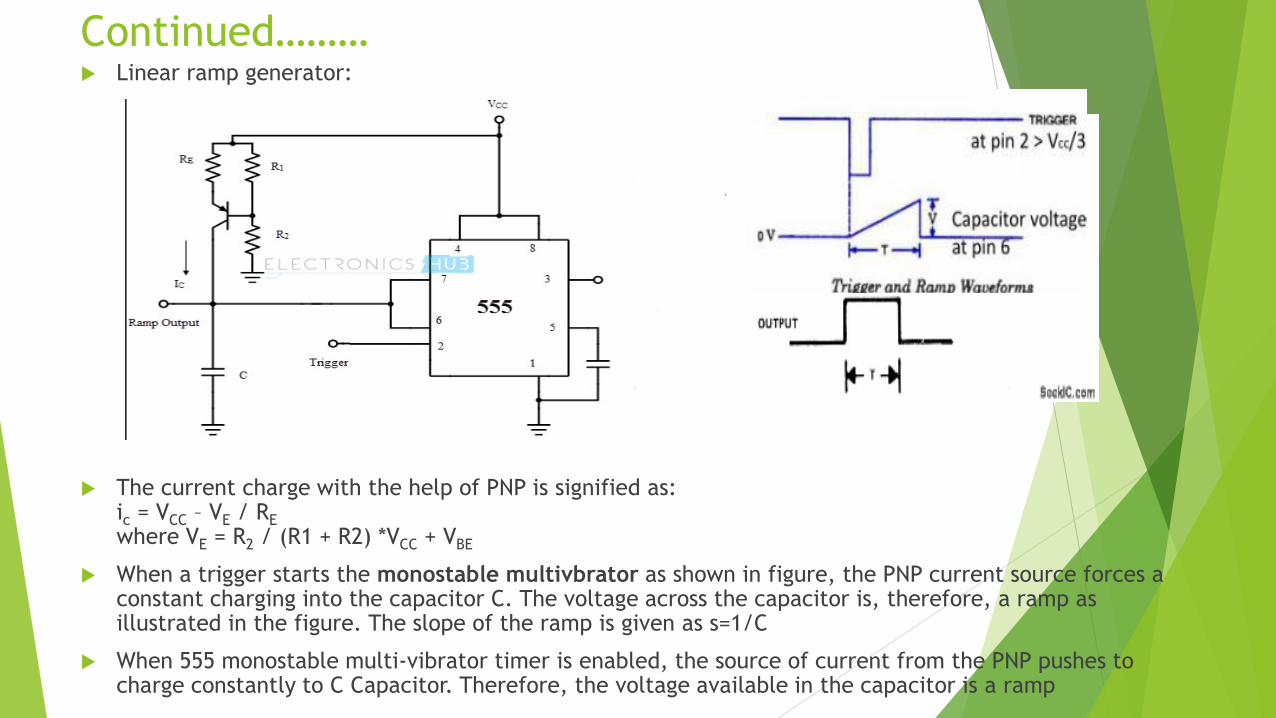
Continued……… Linear ramp generator:
The current charge with the help of PNP is signified as:ic = VCC – VE / RE
where VE = R2 / (R1 + R2) *VCC + VBE
When a trigger starts the monostable multivbrator as shown in figure, the PNP current source forces a constant charging into the capacitor C. The voltage across the capacitor is, therefore, a ramp as illustrated in the figure. The slope of the ramp is given as s=1/C
When 555 monostable multi-vibrator timer is enabled, the source of current from the PNP pushes to charge constantly to C Capacitor. Therefore, the voltage available in the capacitor is a ramp

Continued…. Frequency Divider:
When the IC 555 is used as a monostable multivibrator, a positive going rectangular pulse is available at the
output when a negative going pulse of short duration is applied at the trigger input. By adjusting the time
interval t of the charging or timing circuit the device can be made to work as a Frequency Divider circuit.
If the timing interval t is made slightly larger than the time period of the input pulse (trigger pulse), the
device can act as a Divide – by – two circuit. The timing interval can be controlled by appropriately
choosing the values of the resistor R and the capacitor C in the timing circuit. The waveforms of the input
and output signals corresponding to the divide–by–two circuit are shown below.

Continued….The circuit will trigger for the first negative pulse of the trigger input. As a
result, the output will go to high state. The output will remain high for the time
interval t. During this interval, even if a second negative going trigger pulse is
applied, the output will not be affected and continues to remain high as the
timing interval is greater than the time period of the trigger pulse. On the third
negative going trigger pulse, the circuit is retriggered.
So the circuit will trigger on every alternate negative going trigger pulse i.e.
there is one output pulse for every two input pulses and hence it is a divide–by–
two circuit. By adjusting the timing interval, a monostable circuit can be made
to produce integral fractions of the input frequency.
Pulse Width Modulation:
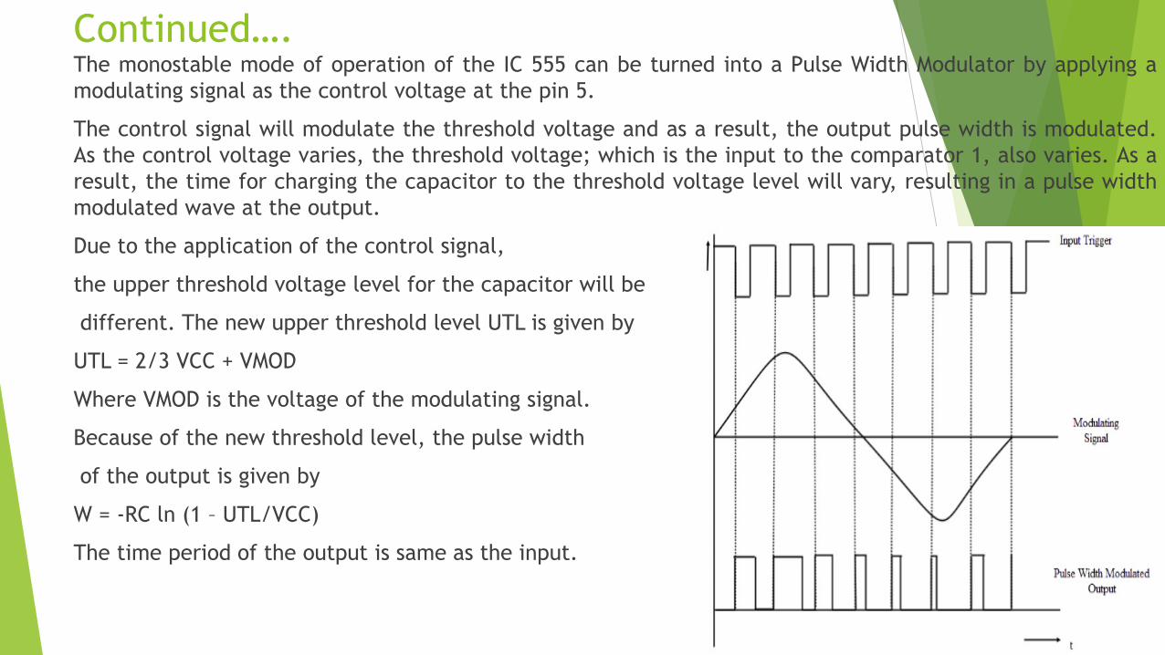
Continued….The monostable mode of operation of the IC 555 can be turned into a Pulse Width Modulator by applying a
modulating signal as the control voltage at the pin 5.
The control signal will modulate the threshold voltage and as a result, the output pulse width is modulated.
As the control voltage varies, the threshold voltage; which is the input to the comparator 1, also varies. As a
result, the time for charging the capacitor to the threshold voltage level will vary, resulting in a pulse width
modulated wave at the output.
Due to the application of the control signal,
the upper threshold voltage level for the capacitor will be
different. The new upper threshold level UTL is given by
UTL = 2/3 VCC + VMOD
Where VMOD is the voltage of the modulating signal.
Because of the new threshold level, the pulse width
of the output is given by
W = -RC ln (1 – UTL/VCC)
The time period of the output is same as the input.

astable multivibrator using 555
Diode D connected in parallel to Rb is only used when an output of duty cycle less than or equal to 50% is required.
The Trigger (pin 2) and Threshold (pin 6) inputs are connected to the capacitor which determines the output of the
timer.
The 4th pin is RESET pin which is active low and is connected to Vcc to avoid accidental resets.

Continued….. When the circuit is switched ON, the capacitor (C) voltage will be less than 1/3 Vcc. So the output
of the lower comparator will be HIGH and of the higher comparator will be LOW. This SETs the
output of the SR Flip-flop.(S=1,R=0,Q=1,Q’=0,o/p=1)
Thus the discharging transistor will be OFF as Q’=0,and the capacitor C starts charging from Vcc
through resistor Ra & Rb.
When the capacitor voltage will becomes slightly greater than 2/3 Vcc the output of the higher
comparator will be HIGH and of lower comparator will be LOW. This resets the SR Flip-
flop.(R=1,S=0,Q=0,Q’=1,o/p=0)
Thus the discharging transistor turns ON and the capacitor starts discharging through resistor Rb.
Soon the capacitor voltage will be less than 2/3 Vcc and greater than 1/3 Vcc and output of both
comparators will be LOW. So the output of the SR Flip-flop will be the previous state.
So the discharging of capacitor continuous.This process continuous and a rectangular wave will be
obtained at the output.
Continued… Voltage across the capacitor,vc=Vcc(1-𝑒
−𝑡
𝑅𝐶)
Let t1 is the time taken to charge from 0 to 2
3Vcc
2
3Vcc =Vcc(1-𝑒
−𝑡1
𝑅𝐶 ) -------t1=1.098RC-------1
Let t2 is the time taken to charge from 0 to 1
3Vcc
1
3Vcc =Vcc(1-𝑒
−𝑡2
𝑅𝐶 ) -------t2=0.405RC-------2
Time taken by the capacitor to charge from 1
3Vcc to
2
3Vcc
tON=t1-t2=1.098RC-0.405RC=0.693RC
tON for the circuit=0.693(𝑅𝑎 + 𝑅𝑏)𝐶
tOFF=0.693(Rb)C
Total time=tON+tOFF=0.693(Ra+2Rb)C f=1
𝑇=
1.45
𝑅𝑎+2𝑅𝑏 𝐶(Unsymmetrical waveform)
Note:tON>tOFF To obtain a symmetrical waveform,Ra=0,ie pin 7 is directly connected to Vcc
To set at practically any level.D1 is appended and is short circuited so that tON= 0.693(Ra)C during charging.tOFF=0.693(Rb)C during discharging.
T=tON+tOFF=0.693(Ra+Rb)C,f=1.45
𝑅𝑎+𝑅𝑏 𝐶and D=
𝑅𝑏
𝑅𝑎+𝑅𝑏(Symmetrical waveform)
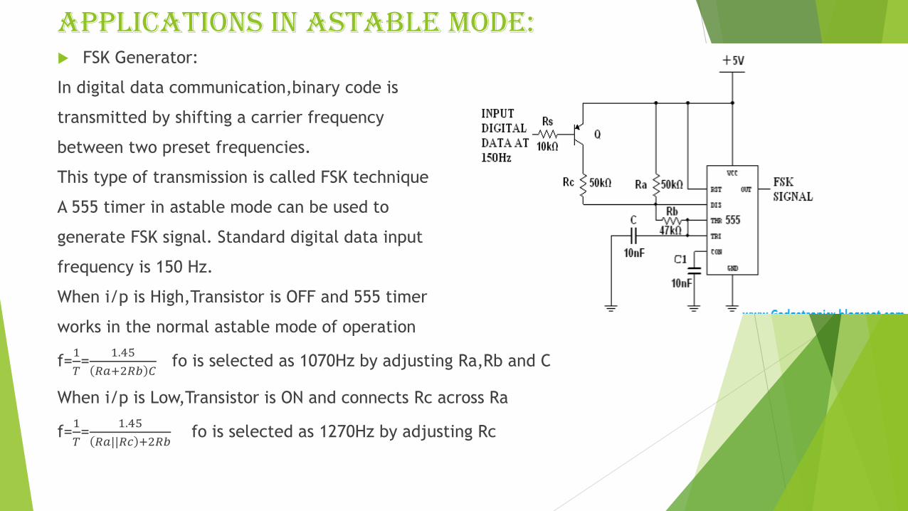
Applications in Astable mode: FSK Generator:
In digital data communication,binary code is
transmitted by shifting a carrier frequency
between two preset frequencies.
This type of transmission is called FSK technique
A 555 timer in astable mode can be used to
generate FSK signal. Standard digital data input
frequency is 150 Hz.
When i/p is High,Transistor is OFF and 555 timer
works in the normal astable mode of operation
f=1
𝑇=
1.45
𝑅𝑎+2𝑅𝑏 𝐶fo is selected as 1070Hz by adjusting Ra,Rb and C
When i/p is Low,Transistor is ON and connects Rc across Ra
f=1
𝑇=
1.45
𝑅𝑎||𝑅𝑐 +2𝑅𝑏fo is selected as 1270Hz by adjusting Rc

Continued… Pulse Position Modulator:
Constructed by applying a modulating signal
to pin 555 connected for astable operation.
The o/p pulse position varies with the
modulating signal,since the threshold voltage
And the time delay is varied.
2.Design an astable mv using 555 for a frequency of 1KHz and a duty cycle of 70%.Assume C=0.1µF
T=tON+tOFF=0.693(Ra+2Rb)C
Duty cycle=𝑡𝑂𝑁
𝑡𝑂𝑁+𝑡𝑂𝐹𝐹=𝑡𝑂𝑁
𝑇=
0.693(Ra+Rb)C0.693(Ra+2Rb)C
=0.7=7
10Ra=
4
3Rb
T= 0.693(Ra+2Rb)C=> 0.693∗10
3∗Rb∗0.1∗10−6 = 10−3
Rb=6.8KΏ

Continued….3. Design an astable mv using 555 for a frequency of 1KHz and a duty cycle of
25% and 50%. Assume C=0.1µF
Ans:f=1KHz and D=0.25
f=1.45
𝑅𝑎+2𝑅𝑏 𝐶=1KHz D=
𝑅𝑏
𝑅𝑎+2𝑅𝑏=0.25
0.25(Ra+2Rb)=Rb ;0.25Ra-0.5Rb=0---------1
Ra+2Rb=14500----------2
Ra=7.25KΏ,Rb=3.62KΏ
f=1KHz and D=0.5
f=1.45
𝑅𝑎+𝑅𝑏 𝐶=1KHz D=
𝑅𝑏
𝑅𝑎+𝑅𝑏=0.5
0.5(Ra+Rb)=Rb ;0.5Ra-0.5Rb=0----------1
Ra+Rb=14500------------2
As D=0.5,Ra=Rb=7.25kΏ

Analog multiplier A multiplier produces an o/p Vo is proportional to the product of two i/ps Vx and Vy
Vo=KVxVy(K-scaling factor=(1/10)𝑉−1
To perform analog multiplication,(i)logarithmic summing technique(ii)Pulse height/width modulation
technique(iii)variable transconductance technique(iv)Multiplication using Gilbert Cell
Gilbert Multiplier Cell
The Gilbert multiplier cell is a modification of the emitter coupled cell and this allows four –
quadrant multiplication. Therefore, it forms the basis of most of the integrated circuit balanced
Multipliers. Two cross- coupled emitter- coupled pairs in series connection with an emitter coupled
pair form the structure of the Gilbert multiplier cell.

Continued…. The collector current of Q3 and Q4 are given by
Ic3=𝐼𝑐1
1+𝑒−𝑉1/𝑉𝑇and Ic4=
𝐼𝑐1
1+𝑒𝑉1/𝑉𝑇
Similarly, the collector current of Q5 and Q6 are given by
Ic5=𝐼𝑐2
1+𝑒𝑉1/𝑉𝑇and Ic6=
𝐼𝑐2
1+𝑒−𝑉1/𝑉𝑇
collector current IC1 and IC2 of transistors Q1 and Q2 can be expressed as
Ic1=𝐼𝑒𝑒
1+𝑒−𝑉2/𝑉𝑇and Ic2=
𝐼𝑒𝑒
1+𝑒𝑉2/𝑉𝑇
Substituting the above equation in IC3 and IC4, we get
Ic3=𝐼𝑒𝑒
(1+𝑒−−𝑉1𝑉𝑇 )(1+𝑒
−−𝑉2𝑉𝑇 )
Ic4=𝐼𝑒𝑒
(1+𝑒𝑉1𝑉𝑇)(1+𝑒
−𝑉2𝑉𝑇 )
Similarly substituting Ic2= in Ic5 and IC6 , we get,
Ic5=𝐼𝑒𝑒
(1+𝑒−𝑉1𝑉𝑇)(1+𝑒
−𝑉2𝑉𝑇)
Ic6=𝐼𝑒𝑒
(1+𝑒−𝑉1𝑉𝑇 )(1+𝑒
𝑉2𝑉𝑇)
The differential output current I is given by
∆I =IL1 - IL2
= (IC3 +IC5) - ( IC4+IC6)
=(IC3 - IC6)-(IC4 - IC5)
∆I=Iee tanh( 𝑉1
2𝑉𝑇) tanh(
V22VT
)
when V1 and V2 are small,Gilbert cell can be used as four quadrant analog multiplier with the use of current to voltage converters

AD 633 ic Analog multiplier is a circuit whose output voltage at any instant is proportional to the
product of instantaneous value of two individual input voltages.
Important applications of these multipliers are multiplication, division, squaring and square –
rooting of signals, modulation and demodulation.
These analog multipliers are available as integrated circuits consisting of op-amps and other
circuit elements.
The AD633 multiplier is a four – quadrant analog multiplier.
It possesses high input impedance; this characteristic makes the loading effect on the signal
source negligible.

Continued…. It can operate with supply voltages ranging from ±18V.
IC does not require external components.
The typical range of the two input signals is ±10V.
The output Vo is the product of the two inputs Vx and Vy is divided by a reference voltage Vref.
Normally, the reference voltage Vref is internally set to 10V. Therefore, V0 =VxVy/10.
In other words, the basic input – output relationship can be defined by KVx Vy when K = 1/10,
a constant. Thus for peak input voltages of 10V, the peak magnitude of output voltage is 1/10
*10 *10 =10V. Thus, it can be noted that, as long as Vx < 10V and Vy < 10V, the multiplier output
will not saturate.
Applications of Multiplier ICs:
The multiplier ICs are used for the following purposes:
1. Voltage Squarer
2. Frequency doublers
3. Voltage divider
4. Square rooter
5. Phase angle detector
6. Rectifier

Phase Locked Loop(pll) Closed loop feedback system, whose o/p frequency and phase are in lock with the frequency and
phase of the input signal.
Can detect the phases of two signals
Main components:
▪ Phase detector/comparator
▪ LPF
▪ error amplifier(A)
▪ Voltage Controlled Oscillator
If an input signal vs of frequency fs is applied to PLL,phase detector compares the phase and
frequency of the incoming signal to that of the o/p vo of VCO

Continued…. If two signals differ in frequency /phase an error voltage ve is generated.
Phase detector is basically a multiplier which generates the sum and difference signal
fs+fo and fs-fo
LPF removes fs+fo component
Error amplifier amplifies the difference component and applied as a control voltage vc to VCO
Free running frequency fo of the VCO is determined by an external resistor and timing capacitor
By applying a dc control voltage, VCO frequency is shifted to reduce the difference frequency
Then the signal is in capture range.
As the process continues fo becomes equal to fs,except for a finite phase difference the circuit is
said to be locked.then the signal is in lock range
Once locked, PLL tracks the frequency changes of i/p signal.
PLL goes through three stages(i)free running frequency (ii)Capture range(iii)Locked/tracking
During the capture range, sine wave is obtained as LPF o/p(fs-fo).After adjustment of VCO
frequency,fo by the dc control voltage fs=fo. This is the locked/tracking range.Tracking range is
greater than Capture range.

Important definitions of PLL Lock –in-Range: Once PLL is locked, it can track frequency changes in the incoming signals. The
range of frequencies over which PLL can maintain lock with the incoming signal is called Lock –in
–range/Tracking Range.
Capture Range: The range of frequencies over which PLL can acquire lock with the incoming
signal is called Capture Range.
Pull-in-time: The total time taken by the PLL to establish lock.
Basic building blocks:
1. Phase detector-Analog
▪ Switch type phase detector-o/p from VCO controls the switching action and i/p frequency ,fs
▪ If Φ=0 fs=fo .The switch will be closed only when VCO o/p is +ve.
▪ o/p waveform will be half sinusoids half wave detector
▪ Average value of the o/p waveform is shown as dotted line
▪ The error voltage is zero when the phase shift between the two i/ps is 90 degree
▪ For perfect lock VCO o/p is out of phase.
Ve= KΦ (Φ-π
2) where KΦ is phase angle to voltage transfer coefficient

Continued….

Continued…. Phase detector-digital
(1)CMOS type XOR type
▪ when only one of the i/p fs or fo is high XOR o/p is high
▪ Used when both the i/p signals are square waves
▪ fs leads fo by Φ degrees
▪ Maximum dc o/p of the gate occurs when the phase diff
Is π
▪ Slope of the curve is KΦ
▪ For Vcc=5V KΦ =5
π=1.59V/rad
▪ Vdc is linear upto 180

Continued…..(2) Edge triggered phase detector
▪ RS FF made by NOR gate(CD4001)
▪ Used when both pulse signal with duty cycle less than 50%
▪ Better capture tracking and locking (Vdc is linear upto 360)

2. Voltage Controlled Oscillator(VCO)
Timing capacitor ,Ct is linearly charged/discharged
by a constant current source/sink
Amount of current is controlled by changing
modulation input or timing resistor Rt
Voltage across capacitor Ct is applied to
inverting i/p of schmitt trigger A2 via buffer amplifier A1
Voltage swing of Schmitt trigger is designed Vcc -0.5Vcc
If Ra=Rb voltage at non inverting i/p of A2 0.5Vcc-0.25Vcc
Voltage on Ct >0.5Vcc during charging,
o/p of Schmitt trigger goes low ie.0.5Vcc
At that time capacitor discharges,
and when it is at 0.25 Vcc, o/p of Schmitt trigger
goes high-Vcc

Calculation of o/p frequency Voltage on the capacitor changes from
0.25Vcc to 0.5 Vcc,Δ V=0.25Vcc
Capacitor charges with the constant current source
ΔVΔt
=iCt
>>0.25Vcc
Δt=
iCt
Δt =0.25Vcc∗Ct
i
Time period of triangular waveform=2 Δt
Frequency of oscillator ,fo=1T=
12Δt
>>>i
0.5Vcc∗Ct
As i=(𝑉𝑐𝑐−𝑣𝑐)
𝑅𝑡
fo =2(Vcc−vc)Vcc∗Rt∗Ct frequency can be changed by Rt,Ct or vc
If voltage at pin 5 is biased at 7/8Vcc, fo=0.25Rt∗Ct

Voltage to frequency conversion factor

3. Low pass filter May be active or passive
Removes high frequency noise and controls dynamic chara of PLL such as
Capture and lock range,Bandwidth and transient response
If filter BW reduces, response time increases and capture range reduces
Due to the presence of filter capacitor a short time memory to PLL
Produces a high noise immunity and locking stability

PLL IC 565 14 pin IC, usable over the frequency range 0.1 Hz to 500 kHz
The centre frequency of the PLL is determined
fo=0.25Rt∗Ct
where Rtand Ct are an external resistor and capacitor
connected to pins 8 and 9, respectively.
▪ The values of Rt and Ct are adjusted such that the
free running frequency will be at the centre of the
input frequency range. The value of Rt is restricted
from 2kΩ to 20 kΩ but a capacitor can have any value.
▪ A capacitor C connected between pin 7
and pin 10 forms a first order LPF with an internal
Resistance of 3.6 kΩ.
▪ The value of filter capacitor C should be large enough
to eliminate possible oscillations in the VCO voltage.

Continued…. Lock range and capture range equation:
Lock range increases with an increase in input voltage but decreases with increase in supply
voltage.

PLL Applications o/p of PLL system –voltage signal corresponding to error voltage/frequency signal at VCO o/p
Voltage signal is used in frequency discriminator
Frequency signal is used in signal conditioning, frequency synthesis/clock recovery applns
In case of voltage o/p, when PLL is locked to an i/p frequency, error voltage, vc(t) is
proportional to fs-fo.
In case of FM signal, when i/p frequency is varied, vc(t) is also varied to maintain the lock.
Thus it acts as frequency discriminator that converts i/p frequency changes to voltage changes.
In case of frequency o/p,if i/p signal consists of many frequency components PLL locks on one
particular frequency component.
1.Frequency Multiplication/Division
Nfs
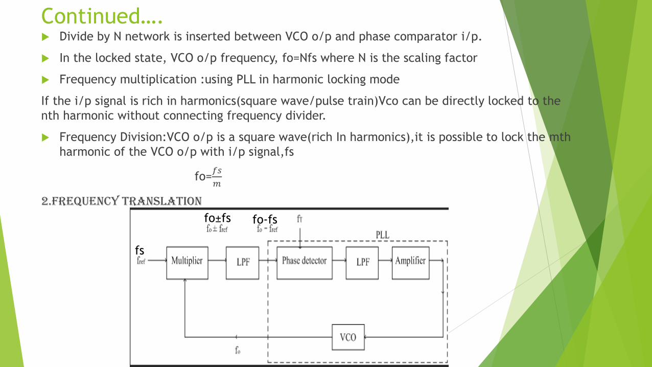
Continued…. Divide by N network is inserted between VCO o/p and phase comparator i/p.
In the locked state, VCO o/p frequency, fo=Nfs where N is the scaling factor
Frequency multiplication :using PLL in harmonic locking mode
If the i/p signal is rich in harmonics(square wave/pulse train)Vco can be directly locked to the
nth harmonic without connecting frequency divider.
Frequency Division:VCO o/p is a square wave(rich In harmonics),it is possible to lock the mth
harmonic of the VCO o/p with i/p signal,fs
fo=𝑓𝑠
𝑚
2.Frequency translation
fs
fo±fs fo-fs

Continued…. Multiplier(mixer) and LPF are connected externally to the PLL.
o/p of mixer contains the sum and difference. When passed thru LPF fo-fs is obtained
Translation /offset frequency (fT<<fs) is applied to phase comparator.
When PLL is locked state, fo-fs=fT;fo=fs+fT Thus incoming frequency fs is shifted by fT
3.AM Detection
PLL is locked to the carrier frequency of the incoming AM signal. Then fo=carrier frequency
VCO o/p is 90º out of phase and also AM i/p is also phase shifted by 90º.
Thus both signals are in same phase. O/p of the multiplier contains both the sum and difference signals and is filtered by LPF.

Continued…..4.FM demodulation
If PLL is locked to a FM signal,VCO tracks the instantaneous frequency of the i/p signal.
Filtered error voltage which controls the VCO and maintains lock with the i/p signal is the
demodulated FM o/p.
5.Frequency Shift Keying (FSK) Demodulator
Binary data is transmitted by means of a carrier frequency which is shifted between two preset
frequencies.—FSK technique

Continued…. Binary data can be retrieved using FSK demodulator at the receiving end.
When signal is applied at the i/p,loop locks to the i/p frequency and tracks it
between two frequencies with a corresponding dc shift at the o/p.
3 stage filter removes carrier component and o/p signal is made logic
compatible by a voltage comparator.

Monolithic voltage regulators Provide a stable dc voltage for powering other electronic circuits
Provide substantial o/p current
(a)Series regulator:
Series regulator :power transistor in series b/w unregulated dc input and the load.o/p voltage is
controlled by the continuous voltage drop across series pass transistor.as the transistor conducts in
the active or linear region. These regulators are called Linear regulators.
Linear regulators –fixed /variable o/p voltage which can be –ve or +ve.
(b)Switching regulator:
Operate power transistor as a high frequency on/off switch,so that power transistor does not
conduct current continuously. Efficiency is improved.

Series opamp regulator
Provides a stable dc voltage independent of load current ,temperature and ac line voltage
variations.
Circuit consists of following four parts:
(a)Reference voltage circuit
(b)Error amplifier
(c)Series pass Transistor
(d)Feedback network
Unregulated
power supply
βVo
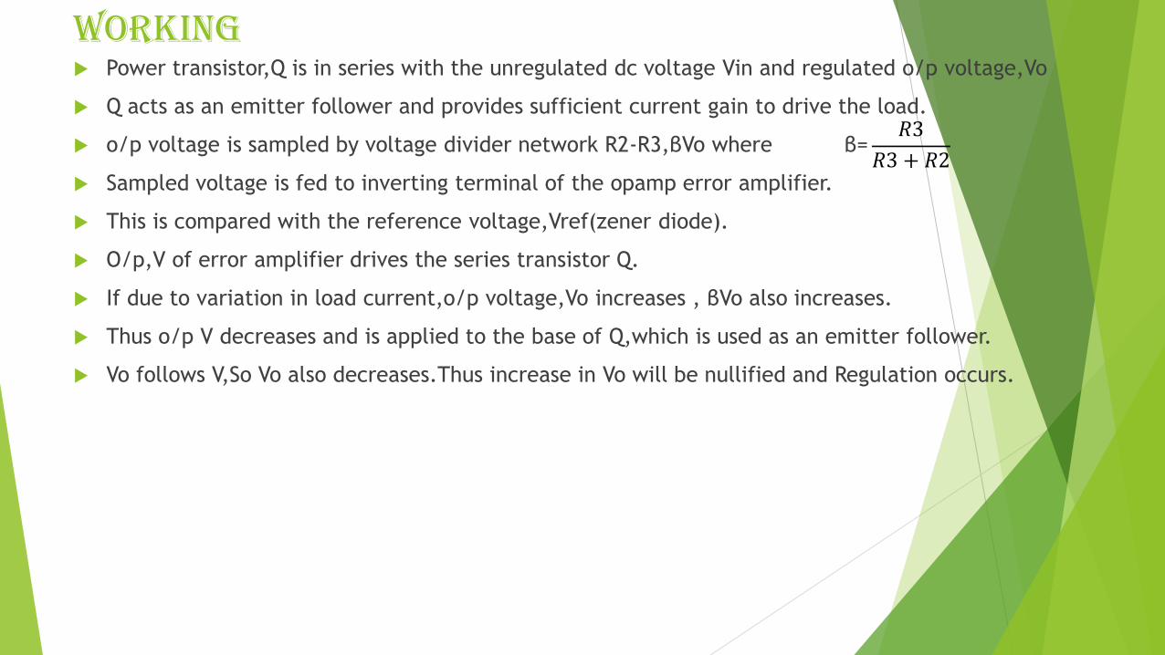
working Power transistor,Q is in series with the unregulated dc voltage Vin and regulated o/p voltage,Vo
Q acts as an emitter follower and provides sufficient current gain to drive the load.
o/p voltage is sampled by voltage divider network R2-R3,βVo where β=
Sampled voltage is fed to inverting terminal of the opamp error amplifier.
This is compared with the reference voltage,Vref(zener diode).
O/p,V of error amplifier drives the series transistor Q.
If due to variation in load current,o/p voltage,Vo increases , βVo also increases.
Thus o/p V decreases and is applied to the base of Q,which is used as an emitter follower.
Vo follows V,So Vo also decreases.Thus increase in Vo will be nullified and Regulation occurs.
𝑅3
𝑅3 + 𝑅2

Fixed voltage series regulators-78XX,79XX Low cost,high reliability,reduction in size,easy to use,excellent performance
Regulator IC units contain circuitry for reference source,comparator,control unit and
overload protection in a single IC.
1-unregulated input voltage,2-regulated output voltage,3-ground
Available in plastic packages(TO-220 type) and Metal packages(TO-3 type)

78XX 3 terminal,positive fixed voltage regulators.
Seven o/p voltage options available 5,6,8,12,15,18 and 24V
Last number XX indicates the o/p voltage.
7815 represents a 15 V regulator.
Input capacitance,C1 to cancel the inductive effects due to long distribution
leads.
O/p capacitance,C2 improves transient response.

79XX 3 terminal,negative fixed voltage regulators.
Two extra voltage options of -2V and -5.2V
Characteristics of 3 terminal IC regulators
Vo-The regulated o/p voltage is fixed at a value specified by the manufacturer.
Vin ≥ |Vo|+2-The unregulated input voltage must be atleast 2V more than the
regulated o/p voltage.Eg:If Vo=5V then Vin=7V
Thermal Shutdown-IC has a temperature sensor (built in) which turns off the IC when it
becomes too hot(125ºC-150ºC).The o/p current will drop till the IC is cooled.
Io(max)-The load current may vary from 0 to rated maximum o/p current.IC is usually
provided with a heat sink, else it may not provide the rated max o/p current.

Adjustable regulator
Ground terminal is floating
Vo=Vr+Vpot=Vr+(Iadj+I1)R2
=Vr+IadjR2+𝑉𝑟𝑒𝑓
𝐼1R2
=(1+𝑅2
𝑅1)𝑉𝑟+IadjR2 where Vr is the regulated voltage difference b/w out and gnd terminal
The effect of Iadj is minimized by choosing R2 small enough to minimize the term IadjR2
The minimum o/p voltage is the value of the fixed voltage available from the regulator.
Vpot

Problem: Specify suitable component values to get Vo=7.5V in the circuit using a 7805 regulator
Ans:For 7805,Iadj=4.2mA.Let I1=25mA
As Vr=5V for 7805 ,R1=Vr/I1=5/25mA=200Ώ
Choose R2 to develop a voltage of 2.5V across it.[ Vo-Vr=(Iadj+I1)R2,Vo=7.5V,Vr=5V]
R2=2.5𝑉
Iadj+I1=
2.5𝑉
4.2mA+25mA= 85.6 Ώ
Choose R2=85 Ώ

IC 723(General Purpose Regulator)3 terminal regulators(78XX and 79XX) have limitations like
No short circuit protection
Fixed o/p voltage(+/-)

Continued…. Low current device can be boosted to provide 5A or more by connecting external components.
IC 723 is Adjustable over a wide range
Limitation is it has no built in thermal protection and no short circuit current limits.
Functional block diagram
Section 1:Constant current source,zener diode and reference amplifier produces a fixed voltage of 7V at Vref. Constant current source forces the zener to operate at a fixed point so that zener o/ps a fixed voltage.
Section 2:consists of error amplifier, series pass transistor,Q1 and current limit transistor,Q2.Error amplifier compares a sample of the o/p voltage applied at INV terminal to Vref applied at NI terminal
Error signal controls the conduction of Q1
Vref

Low voltage and high voltage configuration Positive low voltage (2V to 7V) regulator
Voltage at NI terminal of error amplifier due to R1R2 divider network,=Vref𝑅2
𝑅1+𝑅2
Difference between NI terminal voltage and INV terminal voltage(Vo) is amplified by the error amplifier.
O/p of error amplifier drives the pass transistor Q1 to minimize the difference
Q1 acts as an emitter follower ,Vo=Vref𝑅2
𝑅1+𝑅2

Continued…. If o/p voltage goes low,INV terminal voltage also becomes low making o/p of error amplifier more
positive and this drives Q1 more into conduction.
This allows more current to flow into the load causing voltage across load to increase.Thus initial drop
in the load voltage ha been compensated.
Similarly increase in load voltage is also regulated.
Vref=7.15V Vo=7.15𝑅2
𝑅1+𝑅2which will be always less than 7V and thus Low voltage Regulator
Positive high voltage (>7V) regulator
To produce regulated o/p voltage >7V
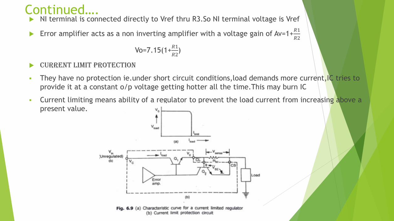
Continued…. NI terminal is connected directly to Vref thru R3.So NI terminal voltage is Vref
Error amplifier acts as a non inverting amplifier with a voltage gain of Av=1+𝑅1
𝑅2
Vo=7.15(1+𝑅1
𝑅2)
Current limit protection
▪ They have no protection ie.under short circuit conditions,load demands more current,IC tries to
provide it at a constant o/p voltage getting hotter all the time.This may burn IC
▪ Current limiting means ability of a regulator to prevent the load current from increasing above a
present value.

working▪ O/p voltage remains constant for load current below Ilimit
▪ As current approaches the limit o/p voltage drops and this is done by
connecting an external resistor Rsc b/w CS and CL terminals.
▪ CL terminal is connected to Vo and CS to the load
▪ Load current produces a voltage drop across Rsc which is applied directly
across the BE jn of Q2.Q2 turns On when it becomes ≈0.5V
▪ Current from error amplifier flows to collector of Q2 and base current of Q1 is
decreased which reduces emitter current of Q1.So any increase in load
current will be nullified.
Ilimit =𝑉𝑠𝑒𝑛𝑠𝑒
𝑅𝑠𝑐=0.5𝑉
𝑅𝑠𝑐--------------current sensing technique
Current foldback
▪ Load current is maintained at a present value in current limiting technique.
▪ When overload condition occurs o/p Vo drops to zero.
▪ If the load is short circuited maximum current flows thru regulator.
▪ To protect this, short circuit current should be limited.
▪ Current foldback is used

working As current demand increases,Vo is held constant till a present
Current level,Iknee is reached.If current exceeds this level,both o/p voltage and o/p current decreases
Voltage at CL is divided by R3-R4 .
CL transistor Q2 conducts when
voltage across Rsc ≈0.5V(atleast)
When Q2 conducts Q1 becomes OFF
And current Il decreases and Vo
decreases

Continued…. Current boosting
Maximum current that 723 IC can provide is 140mA
Current level can be boosted by adding a transistor Q1
to the voltage regulator.
Collector current of pass transistor Q1 comes from
Unregulated Vdc.o/p current from Vo terminal drives
the base of pass transistor Q1.This base current gets
multiplied by the beta of pass transistor
so that 723 has to provide only the base current .
I load=β pass transistor *Io(723)

Questions:1. With the help of circuit diagram, internal functional diagram and relevant
graphs, explain the working of a Monostable Multivibrator using IC555.
2. Draw the input and different output waveforms of Monostable multivibratorusing 555. Derive the equation for pulse width.
3. With the help of circuit diagram and internal diagram, explain the working ofa Low Voltage Regulator using IC723.
4. With the help of block diagram explain the working of PLL. Explain any twoapplications of PLL.
5. Explain the operation of Phase Locked Loop. What is lock range and capturerange?
6. Explain the internal diagram of I.C. 723.Explain how current boosting isachieved using I.C 723
7. Design a circuit to convert 1 KHz, 50% duty cycle square wave to 1 KHz, 30%duty cycle rectangular wave.
8. How to configure fold back current limiting protection in 723 voltageregulator IC. Explain the circuit with internal block diagram of the IC.
9. How phase detector is implemented in digital PLL?
10. Design a circuit to multiply the incoming frequency by a factor of 5 using 565PLL.


![Analog Electronic Circuits [15MEC31T ] Question Bank - Jain ...](https://static.fdokumen.com/doc/165x107/63160831aca2b42b580e172e/analog-electronic-circuits-15mec31t-question-bank-jain-.jpg)