
MICROELECTRONICS CIRCUITS
59
1 MICROELECTRONICS CIRCUITS Subject Code: 10EC63 VI semester ECE References: Text Book: 1. “Microelectronic Circuits”, Adel Sedra and K.C. Smith, 5th Edition, Oxford University Press, International Version, 2009. Reference Book: 1. “Fundamentals of Microelectronics” , Behzad Razavi, John Wiley India Pvt. Ltd, 2008. 2. “Microelectronics – Analysis and Design”, Sundaram Natarajan, Tata McGraw- Hill, 2007 Create PDF files without this message by purchasing novaPDF printer (http://www.novapdf.com)
-
Upload
khangminh22 -
Category
Documents
-
view
0 -
download
0
Transcript of MICROELECTRONICS CIRCUITS

1
MICROELECTRONICS CIRCUITS Subject Code: 10EC63
VI semester ECE
References: Text Book: 1. “Microelectronic Circuits”, Adel Sedra and K.C. Smith, 5th Edition, Oxford University Press, International Version, 2009. Reference Book: 1. “Fundamentals of Microelectronics” , Behzad Razavi, John Wiley India Pvt. Ltd, 2008. 2. “Microelectronics – Analysis and Design”, Sundaram Natarajan, Tata McGraw-Hill, 2007
Create PDF files without this message by purchasing novaPDF printer (http://www.novapdf.com)

2
MODIFIED SYLLABUS
Create PDF files without this message by purchasing novaPDF printer (http://www.novapdf.com)

3
Unit 1 – Chapter 4
MOS Field-Effect Transistors (MOSFETs)
UNIT 1 OUTLINE 1.1 Device Structure and Physical Operation 1.2 Current – Voltage Characteristics 1.3 MOSFET Circuits at DC 1.4 Biasing in MOS amplifier circuits 1.5 Small Signal Operation and Models 1.6 The MOSFET as an Amplifier and as a Switch 1.7 Single Stage MOS amplifiers 1.8 SPICE MOSFET models and examples LEARNING OUTCOMES: At the end of this chapter one can clearly get to know the following: Understanding Physical construction and operation of an Enhancement
MOSFET Drawing the V-I characteristics of n and p channel E-MOSFET DC operation or biasing of MOSFETs AC Operation: Small signal modeling of MOSFETs Single stage MOS amplifiers : Common Source, Common Drain and Common
Gate amplifiers SPICE modeling of MOSFETs INTRODUCTION
Along with the Junction Field Effect Transistor (JFET), there is another type of Field Effect Transistor available whose Gate input is electrically insulated from the main current carrying channel and is therefore called an Insulated Gate Field Effect Transistor or IGFET. The most common type of insulated gate FET which is used in many different types of electronic circuits is called the Metal Oxide Semiconductor Field Effect Transistor or MOSFET for short.
The IGFET or MOSFET is a voltage controlled field effect transistor that differs from a JFET in that it has a "Metal Oxide" Gate electrode which is electrically insulated from the main semiconductor N-channel or P-channel by a thin layer of insulating material usually silicon dioxide (commonly known as glass). This insulated metal gate electrode can be thought of as one plate of a capacitor. The isolation of the controlling Gate makes the input resistance of the MOSFET extremely high in the Mega-ohms (MΩ) region thereby making it almost infinite.
Create PDF files without this message by purchasing novaPDF printer (http://www.novapdf.com)

4
As the Gate terminal is isolated from the main current carrying channel "NO current flows into the gate" and just like the JFET, the MOSFET also acts like a voltage controlled resistor were the current flowing through the main channel between the Drain and Source is proportional to the input voltage. Also like the JFET, this very high input resistance can easily accumulate large amounts of static charge resulting in the MOSFET becoming easily damaged unless carefully handled or protected.
MOSFETs are three terminal devices with a Gate, Drain and Source and both P-channel (PMOS) and N-channel (NMOS) MOSFETs are available. The main difference this time is that MOSFETs are available in two basic forms:
1. Depletion Type - the transistor requires the Gate-Source voltage, (VGS) to switch the device "OFF". The depletion mode MOSFET is equivalent to a "Normally Closed" switch.
2. Enhancement Type - the transistor requires a Gate-Source voltage, (VGS) to switch the device "ON". The enhancement mode MOSFET is equivalent to a "Normally Open" switch.
Basic operating principle of a MOSFET:
Use of the voltage between two terminals to control the current flowing in the third terminal
Also, the control signal can be used to cause the current in the third terminal to change from zero to a large value, thus allowing the device to act as a switch.
The FET differs from BJT in the following important characteristics:
1. It is a unipolar device 2. It is simpler to fabricate 3. Occupies less space in Integrated form, packaging density is high(>200 million) 4. It has higher input resistance 5. It can be used as a symmetrical Bilateral switch 6. It functions as a memory device 7. It is less noisy than a BJT 8. It exhibits no offset voltage at zero input, hence making an excellent signal
chopper
THE ONLY DISADVANTAGE IS IT HAS SMALLER GAIN- BANDWIDTH PRODUCT THAN BJT
The symbols and basic construction for both configurations of MOSFETs are shown below.
Create PDF files without this message by purchasing novaPDF printer (http://www.novapdf.com)
5
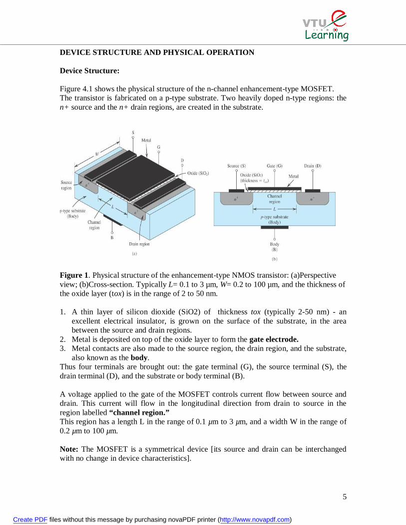
DEVICE STRUCTURE AND PHYSICAL OPERATION Device Structure: Figure 4.1 shows the physical structure of the n-channel enhancement-type MOSFET. The transistor is fabricated on a p-type substrate. Two heavily doped n-type regions: the n+ source and the n+ drain regions, are created in the substrate.
Figure 1. Physical structure of the enhancement-type NMOS transistor: (a)Perspective view; (b)Cross-section. Typically L= 0.1 to 3 µm, W= 0.2 to 100 µm, and the thickness of the oxide layer (tox) is in the range of 2 to 50 nm. 1. A thin layer of silicon dioxide (SiO2) of thickness tox (typically 2-50 nm) - an
excellent electrical insulator, is grown on the surface of the substrate, in the area between the source and drain regions.
2. Metal is deposited on top of the oxide layer to form the gate electrode. 3. Metal contacts are also made to the source region, the drain region, and the substrate,
also known as the body. Thus four terminals are brought out: the gate terminal (G), the source terminal (S), the drain terminal (D), and the substrate or body terminal (B). A voltage applied to the gate of the MOSFET controls current flow between source and drain. This current will flow in the longitudinal direction from drain to source in the region labelled “channel region.” This region has a length L in the range of 0.1 µm to 3 µm, and a width W in the range of 0.2 µm to 100 µm. Note: The MOSFET is a symmetrical device [its source and drain can be interchanged with no change in device characteristics].
Create PDF files without this message by purchasing novaPDF printer (http://www.novapdf.com)

6
Device Operation: (i) With No Gate Voltage With no bias voltage applied to the gate, two back-to-back diodes exist in series between drain and source. They prevent current conduction from drain to source when a voltage VDS is applied. The path between drain and source has a very high resistance (of the order of 1012Ω). (ii) Creating a Channel for Current Flow The source and the drain are grounded and a positive voltage is applied to the gate. The positive voltage on the gate causes the free holes (which are positive charged) to be repelled from the region of the substrate under the gate. These holes are pushed downward into the substrate, leaving behind a carrier-depletion region as shown below.
The positive gate voltage attracts electrons from the n+ source and drain regions into the channel region. When a sufficient number of electrons accumulate near the surface of the substrate under the gate, an n region is in effect created, connecting the source and drain regions, as indicated in Fig. 4.2. This MOSFET is called an n-channel MOSFET or, alternatively, an NMOS transistor. The induced channel is also called an inversion layer. The induced n region thus forms a channel for current flow from drain to source. Note: The value of VGS at which a sufficient number of mobile electrons accumulate in the channel region to form a conducting channel is called the threshold voltage and is denoted Vt.
Figure 4.2 The enhancement-type NMOS transistor with a positive voltage applied to the gate. An n channel is induced at the top of the substrate beneath the gate.
Create PDF files without this message by purchasing novaPDF printer (http://www.novapdf.com)
7
The value of Vt is controlled during device fabrication and typically lies in the range of 0.5 V to 1.0V. Now if a voltage is applied between drain and source, current flows through this induced n region. The gate and the channel region of the MOSFET form a parallel-plate capacitor, with the oxide layer acting as the capacitor dielectric. An electric field thus develops in the vertical direction. It is this field that controls the amount of charge in the channel, and thus it determines the channel conductivity and, in turn, the current that will flow through the channel when a voltage vDS is applied.
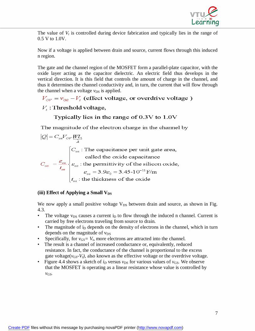
(iii) Effect of Applying a Small VDS We now apply a small positive voltage VDS between drain and source, as shown in Fig. 4.3. • The voltage vDS causes a current iD to flow through the induced n channel. Current is
carried by free electrons traveling from source to drain. • The magnitude of iD depends on the density of electrons in the channel, which in turn
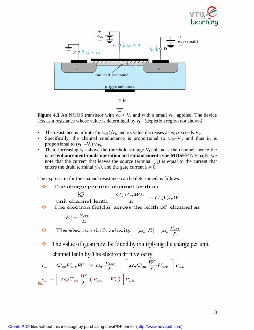
depends on the magnitude of vDS • Specifically, for vGS= Vt, more electrons are attracted into the channel. • The result is a channel of increased conductance or, equivalently, reduced resistance. In fact, the conductance of the channel is proportional to the excess gate voltage(vGS-Vt), also known as the effective voltage or the overdrive voltage. • Figure 4.4 shows a sketch of iD versus vDS for various values of vGS. We observe that the MOSFET is operating as a linear resistance whose value is controlled by vGS.
Create PDF files without this message by purchasing novaPDF printer (http://www.novapdf.com)
8
Figure 4.3 An NMOS transistor with vGS> Vt and with a small vDS applied. The device acts as a resistance whose value is determined by vGS (depletion region not shown).
• The resistance is infinite for vGS≦Vt, and its value decreases as vGS exceeds Vt. • Specifically, the channel conductance is proportional to vGS–Vt, and thus iD is
proportional to (vGS–Vt) vDS. • Then, increasing vGS above the threshold voltage Vt enhances the channel, hence the
name enhancement-mode operation and enhancement-type MOSFET. Finally, we note that the current that leaves the source terminal (iS) is equal to the current that enters the drain terminal (iD), and the gate current iG= 0.
The expression for the channel resistance can be determined as follows:
Create PDF files without this message by purchasing novaPDF printer (http://www.novapdf.com)
9
Figure 4.4 The iD–vDS characteristics of the MOSFET in Fig. 4.3 when the voltage applied between drain and source, vDS, is kept small. The device operates as a linear resistor whose value is controlled by vGS. (iv) Operation as vDS Is Increased • As we travel along the channel from source to drain, the voltage (measured relative to
the source) increases from 0 to vDS. • Thus the voltage between the gate and points along the channel decreases from vGS at the source end to vGS–vDS at the drain end.
Create PDF files without this message by purchasing novaPDF printer (http://www.novapdf.com)

10
• Since the channel depth depends on this voltage, we find that the channel is no longer of uniform depth. As vDS is increased, the channel becomes more tapered and its resistance increases correspondingly. When vDS is increased to the value that reduces the voltage between gate and channel
at the drain end to Vt , vGD= Vt or vGS–vDS= Vt or vDS= vGS–Vt
the channel depth at the drain end decreases to almost zero, and the channel is said to be pinched off. As the value reached for vDS= vGS–Vt, the drain current saturates, and the
MOSFET is said to have entered the saturation region of operation. vDSsat= vGS–Vt (4.1)
The region of the iD–vDS characteristic obtained for vDS< vDSsat is called the triode region.
Figure 4.5 Operation of the enhancement NMOS transistor as vDS is increased. The induced channel acquires a tapered shape, and its resistance increases as vDS is increased. Here, vGS is kept constant at a value > Vt.
Create PDF files without this message by purchasing novaPDF printer (http://www.novapdf.com)

11
Create PDF files without this message by purchasing novaPDF printer (http://www.novapdf.com)

12
Derivation of the iD-vDS Relationship In the MOSFET, the gate and the channel region form a parallel-plate capacitor for which the oxide layer serves as a dielectric.
Figure 4.7 Derivation of the iD-vDS Relationship of the NMOS transistor If the capacitance per unit gate area is denoted Cox and the thickness of the oxide layer is tox, then Cox=εox/ tox (4.2) Where εox is the permittivity of the silicon oxide, ε= 3.9 ε0= 3.9×8.854×10-12 = 3.45×10⁻¹¹F/m Initially 푣 > 푉 푡표푖푛푑푢푐푒푐ℎ푎푛푛푒푙푎푛푑푣 < 푣 − 푉 and triode region of operation is assumed i.e
Create PDF files without this message by purchasing novaPDF printer (http://www.novapdf.com)

13
The gate and channel region form a parallel plate capacitor with oxide layer as the dielectric. If the capacitance per unit area is Cox and the thickness of the oxide layer is tox Now consider the infinitesimal strip of the gate at distance x from the source. The capacitance of the strip is Cox W dx To find the charge stored on this strip of gate capacitance, we multiply capacitance by effective voltage between Gate and the Channel at point x 푑푞 = −퐶 (푊푑푥)[푣 − 푣(푥)− 푉 ] The voltage vDS produces an electric field along the channel in the negative x direction. At point x this field can be expressed as
퐸(푥) = −푑푣(푥)푑푥
The Electric field E(x) causes the electron charge dq to drift toward the drain with a velocity dx/dt
푑푥푑푡 = −µ 퐸(푥) = µ
푑푣(푥)푑푥
The resulting drift current ‘i’ can be obtained as follows:
푖 = 푑푞푑푡 =
푑푞푑푥
푑푥푑푡
Substituting the above values, the drain current ‘i’ can be obtained as follows:
푖 = −µ 퐶 푊[푣 − 푣(푥)− 푉 ] 푑푣(푥)푑푥
Since the current ‘i’ is constant at all points along the channel it must be equated to the drain current iD
푖 = −푖 = µ 퐶 푊[푣 − 푣(푥)− 푉 ] 푑푣(푥)푑푥
푖 푑푥 = µ 퐶 푊[푣 − 푣(푥)− 푉 ]푑푣(푥)
Integrating both sides from 푥 = 0푡표푥 = 퐿푎푛푑푣(0) = 0푡표푣(퐿) = 푣
푖 푑푥 = µ 퐶 푊[푣 − 푣(푥)− 푉 ]푑푣(푥)
Gives
푖 = µ 퐶푊퐿
[푣 − 푉 ]푣 −12 푣 ]
Create PDF files without this message by purchasing novaPDF printer (http://www.novapdf.com)

14
In the saturation region substituting we get
푖 = 12 (µ 퐶 )
푊퐿 (푣 − 푉 )
The process transconductance parameter is denoted kn’ and kn’=µnCox Therefore the iD –vDS relationship can be expressed in terms of kn
’ as follows:
푖 = 푘 푊퐿
[푣 − 푉 ]푣 −12 푣 ] … . . 푡푟푖표푑푒푟푒푔푖표푛
푖 = 12 푘 (푣 − 푉 ) … … … 푠푎푡푢푟푎푡푖표푛푟푒푔푖표푛
• The drain current is proportional to the ratio of the channel width W to the channel length L, known as the aspect ratio of the MOSFET. • For a given fabrication process, however, there is a minimum channel length, Lmin. In fact, the minimum channel length that is possible with a given fabrication process is used to characterize the process and is being continually reduced as technology advances. State of the art MOS technology is a 0.13-µm process, meaning that for this process the minimum channel length possible is 0.13 µm, corresponding to a minimum width of 0.16 µm and tox= 2nm.
Solution:
(a) 퐶 = = . ××
= 4.32 × 10 퐹/푚 = 4.32푓퐹/µ푚
푘 =µ 퐶 = 450 . 푠 × 4.32푓퐹/ µ푚 = 194 × 10 퐹/푉. 푠 = 194µ퐴/푉
(b) For operation in the saturation region,
푖 = 12 푘 (푣 − 푉 )
Create PDF files without this message by purchasing novaPDF printer (http://www.novapdf.com)

15
Thus,100 = × 194 ×.
(푉 − 0.7 ) which results in 푉 − 0.7 = 0.32푉 Or 푉 = 1.02푉 And 푉 = 푉 − 0.7 = 0.32푉 For the MOSFET in the triode region with 푣 very small,
푖 = 푘푊퐿 (푣 − 푉 ) 푣
From which the drain to source resistance rDS can be found as
푟 =푣푖 |푠푚푎푙푙푣
=[ ( ) ]
Thus 1000 =
[ × × ( . ) ]
which yields,
푉 − 0.7 = 0.52푉 Or 푉 = 1.22푉 4.1.7 The p-Channel MOSFET A p-channel enhancement-type MOSFET (PMOS transistor), fabricated on an n-type substrate with p+ regions for the drain and source, has holes as charge carriers. The device operates in the same manner as the n-channel device except that vGS and vDS are negative and the threshold voltage Vt is negative. Also, the current iD enters the source terminal and leaves through the drain terminal.
Figure 4.8 Physical construction of p channel E-MOSFET
Create PDF files without this message by purchasing novaPDF printer (http://www.novapdf.com)

16
In general, NMOS devices are normally preferred to PMOS because
Smaller Operate faster and Requires lower supply voltages than PMOS.
4.1.8 Complementary MOS or CMOS As the name implies, complementary MOS technology employs MOS transistors of both polarities. At present time CMOS is the most widely used of all the IC technologies. Figure 4.9 shows cross-section of a CMOS chip illustrating how the PMOS and NMOS transistors are fabricated. While the NMOS transistor is implemented directly in the p-type substrate, the PMOS transistor is fabricated in a specially created n region, known as an nwell.
Figure 4.9 Cross-section of a CMOS integrated circuit. Not shown are the connections made to the p-type body and to the n well; the latter functions as the body terminal for the p-channel device. 4.2 CURRENT-VOLTAGE CHARACTERISTICS of an n-channel E-MOSFET The drain is always positive relative to the source in an n-channel FET. The circuit Symbol for an n-channel E-MOSFET is as shown below:
Create PDF files without this message by purchasing novaPDF printer (http://www.novapdf.com)

17
Figure 4.10 (a) Circuit symbol for the n-channel enhancement-type MOSFET. (b) Modified circuit symbol with an arrowhead on the source terminal to distinguish it from the drain and to indicate device polarity (i.e., n channel). (c) Simplified circuit symbol to be used when the source is connected to the body or when the effect of the body on device operation is unimportant. Consider an n-channel enhancement-type MOSFET with voltages vGS and vDS applied and with the normal directions of current flow indicated.
Figure 4.11 (a) An n-channel enhancement-type MOSFET with vGS and vDS applied and with the normal directions of current flow indicated. (b)The iD–vDS characteristics for a device with k’n(W/L) = 1.0 mA/V2. There are three distinct regions of operation: the cutoff region, the triode region, and the saturation region. • The saturation region is used if the FET is to operate as an amplifier. • For operation as a switch, the cutoff and triode regions are utilized To operate the MOSFET in the triode region we must first induce a channel,
Create PDF files without this message by purchasing novaPDF printer (http://www.novapdf.com)

18
And then keep vDS small enough so that the channel remains continuous. This is achieved by ensuring that the gate-to-drain voltage is
The n-channel enhancement-type MOSFET operates in the triode region when vGS is greater than Vt and the drain voltage is lower than the gate voltage by at least Vt volts. In the triode region, the iD-vDS characteristics can be described by
where kn’= µnCox is the process transconductance parameter. If vDS is sufficiently small
Specifically, for vGS set to a value VGS, rDS is given by,
It is also useful to express rDS in terms of the gate-to-source overdrive voltage
To operate the MOSFET in the saturation region, a channel must be induced, vGS≧Vt (Induced channel) and then the Gate-Drain and drain source voltages should be vGD≦Vt or vDS≧vGS-Vt (Pinched-off channel) The n-channel enhancement-type MOSFET operates in the saturation region when vGS≧Vt and vDS is higher than the gate voltage by at least Vt volts.
Create PDF files without this message by purchasing novaPDF printer (http://www.novapdf.com)

19
The boundary between the triode region and the saturation region is characterized by vDS= vGS-Vt (Boundary) Substituting this value of vDS into Eq. (4.11)
Since the drain current is independent of the drain voltage, the saturated MOSFET behaves as an ideal current source whose value is controlled by vGS according to the nonlinear relationship in the above Eq.
Figure 4.12 The iD–vGS characteristic for an enhancement-type NMOS transistor in saturation (Vt = 1 V, k’n W/L = 1.0 mA/V2). Figure 4.13 shows a circuit representation of this view of MOSFET operation in the saturation region. Note that this is a large-signal equivalent-circuit model.
Figure 4.13 Large-signal equivalent-circuit model of an n-channel MOSFET operating in the saturation region.
Create PDF files without this message by purchasing novaPDF printer (http://www.novapdf.com)

20
Finite Output Resistance in Saturation Change in vDS in saturation, implies no change in corresponding iD and hence infinite resistance in saturation. This is because of the assumption that once channel is pinched off, further increase in vDS have no effect on the channel’s shape. But, in practice, as vDS is increased, the channel pinch-off point is moved slightly away from the drain, toward the source. Channel Length Modulation: With an increase in vDS, the channel length decreases from L to L-ΔL, but voltage drop across it remains the same, and the additional drop will appear across the depletion region between the end of the channel and the drain
To account for the dependence of iD on vDS in saturation, replace L with L- ΔL in the iD Eq.
λ is a process technology parameter and now the expression for iD becomes,
Figure 4.14 Increasing vDS beyond vDSsat causes the channel pinch-off point to move slightly away from the drain, thus reducing the effective channel length (by DL).
Create PDF files without this message by purchasing novaPDF printer (http://www.novapdf.com)

21
Figure 4.15 Effect of vDS on iD in the saturation region. The MOSFET parameter VA depends on the process technology and, for a given process, is proportional to the channel length L. The extrapolated characteristics intersect the x-axis at VA, and the corresponding value of vDS for iD=0, from the equation will be -1/ λ VA = 1/ λ and VA = VA’L V/µm where VA is called Early Voltage With the dependence of iD on vDS, we can now define the output resistance as follows:
Create PDF files without this message by purchasing novaPDF printer (http://www.novapdf.com)

22
Figure 4.17 Large Signal equivalent model of n-channel E-MOSFET incorporating ro 4.2.4 Characteristics of the p-Channel MOSFET The circuit symbol for the p-channel enhancement-type MOSFET is shown in Fig. 4.18(a). Recall that for the p-channel device the threshold voltage Vt is negative. To induce a channel we apply a gate voltage that is more negative than Vt.
vGS≦Vt (4.27) And apply a drain voltage that is more negative than the source voltage. To operate in the triode region VDS must satisfy
vDS≧vGS-Vt
To Operate in saturation, vDS must satisfy the relationship,
The symbols and Circuit diagram to measure V-I characteristics of a p-channel MOSFET are as shown below:
Create PDF files without this message by purchasing novaPDF printer (http://www.novapdf.com)

23
Figure 4.18 (a) Circuit symbol for the p-channel enhancement-type MOSFET. (b) Modified symbol with an arrowhead on the source lead. (c) Simplified circuit symbol for the case where the source is connected to the body
Figure 4.18 (d) The MOSFET with voltages applied and the directions of current flow indicated. Note that vGS and vDS are negative and iD flows out of the drain terminal. Comparison of NMOS and PMOS FETs The NMOS and PMOS FETs are compared in terms of their symbol representation and large signal equivalent models as shown below:
Create PDF files without this message by purchasing novaPDF printer (http://www.novapdf.com)

24
Figure 4.19 Comparison of the NMOS and PMOS transistors 4.2.5 The Role of the Substrate---The body Effect In most of the applications the Source and Body terminals are connected and therefore VSB =0 and it has no effect on the circuit operation. But, in IC’s, substrate is connected to the most negative voltage, making SB junction reverse biased, hence the depletion region around the channel increases decreasing the channel depth This decrease in channel depth should be compensated by a corresponding increase in Vt
The body voltage controls iD; thus the body acts as another gate for the MOSFET, a phenomenon known as the body effect. Here we note that the parameter γ is known as the body-effect parameter 4.2.6 Temperature Effects 1. The magnitude of Vt decreases by about 2 mV for every 1oC rise in temperature. This decrease in |Vt| gives rise to a corresponding increase in drain current as temperature is increased. 2. But, K’ decreases with temperature and its effect is dominant. Therefore, Overall effect is decrease in iD with increase in temperature
Create PDF files without this message by purchasing novaPDF printer (http://www.novapdf.com)

25
4.2.7 Breakdown and Input Protection There are three types of Breakdown: Weak avalanche: For VDS>20V up to 150V avalanche breakdown between D and
Substrate causing large drain currents Punch through: Occurs in short channel devices for smaller voltages, when depletion
region of drain extends to source, through the channel Permanent breakdown: Due to high values of VGS in the range of 30V which may
cause the thin oxide layer to be ruptured. Therefore Input protection circuits are provided with MOSFETs
MOSFET CIRCUITS AT DC - Examples Problem 1:
Create PDF files without this message by purchasing novaPDF printer (http://www.novapdf.com)

26
Problem 2
Create PDF files without this message by purchasing novaPDF printer (http://www.novapdf.com)

27
Create PDF files without this message by purchasing novaPDF printer (http://www.novapdf.com)

28
Problem 3:
Create PDF files without this message by purchasing novaPDF printer (http://www.novapdf.com)

29
4.4 THE MOSFET AS AN AMPLIFIER AND AS A SWITCH 4.4.1 Large-Signal Operation-The Transfer Characteristic Figure 4.26(a) shows the basic structure (skeleton) of the most commonly used MOSFET amplifier, the common-source (CS) circuit or ground-source circuit.
Create PDF files without this message by purchasing novaPDF printer (http://www.novapdf.com)

30
Figure 4.26(a)Basic structure of the common-source amplifier. (b)Graphical construction to determine the transfer characteristic of the amplifier in (a) The basic control action of the MOSFET is that changes in vGS(here, changes in vI as vGS=vI) give rise to changes in iD, we are using a resistor RD to obtain an output voltage vo
Figure 4.26(b) shows a sketch of MOSFET’s iD-vDS characteristic curves superimposed on which is a straight line representing the iD-vDS relationship of Eq.(4.37). The straight line in Fig.4.26(b) is known as the load line. For any given value of vI<Vt, the transistor will be cut off, as shown in the iD-vDS
curve and find vo from the point of intersection of this curve with the load line. The circuit works as follows: Since vGS=vI, we see that for vI<Vt, the transistor will be
cut off, iD will be zero, and vo=vGS=VDD. Operation will be at the point labeled A. As vI exceeds Vt, the transistor turns on, iD increases, and vo decreases. Since vo will
initially be high, the transistor will be operating in the saturation region. This corresponds to points along the segment of the load line from A to B.
Create PDF files without this message by purchasing novaPDF printer (http://www.novapdf.com)

31
Figure 4.26(Continued)(c) Transfer characteristic showing operation as an amplifier biased at point Q. 4.4.3 Operation as a Switch When the MOSFET is used as a switch, it is operated at the extreme points of the transfer curve. • Specifically, the device is turned off by keeping vI< Vt resulting in operation somewhere on the segment XA with vo=VDD.
Create PDF files without this message by purchasing novaPDF printer (http://www.novapdf.com)

32
• The switch is turned on by applying a voltage close to VDD, resulting in operation close to point C with vo very small (at C, vo=Voc). The common-source MOS circuit can be used as a logic inverter with the “low” voltage level close to 0 V and the “high” level close to VDD. 4.4.4 Operation as a Linear Amplifier • To operate the MOSFET as an amplifier we make use of the saturation-mode
segment of the transfer curve. • The device is biased at a point located somewhere close to the middle of the curve;
point Q called the quiescent point. • The voltage signal to be amplified vi is then superimposed on the dc voltage VIQ as
shown in Fig.4.26(c).It can be seen that the amplifier will be very linear, and vo will have the same waveform as vi except that it will be larger by a factor equal to the voltage gain of the amplifier at Q
• The voltage gain is equal to the slope of the transfer curve at the bias point Q. • Observe that the slope is negative, and thus the basic CS amplifier is inverting. 4.4.5 Analytical Expressions for the Transfer Characteristic The i-v relationships that describe the MOSFET operation in the three regions- cutoff, saturation, and triode- can be easily used to derive analytical expressions for the three segments of the transfer characteristics.
Substituting iD in the expression for vo
Create PDF files without this message by purchasing novaPDF printer (http://www.novapdf.com)

33
Therefore, the expression for the incremental voltage gains Av at a bias point Q at which VI = VIQ as follows:
Create PDF files without this message by purchasing novaPDF printer (http://www.novapdf.com)
34
4.5 BIASING IN MOS AMPLIFIER CIRCUITS An essential step in the design of a MOSFET amplifier circuit is the establishment of
an appropriate dc operating point for the transistor. This is the step known as biasing or bias design 4.5.1 Biasing by Fixing VGS The most straightforward approach to biasing a MOSFET is to fix its gate-to-source voltage VGS to the value required to provide the desired ID.
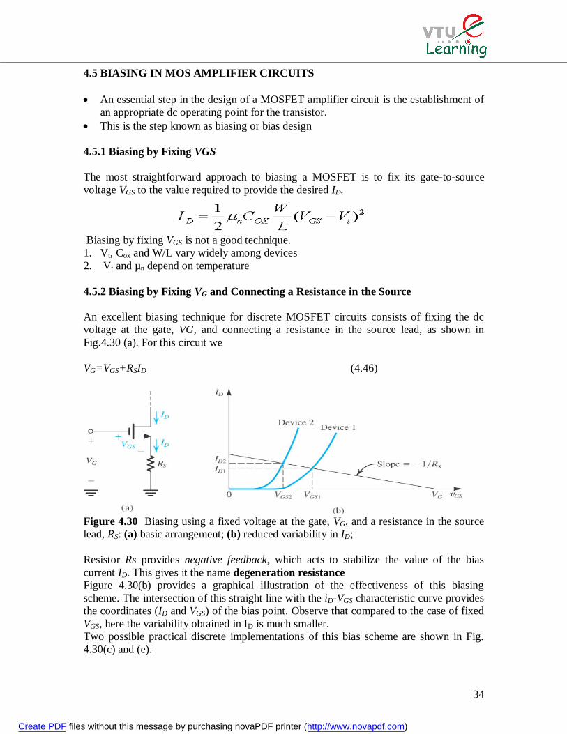
Biasing by fixing VGS is not a good technique. 1. Vt, Cox and W/L vary widely among devices 2. Vt and µn depend on temperature 4.5.2 Biasing by Fixing VG and Connecting a Resistance in the Source An excellent biasing technique for discrete MOSFET circuits consists of fixing the dc voltage at the gate, VG, and connecting a resistance in the source lead, as shown in Fig.4.30 (a). For this circuit we VG=VGS+RSID (4.46)
Figure 4.30 Biasing using a fixed voltage at the gate, VG, and a resistance in the source lead, RS: (a) basic arrangement; (b) reduced variability in ID; Resistor Rs provides negative feedback, which acts to stabilize the value of the bias current ID. This gives it the name degeneration resistance Figure 4.30(b) provides a graphical illustration of the effectiveness of this biasing scheme. The intersection of this straight line with the iD-VGS characteristic curve provides the coordinates (ID and VGS) of the bias point. Observe that compared to the case of fixed VGS, here the variability obtained in ID is much smaller. Two possible practical discrete implementations of this bias scheme are shown in Fig. 4.30(c) and (e).
Create PDF files without this message by purchasing novaPDF printer (http://www.novapdf.com)

35
Figure 4.30 Biasing using a fixed voltage at the gate, VG, and a resistance in the source lead, RS: (c) practical implementation using a single supply; (e) practical implementation using two supplies Example:
Create PDF files without this message by purchasing novaPDF printer (http://www.novapdf.com)

36
Create PDF files without this message by purchasing novaPDF printer (http://www.novapdf.com)

37
4.19 Repeat Example 4.9 when fixed VGS bias is used. The circuit for fixed VGS bias is as shown below:
Let the drop across the drain resistor RD and the drain source voltage of MOSFET VDS be equal = 15/2=7.5V Therefore the value of RD = 7.5/0.5mA = 15kΩ Now the value of VOV can be calculated using the equation, 푖 = 푘 (푣 − 푉 )
Here VG =2V.Hence the possible values for RG1 and RG2 can be 2MΩ and 13MΩ. Now, if the value of Vt change to 1.5V, the new value of iD would be,
푖 = 푘 (푣 − 푉 ) 푖 = × 1(2 − 1.5) = 0.125푚퐴
Therefore the difference/ change in the drain current is, ∆푖 = (0.125− 0.5)푚퐴 = −0.375푚퐴
Create PDF files without this message by purchasing novaPDF printer (http://www.novapdf.com)

38
Therefore the % change in iD is .
.= −75%
4.5.3 Biasing Using a Drain-to-Gate Feedback Resistor Here the large feedback resistance RG (usually in the MΩ range) forces the dc voltage at the gate to be equal to that at the drain (because IG=0) as shown in figure Fig. 4.32. Thus we can write VGS=VDS=VDD-RDID VDD=VGS+RDID (4.49) which is identical in form to Eq. (4.46).
Figure 4.32 Biasing the MOSFET using a large drain-to-gate feedback resistance, RG. Example: It is required to design a Gate-Drain feedback bias circuit to operate at a DC current of 0.5mA. Assume VDD = +5V, Kn’W/L=1mA/V2, Vt=1V and λ=0. Find RD, ID and VD Refer to the same circuit of Figure 4.32. Here vGS and VD should be at the same voltage. Hence we can find vGS first using the saturation expression for drain current.
푖 = 12푘 (푣 − 푉 )
Create PDF files without this message by purchasing novaPDF printer (http://www.novapdf.com)

39
0.5 = 12
× 1(푉 )
푉 = 1푉푎푛푑ℎ푒푛푐푒푣 = 2푉 = 푉 푅 = =
.= 6푘Ω
Allowing for 5% change in RD, the new standard resistance that can be used is 6.2KΩ With a 6.2kΩ resistor new value for ID is 0.484mA Then, the corresponding value of VDS=VDD-RDID VDS=5-6.2*0.484 = 1.9V
4.5.4 Biasing Using a Constant-Current Source The most effective scheme for biasing a MOSFET amplifier is that using a constant-current source. Figure 4.33(a) shows such an arrangement applied to a discrete MOSFET. A circuit for implementing the constant-current source I is shown in Fig. 4.33(b).
Figure 4.33 (a) Biasing the MOSFET using a constant-current source I. (b) Implementation of the constant-current source I using a current mirror.
Create PDF files without this message by purchasing novaPDF printer (http://www.novapdf.com)
40
Transistor Q1, whose drain is shorted to its gate and thus is operating in the saturation region, such that
Where we have neglected channel-length modulation (i.e., assumed λ=0) • The drain current of Q1 is supplied by VDD through resistor R. Since the gate currents are zero,
(4.51) R is considered to be the reference current of the current source and is denoted IREF. Now consider transistor Q2: It has the same VGS as Q1; thus if we assume that it is operating in saturation, its drain current, which is the desired current I of the current source, will be
where we have neglected channel-length modulation. Equation (4.51) and (4.52) enable us to relate the current I to the reference current IREF,
(4.53) This circuit, known as a current mirror, is very popular in the design of IC MOS amplifiers. 4.6 SMALL-SIGNAL OPERATION AND MODELS In Section 4.4 we learned that linear amplification can be obtained by biasing the MOSFET to operate in the saturation region and by keeping the input signal small. 4.6.1 The DC Bias Point The dc bias current can be found by setting the signal vgs to zero; thus,
The dc voltage at the drain, VDS or simply VD (since S is ground), will be
To ensure saturation-region operation, we must have
Create PDF files without this message by purchasing novaPDF printer (http://www.novapdf.com)

41
Furthermore, since the total voltage at the drain will have a signal component superimposed on VD, VD has to be sufficiently greater than VD -Vt to allow for the required signal swing.
Figure 4.34 Conceptual circuit utilized to study the operation of the MOSFET as a small-signal amplifier. 4.6.2 The Signal Current in the Drain Terminal
• The first term on the right-hand side of Eq.(4.57) can be recognized as the dc bias
current ID (Eq. 4.54). • The second term represents a current component that is proportional to the input
signal vgs. • The third term is a current component that is proportional to the square of the
input signal.
Create PDF files without this message by purchasing novaPDF printer (http://www.novapdf.com)

42
Figure 4.35 presents a graphical interpretation of the small-signal operation of the enhancement MOSFET amplifier.
Figure 4.35 Small-signal operation of the enhancement MOSFET amplifier.
Create PDF files without this message by purchasing novaPDF printer (http://www.novapdf.com)
43
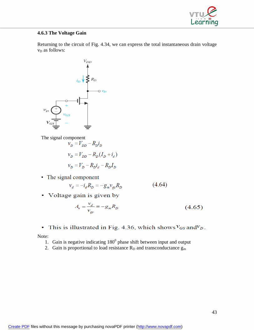
4.6.3 The Voltage Gain Returning to the circuit of Fig. 4.34, we can express the total instantaneous drain voltage vD as follows:
The signal component
Note:
1. Gain is negative indicating 1800 phase shift between input and output 2. Gain is proportional to load resistance RD and transconductance gm
Create PDF files without this message by purchasing novaPDF printer (http://www.novapdf.com)

44
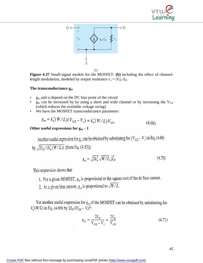
Figure 4.36 Total instantaneous voltages vGS and vD for the circuit in Fig 4.34 4.6.5 Small Signal Models for the MOSFET FET behaves as a Voltage controlled current source – taking a signal vgs between gate and source and provides a current gmvgs at the drain terminal Input and output resistances are very high ideally, infinite
Figure 4.37 Small-signal models for the MOSFET: (a) neglecting the dependence of iD on vDS in saturation Exact Model • The previous model assumes iD is independent of vDS which is not true, because of the
effect of channel length modulation. • This was modeled by a finite resistance r0 between drain and source, in parallel to the
controlled current source typically of the order of 10kΩ to 100kΩ
Create PDF files without this message by purchasing novaPDF printer (http://www.novapdf.com)
45
Figure 4.37 Small-signal models for the MOSFET: (b) including the effect of channel-length modulation, modeled by output resistance ro = |VA| /ID. The transconductance gm
• gm and r0 depend on the DC bias point of the circuit • gm can be increased by by using a short and wide channel or by increasing the VGS
(which reduces the available voltage swing) • We have the MOSFET transconductance parameter:
Other useful expressions for gm - 1
Create PDF files without this message by purchasing novaPDF printer (http://www.novapdf.com)

46
The T equivalent –Circuit Model • The T model can be developed through a simple transformation of the previous
hybrid –π model. • This is very useful in many applications
Figure 4.39 Development of the T equivalent-circuit model for the MOSFET. For simplicity, ro has been omitted but can be added between D and S in the T model of (d). Figure 4.39(a) shows the equivalent circuit studied above without ro. In figure 4.39(b) we have added a second gmvgs current source in series with the
original controlled source without causing any change in circuit operation. This newly created circuit node, labelled X, is joined to the gate terminal G in Fig
4.39(c). The gate current does’nt change, and remains at zero. A controlled current source gmvgs connected across its control voltage can be
represented by a resistance as long as this resistance draws an equal current as the source. This replacement is shown in fig. 4.39(d).
The resistance between gate and source looking into the source is 1/gm, and the resistance as seen from the gate is infinite.
Create PDF files without this message by purchasing novaPDF printer (http://www.novapdf.com)

47
Alternate representation- VCCS by CCCS
Figure 4.40 (a) The T model of the MOSFET augmented with the drain-to-source resistance ro. (b) An alternative representation of the T model. Modeling the Body Effect • When source and substrate are not shorted and substrate is tied to the most negative
supply in the circuit, the body effect comes into picture and the substrate acts like a second gate for the MOSFET
• The signal Vbs gives rise to a drain current component, written as gmbvbs, where gmb is the body transconductance defined as
where
and
Figure 4.41 Small-signal equivalent-circuit model of a MOSFET in which the source is not connected to the body.
Create PDF files without this message by purchasing novaPDF printer (http://www.novapdf.com)
48
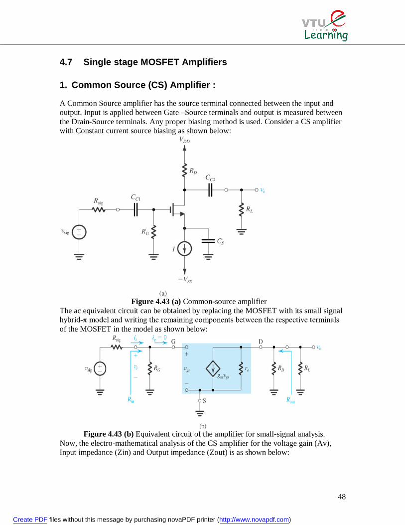
4.7 Single stage MOSFET Amplifiers
1. Common Source (CS) Amplifier :
A Common Source amplifier has the source terminal connected between the input and output. Input is applied between Gate –Source terminals and output is measured between the Drain-Source terminals. Any proper biasing method is used. Consider a CS amplifier with Constant current source biasing as shown below:
Figure 4.43 (a) Common-source amplifier
The ac equivalent circuit can be obtained by replacing the MOSFET with its small signal hybrid-π model and writing the remaining components between the respective terminals of the MOSFET in the model as shown below:
Figure 4.43 (b) Equivalent circuit of the amplifier for small-signal analysis.
Now, the electro-mathematical analysis of the CS amplifier for the voltage gain (Av), Input impedance (Zin) and Output impedance (Zout) is as shown below:
Create PDF files without this message by purchasing novaPDF printer (http://www.novapdf.com)

49
Generally a Common Source amplifier will have a source resistance to improve the stability of the bias point. But this resistance also causes negative feedback and hence the voltage gain will be lesser than in a CS amplifier without source resistance.
Figure 4.44 (a) Common-source amplifier with a resistance RS in the source lead. The small signal equivalent circuit with ro neglected is as shown below:
Create PDF files without this message by purchasing novaPDF printer (http://www.novapdf.com)

50
Figure 4.44 Small signal equivalent model of Common Source amplifier with Rs From the figure we can see that as in the case of the CS amplifier, 푅 = 푅 = 푅 and thus
푉 = 푉푅
푅 + 푅
But, here unlike the previous CS circuit, 푣 is only a fraction of 푣 .It can be determined from the voltage divider composed of 1 푔⁄ and 푅 that appears across the amplifier input as follows:
푣 = 푣
1푔
1푔 + 푅
=푣
1 + 푔 푅
Hence 푣 can be controlled by 푅 . The current 푖 is equal to the current I flowing in the source lead, thus 푖 = 푖 =
푣1푔 + 푅
= (푔 푣 )/(1 + 푔 푅 )
Thus including 푅 reduces 푖 by the factor (1 + 푔 푅 ). The output is now found from
Create PDF files without this message by purchasing novaPDF printer (http://www.novapdf.com)

51
푣 = −푖 (푅 ||푅 ) = − ( || ) 푣
퐴 = − ( || )
and setting 푅 as ∞ gives
퐴 = −푔 푅1푔 + 푅
The overall voltage gain 퐺 is,
퐺 = −푅
푅 + 푅푔 (푅 ||푅 )
1푔 + 푅
This shows that gain is reduced by a factor (1 + 푔 푅 ) than in the previous CS amplifier without 푅 .This factor is called the “amount of feedback” and that it determines both the magnitude of performance improvement and as a tradeoff, the reduction in gain. Since this 푅 was used to improve the stability under dc conditions, by reducing the variability of ID, for ac operation it has a similar action (reducing id), it is called “Source degeneration resistance”. Another useful interpretation of the gain expression is that the gain from gate to drain is simply the ratio of the total resistance in the drain, (푅 ||푅 ) to the total resistance in the source, [ + 푅 ] Common Gate Amplifier [CG amplifier] By applying a signal ground on the MOSFET gate terminal, a circuit configuration aptly named Common Gate or grounded gate amplifier is obtained. The input is applied between source and Gate and the Output is measured between the Drain and Gate. Since both the dc and ac voltages at the gate are zero, the gate terminal can be directly grounded as shown.
Create PDF files without this message by purchasing novaPDF printer (http://www.novapdf.com)

52
Figure 4.45 (a) A common-gate amplifier based on the circuit of Fig. 4.42. The small signal equivalent circuit of the Common Gate Amplifier is as shown below. For simpler analysis we have used the T-model without considering the effect of ro.
Figure 4.45 (b) A small-signal equivalent circuit of the amplifier in (a). Analysis: The input resistance is given as
Create PDF files without this message by purchasing novaPDF printer (http://www.novapdf.com)

53
푅 = 1푔
Since gm is of the order of 1mA/V, the input resistance of the CG amplifier is relatively low (of the order of 1kΏ) than in the CS amplifier. 푉 = 푉
푅푅 + 푅
푣 = 푣
1푔
1푔 + 푅
=푣
1 + 푔 푅
The loss of signal strength in coupling the signal to input of the CG amplifier is due to the low value of Rin.
푅 ≪1푔
The current 푖 is given by, 푖 =
푣푅 =
푣1푔
= (푔 푣 )
And the drain current id is 푖 = 푖 = −푖 = −(푔 푣 ) Thus the output voltage can be found as 푣 = 푣 − 푖 (푅 ||푅 ) = 푔 (푅 ||푅 ) Resulting in voltage gained 퐴 = 푔푚(푅퐷||푅퐿) From which the open circuit voltage gain can be found as 퐴푣표 = 푔 푅 The overall voltage gain can be obtained as follows:
Create PDF files without this message by purchasing novaPDF printer (http://www.novapdf.com)

54
퐺 = 푅
푅 + 푅 퐴 = 퐴
1푔
1푔 + 푅
=퐴
1 + 푔 푅
Resulting in
퐺 = 푔 (푅 ||푅 )
1 + 푔 푅
Finally the output resistance is found by inspection to be, 푅 = 푅 = 푅 Note: The CG amplifier is non inverting The input resistance of CG amplifier is very low. Voltage gain is smaller than that of a CS amplifier by factor (1+gmRsig) which is due
to low Rin. This circuit also acts like a Unity gain current amplifier or a Current follower This is most commonly used in the Cascode amplifier. Common Drain Amplifier (CD amplifier) The signal ground is established at the drain terminal, input is given between the Gate and Drain terminals and Output is measured between the Source and Drain terminals as shown below:
Figure 4.46 (a) A common-drain or source-follower amplifier.
Create PDF files without this message by purchasing novaPDF printer (http://www.novapdf.com)

55
Here also, it is more convenient to use the small signal T-model for analysis, but including the resistance ro as shown below:
Figure 4.46 (b) Small-signal equivalent-circuit model. Analysis: The input resistance is given as 푅 = 푅 푉 = 푉 = 푉
Usually 푅 is selected to be much larger than 푅 with the result that 푣 ≅ 푣
푣 = 푣 푅 ||푟
(푅 ||푟 ) + 1푔
From which the voltage gain Av is obtained as
Create PDF files without this message by purchasing novaPDF printer (http://www.novapdf.com)

56
퐴 = 푅 ||푟
(푅 ||푟 ) + 1푔
And the open circuit voltage gain Avo as 퐴 =
푟
푟 + 1푔
Normally 푟 ≫ , causing voltage gain to become nearly unity. Thus the voltage at the source follows the voltage at the gate, giving the circuit its popular name of source follower. In many discrete circuits 푟 ≫ 푅 which enables the equation to be approximated by,
퐴 ≅푅
푅 + 1푔
The overall voltage gain Gv can be found as,
퐺 =푅
푅 + 푅 푅 ||푟
(푅 ||푟 ) + 1푔
Which approaches unity for 푅 ≫ 푅 , 푟 ≫ 푅 and 푟 ≫ The circuit for determining the output resistance 푅 is as shown in figure. Because the gate voltage is now zero, looking back into the source, we see between the source and ground a resistance in parallel with푟 , thus
푅 = 1푔 ||푟
Normally푟 ≫ , reducing 푅 to
푅 ≅ 1푔
Which indicates 푅 will be moderately low. Note: In source follower, Rin is independent of RL and Rout is independent of Rsig, due to
zero gate current. Hence, it has a very high input resistance, very low output resistance and a voltage
gain that is less than or close to unity. It is normally used as a buffer amplifier.
Create PDF files without this message by purchasing novaPDF printer (http://www.novapdf.com)

57
Summary: The CS amplifier is best suited for obtaining the bulk of the gain required in an
amplifier. Depending on the gain required, either a single stage or a cascade of two or three stages is used.
Including a resistor RS in the source terminal of the CS amplifier provides a number of improvements in its performance, as it behaves like an amplifier with negative Voltage series feedback amplifier, but at the expense of reduced gain.
The low input resistance of the CG amplifier is used as unity gain current amplifier or current follower and also in Cascode amplifier.
The source follower finds application as a voltage buffer for connecting a high resistance source to a low resistance load and as the output stage in a multistage amplifier.
PN: For SPICE MOSFET models and examples please refer to pages 446 to 453 in the text book Adel Sedra and K C Smith
Solutions to few selected exercise problems Refer page 455 to 466 for the problem statements 4.1 The capacitance per unit area is 퐶 = 휀 = 3.45 ∗ 10 퐹/푚 푡 = 5푛푚 퐶 = . ∗ = 6.9푓퐹/휇푚
For 푡 = 5푛푚, 퐶 = 0.56푓퐹/휇푚 For a capacitance of 1pF, we require an area A: 퐴 =
. × = 145휇푚 푓표푟푡 = 5푛푚
퐴 =
. × = 1163휇푚 푓표푟푡 = 20푛푚
For a square plate capacitor of 10pF,
Create PDF files without this message by purchasing novaPDF printer (http://www.novapdf.com)

58
퐴 = 10 × 145 = 1450휇푚 푓표푟푡 = 5푛푚 퐴 = 10 × 1163 = 11630휇푚 푓표푟푡 = 20푛푚
--------------------------------------------------------------------------------------------------------- 4.2 Drain current is directly proportional to the width of the channel.Therefore if width is 10 times greater, then iD would be 10 times greater as well.
K = constant of proportionality = . × .
= 10푚퐴/푉
푟 =푖푣 =
10.2 = 5푘훺푓표푟푉 표푓0.5푉
푟 =푖푣 =
10.5 = 10푘훺푓표푟푉 표푓1푉
푟 = 15푘훺푓표푟푉 표푓1.5푉
푟 = 20푘훺푓표푟푉 표푓2푉
5푘훺 ≤ 푟 ≤ 20푘훺푓표푟0.5푉 ≤ 푉 ≤ 2푉
------------------------------------------------------------------------------------------------------------ 4.3 We know that
Create PDF files without this message by purchasing novaPDF printer (http://www.novapdf.com)

59
푖 = 12 푘 (푣 − 푉 )
푘 =µ 퐶 For equal drain currents, µ 퐶 = µ 퐶 = =
. = 2.5
------------------------------------------------------------------------------------------------------------ 4.34
퐼 =푉 − 푉
푅 =5 − 0푅 = 1푚퐴
푅 = 5푘Ω 푣 = 푣 푖푚푝푙푖푒푠푆푎푡푢푟푎푡푖표푛 Therefore
푖 = 12 푘 (푣 − 푉 )
1 =
12 × 60 × 10 ×
1003 (푣 − 1)
Implies 푣 = 2푉푎푛푑푉 = −2푉
푅 = −2 − (−5)
1 = 3퐾Ω NOTE: PLEASE REFER TO ALL THE EXAMPLE PROBLEMS IN PRESCRIBED TEXT BOOK SEDRA AND SMITH
ALL THE BEST
------------------------------------------------------------------------------------------------------------------------------------------------------------------------------------------------------------------------
Create PDF files without this message by purchasing novaPDF printer (http://www.novapdf.com)