
ece 3410 - microelectronics i lecture notes - USU Canvas
91
ECE 3410 MICROELECTRONICS I LECTURE NOTES Spring 2016 Chris Winstead Associate Professor Electrical and Computer Engineering [email protected]
-
Upload
khangminh22 -
Category
Documents
-
view
0 -
download
0
Transcript of ece 3410 - microelectronics i lecture notes - USU Canvas

E C E 3 4 1 0M I C R O E L E C T R O N I C S IL E C T U R E N O T E S
Spring 2016
Chris WinsteadAssociate Professor
Electrical and Computer [email protected]

Copyright © 2016
published by utah state university
department of electrical and computer engineering
http://www.ece.usu.edu
Licensed for redistribution and adaptation under the Creative CommonsAttribution-ShareAlike International 4.0 License, CC-BY-SA-4.0.

Contents
List of Figures . . . . . . . . . . . . . . . . . . . . . . . . . 4
List of Netlists . . . . . . . . . . . . . . . . . . . . . . . . . 8
List of Examples . . . . . . . . . . . . . . . . . . . . . . . . 9
List of EveryCircuit Demos . . . . . . . . . . . . . . . . . 11
Read Me 15
Introduction 17Signal sources . . . . . . . . . . . . . . . . . . . . . . . . . 17
Ideal Amplifier Models . . . . . . . . . . . . . . . . . . . . 21
Real Amplifiers . . . . . . . . . . . . . . . . . . . . . . . . 25
Equivalent small-signal resistance and impedance . . . . 30
Frequency Response of Amplifiers . . . . . . . . . . . . . 30
Harmonic distortion . . . . . . . . . . . . . . . . . . . . . 37
Operational Amplifier Circuits 39Amplifiers with finite open-loop gain . . . . . . . . . . . 39
Difference amplifiers . . . . . . . . . . . . . . . . . . . . . 45
Instrumentation amplifiers . . . . . . . . . . . . . . . . . . 48
Non-Ideal Op Amp Characteristics . . . . . . . . . . . . . 50
Frequency Response of Op Amps . . . . . . . . . . . . . . 54
Slewing . . . . . . . . . . . . . . . . . . . . . . . . . . . . . 58
Full Power Bandwidth (FPBW) . . . . . . . . . . . . . . . 60
Op Amp Integrators and Differentiators . . . . . . . . . . 61
Introduction to Diodes 67Ideal switch model . . . . . . . . . . . . . . . . . . . . . . 67
Exponential model . . . . . . . . . . . . . . . . . . . . . . 69
Constant voltage-drop model . . . . . . . . . . . . . . . . 69
Iterative Analysis . . . . . . . . . . . . . . . . . . . . . . . 70
Linearized Model . . . . . . . . . . . . . . . . . . . . . . . 72
Diode Circuits 75Half-Wave Rectifier . . . . . . . . . . . . . . . . . . . . . . 75
Resistor-diode regulator . . . . . . . . . . . . . . . . . . . 77

4
Peak rectifier . . . . . . . . . . . . . . . . . . . . . . . . . . 78
Envelope detector . . . . . . . . . . . . . . . . . . . . . . . 79
Bridge Rectifier . . . . . . . . . . . . . . . . . . . . . . . . 81
Voltage Regulators . . . . . . . . . . . . . . . . . . . . . . 83
Super Diode, Precision Rectifier . . . . . . . . . . . . . . . 87
DC Restoration, Clamped Capacitor . . . . . . . . . . . . 89
Boost converter . . . . . . . . . . . . . . . . . . . . . . . . 90

List of Figures
1 Thévenin equivalent voltage signal source. . . . . . 17
2 Norton equivalent current signal source. . . . . . . 17
3 Example FFT display on an oscilloscope. . . . . . . 17
4 A sinusoid has a single Fourier component that ap-pears as an impulse function on the spectral repre-sentation. In this case the magnitude is 40 dB, whichcorresponds to a time-domain zero-to-peak amplitudeof 200 V. . . . . . . . . . . . . . . . . . . . . . . . . . 18
5 Passive linear components and their equivalent Laplace-domain impedances. . . . . . . . . . . . . . . . . . . 18
6 Low-pass configuration. . . . . . . . . . . . . . . . . 19
7 High-pass configuration. . . . . . . . . . . . . . . . . 20
8 Ideal linear voltage amplifier model at low or mid-band frequencies. . . . . . . . . . . . . . . . . . . . . 21
9 Coupling interactions in voltage amplifiers. Resistivevoltage dividers appear at the input and output in-terfaces. . . . . . . . . . . . . . . . . . . . . . . . . . . 21
10 Ideal linear current amplifier model at low or mid-band frequencies. . . . . . . . . . . . . . . . . . . . . 23
11 Coupling interactions in current amplifiers. Resistivecurrent dividers appear at the input and output in-terfaces. . . . . . . . . . . . . . . . . . . . . . . . . . . 23
12 Coupling interactions in transconductance amplifiers.A resistive voltage divider appears at the input inter-face and a current divider at the output interface. . 24
13 Coupling interactions in transresistance amplifiers.A resistive current divider appears at the input inter-face and a voltage divider at the output interface. . 24
14 DC transfer characteristic of an ideal amplifier. . . 25
15 Non-linear transfer characteristic showing non-constantslope. The amplifier saturates when the gain falls be-low 1 V/V. . . . . . . . . . . . . . . . . . . . . . . . . 25

6
16 Zoomed transfer characteristic showing approximatelylinear behavior for small signal variations. . . . . . 26
17 Offset point of a non-linear transfer characteristic. . 26
18 Small-signal activity overlaid on the nonlinear trans-fer characteristic. . . . . . . . . . . . . . . . . . . . . 26
19 Linear temperature sensor model. The DC offset VS
is set to zero (i.e. shorted out) for small-signal anal-ysis. . . . . . . . . . . . . . . . . . . . . . . . . . . . . 28
20 Small-signal equivalent temperature sensor model.The lower-case signals vs and vout represent the vari-ations in the corresponding physical signals. . . . . 28
21 Linearized approximation of thermistor resistance fortemperatures near 300 K . . . . . . . . . . . . . . . . 29
22 An example amplifier model showing parasitic capac-itances. . . . . . . . . . . . . . . . . . . . . . . . . . . 30
23 General “black-box” model of a linearized amplifiercircuit. Zeros are roots of s in the numerator and polesare roots in the denominator. . . . . . . . . . . . . . 31
24 Bode plot of a low-pass system with transfer function
H(s) = K1
1 + s/ωp0,
with a single pole at ωp0 and no zeros, and with gainconstant K = 104 corresponding to 80 dB. In thisexample the pole is at 100 rad/s. The phase responsebegins to decrease at 10 rad/s, loses 45° per decade,and the phase change concludes at 1× 10³ rad/s. . 32
25 Bode plot of a high-pass system with transfer func-tion
H(s) = Ks
1 + s/ωp0,
which has a single zero at the origin, and a single poleat 100 rad/s. The gain constant is K = 104, corre-sponding to 80 dB. The phase response is due to thepole; the zero contributes no phase change since it oc-curs at the origin. . . . . . . . . . . . . . . . . . . . 33
26 Bandpass amplifier model where coupling capacitorsCC1 and CC2 are used to reject or replace the DC off-sets VSIG and VOUT. . . . . . . . . . . . . . . . . . . . . 34
27 Bode plot of a band-pass system with a single zeroat the origin, and two poles at 100 rad/s and 1× 10⁶ rad/s. The gain constant is K = 104, corresponding to80 dB. The phase response is due to the two poles, ap-proaching −180° at higher frequencies. . . . . . . . 35

7
28 Harmonic “spurs” appear at integer multiples of thefundamental frequency, and represent distortion. . 37
29 Operational amplifier symbol . . . . . . . . . . . . . 39
30 Inverting op amp configuration . . . . . . . . . . . . 40
31 Non-inverting amplifier configuration . . . . . . . . 42
32 Voltage follower configuration . . . . . . . . . . . . 44
33 Difference amplifier configuration . . . . . . . . . . 45
34 Instrumentation amplifier configuration . . . . . . . 48
35 Inverting configuration showing bias-current sources. 50
36 Inverting configuration showing input offset voltagesource. . . . . . . . . . . . . . . . . . . . . . . . . . . 52
37 Saturation due to offset voltage . . . . . . . . . . . . 52
38 Standard op amp frequency response . . . . . . . . 54
39 Closed-loop frequency response . . . . . . . . . . . 56
40 Slew-rate distortion in an op amp circuit. . . . . . . 58
41 Generalized inverting configuration with complex impedances. 61
42 Ideal Miller integrator. . . . . . . . . . . . . . . . . . 61
43 Idealized capacitive inverting configuration. . . . . 61
44 Practical capacitive configuration with DC bypass re-sistor. . . . . . . . . . . . . . . . . . . . . . . . . . . . 62
45 Practical capacitive configuration with switched DCbypass. . . . . . . . . . . . . . . . . . . . . . . . . . . 62
46 The two switching phases of a capacitive invertingconfiguration. . . . . . . . . . . . . . . . . . . . . . . 62
47 Miller integrator with DC bypass resistor RF. . . . . 64
48 Miller integrator with switched DC bypass. . . . . . 64
49 Diode symbol and notation. . . . . . . . . . . . . . . 67
50 Diode max-value circuit. . . . . . . . . . . . . . . . . 68
51 Diode min-value circuit. . . . . . . . . . . . . . . . . 68
52 Diode transfer characteristic. The current increasesvery rapidly when vD ≈ 0.7 V. . . . . . . . . . . . . 69
53 Iterative solution for resistor-diode series configura-tion. . . . . . . . . . . . . . . . . . . . . . . . . . . . . 71
54 Linearized diode model. . . . . . . . . . . . . . . . . 72
55 Iterative solution of linearized model parameters. . 72
56 Iterative solution of the resistor-diode series config-uration using the linearized model. . . . . . . . . . 73
57 Half-wave rectifier circuit. . . . . . . . . . . . . . . . 75
58 Behavior of the half-wave rectifier. The ideal switchmodel is compared to the more accurate constant-0.7 Vdrop model. . . . . . . . . . . . . . . . . . . . . . . . 75
59 Linearized model of half-wave rectifier. . . . . . . . 76

8
60 Single-diode regulator circuit. . . . . . . . . . . . . . 77
61 Diode regulator simulation . . . . . . . . . . . . . . 77
62 Linearized model of the single-diode regulator. . . 77
63 Current delivered into the capacitor in the peak de-tector circuit. . . . . . . . . . . . . . . . . . . . . . . . 79
64 Envelope detector circuit. . . . . . . . . . . . . . . . 79
65 Behavior of the envelope detector circuit. . . . . . . 79
66 Full wave bridge rectifier circuit. . . . . . . . . . . . 81
67 A four-diode voltage regulator. . . . . . . . . . . . . 83
68 Small-signal equivalent circuit model of the four-diode2.8 V regulator. . . . . . . . . . . . . . . . . . . . . . . 83
69 Behavior of the four-diode regulator from SPICE sim-ulation. . . . . . . . . . . . . . . . . . . . . . . . . . . 85
70 Zoomed view of the ripple voltage on vOUT. . . . . 86
71 Precision rectifier circuit with op amp feedback. . . 87
72 Clamped capacitor circuit. . . . . . . . . . . . . . . . 89
73 Behavior of DC restorer (clamped capacitor) circuitsimulated in SPICE. . . . . . . . . . . . . . . . . . . . 89
74 Idealized boost converter circuit. . . . . . . . . . . . 90
75 Output voltage from the boost converter when initial-ized at zero. . . . . . . . . . . . . . . . . . . . . . . . 91

List of Netlists
1 envelope_detector.sp . . . . . . . . . . . . . . . . . . 80
2 bridge_rectifier.sp . . . . . . . . . . . . . . . . . . . . 82
3 basic_regulator.sp . . . . . . . . . . . . . . . . . . . . 85
4 superdiode.sp . . . . . . . . . . . . . . . . . . . . . . 88
5 741.sp (top lines showing port order) . . . . . . . . 88
6 dc_restorer.sp . . . . . . . . . . . . . . . . . . . . . . 90
diodes/boost_converter.sp . . . . . . . . . . . . . . . . . . 91


List of Examples
1 Low-pass RC circuit . . . . . . . . . . . . . . . . . . . . . 19
2 High-pass RC circuit . . . . . . . . . . . . . . . . . . . . . 19
3 Linearization of a sensor . . . . . . . . . . . . . . . . . . . 27
4 Linearization of a thermistor model . . . . . . . . . . . . 28
5 Bias current in inverting configuration . . . . . . . . . . . 50
6 Maximum resistance due to Ibias . . . . . . . . . . . . . . 50
7 Inverting configuration with offset voltage . . . . . . . . 52
8 Closed-loop frequency response, low-gain . . . . . . . . 56
9 Closed-loop frequency response, high-gain . . . . . . . . 56
11 Max-Value Circuit . . . . . . . . . . . . . . . . . . . . . . . 68
12 Min-Value Circuit . . . . . . . . . . . . . . . . . . . . . . . 68
13 Min-value circuit with 0.7V drop model . . . . . . . . . . 69
14 Iterative analysis . . . . . . . . . . . . . . . . . . . . . . . 70
15 Iteration with linearized model . . . . . . . . . . . . . . . 73
16 Half-wave rectifier with vin < 0 . . . . . . . . . . . . . . . 75
17 Half-wave rectifier with vin = 1V . . . . . . . . . . . . . . 75
18 Four-diode voltage regulator design . . . . . . . . . . . . 83
19 Two Diode Regulator with Op Amp Buffer . . . . . . . . 86


List of EveryCircuit Demonstrations
2 Ideal Voltage Amplifier . . . . . . . . . . . . . . . . . . . . 21
4 Ideal Band-Pass Amplifier Model . . . . . . . . . . . . . . 35
6 Capacitive Coupling . . . . . . . . . . . . . . . . . . . . . 36
8 Inverting configuration . . . . . . . . . . . . . . . . . . . . 41
10 Non-inverting configuration . . . . . . . . . . . . . . . . . 43
12 Voltage follower configuration . . . . . . . . . . . . . . . 44
14 Difference amplifier (differential mode) . . . . . . . . . . 45
16 Non-inverting circuit with bias and offset . . . . . . . . . 52
18 Closed-loop frequency response . . . . . . . . . . . . . . 57


Read Me
These lecture notes are intended as a companion for Sedra andSmith’s Microelectronic Circuits. The order of topics contained inthese notes should roughly correspond to the lecture presenta-tions in ECE 3410 at Utah State University.
We will make use of two software applications for simulatingelectronic circuits:
• The EveryCircuit Simulator is a very simple applicationfor drawing schematics and simulating basic circuits. It isavailable as an app for iOS and Android devices, and canbe used as a web-based application on desktop and laptopcomputers. A class license is available so that you can useEveryCircuit for free. The license code will be posted onCanvas. Throughout these notes you will find EveryCircuitdemonstrations. You can directly access these demonstrationsby clicking on the link in the title of each demonstration.Note: you will need to use Google Chrome to run the webdemonstrations. EveryCircuit is a very convenient tool thatallows you to rapidly test out course concepts and designideas, and is strongly recommended for this course.
• The NGSpice Simulator is a free, open-source implemen-tation of the classic Berkeley SPICE software, which is theancestor of all modern electronic simulation software. Al-though Berkeley SPICE was first developed in 1973 (seethe overview of SPICE history at Wikipedia), it continuesto be maintained and updated to the present day, and newresearch ideas are periodically incorporated into its code.SPICE therefore represents both the history and the state-of-the-art in electronic design. NGSpice is able to run on Linux,Mac and Windows platforms, and is free to use. While SPICEis a little harder to use than EveryCircuit, we will see thatit is vastly more powerful and there are many circuits andanalyses that can’t be done at all in EveryCircuit.
You will also need to familiarize yourself with the Linux

16
operating system as it is widely used in the electronics andsemiconductor industries, especially for cutting-edge designof micro- and nano-scale integrated circuits and systems. Ifyou want to make chips, you have to do it in Linux. Our labsessions will make use of the Linux-based Design AutomationLab (DAL) and you will have an opportunity to get introducedto Linux and do some tutorials during the first two weeks of thesemester.
It is not mandatory to use these notes, but you will likelyfind a lot of benefit to studying the examples and alternativeexplanations here in addition to reading the textbook. Thesenotes will be updated frequently as I add more examples andsections.

Introduction
Signal sources
+−vsig
Rsig
+
−
Figure 1: Thévenin equivalent voltage signal source.
vsig Rsig
+
−
Figure 2: Norton equivalent current signal source.
Electronic circuits and systems can be loosely divided into twoclasses: those that process signals, which are electrical repre-sentations of information, and those that convey or convertelectrical power. In this course we are primarily concerned withcircuits that process signals, in the broadest possible sense. Asignal may convey physical information, e.g. an audio signalproduced from a microphone, or it may convey discrete ordigital information as part of a computational process. Regard-less of the context, we will always view signals as electricalinformation, either a current or voltage.
A transducer is a device that converts a physical signal intoan electrical one. From the circuit perspective, we usually model1
1 A model is a useful approximation of a physicaldevice or system. We use models to simplify ourunderstanding of complex electronic components.
a transducer as either a voltage source or a current source.Every signal source has an associated internal impedance,represented by Thévenin or Norton equivalent circuits.
Spectrum and Frequency Response
Most information-bearing signals are not constant. A signal x (t)that changes over time can be represented as a superpositionof sinusoidal signals with various magnitudes, frequenciesand phases. The function that characterizes the magnitudesand phases at each frequency is called the signal’s complex-valued Fourier spectrum, written X (jω). The theory of spectraltransforms is quite sophisticated, but in this course we mostlyrequire a simplified version known as the steady-state. For ourpurposes, we may consider the Laplace transform X(s) to beequivalent to the Fourier spectrum, with s = jω.
On a modern digital oscilloscope, a signal’s spectrum can beviewed by selecting a Fast Fourier Transform (FFT) display,
Figure 3: Example FFT display on an oscilloscope.
which reports the signal’s magnitude spectrum, equal to thecomplex magnitude |X(jω)|. Since X(jω) is a complex function,

18 ece3410 lecture notes
the magnitude is obtained as
|X(jω)|2 = X(jω)× X∗(jω).
The magnitude spectrum is typically expressed in units ofdecibels, and the complex phase ∠X(jω) is usually expressedin degrees (0 to 360).
101 102 103 104 1050
20
40
ω (rad/sec)
VS(s)
(dB)
Figure 4: A sinusoid has a single Fourier componentthat appears as an impulse function on the spectralrepresentation. In this case the magnitude is 40 dB,which corresponds to a time-domain zero-to-peakamplitude of 200 V.
The individual sinusoidal signal components are expressedas
va (t) = VA sin (ω0t + φ) ,
where VA is the zero-to-peak amplitude, ωs is the signal fre-quency in radians per second, t is the time in seconds, and φ isthe phase-shift in radians.
A pure or single-tone sinusoid has a magnitude spectrumrepresented by a single impulse function
VA (ω) =12VAδ (ω−ωs) .
The impulse height in decibels is 20 log10 (VA/2). So a zero-to-peak magnitude of 1 V corresponds to −6 dB, 10 V correspondsto 14 dB, 100 V corresponds to 34 dB, and so on. Frequency Units:
• ω = 2π f
• f is in Hz (cycles per second)
• ω is in radians per second.
• ω is “omega”, not w.
• A magnitude V in dB is 20 log10(V)
• A power P in dB is 10 log10(P).
When signals pass through electronic circuits, their magni-tude and phase are altered. The circuit’s transfer function is theratio of the output spectrum to the input spectrum. If a circuit’sinput is X(s) and its output is Y(s), then the transfer function is
H(s) =Y(s)X(s)
.
We may interpret the transfer function in terms of frequency bysubstituting s = jω. The transfer function’s magnitude responseis usually expressed in decibels as
|H (ω)| (dB) = 20 log10 |H (ω)|
= 10 log10 |H (ω)|2 .
When expressed in decibels, the magnitude reveals useful in-formation about the circuit. When |H (ω)| = 0 dB, the output’samplitude is equal to the input. When |H (ω)| is positive, theoutput’s amplitude is greater than the input, and the circuit issaid to have gain. When |H (ω)| is negative, the output’s ampli-tude is less than the input, and the circuit is said to attenuatethe signal.
R
C
L
R
1Cs
Ls
Figure 5: Passive linear components and theirequivalent Laplace-domain impedances.
For a linear circuit, the transfer function is obtained usingcomplex impedances for capacitors and inductors. A capacitorwith capacitance C has impedance 1/(sC), and an inductor with

introduction 19
inductance L has impedance sL. Once components are replacedby their equivalent impedances, they can be analyzed as thoughthey were resistors where the resistance values are polynomialsin s.
VIN(s)R
1/sC
VOUT(s)
Figure 6: Low-pass configuration.
The low-pass configuration is like a simple voltage divider. Theimpedances are Z1 = R and Z2 = 1/sC. Then
VOUT(s) = VIN(s)(
Z2
Z1 + Z2
)⇒ H(s) =
VOUT(s)VIN(s)
=1/sC
R + 1/sC
=1
1 + sRC
The low-pass transfer function is commonly represented as
H(jω) =1
1 + jω/ω3dB
. The magnitude response is then
|H(ω)|2 =
(1
1 + jω/ω3dB
)(1
1− jω/ω3dB
)=
(1
1 + ω2/ω23dB
)
At low frequencies where ω ω3dB, the magnitude response is flat, approximately equal to one. Athigher frequencies where ω ω3dB, the magnitude drops rapidly. At these high frequencies, sinceω/ω3dB 1, we can make an approximation:
ω/ω3dB + 1 ≈ ω/ω3dB
⇒ |H(ω)| ≈ ω3dB/ω (high frequencies above ω3dB)
When represented in decibels, we find that
|H(ω)| ≈ 20 log10
(ω3dBω
)= 20 log10 ω3dB − 20 log10 ω.
So as ω increases, the magnitude decreases by 20 dB per decade.
Example 1 (Low-pass RC circuit).

20 ece3410 lecture notes
VIN(s)1/sC
R
VOUT(s)
Figure 7: High-pass configuration.
The high-pass configuration has impedances are Z1 = 1/sC and Z2 =
R. Then
VOUT(s) = VIN(s)(
Z2
Z1 + Z2
)⇒ H(s) =
VOUT(s)VIN(s)
=R
R + 1/sC
=sRC
1 + sRC
The high-pass transfer function is commonly represented as
H(jω) =jω/ω3dB
1 + jω/ω3dB
. The magnitude response is then
|H(ω)|2 =
(jω/ω3dB
1 + jω/ω3dB
)(−jω/ω3dB
1− jω/ω3dB
)=
(ω2/ω2
3dB1 + ω2/ω2
3dB
)
At high frequencies where ω ω3dB, the magnitude response is flat, approximately equal to one. Atlower frequencies where ω ω3dB, the magnitude drops rapidly. Since ω/ω3dB 1, we can makean approximation:
ω/ω3dB + 1 ≈ 1
⇒ |H(ω)| ≈ ω/ω3dB (low frequencies below ω3dB)
When represented in decibels, we find that
|H(ω)| ≈ 20 log10
(ω
ω3dB
)= 20 log10 ω− 20 log10 ω3dB.
So as ω increases from very low frequencies, the magnitude increases by 20 dB per decade.
Example 2 (High-pass RC circuit).
A note on approximations: in these examples we used aIf A B then:
A + B ≈ A
1A
+1B≈ 1
BA
A + B≈ 1
BA + B
≈ BA
and so on...
very common method of large-value approximation. We willuse this procedure many times. Suppose two quantities A andB differ greatly in value, so that A B. The notion of “muchgreater than” is somewhat fuzzy, but in this course we willdefine it as more than a 10× difference between two quantities.

introduction 21
Ideal Amplifier Models
Rin
+−Avvin
Rout+
−
vin
+
−
vout
Figure 8: Ideal linear voltage amplifier model at lowor mid-band frequencies.
An ideal linear amplifier is a circuit which receives an inputsignal X and produces an output signal Y = AX. In otherwords, the output is larger than the input by a constant multipleA, called the gain. The input/output signals can be eithercurrent or voltage, which introduces four possible amplifierconfigurations:
Input Output Amplifier Type Gain Name and Symbol
Voltage Voltage Voltage Amplifier Gain Av
Current Current Current Amplifier Gain Ai
Voltage Current Transconductance Amplifier Transconductance Gm
Current Voltage Transresistance Amplifier Transresistance Rm
In order to use an amplifier, it has to be connected to itssignal source on the input side and its load on the output side.This creates a coupling interaction between the amplifiersinternal resistances and the neighboring signal resistances. Inthe voltage amplifier, we see a voltage-divider effect at both theinput and output interfaces:
Rin
+−Avvin
Rout+
−
vin
+
−
vout
+−vsig
Rsig
RL
vIN = vSIG
(Rin
Rin + Rsig
)vOUT = AvvIN
(RL
Rout + RL
)
Figure 9: Coupling interactions in voltage amplifiers.Resistive voltage dividers appear at the input andoutput interfaces.As a result the complete system is described by the gain
equation in combination with the coupling divider ratios. Todescribe this effect, we distinguish the open-circuit gain fromthe loaded gain:
open-circuit gain: Avo ,vOUT
vIN= Av
loaded gain: AvL ,vOUT
vIN= Av
(Rin
Rin + Rsig
)(RL
Rout + RL
).
To maximize the amplifier’s gain, we want to eliminate thecoupling ratios by making them very close to one. This is Maximum gain in voltage amp: Rout RL and
Rin Rsig. In the limit, a truly ideal voltage amp hasRin → ∞ and Rout → 0.
achieved when the amplifier has large input resistance and asmall output resistance.

22 ece3410 lecture notes
This demonstration implements the ideal voltage amplifier model from Figure 9 with Rsig, Rin, Rout andRL all equal to 1 kΩ, and a voltage gain Av = 10 V/V. The simulation traces show an attenuation byhalf at each signal port due to the voltage-divider couplings.
Exercise: Increase Rin to 10 kΩ and then 100 kΩ, and observe what happens to the amplitude of vin
compared to vsig for these values. Then do the same for RL. You should notice that the couplingeffects disappear when RL Rout and Rin Rsig. Verify that your observations match the value of theloaded gain predicted by our analysis in this section.
EveryCircuit Demonstration 2 (Ideal Voltage Amplifier).

introduction 23
Rin Aiiin Rout
ioutiin
loadvsig
Figure 10: Ideal linear current amplifier model at lowor mid-band frequencies.
The ideal linear current amplifier is very similar to thevoltage amplifier, except that we get current dividers instead ofvoltage dividers at the input and output terminals. In a currentdivider, the opposite resistance appears in the numerator, so theconditions for achieving maximum are reversed.
For current amplifiers, the most ideal gain is called the short-circuit gain Ais, since we can eliminate the coupling ratios bysetting RL to zero, hence short-circuiting the output. The gainexpressions for a current amplifier are:
short-circuit gain: Ais ,iOUT
iIN= Ai
loaded gain: AiL ,iOUT
iIN= Ai
(Rsig
Rin + Rsig
)(Rout
Rout + RL
).
Maximum gain in current amp: Rout RL andRin Rsig. In the limit, a truly ideal current amp hasRin → 0 and Rout → ∞.
To maximize the current amplifier’s gain, we want to elimi-nate the coupling ratios by making them very close to one. Thisis achieved when the amplifier has small input resistance anda large output resistance, the opposite of what we found forvoltage amplifiers.
Rin Aiiin Rout
ioutiin
RLisig Rsig
iIN = vSIG
(Rsig
Rin + Rsig
)iOUT = AiiIN
(Rout
Rout + RL
)
Figure 11: Coupling interactions in current amplifiers.Resistive current dividers appear at the input andoutput interfaces.

24 ece3410 lecture notes
The remaining amplifier types are mixtures of voltage andcurrent amplifiers. The transconductance amplifier takes Transconductance amplifiers are especially important
since they are the basis of transistor device models.voltage input and delivers a current output. Then we see avoltage divider at the input interface and a current divider atthe output interface/
Rin Gmvin Rout
+
−
vin
iout
RL
+−vsig
Rsig
vIN = vSIG
(Rin
Rin + Rsig
)iOUT = GmvIN
(Rout
Rout + RL
)
Figure 12: Coupling interactions in transconductanceamplifiers. A resistive voltage divider appears at theinput interface and a current divider at the outputinterface.
For the transconductance amplifier, the gain expressions are:
short-circuit gain: Gms ,iOUT
vIN= Gm
loaded gain: GmL ,iOUT
vIN= Gm
(Rin
Rin + Rsig
)(Rout
Rout + RL
).
Maximum gain in transconductance amp: Rout RLand Rin Rsig. In the limit, a truly ideal transconduc-tance amp has Rin → ∞ and Rout → ∞.
To maximize the transconductance amplifier’s gain, we wantto eliminate the coupling ratios by making them very closeto one. This is achieved when the amplifier has large inputresistance and a large output resistance.
Lastly, The transresistance amplifier takes current input anddelivers a voltage output. Then we see a current divider at theinput interface and a voltage divider at the output interface/
Rin
+−Rmiin
Rout+
−
vout
iin
isig Rsig RL
iIN = vSIG
(Rsig
Rin + Rsig
)vOUT = RmiIN
(RL
Rout + RL
)
Figure 13: Coupling interactions in transresistanceamplifiers. A resistive current divider appears at theinput interface and a voltage divider at the outputinterface.
For the transresistance amplifier, the gain expressions are:
open-circuit gain: Rmo ,vOUT
iIN= Rm
loaded gain: RmL ,vOUT
iIN= Rm
(Rsig
Rin + Rsig
)(RL
Rout + RL
).
Maximum gain in transresistance amp: Rout RLand Rin Rsig. In the limit, a truly ideal transconduc-tance amp has Rin → 0 and Rout → 0.
To maximize the transresistance amplifier’s gain, we want toeliminate the coupling ratios by making them very close to one.This is achieved when the amplifier has small input resistanceand a small output resistance, the opposite of what we foundfor transconductance amplifiers.

introduction 25
Real Amplifiers
Real amplifiers are affected by nonlinear transfer characteris-tics between the input and the output.
−10 10
−100
100
Input
Output
Ideal Linear Amplifier
Figure 14: DC transfer characteristic of an idealamplifier.
The ideal transfer characteristic is a straight line, extend-ing from −∞ to +∞ with a constant slope. The gain of thisamplifier is the slope of its transfer characteristic:
Gain ,dvOUT
dvIN.
Real amplifiers do not exhibit such ideal behavior. A more real-istic transfer characteristic is a curve that saturates at maximumand minimum values of vOUT, with a non-constant slope inbetween.
−15 −10 −5 5 10 15
−100
100
Input
Output
−15 −10 −5 5 10 15
−100
100
Input
Gain
Figure 15: Non-linear transfer characteristic showingnon-constant slope. The amplifier saturates when thegain falls below 1 V/V.Since the slope varies, the gain is non-constant. This introduces
distortion into the signal being amplified. Due to this nonlinearbehavior, we are unable to use linear circuit methods to analyzethe amplifier system. As a result, analysis and design canbecome very complex tasks. To simplify our understanding ofnonlinear systems, we rely on the concepts of linearization andsmall-signal analysis.
A linearized model is a direct application of the first-orderTaylor series approximation. For a non-linear function f (x), theTaylor approximation is defined around an offset x0 as
f (x) ≈ f (x0) + (x− x0)∂ f∂x
∣∣∣∣x0
.
= f0 + A (x− x0)
This approximation is only valid for small variations, i.e. when|x− x0| is small (the meaning of “small” here is fuzzy; thevariation is considered small enough if the approximation issufficiently accurate for our needs). The Taylor approximationcan be interpreted as zooming-in on the original function, suchthat the zoomed portion is a nearly straight line:

26 ece3410 lecture notes
−15 −10 −5 5 10 15
−100
100
Input
Output
Real Non-Linear Amplifier
−1 −0.5 0.5 1
−10
−5
5
10
Input
Output
Zoomed Non-Linear Amplifier
Figure 16: Zoomed transfer characteristic showingapproximately linear behavior for small signalvariations.Small-signal equivalent circuit models
The Taylor linearization reveals an extremely useful aspect oflinearized circuits: thanks to the principle of superposition, wecan separate the circuit’s behavior into two parts: the DC offsetor bias point x0, f0 and the small signal variation (x− x0). Inthe circuit context, the transfer characteristic shows the large-signal relationship between two signals vIN and vOUT. Werefer to these as the total instantaneous signals, i.e. the precisephysical signal value at an instant in time.
VIN
VOUTQ Point,Bias Point,DC Offset
Figure 17: Offset point of a non-linear transfercharacteristic.
vOUT = VOUT + vout
DC part
Small Signalpart
Total InstantaneousSignal
vin
vout
Figure 18: Small-signal activity overlaid on thenonlinear transfer characteristic.
For non-linear circuits, it is often difficult to analyze the totalinstantaneous signal, so we split it into a superposition of twoparts:
DC offset – the central or average value of a signal; what youwould measure on an oscilloscope as the signal’s MEAN. Wewrite DC offsets using all capital letters, as in VIN or VOUT.
Small-signal – the amount by which the signal varies from theoffset; what you would measure on an oscilloscope set to AC
Coupling. We write small-signal quantities in all-lowercase,as in vin or vout.
Total instantaneous signal – the superposition of the offset andsmall signal; what you would measure on an oscilloscopeset to DC coupling. We write the total instantaneous signalusing lowercase letters with uppercase subscripts, as in vIN orvOUT.
The uppercase/lowercase notation is useful to keep track ofour separate analysis domains, but is not entirely perfect. Forexample, we also use uppercase symbols to represent sinusoidalamplitudes, which can sometimes create ambiguity. To helpdistinguish these quantities, we will try and use calligraphicfont for sinusoidal amplitudes, as in VA.

introduction 27
Procedure for small-signal analysis
When analyzing a linearized circuit, we often want to analyzejust the signals, without being distracted by their DC offsets.We want to know, for example, the AC amplitude and phaseshift of signals at various points in a circuit. The principle ofsuperposition allows us to extract the small-signal behavior byfollowing these steps:
1. Solve the circuit’s DC operating point. In many cases wemay only need to find part of the DC solution in order to dothe next step.
2. Linearize the circuit by applying a Taylor approximationcentered at the DC operating point.
3. Replace any non-linear components with their linearizedequivalents.
4. Set all DC independent sources (both current and voltage)to zero. Voltage sources become short-circuits, and currentsources become open-circuits. Note: do not modify anytime-varying or dependent sources.
28 ece3410 lecture notes
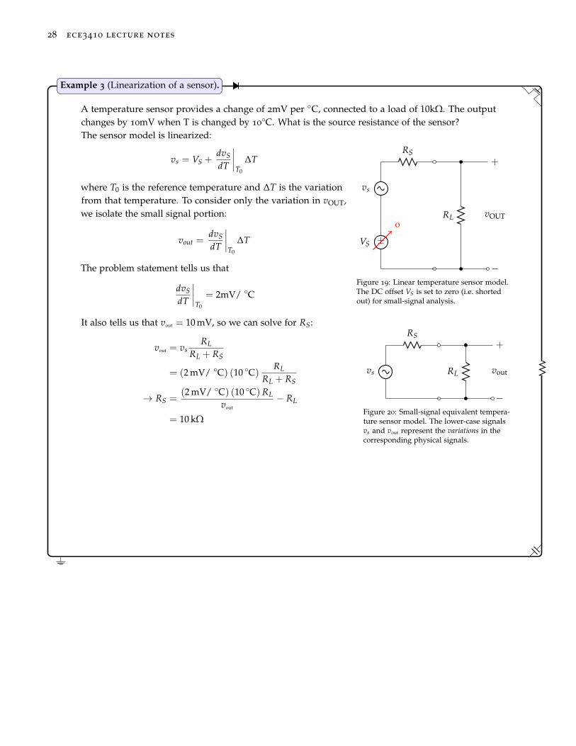
A temperature sensor provides a change of 2mV per C, connected to a load of 10kΩ. The outputchanges by 10mV when T is changed by 10
C. What is the source resistance of the sensor?
−
+
+−VS
vs
RS
0
RL vOUT
Figure 19: Linear temperature sensor model.The DC offset VS is set to zero (i.e. shortedout) for small-signal analysis.
The sensor model is linearized:
vs = VS +dvSdT
∣∣∣∣T0
∆T
where T0 is the reference temperature and ∆T is the variationfrom that temperature. To consider only the variation in vOUT,we isolate the small signal portion:
vout =dvSdT
∣∣∣∣T0
∆T
The problem statement tells us that
dvSdT
∣∣∣∣T0
= 2mV/ C
It also tells us that vout = 10 mV, so we can solve for RS:
vout = vsRL
RL + RS
= (2 mV/ C) (10 C)RL
RL + RS
→ RS =(2 mV/ C) (10 C) RL
vout
− RL
= 10 kΩ
−
+
vs
RS
RL vout
Figure 20: Small-signal equivalent tempera-ture sensor model. The lower-case signalsvs and vout represent the variations in thecorresponding physical signals.
Example 3 (Linearization of a sensor).

introduction 29
A thermistor is modeled by the Steinhart-Hart equation:
R = R0e−B(
1T0− 1
T
)
280 290 300 310 320
0.99
1
1.01
1.02·104
T (Kelvin)
R(Ω
)
ActualLinearized
Figure 21: Linearized approximation of thermistorresistance for temperatures near 300 K
where R0 and T0 are reference measurements, T andT0 are in Kelvin, and B is a device-specific parame-ter. For small temperature changes (e.g. changes in aroom’s temperature), we can approximate this using alinearized model centered around T0:
R ≈ R0 + ∆Td
dT
(R0e−B
(1
T0− 1
T
))∣∣∣∣T=T0
= R0 + ∆T(
R0e−B(
1T0− 1
T
))d
dT
(−B
(1T0− 1
T
))∣∣∣∣T=T0
= R0 − ∆TR0
(BT2
0
)
So if T0 = 300 K , R0 = 10 kΩ and B = 50 K−1, then fortemperatures near 300 K we have
R ≈ 10 kΩ− ∆T × 5.5 Ω
So we should see a difference of about 5.5 Ω/K. Tocheck the accuracy of this approximation, we can compare the actual (nonlinear) equation to thelinearized result, as shown in Figure 21. Note that the accuracy is best for very small ∆T, and theerror begins to grow as |∆T| increases.
Example 4 (Linearization of a thermistor model).

30 ece3410 lecture notes
Equivalent small-signal resistance and impedance
In example 3 we determined the series internal resistance of atemperature sensor. Since this resistance affected the sensor’sincremental or differential behavior, we can refer to it as asmall-signal resistance. By definition, a small-signal resistanceis the ratio of the small change in current in a branch thatresults from a small change in voltage across the correspondingterminals. This can be stated mathematically in a few differentways:
large-signal definition: rX =∂vX∂iX
∣∣∣∣DC
small-signal definition: =vx
ix
From this definition we can define an analysis procedure fordetermining a circuit’s small-signal equivalent resistance:
1. Linearize the circuit and obtain the small-signal equivalentmodel.
2. Set any independent signal sources to zero.
3. Insert a test voltage source vx across the terminals of interest.
4. Solve the current ix that flows through the test source vx.
5. The equivalent resistance is rx = vxix
.
Note that this procedure only works for small-signal models.Do not use the large-signal ratio vX/iX!
Frequency Response of Amplifiers
Every circuit has a frequency response. At the very least, thereis a hidden capacitance between every pair of nodes, called theparasitic capacitance. These capacitances introduce multiplepoles and zeros into the circuit’s frequency response.
Rin
+−Avvin
Rout
Cin Cout
C f
+
−
vin
+
−
vout
+−vsig
Rsig
RL
Figure 22: An example amplifier model showingparasitic capacitances.

introduction 31
The general “ZPK” form of the transfer response is
H(s) = K ∏k (1− s/ωzk)
∏m(1− s/ωpm
)+
−
H(s) = VY(s)VX (s)
+
−
vX vy
Zeros
Poles
Figure 23: General “black-box” model of a linearizedamplifier circuit. Zeros are roots of s in the numera-tor and poles are roots in the denominator.
where ωzk are the zeros, indexed by k and ωpm are the poles,indexed by m. In this course we will concern ourselves almostexclusively with “simple” poles and zeros in the left half-plane.In other words, we’ll assume that all poles and zeros are real-valued (not complex or imaginary), are all well separated (theydo not overlap in value), and are negative valued. If theseconditions are satisfied, then we can use a simplified “stick-figure” method to produce approximate magnitude and phaseresponse diagrams, which are called Bode plots.

32 ece3410 lecture notes
Low-pass systems
For every pole ωpm, the magnitude decreases by 20 dB perdecade at frequencies above the pole. The phase responsedecreases by 90° between the frequencies 0.1ωpm and 10ωpm,and crosses −45° at ωpm.
100 101 102 103 104 105 106 107 108 109
0
50
100ωp0
-20dB/decade
Gai
nM
agni
tude
(dB)
100 101 102 103 104 105 106 107 108 109−100
−50
0
45 Phase Loss
Frequency
Phas
e(°
)
Figure 24: Bode plot of a low-pass system withtransfer function
H(s) = K1
1 + s/ωp0,
with a single pole at ωp0 and no zeros, and with gainconstant K = 104 corresponding to 80 dB. In thisexample the pole is at 100 rad/s. The phase responsebegins to decrease at 10 rad/s, loses 45° per decade,and the phase change concludes at 1× 10³ rad/s.

introduction 33
High-pass systems
For every zero ωzk, the transfer function increases by 20 dBper decade at frequencies above the pole. The phase responseincreases by 90° between the frequencies 0.1ωpm and 10ωpm,and crosses −45° at ωpm.
In high-pass systems, there is usually a zero at the origin.In that case, there is no phase response associated with thezero (it occurs at infinitely low frequency on the logarithmicscale), and the zero must be canceled by one or more poles athigher frequencies. On the Bode plot, the magnitude responsereaches its maximum value and becomes constant after the firstpole, ωp0. For frequencies below ωp0, the magnitude responsedecreases by 20 dB per decade.
100 101 102 103 104 105 106 107 108 109
0
50
100ωp0
+20dB/decade
Gai
nM
agni
tude
(dB)
100 101 102 103 104 105 106 107 108 109−100
−50
0
45 Phase Loss
Frequency
Phas
e(°
)
Figure 25: Bode plot of a high-pass system withtransfer function
H(s) = Ks
1 + s/ωp0,
which has a single zero at the origin, and a singlepole at 100 rad/s. The gain constant is K = 104,corresponding to 80 dB. The phase response is due tothe pole; the zero contributes no phase change sinceit occurs at the origin.

34 ece3410 lecture notes
Band-pass systems
Many circuit’s exhibit a mix of high-pass and low-pass char-acteristics. We will especially see this in circuits that use ca-pacitive coupling to separate the DC offset from an AC smallsignal. In a bandpass system, the transfer function’s magnitudeis highest for middle frequencies between two pole frequenciesωL and ωH . This zone is referred to as the circuit’s mid-band orpass band.
A typical band-pass amplifier model is shown below. Thesignal source has a DC offset voltage VSIG, which is usuallyundesirable since it will be amplifier along with the signal. Inorder to amplify just the signal, the offset is rejected by usinga coupling capacitor CC1 to create a high-pass response at theinput. The amplifier’s output similarly has an undesired DCoffset VOUT, which is rejected using the coupling capacitor CC2.
Rin
+−VOUT
+−Avvin
Rout
Cout
+
−
vin
+
−
vout
+−VSIG
vsig
Rsig CC1
RL
Figure 26: Bandpass amplifier model where couplingcapacitors CC1 and CC2 are used to reject or replacethe DC offsets VSIG and VOUT.To analyze the bandpass circuit, we replace capacitors by
their Laplace domain equivalent impedances. We then have
vin = vsig
(sCC1Rin
1 + sCC1 (Rin + Rsig)
)vout = Avvin
(RL
RL + Rout + sCoutRoutRL
)= vsig Av
(sCC1Rin
1 + sCC1 (Rin + Rsig)
)(RL
RL + Rout + sCoutRoutRL
)The transfer function is
H (s) =vout
vsig
= Av
(RL
RL + Rout
)(sCC1Rin
(1 + sCC1 (Rin + Rsig)) (1 + sCout (RL ‖ Rout))
)In this case there is a zero at the origin and two poles located at

introduction 35
two frequencies:
ωp0 =1
CC1 (Rin + Rsig)
ωp1 =1
Cout (RL ‖ Rout)
Under ideal conditions, the voltage amplifier should havevery high Rout which places ωp0 at a low frequency, and itshould have a very low Rout which places ωp0 at a high fre-quency. Since there is a zero at the origin, the magnitude risesby 20 dB per decade for frequencies below ωp0, and then be-comes flat between ωp0 and ωp1. For frequencies higher thanωp1 the magnitude falls by 20 dB per decade.
100 101 102 103 104 105 106 107 108 109
0
50
100ωp0 ωp1
+20dB/decade -20dB/decade
midband
Gai
nM
agni
tude
(dB)
100 101 102 103 104 105 106 107 108 109
−150
−100
−50
0 45 Phase Loss
→ 90 Phase Loss
→ 180 Phase Loss
135 Phase Loss
Frequency
Phas
e(°
)
Figure 27: Bode plot of a band-pass system with asingle zero at the origin, and two poles at 100 rad/sand 1× 10⁶ rad/s . The gain constant is K = 104,corresponding to 80 dB. The phase response isdue to the two poles, approaching −180° at higherfrequencies.

36 ece3410 lecture notes
This demonstration shows an implementation of the band-pass model from Figure 26. Examine thiscircuit and perform both AC simulations (frequency mode) and transient simulations (time mode).Try increasing and decreasing both CC1 and Cout by 10× (for a total of four different cases), andobserve how the pole frequencies change. Verify that the observations match the predictions from ouranalysis in this section.
EveryCircuit Demonstration 4 (Ideal Band-Pass Amplifier Model).
This capacitive coupling demonstration shows how we can remove a signal’s DC offset and replaceit with a different offset. The circuit works through superposition of high-pass and low-pass signalpaths. The input AC signal has an offset of 10 V and a zero-to-peak amplitude of 1 V. At the out-put, the original offset is rejected by the coupling capacitor. A new offset of 1 V is provided by anindependent DC voltage source, and is superimposed through the 1 kΩ resistor on the output side.
EveryCircuit Demonstration 6 (Capacitive Coupling).

introduction 37
Harmonic distortion
When a pure sinusoid is input to perfectly linear amplifier, theoutput is expected to be a pure sinusoid, and its magnitudespectrum should have a single impulse. Real amplifiers are notperfectly linear though, so the output is usually not a perfectsinusoid.
103 1040
20
40
ω (rad/sec)
VS(s)
(dB)
Figure 28: Harmonic “spurs” appear at integer mul-tiples of the fundamental frequency, and representdistortion.
As a result, unexpected features called harmonics appearin the output magnitude spectrum. Harmonics are spuri-ous impulses that appear at integer multiples of the originalfundamental signal frequency. So if the input sinusoid has afundamental frequency component at f0, the distorted outputsinusoid has harmonic components spaced at integer multiplesfk = k f0.
Aliasing
Since the harmonic components can extend to very high fre-quencies, they may contribute to aliasing effects in a digitaloscilliscope’s FFT display. Aliasing occurs when a signal vio-lates the Shannon-Nyqvist Sampling Theorem, which states thatthe sampling rate must be at least twice the highest frequencypresent in the signal. On a typical digital oscilloscope, we mustbe aware of the following considerations:
• The Sec/Div knob sets the sampling rate fS.
• If the signal frequency f > fS/2, then the scope will show animage at f − fS/2. So if you increase f beyond fS/2, the signalpeak on the FFT will appear to move backwards.
• When many high-frequency harmonics are present, theirimages will overlap again and again over the FFT display,creating an erroneous and confusing plot.
• Higher frequency harmonics can be suppressed by activatingan internal bandwidth limit on the oscilloscope’s inputchannel.
• When zooming in to see more detail on the FFT display, donot use the Sec/Div knob. Instead, look for a digital zoomsetting in the FFT menu.


Operational Amplifier Circuits
Amplifiers with finite open-loop gain−
+
vOUT
v−
v++
−
vid
Figure 29: An op amp has two input terminals andone output. The input signal is differential, withvid , v+ − v−. The output is single-ended, withvOUT = Avid.
Operational amplifiers (op amps) are nearly ideal differentialamplifiers. This means that their output is proportional to thedifference of their inputs, and is governed by the characteristicequation
vOUT = A(v+ − v−
),
where gain is the amplifier’s voltage gain. Since op amps arenearly ideal, we expect them to have very high Rin and very lowRout. Furthermore, there should be zero current passing into theop amp’s input terminals.
Op amps are almost always used in negative feedback con-figurations where there is some path for current to flow be-tween the amplifier’s output and its inverting input terminal.To analyze realistic op amp circuits with feedback, we need tointroduce some more refined notation:
G? = The desired or ideal or nominal closed-loop gain
⇒ G?i = for an inverting configuration
⇒ G?ni = for a non-inverting configuration
G = The actual achieved closed-loop gain.
A = The op amp’s finite open-loop gain, in volts per volt.
ε = The error coefficient
⇒ G = G?ε
Notice that the concept of “open-loop gain” is distinct fromthe “open circuit gain,” but in this chapter we will considerthem to be approximately the same. The open-loop gain refersto the amplifier’s gain without feedback, whereas the open-circuitgain refers to the gain without a load. Since an op amp is ex-pected to have a very low Rout, we will assume that loadingeffects are negligible.

40 ece3410 lecture notes
Inverting amplifier
−
+
vOUT
R2
R1vIN
i1
i2
v−
v+
Figure 30: Inverting op amp configuration. Nocurrent flows into the op amp’s terminals, so i2 = i1.
Summary: This configuration’s characteristics are:
G? = −R2
R1
G = εG?
ε =A
1 + A + R2R1
The standard inverting configuration includes an input resistorR1 and a feedback resistor R2. Whenever an op amp is con-nected in a negative feedback configuration, it will exhibit avirtual short effect that forces v− to be approximately equal tov+. The virtual short occurs because the op amp’s open-loopgain tends to be very large. We can prove the virtual short effectunder the most ideal condition: that the op amp’s open loopgain is so large it effectively approaches infinity.
Proof. First suppose v− > v+. Then we expect to see a largenegative voltage at vOUT. By superposition,
v− = vIN
(R2
R1 + R2
)+ vOUT
(R1
R1 + R2
).
But if the op amp’s gain A → ∞, then vOUT → −∞ andconsequently v− → −∞. This creates a contradiction, sincewe supposed that v− > v+. On the other hand, if v− < v+,then vOUT → ∞ and consequently v− → ∞, which is anothercontradiction. The only non-contradictory scenario is if v− =
v+.
Thanks to the virtual short effect, we can say that ideallyv− = 0, so the current passing through R1 is
i1 =vIN
R1.
Since there is no current passing into the op amp’s input termi-nals, the entire current i1 must pass through R2. Then i2 = i1and vOUT = −i1R2 = −vIN (R2/R1). This result is based on The closed-loop gain is the ratio vOUT/vIN when a
negative feedback connection is present.ideal assumptions, so we can say that the ideal closed-loopgain is
G?i = −R2
R1.
The ideal analysis assumes that the op amp’s open-loop gaingoes to infinity. We can perform a more realistic analysis byaccounting for the op amp’s finite open-loop gain. In this case,the op amp has an inexact virtual short, so we should not relyon it in our analysis. Instead, we can solve for the closed-loopgain beginning from the op amp’s characteristic equation:

operational amplifier circuits 41
vout = A(v+ − v−
)⇒ vout = A
(0− v−
)⇒ v− = −vout
A
i2 = i1 =vout − v−
R2
=v− − vin
R1
Then we have
R1
(vout
(1 +
1A
))= R2
(−vout
A− vin
)⇒ vout
(1 +
1A
+R2
R1 A
)= −R2
R1vin
⇒ Gi =vout
vin
=
(−R2
R1
)(A
A + 1 + R2/R1
)Notice that, in this form, we can express the circuit’s actual
gain as the product of two terms:
Gi = G?i × ε
G?i = −R2
R1
ε =A
A + 1 + R2/R1
The first term, G?, is the gain expected if we used an ideal opamp. The second term, ε, is an error coefficient that quantifiesthe effect of using an op amp with finite open-loop gain A.
This circuit implements an inverting configuration where the op amp’s open-loop gain is A =
10 V/ V (i.e. 20 dB). The resistor values are R1 = 1 kΩ and R1 = 2 kΩ, so we expect an ideal closed-loop gain of G? = −2 V/ V. The input signal has a zero-to-peak amplitude of 1 V, so the outputamplitude should be 2 V. Simulate this circuit and observe the output amplitude. It should be 1.54 V.To verify that this matches the prediction from our theory, solve for ε and G using the methods de-scribed in this section. Then, try increasing the op amp’s open-loop gain to 20 V/V and repeat yourcalculations to verify that the theory holds up.
EveryCircuit Demonstration 8 (Inverting configuration).

42 ece3410 lecture notes
Non-inverting amplifier
−
+
vOUT
R2
+− vIN
R1
i1
i2v−
v+
Figure 31: Non-inverting amplifier configuration.The “virtual short” effect causes the op-amp’sinput terminals to have nearly equal potentials, sov− ≈ v+.
Summary: This configuration’s characteristics are:
G? = 1 +R2
R1
G = εG?
ε =A
1 + A + R2R1
The non-inverting configuration is similar to the invertingconfiguration, except the input signal is applied at v+. Underideal assumptions, we may appeal to the virtual short so thatv− = vIN, and i2 = i1. Then
i1 = −vIN
R1
vOUT = vIN − i1R2
= vIN + vINR1
R2
⇒ G?ni = 1 +
R1
R2
To obtain the more realistic gain accounting for finite open-loop gain, we begin from the characteristic equation as before:
vout = A(vin − v−
)⇒ v− = vin −
vout
A
i2 = i1 =vout − v−
R2
=v−
R1
Rearranging we get:
R1(vout − v−
)= R2v−
⇒ R1
(vout − vin +
vout
A
)= R2
(vin −
vout
A
)⇒ vout
(1 +
1A(1 + R2/R1)
)= vin
(1 +
R2
R1
)⇒ vout
(1 +
G?ni
A
)= vinG?
ni
⇒ vout
(A + G?
niA
)= vinG?
ni
⇒ G =vout
vin
= G?ni
(A
A + G?ni
)⇒ G = G?
ni
(A
A + 1 + R2/R1
)

operational amplifier circuits 43
Once again we may express the result in two parts, G? and ε:
G?ni = 1 +
R2
R1
ε =A
A + 1 + R2/R1
Gni = G?ni × ε
Notice that the error coefficient, ε, is the same for both theinverting and non-inverting configurations.
Generalized Result
Since the error coefficient is the same in both configurations, theclosed-loop gain can be generally expressed as
G = G? × ε
= G?
(A
A + 1 + R2/R1
)
Make a copy of the inverting configuration circuit and modify it to implement a non-inverting config-uration. Keep the parameters from the original exampe, R1 = 1 kΩ, R2 = 2 kΩ and A = 10 V/V, andset the input signal amplitude to 1 V. For these parameters, calculate the expected values of G?, ε andG. Simulate the circuit and verify that the output amplitude agrees with your calculations.
EveryCircuit Demonstration 10 (Non-inverting configuration).

44 ece3410 lecture notes
Voltage Follower
The voltage follower represents a slightly different case, sincethere are no resistors.
−
+vIN
vOUT
Figure 32: Voltage follower configuration. Due to the“virtual short” effect, vOUT ≈ vIN.
Summary: This configuration’s characteristics are:
G? = 1
G = εG?
ε =A
1 + A
In this configuration, we have the following device equations:
vOUT = A(v+ − v−
)= A (vIN − vOUT)
⇒ G =vOUT
vIN=
AA + 1
In this case, the gain can be expressed as
G?v f = 1
εv f =A
A + 1Gv f = G?
v f × εv f
Make a copy of the inverting configuration circuit and modify it to implement a voltage followerconfiguration. Keep the same op amp gain from the original example, A = 10 V/V, and set the inputsignal amplitude to 1 V. Calculate the expected values of G?, ε and G. Simulate the circuit and verifythat the output amplitude agrees with your calculations.
EveryCircuit Demonstration 12 (Voltage follower configuration).

operational amplifier circuits 45
Difference amplifiers
To make an amplifier with fully-differential input, we can com-bine inverting and non-inverting configurations. This gives ustwo gains:
G?ni = 1 +
R2
R1
G?i = −R2
R1
−
+
R3
+
R1
−
R2
R4
vOUTvIN
Figure 33: Difference amplifier configuration foramplifying a differential signal. Inverting and non-inverting configurations are superimposed. Theresistor-divider R3 −−R4 is used to ensure the samegain for the inverting and non-inverting signal paths.
To achieve proper differential operation, the inverting andnon-inverting gains must be balanced, i.e. Gni = Gi. In theirusual configurations, this is not the case. In order to balance theinverting and non-inverting gains, we insert the voltage dividerR3, R4, so that:
G?ni →
(1 +
R2
R1
)(R4
R3 + R4
)=
R2
R1(condition for balance)
⇒(
R4
R3 + R4
)(1 +
R2
R1
)=
R2
R1
Then solving for R4/R3 we find that
R3
R3 + R4=
(R2
R1
)(R1
R2 + R1
)=
R2
R1 + R2
Then we can invert both sides:
1 +R3
R4= 1 +
R1
R2
⇒ R3
R4=
R1
R2
So the resistor ratios need to be matched.

46 ece3410 lecture notes
−
+
R3
R1
R2
R4
vOUT
vipvin
vCM
This circuit implements a difference amplifier withboth differential and common-mode input circuits.In the initial setup, you should see that the two dif-ferential input signals, vip and vin, have zero-to-peakamplitudes of 1 V and a frequency of 1 kHz. One ofthe sources, vip, has a phase of 180° in order to haveopposite polarity from vin. The common-mode signalvCM is shared by both of the input signals, i.e. theyshare this signal component; it is common to bothof them. In the example design, vCM has a smallamplitude of 100 mV and a frequency of 300 Hz. Weexpect the common-mode signal to be canceled out,so it should not appear at all in the output signal.To verify this, increase the amplitude of vCM to 5 V,so it will be clearly visible. Notice that the outputwaveform doesn’t change.
Next, modify the value of R4 by increasing it to 4 kΩ. Keep the amplitude of vCM at 5 V, and let thesimulation run for a while. You should observe that a 300 Hz fluctuation is superimposed onto theoutput signal. The common-mode is no longer canceled.
EveryCircuit Demonstration 14 (Difference amplifier (differential mode)).
The importance of matching
If the inverting and non-inverting gains are imbalanced, thenthe common-mode signal is not perfectly cancelled. To see this,we now consider the actual gains Gi and Gni, which may differdue to imprecision in actual resistor values:
vIN+ =
12
v+sig + vCM
vIN− =
12
v−sig + vCM
⇒ vOUT =12(Gni + Gi) vsig + (Gni − Gi) vCM
The latter part of this result is called the common-mode gain,ACM = (Gni − Gi). The Common Mode Rejection Ratio(CMRR) is the ratio of the effective differential gain, Ad =12 (Gni + Gi), to ACM:
CMRR =Ad
ACM
This figure is often specified in dB. Ideally it should be infinite.

operational amplifier circuits 47
Input resistance in the difference amplifier
One source of mismatch in the difference amplifier is that theinput resistances are unmatched between the two input legs. Toevaluate the input resistance, we apply the method described in?? separately for each leg of the input signal.
At the inverting input, we find that the input resistance isequal to R1, since vip = 0, so that v+ = 0 and, due to the virtualshort, v− = 0. At the non-inverting input, the equivalent resis-tance is equal to R3 + R4. If the input signals have a significantseries resistance, we will see signal attenuation due to resistivecoupling effects, which modifies the gain. Let us assume thatboth vip and vin are both connected in series with a resistanceequal to Rsig. Then this resistance is effectively added in serieswith R1 and R3, so that after accounting for this loading effectthe gain becomes
G?L =
R2
R1 + Rsig
.
In other words
G?L = G?
(R1
R1 + Rsig
).
If we repeat this analysis on the non-inverting signal path,we will find the same ratio. Finally, accounting for finite gaintogether with the loading effect:
GL = G?
(R1
R1 + Rsig
)ε,
where ε is now modified due to the presence of Rsig:
ε =A
1 + A + R2R1+Rsig
.

48 ece3410 lecture notes
Instrumentation amplifiers
−
+vi1
−
+vi2
2R1
R2
R′2
vx
vy
iy
ix
ix − iy
−
+
R3
R3 R4
R4
vout
Figure 34: Instrumentation amplifier configurationfor amplifying differential signals. Since both inputsare connected to the op amps’ non-inverting termi-nals, they should both have high input resistanceand matched electrical characteristics. Comparedto difference amplifiers, this configuration is lesssensitive to resistor mismatch and has improvedCMRR.
Advantages over difference amplifiers:
• Very high input resistance (Rin → ∞).
• Gain controlled by a single resistor (2R1).
• CMRR increased by the gain of the pre-amp stage.
Disadvantages:
• Needs three op amps.
• Higher power consumption.
Instrumentation amplifier AD analysis.
We have three amplifiers. The first two are non-inverting con-figurations. Together they are described as a fully-differentialpre-amplifier. The third op amp is configured as a difference am-plifier. The differential gain may be analyzed as a superpositionof two non-inverting configurations:
vx = vi1
(1 +
R2
R1
)− vi2
R2
R1
vy = vi12
(1 +
R2
R1
)− vi1
R2
R1
The overall gain of the pre-amplifier stage is then
AD1 =vx − vy
vi1 − vi2
= 1 +2R2
2R1
= 1 +R2
R1.
The difference amplifier contributes a gain of R4/R3, so thetotal differential gain is
AD =
(1 +
R2
R1
)(R4
R3
).
Instrumentation amplifier ACM analysis.
We expect to obtain a net improvement in CMRR throughthis configuration, compared to the difference amplifier. Infact, the instrumentation amplifier achieves the following twoadvantages:

operational amplifier circuits 49
• Eliminates sensitivity to R1 in the non-inverting configura-tions by sharing R1 between the two circuits.
• Eliminates sensitivity to mismatch in R2.
In the Common-Mode case, set vi1 = vi2 = vicm. Then, dueto the virtual short effect, the op amp’s inverting terminals arealso equal to vicm. Therefore the voltage drop across R1 is zero,so that
ix − iy = 0
⇒ vx = vy
Note that this result does not depend on the matching be-tween R2 and R′2. We may conclude that the pre-amplifier’scommon-mode gain is
ACM1 = 0V/ V
. This would mean that the instrumentation amplifier has atheoretically infinite CMRR. In practice, the op amps them-selves will contribute second order imperfections (“second order”means they contribute smaller effects than resistor mismatch),resulting in some residual imbalance and a finite CMRR.

50 ece3410 lecture notes
Non-Ideal Op Amp Characteristics
We have already discussed finite open-loop gain, finite inputresistance and common-mode gain as non-ideal features of opamp circuits. Now we will examine two additional features:
• Input bias current
• Offset voltage
Input Bias Current
Every op amp has a small but non-zero bias current flowinginto its input terminals; a typical value might be 10 µA, but thiscan vary across a wide range for different products. The biascurrent is typically a fixed current that can be modeled as a DCcurrent source.
In this example we analyze the effect of bias current on an inverting configuration.
−
+Ibias
Ibias
R1
vIN
R2
vOUTv−
Figure 35: Inverting configuration showing bias-current sources.
The theorem of superposition allows us to set vin = 0 toanalyze the contribution of Ibias. In this case, we see that
v− = 0 (virtual short) ⇒ vout = IbiasR2
By superposition, we can add in the contribution fromvin, resulting in
vout = vin
(−R2
R1
)+ R2 Ibias.
Based on this example, we can see that the effect of Ibias
is to introduce a DC offset voltage on vout. This placesa limitation on the size of R2 that can be used. Suppose,for instance, that we have
Ibias = 10µA R2 = 1MΩ VR = 5V
and the op amp’s power rails are at ±VR. In this case, the bias current induces an output offsetvoltage equal to
IbiasR2 = 10V,
which is greater than the rail of the op amp. As a result, the op amp will simply saturate.
Example 5 (Bias current in inverting configuration).

operational amplifier circuits 51
Given Ibias, an input signal vIN and a desired closed-loop gain G, how can we determine the maxi-mum allowable value for R2? Suppose vmax is the maximum value of vIN, and vmin is the minimum(note that vmin can be a negative voltage). Then our circuit must satisfy
IbiasR2 + Gvmin < VR ⇒ R2 <VR + Gvmin
Ibias.
So returning to our example where Ibias = 10 µA and VR = 5 V, and let G = −10 V/V and vmin =
−0.1 V, we find
R2 <(5 V) + (1 V)
10 µA= 600 kΩ.
Example 6 (Maximum resistance due to Ibias).

52 ece3410 lecture notes
Offset Voltage
Every op amp has a DC offset voltage so that its equation is
vout = A(v+ − v− + Vofs
).
When used in high-gain circuits, this offset voltage gets ampli-fied, which may lead to erroneous signal processing in somecircuits.
Vofs is random, usually varying in the range ±10mV. Vofs canalso change slowly over time, making it difficult to zero it outby design.
Suppose an inverting op amp configurationhas supply rails equal to +5V and −5V, andis configured to have a closed loop gainG = −R2/R1 = −100V/ V. The input signalis a sinusoid with peak-to-peak amplitude45mV, and the op amp has an offset voltageVofs = 10mV. Draw the output waveform.
Answer: the output amplitude is 4.5V, butsince the offset voltage is also amplified,the output will contain a DC offset equal to1.01V, hence the output waveform is
vout = 1.01 + 4.5 sin (2π f t) .
This will result in clipping of the waveform.
−
+
+−
Vofs
R1vin
R2
voutv−
Figure 36: Inverting configuration showing inputoffset voltage source.
0 5 10
−5
0
5
Time [s]
Out
put
Volt
age
[V]
Effect of Vofs
v∗outvout
Figure 37: Waveform saturation caused by unde-sired amplification of the op amp’s input offsetvoltage.
Example 7 (Inverting configuration with offset voltage).

operational amplifier circuits 53
This circuit implements models of both Ibias and VOFS in a non-inverting op amp configuration. Sincethe EveryCircuit op amp model is very ideal, a slight circuit trick is used to model the bias current bysteering it into ground instead of into the op amp terminal. This trick doesn’t change anything at allabout the circuit’s behavior. The model uses typical values of 10 µA and −10 mV for the bias currentand offset voltage, respectively.
We see that the output waveform has a significant DC offset due to the bias and offset effects, andpart of the waveform is saturated. To get some experience with these effects, you can experimentwith larger and smaller values of each, and with positive and negative values of VOFS. Occasionallythe simulation will halt and complain that it can’t find a solution. Usually in these cases you can justrestart the simulation and will proceed without any problems.
Design question: how can the circuit be modified to minimize the undesirable offset and avoidsaturating the output waveform?
EveryCircuit Demonstration 16 (Non-inverting circuit with bias and offset).

54 ece3410 lecture notes
Frequency Response of Op Amps
General-purpose op amps are said to be internally compen-sated devices, meaning they are deliberately designed to havea single-pole frequency response with a very low cutoff fre-quency:
A (s) =A0
1 + s/ωc
where
ωc = The low cutoff frequency
A0 = The DC open-loop gain, in V/V
The frequency response looks like this:
100 101 102 103 104 105 106 107 108
0
50
100ωc
ωt
Gai
nM
agni
tude
(dB)
100 101 102 103 104 105 106 107 108
−150
−100
−50
0
PM
Phas
e(°
)
Figure 38: Standard op amp frequency response. Inthis example, ωc = 100 rad/s, ωt = 1× 10⁶ rad/s,and Av0 = 80 dB. In real op amp products theseparameters can vary significantly for differentproducts. For a given product, ωt typically showslow part-to-part variation and is a useful figure-of-merit.
The phase response loses 45° about the dominant pole ωc.There are typically additional poles at frequencies above ωt,which can cause additional phase loss just prior to ωt. ThePhase Margin (PM) measures how much phase is lost at ωt.Specifically,
PM = 180° +∠A (jωt)
(note that ∠A (jωt) is negative).For our (introductory) purposes, we will assume that PM =
90°.

operational amplifier circuits 55
Unity-Gain Frequency
A typical op amp has a a very large DC open-loop gain, oftengreater than 80 dB or 10 000 V/V. Then the magnitude responsecan be approximated as
A (ω) =
√A2
01 + ω2/ω2
c
≈ A0ωc
ω
The unity-gain frequency ωt is where the gain magnitude isequal to unity, i.e. 1 V/V:
1 = ωcA0
ωt
⇒ ωt = ωc A0 Note A0 is in V/V
Because of this result, the unity-gain frequency is often referredto as the Gain-Bandwidth Product (GBP). We can also write thetransfer function in terms of ωt as follows:
A (s) =A0
1 + sA0/ωt
Closed-Loop Frequency Response
Consider the inverting configuration using an op amp with aone-pole response:
ACL (s) =(−R2
R1
)(A (s)
A (s) + 1 + R2/R1
)⇒ ACL (s) = G?
( A01+s/ωc
A01+s/ωc
+ 1− G?
)
⇒ ACL (s) = G?
(A0
A0 + 1− G? + s (1− G?) /ωc
)≈ G?
(A0
A0 + s (1− G?) /ωc
)since A0 1− G?
= G?
(1
1 + s (1− G?) /ωt
)We can re-write this as a single-pole transfer function with pole
ωCL = ωt/ (1− G?)
= ωt/ (1 + R2/R1) .
This result introduces the universal Gain-Bandwidth Trade-off. By using feedback, we can convert between bandwidth and

56 ece3410 lecture notes
closed-loop gain according to an approximate one-to-one ratio.Note that for a given op amp, all configurations have the sameunity-gain frequency. Hence we consider ωt to be the universalparameter of an op amp’s frequency response.
The closed-loop frequency response looks like this:
100 101 102 103 104 105 106 107 108
0
50
100ωc
ωt
ωCL
Gai
nM
agni
tude
(dB)
Figure 39: Closed-loop magnitude response (inred) for an op-amp feedback configuration. Theopen-loop response is also shown (in blue). For fre-quencies greater than ωCL, the closed-loop responseapproximately matches the open-loop response.
Consider the following parameters:
ωt = 10MHz
R2/R1 = 10
What are the closed-loop DC gain, the 3dB cutoff frequency, and the unity-gain frequency for theseparameters?
ACL = −10VV
ωt = 10MHz
ωc = 909kHz
Example 8 (Closed-loop frequency response, low-gain).

operational amplifier circuits 57
Consider the following parameters:
ωt = 10MHz
R2/R1 = 100
What are the closed-loop DC gain, the 3dB cutoff frequency, and the unity-gain frequency for theseparameters?
ACL = −100VV
ωt = 10MHz
ωc = 99kHz
Notice that as the desired gain G grows to be very large, the cutoff frequency approximates to ωt/G.
Example 9 (Closed-loop frequency response, high-gain).
This circuit models an op amp with a single-pole transfer function connected in a non-invertingconfiguration. Since EveryCircuit’s built-in op amp model is basically ideal, we have to insert extracomponents to introduce a pole at the op amp’s output node. This is accomplished using an RClow-pass network followed by a voltage buffer comprised of a dependent voltage source with a gainof 1 V/V.
Perform a frequency simulation of the closed-loop system and observe the major parameters: theDC gain ACL (in dB), the 3 dB cutoff frequency ωc, and the unity-gain frequency ωt. Next, increasethe value of R2 by 10× and then 100×, and observe how it changes ACL and ωc. Convert ACL toV/V in order to test the predictions from the theory presented in this section. Verify that ωt remainsconstant and is approximately equal to ACLωc.
EveryCircuit Demonstration 18 (Closed-loop frequency response).

58 ece3410 lecture notes
Slewing
0 2 4 6 8 10
−1
0
1
Time
v out
A signal affected by slewing
Figure 40: Slew-rate distortion in an op amp circuit.
Slewing is very different from ordinary transfer-function basedbehavior. Slewing can be thought of as saturation of v′out, i.e.a second-order saturation effect. As such, it is fundamentallynon-linear and introduces harmonic distortion into the signal.
SR = maxddt
vout given in V/µs.
Slewing tends to turn the output signal into a triangle wave.If the op amp’s input signal is a pure sinusoid, then we candetermine if the output will be affected by slewing:
v∗out = ACLVA sin (2π f t)
⇒ ddt
v∗out = 2π f ACLVA cos (2π f t)
where VA is the input signal amplitude. This tells us that slew-ing may occur if VA is large, or if the frequency f is large, or ifthe closed-loop gain ACL is large. The maximum rate of signalchange must be less than the slew-rate:
2π f ACLVA ≤ SR
Slew-rate limiting Suppose an amplifier has the following characteristics:
SR = 1V/µs
ACL = 2 V/V
f = 100kHz
What is the maximum input amplitude VA which can guarantee no slewing?
VAmax =SR
2π f ACL
= 0.796V.
Clearly the slew rate can present real limitations for a circuit.
Example 10.
Although slewing distortion occurs commonly in op ampcircuits, there is no easy way to model it in simple simulatorslike EasyCircuit. To get an accurate prediction of slew-rate

operational amplifier circuits 59
limiting, we need to use a more advanced simulator like SPICE.This is one of the first instances where we can see the need forsophisticated engineering software.

60 ece3410 lecture notes
Full Power Bandwidth (FPBW)
The FPBW is the maximum frequency at which an op ampcan deliver its full-swing output signal (i.e. rail-to-rail outputamplitude). If the op amp has rails at ±VR, then the maximumoutput amplitude is VO = VR. Then
FPBW =SR
2πVR
If the op amp is single-supply, then the maximum amplitudeis VR/2, so
FPBW =SR
πVR
The circuit will process any frequency less than the FPBWdistortion-free. For higher frequencies, you may begin to seespurious harmonics in the output spectrum.
Once the FPBW is known, the slewing limit can be predictedas follows:
VOmax = VRFPBW
f
Hence if you know the FPBW and the rail voltage, you canestimate the maximum allowable amplitude at a given highfrequency.

operational amplifier circuits 61
Op Amp Integrators and Differentiators
−
+
vn
Z2
vout
Z1vin
Figure 41: Generalized inverting configuration withcomplex impedances.
If the circuit is analyzed in the Laplace domain, we can con-sider arbitrary impedances to behave as through they wereresistors. Then
ACL =vout (s)vin (s)
= −Z2 (s)Z1 (s)
Differentiator: Z1 is a capacitor
If Z1 is a capacitor C1, and Z2 is a resistor R2, then
Z1 (s) =1
sC1
⇒ ACL (s) = −sC1R2.
In this transfer function, −C1R2 is just a scale constant. Thesignal is multiplied by s, resulting in differentiation in thetime-domain.
Integrator: Z2 is a capacitor−
+
vn
C2
vout
R1vin
Figure 42: Ideal Miller integrator.
If Z2 is a capacitor C2, and Z1 is a resistor R1, then
Z2 (s) =1
sC2
⇒ ACL (s) = −R1
sC2.
In this transfer function, −R2/C1 is just a scale constant.The signal is multiplied by 1/s, resulting in integration in thetime-domain.
Z1 and Z2 are both capacitors−
+
vn
C2
vout
C1
vin
Figure 43: Idealized capacitive inverting configura-tion.
If both of the impedances are capacitors, then the behavior issimilar to an inverting configuration.
Z1 (s) =1
sC1
Z2 (s) =1
sC2
⇒ ACL (s) = −C1
C2.
In this transfer function, −C1/C2 is the amplifier’s gain. The sterms cancel out, resulting in no integrating or differentiatingbehavior.

62 ece3410 lecture notes
Practical Considerations
−
+
vn
C2
vout
C1
vin
RF
Figure 44: Practical capacitive configuration with DCbypass resistor.
In practice, capacitors cannot simply be left floating at theop amp terminals. Consider the circuit shown in Figure 43.Node vn is left floating, which means there is nothing to defineits potential. It could literally be anything, which could bedisastrous.
Additionally, there is no path for the op amp’s DC biascurrent to flow. To address these problems, we have someoptions:
(a) Include large resistances to passively clear the charge on v−.
(b) Use ideal switches to periodically reset charge on v−.
−
+
vn
C2
vout
C1
vin
Figure 45: Practical capacitive configuration withswitched DC bypass.
Method (b) is commonly used in integrated circuits, wherecapacitors are easier to make than resistors, and switches aremade using MOSFET transistors. One of the key advantagesto the circuit in Figure 45 is that it can cancel out the op amp’soffset voltage. When used for this purpose it is often called anauto-zeroing circuit. We can analyze the auto-zeroing circuitin two phases. In Phase 1, the switches are configured to shortacross C2 and to connect the top plate of C1 to ground. In thisphase, the op amp is basically in a voltage-follower configura-tion. Due to the virtual short effect, vn should be equal to VOFS,so C1 gets charged up to a voltage equal to VOFS. Meanwhile C2
is discharged to a voltage of zero.
−
+
vn
C2
vout
C1
vin
+−VOFS
Phase 1
−
+
vn
C2
vout
C1
vin
+−VOFS
Phase 2Figure 46: The two switching phases of a capacitiveinverting configuration.
In Phase 2, the input is connected, and node vn is left float-ing, so that no charge can be added or removed from vn. Soany charge added to the outside plate of C1 has to be balancedby an opposite charge on the outside plate of C2. The chargeQ1 = vIN/C1 must be balanced by Q2 = vOUT/C2 = −Q1.

operational amplifier circuits 63
Therefore
vOUTC2
= −vIN
C1
⇒ vOUT
vIN= −C2
C1.
This interpretation allows us to build practical op amp configu-rations using only capacitors. There’s a good reason for doingthis: resistors are big but capacitors are small. When makingcircuits at the micro or nano scale, it is usually preferred to usecapacitors and avoid resistors whenever possible.

64 ece3410 lecture notes
Miller Integrator
When Z2 is a capacitor and Z1 is a resistor, as in Figure 42,the circuit is called a Miller integrator. The ideal circuit fromFigure 42 suffers from a few practical difficulties:
1. What determines the Initial Condition of the integrator?Usually we want vout = 0 at some starting time t = 0.
2. When vin = 0, we expect vout = 0 for all t > 0. However the opamp’s systematic offset voltage creates a “ghost input” thatgets integrated, so the charge on C2 will go to ∞.
3. There is no reset mechanism to zero the charge on C2. If vin
is a sinusoid centered at 0, the offset will keep charging C2
without limit.
−
+
vn
C2
vout
R1vin
RF
Figure 47: Miller integrator with DC bypass resistorRF .
To resolve these difficulties, there are two common solutions.The first solution is to use a large passive bypass resistor RF
connected in the feedback path, as shown in Figure 47. Thebypass resistor serves to zero the DC charge on C2. If RF issufficiently large, then it will have minimal influence on thefrequency response above DC, however it may contribute tooffset effects due to the op amp’s bias current and offset voltage.It will also tend to amplify any DC offset present in the inputsignal. At very low frequencies, we can treat the capacitor C2
as an open-circuit, i.e. we simply remove it from the circuit.This reveals the circuit’s DC behavior, an inverting integratorwith gain −RF/R1. Similarly at higher frequencies where(ωC2)
−1 RF, we can ignore the presence of RF and the circuitshould behave like an ideal integrator. −
+
vn
C2
vout
R1vin
Figure 48: Miller integrator with switched DCbypass.
The second solution is to use a switching reset in the feed-back path. We use a switch which is closed periodically tozero the charge on C2. This method has the advantage of beinginsensitive to the op amp’s bias current, and is only weaklysensitive to the input offset voltage. The main drawback is thatthe switch also resets the signal integration result, so it is notpossible to integrate over a long period of time.
Frequency Analysis
The Miller Integrator introduces an interesting frequency re-sponse. We can solve the unity-gain frequency by evaluating

operational amplifier circuits 65
the magnitude:
ACL (jω) =1
ωR1C2
⇒ ωt =1
R1C2.
We can draw the magnitude response by placing a point at ωt,then draw backwards adding 20dB per decade at frequenciesbelow ωt. The response grows toward ∞ as the frequencyapproaches DC.


Introduction to Diodes
vA vB
+ vD −
iD
Figure 49: Diode symbol and notation.
A diode is like a valve that lets current flow one directionbut not the other. It is a nonlinear device, which means thetraditional linear analysis techniques cannot be directly applied.We begin with some simplified models that are useful forbuilding intuition about diode circuits. After that, we’ll build upto more accurate (but difficult) models and techniques. We’ll seethat accurate simulation using SPICE (or a similar software tool)is essential for designing nonlinear circuits.
Ideal switch model
The simplest way to understand a diode is to consider it as anideal switch.
• When vD > 0, the switch is closed and iD can be any positivevalue.
• When vD ≤ 0, the switch is open and iD = 0.
Using the switch model, we first make a hypothesis as towhether the diode is ON or OFF. Then, we analyze the circuitto verify it is consistent with that hypothesis. This approachintroduces our first iterative procedure: If the circuit containsmultiple diodes, we initially assume that all diodes are OFFand then analyze the circuit. Any diode with a forward voltageis then turned ON. After changing the diode’s state, we mustre-analyze the circuit to see if any additional devices need to beturned ON.
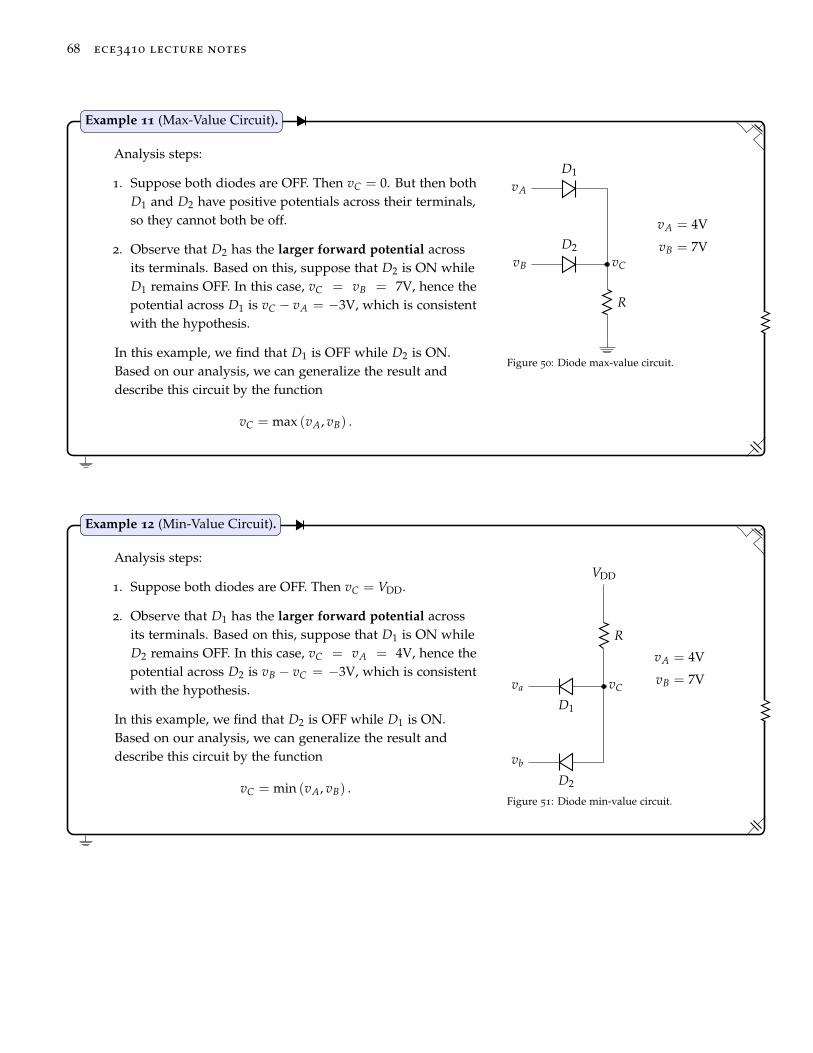
68 ece3410 lecture notes
Analysis steps:
1. Suppose both diodes are OFF. Then vC = 0. But then bothD1 and D2 have positive potentials across their terminals,so they cannot both be off.
2. Observe that D2 has the larger forward potential acrossits terminals. Based on this, suppose that D2 is ON whileD1 remains OFF. In this case, vC = vB = 7V, hence thepotential across D1 is vC − vA = −3V, which is consistentwith the hypothesis.
In this example, we find that D1 is OFF while D2 is ON.Based on our analysis, we can generalize the result anddescribe this circuit by the function
vC = max (vA, vB) .
vA
vB
D1
vC
D2
R
vA = 4V
vB = 7V
Figure 50: Diode max-value circuit.
Example 11 (Max-Value Circuit).
Analysis steps:
1. Suppose both diodes are OFF. Then vC = VDD.
2. Observe that D1 has the larger forward potential acrossits terminals. Based on this, suppose that D1 is ON whileD2 remains OFF. In this case, vC = vA = 4V, hence thepotential across D2 is vB − vC = −3V, which is consistentwith the hypothesis.
In this example, we find that D2 is OFF while D1 is ON.Based on our analysis, we can generalize the result anddescribe this circuit by the function
vC = min (vA, vB) .
VDD
R
vC
D1
va
D2
vb
vA = 4V
vB = 7V
Figure 51: Diode min-value circuit.
Example 12 (Min-Value Circuit).

introduction to diodes 69
Exponential model
A more accurate model of the diode is given by this expression: Diode physical device parameters:
IS = Scale current, typ. ≈ 1pA to 1nA
n = Grading coefficient, typ. ≈ 1
UT = Thermal voltage,kBT
q≈ 26mV at room temp.
kB = Boltzmann constant = 8.6173× 10⁻⁵eV/ K
T = Temperature (K) ≈ 300K at room temp.
q = Elementary charge = 1eV/ V
iD = IS
[exp
(vD
nUT
)− 1]
Notice that when vD = 0, the current is also zero. WhenvD > 0, the exponential part rapidly becomes much greater thanone. When vD < 0, the exponential part rapidly becomes muchsmaller than one. This splits the diode into two different modes:called forward bias and reverse bias, respectively.
Forward bias iD ≈ IS exp(
vDnUT
).
Reverse bias iD ≈ −IS.
Constant voltage-drop model
0 0.2 0.4 0.6 0.8 10
2
4
6
8
10
vDi D
(mA
)
Figure 52: Diode transfer characteristic. The currentincreases very rapidly when vD ≈ 0.7 V.
From the physical model, we can see that the iD curve becomesvery steep when vD ≥ 0.7V, so we can say this is approximatelythe ON voltage of the diode. When a diode is turned ON, itshould have a nearly constant forward voltage drop equal to0.7V.
Analysis steps:
1. Complete the analysis using the ideal switch model. We find that D1 is ON and D2 is OFF.
2. Estimate a more accurate result by adding a 0.7V forward drop to every diode that is ON, hence
vC = vA + 0.7V = 4.7V
Based on our analysis, we can generalize the result and describe this circuit by the function
vC = min (vA, vB) + 0.7V.
Important Note: If |vA − vB| < 0.7V, then this method does not yield any valid solution. In that case,we must use the full physical model with iterative analysis to arrive at the correct solution.
Example 13 (Min-value circuit with 0.7V drop model).

70 ece3410 lecture notes
Iterative Analysis
The constant voltage drop model gives us an approximationthat is useful for back-of-the-napkin analysis. For a more preciseanalysis, we must solve the voltages and currents using thefull physical model. The resulting equations do not often haveclosed-form solutions, so we must apply an iterative methodbased on this procedure:
1. Obtain an initial solution using the switch model.
2. Improve the solution using the constant voltage drop model.
3. Based on that solution, calculate the resulting currents thatshould flow through linear elements (resistors).
4. From those currents, estimate a more exact voltage drop foreach diode.
5. Repeat steps 3 and 4 in a loop until the answers converge toa stable answer.
Convergence: How to know when the iterations are finished
Most of the time, we do not carry out iterative analysis byhand; we use SPICE or a similar simulator to perform thesecalculations for us. “Under the hood,” SPICE performs iterativecalculations to predict a circuit’s behavior. These simulators usetwo criteria to decide when iterations are complete: absolutetolerance (abstol) and relative tolerance (reltol), defined as:
• abstol – Simulation continues until all voltages and currentssatisfy
|∆x| < abstol
• reltol – Simulation continues until all voltages and currentssatisfy ∣∣∣∣∆x
x
∣∣∣∣ < reltol
Most simulators will allow you to adjust the abstol and reltolparameters. Smaller values result in better accuracy, but willtake more time to finish.

introduction to diodes 71
vAR
D
vB
ii
vA = 3V
R = 1kΩ
Figure 53: Iterative solution for resistor-diode seriesconfiguration.
In this example, the current i is described by twoequations:
i =vA − vB
R
i = IS exp(
vBnVT
)Because of the exponential term, there is no easysolution. We may solve the circuit by iteration:
1. Using the ideal switch model, we see that D mustbe ON.
2. Using the 0.7V model, we obtain an initial guess
v(0)B = 0.7V
i(0) = 1mA
3. Using the resistor equation, we obtain a newestimate for the current:
i(1) =3− 0.7
1kΩ= 2.3mA
4. From the diode equation, we can obtain a newestimate for the voltage:
v(1)D = v(0)D + nVT ln
(i(1)
i(0)
)= 0.72166V.
5. We repeat these analyses using the generalizedequations
i(k+1) =vA − v(k)B
R
v(k+1)B = v(k)B + nVT ln
(i(k+1)
i(k)
)
By following this procedure, we obtain the following sequence of results:
k i [mA] vB [V] ∆i [mA] ∆vB [V]
0 1 0.7 - -1 2.3 0.72166 1.3 0.02166
2 2.2783 0.72141 −0.021656 −2.5× 10⁻⁴
3 2.2786 0.72141 2.4596× 10⁻⁴ 2.8067× 10⁻⁶
Notice that the changes ∆i and ∆vB become smaller with each iteration. This means that the calcula-tions are converging onto the correct answer, where all equations find perfect agreement.
Example 14 (Iterative analysis).

72 ece3410 lecture notes
Linearized Model
Yet another way of modeling the diode is to use a linear approxi-mation.
+
ID
−
+−VD
rd
vD
iD
+
vd
−
id
Figure 54: Linearized diode model.
Recall the definitions of small-signal notation, ID and VD arethe operating point values, id and vd are small variations, and iD
and vD are the actual physical signal values. Hence
iD = ID + idvD = VD + vd
Looking at this circuit, it is easy to see that rd = vd/id. Sincevd and id represent small variations, we can interpret rd as thederivative:
rd =dvDdiD
≈[
diDdvD
]−1
=
[IS
nVTexp
(VDnVT
)]−1
=nVTID
If we use the 0.7V model, and assume room temperatureoperation with n = 1 (so nVT = 0.026V), then the values for thismodel are
VD = 0.7V
ID = 1mA
rd = 26Ω
Iteration with the linearized model
Iterative analysis can be combined with small-signal analysis byrepeatedly recalculating rd. In this version, the diode’s circuitmodel looks like this:
+
i(k)D
−
+− v(k)D
r(k)d
v(k+1)D
i(k+1)D
+
vd
−
id
Figure 55: Iterative solution of linearized modelparameters.
The analysis procedure is as follows:
1. Use the constant 0.7V model to obtain an initial guess for allvoltages and currents, and for r(0)d .
2. Using linear circuit analysis, find the solution for v(k+1)D .
3. Using the non-linear device current equation, calculate thecurrent i(k+1)
D and the small-signal resistance r(k+1)d :
i(k+1)D = i(k)D exp
(v(k+1)
D − v(k)DnVT
)

introduction to diodes 73
4. Repeat the calculations until the answer is sufficiently con-verged.
Beginning from the initial conditions i(0)D = 1mA, v(0)D = 0.7V
and r(0)d = 26Ω, we may solve new values for the voltages andcurrents. Those new values may then be used to improve thecalculation of rd.
The chief advantage of using small-signal iteration is thatit provides stable convergence for most circuits, whereas themethod of direct iteration can sometimes fail. This method ismathematically equivalent to the Newton-Raphson method,and is the most common type of algorithm used in circuitsimulators like SPICE.
For example, we may reconsider our resistor-diode circuit:
vAR
≈
+
RvA
i(k)
−
+−v(k)B
r(k)d
v(k+1)B
i(k+1)
+
vd
−
id
Figure 56: Iterative solution of the resistor-diode series configuration using the linearized model.
In this example, the iterative procedure yields the following table of results:
k i [mA] vB [V] rd [Ω] id [mA] vd [V]
0 1 0.7 26 2.25504 0.032943
1 3.5504 0.73294 7.3232 −1.0705 −0.0093302 2.4799 0.72361 10.4843 −0.1934 −0.0021123 2.2865 0.7215 11.3713 −0.0000079 −0.000094 2.2786 0.72141 11.4106 0 0
Example 15 (Iteration with linearized model).


Diode Circuits
Half-Wave Rectifiervin
R
vout
Figure 57: Half-wave rectifier circuit.
The 1/2-wave rectifier circuit passes current only when vout >
0.7V. In this case, the diode’s forward voltage drop is close to0.7V, regardless of the current that flows, so that vout ≈ vin − 0.7V.When the diode is OFF, no current flows, so vout ≈ 0V. Thisbehavior is approximately described by the expression
vout ≈ max (0, vin − 0.7V) .
−1
0
1
Time
Volt
age
vin
vout (ideal)vout (0.7V drop)
Figure 58: Behavior of the half-wave rectifier. Theideal switch model is compared to the more accurateconstant-0.7 V drop model.
In this example, let vin = −1V and R = 1kΩ. We want to solve for vout. First, we assume the diode isOFF and check for consistency. We find that vout = 0 and therefore the diode’s forward drop is vD =
−1V. Since vD is negative, the diode must be OFF, so vout = 0V.
Example 16 (Half-wave rectifier with vin < 0).

76 ece3410 lecture notes
vin
1mA
+ −
0.7 V26 Ω1 kΩ
vout
Figure 59: Linearized model of half-wave rectifier.
In this case the diode is clearly ON. Using the con-stant voltage drop approximation, we can estimatethat vout ≈ 0.3V. A more precise estimate may beobtained using the small-signal model:
vout + 0.7V− vin
26Ω+
vout
1kΩ− 1mA = 0
⇒ vout
(126
+1
1kΩ
)= 1mA +
vin − 0.726
Now solving for vout:
⇒ vout = (1mA) (26Ω ‖ 1kΩ) +vin − 0.7
26(26Ω ‖ 1kΩ)
Now notice that (26 ‖ 1000) ≈ 26 (try it). Then we can simplify the approximation:
vout ≈ 26mV + vin − 0.7V
≈ vin − 0.684V.
This provides a more accurate approximation when the resistor R is large. In the case where vout =
1V, we find that
vout ≈ 0.343V
iD ≈ 343µA
Example 17 (Half-wave rectifier with vin = 1V).

diode circuits 77
Resistor-diode regulator
The regulator circuit is similar to the 1/2-wave rectifier, onlyit interchanges the positions of the diode and resistor. In thiscircuit, when vin < 0.7V, the diode is either OFF or only weaklyON, so the current is close to zero. In that case, the voltage dropacross R is nearly zero, so vout ≈ vin. When vin > 0.7V, the diodeis clearly ON. Using the constant voltage drop model, we findthat vout ≈ 0.7V, so the waveform is “clipped” at 0.7V.
vin vout
Figure 60: Single-diode regulator circuit.
0
0.2
0.4
0.6
0.8
1
Time
Volt
age
0.7V Regulator Behavior
vin
vout
Figure 61: Behavior of the single-diode regulatorcircuit with R = 100. The results from SPICEsimulation are more accurate than hand analysis.A more accurate analysis is obtained using the linearized
diode model. By applying the node-voltage method at vout, wefind that
vout − vin
R+
vout − 0.7V26Ω
+ 1mA = 0
⇒ vout
(1R+
126Ω
)=
vin
R+
0.7V26Ω
⇒ vout = vin
26Ω26Ω + R
+ 0.7VR
R + 26Ω
vin
R
1 mA
+−0.7V
26Ω
vout
Figure 62: Linearized model of the single-dioderegulator.
As the name implies, regulators are used to produce sta-ble DC voltages. Ideally, a regulator should produce 0.7V re-gardless of vin (so long as vin > 0.7V). The preceding analysisrevealed a slight dependency between vin and vout:
∆vout = ∆vin
(26Ω
R + 26Ω
).
In practice, the residual ∆vout signal can introduce interferenceinto the circuits that are interfaced with the regulator. Accord-ing to this analysis, the regulation works best when R is large.

78 ece3410 lecture notes
Peak rectifier
The peak rectifier (or peak detector) circuit is like a rectifierthat uses a capacitor in place of the resistor. This circuit canbe interpreted as an integrating rectifier. Unlike the usualdiode circuits, the 0.7V approximation can be misleading whenapplied to the peak rectifier.
vin
C
vout
This is because the capacitor integrates all of the current thatpasses through it:
vout =1C
∫ tF
0iD (t) dt.
When the diode is OFF, a small current still flows, and thatcurrent is steadily accumulated by the capacitor’s integratingbehavior.
Consider the output from a SPICE simulation where C =
1nF, shown below. In this simulation, we can see that vout risesinitially to 0.263V, which is approximately vin − 0.437V. Clearlythe 0.7V model is not working.
−0.5
0
0.5
Time
Volt
age
Peak Detector Circuit with 0.7V Input Amplitude
vin
vout
To understand why the 0.7V model fails, we may examinethe diode current, shown in the figure below. Although thecurrent never exceeds 1µA, the small pulses are sufficient tocharge C.
In each cycle of the input waveform, the peak current getssmaller, so the output waveform marches in smaller and smallersteps toward the peak value of the input voltage. Given enoughtime, vout will eventually rise very close to the actual peak. Thiseffect can be used to create AC-to-DC converters.

diode circuits 79
0
1
2
3·10−8
Time
Cur
rent
Peak Detector Current
i
Figure 63: Current delivered into the capacitor in thepeak detector circuit.
Envelope detector
The peak detector circuit can also be used in a variety of ap-plications for instrumentation and communication. In theseapplications, we usually want to detect the envelope of somewaveform, which requires that vout be allow to drop when vin de-creases. This is accomplished by adding a resistor R in parallelwith C, resulting in an envelope detector:
vin
C
vout
R
Figure 64: Envelope detector circuit.
An example SPICE simulation result is shown in the plotbelow. This simulation used the following values:
C = 10µF
R = 10kΩ
f = 10Hz
In this circuit, the diode is able to rapidly charge the capaci-tor C, which is then slowly discharged by R.
−2
0
2
4
Time
Volt
age
Envelope Detector
vin
vout
Figure 65: Behavior of the envelope detector circuit.
When the didoe is OFF, the output waveform is described by

80 ece3410 lecture notes
the standard RC discharge equation
vout (t) = vpeak (1− exp (−RC (t− t0))) ,
where t0 is the time when the diode turns OFF.
Netlist 1: envelope_detector.sp
* envelope detector circuit
* Generic diode model:
.model diode d(Is=2.0298e-15, n=1)
* The input is a damped 10Hz sine wave that
* looks like an impulse:
Vin 1 0 SIN(0 5 10 0.25 8)
* Peak detector circuit:
D1 1 2 diode
C1 2 0 10uF
R1 2 0 10k
* Transient simulation:
.tran 1m 1.5
.end

diode circuits 81
Bridge Rectifier
A bridge rectifier circuit, shown below, provides full-waverectification. Node numbers in the figure are indicated in blue,corresponding to the example SPICE description.
D 1 D2
D3 D 4
loadvIN
− +
−
+
vOUT
0
2
1
3
Figure 66: Full wave bridge rectifier circuit.
Analysis:
Case 1: vIN > 0. In this case, we see that the mostpositive potential appears at the anode ofD2. Based on this, we may predict that D2 isON while D1 is OFF. Since the most negativepotential appears at the anode of D4, we mayconclude that D4 is OFF.
Based on this reasoning, we infer that thecurrent flows in a zig-zag through D2, then theload, then D3. The potential appearing acrossthe load is
vOUT ≈ vIN − 1.4V.
Case 2: vIN < 0. In this case the most positive potentialappears at the anode of D4, and the most nega-tive potential appears at the cathode of D1. Wemay conclude that the current flows in a zig-zagthrough D4, then the load, then D1. In this casethe potential appearing across the load is
vOUT ≈ |vIN| − 1.4V.

82 ece3410 lecture notes
The bridge arrangement ensures that the polarity across theload is always oriented right-to-left, regardless of the inputpolarity.
−10
−5
0
5
10
Time
Volt
age
Bridge Rectifier Circuit with 10V Input Amplitude
vin
vout
SPICE simulation example for the bridge rectifier:
Netlist 2: bridge_rectifier.sp
* bridge rectifier circuit
* Generic diode model:
.model diode d(Is=2.0298e-15, n=1)
* The input is a 120Hz sine wave:
Vin 2 1 SIN(0 10 120)
* Bridge rectifier:
D1 0 2 diode
D2 2 3 diode
D3 0 1 diode
D4 1 3 diode
* Load resistor:
Rload 3 0 1k
* Transient simulation:
.tran .1m 0.02
.end

diode circuits 83
Voltage Regulators
We previously considered a 0.7V regulator circuit. We canextend this concept to produce other regulated voltages byconnecting multiple diodes in series. For example, we mayconnect four diodes in series to create a 2.8V regulator circuit:
VDD
R
vOUT
Figure 67: A four-diode voltage regulator.
Ripple Analysis: Line Regulation
The regulator is able to reject ripple waveforms that appear inthe supply voltage, however the rejection is not perfect. A closeinspection reveals that a small ripple is injected into vOUT:
The regulator’s quality is measured by the amount of ripplethat appears in vout. More precisely, we want to know the ratioof output ripple amplitude to input ripple amplitude. Thisquantity is called the line regulation, defined as
LR =∆vOUT
∆VDD
To predict this, we must calculate the small-signal gain ofAC signals that are transferred from vin to vout. We previouslyintroduced a small-signal model that allows each diode tobe replaced by a linear approximation. Now we introducethe concept of an AC Equivalent Circuit which we can use toanalyze the non-DC behavior.
vdd
R
rd
rd
rd
rd
vout
Figure 68: Small-signal equivalent circuit model ofthe four-diode 2.8 V regulator.
Deriving the AC Equivalent Circuit
Step 1 To obtain the linear circuit approximation,replace all non-linear devices (e.g. diodes)with their linearized companion models, as inprevious examples.
Step 2 To obtain the AC equivalent circuit, set allindependent DC sources to zero. This meansthat independent current sources are replacedby open-circuits, and independent voltagesources are replaced by short-circuits.
After obtaining the AC equivalent circuit, we use all-lower-case notation to indicate the ripple waveforms vin and vdd. Usingthe AC equivalent circuit, we can solve for the line regulation asthe ratio of these small signals:
LR ≈ vout
vdd
Reminder: The lower-case signal vout represents thesmall ripple signal appearing in the output. Theall-upper-case notation VOUT is used to representthe DC (average) value. The actual physical signal isvOUT (t) = VOUT + vout (t) .

84 ece3410 lecture notes
Let
vin = 10V + (0.5V) sin (2π f t) .
Basic analysis
Find R to get an average current of 1mA, resulting in vout = 2.8V.
1mA = I =vin − vout
R
⇒ R =vin − vout
I= 7.2kΩ
The behavior of this circuit is investigated using SPICE simulation. The results shown below includea supply ripple with zero-to-peak amplitude of 0.5V at 120Hz. From SPICE simulations, we seethat the actual output voltage is 2.7863V, which is slightly less than the intended value. The rippleamplitude is also found to be 14.158mV.By using the small-signal model, we can obtain a reasonable estimate of vout, the small ripple wave-form that is superimposed on the regulator’s output:
vin = (0.5V) sin (2π f t)
vout = vin
4rdR + 4rd
= vin
(104
7200 + 104
)= vin (0.014239)
= (7.12mV) sin (2π f t)
Then the line regulation is
LR =vout
vdd
=7.12mV500mV
= 0.014239
= 1.4239%
Example 18 (Four-diode voltage regulator design).

diode circuits 85
Netlist 3: basic_regulator.sp
* 2.8V regulator circuit
* Generic diode model:
.model diode d(Is=2.0298e-15, n=1)
* The input is a 120Hz sine wave with a 10V offset.
* The supply ripple amplitude is 0.5V
Vin 1 0 SIN(10 0.5 120)
* Regulator circuit
* The output is at node 2
R1 1 2 300
D1 2 3 diode
D2 3 4 diode
D3 4 5 diode
D4 5 0 diode
* Transient simulation:
.tran .1m 0.02
.end
0
5
10
Time
Volt
age
Regulator Circuit with 120Hz Supply Ripple
vin
vout
Figure 69: Behavior of the four-diode regulator fromSPICE simulation.

86 ece3410 lecture notes
2.78
2.79
2.79
Time
Volt
age
Regulator Output Ripple
Figure 70: Zoomed view of the ripple voltage onvOUT.
General Analysis
In general, for a diode circuit comprised on N diodes with biascurrent ID, generated by an input voltage VIN and resistance R,we can produce a regulated voltage VOUT = NVD, where VD isthe individual diode voltage associate with ID. Then the lineregulation is
LR =NVT/ID
R + NVT/ID
=NVT
RID + NVT
=NVT
VDD −VOUT + NVT.
The smaller we make this value, the better quality we willprovide on the regulator output. Things that achieve goodquality regulation include:
• A large voltage drop RID, i.e. vin should be significantlygreater than the regulated vout.
• A small number of diodes N.

diode circuits 87
Another approach is to use two diodes at 1mA to createa 1.4V reference, which is then multiplied using a non-inverting op amp configuration to yield 2.8V:For this configuration, the line regulation is:
LR = (G)2VT
(10V− 1.4V) + 2VT
= 0.01202 (V/V) .
So it appears that this solution is slightly better, although itmay be affected by the tolerances on R1 and R2, as well asthe op amp’s input bias current and finite gain.
VDD
R
D1
D2
−
+
R1
R2
vOUT
Example 19 (Two Diode Regulator with Op Amp Buffer).
Super Diode, Precision Rectifier−
+vin
va
vout
Rload
Figure 71: Precision rectifier circuit with op ampfeedback.
This circuit operates in two modes. When the diode is forwardbiased, it is a unity-gain follower. Note that in this configura-tion vD can be very near zero, because little current is requiredto regulate the op amp’s inverting terminal.
When the diode is reverse biased, the op amp is discon-nected from the output node. Therefore it delivers no currentto the load, and vout = 0. Note that in this configuration, theop amp’s loop is open, which will cause va to rail negative. Be-cause of this issue, this circuit is best used with a single-sidedpower supply.
−4
−2
0
2
4
Time
Volt
age
Superdiode With Single-Rail Supply
vin
vout

88 ece3410 lecture notes
Netlist 4: superdiode.sp
* super-diode precision rectifier simulation
* Include model for 741 op amp:
.include 741.sp
* Generic diode model:
.model diode d(Is=2.0298e-15, n=1)
VIN 1 0 SIN(0 4 10)
VDD 10 0 DC 10V
* 741 instance
* Pin order: v+ v- VR+ VR- vo
X1 1 2 10 0 3 uA741
D1 3 2 diode
RL 2 0 1k
.tran 1m 0.5
.end
The superdiode netlist uses a SPICE model for the uA741 opamp. The model is provided by the vendor, and the usage isdocumented in the model file:
Netlist 5: 741.sp (top lines showing port order)
* SPICE model for uA741 op amp
*
* To use a subcircuit, the name must begin with ’X’. For example:
* X1 1 2 3 4 5 uA741
*
* connections: non-inverting input
* | inverting input
* | | positive power supply
* | | | negative power supply
* | | | | output
* | | | | |
.subckt uA741 1 2 3 4 5

diode circuits 89
DC Restoration, Clamped Capacitor vin
Cvout
Figure 72: Clamped capacitor circuit.
In this circuit the behavior depends on the capacitor’s charge q.
vout = vin +qC
When the diode is forward biased, the capacitor is able to becharged via current flowing through the diode. When the diodeis reverse biased, no current flows, so that capacitor holds itscharge.
To analyze the circuit, consider the initial condition q (t = 0) =0, so that initially vout = vin. Suppose vin is initially zero, and in-creases above zero. Then the diode will stay reverse biased, andq doesn’t change.
But if vin decreases below zero, then the diode will begin toswitch on. The capacitor will accumulate charge equal to
q (t) = iDt
= IS exp(−vout
VT
)t.
This current will be greater than zero as long as vout < 0.Consequently, the capacitor will collect charge until vout = 0.As a result of this process, the capacitor will store a voltageequal to the minimum value of vin.
Result: vout is a shifted version of vin, such that its minimumvalue is equal to zero.
−2
0
2
Time
Volt
age
DC Restorer Circuit with 1V Input Amplitude
vin
vout
Figure 73: Behavior of DC restorer (clamped capaci-tor) circuit simulated in SPICE.

90 ece3410 lecture notes
Netlist 6: dc_restorer.sp
* DC restoration circuit
* Generic diode model:
.model diode d(Is=2.0298e-15, n=1)
* The input is a 10Hz sine wave:
Vin 1 0 SIN(0 2 10)
* Peak detector circuit:
D1 0 2 diode
C1 1 2 10uF
* Transient simulation:
.tran 1m 2
.end
Boost converterVIN
L
C
VOUT
iL
Figure 74: Idealized boost converter circuit.
Diodes are frequently used in power conversion circuits. Inthis appendix we look at one important step-up DC-to-DC con-verter circuit, known as the boost converter. The boost converterconsists of an inductor, a diode, a switch and a load capacitance:
When the switch closes, the inductor is shorted to ground,resulting in a large current. When the switch opens, the induc-tor’s current cannot change instantly, so the current is forcedthrough the diode into the capacitor. These establishes a largepotential across the capacitor.
More precisely, suppose that the switch is initially open andthe current iL is zero. Then, at time t = 0, the switch closesabruptly. The current is then
iL (t) =1L
∫ t
0VINdτ =
VIN
L× t.
Then if the switch opens again at some time t1, the inductorpossesses a store energy equal to
E (t1) =12
LI2.
Since the current must continue flowing through the inductor,all of this energy is transferred into the capacitor. If the switchis toggled very rapidly, with period T, then the current iL will“ripple” up and down, transferring packets of energy in eachcycle.
Suppose the switch is closed for a time DT, where D is theduty cycle of the switching clock. Then the switch is open for a

diode circuits 91
time (1− D) T. At steady state, the current should grow andshrink by the same amount:
∆iL(on) = VIN
DTL
∆iL(off) = − (VIN −VOUT)(1− D) T
LIf we set the rise and fall equal to each other (as required forsteady-state operation), then we can solve for VOUT:
VOUT =VIN
1− DNote that this analysis only works if the switching is very fast,so that the inductor current never drains completely to zero.
0 0.5 1 1.5
·10−3
20
30
40
50
Time (s)
v OU
T(V
)
Figure 75: Output voltage from the boost converterwhen initialized at zero.
If the switching clock has a 50% duty cycle, then the circuitacts as a voltage doubler. An example SPICE simulation fol-lows with VIN = 20 V and a switch frequency of 5 MHz with aduty cycle of 62%. The expected output is VOUT = 52.6 V. Theoutput approaches the expected limit after about 1 ms, whichcorresponds to five thousand switching cycles in this example.
* Boost converter simulation
* Generic diode model:
.model diode d(Is=2.0298e-15, n=1)
* switch model:
.model switch sw(Ron=5, Roff=100000, Vt=0.001, Vh=0.0001)
* The input is 10V DC
Vin 1 0 DC 20V
* The switch control voltage is a high-frequency pulse waveform
Vswitch 4 0 PULSE(0 1 0 1n 1n 125n 200n)
* Boost converter circuit:
* Inductor:
L1 1 2 100u
* Diode, load capacitor and switch:
D1 2 3 diode
CL 3 0 10u
S1 2 0 4 0 switch
.tran 100n 1500u
.end