
Designing Waveform- Processing Circuits
228
Designing Waveform- Processing Circuits Volume 4 Analog Circuit Design Series D. Feucht Innovatia Laboratories Raleigh, NC.
-
Upload
khangminh22 -
Category
Documents
-
view
0 -
download
0
Transcript of Designing Waveform- Processing Circuits

Designing Waveform-Processing Circuits
Volume 4Analog Circuit Design Series
D. FeuchtInnovatia Laboratories
Raleigh, NC.

Published by SciTech Publishing, Inc.911 Paverstone Drive, Suite BRaleigh, NC 27615(919) 847-2434, fax (919) 847-2568scitechpublishing.com
Copyright © 2010 by Dennis Feucht. All rights reserved.
No part of this publication may be reproduced, stored in a retrieval system or transmitted in any form or by any means, electronic, mechanical, photocopying, recording, scanning or otherwise, except as permitted under Sections 107 or 108 of the 1976 United Stated Copyright Act, without either the prior written permission of the Publisher, or authorization through payment of the appropriate per-copy fee to the Copyright Clearance Center, 222 Rosewood Drive, Danvers, MA 01923, (978) 750-8400, fax (978) 646-8600, or on the web at copyright.com. Requests to the Publisher for permission should be addressed to the Publisher, SciTech Publishing, Inc., 911 Paverstone Drive, Suite B, Raleigh, NC 27615, (919) 847-2434, fax (919) 847-2568, or email [email protected].
The publisher and the author make no representations or warranties with respect to the accuracy or completeness of the contents of this work and specifi cally disclaim all warranties, including without limitation warranties of fi tness for a particular purpose.
Editor: Dudley R. KayProduction Manager: Robert LawlessTypesetting: SNP Best-Set Typesetter Ltd., Hong KongCover Design: Aaron LawhonPrinter: Docusource
This book is available at special quantity discounts to use as premiums and sales promotions, or for use in corporate training programs. For more information and quotes, please contact the publisher.
Printed in the United States of America
10 9 8 7 6 5 4 3
ISBN: 9781891121852Series ISBN: 9781891121876
Library of Congress Cataloging-in-Publication DataFeucht, Dennis. Designing waveform-processing circuits / D. Feucht. p. cm. – (Analog circuit design series ; v. 4) Includes bibliographical references and index. ISBN 978-1-891121-85-2 (pbk. : alk. paper) – ISBN 978-1-891121-87-6 (series) 1. Signal generators. 2. Oscillators, Electric. 3. Signal processing. 4. Electronic circuit design. I. Title. TK7872.S5.F83 2010 621.3815′33–dc22
2009028291

Preface
Solid-state electronics has been a familiar technology for almost a half century, yet some circuit ideas, like the transresistance method of fi nding amplifi er gain or identifying resonances above an amplifi er’s bandwidth that cause spurious oscillations, are so simple and intuitively appealing that it is a wonder they are not better understood in the industry. I was blessed to have encountered them in my earlier days at Tektronix but have not found them in engineering text-books. My motivation in writing this book, which began in the late 1980s and saw its fi rst publication in the form of a single volume published by Academic Press in 1990, has been to reduce the concepts of analog electronics as I know them to their simplest, most obvious form, which can be easily remembered and applied, even quantitatively, with minimal effort.
The behavior of most circuits is determined most easily by computer simula-tion. What circuit simulators do not provide is knowledge of what to compute. The creative aspect of circuit design and analysis must be performed by the circuit designer, and this aspect of design is emphasized here. Two kinds of reasoning seem to be most closely related to creative circuit intuition:
1. Geometric reasoning: A kind of visual or graphic reasoning that applies to the topology (component interconnection) of circuit diagrams and to graphs such as reactance plots.
2. Causal reasoning: The kind of reasoning that most appeals to our sense of understanding of mechanisms and sequences of events. When we can trace a chain of causes for circuit behavior, we feel we understand how the circuit works.
These two kinds of reasoning combine when we try to understand a circuit by causally thinking our way through the circuit diagram. These insights, obtained

viii Preface
by inspection, lie at the root of the quest. The sought result is the ability to write down accurate circuit equations by inspection. Circuits can often be analyzed multiple ways. The emphasis of this book is on development of an intuition into how circuits work with a perspective that can be applied more generally to cir-cuits of the same class.
The previous three volumes of this Analog Circuit Design series, DesigningAmplifi er Circuits, Designing Dynamic Circuit Response, and Designing High-Performance Amplifi ers, are primarily concerned with amplifi cation. This fourth volume widens coverage to other kinds of analog and analog-digital (or “mixed-signal”) circuits in two chapters. The fi rst starts with a solid-state coverage of voltage references, mainly bandgap references. Much is also made of various current source circuits, then light coverage of fi lters, hysteretic switches (Schmitt triggers), clamps and limiters, monostable multivibrators (MMVs) and timing circuits – a mix of circuitry that appears repeatedly in electronics. Analysis of some of this familiar circuitry is taken in directions largely unfamiliar, such as what affects the frequency of astable MMV oscillators. Capacitance and resis-tance multiplier circuits are less common though exhilarating in how they func-tion. Some oscilloscope-specifi c circuitry appears; trigger generators also fi nd application in digital synchronizing circuits. Ramp and sweep generators can be used in other kinds of instruments such as mass spectrometers, as can the class of function-generating circuits that include logarithmic and exponential amplifi ers and power-series generators. Triangle-wave generators continue a test instrument theme as the core of function generators. Absolute-value or preci-sion rectifi er circuits and peak detectors close out the wide range of different circuits with which the competent analog circuit designer must be familiar.
The second and last chapter is mainly about analog-digital conversion, both A/D and D/A, beginning with some characterizing concepts that are then applied to a catalog presentation of DACs followed by ADCs. Voltage-to-frequency converters are also included as a kind of ADC. All of these circuits receive analysis resulting in equations useful for design. The chapter continues with the mathematically oriented theory of time- and frequency-domain sam-pling theory. I try to present it with an emphasis on what the equations mean rather than to engage in math for its own sake. Sampling circuits follow, and the volume closes with a brief mention of switched-capacitor circuits. While sampling is not covered to the extent that a digital-signal processing (DSP)

Preface ix
textbook would, the basic concepts are laid out as they apply to circuit design. From what is presented here, the reader should be better prepared to access both digital control theory and DSP literature.
Much of what is in this book must be credited in part to others from whom I acquired essential ideas about circuits at Tektronix, mainly in the 1970s. I am particularly indebted to Bruce Hofer, a founder of Audio Precision Inc.; Carl Battjes, who founded and taught the Tek Amplifi er Frequency and Transient Response (AFTR) course; Laudie Doubrava, who investigated power supply topics; and Art Metz, for his clever contributions to a number of designs, some extending from the seminal work on translinear circuits by Barrie Gilbert, also at Tek at the same time. Then there was Jim Woo, who, like Battjes, was another oscilloscope vertical amplifi er designer; Ian Getreu and Bob Nordstrom, from whom I learned transistors; and Mike Freiling, an artifi cial intelligence researcher in Tektronix Laboratories whose work in knowledge representation of physical systems infl uenced my broader understanding of electronics.
In addition, in no particular order, are Fred Beckett, Lee Jalovec, Wayne Kelsoe, Cal Diller, Marv LaVoie, Keith Lofstrom, Peter Starič, Erik Margan, Tim Sauerwein, George Ermini, Jim Geddes, Carl Hollingsworth, Chuck Barrows, Dick Hung, Carl Matson, Don Hall, Phil Crosby, Keith Ericson, John Taggart, John Zeigler, Mike Cranford, Allan Plunkett, Neldon Wagner, and Paul Magerl. These and others I have failed to name have contributed personally to my knowledge as an engineer and indirectly to this book. Most of all, I am indebted to the creator of our universe, who made electronics possible. Any errors or weaknesses in this book, however, are my own.

Contents
Chapter 1 Designing Waveform-Processing Circuits . . . . . . . . . . . . . . . . . . . 1Voltage References . . . . . . . . . . . . . . . . . . . . . . . . . . . . . . . . . . . . . . . . . . . . . . . . . 1Current Sources . . . . . . . . . . . . . . . . . . . . . . . . . . . . . . . . . . . . . . . . . . . . . . . . . . 24Filters . . . . . . . . . . . . . . . . . . . . . . . . . . . . . . . . . . . . . . . . . . . . . . . . . . . . . . . . . . . 40Hysteretic Switches (Schmitt Triggers). . . . . . . . . . . . . . . . . . . . . . . . . . . . . . . . 54Discrete Logic Circuits . . . . . . . . . . . . . . . . . . . . . . . . . . . . . . . . . . . . . . . . . . . . . 58Clamps and Limiters . . . . . . . . . . . . . . . . . . . . . . . . . . . . . . . . . . . . . . . . . . . . . . 60Multivibrators and Timing Circuits. . . . . . . . . . . . . . . . . . . . . . . . . . . . . . . . . . . 66Capacitance and Resistance Multipliers . . . . . . . . . . . . . . . . . . . . . . . . . . . . . . . 76Trigger Generators . . . . . . . . . . . . . . . . . . . . . . . . . . . . . . . . . . . . . . . . . . . . . . . . 80Ramp and Sweep Generators . . . . . . . . . . . . . . . . . . . . . . . . . . . . . . . . . . . . . . . 86Logarithmic and Exponential Amplifi ers . . . . . . . . . . . . . . . . . . . . . . . . . . . . . . 90Function Generation . . . . . . . . . . . . . . . . . . . . . . . . . . . . . . . . . . . . . . . . . . . . . . 99Triangle-Wave Generators . . . . . . . . . . . . . . . . . . . . . . . . . . . . . . . . . . . . . . . . . 106Absolute-Value (Precision Rectifi er) Circuits. . . . . . . . . . . . . . . . . . . . . . . . . . 121Peak Detectors . . . . . . . . . . . . . . . . . . . . . . . . . . . . . . . . . . . . . . . . . . . . . . . . . . 129
Chapter 2 Digitizing and Sampling Circuits . . . . . . . . . . . . . . . . . . . . . . . 135Electrical Quantities Both Encode and Represent Information . . . . . . . . . . 135Digital-to-Analog Converters . . . . . . . . . . . . . . . . . . . . . . . . . . . . . . . . . . . . . . . 136DAC Circuits . . . . . . . . . . . . . . . . . . . . . . . . . . . . . . . . . . . . . . . . . . . . . . . . . . . . 149Parallel-Feedback ADCs . . . . . . . . . . . . . . . . . . . . . . . . . . . . . . . . . . . . . . . . . . . 154Integrating ADCs . . . . . . . . . . . . . . . . . . . . . . . . . . . . . . . . . . . . . . . . . . . . . . . . 161Simple µC-Based Σ-∆ ADCs . . . . . . . . . . . . . . . . . . . . . . . . . . . . . . . . . . . . . . . . 170

Voltage-to-Frequency Converters. . . . . . . . . . . . . . . . . . . . . . . . . . . . . . . . . . . . 176Parallel and Recursive Conversion Techniques . . . . . . . . . . . . . . . . . . . . . . . . 182Time-Domain Sampling Theory . . . . . . . . . . . . . . . . . . . . . . . . . . . . . . . . . . . . 186Frequency-Domain Sampling Theory . . . . . . . . . . . . . . . . . . . . . . . . . . . . . . . . 189The Sampling Theorem (Nyquist Criterion). . . . . . . . . . . . . . . . . . . . . . . . . . 197Sampling Circuits . . . . . . . . . . . . . . . . . . . . . . . . . . . . . . . . . . . . . . . . . . . . . . . . 201Switched-Capacitor Circuits . . . . . . . . . . . . . . . . . . . . . . . . . . . . . . . . . . . . . . . . 205Closure. . . . . . . . . . . . . . . . . . . . . . . . . . . . . . . . . . . . . . . . . . . . . . . . . . . . . . . . . 207
References . . . . . . . . . . . . . . . . . . . . . . . . . . . . . . . . . . . . . . . . . . . . . . . . . . . 209
Index . . . . . . . . . . . . . . . . . . . . . . . . . . . . . . . . . . . . . . . . . . . . . . . . . . . . . . . 213
vi Contents

1Waveform-Processing Circuits
Besides amplifi cation and multiplication, various other waveform-processing functions are a part of the analog circuit design repertoire. Most of these are nonlinear. This chapter surveys a wide variety of waveform-processing circuits, where a waveform is an electrical function of time.
VOLTAGE REFERENCES
Stable and accurate voltage sources are needed as references for measurement circuits and power supplies. The Zener diode is a simple voltage-reference device. Although it has been in use a long time, it is still the most stable kind of reference available (other than reference standards such as temperature-controlled batteries or superconducting quantum-effect devices). A simple Zener-based reference is shown below.
+V
R
VZ
CVZ
Zener diodes combine two mechanisms, tunneling and avalanche breakdown. Tunneling has a negative temperature coeffi cient (TC), and avalanche has a positive TC. At around 5 V the mechanism TCs cancel, but the tolerance for

2 Chapter 1
5 V Zeners is not good, making selection necessary for low TC. The TC of Zeners increases reliably with Zener voltage VZ above about 6 V at about 1 mV/°C per volt, or 0.1%/°C. At a VZ of 5.6 V, the TC is that of a forward-biased diode, about −2 mV/°C. Placing a diode in series with a 5.6 V Zener results in a zero-TC 6.3 V Zener reference diode. Manufacturers’ literature shows that low-TC diodes are around 6.3 V. Low-TC Zeners at higher voltages are also possible by stacking more diodes in series, but tracking makes repeatable manufacture of zero-TC devices more diffi cult.
Zener diodes are noisy, especially at low currents. Consequently, they are bypassed with a capacitor, as shown above. In integrated circuits (ICs), high-performance Zeners are built below the IC surface as subsurface Zeners, which are less noisy because surface effects are eliminated. Lateral ion-implanted Zeners have low-tolerance voltages (typically less than 1%) and are commonly used as references in IC circuits. With a substrate temperature controller on the same chip, monolithic references with 1 ppm/°C are commercially available.
A minimum TC also depends on Zener current IZ, typically 5 to 10 mA. The circuit shown above is subject to IZ variation with the voltage supply. The resistor supplying IZ can be bootstrapped with an operational amplifi er (op-amp).
+
R
Rf
VZ
–
Ri
VR
The op-amp output,
VRR
VRf
iZ= +
⋅1

Waveform-Processing Circuits 3
supplies a stable Zener current of (VR − VZ)/R. This reference requires a starting circuit for the Zener, when power is fi rst applied. A simpler bootstrap circuit, shown below, uses a transistor b-e junction as the Zener diode, for which VZ is 6 to 7 V, with a TC of around 2 mV/°C.
RB
Q2
VR
R
+V
Q1
The Zener Q1 is in series with the forward-biased b-e junction of Q2. The com-bination forms a reference Zener and has a low TC. Q2 provides shunt regulation to reduce output resistance. Zener diodes have dynamic resistances of around 10 Ω, increasing with VZ to 100 Ω. Thus, their load regulation is unacceptable for high stability and must be buffered. Another disadvantage to Zeners is that a smaller reference voltage is desired for monolithic 5 V regulators and other devices, such as analog-to-digital converters (ADCs) and digital-to-analog con-verters (DACs), which operate from 5 V.
A newer kind of voltage reference is based on the temperature characteristics of PN junctions themselves. Junction voltage has a negative TC of about −2 mV/°C. The differential voltage across two matched junctions (as for a dif-ferential amplifi er [diff-amp]) is
∆V VII
kTq
II
Te
= ⋅ = ⋅ln ln2
1
2
1

4 Chapter 1
When the current ratio is held constant, ∆V has a positive, linear TC of
TCVC
∆Vkq
II
IIe
( ) = ⋅ =
⋅ln . ln2
1
2
1
86 17µ°
By scaling ∆V and adding it to junction voltage V, the output is
V V g V V g VII
O T= + ⋅ ( ) = + ⋅∆ ln 2
1
where g is the gain required to amplify ∆V so that its TC is opposite that of V. If the junction areas of Q1 and Q2 are not equal, the more general form of ∆V is
∆V VJJ
VII
AA
T T= ⋅ = ⋅
⋅
ln ln2
1
2
1
1
2
where J is current density, and A is the b-e junction area: J = I/A. The TC of VO
is
TC VdVdT
dVdT
gd VdT
OO( ) = = + ⋅ ∆
We can substitute for the TC of V and ∆V, set TC(VO) to zero, and solve for the gain g. To fi nd TC(V), we fi rst differentiate V:
dVdT
ddt
VII I
dIdT
VVTI
TS S
ST=
= − ⋅
⋅ + ≅ −ln
12
mVC°
The expression
TC% II
dIdT
SS
S( ) = ⋅
1
is the fractional TC(IS).

Waveform-Processing Circuits 5
From semiconductor physics, saturation current is
I q AD p
LD n
Lk T A n
L N L NS e
h no
h
e po
ei
h
h D
e
e A
= ⋅ ⋅ +
= ⋅ ⋅ ⋅ ⋅ +
2 µ µ
where D are diffusion coeffi cients, L are diffusion length constants, pno and npo
are the equilibrium minority hole and electron concentrations, respectively, Nare the ion doping concentrations, m are the carrier mobilities, and ni is the intrinsic carrier concentration, where
n p no o i⋅ = 2
and no and po are the equilibrium electron and hole concentrations, respectively. In the IS equation, m and n2
i are temperature dependent; the other constants are fi xed by geometry, doping, or materials properties. Delving deeper into solid-state physics,
n T eiE kTgo2 3∝ −
where Ego is the semiconductor bandgap energy, linearly extrapolated to 0 K. For silicon it is
Ego Si eV( ) = 1 205.
Because VT = kT/qe, the previous equation can be expressed as
n T T eiV Vgo T2 3( ) ∝ −
IS also depends on m(T). For silicon, m(T) ∝ T −2.6. With this value, it follows from IS that
I T T T e T eSV V V Vgo T go T∝ ⋅ ⋅ =− − −2 6 3 1 4. .
6 Chapter 1
By taking the derivative and dividing it by IS,
TC% II
dIdT
V VT
SS
S go T( ) = ⋅ =+1 1 4.
TC%(IS) can now be expressed, at 300 K,
TC% C C CKI S T( ) = + ==300 15 53 0 47 16. % . % %° ° °
The dominant effect on TC%(IS) with temperature is the fi rst term, involving the bandgap. The mobility (second term) affects it only about 3%.
Returning to dV/dTI and solving,
dVdT I
dIdT
VVT
V V VTI S
ST
go T= − ⋅
⋅ + =
− − ⋅1 1 4.
At 300 K and IS = 10−14 A, for I = 1 mA, V = 0.655 V, and
dVdT
= − ≅ −1 95 2 0. .mV
CmV
C° °
While we are calculating TCs, the fractional TC of I is
TC% II
dIdT
II
dIdT T
VVV
V S
S
T
( ) = ⋅ = ⋅ − ⋅1 1
At 300 K and V = 0.655 V, as before,
TC% C C CI V( ) = − ≅16 8 44 8% . % %° ° °
It is already established that
TC% VV
dVdT T
TT
T( ) = ⋅ =1 1
At 300 K, TC%(VT) = 0.33%/°C.
Waveform-Processing Circuits 7
Returning to TC(VO), we must yet fi nd
d VdT
VT
JJ
T∆ = ⋅ ln 2
1
Substituting dV/dTI and the above equation into TC(VO),
dVdT
VT I
dIdT
V gJJ
VT
O
I S
ST
T= − ⋅
⋅ + ⋅
⋅
1 2
1
ln
From dV/dTI, this can also be expressed in Vgo as
dVdT
V I I g J JT
O
I
T S=⋅ ( ) + ⋅ ( ) −( ) −ln ln .2 1 1 4 Vgo
For TC(VO) = 0, the required gain is
gI dI dT T V V
J JV T I I
J JS S T go T S= ( )⋅ ( ) ⋅ − ( )
( ) =− ( ) −( )
(1 1 4
2 1 2 1lnln .
ln ))
The constraint on achieving a zero TC is that I be held constant.
Example: Bandgap Reference Design
The CA3086 bipolar junction transistor (BJT) array has IS = 10−15 A at 300 K. Let I be 1 mA. Then V = 0.715 V, and from dVO/dTI,
dVdT
gJJ
O ≅ − +
⋅ ⋅2 38 4 14 86 17 2
1
. . . lnmV
CmV
CVC° °
µ°
The fi rst two terms have a combined TC of −1.76 mV/°C. The gain required to null this TC is, from the formula for g,
gJ J J J
= ( )⋅ ( ) − ( ) ( )( ) = ( )
0 16 300 0 715 25 87 20 4
2 1 2 1
. . .ln
.ln
K K V mV

8 Chapter 1
Finally, from VO,
V VO T= + ( ) ⋅ = + =0 175 20 4 0 715 0 527 1 242. . . . .V V V V
The result for VO is curiously close to Vgo. Substituting g into VO, then
V V VO go T= + =1 4 1 242. . V
A concise expression for VO, in terms of g, follows from substituting ∆V intoVO:
V VII
g VJJ
VII
JJ
O TS
T TS
= ⋅
+ ⋅ ⋅
= ⋅
⋅
ln ln ln2
1
2
1
g
Substituting g, this reduces to the previous equation for VO.The gain formula of g can be expressed more simply using ∆V as
gV V V
Vgo T=
+ ⋅ −1 4.∆
This simpler formula for g is expressed entirely in static circuit voltages.
R1
VQ1
R3
Q2
R2∆+
–
V
Q3
VO
I0
+
–

Waveform-Processing Circuits 9
This simple bandgap circuit is the Widlar bandgap reference, after Bob Widlar (pronounced “Wide-ler”), who invented the bandgap concept. R1 sets current I1 through Q1. The current, or current density, of Q1 must be larger than that of Q2 to create a positive ∆V across R2. Assuming a = 1 for Q2, the gain is VR3/∆V = R3/R2. The application of the equation for VO involves VR3
and VBE3:
V V V VII
RR
VJJ
O BE R TC
ST= + = ⋅ +
⋅ ⋅3 3
3
3
3
2
1
2
ln ln
This must equal the previous expression for VO above. The junction currents are kept constant by bootstrapping their sources from the stable output, sup-plied by I0. Q3 also shunt regulates the output. In this analysis, a error has been ignored, and biasing constrains VBE3 > VBE1 to keep from saturating Q2. Conse-quently, I2 < I1 < I3 for equal areas. The topology places a limit on how large ∆Vcan be made.
Example: Widlar Bandgap Reference
Based on the topology of the Widler circuit shown above and the pre -vious example, IE3 = 1 mA and VBE3 = 0.715 V. The output voltage is VO = 1.242 V. Then
V V VR O BE3 3 0 527= − = . V
We must set I1 < IE3 to reverse-bias the b-c junction of Q2 and for ∆V = VR2 > 0, I2
< I1. For maximum I1/I2, let VCB2 = 0 V, the same as VCB1. At low currents, the drop across r′c is negligible, and saturation of Q2 is avoided. Then
V V I IBE E1 3 1 3= ⇒ =

10 Chapter 1
By choosing I1, we choose ∆V as
∆V VII
TC= ⋅ ln 3
2
Let I2 = 100 µA. Then
∆V VII
T= ⋅ =ln .1
2
59 6 mV
and
gV V
VO= − =∆
8 85.
Furthermore,
RV V
IO
32
0 527= − = =. V100 A
5.27 kµ
Ω
RRg
23 595= = Ω
Then
RV V
IO
11
1
0 572527= − = =. V
1 mAΩ
Total current is 2.1 mA, considerably less than the zero-TC current of typical Zeners. Much lower currents are also feasible.

Waveform-Processing Circuits 11
The Widlar reference has the disadvantage of a fi xed output voltage that is not optimal for many applications. A bandgap reference with arbitrary output would be better.
The differential bandgap circuit shown above, invented by Paul Brokaw at Analog Devices, Inc., has output VR that is set by Rf and Ri. Q2 has a higher current density than Q1, making ∆V the difference of the VBE voltages;
∆V I R V V V VII
VJJ
BE BE TS
T= ⋅ = − = − ⋅ = ⋅1 2 11 2
1
ln ln
The op-amp inputs are kept at the same voltage by feedback so that
I R I R1 1 2 2⋅ = ⋅
V
R1
Q1
∆+
–
R2
+
–
+V
VR
Rf
Ri
Q2 VB
V0
R0
V+
–
R

12 Chapter 1
If J2/J1 and I1 are chosen, then ∆V is determined by R. By choosing the b-e junc-tion areas, we also determine I2. Thus, R1 and R2 are determined. Then
V I I R0 1 2 0= +( )⋅
is set by R0. The base voltage is then
V V V VII
RR
II
VJJ
B TS
T= + = ⋅
+
⋅ +
⋅ ⋅
02 0 2
1
2
1
1ln ln
Finally, the output is
V VRR
R Bf
i
= ⋅ +
1
For zero TC(VR), we must have TC(VB) = 0. For this circuit, VB has the form of VO, the basic bandgap-reference equation. VB is VO, V0 corresponds to g ⋅∆V,and
gVV
RR
II
= =
⋅ +
0 0 2
1
1∆
For TC(VB) = 0, g must satisfy the g formula, or
V V V g VB0 = − = ⋅ ∆
The TC(V0) > 0 and is linear with absolute temperature.

Waveform-Processing Circuits 13
Example: Differential Bandgap Reference
R0
Q2Q19
10
V∆
+
–
R1 R2
0.54 V
825 Ω
V0
12
13
1114CA 3086
1.00 kΩ
45.3k Ω
4.53 kΩ
43 k 2
1
Q3 Q4
3
5
4
Q5 Q6
2N3906 2N3906
4.3 V3.2 V Q7
8
6
7VR = 2.50 V
Rf 1.00 kΩ
VB25Ω cermet
2.5 V adj.
1.24 V
Ri 1.00 kΩ
RE 75.0 kΩ
V
+
–= 0.70 V
+5 V +5 V
+5 V
Ω
2.2 V
R
The circuit sketched above is based on a fi ve-transistor CA3086 array of matched transistors with equal areas. The goal is to design a 2.50 V reference. For CA3086 BJTs,
I S = −10 15 A
For this design, let
JJ
I I2
11 210 60 600= = =, A, Aµ µ

14 Chapter 1
Then
RV
IVT= = ⋅ ( ) = = ⇒ ±∆ Ω Ω
1
1060
59 56992 1 00
ln ..
µ µAmV
60 Ak 1%
Now proceed to fi nd R0 by fi rst calculating V:
V V VBE T= = ⋅
=−2 15
6000 702ln .
µA10 A
V
Then, from Ohm’s law and the expression for V0,
V R0 0 660 1 242 0 702 0 541= ⋅ ( ) = − =µA V V V. . .
Solve for R0:
R0 819 825 1= ⇒ ±Ω Ω %
Now calculate R1 and R2 from the IR equation. This is a ratio requiring another constraint to determine actual values. Note that VCB of Q1 and Q2 are in series with that of Q3 and Q4. VC3 is a junction drop down from the supply of 5 V, or about 4.3 V. But VC4 is less; it is a junction drop up from the output of 2.5 V or 3.3 V. And VB = 1.242 V. Split the voltage difference between the series b-c junc-tions so that
V VB B3 43 3 1 24
1 24 2 3= = − + =. .. .
V V2
V V
Then
R15 2 3
45 1= − = ⇒ ±V V60 A
k 45.3 k.
%µ
Ω Ω
and

Waveform-Processing Circuits 15
RR
21
104 5 4 53 1= = ⇒ ±. . %k kΩ Ω
To compensate the diff-amp for bias current, set the source resistances equal. This requires a base resistor for Q3 of
RB3 45 3 4 53 40 8 43= − = ⇒. . .k k k kΩ Ω Ω Ω
The diff-amp emitter bias current is set by RE. If we choose it to be 20 µA, then base current for b ≅ 100 is about 100 nA, a small fraction of 60 µA. The emitter voltage is a junction drop down from VB3, or about 1.5 V. Then
RE = =1 575
. V20 A
kµ
Ω
Finally, the feedback divider is
RR
f
i
+ = =12 500
2 013.
.V
1.242 V
Choose Ri = 1.00 kΩ, 1%, a convenient value. Then Rf = 1.013 kΩ. To allow adjustment of the output to correct for parts tolerances, place a trim-pot (screwdriver-adjusted potentiometer) in series with
R f = ±1 00 1. %kΩ
having twice the remaining resistance, to center the pot, or
Radj = ⋅ −( ) = ⇒2 1 013 1 00 25 8 25. . .k kΩ Ω Ω Ω
A cermet pot has a low TC, required for the application, but such a low value may not be available in cermet, and Rf must be reduced to make the trim-pot larger.

16 Chapter 1
All parts values have now been determined, and the circuit can be “proto-typed” to verify performance. A prototype was built with the following deviations:
R R R1 2 049 9 1 4 99 1 820 5= ± = ± = ±. % . % %k , k ,Ω Ω Ω
The supply measured 5.01 V, V0 was 0.540 V, and VB was 1.242 V. These measure-ments were taken on a warm spring evening in a building without air condition-ing; the temperature was approximately 300 K. The CA3086 was then heated to about 50°C above ambient temperature with a soldering iron, and VB became1.237 V. The circuit was then cooled with circuit cooler (an aerosol); VB was then 1.248 V. A rough calculation indicates that TC(VB) is roughly 100 ppm, about the same TC as the metal-fi lm 1% resistors. In a refi ned design, this discrete implementation should have all 1% metal-fi lm resistors (no 5% composition resistors). Better yet, it should be an integrated circuit. But for the 30 minutes it took to build, it demonstrated the validity of the derived design equations.
Q1
R0
Ri
Q5
Q4
Rf
Q3
R
Q2
+V
VR

Waveform-Processing Circuits 17
In integrated form, a simple differential bandgap reference can have the topology shown above, in which an emitter-area ratio other than one is used, where A1 > A2. Q3 is a current mirror, and Q4 and Q5 form a Darlington buffer to the output.
R2
R
+
–
+V
VR
Rf
V+
–
Q2VB
R1
Q1
V0
Ri
V
+
–
∆
This third bandgap-reference topology uses an op-amp with inputs from the emitter (instead of collector) circuit of the bandgap cell, Q1 and Q2. The analysis is similar to the previous one. Equations for ∆V and VR are valid. So are the IRequation and VO, where V0 equals I1R1 = I2R2. The equation for VB is slightly modifi ed:
V V V VII
I R VII
RR
VB TS
TS
T= + = ⋅
+ ⋅ = ⋅
+
⋅ ⋅0
21 1
2 1ln ln lnnJJ
2
1
By comparison,
gVV
RR
= =0 1
∆
and the previous expression for VO also applies.

18 Chapter 1
Besides these three popular bandgap circuits, various other topologies have been used in commercial ICs.
RB
RL
+
–
+V
VL
VB
VD
VO
In some designs, a very simple voltage reference is needed that does not require a low TC. A shunt-feedback voltage source is shown above. We want VO
to be insensitive to the temperature and supply voltage V for good power-supplyrejection (PSR).
This circuit has no closed-form static solution but can be designed without iteration, given V, VO, and IS. Assume that the diode and BJT are matched. The supply current is IE; choose IE. Then
V VI
IB T
E
S
= ⋅ ⋅ln
α
By Kirchhoff’s voltage law (KVL),
V V I R V V I R VI
IO E L D E L T
E
S
= − ⋅ − = − ⋅ − ⋅ ⋅ln
α
where VD equals VB. Then
RV V V
IL
O B
E
= − +( )

Waveform-Processing Circuits 19
KVL is again applied to the base circuit:
V I R VR
IE L B
B
E− ⋅ − =+β 1
Solving for RB yields
RV V
IRB
B
EL= +( ) ⋅ −
−
β 1
The PSR is expressed in small-signal quantities as vo/v.
rinrin RL+
v
RL
rinRL +
rin
rdvo
vl
RLrin RL+
β– o
The fl ow graph, shown above, reduces to
vv
rr R
R rR r r
rr R
ro in
in L
L in
L in d
in
in Ld=
+ +( ) ⋅⋅
+≅
+ +( ) ⋅≅
β β1 10,
≅−
≅VV V
rO
Be, 0
where
r R rin B e= + +( )⋅β 1
PSR is often expressed as the PSR ratio (PSRR):
PSRR ≡ ⋅20 logvvo

20 Chapter 1
The TC of the shunt-feedback reference largely depends on TC(b). The output voltage is
V V V I R V VI
RO B D B B B DE
B= − + ⋅ = −( ) ++
⋅β 1
Because the junctions nearly cancel, the fi rst term is negligible. In the second term, IB(T ) varies with b(T ) at about 1%/°C. Less base current is required to sustain VL with increasing b. Thus, VO has a negative TC. For small changes in VO and constant V, vo varies inversely with b.
Feedback reduces the dynamic output resistance to
rr RR r R
rR
r Rr v
vout
in L
L in Lin
L
in L
in o≅+ ⋅ +( )
= ⋅+ +( )
=+
⋅ −1 1 11
β β β
≅+
⋅ −−
≅R V VV V
rB L
Beβ 1
0,
Example: Shunt-Feedback Voltage Reference
The shunt-feedback reference circuit has the following design parameters:
I V VS O= = = =−10 99 5 2 515 A, , matched junctions, V, Vβ .
Let IE = 1 mA. This value is chosen so that any load current is negligible in comparison. Applying VB, RL, and RB yields
V VB T= ⋅ =−ln .1
0 71515
mA10 A
V
RL = − +( ) = ⇒5 2 5 0 7151
1 79 1 8V V V
mAk k
. .. .Ω Ω
RB = ( ) ⋅ − −
= ⇒1005 0 715
1 79 250 240V V
1 mAk k k
.. Ω Ω Ω

Waveform-Processing Circuits 21
The PSR is calculated as follows:
rin = + ( )⋅ ( ) =240 100 26 243k kΩ Ω Ω
vv
o =+ ( )⋅ ( ) =243
243 100 1 80 57
kk k
ΩΩ Ω.
.
This does not amount to much power-supply rejection. As a PSRR, it is only 4.8 dB. The dynamic output resistance is reduced to
rout = ( )⋅ ×( ) =−243 4 26 10 1 033k kΩ Ω. .
In this example, the shunt-feedback voltage reference rout has only about a × 2 advantage over a resistive divider because RL is not very large relative to rin.
R1 +
–
I
V
R2
A simple voltage source that is easily fl oated is the VBE multiplier, shown above. When driven by a current source, it behaves as a shunt-feedback amplifi er with voltage,
V R I VRR
B BE= ⋅ + ⋅ +
1
1
2
1
= ⋅+
+ ⋅ +
+ → ∞I RV
RR
R RBE1 1
21 2
11
β,
= ⋅ +
→ ∞VRR
BE 1 1
2
, β

22 Chapter 1
where I is the total current. Its main advantage over a current-driven resistor is its dynamic resistance,
r R R r rR R r
R rout m= +( ) ⋅ +
1 2
1 2
2π
π
π
where rm is the BJT transresistance of re/a and rp = (b + 1)re. The fi rst shunt resistance is the divider resistance, and the second is the equivalent BJT resis-tance. If the resistive-divider loading is negligible, then
r rV
VVI
VV I I
V II I
out mBE
T
E T S S
≅
= ⋅ ⋅
⋅ ( ) =⋅ ( )
1α αln ln
The numerator is the value of a current-driven resistor; the denominator is the improvement factor due to the BJT.
The voltage source driving this circuit is VBE, which drifts with temperature. From V,
dVdT
I RTC
RR
V TC VBE BE= − ⋅+
⋅ ⋅ ( ) + +
⋅ ⋅ ( )1 1
211
βα β% %
assuming TC(a) ≅ 0. The fractional TC of junction voltage with constant I,which is found for VBE = V on p. 6 from dV/dTI, is
TC VV
dVdT V
V V VT T
VBE I
BE
BE
I BE
BE go T go%( ) = ⋅ = ⋅− + ⋅( ) = −
+1 1 1 4 11
1 4..
. ⋅⋅
VV
T
BE
Then dV/dT, with a typical VBE = 0.7 V, at 27 °C, becomes
typical C V CdVdT
I R RR
= − ⋅+
⋅ °( ) − +
⋅ ( ) ⋅ °( )1 1
211 1 0 7 0 26
β% . . %

Waveform-Processing Circuits 23
and the TC(V ) < 0. This circuit is commonly used in the base circuit of comple-mentary common-collector (CC) buffers, as an alternative to a voltage drop across a resistor driven by a current source. It can be designed so that its TC tracks the CC output BJTs in “Complementary Emitter-Follower Output Ampli-fi er” in Designing High-Performance Amplifi ers.
R2
+
–
V
R1 R3
Q1
Q2
A VBE multiplier with an additional gain stage is shown above. The circuit below is the general form of the VBE multiplier.
R + –
VR+
Gm
The voltage source VR drives the shunt transconductance amplifi er across R.With a current of I, the voltage across R is

24 Chapter 1
V I V G RG
R mm
= + ⋅( ) ⋅
1
The incremental dynamic resistance is
r RG
outm
= 1
Without the amplifi er, it is R. For large Gm, it approaches zero.
CURRENT SOURCES
V∆+
–
I0
Q2
I0
14 I0
R
Q1
I
Gm
The three-terminal current-source IC, based on the National Semiconductor LM334, has a bandgap cell Q1, Q2, and a transconductance amplifi er with an output of 14I0. Each BJT conducts I0, and the area of Q1 is 14 times that of Q2,or A1 = 14A2. With the same current,
JJ
2
1
14=

Waveform-Processing Circuits 25
The terminal current at 25°C is
I IVR
VR
T= ⋅ = ⋅
=
⋅ ⋅ ( ) =
( ) ⋅ ( )16 16
151615
14 1 067 67 770
∆ ln . . mVRR R
=72 3. mV
The data book specifi es that the voltage across R is 67.7 mV. I varies with VT and has a TC of 0.336%/°C at 25°C. A shunt RD combination in series with this part adds a negative TC. If the shunt R is chosen properly, the TC can be set to zero.
RL
+ –K
VR
+
VL
R
I
V
A current source based on the VBE-multiplier concept is shown above. The amplifi er has voltage gain K. Otherwise, the topology is the same as the VBE-multiplier voltage source. The circuit equations are
V K V V VR L= ⋅ +( ) −[ ]
or
VK
KV VR L=
+
⋅ +( )
1

26 Chapter 1
Substituting for V,
V I R RL= ⋅ +( )
Also,
V I RL L= ⋅
Then solving for I,
I
KK
V
R R K
R
L
= + ) ⋅
+ +( )1
1
For an op-amp, K → ∞, and
IVRK
R→∞ =
I is independent of the load, as desired. The dynamic output resistance, which ideally is infi nite, is
rdVdI
dVdV
dVdI
RR R
KR K R RoutL L L
LL= − = − ⋅ = −
+
⋅ −( ) = ( ) ⋅ ( )
As K → ∞, rout → ∞, as desired. R should be made as small as feasible to maintain high rout for small RL. RL begins to affect I signifi cantly as it approaches the value of R.
V+
R
RC
Q1
Q2
V
I

Waveform-Processing Circuits 27
A BJT realization of the VBE-multiplier current source is shown above. VR is VBE of Q1, and K is the loop gain with VBE1 as input:
Kv
vR r R r R
rbe
C e L
e
= = ⋅ +( ) ⋅ + +( )[ ]1
2 1
1
1α β π
R should be made small for load insensitivity and RC large for high K. I ∝ VR =VBE1 and TC(VBE) ≅ −2 mV/°C,
TC% TC%I VBE( ) = ( )1
In the BJT current source, the diff-amp input is the b-e junction of Q1, and IE1
also contributes to I, or
I I IE C≅ +1 2
If IC1 is chosen, then VBE1 is determined and R is calculated from
RV I I
I IT C S
E
= ⋅ ( )−
ln 1
1
Next, RC must be chosen to satisfy static constraints. Given RL and V, and with BJT parameter IS, then
I I II
I IE EE
E2 11
11
= − ++
= − ⋅β
α
and
V VII
BE TC
S2
2= ⋅ ln
Then the current through RC, corrected for IB2, is
I II I I
RC EE E= ⋅ ++
=+( )[ ]⋅ +
+α
ββ β
β12
21
11
1

28 Chapter 1
With these calculated values,
RV V V I R
IC
BE BE L
RC
= − + + ⋅( )2 1
Example: VBE-Multiplier Current Source
The current source shown above has a 1 kΩ nominal load to ground and V = 5 V. Choose I to be 1 mA. The BJTs have b = 99 and IS = 10−15 A. Then, if we let
IC1 100= µA
V VBE T1 15
1000 655= ⋅ =−ln .
µA10 A
V
it follows that
R =−
= ⇒0 6551 100
728 750. V
mA AµΩ Ω
From the equation for IE2, IE2 = 0.901 mA, and VBE2 = 0.712 V. IRL = 1 V. Next, IRC = 10.80 µA, and fi nally, from RC,
RC = − = ⇒5 2 36724 4 24
V V10.80 A
k k.
.µ
Ω Ω
K is calculated to be 80. This makes rout = 342 kΩ. The dynamic output resistance is positive, though the static resistance is negative because the output terminal is that of a source. Because R ≅ RL, this design could be improved by a choice of smaller IE1, causing R to be smaller. Because IE1 is already a tenth IE2, we are at a point of diminishing improvement. An op-amp realization would get around the lower limits on R .

Waveform-Processing Circuits 29
This circuit is quite sensitive to the value of R. It was built using a 750 Ω, 5% resistor; the resulting I was about 7% low. With a trim-pot adjusted to 728 Ω,the error was about 0.2%. Therefore, a 1% value of 732 Ω would be a better choice for R.
IV
II
+
––
+
RLI
R2
Ri
VL
VL
R3
OV
L
An op-amp-based current source was invented in 1963 by Brad Howland at the Massachusetts Institute of Technology (MIT). It is the Howland current source,shown with a fl oating voltage source input. This circuit has positive feedback to the noninverting input. With a suffi ciently large load resistance, the circuit becomes unstable. The positive feedback provides a bootstrap effect that keeps the load current IL constant.
The op-amp keeps its inputs at the same voltage; both are at the load voltage VL. The same voltage appears at both ends of the input branch through which fl ows the input current,
IVR
II
i
=

30 Chapter 1
This current fl ows through R2, causing
V I R VRR
V VO I Li
I L= ⋅ + = ⋅ +22
VO is thus established. It causes a current through R3; applying Kirchhoff’s current law (KCL) at the load node and substituting VO,
I IV V
RVR
RR R
VR R
R RL I
O L I
i iI
i
= + − = +
⋅
⋅ = +
3
2
3
2 3
3
1 ⋅⋅VI
The cancellation of VL in the numerator manifests bootstrapping. VO tracks VL,keeping IL independent of VL and hence the circuit behaves as a current source.
–
+
V1
IL
R2
VL R4
OV
R1
R3
V2
Floating voltage sources are usually inconvenient. A more general Howland circuit, shown above, has two voltage inputs, V1 and V2, with differential input
V V VI = −2 1
What is different is that the currents in R1 and R3 can be different. The circuit is solved similar to the previous one. VO from the inverting side is
V V I R VV V
RR
RR
VRR
VO L LL
L= + ⋅ = + − ⋅ = −
⋅ + +
⋅2 2
1
12
2
11
2
1
1

Waveform-Processing Circuits 31
On the noninverting side, applying KCL and substituting for VO,
IV V
RV V
RR
R RV
VR
RR R R
LL O L= − + − = −
⋅
⋅ + +
⋅−
2
3 4
2
1 41
2
3
2
1 4 3
1 ⋅VL
This general expression for IL is not independent of VL, as required of a current source. The coeffi cient of VL is set to zero under the condition
RR R R
RR
RR
RR
RR
2
1 4 3
2
4
1
3
2
1
4
3
1⋅
= ⇒ = =or
Under this condition, IL reduces to
current source IV V
RVR
LI= − =2 1
3 3
The output resistance is found by regarding the static quantities of IL as vari-ables, and then differentiating and inverting
rVI
RR R R
RR R R R
outL
L
= =⋅
−
=
−∂∂
112
1 4 3
4
2 1 4 3
Under the current-source conditions, rout is infi nite.
–
+
V1
R2
VL
Vo
R4
R1
R3
V2
V–
V+
+
– IL
R5

32 Chapter 1
The modifi ed Howland source above has an additional resistor R5 and a buffer between the load and noninverting input. This increases compliance (load-voltage range) and load-current range because R5 can be made small while R4
satisfi es the gain requirement of a current source. If IR4 << IL, the buffer can be omitted and R4 connected to R5. For this circuit, assume fi nite op-amp gain Kand apply superposition to the op-amp inputs:
VR
R RV
RR R
VO− =+
⋅ +
+
⋅1
1 2
2
1 21
VR
R RV
RR R
VL+ =+
⋅ +
+
⋅3
3 4
4
3 42
The op-amp output voltage is
V K V VK
R R R KVO O K= ⋅ −( ) =
+( )[ ] +⋅ ( )+ − →∞
1 2 1
when K → ∞, VO is
VR R
RR
R RV
RR R
VR
RO K →∞ = +
⋅
+
⋅ −
+
⋅ +1 2
1
4
3 42
2
1 21
3
3 ++
⋅
R
VL4
The load current then is
IV V
RL
O L= −5
Substituting VO for infi nite K yields an expression in V1, V2, and VL. When the coeffi cient of VL is set to zero, the current-source condition results. Not surpris-ingly, it is the same as the previous conditions because the feedback topology is the same as the previous circuit. Then

Waveform-Processing Circuits 33
IRR
VR
RR
VR
LI I=
⋅ =
⋅2
1 5
4
3 5
where VI = V2 − V1.When the buffer is omitted (shorted), IL is reduced by IR4. The incremental
gain of the noninverting loop is calculated as follows. For ∆IL = 0, the change in current through R5 must equal that through R3 and R4, or
v vR
vR R
o L L− =+5 3 4
or
vv
R RR R R
L
o
= ++ +
3 4
3 4 5
The noninverting loop gain to vL must be that of a current source and is
vv
vv
vv
RR R
R RR
R RR R RL
o L
o
+
+⋅ ⋅ =
+
⋅ +
⋅ +
+ +
3
3 4
1 2
1
3 4
3 4 5
For the noninverting loop gain to be 1,
RR
R RR
2
1
4 5
3
= +
Then the differential of the load current is
dIIV
dVIV
VV
dV
R A
LL
LL
L
o
o
ii=
⋅ +
⋅
⋅
↑ ↑ ↑
∂∂
∂∂
∂∂
0 1 5 vv

34 Chapter 1
where Av ⋅dVi = dVo. For a current source, only dVi (not dVL) can change IL.
–
+
R1
R2
OV
IO
II
The fi gure above shows an inverting current-gain amplifi er that uses positive feedback, a variation on the Howland topology. With the voltages at the op-amp inputs kept equal, R1 and R2 drop the same voltage. It then follows that
II
RR
O
I
= 1
2
II
– +R1 R2
DAC–
+
Rf
OV
R2

Waveform-Processing Circuits 35
This application of the inverting op-amp current amplifi er reverses the DAC output-current polarity and scales it for input to the inverting op-amp. The voltage output is negative. Of signifi cance is the DAC output node, which is kept at the same voltage as the virtual ground (inverting input) of the op-amp, meeting the constraint of a limited-compliance DAC.
R
II
+
–
1R2
IO
The noninverting current amplifi er above applies to R2, through the ×1buffer, the same voltage that is across R1. The current gain is
II
RR
O
I
= +1 1
2
kR
R
IO
A
+
–
Shown above, this current amplifi er is used to boost the output current IO of an amplifi er by k times.

36 Chapter 1
By reversing the buffer, as shown above, current is attenuated instead, in this precision fl oating current shunt. This circuit is similar to a previous current source; VR is removed, and R is driven by II instead. The current gain is the current divider formula,
II
RR R
O
I
=+
2
1 2
Example: Bipolar Simulated Resistance
II R+
–
2
IO
R1
–
+
VO
R 2′
R 4′
R1
R3
V+
V–
RiVI
II
R
(1 – ) R
x
x
A circuit with similar topology to the Howland current source provides a preci-sion, adjustable, bipolar input resistance and can be used in the one-op-amp diff-amp in place of the grounded resistor. This is sometimes necessary due to

Waveform-Processing Circuits 37
unavoidable parasitic resistance in the ground return path. Applying KCL twice gives
RVI
RRR
RII
I
= = ⋅ +
−1
4
321
where R2 and R4 include the trim-pot resistances. When R1 = R3 = R , then
R R R Ri = + −( )4 2
When the trim-pot is centered, R2 = R4, and Ri = R . If we set R ′2 = R ′4, the trim-pot allows adjustment of Ri around R as center value.
Example: Inverting Howland Current Source
vI
–
+
R–
–
+
R – RS
v1–1
v2
vL
RS
iL
The goal in this example is to design an op-amp current source based on the bootstrapping behavior of the Howland source but with an inverted output. The ×(−1) amplifi er can be an inverting op-amp. Then
v v vR
R Rv v
RR R
vR R
IS
L IS
LS
2 12= − = − −
−
⋅ −( )
=−
⋅ − ⋅ −
RR Rv
SI−
⋅
The load current is, by KCL,
iv v
Rv vR R
LL
S
L I
S
= − − −−
2

38 Chapter 1
Substituting for v2 and reducing, we fi nd that the coeffi cient of vL is zero, as required for a current source. Then iL depends only on vI:
iv
RL
I
S
= − 2
This circuit therefore functions as a current source.
+
–
IO
R
IV
–
+
A common way to generate a current IO from a given voltage VI is to use an op-amp voltage-to-current (V/I ) converter, shown above. The op-amp keeps VI
across R so that
IVR
OI=
The fi eld-effect transistor (FET) can be replaced by a BJT or Darlington, though it avoids error due to a loss. This circuit need not be grounded. Ground can be replaced by −VEE or, for the complementary V/I converter using the opposite polarity of transistor, by +VCC.
The current mirrors in Designing Amplifi er Circuits, “Current Mirrors”, are current-gain amplifi ers and can be used as current-driven current sources.

Waveform-Processing Circuits 39
For high precision, the Wilson current mirror shown above should have a junc-tion in the collector of Q2 for electrical symmetry between Q1 and Q2, especially if R1 and R2 are not used, as shown below.
II IO
Q3
Q2 Q1
R
Wilson current mirror
1R2
Q4
II IO
Q1
Q3
Q2

40 Chapter 1
An application for the complementary form of this current mirror, shown below, is similar to that of the current-inverter circuit except that the output is a bipolar current. The total DAC output current is
I I Ifs = +1 2
D1 keeps Q3 out of saturation when D2 conducts.
Q4
Q1
Q3
Q2
V+
R R
D1
D2
DAC
I1
I2 IO
FILTERS
Filters are characterized generally by their transfer functions in the complex-frequency domain. As rational functions of s, numerator and denominator can be factored into fi rst- and second-order factors. Higher-order fi lter polynomials are products of these lower-order factors. Filter responses can be categorized

Waveform-Processing Circuits 41
broadly as low-pass (LP), high-pass (HP), or band-action fi lters, which are either band-pass (BP) or band-reject (or “notch”) fi lters.
In Designing Dynamic Circuit Response, amplifi er analysis assumed a low-pass response. In Designing High-Performance Amplifi ers, some use of high-pass fi lters in composite amplifi ers was demonstrated. In radio communications, highly resonant, or tuned, circuits are used as band-pass fi lters. These circuits have low z or high Q (Q = 1/2 ⋅z ). Their complex poles are very underdamped and have dominant imaginary components. That is, they lie near the jw-axis.
jω
σ
p1
s jω≈
jωd ≈ jωn
jω p2–
p2
ωn
jω p1–
The conjugate pole-pair p1 and p2 is
p j jQ
jQ
d n nn
n1 22
212
11
2, = − ± = − ⋅ ± ⋅ − = −
⋅± ⋅ −
⋅( )α ω ζ ω ω ζ ω ω
For Q >> 1, the poles have imaginary component ±jwd ≅ ±jwn. The steady-state sinusoidal (or jw-axis) response is found (as in “s-Plane Frequency Response” in Dynamic Circuit Response) from the zero-vector lengths divided by the pole-vector lengths. Note that jw − p1 varies signifi cantly in both magnitude and angle around jwn, where peaking of the magnitude response occurs. At jwd ≅ jwn,jw − p1 is minimum and the band-pass transfer function is maximum. There, ∠( jw − p1) passes through 0°, an indication of resonance. From the geometry

42 Chapter 1
of the above fi gure, variations in jw around jwd have little effect on the length or orientation of the conjugate pole vector,
j p j j j j jn n n nω ω ω ω ω ω− ≅ − −( ) = ≅2 2 ,
Similarly, the zero at the origin effects little change, and the net effect of the conjugate pole and zero is
jj p j j n
ωω ω ω−
≅≅2
12
These narrowband approximations assume that the poles are near ±jwn and that the frequency range for jw is around jwn. The second-order resonant response is consequently reduced to a fi rst-order approximation of the pass-band response:
ss p s p j p
n
s j
n
n
ω ωωω−( )⋅ −( ) ≅ ⋅
−≅1 2 1
12
Application of the narrowband approximations effects a band-pass to low-pass fi lter transformation. The fi rst-order result is the response centered around jwn
instead of the s-plane origin.
p1
+ωd αj ( )
ωdj
α
α
–ωd αj ( )
45°
α
2 α
α2
A critical parameter of tuned circuits is their bandwidth relative to their reso-nant frequency. The less damped a resonant circuit is, the narrower its band-width and the more selective its response to a particular frequency channel. On the above plot, a closer view of the s-plane near p1 is shown. As previously defi ned, bandwidth is the frequency at which the magnitude of the response

Waveform-Processing Circuits 43
rolls off to 1 2 of its low-frequency value. In this case, two frequencies are centered about jwd where roll-off to 1 2 occurs. For bandpass response, band-width is defi ned by those frequencies. The magnitude of the passband response rolls off to bandwidth magnitude when j pω − =2 2. At this vector length, the pole angles are 45°, and by geometry the bandwidth frequencies are j(wd + a)and j(wd −a). Under the narrowband approximation, the bandwidth frequen-cies are
j j nω ω α≅ ±( )
The bandwidth is consequently
ω ω α ω αbw n= +( ) − =
And the width of the passband is
∆ω ω α ω α α ω= +( ) − −( ) = ⋅ = ⋅n n bw2 2
From the pole roots,
α ω ωα
ωω
=⋅
⇒ =⋅
=n n n
2 2 ∆
In this formula, the signifi cance of expressing z as Q is made explicit; Q is the selectivity. The larger Q is, the narrower the bandpass width relative to the center frequency.
A geometric interpretation (Angelo 1969) in the s-plane also eases locating the frequency of maximum magnitude or gain wm for a complex pole-pair. When the pole vectors form a right angle at f, the vertex on the jw axis is at jwm.Let the vectors be r1 and r2, as shown. Then the goal is to maximize the mag-nitude response,
ωρ ρ
n2
1 2⋅

44 Chapter 1
It is maximum when r1⋅ r2 is minimum. From geometry, the area of the tri-angle that is formed by r1, r2, and the vertical (dashed) line between the poles, of length 2 ⋅wd, is
A d= 1 ⋅ ⋅ ⋅( )2
2α ω
= ⋅α ωd
= ⋅ ⋅12
1 2ρ ρ φsin
As the jw vertex moves, the area remains constant. The magnitude response is thus
ωα ω
φ ωα
φ φn
d
n Q2
2 2⋅ ⋅⋅ ≅
⋅⋅ = ⋅sin sin sin
When f = 90°, sin f is maximum as is the response. At wm, the peak magnitude is Q. From the Pythagorean theorem,
ω ω αm d2 2 2= −
The triangles themselves are not physically signifi cant but are a mnemonic device for reasoning in the s-plane.
jω
σ
p1
jωm
p2
φ
ρ1
ρ2

Waveform-Processing Circuits 45
Cascaded stages of identical tuned circuits improve selectivity. This scheme of synchronous tuning has a bandwidth reduction factor previously derived in Designing High-Performance Amplifi ers, “Mutliple-Stage Response.” The factor, for n stages, is
2 11 n −
In this case, bandwidth reduction is desirable because it improves selectivity.A shunt RLC is a parallel resonant circuit with an impedance of
ZsL
s LC s L Rs C
s s RC LCp =
+ ( ) +=
+ ( ) +2 21 1 1
with parameters
ωnn
nL C QR CL C
RZ
ZLC
= ⋅ = ⋅⋅
= =1 , ,
The band-pass width is ∆w = 1/RC and is not affected by L. Thus L can be adjusted to tune the circuit without affecting ∆w. These parameters describe a circuit in which Zp is driven by a current source. For example, it can be a col-lector or drain load of a tuned amplifi er stage.
A more accurate model of an LC parallel-resonant (“tank”) circuit, commonly found in radios, includes the series resistance of the inductor, Rs. We then have three parallel branches with admittance,
Y sCsL R Rs p
= ++
+1 1
Solving for Z = 1/Y gives
Z R Rs L R
s LC s L R R Cs p
s
p s
= ( ) ⋅ ( ) +( ) + ( ) +[ ] +
112

46 Chapter 1
As usual, ωn LC= 1 , but Q is now
QL C R R L Cp s
=+1
Q is infi nite when Rp is infi nite and Rs is zero.For large Q, the parallel-resonant circuit parameters suggest that L must be
small or C large. Parasitic elements associated with components limit the practi-cal range of values of L or C. Also, interstage loading resistance can be too small to allow high Q. In these cases, impedance transformation in the resonant circuit is often the solution.
C L
Rp
n2
n −1n
turns
1n
turns
A tapped inductance transforms load resistance Rp/n2 to Rp across the shunt LC. The inductor is an autotransformer with a high coupling coeffi cient (k ≅1). The mutual inductance causes the LC voltage to be n times that across the resistance, where n is the turns ratio of the total to bottom windings. The capaci-tor current is increased n times, causing Rp to appear 1/n2 times smaller across the lower winding.
L C
Rpnn
n – 1
Cn
C
C1
C2

Waveform-Processing Circuits 47
A capacitive divider is used in a similar way except that the capacitors do not have a mutually coupled fi eld. The impedance across the inductor terminals is, for w >> 1/(Rp/n) ⋅ (C1 + C2),
ZsC sC
Rn s C C
Rn
C CC
p p= + =( )
⋅ +
1 1 1
1 2 1 2
1 2
1
The impedance shunting L is a series C1C2 branch shunting Rp. If the equivalent shunt LC resistance is Rp, as assumed, then n must be
nC C
C= +
1 2
1
Two of the most popular op-amp second-order fi lters are the Sallen-Key and multiple-feedback fi lters.
R1 R2
C2
C1
Vo+K
V
+
–
i
The Sallen-Key LP fi lter, shown above, can be analyzed as a feedback amplifi er for voltage gain or by application of KCL and divider formulas. The transfer function is
VV
Ks R R C C s K R C R R C
o
i
=( ) + −[ ]⋅ ⋅ + +( ) ⋅ +2
1 2 1 2 1 1 1 2 21 1

48 Chapter 1
Let the amplifi er be a ×1 buffer. Then the transfer function collapses to
VV s R R C C s R R C
Ko
i
=( ) + +( ) ⋅ +
=11
12
1 2 1 2 1 2 2
,
An op-amp need not be used for the buffer; in some cases, an emitter-follower is good enough. The resonant frequency is at
ωnR R C C
= 1
1 2 1 2
and
QR R C
R R C= ( )⋅
+( ) ⋅1 2 1
1 2 2
For minimal waveform distortion, a Bessel or maximally fl at envelope delay (MFED) response requires a Q corresponding to a pole angle of 30° (ζ = 3 2) or
Q MFED( ) = ≅33
0 577.
and, from wn and Q, (R1R2) ⋅C1/(R1 + R2) ⋅C2 = 1/3.
C1 C2
R2
R1
Vo+K
V
+
–
i
This high-pass fi lter (above) has the general topological form of the low-pass, but with transfer function
Waveform-Processing Circuits 49
VV
Ks R R C C
s R R C C s R C K K R Co
i
= ⋅( ) + + −( )[ ]⋅ +
21 2 1 2
21 2 1 2 1 1 2 21 1
For K = 1,
VV
s R R C Cs R R C C sR C
Ko
i
=+ +
=2
1 2 1 22
1 2 1 2 1 1 11,
Compared with the LP fi lter, wn is the same and
QR CR C
= 2 2
1 1
Vi
–
+
R1
Vo–R2
R3
C1
K
C2
The multiple-feedback topology has two feedback paths, as in the LP fi lter shown above. For infi nite op-amp gain, the LP fi lter transfer function is
VV
RR s R R C C s R C
RR
R R C
o
i
= − ⋅+ + +
⋅ +
⋅ 3
1 22 3 1 2 3 1
3
12 3 2
1
1 ++1
For the BP fi lter, shown below,
VV
sR C R R R Cs R R R C C s R R C C
o
i
= − ⋅ ( ) ⋅( ) ⋅ + ( ) ⋅ +( ) +
1 12
1 2 3 22
1 2 3 1 2 1 2 1 2 1

50 Chapter 1
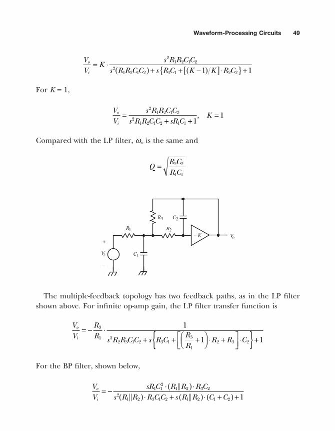
These circuits cannot achieve high Q values without appreciable attenuation of the input signal, but they provide a simple second-order fi lter with good phase linearity. In the multiple-feedback topology, all elements affect both wn and Q.In practice, Q is limited to about 20.
Vi
–
+
R1
Vo– K
R2
R3C1
C2
iV LPVA Σ–
–
–
HPV BPV ω ns–s–
ωn
Q– 1
The state-variable fi lter topology gets around the design diffi culty of interact -ing fi lter parameters at the expense of additional circuitry. This scheme is that of the analog computer; cascaded integrators output state variables that are weighted, combined, and fed back or output. The block diagram shown above produces HP, BP, and LP outputs, with corresponding op-amp implementation below.

Waveform-Processing Circuits 51
A quad op-amp IC suffi ces for gain blocks. Op-amp A is an input summing block, B and C are op-amp integrators, and D is a scaling feedback block. The transfer functions for the three fi lter outputs are
VV
As Q si
von n
LP = ⋅( ) + ( ) +
1
1 12ω ω
VV
As
s Q sivo
n
n n
BP = ⋅( ) + ( ) +
ωω ω2 1 1
VV
As
s Q sivo
n
n n
HP = ⋅ ( )( ) + ( ) +
ωω ω
2
2 1 1
where
ARR R C
QRR
voi
nn Q
= − = =, ,ω 1
In the characteristic equation, RQ occurs in the linear term but not in the qua-dratic term, thus leaving it free for adjustment of Q independent of wn. Its adjustment has the locus of a semicircle centered at the origin.
+
–
VLP
R
Ri
B
Vi
R
HPV Rn–
+
C
A BPV Rn
C–
+
C
RR
+
–D
RQ

52 Chapter 1
State-variable fi lters can achieve a high Q relative to multiple-feedback fi lters.
jRQ increasing
ω
σ
1a
+
−
+−
b2a
− 2b
−=
+
–
R5
Ri
B
Vi
R
BPV R2–
+
C
A LPV R3
C–
+
1
C1
2R4
A similar fi lter topology is the biquad fi lter (above), named for the biquadratic form of the transfer function
s ds es bs c
2
2
+ ++ +
It is similar in form to state-variable fi lters, but damping is adjusted within the cascaded loop of blocks at A in the block diagram above. This topology, like the state-variable fi lter, has multiple fi lter outputs; both BP and LP are available. By weighting and combining outputs from two or three of the op-amps in a fourth op-amp output stage, additional fi lters can be realized.

Waveform-Processing Circuits 53
For the biquad fi lter,
VV
RR
sR C
R R
sR C R C
R Rs
R C RR R
i i
BP = − ⋅
+
5
2 2
4 3
2 2 2 5 1
4 3
2 2 5
4 33 1
1( ) ⋅
+R
and
VV
RR R R
sR C R C
R Rs
R C RR R R
i i
LP = ⋅ ⋅
+ ( )
5
4 3 2 2 2 5 1
4 3
2 2 5
4 3 1
1 1
+ 1
The fi lter parameters are then
ω ωn nR R
R R C CQ R C= =4 3
2 5 1 21 1,
The biquad fi lter has an advantage over previous fi lter topologies in that the band-pass ∆w is adjustable independent of center frequency wn. From the expres-sion for Q above,
∆ω ω= =n
Q R C1
1 1
Because wn is independent of R1, it independently adjusts ∆w. The band-pass function can be simplifi ed to
VV
RR
sR C
s R C s R C R Ri
f
i
f
f f f
BP = − ⋅( ) + ( )[ ] +2 2
1 1
where
R R R R R C C Cf2 5 4 3 1 2= = = = =, ,
Gain is independently set by Ri, and ∆w by R1.

54 Chapter 1
+
–R1
Vi
R1
C
R
Vo
One other fi lter, shown above, is an all-pass fi lter that operates as a phase shifter. Its transfer function is
VV
sRCsRC
sRCsRC
sRCsRC
o
i
=+
− = −+
= − − ++
21
111
11
The delay time through the fi lter is
t R Cd = ⋅ ⋅2
Phase can be adjusted by adjusting R . This can be done electronically using a CMOS DAC or FET.
HYSTERETIC SWITCHES (SCHMITT TRIGGERS)
Comparators are usually inadequate for providing a single output transition when the input polarity changes. Slowly changing input signals with some noise cause the output to “dither”: to alternate between the high and low states near the input threshold. This dithering is reduced or eliminated by an input deadzone or deadband, an input range around the threshold where no output change can occur. Furthermore, if the deadzone is state dependent,

Waveform-Processing Circuits 55
The accompanying circuit is an inverting hysteretic comparator, or Schmitt trigger circuit. The state dependence is achieved by use of positive feedback. In effect, the Schmitt trigger is a bistable memory device.
Ov
IvHVLV
UV
DV
–
+
Ri
Rf
Ov
R2
V
R1
+
v+Iv
–
+
the effect is called hysteresis. The fi gure below shows a characteristic square hys-teresis loop.

56 Chapter 1
Assume that the output is in the high state; then vO = VU. Thevenize the divider R1, R2 so that its Thevenin voltage is VT, the threshold voltage, and its resistance is Ri:
VR
R RV R R RT i=
+
⋅ =2
1 21 2,
With vO high, v+ is set from the feedback divider Rf, Ri. When vI increases to where the comparator inputs are equal, the output changes to a low state. This input voltage is VH, the upper hysteresis threshold. By setting v+ = VH, by superposition,
VR
R RV
RR R
VHi
f iU
f
f iT=
+
⋅ ++
⋅
Once vO is low, then vI must decrease to VL, the lower threshold, before vO
becomes high. By letting v+ = VL and again applying superposition,
VR
R RV
RR R
VLi
f iD
f
f iT=
+
⋅ ++
⋅
The deadzone size is the width of the hysteresis loop. This hysteresis window is
inverting ∆v V VR
R RV VI H L
i
f iU D= − =
+
⋅ −( )
+
–
V
Ri
Ov
T
v+
Iv
–
+
Ov
IvHVLV
UV
DV
Rf

Waveform-Processing Circuits 57
A noninverting form of hysteretic comparator, shown above, has a similar hysteresis loop, but it is traversed in the counterclockwise direction. The circuit has a positive feedback divider and can be analyzed by superposition. When vO
is either high or low, the threshold for v+ is fi xed at VT.Hence, we must solve for VL and VH after applying superposition. The results
are
VRR
VR
R RV
RR
VR
Lf
iT
i
f iU
i
fU= +
⋅ −
+
⋅
= −
⋅ +1 ii
fT
RV+
⋅1
and
VRR
VRR
VHi
fD
i
fT= −
⋅ + +
⋅1
with the following input hysteresis window:
∆v V VRR
V VI H Li
fU D= − =
⋅ −( )
RE
Q1
Iv
–
+
RL1
+V
Q2
VZ+
RL2
V+
Ov

58 Chapter 1
A two-transistor discrete realization of a hysteresis comparator is the emitter-coupled Schmitt trigger, shown above. This is a diff-amp with positive feedback from the collector of Q1 through a voltage translator VZ to the base of Q2 return-ing to the emitter of Q1. The hysteresis loop goes clockwise. The additional inversion at the collector of Q2 reverses the direction of the loop at vO. VZ pro-vides an additional degree of freedom in setting the thresholds.
This circuit introduces another aspect of hysteretic comparators: As the input approaches the threshold, the diff-amp transconductance increases. Away from the threshold, one of the diff-amp transistors is cut off, and diff-amp trans-conductance is low. As a result, loop gain is low. But when the threshold is approached, the cut-off transistor begins to conduct, and loop gain increases. When it reaches one, the positive-feedback loop becomes unstable and transi-tions to the other state. To fi nd the threshold voltages accurately, an iterative solution is required since diff-amp gain changes with input voltage. In other words, a large-signal analysis is necessary using the diff-amp transconductance equation.
The hysteretic comparator is a positive-feedback amplifi er and is inherently unstable. This instability must be controlled in the design; instability is allowed only for changing state. If the loop gain has peaking, then as the input voltage approaches the threshold, a loop gain of one is reached fi rst at wm, the frequency at which the loop-gain magnitude peaks. Before the output changes, the loop oscillates with frequency wm. Therefore, otherwise stable loops require a loop gain without peaking.
DISCRETE LOGIC CIRCUITS
Even analog designs are likely to require some logic functions. In discrete designs, it is often unnecessary to add logic ICs to perform simple logic func-tions. The circuits below are a variety of diode and BJT logic circuits using only two diodes or one transistor.

Waveform-Processing Circuits 59
In the fi gure below, two more circuits are shown, using four transistors, to realize an exclusive-nor and an and-or-invert (AOI) gate below it.
⋅
A
B
A
B
(a)
A B+V+
A B
(b)
B
(c)
A
⋅A B
A
⋅A B
(d)
B
(e)
V+
⋅A BA B+
=A
(f)
⋅A B
A
B
B
(g)
B
AA B+=
⋅A B
B
A
V+ V+
B
A
V+
(h) (i)
A B+=⋅A B
⋅A BA B+
=

60 Chapter 1
These circuits have no particular merits other than their simplicity. Discrete realization of logic circuits is sometimes advantageous among analog circuitry when BJTs (or circuit-board space) are left over in an array and a gate or two is required.
CLAMPS AND LIMITERS
Nonlinear circuits that modify waveforms in some manner involving limits are clamps or limiters. Depending on the particular application, they might have other names.
A B⊕
V+
A B
DB
A C
V+
AB CD+

Waveform-Processing Circuits 61
In (a), diodes are used to limit the range of vI by “clipping” the signal outside the range of ±V. This circuit is commonly used as an input protection circuit in MOS ICs and oscilloscope trigger inputs. It is sometimes called a clipping circuit.Figure (b) shows a type of clamp that establishes a waveform at a given voltage level. An application is as a baseline restorer in video signal processing. The nega-tive extremes (sync tips) are established near ground by the clamp diode.
An important application of clamps is to keep transistors from saturating. Small-signal saturated transistors have excess charge in their base from being overdriven. This charge must be removed to turn the transistor off, and with limited base-current drive the base storage time increases. This causes a delay in turn-off. Falltime is not signifi cantly affected.
In large-signal (power) transistors, although excess base charge is a storage-time factor, another effect dominates, causing fall times of unclamped transistors to be larger. With large collector currents, a BJT operates in the high-level injection region, where the collector minority-carrier concentration (majority carriers from the base) approaches that of the collector majority concentration.
+V
–V
vI–V
+V
0 V
–0.6 V
(a)
(b)
62 Chapter 1
Under high-level injection, the collector side of the b-c junction actually inverts in charge polarity due to a dominance of carriers from the base. This Kirk effect causes conductivity modulation of the base, causing the base width to effectively increase. This effect occurs at a vCE just above saturation, in the qua-sisaturation region, and causes excess rounding in the collector family of curves at low vCE (of a few volts). (A related effect, called crowding, is due to ohmic vBE
drop laterally across the base, which causes less conduction in the center of the base than in the outer ring closer to the base contact.) Conductivity modulation also affects the fall time. As excess charge is swept out of the base, the excess base width begins to decrease, and turn-off commences. By decreasing excess base drive, conductivity modulation also decreases, along with both storage and fall times.
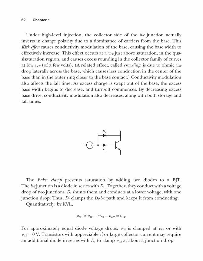
D2
D1
The Baker clamp prevents saturation by adding two diodes to a BJT. The b-c junction is a diode in series with D1. Together, they conduct with a voltage drop of two junctions. D2 shunts them and conducts at a lower voltage, with one junction drop. Thus, D2 clamps the D1-b-c path and keeps it from conducting.
Quantitatively, by KVL,
v v v v vCE BE D D BE≅ + − ≅1 2
For approximately equal diode voltage drops, vCE is clamped at vBE or with vCB ≈ 0 V. Transistors with appreciable r ′c or large collector current may require an additional diode in series with D1 to clamp vCB at about a junction drop.

Waveform-Processing Circuits 63
The disadvantage of the Baker clamp is the higher on-state vCE, typically a half volt. The Schottky clamp has reduced vCE(on). It is a variation of the Baker clamp and is very simple: A Schottky diode, with forward voltage of about 0.4 V, shunts the b-c junction. When vC decreases to 0.4 V below the base voltage, the Schottky diode turns on, clamping vCE at about 0.3 V. In Schottky logic output stages, this clamp prevents hard saturation while allowing lower vCE(on) than a standard Baker clamp.
D2
D1
D3
As D1 is in series with the b-e junction, no turn-off path exists without a shunt b-eresistor or, as shown above, a diode shunting D1 and reversed (or antiparallel) relative to D1.
Q1
Q2
Q3
If a complementary CC driver is used to drive the clamped transistor, as shown above, only one added diode is required for the Baker clamp. The b-e junction of Q1 takes the place of D1 in the previous circuit and the b-e junction of Q3 for

64 Chapter 1
A second emitter is added to the transistor to operate as a clamp. This anti-saturation emitter is connected back to the base. Because the b-c junction, as a diode, also points outward (as does the emitter arrow), the second emitter can be regarded as a second collector, as shown. It is more heavily doped than the collector and shunts current from it at low vBC. When the collector voltage decreases to near saturation, the second emitter dominates; for the same reverse bias, it has more minority carriers to inject into the base. As a result, the b-cjunction does not conduct heavily in the forward direction, avoiding hard saturation.
In the Murphy clamp, Q3 avoids saturation by its second emitter. This emitter is reverse-biased by vBE2, allowing vCB3 to decrease to vBE2 before the anti-satura-tion emitter takes effect. In addition, the shunted collector current is taken from the input drive current. The current gain of Q2 amplifi es this limiting action, resulting in a “sharp” limiting response.
Q1
Q2
Q3
D3. The diodes themselves also must have suitably fast turn-off recovery capability.
The feedback clamp scheme shown below, used in ICs, is a form of the Murphyclamp.
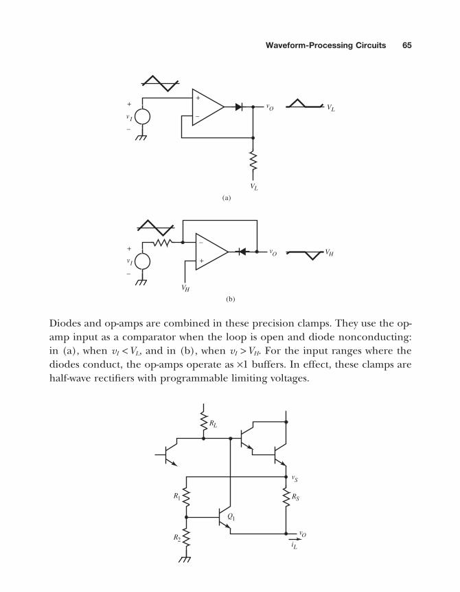
Waveform-Processing Circuits 65
Diodes and op-amps are combined in these precision clamps. They use the op-amp input as a comparator when the loop is open and diode nonconducting: in (a), when vI <VL, and in (b), when vI >VH. For the input ranges where the diodes conduct, the op-amps operate as ×1 buffers. In effect, these clamps are half-wave rectifi ers with programmable limiting voltages.
+
v
+
–I
(a)
–
VL
VL
vO
vO
–
v
+
–
I
(b)
+
VH
VH
Q1
RL
R1
R2
RS
vS
vO
iL

66 Chapter 1
A common limiter in power supply circuits is the foldback current limit, with one realization of it shown above. As load current iL increases, the voltage drop across RS increases until the b-e junction of Q1 is turned on. The transistor con-ducts, diverting base drive from the series regulator Darlington. The current is limited to
maxiv v R R R
RL
BE S
S
= ( ) + ⋅ +( )[ ]on 1 1 2
where vBE(on) is the vBE1 value for which the loop gain is barely suffi cient to sustain the limiting value of iL. The maximum current depends on vS, graphed below.
R2
R1 R2+
R1R1 R2+( )
RS
vS⋅ vBE (on)
Rs
vBE (on)R2
R1 R2+⋅
vBE (on)Rs
iLmax
The current limit decreases or “folds back” with reduced voltage so that a short conducts reduced current and thus power dissipation in the Darlington BJTs. As the short “clears” (load resistance increases), more current is allowed.
MULTIVIBRATORS AND TIMING CIRCUITS
Multivibrators (MVs) are positive-feedback (or regenerative) switching circuits with analog timing of switching behavior. They can be bistable, having two stable states (as Schmitt trigger circuits have); monostable, having one stable state; or astable,having no stable states. Monostable multivibrators (MMVs) are also called “one-shots”; they change output state upon input of a trigger signal. This quasistable state lasts for a timed interval (until the MMV “times out”), at which time it

Waveform-Processing Circuits 67
reverts to its stable state. MMVs are used to generate a triggered pulse of a given duration. Astable MVs are digital oscillators, or clock generator circuits, and some-times are called “free-running” MVs.
C1
Q1
R1
Q2
RL1
C2
R2
RL2
V+
The two-BJT astable MV topology consists of two capacitively coupled common-emitter (CE) stages. When vC 2 goes low, the negative transition is coupled through C1, cutting off Q1. R1, C1 form an RC differentiator, and vB1 begins to increase exponentially as C1 charges through R1. (Assume that the b-e junction of Q1 is not in reverse breakdown.) When vB reaches vBE1(on), Q1 conducts, causing its collector to transition to near ground. This cuts off Q2 for the second half-cycle of oscillation in the same way Q1 was cut off. For identical CE stages, the duty-ratio,
Dt
t ttT
on
on off
on=+
=
is 50%. When Q1 turns on and drives Q2 off, vC2 goes high (to +V), and C1 is charged in the other direction through RL2 and the b-e junction of Q1. This recharging time constant must be shorter (at least by 1/5) than R1C1 to fully recharge the capacitor. Therefore, R1, R2 must be at least fi ve times RL1, RL2.
MV frequency is increased by reducing coupling capacitor C. To analyze the effect of Cbe on timing, assume that the base timing resistor R is a current source

68 Chapter 1
I instead. This assumption is valid for off-times that are much less than the time constant RC when the exponential base voltage can be approximated as linear. Then C and Cbe form a capacitive voltage divider so that a negative input step of −V causes vB to step down to
v VC
C CvB
beBE0 0+( ) = − ⋅
+
+ ( )
Without the effects of Cbe, the timing ramp of vB has a slope of I/C and times out at
tCI
V1 = ⋅
With Cbe,
v tI
C Ct v tBE
beB( ) =
+
⋅ − ( ) >+0 0,
t
vB
vBE(0)
vBE (0) – V
t1Cbe 0
Cbe = 0
≠
The offset of vBE(0) does not affect timing since it is also the voltage threshold for determining t1. Set vBE(t1) = vBE (0) and solve for t1; it is the same as the pre-vious t1. Therefore, Cbe does not affect timing.
The previous analysis assumed zero fall time of the negative input step. To examine this assumption, consider the effect of switching time on timing by

Waveform-Processing Circuits 69
approximating the negative transition at the collector with a linear approxima-tion to the waveshape and its average slope m.
t1t
tfvB
vBE(0)
vBE (0) – V
vBE (0) – vf
Input transition
mI
C
Let the transition time be tf. Then, from the above v-t graph, the slower the transition, the smaller the negative excursion of the timing voltage, −vf ; thus,
t tCI
vf f1 − = ⋅
and
vIC
m tf f= − +
⋅
with m = −V/tf. Substituting and solving for t1,
tCI
IC
Vt
t tCI
Vf
f f1 = ⋅ − +
⋅ + = ⋅
Therefore, when tf < t1, the falltime has no effect on timing.
t1t
vB
IC
∆
rc 0
IC
cIr≠
rc = 0

70 Chapter 1
The fi nal timing analysis determines the effect of collector resistance rc of the conducting transistor. From the above graph, although the slope of vB(t) is independent of rc, the initial step size is not. With rc, I causes an opposing step of I ⋅ rc that translates into a time error of
∆tI rI C
r Ccc1 = ⋅ = ⋅
The fractional error is I ⋅ rc/V. Consequently, to minimize rc, the BJTs must be driven well into saturation by R1 and R2.
The two-BJT astable MV timing is independent for each half-cycle. This makes adjustment of half-cycle timing easy, but since the period depends on both half-cycles, each can contribute to period error. Two separate timing circuits are not necessary.
vO
+
–
1R
2R
C R
fR
RL
iR
+V
+V
The astable MV above, based on an open-collector comparator such as the LM393, has only one timing capacitor. This single-supply clock generator uses regenerative feedback through Rf to effect a hysteretic comparator while the timing is done by R and C. When vO = VU (high state), the timing waveform

Waveform-Processing Circuits 71
at v− is increasing and crosses VH at the v+ input. Then vO goes low (to VD), and the timing waveform decreases toward it while v+ = VL. When it reaches VL, vO
switches high again.For single-supply operation, R1 and R2 set a voltage around which the input
hysteresis limits of VL and VH are chosen. When vO = VU, the timing resistance is
R R R R R R R RU L f i i= + +( ) =, 1 2
VU and VH are calculated from the divider formed by RL, Rf, and Ri. The timing voltage v− begins at VL and heads for VU. The high-state time duration is
t R CV VV V
H UU L
U H
= ⋅ ⋅ −−
ln
During the low output state, vO = VD and v+ = VL. The comparator BJT saturates, and VD ≅ 0 V. Then v− decreases from VH toward VD, and
t R CV VV V
R CVV
LH D
L D
H
L
= ⋅ ⋅ −−
≅ ⋅ ⋅
ln ln
Finally, the output period is:
T t tH L= +
One of the most versatile MV circuits is the timer, notably the 555 bipolar and 7555 CMOS ICs, with block diagram shown below. This timer is mainly applied as a MMV or clock generator. It consists of two comparators with trigger (/TR) and threshold (TH) inputs. The other inputs are taken from a resistive divider from the supply, VCC. For the bipolar version, R = 5 kΩ; for the CMOS version it is R > 100 kΩ.

72 Chapter 1
The threshold-comparator input threshold voltage is
V VH CC= ⋅23
The trigger-comparator voltage is
V VL CC= ⋅13
The comparator outputs drive a NOR-gate RS fl ip-fl op (FF). The trigger input overrides the threshold input for control of the output. When /TR is asserted [v(/TR) < VL], the output is forced high. The reset input (/RES), however, overrides all other inputs. A separate transistor (BJT in 555, MOSFET in 7555) with open collector (or drain) marked /DIS (for discharge) is an alternative output for MV control.
An astable MV circuit using the timer is shown below. Initially, /TR is low and the output is high. The discharge transistor is off. C charges through R1 and R2
–
+
R
TR2
+
–
R
TH6
+V CC
8
FM5
RES4
DIS
OUT
7
3
1
R
555

Waveform-Processing Circuits 73
until the timing voltage crosses VH. The output goes low, /DIS sinks current, and C discharges to ground through R2. When the timing voltage crosses VL, the cycle repeats.
1R
2R
C
TR
DIS
TH OUT
2
6 3
1
4 8
+5 V
7
The time duration for a high output is
t R R CV VV V
R R C RHCC L
CC H
= +( )⋅ ⋅ −−
= +( )⋅ ⋅ ≅ ( ) ⋅1 2 1 2 12 0 693ln ln . ++( )⋅R C2
For a low output,
t R CVV
R C R CLH
L
= ⋅ ⋅
= ⋅ ⋅ ≅ ( ) ⋅ ⋅2 2 22 0 693ln ln .
The period is therefore
T t t R R C R R CH L= + = +( )⋅ ⋅ ≅ ( ) ⋅ +( ) ⋅1 2 1 22 2 0 693 2ln .

74 Chapter 1
with duty-ratio
DR R
R R= +
+ ⋅1 2
1 22
Given tL < tH, a duty-ratio of D < 0.5 is not possible with this circuit. An alterna-tive circuit achieves a longer tL by placing an additional resistor in series with /DIS. A CMOS alternative with accurate 50% duty-ratio is shown below.
R
C
TR
TH OUT
The output is used instead of /DIS to control timing, and the timing elements are the same for both half-cycles. The period is
T R C RC= ⋅ ⋅ ⋅ = ⋅2 2 1 386ln .
A timer-based MMV, (a) below, is triggered by a negative-going pulse. It sets the output high, and C begins to charge through R. The initial voltage on C is0 V, and it charges to VH. The time-out is thus
t R CVV
R C R CHH
CC
= − ⋅ ⋅ −
= ⋅ ⋅ ( ) ≅ ⋅ ⋅ln ln .1 3 1 1
If the trigger pulse duration exceeds tH, the output is kept high until the trigger goes high, as in (b).

Waveform-Processing Circuits 75
A MMV that begins its time-out after the trigger pulse goes high is shown above. The additional PNP transistor keeps C discharged until the trigger releases. This MMV is retriggerable in that the output remains high as long as trigger pulses continue to occur before time-out. Each new pulse resets the timing and retriggers the MMV.
+VCC
R
C
DIS
TR
TH OUT
OUT
TR
(a) (b)
+VCC
R
C
DIS
TR
TH OUT
+VCC
R
C
DIS
TR
3
+VCC
R1
R1
C1
FM

76 Chapter 1
The FM terminal (pin 5) allows control of the comparator thresholds, where a positive transition on the FM terminal triggers the MMV. The /TR input is biased at VCC/4. The trigger-comparator divider voltage is raised by the positive step of the trigger to where the step exceeds VCC/2 and starts the time-out.
For long time-outs, a large R, a large C, or both are needed. For a large R,timer-comparator bias currents can cause timing error. The bipolar timer has an NPN diff-amp input stage in its threshold comparator and a PNP stage for the trigger comparator. The bias currents IB place a limit on the minimum charging current. For large C, electrolytic capacitors are likely to be used. Their limitation is their leakage current. Aluminum electrolytics typically leak at 20 nA/µF; tantalum leaks at 5 nA/µF. If C is placed as shown below, its leakage current IL path is modeled by a shunt resistance Rp, shunting the timing resistor R. The maximum limit on R is thus set by Rp. This circuit has less timing noise ( jitter) because the target voltage of C is 0 V instead of VCC, the same voltage to which Rp would discharge C. When C is ground-based, Rp opposes charging instead of aiding it.
+VCC
R
DIS
TR
TH
IL
Rp
C+
IB
IB
CAPACITANCE AND RESISTANCE MULTIPLIERS
Timing circuits with long time-outs often require large capacitors. For accurate timing, these capacitors are plastic. Large-value plastic capacitors are volumetri-

Waveform-Processing Circuits 77
cally large and expensive. The capacitance multiplier is a circuit that uses gain to make a small capacitor appear electrically large. One realization is shown below.
vO 1
C
iR
fR
×vCvI
iI
Here, a current source drives the C multiplier to generate a ramp waveform. The ×1 buffer causes Ri and Rf to form a current divider because it keeps the voltage across Rf the same as across Ri. The charging current is a fraction of the input current, or
ii
RR R
C
I
f
f i
=+
The equivalent capacitance Ceq is based on the relation
i Cdvdt
iC
dvdt
iC
I eqO I
eq
O C= ⋅ ⇒ = =
The last equality follows because vO = vC. Applying the current fraction,
Cii
CRR
CeqI
C
i
f
=
⋅ = +
⋅1
This is a “transcapacitance” multiplier because vO is not across the same termi-nals that iI fl ows through. The input is Ceq in series with Rf Ri.

78 Chapter 1
A true capacitance multiplier (above) can be based on the Miller effect. The ×1buffer drives an inverting op-amp with a gain of −Rf/Ri. Applying Miller’s theorem,
CRR
Ceqf
i
= +
⋅1
Above the bandwidth of the amplifi er branch, the input is no longer purely capacitive but also has a shunt RL in series with Ceq.
Example: Timer with Capacitance Multiplier
–
+
C
fR
iR 1×
Ceq
Ri
+ –
vC
C
Rf
R
+V
Ri TH
DIS
TR

Waveform-Processing Circuits 79
The threshold-terminal bias current of a 555 timer limits its useful timing range as an MMV. A current-divider capacitance multiplier is used to extend the time-out tH by connecting it as shown above. The TH input is now driven by the op-amp output, eliminating bias-current error from TH but introducing op-amp offset current and voltage error. An equivalent circuit shown below is derived as follows.
vC
C
R
+V
+
–
– +VOS
VOS
TH
RiRf Ri+( )VOS
Rf Ri
RiRf( )+ 1
Rf
The op-amp circuit with Rf and Ri is Thevenized and fl oated on vC. The op-amp offset voltage VOS is divided by the resistors so that its Thevenin voltage is
VR
R ROS
i
f i
⋅+
in series with Rf Ri. Because the op-amp has ×1 gain, VOS also is in series with the TH input. In addition, VOS at the op-amp output contributes VOS/Rf to the timing current. From this model, timing error is calculated.
For signifi cant multiplication of C, Ri >> Rf. The series Thevenin voltage source is then about VOS, and the IOS term in the error current dominates.
Capacitance multiplication is achieved in the preceding circuits by applying bootstrapping to a current divider. The idea can be extended to resistance

80 Chapter 1
multiplication. A basic instance is the bootstrapped CC or FET CD stage (in “The Effect of Base-Emitter Shunt Resistance” of Designing Amplifi er Circuits).
A more deliberate and precise resistance multiplier, shown above, uses an op-amp buffer instead of a CC or common source (CS) amplifi er. Solving the circuit for rin,
r RRR
Rin = ⋅ +
+1
3
231
TRIGGER GENERATORS
A trigger generator is a kind of precision synchronizer. In television defl ection systems, horizontal and vertical scans or sweeps of the CRT are synchronized to the video signal by perturbing a free-running oscillator with the synchronization (or sync) signal, forcing it to lock to the sync frequency. The sync pulse also corrects the phase each cycle.
In synchronous digital systems, asynchronous events must be synchronized to the system clock. This is usually done using a fl ip-fl op (or fl op) clocked by the system clock; the asynchronous pulse is the data input to the fl op. The problem with this scheme is that if the data pulse changes state too soon before the active edge of the clock, the fl op setup time is insuffi cient and the output state is indefi nitely indeterminate. A second fl op cascaded with the fi rst can reduce the indeterminate time skew at the expense of one clock period of delay. Of course,
+
−
1R
2R
3R
rin

Waveform-Processing Circuits 81
the fi rst fl op output may remain indeterminate for longer than one clock period, but the probability diminishes rapidly with time.
This synchronizing problem is especially acute in oscilloscopes. The vertical waveform is fed to an event processor. On a selected slope and at the voltage of the trigger-level control, a comparator generates an event, an output transition that is used to start the sweep. When the sweep reaches the right end of the CRT screen, the CRT beam is turned off, and the beam retraces back to the left side, where it settles to the same starting position.
During sweep retrace, a hold-off pulse keeps input waveforms from fi ring the sweep until it is settled in its starting position. This hold-off pulse is asynchro-nous with the trigger events. If an event occurs while hold-off is releasing, time skew occurs in starting the sweep; this trigger jitter causes successive traces to be horizontally misaligned; the trace appears fuzzy, and multiple traces can be observed.
HOTR
DC
AQ D
CB
Q GATE
The trigger generator above reduces jitter by synchronizing the trigger events, TR , and hold-off pulses, HO. The circuit consists of two D fl ip-fl ops and a delay device, such as a digital delay-line or the propagation delay of some logic devices. The fl ops are clocked on positive (rising) edges by TR. The sweep gate is asserted low (as /GATE) and enables the sweep generator. The negative (falling) edge of /GATE must occur consistently at a fi xed delay time relative to the rising edge of TR. Assume HO is low; TR clocks fl op A. As its Q output settles, TR is delayed and then clocks fl op B. If the delay is long enough, fl op A output becomes valid and sets up the D input of fl op B for its setup time. Then when the delayed TR clocks B, the output edge time is determinate. Most of the time, HO does not violate fl op A D input setup time, but when it does, fl op B is required to synchronize its release with the trigger event. This
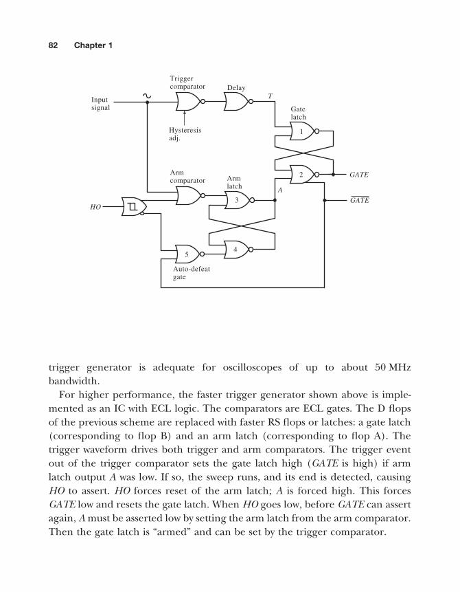
82 Chapter 1
trigger generator is adequate for oscilloscopes of up to about 50 MHz bandwidth.
For higher performance, the faster trigger generator shown above is imple-mented as an IC with ECL logic. The comparators are ECL gates. The D fl ops of the previous scheme are replaced with faster RS fl ops or latches: a gate latch (corresponding to fl op B) and an arm latch (corresponding to fl op A). The trigger waveform drives both trigger and arm comparators. The trigger event out of the trigger comparator sets the gate latch high (GATE is high) if arm latch output A was low. If so, the sweep runs, and its end is detected, causing HO to assert. HO forces reset of the arm latch; A is forced high. This forces GATE low and resets the gate latch. When HO goes low, before GATE can assert again, A must be asserted low by setting the arm latch from the arm comparator. Then the gate latch is “armed” and can be set by the trigger comparator.
Inputsignal
Triggercomparator Delay
Hysteresisadj.
Armcomparator
3
Armlatch
1
A
Gatelatch
2 GATE
45
Auto-defeatgate
T
HOGATE

Waveform-Processing Circuits 83
The detailed sequence of events is shown above. HO has become low. When the input waveform goes below the arm-comparator threshold VA, the arm latch is set (A is low) through gate 3. The range of time when arming can occur is shown as the negative half-cycle of the input waveform. It crosses the trigger-comparator threshold VT, is delayed, and attempts to set the gate latch by assert-ing T high. If A has been low long enough, GATE goes high without jitter.
The hysteresis is the difference in comparator thresholds. Because the wave-form has a fi nite slope, a time delay is generated between the latest possible arming A and earliest trigger T. The additional gate delay in the trigger path lets A settle to a valid level at the gate latch input.
The relative time delay of the trigger and arm paths is critical to proper synchronization. Otherwise, two trigger anomalies can occur: trigger jitter and double triggering.
Consider fi rst the case where the trigger-path delay is too short relative to the arm path. A low logic level at A must be established through the arm path pre-ceding trigger-path assertion at T (of a high level). With insuffi cient delay in the trigger path, T could assert before A is settled. This occurs when the input, on its positive slope, is crossing VA just as HO releases at the latest possible arming time. Gate 3 of the arm latch will be driven by a quick pulse, barely enough to cause the arm latch to change state after some time. This leaves A
VT
VA
Hysteresis Input waveform
T Trigger input
A Arm input
to gate latch
Trigger pathdelay time
Must go low before arming waveform arrives
Earliestarming
Arming waveformmust settle beforetrigger arrives
Latest arming

84 Chapter 1
indeterminate. When the trigger-path input to gate 2 goes low, A causes an uncertain starting edge at GATE. Trigger jitter is the result.
Now consider the case in which the trigger-path delay is too long relative to the arm path. When the negative slope of the input signal decreases through VT, the trigger path propagates a low level at T. Meanwhile, the arm path also propagates, through the arm latch, a low level at A. This arming of the gate latch must be preceded by a low level at T. If the trigger-path delay is excessive, the release of the gate latch at A occurs while T is still high, causing GATE togo high. This produces an extra GATE or double trigger. Under correct opera-tion, only the positive slope asserts GATE. Double triggering occurs when HOreleases just as the input signal crosses the arm comparator threshold at the earliest possible arming. On the screen, the waveform appears to be triggering on both slopes.
The optimal delay between the paths is somewhere between these two extremes. Delay-time tolerance is provided by the comparator threshold hyster-esis and fi nite slope (or slew rate) of the input waveform. Because the trigger path to gate 2 is one gate longer than the arm path, the hysteresis delay on the negative slope of the waveform must be at least one gate delay, tpd, to avoid double triggering. An approximate maximum tpd can be calculated by assuming a maximum amplitude sinusoidal input of frequency fmax. The gate propagation delay must be
tV V
V fpd
T A
fs
< = −⋅ ⋅
hysteresisslew rate 2π max
A hysteresis adjustment of the comparator threshold on the trigger comparator allows the trigger generator to be adjusted for maximum-frequency fault-free triggering.
Trigger jitter can be observed on an oscilloscope screen. Spurious traces to the left of the main trace are caused by late triggering. A waveform that is advanced in phase (hence, late) appears shifted to the left. This may seem counterintuitive since later time is to the right on the screen. But it is GATE thatis late relative to the waveform. If the sweep gate had started on time, the wave-form would not have advanced as far in phase.

Waveform-Processing Circuits 85
Slew-rate limiting of the input to the trigger system causes it to shift in time on the screen as the trigger level is adjusted. The limited waveform is time distorted, and its phase error varies with amplitude relative to the vertical signal. A time-domain test of trigger-generator performance is to let the input be a pulse of varying width. The minimum width that achieves a stable trigger is an index of generator speed capability.
In the trigger-generator circuit diagram, the function of gate 5 has not yet been described. The auto trigger mode causes the sweep to run at a low rate (typically < 50 Hz) to display a trace on the screen when no signal is present (or when the trigger controls are not adjusted properly). An auto-mode retrigger-able MMV is driven by GATE. If the sweep has not run for a while, the auto-MMV times out and gates the sweep on directly. When a triggered gate occurs, the MMV is reset and the free-run mode turned off. Now, if HO were the input to gate 4, at high sweep speeds, it would be diffi cult to get out of the free-run mode without gate 5.
At high sweep rates, HO has a large duty-ratio. That is, it takes much longer to retrace and recover from a sweep than the sweep time. If a slow trigger wave-form is applied with a period much greater than the sweep time (when HO isunasserted), the probability is low that during the sweep the signal would cross the hysteresis window. To escape the free-run mode, a GATE pulse is needed to reset the auto-MMV. The auto-defeat gate (gate 5) is added to provide the pulse.
When HO unasserts during free run of the sweep, if the trigger signal is below VA, the arm-latch output A goes low. Since the sweep was run by the auto-gate waveform, GATE is low, /GATE is high, and gate 5 thus blocks HO from resetting the arm latch. This allows the input time to cross VT and set the gate latch on
Late
Early
GATE
t

86 Chapter 1
its next half-cycle. If it does while HO is low, a triggered gate is asserted and the auto-MMV is reset. More likely, if HO is high, gate 5 allows /HO to reset the arm latch, and A goes high, resetting the gate latch low. GATE is high for the propagation time around the loop of gates 2-5-4-3-2. This is a few nanoseconds, enough time to reset the auto-MMV.
Another approach to auto triggering, autolevel, is to generate a triangle wave with a counter and DAC and sum it with the trigger-level control output. The tri-angle wave scans the level through the input range. When it intersects the input waveform, a trigger event is generated, and triggering then occurs. If no input is present, it autogenerates a trigger when the set trigger level is crossed.
An alternative approach to automatic triggering, peak-to-peak auto, uses positive and negative peak detectors to generate voltages at the extrema of the input signal. The trigger-level potentiometer is then placed between these peak volt-ages so that its control range is always within the signal range.
RAMP AND SWEEP GENERATORS
Oscilloscope time-base systems consist of a trigger generator followed by a sweep generator. The sweep generator is a gated ramp or sawtooth generator that drives the horizontal defl ection amplifi er. Ramp generators are also used in magnetically defl ected CRT display systems to generate defl ection-coil currents, in mass spectrometers, and in pulse-width modulators.
A bootstrap ramp generator uses the bootstrapping technique to maintain a con-stant voltage across a timing resistor R . As C charges, the top end of R followsit, driven by a buffer. The result is a linear ramp output.
K
V
c
R
V
+
C Ri
Ro

Waveform-Processing Circuits 87
With fl oating voltage source V, the ramp slope is
dvdt
V RC
VR C
= =⋅
This perfect scheme is spoiled by shunt resistance Ri (of the capacitor and buffer input), buffer output resistance, Ro, and buffer gain deviation from unity. Let Vbe gated on at t = 0 as
v t V u t V s V s( ) = ⋅ ( ) ⇒ ( ) =
Then solving the circuit in s,
V sV s
RR R K R s
R RK
R C
c i
o i oi
( )( )
=+ + −( ) ⋅
⋅ +−
)
⋅ +11
11
where K is a buffer voltage gain near one. The bootstrap effect appears as the increase in effective resistance of R + Ro by 1/(1 − K) times. With very large Ri,this increases the time constant by the same factor. In effect, the ramp is gener-ated as the initial segment of a long exponential curve. K, Ro and Ri all contrib-ute to the time-constant deviation from RC.
+
–
R
C
Vo−K
V(s)

88 Chapter 1
Another approach to ramp generation is to use an op-amp integrator. This Miller ramp generator has a transfer function of
V sV s
Ks K R C
o( )( )
= − ⋅+( ) ⋅ ⋅ +
11 1
For an op-amp, K → ∞, and the transfer function approaches −1/sRC, an ideal integrator. With fi nite gain, the output is an exponential with time constant multiplied by (1 + K); the early part of the curve is approximately linear. The fractional deviation, e, from linear response is
ετ
≅⋅
=⋅ ⋅ ⋅ +( )
t tR C K2 2 1
where t is the effective time constant. The fractional nonlinearity was derived by series-expanding the response exponential to the quadratic term, subtracting the (ideal) linear and constant terms, and dividing by the linear term. Error grows with time as the exponential becomes increasingly sublinear. This error formula applies to both bootstrap and Miller ramp generators; the responses of both are exponentials.
Finite gain also causes a slope error in the Miller integrator. In the transfer function, let V(s) be that of V/s. Then the transfer function corresponds to the normalized time-domain response of
dv t Vdt
o( )
Applying the initial value theorem,
dv t Vdt
s Ks
s K R CK
K RCt s
0
0
11 1 1
1( ) = − ⋅+( ) ⋅ ⋅ +
= −+
⋅
= →∞lim
The initial slope of the ideal ramp response, −1/sRC, is −1/RC. Thus,
fractional slope error =+K
K1

Waveform-Processing Circuits 89
Fast Miller ramp generators are driven by an input current source instead of a voltage source and R. This produces a more linear response and reduces the effect of input impedance. The ideal response of −1/sC is only approximate. More precisely,
V sI s
sCK s
K s
K sK s sC
o
i
( )( )
=⋅ + ( )
( )
= ( )+ ( )
⋅11 1
1
The ideal response is multiplied by the s-domain equivalent of the fractional slope error. To approach the ideal, the op-amp must maintain high gain at high frequencies. This is a major limitation, especially since the op-amp output impedance gyrates inductively. For
K sK
so
bw
( ) =+τ 1
K sK s
KK s K
KK s
o
o bw o
o
o T
( )+ ( )
=+
⋅
+( )[ ] +≅
+
⋅
+1 11
1 1 11
τ τ 11
The op-amp adds an additional pole at its unity-gain frequency fT.An improved ramp generator is based on the simplicity of a gated current
source charging a capacitor, followed by a buffer amplifi er. Feedback loops are avoided, and the step response is faster than for the previous two schemes.
Ii
C
(a)
Ii
C
(b)

90 Chapter 1
Bruce Hofer recognized the topological equivalence of this current-source ramp generator (b) with the Miller generator (a). The difference is in where ground is placed. In the Miller, the BJT is a CE; in the current-source, it is a CC. In the Miller, any anomalous switching voltage at the FET gate is coupled through C to the output; in the current-source generator, it is bypassed by C toground.
LOGARITHMIC AND EXPONENTIAL AMPLIFIERS
iI
–
+vO
Logarithmic amplifi ers are useful for compressing a wide dynamic-range wave-form, for multiplying, and for function generation. This simple log-amp is based on the BJT b-e (diode) junction v-i relationship:
i I e i ISv V
ST= ⋅ >>,
The input current iI is the BJT collector current and the output voltage,
v v ViI
ViI
O BE TC
ST
I
S
= − = − ⋅
= − ⋅
ln ln
This log-amp refl ects the temperature sensitivity of the b-e junction and drifts due to both VT and IS.
Detailed expressions for iC and iE (Gibbons and Horn 1964) indicate that several error terms vanish when vCB is zero. The logarithmic relation extends to lower currents for iC (because vCB = 0 and vBE ≠ 0) and is accurate over about

Waveform-Processing Circuits 91
nine decades. The high end (typically 10 mA) is limited by ohmic voltage drops in series with vBE and at the low end (typically 100 pA) by IS. From vO,
v V i V IBE T C T S= ⋅ + ⋅ln ln
The slope of vBE versus ln iC is linear with a slope of
dvd i
dvd i
d id i
Ve
BE
C
BE
C
C
CT
log lnln
log log.( ) =
( )⋅ = ⋅ =1
59 56mVdec
For each decade of change in iC, vBE changes by about 60 mV at 300 K over typi-cally nine decades of iC.
iI
–
+
vO
–
+B
RER1
Q1 Q2
R2A
IR
The effect of IS can be eliminated with a matched pair of BJTs, as in the log-ratioamplifi er above. Assuming equal IS,
∆v v v v VIi
BE B BE BE TR
I
= = − = ⋅
2 2 1 ln
The output is vB2 scaled by the divider, or
vRR
vRR
Vii
O B TI
R
= +
⋅ = − +
⋅ ⋅
2
12
2
1
1 1 ln

92 Chapter 1
The second op-amp B functions like A in keeping iC2 = IR, a reference current. For iI < IR, vO > 0. Op-amp B controls the emitter currents iI + IR, whereas op-amp A controls vB2 to keep iC1 = iI. RE is selected so that the output voltage range of B can span the range of iI + IR.
This circuit eliminates dependence on IS but is dependent on VT. The 0.33%/°C TC of vB2 is sometimes compensated by making R1 a positive TC (PTC) thermistor. Its TC is found by differentiating vO with respect to T, setting it to zero, and solving for dR1/dT. The fractional TC equation is
1 1 1 1
1
1 2
1 21
2
vdvdT
vT R
dRdT
RR R T
RR
O
OO⋅ = ( ) = − ⋅ ⋅
+
= − ( )⋅TC% TC%
RR R1 2+
When TC%(vO) = 0,
TC% C at 30RT
R RR
R RR
11 2
2
1 2
2
10 33( ) =
⋅ +
≅ ( ) ⋅ +
. % ° 00 K
Example: Log-Amp Design
A log-amp based on the log-ratio circuit requires an input range of 0.1 µA to 1 mA with minimal temperature drift. The output must be 0 V at an input of 1 mA (fs) and 4 V at 0.1 µA (zs).
The scaling is 4 V per four decades or 1 V/dec of iI. The divider must be
RR
2
1
11
6016 8+
= =V dec
mV dec.
PTC thermistors with 1 kΩ values are available, so let R1 = 1 kΩ. Then from the divider ratio, R2 = 15.8 kΩ. The TC of R1 must be
TC% C CR1 0 3316 815 8
0 35( ) = ( ) ⋅ =( ). %
.
.. %° °

Waveform-Processing Circuits 93
For vO = 0 V at 1 mA input, IR = 1 mA. This can be supplied from a voltage refer-ence of 5 V through a 4.99 kΩ, 1% resistor. When iI is supplied from vI througha 100 kΩ, 1% resistor, the input range is 10 mV to 100 V. Finally, for a minimum op-amp B output voltage of about −4.7 V, RE = 4 V/2 mA = 2 kΩ.
Op-amp input capacitance Ci can destabilize the log-amp. A feedback capaci-tor Cf forms a pole with collector resistance rc. The loop gain is
GHK
srr
sr Csr C Cbw
c
M
M f
c f i
=+
⋅ ⋅⋅ +
⋅ +( ) +τ 11
1
where K and tbw are op-amp open-loop gain and bandwidth, and rc is collector resistance:
r rc o= +( ) ⋅β 1
Also,
rr r
rr
Me e
me= + ′ = + ′
α α
The zero depends on rM, which varies with iC. For stability, the poles must be separated and the zero placed for lead compensation near a loop gain of one.
vI
R2
R1
Q1 Q2
RE
IR
A–
B+
–
Rf
vO
+

94 Chapter 1
The inverse function, exponentiation, is achieved by modifying the log-amp. In this exp-amp (or antilog-amp), op-amp A maintains a constant iC1 = IR.Then
vR
R Rv v v V
Ii
B I BE BE TR
C1
1
1 21 2
2
=+
⋅ = − = ⋅
ln
and at the output,
v R iO f C= ⋅ 2
Solving for iC2 in vB1 and substituting yields
v R IR
R RvV
O f RI
T
= ⋅ ⋅+
⋅
exp 1
1 2
Temperature compensation is also required for VT.
v
i1
i2
1+
–
2+
–
Q2 4
+
–
+
–
3
i3
Q
Q1 3Q
4
i4 fR
O
Log-amps, exp-amps, and amplifi ers combine to form function-generating circuits. Four op-amps and matched BJTs combine in the circuit diagram above to form a multiplier or divider based on the relation

Waveform-Processing Circuits 95
xy x y x y= +( ) = +( )−log log log exp log log1
The BJTs are connected with b-e junctions in series so that
ViI
ViI
ViI
ViI
TS
TS
TS
TS
⋅
+ ⋅
= ⋅
+ ⋅ ln ln ln ln1 2 3 4
or
ii i
i4
1 2
3
= ⋅
In practice, the basic log-amp is stabilized, and voltage input and offset (for bipolar operation) are provided, as shown below.
VOS
vI
RI
ROS
+
–
RI ROS
REvO
Cf
VT can be temperature compensated with a thermistor, but a more exacting approach uses two log-ratio amps and a divider. The fi rst log-amp has inputs iI
and IR, and the second is a temperature compensator; it has inputs of IR andk ⋅ IR, where k is a scale factor. The log output is the quotient of the two log-ratio amp outputs:
V i IV kI I
i Ik
T I R
T R R
I R⋅ ( )⋅ ( ) = ( )lnln
lnln

96 Chapter 1
A log-ratio amplifi er with output,
v Vii
O TX
Z
= ⋅
ln
and an exp-amp with output,
i i e ivV
O YV V
YI
T
I T= ⋅ = ⋅
( ) exp
are combined with an amplifi er of gain k in the fi gure above. The output is
i iii
O YX
Z
k
= ⋅
For k < 1, the amplifi er is replaced by a voltage divider. This function is quite versatile; scaled powers of ratios include squares, cubes, square roots, and trun-cated power series of transcendental functions. For example,
sin.
. %x xx
x≅ − ≤ ≤ ±3
6 790
21 35, error
π
With fractional powers, a better approximation is (see Sheingold 1974)
sin.
. %.
x xx
x≅ − ≤ ≤ ±2 827
6 28 20 25, 0 error
π
Also,
tan.
.− ≅ ⋅
+1
1 2125
1 21252 1x
xx
π
log kiY
vIiXiZ exp iO = iY
iXiZ( )k

Waveform-Processing Circuits 97
The inverse function f −1(x), of a function circuit f(y), can be realized by placing f(y) in the feedback path of an op-amp. The output,
y K x f y= ⋅ − ( )( )
or
xyK
f y= + ( )
For infi nite K, x = f(y), or y = f −1(x). This is useful for generating functions implicitly.
f(y)
Σ K yx +–
K yx +
–
Σ
Π
x=
y2
(a)
x ab
ab
y x=
(b)
In (a), a multiplier (indicated by the Π symbol) is in the feedback path of a noninverting op-amp. The circuit outputs the square root of the input:
y K x yyK
x y= ⋅ −( ) ⇒ = −2 2

98 Chapter 1
For infi nite K, x = y2 or y = x . Implicit function generation, as in (b), is often more accurate for the same complexity of function blocks because the range over which intermediate variables must maintain accuracy is reduced.
This is especially true of the commonly used root sum of squares (rss) func-tion, the vector magnitude function or Pythagorean formula:
y xkk
n
==
∑ 2
1
The range of x 2k can be large but need not be if computed implicitly. An implicit
formula is derived from y. Squaring each side, adding y ⋅xn, factoring, and dividing,
yx yxy x
x x y xy x
xy x
xkn
n
n
kn
n n
n
kn
nn=
++
=+ +( )+
=+
+∑ ∑ ∑− −21
21
1 21
1
In this formulation of y, it is fed back to divide x 2k, thus reducing the required
input dynamic range.A function describing the output of a bridge circuit with a sensor in one
branch is
yx
xy x y=
+⇒ = ⋅ −( )
11
More generally,
yA x
A xA y x
k
kk= ⋅
+ ⋅= −( )⋅
1
Finally, a two-term power series with y(0) = 0 is
y A x x B x C yA x B x
C x= ⋅ + ⋅ ⋅ + ⋅( ) = ⋅ + ⋅
− ⋅
2
1

Waveform-Processing Circuits 99
FUNCTION GENERATION
Function generation by log-amp circuits is based on the logarithmic nature of BJT junctions. The translinear cell is also a basis for function generation. The basic cell can be generalized by placing an arbitrary number of junctions in series on either the input or output side of the cell. For example, the current squarer shown below has two junctions in series on the input side.
iI iO
Q 3
Q1
Q2
As in translinear-cell analysis, assume that b is infi nite. The output current is derived from the circuit equations
v ViI
BE TI
S3 2= ⋅ ⋅
ln
i IvV
iI
O SBE
T
I
S
= ⋅
=exp 3
2
More generally, m series input junctions results in imI output. The translinear cell
is not dependent on IS as this circuit is.

100 Chapter 1
In the above circuit, the improved current squarer adds Q3, biased at a constant current I3. Its additional junction drop provides the needed correction for IS:
v ViI
v v ViI
VII
B TO
SB BE T
I
ST
S4 3 3
32= ⋅
= − = ⋅ ⋅
− ⋅
ln ln ln
or
iiI
OI=2
3
The squarer circuit concept can be extended to m input diodes and m − 1 stages like Q3 with currents I1 to Im−1. The output current is then
ii
I I IO
Im
m
=⋅ −1 2 1
iI
Q3
Q1
Q 2
Q4
iO
I3
+V
m
m–1
iI
IR
iO
1×

Waveform-Processing Circuits 101
A more general scheme is shown above. Here, two stacks of diode junctions drive the BJT. The stack biased by IR is buffered to keep BJT current separate from IR. Applying KVL to the loop and eliminating VT ⋅ ln,
iI
iI
II
iI
iI
O
S
I
S
mS
R
mO
R
I
R
m
=
⇒ =
−1
Fractional powers result by exchanging iI and iO, as shown below, with appropriate modifi cations. The BJT is moved to the former input string, and its fi rst diode is now at the new input. Applying KVL and discarding VT ⋅ ln,
iI
iI
II
iI
iI
O
S
mI
S
R
S
mO
R
I
R
m
=
⋅
⇒ =
−1 1
m–1
iO
IR
iI
1×m–1
Example: Square-Root Circuit
An example of a square-root circuit used in a medical laser is shown below to compensate for the quadratic (square-law) behavior of the fl ashlamp. A transis-tor array is used to provide matched BJTs.

102 Chapter 1
The BJT with base pin 9 corresponds in function to Q3 of the current-squarer. The circuit function is
vv
RR
R Iv Vv V
RR
V R Io
i
f
if R
o R
i R
f
iR f R
2 2
5 832=
⋅ ⋅ = ⇒ ( )
( ) = = ⋅. ,V
where Rf = R5, Ri = R1, and IR = 5.83 µA is set by R8. The circuit has a ×10 gain at full scale. The transistor array has IS = 10−15 A.
100 k
R5C2
150 pF
150 pF
C310 µF
5.83µA
U1B
+5 V
+5 V
−5 V
−5 V
+2.5 V
1.14 V0.1 µF
C4
R6
2.0 k 583 mV fs
58.3 mV fs
D2
1N4148
D11N4148
56
7
8+4
−+
−+
+0.58 V
QA1
QA1
QA1
QA1
C1
QA1CA3046/CA3086
U1ALM358AN
R110 k
R210 k
R32.0 k
R727 k
R8330 k
R422 k
9
1110
35
4
1514
12
76
5
1 32
23
6
iX iY
Q1Q 2
iO
Ev

Waveform-Processing Circuits 103
A rss circuit, shown above, based on a generalized translinear cell can be extended to three or more inputs. The voltage at the emitter, across the common diode, is
v Vi i
IE T
S
= ⋅ +
ln 1 2
Applying KVL and removing VT ⋅ ln results in
iI
iI
iI
Ii i
iI
Ii iS S
X
S
S Y
S
S1 22
1 2
2
1 2
+ =
⋅
+
+
⋅
+
= +
+⋅i i
i i IX Y
S
2 2
1 2
1
The output current is
i i i i iO X Y= + = +1 22 2
+
–
iX
–
+
Q1 Q3
D1i1 i2
Q2
D2
iY
–
+D3 D4
Rf
vO
A log-antilog scheme for an rss circuit (above) has common output current,
i i iO = +1 2

104 Chapter 1
and two loops to which KVL is applied:
iI
iI
iI
iI
iI
X
S S
O
S
Y
S S
=
⋅
=
21
22and ⋅⋅
iIO
S
These equations reduce to
i i i i i iX O Y O2
12
2= ⋅ = ⋅and
Adding them results in
i i i i i i i i iO O X Y O X Y⋅ +( ) = = + ⇒ = +1 22 2 2 2 2
An rms circuit similar to these rss circuits consists of three cascaded blocks: a squarer, averager (integrator), and square-root block. The rms circuit requires the intermediate averaging function.
The Analog Devices AD534 cleverly implements the rms function implicitly, using a current-squarer circuit and making use of its inherent divider capability. By feeding back the output as a divisor, the circuit implements the rms function,
v avg vo i= ( )2
or
v avg vo i2 2= ( )
by implementing the equivalent expression,
vavg v
vo
i
o
=( )2
The scheme is shown below. The fi rst stage is an absolute-value circuit that drives the squarer-divider with iC3. The Q3 collector voltage is vi/R2. An ampli-

Waveform-Processing Circuits 105
fi er, U3, is used to drive the emitter of Q9 with the voltage required for it to conduct iC5.
R2
R1 R3 R4 U2
U3
U1 Q1 Q2
Q3
Q4
Q9
Q5 Q6
Q7
R525 k
Q8
IR
vi
R6
vo
C
Q10
+V
+V
−V
+−
−+
+−
Writing the loop equation for the squarer,
2 3 9 10⋅ ⋅
= ⋅
+ ⋅
V
iI
ViI
ViI
TC
ST
C
ST
C
S
ln ln ln
This reduces quickly to
iii
CC
C10
32
9
=
The current mirror (Q5, Q6, and Q8) replicates the squarer output current, iC10,as rms output current, iC8, and feeds a copy of it back to the divider as iC9. The squarer output current is averaged by R5, C. Q7 is driven with a reference current, IR. Then its emitter voltage is related to iC9, the output current, by
v V i Ie T o R7 = ⋅ ( )ln
With proper scaling of vi and IR, ve7 is a log-rms (or dB-rms) output.

106 Chapter 1
TRIANGLE-WAVE GENERATORS
Function generators are a low-cost and versatile signal source. Their oscillator is a kind of multivibrator combined with a dual-slope ramp generator. This triangle-wave generator (TWG) outputs both triangle and square waves. TWGs are voltage-controlled oscillators (VCOs); their frequency can be accurately con-trolled over several decades by an input voltage, designated voltage-controlled frequency (VCF) or voltage-controlled generator (VCG) on commercial func-tion generator (FG) instruments. This makes them useful for frequency sweep-ing or modulation. An external phase-locked loop (PLL) can make them accurate frequency sources as well.
Frequency ×1R C
–
+
An early approach to triangle-wave generation coupled a Miller ramp genera-tor with a bistable MV or Schmitt trigger. The bipolar square-wave from the switch is integrated by the op-amp, producing a triangle wave. For a symmetric (50% duty-ratio) output, the magnitudes of the square-wave levels must be equal for equal triangle-wave slopes. The frequency can be adjusted, as shown, by varying the amplitude of the square-wave input to the integrator. Like ramp generators using an op-amp integrator, this approach is both speed- and precision-limited. For a VCF range of three decades and a full-scale square-wave amplitude of 10 V, at zero scale (the low-frequency end) the square-wave amplitude is 10 mV. For 1% waveform symmetry, the integrator input offset error must be less than 100 µV.

Waveform-Processing Circuits 107
Speed-wise, for a high-frequency limit of 1 MHz, triangle-wave amplitude of 10 V, and triangle nonlinearity of less than 1%, the slope magnitude is
dvdt
VRC
VT
TW SQ TW= = =4
10 V250 ns
where VSQ and VTW are square-wave and triangle-wave amplitudes and T theirperiod. VSQ is also 10 V, and RC = 250 ns. The integrator op-amp gain require-ment for the specifi ed nonlinearity is calculated from the ramp fractional non-linearity, which is
ετ
≅⋅
−⋅ ⋅ ⋅ +( )
t tR C K2 2 1
The integrator fractional nonlinearity and required gain are
εε
=⋅ +( ) ⋅ ⋅
⇒ =⋅ ⋅ ⋅
−TK R C
KTR C
22 1 4
1
K must be at least 999 at 1 MHz, an almost 1 GHz unity-gain bandwidth.
A B
C
I
×1
I

108 Chapter 1
To achieve better performance, current-source ramp generation is used with a bipolar current source. Two matched current sources are used to achieve bipolar charging of C. The positive (source) and negative (sink) currents are alternately switched into C each half cycle. This scheme is much faster and more precise than the fi rst one but requires matching of current sources for time symmetry and symmetric hysteresis thresholds for voltage symmetry.
+V
Q3
I
I
–V
D3 D4
D1 2D
RE
C
R
–V
–V
Q2Q1
Q4
R2
R1
RL2RL1
+V
0
A more concrete circuit realization (above) is a fast TWG, capable of over 100 MHz triangle-wave frequency. The hysteresis-switch and current-switch driver Q1–Q4 can be implemented with a single ECL NOR gate. The diode bridge is switched by Q3 and is limited mainly by diode shunt capacitance. Sometimes a Faraday shield is placed between the left and right halves of the diode bridge to decouple the square-wave node vE3 from the triangle-wave node at C. The input resistance of the Schmitt trigger is not high, resulting in appreciable

Waveform-Processing Circuits 109
A variation on the bipolar current supply uses only one current source for charging C. This eliminates the matching problem between sources. The Signet-ics NE565 FG and NE566 PLL both have TWGs of the above design. Q1 and Q2
form a current source or V/I converter with input vF, the VCF input. It gener-ates I through R, the timing resistor. Switching of I is controlled by Q5. When it is off, D2 conducts I, and C charges (positive). When Q5 is on, vC3 < vC4, and D1
conducts I through Q3, where it is replicated in Q4 as −I. Thus, C is discharged with the same magnitude of current as it is charged. Symmetry depends on current-mirror matching.
+V
R
Q1
Q2
vF
D1 D2
Q3 Q4
Q5
C
nonlinearity. By adding a good buffer, its additional delay slows the loop. Speed and precision are, as usual, in confl ict.

110 Chapter 1
It is not necessary to switch both current sources. To simplify switching, the I-2Ischeme is used. Only one current switch is required, but now the I and 2I sourcesmust be matched at an accurate ratio of 2.
A more recent approach to better symmetry is to control one current source based on the triangle-wave slope generated by the other. In the differ-ential TWG, instead of connecting triangle-wave node A (page 107) to ground, it charges a second capacitor of the same value from −I while the node B capaci-tor charges from +I. Its triangle wave is inverted relative to the one at node B. The two waveforms are then summed. Ideally, the sum is zero, but any differ-ence is an error voltage that is applied to one of the current sources to correct the slope of the waveform it is generating to match the other. This scheme increases symmetry enough at low currents to extend the VCF range an extra decade.
I
C
2I

Waveform-Processing Circuits 111
A conceptually similar scheme is used in the Exar XR2206 FG IC, shown in simplifi ed form above. The triangle wave is developed differentially across C andrequires a diff-amp pick-off. Q1–Q4 are the timing-current switches, but there is only one timing-current source. Q1, Q2, Q7, and Q8 are the hysteresis switch. The b-e junctions of Q1–Q2 sense the waveform and switch on when vE is reduced suffi ciently. On one half-cycle, Q1 and Q4 conduct; on the other half-cycle, Q2
and Q3 conduct. ISW sets the hysteresis thresholds. If the RSW are matched, the levels are symmetric. A disadvantage in this scheme is that the switching voltage is added to the capacitor ramp voltage at nodes A and B, as shown. It is diffi cult for a diff-amp to common-mode reject these fast switching edges, and some “glitches” appear in the triangle-wave output.
RL
RSW RSW
+V
Q7 Q8
Q1 Q2
CA B
Q3 Q4
Q5 Q6
–V –V
ISW I
Q1 on Q1 off
Q2 onQ2
vA
vB
RL
off

112 Chapter 1
The performance of a TWG loop depends on the subsystems within the loop. The timing capacitor must be of suffi cient quality (plastic), and for multiple frequency ranges, a matched set is usually required. The triangle-wave buffer must be fast, have low input-voltage offset and bias current, and high input resistance. The current switches must be fast and have low current leakage when off. Transistors are generally superior to diodes in both leakage and switching characteristics and are used as switches as shown in the TWG loop above. A minimum of two switches is required in a balanced two-source scheme, as shown. The switching scheme here consists of complementary diff-amps. Two BJTs switch the current-switch BJTs.
The timing-current generators also must be capable of operating accurately over as many decades of current as the VCF range because output frequency is proportional to timing current. Complementary V/I converters are commonly used to supply both polarities of current. These converters must be driven by precision circuitry that establishes symmetric voltages at their inputs. These cir-cuits need only the bandwidth required of the FM VCF signal. Sometimes BJTs are used as the current-source transistors in V/I converters instead of FETs for their higher output impedance. When a source is supplying the timing current
+V
I
Q1 Q2
Q3 Q4
I–V
C

Waveform-Processing Circuits 113
through a diode bridge, the triangle wave is at its output. Whatever parasitic output capacitance the current source has affects the timing. The additional isolation offered by a BJT switch over a diode minimizes this problem.
+
–
+
–VH Q
QVL
Within the TWG loop is the hysteresis switch. Schmitt triggers of the regen-erative MV kind are sometimes used, but their thresholds are often not accurate enough. The dual-level comparator circuit (above) is more accurate. The com-parator outputs are asserted (high) only momentarily as the ramp crosses a threshold at a peak. The RS fl op, made of NOR gates, is set to alternating states. This is not the fastest circuit since it consists of several stages of processing and can be used up to about 20 MHz.
Not only must the thresholds be symmetric; a hysteresis switch must also have little delay because the total loop delay determines the maximum operating frequency. As loop delay time td becomes an appreciable fraction of the period T, the ramp increases in magnitude beyond the threshold before the slope changes. The triangle-wave amplitude thus begins to increase with frequency.
VM
ωω
vM
d

114 Chapter 1
The effect is graphed. VM is the low-frequency triangle amplitude and hysteresis threshold. Because of delay, it increases to vM( f ). For a ramp slope of m,
v V m tM M d= + ⋅
where the slope is
mvT
vT
M M= =4
4
Substituting into vM,
v VvT
tV
t TV
tM M
Md
M
d
M
dd
d
= + ⋅ =− ( ) =
− ( ) =41 4 1 2ω ω
ω π,
Using the approximation
11
1 1−
≅ + <<x
x x,
then
v VM Md
d≅ ⋅ +
<<1
ωω
ω ω,
This equation also results from assuming the low-frequency slope of
mVT
M= 4
in vM. The period increases over its low-frequency value by 4 ⋅ td. From the vM
approximation, wd is like a zero break frequency for vM, but from the exact expression, vM is vertically asymptotic at wd. As w approaches wd, td dominates T. A td of 10 ns breaks at

Waveform-Processing Circuits 115
ft
dd
= 14
or 25 MHz.Because vM(w) is nonlinear, a nonlinear compensator is required to make
vM(w) = VM. Transfer-function compensation is based on linear analysis, requir-ing another approach. This is an adaptive control problem; a parameter VM must be varied to achieve ideal compensation. The amplitude error is
∆v v VV
v vff
M M MM d
dM
dM
d
= − = ⋅ ( )− ( ) = ⋅
= ⋅
ω ωω ω
ωω1
If VM is replaced by VM − ∆vM or if the triangle wave itself, vTW, is modifi ed to vTW
+ ∆vM, then vM becomes a constant VM. Because the TWG frequency is deter-mined by the VCF voltage vF, frequency information can be derived from it to set the comparator thresholds. The slope of vTW is I/C. If I is generated by a V/Iconverter by VCF voltage vF across timing resistor R, then,
mvRC
F=
For w << wd, the low-frequency slope applies. Equating to m above,
fv
R C VF
M
=⋅ ⋅ ⋅4
and the adaptive VM is
adaptive V V v VV
V v RC tV v
tRC
M M M MM
M F dM F
d→ − = − ( )( ) −≅ − ⋅
∆
1
This is an instance of model-reference adaptive control and is based on a priori knowledge of the circuit-model f. When R or C are switched to change frequency ranges, the model changes. Switching of RC in the adaptive VM is required for the model to represent the circuit.

116 Chapter 1
Another approach to TWG-loop compensation is to place in the loop a time advance to cancel td. In the s-domain, the delay is e −std and a compensating advance is e std. Time advances are not realizable in physical (causal) systems, and this form of compensation can be only approximated. The power-series expan-sion of the time delay is
e sts t s t
stst
std
d dd
d
d− = − + − + ≅ − ≅+
12 6
11
1
2 2 3 3
The single-pole approximation to a time delay suggests that a phase-lead com-pensator with zero at 1/td and higher-frequency pole provides approximate compensation.
A rational approximation to the time advance is the Padé approximation. A fi rst-order approximation is
estst
st d
d
d ≅ +− +
2 12 1
It is a nonminimum-phase transfer function. A second-order Padé approxima-tion is
es t sts t st
st d d
d d
d ≅ + +− +
2 2
2 2
6 126 12
It can be factored, which results in
zt
j pt
jd d
1 2 1 21
3 31
3 3, ,=
⋅ ±( ) =
⋅ − ±( ),
The pole-zero placement is symmetric about the origin and represents an all-pass fi lter. This is consistent with the delay function in that it effects only a shift in time with no amplitude change. The pole and zero pairs have an angle of
φ = ≅−tan 1 33
30°

Waveform-Processing Circuits 117
Besides being rational approximations, these delay compensators are linear whereas the circuit is nonlinear. Frequency-domain analysis assumes sinusoids, not triangle waves. For w << wd, the nonlinearity is not too severe and can be approxi-mated as linear, and the phase error in the rational approximations is minimal.
f
FC
IFMMV
TWG
τ
vF
The versatility of the FG is due partly to its wide VCF range. For frequency-response or Bode magnitude plots, a logarithmically swept VCF directly pro-duces a log-frequency plot on an oscilloscope display. A simple way of producing a logarithmic sweep is shown above. On each cycle of the FG output, the MMV is triggered. It gates on a current source for a fi xed time, transferring a fi xed charge to the VCF capacitor CF. This increments vF by a fi xed amount, causing the output frequency to increment. As the frequency increases, the rate of increase of vF increases along with it and is exponential. The resulting frequency sweep, when displayed, is stepwise logarithmic.
Quantitatively, let the MMV time-out be t < T = 1/f. During a given time interval ∆t, n periods of the output occur. Then
∆∆vt
n I Cn T
fIC
F F F F
F
= ⋅ ( )⋅
= ⋅ ⋅
τ τ
In the limit, for small ∆vF or infi nite n,
limn
F F F
F
vt
dvdt
IC
f→∞
= =
⋅∆
∆τ
As a voltage-to-frequency (V/F ) converter (VFC),
f k vF F= ⋅

118 Chapter 1
Substituting into the limit equation and solving,
v v eF FI C k tF F F= ( ) ⋅ ⋅ ⋅ ⋅( )0 τ
The sweep-rate constant is (IF ⋅t/CF) ⋅kF, and the sweep time is
tf f
I C kSWP
F F F
= ( )( )⋅( )⋅
ln 0τ
where f(0) is the starting frequency and f the ending frequency. The VFC con-stant kF can be found from the TWG parameters. For triangle-wave amplitude of VM, the slope is
VT
IC
v RC
fRC V
v kRC V
M F
MF F
M41
41 1
41= = ⇒ = ⋅
⋅ ⇒ = ⋅
Besides VCF, the TWG current sources can be individually controlled for variable symmetry or duty-ratio. A voltage-controlled symmetry (VCS) input allows pulse-width modulation (PWM) of the output waveforms.
/2
VM
π
v
VM
4T t
A third waveform available on FGs is the sine wave. This function is not gen-erated by the TWG loop but by a sine converter circuit. Most commonly, this is a multiple-diode clamp that performs a piecewise-linear waveform shaping of

Waveform-Processing Circuits 119
the triangle wave. Commonly used shapers use diode bridges for symmetry and diode drift cancellation. The initial part of the triangle and sine waves has the same slope. For sine amplitude of VA, the slopes are equated:
VT
VVV
MA
M
A4 21 57= ⋅ ⇒ = ≅ω π.
The most signifi cant anomaly of these sine shapers is the triangle-wave peaks in the sinusoid. At the peaks, the derivative of the triangle wave is discontinuous and is diffi cult to remove entirely from the sine wave. Typically, three-break-point sine shapers produce less than 0.25% total harmonic distortion (THD) in the audio range.
Another scheme uses the hyperbolic tangent function of the BJT diff-amp as an approximate sine converter. This results in somewhat more dis-tortion than the multiple-clamp circuit. MOS diff-amps have a quadratic transfer function and also approximate a sine output with adjusted parameters.
I120
I6
I
i1
i3 i4
i2

120 Chapter 1
A more elegant approach is to return to the translinear cell concept. By stack-ing diodes with diff-amp pick-offs, arbitrary power series expansions can be realized, as in the above circuit for three terms of a sine expansion. The Taylor-series expansion is
sin sinii
x xx x1
2
3 5
6 120= = − +
The truncation error is less than 0.07%. For two terms, the error is 0.14%, still favorable relative to the other schemes. This sine converter operates over an input range of x from 0.5 to 2.
I2 Q
i3 i4
Q5 Q6Q3 Q4
Q1 Q2
D2
i2i1
D1
VB
The two-term sine shaper sketched above has a topology similar to a Gilbert gain cell. It passes the linear term through Q5–Q6 while Q1–Q2 develop the second term of the output. Together,
i iI I
i IO I
Q I
l I
= ⋅ −+ ( )
1
2
1 2

Waveform-Processing Circuits 121
where
i i i i i i I i i I i iI O I Q C C= − = − = + = +1 2 3 4 1 2 1 2, , ,
The ratio 2IQ/II is adjusted for minimum THD of less than 0.1% when the ratio is about 1.5.
ABSOLUTE-VALUE (PRECISION RECTIFIER) CIRCUITS
A full-wave rectifi er performs the absolute-value function
xx x
x x=
≥− <
,
,
0
0
A half-wave rectifi er performs the function
f xx x
x( ) =
≥<
,
,
0
0 0
Half-wave rectifi cation is mainly applied as a bipolar to unipolar (ac-to-dc) con-version technique in low-power power supplies or AM demodulators. Rectifi ers can be designed to output either polarity; the positive outputs of x or f(x)could instead be −x or −f(x). For waveform processing involving mathematical functions, x is more commonly needed.
Iv
+
–
Ov
+
–
A single diode can half-wave rectify (above).

122 Chapter 1
Two diodes are used for full-wave rectifi cation with a ground-based differential input (above) and a diode bridge for a fl oating input (below).
Ov
2vI
+
–
2vI
+
–
Iv
+
–
Ov
+
–
A more recent addition to rectifi er circuits is the synchronous rectifi er. It uses active devices, usually MOSFETs, that are switched by the input itself. These circuits are associated with power conversion and are commonly found in power sup-plies, both linear and switched. The precision clamps of “Clamps and Limiters” are half-wave rectifi ers.
+
–R1
B–
+A
vI
–
+
R3
R2
D1
D2
R4 R5
vO
–

Waveform-Processing Circuits 123
Absolute-value circuits can be designed many ways. The common constraint is that the gain magnitude for vI < 0 be the same as for vI ≥ 0, so that −Av− = Av+.A common absolute-value circuit is shown above. It has similar frequency responses for positive and for negative inputs. On the positive half-cycle, D1
conducts, and op-amp A operates in the inverting confi guration. Op-amp B converts this output to a single-ended signal vO. The gain expressions are
ARR
RR
AR R R
RR
R Rv v+ −= −
⋅ −
= − +( )
⋅
+2
1
5
4
3 2 4
1
5
2 4
; ++
1
Equating Av+ to −Av−, the constraint on resistor values is
R R R R3 5 2 4= =,
Because R1 is unconstrained, it can set the gain. Op-amp B must have a fast large-signal response to follow the discontinuities in the waveform it amplifi es.
+
–R1
A
vI
–
+
R3–
+
–B vO
R2
This circuit uses only one diode. Op-amp A functions for negative inputs as the fi rst stage of gain in the forward path, cascaded with op-amp B, a ×1 buffer. The gain is
ARR
v− = − 2
1

124 Chapter 1
For positive inputs, op-amp A is disconnected from B, and vI is applied directly to the input of B through R3. The value of R3 does not affect gain; its purpose is to limit current from op-amp A when the diode conducts. Thus, positive inputs bypass A and are merely buffered by B with a gain of Av+ = 1. The con-straint is simply that Av− = −1:
R R1 2=
The positive-gain path involves only one op-amp and has a faster response than the negative-gain path for negative inputs.
+
vI
+
D1
vO
–
D3
I
D2
R1
I
R2
–
A similar kind of circuit with only one op-amp requires matched diodes D1
and D2 and current sources as a trade-off for fewer components. In IC form, this is attractive. The positive-gain path is through D1 and the op-amp, with a gain of one. D2 also conducts, causing the inverting op-amp input to follow the input. For negative inputs, D1 is off, D3 is on to satisfy the current source, and the op-amp inverts with a gain of −R2/R1. D2 conducts all the time to balance D1 or D3.The constraint is
R R1 2=

Waveform-Processing Circuits 125
Another variation on this theme, which allows adjustment of gain at the output by means of R4, is shown above. The gains are
ARR
AR R
Rv v+ −= + = +
4
2
4 2
1
1,
The constraint again applies. R4 is not constrained and can be used to set the gain. D2 clamps op-amp A input to virtual ground for positive signals so that R1
does not affect Av+.
B–
+
R3
R2 R4
vO
+
–A
D2
D1
vI
–
+
–
R1
vO
D1
vI
R4
–
+A
D2
R2 R3–
+B
R1

126 Chapter 1
This absolute-value circuit has a high-impedance input but is constrained to a gain of one. For Av+ = 1 then
ARR
RR
RR
R RR R
v− = +
⋅ −
+ +
= − ⋅
⋅2
1
4
3
4
3
2 4
1 3
1 1 1
The constraint is
RR R
R4
1 3
2
2= ⋅ ⋅
One combination of resistors satisfying the constraint is
R R R R1 2 3 42= = ⋅ =
vOD2
vI
–
+A
R2
–
+B
R1
R3
D1
R4
This absolute-value circuit also has a high-impedance input, with gains
AR R
RA
RR
v v+ −= + + = −2 3
1
3
2
1,

Waveform-Processing Circuits 127
and with the constraint
RR
R RR R
1
2
3 2
3 2
11
= +( )−( )
Implicit in the constraint equation is the additional constraint that R3 > R2.
Ri/2RfU1
U2
Q1 Q2
Ri
RR
vI
vo
−+
+
−+
The absolute-value circuit shown above is essentially that used in the AD534 root mean square (rms) circuit. The transistors and resistors must match for accuracy. For positive vI, the BJTs are cut off, and input current fl ows in the lower path through Ri to the input of U2. For negative vI, both BJTs conduct and present the same voltage at their emitters. Q1 completes the path back to the U1 input while Q2 conducts half that current through the lower Ri via R/2to vI. This causes the output op-amp to conduct the same amount of current as in Ri, and the circuit transfer function is
vv
RR
O
I
f
i
= −
As with most other absolute-value circuits, the path for one polarity (positive vI
in this case) is faster than for the other polarity. Also, design of the above circuit should take into account the reverse b-e breakdown-voltage limitation, typically around 5 V to 7 V. This limits not only the U1 negative output saturation voltage for positive inputs but also the positive range of vI. A single-supply op-amp with grounded negative supply terminal allows for maximum positive vI range.

128 Chapter 1
Not all absolute-value circuits must be designed by matching gains of positive- and negative-gain paths. This circuit resembles an instrumentation amplifi er but its output current is unipolar. For vI > 0, D1 and Q2 conduct. D1 reverse-biases Q1. The negative-gain path is through D2 and Q1. The circuit is symmetric and has output current
ivR
OI=
Iv
–
+iO
1QA
D1
R
–
+ 2QB
D2
+
–
+
–R1
B–
+
A
vI
–
+
R6
R2D1
D2
R5
vO
–
R4
R3
R3= R4 2/
R1
R2

Waveform-Processing Circuits 129
Finally, this circuit has a rectifi er section similar to the fi rst absolute-value circuit but with gain set by R5. The positive-gain path is through A, then B; the negative-gain path is through R3 and B. For negative inputs, D2 conducts through R6, a current-limiting resistor, forcing the inverting input to virtual ground. R4
and R2 then shunt the input of B, but this does not affect the gain.Some op-amps have inherently unipolar outputs and can be fashioned
into precision rectifi ers. When current mirrors, CMOS inverters, and other elemental circuits are also used, the collection of absolute-value circuits becomes extensive.
PEAK DETECTORS
Peak detectors are a class of circuits that extract the extrema of waveforms. They are essentially rectifi er circuits with a memory. A simple example is the rectifi er-fi lter combination of power supplies.
Ov
Iv
+
–
+
–
The diode conducts to charge the fi lter capacitor whenever the source-circuit voltage exceeds the capacitor voltage. The capacitor charges to the peak input voltage.
Iv
+
–
Ov > 0 Iv
+
–
Ov >0
–V
(a) (b)
+V
C
C

130 Chapter 1
Fast, simple detectors (shown above) of maxima (positive peaks), (a), and minima (negative peaks), (b), use a CC stage that charges C.
Slower, more precise peak detectors, shown below, are reset through FETs that discharge the capacitors. Ideally, after C has been charged to the peak voltage, it retains its charge indefi nitely. (In this respect, peak detectors are similar to S/H circuits.) The capacitor must have low leakage (high insulation resistance) to minimize the discharge rate. It must also have low dielectric absorption so that when reset, it retains 0 V until recharged by the input wave-form. These requirements suggest a plastic or mica capacitor.
ResetC
Iv
+
–
+
–Ov > 0
(a)
ResetC
Iv
+
–
+
–Ov >0
(b)
This applies also to its load, including the reset FET, and to the op-amp bias current. For the circuit below, load leakage is minimized by using a high-impedance buffer with low input bias current. When it drives the input op-amp, its offset-voltage error is compensated by being in the loop. The feedback loop also effectively reduces the time constant rout ⋅C by the loop gain, where rout isthe resistance in series with the diode. Fast peaks are thus detected more accurately.

Waveform-Processing Circuits 131
To avoid overcharging, the feedback response must not be underdamped or overshoot occurs. Op-amp B must be faster than A to minimize loop delay and avoid overshoot. That is, a single dominant pole in the loop due to A yields a damped response. Because of the output loading of C and the additional pole it causes, op-amp A usually must be frequency compensated.
If op-amp A has limited output current, a CC buffer can replace the diode. This increases charging current by the b of the transistor and slew-rate increases by b.
D2 and R are added to keep op-amp A from being driven into saturation when D1 is off. R limits D2 current. This enables the op-amp to respond more quickly as its output now follows the input. This also keeps its output from quickly switching to its saturation limits when D1 cuts off, thus minimizing transient feed-through to the hold capacitor via D1 shunt capacitance.
Iv
+
–
D1
C
Reset
vO
RD2
A+
– B+
–
Iv
+
–
D1
C
Reset
vO
C
R
D2
+
–+
–
To further minimize bias-current error, a similar capacitor can be placed around op-amp B. Both capacitors are charged by the bias current, resulting in

132 Chapter 1
the same ∆v across each. The error voltage on the feedback capacitor subtracts from the hold-capacitor voltage, thus compensating its error. The feedback capacitor, however, must also be reset; two reset switches are required.
Iv
+
–
D1
C
Reset
vO
RD2
A+
– B+
–
D3
1
R2
Finally, the diode must have a low reverse saturation current to minimize leakage when off. Reverse current varies with reverse voltage and is minimized by minimizing the voltage across the nonconducting diode. This can be done by, again, using the versatile technique of bootstrapping. D3 and R2 have been added to the fi rst two-op-amp peak detector. vO follows the capacitor voltage when holding, and R2 applies this voltage to the anode of D3, reducing its voltage to zero. D1 blocks this node from the varying output of op-amp A, but its leakage is not critical for low values of R2. When C is charging, R2 isolates the diode node from the output of op-amp B. With this approach, special low-leakage diodes can be avoided in most applications. An alternative is to replace D1 of the origi-nal peak detector with a junction fi eld-effect transistor ( JFET). Its gate-source junction typically has lower leakage than discrete diodes.
The bootstrapping technique of leakage decoupling can be applied to the reset switch also. Two switches are placed in series, with a resistor from the output connected to their series connection. Both switches are driven by the Reset signal.
Bootstrapping can also decrease acquisition time if input impedance is not critical. In the fi rst two-op-amp peak detector, add a resistor in series with vI anda bootstrap diode from output to the op-amp A noninverting input so that it conducts from output to input. Then the fi rst fast peak charges C. Through the

Waveform-Processing Circuits 133
bootstrap diode, the output of op-amp A is now driven to this voltage, which is near the peak. The next fast peak has less voltage over which to slew the output to further charge C.
Most of the charging time occurs when op-amp A output is near the peak voltage because it is not required to supply the large slew-rate-limited currents that a large voltage difference causes. Feedback then increases response time if rout ⋅C corresponds to frequencies at which the loop gain is still high.
The hold capacitor size is chosen as a trade-off between hold time and acqui-sition time. For fast peaks, a small C is preferred for faster charging. But a smaller capacitor develops hold error at a higher rate than a larger C. Therefore, C is chosen as a compromise between acquisition and hold-time requirements. A two-stage peak detector mitigates the trade-off. The fi rst stage is optimized to be fast, whereas the second stage has a long hold time.

2Digitizing and Sampling Circuits
ELECTRICAL QUANTITIES BOTH ENCODE AND REPRESENT INFORMATION
An electrical quantity in time x(t) is a signal when it encodes information. The information is interpreted according to a representational theory, such as logic theory for digital signals or transforms based on analogy for analog signals. The theory of representation is independent of the encoding scheme. In communi-cations theory, encoding is called modulation. What the modulating signal rep-resents is independent of its encoding. A thermometer output, for example, can be encoded in analog or digital form but represents temperature, regardless.
Another way to think about information encoding is as two levels of representation. The encoding scheme is a representation at the electrical level, and the encoded information represents a quantity that is independent of elec-tricity. This “more abstract” level of representation has to do with the applica-tion. Consequently, electronics is useful in domains that have nothing to do with electronics because both signals and their processing operations have meaning-ful interpretations for the application.
Information can be encoded as discrete or continuous functions of either an electrical quantity (usually voltage or current) or of time. The information to be encoded and the encoding scheme can be either discrete or continuous. The compatibility of an encoding scheme with the encoded information is a design consideration. For example, discrete functions are often best represented by digital encoding. Engineers sometimes differ over the relative merits of discrete versus continuous encoding and processing of information. The difference between discrete, or digital, and continuous, or analog, encoding is so important that each constitutes a major subdiscipline within electronics.

136 Chapter 2
A digital signal is discrete in both x and t. Binary encoding is by far the domi-nant digital encoding of x, where x ∈ XL, XH. These two values or “levels” are named low (XL) and high (XH) and represent binary logic states of false and true,or, in Boolean algebra, 0 and 1. Whether the low level represents true or falsedepends on the polarity of the logic; a low level is false in positive logic and true in negative logic. Digital encoding can have more than two levels. The number of levels equals the modulus or base of the number representation. For example, decimal numbers can be encoded in a 10-level scheme. As the modulus increases, the representation approaches a continuous form.
An example is the output of digital-to-analog converters (DACs). For an 8-bit DAC, 256 discrete levels may adequately approximate a continuous function in some applications. The DAC could, however, be considered an encoder of base-256 numbers. In this sense, continuous waveforms are of infi nite modulus, and analog engineers are actually digital engineers who specialize in infi nite-base encoding.
Discrete functions can also be encoded in time. Frequency-shift keying, a kind of binary FM used in modems, is one approach. More common to computer electronics is synchronous and asynchronous serial encoding of alphanumeric characters in ASCII. Many other purely digital encoding schemes make digital encoding and communications a specialty in itself.
Continuous functions can also be encoded purely in time as the width of a (binary) pulse (pulse-width modulation [PWM]) or by its time difference rela-tive to another event in the signal (pulse-position modulation) or simply by the pulse frequency, as is the output of voltage-to-frequency converters (VFCs).
Finally, waveforms that are continuous in x and discrete in t are sampled wave-forms. These waveforms are of great importance in association with analog-to-digital (A/D) and digital-to-analog (D/A) conversion and with sampled-data systems in general, systems that contain discrete-time waveforms, such as a motor servo controller with a digital position encoder, or any system with sample-and-hold circuits.
DIGITAL-TO-ANALOG CONVERTERS
Digital-to-analog converters convert digital input codes to output voltages or currents. The transfer curve for a unipolar three-bit DAC has discrete voltages at the discrete (integer) values of the digital input code d.

Digitizing and Sampling Circuits 137
The digital code is an ordered set of bits that represent integers. Various number representations are possible, but the most common are shown in the table for three bits.
Integer Offset BinaryTwo’s
Complement Sign-Magnitude
3 111 011 011 +fs
2 110 010 010
1 101 001 001
0 100 000 000 100 zs
−1 011 111 ↑ 101 ↑
−2 010 110 0+ 110 0−
−3 001 101 111
−4 000 100 ↑ −fs↵
inverted MSB
↵
(sign)
MSB 1 ⇒ −
These are signed (bipolar) representations of integers. The most common number representations are two’s complement and offset binary. They differ only in the polarity of their sign bit. Binary-coded decimal (BCD) is also some-times used, in which the fi rst 10 binary numbers represent a decimal number.
In the above table, the positive full-scale (fs) value is 3, and the negative fs value is −4, one greater in magnitude. This asymmetry results from assigning a state to zero. Sign-magnitude coding is symmetric, but it has two zero states. In general, for n bits, there are 2n states. The transfer characteristic for a unipolar n-bit DAC is
1 2 3 4 5 6 7 d0
Vfs
VR
vO
VLSB
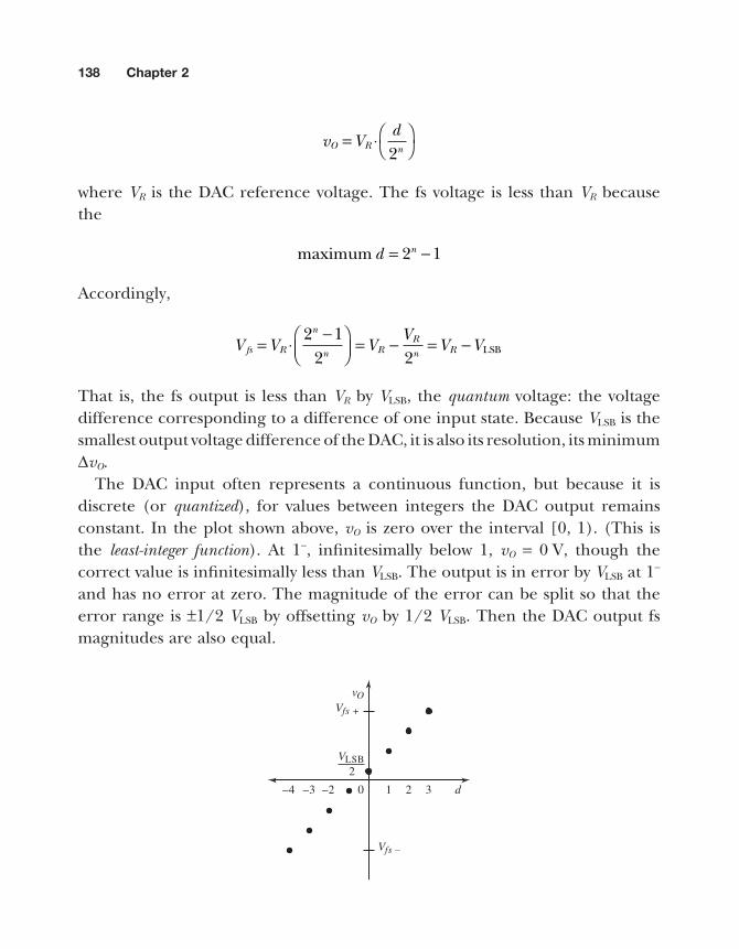
138 Chapter 2
v Vd
O R n= ⋅
2
where VR is the DAC reference voltage. The fs voltage is less than VR because the
maximum d n= −2 1
Accordingly,
V V VV
V Vfs R
n
n RRn R= ⋅
−
= − = −2 1
2 2LSB
That is, the fs output is less than VR by VLSB, the quantum voltage: the voltage difference corresponding to a difference of one input state. Because VLSB is the smallest output voltage difference of the DAC, it is also its resolution, its minimum ∆vO.
The DAC input often represents a continuous function, but because it is discrete (or quantized), for values between integers the DAC output remains constant. In the plot shown above, vO is zero over the interval [0, 1). (This is the least-integer function). At 1−, infi nitesimally below 1, vO = 0 V, though the correct value is infi nitesimally less than VLSB. The output is in error by VLSB at 1−
and has no error at zero. The magnitude of the error can be split so that the error range is ±1/2 VLSB by offsetting vO by 1/2 VLSB. Then the DAC output fs magnitudes are also equal.
1 2 30
2
–2–3–4
Vfs +
vO
VLSB
Vfs –
d

Digitizing and Sampling Circuits 139
Quantization error causes quantization noise, which is a sawtooth function that cycles between −VLSB/2 and +VLSB/2 between each state (∆d = 1). The rms value of this noise vn is
rms LSB LSBLSBv
dV
dd d d
VVn d
d= ⋅
⋅ ( ) = ≅ ⋅−
+∫
112
0 32
2
2
∆ ∆∆
∆.
A signal-to-noise ratio (SNR) defi nition for n bits is
SNRrms
LSB
LSB
= =⋅
= ⋅ ≅ ⋅Vv
V
VR
n
nn n2
1212 2 3 46 2.
In decibels, this is
SNR dB( ) = ⋅ ⋅( ) = ⋅ + ⋅ ⋅ ≅ + ⋅20 12 2 20 12 20 2 10 8 6 02log log log . .n n n
The dynamic range is about 6 ⋅n dB, and quantization noise is about 10.8 dB independent of the number of bits. Each additional bit increases the range by ×2, an octave, and this is 6 dB/octave, the slope of a Bode plot zero.
A different characterization of the SNR is as the ratio of rms signal to rms noise for a sinusoid. The rms value of a sine of amplitude V is 2 2( )V . Then
SNRrms sine
rms noiseLSB
LSB
= =( )⋅( )⋅
= ⋅
≅2 2 2 2
122
62
1 23n
nV
V. ⋅⋅2n
In dB scaling, this is
SNR dB( ) = ⋅
+ ⋅ ≅ +206
220 2 1 76 6 02log log . .n n
The dynamic range remains the same under this defi nition of SNR, but the signal is less relative to the noise. This explains why the constant term of 1.8 dB is less than in the fi rst SNR(dB).

140 Chapter 2
In actual DACs, the step size of quantum VLSB is not constant, which affects the linearity of vO/d. A measure of this nonlinearity is the differential linearity error (DLE), or differential nonlinearity, the amount a step differs from VLSB:
DLE LSB= −∆v Vstep
If DLE exceeds VLSB, the transfer curve is nonmonotonic, decreasing in output value with increasing d. This behavior can cause limit-cycle oscillation in control system applications. DACs also have offset and scaling (gain) errors, but these are nulled by external adjustment; the DLE cannot be.
DACs often output functions of time, vO(t); their dynamic response is impor-tant. This is characterized by the settling time to within ½ VLSB of error. A dynamic anomaly of DACs is that when a large number of bits change in d, the effects of individual bits on the output are not exactly synchronized. At the output, momentary pulses or “glitches” appear until all the bits settle. This phenomenon is especially evident at midscale, when d changes from 011 to 100 (for a three-bit DAC). The change in most-signifi cant bit (MSB) must be canceled by the com-bined changes of all the other bits, to within VLSB, the correct ∆vO.
When glitches are unacceptable, as in CRT display systems, the DAC is fol-lowed by a deglitcher. These are either hf limiters or samplers with a delay. In delayed samplers, the DAC output is allowed to settle. Then it is sampled, and this value is output. The sampling control signal is delayed from the clock that changes DAC input states.
2R
4R
8R
RQ3
Q2
Q1
Q0
Rf
–
+
4d
4-bit CMOS register
vO
Rf8
15 R

Digitizing and Sampling Circuits 141
DAC designs are categorized as either bipolar junction transistor (BJT) or complementary metal-oxide semiconductor (CMOS). Both achieve binary weightings of voltage or current for each bit by a resistive network. Unless the number of bits is few (≤4), these are R-2R or resistive ladder networks. Otherwise, a set of binary-weighted resistors suffi ce. A four-bit binary-weighted resistor DAC is shown, voltage-driven by a CMOS register. The output is a function of each of the bits bi of d:
v RVR
bVR
bV
Rb
VR
bRR
VO fR R R R f
R= − ⋅ ⋅ + ⋅ + ⋅ + ⋅
= −
⋅ ⋅ −
3 2 1 02 4 8
2 iii
ib⋅( )−
=∑ 3
0
3
where b0 is the least-signifi cant bit (LSB) and VR is the CMOS register supply voltage, the DAC voltage reference. (CMOS digital outputs accurately approach the supply rails.) The resistors must have suffi cient precision to minimize DLE. The resistor requiring the most precision is at the MSB, R, since it must be within
∆RR
RR
n n= ± ⋅ = ± ⋅ = ±− −( ) −12
12
2 21
LSB
A four-bit DAC must have a tolerance on R of 6.3%. A 5% resistor suffi ces. For eight bits, the tolerance is 0.4%. This is diffi cult to achieve in monolithic form when the resistor values have such a wide range.
2R
Q3
Q2
Q1
Q0
Rf
–
+
4d
4-bit CMOS register
vO
RfR
2R
2R
2R
R
R
R
2R

142 Chapter 2
A standard alternative is the voltage-switching R-2R network, another four-bit DAC.
In general, the binary weighting,
W d bin i
i
n
( ) = ⋅−−
=∑ 2
0
is the essence of DAC function. This weighting is achieved in the R-2R network. Beginning with b0, if it is 1, Q0 output is VR; if it is 0, then the output is 0 V. For b0 = 1, the Thevenin equivalent circuit is shown below.
+VR
b01
0
R2
R
R2
R2
VR2
At each stage of an R-2R network, the input resistance is 2R and the voltage of the previous stage is halved. From the input end of the network, the b0 voltage is consequently halved four times. At the output, the op-amp is driven by a source resistance of R (another series R was not added to the network to make it 2R) and voltage of W(d)VR.
VR
R2 R2 R2 R2 R2
R R RI R
iO′
iO R
+
–vO
LSBMSB
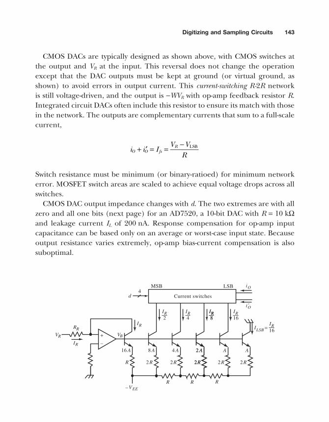
Digitizing and Sampling Circuits 143
CMOS DACs are typically designed as shown above, with CMOS switches at the output and VR at the input. This reversal does not change the operation except that the DAC outputs must be kept at ground (or virtual ground, as shown) to avoid errors in output current. This current-switching R-2R network is still voltage-driven, and the output is −WVR with op-amp feedback resistor R.Integrated circuit DACs often include this resistor to ensure its match with those in the network. The outputs are complementary currents that sum to a full-scale current,
i i IV V
RO O fs
R+ ′ = =− LSB
Switch resistance must be minimum (or binary-ratioed) for minimum network error. MOSFET switch areas are scaled to achieve equal voltage drops across all switches.
CMOS DAC output impedance changes with d. The two extremes are with all zero and all one bits (next page) for an AD7520, a 10-bit DAC with R = 10 kΩand leakage current IL of 200 nA. Response compensation for op-amp input capacitance can be based only on an average or worst-case input state. Because output resistance varies extremely, op-amp bias-current compensation is also suboptimal.
–
+
RR
VR
IR
R
VEE–R R
VB
16 A 8 A
R2
IR
IR2
4 A
R2
IR4
2 A
R2
IR8
R
2 A
R2
IR8
A
R2
IR16
A
R2
= IR16LSB
iO′
Current switches4
d
MSB LSB
I
iO

144 Chapter 2
Typical BJT DAC design is based on a current-switching R-2R network. An input op-amp establishes a reference current IR in one of several BJTs with emitters connected to an R-2R network. The emitter areas are ratioed with the current each conducts, to maintain the same VE for all BJTs. The BJT collectors drive current switches. These can be differential amplifi ers (diff-amps) with logic-compatible inputs. Their collectors are connected to either the iO or iO′ outputs. CMOS DAC outputs have no voltage compliance, but the BJT current outputs from collectors need not be held at a fi xed voltage.
IL200 nA 37 pF
iO
120 pF
iO
IRn2
IL
200 nA
VR≈10 k Ω
d = 0000
120 pF
iO
IRn2
IL
200 nA
VR≈10 k Ω
′
IL200 nA 37 pF
iO′
(a)
(b)
d = 1111

Digitizing and Sampling Circuits 145
The R-2R network is not switched but is a multiple binary current divider. The voltage in the series-R string doubles at each successive stage toward the termi-nation at the LSB. The reference current is established by the op-amp circuit as VR/RR. The output is
i W d IO R= ( )⋅
and the complementary output is
′ = − =−
⋅ −i I i I iO fs O
n
n R O2 1
2
The equation for Ifs applies here. The relationship between IR and Ifs is the same as for the CMOS DAC:
I I I Ifs
n
n R R=−
⋅ = −2 1
2LSB
The complementary output current is also related to W(d) as
′ = ( )⋅i W d IO R
where
W d b b bin i n i n i
i
n
( ) = ⋅ =−− − −
=∑ 2
0, logical complement of
That is, W—
is the complementary weighting, the result of the bit-wise negation (or one’s complement) of d.
Monotonicity among the LSBs, achieved with the scaled-emitter technique shown below, is used with the ladder network. The LSB terminating current of the ladder network, instead of being grounded, is fed to a second branch of emitter-scaled BJTs that switch the three LSBs. Monotonicity is ensured by branching.

146 Chapter 2
2 A A A
R-2R network
VEE–
A2 A2 A A4 AA
VB2
b4 b3 b2 b1 b0
iO′
iO
-bit DACm
Segmentdecoder
R
VEE–
A A
R
IR
A
R
A
R
A
R
A
R
4s3
iO′
iO
iO′
iO
s2s1s0
md
2
For DACs with a large number of bits, the branching idea can be realized in a different topology. The segmented DAC, shown above for a two-bit segmenta-tion, does current weighting with two networks. The input network is driven by a reference current as before. The two MSBs are decoded by a segment decoder.
Digitizing and Sampling Circuits 147
They switch four equal currents to either output or to the branching input of an R-2R network of the remaining m LSBs. A segment decoder successively switches more segments with larger MSB codes to iO as the m LSBs divide the current from one segment (s1 in the fi gure) between iO and iO′ . The remaining segment currents go to iO′ . For m = 2, when d ≤ 0011, all segments except s0 are switched to iO′ . When d = 0100, s0 switches to iO, and s1 switches to drive the branch DAC, as shown. The remaining switches stay on iO′ .
Although the branching effect assures monotonicity, the transfer curve linearity can be much worse than the DLE. But in many applications, the DLE is all that matters for linearity. The match of the segment currents does not determine DLE, only the overall linearity. The segmented DAC uses fewer resis-tors since each segment requires only one resistor, not two as in a ladder network.
A very simple DAC design is the serial-output DAC, easily realized by one fi ltered output line of a computer. A PWM generator, either in hardware or software, drives a low-pass fi lter with break frequency far below the PWM frequency. The average output voltage is proportional to the duty-ratio. The disadvantage of this scheme is that it is slow and inherently noisy due to ripple from the fi ltered pulse. But if the pulse amplitude is accurate and the transitions are fast, a high-resolution output is achievable in direct trade-off with response time.
The ripple amplitude varies with pulse duration, which depends on the duty-ratio D. For high or low D, ripple is least and is highest at D = 50%. In steady-state, the ripple extends from vL to vH around the average, DV. The ripple amplitude,
∆v v vH L= −
is derived from the decaying exponential, when the pulse is low:
v vv
vv
ev
DVH L
H H
D T−= = ≅− −( )⋅∆ ∆1 τ
The approximation assumes that ripple is small relative to average output voltage and that vH ≅ D ⋅V. Also, t is the fi lter time constant. Solving for the ratio of PWM frequency to fi lter break frequency for 1 LSB of ripple,

148 Chapter 2
ff
DD
v Vbw
nPWM
LSB≅ −⋅ −( )−( ) =−
2 11 2π
ln, ∆
For four bits, fPWM must be 23.5 fbw at D = 0.5 and 401 fbw for eight bits. At 10% duty-ratio for four bits, the frequency ratio is only 5.8 and is 8.7 for 90%. (At the extremes of D, the approximation fails. At D = 2−n and D = 1, the ratio is 0.) Other pulse waveforms from rate-multipliers or statistically biased digital pseudo-random noise have less ripple for the same clock-to-fi lter frequency ratio but are harder to generate.
VR
C1
S1
S2
S3
C2
vO
A serial-input DAC is shown above, with three switches and two equal capaci-tors C1 = C2. A serial digital input begins with the LSB. The DAC operates in two phases for each successive bit. On phase 1, switch S3 is open, and a serial input bit closes either S1 (for b = 1) or S2 (for b = 0), charging C1 to
q C b Vi i R= ⋅ ⋅
On phase 2, S1 and S2 are open, and S3 is closed. C2 contains the net charge from previous cycles. On the ith bit on phase 1, this charge is
q C vi i− −= ⋅1 1
On phase 2, S3 closes, and
vq q
CV
bv
ii i R
ii=
+⋅
=
⋅ +− −1 1
2 2 2

Digitizing and Sampling Circuits 149
For n bits, the voltage is
vV
bV
bV
bnR
nR
nR
n=
⋅ +
⋅ +
⋅ +
− −
2 4 81 2 . . .
This iterative equation reduces to the closed form of
v b V W d Vni
n ii
n
R R= ⋅
⋅ = ( )⋅−
−=∑2
1
After n bits, vn is the converted voltage. It must be stored separately for output during the next conversion. The number of bits of monotonic conversion is limited by capacitor matching and switch leakage.
DIGITAL-TO-ANALOG CONVERTER CIRCUITS
In the fi gure below, a digital-to-analog converter is used as a component in a converter circuit. The DAC schematic symbol is used, with a small circle at iO′to indicate the complementary output, after the convention of logic symbols. The op-amp output is bipolar and is offset by IR/2 by a resistor of 2R, where R is the current-reference resistor. Without this offset, vO is unipolar, ranging from 0 V to Ifs ⋅Rf. By shifting iO down by IR/2, vO at negative fs is one VLSB greater in magnitude than positive fs. IR/2 corresponds to the midscale or zero state of d.
–
+
V+RfR2
iO
vO
iO
′
DAC
IR2
R
IR
= ( – )iOIR2
Rf

150 Chapter 2
The offset-binary output is
v iI
R W I RO OR
f R f= −
⋅ = −
⋅ ⋅
212
Some output values for a four-bit d are tabulated below.
d W - ½
1111 7/16
1000 0
0111 −1/16
0000 −1/2
A two’s complement coding of d produces the same results when the MSB is inverted.
In the following DAC circuit, the output range is symmetric about zero. The op-amp is driven differentially by the DAC output so that
v i R i R i i R W W I R i I RO O O O O R O fs= ⋅ − ′ ⋅ = − ′( )⋅ = −( )⋅ ⋅ = ⋅ −( )⋅2
The expression for vO in terms of W follows from the equations for iO and iO′ .
–
+
R
vO
iO
iO′
DAC
R
= ( – )iO RiO′
Compared with the offset-binary output, the symmetric-offset output range and step size are twice as large because iO′ is used. The last expression of vO,compared with the offset-binary vO, has twice the gain (2 ⋅ iO) and a comparable offset difference of

Digitizing and Sampling Circuits 151
I I IR fsLSB
2 2 2= −
This leaves the symmetric vO with a VLSB/2 positive offset relative to the offset-binary output. Some four-bit output values are the following:
d W - W—
1111 15/16
1000 1/16
0111 −1/16
0000 −15/16
The extreme states have outputs of equal magnitude while zero is offset by VLSB/2. An inverted output results from exchanging the DAC outputs.
Q4
Q1
Q3
Q2
V+
R R
D1
D2
DAC
I1
I2 IO

152 Chapter 2
A DAC bipolar current source with a current mirror is shown above, taken from “Current Sources.”
Another circuit, one that does not require a current mirror, is shown below. It has similar topology to a Howland current source but is simpler in operation.
i L
–
+
R
vO
iO
iO′
DAC
RSR
1
2
The load current is
iv v
Ri
i R i RR
ii R i R R
RL
O L
SO
O O
SO
O O S
S
=−
− ′ =⋅ − ′ ⋅
− ′ =⋅ − ′ ⋅ +( )1 2 1 2
This reduces to
iRR
i i R R RLS
O O S=
⋅ − ′( ) = +1
1 2,
The differential current output from the DAC is converted into a bipolar single-ended current output.
Because CMOS DACs are passive, switched ladder networks, they can be used “backward” as shown below. The reference voltage is applied across the iO ter-minals, and the voltage output is taken from where the reference voltage is normally applied. This scheme is similar to that of the discrete CMOS DAC without the op-amp. The CMOS switches are driven from the supply voltage VCC,and minimum switch resistance (and linearity error) results by keeping VR well below VCC.

Digitizing and Sampling Circuits 153
DACs can be combined with op-amps to provide programmable gain. The programmable-gain amplifi er (PGA) in (a) above has a wide gain but can have signifi cant voltage offset errors, whereas in (b) the op-amp gain is limited to ×2. In both circuits, R is included in the DAC IC and matches and tracks the ladder resistances. The noninverting confi gurations are similar in concept. For applications in which the digital input is a dynamic waveform and not merely a scale factor, it is multiplied by vI; the DAC multiplies a digital by an analog quantity.
vODACVR
+
–
R
vO
DAC
vI –
+
(a)
RDAC
vO
–
+
vI
(b)

154 Chapter 2
PARALLEL-FEEDBACK ADCS
The inverse function of D/A conversion is analog-to-digital conversion, per-formed by A/D converters (ADCs). We consider here four categories of ADCs, which include many variations. Approximate ranges for conversion rate and precision are given below.
ADC Type Conversion Rate Precision, Bits
Integrating 0.1 Hz–100 Hz 14–22
Cyclic (serial) 1 kHz–100 kHz 10–16
Parallel-feedback 50 kHz–10 MHz 8–12
Parallel (fl ash) 10 MHz–1 GHz 4–8
Parallel-feedback converters are based on a concept similar to that of placing a function block in the feedback loop of an op-amp to achieve the inverse function.
+
–
nC
REGDAC
CNTR CLK
n
d
RV
Xv
C
The fi gure above shows a digital realization of the ramp converter. A counter driven by a clock generates a digital sawtooth output. It drives a voltage-output DAC that outputs the ramp in analog form. When it crosses vX, the comparator output clocks the register and holds the digital count. When the counter over-fl ows, the DAC output resets to its minimum value, and the comparator output goes low, completing the cycle. The comparator output is also an end-of-conversion signal indicating valid register data.

Digitizing and Sampling Circuits 155
In the analog realization shown above, the same concept uses an analog current-source ramp generator. The counter overfl ow turns on the reset switch, discharging the capacitor at the end of the conversion cycle. The analog circuit is subject to errors in ramp slope relative to the clock frequency. The digital form, although not having these timing errors, must have an accurate DAC reference voltage.
A third realization of the ramp converter makes use of a microcomputer (µC)(or any computer) and minimal additional hardware: an n-bit DAC and a com-parator. The µC must have one digital input bit from the comparator and noutput bits to drive the DAC. The software algorithm for ramp conversion uses software variable, VX, to hold the digitized value of vX, and OUT to hold the DAC output value.
+
–
n
CNTR CLK
REG
CV
n
C
I
vX
d
C

156 Chapter 2
The ramp ADC procedure is as follows:
0. Ramp ADC
1. Set OUT to zero: OUT ← 0.
2. Input the IN bit.
3. If IN = 0, then VX ← OUT; go to 1. Else increment OUT: OUT ← OUT + 1.
4. Output OUT; go to 2.
Conversion time is usually limited by the µC; however, for many applications, it is fast enough, and the few additional components are an advantage. The ramp ADC is a poor technique and is seldom used. The conversion time varies but can take up to 2n clock periods.
–
DAC
Xv
OUT
IN
C
n
+
µ
DAC
Xv
n
LOGIC+
–
d
CLK
Ramp ADC: counterTracking ADC: up/down counterSuccessive-approximation ADC: SAR
Parallel-feedback converters have a generalized topology. The type of logic block used determines the type of converter. The ramp ADC uses a simple counter. A slightly better ADC is the tracking converter. Its logic is a bidirectional

Digitizing and Sampling Circuits 157
(up/down) counter. As vX changes, the comparator output causes the counter to count up if the DAC input d is low and down if it is high. The counter servos the DAC to minimize input error at the comparator. Since the counter counts either up or down, the error is always ±1 LSB. For a constant input, a converged counter dithers by one state around the correct value; the comparator output alternates logic levels each clock cycle.
The tracking ADC is an improvement over the ramp ADC because it can be used to follow an input waveform, digitizing it as it occurs (that is, in real time).For small input changes, the counter must change only a few states. This is done in a few clock periods, and conversion is fast. For large input changes, such as a square-wave step, the converter shows slew-rate limitations and a longer conver-sion time. The DAC output tracking slew-rate, if limited by the counting rate, is
dWdt
Vffs
n= ⋅
2CLK
The clock frequency is limited by the loop delay time: the DAC settling time, comparator delay time, and counter clock-to-output time. For a sinusoidal input,
v tV
tXfs( ) = ⋅ ⋅( )
2sin ω
its maximum slew-rate is w ⋅Vfs/2 = p ⋅ f ⋅Vfs. Equating to the tracking slew-rate and solving for the maximum fs sine frequency,
max fs sine CLKf fn
=⋅
⋅12π
The tracking converter can be implemented with the same hardware as the ramp converter. The general µC-based parallel-feedback ADC also applies gen-erally to parallel-feedback converters. Instead of hardware logic, the software logic distinguishes among parallel-feedback ADC types. A tracking ADC proce-dure, based on the same software variables as the ramp ADC, is given below:

158 Chapter 2
0. Tracking ADC
1. Output OUT.
2. Input IN.
3. If IN = 0, then decrement OUT: OUT ← OUT − 1. Else, increment OUT: OUT ← OUT + 1.
4. Set VX to OUT: VX ← OUT.
5. Go to 1.
This procedure is not more complicated than that for the ramp converter but has the performance advantages of the tracking ADC.
The tracking ADC is useful as a track-and-hold (T/H) circuit. The digital output follows the input signal until the clock is gated off or the count clocked into another register. Then the input value, in digital form, is held indefi nitely; no analog hold circuit can do this. As for sampling circuits, and also for peak detectors, a capacitor can accurately maintain its charge for only a limited time.
–
+
RvX
Oi
DAC
Parallel-feedback ADCs compare DAC voltage to vX at the comparator input, as shown previously. Current-output DACs require an additional I-to-V converter stage. In the ADC scheme above, a current-output, bipolar or CMOS, DAC forms a voltage difference with vX by dropping iO ⋅R in series with it. The comparator now senses this difference against 0 V. This current-mode comparison works with bipolar inputs. The inputs of the comparator must be reversed from voltage-mode comparison, or the complementary current output of the DAC must be used instead.

Digitizing and Sampling Circuits 159
A third parallel-feedback converter is the successive-approximation (SA) converter, a very common conversion technique and the most popular of the parallel-feedback converters. It takes n + 1 clock cycles to convert n bits using a bit-wise iterative algorithm. It determines one bit per clock cycle after an initial-ization cycle.
The parallel-feedback ADC logic block is a successive-approximation register(SAR). This register can be realized by an n-bit shift register (SR) and n latches. (A latch is a kind of fl op with a level-sensitive clock input. When the clock is asserted [high], its output follows its input. When the clock is unasserted [low], the output remains the value at the falling edge of the clock.) At the start of conversion, the SR bits are cleared, and the MSB is set. The latch feeds this digital midscale value to the DAC. If vX is larger than midscale, the comparator output is high. When the clock goes low, the MSB is latched. The next clock edge shifts the 1 bit in the SR to the n − 1 bit position, and the cycle is repeated. In effect, beginning with the MSB, n decisions are made, each of which narrows the range of possible values for vX by half. The convergence rate of this proce-dure is on the order of log2(n), and the conversion time is independent of vX.
C SR
SARCarry bit
Shift register
SA latch
The generic µC-based hardware is again used to implement a µC-based SA ADC. The procedure is only slightly more complicated than previous ones but is usually well worth the speed increase. Besides the IN and OUT address loca-tions, the software model is shown above. SAR is a variable that emulates the SAR latch. Variable SR emulates the shift register, which has an additional “carry-bit” stage that is included in the shift loop, as shown. This formulation suggests the effi ciency of assembly-language programming because most µCs have a carry bit and a rotate instruction that includes the carry bit (C). Both software vari-ables can be held in µC registers.

160 Chapter 2
In the following procedure, bit-wise logic operations of AND, OR, and NOT (logic negation) are used and are µC instructions. For µCs without a NOT instruction, X is complemented by using the exclusive-OR (EOR or XOR) instruction with binary 1111 . . . (all binary ones, a two’s-complement −1, or hexadecimal FFF . . .) and X.
0. Successive-approximation ADC
1. Clear SR and SAR: SR ← 0; SAR ← 0. Set C to one: C ← 1.
2. Rotate SR right.
3. If C = 1, then return.
4. SAR ← SAR OR SR
5. Output SAR to OUT: OUT ← SAR.
6. Input from IN.
7. If IN = 1, then go to 2.
Else, set SAR to SAR AND S—R : SAR ← SAR AND (NOT SR).
(Alternative: SAR ← SAR AND (SR EOR 1111 . . .).
8. Go to 2.
The 1 bit, initially in C, is shifted right, into SR, one bit per iteration. When it gets back to C (step 3 checks this), the procedure is done. Step 4 sets the SR 1 bit in the SAR. If the comparator (IN) is high, vX is still greater than the SAR value, and this test bit is left set. If IN is low, the set bit made SAR too large, and it is cleared in step 7. Each bit, beginning at the MSB, is tested and then left set or cleared in SAR.
A speed enhancement for SA converters is to increase the clock rate after the fi rst or second bit is determined. These bits have the most range and require the most slew time of the loop hardware. The less-signifi cant bits cause less comparator voltage change and can be determined more quickly, allowing an increased clock frequency at the expense of more digital hardware.
The ramp and SA converters do not function correctly unless vX is constant during conversion. For dynamic inputs, a sample-and-hold (S/H) circuit must precede the ADC.

Digitizing and Sampling Circuits 161
INTEGRATING ADCS
–
+
R
–
+REGC
C
vOvX
VR
CNTRRV
C CLKRC
Toggle flopCounteroverflow
n
n
NX
A second category of ADC integrates vX and outputs its average value over the conversion period. The dual-slope ADC shown above is an instance. The input to an op-amp integrator is switched between input vX < 0 and positive voltage reference VR. The integrator output zero-crossing is detected by a comparator, and the count of a free-running counter is clocked as the digitized output. The conversion starts when the counter is reset and vX is switched into the integrator. The ramp output has a slope of −vX/RC and ramps up until the counter over-fl ows. For an n-bit counter, this phase lasts 2n clock cycles or T amount of time. In the second phase, the reference is integrated instead. Because its polarity is opposite that of vX, the slope changes polarity, as shown in the graph below.
v∆
t XT
O
vO
VRRC
vXRC
––

162 Chapter 2
When the integrator output crosses zero, the comparator latches the count. The second phase lasts for tX time. The converter then begins another cycle.
The change in integrator output voltage, ∆vO, is the same for both phases:
∆vvRC
TVRC
t tvV
TOX R
X XX
R
= ⋅ = ⋅ ⇒ =
⋅
For a constant-frequency clock, the counts relate to the times by
N f t= ⋅CLK ∆
Therefore, the output count is
NvV
XX
R
n=
⋅2
Dual-slope converter accuracy is not dependent on long-term drift in R, C, or fCLK, only VR. What this analysis assumes is a perfect op-amp and comparator. Their input offsets and delay times degrade converter accuracy.
+
–
R
vX
C
+
–
vO
+
–
Most actual dual-slope converters correct for offset by introducing a third auto-zero phase before phase 1. In addition, for digital voltmeters (DVMs), a high input impedance is desired, and a buffer amplifi er is added before the

Digitizing and Sampling Circuits 163
integrator. An alternative is the noninverting integrator shown above. If the DVM ground is “fl oating” (not connected) to the measured source, then the ×1buffer provides high input impedance as it supplies the charging current for Cthrough R.
Bipolar inputs require another reference, −VR. Reference selection is deter-mined by the comparator output at the end of phase 1. Another design option for bipolar inputs is to exchange the input terminals by switching. This scheme, however, has diffi culty with vX near zero. Offsets can cause the readings for +vX
and −vX to have different magnitudes. More signifi cantly, when offsets dominate the input, the converter can integrate with the wrong (shallow) slope. When the reference is integrated, it is of the same polarity, and vO never crosses zero. To avoid switching in the wrong polarity of reference, hysteresis around zero is sometimes added. But all of this is avoided with two references.
Another input circuit is a V/I converter and a current reference. This elimi-nates R from the integrator and could also eliminate the op-amp in some designs.
The accuracy of the dual-slope ADC is extended by the triple-slope ADC. An additional comparator senses that vO is approaching 0 V and switches in a smaller reference and another counter. The slope magnitude decreases for this next phase and the time duration is extended. The extra counts contribute additional LSBs.
–
+
R
–
+REGC
vOvX
CNTRV
C CLK
S
R
RS flop
n
n
NX
Q
–V R
VCR
C

164 Chapter 2
At somewhat less speed, the simpler modifi ed dual-slope converter uses only one switch and integrates the input during both phases. In phase 1, the negative reference −VR is integrated along with the input. If VR > vX, the integrator output has a positive slope. When it reaches comparator threshold voltage VC,the reference is switched off, and vX integrates until the counter overfl ows at T.The integrator voltage, vO, at this time depends on vX. The next conversion cycle thus begins at a different initial vO.
t
VC
vO
VR
t X
T
vO ( + 1)i
v X –∝ v X∝
The conditions for convergence of vO (and a steady digitized value) are found by solving for vO(i) where i is the cycle index. For the new cycle,
v i v i u t i d T t iO O X X+( ) = ( ) + ⋅ ( ) + ⋅ − ( )[ ]1
where the slopes are
uv V
RCV v
RCd
vRC
v VX R R X XX R= −
−=
−= − >, ; , 0
Also, from the v-t graph,
t iV v i
uV v iV v
RCXC O C O
R X
( ) =− ( )
=− ( )−
⋅

Digitizing and Sampling Circuits 165
Substituting for tX in vO(i + 1) gives
v idu
v i Vdu
dT a v i bO O C O+( ) =
⋅ ( ) + ⋅ −
+
= ⋅ ( ) +1 1
This difference equation is solved by expanding several iterations, beginning with i = 0. The resulting recursion equation for i + 1 = n is
v n a vaa
b aOn
O
n
( ) = ⋅ ( ) + −−
⋅ <011
1,
and is attained by using the geometric-series formula
zzz
zk
k
N N
=
−
∑ = −−
<0
1 11
1,
The series converges only when z decreases with increasing k. For the con-verter, the convergence condition is
du
d uvRC
V vRC
vVX R X
XR< ⇒ − < ⇒ <
−⇒ <1
2
That is, vX must not exceed half the reference voltage VR. Or, in time, tX < T/2.The converged (steady-state) value of vO can be found by letting n go to infi nity in vO(n) or by setting
v i v iO O+( ) = ( )1
in vO(n + 1) and solving for vO:
v Vu d
u dTO C= +
⋅−
⋅
where the second term is always negative, as required for vO < VC. With vO, the steady-state tX from tX(i), is

166 Chapter 2
td
u dT
vV
TXX
R
= −−
⋅ =
⋅
But this is the same as the previous tX, and the digital output is expressed by NX.The modifi ed dual-slope converter has the same transfer characteristic as the dual-slope ADC, though its dynamic response is fi rst-order and takes a few cycles to converge.
In this realization of the modifi ed dual-slope ADC, the Rs must match. VC
need not be accurate – only stable during convergence. Both Rs can be elimi-nated by driving the integrator with a V/I converter for vX and replacing R and −VR with IR. The switch must then be a current switch. This can be accomplished by letting the fl op output divert IR through a diode. For low leakage, a transistor is used instead. The RS fl op consists of two cross-coupled NOR gates. The other two gates in a quad NOR-gate IC implement the clock generator.
Because tX must be kept less than T/2 for stability, the fs tX is set at T/4 by adding two additional bits to the counter (for n + 2 bits total). This wastes 50% of the available integration time but is easy to implement (by a dual-fl op IC) and gives the converter a near-100% overrange capability, an additional half-digit. Besides the register and counter, the total parts count is less than a dozen to implement a three-digit DVM. (A featureless converter such as this is usually called a digital panel meter [DPM].)
–
+
R
–
+
C
vOvX
CLK
–VR
RQD
C

Digitizing and Sampling Circuits 167
Dual-slope ADCs require a large vO range to achieve precision. An idea that is the digital analog of the virtual ground is realized in the charge-balancing (or quantizing or sigma-delta, Σ-∆) ADC, shown above. The circuit topology is very similar to the modifi ed dual-slope ADC, but it works differently. The big circuit difference is that the fl op driven by the comparator is clocked, a D-type fl op instead of an RS fl op.
On a given cycle of the clock, the reference is switched in or out of the inte-grator to keep vO near ground. The comparator output gives the sign of the error. In other words, vO is nulled by discrete-time feedback. The number of clock cycles that the fl op was high, NX, over the total number of conversion counts N, indicates vX.
The transfer characteristic is calculated by constructing the charge-balance equation for the total charge from vX and −VR input to the integrator. For vO = 0, they must be equal, or
Q QX R=
These charges are the sums of the per-cycle charges:
qvR
T qVR
TXX
RR=
⋅ =
⋅CLK CLK,
The total charge of each depends on the number of cycles each is integrated. Then
Q q NvR
N T Q q NVR
N TX XX
R R XR
X= ⋅ =
⋅ ⋅ = ⋅ =
⋅ ⋅CLK CLK,
Then substituting into QX and solving for the output,
NvV
NvV
XX
R
X
R
n=
⋅ =
⋅2
for an n-bit conversion-time counter. This result is, again, the same as for the previous converters.

168 Chapter 2
The charge-balancing circuit is also used as a modulator for serial digital telecommunications (in CODECs) and in audio and speech processing.
An advantage of the integrating ADC is its measurement of the average vX.By integrating, it has inherent noise rejection and does not need a S/H circuit. The noise rejection capability is quantifi ed by beginning with a constant VX with sinusoidal noise added:
v V V tX X N N= + ⋅sinω
The integrator averages vX over the conversion period T, so that
avg vT
v dt VV
TTX X
TX
N
NN= ⋅ ⋅ = + ⋅ −( )∫
11
0 ωωcos
The normal-mode rejection (NMR) of the noise is
NMRinput noise
output noise= = ( )⋅ −( )
=−
VV T T
TT
N
N N N
N
Nω ωω
ω1 1cos cos
For wN = 2p ⋅ fN, and 1 − cos(2x) = 2 ⋅ sin2 x, then
NMR =⋅ ⋅
⋅ ⋅( )π
πf T
f TN
Nsin2
In the decibel scale this is
NMR dB NMR( ) = ⋅ = ⋅ ⋅ ⋅( ) − ⋅ ⋅( )[ ] 20 20 2log log log sinπ πf T f TN N
NMR is plotted below on a log-log graph, for T = 1/60 Hz, and fN from 0.1 Hz to 1 kHz.

Digitizing and Sampling Circuits 169
At fN = n/T, for whole-number n, NMR is infi nite. In practice it is typically about 60 dB of rejection. An exact number of noise cycles fi t the integration interval T, and the sum of the areas of their positive and negative half-cycles cancel, as in (a) below.
1·103
100NMR(f)
fHz
NMRmin(f)
10
10.1 1 10 100 1·103
vN
tT
tT
(a)
(b)
n = 1 n = 3

170 Chapter 2
As fN varies from n/T, the half-cycles of noise at the ends of the interval are truncated and contribute some fraction of a half-cycle. Figure (b) shows the second worst case after that of fN = 0.5/T, in which an entire extra positive half-cycle is integrated at fN = 1.5/T. For rejection of power-line noise, fN is often chosen to be a multiple of the power-line frequency.
More signifi cant are the NMR minima of p ⋅ fN ⋅T. They occur midway between the maxima, at fN = 1.5 ⋅n/T. As fN increases, according to NMR(dB), the NMR minima increase at 20 dB/dec. At noise frequencies of about n times 1/T, about n cycles of noise occur during T. The more half-cycles, the less each contributes to the integrated total. Thus, a fraction more of a half-cycle contributes less error the higher fN is. Note that NMR is the reciprocal of the integrator fre-quency response, which rolls off at 20 dB/dec with periodic notch fi lters.
SIMPLE mC-BASED S-D ADCS
Microcontrollers (µCs) often contain a comparator that can implement a precise ADC with the addition of only an external resistor and capacitor. The technique is to implement a charge-balancing or Σ-∆ (or ∆-Σ) ADC. The basic scheme uses a comparator that outputs µC input bit IN and requires one µC output bit, OUT. The circuit is shown below.
+
–
C
OUT
INXV
cV
R
In µC software, the ADC routine is best implemented as an interrupt routine, driven by a timer of period tINT, the interrupt period. In the circuit above, the ADC reference voltage is the µC supply (VR = VCC). This assumes that the µC has

Digitizing and Sampling Circuits 171
CMOS output bits, so that the outputs for negligible current are near the rails:
OUT bit CMOS levels:V ground0 0
1
→ ( )→
VCC
If greater accuracy than VCC is required, instead of driving R directly from OUT, use it to switch accurate analog switches between reference ground (for 0) and an accurate VR (for 1). If the OUT-bit voltage levels are close enough to the rails, then an accurate VCC can be supplied as the reference.
S-D RC Constraint for n-Bit Accuracy
The charge-balance voltage waveform on the capacitor is a constant voltage with a small exponential ripple riding on it, at the frequency of the OUT switch-ing. If this varying voltage becomes too large, the ADC will not be linear enough for n-bit conversion. The larger is the RC time constant, the smaller the ripple. How large must RC be to ensure n bits of linearity? The ripple voltage,
∆v v v V VC H L LSBn
R= − ≤ = ⋅−2
and
∆vv
vv
eC
H
L
H
t R CINT= − = − − ⋅1 1
where vH and vL are the maximum and minimum of vC. At full scale, vH = VR
and
2 1− − ⋅≥ −n t R Ce INT
or
R Ct
t nINT
n
nINT⋅ ≥
−( )≅ ⋅ >>
− −ln,
1 22 11

172 Chapter 2
For tINT = 1 ms, and n = 8 bits, then R ⋅C ≥ 256 ms. For n = 10, R ⋅C ≥ 1.024 s. The allowable measurement rate is comparable to that of DMMs.
S-D Algorithm
The ADC algorithm, coded as part of the interrupt routine, sets or clears OUT to keep vC = vX. In other words, charge balance is maintained on C so that ∆q = 0. This can be expressed using ∆q = i ⋅∆t, where i = v/R:
V vR
NvR
N NR XX
XX
−⋅ = ⋅ −( )
or
NN
vV
X X
R
=
where N is the number of tINT cycles during the measurement. After N intervals, the measurement ends, and the NX accumulated during this measurement inter-val is related to vX by N and VR:
vVN
NXR
X=
⋅
N is a software parameter and VR = VCC of the µC. For each interrupt, the fol-lowing routine is executed:
If IN = 1: OUT ← 1; increment NX
If IN = 0: OUT ← 0
At the end of the measurement, after N interrupts (or intervals of tINT), then execute:
measured NX ← NX
Reset NX ← 0

Digitizing and Sampling Circuits 173
Unmatched RU and RL
A refi nement that can be brought to the minimalist ADC is to account for dif-ferent resistance values in series with the OUT switches. Let RU be the series resistance when OUT = 1 (high) and RL when it is 0 (low). Then
V vR
NvR
N NR X
UX
X
LX
−⋅ = ⋅ −( )
Given the two switch resistance values, the measured voltage, as a fraction of the reference voltage is
vV
RR
N
NRR
N
X
R
L
UX
L
UX
=
⋅
− −
⋅1
This equation presents the onerous µC task of division, despite the pre-calculated constant, RL/RU. This refi nement is best left for DSPs, which usually facilitate division. As µCs become like DSPs, this improvement becomes feasible to implement.
Auto-Calibration
A more elegant method of producing an accurate measurement without external reference switching can be applied to systems in which multiple chan-nels are multiplexed into the ADC. If two additional MUX inputs are available and the ADC is linear, two-point calibration can be applied. Two reference volt-ages, which can be 0 V and VR, are applied to the ADC, resulting in NX(0 V) =N0 and NX(VR) = NR. A plot of vX versus NX will then have two known points on it, corresponding to the known input voltages. The equation for the calibration line is
vV VN N
N VXR os
RX os=
−−
⋅ +0

174 Chapter 2
where the expression in parentheses is the slope of the line. In general, the offset voltage, Vos, can be of either polarity, requiring negative NX. To get around this, two precision resistors forming a divider from VR can provide instead a known accurate voltage of a ⋅VR, where a is the attenuation ratio of the divider. For this more general case, the equation of the line can be written by equating slope expressions
v VN N
V VN N
X R
X
R R
R
− ⋅−
=− ⋅
−α α
α α
Solving for vX,
vN NN N
V m VXX
RR R=
−−
⋅ −( ) +
⋅ = ⋅ −( ) +[ ]⋅α
αα α α α1 1
By making a = 1/2, then m must be divided by two, a right-shift instruction. To add ½ to it for rounding, increment m before right-shifting. The resulting number is the fraction of VR that is vX.
Inverting S-D ADC
An inverting Σ-∆ converter uses one additional resistor, as shown below.
+
–X
C
IN
OUT
V
RV
RR
XR

Digitizing and Sampling Circuits 175
The RC time constants must still be much greater than tINT; a low OUT is 0 V, and a high level is VCC = a ⋅VR. Charge balance on the capacitor is maintained by the ADC algorithm, keeping VC = VR. This results in ∆Q = 0 C:
v VR
NV V
RN
VR
N NX R
X
CC R
RX
R
RX
−⋅ +
−⋅ = ⋅ −( )
or
vV
RR
aNN
X
R
X
R
X= ⋅ − ⋅
+1 1
For RX = RR, and a = 2, then
vV
NN
X
R
X= ⋅ −
2 1
The following chart summarizes the transfer function.
NX vX
0 2 ⋅ VR = VCC
N/2 VR
N 0 V
The interrupt routine for the ADC is given below:
If IN = 1: OUT ← 0; increment NX
If IN = 0: OUT ← 1
At the end of the measurement, after N interrupts (N intervals of tINT), then execute the following routine:
measured NX ← NX
Reset NX ← 0

176 Chapter 2
These minimal-component ADCs are often adequate for slow, low- to medium-precision, µC-based ADC requirements. Besides few components, other advantages of the Σ-∆ ADC are that it does not need an anti-aliasing fi lter or S/H circuit preceding its input. Its integrating function reduces noise band-width of the measurement. It is an optimal solution for many µC-basedapplications.
The inverting Σ-∆ ADC input circuit could be extended to have a second-order, cascaded RC fi lter using the same software routine, with a total of four external resistors and two capacitors. This adumbration is left to the imagi-nation of the reader. With suffi ciently low tINT, which is achievable on faster µCs and DSPs, high precision can be attained with a medium-performance comparator.
VOLTAGE-TO-FREQUENCY CONVERTERS
A special kind of integrating ADC converts input voltage or current to a pulse frequency. It is a kind of linear voltage-controlled oscillator (VCO) or FM modu-lator with digital output. The topology of the voltage-to-frequency (V/F) converter is similar to previous integrating ADCs.
VC
–
+–
+vfMMV
vO
–VR
R
vX
CR

Digitizing and Sampling Circuits 177
As with parallel-feedback converters, the topological variations among inte-grating ADCs is in the logic block driven by the comparator. For the asynchronousVFC, a MMV replaces the fl op of the charge-balancing converter.
vO
VC
t
vf
t
∆vOu d
Operation resembles the modifi ed dual-slope ADC. When the integrator output vO goes below VC, the comparator output goes high, triggering the MMV and turning on the reference switch. The MMV time-out is th, the time that the output pulse vf is high. During th, vO ramps up with a slope of u. When the MMV times out, the reference is switched out, and vX > 0 causes vO to ramp down with slope d. Slopes u and d are the same as those for the modifi ed dual-slope ADC. The change in vO over one cycle is
∆v u tV v
R CtO h
R Xh= ⋅ =
−⋅
⋅
From this,
tvd
Vv
tlO R
Xh= − = −
⋅∆
1

178 Chapter 2
The output period is the sum of the half-cycles, or
T t tVv
t tVv
th lR
Xh h
R
xh= + = −
⋅ + = ⋅1
Finally, the output frequency is
fT
vV t
X
R h
= =
⋅1 1
This formula is similar to that of previous integrating ADCs except that it depends on th, the MMV time-out duration, instead of a counter overfl ow period. Because th is typically set by an RC circuit, asynchronous VFC accuracy is limited by it. The accuracy also depends on the matching of the R , but the analysis could have been based on an input current iX and reference current IR instead. The resistors are implementation-dependent and not fundamental to the oper-ating principle.
The LM331 is an eight-pin VFC IC, shown below in (a). Instead of using an op-amp integrator, it avoids op-amp error by integrating with a shunt RC that is maintained at vX. The shunt RC voltage vO must be kept small to avoid nonlin-earity. If the exponential waveforms of vO (b) have a time constant RC that is much larger than th, they are approximately linear.
By keeping vO ≅ vX, the LM331 performs charge balancing at vO. The charge through R over T must be the reference charge during T, or
vR
TvR
T I t t RCO XR h h⋅ ≅ ⋅ = ⋅ <<,
Solving for f = 1/T,
fv
R I tt RCX
R hh=
⋅
⋅ <<1,
Also, IR ≅ 1.9 V/RR.

Digitizing and Sampling Circuits 179
This result is also valid for a charge-balancing VFC with a linear integrator but without the constraint. The typical fs frequency is 10 kHz at an output duty-ratio of 50%. Unlike the modifi ed dual-slope ADC, no convergence condition exists, but as tl approaches zero, the fs frequency asymptotically approaches 1/th
VCC
VCC
VCC23
Rh
Ch
5
MMV
Current mirror
VCC
VCC
IR
R C vO
6
7vX +
–
+
–
1.9 V
IR 2
RR
3 vf
+
–1.9 V
LM331
vO
vX
τ∆
= RCvO ≈ 0 V
t
t l
t
vf
f =vX
I R R ⋅ 1th
, th << RC
(a)
(b)
S Q
R Q
–
+

180 Chapter 2
of 20 kHz. When the MMV timing is based on a threshold voltage of (2/3) ⋅ VCC,then
t R C R Ch h h h h= ⋅ ⋅ ≅ ⋅ ⋅ln .3 1 1
A more precise analysis, calculated from the exponential vO, yields a period of
T R CI Rv
eR
X
t R Ch= ⋅ ⋅⋅
⋅ −( ) +
− ⋅ln 1 1
For th << RC,
e t RCh− −( ) ≅1 0
Apply the approximations
ln , ; ,1 0 1 0+( ) ≅ ≅ ≅ + ≅x x x e x xx
to T:
T R CI Rv
tR C
I Rv
t t RR
X
h R
xh h≅ ⋅ ⋅
⋅
⋅
⋅
=⋅
⋅ <<, CC
This period is consistent with the asynchronous-VFC f. For applications in which a compressed scale for vX is desired, the nonlinearity of this converter can be advantageous, thereby invoking the adage, “If you can’t fi x it, feature it.”
The VFC is most sensitive to noise at zero scale (zs), when the down-slope dis shallowest, causing comparator output jitter among crossings of its threshold and thereby jittering f. However, the VFC is an integrating type of ADC because a frequency measurement requires counting vf over a known period. This count-ing function is the digital equivalent of integration. The longer the count inter-val, the more the input is averaged, the greater the precision, and also the slower the conversion rate. For faster conversion at the same precision, the fs frequency

Digitizing and Sampling Circuits 181
must be increased. By changing count intervals, we can make speed-precision trade-offs without a converter change.
The drift in MMV th can be averted by using a digital timer with an accurate clock. Then th would, on the average, be accurate. Because the clock is asyn-chronous with the comparator output, the timer has phase jitter and the time-out varies up to a complete clock cycle. Elaborate schemes have been devised to synchronize a digital counter with an asynchronous trigger to produce an accurate time-out. One simpler scheme combines an analog ramp generator with a counter. The ramp slope is set to VC/TCLK, where VC is a comparator threshold. The trigger starts the ramp. It runs up until the active clock edge occurs. The ramp output is held constant until the counter overfl ows. (More likely, it is a down counter that underfl ows.) The ramp is restarted. When it crosses VC, the comparator signals the time-out. The counter counts one less cycle than is required for the time-out because the ramp generator adds a cycle. Its slope error affects the time-out as an error in only one clock period.
CLK
Q
Q
D
C
VC
vOVR
Switch
Comparatoroutput
CLK
Q
(a)
(b)
–
+
Instead of substituting a clocked timer for the MMV, the synchronous (or clocked) VFC (fi gure a) operates similar to the charge-balancing ADC except that the reference is turned on for only one clock cycle at a time. The

182 Chapter 2
comparator output switches the reference only at the active clock edge (b). The D-fl op input is gated to enable its output to be high for the cycle, thus generat-ing the output pulse. In commercial synchronous VFCs, the fl op output triggers a MMV that sets the output pulse width.
Comparatoroutput
CLK
φ
vO φ delay = 0+
φ delay = (2 )–
π– 2
0
π
The dual-slope waveform of vO is synchronous with the clock only at discrete values of vX. For vX between these quantum levels, the average level of vO slowly drifts due to accumulating phase error. The comparator edge drifts relative to the clock, causing the reference on-time to change linearly. This causes the average level of vO to ramp up or down. When the phase between comparator and clock outputs drifts by a full clock cycle (or 2p radians of phase), the comparator and clock are again in sync; vO has drifted to a quantum level where the phase error is zero. Comparator and clock edges can coincide, and the output can be indeterminate for some time, causing frequency jitter. A trigger-generator circuit is required for synchronizing edges, for higher performance.
PARALLEL AND RECURSIVE CONVERSION TECHNIQUES
The fastest ADCs are parallel or fl ash converters. They have a resistive-divider string of 2n resistors for an n-bit converter. Each resistor drops VLSB and sets the reference input on one of 2n latching comparators that drive an encoder. A clock stores the data as 2n decisions are made simultaneously: 2n − 1 for n bits

Digitizing and Sampling Circuits 183
of conversion plus one for overrange detection. No S/H function is required. Because the circuit complexity grows exponentially with the number of bits, these converters trade off cost, simplicity, and low power for speed. Also with complexity comes a loss of precision because many parts must meet design tol-erances. Integration on a single chip helps alleviate the burden of matching parts.
Parallel ADC power is reduced by CMOS implementation. Switched-capacitor comparators designed from CMOS logic inverters reduce power over BJT com-parators and can be easily auto-zeroed. But for many applications, the optimum criteria are less complexity and more precision at somewhat reduced speed. This has led to conversion topologies that use m-bit parallel ADCs to digitize n > mbits by iteration.
Σ
DAC
–
mvX
ADC2
m
n – m
MSBs
LSBs
ADC1
× 2m+
The multistage or subranging fl ash converter has two stages of fl ash ADCs. The fi rst ADC converts m bits. These MSBs drive a DAC. Its output is subtracted from the input. This remainder or residue is a fraction of one VLSB of the fi rst con-verter. It is the difference between vX and the m-bit quantized vX. The second ADC converts this remainder for the remaining n − m LSBs. If its input range is the same as ADC1, then each VLSB (each step) of ADC1 spans the input range of ADC2, and the remainder must be multiplied by 2m for correct scaling. Con-sequently, ADC1 must have n-bit accuracy in the placement of its voltage levels or steps. Also, to avoid misalignment in time, or phase error, subtraction from vX requires that vX be delayed by the same amount as the path delay of ADC1 and the DAC.

184 Chapter 2
This idea can be taken further. To save on ADCs and DACs, the recursive sub-ranging ADC has a feedback topology instead of the feedforward topology of the multistage fl ash ADC. In effect, it is a parallel-feedback converter with an m-bit comparator (the ADC) instead of the usual one-bit comparator. It requires n/m iterations or cycles for n-bit conversion. For each iteration, beginning with the m MSBs, the ADC output is stored in m bits of an n-bit output register. The multiplexer (MUX) directs the bits. The PGA gain is increased by 2m each itera-tion. This ADC technique requires a hold circuit for vX.
Σ ADC+
–
vXn
PGA MUX REGm
DACn
+
–
Σ +
–
× 2+
–
Σ × 2
0 V
VR2
bn–1(MSB)
vX
+–
bn–2
VR2
VR2
The multistage idea can be taken to its limits by converting one bit per stage. In this n-stage fl ash ADC, each ADC is a comparator designed to have accurate output levels of 0 V and VR/2. Instead of iterating in time, this design iterates

Digitizing and Sampling Circuits 185
hardware stages. It needs no hold on vX since vX ripples through the stages, being processed as it goes, much like a distributed amplifi er. Because it is a bit-wise converter, it implements the SA algorithm in space (hardware) instead of in time as the SA ADC does:
v v bV
i i iR= ⋅ − ⋅
+ +2
21 1
where vn = vX.
Σvi + 1 v × 2
+
–b i + 1
vi
VR
+
–
This same idea has been used recursively in John Fluke Co. DVMs, called the recirculating-remainder or cyclic converter, shown above. It follows a similar recur-sive equation:
v v Vi i R= ⋅ −+2 1
where vn = vX. In the n-stage fl ash ADC, the remainder passed to the next stage is always positive. Here, the error is bipolar; its sign determines the bit. It is made positive by v, amplifi ed by two and then subtracts VR. The block diagram above can be repeated, like the n-stage fl ash, or a S/H can hold the output for recirculation n times.
The serial bit output is ordered MSB fi rst, but the encoding is in Graycode. This code is commonly used in mechanical shaft position encoders because only one bit changes between adjacent states. If the bit outputs are misaligned, an error of only ±1 LSB occurs. Gray-code encoders are used in fast fl ash

186 Chapter 2
converters for the same reason: Any time-skew among output bits between two successive outputs results in at most 1 LSB of error. Gray code is converted to offset binary by the formula
b b gi i i= ⊕+1
where bi are output offset-binary bits, gi are input Gray-code bits, and ⊕ is the exclusive-OR logic operation.
TIME-DOMAIN SAMPLING THEORY
The explanation of A/D conversion assumes that a voltage at one point in time is converted. For a dynamic input, some means of sampling a voltage at an instant and holding this voltage constant is essential to the conversion process. Even fl ash converters require that all comparators sense vX at the same instant. Delays in the latching clock and the inputs among comparators causes this time instant to be instead a time interval ta, called the aperture uncertainty or aperturejitter. Besides this, there is delay from the clock edge to when the input is actu-ally sampled, or aperture delay.
Aperture jitter limits the maximum sine frequency of vX that can be digitized. For a frequency f, all comparators must settle within one VLSB or 2−n ⋅Vfs for nbits. The sine slew-rate is 2p ⋅ f ⋅Vfs for the worst case. Then ta must be less than the time taken to slew 1 LSB, or VLSB; that is,
tV
dV dtV
f V fa
nfs
fsn
< ( ) =⋅
⋅ ⋅=
⋅ ⋅
−
+LSB
max2
21
2 1π π
The maximum sine frequency for a given aperture jitter is thus
max sine ftna
=⋅ ⋅+
12 1 π
An eight-bit converter with 100 ps aperture jitter has a maximum digitizing bandwidth of about 6 MHz. By its nature, aperture jitter is a statistical quantity, leading to root mean square (rms) values of the quantities calculated with it.

Digitizing and Sampling Circuits 187
ADCs that require their input to be held constant over their full conversion period must be preceded by a sampling circuit that then holds the sampled value constant. These are S/H circuits. DACs are inherently digital hold circuits. They hold the sampled output constant and effect a zero-order hold (ZOH). A S/H variation is the track-and-hold (T/H) circuit. Its output follows the input in the tracking mode. S/H theory also applies to T/H circuits.
S/H circuits are based on an underlying theory that has general application to discrete-waveform (or sampled-data) systems. Its development in the time domain begins with the step (a) and impulse (b) functions, shown below.
1
t∆
∆ 0
u
1
t
( )t
(a)
1
t∆
δ
1
t
( )t
(b)
ddt
∆
The step function is derived by taking the limit of v(t) in (a) as ∆ → 0. Then for t < 0, u(t) = 0, but at t = 0+, it is 1. Similarly, the impulse function (in a limit-ing sense) is derived in (b) as the derivative of v(t). As ∆ → 0, the width of the rectangular pulse goes to zero, but the amplitude goes to infi nity. The area remains constant in the limiting process and is the value or “amplitude” of the impulse. In the limit,
lim∆
∆
∆→⋅ =∫
0 0
11dt

188 Chapter 2
The unit impulse has unit value at t = 0 and is zero elsewhere so that
δ t dt( )⋅ =−∞
+∞∫ 1
Now multiply d(t) by a continuous function, v(t), in the integral. Because d is nonzero only at zero, v(0) effectively weights d(t), and
v t t dt v( )⋅ ( )⋅ = ( )−∞
+∞∫ δ 0
More generally, if d is shifted in time by k ⋅T, then
v t t kT dt v kT( )⋅ −( )⋅ = ( )−∞
+∞∫ δ
This can also be expressed as an integral with t as upper bound:
v kT d v kT t kTC
t τ δ τ τ( )⋅ −( )⋅ = ( ) >∫ ,
The impulse function is central to sampling theory. A periodic sequence (or “train”) of impulses conveniently characterizes the sampling process. A repeti-tive d(t) with period Ts is the sum of an infi nite number of time-shifted impulses spaced Ts apart, or
δ δP sk
t t kT( ) = −( )=−∞
∞
∑
When v(t) is multiplied by dP(t), a sampled form of v(t), or v*(t), results. (v(t)is real and thus v*(t) does not designate a complex conjugate.) For t ≥ 0,
v t v t t v t t kT v kT t kTP s s skk
*( ) = ( )⋅ ( ) = ( )⋅ −( ) = ( )⋅ −( )=
∞
=
∞
∑∑δ δ δ00
The resulting function is nonzero only where the impulses occur, with values determined by v(t).

Digitizing and Sampling Circuits 189
The amplitudes of the impulses, though infi nite, graphically represent their area values, which are determined by v(t). This is the behavior of the idealsampler, a switch that closes only for an instant.
v
t
( )t δ
1
t
( )tP
×
*
t
( )tv
( )tv
*( )tvkT
( )tv
s
*
Two graphic representations of the sampled v(t) are shown below.
*
t
( )tv
( )tv
3 5
(b)
t
( )kTv
( )tv
3 5
(a)
Ts Ts Ts Ts Ts Ts
From v(kT), the discrete v(t) for t = kTs in (a) are the integral of each weighted impulse of (b). v*(t) represents the sampled v(t) as a sum or series, whereas v(kTs), k = 0, 1, . . . represents the sampled v(t) as a sequence and dP(t) can also be interpreted as a series from a sequence of unit impulses.
FREQUENCY-DOMAIN SAMPLING THEORY
In the frequency domain, sampling is impulse modulation; v(t) amplitude-modulates the impulse train. The Laplace transform and Fourier series reveal another perspective on sampling and lead to important design criteria.

190 Chapter 2
To derive the Laplace transform of v*(t), begin with d(t) and apply
v t t dt v( )⋅ ( )⋅ = ( )−∞
+∞∫ δ 0
First,
L δ δt t e dt est( ) = ( )⋅ ⋅ = =−∞∫ 00
1
Second, the Laplace transform of dP is
L δPskT
Pk
t e ss( ) = = ( )−
=
∞
∑ ∆0
where Ts is the sampling period. One period of a function f1(t), such as a single cycle of a sinusoid, can be made repetitive as the series
f t f t f t T f t T f t kTs s sk
( ) = ( ) + −( ) + −( ) + = −( )=
∞
∑1 1 1 10
2
Given Lf1(t) = F1(s), then
L f t F s F s e F s e F s esT s T skT
k
s s s( ) = ( ) + ( )⋅ + ( )⋅ + = ( )⋅− − −
=
∞
∑1 1 12
10
Applying the formula,
zz
zk
k=
−<
=
∞
∑ 11
10
,
results in
L f tF s
ee
sTsT
s
s( ) =( )
−<−
−1
11,

Digitizing and Sampling Circuits 191
This is now applied to dP:
L δP P sTsTt s
ee
s
s( ) = ( ) =−
<−−∆ 1
11,
Finally, the Laplace transform of v*(t) is
L Lv t V s v kT t kT v kT es sk
sskT
k
s* *( ) = ( ) = ( )⋅ −( ) = ( )⋅=
∞−
=
∞
∑ ∑δ0 0
This infi nite series of exponentials in s makes V *(s) nonalgebraic and is unwieldy for linear systems analysis. It does, however, resemble the Laplace transform of v(t) for t = kTs. It is simplifi ed by a change of variable,
z e sTs≡
Solving for s,
sT
zs
= ⋅1ln
and substituting for s yields
V s v t v kT zs T z sk
ks
*( ) = ( ) = ( )⋅=( )−
=
∞
∑10
ln Z
The operator Z is the Z transform. The Z transform of v(t) is written as V(z), with the understanding that this is not V(s) with z substituted for s. Note that z isa shifting variable; z−k shifts v(kT) by k periods. The Z transform is used in sampled-system analysis the way that the Laplace transform is used with continu-ous functions. The s-domain offers a continuous view of discrete signals and the z-domain a discrete view of continuous signals.
Now v*(t) is expressed using the Fourier series. Repetitive v(t) with frequency ws can be expressed as the sum of sinusoids at integer multiple frequencies (or harmonics) of ws:

192 Chapter 2
v ta
a n t b n t c en sn
n sn
njn t
n
s( ) = + ⋅ + ⋅ = ⋅
↑ ↑=
∞
=
∞
=−∞
∞
∑ ∑ ∑0
1 12cos sinω ω ω
↑↑staticterm
evenharmonics
oddharmonics
where
aT
v t n t dt bT
v t nns
T
Ts n
sT
T
s
s
s
s= ⋅ ( )⋅ ( )⋅ = ⋅ ( )⋅− −∫ ∫2 2
2
2
2
2cos , sinω ωsst dt( )⋅
and for the exponential Fourier series,
cT
v t e dtns
jn tT
T s
s
s= ⋅ ( )⋅ ⋅−−∫
12
2 ω
The two representations are equivalent and are related by
c a bba
n n n nn
n
= ⋅ + = −12
2 2 1, tanϑ
Even functions of time have no sine terms; odd functions have no cosine terms. Some v(t) can be made odd by subtracting an average offset. The odd function is then transformed and the offset is added as a constant term.
t
( )tv
A
–T Tτ2
– τ20 s
In actual samplers, the sampling waveform is an approximation to an impulse train. It has fi nite amplitude and time duration. The effect this has on sampling can be found by assuming the sampling waveform to be a pulse train with ampli-

Digitizing and Sampling Circuits 193
tude A and pulse width t. Let wn = n ⋅ws. As v(t) is centered around t = 0, it is an even function, and
aA
Tt dt
AT
n
a n
ns
ns
n
n
n
= ⋅ ⋅ =⋅ ⋅
⋅ ( )
=
−∫2 2 2
2
0
2
2cos
sin,
,
ω τ ω τω ττ
τ even
odd
where the discrete an have the continuous envelope of the form
sinc xx
x≡ sin
It is shown below for x = wnt/2 = n ⋅p ⋅ (t/Ts). Instead of an impulse, sinc(x) is the result of fi nite-width sampling pulses.
fτ1– τ
1τ2
τ3
1
sinc
v(f)
f
As t → 0, the pulse train approaches an impulse train. The separation of an(w)decreases in frequency. If instead we let Ts increase, then the effect is the same; harmonic frequency separation decreases. As Ts → ∞, the an merge into a con-tinuous sinc function with a continuous frequency spectrum:
lim lim limT
nT s s T ss s s
nT
nT T→∞ →∞ →∞
=⋅ +( )
−⋅
= =∆ω π π π2 1 2 2
0
As Ts → ∞, the function becomes aperiodic, and the Fourier series becomes the Fourier transform:
F v t V j v t e dtj t( ) = ( ) ≡ ( )⋅ ⋅−−∞
+∞∫ω ω

194 Chapter 2
In the limit, the Fourier series of v(t) undergoes these changes:
→ → ( ) → →=−∞
∞
−∞
+∞∑ ∫n
n sc V j n t dt, , ,ω ω ω ∆
Except for the lower limit of integration, the Fourier transform is a special case of the Laplace transform when s = jw. The unit step and impulse functions have no Fourier series, but they have Fourier transforms.
As Ts increases (or t decreases), the sinc response broadens until, in the limit, it is constant over all frequencies. Thus, the frequency response of an impulse is independent of frequency, as is the Laplace transform of d(t).
The frequency spectrum for dP is
cT
t kT e dtT
ns
sk
jn tT
T
s
s
s
s= ⋅ −( )
⋅ ⋅ =
=−∞
∞−
− ∑∫1 1
2
2 δ ω
This spectrum is also fl at for all frequencies, with a constant amplitude of 1/Ts.It differs from the spectrum for d(t) in that it is discrete. The Fourier series of the impulse train is
δ δ ω πωP s
k s
jn t
ns
s
t t kTT
eT
s( ) = −( ) = ⋅ ==−∞
∞
=−∞
∞
∑ ∑1 2,
The waveforms of dP in both the time and frequency domains are shown below.
t
( )tP
T
1
δ
s–3 Ts– Ts Ts3
ω
( )ωP∆
ωs2– ωs– 0 ωs ωs2
1Ts

Digitizing and Sampling Circuits 195
This representation of dP leads to a different expression for Lv*(t) from that derived previously:
L v t v tT
e e dts
jn t
n
sts*( ) = ( )⋅ ⋅ ⋅−∞
∞
=−∞
∞−∫ ∑1 ω
The index n is independent of t allowing the summation to be removed from the integral:
1 1T
v t e e dtT
v t es
jn t st
n s
s jn ts s⋅ ( )⋅ ⋅ ⋅ = ⋅ ( )⋅−∞
∞ −
=−∞
∞
−∞
∞ − −( )∫∑ ∫ω ω
nndt
=−∞
∞
∑ ⋅
The resulting integral is the Laplace transform, V(s − jnws). Thus,
V sT
V s jns
sn
*( ) = ⋅ −( )=−∞
∞
∑1 ω
This expression for V* has a geometric interpretation in the s-domain. The transform of V(s) is periodic in ws so that
V s V s j s* *( ) = −( )ω
V(s) repeats along the jw-axis at intervals of jws.Previously, dP(t) was expressed as a series of complex sinusoids with amplitude
1/Ts and frequencies of n ⋅ws. The frequency spectrum of v(t) is convolved (or heterodyned) in the frequency domain with the spectrum of dP(t), as shown below.

196 Chapter 2
Multiplication in one domain corresponds to convolution in the other. The sine and cosine terms in v(t) multiply by the terms of dP to produce sum and difference frequencies according to the trigonometric formulas
cos cos cos cosα β α β α β⋅ = −( ) + +( )12
12
cos sin sin sinα β α β α β⋅ = +( ) − −( )12
12
The frequency-domain plots are the magnitude envelopes of the complex Fourier coeffi cients, the amplitudes of the harmonics. For V *( jw), the spectrum of v(t) is centered around harmonics of ws. Thus, the effect of sampling is to generate frequency-shifted copies (or bands) of V(jw) centered around harmon-ics of ws.
t
( )tv
tTs
Time domain( )vnc
ω
Frequency domain
Envelope ofFourier coefficients
= ( )ωV
ω
( )ωP∆
ωs2– ωs– 0 ωs ωs2
( )tPδ
t
( )tPδ( )t* ( )tvv = ⋅
ωωs2– ωs– 0 ωs ωs2
( )tP∆( )ω* ( )ωVV = *

Digitizing and Sampling Circuits 197
THE SAMPLING THEOREM (NYQUIST CRITERION)
The sampling theorem gives a criterion for recovery of v(t) from v*(t). If ws isgreater than twice the highest frequency in V( jw), then the frequency-shifted bands of V( jw) do not overlap and can be separated by fi ltering.
ωωs2– ωs– ωs ωs2
( )ω*V
ωa
ω1ωs2
( )ω–1V ( )ωV ( )ω1V ( )ω2V
ωa =Alias frequency = ω1 – ω s
–
The Nyquist criterion for recoverability of the original continuous signal is
ω ωs h> ⋅2
where wh is the highest frequency component of V(jw). The original signal is recoverable from its sampled form when the highest frequency component is less than the Nyquist frequency, ws/2. In the plot above, the band V1(jw) is a replica of V(jw) centered at ws. It has frequency components below ws that overlap with the positive frequency components of V(jw). These are negative frequencies in V(w) shifted up in frequency by ws.
The signifi cance of negative frequency components in V(jw) is that they are inverted (180° phase-shifted) from their corresponding positive counterparts. The magnitude of V(jw) is symmetric around w = 0; it is an even function and V(−jw) = V(jw). The phase, however, is an odd function and is negative for w <0; for negative n, the angle of cn is J = −n ⋅ws ⋅ t. Then J(−n) = −J(n).
In the plot, V(jw) and V1(jw) are symmetrical around the Nyquist frequency. In effect, V has been folded over at ws/2. The larger wh is, the further back toward lower frequencies the folding extends. These folded frequency

198 Chapter 2
components from V1 are alias frequencies in v*(t) and have a frequency of wa
relative to ws.
t
ω– a
The signifi cance of an alias frequency in the time domain is that a sequence of samples has more than one frequency interpretation. In the fi gure above, V(jw) has one frequency component at w = (3/4) ⋅ws. The samples also fi t a sinusoid of w = −(1/4) ⋅ws, an alias frequency within the band of V(jw). The alias sinusoid is inverted relative to that of V1 because its frequency is negative.
More generally, if w1 of V(jw) is sampled at ws, then from the fi rst plot,
ω ω ω ω ω1 = − −( ) = +s a s a
and
alias frequency = = −ω ω ωa s1
In the plot above, sinusoids of both w1 of V and wa of V1 fi t the sample points. The discrete samples of v(t) are too few per cycle to eliminate wa and v(t) is undersampled. The sampling theorem requires more than two samples per cycle for recovery of v(t). Such a v(t) is oversampled.
Recovery of V(jw) from V*(jw) for oversampled signals is achieved by a low-pass fi lter (LPF) that passes only V(jw). The ideal fi lter magnitude, H(jw), is shown below.

Digitizing and Sampling Circuits 199
It has an immediate cutoff just above wh. The ideal maximum-bandwidth fi lter has a cutoff at the Nyquist frequency.
t
( )th
t
*sinc
t
( )tvv*(t)
In the time domain, this fi lter function transforms into a sinc function. Nonzero sinc values extend to t = −∞, resulting in a noncausal function that can only be approximated by physical (thus causal) circuits. The pulse shape of the ideal LPF transforms into a sinc function in t just as a pulse in the time domain does in w. H( jw) is multiplied by V *( jw) in w to recover V( jw). In t, h(t) is convolved with v*(t) to produce v(t). For bandlimited v(t),
v t v kT t kTss
ss
k
s( ) = ( )⋅ ⋅ −( )
− < <
=−∞
∞
∑ sincω ω ω ω2 2 2
,
The sinc function operates as an interpolator, fi lling in the missing values of v(t).
t
( )tv
( )tv
sT
^
ωωs2
( )ωH
ωs

200 Chapter 2
The fi nal derivation of general usefulness is the spectrum of a zero-order hold. This is the frequency response of a S/H circuit. In the time domain, this is a voltage step turned off Ts later:
ZOH:v t u t v t T u t Ts s( )⋅ ( ) − −( )⋅ −( )
In the s-domain, a ZOH can be regarded as an integrator of weighted impulses, producing v(t), as shown above. This is the typical output waveform from a S/H or DAC.
The integrated waveform is periodic at the sampling rate. An integrator in sis 1/s. When it is normalized to be unitless, then it is 1/s ⋅Ts. A periodic integra-tor is constructed by integrating for Ts. The Laplace transform of this expression is H0(s). The normalized ZOH transfer function is thus
ZOH: H ss T s T
ee
s Ts s
sTsT
s
ss
01 1 1( ) =⋅
−⋅
⋅ = −⋅
−−
The frequency response of H0(s) is found by letting s = jw. Then
H je
j TT
ej T
s
s j Ts
s0
212
ωω
ωωω( ) = −
⋅=
⋅
⋅
− ⋅− ⋅sinc
The magnitude and phase are
H jT
H jTs S
0 02 2
ω ω ω ω( ) =⋅
∠ ( ) =
− ⋅sinc ,
Once again, the sinc function appears. The magnitude plot of the frequency response is shown below.
ω
(jω)H0
ωs2
ωs ωs2
3
1
0.636
0.212

Digitizing and Sampling Circuits 201
The phase response is linear and only time-shifts the output. The phase delay can be seen in the time plot by noting that a best-fi t of v(t) to v(t) requires v(t)to be shifted to the right (delayed in time) by half a step, or by −Ts/2, in agree-ment with ∠H0(jw). Ideal recovery of v(t) from v(t) requires an inverse sinc fi lter, or sinc compensator. This compensator can be implemented in either digital or analog form. It is digital if it precedes a DAC or follows an ADC and analog if it follows a DAC or precedes an ADC.
SAMPLING CIRCUITS
Sample-and-hold or track-and-hold circuits are switched between the sample or track state and hold state by a digital control line. Ideally, the input voltage at the instant of switching to HOLD is retained as a constant at the output of the S/H. T/Hs are similar to S/Hs; in the non-held state, the output follows the input. In a S/H this is not necessarily so, though most S/Hs are actually T/Hs. The sampling impulse of sampling theory corresponds to the active edge of the HOLD signal.
The speed of a S/H is determined by the acquisition time, the time from when sampling or tracking of the input begins to when a settled, held output is avail-able. This time has two terms. The fi rst is the time from when tracking begins to the time when the hold capacitor follows the input waveform. A large initial difference between vI and vC requires slewing time before tracking is accurate. The second term is the setting time at vC when the hold state begins. In addition to acquisition time, aperture delay and jitter also apply to S/H circuits.
Several errors are associated with S/H circuits, and their design consider-ations are closely related to those of peak detectors. Errors occur in the sampling process or in the hold state. The fi rst are dynamic sampling errors. Digital delay causes the effective sampling instant to be delayed. For a rising input, this trans-lates into a voltage error of
vdvdt
tIdε =
⋅
where the digital delay time td is multiplied by the waveform slew-rate. The second cause of error is analog advance. If the input is delayed instead, an

202 Chapter 2
effective negative delay occurs in sampling since the waveform lags behind where it should be when sampling occurs. A rising input waveform is below where it should be and a negative error occurs. It is equivalent to sampling the waveform in advance of the actual sampling instant.
R
C
vO
+
–
vIK 1×
The dominant cause is a voltage lag on the hold capacitor. Its charging always lags somewhat behind the source. This is largely due to charging-source resis-tance R in the S/H circuit shown above. By closing the loop with an op-amp input, we reduce the charging time constant RC by K + 1. The diodes around the op-amp keep its output from saturating when in the hold state. Waveform advance is the major cause of delay error and is compensated by delaying the sampling command.
C
vO1×
Cs
1×vI
vC
A third dynamic error is due to stray capacitance Cs between the hold capaci-tor C and the sampling command line. When this line switches, it causes charge to fl ow through Cs into C. If the capacitor voltage vC is plotted against a range of constant-voltage inputs, the plot is linear. Its slope represents a hold gain. As

Digitizing and Sampling Circuits 203
the input voltage vI increases, the step of extra voltage on C grows in size because the voltage between the hold line vH and vC varies linearly with vI. As the differ-ence between the sample level, Vs, of vH, and vC increases, Cs is charged more, and this charge is transferred to C when vC changes to the hold state. The hold step, or pedestal, thus increases with vI.
vO+
1×vI vC
C
–
Cs
A circuit that avoids this problem is shown above. The hold capacitor is the feedback C of the op-amp. The op-amp isolates vC from the switch node by holding it at virtual ground. Then the voltage across Cs is independent of vI
and the same amount of charge is transferred to C on switching. The charge on Cs is Cs ⋅Vs. The hold gain varies somewhat as Cs varies with voltage as do semiconductor junctions.
The hold capacitor dielectric absorption must be low to avoid recovery effects during the hold state. Its leakage causes static sampling error during the hold state. Any other leakage paths for capacitor charge contribute to leakage error. The buffer amplifi er and sample switch must be low in leakage. A leakage compensator is shown below.
vO+
1×vI
C
–
R

204 Chapter 2
The leakage decoupler R has the same function as in peak detectors. It keeps the voltage across the switch near zero, thus minimizing leakage through it.
vI
C Cs s C
vCQ1 Q2
Another hold-step compensator places another switch similar to Q1 in series with it. This additional switch is shorted, but its Cs (CGS for a MOSFET) connects to the same node. It is driven with an opposite polarity edge so that its stray charge cancels that of Q1.
1 +
–C
vI ×
C2
Q1
1
Q2
RGS
D1
D2
RGS
vO
AB
In this S/H, a JFET switch Q1 passes the waveform through its channel, con-nected to the buffer A. When the control line goes low, Q1 cuts off. D1 conducts a small amount of current through RGS to keep the gate reverse-biased. At the same time, Q2 is also cut off by a similar circuit. The capacitor C2, equal to C1,is a bias-current compensator for the op-amp (as with a previous peak detector). As the hold capacitor C1 charges with IB, so does C2. The differential voltage is canceled at the output. Of course, offset current is not compensated.

Digitizing and Sampling Circuits 205
Finally, very fast S/Hs have the additional error of signal leakage through shunt switch capacitance Cs during hold. This circuit uses a diode sampling bridge.The bridge has two Css in series for each leg of the bridge, or an equivalent of one Cs from input to output. It is current-switched for speed. To reduce addi-tional input-to-output bridge capacitance, the diodes are fed through a metal sheet which functions as a Faraday shield. Sampling bridges of this kind have commonly been used in sampling oscilloscope front ends. The practical limita-tion in their switching time is often the switching speed of their drivers.
SWITCHED-CAPACITOR CIRCUITS
Switched-capacitor circuits replace resistors with capacitors and switches. In ICs, diffusion resistors, made by connecting to the ends of a diffused area, are not optimal since their values are hard to control and they have large areas (their relative values are much better; they match well). Large-value resistors take up so much area that they are often impractical. When accuracy is not important, a kind of resistor made of a thin layer of, say, n material between two p layers – a pinch resistor – can be made large but with a ±20% accuracy. NiCr (nichrome) resistors are very good but costlier to make and trim.
i v
R+
–C
S
vi
C
1v
S i 2S
1vI ×
C
1×
I
I
vCCs
vO

206 Chapter 2
vO+
C
–
f
Ci
S1
S2
vI
This limitation makes switched-capacitor resistors an attractive alternative. The equivalent resistance is shown above. It is a single-pole, double-throw (SPDT) switch S and a capacitor. The SPDT switch is equivalent to two single-pole, single-throw (SPST) switches, synchronized as shown. When S is switched to the input, it charges to the input voltage v with a charge of C ⋅v. When it switches to an output held at ground, it delivers this charge. The output is typically the virtual ground of an op-amp.
If the switching rate is fs, then the charge delivered per unit time, or current, is
i C f v rC f
TC
ss
s= ⋅ ⋅ ⇒ =⋅
=1
The equivalent resistance follows directly and is subject to the Nyquist crite-rion due to switching. The bandwidths of switched-capacitor circuits must be well within the Nyquist frequency for accurate equivalence.
vO+
C
–
f
v
Ci
I

Digitizing and Sampling Circuits 207
vO+
C
–
f
Ci
S1 S2
vI
+
–
This switching scheme inverts vI. Ci charges with switches in the position shown. When switched, charge fl ows out of the op-amp input to ground. In effect, the two-switch circuit is a negative R.
With drive to the grounded side of S1 from the input instead, the two terminal voltages of vI subtract upon switching. The differential voltage vI determines the charges.
CLOSURE
The world of digital electronics merges with analog electronics in digitizing and sampling circuits, but the merged areas – mainly ADCs, DACs, and switched-capacitor and sampling circuits – do not involve logic design. Instead, the underlying theory is an extension of that for continuous functions. The mathe-matics is similar; difference equations replace differential equations. Sampled circuits also include commutating and switched-capacitor fi lters and digital signal processing, but the full story, including dithering, FFTs, DSP fi lters, and windowing, is left for other books.

References
Anderson, T. and Trump, B. (1984, September 6). Clocked V-F Converter Tightens Accuracy and Raises Stability. Electronic Design, pp. 235–244.
Angelo, E. J., Jr. (1969). Electronics: BJTs, FETs, and Microcircuits. New York: McGraw-Hill, Ch. 15.
Anonymous (1981, April 1). Voltage-Reference Basics. EDN, pp. 64–65.
Anonymous (1988, April 14). What’s a Delta-Sigma a-d Converter? Electronic Design,p. 50 (boxed section).
Anonymous (1989, February 23). What’s a Recursive Subranging ADC? Electronic Design,p. 122 (boxed section).
Baedtke, R. Triangle Waveform Generator Having a Loop Delay Compensation Network. Tektronix patent.
Bello, V. G. (1972, March). Design of a Diode Function Generator Using the Diode Equation and Iteration. IEEE Transactions on Circuit Theory, pp. 213–214.
Bray, D. (1983). The Use of Bipolar Semiconductor Junctions in Linear Circuit Design. Interdesign Monochip Application Note APN-33.
Brokaw, A. Paul (1975). The Best of Analog Dialogue, p. 71.
Connors, S. (1974, June 5). Voltage-to-Frequency Converters: A / D’s with Advantages. EDN, pp. 49–54.
DeVito, L. (1986, October 16). Synchronous V/ F Converter Aids Linearity in Data Acquisition. EDN, pp. 183–190. (See 13 Nov. 1986 EDN for Part 2.)
Fattaruso, J. W. and Meyer, R. G. (1985, April). Triangle-to-Sine Wave Conversion with MOS Technology. IEEE Journal of Solid-State Circuits, Vol. SC-20, No. 2, pp. 623–631.
Fennel, J. W. (1969, July 1). Feedback Improves Sample-and-Hold Performance. EDN,pp. 63–64.

210 References
Feucht, D. (1975, June 5). Exploring Function-Generator Design Problems and Solutions. EDN, pp. 37–43.
Gibbons, J. F. and Horn, H. S. (1964, September). A Circuit with Logarithmic Transfer Response over 9 Decades. IEEE Trans. Circuit Theory, Vol. CT-11, No. 3, pp. 378–384.
Gilbert, B. (1977, August 18). Circuits for the Precise Synthesis of the Sine Function. Electronic Letters, Vol. 13, No. 7, pp. 506–508.
Globas, G., Zellmer, J. and Cornish, E. (1974, September). A 250-MHz Pulse Generator with Transition Times Variable to Less than 1 ns. Hewlett-Packard Journal, Vol. 26, No. 1, pp. 1–7.
Gookin, A. (1977, February). A Faster Integrating Analog-to-Digital Converter. Hewlett-Packard Journal, Vol. 28, No. 6, p. 9 (boxed section).
Graeme, J. (1974, September 5). Peak Detector Advances Increase Measurement Accu-racy, Bandwidth. EDN, pp. 73–78.
Graeme, J. G. (1987, September 3). Low-Cost Quad Op Amps Boost Circuit Perfor-mance. EDN, pp. 213–222.
Gray, P. E. and Searle, C. L. (1969). Electronic Principles: Physics, Models, and Circuits.New York: Wiley, Ch. 4.
Henry, P. (1987, May 14). JFET-Input Amps Are Unrivaled for Speed and Accuracy. EDN, pp. 161–169.
Kapoor, A. and Bowers, D. (1986, March 6). Diverse Circuits Exploit Matching in Quad-transistor IC. EDN, pp. 223–232.
Kirby, S. (1983, April 21). Deglitcher Circuit Refi nes d-a-Converter Output. Electronics,p. 151.
Kitchin, C. and Counts, L. (1985, August 22). Multifunction IC Provides Diverse Math Functions. EDN, pp. 175–180.
Klein, G. and Hagenbeuk, H. (1967, June). An Accurate Triangular-Wave Generator with Large Frequency Sweep. Electronic Engineering, pp. 388–390.
Klein, G. and Hagenbeuk, H. (1967, November). Accurate Triangle-Sine Converter. Electronic Engineering, pp. 700–704.
Knapp, R. (1988, February 18). Selection Criteria Assist in Choice of Optimum Refer-ence. EDN, pp. 183–192.
Kolber, M. and McNerney, F. J. (1981, July 23). Reduce Capacitor Leakage Resistance for Stable, Long Time Delays. Electronic Design, p. 173.

References 211
Krauss, G. and Eggert, R. (1974, March). A Moderately Priced 20-MHz Pulse Generator with 16-Volt Output. Hewlett-Packard Journal, Vol. 25, No. 7, pp. 10–15.
Little, A. and Burnett, B. (1988, February 4). S / H Amp-ADC Matrimony Provides Accurate Sampling. EDN, pp. 153–166.
Lobjinski, M. and Bermbach, R. (1982, June 2). Switched-Capacitor Technique Improves a-d Conversion. Electronics, pp. 149, 151.
Mego, T. J. (1987, June 25). Resolve 22 Bits Easily with Charge-Balance ADCs. ElectronicDesign, pp. 109–114.
Meyer, R. G., Sansen, W., Lui, S. and Peeters, S. (1976, June). The Differential Pair as a Triangle-Sine Wave Converter. IEEE Journal of Solid-State Circuits, pp. 418–420.
Neal, J. and Surber, J. (1984, May 3). Track-and-Holds Take Flash Converters to Their Limits. Electronic Design, pp. 381–388.
O’Farrell, J. J. (1989, January 5). 555 Timer Triggers on Millivolt Signal. EDN, pp. 208–209.
Peterson, B. (Ed.) (1979, March 5). Inherently Monotonic DAC-IC Design Eliminates Costly Resistor Matching. EDN, pp. 46, 49.
Phillips, A. B. (1962). Transistor Engineering. New York: McGraw-Hill, p. 131.
Potson, D. and Swing, C. (1988, October 13). Clamping Op Amp Improves ADC. Elec-tronic Design, pp. 124–125.
Regan, T. (1982, September 16). CMOS DACs Work Backwards to Provide Voltage Outputs. Electronic Design, pp. 117–122.
Rife, D. (1982, April 28). High Accuracy with Standard ICs: An Elegant ADC’s Forte. EDN, pp. 137–144.
Shaw, W. S. (1972, May 8). Triangular-Wave Generator Spans Eight Decades. Electronics,p. 104.
Sheingold, D. H. (Ed.) (1974). Nonlinear Circuits Handbook. Norwood, MA: Analog Devices, Inc.
Sprowl, R. (1988, August 18). PWMDAC Simplifi es Output Filtering. EDN, p. 220.
Stefenel, R. (1982, July 14). Positive Pulse Triggers 555 Integrated-Circuit Timer. Elec-tronics, p. 169.
Williams, J. (1982, May 12). Expand Linear Circuit Functions with Nonlinear Design Schemes. EDN, pp. 153–158.

212 References
Williams, J. (1982, September 1). Current-Source Alternatives Increase Design Flexibil-ity. EDN, pp. 169–174.
Williams, J. (1985, May 16). Design Techniques Extend V / F-Converter Performance. EDN, pp. 153–164.
Wyatt, M. A. (1989, March 2). MOSFET Switch Compensates Sampler. EDN, p. 176.
Zuch, E. L. (1978, December 6). Keep Track of Sample-Hold from Mode to Mode to Locate Error Sources. Electronic Design, pp. 80–87.

This page has been reformatted by Knovel to provide easier navigation.
INDEX
Index Terms Links
A
555 timer 71 79
absolute-value function 121
acquisition time 132 133 201
AD534 104 127
ADC conversion rate 154 180
aliasing 176
all-pass 54 116
all-pass filter 54 116
antilog-amp 94
aperture delay 186 201
aperture jitter 186
armed 82
auto trigger 85 86
B
Baker clamp 62 63
bandgap circuit, differential 11
bandgap energy 5
bandgap reference 7 9 17
bandgap-reference equation 12
band-pass filters 41
bandpass response 43
band-pass transfer function 41

Index Terms Links
This page has been reformatted by Knovel to provide easier navigation.
bandwidth reduction factor 45
Barrie Gilbert 133
baseline restorer 61
biquad filter 52 53
biquadratic form 52
BJT DACs 144
Bob Widlar 9
bootstrap ramp generator 86
Brad Howland 29
Bruce Hofer 90
C
capacitance multiplier 77 78
cermet 15
characteristic equation 51
charge-balancing ADC 167 168 170 177
179 181
clamps 60 62 65 122
125
clipping circuit 61
clock generator 67 70 71 166
CMOS DACs 143 152
collector resistance 70 93
complementary CC buffer 23
complex conjugate 188
complex-frequency domain 40
composite 40
composite amplifiers 40
conductivity 62
coupling coefficient 46

Index Terms Links
This page has been reformatted by Knovel to provide easier navigation.
crowding 62
current divider formula 36
current mirror 17 38 39 105
129 152
current squarer 99 100
current-source ramp generator 90 155
current-switching R-2R network 142 144
D
Darlington 17 38 66
deadband 54
deadzone 54 56
deglitcher 140
dielectric absorption 130 203
differential linearity error 140 141 147
distributed amplifier 185
dominant pole 131
double triggering 83 84
dual-slope ADC 161 163 166 177
duty-ratio 67 74 85 106
118 147 148 179
E
ECL 82 108
envelope 193
event 80 81 86 136
exp-amp 94 96

Index Terms Links
This page has been reformatted by Knovel to provide easier navigation.
F
feedforward 184
foldback current limit 66
Fourier transform 193
frequency spectrum 194 195 197
full-wave rectifier 121
function generation 90 98
function generator 106
G
Gilbert gain cell 120
Gray code 185
H
high-level injection 61
hold step 203
Howland current source 29 36 152
hysteresis window 56 57 85
hysteretic comparator 54 55 57 58
70
I
impulse function 187 188 194
impulse modulation 189
impulse train 189 192 193
incremental gain 33
instrumentation amplifier 128
interpolator 199

Index Terms Links
This page has been reformatted by Knovel to provide easier navigation.
J
jitter 76 81 83 180
182 186 201
K
Kirk effect 62
L
Laplace transform 189 194 195 200
leakage decoupling 132
leakage path 203
least-integer function 138
limiters 60 140
LM331 VFC 178
LM334 24
logarithmic amplifiers 90
logarithmic sweep 117
logic functions 58
log-ratio amplifier 91 95
log-rms 105
M
maximum magnitude 43
medical laser 101
MFED response 48
mica 130
Miller effect 78
Miller ramp generator 86 88 106

Index Terms Links
This page has been reformatted by Knovel to provide easier navigation.
MMVs 66
modified dual-slope ADC 164 166 167 177
monotonicity 147
multiple-feedback filter 47 49
multipliers 148
Murphy clamp 64
N
narrowband approximations 42
NE565 FG 109
NE566 PLL 109
nonlinear 1 115 117
nonminimum-phase 116
normal-mode rejection 168
n-stage flash ADC 184 185
Nyquist criterion 197 206
Nyquist frequency 197 199 206
O
offset binary 137 186
offset error 106 153
one-shots 66
oscillation 67
oscilloscopes 81 82
oversampled 198
overshoot 131

Index Terms Links
This page has been reformatted by Knovel to provide easier navigation.
P
Padé approximation 116
parallel or flash converters 182
parallel-feedback converters 156 157 177
Paul Brokaw 11
peak detectors 86 129 158 201
204
peaking 41 58
peak-to-peak auto 86
PGA 153 184
phase shifter 54
phase-lead compensator 116
phase-locked loop 106
piecewise-linear waveform 118
positive-feedback amplifier 58
power-line 170
PSR 18 19 21
pulse-width modulation 118 136 147
Q
quantization noise 139
quasistable state 66
R
R-2R network 142 147
ramp converter 154 155 157
RC differentiator 67
recirculating-remainder ADC 185

Index Terms Links
This page has been reformatted by Knovel to provide easier navigation.
recursive subranging ADC 184
resistance multiplier 80
retriggerable 75 85
rms circuit 104 127
rss circuit 103 104
S
Sallen-Key 47
Sallen-Key filter 47
sample-and-hold 130 136 160 168
183 185 187 200
204
sampled signals 136
sampled-data systems 136
sampler, ideal 189
sampling bridge 205
sampling oscilloscope 205
sampling pulses, finite-width 193
sampling theorem 197 198
saturation current 5 132
scaled-emitter technique 145
Schmitt trigger 54 66 106 108
113
Schottky clamp 63
segmented DAC 146 147
selectivity 43 45
sensitivity 90
serial-input DAC 148
settling time 140 157
shields 108 205

Index Terms Links
This page has been reformatted by Knovel to provide easier navigation.
shunt-feedback amplifier 21
sigma-delta ADC 167
sign-magnitude 137
sinc(x) 193
single-ended 123 152
slew rate 84
SNR 139
source resistance 15 142 202
square-root circuit 101
state-variable filter 50 52
step function 187
subranging flash converter 183
substrate 2
successive-approximation 160
switched-capacitor circuits 205
symmetric 106 108 111 112
116 128 137 150
151 197
sync 80
sync tips 61
synchronous rectifier 122
synchronous tuning 45
T
tapped inductance 46
time advance 116
timer 71 72 74 76
78 170 181
timer-based MMV 74
track-and-hold 158 187 201

Index Terms Links
This page has been reformatted by Knovel to provide easier navigation.
tracking converter 156 157
translinear cell 99 103 120
triangle-wave generator 106 108 112 115
116 118
trigger generator 80 84 85
trigger pulse 74 75
TWG-loop compensation 116
two-BJT astable MV 67 70
U
undersampled 198
V
VBE multiplier 21 23
VCF, VCG 106
VCOs 106
vector magnitude 98
virtual ground 35 125 129 143
167 203 206
voltage translator 58
voltage-controlled symmetry 118
voltage-switching R-2R network 142
voltage-to-current converter 38 109 112 115
163 166
W
Widler, Bob 9

Index Terms Links
This page has been reformatted by Knovel to provide easier navigation.
X
XR2206 FG 111
Z
Z transform 191
Zener diodes 1
zero-order hold 187 200