PULSE AND DIGITAL CIRCUITS
167
PULSE AND DIGITAL CIRCUITS II-B.Tech II- Sem-ECE (R16 Regulation) Prepared By: Dr.V.Balaji (Professor E.C.E)
-
Upload
khangminh22 -
Category
Documents
-
view
0 -
download
0
Transcript of PULSE AND DIGITAL CIRCUITS

PULSE AND DIGITAL CIRCUITS
II-B.Tech II- Sem-ECE
(R16 Regulation)
Prepared By:
Dr.V.Balaji
(Professor E.C.E)

UNIT-1
LINEAR WAVESHAPING
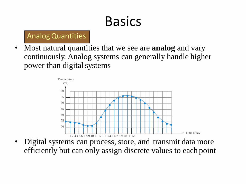
BasicsAnalog Quantities
1 2 3 4 5 6 7 8 9 10 11 12 1 2 3 4 5 6 7 8 9 10 11 12
• Digital systems can Ap.Mr. ocess, store, anP.Md. transmit data more efficiently but can only assign discrete values to each point
• Most natural quantities that we see are analog and vary continuously. Analog systems can generally handle higher power than digital systems
Temperature
(F)
100
95
90
85
80
75
70
Time ofday

Analog and Digital Systems
• Digital systems can process, store, and transmit data more
efficiently but can only assign discrete values to each point
CDdrive
10110011101
Digital data Analog
reproduction
ofmusic audio
signalSpeaker
Sound
waves
Digital-to-analog
converterLinearamplifier

Digital Signals
• Digital waveforms change between the LOW and HIGH
levels. A positive going pulse is one that goes fromanormally
LOW logic level to a HIGH level and then back again. Digital
waveforms are made up of a series of pulses
(b)Negative–going pulse
HIGH
Falling or leadingedge
Rising or
trailingedge
LOW
(a)Positive–goingpulse
HIGH
Rising or leadingedge
Falling or
trailingedge
LOWt0
t1
t0
t1

Pulse Definitions
• Actual pulses are not ideal but are described by the rise
time, fall time, amplitude, and other characteristics.
50%
10%
Baseline
Pulsewidth
Risetime Falltime
Amplitude tW
tr tf
Undershoot
Ringing
Overshoot
Ringing
Droop
90%

Pulse Definitions
• In addition to frequency and period, repetitive pulse
waveforms are described by the amplitude (A), pulse width
(tW) and duty cycle. Duty cycle is the ratio of tW to T.
Volts
Pulsewidth(tW)
Time
Period,T
Amplitude
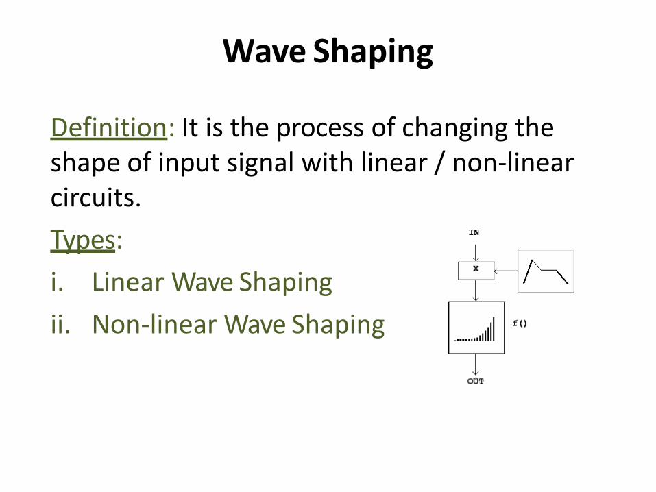
Wave Shaping
Definition: It is the process of changing the shape of input signal with linear / non-linear circuits.
Types:
i. Linear Wave Shaping
ii. Non-linear Wave Shaping
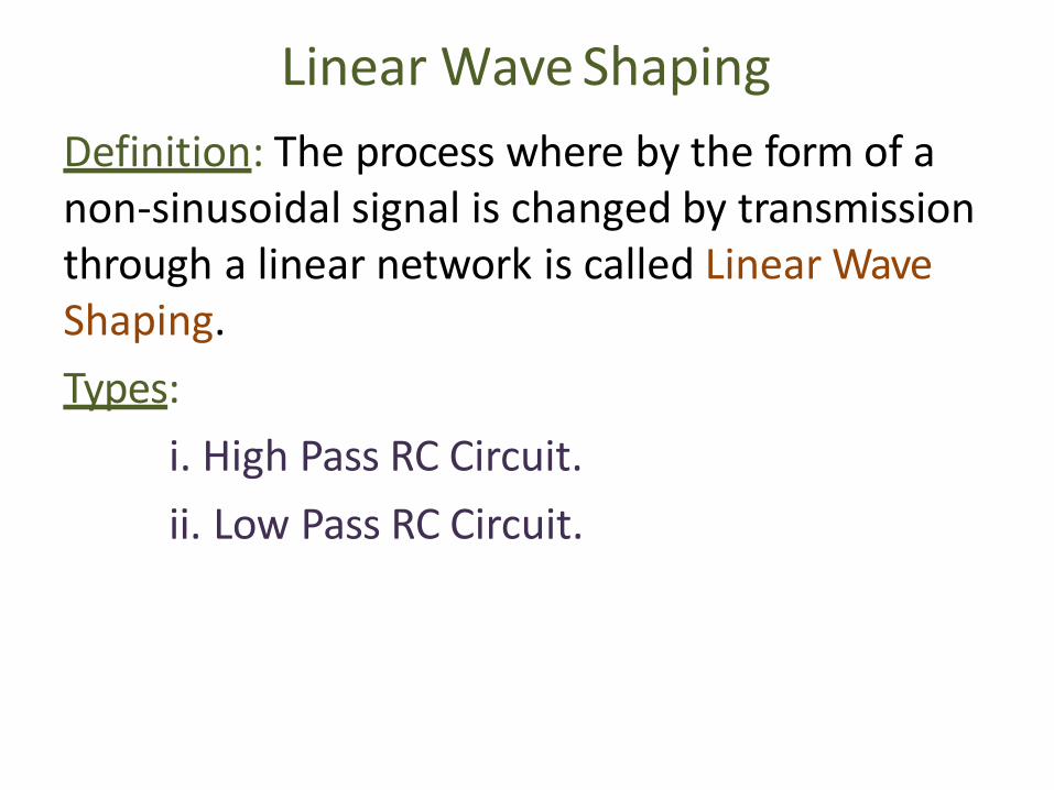
Linear Wave Shaping
Definition: The process where by the form of a non-sinusoidal signal is changed by transmission through a linear network is called Linear Wave Shaping.
Types:
i. High Pass RC Circuit.
ii. Low Pass RC Circuit.
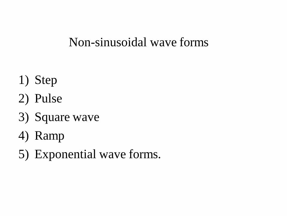
Non-sinusoidal wave forms
1) Step
2) Pulse
3) Square wave
4) Ramp
5) Exponential wave forms.

Step Waveform
tt=0
i
Vi=0 t<0
V =V t>0
A step voltage is one which maintains the value zero for all times t<0 and
maintains the value V for all times t>0.
Vi
V
PulseThe pulse amplitude is „V‟ and the pulse duration is tp.
0≤t≤tp
Otherwise
Vi=V
Vi=0
t=tpt
Vi
V
t=00

Square Wave• A wave form which maintains itself at one constant level v1 for a time T1
and at other constant Level V11 for a time T2 and which is repetitive witha period T=T1+T2 is called a square-wave.
T1 T2
RampA waveform which is zero for t<0 and which increases linearly with time for t>0.
Vi
Vi =αt
Vi =αt , t>0
0t
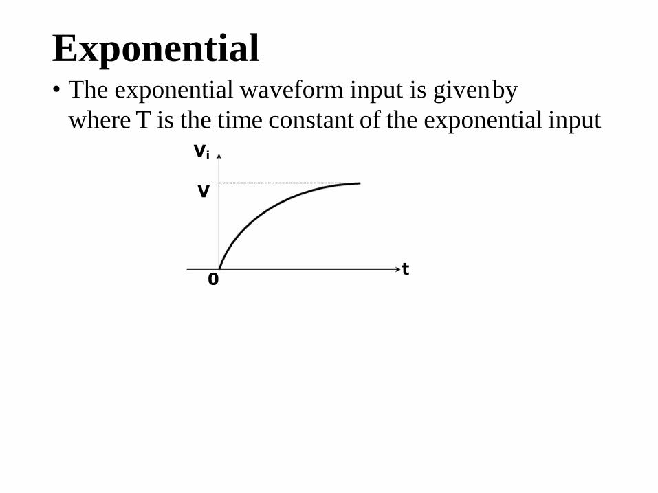
Exponential
0t
• The exponential waveform input is givenby
where T is the time constant of the exponential inputVi
V
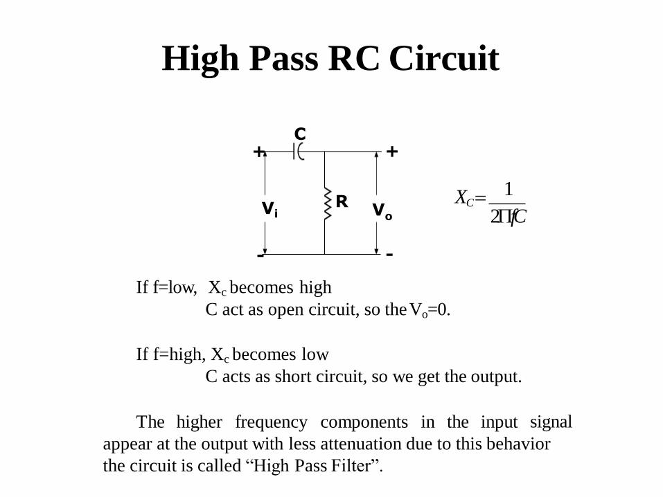
High Pass RC Circuit
R
+
Vo
C+
-
Vi
-
If f=low, Xc becomes high
C act as open circuit, so theVo=0.
If f=high, Xc becomes low
C acts as short circuit, so we get the output.
The higher frequency components in the input signal
appear at the output with less attenuation due to this behavior
the circuit is called “High Pass Filter”.
XC1
2fC
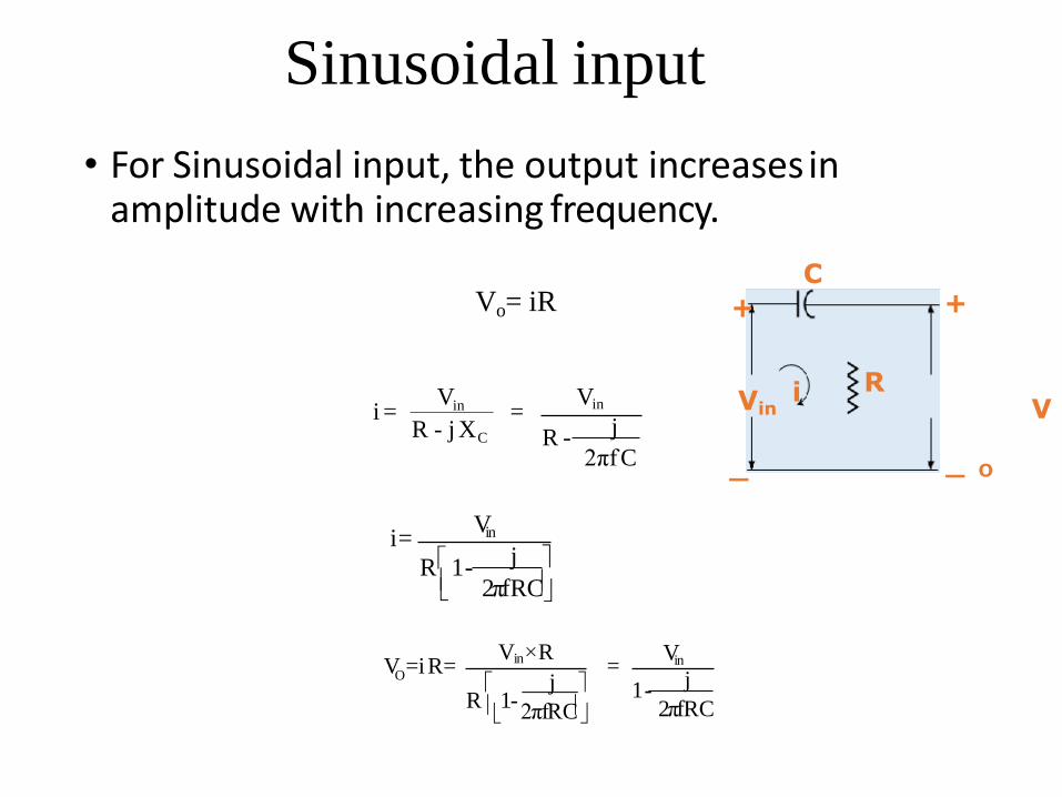
Sinusoidal input
+
V
O
i
+
Vin
_ _
• For Sinusoidal input, the output increases in amplitude with increasing frequency.
C
RV V
i = =in
R - j XC R -
in
j
2πf C
Vini=
R 1- j 2πfRC
O
Vin×R VinV =iR= =1-
j
2πfRC j
R 1-
2πfRC
Vo= iR

VO 1=
Vin 1+j-f1 f
1=
VO
V in
1 +
2
f1
f
θ =-tan -1-f1 =tan-1
f1
f f
At the frequency f = f1
Vin
VO= 1 = 1 =0.7071+1 2
A 0.707

At f = f1 the gain is 0.707 or this level corresponds to a signal reduction of 3
decibels(dB).
f1 is referred to as Lower 3-dB frequency.

Square wave input
• Percentage Tilt ( 00 Tilt)
Tilt is defined as the decay in the amplitude of the output voltage wave due
to the input voltage maintaining constant level
2
1X100P 1
V
V V 1
- T 1R CV '
1= V 1. e
- T2RCV '
2= V2 . e
2V '
1- V = V
V - V ' = V1 2
(1)
(2)
(3)
(4)

& because of• A symmetrical square wave is one for which T1=T2=
symmetry V1 = - V2
By substituting these in above equation (3)
•
-T2RC-V=V1.e V2
-T2RC+
V=V1.e V1
-T2RC
V=V1(1+e )
I
Equation(1)
II
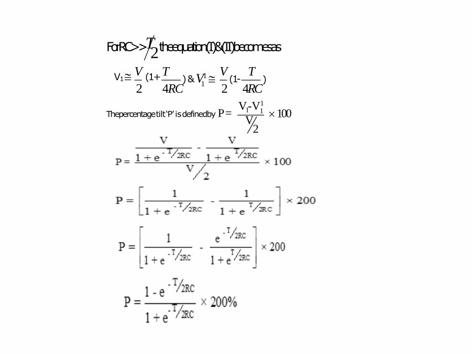
ForRC>>T theequation(I)&(II)becomesas
1
2
V1 V (1+T
2 4RC 2 4RC)&V1
V(1-
T)
1V1 -V
1
Thepercentagetilt‘P’ isdefinedby P=V
2
100

High Pass RC circuit acts as
differentiator:-• The time constant of high pass RC circuit in very small in comparison
within the time required for the input signal to make an appreciable change, the circuit is called a “differentiator”.
• Under this circumstances the voltage drop across R will be very small in comparison with the drop across C. Hence we may consider that the total input Vi appears across C, so that the current is determined entirely by the capacitance.
and the output signal across R is• Then the current is i = C
V0 = iR
V0 = RC
• hence the output is proportional to the derivative of the input.

Low Pass RC Circuit
CX
1
2f
C
If f=low, Xc becomes high
C act as open circuit, so we get the output.
If f=high, Xc becomes low
C acts as short circuit, soVo=0.
As the lower frequency signals appear at the output, it is called as
“Low pass RC circuit”.
Sinusoidal input
inV × XC
OV =
R +
j
X C
CX =
j
1
2fC
inV ×
OV =
R +
1
j C
1
j C
wh
ere
O
Vin VinV= =jRC+1 1+j2fRC
CSoV
1i

O
VinV =
1+ j ff2
2where f =1
2RC
=1
A = VO
Vin 1 + jf
f2
A =1
2
1 + f
f
2
θ=- tan -1 f
f2
and
At the frequency f = f2
Vin
VO = 1 = 1 =0.7071+1 2
A 0.707

At f = f2 the gain is 0.707 or this level corresponds to a signal reduction of 3
decibels(dB).
f2 or fh is referred to as upper 3-dBfrequency.

Square wave input
00to
• Rise Time( tr):
The time required for the voltage to rise from 10 90 0
0of the final steady value is called “Rise Time”.
Vd.c.
V’
V01
V02
V’ V2V2
V1
T1
V’’
T2

The output voltage V01 & V02 is givenby
V01
V02
=V1 +(V1-V 1) . e -T1
RC
=V11 +(V2-V11 ) . e -T2
RC
…………………(1)
…………………(2)if wesetand
V01 = V2 at t=T1
V02 = V1 at t= T1+T2
1 1
V2= V +( V1-V ) e
11 111
-
-T1RC
T2RCV =V +(V2-V ) e
Since the average across R is zero then the d.c voltage at the output is same as that of theinput. This average value is indicated as Vd.c.Consider a symmetrical square wave with zero average value, so that

- T
V 1 - e - T
2RC V =
2 1 + e 2RC
T
V e T
2RC - 1 V2 =
2e 2RC + 1
2 2 e2x + 1V =
V.
e2x - 1where x =
T
4RC
2V = V tan hx
2
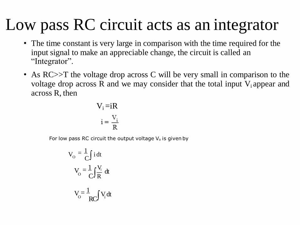
Low pass RC circuit acts as an integrator• The time constant is very large in comparison with the time required for the
input signal to make an appreciable change, the circuit is called an“Integrator”.
• As RC>>T the voltage drop across C will be very small in comparison to thevoltage drop across R and we may consider that the total input Vi appear andacross R, then
Vi =iR
For low pass RC circuit the output voltage Vo is givenby
OV = 1
i dtC
OV =
1 Vi dtCR
O iV =
1Vdt
RC
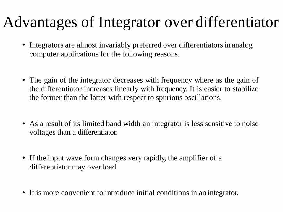
Advantages of Integrator over differentiator
• Integrators are almost invariably preferred over differentiators in analog
computer applications for the following reasons.
• The gain of the integrator decreases with frequency where as the gain ofthe differentiator increases linearly with frequency. It is easier to stabilizethe former than the latter with respect to spurious oscillations.
• As a result of its limited band width an integrator is less sensitive to noise voltages than a differentiator.
• If the input wave form changes very rapidly, the amplifier of a
differentiator may over load.
• It is more convenient to introduce initial conditions in an integrator.

RL Circuits
• RL filter or RL network, is an electric circuit composedof resistors and inductors
driven by a voltage or current source
• XL = ωL

UNIT-2
NON-LINEAR WAVE
SHAPING
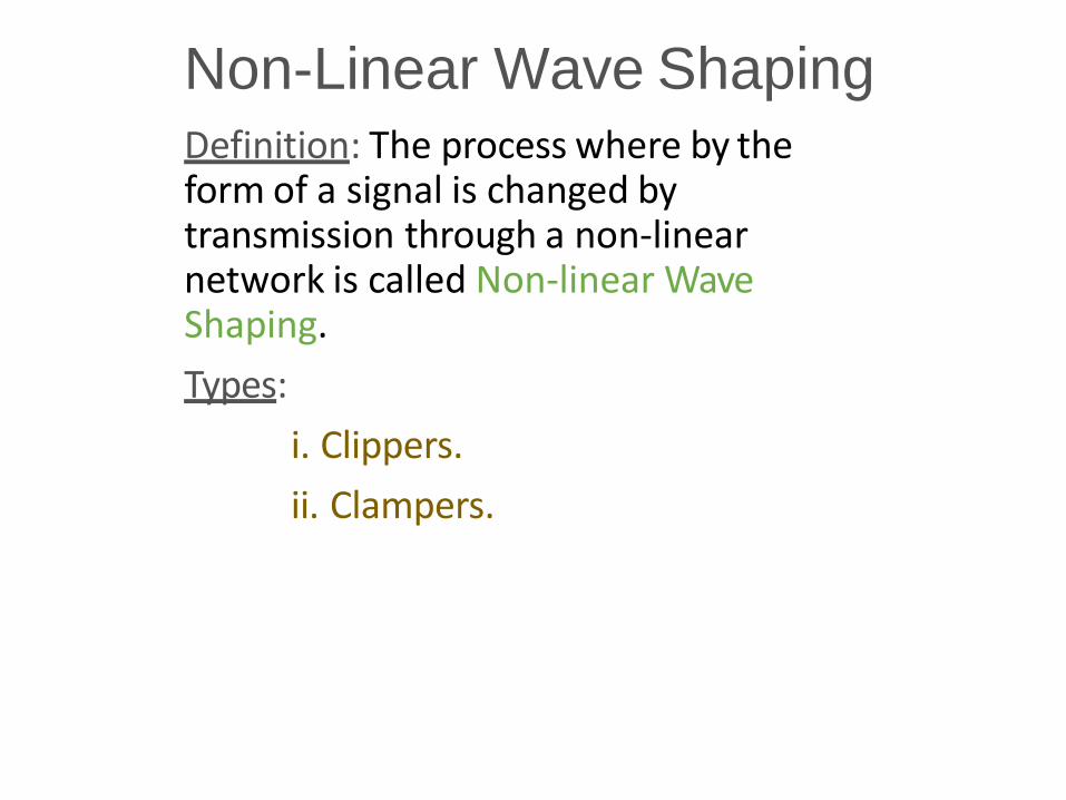
Non-Linear Wave ShapingDefinition: The process where by the form of a signal is changed by transmission through a non-linear network is called Non-linear Wave Shaping.
Types:
i. Clippers.
ii. Clampers.
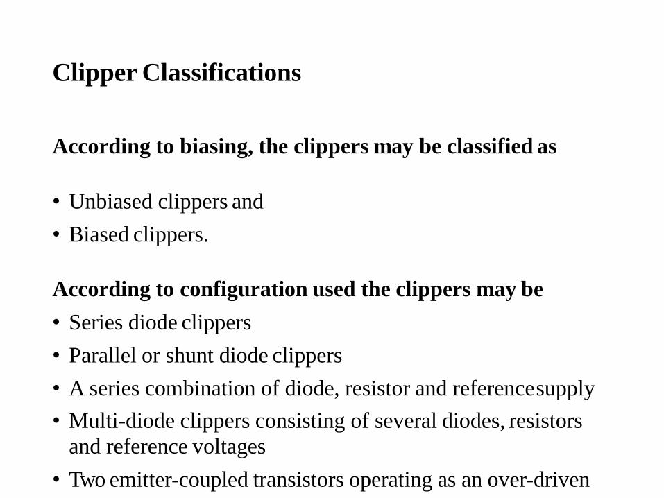
Clipper Classifications
According to biasing, the clippers may be classified as
• Unbiased clippers and
• Biased clippers.
According to configuration used the clippers may be
• Series diode clippers
• Parallel or shunt diode clippers
• A series combination of diode, resistor and referencesupply
• Multi-diode clippers consisting of several diodes, resistors
and reference voltages
• Two emitter-coupled transistors operating as an over-driven
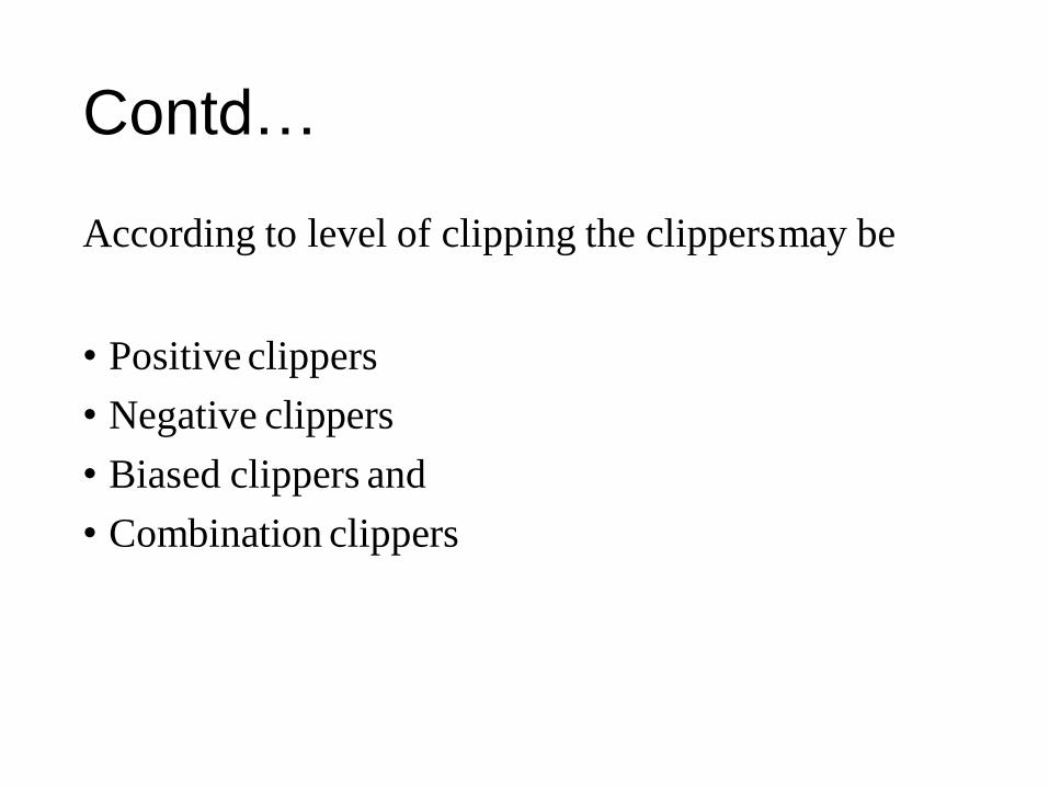
Contd…
According to level of clipping the clippersmay be
• Positive clippers
• Negative clippers
• Biased clippers and
• Combination clippers
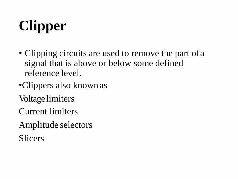
Clipper
• Clipping circuits are used to remove the part ofa signal that is above or below some defined reference level.
•Clippers also known as
Voltagelimiters
Current limiters
Amplitude selectors
Slicers

Unbiased clippers( Parallel
PositiveClippers)• Without the battery, the output of the circuit below would
be the negative portion of the input wave (assumingthebottom node is grounded). When vi > 0, the diode is on (short-circuited), vi is dropped across R and vo=0. When vi<0, the diode is off (open-circuited), the voltage across R iszero and vo=vi.

Unbiased clippers( Parallel
Negative Clippers)+ive cycle :- anode is at ground potential and cathode sees
variable +ive voltage from 0 to +Vm So complete cycle, the diode is reverse biased and Vo =Vin.At positive peak Vo=+5V
-ive cycle :- anode is at ground potential and cathode sees variable -ive vols from 0 to –Vm. When magnitude of in put volatge i.e / Vin/ >Vd, the diode become forward biased and hence Vo =-Vd =0.7V

Series positive clipper
+ive cycle :- anode is at ground potential and cathode sees variable +ive voltage from 0 to +Vm.For comlpete, cycle,diode become reverse biased and hence Vo=0V
-ive cycle :- anode is at ground potential and cathode sees variable -ive voltage from 0 to –Vm. So in complete cycle, the diode is forward biased and Vo= Vin + Vd andAt negative peak,Vo= -Vm+ Vd = -5v
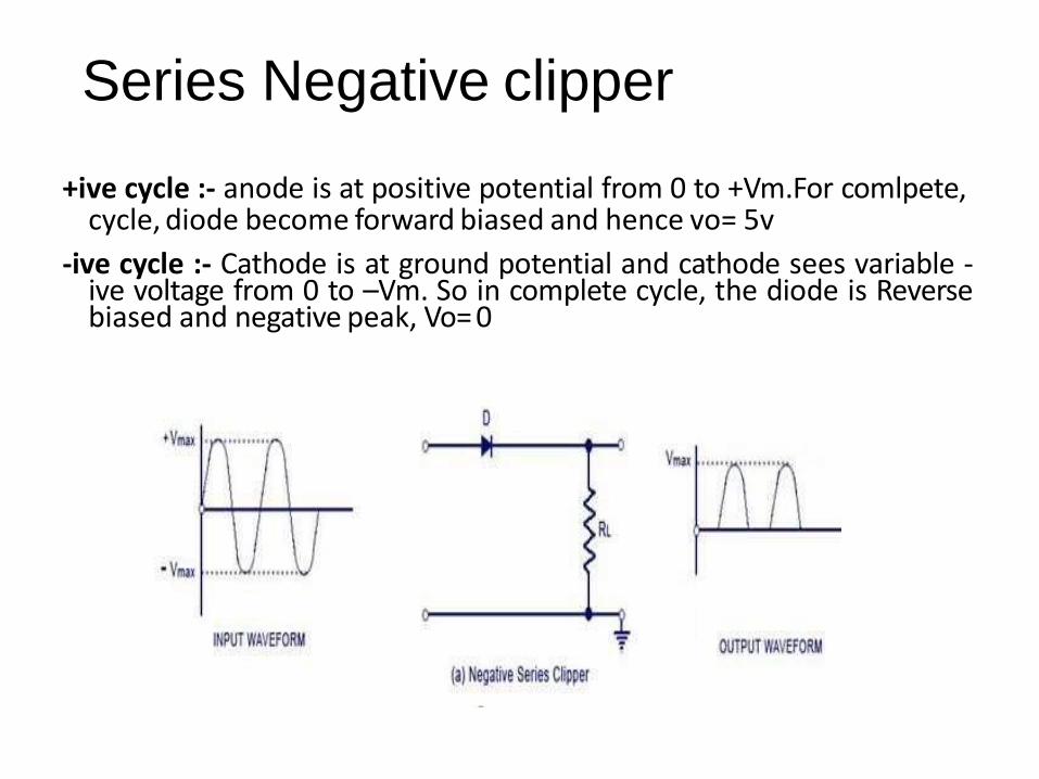
Series Negative clipper
+ive cycle :- anode is at positive potential from 0 to +Vm.For comlpete,cycle, diode become forward biased and hence vo= 5v
-ive cycle :- Cathode is at ground potential and cathode sees variable -ive voltage from 0 to –Vm. So in complete cycle, the diode is Reversebiased and negative peak, Vo= 0

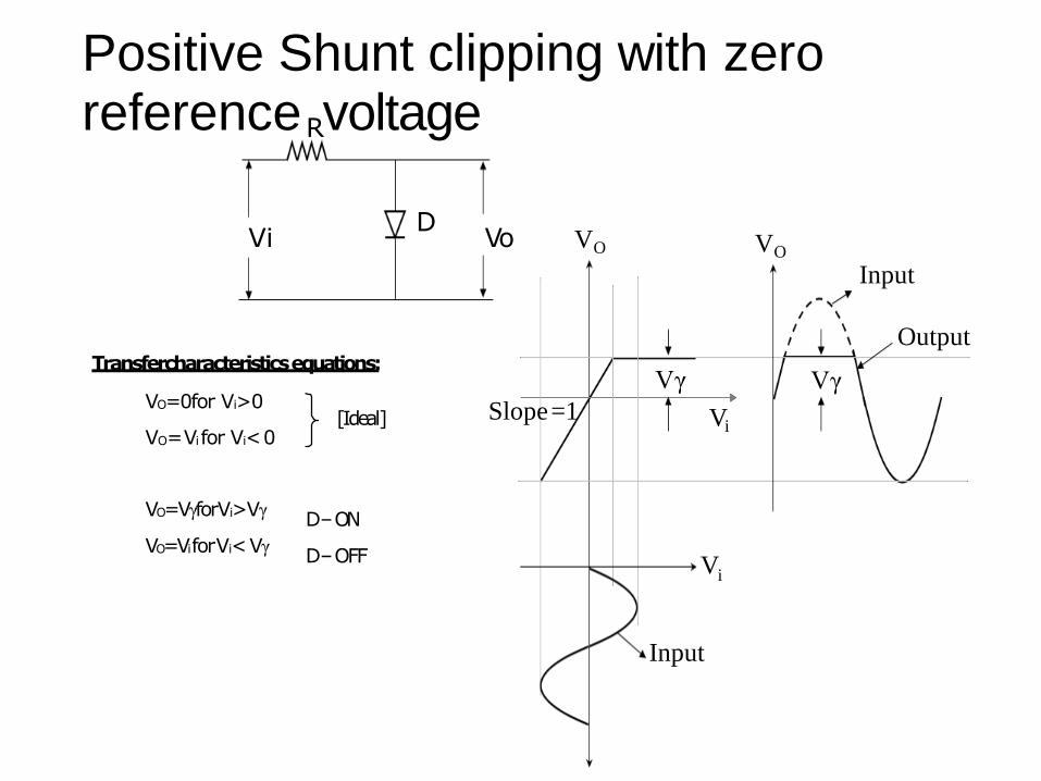
Positive Shunt clipping with zero referenceRvoltage
DVoVi
Transfercharacteristicsequations:
VO=0for Vi>0
VO=Vifor Vi<0
D–ONVO=VγforVi>Vγ
VO=ViforVi<VγD–OFF
[Ideal]
VO
Vi
VO
Vi
Slope=1
Vγ Vγ
Input
Input
Output

Positive Shunt clipping with positive reference vRoltage
D
Vi Vo
Transfer characteristics
equations:
Vi < VR+Vγ D – OFF
VO = Vi
D – ONVi > VR+Vγ
VO = VR+Vγ
Input
VR + Vγ VR + VγOutput
VOVR VO
Vi
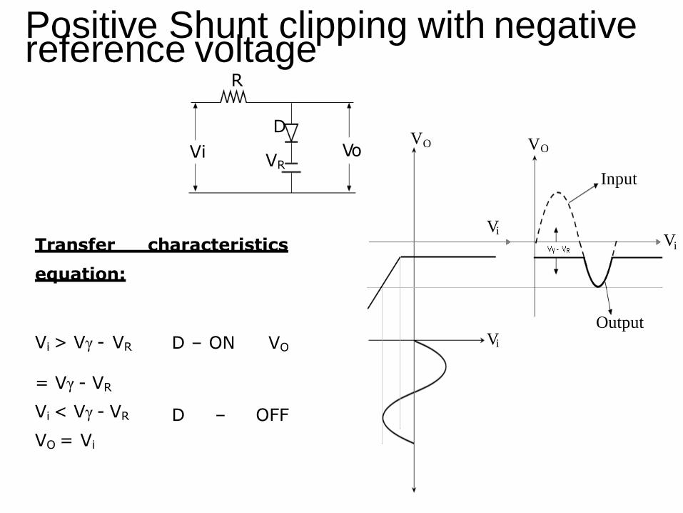
Positive Shunt clipping with negativereference voltage
R
D
VRVi Vo
Transfer characteristics
equation:
Vi > Vγ - VR D – ON VO
D – OFF
= Vγ - VR
Vi < Vγ - VR
VO = Vi
VO VO
Vi
Vi
Input
Output
Vi

Negative Shunt clipping with zero reference voltage
R
Vi VoD
Transfer characteristic
equations:
Vi > -Vγ D –OFF VO = Vγ
Vi < -Vγ D –ON VO = -Vγ
-Vγ -Vγ
VOVO
Vi
Vi
Input
Output

Negative Shunt clipping with positivereference voltage
R
D
VRVi Vo
Transfer characteristics
equations:
D – ONVi < VR-Vγ
VO = VR-Vγ
Vi > VR-Vγ D – OFF
VO = Vi
VR - Vγ
VO
Vi
Vi
VO
DOFF
DON

Negative Shunt clipping with negative reference voltage
R
D
VR
Vi Vo
Transfer characteristic
equations:
D – ON VOVi < -( Vγ + VR)
= -( Vγ + VR)
Vi < -( Vγ + VR) D – OFF VO = Vi
VO VO
Vi
Vi
- (Vγ +VR
Input
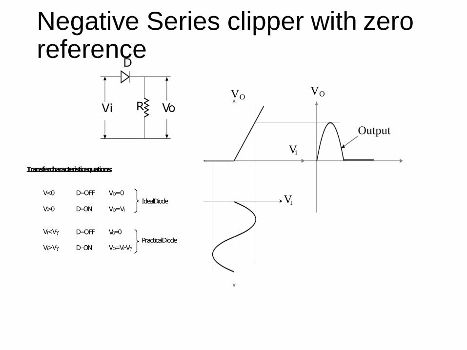
Negative Series clipper with zeroreference
RVi Vo
D
Transfercharacteristicequations:
Vi<0
Vi>0
D–OFF
D–ON
VO=0
VO=Vi
IdealDiode
Vi<Vγ D–OFF VO=0
Vi>Vγ D–ON VO=Vi-VγPracticalDiode
VOVO
Vi
Vi
Output

CLIPPING ATTWOINDEPENDENT LEVELS
R
D
VRVi Vo
D
VR
Transfercharacteristicequations:
Inp
ut
(Vi)
DiodeStateOutp
ut
(VO)
Vi VR1
D1 –ON,D2 –OFF VO=VR1
VR Vi VR1 2
D1 –OFF,D2 –OFF VO=Vi
Vi VR2D1 –OFF,D2 –ON VO=VR
2
VO VO
Vi
Vi
Input
OutputVR
1

Contd..

Transistor Clipper circuit
waveform will be clipped o
• The transistor has two types of linearities—One linearity happens when the transistor passes from cut-in region to the
active region. The other linearity occurs when the transistor passesfrom the active region to the saturation region. When any input signalpasses through the transistor, across the boundary between cut-in regionand active region, or across the boundary between the active region andsaturation region, a portion of the input signal ff.
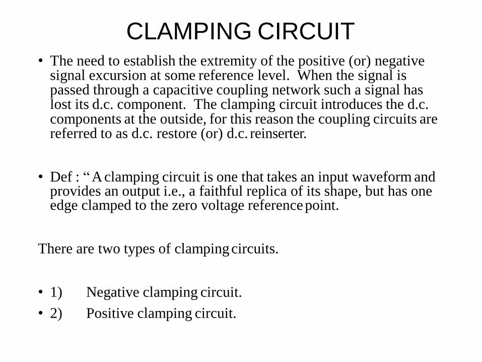
CLAMPING CIRCUIT• The need to establish the extremity of the positive (or) negative
signal excursion at some reference level. When the signal is passed through a capacitive coupling network such a signal has lost its d.c. component. The clamping circuit introduces the d.c. components at the outside, for this reason the coupling circuits are referred to as d.c. restore (or) d.c. reinserter.
• Def : “ A clamping circuit is one that takes an input waveform and provides an output i.e., a faithful replica of its shape, but has one edge clamped to the zero voltage reference point.
There are two types of clampingcircuits.
• 1) Negative clamping circuit.
• 2) Positive clamping circuit.

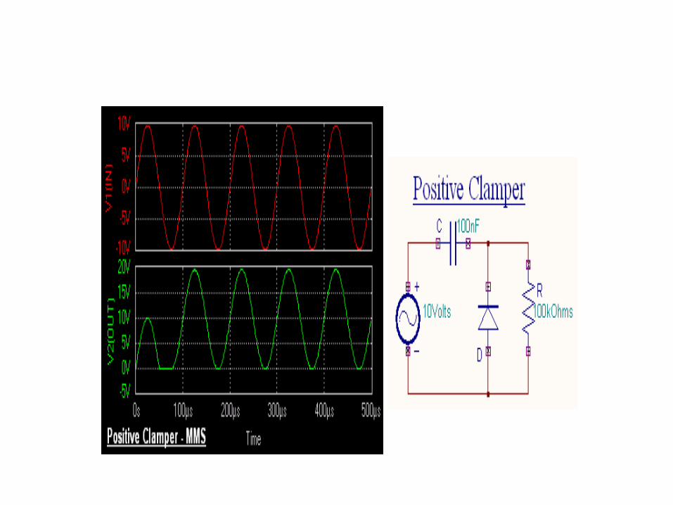
Diode :- ClamperPositive Clamper
The circuit for a positive
clamper is shown in the figure.
During the negative half cycle
of the input signal, the diode
conducts and acts like a short
circuit. The output voltageVo
0 volts . The capacitor is
charged to the peak value of
input voltage Vm. and it
behaves like a battery. During
the positive half of the input
signal, the diode does not
conduct and acts as an open
circuit. Hence the output
voltage VoVm+ Vm This
gives a positively clamped
voltage.Vo Vm+ Vm = 2
Vm

Negative ClamperDuring the positive half cycle
the diode conducts and acts
like a short circuit. The
capacitor charges to peak
value of input voltage Vm.
During this interval the
output Vo which is taken
across the short circuit will
be zero During the negative
half cycle, the diode is open.
The output voltage can be
found by applying KVL.

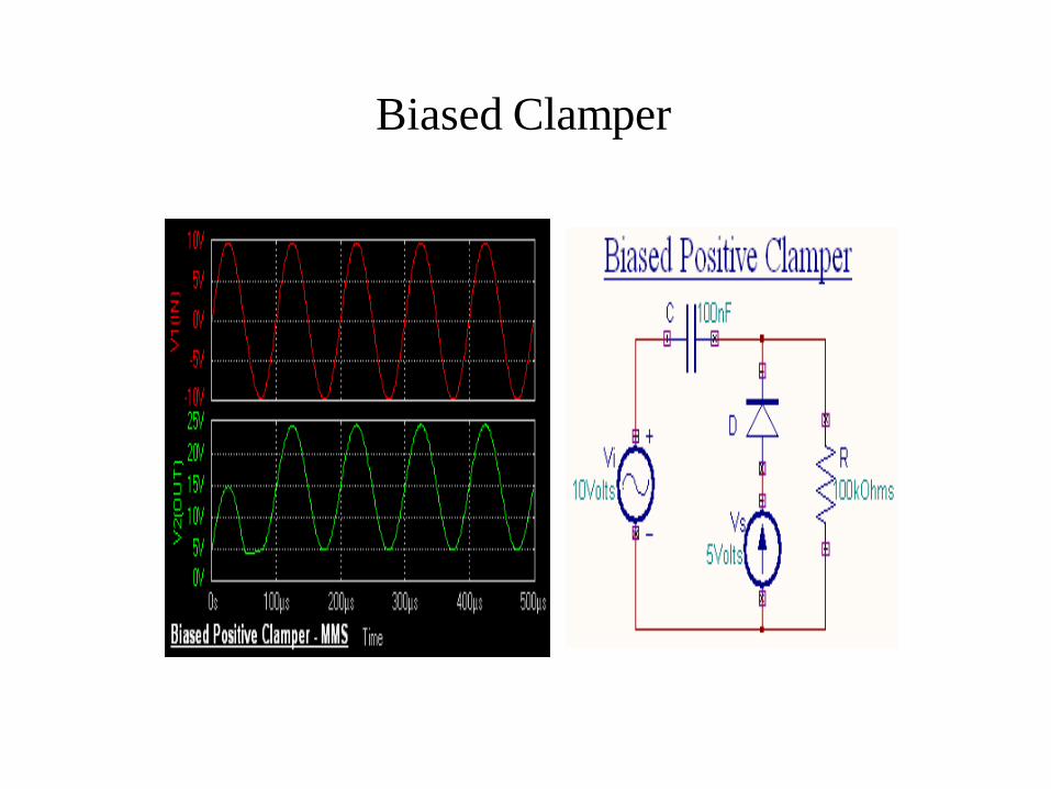
Biased Clamper

CLAMPING CIRCUIT THEOREM
• Therefore the charge acquired by the capacitor during the forward interval
Af =
Rf
Ar R
Consider a square wave input is applied to a clamping circuit under steady state condition
If Vf (t) is the output waveform in the forward direction, then from below figure
the capacitor charging current isV
if =f
Rf
Therefore the charge acquired by the capacitor during the
forward interval
i dt = V dt =Af
Rf
T1 T1
f
1
Rf f
0 0
…………….. (1)

•Similarly if Vf (t) is the output voltage in the reverse direction, then the current which discharges by the capacitor is
1 ArT2 T2
ir dt = R Vrdt =
R …………….. (2)
T1 T2
In the steady-state the net charge acquired by the capacitor
must be zero.
Therefore from equation (1) & (2) this equation says that
for any input waveform the ratio of the area under the output voltage
curve in the forward direction to the reverse direction is equal to the
ratio .

Clamping Circuit taking Source and Diode Resistances into account
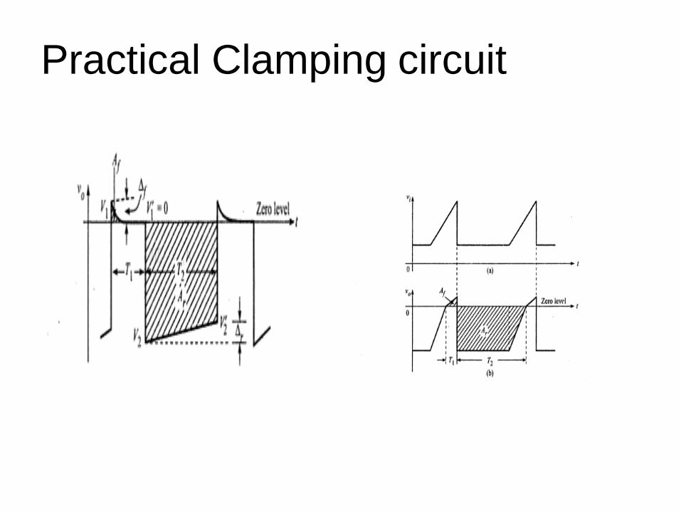
Practical Clamping circuit
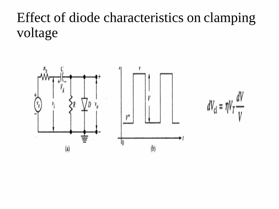
Effect of diode characteristics on clamping voltage

Synchronized Clamping
Steady State Switching
Characteristics of Devices
UNIT - 3


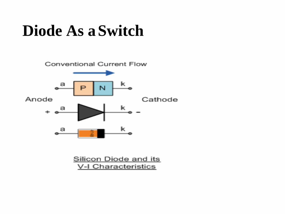
Diode As a Switch
• The semiconductor Signal Diode is a smallnon-linear semiconductor devices generally used in electronic circuits, where small currents or high frequencies are involved such as in radio, television and digital logic circuits
Diode As a Switch

• Unlike the resistor, whose two terminal leads are equivalent, the behavior of the diode depend on the relative polarity of its terminals.
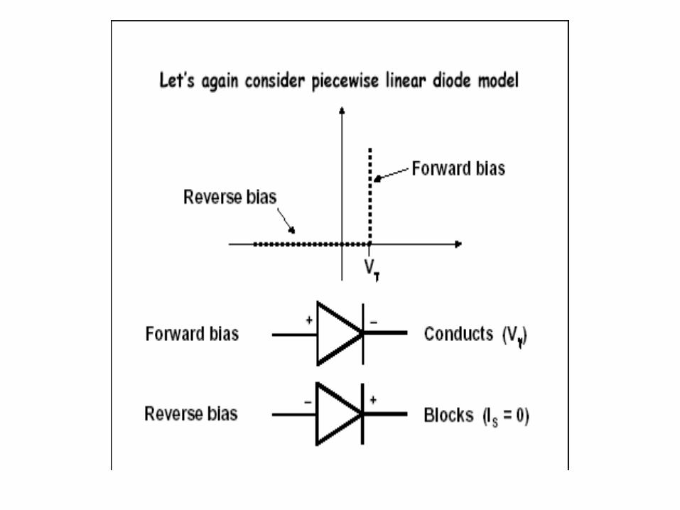
• Ideal Diode
•
Piece-wise linear model

Contd….
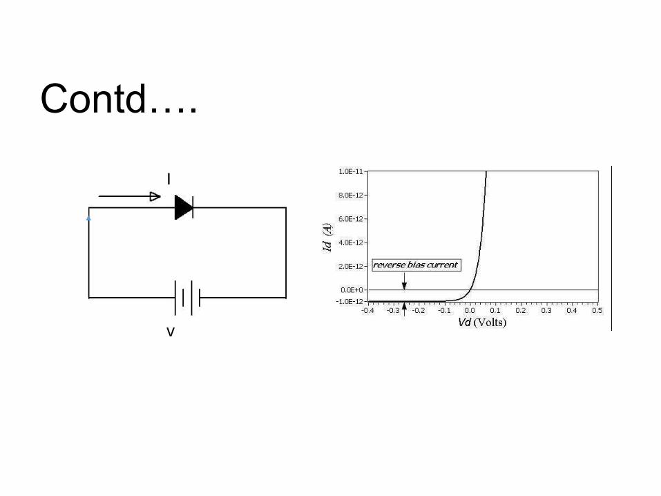
Contd….
v
I
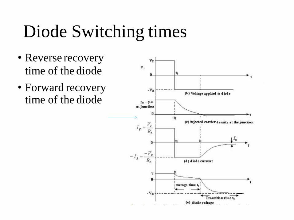
Diode Switching times
• Reverse recovery
time of the diode
• Forward recovery time of the diode

Contd…
• As long as the voltage Vi = VF till t1, the diode is ON. The forward resistance of the diode being negligible when compared to RL, therefore If= Vf/R. At t = t1, the polarity of Vi is abruptly reversed, i.e.Vi = -VR and Ir = -Vr/R until t = t2 at which time minority carrier density pn at x = 0 has reached the equilibrium value pn0.
• At t = t2 the charge carriers have been swept, the polarity of the diodevoltage reverses, the diode current starts to decrease. The time duration, t1 tot2, during which period the stored minority charge becomes zero is called thestorage time ts. The time interval from t2 to the instant that the diode hasrecovered (V = -VR) is called the transition time,tt. The sum total of thestorage time,ts and the transition time,tt is called the reverse recovery time ofthe diode, trr.
• trr = ts + tt

The BJT as a Switch• Transistor as a Switch works in two regions
• Cut off
• Saturation


Transistor Switching Times
• Delay time(td)
• Rise time(tr)
• Storage time(ts)
• Fall time(tf)
Contd..• Delay Time, td : It is the time taken for the collector current to reach from its initial
value to 10% of its final value If the rise of the collector current is linear, the time required to rise to 10%IC(sat) is 1/8 the time required for the current to rise from 10% to 90% IC(sat). where tr is the rise time
• Rise Time,tr : It is the time taken for the collector current to reach from 10% of its final value to 90% of its final value. However, because of the stored charges, the current remains unaltered for sometime interval ts1 and then begins to fall. The time taken for this current to fall from its initial value at ts1 to 90% of its initial value is ts2. The sum of these ts1 and ts2 is approximately ts1 and is called the storage time.
• Storage time, ts : It is the time taken for the collector current to fall from its initialvalue to 90% of its initialvalue.
• . Fall time, tf : It is the time taken for the collector current to fall from 90% of its
initial value to 10% of its Initialvalue.
• Ton=td+tr
• Toff= ts+tf

Breakdown mechanisms in BJTs• The breakdown voltage of a BJT also depends on the chosen circuit
configuration:
• In a common base mode (i.e. operation where the base is grounded and forms the common electrode between the emitter-base input and collector-base output of the device) the breakdown resembles that of a p-n diode.
• In a common emitter mode (i.e. operation where the emitter is grounded and forms the common electrode between the base-emitter input and the collector-emitter output of the device) the transistor action further influences the I-V characteristics and breakdown voltage.
• Avalanche breakdown of the base-collector junction is further influenced by transistor action in common-emitter mode of operation, since the holes generated by impact ionization are pulled back into the base region which results in an additional base current. This additional base current causes an even larger additional flow of electrons through the base and into the collector due to the current gain of the BJT. This larger flow of electrons in the base collector junction causes an even larger generation of electron-hole pairs.

SCR
• A Silicon Controlled Rectifier (or Semiconductor ControlledRectifier) is a four layer solid state device that controls currentflow
• The name “silicon controlled rectifier” is a trade name for the
type of thyristor commercialized at General Electric in 1957
UNIT -4
MULTIVIBRATORS
and
TIME BASEGENERATORS

Multivibrators
• Multivibrator – A circuit designed to have zero, one, or two stable outputstates.
• There are three types of multivibrators.• Astable (or Free-Running Multivibrator)
• Monostable (or One-Shot)
• Bistable (or Flip-Flop)

Bistable Multivibrators• Bistable multivibrator – A switching circuit with two stable
output states. The bistable multivibrator has twoabsolutely stable states• Also referred to as a flip-flop.
• The output changes state when it receives a valid input trigger signal, and remains in that state until another valid trigger signal is received.

Bistable Multivibrator Waveform

Monostable Multivibrator• Multivibrators have two different electrical states, an output “HIGH” state and an output
“LOW” state giving them either a stable or quasi-stable state depending upon the type of multivibrator. One such type of a two state pulse generator configuration are called Monostable Multivibrators.
• Monostable Multivibrators have only ONE stable state (hence their name: “Mono”), and produce a single output pulse when it is triggered externally. Monostable Multivibrators only return back to their first original and stable state after a period of time determined by the time constant of the RC coupled circuit.

Waveforms
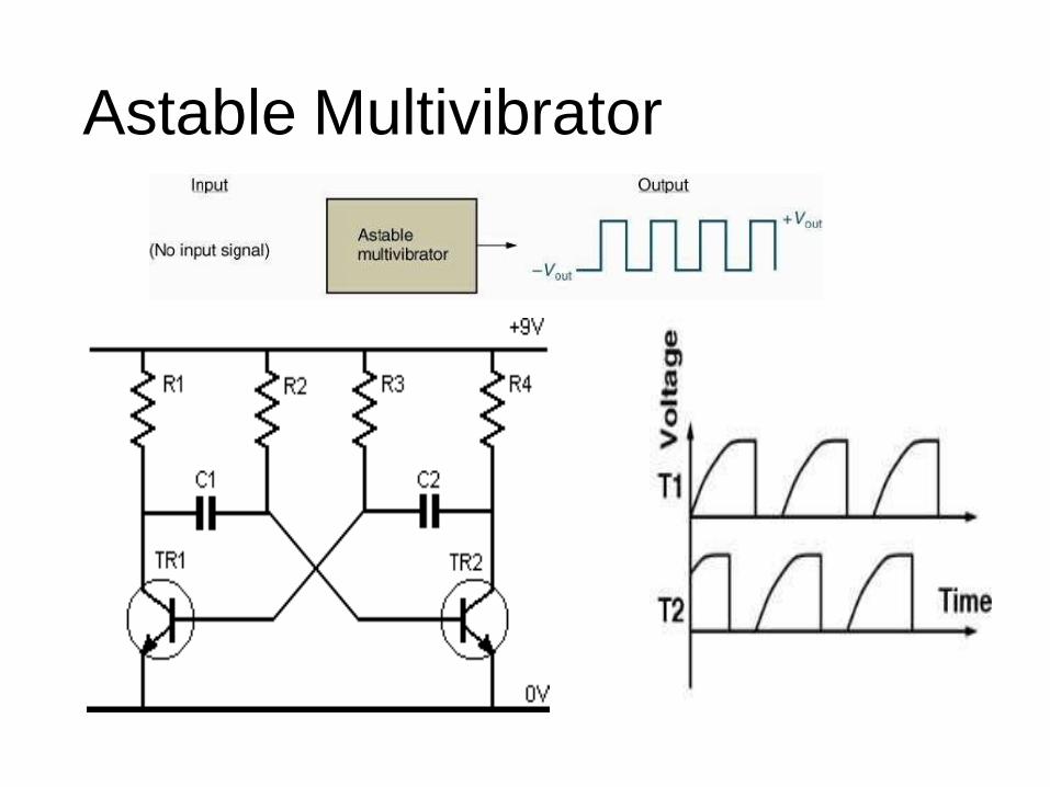
Astable Multivibrator

Waveforms

Commutating Capacitors
• Conduction transfers takes two phases
• 1) Transitiontime
• 2) Settling time

Triggering the binary
• Two types of triggering
• 1) Symmetrical 2) Unsymmetrical
• In un symmetrical triggering, two triggers are required. One to set the circuit in particular stable state and other is to reset
• In Symmetrical triggering , uses only one trigger pulse input to the any of the one transistor
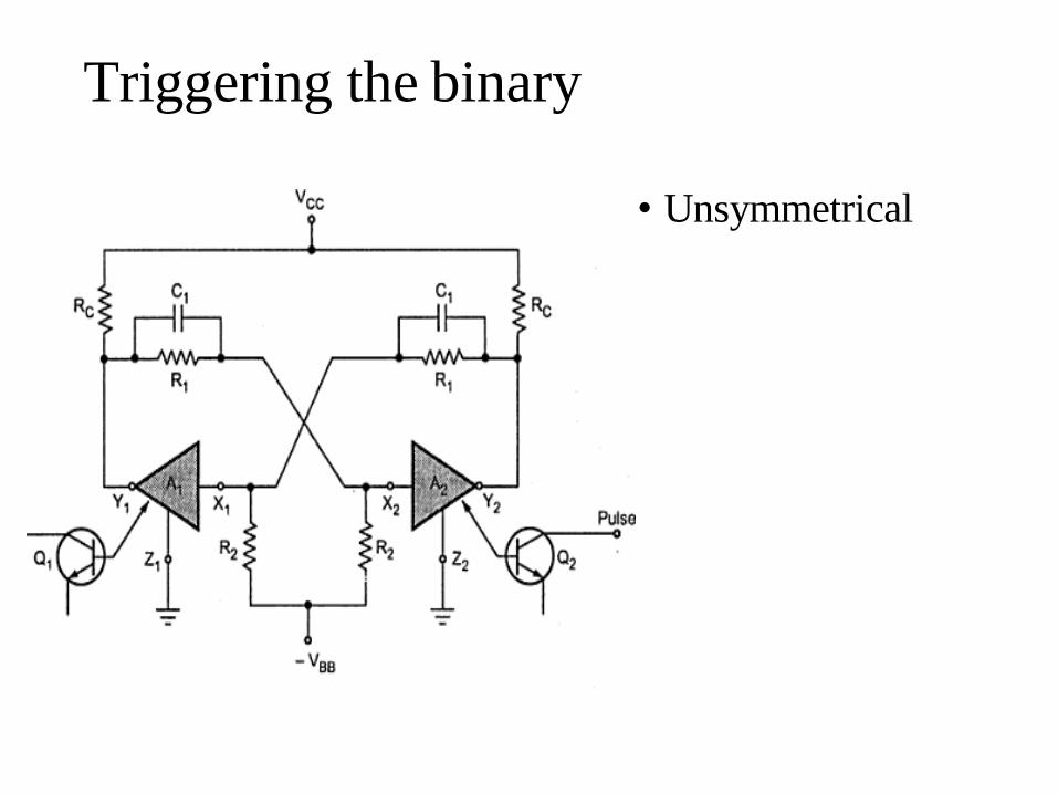
Triggering the binary
• Unsymmetrical
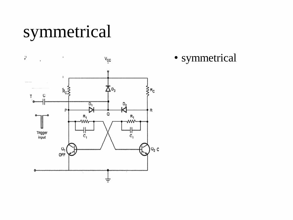
symmetrical
• symmetrical
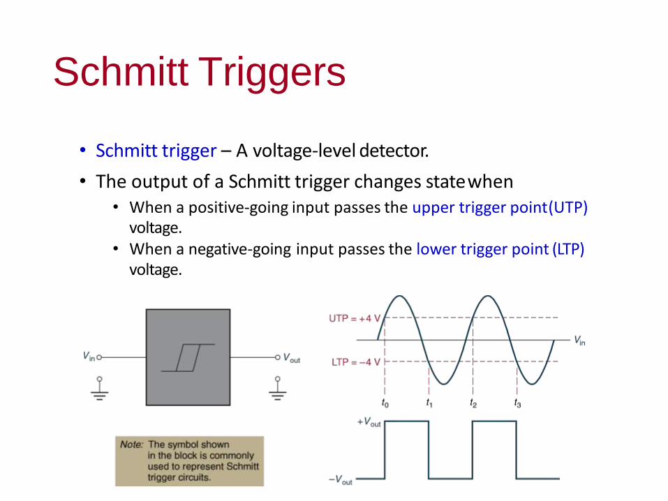
Schmitt Triggers
• Schmitt trigger – A voltage-level detector.
• The output of a Schmitt trigger changes statewhen• When a positive-going input passes the upper trigger point(UTP)
voltage.• When a negative-going input passes the lower trigger point (LTP)
voltage.

Trigger Point Voltages• Trigger point voltages may be equal or unequal in
magnitude, and are opposite in polarity.

Hysteresis• Hysteresis – A term that is often used to describe the range of
voltages between the UTP and LTP of a Schmitt trigger.

Schmitt trigger using transister

• Assume NPN transistor with
• Let
vardhaman
Astable multivibrator to generate a squarewave of 1 kHz:
25h fe
Ic 5mA
Vcc 12V
T1 T2T/2
• Assume symmetrical square wave i.e.
• Neglect the junction voltages.
• We have f= 1 kHz
• So, T=1/1kHz = 1ms

=5/25
=0.2mA
vardhaman
Q1
ON and OFF.Then
Q2
• Let
Rc2
feh
=(12-0)/5 Rc1
=2.4Ik =C 2( s a t)
i B 2 m i n
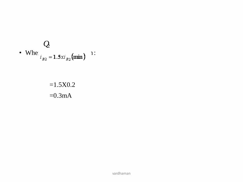
• When is in saturatio n :
=1.5X0.2
=0.3mA
vardhaman
Q2
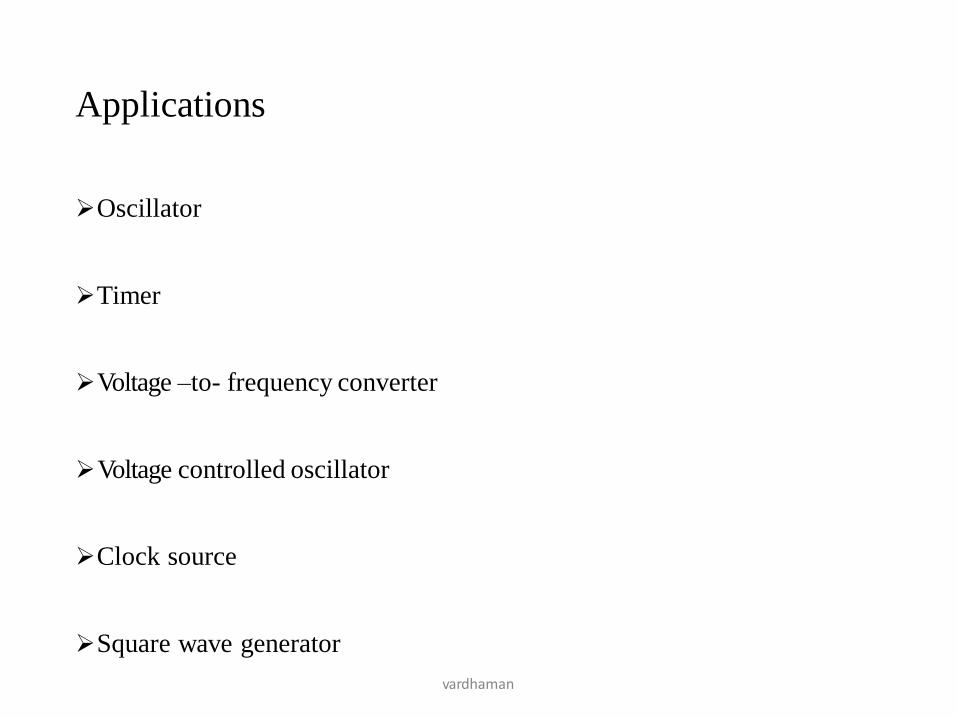
Oscillator
Timer
Voltage –to- frequency converter
Voltage controlled oscillator
Clock source
Square wave generator
vardhaman
Applications

General features of time base generator
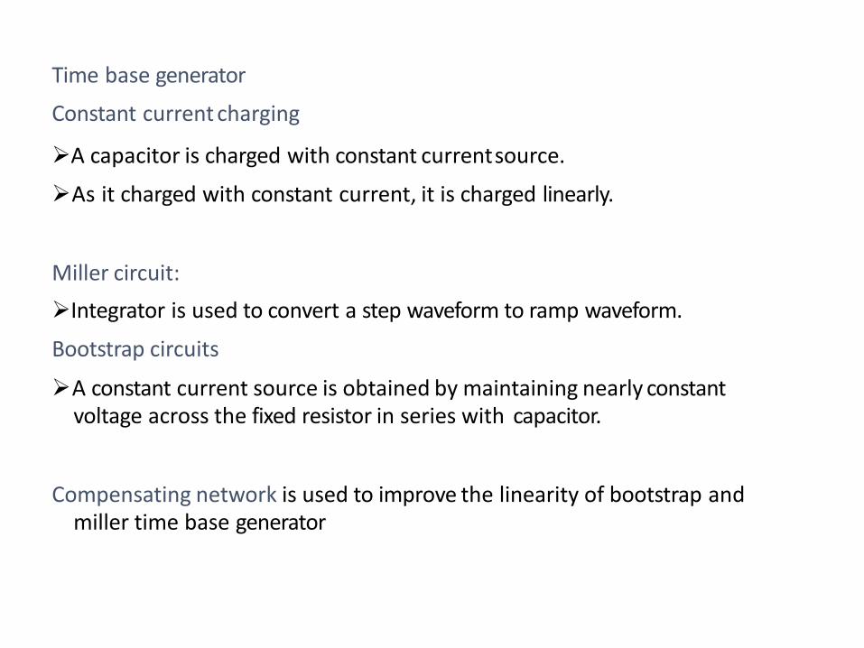
Time base generator
Constant current charging
A capacitor is charged with constant currentsource.
As it charged with constant current, it is charged linearly.
Miller circuit:
Integrator is used to convert a step waveform to ramp waveform.
Bootstrap circuits
A constant current source is obtained by maintaining nearly constantvoltage across the fixed resistor in series with capacitor.
Compensating network is used to improve the linearity of bootstrap andmiller time base generator

Exponential sweep circuit

Transistor miller time base generator

Input and output waveforms

Transistor bootstrap time base generator
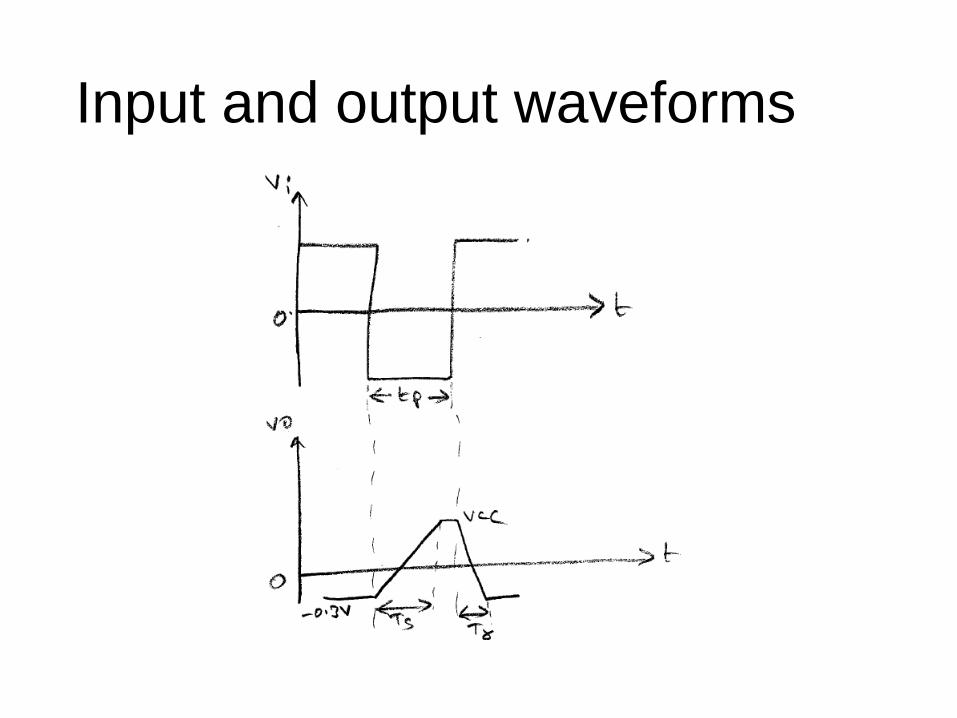
Input and output waveforms
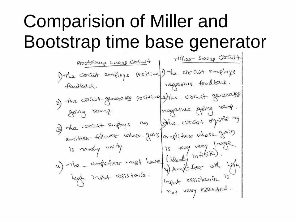
Comparision of Miller and Bootstrap time base generator

UNIT-5
SAMPLING GATES
&
Logic gates

Sampling Gates
• Sampling Gates are also called as Transmission gates ,linear gates and selection circuits,in which the output is exact reproduction of the input during a selected time interval and zero otherwise.
• It has two inputs – gating signal, rectangular wave
• Two types
• Unidirectional
• Bidirectional
Gating
Input
Sampling GateOutput
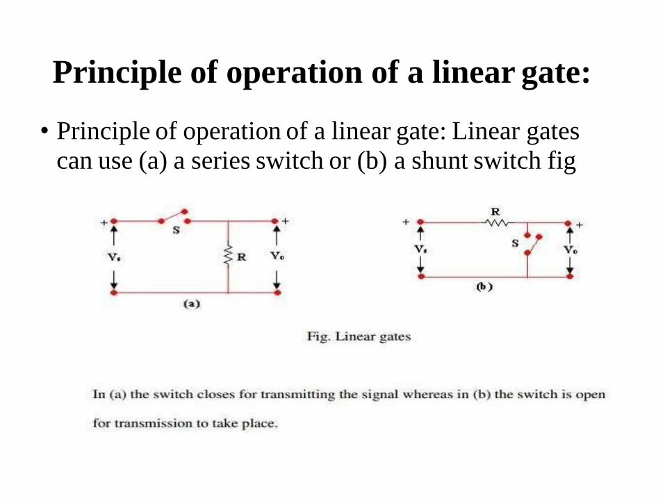
Principle of operation of a linear gate:
• Principle of operation of a linear gate: Linear gates
can use (a) a series switch or (b) a shunt switch fig
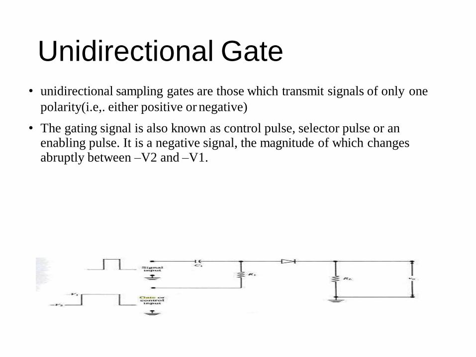
Unidirectional Gate
• unidirectional sampling gates are those which transmit signals of only one
polarity(i.e,. either positive or negative)
• The gating signal is also known as control pulse, selector pulse or an enabling pulse. It is a negative signal, the magnitude of which changes abruptly between –V2 and –V1.
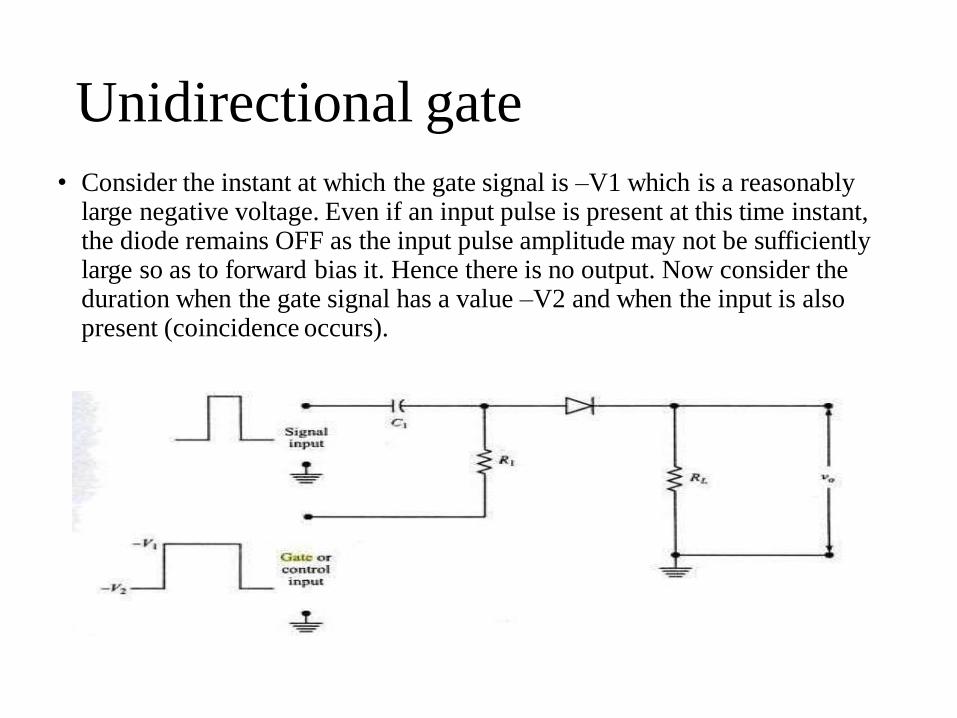
Unidirectional gate
• Consider the instant at which the gate signal is –V1 which is a reasonably large negative voltage. Even if an input pulse is present at this time instant, the diode remains OFF as the input pulse amplitude may not be sufficiently large so as to forward bias it. Hence there is no output. Now consider the duration when the gate signal has a value –V2 and when the input is also present (coincidence occurs).
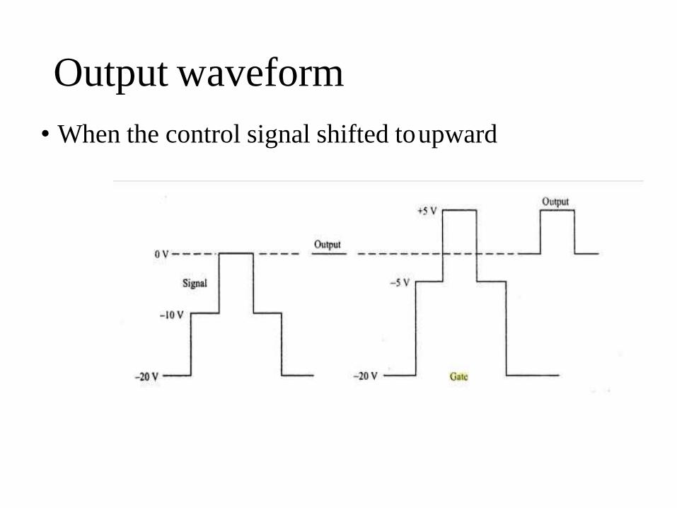
Output waveform
• When the control signal shifted toupward

pedestal
• When the control signal is shifted to positive value ,so it willbe superimposed on input and control signals .so the pedestal occurs

Unidirectional Gate
• unidirectional sampling gates are those which transmit signals of only one
polarity(i.e,. either positive or negative)
• The gating signal is also known as control pulse, selector pulse or an enabling pulse. It is a negative signal, the magnitude of which changes abruptly between –V2 and –V1.
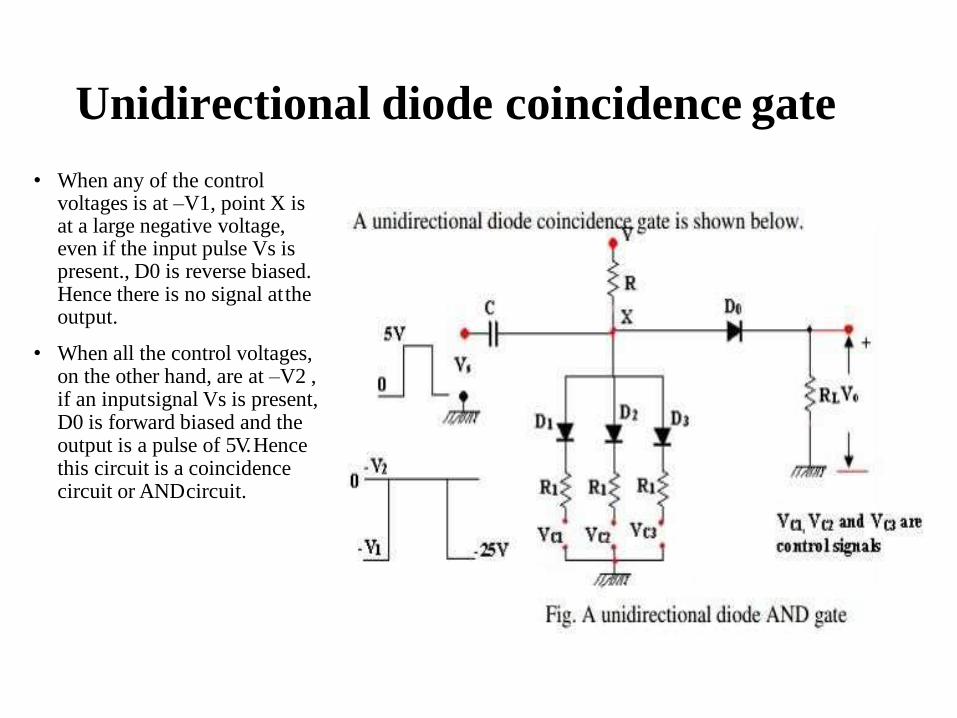
Unidirectional diode coincidence gate
• When any of the control voltages is at –V1, point X is at a large negative voltage, even if the input pulse Vs is present., D0 is reverse biased. Hence there is no signal atthe output.
• When all the control voltages, on the other hand, are at –V2 , if an inputsignal Vs is present, D0 is forward biased and the output is a pulse of 5V. Hence this circuit is a coincidence circuit or ANDcircuit.

Bidirectional Sampling gate
• Bidirectional sampling gates are those whichtransmit
signals of both the polarities.
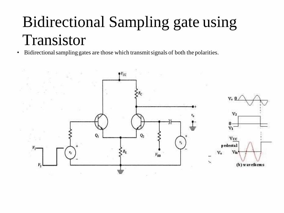
Bidirectional Sampling gate using
Transistor• Bidirectional sampling gates are those which transmit signals of both the polarities.

Circuit that minimizes the pedestal• Circuit that minimizes the pedestal

Contd …• The control signal applied to the base of Q2 is of opposite polarity to that applied to
the base of Q1. When the gating signal connected to Q1 is negative, Q1 is OFF and atthe same time the gating signal connected to Q2 drives Q2 ON and draws current IC.As a result there is a dc voltage Vdc at the collector. But when the gate voltage at thebase of Q1 drives Q1 ON, Q2 goes OFF. But during this gate period if the input signalis present, it is amplified and is available at the output, with phase inversion. But thedc reference level practically is Vdc. As such the pedestal is either eliminated orminimized.

Two Diode Sampling gate
• When the control signals are at V1, D1 and D2 are OFF, no input signal is transmitted to the output. But when control signals are at V2, diode D1 conducts if the input is positive pulses and diode D2 conducts if the input is negative pulses. Hence these bidirectional inputs are transmitted to the output. This arrangement eliminates pedestal, because of the circuit symmetry.
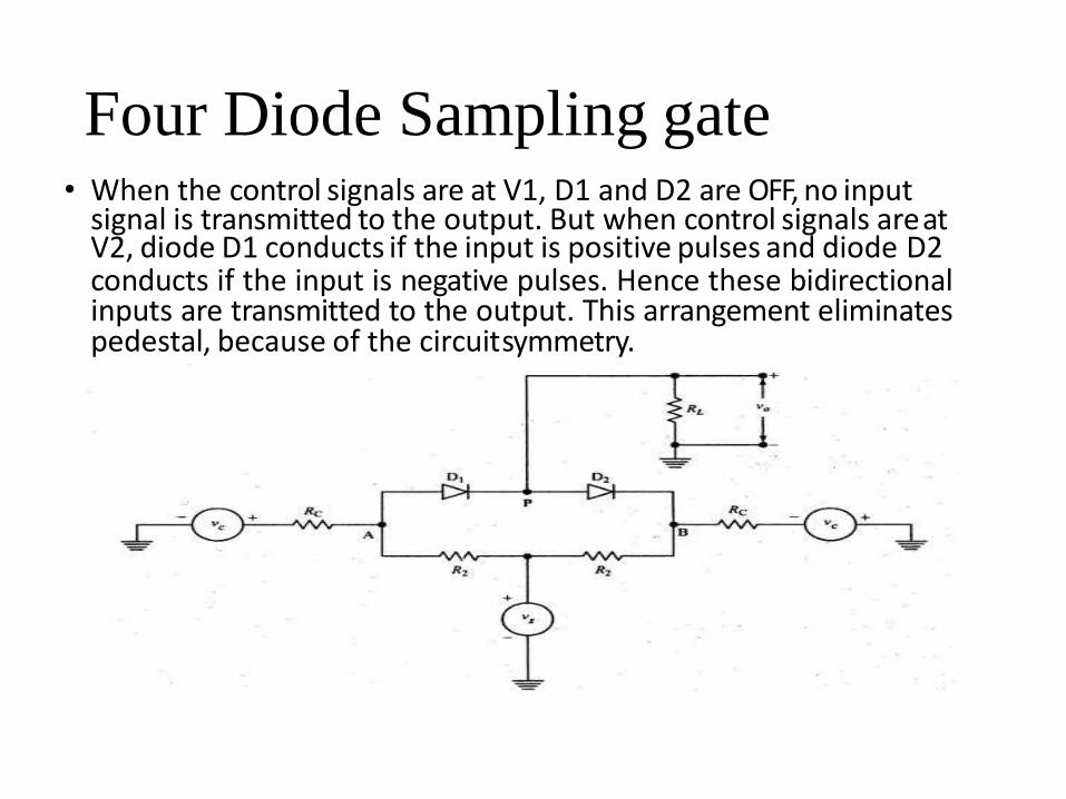
Four Diode Sampling gate• When the control signals are at V1, D1 and D2 are OFF, no input
signal is transmitted to the output. But when control signals areatV2, diode D1 conducts if the input is positive pulses and diode D2conducts if the input is negative pulses. Hence these bidirectionalinputs are transmitted to the output. This arrangement eliminatespedestal, because of the circuitsymmetry.

Applications
• ChopperAmplifier
• Multiplexers
• ADC
• Sampling Scope
• Sample and hold circuits
Logic gates

1. Definition
2. Logic design, Digital system
3. Truth table
4. Inputs and outputs
5. Pulse logic or level logic
6. Level logic ---1) Positive logic
2) Negative logic
Basic gates
Universal gates
Derived gates


Other names: Any or all gate
Inclusive OR gate
IC 7432: Four two-input OR gates.

AND gate: all or nothing gate
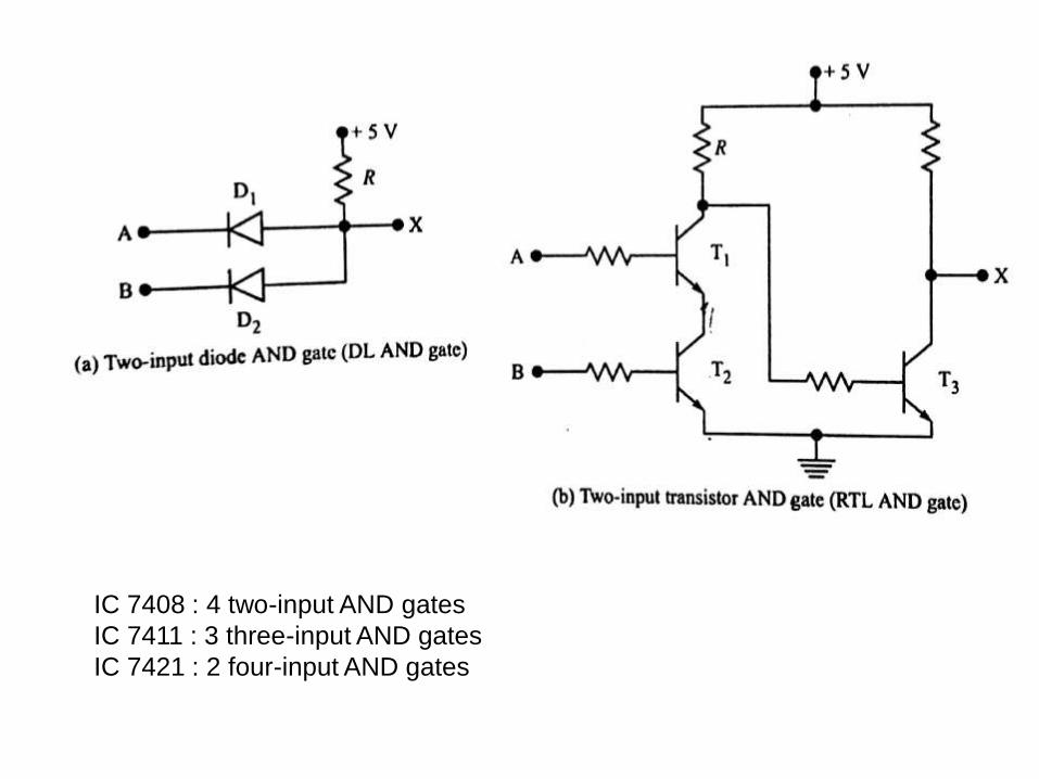
IC 7408 : 4 two-input AND gates
IC 7411 : 3 three-input AND gates
IC 7421 : 2 four-input AND gates

NOT gate (Inverter)
IC 7404 : Hex or Six inverters


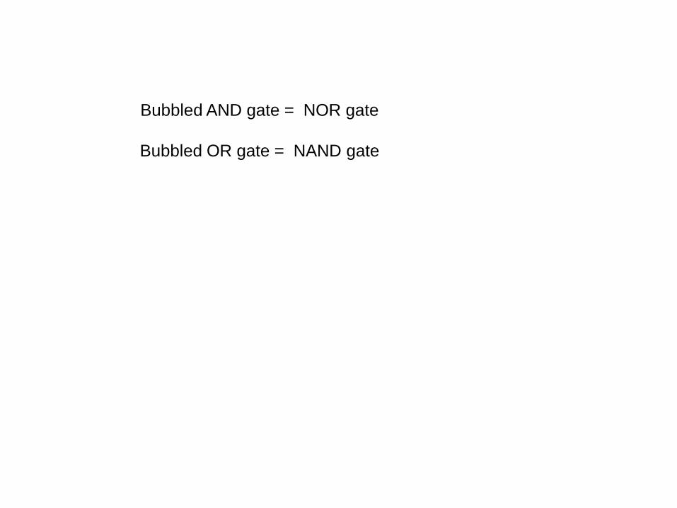
Bubbled AND gate = NOR gate
Bubbled OR gate = NAND gate
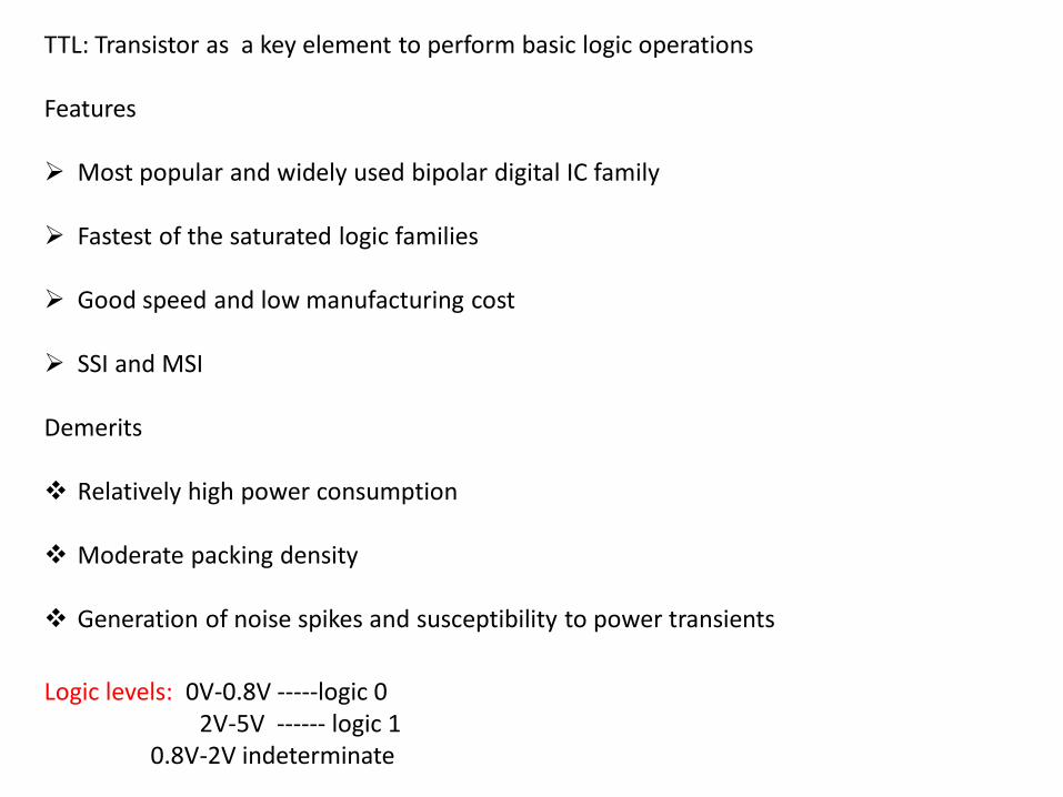
TTL: Transistor as a key element to perform basic logic operations
Features
Most popular and widely used bipolar digital IC family
Fastest of the saturated logic families
Good speed and low manufacturing cost
SSI and MSI
Demerits
Relatively high power consumption
Moderate packing density
Generation of noise spikes and susceptibility to power transients
Logic levels: 0V-0.8V -----logic 02V-5V ------ logic 1
0.8V-2V indeterminate


If any input is low the corresponding base emitter
junction becomes forward biased and the transistor
conducts

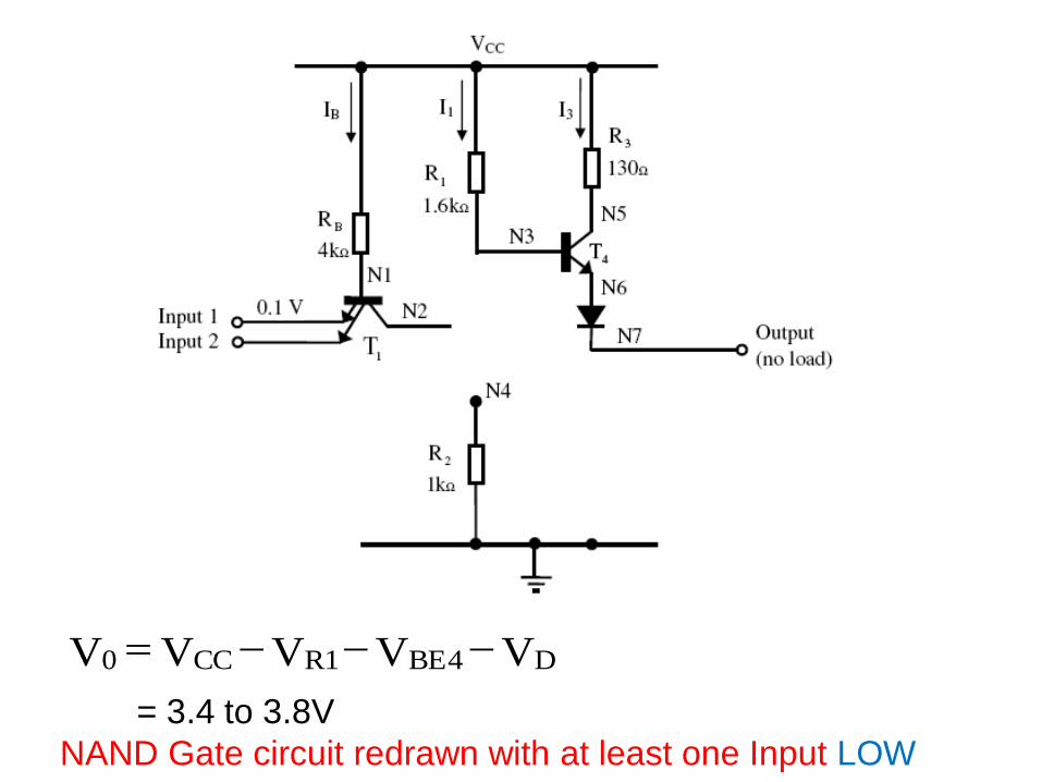
= 3.4 to 3.8V
NAND Gate circuit redrawn with at least one Input LOW
VVVVV D4BE1RCC0
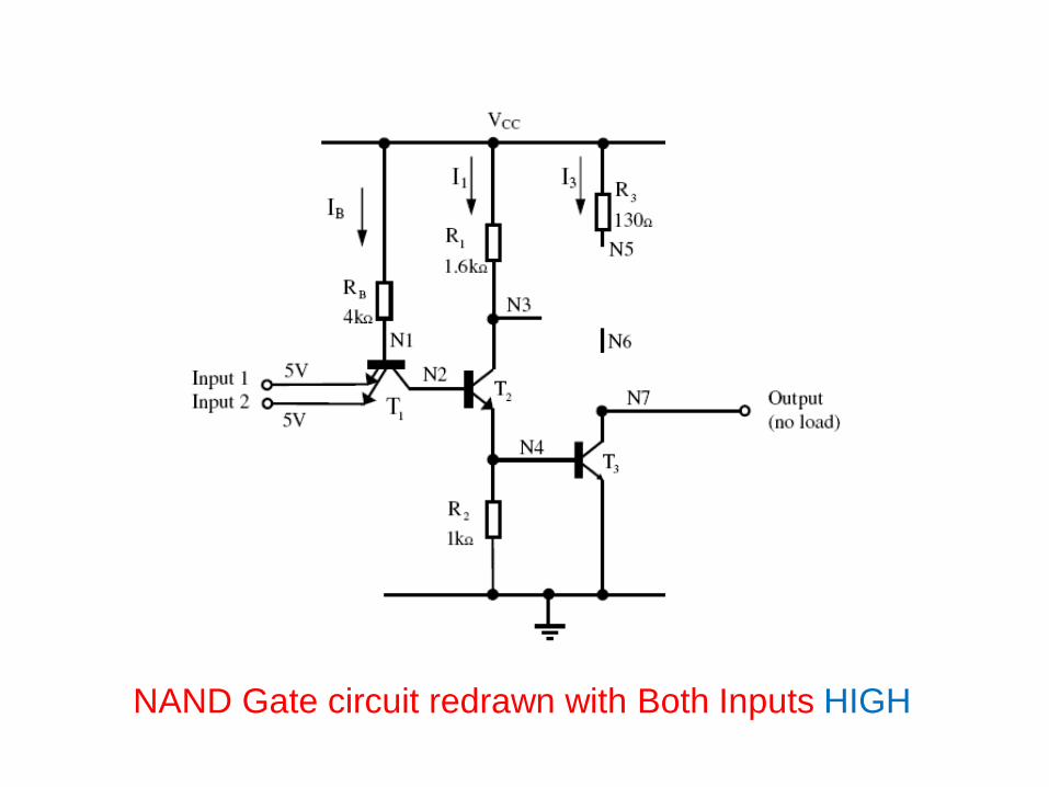
NAND Gate circuit redrawn with Both Inputs HIGH

Functional Table

Totem-pole Output :
Never Two transistors conduct simultaneously
1. Transistor and D keeps the circuit power dissipation low.
2. In the output HIGH state, acts as emitter follower with its associated low
output impedance. Small time constant for charging up any capacitive load on the
output provides very fast rise time.
Disadvantages:
1. During the transition of LOW to HIGH turns off more slowly than
turns ON. So TTL suffers from internally generated current spikes because of
totem-pole,
2. Totem – pole outputs cannot be wire ANDed.
T4
T4
T3 T4
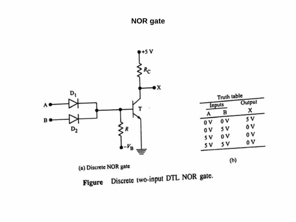
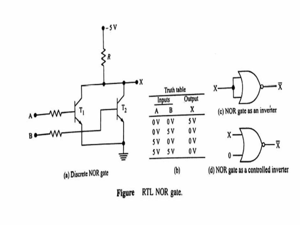
NOR gate
1. Show that the NAND and NOR gates are universal gates.
2. Pulsed operation of logic gates
3. AOI logic – XOR gate, XNOR gate
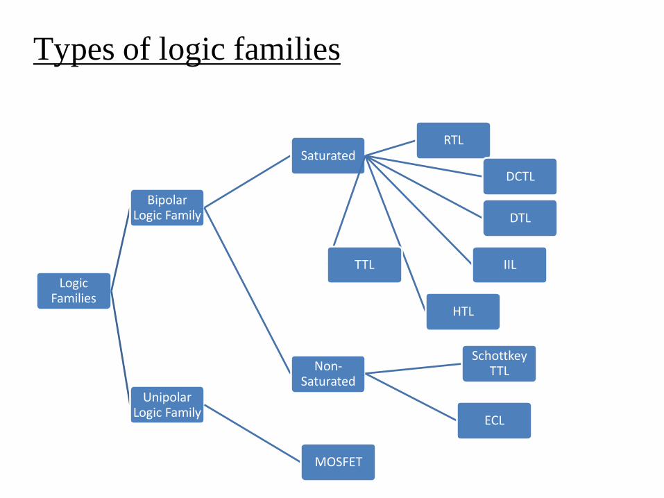
Types of logic families
Logic Families
Bipolar Logic Family
SaturatedRTL
DCTL
IIL
DTL
HTL
TTL
Non-Saturated
Schottkey TTL
ECL
Unipolar Logic Family
MOSFET

BIPOLAR ICs
The main element of a bipolar ICs are Resistors,
Diodes, Capacitors and Transistors.
They can be operated in two ways:
SaturatedNon-Saturated
Saturated Logic: The transistors in the IC are driven
to saturation
Non-Saturated Logic: The transistors in the IC are
not driven to saturation.

BIPOLAR ICs
Saturated Bipolar families are:
Resistor-Transistor logic (RTL),Direct-Coupled transistor logic (DCTL),Integrated-injection logic (IIL),Diode-transistor logic (DTL),High-Threshold logic (HTL) andTransistor-transistor logic (TTL)
Non-Saturated Bipolar families are:
Schottkey TTLEmitter-Coupled logic (ECL)

UNIPOLAR LOGIC FAMILIES
MOS devices are unipolar devices and only
MOSFETs are employed in MOS logic
circuits.
These families are:
PMOS (p-channel MOSFETs)NMOS (n-channel MOSFETs)CMOS (Both p- and n- channel MOSFETs are fabricated on same silicon chip)

151
Basic Logic Families
TTL – Transistor-Transistor Logic based onbipolar transistors.CMOS – Complementary Metal-OxideSemiconductor logic based on metal-oxide-semiconductor field effect transistors(MOSFETs).ECL – Emitter Coupled Logic based onbipolar transistors.

152
General Characteristics of Basic Logic
Families
CMOS consumes very little power, has excellent noise immunity, and is used with a wide range of voltages.TTL can drive more current and uses more power than CMOS.ECL is fast, with poor noise immunity and high power consumption.

1. Classification of logic families
We have seen that different devices use different voltages ranges for their logic
levels
They also differ in other characteristics
In order to assure correct operation when gates are interconnected they are
normally produced in families
The most widely used families are:
Complementary Metal Oxide Semiconductor (CMOS)
Transistor-Transistor Logic (TTL)
Emitter-Coupled Logic (ECL)
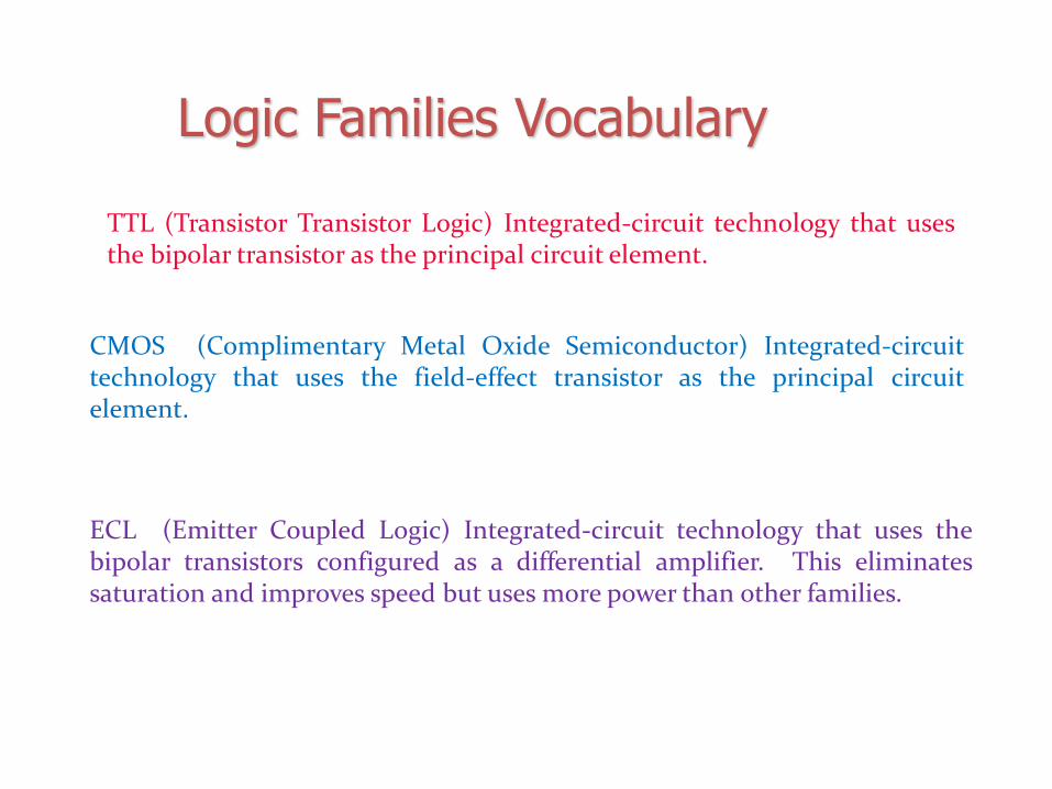
Logic Families Vocabulary
TTL (Transistor Transistor Logic) Integrated-circuit technology that usesthe bipolar transistor as the principal circuit element.
CMOS (Complimentary Metal Oxide Semiconductor) Integrated-circuittechnology that uses the field-effect transistor as the principal circuitelement.
ECL (Emitter Coupled Logic) Integrated-circuit technology that uses thebipolar transistors configured as a differential amplifier. This eliminatessaturation and improves speed but uses more power than other families.

Transistor-transistor logic (TTL)
based on bipolar transistorsone of the most widely used families for small- and medium-scale devices – rarely used for VLSItypically operated from 5V supplytypical noise immunity about 1 – 1.6 Vmany forms, some optimised for speed, power, etc.high speed versions comparable to CMOS (~ 1.5 ns)low-power versions down to about 1 mW/gate
Logic Family Characteristics

Logic Family Characteristics
Complementary metal oxide semiconductor (CMOS)
most widely used family for large-scale devices
combines high speed with low power consumption
usually operates from a single supply of 5 – 15 V
excellent noise immunity of about 30% of supply voltage
can be connected to a large number of gates (about 50)
many forms – some with tPD down to 1 ns
power consumption depends on speed (perhaps 1 mW)

Emitter-coupled logic (ECL)based on bipolar transistors, but removes problems of storage time by preventingthe transistors from saturatingvery fast operation - propagation delays of 1ns or lesshigh power consumption, perhaps 60 mW/gatelow noise immunity of about 0.2-0.25 Vused in some high speed specialist applications, but now largely replaced by highspeed CMOS
Logic Family Characteristics

when the input voltage to a bipolar transistor is high thetransistor turns ON and the output voltage is driven down toits saturation voltage which is about 0.1 Vhowever, saturation of the transistor results in the storage ofexcess charge in the base regionthis increases the time taken to turn OFF the device – an effectknown as storage timethis makes the device faster to turn ON than OFFsome switching circuits increase speed by preventing thetransistors from entering saturation
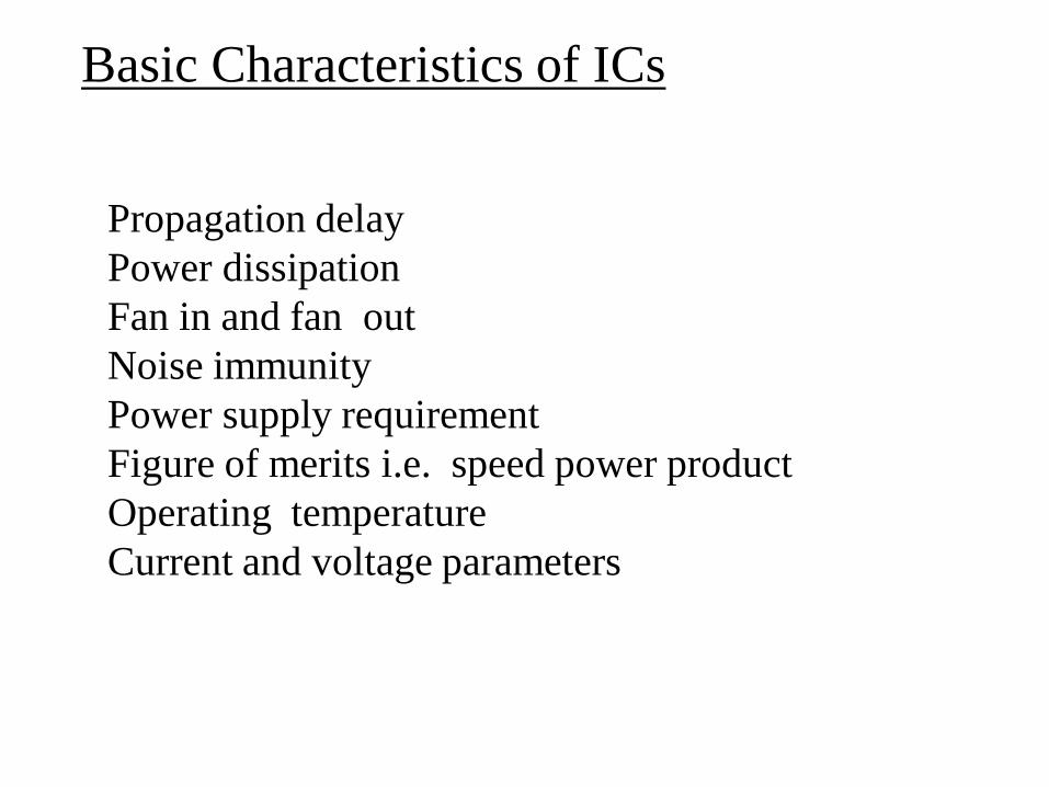
Basic Characteristics of ICs
Propagation delay
Power dissipation
Fan in and fan out
Noise immunity
Power supply requirement
Figure of merits i.e. speed power product
Operating temperature
Current and voltage parameters

Speed of operation
Propagation delay
The speed of operation of an IC is expressed in terms of
propagation delay.
Propagation delay is defined as the time taken for the
output of a gate to change after the inputs have changed
The time difference between the application of input and
appearance of output is also called as propagation delay.

Power dissipation
Power dissipation is the nature of the power consumed by a logic
gate when fully driven by all its inputs.
It is expressed in milli Watts or nano Watts

Fan in
The fan-in of a gate is the number of inputs connected to the gate
without degradation in the voltage levels.
Fan out
Fan out is the maximum number of similar logic gates that a gate
can drive without any degradation in voltage levels.


Noise immunity
The noise immunity of a logic circuit refers to the circuit ability to
tolerate noise without causing spurious changes in the output
voltage.
A quantitative measure of the noise immunity is called noise
margin.
Speed power product : Figure of merit of an IC family
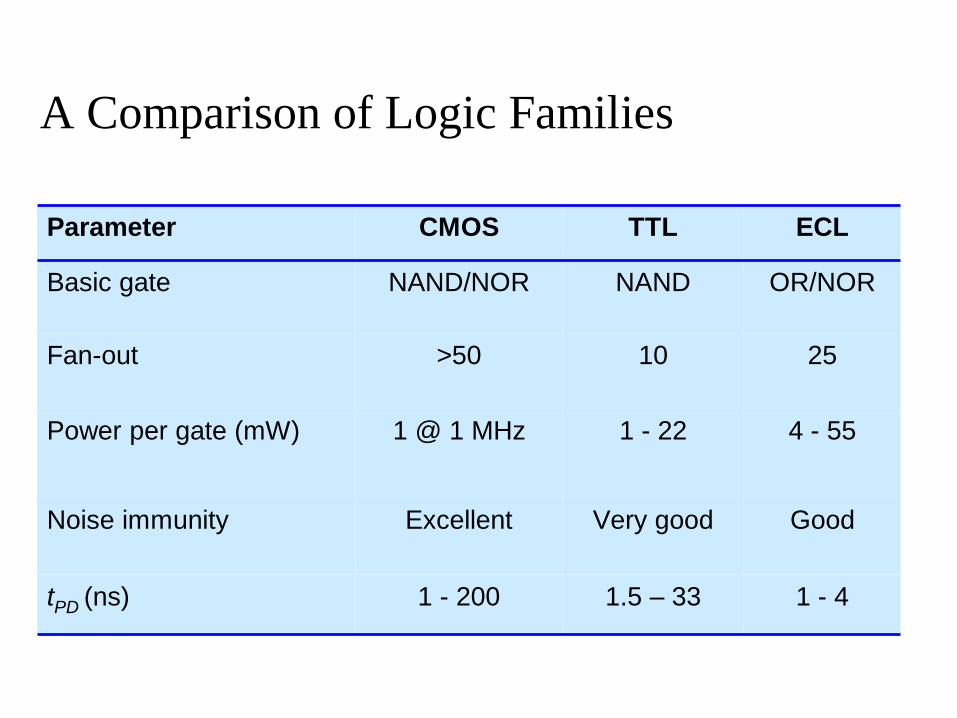
A Comparison of Logic Families
Parameter CMOS TTL ECL
Basic gate NAND/NOR NAND OR/NOR
Fan-out >50 10 25
Power per gate (mW) 1 @ 1 MHz 1 - 22 4 - 55
Noise immunity Excellent Very good Good
tPD (ns) 1 - 200 1.5 – 33 1 - 4
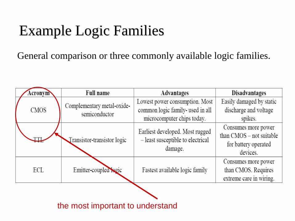
Example Logic Families
General comparison or three commonly available logic families.
the most important to understand