Designing Arithmetic Digital Circuits via Rewriting-Logic
15
Designing Arithmetic Digital Circuits via Rewriting-Logic * MauricioAyala-Rinc´on † Reiner W. Hartenstein ‡ Ricardo P. Jacobi § Carlos H. Llanos ¶ Wander J. de Queroz ‖ Abstract In this work we present our current investigation on use of rewriting-logic as a higher abstraction way to tackle digital design. Rewriting can be used to specify, simulate and even synthesize complex application specific digital systems, which provides a higher abstraction level than current system level languages. To illustrate the possibilities of rewriting-logic in the context of regular hardware structures we describe how to implement different arithmetic operators. Keywords: Rewriting-logic, high level specification and design of digital circuits. 1 Introduction The specification of VLSI systems in an abstract level is still an open problem. Last years we have seen a growing number of users adopting VHDL for logic and register transfer level descriptions. Although VHDL provides constructions similar to traditional programming languages, it is still not suitable for more abstract design representations. System level languages based on C, C++ and Java are emerging, that allow to describe hardware and software modules using the power of high-level programming languages. SpecC (www.specc.org) and SystemC (www.systemc.org) are probably the most popular ones nowadays. It is a common approach to describe a system using one of those languages and translate the hardware modules to VHDL for hardware synthesis [7, 8]. The use of rewriting systems to describe circuits is not a novelty. In recent years some work on applying rewriting techniques to the specification and synthesis of digital processors has been developed. It is worth to mention the work of Kapur and Subramaniam, who have used successors of the well-known Rewriting Rule Laboratory - RRL for verifying arithmetic circuits [10, 11] as well as the work of Arvind’s group that treated the design of processors over simple architectures [15, 16, 1] and synthesis of digital circuits [9]. His approach to architectural specification was to describe simple RISC processors using rewriting systems and to translate these specifications to a standard hardware description language like Verilog for simulation purposes. That approach introduces the cost of program translation, since rewriting systems are only used to specify and not to simulate the design. In [2] we have addressed the specification as well as the simulation via the rewriting-logic environment ELAN [6]. In that work rewriting-logic based specification and further simulation of simple RISC processors were addressed while it was illustrated the design exploration of some architectural alternatives, like branch prediction in speculative processors and out-of-order execution for which the use of logical strategies was essential: the former was simulated by pure rewriting and the latter by logic strategies. In [3] we validated an implementation of the Fast Fourier Transform - FFT over a dynamically reconfigurable systolic array of linear size in ELAN. Classical circuits for the FFT are of size O(n ln(n)) which makes our specification of great relevance. In that work the specification of the systolic array was done via rewriting rules and the control of reconfiguration and execution steps of the processor ∗ Supported by CAPES/DFG Brazilian/German foundations. † Corresponding author. Departamento de Matem´ atica, Universidade de Bras´ ılia, Bras´ ılia D.F., Brasil. [email protected]. Partially supported by CNPq Brazilian council. ‡ Fachbereich Informatik, Universit¨ at Kaiserslautern, Kaiserslautern, Germany. [email protected]. § Departamento de Ciˆ encia da Computa¸ c˜ ao, Universidade de Bras´ ılia, Bras´ ılia D.F., Brasil. [email protected]. ¶ Departamento de Engenharia Mecˆ anica, Universidade de Bras´ ılia, Bras´ ılia D.F., Brasil. [email protected]. ‖ Departamento de Microeletr´ onica, Universidade Federal de Rio Grande do Sul, Porto Alegre, Brasil. 1
-
Upload
independent -
Category
Documents
-
view
2 -
download
0
Transcript of Designing Arithmetic Digital Circuits via Rewriting-Logic
Designing Arithmetic Digital Circuits via Rewriting-Logic∗
Mauricio Ayala-Rincon† Reiner W. Hartenstein‡ Ricardo P. Jacobi§
Carlos H. Llanos¶ Wander J. de Queroz‖
Abstract
In this work we present our current investigation on use of rewriting-logic as a higher abstraction
way to tackle digital design. Rewriting can be used to specify, simulate and even synthesize complex
application specific digital systems, which provides a higher abstraction level than current system level
languages. To illustrate the possibilities of rewriting-logic in the context of regular hardware structures
we describe how to implement different arithmetic operators.
Keywords: Rewriting-logic, high level specification and design of digital circuits.
1 Introduction
The specification of VLSI systems in an abstract level is still an open problem. Last years we have seena growing number of users adopting VHDL for logic and register transfer level descriptions. AlthoughVHDL provides constructions similar to traditional programming languages, it is still not suitable for moreabstract design representations. System level languages based on C, C++ and Java are emerging, that allowto describe hardware and software modules using the power of high-level programming languages. SpecC(www.specc.org) and SystemC (www.systemc.org) are probably the most popular ones nowadays. It is acommon approach to describe a system using one of those languages and translate the hardware modules toVHDL for hardware synthesis [7, 8].
The use of rewriting systems to describe circuits is not a novelty. In recent years some work on applyingrewriting techniques to the specification and synthesis of digital processors has been developed. It is worthto mention the work of Kapur and Subramaniam, who have used successors of the well-known Rewriting
Rule Laboratory - RRL for verifying arithmetic circuits [10, 11] as well as the work of Arvind’s group thattreated the design of processors over simple architectures [15, 16, 1] and synthesis of digital circuits [9].His approach to architectural specification was to describe simple RISC processors using rewriting systemsand to translate these specifications to a standard hardware description language like Verilog for simulationpurposes. That approach introduces the cost of program translation, since rewriting systems are only usedto specify and not to simulate the design. In [2] we have addressed the specification as well as the simulationvia the rewriting-logic environment ELAN [6]. In that work rewriting-logic based specification and furthersimulation of simple RISC processors were addressed while it was illustrated the design exploration of somearchitectural alternatives, like branch prediction in speculative processors and out-of-order execution forwhich the use of logical strategies was essential: the former was simulated by pure rewriting and the latterby logic strategies. In [3] we validated an implementation of the Fast Fourier Transform - FFT over adynamically reconfigurable systolic array of linear size in ELAN. Classical circuits for the FFT are of sizeO(n ln(n)) which makes our specification of great relevance. In that work the specification of the systolicarray was done via rewriting rules and the control of reconfiguration and execution steps of the processor
∗Supported by CAPES/DFG Brazilian/German foundations.†Corresponding author. Departamento de Matematica, Universidade de Brasılia, Brasılia D.F., Brasil. [email protected].
Partially supported by CNPq Brazilian council.‡Fachbereich Informatik, Universitat Kaiserslautern, Kaiserslautern, Germany. [email protected].§Departamento de Ciencia da Computacao, Universidade de Brasılia, Brasılia D.F., Brasil. [email protected].¶Departamento de Engenharia Mecanica, Universidade de Brasılia, Brasılia D.F., Brasil. [email protected].‖Departamento de Microeletronica, Universidade Federal de Rio Grande do Sul, Porto Alegre, Brasil.
1

was done via logic strategies. All that work makes it evident that rewriting(-logic) can be used to specify,simulate and even synthesize complex application specific digital systems, which provides a higher abstractionlevel than current system level languages. In particular, rewriting-logic based specification is a promisingtool for the task of conceiving efficient implementations over dynamically reconfigurable architectures, werethe old notion of software being executed over fixed hardware is being changed by sophisticated notionssuch as “configware” and “morphware” which combine reconfiguration and execution instructions in a newcomputing paradigm adequate for current microelectronic technology development [5].
In this work we are going to specify and design lower levels of hardware by illustrating how rewriting canbe used as a higher abstraction way to tackle digital design of simple arithmetic operators.
We discuss on the rewrite based specification of arithmetic operators and how to obtain equivalentalgebraic expressions which are adequate for assisting the circuit design phases. Three simple arithmeticoperators are considered: Tally, Convolution and Multiplier.
2 Designing circuits for simple arithmetic operators
We suppose the reader is familiar with the notions of rewriting theory as presented in [4] and with simplenotions of digital circuits as in [12].
One of our current goals is to analyze the possibilities of using rewriting to synthesize circuits for simplealgebraic operations. Properties of shift-left (shl) and shift-right (shr) binary operators used in algebraiccircuits synthesis can be naturally described in a rewriting-based language. The set of rewriting rules belowdescribes some properties of these operators over binary number variables w, u and v, that will be furthershowed useful in this context.
2 · w → shl(w) shr(u) + shr(v) → shr(u + v)shl(shr(w)) → w shl(u) + shl(v) → shl(u + v)shr(shl(w)) → w
In addition to the rules for shl and shr, algebraic rules for the operation of selection of the ith lesssignificant bit of a binary number Y , Π(Y, i), can be stated as
Π(Y, 0) → lsb(Y ) Π(Y, succ(n)) → Π(shr(Y ), n)
where lsb denotes the least significant bit operator and succ and 0 are the usual constructors for the naturalnumbers. Then y0 corresponds to lsb(Y ); y1 to lsb(shr(Y )), y2 to lsb(shr2(Y )) and y3 to lsb(shr3(Y )).
To illustrate the possibilities of rewriting in the context of regular hardware structures we describe howto implement different algebraic operators.
2.1 Tally
The tally operator gives the number of 1’s occurring in a binary word X of length n. Then tally may bebuilt by the following algorithm:
function tally(X)
begin
Output := 1;
For i=1 to length(X) do
if X[i]=1 then Output:=Output*2
/* else Output:=Output*1 */
end
where output represent a binary word of n + 1 bits. For instance, if the number of 1’s of X of length 5 is 3the output value is 001000.
tally(X) for X of length n can be formulated as
Πn
i=1if xi = 1 then 2 else 1
2
or equivalentlyΠn
i=1(xi + 1)
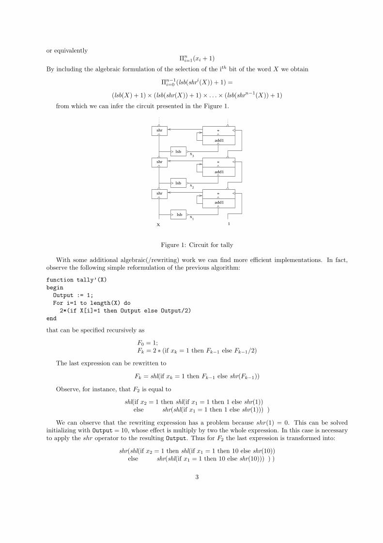
By including the algebraic formulation of the selection of the ith bit of the word X we obtain
Πn−1
i=0(lsb(shri(X)) + 1) =
(lsb(X) + 1) × (lsb(shr(X)) + 1) × . . . × (lsb(shrn−1(X)) + 1)
from which we can infer the circuit presented in the Figure 1.
x1
x
x
2
3
X 1
lsb
lsb
lsb
add1
add1
add1
*
*
*shr
shr
shr
Figure 1: Circuit for tally
With some additional algebraic(/rewriting) work we can find more efficient implementations. In fact,observe the following simple reformulation of the previous algorithm:
function tally’(X)
begin
Output := 1;
For i=1 to length(X) do
2*(if X[i]=1 then Output else Output/2)
end
that can be specified recursively as
F0 = 1;Fk = 2 ∗ (if xk = 1 then Fk−1 else Fk−1/2)
The last expression can be rewritten to
Fk = shl(if xk = 1 then Fk−1 else shr(Fk−1))
Observe, for instance, that F2 is equal to
shl(if x2 = 1 then shl(if x1 = 1 then 1 else shr(1))else shr(shl(if x1 = 1 then 1 else shr(1))) )
We can observe that the rewriting expression has a problem because shr(1) = 0. This can be solvedinitializing with Output = 10, whose effect is multiply by two the whole expression. In this case is necessaryto apply the shr operator to the resulting Output. Thus for F2 the last expression is transformed into:
shr(shl(if x2 = 1 then shl(if x1 = 1 then 10 else shr(10))else shr(shl(if x1 = 1 then 10 else shr(10))) ) )
3

shr
x1
shr
shr
shr
X
shl
1 0lsb
shl
1 0lsb
shr
x2
10
Figure 2: Simplified circuit for tally
from the regularities in the previous expression we can infer the simpler circuit of the Figure 2.The circuit in the Figure 2 has included comparators circuits in order to test the Xi value (0 or 1). This
version is better than the circuit showed in the Figure 1 in several ways; for instance, the comparison andthe shl binary circuits are cheaper than the addition and multiplier circuits used in the first tally version.
2.2 Multiplier
In the previous two examples rewriting is used as an assistant tool for deducing appropriate algebraic termswith many regularities. Detection of regularities is done in an ad hoc manner. We show that in more detailin the following example of multiplication. The desired multiplication may be established as
∑3
i=02i·(yi·X)
that is equal to 20·(y0 ·X) + 21
·(y1 ·X) + 22·(y2 ·X) + 23
·(y3 ·X).By applying the rewrite rules for shl and shr, we obtain
∑3
i=02i·(yi ·X) →∗
y0 ·X + shl(y1 ·X) + shl2(y2 ·X) + shl3(y3 ·X) →∗
y0 ·X + shl(y1 ·X + shl(y2 ·X + shl(y3 ·X)))
were by shln and shrm we denote n and m compositions of the operators shl shr, respectively.Replacing adequately the previous patterns at the expression y0 ·X + shl(y1 ·X + shl(y2 ·X + shl(y3 ·X))),
we obtain ∑3
i=02i·(yi ·X) →∗
y0 ·X + shl(y1 ·X) + shl2(y2 ·X) + shl3(y3 ·X) →∗
y0 ·X + shl(y1 ·X + shl(y2 ·X + shl(y3 ·X)))
from which we can notice the regularities that will be useful for the construction of the desired circuit schema:
lsb(Y )·X + shl(lsb(shr(Y ))·X +︸ ︷︷ ︸
CondAddShift
shl(lsb(shr2(Y ))·X +︸ ︷︷ ︸
shl(lsb(shr3(Y )))·X+︸ ︷︷ ︸
~0)))
CondAddShift CondAddShift
In order to obtain more regularity than in the previous expression we can precede the whole expressionwith “shr(shl(”. But the main problem of the resulting expression is that the first CondAddShift porthas as input y3, that is the last of the four bits of Y that can be computed with sequences of the form
4

shr
lsb
shr
lsb
shr
lsb
shr
lsb
shr
lsb
shr
lsb
shr
lsb
shr
lsb
shr
+
01
X 0
shr
+
01
0X
CY
shr
+
01
X 0
shr
+
01
0X
y
y1
y0
y2
3
Figure 3: Circuit schema for 4-bit numbers multiplication
lsb(shr(shr(. . . (Y ) . . .))). To avoid this problem from the pure beginning observe that
∑3
i=02i·(yi ·X) = 24
·∑
3
i=0shr4−i(yi ·X) →∗
shl4(shr(y3 ·X) + shr2(y2 ·X)+
shr3(y1 ·X) + shr4(y0 ·X)) →∗
shl4(shr(y3 ·X + shr(y2 ·X + shr(y1 ·X + shr(y0 ·X)))))
= shl4(shr(lsb(shr3(Y ))·X+shr(lsb(shr2(Y ))·X+shr(lsb(shr(Y ))·X+shr(lsb(Y )·X)))))
Regularities of the internal expression (without the external shr4) can be described as
shr(lsb(shr3(Y ))·X+︸ ︷︷ ︸
shr(lsb(shr2(Y ))·X+︸ ︷︷ ︸
CondAddShift CondAddShift
shr(lsb(shr(Y ))·X+︸ ︷︷ ︸
shr(lsb(Y )·X +~0)︸ ︷︷ ︸
)))
CondAddShift CondAddShift
And from that expression one can straightforwardly build and schema for the desired circuit schema presentedin the Figure 3.
One of the interesting particularities of rewriting that emerges in this context is that rewriting should bedirected to normal forms that are not simplified as usual. Namely, rewriting should be guided here in such away that the obtained canonical forms are simple from the point of view of hardware implementation. Thatis not the standard in what we could call classical algebraic rewriting, where terms are simplified to shorter
and simpler forms.
5
∧
a3a0 a1 a2
∧
∨∨∨∨
λ
s0 s1 s2 s3
∨∨
¬
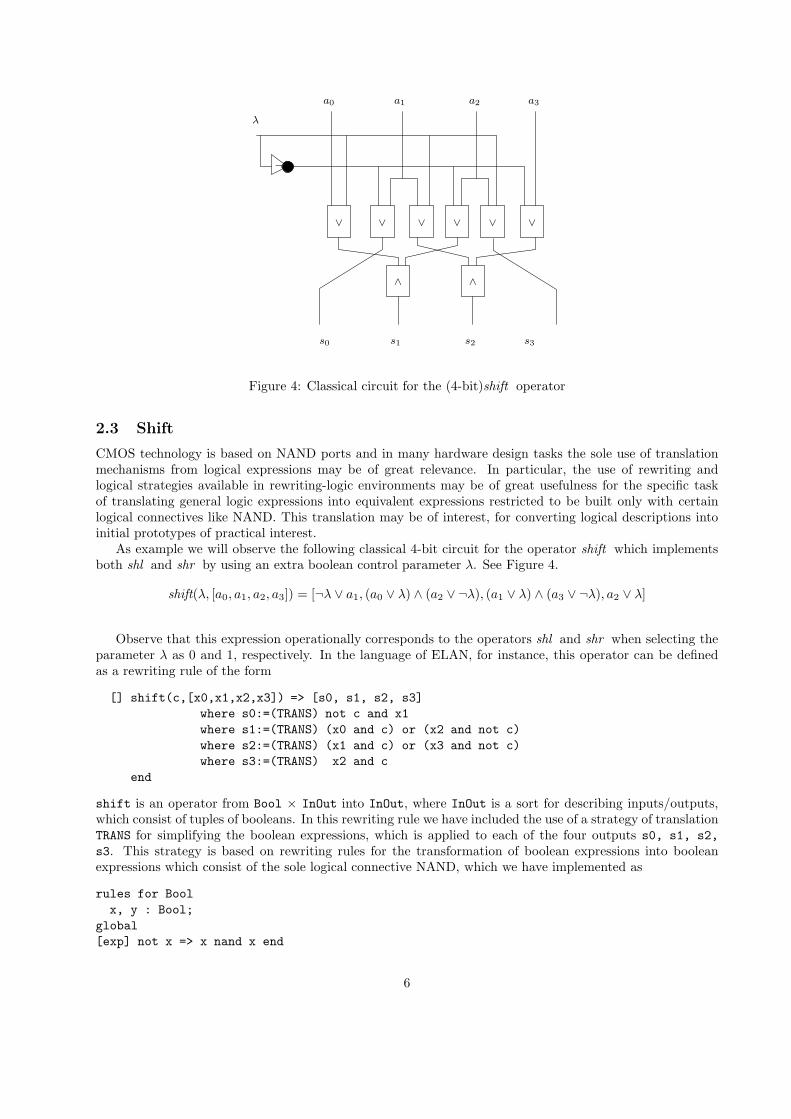
Figure 4: Classical circuit for the (4-bit)shift operator
2.3 Shift
CMOS technology is based on NAND ports and in many hardware design tasks the sole use of translationmechanisms from logical expressions may be of great relevance. In particular, the use of rewriting andlogical strategies available in rewriting-logic environments may be of great usefulness for the specific taskof translating general logic expressions into equivalent expressions restricted to be built only with certainlogical connectives like NAND. This translation may be of interest, for converting logical descriptions intoinitial prototypes of practical interest.
As example we will observe the following classical 4-bit circuit for the operator shift which implementsboth shl and shr by using an extra boolean control parameter λ. See Figure 4.
shift(λ, [a0, a1, a2, a3]) = [¬λ ∨ a1, (a0 ∨ λ) ∧ (a2 ∨ ¬λ), (a1 ∨ λ) ∧ (a3 ∨ ¬λ), a2 ∨ λ]
Observe that this expression operationally corresponds to the operators shl and shr when selecting theparameter λ as 0 and 1, respectively. In the language of ELAN, for instance, this operator can be definedas a rewriting rule of the form
[] shift(c,[x0,x1,x2,x3]) => [s0, s1, s2, s3]
where s0:=(TRANS) not c and x1
where s1:=(TRANS) (x0 and c) or (x2 and not c)
where s2:=(TRANS) (x1 and c) or (x3 and not c)
where s3:=(TRANS) x2 and c
end
shift is an operator from Bool × InOut into InOut, where InOut is a sort for describing inputs/outputs,which consist of tuples of booleans. In this rewriting rule we have included the use of a strategy of translationTRANS for simplifying the boolean expressions, which is applied to each of the four outputs s0, s1, s2,
s3. This strategy is based on rewriting rules for the transformation of boolean expressions into booleanexpressions which consist of the sole logical connective NAND, which we have implemented as
rules for Bool
x, y : Bool;
global
[exp] not x => x nand x end
6

λ
s1 s2
a3a0 a1 a2
s0 s3
NAND
NAND NAND NAND NAND NAND NAND
NANDNANDNANDNAND
Figure 5: NAND circuit for the (4-bit)shift operator
[exp] x xor y => (x or y) and (((not x) nand y) or (x nand (not y))) end
[exp] x and y => not ( x nand y ) end
[exp] x or y => (not x ) nand (not y) end
[log] x or x => x end
[log] x and x => x end
[exp] x imp y => (not x) or y end
[log] not not x => x end
[simpl] (x nand x) nand (x nand x) => x end
end
The strategy TRANS is implemented as
strategies for Bool
implicit
[] TRANS => normalise(log);normalise(exp);normalise(simpl)
end
end
Then when rewriting the expression “shift(λ,[a0,a1,a2,a3])”, for some adequate boolean variablesdefined in the specification, we obtain the following reduced expression which consists of NAND connectivesonly.
(((λ nand λ︸ ︷︷ ︸
)nand a1)nand((λ nand λ︸ ︷︷ ︸
)nand a1)),
((a0 nand λ)nand(a2 nand(λ nand λ︸ ︷︷ ︸
))),
((a1 nand λ)nand(a3 nand(λ nand λ︸ ︷︷ ︸
))),
((a2 nand λ)nand(a2 nand λ))
Regularities are underbraced. Notice that λ nand λ ≡ ¬λ. From the last expression we can build thelogical circuit for the general shift operator which depends only on the connective NAND drawn in theFigure 5.
The ELAN specification is presented in the appendix A. For other desired technologies, based for instancein gates NOR and NOT only, it is very natural to define the adequate translation rewriting rules and strategy.Furthermore, once the desired component is selected we can also define adequate strategies over the original
7
specification for simulating the execution of circuits. We illustrate this by showing how our specification canbe enlarged for simulating the general shift operator.
We add rewriting rules for simulating the application of boolean connectives (notice that we don’t importthe booleans from the ELAN library for having the whole control).
rules for bool
x, y : bool;
global
...
[sim] 0 and 0 => 0 end
[sim] 0 and 1 => 0 end
[sim] 1 and 0 => 0 end
[sim] 1 and 1 => 1 end
[sim] not 1 => 0 end
[sim] not 0 => 1 end
[sim] x or y => not((not x) and (not y)) end
end
Additionally, we add a new rule and a strategy for normalization of booleans restricted to the previousrewriting rules.
strategies for bool
implicit
[] TRANS => normalise(log);normalise(exp);normalise(simpl) end
[] SIMUL => normalise(sim) end
end
rules for InOut
x0, y0, x1, y1, x2, x3, s0, s1, s2, s3, c : bool;
global
...
[SM] shift(c,[x0,x1,x2,x3]) => [s0, s1, s2, s3]
where s0:=(SIMUL) (not c) and x1
where s1:=(SIMUL) (x0 and c) or (x2 and not c)
where s2:=(SIMUL) (x1 and c) or (x3 and not c)
where s3:=(SIMUL) x2 and c end
end
Notice that this strategy, instead of translating the boolean expressions, will apply the boolean operationsto specific given inputs.
Finally, for normalizing ground instances of the shift operator an additional strategy is included for thesort InOut which will allow for normalization via the SM rule for this operator.
strategies for InOut
implicit
...
[] SIMUl => normalise(SM) end
end
Then when providing ground goals of the form shift(0,[1,0,1,0]) we will obtain the correspond-ing output of this component, that is [0,1,0,0] or the shl of the given input [1,0,1,0]. Similarly,shift(1,[1,0,1,1]) gives the result [0,1,0,1], which is the shr of the given input [1,0,1,1].
Unlike the necessary effort which is usual in functional languages like Haskell for hardware design (seefor example [14]), in ELAN we can profit from the natural flexibility provided by the separation between
8

rewriting and logical strategies, has been also of relevance in other contexts of hardware specification suchas the one of reconfigurable architectures, where one can separate the specification of the hardware from thecontrol of reconfiguration and execution steps via logic strategies [3].
3 Conclusions and future work
We exemplified how sequential digital circuits that implement the Tally, Convolution and Multiplier arith-metic operators may be algebraically specified and treated by rewriting. The high degree of abstractionprovided by rewriting systems makes it possible to specify digital circuits in a higher level than the given byother programing environments. This is very important in digital design where the high level of complexitymakes it necessary to handle millions of transistors per square centimeter. Rewriting allows for estimations ofthe behavior of the circuits before logical synthesis phases. Specifying digital circuits by rewriting techniquespermits to extract directly a spacial implementation; in fact, we illustrated how the spacial implementationscan be improved using a time domain implementation, and we showed how to obtain this improvementsstarting from the regularities of the shl and shr operators.
One interesting aspect that emerges from this study is the necessity of new hardware oriented notionsof normal forms, since the algebraic expressions that are more suitable to hardware mapping are those withmore regularities (and consequently those that can be implemented with regular hardware structures) andnot the simplest ones from the algebraic point of view, that is the usual goal when simplifying by rewriting.
Much work remains to be done. In particular, our rewriting specification language is being enriched withother operators which provide additional semantics for sequential/parallel and spatial/temporal hardwarenotions such as delay, multiplexer operators, etc. Furthermore, the translation of rewriting specifications(to high level description hardware languages like Verilog and VHDL and) to the language of layout circuitdesign tools is essential to enable the necessary dynamism between the rewrite based algebraic manipulationand the corresponding circuit design.
References
[1] Arvind and X. Shen. Using Term Rewriting Systems to Design and Verify Processors. IEEE Micro,19(3):36–46, 1999.
[2] M. Ayala-Rincon, R. Hartenstein, R. M. Neto, R. P. Jacobi, and C. Llanos. Architectural Specification,Exploration and Simulation Through Rewriting-Logic. Colombian Journal of Computation, 3(2):20–34,2002.
[3] M. Ayala-Rincon, R. Nogueira, C. Llanos, R. P. Jacobi, and R. W. Hartenstein. Modeling a Recon-figurable System for Computing the FFT in Place via Rewriting-Logic. In Proc. 16th Symposium on
Integrated Circuits and System Design, pages 205–210. IEEE CS Press, 2003.
[4] F. Baader and T. Nipkow. Term Rewriting and All That. Cambridge University Press, 1998.
[5] J. Becker and R. Hartenstein. Configware and Morphware going Mainstream. Journal of Systems
Architecture, 49:127–142, 2003.
[6] P. Borovansky, C. Kirchner, H. Kirchner, and P.-E. Moreau. ELAN from a Rewriting Logic Point ofView. TCS, 285(2):155–185, 2002. See [13].
[7] J. M. P. Cardoso and H. C. Neto. Macro-Based Hardware Compilation of Java Bytecodes into a Dy-namic Reconfigurable Computing System. In Proc. of 7th Symposium on Field Programmable Custom-
Computing Machines, pages 2–11. IEEE CS, 1999.
[8] J. Hammes, R. Rinker, W. Bohm, W. Najjar, B. Draper, and R. Beveridge. Cameron: High Level Lan-guage Compilation for Reconfigurable Systems. In Proc. of the Int. Conference on Parallel Architectures
and Compilation Techniques, pages 236–244. IEEE CS, 1999.
9

[9] J. C. Hoe and Arvind. Hardware Synthesis from Term Rewriting Systems. In Proc. of the 10th IFIP
International Conference on VLSI - VLSI’99, pages 595–619. Kluwer, 1999.
[10] D. Kapur and M. Subramaniam. Mechanizing Verification of Arithmetic Circuits: SRT Division. InProc. 17th FSTTCS, volume 1346 of LNCS, pages 103–122. Springer Verlag, 1997.
[11] D. Kapur and M. Subramaniam. Using an Induction Prover for Verifying Arithmetic Circuits. J. of
Software Tools for Technology Transfer, 3(1):32–65, 2000.
[12] R. H. Katz. Contemporary Logic Design. Addison Wesley, 1993.
[13] N. Martı-Oliet and J. Meseguer, editors. Special Issue on Rewriting Logic and its Applications, volume285. TCS, 2002.
[14] P. Bjesse and K. Claessen and M. Sheeran and S. Singh. Lava: Hardware Design in Haskell. In ACM
Sigplan Int. Conf. on Functional Programming, 1998.
[15] X. Shen and Arvind. Design and Verification of Speculative Processors. Technical Report 400 A,Laboratory for Computer Science - MIT, 1998.
[16] X. Shen and Arvind. Modeling and Verification of ISA Implementations. Technical Report 400 B,Laboratory for Computer Science - MIT, 1998.
A ELAN specification of transformation rules and strategies
Here we included the translation rules for boolean expression we have used in the construction of the circuitfor the general shift operator.
module nxor[varbool]
import global
varbool eq[variable] identifier list[identifier];
end
sort bool varbool InOut;
end
operators global
FOR EACH Id:identifier SUCH THAT Id:=(listExtract) elem(varbool) :
{ Id : varbool; }
@ : (varbool) bool;
0 : bool;
1 : bool;
@ xor @ : (bool bool) bool;
(@ xor @) : (bool bool) bool alias @ xor @:;
not @ : (bool) bool;
not (@) : (bool) bool alias not @:;
(not @) : (bool) bool alias not @:;
@ and @ : (bool bool) bool;
(@ and @) : (bool bool) bool alias @ and @:;
@ or @ : (bool bool) bool;
(@ or @) : (bool bool) bool alias @ or @:;
@ nor @ : (bool bool) bool;
(@ nor @) : (bool bool) bool alias @ nor @:;
@ imp @ : (bool bool) bool;
(@ imp @) : (bool bool) bool alias @ imp @:;
@ nand @ : (bool bool) bool;
(@ nand @) : (bool bool) bool alias @ nand @:;
’[’ @ ’]’ : (bool) InOut;
’[’ @,@ ’]’ : (bool bool) InOut;
’[’ @,@,@ ’]’ : (bool bool bool) InOut;
’[’ @,@,@,@ ’]’ : (bool bool bool bool) InOut;
10

@ SUM2bits @ : (InOut InOut) InOut;
NEG @ : (InOut) InOut;
shift(@,@) : (bool InOut) InOut;
end
stratop global
TRANS : <bool> bs;
SIMUL : <bool> bs;
TRANs : <InOut> bs;
SIMUl : <InOut> bs;
end
rules for bool
x, y : bool;
global
[exp] not x => x nand x end
[exp] x xor y => (x or y) and (((not x) nand y) or (x nand (not y))) end
[exp] x and y => not ( x nand y ) end
[exp] x or y => (not x ) nand (not y) end
[log] x or x => x end
[log] x and x => x end
[exp] x imp y => (not x) or y end
[log] not not x => x end
[simpl] (x nand x) nand (x nand x) => x end
[sim] 0 and 0 => 0 end
[sim] 0 and 1 => 0 end
[sim] 1 and 0 => 0 end
[sim] 1 and 1 => 1 end
[sim] not 1 => 0 end
[sim] not 0 => 1 end
[sim] x or y => not((not x) and (not y)) end
end
strategies for bool
implicit
[] TRANS => normalise(log);normalise(exp);normalise(simpl) end
[] SIMUL => normalise(sim) end
end
rules for InOut
x0, y0, x1, y1, x2, x3, s0, s1, s2, s3, c : bool;
global
[] [x1,x0] SUM2bits [y1,y0] => [s2,s1,s0]
where s0 :=(TRANS) (x0 xor y0)
where s1 :=() (x1 xor y1) xor (x0 and y0)
where s2 :=(TRANS) ((x0 and y0) and (x1 or y1)) or (x1 and y1) end
[] NEG [x1] => [not x1] end
[TR] shift(c,[x0,x1,x2,x3]) => [s0, s1, s2, s3]
where s0:=(TRANS) (not c) and x1
where s1:=(TRANS) (x0 and c) or (x2 and not c)
where s2:=(TRANS) (x1 and c) or (x3 and not c)
where s3:=(TRANS) x2 and c end
[SM] shift(c,[x0,x1,x2,x3]) => [s0, s1, s2, s3]
where s0:=(SIMUL) (not c) and x1
where s1:=(SIMUL) (x0 and c) or (x2 and not c)
where s2:=(SIMUL) (x1 and c) or (x3 and not c)
where s3:=(SIMUL) x2 and c end
end
strategies for InOut
implicit
[] TRANs => normalise(TR) end
[] SIMUl => normalise(SM) end
end
11

end
B Convolution
The convolution of two binary n-arrays X and Y is defined as the (2n − 1)-array Z whose components are given by:
zi = x0yi + x1yi−1 + . . . + xiy0
where all components xj , yj with j 6∈ {0, 1, . . . , n−1} are considered as zero. For instance, z0 = x0y0; z1 = x0y1+x1y0; z2n−1 =xn−1yn−1. We show how to compute the convolution of two 3-arrays X and Y , that is
Z = (x0y0, x1y0 + x0y1, x2y0 + x1y1 + x0y2, x2y1 + x1y2, x2y2)
Each component, zi, of Z can be seen as the internal product of the arrays (x2, x1, x0) and (yi−2, yi−1, yi). Thus Z can bewritten as
([,]4i=0x2yi−2 + x1yi−1 + x0yi)
By including the use of the operators and rewriting rules for the selection of bits of X and Y we obtain:
([,]4i=0lsb(shr2(X))yi−2 + lsb(shr(X)yi−1 + lsb(X)yi ) =
([,]4i=0Σ2
j=0lsb(shrj(X))yi−j ) =
([,]4i=0Σ2
j=0lsb(shrj(X))lsb(shri(shlj(Y ))) )
from which we can infer the circuit in the Figure 6.
lsb
lsb
lsb
0
Y
shl
shl
y
y
y
−1
−2
lsb
lsb
lsb
0
Y
shl
shl
y
y
y
−1
−2
x
lsb
lsb
shr
shr
1
X
shr
shr
*
*
*
+
*
*
*
+
0z z
1
lsb
lsb y
shr lsby
shr lsby
2
shr lsby
0
shr lsb y
xlsb2
x0
−1
1
0
1y
Figure 6: Implementation of the convolution operator
We can observe that the terms associated to yi (i.e., where i 6∈ {0, 1, 2} are effectively set as zero since the shl and shr
operators insert a 0 bit value in the position of the less and most, respectively, significant bit of Y .From the logical point of view the previous circuit is satisfactory, but not from the operational one. In fact, supposing that
all components of the circuit are synchronous (that (in the practice is wrong and) means that the operation of each componentis done in exactly one cycle of the clock), one can observe that there is no synchronization in the time the inputs of the “adder”components of the circuit are ready to be processed by these components. For instance, observe the inputs of the first adder(from left to right) in the Figure 6. The first input (in the order bottom up) is ready after two cycles: one for the simultaneousselection of the less significantly bits of X and Y (that is done through the components lsb) and one for the “multiplier”component which gives x0 ∗y0; the second input is ready after three cycles: two for the simultaneous selection of the second lesssignificantly bit of X and y1 (that is done through shr, shl and lsb components) and one for the multiplier component whichgives x1 ∗ y−1; the third input is similarly showed to be ready after four cycles as x2 ∗ y−2. In the practice the first addercomponent of a circuit implemented in this way will independently give in the third, fourth and fifth cycles as output x0 ∗ y0,x1 ∗ y−1 and x2 ∗ y−2, respectively, and not the desired output that is x0 ∗ y0 + x1 ∗ y−1 + x2 ∗ y−2.
12
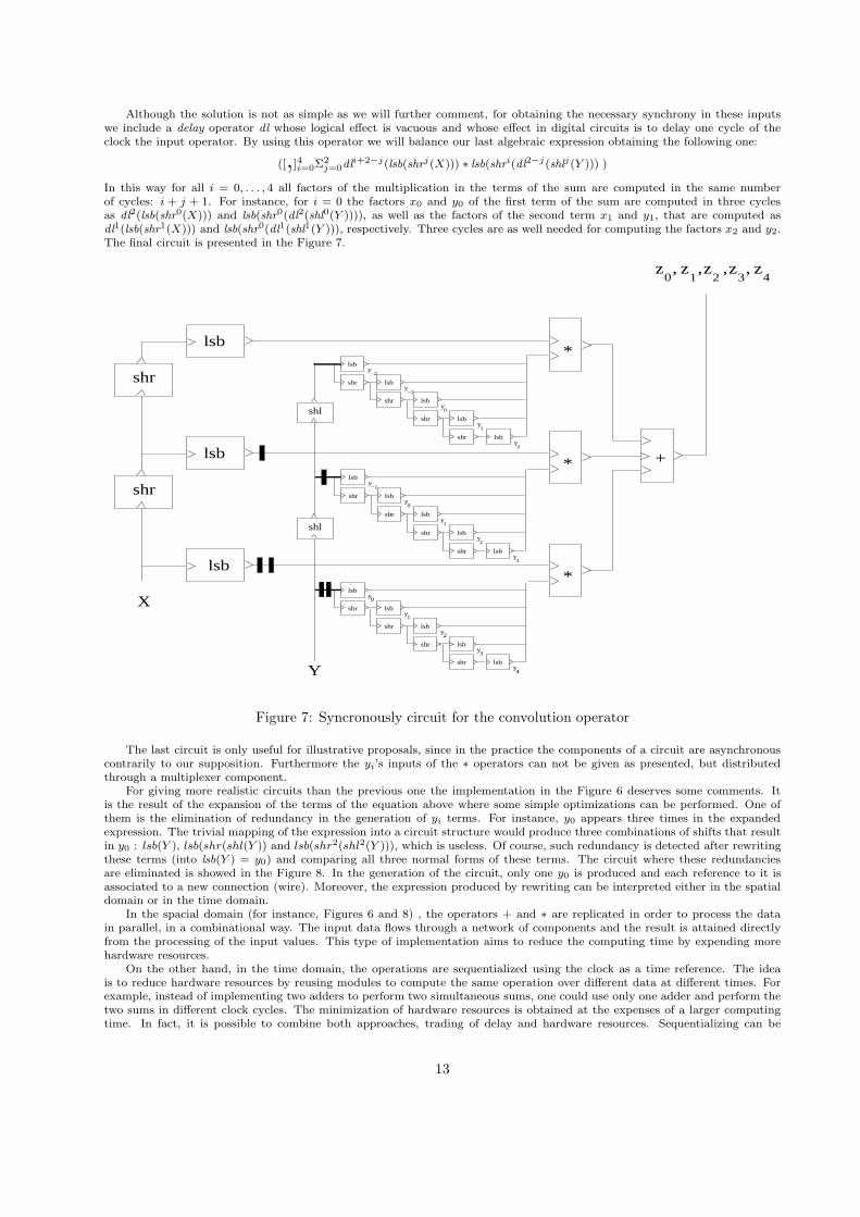
Although the solution is not as simple as we will further comment, for obtaining the necessary synchrony in these inputswe include a delay operator dl whose logical effect is vacuous and whose effect in digital circuits is to delay one cycle of theclock the input operator. By using this operator we will balance our last algebraic expression obtaining the following one:
([,]4i=0Σ2j=0dli+2−j(lsb(shrj(X))) ∗ lsb(shri(dl2−j(shlj(Y ))) )
In this way for all i = 0, . . . , 4 all factors of the multiplication in the terms of the sum are computed in the same numberof cycles: i + j + 1. For instance, for i = 0 the factors x0 and y0 of the first term of the sum are computed in three cyclesas dl2(lsb(shr0(X))) and lsb(shr0(dl2(shl0(Y )))), as well as the factors of the second term x1 and y1, that are computed asdl1(lsb(shr1(X))) and lsb(shr0(dl1(shl1(Y ))), respectively. Three cycles are as well needed for computing the factors x2 and y2.The final circuit is presented in the Figure 7.
z4
lsby
lsby
shr
lsby0
shr
lsby
shr
lsby
shr
−2
−1
1
2
lsby
lsby
shr
lsby2
shr
lsby
shr
lsby
shr
0
1
3
4
lsby
lsby
shr
lsby
shr
lsby
shr
lsby
shr
3
−1
0
1
2
lsb
shr
lsb
shr
X
lsb
+*
*
*
0z z z z
1 2 3, , , ,
shl
shl
Y
Figure 7: Syncronously circuit for the convolution operator
The last circuit is only useful for illustrative proposals, since in the practice the components of a circuit are asynchronouscontrarily to our supposition. Furthermore the yi’s inputs of the ∗ operators can not be given as presented, but distributedthrough a multiplexer component.
For giving more realistic circuits than the previous one the implementation in the Figure 6 deserves some comments. Itis the result of the expansion of the terms of the equation above where some simple optimizations can be performed. One ofthem is the elimination of redundancy in the generation of yi terms. For instance, y0 appears three times in the expandedexpression. The trivial mapping of the expression into a circuit structure would produce three combinations of shifts that resultin y0 : lsb(Y ), lsb(shr(shl(Y )) and lsb(shr2(shl2(Y ))), which is useless. Of course, such redundancy is detected after rewritingthese terms (into lsb(Y ) = y0) and comparing all three normal forms of these terms. The circuit where these redundanciesare eliminated is showed in the Figure 8. In the generation of the circuit, only one y0 is produced and each reference to it isassociated to a new connection (wire). Moreover, the expression produced by rewriting can be interpreted either in the spatialdomain or in the time domain.
In the spacial domain (for instance, Figures 6 and 8) , the operators + and ∗ are replicated in order to process the datain parallel, in a combinational way. The input data flows through a network of components and the result is attained directlyfrom the processing of the input values. This type of implementation aims to reduce the computing time by expending morehardware resources.
On the other hand, in the time domain, the operations are sequentialized using the clock as a time reference. The ideais to reduce hardware resources by reusing modules to compute the same operation over different data at different times. Forexample, instead of implementing two adders to perform two simultaneous sums, one could use only one adder and perform thetwo sums in different clock cycles. The minimization of hardware resources is obtained at the expenses of a larger computingtime. In fact, it is possible to combine both approaches, trading of delay and hardware resources. Sequentializing can be
13

lsb
lsbshr
lsbshr
shr
shr
lsb
lsb
lsb
y0
x1
x2
lsb
lsb
+*
*
*
lsbshr
lsbshr
X Y
shl
shl
y1
y2
y3
y4
y-1
y-2
x0
+*
*
*
+*
*
*
+*
*
*
+*
*
*
z0
z1
z2
z3
z4
Figure 8: Parallel implementation of the convolution operator
increased by processing one bit at a time. In this case, data is input through shift registers, one bit at each clock cycle. Theoutput is obtained one bit at a time, and there is only one output to the circuit.
Thus, based on the same expression produced by rewriting, one can depict the circuit in the Figure 9. There is only one
y2 y1 y0 0 0 0 0
x2 x1 x0
+
*
y2 y1 y00 0 0 0
z2 z1 z0z4 z3
(i = 0)
(i = 4)
Figure 9: Sequential implementation of the convolution operator
operator of each type. The logic product is iterated j times to produce each zi. An additional memory element is introduced inthe feedback path from the logic sum operator and its input. It stores temporary values and produces one output every threecycles, corresponding to a complete iteration over j . In this implementation, Y and X are input in the beginning of a j cycleand are shifted three times to produce the corresponding output. Y is loaded at different positions in a seven bits register,corresponding to the different values of i . The Figure illustrates the position of Y for the cases where i = 0 and i = 4. Theoutput is computed one bit every three cycles and it is input to a shift register that will store the 5 bit value after 15 clockcycles.
An intermediate solution can be obtained by selectively expanding some iterations in the space domain. The circuit in theFigure 10 shows an alternative where the interaction over j is expanded, producing three logic product modules. The shifts
and lsb operators applied on Y and X, in this case, do not iterate over time. In fact, from the hardware point of view, thecomposition of operator lsb(shrk(Y )) is implemented directly by a wire connected to bit k of the register. After X and Y are
14

clock
X
Y
y2 y1 y0 0 0
+
*
z2 z1 z0z4 z3
**
shr
lsbx0
shr
lsblsbx1 x2
shr
lsby0
shr
lsblsby2 y1
clock
Figure 10: Sequential-parallel implementation of the convolution operator
loaded, with two trailing zeros to represent y−1 and y−2, the result is computed in 5 clock cycles.For comparison purposes, the parallel implementation produces the result after one clock cycle, while the sequential one
takes 15 clock cycles.
15