Second-Order Circuits
46
4 Second-Order Circuits In this chapter second-order circuits are studied whose behavior can be described by second-order (ordinary linear) differential equations. The order of a circuit equation equals the number of energy storage elements resulting from all the possible series/parallel combinations of inductors/capacitors. In fact, there is no reason why the scope should be limited to second-order circuits. However, only up to second-order circuits are discussed in detail because the responses of higher-order circuits can be approximated by linear combinations of the responses of first/second-order circuits. By applying the Laplace transform method together with the symbolic computation of MATLAB there is no difficulty in solving higher-order circuits, even in the case where they are driven by sinusoidal sources. Especially in Section 4.5, the concepts of the transfer function and the impulse response are introduced and the input–output relationship of a linear time-invariant (LTI) system is derived in the form of convolution to expose readers to the system theory in order to give a broad view of circuit systems. In Section 4.6, for the purpose of making the readers ready to study the analysis of AC circuits, it is examined how the steady state response of a system to a sinusoidal input is expressed in terms of the frequency response. The frequency response of a system is obtained by substituting s ¼ jo into the transfer function, where o is the angular frequency of the input source applied to the system. 4.1 The Laplace Transform for Second-Order Differential Equations In the previous chapter use of the Laplace transform for solving the first-order circuits was discussed. Here we consider a second-order differential equation d 2 yðtÞ dt 2 þ a 1 dyðtÞ dt þ a 0 yðtÞ¼ xðtÞ with the initial condition yð0Þ¼ y 0 ; y 0 ð0Þ¼ y 1 ð4:1Þ which describes the time-domain relationship between the input xðtÞ and the output yðtÞ of a (circuit) system. Taking the Laplace transform of both sides and using the differentiation property (Table A.2(5) in Appendix A) of the Laplace transform yields s 2 Y ðsÞ y 0 ð0Þ syð0Þþ a 1 ½sY ðsÞ yð0Þ þ a 0 Y ðsÞ¼ XðsÞ ðs 2 þ a 1 s þ a 0 ÞY ðsÞ¼ XðsÞþ y 0 ð0Þþ syð0Þþ a 1 yð0Þ This algebraic equation is solved to obtain the s-domain solution Y ðsÞ¼ XðsÞþ y 0 ð0Þþ syð0Þþ a 1 yð0Þ s 2 þ a 1 s þ a 0 ð4:2Þ Circuit Systems with MATLAB 1 and PSpice 1 Won Y. Yang and Seung C. Lee # 2007 John Wiley & Sons (Asia) Pte Ltd ISBNs: 0 470 85275 5 (cased) 0 470 85276 3 (Pbk)
-
Upload
khangminh22 -
Category
Documents
-
view
6 -
download
0
Transcript of Second-Order Circuits

4
Second-Order Circuits
In this chapter second-order circuits are studied whose behavior can be described by second-order
(ordinary linear) differential equations. The order of a circuit equation equals the number of energy
storage elements resulting from all the possible series/parallel combinations of inductors/capacitors. In
fact, there is no reason why the scope should be limited to second-order circuits. However, only up to
second-order circuits are discussed in detail because the responses of higher-order circuits can be
approximated by linear combinations of the responses of first/second-order circuits. By applying the
Laplace transform method together with the symbolic computation of MATLAB there is no difficulty in
solving higher-order circuits, even in the case where they are driven by sinusoidal sources.
Especially in Section 4.5, the concepts of the transfer function and the impulse response are introduced
and the input–output relationship of a linear time-invariant (LTI) system is derived in the form of
convolution to expose readers to the system theory in order to give a broad view of circuit systems. In
Section 4.6, for the purpose of making the readers ready to study the analysis of AC circuits, it is
examined how the steady state response of a system to a sinusoidal input is expressed in terms of the
frequency response. The frequency response of a system is obtained by substituting s ¼ jo into the
transfer function, where o is the angular frequency of the input source applied to the system.
4.1 The Laplace Transform for Second-Order Differential Equations
In the previous chapter use of the Laplace transform for solving the first-order circuits was discussed.
Here we consider a second-order differential equation
d2yðtÞdt2
þ a1dyðtÞdt
þ a0yðtÞ ¼ xðtÞ with the initial condition yð0Þ ¼ y0; y0ð0Þ ¼ y1 ð4:1Þ
which describes the time-domain relationship between the input xðtÞ and the output yðtÞ of a (circuit)
system. Taking the Laplace transform of both sides and using the differentiation property (Table A.2(5)
in Appendix A) of the Laplace transform yields
s2YðsÞ � y0ð0Þ � syð0Þ þ a1½sYðsÞ � yð0Þ� þ a0YðsÞ ¼ XðsÞ
ðs2 þ a1sþ a0ÞYðsÞ ¼ XðsÞ þ y0ð0Þ þ s yð0Þ þ a1yð0Þ
This algebraic equation is solved to obtain the s-domain solution
YðsÞ ¼ XðsÞ þ y0ð0Þ þ s yð0Þ þ a1yð0Þs2 þ a1sþ a0
ð4:2Þ
Circuit Systems with MATLAB1 and PSpice1 Won Y. Yang and Seung C. Lee# 2007 John Wiley & Sons (Asia) Pte Ltd ISBNs: 0 470 85275 5 (cased) 0 470 85276 3 (Pbk)

This expression will be expanded into partial fractions and the inverse Laplace transform taken to find
yðtÞ. Assuming zero initial conditions yð0Þ ¼ 0 and y0ð0Þ ¼ 0 for simplicity gives the transfer or system
function, which is defined to be the s-domain input–output relationship, i.e. the ratio of the transformed
output to the transformed input (with zero initial conditions) as
GðsÞ ¼ YðsÞXðsÞ ¼
1
s2 þ a1sþ a0ð4:3Þ
Suppose that the input is of the unit step function xðtÞ ¼ usðtÞ with XðsÞ ¼ 1=s. Then the transformed
output becomes
YðsÞ ¼ GðsÞXðsÞ ¼ XðsÞs2 þ a1sþ a0
¼ 1
sðs2 þ 2�orsþ o2r Þ
ð4:4Þ
The process and result of taking the partial fraction expansion of Equation (4.4) depends on the
characteristic roots, i.e. the roots of the characteristic equation, which is formed by setting the
denominator of the transfer function (4.3) to zero:
s2 þ a1sþ a0 ¼ s2 þ 2�orsþ o2r ¼ 0 with or ¼
ffiffiffiffiffia0
p; � ¼ a1=ð2orÞ ¼ a1=2
ffiffiffiffiffia0
p ð4:5Þ
where the discriminant of this equation is
D ¼ a21 � 4a0 ¼ ð2�orÞ2 � 4o2r ¼ 4ð�2 � 1Þo2
r
Depending on the value of the discriminant D or the parameter � (zeta), there are three cases:
(1) The overdamped case with two distinct real roots: j�j > 1
(2) The critically damped case with double real roots: j�j ¼ 1
(3) The underdamped case with two distinct complex roots: 0 � j�j < 1
Before looking into these three cases in detail, let us think about the meaning of the characteristic
equation, i.e. ‘Why do we call it the characteristic equation?’ It is so called because it characterizes the
behavior of the system regardless of the input or the initial conditions in the sense that its roots (called the
characteristic roots) tell about the transient response, i.e. the output of the system during the transient
period; this will be further explored.
4.1.1 Overdamped Case with Two Distinct Real Characteristic Roots
With two distinct real roots
s1; s2 ¼ 12ð�a1 �
ffiffiffiffiffiffiffiffiffiffiffiffiffiffiffiffiffia21 � 4a0
pÞ ¼ ��or �
ffiffiffiffiffiffiffiffiffiffiffiffiffi�2 � 1
por with j�j > 1 ð4:6Þ
the transformed output equation (4.4) can be expanded into the partial fraction form as
YðsÞ ¼ 1
sðs� s1Þðs� s2Þ¼ K0
sþ K1
s� s1þ K2
s� s2ð4:7Þ
for which the inverse Laplace transform is obtained as
yðtÞ ¼ L�1fYðsÞg ¼TableA:1ð3Þ;ð5Þ ðK0 þ K1es1 t þ K2e
s2 tÞ usðtÞ ð4:8Þ
178 Chapter 4 Second-Order Circuits

If a1 > 0 so that s1 < 0 and s2 < 0 with � > 1, this output converges to K0 and the system is said to be
stable. If a1 < 0 so that s1 > 0 and s2 > 0 with � < �1, this output diverges (to 1 or �1) and the
system is said to be unstable in the sense that the output is unbounded for a bounded input like
xðtÞ ¼ usðtÞ.
4.1.2 Critically Damped Case with Double Real Characteristic Roots
With double real roots
s1; s2 ¼ � a1
2¼ �or or or with j�j ¼ 1 ð4:9Þ
the transformed output equation (4.4) can be expanded into the partial fraction form as
YðsÞ ¼ 1
sðs� s1Þ2¼ K0
sþ K1
ðs� s1Þ2þ K2
s� s1ð4:10Þ
for which the inverse Laplace transform is obtained as
yðtÞ ¼ L�1fYðsÞg ¼TableA:1ð3Þ;ð5Þ;ð6ÞðK0 þ K1 t es1 t þ K2e
s2 tÞ usðtÞ ð4:11Þ
If a1 > 0 so that s1 ¼ s2 < 0 with � ¼ 1, this output converges toK0 and the system is said to be stable. If
a1 < 0 so that s1 ¼ s2 > 0 with � ¼ �1, this output diverges and the system is said to be unstable in the
sense that the output is unbounded even for a bounded input like xðtÞ ¼ usðtÞ.
Note. You may wonder whether t e�a t ¼ t=ea t(with a > 0) converges. Apply L’Hospital’s rule (refer to the website
http://tutorial.math.lamar.edu/AllBrowsers/2413/LHospitalsRule.asp.):
limt!1
t e�a t ¼ limt!1
t
eat¼ lim
t!1
1
a eat¼ 0
4.1.3 Underdamped Case with Two Distinct Complex Characteristic Roots
With two distinct complex roots
s1; s2 ¼ 12ð�a1 � j
ffiffiffiffiffiffiffiffiffiffiffiffiffiffiffiffiffi4a0 � a21
pÞ ¼ ��or � j
ffiffiffiffiffiffiffiffiffiffiffiffiffi1� �2
por ¼ ��� jod with 0 � j�j < 1 ð4:12Þ
the transformed output equation (4.4) can be decomposed as
YðsÞ ¼ 1
sðs2 þ 2�orsþ o2r Þ
¼ 1
sððsþ �Þ2 þ o2dÞ
¼ K0
sþ K1ðsþ �Þðsþ �Þ2 þ o2
d
þ K2od
ðsþ �Þ2 þ o2d
ð4:13Þ
for which the inverse Laplace transform is obtained as
yðtÞ ¼ L�1fYðsÞg ¼TableA:1ð3Þ;ð9Þ;ð10Þ ðK0 þ K1e�� t cosodt þ K2e
�� t sinodtÞ usðtÞ ð4:14Þ
Note. There should be no concern about how to get the numerical values of the coefficients Ki’s, because they can be
computed using the formula (A.28) in Appendix A or something similar and they do not affect the behavioral
characteristic of the output.
4.1 The Laplace Transform for Second-Order Differential Equations 179

Note. What is the notion of ‘damped’ contained in the terms ‘overdamped’, ‘critically damped’, and ‘underdamped’?
It means that the amplitude decreases as time goes by.
The feature of the underdamped case that distinguishes it from the other cases is the oscillation (with
the damped frequency ofod ¼ffiffiffiffiffiffiffiffiffiffiffiffiffi1� �2
po r) described by the cosine/sine terms in Equation (4.14), where
or is the undamped resonant frequency for the undamped case with � ¼ 0. If only the real part of the
complex characteristic roots is negative, i.e. ��or ¼ �� < 0, the amplitude of oscillation decreases
(exponentially), where � ¼ �or is the damping constant describing how fast the amplitude decreases.
The key parameter �, which affects the oscillation frequency as well as the damping constant, is called the
damping ratio.
4.1.4 Stability of a System and Location of its Characteristic Roots
To obtain an overview of the relationship between the characteristic roots and the features of the system
in terms of its natural response, it would be good to plot the locations of the characteristic roots on the
complex plane called the s-plane, as depicted in Figure 4.1. From Figure 4.1, the following observations
can be made:
1. The coefficients (a0, a1, �, and or) of the characteristic equation (4.5) or the denominator of the
transfer function (4.3) are solely determined by the system parameters and are not affected by the
input (xðtÞ) or the initial conditions (yð0Þ and y0ð0Þ) of the system. This implies that the characteristic
roots characterize the system itself rather than its outputs.
2. If only a1 > 0 or, equivalently,��or ¼ �� < 0 so that the characteristic roots are located in the left-
half plane (LHP), the system is stable in the sense that the output is bounded for any bounded input
like xðtÞ ¼ usðtÞ. In this case T ¼ 1=� is the time constant, which is defined to be the time taken for
the transient output to reach 63.2 % of its steady state value. On the contrary, if only a1 < 0 or,
equivalently,��or ¼ �� > 0 so that the characteristic roots are located in the right-half plane (RHP),
the system is unstable in the sense that the output can be unbounded for a bounded input like
xðtÞ ¼ usðtÞ.3. The closer the characteristic roots (with od ¼
ffiffiffiffiffiffiffiffiffiffiffiffiffi1� �2
po r � �or ¼ � or � � 0) are to the jo axis,
the tougher the oscillation in the output stemming from the roots becomes, as depicted in Figure 4.1(3).
Figure 4.1 Locations of characteristics roots, the natural responses, and the system stability
180 Chapter 4 Second-Order Circuits

4. If a1 ¼ 0 or, equivalently, ��or ¼ �� ¼ 0 so that the characteristic roots are located on the jo axis
(Figures 4.1(4) and (7)), the system is marginally or neutrally stable in the sense that the output is
bounded for any bounded input that does not have the same mode as the characteristic roots. For
example, suppose a sinusoidal input xðtÞ ¼ cos t usðtÞ is applied to a neutrally stable system having
the transfer function GðsÞ ¼ 2=ðs2 þ 1Þ, where the characteristic roots are obtained as s ¼ � j (lying
on the jo axis) by setting the denominator of GðsÞ to zero. Noting that the Laplace transform of the
input is XðsÞ ¼ Lfcos t usðtÞg ¼TableA:1ð8Þ s=ðs2 þ 1Þ, the transformed output and its inverse Laplace
transform can be found as
YðsÞ ¼ð4:4ÞGðsÞXðsÞ ¼ 2
s2 þ 1
s
s2 þ 1¼ 2s
ðs2 þ 1Þ2!TableA:1ð7Þ
TableA:2ð7ÞyðtÞ ¼ t sin t usðtÞ
which will diverge to 1 as time goes by. However, for any other input than having the frequency
corresponding to the characteristic roots s ¼ � jor with or ¼ 1 rad/s, the system does not have
unbounded output, but has some oscillatory output components with a constant amplitude and of the
undamped resonant frequency or. This shows that the output of a neutrally stable system is generally
bounded except in the event of the input whose mode coincides with the characteristic roots.
Note. The followingMATLAB statements can be typed into the MATLAB command window to check if the above
inverse Laplace transform is correct:
>>syms s; ilaplace(2*s/(s^2þ 1)^2)
ans¼ t*sin(t)
5. The story about the stability of a second-order system in connection with its characteristic roots seems
to be done. How about the stability of higher-order systems havingmore than two characteristic roots?
If only a single characteristic root is in the RHP (Figures 4.1(5) and (6)), the system is unstable. If only
a single real root or two complex characteristic roots are on the jo axis and the other ones are all in the
LHP, the system is neutrally/marginally stable. If and only if all the characteristic roots are in the LHP
(Figures 4.1(1), (2), and (3)), the system is stable. In this context, the imaginary axis, i.e. the jo axis on
the s-plane (s ¼ �þ jo : a complex variable) is the boundary that determines the stability of a system,
where its characteristic roots are plotted on that plane.
4.2 Analysis of Second-Order Circuits
In this section a series RLC circuit, a parallelRLC circuit, and a circuit with twomeshes/nodes are solved,
which are described by a second-order (ordinary linear) differential equation. The responses of higher-
order circuits can be regarded as a linear combination of the responses of first/second-order circuits. The
Laplace transform method together with the symbolic computation of MATLAB may alleviate the
computational difficulty involved in solving higher-order circuits.
4.2.1 A Series RLC Circuit
Consider the circuit of Figure 4.2.1(a) in which the initial values of the inductor current and the capacitor
voltage are
iLð0Þ ¼ I0 and vCð0Þ ¼ V0
respectively. To find the mesh current iðtÞ, we apply KVL to the RLC loop to set up the mesh equation in
the time domain as
vRðtÞ þ vLðtÞ þ vCðtÞ ¼ R iðtÞ þ Ldi ðtÞdt
þ 1
C
ðt�1
iðtÞdt ¼ viðtÞ
4.2 Analysis of Second-Order Circuits 181

and take its Laplace transform (Table A.2(5) and (6)) to write the transformed mesh equation as
R IðsÞ þ L½sIðsÞ � I0� þ1
C
1
sIðsÞ þ 1
s
ð0�1
iðtÞdt� �
¼ ViðsÞ
R þ sL þ 1
sC
� �IðsÞ ¼ ViðsÞ �
1
s
1
C
ð0�1
iðtÞdt� �
þ LI0 ¼ ViðsÞ �V0
sþ L I0 ð4:15Þ
A better way to get this equation is to transform the circuit into its s-domain equivalent (see Figure 3.6),
as depicted in Figure 4.2.1(b) and apply the mesh analysis as if the circuit were made of just resistors and
sources. In either case, Equation (4.15) is solved to obtain the transformed mesh current as
IðsÞ ¼ ViðsÞ � V0=sþ L I0
Rþ s Lþ 1=ðsCÞ ¼ ½sViðsÞ � V0�=Lþ I0s
s2 þ sR=Lþ 1=ðLCÞ ð4:16Þ
and can take its inverse Laplace transform to find iðtÞ.If the voltages across the inductor/capacitor are needed, they can be found by using the V–I
relationships (3.15a) and (3.16b):
VLðsÞ ¼ð3:15aÞsL IðsÞ � L iLð0Þ
VCðsÞ ¼ð3:16bÞ 1
sCIðsÞ þ vCð0Þ
s
Note. Be careful not to make the mistake of missing out the initial condition terms.
The transfer function of this circuit with the source voltage as the input and the mesh current as the
output is
GðsÞ ¼ IðsÞViðsÞ
����with zero initial conditions
V0¼0; I0¼0
¼ð4:16Þ s=L
s2 þ s R=Lþ 1=ðLCÞ
and the characteristic equation obtained by setting its denominator to zero is
s2 þ sR
Lþ 1
LC¼ 0 ð4:17Þ
Note. The notation GðsÞ denoting a transfer function should not be confused with G denoting a conductance.
Figure 4.2.1 The circuit for Example 4.1
182 Chapter 4 Second-Order Circuits

(Example 4.1) Time Responses of a Series RLC Circuit
Consider the series RLC circuit of Figure 4.2.1(a) in which the source voltage and the initial conditions
of the capacitor and inductor are
viðtÞ ¼ Vi usðtÞ ¼ 2usðtÞ ½V� ! ViðsÞ ¼2
s; I0 ¼ 1 ½A�; and V0 ¼
1
2½V� ðE4:1:1Þ
respectively. Noting that the discriminant of the characteristic equation (4.17) is
D ¼ ðR=LÞ2 � 4=ðLCÞ, find the mesh current and the voltages across the inductor and capacitor for
four different sets of values of R, L, and C.
(a) R ¼ 3=2O, L ¼ 1=2H, and C ¼ 1 F ! D ¼ ðR=LÞ2 � 4=ðLCÞ > 0 (overdamped)
The transformed mesh current (4.16) is expanded into the partial fraction form as
IðsÞ ¼ ½sViðsÞ � V0�=Lþ I0s
s2 þ sR=Lþ 1=ðLCÞ ¼ 3þ s
s2 þ 3sþ 2¼ K1
sþ 1þ K2
sþ 2ðE4:1:2Þ
where the coefficients are obtained by using the formula (A.28) in Appendix A as
K1 ¼ðA:28aÞ ðsþ 1ÞIðsÞjs¼�1 ¼sþ 3
sþ 2
����s¼�1
¼ 2 ðE4:1:3aÞ
K2 ¼ðA:28aÞ ðsþ 2ÞIðsÞjs¼�2 ¼sþ 3
sþ 1
����s¼�2
¼ �1 ðE4:1:3bÞ
Thus the inverse Laplace transform of IðsÞ is taken to get the mesh current iðtÞ as
IðsÞ ¼ K1
sþ 1þ K2
sþ 2¼ 2
sþ 1� 1
sþ 2
iðtÞ ¼ L�1 fIðsÞg ¼TableA:1ð5Þ I0 ¼ 1 ½A� for t ¼ 0�
2e�t � e�2t½A� for t � 0
( ðE4:1:4Þ
Noting that this mesh current flows through the inductor and the capacitor in series, the s-domain V–I
relationships (3.15a) and (3.16b) are used to obtain the voltages across them as
VLðsÞ ¼ð3:15aÞsL IðsÞ � L iLð0Þ ¼ðE4:1:1Þ;ðE4:1:2Þ sðsþ 3Þ
2ðs2 þ 3sþ 2Þ �1
2
¼ �1
ðsþ 1Þðsþ 2Þ ¼ � 1
sþ 1þ 1
sþ 2
vLðtÞ ¼ L�1fVLðsÞg ¼TableA:1ð5Þ � e�t þ e�2t ½V� for t � 0 ðE4:1:5Þ
VCðsÞ ¼ð3:16bÞ 1
sCIðsÞ þ vCð0Þ
s¼ðE4:1:1Þ;ðE4:1:2Þ sþ 3
sðsþ 1Þðsþ 2Þ þ1=2
s
¼ 3=2
s� 2
sþ 1þ 1=2
sþ 2þ 1=2
s
vCðtÞ ¼ L�1 fVCðsÞg ¼TableA:1ð5Þ V0 ¼ 1
2½V� for t ¼ 0�
2� 2e�t þ 1
2e�2t½V� for t � 0
8><>: ðE4:1:6Þ
4.2 Analysis of Second-Order Circuits 183

These results might be obtained by using the time-domain v–i relationships (3.1a) and (3.4b):
vLðtÞ ¼ð3:1aÞL diðtÞdt
¼ðE4:1:4Þ 1
2½2ð�1Þ e�t � ð�2Þ e�2t� ¼ �e�t þ e�2t ½V� for t � 0 ðE4:1:7Þ
vCðtÞ ¼ð3:4bÞ 1C
ðt�1
iðtÞdt ¼ 1
C
ðt�1
iðtÞdtþ 1
C
ðt0
iðtÞdt
¼ðE4:1:4ÞvCð0Þ þ
1
C
ðt0
ð2e�t � e�2tÞdt ¼ðF:33Þ V0 � 2e�tjt0 þ 21
2e�2t
��t0
¼ 1
2� 2ðe�t � 1Þ þ 1
2ðe�2t � 1Þ ¼ 2� 2e�t þ 1
2e�2t ½V� for t � 0 ðE4:1:8Þ
However, this method does not seem to be the first choice, because it takes more time and effort than
the Laplace transform approach.
(b) R ¼ 1O, L ¼ 1=2H, and C ¼ 2 F ! D ¼ ðR=LÞ2 � 4=ðLCÞ ¼ 0 (critically damped)
The transformed mesh current (4.16) is expanded into the partial fraction form as
IðsÞ ¼ ½sViðsÞ � V0�=Lþ I0s
s2 þ sR=Lþ 1=ðLCÞ ¼ 3þ s
s2 þ 2sþ 1¼ K1
sþ 1þ K2
ðsþ 1Þ2ðE4:1:9Þ
where the coefficients are obtained by using the formula (A.28) as
K1 ¼ðA:28bÞ d
dsðsþ 1Þ2IðsÞjs¼�1 ¼
d
dsðsþ 3Þjs¼�1 ¼ 1 ðE4:1:10aÞ
K2 ¼ðA:28bÞ ðsþ 1Þ2IðsÞjs¼�1 ¼ sþ 3js¼�1 ¼ 2 ðE4:1:10bÞ
Thus the inverse Laplace transform of IðsÞ is taken to get the mesh current iðtÞ as
IðsÞ ¼ K1
sþ 1þ K2
ðsþ 1Þ2¼ 1
sþ 1þ 2
ðsþ 1Þ2
iðtÞ ¼ L�1fIðsÞg ¼TableA:1ð5Þ;ð6Þ I0 ¼ 1 ½A� for t ¼ 0�
e�t þ 2t e�t ½A� for t � 0
�
The s-domain V–I relationships (3.15a) and (3.16b) are used to obtain the voltages across the inductor
and capacitor as follows:
VLðsÞ ¼ð3:15aÞsL IðsÞ � L iLð0Þ ¼ðE4:1:1Þ;ðE4:1:9Þ sðsþ 3Þ
2ðsþ 1Þ2� 1
2¼ 1=2
sþ 1� 1
ðsþ 1Þ2
vLðtÞ ¼1
2e�t � t e�t ½V� for t � 0 ðE4:1:12Þ
VCðsÞ ¼ð3:16bÞ 1
sCIðsÞ þ vCð0Þ
s¼ðE4:1:1Þ;ðE4:1:9Þ sþ 3
2sðsþ 1Þ2þ 1=2
s
¼ 3=2
s� 1
ðsþ 1Þ2� 3=2
sþ 1þ 1=2
s
vCðtÞ ¼ L�1fVCðsÞg ¼TableA:1ð5Þ;ð6Þ V0 ¼1
2½V� for t ¼ 0�
2� 3
2e�t � t e�t ½V� for t � 0
8><>: ðE4:1:13Þ
184 Chapter 4 Second-Order Circuits
These results could be obtained by using the time-domain v–i relationships (3.1a) and (3.4b) of the
inductor and capacitor. However, the method is not recommended since it takes more time and effort.
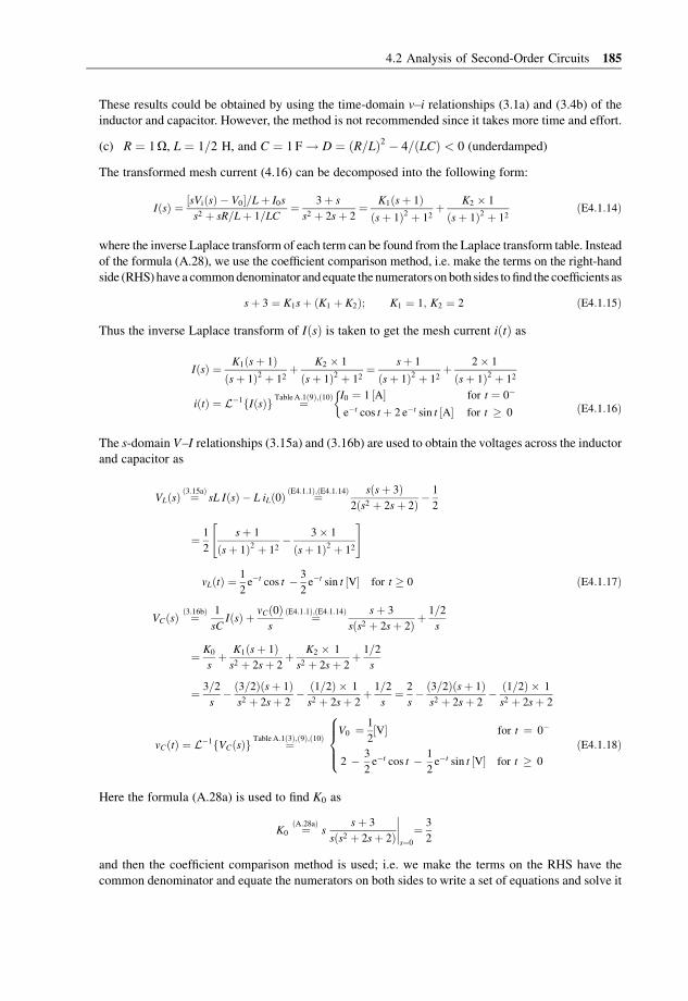
(c) R ¼ 1O, L ¼ 1=2 H, and C ¼ 1 F ! D ¼ ðR=LÞ2 � 4=ðLCÞ < 0 (underdamped)
The transformed mesh current (4.16) can be decomposed into the following form:
IðsÞ ¼ ½sViðsÞ � V0�=Lþ I0s
s2 þ sR=Lþ 1=LC¼ 3þ s
s2 þ 2sþ 2¼ K1ðsþ 1Þ
ðsþ 1Þ2 þ 12þ K2 � 1
ðsþ 1Þ2 þ 12ðE4:1:14Þ
where the inverse Laplace transform of each term can be found from the Laplace transform table. Instead
of the formula (A.28), we use the coefficient comparison method, i.e. make the terms on the right-hand
side (RHS)have a commondenominator andequate the numeratorsonboth sides tofind the coefficients as
sþ 3 ¼ K1sþ ðK1 þ K2Þ; K1 ¼ 1; K2 ¼ 2 ðE4:1:15Þ
Thus the inverse Laplace transform of IðsÞ is taken to get the mesh current iðtÞ as
IðsÞ ¼ K1ðsþ 1Þðsþ 1Þ2 þ 12
þ K2 � 1
ðsþ 1Þ2 þ 12¼ sþ 1
ðsþ 1Þ2 þ 12þ 2� 1
ðsþ 1Þ2 þ 12
iðtÞ ¼ L�1fIðsÞg ¼TableA:1ð9Þ;ð10Þ I0 ¼ 1 ½A� for t ¼ 0�
e�t cos t þ 2 e�t sin t ½A� for t � 0
�ðE4:1:16Þ
The s-domain V–I relationships (3.15a) and (3.16b) are used to obtain the voltages across the inductor
and capacitor as
VLðsÞ ¼ð3:15aÞsL IðsÞ � L iLð0Þ ¼ðE4:1:1Þ;ðE4:1:14Þ sðsþ 3Þ
2ðs2 þ 2sþ 2Þ �1
2
¼ 1
2
sþ 1
ðsþ 1Þ2 þ 12� 3� 1
ðsþ 1Þ2 þ 12
" #
vLðtÞ ¼1
2e�t cos t � 3
2e�t sin t ½V� for t � 0 ðE4:1:17Þ
VCðsÞ ¼ð3:16bÞ 1
sCIðsÞ þ vCð0Þ
s¼ðE4:1:1Þ;ðE4:1:14Þ sþ 3
sðs2 þ 2sþ 2Þ þ1=2
s
¼ K0
sþ K1ðsþ 1Þs2 þ 2sþ 2
þ K2 � 1
s2 þ 2sþ 2þ 1=2
s
¼ 3=2
s� ð3=2Þðsþ 1Þ
s2 þ 2sþ 2� ð1=2Þ � 1
s2 þ 2sþ 2þ 1=2
s¼ 2
s� ð3=2Þðsþ 1Þ
s2 þ 2sþ 2� ð1=2Þ � 1
s2 þ 2sþ 2
vCðtÞ ¼ L�1fVCðsÞg ¼TableA:1ð3Þ;ð9Þ;ð10ÞV0 ¼ 1
2½V� for t ¼ 0�
2 � 3
2e�t cos t � 1
2e�t sin t ½V� for t � 0
8>><>>: ðE4:1:18Þ
Here the formula (A.28a) is used to find K0 as
K0 ¼ðA:28aÞs
sþ 3
sðs2 þ 2sþ 2Þ
����s¼0
¼ 3
2
and then the coefficient comparison method is used; i.e. we make the terms on the RHS have the
common denominator and equate the numerators on both sides to write a set of equations and solve it
4.2 Analysis of Second-Order Circuits 185

for the coefficients as follows:
sþ 3 ¼ K0ðs2 þ 2sþ 2Þ þ sðK1ðsþ 1Þ þ K2Þ¼ ðK0 þ K1Þs2 þ ð2K0 þ K1 þ K2Þsþ 2K0 ðE4:1:19Þ
The coefficient of the second-degree term: K0 þ K1 ¼ 0; K1 ¼ �K0 ¼ �3=2
The coefficient of the first-degree term: 2K0 þ K1 þ K2 ¼ 1; K2 ¼ 1� 2K0 � K1 ¼ �1=2
The coefficient of the constant term: 2K0 ¼ 3; K0 ¼ 3=2 (for crosscheck)
The following statements can be typed into the MATLAB command window to get the same
result:
>> A¼ [1 1 0; 2 1 1; 2 0 0]; b¼ [0;1;3];
>> K¼ A\b
K¼ 1.5000
�1.5000
�0.5000
Note. MATLAB could help muchmore than just solving a set of equations, which will be discussed at the end of this
example.
(d) R ¼ 0O, L ¼ 1=2H, and C ¼ 1=2 F ! D ¼ ðR=LÞ2 � 4=ðLCÞ < 0 (undamped)
The transformed mesh current (4.16) is decomposed into the following form:
IðsÞ ¼ ½sViðsÞ � V0�=Lþ I0s
s2 þ sR=Lþ 1=ðLCÞ ¼ 3þ s
s2 þ 4¼ s
s2 þ 22þ ð3=2Þ � 2
s2 þ 22ðE4:1:20Þ
the inverse Laplace transform of which is
iðtÞ ¼ L�1fIðsÞg ¼TableA:1ð7Þ;ð8Þ I0 ¼ 1 ½A� for t ¼ 0�
cos 2t þ ð3=2Þ sin 2t ½A� for t � 0
(ðE4:1:21Þ
The s-domainV–I relationships (3.15a) and (3.16b) are used to obtain the voltages across the inductor and
capacitor as
VLðsÞ ¼ð3:15aÞsLIðsÞ � LiLð0Þ ¼ðE4:1:1Þ;ðE4:1:20Þ sðsþ 3Þ
2ðs2 þ 4Þ �1
2¼ 1
2
3s
s2 þ 22� 2� 2
s2 þ 22
� �
vLðtÞ ¼3
2cos 2t � sin 2t ½V� for t � 0 ðE4:1:22Þ
VCðsÞ ¼ð3:16bÞ 1
sCIðsÞ þ vCð0Þ
s¼ðE4:1:1Þ;ðE4:1:20Þ 2ðsþ 3Þ
2ðs2 þ 4Þ þ1=2
s¼ 2
s� ð3=2Þs� 2
2ðs2 þ 22Þ
vCðtÞ ¼ L�1fVCðsÞg ¼TableA:1ð3Þ;ð7Þ;ð8ÞV0 ¼
1
2½V� for t ¼ 0�
2� 3
2cos 2t þ sin 2t ½V� for t � 0
8>><>>: ðE4:1:23Þ
(e) Compose the following MATLAB program, save it as an M-file named cir04e01.m, and
run it to get the solutions and plot them for all the cases given above as depicted in
Figure 4.2.2.
186 Chapter 4 Second-Order Circuits

%cir04e01.m for Example 4.1
clear, clf
syms s; Vi¼ 2; Vis¼ Vi/s; I0¼ 1; V0¼ 1/2;
tt¼ [0:500]*0.02; % the time vector for the time interval [0,10]
for m¼ 1:4
if m¼¼ 1, R¼ 3/2; L¼ 1/2; C¼ 1;
elseif m¼¼ 2, R¼ 1; L¼ 1/2; C¼ 2;
elseif m¼¼ 3, R¼ 1; L¼ 1/2; C¼ 1;
else R¼ 0; L¼ 1/2; C¼ 1/2;
end
Is¼ ((s*Vis-V0)/Lþ I0*s)/(s^2þ s*R/Lþ 1/L/C); % Eq. (4.16)
i¼ ilaplace(Is) % the inverse Laplace transform i(t)
VLs¼ s*L*Is - L*I0; vL¼ ilaplace(VLs) % the inductor voltage
VCs¼ Is/s/Cþ V0/s; vC¼ ilaplace(VCs) % the capacitor voltage
for n¼ 1:length(tt)
t¼ tt (n); it(n)¼ eval(i); vLt(n)¼ eval(vL); vCt(n)¼ eval(vC);
end
subplot(220þm), plot(tt,it, tt,vLt, tt,vCt), hold on
end
Note. The result makes us happy with the Laplace transform andMATLAB or equivalent software. On the other hand
it makes us feel sorry for those who have not experienced the amazing usefulness and convenience of such tools.
(Example 4.2) A Series RLC Circuit for Arcing (Ignition)
Consider the series RLC circuit for an ignition system of Figure 4.3.1(a) in which the values of the
voltage source, the resistor R, the inductor L, and the capacitor C are
viðtÞ ¼ Vi usðtÞ ¼ 12usðtÞ ½V� ! ViðsÞ ¼12
s; R ¼ 3O; L ¼ 0:01H; and C ¼ 10�6 F ðE4:2:1Þ
Figure 4.2.2 The output voltage/current of the circuit depicted in Figure 4.2.1 (Example 4.1)
4.2 Analysis of Second-Order Circuits 187

respectively. In this circuit the voltage across the primary coil of the transformer (with a turns ratio of
1:100) is stepped up to 100 times across the secondary coil, which is expected to be high enough to
initiate an arc discharge across the spark plug gap. We will find the voltages across the inductor L and
the capacitor C after t ¼ 0 when the switch is opened. Note the following point:
As will be discussed in the next chapter about magnetically coupled coils, a transformer can step up/
down only the AC voltage, varying with time in its magnitude and polarity. How can the transformer
step up the voltage (across the primary coil) in this circuit having only a DC voltage source? It is
made possible by an almost undamped RLC circuit with the characteristic roots located close to the
jo axis (od � �), which produces oscillatory (AC-like) voltages across the inductor (see Figure
4.1(3)).
To make a quantitative analysis of this circuit for finding the voltages across the inductor and the
capacitor, it is supposed that the switch across the capacitor has been closed for a long time until
t ¼ 0 when the switch is opened. Then at t ¼ 0�, the circuit is expected to reach DC steady state,
where the inductor acts like a short circuit so that the mesh current through R-closed SW-L is
ið0Þ ¼ iLð0�Þ ¼Vi
R¼ 12
3¼ 4A ðE4:2:2Þ
The capacitor voltage at t ¼ 0� is vCð0�Þ ¼ 0V since the capacitor has been shorted by the closed
switch. Note the following:
1. These values of iLð0�Þ and vCð0�Þ are the final (steady state) values for the circuit with the switchclosed for t < 0 and are also the initial values for the circuit with the switch opened at t ¼ 0 because
of the continuity rules on the inductor current and the capacitor voltage.
2. The s-domain equivalent of this circuit with the initial inductor current iLð0Þ represented by a
(transformed) voltage source of L iLð0Þ (see Figure 3.6(b1)) is shown in Figure 4.3.1(b).
(a) Find the inductor voltage vLðtÞ and its maximum amplitude to make sure that the voltage induced
across the secondary coil will be high enough to produce an arc in the air gap of the spark plug.
Applying KVL to the transformed circuit in Figure 4.3.1(b) yields the mesh equation as
Rþ sLþ 1
sC
� �IðsÞ ¼ Vi
sþ L iLð0Þ ðE4:2:3Þ
This equation is solved to get the mesh current as
IðsÞ ¼ Vi=Lþ s ið0Þs2 þ sR=Lþ 1=ðLCÞ ðE4:2:4Þ
Figure 4.3.1 The RLC circuit for Example 4.2
188 Chapter 4 Second-Order Circuits

and then Equation (3.15a) is used to obtain the voltage across the inductor as
VLðsÞ ¼ð3:15aÞsLIðsÞ � LiLð0Þ ¼ðE4:2:4Þ sVi þ s2L ið0Þ � L ið0Þ ½s2 þ sR=L þ 1=ðLCÞ�
s2 þ sR=Lþ 1=ðLCÞ
¼ðE4:2:2Þ sVi � L ðVi=RÞ ½sR=L þ 1=ðLCÞ�s2 þ sR=Lþ 1=ðLCÞ ¼ �Vi=ðRCÞ
s2 þ sR=Lþ 1=ðLCÞðE4:2:5Þ
On the premise that
R
L
� �2
� 4
LC 0 ðunderdampedÞ ðE4:2:6Þ
so that the characteristic equation s2 þ sR=Lþ 1=ðLCÞ ¼ 0 has complex roots, the inverse
Laplace transform of Equation (E4.2.5) yields the inductor voltage as follows:
VLðsÞ ¼ðE4:2:5Þ �½Vi=ðod RCÞ�od
ðsþ �Þ2 þ o2d
ðE4:2:7Þ
with � ¼ R=ð2LÞ ¼ 3=ð2� 0:01Þ ¼ 150; od ¼ffiffiffiffiffiffiffiffiffiffiffiffiffiffiffiffiffiffiffiffiffiffiffiffiffiffiffiffiffiffiffiffiffiffiffiffiffiffiffiffi1=ðLCÞ � ½R=ð2LÞ�2
q� 104
vLðtÞ ¼ L�1fVLðsÞg ¼TableA:1ð9Þ � Vi
odRCe��t sinðodtÞ for t � 0 ðE4:2:8Þ
Now the time derivative of vLðtÞ is set to zero to find the peak time at which the absolute value
of vLðtÞ is maximized:
dvLðtÞdt
¼ðE4:2:8Þ
ðF:27;28;29;30Þ� Vi
odRCe��t½�� sinðodtÞ þ od cosðodtÞ� ¼ 0
tanðodtÞ ¼od
�; t ¼ 1
od
tan�1 od
�þ k�
� ; tpeak ¼
1
od
tan�1 od
�¼ 0:16ms ðE4:2:9Þ
This peak time is within the first period of 2�=od ’ 0:63ms and much earlier than the time
constant 1=� ¼ 1=150 ’ 6:7ms. Therefore,
tpeak 1
�! �tpeak 1 ! e��tpeak ’ 1 ðE4:2:10Þ
which implies that the amplitude of oscillation decreases little at t ¼ tpeak. The peak time
(E4.2.9) can be substituted for t into Equation (E4.2.8) to find the maximum amplitude of the
inductor voltage as
VL;peak ¼ jvLðtpeakÞj ¼Vi
odRCe��tpeak sinðodtpeakÞ ’
ðE4:2:10Þ Vi
odRCsinðtan�1 od
�Þ
¼ Vi
odRC
odffiffiffiffiffiffiffiffiffiffiffiffiffiffiffiffi�2 þ o2
d
p ¼ Vi
RCffiffiffiffiffiffiffiffiffiffiffiffiffiffiffi1=ðLCÞ
p ¼ Vi
R
ffiffiffiffiL
C
r¼ 12
3
ffiffiffiffiffiffiffiffiffiffi10�2
10�6
r¼ 400V ðE4:2:11Þ
This voltage across the primary coil of the transformer (with a turns ratio of 1:100) is stepped up to
100 times across the secondary coil so that the maximum amplitude of the voltage across the spark
plug gap will be
vsp;peak ¼ 100� 400 ¼ 40 kV ðE4:2:12Þ
This voltage may be high enough to break the dielectric strength of the air (in the gap of the spark
plug), amounting to about 3 kV/mm. All these computations as well as the plotting job are
4.2 Analysis of Second-Order Circuits 189

performed in the following MATLAB program cir04e02a.m. Figures 4.3.2(a) and (b) show
vLðtÞ obtained by running this program and that obtained from the PSpice simulation, respectively.
(b) Find the capacitor voltage vCðtÞ and its maximum amplitude to see that it is not so high as to
produce an arc between the two contacts of the switch in parallel with the capacitor.
Noting that the (transformed) mesh current has been obtained as Equation (E4.2.4),
Equation (3.16b) is used to obtain the voltage across the capacitor as
VCðsÞ ¼ð3:16bÞ 1
sCIðsÞþ vCð0Þ
s¼
vCð0Þ¼0
ðE4:2:4Þ Vi=LCþ sVi=ðRCÞs½s2 þ sR=Lþ 1=ðLCÞ� ¼ Vi
1
s� sþR=L� 1=ðRCÞs2 þ sR=Lþ 1=ðLCÞ
� �
¼ Vi
1
s�ðsþ �Þþ f½�� 1=ðRCÞ�=odgod
ðsþ �Þ2 þo2d
!ðE4:2:13Þ
vCðtÞ ¼ L�1fVCðsÞg ¼TableA:1ð3Þ;ð9Þ;ð10ÞVi �Vi e
��t cosðodtÞþ�� 1=ðRCÞ
od
sinðodtÞ� �
for t � 0 ðE4:2:14Þ
Figure 4.3.2 The simulation results for the circuit in Figure 4.3.1
%cir04e02a.m for Example 4.2(a)
clear, clf
Vi¼ 12; R¼ 3; L¼ 0.01; C¼ 1e-6; I0¼ Vi/R; V0¼ 0;
syms s, Vis¼ Vi/s; Is¼ ((s*Vis-V0)/Lþ I0*s)/(s^2þ s*R/Lþ 1/L/C); %Eq.(4.16)
VLs¼ s*L*Is - L*I0; vL¼ ilaplace(VLs) % the inductor voltage
dvL¼ diff(vL), pretty(dvL) % the time derivative of vL(t)
dvL¼ inline(‘6e4*exp(�150*t)*sin(1e4*t)�4e6*exp(�150*t)*cos(1e4*t)’,‘t’);
tpeak¼ fsolve(dvL,1e-4,optimset(‘fsolve’)) % the peak time Eq. (E4.2.9)
t¼ tpeak; vLmax¼ eval(vL) % the peak (maximum) amplitude of vL
t0¼ 0; tf¼ 0.01; N¼ 500;
tt¼ t0þ [0:N]/N*(tf-t0); % the time vector for the time interval [0,0.01s]
for n¼ 1:length(tt)
t¼ tt(n); vLt(n)¼ eval(vL);
end
sigma¼ R/2/L; wd¼ sqrt(1/L/C-sigma^2)
vLt1¼ � Vi/(wd*R*C)*exp(�sigma*tt).*sin(wd*tt); % Eq. (E4.2.8)
plot(tt,real(vLt), tt,vLt1,‘k:’, tpeak*[1 1],[0 vLmax],‘r:’)
190 Chapter 4 Second-Order Circuits

The time derivative of vCðtÞ is now set to zero in order to find the peak time at which the absolute
value of vCðtÞ is maximized, where dvCðtÞ=dt is obtained from taking the inverse Laplace
transform of LfdvCðtÞ=dtg ¼ sVCðsÞ � vCð0Þ:
L dvCðtÞdt
� ¼TableA:2ð5Þ
sVCðsÞ � vCð0Þ ¼ð3:16bÞs
1
sCIðsÞ þ vCð0Þ
s
� �� vCð0Þ ¼
1
CIðsÞ
¼ðE4:2:4ÞVi=ðLCÞ þ sVi=ðRCÞs2 þ sR=Lþ 1=ðLCÞ ¼
Vi
2�LC
ðsþ �Þ þ ð�=odÞod
ðsþ �Þ2 þ o2d
dvCðtÞdt
¼ L�1 1
CIðsÞ
� ¼TableA:1ð9Þ;ð10Þ Vi
2�LCe��t cosðodtÞ þ
�
od
sinðodtÞ� �
¼ 0
od t ¼ tan�1 �od
�
� þ k �; tpeak;C ¼ 1
od
�� tan�1 od
�
� ’ 0:16ms ðE4:2:15Þ
Noting that this peak time is also within the first period of 2�=od ’ 0:63ms and much earlier than
the time constant 1=� ¼ 1=150 ’ 6:7ms so that the amplitude of oscillation decreases little at
t ¼ tpeak;C , the maximum amplitude of the capacitor voltage can be found as
VC;peak ¼ jvCðtpeak;CÞj ¼ðE4:2:14ÞVi � Vi e
��t cosðodtpeak;CÞ þ�� 1=ðRCÞ
od
sinðodtpeak;CÞ� �
cosðodtpeak;CÞ ¼ðE4:2:15Þcos �� tan�1 od
�
� ¼ � cos tan�1 od
�
� ¼ ��ffiffiffiffiffiffiffiffiffiffiffiffiffiffiffiffi
�2 þ o2d
psinðodtpeak;CÞ ¼ðE4:2:15Þ
sin �� tan�1 od
�
� ¼ sin tan�1 od
�
� ¼ odffiffiffiffiffiffiffiffiffiffiffiffiffiffiffiffi
�2 þ o2d
p
0BBB@
1CCCA
’ðE4:2:15Þ
Vi 1� ��ffiffiffiffiffiffiffiffiffiffiffiffiffiffiffiffi�2 þ o2
d
p � �� 1=ðRCÞod
odffiffiffiffiffiffiffiffiffiffiffiffiffiffiffiffi�2 þ o2
d
p" #
¼ Vi
ffiffiffiffiffiffiffiffiffiffiffiffiffiffiffi1=ðLCÞ
pþ 1=ðRCÞffiffiffiffiffiffiffiffiffiffiffiffiffiffiffi
1=ðLCÞp ’ Vi
R
ffiffiffiffiL
C
r¼ 12
3
ffiffiffiffiffiffiffiffiffiffi10�2
10�6
r¼ 400V
,1
RC¼ 1
3� 10�6¼ 333 333 � 1ffiffiffiffiffiffi
LCp ¼ 1ffiffiffiffiffiffiffiffiffiffiffiffiffiffiffiffiffiffiffiffiffiffiffiffiffi
10�2 � 10�6p ¼ 10 000
� �ðE4:2:16Þ
which is close to the amplitude of the inductor voltage vLðtÞ.What is the minimum distance between two contacts of the switch in parallel with the
capacitor such that the dielectric strength of the air between them is not broken by
VC;peak ¼ 400V? It is
dsw;min ¼400V
3000V=mm¼ 0:133mm ðE4:2:17Þ
Readers are invited to compose a MATLAB program cir04e02b.m, which performs all these
computations as well as the plotting job.
Note. It is interesting to note that the ratios of the amplitudes of the voltages across the inductor and the
capacitor to that of the input voltage source Vi are commonly close to the voltage magnification ratio given by
Equation (8.19) as
Q ¼ vL;peak
Vi
’ vC;peak
Vi
’ðE4:2:11Þ;ðE4:2:16Þ 1
R
ffiffiffiffiL
C
rð4:18Þ
4.2 Analysis of Second-Order Circuits 191

4.2.2 A Parallel RLC Circuit
Consider the circuit of Figure 4.4.1(a) in which the initial values of the inductor current and the capacitor
voltage are
iLð0Þ ¼ I0 and vCð0Þ ¼ V0
respectively. To find the voltage vðtÞ at the top node, KCL can be applied to the top node to set up the node
equation in the time domain as
iRðtÞ þ iLðtÞ þ iCðtÞ ¼v ðtÞR
þ 1
L
ðt�1
vðtÞdtþ CdvðtÞdt
¼ iiðtÞ
and its Laplace transform (Table A.2(5) and (6)) taken to write the transformed node equation as
VðsÞR
þ 1
L
1
sVðsÞ þ 1
s
ð0�1
vðtÞdt� �
þ C½sVðsÞ � V0� ¼ IiðsÞ
1
Rþ 1
sLþ s C
� �VðsÞ ¼ IiðsÞ �
1
s
1
L
ð0�1
vðtÞdt� �
þ CV0 ¼ IiðsÞ �I0
sþ CV0 ð4:19Þ
A better way to get this equation is to transform the circuit into its s-domain equivalent, as depicted in
Figure 4.4.1(b), and apply KCL to the top node to write the node equation (4.19) directly. In either case,
Equation (4.19) is solved to obtain the transformed node voltage as
VðsÞ ¼ IiðsÞ � I0=sþ C V0
1=Rþ s C þ 1=ðsLÞ ¼½s IiðsÞ � I0�=C þ V0s
s2 þ s=ðRCÞ þ 1=ðLCÞ ð4:20Þ
and its inverse Laplace transform is taken to find vðtÞ.If the currents through the inductor/capacitor are needed, they can be found by using the V–I
relationships (3.15b) and (3.16a):
ILðsÞ ¼ð3:15bÞ 1
sLVðsÞ þ iLð0Þ
s
ICðsÞ ¼ð3:16aÞs CVðsÞ � C vCð0Þ
Note. Care should be taken here not to make the a mistake of missing out the initial condition terms.
Figure 4.4.1 The circuit for Example 4.3
192 Chapter 4 Second-Order Circuits

Note that the transfer function of this circuit with the source current as the input and the node voltage as
the output is
GðsÞ ¼ VðsÞIiðsÞ
����with zero initial conditions
V0¼0; I0¼0
¼ s=C
s2 þ s=ðRCÞ þ 1=ðLCÞ
and the characteristic equation obtained by setting its denominator to zero is
s2 þ s
RCþ 1
LC¼ 0 ð4:21Þ
(Example 4.3) Time Responses of a Parallel RLC Circuit
Consider the parallel RLC circuit of Figure 4.4.1(a) in which the source current and the initial
conditions of the inductor and capacitor are
iiðtÞ ¼ 50 sin 2t usðtÞ ½A� !TableA:1ð7ÞIiðsÞ ¼
50� 2
s2 þ 22; I0 ¼ 0A; and V0 ¼ 0V ðE4:3:1Þ
respectively. Noting that the discriminant of the characteristic equation (4.21) is D ¼ ½1=ðRCÞ�2�4=ðLCÞ, find the node voltage for four different sets of values of R, L, and C.
(a) R ¼ 2=3O, C ¼ 1=2 F, and L ¼ 1H ! D ¼ ½1=ðRCÞ�2 � 4=ðLCÞ > 0 (overdamped)
The transformed node voltage (4.20) is decomposed into the following form:
VðsÞ ¼ ½s IiðsÞ � I0�=C þ V0s
s2 þ s=ðRCÞ þ 1=ðLCÞ ¼200 s
ðs2 þ 22Þðs2 þ 3sþ 2Þ
¼ K1
sþ 1þ K2
sþ 2þ K3 sþ K4 � 2
s2 þ 22ðE4:3:2Þ
where the coefficients are obtained by using the formula (A.28) in Appendix A together with the
coefficient comparison method as
K1 ¼ðA:28aÞðsþ 1ÞVðsÞjs¼�1¼ ðsþ 1Þ 200 s
ðs2 þ 22Þðsþ 1Þðsþ 2Þ
����s¼�1
¼ �40 ðE4:3:3aÞ
K2 ¼ðA:28aÞðsþ 2ÞVðsÞjs¼�2¼ ðsþ 2Þ 200 s
ðs2 þ 22Þðsþ 1Þðsþ 2Þ
����s¼�2
¼ 50 ðE4:3:3bÞ
200s ¼ K1ðsþ 2Þðs2 þ 22Þ þ K2ðsþ 1Þðs2 þ 22Þ þ ðK3sþ 2K4Þðs2 þ 3sþ 2Þ
¼ ðK1 þ K2 þ K3Þs3 þ ð2K1 þ K2 þ 3K3 þ 2K4Þs2
þ ð4K1 þ 4K2 þ 2K3 þ 6K4Þsþ ð8K1 þ 4K2 þ 4K4Þ ðE4:3:3cÞ
The coefficient of the third-degree term: K1 þ K2 þ K3 ¼ 0; K3 ¼ �K1 � K2 ¼ 40� 50 ¼ �10
The coefficient of the zeroth-degree term: 8K1 þ 4K2 þ 4K4 ¼ 0; K4 ¼ �2K1 � K2 ¼ 30
The coefficient of the second-degree term: 2K1 þ K2 þ 3K3 þ 2K4 ¼ 0 (for crosscheck)
The coefficient of the first-degree term: 4K1 þ 4K2 þ 2K3 þ 6K4 ¼ 200 (for crosscheck)
4.2 Analysis of Second-Order Circuits 193

Thus the inverse Laplace transform of VðsÞ is taken to get the node voltage vðtÞ as
VðsÞ ¼ K1
sþ 1þ K2
sþ 2þ K3 sþ K4 � 2
s2 þ 22¼ �40
sþ 1þ 50
sþ 2þ�10 sþ 30� 2
s2 þ 22
vðtÞ ¼ L�1fVðsÞg ¼TableA:1ð5Þ;ð7Þ;ð8Þ � 40e�t þ 50e�2t � 10 cos 2t þ 30 sin 2t ½V� for t � 0 ðE4:3:4Þ
Noting that this node voltage is applied across the inductor and the capacitor in parallel, the s-domain
V–I relationships (3.15b) and (3.16a) or the time-domain v–i relationships (3.1b) and (3.4a) could be
used to obtain the currents through each of them if necessary.
(b) R ¼ 1O, C ¼ 1=2 F, and L ¼ 2H ! D ¼ ½1=ðRCÞ�2 � 4=ðLCÞ ¼ 0 (critically damped)
The transformed node voltage (4.20) is decomposed into the following form:
VðsÞ ¼ ½s IiðsÞ � I0�=C þ V0s
s2 þ s=ðRCÞ þ 1=ðLCÞ ¼200 s
ðs2 þ 22Þðs2 þ 2sþ 1Þ ¼K1
sþ 1þ K2
ðsþ 1Þ2þ K3 sþ K4 � 2
s2 þ 22ðE4:3:5Þ
where
K1 ¼ðA:28bÞ d
dsðsþ 1Þ2VðsÞ
��s¼�1
¼ d
ds
200 s
s2 þ 22
� �����s¼�1
¼ 200ð s2 þ 4Þ � s� 2s
ðs2 þ 4Þ2
�����s¼�1
¼ 24 ðE4:3:6aÞ
K2 ¼ðA:28bÞðsþ 1Þ2VðsÞ��s¼�1
¼ 200 s
s2 þ 22
����s¼�1
¼ �40 ðE4:3:6bÞ
200s ¼ K1ðsþ 1Þðs2 þ 22Þ þ K2 ðs2 þ 22Þ þ ðK3sþ 2K4Þðs2 þ 2sþ 1Þ¼ ðK1 þ K3Þs3 þ ðK1 þ K2 þ 2K3 þ 2K4Þs2
þ ð4K1 þ K3 þ 4K4Þsþ ð4K1 þ 4K2 þ 2K4Þ ðE4:3:6cÞ
The coefficient of the third-degree term: K1 þ K3 ¼ 0; K3 ¼ �K1 ¼ �24
The coefficient of the zeroth-degree term: 4K1 þ 4K2 þ 2K4 ¼ 0; K4 ¼ �2K1 � 2K2 ¼ 32
The coefficient of the second-degree term: K1 þ K2 þ 2K3 þ 2K4 ¼ 0 (for crosscheck)
The coefficient of the first-degree term: 4K1 þ K3 þ 4K4 ¼ 200 (for crosscheck)
Thus the inverse Laplace transform of VðsÞ is taken to get the node voltage vðtÞ as
VðsÞ ¼ K1
sþ 1þ K2
ðsþ 1Þ2þ K3 sþ K4 � 2
s2 þ 22¼ 24
sþ 1þ �40
ðsþ 1Þ2þ�24 sþ 32� 2
s2 þ 22
vðtÞ ¼ L�1fVðsÞg ¼TableA:1ð5Þ;ð6Þ ;ð7Þ;ð8Þ24 e�t � 40 t e�t � 24 cos 2t þ 32 sin 2t½V� for t � 0 ðE4:3:7Þ
(c) R ¼ 1O, C ¼ 1=2 F, and L ¼ 1H ! D ¼ ½1=ðRCÞ�2 � 4=ðLCÞ < 0 (underdamped)
The transformed node voltage (4.20) is decomposed into the following form:
VðsÞ ¼ ½s IiðsÞ � I0�=C þ V0s
s2 þ s=ðRCÞ þ 1=ðLCÞ ¼200 s
ðs2 þ 22Þðs2 þ 2sþ 2Þ
¼ K1ðsþ 1Þ þ K2 � 1
ðsþ 1Þ2 þ 12þ K3 sþ K4 � 2
s2 þ 22ðE4:3:8Þ
194 Chapter 4 Second-Order Circuits

where
200s ¼ ðK1sþ K1 þ K2 Þðs2 þ 22Þ þ ðK3sþ 2K4Þðs2 þ 2sþ 2Þ
¼ ðK1 þ K3Þs3 þ ðK1 þ K2 þ 2K3 þ 2K4Þs2
þ ð4K1 þ 2K3 þ 4K4Þsþ ð4K1 þ 4K2 þ 4K4ÞðE4:3:9Þ
>> A¼ [1 0 1 0; 1 1 2 2; 4 0 2 4; 4 4 0 4]; b¼ [0 0 200 0]; K¼ A^�1*b.’
K¼ 20 �60 �20 40
Thus the inverse Laplace transform of VðsÞ is taken to get the node voltage vðtÞ as
VðsÞ ¼ K1ðsþ 1Þ þ K2 � 1
ðsþ 1Þ2 þ 12þ K3 sþ K4 � 2
s2 þ 22¼ 20ðsþ 1Þ � 60� 1
ðsþ 1Þ2 þ 12þ�20 sþ 40� 2
s2 þ 22
vðtÞ ¼ L�1fVðsÞg ¼TableA:1ð7Þ;ð8Þ ;ð9Þ;ð10Þ20e�t cos t � 60e�t sin t � 20 cos 2t þ 40 sin 2t½V� for t � 0 ðE4:3:10Þ
>> syms s; v¼ ilaplace (200* s/(s^2þ 4)/(s^2þ 2*sþ 2))
v¼ �20*cos(2*t)þ 40*sin(2*t) þ20*exp(�t)*cos(t) �60*exp(�t)*sin(t)
(d) R ¼ 1O(open), C ¼ 1=2 F, and L ¼ 1=2H ! D ¼ ½1=ðRCÞ�2 � 4=ðLCÞ < 0 (undamped)
The transformed node voltage (4.20) is decomposed into the following form:
VðsÞ ¼ ½s IiðsÞ � I0�=C þ V0s
s2 þ s=ðRCÞ þ 1=ðLCÞ ¼200 s
ðs2 þ 22Þðs2 þ 12Þ
¼ K1sþ K2 � 1
s2 þ 12þ K3 sþ K4 � 2
s2 þ 22ðE4:3:11Þ
where
200s ¼ ðK1sþ K2Þðs2 þ 22Þ þ ðK3sþ 2K4Þðs2 þ 1Þ
¼ ðK1 þ K3Þs3 þ ðK2 þ 2K4Þs 2 þ ð4K1 þ K3Þsþ ð4K2 þ 2K4Þ ðE4:3:12Þ
>> A¼ [1 0 1 0; 0 1 0 2; 4 0 1 0; 0 4 0 2]; b¼ [0 0 200 0]; K¼ A\b.’
K¼ 66.6667 0 �66.6667 0
>> format rat, K % for fractional form of numeric values
K¼ 200/3 0 �200/3 0
Thus the inverse Laplace transform of VðsÞ is taken to get the node voltage vðtÞ as
VðsÞ ¼ ð200=3Þ ss2 þ 12
þ ð�200=3Þ ss2 þ 22
vðtÞ ¼ L�1fVðsÞg ¼TableA :1ð8Þð200=3Þ cos t � ð200=3Þ cos 2t½V� for t � 0
ðE4:3:13Þ
>> syms s; v¼ ilaplace(200*s/(s^2þ4)/(s^2þ1))
v¼ 200/3*cos(t) �200/3*cos(2*t)
(e) You may compose the following MATLAB program, save it as an M-file named cir04e03.m,
and run it to get the solutions and plot them for all the cases (a), (b), (c), and (d) given above, as
depicted in Figure 4.4.2.
4.2 Analysis of Second-Order Circuits 195

%cir04e03.m
clear, clf
syms s
t0¼ 0; tf¼ 20; N¼ 1000; tt ¼ t0þ[0:N]*(tf�t0)/N; % Simulation interval
Iis¼ 50*2/(s^2þ2^2); V0¼ 0; I0¼ 0; % Eq. (E4.3.1)
for m¼ 1:4
if m¼ ¼ 1, R¼ 2/3; C¼ 1/2; L¼ 1;
elseif m¼ ¼ 2, R¼ 1; C¼ 1/2; L¼ 2;
elseif m¼ ¼ 3, R¼ 1; C¼ 1/2; L¼ 1;
else R¼ inf; C¼ 1/2; L¼ 2;
end
G¼ 1/R; Vs¼ ((s*Iis-I0)/CþV0*s)/(s^2þs*G/Cþ1/L/C); % Eq. (4.20)
v¼ ilaplace(Vs) % the inverse Laplace transform
for n¼ 1:length(tt)
t¼ tt(n); vt(n)¼ eval(v);
end
subplot(220þm), plot(tt, vt)
end
(Example 4.4) Design of a Parallel RLC Circuit for Triggering
Consider the parallel RLC circuit of Figure 4.5.1(a) in which the capacitor C is normally charged from
the DC voltage source of 12 V when the switch is connected to position a and then is discharged to
supply the stored energy to the resistor R ¼ 3O after the switch is moved to position b. The design
objective is to determine the values of L and C such that R dissipates the energy more than 1 J during the
first period of 0.1 s just after the switch is flipped to position b. More specifically, the voltage vðtÞ acrossor the current through Rwill be made to oscillate 5 times for one time constant of T ¼ 0:5 s. This designspecification can be expressed in terms of the parameters of the damping constant � and the damped
frequency od as follows:
� ¼ �or ¼1
T¼ 1
0:5¼ 2 ½1=s� and od ¼ 2�
5
T
� �¼ 20� ½rad=s� ðE4:4:1Þ
If only the circuit conforms to this specification, the oscillatory voltage with an amplitude of about 12 V
is expected to make about 2 J of energy dissipated in R ¼ 3O for 0.1 s:
Figure 4.4.2 The output voltage of the circuit depicted in Figure 4.4.1 (Example 4.3)
196 Chapter 4 Second-Order Circuits

ER ¼ð1:9Þð0:10
1
Rv2ðtÞdt � 1
3
ð0:10
ð12 sinodtÞ2dt ¼ðF:14Þ 122
6
ð0:10
ð1� cos 2odtÞdt ¼ 2:4 J ðE4:4:2Þ
(a) To determine the values of L and C such that the design specification is met, the characteristic
equation (4.21) of the supposedly underdamped parallel RLC circuit will be written as
s2 þ 1
RCsþ 1
LC¼ ðsþ �Þ2 þ o2
d ¼ s2 þ 2�sþ ð�2 þ o2dÞ ¼ðE4:4:1Þ
s2 þ 4sþ ð4þ 400�2Þ ðE4:4:3Þ
This implies that the values of L and C should be determined as
1
RC¼ 4; C ¼ 1
4R¼ 1
12F ðE4:4:4aÞ
1
LC¼ 4þ 400�2 ’ 3951:8; L ¼ 1
3951:8C¼ 12
3951:8’ 0:003H ðE4:4:4bÞ
(b) With the values of L and C determined in (a), find the node voltage vðtÞ of the circuit. For the
s-domain equivalent in Figure 4.5.1(b), the node voltage that is produced by the current source of
CvCð0Þ corresponding to the initial capacitor voltage is
VðsÞ ¼ð4:20Þ C vCð0Þ1=Rþ s C þ 1=ðsLÞ ¼
V0s
s2 þ s=ðRCÞ þ 1=ðLCÞ ¼12s
ðsþ �Þ2 þ o2d
¼ K1ðsþ �Þðsþ �Þ2 þ o2
d
þ K2 od
ðsþ �Þ2 þ o2d
ðE4:4:5Þ
with K1 ¼ 12; K2 ¼ �12�=od ¼ �24=20� ¼ �0:382
Since the absolute value of the coefficient of the second term (jK2j ¼ 0:382) is much less than that
of the first term (jK1j ¼ 12), the node voltage can be approximated by just the first term as
vðtÞ ¼ L�1fVðsÞg ¼TableA:1ð10ÞK1e
��t cosodt ¼ 12e�2t cos 20�t ½V� ðE4:4:6Þ
(c) With the node voltage obtained in (b), find the energy dissipated in R for the first period of 0.1 s:
ER ¼ð0:10
1
Rv2ðtÞdt ’
ðE4:4:6Þ 1
3
ð0:10
ð12e�2t cos 20� tÞ2dt ¼ðF:15Þ 122
6
ð0:10
e�4tð1þ cos 40� tÞdt
’ 24
ð0:10
e�4tdt ¼ðF:33Þ 24 1
�4e�4t
��0:10¼ 6ð1� e�0:4Þ ’ 1:98 J ðE4:4:7Þ
(d) All of the above computations for analysis can be done by running the following MATLAB
program cir04e04.m. In Figure 4.5.2 it plots the approximate node voltage (E4.4.6) together
with the exact one obtained by using ilaplace( ), which is the MATLAB function for the
inverse Laplace transform.
Figure 4.5.1 The circuit for Example 4.4
4.2 Analysis of Second-Order Circuits 197

%cir04e04.m
clear, clf
syms s
Vi¼ 12; R¼ 3; L¼ 0.003; C¼ 1/12; vC0¼ Vi;
Vs¼ C*vC0/(1/Rþ1/s/Lþs*C); % Eq. (E4.4.5)
v¼ ilaplace(Vs) % the inverse Laplace transform
t0¼ 0; tf¼ 2; N¼ 500; tt¼ t0 þ [0:N]/N*(tf�t0);
for n¼ 1:length(tt)
t¼ tt(n); vt(n)¼ eval(v);
end
sigma¼ 1/2/R/C; wd¼ sqrt(1/L/C-sigma^2);
K1¼ Vi; K2¼ �Vi*sigma/wd; vt1¼ K1*exp(�2*tt).*cos(20*pi*tt); % Eq. (E4.4.6)
plot(tt,vt, tt,vt1,‘:’)
Power_of_R¼ inline(‘48*exp(�4*t).*cos(20*pi*t).^2’,‘t’);
Energy_dissipated_i n_R¼ quad(Power_of_R,0,0.1) % Eq. (E4.4.7)
4.2.3 Two-Mesh/Node Circuit
Once a given circuit with its initial conditions is transformed into its s-domain equivalent, it can be dealt
with it as if it consisted of sources and resistors only, where the passive elements have impedances (R, sL,
or 1=ðsCÞ) that can be thought of as generalized resistances. The number of inductors/capacitors or
meshes/nodes makes no essential difference. The same criterion is used for determining which one of
mesh analysis and node analysis has a computational advantage (see Section 2.6):
1. Which is fewer, the number of mesh equations, (b� nþ 1), or that of node equations, (n� 1)? Note
that b is the number of branches having an element (between the two nodes) and n is the number of
nodes in a circuit with every source removed (see Section 1.4.4).
2. Which is easier, converting all the sources into voltage sources or current sources? Note that it is easy
to set up the mesh equations for circuits having no current sources and the node equations for circuits
having no voltage sources. In this context, we had better choose the analysis method before
transforming the initial conditions into their s-domain equivalent sources and then transform them
into voltage or current sources depending on the analysis method.
3. Which do you want to find, current or voltage?
(Example 4.5) A Two-Mesh/Node Circuit
Consider the circuit of Figure 4.6(a) in which the values of the source voltage, the resistors, the
inductor, and the capacitor are
Vi ¼ 1V; R1 ¼1
2O; R2 ¼
1
2O; L ¼ 1
4H; and C ¼ 1 F ðE4:5:1Þ
Figure 4.5.2 The output voltage of the circuit depicted in Figure 4.5.1
198 Chapter 4 Second-Order Circuits

respectively. Suppose the switch has been connected to the DC voltage source Vi for a long time before
t ¼ 0 when it is flipped to the ground. Since the circuit is supposed to be in the DC steady state where
the inductor L is like shorted and the capacitor C is like opened, the (initial) values of the inductor
current and the capacitor voltage at t ¼ 0 are found to be
I0 ¼ iLð0Þ ¼ Vi=R1 ¼ 1=ð1=2Þ ¼ 2A and V0 ¼ vCð0Þ ¼ Vi ¼ 1V ðE4:5:2Þ
Figures 4.6(b) and (c) show the s-domain equivalents with the initial conditions represented by voltage
and current sources that suit the mesh/node analysis, respectively.
(a) Mesh Analysis
The formula (2.12) for the s-domain equivalent in Figure 4.6(b) can be used to write the mesh
equation as
s=4þ 1=2 �1=2�1=2 1=2þ 1=2þ 1=s
� �I1ðsÞI2ðsÞ
� �¼ 1=2
�1=s
� �ðE4:5:3Þ
which yields
sþ 2 �2
�s 2sþ 2
" #I1ðsÞ
I2ðsÞ
" #¼
2
�2
" #
I1ðsÞI2ðsÞ
" #¼ 1
2ðs2 þ 2sþ 2Þ2ðsþ 1Þ 2
s sþ 2
" #2
�2
" #¼ 2
ðsþ 1Þ2 þ 12
ðsþ 1Þ � 1
�1
" #ðE4:5:4Þ
i1ðtÞ ¼ L�1fI1ðsÞg ¼TableA:1ð9Þ;ð10Þ2e�tðcos t � sin tÞ usðtÞ½A� ðE4:5:5aÞ
i2ðtÞ ¼ L�1f I2ðsÞg ¼TableA:1ð9Þ �2e�t sin t usðtÞ ½A� ðE4:5:5bÞ
Figure 4.6 The circuit for Example 4.5
4.2 Analysis of Second-Order Circuits 199

The s-domain V–I relationship (3.16b) can also be used to get the capacitor voltage as
VCðsÞ ¼ð3:16bÞ 1
sCI2ðsÞ þ
vCð0Þs
¼ðE4:5:2Þ;ðE4:5:4Þ �2
sðs2 þ 2sþ 2Þ þ1
s¼ ðsþ 1Þ þ 1
ðsþ 1Þ2 þ 12;
vCðtÞ ¼ e�tðcos t þ sin tÞ usðtÞ ½V� ðE4:5:6Þ
(b) Node Analysis
The formula (2.10) for the s-domain equivalent in Figure 4.6(c) can be used towrite the node equation as
4=sþ 2þ 2 �2
�2 2þ s
� �V1ðsÞV2ðsÞ
� �¼ 2=s
1
� �ðE4:5:7Þ
which yields
4ðsþ 1Þ �2s
�2 sþ 2
� �V1ðsÞV2ðsÞ
� �¼
2
1
� �
V1ðsÞV2ðsÞ
� �¼ 1
4ðs2 þ 2sþ 2Þsþ 2 2s
2 4ðsþ 1Þ
� �2
1
� �¼ 1
ðsþ 1Þ2 þ 12
sþ 1
ðsþ 1Þ þ 1
� �ðE4:5:8Þ
v1ðtÞ ¼ e�t cos t usðtÞ ½V� ðE4:5:9aÞv2ðtÞ ¼ e�tðcos t þ sin tÞ usðtÞ ½V� ðE4:5:9bÞ
The s-domain V–I relationship (3.15b) is also used to obtain the inductor current as
ILðsÞ ¼ð3:15bÞ 1
sL½�V1ðsÞ� þ
iLð0Þs
¼ðE4:5:2Þ;ðE4:5:8Þ � 4ðsþ 1Þsðs2 þ 2sþ 2Þ þ
2
s¼ 2ðsþ 1Þ � 2� 1
ðsþ 1Þ2 þ 12
iLðtÞ ¼ 2e�tðcos t � sin tÞ usðtÞ ½A� ðE4:5:10Þ
4.2.4 Circuits Having Dependent Sources
The following example illustrates that transformed (s-domain) equivalents are good for analyzing
circuits regardless of the existence of dependent sources in the circuits.
(Example 4.6) A Circuit with a Dependent Source
Let us apply the mesh analysis and the node analysis to the circuit of Figure 4.7(a) to find the
expression of the transformed output voltage VoðsÞ in terms of the transformed input source voltage
ViðsÞ.
(a) Mesh Analysis
First, the controlling variable V2ðsÞ is expressed in terms of I1ðsÞ and I2ðsÞ as
V2ðsÞ ¼ð3:16bÞ 1
sC2
IC2ðsÞ þ vC2
ð0Þs
¼ 1
sC2
½I1ðsÞ � I2ðsÞ� þvC2
ð0Þs
ðE4:6:1Þ
Then the circuit is transformed into the s-domain equivalent with the initial conditions represented by
voltage sources as depicted in Figure 4.7(b), and the mesh equation is written as
R1 þ R2 þ 1=ðsC2Þ �½R2 þ 1=ðsC2Þ��½R2 þ 1=ðsC2Þ� 1=ðsC1Þ þ R2 þ 1=ðsC2Þ
� �I1ðsÞI2ðsÞ
� �¼ ViðsÞ � vC2ð0Þ=s
vC2ð0Þ=s� vC1ð0Þ=s� KV2ðsÞ
� �ðE4:6:2Þ
200 Chapter 4 Second-Order Circuits

Equation (E4.6.1) is substituted for V2ðsÞ into the right-hand side (RHS) of Equation (E4.6.2), and theunknown terms on the RHS are moved to the LHS to write
R1þR2þ1=ðsC2Þ �½R2þ1=ðsC2Þ��½R2þð1�KÞ=ðsC2Þ� 1=ðsC1ÞþR2þð1�KÞ=ðsC2Þ
" #I1ðsÞI2ðsÞ
" #¼
ViðsÞ�vC2ð0Þ=sð1�KÞvC2ð0Þ=s�vC1ð0Þ=s
" #
sðR1þR2ÞC2þ1 �ðsR2C2þ1Þ�½sR2C1C2þð1�KÞC1� C2þsR2C1C2þð1�KÞC1
" #I1ðsÞI2ðsÞ
" #¼
sC2ViðsÞ�C2vC2ð0Þð1�KÞC1C2vC2ð0Þ�C1C2vC1ð0Þ
" # ðE4:6:3Þ
With the assumption of zero initial conditions vC1ð0Þ ¼ 0 and vC2
ð0Þ ¼ 0 for simplicity, this equation
is solved to obtain the mesh currents as
I1ðsÞI2ðsÞ
� �¼ sC2ViðsÞ
s2R1R2C1C22 þ s½ðR1 þ R2ÞC2
2 þ ð1� KÞR1C1C2� þ C2
C2 þ s R2C1C2 þ ð1� KÞC1
s R2C1C2 þ ð1� KÞC1
� �ðE4:6:4Þ
Thus the output voltage is
VoðsÞ ¼ KV2ðsÞ ¼ðE4:6:1Þ K
sC2
½I1ðsÞ � I2ðsÞ�
¼ðE4:6:4Þ K
s2R1R2C1C2 þ s½ðR1 þ R2ÞC2 þ ð1� KÞR1C1� þ 1ViðsÞ
ðE4:6:5Þ
(b) Node Analysis
To apply the node analysis, the circuit is transformed into the s-domain equivalent with the initial
conditions represented by current sources and the independent/dependent sources converted into
current sources,
Figure 4.7 The circuit for Example 4.6
4.2 Analysis of Second-Order Circuits 201

as depicted in Fig. 4.7(c), and then the node equation is written as
1=R1 þ sC1 þ 1=R2 �1=R2
�1=R2 1=R2 þ s C2
� �V1ðsÞV2ðsÞ
� �¼ ViðsÞ=R1 þ C1vC1
ð0Þ þ sC1KV2ðsÞC2vC2
ð0Þ
� �ðE4:6:6Þ
To solve this equation for V1ðsÞ and V2ðsÞ, we move the unknown term sC1KV2ðsÞ on the RHS to the
left-hand side (LHS) and rearrange the equation as
R2 þ s R1R2C1 þ R1 �R1 � sK R1R2C1
�1 1þ s R2C2
� �V1ðsÞV2ðsÞ
� �¼ R2 ViðsÞ þ R1R2C1vC1ð0Þ
R2C2vC2ð0Þ
� �ðE4:6:7Þ
With the assumption of zero initial conditions vC1ð0Þ ¼ 0 and vC2
ð0Þ ¼ 0 for simplicity, this equation
is solved for the node voltages as
V1ðsÞV2ðsÞ
� �¼ R2 ViðsÞ
s2R1R22C1C2 þ sR2½ðR1 þ R2ÞC2 þ ð1� KÞR1C1� þ R2
1þ s R2C2
1
� �ðE4:6:8Þ
Thus the output voltage is
VoðsÞ ¼ KV2ðsÞ ¼ðE4:6:8Þ K
s2R1R2C1C2 þ s½ðR1 þ R2ÞC2 þ ð1� KÞR1C1� þ 1ViðsÞ ðE4:6:9Þ
(c) Mesh/Node Analysis Using MATLAB
All the above computations can be performed by running the following MATLAB program
cir04e06.m.
%cir04e06.m
clear, clf
syms s R1 R2 C1 C2 K Vis
sC1¼ s*C1; sC2¼ s*C2;
display(‘(a)’)
Z¼ [R1þR2þ1/sC2 �(R2þ1/sC2); �(R2þ(1-K)/sC2) 1/sC1þR2þ(1-K)/sC2];
Is¼ Z\[Vis; 0]; % Eq. (E4.6.3) -> (E4.6.4)
Vos¼ K/sC2*(Is(1)-Is(2)); % Eq. (E4.6.5)
pretty(simplify(Vos))
display(‘(b)’)
Y¼ [1/R1þsC1þ1/R2 �1/R2-sC1*K; �1/R2 1/R2þsC2];
Vs¼ Y\[Vis/R1; 0]; % Eq. (E4.6.6) -> (E4.6.8)
Vos¼ K*Vs(2); % Eq. (E4.6.9)
pretty(simplify(Vos))
>> cir04e06
K Vis�������������������������������
2
R2 s C2 þ C2 R2 s C1 R1 � C1 K R1 s þ 1 þ R1 s C2 þ C1 R1 s
4.2.5 Thevenin Equivalent Circuit
The following example illustrates the fact that transformed (s-domain) equivalents are also effective for
finding Thevenin equivalents.
202 Chapter 4 Second-Order Circuits
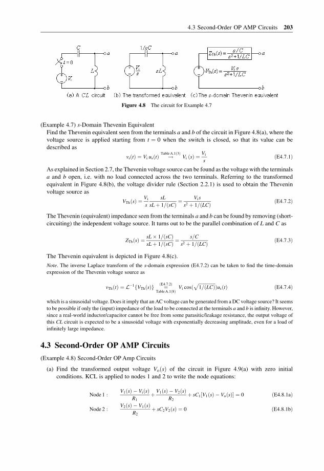
(Example 4.7) s-Domain Thevenin Equivalent
Find the Thevenin equivalent seen from the terminals a and b of the circuit in Figure 4.8(a), where the
voltage source is applied starting from t ¼ 0 when the switch is closed, so that its value can be
described as
viðtÞ ¼ Vi usðtÞ !TableA:1ð3ÞVi ðsÞ ¼
Vi
sðE4:7:1Þ
As explained in Section 2.7, the Thevenin voltage source can be found as the voltagewith the terminals
a and b open, i.e. with no load connected across the two terminals. Referring to the transformed
equivalent in Figure 4.8(b), the voltage divider rule (Section 2.2.1) is used to obtain the Thevenin
voltage source as
VThðsÞ ¼Vi
s
sL
sLþ 1=ðsCÞ ¼Vis
s2 þ 1=ðLCÞ ðE4:7:2Þ
The Thevenin (equivalent) impedance seen from the terminals a and b can be found by removing (short-
circuiting) the independent voltage source. It turns out to be the parallel combination of L and C as
ZThðsÞ ¼sL� 1=ðsCÞsLþ 1=ðsCÞ ¼
s=C
s2 þ 1=ðLCÞ ðE4:7:3Þ
The Thevenin equivalent is depicted in Figure 4.8(c).
Note. The inverse Laplace transform of the s-domain expression (E4.7.2) can be taken to find the time-domain
expression of the Thevenin voltage source as
vThðtÞ ¼ L�1fVThðsÞg ¼ðE4:7:2Þ
TableA:1ð8ÞVi cosð
ffiffiffiffiffiffiffiffiffiffiffiffiffiffiffi1=ðLCÞ
pÞusðtÞ ðE4:7:4Þ
which is a sinusoidal voltage. Does it imply that an AC voltage can be generated from aDC voltage source? It seems
to be possible if only the (input) impedance of the load to be connected at the terminals a and b is infinity. However,
since a real-world inductor/capacitor cannot be free from some parasitic/leakage resistance, the output voltage of
this CL circuit is expected to be a sinusoidal voltage with exponentially decreasing amplitude, even for a load of
infinitely large impedance.
4.3 Second-Order OP AMP Circuits
(Example 4.8) Second-Order OP Amp Circuits
(a) Find the transformed output voltage VoðsÞ of the circuit in Figure 4.9(a) with zero initial
conditions. KCL is applied to nodes 1 and 2 to write the node equations:
Node 1 :V1ðsÞ � ViðsÞ
R1
þ V1ðsÞ � V2ðsÞR2
þ sC1½V1ðsÞ � VoðsÞ� ¼ 0 ðE4:8:1aÞ
Node 2 :V2ðsÞ � V1ðsÞ
R2
þ sC2V2ðsÞ ¼ 0 ðE4:8:1bÞ
Figure 4.8 The circuit for Example 4.7
4.3 Second-Order OP AMP Circuits 203

Regarding the pair of two resistors R3 and R4 in series as a voltage divider and applying the virtual
short principle (Remark 1.2(2)) for the OP Amp with negative feedback, the voltage at node 2,
which is the positive input terminal of the OP Amp, can be written as
V2ðsÞ ¼ VþðsÞ ¼virtual shortV�ðsÞ ¼voltage divider R 3
R3 þ R4
VoðsÞ
This implies
VoðsÞ ¼ KV2ðsÞ with K ¼ R 3 þ R4
R3
ðE4:8:2Þ
Substituting this into Equation (E4.8.1), the node equations can be rewritten in matrix–vector
form as
1=R1 þ sC1 þ 1=R2 �1=R2 � sC1 K
�1=R2 1=R2 þ s C2
� �V1ðsÞV2ðsÞ
� �¼ ViðsÞ=R1
0
� �ðE4:8:3Þ
and solved for VðsÞ to obtain the expression of VoðsÞ ¼ KV2ðsÞ in terms of ViðsÞ as
VoðsÞ ¼ KV2ðsÞ ¼K
s2R1R2C1C2 þ s½ðR1 þ R2ÞC2 þ ð1� KÞR1C1� þ 1ViðsÞ ðE4:8:4Þ
(b) Find the transformed output voltage VoðsÞ of the circuit in Figure 4.9(b) with zero initial
conditions. KCL is applied to nodes 1 and 2 to write the node equations:
Node 1 :V1ðsÞ � ViðsÞ
R1
þ V1ðsÞR2
þ sC3½V1ðsÞ � VoðsÞ� þ sC4V1ðsÞ ¼ 0 ðE4:8:5aÞ
Node 2 : sC4½0� V1ðsÞ� þ0� VoðsÞ
R5
¼ 0 ðE4:8:5bÞ
These node equations can be written in matrix–vector form as
1=R1 þ 1=R 2 þ sC3 þ sC4 �sC3
sC4 1=R5
� �V1ðsÞVoðsÞ
� �¼
ViðsÞ=R1
0
� �R1 þ R2 þ s R1R2ðC3 þ C4Þ �s R1R2 C3
s R5 C4 1
� �V1ðsÞVoðsÞ
� �¼
R2 ViðsÞ0
� � ðE4:8:6Þ
Figure 4.9 Second-order active filters
204 Chapter 4 Second-Order Circuits

and solved to obtain the expression of VoðsÞ in terms of ViðsÞ as
VoðsÞ ¼�s R2R 5C4
s2R1R2R5 C3C 4 þ s R1R2 ðC3 þ C 4Þ þ R1 þ R2
ViðsÞ ðE4:8:7Þ
4.4 Analogy and Duality
4.4.1 Analogy
In Section 4.1 the transfer or system function is defined as the ratio of the transformed output YðsÞ to thetransformed input XðsÞ (with zero initial conditions)
GðsÞ ¼ YðsÞXðsÞ
����with zero initial conditions
ð4:22Þ
Even if this concept is defined for a differential equation like Equation (4.1) with the input variable xðtÞand the output variable yðtÞ, it is the transformed input–output relationship of a system whose time-
domain input–output relationship is described by the differential equation. A question arises. Why is the
assumption of zero initial conditions needed for a definition of the transfer function? It is because the
transfer function describing the characteristics of a system should be defined so that it does not vary with
the initial conditions.
In fact, a differential equation having an input xðtÞ and an output yðtÞ can be thought of as an abstractsystem. However, what is meant by a system is often a physical system such as an electrical system
(circuit), a mechanical system, etc. For example, a series RLC circuit is described by the time-domain
input–output relationship based on Kirchhoff’s laws as
LdiðtÞdt
þ R iðtÞ þ 1
C
ðt�1
iðtÞd t ¼ vðtÞ
which, in view of the definition of the current iðtÞ ¼ dq=dt, can be rewritten as
Ld2qðtÞdt2
þ RdqðtÞdt
þ 1
CqðtÞ ¼ vðtÞ ð4:23Þ
where L ¼ inductance, R ¼ resistance, C ¼ capacitance, q ¼ electric charge, and v ¼ voltage. Likewise,
a mass–dashpot–spring system is described by the time-domain input–output relationship based on
Newton’s law as
Md2yðtÞdt2
þ BdyðtÞdt
þ K yðtÞ ¼ f ðtÞ ð4:24Þ
where M ¼ mass, B ¼ damping coefficient, K ¼ spring constant, y ¼ displacement, and f ¼ force.
On the assumption of zero initial conditions, the Laplace transform of the differential equations is
taken and then the transfer functions are found as
Ls2QðsÞ þ RsQðsÞ þ 1
CQðsÞ ¼ VðsÞ ! QðsÞ
VðsÞ ¼1
Ls2 þ Rsþ 1=Cð4:25aÞ
Ms2YðsÞ þ BsYðsÞ þ KYðsÞ ¼ FðsÞ ! YðsÞFðsÞ ¼
1
M s2 þ Bsþ Kð4:25bÞ
4.4 Analogy and Duality 205

These two systems are said to be analogous in the sense that their input–output relationships are
described by the differential equations and transfer functions that are mathematically identical, though
the physical meanings of their input, output variables, and the coefficients are different.
4.4.2 Duality
While the analogy introduced in the previous section is for systems that are governed by different
physical laws, duality is for systems that are governed by the same physical laws. For example, the two
circuits in Figures 4.10(a) and (b) are dual to each other in the sense that the mesh equation for one circuit
is identical to the node equation for the other circuit if every variable such as voltage/current and every
parameter such as resistance/conductance and inductance/capacitance are switched to the corresponding
variable/parameter listed in Table 4.1.
Note that the mesh equation for the circuit in Figure 4.10(a) and the node equation for the circuit in
Figure 4.10(b) are
R1 þ 1=ðsCÞ �1=ðsCÞ�1=ðsCÞ R2 þ s Lþ 1=ðsCÞ
� �I1ðsÞI2ðsÞ
� �¼ ViðsÞ � vCð0Þ=s
vCð0Þ=sþ L iLð0Þ
� �ð4:26aÞ
and
G1 þ 1=ðsLÞ �1=ðsLÞ�1=ðsLÞ G2 þ sC þ 1=ðsLÞ
� �V1ðsÞV2ðsÞ
� �¼ IiðsÞ � iLð0Þ=s
iLð0Þ=sþ CvCð0Þ
� �ð4:26bÞ
respectively. They can be obtained from each other by the following exchange:
Vi½V� $ Ii½A�; vC½V� $ iL½A�; I1½A� $ V1½V�; I2½A� $ V2½V�L½H� $ C½F�; R1½O� $ G1½S�; R2½O� $ G2½S�
To construct the dual circuit for a given (primal or original) circuit, the following steps are taken:
1. Assign the mesh current in the same (clockwise) direction for every mesh.
2. Place a node inside every mesh and one additional (reference) node outside the primal circuit.
3. Connect the nodes for neighboring meshes by lines through every element shared by two meshes.
Connect each node for an outer mesh to the outside (reference) node through every element that is
hanging on an outer branch, not shared with another mesh.
Figure 4.10 Construction of dual circuits
206 Chapter 4 Second-Order Circuits

4. Attach the corresponding dual element to the line (branch) drawn at Step 3. If the element in the primal
circuit is a capacitor of C ¼ 10F shared by meshes 1 and 2, the corresponding dual element should be
an inductor of L ¼ 10H connected between nodes 1 and 2 in the dual circuit. If the element in the
primal circuit is a resistor of R1 ¼ 2O on the outside branch of mesh 1, the corresponding dual element
should be another resistor of conductance G1 ¼ 2 S or resistance R1 ¼ 1=2O, which is connected
between node 1 and the outside (reference) node in the dual circuit. If the element in the primal circuit is
a voltage source of, say, 5 V and with the polarity to increase/decrease the mesh current, the dual
element should be a current source of 5 A and with the direction entering/leaving the node correspond-
ing to the mesh. For example, the voltage source vCð0Þ=s shared by the two meshes 1 and 2 of the
circuit in Figure 4.10(a) has the polarity to decrease the mesh current I1 and increase I2, while the
current source iLð0Þ=s connected between the two nodes 1 and 2 of the dual circuit in Figure 4.10(b) hasthe direction of leaving node 1 (to decrease the node voltage V1) and entering node 2 (to increase V2).
4.5 Transfer Function, Impulse Response, and Convolution
In Sections 4.1 and 4.4, we take the Laplace transform of the differential equation describing a system on
the assumption of zero initial conditions to obtain the ratio of the transformed output to the transformed
input as the transfer function. It is, however, possible only for differential equations with the following
two features:
1. They are composed of only terms that are proportional to the input, the output, or their derivatives
(linearity).
2. All the coefficients are constants not varying with time (time-invariance).
The systems described by such a linear differential equation with constant coefficients are said to be
linear time-invariant (LTI) systems.
To establish the concept of a transfer function from another point of view, both sides of Equation
(4.22), the definition of the transfer function, are multiplied by XðsÞ to write
YðsÞ ¼ð4:22ÞGðsÞXðsÞ ð4:27Þ
This transformed input–output relationship will be used to obtain the impulse response, i.e. the output of
a system having the transfer functionGðsÞ, to a unit impulse input xðtÞ ¼ �ðtÞwith the Laplace transformXðsÞ ¼ Lf�ðtÞg ¼ 1:
YðsÞ ¼ð4:27ÞGðsÞXðsÞ ¼XðsÞ¼1
xðtÞ¼�ðtÞGðsÞ ! L�1fGðsÞg ¼ gðtÞ; GðsÞ ¼ LfgðtÞg ð4:28Þ
This implies that the transfer function of a system can be interpreted as the Laplace transform of the
impulse response gðtÞ, which can be regarded as another definition of the transfer function.
Table 4.1 Variables and parameters dual to each other
Voltage v½V� $ i½A� Current
Resistance R½O� $ G½S� Conductance
Inductance L½H� $ C½F� Capacitance
Mesh $ Node
Series $ Parallel
Open-circuit $ Short-circuit
4.5 Transfer Function, Impulse Response, and Convolution 207

Now a question may arise: How is the output yðtÞ of an LTI system related to a general input xðtÞwith its impulse response gðtÞ? Is it yðtÞ ¼ gðtÞxðtÞ? No! It is not a multiplication but a convolution, as it
can be obtained from the inverse Laplace transform of Equation (4.27) (see Equation (A.18) in
Appendix A):
yðtÞ ¼ gðtÞ xðtÞ ¼ð1�1
gðt � tÞxðtÞdt ¼ð1�1
xðt � tÞ gðtÞdt ð4:29Þ
To appreciate this time–domain input–output relationship, the output of an LTI system to an arbitrary
input approximated by a linear combination of rectangular pulses will be found in Section 4.5.4.
4.5.1 Linear Systems
A system is said to be linear if the superposition principle holds, i.e. its output to a linear combination of
several arbitrary inputs is the same as the linear combination of the outputs to individual inputs.
Superposition Principle
Let the output of a system to each individual input xiðtÞ be yiðtÞ ¼ GfxiðtÞg. Then the output of the
system to a linearly combined inputP
ai xiðtÞ is
yðtÞ ¼ GX
ai xiðtÞg ¼X
ai GfxiðtÞn o
¼X
ai yiðtÞ ð4:30Þ
(Ex.) A linear system: yðtÞ ¼ 2xðtÞ; y1ðtÞ þ y2ðtÞ ¼ 2x1ðtÞ þ 2x2ðtÞ � 2½x1ðtÞ þ x2ðtÞ�(Ex.) A nonlinear system: yðtÞ ¼ xðtÞ þ 1; y1ðtÞ þ y2ðtÞ ¼ ½x1ðtÞ þ 1� þ ½x2ðtÞ þ 1� 6¼ ½x1ðtÞ þ x2ðtÞ� þ 1
4.5.2 Time-Invariant Systems
Let the output of a system to an arbitrary input xðtÞ be yðtÞ ¼ GfxðtÞg. The system is said to be time-
invariant or shift-invariant if its output to the delayed/shifted input xðt � t1Þ is the delayed version
yðt � t1Þ of the original output, i.e.
yðt � t1Þ ¼ Gfxðt � t1Þg ð4:31Þ
(Ex.) A time-invariant system: yðtÞ ¼ sin½xðtÞ�(Ex.) A time-varying system: yðtÞ ¼ ðsin t Þ xðtÞ
4.5.3 The Pulse Response of a Linear Time-Invariant System
Consider a linear time-invariant (LTI) system with the impulse response and the transfer function given
by
gðtÞ ¼ e�atusðtÞ and GðsÞ ¼ð4:28Þ LfgðtÞg ¼ Lfe�atusðtÞg ¼TableA:1ð5Þ 1
sþ a
respectively. Let a unity-area rectangular pulse input of duration (pulsewidth) T and height 1=T
xðtÞ ¼ 1
TrTðtÞ ¼
1
T½usðtÞ � usðt � TÞ�
XðsÞ ¼ LfxðtÞg ¼ 1
TLfusðtÞ � usðt � TÞg ¼Tables A:1ð3Þ;A:2ð2Þ 1
T
1
s� e�Ts 1
s
� �
208 Chapter 4 Second-Order Circuits

be applied to the system. Then the output gTðtÞ, which is called the pulse response, is obtained as
YTðsÞ ¼ GðsÞXðsÞ ¼ 1
T
1
sðsþ aÞ � e�Ts 1
sðsþ aÞ
� �¼ 1
aT
1
s� 1
sþ a� e�Ts 1
s� 1
sþ a
� �� �
gTðtÞ ¼ L�1fYTðsÞg ¼Tables A:1ð3Þ;ð5Þ;A:2ð2Þ 1
aTð1� e�atÞusðtÞ � ð1� e�aðt�TÞÞ usðt � TÞh i
If we let T ! 0, i.e. decrease T to an infinitesimal so that the rectangular pulse input becomes an impulse
�ðtÞ of instantaneous duration and infinite height, how can the output be expressed? Taking the limit of
the output equation with T ! 0 yields the impulse response gðtÞ (see Figure 4.11):
gTðtÞ !T!0 1
aTð1� e�atÞ usðtÞ � ð1� e�aðt�TÞÞusðtÞh i
¼ 1
aTðeaT � 1Þe�atusðtÞ ’
ðF:25Þ
a T!0
1
aTð1þ aT � 1Þe�atusðtÞ ¼ e�atusðtÞ � gðtÞ ð4:32Þ
This implies that as the input gets close to an impulse, the output becomes close to the impulse response,
which is quite natural for any linear time-invariant system.
4.5.4 The Input–Output Relationship of a Linear Time-Invariant System
To find the input–output relationship of a linear time-invariant (LTI) system with the impulse response
gðtÞ, an input signal xðtÞ is approximated as a linear combination of many scaled, time-shifted
rectangular pulses and its limit is then taken with T ! 0 (see Figures 4.12(a1) and (a2)):
xðtÞ ¼X1
m¼�1xðmTÞ 1
TrTðt�mTÞT with rTðt�mTÞ ¼ usðt�mTÞ � usðt�mT � TÞ ð4:33Þ
!T!dt; mT!txðtÞ ¼ lim
T!0xðtÞ ¼
ð1�1
xðtÞ�ðt� tÞdt¼ xðtÞ �ðtÞ with �ðtÞ ¼ limT!0
rT ðtÞ=T ð4:34Þ
where the fact was used that the limit of the unity-area rectangular pulse rTðtÞ=T with T ! 0 is the unit
impulse �ðtÞ. Now the superposition principle (Equation (4.30)) based on the linearity and time-
invariance of the system can be applied to obtain its output yðtÞ to the approximate input xðtÞ. Then,
Figure 4.11 The pulse response and the impulse response
4.5 Transfer Function, Impulse Response, and Convolution 209

noting that the limit of the pulse response gTðtÞwith T ! 0 is the impulse response gðtÞ as illustrated byEquation (4.32), the limit of yðtÞ with T ! 0 is taken to get the output yðtÞ to the exact input xðtÞ as
yðtÞ ¼ GfxðtÞg ¼X1
m¼�1xðmTÞgTðt�mTÞT ð4:35Þ
!T!dt; mT!tyðtÞ ¼ lim
T!0yðtÞ ¼ GfxðtÞg ¼
ð1�1
xðtÞgðt� tÞdt¼ xðtÞ gðtÞ with gðtÞ ¼ limT!0
gTðtÞ ð4:36Þ
This implies that the output of an LTI system to an input can be expressed as the convolution (integral) of
the input and the impulse response. Figures 4.12(b1) and (b2) demonstrate the validity of this argument
and may enhance understanding of the above equation.
We use the convolution property (A.18) of the Laplace transform to take the Laplace transform of the
time-domain input–output relationship (4.36) and find the s-domain input–output relationship as
YðsÞ ¼ GðsÞXðsÞ ð4:37Þ
which agrees with Equation (4.27).
[Remark 4.1] Impulse Response and Transfer (System) Function
The impulse response of a system is defined to be the output to a unit impulse input xðtÞ ¼ �ðtÞ and canbe expressed as the limit of the pulse response with T ! 0:
gðtÞ ¼ limT!0
gTðtÞ ¼ limT!0
G1
TrTðtÞ
� ¼ G lim
T!0
1
TrTðtÞ
� ¼ Gf�ðtÞg ð4:38Þ
The transfer or system function of a linear time-invariant (LTI) system is defined as the ratio of the
transformed output to the transformed input and turns out to be the Laplace transform of the impulse
response, corresponding to the transformed output to the transformed input XðsÞ ¼ 1:
GðsÞ ¼ YðsÞXðsÞ ¼ YðsÞjXðsÞ¼1 ¼ LfgðtÞg ð4:39Þ
Figure 4.12 The input–output relationship of a linear time-invariant (LTI) system – convolution
210 Chapter 4 Second-Order Circuits

4.6 The Steady-State Response to a Sinusoidal Input
The transfer functions of most LTI systems are rational functions of the complex variable s, which are
quotients of two polynomials in s as
GðsÞ ¼ YðsÞXðsÞ ¼
QðsÞPðsÞ ¼
bMsM þ bM�1s
M�1 þ � � � þ b0
sN þ aN�1sN�1 þ � � � þ a0¼ Kðs� z1Þðs� z2Þ � � � ðs� zMÞ
ðs� p1Þðs� p2Þ � � � ðs� pNÞð4:40Þ
where each value of s ¼ zm, m ¼ 1; 2; . . . ;M, making the numerator QðsÞ zero is called a zero, and eachone of s ¼ pn, n ¼ 1; 2; . . . ;N, making the denominator PðsÞ zero is called a pole of the transfer function.Note that the poles of the transfer function are the characteristic roots since the characteristic equation is
obtained by setting the denominator of the transfer function to zero.
For simplicity, the following assumptions are made about the transfer function of an LTI system:
1. The degree of the numerator polynomial QðsÞ, M, is less than that of the denominator polynomial
PðsÞ, N, i.e. M < N.
2. All the poles are in the left-half plane (LHP); i.e. the real parts of all the poles are negative so that the
system is stable (see Section 4.1.4).
On these assumptions, let us find the steady state response to a sinusoidal input xðtÞ such as
xðtÞ ¼ A cosðot þ �Þ ¼ Aðcos� cosot � sin� sinotÞ ð4:41aÞ
XðsÞ ¼ LfxðtÞg ¼TableA:1ð7Þ;ð8ÞAðs cos�� o sin�Þs2 þ o2
ð4:41bÞ
Substituting this transformed input into the s-domain input–output relationship (4.37), taking the partial
fraction expansion, and taking the inverse Laplace transform yields
YðsÞ ¼ð4:37ÞGðsÞXðsÞ ¼ð4:40Þ;ð4:41bÞ QðsÞðs� p1Þðs� p2Þ � � � ðs� pNÞ
Aðs cos�� o sin�Þs2 þ o2
¼partial fraction K1
s� p1þ K2
s� p2þ � � � þ KN
s� pNþ K0
s� joþ K
0
sþ joð4:42Þ
yðtÞ ¼ L�1fYðsÞg ¼TableA:1ð5ÞK1 e
p1t þ K2 ep2t þ � � � þ KN e pN t þ K0 e
jot þ K0 e
�jot ð4:43Þ
where
K0 ¼ðA:28aÞðs� joÞYðsÞjs¼jo ¼ GðsÞAðs cos�� o sin�Þsþ jo
����s¼jo
¼ Gð joÞAð jo cos�� o sin�Þj2o
¼ Gð joÞAðcos�þ j sin�Þ2
¼ðF:20Þ 12Gð joÞA e j� ¼ðC:4Þ 1
2jGð joÞjA e j½�ðoÞþ�� with �ðoÞ ¼ ffG ð joÞ ð4:44Þ
Here, Gð joÞ; obtained by substituting s ¼ jo (o ¼ the radian frequency of the input source) into the
transfer function, is called the frequency response, which will be discussed in detail in Chapter 8.
Complying with the assumption of stability that the real parts of all the characteristic roots (s ¼ pn’s) are
negative, all the terms (stemming from the characteristic roots) but the last two terms originating from the
4.6 The Steady-State Response to a Sinusoidal Input 211

sinusoidal input will die out as time goes by. Consequently, the sinusoidal steady state response turns out
to be
yssðtÞ ¼ K0 ejot þ K
0 e�jot ¼ 2RefK0e
jotg ¼ð4:44Þ 2Re 12jGð joÞ jA e j½otþ�ðoÞþ��� �
¼ðF:20ÞAjGðjoÞj cos½ot þ �ðoÞ þ �� ð4:45Þ
where jGð joÞ j and �ðoÞ are the magnitude and phase of the frequency response Gð joÞ. Comparing this
steady state response with the sinusoidal input (4.41a), it can be seen that its amplitude is jGð joÞjtimes the amplitude of the input, A, and its phase is �ðoÞ plus the phase of the input, �, at the source
frequency, o.The expression for the sinusoidal steady state response can be obtained from the time-domain input–
output relationship (4.36); i.e. noting that the sinusoidal input (4.41a) can be written as the sum of two
complex conjugate exponential functions
xðtÞ ¼ A cosðot þ �Þ ¼ðF:21ÞðA=2Þ ðe jðotþ�Þ þ e�jðotþ�ÞÞ ð4:46Þ
e jðotþ�Þ is substituted for xðtÞ into Equation (4.36) to get the partial steady state response as
yðtÞ ¼ GfxðtÞg ¼ð4:36Þð1�1
xðtÞgðt � tÞdt ¼ð1�1
e jðotþ�Þgðt � tÞdt
¼ e jðo tþ�Þð1�1
e�joðt�tÞgðt � tÞdt ¼ e jðo tþ�Þð1�1
e�jo tgðtÞdt ¼ e jðo tþ�Þ Gð joÞ ð4:47Þ
with
Gð joÞ ¼ð1�1
e�jo tgðtÞd t ¼causal system
gðtÞ¼0 for t<0ð10
e�jo tgðtÞdt ¼ð10
e�s tgðtÞd tjs¼jo ¼ðA:1ÞGðsÞjs¼jo ð4:48Þ
where we used the definition (A.1) of the Laplace transform relying on another assumption that the
system is causal, i.e. the impulse response gðtÞ is zero for all t < 0. In fact, all physical systems satisfy
the assumption of causality that its output does not precede the input. The total sinusoidal steady state
response to the sinusoidal input (4.46) can be expressed as the sum of two complex conjugate terms and
finally turns out to be identical with Equation (4.45):
yssðtÞ ¼A
2½e jðo tþ�ÞGð joÞ þ e�jðo tþ�ÞGð�joÞ�
¼ A
2½e jðo tþ�ÞjGð joÞje j� þ e�jðo tþ�ÞjGð�joÞje�j��
¼ A
2jGð joÞjðe jðo tþ�þ�Þ þ e�jðo tþ�þ�ÞÞ ¼ðF:21ÞAjGð joÞj cosðot þ �þ �Þ ð4:49Þ
[Remark 4.2] Frequency Response and Stability
For stable systems with all the poles of the transfer functionGðsÞ(i.e. all the characteristic roots) in theleft-half plane (LHP), the frequency response Gð joÞ, obtained by substituting s ¼ jo into GðsÞ,determines the steady state response yss to a sinusoidal input xðtÞ of radian frequencyo. The amplitude
of yss is the product of jGð joÞj and the amplitude of the input sinusoid. The phase of yss is the sum of
�ðoÞ ¼ ffGð joÞ and the phase of the input sinusoid, where o is the radian frequency of the input. The
concept of frequency response is indispensable for the analysis of AC circuits using the phasor
method, which will be introduced in Chapter 6.
212 Chapter 4 Second-Order Circuits

Note. The transfer functionGðsÞ (Equation (4.39)) and frequency responseGð joÞ (Equation (4.48)) of a system are
the Laplace transform and Fourier transform of the impulse response gðtÞ of the system, respectively.
4.7 An Example of MATLAB Analysis and PSpice Simulation
(Example 4.9) MATLAB Analysis and PSpice Simulation
Consider the second-order OPAmp circuit of Figure 4.9(a) in which the values of the parameters are
given as follows:
Vi ¼ 1V ! ViðsÞ ¼ 1=s; R1 ¼ 1=2 kO; R2 ¼ 1=25 kO; R3 ¼ R4 ¼ 1 kO; C1 ¼ C2 ¼ 1mF ðE4:9:1Þ
Substituting these parameter values into Equation (E4.8.4) and taking the inverse Laplace transform
yields
VoðsÞ ¼ðE4:8:4Þ K ¼ ðR3 þ R4Þ=R3
s2R1R2C1C2 þ s½ðR1 þ R2ÞC2 þ ð1� KÞR1C1� þ 1ViðsÞ
¼ðE4:9:1Þ K ¼ 2
s2 � ð1=2Þð1=25Þ þ sð1=2þ 1=25þ ð1� 2Þð1=2ÞÞ þ 1
1
s
¼ 2� 50
sðs2 þ 2sþ 50Þ ¼2
s� 2ðsþ 1Þ þ ð2=7Þ � 7
ðsþ 1Þ2 þ 72 ¼ ðsþ �Þ2 þ o2d
ðE4:9:2Þ
voðtÞ ¼ L�1fVoðsÞg ¼TableA:1ð3Þ;ð9Þ;ð10Þ2� 2 e�t cos 7t þ 1
7sin 7t
� �½V� ðE4:9:3Þ
Figure 4.13 Simulation of the circuit depicted in Figure 4.9(a) (for Example 4.9)
4.7 An Example of MATLAB Analysis and PSpice Simulation 213

This analytical result indicates that the output voltage has an oscillation of damped frequency
od ¼ 7 rad/s and period 2�=od ¼ 0:8976 s, the amplitude decreasing exponentially with the time
constant of 1=� ¼ 1 s.
The followingMATLAB program cir04e09.m is run to get the same result together with the plot
of voðtÞ depicted in Figure 4.13(b). Figures 4.13(a) and (c) show the PSpice schematic and the output
voltage waveform voðtÞ obtained from the PSpice simulation, respectively.
%cir04e09.m
clear, clf
syms s R1 R2 R3 R4 C1 C2 K Vis
sC1¼ s*C1; sC2¼ s*C2; K¼ (R3þR4)/R3;
Y¼ [1/R1þsC1þ1/R2 �1/R2-sC1*K; �1/R2 1/R2þsC2];
Vs¼ Y\[Vis/R1; 0]; % Eq.(E4.8.3)
Vos¼ K*Vs(2); pretty(Vos) % Eq.(E4.8.4)
% To substitute the numeric values for the parameters
% Vi¼ 1; R1¼ 500; R2¼ 40; R3¼ 1e3; R4¼ 1e3; C1¼ 1e�3; C2¼ 1e�3; K¼ (R3þR4)/R3;
Vos¼ subs(Vos,{Vis,R1,R2,R3,R4,C1,C2},{1/s,500,40,1e3,1e3,1e�3,1e�3})
% 2000/s/(1000þ20*s^2þ40*s)¼ 100/s/(s^2þ2*sþ50): Eq.(E4.9.2)
vo¼ ilaplace(Vos) % 2-2*exp(�t).*(cos(7*t)þ1/7*sin(7*t)): Eq.(E4.9.3)
t0¼ 0; tf¼ 3; N¼ 600; tt¼ t0þ(tf-t0)/N*[0:N]; % time vector for [0,3]sec
for n¼ 1:length(tt)
t¼ tt(n); vot(n)¼ eval(vo);
end
plot(tt,real(vot))
>> cir04e09
(R3þ R4) Vis
�����������������������������2
R3þ R1 s C1 R2 R3 C2þ R1 R3 s C2� R1 s C1 R4þ R3 R2 s C2
Vos¼ 2000/s/(1000þ 20*s^2þ 40*s) % Eq.(E4.9.2)
vo¼ 2� 2*exp(�t)*cos(7*t)�2/7*exp(�t)*sin(7*t) % Eq.(E4.9.3)
Problems
4.1 A Series RLC Circuit
Consider the circuit of Figure P4.1
(a) Let the initial values of the inductor current iLðtÞ and the capacitor voltage vCðtÞ and the valueof the voltage source viðtÞ be
iLð0Þ ¼ 3:2mA; vCð0Þ ¼ 1V; and viðtÞ ¼ 2usðtÞ ½V� ðP4:1:1Þ
respectively. Find the capacitor voltage vCðtÞ after t ¼ 0 when the switch is closed. Modify and/
or complete the following MATLAB program cir04p01a.m to find vCðtÞ and plot it togetherwith the analytical expression of vCðtÞ for 0 � t � 0:5ms.
214 Chapter 4 Second-Order Circuits

%cir04p01a.m
clear, clf
syms s; Vis¼ 2/s; iL0¼ 3.2e�3; vC0¼ 1;
R¼ 100; L¼ 1.5625e�3; C¼ 0.4e�6; sL¼ s*L; sC¼ s*C;
t0¼ 0; tf¼ 5e�4; N¼ 500; tt¼ t0þ [0:N]/N*(tf�t0);
Is¼ (VisþL*iL0-vC0/s)/(RþsLþ1/sC); % Eq. (4.16)
VCs¼ Is/sC þ vC0/s; % Eq. (3.16b)
vC¼ ilaplace(VCs); pretty(vC)
for n¼ 1:length(tt)
t¼ tt(n); vCt(n)¼ eval(vC);
end
plot(tt,real(vCt))
(b) Let the initial values of the inductor current iLðtÞ, the capacitor voltage vCðtÞ; and the value ofthe voltage source viðtÞ be
iLð0Þ ¼ 0A; vCð0Þ ¼ 0V; and viðtÞ ¼ 4:8 cosð40 000tÞusðtÞ½V� ðP4:1:2Þrespectively. Do the same job as in (a).
4.2 A Parallel RLC Circuit
Consider the circuit of Figure P4.2 in which the switch is closed at t ¼ 0 when the initial conditions
are
iLð0Þ ¼ 0:03mA and vCð0Þ ¼ 1V ðP4:2:1Þ
(a) Find the Norton equivalent of the left part (consisting of Vi, R1, and R2) of the circuit seen from
terminals a and b.
(b) Find the top node voltage v2ðtÞ after t ¼ 0 when the switch is closed.
Figure P4.1
Figure P4.2
Problems 215

4.3 A Second-Order Circuit with Two Meshes/Nodes
Consider the circuit of Figure P4.3 in which the switch has been connected to position a for a long
time until t ¼ 0 when it is flipped to position b.
(a) Find the initial conditions, i.e. iLð0Þ and vCð0Þ.(b) Find the capacitor voltage vCðtÞ for t � 0 s.
Note. Readers are encouraged to use MATLAB or its equivalent to obtain the solutions.
4.4 A Second-Order Circuit with Two Meshes/Nodes
Consider the circuit of Figure P4.4 in which the switch has been closed at t ¼ 0 when all the initial
conditions are zero. Find the capacitor voltage vCðtÞ in the following three ways.
(a) Use the voltage divider rule:
VCðsÞ ¼
ðR2 þ sLÞ=ðsCÞðR2 þ sLÞ þ 1=ðsCÞ
R1 þðR2 þ s LÞ=ðsCÞ
ðR2 þ sLÞ þ 1=ðsCÞ
ViðsÞ ðP4:4:1Þ
(b) Use the mesh analysis.
(c) Use the node analysis.
4.5 A Second-Order Circuit
Consider the circuit of Figure P4.5.
Figure P4.3
Figure P4.4
216 Chapter 4 Second-Order Circuits

(a) Find iLðtÞ and vCðtÞwhere the switch has been connected to the ground side for a long time until
t ¼ 0, when it is flipped to the 15 V voltage source side.
(b) Find iLðtÞ and vCðtÞ where the switch has been connected to the 15 V voltage source side for a
long time until t ¼ 0, when it is flipped to the ground side.
4.6 Transfer Function of a Second-Order Circuit with a Dependent Source
Consider the circuit of Figure P4.6 in which all the initial conditions are assumed to be zero. Find
the transfer function VoðsÞ=ViðsÞ in the following two ways.
(a) Use the mesh analysis.
(b) Use the node analysis.
4.7 Transfer Function of a Second-Order Circuit with a Dependent Source
Consider the circuit of Figure P4.7 in which all the initial conditions are assumed to be zero. Find
the transfer function VoðsÞ=ViðsÞ.
4.8 Transfer Function of a Second-Order Circuit with a Dependent Source
Consider the circuit of Figure P4.8 in which all the initial conditions are assumed to be zero. Find
the transfer function VoðsÞ=ViðsÞ.
Figure P4.5
Figure P4.6
Figure P4.7
Problems 217
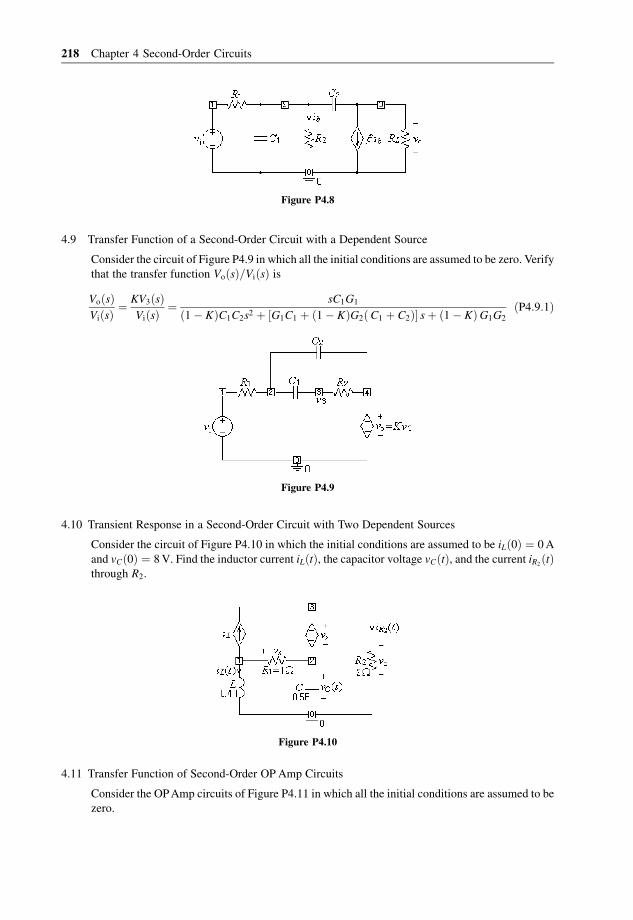
4.9 Transfer Function of a Second-Order Circuit with a Dependent Source
Consider the circuit of Figure P4.9 in which all the initial conditions are assumed to be zero. Verify
that the transfer function VoðsÞ=ViðsÞ is
VoðsÞViðsÞ
¼ KV3ðsÞViðsÞ
¼ sC1G1
ð1� KÞC1C2s2 þ ½G1C1 þ ð1� KÞG2ðC1 þ C2Þ� sþ ð1� KÞG1G2
ðP4:9:1Þ
4.10 Transient Response in a Second-Order Circuit with Two Dependent Sources
Consider the circuit of Figure P4.10 in which the initial conditions are assumed to be iLð0Þ ¼ 0A
and vCð0Þ ¼ 8V. Find the inductor current iLðtÞ, the capacitor voltage vCðtÞ, and the current iR2ðtÞ
through R2.
4.11 Transfer Function of Second-Order OP Amp Circuits
Consider the OPAmp circuits of Figure P4.11 in which all the initial conditions are assumed to be
zero.
Figure P4.8
Figure P4.9
Figure P4.10
218 Chapter 4 Second-Order Circuits

(a) Find the transfer function VoðsÞ=ViðsÞ of the circuit (a).(b) Find the transfer function VoðsÞ=ViðsÞ of the circuit (b).
4.12 A Double Integrator
Consider the OPAmp circuit of Figure P4.12 in which all the initial conditions are assumed to be
zero. Apply KCL to nodes 1, 2, and 3 to write a set of node equations in V1ðsÞ, V3ðsÞ, and VoðsÞ.Then solve it to find the transfer function
GðsÞ ¼ VoðsÞViðsÞ
¼ � 1
ðRCÞ 2s2 ðP4:12:1Þ
Note. The circuit in Figure P4.12 saves one OPAmp compared with another (two-stage) double integrator made
of two integrators connected in cascade, but instead requires more resistors/capacitors.
4.13 Steady State Response of a Second-Order OP Amp Circuit
Consider the OPAmp circuit of Figure P4.13 in which all the initial conditions are assumed to be
zero.
Figure P4.12
Figure P4.11
Figure P4.13
Problems 219

(a) Verify that the transfer function of the circuit is
GðsÞ ¼ VoðsÞViðsÞ
¼ pðsþ zÞsðsþ pÞ with p ¼ 1
R1 C1
and z ¼ 1
R2 C2
ðP4:13:1Þ
(b) Verify that the steady state output voltage of the circuit to a sinusoidal input viðtÞ ¼ Vim cosot is
vo;ssðtÞ ¼
ffiffiffiffiffiffiffiffiffiffiffiffiffiffiffiffiffiffiffiffiffiffiffiffiffiffiffiffiffiffiffiffiffiffiffiffi1þ ½1=ðoR2 C2Þ�2
qffiffiffiffiffiffiffiffiffiffiffiffiffiffiffiffiffiffiffiffiffiffiffiffiffiffiffiffi1þ ðoR1C1Þ2
q Vim cosðot þ �Þ
with � ¼ tan�1 1
oR1C1
� �� tan�1 1
oR2C2
� �� 90�
ðP4:13:2Þ
(c) With the values of the parameters as
R1 ¼ 100O; R2 ¼ 400O; C1 ¼ 70�F; C2 ¼ 2:5�F; and o ¼ 1000 rad=s
ðP4:13:3Þfind the largest amplitude of the input voltage, Vim, such that the output voltage is bounded
between the dual saturation limit voltages �Vom ¼ �11:6V (close to the values of the bipolar
supply voltages VCC=VEE ¼ �12).
Note. If the output voltage determined by Equation (P4.13.2) exceeds the range upper/lower-bounded by
the dual saturation limit voltages �Vom ¼ �11:6V, the real steady state output voltage will be a clipped
sinusoid.
(d) Noting that ViðsÞ ¼ LfVim cosotg ¼ Vims=ðs2 þ o2Þ, use MATLAB or its equivalent to find
the total response
voðtÞ ¼ L�1fVoðsÞg ¼ L�1fGðsÞViðsÞg ðP4:13:4Þ
to a sinusoidal input viðtÞ ¼ 58 cosot and plot it together with the steady state response
(P4.13.2) for the time interval [0, 0.05 s].
(e) Perform the PSpice simulation to get the response to a sinusoidal input viðtÞ ¼ 58 cosot.
4.14 A Second-Order OP Amp Circuit Implemented in Hardware
Figure P4.14(a) shows a hardware connection diagram that consists of two chips containing an OP
Amp together with two resistors and one capacitor.
Figure P4.14
220 Chapter 4 Second-Order Circuits

(a) Fill in the square boxes with the corresponding pin numbers in the schematic of
Figure P4.14(b).
(b) On the assumption of zero initial conditions, apply KCL to nodes a and b to write a set of node
equations and solve it to find the expression of VoðsÞ in terms of ViðsÞ.
4.15 Wien Bridge Oscillator
Consider the OP Amp circuit of Figure P4.15(a).
(a) For the OPAmp with a negative feedback path connecting the output terminal to the negative
input terminal, the virtual short principle (Remark 1.2(2)) says that the voltages at the positive
and negative input terminals are almost equal:
v1 ¼ v2 ¼R4
R 3 þ R4
vo ¼ bvo ðP4:15:1Þ
Let the initial voltages of the capacitors C1 and C2 be
vC1ð0Þ ¼ 0 and vC2
ð0Þ ¼ V20 ðP4:15:2Þ
respectively, where the nonzero one of the capacitor C2 is represented by the current source of
C2vC2ð0Þ in parallel with C2, as depicted in Figure P4.15(a). Apply KCL to node 1 to write the
node equation and solve it to find VoðsÞ as
b� 1
R1 þ 1=ðsC1Þþ b
R2
þ s bC2
� �VoðsÞ ¼ C2V20 ðP4:15:3Þ
VoðsÞ ¼V20R2C2ð1þ s R1C1Þ
bR1R2 C1C2s 2 þ s½b R1C1 þ bR2C2 þ ðb� 1ÞR2C1� þ bðP4:15:4Þ
(b) With the initial voltage vC2ð0Þ ¼ V20 as a kind of input, Equation (P4.15.4) (excluding V20Þ can
be regarded as a transfer function and its denominator set to zero to obtain the characteristic
equation. With reference to Section 4.1.4, verify that the following condition:
R4
R3 þ R4
¼ b ¼ R2C1
R1 C1 þ R2C2 þ R2C1
ðP4:15:5Þ
Figure P4.15
Problems 221

guarantees that the characteristic equation has imaginary roots s ¼ jor so that the output will
have an everlasting oscillation of frequency
or ¼1ffiffiffiffiffiffiffiffiffiffiffiffiffiffiffiffiffiffiffiffiffi
R1R2C1C2
p ðP4:15:6Þ
(c) Verify that, with
vC2ð0Þ ¼ V20 ¼ 1V; R1 ¼ R2 ¼ R4 ¼ 1 kO; R3 ¼ 2 kO; and C1 ¼ C2 ¼ 1�F
ðP4:15:7Þ
the output voltage is as follows:
VoðsÞ ¼1
b
sþ or
s2 þ o2r
¼ 3s
s2 þ 10002þ 3� 1000
s2 þ 10002ðP4:15:8Þ
voðtÞ ¼ 3ðcos 1000t þ sin 1000tÞusðtÞ ¼ 3ffiffiffi2
psinð1000t þ 45�ÞusðtÞ ½V� ðP4:15:9Þ
(d) Use MATLAB or its eqivalent to plot voðtÞ for the time interval [0, 20 ms].
(e) With reference to the PSpice schematic in Figure P4.15(b), perform the PSpice simulation to
get the amplitude and the period of voðtÞ.
4.16 Design and Simulation of a Second-Order OP Amp Circuit
Consider the circuit of Figure 4.9(b) in which some values of the parameters are given as
Vi ¼ 1:41V; R1 ¼ R2; R5 ¼ 5:1 kO; and C3 ¼ C4 ðP4:16:1Þ
(a) Choose the values ofC3 ¼ C4 and R1 ¼ R2 from Table G.3.1 (standard capacitance values) and
Table G.2 (5 % tolerance standard resistance values) in Appendix G such that the time constant
is close to, but not shorter than, T ¼ 0:1s and the damped frequency is close to, but not higher
than, od ¼ 2�ð2=TÞ[rad/s] (corresponding to two oscillations per time constant), or equiva-
lently the poles of the transfer function are located near to
��� jod ¼ð4:12Þ � 1
T� jod ¼ �10� j40� ðP4:16:2Þ
(b) With the parameter values determined in (a), find the output voltage voðtÞ to the DC input
voltage of 1.41 V and plot it for the time interval [0, 0.5 s].
(c) Perform the PSpice simulation to get the output voltage voðtÞ to the DC input voltage of 1.41 V
for the time interval [0, 0.5 s] and find the oscillation period as the time between the first peak/
trough time and the second one.
222 Chapter 4 Second-Order Circuits