
Electronic Circuits for the Evil Genius, Second Edition
317
-
Upload
khangminh22 -
Category
Documents
-
view
0 -
download
0
Transcript of Electronic Circuits for the Evil Genius, Second Edition


ElectronicCircuits for the
Evil Genius™

Evil Genius™ Series
Bike, Scooter, and Chopper Projects for the Evil Genius
Bionics for the Evil Genius: 25 Build-It-Yourself Projects
Electronic Circuits for the Evil Genius, Second Edition: 64 Lessons with Projects
Electronic Gadgets for the Evil Genius: 28 Build-It-Yourself Projects
Electronic Sensors for the Evil Genius: 54 Electrifying Projects
50 Awesome Auto Projects for the Evil Genius
50 Green Projects for the Evil Genius
50 Model Rocket Projects for the Evil Genius
51 High-Tech Practical Jokes for the Evil Genius
46 Science Fair Projects for the Evil Genius
Fuel Cell Projects for the Evil Genius
Holography Projects for the Evil Genius
Mechatronics for the Evil Genius: 25 Build-It-Yourself Projects
Mind Performance Projects for the Evil Genius: 19 Brain-Bending Bio Hacks
MORE Electronic Gadgets for the Evil Genius: 40 NEW Build-It-Yourself Projects
101 Outer Space Projects for the Evil Genius
101 Spy Gadgets for the Evil Genius
125 Physics Projects for the Evil Genius
123 PIC® Microcontroller Experiments for the Evil Genius
123 Robotics Experiments for the Evil Genius
PC Mods for the Evil Genius: 25 Custom Builds to Turbocharge Your Computer
PICAXE Microcontroller Projects for the Evil Genius
Programming Video Games for the Evil Genius
Recycling Projects for the Evil Genius
Solar Energy Projects for the Evil Genius
Telephone Projects for the Evil Genius
30 Arduino Projects for the Evil Genius
25 Home Automation Projects for the Evil Genius
22 Radio and Receiver Projects for the Evil Genius

ElectronicCircuits for the
Evil Genius™,Second Edition
64 Lessons with Projects
Dave Cutcher
New York Chicago San Francisco Lisbon London MadridMexico City Milan New Delhi San Juan Seoul
Singapore Sydney Toronto

Copyright © 2011 by The McGraw-Hill Companies, Inc. All rights reserved. Except as permitted under the United States Copyright Act of 1976, no part of this publication may be reproduced or distributed in any form or by any means, or stored in a database or retrieval system, without the prior written permission of the publisher.
ISBN: 978-0-07-174413-3
MHID: 0-07-174413-4
The material in this eBook also appears in the print version of this title: ISBN: 978-0-07-174412-6, MHID: 0-07-174412-6.
All trademarks are trademarks of their respective owners. Rather than put a trademark symbol after every occurrence of a trademarked name, we use names in an editorial fashion only, and to the benefi t of the trademark owner, with no intention of infringement of the trademark. Where such designations appear in this book, they have been printed with initial caps.
McGraw-Hill eBooks are available at special quantity discounts to use as premiums and sales promotions, or for use in corporate training programs.To contact a representative please e-mail us at [email protected].
Trademarks: McGraw-Hill, the McGraw-Hill Publishing logo, Evil Genius™, and related trade dress are trademarks or registered trademarks of The McGraw-Hill Companies and/or its affi liates in the United States and other countries and may not be used without written permission. All other trademarks are the property of their respective owners. The McGraw-Hill Companies is not associated with any product or vendor mentioned in this book.
Information has been obtained by McGraw-Hill from sources believed to be reliable. However, because of the possibility of human or mechanical error by our sources, McGraw-Hill, or others, McGraw-Hill does not guarantee the accuracy, adequacy, or completeness of any information and is not responsible for any errors or omissions or the results obtained from the use of such information.
TERMS OF USE
This is a copyrighted work and The McGraw-Hill Companies, Inc. (“McGrawHill”) and its licensors reserve all rights in and to the work. Use of this work is subject to these terms. Except as permitted under the Copyright Act of 1976 and the right to store and retrieve one copy of the work, you may not decompile, disassemble, reverse engineer, reproduce, modify, create derivative works based upon, transmit, distribute, disseminate, sell, publish or sublicense the work or any part of it without McGraw-Hill’s prior consent. You may use the work for your own noncommercial and personal use; any other use of the work is strictly prohibited. Your right to use the work may be terminated if you fail to comply with these terms.
THE WORK IS PROVIDED “AS IS.” McGRAW-HILL AND ITS LICENSORS MAKE NO GUARANTEES OR WARRANTIES AS TO THE ACCURACY, ADEQUACY OR COMPLETENESS OF OR RESULTS TO BE OBTAINED FROM USING THE WORK, INCLUDING ANY INFORMATION THAT CAN BE ACCESSED THROUGH THE WORK VIA HYPERLINK OR OTHERWISE, AND EXPRESSLY DISCLAIM ANY WARRANTY, EXPRESS OR IMPLIED, INCLUDING BUT NOT LIMITED TO IMPLIED WARRANTIES OF MERCHANTABILITY OR FITNESS FOR A PARTICULAR PURPOSE. McGraw-Hill and its licensors do not warrant or guarantee that the functions contained in the work will meet your requirements or that its operation will be uninterrupted or error free. Neither McGraw-Hill nor its licensors shall be liable to you or anyone else for any inaccuracy, error or omission, regardless of cause, in the work or for any damages resulting therefrom. McGraw-Hill has no responsibility for the content of any information accessed through the work. Under no circumstances shall McGraw-Hill and/or its licensors be liable for any indirect, incidental, special, punitive, consequential or similar damages that result from the use of or inability to use the work, even if any of them has been advised of the possibility of such damages. This limitation of liability shall apply to any claim or cause whatsoever whether such claim or cause arises in contract, tort or otherwise.


Dave Cutcher is a retired high school shop teacher. He always coaxed his students tobelieve in themselves and that success in life was not limited to school. He taught youngpeople and electronics was just the topic. Currently living in British Columbia, he teachesnight school courses and does volunteer work within the community. People comment thathe always thinks outside of the box. His reply, “What box?” As a life long learner and adultwith ADHD, he is interested in everything because everything is interesting.
About the Author

This page intentionally left blank

vii
Contents at a Glance
PART ONE Components. . . . . . . . . . . . . . . . . . . . . 1
1 Components . . . . . . . . . . . . . . . . . . . . . . . . . . . . . . . . . . . . . . . . . . . 5
2 Resist If You Must . . . . . . . . . . . . . . . . . . . . . . . . . . . . . . . . . . . . . . 15
3 More Components and Semiconductors . . . . . . . . . . . . . . . . . . 25
4 Two Projects and Then Some More . . . . . . . . . . . . . . . . . . . . . . 43
PART TWO Introduction to Digital Electronics. . 57
5 Digital Logic . . . . . . . . . . . . . . . . . . . . . . . . . . . . . . . . . . . . . . . . . . . 61
6 The First NAND Gate Circuit. . . . . . . . . . . . . . . . . . . . . . . . . . . . . 77
7 Analog Switches for Digital Circuits . . . . . . . . . . . . . . . . . . . . . . 91
8 The NAND Gate Oscillator. . . . . . . . . . . . . . . . . . . . . . . . . . . . . . . 99
9 How Do We Understand What We Can’t See? . . . . . . . . . . . . . 107
10 Digital Logic Project . . . . . . . . . . . . . . . . . . . . . . . . . . . . . . . . . . . . 127
PART THREE Counting Systems in Electronics . . 145
11 Introducing an Analog-to-Digital Converter . . . . . . . . . . . . . . . 149
12 The 4017 Walking Ring Counter. . . . . . . . . . . . . . . . . . . . . . . . . . 159
13 Running a Seven-Segment Display . . . . . . . . . . . . . . . . . . . . . . . 169
14 Define, Design, and Make Your Own Project . . . . . . . . . . . . . . . 183
PART FOUR Amplifiers: What They Are and How to Use Them . . . . . . . . . . . 195
15 What Is an Amplifier? . . . . . . . . . . . . . . . . . . . . . . . . . . . . . . . . . . . 199
16 Exploring the Op Amp . . . . . . . . . . . . . . . . . . . . . . . . . . . . . . . . . . 215
17 Applying the Op Amp: Building the Intercom . . . . . . . . . . . . . 235
18 Prototype and Design: Patience Has Its Rewards . . . . . . . . . . 247
PART FIVE Appendices . . . . . . . . . . . . . . . . . . . . . 261
A Common Component Packaging . . . . . . . . . . . . . . . . . . . . . . . . . 263
B Capacitors: Reading and Decoding . . . . . . . . . . . . . . . . . . . . . . . 265
C Animations List . . . . . . . . . . . . . . . . . . . . . . . . . . . . . . . . . . . . . . . . 269
D Glossary . . . . . . . . . . . . . . . . . . . . . . . . . . . . . . . . . . . . . . . . . . . . . . . 271
E Make Your Own Printed Circuit Boards . . . . . . . . . . . . . . . . . . . 281
Index. . . . . . . . . . . . . . . . . . . . . . . . . . . . . . . . . . . . . . . . . . . . . . . . . . 287
viii Electronic Circuits for the Evil Genius

Contents
Acknowledgments . . . . . . . . . . . . . . . . . . . . . . . . . . . . . . . . . . . . . . . . . . . . . . . . . . xiii
Preface . . . . . . . . . . . . . . . . . . . . . . . . . . . . . . . . . . . . . . . . . . . . . . . . . . . . . . . . . . . xv
Common Components, Symbols, and Appearance . . . . . . . . . . . . . . . . . . . . . . . . . xvii
PART ONE Components. . . . . . . . . . . . . . . . . . . . . 1
1 Components. . . . . . . . . . . . . . . . . . . . . . . . . . . . . . . . . . . . . . . . 5Lesson 1 Inventory of Parts Used in Part One . . . . . . . . . . . . . . . . . . . . . . . . . . . . 5Lesson 2 Major Equipment . . . . . . . . . . . . . . . . . . . . . . . . . . . . . . . . . . . . . . . . . . 8Lesson 3 Your First Circuit . . . . . . . . . . . . . . . . . . . . . . . . . . . . . . . . . . . . . . . . . . 11
2 Resist If You Must . . . . . . . . . . . . . . . . . . . . . . . . . . . . . . . . . . . 15Lesson 4 Reading Resistors . . . . . . . . . . . . . . . . . . . . . . . . . . . . . . . . . . . . . . . . . . 15Lesson 5 The Effect Resistors Have on a Circuit . . . . . . . . . . . . . . . . . . . . . . . . . 17Lesson 6 The Potentiometer. . . . . . . . . . . . . . . . . . . . . . . . . . . . . . . . . . . . . . . . . . 19Lesson 7 Light-Dependent Resistors . . . . . . . . . . . . . . . . . . . . . . . . . . . . . . . . . . . 21
3 More Components and Semiconductors . . . . . . . . . . . . . . . . 25Lesson 8 Capacitors and Push Buttons . . . . . . . . . . . . . . . . . . . . . . . . . . . . . . . . . 25Lesson 9 Introducing Transistors . . . . . . . . . . . . . . . . . . . . . . . . . . . . . . . . . . . . . . 31Lesson 10 The PNP Transistor. . . . . . . . . . . . . . . . . . . . . . . . . . . . . . . . . . . . . . . . 34Lesson 11 The Phototransistor: Shedding Some Light on Another Component. . 38
4 Two Projects and Then Some More . . . . . . . . . . . . . . . . . . . . 43Lesson 12 Your First Project: The Automatic Night Light . . . . . . . . . . . . . . . . . . 43Lesson 13 Specialized Transistors—The SCR. . . . . . . . . . . . . . . . . . . . . . . . . . . . 49Lesson 14 The Regulated Power Supply . . . . . . . . . . . . . . . . . . . . . . . . . . . . . . . . 53
PART TWO Introduction to Digital Electronics. . 57
5 Digital Logic. . . . . . . . . . . . . . . . . . . . . . . . . . . . . . . . . . . . . . . . 61Lesson 15 A Spoiled Billionaire . . . . . . . . . . . . . . . . . . . . . . . . . . . . . . . . . . . . . . 61Lesson 16 The Basic Digital Logic Gates . . . . . . . . . . . . . . . . . . . . . . . . . . . . . . . 66Lesson 17 Integrated Circuits CMOS ICs . . . . . . . . . . . . . . . . . . . . . . . . . . . . . . . 72
6 The First NAND Gate Circuit . . . . . . . . . . . . . . . . . . . . . . . . . . 77Lesson 18 Building the First NAND Gate Circuit. . . . . . . . . . . . . . . . . . . . . . . . . 77Lesson 19 Testing the Input at Test Point 1 . . . . . . . . . . . . . . . . . . . . . . . . . . . . . . 80Lesson 20 Test Point 2—The NAND Gate Processor at Work . . . . . . . . . . . . . . . 81
ix

Lesson 21 Test Point 3—Introducing the Resistor/Capacitor Circuit . . . . . . . . . . 83Lesson 22 Test Point 4—The Inputs Are Switches . . . . . . . . . . . . . . . . . . . . . . . . 86
7 Analog Switches for Digital Circuits . . . . . . . . . . . . . . . . . . . . 91Lesson 23 Understanding Voltage Dividers . . . . . . . . . . . . . . . . . . . . . . . . . . . . . . 91Lesson 24 Create a Light-Sensitive Switch . . . . . . . . . . . . . . . . . . . . . . . . . . . . . . 96Lesson 25 The Touch Switch . . . . . . . . . . . . . . . . . . . . . . . . . . . . . . . . . . . . . . . . . 97
8 The NAND Gate Oscillator . . . . . . . . . . . . . . . . . . . . . . . . . . . . 99Lesson 26 Building the NAND Gate Oscillator. . . . . . . . . . . . . . . . . . . . . . . . . . . 99Lesson 27 Understanding the NAND Gate Oscillator . . . . . . . . . . . . . . . . . . . . . . 103
9 How Do We Understand What We Can’t See? . . . . . . . . . . . 107Lesson 28 Controlling the Flash Rate . . . . . . . . . . . . . . . . . . . . . . . . . . . . . . . . . . 107Lesson 29 Create a Sound Output and Annoy the Person Next to You. . . . . . . . . 110Lesson 30 Introducing the Oscilloscope . . . . . . . . . . . . . . . . . . . . . . . . . . . . . . . . 112Lesson 31 Scoping Out the Circuit . . . . . . . . . . . . . . . . . . . . . . . . . . . . . . . . . . . . 119Lesson 32 Using a Transistor to Amplify the Output . . . . . . . . . . . . . . . . . . . . . . 122Lesson 33 The Photo Transistor: You Can’t Do This with an LDR . . . . . . . . . . . 124
10 Digital Logic Project . . . . . . . . . . . . . . . . . . . . . . . . . . . . . . . . . 127Lesson 34 Design—Systems and Samples . . . . . . . . . . . . . . . . . . . . . . . . . . . . . . 127Lesson 35 Consider What Is Realistic . . . . . . . . . . . . . . . . . . . . . . . . . . . . . . . . . . 140Lesson 36 Building Your Project . . . . . . . . . . . . . . . . . . . . . . . . . . . . . . . . . . . . . . 142
PART THREE Counting Systems in Electronics . . 145
11 Introducing an Analog-to-Digital Converter . . . . . . . . . . . . . 149Lesson 37 Introducing Possibilities—Electronics That Count . . . . . . . . . . . . . . . 149Lesson 38 RC1—Creating the Switch . . . . . . . . . . . . . . . . . . . . . . . . . . . . . . . . . . 150Lesson 39 Introducing the 4046 Voltage-Controlled Oscillator . . . . . . . . . . . . . . 153
12 The 4017 Walking Ring Counter . . . . . . . . . . . . . . . . . . . . . . . 159Lesson 40 Introducing the Walking Ring 4017 Decade Counter . . . . . . . . . . . . . 159Lesson 41 Understanding the Clock Signal Used by the 4017 . . . . . . . . . . . . . . . 163Lesson 42 Controlling the Count—Using the Chip’s Control Inputs . . . . . . . . . . 166
13 Running a Seven-Segment Display . . . . . . . . . . . . . . . . . . . . . 169Lesson 43 Introducing the Seven-Segment LED . . . . . . . . . . . . . . . . . . . . . . . . . . 169Lesson 44 Control the Seven-Segment Display Using the 4511 BCD . . . . . . . . . 170Lesson 45 Decimal to Binary—The 4516 . . . . . . . . . . . . . . . . . . . . . . . . . . . . . . . 174Lesson 46 The Displays Automatically Fade Out . . . . . . . . . . . . . . . . . . . . . . . . . 180
14 Define, Design, and Make Your Own Project . . . . . . . . . . . . . 183Lesson 47 Defining and Designing Your Project . . . . . . . . . . . . . . . . . . . . . . . . . . 183Lesson 48 Your Project: If You Can Define It, You Can Make It!. . . . . . . . . . . . . 189
x Electronic Circuits for the Evil Genius
PART FOUR Amplifiers: What They Are and How to Use Them . . . . . . . . . . . 195
15 What Is an Amplifier? . . . . . . . . . . . . . . . . . . . . . . . . . . . . . . . . 199Lesson 49 Transistors as Amplifiers and Defining Current . . . . . . . . . . . . . . . . . . 199Lesson 50 Defining Work, Force, and Power . . . . . . . . . . . . . . . . . . . . . . . . . . . . 205Lesson 51 What Do I Have to Gain?: Definitions . . . . . . . . . . . . . . . . . . . . . . . . . 210Lesson 52 The World Is Analog, So Analog Is the World . . . . . . . . . . . . . . . . . . . 212
16 Exploring the Op Amp . . . . . . . . . . . . . . . . . . . . . . . . . . . . . . . 215Lesson 53 Alternating Current Compared with Direct Current. . . . . . . . . . . . . . . 215Lesson 54 AC in a DC Environment . . . . . . . . . . . . . . . . . . . . . . . . . . . . . . . . . . . 220Lesson 55 Setting Up the Operational Amplifier. . . . . . . . . . . . . . . . . . . . . . . . . . 222Lesson 56 Using Feedback to Control Gain . . . . . . . . . . . . . . . . . . . . . . . . . . . . . 229
17 Applying the Op Amp: Building the Intercom. . . . . . . . . . . . 235Lesson 57 Building a Power Amplifier Controlled by an Op Amp. . . . . . . . . . . . 235Lesson 58 The Electret Microphone . . . . . . . . . . . . . . . . . . . . . . . . . . . . . . . . . . . 238Lesson 59 Using the Speaker as a Microphone . . . . . . . . . . . . . . . . . . . . . . . . . . . 240Lesson 60 Introducing Transformers and Putting It All Together . . . . . . . . . . . . . 242
18 Prototype and Design: Patience Has Its Rewards . . . . . . . . . 247Lesson 61 Systems and Subsystems . . . . . . . . . . . . . . . . . . . . . . . . . . . . . . . . . . . 248Lesson 62 Switching to the Two-Way Door Phone . . . . . . . . . . . . . . . . . . . . . . . . 252Lesson 63 Design and Applications: Exploring the Possibilities . . . . . . . . . . . . . 255Lesson 64 Assembling the Project . . . . . . . . . . . . . . . . . . . . . . . . . . . . . . . . . . . . . 259
PART FIVE Appendices . . . . . . . . . . . . . . . . . . . . . 261
A Common Component Packaging. . . . . . . . . . . . . . . . . . . . . . . 263Transistors . . . . . . . . . . . . . . . . . . . . . . . . . . . . . . . . . . . . . . . . . . . . . . . . . . . . . . . . 263Potentiometers . . . . . . . . . . . . . . . . . . . . . . . . . . . . . . . . . . . . . . . . . . . . . . . . . . . . . 263Transformers . . . . . . . . . . . . . . . . . . . . . . . . . . . . . . . . . . . . . . . . . . . . . . . . . . . . . . 264
B Capacitors: Reading and Decoding . . . . . . . . . . . . . . . . . . . . 265Reading Values. . . . . . . . . . . . . . . . . . . . . . . . . . . . . . . . . . . . . . . . . . . . . . . . . . . . . 265Tolerance: Quality and Accuracy of Capacitors . . . . . . . . . . . . . . . . . . . . . . . . . . . 266
C Animations List . . . . . . . . . . . . . . . . . . . . . . . . . . . . . . . . . . . . . 269Related Animations . . . . . . . . . . . . . . . . . . . . . . . . . . . . . . . . . . . . . . . . . . . . . . . . . 269
D Glossary . . . . . . . . . . . . . . . . . . . . . . . . . . . . . . . . . . . . . . . . . . . 271
E Make Your Own Printed Circuit Boards . . . . . . . . . . . . . . . . . 281
Index . . . . . . . . . . . . . . . . . . . . . . . . . . . . . . . . . . . . . . . . . . . . . . . . . . . . . . . . . . . . 287
Contents xi

This page intentionally left blank

Acknowledgments
FOR A VARIETY OF REASONS, there are many people I need to thank.
First are my current guinea pigs, who chose to be caged in a classroom with me forthree years running. Andrew Fuller who put together the game “When Resistors GoBad.” He and André Walther, two very original Evil Geniuses. I hope they understandthe molar concept in chemistry now and won’t raise a stink about me mentioningthem. Eric Raue and Eric Pospisal, both for being the gentler geniuses they are. AndBrennen Williams, who was more patient with me at times than I was with him. It wasa difficult year.
I’ve had only one formal class in electronics, taught by Gus Fraser. He let me teachmyself. Bryan Onstad gave me a goal to work toward and a platform to work on. DonNordheimer was the first adult who actually worked through my material outside ofthe classroom environment. At the same time, he proofed the material from the adultperspective. I owe heartfelt thanks for the encouragement from Pete Kosonan, the firstadministrator who enjoyed the creative flow of the students as much as I did. ForSteve Bailey, the second administrator I found who wasn’t threatened by kids whoknew more than he did. For the many others like Paul Wytenbrok, Ian Mattie, JudyDoll, and Don Cann, who continually encouraged me over the five years it took todevelop this material. For Brad Thode, who introduced me to the necessity ofchanging careers within teaching back in 1989. For Mrs. Schluter and Mrs. Gerard,who taught me to believe in myself and recognize that there was room for creativity,not just what they wanted to hear.
Then to Dave Mickie who understood that conditions like ADHD cannot be cured,only managed. I’ll be forever grateful for the encouragement and support he providedas I moved forward with my work.
To my parents, who knew they couldn’t change me, so they encouraged me.
xiii

This page intentionally left blank

WE CASUALLY ACCEPT ELECTRONICS in our everyday world. Those who don’tunderstand how it works are casually obedient. Those who take the time to learnelectronics are viewed as geniuses. Do you want to learn how to control the power ofelectronics?
This text provides a solid introduction to the field of electronics, both analog anddigital. Electronic Circuits for the Evil Genius is based on practical projects thatexercise the genius that exists in all of us. Components are introduced as you buildworking circuits. These circuits are modified and analyzed to help explain the functionof the components. It’s all hands-on. Analysis is done by observation, using a digitalmultimeter, and using your computer as an oscilloscope.
You will build two major projects in the first part:
■ An automatic night light
■ A professional-quality alarm
The remainder of the text focuses on three major projects, one per part:
■ Building a digital toy using logic gates
■ Designing and building an application using digital counting circuits
■ Applying transistors and Op Amps as you build a two-way intercom system
The lessons and prototype circuits built in the book are focused on developing asolid foundation centered on each of these major projects. You work from ideas toprototypes, producing a final product.
Additional materials for this book, including lesson quizzes and answers keys, areavailable online at www.mhprofessional.com/computingdownload.
I hope you enjoy building the projects and reading the book as much as I enjoyeddeveloping them.
Dave Cutcher
xv
Preface

This page intentionally left blank

Name Class Purpose Symbol Photograph
Electrolytic Capacitor 1. RC timer
Capacitor Micro Farad 2. Isolate AC
(�F) 3. Buffer/filter
Film Capacitor Capacitor 1. RC timer
Nano Farad 2. Isolate AC
(nF) 3. Buffer/filter
Disk Capacitor Capacitor 1. RC timer
Pico Farad 2. Buffer/filter
(pF)
Power Diode Diode One way valve
for high voltage
Signal Diode Diode One way valve
for low voltage
Zener Diode Diode One way until
voltage reaches
preset breakdown
Light Emitting Diode 1. Indicator
Diode (LED) 2. Light source
3. Signal transfer
Common Components, Symbols, and Appearance
xvii

Name Class Purpose Symbol Photograph
Fixed Resistor Resistor Limits flow of
current
Potentiometer Resistor Adjustable resistor
Light Dependent Resistor General purpose
Resistor (LDR) light sensor
Push Button Hardware Momentary switch
Normally Closed
(PBNC)
Push Button Hardware Momentary switch
Normally Open
(PBNO)
Single Pole Hardware Simple open/
Single Throw close switch
(SPST)
Single Pole Hardware Controls single
Double Throw connection one of
(SPDT) two directions
Double Pole Hardware Matched control of
Double Throw two individual
(DPDT) connections in two
directions
xviii Electronic Circuits for the Evil Genius

Name Class Purpose Symbol Photograph
Relay Switch Secondary switch
controlled by
primary circuit
Operational Amplifier Very versitile, Available DIP and SIP
Amplifier multipurpose Various packages
component
NPN Transistor Transistor Simple analog See Appendix A,
electronic switch. Common Component
Needs both current Packaging
and voltage to
operate. Acts like
PBNO.
PNP Transistor Transistor Simple analog See Appendix A,
electronic switch. Common Component
Needs both current Packaging
and voltage to
operate. Acts like
PBNC.
Photo Transistor Transistor Light sensitive analog Various packaging
and digital signal
pickup.
Silicon Transistor Single event See Appendix A,
Controlled latching circuit Common Component
Rectifier (SCR) Packaging
Power Regulator Transistor DC to DC power See Appendix A,
conversion. Common Component
Packaging
Field Effect Transistor Available in PNP and See Appendix A,
Transistor NPN configuration. Common Component
Needs only voltage Packaging
to operate.
Common Components, Symbols, and Appearance xix
��
��
�
��
�
�
�
�
�

Name Class Purpose Symbol Photograph
Electret Microphone Sound pickup
Microphone
Speaker Speaker Sound output
Transformer Transformer Used to isolate or See Appendix A,
change AC voltage Common Component
from a primary to Packaging
secondary circuit.
AND Gate Logic Gate InA InB Out
H H H
H L L
L H L
L L L
OR Gate Logic Gate InA InB Out
H H H
H L H
L H H
L L L
NAND Gate Logic Gate InA InB Out
H H L
H L H
L H H
L L H
NOR Gate Logic Gate InA InB Out
H H L
H L L
L H L
L L H
xx Electronic Circuits for the Evil Genius

Components
P A R T O N E
Components
P A R T O N E

This page intentionally left blank

Electronics is BIG. You need a solid foundation.
3
Building the Foundation
Imagine the solid foundation needed for the work being done on the
construction shown here.
The Parts Bin on the following page has the complete parts list used in
Part One. These are pictured in the front of the book in the section Common
Components, Symbols, and Appearance.

Description Type Quantity
Diode 1N4005 Semi(D) 3
LED Semi(L) 3
2N-3906 PNP transistor TO-92 case 1
2N-3904 NPN transistor TO-92 case 1
Phototransistor LTE 4206 E (darkened glass) 1
3mm diam: tuned to 940nm
Infra Red Diode LTE 4206 (clear glass) 1
3mm diam: emits 940nm
SCR C106B Various packages 1
7805 Power regulator TO-220 case 1
Wall adapter 120vAC to 9vDC Transformer 1
100 � Resistor 1
470 � Resistor 2
1000 � Resistor 1
2,200 � Resistor 1
10,000 � Resistor 1
22,000 � Resistor 1
47,000 � Resistor 1
100,000 � Resistor 1
220,000 � Resistor 1
100,000 � 1/4 watt Potentiometer 1
Light-dependent resistor LDR 1
.1 �F film cap Cap 1
10 �F Electrolytic Cap 1
100 �F Electrolytic Cap 1
1000 �F Electrolytic Cap 1
470 �F Electrolytic Cap 1
24 gauge wire Hookup wire Various colors
Battery clip Hardware 2
Alligator clips (red and black) Hardware 1 each
Buzzer 9v Hardware 1
LED collars Hardware 3
PCB for night light Hardware 1
PCB for SCR alarm Hardware 1
Solderless breadboard Hardware 1
PBNC momentary Switch 2
PBNC momentary Switch 1
■ Not all components will be consumed by project work.
P A R T S B I N F O R P A R T O N E
4

Components
S E C T I O N 1
5
IN LESSON 1, YOU WILL BE INTRODUCED to manycommon components that are always present inelectronics and many of the bits and pieces youwill use in the course. It starts out as a jumble. Asyou use the parts, the confused mass becomes anorganized pile.
In Lesson 2, you will become acquainted withthe two major tools that you will use throughoutthe course.
In Lesson 3, you will build your first circuit onthe solderless breadboard, a platform that allowsyou to build circuits in a temporary format.
You use your digital multimeter and get voltagemeasurements when you set up and test your firstcircuits.
Lesson 1Inventory of Parts Used in Part One
All components look the same if you don’t knowwhat they are. It’s like when you first visit adifferent country. There’s a pile of change, just likein Figure L1-1. You have to be introduced to thecurrency and practice using it, but you becomecomfortable with it quickly. Now you need tounjumble the pile and become familiar with yourelectronic components.
Do not remove the small
integrated-circuit (IC) chips shown
in Figure L1-2 from their antistatic packaging. They
are packed in a special antistatic tube or special
sponge material.
Semiconductors
These are the electronic components you will beusing in Part One. As you identify them, set themaside into small groups.
Figure L1-1
NOTE
Figure L1-2
6 Section 1 ■ Components
Diodes
You will need three power diodes as shown inFigures L1-3 and L1-4.
The number on the side reads 1N4005. If thelast number is not 5, don’t worry. Any diode of thisseries will do the job.
Light-Emitting Diodes
Light-emitting diodes are also known as LEDs.You will need three. An example is illustrated inFigure L1-5.
They can be any color. The most commoncolors are red, yellow, and green.
Resistors
There should be lots of colorful resistors, nearly allthe same size. Notice that in Figure L1-6 eachresistor has four color bands to identify it. If youknow the colors of the rainbow, you know how toread resistors.
Find these resistors:
■ One brown-black-brown-gold 100 �
■ Two yellow-violet-brown-gold 470 �
■ One brown-black-red-gold 1,000 �
■ One brown-black-orange-gold 10,000 �
■ One red-red-orange-gold 22,000 �
■ One yellow-violet-orange-gold 47,000 �
■ One brown-black-yellow-gold 100,000 �
Capacitors
As you see in Figure L1-7, the capacitor shown is black and white. The colors of capacitors aredifferent, depending on the manufacturer. Thenagain, all pop cans look alike, but each brand has a different label. Locate four small capacitors,different in size. Written on each are differentvalues and other mumbo jumbo. Look for theinformation that specifically lists 1 μF, 10 μF, 100 μF, and 1000 μF.
There is another capacitor of a different shape tolocate. Figure L1-8 shows the other capacitor used inPart One. Again, it is presented in black and white,because the color will change as the manufacturerchanges. It is a 0.1 μF capacitor. It may be marked as any of the following: 0.1, �1, or 100 nF.
Figure L1-3
Figure L1-4
Figure L1-5
Figure L1-6
Figure L1-7

Silicon-Controlled Rectifier
The ID number 1067X for the silicon-controlledrectifier (SCR) is written on the face, as shown inFigure L1-9. This SCR comes in this particularpackage. Not everything with this shape is an SCR,just as not everything in the shape of a pop can isyour favorite flavor.
Transistors
You need two transistors, like that illustrated inFigure L1-10. They are identical except for thenumber 3904 or 3906. All other writing and marksare the manufacturer telling us how great they are.
Hardware
The solderless breadboard is shown in Figure L1-11.
Figures L1-12 and L1-13 illustrate two pushbuttons—they are different, but you can’t tell thisby looking at them. Figure L1-12 is the normallyopen push button (push to close the contacts), andFigure L1-13 shows the normally closed pushbutton (push to open the contacts).
You should have lots of 24-gauge solid wirewith plastic insulation in many different lengths.
Two battery clips are shown in Figure L1-14.
Lesson 1 ■ Inventory of Parts Used in Part One 7
Figure L1-8
Figure L1-9
Figure L1-10
Figure L1-11
Figure L1-12
Figure L1-13
Figure L1-14

8 Section 1 ■ Components
A 9-volt buzzer is shown in Figure L1-15.
Two printed circuit boards are premade for yourprojects: Figure L1-16 shows the one that will beused for the night-light project; Figure L1-17shows the one that will be used for your SCRalarm project.
Two adjustable resistors are also supplied: Thelight-dependent resistor (LDR) is shown in FigureL1-18 and the potentiometer is shown in FigureL1-19.
Lesson 2Major Equipment
The solderless breadboard and digital multimeterare two of the most common tools used inelectronics. Let’s introduce you to them now.
The Solderless Breadboard
When smart people come up with ideas, first theytest those ideas. They build a prototype. Theeasiest way to build prototypes and play with ideasin electronics is on the solderless breadboard,shown here in Figure L2-01.
The main advantage of the solderlessbreadboard is the ability to exchange parts easilyand quickly.
Figure L1-15
Figure L1-16
Figure L1-17
Figure L1-18
Figure L1-19

The top view in Figure L2-1 shows the manypairs of short five-hole rows and a pair of longrows down each side; each of these lines is markedwith a strip of paint.
The Digital Multimeter
I recommend the Circuit Test DMR2900 displayedin Figure L2-2. The autoranging digital multimeter(DMM) offers beginners the advantage of beingeasier to learn. The second style of DMM is notautoranging. This style is easy to use after youbecome familiar with electronics, but it tends to beconfusing for the beginner. A typical dial of anonautoranging multimeter is confusing, as youcan see in Figure L2-3.
I discourage the use of outdated whisker-stylemultimeters for this course. Figure L2-4 shows anexample of what to avoid.
Connection Wire
A box of wire provided in the kit is displayed inFigure L2-5.
These are different lengths convenient for thesolderless breadboard. However, if you need to cutthe wire, wire clippers will work perfectly. Oldscissors work as well.
Set the dial of the DMM to CONTINUITY. Thissetting is shown in Figure L2-6.
Lesson 2 ■ Major Equipment 9
Figure L2-1
Figure L2-2
Figure L2-3
Figure L2-4
Figure L2-5
Touch the end of both red and black probes tothe colored covering. The DMM should be silentand read OL, as in the readout illustrated in FigureL2-7, because the resistance of the insulationprevents any current from passing.
Be sure the strip of insulating plastic is removedfrom both ends of the piece of wire, as shown inFigure L2-8. If you don’t have a proper wirestripper available, use a knife or your fingernails to cut the insulation. Be careful not to nick thewire inside the insulation.
Now touch the end of both probes to theexposed wire. The DMM should read “00” andbeep, just like the readout in Figure L2-9. The wireis a good conductor, and the DMM shows“continuity,” a connected path.
Exercise: Mapping the Solderless Breadboard
Strip the end of two pieces of wire far enough towrap around the DMM probes on one end andenough to insert into the solderless breadboard(SBB) on the other end, as shown in Figure L2-10.
1. Set your digital multimeter to CONTINUITY.Now refer to Figure L2-11. Notice the lettersacross the top and the numbers down the sideof the solderless breadboard.
2. Probe placement:
a. Place the end of one probe wire into theSBB at point “h3” and mark that on thedrawing.
b. Use the other probe to find three holesconnected to the first. The multimeter will indicate the connection.
c. Draw these connections as solid lines.
10 Section 1 ■ Components
Figure L2-6
Figure L2-7
Figure L2-8
Figure L2-9
Figure L2-10
3. Base points:
a. Create four more base points at e25, b16,f30, and c8.
b. Use the other probe to find three holesconnected to each of these points.
c. Again draw these connections as solidlines.
4. Additional base points:
a. Choose two more base points on theoutside long, paired lines. These lines arenot lettered or numbered but have a stripeof paint along the side. Mark them on theprevious diagram.
b. Find three holes connected to each ofthese points.
c. Again draw these connections as solidlines.
5. Be sure that you can define the termsprototype, insulator, and conductor.
6. With your multimeter set on CONTINUITY,walk around and identify at least five commonitems that are insulators and five commonmaterials that are conductors.
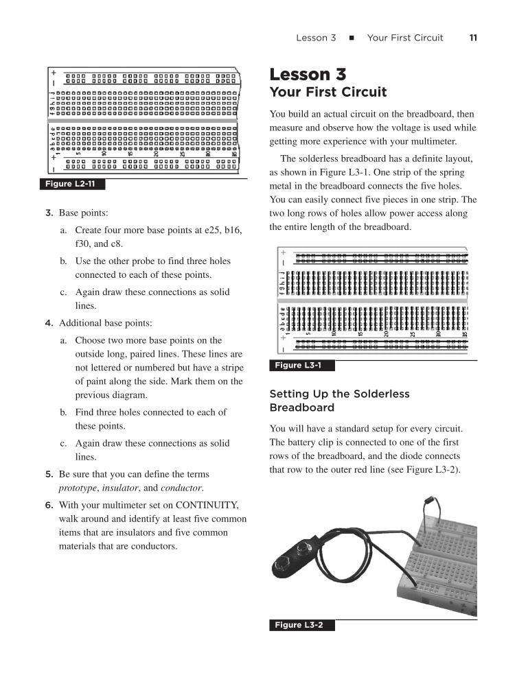
Lesson 3Your First Circuit
You build an actual circuit on the breadboard, thenmeasure and observe how the voltage is used whilegetting more experience with your multimeter.
The solderless breadboard has a definite layout,as shown in Figure L3-1. One strip of the springmetal in the breadboard connects the five holes.You can easily connect five pieces in one strip. Thetwo long rows of holes allow power access alongthe entire length of the breadboard.
Setting Up the SolderlessBreadboard
You will have a standard setup for every circuit.The battery clip is connected to one of the firstrows of the breadboard, and the diode connectsthat row to the outer red line (see Figure L3-2).
Lesson 3 ■ Your First Circuit 11
Figure L2-11
Figure L3-1
Figure L3-2

12 Section 1 ■ Components
Notice the gray band highlighted in Figure L3-3on the diode. It faces in the direction that thevoltage is pushing.
The voltage comes through the red wire,through the diode, and then to the power strip onthe breadboard.
Why Bother?
This power diode provides protection for eachcircuit that you build in the following ways:
■ The diode is a one-way street. You can viewthe animated version of Figure L3-4 at thewebsite www.mhprofessional.com/computingdownload.
■ Many electronic components can be damagedor destroyed if the current is pushed throughthem the wrong way, even for a fraction of asecond.
■ This standard breadboard setup helps ensurethat your battery will always be connectedproperly.
■ If you accidentally touch the battery to the clipbackwards, nothing will happen because thediode will prevent the current from moving.
Breadboarding Your First Circuit
Your LED is a light-emitting diode. That’s right, adiode that emits light. It has the same symbol as adiode, but it has a “ray” coming out, as shown herein Figure L3-5.
Figure L3-6 is a picture of an LED. Never touchyour LED directly to your power supply. A burned-out LED looks just like a working LED. Note inthe picture how to identify the negative side.
The shorter leg: This is always reliable withnew LEDs, but not with ones that you have handledin and out of your breadboard. As you handle thecomponents, the legs can get bent out of shape.
Figure L3-03
Figure L3-4
■ D1—Power diode 1n400x
■ LED1—LED any color
■ R1—470-ohm resistor
P A R T S B I N
Figure L3-5
Figure L3-6

The flat side on the rim: This is always reliablewith round LEDs, but you have to look for it.
Remember that the LED, as a diode, is a one-way street. It will not work if you put it inbackward.
Figure L3-7 shows several resistors. The resistorsymbol is illustrated in Figure L3-8. The resistoryou need is the 470-ohm yellow-violet-brown-gold.
Resistance is measured in ohms. The symbol forohms is the Greek capital letter omega: �.
The schematic is shown in Figure L3-9. Set upyour breadboard as shown in Figure L3-10. Notethat this picture shows the correct connections. Thered wire of the battery clip is connected to thepower diode that in turn provides voltage to the topof the breadboard. The black wire is connected tothe blue line at the bottom of the breadboard.
1. Always complete your breadboard before you
attach your power to the circuit.
2. Attach your battery only when you are ready to
test the circuit.
3. When you have finished testing your circuit, take
your battery off.
Exercise: Measuring Voltage on Your First Circuit;
Your First Circuit Should Be Working
Figure L3-11 shows what is happening. Like awaterfall, all of the voltage goes from the top tothe bottom. The resistor and LED each use up partof the voltage. Together, they use all the voltage.The 470-ohm resistor uses enough voltage to makesure the LED has enough to work, but not so muchthat would burn it out.
Lesson 3 ■ Your First Circuit 13
Figure L3-7
Figure L3-8
Figure L3-9
Figure L3-10
NOTE

How the Voltage Is Being Used in the Circuit
1. Set the DMM to direct current voltage(DCV). If you are using a multimeter that isnot autoranging, set it to the 10-volt range.
2. Measure the voltage of the 9-volt batterywhile it is connected to the circuit.
3. Place the red (�) probe at test point A (TP-A)and the black (–) probe at TP-D (ground). The arrows in the schematic shown in FigureL3-12 indicate where to attach the probes.Corresponding test points have been noted in Figure L3-13 as well.
4. Record your working battery voltage. ____V
5. Measure the voltage used between thefollowing points:
■ TP-A to TP-B across the safety diode ____V
■ TP-B to TP-C across the 470-ohm resistor ____V
■ TP-C to TP-D across the LED ____V
6. Now add the voltages from #5. ____V
7. List working battery voltage (recorded in item 2). ____V
8. Compare the voltage used by all of the partsto the voltage provided by the battery.
The voltages added together should beapproximately the same as the voltage provided bythe battery. There may be only a few hundredths ofa volt difference.
14 Section 1 ■ Components
Figure L3-11
Figure L3-12
Figure L3-13

Resist If You Must
S E C T I O N 2
15
RESISTORS ARE ONE OF the fundamentalcomponents within electronics. They are funnylittle things and come in all different colors. Andjust like a rainbow, they come in all sizes too.
To master electronics, you must first master thesecret color code, unlocking the mystery of how totell one resistor from another.
But beware! Can you handle the knowledge andpower that lies beyond this task?
Lesson 4Reading Resistors
Fixed resistors are the most common electroniccomponents. They are so common because they
are so useful. Most often, these are identified usingtheir color code (Table L4-1). If you think thesecret code is hard to remember, just ask any six-year-old to name the colors in the rainbow.
The gold bands are always read last. Theyindicate that the resistor’s value is accurate towithin 5 percent.
When using the digital multimeter to measureresistance, set the dial to �. Notice the two pointsof detail shown in Figure L4-1.
The first point is that when the dial is setdirectly to the � symbol to measure resistance, it also appears on the readout. Second, notice theM next to the � symbol. That means the resistorbeing measured is 0.463 M�, which is 0.463
First Band: Second Band: Third Band: Color Band Value Value Number of Zeros Units
Black 0 0 No zeros Tens ##
Brown 1 1 One zero “0” Hundreds ##0
Red 2 2 Two zeros “00” Thousands (k) #, #00
Orange 3 3 Three zeros “000” Ten thousands (k) ##,000
Yellow 4 4 Four zeros “0,000” Hundred thousands (k) ##0,000
Green 5 5 Five zeros “00,000” Millions (M) #,#00,000
Blue 6 6 Six zeros “000,000” Ten millions (M) ##,000,000
Violet 7 7 Not available
Gray 8 8 Not available
White 9 9 Not available
TABLE L4-1 Resistor Band Designations

16 Section 2 ■ Resist If You Must
million ohms, or 463,000 ohms. When the M isthere, never ignore it.
As you use resistors, you quickly become familiarwith them. The third band is the most importantmarker. It tells you the range in a power of 10. In apinch, you could substitute any resistor of nearly thesame value. For example, a substitution of a red-red-orange could be made for a brown-black-orangeresistor. But a substitution of a red-red-orange with ared-red-yellow would create more problems than itwould solve. Using a completely wrong value ofresistor can mess things up.
Exercise: Reading Resistors
If you have an autoranging multimeter, set thedigital multimeter (DMM) to measure resistance. Ifyou do not have an autoranging DMM, you have towork harder because the resistors come in differentranges. Set the range on your DMM to match therange of the resistor. That means that you shouldhave an idea of how to read resistor values beforeyou can measure them using a DMM that is notautoranging. Thus, as you can see, an autorangingDMM really does make it much easier.
Your skin will conduct electricity, and if youhave contact with both sides of the resistor, theDMM will measure your resistance mixed with theresistor’s. This will give an inaccurate value.
Proper Method to Measure Resistor’s Value
Figure L4-2 shows how to measure a resistor.Place one end of the resistor into your solderlessbreadboard and hold the probe tightly against it,but not touching the metal. You can press the otherprobe against the top of the resistor with yourother finger.
1. Table L4-2 lists some of the resistors that youwill need to be able to identify, because youuse them soon.
2. Don’t be surprised if the resistor value is notexactly right. These resistors have a maximumerror of 5 percent. That means that the 100-ohm resistor can be as much as 105 ohms oras little as 95 ohms. Plus or minus 5 ohmsisn’t too bad. What is 5 percent of 1,000,000?
■ What is the maximum you would expect to see on the 1,000-ohm resistor? _____ �
■ What is the minimum you would expect to see on the same 1-kilo-ohm resistor? ____ �
3. Measure your skin’s resistance by holding a probe in each hand. It will bounce around, but try to take an average. ______ �
■ Did you know that this can be used as acrude lie detector? A person sweats whenthey get anxious. Have a friend hold the
Figure L4-2
Figure L4-1

probes. Then ask them an embarrassingquestion. Watch the resistance go down fora moment.
4. Write each of these values as a number withno abbreviations.
■ 10 k� � ________ �
■ 1 k� � ________ �
■ 0.47 k� � ________ �
■ 47 k� � ________ �
Lesson 5The Effect Resistors Have on a Circuit
Throughout electronics, resistors are used tocontrol the voltage and flow of the current. Eventhough this lesson is not very long, it does taketime. Do it properly and you will get properresults. You will observe, chart, and describe theeffects of different strength resistors when they areall set up in identical circuits.
Let’s go back to the breadboard and see howdifferent resistors affect a simple circuit. Both theresistors and LEDs are loads. The resistor usesmost of the voltage, leaving just enough for theLED to work. The LEDs need about two volts.
What would happen if you changed resistors onthe circuit you just built, shown in Figure L5-1?
You measured the voltage used across theresistor from TP-B to TP-C and measured thevoltage used across the LED from TP-C to TP-D.
Lesson 5 ■ The Effect Resistors Have on a Circuit 17
First Band: Second Band: Third Band: Value Value Number of Zeros Resistor Value DMM Value
Brown Black Brown 100 � ________�
1 0 0
Violet Brown 470 � ________�
4 7 0
Brown Black Red 1,000 � ________�
____ ____ 00
Brown Black Orange 10 k� ________�
____ ____ 000 10,000�
Red Red Orange 22 k� ________�
____ ____ ____ 22,000 �
Brown Black Yellow 100 k� ________�
____ ____ ____ 100,000
TABLE L4-2 Resistors Needed
Figure L5-1

Figure L5-2 is the schematic of the circuit.
Figure L5-3 shows a waterfall. A waterfallanalogy explains how voltage is used up in thiscircuit. The water falls over the edge. Some of theforce is used up by the first load, the safety diode.More of the voltage is then used by the secondload, the resistor. The remaining voltage is used bythe LED.
This “waterfall” shows how the voltage is usedby a 470-ohm resistor. If the resistor wasn’t there,the LED would be hit with the electrical pressureof more than eight volts. It would burn out.
Remember, all the water over the top goes to thebottom, and all of the voltage is used betweensource and ground. Each ledge uses some of the
force of the falling water. Each component usespart of the voltage.
What happens if there is more resistance? More ofthe voltage is used to push the current through thatpart of the circuit, leaving less to power the LED.
This is represented visually in Figure L5-4.
Exercise: The Effect Resistors Have on a Circuit
Your setup should look like Figure L5-5. Haveyour resistors arranged from lowest to highestvalue as presented in Table L5-1.
18 Section 2 ■ Resist If You Must
Figure L5-3
LED BrightnessTotal Voltage Voltage Drop Voltage Drop (compared to
Resistor Value Available Across Resistor Across the LED 470 �)
100 � _____V _____V _____V __________
470 � _____V _____V _____V Normal
2,200 � _____V _____V _____V __________
10,000 � _____V _____V _____V __________
47,000 � _____V _____V _____V __________
220,000 � _____V _____V _____V __________
TABLE L5-1 Exercise Sheet
Figure L5-2

Lesson 6The Potentiometer
Some resistors change resistance over a widerange. You use potentiometers daily as volumecontrols. Potentiometers are still widely used,though they are being replaced by digital pushbuttons.
Not all resistors are “fixed” like the small color-banded ones that you’ve already been introducedto. A common variable resistor is thepotentiometer, pictured in Figure L6-1.
This useful device is often simply referred to as apot. A smaller version is also shown. These arecalled trim pots. You have often used potentiometers
as volume controls. The maximum resistance valueis usually stamped onto the metal case.
Figure L6-2 shows a picture of a potentiometertaken apart. The potentiometer works because thesweep arm moves across the carbon ring andconnects that to the center. The leg on the left isreferred to as A, the center leg as C (center), andthe right leg as B.
The carbon ring shown in Figure L6-3 is theheart of the potentiometer. It is made of carbonmixed with clay. Clay is an insulator. Carbon is theconductor.
The action of the potentiometer is the sweeparm (copper on white plastic) moving across thecarbon ring (Figure L6-4). The sweep arm allowsthe current to move between A and C as its
Lesson 6 ■ The Potentiometer 19
Figure L5-4
Figure L5-5
Figure L6-1
Figure L6-2

20 Section 2 ■ Resist If You Must
position changes. The resistance between A and Calso changes with distance.
The distance between A and B is always thesame, so the resistance between A and B is alwaysthe same. The value for this demonstrationpotentiometer is 100,000 ohm. The 100-kilo-ohmvalue means the set value between legs A and B is100 kilo-ohm. Ideally, the minimum between A andC is 0 ohm (directly connected), and the maximumbetween A and C should be 100 kilo-ohm.
The ratio between carbon and clay determineshow easily electrons pass through the resistor. Moreclay means less carbon. Less carbon means lessconducting material. That creates higher resistance.
The carbon in the ring is similar to the carbon in a pencil. The pencil lead is also made of amixture of carbon and clay. Soft pencils have lessclay and more carbon. A mark by a soft pencil willhave less resistance. Hard pencils have lead thatcontains more clay and less carbon. These providehigher resistance.
Exercise: The Potentiometer
1. Use a No. 2 soft pencil to draw a thick line onthis piece of paper as demonstrated in FigureL6-5. A harder pencil has too much clay andwill not give good results.
2. Set your multimeter to measure resistance �.If it is not autoranging, set it to maximumresistance.
3. As shown in Figure L6-6, press the probesdown hard against the pencil trace about aninch apart. Be sure that you don’t touch thetips of the probe. You want to measure theresistance of the pencil trace, not theresistance of your body.
a. Now record the resistance from themultimeter: _______ �. If the DMM saysthe resistance is out of range, move theprobes together until you get a reading.
b. Move the probes closer together and thenfarther apart. Write down what youobserve.
Figure L6-5
Figure L6-6
Figure L6-3
Figure L6-4

4. Use the 100-kilo-ohm potentiometer. Record your results.
a. Measure the resistance between the two outer legs A and B. ______ �
b. Adjust the knob and check the resistance between A and B again. ______ �
c. Adjust the knob about halfway. Measure the resistance between the left and middle legs—A and C. ______ �
d. Turn the knob a bit and check again. Note any change. ______ �
Explain what is happening, relating that to thecarbon ring shown in Figure L6-3.
__________________________________________________________________________
5. Make sure that you have the battery hookedup properly through the power diode as notedon the schematic.
6. As you turn the shaft of the potentiometer, theLED should brighten and dim. Explain whatis happening.
__________________________________________________________________________
7. Why is there a 470-ohm fixed resistor in thiscircuit?_____________________________
Breadboarding the Circuit
Note the similarities of the schematic shown inFigure L6-7 and the picture of the circuit displayedin Figure L6-8.
Lesson 7Light-Dependent Resistors
Another variable resistor is the light-dependentresistor (LDR). The LDR changes its ability toconduct electrons with the change of light. It iscommonly used to turn equipment on automaticallyas night falls. Some cars use it as the input to theswitch that turns on headlights as conditionschange, even as they drive through a tunnel. Thesymbol for the LDR is shown here in Figure L7-1.
There is no room to place a value on mostLDRs. They are ordered and supplied in specificvalues. An easy way to measure the maximumresistance is to measure it in darkness.
Lesson 7 ■ Light-Dependent Resistors 21
Figure L6-7
Figure L6-8

Insert the LDR onto the breadboard so the legsare not connected, as shown here in Figure L7-2.Measure the resistance using your DMM. Thereadout may be jumping around because LDRs are sensitive.
Look at Figure L7-3. Place the lid of a blackpen over the LDR and measure the resistanceagain.
Breadboard the Circuit
Note the similarities of the schematic in Figure L7-4 and the breadboard layout in Figure L7-5.
22 Section 2 ■ Resist If You Must
Figure L7-3
■ D1—Power diode
■ LDR—1 MW dark
■ LED—5 mm round
P A R T S B I N
Figure L7-4
Figure L7-5
Figure L7-1
Figure L7-2

What to Expect
1. Attach the battery and note the brightness ofthe LED. It should be fairly bright.
2. Place the lid of the pen over the LDR again.The LED should dim to nearly nothing.
3. Consider this. What is the relationshipbetween the amount of light on the LDR andthe LDR’s resistance?
Exercise: Light-Dependent Resistors
1. Disconnect the power supply. Measure andrecord the resistance of the LDR in the light.It may be necessary to take a rough averagebecause it will be jumping around wildly.
2. Place a dark black pen lid over the LED andmeasure the resistance again. Remember thatyour fingers can affect the readout.
3. Attach the power supply and note thebrightness of the LED. Place the lid of the pen
over the LDR again. State the relationshipbetween the amount of light on the LDR andthe resistance of the LDR.
4. Note the minimum resistance that occurs onthe LDR in the light. Why is the 470-ohmresistor not used in this circuit?
5. Consider the “waterfall” diagrams presentedin Figure L7-6. From brightest to darkestconditions, what would be the best order ofthese diagrams regarding the LDR’s effect onthe brightness of the LED?
Lesson 7 ■ Light-Dependent Resistors 23
Figure L7-6

This page intentionally left blank

More Components and Semiconductors
S E C T I O N 3
25
SIMPLE PLUMBING SYSTEMS can be used to explainmany components in electronics.
■ Water flows like electrons flow.
■ We can put pressure behind water.
■ There are different size pipes.
■ Valves control the flow of water.
■ We can fill containers with water.
■ We can drain the water from those containers.
Lesson 8Capacitors and Push Buttons
Yes, there is more to electronics than resistors andLEDs. Capacitors are used to store small charges.Push buttons allow you to control connections tovoltage. This lesson introduces both capacitors andpush buttons. You then build a circuit that appliesthem together.
Capacitors
A capacitor has the capacity (ability) to store anelectric charge. You can see in Figure L8-1 that thesymbol of the capacitor represents two plates.
In Figure L8-2, the opened capacitor clearlyshows that the capacitor is made of just two metalplates, with a bit of insulation between them. Theycome in three basic shapes and all sizes.
Figure L8-1
Figure L8-2

26 Section 3 ■ More Components and Semiconductors
Capacitors in the upper range, 1 microfarad andhigher, are electrolytic capacitors. They must beconnected in the right direction. There are twoindicators of the negative side. First, there is acolored stripe down the side that indicates polarity,and second, if both legs come out of the same side,one leg is shorter. That is the negative leg. It is“minus” some length. Only the electrolyticcapacitors have a positive and negative side. Thedisk and film capacitors do not have a positive ornegative side. A variety of capacitors arerepresented in Figure L8-3.
Remember that a backwards electrolytic is adead electrolytic. These must be connectedcorrectly. Figure L8-4 helps remind us.
When electricity was first being defined over200 years ago, the measurements were done withcrude instruments that were not sensitive. Thepeople who defined the units missed the mark, butwe still use them today. The farad is the basic unitof capacitance. One farad is so huge that today, thestandard unit in electronics is one-millionth of afarad. The Greek letter μ (mu) represents micro forthe unit. That is 0.000001 F or 1 � 10–6 farads,and is commonly written as 1 μF (1 μF � 1microfarad � 0.000001 F � 1 � 10–6 F).
We’ll go back to using the water analogy. If you think of the electric charge like water, thecapacitors can be compared to containers able tohold that water. The amount of charge capacitorscan hold depends on their purpose, just likevarying size containers used to hold water. Suchcontainers are pictured in Figures L8-5, L8-6, and L8-7.
As mentioned before, capacitors come in threestandard types. Disk capacitors hold the smallestamount. They have a common shape shown inFigure L8-8. They are so small that theircapacitance is measured in trillionths of a farad,
Figure L8-3
Figure L8-4
Figure L8-5
Figure L8-6

called picofarads. Their general range is from1 picofarad to 1,000 picofarads. To look at thatanother way, that is one-millionth of a microfaradto one-thousandth of a microfarad.
To visualize the size of charge they are able tohold, think of water containers ranging from athimble (Figure L8-9) up to a mug (Figure L8-10).
Film capacitors are box-shaped, as shown inFigure L8-11. They are midrange. They holdbetween a thousandth of a microfarad and a fullmicrofarad.
Their capacitance range is 1,000 times that ofthe disk capacitor. A good analogy for the relativesize of charge a film capacitor holds is to think ofa range from a sink, shown in Figure L8-12, up tothe size of a large bathtub, shown in Figure L8-13.
Electrolytic capacitors are small and can-shaped. Find the electrolytic capacitors in yourinventory. They should look similar to theelectrolytic capacitors pictured in Figure L8-14.There might be various colors.
Lesson 8 ■ Capacitors and Push Buttons 27
Figure L8-7
Figure L8-8
Figure L8-9
Figure L8-10
Figure L8-11

These hold the larger amounts of 1 microfaradand above. Their capacitance abilities can bethought of in larger dimensions, from swimmingpools (Figure L8-15) to lakes (Figure L8-16).
Push Buttons
There are two main types of push buttons, and theycan look identical to the picture in Figure L8-17.
Push Button Normally Open (PBNO)
Push the button; a piece of metal connects withtwo metal tabs inside, as you can see in Figure L8-18. It creates a temporary path, and the chargecan flow. Set your digital multimeter (DMM) toCONTINUITY and put a probe to each contact forthe push button. CONTINUITY should show onlywhen you are pushing the plunger down.
28 Section 3 ■ More Components and Semiconductors
Figure L8-12
Figure L8-13
Figure L8-14
Figure L8-15
Figure L8-16
Figure L8-17

Push Button Normally Closed (PBNC)
Push the button; a piece of metal disconnects fromthe two metal tabs inside, as depicted in Figure L8-19. It creates a temporary break, and the chargecannot flow. Set your DMM to CONTINUITY andput a probe to each contact for the push button.CONTINUITY will show all the time, exceptwhen you are pushing the button down.
Build This Circuit
Build the circuit shown in Figure L8-20 (see also the Parts Bin). Note the similarity between theschematic in Figure L8-20 and the photograph inFigure L8-21.
Lesson 8 ■ Capacitors and Push Buttons 29
Figure L8-18
Figure L8-19
Figure L8-20
Figure L8-21
■ PB1—Normally open solder connectingwire to the legs
■ C1—1,000 μF electrolytic
■ LED—5 mm round
■ R1—470 �
P A R T S B I N

30 Section 3 ■ More Components and Semiconductors
How It Works
Carefully note the sequence of actions in Figure L8-22.
1. The normally open push button closes.
2. Voltage fills the capacitor and powers theLED.
3. The PBNO opens, cutting off the voltage.
4. The capacitor drains through the LED.
a. As the capacitor drains, the voltagedecreases.
b. As the voltage decreases, the LED dims.
Exercise: Capacitors and Push Buttons
1. Look closely at the electrolytic capacitors. Besure to note the stripe and the short leg thatmarks the polarity.
2. Describe what happens in your circuit as youpush the button, then let go.
3. Disconnect the wire indicated in Figure L8-23between the capacitor and R1.
a. Push the button to charge the capacitor.Now wait for a minute or so.
b. Set your DMM to the proper voltagerange. Put the red probe to the positiveside of the cap and the black probe toground.
c. Record the voltage that first appears. Thecapacitor will slowly leak its chargethrough the DMM. Reconnect the wireand describe what happens.
4. Use Table L8-1 to record your information asyou play with your circuit.
Figure L8-22
Figure L8-23
Cap Value Time
1,000 �F
470 �F
100 �F
10 �F
1 �F
TABLE L8-1 Information Record
a. As you replace each capacitor and recordthe time, the LED stays on. Don’t expectthe time to be very exact.
b. Describe the pattern that you see here.__________________________________
5. Briefly describe what capacitors do._____________________________________
6. Place the 1,000-microfarad capacitor backinto its original position. Now replace thenormally open push button (PBNO) with thenormally closed push button (PBNC).Describe the action of this circuit.
Lesson 9Introducing Transistors
Learning electronics is not hard. It
is lots of new information, but it is
not hard. Think about it, but not as hard as the guy
in Figure L9-1.
Considering that it has only been a bit more than100 years since the first transatlantic radio message,electronics is a young technology. The invention ofthe transistor in 1947 was the first step towards themicrosizing of all electronics we use today. TheNPN (negative-positive-negative) is truly electronic.
It acts like a normally open push button, but has nomoving parts. The transistor is the basic electronicswitch. It does have an interesting history thatmakes for good outside reading. Our entireelectronic age is dependent on this device.
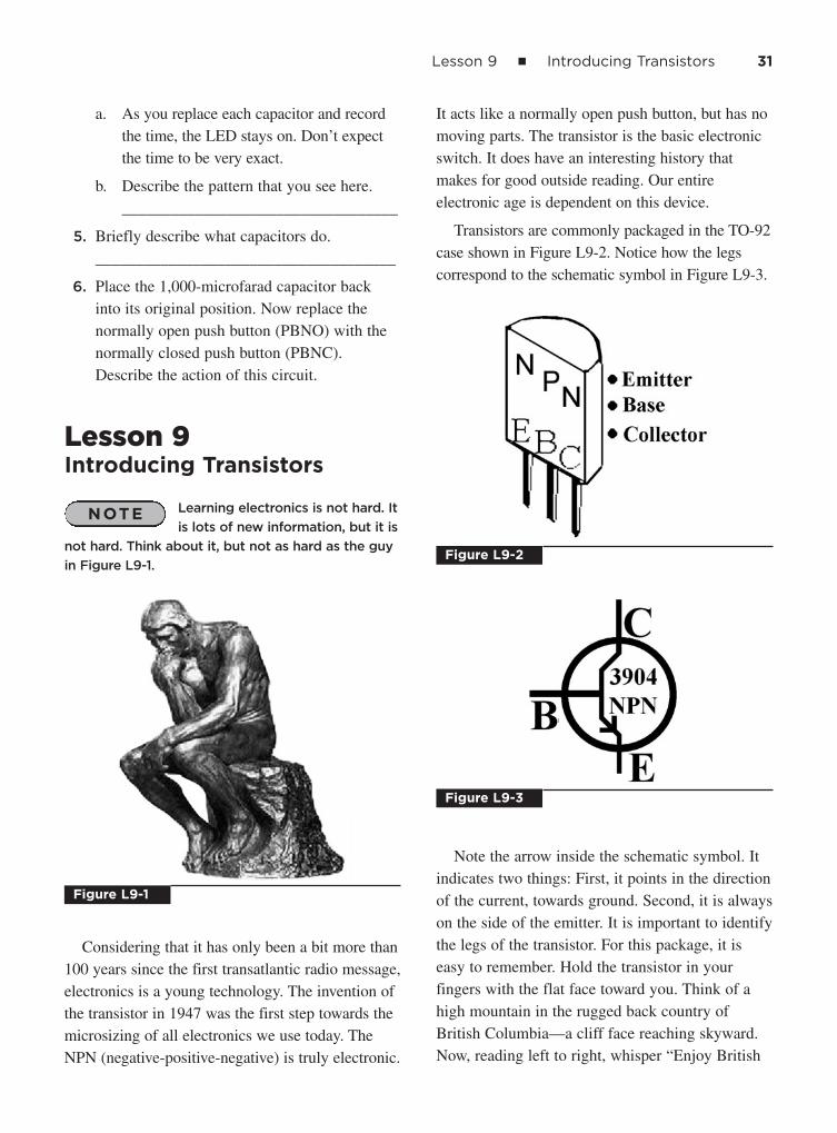
Transistors are commonly packaged in the TO-92case shown in Figure L9-2. Notice how the legscorrespond to the schematic symbol in Figure L9-3.
Note the arrow inside the schematic symbol. Itindicates two things: First, it points in the directionof the current, towards ground. Second, it is alwayson the side of the emitter. It is important to identifythe legs of the transistor. For this package, it iseasy to remember. Hold the transistor in yourfingers with the flat face toward you. Think of ahigh mountain in the rugged back country ofBritish Columbia—a cliff face reaching skyward.Now, reading left to right, whisper “Enjoy British
Lesson 9 ■ Introducing Transistors 31
NOTE
Figure L9-1
Figure L9-2
Figure L9-3

32 Section 3 ■ More Components and Semiconductors
Columbia.” You have just identified the three legs.Cute, but it helps.
There are thousands of different types oftransistors. The only way to identify them is toread the numbers printed on the face of thepackage itself. But even with thousands, there areonly two basic types of transistors, the NPNtransistor and the PNP transistor.
The NPN Transistor
This lesson introduces the NPN transistor, usingthe 3904 NPN. Lesson 10 introduces the 3906PNP. They are opposites but evenly matched intheir properties.
The NPN transistor is turned on when voltageand current are applied to the base. The NPNtransistor acts very much like the water faucetpictured in Figure L9-4. A little pressure on thehandle opens the valve, releasing the water under pressure.
As you can see in Figure L9-5, a little voltageand current on the base of the NPN transistor leadsto a large increase in the flow of current throughthe NPN transistor from the collector to the emitter.
Another way of thinking about it—the forceneeded to open the gates on the Grand CouleeDam, pictured in Figure L9-6, is small compared tothe amount of force that moves through those gates.
Build the NPN Transistor Demonstration Circuit
You have used the capacitor to store small amountsof electricity. It powered the LED directly, butcould only do that for a brief moment. Here, weuse the capacitor to power the transistor. Again,you need to note the similarity between theschematic in Figure L9-7 and the way the circuit is pictured on the solderless breadboard in FigureL9-8 (see also the Parts Bin).
Figure L9-4
Figure L9-5
Figure L9-6

What to Expect
The LED stays off as you attach your battery. Pushand release the push button. The LED will turn on
immediately. It will dim and turn off. This action isfaster with smaller capacitors.
How This Circuit Works
You are using the charge held in the capacitor topower the transistor. The transistor provides a pathfor the current to the LED.
Because the base of the transistor uses muchless power than the LED, the voltage drains fromthe capacitor very slowly. The higher-value resistorof 22,000 ohms slows the drain from the capacitorsignificantly.
The LED staaaaaays on muuuuuuchloooooonger.
Exercise: Introducing Transistors
1. Briefly describe the purpose of the transistor.
_____________________________________
2. What do you think? Anything that looks like atransistor is a transistor.
3. Describe how to tell which leg of thetransistor is the emitter.
_____________________________________
4. Which leg of the transistor is the base?
_____________________________________
5. What two separate things does the arrowinside the transistor symbol indicate?
a. _________________________________
_________________________________
b. _________________________________
_________________________________
6. What is the only way to tell the type oftransistor? ____________________________
_____________________________________
7. Regarding the water faucet analogy, is thewater pressure provided by the water systemor the handle? The pressure is provided by the_____________________________________
Lesson 9 ■ Introducing Transistors 33
■ D1—Safety diode
■ PB—PBNO
■ C1—10 μF
■ R1—22 k�
■ R2—470 �
■ Q1—NPN 3904
■ LED—5 mm round
P A R T S B I N
Figure L9-7
Figure L9-8
34 Section 3 ■ More Components and Semiconductors
8. Press and release the push button. After yourelease the push button, what part provides thepower to the base of the transistor?_____________________________________
_____________________________________
9. Describe the path of the current that providesthe power to the LED. Here is something toconsider regarding the answer. The capacitoris not powering the LED. It is only poweringthe transistor.
10. Record three time trials of how long the LEDstays on with the 10-microfarad capacitor.
Replace C1 with the 100-microfaradcapacitor. Time the LED here for three timesas well, and find the average.
Roughly stated, how much more time didthe 100-microfarad capacitor keep the LED onfor than the 10-microfarad capacitor?
a. Three times longer
b. Five times longer
c. Eight times longer
d. Ten times longer
Write down your prediction of how muchtime the 1,000-microfarad capacitor wouldkeep the LED working.
Okay, now put in your 1,000-microfaradcapacitor. Try it out three times, and averagethe time.
How accurate was your prediction?
11. Describe in detail how this circuit works.Consulting Figure L8-22 of the capacitorpowering the LED once the push button isreleased, the voltage pressure to the base isprovided by the________________________.
Lesson 10The PNP Transistor
We use only the NPN 3904 and PNP 3906. Theserepresent the two general classifications oftransistors. They are evenly matched but oppositein their action.
The identity of the legs on the TO92 packagestays the same, as shown in Figure L10-1. But lookclosely at the symbol for the PNP in Figure L10-02.
Note that the schematic symbol of the transistorholds some important information. The arrowinside the schematic symbol still points in thedirection of the common current, but is on the topside now. Because it is always on the side of theemitter, that means the PNP emitters and collectors
Time 1 Time 2 Time 3 Average
____ s ____ s ____ s ____ s
Time 1 Time 2 Time 3 Average
____ s ____ s ____ s ____ s
Time 1 Time 2 Time 3 Average
____ s ____ s ____ s ____ s
Figure L10-1
Figure L10-2

have reversed positions relative to the NPN. Thelegs on the package are still the same, though. Theemitter and collector have traded positions relativeto the current flow.
Not only are the emitter and collector positionsreversed, but the action is reversed as well. ThePNP transistor’s action is the opposite of the NPN’s.As you increase the voltage to the base, the flowdecreases; as the voltage to the base decreases, thePNP transistor is turned on more. The valve startsin an open position.
The PNP transistor still acts very much like thewater faucet as shown in Figures L10-3 and L10-4.
But now, a little pressure on the handle closes thevalve, stopping the water. No pressure on thehandle allows the water to push through the faucet.No pressure (voltage) on the base of the PNP
transistor allows the voltage and current to pushthrough the transistor.
But just like turning the water faucet’s handlewill decrease the water flow, voltage to the base ofthe transistor will decrease the flow of currentthrough the transistor. Enough pressure on thehandle of the water faucet will shut it off. Enoughvoltage at the base will turn the PNP transistor offcompletely as well.
Surprisingly, the base has the same action for boththe NPN and PNP transistors. It just has a differentstarting position, as shown in Figure L10-5.
Lesson 10 ■ The PNP Transistor 35
Figure L10-3
Figure L10-4
Figure L10-5

36 Section 3 ■ More Components and Semiconductors
Breadboard the PNP TransistorDemonstration Circuit
The capacitor is powering the transistor. Butremember for this PNP transistor that when thecapacitor is charged, it is going to put pressure onthe base of the transistor that will stop the flow.
Note the similarity between this schematic inFigure L10-6 and what the schematic was for theNPN transistor. Also, notice that the transistor in
Figure L10-7 is physically reversed compared tothe NPN transistor in the previous lesson.
What to Expect
The LED turns on as soon as you attach yourbattery.
1. Push and release the push button.
2. The LED will turn off immediately. It willslowly turn back on.
How It Works
1. When you first attach your battery, the LEDturns on immediately because there is novoltage pressure pushing at the base, so thevalve is in the opened position, allowing thecurrent to flow from emitter to collector.
2. When you push the plunger down, the voltageimmediately pushes against the base of the3906 PNP transistor (Q1), closes the valve,and blocks the current flow. Voltage also fillsthe capacitor C1.
After you release the push button, C1holds the voltage pressure and keeps voltageon the base, keeping the valve closed and thecurrent cut off.
Figure L10-6
Figure L10-7
■ Q1—PNP 3906
■ R1—100 k�
■ R2—22 k�
■ R3—470 �
■ C1—10 μF
■ PB—N.O.
■ LED—5 mm round
P A R T S B I N

3. As the voltage drains from C1 through R1, thevoltage pressure against the base is released.The transistor starts passing current andvoltage again slowly. The LED turns back on.
4. Why the extra resistor (R1)? (a) Before thepush button is closed, both C1 and the base ofthe 3906 PNP transistor have no voltage.Because there is no voltage pressure on thebase of Q1, the valve is open and current flowsfrom emitter to collector; (b) when the voltagein the capacitor is high, Q1’s valve stays shut;(c) the path for current to escape from C1through the transistor is blocked because thevalve is closed; (d) so, R1 is necessary to drainthe charge from the capacitor. This allowsQ1’s valve to open again.
The capacitor is unable to drain and thetransistor stays off because the voltage from thecapacitor keeps the pressure on the base of thetransistor, keeping the valve closed. The capacitorcannot drain through the base of the PNP transistorlike it did in the previous 3904 NPN circuit. Theextra resistor allows the cap to slowly drain,decreasing the voltage pressure on the base of thePNP transistor, allowing the valve to reopen andlet current flow again.
Exercise: The PNP Transistor
1. In the schematic, Q stands for whatcomponent? Q represents the __________________________________________________.
2. The arrow in the transistor symbol representswhat action?
a. Direction of current flow
b. Direction of the collector
c. Direction of the base
d. Direction of the emitter
3. The arrow is always on the side of which legin the schematic?
a. Voltage
b. Emitter
c. Base
d. Collector
4. What would happen if R3 were not in thecircuit and the LED was connected directly tothe collector of the 3906 transistor?
a. LED would burn out.
a. LED would be bright.
a. LED would not work.
a. LED would flash.
Explain your answer to the above.
_____________________________________.
5. Replace C1 with the 100-microfaradcapacitor. Describe what happens.
_____________________________________.
Why does changing the capacitor affect thecircuit this way?
_____________________________________.
6. Change C1 back to 10 microfarad. Nowchange R1 to 10 megohm (brown-black-blue).Describe what happens.
_____________________________________.
7. Think of the capacitor as a sink, holdingwater. Think of the resistor as the drainpipe.Which of the following statements bestexplains how changing to a higher resistancehas the same effect as changing to a largercapacitor?
a. The drain is bigger and empties the waterfaster.
b. The drain is smaller and empties the waterslower.
c. The volume of water is bigger and takeslonger to drain.
Lesson 10 ■ The PNP Transistor 37

38 Section 3 ■ More Components and Semiconductors
d. The volume of water is smaller and drainsfaster.
8. Play a little.
a. Replace R3 and the LED with the buzzer.Make sure the buzzer’s red wire is gettingvoltage from the 3906’s collector and theblack wire is connected to ground.
b. Push button and release. What happens tothe sound as the capacitor discharges?
_________________________________.
9. Carefully describe in your own words howthis circuit works.
_____________________________________.
Lesson 11The Phototransistor:Shedding Some Light onAnother Component
All transistors are light-sensitive. Shortly aftertransistors were invented, engineers recognized thattheir new toys gave different results as lightingconditions changed. Lots of work went intoshielding the guts of the early transistors. But at thesame time, lots of effort was put into understandingand finding uses for this phenomenon.
The results of this research? The phototransistor.Figure L11-1 shows both the phototransistor(darkened glass) and its corresponding infrared(IR) LED (clear glass).
Many of the available phototransistors havebeen developed to react to specific wavelengths oflight. This is important, because the intent is tocontrol the transistor, leaving nothing to chance.
So how do we use this “tuned” phototransistor toour advantage? Here, I’m using a phototransistorthat reacts specifically to IR light with a wavelengthof 940 nanometers. Both sunlight and filament lightbulbs create IR that will affect our phototransistor.Fluorescent lights don’t have an infrared componentin their spectrum.
So what to use as a light source? Hmmm? Whatcolor LEDs are readily available? Red, yellow,blue, green, and orange. Table L11-1 shows thewavelength of each color. Our eyes don’t respondto the wavelengths above 750 nm, but digitalcameras do respond to low-end IR.
LEDs that emit IR are also available. We use onethat is specifically matched to the phototransistorwe’ll be using. Even the part numbers are the same,except for one added letter.
Let’s start playing. The Parts Bin has a full parts list.
Figure L11-1
400nm 475nm 510nm 570nm 590nm 650nm 750 to 2,500nm
Violet Blue Green Yellow Orange Red Infrared
TABLE L11-1 We Need an Infrared LED for an Infrared Phototransistor

Figure L11-2 presents the basic schematic. Yes,there really are two separate circuits next to eachother. Well, how else can they be compared? Eachsystem has its own input, processor, and output.Build the two circuits. The second system has thetwo new components. The LDR responds best to aorange or yellow LED. The IR LED is paired withthe phototransistor. Figure L11-3 shows the setupon the breadboard.
Each pair represents a separate system.
■ LED 1 is the input to the LDR. The LDR is theprocessor. LED 2 is the output of the firstsystem.
■ IR LED is the input to the phototransistor. Thephototransistor is the processor. LED 4 is theoutput of the second system.
What to Expect
Do your work away from sunlit windows. Daylightprovides a full spectrum that affects both the LDRand the phototransistor.
As you slide a piece of thick paper between theinput and processor of each system, the outputsturn on and off. Does the phototransistor act likean NPN or PNP transistor? The output should beoff when there is no input.
No big deal. Pretty much the same. Why bother?
But they aren’t the same. Let’s do somemeasuring. Why else would I have labeled a testpoint on each circuit? For each system, measureand record the test point voltage for bothconditions. Record your results. System 1: TP1_____volts. System 2: TP2 _____volts.
For System 1, the LDR uses a large amount ofthe voltage. However, the phototransistor usesabout as much as the diode did back in Lesson 3.There is significantly more voltage available atSystem 2’s test point.
“Yeah?” you say. “So what?” So let’s play. Let’ssee if it means anything.
Lesson 11 ■ The Phototransistor: Shedding Some Light on Another Component 39
■ R1, R2, R3, R4—470 �
■ LED 1—Yellow or orange work best
■ LED 2, 3, and 4—Whatever colors youwant
■ Infrared LED 3mm (clear glass)—LTE4206/IR 3mm 940nM
■ LDR—1 M� dark
■ NPN phototransistor 3mm (darkenedglass)—LTE 4206E/IR 3mm 940nM
P A R T S B I N
Figure 11-2
Figure L11-3

Modifying the Setup
Make a copy of Figure L11-4 and paste it ontosome thick paper.
The complete setup is shown in Figure L11-5.Cut the disk and slots. Center your disk on a pencilso it spins evenly.
Now, as you spin the pencil, rate theresponsiveness of each circuit on the “MushinessScale” (Table L11-2).
How It Works
The LDR’s response is limited. The photosensitivearea does not instantly change resistance. It ismeasured in � per millisecond. Also, you’ve seenthat the resistance does not go much below 1 k�.
However, the phototransistor’s response time ismeasured in microseconds. That’s 1,000 timesfaster than the LDR. It doesn’t need much input to“saturate” the base, opening the transistor’s valvequickly and completely. There is little resistance,providing a clean, fast, and accurate response.
40 Section 3 ■ More Components and Semiconductors
Figure 11-4
Figure 11-5
Input through Veryslot Processor Output Slow crisp
LED 1 LDR LED2 1 2 3 4 5 6 7 8 9 10
IR LED Photo
Transistor LED4 1 2 3 4 5 6 7 8 9 10
TABLE L11-2 Does the LDR or Phototransistor Work Better, Even at Different Speeds?

Modify It Some More
Take a moment. Compare the system responsewhen the light source is a bit farther away. InFigure L11-6, the input half of the circuits hasbeen moved to the opposite end of the breadboard.There will be a noticeable difference between thetwo systems.
Did you know that your TV remote usesinfrared? See if your phototransistor responds toyour remote control. Press a key. Any key will do.It should respond.
Lesson 11 ■ The Phototransistor: Shedding Some Light on Another Component 41
Figure 11-6

This page intentionally left blank

Two Projects and Then Some More
S E C T I O N 4
43
ENOUGH OF THIS PLAYING around. Let’s dosomething.
Lesson 12Your First Project: TheAutomatic Night Light
We combine our knowledge and the components tomake an automatic night light. It dims in the lightand brightens in the dark. Using the LDR, buildthe circuit shown in Figure L12-1 on yourbreadboard. The photograph of the circuit appearsin Figure L12-2 (see also the Parts Bin).
Figure L12-1
Figure L12-2
■ D1—1N400X diode
■ P1—100 k� pot
■ R1—22 k�
■ R2—470 �
■ LDR—1 M� dark
■ Q1—NPN 3904
■ LEDs—5 mm round
P A R T S B I N

44 Section 4 ■ Two Projects and Then Some More
What to Expect
1. Attach your power supply.
2. Turn the knob on the pot one direction until thelight-emitting diodes (LEDs) are barely off.
3. Now darken the room or stand in a closet. TheLEDs will turn on.
4. Move to a semi-lit area. The LEDs will dim asyou move into the light. Adjust the pot so thatthe LEDs are again barely off. Any reductionof the amount of light will now turn the LEDson. This is your automatic night light.
How It Works
Figure L12-3 shows the movement of current andvoltage in the circuit as the light changes.Remember the NPN transistor needs positivevoltage to its base to turn on.
1. The potentiometer adjusts the amount ofvoltage shared by the 22-kilo-ohm resistor andthe LDR.
2. In light, the LDR has low resistance, allowingall of the voltage to flow through to ground.Because the base of Q1 gets no voltage, thevalve from C to E stays closed.
3. The resistance in the LDR increases as it getsdarker, providing more voltage to the base ofthe transistor, pushing the valve open.
4. As the voltage flows through the transistor,the LEDs turn on.
If P1 is set to a low resistance, more voltagegets through. The more voltage that gets throughthe potentiometer, the easier Q1 turns on, becausethe LDR cannot dump all of the voltage.
Exercise: Your First Project—
The Automatic Night Light
1. Set the pot so the resistance between legs Aand C, the center leg, is close to 50 kilo-ohms.Figure L12-3 shows how the voltage and currentmove in the different conditions for this setup.
2. Now set your circuit under a fairly good light. Measure and record the voltage at the test point shown in Figure L12-4. ______ V
3. Now cover the LDR with a heavy, dark pen cap. Measure and record the voltage at the test point again. ______ V
Did the LED output change at all?
So here’s a major question: Do you recallhow much voltage is used from V� to ground?
■ Does it depend on the amount of voltageavailable? NO!
■ Does it depend on the number or types ofparts in the circuit? NO!
Figure L12-3

By definition, voltage used between V�
and ground doesn’t relate to any circuitvariables.
The question is like asking, “How muchdistance is there between this altitude and sealevel?”
The answer is—whatever the altitude is—all the distance!
By definition, ground is 0 volts.
■ How much voltage is used between V�
and ground?
■ The answer will always be All the voltageis always used between V� and ground.
4. Okay. Figure L12-5 will help explain how allthe voltage in this circuit is used.
Remember the idea of the waterfall whenwe first looked at resistors. As the size of theload increased, the amount of voltage usedincreased proportionately. The same thinghappens with two resistor loads in this circuit.More detail is given in Figure L12-6.
The pot uses some voltage because it is setnear 50,000 ohm here.
The LDR uses a small amount of thevoltage in the light because it has a smallresistance. When it is in the dark, the LDRhas a great deal of resistance. The base of the
Lesson 12 ■ Your First Project: The Automatic Night Light 45
Figure L12-4
Figure L12-5

46 Section 4 ■ Two Projects and Then Some More
transistor reacts to the voltage available at thatpoint where the LDR and pot connect. Itbecomes obvious which situation providesmore voltage to the transistor’s base.
5. Set the pot so the resistance between legs Aand C, the center leg, is close to 0 ohms.Figure L12-6 shows how the voltage availableto the transistor base is identical in both thelight and the dark. The potentiometer usesnone of the voltage, so the base of thetransistor is exposed to nearly full voltage inboth circumstances.
6. Now set your circuit under a fairly good light. Measure and record the voltage at the test point shown in Figure L12-6. ______ V
7. Now cover the LDR with a heavy, dark pen cap. Measure and record the voltage at the test point again. ______ V
Did the LED output change at all? Did youexpect the output to change?
8. Set the pot so the resistance between legs Aand C, the center leg, is close to 100 kilo-ohms. Figure L12-7 shows how the voltage isresponding to the changing resistance of the
Figure L12-7
Figure L12-6

LDR, changing the voltage available to thebase of the transistor. The pot here is adjustedto twice as much resistance as before, so itwill use twice as much of the voltageavailable. The LDR must be set into nearlycomplete darkness or you will get muddyresults.
9. Now set your circuit under a fairly good light. Measure and record the voltage at the test point. ______ V
10. Now cover the LDR with a heavy, dark pen cap. Measure and record the voltage at the test point again. ______ V
Did the LED output change at all?
Substitute the Phototransistor for the LDR
The LDR has been the traditional component usedto respond to ambient light, commonly applied in a variety of circuits from toys to streetlights.However, this simple and useful component isfalling out of favor because it contains cadmium, a highly toxic substance. Don’t eat them. Import to the European Union is already restricted.
Here is a substitute night light circuit that usesthe phototransistor. The few components are listedin the Parts Bin. Because this is a much simplercircuit, it is not useful for explaining the conceptsjust introduced.
With so few components, the schematic inFigure L12-8 is very simple.
Make sure that the phototransistor is set inproperly. The flat edge and short leg indicate thecollector. This phototransitor acts like an NPNtransistor. The collector is connected towards V�.
How It Works
Remember—sunlight has the complete spectrum,including infrared (IR). Incandescent light bulbsalso produce some IR. Most fluorescent lights donot have an IR component, so the phototransistornight light will react to daylight and older “wire”light bulbs, but most likely will stay on whetherthe fluorescent lights are turned on or off.
1. Look at Figure L12-9. When there is IR inputto the base of Q1, the phototransistor, voltageand current flow through it directly to ground.Nothing is left at TPA to tickle the base ofQ2. So Q2 stays off. No voltage or currentmoves through Q2. As long as Q1 stays on,Q2 remains off. No power for the LED.
2. When there is no input to the base of Q1 (noinfrared) the voltage and current cannot movethrough the phototransistor. Instead, they arererouted to the base of Q2, turning on the
Lesson 12 ■ Your First Project: The Automatic Night Light 47
■ R1—22 k�
■ R2—470 �
■ Q1—NPN photo transistor LTE 4206 E(darkened glass) 3mm diam
■ Q2—2N3904 NPN in a TO-92 package
■ LED—Standard 5mm
P A R T S B I N
Figure L12-8

48 Section 4 ■ Two Projects and Then Some More
2N3904 transistor. Voltage and current movethrough Q2 from C to E, turning on the LED.
Like plumbing, it’s all about controlling theflow. Once you understand the initial concept, itreally is simple.
Building the Automatic Night Light Project
This is a top view of your printed circuit board(PCB). The traces on the underside are shown asgray in Figure L12-10.
Figure L12-11 shows the view of the PCBlooking directly at the bottom. The copper tracesreplace the wires used in the solderless breadboard.
The series of frames in Figure L12-12 showhow the PCB layout was developed. Creating sucha layout is a relatively simple task.
Mounting Your Parts
Be certain to get your parts into the correct holes,as displayed in Figure L12-13. Your solderingtechnique is vital. Check out the solderinganimation on the website www.mhprofessional.com/computingdownload. Each solder connectionshould look like a Hershey’s Kiss. Just as one badapple spoils the bunch, one bad solder can spoilyour project (and your fun). The parts are mountedonto the board so that their legs stick out throughthe bottom. The copper traces are on the bottom.The soldering is on the bottom. This is a good job.
Figure L12-11
Figure L12-9
Figure L12-10

I got such a laugh when the circuit in FigureL12-14 was presented to me for troubleshooting.This person did not follow directions. Theymanaged to mount the parts on the wrong side ofthe printed circuit board. They made a mess. Itdidn’t work. There is never enough time to do itright, but there is always time to do it over.
Finishing Up
I would recommend using a touch of hot glue oneach corner of the PCB and then pressing thecircuit onto a thick piece of cardboard. You can
mount it on anything that is an insulating material.Anything metallic would short-circuit your project,and probably destroy the transistor.
Lesson 13Specialized Transistors—The SCR
There are many highly specialized types oftransistors. Here we use a latching switch called asilicon-controlled rectifier (SCR). This componentis also referred to as a triode for alternatingcurrent (TRIAC). The SCR acts like a “trapdoor.”Once triggered, it stays latched open. You arefamiliar with this because it is the basic component
Lesson 13 ■ Specialized Transistors—The SCR 49
Figure L12-12
Figure L12-13
Figure L12-14

50 Section 4 ■ Two Projects and Then Some More
in fire alarms and burglar alarms. Once triggered,it stays on. This is your second project, aprofessional-quality alarm circuit.
Electronics is all about using an electrical pulseto control things or pass information. A commonlyused solid-state switch (no moving parts) is theSCR. It is provided in a variety of packages, themost common ones are pictured next to theirsymbol in Figure L13-1.
Remember, not everything in this type of packageis an SCR.
■ “A” leg is anode, the positive side.
■ “G” leg is gate; not to be confused with ground,“gnd.”
■ “K” leg is cathode, referring to the groundedside. “C” is already used for capacitor, forexample, C1, C2.
The SCR is often used in alarm systems; once itis triggered, it stays on. Its action is best depictedin the series of frames shown here in Figure L13-2.
When V� hits the G (gate) leg of the SCR, alatch releases, opening a “trapdoor” between A(anode) and K (cathode). This trapdoor remainsopen until the power is removed. In other words, itlatches itself open. That is why an SCR is called alatching circuit. The only way to turn the SCR offis to shut off the power. Turn the power on again,and the SCR is reset.
Breadboard the SCR Circuit
There are four stages to building this professional-style alarm circuit. Each one will be consideredindividually.
Stage 1: The Basic System
Build the basic SCR circuit by carefully followingthe schematic presented in Figure L13-3. The partslayout is shown in the photograph in Figure L13-4(see also the Parts Bin). Don’t get too comfortableusing the photograph. You will have to depend onschematics from now on to help you develop youralarm circuit.
■ D1—1N400X
■ R1—100 k�
■ R2—470 �
■ SCR—TRIAC C106B
■ Buzzer—9v
■ LED—5 mm round
P A R T S B I N
Figure L13-1
Figure L13-2

What to Expect
■ When you attach the battery, it should be quiet.
■ Touch the sensor probe to the end of R1. Thebuzzer should turn on.
■ You need to disconnect the battery to reset the SCR.
How It Works
1. When you attach the battery, the LED is offand the buzzer is quiet. Voltage is notavailable to the LED and buzzer because theSCR has not been activated. The circuit pathbetween A and K is not available until voltageis put to the gate.
2. When you touch the end of the probe to thebottom of the 100-kilo-ohm resistor, voltage isfed to the gate (G) leg.
3. The voltage activates the latch and opens thecircuit path from A (V�) to K (gnd). Currentmoves on this path from A to K, through theSCR, providing voltage and power to the LEDand the buzzer.
4. The buzzer and LED should turn on and stayon until you disconnect the power. When youreconnect the power, the LED should not lightand the buzzer should be quiet.
Stage 2: Make Life Easier
It is a hassle to disconnect the battery each timejust to reset the SCR. Wouldn’t it be so mucheasier just to use a push button to reset the circuit?So go ahead and use the normally closed pushbutton to do just that.
It does not matter where the voltage to the SCR iscut off. As you can see in Figure L13-5, any of thefollowing suggestions work. Each one disconnectsthe voltage to the circuit and resets the SCR.
Lesson 13 ■ Specialized Transistors—The SCR 51
Figure L13-3
Figure L13-4

52 Section 4 ■ Two Projects and Then Some More
Stage 3: Avoid Static Buildup
Modify the SCR circuit with a few changes, shownin Figure L13-6.
1. Shift the SCR below the LED and buzzer. Inmost circuits, you can be flexible. It reallydoesn’t matter which component comes first.
2. Add the 0.1-microfarad capacitor.
3. Add the PBNO for a trigger.
How It Works
1. When the push button is pushed, the capacitorfills “nearly” instantly because the 100,000-ohm resistor slows down the current. Thecapacitor acts like a cushion and dampens anysmall but annoying jumps in the voltage to thegate that might be caused by static electricity.It avoids false alarms by preventing anyaccidental triggering of the SCR.
2. The gate (G) of the SCR senses the signalwhen the capacitor is filled.
Stage 4: A Complete System
Now modify your circuit to make a simple butprofessional-quality alarm system by adding threemore parts to your working breadboard, as shownin Figure L13-7.
■ D2—1N400X
■ R1—47 k�
■ PBNC—Normally closed push button
P A R T S B I N
Figure L13-5
Figure L13-6

What to Expect
■ Attach your power supply. The LED should beoff and the buzzer quiet.
■ Push the plunger on the PBNC. The buzzerwill start, and the LED light will turn on.
■ To reset, disconnect the power—count tenseconds—and then reconnect.
■ Now push the plunger on PBNO. The buzzerand LED will turn on.
How It Works
As long as the PBNO stays closed, the voltagetakes the “path of least resistance” and goesdirectly to ground. No voltage reaches G, the gateof the SCR.
When the PBNO is pushed, the connection toground is broken and the voltage has to movethrough D2, activating G, and turning the SCR on.
As long as the PBNC stays open, the voltagecannot move across the gap. Air is a greatinsulator. No voltage reaches G. When the PBNCis pushed, the voltage travels through to the gateleg, turning the SCR on.
Exercise: Specialized Transistors—The SCR
1. If a component looks like your SCR, it is anSCR. True/false. Support your answer.
2. How can you tell if it is an SCR withoutputting it onto your breadboard?
3. Many alarm systems use an SCR. Forexample, a fire alarm, once triggered, keepsgoing. Describe what needs to be done toreset the SCR in the alarm.
4. Use Figure L13-7 to follow the current’s pathwhen the PBNC is in its normal position.
5. How does the path change when you push theplunger on the PBNC?
6. Follow the current’s path when the PBNO isin its normal position.
7. How does the path change when you push theplunger on the PBNO?
8. Have you ever seen metal foil tape on theedge of store windows? There is a smallcurrent running through this tape. If thewindow breaks, the foil is torn. Whatcomponent does the foil tape replace in yourburglar alarm system?
9. Describe how a normally open type of switchwould be used in a burglar alarm?
Assembling the Alarm
Figure L13-8 represents the SCR’s printed circuitboard when viewed from the bottom. Figure L13-9shows lines that appear faded. This is the view ofthe PCB when you look at the traces through thefiberglass backing.
Consider this: If you mount your simple pushbuttons onto the PCB directly, you have a verycute demonstration circuit. If you mount the pushbuttons on a long wire, you still need to wait forsomeone to push one of the buttons. That still isn’tmuch of an alarm. What you really need to do iscreate your own contact switches. When you do
Lesson 13 ■ Specialized Transistors—The SCR 53
Figure L13-7

54 Section 4 ■ Two Projects and Then Some More
this, you can apply this as a real alarm system. Thebest setup for your power supply is to have both awall adapter and a 9-volt battery. This way, thecircuit still works even if your house has no power.
Lesson 14The Regulated Power Supply
Have your batteries been feeling tired lately? Notwhat they used to be? All used up? Just don’t havethat push they used to have? There’s a better way.
Here, we build a power supply that provides astable 9v DC that you can always use as youcontinue to develop your skills. We’ll use anotherspecialized transistor, the voltage regulator, inconjunction with a basic wall adapter. Any 9v DCwall adapter will do—even the one provided in theEvil Genius Kit.
The few important things are highlighted inFigure L14-1.
1. Voltage input (120v AC) and output (9v DC)
2. Amount of output current (200mA)
3. The output plug wiring as a graphic
Now that you’ve looked at it, plug it into thewall. Don’t worry about what you are about to donext. Any wall adapter in this range actually putsout less power than most 9-volt batteries. Set yourDMM to vDC. Hold the red lead to one part of theoutput plug and the black line to the other. See thedisplay in Figure L14-2.
Figure L14-2
Figure L13-8
Figure L13-9
Figure L14-1

Why does it show 13 vDC? Because it isunregulated. It will give more than 9 volts,depending on how hard it’s working. What we’regoing to do is build a regulated power supply thatwill provide us with 9 volts all the time.
Let’s Get to Work
The following directions will get you to FigureL14-3:
1. Remove the adapter from the wall (duh!).
2. Clip the wires as close as possible to the DCoutput plug. Separate and strip the outputwires.
3. Plug the adapter back in. Use the DMM againto determine which line is V�.
4. Remove the sheaths from the alligator clips.Slide the red sheath onto the V� line and theblack onto the ground.
5. Double-check that you have the lines properlyidentified.
6. Unplug it while you solder the clips onto eachline. Figure L14-3 shows the finished product.
All that, and now we can get to the realworkhorse of this circuit, the 7809 voltageregulator, proudly displayed in Figure L14-4.
The 7809 is only one of many in the 78XX and79XX voltage regulator series. Table L14-1 showswhat is available in the full series.
Respectively, place a red hookup wire into holeE-60 of your SBB and a black hookup wire intothe ground line on the bottom. The schematic inFigure L14-5 shows how to set up the circuit, andthe photo in Figure L14-6 shows the layout.
The capacitor actually is part of the workingcircuit. The LED isn’t necessary, but convenientlytells us when the circuit is powered up.
Lesson 14 ■ The Regulated Power Supply 55
Figure L14-3
Figure L14-4
Positive Regulators Negative Regulators
7803 +3vDC 7903 –3vDC
7805 +5vDC 7905 –5vDC
7809 +9vDC 7909 –9vDC
7812 +12vDC 7912 –12vDC
7815 +15vDC 7915 –15vDC
TABLE L14-1 Other Voltage Regulators AreAvailable, but the 78XX Series Is Most Popular

1. The V� input line from the wall adaptershould be wired directly to the 7809’s input leg.
2. The adapter’s ground wire is connecteddirectly to the blue ground line across thebottom of your SBB.
3. The output leg is connected directly to the red V� line that runs across the top of thebreadboard.
What to Expect
Plug it in. First off, the LED should come on. Ifthe LED does not turn on, unplug the wall adapterimmediately and check your wiring.
Now, measure the voltage across the capacitor,because conveniently, it has exposed wires.
It should have a readout of 9v DC. This 7809voltage regulator has a tolerance of 4 percent. So its maximum would be 9.36v and minimum 8.64v.
Okay, that’s it for your quick, regulated powersupply. Use this as your power supply for the restof the book.
Like I’ve said before: Electronics is not hard.There’s lots of new information, but it’s not hard.
56 Section 4 ■ Two Projects and Then Some More
Figure L14-5
Figure L14-6

Introduction to Digital Electronics
P A R T T W O

This page intentionally left blank

Digital technology circa 1801.
59
The Start of the Digital Revolution
Actually, the idea of “digital” was first introduced by the textile industry. It
all started with an attachment to an existing loom. The Jacquard head
attached to the large Dobby loom (figure below). A set of punched cards
was connected to a chain. Once the cards were set, the up/down motion of
a single lever moved them forward, advancing the pattern. Thus, digital as a
functional technology was introduced over 200 years ago.

Description Type Quantity
1N4148 Signal diode 1
2N-3906 PNP transistor TO-92 case 2
2N-3904 NPN transistor TO-92 case 2
Phototransistor LTE 4206 E (darkened glass)3mm diameter: tuned to 940nm 1
Infrared LED LTE 4206 (clear glass)3mm diameter: tuned to 940nm 1
LED 5 mm 2
100 � Resistor 1
1,000 � Resistor 2
10,000 � Resistor 1
22,000 � Resistor 1
39,000 � Resistor 1
100,000 � Resistor 2
220,000 � Resistor 1
470,000 � Resistor 2
1,000,000 � Resistor 1
2,200,000 � Resistor 1
4,700,000 � Resistor 1
10,000,000 � Resistor 2
20,000,000 � Resistor 1
100 k� trim pot Potentiometer 1
Light-dependent resistor LDR 1
10 �F Cap
100 �F Cap
.01 �F disk Cap 1
.1 �F film Cap 1
1 �F radial Cap 1
4011 quad NAND gate IC 1
1" � 1/8" heat shrink Hardware 4
1/8" male plug Hardware 1
14-pin DIP socket Hardware 1
2" � 1/4" heat shrink Hardware 1
Alligator clips (red and black) Hardware 1 each
Battery clip Hardware 1
PBNC Hardware 2
PBNO Hardware 2
Speaker 8 � Hardware 1
24 gauge wire Hookup wire Various colors
Speaker wire 3’ 20 gauge Hardware 1
Printed circuit board PCB 1
■ Not all components will be consumed by project work.
P A R T S B I N F O R P A R T T W O
60

THIS COURSE DEALS WITH a vast amount of newinformation. Remember that electronics is nothard; there’s just lots of new information to learn.
Lesson 15A Spoiled Billionaire
As we begin the “digital” electronics unit, thislesson shows us a system that we can use to becertain that all of the information is transferred allthe time, perfectly. You must be able to count to 255and know the difference between “on” and “off.”
With apologies to Bill Gates, but inspired by hisexplanation in his book, The Road Ahead: There isan eccentric billionaire who lives near Seattle. Heis particular about his lighting in different rooms ofhis homes, especially his den. He likes it set atexactly 187 watts. And when you’re rich, you getwhat you like. But here’s the real problem. Hiswife also uses the den and she “likes” 160 watts.
They asked their groundskeeper to come up with asolution they could use in all their homes aroundthe world. He first installed a dimmer switch andput a mark next to the spot that represented theirpreferences, which is pictured in Figure L15-1.
On inspection, the groundskeeper was told thathis solution was not acceptable. It was not exactenough. So he thought further and had an idea.Actually, eight ideas.
His idea is shown in Figure L15-2: a light barwith eight separate specific value lights. Each light
Digital Logic
S E C T I O N 5
61
Figure L15-1
Figure L15-2

would have a different wattage rating, and eachwould have its own switch. To adjust the lightingfor his own needs, the billionaire would only haveto turn on a set of specific switches. Those aredisplayed specifically in Figure L15-3.
And to make the softer lighting situation forMrs. Billionaire, she flips the switches shown inFigure L15-4.
So all the groundskeeper had to do was write anote under the set of switches in the den.
His � 10111011Hers � 10100000
(The Road Ahead, Bill Gates, pg. 25)
By turning these switches on and off, you canadjust the lighting level in watt increments from 0 watts (all switches off) to 255 watts (all switcheson). This gives you 256 possibilities.
If you want 1 watt of light, you turn on only therightmost switch, which turns on the 1-watt bulb(shown in Figure L15-5).
62 Section 5 ■ Digital Logic
Figure L15-3
Figure L15-4
Figure L15-5

If you want 2 watts, you turn on only the 2-wattbulb (shown in Figure L15-6).
If you want 3 watts of light, you turn on both the1-watt and 2-watt bulbs, because 1 plus 2 equalsthe desired 3 watts (shown in Figure L15-7).
If you want 4 watts of light, you turn on the 4-watt bulb.
If you want 5 watts, you turn on just the 4-wattand 1-watt bulbs (shown in Figure L15-8).
If you want 250 watts of light, you turn on allbut the 4-watt and 1-watt bulbs (shown in FigureL15-9).
If you have decided the ideal illumination levelfor dining is 137 watts, you turn on the 128-, 8-, and1-watt bulbs, like this (shown in Figure L15-10).
Lesson 15 ■ A Spoiled Billionaire 63
Figure L15-6
Figure L15-7
Figure L15-8
Figure L15-9
Figure L15-10

This system makes it easy to record an exactlighting level for later use or to communicate it toothers who have the same light switch setup.Because the way we record binary information isuniversal—low number to the right, high numberto the left, always doubling—you don’t have towrite the values of the bulbs. You simply recordthe pattern of switches: on, off, off, off, on, off,off, on. With that information, a friend canfaithfully reproduce the 137 watts of light in yourroom. In fact, as long as everyone involved double-checks the accuracy of what they do, the messagecan be passed through a million hands; at the end,every person will have the same information andbe able to achieve exactly 137 watts of light.
To shorten the notation further, you can recordeach “off” as 0 and each “on” as 1. This meansthat instead of writing down “on, off, off, off, on,off, off, on,” meaning turn on the first, the fourth,and the eighth of eight bulbs and leave the othersoff, you write the same information as1,0,0,0,1,0,0,1, or 10001001, a binary number. Inthis case, it’s 137. You call your friend and say:“I’ve got the perfect lighting level! It’s 10001001.Try it.” Your friend gets it exactly right by flippinga switch on for each 1 and off for each 0.
This may seem like a complicated way todescribe the brightness of a light source, but it isan example of the theory behind binary expression,the basis of all modern computers.
The simplest computers use an 8-bit system like the eight light switches. Each bit is a bit ofinformation. The binary word of 8 bits makes 1 byte, as shown in the explanations earlier.
From the earliest days of computing, thealphabet and numerals have been assigned specificvalues (Table L15-1).
The real question for the rest of us becomes—Why use binary? It seems so confusing!
The answer is actually very simple. We aredealing with machines. The easiest thing for a
machine to sense is whether something is on oroff.
So we are forced to use a system that can countin on’s and off’s.
But still you ask, why bother?
Well, look at it (Table L15-2).
64 Section 5 ■ Digital Logic
Space = 20 = 00010100
A = 65 = 01000001 a = 97 = 01100001
B = 66 = 01000010 b = 98 = 01100010
C = 67 = 01000011 c = 99 = 01100011
D = 68 = 01000100 d = 100 = 01100100
E = 69 = 01000101 e = 101 = 01100101
F = 70 = 01000110 f = 102 = 01100110
G = 71 = 01000111 g = 103 = 01100111
H = 72 = 01001000 h = 104 = 01101000
I = 73 = 01001001 i = 105 = 01101001
J = 74 = 01001100 j = 106 = 01101010
K = 75 = 01001101 k = 107 = 01101011
L = 76 = 01001110 l = 108 = 01101100
M = 77 = 01001101 m = 109 = 01101101
N = 78 = 01001110 n = 110 = 01101110
O = 79 = 01001111 o = 111 = 01101111
P = 80 = 01010000 p = 112 = 01110000
Q = 81 = 01010001 q = 113 = 01110001
R = 82 = 01010010 r = 114 = 01110010
S = 83 = 01010011 s = 115 = 01110011
T = 84 = 01010100 t = 116 = 01110100
U = 85 = 01010101 u = 117 = 01110101
V = 86 = 01010110 v = 118 = 01110110
W = 87 = 01010111 w = 119 = 01110111
X = 88 = 01011000 x = 120 = 01111000
Y = 89 = 01011001 y = 121 = 01111001
Z = 90 = 01011100 z = 122 = 01111010
TABLE L15-1 The Binary Alphabet: The ASCII Table

Exercise: A Spoiled Billionaire
I am writing in binary code!
010010010001010001100001011011010001010001
110111011100100110100101100111011010000111
010001101001011011100110111000101000110100
101101110000101000110001001101001011011100
110000101110010011110010001010001100011011
01111011001000110010
1. What do you think is the most importantadvantage of using digital information?
Use Table L15-3 to help translate frombinary to decimal, and back.
Lesson 15 ■ A Spoiled Billionaire 65
Bit number Bit 8 Bit 7 Bit 6 Bit 5 Bit 4 Bit 3 Bit 2 Bit 1
Value 128 64 32 16 8 4 2 1
TABLE L15-3 Binary to Decimal and Back
Analog Digital
Advantages
1. Varying voltages. 1. Precise transfer of information.
2. Easy to record. 2. No generational loss.
3. Easy to play back. 3. Footprint of a bit can be done at
the molecular level.
4. Common transfer rate is a billion
bits per second.
5. Any material can be used for
storing data: 0s and 1s.
Disadvantages
1. Not precise. 1. Needs special equipment to transfer,
record, and read information.
2. Signal loss with each generation
recorded. Have you ever watched a
copy of a copy of a videotape? Ugh!
3. Takes up large “recording” space.
Compare the size of a videotape to a
DVD or a memory stick.
4. Limited transfer time—how long does it
take to record a video, compared to
transfer of a CD or MP3 file?
5. Specific media used for storage doesn’t
translate from one media to another—
for example, video to film.
6. Signal fades as media ages.
TABLE L15-2 Compare Analog to Digital

2. Translate the following 8-bit binary codes tothe decimal equivalent.
3. Translate the following decimal numbers tothe binary codes.
4. Consider this. If 8 bits count up to 255decimal, what is the maximum that a 9-bitbinary word can count?
Lesson 16The Basic Digital Logic Gates
You build prototypes of the five main types oflogic gates in this lesson. Each gate can be builtwith individual transistors that act like normallyopen or normally closed push buttons. All theseswitches do is redirect the output to voltage (V) or ground.
The AND gate and NOT AND gate are perfectlyopposite in their outputs. The OR gate and NOTOR gate are also perfectly opposite in their output.
In digital electronics, the voltage state is namedin three different ways:
■ Each term for voltage has an alternate name for ground.
■ These terms are generally interchangeable.
■ The terms are usually paired. Terms like V�
and ground are used together just like the termhigh is used with low, and 1 with 0.
■ Digital gives an output of high or low, but weoften have to use a real-world analog input.
All gates have at least one input, but all gateshave only one output.
Inputs are the analog “sensors.” They comparethe voltage they feel to the voltage of the chip.They sense if the input is to be seen as high or low.
Output is the result of the logic function,whether the gate provides a full V� or ground atthe output.
■ The real world analog input usually neverhappens as a convenient high or low.
■ So digital gates have been designed to comparethe input against their own power source ofV�.
■ Anything above half of V� is seen as a highinput.
■ Anything below half of V� is seen as a lowinput.
66 Section 5 ■ Digital Logic
Binary Decimal
10101100
01100110
10010011
00110001
Voltage States
V+ Ground
1 0
High Low
Decimal Binary
241
27
191
192

Inputs Are the Analog Sensors
■ For example, as shown in Figure L16-1, thegate is powered by 10 volts.
■ Anything connected to the input that is over 5 volts is seen as a high input.
■ Alternatively, any input voltage that is below 5 volts is seen as a low input.
The chip contains inputs, processors, andoutputs.
Each of these needs power. They are allpowered from the same power source. The voltagesource is shown as the line coming into the symbolmarked with the V�.
The NOT Logic Gate
The input given is NOT the output. You can seethis in Figure L16-2.
This is often referred to as an inverter. It“inverts” the input.
■ You can see that the input is like a push button.It controls the voltage flow through thetransistor switch inside the chip.
■ The transistor processor inside is like the pushbutton demonstration circuits. The transistorresponds to the input, controlling voltage to theoutput.
For the purpose of this exercise, refer to FigureL16-3.
Lesson 16 ■ The Basic Digital Logic Gates 67
Figure L16-1
Figure L16-2

■ The pushed button is high.
■ The unpushed button is low.
Breadboard the NOT Gate Simulation Circuit
This circuit quickly demonstrates the action of theNOT gate (see Figure L16-4).
The input is the force of your finger. The binaryprocessor is the push button’s position (up � 0,down � 1). The output is the LED. On is high, andoff is low (Table 16-1).
The AND Logic Gate
As shown in Figure L16-5, both input A ANDinput B have to be Hi to get an Hi output.
68 Section 5 ■ Digital Logic
Figure L16-3
Figure L16-4
Input Output
High _______
Low ________
TABLE L16-1 NOT Gate: Complete the Logic Table for This Gate
Figure L16-5

These inputs are like normally open pushbuttons. They control the voltage flow through theNPN transistors inside the chip. The transistorprocessors inside are like the push buttondemonstration circuits shown here. The transistorsrespond to the inputs, controlling voltage to theoutput.
Breadboard the AND Gate Simulation Circuit
Build the simulation circuit that demonstrates theaction of the AND gate as displayed in FigureL16-6. Remember that for the purpose of thisexercise, as shown in Figure L16-3:
■ The pushed button is high.
■ The unpushed button is low.
The NPN transistors act like the normally openpush buttons. Voltage at the base greater than halfof V� allows the voltage to move through (TableL16-2).
The OR Logic Gate
As shown here in Figure L16-7, input A OR inputB has to be HI to get an HI output. The inputs stillact like normally open push buttons. They controlthe voltage flow through the NPN transistors insidethe chip. The transistor processors inside are likethe push button demonstration circuit shown here.The transistors respond to the input, controlling thevoltage to the output.
Breadboard the OR Gate Simulation Circuit
Build the simulation circuit that demonstrates theaction of the OR gate as displayed in Figure L16-8.
Lesson 16 ■ The Basic Digital Logic Gates 69
Figure L16-6
Input A Input B Output
High High ______
High Low ______
Low High ______
Low Low ______
TABLE L16-2 AND Gate: Complete the Logic Table
Figure L16-7

Remember that for the purpose of this exercise,as shown in Figure L16-8:
■ The pushed button is high.
■ The unpushed button is low.
The NPN transistors act like the normally openpush buttons. Voltage at the base greater than halfof V� allows the voltage to move through (TableL16-3).
The NAND Logic Gate
As shown in Figure L16-9, the NAND gate looks abit more complex. It really isn’t. It is designed togive the exact opposite results of an AND gate.That is why it is referred to as a NOT AND gate.
Breadboard the NAND Gate Simulation Circuit
Build the simulation circuit that demonstrates theaction of the NAND gate as displayed in FigureL16-10.
The PNP transistors act like normally closedpush buttons. Voltage at the base greater than halfof V� stops the voltage from moving through(Table L16-4).
70 Section 5 ■ Digital Logic
Figure L16-8
Input A Input B Output
High High ______
High Low ______
Low High ______
Low Low ______
TABLE L16-3 OR Gate: Complete the Logic Table
Figure L16-9
Figure L16-10

The inputs act like normally closed pushbuttons. They control the voltage flow through thePNP transistors inside the chip. The transistorprocessors inside are like the push buttondemonstration circuit shown in L10-16. Thetransistors respond to the input, controlling thevoltage to the output.
The NOR Logic Gate
The NOR gate is displayed in Figure L16-11. Justlike the NAND gate, it looks overly complex.Relax. It, too, was designed to give the exactopposite results of an OR gate. That is why it isreferred to as a NOT OR gate. The inputs act likenormally closed push buttons. They control thevoltage flow through the PNP transistors inside thechip. The transistor processors inside are like thepush button demonstration circuit shown here. The
transistors respond to the input, controlling thevoltage to the output.
Breadboard the NOR Gate Simulation Circuit
Build the simulation circuit that demonstrates theaction of the NOR gate as displayed in FigureL16-12.
The PNP transistors act like normally closedpush buttons. Voltage at the base greater than halfof V� stops the voltage from moving through(Tables L16-5 and L16-6).
Lesson 16 ■ The Basic Digital Logic Gates 71
Input A Input B Output
High High ______
High Low ______
Low High ______
Low Low ______
TABLE L16-4 NAND Gate: Complete theLogic Table
Figure L16-11
Figure L16-12

Exercise: The Basic Digital Logic Gates
1. What did you use to represent the inputs?
2. What component is used to represent theprocessor?
3. What component is used to represent theoutput?
4. Where does the voltage powering the outputcome from?
5. When the push buttons were unpushed, thatrepresented a state of high or low at the input?
6. When the push buttons were pushed, thatrepresented a state of high or low at the input?Look again at the graphics of the logic gates.
7. What components are actually used in theintegrated circuit (IC) chip as the processors?
8. The input is actually similar to which part ofthe transistor?
Lesson 17Integrated Circuits CMOS ICs
There are thousands of integrated circuits (ICs).The 4000 series of complementary metal oxidesemiconductor (CMOS) ICs are popular becausethey are inexpensive and work with as little as 3volts and as much as 18 volts. With mishandling,however, they are easily destroyed by staticelectricity. So they go from packing material toyour solderless breadboard. Some basic vocabularyis developed. Common layout for these chips isdiscussed. Handling instructions are given. Andmentioned again. Did I already say that thesethings are static sensitive? Don’t rub them in yourhair. They won’t stick to the ceiling like balloonsafterward. They just won’t work.
You need this information, because in the nextchapter, you will:
■ Build a prototype of a digital alarm system
■ Learn to use a variety of events that can startthe system
■ Learn how to determine the system output
■ Learn how to determine how long the systemstays on after it is triggered.
The IC that you will use is the 4011 CMOS.The 4011 chip is set into a 14-pin dual inlinepackage (DIP). Figure L17-1 shows an 18-pin chipin a DIP format.
72 Section 5 ■ Digital Logic
Input A Input B Output
High High ______
High Low ______
Low High ______
Low Low ______
TABLE L16-5 NAND Gate: Complete theLogic Table
NOT AND OR NAND NOR
In Out In A In B Out In A In B Out In A In B Out In A In B Out
Put Put Put Put Put
High Low High High High High High High High High Low High High Low
Low High High Low Low High Low High High Low High High Low Low
Low High Low Low High High Low High High Low High Low
Low Low Low Low Low Low Low Low High Low Low High
TABLE L16-6 Comparing the Gates

Precautions
The 4000 series CMOS IC has been used inelectronics since the 1970s. They are versatile andwidely used. They are used here because they workon a range from 3 to 18 volts. They areinexpensive, too! But they are static sensitive.Yes, I know I’m repeating myself. You know.Shuffle across the carpet and zap your friend. Eventhe smallest zap can toast a CMOS chip (seeFigure L17-2).
Ignore these precautions at your
own risk!
1. Always store the IC in a carrying tube or in
“static” foam until it is placed into the circuit.
2. Remove static from your fingers. Touch some
type of large metal object to remove any static
electricity from your fingers before you handle
the CMOS chips.
3. Don’t walk across the room with a CMOS chip in
hand. Walking across linoleum or a rug in a dry
room will build up a static charge.
4. Always check that the chip is set in properly. A
backward chip is a dead chip ($$).
5. Always tie any unused inputs to ground. I’ll note
where we have done that in this circuit.
6. Having an unused input pin unconnected is not
the same as tying it to ground. If an input is not
connected, the small voltage changes in the air
around us can affect the input.
Take a Moment and Look at thePartial List of CMOS Series
For a more complete idea of the chips available,visit www.abra-electronics.com.
■ 4000 Dual 3-input NOR gate plus inverter
■ 4001 Quad 2-input NOR gate
■ 4002 Dual 4-input NOR gate (same as74HC4002)
■ 4006 18-stage shift register, serial-in/serial-out
■ 4007 Dual CMOS pair plus inverter
■ 4008 4-bit, full-adder arithmetic unit
■ 4009 Hex inverter—OBSOLETE, use 4049instead
■ 4010 Hex buffer—OBSOLETE, use 4050instead
■ 4011 Quad 2-input NAND gate
■ 4012 Dual 4-input NAND gate
■ 4013 Dual Type D Flip-Flop
■ 4014 8-stage shift register, parallel-in/serial-out
■ 4015 Dual 4-stage shift register, serial-in/parallel-out (same as 74HC4015)
■ 4016 Quad bilateral analog switch
■ 4017 Decade counter, synchronous 1-of-10outputs
■ 4018 Programmable counter, walking ring
■ 4019 4-pole, double-throw data selector
■ 4020 14-stage binary ripple counter (same as74HC4020)
■ 4021 8-stage shift register, parallel-in/serial-out
Lesson 17 ■ Integrated Circuits CMOS ICs 73
Figure L17-1
Figure L17-2
CAUTION

74 Section 5 ■ Digital Logic
■ 4022 Octal counter, synchronous 1-of-8 outputs
■ 4023 Triple 3-input NAND gate
■ 4024 7-stage binary ripple counter (same as74HC4024)
■ 4025 Triple 3-input NOR gate
■ 4026 Decade counter and 7-segment decoderwith enable
■ 4027 Dual JK Flip-Flop with preset and clear
■ 4028 1-of-10 decoder
■ 4029 Up-down synchronous counter, decade orhexadecimal
■ 4030 Quake EXCLUSIVE-OR gate—OBSOLETE, use 4077 or 4507
■ 4031 64-stage shift register, serial-in/serial-out
■ 4032 Triple-adder, positive-logic arithmetic unit
■ 4033 Decade counter and 7-segment decoderwith blanking
■ 4034 8-bit bidirectional storage register
■ 4035 4-stage shift register, parallel-in/parallel-out
■ 4038 Triple-adder, negative-logic arithemtic unit
■ 4040 12-stage binary ripple counter (same as74HC4040)
■ 4041 Quad inverting/noninverting buffer
■ 4042 Quad latch storage register
■ 4043 Quad Flip-Flop, R/S NOR logic
■ 4044 Quad Flip-Flop, R/S NAND logic
■ 4046 Phase-locked loop, special device
■ 4047 Astable and monostable multivibrator
■ 4049 Hex inverter/translator (same as74HC4049)
■ 4050 Hex buffer/translator (same as 74HC4050)
■ 4051 1-of-8 analog switch (same as 74HC4051)
■ 4052 Dual 1-of-4 analog switch (same as74HC4052)
■ 4053 Triple 1-of-2 analog switch (same as74HC4053)
■ 4060 14-stage binary ripple counter withoscillator (same as 74HC4060)
■ 4063 4-bit magnitude comparator arithmeticunit
■ 4066 Quad analog switch, low-impedance(same as 74HC4066)
■ 4067 1-of-16 analog switch
■ 4068 8-input NAND gate
■ 4069 Hex inverter
■ 4070 Quad EXCLUSIVE-OR gate
■ 4071 Quad 2-input OR gate
■ 4072 Dual 4-input OR gate
■ 4073 Triple 3-input AND gate
■ 4075 Triple 3-input OR gate (same as74HC4075)
■ 4076 4-stage tri-state storage register
■ 4077 Quad 2-input EXCLUSIVE-NOR gate
■ 4078 8-input NOR gate (same as 74HC4078)
■ 4081 Quad 2-input AND gate
■ 4082 Dual 4-input AND gate
■ 4089 Binary rate multiplier, special device
■ 4093 Quad 2-input NAND Schmitt Trigger
■ 4097 Dual 1-of-8 analog switch
The 4011 Dual Input Quad NAND Gate
The 4011 IC is a semiconductor that looks likeFigure L17-3.
Figure L17-3

Notice the method of numbering the pins. AllDIPs use this system.
Looking at the IC from the top, the referencenotch should be to the left as shown. Then, pin 1 ison the bottom left. The numbering starts there andmoves counterclockwise.
What happens when you flip the chip upsidedown? Where is pin 1 now?
Study Figure L17-4. The 4011 IC contains four separate NAND gates, each able to workindependently. It has 14 pins. These pins are theconnecting points.
■ Here is the pin-out diagram for the 4011.
■ Each pin has a specific function for each IC. It is important to connect these pins correctly.
■ Pins 1 and 2 are inputs to the NAND gate thathas its output at pin 3.
■ Power to the chip is provided through pin 14.
■ The chip’s connection to ground is through pin 7.
■ The inputs redirect the output of each gate tovoltage (pin 14) or to ground (pin 7).
Exercise: Integrated Circuits, CMOS ICs
1. What is a DIP?
2. State the functional voltage range of a CMOSIC. _____ to _____ V
3. Briefly state the six major precautionsregarding the proper care and feeding of an IC.
a. __________________________________
b. __________________________________
c. __________________________________
d. __________________________________
e. __________________________________
f. __________________________________
4. Draw a picture of your 4011 chip.
5. Indicate on your drawing all writing on thechip.
6. Include the marker notch on your drawing.
7. Label pins 1 through 14.
8. From the diagram sheet, which pin powers the4011 chip? ________
9. Which pin connects the chip to ground?________
10. Describe clearly how to identify pin 1 on anyIC. __________________
11. What would happen if a wire connection ofthe 4011 was made to the wrong pin?
_____________________________________
_____________________________________
12. Would your answer for the previous questionbe true for any IC? Look at the list of someCMOS ICs, mostly the 4000 series.
13. Look at the list of some of the CMOS ICs ofthe 4000 series. How many ICs shown arededicated logic gate chips?
Lesson 17 ■ Integrated Circuits CMOS ICs 75
Figure L17-4

This page intentionally left blank

The First NAND Gate Circuit
S E C T I O N 6
77
THIS IS GOING TO LOOK very messy andcomplicated at first. As you get used to it, you willsee that it really is very simple. In this chapter, wewill do the following:
■ We will build and become familiar with a basicdigital circuit.
■ We will learn how an analog signal istranslated into a digital output, using differentinput devices.
■ We will be introduced to control timing in aresistor-capacitor circuit.
Lesson 18Building the First NAND Gate Circuit
Enough talk, already. Back to the fun stuff.
Breadboard the circuit shown in Figures L18-1and L18-2 (see the Parts Bin).
Even though they don’t look the same, matchthe pin numbers in the drawing with the pinnumbers on the schematic. Refer back to the 4011pin-out diagram of Figure L17-4 to help you withthis.
■ R1—100 k�
■ R2—10 M�
■ C1—1μF axial or radial
■ LED—5 mm round
■ D1—Signal diode (skinny golden)*
■ IC 1—4011 Quad NAND gate
* Don’t use the fat golden diode. You can substitute
the black power diode.
P A R T S B I N
Figure L18-1

78 Section 6 ■ The First NAND Gate Circuit
What to Expect
When you attach the power supply, the LEDshould stay off.
The circuit is working when you momentarilyclose the PBNO and the LED turns on for abouteight seconds, and then automatically turns offagain.
If the LED turns on as soon as you attach thepower supply, immediately disconnect the power.Something is wrong. If the power remainsconnected, you could burn out your chip. Also, ifall you wanted to do was turn an LED on, what’sall the other stuff doing in the circuit? Just use anLED and resistor for that.
If the circuit refuses to work immediately, youneed to refer to the Troubleshooting section.
Troubleshooting
Some general questions to ask as you look forerrors:
1. Is the power connected properly? Are youpositive about that? Check again!
2. Are your breadboard connections doneproperly? All connections need to be in thesmall rows of five dots. Look quickly for anyside-by-side connections.
3. Are your parts in the right way?
■ Is your chip in the right way?
■ Is your diode going the right way, asshown in the schematic?
■ A backward capacitor won’t help either.
■ A backward LED won’t turn on, even ifeverything else is working.
4. Now examine Figure L18-3.
■ Set your DMM to voltage DC. Connect theblack probe to ground.
■ Use the red probe to take twomeasurements of the voltage at each of the19 checkpoints. The first measurement iswhen the circuit is at rest. That is, youhave connected the power supply but notplayed with the push button. Record yourresults.
■ The second set of measurements is whenthe push button is being held down andpins 12 and 13 are being connected to
Figure L18-2

ground through the push button. This is toguarantee that you are measuring thecircuit in its active state. See Table L18-1.
Focus on the area that does not match theexpected results.
Lesson 18 ■ Building the First NAND Gate Circuit 79
Figure L18-3
At Rest Active
Pins 12 and 13 Connected to Ground
1. V+ These points are connected directly to voltage. V+ These points are still connected directly to
voltage.
2. This is a bit less than V+. 0 volts because when the push button is
closed, it is connected directly to ground.
3. This is the same as 2. This is the same as 2.
4. Reading should be 0.0 V. Reading should be V+.
5. 0 volts or close to it. Reading should be V+.
6. The readout from pin 3 should read V+. This should be V+ minus 2 V (LED uses 2 V).
Remove LED and reading should change to V+.
7. LED flat side toward pin 3 LED should be off. LED should be on and remain on for eight or
so seconds after you release the push button.
8. Pins 5, 6, 8, and 9 should have 0.0 V. These are connected directly to ground and
should still have 0.0 V.
TABLE L18-1 Measurements for Figure L18-3

80 Section 6 ■ The First NAND Gate Circuit
Lesson 19Testing the Input at Test Point 1
You will measure the voltage at the inputs whenthe input (push button) is high and low. If the pushbutton works, you will measure the voltage when itis not pushed. There will be no voltage when youpush it, because you are connecting directly toground when it is pushed.
Record all of your results on the data table atthe end of Section 6.
Wrap a piece of wire around the common probe(black) and attach it to the ground line of yourbreadboard. Figure L19-1 shows clearly how to doit. This makes it easier to do all the other thingsyou need to do as you use the red probe tomeasure the voltage at different test points.
Attach the power supply and measure thevoltage at the test point 1 (TP1) shown in FigureL19-1.
■ Figure L19-2 shows that the voltagethrough R1 is putting pressure on pins 12and 13, the connected pair of inputs to oneof the 4011 NAND gates. The inputvoltage is seen as a high.
■ When you measure the voltage at TP1without pressing the normally open pushbutton, you are measuring the actualvoltage at the input to the NAND gate.
Is that voltage greater than half of thepower source voltage? _____
It should be much greater than half ofthe voltage.
Describe the state of the inputs to thefirst NAND gate when the system is atrest. ___________________________
With the power supply still connected, push theplunger of the push button down. Record thevoltage.
What Is Happening Here?
■ Figure L19-3 shows that when you closethe push button, the voltage through R1flows directly to ground. Like water, thevoltage and current always takes theeasiest path.
■ The connected pair of inputs 12 and 13 nolonger have any voltage pressure on them.They are all connected to ground. Groundat 0.0 volts is definitely less than half of thevoltage supplied to the chip. Rememberthat ground is just another word for a low
Figure L19-1
Figure L19-2

state. Is that voltage greater than half of thepower source voltage?___________
It should read 0.0 volts. With the plungerdown, it should be connected directly toground.
Describe the state of the inputs to thefirst NAND gate when the push button isclosed.
Describe what happens to the voltage onthe DMM when you release the push button.
The other instrument reading shown in FiguresL19-4 and L19-5 is an oscilloscope. Eachhorizontal line equals 2 volts. The line representingvoltage is at 4.5 lines up. 4.5 3 2 represents 9 volts.
Don’t worry if you don’t have a properoscilloscope available. Your computer can be usedas a cheap “scope” with freeware available online.Soundcard Scope was developed by ProffessorChristain Zeitnitz.
It is a wonderful tool and available atwww.zeitnitz.de/christian/scope_en. The onlyfailing is that it is limited to measuring rapidlychanging signals. We’ll be doing that soon enough.It will not measure a stable DC input.
Lesson 20Test Point 2—The NAND Gate Processor at Work
When the inputs are connected to ground, the outputwill be internally connected to voltage. Try it out!
For the NAND gate, if the inputs are connectedto voltage, the output should be connected toground. Conversely, if the inputs are connected tovoltage, the output is internally connected toground. The results happen instantly. Take aminute and understand the NAND gate.
What to Expect
With the system at rest and the push buttonuntouched, measure the voltage at the output of the first NAND gate at pin 11 (Table L20-1).
Lesson 20 ■ Test Point 2—The NAND Gate Processor at Work 81
Figure L19-3
Figure L19-4
Figure L19-5
Input A Input B Output
High High Low
High Low High
Low High High
Low Low High
TABLE L20-1 NAND Gate Logic Table

82 Section 6 ■ The First NAND Gate Circuit
The measurement for TP2 is at pin 11.Referring to the schematic in Figure L20-1, this isright at the output of the first gate, but before thediode.
Record all of your results on the data table atthe end of Section 6.
1. Measure the voltage at TP2 with the pushbutton open and record your results.
■ Because pins 12 and 13, the inputs to theNAND gate, are high, the output at pin 11is low.
■ This would be the expected value of theoutput when the circuit is “at rest.”
2. Measure the voltage at TP2 with the pushbutton held closed and record your results.
■ Both inputs of the NAND gate are nowconnected directly to ground; that is to say,they are tied to ground, as shown in FigureL20-2. Remember that in the NAND gate,if either input receives a low, it produces ahigh output.
■ This would be the expected value of theoutput when the circuit is just started, or“activated.”
The output at pin 11 is normally low when thecircuit is at rest. Remember low equals ground.
This is how the output at TP2 would look on anoscilloscope. Figure L20-3 shows where thevoltage would be when the circuit is at rest. FigureL20-4 shows where the voltage would be when theplunger is held down and pin 11 is connected toground.
Figure 20-1
Figure L20-2
Figure 20-3

The voltage produced at pin 11 pushes throughthe diode and gets trapped on the other side.Referring to the schematic in Figure L20-4, itwould be okay to say that the voltage and currentare trapped on the right side of the diode and notable to drain to ground through pin 11. It reachesground another way.
Lesson 21Test Point 3—Introducing theResistor/Capacitor Circuit
You are introduced to a resistor/capacitor workingas a pair to control timing. You saw this brieflywhen you were introduced to capacitors in PartOne. This is called a resistor/capacitor (RC)circuit. This is actually one of the majorsubsystems in electronics used to control timing.Here it is used to control how quickly the voltageto the second NAND gate drains, which controlshow long the LED stays on. In an RC timingcircuit, imagine this: The capacitor is like a sinkand holds the charge. The resistor is like a drainpipe. It allows the charge in the sink to flow out.
Note that TP3 can be considered anywherealong the common connection of D1, R2, and C1and pins 1 and 2. They are all connected togetheras they are shown in Figure L21-1.
Record all of your results on the data table atthe end of Section 6.
1. Before you take any measurements, allow thecircuit to remain unused for at least a minute.Measure the voltage at TP3 with the pushbutton plunger untouched and record yourresults.
2. Measure the voltage at TP3 with the pushbutton held closed and record your results.Figure L21-2 shows that as long as the NANDgate’s output at pin 11 is high, the voltage andcurrent push through D1 and do two things.They influence the inputs of the secondNAND gate and fill the capacitor.
3. Now keep the probe at TP3. Release the pushbutton (PB) and watch the DMM. Whathappens here is completely different from TP1or TP2. The voltage slowly decreases. If youare using a poor-quality DMM, the voltage
Lesson 21 ■ Test Point 3—Introducing the Resistor/Capacitor Circuit 83
Figure 20-4
Figure L21-1
Figure L21-2

84 Section 6 ■ The First NAND Gate Circuit
will drain through the probe in less than 2 seconds. Ideally, it should take over 20 seconds to drain to near 0 volts.
What Is Happening Here?
The illustrations in Figure L21-3 and Figure L21-4show that when the PB is released the output at pin11 goes low. The diode traps the voltage on the“right” side. The capacitor holds the voltage thatinfluences the inputs of the second NAND gate atpins 1 and 2. Meanwhile, the voltage is drainingfrom C1 through R2.
You can see the voltage draining on your DMM,too.
When a resistor and capacitor are used togetherlike this for timing, this is referred to as an RCcircuit.
Now consider how this affects the inputs to thesecond NAND gate:
■ The voltage at pins 1 and 2 has just movedfrom 0 (low) to 9 volts (high) instantly. Noproblem.
■ But the most important point here is that this isdigital. It works in highs or lows, ons and offs.
■ The RC’s voltage is analog. Inputs aredesigned to respond to analog inputs. The inputfor the second NAND gate is slidingdownward, controlled by the RC circuit. Wherealong that sinking voltage path do the secondgate’s inputs at pins 1 and 2 switch fromsensing the voltage as high to sensing thatinput as low?
Start the circuit again and carefully watch theDMM. What is the voltage when the LED turnsoff?
What’s that you say? It looks pretty close to 4.5volts.
That’s right, but only if you use precisely 9 voltshere.
Note that Figure L21-5 shows how the fallingvoltage would be shown on an oscilloscope. Thevertical lines are used to measure time. The timeunits here are very large for electronics,representing half-second units.
Figure L21-3
Figure L21-4
Figure L21-5

Remember that digital inputs are designed to:
■ Sense anything above 1/2 of V+ as high.
■ Sense anything below 1/2 of V+ as low.
■ The state of the input changes at half of thevoltage supplied to pin 14.
■ If the voltage powering the chip through pin 14is 9 volts, the state of the inputs to the gatechanges from high to low at 4.5 volts.
■ If the supply voltage is 12 volts, the inputs tothe gate will change from high to low input at6 volts.
Exercise: Test Point 3 and Introducing the RC Circuit
1. Record the “at rest” voltage of TP3 on thedata sheet at the end of Section 6.
2. Push the button’s plunger and hold it closedwhile you check and record on the data sheetthe voltage at TP3.
3. How much voltage is used up by the diode(tp2@HI � tp3@HI � V used)? Diodevoltage � ____ V
4. Describe what happens to the voltage on theDMM when you release the push button.
5. How long did the LED stay on for yourcircuit? ______ s
6. What was the voltage on your DMM for TP3 when the LED was turned off?
______ V
7. How much time does it take for the voltage to drain to 1 volt? ______ s
8. What is the capacitor in the RC circuit beingcompared to? A _____________
9. What is the resistor in the RC circuit comparedto? The _____________
10. Replace R2 with a 20-megohm resistor. How much time does the LED stay on now? ______s
11. For R2 � 20 M�, what is the voltage whenthe LED turns off? ______V. Is the LEDgoing off at almost the exact point when thecapacitor is half drained? Yes or No? It shouldbe very nearly the same as before. Why wouldyou expect this? ________________________
12. With R2 � 20 M�, how much time does ittake the voltage to drain to 1 volt? ______ sHow does that relate to the time it took todrain when it was the 10-megohm resistor?_____________________________________
13. Reset R2 back to 10 megohms. Replace thecapacitor with the value of 10 μF. What is thetime for the LED to stay lit with the capacitor10 times larger? ______ s
Was that predictable?
14. Use this as a rough formula for RC timers. Itgives an estimate of the time it takes an RCcircuit to drain from being filled to when it isnear the voltage that affects the digital inputs.
R*C � T
R is in ohms.
C is in farads.
T is time measured in seconds.
Here
C � 1 μF � 0.000001F � 1 � 10–6F
Also
R � 10 M� � 10,000,000 �
R � C � T
(1 � 107 �) � (10–6F) � 101s
See Table L21-1.
Lesson 21 ■ Test Point 3—Introducing the Resistor/Capacitor Circuit 85
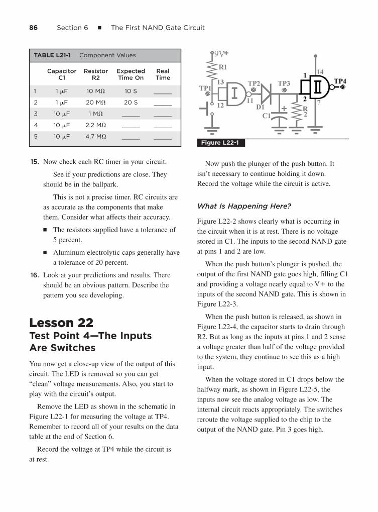
15. Now check each RC timer in your circuit.
See if your predictions are close. Theyshould be in the ballpark.
This is not a precise timer. RC circuits areas accurate as the components that makethem. Consider what affects their accuracy.
■ The resistors supplied have a tolerance of5 percent.
■ Aluminum electrolytic caps generally havea tolerance of 20 percent.
16. Look at your predictions and results. Thereshould be an obvious pattern. Describe thepattern you see developing.
Lesson 22Test Point 4—The Inputs Are Switches
You now get a close-up view of the output of thiscircuit. The LED is removed so you can get“clean” voltage measurements. Also, you start toplay with the circuit’s output.
Remove the LED as shown in the schematic inFigure L22-1 for measuring the voltage at TP4.Remember to record all of your results on the datatable at the end of Section 6.
Record the voltage at TP4 while the circuit is at rest.
Now push the plunger of the push button. Itisn’t necessary to continue holding it down.Record the voltage while the circuit is active.
What Is Happening Here?
Figure L22-2 shows clearly what is occurring inthe circuit when it is at rest. There is no voltagestored in C1. The inputs to the second NAND gateat pins 1 and 2 are low.
When the push button’s plunger is pushed, theoutput of the first NAND gate goes high, filling C1and providing a voltage nearly equal to V� to theinputs of the second NAND gate. This is shown inFigure L22-3.
When the push button is released, as shown inFigure L22-4, the capacitor starts to drain throughR2. But as long as the inputs at pins 1 and 2 sensea voltage greater than half of the voltage providedto the system, they continue to see this as a highinput.
When the voltage stored in C1 drops below thehalfway mark, as shown in Figure L22-5, theinputs now see the analog voltage as low. Theinternal circuit reacts appropriately. The switchesreroute the voltage supplied to the chip to theoutput of the NAND gate. Pin 3 goes high.
86 Section 6 ■ The First NAND Gate Circuit
Capacitor Resistor Expected RealC1 R2 Time On Time
1 1 �F 10 M� 10 S _____
2 1 �F 20 M� 20 S _____
3 10 �F 1 M� _____ _____
4 10 �F 2.2 M� _____ _____
5 10 �F 4.7 M� _____ _____
TABLE L21-1 Component Values
Figure L22-1

Lesson 22 ■ Test Point 4—The Inputs Are Switches 87
Figure L22-2
Figure L22-3
Figure L22-4

Now put the LED back into the circuit, asshown in Figure L22-6.
There is some further testing to be done, butfirst, a puzzling question in two parts.
Part 1: Why does the LED stay off when theoutput from the second NAND gate at pin 3 goes high?
In an effort to answer this question, try this:
1. Stand up.
2. Put your palms together in front of your chest.
3. Push them together with equal force.
Why don’t they move? Because each hand hasequal force pushing in opposite directions. Oneforce cancels the other. There is no movement.This concept is also shown in Figure L22-7.
The LED stays off when the output at pin 3provides an equal force to V+. It is like havingboth legs of the LED connected to voltage at thesame time. Nothing is going to happen.
Part 2: Remember, there were two parts to thequestion.
How does a “low” output of 0 volts turn theLED on?
Look at the schematic diagram in Figure L22-4closely. The inputs act only as switches. Theyreroute the output to voltage or ground, dependingon the conditions. Here, when the output isconnected to ground, the voltage moves from V+,through the LED, through the IC, to pin 7, whichis connected directly to ground.
88 Section 6 ■ The First NAND Gate Circuit
Figure L22-5
Figure L22-6Figure L22-7

Think about the beauty of it.
■ When a digital output is Hi, it can be used as avoltage source.
■ And when the output of a digital system is low,it can be used as ground. Figure L22-8 givespause for thought.
Exercise: TP4—The Inputs Are Switches
Table L20-1 is a detailed outline of the system atrest. Make a detailed outline for the active system.
1. Make a detailed outline for the ACTIVEsystem.
Input
Processor
Output
2. Connect the LED as shown in Figure L22-9.
a. Describe what the circuit does now when itis at rest.
b. Describe what the circuit does now when itis active.
c. Explain what is happening. Keep in mindthe fact that pin 3 is the output of thesecond NAND gate.
Section 6 Data Sheet
Record all of your results from Section 6 in thedata table in Table L22-2. There appears to be ahuge amount of information. This single table canbe used for your convenient reference and review.
Lesson 22 ■ Test Point 4—The Inputs Are Switches 89
Figure L22-8
Input At rest, the inputs to the first NAND gate at pins 12 and 13 are tied to V+ through R1.
Processor 1. Because the inputs to the first NAND gate are both high, the output is low.
2. The capacitor has little or no voltage because it has drained through R2.
3. The inputs to the second NAND gate are both low. They are tied to ground
through R2.
4. Because the inputs to the second gate are both low, the output from the second
gate is high. The second gate acts as a source for voltage.
Output Because there is no voltage difference between V+ and the high output of the
second NAND gate, there is no pressure to push the current. The LED remains off.
TABLE L22-1 Outline of System at Rest
Figure L22-9

90 Section 6 ■ The First NAND Gate Circuit
System at Rest System Active
PB unpushed for 1 minute PB pushed Immediately upon release
TP1
TP2
TP3*
TP4 A (no LED)
TP4 B (LED In)
*What was the voltage to the inputs of the second NAND gate when they sensed a change from a high input to lowinput and the LED was turned off?
TABLE L22-2 Data Table

Analog Switches for Digital Circuits
S E C T I O N 7
IS THERE REALLY GOLD at the end of a rainbow?That’s only wishing for power. But the knowledgeof how to use voltage dividers? THAT is POWER!There is real power in this knowledge! Knowingthis gives you the power to control. Electronics isabout control.
Lesson 23Understanding VoltageDividers
While playing with a potentiometer and one fixedresistor, we can adjust the pot’s resistance to giveus any voltage at the midpoint. We can use thisflexibility to our advantage, but first, we have tounderstand what’s happening so we can control it.
You know that voltage is used as it passesthrough resistor loads. The higher the value of theresistor, the greater the amount of voltage used.You already know, as well, that all the voltage isused from V� to ground. So far, so good. Here,we use two resistors to give us any voltage wewant at the midpoint. We divide the voltage. There is even a simple math formula to predict the outcome.
Here we will apply our knowledge to buildswitches that control the circuit. Some havemoving parts, but others don’t. The projects youwill be building can use many types of switches.Here are some examples.
Figure L23-1 shows a simple motion detector.You can make many physical switches that worklike a push button.
■ It can be made small enough to be hidden insmall boxes or cans.
■ It can be made sensitive enough to triggerwhen a person walks by on a wooden floor.
Figure L23-2 uses what is referred to as a breakbeam. The sensor acts like a dark detector. Itrequires a source of light to keep the light-dependent resistor at a low resistance. If the beamof light is interrupted, the resistance increases. The changing voltage level triggers the inputs.
Figure L23-1
Figure L23-2
91

92 Section 7 ■ Analog Switches for Digital Circuits
By trading positions of the resistor and LDR,you create a light detector. Such a device can beused to alert you when a car turns into yourdriveway. The headlights would trigger this unit.
At what voltage do digital inputs sense thechange from high to low? Ideally, it would be rightat half of the voltage supplied to the system.
That means that if V� is 9 volts, the inputs sensethe high-to-low change as V� falls below 4.5 volts.
How do we get the inputs to change from highto low at the first gate? Right now, as you can seein Figure L23-3, you have the normally open PB toconnect those inputs directly to ground when youpush that plunger.
Modify the Circuit
Remember always to detach your power whenmaking changes.
Make the three changes on your solderlessbreadboard that are shown in Figure L23-4.
1. Replace the PB with the trimmingpotentiometer.
2. Replace R1 with a 39-kilo-ohm resistor.
3. Remove C1. You remove the capacitor so thatthe circuit reacts instantly.
Now put the trim pot back into the circuit. Turnthe trim pot backward until the LED goes off.Remove it again and measure the resistance at thatpoint. Actually, it will be much less than 39 kilo-ohms. But this is an introduction to voltagedividers. Let’s keep it simple.
What to Expect
1. Turn the trim potentiometer to full resistance.
2. Measure resistance between A and center. (B is unconnected.)
3. It should be near 100,000 ohms.
4. Attach the power.
5. The LED should be off.Figure 23-3
Figure L23-4

6. Adjust the trim pot until the LED goes on. It should stay on.
7. Disconnect the power; remove the trim pot.
8. Measure and note the resistance between Aand center now.
How It Works
We can use different resistors and variable resistorsto create changing voltages similar to what we didwith the night light.
Remember the night light? This is for referenceonly. Don’t rebuild it.
Think of how the night light worked. Use FigureL23-5 as a reference.
■ The NPN transistor needed positive voltage toits base to turn on.
■ The potentiometer adjusted the amount ofvoltage shared by the 22-kilo-ohm resistor andthe LDR.
■ In light, the LDR had a low resistance,allowing all of the voltage to flow through toground. Because the base of Q1 got no voltage,the valve from C to E stayed closed.
■ The resistance in the LDR increased as it gotdarker, providing more voltage to the base ofthe transistor, pushing the valve open.
■ As the voltage flowed through the transistor,the LEDs turned on.
We can apply the same idea to the digital circuitinputs, as we can see in Figure L23-6.
Lesson 23 ■ Understanding Voltage Dividers 93
Figure L23-5
Figure L23-6

94 Section 7 ■ Analog Switches for Digital Circuits
Remember: By simple definition, a circuit usesall of the voltage between the source and ground.
1. Two resistors set between voltage and grounduse all of the voltage.
2. The first resistor uses some of the voltage, andthe second uses the rest.
3. If you know the value of each resistor, youcan figure the voltage used by each one usingsimple ratios. You compare the partial load tothe whole load.
Look at Figure L23-7 as an example. Here R1 � R2.
R1 � 10 k�
R2 � 10 k�
When R1 � R2, the voltage at the midpoint isexactly half of V� because each resistor usesexactly half of the voltage.
V ( R1 ) � voltage usedR1 � R2
9v ( 10 k� ) � 4.5v10 k� � 10 k�
This gives us a number of 4.5 volts used.
Why does the voltage split like this?
Simply because the resistor is a load. The largerthe individual load when compared to the totalload, the more voltage is used up. If there are twoloads of equal value, they both use the sameamount of voltage.
Build on Your Breadboard R1 = R2
Do not take apart your digital circuit.
Build the setup of two resistors on a separatespot of your solderless breadboard (SBB).
R1 � 10 k�
R2 � 10 k�
Measure and record the voltage at these points.
Voltage from V� to ground_____ � totalvoltage.
Voltage across R1, from V� to midpoint_____� voltage used by R1.
Voltage across R2, from TP to ground_____ �voltage used by R2.
The voltage measured across R1 and R2 shouldbe the same and equal to half of V�. It may be offby a few hundredths of a volt because of thefollowing:
1. The voltmeter acts as a third load and affectsthe circuit.
2. The resistors have a range of accuracy of plusor minus 5 percent. That means a 10-kilo-ohmresistor could have a value of 9,500 ohms to10,500 ohms.
The ideal statement for voltage at the midpointwhen R1 � R2 is that the voltage is divided byhalf.
The load uses that portion of the voltage, in aratio compared to the total load.
Build on Your Breadboard R1 > R2
What happens when we build a voltage divider ofunequal parts?
Figure L23-7

Here is what happens when R1 is 10 times thevalue of R2, as laid out in Figure L23-8. ReplaceR2 with a 1-kilo-ohm resistor.
If, for example:
V� � 9.0 V
R1 � 10 k�
R2 � 1 k�
Again, figure the voltage used like this.
But remember that the important informationreally is the voltage remaining.
R1 uses up 10/11 of the total voltage. That is8.2 volts to be exact. The voltage left at themidpoint should be about 1/11 of the total because:
Total volts – used volts � remaining volts
11/11 – 10/11 � 1/11
9 V – 8.2 V � 0.8 V
It is important to be able to predict the voltageat the midpoint.
This allows you to trigger a digital circuit withwhatever switch you create.
Exercise: Understanding Voltage Dividers
Predict the voltage in a voltage divider if you haveexactly 9 volts.
Don’t breadboard these voltage dividers.
Use the formula. And don’t forget:
Total � Used � Remaining.
1. R1 � 1 k�
R2 � 10 k�
Midpoint V � ______
2. R1 � 100 �
R2 � 1 k�
Midpoint V � ______
3. R1 � 1 k�
R2 � 100 �
Midpoint V � ______
4. R1 � 39 k�
R2 � 100 k�
Midpoint V � ______
5. R1 � 39 k�
R2 � 2.2 M�
Midpoint V � ______
6. R1 � 2.2 M�
R2 � 100 k�
Midpoint V � ______
7. R1 � 100 k�
R2 � 20 M�
Midpoint V � ______
Lesson 23 ■ Understanding Voltage Dividers 95
Figure L23-8
Vtotal ( ) Vused
9V (10 k� / 10 k� � 1k�) � 8.2V
R1
R1 R2

Lesson 24Create a Light-SensitiveSwitch
Here, the trim pot is replaced by an LDR to createa light-sensitive switch to trigger the NAND gate.It is a voltage divider that uses a light-dependentresistor as one of the loads.
Remove the last section’s two-resistor voltagedivider setup from the SBB so they are no longerin the way.
The inputs to the first gate are held high viaconnections through R1. The circuit is at rest. No,it is not off. The circuit is off only when the poweris disconnected (Table L24-1).
Disconnect power when you
change parts on the breadboard.
Refer to Figure L24-1 as we do a quick reviewof how the trim pot worked as a switch.
The 100-kilo-ohm trim pot replaced thenormally open push button with a slidingresistance. As the trim pot changed resistance, theratio of the voltage divider changed. Notice whathappened to the output of the circuit as youadjusted the trim pot back and forth.
■ As you increased the resistance, the voltage tothe first NAND gate’s inputs increased. It washarder for the voltage to reach ground becauseof the increased resistance of the trim pot.
■ The inputs to the NAND gate were connectedto voltage, giving a low output from the firstgate.
■ With the first gate inputs connected to a high,the system was at rest.
Modifying the Circuit: The Light Detector
The capacitor remains out (disconnected) for thislesson. Leaving it in will delay the change inoutput and confuse what you should see. Now trythe other variable resistor, the LDR.
1. Remove the trim pot.
2. Place the LDR into your circuit as shown inFigure L24-2.
96 Section 7 ■ Analog Switches for Digital Circuits
Input A Input B Output
High High Low
High Low High
Low High High
Low Low High
TABLE L24-1 NAND Logic Table
NOTE
Figure L24-1

What to Expect
1. When you attach the battery, the LED shouldturn on instantly because this circuit is at restin the dark.
2. Because this setup is active in the light, youwill have to place the circuit into a darksituation for it to be at rest.
3. When the resistance of the LDR goes down inthe light, the inputs to the first NAND gatesense that decrease in voltage. When it dropsbelow half of the voltage from the powersupply, they sense this as a low input.
Modifying the Circuit: The Dark Detector
Reverse the positions of R1 and the LDR as shownin Figure L24-3. This simple change creates a darkdetector. It is at rest in the light, and becomesactive if the resistance of the LDR goes above 39 kilo-ohms.
This setup needs to be in constant light to keepthe circuit at rest. It will detect a break in a lightsource. If you put the circuit in the light and anobject breaks the light source to the LDR, it willstart the circuit. A common favorite is to put thisswitch onto a toy car. Its headlights turn on everytime it goes under something.
Lesson 25The Touch Switch
This switch depends on the fact that your skin hasa resistance that is always between 100 k� and2 M�, depending on how sweaty you are. Weexploit this natural resistance in a voltage divider.
1. Set your digital multimeter to resistance.
2. Grasp a probe in each hand.
The resistance reading will constantly change,but should stay in the same range—somewherebetween 100,000 ohms (100 k�) and 1,000,000ohms (1 M�).
Lesson 25 ■ The Touch Switch 97
Figure 24-2 Figure 24-3

98 Section 7 ■ Analog Switches for Digital Circuits
Now change the beginning portion of the circuitto resemble the schematic shown in Figure L25-1.
What to Expect
1. Attach your battery.
2. Touch your finger to both of the wires at thesame time.
The LED turns on when your finger touchesboth wires that make the touch switch.
How It Works
Figure L25-2 demonstrates the effect of thefinger’s resistance when you become part of thecircuit. The input pins 12 and 13 sense less than
half of V� when the finger touches. A voltagedivider only exists when there are two resistors. So consider: Is there a voltage divider when youare not touching the contacts?
Figure the actual voltage at the inputs to the firstNAND gate when the finger is touching. Assumeyou have a very dry finger and it has a resistancearound 1 megohm.
Figure L25-1Figure 25-2
Vused Vtotal ( )Vtotal Vused Vmidpoint
R1
R1 R2

HAVE YOU SEEN THE WIZARD OF OZ? Don’t befrightened, and don’t “ignore the man behind thecurtain.” Any technology that one does notunderstand is often interpreted as “magic!”
Knowledge, Design, Control
As you start to learn how to control digital inputs,you actually start to understand how some of the“whiz-bang” electronics around you actually work.Go out and buy a copy of a monthly electronicsmagazine. You will actually understand more thanyou expect. Remember, electronics is not hard—just lots of new information.
Lesson 26Building the NAND Gate Oscillator
Here, just like the title says, you will incorporatethe two unused NAND gates of the 4011 and buildan extension onto your existing circuit. Thatextension will create a flashing output.
Add to your breadboarded circuit. Don’t stripyour breadboard.
Here you will get some dramatic changes byadding three basic components and changing somewiring to use the other two NAND gates.
Note what is needed in Figure L26-1 and theParts Bin.
The NAND Gate Oscillator
S E C T I O N 8
99
RC1 and RC2 are highlighted.Figure L26-1

100 Section 8 ■ The NAND Gate Oscillator
There are only four points connected to groundnow. Make sure that inputs 5/6 and 8/9 are nolonger connected to ground.
What to Expect
Press the button to make the circuit go “active.”The LED should flash once a second for abouteight seconds. It stops and automatically returns to its rest state.
If It Isn’t Working: Problems and Troubleshooting
This troubleshooting guide will help you with theoscillator prototype on your breadboard and yourfinished project.
The intent of the troubleshooting guide is tohelp you locate the problem causing your circuitnot to work. The hardest part of troubleshooting isfinding the source of the problem. Once you findthe cause of the problem, it’s usually not difficultto fix it. I don’t go into detail on how to fix it onceyou’ve located it. Upon closer inspection, thatbecomes self-evident.
Something to consider: If your LED is flashingfaster than 24 frames per second, it looks like it ison steadily to you. Did you know that if the LED isblinking at 24 Hz or faster, your eyes tell you it isnot blinking at all? That is why movies are shownat 26 frames per second. You are sitting in completedarkness for half of the time. You just can’t noticeit. Old silent movies are stuttering and jerkybecause they were often done at a rate just less than24 frames per second. You can notice that.
There are usually four major problems thatoccur with this circuit.
1. Attach power, and the LED lights up but doesnot blink. Start at number 1 on the checklistbelow.
2. The LED blinks as soon as you attach thebattery. Start at number 1 on the checklistbelow, but pay careful attention to the firstgate. Something is triggering the inputs atpins 12 and 13.
3. The LED is off until you activate the circuit.The LED turns on but does not blink. It doestime off properly. Problems at RC2. CheckR3, R4, and C2 connections and values. Thenstart at 10. If you don’t get half of V�, returnto start at 1.
4. The LED is off and stays off. Is your powersupply connected? Start at 1. Do not justinsert a fresh 4011 chip into the circuit. If aphysical error blew your chip, that same errorwill keep on blowing chips until you fix it.
Troubleshooting
If you find a step checks out OK, then move to thenext step. If not, do what is recommended.
1. Visually inspect all connections.
■ All pins on the 4011 chip should be used. Ifyou find an open pin, something is missing.
■ A wire left in from the previous setup couldstill be connecting pins 1 and 2.
■ R1—100 k�
■ R2—10 M�
■ R3—470 k� (new)
■ R4—2.2 M� (new)
■ C1—1 �F
■ C2—1 �F (new)
■ D1—4148 Signal diode
■ LED—5 mm red
■ IC1—4011 Quad NAND gate
■ PB—Normally open
P A R T S B I N

Lesson 26 ■ Building the NAND Gate Oscillator 101
■ Pins 5 and 6 are connected, but the wireconnecting these to ground needs to beremoved.
■ Pins 8 and 9 are connected, but the wireconnecting these to ground needs to beremoved.
■ Make sure that none of the bare legs of theparts are touching at crossovers, creating ashort circuit.
2. Look at all parts that have to be put in withpolarity in mind. Positive must be toward V� and negative toward ground.
■ Capacitors 1 μF and bigger
■ Chip
■ LEDs
■ Transistors (Lesson 32)
■ Diodes
■ Speaker (Lesson 29)
3. Check that the IC has power.
■ Note that V� is being supplied to pin 14.Check that voltage is being supplied fromthe battery to the V� line on the board.
■ Check that there is a wire connecting pin14 to the V� line.
4. Note that ground has only four connections.Check that there is continuity from the smallbutton on the battery clip to the ground line.
■ Pin 7
■ R2
■ C1
■ Contact to the input switch
5. Here you are looking for short circuits in yourwiring. This can also be caused by sloppysoldering.
■ Disconnect the power and replace the chipin the breadboard with a chip seat (emptysocket).
■ Get a multimeter and start checking atpoints noted. Infinite or over limit meansthat there should be absolutely noconnection between the two pins with the chip removed (see Tables L26-1 andL26-2).
■ Zero ohms means there is a directconnection.
6. Replace R1 with 100 kilo-ohms (20 megohmsis too sensitive and will start the circuit).
■ With the battery connected, check that thevoltage at pins 12 and 13 is well above halfvoltage when the switch is “open.”
■ Check that the voltage at pins 12 and 13 iswell below half voltage when the switch is“closed.”
Red Black ExpectedProbe at Probe at Resistance
Pin 1 Pin 7 Infinite
Pin 2 Pin 7 Value of R2
Pin 3 Pin 7 Infinite
Pin 4 Pin 7 Infinite
Pin 5 Pin 7 Infinite
Pin 6 Pin 7 Infinite
Pin 8 Pin 7 Infinite
Pin 9 Pin 7 Infinite
Pin 10 Pin 7 Depends on the
output; disconnect
the output, and it
should be infinite
Pin 11 Pin 7 Infinite
Pin 12 Pin 7 Infinite
Pin 13 Pin 7 Infinite
Pin 14 Pin 7 Infinite
TABLE L26-1 Measure the Resistance at EachLeg of the Chip with the BlackProbe Connected to Ground

7. With the battery connected, check the voltageat pin 11 when the switch is “open.” It shouldread 0.0 volts (low).
■ Close the switch and check the voltage atpin 11 when the switch is “held closed.” Itshould be V� (HI).
■ If pin 11 does not respond properly, eitherthe gate is burnt out or pin 11 isaccidentally connected to ground orsomewhere else.
8. With the battery connected, check the voltageat pin 2 (RC1) when the switch is “open.” Itshould be sinking toward 0 volts.
■ Check the voltage at pin 2 (RC1) when theswitch is “held closed.” It should be up atfull voltage.
■ If RC1 does not fill, check the value of R2.Also, check if diode 1 is in the right way.Then replace D1 with a power diode1N4005. The signal diode might have burntout. Also, check for accidental connectionsto ground or somewhere else.
9. When pin 2 is low, pin 3 should be high.Conversely, when pin 2 is high, pin 3 shouldbe oscillating.
■ Use a multimeter to check if the oscillatoris working at pin 3.
■ If RC2 is set for slow pulse of 2 Hz orslower, the reading will swing from V�
to 0 volts.
■ If RC2 is set for a faster frequency, thereading will stay at half of V�.
■ For example, if V� is 9 volts, the meterwill read 4.5 volts because it will averagethe voltage swings between 9 and 0 volts.
10. The output at pin 3 should be directlyconnected to pins 5 and 6. The reading at pins 5 and 6 will be identical to the reading at pin 3.
11. The output of pins 5 and 6 is at pin 4. Checkto see that the gate is working.
12. The inputs to the fourth gate, pins 8 and 9, areconnected directly to pin 4. Check to see thatthe gate is working.
13. Is your output device working?
■ Is an LED burnt out? Test them singly in a9-volt system with a 470-ohm resistor.
■ Perhaps your speaker is broken. Checkcontinuity on the speaker wire.
■ Is your transistor the correct value? Maybeit is burnt out. Table L51-2 guides youthrough testing of transistors.
102 Section 8 ■ The NAND Gate Oscillator
Red Black ExpectedProbe at Probe at Resistance
Pin 1 Pin 2 Infinite
Pin 2 Pin 3 Infinite
Pin 3 Pin 4 Infinite
Pin 4 Pin 5 Infinite
Pin 5 Pin 6 0 �
Pin 6 Pin 7 Infinite
Pin 7 Pin 8 Infinite
Pin 8 Pin 9 0 �
Pin 9 Pin 10 Infinite
Pin 10 Pin 11 Infinite
Pin 11 Pin 12 Infinite
Pin 12 Pin 13 0 �
Pin 13 Pin 14 Value of R1
Pin 14 Pin 1 Infinite
TABLE L26-2 Measure the Resistance fromEach Pin to the Next; the ChartAssumes that RC2 Oscillator IsInstalled

Lesson 27Understanding the NANDGate Oscillator
Table L27-1 describes the present system. It is aneven closer look at how the NAND gate works.The NAND gate oscillator is widely used becauseit can be tuned easily using an RC. Watch for thenew vocabulary. Master the material now or be aslave later.
Recall the logic table for the NAND gate (Table L27-2).
In review, recall what happens at RC1. Gate 1 is used to start the RC1. RC1’s C1 fills and drainsthrough R2. These control the time the circuit stays on.
■ Gate 1 output goes high.
■ D1 traps the voltage on RC1 side.
■ C1 fills.
■ R2 drains the voltage.
The action of an RC circuit is always the same.The only difference is the speed that the circuitfills or drains. Figure L27-1 reviews that basicaction.
But we are interested now in RC2. RC2 is madeof C2 and R4. They use gate 2 to make anoscillator. The oscillation action happens at gate 2.
Look at the setup of gate 2 shown in FigureL27-2. The high or low state of pin 3 determines
Lesson 27 ■ Understanding the NAND Gate Oscillator 103
Input Processors Output
Push RC1-Push on/ LED flashing once
button timed off about per second
10 per second
RC2-NAND gate
RCM oscillator
At 1 flash per second
TABLE L27-1 The System Diagram as It Exists Now
Input A Input B Output(Pin 2) (Pin 1) (Pin 3)
High High Low
High Low High
Low High High
Low Low High
TABLE L27-2 Logic Table for the NAND Gate
Figure L27-1
Figure L27-2

the state of pin 1. Pins 1 and 3 have a specialrelationship. Pin 3 is the master; pin 1 is the slave.
Table 27-3 shows the system at rest. There is noactivity or changing voltage values happeningwithin the circuit.
So pin 1 is a slave to pin 3. When the system isat rest, C1 has less than half of V�. Because pin 2is low, pin 3 gives a high output. Note the NANDgate’s logic in Table L27-2. In fact, if either inputis low, the output is high. This is shown plainly inFigure L27-3.
But what happens when the circuit becomesactive? Figure L27-4 clearly shows that when pin 2goes high, because the capacitor is charged, pin 3goes low.
It takes a fraction of a second for the input atpin 1 to respond because C2 has to drain. Once ithas drained, the voltage at pin 1 matches theoutput of pin 3. Wait!? Pin 3 is now low. So pin 3makes pin 1 low, but pin 2 is high. One of the
104 Section 8 ■ The NAND Gate Oscillator
Time (Seconds) Input A at Pin 2 Input B at Pin 1 Output at Pin 3
The system remains at rest until pin 2 Slaved to pin 3 As long as one input is low,
changes state when RC1 gets charged. the output is high.
1 Low High
2 Low High High
3 Low High High
4 Low High High
TABLE L27-3 System at Rest
Figure L27-3
Figure L27-4

Lesson 27 ■ Understanding the NAND Gate Oscillator 105
inputs is low, which makes the output at pin 3 gohigh. This is better than a puppy chasing its tail.
The series of actions is actually laid out veryneatly in Table L27-4.
The system starts at rest. When the systembecomes active, oscillating start.
Animated version of this table is atwww.mhprofessional.com/computingdownload. Asyou can see, the feedback loop at gate 2 creates theoscillation! All animated graphics are availableonline and are listed in Appendix C.
Voltage in RC1 System State Time Input A Pin 2 Input B Pin 1 Output Pin 3
0 Rest 0 Low High
0 Rest 0 Low High High
0 Rest 0 Low High High
9 Active 1 High High Low
8.5 Active 2 High Low High
8.0 Active 3 High High Low
7.5 Active 4 High Low High
7.0 Active 5 High High Low
6.5 Active 6 High Low High
6.0 Active 7 High High Low
5.5 Active 8 High Low High
5.0 Active 9 High High Low
4.5 Active 10 High Low High
4.0 Rest 11 Low High High
3.5 Rest 12 Low High High
3.0 Rest 13 Low High High
TABLE L27-4 Series of Actions

This page intentionally left blank

How Do We Understand What We Can’t See?
S E C T I O N 9
EVEN WHEN WE CAN’T SEE what’s happening, wecan predict, measure, and visualize.
Lesson 28Controlling the Flash Rate
This lesson explains how it is done and you get todo exactly that. You learn the relationship betweenthe RC values and the frequency output.
The values of C2 and R4 that make RC2determines the rate of oscillation. The rate ofoscillation is properly called hertz (Hz). Hertz isfrequency per second. Another way of saying thisis how many beats per second. It is a standard unit.
How It Works
First, an explanation of how the second resistor/capacitor circuit (RC2) works. Then we’ll playwith it. This is not an exact representation of thecircuit, but it will help you understand what isreally happening.
Figure L28-1 shows your original RC2 setupwhere C2 � .1 μF and R4 � 2.2 megohms. R4 isrepresented by the pipeline feeding the capacitor.
Pin 2 is low. The system is at rest and stable.
The high output from pin 3 is defined by theinputs. The capacitor C2 is fully charged. There isno place for it to empty.
When RC1 gets charged, the system becomesactive. You recognize that the high inputs at pin 1and pin 2 create a low output. The low output atpin 1 allows the charge held in C2 to begindraining. It does so at a speed determined by thesize of R4. Figure L28-2 shows the action ofdrainage from C2. As long as the voltage is abovethat magical half of the voltage mark, pin 1 sees its input as high.
Figure L28-1
Figure L28-2
107

108 Section 9 ■ How Do We Understand What We Can’t See?
But as soon as the charge in C2 drops below acertain point, the input to pin 1 senses that input aslow. HMM? Pin 2 is still high. NAND gate logicdemands that the output at pin 3 become high, andC2 starts to fill (see Figure L28-3).
Of course, this continues until it goes above thatmagical marker, when the action reverses again.RC1 may be set for 10 seconds. RC2 might be setfor 1 Hz. So by the time pin 2 goes low again,RC2 will have filled and drained 10 times.
RC2’s rate of voltage charge/discharge ischarted and shown in Figure L28-4.
C2 fills and drains. This creates the analog inputto pin 1. That sliding up and down input controlsthe digital high and low output shown as thicksquare waves.
I have made the assumption that the powersupply is a convenient 9 volts. That makes thehalf-voltage mark 4.5 volts. Notice the grayed area
around the half-voltage mark. In simplifying theexplanation, I have referred to the magical point ofhalf of V�. That’s not quite true. There is a bitmore of a range. If the voltage is moving upward,it has to rise above about 5 volts to be sensed ashigh. If the voltage is dropping, it has to dropbelow nearly 4 volts before it is registered by theinputs as low.
Modifying the Circuit
Make sure your power is disconnected.
Now replace C2 with a 0.01-μF capacitor. Usethe DMM to check the capacitance. Ideally, thecapacitor you have is marked the same way as thedisk capacitor shown in Figure L28-5. There is nostandard for marking capacitors. There are severalgenerally accepted methods. You can expect to seethe marking 103Z. That refers to 10 followed bythree zeros. In other words, 10,000. Diskcapacitors are measured in picofarads. That is amillionth of a microfarad. That is a thousandth of a nanofarad. 10,000 pF is 10 nF is 0.01 μF.
Or it might be marked with 0.01 or even u01.This refers to 0.01 μF. The label u01 uses the valuemarker as a decimal marker as well. Face it, there’snot much space.
This capacitor is 10 times smaller than the oneyou have in the circuit right now. Capacitors thissmall do not have any polarity. There are nopositive or negative legs. R4 is unchanged at 2.2 megohms.
Figure L28-3
Figure L28-4
Figure L28-5

Connect your power supply.
Notice the new setup shown in Figure L28-6.
The system is at rest, but C2 is represented as atenth the size as before. So what do you expectwill happen?
The LED should flash very quickly for about 10 seconds, depending on your timing for RC1.Figure L28-7 shows the reaction by the NANDgate to the changing voltages on pin 1.
Ideally, it reacts exactly 10 times faster becausethe capacitor is 10 times smaller.
Exercise: Controlling the Flash Rate
Pull R2, the resistor, from RC1. That way you cancount without worrying about the circuit timingout at the wrong time.
On your solderless breadboard, you will changecomponents to affect the oscillation timing of RC2.Track your results in Table L28-1.
Lesson 28 ■ Controlling the Flash Rate 109
Figure L28-6
Figure L28-7
Timing Flashes in 10 s Average
R4 C2 Comment 1 2 3
1 M� 0.1 �F
2.2 M� 0.1 �F Twice the resistance
Expect half the rate
4.7 M� 0.1 �F Twice the resistance
Expect half the rate
10 M� 0.1 �F Twice the resistance
Expect half the rate
10 M� 0.01 �F Tenth the capacity
Expect 10 times faster flash rate
4.7 M� 0.01 �F Half the resistance
Expect twice as fast
2.2 M� 0.01 �F Half the resistance
Expect twice as fast
1 M� 0.01 �F Half the resistance
Expect twice as fast
TABLE L28-1 Tracking Table

110 Section 9 ■ How Do We Understand What We Can’t See?
Is there a pattern when you compare it to theflashing rate using the 0.1 μF capacitor that was 10 times larger?
Lesson 29Create a Sound Output and Annoy the Person Next to You
You adjusted the frequency of RC2. This is a directcontinuation of the previous lesson, but the LEDoutput has a flash rate too fast to see. Did youknow that people see smooth motion if relatedpictures are presented at 24 frames per second?That is why movies are projected onto a screen atthat rate. That is also why we have to move fromthe LED to a speaker. When the LED is 24 framesa second or faster, it might appear to dim a little,but you won’t see it flash. Why does it dim?Because it is off half the time. Don’t you realizeyou’re sitting in complete darkness in the moviesfor half the time, too?
Modifying Your Circuit
Don’t clear your breadboard. Figure L29-1 showsthe schematic that you have been using (see theParts Bin). Just replace the LED with the speakerand change the values of other components statedin the parts list.
Also, if you removed R1 for the exercise inLesson 28, put it back in.
Disconnect your power to make these changes.
Going from left to right on the schematic.
1. You have a touch switch to activate the circuit.
2. The amount of time the circuit stays active isset by R2 and C1. R2 and C1 make the firstresistor/capacitor circuit (RC1).
3. The rate of oscillation is determined by C2and R4 (RC2).
4. Here, the voltage from pin 10 moves from V�
(high) to ground (low) at a frequency set byRC2.
Be cautious. Don’t connect your speakerdirectly to a battery or the power supply.Small speakers are made with very fine wire.
Figure L29-1
■ R1—20 M�
■ R2—10 M�
■ R3—470 k�
■ R4—2.2 M�
■ C1—1 μF electrolytic
■ C2—0.1 μF
■ D1—4148 Signal diode
■ Speaker—8 �
■ IC—4011 Quad NAND gate
P A R T S B I N

Too much current will heat the wire, possiblyenough to melt it. Such a break would renderthe speaker useless.
5. Speakers respond only to voltage changes.Speakers do not produce sound just becauseV� is applied to them. Buzzers have a circuitinside. They create their own noise. If you putyour speaker to voltage, you hear a “crackle”as you connect and another as you disconnect.It is merely responding to changes in voltage.An excellent explanation about how a speakerworks is posted at www.howstuffworks.com/speaker1.htm.
6. Replace the LED with the 8-ohm speaker.Note the polarity of the speaker.
The speaker will click slowly and veryquietly. You may have to use your fingers tofeel the pulse. It should pulse about 15 to 20times in five seconds.
The speaker pulses each time the current isturned on, moving from low to high, and eachtime the current is turned off, moving fromhigh to low. In the previous exercise youpulsed the LED at different speeds bychanging the rate of oscillation in RC2.
Your exercise results should have shown thispattern (see Table L29-1).
Decreasing the resistance is like widening thedrain. Figure L29-2 shows that by decreasing theresistor value we increase the oscillation speedbecause it takes less time to fill and drain thecapacitor.
Exercise: Create an Annoying Sound Output
A quick definition. Hertz is a measurement offrequency, specifically defined as a measure ofbeats per second. For example, a system oscillatingat 512 beats per second is more easily stated as512 hertz.
As you do the following changes, note yourobservations in Table L29-2. Remember to detachpower any time you make a change to yourprototype on your breadboard.
It’s annoying, but very quiet right now becausethe 4011 IC does not produce very much power atthe output. So the volume is not much at all. ButFigure L29-2 offers hope.
Lesson 29 ■ Create a Sound Output and Annoy the Person Next to You 111
Resistor Values Capacitor Values Flashes in 10 s Speed
10 M� 0.1 �F 1 Very slow
4.7 M� 0.1 �F 2 Double of previous
2.2 M� 0.1 �F 4 Doubled again
1 M� 0.1 �F 10 10 times faster than the 10 M�
TABLE L29-1 Exercise Results
Resistor Capacitor Value R4 Value C2 Description
4.7 M� 0.01 �F
2.2 M� 0.01 �F
1.0 M� 0.01 �F
470 k� 0.01 �F
220 k� 0.01 �F
100 k� 0.01 �F
47 k� 0.01 �F 500 Hz
Now, one more change. Put your ear very close
to the speaker. Listen for the quiet tone.
22 k� 0.01 �F 1,000 Hz
TABLE L29-2 Observations
Lesson 30Introducing the Oscilloscope
This lesson:
■ Introduces one of the most important tools inelectronics
■ Introduces you to the concept of what anyoscilloscope can do
■ Shows you how to build a probe to use withthe Soundcard Scope
■ Acts as an introduction to using the popularSoundcard Scope freeware
If you have an oscilloscope sitting on your deskat home, you are unique. If you have access to anoscilloscope, you are special.
Otherwise, I recommend the Soundcard Scope.You can download it from http://www.zeitnitz.de/Christian/scope_en. It was created ChristianZeitnitz, professor of physics at WuppertalUniversity.
Think of the Soundcard Scope as a special“skin” for your sound card. Different skins allowfor different adjustable visual effects that show onyour monitor as music plays. Soundcard Scopetakes this idea forward a step. The SoundcardScope skin reacts to the internal signals as well as“microphone” or “line” inputs to your sound card.
In the real world, we expect that as priceincreases, complexity and quality should increase.Soundcard Scope, however, is priceless. It stillincludes all of the major functions common to all
112 Section 9 ■ How Do We Understand What We Can’t See?
Figure L29-2
Disclaimer
Safety measures when using Soundcard Scope
and the Soundcard Scope Probe:
The Soundcard Scope Probe is designed to
be used only with your 9-volt systems and the
proper probe. Make sure you follow testing
procedures before you use it. Instructions for
building the probe are given in this lesson.
Being software, Soundcard Scope itself
cannot damage your hardware, but it is very
easy to burn out at least your sound card when
trying to investigate signals of unknown
amplitude and DC offset.
So, you must always be extremely careful
when establishing an electrical connection
between your computer and external equipment.
It is a good practice to use a conventional
multimeter or real oscilloscope to find out
whether signal levels are acceptable for your
sound card.
Regarding connecting to things besides
circuits produced in this book, it should be safe
to connect to any audio/video equipment using
standard line in jacks and cables. You may
consider at least using the Scope Probe to
decrease the voltage input. Make sure you have
a stable signal source that allows you to control
signal level manually, outside of the computer.
To avoid personal injury, always follow the usual
safety rules when working with electric circuits.
SOUNDCARD SCOPE IS SUPPLIED TO YOU
AS IS, AND IN NO CASE IS THE AUTHOR OF
SOUNDCARD SCOPE OR THE ASSOCIATED
PROBE RESPONSIBLE FOR PERSONAL INJURY,
HARDWARE, AND/OR DATA DAMAGE,
PROPERTY DAMAGE, OR PROFIT/LOSS
ARISING FROM USE OR INABILITY TO USE
THIS OSCILLOSCOPE SOFTWARE.
THE AUTHOR/DESIGNER DOES NOT
GUARANTEE THE FITNESS OF SOUNDCARD
SCOPE FOR ANY PARTICULAR PURPOSE.
SOUNDCARD SCOPE IS NOT INTENDED FOR
INDUSTRIAL OR COMMERCIAL USE.

oscilloscopes, plus some added features. Its qualityis adequate for our immediate needs. One of itslimitations is that it ignores stable DC voltage. Butit does respond to changing voltages in the audiofrequencies 40 Hz to 15,000 Hz. Its biggestadvantage is the price.
For this particular oscilloscope
software, the input is defined by
Windows “Master Volume” sound mixer. The
Soundcard Scope software does not communicate
directly with the sound card. With this in mind, any
Soundcard Scope problems should be dealt with
through Windows’ own sound card system. Check
page 8 of the scope’s manual.
As the Digital Revolution became the digitalstandard, oscilloscopes changed too. The best-qualityscopes still cost in excess of $20,000. An adequatebeginner’s scope would be a two-channel Velmanhandheld scope or external USB hardware, starting
around $150. For classrooms, $2000 for a goodquality scope is not unreasonable. Reconditionedanalog equipment is an option frequently overlooked.Equipment that was “top of the line” 20 years agocan be purchased at reasonable cost. These oldertools give quality outputs comparable to equipmentthat would cost over ten times as much new.
Your DMM measures voltage. It has no timecomponent.
Oscilloscopes are used to give instantvisualization of voltage compared to time. Its inputclips to the system’s output and displays a graph ofthe voltage represented on the Y axis (vertical) andtime shown across the screen horizontally as the Xaxis. You are able to adjust the scales.
Oscilloscopes specifically create pictures ofvoltage changes over time. A good scope can showevents that occur at a snail’s pace, or it can freeze aframe to display microsecond variations.
Initial Walkabout
Enough of me blathering on. If you do not havealternative hardware, download, install, and startthe Soundcard Scope now. At startup, theSoundcard Scope screen looks like Figure L30-1.
Lesson 30 ■ Introducing the Oscilloscope 113
IN GENERAL, USE SOUNDCARD SCOPE AND
THE ASSOCIATED PROBE AT YOUR OWN RISK.
ALWAYS CONSULT YOUR SOUND CARD
MANUAL FOR DETAILS ON CONNECTING TO
EXTERNAL DEVICES.
NOTE
Figure L30-1

Be aware that this entire tool is not even a gooddoorstop unless you have a signal.
The Soundcard Scope has some valuablefeatures that we are going to use immediately.
Open and adjust your master volume control tomatch Figure L30-2, and then close it.
Click the Signal Generator tab. Adjust thefrequencies as shown in Figure L30-3.
Return to the oscilloscope screen. The left sideof Figure L30-4 shows what to expect. It should beclose, so don’t worry if it’s not exactly what yousee. The signal might be too big to fit on thedisplay screen. Don’t change the signal size withthe master volume control. Adjust the scale of thegraph by inserting the number .2 as indicated by#1 in the Amplitude control area. You can mouseover the knob on any of these to control them.Your display should now be similar to the right
114 Section 9 ■ How Do We Understand What We Can’t See?
Figure L30-2
Set channel 1 as 250 Hz and channel 2 at 300 Hz.Figure L30-3

side of Figure L30-4. Just like on a piece of paper,the information in the graph doesn’t change—justthe scale. The notations in #1’s display indicatethat each division has doubled its value.
The more information you have, the better youcan understand what is happening. Click the STATUS
button under Measure, as indicated by #2 onFigure L30-4. Choose the Hz and Volts option.Check the Frequency and Voltage boxes that popup next to it. An information bar appears at #2’sdisplay. The fact that the readout should be 250and 300, respectively, doesn’t matter. The first
number is cut off because of limited space. Thefact that the reading is off by .01 is irrelevant.
Wouldn’t it be nice to play with one signal at atime? Again, it’s not hard if you know how. InFigure L30-5, #1 shows the box next to Sync CH 1& 2 has been deselected. Just above that, at #2,click the Select CH button, activating only CH 1.At #3, you can shift the amplitude of Channel 1 tofurther distinguish it from Channel 2’s signal.Change its scale to .4 per division as noted by #3.Now you have the left screen of Figure L30-5.
Lesson 30 ■ Introducing the Oscilloscope 115
Figure L30-4
Figure L30-5

116 Section 9 ■ How Do We Understand What We Can’t See?
Wait a minute? Regarding the amplitude, haveyou noticed that the Y axis has no unit. We knowit’s voltage, but shouldn’t it be showing .1 v/div or .4 v/div? Why just .1 or .4? Here’s what’shappening. As a generic program, it was designedto interact cleanly with a wide variety of softwareand hardware. There is no guarantee of accuracy.The intent of any scope is to picture voltagechanges across time and to compare one signal’sstrength to another. Use your DMM if you wantaccurate voltage.
But there is a definite unit attached to the Xaxis. In Figure L30-5, the #4a display on the leftscreen shows all activity taking place in 20 ms. For those of you stuck on fractions, that’s 1/50th of a second. If you want to get a closer look,change the value at #4 to 10 ms per division. The signal stretches as it is magnified across time.The screen now displays the voltage changes over10 ms at #4b.
This scope is really capable. Here’s one morething to play with right now. At #5, click theSingle button underneath Channel Mode.
Use the following settings, and you’ll create theform in Figure L30-6:
■ Amplitude at .2/division
■ Synchronize CH1 and CH2
■ Time at 100 ms
■ Channel Mode � CH1 � CH2
When you’re finished playing, tab over toFrequency Analysis to see the screen shown inFigure L30-7.
Sure enough, the Frequency Analysis featurehas something to do with frequency analysis.Capable of only one channel at a time, this toolanalyzes individual signals and displayscomponent parts, showing relative strengths.
Building the Scope Probe
If you already have access to an oscilloscope, youdon’t need to build a scope probe. It is a piece ofequipment that you need to be able to test yourown circuits using the Soundcard Scope on yourcomputer.
What the Probe Does
The probe takes any signal in your circuit, cuts outall but 1/11th using a simple voltage divider, andfeeds that remaining fraction to your sound card.Your sound card feeds this signal to the Soundcard
Figure L30-6
Figure L30-7

Scope software, which interprets this signal anddisplays it on your screen.
Keep in mind that any sound card cannot acceptmore than 2 volts. Anything more than 2 volts willcause damage to your sound card. So if your outputis 9 volts, only .8 volts is fed to your sound card.
There are three sections to the probe, as shownin Figure L30-8.
A more detailed set of photographs is availableon the website www.mhprofessional.com/computingdownload.
The Connecting Clips
1. You need to have at least a three-foot lengthof speaker cord. Carefully remove one inch ofinsulation from both ends.
2. Mark one of the lines on both ends to identifyit as the same line on both sides. Use this linefor ground.
3. Disassemble the clips and slide the coversonto the wire.
4. Twist the end of each wire strand and pushthis strand through the hole at the base of theclip as shown in detail in Figure L30-9.
5. Lay the insulation into the saddle and usepliers to crimp the two sides of the saddleover the insulation. This physically holds theclip to the wire.
6. Now solder the wire strand at the bottom andclip the extra wire away. You should havesomething similar to Figure L30-10 now.
7. Slide the covers over the back of the clips.This is done easily if the jaws are clampedopen onto something large.
That should finish the clips.
The Voltage Divider
The voltage divider is the heart of the probe. It isnot a regular connector, but decreases the inputvoltage by a factor of 1:11.
Assembling the voltage divider for the scopeprobe requires the following:
1. Cut the dual cord six inches from the endopposite the clips.
2. Strip at least 1/4 inch (0.5 cm) of insulationoff four ends.
3. Mark both sides of the ground line. This is theone connected to the black clip.
4. Figure L30-11 displays how to wrap the wirearound the resistor leg before soldering. Thisis not critical, but it is very effective.
Lesson 30 ■ Introducing the Oscilloscope 117
Figure 30-8
Figure L30-9
Figure L30-10
Figure L30-11

118 Section 9 ■ How Do We Understand What We Can’t See?
5. Slide skinny heat-shrink tubing onto each linebefore you solder. The heat-shrink tubing iseasier to use than tape. The layout is shownhere in Figure L30-12.
6. Move the heat-shrink tubing away from theheat of the soldering area until you are readyto shrink it into place. Test your partsplacement immediately after you finish yoursoldering.
Use the schematic diagram in Figure L30-13 as a guide to check that your scopeprobe is set up properly (see Table L30-1).
Then you can move the heat-shrink tubinginto place as displayed in Figure L30-14.
7. You can shrink the tubing either by using ahair dryer on its hottest setting or by caressingit with the hot solder pen.
8. Then slide the wider piece of heat-shrinktubing over your voltage divider. Shrink thatinto place over the other heat-shrink joints.
DONE.
The Jack
Connecting the plug is the same as connecting thealligator clips.
Remember to slide the heat-shrink tubing ontothe wire first.
1. Clamp and solder the ground wire to the longstem shown in Figure L30-15. The long stemis connected to the base, the lowest part of theplug. Now slide the heat-shrink tubing overthe ground line connection. Make sure thereare no stray wires.
Figure L30-12
Figure L30-13
Probe Values
Red clip to plug tip 1 k�
Plug tip to plug base 100 �
Ground line to plug tip 100 �
Signal to ground 1.1 k�
Ground to plug base 0 �
TABLE L30-1 Scope Probe Checklist
Figure L30-14
Figure L30-15

2. Lead the signal line between both of the otherleads. We are going to have only one signalfeed to the sound card, so both tabs will beconnected. Solder that line to both tabs. Thereis no need to cover the last connection withheat shrink.
3. Slide the cover back down and screw it overthe back.
Again, make sure your readings match TableL30-1 before you try it out. A wrong connectionhere can be disastrous.
You will use the scope probe in Lesson 31.
Lesson 31Scoping Out the Circuit
When you do testing and
measurements, don’t set your
circuit near the computer. The “noise” generated by
its power supply will corrupt your readings.
We’ll start off with a comment about what we canrealistically expect from the Soundcard Scope.First, this is a “low power” circuit. Even thoughthe circuit works at 9V, the total power output isaround .02 watts. Even at that low power, 9Vthreatens any sound card. Second, the scope probereduces the signal’s voltage by 90 percent. Thatreduces the power to less than .002 watts. Third,your sound card might not respond to these reallysmall power signals. So no matter how high you
set the volume control, at best, you still will notsee signals at Test Point 1 or 2. If you do get asignal, it will be badly distorted.
What I’m saying is that you might not be able toget a signal to display for Test Points 1 and 2because of the following combined factors:
1. The power output of the circuit at these testpoints
2. Scope probe (adds to the problem)
3. Sound card
4. Windows’ sound control
5. The Soundcard Scope
We’ll start off with the basic circuit shown inFigure L31-1. All of the following work will referto these test points. Necessary modifications to thecircuit are listed here.
1. Setup is with R4 � 47k� and C2 � 10 nF.
2. Remove any connections to pin 10 so there isa clean output.
3. Connect pins 12/13 directly to ground so thecircuit is continuously active.
4. Now open the Soundcard Scope. Don’t adjustanything.
5. Connect the probe’s plug into the microphone(line in) connection of your computer. If yourcomputer asks you to define the input as “linein” or “microphone,” choose microphonebecause it is much more sensitive.
Lesson 31 ■ Scoping Out the Circuit 119
Figure L31-1
NOTE

120 Section 9 ■ How Do We Understand What We Can’t See?
Connect your scope probe’s clips as notedhere:
■ The black clip connects to ground and staysthere.
■ Place a piece of wire into the red alligatorclip. Use that wire to touch the signalsources.
You will see something similar to FigureL31-2.
6. Now go directly to the Signal Generator.Make the adjustments shown in Figure L31-3
■ Set the channel you are using to 1000 Hz.
■ Adjust the amplitude knob to .1.
7. Shift over to the Frequency Analysis screen.
■ Increase the magnification by 5 to 10 times.
■ Scroll to the lower frequencies (left).
■ Figure L31-4 compares the signal from thecircuit to the 1k Hz Signal Generator’ssignal.
■ Remember that the scope probe decreasesthe circuit’s amplitude by 90.
8. Return to the scope view and make thefollowing adjustments to get the display onFigure L31-5:
■ Expand the time scale (X axis) by 10 times.Change the time/div from 20 ms to 2 ms.
■ Expand the amplitude scale by 10 times.
9. Now that you have a reasonable view of thecircuit’s output, scope out the rest of thecircuit.
Figure L31-2
Figure 31-3
Figure 31-4

Test Point 0
It is important to understand the scope reading atTest Point 0. First, check out the voltage usingyour DMM. It should be steady between 8 and 9volts. When you first touch the lead of your scopeprobe to TP0, the signal jumps, but then quicklysettles back to the center and sits there.
Why? It’s easy to understand what’s happening.The Soundcard Scope responds only to electronicsignals in the sound frequency range.
Is the signal at TP0 changing? No frequency �0.0 Hz. Then why the sudden jump just as youconnect? Obviously, the disconnected probe’s input has no real voltage. The input voltage jumpsas you connect. The scope is reacting to thatvoltage change. But with no more activity, there is no more signal.
Test Point 1
We know that the oscillating input to pin 1 activelychanges the gate’s output at pin 3. But remember:Pin 1 is an input, a gauge that compares its voltageto the voltage supplied to the IC. What we see inFigure L31-6 is the changing signal to a NANDgate’s input.
The rising slope indicated by A1 shows theincrease in voltage as the cap charges from the halfV� mark. The downward slide, B1, displays the
capacitor’s discharge as the voltage returns to thehalf V� mark. As the signal passes the half V�
mark, Pin 1 interprets this as a Lo input. Pin 3changes the phase from Lo to Hi. C3 startscharging, moving upwards until the signal passesthe half V� mark. The cycle then repeats itself.
Test Point 2
Test Point 2 is the junction of R3, R4, and C2.Even though the action in Figure L31-7 looksdramatic, it is actually showing the same action asTest Point 1, even though it has more amplitude.Each signal unit lasts the same amount of time, butthe charging cycle is much faster, and the
Lesson 31 ■ Scoping Out the Circuit 121
Figure 31-5Figure 31-6
Figure L31-7

discharge takes up the rest of the time. The actualevents take exactly the same amount of time.Because R3 is 10 times more resistant than R4, thecharging action at that point is 10 times slower andthe signal is smaller.
We’ll overlay these test points in Figure L31-8to examine how the signals relate to each other.
Remember what happens when pin 1’s inputreaches half V�? As a voltage comparator, pin 1interprets that as Lo and kicks the NAND gate’soutput (pin 3) to Hi.
Test Point 4
The signal at Test Point 4 looks a bit smaller andwobblier. It’s been affected by the action at RC2.Keep in mind that TP4 is both the output of thethird NAND gate and input to the fourth NANDgate. Figure L31-9 compares Test Point 4 to TestPoint 5, the last gate’s output.
Two significant changes happened to the inputsignal.
■ The output signal has been inverted, flippedupside down.
■ The output signal has been refreshed. Thatmeans that the weak input signal has beenrestored to full strength.
Now, let’s return to making annoying sounds.
Lesson 32Using a Transistor to Amplify the Output
Transistors are a natural choice as amplifiers. Theiraction and application are explained. Either transistorwould work, but the PNP is used because it offerscertain advantages. You get a great response withdogs howling at 1,000 Hz. It “hertz” their ears.
Right now you have a very quiet alarm. Theoutput from the 4011 NAND gate provides a smallamount of power. It is enough to turn on an LED.You have already found it is definitely not enoughpower to give even a small speaker any volume.But it provides plenty of power to turn on atransistor.
Modifying the Circuit
Make the modification shown in Figure L32-1. Be sure to insert the PNP 3906 transistor the right way.
122 Section 9 ■ How Do We Understand What We Can’t See?
Figure 31-8
Figure L31-9

Why use the PNP 3906 transistor? Think . . .when the system is at rest, pin 10 is high. The twoopposing voltages stopped any movement ofcurrent, and that’s why the LED stayed off. FigureL32-2 shows how this action is used to ouradvantage. A high output keeps the voltage frommoving through the transistor. The 3906 is turnedoff. This way, you don’t drain the battery.
What to Expect
This circuit should be quiet when you connect thepower. At most, it might squeak for a fraction of asecond. If it continues, disconnect the power andcheck the circuit.
When you activate the circuit, the sound shouldbe annoyingly louder. Don’t worry if, as it returnsto rest, the speaker “burps.”
How It Works
When pin 10 goes low, the transistor turns on andthe following happens:
1. This allows much more voltage and current topass through.
2. That results in more power passing throughthe speaker coil.
3. The greater power produces moreelectromagnetic force in the coil.
4. That produces more movement of the coil andcone, producing a louder output.
If you chose to use the NPN 3904 transistor,here’s what happens. While at rest, the high outputfrom pin 10 would keep the current flowing fromvoltage directly through the speaker coil to ground.This is shown in Figure L32-3.
This would quickly drain the battery and annoyyou.
How much better not to drain the batteryquickly and go annoy some other people now.
Lesson 32 ■ Using a Transistor to Amplify the Output 123
Figure L32-1
Figure L32-2
Figure L32-3

124 Section 9 ■ How Do We Understand What We Can’t See?
Lesson 33The Photo Transistor: YouCan’t Do This with an LDR
Now is a good time to revisit the phototransistorand further examine its unique abilities. Manydigital systems transfer data wirelessly, through theair or through optical cable.
Surprisingly simple substitutions are made inFigure L33-1 to change over to the infrared LED.Use the same values for RC2 as you did in Lesson31, producing a frequency in the 1kHz range, andkeep pins 12 and 13 connected directly to groundfor an uninterrupted signal.
Remember that the short leg/flat
edge of the phototransistor
represents “C.”
The speaker/phototransistor circuit is separate, atthe far end of the SBB. Figure L33-2 indicates theactual distance I’ve given between the two circuits.
The power provided through a transistor willburn out our infrared LED, but we do want it as“bright” as possible. Also, we use the second LEDto tell us that something we can’t see is actuallyworking. We could add three more regular or IRLEDs in series to cut the voltage. Each LED usesabout 1.7 volts. That would work. But a single100-ohm resistor will eat up the remaining voltage.
If you really want to see an IR LED working,look at a TV remote control’s output through adigital camera, and then push a button. The IRLED might appear bright or hardly on at all.
1. Make sure the IR LED and phototransistor arelined up directly with each other. The bestresults come from having both componentslooking at each other through a straw.
2. Open the Soundcard Scope and plug in yourscope probe.
3. Connect the scope probe to TP1, shown inFigure L33-1.Figure L33-1
NOTE
Figure L33-2

4. When you apply power to the circuit, youshould get both sound and activity on thescope screen.
Shift over to the Soundcard Scope’s FrequencyAnalysis tool, and you’ll see something similar toFigure L33-3.
Two pieces of data give you valuableinformation:
1. The amplitude, marked on the left side.
2. The frequency. My circuit produces 878 Hz,which is within acceptable tolerance.
Shift the probe over to TP2, between thephototransistor and speaker. The sound continues,but you lose the signal. Real scopes are moresensitive and you would see the signal. To makethe signal more available to us, match the partialschematic in Figure L33-4 by replacing thespeaker with a 10 k� resistor.
Look at those two readouts again.
1. The amplitude has dropped significantly. Youcould tell that just from the volume of thespeaker. That’s to be expected.
2. But look at that frequency—it shouldprecisely match the 4011’s output.
Put your finger between the IR LED and thephototransistor. The amplitude diminishes but thefrequency remains unchanged.
Have you noticed that more than one frequencyregisters on the scale? What about those otherfrequencies? I’ve highlighted the first one in backin Figure L33-3. These are harmonics created bythe main frequency. They resonate strongly enoughto be picked up by the scope.
Use your mouse to move the dashed verticalline to directly cover the first harmonic.
The vertical cursor’s readouts correspond to the vertical cursor’s placement. It indicates afrequency of 2630 Hz. And you’re saying “Yeah?So what?”
Multiply my base frequency by three.
878 � 3 � 2634
After you check that out for your system, do thesame for the second large harmonic. What numberworks? Is there a pattern?
The initial frequency and the harmonics arecreated at first by the 4011 circuit. That signal istransmitted by the IR LED. The phototransistorreceives and reproduces that signal precisely.
Lesson 33 ■ The Photo Transistor: You Can’t do This with an LDR 125
Figure L33-3
Figure L33-4

Any analog transistor reacts precisely (I keepusing that word) to the input at its base. Thefrequency is identical. The relative strength withinthe signal stays constant. If the received signal wasamplified, it would be an accurate reproduction ofthe original signal.
My suggestion is that you don’t use thiscomponent as part of the 4011 project. Save it as adesign component for Part Four, where we playwith amplifiers. It can be used to transmit voice ordata signals and other neat things.
126 Section 9 ■ How Do We Understand What We Can’t See?

Digital Logic Project
S E C T I O N 1 0
127
WOULDN’T IT BE EASIER for projects just to giveyou a circuit board, tell you where you have to putthe parts, and then solder them in? In fact, that’s agreat plan if your career goal is to be a solderjockey in a Third World country. However, thatcareer opportunity is vanishing as such workers are being replaced by robots.
Lesson 34Design—Systems and Samples
Design is the most interesting portion of the entirefield of electronics. Different components buildinto specific unit parts. Like Lego, every part fitstogether. Have fun. Use your imagination.
1. The reader develops different applications bydefining different inputs and outputs.
2. Common modifications to the processor areexplored.
3. Examples of reasonable enclosures areprovided and discussed.
Inputs
There are four main areas (see Table L34-1) toexplore in designing your own project.
Contact Switches
Any of the contact mechanisms can be substitutedfor the push button shown in the schematic ofFigure L34-1. The value of R1 should be 100 k�.
You do have the regular push button availableshown in Figure L34-2. Aside from being boring,however, it is hard to rig these buttons to turn onwith anything other than a push of the finger.
Processor
Input RC1 RC2 Output
Contact Switches Turn On/Timed Off No Oscillation Low Power LEDs Music Chip
Light Detector Time On Delay Oscillation Rate
Dark Detector Touch Off Amplified Power
Touch/Moisture Turn Off/Time On Buzzer Speaker Motors Relays
TABLE L34-1 Four Main Areas

128 Section 10 ■ Digital Logic Project
Then there is the motion detector, displayed inFigure L34-3. These can be made by balancing aweight on the end of a spring. Almost any metalweight will do, but a tapered screw is most easilyattached. The best springs for this purpose areinside retractable pens. But you can’t solder tospring steel. For the weight, turn the screw into thespring until it catches. For the bottom, wrap apiece of copper wire around the base. Solder thewire to the PCB. This style of switch can be madeto be surprisingly sensitive.
Turn the spring mechanism upside down. Thispendulum setup shown in Figure L34-4 is notnearly as sensitive as the upright spring, but it usesthe same concept.
Two springs can be attached to a nonmetalsupport. They can pass over a metal contact bar, asdemonstrated in Figure L34-5.
Either the spring support or the metal bar canslide. This is the perfect setup for doors ordrawers.
Microswitches are exactly that. They are verysmall. They are readily available for free. Anybroken mouse provides two of them. If you go outand try to purchase these new, they will costupward of $4 each. Each switch has three contacts.Look closely at the photo in Figure L34-6. One iscalled the “common” because it is shared betweenthe two other contacts. Like common property.Depending on your choice, this switch can act as anormally open or normally closed push button.
A coin-activated switch is a bit trickier to make.Vending machines often use a lever on amicroswitch. The coin pushes the lever down,which in turn pushes the contact switch down. Asimpler device is shown in Figure L34-7.
Figure L34-1
Figure L34-2
Figure L34-3
Figure L34-4
Figure L34-5

It works and is simple to build. Mount the twometal strips onto a simple wooden or plastic base.
Light-Dependent Resistor
The LDR can easily be set up to get triggered bylights turning on and off.
Light Detector
The LDR is the base of this light-sensitive switch.The circuit shown in Figure L34-8 will becomeactive when it is exposed to light.
Unwanted light may turn it on rather than theevent you intended. If the LDR is to be used in agenerally well-lit area, it is best to use a cowling,as shown in Figure L34-9.
Depending on the light source, it might benecessary to use a lens to concentrate the lightsource onto the LDR. This is demonstrated inFigure L34-10.
Just remember that a lens works only with apreset light source and won’t successfully focusgeneralized light.
Dark Detector
The circuit shown in Figure L34-11 is identical toL34-8, except that the two components have tradedplaces.
Lesson 34 ■ Design—Systems and Samples 129
Figure L34-6
Figure L34-7
Figure L34-8
Figure L34-9
Figure L34-10
Figure L34-11

130 Section 10 ■ Digital Logic Project
With the reversing of the LDR and 39-kilo-ohmresistor, the voltage divider is reversed as well. Acowling, shown in Figure L34-9, is even moreimportant here. The circuit stays at rest as long asa steady light falls on the LDR. If you want to usea steady light source such as a laser pointer, thecowling guarantees the circuit will react to thebreaking of that one light source.
The best source for light over a long distance isthe laser pen. Using mirrors, the beam can eventravel around corners. The system is shown inFigure L34-12. A laser pen can be powered with awall adapter matched to the same power rating asthe batteries that normally power it. Every cellinside a laser pen has 1.5 volts. For example, if ithas three cells, you need to find a wall adapter thatprovides 4.5 volts.
The beam here is shone from inside a windowand travels around the outside of the house. Aspeaker in both next-door neighbors’ homes wasset off for 10 seconds at 1,000 Hz. The system wasable to be keyed off outside by the owner.
Be careful. Many laser pens claim
to meet safety specifications, but
really can damage your eyes if you are exposed
over time.
Touch Switch
The schematic shown in Figure L34-13 works as atouch switch. This setup will also work with waterspills. All it needs is two bare wires close together,but not touching.
A clean, professional-looking, touch-sensitiveswitch can be made by connecting the wires to theunderside of broad-headed pins or thumbtackspushed through black plastic. These are displayedin Figure L34-14.
Processors
You can choose from several physicalmodifications and a wide variety of RC timingoptions or no RC timing at all.
Possibilities for the FirstResistor/Capacitor Circuit—RC1
Figure L34-15 shows the basic RC1 setup.
Figure L34-12
CAUTION
Figure L34-13
Figure L34-14

Table L34-2 provides a rough guide for timingRC1. Remember that this is only a rough guide. Itis not a precise time.
The schematic in Figure L34-16 shows how tomanually speed up the timed off. Use pinheads forthe touch switch. Your finger acts like a 1-megohmresistor. If R2 is 10 megohms, it will drain C1 10 times faster. Or you could use a PBNO to drain C1 instantly.
The next circuit is similar. As you can see inFigure L34-17, the simple modification causesseveral changes. This alarm stays active until youturn it off. C1 keeps the inputs of the second gatehigh until you touch the points to drain C1. Yourfinger is the only drain. A hidden touch point of twopinheads or a push button (normally open) is all thatyou need. Use a small capacitor at C1 (0.1 μF), andwhen you touch the pinheads, the alarm will appearto turn off instantly (about a half-second).
The schematic in Figure L34-18 is alsoimpressive. It is a delayed time on. It can be usedeffectively in the light-sensitive switches to slowdown the triggering speed.
This modification can be used to delay theactivation of the circuit. It can be used to give youtime to set the circuit in a car alarm, for example,and give you time to close the door.
Lesson 34 ■ Design—Systems and Samples 131
Figure L34-15
R2 C1 Time
20 M� 10 �F 120
10 M� 10 �F 60
4.7 M� 10 �F 30
20 M� 1 �F 12
10 M� 1 �F 6
4.7 M� 1 �F 3
TABLE L34-2 RC1 Timing
Figure L34-16
Figure L34-17
Figure L34-18

The value of the extra R must be, at most, a fifththe value of R2 to work because the extra R andR2 become a voltage divider. The input at pin 2must rise clearly above the half-voltage mark. Togive more time, use a larger capacitor.
If you choose, you can remove C1 as shown inFigure L34-19. This effectively destroys RC1.When the inputs are low at pins 12 and 13, thecircuit is active. The circuit immediately turns offwhen the inputs go high.
Timing and Modifications for the Second RC Circuit
There is limited potential for modifying RC2, asyou can see in Figure L34-20. Either it is there andgenerating an oscillation at a preset frequency, or itis not there.
Table L34-3 provides preset values for RC2 thatproduce nearly specific frequencies. It is not a
precise time. You won’t be able to use it as areliable pitch pipe for tuning.
For certain applications, it is obvious that youwant to remove RC2. No oscillating, please. Forexample, you don’t want to listen to the firstphrase of “happy birthday t’” (wait two seconds)“happy birthday t’ . . . ” as your circuit worksthrough a two-second on, two-second off cycle.Figure L34-21 shows two details necessary todisable RC2.
The first detail is to reconnect pins 1 and 2together. Second, remove R3, R4, and C2. Failureto do so will lead to confusion.
132 Section 10 ■ Digital Logic Project
Figure L34-19
Figure L34-20
R4 C2 Frequency
2.2 M� 0.1 �F 1 Hz
2 M� 0.1 �F 2 Hz
470 k� 0.1 �F 4 Hz
220 k� 0.1 �F 10 Hz
100 k� 0.1 �F 20 Hz*
47 k� 0.1 �F 40 Hz
22 k� 0.1 �F 100 Hz
1 M� 0.01 �F 20 Hz
470 k� 0.01 �F 40 Hz
220 k� 0.01 �F 100 Hz
100 k� 0.01 �F 200 Hz
47 k� 0.01 �F 400 Hz
22 k� 0.01 �F 1,000 Hz
10 k� 0.01 �F 2,000 Hz
4.7 k� 0.01 �F 4,000 Hz
2.2 k� 0.01 �F 10,000 Hz
* The eye can’t distinguish flashing fromcontinuous motion for anything faster than 24 frames per second.
TABLE L34-3 Values for RC2

Outputs
Table L34-4 describes the outputs by comparingoscillation needs against power requirements.
Low Power
A low-powered output is good for only low-powered applications.
LEDs
The output of a 4011 chip can power more than 10LEDs, but not many more. Even so, there are twoways to wire these up: the right way and the wrong
way. Figure L34-22 shows the right way to connectmore than four LEDs.
Music Chip
Carefully remove a music chip from a greetingcard. Don’t break any wires. Examine the musicchip.
■ Tape the wires to the speaker in place. Don’tbend them.
■ Note the circuit’s connection to the “�” side ofthe battery.
■ Remove the battery from the music chip.Remove the small stainless steel battery holder,crimped in place.
■ Solder two wires, respectively, to the circuit’s� and � battery connectors.
■ Connect the ground side to pin 10.
■ Connect the V� side to voltage of your circuit.
Lesson 34 ■ Design—Systems and Samples 133
Figure L34-21
High Power Output
Low Power Needs aOutput Transistor
Oscillating Slow Flashing Speaker for
Alarm (1,000
Hz)
LEDs Buzzer (slow
pulse @ 1 Hz)
Relay (slow
pulse @ 1 Hz)
Not Music Chip Car Alarm
Oscillating Relay (no pulse)
Low-Power DC
Motor
TABLE L34-4 Comparing Oscillation NeedsAgainst Power Requirements
Figure L34-22

134 Section 10 ■ Digital Logic Project
■ If the sound is scratchy, place two or threeLEDs in line with the music chip, as shown inFigure L34-23. The music chips run off 1.5volts. Too much voltage can keep them fromworking. The LEDs use up voltage, dropping itdown to where the music chip can functionproperly.
High-Powered Outputs
Adding a transistor to amplify the circuit’s outputis pretty easy too.
Buzzer
A buzzer has different needs than a speaker foroutput. All a buzzer needs is voltage. It producesits own signal. If you want the buzzer to turn onand off, use a slow oscillation of 1 Hz. It will“beep” once a second, on and off. A signal fasterthan 10 Hz will only confuse the buzzer and givemuddled results at best. Figure L34-24 shows thesetup.
An amplified output to a buzzer should oscillateat 1 Hz. That can be created with RC2 values ofR4 � 2.2 megohms and C2 � 0.1 μF (see TableL34-3).
Speakers
Speakers need a signal to be heard. If you put onlyvoltage to a speaker, you will hear a crackle as thevoltage is turned on. Nothing more. The speakerneeds a signal generated by RC2. A 1,000-Hzsignal generated by using a 0.01-microfaradcapacitor and 22-kilo-ohm resistor is a verynoticeable sound. The PNP transistor shown inFigure L34-25 amplifies the strength of the signal.
Relays
Relays allow us to use the 9-volt system to controlpower for another system. The on/off to the secondsystem is connected through the relay.
Relays can be used in a variety of places, butthey are best used in the following:
■ Car alarms. A slowly pulsed relay connected toa squawker creates a sound unique from all theother car alarms we’ve come to ignore.
Figure L34-23
Figure L34-24
Figure L34-25

■ Control the power to 120-volt circuit. This canbe used for Christmas lights. The sun goesdown; the lights automatically come on.
■ Nonoscillating toy motor circuits, instead ofdirect connection to pin 10. The best resultshappen here when the motor uses a separatepower supply and won’t work off 9 volts.
This option presents easy rewiring. The on/offpower to the motor is routed through the relay.
Here is a quick explanation of how a relayworks. As the current flows toward ground, amagnetic field expands, creating an electromagnetthat closes a switch. The diode shown in FigureL34-26 is vital because there is a close relationshipbetween electric current and magnetism. When theelectricity is turned off, the collapsing magneticfield actually pushes the current backward. Thereversed diode across the relay helps to control thebackward surge of voltage pressure and currentcreated by the collapsing electromagnetic field. If itis not in place, the transistor will quickly burn out.
Motor
Depending on your needs, a small motor mightwork directly connected to a transistor, as shown inFigure L34-27. The best motors for this purpose
are the miniature vibrator motors made for cellphones. These can be purchased throughelectronics surplus suppliers found on the Internet.
For most small motors, a relay would providemuch better results.
Electric motors use electricity and also generateelectricity.
Try this with the motor outside of the circuit, ifyou are interested.
Connect the DMM across the motor leads andspin the shaft first one way and then the other. Themotor also uses current and magnetic fields tocreate movement.
The reversed diode across the small motor helpsto control the backward pressure of the extravoltage created by the motor. If it is not in place,the transistor would quickly burn out.
Examples
Each of the systems shown was conceived anddesigned by people just learning electronics.
A Pop Can Motion Detector
The weight on a spring input was “tuned”precisely so it would start as someone walked bythe table that it was on. By the time they stoppedand turned around to look where the noise wascoming from, it would stop. All they would seewas normal-looking junk on the table.
Lesson 34 ■ Design—Systems and Samples 135
Figure L34-26
Figure L34-27

136 Section 10 ■ Digital Logic Project
The pop had been removed via a hole in thebottom. The rim on the top had been sanded downso the lid was removed intact. A picture is shownin Figure L34-28. The related schematic isdisplayed in Figure L34-29 (see also Table L34-5).
The Gassy Cow
This is definitely a young man’s idea of fun. AnMPG file on the website www.mhprofessional.com/computingdownload shows the real action of thisfun toy. Words simply don’t do it justice. A pictureis shown in Figure L34-30. The related schematic isdisplayed in Figure L34-31 (also see Table L34-6).
Figure L34-28
Figure L34-29
Input Processor Output
Motion RC1 = 5 s Speaker
detector (amplified)
RC2 = 1,000 Hz
TABLE L34-5 Related to SchematicDisplayed in Figure L34-29
Input Processor Output
Light RC1 = Instant Speaker
Detector On/Off (amplified)
RC2 = 80 Hz
TABLE L34-6 Related to SchematicDisplayed in Figure L34-31
Figure L34-30

Shadow Racer
An MPG file on the website www.mhprofessional.com/computingdownload shows the action of thisrace car. Wave your hand over the top, and away itgoes. It has an on/off switch; otherwise, it wouldwant to go all night. A picture is shown in FigureL34-32. The related schematic is displayed inFigure L34-33 (also see Table L34-7).
Jiggle Me Teddy
This one proves that other familiar toys are nogreat works of genius, just great works ofmarketing. A picture is shown in Figure L34-34.The special motor setup for creating the jiggle isshown in Figure L34-35. The related schematic isdisplayed in Figure L34-36 (also see Table L34-8).
Lesson 34 ■ Design—Systems and Samples 137
Figure L34-31
Figure L34-33
Input Processor Output
Dark RC1 = 10 s Small Motor
Detector
RC2 = Disabled
TABLE L34-7 Related to SchematicDisplayed in Figure L34-33
Figure L34-32

There are two film canisters inside the teddybear. The motion detector is a spring in a loop. Themotor has a weight soldered onto its shaft. Bothare sealed inside film canisters that keep themfrom getting caught up in the stuffing.
Supercheap Keyboard
This is a particularly challenging application. AnMPG demonstration is given on the websitewww.mhprofessional.com/computingdownload.
The initial input is a touch switch, just to makethe circuit active.
The second input changes the value of R4 inRC2. That changes the output frequency. RC2 isgiven stability by having a 20-megohm resistorconnected. A picture is shown in Figure L34-37.The related schematic is displayed in Figure L34-38 (also see Table L34-9).
138 Section 10 ■ Digital Logic Project
Figure L34-36
Input Processor Output
Motion RC1 = 10 s Motor with
detector Eccentric
RC2 = Disabled
TABLE L34-8 Related to SchematicDisplayed in Figure L34-36
Figure L34-34
Figure L34-35
Figure L34-37

Heartthrob Teddy
Even though this is a basic application, it is worthmentioning that as a child’s toy, it is still a favorite.Kiss the bear on his nose and his heart throbs. Apicture is shown in Figure L34-39. The related
schematic is displayed in Figure L34-40 (also seeTable L34-10).
Lesson 34 ■ Design—Systems and Samples 139
Figure L34-38
Figure L34-40
Input Processor Output
Touch Switch RC1 = Instant Speaker
and push On/Off amplified
buttons (RC2)
RC2 = Various
C2 = 0.01 μF
R4 = Various
TABLE L34-9 Related to SchematicDisplayed in Figure L34-38
Figure L34-39

Lesson 35Consider What Is Realistic
Completing this project should take no more than afew hours of applied time.
Designing the Enclosure
Use what is available around you. Consider theprojects shown as examples. None of themrequired the students to “build” the enclosure.Each of these applications was designed with theidea of putting the circuit into something premade.
KISS
Remember the KISS principle: Keep It Simple,Students! Is your initial design realistic?
Can this circuit do what you imagine it can? Itis not a clock! It is not a radio! If you want to havetwo different outputs, this system is severelylimited. You could have a buzzer pulsing and anLED flashing easily, but it becomes too complex tohave the circuit control a music chip and a motorat the same time.
Keep It Simple, Students! This is an applicationof your learning.
Parts, Parts, Parts
What parts are available to you?
If you purchased the kit through www.abra-electronics.com, you have what you
need for the basic application, including thetransistor. If you live in a larger city, there isprobably an electronics components supplier nearyou. Look in the Yellow Pages. If you don’t have asupplier in town, find and order your componentsover the Internet. An excellent source, reasonablypriced, is www.abra-electronics.com.
The Level of Difficulty
Consider what is realistic when designing andbuilding your project.
A simple idea applied with imagination willbetter impress people than a complex idea that isnever finished.
What is a “counterproductive” design?
A motion detector in a toy car. It starts whenyou jiggle it and keeps going because it jigglesitself. It is like a screen door on a submarine. Ithelps keep the fish out.
If you find the material fairly easy, create asimple project now so you can keep moving.
If you find the material difficult, create a simpleproject now so you won’t get bogged down hereand can keep moving through the course.
Time
Real limitations have to be balanced against theavailable time.
There are two general things I have found in life.
Most people are always in such a rush. Do this!I gotta do that!
There is never enough time to do it right, butthere is always time to do it over.
Note Regarding the LDR
Many items that use an LDR need an on/off switch.Think of your little brother or sister. Time for bed.Lights out—the doll’s eyes just keep flashing.
Or you can just keep the lights on at night.
140 Section 10 ■ Digital Logic Project
Input Processor Output
Touch Switch RC1 = 10 s LEDs
(pinheads on
nose)
RC2 = 2 flashes/
second
TABLE L34-10 Related to SchematicDisplayed in Figure L34-40

Safety
What if you want to use a relay to switch on a120-volt AC circuit? My answers are:
1. Who do you know that is comfortableworking with 120 volts? Get their help! Safety first!
2. If you don’t have direct, knowledgeable help,modify your expectations. Use the relay toswitch a smaller voltage! Safety last!
3. What you don’t know can hurt you! Safetyalways!
a. You need to have a proper relay andenclosure for the 120 volts.
b. Mount the PCB properly into the enclosure.At 9 volts, you can be sloppy.
c. Enclosure considerations need to meetcertain standards for higher voltages.
d. Remember soldering considerations for 120volts. You can have messy soldering for a9-volt system and have it work, or not, andstill be safe.
e. A messy 120-volt system could spark up anotherwise uneventful day.
Practice Designing Systems
Describe the two systems in Tables L35-1 and 35-2.
Assume that these sample systems use only afew parts you don’t already have.
1. Given a musical doorbell, explain the system.
2. Your system can be used to create a car alarm.Support each description with a schematic.
3. Many car alarms turn off when they are tiltedmore than 20 degrees, allowing for quiettowing. Imagine some type of automatic inputthat could cut the power in this situation.Describe how this would work.
4. No matter how you apply this system, theelectronics are similar. The application isdefined by the inputs, outputs, and theenclosure.
Develop five applications for this project. Look at all of them carefully. Scribble a quick systemdiagram for each of them. Then toss three. Nowcommit to one of the two remaining. Move forward.
Lesson 35 ■ Consider What Is Realistic 141
Processor 2 (RC2) There is no oscillator (RC2) Output Connect pin 10
Input Processor 1 (RC1) in this system. to chip’s V+
Push Button (N.O.) Timed to the length Amplified to regular speaker.
of the music chip’s tune.
Schematic Schematic Schematic
TABLE 35-1 The Music Chip Is Its Own System, Powered by the 4011’s Hi Output
Input Processor 1 RC1 Processor 2 RC2 Output
Description Description Description Description
Schematic Schematic Schematic Schematic
TABLE 35-2 The Amplified Output Has Power to Turn on a Squawker Designed for Alarm Systems

142 Section 10 ■ Digital Logic Project
Lesson 36Building Your Project
Here you get to solder your parts onto the printedcircuit board. Yes, the same PCB is being used for all of the many different applications. Theprocessor is essentially the same. You havedeveloped an application by defining anddesigning different inputs and outputs. You alsohave to find a reasonable enclosure to use for yourdefined application.
This lesson deals with parts placement. Closeattention is paid to the different variations ofinputs, processors, and outputs. Figure L36-1shows the bottom view of the printed circuit board.Figure L36-2 shows the same PCB from the topview. Note that the voltage and ground lines havebeen displayed with different textures.
The parts placement shown in Figure L36-3 isfor a standard application with low-power output.Note that the chip seat is soldered into the PCB.The 4011 can be inserted and removed as needed.
Parts are shown in place for high-poweredoutput in Figure L36-4. Again, this is a standardapplication for the high-power output.
Inputs: Variations and PartsPlacement
A close look at Figure L36-5 reveals the smalldifference in parts placement between the lightdetector and the dark detector. Use the same padsfor hooking up the touch switch as shown inFigure L36-6.
Figure L36-1
Figure L36-2
Figure L36-3
Figure L36-4
Figure L36-5

RC1: Variations, Timing, and Parts Placement
Remember that this is only a rough guide. It is nota precise timer (see Table L36-1).
If you want to add the ability to adjust thetimed-off setting manually, Figure L36-7 showswhere to connect the wires that would lead to thecontact points that you would touch.
RC2: Variation and Timing
Remember that this is only a rough guide (see TableL36-2). The 4011 oscillator is not a precise timer.
The most common option that people want,however, is to disable RC2. The most effective wayto reconnect pin 1 and pin 2 is displayed in FigureL34-8.
If at first your circuit does not work, then it istime to do some troubleshooting. Refer back toLesson 26.
Lesson 36 ■ Building Your Project 143
Figure L36-6
Resistor Capacitor Time Output
20 M� 10 �F 120 s
10 M� 10 �F 60 s
4.7 M� 10 �F 30 s
20 M� 1 �F 12 s
10 M� 1 �F 6 s
4.7 M� 1 �F 3 s
TABLE L36-1 Rough Guide
Resistor Capacitor Time Output
2.2 M� .1 �F 1 Hz
1 M� .1 �F 2 Hz
470 k� .1 �F 4 Hz
220 k� .1 �F 10 Hz
100 k� .1 �F 20 Hz*
47 k� 0.1 �F 40 Hz
22 k� 0.1 �F 100 Hz
1 M� 0.01 �F 20 Hz*
470 k� 0.01 �F 40 Hz
220 k� 0.01 �F 100 Hz
100 k� 0.01 �F 200 Hz
47 k� 0.01 �F 400 Hz
22 k� 0.01 �F 1,000 Hz
10 k� 0.01 �F 2,000 Hz
4.7 k� 0.01 �F 4,000 Hz
2.2 k� 0.01 �F 10,000 Hz
* The eye sees continuous action at anything
faster than 24 Hz.
TABLE L36-2 Rough Guide
Figure L36-7
Figure L36-8

This page intentionally left blank

Counting Systems inElectronics
P A R T T H R E E

This page intentionally left blank

This small portion of the transportation system provides an appropriate analogy.
147
Systems within Systems
Remember that the intention of this course is to deepen your understanding
of electronics. The best way to understand electronics is by thinking of it as
“systems.”
Systems can be simple, but they are usually complex, composed of
multiple layers and subsystems, as shown in the figure below.
1. Visible subsystems include:
a. Cars and trucks, and highways
b. Trains and tracks
2. And the not so visible:
a. Manufacturing
b. Maintenance and repair
c. Producing and transporting fuel
d. Marketing
The Parts Bin on the next page has the complete inventory for Part Three.
Make every part count.

Description Type Quantity
5.1 z 1N4133 Zener diode 1
1N4005 Power diode 5
2N-3904 NPN transistor TO-92 case 1
LEDs 5 mm 15
7 SEG CC .56" 7-segment display 1
100 � Resistor 1
470 � Resistor 15
1,000 � Resistor 1
22,000 � Resistor 1
47,000 � Resistor 1
100,000 � Resistor 15
220,000 � Resistor 1
470,000 � Resistor 1
1,000,000 � Resistor 1
2,200,000 � Resistor 1
10,000,000 � Resistor 5
20,000,000 � Resistor 4
.1 �F disk or film Cap 2
1 �F radial 15 v Cap 3
22 �F radial 15 v Cap 1
4017 Walking ring IC 1
4046 VCO (A to D) IC 1
4511 7-segment control IC 1
4516 (D to A) IC 1
4011 Quad NAND gate IC 1
Oscillator input PCB 1
Dual input PCB 1
4046 � Timed Off PCB 1
7-segment system PCB 1
4017 Walking ring PCB 1
PBNO momentary Hardware 1
Battery clip Hardware 1
LED collars set Hardware 10
Socket (14 pin DIP) Hardware 1
Socket (16 pin DIP) Hardware 4
P A R T S B I N F O R P A R T T H R E E
148

Introducing an Analog-to-Digital Converter
S E C T I O N 1 1
149
HERE IS A PREVIEW OF SOME of the fun possibilitiesthat can be designed with the knowledge you willlearn in Part Three. You also get a reminderregarding the care and feeding of your CMOS ICs.
Lesson 37Introducing Possibilities—Electronics That Count
The DigiDice shown in Figure L37-1 is the basicsystem that you will build as a prototype beforeyou begin to design your own application.
Here, a varying analog voltage input is changedinto a random number generator (see Table L37-1).
Thousands of applications and toys can bedeveloped from these components. You’vecertainly seen some of these at the mall or casino.
There are simple fortune tellers, lottery numbergenerators, light chasers, animated signs, slotmachines, and many more. You might have evenspent some money on them. Ideas are explored infurther depth in Lesson 47.
Your focus should be understanding how thecomponents can relate to each other, much assmaller pieces shown in Figure L37-2 relate tolarger structures and models they are used to build.
Each part is a piece of the larger unit, and eachunit can be a piece of the larger system.
Input Processor Output
Push button 1. Roll down (4046 IC) controlling 1. Fast cycling through 6 LEDs.
2 and 3
2. Walking ring 6 LEDs (4017 IC) 2. Fast cycling through numbers 0 through
9 shown on the number display.
3. Decimal-counting binary (4510 IC) 3. Cycling slows steadily to a completely
unpredictable stop.
4. Binary-counting decimal (4511 IC); 4. Displays of both fade about 20 s after
seven-segment display the cycling stops, and the system waits
to be triggered again.
TABLE L37-1 Random Number Generator
Figure L37-1

150 Section 11 ■ Introducing an Analog-to-Digital Converter
Safety First, Last, Always
From the CMOS Cookbook by Don Lancaster,page 50:
“New CMOS ICs from a reliable source arealmost always good and, with a little common-sense handling, practically indestructible.Possibly you will get two bad circuits perhundred from a quality distributor, maybe afew more from secondary sources unless youare buying obvious garbage. In general, theICs are the most reliable part of your circuitand the hardest part to damage.
“If your CMOS circuit doesn’t work,chances are it is your fault and not the IC’s.Typical problems include:
1. Forgetting to tie down inputs
2. Forgetting to debounce and sharpeninput clocking signals
3. Getting the supplies connected wrong,totally unbypassed, or backward
4. Putting the ICs in upside down
5. Doing a PCB layout topside andreversing all the connections
6. Missing or loosening a pin on a socketor bending a pin over
7. Misreading a resistor (have you evernoticed the color-code similarity betweena 15-ohm resistor and a 1-megohmresistor?)
“And of course, causing solder splashesand hairline opens and shorts on a printedcircuit board.
“The key rule is this: Always BLAMEYOURSELF FIRST and the ICs LAST.Always assume that there is somethingincredibly wrong with your circuits when youfirst power them up. You’ll be right almostevery time. In fact, if things seem to workperfectly on the first try, this may mean thatthe real surprises are hiding, waiting to getyou later or when it is more expensive tocorrect them. Anything that ‘has’ to becorrect is usually the mistake. And whatseems like ‘impossible behavior’ is really thepoor IC trying its best to do a good job. Witha little help and the right attitude you canhelp the ICs along.”
Remember: What seem like impossible outputsreally are impossible outputs.
Lesson 38RC1—Creating the Switch
Here you are introduced to the zener diode, usedinside an RC circuit. It modifies the input to the4046 IC.
The switch for this circuit is an RC thatprovides voltage from 4 volts to 0 volts as theresistor/capacitor circuit drains. But doesn’t mypower supply provide 9 volts? How do I get 4 volts? For this task, you will use a zener diode.Three common types of diodes are displayed inFigure L38-1 (also see Table L38-1).
A zener diode allows for two-way traffic, butonly if there is enough voltage pressing backward.Here’s what that means. When voltage is applied to
Figure L37-2

the positive side (anode) of the zener diode, all thevoltage passes through. This is shown in the leftside of Figure L38-2.
But on the right side of Figure L38-2 the voltageis applied to the negative side (cathode) of the zener.In that situation only a predetermined amount isblocked. That is called the zener diode’s breakdownvoltage. Simply put, that is when the diode’sproperties break down. The zener diode we areusing has a breakdown voltage rated at 5.1 volts.
It is important to note that zener diodes arelabeled the same way as other diodes, but theymust be put in “backward.” So even though theblack line still refers to the diode’s cathode, asshown in Figure L38-3, a zener cathode is pointedtoward the positive. Note the extra squiggle on thecathode bar that identifies the diode as a zener.
Zener diodes are available in ranges of 2 to 20volts.
It is very important to note that your power supplymust be 7 volts or more. If you use a power diode asa “protection” device, it will drop voltage by nearly1 volt. And 7 volts minus 1 volt leaves 6 useful volts.Now the zener blocks 5 volts. Thus, 6 minus 5 voltsleaves 1 volt; 1 volt left to play with. You can’t domuch with 1 volt. This is particularly a concern ifyou are using a 9-volt battery as your power source.
Exercise: RC1—Creating the Switch
1. You are going to measure the breakdown voltageof your zener diode. It is rated at 5.1 volts.
Figure L38-4 has two different setups foryou.
Lesson 38 ■ RC1—Creating the Switch 151
Zener diode One-way valve used as
counterflow lane during rush
hour. It is for light traffic.
Signal diode One-way valve to handle light
traffic (smooth, one-lane,
unpaved road).
Power diode One-way valve able to handle
large traffic demands (four-
lane highway). Marked as
1N400#.
TABLE L38-1 Common Types of Diodes
Figure L38-1
Figure L38-2
Figure L38-3
Figure L38-4

152 Section 11 ■ Introducing an Analog-to-Digital Converter
The voltage used by any component in acircuit does not change because of its positionin the circuit (see Table L38-2).
2. Now check out the actual effects of the zenerdiode (see Table L38-3). Figure L38-5 showstwo circuits. Breadboard each separately anddo the measurements. Note the LED in each.
3. Define “breakdown” voltage.________________________________
4. If a zener diode has a breakdown voltage of7.9 volts, how much voltage remains after thediode when V� is 12 volts? ___________
Breadboard This Circuit
Build the circuit shown in Figure L38-6 on yourbreadboard (see the Parts Bin).
For the setup on the left For the setup on the right
Total V from TPA to TPC = _____ Total V from TPA to TPC = _____
V used from TPA to TPB = _____ V used from TPA to TPB = _____
Volts used across zener = _____ Volts used across zener = _____
How accurate is the rating? _____ How accurate is the rating? _____
TABLE L38-2 Two Different Setups
For the setup on the left For the setup on the right
TPA to TPD (voltage to ground) TPA to TPD
TPA to TPB TPA to TPB
TPB to TPC How much voltage is available to the LED
at this point?
How much voltage is available to the LED TPB to TPC
at this point?
TPC to TPD TPC to TPD
Describe the brightness of the LED compared Describe the brightness of the LED.
to the next setup.
_______________________________________ _______________________________________
Why is the LED a different brightness from the
previous setup?
_______________________________________
TABLE L38-3 Two Different Setups
■ PB—Normally open push button
■ D1, D2—Power diodes
■ R1—10 M�
■ DZ—5.1 Zener diode
■ C1—1 μF electrolytic
P A R T S B I N

This is the switch that you will use for the largersystem. But first, do some initial voltage testing atthe output. Check for a few critical items.
1. What is the peak voltage?
2. How long does it take to drain to 0 volts?
3. How sensitive is it?
a. Is any voltage fed through if you touchacross the bottom of the push button?
b. Substitute an LDR into the spot for thepush button. Anything?
4. Change the values for R1 and C1. Does theRC act the way you would expect?
5. Take the zener diode out. Replace it with awire. Do the measurements again. What is thebiggest effect that the zener has on this switch?
Lesson 39Introducing the 4046Voltage-Controlled Oscillator
The 4046 chip takes the analog voltage from theRC switch and changes it directly into digital“clock” signals (Table L39-1). It is the “analog-to-digital” converter. How does it count? Digitally! 0 – 1 – 0 – 1 – 0 – 1 – 0
The voltage input at pin 9 determines thefrequency output at pin 4. Breadboard this circuit(see the following Parts Bin).
Pay attention to the schematic in Figure L39-1.Only three pins are connected on the top side ofthe IC. Don’t accidentally build on top of the 4046.
Lesson 39 ■ Introducing the 4046 Voltage-Controlled Oscillator 153
Figure L38-6
Input Pin 9 from RC1 Processor VCO Output Rolldown Clock Signal
The rate of voltage drain is The VCO in the 4046 compares The length of the rolldown is
controlled by the value of the input voltage at pin 9 to controlled by RC1.
R1 and C1 (RC1). the supply voltage at pin 16.
The voltage from RC1 is There is a direct relation The output starts quickly but
moving from about 4 volts between the input voltage and “rolls down” to a complete stop.
to ground. the speed of oscillation at pin 4,
the output.
The higher the input voltage, the Definition: A clock signal is a rise
faster the oscillation output. from 0 V to V+ in less than 5 �S
The maximum oscillation is (1 � = 1 micro = 0.000001).
controlled by R2 and C2 (RC2).
TABLE L39-1 System Diagram of Our Application of the 4046 IC

Also, note the space restriction that is beingimposed. You should squish this initial circuit intothe first 15 rows of the breadboard as noted inFigure L39-2.
What to Expect
The circuit should work like this. You push andrelease the plunger. The LED turns on. As youwait, you notice that the LED appears to beflashing, but it’s so fast, you’re not sure. As youpatiently watch, the flashing becomes very obviousas it slows down. It should slow down to a crawlbefore it stops. It could stop with the LED on oroff. But it will stop. To see an animation of what to
expect when the circuit is working, go towww.mhprofessional.com/computingdownload.
1. We are using only the voltage-controlledoscillator portion of the 4046.
2. Breadboard this circuit and briefly test that itis working.
3. Be sure to scrimp on the space as shown inFigure L39-2. This circuit should occupy only15 rows of the SBB.
4. All components should be laid out north-southor east-west.
5. Wiring should not cross over the top of majorcomponents.
6. Wire length should be kept short enough sothat your little finger can’t fit underneath.
In this schematic, the wire connecting R2 to pin 11 jumps across the wire connected to pin 9.
4046 Data Sheet
Now is the time to look at the 4046 data sheet.Even if your circuit is not immediately successful,work through the data sheet first.
The diagram in Figure L39-3 is relevant to allICs. Like any manufactured product, each chip ismarked with all the important information. Whowould have thought?
154 Section 11 ■ Introducing an Analog-to-Digital Converter
■ R1—10 M�
■ R2—220 k�
■ C1—1 μF electrolytic cap
■ C2—0.1 μF film or disk cap
■ D1—1N400# power diode
■ D2—1N400# power diode
■ DZ—1N1N4733 5.1 Zener diode
■ PB—Normally open PB
■ LED—5 mm round
■ IC1—4046 CMOS
P A R T S B I N
Figure L39-1
Figure L39-2
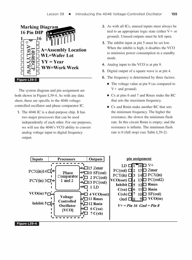
The system diagram and pin assignment areboth shown in Figure L39-4. As with any datasheet, these are specific to the 4046 voltage-controlled oscillator and phase comparator IC.
1. The 4046 IC is a dual-purpose chip. It has two major processors that can be usedindependently of each other. For our purposes,we will use the 4046’s VCO ability to convertanalog voltage input to digital frequencyoutput.
2. As with all ICs, unused inputs must always betied to an appropriate logic state (either V� orground). Unused outputs must be left open.
3. The inhibit input at pin 5 must be set low.When the inhibit is high, it disables the VCOto minimize power consumption in a standbymode.
4. Analog input to the VCO is at pin 9.
5. Digital output of a square wave is at pin 4.
6. The frequency is determined by three factors.
■ The voltage value at pin 9 (as compared toV� and ground).
■ Cx at pins 6 and 7 and Rmax make the RCthat sets the maximum frequency.
■ Cx and Rmin make another RC that setsthe minimum frequency. The higher theresistance, the slower the minimum flashrate. In this circuit Rmin is empty; and theresistance is infinite. The minimum flashrate is 0 (full stop) (see Table L39-2).
Lesson 39 ■ Introducing the 4046 Voltage-Controlled Oscillator 155
Figure L39-3
Figure L39-4

156 Section 11 ■ Introducing an Analog-to-Digital Converter
An example of the expected output on anoscilloscope is provided online atwww.mhprofessional.com/computingdownload.Examples are available for both real scopes andSoundcard Scope.
Troubleshooting PCCP
These are always the first four steps oftroubleshooting:
1. Power. Check your voltage and groundconnections. Use the DMM to check thepower and ground to the chip. This inspectionincludes checking the power supply voltage,proper connections, and broken powerconnectors.
2. Crossovers. Visually inspect that there isn’tany inappropriate touching in your circuit.Don’t get your wires crossed. We’re talkingelectronics here.
3. Connections. Check your connections againstthe schematic. For example, the schematicshows there are only three connections to thechip from pins 9 to 16. There are only five on
the bottom, between pins 1 and 8. Did youmiss one or get an extra one? Are they in theright place?
4. Polarity. What could affect the circuit if itwere backward? Let’s think about that. Hmm?Diodes, or the output LED. C1 is electrolytic,so it is polar. What about the chip? Do youthink it would work if it were popped inbackward? Don’t try it out to see.
Ninety-five percent of all problems will befound if you work through the PCCP method.Predict what the output should be. Use your DMMto double-check the results that you expect.
Exercise: Introducing the 4046 VCO
1. Here’s a question to think about. Lookcarefully at the system diagram for the 4046.Why is pin 3 connected to pin 4? __________
2. In digital logic, there are two states. They arenot Hawaii or Alaska. What are the two logicstates? ___________ and ___________
3. Why must unused inputs be conditioned highor low? ______________
4. RC1 determines the length of the rolldown.
R1 � ___
C1 � ___
RC1 timing ____
Replace C1 with a value 10 times larger.
5. What is the voltage being provided to yourcircuit? Use the DMM and measure this at pin 16. __________ volts.
6. Remove the LED and set the DMM red probedirectly to pin 4, black to ground.
Start the rolldown. Record the reading ofV� pin 4 at the beginning of the rolldown.__________ V
As the rolldown begins, the voltagereading at pin 4 should be half of the voltageat pin 16.
Input Processor Output
Voltage fed Input voltage The VCO
to pin 9 at pin 9 produces a
square wave at
pin 4 [VCOout]
[VCOin] is
compared to
V+ and ground.
Maximum
frequency output
is determined by
Cx and Rmx.
Minimum
frequency output
is determined by
Cx and Rmn.
TABLE L39-2 Minimum Flash Rate

Lesson 39 ■ Introducing the 4046 Voltage-Controlled Oscillator 157
7. An oscilloscope (Soundcard Scope) is the besttool to help understand this. With the LEDremoved, attach the scope probe’s red clip tothe output at pins 3 and 4. The black clip goesto ground. The plug goes into the “Line In”connection of the sound card. The settings areshown in Figure L39-5.
Figure L39-6 shows why the DMM readshalf of the V�. The output is V� half the timeand 0 volts for the other half. The signal isswitching quickly enough that the DMMaverages the voltage and reads it as half of V�.
8. From the glossary, define “clock signal.”__________________________________
9. A square wave is made by a clock signaloccurring at a steady frequency. Draw arepresentation of a square wave in theoscilloscope face presented in Figure L39-7.
10. Modify your breadboard slightly to representthe changes shown in Figure L39-8. Thisallows you to adjust the voltage using avoltage divider. If the voltage is kept stable atthe input to pin 9, what happens to the outputat pin 4? ____________________
Figure L39-5
Figure L39-6
Figure L39-7

11. Consider the schematic presented in FigureL39-9.
12. RC2 controls the maximum frequency. It ismade of Rmx and Cx, noted in the schematicas R2 and C2. Predict what would happen ifthe resistance were increased by 10 times.
Frequency would be
a. 10 � C faster
b. 10 � slower
Try it out. Change R2 from 220 kilo-ohmsto 2.2 megohms. Did it make the frequencyfaster or slower? Did you predict correctly?Think about it. Did the increased resistancespeed up or slow down the drain of C2? ResetR2 back to 220 kilo-ohms.
13. On the 4046 data sheet, pin 12 controls theminimum frequency, Rmn. Right now pin 12is empty. No resistor means “infinite”resistance. Air is a pretty good resistor. Placea 10-M ohm resistor from pin 12 to ground.Start the rolldown. What is the result?
If there is less resistance, predict whetherthe minimum frequency is going to increase(faster) or decrease (closer, to no flashing)when it stops.
158 Section 11 ■ Introducing an Analog-to-Digital Converter
Figure L39-8
Figure L39-9
Input Processor Output
Amount VCO Frequency
of light changes

The 4017 Walking Ring Counter
S E C T I O N 1 2
159
SO WE HAVE A CLOCK signal output. It rolls down toa complete stop. Now to expand from 1 LED to 11 LEDs. They don’t all go on at once. It actuallycounts: 1, 2, 3, 4, 5, 6, 7, 8, 9, 10, 1, 2, 3, . . . andhigher if you want to use the carryout capabilities.
Lesson 40Introducing the Walking Ring4017 Decade Counter
Here is the system diagram for the prototypeapplication of the 4017 IC (see Table L40-1).
Be very careful not to use too much space.There are still two major circuits to fit onto yourboard. All of the cathode sides of the LEDs can beganged onto the unused line on the bottom asshown in Figure L40-1 (see the Parts Bin). Thecommon resistor can connect the LED line toground.
Input Processor Output
Roll down clock signal 1. Each clock advances the 1. Fast cycling through 10.
LEDs from the 4046 output high output sequentially,
walking through outputs
0 through 9.
2. When the count reaches 2. Cycling slows steadily to a
output 9, it starts counting complete stop, randomly at
from output 0 again. any of the 10 outputs.
TABLE L40-1 Prototype Application
Figure L40-1
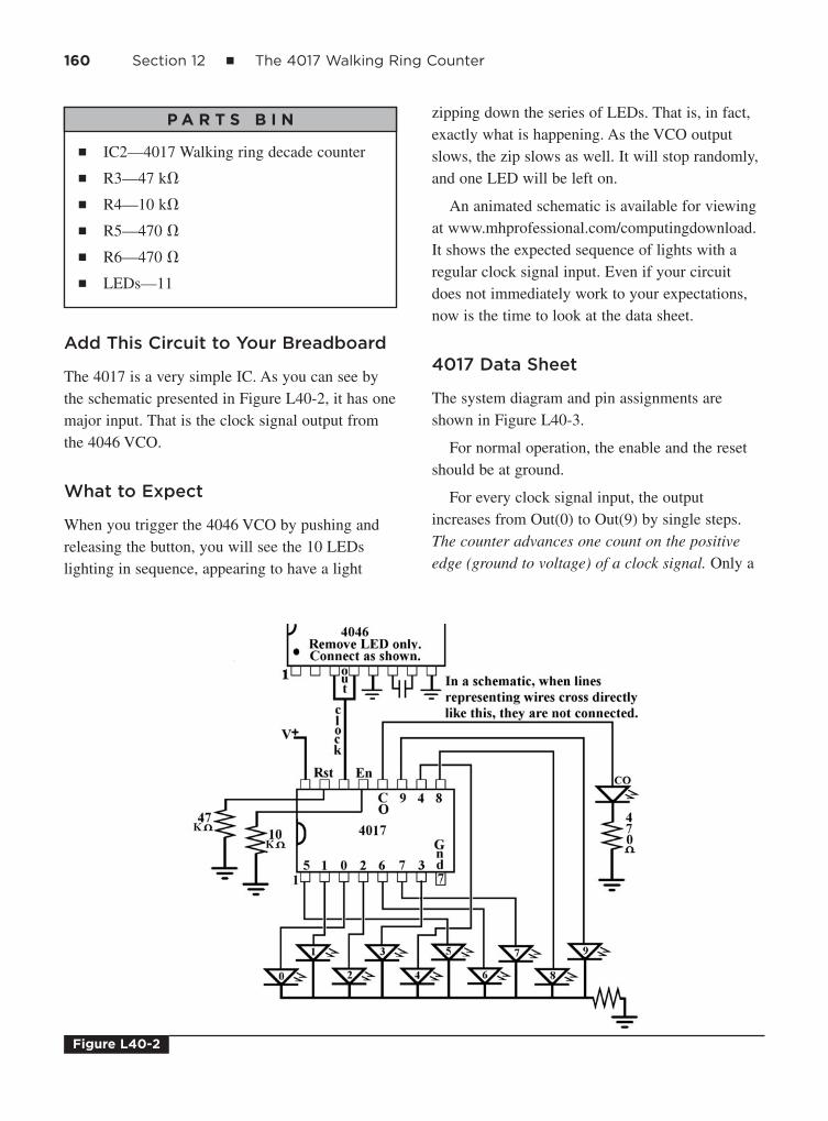
160 Section 12 ■ The 4017 Walking Ring Counter
Add This Circuit to Your Breadboard
The 4017 is a very simple IC. As you can see bythe schematic presented in Figure L40-2, it has onemajor input. That is the clock signal output fromthe 4046 VCO.
What to Expect
When you trigger the 4046 VCO by pushing andreleasing the button, you will see the 10 LEDslighting in sequence, appearing to have a light
zipping down the series of LEDs. That is, in fact,exactly what is happening. As the VCO outputslows, the zip slows as well. It will stop randomly,and one LED will be left on.
An animated schematic is available for viewingat www.mhprofessional.com/computingdownload.It shows the expected sequence of lights with aregular clock signal input. Even if your circuitdoes not immediately work to your expectations,now is the time to look at the data sheet.
4017 Data Sheet
The system diagram and pin assignments areshown in Figure L40-3.
For normal operation, the enable and the resetshould be at ground.
For every clock signal input, the outputincreases from Out(0) to Out(9) by single steps.The counter advances one count on the positiveedge (ground to voltage) of a clock signal. Only a
■ IC2—4017 Walking ring decade counter
■ R3—47 k�
■ R4—10 k�
■ R5—470 �
■ R6—470 �
■ LEDs—11
P A R T S B I N
Figure L40-2

single output pin from Out(0) to Out(9) is high atany moment. By definition, if the output is nothigh, it will be low. When the count is at Out(9),the next clock input recycles output to Out(0),giving us the term “walking ring” because it iswalking in circles.
Carryout
When Out(9) is reached, pin 12 carryout sets high.The carryout terminal is high for counts 0 through4 and low for counts 5 through 9.
Because the carryout clocks once for every 10clock inputs, the 4017 is often referred to as a“decade” or “divide by 10 counter.” For example,it can be used to convert a 10,000-Hz signal inputat pin 14 to a 1,000-Hz signal output at pin 12.
Making the reset high for a moment returns thecounter to Out(0), setting pin 3 output to high. Allother outputs drop to ground. The reset must bereturned to ground to allow counting to continue.To stop the advance of the count, place a high onenable, pin 13. Returning enable to low will allowthe count to continue.
As with any digital circuit, the inputs must beconditioned. That simply means they must beconnected to either high or low at all times.
Of course, every input has its preferred state.
■ Pin 13 enable should normally be set low;otherwise, the 4017 count will be frozen.
■ Pin 15 reset should normally be set to low;otherwise, the 4017 will ignore the count. Itwill be stuck at 0.
The clock must be bounceless and have onlyone ground-to-positive movement for each desiredcount.
The 4017, like all CMOS chips, uses very littlepower. When it is at rest, it uses 0.002 watt ofpower at 5 volts.
Troubleshooting
What if the circuit is not working properly? Beforeyou jump in, there are some bigger items toconsider. Now is the time to start thinkingsystematically. Yes, you need to work through thecircuit using the PCCP troubleshooting method,but the circuit just doubled in size. There are somenecessary questions to ask first.
1. Do you have paper and pencil to recordinformation down as you proceed?
2. What is working? Is there still a clock signal?
■ How can you tell? If there is no clocksignal, then the problem is in the VCO.
■ If there is a clock signal and the LEDs arenot working, then the problem is in thewalking ring.
3. Once you have narrowed down the error to asingle system area, start the PCCP process.And even though it may sound redundant,check the power anyway.
Lesson 40 ■ Introducing the Walking Ring 4017 Decade Counter 161
Figure L40-3
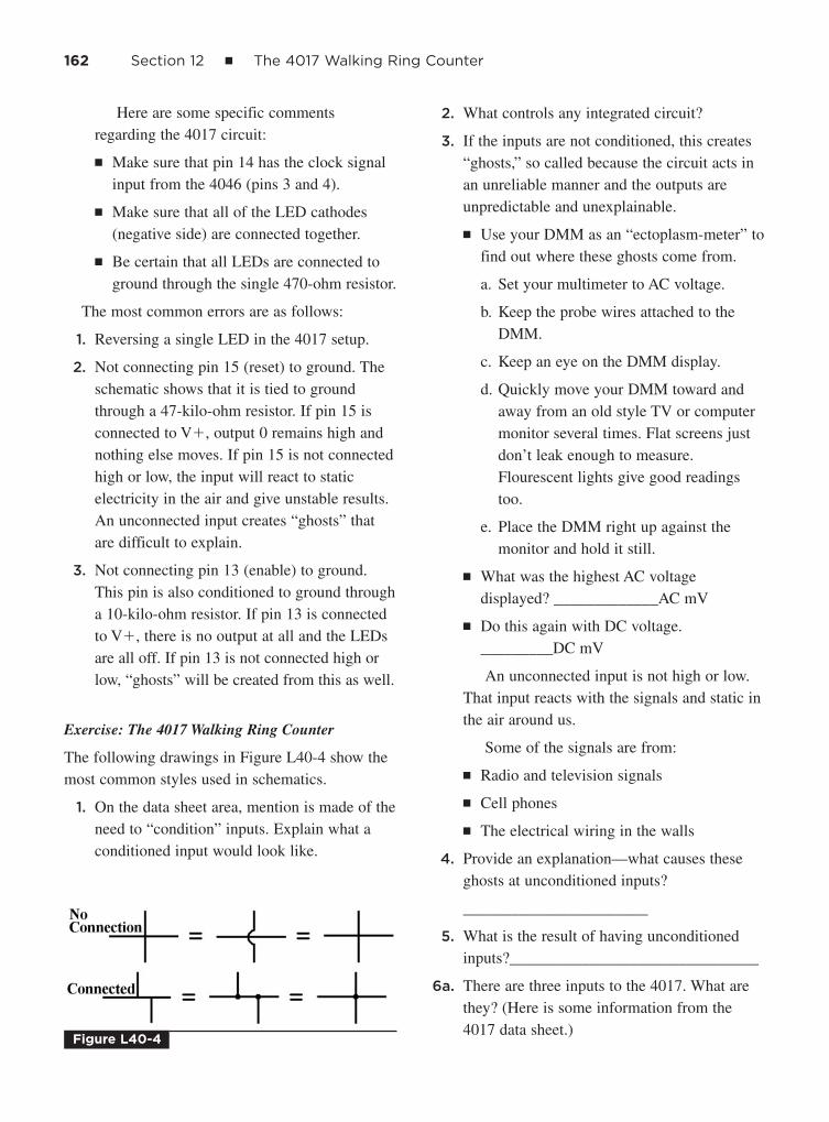
162 Section 12 ■ The 4017 Walking Ring Counter
Here are some specific commentsregarding the 4017 circuit:
■ Make sure that pin 14 has the clock signalinput from the 4046 (pins 3 and 4).
■ Make sure that all of the LED cathodes(negative side) are connected together.
■ Be certain that all LEDs are connected toground through the single 470-ohm resistor.
The most common errors are as follows:
1. Reversing a single LED in the 4017 setup.
2. Not connecting pin 15 (reset) to ground. Theschematic shows that it is tied to groundthrough a 47-kilo-ohm resistor. If pin 15 isconnected to V�, output 0 remains high andnothing else moves. If pin 15 is not connectedhigh or low, the input will react to staticelectricity in the air and give unstable results.An unconnected input creates “ghosts” thatare difficult to explain.
3. Not connecting pin 13 (enable) to ground.This pin is also conditioned to ground througha 10-kilo-ohm resistor. If pin 13 is connectedto V�, there is no output at all and the LEDsare all off. If pin 13 is not connected high orlow, “ghosts” will be created from this as well.
Exercise: The 4017 Walking Ring Counter
The following drawings in Figure L40-4 show themost common styles used in schematics.
1. On the data sheet area, mention is made of theneed to “condition” inputs. Explain what aconditioned input would look like.
2. What controls any integrated circuit?
3. If the inputs are not conditioned, this creates“ghosts,” so called because the circuit acts inan unreliable manner and the outputs areunpredictable and unexplainable.
■ Use your DMM as an “ectoplasm-meter” tofind out where these ghosts come from.
a. Set your multimeter to AC voltage.
b. Keep the probe wires attached to theDMM.
c. Keep an eye on the DMM display.
d. Quickly move your DMM toward andaway from an old style TV or computermonitor several times. Flat screens justdon’t leak enough to measure.Flourescent lights give good readingstoo.
e. Place the DMM right up against themonitor and hold it still.
■ What was the highest AC voltagedisplayed? _____________AC mV
■ Do this again with DC voltage._________DC mV
An unconnected input is not high or low.That input reacts with the signals and static inthe air around us.
Some of the signals are from:
■ Radio and television signals
■ Cell phones
■ The electrical wiring in the walls
4. Provide an explanation—what causes theseghosts at unconditioned inputs?
_______________________
5. What is the result of having unconditionedinputs?_______________________________
6a. There are three inputs to the 4017. What arethey? (Here is some information from the4017 data sheet.)
Figure L40-4

a. _________ at pin _____conditioned by itsconnection to the 4046 output.
b. _________ at pin _____ conditioned ____in normal operation.
c. __________at pin _____ conditioned ____in normal operation.
6b. State the purpose of each input. (Here is someinformation from the 4017 data sheet.)
a. ___________/ purpose_________________
b. ___________/ purpose_________________
c. ___________/ purpose_________________
7a. What is the strict definition of the clock signal?
_____________________________________
7b. Which shape in Figure L40-5 best shows aclock signal?
8. Set the DMM to VDC. With the red probe to4017’s pin 1, trigger the circuit. Are theresults the same as the output of pins 3 and 4of the 4046? _______
9. The output from the 4046 VCO on theoscilloscope should have been similar to thediagram shown in Figure L40-6.
If you set up the oscilloscope just tomeasure at pin 1 of the 4017, what would youexpect to see?
a. The same clock signal output frequency
b. Only half of the output frequency
c. High for the first five, low for the secondfive
d. Only one-tenth of the output
10. Consider the carryout (pin 12).
a. It is high for half the cycle and low for theother half.
When does the carryout of the 4017change from low to high?___________
When does the carryout of the 4017change from high to low?___________
b. Explain why the output of pin 12 (carryout)is so different from the other output pins 0through 9. (Refer to the 4017 data sheet.)___________________________________
__________________________________
Lesson 41Understanding the ClockSignal Used by the 4017
Hickory dickory dock. The system responds to aclock.
A clock signal is widely used in electronics totrigger events throughout larger systems.
Definition: A clock signal is a clean digitalsignal that raises from zero to full voltageinstantly. It must take fewer than 5 microseconds.That is 0.000005 second (1 microsecond � 10–6
second).
A clock signal is all of the following:
■ Is a very clean signal
■ Does not bounce or echo
■ Triggers one event
Lesson 41 ■ Understanding the Clock Signal Used by the 4017 163
Figure L40-5
Figure L40-6

164 Section 12 ■ The 4017 Walking Ring Counter
The clock signal is generated by the 4046 VCOcircuit and is used to trigger the 4017 circuit. Eachclock signal advances the “high” output by one asshown in Figure L41-1.
Each of the 4017’s output provides a clean clocksignal as it changes from low to high. When theoutput changes from 9 to 0, the carryout at pin 12“clocks” and remains high until the count advancesfrom Out(4) to Out(5). Any of the outputs can beused as clock signal inputs to trigger other circuits.
When reset is momentarily set to high, the countresets to 0.
When the enable is set to high, the count stopsuntil it is returned to low.
Remember, all inputs need to be conditioned toeither high or low.
Refer back to the data sheet provided in Lesson40 as you work through this lesson.
To understand the circuit better, take one of theLEDs out and put it in backward.
■ Trigger the circuit.
■ How many LEDs are lit at one time? _____
■ There is a rolldown . . . but now there are twolights on all the time: one of the other nineLEDs and the reversed LED.
■ The drawing in Figure L41-2 best explainswhat is happening.
Remember: Only one output is high at any time;the rest are low.
The reversed LED acts as ground. So the pinpowering the LED in the count is draining throughthe backward LED connected to an output that islow. Return the LED to its proper position.
Exercise: Understanding the Clock Signal and the 4017
Here we will compare a PB switch to a clocksignal input. This setup substitutes a singlemechanical action for a clock signal. Rememberthat a clock signal is very fast (millionths of asecond) and very clean. The LEDs advance by oneper clock signal. Be sure to change back to theoriginal setup when this exercise is done.
Figure L41-1
Figure L41-2

1. Attach a 100-kilo-ohm resistor and the PBNOto the clock input of the 4017 as shown inFigure L41-3.
2. Remove the wire that carries the clock signalfrom the 4046 (pins 3 and 4) to the 4017 (pin 14). When everything is set up, attach the power.
3. What LED is lit now? LED # ________
■ Press the plunger down in a definitemovement.
■ Don’t release it.
■ What LED is lit now? LED # ________
■ Release the plunger.
■ Did the count advance when you releasedthe plunger? That was a voltage movementfrom V� to ground.
4. You expect a push button to be a fast andclean movement from ground to V�. Is it aclock signal?____
■ You cannot use any mechanical device toprovide a clock signal.
■ A clock signal must be generatedelectronically.
5. Push and release the plunger a few moretimes.
■ You can expect that the count will advanceby a single step . . . sometimes by two orthree steps.
■ The contacts of a physical switch like apush button do not provide a clean enoughsignal when a clock signal is required.
■ An unclean input has bounce as shown inFigure L41-4. Such a bounce is too fast tobe noticed on inexpensive oscilloscopes. Itwould be impossible to see on SoundcardScope. But you see the results of thebounce as the 4017 counts more than onestep in each push of the plunger.
Lesson 41 ■ Understanding the Clock Signal Used by the 4017 165
Figure L41-3

If an input says it needs a clock signal, only a clock signal will do. The CMOS 4093 is aspecialized IC designed to “debounce” mechanicalswitches. It is nothing more than a fancy 4011chip. It has been designed to react much moreprecisely to the inputs.
Lesson 42Controlling the Count—Usingthe Chip’s Control Inputs
You’ve seen that the major input is a clock signal.There are two other inputs. Let’s visit them and seewhat they do.
Add two long wires to the breadboard as shownin Figure L42-1. These will be used as connectionsto V� when needed. Leave the ends loose. Noticehow pin 15 (reset) and pin 13 (enable) are eachconnected to ground through a resistor. That waythe input is still conditioned, even if you do nothave the probe connected somewhere.
Reset
1. Trigger the 4046 to start the rolldown. All 10LEDs should flash in sequence. Now connectthe reset probe to the anode (�) side of LEDnumber 7. What happens?
2. Choose another LED and do the same thing.What happens? What does the reset do whenit is set high for a moment?
3. Wait until the rolldown stops. Touch it to V�.
4. What happens if you keep the reset high andstart the rolldown?
166 Section 12 ■ The 4017 Walking Ring Counter
Figure L41-4
Figure L42-1

Take a look again at how the data sheet definesthe purpose of the reset. It does exactly what itsays it does. And the same is true for the enablefunction.
Enable
1. Pull the reset wire out while you play with theenable. Start the rolldown. Now connect theenable probe to the anode (positive) side ofany LED. What happens?
2. Choose another LED. What happens? Whatdoes the enable do when it is set high for amoment?
3. Wait until the rolldown stops. Touch it to V�.
4. What happens if you keep the enable high andstart the rolldown?
So what good are these? That is up to youto decide. Maybe you don’t want to countzero to nine all the time. Maybe you onlywant it to count to six, like rolling a die.Maybe you have a hexapod robot. It has apreset cycle for its six legs. You can use the4017 to trigger this system. Figure L42-2shows a really cheap, simple, yet effectiveidea for applying the 4017 in a video securitysurveillance system.
The system needs to have the “high”produced by any source to reset the system.The reset does not need a clean clock signal.Any momentary high will do. The “high”from pin 10 is used here. Why don’t we seethe LED connected to pin 10 light up?Because of the speed, the circuit reacts inmicroseconds. That is too fast for us to noticeany response in the LED.
5. Predict what happens when the reset wire isconnected to pin 1. Pin 1 is related to whatoutput?
a. Out 0
b. Out 2
c. Out 4
d. Out 5
e. Out 10
6. Underline which LEDs light up. 0, 1, 2, 3, 4,5, 6, 7, 8, 9
7. What is the state of the carryout for thissetup?
a. On all the time
b. On for the first two, off for the second two
c. Doesn’t light up
Lesson 42 ■ Controlling the Count—Using the Chip’s Control Inputs 167
Figure L42-2

168 Section 12 ■ The 4017 Walking Ring Counter
8. How are the three inputs conditioned so theyare always connected to either high or low?
a. Clock______________________________
b. Reset______________________________
c. Enable_____________________________
9. Look at the schematic. The “enable” isconditioned to low through the 10-k� resistor.Start the circuit from the 4046. In the middleof this standard rolldown, connect the enableto V�. Note what happens. Leave it attachedfor 30 seconds, and then trigger the rolldown.Disconnect the enable from V� so it is lowagain. The rolldown should pick up again inthe middle. Describe what the enable does.
_____________________________________
_____________________________________
10. In the following system diagram, describe theprocessor for the video security system shownin Figure L42-2 (see Table L42-1).
Input Processor Out
Video Three items Video recorder
camera are necessary
signal for this
processor.
1. A circuit that
generates
clock signals.
2. The 4017
does what?
_________
3. The 4066*
does what?
_________
* The 4066 is the equivalent of four high-quality
NPN transistors in a single package. What does
it do here in the circuit?
TABLE L42-1 System Diagram

Running a Seven-SegmentDisplay
S E C T I O N 1 3
169
THE SEVEN-SEGMENT DISPLAY depends on two majorchips. I introduce the “slave” 4511 first so you canunderstand how it is controlled. Then the 4516“master” is introduced. You will investigate andplay with most of the possibilities of each chip asthey are presented. At the end of this chapter, youwill have the prototype of the DigiDice and be ableto explain it. Better than that, you will be able tocontrol it. Remember, binary’s the word.
Lesson 43Introducing the Seven-Segment LED
Here you have a real number output. It’s just a setof LEDs set up to represent numbers.
Here is the system diagram from the beginningof Part Three (see Table L43-1).
Remember that there is to be a number outputtoo. In this chapter we will add the numberreadout. Everything revolves around creating a
number output using a seven-segment LEDdisplay. This simple device is created by usingindividual LEDs in rectangular shape, set into apackage that creates a number, as shown in Figure L43-1.
So you might have some seven-segmentdisplays lying around. You try them out. Theymight work and they might not. That is becausethere are two major types of seven-segmentdisplays: the CC and the CA. The type that is usedhere is referred to as a common cathode (CC). Aproper schematic diagram for the CC is shown inFigure L43-2.
Input Processor Output
Push button 1. Rolldown (4046 IC) controlling 2 1. Fast cycling through six LEDs.
2. Walking ring resets at 6 (4017 IC) 2. Fast cycling through numbers 0
through 6.
3. Binary counting decimal (4511 IC) 3. Cycling slows steadily to a complete
stop, randomly at points 1 through 6.
TABLE L43-1 System Factors
Figure L43-1

170 Section 13 ■ Running a Seven-Segment Display
This type of seven-segment LED display isreferred to as a common cathode because all of theLEDs share the same ground line. You have to addresistors on the anode (positive) side for each LED.The alternate type of seven-segment display isshown in Figure L43-3. Note that it is almostidentical, yet completely opposite, of the CC layout.
Just as with the CC, you still have to addresistors. This is done on the cathode (negative) sidefor each LED in this package. Just a further note:The two package styles are not interchangeable.A CC will not substitute for a CA (commonanode) package in any circuit because it is thesame as placing an individual LED in backward. It just doesn’t work.
Right now, you need to map out your seven-segment display. Set the seven-segment displayinto your breadboard as shown in Figure L43-4.
Be sure to use a 470-ohm resistor to cut thevoltage to the individual LEDs as you map out thepins. The center pin of each side is a commonground connection. Only one needs to beconnected to ground.
Now use a single wire to determine which pinpowers which LED. Label your drawing. You willneed this information to wire up your next circuit.
How would you create the number 7?
Lesson 44Control the Seven-SegmentDisplay Using the 4511 BCD
1. Getting numbers to present onto the seven-segment display has to be easier than rewiringall the time. Electronics is about control. Hereis a chip that controls the seven-segmentdisplay.
2. Several IC processors are available to changeinputs into number outputs.
3. The 4511 BCD CMOS IC used here is a basicbinary-counting decimal processor.
4511 Data Sheet
The system diagram and pin assignments for the4511 BCD are shown in Figure L44-1.
Figure L43-2
Figure L43-3
Figure L43-4

Basic Operation
The 4511 BCD accepts a binary input code andconverts it to be displayed on a seven-segment,common cathode LED (all segments share thesame connection to ground).
The binary code placed on B1, B2, B4, and B8inputs is translated as a code for display on a CCseven-segment LED. For instance, if B8 is low, B4 is high, B2 is high, and B1 is low [0110], thisinput combination will make outputs c, d, e, f, and g high, while outputs a and b remain low,creating a decimal six.
In normal operation the lamp test and blankingare held high while store is connected to ground.
■ Lamp test: If lamp test is grounded, all of thelettered outputs will go high.
■ Blanking: If blanking input is made low, alllettered outputs go low, turning the display off.
Note as well that any input representing anumber bigger than decimal nine will blank thedisplay. Even though this 4-bit binary word cancount from 0 (0000) to 15 (1111), the 4511 isdesigned to operate a seven-segment LED thatcannot count above nine. Any binary word above0101 is unreadable. The 4511 will blank, turningoff all outputs to the display.
If the store input is made high, the value of theinput code at that instant is held internally and canbe used later.
The 4511 BCD system layout is described in theTable L44-1.
Breadboarding the Seven-SegmentDisplay and 4511 Display Driver
Set the chip and seven-segment display near theend of your breadboard as shown in Figure L44-2.
Now build this circuit from the schematic inFigure L44-3.
Lesson 44 ■ Control the Seven-Segment Display Using the 4511 BCD 171
Figure L44-1
Input Processor Output
A binary word Binary code is Decimal value
provides high converted for of binary input
signals at the display by shown on the
binary inputs. the binary- seven-segment
counting LED.
decimal
processor.
TABLE L44-1 4511 BCD System Layout

The wire probes are only needed for testing inthis lesson.
Building this circuit on the breadboard canprove to be challenging. The picture in FigureL44-4 is provided to help guide you. There is acorrect technique for breadboarding, and then thereis a mess.
■ Note that the resistors have had their legsclipped shorter on one side. Then they areplaced upright.
■ Insulated wires are used to make the longconnections. Those wires are a bit longer than
172 Section 13 ■ Running a Seven-Segment Display
Figure L44-2
Figure L44-3
Figure L44-4

the actual connection. That relieves any strainthat might cause the wire to spring out of itshole.
■ The wires are gently bent. Sharp cornersactually encourage the solid wire to breakunder the insulation. Such breaks arefrustrating and hard to find.
What to Expect
When you attach power to this circuit, the seven-segment display should read ZERO. That is,segments A, B, C, D, E, and F are lit. Not thecrossbar, G. If you have a backward “6,” you haveswitched the outputs “F” and “G.”
1. Touch the wire probes connected from inputsB1, B2, B4, and B8 separately to V�. This“injects” a high signal into the various binaryinputs.
2. Touch both B2 and B4 to voltage at the sametime.
3. Try different combinations.
4. What happens when you try to inject a high atB8 and B2 at the same time? It should blankthe display.
Troubleshooting
Run through the PCCP. The most commonproblems in this setup are as follows:
■ Crossed wires.
■ Reversed display.
■ Individually burned-out LEDs on the display.
■ Blanking at pin 4 and lamp test at pin 5 areconnected to V�. Either connected to groundwould keep this circuit from working.
Exercise: Control the Seven-Segment Display Using the 4511 BCD
The inputs B8, B4, B2, and B1 represent binaryinputs.
Together, all four binary inputs create a 4-bitbinary word. Figure L44-5 presents an excellentrepresentation of how the binary word input relatesto the display driver outputs.
1. Use the wire probe to connect B1 (pin 7) tovoltage. What is the readout of the display?____________
2. Use the wire probe to connect B2 (pin 1) tovoltage. What is the readout of the display?____________
3. Use the two separate wire probes to connectboth B1 and B2 to voltage. What is displayed?____________
4. Work through Table L44-2.
Lesson 44 ■ Control the Seven-Segment Display Using the 4511 BCD 173
Figure L44-5

The highest binary input that the 4511recognizes is when inputs B8 and B1 are bothhigh.
That means the highest it can count is 9.Anything over a binary input equal to“decimal 9” will cause it to blank out.
5. Why are inputs 1, 2, 6, and 7 connected toground through 100k� resistors?__________________________________________________________________________
6. What is the maximum count of a 4-bit binaryword? _______________________________
7. What is the highest number that the 4511seven-segment driver is able to display?_____________________________________
8. BCD stands for binary-counting decimal:Binary in—decimal out.
What is the binary word for decimal 7?_____________________________________
9. Besides the binary word input, there are threeother inputs to the 4511. What are they (fromthe 4511 data sheet)?
a. ______ at pin______ is conditioned______ in normal operation. What is itspurpose? ___________________________
b. ______ at pin______ is conditioned______ in normal operation. What is itspurpose?____________________________
c. ______ at pin______ is conditioned______ in normal operation. What is itspurpose?____________________________
10. Test blanking and lamp test separately. Simplyconnect them to ground momentarily.
Lesson 45Decimal to Binary—The 4516
The 4516’s output is the binary word input to the4511. It changes the decimal clock signal from the4046 VCO to a binary output used by the 4511.This lesson explains the operation and applicationof the 4516 BCD IC.
174 Section 13 ■ Running a Seven-Segment Display
Binary Seven-Segment Number B8 B4 B2 B1 Word Display Output
Zero Low Low Low Low 0000 A B C D E F
One Low Low Low High 0001 C and D
Two
Three
Four
Five
Six
Seven
Eight
Nine
Ten
TABLE L44-2 Wire Probe

Data Sheet: 4516 Binary CountingDecimal—Up/Down Zero to 15Counter
The system diagram and pin assignment for the4516 are shown in Figure L45-1.
Basic Operation
For each clock signal input, the binary word outputchanges by one. The binary word shows as a highsignal on corresponding outputs. For example, forthe decimal number “7,” the output B8 is low,while B4, B2, and B1 are high [0111].
In normal operation the inputs carry-in, reset,and preload are held low.
The binary word increments one count on theclock signal at pin 15. The movement is dependenton the setting of the up/down control. The outputappears as the binary word at the outputs B8, B4,B2, B1.
Up/Down Control
When the U/D control is set to high, the countproceeds upward. When decimal 15 [1111] isreached, the count cycles back to zero [0000] andcarryout is triggered. When the U/D control is setto low, the count proceeds backward. When
decimal zero [0000] is reached, the count cyclesbackward to 15 [1111], and carryout is triggered.
Carry-In
The carry-in must be held low to allow counting.Holding the carry-in high stops the count, makingit function like the enable switch of the 4511.
When multiple stages are used, the chips sharethe clock signal, as shown in Figure L45-2.Carryout of each stage connects to the carry-in ofthe next level.
Reset
By momentarily connecting reset to V�, the countreturns to zero [0000]. The reset must be returnedto ground to allow counting to continue.
Lesson 45 ■ Decimal to Binary—The 4516 175
Figure L45-1
Figure L45-2

176 Section 13 ■ Running a Seven-Segment Display
Preload
Any number can be preloaded into the 4516 bypresetting the appropriate binary word to voltagethrough the preload inputs [L8, L4, L2, L1]. These preloaded inputs are loaded on to theircorresponding binary outputs [B8, B4, B2, B1] bybringing the preload at pin 1 high for a moment.As with reset, the preload must be returned toground to allow counting to continue.
Pin 15 should be in a low state and
there should be no clock inputs to
pin 15 when preloading is done.
Add to the System on the Breadboard
Leave a small patch of five free lines on one sidefor the last part of the system introduced in thenext lesson.
As the schematic shows in Figure L45-3, the4516 uses seven more 100 k� resistors and morewire. You also add a temporary display of thebinary word using four extra LEDs.
1. Remove the 100 k� resistors from the 4511’s inputs.
2. Preload control at pin 1, and the preloadpresets L8, L4, L2, and L1 are attached toground through 100 k� resistors.
3. Carry-in is connected to ground, because it isan unused input.
4. Carryout can be left open. It is an output usedto trigger another stage in counting.
5. Reset is attached to ground through a 100 k�
resistor.
6. Start with the up/down control connected by a100 k� to V�.
What to Expect
Here’s what to expect before you start to play. Usethe clock signal from the carryout of the 4017 asthe INPUT clock signal to the 4516. The numberwill advance one for every run down all 10 LEDs.Note that this wiring is specific to where you arenow. It is subject to being played with by curiousfingers and nimble minds.
Also, at this point, the up/down control at pin 9can be connected to V� (counting up) or ground(counting down) through a 100 k� resistor.
NOTE
The insert shows the most common error—do not wire like this!Figure L45-3

Exercise: Decimal to Binary—The 4516
A: Initial Setup
The 4516 acts as the interpreter. It changes thedecimal clock signal source into the binary inputused by the 4511 display driver.
The outputs of the 4516, B8, B4, B2, and B1 arewired directly to corresponding inputs of the 4511.The four LEDs display the 4516’s binary word. Itmatches the decimal number displayed on theseven-segment LED. Now place a 10-megohmresistor from pin 12 of the 4046 to ground. Thissets the minimum frequency output of the 4046 to about 1 Hz. This way, you don’t have tocontinually trigger the roll down.
Make sure that the 4516’s up/down counter (pin10) is conditioned to V� so it counts upward.
1. The shortened “DCB” stands for what?
D____________ C______________
B____________
2. The shortened “BCD” stands for what?
B____________ C______________
D____________
B: Inputs Inputs Everywhere
Be careful while you are exploring. You canaccidentally connect V� directly to ground. Thatshorts out the power supply. Even though it lookslike everything turns off, a short circuit candamage your power supply.
■ Up/down counter. First, try out the up/downcounter at pin 10. Use a long wire as shown inFigure L45-4 to connect the up/down control toground.
■ The reset. Use a wire probe and momentarilytouch the reset input to voltage as shown inFigure L45-5.
■ The preload. This is easy to do. Don’t removethe resistors. They allow flexibility. Pop a shortwire into both L2 and L4 as shown in FigureL45-6, and connect them to V�. Connect along wire to preload. Touch the preload wire toV�, just for a moment. Your display shouldnow show the number “6.” When the preload isset to high, the values preset on the load inputsare dumped onto their matching binary countoutputs.
Lesson 45 ■ Decimal to Binary—The 4516 177
Figure L45-4

C: Now for Some Serious Playtime! Exploring the Possibilities
Right now, both the 4017 and 4516 are connecteddirectly to the clock output of the 4046 as shownin Figure L45-7.
1. The 4046 clocks the 4017. Now connect the4017’s carryout to the clock input of the 4516as shown in Figure L45-8. Think about it. Tryto explain what is happening.
2. This is even better. The 4046 clocks to the4516. Connect the carryout of the 4516directly to the clock input of the 4017. Thesetup is shown in Figure L45-9. What ishappening?
178 Section 13 ■ Running a Seven-Segment Display
Figure L45-5
Figure L45-6
Figure L45-7
Figure L45-8

3. Will the 4516 still count zero to nine in thissetup when you play with the reset or enableof the 4017? Try it out.
4. Remember the carryouts of the 4017? It ishigh for the first five numbers, and then goeslow for the second five numbers. Try the setupshown in Figure L45-10. Connect the 4017carryout to the up/down counter of the 4516.Predict what’s going to happen. Were youright?
5. Any other ideas?
D. Setting Up the DigiDice
Figure L45-11 is the graphic system diagram thatyou can use to set up your prototype for DigiDice.Notice that some particular features have beenincorporated into the system.
The 4046 clock feeds to both 4017 and 4516.
When “Out 6” of the 4017 goes high, this signalis used to trigger the following:
1. The reset of the 4017 (the first six LEDs lightup in sequence)
2. The preload (pin 1) of the 4516
■ L1 (pin 4) must be set directly to voltage.
■ This will load the number “1” when it istriggered, effectively skipping “0.”
■ Resulting in numbers displayed 1-2-3-4-5-6-1-2-3 . . .
At this time, you can remove both the 10-megohmresistor from the 4046’s pin 12 and the LEDs usedto display the binary word. The minimumfrequency will return to full stop, and you will haveroom for one last addition to the entire system.
Lesson 45 ■ Decimal to Binary—The 4516 179
Figure L45-9
Figure L45-11
Figure L45-10

Lesson 46The Displays Automatically Fade Out
Of course, your mother never reminded you,“Can’t you remember to turn off the lights afteryou leave the room?” With the next step, you’llnever have to worry about that with your circuit.
Hey! If you didn’t do it yet, do it now. Removethose LEDs used to show the binary word.
Power consumption is important if you usebatteries to power the system. CMOS electronicsare popular because the systems use so littlepower. In comparison, the LEDs gobble energy in this system. In this lesson we apply a simple RC to the system that automatically cuts the powerto the LEDs.
A basic system diagram is shown in Table L46-1. It includes the RC that automatically turnsoff the LEDs.
A detailed system diagram for DigiDice dealswith the input/processor/output of each piece ofthe system (see Table L46-2).
Displaying the system this way can beconfusing and long-winded. A “graphics systemdiagram” shows how all of that information can bedisplayed more efficiently. Such diagrams are morereadily understood and infinitely easier to usewhen designing and troubleshooting systems.Figure L46-1 is the graphic system diagramshowing how RC3 is set into the system.
But even a graphic system diagram does notshow the full schematic. For that matter, at thispoint, I’m not going to show the full schematiceither. All that needs to be shown is the specificschematic of interest and the notation of how it isconnected into the system. Figure L46-2 is theschematic showing how RC3 controls the NPNtransistor.
Everything used here should be fairly obvious,except for the extra diode. Why is the extra diodethere? The diodes separate RC1 from RC3. Here isa complete explanation why it is necessary.
RC1 and RC3 are isolated from each otherusing the diodes to prevent any reverse flow of thecurrent. If there were no diodes, the charges wouldbe shared between the capacitors of RC1 and RC3.This is shown in Figure L46-3.
180 Section 13 ■ Running a Seven-Segment Display
Input Processor 1 Processor 2 Processor 3A Processor 4 Output 1
A contact RC1 controls 4046 VCO 4017 Walking Timed off as 6 LEDs
switch like the timing of RC2 controls ring 1-10 a power saver.
a PBNO the rolldown max and min counter. RC3 controls
frequency of Seventh LED the transistor
the clock (out 6) is that cuts power
signal connected to to the LEDs
reset and
preload controls
on the 4516
Processor 3B Output 2
4516DCB(P) Seven-segment
4511BCD display counting
1-2-3-4-5-6
TABLE L46-1 Basic System Diagram

Lesson 46 ■ The Displays Automatically Fade Out 181
First Section, Including the 4046
Input Processor Output
Push button closes Falling voltage controlled by Length of rolldown controlled by
Voltage filling RC1 the RC1 drains from max to RC1. Rolldown clock signal.
minimum. The voltage at
pin 9 is compared to V+.
This controls speed of
voltage-controlled oscillator.
Second Section 4017
Input Processor Output
Clock rolldown from the 1 of 10 counter reset at out 6. Walking ring provides high to out 0
output of the 4046 to out 6.
Reset Out 6 is used to reset 4017 to 0.
Out 6 is used as controlling input to 4510.
Second Section LEDs
Input Processor Output
Walking ring provides Light
high to 1 of 6 LEDs
in sequence.
Third Section Starting with 4516
Input Processor Output
Clock rolldown from Decimal counting binary Advancing binary code
4046
High input from 4017
out 6 triggers preload
of L1
U/D counter set up
or down
Third Section 4511
Input Processor Output
Binary word Converter for seven-segment LED Decimal value of binary input shown on
the seven-segment LED
Binary-counting
Decimal
Fourth Section Timed Off
Input Processor Output
Voltage filling RC3 Transistor opens, then slowly Displays fade-out1-2-3-4-5-6
closes the connection to ground
as controlled by RC3
TABLE L46-2 Detailed System Diagram

The resistors would act together, too. RC1 andRC3 would combine and act as a single RC.
If there were only one diode, the unisolatedcapacitor shares its charge first. This is demonstratedin Figure L46-4. The charge in the 1-μF capacitorof RC1 would push through the lower diode andadd to the charge of the 22-microfarad capacitor ofRC3. The reverse would also occur; if the bottomdiode were not present, the charge stored in the 22-μF capacitor of RC3 would push through the
upper diode and add to the charge of the 1-μFcapacitor of RC1.
The complete and proper setup is shown in FigureL46-5. Each RC acts independently. The RC1rolldown should finish 5 to 10 seconds before thefadeout really finishes. If the LEDs fade out beforethe rolldown is completed, adjust the timing of eitherRC1 to be shorter or the timing of RC3 to be longer.
182 Section 13 ■ Running a Seven-Segment Display
Figure L46-1
Figure L46-2
Figure L46-3
Figure L46-5
Figure L46-4

Define, Design, and Make Your Own Project
S E C T I O N 1 4
183
Imagination is more important than knowledge.—Einstein
IT HAS BEEN MY EXPERIENCE that when people are given instructions to make something forthemselves, they will complain. Either they aregiven far too much detail or what they perceive as not nearly enough. All this from the sameaudience. What I have done here is give examples.The more complex the example, the more I chooseto talk in terms of concept, not detail. I do this onpurpose. This is your project. If I gave you all ofthe details, it becomes my project and you copyingmy project.
Remember the earlier comment about Lego.That was a serious statement. Parts of one fitperfectly into the parts of another. That is one ofthe beauties of digital electronics. Think about it.You have learned enough that you could almostbuild the controller for an arena’s scoreboard. You can develop your own applications using justa portion of the system. Next time you go to themall, carefully look at those fancy gadgets that eat your quarters and tell you your fortune. What?You say you can’t do that? Then why not?
Lesson 47Defining and Designing Your Project
Ideas to keep in mind:
1. In an ideal world, the sky is the limit.
2. Murphy was probably right. Murphy’s firstlaw states, “If anything can go wrong, it will.”Do an Internet search of “Murphy’s law” �Technology.
3. In reality you will never have:
■ Enough time
■ Enough money
■ The right equipment for the job
4. Your expectations for this project should bereasonable.
■ Five printed circuit boards are provided inthe kit for this unit. This provides you withmaximum flexibility.
■ The biggest limitation that exists for thisproject is your inability to create your ownenclosure.
■ The most reasonable and inexpensivepremade enclosures are old plastic VHScassette cases.
■ These are often available with plastic liningthat allows you to insert labels, signs, anddirections.

184 Section 14 ■ Define, Design, and Make Your Own Project
Notes Regarding Possibilities
This is digital electronics. The processors can bemixed and matched, or not used at all.
1. 4046 VCO:
■ Can be set to a specific frequency
■ Rolls down
■ Can roll up (think about it)
■ Can set minimum frequency
■ Can set maximum frequency
■ Has frequency range
2. 4017 walking ring:
■ Dependent on a clock signal, but any clocksignal will do.
■ Don’t underestimate reset or enable.
■ Can count 0 to 9, and reset or freeze on anypredetermined number.
■ What about the carryout? High for half thecount, low for the other half.
■ What about using two 4017s, counting 0 to99 in rows?
■ The outputs are not limited to LEDs, asshown in Figure L47-1. They can controltransistors to give power.
3. 4516/4511 BCD unit:
■ Like the 4017, it is dependent on a clocksignal.
■ With a 1-Hz signal, you could make abinary clock.
■ The 4516 has more inputs than outputs.
■ The U/D control takes any digital input. Itis not dependent on a clock signal.
■ What about having two 4516s counting 0 to99 in digits?
Timing
There are only three separate RC timers right now.More are possible. RC1 and RC3 work together. IfRC1 is longer than RC3, the displays fade beforethe rolldown is complete. Use Table L47-1 to setthe timing of the RCs to your desires.
Examples
Each of five examples presented has a unique twistin its application. New portions are explained indetail. Some of the design components, by theirvery nature, are identical between projects. Whenthat happens, that portion is mentioned briefly.
The Ray Gun
The ray gun displayed in Figure L47-2 is awonderful little project.
Figure L47-1
Resistor Capacitor Time
20 M� 10 �F 200 seconds
10 M� 10 �F 100 seconds
4.7 M� 10 �F 50 seconds
20 M� 1 �F 20 seconds
10 M� 1 �F 10 seconds
4.7 M� 1 �F 5 seconds
TABLE L47-1 Set Timing of RCs
Figure L47-2

The entire system has been enclosed in a squirtgun. The unique idea here is that only a portion ofthe larger system has been applied as shown in thegraphics system diagram of Figure L47-3.
The same system can be applied to a pushbutton fortune teller or a 10-LED roulette wheel.
The “Whatever” Detector
The only unique quality here is the switch and thename you give it. In fact, this is the same system,but applied as a fake metering device. Fill in the
word of your choice for “whatever.” The beauty isthat it actually changes frequency from person toperson. Did you notice that you could get thecircuit to work by just touching across the bottomof the push button? Try it. The packaging can befancy, as shown in Figure L47-4, or you could usea simple box.
You could moisten your palm and pick up the“Ghost Detector,” claiming all sorts of things asyou point it toward a dark corner. Give it to yourfriend and watch as it goes dead. A littleknowledge isn’t dangerous. It’s fun.
An Animated Sign
The animated sign shown in Figure L47-5 could beused for a variety of shapes.
Both of the things that make this unique areshown in the graphics system diagram of FigureL47-6.
Lesson 47 ■ Defining and Designing Your Project 185
Figure L47-3
Figure L47-4
Figure L47-5

First is the subsystem that triggers the 4046. Itis a 4011 oscillator set to pulse every 20 seconds.The maximum frequency is set to 20 Hertz. It rollsdown almost to a complete stop before it kicks theoscillator high again. The schematic is shown inFigure L47-7.
Second is the necessity for ultrabright LEDs tomake the output visible from a distance. Thisrequires the output of the 4017 to use transistors toamplify the power.
The IQ Meter
This is another wonderful gadget. It could just aseasily be called a lottery number generator. Yousecretly control the first digit by a hidden touchswitch made from two pinheads. Shown in FigureL47-8, when you hold it, you’re guaranteed anumber above 100.
Everybody else gets a number under 100. Itdoesn’t use the walking ring at all. To do itproperly, though, does require two sets of thenumber display circuits and three seven-segmentLEDs. Directions to make your own printed circuitboards are provided at www.mhprofessional.com/computingdownload. Figure L47-9 shows thegraphic system diagram for the IQ meter.
Modify the dual NAND gate PCB, included inthe kit, so it is a single-touch switch. You canfigure out the wiring to get a high output to show 1and a low output to show 0 on the seven-segmentdisplay.
Love Meter Fortune Teller
This wonderful gadget is popular in the malls. Ittakes two inputs to work. You pay a quarter and doone of several different things. You might put yourpalm on the outline of a hand or pass your handover the hand of the plastic gypsy. You might touchone pad and your girlfriend touches the other; thenyou kiss. Then the lights flash, and you get your
186 Section 14 ■ Define, Design, and Make Your Own Project
Figure L47-6
Figure L47-7
Figure L47-8

fortune told. The outcomes shown in Figure L47-10 come directly from The Magic 8-Ball toy made by Tyco Toys.
The graphics system diagram for the fortuneteller is shown in Figure L47-11.
The schematic for the dual input trigger isshown in Figure L47-12. It is important to giveplenty of time for the coin input to time out, sothat by the time they trigger the second input, thefirst has not timed out.
Event Counter and Trigger
This device will count how many times somethinghappens and then trigger an output. With two 4516chips, the output can be set to trigger at anynumber between 0 and 255. The graphics system
Lesson 47 ■ Defining and Designing Your Project 187
Figure L47-9
Figure L47-10
Figure L47-11

diagram in Figure L47-13 is set up for a singlenumbering system.
The 4516 can be preset to any number from 0 to15. You don’t have to feel confined to what thedisplay can show. Set the up/down control to countbackward. The output is triggered when everything
reaches zero. Figure L47-14 shows how to applytwo 4071 quad OR gates to check to logic output.
The 0000 0000 can be made by the following:
■ Counting up and rolling over the top number
■ Counting down until you hit the bottom
■ Triggering reset by an outside event
Slot Machine
It is possible to do this. What if I get two rows ofwalking rings and trigger them both? When theLEDs match, it can work like a slot machine andtrigger a payout. What a simple concept. Moveforward with this one only if you have confidence.It can work, but it takes work. The graphics systemdiagram for a two-line slot machine is shown inFigure L47-15.
188 Section 14 ■ Define, Design, and Make Your Own Project
Figure L47-12
Figure L47-13
Figure L47-14
Figure L47-15

It appears obvious that you can compare theoutputs using an AND gate. The 4081 dual inputquad AND gate is ideal. But consider that a highoutput from the two walking rings might crosseach other for a millisecond. That is enough totrigger the AND gate falsely. It is important toslow down the comparison to prevent falsetriggering. Such a circuit is displayed in FigureL47-16. This ensures that each LED in the pairmust be high for a minimum of half a secondbefore the AND gate input moves above thetriggering voltage.
What about the payout? I’ll be honest. Checkyour phone directory for any shop that repairsvending machines. Unless you are a skilledmachinist and have time, you will save yourselfmany headaches by purchasing a used coin returnmechanism. Usually, one clock signal in kicks onequarter out. It would be fairly safe to say theoutput from the 4081 will be a clean clock signal.Have fun.
One Last Word
Be creative. Be patient with yourself. Breadboardyour prototype before you start building onto yourprinted circuit board.
Lesson 48Your Project: If You CanDefine It, You Can Make It!
Lesson 48 includes the following for building eachsubsystem of your project:
■ The printed circuit board layout
■ The schematic laid out onto the PCB
■ The parts placement onto the PCB
The possibilities for creating differentapplications with the subunits of this circuit shouldbe limited only by your imagination. But I have toapologize. There are real limitations to this course.I have strived to provide you with a wide range ofprinted circuit boards. You can control all of thevarious inputs for each processor. Be reasonableand realistic in your applications.
If you choose to expand your project beyond thecomponents provided, they should be available atany electronics components store, or order themfrom www.abra-electronics.com. If you really wantto play, there are instructions for creating your ownprinted circuit boards at www.mhprofessional.com/computingdownload.
WIRE TYPE: A comment is necessaryregarding the type of wire that you are using asyou start to build your project. Up to this point,you have been using 22- to 24-gauge solid-corewire for prototyping on your breadboard. Solid
Lesson 48 ■ Your Project: If You Can Define It, You Can Make It! 189
Figure L47-16

190 Section 14 ■ Define, Design, and Make Your Own Project
wire is great for prototyping. But it breaks easily.Bend a piece back and forth 10 times. If it didn’talready break, it will soon. As you build yoursubsystems, use stranded wire to connect them.Stranded wire will bend back and forth withoutstraining itself. But it is difficult to use onbreadboards. This wire is readily available at dollarstores, but is disguised as “telephone wire.”
Inputs
There are four different types of input switches.
■ The contact switch: Recall that basicmechanical switches were discussed in somedetail in Part Two.
■ The touch switch: The initial switch using thezener diode is sensitive enough to react toskin’s resistance. This is not digital. Connectthe push button’s wires to pinheads instead.
■ Two Input Digital: A coin or other action atthe SW1 in Figure L48-1 will turn the outputof the first gate high for about 20 seconds. Youwould then have that time to activate thesecond NAND gate using the SW2.
The bottom view of the PCB is shown next tothe top view parts layout drawing in Figure L48-2.
Many of the possible variations for these inputswitches are discussed in depth in Part Two. Usethe same layouts and component values, dependingon the type of switch you want to build.
■ The Self-Kicking Oscillator: The schematicfor the self-kicking oscillator is shown inFigure L48-3. Remember that the frequency isset by the RC. The inputs of the unused gateshave been set to ground.
The timing for the rolldown can be adjusted, butthe oscillation timing should be longer than therolldown timing if you want the rolldown to stopcompletely before it gets kicked again. Theschematic is shown in Figure L48-4.Figure L48-1
Figure L48-2
Figure L48-3

Processors
There are many processor systems and subsystemshere. Each has its major input and a vairety ofminor inputs. The potential combinations arelimited only by your imagination.
VCO and Timed Off
The heart of the system’s rolldown is the VCO’sreaction to the voltage drop of RC1. To save space,three subsystems have been grouped together onone printed circuit board. Naturally, RC1 and the4046 VCO would inhabit the same board. I’veincluded the Timed Off circuit on this board aswell. Figure L48-5 shows the individualschematics that exist on this one PCB.
This does make for a more complex PCBlayout, as you can see in Figure L48-6. Note thatthe components that make up the Timed Offportion have been marked with an *.
Lesson 48 ■ Your Project: If You Can Define It, You Can Make It! 191
Figure L48-4
Figure L48-5
Figure L48-6

192 Section 14 ■ Define, Design, and Make Your Own Project
Because the PCB is fairly crowded, anotherview in Figure L48-7 is provided. This top viewidentifies each component by value and relation.
The Walking Ring
The schematic of the 4017 walking ring in FigureL48-8 says it all.
Remember that any digital high can be used tocontrol the reset or enable. Otherwise, these inputsneed to be held low. Figure L48-9 shows the PCBand parts layout.
Even thought this is not as complex as theprevious PCB, Figure L48-10 emphasizes the extracontrol inputs available on the walking ring PCB.
The LEDs are not expected to live on this PCB.Remember to use stranded wire to connect theLEDs. Also, there is no ground connection for the
LEDs on the 4017 PCB. That is because each ofthe LED’s negative legs (cathode) is wiredtogether, as shown in Figure L48-11, and that oneconnection leads back to the Timed Off circuit.
So now you have 10 or so LEDs floating onwires. They can be neatly mounted onto anenclosure using the LED collars. The collars fitsnugly into holes made by a 7-mm or 9/32" drillbit. Figure L48-12 shows how to use thesemarvelous little items.
Figure L48-7
Figure L48-8
Figure L48-9
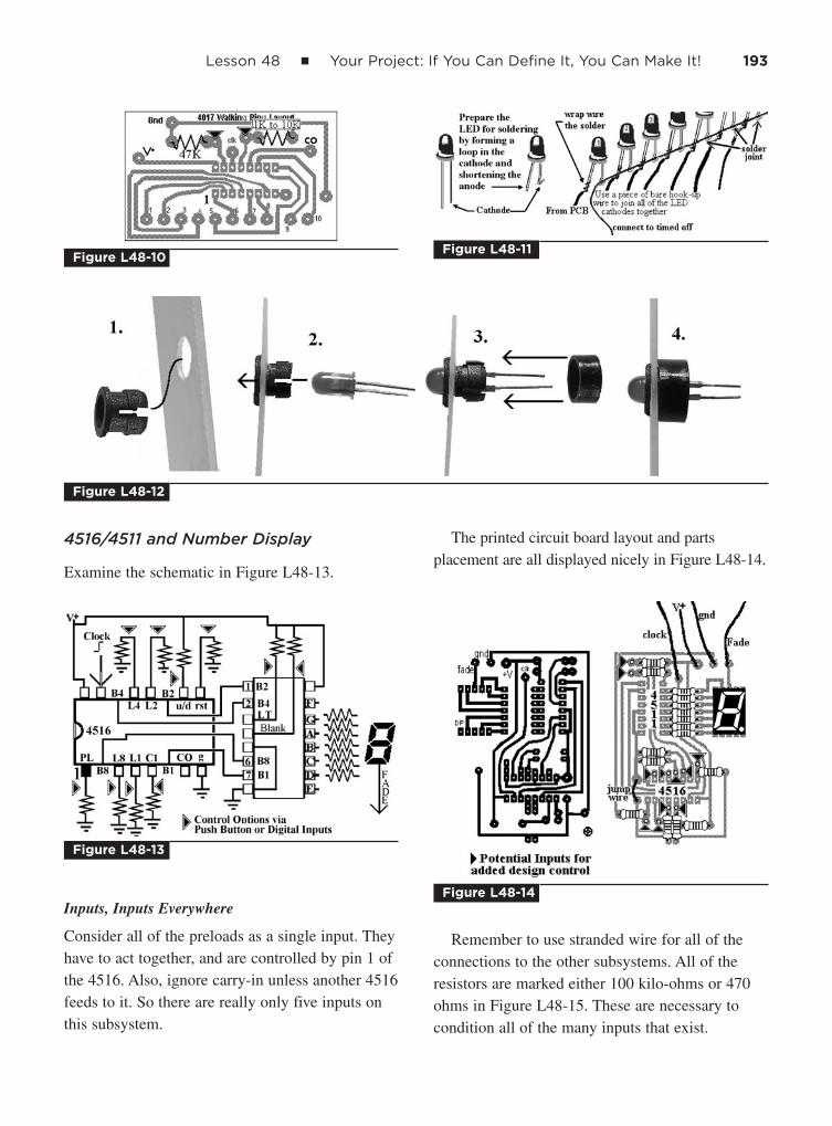
4516/4511 and Number Display
Examine the schematic in Figure L48-13.
Inputs, Inputs Everywhere
Consider all of the preloads as a single input. Theyhave to act together, and are controlled by pin 1 ofthe 4516. Also, ignore carry-in unless another 4516feeds to it. So there are really only five inputs onthis subsystem.
The printed circuit board layout and partsplacement are all displayed nicely in Figure L48-14.
Remember to use stranded wire for all of theconnections to the other subsystems. All of theresistors are marked either 100 kilo-ohms or 470ohms in Figure L48-15. These are necessary tocondition all of the many inputs that exist.
Lesson 48 ■ Your Project: If You Can Define It, You Can Make It! 193
Figure L48-10Figure L48-11
Figure L48-12
Figure L48-13
Figure L48-14

194 Section 14 ■ Define, Design, and Make Your Own Project
That’s really all there is to it. The rest is up toyou.
Figure L48-15

Amplifiers: What They Are and How to Use Them
P A R T F O U R

This page intentionally left blank

Imagine our world without amplifiers. It would be a quiet place.
197
Pump Up the Volume
Where would we be without amplifiers? The telegraph system was invented
in 1844 long before amplifiers existed. The figure below shows an early
input key. The signal had to be relayed down the line from each station
because it weakened with distance. Imagine our world without amplifiers.
It would be a quiet place.
The Parts Bin on the following page has the complete parts list used in
Part Four.

Description Type Quantity
2N-3906 PNP transistor TO-92 case 2
2N-3904 NPN transistor TO-92 case 2
LED 5 mm 1
Electret microphone Mic 1
10 � Resistor 1
100 � Resistor 2
100 k� Resistor 2
1 k� Resistor 2
4.7 �F Capacitor 1
470 �F Capacitor 1
1000 �F Capacitor 1
8 ohm Speakers 2
100,000 ohm 1/2 watt Potentiometer 1
LM 741 op amp IC 1
Audio transformer Transformer 1
Alligator clips (red and black) Hardware 1 each
1/8" plug Hardware 1
1" heat shrink 1/8" d Hardware 2
Speaker wire Hardware 4 meter 12'
4PDT Switch 1
Door phone PCB 1
■ Not all components will be consumed by project work.
P A R T S B I N F O R P A R T F O U R
198
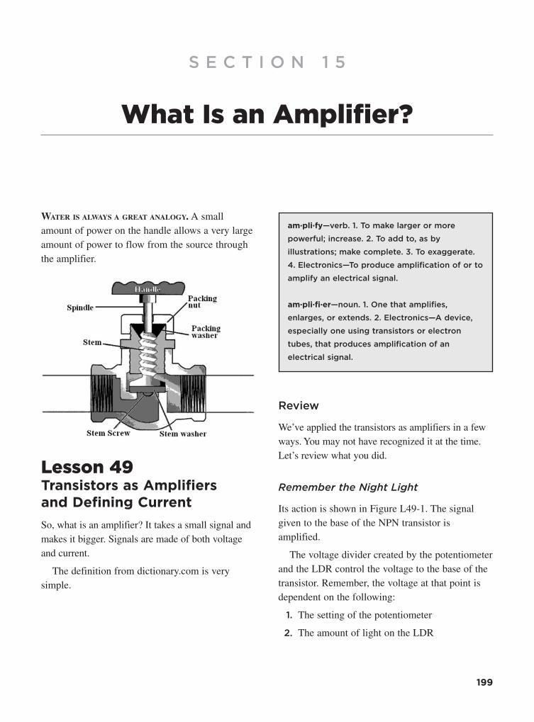
What Is an Amplifier?
S E C T I O N 1 5
199
WATER IS ALWAYS A GREAT ANALOGY. A smallamount of power on the handle allows a very largeamount of power to flow from the source throughthe amplifier.
Lesson 49Transistors as Amplifiers and Defining Current
So, what is an amplifier? It takes a small signal andmakes it bigger. Signals are made of both voltageand current.
The definition from dictionary.com is verysimple.
Review
We’ve applied the transistors as amplifiers in a fewways. You may not have recognized it at the time.Let’s review what you did.
Remember the Night Light
Its action is shown in Figure L49-1. The signalgiven to the base of the NPN transistor isamplified.
The voltage divider created by the potentiometerand the LDR control the voltage to the base of thetransistor. Remember, the voltage at that point isdependent on the following:
1. The setting of the potentiometer
2. The amount of light on the LDR
am·pli·fy—verb. 1. To make larger or more
powerful; increase. 2. To add to, as by
illustrations; make complete. 3. To exaggerate.
4. Electronics—To produce amplification of or to
amplify an electrical signal.
am·pli·fi·er—noun. 1. One that amplifies,
enlarges, or extends. 2. Electronics—A device,
especially one using transistors or electron
tubes, that produces amplification of an
electrical signal.

200 Section 15 ■ What Is an Amplifier?
The signal to the base of the transistor has littlepower, not even enough to turn on an LED,because so little current gets through the 100-kilo-ohm potentiometer set at midrange.
The action of how the signal to the base isamplified by the NPN transistor is demonstrated in Figure L49-2. This action acts as a valvecontrolling the power source to the LEDs:
■ The smaller signal controls the transistor’svalve action.
■ The resulting amplified signal from C to E is amuch more powerful version of the originalsmall signal.
Audio for the NAND Gate Oscillator
Remember when you first connected your speakerdirectly to the NAND gate output? The signal wasso quiet that you had to place your ear right on topof the speaker to hear it … and that was in a quiet
room. The amount of current passing from V� topin 10 when it was low was enough to light anLED, but not enough to really shake the speaker.This is the schematic in the left side of FigureL49-3.
Figure L49-1
Figure L49-2
Figure L49-3

That small signal to the base was amplified by the PNP transistor, shown inserted into theschematic in the right side of Figure L49-3. Thesmall signal was used to control the transistorvalve action that controlled the power directlyfrom the voltage source.
The weak signal to the base was amplified bythe PNP transistor, providing plenty of power tothe speaker coil to make an amazingly annoyingloud sound.
“Wait a minute …,” you say. “Didn’t the digitalgate provide 9 volts, and the transistor gave 9 voltsas well, so why was the transistor output morepowerful?”
Calculating the Current: Amperage
The difference was not in the voltage, the pushbehind the electrons, but in the quantity ofelectrons being pushed, the current.
Figure L49-4 starts a very practical way ofpicturing current in an electrical system.
In electronics, voltage is the push behind theflow, or the force.
For a creek, gravity is the push, the force behindthe flow, as water runs downhill.
A creek, by definition, has little current. Currentis measured by how quickly water passes by inliters per second or cubic feet per second. Thiscreek has a current of 5 ft3/s.
Now think of a stream like the one pictured herein Figure L49-5. It has a modest current, but youcould walk across it.
Consider that the downhill “slope” is the sameas the creek. The force is the same, but the bigdifference is the “current,” the amount of water. Itis more powerful.
This stream has a current of 100 ft3/s.
This river pictured in Figure L49-6 has a verylarge current. Even though it has less “slope” asthe creek and stream shown, it has more waterflowing by a single point, every second. If youtried to swim across, you would be swept away.
Lesson 49 ■ Transistors as Amplifiers and Defining Current 201
Figure L49-4
cur·rent (noun). 1. A steady, smooth onward
movement: a current of air from a fan; a current
of spoken words. Synonyms—flow. 2. The part
of a body of liquid or gas that has a continuous
onward movement: rowed out into the river’s
swift current. 3. A general tendency, movement,
or course. Synonyms—tendency. 4. Symbol I,
Impedance (a) A flow of electric charge. (b)
The amount of electric charge flowing past a
specified circuit point per unit time.
(dictionary.com)
Figure L49-5

Obviously, the river is the most powerful. Theforce is the same, but the difference here is theamount of water. The river has a current of 20,000 ft3/s.
In electricity, current is electrons passingthrough a wire.
The standard unit of current is an ampere (Amp or A, for short): 1 Amp � 1 Coulomb/second (1 Coulomb � 1018 electrons).
Current is the general term. Amperage is the unitof current. The common abbreviation for current is I(impedance). People new to electronics say, “It’ssuch a pile of new words. ‘I’ looks odd.” But think ofthe word stampede with a herd of electrons poundingthrough the wires. Now that’s an “impede.” There’s awild one shown in Figure L49-7.
So how much is a coulomb? How much currentis moving through an electronic system? Howcould we look at the electrical equivalent to acreek in Figure L49-8 and figure the current usedby an LED?
The current is a quantity we cannot measuredirectly with the tools at hand. But we can figurethe amperage by using Ohm’s law. Ohm’s lawsimply states that V � IR, where George Ohmcalculated that the amount of pressure in a circuitis directly related to the amount of current passingthrough the load.
Here’s how Ohm’s law works. Think of a hose.A regular garden hose will do. The hose in FigureL49-9 has a fixed diameter, so the resistance is notgoing to change.
The higher the pressure, the more water flowsthrough it. The lower the pressure, the smaller thecurrent becomes.
But if you change the resistance asdemonstrated in Figure L49-10 and Figure L49-11,that affects the amount of current, too.
202 Section 15 ■ What Is an Amplifier?
Figure L49-6
Figure L49-7
Figure L49-8
Unit Measuring
V � Voltage Voltage is the unit of force.
I � Amperage Amperage is the unit of current
(impedance).
R � � Ohm is the unit of resistance.

The fire hose shown in Figure L49-12 offersvery low resistance because the hose is bigger. It isable to handle lots more current, but the pressurefrom the city supply is the same.
Back to Ohm’s Law (V = IR)
This is a simple three-variable equation: A � B � C. If you know two variables, you canfigure the third. But how would you figure thecurrent in the simple LED circuit shown in FigureL49-8?
To figure the current flowing through the LED’scircuit, you need to know (a) the voltage used bythe resistor (the pressure drop) and (b) theresistance.
Now, back to considering the basic circuit. Let’smake some assumptions.
Lesson 49 ■ Transistors as Amplifiers and Defining Current 203
Figure L49-9
Figure L49-10
Figure L49-11
Figure L49-12

1. The power supply is a perfect 9 volts.
2. “R”: The resistor’s value is a perfect 470ohms.
3. “V”: Connect power and measure the voltagedrop across the resistor—from TP a to TP b.The voltage drop across the resistor is 7.23volts. V � IR so:
So we just figured out how much current passedthrough the resistor. Does that tell us how muchpasses through the LED? Yes, it does. Consider thefollowing:
Exercise: Transistors as Amplifiers
and Defining Current
1. Define amplifier as it relates to electronics.
____________________________________
2. Match these units to the terms they represent.
V, A, W, hose width, force, coulombs persecond, gravity, ft3/sec, I, R, current
3. Define the two combined factors that make acurrent.
a. ___________________________________
b. ___________________________________
4. What is a basic unit used to show current inthe following?
a. Water system ___________________________________
b. Electrical system ___________________________________
5. Write without scientific notation how manyelectronics there are in a 1-coulomb charge.
_____________________________________
6. There are 0.0153 amperes in the LED circuit.Write out exactly how many electrons pass asingle point in the wire in 1 second.
___________________ � 1.53 1016 electrons
Recognize that this is considered a verysmall current.
7. Now it is time to observe the actual effect thatdifferent resistors have on the current.
In Lesson 5, you used the same circuit asthe one shown in Figure L49-13. At that time,you observed what happened as you changedresistors. Now you get to understand whathappened.
204 Section 15 ■ What Is an Amplifier?
I
7.23 V I 470 �
I 0.0153 A
VR
A simple statement. Unless some is added or
taken away:
■ The current in a hose is the same along the
entire hose.
■ The current in a creek is the same along the
entire creek.
■ The current in a simple circuit is the same
throughout the entire circuit.
For a simple circuit, the amount of current is
the same throughout the system. The current (I)
passing through the resistor is the same amount
of current through the LED as well.
Pressure Current Resistance
Figure L49-13

Measure the resistors used here with yourDMM. Do all figuring here to three significantfigures. This means that in terms of accuracy,all numbers have three digits. For example, a10-kilo-ohm resistor has two significantfigures because the color coding only showstwo digits. On the DMM it might show 9.96kilo-ohms. That shows three significantfigures.
You can copy most of the information fromthe exercise you did for Lesson 5 to TableL49-1.
8. Think of your garden hose.
a. If you turn the hose on, the pressure comesfrom where?_________________________
b. Pressure in an electronic system is calledwhat? ______________________________
c. If you leave the pressure the same andsqueeze the hose, this increases what?___________________________________
d. As you increase the resistance, whathappens to the current?________________
e. If voltage in a system remains constant,current will decrease if resistance iswhat?______________________________
f. Conversely, the current will increase whenresistance is what?____________________
Lesson 50Defining Work, Force, and Power
What are we amplifying? Here you learn howwork, force, and power are defined and measuredin electronics. Amplifiers by their very nature areanalog devices. The transistors you’ve worked withare analog. They responded to any voltage to thebase in varying degrees. Remember, NPN wasturned on by more voltage to the base, and thePNP was turned off as the voltage increased. Here you will be introduced to the two types ofamplifiers that match the opposite actions of thetransistors you’ve already dealt with.
What Is Force?
Force is the amount of energy exerted. In FigureL50-1, Atlas is exerting a force to hold up the sky.But by definition, no work is happening becausethere is no movement. If an object is not moved,no work is done, no matter how great the force.
Lesson 50 ■ Defining Work, Force, and Power 205
Current in System Resistor DMM Voltage Drop Vdrop Voltage Dropin Order Resistor Value Across Resistor
Amps =� Across the LED
100 � _____� _____Volts 0._____ A _____Volts
470 � _____� _____Volts 0._____ A _____Volts
2.2 k� _____� _____Volts 0._____ A _____Volts
10 k� _____� _____Volts 0._____ A _____Volts
47 k� _____� _____Volts 0._____ A _____Volts
220 k� _____� _____Volts 0._____ A _____Volts
TABLE L49-1 Information from the Exercise
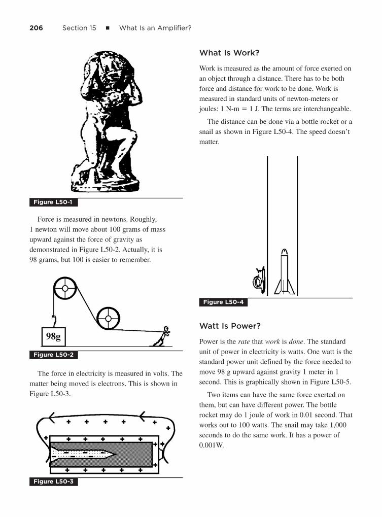
Force is measured in newtons. Roughly, 1 newton will move about 100 grams of massupward against the force of gravity asdemonstrated in Figure L50-2. Actually, it is 98 grams, but 100 is easier to remember.
The force in electricity is measured in volts. Thematter being moved is electrons. This is shown inFigure L50-3.
What Is Work?
Work is measured as the amount of force exerted onan object through a distance. There has to be bothforce and distance for work to be done. Work ismeasured in standard units of newton-meters orjoules: 1 N-m � 1 J. The terms are interchangeable.
The distance can be done via a bottle rocket or asnail as shown in Figure L50-4. The speed doesn’tmatter.
Watt Is Power?
Power is the rate that work is done. The standardunit of power in electricity is watts. One watt is thestandard power unit defined by the force needed tomove 98 g upward against gravity 1 meter in 1second. This is graphically shown in Figure L50-5.
Two items can have the same force exerted onthem, but can have different power. The bottlerocket may do 1 joule of work in 0.01 second. Thatworks out to 100 watts. The snail may take 1,000seconds to do the same work. It has a power of0.001W.
206 Section 15 ■ What Is an Amplifier?
Figure L50-1
Figure L50-2
Figure L50-3
Figure L50-4

But look at the power in different watersystems. The force of gravity pulls water over theedge of the cliff in both of the waterfalls shown inFigure L50-6. The current of both waterfalls hasthe same force of gravity on them. It is 180 feet ateach of these falls. But power is defined by thecurrent multiplied by the force. By definition, thecurrent includes both quantity and rate. I wouldstand under only one of them.
Multiply the current by the voltage, and thatgives power. In any system, power is determinedby how fast work is done.
The LED is a low-power light output. Howmuch power is used by the LED? Consider thebasic circuit shown here in Figure L50-7.
To figure the power used by the LED, you needto know both voltage and current.
Now this becomes a three-step process. But theyare three simple steps.
1. You need to measure the voltage drops acrossthe LED (TP B to TP C).
2. Then you have to calculate the current movingthrough the resistor. V � IR, where voltage isnow the drop specifically across the resistor.
Lesson 50 ■ Defining Work, Force, and Power 207
Figure L50-5
Figure L50-6
Figure L50-7
■ In these natural water systems:
Power � current � force
Current � ft3/s � the amount of water
passing by and how fast it is flowing
Force � slope � the amount of push behind
the current, the pressure
■ In electrical systems:
Power � current � force
Force � voltage
Current = amperage measured as a standard
where 1 A � 1 C/s
Remember that 1 C is a standard mass of
electrons.
Power is measured in watts.
1 W � 1 A � 1 V

208 Section 15 ■ What Is an Amplifier?
TP A to TP B. There is no way to measure theresistance of the LED to otherwise help figureout the current. Remember that the currentmoving through one component in series isthe same current for all components along that line.
3. Then you calculate the power.
Voltage drop across the LED multiplied by thecurrent in the system equals power used by theLED.
Your numbers should be close to the sampleprovided. Plug these numbers into the formula forpower:
Watts � Volts � Amperes
0.0270 W � 1.77 V � 0.0153 A
Oooh! 27 milliwatts. Brilliant.
Exercise: Defining Work, Force, and Power
1. Force is the amount of energy exerted. It ismeasured in what units? _________________
2. Roughly 1 N moves ______ grams upwardagainst the force of gravity (specifically it is_____ g).
Work � Force � Distance
3. Work is the amount of _______ exerted on anobject over a __________.
4. If an object is not moved (or the distanceequals zero), how much work is done?
5. The unit used to measure work is_______________.
Another name for the same unit is joules.
1 joule � 1 ____________.
6. Both are equal to the amount of work donewhen moving ____ g __m upward.
7. Power is the ___________ that work is beingdone.
8. The common unit for power is ___________,abbreviated as _______.
9. Provide an example where two items havedifferent amounts of power output eventhough the same force is exerted on them.
You probably already know that 1 W �1,000 mW (milliwatts). The prefix “milli”represents a thousandth (0.001). You’ve seen itin chemistry (mL) and physics (mm).
Power for electricity is figured using theformula watts � volts � amperes.
10. The LED sample power output is 0.027 watt.
That is ________mW.
11. You have seen in the previous exercise howincreasing resistance dampens current. Thepower output is directly proportionate to the current available. If the supply voltageremains constant and the resistance increases,the current decreases.
Don’t breadboard the setup in Figure L50-8. You did this same set of resistors earlyon, and you can copy the values directly fromthe exercise sheet you did in Lesson 5.
Calculate the power available to the LEDsfor each setup (Table L50-1).
Figure L50-8

12. John’s car has a 150-watt amp working off 12volts. His parents have a 22-watt home systemthat runs off 120 volts. Which system is morepowerful?
(Hint: What is the color of GeorgeWashington’s white horse?)________________
13. What is the current in a 100-watt light bulbworking off 120 volts? ___________
People used to say the standard lightingneeded to read was the light provided by a100-watt incandescent light. The same amountof light can be provided by five ultrabrightwhite LEDs at 50 mA each.
14. Compare LEDs for power usage (see TableL50-2).
15. Use Ohm’s law to calculate the amount ofcurrent passing from C to E in Figure L50-9.
Lesson 50 ■ Defining Work, Force, and Power 209
Current inSystem
R Value �= Amp
Voltage Drop LED Power Used Measure V + to Gnd Ohms Across the LED Brightness by LED
Copy Copy Calculate Vtotal – VR = VLED Copy W = (V) (I)
100 � ___Volts 0.____ A ____Volts _______ _0._______W
470 � ___Volts 0.____ A ____Volts Normal _0._______W
2.2 k� ___Volts 0.____ A ____Volts _______ _0._______W
10 k� ___Volts 0.____ A ____Volts _______ _0._______W
47 k� ___Volts 0.____ A ____Volts _______ _0._______W
220 k� ___Volts 0.____ A ____Volts _______ _0._______W
TABLE L50-1 Power Available
Type Voltage Current Brightness Power
Regular red diffuse 1.8 v 30 mA 2,000 mcd
Regular green diffuse 2.1 v 30 mA 2,000 mcd
Regular yellow diffuse 2.3 v 30 mA 2,000 mcd
High-intensity yellow 2.1 v 50 mA 6,500 mcd
Ultrabright red 2.4 v 50 mA 8,000 mcd
TABLE L50-2 Power Usage
Figure L50-9

210 Section 15 ■ What Is an Amplifier?
16. How much power is available at the pointbetween R2 and R3? ______mW
17. Is this enough power to light up an LED?Yes / No
Lesson 51What Do I Have to Gain?:Definitions
As you turn the volume control on your radio, thepotentiometer’s changing resistance isn’t just usingup some of the power to the speakers. Its actionsare much more subtle. Amplifiers use an efficientmethod to control their power output. Read on andsee what you have to gain.
Defining Gain
In an amplifier, the input signal is small and theoutput signal is big! Gain is the ratio thatcompares input to output.
■ Gain � output/input
■ Gain � signalout/signalin
Gain is a statement of a basic ratio. It has nostandard unit because the ratio compares identicalunit values, such as current.
■ Gain � Iout/Iin
Gain in the NPN Transistor
Set up a modified version of the night light circuit.The schematic in Figure L51-1 shows a fewchanges needed to calculate the gain of the NPN3904 transistor.
1. R1 at 47 kilo-ohms simulates thepotentiometer set to midrange.
2. R2 will be various resistors simulating theLDR at different light levels. Bright lightwould have low resistance.
3. R3 is 22 kilo-ohms. I never did explain beforewhat it did. It restricts current to the base(input) of the transistor.
4. In Figure L51-2, R4 and R5 make a voltagedivider. Measuring the voltage drop across R4makes it an easy task to calculate the currentavailable at the emitter (output).
How would we calculate gain for this setup?
This is a matter of comparing the current inputand current output.
They get set into a ratio, and there is your gain.
Gain � Iout/Iin
Table L51-1 was done with a 12-volt walladapter as a power supply. The readings here willnot necessarily match your readings.
Figure L51-1
Figure L51-2

For figuring the power output of the transistor,the following considerations have been made:
1. Since R4 � R5, they both use the sameamount of power.
2. The voltage drop across both loads isidentical.
3. The current on the same line is unchanged.
4. They use all the power available from thetransistor.
5. Therefore PR4 � PR5 � PEmitter
Remember that the LED used 27 mW of power.Based on the numbers developed in this sample,the LED begins to fade when there is a bit lessthan 50 kilo-ohms on R2 because from that pointon, there is not enough power.
Exercise: What Do I Have to Gain: Definitions
1. Test the quality of your transistors using theDMM diode test. Record your readings inTable L51-2.
For the circuit-test DMR 2900 multimeter,you first set it to “Continuity” and then pressthe DC/AC button. The symbol in the top-leftcorner changes from the “beeper” icon to adiode symbol. Many multimeters simply use thecontinuity tester to give the reading.
2. Before we move into measuring a complexcircuit, let me prove to you that when youcalculate the current in one portion of acircuit, that current is the same for theremainder of that circuit. You don’t need tomake the simple schematic shown in FigureL51-3. All the needed information is there.
Lesson 51 ■ What Do I Have to Gain?: Definitions 211
Power Used Power @ Iin (base) Vdrop Iin @ R4 Gain = by R4 E PR4 + PR5
R2 VTP1 Vdrop R3 V/� = A R4 V/� = A Iout/Iin W = V x A = Ptotal
1 1 M 7.54 V 2.83v 2.83 V/ 2.05v 2.05 V/ 20.5 mA/ 2.05 V 0.082 W
22,000 � 100 � = 0.129 mA 20.5 mA = 82.0 mW
= 0.129 mA 20.5 mA Gain = 159 = 0.042 W
2 470 K 7.39 V 2.73v 0.124 mA 2.0v 20 mA 161 0.040 W 80.0 mW
3 100 K 6.23 V 2.27v 0.105 mA 1.64v 16.4 mA 159 26.9 mW 53.2 mW
4 47 K 5.10 V 1.83v 0.083 mA 1.29v 12.9 mA 155 16.6 mW 33.2 mW
5 10 K 2.26 V 0.718v 0.033 mA 0.433v 4.33 mA 131 1.87 mW 3.74 mW
6 4.7 K 1.26 V 0.299v 0.013 mA 0.15v2 1.52 mA 116 0.231 mW 0.462 mW
TABLE L51-1 Ratio and Gain
NPN 3904 The Readouts Are � 5% PNP 3906
Ered to Bblack (expect OL) Ered to Bblack (expect 0.68)
Bred to Cblack (expect 0.68) Bred to Cblack (expect OL)
Eblack to Bred (expect 0.68) Eblack to Bred (expect OL)
Bblack to Cred (expect OL) Bblack to Cred (expect 0.68)
TABLE L51-2 Readings

Now how much voltage is used across R1and R2 individually?
Remember the formula to calculate thiswas:
Vdrop � Vtotal [R1/(R1 � R 2)]
Vdrop across R1 � ____
Vdrop across R2 � ____
3a. How much current is passing through R1?
Use Ohm’s law: V � IR
V� A
�
Vdrop across R1/1,000 � � current at R1
3b. How much current is passing through R2?
Vdrop across R2/2,700 � � current at R2
4. Is the current through R1 and R2 nearlyidentical? Does IR1 � IR2? Yes/No
5. If you want to set up a test circuit, go aheadand do the real measurements. Remember thatyou can use three significant figures if youmeasure the resistance with the DMMdirectly. Use only two if you don’t measurethe resistance but just use the color code.
6. Now, referring to the schematic in FigureL51-2, use the values shown for R2. R2 is theonly resistor that changes values. R3 keeps the 22 k� value shown in Figure L51-1 (seeTable L51-3).
Lesson 52The World Is Analog, So Analog Is the World
Here we finally get to see how an amplifier relatesto the real world. But keep in mind that this is notdigital. Nothing in the real world is digital. Analogis the world.
Amplifiers are analog systems. They deal withchanging voltage. Modern technology promotesthe use of digital storage and transfer ofinformation. As well, we have digital transmissionof information on cable and the Internet. Goodamplifiers feed digital information in and providedigital information out. But amplifiers, by andlarge, deal with sliding analog voltages toduplicate the sound and light as it occurs naturally.
212 Section 15 ■ What Is an Amplifier?
Figure L51-3
Power Used Power @ EIin @ B Vdrop Iin @ R4 Gain = by R4 PR4 + PR5
R2 VTP1 Vdrop R3 V/� = A R4 V/� = A Iout/Iin W = V x A = Ptotal
1 1 M
2 470 K
3 100 K
4 47 K
5 10 K
6 4.7 K
TABLE L51-3 Readings

Lesson 52 ■ The World Is Analog, So Analog Is the World 213
The Noninverting Amplifier
As shown in Figure L52-1, the NPN transistorworks in a very direct manner. As the signal to thebase increases, the valve opens. As one goes up,the other goes up in direct proportion. This is adirect relationship. The output is proportional withthe same voltage as the input. More voltage increates more voltage out. Voltage is not inverted.
The Inverting Amplifier
Look at Figure L52-2. The PNP transistor has theopposite action of the NPN transistor. As the signalto the base increases, the valve closes. As one goesup, the other goes down in direct proportion. Thisis an opposing relationship. The output isproportional but opposite of the input voltage.
The voltage is inverted, but the gain is the sameas the NPN because gain is always stated as anabsolute value.
The NPN is a “noninverting” amplifier.
The PNP is an “inverting” amplifier.
Of course, in high tech, we have to use fancywords such as noninverting.
The Op Amp
We are going to be using an 8-pin DIP 741amplifier on a chip. The basic hookup diagram isshown in Figure L52-3. These are called Op Amps,short for operational amplifiers. There are manymore amplifiers than there are CMOS 4000 seriesIC chips. Just look at the partial listing atwww.mhprofessional.com/computingdownload.Each Op Amp has its own features regarding:
■ Power input and output
■ Response time
Figure L52-1
Figure L52-2
Definitions
Inverting—to turn upside down.
Noninverting—not to turn upside down. To leave
right side up.

■ Frequency
■ Other factors
The main idea to keep in mind is how any OpAmp works. The Op Amp compares the voltagedifference between the two inputs (pins 2 and 3here) and responds to that difference.
Here we will use the LM741 because of its lowpower needs and simplicity.
Note that there are both inverting andnoninverting inputs.
Exercise: The World Is Analog,
So Analog Is the World
1. Which input pin of the LM741 has actionsimilar to the NPN transistor? pin _______
2. That action is called what? _______________
3. Define the term inverting amplifier._____________________________________
4. For an inverting amplifier, what is the gainwhen the output is � 100 mV and the inputwas � 10 mV? Be aware that gain is alwaysstated as an absolute value.
a. � 10
b. � 10
c. � 0.1
d. � 0.1
5. Look at www.mhprofessional.com/computingdownload for a partial list of amplifier ICsthat are available on today’s market. Would Ibe right in saying that there is a limitedselection of amplifiers available to work with?
Download a full LM741 data sheet athttp://cache.national.com/ds/LM/LM741.pdf.You need to have Adobe PDF reader installedto be able to access this document.
6. On the LM741 data sheet, page 1, the LM741is manufactured in how many package styles?_____________________________________
7. From the LM741 data sheet, page 2, examinethe numbers on your chip. Determine if youare working with a 741, 741A, or 741C.
8. From the LM741 data sheet, page 2, whatsupply voltage is the LM741 expecting?_____________________________________
9. More interesting information from the LM741data sheet, page 2—your solder pen gets up to400°C—how long can the LM741 enduredirect heat from a solder pen? ____________
10. Now turn to page 3 of the LM741 data sheet.The LM741 is considered to be a low-powerOp Amp. For example, at rest the typicalcurrent draw for this Op Amp is what?_____________________________________
11. And more info from the LM741 data sheet,page 3—when really pushed, the LM741consumes a whopping _______mW of power.
12. Turn to page 4 of your LM741 data sheet.How many transistors are packaged into theLM741 IC? _____________
214 Section 15 ■ What Is an Amplifier?
Figure L52-3

Exploring the Op Amp
S E C T I O N 1 6
215
THE CIRCUIT IN THIS UNIT is a “teaching” circuit.The job of amplifying can be done using a varietyof methods, each one cleaner than the next. Butthis circuit allows the introduction of a pile ofnecessary concepts along the way.
Lesson 53Alternating Current Comparedwith Direct Current
Here I explain the necessary analogy comparingalternating current as sound and direct current aswind.
Direct Current
We always hear the terms direct current (DC) andalternating current (AC). Direct current means thatthe current in the system is always flowing in onedirection. Electronics depends on direct current.Naturally, flowing water has been a goodcomparison for positive DC voltage V�. Wateralways flows in one direction—downhill, towardthe lowest point. Direct current is easily generatedby chemical reactions in batteries. Figure L53-1shows positive movement of electrons while thescope shows the voltage is above ground. So thevoltage pushes the electrons one way. However,what happens when the voltage is reversed andpushes the electrons the “other way”? Figure L53-2 shows us how that really works.
Figure L53-1
Figure L53-2

216 Section 16 ■ Exploring the Op Amp
Just a note regarding the representations here ofDC on a regular oscilloscope. Soundcard Scopedoes not respond to stable DC voltage as a regularoscilloscope would.
With direct current, you can have a positivevoltage V� or a negative voltage V–. Attach abattery backward, and you have created V–.
A more effective analogy for DC would be tothink of water in a pipe or wind in a tunnel. It canmove easily in both directions.
Alternating Current
Put simply, alternating current is a flow ofelectrons that keeps alternating and changingdirections. The electrons don’t get displaced, asthey do in DC. Figures L53-3 to L53-5 are framesets from animations available at the website notedin Appendix C. Those animations show far moreclearly the action of what is happening.
But if the electrons don’t flow, how is theenergy transferred? A great analogy for AC issound waves. Air particles don’t flow as soundtravels through the air, but they do move; they
vibrate. Sound is a pressure wave that movesthrough the air. A vibrating string sets one particlebumping into the next.
Simplified, the particles don’t get displaced likethey do in a wind. They vibrate in place. In fact,when sound is translated into an electronic signal,it is carried as an AC signal as shown in FigureL53-5.
Figure L53-6 represents a regularly oscillatingaction of electrons in an AC system. This shows asteady AC signal on the scope.
AC on the Oscilloscope
Why does a steady AC signal look like this on theoscilloscope screen? The following explains indetail the transformation of real electron movementinto a sine wave:
1. This is the actual movement of the electrons,represented in Figure L53-3.
■ A lot of voltage exists as it speeds up in thecenter. The voltage decreases as it slowsdown.
Figure L53-3
Figure L53-4
Figure L53-5
Figure L53-6

■ It actually has zero volts as it stops andreverses direction.
2. Figure L53-7 graphically shows the increasein the voltage of the electron as it speeds upand slows down. The voltage actuallyinscribes a circle.
Notice two things here:
■ The distance the electron moves along thebase line changes as the voltage increasesand decreases. Put simply, the bigger thepush, the faster it moves. The smaller thepush, the slower it moves.
■ Each segment around the outside of thecircle actually represents time.
3. It is not easy to show something that movesbackward, because time moves forward. SoFigure L53-8 shows the negative voltagemovement happening after the positive voltage.
4. Time is important. How do we show time?Right now, time is chasing around on theoutside of the circle and distance is markedacross the horizontal ground line. But thedistance the electrons move is not asimportant to us as timing. So the next thing to do is to impose a time measure onto thehorizontal line, replacing distance as themeasure. This is shown in Figure L53-9. The amount of voltage (energy or force) that defined the height remains in place.Obviously, time is marked in evenly spacedincrements.
The result? The circular outline changesinto the classic sine wave shape.
Note that ground is at the center of theaction, the interplay between V� and V–. As I said, our amplifier deals with sound. You will now learn how to measure with thetools at hand.
Getting Ready to Explore the Op Amp
Having a good source of a stable signal is vitalwhen working with amplifiers. Signal generators,like the one in Figure 53-10, would be good tohave available in a classroom. Otherwise, theSoundcard Scope’s signal generator can create the
Lesson 53 ■ Alternating Current Compared with Direct Current 217
Figure L53-7
Figure L53-8
Figure L53-9

tones we need. A variety of other audio programscan record and blend these tones.
I use “Gold Wave” shareware. This completeaudio editor exceeds our immediate needs, but I’drather use a program you can grow into instead ofa program that we’ll outgrow quickly.
1. Open the Soundcard Scope. We will usedefault settings for our work here.
2. Set the Signal Generator’s channel 1 to 250 Hz.
3. Use any software to record and save thisfrequency as a 30-second wave (*.wav) file.
4. Exit the Soundcard Scope.
5. Start up the 250-Hz wave file you just created.It does not matter what program you use.
6. Check this frequency out on the FrequencyAnalysis portion of the Soundcard Scope.When you are satisfied with the results here,make a 300-Hz and 1000-Hz wave file.
Start up the 250-Hz signal again.
7. Plug the channel 1 cord into the earphonejack.
8. Use Figure 53-11 as a guide to make sure thatall of the software controls are set tomaximum.
9. Record the maximum output for this file.____mVac.
Figure 53-12 helps explain the best methodfor accurately adjusting the output a fewmillivolts at a time.
10. Now, while you are connected and the tone isrunning, adjust the volume controls to each ofthe voltage settings shown here. Check themoff as you go.
218 Section 16 ■ Exploring the Op Amp
Figure L53-10
Figure L53-11
Figure L53-12
___ 200 mVac ___ 100 mVac ___ 40 mVac
___ 15 mVac ___ 5 mVac

11. Once you have that done, reset the 250 Hz to40 mVac, and then stop the signal. Withouttouching the volume settings, load and startthe 300 mVac signal. Record the mVac shownon the DMM. _____
12. Don’t touch those dials or change anysettings. Load up, start, and measure thevoltage of the 1000-Hz signal. ____ mVac.
Does the voltage remain constant as thefrequency increases?
Why Doesn’t DC Voltage Show Up on an AC Circuit?
Fair question, so let’s check it out.
1. Okay, now you can readjust the volume backup to maximum.
2. Set your DMM to measure DC voltage.Connect the clips.
No matter how hard you try, you cannot get ameasurement of DC voltage from an AC signal.Why doesn’t the signal show any DC voltage?You’ve seen something like this before. Look atFigure 53-13.
Remember when you used the DMM to recordthe rolldown output from the 4046? The voltagereading at pins 3 and 4 was half of the V� fed tothe IC at pin 16. The output is V� half the timeand 0.0 volts for the other half. The signal wasswitching quickly enough that the DMM averagedthe voltage and read it as half of V�.
Consider that this is the same situation. Theoutput is V� half the time and V– the other half.The 200 mVac signal actually averages –.1 V for halfthe time, and �.1 V the other half. These two signalsaverage out, and the DC voltage reading is ZERO.
Comparing Outies to Innies
Here are some last things to do with your recordedAC signal. Use the setup in Figure 53-14 to
Lesson 53 ■ Alternating Current Compared with Direct Current 219
Figure L53-13
Figure L53-14

220 Section 16 ■ Exploring the Op Amp
compare the computer’s output (recorded wavesignal on channel 1) to its matched external inputon channel 2.
Ch1: Output—Headphone Jack at 40 mVac
Ch2: Input—microphone
1. Start the 250-Hz wave file and adjust theoutput to 40 mVac.
2. Turn on the Soundcard Scope.
3. Remove the check mark that synchronizesCh1 and Ch2. They need to workindependently.
4. Plug the channel 2 connecting cord into themicrophone input.
Now you are able to compare the computer’soutput directly to its corresponding input. Anyobvious differences you see here can be expectedto show up in all of your tests.
Here’s what you are looking for while you’recomparing the two signals:
Compare the amplitude of output to input.
■ You can expect the amplitude to drop—thequestion is by how much.
■ Does the input even respond? The signal mightbe too small for the card to respond.
■ Are the signals naturally aligned (lock-steppedso that the peaks and valleys match)?
Once you have observed this basic feedback:
1. Decrease the output signal’s volume (Ch1)until the input on Ch2 stops responding.
2. Disconnect the two cords and use your DMMto measure the AC voltage from the outputsignal.
Be aware that any input signal smaller than thisvalue will not register on your computer’s input.These comparisons and results will vary fromcomputer to computer because they are dependenton a variety of factors.
Lesson 54AC in a DC Environment
But if alternating current goes forward andbackward, how can it be used in a direct currentsystem? How can AC be imposed onto a DCsystem? Relax. We can either eat on the ground, orwe can pull out a table and use that raised surface.You know enough actually to set up that raisedsurface in electronics.
The AC Signal in a DC Environment
If AC goes forward and backward, how can wework with AC in a system that uses only V– from asingle 9-volt battery?
To begin, recall the analogy comparing directcurrent to wind and alternating current to sound.Figure L54-1 shows how sound can be carried inthe wind. The animation at the website inAppendix C shows the action much more clearly.
Figure L54-1

With this in mind, you can carry an AC signal in a DC environment. Here’s a larger analogy toexplain how. In electricity, you have above groundand below ground. As an analogy, when you go out for a picnic, you can use the ground as aconvenient surface, as shown in Figure L54-2.
Or you can set up a table—and in that sensecreate an artificial surface above the ground asshown in Figure L54-3.
Even though the ground is a natural place to puta picnic, an artificial surface like the table is muchmore convenient. Adjusting the reference for theAC signal in a DC system is much moreconvenient, too, as you can see in Figure L54-4.
We can create an adjusted reference for analternating current signal within a DC voltageenvironment by using a simple voltage divider.
If V � is 9 volts, then half of V � is 4.5 volts.
In the system shown in Figure L54-5, theadjusted reference acts identically as ground in a4.5 VAC system.
Lesson 54 ■ AC in a DC Environment 221
Figure L54-2
Figure L54-3
Figure L54-4
Figure L54-5

222 Section 16 ■ Exploring the Op Amp
How does an AC signal move in a DCenvironment?
Look closely at the two drawings in Figure L54-6. The image on top shows the AC signal withground as its natural reference.
The image on the bottom shows the AC signalwith an adjusted reference in a DC environment.The current does not affect the signal.
Lesson 55Setting Up the Operational Amplifier
The Op Amps are, by far, the most versatile andvaluable components in all of electronics. They areactually the heart of many digital systems. I can’tpass up this opportunity to explore how they areapplied and used in digital electronics.
Start Building the Circuit
As we just learned in Lesson 54, there needs to bea reference point for carrying the AC signal. Set upthe two resistors as shown in Figure 55-1. Thesewill be the voltage dividers used to set yourreference point. It’s best to use 5 band 1% resistors.
Take the following measurements:
■ Total voltage ______
■ The reference point voltage ______
This allows ______volts above the reference toact as the positive portion of the AC signal and_______volts below the reference to act as the_______ for the AC signal.
Now Add the Op Amp
Figure 55-2 moves us to the next step.
Figure L54-6
Figure L55-1
Figure L55-2

The midpoint of R1 and R2 is now simplyreferred to as Vref (voltage reference).
Connect Vref to the inverting input at pin 2 (–).
Being an input, pin 3(�) must be connectedsomewhere. The diagram above shows it connectedto ground, injecting a Lo to the noninverting input.
The Op Amp’s output at pin 6 reacts to thevoltage difference between pin 2 and pin 3.
Because the noninverting input at pin 3 is lowervoltage than Vref, the output at pin 6 is also Lo.
Do your measuring.
Now shift the R3 to inject a Hi signal to pin 3.The Hi input should give a Hi output. Don’t takemy word for it. Check it out. Is it what youexpected?
An important notice just arrived from ourdepartment of redundancy department.
The input to the non inverting input is notinverted at the output.
Moving Forward
Use Figure 55-3 as a guide and shift the Vref
connection from pin 2 to pin 3. Just to make surewe’re on the same page, R3 should initially be setto ground, so pin 2 senses its input as Lo.
Check the output. Lo Input—Hi Output
Switch the R3 to inject a Hi input.
TAH DAH! The input is inverted.
The Voltage Comparator
Moving forward again with Figure 55-4, we seesmall but significant changes.
What we’ve seen so far is that the voltagecomparator reacts to obvious voltage differencesbetween the inverting input and Vref. Using thissetup, we can see how well the Op Amp comparesminimal voltage differences. R3 is important.Because an Op Amp only compares voltages,current isn’t important. R3 dampens the currentthat reaches the input.
1. Use your DMM to check Vref. ______ volts
2. Attach the DMM’s red probe to Vinvert and theblack probe to ground.
3. Follow the instructions in Table 55-1.
Lesson 55 ■ Setting Up the Operational Amplifier 223
Figure L55-3
Figure L55-4

Do the same in Table 55-2, but with thevoltage divider giving just a bit under Vref.
4. When Vinvert is less than Vref, Vout becomes Hior Lo?
5. When Vinvert is greater than Vref, Vout
becomes Hi or Lo?
6. Don’t spend too much time on this, but try toadjust the voltage at pin 2 (Vinvert) so that it isthe same as Vref.
If you could get them to match, whatvoltage would you expect at pin 6, Vout? ____
WAIT! STOP! HOLD IT! Before we rush by,think of the power and beauty of little things, likein Figure 55-5. The voltage comparator really isthe heart and workhorse of our digital world.
Really! This is your basic NOT gate. You have areference voltage and an input to compare to it.The output responds instantly to the difference,giving a Hi output for any input less than half ofV� and a Lo output for any input greater than halfof V�.
But enough of this talk. We’re simply playingwith adjusting a DC voltage, comparing that toanother DC voltage. It’s your turn again. Roll thedice and take another step forward.
Injecting an AC Signal into a DCCircuit (One Last Modification)
What we really want to be able to do is feed an ACsignal related to sound into this circuit. Isn’t thatwhat we were talking about in Lesson 54?
As you recall, the AC’s current moves positivelyand negatively. The center of an AC signal has novoltage. That point is ground. But with a bit ofmagic (applied technology) we can move thatsignal up off of the ground. We change it so that it is moving positively and “not so positively.”
Get your SBB to match Figure 55-6.
224 Section 16 ■ Exploring the Op Amp
Adjust the potentiometer so that the midpoint Adjust the potentiometer so that the midpoint voltage (Vinvert) is just a bit over Vref. voltage (Vinvert) is even a bit higher.
a. Vref = ______ a. Vref = ______
b. Vinvert = ______ b. Vinvert = ______
c. Vout = ______ (Speak Digital! Hi or Lo?) c. Vout = ______
TABLE 55-1 No Matter How Small the Difference, Any Input Above Vref Will Output Lo
a. Vref = ______ a. Vref = ______
b. Vinvert = ______ b. Vinvert = ______
c. Vout = ______ c. Vout = ______
TABLE 55-2 Equal, but Opposite Reaction!
Figure L55-5

First, recognize that the capacitors are Vital inthese positions. They are being used as audiocouplers.
Audio Couplers
Capacitors have three main uses. So far, we’veused them as part of RC timers. Here, we’ll use thecapacitor as an audio coupler. In this position, as itconnects the audio signal to the circuit and itseparates the AC signal (tiny voltage fluctuations)from the DC voltage:
■ It isolates the Op Amp from any current input.
■ The AC signal passes through the capacitor.
■ The AC signal is automatically centered to theOp Amp’s adjusted Vref.
■ Steady DC voltage does not get translatedthrough the capacitor.
The following analogy offers the best explanation:
AC signals passing through a capacitor aresimilar to sound passing through a closed window,just like it is shown in Figure 55-7. Wind can’tpass through a window. If the wind is steady, youdon’t even hear it. The wind is like the DC voltageand current. But the sound. Ahh. The sound itselfis made of small vibrations; the window vibrates aswell, if even just a little. And … the air on theinside of the window vibrates too, transferring thesound to other side. The sound represents the smallfluctuations, variations in the voltage.
Simply stated, the active voltage changescreated by the signal on one side of the capacitoraffect the charge on the opposite plate of thecapacitor.
Now Let’s Have Some Fun
The diagram in Figure 55-8 describes what we’reaiming for.
Power Up Your Circuit
1. Open Soundcard Scope’s Signal Generator.
2. Set CH2 to 250 Hz. Tab over to the Scopescreen.
3. Clear the Sync CH1 & 2 check box.
4. Plug the CH2 connector into your computer’sheadphone output.
Lesson 55 ■ Setting Up the Operational Amplifier 225
Figure L55-6
Figure L55-7
Figure L55-8

226 Section 16 ■ Exploring the Op Amp
5. Using your DMM, set CH2’s signal strengthto 40 mVac (.040 vac).
6. Connect CH2 connector’s signal clip to thecircuit’s “input” and the black clip to ground.
7. Plug the CH1 connector into the“microphone” input.
8. Connect the CH1 connector’s signal clip tothe circuit’s “output,” again, black to ground.
Ideally, you will see results similar to Figure 55-9.
The concept here is more than just important.But before I continue, let’s improve the harmonyand play with the tempo.
Disconnect the power for a moment while youset up the new signal.
Take Another Step Forward
Tab over to the Signal Generator and make thesechanges:
1. Signal Generator
2. Channel 1 � 250 Hz
3. Channel 2 � 300 Hz
4. These two tones blend nicely. Goodresonance. While you listen, go back to thescope view in Figure 55-10. Find thehighlighted area at the bottom of the controlscreen.
They give you the ability to:
■ Add the signal from each channel together.Figure L55-9
Figure L55-10

■ Subtract the signals from each other: difference
■ Multiply the two signals: product
Figure 55-11 provides screen shots of eachfunction.
Now for Something Completely Different
1. Unplug the CH2 connector.
2. Plug in some earphones and listen to the tonescreated by the Signal Generator.
These are two separate signals.
We need to blend these two signals so they feedto your circuit from a single channel. The diagramin Figure 55-12 explains what needs to be done.
■ You can create this 30-second wave fileyourself, or download it (Lesson55BlendedTone.wav) from www.mhprofessional.com/computingdownload.
■ You can’t use the Soundcard Scope to play thisfile, but any music software will do it.
■ You know you’ve done it properly when youhear the blended tone in just one ear when bothchannels are turned on.
Onwards
The circuit hasn’t changed since Figure 55-6, andwe’re going to use exactly the same system setupas Figure 55-8.
Start the Soundcard Scope.
Make sure to clear the Sync CH1 & 2 checkbox.
Start the single-channel blended tone.
1. Use the CH2 connector (headphone output) toadjust the blended tone’s strength to 40 mVac.
2. Connect the blended tone signal to thecircuit’s INPUT.
3. Connect the CH1 connector to the circuit’sOUTPUT and microphone input.
Figure 55-13 compares the Soundcard Scope’ssignals and my real scope’s signals.
Lesson 55 ■ Setting Up the Operational Amplifier 227
Figure L55-11
Figure L55-12

It does look pretty good, doesn’t it? For theprice, Soundcard Scope gives a great readout. Butdo you see the flaw?
Remember, this is an inverting Op Amp. Whydoes it show a “noninverting” output? When Ichecked this out on my real scope (Figure 55-14),
228 Section 16 ■ Exploring the Op Amp
Figure L55-13
Figure L55-14

it gave me exactly what I expected. Honestly, Ican’t explain the error, but for our purposes, it’ssmall. Recognize it for what it is, and move on.
Meanwhile, take a closer look at the settings onthe real scope.
■ Time/div �
■ CH1 v/div �
■ CH2 v/div �
As a voltage comparator, a millivolt’s differenceat the input produces an instant reaction at theoutput.
Lesson 56Using Feedback to Control Gain
This lesson is dedicated to investigating andexplaining the action of the potentiometer and how it acts as a volume control. The schematic is displayed in Figure L56-1.
Modify Your Breadboard (Again)
■ Replace the 10 M� resistor with the 1 k� and10 k� Pot in series to make a much morebalanced feedback loop.
■ Replace the two resistors and audio couplingcapacitor at the end with the 100 � resistorand a 470 μF cap.
What we are using here is called “negativefeedback.” We will use this feedback to control thegain. You just built the Op Amp. Now you get totest it. You will set the gain through this uniquefeedback system. Actually, it’s only a voltagedivider applied in a familiar way.
This feedback loop is where things like volumeand tone are controlled. Not only is it much easierto control the signal when it is small, but thecomponents used to do it are smaller and lessexpensive. This is a half-watt intercom system. Thepotentiometer used here is rated for one-quarterwatt. Using this potentiometer to control the signalto the speakers directly would create enough heatthat it would burn out.
Again, refer to Figure L56-1 as we prepare totake some measurements needed as a foundationfor some important concepts.
1. No power to the circuit yet.
2. Remove the potentiometer and set it tominimum resistance (0 �), and then set itback in.
3. Start up any of your prerecorded pure-tonefrequency files.
Lesson 56 ■ Using Feedback to Control Gain 229
Figure L56-1

4. Use your DMM to adjust channel 1’s outputto a very small 10 mVac. Input � ____mVac.
5. Attach the colored clip of your CH1connecting cord to your circuit’s signal input.As usual, the black clip goes to ground.
6. Power up the circuit.
7. Directly at pin 6, check the signal’s strengthwith your DMM. Output � _____mVac.
Input’s voltage should be identical (or atleast very close) to the output’s voltage.Output, Input � 1. Gain � 1.
8. Set the Pot to maximum resistance.
9. Measure the output directly at pin 6._____mVac.
The ouput voltage should be 11 timesgreater than the input (gain � 11).
Recall that gain can be stated as a ratio ofvoltage to voltage, power to power, and evenRtotal to R1.
Gain � Output/Input
What to Expect
Ideally, the input signal voltage for this circuit isbetween 0.010 and 0.015 V AC.
■ When the Pot is set to 0 ohms, the outputshould equal the input.
■ When the potentiometer is set to 0 ohms, thenR3 � Pot gives a ratio of 1.
R2
■ The voltage divider has a ratio of 1. Gainshould be 1.
■ When the Pot is set to 10,000 ohms, the outputshould be 11 times greater than the input.
When the potentiometer is set to 10,000 ohms,then R3 � Pot gives a ratio of 11.
R2
The voltage divider has a ratio of 11. Gainshould be 11.
How It Works: Feedback to the Inverting Input
Here’s are some questions: “Why does the volumego down when the potentiometer has lowerresistance? Wouldn’t less resistance mean morecurrent passing? Doesn’t more current passingmean more volume?”
The answer is in the fact that the output signalhas been inverted and a portion of the invertedsignal is now being directed back onto the originalsignal. It is the same as adding a negative number.Think of it as subtraction. Subtraction is exactlywhat is being shown in the graphic representationof the signal with feedback in Figure L56-2.
The size of the feedback signal increases as theresistance in the potentiometer decreases.
The original signal minus the larger feedbacksignal results in a smaller output signal.
Signalin – Signalfeedback � Signaloutput
The graphic in Figure L56-3 more accuratelyrepresents a real signal.
230 Section 16 ■ Exploring the Op Amp
Figure L56-2

Exercise: Using Feedback to Control the Gain
1. What was the expected gain using the resistorratios in the following?
Gain �R4 � Pot
R3
a. _____
b. _____
c. _____
2. What was the expected gain using the voltageoutput compared to the voltage input?
Gain �VOUT
VIN
a. _____
b. _____
c. _____
3. Consider what would happen if R3 were burntout and had infinite resistance (�20 M�).
a. Write out the expected ratio.___________________________________
b. Think about it. Would that mean thevolume would be extra loud, or not at all?
c. Would you be able to control the volume?___________________________________
4. Consider what would happen if R3 wereshorted out. In this case, R3 would have 0 ohm—no resistance.
a. State the expected ratio. ___________
b. Would you be able to control the volume?
5. Feedback—here you will need to use a bit ofmath to help explain the real action at theinverting input (pin 2).
Lesson 56 ■ Using Feedback to Control Gain 231
Figure L56-3
(A) Input = (B) Input = (C) Input = Input = 10.0 mVAC 10.0 mVAC 10.0 mVAC
VAC between 0.0 VAC* R4 + Pot = 1 k� R4 + Pot = 5 k� R4 + Pot = 10 k�
TPIN to TPA
Vinput = TPA to TPREF
TPoutput = TPOUT to TPREF
TPINVERT to TPREF
TPA to TPINVERT
Across 100 � resistor
* Input from the headphones output with the volume adjusted to 0.0 volts AC. If the input to the Op Amp isunattached, static in the air will give erroneous readings. Remember what happens when inputs to a digitalsystem are not tied either Hi or Lo? We can get the same ghosts here.
TABLE 56-1 Collect This Data from the Setup in Figure 56-1

232 Section 16 ■ Exploring the Op Amp
At a gain of 1, you have the least resistancein the Pot. How does the “least resistance”provide the quietest volume? Shouldn’t lessresistance mean more signal?
And that is exactly what less resistancemeans. But it means more signal in thefeedback. More signal subtracted from theoriginal input.
a. So calculate the amount of current beingallowed to “feed back.”
Use Ohm’s law V � IR. You know thevoltage, and you know the resistance (seeTable L56-2).
b. Now calculate the current that is availableat the inverting input pin 2. That is ameasure of TPA to reference with R4disconnected so there is no feedback at all.You will get a measure of the full signal.The current at the inverting input pin 2 is__________________.
c. A little subtraction is now in order. Foreach of the previous three settings,calculate the real signal at the invertinginput pin 2. Use the simple formula:
full signal � feedback � signal at pin 2
See Table L56-3.
6. For this exercise, you need the followingpieces from around the house:
■ One long and skinny rubber band
■ One short rubber band
■ One large piece of cardboard
■ Three tacks
Now cut the long rubber band in one spot,giving you one long strand.
Cut the short rubber band into two shorterpieces.
Gently stretch and tack the long strandacross the cardboard surface. It should betight enough to pluck.
Now tie a short piece to the center of thelong one as demonstrated in Figure L56-4.Secure the end of that tack, too.
Current feedback to pin 2
When R4 + Pot = 1 k�
Current feedback to pin 2
When R4 + Pot = 5 k�
Current feedback to pin 2
When R4 + Pot = 10 k�
TABLE L56-2 Calculations
Full signal Feedback Signal at pin 2
R4 + Pot = 1 k�
_______ ________ ________
Full signal Feedback
R4 + Pot = 5 k�
_______ ________ ________
Full signal Feedback
R4 + Pot = 10 k�
_______ ________ ________
TABLE L56-3 Calculations
Figure L56-4

The long strand with the small connectoraltogether represents a signal.
Now attach the second short piece to thecenter of the long strand. As you tug gently on that loose strand, your input acts like thefeedback; your force is being subtracted fromthe original force on top.
Just like this simple physical demonstration,both the original input and the “inverted”feedback combine to create the signal that isbeing fed into the Op Amp. The sum of thesetwo combines to create the final output of theOp Amp at pin 6.
Lesson 56 ■ Using Feedback to Control Gain 233

This page intentionally left blank

Applying the Op Amp: Building the Intercom
S E C T I O N 1 7
235
HERE YOU’LL EXPLORE the individual portions ofthe intercom as you build the system. Considerradios. The system depends on amplifiers.
The microphone changes a voice into a smallelectric signal. This tiny signal from the microphoneis amplified thousands of times before it is releasedas part of a modulated electromagnetic radiofrequency.
A receiver is tuned to “resonate” to thatfrequency. Harmonics are a wonderfulphenomenon. That weak harmonic signal isamplified in both voltage and current before it isdirected to the speakers.
Lesson 57Building a Power AmplifierControlled by an Op Amp
So the Op Amp is now working as a preamp. Thesignal voltage has been increased, but there isn’tmuch output at all. Time to crank up the power.
The preamp specifically boosts the voltage to alevel that a power amplifier can use. Here we willemploy transistors as the power amp. The voltageis already there. The power amplifier adds currentto the voltage, effectively increasing the power.
Remember:
Power � current (I) � voltage (V) or P � IV
A huge variety of amplifier ICs are available toachieve the same purpose. But I use transistorsbecause this is a “teaching circuit” that lends itselfto explaining concepts common to all amplifiers.
The Power Amplifier
Still, many audiophiles swear that transistors arethe best power amplifiers because they provide adifferent quality output than ICs. But before them,there were the audiophiles who swore by vacuumtubes.
Modify the Circuit
Add the components shown in Figure L57-1 to thepreamp you have built. Note the rewiring of thePot and the addition of C3 (470 μF).
The preamp created by the LM741 Op Ampeffectively did three things:
1. It amplified the voltage.
2. It limited the amount of current by its verynature.
3. It still provided enough current for thetransistors.

236 Section 17 ■ Applying the Op Amp: Building the Intercom
The pictures in Figure L57-2 show how thetransistors act as power amplifiers. Animatedversions of these drawings are available forviewing at www.mhprofessional.com/computingdownload.
The two transistors act in opposition to eachother, controlling the signal output. As the valvesopen and close, they allow for much largermovement of current than allowed previously. Thevoltage and larger quantities of current create amuch more powerful output than the LM741 couldproduce by itself.
Okay. So I have explained how the poweramplifier works. Here is where you will find out how much power your amplifier is reallyproducing. For all of the exercises, use a 1,000-Hzsignal input at 10 to 15 mV.
1. Refer back to the measurements you did inLesson 56. You took all the recordings neededand did all the calculations to get started.
Remember:
Power (watts) � voltage (V) � current (I)
a. What is the VAC across R3?
b. What is the current across R3? (V � I � R)
Figure L57-1
Figure L57-2

c. Figure the power across R3 when you hadminimum volume (gain � 1).
Power at R3 � _______watts
d. Figure the power across R3 when you hadmaximum volume (gain � 11).
Power at R3 � _______watts
2. Now calculate the power output by measuringthe VAC available across the 100-ohm resistor.Then measure the VAC across both 100-ohmresistors. The reading should double. What? A voltage divider in AC? With thosemeasurements, you can now calculate thecurrent. How does it feel knowing you are incontrol of all that power?
In comparing voltages used, alwayscompare AC voltage to AC voltage. The samegoes for comparing DC voltages to each other(see Table L57-1).
3. In Lesson 56, without transistors, what wasthe power output at maximum volume? _____ W
4. In this exercise, with transistors, what was thepower output at maximum volume? _____ W
C2—The Capacitor as a Buffer
What is a buffer? A buffer cushions the blow.You’ve been using a 1000 μF capacitor as a bufferfor a while, ever since you set up the voltageregulator in Lesson 14. Refer to Figure L57-3.
The voltage demands of the power amplifierdraw quantities of power, but not steadily. Thishappens in quick bursts. A buffer, or reservoir inthe form of a large capacitor, is necessary whenusing a small wall adapter or a 9-volt battery. Asthe power is tapped, the output fluctuates becausethe power supply cannot generate current quicklyenough. This creates an unstable signal. The largecapacitor keeps the current and voltage supplysteady.
There is an interesting twist here. If you reallywant to hear this, you can’t use our regular testfrequencies. Their current draw is too stable.
■ Connect the system to a 9-volt battery.
■ Inject some music into your system.
■ Adjust the volume to fairly loud.
■ Pull out the 1000 μF cap.
The effect is quite noticeable.
The Second Audio Coupler
The second audio coupler is in place specifically to isolate the AC output from the DC voltage asshown in Figure L57-4.
In reality, if this capacitor were not in place andthe speaker were connected between the outputand ground, the entire signal would cease to exist.The AC output signal would be destroyed because
Lesson 57 ■ Building a Power Amplifier Controlled by an Op Amp 237
Gain of 1 Gain of 11Minimum Maximum Volume Volume
VAC across the
100 � load ______ V ______ V
V/� = A ______ A ______ A
Watts = volts
x amperes ______W ______W
TABLE L57-1 Comparing Voltages
Figure L57-3

the signal and feedback at pin 2 would bereferenced to ground in a DC system. They wouldno longer be floating artificially referenced to aredefined ground at half of the voltage. Take amoment and trace the circuit.
If you want to stop the circuit from working, goahead and bypass C3 and connect the speakerdirectly to the connected emitters.
What? It stopped working? Don’t say I didn’ttell you so.
Lesson 58The Electret Microphone
An electret microphone is a common component inaudio systems. It is inexpensive and very sensitive.Microphones offer many design opportunities forthis project.
Look carefully at the components inside theelectret microphone (Figure L58-1).
There are three types of microphones:
1. The coil microphone is similar to a speaker. Ituses a magnet set inside a coil of wire. Thesecan work independently of a powered circuitbecause they create their own voltage.
2. Piezo (crystal) microphones also create theirown energy. These crystal structures respondto the compression and decompression ofsound waves, releasing electrical energy. Thecrystals effectively translate the fluctuatingenergy into fluctuating voltage. This works inreverse, too. Feed voltage to the crystals andthey vibrate. This effect is used to createquality, low-power speakers.
3. The electret microphone is an active capacitor.One of its plates is exposed to the air so that itvibrates as sound hits it. The plate’s fluctuationsdisturb the steady DC voltage (pressure) bydeforming the exposed plate ever so slightly.Those fluctuations in voltage match the sound.That becomes our signal. Because the electretmicrophone is an active capacitive component,it needs power to work.
The photo in Figure 58-2 shows one of the legsconnected directly to the outer casing. That leg isground.
238 Section 17 ■ Applying the Op Amp: Building the Intercom
Figure L57-4
Figure L58-1
Figure L58-2

Build the Circuit
Set up Figure L58-3 as an independent circuit.Don’t attach it to your Op Amp’s input.
The parts needed are listed in the Parts Bin.
All of this looks new, but you’re alreadyfamiliar with it. Let’s take a walk through.
■ R1. Because it is a single resistor, R1 onlydecreases the current, not the voltage.
■ The microphone, like many capacitors, isbalanced between DC voltage source andground.
■ C1 and C2 are audio couplers. They pass theAC signal but block the current.
■ Q1 is your basic 2N3904 NPN transistor.
■ R2 is the feedback loop, from output to input.It works exactly the same as in the Op Amp.
■ The ratio of R2:R3 (100k:10k) dictates thegain created by this single transistor amplifier.
Checking It Out
Power it up and let’s do some measuring. You willhave to set up a speaker near the microphone whilea recorded tone is playing. Check AC and DCvoltages at all four test points and record these onTable L58-1.
You can use the Soundcard Scope’s Channel 2to see the tone’s signal, but music output from thecomputer will occupy both channels. If you wantto see the microphone’s response to music, you’llhave to use an outside sound source—somethingother than your computer.
To use the microphone as an input to the OpAmp, C2 acts as the output audio coupler for themicrophone subsystem and the input audio couplerfor the Op Amp circuit.
Lesson 58 ■ The Electret Microphone 239
Figure L58-3
■ R1 & R3—10 k�
■ R2—100 k�
■ M—Electret microphone
■ C1—.1 μF
■ C2—4.7 μF
■ Q1—2N3904 NPN
P A R T S B I N
DC DC AC AC
Tone Music Tone Music
TP1
TP2
TP3
TP4
TABLE L58-1 After You’ve Checked the Tone,Do It Again with Some Music

240 Section 17 ■ Applying the Op Amp: Building the Intercom
Lesson 59Using the Speaker as a Microphone
An intercom has a microphone on one side and aspeaker on the other. But then you would need two complete systems, each with a microphoneinput and a speaker output. You don’t have amicrophone? With some imagination and appliedknowledge, we can do this with one system. Youcan use the speaker as a microphone. To do this,though, you have to understand a bit about how aspeaker works. The speaker was designed as aspeaker, not a microphone, as we will use it. It puts out a small signal—tiny.
When we use the speaker as a microphone, thefollowing happens:
■ Sound vibrates the cone.
■ The cone moves the magnet.
■ The magnetic field causes electron movementin the wire.
■ This signal is used as the input to the Op Amp.
But still, the speaker is a poor microphone. Itwasn’t designed to be used as a microphone. Butdon’t take my word for it.
Record this important information.
1. How much of a signal does the speakerproduce on your DMM?
a. Attach the DMM to the speaker. Set it toVAC. Red probe to V� and black to V–.
b. Speak into the speaker with your mouthabout 2 inches (5 cm) from the cone. It’sbest to read from printed material ratherthan sit and repeat “Hellooooo.” ______mV
c. The best input signal you can produce is a“pucker” whistle. _______mV
2. How much of a signal does the speakerproduce on your oscilloscope?
a. Hook up your speaker to the test cord, andplug it directly into the computer’smicrophone input. Then open theSoundcard Scope. We are not using theoscilloscope probe. The signal is too small.If we used the voltage divider, it would not
Figure L59-1

register. Use the oscilloscope setup shownin Figure L59-1.
b. Speak into the speaker. Make note of themaximum positive and negative voltages.
c. Now whistle into the speaker. You shouldsee a beautiful sine wave. Did you knowthat your whistle is nearly a pure tone?
d. Draw a representation of your whistlesignature onto the scope face provided inFigure L59-2.
3. Applying the speaker in the circuit.
a. Now set this second speaker into your SBBas shown in Figure L59-3.
b. Turn the gain down all the way and useyour pucker whistle.
c. As you increase the volume, the circuitmight start screeching at you. Notch thegain backward until the screeching stops.The screeching is caused by feedbackdemonstrated in Figure L59-4. Sound
from the output is reaching the input andmultiplying itself.
d. You can solve this problem in two ways.The first is to give more distance betweenthe output and the input. But right now, youcan remove the output speaker. This is aneasy solution for the moment. After all,
Lesson 59 ■ Using the Speaker as a Microphone 241
Figure L59-2
Figure L59-3
Figure L59-4

242 Section 17 ■ Applying the Op Amp: Building the Intercom
you will need to do some measuring at theoutput, and don’t want the speaker to get inthe way.
4. Scoping the circuit output.
a. Replace the speaker with the connectorcord clips, the red clip to C3 (neg), andblack to ground. The cord is plugged intothe sound card “line in,” or microphoneinput.
b. With the volume turned all the way down,whistle and look at the signal on the scope.
c. It should be identical to the signal takendirectly from the speaker earlier.
d. Now turn the volume all the way up.Whistle again. Draw this on the scope facein Figure L59-5.
5. Check out the AC voltage of the maximumoutput of your whistling using the DMM.______Vac Max.
6. Listen to the circuit output.
a. Now before you put the output speakerback in, solder the ends of the dual-wireline to your speaker. That line should be atleast five feet long. Place it back into thecircuit.
b. Place the input and output speakers as farfrom each other as possible.
c. Whistle into the input speaker.
Hmm. The output is very quiet, even atfull volume.
The last component will take care of that.
Lesson 60Introducing Transformers and Putting It All Together
So you’ve seen that speakers aren’t microphones.The small signals they produce need a differentkind of preamp to get a clean signal from thissubsystem to the next stage of the amplifiersystem. Right now, the output directly from thespeaker is a paltry 1 millivolt. So the output fromthe amplifier is also very weak. Such a smallsignal needs to be cleanly amplified even before itis fed to the preamp. To restate, the signal needs tobe preamplified before it gets to the preamplifier.Without having a two-stage preamplifier, there just isn’t enough signal there to control the power amplifier.
Here I will introduce transformers as a methodto preamplify the signal to the preamp. It isfrequently done with microphones as well.
Here is a great place to use a transformer. SeeFigure L60-1.
Figure L59-5
Figure L60-1

What we have here is another basic electroniccomponent. Transformers are used in homes ineverything from wall adapters to microwaves.Larger versions are vital to the supply anddistribution of electric power. You will use aminiature transformer like the one shown in Figure L60-2.
How a Transformer Works
Actually, there are two main questions here:
■ How does a transformer work?
■ What does it transform?
As you saw with the speaker, moving electronscreate a magnetic field. What was not mentioned isthat the reverse is also true. A moving magneticfield induces (encourages) electrons to move in aconducting wire. The moving electrons in one wirecreate a magnetic field that induces electrons in anearby wire to move as shown in Figure L60-3.
Also notice that a second wire is too far away tobe influenced by the magnetic field created in thefirst wire. Animated versions of these figures areavailable for viewing at www.mhprofessional.com/computingdownload.
Pretty fancy! But better yet, examine FigureL60-4. It depicts how this concept is applied soneatly in electricity and electronics.
If we lay many wires next to the “primary”wire, it will induce (encourage) a voltage in eachof the “secondary” wires. But wait. There’s more.If each of those secondary wires is connected asone long wire, the voltage induced in each wire isadded to the next. This is shown in Figure L60-5.
Lesson 60 ■ Introducing Transformers and Putting It All Together 243
Figure L60-2
Figure L60-3
Figure 60-4

Checking Out the Audio Transformer
Pull out the miniature audio transformer. It shouldbe wrapped in green. Various colors indicatevarious uses. Most likely there will be three wireson one side and only two on the other as shownpreviously in Figure L60-2.
If there are only two wires from each side,continue with the following exercise. It willbecome obvious which side is primary and whichis secondary as you do the work.
The primary side has two wires. The secondaryside has three wires. The middle wire on thesecondary is referred to as the center tap. You canclip and tape it off. We won’t use it at all.
Plug the test cord into the headphones output ofyour sound card. Use the software-based volumecontrol to adjust the 1,000-Hz wave output to 5mVac. Now attach the clips to the primary wires ofthe transformer as shown in Figure L60-6.Measure the output of the two outermostsecondary wires (see Table L60-1).
Output SignalAverage Ratio � ________
Input Signal
In transformers, the fixed gain is referred to as astep-up or step-down ratio. This ratio actuallyreflects the physical relationship of the number ofprimary to secondary windings. A step up of 8 iscreated when you have 20 windings in the primaryand 160 windings in the secondary. A wall adaptersteps the voltage down. For example, one thatprovides 9 volts from a 120-volt system literallyhas a ratio of 120 windings in the primary for every9 in the secondary. That’s close to a ratio of 13:1.
The ratio on the audio transformer should bemuch greater than 1:1. If it is less than 1:1, youhave your input connected to the secondary side ofthe transformer.
244 Section 17 ■ Applying the Op Amp: Building the Intercom
Figure L60-5
Figure L60-6
Ratio of Input to Output at Output VAC/Primary Secondary Input VAC
5 mVAC
10 mVAC
25 mVAC
50 mVAC
100 mVAC
TABLE 60-1 Output Measurement

Now attach the speaker to the primary side ofthe audio transformer. Again, use the DMM to setthe output at the secondary, measuring AC voltageas shown in Figure L60-7.
■ Input at Primary � _____mVAC
■ Output at Secondary � _____mVAC
Does this match the previous ratios? It should.
Insert the Audio Transformer into the Circuit
Insert the audio transformer into the circuit asshown in Figure L60-8.
Now test the entire system using the 1,000-Hzsignal. Set the output of your sound card to 5 mVACby first connecting it to the DMM. Use the softwarecontrol to set the output signal strength precisely.
Measure the AC signal at different pointsindicated and record the readings in Table L60-2provided.
Lesson 60 ■ Introducing Transformers and Putting It All Together 245
Figure L60-7
Figure L60-8
5 mVac 5 mVac 10 mVac 10 mVac 1,000-Hz Sine Wave Tone Gain = 1 Gain = 11 Gain = 1 Gain = 11
VAC TP input to reference
VAC TP output to reference
5 mVac 5 mVac 10 mVac 10 mVac Favorite Music CD Gain = 1 Gain = 11 Gain = 1 Gain = 11
VAC TP input to reference
VAC TP output to reference
Points to keep in mind.1. This is not a high-fidelity system.2. Any feed higher than 10 mVac will probably start sounding lousy because of clipping. The output signal is limited
to 4.5 volts above the reference and 4.5 volts below the reference. You can’t get more with this system. Try forbigger, and you lose most of the signal.
TABLE L60-2 AC Signal Measurements

246 Section 17 ■ Applying the Op Amp: Building the Intercom
Parts list for reference:
■ R1, R2 100 k� C1 � 4.7 μF
■ R3, R4 1,000 � C2 � 1000 μF
C3 � 470 μF
The Intercom System
Remove the test cord and put the speaker to beused as a microphone into place as shown inFigure L60-9.
Now you can use it as an amplifier. Talk into thespeaker set up as the microphone. Adjust the gainto get the best quality and volume. At this point,you will find it necessary to separate the twospeakers by at least five feet of wire. If they stillsqueal, turn down the gain or put one speaker onthe other side of a sound barrier like a box or door.Take a few more measurements (see Table L60-3).
Figure L60-9
mVAC mVAC mVAC mVAC Pucker Whistle into Speaker Gain = 1 Gain = 11 Gain = 1 Gain = 11
VAC TP input to reference
VAC TP output to reference
TABLE L60-3 Measurements

Prototype and Design: Patience Has Its Rewards
S E C T I O N 1 8
247
1825: William Sturgeon invented the electromagnet.
1831: Michael Faraday’s and Joseph Henry’selectromagnetic phenomena researchstimulated Sam Morse to devise a telegraphreceiver.
1832: Morse conceived the idea of a single-circuitelectromagnetic telegraph.
1835: Morse built the telegraph, only four yearsafter Faraday explained magnetic induction.
1837: Morse solicited money and investments tobuild a test telegraph system. The greatfinanciers of the age saw no future in sparks.
1838: The U.S. Congress turned Morse down. Hetried to conjure up support in Europe with nosuccess.
1843: Morse went on alone. He finally securedcongressional support for a 41-mile (60-km)line between Baltimore, Maryland, andWashington, D.C.
1844, May 23: Morse sent the first telegraphicmessage, “Behold, What hath God wrought!”

248 Section 18 ■ Prototype and Design: Patience Has Its Rewards
Lesson 61Systems and Subsystems
With an eye to upcoming design work, we make anin-depth tour of the amplifier’s subsystems nowand their possibilities. Currently, your breadboardshould reflect the schematic in Figure L61-1. Thissetup is dealt with in Table L61-1.
The Systems We Take for Granted
There are two underlying systems that need to berecognized:
■ The regulated and buffered power supply isvital. Figure L61-2 reminds us, and Table L61-2 discusses the power supply in detail.
■ The audio couplers create an AC environment,necessary for the 741 Op Amp. These are non-negotiable.
Figure L61-1
Processor #1a Processor #1b Processor #2 Processor #3 Processor #4
Input determines Pre amp Op Amp: Analog Power amplifier Speaker
type of pre amp dependent on inverting amplifier adds current
type of input
1 to 5 mVac The audio Feedback loop Classic dual .5 watt 8�
produced by the transformer’s set controls gain: transistor “push/
speaker itself gain increases Range 1 to 11 pull” setup
voltage but not
the power
TABLE L61-1 The Basic System
Figure L61-2

The power supply suggested in Figure L61-3 isbest for increasing this circuit’s power withouthaving to modify either the circuit or its components.
Processor #1a: Initial Input—Speaker as Microphone
Table L61-3 details the speaker as a subsystem.
Processor #1b: Initial Input—Pre Amp (Audio Transformer)
The audio amplifier is used here because thespeaker creates its own voltage. The ratio of theprimary coil to secondary coil can be roughlydetermined by the resistance readings shown inTable L61-4.
Lesson 61 ■ Systems and Subsystems 249
Input Processor Output
Sound waves as pressure The diaphragm moves the Small voltages created in the coil
variations move the paper magnet inside the wire coil, match the sound input.
diaphragm. inducing electron movement.
TABLE L61-3 Any Single Component Can Be Considered as an Entire Subsystem
Input Processor Output
Small signal fed into primary The secondary coil’s wire is Voltage increases but current
coil (.85�). so fine and long that it has decreases. The power out is the
60�. Very sensitive. same as the power in.
TABLE L61-4 The Audio Amplifier Has a Set Gain
Figure L61-3
Processor 2 Processor 3 Output 1 Processor 1 7809 Buffering Cap— Regulated Output 2
Input Wall Adapter (9v@1 amp) 1000 �F minimum 9VDC LED
120 VAC Wall adapter Provides a Provides extra Very stable LED indicates
Line AC to DC steady 9 VDC. power for 9VDC within that power is
Voltage (unregulated) Cannot exceed sudden demand wall adapter available
with rated rated output ratings
power output of wall adapter.
TABLE 61-2 Most Systems Take the Power Supply for Granted

Processor #2: The Operational Amplifier
Our basic system is an analog-inverting Op Amp.Table L61-5 gives details about it.
Processor #3: The Power Amplifier
The power amp (Table L61-6) is the section that“adds” current to the existing voltage.
I won’t be redundant and discuss the “speakeras output.” It is exactly the opposite of the“speaker as input.” Voltages fluctuations in thecoil move the diaphragm back and forth over themagnet. The moving paper diaphragm createssound waves as pressure variations in the air. Thisis essentially how any speaker works.
Variation on a Theme
Here are some suggestions just to get you thinking.These are expanded in Lesson 63.
Processor 1—Inputs
Any method that creates a fluctuation of at least 1 mVac can be used as an input to this system.Table L61-7 lists the four general categories ofinputs available to us.
Processor 2—Op Amp
This is the best place to modify the signal. TableL61-8 suggests some possibilities.
250 Section 18 ■ Prototype and Design: Patience Has Its Rewards
Input Processor Output
7 to 15mVac The feedback loop allows AC signal connects directly to the
adjustable gain up to 11 times. matched transistors’ bases.
TABLE L61-5 Remember, the Heart of This System Is the Summing of the Two Signals
Sound Light Radio Frequency Direct Line Input
Electret microphone Phototransistor Antennae or pick-up A signal created from
(transistor pre amp) (transistor pre amp) coil (audio transformer) another source like an
MP3 player (might not
need re-amp)
Coil microphone Light-dependent
(audio transformer) resistor (audio transformer)
Crystal (piezo)
microphone
(audio transformer)
TABLE L61-7 Potential Modifications for the Initial Input (Processor 1)
Input Processor Output
Varying AC signal controls Classic “push/pull” setup. Output AC signal maximum =
the matched transistors The varying voltage controls .5 watt. The output is limited by
simultaneously. the valving action that draws the power available from the
current directly from the power supply and the capacity of the
supply. transistors.
TABLE L61-6 Recall that Power Is Stated as Watts: Watts = Voltage (x) Impedance [W = VI]

Processor 3—The Power Amplifier
If you want more out of your system, you have toput more in. Size does make a difference. Butproviding a larger power output brings its owncomplications.
1. A bigger wall adapter will provide highervoltage and more amps: W � V (�) A.
2. To handle the larger power supply, you willneed a bigger voltage regulator that canhandle more voltage and more amps.
a. A different package 7809 can handle morepower. Then there are the 7812 and 7815.These obviously provide more voltage.
b. The 7909? Something new! What does itdo? Thought you’d never ask. It’s anegative voltage regulator.
You can have 9 V� on top and 9V– on thebottom: a spread of 18 volts. That’s close to thelimit for the 741 Op Amp.
If you increase the power supply, you needbigger, but still matched, transistors for the poweramplifier section. The 2N3904 and 2N3906 areavailable in only the TO-92 package, and they arereally limited in power. My suggestion would be
the 2N2222 NPN switching transistor and its PNPcomplement, 2N2907A. In the TO-18 metalpackage, these are rated for operating steadily witha draw of 500 mA @ 40 volts (20 watts), with amaximum of 800 mA @ 60 volts (48 watts).
Processor 4—The Output
It’s the end of this system, but it could just be thebeginning of another.
1. Analog
a. Speaker and sound
b. Modulated power to a light source (IR LEDor laser pointer)
2. Digital
a. Hi or Low output as a trigger for anothercircuit (not a clock output)
b. Animatronics (motor control)
3. Feed amplified signals and events to thecomputer.
Don’t just sit there—start playing!
Lesson 61 ■ Systems and Subsystems 251
Add filters so the system works as Incident indicator Voltage comparator Movement
High-pass Filter The Op Amp outputs Analog–Digital A special input directly at
(blocks lower a digital Hi or Lo converter the Op Amp can indicate
frequencies) when an input lasts both movement and
Low-pass Filter longer than a direction.
(blocks higher predetermined length
frequencies) of time.
Mid-range Filter
(removes the voice
range, e.g., karaoke)
Hi/Low Filter
(filters all except the
voice range)
TABLE L61-8 Even with All These Options, We Can Still Use the System as Just an Intercom

252 Section 18 ■ Prototype and Design: Patience Has Its Rewards
Lesson 62Switching to the Two-Way Door Phone
Yes, you now have the first half of the intercomsystem. But with a flick of a switch, you canreverse the signals, making two halves of anintercom. Then you can finish up.
The Evolution of Switches
Up until now, you have been using momentarycontact switches like the ones shown in FigureL62-1.
Normally open push buttons have contact onlywhen they are pushed and held.
Normally closed push buttons have contact allthe time, until they are pushed.
Examples of these can be found in itemsranging from telephones to game controllers.
The single-pole single-throw (SPST) switchdisplayed in Figure L62-2 has definite on and offpositions.
It is designed to be used with only one circuitpathway.
The single-pole double-throw (SPDT) switchsplits one line into two paths. The example shownin Figure L62-3 shows how a single voltage can be
used to power two different items. Sometimesthere is an off position set into the middle.
Notice that the center tab can have a connectionto either side, depending on the position of thetoggle.
The double-pull double-throw (DPDT) switch islike having two SPDT switches glued together sideby side, sharing the same toggle. Figure L62-4displays the commonly found package of theDPDT switch. Note the action of the switch inFigure L62-5. Except for the toggle, the two sidesare completely independent of each other.
Figure L62-1
Figure L62-2
Figure L62-3

The DPDT is found frequently used on stereosystems. They are often paired with indicator lightsto show the current function chosen.
But wait … aren’t stereo systems just that?Stereo!
They have a left and a right signal. Each side iscompletely separate, too! Figure L62-6 shows howtwo DPDT switches can be made to work togetherin a big switch. It would be a double DPDTswitch. But let’s make life easier. Just call it a4PDT switch. Figure L62-6 displays the four polesand double throw.
Now that’s a switch! They don’t come muchbigger than that!
Making the Two-way Door Phone
So far, you have the complete system as shown inFigure L62-7.
It uses a speaker as a microphone and you cantalk one way. By using the 4PDT switch, you canmake it into a two-way system. This is done byrerouting the input and output signals. Figure L62-8shows the numbering of the tabs for the 4PDTswitch. Study the wiring diagram in Figure L62-9
Lesson 62 ■ Switching to the Two-Way Door Phone 253
Figure L62-4Figure L62-5
Figure L62-6

254 Section 18 ■ Prototype and Design: Patience Has Its Rewards
carefully. You don’t want to make a mistake here.Each speaker will have four wires, two on each side.
Recognize that, depending on the position of theswitch, only one on each side will be connected atany time. In one position, the speaker on the leftacts as the microphone. In the other position, thespeaker on the right acts as the microphone.
That is all there is to it!
There is only one switch, and you control itfrom the inside.
Figure L62-7
Figure L62-8
Figure L62-9

Lesson 63Design and Applications:Exploring the Possibilities
Arthur C. Clarke formulated the following three“laws” of prediction:
1. When a distinguished but elderly scientiststates that something is possible, he is almostcertainly right. When he states that somethingis impossible, he is very probably wrong.
2. The only way of discovering the limits of thepossible is to venture a little way past theminto the impossible.
3. Any sufficiently advanced technology isindistinguishable from magic. Figure L63-1 isthe old RCA logo “His Master’s Voice.” Whatwe now consider simple used to amaze theworld.
Here are five projects that provide examples ofimaginative applications:
1. Amplitude modulation: Communication on abeam of light (Table L63-1)
a. Laser listener: Remember that sound makesa window vibrate. Bounce a laser beam offthe window and onto your phototransistor.
b. Directly power the laser pointer with anamplified signal. A phototransistor andspeaker will translate the beam back intosound.
c. Communicating privately back and forthwith two sets.
2. Animatronics: Talking and singing bivalveshell (Table L63-2)
3. Measuring density and vibrations: Water in ariver, thickness of air pollution, heart monitor,or even a seismograph to measure trafficrumbling on a nearby road (Table L63-3).
Lesson 63 ■ Design and Applications: Exploring the Possibilities 255
Figure L63-1
Input Processor 1 Processor 2 Processor 3 Processor 4 Output
Sound source Modulated Phototransistor Op Amp Power amp Speaker
laser beam or solar cell
pickup
TABLE L63-1 The High-Power Output Section Discusses Using the Power Amp as a Power Source
Input Processor 1 Processor 2 Processor 3 Processor 4 Output
Sound source Microphone Op Amp Power amp Power to Hinged
and pre amp voltage a motor movement
comparator
TABLE L63-2 Making the World Your Oyster Is Easier than You Think

For daytime and further distance, a laser isbetter input. To measure across distances,reflect the laser beam off a distant mirror. Makesure that all sections are solidly secured so theydon’t add to the shaking. This setup can besurprisingly sensitive. Also, the phototransistorcan be protected from sunlight’s IR by tuckingit deep into a darkened tube.
4. Radio frequency pickup (Table L63-4): Usethis as an electromagnetic energy detector.
5. Natural rhythms: Listen to the sunrise (TableL63-5).
Considerations for the Input
This circuit needs an input that creates at least a 1 mVfluctuation. Here are two suggestions that couldhelp magnify that physical input if it is too small.
1. Specifically, when using a phototransistorduring the daytime, you can protect it from thesunlight’s IR by tucking it into a dark tube.
2. A parabolic surface works for both sound andlight. Mini-umbrellas create a semi-rigidparabolic surface that works nicely for sound.Silvered Mylar film sold as emergencyblankets at dollar stores reflect light. FigureL63-2 helps remind us that a parabola is not a semicircle. Large telescopes and smallsatellite dishes use the same concept forgathering and focusing.
256 Section 18 ■ Prototype and Design: Patience Has Its Rewards
Input Processor 1 Processor 2 Processor 3 Line Out
Infrared LED or laser Phototransistor Single transistor Op Amp Soundcard Scope
or solar panel pre amp and recorder
TABLE L63-3 This System Can Measure the Rate and Density of Any Flowing Fluid
Input Processor 1 Processor 2 Processor 3 Output
Antennae loop Audio Op Amp Power amp Speaker
(wire coil with an transformer
open center)
TABLE L63-4 This All Depends on the Input Antenna
Input Processor 1 Processor 2 Processor 3 Processor 4 Output
Any reflected Lens to Phototransistor Op Amp Power amp Speaker
light concentrate or solar cell
light
TABLE 63-5 Listen to the Sunlight Reflected Off Trees During a Windy Sunrise
Figure L63-2

3. A lens inside a tube (Figure L63-3) worksnicely for focusing a moderately strong lightsource. It is limited to light only and is notnearly as large as the parabolic surface.
4. A cone made of rolled material (Figure L63-4) is the simplest of any focusing tools.Several factors make it less efficient thaneither of the previous options. The resultingsignal is muddy, but it does work.
Consideration for the Output
The power amplifier’s size is ultimatelydetermined by your intended output. Even thougha large power output will drive a smaller load, itcould also burn it out. For example, a 2.0-wattoutput will eventually burn out a 0.5-watt 8 �speaker. After some heavy figuring usingdifferential calculus, I suggest that a 2-wattspeaker be used with a 2-watt power supply.
High-Power Output
1. Modulate power to directly power a laserpointer. Note the setup in Figure L63-5A. Thisworks nicely over a few hundred meters.
2. High-power digital signals can directly powermotors. Figure L63-5B’s setup can handlesmall motors. This setup provides short burstsin both directions. 5B’s diodes preventfeedback, which would create disturbingpower spikes that could damage the Op Amp.Remove the zener if you want movement inonly one direction.
Low-Power Output
When I say low power, I mean “low power.” To dothis, the schematic in Figure L64-6 drops thepower amplifier stage and places the second audiocoupler directly after the Op Amp’s output. A low-power output is necessary specifically for systemsthat have their own power supply.
Lesson 63 ■ Design and Applications: Exploring the Possibilities 257
Figure L63-3
Figure L63-4
Figure L63-5
A B
Figure L63-6

258 Section 18 ■ Prototype and Design: Patience Has Its Rewards
Considerations for the Main Processor
Brief descriptions are given here for the twodifferent setups in Figure L63-7.
1. Figure L63-7A is the basic processor out withadjustable gain, maximum 1:11. This is goodfor voice or any basic mid-range signal.
a. To listen to the sound of nature, or yourfriends at over 100 meters away, mount theelectret microphone at the focal point of asimple parabolic reflector. This can be usedas a basic audio amplifier. It is not highfidelity in any sense of the word. There arebetter Op Amps for this purpose. But it isexcellent for voice communication.
b. Blood flows. Treat this as an audio signal.What about a heart monitor? Use an IRLED and phototransistor that are bothlensed sideways. Tape them onto the tip ofyour finger, on opposite sides, facing eachother. Feed the output directly to themicrophone input of the computer. Watch iton the Soundcard Scope. Record it using ahigh sampling rate and save it as a wavefile (*.wav).
c. A marvelous application is in your hands bysimply replacing the electret microphonewith a phototransistor. Make sure the lens isshiny enough to concentrate the diffused
light. And I’m serious. At sunrise, point thisdevice westward at trees in a soft breeze.There is no other sound like it as they comeinto the light. You can also listen to lightreflecting off insect wings.
2. Figure L63-7B increases the gain to1:1,000,000. The clipped output signals are asgood as digital highs and lows. This circuitcan be used for controlling small motors.Those motors, in turn, control a lever arm thatlifts any small object on a hinge. This motionis counterbalanced by either gravity or aspring so the object returns to its originalposition when the circuit’s output is low.There are lots of examples on the Internet.
3. Figure L63-8 is strictly a digital system. Itsinputs can be physical, light, or sound. It willgive a Hi output depending on the length andstrength of the input signal. Also, this basicvoltage comparator is a “voltage follower.”This term refers to the fact that the outputvoltage state (Hi or Lo) matches that of theinput. The input signal must last long enoughand be strong enough to raise the voltage inthe capacitor above half of V� before the 1 M� resistor drains it. Vary the timing bychanging the value of the capacitor. You canuse the same single transistor amplifier fromway back in Unit 2. Don’t use the singletransistor’s pre-amp setup.
Figure L63-7
A B

This high output is good as a trigger forstarting any secondary system that depends ona Hi or Lo signal. Think wildlife and a digitalcamera. Or a basic security system.
4. Figure 63-9 presents an entirely different input to the circuit. Not sound. Not light.Electromagnetic radiation! This isn’t the typeof radiation most people think about when yousay “radiation.” It is a general term referring tothe concept that electromagnetic energy movesin all directions—it radiates out from itssource. In fact, we live in a world polluted byelectromagnetic energy. All you need to senseit is a good antenna feeding into the audiotransformer.
Use magnet wire that is 28 gauge or finer.Wind it at least 100 times around the outsideof a 5-inch (13-cm) wide square of cardboard.Do not hold the antenna in your hand. You area large capacitor and affect the small antenna.
Place the antenna on the end of a plastic ruler.Do all of your initial testing with the audiotransformer in place. Also, keep the volumevery low when you start testing differentthings. My computer puts out about 4 mVnoise. The microwave oven jumped from 0.0volts to 15 mV as I turned it on. But the oldTV leaked enough energy to boost theDMM’s reading up beyond 150 mV. If I’d hadearphones, I would have blasted myselfthrough the roof.
Consider changing the shape of theantenna to meet your needs. The antennashaped as a tube responds nicely to very smallvoltage fluctuations of any line passedthrough its open center. You can listen in onan active landline telephone conversation.
Lesson 64Assembling the Project
See the Parts Bin for the project parts list.
Lesson 64 ■ Assembling the Project 259
Figure L63-8
Figure L63-9
■ R1, R2—100 k�
■ R3, R4—1 k�
■ P1—10 k�
■ C1—4.7 �F
■ C2—1000 �F
■ C3—470 �F
■ T1—Audio transformer (1:50) green
■ IC1—741 low-power Op Amp
■ Q1—2N3904 NPN
■ Q2—2N3906 PNP
■ Speakers (2)—8 �
■ Switch—4PDT
P A R T S B I N

Figure L64-1 shows the PCB and partsplacement for the door phone.
Assemble the project onto the printed circuitboard.
The speaker wiring diagram is shown in FigureL64-2.
Remember to be careful as you do the assembly.
1. Solder the 8-pin chip seat for the 741. Do notsolder the IC directly.
2. Note the placement of polar components. Theonly nonpolar components you have in thiscircuit are resistors.
3. The 3904 and 3906 transistors are notinterchangeable in any circuit. Be sure theyare properly placed. Overheating thetransistors with a solder pen will destroythem. If the circuit doesn’t work aftersoldering, check the transistors. Use thetransistor check sheet provided in Table L51-2.
4. The potentiometer will not fit directly onto the PCB. Solder short wires to the legs of thepotentiometer. Keep them short or they willact like antennas and be the source of abackground hum that shouldn’t exist.
What else is there to say? Seriously, if you’vecome this far, keep going. The big question is“Where to?” To begin with, get a subscription toNuts and Volts or Everyday Practical Electronics.Or get some other Evil Genius books. Like I saidearlier: Don’t just sit there, start playing!
260 Section 18 ■ Prototype and Design: Patience Has Its Rewards
Figure L64-1
Figure L64-2

Appendices
P A R T F I V E

This page intentionally left blank
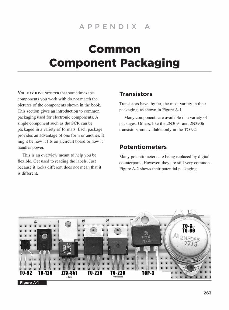
YOU MAY HAVE NOTICED that sometimes thecomponents you work with do not match thepictures of the components shown in the book.This section gives an introduction to commonpackaging used for electronic components. Asingle component such as the SCR can bepackaged in a variety of formats. Each packageprovides an advantage of one form or another. Itmight be how it fits on a circuit board or how ithandles power.
This is an overview meant to help you beflexible. Get used to reading the labels. Justbecause it looks different does not mean that it is different.
Transistors
Transistors have, by far, the most variety in theirpackaging, as shown in Figure A-1.
Many components are available in a variety ofpackages. Others, like the 2N3094 and 2N3906transistors, are available only in the TO-92.
Potentiometers
Many potentiometers are being replaced by digitalcounterparts. However, they are still very common.Figure A-2 shows their potential packaging.
Figure A-1
Common Component Packaging
A P P E N D I X A
263

Transformers
Transformer packaging sizes, like any othercomponent, are determined by the powerrequirements. The largest transformer, shown in Figure A-3, is a small power transformer.
Figure A-2
Figure A-3
264 Appendix A ■ Common Component Packaging

Capacitors: Reading and Decoding
A P P E N D I X B
CAPACITORS TEND TO BE CONFUSING because there isno standard method of marking them. Even I getturned around when trying to decipher somecreatively marked caps. If you are unsure, just useyour DDM to verify what you think you see.
Reading Values
Each range of capacitors is packaged and referredto differently.
Remember! Coloring is nothing more thanadvertising for who made it.
■ Electrolytic capacitors are easy. They havepositive and negative connections. They mustbe placed properly. Polarity is clearly marked.Radial electrolytic capacitors have both leadsfrom one end. Axial capacitors have a lead ateach end. Figure B-1 shows that voltage ratingsand capacitance are clearly marked.
265
Farad : F Microfarad : �F Nanofarad = nF Picofarad = pF
1 F = 1 million �F = 1 billion nF = 1 trillion pF
1 F = 1,000,000 �F = 1,000,000,000 nF = 1,000,000,000,000 pF
1 �F = 10–6 F 1 nF = 10–9 F 1 pF = 10–12 F
1 �F = 1,000 nF = 1,000,000 pF
1 nF = 1,000 pF
TABLE B-1 The Farad Was Defined Over 200 Years Ago; Today, the Base Unit is the �F
Figure B-1

■ Film capacitors are usually standard boxyshapes. Assume they are marked in nanofarads,but don’t bank on nanofarads or a boxy shapeall the time. Sometimes they are dipped inplastic and lose their boxy appearance. Theseare made of stacked layers of conductive film.
■ Disk capacitors dominate the picofarad range.They are usually made of two circular plates,dipped into ceramic material and baked. Goodexamples of both appear in Figure B-2.
The markings of disk capacitors appear cryptic.The numbers read sort of like a resistor. Figure B-3shows a range of values, and Table B-2 shows howto read them. Regarding the cap marked n22, the
unit marker substitues as the decimal. So its valueis .22nF.
Any capacitor rated above the intended voltagecan be used in a circuit. For example, a capacitorrated at 600 volts can be used in a 9-volt circuit.There’s no problem as long as maximum voltagedoes not exceed the capacitor’s rated maximum.
Tolerance: Quality andAccuracy of Capacitors
The marking for accuracy of capacitors is noted oneach package. Look at the pictures. On each, thereis a prominent letter “K,” “M,” etc. Shown in TableB-3, these letters note tolerance.
266 Appendix B ■ Capacitors: Reading and Decoding
Figure B-2
Figure B-3

Appendix B ■ Capacitors: Reading and Decoding 267
Marking Base Number Number of Zeros Results in pF Results in nF
220 22 0 22 pF .022 nF
221 22 1 220 pF .22 nF
222 22 2 2200 pF 2.2 nF
223 22 3 22000 pF 22 nF
TABLE B-2 The Third Number Denotes the Number of Zeros
F G J K M Z
±1% ±2% ±5% ±10% ±20% –20% to
+80%
TABLE B-3 The Letter “K” Used Here HasNothing to Do with 1,000

This page intentionally left blank

Animations List
A P P E N D I X C
Related Animations
THESE ANIMATIONS CAN be found atwww.mhprofessional.com/computingdownload
Part One
Figure L3-4
Figure L6-4
Figure L8-18
Figure l8-19
Figure L8-22
Figure L9-5
Figure L12-3
Figure L12-12
Figure L13-2
Figure L13-7 (a and b)
Part Two
Figure L15-1
Figure L16-1
Figure L16-2
Figure L16-3
Figure L16-4
Figure L16-5
Figure L16-7
Figure L16-9
Figure L19-4
Figure L20-1
Figure L21-2
Figure L21-5
Figure L22-7
Figure L23-5
Figure L23-6
Figure L23-7
Figure L24-1
Figure L24-2
Figure L24-3
Figure L25-2
Figure L27-1
Figure L27-2
Figure L27-3
Figure L27-4
Figure L28-1
Figure L28-2
Figure L28-3
Figure L28-4
Figure L28-6
Figure L28-7
Figure L32-2
Figure L32-3
269

Part Three
Figure L37-1
Figure L38-2
Figure L39-1
Figure L40-2
Figure L41-1
Figure L42-2
Figure L43-1
Figure L44-5
Figure L46-3
Figure L46-4
Figure L46-5
Part Four
Figure L49-1
Figure L49-2 (a, b, and c)
Figure L50-2
Figure L50-3
Figure L50-5 (a, b, and c)
Figure L52-2
Figure L53-1
Figure L53-2
Figure L53-3
Figure L53-4
Figure L53-5
Figure L53-7
Figure L53-8
Figure L53-9
Figure L54-1 (a, b, and c)
Figure L54-6 (a and b)
Figure L55-7
Figure L56-2
Figure L57-2
Figure L60-3
Figure L60-4
Figure L60-5
Figure L62-1
Figure L62-2
Figure L62-3
Figure L62-4
Figure L62-5
Figure L62-6
270 Appendix C ■ Animations List

Glossary
A P P E N D I X D
AC
Alternating current (AC) is a current that pushesthe electrons both forwards and backwards througha wire. AC is easily produced and transmitted forhousehold and industrial use. Audio signals are ACbecause the sound wave creates a signal thatpushes and pulls—creating a positive and negativevoltage. AC is generally not used for digitalelectronic applications. See DC (direct current).
active
The state of a circuit, referring to whether thecircuit is responding to an input. Alternatively, theother state is rest.
air capacitor
An air capacitor is an adjustable cap that works inthe pF range, used for radio frequency tuning.
amp (ampere)
This is the basic unit of current (I) in electricity. Itis a specific measure of electrons that flow past apoint in one second.
amplifier
An amplifier uses a smaller signal to control thelarger flow of voltage and current directly from thepower source. See pre-amp, power amp, Op Amp.
amplitude
This is the strength of a signal. If the volumechanges, the output amplitude changes. A 6-volt
AC signal has six times the amplitude of a 1-voltAC signal.
analog
A signal that varies continuously over a givenrange, as compared to a digital signal where onlydiscrete values of Hi (V�) and Lo (ground) areconsidered significant.
analog to digital (AD)
A device that changes a continuously variablesignal, such as motion or electrical voltage, intodigital values. Thus, it provides analog-to-digitalconversion.
AND gate
Digital logic for the AND gate. When all inputs areHi, the output is Hi.
anode
Commonly used term referring to the positive sideof a polar component.
astable
An astable oscillator creates a continuousfrequency as long as that portion of the processoris active. The frequency of the oscillator is set bythe value of the components in the RC circuit.
battery
The term comes from a grouping of cells togetherin parallel or series. A 9-volt battery is made of agrouping of six 1.5-volt cells.
271

BCD (binary counting decimal)
A binary input is interpreted and then presented ona decimal seven-segment display output. The 4511is a BCD interpreter.
bias
The general term means a tendency or prejudicetowards a specific point of view. In electronics, abias is created by using voltage dividers to createan artificial center point for an audio AC signal. Ifan audio system uses 12 volts, the bias is set to 6volts. This method is easiest when only positiveDC voltage is available.
binary
The counting system that depends on only twodigits, used by computers and machinery because itis easier for these systems to sense an on/off setup,rather than partial voltages. Computers use amagnetic system of north/south polarity to storebits of information. See bit, byte, digital.
bit
A single piece of information that stores binarydata. It is the individual piece (bit) that is turnedon/off, or an area polarized north/south onmagnetic media, or a dimpled/not dimpled spot on a CD/DVD disk.
bounce
Bounce is found in any mechanical switchconnected to a digital system. Most digitalcircuitry is capable of responding in microseconds,but when a switch is thrown, the current changeoften fluctuates like a bouncing ball. If thisfluctuation “bounces” above the digital responsethreshold of half of V�, it creates problems ofcounting an event twice instead of once. To takecare of this problem, use a Schmitt trigger.
byte
A combination of 8 bits of information, capable ofstoring up to 256 pieces of data.
capacitor
A device composed of two conducting surfacesseparated by an insulator called a dielectric. (1) Ithas the ability to store electrical energy and releaseit in an RC circuit—called sink and drain. (2) Itcan be used as a filter to smooth out a signal. (3) Itcan be used to block the flow of current, but stillallow the changing signal to pass, as in an audiocoupling—like a membrane across a drum. Seefilm capacitor, electrolytic capacitor, diskcapacitor.
cathode
Commonly used term referring to the negative sideof a polar component.
cell
A single electrochemical generating unit. Usuallyzinc and copper are used in general-purpose andalkaline cells that produce 1.5 volts. Nickel andcadmium are used in rechargeable cells. They areganged together in series or parallel to create abattery.
circuit
A course, pathway, tour, or journey. An electricalcircuit is one that is a complete pathway andprovides a path for the current.
clock signal
A clean digital signal that rises from zero to fullvoltage instantly in microseconds. A clock doesnot have any bounce. A circuit that produces aclock signal from a push button is often referred toas a Schmitt trigger.
CMOS
An acronym for complementary metal oxidesemiconductor, pronounced see-moss, CMOS is awidely used type of IC.
272 Appendix D ■ Glossary

conductor
A conductor carries electricity easily. It is made ofany material that has unbound electrons that areable to freely flow when a voltage or pressure(electromotive force) is applied to it. All metals areconductors. Some nonmetals, such as silicon andcarbon, also act as conductors. See insulator.
continuity
Continuity is a test done with the digitalmultimeter to check if there is a “continuous”connection between two points. Most multimetersare designed to give instant feedback in a YES/NOformat: YES indicates there is a connection withvery little resistance; NO indicates there is not aconnection of very little resistance.
coulomb
Named for Charles de Coulomb (1736–1806), whodevised a method of measuring electrical quantity.It is the quantity of electricity conveyed in onesecond by a current of one ampere.
coupling
A capacitor can be used for audio coupling, that is,to pass an AC signal but not pass any current. Thisis like sound passing through the head of a drum.No air passes through the drum head, but thesignal still passes with ease and clarity. Audiocoupling also applies capacitors as filters.
DC
DC (direct current) moves in only one direction. It may change voltage, but it does not reversedirection.
DCB
Decimal counting binary (DCB) happens when aprocessor has an input of a clock signal andchanges its binary output by one step for eachadditional clock signal. The 4510 is an example ofa DCB interpreter.
digital
(1) Relating to data that is represented in the formof discrete on’s and off’s, 1 or 0s; as opposed toanalog (continuous voltage fluctuation). (2) Anelectronic circuit that uses digital logic in its input,processor, or output.
digital circuit
A circuit that has a processor and output thatoperate in only two states: on and off.
digital logic
The method of using analog and digital inputs tomake digital decisions. The five most commongates are AND, OR, NAND, NOR, and NOT.
digital output
The output signal of a digital circuit represents a set value of conditions. The information iscontained in a code consisting of a sequence ofone or more discrete voltage or current levels, eachrepresenting a value of zero or one. The sequence01000001 may then be interpreted as a byte with avalue of 65 and then presented on your monitor asthe letter A.
digital recording
Any recording in which the signal is first convertedto digital format. A CD uses 16 bits of informationfor a single binary word, while a DVD uses 20 bitsof information for a single binary word.
diode
A basic electronic device characterized by theability to pass an electric current easily frompositive to negative. They act as a one-way street.Three types of diodes are used in this course: (1)power diode designed for 1 watt at 400 volts, (2)the signal diode that passes miliamps, and (3) thezener diode.
Appendix D ■ Glossary 273

DIP
Dual inline package. One of a series of acronymsreferring to common packaging used in electronics.DIP packaging specifically has two rows ofmatching pins.
disk capacitor
Disk capacitors are designed to hold the smallestcapacitance values in the picofarad (pF) range. Theyare usually light brown and disk shaped.
dumb
A dumb circuit does not have any way todetermine if a specific event has occurred or whena particular number has been reached.
electrolytic capacitor
An electrolytic capacitor is a polarized capacitor,usually in the microfarad (μF) range. It has apositive and negative side. If it is put in backwards,it will not work effectively, and might fry itself(very messy).
electromotive force
(1) The amount of energy supplied by an electriccurrent passing through a given source, asmeasured in volts. (2) The energy differenceexisting between the positive and ground that are provided by the same energy source. Anelectromotive force (electrons) passing through awire will create a magnetic field. A magnetic fieldmoving around a wire will create an electromotiveforce and push electrons.
electron
A negatively charged particle that is part of thestructure of an atom. Free electrons flow inconductors to create current. An electromotiveforce—voltage—is needed to push electronsthrough a conductor. Electrons that are not boundto a specific atom or molecule are considered“free.” A material with many unbound electrons isconsidered a good conductor, such as metals. Amaterial that has all of the electrons tied up in
chemical bonds will not conduct electricity. It is agood insulator.
energy
The ability to do work. Energy in electricity ismeasured in volts.
farad
The unit of capacitance named for MichaelFaraday. The basic common unit is 1 μF, whichequals 1 microfarad, that is, .000001 F.
film capacitor
Film capacitors are designed to hold the mid-rangecapacitance values in the nanofarad (nF) range.They are often shaped like a small box.
filter
A capacitor can act as a filter in two distinct ways.(1) It can be a buffer by acting as a reservoir ofextra electrons. When a spike goes above theregular voltage, the sudden surge is softenedbecause the capacitor fills up and dumps the extraback out slower than the actual surge. If there is amomentary drop in voltage, that is softened aswell, because the capacitor discharges its contentonto the line. (2) It can be a high pass or low passfilter by allowing only higher or lower frequenciesto pass. Low-frequency sound passes through a .1μF capacitor, while higher sounds are filtered out.High-frequency sounds pass through a .001 μFcapacitor, while the lower sounds are filtered out.
force
In electricity, voltage (V�) is the unit used tomeasure the amount of electromotive force (push)in a circuit.
frequency
The number of cycles or events per unit time,commonly having units of sec-1 (hertz). Inacoustics, this refers to the number of waves perunit time that are produced by a vibrating object.
274 Appendix D ■ Glossary

gain
Gain is the basic measurement of the amplitude ofsignal output divided by the amplitude of signalinput. It is set by resistor ratios to control feedbackin an Op Amp.
gate
See digital, logic.
ghost
A ghost is troubleshooting a problem that cannotbe defined, because an error is not regular. Themost common causes of a “ghost” are (1) loosewires, (2) wires that cross and touch when theyshouldn’t, and (3) unused inputs to CMOS chipsthat have not been tied to V� or ground.
heat sink
A heat sink is used to remove unused power froman amplifier or transistor. For example, if a 20-watt amplifier is being fed 20 watts of powerbut only using 5 watts because the music is quiet,15 watts of power have to be dumped as heat. Aheat sink allows the heat to move away from theamplifier chip. If the heat is not moved away, theamplifier chip will overheat and shut down, oroverheat and melt.
hertz (Hz)
A unit of frequency equivalent to cycles persecond. One kilohertz is 1,000 cycles per second.
hysteresis
Related to hysteria. In electronics, it refers to theoutput of a logic gate going hysterical as thevoltage at one of the inputs passes slowly throughthe half V� range. The gate tries to physicallyrespond as both high and low at the same time,flip-flopping wildly. Sometime this results in atrailing blip of sound at the output.
IC
An integrated circuit (IC) is any miniaturemanufactured circuit made of many transistors andcomponents working together in one package. Thepackage is usually presented in DIP or SIP format.The technique for manufacturing ICs depends onusing a photographic process. Tens of thousands ofICs are available on the market today.
input
The input is the action that starts the circuit. It isthe first part of a system diagram.
insulator
An insulator cannot conduct electricity because ithas all of the electrons bound into its chemicalmakeup. It does not have free electrons, so anelectric force is not able to move through thematerial. See conductor.
invert
To turn upside down. For example, a NOT gateinverts a signal from Hi to Lo.
kilo
A measurement unit of 1,000 abbreviated as “K.”For example 100 K ohms is easier to write than100,000 ohms.
Kirchoff’s law
Kirchoff’s law is used to figure the resistance in asystem that has many load levels set in parallel.
layout
The layout represents the trace of copper on theprinted circuit board. Any layout is specific to oneapplication. To change the specific circuit, youmust effectively change the layout.
load
Any item that consumes electricity, such as aresistor, a speaker, household appliance, streetlighting, or an industrial electrical motor.
Appendix D ■ Glossary 275

logic
A logic circuit consisting of one or more diodegates connected to the base of a transistor, inwhich the AND or OR functions performed by thediode gates control the on-off status of thetransistor.
mega
A measurement unit of 1,000,000 oftenabbreviated as “M.” For example, 1 M ohms iseasier to write than 1,000,000 ohms.
micro
A measurement unit of .000001 often abbreviatedas “μ” or simply “u” referring to the Greek letter“mu.” For example 47 μF is easier to write than.000047 F.
microprocessor
The central processing unit of a microcomputer,usually manufactured on a single semiconductorchip, containing anywhere from a few thousand toseveral million or more semiconductors on a singleintegrated circuit.
milli
A measurement unit of .001 often abbreviated as“m” and not to be confused with “mu” for micro.For example, 7 mW is easier to write than .007watts. An average LED uses 20 mA.
monostable
A monostable oscillator is a “one-shot” timer—usually an RC circuit. When triggered by anoutside event, it turns on a portion of a processoras the capacitor fills. As the resistor drains thevoltage from the capacitor, the controlled processorturns off. The speed of the “one-shot” timer is setby the value of the components in the RC circuit.
NAND
Digital logic for the NAND date (not AND). Whenany input is Lo, the output is Hi.
nano
A measurement unit of .000000001 often abbreviatedas “n.” For example, 100 nF is easier to write than.0000001 F. Because film capacitors are producedwidely in the nanofarad range, their measurementsare often given in nF. .001 μF � 1 nF � 1000 pF.
NOR
Digital logic for the NOR gate (not OR). When allinputs are Lo the output is Hi.
normally closed (NC)
The two contacts are connected in an NC switch.Current passes easily because the two wiresconnect and there is no resistance. When activated,they become disconnected and the electrons cannotpass through the air.
normally open (N.O.)
The NO push button has infinite resistancebetween the two legs when the button is notpushed. When it is pushed, the two wires connectand there is no resistance.
NOT
Digital logic for the NOT gate. It inverts the input.A Hi input becomes a Lo output, and a Lo inputbecomes a Hi output.
NPN
An NPN transistor turns on more with morepositive voltage to the base. The emitter isconnected toward the ground. An NPN junction is formed by placing a thin layer of p-typesemiconductor material between two layers of n-type semiconductor material. The p-typesemiconductor becomes a conductor when a small voltage is applied to it.
ohm
A standard unit of electrical resistance, equal to theresistance of a circuit in which an electromotiveforce of 1 volt will maintain a current of 1 amp.Named for George S. Ohm.
276 Appendix D ■ Glossary

Ohm’s law
Simply stated, the amount of voltage pressure in acircuit is equal to the amount of current multipliedby the resistance of the load. V � I (�) R.
Op Amp
Shorthand for Operational Amplifier.
OR
Digital logic for the OR gate. When any input isHi, the output is Hi.
oscillator
A circuit that creates a regular and predictable beator frequency. See astable, monostable.
output
Output is the action resulting from the processingdone by an electronic system. It is the last unit of asystem diagram.
parallel
A parallel circuit happens when all the componentsor loads are connected to each other side by side.Each load is provided with the same amount ofvoltage, but the current is evenly shared betweenthe loads. See series.
pico
A measurement unit of .000000000001 (10–9)often abbreviated as “p.” For example, 100 pF iseasier to write than .0000000001 F. Because diskcapacitors are produced widely in the picofaradrange, their measurements are often given in pF..001 μF � 1 nF � 1000 pF.
piezoelectric
This effect occurs in specific nonmetallicmaterials, such as quartz crystals, or in engineeredceramics and plastics. Piezos can be used asspeakers and in sensors. (1) A voltage or electricfield is produced in specific crystals when thesecrystals are compressed or decompressed rapidly.
(2) When a voltage is applied to a piezo material, itwill compress or decompress, relative to the size ofthe voltage.
PNP
A PNP transistor turns on more with less voltageto the base. The emitter is connected toward thevoltage. A PNP junction is formed by placing athin layer of n-type semiconductor materialbetween two layers of p-type semiconductormaterial. The n-type semiconductor becomes aninsulator when a small voltage is applied to it.
polarity
Some components need to be set in with attentionto the direction of the current and voltage. Theseparts are “polar.” If these parts are placed inbackwards, the component will not functionproperly. They may even be damaged if voltage is directed through them the wrong way. Mostelectronic components have polarity. Resistors donot have polarity because the current and voltagecan pass both ways.
power
Power is defined as the speed at which work isdone. In electronics and electricity, power ismeasured in watts. 1 watt � 1 amp � 1 volt.Restated, that is the amount of electrons passing aspecific point in one second, multiplied by theamount of force pushing the electrons.
power amp
A power amp is used to increase a signal’s strength(amplitude) from the 1-watt range to whatever isneeded for the speakers at hand. Common poweramps provide anywhere from 20 watts to 300watts. Power amps are rated by their range ofresponse. The concern with power amps is theability to provide enough power (12 volts � 25amps � 300 watts) and being able to removeunused power through heat sinks.
Appendix D ■ Glossary 277

pre-amp
A pre-amp is a low-power amplifier that increasesa signal’s strength (amplitude) from the milliwattrange to the 1-watt range. A pre-amp is often ratedby its gain and clarity of signal. Most poweramplifiers need to have a signal fed to them that isin the 1- to 2-watt range.
processor
(1) A device that interprets and executesinstructions. (2) Referring to the center portionof a system diagram.
prototype
A prototype is a test product, built as closely to thereal finished product as possible. A prototype isusually built in a fashion that allows easy andquick changes for testing purposes.
Q
Transistors are always noted with a “Q.” Transistoris an awfully long word, and “T” is used for otherthings in electronics, like “transformer.”
random
A result happening by chance. There should be nopattern in “random” events.
RC circuit
A resistor/capacitor (RC) circuit is used forcapturing voltage and releasing it in a controlledmanner. This allows the designer to control thetime at which the digital input will sense thechange above half voltage to below half voltage.
resistance
The fact of opposing or acting against. Inelectricity, resistance opposes the flow of current,generates heat, controls electron flow, and helpssupply the correct voltage when set up as a voltagedivider. Resistance depends on the material used,the length and cross-sectional area of theconductor, and the temperature. It is measured in
ohms and follows Ohm’s law. Resistance ismeasured in ohms, kilo-ohms, or megohms.
resistor
A component in an electric circuit that providesopposition to or limits the current flow accordingto Ohm’s law. The carbon resistors used in thiscourse are made by mixing carbon particles with aceramic binder in measured amounts. These arebaked into standard cylindrical shapes, markedwith standard color-coding. They create resistanceto current flow and act as a load in the circuit.
rest
At rest, power is provided to the system, but thesystem is not active. The 4011 chip needsmicroamps (.003 of a milliamp) to stay powered inits rest mode. At this rate, a 9-volt alkaline batterywill power a 4011 chip for two to three years.
schematic
A plan, plot, and design of an electronic system, or portion of that system, using only symbols torepresent the components and their connections toeach other.
Schmitt trigger
A circuit that produces a clock signal from a pushbutton is often referred to as a Schmitt trigger. It isdesigned to eliminate bounce. A common Schmitttrigger is available in the 4093 CMOS IC.
semiconductor
A material that has intermediate values ofelectrical resistivity, between the values for metalsand insulators. It conducts electrons under certainsituations, but resists their flow in other situations.The properties of such basic materials as silicon,carbon, and germanium are the heart ofsemiconductors. Semiconductors are the basicmaterial of various electronic devices used intelecommunications, computer technology, controlsystems, and other applications.
278 Appendix D ■ Glossary

series
A series circuit is one in which each component orload is joined end to end, successively with thenext. The current flow is determined by adding theresistance of each component in the chain together.The current stays the same for each component,but the voltage drops in relation to the resistance ofeach load. See parallel.
SIP
Single inline package. One of a series of acronymsreferring to common packaging used in electronics.SIP packaging specifically has a single row of pins.
smart
A smart circuit can use feedback to determine if a specific event has occurred. For example, a 4017 walking ring counter can be wired to sensewhen a specific number in a counting sequence has been reached.
solder
(1) An action that joins metal objects withoutmelting them. The metal objects are fused togetherwith an alloy that has been applied to the jointbetween them. (2) Any of several alloys used inthis process. Electronics most often use a 60% tinplus 40% lead alloy.
state
(1) The state of a circuit is either “active” or “atrest.” Active refers to the idea that the circuit hasbeen turned on. At rest means that the circuit iswaiting for an event to happen. A CMOS circuit atrest needs as little as a microamp of current topower the IC chip at rest. (2) Refers to the outputof a logic gate. The output state is either Hi or Lo.
static electricity
Energy in the form of a stationary electric charge.This charge can be built up on your body when youwalk across a nylon carpet. You reach for a
doorknob, and a spark jumps the gap as anelectrostatic discharge. Such a charge can be storedin capacitors and thunderclouds, or anynonconductive surface. It can be produced byfriction or induction. This charge can build up hugevoltage (but small current) and can fry many ICs.
system
(1) Referring to a large orderly arrangement ofinterconnected units such as a telephone system.(2) A system diagram that represents the inputs,processors, and outputs of an electronic unit,emphasizing their relationship in the circuit.
threshold
The amount of voltage needed for an input of adigital circuit to sense a change of state.
tie
To connect components together. For example, totie pins 12 and 13 together means to connect themwith a wire.
transistor
The basic electronic switch. These are analogswitches—the voltage passed through the transistoris directly related to the amount of voltage appliedto the base. It is an active semiconductor device,usually made from germanium or silicon, andpossessing at least three terminals (typically, abase, emitter, and collector) and characterized byits ability to amplify current. They are used in awide variety of equipment, such as amplifiers,oscillators, and switching circuits. See NPNtransistor, PNP transistor.
Vcc
Vcc is another way of labeling ground.
VCO
VCO is shorthand for voltage-controlled oscillator.A complete VCO is housed in the 4046 CMOS IC.
Appendix D ■ Glossary 279

Vdd
Vdd is another way of labling V�.
voltage
Voltage is the amount of “push” behind thecurrent. It represents the potential energy or forcein a circuit. The potential difference orelectromotive force is measured in volts.
voltage divider
By using resistors as artificial loads, voltage can beset at a midpoint to any predetermined valuedesired. This technique is widely used in biasingaudio systems and in sensors where an eventcauses one of the resistors to change value,therefore changing the midpoint voltage value.
watt
Power output is defined as how fast work is done.In electronics and electricity, power is measured inwatts. 1 watt � 1 amp � 1 volt. Restated, that isthe amount of electrons passing a specific point inone second, multiplied by the amount ofelectromotive force.
work
The measure of force times distance.
zener diode
A diode that “breaks down” at a specific voltagevalue, allowing current to move from cathode toanode. It can be used for voltage referencepurposes or for voltage stabilization.
280 Appendix D ■ Glossary

Make Your Own Printed Circuit Boards
A P P E N D I X E
281
THIS METHOD IS GREAT for prototypes andhobbyists.
I know that other people have developed thisprocess. The only thing I can claim is that Iindependently developed this process andsuccessfully used it in my classroom.
For your convenience, www.mhprofessional.com/computingdownload presents this section withlarge color photos providing clarity lacking inblack and white.
This photo shows all of the materials needed tocreate your own printed circuit board (Figure E-1).
Figure E-1

Clean the copper clad material using scouringpowder to remove the light plastic film that keepsthe copper from tarnishing (Figure E-2). Nofingerprints!
I use photo-quality inkjet paper (EpsonS041062). It is the best quality for the money($17/100 sheets). The key is the clay base. Thiskeeps the ink from absorbing into the paper fibers(Figure E-3).
When looking at the paper, bend a corner of thesheet over on itself (don’t crease it) to compare thebrightness of each side. Don’t think “white.” Thatgets confusing. Compare “brightness.” The brighter
side is the one with the clay. Print onto the claysurface.
Remember, use a laser printer. The philosophyis to melt the plastic toner against the copper. Ihave had feedback that some brands of laserprinters simply do not work, but I’ve had successwith any laser printers I’ve used, including HPs,Lexmarks, and Canons.
This close-up shows the quality of traces thatcan be made using my inexpensive method (FigureE-4). Even beginners can create the .03-inch (.75-mm) width. With care and practice, you can getthe .02-inch width just as regularly. The highlightedpad had paper debris covering the copperunderneath, so it did not get etched properly.
With the image facing the copper side of thePCB material, fold the margins of the layouttightly around the edges of the PCB and securewith masking tape. Regular masking tape doesn’tdisintegrate when heated. The paper must besecured so that the image can’t shift (Figure E-5).
Use a regular clothes iron (Figure E-6). Turn offthe steam. Set to maximum temperature. Someirons are hotter than others. The paper should notdiscolor during this one-minute heating process.
282 Appendix E ■ Make Your Own Printed Circuit Boards
Figure E-2
Figure E-3
Figure E-4

Use an ironing board or cutting boardunderneath. It should be a smooth, nonmetal, heat-resistant surface.
This photo attempts to show real strain in myhand as I apply pressure while moving in tightcircles, about one per second for a minute.
Immediately apply pressure to the paper andcopper clad board.
Without a vise at home, I place the hot PCB andpaper between two small metal sheets. This thengoes onto the floor, copper side up. I then place abook (to spread my weight evenly) on top of thesetup. My foot is too big to show, but my
daughter’s Ken doll helps convey the idea (FigureE-7). Stand for a minute right on top of the board.
Use a vise for better results. Gently secure theboard between metal plates and apply softpressure. Don’t squish. Just secure the board untilit has cooled.
Place the cool wrapped board into water. Let itsit for a minute. This is important even thoughnothing appears to happen (Figure E-8).
DON’T SKIP THIS STEP! This is the onestep that everybody forgets and then complainsafterwards that the processes didn’t work.
Appendix E ■ Make Your Own Printed Circuit Boards 283
Figure E-5
Figure E-6
Figure E-7
Figure E-8

Spread a few drops of dish soap around on thewet paper (Figure E-9). The soap helps the watersoak through. The paper becomes translucent andexpands where it’s not attached to the PCB.
Remove the tape from the back and peel themajority of the paper off. A good amount of paperdoes remain behind. Remember, you are separatingthe clay surface from the paper. This shows a goodidea of what you can expect as you peel the paperoff (Figure E-10).
Use a dripping wet paper towel to gently rub offthe remaining paper (Figure E-11). The towelingwill disintegrate as you do this. Don’t rub too hard.
You don’t want to remove any of the toner nowmelted onto the copper.
This shows the dried results. Notice the paperremaining in some spots. Wet the area and use asharpened point to clear it. Even fresh chemicalshave difficulty etching through paper (Figure E-12).
These photos show progression from paper tofinished PCB (Figure E-13).
■ Before etching, carefully inspect the layout afterthe paper is removed and the board is cleaned.
■ I used a “Staedtler Mars” permanent marker toreinforce areas that looked weak. Any color
284 Appendix E ■ Make Your Own Printed Circuit Boards
Figure E-9
Figure E-10
Figure E-11
Figure E-12

works, but red highlights where it has beenapplied. I mention the brand name here onlybecause the quality of the permanent ink doesmatter.
For etching, I prefer ferric chloride. It isinexpensive and doesn’t lose potency with age.Read the safety information. Handled properly, itis safe enough. Use only plastic tools. Handledimproperly, it is very nasty.
■ Use steel wool or finer grit sandpaper toremove the toner.
■ This is a good board. If you have small breaks,those can be bridged with solder.
■ Drill all holes with a #60 bit.
If you need to use support screws, be sure todrill the 1/8-inch-diameter holes before youpopulate the board.
Appendix E ■ Make Your Own Printed Circuit Boards 285
Figure E-13

This page intentionally left blank

Index
287
4046 voltage-controlled oscillator, 153–1584511 BCD, 170–174
number display, 193–1944516 BCD, 174–179
number display, 193–194
A
AC, 216in a DC environment, 220–222DC voltage on an AC circuit, 219defined, 271injecting an AC signal into a DC circuit,
224–225on the oscilloscope, 216–217
active, defined, 271air capacitors, defined, 271alternating current. See ACamps (amperes), defined, 271amperage, 201–203amplifiers, 199–205
analog, 212–214defined, 199, 271inverting, 213noninverting, 213Op Amps, 213–214systems and subsystems, 248–251transistors as, 199–205
amplitude, defined, 271amplitude modulation, 255analog, 84
amplifiers, 212–214defined, 271vs. digital, 65
analog to digital (AD), defined, 271analog-to-digital converter, 149–158AND gates, 66, 68–69
defined, 271animated sign, 185–186animations list, 269–270animatronics, 255Anode, defined, 271antistatic packaging, 5ASCII table, 64astable, defined, 271
audio couplers, 225, 237–238automatic night light, 43–49
B
battery, defined, 271battery clips, 7BCD (binary counting decimal), defined, 272bias, defined, 272binary, defined, 272binary information
“spoiled billionaire” example, 61–66See also ASCII table
bit, defined, 272blanking, 171bounce, 165
defined, 272breadboard. See solderless breadboardbreak beams, 91buzzers, 8, 134bytes, defined, 272
C
capacitance, 26capacitors, 6–7, 25–28
as a buffer, 237defined, 272disk, 26–27, 108, 266, 267, 274electrolytic, 26, 27–28, 265, 274film, 27, 28, 266, 274marking, 108reading values, 265–266tolerance, 266, 267
carry-in, 175carryout, 161cathode, defined, 272CC. See common cathode (CC)cells, defined, 272circuit boards, 8circuits
building a circuit on the breadboard, 11–14defined, 272
Clarke, Arthur C., 255clock signal, 163–166
defined, 272

288 Electronic Circuits for the Evil Genius
CMOS, defined, 272CMOS Cookbook (Lancaster), 150CMOS integrated circuits (ICs), 72–75
partial list of, 73–74troubleshooting, 150
coil microphones, 238coin-activated switches, 128–129common cathode (CC), 169–170conductor, defined, 273connecting clips, 117contact switches, 127–129, 190continuity, defined, 273control inputs, 166–168coulomb, 202
defined, 273coupling, defined, 273current, calculating, 201–203
D
dark detector, 91, 97, 129–130DC, 215–216
AC in a DC environment, 220–222DC voltage on an AC circuit, 219defined, 273injecting an AC signal into a DC circuit, 224–225
DCB, defined, 273DCV. See direct current voltagedensity, measuring, 255design, 127
and applications, 255–259contact switches, 127–129defining and designing your project, 183–189designing the enclosure, 140–141gassy cow, 136–137heartthrob teddy, 139–140high-powered outputs, 134–135jiggle me teddy, 137–138low-powered outputs, 133–134pop can motion detector, 135–136safety, 141shadow racer, 137supercheap keyboard, 138–139
DigiDice, 149, 179digital, 84
vs. analog, 65defined, 273
digital circuit, defined, 273digital inputs, 85digital logic, defined, 273
digital logic gates. See logic gatesdigital multimeter, 9digital output, defined, 273digital recording, defined, 273diodes, 6
common types of, 151defined, 273as protection for circuits, 12
DIPs, 72defined, 273
direct current. See DCdirect current voltage, 14disk capacitors, 26–27, 108, 266, 267
defined, 274DMM. See digital multimeterdouble-pull double-throw (DPDT) switches,
252–253dual inline packages. See DIPsdumb circuits, defined, 274
E
electret microphones, 238–239electrolytic capacitors, 26, 27–28, 265
defined, 274electromotive force, defined, 274electrons, 243
defined, 274enable function, 167–168energy, defined, 274event counter and trigger, 187–188exercises
the 4017 walking ring counter, 162–163the automatic night light, 44–47the basic digital logic gates, 72capacitors and push buttons, 30–31control the seven-segment display using the
4511 BCD, 173–174controlling the flash rate, 109–110create an annoying sound output, 111–112decimal to binary—the 4516, 177–179defining work, force and power, 208–210the effect resistors have on a circuit, 18–19the inputs are switches, 89integrated circuits, CMOS ICs, 75introducing the 4046 VCO, 156–158introducing transistors, 33–34light-dependent resistors, 23mapping the solderless breadboard, 10–11measuring voltage on your first circuit, 13–14

the PNP transistor, 37–38the potentiometer, 20–21RC1—creating the switch, 151–152reading resistors, 16specialized transistors—the SCR, 53transistors as amplifiers and defining current,
204–205understanding the clock signal and the 4017,
164–166understanding voltage dividers, 95–96using feedback to control the gain, 231–233what do I have to gain: definitions, 211–212the world is analog, so analog is the world, 214
F
Faraday, Michael, 247farads, 26, 265
defined, 274See also picofarads
feedback, using to control gain, 229–233film capacitors, 27, 28, 266
defined, 274filters, defined, 274flash rate, 107–110force, 205–206
defined, 274frequency, defined, 274
G
gaindefined, 210, 275in the NPN transistor, 210–211using feedback to control, 229–233
gassy cow, 136–137Gates, Bill, 61ghost, defined, 275glossary, 271–280Gold Wave shareware, 218
H
heartthrob teddy, 139–140heat sink, defined, 275hertz, 107, 111
defined, 275hysteresis, defined, 275Hz. See hertz
I
ICs, defined, 275
inputs, 66, 67, 81, 250comparing to outputs, 219–220defined, 275as switches, 86–90
insulator, defined, 275integrated-circuit (IC) chips
antistatic packaging, 5See also CMOS integrated circuits
(ICs); ICsintercom. See two-way door phoneinvert, defined, 275inverters. See NOT gatesinverting amplifiers, 213inverting input, 223IQ meter, 186
J
jack, 118–119jiggle me teddy, 137–138
K
keyboard, 138–139kilo, defined, 275Kirchoff’s law, defined, 275KISS principle, 140
L
lamp test, 171Lancaster, Don, 150laser listeners, 255laser pens, 130latching circuits, 50
See also silicon-controlled rectifierslaws of prediction, 255layout, defined, 275LDRs. See light-dependent resistorsLEDs, 6, 12–13, 133–134
flash rate, 100vs. phototransistors, 40seven-segment LEDs, 169–170
light detector, 129light-dependent resistors, 8, 21–23, 129–130
on/off switches, 140substituting a phototransistor for a LDR,
47–48light-emitting diodes. See LEDslight-sensitive switches, creating, 96–97load, defined, 275logic, defined, 276
Index 289

logic gates, 66–72compared, 72
love meter fortune teller, 186–187
M
mega, defined, 276micro, defined, 276microphones
coil, 238electret, 238–239piezo (crystal), 238using speakers as, 240–242, 249
microprocessors, defined, 276microswitches, 128mili, defined, 276monostable, defined, 276Morse, Sam, 247motion detector, 128
pop can motion detector, 135–136motors, 135music chip, 133–134
N
NAND gate circuitsbuilding, 77–79test point 2, 81–83testing the input at test point 1, 80–81
NAND gates, 70–714011 dual input quad, 74–75audio for the NAND gate oscillator,
200–201building the NAND gate oscillator, 99–102creating a light-sensitive switch to trigger,
96–97defined, 276logic table, 103processor, 81–83understanding the NAND gate oscillator,
103–105See also NOT AND gates
nano, defined, 276negative feedback, 229
See also feedbacknoninverting amplifiers, 213noninverting input, 223NOR gates, 70–71
defined, 276See also NOT OR gates
normally closed (NC), defined, 276
normally open (NO), defined, 276NOT AND gates, 66
See also NAND gatesNOT gates, 67–68
defined, 276NOT OR gates, 66
See also NOR gatesNPN transistors, 32–34, 44, 69, 70
defined, 276gain in, 210–211See also transistors
O
Ohm, George, 202ohms, 13
defined, 276Ohm’s law, 202, 203–204
defined, 277Op Amps, 213–214, 250, 251
building a power amplifier controlled by an Op Amp, 235–238
defined, 277setting up, 222–229
operational amplifiers. See Op AmpsOR gates, 66, 69–70
defined, 277oscillators
4046 voltage-controlled oscillator, 153–158building the NAND gate oscillator, 99–102defined, 277self-kicking oscillator, 190–191understanding the NAND gate oscillator,
103–105oscilloscopes, 81, 112–119
AC on, 216–217scoping out the circuit, 119–122
outputs, 66, 81comparing to inputs, 219–220defined, 277See also sound output
P
packagingpotentiometers, 263–264transformers, 264transistors, 263
parallel, defined, 277parts bin
for Part Four, 198
290 Electronic Circuits for the Evil Genius

for Part One, 4for Part Three, 148for Part Two, 60
parts placement, 142–143PBNC, 29–30PBNO, 28–29PCBs. See printed circuit boardsPCCP, 156phototransistors, 38–41, 124–126
vs. LEDs, 40substituting for the LDR, 47–48
pico, defined, 277picofarads, 27, 108
See also faradspiezo (crystal) microphones, 238piezoelectric, defined, 277PNP transistors, 34–38, 70–71
defined, 277See also transistors
polarity, defined, 277pop can motion detector, 135–136pot. See potentiometerspotentiometers, 8, 19–21
packaging, 263–264power, 206–208
defined, 277power amp, defined, 277power amplifiers, 250, 251
building a power amplifier controlled by an Op Amp, 235–238
power diodes, 151power supply, regulated, 54–56preamps, 235
defined, 278prediction, laws of, 255preload, 176printed circuit boards
for automatic night light project, 48making your own, 281–285
processorsconsiderations for main processor,
258–259defined, 278possibilities for the first resistor/capacitor
circuit (RC1), 130–132timing and modifications for the second RC
circuit, 132VCO and Timed Off circuit, 191–192walking ring, 192–193
projectsautomatic night light, 43–49defining and designing, 183–189making your project, 189–194
prototype, defined, 278push buttons, 7
Push Button Normally Closed (PBNC), 29–30Push Button Normally Open (PBNO), 28–29
Q
Q, defined, 278
R
radio frequency pickup, 256random, defined, 278random number generator, 149ray gun, 184–185RC circuits, defined, 278regulated power supply, 54–56relays, 134–135reset, 175resistance
decreasing, 111defined, 278measurement of, 13, 15–16
resistor/capacitor (RC) circuits, 83–86creating the RC1 switch, 150–153
resistors, 6, 13band designations, 15defined, 278the effect resistors have on a circuit, 17–19measuring a resistor’s value, 16–17reading, 15–17substituting, 16
rest, defined, 278The Road Ahead (Gates), 61, 62
S
safety, 141SBB. See solderless breadboardschematic, defined, 278Schmitt trigger, defined, 279SCRs. See silicon-controlled rectifiersself-kicking oscillator, 190–191semiconductors, 5
defined, 278series, defined, 278seven-segment display
4516 BCD, 174–179
Index 291

seven-segment display (continued)controlling using the 4511 BCD, 170–174displays automatically fading out, 180–182LED, 169–170
shadow racer, 137signal diodes, 151Signal Generator, 120, 217–218, 225, 226silicon-controlled rectifiers, 7, 49–54single-pole double-throw (SPDT) switches, 252single-pole single-throw (SPST) switches, 252SIP, defined, 279slot machine, 188–189smart circuits, defined, 279solder, defined, 279soldering technique, 48–49solderless breadboard, 7, 8–9
layout, 11mapping (exercise), 10–11setting up for a circuit, 11–12
sound outputcreating, 110–112using transistors to amplify, 122–123
Soundcard Scope, 112–116safety measures, 112–113See also oscilloscopes
Soundcard Scope Probesafety measures, 112–113See also oscilloscopes
speakers, 134using as a microphone, 240–242, 249
state, defined, 279static
and CMOS ICs, 73integrated-circuit (IC) chips’ antistatic
packaging, 5static electricity, defined, 279Sturgeon, William, 247sunrise, listening to, 256supercheap keyboard, 138–139switches
evolution of, 252–253inputs as, 86–90
system, defined, 279system, layout, 180, 181
T
telegraph, development of, 247threshold, defined, 279tie, defined, 279
Timed Off circuit, 191–192timing, 184touch switches, 97–98, 130, 190transformers, 242–246
audio, 244–246, 249packaging, 264
transistors, 7, 31–32as amplifiers, 199–205defined, 279NPN transistors, 32–34, 44, 69, 70, 210–211, 276packaging, 263PNP transistors, 34–38, 70–71, 277using to amplify the output, 122–123
TRIAC, 49See also silicon-controlled rectifiers
trim pots, 19See also potentiometers
triode for alternating current, 49See also silicon-controlled rectifiers
two-way door phoneassembling, 259–260switching to, 252–254
U
up/down control, 175
V
Vcc, defined, 279VCO
4046 voltage-controlled oscillator, 153–158defined, 279and Timed Off circuit, 191–192
Vdd, defined, 280vibrations, measuring, 255voltage
DC voltage on an AC circuit, 219defined, 280measuring on your first circuit (exercise), 13–14used between V+ and ground, 44–45waterfall analogy, 18
voltage comparators, 223–224voltage dividers, 91–96, 117–118
defined, 280voltage follower, 258voltage reference, 223voltage regulators, 55voltage state, 66voltage-controlled oscillator. See VCOVref, 223
292 Electronic Circuits for the Evil Genius

W
walking ring 4017 decade counter, 159–163, 192–193clock signal, 163–166control inputs, 166–168
waterfall analogy, 18watts, 206
defined, 280wavelengths of colors, 38“whatever” detector, 185Winscope 2.5.1, 81
wire, 9–10type of, 189–190
work, 206defined, 280
Z
Zeitnitz, Christian, 112Zeldovich, Konstantin, 81Zener diodes, 150–153
defined, 280
Index 293