Designing with TTL Integrated Circuits - bitsavers.org
334
Designing with TTL Integrated Circuits Prepared by the Ie Applications 5taft of Texas Instruments Incorporated
-
Upload
khangminh22 -
Category
Documents
-
view
0 -
download
0
Transcript of Designing with TTL Integrated Circuits - bitsavers.org

Designing with TTL Integrated Circuits Prepared by the
Ie Applications 5taft of Texas Instruments
Incorporated

Designing with
TTL Integrated Circuits

Crawford • MOSFET IN CIRCUIT DESIGN
Delhom • DESIGN AND APPLICATION OF TRANSISTOR SWITCHING CIRCUITS
The Engineering Staff of Texas Instruments Incorporated • CIRCUIT DESIGN FOR AUDIO, AM/FM, AND TV
The Engineering Staff of Texas Instruments Incorporated • SOLID-STATE COMMUNICATIONS
The Engineering Staff of Texas Instruments Incorporated • TRANSISTOR CIRCUIT DESIGN
The Ie Applications Staff of Texas Instruments Incorporated • DESIGNING WITH TTL INTEGRATED CIRCUITS
Hibberd • INTEGRATED CIRCUITS
Hibberd • SOLID-STATE ELECTRONICS
Kane and Larrabee • CHARACTERIZATION OF SEMICONDUCTOR MATERIALS
Runyan • SILICON SEMICONDUCTOR TECHNOLOGY
Sevin • FIELD-EFFECT TRANSISTORS

Designing' with TTL Integrated Circuits
Prepared by the IC Applications Staff of Texas Instruments Incorporated
Edited by Robert L. Morris and John R. Miller
Contributors W. D. Anderson
A. G. Douce
R. C. Grimes W. R. Heniford
R. L. Morris
R. F. Schweitzer
S. Wolff
McGRAW-HILL BOOK COMPANY
New York St. Louis San Francisco Dusseldorf Johannesburg Kuala Lumpur London Mexico Montreal New Delhi Panama Rio de Janeiro Singapore Sydney Toronto

Sponsoring Editor Tyler G. Hicks Director of Production Stephen J. Boldish Editing Supervisor Linda B. Hander Editing and Production Staff Gretlyn Blau,
Teresa F. Leaden, George E. Oechsner
DESIGNING WITH TTL INTEGRATED CIRCUITS
Copyright © 1971 by Texas Instruments Incorporated. All Rights Reserved. Printed in the United States of America. No part of this publication may be reproduced, stored in a retrieval system, or transmitted, in any form or by any means, electronic, mechanical, photocopying, recording, or otherwise, without the prior written permission of Texas Instruments Incorporated. Library oj Congress Catalog Card Number 77-150465
07-063745-8
1234567890 HDBP 754321

Preface
During every new era in the history of a technology, there emerges a class of devices so versatile, economical, and reliable that they become known as the workhorses. In this integrated-circuit era of logic-system technology, TTL (transistor-transistor logic) integrated circuits have clearly achieved that eminence.
This book is devoted exclusively to TTL circuits. It will familiarize the reader with the entire TTL family, their basic descriptions, electrical performance, and applications. Since the intelligent selection of TTL circuits depends upon sound digital-system concepts and logic-design techniques, much of the book lays this foundation of theory. Throughout the book, however, emphasis is on the practical implementation of logic functions. To this end, a great many working circuits are presented as examples. And to this end, the authors, relying on their applications experience, have tried to anticipate and solve the problems that most often face the practical designer.
An approach has been used that makes this book valuable not only to the logic-systems designer but to a broad spectrum of readers-from hobbyists to designers of powerful computers, and from electronics companies to industries now far-removed from electronics. Obviously, one book cannot encompass all knowledge in this complex field, nor can it avoid
becoming outdated in some particulars regarding products; both of these problems are easily solved, however, by contacting Texas Instruments.
Information contained in this book is believed to be accurate and reliable. However, responsibility is assumed neither for its use nor for any infringe
ment of patents or rights of others which may result from its use. No license is granted by implication or otherwise under any patent or patent right of Texas Instruments or others.
Texas Instruments Incorporated Components Group
v


Contents
Preface. . . . . . . . . . . . . . . . . . . . . . . . . . . . . . . . . . . . . . . . . . v
Chapter 1. Introduction to Digital Logic ......................... .
1.1 The Binary System . . . . . . . . . . . . . . . . . . . . . . . . . . . . . . I 1.2 Logic Circuits. . . . . . . . . . . . . . . . . . . . . . . . . . . . . . . . . . 2 1.3 Use of Logic Gates·. . . . . . . . . . . . . . . . . . . . . . . . . . . . . . 4 1.4 Logic Designation . . . . . . . . . . . . . . . . . . . . . . . . . . . . . . . 8 1.5 Comparison of Logic Types. . . . . . . . . . . . . . . . . . . . . . . . . 8 1.6 Levels of Integrated-circuit Complexity . . . . . . . . . . . . . . . . . 13
Chapter 2. Series 54/74 Overview . . . . . . . . . . . . . . . . . . . . . . . . . . . . . 15
2.1 Typical Characteristics . . . . . . . . . . . . . . . . . . . . . . . . . . . . 15 2.2 Standard Series 54/74 TTL. . . . . . . . . . . . . . . . . . . . . . . . . 16 2.3 Series 54/74 Low-power TTL . . . . . . . . . . . . . . . . . . . . . . . 18 2.4 Series 54H/74H High-speed TTL. . . . . . . . . . . . . . . . . . . . . 18 2.5 Series 54S/74S Schottky-clamped TTL ... . . . . . . . . . . . . . . 21
Chapter 3. Circuit Analysis and Characteristics of Series 54/74 . . . . . . . .. 23
3.1 Basic TTL Operation. . . . . . . . . . . . . . . . . . . . . . . . . . . . . 23 3.2 TTL Advantages. . . . . . . . . . . . . . . . . . . . . . . . . . . . . . . . 24 3.3 Circuit Parameters. . . . . . . . . . . . . . . . . . . . . . . . . . . . . . . 25 3.4 Circuit Characteristics of Specialized Gates . . . . . . . . . . . . 45 APPENDIX TO CHAPTER 3: TTL Loading Rules. . . . . . . . . . . . . . . . 57
Chapter 4. Extended-range Operation . . . . . . . . . . . . . . . . . . . . . . . . . .. 67
4.1 Integrated-circuit Components . . . . . . . . . . . . . . . . . . . . . . . 67 4.2 Device Reaction to External Influences . . . . . . . . . . . . . . . . . 69 4.3 Voltage Breakdown for Input and Output . . . . . . . . . . . . . . . 79
vii

viii Contents
Chapter 5. Noise Considerations 83
5.1 Noise Types and Control Methods. . . . . . . . . . . . . . . . . . . . 84 5.2 Shielding..................................... 84 5.3 Grounding and Decoupling. . . . . . . . . . . . . . . . . . . . . . . . . 85 5.4 Cross Talk . . . . . . . . . . . . . . . . . . . . . . . . . . . . . . . . . . . . 93 5.5 Transmission-line Reflections. . . . . . . . . . . . . . . . . . . . . . . . 96
Chapter 6. Combinational Logic Design. . . . . . . . . . . . . . . . . . . . . . . . . .. 107
6.1 Basic Functions. . . . . . . . . . . . . . . . . . . . . . . . . . . . . . . .. 107 6.2 Postulates and Theorems. . . . . . . . . . . . . . . . . . . . . . . . . .. 108 6.3 Logic Expressions . . . . . . . . . . . . . . . . . . . . . . . . . . . . . .. 109 6.4 Simplification and Minimization. . . . . . . . . . . . . . . . . . . . .. 110 6.5 Practical Logic Gates. . . . . . . . . . . . . . . . . . . . . . . . . . . .. 114 6.6 Analysis of Logic Circuits. . . . . . . . . . . . . . . . . . . . . . . . .. 115 6.7 Implementation of Logic Expressions . . . . . . . . . . . . . . . . .. 118 6.8 Implementation of Fundamental Logic Functions. . . . . . . . .. 119 6.9 Combinational Logic Applications . . . . . . . . . . . . . . . . . . .. 131 Bibliography. . . . . . . . . . . . . . . . . . . . . . . . . . . . . . . . . . . . .. 159
Chapter 7. Flip-flops........................................ 161
7.1 Flip-flop Types. . . . . . . . . . . . . . . . . . . . . . . . . . . . . . . .. 163 7.2 Series 54/74 Flip-flops. . . . . . . . . . . . . . . . . . . . . . . . . . .. 171 7 .3 Flip-flop Applications. . . . . . . . . . . . . . . . . . . . . . . . . . . .. 173
Chapter 8. Decoders........................................ 181
8.1 Decoder Theory . . . . . . . . . . . . . . . . . . . . . . . . . . . . . . .. 181 8.2 Series 54/74 Decoders and Decoder/Drivers. . . . . . . . . . . . .. 189 8.3 Applications of Decoders . . . . . . . . . . . . . . . . . . . . . . . . .. 202
Chapter 9. Arithmetic Elements. . . . . . . . . . . . . . . . . . . . . . . . . . . . . . .. 211
9.1 Addition of Binary Numbers. . . . . . . . . . . . . . . . . . . . . . .. 211 9.2 Parallel Binary Addition. . . . . . . . . . . . . . . . . . . . . . . . . .. 213 9.3 Serial Binary Adder. . . . . . . . . . . . . . . . . . . . . . . . . . . . .. 214 9.4 Series 54/74 TTL Arithmetic Elements . . . . . . . . . . . . . . . .. 214 9.5 Binary Representations for Computer Arithmetic. . . . . . . . . .. 220 9.6 Addition and Subtraction of Decimal Numbers with Binary
Representations . . . . . . . . . . . . . . . . . . . . . . . . . . . . . .. 224 9.7 Fast Binary Addition. . . . . . . . . . . . . . . . . . . . . . . . . . . .. 235 9.8 Adder Applications to Binary Number Representation
Conversion . . . . . . . . . . . . . . . . . . . . . . . . . . . . . . . . .. 240

Contents ix
Chapter 10. Counters 243
10.1 Ripple Counters .... . . . . . . . . . . . . . . . . . . . . . . . . . .. 243 10.2 Synchronous Counters. . . . . . . . . . . . . . . . . . . . . . . . . . .. 248 10.3 Series 54/74 Counters. . . . . . . . . . . . . . . . . . . . . . . . . . .. 254 10.4 Counter Implementation and Applications . . . . . . . . . . . . .. 271
Chapter 11. Shift Registers . . . . . . . . . . . . . . . . . . . . . . . . . . . . . . . . . . .. 285
11.1 SN54/74 Shift Registers .......................... 286 11.2 Shift Register Counters and Generators . . . . . . . . . . . . . . .. 292 11.3 Other Shift Register Applications .................. " 305
Chapter 1 2. Other Applications . . . . . . . . . . . . . . . . . . . . . . . . . . . . . . . .. 309
12.1 A Simple Binary Multiplier. . . . . . . . . . . . . . . . . . . . . . .. 309 12.2 12-hour Digital Clock. . . . . . . . . . . . . . . . . . . . . . . . . . .. 313 12.3 Serial Gray Code to Binary Conversion. . . . . . . . . . . . . . .. 313 12.4 Modulo-360 Adder. . . . . . . . . . . . . . . . . . . . . . . . . . . . .. 315
Index. . . . . . . . . . . . . . . . . . . . . . . . . . . . . . . . . . . . . . . . . .. 319


1
I ntroduction to Digital Logic
The first electronic computers were very cumbersome because they used the decimal system, which required 10 distinct levels for each order. The problem of defining and maintaining these 10 levels proved to be so great that the decimal system was replaced by a simple binary system with only two levels or digits (0 and 1). In binary arithmetic, a quantity either exists or does not exist, and this type of decision making is relatively easy to implement with transistor circuits, where a voltage either exists or does not exist at the output. And since the transistor can change from one condition to the other in less than one-millionth of a second, it can make at least a million decisions per second.
The basic operation performed by digital-computer logic is the process of addition. Subtraction, multiplication, and division are carried out by modifications of the addition process. For example, to multiply 15 by 5, the digital computer simply adds five ! 5s. Although a great many binary circuits are required for such an operation, the simplicity of the system and the economics of the transistor and the integrated circuit have made binary digital computers extremely attractive.
Data are fed into a digital computer in the form of electrical pulses at two discrete voltage levels, and information is represented by the number of pulses and the time spacing between them. In most computers, data fed into the computer in decimal form are converted to equivalent binary form, and the arithmetic is carried out with binary numbers. The result is reconverted to decimal form at the output.
1.1 THE BINARY SYSTEM
An understanding ofthe operation of digital integrated circuits requires familiarity with the binary system and its use in logical decision making. In binary language, the first (or off) state is called 0, and the second (or on) state is called l.
In the decimal system, we first count in units up to 9, and then for the next order we go back to unit 0 but insert a 1 in the second-order column to indicate that we have counted through all the units once. This gives us 10. To count with the binary scale, we follow exactly the same procedure, using only the numbers 0 and 1. After count 1, we have used all our units and must move to the second-order column

2 Designing with TTL Integrated Circuits
"Table 1.1. Conversion from Decimal to Binary
Decimal Binary
0 0
2 10 3 11 4 100 5 101 6 110 7 111 8 1000 9 1001
10 1010 11 1011 12 1100 13 1101 14 1110 15 1111 16 10000 32 100000 64 1000000
128 10000000
to indicate that we have counted through our scale once. Thus the number 2 in the decimal system is indicated by 10 (called one-zero, not ten) in the binary scale. The next count is indicated by changing the 0 to 1, giving 11 (one-one) corresponding to 3 in the decimal system. Now we have used all our units again, and so for the next count both columns must go back to 0, and we put a 1 in the third-order column, giving 100 (one-zero-zero) as the binary equivalent of 4.
Table 1.1 gives the equivalent binary numbers for some decimal numbers. Note that the binary number 10 is equal to decimal 2, which is 21; binary 100 equals decimal 4, or 22; binary 1000 equals decimal 8, or 23 ; and binary 10000 equals decimal 16, or 24. Every additional order of binary numbers corresponds to an additional power of2. This fact is used in converting a binary number to its decimal equivalent. For example, take the binary number 11010. This is equivalent to 24 + 23 + 0 + 21 +0, or 16 + 8 + 0 + 2 + 0, which equals 26. Conversely, a decimal number can be converted to binary by repeatedly subtracting the highest possible power of 2. Take the decimal number 26. First subtract 16, (24), which in binary is 10000. From the remaining 10, subtract 8, (23), or binary 1000. This leaves 2, or binary 10. Adding the binary numbers 10000 + 1000 + 10 gives 11010.
Binary numbers obviously require a longer sequence of digits than their decimal equivalents, especially the larger numbers; but because the electronic digital computer can process millions of simple additions per second, the relative size of binary numbers presents no serious problem.
1 .2 LOGIC CIRCUITS
Logic circuits make the series of decisions necessary to obtain the logical answer to a problem having a given set of conditions. To make logic decisions, three basic

Introduction to Digital Logic 3
logic circuits (called gates) are used: the OR circuit, the AND circuit, and the NOT circuit.
The OR Circuit. This basic circuit has two or more inputs and a single output. The inputs and the output can each be at one of two states, 0 or l. The circuit is arranged so that the output is in state I when anyone of the inputs is in state 1; i.e., the output is 1 when input A or input B or input C is 1. The circuit can be illustrated by the analogy shown in Fig. l.la. A battery supplies a lamp L through three switches in parallel. The switches are the three inputs to the lamp; the light from the lamp represents the circuit output.
If we define an open switch as a 0 state and no light as a 0 state, and we define a closed switch as a I state and a glowing lamp as a I state, we can list the various combinations of switch states and the resulting output states. This list is called a truth table and is shown in Fig. 1.1b. From the truth table it can be seen that all switches must be open (0 state) for the light to be off (output 0 state).
This type of circuit is called an OR gate and has the symbolic representation shown in Fig. l.lc, which shows an OR gate with three inputs. Thus, the OR gate is used to make the logic decision on whether or not at least one of several inputs is in the 1 state.
The AND Circuit. This circuit also has several inputs and only one output, but in this case the circuit output is at a logical I state only if all inputs are in the logical I state simultaneously. This is illustrated in Fig. l.2a. Here lamp L lights only
A
B
c
o
L O=Off 1 = On
~ ____________________ ~(a)
A B C L
0 0 0 0
0 0 1 1
0 1 0 1
0 1 1 1 ( b)
1 0 0 1
1 0 1 1
1 1 0 1
1 1 1 1
~::=[>-L (c)
Fig. 1.1. The OR circuit: (a) analogy; (b) truth table; (c) symbol.
O. O. o.
r~;--7'l
L
O=Off 1 =On
~ ______________________ ~(a)
A B C L
0 0 0 0
0 0 1 0
0 1 0 0
0 1 1 0 ( b)
1 0 0 0
1 0 1 0
1 1 0 0
1 1 1 1
~~L (c)
Fig. 1.2. The AND circuit: (a) analogy; (b) truth table; (c) symbol.

4 Designing with TTL Integrated Circuits
if switch AJ switch BJ and switch C are all closed at the same time. The lamp does not light if anyone of the switches is open. With the same notation as before, the truth table for the AND circuit is shown in Fig. 1.2bJ and the symbolic representation is shown in Fig. 1.2c. Thus, the AND gate makes the logic decision on whether or not several inputs are all in the 1 state at the same time.
This is a convenient spot for a brief digression into a description of fan-in and fan-out. The number of inputs to a gate is called the fan-in. In the above examples, each gate has a fan-in of three. There is only one output signal from a gate, but it may be required that this signal be fed to several other logic gates. The number of subsequent gates that the output of a particular gate can drive is called the fan-out.
The NOT Circuit. This circuit has a single input and a single output and is arranged so that the output state is always opposite to the input state. Consider' Fig. l.3a. When the switch is open (0), current flows through the lamp and it lights (l). If the switch is closed, current flows through the switch rather than the lamp, which goes out. This operation of making the output state opposite to that of the input is called inversion, and a circuit designed to do this is called an inverter. Its simple truth table is shown in Fig. 1.3b and its symbol in Fig. 1.3c.
NOR and NAND Gates. A NOT circuit can be combined with an OR gate or an AND gate so that inversion occurs together with the gate function. A NOT circuit combined with an OR gate is called a NOR gate. This is illustrated using the lamp-circuit analogy in Fig. l.4a. If anyone of the switches is in the I state, the lamp is in the 0 state. The truth table is shown in Fig. l.4b and the symbol in Fig. l.4c. .
Similarly, a NOT circuit combined with an AND gate is called a NAND gate (Fig. 1.5a). When all switches are in the I position, the lamp is in the 0 state. The truth table for the NAND circuit is shown in Fig. 1.5b and the symbol in Fig. 1.5c.
1 .3 USE OF LOGIC GATES
To illustrate the use of logic gates, consider the operation of adding together two binary numbers, A and B. First, consider the simplest case, when A and Beach
A L O=Off 1 =On
(0 )
Efm o 1 (b)
1 0
A ---[::>0- L (c) Fig. 1.3. The NOT circuit: (a) analogy; (b) truth table; (c) symbol.

L
0= Off
1 = On
L-____________ ~ __ --__ --~(a)
A B C L
0 0 0 1
0 0 1 0
0 1 0 0
0 1 1 0 (b)
1 0 0 0
1 0 1 0
1 1 0 0
1 1 1 0
i:=V-- L (c)
Fig. 1.4. The NOR circuit: (a) analogy; (b) truth table; (c) symbol.
Introduction to Digital Logic 5
1
::~~ O. Il
C
L 0= Off
1 = On ~ ____________ -4 ______ ~(a)
A B C L
0 0 0 1
0 0 1 1
0 1 0 1
0 1 1 1 ( b)
1 0 0 1
1 0 1 1
1 1 0 1
1 1 1 0
~E=[}--L (c)
Fig. 1.5. The NAND circuit: (a) analogy; (b) truth table; (c) symbol.
consist of one binary digit, either ° or 1. The logic diagram of a circuit for this addition is shown in Fig. I.6a and the overall truth table in Fig. I.6b. The two inputs to the circuit, A and B, are each connected to an AND gate: A to AND!, B to AND2. A and B are also fed to the opposite gates through inverters 11 and 12. Thus when A is 1, its input to gate AND1 is 1 and its input to AND2 is 0; when A is 0, its input is ° to AND1 and 1 to AND2. The outputs from the two AND gates are connected to an OR gate, and the output from the OR gate gives the sum S. A and B are also fed as direct inputs to a third AND gate AND3, whose output gives the carry C.
Consider the operation of the circuit. There are four possible conditions:
1. A = ° and B = 0. None of the AND gates can give an output since at least one input to each of them is 0. Thus both the sum and carry indicate 0, giving the answer 00.
2. A = 1 and B = 0. A gives a 1 to gate AND1, and the ° at B is inverted by 11 to give another 1 to gate AND1. Thus, both inputs to AND1 are 1, and the gate operates to give a I-output into the OR gate. Both inputs to gate AND2 are 0, and so the output from this gate is 0. Since one of the inputs to the OR gate is 1, the output sum is 1. The carry gate AND3 does not operate since one of its inputs is 0, and so the carry output is 0, giving the answer ° 1.
3. A = ° and B = 1. The operation is the same as in condition 2 above, but inputs to AND1 and AND2 are reversed. Again, the answer is 01.
4. A = 1 and B = 1. Neither gate AND1 nor AND2 can give an output since

6 Designing with TTL Integrated Circuits
B A
,--------1 I I I I I I I I I I I I I I I I I I L _________ J (a)
Carry Sum
B A
(b)
B A Carry Sum
0 0 0 0 (c) H.A. 0 1 0 1 1 0 0 1
1 1 1 0 C S
Fig. 1.6. The half-adder: (a) arrangement; (b) truth table; (c) symbol.
B A
(0 )
Carry out
Carry B A
in
0 0 0
0 0 1
0 1 0
( b) 0 1 1
1 0 0
1 0 1
1 1 0
1 1 1
Carry
in
Sum
Carry Sum
out
0 0
0 1 0 1
1 0
0 1
1 0
1 0
1 1
Fig. 1.7. The full-adder: (a) arrangement; (b) truth table.
one of their inputs is 0 from the inverter, and so the sum is O. But both inputs to the carry gate AND3 are 1, and so it operates to give a carry output of 1. Thus, the answer is 10.
This circuit can be considered as a basic logic block (as shown by the dashed block in Fig 1.6) with two inputs and two outputs. As such it is called a half-adder, "half" because it adds only first-order numbers. When adding two numbers in an order higher than the first, it is necessary to make provision for the circuit to accept and add in a carry from the previous order. To do this, a full-adder circuit is necessary. One method of making a full-adder is to use two half-adders as in Fig. 1.7a. The first adds A and B, and the second adds the resulting sum to a carry input from the previous order to give the final sum. The carry outputs from the two half-adders are fed to an OR gate whose output gives the final carry. The truth table for the full-adder is given in Fig. 1.7 b. A little analysis shows that a carry output cannot exist at the outputs of both half-adders simultaneously.
A series of full-adders in parallel can be used to add binary numbers of several orders. The first order will not have a carry input, and can be a half-adder. Figure I.8b is the block diagram for a system to add together two 3-order binary numbers A3A01 and B3B2Bl as indicated in the addition table, Fig. I.8a.
lt is interesting to count the number of gates required for these adding units.

Introduction to Digital Logic 7
A single full-adder as in Fig. 1.7 needs six AND gates, three OR gates, and four inverters for a total of thirteen gates just to add two binary digits in the same order. Modern computers must handle about ten decimal orders-decimal numbers up to 10,000,000,000, or 233. In binary terms, this is 34 orders, or bits. Adding together two 34-bit binary numbers requires 33 full-adders and a half-adder, for a total of 435 gates.
Given the requirement of repeated addition for multiplication, and facilities for other manipulations, it is easy to see why the number of gates in the arithmetic unit of a modern digital computer can often exceed 10,000. In such a unit, there will be repeated use of the same type of gate; all the AND gates can be identical, and the same is true of all the OR gates and inverters. With integrated circuits, many identical circuits can be fabricated on a single slice of silicon, with identical performance between circuits and at a low manufacturing cost. Moreover, the design and tooling costs for a new type of gate can be spread over many manufactured units.
In this description of binary addition, boxes have been labeled AND and OR; the overall function is controlled by how these boxes are interconnected. This is an important aspect of logic-circuit design. If the gates operate satisfactorily on binary 0, 1 basis, the design of the logic system can be completely carried out on paper. From the logic-system viewpoint, no matter what the boxes contain-relays, vacuum tubes, magnetic cores, transistors, or integrated circuits-the overall logic function will be the same. Which of these devices to use is determined by such factors as cost, size, power requirement, speed, and reliability.
4th bit
c (b)
A3 A2 A]
(a) B3 B2 B] +
I C 83 82 81
--1--~~~ I ~--~~
I I
I I I I L ____ _
1 st bit
B1 A]
r--'------'--, I I
'---r------.--' I
I I I I
I I ~--~
s,
Fig. 1.8. The 3-bit parallel adder: (a) addition table; (b) arrangement.

8 Designing with TTL Integrated Circuits
1.4 LOGIC DESIGNATION
Logical 1 and 0 are represented, in most modern logic systems, by voltage levels. There are generally accepted rules for the definition of these logic levels in digital systems: positive logic (or active high levels) means that the most positive logic voltage level (also referred to as the high level) is defined to be the logical 1 state, and the most negative logic voltage level (also referred to as the low level) is defined to be the logical 0 state. Negative logic (or active low levels) is just the opposite-the most positive (high) level is a 0, and the most negative (low) level is a 1.
The effect of changing from one logic designation to the other is that all logic functions are complemented; for example, an AND becomes an OR, a NOR becomes a NAND, etc. The simplest approach to converting the logic designation (positive or negative) is to replace all Os with Is and all Is with Os in the truth table for the device, and then determine the resulting logic function. Chapter 6, "Combinational Logic Design," offers some detail on this subject.
The choice of positive or negative logic is made by the individual logic designer, largely as a matter of personal preference. There is no real advantage to either designation. Most logic designers and textbooks on logic design use positive logic, and positive logic is used throughout this book. However, in an attempt to make data on specific logic elements as general as possible, there is a trend toward specifying H (high level) or L (low level) in truth tables rather than Os and Is. Such a table is accurately called a function table rather than a truth table. But the latter term prevails, causing concern only to the purist.
The use of Hand L in a function table eliminates the need to specify whether a truth table is stated in positive or negative logic, but it may temporarily confuse a person who normally thinks in terms of the strict Boolean terms of 0 and 1. The terms "positive" and "negative" logic have no place in pure logic theory. It is necessary to consider logic designation only when the physical implementation of a logic function is under consideration.
Accordingly, positive logic is understood in all discussions in this book unless the contrary is specified.
1.5 COMPARISON OF LOGIC TYPES
This brief comparison of logic types will explain the ascendancy of the transistor-transistor logic (TTL) family. Although the various logic types are identical as to functions performed, logic families can be distinguished by how they perform these functions.
Direct-coupled Transistor Logic (DeTL). A DCTL NOR gate is shown in Fig. 1.9. The input voltage is normally taken from the collector of the previous gate, and the output connects directly to the input of the following gate as indicated by the dashed-line circuits. If a logical 1 is input to A or B or C, the respective transistor saturates and the output voltage drops to its saturation voltage, giving a 0 output. With the dashed-line driving and load gates connected, the logic voltage swing at both input and output of the NOR gate will be from about 0.2 V for 0 to 0.9 V for 1. Threshold voltage is about 0.7 V. The advantage of the system is simplicity.

r---------------
~ t-l
v.... I A __ +I. L_ , ........ ,
I
l B
c
Introduction to Digital Logic 9
Vee +
Output
I'~~ I Zero 0 I -I I I I /A l_ .. _Y
~,
lV~-_l ' "T VT - I
Vin + I Zero i
_----------__ ~____e>_-----___'
Fig. 1.9. Basic DCTL circuit.
The chief disadvantage of DCTL is that operation is affected by slight differences in characteristics of the individual transistors. If one transistor has a base-emitter voltage slightly lower than that of transistors in parallel with it, this transistor takes most of the available current and thus prevents proper overall operation of the circuit; this is called current hogging. To reduce the effect, resistors are included in series with each base lead so that the base current is less dependent on the individual base-emitter characteristics. The circuit then becomes resistor transistor logic (RTL).
Resistor Transistor Logic (RTL). This was the first family of logic circuits established as a standard catalog line. The basic arrangement in Fig. 1.10 shows the series resistors added to each transistor. Reducing the current-hogging effect with resistors permits a larger fan-out. However, resistors slow the switching speed of the circuit. Input capacitance must now be charged and discharged through additional resistance, increasing the circuit's time constant. Thus, with RTL, there
A R
B R
c R
,....-----_-------41-_---, I ... I \.-/ t---"vV\,... ..... -i,. I , ..... '---, I ... I I \.-....... I t---"J'J'"... ..... -~ I
I f""-~ I I ......... I L--... vV,,-_-{ I
' ..... ~-t I I I I I
_-----------------t~ __ I_-------____ J
Fig. 1.10. Basic R TL circuit.

10 Designing with TTL Integrated Circuits
must be a compromise between fan-out and switching speed. Typical values of fan-out are 4 and 5, with a switching delay of 50 ns. The operating points and logic voltage swing are similar to those for DCTL. R TL has relatively poor noise immunity. The noise margin from 0 to threshold voltage is about 0.5 V, and only 0.2 V from I to threshold voltage.
Resistor-capacitor Transistor Logic (RCTL). RTL switching speed can be improved by adding a capacitor in parallel with the series resistor. This variation is called resistor-capacitor transistor logic (RCTL) and is shown in Fig. 1.11. The capacitor allows the leading and trailing edges of a signal pulse to bypass the resistor so that the transistor input capacitance charges more quickly. The use of the capacitor also allows higher values of resistance, making possible lower power dissipation per gate. The RCTL circuit is less than ideal from the viewpoint of fabrication because it includes a high proportion of resistors and capacitors. Capacitors and high-value resistors are relatively expensive in monolithic IC form because of the large area they require. RTL and RCTL circuits are still used in established equipment but seldom appear in new designs.
Diode Transistor Logic (DTL). A DTL logic circuit is shown in Fig. 1.12. Logic is performed by the input diode Dl, D2, and D3. The signal is then coupled through a series diode Ds to an inverter stage consisting of a transistor and its load resistor. The overall DTL circuit is a NAND gate.
If all inputs are at a 1 with a positive signal voltage equal to Vcc, the three input diodes are reverse-biased and pass no current. The series diode Ds is forwardbiased. Current flows through Rn and Ds into the base of the transistor and holds it in saturation. The low collector voltage VcE(sat) gives a 0 at the output.
If anyone input drops to ground potential, or goes low, the corresponding input diode conducts and current flows through Rn and that input diode. The potential at point X drops to the voltage across the input diode, about 0.7 V. This potential is not sufficient to drive current through Ds and the transistor base-emitter junction. Thus, the transistor is off and its collector potential rises to Vcc, giving a logical output.
A
B
c R
-I " I r-;r-, .... 1 I 01 I I/' r-....... './·".".. ..... 4:: I "'--., I r-~~-" ... I 1 I II I v" I r~-1-, I I" .... -i I r-1r-i ,,,,'" I L .. -J\lh-.... -t I
, ',--~ I I I I
__ --------------......... -_---------J Fig. 1.11. Basic RCTL circuit.

Introduction to Digital Logic 11
,--------- Vee +
Ro
Output
veC~l Vout +
Zero
Fig. 1.12. Basic DTL circuit.
Under the former condition that all inputs are at a positive Vee potential, the input diodes are reverse-biased and current flows through RD and Ds into the base of the transistor. The potential at point X is approximately 1.4 to 0.7 V across the series diode Ds, and 0.7 V across the transistor base-emitter junction. Now, assume one input voltage is gradually reduced. Before the associated input diode can start to conduct, input voltage must be reduced to 0.7 V so that there is a forward voltage of 0.7 V across the diode. When the input diode conducts, point X voltage falls to 0.7 V and the transistor is off. Thus, the threshold voltage of this circuit is 0.7 V. If two diodes in series are used for Ds, threshold voltage is increased by an additional 0.7 V, to 1.4 V. This is usually the case in practical DTL circuits.
With a I-input, the input resistance of the gate is high; the diodes are reversebiased, and the gate does not load the previous circuit. Thus, outputs from a driving DTL circuit can be full supply voltage Vae. If Vae is 4 V, the two operating points at the input and output of the gate are 0.2 V for logical 0 and 4 V for logical 1. If two series diodes are used with a threshold voltage of 1.4 V, the logical-O-state noise margin is 1.2 V-substantially better than that of RCTL.
The DTL circuit switches faster than the RTL circuit, because the signal passes through the low forward resistance of the diodes to the transistor. A typical delay time is 25 ns. A fan-out as high as 8 is possible because of the high input impedance of the subsequent gates in the 1 state. The use of diodes rather than resistors and capacitors makes the DTL circuit more economical in IC form.
Transistor-transistor Logic (TTL). Operation of TTL circuits will be dealt with later in detail. It is important, however, to note major differences of TTL from other gate types. Figure 1.l3 is the basic circuit of a TTL NAND gate. A single multi emitter transistor replaces input diodes and the series diode of DTL. Each emitter-base diode serves as one input, and the base-collector diode functions as the series diode. The multiemitter transistor is economically fabricated in monolithic form. A single isolated collector region is diffused, a single base region is diffused and formed in the collector region, and the several emitter regions are diffused as separate areas into the base region.
An output stage using an active pull-up transistor is added to the basic logic circuit to give current-gain drive for switching in both directions. This output configuration results in faster switching speed and higher fan-out capability.

12 Designing with TTL Integrated Circuits
B
C
Vr VCCM Yin + =-0
,---------41---__ V CC +
T1 Output
VCC~l Vout +
Zero
Zero Fig. 1 .13. Basic TTL circuit.
The TTL circuit is adaptable to virtually all forms of Ie logic and produces the highest performance-to-cost ratio of all logic types.
Emitter-coupled Logic (EeL). A basic emitter-coupled logic gate is shown in Fig. 1.14. The emitters oflogic transistors Tl, T2, and T3 are coupled to the emitter of a reference transistor T4. The common-emitter resistor RE is high enough in resistance to act as a constant-current source. The base of transistor T4 is connected to a reference voltage ~b. If the inputs are all near ground potential (logical 0), Tl, T2, and T3 are all off. No current flows through Rl, and the common-collector potential rises toward Voo. This drives T5 into conduction, and the output from the emitter of T5 goes positive to give a logical 1 output.
If one of the inputs is made positive and higher than the value of ~b (logical l), current flows through the associated transistor, causing the collector potential to fall and the output voltage from T5 also to fall, giving a logical 0 output. Since resistance RE constitutes a constant-current source, as current through the logic transistor increases, current through the reference transistor decreases. The switching threshold voltage is equal to the reference voltage ~b. Emitter coupling prevents
,------~----.--~VCC+
R1
A-------I
B~----~--~ T2
c~----~---~~-~ ~-.... Output
Vbb~ Vout + - -0 Zero
Fig. 1.14. Basic EeL circuit.

Introduction to Digital Logic 13
Fig. 1.1 S. Propagation time versus power spectrum of logic families.
Q) +-g, 100 ,----,-----,
Q) a. Q)
i 10 f-----+----"<---I
c
E o 0> o a. e a...
1 '----_----'-__ ---J
1 10 100
Power dissipation per gate, mW
the transistors from going into saturation. The result is very fast switching speed, typically only a few nanoseconds. Power dissipation, however, is relatively hightypically 50 m W. EeL is presently used in only the largest computers, where many disadvantages can be suffered for the sake of high speed. Since the input threshold voltage is equal to the reference voltage Jibb' it is well defined, but the 0 and 1 levels cannot be defined as precisely as in saturated circuits. The use of an emitter-follower output circuit gives a very low output impedance, allowing a very high fan-out of up to 25.
All the basic digital circuits described are available as standard types. In the detailed design of each family of circuits there is a compromise between switching speed and power dissipation, depending upon the specific application requirements. Figure 1.15 summarizes the relationship between typical propagation time and power dissipation for the various logic families.
1.6 LEVELS OF INTEGRATED-CIRCUIT COMPLEXITY
The first objective in the development of integrated circuits was the fabrication of a complete gate on a single silicon chip and its encapSUlation in a suitable package. It soon became clear, however, that several similar gates can be fabricated on a single chip at very little additional cost. The next step, therefore, was to obtain the lowest cost per gate by forming as many gates as possible on one chip and encapsulating it in one package. This increasing complexity, coupled with the variety of logic-circuit types, has generated the need for definitions of complexity levels.
It is generally accepted that conventional digital integrated circuits contain 1 to 12 equivalent logic gates. At Texas Instruments this level of integration is known as small-scale integration (SSI). Medium-scale integration (MSI) refers to devices containing from 13 to 99 equivalent gates. Large-scale integration (LSI) covers the complexity range beyond 99 gates. These definitions refer to monolithic structures of semiconductor material and do not include hybrid assemblies.
The trend toward higher complexity levels has been motivated not only by the obvious advantages of reduced size and weight, but by the more significant advantage of the higher reliability that results from minimizing interconnections. There are other less obvious advantages as well. Figure 1.16 illustrates how MSI has affected one product. In 1963, the circuit on the left required 36 transistors and 244 diodes

14 Designing with TTL Integrated Circuits
Fig. 1.16. Three generations of printed circuit boards.
to implement three 4-bit counters. By 1966, SSI performed the same function with 13 integrated circuits. In 1969, the development ofMSI counter functions permitted the same capability in a single package, so that the board on the right is identical to the other two boards in function.
By comparison there occurred an 89 percent reduction in printed-circuit-board area. Also, two out of three sets of plug-in connectors and over half the cost of the larger enclosure for the system were saved. Even more important, system-design time was saved because the Ie counters were already designed; production assembly labor time was reduced because only four components must be mounted as compared to 280 originally; systems check-out and test were simplified because 50 test points replaced 600; and the system builder enjoys reductions in inventory, spareparts stocking, materials handling, vendor negotiations, and paper work.

2
Series 54/74 Overview
The Texas Instruments transistor-transistor logic family was introduced as a standard product line in 1964. Designated semiconductor network (or SN) Series 54 and implemented in the circuit configuration of Fig. 2.1, the original devices were intended primarily for the military market, where size, power consumption, and reliability requirements were paramount. Soon TI was able to offer these circuits as Series 74-lower-cost industrial versions with guaranteed operating characteristics over a 0 to 70°C range. Series 54 continues to cover the -55 to 125°C range.
At this writing, the Series 54/74 TTL family has grown and evolved into four major divisions: standard (SN54/74), high-speed (SN54H/74H), low-power (SN54L/74L), and Schottky-diode-clamped (SN54S/74S). Although the high-speed and low-power series were designed for specific applications, all four families are compatible and will interface directly with one another. This broad spectrum of speed/power combinations enables the designer to optimize all portions of a system according to his required-performance specifications.
2.1 TYPICAL CHARACTERISTICS
Not only are individual members of the Series 54/74 TTL families compatible, but they have the following typical characteristics in common:
Supply voltage Logical 0 output voltage Logical 1 output voltage Noise immunity
5.0 V 0.2 V 3.0 V 1.0 V
When circuits of different series are combined, there are additional loading rules that should be observed. Loading guidelines are given in Chapter 4, "Extendedrange Operation."
15

16 Designing with TTL Integrated Circuits
2.2 STANDARD SERIES 54/74 TTL
Standard Series 54/74 integrated circuits offer a combination of speed and power dissipation best suited to most applications. The basic standard gate circuit (Fig. 2.1) features a multiple-emitter input and an active pull-up output configuration. This multiple-emitter input transistor Ql offers the most logic for the least physical size, and it is a major contributor to the fast switching speed of TTL. Low output impedance is attained with the active pull-up output transistor Q3, which also results in improved noise immunity and faster switching.
As shown in Table 2.1, circuits offered in the standard Series 54/74 line include shift registers, counters, decoders, memories, data selectors, and arithmetic elements in addition to the small-scale integration (SSI) devices. The circuits also include
Table 2.1. Standard TTL Integrated Circuits
Small-scale integration (SSI)
NAND/NOR gates: Quad 2-input NAND ..................................... . Quad 2-input NAND, open collector ........................... . Quad 2-input NOR. . . . . . . . . . . . . . . . . . . . . . . . . . . . . . . ....... . Quad 2-input NAND, open collector . . . . . . . . . . . . . . . . . . . . . . . .... . Hex inverters . . . . . . . . . . . . . . . . . . . . . . . . . . . . . . . . . . . . . . . . . . Hex inverter buffer/driver, open collector ......................... . Hex buffer/driver, open collector. . . . . . . . . . . . . . . . . . . . . . . . . . . . . .. Quad 2-input AND. . . . . . . . . . . . . . . . . . . . . . . . . . . . . . . . . . . . . . . Quad 2-input AND, open collector. . . . . . . . . . . . . . . . . . . . . . ....... . Triple 3-input NAND . . . . . . . . . . . . . . . . . . . . . . . . . . . . . ....... . Hex inverter buffer/driver, open collector ......................... . Hex buffer/driver, open collector .............................. . Dual 4-input NAND ..................................... . Quad 2-input NAND, open collector ........................... . 8-input NAND . . . . . . . . . . . . . . . . . . . . . . . . . . . . . . . . . . . . . ... . Dual 4-input NAND buffer; ................................ .
AND-OR-INVERT gates: Expandable dual 2-wide 2-input .............................. . Dual 2-wide 2-input . . . . . . . . . . . . . . . . . . . . . . . . . . . . . . . . . . ... . Expandable 4-wide 2-input . . . . . . . . . . . . . . . . . . . . . . . . . . ....... . 4-wide 2-input. . . . . . . . . . . .............................. .
Expanders.: Dual 4-input. . . . . . . . . . . . . . . . . . . . . . . . . . . . . . . . . . . . . . . . . . .
Flip-flops: Edge-triggered J-K ...................................... . J-K master-slave ....................................... . Dual J-K master-slave .................................... . Dual D-type edge-triggered ................................. . Dual J-K master-slave, preset and clear .......................... . J-K master-slave ....................................... . J-K master-slave ............................. . Dual J-K master-slave . . . . . . . . . . . . . . . . . . . . . . . . . . . Monostable nonretriggerable .......... . . . . . . . . . . . . . . . . . . . . . . .
SN54/7400 54/7401 54/7402 54/7403 54/7404 54/7406 54/7407 54/7408 54/7409 54/7410 54/7416 54/7417 54/7420 54/7426 54/7430 54/7440
SN54/7450 54/7451 54/7453 54/7454
SN54/7460
SN54/7470 54/7472 54/7473 54/7474 54/7476 54/74104 54/74105 54/74107 54/74121

Series 54/74 Overview 17
Table 2.1. Standard TTL Integrated Circuits (Continued)
Medium-scale integration (MSI)
Decoders: BCD-to-decimal (4-to-10 lines) Excess-3-to-decimal (4-to-1O lines) .... Excess-3-Gray-to-decimal (4-to-1O lines) . BCD-to-decimal decoder/driver (4-to- 10 lines) . BCD-to-7 segment decoder/driver BCD-to-7 segment decoder/driver BCD-to-7 segment decoder/driver BCD-to-7 segment decoder/driver BCD-to-decimal decoder/driver .. BCD-to-decimal decoder/driver .. 4-line-to-16-line decoder / dem ultiplexer Dual 2-line-to-4 line decoder/demultiplexer. Dual 2-line-to-4 line decoder/demultiplexer, open collector
Memories/latches: 4-bit bistable latches ..... . 4-bit bistable latches ..... . l6-bit active element memory. 16-bit active element memory. 256-bit read-only memory. 8-bit bistable latches
Arithmetic elements: Gated full-adder 2-bit full-adder .. 4-bit full-adder .. Quad 2-input exclusive-OR gate 4-bit arithmetic logic unit .. Look-ahead carry generator.
Counters: Decade .... Divide-by-12. 4-bit binary . Synchronous decade up/down Synchronous 4-bit up/down .....
Shift registers: 8-bit 4-bit 4-bit 5-bit
Data selectors/multiplexers: 16-bit ...... . 8-bit, with strobe .. 8-bit ........ . Dual 4-line-to-1-line
Miscellaneous: 8-bit odd/even parity generator/checker.
SN54/7442 54/7443 54/7444 54/7445 54/7446 54/7447 54/7448 54/7449
SN74l4l SN54/74145
54/74154 54/74155 54/74156
SN54/7475 54/7477 54/7481 54/7484
SN7488 SN54/74100
SN54/7480 54/7482 54/7483 54/7486 54/74181 54/74182
SN54/7490 54/7492 54/7493 54/74192 54/74193
SN54/7491A 54/7494 54/7495 54/7496
SN54/74150 54/74151 54/74152 54/74153
SN54/74180
a wide choice of flip-flops: single and dual, edge-triggered or master-slave, D-type or J-K input. A versatile one-shot and a wide variety of gate circuits, including open-collector output gates, are also available.

18 Designing with TTL Integrated Circuits
4 1.6
k.Q k.Q
Q1
Output
1.0 Inputs k.Q
-= Fig. 2.1. Original SN54/74 TTL gate.
2.3 SERIES 54/74 LOW-POWER TTL
Low-power circuits, designated Series 54L/74L, give the best speed-power product of all logics available. The basic low-power gate circuit as shown in Fig. 2.2 has essentially the same configuration as that of the standard Series 54/74 gate; only the resistor values are increased. Since an increase in resistance results in a reduction of power dissipation, the power requirements of low-power gates are less than one-tenth of those of standard les. Series 54L/74L devices have a power dissipation of only 1 m W per gate and speeds approximately twice as fast as other circuits with similar power dissipation. A speed of 33 ns per gate is typical.
Series 54L/74L is ideal for applications where power consumption and heat dissipation are the critical parameters. Table 2.2 lists the low-power SSI and MSI circuits now available.
2.4 SERIES 54H/74H HIGH-SPEED TTL
The circuit configuration of the high-speed gate (Fig. 2.3) is basically the same as that of the standard Series 54/74 gate. However, resistor values are lower and clamping diodes are included on each multiple-emitter input to reduce transmission-line effects that become more apparent with the faster rise and fall times.
Inputs 12 k.Q
Vee (5 V)
Output
Fig. 2.2. Low-power TTL gate SN54L/74L.

Series 54/74 Overview 19
Table 2.2. Low-power TTL Integrated Circuits
NAND/NOR gates: Quad 2-input NAND. Hex inverter ..... . Triple 3-input NAND Dual 4-input NAND.
Small-scale integration (SSI)
8-input NAND .............. . AND-OR-INVERT gates:
Dual 2-wide . . . . . . . . . . . . . . . . . . . . . . . . . . . . . . . . . . . . . . . . . . . 4-wide 3-2-2-3-input . . . . . . . . . . . . . . . . . . . . . ...... . 2-wide 4-input. . . ........ .
Flip-flops: R-S master-slave J-K master-slave Dual J-K master-slave ............. . Dual D-type edge-triggered .......... . Dual J-K master-slave ............. .
Arithmetic elements: Quad 2-input exclusive-OR
Counters: 4-bit binary . . .
Shift registers: 8-bit ...... . 4-bit right/left shift ....... .
Medium-scale integration (MSI)
4-bit data selector/storage register .... 4-bit right/left shift ........ .
Miscellaneous: 4-bit magnitude comparator ....
SN54/74LOO 54/74L04 54/74L10 54/74L20 54/74L30
SN54/74L51 54/74L54 54/74L55
SN54/74L71 54/74L72 54/74L73 54/74L74 54/74L78
SN54/74L86
SN54/74L93
SN54/74L91 54/74L95 54/74L98 54/74L99
SN54/74L85
...-----........ -----+----oVcc (5 V)
Inputs O--+-........ -----J
Clamping diodes
2.8 k,O,
01
760 ,0,
470 ,0,
4 k'o'
58 ,0,
t----oOutput
Fig. 2.3. High-speed TTL gates, SN54H/74H.

20 Designing with TTL Integrated Circuits
The output section consists of a Darlington transistor pair Q3 and Q4. This arrangement provides slightly higher speed (6 ns per gate) than the standard gate because of transistor action and low steady-state output impedance, which is typically 10 Q in the unsaturated state and 100 Q in the saturated state. However, high-speed TTL circuits, Series 54H/74H, have the disadvantage of using more power than the standard Series 54/74 gate.
Table 2.3 lists the available SSI and MSI circuit functions, including both AND
Table 2.3. High-speed TTL Integrated Circuits
Small-scale integration (SSI)
NAND/NOR gates: Quad 2-input NAND. . . ................................ . Quad 2-input NAND, open collector ......................... . Hex inverter ........................................ . Hex inverter, open collector. . . . . . . . . . . . . . . . . . . . . . . . . . . . . . . . Triple 3-input NAND . . . . . . . . . . . . . . . . . . . . . . . . . . . . . . . ... . Triple 3-input AND . . . . ............................... . Dual 4-input NAND. . . . . . . . . . . . . . . . . . . . . . . . . . . . . . . . ... . Dual 4-input AND . . . . . ............................... . Dual 4-input NAND, open collector .......................... . 8-input NAND . . . . . . . . . . . . . . . . . . . . . . . . . . . . .......... . Dual 4-input NAND buffer ............................... .
AND-OR gates and AND-OR-INVERT gates: Expandable dual 2-wide 2-input AND-OR-INVERT ................ . Dual 2-wide 2-input AND-OR-INVERT ....................... . Expandable 4-wide 2-2-2-3-input AND-OR. . . . . . . . . . . . . . . . . . . ... . Expandable 4-wide 2-2-2-3-input AND-OR-INVERT ................ . 2-2-2-3-input AND-OR-INVERT ........................... . Expandable 2-wide 4-input AND-OR-INVERT ................... .
Expanders: Dual 4-input. . . . . . . . . . . . . . . . . . . . . . . . . . . . . . .......... . Triple 3-input . . . . . . . . . . . . . . . . . . . . . . . . . . . . . .......... . 3-2-2-3-input AND-OR . . . . . . . . . . . . . . . . . . . . . . . .......... .
Flip-flops: J-K master-slave ..................................... . J-K master-slave ..................................... . Dual J-K master-slave . . . . . . . . . . . . . . . . . . . . . . . . . . . . . . . . . . . Dual D-type edge-triggered ............................... . Dual J-K master-slave with preset and clear ..................... . Dual J-K master-slave . . . . . . . . . . . . . . . . . . . . . . . . . . . . . . . . . . . J-K, negative edge-triggered ............................... . J-K, negative edge-triggered. . . . . . . . . . . . . . . . . . ............. . Dual J-K, negative edge-triggered ........................... . Dual J-K, negative edge-triggered ........................... . Dual J-K, negative edge-triggered ........................... .
Medium-scale integration (MSI)
Arithmetic elements: 4-bit true/complement, zer%ne element ....................... . Dual carry-save full-adder. . . . . . . . . . . . . . . . . . . . . . . . . . . . . . . . .
SN54H/74HOO 54H/74HOI 54H/74H04 54H/74H05 54H/74HlO 54H/74HII 54H/74H20 54H/74H21 54H/74H22 54H/74H30 54H/74H40
SN54H/74H50 54H/74H51 54H/74H52 54H/74H53 54H/74H54 54H/74H55
SN54H/74H60 54H/74H61 54H/74H62
SN54H/74H71 54H/74H72 54H/74H73 54H/74H74 54H/74H76 54H/74H78 54H/74HlOl 54H/74H102 54H/74H103 54H/74HI06 54H/74H108
SN54H/74H87 54H/74H183

(a ) Transistor and Schottky barrier diode clamp
Series 54/74 Overview 21
(b) Symbol for transistor with Schoitky barrier diode clamp
Fig. 2.4. Schottky-clamped TTL, SN54/74S.
and NAND gates, single-wire expanders, and open-collector output gates to facilitate the wire-AND function.
Series 54H/74H also includes master-slave flip-flops and edge-triggered flip-flops capable of operation with clock-input frequencies as high as 50 MHz.
2.5 SERIES 54S/74S SCHOTTKY-CLAMPED TTL
Series 54S/74S has the highest speed in the 54/74 line. It combines the high speed of unsaturated logic (EeL) with the relatively low power consumption of TTL; This performance is achieved by using a Schottky-barrier diode (SBD) as a clamp from base to collector as shown in Fig. 2.4. The features of the SBD that make it useful are that it is free from minority carriers and therefore has no stored charge, and that the SBD has a lower forward voltage drop than a silicon p-n junction. When used as a clamp, the SBD diverts most of the excess base current and prevents the transistor from reaching "classic" saturation. With virtually no stored charge in either the SBD or the transistor, there is a great reduction in storage time, which significantly improves transistor switching time.
The output has been modified on the 54S/74S types to give a symmetrical transfer characteristic (see Fig. 2.5). Q3 and the associated resistors replace the resistorto-ground used in the other types of 54/74 series.
Outstanding features of Series 54S/74S are 3-ns average propagation delay time and an average power dissipation per gate of 20 mW.
Fig. 2.5. Schottky-barrier diode clamp.
----i_-....... ---~-ovcc
2.8 k.Q
900 .Q Q5
SN54174S00
50 .Q


Circuit Analysis and Characteristics of Series 54/74
3.1 BASIC TTL OPERATION
3
The basic NAND gate is shown in Fig. 3.1; all inputs must be at logical I in order that the output be at a logical 0 (any input at logical 0 will give a logical lout). The NAND function itself is accomplished from the input of QI to the collector of Q2, and transistors Q3 and Q4 make up the output drive circuitry.
An understanding of circuit operation can be facilitated by reference to the voltage transfer characteristic, Fig. 3.2. If V; at one or more of the input emitters is less than V:Z, transistors Q2 and Q3 are turned off. This causes transistor Q4 to conduct, resulting in a logical I output. The logical I output can be determined approximately from
VOH = Vae - VsE(Q4) - VF
where Vp is the forward voltage drop of the diode. With the input voltage less than ~, current flows out of the input emitter of QI and is determined primarily by Vae and Rl. Q4 acts as an emitter-follower, providing a low-impedance driving source in the logical I state.
A
B
,..----......----"'--0 Vee
4 k.a R1 1.6 k.a R2
D Output
Y
L-------+--oGround
~~Y Y=AB
Fig. 3.1. Schematic diagram and logic symbol for SN54/74 TTL NAND gate.
23

24 Designing with TTL Integrated Circuits
4.0 a. Logical 1----
3.0
~ 2.0 ~
1.0
Logical 0--a
Fig. 3.2. TTL voltage transfer characteristics.
When Jj of all inputs is greater than ~ (Fig. 3.2), transistors Q2 and Q3 conduct; Q4 is off, and the output is at a logical O. The logical 0 level is determined by the saturation resistance of Q3 and the current it must sink. QI is now operating in its inverse active region and requires an input current of IBhFE(inv)' Where hFE
is a forced beta condition, its value is much . less than I. For purposes of discussion, the input levels defined by Va < Ji] < r:: will be
considered the transition region where translation occurs from a logical I output to a logical 0 output. Assume that all inputs are tied together, and Ji] is increased from O. QI base current is gradually diverted from the emitter of QI to the collector of QI, causing Q2 to conduct. This conduction occurs at Jj:::::: 0.7 V (point a on Fig. 3.2). Q2 is now operating in its linear region with a gain from input to collector determined by the ratio R2j R3. Since Q4 remains on, the output follows the gain characteristic of Q2 and therefore decreases at a slope of 1.6 (point a to b on transfer curve). At point b the input is high enough to cause Q3 to conduct. This conduction effectively reduces the emitter impedance of Q2 and increases its gain; hence the steep slope region between points band c. Q4 turns off at point c, and the output is at the logical 0 state.
Power-supply current is different from one output state to another, because the number of "on" devices changes. During the switching transition there is a period when Q2, 3, and 4 are all on. This results in Icc current spiking, which is discussed in Chapter 5, "Noise Considerations."
3.2 TTL ADVANTAGES
As shown in Fig. 3.1, the multiple-emitter input transistor QI provides some advantages not otherwise attainable. When the voltage at any input is low (logical 0), that base-emitter junction is forward-biased. For this condition, conventional n-p-n transistor action requires a large current flow into the collector terminal. Since the collector circuit of QI is also the base circuit of Q2, and since large reverse base current is not possible, QI saturates. The forward-biased collector-base junction

Circuit Analysis and Characteristics of Series 54/74 25
provides an extremely low impedance path for fast removal of Q2 stored base charge. Turn-off time is therefore much better than in other gate configurations.
The multiple-emitter transistor replaces combinations of diodes, resistors, and transistors found in other logic types. By comparison then, its geometrical size is small. Smaller size yields lower costs or more functions, or both, per given IC chip. Smaller size also reduces parasitic capacitance, and faster switching speed results.
On the output side of the TTL gate, Q3 and Q4 make up what is referred to as a totem-pole or active pull-up output. The purpose is to provide a low driving source impedance. This arrangement permits a high-capacitance load to be driven without seriously degrading switching time. With the output in the logical 1 state, Q4 appears as an emitter-follower source driving current into the load. For a logical o output, current from the load is impeded only by the low saturation resistance of Q3.
3.3 CIRCUIT PARAMETERS
Specification sheets can be misleading unless test conditions are clearly stated. TI Series 54/74 TTL ICs are guaranteed at worst-case test conditions. A TI specification that a 54/74 TTL device has a fan-out of 10 can be taken at face value. With ten 54/74 TTL gate inputs connected to an output, the device is guaranteed to operate within specifications over its entire temperature range and supply voltage range. It is not necessary to limit the fan-out to 8 or 9 to assure that the device will always operate. The worst-case testing provides a built-in margin of safety. All d-c limits shown on the data sheet are guaranteed over the entire temperature range (-55 to + 125°C for Series 54 and 0 to 70°C for Series 74) and the entire supply voltage range (4.5 to 5.5 V for Series 54, and 4.75 to 5.25 V for Series 74). A single minimum or maximum value is guaranteed over a temperature and supply voltage range, since the designer is limited by whatever happens to be the worst value of a particular parameter, regardless of the temperature and supply voltage at which it occurs. This practice gives added assurance of reliable system operation.
The following sections describe the terminal characteristics for a typical 54/ 74 TTL gate. They describe also the worst-case testing procedures used for the data sheet specifications. The curves represent the characteristics of a typical device at the time of writing. Although most devices have characteristics close to the average values shown, some devices may vary within the data sheet limits.
Transfer Characteristics. Since the most common application for a logic gate is to drive another similar logic gate, the input and output logic levels must be' compatible. The input and output logic levels for Series 54/74 logic functions are defined as follows (symbols given first have superseded the symbols in parentheses, but the older forms are still seen; definitions are in positive logic):
li;L (previously Jiin(O») is the voltage level required for a logical 0 at an input. It is a guaranteed maximum of 0.8 V.
J:-iH (previously JiinW) is the voltage level required for a logical 1 at an input. It is a guaranteed minimum of 2 V.
VoL (previously ~ut(O») is the voltage level output from an output in the logical o state. It is a guaranteed maximum of 0.4 V.

26 Designing with TTL Integrated Circuits
Table 3.1. Typical Output and Threshold Voltages for TI SNS400/7400 Gates
As function of ambient temperature TA ' Vee = 5 V, N = 10
-55°C O°C 25°C 70°C 125°C
VOH 3.0 3.1 3.25 3.3 3.5
VOL 0.25 0.29 0.30 0.31 0.32 VT 1.5 1.4 1.3 1.2 1.0
As function of supply voltage Vee' TA = 25°C, N = 10
4.5 V 4.75 V 5.0 V 5.25 V 5.5 V
VOH 2.6 2.85 3.25 3.35 3.55
VOL 0.33 0.32 0.30 0.30 0.30 VT 1.28 1.29 1.3 1.32 1.35
VoH (previously V;;utw) is the voltage level output from an output in the logical I state. It is a guaranteed minimum of 2.4 V.
VT is the threshold voltage at which the input and output voltages are equal.
Typical values for these parameters are presented in Table 3.1 for TI Series 54/74 gates. These are not worst-case definitions, but typical operating values for the guaranteed fan-out of 10 (N = 10). Examination of Table 3.1 reveals that these voltage parameters are a function of both ambient temperature and supply voltage. Typical Vo us. Jil transfer characteristics as a function of ambient temperature are shown in Fig. 3.3.
To assure the user ofTI SN54/74 TTL circuits a safe operating margin, the devices are tested and guaranteed to the data sheet limits shown in Table 3.2.
These voltage values are guaranteed for a fan-out of 10 over the entire recommended supply voltage range and ambient temperature range.
Inspection of Table 3.2 reveals that the guaranteed maximum logical 0 output voltage (VoL ~ 0.4 V) is 400 mV less than the guaranteed minimum logical 0 input voltage (JilL ~ 0.8 V) required for a gate to operate correctly. Also, the guaranteed minimum logical 1 output voltage (VOH 2 2.4 V) is 400 m V greater than the guaranteed maximum logical 1 input voltage (JilH 2 2.0 V) required for a gate to operate
Table 3.2. Guaranteed Input/Output Parameters for TI SNS400/7400 Gates
Ambient Supply Fan-out
temperature range voltage range
SN5400 -55°C S TA S 125°C 4.5 V S Vee S 5.5 V N= 10 SN7400 O°C S TA S 70°C 4.75 V S Vee S 5.25 V
Guaranteed output parameters. . . VOH 2:: 2.4 V VOL S 0.4 V Guaranteed input parameters ... ~H 2:: 2.0 V ~L S 0.8 V

Circuit Analysis and Characteristics of Series 54/74 27
VI, input voltage, V
Fig. 3.3. Voltage transfer characteristics for typical SN54/74 TTL NAND gate.
correctly. This 400-m V margin of safety in both logic states is called the guaranteed d-c noise margin; it will be discussed further in Chapter 5, "Noise Considerations." Thus a 54/74 gate output is compatible with a 54/74 gate input and is capable of driving up to 10 of these gate inputs with a guaranteed 400-mV margin of safety.
Input Characteristics. Knowledge of the input and output characteristics of a 54/74 gate is necessary to utilize these devices fully. This knowledge is particularly necessary when a device interfaces with something other than 54/74 TTL elements or is used outside the guaranteed specifications (see Chapter 4, "Extended-range Operation"). For example, the expression "fan-out of 10" has no meaning when anything but other 54/74 gates are being driven. Knowledge of the voltage-current relationships for all elements involved is necessary for proper design.
Figures 3.4 and 3.5 illustrate typical input current (II) versus input voltage (J:i) characteristics for a 54/74 TTL gate input during normal operation. Any device used to drive a TTL gate must both source and sink current. Conventionally, current flowing toward a device terminal is designated positive, and current flowing away is negative. To comply with this convention, current-direction arrows are shown directed toward a device terminal, since this is the assumed positive direction. Thus, IlL (previously Iin(O» is a negative current since it flows out of the input terminal. Since IIH (previously I inW) flows into the input terminal, it is positive.
Figure 3.6 depicts a standard Series 54/74 input circuit showing the path for IlL. During a logical 0 input state (J:iL S 0.8 V), the input current IlL is primarily determined by resistor Rl. However, IlL is also a function of the supply voltage Vee, the ambient temperature TA, and the input voltage J:iL (see Figs. 3.4 and 3.5).
28 Designing with TTL Integrated Circuits
C
1-1
VCC=5 V
+1 mA
(
Guaranteed IIH 40 f-LA max@ 2.4 V
oL-----~----~--~~~~~§§~~
-1 mA
/Guaranteed IlL -V -1.6 mA max @ 0.4 V
-2mA~----~------~------~------~------~----~ o 2 3 4 5 6
Vin' Volts
Fig. 3.4. Input characteristics as a function of temperature for standard Series SN54/74.
To assure desired device operation under all possible conditions, the worst-case test shown in Fig. 3.7 is performed on all devices. Note that· Vee is taken to its highest allowable value to maximize IlL' With the exception of the input under test, all unused inputs are taken to a logical 1 to maximize any contribution of these inputs to IlL of the emitter under test. This logical 1 test value (4.5 V) was chosen by noting that in the normal 54/74 totem-pole output circuit, there exists minimally one ~E drop and a diode VF drop (See Fig. 3.1) between supply and output. Therefore, IlL is measured under the most generally prevailing worst-case conditions. The real concern is to screen out those devices with an IlL of sufficient magnitude to cause greater than 0.4 V to be present in a gate output driving 10
c ,..:..-
+1 mA
40 f-LA max @ 2.4 V
(
Guaranteed lin
0~--------~---a+'~--------~55~~~~~
Guaranteed IlL
.~-1.6mA [email protected] V
-2mAL-____ ~ ______ ~ ______ ~ ______ ~ ______ ~ ____ ~
o 2 3 Vin, Volts
4 5 6
Fig. 3.5. Input characteristics as a function of supply voltage for standard Series SN54/74.

Circuit Analysis and Characteristics of Series 54/74 29
vec
VIL +
Fig. 3.6. Series SN54/74 input circuit illustrating IlL'
4.5 V VeC(max)
Open
1. vIL = VOL max = 0.4 V
2. Vee= 5.5 V for series 54
3. Vee = 5.25 V for series 74
Fig. 3.7. Worst-case testing for IlL' 4. Each input is tested separately
such inputs (VOL ~ 0.4 V at IOL [previously Iout(O)] = 16 rnA). Thus, all acceptable 54/74 gates have I/L ~ 1-1.61 rnA at ~ = 0.4 V; this current is a logical 0 load of N = 1 for a gate output.
Another input parameter that must be measured and controlled is input current in the logical 1 state I IH• When all inputs of a multiple-emitter 54/74 TTL gate are at logical 1, the emitter-base junction is reverse-biased, and the collector-base junction is forward-biased. Thus, an emitter acts like a collector, and a collector acts like an emitter. Input current now is a function of the inverse current gain hFE(inv) of the input transistor Ql (see Fig. 3.8). However, if one or more of the input emitters is a logical 0, inverse transistor action between emitters, or emitterto-emitter leakage, may occur in addition to or in place of the inverse transistor
Vee
Fig. 3.S. Series SN54/74 input circuit illustrating 1m.

30 Designing with TTL Integrated Circuits
action between the logical 1 emitter and the collector. Thus, IIH current may split into several currents inside the TTL gate (see Fig. 3.8). Figures 3.4 and 3.5 show that IIH is a function of supply voltage, ambient temperature, and actual input voltage VIH.
To assure desired device operation under all possible conditions, the worst-case test shown in Fig. 3.9 is performed on all devices. Note that all unused inputs are grounded, and Vee is maximized to provide maximum IIH current. This arrangement maximizes base current drive for inverse hFE operation. The real concern is to screen out those devices with an IIH of sufficient magnitude to cause a VoH of less than 2.4 V to be present at the gate output driving 10 such inputs. An IIH S 40 p,A measured with ~ at 2.4 V is acceptable.
An additional IIH test is performed to check for input emitter breakdown voltage. Again, the circuit of Fig. 3.9 is used, but a VIH = 5.5 V. An acceptable device has an IIH sImA at 5.5 V. The breakdown voltage test at 5.5 V is performed to assure that an input emitter-base junction will not be damaged if a voltage source up to 5.5 V (maximum recommended Vee for Series 54/74 devices) is applied to a gate input. The emitter-base junctions of a Series 54/74 TTL gate are physically very small, and they may be damaged if too much power is dissipated in the junction. Up to 5.5 mW (IIH sImA at 5.5 V) may safely be dissipated at a gate input without damaging the device. Further information is presented in Chapter 4, "Extendedrange Operation."
From this discussion, it should be apparent that each input of a multiple-emitter TTL gate represents a load of 1 (N = 1) in both logical states. A logical 0 input load is IlL S /-1.6/ mA at ~n = 0.4 V. A logical 1 input load is IIH S 40 p,A at ~n = 2.4 V.
Output Characteristics. The Series 54/74 gate output stage is designed for a fan-out often 54/74 gate inputs. An examination of the output test conditions will explain this more fully.
Figure 3.10 depicts that section of the output drive circuit which produces a logical o output voltage VoL. Figures 3.11 and 3.12 illustrate the typical characteristics for
Vee (max)
Open
1. V1H= VOH min = 2.4 V
2.Vee= 5.5 V for series 54
3. Vee= 5.25 V for series 74
4. Each inputtested separately
Fig. 3.9. Worst-case testing for IlL at "V;H = Ji~)H min.
Vee
R1 R2
Fig. 3.10. Series SN54/74 output drive circuit illustrating VoL.

Circuit Analysis and Characteristics of Series 54/74 31
2.5.-------------------------------------------------------~
2.0
~ 1.5 g
--I
::9 1.0
0.5
Vee = 5.0 V
Vin = 2.0 V
Isink,mA
Figure 3.11
VOL as a function of 10L (sink current). Note that VOL for constant 10L decreases for increasing ambient temperature (Fig. 3.11) and increasing supply voltage (Fig. 3.12). Thus the output transistor (Q3 of Fig. 3.11) is more difficult to keep in saturation at lower temperatures and lower supply voltages. Acc~rdingly, the minimum supply voltage is used for worst-case testing of VOL' Figure 3.13 shows
1.2
1.0
0.8 Vin=2.0 V
> ~ 0.6
-:?
0.4
0.2
Isink, mA
Figure 3.12

32 Designing with TTL Integrated Circuits
Vee (min)
1. VIH=VIH min=2.o V
2.lsink =16 rnA
3. Vee = 4.5 for series 54
4. Vee = 4.75 V for series 74
5. All inputs are tested simultaneously Fig. 3.13. Worst-case testing for VOL'
the method used for worst-case testing for VoL' All inputs are connected to the minimum logical 1 input voltage (2.0 V). Since the gate was designed to drive ten 54/74 input logical 0 loads, it must sink 16 rnA at VoL :::; 0.4 V (IlL:::; 1-1.61 rnA a t VoL = 0.4 V) to pass this VoL test.
Figure 3.14 shows that the logical I output drive circuit consists primarily of the emitter-follower transistor Q4 and resistors R2 and R4. Typical VoH us. IOH (previously Ioutw) characteristics are shown in Figs. 3.15 and 3.16. For constant IoH, VoH decreases with decreasing supply voltage and with decreasing temperature. In fact, the logical 1 output voltage follows changes in the supply voltage practically volt for volt.
When measuring worst-case logical 1 output levels, the minimum supply voltage is used (see Fig. 3.17). When a worst-case logical 0 input voltage (0.8 V) is applied to an input, and when that voltage is required to hold the output transistor Q3 (see Fig. 3.14) in the off state, unused inputs are tied to the supply voltage. This situation represents worst-case conditions, since this high voltage would tend to turn on the transistor Q3 if it were not for the logical 0 input. Since the gate was designed
Vee
R2
Fig. 3.14. Series SN54/74 output drive circuit illustrating VOH.

Circuit Analysis and Characteristics of Series 54/74 33
5.0~--------------------------------------------------~
4.0
I
§> 2.0
1.0
4 8 12
VCC=5.0 V
Vin=O.4 V
16 20 24
1 load and lOS, mA
Figure 3.15
28 32
to drive ten 54/74 input logical I loads, it must source -400 IlA at VoH ~ 2.4 V (IIH:::; 40 IlA at fin = 2.4 V) to pass this VoH test.
A second IOH test has been provided to determine the logical I output current when the output is shorted to ground; this is the los test. This test checks the value of current-limiting resistor R4 and proper operation of transistor Q4 and diode D (see Fig. 3.14). Both a minimum and a maximum los (short-circuit output current)
5.0~------------------------------------------------------~
4.0
~ 3.0
g. I
~ 2.0
1.0
4 8 12 16 20 Iload and los ,mA
Figure 3.16
24
Vin = 0.4 V
Temp=2.5°C
28 32

34 Designing with TTL Integrated Circuits
Vee (min)
1. VIL=VILmax=0.8 V
2. Ilaad = - 400 /-LA 1. VOH=O
3. Vee = 4.5 V for series 54 2. Vee = 5.5 V for series 54
4. Vee= 4.75 V tor series 74 3. Vee =5.25 V for series 74
5. Each input is tested separately 4. Each gate is tested separately
Fig. 3.17. Worst-case testing for VOH' Fig. 3.18. Worst-case testing for los.
Input Vee Output
Test circuit
Output ------,.
1.5 V
Voltage waveforms ------- VOL
The generator has the following characteristic: Vgen = 3.5 V, to= 5ns,t1 = 10 ns, tp=0.5 /-Ls, PRR =1mHz ,Zout~50.a
2. All diodes are 1 N3064
4. CL includes probe and jig
5. When testing the SN5400/ SN7400, connect all unused inputs to 2.4 V
7. Vee= 5 V Figure 3.19

Circuit Analysis and Characteristics of Series 54/74 35
23
19
'" 15 c~ ...J :r: 0..
of- 11
7
I- ............... Fan-out ~ 10
~, Vee= 5 V
............... -....... ~ I
I-
~ --- CL=150pF
" --- ........... ---- C~= 100 pF I- ---- -----~ ------ C~= 50 pF -------r-- ---I- --- - CL=30 pF -I--- CL=15pF r-l-
I-
3
f-I I I I I I I I I
-60 -40 -20 o 20 40 60 80 100 120 Ambient temperature, °C
Fig. 3.20. Typical propagation delay time to logical 0, for SN5400.
are specified using the test circuit of Fig. 3.18, and typical values are shown in Figs. 3.15 and 3.16. All inputs are tied to ground, and maximum Vac is used. Test limits are /-20/ rnA::;; los::;; /-55/ rnA for Series 54 and /-18/ rnA::;; los::;; /-55/ rnA for Series 74. Too large a value of los could damage the device, and too small a value would degrade output logical 1 switching times, since load capacitance could not be charged rapidly.
Switching Speed. Two switching-time parameters are tested on TI 54/74 TTL gates: propagation delay time tpHL (previously t pdO) from a logical 1 to a logical 0 level at the output, and propagation delay time tpLH (previously t pd1) from a logical o to a logical I level at the output. Both parameters are measured with respect to the input pulse, using the test conditions of Fig. 3.19. The diodes, resistor RL ,
and capacitor CL are used to approximate the loading of 10 TTL gate inputs. These switching tests are performed at nominal conditions only: Vac = 5 V, ~ = 25°C, and N = 10. Acceptable devices have t pHL ::;; 15 ns and t pLH ::;; 22 ns (SN5400/SN7400). Under these conditions a typical device will have tpHL:::::::: 7 ns and tpLH:::::::: 11 ns. Typical switching times as a function of ambient temperature and capacitive loading on the gate output are shown'in Figs. 3.20, 3.21, and 3.22. Note that tpHL decreases with increasing temperature, and tpLH is essentially independent of temperature.
Typical propagation times as a function of supply voltage and capacitive loading on the output are di~layed in Figs. 3.23,3.24, and 3.25. Average propagation delay time tpd is the numerical average of tpHL and tpLH under any given set of conditions.
An actual waveform of a 54/74 gate switching between the two logic levels is portrayed in Fig. 3.26. These pictures were taken with actual 54/74 gates tied to the output under test. Increased rise and fall times for the larger fan-outs are due primarily to the increased capacitance present.

36 Designing with TTL Integrated Circuits
(/)
c
24
20
16
~ 12 a..
+-
8
4
o
-
-
-
r-
~
~
~----- ~ --~ -I I I
~ I--CL=150 pF
~ ----~ ~CL=100 pF - --~ ~ -----~ ~ I--CL=50 pF -~ ~ fO""CL=30 pF
~ ~ ~ ~ ~
~CL= 15 pF --- ~ ~ -- ------~ ~ ~
I I I I I I I
-60 -40 -20 o +20 +40 +60 +80 +100 +120 Ambient temperature,OC
Fig. 3.21. Typical propagation delay time to logical 1, for SN5400.
Supply Current Characteristics. Power-supply current requirements for all Series 54/74 circuits are specified as maximum current drains with maximum permissible power-supply voltage Vao. Test conditions are illustrated in Fig. 3.27. These are worst-case static d-c tests and are performed separately for the output at a logical 0, 100L (previously 100(0») and for the output at a logical 1 ,100H (previously 100w)·
Since 54/74 gate packages contain different numbers of gates (one, two, three, four, or six), the supply current required by different gate packages will not be
20
16
~ 12 "0 a.
+-
8
4
-
-
-
r-
r-
o -60
- --r-- -CL=150 pF f--
--- - -CL =100pF_ -f---
- I.- CL = 50 pF
I.- CL = 30 pF -
i-- CL = 15 pF
I I I I I I ~ 1 I I
-40 -20 o +20 +60 +80 +100 +120 Ambient temperature,OC
Fig. 3.22. Typical propagation delay, average of tpLH and tpH£> for SN5400.

...J :r: ~
Circuit Analysis and Characteristics of Series 54/74 37
3or---------------------------------------------------------------~
Yin = 2.4 Von non pulsed input Fan-out = N-l0, varying Cload
26 Temp= 25°C
Time=1.5Viol.5V
22
Pulse in" 1 mHz; ampl 3.0 V ~ 18
TR= 10ns (0.7 V to 2.7 V) o "0
1-0.
14
10
TF= 5ns (2.7 V to 0.7 V)
pw= 500 ns
6~------~--------~--------~--------~--------~--------L-------~ o 50 100 150 200 250 300 350
Load capacitance, pF
Figure 3.23
32r--------------------------------------------------------------
28
~ 24 cV E
+= c o
+= g, 20 o 0-o a. Q) 0>
~ 16 QJ
~
12
Yin =2.4 V on nonpulsed input
Temp = 25°C
Time = 1.5 V to 1.5 V Fan-out= 10 except for CL
Pulse-in = 1 mHz; ampl 3.0 V
TR= 10 ns (0.7 V to 2.7 V)
TF= 5 ns (2.7 V to 0.7 V)
pw= 500 ns
80~-------5LO-------1-0LO--------15LO-------2-0LO--------25LO-------3-0LO-------3~50
CL, pF
Figure 3.24

38 Designing with TTL Integrated Circuits
Vl C
.....I
34r-----------------------------------------------------~----~
Vin = 2.4 Von non pulsed input
30. Temp" 2.5 °C
Time=1.5 V to 1.5 V
26
Fan-out = N -10 varying C load
1E 22 f- Pulse-in=lmHz,ampI5V
TR=10 ns (0.7 V to 0..7 Vl
TF = 5 ns (2.7Vtoo..7Vl
pw= 500 ns 18
14
lo.o.~------~------~~----~~----~~------~~-----=~------~35o.
Figure 3.25
constant. However, the average per-gate supply current will be essentially the same in different device types. A normalized average per-gate value of supply current can be obtained for any gate package by dividing the total supply current (Ioo) by the number of gates the circuit contains. Of course, all gates within the package must be in the same logic state to make this a valid test.
Maximum lOOL per gate is specified at 5.5 rnA. Maximum lOOH per gate is specified
4
~ 3 o >
+ ::>
~2 "0 c o c:
"5
SN74o.o. N at fan-out = 1,5, 10
Time, ns
Fig. 3.26. Typical SN54/74 switching times at 25°C.

Circuit Analysis and Characteristics of Series 54/74 39
Vee (max)
V;" 0 I~I~? Ope"
1. Logical 0 and logical conditions are tested
2. Vin = 5 V for logical 0 test
3. Vin= 0 for logical 1 test
4. Vee = 5.5 V for series 54
5. Vee = 5.25 V for series 74
6. All gates are tested simultaneously
Fig. 3.27. Worst-case testing for logical 0 and Icctotal
logical I supply current. Average per- gate value = no. of gates in package
as 2.0 rnA. Worst-case supply current tests are performed at maximum supply voltage. At the nominal supply voltage of 5 V, typical leeL per gate is 3 rnA, and typical leeH is I rnA. Thus leeL is about three times as large as leeH. Figure 3.28 illustrates the variation of supply current with supply voltage. The complex variations of supply current with ambient temperature shown in Fig. 3.29 illustrate the normal opposing temperature coefficients present in an integrated circuit.
When power-supply currents are specified by a manufacturer at the nominal Vee (5 V), the true worst-case current drain is not obtained. lee at nominal Vee is, in fact, approximately 91 percent of the worst-case value, and the resulting power dissipation is approximately 82 percent of the worst-case value.
5.0~---------------------------------------------------------.
« E
~
4.0
g, 3.0 Q; a. Q)
0-
~
12 .0
u .:::
IeeH,Vin =0.4 v
1.oL_-----~=::..---------
OL-----~----~----~ ____ ~ ____ ~ ____ ~ ______ ~ ____ ~ ____ ~~ 4.0 4.2 4.4 4.6 4.8 5.0 5.2 5.4
Vee, volts
Figure 3.28

40 Designing with TTL Integrated Circuits
4.o,...----------------. <! E
; 3.0 o 0'
~ a. ~ 2.0 ~ Q)
> o ~ 1.0 u U
H
Temperature,OC Figure 3.29
The currents mentioned above are for static d-c conditions only. When a 54/74 TTL gate switches from one logical state to the other, a momentary increase in supply current drawn by the gate occurs. With no load on the output, this increased supply current is used primarily to charge internal capacitance and lasts only a few nanoseconds. Any capacitance connected to the output must be charged and discharged as the gate output switches. When an output switches from logical 0 to logical 1, any capacitance connected to the output must be 'charged by increased IOOH current. This charging current may be as much as the los of the gate. Figure 3.30 illustrates the effect of gate switching frequency on average supply current (and thus power dissipation of the gate). Note the pronounced effect of load capacitance on average supply current.
D-C Noise Margin. D-c noise margin is defined as the difference between the guaranteed logic state voltage limits of a driving gate and the voltage requirements of a driven device. The 400-m V area of safe operation commonly called guaranteed d-c noise margin is illustrated in Fig. 3.31. The principal motivating factor in setting up the test conditions is to guarantee the user an absolutely safe operating margin, as pointed out in the earlier discussion on d-c testing of TTL gates.
<! E c)
100.-------------------------. v = 5.0 V
50
Vin= 50% duty cycle at 3.0 V
N=10
.:j 10 Q) 0' o
l 5
110~---~-~---~-~1---~5~~10--2~0---5~0-~
kHz MHz MHz MHz MHz MHz
Frequency
Figure 3.30

Circuit Analysis and Characteristics of Series 54/74 41
Fig. 3.31. Definition of noise margin for SN54/74 gates.
Voltage
Guaranteed { output voltage
range for logical 1 --{
Guar.anteed dc nOise margin for logical 1
Guaranteed dc noise margin { for logical a
Guaranteed {-output voltage
range for logical a ---
Permissible input voltage
Vee -}
2.4 range for logical 1
2.0--
0.8 -} Permissible input
0.4 voltage range for
Ground=O- logical a
TTL gate outputs are tested under worst-case temperature and Vae, and they are guaranteed not to exceed 0.4 V for a logical 0 or fall below 2.4 V for a logical 1. However, when voltages are applied to the input to obtain these output conditions, 2.0 V is used as a logical 1 input and 0.8 V is used as a logical O. A guaranteed worst-case margin of 400 m V for both logic states results (see Fig. 3.31). In the logical 0 state, the output cannot go above 0.4 V, but the driven gate requires an input voltage higher than 0.8 V before significant output voltage change occurs. A 400-m V noise excursion is then possible without propagating the noise through subsequent stages.
Although only a 400-m V noise margin is guaranteed, a TTL gate typically exhibits a noise margin in excess of 1.0 V. Series 54/74 gates change state as the input voltage passes through a threshold voltage VT of about 1.35 V (TA = 25 0 C). The output is typically 3.3 V in the logical 1 state (see Fig. 3.4) and 0.2 V in the logical o state. Therefore, in the logical 1 state the output can typically tolerate 1.5 V of negative-going noise on the line connecting the two gates before causing the driven gate to change state falsely. Similarly, 1.15 V of positive-going noise can typically be tolerated on a line in the logical 0 state. As shown in Fig. 3.32, TTL gates have more than I-V typical noise margin with Vee of 5.0 V in both logic states. Note that the margin varies with a change in ambient temperature but is never less than 400 mY.
A-C Noise Margin. The term d-c margin seems a little inappropriate when applied to noise, which by general conception is an a-c factor. While "d-c noise" is not impossible, the user is much more concerned with a transient type of noise. In circuits with the speed of integrated-circuit logic, microsecond-wide pulses are extremely long and may be treated as d-c so far as operating margins are concerned. As the pulse widths shorten into the low-nanosecond region, a limit is reached where an input pulse can be shorter than the time required for a signal to propagate through the device. As this point is approached, higher-amplitude pulses are required to

42 Designing with TTL Integrated Circuits
3.0
~20 c . . ~ o E ~1.0 '0 z
Vee=5.0 V
Fan-out=10
Input ata lagicall stage
Input at a logical 0 state
------f--------4"'''--Guaranteed, either state (0.4 V)
-50 -10 10 50 90 130 Temperature, °C typic a I
Fig. 3.32. SN54/74 typical d-c noise margins.
effect a change at the output, and eventually any reasonable-amplitude pulse will not be propagated through. There is very little of the delay-line effect involved; where once a pulse is introduced, it will propagate through the line, even though the line delay is many times longer than the pulse. Rather, it is a matter of changing the input to a different state long enough for the device to respond. This effect accounts for the sharp knee in the a-c noise-immunity curve of Fig. 3.33.
There is, however, some effect traceable to the pulse amplitude. This may be broken into two separate reactions:
1. Effect of the input being driven into the opposite state marginally or completely. This affects the propagation delay of the device.
2. Capacitive storage and coupling effects which cause high-amplitude pulses to enter and be partially stored. This behavior allows the gate to continue to respond to the pulse even after it has disappeared at the input. There can also be a progressive reaction to closely repeated high-amplitude pulses. Although the first pulses of a sequence may not trigger gate response, subsequent ones may. If the time between pulses is greater than the pulse
5.0,.------------,-------------, I Enl: Noise pulse magnitude
4.0
>:. 3.0 c:
w
f 2.0 ::l
E .~ ~ 1.0 '0 z
2
Ambient temperature = 25°C
Input at a 0 state
4 6 8 Pulse width, ns
10
Vee = 5 V Fan-out = 10
12 14
Fig. 3.33. SN54/74 typical a-c noise immunity.
16

Circuit Analysis and Characteristics of Series 54/74 43
width, there should be no buildup. Again, this applies only to very fast, very short high-amplitude pulses.
In the pulse width/amplitude noise-immunity curves of Fig. 3.33, only the worst case is considered, which is a O-to-l noise transition. Immunity to I-to-O transitions of the NAND gate is generally better because of the longer propagation time of the device output to the 1 state.
Noise Reiection. The ability of a logic element to operate in a noise environment involves more than the d-c or a-c noise margins. To be a problem, an externally generated noise pulse must be received into the system and cause a malfunction. Stable logic systems with no storage elements are practically impervious to a-c noise, although large d-c voltages could cause trouble. Systems with triggerable storage elements, or those operating fast enough for the noise to appear as a signal, are much more susceptible.
The noise voltage must be introduced into the circuit by radiated or coupled means. The amount of noise power required to develop a given voltage is strictly a function of the circuit impedance. It is in this way that the low output impedances of TTL improve noise immunity. Noise power must be transferred from the noise source, with some arbitrary impedance, through a coupling impedance to the impedance of the circuit under consideration.
A typical circuit where the coupling impedance is stray capacitance, and the load impedance is provided by gates, is shown in Fig. 3.34. In relatively tight coupling such as this, the loading effect on the driving source is significant enough to be considered. However, since the source effect is difficult to assess and is in a direction to improve rather than degrade the noise rejection, its effects will be ignored, resulting in a worst-case type of response indication. Also, in the case of radiated noise, the source resistance is definitely a factor in noise coupling, essentially replacing the reactive coupling impedance.
Thus ignoring the driving source impedance to make the conditions more nearly standard, it is possible to determine a set of curves relating the developed noise pulse to the noise source amplitude, the noise rise (or fall) time, the coupling impedance, and the load impedance. Such curves have been developed by Elmore and Sandst for several different input waveforms. The type that is most applicable
two c. Elmore, and M. Sands, "Electronics Experimental Techniques," pp. 30 ff., McGrawHill Book Company, New York, 1949.
Figure 3.34

44 Designing with TTL Integrated Circuits
(a. )
(b)
Figure 3.35
here is the ramp input, since the TTL wavefront is essentially a ramp with a dv / dt of 0.4 V per ns to 0.8 V per ns, considering the extremes between SN54H/74H and SN54L/74L.
Figure 3.35a shows the equivalent circuit from which the plot of Fig. 3.35b was developed. The input pulse (shown as a heavy line) is a step signal with a linear rise, requiring unit time (normalized), and the output pulse is represented analytically by
with
eo = 7(1 - e-th)
7=RC
holding for unit time. This is followed by an exponentially decaying voltage having a time constant 7. Values of 7 and t on the figure are normalized by the value of the total rise time of the simulated noise pulse ei . Using Fig. 3.35b, it is possible to determine the pulse width and amplitude of the coupled noise pulse.
As an example, allow a pulse of 4-V amplitude rising at 0.4 V per ns with gate 2 output (Fig. 3.34) in the logical 1 state. Assume the nominal 70-Q output impedance and 70 pF of coupling capacitance.
7 = RC = (70 X 10-12)(70) = 4.9 X 10-9 = 4.9 ns
Total rise time = 0.44v~ns = 10 ns
Now to convert the normalized values of 7 and t of Fig. 3.35b to actual values, multiply by 10 ns. The output voltage scale will be multiplied by 4 V. Using the 7 = 0.5 (actual value 7 = 5) curve gives a peak eo of 1.64 V (0.41 X 4) and a pulse width of 12 ns (1.2 X 10) at the 50 percent points. To determine whether or not this pulse will cause interference, these values (1.6 V and 12 ns) are entered on the graph of Fig. 3.33. Since the gate has 2.0 V of noise immunity at this point, the gate will not be affected.

Circuit Analysis and Characteristics of Series 54/74 45
!fan open-collector gate such as the SN5403/SN7403 were to be used with a l-kQ pull-up resistor (or other resistive pull-up device, such as an RTL or DTL), the picture would change:
T = (70 X 10-12)(1 X 10³) = 70 X 10-9 = 70 ns
Now the amplitude (from the curves) is about 3.6 V (0.9 X 4), and the pulse width at the 50 percent points is approximately 60 ns (6 X 10). This will certainly cause interference to gate 3 (Fig. 3.34).
This is obviously an oversimplification. The coupling impedances are complex (but resolvable into RLC series coupling elements), and the gate output impedance changes with load. But our purposes here are to show why and how the low impedance of TTL rejects noise and to facilitate a comparison with other logic types.
The ability to operate in a noisy environment is, then, an interaction of the built-in operating margins, the time required for the device to react, and the ease with which a noise voltage is developed. In all except the ability to react to short noise pulses, if developed, TTL design has emphasized noise rejection.
So far nothing has been said about noise in devices other than gate circuits. Many MSI devices are complex gate arrays, and because of their small size, they are superior in noisy-environment operation to their discrete gate equivalents. Noise tolerance of latching devices is implied in the setup times, hold times, clock pulse width, data pulse widths, and similar parameters. Output impedances and input noise margins are quite similar to those of the gates and may be treated similarly. A point to be remembered is that if a latching device does become noise-triggered, the effective error is stored and does not disappear with the noise.
3.4 CIRCUIT CHARACTERISTICS OF SPECIALIZED GATES
In the preceding discussion, the NAND gate was used as the basic model for characterizing 54/74 TTL. The basic electrical parameters developed for the NAND gate can be applied to all SSI and MSI functions with few exceptions. The gates discussed in this section are variations on the basic TTL structure, and the particular differences in circuit structure and parameters are pointed out.
Open-collector Gates, Inverters, and Drivers. As previously explained, the totem-pole output configuration has the advantage of low output impedance in both logical states and is largely responsible for the capability to drive highly capacitive loads, the low-noise susceptibility and the high-speed performance characteristics of Series 54/74. This output circuit configuration, however, is not well suited to the wire-AND logic connection.
Wire-AND-ing means simply tying gate outputs together (Fig. 3.36a) to obtain the AND function. In comparison with the method of using three NAND gate levels (Fig. 3.36b) to obtain the NAND-AND function, this saves two levels of logic and their associated delays. In the wire-AND configuration, there is a very good possibility that a single gate will have a logical 0 output, and all others will be at a logical!. If the wire-AND connection were implemented using gates with a totem-pole output stage, this single output stage in the 0 state would be required to sink current

46 Designing with TTL Integrated Circuits
A
B
C o E
F G
Vee
p--+----......... +---oy
y= AB· CDE' FG
(a.) Wire -and connection
y
( b) Connection using gates with totem-pole outputs
Fig. 3.36. Comparison of open-collector gates in wire-AND configuration with totem-pole output gates.
from the active pull-up transistors of all the other gates. Apart from degradation of the logical 0 voltage level, there exists the possibility of high-current damage to the output stage transistors. A totem-pole output can source as much as 55 rnA (los-only one gate output in a package should be short-circuited), and a gate output is guaranteed to sink only 16 rnA (lOL)' It is for these reasons that the opencollector versions exist and that gates with totem-pole outputs are not generally recommended for use in the wire-AND configuration.
Vee
Fig. 3.37. Open-collector NAND gate -= showing external resistor connection.

Circuit Analysis and Characteristics of Series 54/74 47
Table 3.3 is a summary of SSI and MSI logic functions with open-collector output stages that might possibly be used in the wire-AND configuration. The parameters most used in the design of a wire-AND circuit are shown. Note that the SN54/7426 presently has the lowest guaranteed I oH. The other tables and calculations use the most common specifications, those of the SN54/7401; equations and examples are given so that calculations can be made for any of the devices.
Figure 3.37 is a typical output stage circuit diagram for these devices. Some thought must be given to the value of the pull-up resistor RL • A large value for RL will reduce power consumption, but in the logical I state it also determines output impedance. Since high output impedance tends to increase propagation delay and increase noise susceptibility, a compromise is necessary between switching time and power consumption-and fan-out also must be considered. A maximum value for RL must be found which will ensure that the output will be equal to or greater than 2.4 V in the logical I state. For the logical 0 state a minimum value for RL must
Table 3.3. Guaranteed Ratings for Output Stage of Series 54/74 Open-collector Logic Functions
VOH max, 10H at VOL max 1 0L,
'Type Logic function VOH max, at 1 0L , V
p.A V rnA
Standard SSI
SN54/7401 Quad 2-input NAND 5.5 250 0.4 16 SN54/7403 Quad 2-input NAND* 5.5 250 0.4 16 SN54/7405 Hex inverter 5.5 250 0.4 16 SN5406 Hex inverter buffer/driver 30 250 0.7/0.4 30/16 SN7406 Hex inverter buffer/driver 30 250 0.7/0.4 40/16 SN5407 Hex buffer/driver 30 250 0.7/0.4 30/16 SN7407 Hex buffer/driver 30 250 0.7/0.4 40/16 SN54/7409 Quad 2-input AND 5.5 250 0.4 16 SN5416 Hex inverter buffer/driver 15 250 0.7/0.4 30/16 SN7416 Hex inverter buffer/driver 15 250 0.7/0.4 40/16 SN5417 Hex buffer/driver 15 250 0.7/0.4 30/16 SN7417 Hex buffer/driver 15 250 0.7/0.4 40/16 SN54/7426 Quad 2-input NAND 15/12 1,000/50 0.4 16
High-speed
SN54/74HOI Quad 2-input NAND 5.5 250 0.4 20 SN54/74H05 Hex inverter 5.5 250 0.4 20 SN54/74H22 Dual 4-input NAND 5.5 250 0.4 20
MSI
SN54/7445 BCD-to-decimal decoder/driver 30 250 0.9/0.4 80/20 SN54/74145 BCD-to-decimal decoder/driver 30 250 0.9/0.4 80/20 SN54/74156 Dual 2-line-to-4-line decoder 5.5 250 0.4 16 SN7488 256-bit read-only memory 5.5 100 0.4 12
* Same pin configuration as SN54/7400.

48 Designing with TTL Integrated Circuits
be found which will ensure that VoL will not exceed 0.4 V with the combined load of the resistor and the fan-out to other gate inputs.
Note that the values chosen for VoH (~2.4 V) and VoL (~0.4 V) are the guaranteed output logic levels for a standard totem-pole output stage. Using these values for the wire-AND circuit design gives a guaranteed d-c noise margin of 400 m V, as previously discussed. The design could also be based on values nearer to the gate input parameters J:iL (~0.8 V) and J:iH (~2 V), with the understanding that the d-c noise margin will be reduced accordingly. RL , for either logic state, may be calculated from
R - ~L L-
IRL
where ~L equals the voltage across RL , and IRL equals the current through RL .
Figure 3.38 shows the case for a logical I output at the wire-AND node and the currents that must be considered. Since at least 2.4 V should be present, no more than 2.6 V (see Fig. 3.38) can be dropped across RL. The current through RL is a composite of current into the loads €IIH and leakage current into output transistors which are biased off €IoH' Both IOH and IIH are data sheet specifications; they are 250 /LA maximum and 40 /LA maximum, respectively. The maximum value of RL is found in this case; a greater value would result in a lower logical! output voltage level.
A minimum value for RL is found by considering the logical 0 conditions (see Fig. 3.39). Again RL is permitted to drop a maximum voltage as dictated by noise margin, i.e., supply voltage minus the maximum allowable logical 0 level (refer to Fig. 3.39). Current through RL and the gate loads must now be limited to the
Vee
VIL
~----~vr-=~--~
IOH 7) =4
7) =4.250 fJ-A
= 1 mA
TTL
NoiLoad=NoIIH (max)
=3.40fJ-A =120fJ-A
CALCULATION:
R _ Vee - VOH required
L(max)- '7 'IOH+ N·IIH
5-2.4
0.001 +0.00012
2.6 0.00112
2,321 n
Fig. 3.38. Logical I circuit conditions, calculation of RL(max)'

Vee
~ Maximum Isink capability of one "on" output = 16 mA
Ca Icu lations;
Circuit Analysis and Characteristics of Series 54/74 49
Isink from load = N· III max
= 3·1.6 mA
= 4.8 mA
*Current through off outputs negligible at logical 0
Vee - VOL required R L( min) = -I-s-in-k -c-a-pa-b-i I i-ty---I-s-'-ink-fr-o-m-T-T-L-Io-a-d-S
5.0 -0.4 0.016-0.0048
4.6 0.0112
410n
Fig. 3.39. Logical 0 circuit conditions, calculation of RL(min).
maximum sink-current capability of one output transistor. If several gates are wire-AND connected, current through RL may be shared by parallel output transistors. However, unless it can be guaranteed that more than one transistor will be on during logical 0 periods, the current must be limited to one 10L• It is essential to note, however, that logical 1 output impedance due to the pull-up resistor is significantly greater than that of the active pull-up totem-pole output. This characteristic of an open-collector type of device restricts its use in applications that are critical with respect to switching speed, a-c noise immunity, and high-capacitive drive. Table 3.4 provides minimum and maximum resistor values for several combinations of TTL loads and wire-AND connected output stages.
With a fan-out of 10 and no wire-AND connections, the calculation for RL indicates an infinite resistance value (VRL -+- 0 = (0). However, a 4-k[2 resistor satisfies the logical I condition, and it limits the logical 0 output voltage to less than 0.43 v.
Since RUmax) decreases with increasing 11, the maximum allowable 11 is reached when RL decreases to the value of RUmin). Table 3.4b shows the maximum value of YJ for the value of RUmin) associated with fan-outs of 1 through 10.
Compare the SN54/7426, which is similar to the SN54/7401 with the exception that it has a guaranteed 10H of 50 /LA. To see the improvement in 11 that could

50 Designing with TTL Integrated Circuits
Table 3.4 (a)
Fan-out Maximum 1/*
to TTL loads, N 1 2 3 4 5
1 8,965 4,814 3,291 2,500 2,015 2 7,878 4,482 3,132 2,407 1,954 3 7,027 4,193 2,988 2,321 1,897 4 6,341 3,939 2,857 2,241 1,843
5 5,777 3,714 2,736 2,166 1,793 6 5,306 3,513 2,626 2,096 1,744 7 4,905 3,333 2,524 2,031 1,699
8 4,561 3,170 2,429 1,969 1,656
9 4,262 3,023 X X X
10 4,000t X X X X
(b)
Fan-out RL , 1/,*
to TTL minimum loads, N ohms
maximum
1 319 32 2 359 28 3 410 24 4 479 21 5 575 17 6 718 13 7 958 9 8 1,437 5 9 2,875 2
10 4,000t 1
*1/ is the number of open-collector outputs tied to the wire-AND node. X Not recommended or not possible. t The theoretical value is 00. See explanation in text. All values shown in the table are based on Vee = 5 V.
Logical 1 conditions: Logical 0 conditions:
Equation for calculation of 1/ max :
VOH required = 2.4 V loH maximum = 250 (LA
VOL required = 0.4 V loL maximum = 16 rnA
2.6 N· lIH 1/max = -R---l- - --
L(min)· OH loH
6 7
1,688 1,452 1,645 1,420 1,604 1,390 1,566 1,361 1,529 1,333 1,494 1,306 1,460 1,280
X X X X X X

Circuit Analysis and Characteristics of Series 54/74 51
Figure 3.40
A B
C o
r------o AB+CD
P----o AB+CD
be made, consider the specifications of the SN54/7426, which include an IOH of 50 p,A rather than 250 p,A previously used. For a fan-out of one gate load using the SN54/7426, Y/ can be a maximum of 162.
AND Gates. As a further aid in system cost minimization and control of critical propagation delays, some available devices include an additional inverting stage. The delay introduced by this technique is less; it is more predictable than cascading two gates to obtain a noninverting output, and the power drain is less. This is attained by performing the inversion at low power levels and eliminating stray capacitance and inductance effects from outside. Less than 5 m W per gate increase in power is required, with about 4 ns propagation delay increase over the NAND gates. Otherwise, input and output parameters are identical.
This function is available in the triple 3-input and dual 4-input high-speed gates, SN54Hll/74Hll and SN54H2l/74H2l, respectively, and the SN5408/7408 quadruple 2-input. An open-collector version of the SN5408/7408 is available as the SN5409 /7 409.
NOR Gates. AND logic is easily obtained from the basic NAND gate simply by inverting the output. NOR and OR functions, however, require significant additional logic levels if implemented strictly from NAND gates (see Fig. 3.40). Propagation delay, cost, and size may be seriously affected if this scheme is used repeatedly. For this reason a quadruple 2-input NOR gate, the SN5402/7402, is included in Series 54/74. The schematic diagram is shown in Fig. 3-41. In this circuit if either transistor Q2A or Q2B conducts, Q3 will be on and Q4 off, i.e., an output logical O. Q2A and Q2B conduct when the associated input is at a high level; hence the resultant NOR function Y = A + B.
Vc
R1A R2 RlB R4 4 k.Q 1.6 k.Q 4 k.Q 130.Q
:=[>-out A B
Output
R3 1k.Q
Ground
( 0) ( b)
Fig. 3.41. Circuit and logic schematic of 2-input NOR gate SN5402/7402.

52 Designing with TTL Integrated Circuits
Use of the totem-pole output, equivalent transistor geometries, and equivalent resistor values render the performance characteristics of this device equal in all respects to that of the standard SN5400/7400 NAND gate.
AND-OR-INVERT and Expander Gates. Although wire-AND performing the function
y = AB . CD = AB + CD
is possible with the TTL open-collector NAND gates, a penalty is always paid in loss of fan-out and, if power is minimized, in loss of speed. For these reasons, the AOI (AND-OR-INVERT) TTL gates were introduced to perform the same function in a single stage, thus maintaining the 15-ns maximum delay and full fan-out of 10. These are available in the standard Series 54/74 and in the low-power and high-speed versions. The following logic functions are available:
y= AB + CD + X
Y = AB + CD + EF + GH + X
Y = AB + CD + EF + GHI + X
y= ABCD + EFGH + X
y= ABC + DEF
Y = ABC + DE + FG + HI]
Y = AB + CD + EF + GHI + X (noninverting)
The term X indicates the expandable input which is available on every function except those of the low-power line, although nonexpandable versions are available in each function. Expander gates are available with various input arrangements; it is important to note, however, that not all expanders can be used with all expandable gates. The acceptable combinations are stated in the data sheets. The number of expanders that can be attached to any gate is limited; this is also specified in the data sheets.
Propagation delays are stated for the AOI gates without expanders attached. When expanders are attached, propagation delay increases, owing to capacitive loading of the AND-ing collector resistor. Propagation delays are stated in the expanded conditions for the AOI gates only under the expander parameters, since propagation delay of the expander is measured in conjunction with the AOI gate. Since there is an increase of 5 ns in t PHL and an increase of 8 ns in t PLH caused by the addition of one expander to the SN5450/SN7450 or SN5453/7453, similar increases should be allowed for each expander connected. Calculation using the 1.6-kg collector resistor in these devices indicates about 1 ns per pF; this indicates a typical capacitance addition of about 8 pF per expander connected.
The high-speed expanders, for use with SN54H/74H expandable gates, do not specify a propagation delay, but they do specify a capacitance of 1.3 pF at the output. Since this capacitance is quite small in relation to the stray capacitance in normal interconnections, it is of little' consequence. A more useful concept is that of the expander node resistance and stray capacitance. Since the resistor value

Circuit Analysis and Characteristics of Series 54/74 53
is half that of the SN5453/7453, about half the increase in delay is to be expected, i.e., 2.5 ns tpHL and 4 ns tpLH per expander attached.
It is possible to mix the standard AOI gates and expanders with those of the high-speed line in certain restricted arrangements. These are indicated in Table 3.5.
It is practical to use the expansion point of the AOI gates to introduce delay into the circuit by adding shunt capacitance to ground. Between 0.5 and 1 ns per pF will be achieved. The delay is obtained by changing the rise and fall time of the output. Consequently, it may be necessary to reshape the waveform after long delays have been achieved.
Schmitt Input NAND Gates. Various problems are encountered when the inputs to logic devices change state slowly:
1. Rise-time-sensitive devices may not operate. 2. Instability may result if logic gates are biased in the active region too long. 3. Propagation delays become difficult to predict. Many logical decisions may
be made while one data input is in transition. Timing becomes more difficult.
For these reasons, and since- many data sources are inherently slow, a device to "square up" the waveforms is desirable. The SN54/74l3 Schmitt trigger provides this shaping by introducing positive feedback into a circuit to obtain high gain and hysteresis. The SN54/7413 is a dual 4-input Schmitt trigger fully compatible with TTL or DTL, and it requires only the standard Vee of +5 V to operate. Figure 3.42 shows the Jiin/ ~ut characteristic of the SN54/7413' and the 800 m V of hysteresis present. Note that were the poor waveform to be fed directly into logic devices,
Table 3.5
AOI gate Expander Remarks
SN5450/7450 SN5460/7460 See data sheet SN5453/7453 SN54H60/74H60 IlL = 2 rnA
SN54H62/74H62 IlL = 2 rnA; tpD less than for 4 SN5460/7460 expanders
SN54H50/74H50 SN 54H60/74H60 See data sheet SN54H53/74H53 SN54H62/74H62 See data sheet SN54H55/74H55 SN5460/7460 Drive capability adequate, but not
guaranteed; slight speed loss compared with SN54H50-54H60; speed gain compared with SN5450-SN5460
SN54H52/74H52 SN54H61/74H61 See data sheet (Neither device should be combined otherwise than as shown here.)
SN54L51/74H51 None SN54L54/74L54 None SN54L55/74L55 None

54 Designing with TTL Integrated Circuits
4.0 4 r-------------------,
3.0
~ ~2.0
-§ ;:$'1.0
-
-
-
o o
Vout
I
0.4 0.8 1.2 1.6 2.0 Vin , volts Time,fL sec
Fig. 3.42. Typical transfer characteristics.
1.70r-----------------------------------------------------~
1.68 r-> Q)
~ 1.66 tr-~_------------------------~ r--.c
~ : 1.64-Q) Cl. Cl.
:::>
1.62 -
1.60~--~1~--~1----~1~1----1L-----1~--~1~--~1~--~1~--~ -55 -35 -15 0 +5 +25 +45 +65 +85 +105 +125
Temperature,OC
Fig. 3.43. Typical temperature variation of upper threshold voltage, SN5413.
0.90 r--------------------------------------------------------,
0.88
> -i 0.86 > ~
"U '0 ~ 0.84 .c +-
~ ~ 0.82 --1
0.80~--~------L---~~----~----~----~----~----~----~ -55 -35 -15 o +5 +25 +45 +65 +85 +105 +125
Temperature,OC
Fig. 3.44. Typical temperature dependence of lower threshold voltage, SN5413.

Circuit Analysis and Characteristics of Series 54/74 55
double triggering would occur at point a in the waveform. Dotted lines in Fig. 3.42 show a typical SN54/74 gate response to the input waveform.
Input currents are limited to -1.6 rnA and 40 JlA in the low and high states, respectively, to minimize loading on the signal source. However, these current requirements must be supplied by the signal source, and the source impedance is thus restricted. For example, if the source voltage can drive to no lower than -1 V, the O-state impedance must be no greater than
Z - Vs(out>L - J.iL SL -
IlL
-1 - 0.8 1.6
1.8 V = 1,125 Q 1.6 rnA
Greater or smaller driving voltage would allow greater or smaller impedance in the source. A similar calculation can be made for the high state:
Vs(out>H - J.iH ZSH = ~~-==----==
IIH
Vs(out)H - 2.4 40 rnA
The upper and lower trip points are stable over the full temperature range, showing a typical change of less than +2.5 percent, which establishes a stable hysteresis characteristic. Curves showing the input parameter variations with temperature and Vao are shown in Figs. 3.43, 3.44, 3.45, and 3.46.
Propagation delays are measured from the approximate input thresholds of 0.9 and 1.7 V to the output at 1.5 V. With standard TTL loads, propagation delays are t PHL = 30 ns maximum and t PLH = 35 ns maximum. Typical delays, including variation with Vao and temperature, are shown in Figs. 3.47 and 3.48. With this
850,-----------------------------------------------.
830
> 810 E ul
"in Q)
~ 790 Vl >I
770
750~--~----~---L~--~-----L----~----L---~----~ -55 -15 +25 +85 +105 +125
Temperature ,oC
Fig. 3.45. Typical temperature variation of hysteresis, SN5413.

56 Designing with TTL Integrated Circuits
2.0,------------'------,
1.6
1.2
~ Lower threshold voltage
~ 0.8 L ___ ------==::==~ Hysteresis
0.4
o~------~-------~ Fig. 3.46. Typical variation of thresholds and hysteresis with supply voltage, SN7413.
4.5 5.0 Supply voltage, V
5.5
30,-------------------------~
15
1~5~5--~--~-~~--~--~-~--~--~--+~125
Temperature, °C
Fig. 3.47. Typical variation of t PLH with temperature and load capacitance, SN5413.
(/)
c:
30.------------------------------------~
~ 20 Q..
+-
15
Temperature,OC
Fig. 3.48. Typical variation of t PHL with temperature and load capacitance, SN5413.

Circuit Analysis and Characteristics of Series 54/74 57
Figure 3.49
s-L-1 I
~ I I
TD~
TD~RC
R~390 n
speed capability and the typical TTL input loads it presents, it is practical to use any spare Schmitt trigger as a standard gate.
A typical application in which the SN54/7413 is used as a delay element is illustrated by Fig. 3.49. One-half the SN54/7413 is used as a standard NAND gate.
Appendix to Chapter 3
TTL LOADING RULES
Normalized Fan-out. Fan-out capabilities shown on the individual data sheets in the TI catalog have been normalized to reflect the circuits' ability to supply a load or sink current to a number (N) of selected unit loads. In each of the three TTL families, the selected unit load consists of a circuit representative of the worstcase current required to drive one emitter of the multiple-emitter input transistor characteristic of that family. A summary ofthe values used for normalizing is shown in Table A.I. Figures A.I and A.2 illustrate the direction of the currents.
Load Output ~e----'----------+-----
Gnd----+---
Fig. A. 1 . Logical 1 currents
Load Output Vee ----.----------+---
Isink
@OAV (0.3 V for Series 54L174L)
Gnd ----*---- - - - - --
Fig. A.2. Logical 0 currents

58 Designing with TTL Integrated Circuits
Table A.l. Values Used for Normalizing
Characteristics
Series Output
state Standard totem-pole Each standard or Darlington output input emitter
Logical 1 I load = - 400 p,A 1m = 40 p,A max VOH = 2.4 V min at Jiin = 2.4 V
54/74
Logical 0 I sink = 16 rnA IlL = -1.6 rnA max VOL = 0.4 V max at Jiin = 0.4 V
Logical 1 I load = - 500 p,A 1m = 50 p,A max VOH = 2.4 V min at Jiin = 2.4 V
54H/74H
Logical 0 I sink = 20 rnA IlL = -2 rnA max VOL = 0.4 V max at Jiin = 0.4 V
Logical 1 I load = - 100 p,A 1m = 10 p,A max VOH = 2.4 V min at Jiin = 2.4 V
54L/74L
Logical 0 Isink = 2 rnA IlL = -0.18 rnA max VOL = 0.3 V max at Jiin = 0.3 V
* Actual fan-out values shown here are: logical I fan-out = I load + 1m logical 0 fan-out = Isink + IlL
t Limiting parameter is I load of driving circuit.
Fan-out*
Actual Normalized
10
10
10
10
10
10
10
lOt >11
Termination of Unused Inputs. Input current requirements for multiple emitters of the same input transistor which are connected so as to be driven by the same output are detailed in Table A.2.
This merely illustrates the fact that when unused inputs are tied to used inputs, only the I in(1) current requirements are increased. Most new TI TTL MSI circuits are characterized to drive 20 normalized logical 1 level loads to simplify the termination of unused inputs to used inputs.
Combining Standard, High-speed, and Low-power Circuits. Since various sections of digital logic systems have different speed requirements, a considerable improvement in system efficiency is realized when all three speed/power ranges of Tl's compatible TTL are utilized. For example, Series 54H/74H high-speed circuits
Table A.2. Input Currents When Emitters Are Tied Together
Number of Total input current required emitters
tied tegether IlL 1m
I 1 X IlL 1 X 1m 2 1 X IlL 2 X 1m 3 1 X IlL 3 X 1m
N 1 X IlL NX 1m

Circuit Analysis and Characteristics of Series 54/74 59
Series Series 54L174L
Output ~c----~--------+---------~---------.----
Series 54174 Load A
/: 54L174L loads~ B C
40kn
Gnd-~--
Figure A.3
may be employed in critical arithmetic sections, while standard-speed Series 54/74 and Series 54L/74L SSI and MSI circuits can be selectively used without degradation in system performance (and without special interface circuits) to minimize power consumption.
The most efficient calculations for maximum fan-out when mixing standard, high-speed, and low-power TTL circuits are achieved by using the actual current values. As an example, consider a Series 54L/74L gate (see Fig. A.3) driving one Series 54/74 load (A), two Series 54L/74L loads (B and C), and four unused emitters (Bl~ Bz, Cl~ and C2 , two on each of the 54L/74L input transistors B and C). The calculations are shown in Table A.3.
Generalized Loading Rules for the TTL Families. Attempts to normalize the three families to a single set of fan-out numbers result in the apparent loss of some drive capability when compared to the calculations using actual current values. Moreover, to be usable, the group of generalized fan-out numbers should be a small group of easily remembered values. A look at the actual normalized fan-out capability of each TTL family, when compared to input current requirements of the other two families, is provided in Table A.4.
The most significant variation between actual and generalized fan-out capabilities occurs when Series 54L/74L outputs are used to drive Series 54/74 and 54L/74L
Table A.3. Examples of Calculating Maximum Fan-out (Series 54L/74L)
Available drive
I 10ad = 100 }JA
100fLA Less total load values: ----o
I sink = 2 rnA
1.96 rnA
0.04 rnA
A B
Bl B2 C C1
C2
Total
Load
IIH = 40 fLA IIH = 10 fLA IIH = 10 fLA IIH = 10 fLA IIH = 10 fLA IIH = 10 fLA IIH = 10 fLA
100 fLA
IlL = 1.6 mA IlL = 0.18 rnA IlL = 0.18 rnA IlL = 0.18 rnA IlL = 0.18 rnA IlL = 0.18 rnA IlL = 0.18 rnA
1.96 rnA

60 Designing with TTL Integrated Circuits
inputs. The generalized numbers indicate that the Series 54L/74L output will drive only one Series 54/74 load and one Series 54L/74L load simultaneously. Calculations in Table A.4 show that a Series 54L/74L output will drive at least one Series 54/74 load and two Series 54 L/7 4 L loads.
Series 54/74 input load factor. . . . . . . . . . . . . . . . . . . . . . . . . . . . 1.00 Series 54L/74L input load factor .......................... (+ )0.25
Series 54L/74L output load factor. . . . . . . . . . . . . . . . . . . . . . . . . 1.25
When Series 54L/74L is used to drive 54L/74L loads, the generalized fan-out number for 54L/74L outputs is actually twice as large as when driving Series 54/74 or 54H/74H loads (see Table A.5). This can easily be compensated for by:
1. Doubling the Series 54/74 or 54H/74H input load factor and using 2.5 as fan-out capability for Series 54L/74L.
Table A.4. Actual D-C Fan-out Capabilities
Series 54/74
driving Series
54H/74H
I load = 400 pA -+ 50 pA = 8 loads I sink = 16 rnA -+ 2 rnA = 8 loads
Series 54/74
driving Series
54L/74L
I load = 400 pA -+ 10 flA = 40* loads ® I sink = 16 rnA -+ 0.18 rnA = 88.8 loads
Series 54H/74H
driving Series 54/74
I load :: 500 flA ~ 40/LA =_12.5 loads © I sink - 20 rnA "7" 1.6 rnA - 12.5 loads
Series 54H/74H
driving Series
54L/74L
I load = 500 /LA -+ 10 /LA = 50* loads @ I sink = 20 rnA -+ 0.18 rnA = 111.1 loads
Series 54L/74L
driving Series 54/74
I load = 100 /LA -+ 40 /LA = 2.5 loads I sink = 2 rnA -+ 1.6 rnA = 1.25t loads ®
Series 54L/74L
driving Series
54H/74H
I load = 100 /LA -+ 50 /LA = 2 loads I sink = 2 rnA -+ 2 rnA = 1 t load ® * Limiting parameter is I load of driving circuit. t Limiting parameter is I Sink of driving circuit.
54H/74H and 54L/74L normalized to 54/74
54/74 and 54L/74L normalized to 54H/74H
54/74 and 54H/74H normalized to 54L/74L

Circuit Analysis and Characteristics of Series 54/74 61
Table A.5. Generalized D-C Fan-out Capabilities to Mixed Loads
Series driving
Series 54/74 54H/74H
10 + 1.25 = 8 ® 54H/74H and 54L/74L
Series driving
Series normalized to 54/74
54H/74H 54L/74L
10 + 0.25 = 40 ® Series
driving Series
54H/74H 54L/74L
12.5 + 1 = 12.5 © 54/74 and 54L/74L
Series driving
Series normalized to 54H/74H
54H/74H 54L/74L
1.25 + 0.25 = 50 @
Series driving
Series 54L/74L 54/74
1.25 + 1 = 1.25 ® 54/74 and 54H/74H Series
driving Series normalized to 54L/74L
54/74 54/74
1.25 + 1.25 = 1 ®
EXAMPLE
Input load factor-Series 54/74 (one load doubled) .......... 2.00 Input load factor-Series 54L/74L (two 0.25 loads) .......... (+ )0.50 Output load factor-Series 54L/74L ..................... 2.50
2. Or, doubling the remaining Series 54L/74L output load factor after subtracting Series 54/74 loads.
EXAMPLE
Output load factor-Series 54L/74L ............ . . . . . . . . . 1.25 Input load factor-Series 54/74 ......................... (- )1.00
Remaining output load factor: Series 54L/74L . . . . . . . . . . . . . . . . . . . . . . . . . . . . . . . . . . . 0.25 Double . . . . . . . . . . . . . . . . . . . . . . . . . . . . . . . . . . . 0.25 X 2 = 0.50
Input load factor-Series 54L/74L (two 0.25 loads) .. . . . . . . . . 0.50 0.00
These fan-out rules are very useful for tabulating loading of outputs. However, if these maximums are reached for a particular output, it will be advantageous if the actual current values are considered, especially if loads remain which could be driven within the allowable maximum. A detailed listing of generalized load and fan-out factors for inputs and outputs of the three TTL families is provided in Tables A.6, A.7, A.8, and A.9.

62 Designing with TTL Integrated Circuits
Table A.6. Series 54/74 Generalized Loading Factors
Series 54/74 Series 54/74
Input Output Input Output Device Location load load Device Location load load
factor factor factor factor
SN5400/7400 Any input 1.0 SN5448/7448 Any input except Any output ... 10.0 BI/RBO 1.0
BIjRBO node 2.6 SN5401/7401 Any input 1.0 Any output except
Any output ... 10.0 BIjRBO . .. 4.0
SN5402/7402 Any input 1.0 BI/RBO node ... 5.0
Any output ... 10.0 SN5449/7449 Any input 1.0
SN5403/7403 Any input 1.0 Any output ... 6.0 Any output ... 10.0
SN 5404 /7 404 Any input 1.0 SN5450/7450 A, B, C, or D input 1.0
Any output ... 10.0 X and X input N/A Any output ., . 10.0
SN5405/7405 Any input 1.0 Any output ... 10.0 SN5451/7451 Any input 1.0
SN54 10/7410 Any input 1.0 Any output ... 10.0
Any output " . 10.0 SN5453/7453 A, B, C, D, E, F, G,
SN5420/7420 Any input 1.0 and H input 1.0 Any output ... 10.0 X or X input N/A
Output ... 10.0 SN5430/7430 Any input 1.0
Output ... 10.0 SN5454/7454 Any input 1.0
SN5440/7440 Any input 1.0 Output ... 10.0 Any output ... 30.0
SN744lA B, C, or D input 1.0 S N 5460 /7 460 Any input 1.0
A input 2.0 X or X output ... N/A
Any output ... N/A SN5470/7470 11> 12, 1*, K 1, K2 ,
SN5442/7442 Any input 1.0 or K* input 1.0 Any output ... 10.0 Clock input 1.0
Preset or clear input 2.0 SN5443/7443 Any input 1.0 Q or Q output 10.0 ...
Any output ... 10.0
SN5444/7444 Any input 1.0 SN5472/7472 11, 12, 13 , K 1, K2,
Any output ... 10.0 or K3 inputs 1.0 Clock input 2.0
SN5445/7445 Any input 1.0 Preset or clear Any output ... 12.5 inputs 2.0
SN5446/7446 Any input except Q or Q output ... 10.0
BI/RBO 1.0 BI/RBO node 2.6 SN5473/7473 lor K input 1.0 Any output except Clock input 2.0
BIjRBO ... 12.5 Clear input 2.0 BIjRBO node ... 5.0 Q or Q output . .. 10.0
SN5447/7447 Any input except BIjRBO 1.0 SN5474/7474 D input 1.0
BI/RBO node 2.6 Clock input 2.0 Any output except Preset input 2.0
BIjRBO ... 12.5 Clear input 3.0 BIjRBO node .. . 5.0 Q or Q output ... 10.0

Table A.7. Series 54/74 Generalized Loading Factors
Series 54/74 Series 54/74
Input Output Input Output Device Location load load Device Location load load
factor factor factor factor
SN5475/7475 D l , D2, D3, or SN5491A/7491A A or B input 1.0 D4 input 2.0 CP input 1.0
Clock 1-2, or Q or Q output ... 10.0 clock 3-4 input 4.0
Any output ... 10.0 SN5492/7492 Row or RO(2) input 1.0 BC input 4.0
SN5476/7476 J or K input 1.0 A input 2.0 Clock input 2.0 Any output ... 10.0 Clear input 2.0 Preset input 2.0 SN5493/7493 Row or RO(2) input 1.0
Q or Q output ... 10.0 B input 2.0 A input 2.0
SN5477/7477 Any D input 2.0 Any output ... 10.0 Clock 1-2 or
clock 3-4 input 4.0 SN5494/7494 Any input except
Any output ... 10.0 preset I or 2 1.0 Preset I or pre-
SN5480/7480 Av A2, BI, B2, Ae, set 2 input 4.0
or Be input 1.0 Any output ... 10.0
A* or B* input 1.65 Cn input 5.0 SN5495/7495 Any input except
L or ~ output 10.0 mode control 1.0 ... ~output 5.0 Mode control input 2.0 ... A* or B* output 3.0 Any output ... 10.0 .. .
SN5481/7481 Write I and write SN5496/7496 Any input except
o input 1.0 preset 1.0
X and Y inputs: Preset input 5.0
Logical 0 7.0 Any output ... 10.0
Logical I 10.0 SN54 100/74 100 Any D input 2.0 So or Sl: SN5481 ... 12.5 Clock I or
SN748 I ... 25.0 clock 2 input 8.0 Any output ... 10.0
SN5482/7482 Al or Bl input 4.0 A2 or B2 input 1.0 SN54 107 /74107 J or K input 1.0 Co input 4.0 Clock input 2.0 C2 output ... 5.0 Clear input 2.0 LI or L2 output ... 10.0 Q or Q output . .. 10.0
SN5483/7483 AI' Bl, A3, or SN54121/74121 Al and A2 inputs 1.0
B3 input 4.0 B input 2.0
A2, B2, A4, or Any output ... 10.0
B4 input 1.0 Co input 4.0 SN54145/74145 Any input 1.0
C4 output 5.0 Any output ... 12.5 .. . L I, L 2, L3, or
SN54150/74150 Any input 1.0 L4 output ... 10.0
Any output:
SN5484/7484 Write I and write Logical I ... 20.0
o input 1.0 Logical 0 ... 10.0
X and Y inputs: SN54151/74151 Any input 1.0 Logical 0 7.0 Any output: Logical 1 10.0 Logical 1 20.0 ...
So or Sl ... 25.0 Logical 0 10.0 . ..
SN5486/7486 Any input 1.0 SN54152/74152 Any input 1.0 Any output: Any output:
Logical 1 ... 20.0 Logical I . .. 20.0 Logical 0 ... 10.0 Logical 0 . .. 10.0
SN5490/7490 Row, R0(2)' RgW' SN54180/74180 Data input 1.0 or R9(2) input 1.0 Odd or even inputs 2.0
BD input 4.0 Any output: A input 2.0 Logical I ... 20.0 Any output ... 10.0 Logical 0 . .. 10.0

Table A.S. Series 54H/74H Generalized Loading Factors
Series 54H/74H Series 54H/74H
Input Output Input Output Device Location load load Device Location load load
factor factor factor factor
SN54HOO/74HOO Any input 1.25 SN 54H62/74H62 Any input 1.25 Any output ... . 12.5 X or X output .... N/A
SN 54HO lj74HO I Any input 1.25 SN54H71/74H71 JlA, J2A, JIB, Any output .... 12.5 12B, KIA,
K2A, KIB, or SN 54H04/74H04 Any input 1.25 K2B input 1.25
Any output .... 12.5 Clock input 2.50 Preset input 3.75
SN 54H05 /74H05 Any input 1.25 Q or Q output 12.5 .... Any output .... 12.5
SN 54H 1O/74H 10 Any input 1.25 SN54H72/74H72 JI, 12, J3, Kl,
K2, or K3 Any output .... 12.5 input 1.25
SN54HIlj74Hl1 Any input 1.25 Preset or clear
Any output 12.5 input 2.50 ....
Clock input 1.25
SN 54H20/74H20 Any input 1.25 Q or Q output .... 12.5
Any output .... 12.5 SN54H73/74H73 J, K, or clock
SN54H21/74H2I Any input 1.25 input 1.25
Any output .... 12.5 Clear input 2.50 Q or Q output .... 12.5
SN 54H22/74H22 Any input 1.25 Any output .... 12.5 SN 54H76/74H76 J, K, or clock
input 1.25 SN 54H30/74H30 Any input 1.25 Clear or preset
Any output .... 12.5 input 2.50 Q or Q output .... 12.5
SN 54H40/74H40 Any input 2.5 Any output .... 37.5 SN54H78/74H78 J or K input 1.25
Clear input 5.00 SN 54H50/74H50 A, B, C, Clock or preset
or D input 1.25 input 2.50 X or X input N/A Q or Q output .... 12.5 Any output .... 12.5
SN54H87/74H87 Any input 1.25 SN54H51/74H5I Any input 1.25 Any output .... 12.5
Any output .... 12.5 SN54HI01/74HIOl J or K input 1.25
SN 54H52/74H52 A, B, C, D, E, Preset input 2.50
F, G, H, or Clock input 3.0 J input 1.25 Any output .... 12.5
X input N/A SN54H102/74H102 J or K input 1.25 Output .... 12.5
Preset or clear
SN54H53/74H53 A, B, C, D, E, input 2.50
F, G, H, or Clock input 3.0
J input 1.25 Any output .... 12.5
X or X input N/A SN54H103/74H103 J or K input 1.25 Output .... 12.5 Clear input 2.50
SN 54H54/74H54 Any input 1.25 Clock input 3.0 Any output 12.5
Output ... . 12.5 ....
SN54H106/74H106 J or K input 1.25 SN54H55/74H55 A, B, C, D, E, F, Preset or clear
G, ?! H input 1.25 input 2.5 X or X input N/A Clock input 3.0 Output .... 12.5 Any output . ... 12.5
SN54H60/74H60 Any input 1.25 SN54H 108/74H 108 J or K input 1.25 X or X output .. , . N/A Preset input 2.5
Clear input 5.U SN54H6lj74H61 Any input 1.25 Clock input 6.0
Any output .... N/A Any output . ... 12.5

Table A.9. Series 54L/74L Generalized Loading Factors
Series 54L/74L
Input Output Output Device Location load load load
factor factor factor*
SN54LOO/74LOO Any input 0.25 Any output ., .. 1.25 2.5*
SN54L04/74L04 Any input 0.25 Any output .... 1.25 2.5*
SN54LlO/74LIO Any input 0.25 Any output ., .. 1.25 2.5*
SN54L20/74L20 Any input 0.25 Any output .... 1.25 2.5*
SN54L30/74L30 Any input 0.25 Output ., .. 1.25 2.5*
SN54L51/74L51 Any input 0.25 Any output .... 1.25 2.5*
SN54L54/74L54 Any input 0.25 Any output '" . 1.25 2.5*
SN54L55/74L55 Any input 0.25 Any output '" . 1.25 2.5*
SN54L71/74L71 Rl, R2, R3, SI, S2, or S3 input 0.25
Clock input 0.50 Preset or clear input 0.50 Q or Q output ., .. 1.25 2.5*
SN54L72/74L72 Jl, 12, J3, Kl, K2, or K3 input 0.25
Clock input 0.50 Preset or clear input 0.50 Q or Q output ., .. 1.25 2.5*
SN54L73/74L73 J or K input 0.25 Clock input 0.50 Clear input 0.50 Q or Q output ., .. 1.25 2.5*
SN54L78/74L78 J or K input 0.25 Preset input 0.50 Clear or clock input 1.00 Q or Q output '" . 1.25 2.5*
SN54L86/74L86 Any input 0.50 Any output '" . 1.25 2.5*
SN54L91/74L91 Any input 0.25 Any output ., .. 1.25 2.5*
SN54L93/74L93 RO(1) or RO(2) input 0.25 B input 0.50 A input 0.50 Any output ! ., .. 1.25 2.5*
SN54L95/74L95 Any input except mode control 0.25
Mode control input 0.50 Any output ., .. 1.25 2.5*
* Use these numbers when driving Series 54L/74L loads only.


4 Extended-range Operation
Although data sheet specifications set limits of operation for TTL devices beyond which no guarantees are made, it is frequently desirable to operate outside these limits. Such an approach can be justified when the specifications are based on worst-case testing of all parameters. It is sometimes acceptable, for instance, to risk losing half the 400-m V d-c safety margin in order to increase the fan-out. (Even though loading may be increased, in most cases a safety margin exceeding the data sheet guarantee would still exist.) It is the purpose of this section to show the capability of the devices and their variations.
It must be understood that (except in the case of a specific contract between vendor and customer) a component manufacturer cannot accept responsibility for the performance of a device that is so operated that catalog data specifications are exceeded.
4.1 INTEGRATED-CIRCUIT COMPONENTS
The three components basic to a monolithic circuit-transistors, diodes, and resistors-determine the capabilities of the circuit. Hence the characteristics and reactions of these components to external factors must be understood before we attempt a description of the circuit performance under variable influences. Secondary factors such as capacitance, although certainly not constant, are not important, and they can safely be ignored for the purpose at hand.
Resistance. The sheet resistance of integrated-circuit material used to fabricate standard TTL resistors is 130 Q per square and increases with temperature at about 1 percent per cc above OCC. Below OCC, the temperature coefficient of resistance can be considered o. On the other hand, the high resistances required by low-power TTL are provided by a different doping level, and the design center is 260 Q per square. Figure 4.1 shows the typical variation of resistance with temperature.
Other resistances, such as the Ros of transistors, diode forward resistance, and substrate resistance, also vary directly with temperature. While not very precise for these resistances, the variations shown in Fig. 4.1 may be applied with acceptable accuracy.
67

68 Designing with TTL Integrated Circuits
1.15
1.10
~I~ I-- 10 ~ C\J
~
1.05
~ oj-u .£ c 1.00 .~ oj-e .~
e E ~ 0.95 z
0.90
-60 -40 -20 o 20 40 60 80 100 120 140
Ambient temperature, 0 C
Fig. 4.1. Typical integrated-circuit resistance versus temperature.
Diodes. Diode characteristics of interest are the forward resistance, the forward conductor voltage "Vp" and sometimes the reverse breakdown voltage.
Reverse leakage, while worthy of investigation, is a difficult factor to analyze. The normal integrated-circuit diode is a transistor with a collector-base short circuit, and the highly temperature-dependent reverse leakage is unimportant in contrast with the apparent leakage caused by the inverse hFE of the transistor. These leakages
0.90
0.80
<J)
+-0 0.70 >
~ >
0.60
. -60 -40 -20 o 20 40 60 80 100 120 140
Ambient temperature, 0 C
Fig. 4.2. Typical v;" of integrated-circuit diodes and base-emitter junctions versus temperature.

Extended-range Operation 69
1.5
1.4
:t :r 1.3 !:. 10
~ ~ LLJ 1.2
I lJ.. I . 1.1
~ 1.0 <..>
.E c 0.90 .2 +-
0.80 0 .~
"0 0.70 E a z
-60 -40 -20 o 20 40 60 80 100 120 140
Ambient temperature, °C
Fig. 4.3. Typical integrated-circuit transistor hFE versus temperature.
are found to increase by a factor of2 between 25 and 100°C, and they change very little below 25 0 C.
The typical emitter-base junction forward voltage ~ of 0.73 V at 1 rnA consists of typically 0.6 V offset, plus an IR drop of 0.13 V. Figure 4.2 indicates the typical ~ and its variation with temperature.
When reverse-biased, the emitter-base junction goes into breakdown conduction somewhere close to 6 V. Where collector-base junctions or collector-substrate junctions must be considered, a wide range of breakdown voltages must be allowed. These values are generally higher than emitter-base junction breakdown voltages and range from less than 10 V to greater than 50 V.
Transistors. The breakdown voltages, forward emitter-base voltage, bulk resistance, and leakages already mentioned apply also to the active transistor. The major remaining parameter, and one of the most important, is the hFE• An increase in temperature results in a proportional increase in current gain. The shift of hFE with temperature is indicated in Fig. 4.3. This plot is useful for predicting device parameter shift, although precise figures are difficult to obtain because of compensating and additive factors, such as resistor value, drift, and VEE shift.
4.2 DEVICE REACTION TO EXTERNAL INFLUENCES
With the internal component parameter variations as a base, it is possible to predict in general terms the way the total device will react. Actual data are used as basis for extended-range design.
Output Stage. The logical 1 output voltage is set by the Vee supply and the various voltage drops in the path to the output (see Fig. 4.4). At low currents, there is one diode drop (~), one VEE drop, and the IR drop across the base resistor. At higher currents, the transistor saturates and the emitter-follower action is lost.

70 Designing with TTL Integrated Circuits
Vee
I r----*-...., I
Unsaturated I i Saturated
I I I I I I I I I I \, I ---\ I
I \ I \
I '---. \
'- ----Gnd
Fig. 4.4. TTL output circuit showing accumulation of voltage drops for a logical 1 output.
In this condition, the voltage drops are the Vp, plus the IR drops of the transistor Res and the collector resistor. The output voltage follows changes in vee almost volt for volt. Testing is done at worst-case low vee, and if higher values are used, the difference can be expected to add to the guaranteed data sheet value.
Since resistor values go up with temperature and diode ~ goes down, these changes tend to affect each other. In the unsaturated state, the diode and VsE changes dominate, and the output voltage can be expected to rise with temperature. When saturated, there is more resistive effect, but still there is a slight tendency for the voltage to increase with temperature. The low impedances involved reduce the effects of leakage to negligible levels.
Similarly the lowest allowable supply voltage is used when testing a logical 0 output, since the lower voltage reduces the base drive to the output transistor and makes it more difficult to keep the transistor in saturation. Figure 4.5 shows the source paths for the output base current. The junction characteristics again override
Vee
~--Isink
Fig. 4.5. TTL circuit showing the paths for base current to the sinking transistor.

Fig. 4.6. Accumulation of voltage drops related to switching threshold.
Extended-range Operation 71
Vee
the resistive change, and the base drive decreases directly with temperature, especially below 0 ° C, where the resistor change rate decreases.
The Res of the output transistor is lower at low temperature, resulting in a slightly lower logical 0 level with standard fan-out. The higher current-handling ability is seriously curtailed by loss of saturation caused by the decreased base drive, and complicated by the decreased hFE of the transistors. Data show the change in output capability to be essentially linear with temperature at about 0.l5 rnA per °C. Similarly, the effects of Vae appear to be linear at about 8 to 10 rnA per V.
Input Stage. The input threshold Vth as seen in Fig. 4.6 is set by the accumulation of VsE(Q2) + VsE(Q3) + VaB(Ql) - VsE(Ql)' Thus it varies predictably with temperature at twice the temperature coefficient of a single silicon junction. Data show it decreasing with rising temperature at 4.2 mV per °C. This factor is of interest primarily when driving from other than normal logic sources (including overloaded logic devices).
Above the threshold, the input emitter-base junction is reverse-biased, and only leakage and inverse hFE current flows; this current is typically so small that even a load of 10 inputs combined rarely exceeds the guarantee for a single input and deserves little further consideration unless the input is to be driven more positive than the 5.5-V data sheet limit. Avalanche breakdown occurs if much over 6-V differential between the emitter and any other emitter or the collector is allowed. Operation in the breakdown region can be tolerated if the current is limited to 2 rnA or less for the SN54/74 and SN54H/74H, or to 0.5 rnA for the SN54L/74L.
When an input is driven below the threshold, the current switches from the few micro amps leakage into the device to about 0.8 rnA out of the device, and then increases linearly to a guaranteed maximum at a specified JilL of 0.40 V. When using the typical curves as a design basis, it should also be noted (Fig. 4.7) that as the voltage JilL at the input increases, the current decreases:
Vee - VBE(Ql) - JilL IlL =--------~~---
RB(Ql)
If an input is driven below 0 V, current increases linearly until the input clamping diode becomes forward-biased (see Figs. 4.7 and 4.l2). At this point current increases rapidly, and it must be limited to less than 20 rnA for the SN54/74 and SN54H/74H devices, or to 2 rnA for the SN54L/74L.

72 Designing with TTL Integrated Circuits
--------411------0 vee
lin
Vin(A) -
Vin( B) 0---+---..---1
t Vin Fig. 4.7. Circuit for measurement of + _~ ________ -*-__ Substrate TTL gate input current versus input
ground voltage.
Output Drive. Output O-state drive (sinking mode) capability is given in Fig. 4.8 from -55 to + 125°C for three values of Vee (normalized to a Vee of 5.0 V at 25°C). As an example, when Vee = 5.0 V at -55°C, the sink capability of the SN5400 is down to approximately 40 percent of the 25 ° C and Vee = 4.5 V value. Now if the SN5400, which is guaranteed for 16 mA at 4.5 V and -55°C, is used at 5.0 V at 20°C, it should be able to sink approximately 280 percent of 16 rnA, or 45 rnA. Similar extrapolation may be made to any other point for the device.
The solid curve is for the standard VoL = 0.40 V (0.3 V for SN54L/74L) maximum output. Where noise margin is not critical, the dashed curve, taken at a maximum logical 0 level of 0.80 V (0.70 V for SN54L/74L), may be used, again normalized to the same point as the VoL = 0.40 V curves. For instance, if VoL = 0.80 V is acceptable, and the Vee is 5.5 V, then approximately 300 percent of 16 rnA, or 48.0 rnA, is available at -55°C instead of the guaranteed 16 mAo A typical value for VoL = 0.60 V can be found midway between the 0.40 and the 0.80 values. For the Series SN74 devices, which are specified only to 0 ° C, a similar readoff is possible
> 0 to " u u
> +-0
~I u I- ~ ...... (\J
~
.... ~ u ~ c 0
+= 0
.!::! a E 0 z
2.0
1.8
1.6
1.4
1.2
1.0
0.8
0.6
0.4
0.2
0 -60
~ ------- ------/" - ----/ - -/'" ---------,~~~~--7}
/ /" _____ -- -- VOL $ 0.8 V
/ / / ____ -- Vee = 5.5 V
/ / ,,/ Vee = 5.0 V / / /,/ Vee = 4.5 V
// /
-40 -20 o
Vee = 5.5 V
Vee = 5.0V
Vee = 4.5 V
20 40 60
Ambient temperature, °C
VOL = 0.4 V 7
80 100 120
Fig. 4.8. Output sink~current capability (logical 0): (a) 54/74.
140

Extended-range Operation 73
2.4
2.2 > 0 2.0 l1i
() 1.8
()
> 1.6 +-0
1.4
~I~ I- 10 ..... ::; 1.2
0 1.0 +-<.)
0.8 .E c
0.6 .2 +-0 .~ 0.4
~~===:==Vee ~-5.5 V JiI7~~=7 / Vee' 5.0V~
vee = 4.5 V VOL = 0.4 V 0 E
0.2 0 z 0 -60 -40 -20 o 20 40 60 80 100 120 140
Ambient temperature, °C
Fig. 4.8. (b) 54/74H.
> 2.1
0 2.0 l1i
() 1.8 ()
> 1.6 +-0
1.4
"I~ ~ ~ 1.2
~ 1.0
<.) 0.5 .E c 0.4 .2 +-
.§ 0.3 VOL = 0.3 V 0
E 0.2 a Z 0
-60 -40 -20 0 20 40 60 80 100 120 140
Ambient temperature, °C
Fig. 4.8. (c) 54/74L.
for use at lower temperatures. Use at higher than the rated temperature is not recommended, since leakage is usually the culprit in loss of capability, and its effect is difficult to characterize.
A similar presentation is made for the output logical 1 state at Ji(m = 2.4 V and 2.0 V. Percentage changes are read off in exactly the same way as shown in Fig. 4.9.

74 Designing with TTL Integrated Circuits
In addition, O-state and I-state Vol10 curves are given in Figs. 4.10 and 4.11. Principally, these are for use at very low O-state currents and very high I-state currents and for indicating typical values when the guarantees are exceeded. When interfacing with other devices, the gate must frequently drive high currents while sinking very little. Note the very low O-state output voltage at low currents.
2.0
> 0 1.8 tD
u -Y
1.6
+- 1.4 c
~r~ I- It) 1.2 ...... ~
Vee = 5.0 V 0 1.0 +-u .2 c
0.8 0
---------Vee = 4.5 V
+= ~ 0.6 c E 0.4 a z
0.2
0 -60 -40 -20 o 20 40 60 80 100 120
Ambient temperature,OC
Fig. 4.9. Output source current capability (logical 1): (a) 54/74.
2.0 > 0 1.8 tD
u 1.6 -Y +- 1.4 0
~I ~ 1.2 I- It) ...... N
0 1.0 +- -------~ u .2 0.8 c
Vee =4.5 V 0
+= 0.6 .§ -0 E 0.4 a z
0.2
0 -60 -40 -20 0 20 40 60 80 100 120
Am bient temperature, °C
Fig. 4.9. (b) 54/74H.

2.0 > 0 1.8 to
u 1.6 u
> +- 1.4 0
4\ ~ ~E 1.2
c 1.0 0 +-u .2 1.8 c .2 +- 0.6 .§ 0
0.4 § 0 z
0.2
0 -60
~
-40 -20
1.2
1.1
1.0
0.9
0.8
~ (5 0.7 > ~ ~ 0.6
0.5
0.4
0.3
0.2
0.1
0 10
Extended-range Operation 75
-----Vee = 5.5 V -- ------ -----
0 20 40 60 80 100 120
Ambient temperature, °C
Fig. 4.9. (c) 54/74L.
Vee =5.0v
Vin=2.0V
TA=25°C
Fig. 4.10. VoL us. 10L: (a) SN7400.
!

76 Designing with TTL Integrated Circuits
If)
+-(5 >~ ....J 0 >
<II +-o
1.2
1.1
1.0
0.9
0.8
0.7
> 0.6 ....J o
> 0.5
0.4
0.3
0.2
0.1
o
1.2
1.1
1.0
0.9
0.8
0.7
0.6
0.5
0.4
0.3
0.2
0.1
0 2
Vee = 5.0V Vin = 2.0V TA = 25°C
40 60 IOL , mA
80
Fig. 4.10. (b) SN74HOON.
4
Vee=5.0V
Vin= 2.0 V TA =25°C
6 8
IOL, mA
Fig. 4.10. (c) SN74LOO.
100
10 12 14

3.0
2.5
2.0
.l!? '0 > i ~ 1.5
1.0
0.5
o
3.5
3.0
2.5
2.0
~ '0 > i ~ 1.5
Extended-range Operation 77
Vee = 5.0V
Vin = 0.8V
TA = 25°C
5 10 20
IOH,mA
30
Fig. 4.11. VOL us. I oH: (a) SN7400N.
IOH,mA
Fig. 4.11. (b) SN74HOON.
40
Vee = 5.0 V Vin =0.8V TA = 25°C

78 Designing with TTL Integrated Circuits
3.5
3.0
2.5
2.0 VCC =5.0V
~ Vin =0.7V '0 TA = 25°C > :r: 0
> 1.5
3 5 6 7
Fig. 4.11. (c) SN74LOON.
Input Loading. Input current varies only slightly with temperature. What is more important is the variation with Vae and input voltage. The typical curves for input current with varying J:j are given in Fig. 4.l2. Worst case is given for highest Vee on the data sheet. The full voltage range curve shows the breakdown points, positive and negative, and shows also what happens in the vicinity of the threshold as JiI is varied. A combination of the input curves must be used at times. For example, if it is desired to operate at JiIL = 0.80 V at maximum possible fan-out for the driving gates, worst-case driving current can be obtained from Fig. 4.8, and the typical driving current from Fig. 4.l0, plus data sheets of course. The input current would be decreased by about 20 percent in going from a JiIL of 0.4 V to 0.8 V; this is from Fig. 4.l2a. The typical logical 0 fan-out for devices using these modified noise-margin parameters would be calculated:
where I~ = IOL at VoL = 0.8 V Ii = IlL at JiIL = 0.8 V
l' NL = I?
I
NL = fan-out for logical 0 output

Extended-range Operation 79
For example, using the standard Series 54/74 (Figs. 4.10a and 4.12a),
58 rnA NL = = 72
O.8mA
4.3 VOLTAGE BREAKDOWN FOR INPUT AND OUTPUT
Operation in the breakdown region is not prohibited so long as power dissipation is limited and the possible device instability is not a problem. This instability is due to negative resistances in the snap-back characteristic which usually exists during breakdown.
Input breakdowns, as illustrated in Fig. 4.12, occur when driving from high-voltage sources. As previously recommended, current must be limited by source resistance or added series resistance.
-3 -2 -1
I. I
I I
/ /
/ /
I
10
8
6
4
2
-2
-4
-6
-8
-10
-12
-14
-16
-18
-20
-22
-24
2 3
Both inputs grounded or one tied to Vin (negligible
difference)
Gate without input clamp diodes
Vcc=5.0V
TA = 25°C
Fig. 4.12. Typical lin US. Vin for a gate input: (a) SN7400.

80 Designing with TTL Integrated Circuits
6
4
2
-4
-6
-8
-10
-12
Both inputs tied to Vin, or one grounded
Vee =5.oV
-14 TA=25°C
-16
-18
-20
-22
-24
Fig. 4.12. (b) SN7400.
Table 4.1. Thermal Impedances for Various Package Types*
Package
Description Suffix
8-pin plastic. .'. P 14-pin plastic. N 16-pin plastic. N 24-pin plastic. N 14-pin C-DIP. J 16-pin C-DIP. J 14-pin flat (alloy) S 14-pin flat (frit) F 14-pin C-Pack .. lO-pin TO-5 (alloy) L
Thermal impedance, °C/W
()JC ± 5%t ()JX± l5%t
52 95 40 80 36 67 37 62 27 80 27 (est.) 80 (est.) 70 109
123 172 27 39 125
*The values given are nominal and are not guaranteed. Test bars were used in measurements for uniformity. Measurements were made with 300-mW dissipation.
t()JC = thermal impedance from junction to case using freon as a heat sink. t()JX = thermal impedance from junction to still air ambient with package in a socket.

-2 -1
9
8
7
6
5
Extended-range Operation 81
I 80th inputs I tiedtoVin ~
4 One input grounded
3
2
-6
-7
2 3
7 8 9 10
80th inputs tied to Vin. or one grounded
VCC =5.0V
TA = 25°C
Fig. 4.12. (c) SN74LOO.
Output breakdown is not specified for the active pull-up output. It is safe to apply positive voltages of less than 8 V in the high output state. Voltages greater than 8 V must be accompanied by resistance, to limit device power dissipation.
Open-collector device voltage ratings should be observed. When they must be exceeded, sufficient resistance should be inserted to limit dissipation, considering the snap-back characteristic of the output breakdown.
Under any conditions, maximum specified dissipation of an Ie package should not be exceeded. Table 4.1 lists the typical values for thermal impedances of the packages presently available. Power may be primarily dissipated in a single gate, except for the 54L/74L devices, or it may be distributed randomly. For the SN54L/74L devices, breakdown voltage limits apply prior to the power dissipation limit P max For example, a 30-V supply (VsB) is to be connected to a device that is rated at 30 V but snaps back to a voltage Vs-B of 15 V, which is essentially Vc.BR)CEO·

82 Designing with TTL Integrated Circuits
A safe value of series resistance Rs can be found:
~B - VS-B Rs=-----PmaxIVS-B
(~B - VS-B)VS-B Pmax
_ (30 - 15)15 _ 9 Q - 0.25 - 00
The user of devices in this mode should be cautioned that oscillation frequently does occur. Although it is usually not harmful in the immediate area, it does couple into other logic, and this eventuality must be considered.

5
Noise Considerations
Few subjects are so inclusive in scope and varied in connotation as the generalized term noise. The specific area of interest here is extraneous voltages and currents in digital logic systems.
Figure 5.la is a typical digital logic circuit. The effects of noise coupled into the circuit can be seen in Fig. 5.1b and c. In Fig. 5.lb a small noise pulse is present on the clock line, but the flip-flop does not respond as it does to the greater pulse in Fig. 5.lc.
If this circuit were part of some decision-making system, the condition in Fig. 5.lc would produce erroneous answers-usually worse than no answer at all. The noise present in Fig. 5.lb, while undesirable, is not really harmful.
The origins and characteristics of such noise are considered, along with pertinent device characteristics. Methods for eliminating or counteracting the effects of noise in logic systems are presented.
Fig. 5.1. Typical logic circuit with noisy inputs. (b)
Preset Q
lO---<JIClock
K Q
Clock
Q
(0)
Clear
(c)
83

84 Designing with TTL Integrated Circuits
5.1 NOISE TYPES AND CONTROL METHODS
Several types of noise must be dealt with in logic systems. The following classification of noise is used:
1. External noise-environmental noise radiated into the system. Such noise results from circuit breakers, brush motors, arcing relay contacts, or magnetic-field-generating activity.
2. Power-line noise-noise coupled through the a-c or d-c power distribution system. Initial sources are frequently the same as those of external noise.
3. Cross talk-noise induced into signal lines from adjacent signal lines. 4. Signal-current noise-noise generated in stray impedances throughout the
circuit from the flow of required signal currents. 5. Transmission-line reflections-noise from unterminated transmission lines
that cause ringing and overshoot. 6. Icc current spikes-noise caused by switching of the totem-pole output stage.
In general, these noise categories may be dealt with according to the following:
5.2 SHIELDING
NOISE TYPES
External ) Power line
Cross talk ) Signal current Transmission line Icc spikes
CONSIDERA nONS
{
Shielding Grounding Decoupling Device properties
Electrical equipment must function in an extremely noisy environment in addition to its own internally generated noise. Noise pulses may come from many sources, but will be either an electrostatic field or electromagnetic field or both. The noise wavefront must be prevented from entering the equipment. These noise fields are usually changing at a rapid rate; thus, the shield required to exclude them may be quite small. For effective exclusion, the sensitive circuitry must be completely shielded. Although aluminum or similar materials may be effective in stopping electrostatic noise, only a ferrous metal can successfully protect equipment against magnetic fields. It is helpful to connect the system to a good earth ground, but the shield system must be complete and must be grounded to the system ground; otherwise the shield may couple the noise into the system.
External noise may be conducted into the system by the power lines. Decoupling and filtering of these lines should be standard design procedure.
Fast systems of logic, because of their greater bandwidth, are generally assumed to be more susceptible to externally generated noise than are slower systems. This assumption contains some truth, but it is not so relevant as it is widely believed to be. A slow logic system is less susceptible to noise than a faster one only if it is slow compared with the noise signals. One of the fastest of the industrial noise

Noise Considerations 85
generators is the silicon-controlled rectifier (SCR, Thyristor, etc.). These devices produce rise times of about I JlS. Edges as slow as this are fast when compared with even the slowest types of integrated-circuit logic elements. For example, MOS is probably the slowest Ie logic, and yet it has a propagation delay of about 0.5 JlS and is as susceptible to industrial noise as the fastest TTL is. Actually, TTL has such low impedance that it is less susceptible to noise than MOS or any other logic system.
5.3 GROUNDING AND DECOUPLING
In the generation of internal noise the total propagation delay is of secondary importance; it is the actual transition time that determines the amplitude/frequency spectrum of the generated signal at the higher harmonics. Application of the Fourier integral to Series SN54/74 waveforms shows frequency components of significant amplitude exceeding 100 MHz. In consideration of the frequency spectrum generated when an SN54/74 device switches, it is obvious that a system using these devices must receive consideration from an RF viewpoint if trouble is to be avoided, even though the repetition rates may be only a few hertz. The transient currents generated by charging capacitance, changes in levels of direct currents, line driving, etc., must be considered. For example, a gate driving a transmission line may be represented by a voltage source E having an output impedance Z8 connected to an impedance Zo' and loaded with resistance R (Fig. 5.2).
From transmission-line theory, t line termination is not a factor in drive current until after a reflected pulse returns from the termination to the transmitting device. In a practical TTL circuit the line termination must be high relative to the Zo of the line. Assume the voltage E is 5 V in amplitude, the Z8 of the source is 50 Q, and the Zo of the line is also 50 Q. When E makes the transition from 0 V to 5 V, the voltage across the input of the line will be, by Ohm's law,
Z V = E 0 = 2.5 V
w Z8 + Zo
Now for the 50-Q line to become charged, a current must flow onto the line equal to
t John L. Stewart, "Circuit Analysis of Transmission Lines," pp. 23-42, John Wiley & Sons, Inc., New York, 1958.
Fig. 5.2. Simplified circuit of a gate driving a loaded transmission line.
Line input Zo
R

86 Designing with TTL Integrated Circuits
·Impedance of poor ground return
II • , I \ I '--'
*
Fig. 5.3. Noise generation due to poor transmission-line returns.
JUne = ~n = ~ = 50 rnA Zo 50
This current also flows in the ground return, in this case the transmission-line ground. If the line and return are originated and terminated close to the driving and receiving devices, there is no discontinuity in the line. Where the ground is poorly returned, the currents flowing see the discontinuity in the cable as a high impedance, and a noise spike is generated. Viewed in a slightly different manner, the ground current sees a low impedance and a current cancellation if the ground is properly carried through; if not, it sees a high impedance. See Fig. 5.3 for a specific example. Assume the gate driving the line is switched from the 1 to the o state. Current flows as indicated by the arrow marked 1. Since the line is improperly returned to the driver, a pulse is developed across the impedance. A possible consequence is the false output of gate 3.
If the ground return is properly made, desirable results are obtained in that the impedance discontinuity is eliminated and current cancellation occurs at the ground point. Undesirable voltage spikes are then eliminated. Two rules to reduce transmission-line current effects to acceptable levels in TTL systems may be set forth. These are empirical rules found to be effective (see Figs. 5.4 and 5.5).
Output
Broken arrow shows path of line-charging current
Fig. 5.4. Ideal transmission-line current handling.

'I I
Fig. 5.5. TTL totem-pole output stage for standard and low-power 54/74.
Noise Considerations 87
Vee
R4
Output
1. Carry twisted pair and coaxial returns to a good ground termination close to the driving and receiving devices. Figure 5.4 illustrates the necessity for this practice.
2. Decouple Vao of line-driving and line-receiving gates close to the device with a O.l-,uF disk ceramic capacitor (see Fig. 5.4).
As the logic devices change state, current levels change owing to different device currents required in each state, to external loading, to transients caused by charging and discharging capacitive loads, and to conduction overlap in the totem-pole output stage. When a gate changes states, its internal current changes from IOOH to IOOL
(these values are stated on the data sheet for each device). Also any capacitance, stray or otherwise, must be charged or discharged for a logic state change. The capacitance must be charged by a current:
I = C dv C dt
If we know the total stray capacitance on a gate output, the logic level voltage excursion, and associated rise or fall times, then the ideal-case instantaneous current during the transition can be calculated.
From this equation, it can be seen that the current transient for charging load capacitance will increase with the higher-speed TTL circuits. Therefore, the 54/74L will have the lowest transient current, and the 54/74S will have the highest. Another parameter that should be considered is the value of R4 (Fig. 5.5). R4 acts as a limit on the charging current; in this regard also, the low-power TTL series has the lowest current transient.
The current required for charging CL shown in Fig. 5.6 is supplied by the Veo supply when the transition is from logical 0 to logical 1 at the output of GI. When the output of GI goes from logical 1 to 0, the capacitance CL is shorted to ground by transistor Q3 (Fig. 5.5) and so has no effect on 100,
A characteristic common to all TTL totem-pole output stages contributes an additional current transient when the output changes from a logical 0 to a 1. This

88 Designing with TTL Integrated Circuits
IcC -...-------4t-----~----Vcc
CL includes all capacitance: stray, device, etc.
Fig. 5.6. Circuit showing effective capacitive loading.
transient or spike is caused by the overlap in conduction of the output transistors Q3 and Q4 of Fig. 5.6. The situation arises because Q4 can turn on faster than Q3 can turn off. This allows a direct circuit for the supply voltage to ground which is limited by Res of Q3 and Q4 and R4. The peak current can be estimated by
I - Vae - Vn - VaEsat(Q3) - VcEsat(Q4) e~m~)- R4
The total charge that flows owing to conduction overlap is determined by the equation above and the duration of the overlap. As would be expected, the lowpower TTL series has the lowest current spikes and the longest duration because of the slower speeds. Conversely, the high-speed TTL series exhibits higher current spikes of shorter duration.
The total lee switching transient is then a combination of these three major effects: difference in leeH and leeL' the charging of load capacitance, and conduction overlap. Tests were made to show these effects, and the results are given in Figs. 5.7 and 5.8. First (Fig. 5.7), each of the four types of Series 54/74 was tested with no load (the scope probe was connected to the output only when measuring ~ut' and the photos were double-exposed). This was intended to approximate the effects of conduction overlap isolated from the transient caused by charging load capacitance. Notice that different scales are used in certain of the comparisons. The results are almost as predicted: the SN74LOO has the lowest transient, and the SN74HOO has the highest. But the SN74S00 should be higher still, since it is the fastest circuit. The reason for the decrease can be explained by referring to Fig. 2.4. The additional transistor Q3 and associated resistors give more closely matched switching times for the output transistors Q4 and Q6, resulting in a smaller transient even though the typical rise time is 3 ns compared to 9 ns for the SN54/74.
The second series of tests (Fig. 5.7) covers a capacitive load of 50 pF (refer to Fig. 5.9 for connection). For this test, all the lee transient peaks increase in amplitude and width. It is interesting to note, in comparing the SN74S and SN74H, that the transients for the two are more nearly equal, because the part of the transient due to the added CL now predominates over the contribution made by the conduction overlap effect. Voltage spikes on Vae, measured at the IC package, are also increased, owing to the larger transient currents. Finally, Fig. 5.8 shows the additional effect of CL = 50 pF plus a typical load used to measure switching times. Also shown are the effects of connecting bypass or decoupling capacitors for Vee at the IC package.

Noise Considerations 89
From these tests, one can conclude that the condition to be avoided (in fact, the only one that can be avoided) is unnecessary stray capacitance in circuit wiring. The charging of load capacitance in most cases overshadows the other two effects with respect to noise produced on the Vee line by switching current transients.
The flow paths of these currents have been investigated to determine the grounding and decoupling necessary to counteract their effects. Vee decoupling thus may be approached in two ways; common to both is the requirement to maintain low impedance from the individual circuit Vee to ground. First, the Vee line may be considered a transmission line back to a low-impedance supply. The positive bus may be laminated with a ground bus to form a strip transmission line of extremely
VOUT 5V 5V
Ice 1mA 4mA
Vee 0.2V
(a) SN74LOO no load ( b) SN7400 no load
Your 5V 5V
Ice 10mA 4mA
Vee 0.5 V 0.2V
(c) SN74HOO no load (d) SN74S00 no load
VOUT 5V 5V
lee 2mA 10mA
Vec 0.05 V 0.2V
(e) SN74LOO load: CL= 50 pF (f)SN7400 load:CL=50 pF
VOUT 5V 5V
lee 20mA 20mA
Vee 1 V 1V
(g) SN74HOO load: CL = 50 pF (h)SN74S00 load: CL=50 pF
1. Vec = 5 V 3. Rise and fall times of input pulse are 10 ns
2. Sweep is 50 ns/division 4. Vertical scales are in units shown per division
Fig. 5.7. Iaa transient, comparison of 54/74 types.

90 Designing with TTL Integrated Circuits
5V
10mA
0.5 V
(a) Load: CL =50 p F No bypass
5V
10mA
0.2V
(c) Load: CL = 50 pF Diodes and resistor Bypass of 3,000 pF
5V
10mA
0.2 V
(b) Load: CL = 50 pF Diodes and resistor No bypass
5V
10mA
0.2V
( d) Load: CL = 50 pF Diodes and resistor Bypass of 0.01 fLF
1. Vcc = 5 V 3. Rise and fall times of input pulse are 10 ns
2. Sweep is 50 ns/division 4. Vertical scales are in units shown per division
Fig. 5.8. 100 transient for SN7400; comparison for varying loads and bypassing of Vao line.
low impedance as is done in some emitter-coupled logic systems (Fig. 5.10a). Such a line may be electrically approximated with lumped capacitances (Fig. 5.10b); the inductances are usually a distributed component which must be minimized to lower the Zo of the line. An alternative approach is to consider the Vee bus as a d-c connecting element only and provide a low-impedance path near the devices for the transient currents to ground (Fig. 5.11). For effective filtering and decoupling,
Vee
390.11 (411N9i6
son \ :--::,::"e is 5io.of#20 looped owoy f.om grouod plooe ~ 2.Vcc"5V
Fig. 5.9. Test circuit for Figs. 5.7 and 5.8.

Noise Considerations 91
Vee"",----'
(a) (b)
Fig. 5.10. Transmission-line power buses.
the capacitors must be able to supply the change in current for a period of time greater than the pulse width of this current. Since the problem is one of essentially d-c changes due to logic state changes coupled with transients associated with the changes, two different values of time constant must be considered. Capacitors combining the high capacitance required for long periods with the low series reactance required for fast transients are prohibitive in cost and size. A good compromise is the arrangement shown in Fig. 5.12. Typical component values may be found as follows. For the RF capacitor C2, assume the parameters to have common values such as
then
/j,Icc = 50 rnA
/j,V::;: 0.1 V
/j,T = 20 ns
2 _ /j,Icc C - /j,V//j,T
50 X 10-3
0.1/(20 X 10-9)
= 10,000 X 10-12
= 0.01 p,F
(50)(20) X 10-12
0.1
The same approach may be used for the low-frequency capacitor Cl. However, the factor /j,T, which was merely a worst-case transient time when calculating CI, now becomes a bit hazy. An analysis of the current cycling on a statistical basis is the best approach in all but the simplest systems. The recommended procedure is to use brute force and decouple with 10 to 50 p,F.
A discrete inductance of 2 to 10 p,H is sometimes added for further decoupling. However, its benefits are questionable, and its usefulness should be evaluated for
Vee bus-........ ---...-----+
Fig. 5.11. Capacitive storage Vac system.

92 Designing with TTL Integrated Circuits
Distributed L .JYVY''----<!.....--__ ....-__ ---. ___ ...- ___ - - - Vee bus
r----4I----~---~---+- -- - ---
Fig. 5.12. Commonly used power distribution and decoupling system.
the individual system. The low-pass filter formed must be capable of keeping the transients confined and off the distribution bus. The possibility of resonance in the inductor or LC combination must be considered.
Noise spikes on the Vac1ine that do not force the gate output below the threshold level are not serious. Downward spikes as great as 3 V have been tolerated on the Vac line without propagating through the logic system. Thus the system designer / can be greatly relieved on the subject of Vac noise if even minimal consideration is given to the subject.
Ground noise is another matter. Pulses on the ground line can ,quite readily exceed the noise threshold. Only if a good ground system is maintained can this problem be overcome. If proper attention is paid to the ground system, problems seldom arise.
The concept of a common ground plane structure as used in RF and high-speed digital systems is quite different from that of the common ground point as used in low-frequency circuits. The more closely the chassis and ground can approach being an integral unit, the better the noise suppression characteristics of the system. Consequently all parts of the chassis and ground bus system should be bound tightly together electrically and mechanically. Floating or poorly grounded sections not only break the integrity of the ground system, but may actually act as a noise distribution system.
The matter of grounds and decoupling on printed boards requires some attention here. The most desirable arrangement would be a double-clad board with one side carrying the interconnections and the other a solid ground plane. Where component density prohibits this, the ideal should be relaxed only as far as necessary. Cross talk can become a problem on large boards; an adequate board ground mesh will go far in reducing cross talk as well as ground noise. Some suggestions for board grounds where a plane is not practical are:
l. Make the ground strap as wide as possible everywhere, even though this may mean its width varies radically.
2. Form a complete loop around the board; bring both sides of the board through separate pins to the system ground.
The Vac line can provide part of the ground mesh on the board, provided it is properly decoupled. For a TTL system a good rule of thumb is 0.01 ,uF per synchronously driven gate and at least 0.1 ,uF per 20 gates regardless of synchro-

Noise Considerations 93
nization. This capacitance may be lumped, but it is more effective if distributed over the board. A good rule to follow is to permit no more than 5 in. of wire between any two package Vee points. RF-type capacitors for decoupling are mandatory; disk ceramics are a good choice. It is sometimes a good practice to decouple the board from the external Vee line with a 2.2-p,H inductor and a 10- to 50-p,F capacitor as stated earlier, but this is optional, and the RF capacitors will still be required. In addition, it is strongly recommended that gates driving long lines have the Vee supply decoupled at the gate Vee terminal and that the capacitor ground, device ground, and transmission-line ground be brought to a common point. The reasons for this should be more obvious after studying the currents involved in switching and line driving.
5.4 CROSS TALK
When currents and voltages are impressed on a connecting line in a system, it is impossible for adjacent lines to remain unaffected. Static ,and magnetic fields interact and opposing ground currents flow, creating linking magnetic fields. These cross-coupling effects are lumped together as cross talk.
Signal lines are grouped into three categories: coaxial lines, twisted-pair lines, and straight wire lines. Because of the low impedance and shielding characteristics of coaxial cable, coaxial cable cross talk is minimal and is no problem with TTL.
Figure 5.13 is adequately descriptive of practical types of signal transmission lines. The mutual reactances Lm and Cm which form the noise coupling paths, and the line parameters Ls and Cg which govern the Zo of the line, will vary with the type of line used. Since cross talk is a function of the ratio of the mutual impedances to the line characteristic impedances, the selection of transmission-line type must be at least partially a factor in cross talk considerations.
Direct-wired connections are the simplest and cheapest approach, but they are also the poorest for noise rejection. It is possible to use direct leads up to 10 in., and up to 20 in. if the lead is routed close to ground and not cabled tightly together with similar leads.
When the length of the signal line increases, the line impedance is seen by the driving and receiving gates. As shown in Fig. 5.14, a pulse sent along the sending line G3-G4 will be coupled via coupling impedance Zc onto the receiving line GI-G2,
-cD-
All gates SN7400
Fig. 5.13. Coupling impedances involved in cross talk.

94 Designing with TTL Integrated Circuits
Vee
O-----+---'~------i G2
1 Zc
O-----~-------iG4
Zc = coupling impedance
Fig. 5.14. lines.
Illustration of capacitive cross talk between two signal
which can be in either of the two logic states. The extent to which cross talk will occur depends on the type of lines used and their relationship to each other.
The voltage impressed on line G3-G4 by gate G3 is
T7 _ Va3Zo "SL -
RS3 + Zo
where Va3 = open-circuit logic voltage swing generated by gate G3 RS3 = output impedance of G3
Zo = line impedance VsL = voltage impressed on the sending line
The relationship for the above equation is illustrated in Figs. 5.l5 and 5.l6. The coupling from the sending to the receiving line can be represented by taking
the coupling impedance Zc into account. An equivalent circuit to represent the coupling from the sending line to the receiving line is shown in Fig. 5.l6.
Two Zo loads are shown at the receiving line to represent the fact that, from the theoretical lumped coupling point in the receiving line, there are two lines in parallel, one going to gate GI and one to gate G2. The voltage ~L developed across the receiving line is therefore
ZO ~L = VsL2(Zc + Zo)
Since the input impedance of gate G2 will almost invariably be large compared with Zo' the full open-circuit output voltage of the receiving line will appear at the input of G2. Therefore,
Rs
(Zo)
Figure 5.15

Noise Considerations 95
Vee
Receiving line
-(Zo) VRL (Zo)- Vin(2) I
1 -=
Sending line
(Zo) (Zo)-
1 Figure 5.16
Thus
Vin(2) = Zo • Zo JiG3 (Zc + Zo)(RS3 + Zo)
If RS3 ~ Zo' this expression may be simplified to
which will be the cross talk noise-to-signal ratio of this transmission system. The worst case for signal-line cross talk occurs when sending and receiving lines
are close together but widely separated from a ground return path. The lines then have a high characteristic impedance and a low coupling impedance Zc' For example, if the lines consist of %5-in. conductors spaced ]130 in. apart and farther than 0.78 in. from any ground conductors, the impedances will be Zo ::::::: 200 Q and ZM::::::: 80 Q. The signal-to-noise ratio will then be
Vin(2) I 071 JiG3 = 1 + 80/200 = .
This is clearly unsatisfactory, for no normal logic circuit has a noise margin greater than one-third the logic swing. Such potential cross talk can be avoided by preventing such close spacing of conductors.
If in this example a ground plane were introduced, spaced %5 in. from each conductor, the impedances become Zo ::::::: 50 Q and Zc ::::::: 125 Q. Substituting these val ues yields
I 1 + 125/50 = 0.29
Although this degree of cross talk would probably not be disastrous, it provides little safety margin.

96 Designing with TTL Integrated Circuits
If the sending and receiving lines were twisted pairs laid closely side by side, the impedances would be Zo::::::: 80 Q and Zc::::::: 400 Q. The cross talk noise-to-signal ratio would then be
1 1 + 400/80 = 0.17
This is safe and practical for all conventional logic circuits including 54/74 TTL. Mutual coupling can be reduced by using coaxial cable or shielded twisted pairs.
When mutual inductance and capacitance are decreased, however, line capacitance is increased, imposing restrictions on the driver. Coaxial cable combines very high mutual impedance with low characteristic impedance, and shielding as well. It effectively eliminates cross talk, but it is necessary in only the noisiest environments. Twisted pairs are usually adequate, and they are typically less expensive and easier to work with.
Fortunately, much of the noise that may be coupled in is subdued by the low output impedances of 54/74 TTL. An indication of the superior noise rejection characteristics ofSN54/74 TTL can be observed in the circuit in Fig. 5.17. Although Cm is large (0.001 p.F) and Cg so small that it can be ignored, capacitive cross talk still does not appear. This leaves the designer only inductive coupling effects to deal with.
5.5 TRANSMISSION-LINE REFLECTIONS
When the interconnections used to transfer digital information become long enough so that line propagation delay is equal to or greater than the pulse transition times, the effects of reflections must be considered. These reflections are created because most TTL interconnections are not terminated in their characteristic im-
JLJL c[) __ em-.±~.O---<Ol:: em .00ifLF
A
B e
I I ' - - -~ ~ - -
--------------All gates SN7400N Vert: 5 Vlcm
Hariz: 0.5 fLs/cm
e
B
Figure 5.17

« E
-:=" ~ ::l
U
80
70
60
50
40
30
20
10
0
-10
-20
-30
-40
-50
Noise Considerations 97
I Output
/I09iCQI1
* Clamp diode is assumed to be present
-2 -1.5 -1 -0.5 0 0.5 1 1.5 2 2.5 3 3.5 4 4.5 5 5.5 6 6.5 7
Volts
Fig. 5.18. Output and input characteristics of a typical Series SN54/74 device at TA = 25°C and Vao = 5.0 V.
pedance. Reflections lead to such things as reduced noise margins, excessive delays, ringing, and overshoot. Some method must be used to analyze these reflections. Basic transmission-line equations are applicable but unwieldy, since neither the gate's input nor output impedance is linear. Transmission-line characteristics of TTL interconnections can best be analyzed by a simple graphic technique.
Figure 5.18 shows piecewise linear plots of a gate input and both (logical 0 and 1) conditions of the output for a typical SN54/74 device. The output curves are plotted in the normal way with positive slopes, but the input is inverted, since it will be at the receiving end of a transmission line. The logical 0 and 1 intersections are indicated on the plot. These points are the steady-state values which will be o bserved on a lossless transmission such as shown in Fig. 5.19.
S~~1r--------------2_00--n_li_ne_*---------------'1---S~ J
Vdriver Vreceiver
j '200 n noe Is typleol of ° P.C. booed con with no poeoll" j ground or voltage plane
Fig. 5.19. Typical TTL interconnection.

98 Designing with TTL Integrated Circuits
80
70
60
50
40
30 <{
E 20 +-c
~ 10 :J
0 0
-10
-20
-30
-40
-50
-2 -1.5 -1 -0.5 0 0.5 1.5 2 2.5 3 3.5 4 4.5 5 5.5 6 6.5 7 Volts
Fig. 5.20. Logical I-to-O transition, Zo = 200 Q.
Figure 5.19 shows a typical TTL interconnection. Open wires will usually have characteristic impedances of 150 to 200 Q, depending upon the amount of capacitive coupling to ground. To evaluate a logical I-to-O transition, Fig. 5.20 is used. The line -1/Zo (Zo = 200 Q) which represents the transmission line is superimposed on the output characteristic curves. Since evaluation of a logical I-to-O transition is desired, the - 1/ Zo line starts at the point of intersection of the impedance curves of the input and output for a logical 1 condition; this point is labeled to' The slope
5 5 Driver output Receiver input
4 4
3 3 ~
If>
~2 ~ 2
-1
Fig. 5.21. Voltage versus time for Zo = 200 Q and a logical I-to-O transition.

Noise Considerations 99
80
70
60
50
40
30 « E 20 "'i ~ 10 :J
U 0
-10
-20
-30
-40
-50
-2 -1.5 -1 -0.5 0 0.5 1 1.5 2 2.5 3 3.5 4 4.5 5 5.5 6 6.5 7 Volts
Fig. 5.22. Logical O-to-l transition, Zo = 200 n.
- 1/ Zo then proceeds toward the logical 0 output curve. At time to, the driver output voltage is determined by the intersection of - 1/ Zo and the output 0 curve (::::::: +0.25 V). The transmission-line slope now becomes + I/Zo and is drawn toward the input curve. At time t1 (tn+1 - tn = time delay of line), the receiving gate sees -0.75 V. Now the line slope changes back to -1/Zo' and the graph continues as the intersection of the input and output curves for a logical 0 is approached. Figure 5.21 plots driver and receiver voltages versus time in this case.
A logical O-to-l transition is treated in approximately the same manner (Fig. 5.22). The line -1/Zo now starts at the intersection for a logical O. At time to' the driver's output rises to + 2.4 V, and at time t1, the receiving gate's input goes to +5.0 V. Ringing then occurs on the line because both ends are now terminated in a high impedance. This ringing decreases in amplitude as a steady-state condition is approached. Both the output and input voltages are plotted in Fig. 5.23 for this case.
In Figs. 5.24 to 5.31, graphic analysis is applied to 50- and 100-Q transmission lines. Notice that a decrease in line impedance does not significantly change the logical I-to-O transition characteristics. This is owing to the low driver output impedance in the 0 state and the presence of an integral clamping diode on the input of the receiving gate. Line impedance does, however, significantly alter the O-to-l transition characteristics. As the line impedance increases, overshoot at the receiving end also increases. This overshoot should be limited to no more than + 5.5 V to avoid emitter-to-emitter breakdown ofthe receiving gate. Low impedance

<! E
80
70
60
50
40
30
_ 20 +c ~ 10 :::J
U
-10
-20
-30
-40
-50
5 Driver output
4
f3
2
5 Receiver input
4
O~--~OL-1~~2~3--4L-~~~~--~~-L~--~~-L~~
Fig. 5.23. Voltage versus time for Zo = 200 g and a logical O-to-l transition.
-2 -1.5 -1 -0.5 0 0.5 1.5 2 2.5 3 3.5 4 4.5 5 5.5 6 6.5 7 Volts
Fig. 5.24. Logical l-to-O transition, Zo = 100 g.
100

5 5 Driver output Receiver input
4 4
3 3 ~ ~ 0 0 >2 >
2
Oi2345678 o
-1 -1
Fig. 5.25. Voltage versus time for Zo = 100 n and a logical O-to-l transition.
80
70
60
50
40
30
« E 20 +-" c
~ 10
u 0
-10
-20
-30
-40
-50
-2 -1.5 -1 -0.5 0 0.5 1.5 2 2.5 3 3.5 4 4.5 5 5.5 6 6.5 7 Volts
5
4
3 ~ g
2
Fig. 5.26. Logical O-to-l transition, Zo
Driver output 5
4
3 ~ o >2
100 n.
Receiver input
o 01234 0 01234
Fig. 5.27. Voltage versus time for logical O-to-l transition and Zo 100 n.
101

102 Designing with TTL Integrated Circuits
80
70
60
50
40
30 <{
E 20 +-c:
t 10 ::J
U 0
-10
-20
-30
-40
U-..-'--"'-'---'---.J'--L-L--'--'--'--'-....L---L-L.L...J.-L I I I I I ..L ... LL1-'-~-'----!.-L--'---'--L-.l.----L __ --' -2 -1.5 -1 -0.5 0 0.5 1 1.5 2 2.5 3 3.5 4 4.5 5 5.5 6 6.5 7
Volts
Figure 5.28
lines significantly affect noise margins of gates placed as shown in Fig. 5.32. Note that receiver B will see only + 1.25 V for two time delays of the transmission line. Its output can therefore not be guaranteed until time t2, or two transmission-line delays.
The scope photographs of Fig. 5.33 were taken to show the effectiveness of the graphic techniques. In most cases, the calculated and experimental values of voltage steps agree within r"eason. The ringing that appears for the open wire is not imme-
5 5 Driver output Receiver input
4 4
3 3
<f) g2
0 2 3 4 5 0
012345
-1 -1
Fig. 5.29. Voltage versus time for logical I-to-O transition and Zo = 50 Q.

« E
80
70
60
50
40
30
~_ 20
t 10 ::::> u
-10
-20
-30
-40
-50
Noise Considerations 103
-2 -1.5 -1 -0.5 0 0.5 1.5 2 2.5 3 3.5 4 4.5 5 5.5 6 6.5 7 Volts
Figure S.30
diately obvious, but this is because the input and output curves in this region lie practically along the positive horizontal axis. At the scale used for the graphic analysis, it is difficult to go much beyond the first few reflections. As stated before, the graphic analysis is idealized; stray capacitance and inductance are not considered. t
5
4
3 $? "0 >2
tFor additional information see John A. De Falco, Reflections and Crosstalk in Logic Circuit Interconnections, IEEE Spectrum, July, 1970, and Robert S. Singleton, No Need to Juggle Equations to Find Reflections-Just Draw Three Lines, Electronics, Oct. 28, 1968.
Driver output 5 Receiver input
4
3 ~
~ 2
O~ __ ~-L-L-L~~L-L-~~ ____ __
012345678 012345678
Fig. S.31. Voltage versus time for logical O-to-l transition and Zo = 50 n.

Driver
Receiver
Driver
Receiver
Driver
Receiver
A
5
4 >
Q)
.~ 2 <.) Q)
0::
50 n transmission line
0~--~0--~1~2--~3~4~~5--~6~7~~8----~- time
Fig. 5.32. Effect on nearby gate input due to low impedance line.
(0 )
(b)
(c)
Scale: 2.0 V per division 50 ns per division
Vcc = 5 V TA = 25°C
104
Zo=50n RG-58/U
Zo=93n RG-62/U
Zo=200n open wire away from ground plane
Figure 5.33

Noise Considerations 105
The following rules have been established for the minimization of transmission-line effects in TTL systems:
1. Use direct wire interconnections that have no specific ground return for lengths up to about lOin. only. A ground plane is always desirable.
2. Direct wire interconnections must be routed close to a ground plane if longer than lOin. and should never be longer than 20 in.
3. When using coaxial or twisted-pair cables, design around approximately 100 Q characteristic impedance. Coaxial cable of 93 Q impedance (such as Microdot 293-39l3) is recommended. For twisted pair, No. 26 or No. 28 wire with thin insulation twisted about 30 turns per foot works well. Higher impedances increase cross talk, and lower impedances are difficult to drive.
4. Ensure that transmission-line ground returns are carried through at both transmitting and receiving ends.
5. Connect reverse termination at driver output to prevent negative overshoot. 6. Decouple line-driving and line-receiving gates as close to the package Vae
and ground pins as practical, with a O.l-f-tF capacitor. 7. Gates used as line drivers should be used for that purpose only. Gate inputs
connected directly to a line-driving output could receive erroneous inputs due to line reflections, long delay times introduced, or excessive loading on the driving gate.
8. Gates used as line receivers should have all inputs tied together to the line. Other logic inputs to the receiving gate should be avoided, and a single gate should be used as the termination of a line.
9. Flip-flops are generally unsatisfactory line drivers because of the possibility of collector commutation from reflected signals.


6
Combinational Logic Design
Boolean algebra, the algebra of logic, is the mathematical framework upon which logic design is based, and it is used in the description, synthesis, and analysis of binary logical functions. Boolean algebra is based upon the concept that logical statements that can be designated as true (1) or false (0) can be made. No assignment of intermediate values is allowed. The following material is developed around the basic logic functions and the means of implementing these functions by using Series SN54/74 logic elements. This discussion is not intended to be a rigorous treatment of Boolean algebra, and no proofs of theorems or postulates are given. The interested reader is referred to the Bibliography at the end of the chapter for more detailed information on this subject.
6.1 BASIC FUNCTIONS
Basic logic functions and operations are the AND function, the OR function, and the NOT operation.
1. AND FUNCTION. An AND function is a 1 if, and only if, all logic variables involved are Is. This is written for two logic variables A and B as
Y=A·B
and can be represented by a truth table (Fig. 6.1). Normally, the dot denoting the AND function is omitted and A . B is written as AB.
2. OR FUNCTION. An OR function is a 1 if at least one of the variables involved is a 1. For two logic variables A and B, this is written as
Y=A+B
and can be represented by a truth table (Fig. 6.2). 3. NOT OPERATION. This is an inverting operation. It converts the state or
value of a function or variable to its complement. Performing the NOT operation on a function or variable which is a 1 results in a 0 and vice versa. Several notations are used to indicate the NOT operation, such as adding
107

108 Designing with TTL Integrated Circuits
A B y A B Y
0 0 0 0 0 0
0 I 0 0 I I
I 0 0 I 0 I
I I I I I I
Figure 6.1 Figure 6.2
asterisks, stars, primes, etc. The most common is a bar over the function or variable, e.g., "NOT A" or the "complement of A" will be written as 1.
6.2 POSTULATES AND THEOREMS
Properties of ordinary algebra that are also valid for Boolean algebra are:
Commutative property: a: AB = BA b: A + B = B + A
Associative property: a: A(BC) = (AB)C b: A + (B + C) = (A + B) + C
Distributive property: a: A(B + C) = AB + AC b: A + BC = (A + B)(A + C)
Boolean algebra is governed by a set of rules that are not, however, always equal to those valid for ordinary algebra.
The rules governing Boolean algebra are laid down in the postulates and the resulting theorems.
POSTULATES
1 a: A = 1 if A -:j:. 0
I b: A = 0 if A -:j:. 1
2a: 0·0 = 0
2b: 1 + 1 = 1
3a: 1· 1 = 1
3b: 0 + 0 = 0
THEOREMS
la: A + 0 = A
Ib: A· 1 = A
2a: A + 1 = 1
2b: A· 0 = 0
3a: A + A = A
3b: A· A = A
4a:
4b:
5a:
5b:
4a: 1 ·0 = 0
4b: 0+ 1 = 1
5a: 0=1
5b: 1 = 0
(A) = A
(1) = A
A +A = 1
A·A =0

6a: A + B + C + ... = A . E . C . 6b: A· B . C· ... = A + E + C + 7 a: A(A + B) = A + AB = A
7b: A +AB =A(A + B) =A
Combinational Logic Design 109
De Morgan's theorem
The postulates and theorems indicated with an (a) are the duals of the postulates and theorems indicated with a (b). Duality is defined as the changing of all AND signs to OR signs, all OR signs to AND signs, allIs to Os, and all Os to Is. Duality is one of the governing rules of Boolean algebra, and it can be stated that "if an equation is true, then its dual is also true."
The rule of duality is an extremely valuable tool in logic design, especially for complementing logic (Boolean) functions and expressions. Care is necessary when applying the rule of duality; logic functions as they are generally written contain both explicit and implicit parentheses. These groupings must be maintained when applying the rule of duality. For example,
Now with explicit and implicit parentheses, this equation must be written as
Y = {A[B + (CD)]} + (ED)
Application of the rule of duality gives
Y = {A + [B . (C + D)]} . (B + D) Omitting the superfluous brackets results in
Y = [A + B(C + D)](B + D)
De Morgan's theorem (theorem 6) is a good example of the rule of duality, and it will be obvious that it may also be used in the form
A·B·C· ... =A+B+C+ ...
A+B+C+ ... =A·B·C· .,.
6.3 LOGIC EXPRESSIONS
As shown, an AND operation is indicated by a dot, although in most cases this dot is omitted. This notation is used in ordinary algebra to denote multiplication. The original terminology is carried over, and the AND function is in some cases referred to as a product. The word "product" loses its original meaning when used in Boolean algebra, however, and serves only to indicate an AND function. Similarly, an OR function, which is indicated by a plus sign, is at times referred to as a sum. The terms "product" and "sum" in the sense described have been introduced into Boolean algebra for convenience in discussing and describing logic expressions.
It is often desirable to write logic expressions in an easily examinable form. For this purpose logic expressions may be written as:

110 Designing with TTL Integrated Circuits
1. A sum of products~ i.e., an OR-ing of AND-ed variables such as:
AB +AC + BC
in which the products are terms of the expression; or 2. A product of sums~ i.e., an AND-ing of OR-ed variables such as
(P + Q)(Q + R)(P + R)
in which the sums are the terms of the expression.
The terms in the expressions above can be expanded to obtain a general form in which each term is a unique combination of all variables involved. A sum of products can be expanded by applying theorems lb, 3b, and Sa. For example,
Y = AB + AC + B C = A . B • I + A • C . I + B . C . I
= AB(C + C) + AC(B = B) + BC(A + A) = ABC + ABC + ABC + ABC + ABC + ABC
- - --
= ABC + ABC + ABC + ABC
The general form obtained is called the minterm canonical form, sometimes also referred to as the standard sum. Its individual terms are usually called minterms. Other names used instead of minterm are minterm canonical term~ canonical term~ product term~ and P-term.
A product of sums can be expanded into the general form by applying theorems la and Sb and the distributive property. For example,
Y = (P + Q)(Q + R)(P + R) = (P + Q + O)(Q + R + O)(P + R ,+ 0)
= (P +. Q + RR)(Q + R + PP)(P + R + QQ)
Now, using the distributive property, each sum term can be expanded:
Y + (P + Q + R)(P + Q + R)(Q + R + P)(Q + R + P)(P + R + Q)(P + R + Q)
It is easier to recognize repeated terms if the variables are all in the same order, so rearranging:
Y = (P + Q + R)(P + Q + R)(P + Q + R)(f> + Q + R)(P + Q + R)(P + Q + R)
This is called the maxterm canonical form and sometimes the standard product. Its individual terms are usually called maxterms; other names are maxterm canonical term~ sum term~ and S-term.
6.4 SIMPLIFICATION AND MINIMIZATION
Logic expressions and equations describing the functions and operations that have to be performed by a digital system enable the design engineer to determine the implementation of that system. System complexity and size are directly related to the complexity of the corresponding logic expressions and eqt;Lations. Therefore, any algebraic simplification will lead to minimization of system complexity and size. Simplifying logic equations by applying the appropriate theorems is possible, but

Combinational Logic Design 111
it often becomes a cumbersome and time-consuming chore. Therefore, special minimization techniques have been developed to obtain the desired result faster and more accurately. Most common, for a small number of variables, is the use of Karnaugh maps.
A Karnaugh map is a graphic representation of all unique combinations of all variables involved. Thus, a Karnaugh map may be considered to be the graphic representation of the minterm canonical form. Each min term is represented by a cell, and the cells are assembled in an orderly arrangement such that adjacent cells represent min terms which differ by only one variable. A Kamaugh map for four variables is shown in Fig. 6.3. The diagonal line at the upper left-hand corner of the matrix indicates that the variables A and B are represented by the binary notations across the top of the matrix in the same sequence (right-hand digit refers to A and left-hand digit to B). The combinations of A and B as indicated by the binary notations on top are contained in the column below each assignment. The variables C and D are assigned down the side of the matrix and are contained in the horizontal rows of the matrix.
The minterm represented by a cell is determined by the binary assignments of the variables for that cell. A 0 denotes a complemented variable, and a I an uncomplemented variable. A decimal numerical value is assigned to each cell with variable A as the least significant bit.
From Fig. 6.3 it can be seen that the cell arrangement, because of the special sequence of the binary notations, is such that minterms of adjacent cells are identical except for one variable which appears complemented in one cell and uncomplemented in the adjacent cell. According to this definition of adjacency, the cells at the extreme ends of the same horizontal row are also to be considered adjacent. The same applies to the top and bottom cells of a column. As a result, the four corner cells of a Karnaugh map also must be considered to be adjacent.
A logic expression is mapped by entering a I in the cells representing minterms that are contained in the expression, whereas a 0 is entered in the cells representing nonpresent minterms. By applying the distributive property [AB + AC = A(B + C)] and the theorems 5a (A + A = 1) and Ib (A • I = A) to the minterms of two adjacent cells, one variable can be eliminated, because the condition or operation determined by the two minterms is independent of the eliminated variable. The two combined cells may again be combined with two other adjacent cells if the two cell groups are adjacent to each other. Thus, a group of four adjacent
Fig. 6.3. Four-variable Karnaugh map with minterm designation and numerical assignment.
BA D C
00
01
I I
10
00 01
0 I ---- ---DCBA DCBA
4 5
DCBA DCBA
12 13 DCBA DCBA
8 9 DCBA DCBA
I I 10
3 2 DCBA DCBA
7 6 DCBA DCBA
15 14 DCBA DCBA
II 10 - -DCBA DCBA

112 Designing with TTL Integrated Circuits
10 (I o I
Fig. 6.4. Karnaugh map of Y.
cells can be combined, resulting in the elimination of two variables. This process of combining adjacent groups of combined cells may be continued as far as possible.
In general, the combination of 2N adjacent cells results in the elimination of N variables. This can also be stated as
n = log2 m
where n = number of cells eliminated; n = 0, 1, 2, 3, ... m = number of cells combined; m = 1, 2, 3, 8, 16, ...
An example follows: - -
Y = ABC + ABD + ABC + ABD + ACD + ABC + BCD + BCD
ABC contains the minterms: ABCD + ABCD
ABD contains the minterms: ABCD + ABCD
AB C contains the minterms: AB CD + AB CD
ABD contains the minterms: ABCD + ABCD
ACD contains the minterms: ABCD + ABCD
ABC contains the minterms: ABCD + ABCD
BCD contains, the minterms: ABCD + ABCD
BCD contains the minterms: ABCD + ABCD
The Karnaugh map of the function Y is shown in Fig. 6.4. The highest order of simplification will be attained when the Is in the Karnaugh
map are combined in as few groups as possible, each of which contains as many adjacent cells as possible. It must be understood, however, that the number of adjacent cells in each group must be the result of an integral power of 2; ot~erwise theorem 5a cannot be applied to all cells of the group. Groups of combined adjacent cells may share one or more cells with one or more other groups. This is permissible because an OR-ing of identical variables, terms, or minterms results in the variable, term, or minterm itself, as is indicated by theorem 3a (A + A = A).
The Is in the Karnaugh map of Fig. 6.4 can be combined into three groups (I,

Combinational Logic Design 113
II, and III). It can be derived (using theorems 5a and Ib) that the terms represented by the three groups are:
Group I: A Group II: Be Group III: BCjj
Thus,
Y = ABC + ABD + ABC + ABD + ACD + ABC + BCD + BCD -- -
=A + BC + BCD
The terms represented by the three groups can be more easily found by examining the location of the three groups. Group I is located in two columns, and according to the binary notations of those columns, the term represented by group I is true for A = 1 (in both columns) no matter whether B is a 0 or a 1. This means that the term is independent of B, which in this case is a so-called redundant variable. Group I is also located in all four rows which contain all possible combinations of C and D. Thus, the term represented by group I is independent of C and D, which are consequently also redundant variables for group 1. As a result, the term represented by group I is A. The location of group II is such that it represents a term which is true for B = 0 (in both columns) with A as a redundant variable, and is also true for C = 0 (both rows) with D as a redundant variable. Consequently, the term represented by group II is Be. The term represented by group III is true for B = 1 (both columns) with A as a redundant variable and for C = I and for D = O. Thus, the term represented by group III is BCD.
Since the logic expression of the preceding example contained four variables, a four-variable Karnaugh map was used. Figure 6.5 shows Karnaugh maps with minterm and decimal numerical values for two and three variables. The Karnaugh map is a valuable minimization tool in logic design. It is not very well suited, however, when a large (greater than 6) number of variables is involved, because the location of adjacent cells (in the sense of a one-variable difference) is in those cases not immediately obvious. A more suitable minimization technique for large numbers of variables is the Quinte-McCluskey method, which has the additional advantage of being easily programmed for solution by computer. This method will not be discussed here. Interested readers are referred to items 2, 3, and 4 of the Bibliography.
Fig. 6.5. Karnaugh maps: (a) for two variables; (b) for three variables.
B
a
1
A 0
0 --BA
2
BA
1
1 SA
3
BA
(0 )
BA 00 01 1 1 10 C
0 1 3 2 0 --- --
CBA - -
CBA CBA CBA
4 5 7 6 1
CSA CSA CBA CBA
(b)

114 Designing with TTL Integrated Circuits
6.S PRACTICAL LOGIC GATES
It has been previously stated that the three basic logic functions are AND, OR, and NOT. Many logic gates, however, combine two or more of the basic logic functions. The most common logic gates are:
is
1. NAND GATE. The NAND gate is AND followed by a NOT operation. This is indicated by a circle at the gate output. The output Y is at a logical o if and only if all its inputs are at a logical 1. The symbol, logic expression, and truth table for a 2-input NAND gate are shown in Fig. 6.6a.
2. NOR GATE. The NOR gate is an OR followed by a NOT operation (circle at the gate output). The output Y is at a logical O. The symbol, logic expression, and truth table for a NOR gate with two inputs (variables) are given in Fig. 6.6b.
3. NOT (INVERTER). The inverter which performs the NOT operation (complementing operation) is shown in Fig. 6.6c.
The logic expression for the output signal of a 2-input NAND gate (see Fig. 6.6a)
Y=AB
According to De Morgan's theorem, this may be written as
A=AB=A+B
From this expression it can be seen that a single NAND gate performs an OR operation on its complemented input signals. Thus, a gate performing the NAND operation can be represented by either of the two symbols in Fig. 6.7.
For a 2-input NOR gate the logic expression (see Fig. 6:6b) of the output signal is
This can also be written according to De Morgan's theorem as
Y=A+B=A·B
::=(}-Y Y=AB
A B Y A
0 0 I 0
0 I I 0
I 0 I I
I I 0 I
B
0
I
0
I
Y
I
0
0
0
A-{>-Y Y=A
~y
o I
I 0
(a )NAND gate ( b) NOR gate ( c) Inverter
Fig. 6.6. Logic gates: (a) NAND gate; (b) NOR gate; (c) inverter.

Combinational Logic Design 11 5
ABD-y Fig. 6.7. Symbols for gates performing the NAND operation.
This means that a single NOR gate performs an AND operation on its complemented input signals. Consequently, gates performing the NOR operation may be represented by either of the two symbols of Fig. 6.8.
6.6 ANALYSIS OF LOGIC CIRCUITS
It is obvious that a variable appears complemented in the expression for the output signal if it has passed through an odd number of inversion levels and that it appears uncomplemented if the number of inversion levels is even. The consequences of De Morgan's theorem for NAND and NOR gates can be generalized as follows:
A NAND (NOR) gate performs an OR (AND) operation on its complemented input variables if it is at an odd number of inversion levels; whereas an AND (OR) operation will be performed on its uncomplemented input variables if it is at an even number of inversion levels.
The foregoing statements lead to the following set of rules for obtaining the logic expression of the output signal of an interconnected array of inverting gates:
1. Consider the gate from which the output signal will be obtained as the first (odd) level of inversion, the preceding gates as the second (even) level, etc.
2. Consider all NAND gates in odd levels to perform the OR operation. 3. Consider all NAND gates in even levels to perform the AND operation. 4. Consider all NOR gates in odd levels to perform the AND operation. 5. Consider all NOR gates in even levels to perform the OR operation. 6. All input variables entering gates in odd levels should appear complemented
in the logic expression of the output signal. 7. All input variables entering gates in even levels should appear uncomple
mented in the logic expression of the output signal.
Example (see Fig. 6.9)
LOGIC EXPRESSION FOR Y1. With regard to Yl' the various inversion levels are located as follows:
a. NAND gate 5 is in the first (odd) level and must be considered to perform the OR operation.
b. NAND gate 4 is in the second (even) level and must be considered to perform the AND operation. Input variable F must appear uncomplemented in the expression for ~.
c. NOR gate 3 is in the second (even) level and must be considered to perform
ABVY Fig. 6.8. Symbols for gates performing the NOR operation.

116 Designing with TTL Integrated Circuits
the OR operation. Input variable C must appear uncomplemented in the expression for 1;.
d. NOR gate 2 is in the third (odd) level and must be considered to perform the AND operation. Input variables D and E must appear complemented in the expression for 1;.
e. NAND gate 1 is in the third (odd) level and must be considered to perform the OR operation. Input variables A and B must appear complemented in the expression for 1;.
The logic expression for 1; is then:
Thus,
First odd inversion level NAND gate 5
~ Y1 = [F' (15 - E)] + [C + (II + B)]
?T\~ Second (even) inversion level NAND gate 4
Third (odd) inversion level NOR gate 2
Second (even) inversion level NOR gate 3
Y1 = A + B + C + DEF
Third (odd) inversion level NAND gate I
LOGIC EXPRESSION FOR 1;. For 1;, the inversion levels have the following locations:
a. NOR gate 6: first (odd) level, AND operation, input variable G must appear complemented.
b. NAND gate 5: second (even) level, AND operation. c. NAND gate 4: third (odd) level, OR operation, input variable Fmust appear
complemented. d. NOR gate 3: third (odd) level, AND operation, input variable C must appear
complemented. e. NOR gate 2: fourth (even) level, OR operation, input variables D and E
must appear uncomplemented. f NAND gate 1: fourth (even) level, AND operation, input variables A and
B must appear uncomplemented.
The logic expression for 1; is then
1; = G - {(F + (D + E)] - [C - (A - B)]} = ABCG(D + E + F)
The expression for 1; can be obtained also in the following way:
1;=1;-G
Y = ABC(D + E + F) rule of duality

B
E
Thus,
3d (odd) level for Y1
4th (even) level for Y2
c
F
2d (even) level for Y I
3d (odd) level for Y2
Combinational Logic Design 117
1st (odd) level for Y1
2d (even) level for Y2
G
I st (odd) level for Y2
Fig. 6.9. Interconnected array of invertmg gates.
Y2 = ABCG(D + E + F)
For more complicated arrays of interconnected inverting gates, the following method may be followed (see Fig. 6.9). Determine, as above, the location of the inversion levels and the logic operations of the various gates.
The logic expression of ~ can be written as
~ is then
~ = q + s
q = c· P p=A+B
q = C· (A + B)
= C·A·B
s = F+ f
r=[j·F;
s = F + (D • E)
=F+D+E
~ = (C . A . B) + (F + D + E) = A + B + C + DEF
The rules and methods outlined in the foregoing are valid for combinational logic consisting of inverting gates only. However, in a system with inverting (NAND and NOR) and noninverting (AND and OR) gates, the same rules and methods can be applied; but for the purpose of analysis, the noninverting gates are replaced by the corresponding inverting gates followed by an inverter. Because an inverter has only one input, it may be treated in the analysis as either a NAND or a NOR gate.
For example, the AND-OR-INVERT circuit of Fig. 6.10a may be represented by the circuit of Fig. 6.10b. Analyzing the circuit of Fig. 6.l0b with the given rules

118 Designing with TTL Integrated Circuits
A A
B B Y Y
C C
D D
Y=AB+CD 3d (odd) inversion
level
2d (even) inversion
level
(0) (b)
1st (odd) inversion
level
Fig. 6.10. Two circuits performing the AND-OR-INVERT operation.
results in
Application of De Morgan's theorem gives
Y = (A + B) + (C + D) = AB + CD
6.7 IMPLEMENTATION OF LOGIC EXPRESSIONS
The rules given for analyzing logic circuits are useful also for determining how a logic expression may be implemented. In general, a logic expression can be implemented in various ways. The implementation selected depends on considerations concerning propagation delay, number of gates, type of gates, signals already available in other parts of the system, etc. For example, implementations for the logic expression
Y=AB + AC + BC
may be derived as follows. METHOD I. The expression consists of an OR-ing of three terms. Since a NAND
gate in the first (odd) level performs an OR function, a 3-input NAND gate is
A
B Y
C
(a) (b)
Fig. 6.11. Two implementations for Y = AB + AC + BC

Combinational Logic Design 119
A >--------------1
B )--__ --1
(0 ) y
c )---+-~
A >--------------1
B
( b) y
C >--+--.--1
Fig. 6.12. Two implementations for Y = A(B + C) + Be.
necessary in the first level. The three OR-ed terms are AND-ings of two input variables. AND operations are performed by NAND gates in even levels or by NOR gates in odd levels. Consequently, at least two implementations are possible:
1. A 3-input NAND gate in the first level preceded by three 2-input NAND gates in the second level. This implementation is shown in Fig. 6.11a.
2. A 3-input NAND gate in the first level and three 2-input NOR gates in the third level (Fig. 6.1lb). It is necessary to put three INVERTERS in the second level, because NOR gates in odd levels perform the OR operation on the inverted input variables. Inverters must be used unless complemented signals are available elsewhere in the system.
METHOD II. The desired logic expression can also be written as
Y = AB + AC + BC = A(B + C) + BC
The modified expression now contains an OR-ing of two terms, so that a 2-input NAND gate is necessary in the first level. To implement term Be, a 2-input NAND gate is needed in the second level. Another 2-input NAND gate in the second level is necessary to AND input variable A with (B + C). The OR-ing (B + C) must be implemented with a 2-input NAND gate in the third level or with a 3-input NOR gate in the fourth level. Both implementations are shown in Fig. 6.12.
6.8 IMPLEMENTATION OF FUNDAMENTAL LOGIC FUNCTIONS
NAND Circuits. In Series 54/74 integrated circuits, NAND gates with two, three, four, and eight inputs are available. NAND circuits with more than eight inputs

120 Designing with TTL Integrated Circuits
SN54174HII and/or
SN54174H21
(a) (b)
Fig. 6.13. NAND circuits with an expanded number of inputs.
may be formed by combining several gates. A brute-force method is shown in Fig. 6.13a, where the number of inputs of a NAND gate is expanded by means of AND circuits made of NAND gates followed by inverters. Using this type of implementation, NAND circuits with up to 64 inputs are possible.
Another solution is to use the AND gates such as the SN54/7408 (two inputs), SN54/74Hll (three inputs), or SN54/74H2l (four inputs) to expand the number of inputs of a NAND gate as shown in Fig. 6.13b. In this way, NAND circuits with up to 32 inputs may be achieved.
NOR Circuits. A quadruple 2-input NOR gate SN54/7402 is available in Series 54/74. This gate may be combined as in Fig. 6.14 to obtain a 4-input NOR circuit. Also available are AND-OR-INVERT gates which may be used as NOR circuits; in this case only, one input of each AND gate cari be used for signal input. All other inputs of the AND input gates must be connected either to the signal input or to a logical 1 level.
Figure 6.15a shows an expandable AND-OR-INVERT gate (SN54/7450 or SN54/74H50) with expanders (SN54/7460 or SN54/74H60) in NOR circuit configuration for up to six inputs, and Fig. 6.l5b shows the same technique for up to eight inputs.
AND Circuits. In the standard Series 54/74, there are two types of AND gates available: a quadruple 2-input AND gate with totem-pole output SN54/7408, and a quadruple 2-input AND gate with open-collector output SN54/7409. Two other types of AND gates are available in the high-speed TTL Series 54/74H: a triple 3-input AND gate SN54H/74Hll and a dual 4-input AND gate SN54H/74H2l. These AND circuits may be used also to expand the number of inputs of any NAND
A
8
c
D Y=A-i3-C-i5 Y= A+8+C+D Fig. 6.14. 4-input NOR circuit.

(a)
(b)
Y=A+B+C+D+E+F
A B
SN5417450 (SN5417451) or
SN54174H50( SN54174H 51)
Combinational Logic Design 121
}1J~ ~~ C 0 E F
2XSN5417460 or
2XSN54174H60
Y=A+B+C+D+E+F+G+H
SN54/7453(SN54/7454) or
SN54174H53(SN54174H54) or
SN54174L54( not expandable)
2XSN5417460 or
2XSN54174H60
Fig. 6.15. Expandable AND-OR-INVERT gates in NOR circuit configuration.
and/or AND (input) gate. Increasing the number of inputs to a NAND circuit with high-speed series AND gates as expanders has been shown in Fig. 6.l3b. The same can be done for AND circuits, as is shown in Fig. 6.l6a. Using this configuration, AND circuits with up to 16 inputs can be implemented. It is also possible to make 2-, 3-, 4-, and 8-input AND circuits by inverting the output of NAND gates. By
(a) (b)
Fig. 6.16. AND circuits with AND and/or NAND gates.

122 Designing with TTL Integrated Circuits
using the high-speed series AND gates as expanders (Fig. 6.16b), AND circuits with up to 32 inputs are possible.
Combinational gate networks with a NOR gate SN54/7402 in the first inversion level and NAND gates in the second level (Fig. 6.l7a) also perform the AND operation. In this way, AND circuits with up to 16 inputs are possible.
Instead of the SN54/7402 NOR gate, the NOR circuits of Fig. 6.15 may be used. With the NOR circuit of Fig. 6.l5a, AND circuits with up to 48 inputs (Fig. 6.l7b) can be made. AND circuits with up to 64 inputs are possible (Fig. 6.17 c) with the NOR circuit of Fig. 6.l5b.
As explained earlier, a NOR gate in an odd inversion level performs an AND operation on its complemented input variables. Such a circuit with the SN54/7402 NOR gate performing the AND operation on the variables A and B is shown in
(a)
SN5417453 (SN5417454)
or SN54174H53 (SN54174H54)
or SN54174L54 (not expandable)
SN5417450(SN541745il or
SN54174H50 (SN54174H51) SN5417460
(c)
or SN54174H60
( b)
SN5417460 or
SN54174H60
Fig. 6.17. Combinational AND circuits.
SN5417460 or
SN54174H60
SN5417460 or
SN54174H60

Combinational Logic Design 123
Y=A B Y =A·B·C·D·E· F
(0 )
Y= A·S·C ·D·E· F· G· H
(c)
Fig. 6.18. AND operations with NOR circuits.
Fig. 6.1Sa. The NOR circuits of Fig. 6.15 may also be used in this fashion. With the NOR circuit of Fig. 6.15a, an AND circuit with up to six inputs (Fig. 6.1Sb) can be made, and an AND circuit with up to eight inputs (Fig. 6.1Sc) is possible, using the NOR circuit of Fig. 6.15b.
OR Circuits. Regular OR gates are not available in the standard Series SN54/74, but there is an expandable AND-OR gate (SN54/74H52) in the high-speed series. This gate may be used to perform the OR function. In this case, only one input of each AND gate is used for signal input. All other inputs of an AND input gate must be connected either to the signal input or to a logical 1 level. With the use of expanders (SN54/74H61) an OR gate with up to 10 inputs (Fig. 6.19) can be obtained.
It is also possible to make an OR circuit by inverting the output of the SN54/7402 2-input NOR gate. An OR circuit with up to six inputs can be obtained by inverting the output of the NOR circuit of Fig. 6.15a. Inversion of the output of the NOR circuit of Fig. 6.15b results in an OR circuit with up to eight inputs.
Combinational circuits with a NAND gate in the first level and NOR gates SN54/7402 in the second level (Fig. 6.20) also perform the OR operation. In this

124 Designing with TTL Integrated Circuits
Y=A+B+C+D+E+ F+G+ H+J+ K
SN54174H61 SN54/74H61
ABC D E F G H J K
Fig. 6.19. OR circuit with AND-OR gate SN54/74H52 and expanders SN54/74H61.
way, OR circuits with up to 16 inputs may be obtained. With NOR circuits of the type in Fig. 6.l5a in the second level and an 8-input NAND gate in the first level, an OR circuit with up to 48 inputs is possible. An OR circuit with 64 inputs can be obtained if NOR circuits of the type in Fig. 6.l5b are used in the second level.
It was previously stated that a NAND gate in an odd level performs an OR operation on its complemented input variables. With the available NAND gates, OR operations can be performed on two, three, four, or eight variables, as shown in Fig. 6.2la. By expanding the number of inputs of the available NAND gates with AND gates of the high-speed series, OR operations can be performed on up to 32 variables, as shown in Fig. 6.2lb.
Inverters. An inverter performs the NOT operation on one input variable only. In Series 54/74 several hex inverters (six inverters in one package) are available. The hex inverters of the high-speed series are SN54/74H04 with totem-pole output and SN54/74H05 with open-collector output. Both types are offered also in the standard series: SN54/7404 with totem-pole output and SN54/7405 with opencollector output. In the low-power series only one type of inverter is available, the SN54/74L04 with totem-pole output.
Every inverting gate can be used as an inverter either by connecting all inputs together or by using one input as signal input and connecting all other inputs to the appropriate fixed logical voltage levels as shown in Fig. 6.22.
Fig. 6.20. Combinational OR circuit.

Y
AI------An (0 )
Combinational Logic Design 125
y
M ~ ~ M-----------An Y=AI+A2+ _____ +An
Fig. 6.21. OR operations with NAND circuits.
AND-OR-INVERT Gates. A wide variety of AND-OR-INVERT (AOI) gates is available in the TTL Series 54/74. The logic diagram of a 2-wide 2-input version is shown in Fig. 6.23a. For the purpose of applying the rules for analyzing combinational arrays of inverting gates, the representation of Fig. 6.23b may be used.
From the logic expression of Fig. 6.23, it can be seen that an AOI gate performs an OR-AND operation on its complemented input variables. An AND-OR operation may be obtained by inverting the output signal of an AOI gate. Several types of AOI gates are expandable. Of those circuits, the OR branches can be expanded. For each expandable type, a maximum number of additional OR branches is specified in the data sheets.
A >--_---i
I
A~_ Y=A
A~A o _
-= Y= A
Fig. 6.22. Inverting gates used as inverters.
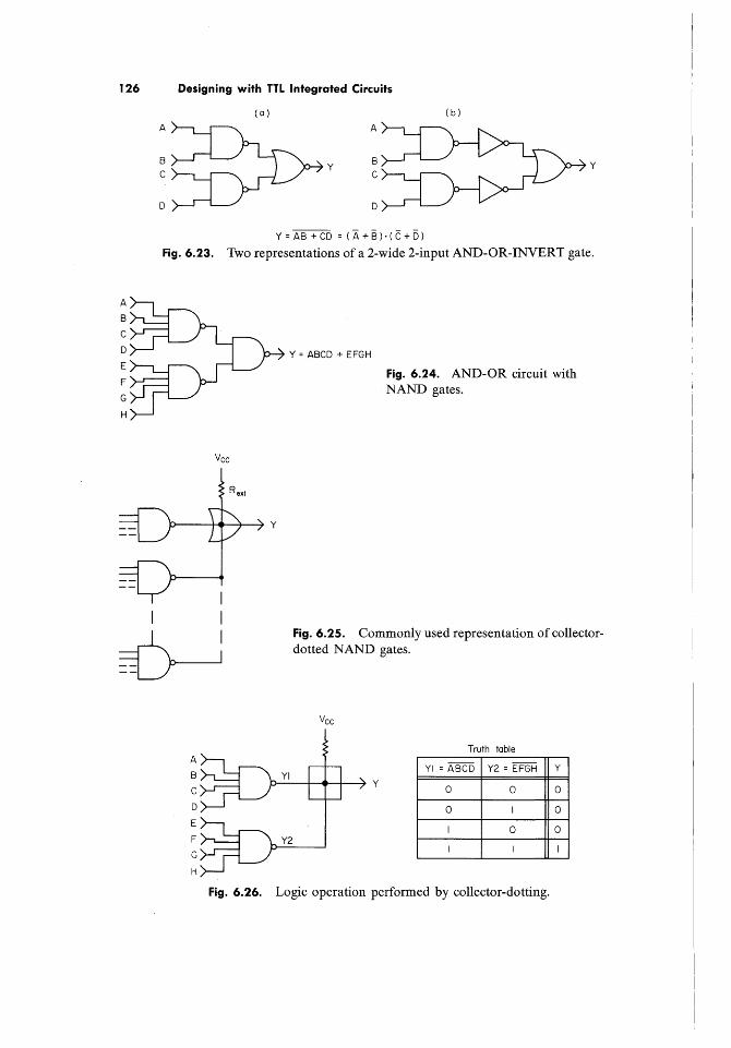
126 Designing with TTL Integrated Circuits
A
B
C
o
(a)
Y
A
B
C
o
Y = AB + CD = ( A + B ) . ( C + 5)
(b)
Y
Fig. 6.23. Two representations of a 2-wide 2-input AND-OR-INVERT gate.
Vee
D---I-*----4-~ Y
I I
V---J
Y = ABCD + EFGH
Fig. 6.24. AND-OR circuit with NAND gates.
Fig. 6.25. Commonly used representation of collectordotted NAND gates.
Vee
Truth table --
YI = ABCD Y2 = EFGH Y
D---+-4>---4-4 Y 0 0 0
0 I 0
I 0 0
I I I
Fig. 6.26. Logic operation performed by collector-dotting.

Combinational Logic Design 127
AND-OR Circuits. In the high-speed Series 54/74H, a 4-wide expandable AND-OR gate is available. The number of OR branches may be expanded with a maximum of six additional OR branches to a total of ten. As mentioned before, an AND-OR circuit may be obtained also by inverting the output signal of an AND-OR-INVERT gate. Application of the rules for analyzing and synthesizing combinational arrays of inverting gates to an AND-OR expression such as Y = ABeD + EFGH results in an AND-OR circuit, as is shown in Fig. 6.24. This circuit consists of a NAND gate in the first inversion level (OR function) and NAND gates in the second inversion level (AND functions).
Open-collector Gates. Several types of open-collector gates are available in Series 54/74. For a listing of open-collector gates refer to Chapter 3, Table 3.1. Open-collector gates must be used with external output pull-up resistors (collector resistors). This opens the possibility of connecting several open-collector outputs together in combination with a single pull-up resistor. Such a configuration performs a logic operation which is often referred to as wired-OR logic, dot-OR logic, or collector-dotting, and is symbolized as in Fig. 6.25. Although widely used, the terms "wired-OR" and "dot-OR," and the OR symbol at the output node of Fig. 6.25 are misleading.
Examination of the output signals of the various open-collector gates and the resulting output signal of the whole collector-dotted array reveals that the latter is a logical I if, and only if, the output signals of all collector-dotted gates are logical I s. The resulting output signal becomes a logical 0 as soon as one or more outputs become a logical O. This is shown in Fig. 6.26 for two collector-dotted 4-input NAND gates. The truth table of Fig. 6.26 is that of an AND function, and it shows that collector-dotting performs an AND operation on the output signals of collectordotted gates. The circuit of Fig. 6.26 may thus be represented by the circuits shown in Fig. 6.27.
The expression for the output signal derived from Fig. 6.27 b shows that collectordotted NAND gates perform an OR-AND operation on the complemented input variables. According to De Morgan's theorem, the expressions of Fig. 6.27 may
y
Y = ABCD • EFGH
A
B
C
D
E
F
G
H
y = (A + B + C + D) • (E + F + G + H)
(0) (b)
y
Fig. 6.27. (a) Functional representation of collector-dotted NAND gates; (b) circuit representation for applying the rules for analyzing combinational arrays of inverting gates.

128 Designing with TTL Integrated Circuits
Vee
be written as
or
Fig. 6.28. Correct representation of collector-dotting.
Y = ABCD + EFGH
Y = ABCD + EFGH
It is apparent from these expressions that collector-dotted NAND gates perform the same operation as AND-OR-INVERT gates; i.e., an inverted OR operation on the AND-ed input variable of the various NAND gates. This interpretation of the logic performance of collector-dotted gates is largely responsible for the misleading terms "wired-OR" and "dot-OR." Thus, the correct description of logic performed by collector-dotting is wire-AND logic and should be represented as in Fig. 6.28.
Exclusive-OR Circuits. An exclusive-OR function of two variables is characterized by the logic expression
- -Y = A EB B = (A + B)(A + B) = AB + AB
The logic symbol and the truth table for a 2-variable exclusive-OR circuit are shown in Fig. 6.29. The standard and low-power Series 54/74 include quadruple 2-input exclusive-OR gates SN54/7486 and SN54L/74L86. In special cases, where fewer than four circuits are necessary, and where the appropriate logic signals are already present, 2-input exclusive-OR circuits may be implemented as in Fig. 6.30.
According to the truth table of Fig. 6.29, a 2-input exclusive-OR circuit gives a logical I output signal whenever its input signals are unequal (A = 1, B = 0; or A = 0, B = 1). It should be noted that the same truth table applies when adding
A B
0 0
0 I
I 0
I I
Y
0
I
I
0 Fig. 6.29. Symbol and truth table for exclusive-OR circuit.

1/4 SN54/7402
A >---.....---\
B >--"--+--1
1;3 SN54H/u 4H II
(a)
1f4SN541740I or 1/4SN5417403
A
B
1/4 SN54/7401 or 1/4 SN54/7403
(cl
A
B
1/2 SN5417451
(e)
A
y
Combinational Logic Design 129
Vee 1/4 SN5417402
Rex!
; 1 DJJ>-y I y
(d)
SN5417400 1\
Y
y (f)
1/4SN5417400
Y = A(±) B = (A + B)( A + B) = AB + AB
Fig. 6.30. 2-input exclusive-OR circuits.
two binary digits (bits). A 2-input exclusive-OR circuit is therefore sometimes called a modulo-2 adder or a half-adder. The name half-adder refers to the fact that a possible carry-bit, resulting from an addition of two preceding bits, has not been taken into account. A full addition is performed by a second exclusive-OR circuit with the output signal of the first circuit and the carry as input signals, as shown in Fig. 6.31.

130 Designing with TTL Integrated Circuits
A
B
C>-------H y= A(f)B(f)C Fig.6.31. Cascading of two exclusive-OR
circuits.
The configuration of Fig. 6.31 is a cascading of two exclusive-OR circuits resulting in an exclusive-OR-ing of three variables A, B, and C. Consequently, the sum output of a full-adder for two bits is an exclusive-OR-ing of the two bits to be added and the carry of the preceding adding stage. The logic expression of an exclusive-OR-ing of three variables A, B, and C is
- -A 0:J B 0:J C = (AB + AB)C + (AB + AB)C
= (AB + AB)C + (AB + AB)C
= ABC + ABC + ABC + ABC
In general, an exclusive-OR-ing of n variables results in a logical I output if an odd number of the input variables are Is. An exclusive-OR-ing of n variables may be obtained by cascading 2-input exclusive-OR circuits. Two ways of cascading are possible, as shown in Fig. 6.32.
Both cascading methods require the same number of 2-input exclusive-OR circuits. With the method of Fig. 632b, however, the output signal is obtained much faster, in a maximum of three gate propagation delays. On the other hand, the
A
B
C >------+-1
0>--------+1
E >-----------~
F >---------------~
G r------------------~H
H >----------------------~
A
B
C
o
E
F
G
H
y
Fig. 6.32. Two ways of cascading 2-input exclusive-OR circuits.
y

Combinational Logic Design 131
A B y
0 0 I
0 I 0
Fig. 6.33. Truth table for a 2-input exclusive-NOR function. I 0 0
I I I
method of Fig. 6.32a requires a maximum of seven gate propagation delays. For exclusive-OR operations, the following rules can be derived:
AEBA=AoA+AoA=O - - -
AEBA=AoA+AoA=1 - -
AEBI =AoO+A 01 =A
AEBO=Aol+AoO=A
A EB A EB A EB ... EB A = 0 if total number of terms is even = A if total number of terms is odd
- - - -A EB A EB A ... EB A = 1 if total number of terms is even
= A if total number of terms is odd
A EB 1 EB 1 EB ... EB 1 = A if total number of terms is even = A if total number of terms is odd
AEBOEBOEB ... EBO =A
Exclusive-NOR (Comparator) Circuitso Another widely used logic function of two variables is characterized by the expression
Y = (A + B)(A + B) = AB + AB
A circuit performing this operation may be obtained by inverting the output signal of a 2-input exclusive-OR circuit. According to De Morgan's theorem,
- -A + B = AB + AB = (A + B)(A + B) = AB + AB
The truth table of this logic function is given in Fig. 6.33; it shows that a logical 1 output is obtained whenever the two input signals are equal (A = 1, B = 1; or A = 0, B = 0).
A circuit performing this operation is known under several names: exclusive-NOR, comparator, or coincidence circuit. Besides inverting the output signal of an exclusive-OR circuit, 2-input exclusive-NOR circuits may be implemented as in Fig. 6.34.
6.9 COMBINATIONAL LOGIC APPLICATIONS
Gray-to-binary Converter. The Gray code is a reflected digital code with the special property that two adjacent Gray code numbers differ by only 1 bit. For 4 bits, the binary code and the corresponding Gray code are shown in Fig. 6.35.
A combinational logic network is required that gives, for any Gray code number

132 Designing with TTL Integrated Circuits
1/4 SN5417400
A A
B B
Y
iJ4 SN5417402
(a)
Y4SN5417401 '14 SN5417403
Rex! A A
Y
B >---__t.......,
B >-------1
(c)
iJ4 SN5417400
1/4 SN5417400
(b)
(d)
y
y
:;>----~ Dtt:v : V
iJ4 SN5417400
(e)
1/4 SN5417400
A>--~----~
B~-~'----~
'---------,v /
SN54/7402
(f)
y ::~ _______ ~V
:~V 1/4 SN5417486
or 1/4SN54L17486
(h)
or iJ4 SN54L174L86
(i) y = A<±> B = AB + AS = (A + S)(A + B)
Fig. 6.34. 2-input exclusive-NOR circuits.

Combinational Logic Design 133
Gray Binary
G3 G2 G, Go B3 8 2 B, Bo
0 0 0 0 0 0 0 0 0 I 0 0 0 I 0 0 0 I 2 0 0 I I 0 0 I 0 3 0 0 I 0 0 0 I I 4 0 1 1 0 0 1 0 0 5 0 1 1 1 0 1 0 1
6 0 1 0 1 0 1 1 0 7 0 1 0 0 0 1 1 1
8 1 1 0 0 1 0 0 0 9 I 1 0 I I 0 0 1
10 I I I I 1 0 I 0 II I I I 0 I 0 I I 12 I 0 I 0 1 I 0 0 13 1 0 I 1 1 I 0 I 14 I 0 0 I I I I 0
Figure 6.35 15 I 0 0 0 1 1 I I
at its input, the corresponding binary number at its outputs. A convenient way to arrive at the logic expressions for Bo through B3, in terms of Go through G3, is to use the Karnaugh maps of Fig. 6.36. Converting a 4-bit Gray code into a 4-bit binary code results in the following logic expressions:
Bo = Go EB G1 EB G2 (f) G3
Bl = G1 EB G2 EB G3
B2 = G2 EB G2
B3 = G3
In general, Bn = G n EB G(n+1) EB G(n+2) EB G(n+3) EB ... , with the understanding that nonexistent bits are considered to be O. The result is that the most significant bit (MSB) in the Gray code and in the binary code are identical, and that the less significant bits are obtained by a cascading of exclusive-OR operations on the Gray code bits. A logic diagram of a Gray-to-binary converter for n bits is shown in Fig. 6.37.
Binary-to-Gray Converter. The same procedure as in the foregoing can be used for a binary-to-Gray converter, only now the conversion table (Fig. 6.35) is to be used from right to left, with the binary code as input and the Gray code as the output. Figure 6.38 shows corresponding Karnaugh maps. Converting a 4-bit binary code into a 4-bit Gray code results in the following logic expressions:
Go = Bo EB Bl
G1 = Bl EB B2
G2 = B2 EB B3
G3 = B3
In general, G n = Bn EB B(n+l) again, with the understanding that nonexistent bits

134 Designing with TTL Integrated Circuits
Karnaugh map for Bo
Bo = G2G3 (GOG I + GOGI ) + G2 G3 (GoG I + GOG I )
+ G2G3 (GOG I + Go GI ) + G2 G3 (GOG I + Go GI )
= (GOGI + Go GI) (G2G3 + G2 ( 3)+(G O GI + Go GI) (G 2 G3 + G2 G3 )
= (G O<±>GI)(G2 <±> G3 )+(GO <±>G I ) (G 2 <±>G 3 )
Bo = Go <±> GI <±> G2 <±> G3
Karnaugh map for BI
BI = GI G2G3 + GI G2G3 + GI G2 G3 + GI G2 G3
= GI (G2 G3 + G2 G3 ) + 81 (G 2 G3 +G2 G3 )
= GI (G2<±>G 3 ) + GI (G2 <±>G3 )
BI = GI <±> G2 <±> G3
Karnaugh map for B2
B2 = G2 83 + G2 G3
B2 = G2 <±> G3
Karnaugh map for B3
B3 = G3
Figure 6.36
GI Go
G2 00
00 0
01 I
II 0
10 I
GI Go
G2 00
00 0
01 (I
II 0
10 (I
G1 Go
G2 00
00 0
01 I
II 0
10 (I
G1 Go
G2 00
00 0
01 0
II I
10 I
01 II 10
I 0 I
0 I 0
I 0 I
0 I 0
Bo
01 II 10
0 (I I
I 0 0
0 (I I
I 0 0
01 II 10
0 0 0
I I I
0 0 0
I I I
01 II 10
0 0 0
0 0 0
I I I
I I I

Combinational Logic Design 135
}-------7 Bo
Fig. 6.37. Gray-to-binary converter for n bits.
are considered to be o. A logic diagram of a binary-to-Gray converter for n bits is shown in Fig. 6.39.
Combined Binary-to-Gray and Gray-to-binary Converter. The two converters previously discussed may be combined to obtain a controllable dual-purpose converter as shown in Fig. 6.40.
Excess-3-to-BCD Converter. The excess-3 code is a self-complementing binarycoded deCimal number system. Self-complementing means that the 1 's complement of a number can be obtained by inverting each bit of that number. The excess-3 code and the corresponding binary code are given in Fig. 6.41. It should be noted that in the excess-3 code, the six states shown in Fig. 6.42 are never used. Consequently, these six states may be called "don't care" states, and the corresponding cells in the Karnaugh maps (Fig. 6.43) may be made Is or Os at the designer's choice for the best minimization. Conversion of the excess-3 code into BCD requires the following logic expressions:
A =Eo
B = Eo EB E1
C = EoE2 + EoE1E2 + EoE1E 3
D = EoE1E3 + E2E3
An implementation of an excess-3-to-BCD converter is shown in Fig. 6.44. BCD-to-excess-3 Converter. For this conversion, Fig. 6.41 must be used from
right to left. Notice that in the BCD code, the six states in Fig. 6.45 are not used. Thus, these six states are "don't care" states and are handled (see Fig. 6.46) as in the preceding example. An implementation of a BCD-to-excess-3 converter is shown in Fig. 6.47.

136 Designing with TTL Integrated Circuits
Kornough mop for Go
Go Bo BI + BoBI
Go Bo (E) BI
Kornough mop for GI
GI BI B2 + BI B2
GI BI (E) B2
Kornough mop for G2
G2 B2 B3 + 82 B3
G2 B2 (E) B3
Kornough mop for G3
G3 = B3
B
BIBo
B2 00
00 0
01 0
II 0
10 0
BI Bo
B2 00
00 0
01 I
II I
10 0
BI Bo
8 2 00
00 0
01 (I
II 0
10 (I
BI Bo
3 B2 00
00 0
01 0
II I
10 I
01 II
/""I I 0
I 0
I 0
I 0 ~
01 II
0 I
I 0
I 0
0 I
01 II
0 0
I I
0 0
I I
01 II
0 0
0 0
I I
I I
10 /""I
I
I
I
I ~
10
I
0
0
I
10
0
I)
0
I
10
0
0
I
I
Figure 6.38

Combinational Logic Design 137
Fig. 6.39. Binary-to-Gray converter for n bits.
Xo ~--------------------------------------~
X2 ~--------+-~~------------------------~
MC
MC=O Binary-ta-Gray
MC=I Gray-to-Binary
I I I I I I
'.1."'.1." ,A, MCMC
"t,
Yo
Fig. 6.40. Controllable binary-to-Gray/Gray-to-binary converter.

138 Designing with TTL Integrated Circuits
Excess-3 BCD
E3 E2 EI Eo D C B
0 0 0 I I 0 0 0 I 0 I 0 0 0 0 0 2 0 I 0 I 0 0 I 3 0 I I 0 0 0 I 4 0 I I I 0 I 0 5 I 0 0 0 0 I 0 6 I 0 0 I 0 I I 7 I 0 I 0 0 I I 8 I 0 I I I 0 0 9 I I 0 0 I 0 0
E3 E2 EI Eo
0 0 0 0 0 0 0 I 0 0 I 0 I I 0 I I I I 0 I I I I Figure 6.42
E lEo
E2 00 01
OO ~ X Karnaugh map for A
A=Eo 01 I 0
II I X
10 I 0 ~
X = Don't care
EI Eo
E3 E2 00 01
00 Karnaugh map for C
C=EoE2+Eo EI E2 01 +Eo EI E3
I I
10
A
0 I 0 I 0 I 0 I 0 I
I I
0
0
X
0
A
I I
C
Fig. 6.41. Conversion table: excess-3-to-BCD.
EIEo 10 E2 00
r-X
I
X
I '--
10
Karnaugh map for B
B=EoEI + EoEI
B=Eo®EI
Karnaugh map for D
D=EoEI E3+ E2E3
Figure 6.43
00 X
01 0
I I 0
10 0
EI Eo
E2 00
00 X
01 0
I I (I
10 0
01 I I
X 0
I 0
X X
I 0 "-../
B
01 I I
X 0
0 0
X X
0 I "-../
D
10
~
I
X
I 1......-/
10
X
0
X
0

Combinational Logic Design 139
Eor---------~------------------~ A
B EI r--+------+-------------------~
c
D
E3r-----------------~
Fig. 6.44. Excess-3-to-BCD converter.
Decimal-to-BCD Converter. Decimal signals of nonelectronic systems are often available as 10 output lines. If a logical 1 is the active state of the line (see Fig. 6.48), the circuit of Fig. 6.49 may be used for the conversion to BCD. If the active state of a line is a logical 0 (see Fig. 6.50), the circuit of Fig. 6.51 may be used for the conversion.
Binary-to-BCD and BCD-to-binary Conversion. The converters described are of the asynchronous (nonc1ocked) type and consist solely of combinational logic gate arrays. The conversion technique used is based upon the methods described by J. F. Couleur and others.t
BINARY-TO-BCD CONVERTER. A binary number NB is usually expressed in the form
NB = b(n-i)' b(n-2)' ... , b i , b o
where n is the number of bits, and the b's are either 1 s or Os. The decimal
t See references 5, 6, and 7 of Bibliography at end of chapter.
D C B A
I 0 I 0 I 0 I I I I 0 0 I I 0 I I I I 0 I I I I
Figure 6.45

140 Designing with TTL Integrated Circuits
BA DC o 0
00 17
Karnaugh map for E
Eo =A 01 I
I I X
10 I 1-----'
X= Don't care
BA DC
Karnough map for E2
E 2 =AC+BC+ABC
00
01
I I
10
00
0
'I'
X '--'
0
01
0
0
X
0
1°1
II
0
X
II
I
I I
0
0
X
X
I II
II j 0
X
(X I I
10
"I
I
X
X '----
10
IJ
0
X
XI
BA DC
Karnaugh map for E I
EI=AB+AB
EI =A®B
D
Karnaugh map for E3
E3 =AC+ BC+ D
00
01
I I
10
BA C
00
01
I I
10
Figure 6.46
00
'i'
I
X
0
00
0
I
X
I
Ar---~~----------------------~ ":>0------4 Eo
B>-~~----------------~
C>-..-f-I-----------\
D>-----------------------------~
Fig. 6.47. BCD-to-excess-3 converter.
01 I I 10
0 'i' 0
0 I 0
X X X
0 X X
01 I I 10
0 0 0
/1 I I
,X X X
I X X

Line 9
0 0 0 0 0 0 0 0 0 I
Line 9
I I I
I I I I I I
0
Combinational Logic Design 141
Conversion table: 10 I ines to BCD, active Is
Line 8 Line 7 Line 6 Line 5 Line 4 Line 3 Line 2 Line I Line 0
0 0 0 0 0 0 0 0 I 0
0 0 0 0 0 0 0 I 0 I 0 0 0 0 0 0 I 0 0 2 0 0 0 0 0 I 0 0 0 3 0 0 0 0 I 0 0 0 0 4 0 0 0 I 0 0 0 0 0 5 0 0 I 0 0 0 0 0 0 6 0 I 0 0 0 0 0 0 0 7 I 0 0 0 0 0 0 0 0 8
0 0 0 0 0 0 0 0 0 9
Fig. 6.48. Conversion table: lO-lines to BCD, active Is.
A =1+3+5+7+9
B = 2+3+6+7
C=4+5+6+7
D =8+9
987654321
D C
0 0 0 0 0 0 0 0 0 I 0 I 0 I 0 I I 0 I 0
p--~A
B
c
"X>-----+D
Fig. 6.49. lO-line decimal-to-BCD converter, for active Is on input lines.
Conversion table: 10 I ines to BCD, active Os
Line 8 Line 7 Line 6 Line 5 Line 4 Line 3 Line 2 Line I Line 0 D C
I I I I I I I I 0 0 0 0 I I I I I I I 0 I I 0 0 I I I I I I 0 I I 2 0 0 I I I I I 0 I I I 3 0 0 I I I I 0 I I I I 4 0 I I I I 0 I I I I I 5 0 I
I I 0 I I I I I I 6 0 I
I 0 I I I I I I I 7 0 I 0 I I I I I I I I 8 I 0 I I I I I I I I I 9 I 0
Fig. 6.50. Conversion table: lO-lines to BCD, active Os.
B A
0 0 0 I I 0 I I 0 0 0 I I 0 I I 0 0
0 I
B A
0 0 0 I I 0 I I 0 0 0 I I 0 I I 0 0 0 I

142 Designing with TTL Integrated Circuits
987654321
A = 1+3+5+7+9
B =2+3+6+7
0=8+9 Fig. 6.51. lO-line decimal-to-BCD converter, for active Os on input lines.
value ND of NB is
ND = b(n-1) • 2(n-1) + b(n-2) • 2(n-2) + ... + b 1 • 21 + bo • 20
The expression for ND can be written in a form known as nested multiplication by 2. For example, the decimal value ND of a 5-bit binary number is normally written as
ND = b4 • s4 + b3 • 23 + b2 • 22 + b1 • 21 + bo
As a nested multiplication by 2, the expression for ND will be
ND = {[(b4 • 2 + b3) • 2 + b2] • 2 + b1 } • 2 + bo
The nested multiplication by 2 can be carried out by shifting the binary number NB , most significant bit (MSB) first b(n-1)' into a register at its least significant end. The nested multiplication is completed when the least significant bit (LSB) bo of NB is shifted into the least significant stage of the register (see Fig. 6.52).
MSB LSB MSB LSB
I 0 I 0 I 0 I 0 I b4 I-I b3 I b2 b l bo 0
No = b4
I 0 I 0 I 0 b4 b3 - b2 b l bo I 0 0 I No = b4 · 2 + b3
0 I 0 I b4 b3 b2 b l bo 0 I 0 I 0
I I I I + +
b4 b3 b2 I bl bo 0 I 0 I 0 I 0 0 I No = {[(b4 ' 2 + b3)· 2+b2]' 2+b l}'2+bo
Fig. 6.52. Nested multiplication by 2.

Combinational Logic Design 143
Most sign i ficant end Least signi ficant end --I-'---'---~--~----~--'---~--~--~'-~~~
14 x 100
__ L- _ '---_--'--_----I.J.--_--l..-_---I __ ...l.-_--L1 __ .....l-_---"-__ .L..-_--'
- - - - - ----v-------.--J/ ''--------..vr---------/ ''--------..vr--------.J/ Decade 2 Decode I Decode a
Fig. 6.53. BCD register value assignment.
Upon completion of the shifting in, NB is stored in the register in straight binary form. To convert NB into a BCD number, the value assignment of the register stages must be changed, and appropriate corrections must be made during the shifting. For this purpose, the register stages must be divided into groups of four consecutive stages, beginning with the least significant end of the register. Each group of four register stages represents a decade. Within a decade, starting at the least significant side of the decade, binary values are assigned to the four stages. The result is a value assignment as illustrated in Fig. 6.53, with the understanding that a decade cannot contain a number greater than 9. According to binary value assignment within a decade, each shift to the left in Fig. 6.53 represents a multiplication by 2. However, if a logical I passes the boundary between two decades-i.e., if a logical I is shifted from the 8-assigned stage of any decade to the I-assigned stage of the next higher decade-its value increases only from 8 to 10 (instead of increasing from 8 to 16). Apparently, a value of 6 is lost. This loss must be corrected after the shift has taken place by adding 6 to the value of those decades from which a logical 1 has been shifted to a higher decade. This correction can also be made before the shift. In that case, whenever a logical 1 is present in the 8-assigned stage of a decade before the shift, 3 must be added to the value of that decade prior to the shift. This will result in a value increase by 6 after the shift. Another correction must be made if a decade, after shifting, contains a number greater than 9. In such a case, a value of 10 must be subtracted from that decade, and a value of 1 added to the next higher decade. Correction for this situation can also be made before the shift has taken place. In that event if a decade contains a number (greater than 4) that after shifting will produce a number greater than 9 prior to shifting, 5 must be subtracted from the number in that decade, and provision must be made for adding a value of 1 to the number of the next higher decade after the shift. This provision can be made by entering a logical 1 into the 8-stage of the decade with a number greater than 4 prior to shifting. Consequently, the correction for a decade which contains a number greater than 4 before the shift consists of subtracting 5 and adding 8, resulting in the addition of 3.
Thus, it turns out that all necessary corrections will take place automatically if, prior to shifting, 3 is added to the values of those decades which contain a number greater than 4. The described conversion procedure is shown in Fig. 6.54 for a 6-bit binary number.
The binary-to-BCD conversion as described is often implemented with shift registers and adders. This serial synchronous approach makes a parallel-to-serial input conversion necessary. In many cases a nonc1ocked approach, consisting of

144 Designing with TTL Integrated Circuits
Binary number = I
101010101l01~lololl Shift
I 0 I I; Decimal vdue=59
o I
I 0 I 0 I 0 I 0 II 0 I 0 I 0 I I I I 0 I Shift
I 0 I 0 I 0 I 0 II 0 I 0 I 0 I I I I 0 I Shift
I 0
Add
o I 001 Shift
1010101111011101011 Shift
001 Add
I .0 0 I
Shift
1 0 II 10
1 I III 10
1 0 II I
[J Decode I Decade 0
Fig. 6.54. Example of binary-to-BCD conversion algorithm.
I 0 I I 0 0 I ci BI AI Do Co BoAo
Fig. 6.55. Nonclocked configuration for binary-to-BCD conversion.

Combinational Logic Design 145
identical logic gate arrays, offers such advantages as parallel inputs that eliminate parallel-to-serial conversion, higher conversion speeds, and simple expansion for a greater number of bits.
In nonclocked systems, shifting can be achieved with so-called hard-wiring between separate levels. For each shift operation, a separate level or logic gate array is used. A nonclocked configuration for the conversion example of Fig. 6.54 is shown in Fig. 6.55. The first determination as to whether the shifted-in binary number is greater than 4 takes place after 3 bits have been shifted in. Because of the parallel input capability, these first three shifts can be eliminated in a nonclocked configuration. Adders are not necessary if the logic gate arrays are implemented in such a way that for numbers greater than 4 at the input the corrected numbers (input numbers plus 3) appear at the output. It will be obvious that the shifted-in number to be corrected can never be greater than 9. Thus, the identical logic gate arrays for a nonc1ocked implementation follow the conversion table of Fig. 6.56. The input states equivalent to the numbers 10 to 15 inclusive are "don't care" states, and the corresponding cells in the Karnaugh maps (Fig. 6.57) may be made Is or Os at free choice.
Thus, the logic expressions for the basic cell of a nonclocked binary-to-BCD converter are
K = EGH + EFG + EH
L = EF+ EH+ FG
M= EH+ EFG
N= EG + FG + H
An implementation of the basic cell is shown in Fig. 6.58. The basic cells must be cascaded to convert binary numbers with more than 4
bits. How the basic cells must be connected can be derived from the binary-to-BCD conversion diagram of Fig. 6.59. Each 4-bit rectangle with a plus sign in it represents
Input Output
H G F E N M L K
0 0 0 0 0 0 0 0 0 I 0 0 0 I 0 0 0 I
2 0 0 I 0 0 0 I 0 3 0 0 I I 0 0 I I 4 0 I 0 0 0 I 0 0 5 0 I 0 I I 0 0 0 6 0 I I 0 I 0 0 I 7 0 I I I I 0 I 0 8 I 0 0 0 I 0 I I 9 I 0 0 I I I 0 0
Figure 6.56
10 I 0 I 0 II I 0 I I 12 I I 0 0 }Don., ~" 13 I I 0 I stales 14 I I I 0 15 I I I I

146 Designing with TTL Integrated Circuits
FE HG
Karnaugh map for K
K=EGH+EFG+EH
X = Don't care
00
01
II
10
00
0
0
r-----.. X
1 I-----'
FE
HG 00
00 0 Karnaugh map for M
M = EH+ EFG 01 1
1 1 X
10 0
N
01 1 1
(I 1
0 0
X X
0 X
K
01 1 1
0 0
0 0
X X
1 X
M
10
0
."........., 1
I,.-+-
~
~
10
0
0
X
X
Karnaugh map for L
L=EF+EH+ FG
Ka rnaugh map for N
N=EG+FG+J
Figure 6.57
L K
FE HG o 0 o 1
00 0 0
01 0 0
t--------. II X X
10 1 0 -I------'
FE HG o 0 01
00 0 0
01 0 1
1 1 X X
10 1 1
H G
M
Fig. 6.58. Basic cell for a nonc1ocked binary-to-BCD converter.
1 1 10,
r--.. IJ 1
1 0
r-X X
~ l4 L
1 1 1 0
0 0
1 I'
X X
X X
N
F E
E

0'" 0'" 0'" 0'" 0'" 0'" 0'" 0'" 0'" 0'" 0'" 0'" 0'" 0'" 0'" 0'" 0'" 0'" 0'" 0'" :J 5";--5'":::3 S":;:s~ ;--'5""5"5":J 5""5'"::J ;;-;--:;-
I I I I I I I I I I I 1 I I I I
=-~~~(J1~::'.~~ § ~§.~ §§3§§.9.
T '" .r 'I", ..... '" ,~ 'I", ,~ ,~ 'I", 'I", ,~ ,~ ,~ '''' ,~ '''' ,~ ,'"
n= 4
n=5
n=6
n=7
n=8
H G F +E .. N M L K
H G F +E .. N M L K
H G F +E • N M L K
H G F +E H G F +E • N M L K N M L K
H G F +E H G F +E • N M L K N M L K
+ + n=9 II
+ + + n=IO •
+ + + n= II •
+ + + n=12 •
+ + + + n=13 ..
+ + + + n=14 •
+ + + + n=15 ..
+ + + + + n=16 •
+ + + + + n = 17 - + + + + + n=18 - + + + + + + n=19
~ 'I n=20
- + + + + + +1 - A6 05 C5 85 A5 04 C4 84 A4 03 C3 83 A3 02 C2 82 A2 01 CI 81 AI DO CO BOIAO)
MSD LSD
Fig. 6.59. Binary-to-BCD conversion diagram.

148 Designing with TTL Integrated Circuits
LSB
Do Co BO AO '---v--/
Units
Fig. 6.60. n-bit nonclocked binary-to-BCD converter.

Combinational Logic Design 149
a conversion step as well as a basic cell. The input and output assignments of the basic cells are shown for several conversion steps; they are identical throughout the whole diagram. Unused inputs must be connected to a logical 0 (ground). A practical implementation with basic cells for conversions of up to 12 bits is shown in Fig. 6.60.
BCD-to-binary Converter. For BCD-to-binary conversion, the BCD number is shifted out of the least significant end of the BCD register (see Fig. 6.53). Shifting in this direction represents a division by 2 with every shift. However, if a logical 1 passes the boundary between two decades-i.e., if a logical 1 is shifted from the I-assigned stage of any decade to the 8-assigned stage of the next lower decade-its value reduces from 10 to 8 instead of from 10 to 5. Consequently, the resulting number is a value 3 higher than it should be. In such situations, a correction must be made after the shift by subtracting 3 from the value of those decades in which a logical 1 is shifted from higher decades. As a result, 3 must be subtracted from the values of those decades which after the shift contain a number equal to or greater than 8.
Notice that the correction is made once only: after the shift, because the new number obtained after correction (which is to be considered as the number before the next shift) may also be equal to or greater than 8. The new number, even though it may be equal to or greater than 8, is correct and must not be corrected again. The BCD-to-binary conversion procedure as described is shown in Fig. 6.61.
Like its binary-to-BCD counterpart, the BCD-to-binary converter is often imple-
Fig. 6.61. Example of BCDto-binary conversion.
BCD number = ~ ~ Decimal number=99
CO CO Decade I Decade 0
CJT01OJTII~ Shift
100 I
Subtract
o 0
Shift
10101110/1011101011 Shift
1010101 111010111010 Shift
00100 I
Subtract
I 000 I
I 000 I ~----~v~------~
Binary number

150 Designing with TTL Integrated Circuits
mented with shift registers and adders in a serial synchronous manner. The BCD-to-binary converter described here, however, is of the nonclocked type with parallel input consisting of identical logic gate arrays. Again, shifting is achieved with hard-wiring between separate levels. The implementation of the identical logic gate arrays is such that for numbers equal to or greater than 8 at the input, the corrected numbers (input numbers minus 3) appear at the output. The 4-bit input nhmber consists of the three most significant bits of a BCD decade and the least significant bit of the next higher BCD decade. Examination of the conversion procedure reveals that 5, 6, 7, 13, 14, and 15 never occur as input numbers so that the conversion follows Fig. 6.62. Consequently, the input states equivalent to the numbers 5 through 7 and 13 through 15 are "don't care" states, and thus the corresponding cells in the Karnaugh maps (Fig. 6.63) may be made Is or Os at free choice.
Thus, the basic cell of a nonc1ocked BCD-to-binary converter is determined by the logic expressions:
T=P~S - -
U = PQ + QS + PQS
v= RS + PQS + PRS
w= RS+ PQS
An implementation of this basic cell is shown in Fig. 6.64. The basic cells must be cascaded to convert BCD numbers into binary. The
deviation for the correction of the basic cells can be obtained from the BCD-to-binary conversion diagram of Fig. 6.65. Each 4-bit rectangle that contains a plus sign represents a conversion step as well as a basic cell. The input and output assignments of the basic cells are shown for several conversion steps and are identical throughout the whole diagram. Unused inputs must be connected to a logical 0 (ground). A practical implementation for conversion of up to two BCD decades, using basic cells, is shown in Fig. 6.66.
Input Output
S R Q P W V U T
0 0 0 0 0 0 0 0 0 I 0 0 0 I 0 0 0 I 2 0 0 I 0 0 0 I 0 3 0 0 I I 0 0 I I 4 0 I 0 0 0 I 0 0 5 0 I 0 I 6 0 I I 0 }oom <Xl" 7 0 I I I
states
8 I 0 0 0 010 I 9 I 0 0 I 0 I I 0 10 I 0 I 0 0 I I I II I 0 I I I 0 0 0 12 I I 0 0 I 0 0 I 13 I I 0 I 14 I I I 0 }oon'tco" 15 I I I I
states Figure 6.62

Kornaugh map for T
T = PS + PS = P ®S
Kornaugh map for U
U =PQ+ QS+ PQS
W
QP
SR
00
01
II
10
QP
SR
00
01
1 1
10
00
0
0
1---." 1
1 1---./
00
0
0
0
0
01 1 1
1 1
X X
X X
0 0
T
01 1 1
0 1
X X
? X
1 0
U
V
Combinational Logic Design 151
10
0
X
~
1 '--
10
/""" 1
X
X
~
QP SR
Karnaugh map for V
V = RS +PQS+ P'Rs
Karnaugh mop for W
W = RS + PQS
00
01
II
10
QP
00
01
II
10
Figure 6.63
S
U T
00
0
(I
0
~
00
0
0
(I
0
R
01 II 10
0 0 0
X X X)
? X X
0 0 ~ V
01 1 1 10
0 0 0
X X X
X X X
0 1 0 '--"
W
Q P
Fig. 6.64. Basic cell for a nonelocked BCD-to-binary converter.

01 I'.)
6 Decades I 5 Decades
4 Decades
3 Decades
2 Decades
MSD 8(n-l) C(n-I) 8(n-1)
S W
S R W V
LSD
A(n-Il D(n-2) C(n-2 8(n-2) A(n-2) D(n-3) C(n-3) 8(n-3) A(n-3) D(n-4) C(n-4) 8(n-4) A(n-4) D(n-5) C(n-5) 8(n-5 A(n-5) 0(n-6 C(n-6) 8(n-6) A(n-6)
S R Q ~ S R Q +p S R Q +p S R Q +p S R Q .f. w V U T W V U T W V U T W V U T W V U T R Q +p S R Q +p S R Q +p S R Q +p S R Q +p V U T W V U T W V U T W V U T W V U T Q +p S R Q +p + + + U T W V U T
+ + + + +
+ + + +
+ + + +
+ + + +
+ + +
+ + +
+ + +
+ + +
+ +
+ +
+ +
+
+
+
1 MS8 ! ! ! L S8
big b le bl? b l6 b l5 b l4 bl3 b l2 b ll b io bg be b? b 6 b 5 b 4 b 3 b 2 b l b o
Fig. 6.65. BCD-to-binary conversion diagram.
------- ---"- ~_~~- -;;;a. "~

Decade I Tens -~
CI BI AI
Decade 0 Units ~ DoCoBoAo
Combinational Logic Design 153
Decade I Tens
Decade 0 Decade I Decade 0 Units ~ DoCoBoAo
Units Tens --~ ~--~
BI AI Do CoBoAo AI
Decade I Tens ~
DI CI BIAI
Decade 0 Units ~ Do CoBo Ao
b7 b6 b5 b4 b3 b2 bl bo , V /
Binary number
Fig. 6.66. Cascading basic cells to convert up to two BCD decades into binary.

1 S4 Designing with TTL Integrated Circuits
Using four cascaded cells, two BCD decades can be converted into binary. It turns out that the configuration of four cascaded basic cells is repeatedly used when converting additional BCD decades. Consequently, the configuration of four cascaded basic cells, as shown in Fig. 6.67, may be considered as a standard building block. Cascading these building blocks for BCD-to-binary conversion is shown in Fig. 6.68 for up to five decades.
Binary Number Complementation. In digital arithmetic operations, a subtraction is performed by adding the complement of the subtrahend to the minuend. For this purpose, the l's complement as well as the 2's complement may be used. The characteristic of the 1 's complement is that, when added to the original number, an all-l number will result. Obviously, the l's complement of a number is its inverse. The 2's complement is characterized by the fact that, when added to the original number, the result is an all-O number with a 1 overflowing from the most significant bit place. Using the 2's complement in subtraction has two advantages: no corrections with an end-around-carry are necessary, and representation of the number 0 is unambiguous, because it always appears as an all-O number. In Fig. 6.70, the l's and 2's complements of 4-bit numbers are shown. As previously mentioned, the l's complement is the inverse of the original number. Thus, ai's complementer consists solely of inverters. For a 2's complementer, the Karnaugh maps of Fig. 6.69 can be derived from Fig. 6.70.
A 4-bit 2's complementer is thus characterized by the logic expressions
1'0 = Bo
~ = BotBBl
I; = (Bo + B 1) tB B2
13 = (Bo + Bl + B 2) tB B3
Fig. 6.67. Standard building block for BCD-to-binary converters.

O! O!
Decade 2 r:-:"--:-.
Decade I ~
(a)
Decade 3 ~
Decade 0 ~
Binary number
Decade 2 ~
( b)
(c)
LSB ,I • I •••••• I' ..• ,
v Binary number
" .. , ... ''; ...... /LSB
Binary number
Fig. 6.68. BCD-to-binary converters: (a) three decades; (b) four decades; (c) five decades.

156 Designing with TTL Integrated Circuits
Karnaugh map for To
To = Bo
Karnaugh map for T,
TI = Bo B, + Bo B 1 = Bo <±> B 1
Karnaugh map for T 2
T2 =Bo B2 + B, B2 + Bo BI B2
T2 = (Bo+B, )B2 +(Bo+ BI )B2
T2 =(Bo+B,) ® B2
Karnaugh map for T3
T3=B0 83 +B, 8 3 +B2 8 3 +80 8, 82 B3
T 3 =(Bo+B,+B2)83+(Bo+B, + B2 )B3
T3 =(Bo+ B,+ B2)<±)B3
B, Bo B2 00
00 0
01 0
1 1 0
10 0
B, Bo B2 00
00 0
01 0
1 1 0
10 0
B, Bo B2 00
00 0
01 (I
II 0
10 8 Figure 6.69
01 1 1 10
1 1 0
1 1 0
1 1 0
1 1 0
To
o 1 1 1 10
~ 0 'I'
1 0 1
1 0 1
1 0 1 '---"
01 1 1 10
1 1 1
1 1 1 ~
0 0 0
0 0 0

Combinational Logic Design 157
I's complement Dec Binary 2's complement -
C3 C2 C, Co B3 B2 B, Bo T3 T2 T, To r--
I 1 1 1 0 0 0 0 0 0 0 0 0 I I 1 0 I 0 0 0 I I I I I 1 1 0 I 2 0 0 1 0 I I 1 0 I I 0 0 3 0 0 I I I I 0 I I 0 I I 4 0 1 0 0 1 I 0 0 I 0 I 0 5 0 I 0 I I 0 I I I 0 0 I 6 0 I 1 0 1 0 1 0 1 0 0 0 7 0 I I I I 0 0 I
0 1 1 I 8 1 0 0 0 1 0 0 0 0 I I 0 9 I 0 0 I 0 I I I 0 1 0 1 10 1 0 1 0 0 I 1 0 0 1 0 0 II 1 0 1 1 0 1 0 1 0 0 1 1 12 I 1 0 0 0 I 0 0 0 0 I 0 13 1 1 0 1 0 0 1 I 0 0 0 1 14 1 1 1 0 0 0 1 0
Figure 6.70 0 0 0 0 15 I 1 1 1 0 0 0 1
In general, a 2's complementer is characterized by the logic expression
~ = (Bo + Bl + B2 + ... + B(n_l»)EBBn
with the understanding that To = 0 EB Bo = Bo. An implementation of a 2's complementer is shown in Fig. 6.71.
It is obvious that the circuit of Fig. 6.71 can be used to convert a binary number to its 2's complement, as well as to convert a 2's-complemented number to its original
Fig. 6.71. 2's complementer.
,..--------7 To
Bo )---+----+-\
B, )---t----1I--H T,

I------------------------~~
10 >--..-----------~
II
(0 )
In r---------~-+t X>-----?On
~bitin t Sign bit out )
~-------------------------~ I AL ~ B'CTD~ I 1 ~ _ Vee (b) I L _________________________ ~
I-Al------j-~B~J~------~-) --I L _________________________ J
r--Ay---------B-CO-------(d)--'
I cD 1 ~ T J MC~ I, co~rsion to 2', ","plement I
~ MC = 0, conversion to uncomplemented I Me) numbers I _________________________ ---1
Fig. 6.72. (a) and (b) conversion to 2's complement; (a) and (c) conversion to uncomplemented numbers; (a) and (d) controllable converter.
158

Combinational Logic Design 1 59
number. This is because the 2's complement of a 2's complement is the original number (see Fig. 6.70).
To distinguish uncomplemented (positive) numbers from complemented (negative) numbers, a sign-bit is added to the number on the most significant side. The sign-bit is a 0 for positive (uncomplemented) numbers and a 1 for negative (complemented) numbers.
For a subtraction, the subtrahend is entered into the arithmetic unit through a 2's complementer. There are situations, however, in which the subtrahend is available only in a 2's-complemented (negative) form which must not be complemented again. In those situations, the 2's complementer of Fig. 6.72a in conjunction with the control circuit of Fig. 6.72b can be used. This circuit will convert a number into its 2's complement only if its sign-bit is a O. Numbers with sign-bits equal to 1 will be carried through without conversion. The sign-bit of the number at the output is always made a 1 to indicate negative (complemented) numbers. If the 2's complementer of Fig. 6.72a is used with the control circuit of Fig. 6.72c, it converts only negative (complemented) numbers with sign-bits equal to 1 to positive (uncomplemented) numbers. Positive numbers at the input will be carried through without conversion. The sign-bit of the number at the output is made a 0 to indicate positive (uncomplemented) numbers.
The circuits of Fig. 6.72a and dwhen used together perform both conversion modes under control of input Me. If MC = 1, they perform the same operation as the circuits of Fig. 6.72a and b; the operation of the circuits of Fig. 6.72a and c is performed if MC = o.
BIBLIOGRAPHY
1. Humphrey, W. S., Jr.: "Switching Circuits: With Computer Applications," McGraw-Hill Book Company, New York, 1958.
2. Maley, G. A., and J. Earle: "The Logic Design of Transistor Digital Computers," Prentice-Hall, Inc., Englewood Cliffs, N.J., 1963.
3. McCluskey, E. J.: "Introduction to the Theory of Switching Circuits," McGraw-Hill Book Company, New York, 1965.
4. Wickes, W. E.: "Logic Design with Integrated Circuits," John Wiley & Sons, Inc., New York, 1968.
5. Couleur, J. F.: IRE Transactions on Electronic Computers, EC-7, No.4, 1958, p. 313. 6. Sklar and MacDonald: EDN, April, 1967, p. 54. 7. Benedek and Moskowitz: Electronic Design 21, Oct. 10, 1968, pp. 58-64.


7
Flip-flops
A device that exhibits two different stable states is extremely useful as a memory element in a binary system. Any electrical circuit that has this characteristic falls into the category of devices commonly known as flip-flops. Some other names are bistable multivibratorJ multiJ binarYJ and toggle. All imply the 2-state characteristic of the device.
In its most basic form, a flip-flop consists of two cross-coupled inverting amplifiers. This simply means that the output of one amplifier is connected to the input of the other and vice versa. Figure 7.la shows a circuit comprising two transistors and two resistors that demonstrates the cross-coupling idea. Obviously, if transistor QI is initially turned on (saturated) by applying a positive signal at its base, its collector will be at VaE(sat) (typically 0.2 to 0.4 V). The collector of QI is then tied to the base of Q2 (Fig. 7.lb), turning Q2 off (cutoff). The collector of Q2 tries to rise to Vae. This action only enhances the initial positive signal applied at the base of QI, and we can then remove the initial signal and the circuit will maintain QI in the on state and Q2 in the off state indefinitely.
A positive signal injected at the base of Q2 turns it on. Repeating the sequence, Q2 turns on (saturates) and QI turns off, resulting in a second stable state. In
Fig. 7.1. Comparison of crosscoupled flip-flops: (a) conventional; (b) as cascaded amplifier.
Vee
(0)
Vee
(b)
161

162 Designing with TTL Integrated Circuits
Output (Q) o----..-JVVIor-----.
Set (S)
Output r-'\1V\r--+---o (Q)
Reset Fig. 7.2. Practical circuit for a discrete I..----------O(R) flip-flop.
general, the flip-flop just described can be called a 2-stage positive-feedback saturating amplifier.
Although the circuit shown does have two stable states, it is evident that any signal output at either collector is very small. For example, when Ql saturates, its base can only rise to a ~E(sat) of 1.0 V. If an output is taken at the collector of Q2, the voltage swing is approximately 1.0 - VCE(sat) or 1.0 - 0.2 to 0.4 ;:::: 0.6 V. This is not really a usable signal level in most digital systems using saturated logic.
Figure 7.2 shows a more functional circuit which differs from the first mainly in the addition of two base resistors RB and two control inputs. For values of RB = lORe the circuit will operate like the one in Fig. 7.1a. However, the output signals Q and Q (Q = noninverted output, Q = inverted output) have a voltage swing approximately equal to VCe - VCE(sat). For Vee = 5.0 V the output swing is ;::::4.6 V. In actual practice this value is somewhat lower because of the resistor divider and load current being drawn, typically 3.8 to 4.2 V. It should be noted that for TTL flip-flops, the voltage swing for a VCe of 5 V is typically 3.5 V.
When a positive voltage or pulse is applied to the set input, output Q is forced to the highest positive voltage or logical 1 state. When a positive voltage or pulse is applied to the reset input, output Q is forced to its lowest voltage or logical 0 state. The terms 1 and 0 are used to define the high and low output levels, respectively.
This circuit falls into a category of flip-flops known as latches (the circuit will be defined in greater detail later). It is important to note, however, that some form oflatch is used in every flip-flop. The basic latch concept can be expanded to include such inputs as clocks, multiple data inputs, and variations in enabling or preset controls.
Flip-flops ranging from I-bit storage elements to multibit arrays are useful in arithmetic sections of computers because of their high-speed capabilities. Flip-flops are used in all types of shift and buffer registers, including serial right-and-Ieft-shift with parallel in and out capability, storage buffers for computer input-output systems, and alphanumeric indicator displays, and as accumulators in conjunction with adders to store and update data when clocked. Flip-flops are used also in all types of counter applications including upl down, presettable, gated, and any combination of these. Other uses include error detection and data conversion.

1I25N7400
R P+-...----OQ
5
Fig. 7.3. R-S NAND latch.
7. 1 FLI P-FLOP TYPES
Flip-flops 163
Truth table
R S Q Q
0 0 1* 1*
0 1 I 0
1 0 0 I
1 I No change
* Not allowed, see text
The four basic types of flip-flops are the D, T, R-S, and J-K. The R-S latch will be considered separately because it has one characteristic which is different from the other four.
The Basic Flip-flop. Historically, the R-S latch was probably the first type of flip-flop built and used for data storage because it is considerably simpler than any of the others. The circuit in Fig. 7.2 is an R-S latch using discrete components. If the transistors and resistors of Fig. 7.2 are replaced with two dual-input NAND gates (one-half SN7400), the circuit of Fig. 7.3 results. It has two control inputs and two outputs. The R (reset) and S (set) (also called clear and preset respectively) are termed asynchronous controls since the output changes immediately when either control input changes. For the gates shown, the Os and Is in the truth table represent 0.2 V and 3.3 V typically for positive logic notation.
From the truth table it is evident that four definite states exist for the R-S latch. - -Since Q is defined as the inverse of Q, however, the R = S = 0, Q = Q = 1 state is not allowed. It should be noted that when an R-S latch is built as shown in Fig. 7.3, the assignment of inputs and outputs is purely arbitrary. This is not generally the case in the other types of flip-flops discussed later.
Figure 7.4 shows an R-S latch implemented with NOR gates (one-half SN7402) in place of NAND gates. From the truth table it is seen that for S = 0, R = 1, and S = 1, R = 0, the outputs are identical to the NAND latch of Fig. 7.3. The differences are purely a result of the differe.Q.ces in the NAND and NOR gate functions. Here again, the R = S = ,1, Q = Q = ° state is not allowed.
As stated earlier, the latch is limited to one mode of operation, asynchronous.
1I25N7402
R 0----1---\ JO+-_--<:>Q
50---;--7
Fig. 7.4. R-S NOR latch.
Truth table
R S Q Q
0 0 No change 0 1 1 1 0 0
1 1 0*
*Not allowed, see text
0 1
0*

164 Designing with TTL Integrated Circuits
But it is often desirable to have some form of clock input to the flip-flop, so that the device may be operated simultaneously (synchronously) with all others in a system. It is this requirement which led to the development of the other types of flip-flops.
Synchronous Clocking. Since flip-flops described later have synchronous and clock inputs, a short discussion of these inputs is injected here. In general, the different types of synchronous (also referred to as "data") inputs determine the name of the flip-flop, while the different mechanisms for clocking can be used with any flip-flop type. A synchronous data input is one which does not cause an immediate change in the output. It requires the presence or occurrence of another input, the clock pulse, to generate the change of state. This action makes the device useful in a system application since one clock can be used to control a large number of flip-flops, causing them to change states synchronously and predictably. In TTL flip-flops there is only a single clock input, but the data inputs range from one to about ten, depending on the device and operation desired. The single clock input can be one of three general types: d-c or edge-triggered, a-c coupled, or master-slave.
The d-c or edge-triggered clock is one which causes flip-flop operation at a particular voltage when either a positive or a negative transition occurs. Either one or the other is recognized, but not both, for any chosen device. This type of clock enables the data inputs and transfers the data to the outputs simultaneously, resulting in a high-speed clocking technique that is relatively independent of clock rise and fall times. However, in TTL devices noise immunity decreases as the rise and fall times increase beyond 150 ns.
A-c coupled clocks are not used in any TI TTL device, but they are used extensively in DTL devices. An a-c coupled clock responds to a transition time rather than a voltage, since the clock is capacitively coupled internally to the latching mechanism in the flip-flop. These clocks can be either positive or negative in operation since they respond to one transition or the other. This technique is highly dependent on clock rise or fall times. Typically, values less than 200 ns are required for the device to operate. At values greater than this, operation is either intermittent or impossible.
The master-slave type is basically two latches connected serially. The first latch is called the master and the second is termed the slave. Normal action in clocking consists of four steps as shown in Fig. 7.5. Although the four points are shown as definite points on the waveform, the exact d-c points can be quite wide in tolerance and are not usually specified. The important feature of this type of clocking is that the data inputs are never directly connected to the outputs at any time during clocking; this provides total isolation of outputs from data inputs.
f ---- ~ ----1. Isolate slave from master 2. Enable data inputs to master 3. Disable data inputs 4. Transfer data from master to slave Fig. 7.S. Master-slave clock pulse.

Flip-flops 165
FFn FFn+l FFn+2 {---- Q Q J Q
Data lines ____
K Q K Q K Q
CIOCk{l ----2----
Fig. 7.6. Shift register (using J-K flip-flops).
The phenomenon called clock skew should be mentioned. Consider, for example, a shift register in which the outputs of one flip-flop are directly connected to the inputs of the following flip-flop, as shown in Fig. 7.6. The two clock lines are generated at the same point, but owing to loading conditions, two separate drivers are required. Figure 7.7 shows the clock generator and drivers. The waveforms suggest a possible condition that could exist if the drivers were not of equal delay. The term tpHL is the propagation delay of the gates from the logical 1 to the logical o state, and D..tphl represents the difference between the two gate delays plus capacitive delays due to wire routing and lengths. The shift register uses negative edgetriggered J-K flip-flops whose worst-case minimum propagation time is 10 ns. If the D..tphl time in Fig. 7.7 is greater than 10 ns, the nth flip-flop in Fig. 7.6 could change states before the (n + l)st flip-flop is ever clocked, resulting in possibly erroneous data being shifted into the (n + 1 )st flip-flop. The maximum allowable clock skew in this system is IOns.
In general, the maximum allowable clock skew for a flip-flop can be expressed as
~kew(max) = Tpd(FF) - ~(FF)
where Tpd(FF) is the worst-case minimum propagation delay of the flip-flop, and ~(FF) is the worst-case maximum hold time of the flip-flop. The hold time is defined as the length of time the data inputs must be held stable after the clock pulse has dropped below a given point (usually the 50 percent point, or about 1.5-V level for TTL) to ensure proper operation of the flip-flop. For TTL flip-flops (with only a few exceptions) the hold time will be O.
Fig. 7.7. Clock waveforms and generator.
Clock
gen
CIOCkgen~ I
----Clock 1
----Clock2
,--------Clock 1--+-: """'\~'-______ --Ir- -----
---+I j+-tphl(l}
! ! \ I i --.I I.- Mphl I I
Clock 2
---+I ~tphl(2)

166 Designing with TTL Integrated Circuits
Data input Th = hold time Fig. 7.8. Waveform illustrating setup and
Ts = setup time hold times.
Associated with hold time, setup time is defined as the length of time the data inputs must be stable before clocking the flip-flop. This time is measured from the 50 percent point on the clock pulse edge which activates the outputs. Figure 7.8 shows how setup and hold times are measured with respect to the clock pulse.
D-type Flip-flop. The D-type flip-flop is characterized by a single data (D) input and a clock input. It may have either or both Q and Q outputs available. It can have asynchronous inputs as shown in Fig. 7.9. Although both the preset and clear inputs are shown, they mayor may not be present on some D-type flip-flops. Usually the preset and clear are overriding controls; that is, when either of these inputs is present (in this case logical 0), the operation of the device is inhibited and the output goes to either a 0 or l, depending on which input is present. The operation of the flip-flop is shown by the truth table of Fig. 7.9; the state of the D input is shown prior to clocking, and the state of the Q output is shown just after clocking.
D-type flip-flops can use anyone of the three types of clocking techniques mentioned earlier, but a special case of edge-triggering is sometimes used with this type of flip-flop, in which case it is called a D-type latch. The clocking in this case is still done on an edge, but .while the clock is high, the E input is directly coupled to the output Q. During this time any changes at the D input are immediately reflected at the Q output. When the clock falls, the Q output holds the state of the D input prior to the clock edge until the clock goes high again. The clock actually operates as an enable input to a latch. This kind of flip-flop is useful primarily in data storage and register applications, where temporary data storage is required.
T-type Flip-flop. The T-type flip-flop also has only a single data (T) input and a clock input. It may ~so have asynchronous controls, clear, preset or both, and one or both of Q and Q outputs, as shown in Fig. 7.10. Again, anyone of
D
Clock
Preset
Clear
Q
Truth table
tn tn< 1
D Q
a a 1 1
Fig. 7.9. D flip-flop.

Fig. 7.10. T flip-flop.
T
Clock
Preset
Clear
Flip-flops 167
Truth table
Q tn t n+ 1
T Q
a Qn
1 an
the three clocking techniques can be used. The truth table shows that the operation of the flip-flop is quite simple. When the T input is in the ° state prior to a clock pulse, the Q output will not change with clocking. When the T input is at a 1 level prior to clocking, the Q output will be in the Qn state after clocking. In other words, if the T input is a logical 1 and the device is clocked, the output will change state regardless of what the output was prior to clocking. This is called toggling; hence the name T flip-flop.
The T flip-flop is not generally available as such but is usually generated from one of the other types, as is shown later. It is most often seen in counters and sequential counting networks because of its inherent divide-by-2 capability. When a clock pulse is applied, the output changes state once every input cycle, thus completing one cycle for every two input cycles. This is the action required in many cases for binary-coded counters.
R-S Flip-flop. The R-S or S-R type of flip-flop has either set or reset asynchronous input, or both, and a Q and Q output. Figure 7.11 shows an R-S flip-flop and its truth table. Notice that the first three states of this flip-flop are identical to the first three states of the R-S latch Q output in Fig. 7.4. The only difference is the clock input to the flip-flop. For R = S = 0, the Q output remains the same after clocking, a logical 1. For R = 1, S = 0, the Q output after clocking is a logical 0.
Note that when the Q output is in the logical ° state and the S data input is at a ° level, it does not matter whether the R input is a ° or 1. The Q output at Qn+l will always be a logical 0. Similarly, if Qn is a logical 1 and the R input is a 0, regardless of the state of the S input the output Qn+l is a logical 1. These conditions are significant when designing circuits since they reduce the amount of gating required in counting and decoding applications.
Fig. 7.11. R-S flip-flop.
R
Clock
S
Preset
Q
Clear
Truth table
R S Q
a a Qn
0 1 1
1 a ° 1 1 •
if Indeterminate
Clear=O,Q=O Preset = 0, Q= 1

168 Designing with TTL Integrated Circuits
Preset
Truth table
tn tn+1 J Q J K Q
Clock a a Qn
K Q a 1 a 1 a 1 1 1 an
Clear
Excitation table Qn Qn+1 J K
a a a x a 1 1 X 1 a x 1 1 1 X a
x = Don't care Fig. 7.12. J-K flip-flop.
The only factor that limits the use of the R-S flip-flop in actual applications is the indeterminate condition of the output when R = S = 1. Since the output is not predictable, it is necessary to avoid this input condition when clocking. When it cannot be avoided, a J-K flip-flop is used.
J-K Flip-flop. The J-K flip-flop has two data inputs, J and K, and only a single clock input. Many J-K types have internal gates on the inputs to provide multiple J and K inputs, thereby eliminating the need for external gates in many applications. Figure 7.12 shows a J-K flip-flop _with two asynchronous control inputs (preset and clear) and two outputs (Q and Q). The truth table shows that all four possible states of the input generate defined output states. The truth table is identical to the R -S type (J = S, K = R) with one exception; the fourth condition is J = K = 1. When this input condition exists and the flip-flop is clocked, the output changes state. This is the same as the T type when the T input is at a logical!. The flip-flop simply toggles. Figure 7.12 also presents an excitation table. This table is basically generated by an intuitive analysis of the truth table. If the state of the output Qn prior to clocking is known and it is desired to have an output Qn+l after clocking, the table shows which data input is necessary. The term shown in the table as X represents a "don't care" state. For example, when Qn is a logical 0 and it is desired to have a 0 after clocking (Qn+l = 0), it is necessary that J = 0 before clocking. The state of K does not matter. As noted for the R-S flip-flop, these "don't care" (X) states are valuable in logic design. They allow the designer to use fewer gates at the data inputs to control the gate operation while maintaining defined outputs for all input conditions. The J-K flip-flop is considered the most versatile available, and the variety of devices on the market reflects the trend toward its use.
Figure 7.13 shows a typical J-K master-slave flip-flop in a gate-type representation. This model makes it quite easy to see how the excitation table is generated. The Q output is directly gated with the K input, while the Q output is gated with the J input. The gates are NAND functions, and if any input is a logical 0, the output is a logical 1. Assume initially Q = 0 and Q = 1. Output Q is gated

Flip-flops 169
with K and the clock at ZI. When the clock rises to a logical 1, Q holds the output of gate Zl at a 1 level regardless of the state of the K input. A similar condition exists at Z4. However, when the clock rises to a logical 1 level (clear must be a 1 for flip-flop operation), Q is a logical 1. The flip-flop output at Qn+l i~determined only by the J input. The same analysis can be used for Q = 1 and Q = 0. The state of the K input determines the output.
The J-K may have any of the three general types of clocking. The master-slave J-K has one rather unique characteristic: the setup time for the J and K inputs is always greater than or equal to the clock pulse width. Therefore, the J and K inputs must be held stable until the clock falls. If this condition is not fulfilled, the flip-flop operation may be erroneous. _
Again using Fig. 7.l3 and assuming Qn = 1, Qn = 0, examine what happens if the K input changes from a logical ° to logical 1 ~nd back to a logical ° while the clock is at logical 1 (the J input is inhibited since Q = 0). When K = 0, the output of gate ZI is 1 and does not change the state of the master latch, Z2 and Z3. If K momentarily rises to a 1 level, the output of Zl goes to a logical 0, changing the state of the master. When K returns to a logical ° level, Zl's output returns to logical 1; however, the master latch effectively "remembers" the 1 condition at the K input. When the clock falls to the ° level, the q output changes states: Qn+l = 0, Qn+l = 1. _
When Qn = ° and Qn = 1, the J input controls the output. If the J input rises to a logical 1, while the clock is at logical 1, the master section will "remember" this state. After the clock returns to a ° level, the outputs change to Qn+l = 1 and Qn+l = 0. The excitation table can be used to give a general statement for J-K master-slave operation when the J and K inputs change with the clock high. If Qn = ° and J rises to a logical 1, Qn+ 1 will be 1. If Qn = 1 and K rises to a logical 1, Qn+l will be 0. It is this characteristic that causes the setup time for J-K masterslave flip-flops to be greater than or equal to the clock pulse width.
In recent years the J-K has increased in popularity owing to its wide flexibility and the decreasing price differential between it and other types of flip-flops.
Qo---~ Z7 I------~ o--+---oQ
t--------.-+---oClear
KO------l
Clock
Fig. 7.13. Typical J-K master-slave flip-flop circuit.

170 Designing with TTL Integrated Circuits
D QI---l---<1Q I----<D Q Q T
Clock CL Clock CL
Q,t---4--<:JQ
(0) Toggle only (b) With a T data input
Fig. 7.14. Converting D to T flip-flop: (a) toggle only; (b) with a T data input.
It is often desirable to interchange flip-flop types with little or no additional gating. Most types are interchangeable to some extent, as a comparison of truth tables suggests. Figure 7.14a shows the generation of the T type by simply connect-ing the Q output to the D input. This configuration is equivalent only to the T type with the T input at a logical 1. Figure 7.14b shows a D-to-T equivalent functionally identical to the T type.
Figure 7.15 shows the R-S in J-K, D~ and both T configurations. The J-K is implemented by gating the outputs back to the inputs, using two input AND gates. The D is made by using an inverter on the R input and connecting it to the S input. Of the two types of T conversions shown, one is equivalent to the T with the input always at a 1 level, and the other shows the complete T function using two AND gates.
The J-K type can be used to implement both D- and T-type functions quite easily. The D is accomplished by using an inverter between the J and K inputs as shown in Fig. 7.16. A D type is also shown which makes use of a K* input available on some J-K types. The K* input is merely the inverse of the K input or K. The T type is formed by tying the J and K inputs together; it is not actually manufactured as a flip-flop but is implemented from one of the other types. The D~ R-S~ and J-K types are all manufactured in some configuration similar to those described.
R Q Q
CIO~: In: K
Clock CL
Q
(b) R-S to D ( 0) R-S to J-K
1---4I_-oQ
T
Clock
'----_s-----oo
( c) R-S to T (toggle only) (d) R-StoTwithTdoto input
Fig. 7.15. R-S to J-K, D, and T flip-flops.

Flip-flops 171
(a) J- K to D (b) Alternate J-K to D
DO ~cJL Q_ Q_ Clocka ~
K Q Q
CIOC~: L[J:: K Q Q
K*=K
(c) J-Kto T
TO E[]:J Q_ Q_ ClockO -
K Q Q
Fig. 7.16. J-K to D and T flip-flops.
7.2 SERIES 54/74 FLIP-FLOPS
The flip-flops discussed in this section are considered functionally identical in terms of internal circuit operation. Differences in asynchronous inputs and preset and clear, which will be pointed out within each group, are not to be considered as part of the synchronous function. The flip-flops indicated include all TTL devices, standard, high-speed (H), and low-power (L), and are listed in numerical order in each subgroup. Unless otherwise noted, the following statements are true for all flip-flops listed.
1. For preset and clear inputs: PRESET CLEAR Q Q
preset = 0, Q = I 0 0 I I clear = 0, Q = 0 0 I I 0
I 0 0 I I I No change
These inputs will also be considered asynchronous, and independent of the clock. While they are present, all other operations are inhibited.
2. All flip-flops are d-c coupled. 3. Standard and H series includ~clamping diode on clock inputs. 4. For all flip-flops both Q and Q outputs are available. 5. Setup and hold times are measured from the clock triggering edge as men
tioned earlier. 6. All devices are available in 14-pin or 16-pin flat or dual-in-line packages. 7. All devices are available in ceramic or plastic packages.
J-K Positive Edge-triggered. The SN54/7470 have both preset and clear. Preset and clear functions should occur only while the clock is low, to prevent erroneous operation. This device has three each of the J and K inputs including a J* and K* (inverted J and K). The SN54/7470 are primarily useful in medium- to high-speed systems where gating is required on J and K inputs. This device does not have a clock clamping diode.
J-K Negative Edge-triggered. Presently all negative edge-triggered J-K's are in the H series and operate at clock rates of 50 MHz (typical). Operation is guaranteed for 40 MHz as long as minimum setup times are observed.

172 Designing with TTL Integrated Circuits
SN54/74HIOI have J and K inputs consisting of2-wide 3-input AND-OR gates. One input of each gate is connected to form the clock input. A single asynchronous input is available, preset. The SN54/74HIOI are very useful in applications such as up/down counters and right-left shift registers when AND-OR gating is required for J and K inputs.
SN54/74HI02 are the same as HIOI except that J and K inputs are 4-input AND gates with two inputs tied together for the clock. Both preset and clear inputs are available. The SN54/74HI02 are useful in synchronous counters to eliminate the need for external gates.
SN54/74HI03 consist of two flip-flops in a single package with only one J and one K input for each. Separate clear and clock inputs are provided for each flip-flop. The SN54/74HI03 are ideal for shift register applications.
SN54/74HI06 are identical to the HI03 with two exceptions: the SN54/74HI06 are available in a 16-pin dual-in-line package only, and they have both preset and clear inputs for each flip-flop.
SN54/74HI08 are the same as the HI03 except that a common clock and a common clear input are used for both flip-flops. Separate preset inputs are available.
J-K Master-slave. These flip-flops operate from a complete clock pulse, and the outputs change on the negative transition. A positive clock pulse is used. As mentioned before, for error-free operation data on the J and K inputs should be stable while the clock is high.
SN54/74,H71 are the master-slave equivalents of the HIOI with AND-OR J and K inputs and a preset input.
SN54/7472, SN54/74H72, and SN54/74L72 have three each of the J and K AND gated inputs and both preset and clear inputs. As noted, they are available in all three series with identical pin configurations. These are the master-slave equivalents of the HI02.
SN54/7473, SN54/74H73, and SN54/74L73 are master-slave equivalents of the HI03. They are dual flip-flops with single J and K inputs and separate clock and clear inputs.
SN54/7476 and SN54/74H76 are master-slave equivalents of the HI06. They are dual J-K's with separate clock, preset, and clear inputs.
SN54/74H78 and SN54/74L78 are master-slave equivalents of the HI08, dual flip-flops with common clock and clear inputs and separate preset inputs.
SN54/74I04 have four J and K AND inputs and separate preset and clear inputs. One J input is tied to one K input to give a gate-type input (J -K). If this J-K input is a logical 0, flip-flop operation is inhibited. Since the clock input is buffered with an inverter, it is necessary to maintain the data inputs stable while the clock is low for this device. Capacitive delay is provided on the J and K inputs to increase the allowable clock skew. Maximum allowable delay at 25 0 C is about 20 ns, and the maximum clock frequency is about 30 MHz.
SN54/74I05 are similar to the SN54/74I04 described above with two exceptions: one each of the three remaining J and K inputs is inverted, and delaying capacitors are not included. As a result the SN54/74I05 will toggle slightly faster than the SN54/74 104.
SN54/74 107 are functionally identical to the SN54/7473, but the pin configuration is different. The SN54/74I07 are available only in the dual-in-line package.

Flip-flops 173
R-S Master-slave. SN54/74L71 are similar to the L72. The only difference is R-S rather than J-K operation. This is advantageous in some applications where data inputs cannot be held stable while the clock is high. The devices operate correctly if minimum setup times are observed.
D Positive Edge-triggered. SN54/7474 and SN54/74H74 are dual flip-flops with single D inputs and separate preset and clear inputs. The devices are useful in buffer and storage registers, shift registers, and counters where little additional gating is required on the inputs.
D Latch. SN54/7475 have a single D input and a common clock for two flip-flops with four latches per package. The 54/7475 are primarily used in data storage a pplica tions.
SN54/74100 are functionally the same as the SN54/7475 except that the 54/74100 have eight latches with two clock inputs. Four latches have common clock inputs.
J-K Master-slave with Data Lockout. SN54/74110 have three J and K AND inputs with both preset and clear inputs. These flip-flops have data lockout capability which eliminates the need to hold the data inputs stable while the clock is high. It is only necessary to observe the setup and hold times with respect to the rising edge of the clock pulse to store the data present in the master section. After the rising edge of the clock pulse, the data inputs may change without affecting the outputs. The data thus stored in the master are transferred to the slave on the trailing edge of the clock. These flip-flops make the amount of allowable clock skew directly proportional to the width of the clock pulse. Therefore, the pulse width may be increased as desired to meet system requirements.
SN54/74111 are flip-flops with a clocking mechanism identical to the SN54/110. However, only single J and K inputs with separate clock, clear, and preset inputs are provided. The SN54/74111 are available in a 16-pin dual-in-lim~ package only.
7.3 FLIP-FLOP APPLICATIONS
This section includes a variety of flip-flop circuits, primarily intended to demonstrate the extremely broad field of flip-flop application. Probably the most prominent use of flip-flops is in counter circuits, which are discussed in Chapter 10. Probably the next most familiar circuits using flip-flops are shift and storage registers. Figure 7.17 shows serial shift registers implemented with the J-K, R-S, and D-type flip-flops. In general these registers will have common clear and individual preset lines.
Figure 7.18 presents a 40-MHz serial shift register with asynchronous parallel-load capability. The register is implemented with SN74HI06 flip-flops. The asynchronous parallel load is accomplished by using two SN74HOO gates per flip-flop. They are connected in such a way that a logical 1 on the load input enables the parallel inputs. When the load input returns to the logical 0, synchronous operation is resumed with the preset data loaded in. While the load input is at a logical 1, the serial operation is totally inhibited.
One other general type of shift register is the left-right shift. Figure 7.19 demonstrates a circuit of this type utilizing D-type flip-flops (SN7474s or H74s). The same function can be obtained by using either R-S or J-K types, but one additional inverter is needed at each flip-flop input to make D-type flip-flops from them.

174 Designing with TTL Integrated Circuits
1 st stage 2d stage 3d stage nth stage
---IfT-J Q Data out
CI
--- -K Q
Clock 0------4_-------+----------4_-----
Data in 0--..... ----1 J Q 1------\ J Q I------IJ Q
CI CI CI
K Q 1----4--l K Q t-----t-----i K Q
1st
Data in 0--*"--+--1 S
(a) J-K shift register (edge triggered or moster- slave)
3d ~h
R Q -, ,- R \ /
CI 'y CI 1\
S Q _..J '- S
Clocko----~~------------~-----------~~----------
(b) R-S shift register
1st 2d 3d nth
to to [[[--J-8 (c) 0 shift register
Fig. 7.17. Flip-flops used as shift registers.
Load = 1 for parallel load via asynchronous inputs
Package count 2 SN74HOO 1/6 SN74H04 2 SN74H106
Serial input CI 0--+-----1 J ear A 1-----.,1-----\
Clear Clear B 1---1-----\ J C I----II------i
Clock
Clear
Data out
o I-----\-{)
K Preset A I--+--+--I---l K Preset B I--+--+---Ir---i K Preset C 1--+---+-+-1 K Preset 5
Clock
Load
\ Ain v
Parallel data inputs
Fig. 7.18. 40-MHz shift register with asynchronous parallel load.

Flip-flops 175
Mode Flip- flops are SN7474 or SN74H74 If H74s are used also use SN74H51 AND-OR-INVERT gates
1/2SN7451
Data in 0---1--+-1
Clack 0--------------------__ --------_--Fig. 7.19. Left-right shift register.
A wide variety of serial decode, comparison, and timing functions can be accomplished by using flip-flops. A serial comparator is shown in Fig. 7.20. The operation of the circuit is as follows: Initially a clear pulse is given, which sets both Q outputs to logical O. All possible X and Y inputs prior to clocking the three outputs X> Y, X < y, X = Yare defined in the truth table after a compare pulse is applied. (Note: SN74105s are positive edge-triggered.) If two words A and B are serially applied to the comparator 2 bits at a time, the X = Y output will be at a logical 1 until 2 bits of words A and B ate unequal. At that time, depending on which one is greater, either the X> Y or X < Youtput will be a logical 1. Both Q outputs are connected back to opposite J* inputs, generating a latching effect when either X > Y or X < Y is logical 1; the outputs will remain in that state until another clear pulse is applied.
Clear
~ X J Clear yre
j* -
K Clock
I
LJ* CI~Q' Y J X J
-r- K Clock
Compare ,... I
Q
Q
~
Flip-flops SN74105
X Y X>Y
000 o 1 0
o 1 o
X<Y
o 1 o o
X>Y
X=Y
X<Y
X=Y
o o
Fig. 7.20. Serial magnitude comparator with truth table.

176 Designing with TTL Integrated Circuits
Asynchronous input 0---.......----1 J Qt------o
Clock 0----+---0 Clock
1/2SN74H103
K Ot------o
Clock
Input -----'
Q output --------I Timing for J-K master-slave flip-flop, SN7473
Clock
Input __ ----Ir-IL-__ --InL-__ ..... n"'----_ .....
Q output ____ ---'111....-___ ---' Timing for J-K negative edge triggered flip flop, SN74H103
Fig. 7.21. Synchronizer for asynchronous input.
Many operations involve synchronizing data with respect to a system clock. Figure 7.21 demonstrates how this can be accomplished with both J-K edge-triggered and master-slave flip-flops. The difference is the fact that the master-slave will synchronize input data of any width greater than about 20 ns, which is present while the clock is high, but the edge-triggered type will synchronize data narrower than the clock pulse only if it is present for the setup time at the clock edge that activates the flip-flop.
Another circuit that synchronizes data and generates only a single output pulse always of the same width is shown in Fig. 7.22. In general the data-in must be at least as wide as the clock pulse or it is not recognized (unless it occurs at the clock trailing edge). Again this circuit can be implemented with J-K master-slave flip-flops, the only difference in operation being that the master-slave will recognize data of any width greater than about 20 ns that occur while the clock is high.
A synchronized clock-burst generator is shown in Fig. 7.23. Its Q output is a train of pulses sustained as long as the asynchronous input is at a logical 1. The Q output is positive-going pulses whose width is equal to the time the clock pulse is at logical o leveL As in the other circuits using J-K master-slave flip-flops, this circuit recognizes any positive data regardless of width (>20 ns) while the clock is at a logical!. This feature of the master-slave device makes this circuit useful as aI's detector

Flip-flops 177
Output
Asynchronous inputs ,
J Or--- r-t- J aU Clock / Clock ~- f-<: Clock
r-K '-K Q~ Clear Clear y y
I Clock
Input ----.J"lL....-____ ---'
Output---....I ~ ________ ~r----l~ ________________ __
Timing for J-K negative edge triggered flip-flop
Clock
Input .-J"IL....-_____ ....,j Ui'-;--__ _
Output ~ L Timing for J-K master-slave flip-flop
Fig. 7.22. Synchronized uniform-pulse-width "single-pulse" generator.
Asynchronous input
Clock
Input ..J Edge 0
Trigger Q
Master- 0 slave
Clock
">--------l J
)--....... ---q Clock
K
o f-----..--~ o output
01-----+--- Q output
Fig. 7.23. Synchronized clock-burst generator.

178 Designing with TTL Integrated Circuits
Clock or strobe U u U Input
______ ~n~ ___________________ ~~ ______ _
Q output _____________ ---In'--__________________ ~ Fig. 7.24. Timing for circuit of Fig. 7.23 as l's detector.
or an error detector. The timing diagrams in Fig. 7.24 show the operation of the same circuit with a master-slave unit and with the clock operating as a strobe input. The operation is such that if a logical I level is ever present at the asynchronous input while the clock (or strobe) is high, the output will rise to a logical I during the clock (or strobe) 0 interval.
In many MaS systems a two-phase clock system is required. Figure 7.25 shows how the clock pulse is generated and translated to Mas voltage levels. The outputs will drive 400-pF loads with rise and fall times typically less than 40 ns. For high-threshold MaS it will be necessary to bias the transistors at - JIG and use a resistor divider or a zener to provide the level translation at the bases of the transistors.
A variety of one-shots can be generated by using flip-flops in the configuration of Fig. 7.26. As indicated, for an even number of gate delays the Q output is connected through the gates to the clear input. These circuits, when implemented
+V
200.0, 1/2SN7402 r-----j I I I JO-+-'\J'V\r---;
~~_--+------oPhose I out
Clock 0--_-0
..,e-......,...._---o Phose 2 out
Clock
Q
+V
Gnd---Phose 1 + V ___ ....,
Phose 2 Gnd ------
Fig. 7.25. MOS 2-phase clock generator.

Flip-flops 179
Clock
Output pulse width (typical) = Tpd F -F t Tpd gate (2n +]); n = 0,1,2 ...
Clock
..LlL Input A
J..ll Input B
Output conditions fA> fB:Output = logical 1 fA < fB:Output = logical 0
For SN7476 and n = 2 PW = 16 ns t 10 (5) ns PW~ 66ns
(0) For odd number of gate delays
Q ....... -+--0 Output
PW = T pd(ff) t T pd(gate) (2n); n = 0,1,2 ...
For SN7476 and n = 1 PW = 16 ns + 10 (2) ns PW~ 36 ns
(b) For even number of gate delays
Fig. 7.26. Flip-flop one-shots.
Q
1/2 SN74Hl03
Clock
K Q
fA = fS: 1) Output alternates between logical levels 2) Phose difference determined by duty cycle of output
Input A _IL--_....I...-_ ........ _
Input C _....1...-_ ........ _--1._
OutPut~
Example: fA = fB Input B lags input A by 1200
Fig. 7.27. Digital frequency-phase comparator using Series SN54/74HlOO flip-flops.

180 Designing with TTL Integrated Circuits
with H series flip-flops, are capable of generating pulses as narrow as 12 ns typical with SN74H73. In practical applications the maximum pulse width should be about 250 ns, using low-power devices with six inverter delays.
Figure 7.27 shows a frequency-phase detector. The output indicates frequency differences, as well as phase difference when the frequencies are equal. The output can be measured with respect to either the A or B input. In using this circuit, one ambiguous condition arises. When A and Bare 180 0 out of phase, the output will be a 50 percent duty cycle; when A and B are exactly in phase, the output will be a 50 percent duty cycle, but at half the frequency of the 180 0 condition. This condition is ambiguous only in the sense that if the output is to be integrated, the 0 0 and 180 0 conditions will generate identical results.
1.1
I i I
I

8
Decoders
Many systems require the decoding of information represented by digitalmachine-language words. Decoding is necessary in such applications as data multiplexing, rate multiplying, digital display, digital-to-analog converters, and memory addressing. It is accomplished by matrix systems that can be constructed from such devices as magnetic cores, diodes, resistors, transistors, and FETs. The most common decoding requirements can now be satisfied with off-the-shelf integrated circuits.
8.1 DECODER THEORY
A single binary word N digits in length can represent 2N different elements of information. For example, the subset represented by a 2-bit binary word contains four such elements, each element representing one of the binary states (00, 01, 11, 10) of the word. In Fig. 8.1 each binary state is assigned to one of four letters (w, x, 1: Z). These letters correspond to the four outputs of a decoder with two inputs A and B. Karnaugh maps are then drawn for each state assignment. The map for W shows that output W is logical 1 for input bits A and B both equal to logicalO. The Boolean expression for output W is W = AB. This same reasoning is repeated for the decoding of outputs X, Y, and Z. The equations are implemented by using 2-input NAND gates in Fig. 8.2.
Figure 8.3 shows the reference matrix for decoding a binary word of 3 bits. For simple decoding it is usually not necessary to draw control matrices for each state as was done in Fig. 8.1. Q is true, logical 1, for only A = B = C = O. Since only
Q is assigned to this state, Q = ABC can be directly written by inspection of the reference matrix. A 3-bit binary decoder whose control equations are given in Fig. 8.3 is implemented in Fig. 8.4.
Many machine languages do not use the binary number system to its full capacity. For example, the common BCD (binary-coded decimal) code uses only 10 of the possible 16 states of a 4-bit word. For this reason, a variety of codes can be generated for binary representation of decimal numbers. Figure 8.5 shows some of the common codes. Different codes have been generated to facilitate addition
181

182 Designing with TTL Integrated Circuits
A
B
0
1
A B
0
1
A
B 0 1
0 W X
1 Y Z
Reference matrix 2-bit decoder
Control matrix state W
0 1
8 0
0 0
W=A
Control matrix state Y
0 1
0 0
8 0
A
B
0
1
A B
0
1
Control matrix state X
0 1
0 8 0 0
X = A . B
Control matrix state Z
0 1
0 0
0 8 Y = A . B Z = A . B Fig. 8.1. Control matrices for 2-bit decoder.
0-<7 00 01 11 10
A 0 Q R T S
B 1 U V X W
Q A B C R A B C s A B C T A B C u A § C
V A B C
W A B C
X A B C
Fig. 8.2. 2-line-to-4-line decoder. Fig. 8.3. Reference matrix for 3-bit decoder.

Decoders 1 83
A ----<.---1
B------I
C--..------I
o
Fig. 8.4. 3-line-to-8-line decoder.
Binary 8-4-2-1 2-4-2-1 Excess-3 Excess-3 Gray number or BCD
0000 a a 0001 1 1
0010 2 2 a 0011 3 3 a 0100 4 4 1 4
0101 5 2 3
0110 6 3
0111 7 4 2
1000 8 5
1001 9 6
1010 7 9
1011 5 8
1100 6 9 5
1101 7 6
1110 8 8
Fig.8.S. 4-bit binary codes for 1111 9 7
decimal representation.

184 Designing with TTL Integrated Circuits
Decimal Unweighted digit 5-1-1-1 8-6-4-2-1
a 00000 00000 00000
1 00001 00001 10000
2 00011 00010 11000
3 00111 00011 11100
4 01111 00100 11110
5 10000 00101 11111
6 11000 01000 01111
7 11100 01001 00111
8 11110 10000 00011 9 11111 10001 00001 Fig. 8.6. More-than -4-bi t coder
for decimal representation.
and subtraction, or complementing, or decoding to decimal equivalent, or error detection and correction.
The first two codes shown in Fig. 8.5 (8-4-2-1 or BCD, and 2-4-2-1) are called weighted codes. In a weighted code, direct mathematical conversion can be made from the binary word to its decimal equivalent. For example:
Code weights = 8-4-2-1 Binary word = 1 0 0 1 (least significant bit, or LSB, rightmost) Decimal equivalent = (8 - 1) + (4 - 0) + (2 - 0) + (1 -I) = 9
The excess-3 code shown in Fig. 8.5 is a biased weighted code. Conversion from an excess-3 code to its decimal equivalent can be done in the following manner:
Reference matrix
-<1 C' 00 01 11 10
00 a 1 3 2
01 4 5 7 6
11 X X X X
10 8 9 X X
Control equations
0 A B C B 1 A B C B 2 A B C B 3 A B C B 4 A B C [5
5 A B C D
6 A B C B 7 A B C B 8 A B C D Fig. 8.7. BCD-to-decimal decoder with false-data rejection 9 A § C D (matrix and equations).

Decoders 185
Code weights = 8-4-2-1 Binary word = 1 1 0 0 (least significant bit, or LSB, rightmost) Decimal equivalent = (8 ·1) + (4 . 1) + (2 . 0) + (1 • 0) - 3 = 9
For determining equivalent decimal representation of unweighted codes-for example, excess-3 Gray-some type of reference matrix showing state assignments must be known.
Any number of binary bits greater than 4 can also be used to represent decimal numbers. Some different codes are shown in Fig. 8.6. Note that the unweighted code shown is the counting sequence of a twisted-ring Johnson counter.
Figure 8.7 gives the reference matrix and derived Boolean equations for a BCDto-decimal decoder. These equations are implemented in Fig. 8.8. States 1010,
A ..r"'L
1 B .~
r c -"
1 D
1 ~ T
~
~ 3
~ 5
I
~ I
7
~ §
~-
Fig. 8.8. BCD-to-decimal decoder with false-data rejection (logic diagram).
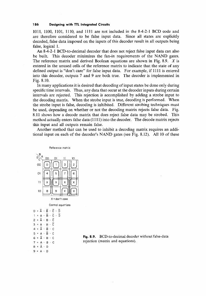
186 Designing with TTL Integrated Circuits
101l~ 1100~ 1101, 1110~ and 1111 are not included in the 8-4-2-1 BCD code and are therefore considered to be false input data. Since all states are explicitly decoded, false data imposed on the inputs of this decoder result in all outputs being false, logical I.
An 8-4-2-1 BCD-to-decimal decoder that does not reject false input data can also be built. This decoder minimizes the fan-in requirements of the NAND gates. The reference matrix and derived Boolean equations are shown in Fig. 8.9. X is entered in the unused cells of the reference matrix to indicate that the state of any defined output is "don't care" for false input data. For example, if IIII is entered into this decoder, outputs 7 and 9 are both true. The decoder is implemented in Fig. 8.10.
In many applications it is desired that decoding of input states be done only during specific time intervals. Thus, any data that occur at the decoder inputs during certain intervals are rejected. This rejection is accomplished by adding a strobe input to the decoding matrix. When the strobe input is true, decoding is performed. When the strobe input is false, decoding is inhibited. Different strobing techniques must be used, depending on whether or not the decoding matrix rejects false data. Fig. 8.11 shows how a decode matrix that does reject false data may be strobed. This method actually enters false data (1111) into the decoder. The decode matrix rejects this input and all outputs remain false.
Another method that can be used to inhibit a decoding matrix requires an additional input on each of the decoder's NAND gates (see Fig. 8.12). All 10 of these
Reference matrix
S D A 00 01 11 10
C'r----''--=-,---:--'--.,----:--'---,.--,-:....:=__,..,
00 G 8 l:J L:J 01 7
11 X
10 8
X = don't care
Control equations
0=A-Ei-c-6 - - -
l=A-S-C-D
2=A-S-C
3=A-S-C
4=A-S-C
5=A-S-C
6=A-S-C
7=A-S-C
8 = A - D
9 = A - D
6
Fig. 8.9. BCD-to-decimal decoder without false-data rejection (matrix and equations)_

Decoders 187
A
B
c
D
T
§
Fig. 8.10. BCD-to-decimal decoder without false-data rejection (logic diagram).
Fig. 8.11. Strobe circuit for BCD-to-decimal decoder with false-data rejection. Strobe
To decoder

188 Designing with TTL Integrated Circuits
A
B
c
D
T
Strobe input -----'
Fig. 8.12. BCD-to-decimal decoder with strobe input.
extra inputs are tied together. When these inputs are at logical 0, all decoder outputs are false. When strobe inputs are at logical 1, the decode matrix is enabled. This method of strobing works whether or not the decoder rejects false data.
Another method of strobing a decoding matrix uses latches as shown in Fig. 8.13. An advantage of this method is that decoded outputs are continuously available. Hence, if these decoded outputs are used to drive display devices, the display outputs do not blink. This strobing method also functions whether or not the decoder rejects false data. The outputs change state only while the strobe input is changing from ° to 1.

Decoders 189
A A
8
To decoder C delete inverters
C in decoder
Fig. 8.13. Strobe circuit for BCD-to-decimal decoder without false-data rejection.
D
Strobe
D
5
D-type flip-flops
The twisted-ring Johnson counter uses five binary bits for its BCD count. A logic diagram, reference matrix, and decoder for this type of counter are shown in Fig. 8.14. This decoder does not reject false data. If a decoder with false-data rejection were built, five input NAND gates would be required, thus changing IC package count from 2%, to 9.
Another special type of 8-4-2-1 BCD decoder which is commonly seen drives 7 -segment display tubes. Since these displays require low voltage and current, allowing them to be driven directly from integrated circuitry, they are becoming widely popular. Figure 8.15 shows the segment layout of a typical display tube, and a matrix that shows how elements are controlled to generate digits. Note that tube elements are initially considered to be on. To produce specific digits, various display elements are turned off. This type of control requires fewer logic operations than if all tube elements were initially assumed to be off and were turned on to generate digits. Figure 8.l6 shows the Karnaugh maps for control of each tube element. For this example it is assumed that the designed decoder need not reject false data, and therefore X ("don't care") is entered in the unused binary states. The derived control equations are implemented in Fig. 8.17.
8.2 SERIES 54/74 DECODERS AND DECODER/DRIVERS
Decoders in various configurations are available in Series 54/74 logic. A summary of these devices appears in Table 8.1. All these devices are of course basically decoders, but the additional terms used in the device descriptions require explanation here.
In the open-collector group, the word driver often appears in the description. This term implies that the output stage has special properties that make it useful in driving not only the usual logic gate input but other devices as well. Devices that can be driven include lamps, special displays, relays, and discrete transistors.

190 Designing with TTL Integrated Circuits
Decimal
o 1
2
3
4
5
6
7
8
9
A
0
o o o o
State table
Counter 8
0
0
1
o o o
C
0
0
0
1
o o
O=A E
1 = A B
2= B C
3=C [5
4=D E
5=A E
6=A 8
7=8 C
8=C D
9= i5 E
Outputs D
0
0
0
0
1
o
E
0
0
0
0
0
C' ~~-<l 000 ()
00 0
01 X
11 8
10 9
EEDDCCBBAA
Karnaugh mop for decoding logic
001 011 010 110 111 101 100
1 2 X X 3 X X
X X X X 4 X X
X X X 6 5 X 7
X X X X X X X
X = don't core
Fig. 8.14. Decoding of twisted-ring Johnson counter states, without false-data rejection.

o
2
3
4
5
6
7
8
Decoders 191
a
d
Segment control
b d e
r---r-~~~--~ __ ~~~--~
r---~~---4~~~~~~~-~
r---~~--~ __ ~~~---+--~ Fig. S.lS. 7-segment display drive requirements.9
'-------'--------'-----""-------""'''----------''''-__ -----'-__ ---1
~ = segment off
Another term that appears is demultiplexer. This means that additional gate inputs have been provided for data or strobe input or both.
A point sometimes overlooked with the open-collector drivers is that the maximum rated voltage of the output transistors is with supply voltage Vec (nominal, of 5 V) applied to the device.
The breakdown voltage will drop considerably if Vcc is not applied. The reason for this is that with the output transistor in the off state and with Vec applied, there is a saturated transistor across the base-emitter of the output transistor. This gives the effect of Ji(BR)CER-collector-to-emitter breakdown voltage with a relatively low resistance from base to emitter. With no Vec applied, the effect is that of V(BR)CEO
breakdown for an open circuit from base to emitter, which is always considerably lower than Ji(BR)CER' The requirement this characteristic imposes on system design is that Vec should be applied before the high voltage on the output transistors is applied. If it is practical to reduce the high voltage while Vac is off, then a safe value would be about one-half the normal value. The breakdown due to high voltage on the output transistors and Vac off can result in permanent damage to the device.
Another situation occasionally overlooked in a system design is that voltage transients may be present on the voltage supply to the load that the driver output transistors are switching.

192 Designing with TTL Integrated Circuits
Segment a Segment b
SA SA D C 00 01 11 10 DC 00 01 11 10
00 1 GJ 1 1 00 1 1 1 1
1- r- ,-- --01 0 1 1 0 01 1 0 1 0
11 X X X X 11 X X X X 1- '---- '---' '---'
10 1 1 X X 10 1 1 X X
a=Ao§oC o5+AoC b=Ao§oC+AoSoC
Segment d
SA DC 00 OJ 11 10
00 1 GJ 1 1
,---., ,---..
01 0 1 0 1
11 X X X X '--" '---'
10 1 iol X X
d=Ao§oC+Ao SoC+Ao§ oC
Segment f
SA DC 00 01 11 10
00 1 I [ 0 0 o J
01 1 1 0 1
11 X X X X
10 1 1 L X 1 f=A o 5 o c+S o A+SoC
X = don't core
SA D C
00
01
11
10
00 If 01
11
10
Segment c
SA DC 00 01 11
00 1 1 1
01 1 1 1
11 X X X
10 1 1 X
c=AoSoC
Segment e
00 01 11 10
1 0 0 1
0 0 0 1
X X X X
1 0 X X
Segment g
00 01 11 10
0 ol 1 1
----..,
1 1 0 1
X X X X '-
1 1 X X
Fig. 8.16. Segment control matrices; I = segment ono
10
~ 1
X
!xl

Fig. 8.17. BCD-to-7-segment decoder without false-data rejection.
DCCBBAA
Decoders 193
D--~O
O---d
n--+-e
D--~f
b--~g
It is quite common, for example, to have a 28-V line that is used for a number of control-type functions in a system. Such supplies are sometimes not well regulated, because the usual loads (relays, lamps, etc.) do not need a regulated supply. Unfortunately, the voltage transients that often result in systems such as this can destroy the driver output transistors unless there is enough series resistance to limit the current to a safe value.
BCD-to-decimal Decoder/Driver for Cold-cathode Tubes. The SN54/74141 (Fig. 8.18) is an 8-4-2-1 BCD-to-decimal decoder designed specifically to drive cold-cathode indicator tubes such as the Burroughs Nixie® or Raytheon Datavue® display tubes. This decoder minimizes switching transients and thereby maintains

~ Table 8.1. Summary of 54/74 Decoders and Decoder/Drivers
Open-collector outputs
Type Description Typical power Packages Zero-blank 10H (pA) max VOH' VOL (volts) max 10M
dissipation, m W available provisions at VOH V at 10L rnA
SN54/7445 BCD-to-decimal decoder/driver 215 J, N N/A 250 30 0.9 80 SN54/7446 BCD-to-7-segment decoder/driver 265 J, N Yes 250 30 0.4 20 SN54/7447 BCD-to-7-segment decoder/driver 265 J, N Yes 250 15 0.4 20 SN54/7448 BCD-to-7 -segment decoder/driver 265 J, N Yes * ... 0.4 6.4 SN54/7449 BCD-to-7 -segment decoder/driver 165 S Yes 250 5.5 0.4 10 SN54/74141 BCD-to-decimal decoder/driver (cold-cathode tubes) 55 J, N Yes 50 55 2.5 7 SN54/74145 BCD-to-decimal decoder/driver 215 J, N N/A 250 15 0.9 80 SN54/74 1 56 Dual 2-line-to-4-line decoder/demultiplexer 125 J, N N/A 250 5.5 0.4 16
Standard totem-pole outputs
Type Description Typical power Packages
dissipation, m W available
SN54/7442 BCD-to-decimal decoder 140 J, N SN54/7443 Excess-3-to-decimal decoder 140 J, N SN54/7444 Excess-3-Gray-to-decimal decoder 140 J, N SN54/74154 4-line-to-16-1ine decoder/demultiplexer 170 N SN54/74 1 55 Dual 2-line-to-4-line decoder/demultiplexer 125 J, N
* DTL-type output: 2-kQ pull-up resistor.

Decoders 195
AO-------------l '--__ --0 0
Bo----.------~~
'--.......... --u 4
~--I--{) 5
c
6
7
8
DO--~--------4
9
Fig. 8.18. BCD-to-decimal decoder/driver, SN54/74141.
a stable display. Full decoding is provided for all possible input states. For inputs of 10 through 15, all the outputs are off. With this feature and some additional external circuitry, the invalid codes can be used to obtain blanking of leading zeros or trailing zeros.
Figure 8.19 shows a two-decade display using a suggested method for blanking leading zeros. Any BCD input above decimal 9 may be used for blanking.

196 Designing with TTL Integrated Circuits
Indicator tube
VSS=170 V
Reset 15 K.Q
Strobe o---+---------+-~
VSS=170 V
15 K
SN7475 SN74i4i
1 SN7490
Clock input
Fig. 8.19. Typical application for SN54/74141 using zero-blanking feature (zero-to-99 counter and display).
When the most significant digit (MSD) is zero, it is blanked, and when both the MSD and least significant digit (LSD) are both zero, both digits are blanked. It may be desirable not to blank the zero LSD, because in such a case the whole display is blanked when the number is all zeros. To avoid blanking the zero LSD, the connection from the output of the SN7420 to the input of the SN7404 is broken, and the gating below this point is eliminated-the SN7404, SN74H21, and SN7400.
The output clamping zener diodes (Fig. 8.18) have a guaranteed minimum zener voltage of 60 V. This means that a swing of from 0 to 60 V may occur on the cathodes of the display tube in the blanking mode. A typical cold-cathode display tube is guaranteed to "fire" with 170 V across the tube, and a lower safe value of positive cathode voltage for negligible glow with JiBB = 170 V is about 50 V. Considering the operating specifications for display tube and driver, the biasing values shown in Fig. 8.19 for the display tube are suggested typical values.
Other BCD-to-decimal Decoder/Drivers. SN54/7442, SN54/7445, and SN54/74145 are 8-4-2-1 BCD-to-decimal decoders consisting of eight inverters and ten 4-input NAND gates (see Fig. 8.20). The inverters are connected in pairs to make BCD input data available for decoding by the NAND gates and to present

Decoders 197
only one standard 54/74 TTL load at each input. Full decoding of input logic assures that all outputs remain off for any false input conditions.
SN54/7442 has a standard TTL output configuration with fan-out capability of 10. SN54/7445 and SN54/74l45 have open-collector outputs instead; each output is a high-performance n-p-n transistor designed for use as an indicator/relay driver or as an open-collector logic-circuit driver. Each of the high-breakdown output transistors (SN54/7445: VCE of 30 V; SN54/74l45: VCE of 15 V) will sink up to 80 rnA.
Other 4-line-to-10-line Decoders. SN54/7443 and SN54/7444 are 4-lineto-IO-line decoders quite similar to SN54/7442 except for the input code. SN54/7443 accepts the excess-3 BCD code shown in Fig. 8.21. Full decoding of input logic assures that all outputs remain off for any false input conditions.
BCD-to-7-segment Decoder/Drivers. Figures 8.22 and 8.23 show a family of BCD-to-7-segment decoder/drivers: SN54/7446, SN54/7447, SN54/7448, and SN54/7449. All these devices have the same decoding circuitry. The SN54/7446 and SN54/7447 have open-collector output transistors, capable of20 rnA each, which drive lamp segments directly by sinking current to ground. (They differ only in the breakdown ratings of the output transistors.) The other two circuits lack the direct-drive output transistors, being intended for driving lamp segments by sup-
Logic diagram Truth table
Output 0 Decimal Inputs outputs
Input A Output I D C B A o 1 2 3 4 5 6 7 8 9
0 0 0 0 0 I I I I I I 1 I I
Output 2 0 0 0 1 1 0 1 I 1 I I I I 1
0 0 1 0 I I o I 1 I 1 1 I 1
Input B Output 3 0 0 1 I I 1 I o I I I 1 I I
0 1 0 0 I 1 I I o 1 1 1 I I
0 I 0 I I 1 I 1 I 0 1 1 I 1 Output 4
0 I I 0 I 1 1 1 I I 0 1 1 I
0 1 I I I I I I I 1 I 0 I I Input C Output 5
I 0 0 a 1 1 I I I I I 1 0 1
1 0 0 I 1 1 1 1 1 1 1 1 1 0 Output 6 I a 1 0 1 1 1 1 1 I 1 1 I 1
1 0 1 I 1 1 1 1 I 1 1 1 1 1
Input D Output 7 1 I 0 0 1 I 1 I I 1 1 1 1 I
1 1 0 1 1 1 1 1 1 1 1 1 1 1
Output 8 1 1 1 0 1 I 1 1 1 1 1 1 1 1
1 I 1 1 1 1 1 1 1 1 1 1 1 1
Output 9
Fig. 8.20. BCD-to-decimal decoder (SN54/7442) and decoder/drivers (SN54/7445 and SN54/74145).

198 Designing with TTL Integrated Circuits
Input
A
Input B
Input C
Input
D
Logic diagram
Output
0 Input
Output A 1
Output 2
Output
3 Input
Output B
4
Output 5 Input
Output C
6
Output 7 Input
Output D
8
Output 9
Output
o Output
1
Output
2
Output
3
Output
4
Output
5
Output
6
Output
7
Output 8
Output
9
SN54/7443 excess - 3 - to-decimal SN54/7444 excess-3-Gray-to-decimal
Truth table
SN5417443 SN5417444
Excess-3- inputs Excess-3- Gray Decimal outputs
inputs
D C B A D C B A 0 1 2 3 4 5 6 7 8 9
0 0 1 1 0 0 1 0 0 1 1 1 1 1 1 1 1 1
0 1 0 0 0 1 1 0 1 0 1 1 1 1 1 1 1 1
0 1 0 1 0 1 1 1 1 1 0 1 1 1 1 1 1 1
0 1 1 0 0 1 0 1 1 1 1 0 1 1 1 1 0 1
0 1 1 1 0 1 0 0 1 1 1 1 0 1 1 1 1 1
1 0 0 0 1 1 0 0 1 1 1 1 1 0 1 1 1 1
1 0 0 1 1 1 0 1 1 1 1 1 1 1 0 1 1 1
1 0 1 0 1 1 1 1 1 1 1 1 1 1 1 0 1 1
1 0 1 1 1 1 1 0 1 1 1 1 1 1 1 1 0 1
1 1 0 0 1 0 1 0 1 1 1 1 1 1 1 1 1 0
1 1 0 1 1 0 1 1 1 1 1 1 1 1 1 1 1 1
1 1 1 0 1 0 0 1 1 1 1 1 1 1 1 1 1 1
1 1 1 1 1 0 0 0 1 1 1 1 1 1 1 1 1 1
0 0 0 0 0 0 0 0 1 1 1 1 1 1 1 1 1 1
0 0 0 1 0 0 0 1 1 1 1 1 1 1 1 1 1 1
0 0 1 0 0 0 1 1 1 1 1 1 1 1 1 1 1 1
Fig. 8.21. Other 4-1ine-to-1O-line decoders: SN54/7443 and SN54/7444.

Input A
Input B
Input C
Input D
*Blanking input or
ripple- blanking output
*Lamp-test input
*Ripple-blanking 04-----1 input
* SN54/7449 do not have these features
t SN54/7448 and -49 do not have output inverters
Decoders 199
Output a
Output b
Output c
Output d
Output e
Output f
Output 9
Fig. 8.22. Logic diagram for BCD-to-7-segment decoder/ drivers: SN54/7446, SN54/7447, SN54/7448, and SN54/7449.

200 Designing with TTL Integrated Circuits
Inputs I Outputs
Decimal BI or LT* RBI* D C B A RBO*
at bt ct dt et ft gt Note function
0 1 1 0 0 0 0 1 1 1 1 1 1 1 0 1
1 1 X 0 0 0 1 1 0 1 1 0 0 0 0 1
2 1 X 0 0 1 0 1 1 1 0 1 1 0 1
3 1 X 0 0 1 1 1 1 1 1 1 0 0 1
4 1 X 0 1 0 0 1 0 1 1 0 0 1 1
5 1 X 0 1 0 1 1 1 0 1 1 0 1 1
6 1 X 0 1 1 0 1 0 0 1 1 1 1 1
7 1 X 0 1 1 1 1 1 1 1 0 0 0 0
8 1 X 1 0 0 0 1 1 1 1 1 1 1 1
9 1 X 1 0 0 1 1 1 1 1 0 0 1 1
10 1 X 1 0 1 0 1 0 0 0 1 1 0 1
11 1 X 1 0 1 1 1 0 0 1 1 0 0 1
12 1 X 1. 1 0 0 1 0 1 0 0 0 1 1
13 1 X 1 1 0 1 1 1 0 0 1 0 1 1
14 1 X 1 1 1 0 1 0 0 0 1 1 1 1
15 1 X 1 1 1 1 1 0 0 0 0 0 0 0
BI X X X X X X 0 0 0 0 0 0 0 0 2
RBI* 1 0 0 0 0 0 0 0 0 0 0 0 0 0 3
LT* 0 X X X X X 1 1 1 1 1 1 1 1 4
* SN54/7449 do not have these features tFor SN5417446 and SN54/7447, invert these entries
X = Don't care (input may be high or low)
Notes: 1. BIIRBO is wire-AND logic serving as blanking input (B1) and/or rippleblanking output (RBO).* The blanking input must be open or held at a logical 1 when output functions 0 through 15 are desired. Ripple- blanking input (RBI)* must be open or at a logical 1 during the decimal 0 input.
2. When a logical 0 is applied to the blanking input (forced condition), all segment outputs go to a logical ot regardless of the state of any other input condition.
3. When ripple-blanking input (RBI)* is at a logical 0 and A= B=C=D= logical ot all segment outputs go to a logical 0 and the ripple- blanking output goes ta a logical 0 (response condition).
4. When blanking input/ripple-blanking output is open or held at a logical 1 and a logical 0 is applied to lamp-test input,* all segment outputs go to a logical 1.+
Fig. 8.23. Truth table for BCD-to-7-segment decoder/drivers: SN54/7446, SN54/7447, SN54/7448, and SN54/7449.

Decoders 201
plying logical I outputs to intermediate logic circuits or driver transistors. (The SN54/7448 has a resistive-pull-up output; the SN54/7449 has open-collector outputs and lacks the auxiliary inputs for strobing, blanking zeros, and testing the lamp.)
4-line-to-16-line Decoder/Demultiplexer. The SN54/74154 is a monolithic 4-line-to-16 line decoder using TTL circuitry to decode four binary inputs into one of sixteen mutually exclusive outputs when both the data and enable inputs are low. (See Figs. 8.24 and 8.25.) SN74154 may be used also as a demultiplexer by using the four input lines to address the output line, passing data from the data input to the selected output when enable input is low. When enable is high, all outputs are high.
Enable Data
A
B
Binary address inputs
C
D
~ ~
;J
A
~ 1 A
B .~ ....,
1 B
c ~ 1
c
D
I "'.J
is
o
~ ~ 2
~ 3
4 ~
~ 5
6 ~
~ ~ ,...--
7
Output·
S
....--t:l 9
r-~ 10
~ r-
....--~
11
12
~ r-13
r-Q 14
"-t::::j~-15
Fig. 8.24. Logic diagram for 4-line-to-16-line decoder/demultiplexer, SN54/74155 and SN54/74156.

202 Designing with TTL Integrated Circuits
Inputs
Enable I Data
Address Outputs
0 C B A 0 1 2 3 4 5 6 7 8 9 10 11 12 13 14 15
0 0 0 0 0 0 0 1 1 1 1 1 1 1 1 1 1 1 1 1 1 1
0 0 0 0 0 1 1 0 1 1 1 1 1 1 1 1 1 1 1 1 1 1
0 0 0 0 1 0 1 1 0 1 1 1 1 1 1 1 1 1 1 1 1 1
0 0 0 0 1 1 1 1 1 0 1 1 1 1 1 1 1 1 1 1 1 1
0 0 0 1 0 0 1 1 1 1 0 1 1 1 1 1 1 1 1 1 1 1 0 0 0 1 0 1 1 1 1 1 1 0 1 1 1 1 1 1 1 1 1 1
0 0 0 1 1 0 1 1 1 1 1 1 0 1 1 1 1 1 1 1 1 1
0 0 0 1 1 1 1 1 1 1 1 1 1 0 1 1 1 1 1 1 1 1
0 0 1 0 0 0 1 1 1 1 1 1 1 1 0 1 1 1 1 1 1 1
0 0 1 0 0 1 1 1 1 1 1 1 1 1 1 0 1 1 1 1 1 1
0 0 1 0 1 0 1 1 1 1 1 1 1 1 1 1 0 1 1 1 1 1
0 0 1 0 1 1 1 1 1 1 1 1 1 1 1 1 1 0 1 1 1 1
0 0 1 1 0 0 1 1 1 1 1 1 1 1 1 1 1 1 0 1 1 1
0 0 1 1 0 1 1 1 1 1 1 1 1 1 1 1 1 1 1 0 1 1
0 0 1 1 1 0 1 1 1 1 1 1 1 1 1 1 1 1 1 1 0 1
0 0 1 1 1 1 1 1 1 1 1 1 1 1 1 1 1 1 1 1 1 0
0 1 X X X X 1 1 1 1 1 1 1 1 1 1 1 1 1 1 1 1
1 0 X X X X 1 1 1 1 1 1 1 1 1 1 1 1 1 1 1 1
1 1 X X X X 1 1 1 1 1 1 1 1 1 1 1 1 1 1 1 1
I
Figure 8.25
The SN54/74154 will accept any 4-bit binary code by selecting the correct true output. This fact allows the designer to use the circuit in applications where uncommon 4-bit binary words must be decoded. Also, since all binary input states are explicitly decoded, false data are rejected when fewer than 16 states are used.
2-line-to-4-line or 3-line-to-8-line Decoder/Demultiplexers. SN54/74155 and SN54/74156 can be used as either two 2-line-to-4-line decoders or one 3-lineto-8-line decoder. (See Figs. 8.26 and 8.27.) When both sections are enabled by the strobes, the common binary address inputs sequentially select and route associated input data to the appropriate output of each section. Individual strobes permit activating or inhibiting each of the 4-bit sections as desired. Data applied to input 1 C are inverted, whereas data applied to 2C are not; therefore, an inverter is unnecessary in the 3-line-to-8-line connection.
SN54/74155, with its totem-pole outputs, is rated for a fan-out of 10 TTL loads. The SN74156, with its open-collector outputs, is rated to sink 16 rnA at a low-level output of less than 0.4 V. '
8.3 APPLICATIONS OF DECODERS
A common application of decimal decoders is in counter systems. A simple system of this sort is shown in Fig. 8.28. Initially the counter is reset to 0 and the hold input is low. When the hold input goes to 1, the counter is enabled and the cycle

Decoders 203
begins. If the clock repetition rate is 9 MHz and the hold remains at logical 1 for 100 p,s, then the number 900 is stored in the counter at the end of a timing cycle. Hold should then remain low for about 1 sec, so that digits may be viewed. A viewing time of 1 sec allows the observer to notice changes in the least significant digits as cycling occurs. Displays used in this example are of the filament-bulb type and cannot usually be driven directly from decoder outputs. Both SN75450 and SN75451 make good display drivers, because they will sink up to 300 rnA with a maximum VeE of 30 V when their integral transistors and NAND gates are directly connected as in Fig. 8.28.
The major disadvantage of this simple system is the visual effect with slow clock frequencies. Observers notice display outputs changing as the counter sequences. The outputs can be disabled during a slow counting cycle, but this may cause noticeable blinking of displays. The system shown in Fig. 8.29 eliminates blinking of display outputs by storing information in an SN7474 D-type flip-flop. (An SN7475 4-bit latch also can be used in the place of two SN7474s.) Counting information is displayed continuously, changing only upon the strobe pulse, when
2-line-to-4-line decoders, or l-line-to-4-line demultiplexers
Inputs Outputs
Select Strobe Doto
A B lG 2G lC 2C lYO lYl lY2 lY3 2YO 2Yl 2Y2 2Y3
X X 1 1 X X 1 1 1 1 1 1 1 1
0 0 0 0 0 0 1 1 1 1 0 1 1 1
0 0 0 0 1 1 0 1 1 1 1 1 1 1
1 0 0 0 0 0 1 1 1 1 1 0 1 1
1 0 0 0 1 1 1 0 1 1 1 1 1 1
0 1 0 0 0 0 1 1 1 1 1 1 0 1
0 1 0 0 1 1 1 1 0 1 1 1 1 1
1 1 0 0 0 0 1 1 1 1 1 1 1 0
1 1 0 0 1 1 1 1 1 0 1 1 1 1
X X X X 0 1 1 1 1 1 1 1 1 1
3-line-to-8-line decoders, or Hine -to-8-line demultiplexers
Inputs Outputs
Address Input or Select Doto Strobe
A B lC 2C lG 2G 2YO 2Yl 2Y2 2Y3 lYO lYl lY2 lY3
X X X X 1 1 1 1 1 1 1 1 1 1
0 0 0 0 0 0 0 1 1 1 1 1 1 1
1 0 0 0 0 0 1 0 1 1 1 1 1 1
0 1 0 0 0 0 1 1 0 1 1 1 1 1
1 1 0 0 0 0 1 1 1 0 1 1 1 1
0 0 1 1 0 0 1 1 1 1 0 1 1 1
1 0 1 1 0 0 1 1 1 1 1 0 1 1
0 1 1 1 0 0 1 1 1 1 1 1 0 1
1 1 1 1 0 0 1 1 1 1 1 1 1 0
Fig. 8.26. Truth tables for Fig. 8.27.

....., o ....
Inputs no 1
Common select inputs
{
Strobe lG
Data 0--------/ lC
Select B o------l I I •
Select 0----1 A
Inputs no.2{ D;~a: ~ I I •
Strobe 2G ______ -----I
'0------0 Output lYO
Output lYl
Output lY2
Output lY3
~Output 2YO
~Output 2Yl
D---O Output 2Y2
~Output 2Y3
Outputs no. 1
Outputs no.2

tv o U'1
c
B o--+--+--
Select inputs
A O--+-----if--
Common strobe
Strobe 0>----------, 1G
Data 1C
Select B
Select 0---- I
A
Data 0----------. 2C
Strobe 0....--------2G
Figure 8.27
--04
--15
--26
--37
--40
--51
Output --6 2 2Y2
Output ----7 3 2Y3
Outputs

'" o 0-
Clock
Hold
Reset
o
SN75451 or
SN75450 r-----..., I 1
'e' : 'W _~_I
Lamp voltage supply
11 21 3141 51 61 71 81 9
Display some as first digit
Display same as first digit
Operating voltage waveforms
Clock I I I I I I I I I J II I I I I I I I I I I I I I I I I I H~ Counting ~ I E Displaying ~ r--Reset
,----------------------------~~
Fig. 8.28. Decoders used in a clock-pulse counter and display system.

~ o 'I
Reset
Clock
Hold
Strobe
~--------------------------------;vr--------------------------------J
To decoders as in Fig 8.28
Operating signal voltage waveforms
I I I I I I I I I I I I I I I I I I I I I I I I I I I I I Clock I I I I I I I I I ~ I c pw2 --d
Strobe nL __________ _
Reset n .. __________ _
pwl:Counter cycling
pw2:Counter inhibited
pwl+pw2 I-sec viewing period
+ Lamp voltage supply
Fig. 8.29. Improved clock-pulse counter and display system to use decoders.
or Ll=Most significant SN75450 L2=Over range

20S Designing with TTL Integrated Circuits
Load ~
Clear Input Input Input
~ r--"-----. ~ ,...--I'----,.
up ~ ~IBlclor Corry up ~IBI clor Corry up ~IBlcl 01 Corry up
::JK I I I I down SN74192 SN74192 SN74192
Circuit L-J' Corry down Corry down Corry down enable A B C D A B C D A B C 0
S~0203040 ~1D 20 30401 ~IO 2030 40j Ik Clk SN7475 Clk SN7475 Clk SN7475 Clk Clk IQ 2Q 3Q 4Q lQ 2Q 3Q 4Q SN7404 lQ 2Q 3Q 4Q
A B C D A B C D A B C D
Lamp test T T T
Blanking 1 r ~ r ~ r ~
SN7447 SN7447 SN7448
ab c d e f g a b c d e f g a b c d e f ~ SN7407 .---..., ~ +25V
I~ I (
- '-
.-- - I r"'II I ·1
k ~ I L... I I r"'II I
7-segment II..... I display: I.... I
Texas Instr ll..oIL I ",.-
/\ TIXL 301 I
X X II...... I
~ or ...... I TIXL 302 II..... I
7- segmeot y-or r...... I Monsanto II..... I
7 - segment display: Manl® I..... I display RCA Numitron® L:_ J Tung- sol
) . . R_ Dlglvac S/G® +~4V +5V
Fig. S.30. Decoders used in a synchronous up/down counter with 7-segment display system.
the timing cycle has ended and correct information is in the counter. The strobe pulse should not occur more than once per second so that digit changes are easily observed. Lamp LI displays a most significant 1, and lamp L2 indicates when the counter range is exceeded.
Figure 8.30 shows a synchronous counter system using the SN74192 synchronous BCD up/down counter. In this example the 7-segment display devices can be driven directly from decoder outputs. Blanking input can be used to modulate outputs, by rapid interruption, thus allowing intensity control of the displays without changing driving voltage. Lamp test allows verification that all display segments are in working order. When the lamp test is a logical 0, all segments are on.
Another application for decoders is in analog-to-digital converters, such as shown in Fig. 8.31. An analog input voltage ~nknown is placed on one side of the SN72709 operational amplifier, and the counter is reset to O. The op amp output is interrogated to find out whether ~nknown > Vknown' If it is, counting continues. Strobe

IV o -0
Reset to zero
)ck
14 2,3 I 14 2,3 I SN7490 6 SN7490
_ 61 12 9 8 11 ~ 8-bit digitoloutput ~-= Li 12 9 8 11
- ~ ~ + 10 6 V ~LAf 8 C 01
I I I r-Colibrated resistors~ I!
SN7442 SN7442 I
987654321 123456789 ~ ... .. ~
~ ~ ~ -'oJ t...oII ... ....
~ ..... .... , ....
.. ... ~
... ...
... ....
"- ... ... ..... ... ~
--.....J L.oI .... ....
~ L.oL . .....l .... .... Ir'.
"~OY 1 ( Strobe .J:.
~ 2k.o. .... + - Vknown
~ ____ ~ 500 ,~I~~ It .0. ~ SN72709 U Input o:,olog voltage: 0 to + 9.9V (Vunknown)
500.0. lkD. lkD.
~
Fig. 8.31. Decoders used in an analog-to-digital converter.

210 Designing with TTL Integrated Circuits
input allows interrogation of the op amp output only after it has stabilized. 1i'known
is generated in the calibrated resistor matrix, with currents summed at the op amp input. When ~nknown < 1i'known' the halt output goes to a logical 0, disabling the counter input. If the summing resistors have been chosen properly, the number stored in the counter will approximate ~nknown' Decoder outputs can then be used to drive a display system.

9 Arithmetic Elements
The essential function of most computers is to perform purely arithmetic operations, and almost all computers employ at least some arithmetic elements. This chapter discusses those TTL integrated-circuit logic elements that are especially applicable to digital arithmetic operations.
9.1 ADDITION OF BINARY NUMBERS
In the binary number system, a quantity is represented by
An • 2n + An- 1 • 2n- 1 + An- 2 • 2
n- 2
+ ... + A2 • 22 + A1 • 21 + Ao • 2° + A_1 • 2-1 + A_2 . 2-2 ...
The actual number as written consists of the characteristics only and would be written AnAn-1An-2 ... AzA1AO' where each A would have a value of either 1 or O. To add, it is necessary to arrange two such numbers so that digits with the same weight are compared.
The following shows all combinations for a I-bit addend and augend:
o 0 +0 +1
o
1 ~ Addend (A) + 0 ±..! ~ Augend (B)
10 ~ Sum (S) 1'\
Carry
Logic equations and a truth table representing these operations are shown in Fig. 9.1.
S(sum) = AB + AB
C( carry) = AB
(1)
(2)
The logic equation for the sum is known also as the exclusive-OR function and can be represented also in Boolean ring algebra as
S = AB + AB = A E8 B (3)
Such an adder can be implemented by the elementary circuit of Fig. 9.2.
211

212 Designing with TTL Integrated Circuits
Addend Augend Sum A B S
0 0 0
0 1 1
1 0 1
1 1 0
S=AB+AB = A®B
C=AB
Figure 9.1
Corry C
0
0
0
1
A B------1
A------1
B
S
~---D)------ C
Fig. 9.2. Half-adder logic diagram.
In the more general case of addition of multi bit numbers, it is necessary to provide for a carry input produced by a previous cycle in a serial adder or a previous stage in a parallel adder. Figure 9.3 presents logic equations and a truth table for an adder that provides for a carry input.
To derive the logic equations, the truth table results are plotted on Karnaugh maps (Fig. 9.4).
S = ABCn_ 1 + ABCn_ 1 + ABCn_ 1 + ABCn_ 1
Cn = BCn_ 1 + ACn_ 1 + AB
(4)
(5)
The previous adder with no provision for carry-in is known as a half-adder. The full-adder can be implemented using basic logic elements as shown in Fig. 9.5.
The function of the circuit in Fig. 9.5 is implemented by the SN54/7480, SN54/7482, and SN54/7483 series of complex function adders.
Inputs Outputs
Corry-in Addend Augend Sum Corry out
Cn-1 A B S Cn
0 0 0 0 0
0 0 0
0 0 0
0 a 1
0 0 0
0 1 0
0 0
S= ABCn-l+ ABCn-l + ABCn-l +A B Cn-l
Cn= BCn-l+ACn-l + AB
Figure 9.3
Cn-l
S = sum Cn= corry out
Figure 9.4

Arithmetic Elements 213
A __ -. ________________ ~
B---+--~----~~----~
Cn-l
B--------.-----~
Cn-l--------+----<l~~
A----~--+-~~~
Fig. 9.5. Full-adder logic diagram.
9.2 PARALLEL BINARY ADDITION
)----5
>----Cn
A number of single-bit full-adders can be arranged as shown in Fig. 9.6 to form a multibit adder. In this circuit arrangement, the carry must be allowed time to propagate through each of the adders before the addition can be considered complete. Although this arrangement can be carried to any length, the carry propagation time makes it unacceptable in many applications.
Addend and augend inputs /I
A4 84 A3 83 A2 B2 Al 81 AO 80
8
Carry 250ut Cn Cn-l Cn Cn-l Cn Cn-l Cn Cn-l Cn Cn-l Logical 0
24 23 22 2' 2°
54 53 S2 S1 50 .
~
v 5um output
Fig. 9.6. Parallel adder, 5 bits.

214 Designing with TTL Integrated Circuits
9.3 SERIAL BINARY ADDER
A serial adder uses one full-adder and performs addition of only one bit position per cycle. The D-type flip-flop is required for storage of a possible carry to the next cycle.
There are several options for the shift registers, such as parallel or serial data entry and various connections for input and output. The sum register can be combined with either the addend or the augend register so that the sum displaces the original number at completion. It may also be desirable, where the same number is repeatedly added, to recirculate a number within a register by connecting the output to the input as shown by the dashed line at the addend register in Fig. 9.7.
9.4 SERIES 54/74 TTL ARITHMETIC ELEMENTS
There are presently six complex-function adder packages in the Series SN54/74 logic for 1, 2, and 4 bits.
SN54/7480. The SN54/7480 is a single-bit gat~d full-adder with gated complementary inputs and complementary sum (~ and ~) outputs. The inverted carry output is designed for medium- and high-speed multiple-bit parallel add/serial carry applications. The circuit utilizes diode transistor logic (DTL) for the gated inputs, and high-speed, high-fan-out TTL for the sum and carry outputs. The circuit is compatible with both DTL and TTL logic. The implementation of a single-inversion, high-speed, Darlington-connected, serial carry circuit minimizes the need for extensive look-ahead and carry-cascading circuits. The equivalent logic diagram is shown in Fig. 9.8.
The SN7480 is designed specifically for multibit addition or subtraction operations without external gates or inverters. In the SN7480, two methods are used to reduce
seriOIL;nput ------- --- -------------,
Addend LSB I
n-bits shift register
A B LSB Serial
input Full Cn-114-----, odder
CP-----' S Cn
LSB Q
CP Q
CP
Fig. 9.7. Serial adder.

Arithmetic Elements 215
A1
A2
A ~
Ae 2:
B1
B2
B
Be
Cn Cn+1
Fig. 9.S. SN7480 gated full-adder.
the carry delay. The carry circuit employs a high-speed Darlington output, and the logic gating has only one inversion between the carry input Cn and the carry output Cn+1• This logic configuration results in an inverted carry output. To counteract this inverted input to the following stage without sacrificing propagation time for the carry, gates are provided within the circuit to invert A and B inputs and the sum output. This interconnection method is illustrated by bit 2 and bit 4 of the adder in Fig. 9.9. The inverted carry output is a true carry from bit 2 and bit 4, permitting the use of noninverted A and B inputs for the odd-numbered bits.
2: Output /~ ____________________ -JA~ ________________ ~
A1 0
A2 ~ B1 ~ B2 U) Cn+l BC B* NC
Fig. 9.9. N-bit binary adder using the SN7480.
To N stages

216 Designing with TTL Integrated Circuits
The input control is used to disable the A and B inputs when memory or register information is being shifted. A logical 0 applied to this line will bring each sum to a 0 condition and maintain this level regardless of the state of the input information into each bit. Input control is applied to A2 and B2 of odd-numbered bits and to Ae and Be of even-numbered bits. These alternating patterns are necessary to coincide with the varying input sequence they control. The A* and B* inputs require the use of a gate with open-collector output such as the SN740l, SN7403, and SN74HOI as a signal source.
SN54/7482 and SN54/7483. The SN7482 (Fig. 9.l0) and SN7483 (Fig. 9.ll) are respectively 2- and 4-bit binary adders that perform parallel addition with internally connected ripple-through (serial) carry. The sum outputs are provided for each bit, and the resultant carry-out C2 or C4 is obtained from the last full-adder stage. The basic logic configuration for the sum and carry is the same as for the SN7480, but there is no gating for inputs on the SN7482 and SN7483 adders. The complement of the carry-out is used for the carry input of higher-order bits. The consequence is that for even-numbered bits, it is required to invert the inputs, and for even-numbered sum outputs, an inverter is (unlike odd-numbered sums) not required.
In addition to the adders, there are other units which are quite often associated with digital arithmetic functions. The SN7486 quadruple 2-input exclusive-OR and the SN74H87 4-bit true/complement gate are such elements.
SN54/7486. The 54/7486 package contains four 2-input exclusive-OR gates.
A2
B2
Fig. 9.10. SN54/7482 2-bit adder, logic diagram.

Fig.9.11. SN54/7483 4-bit adder, logic diagram.
A2
82
84
Arithmetic Elements 21 7
X>--- L:2
")()---L:4

218 Designing with TTL Integrated Circuits
AO BO
A1 B1
A2 B2
A3 B3
YO
Y1
Y2
Y3
SN5417486
Data A
Truth table SN54 17486
Inputs Output
A B Y
0 0 0 0 1 1 1 0 1 1 1 0
Data A
Fig. 9.12. SN54/7486 quad exclusive-OR.
Data A Data A
LoadA~-r~----------~--~----------__ ~-r~----------~-;~-----------'
CloCkA~----~--~------4-----+-~-------4-----+--~------+-----+-~
Clock B~-r+---+-~----~~r+---r~~--~-+~+-~r-~----;-~-r---r~
Load B~-;~----------~--~~----------~-;~-----------+--~~--------~
Data B Data B Data B Data B
The following sequence will exchange the contents
Sequence
Start
Contents of register A
Contents of register B
Clack register A Clock register B Clock register A
For a detailed example
A A$B A$B
(A$BlE!M=B
B B
(A$Bl$B=A A
Contents of Contents of Sequence register A register B
Start 1011 = A 0010= B Clock register A 1001 0010 Clock register B 1001 1011 = A Clock register A 0010 = B 10 11 = A
Fig. 9.13. Register exchange using SN54/7486.

Arithmetic Elements 219
The exclusive-OR function of two variables is
Y=AB +AB or AEBB
Refer to Fig. 9.12 for diagram and truth table. Input clamping diodes and full on-chip buffering are provided to improve circuit
performance and simplify system design. The exclusive-OR function is widely used in digital systems, especially in applications requiring error detection, comparison schemes, and counting.
Figure 9.13 shows an application of the SN7486 in a register exchange function. The contents of register A and register B are exchanged by using the exclusive-OR with the SN5474 duel D-type flip-flops. The data are loaded into the register from the asynchronous inputs on the SN5474. The exclusive-OR can be used also as a controllable true/complement unit as shown in Fig. 9.20.
SN54/74H87. The SN54/74H87 performs the true/complement and 0/1 functions, and the SN74H87 with two control lines transfers 4-bit input data (or their complement) to the output. The control inputs can also set all outputs to 0 or 1. Input clamping diodes and control-line input buffers are provided to improve circuit performance and simplify system design. In addition to the usual application shown in Fig. 9.18, the SN74lI87 has several other uses arising from its ability to produce all 1 s or Os. Since all 1 s is the 2's complement of a binary - 1, a binary number can be decreased by 1 by adding all Is to the number. When it is desirable to perform no addition, the SN74H87 can be set to all Os. Figure 9.14 is the truth table and logic diagram for the true/complement gate.
Fig. 9.14. SN54/74H87 4-bit true/complement 1/0 gate.
Data inputs
Alo------l
A2o---t--+--l
A30---+--+-I
A4 O---+--+-I~
Control {B inputs
C
D--Y4
Truth table SN74H87
Control Output inputs
B C Yl Y2 Y3 Y4
0 0 A1 A2 A3 A4 0 1 A1 A2 A3 A4 1 0 1 1 1 1 1 1 0 0 0 0
Outputs

220 Designing with TTL Integrated Circuits
9.5 BINARY REPRESENTATIONS FOR COMPUTER ARITHMETIC
This section shows the development of algorithms required for performing binary addition and subtraction with the three principal notations used in binary arithmetic. These three notations are the sign and magnitude, I's complement, and 2's complement. The 2's complement is known as a radix complement for binary numbers, just as a 10's complement is a radix complement in the decimal system. The radix complement of a number is defined by Eq. (7).
A + A* = yN (6) or
A* = yN - A
where A = number for which the complement is to be found A * = radix complement of A
r = radix (r = 10 for decimal and 2 for binary) N = number of digits in A
To find the 10's complement of 2,245,
N=4 A* = 104 - 2,245
10,000 -2,245
A* = 7,755
Using binary numbers, find the 2's complement of 10110:
N=5 A* = 25 - 10110
100000 yN
-10110 A
A* = 01010
(7)
The l's complement for binary numbers and the 9's complement for decimal numbers are known as diminished radix complements; they are defined by Eq. (9).
B + B* = yN - I (8) or
B* = yN - I - B
where B = number for which the complement is to be found B* = diminished radix complement of B
(9)
For an example using binary numbers, determine the I's complement of 10110:
N=5 B* = 25 - I - 10110
11111 yN - I -10110 B
B* = 01001

Arithmetic Elements 221
Notice that this operation is equivalent to interchanging all Os with Is and all Is with Os.
Binary point notation will be adopted in the following discussions; this means that all numbers are considered less than 1, and that to the left of the binary point is the sign-bit. A negative number has a 1 in the sign position and a positive number has a 0 in the sign position. This convention is adopted here because of its advantages in binary arithmetic and because it is used in many modem computers.
Sign and Magnitude Notation. In sign and magnitude notation, numbers of the same magnitude are identical to the right of the binary point; they differ only in the sign-bit. Thus,
+26(2-5) = 0.11010
-26(2-5) = 1.11010
(10)
(11)
1'5 Complement Notation. A positive number is the same in all of the three systems discussed.
Negative and positive numbers of equal magnitude in 1 's complement are exact complements of each other. Thus,
+26(2-5) = 0.11010
-26(2-5) = 1.00101
(12)
(13)
2'5 Complement Notation. A negative number is formed by taking its positive counterpart and subtracting it from 2. We then have
+26(2-5) = 0.11010
-26(2-5) = 1.00110
(14)
(15)
A simple rule for finding the 2's complement is to find the 1 's complement and add a 1 to the LSB (least significant bit). Another method which can be of advantage is to start at the right and examine bits of the number in sequence. For each 0 in the number, place a 0 in the complement being generated. When the first 1 is reached, place a 1 in the complement. Thereafter, for each 0 place a 1 in the complement, and for each 1 in the original number, place a 0 in the complement for all bits including the sign-bit.
Sign and Magnitude Addition and Subtraction. The addition of positive numbers is the same in all three notations. One precaution to be observed is that the sum must not exceed I, or the number will exceed the word size of the register.
In Fig. 9.15, for the sign and magnitude representation, note that the (2-5) has been dropped for all the binary numbers; this convention will be used throughout. Subtraction is performed in a parallel binary machine by complement addition for all representations. This can be seen in Figs. 9.15,9.16, and 9.17, where one number is actually subtracted from another. For sign and magnitude subtraction, the usual procedure is to change the sign of the subtrahend and perform the appropriate addition as shown in Fig. 9.15. For example, assume it is desired to subtract a positive number (subtrahend) from a positive number (minuend). It is necessary to change the sign of the subtrahend, that is, complement its sign-bit only, and then proceed according to the rules of addition, substituting the terms minuend, subtrahend, and remainder for augend, addend, and sum, respectively.

222 Designing with TTL Integrated Circuits
Two positive numbers
+13 0.01101
+11 0.01011
+24 : 0.11000
+13 0.01101
-11 1.010 11
+2
01101
10100
c:o~ 00010
0.00010
+11 : 0.01011
-13 : 1.01101
-2
01011
10010
11101
1.00010
Two negative numbers
-13 1.01101 Add magnitudes
-11 1.01011 Duplicate signs
-24 : 1.11000
Oppositely signed numbers,
Augend magnitude larger
-13 1.011 01
+11 0.01011
-2
01101 To augend magnitude
10100 Add addend, complement magnitude
----
( OO~O~ End-around corry (EAC) occurs
Add to above
00010
1.00010 Give result sign of augend
Oppositely signed numbers,
Addend magnitude larger or equal
-11 : 1.01011
+ 1 3: 0.0 1101
+2
01011
10010
11101
0.00010
To augend magnitude
Add addend, complement magnitude
There is no end -around corry (EAC), complement result Give itsign of addend
Fig. 9.1 S. Sign and magnitude addition.
1 '5 Complement Addition and Subtraction. Two positive numbers are added in the same manner in all representations. For negative numbers, each possibility is shown in Fig. 9.16; note that the sign-bit is also added. For subtraction, the I's complement of the subtrahend (including the sign-bit) is added to the minuend; and the EAC (end-around-carry) operation is performed. This actually is equivalent to using the old rule that says "change the sign of the subtrahend and add." The addition is then just as shown in Fig. 9.16.
2'5 Complement Addition and Subtraction. Addition of positive numbers is the same for all notations. For 2's complement addition the numbers (including the sign-bit) are added, and a carry-out from the sign-bit is always ignored. Subtraction, as illustrated in Fig. 9.17, is performed by adding the I's complement of the subtrahend to the minuend, and adding I in the LSB position. This again is

Arithmetic Elements 223
Two positive numbers Two negative numbers
+ 13:0.01101
+11: 0.01011
+ 24: 0.11000
-13 1.10010
+- Add numbers including --+ -11 1.10100 sign bit -
retain positive sign ("1.00 1 10
-13
+11
-2
+13
-11
+2
Oppositely signed numbers, negative result
"----__ -"-....;,,1 Add in EAC -24: 1.00 111
1.100 10
0.01011
+11 0.0 1 a 11 Add numbers including sign bit
-13 1.10010
1.11101 -2 1. 1 1 1 a 1 No EAC
Oppositely signed numbers,
positive result
0.01101 -11 1.10100
1.10100 +13 0.01101
( O.OO~O~ (o.oo~o;
: 0.00010 +2 : 0.000 10
Figure 9.16
Result is correct
Add numbers including sign bit
Add in EAC
Addition
-13: 1.10011
-11'. 1.10101 -- -----24: 1.01000
+13 0.01101 -13:
-11: 1.10101 +11: +2: 0.00010 -=z:--11: 1.10101 +11:
+13: 0.01101 -13: ----+2: 0.00010 -2:
Subtraction
1.10011
0.01011 1.11110
0.01011
1.10011 1.11110
+13: 0.01101 +13: 0.01101
Fig. 9.17. 2's complement addition and subtraction.
(-11): 1.10101 -(+11): 0.01011
0.01101
0.01010
1 +24: 0.11 000
0.01101
1.10100
1 +2: 0.00010

224 Designing with TTL Integrated Circuits
the same as the statement "change the sign of the subtrahend and add." The conversion to the subtrahend 2's complement is initiated by taking the l's complement, and completed by the addition of I at the LSB.
Comparison of Notations. For addition and subtraction the 2's complement is considered to be the most straightforward in implementation, with the I's complement next best, and sign and magnitude most complex.
Exactly one cycle is required for addition or subtraction of any 2's complement numbers. This seems to give a definite advantage to 2's complement notation, but it creates problems in multiplication and division. Sign and magnitude representation, however, is very straightforward in performing multiplication and division.
A disadvantage of I's complement notation is that an EAC (end-around-carry) may require additional time for carry propagation.
To illustrate the difference resulting from the use of a particular notation, Figs. 9.18,9.19, and 9.20 show simple adders/subtracters using each of the representations.
9.6 ADDITION AND SUBTRACTION OF DECIMAL NUMBERS WITH BINARY REPRESENTATIONS
In some instances it is desirable to perform arithmetic operations directly, using decimal numbers. This need often occurs in systems where the result of the arithmetic operation is to be displayed directly and it is desired to avoid conversions. Most numerical display systems interface directly with decimal code representations. Two codes will be considered here: the BCD (binary-coded decimal) and the excess-3 code. F or this discussion, BCD will mean the 8-4-2-1 coding scheme. F or BCD the binary numbers correspond exactly to the value of the decimal number which
Inputs are in proper 2' s complement from /.-___ ---1/\ \
Augend/minuend Addend/su btrahend
,----JI~ ~ LSB I I
~~I True/complement unit ~~-!;:;--!.-o
SN74H87 I
'-r~ SN74H87
--.1~ I 64636261
SN7483COj.-~..£.O C4 SN7483 CO,...-----~·'_I
___ J 2:4 2:3 2:2 2:1 For a.dditional bits LSB
~ Sum/difference
M
M=O, subtract M=1,add
Fig. 9.18. Adder/subtracter using 2's complement notation; 4 bits (including sign-bit).

SN74H87
SN7483
Arithmetic Elements 225
Inputs are in proper 1's complement for M ~ ______ ~A~ ____ ~ I. \
Augend/minuend Addend/subtrahend
~~ LSB
LSB True /complement element ,....--''":-:'!~~-,
B4 B3 B2 B1
"-----~v~-_....J
Sum /difference
M
M=O, subtract M = 1, a.dd
Fig. 9.19. Adder/subtracter using l's complement notation; 4 bits (including sign-bit).
M=O,add M=l, subtract
M
Note: Although only three bits are needed, a 4-bit adder is used for comparison with Fig. 9.18 and 9.19. A 1 and 0 are placed on B4 and A4 so that a carry - out of bit 3 will propagate to C4.
Augend/minuend
A4A3A2AT LSB
Vee
1 k[),
,...--___ -IC4
4
Addend / subtrahand
B4 B3 B2 B1 LSB
LSB 3 2
Sum difference
Fig. 9.20. Adder/subtracter using sign and magnitude notation; 4 bits (including sign-bit).

226 Designing with TTL Integrated Circuits
Uncorrected Corrected Decimal BCD sum BCD sum
C4 [:4 L3E2E1 C4 E4 E3E2E1
0 0000 0000 1 0001 0001 "0
Decimal Binary coded decimal 2 0010 0010 ~ "3
0 0000 3 0011 0011 CT
~ 4 0100 0100 c
0001 5 0101 0101 0
~ 2 0010 6 0110 0110 ~
7 0111 01 f 1 6 3 0011 u
8 1000 1000 0 z
4 0100 _~ _______ '!'Q..O...! _______ -.lQQ1_ 5 0101 10 1010 10000
6 0110 11 1011 10001 12 1100 10010 -0
7 0111 13 10011 ~
1101 ":; 8 1000 14 1110 10100
CT
~
15 1111 10101 c 9 1001 0
+= 16 10000 10110 u
17 10001 10111 ~ 6
103 102 10' 10° 18 10010 11000 u
Example: (9835 )10 = 100111000/0011/0101 19 10011 11001
Fig. 9.21. BCD representation. Fig. 9.22. Results of BCD addition with corrections indicated.
is represented (Fig. 9.21). The advantage of this code is that addition is identical with ordinary binary addition for each character. The sum for each decimal digit must, however, be corrected to take care of carries to the next digit and results which have the binary values 10 through 15.
One of the disadvantages of the BCD system is that it is not easy to form its 9's complement. If the l's complement of a 4-bit binary number is taken, the result in BCD is the 15's complement.
BCD Addition. When BCD addition is performed with a possible carry-in, 20 different sums can be produced. Of these, only 10 will be correct; the remainder will require correction.
For a sum equal to or greater than 1010 (subscript = base), a subtraction of 1010 will give the correct result for the digit in question, and a carry to the next decade will also be required, as can be seen in Fig. 9.22. The required subtraction of 1010 can be achieved by adding the 2's complement of the BCD representation of 1010
4L:3 00 01 11 10
00 0 1 3 2
01 4 5 7 6
11 ( 12 13 r 15 14J I
10 8 9 ll1 10) Figure 9.23

Arithmetic Elements 227
(10102), which is 01102 in BCD or decimal 6. A second 4-bit adder stage is used for the addition. A decoding scheme is required to generate a carry for the following digit, and to control when 6 is added to the sum for correction. The Karnaugh map in Fig. 9.23 represents this decoding of the uncorrected sums. The result of Fig. 9.23 is combined with the carry-out signal to detect a possible sum of 1010 through 1910, thus giving
(16)
which is implemented in Fig. 9.24. BCD Subtraction. Figure 9.25 shows an algorithm for a BCD subtracter. The
1 's complement of the BCD representation of the subtrahend is entered into adder 1, and the true or complement of the result is transferred to adder 2, where either a 1010 or 0000 is added, depending on the sign of the decade in question and the sign of the total result. Examples of a positive and a negative total result are shown
Cn To next higher digit
(most significant carry is ignored)
NC en
10n
SN74H52
NC
Cn-l ---- Cn
102
Fig. 9.24.
From next lower digit Addend (Cn-F 0 for units digit)
'8 4 (\
2 l' Augend
B4 A4 B3 A3 B2 A2 B1 Al
SN7483 CO
E4 E3 E2 El
B3 A3 B2 A2 B1
C4 SN7483 CO
E4 E3 E2 E1
8 4 2 v
Sum
Addend Augend
Cn-1 Cn Cn-1
10°
BCD adder.

228 Designing with TTL Integrated Circuits
Total result positive 102
835 -274
+561
Total result negative
1000 1101
0101
t 0101 0000 0101
429 -476
-47
0011 0101 EAC indicates
1000 1011 0(+ ) total resu It
1011/0000 1 1 -- --
1100 0001
~ ~ Transfer true output of odder 1
1100 0001 1010 0000
10110 0001
'- Ignore this carry
0100 1011 1111
0010 1001 1000 1001 -- --
No EAC indicates ( -) toto I result
101~/001O
-f.H-__ l~0~'tll_1_~4:i7-_TranSfer I's complement
0000 a 1 00 11 a 1 of odder 1 output 0000 _00_0_0 _10_1_0
0000 0100 1 0111
'Ignore this carry
Decade Sign of total result resu It (+) EAC= 1 (-) EAC=O
Transfer true results Transfer 1 's complement of adder 1 of resultof adder 1
(+l
Cn= 1 0000 added 1010 added in adder 2 in adder 2
(-) Cn=O 1010 added 0000 added
in adder 2 in adder 2
Algorithm for BCD subtracter
Fig. 9.25. BCD subtracter: examples and algorithm.
in Fig. 9.25. Arrows indicate EAC (end-around-carry) or carry to the next decade. Figure 9.26 shows a subtracter using the l's complement of the subtrahend
method. To handle more than seven decades, additional inverters must be used for the Ei signal. When the minuend and subtrahend are equal, a minus zero is the indicated result. This mayor may not be a disadvantage, depending on the overall system. It may be useful in some applications to use a conditional true/ complement (SN7486 quad exclusive-OR package) or both A and B inputs to adder I; these units can then be controlled so that the subtrahend and minuend functions can be interchanged, thus avoiding a data transfer to the fixed function inputs shown in Fig. 9.26. If negative subtraction results are not required for a particular system, the five exclusive-OR gates can be deleted, and an inverter connected from the C4

Arithmetic Elements 229
terminal of adder I with its output to terminals B4 and B2 of adder 2. The E signals are also deleted, but the EAC (end-around-carry) connection is maintained. With this system, the absence of an EAC would mean either a zero result (which is in 15's complement form, all Is) or a negative result; for this system, that would be an error.
Another method for performing BCD subtraction is the addition of the 9's complement of the subtrahend to the minuend.
Figure 9.27 indicates the decoding required for conversion to BCD 9's complement representation.
Two possibilities are shown for implementation of the logic of Fig. 9.27. The first (Fig. 9.28) uses a single 4-bit adder and four inverters; the second method (Fig. 9.29) may be more economical for a large number of decades where the packages required can be more fully utilized.
A BCD 9's complement subtracter stage is made up of a BCD adder stage (Fig. 9.24) and a 9's complement stage (Fig. 9.28 or 9.29). Figure 9.30 shows a multibit
Sign (+) if E=1 (-) if E=O
E
NC NC
Subtrahend
~
I+----Cn-l
Basic decade stage
~ Result
--------- Subtrahend
(E= 1 for end around 10 n 101 100 carry) \~---------~v,-__ -~1
Result
Fig. 9.26. BCD subtracter: l's complement of subtrahend.

230 Designing with TTL Integrated Circuits
True
BCD Dec. 8421
ABC 0
0 0000
1 0001 2 0010
3 0011 4 0100
5 0101 6 0110 7 01 1 1
8 1000
9 1 001
W= ABC
X=B Ef)c
Y=C
Z=D
9's Complement
BCD· Dec. 8421
WXYZ
9 100 1
8 1000
7 0111
6 01 10
5 0101 4 0100
3 0011
2 0010 1 0001
0 0000
CD
A B 00 01 11 10
00 1 0 0 1
01 1 0 0 1
11 X X X X
10 1 0 X X
Z=D
Z
Ct A B 0 00 01 11 10 00(1 1 0 0
o 1 0 0 0 0 11 X X X X
10 0 0 X X
W=ABC
CD A 8 0001 11 10
00 0 0 1 1
01 1 1 0 0
11 X l0 X X
10 0 0 X X)
X=BC t BC=B <l> C
CD A 8 0001 11
00 0 0 1
01 0 0 1
11 X X X
10 0 0 X
Y=C
10 1
1
X
X
W
X
Y
Fig. 9.27. BCD 9's complement decoding.
BCD 9's complement subtracter. The 9's complement subtraction for a positive result produces a carry-out of the MSD (most significant digit), and the digit results are represented as their true values.
A negative result will not produce a carry from the MSD, and the digits will be represented in 9's complement form. If necessary, 9's complement generator stages can be used to convert a negative result to the true form. Where the following operation is an addition of this negative result to another number (an actual subtraction if the other number is positive), then this result can go directly into a BCD adder, bypassing the 9's complement generator. For display of a negative result, conversion to the true value is required if standard BCD decoding is to be used.
1 kD. VCC - .......... 'V'v--...... -----.
B4
NC C4 SN7483 CO
X ".--y-'--__ --=.J
Y BCD 9 s complement
Fig. 9.28. BCD 9's complement generator (method 1).

Fig. 9.29. BCD 9's complement generator (method 2).
/ A
8
Arithmetic Elements 231
BCD inputs 1\
\
B D 4 2 1
\(
SN7486
SN74H11
8 4
SN7404
2 W X Y Z ~----------~v~----------~
BCD 9's complement
The BCD adder/subtractor shown in Fig. 9.31 is a combination of the adder of Fig. 9.24 and the subtracter of Fig. 9.26. The additional logic indicated responds to the M (mode control) signal to set up the circuit as either an adder or a subtracter. The same comments previously made on BCD addition and subtraction apply to the combined adderLsubtracter. If more than four decades are to be handled, the inverter driving the Ei input must be changed. Another SN7404 may be paralleled, or an SN7440 buffer gate can be used, depending on the number of decades.
Excess-3 Decimal Code. To avoid the complexity of obtaining the 9's complement with the BCD (8-4-2-1) representation, the excess-3 code can be used. This code gives the 9's complement when the individual bits are inverted-equivalent to taking the l's complement from a binary point of view. There are other codes with this property, but the excess-3 code is the most generally accepted. Figure 9.32 demonstrates that the excess-3 code is formed by adding 3 to each BCD decimal digit representation.
Caut= 1; (+ ) result
Caut=O; ( - ) resu It
100
Fig. 9.30. BCD subtracter: subtrahend 9's complement.

232 Designing with TTL Integrated Circuits
Addend / su btro hend
~ 8 4 2 1
Cn
Eo~--~~~----~-+----~--------~--~r--4r-~r----------Ei
~7486
~-------4_r~----~_r---r--_+---r---------Mi
Eo4-----------+-----------~~_r_;------+_~_r_+-----------Ei
M= 1 for addition
M=O for subtraction
NC C4 Adder 2 SN7483 co
.--__ -'-______ --, ,-__________ ---, ,--_________ Addend Isubtrohend
,--______ ---.--,----, ,-----T"T'"---. ,-----_ Augend Imi nuend
E Cn Cn-1
NC Eo Ei Eo Sign
NC Eo Eo (subtraction only) NC Mo Mi Mo
(t) if E=1 (-) if E=O
V Result
Fig. 9.31. BCD adder/subtracter: l's complement of subtrahend.

Arithmetic Elements 233
De9imal Excess-3
0 0011
0100 2 0101 3 0110 4 0111 5 1000 6 1001 7 1010 8 1011
Figure 9.32 9 1100
Addition is performed as follows: For a no-carry, a 3 must be subtracted from the sum. This will be accomplished by adding 13, which is the 2's complement of the binary representation of 3; the carry-out for this addition is disregarded. For a carry-out, the effect is a carry-out of magnitude 16, which is 6 too much. A magnitude of 6 must be added and 3 must be subtracted to obtain an excess-3 sum for this decade; the net effect is an addition of 3.
Refer to Fig. 9.33 for examples ofexcess-3 addition and subtraction. Notice that sub-
Addition:
~~ 34 : 0 1 1 0 0 1 1 1
+ 1 9: 0100 1 1 00 -- --53 10 10/001 1
__ 1. ~ Add 13 (no carry, this decade)
1011/ __ .. Ignore carry 1101 001 I-Add 3 (carry,thisdecade)
~1 1000 0110
Subtraction, positive result:
34: 01 10 01 1 1 -19: 1011 0011
15 r0001 1 0 10 EAC occurs ~ 1
10 11 Add 3 (carry, this decade) 00 11~Add 13 (no carry, this decade)
0100 1 1000 EAC occurs, result is correct
"'-IgnOre carry
Subtraction, negative result:
19: 0100 1 1 00 -34: 1001 1000
-15 110~/0100 No EAC occurs
1 1 10 /' Add 13 (no carry, this decade) 1101 0011--.. .) Ignore carry __ __ Add 3 (carry, thiS decade
"'1 10 11 0 1 1 1
Fig. 9.33. Excess-3 addition and subtraction: subtrahend 9's complement.
t---+- No EAC, sotake Is complement
0100 1 OOO~True" result

234 Designing with TTL Integrated Circuits
traction is performed by taking the decimal 9's complement (binary l's complement) of the subtrahend and adding it to the minuend. A positive result from subtraction gives the true value while a negative result is in 9's complement form. For negative results, the 9's complement of the output is taken to obtain the true value.
Figure 9.34 shows an excess-3 adder/subtracter with an additional true/complement element so that the true value is always obtained. For subtraction with equal operands, the result is a negative zero, which is the same as for the BCD subtracter. If only an excess-3 adder is required, the two true/complement units and the gating at the LSD (least significant digit) can be deleted, and the Cn of the LSD can be tied to logical O. If only a subtraction operation is required, the true/complement unit for the subtrahend input to adder 1 can be replaced with four inverters; the E output of the MSD is tied directly to the Cn- 1 and Ei of the LSD stage. For this circuit arrangement, 10 decades are maximum; beyond 10, the external gating at the LSD will have to be changed to allow for a larger fan-out.
Sign (subtraction
only) (+ )if E=I (-)ifE=O
Addend /subtrahend
~ Mo ~4 --1--£-+-£ +---1ft iI-I -O<}:Jr---Mi
SN7486 \7 \7 M n y y Y Y Augend/minuend
~
Cn .----T--....-i 14----Cn-l
SN7404
Cn ~---L--=:::;:::;=lf==t++-l-~~vcc
Eo4--------+-+-~-~--~~--Ei
r.======;-;:::====;-;:::=== Addend /subtrahend
V
Figure 9.34
SN7400
M

Arithmetic Elements 235
For the decimal adders and subtracters illustrated, a sign and magnitude notation is implied. Actually, it is even more restrictive in that the sign of the operands is assumed to be positive. A system of using sign and magnitude, 9's complement, or 10's complement notation could be used. It would follow in a general way the sign and magnitude, l's complement, or 2's complement notation for straight binary systems previously discussed. The rules for signed decimal arithmetic systems would be more complex than for straight binary. In some cases where a general signed decimal arithmetic system is being considered, it would be better to use a signed binary system and to convert between the decimal and binary representations.
9.7 FAST BINARY ADDITION
As the word length of a typical carry-propagating parallel adder increases, the time required to complete an addition increases by the delay time per stage for each bit added. There are several techniques for speeding up the process, such as carry look-ahead, asynchronous (carry completion) addition, and conditional sum addition.t Among these, only carry look-ahead techniques will be considered here.
Carry Look-ahead Adders. To facilitate the discussion to follow, three new symbols are defined:
lG=AB
°G=AB
P = AB + AB = A EB B
(17)
(18)
(19)
The A and B symbols represent a pair of operand bits to any stage within an adder. The lG is the symbol for a I-carry generation; it is produced only when both A and Bare 1. For this case, a carry-out is always generated regardless of the carry input to the stage. The °G represents the case of a O-carry-out of the stage in question. For both A and B equal to 0, the carry-out is 0 regardless of the input carry. P is the symbol for propagate, which means that if this condition exists (A = 0, B = 1 or A = 1, B = 0), then whatever state the carry input has will be propagated through as the carry-out of this stage. For a I-carry, it can be stated as
(20)
where the lCn stands for a I-carry output, and the lCn_ l stands for a I-carry input from the previous stage. A no-carry (or O-carry) condition can be stated as
(21)
where the °Cn represents a O-carry output, and °Cn_ l represents a O-carry input from the previous stage. For a I-carry out of the kth stage of an adder, the following can be stated:
(22)
tFor full discussions of these techniques, see Ivan Flores, "The Logic of Computer Arithmetic," Prentice-Hall, Inc., Englewood Cliffs, N.J., 1963.

236 Designing with TTL Integrated Circuits
The pre-superscripts are dropped from here on and will be considered equal to 1. Substituting in Eq. (22) for Gk and Pk gives
i Ck = AkBk + (AkBk + AkBK)Ck- 1 (23)
This reduces to
Ck = AkBk + BkCk- 1 + AkCk- 1 (24)
which is the same as Eq. (5). Refer to the Karnaugh map of Fig. 9.4 for insight into the reduction. Eq. (24) can be written as
(25)
This indicates that the Pk term can be the inclusive-OR function of Ak and Bk [Eq. (25)] as well as the previously defined exclusive-OR of Eq. (19). This property can be used to reduce the number of components required in the hardware implementation of this function. The carry-out of stage k - 1 is
Ck - 1 = Gk- 1 + Pk- 1 Ck- 2 (26)
Now if Eq. (26) is substituted for Ck- 1 in Eq. (22), the following will be obtained:
G4 P4 G3
C4
Ck = Gk + PiGk - 1 + Pk- 1Ck- 2 )
= Gk + PkGk- 1 + PkPk- 1 Ck- 2
G3 P3 G2
y E3 E2
4-bit O-level carry look-ahead adder.
(27)
}
Propagate/ generate section
External CO ~arry
Input
Carry gate section
Adder section

Arithmetic Elements 237
.-----.---....-----.-------;"---;---~--_r_---Addend (8 -bits)
~~~ ~~~ ~~ ~~~ ~~, ~~'d (8-~) GS PS G7 P7 G6 P6 G5 P5 G4 P4 G3 P3 G2 P2 Gl Pl
~~ TGroup~
Level-I au xi liary functions
Carry formation
co ~~~~==~I=::::;:~====::::::;:4==:;::..+=::::::;:4==::;:...+===Addend r+--I-r-I--+r+--h-f----+r+--+-r+-+r+--+-r+-- Augend
C1 = G1+ Pl CO C2= G2+ P2 G1+ P2 Pl CO C3=G3+P3 G2+ P3 P2 Gl + P3 P2 P2Ca C4-Gll+ PlIca C5=G5+P5 Gl1+ P5 PlIca
C6= G6 + P6 G5 + P6 P5 G1I+ P6 P5 G1I+ P6 P5 PlIca
C7= G7 + P7 G6 + P7 P6 G5 + P7 P6 P5 Gr+ P7 P6 P5 PlIca
C8 = G2I+ P2I Gl l + P2I PlIca
Adder section
G1I = G4+P4 G3+P4 P3 G2+P4 P3P2G1
P1I= P4 P3 P2 Pl
G2I =GS+ PS G7+PS P7 G6+PS P7 P6 G5
P2I = PS P7 P6 P5
Fig. 9.36. 8-bit carry look-ahead adder with first-level auxiliary functions.
so that in general it can be seen that
Ck = Gk + PkGk- l + PkPk-1Gk-2 + ... + PkPk-1Pk-2 ... P1Co (28)
where Co is an external carry input. An illustrative example of a O-level carry look-ahead system is shown in Fig. 9.35.
For comparison, a 4-bit ripple-carry parallel adder making use of the logic of Fig. 9.5 would have a path length of eight levels from the external carry input Co to the C4 output. The carry look-ahead adder of Fig. 9.35 has a path length of three levels from Co to C4 • This difference becomes much more significant as the word length becomes longer. The ripple-carry adder gains an additional two levels for each bit, whereas the carry look-ahead maintains the three-level path lengths. As the word length of the carry look-ahead adder is increased, it very quickly requires a massive number of gates and creates fan-in and fan-out problems.
1\. full O-level carry look-ahead adder for long words is in most cases impractical. The use ofFLA (first-level auxiliary) functions (also known as two-level look-ahead) is a method for trading off some of the high-speed capability of the full O-level look-ahead for a reduction in hardware. Figure 9.36 is an illustrative example of

238 Designing with TTL Integrated Circuits
an adder with FLA. For this example, groups of 4 bits make up the FLA functions; the O-level functions are generated as in Fig. 9.35.
The effect of using FLA functions is shown in the reduction in complexity of the C4 and Cs terms. It is instructive to write out the Cs term using only O-level functions:
~=~+~~+~~~+~~~~+~~~~~+~~~~~~ + PSP7P6P5P4P3G2 + PSP7P6P5P4P3P2Gl + PSP7P6P5P4P3P2P1CO (29)
Now the Cs term from Fig. 9.36 is written with FLA functions substituted:
Cs = (Gs + PSG7 + PSP7G6 + PSP7P6G5) + (PSP7P6P5)
• (G4 + P4G3 + P4P3G2 + P4P3P2G1) + (PSP7P6P5)(P4P3P2Pl)(CO) (30)
The equivalence with Eq. (29) is now easily recognized. Generalized equations for the FLA functions are
G{/g = Gk + PkGk- 1 + ... + PkPk- 1 ... Pk-g+2Gk-g+l (31)
P{/g = PkPk- 1 ... Pk- g + 2Pk- g+1 (32)
where K = group number g = number of bits within a group
k/g = k + g
The next step in the same direction as FLA functions is the use of SLA (secondlevel auxiliary) functions. An example is shown in Fig. 9.37 with a block representation to indicate the group divisions.
SLA functions are generated from the FLA functions. The same form of equation as Eqs. (31) and (32) applies, but with the pre-superscript incremented by 1 on both sides of the equation. FLA functions provide a speed advantage approximately proportional to the group size, and the use of SLA functions provides an advantage which is approximately proportional to the square of the group size.
124123122121 120119118117 116 115 114 113112111 110 19 I 8 17 1 6 1 5 14 13 I 2 1 1 I
6 5
3
4-bitgroups for level I 2 - bit groups for level IT
II I I I G2 =G4+ P4 G3
4
Level 0
3 2
Level I
2
Level 11
Fig. 9.37. 24-bit carry look-ahead adder with second-level auxiliary functions.

Arithmetic Elements 239
B 12 II 10 9
A~ P9-12 P5-8 P1-4
Further levels of auxiliary functions can be used. The same process of grouping the previous level, as shown for FLA and SLA functions, is followed. Another possibility is a combination of carry look-ahead for groups using ripple carry. Figure 9.38 shows such an adder using the SN7483 high-speed 4-bit ripple-carry adder element. This is an efficient arrangement considering that a carry will ripple only through the last three stages of one SN7483 in the worst case. Equations for each type of carry are listed here to clarify Fig. 9.38:
or C: + PI -4CO (33)
C8 = C: + P5_gC: + P I - 8CO (34)
C I2 = Ci2 + P9_12C: + P5- I2C: + P I - 12 C O (35)
C I6 = Gn = Ci6 + P12-I6Ci2 + P9- 16C: + P5- I6C: + P I - 16C O (36)
Pn = P I - 16 (37)
The Gn and Pn terms are used when additional word length is needed. A 32-bit arrangement is shown in Fig. 9.39, using the basic circuit of Fig. 9.38. Additional word length could also be achieved by a continuation of the processes of Fig. 9.38. The addition of three more SN7483 elements (for a total of 28 bits) could be accommodated by the SN7430 8-input NAND gate. The Pn term (if needed) would now require a NAND gate and an inverter (two levels) because of the fan-in.
There are many useful combinations other than those shown here of multilevel carry look-ahead and look-ahead combined with ripple carry. Each design is a special case determined by the requirements of word length, speed, cost, logic product line, and many other possible requirements.
co

240
C32
Designing with TTL Integrated Circuits
16 bit odder CO (Fig.9.38) co co
Fig. 9.39. 32-bit adder with carry look-ahead between 16-bit groups.
9.8 ADDER APPLICATIONS TO BINARY NUMBER REPRESENTATION CONVERSION
The 4-bit adder SN7483 can be applied to several of the commonly used binary code number conversion circuits.
Serial Binary to Parallel BCD Converter. The serial binary to parallel BCD converter of Fig. 9.40 operates by adding 0 for numbers 0 through 4 and adding 3 before shifting if it contains 5, 6, 7, 8, or 9. States 10 through 15 never occur if the above corrections are applied. Initially the registers must be cleared by taking the mode control Ivllow for four clock pulses and then returning it to a high state.
10' ,.-_--J/\\-__ -.
/ \
D1 C1 B1 A1
Clock
To next +---------, decode r--:::='--=------=---=-=----,
10° r---~I\'----__
/ \
DO CO BO AO
~---+---+--~~-+---1----M
1....-____ Serial binary
N.C.
input MSB first
Al C1 C1 B1 D1 AO COBO CO DO
Fig. 9.40. Serial binary to parallel BCD converter (two decades shown).

10C 4000---~
8+64+128 2000---"
Arithmetic Elements 241
"100 ,::~:::::: 100 4+132+64 2 8
......,----iA3 ;- t---+---l 8 0--+--+---IB32 £3
1----------023
SN7483 -= 1----------------022 A2~2E;I--___ 1
4 o--+----I:~ - - SN7483 2'Ell---------------------02'
2 O-----lBl CO
10-------------------------~020
BCD input Bi nary output
Fig. 9.41. Parallel BCD to binary converter.
The actual conversion requires n clock pulses for an n-bit word, where n = number of bits.
Parallel BCD to Parallel Binary Converter. The parallel BCD to binary converter of Fig.9.41 uses straight combinational logic to achieve a high conversion speed. The conversion time is limited only by the propagation delay of the adders and is approximately 250 ns. The basic circuit can be extended to any number of decades.
Serial BCD to Serial Binary Converter. Figure 9.42 shows another use for the 4-bit adder in a serial BCD to serial binary converter. The three BCD decades
Mode control } 0= shift in I=shift out 0-----------.....------------,
(convert) Clock O-----_---------+--+----4IIt--------+-........ --,
Serial BCD input (LSB first)
N.C.
Fig. 9.42. Serial BCD to serial binary converter (three decades).

242 Designing with TTL Integrated Circuits
N.C.
NC.
BCD input ,.-__ --11\\.... _______ \
a 'I-------,v.-----I,
Excess- 3 output
d c b
Excess- 3 input ,..--_---J"'--__ --,
b a
D C \'-----,v,-----J1
BCD output
Fig. 9.43. BCD-to-excess-3 and excess-3-to-BCD conversion.
are first shifted into the SN7495 shift registers (mode control = 0); then the mode control is set to I for parallel input, and the converted binary number is shifted out. In the shifting-out process, the adders effectively subtract 3 when a I crosses a decade. This is accomplished by adding the 2's complement of 3 (1101) to the contents of the decade.
Conversion between BCD and Excess-3. Conversion between BCD and excess-3 is accomplished by the constant addition of 3 (see Fig. 9.43). Excess-3 to BCD is accomplished by the subtraction of 3 or, to state it more accurately, by the addition of the 2's complement of 3 (1101).

10
Counters
Flip-flops programmed as counters are found in almost every kind of digital equipment. They are used not only for counting but for equipment operation sequencing, frequency division, and mathematical manipulation as well.
In the most basic sense, counters are memory systems, in that they "remember" how many clock pulses have been applied to the input. The sequence in which information is stored is dependent upon application requirements and the discretion of the logic designer. Many of the more popular counters are available as off-theshelf integrated circuits.
10.1 RIPPLE COUNTERS
The ripple counter is a basic counter commonly implemented with integrated circuits. Of all counters it is the simplest in logic and therefore easiest to design. The ripple counter is limited, however, in its speed of operation. Since the flip-flops in the ripple counter are not under command of a single clock pulse, it is an asynchronous counter.
Figure 10.1 shows a simple 4-bit binary ripple counter. Initially all flip-flops are in the logical 0 state (QA = Q B = Q c = Q n = 0). A clock pulse is applied to the clock input of flip-flop A causing QA to change from logical 0 to logical 1. Flip-flop B does not change state since it is triggered by the negative-going edge of the clock pulse, i.e., by its clock input changing from logical 1 to logical O. With the arrival of the second clock pulse to flip-flop A, QA goes from 1 to O. This change of state creates the negative-going pulse edge needed to trigger flip-flop B, and thus QB goes from 0 to 1. Before arrival of the sixteenth clock pulse all flip-flops are in the 1 state. Clock pulse 16 causes QA' QB' Q c, and Qn to go to 0 in turn.
A 4-bit binary counter repeats itself for every 2N (N = number of flip-flops) clock pulses. This counter sequences in a number system of radix 16 and has 16 discrete states from 0 to N - 1. The 16 binary states are shown in Fig. 10.2.
In applications where the binary states of the counter must be converted into discrete outputs, a decoding network is provided. In Fig. 10.3 a 3-bit binary counter is shown with decoding of its eight possible states from 0 to 7.
243

244 Designing with TTL Integrated Circuits
K
A
Clock input
K
Q c -------'
B
Qd ----------~
C
K
Fig. 10.1. 4-stage binary ripple counter.
Q
D
K
In decoding the states of a ripple counter, spikes occur at decode matrix outputs as counter flip-flops change state. The propagation delay of the flip-flops creates these false states for only a short time, as shown in Fig. 10.4. Decode spikes are possible in any counter unless all flip-flops change state at exactly the same time or only one flip-flop changes state for any clock pulse. To eliminate the spikes at decode matrix outputs, a strobe pulse is used (see Fig. 10.3). The strobe pulse allows decoding to occur only after all flip-flops in the counter have become stable.
Maximum clock frequency for a counter is given by
1 7 ~ N(T;) + 1;,
where N = number of flip-flop stages T; = propagation delay of one flip-flop 1;, = strobe time, width of decoded output pulse
Assuming each flip-flop in the counter shown in Fig. 10.1 has a propagation delay of 50 ns, 200 ns is then required for the counter to change from 1111 to 0000. And if decoding of any state requires 100 ns, then
). ~ 4(50) + 100 = 300 ns
f~ 3.67 MHz
Flip-flop A in the counter of Fig. 10.3 changes state with each clock pulse and therefore divides the input clock frequency by 2. Flip-flop B changes state with every other clock pulse, dividing the frequency by 4. A 4-stage counter can be used to divide by 16 (2n , n = number of flip-flops). Additional stages can be added if

Fig. 10.2. State table, 4-bit ripple counter.
Clock input
Clk Q
K Q K
Clk Q
Q
Strobe pulse input
State Qo
0 0 1 0 2 0 3 0 4 0 5 0 6 0 7 0 8 1 9 1
10 1 11 1 12 1 13 1 14 1 15 1 0 0
Clk
K
Counters
Qc Os
0 0 0 0 0 1 0 1 1 0 1 0 1 1 1 1 0 0 0 0 0 1 0 1 1 0 1 0 1 1 1 1 0 0
Q
Q
QO
Q1
Q2
Q3
Q4
Q5
Q6
Q7
Fig. 10.3. 3-bit ripple counter with decoded outputs.
245
QA
0 1 0 1 0 1 0 1 0 1 0 1 0 1 0 1 0

246 Designing with TTL Integrated Circuits
Clock input
OA L OS
~------~~------~~
OC I L 00
~~n~~ ______ ~n~* ________________ ~~ 01
02 ________ ~r--l n~* ________________ __
03 I 04
__________________ ~~~ __ ~n* 05 I 06
________________________ ~r_I~ ___ ~
07 ~ Strobe input
'" Decoding spikes -,- Typical propagation delay time (exuggerated scale)
Fig. 10.4. Timing diagram, 3-bit ripple counter.
division by some higher power of 2 is required. For division by any integer the following method can be used:
1. Find the number n of flip-flops required:
2n- 1 ~ N ~ 2n
where N = counter cycle length. If N is not a power of2, use the next higher power of 2.
2. Connect all flip-flops as a ripple counter (see Fig. 10.5). 3. Find the binary number N - 1. 4. Connect all flip-flop outputs that are 1 at the count N - 1 as inputs to a
NAND gate. Also feed the clock pulse to the NAND gate. 5. Connect the NAND gate output to the preset inputs of all flip-flops for which
Q = 0 at the count N - 1.
The counter resets in the following manner. At the positive-going edge of the Nth clock pulse all flip-flops are preset to the 1 state. On the trailing edge· of the same clock pulse all flip-flops count to the 0 state; i.e., the counter recycles. For N= 10:
1. 23 ~ 10 ~ 24. Thus, four flip-flops are required. 2. N = 10: 0101 (least significant bit, leftmost). 3. N - 1 = 9: 1001 (LSB, leftmost). 4. Connect as shown in Fig. 10.5.

Counters 247
Each flip-flop in a counter like the one in Fig. 10.5 has a specific decimal weight assigned to it. Flip-flop A has a weight of 2° (or 1) when its output is a logicall. Flip-flop B has a weight of21 (or 2), C has a weight of22 (or 4), and D has a weight of 23 (or 8). The number stored in the counter at any specific time can be determined by summing decimal weights of flip-flops in the 1 state. A counter that counts in a standard binary manner and recycles for every 10 clock pulses is referred to as an 8-4-2-1 BCD (binary-coded decimal) counter.
In many IC counter packages, the preset lines shown in Fig. 10.5 do not exist; only a common clear (or reset) line is available. Figure 10.6 shows a divide-by-12 counter using a common reset line. This counter is designed using the following procedure:
1. Find the number n of flip-flops required:
2n- 1 S N S 2n
where N = counter cycle length. If N is not a power of2, use the next higher power of 2.
2. Connect all flip-flops as a ripple counter. 3. Find the binary number N. 4. Connect all flip-flop outputs for which Q = 1 at the count N, as inputs to
a NAND gate. Connect the NAND gate output to the reset input of the counter.
When the counter reaches its Nth state, output of the NAND gate goes to a logical 0, resetting all flip-flops to O. Although this is the simplest method for resetting
Clock input
1
QJ I
QU I
QJ I
Clk Clk Clk Clk r- J -J r- J -J QI-
A B C D
~K Preset Q
I--K Q Preset
.-K Preset Q "'-K Preset Q
1 ! 1 I 1 I 1 I r
1
l
State QD Qc Qs QA 0 0 0 0 0 1 0 0 0 1 2 0 0 1 0 3 0 0 1 1 4 0 1 0 0 5 0 1 0 1 6 0 1 1 0 7 0 1 1 1 8 1 0 0 0 9 1 0 0 1 0 0 1/0 1/0 0
Fig. 10.5. BCD decade ripple counter.

248 Designing with TTL Integrated Circuits
Clock input
Q
A B C D
K Q Clear K Clear Q K Clear Q K Clear Q
State QD Qc Qs QA
0 0 0 0 0 1 0 0 0 1 2 0 0 1 0 3 0 0 1 1 4 0 1 0 0 5 0 1 0 1 6 0 1 1 0 7 0 1 1 1 8 1 0 0 0 9 1 0 0 1
10 1 0 1 0 11 1 0 1 1 0 1/0 110 0 0
Fig. 10.6. Divide-by-12 ripple counter.
ripple counters, and will be used extensively in this chapter, it is not considered the most reliable. If propagation delay from reset input to flip-flop output varies from stage to stage, the negative reset pulse may not be wide enough to reset all flip-flops to O. For example, if one flip-flop resets in 10 ns and another resets in 50 ns, the reset pulse will exist for only 10 ns, and the slower flip-flop may not reset. Wide variation in reset propagation time is especially prevalent when counter outputs are unevenly loaded.
A good way to eliminate the problems encountered in resetting is to use a latch as shown in Fig. 10.7.
10.2 SYNCHRONOUS COUNTERS
The synchronous counter eliminates the cumulative flip-flop delays seen in ripple counters. All flip-flops in a synchronous counter are under control of the same clock pulse. Repetition rate is limited only by the delay of anyone flip-flop plus delays introduced by control gating. Design of synchronous counters for any number base other than some power of 2 is more difficult than design of a ripple counter, but the design is simplified through the use of the Kamaugh mapping technique.
Figure 10.8 shows a 4-bit synchronous counter with parallel carry. Parallel carry, also known as carry look-aheact is the faster of the two methods of flip-flop control. According to the state table, flip-flop A is required to change state with occurrence of each clock pulse. Flip-flop B changes state when QA = 1. C changes state when QA = QB = 1, and D changes state when QA = QB = Qc = 1. Control of flip-flop

Counters 249
A can be accomplished by tying JA and KA to logical 1. Control of flip-flop B is achieved by connecting JB and KB to QA' Control of flip-flop C can be achieved with the inverted output of a 2-input NAND gate whose inputs are QA and QB' Flip-flop D is controlled as C is, except that the NAND gate inputs are now QA' QB' and Qc'
Synchronous counters for a binary count of cycle length 2n can be designed once the control logic pattern is seen. For a cycle length that is not 2n , control logic sometimes becomes quite confusing. It is for this reason that control matrices (Karnaugh maps) are drawn for each of the flip-flops. Figure 10.9 presets control matrices for the 4-bit synchronous counter of Fig. 10.8.
Figure 10.9a is an excitation table for a J-K flip-flop. Given the present state of a flip-flop, this table shows which input logic levels on the J-K inputs will produce the desired next flip-flop state. Figure 10.9b is the reference matrix for the state
Clock input
Clk Q Q
A B C o E
K Q Clear
K Q Clear
K Q Clear
K Q Clear
K Q Clear
State QE Qo Qc Os QA
0 0 0 0 0 0 1 0 0 0 0 1 2 0 0 0 1 0 3 0 0 0 1 1 4 0 0 1 0 0 5 0 0 1 0 1 6 0 0 1 1 0 7 0 0 1 1 1 8 0 1 0 0 0 9 0 1 0 0 1
10 0 1 0 1 0 11 0 1 0 1 1 12 0 1 1 0 0 13 0 1 1 0 1 14 0 1 1 1 0 15 0 1 1 1 1 16 1 0 0 0 0 17 1 0 0 0 1 18 1 0 0 1 0 19 1 0 0 1 1 0 1/0 0 1/0 0 0
Fig. 10.7. Divide-by-20 ripple counter using reset latch.

250 Designing with TTL Integrated Circuits
Clock input
Clk Clk Clk Clk Q J Q Q Q
A 8 C D
K Q K Q K Q K Q
State Qo Qc Q B QA
0 0 0 0 0 1 0 0 0 1 2 0 0 1 0 3 0 0 1 1 4 0 1 0 0 5 0 1 0 1 6 0 1 1 0 7 0 1 1 1 8 1 0 0 0 9 1 0 0 1
10 1 0 1 0 11 1 0 1 1 12 1 1 0 0 13 1 1 0 1 14 1 1 1 0 15 1 1 1 1 0 0 0 0 0
Fig. 10.S. 4-stage synchronous counter with parallel carry.
assignments and shows how a 4-bit counter sequences through each of its 16 states. Figure 10.9c is a control matrix for flip-flop A. Each square, which is also called
a cell, represents one of 16 possible counter states. If the counter is at 0000 (LSB leftmost), the next state is 1000. To make flip-flop A change state, J must be a logicall and the logic level on K does not matter; hence cell 0000 shows IX. The counter is now at 1000, and its next state will be 0100. To make flip-flop A change state again, K must now be I and the logical level on J does not matter; hence cell 1000 shows XI. This reasoning pattern is continued until the control matrix is completely filled.
Figure 10.9d shows the control matrix for flip-flop B. When the counter is at 0000, the next state requires B to remain O. J = 0, K = X in cell 0000 will satisfy this requirement. In cell 1000, IX is entered so that the next counter state will be 0100. For counter state 1100 to occur, IX is placed in cell 0100.
When all control matrices are completed, each is examined and Boolean expressions for controlling flip-flops are determined. JA = KA = 1 becomes the control equation for flip-flop A. Control equations for the other three flip-flops are JB = KB = QA,JC = Kc = QA· QB' andJn = Kn = QA • QB· Qc' Since NAND

Counters 251
gates perform the required Boolean functions, they are used for controlling flip-flops C and D.'
Maximum clock frequency for a 4-bit synchronous counter with parallel carry is easily formulated:
I 7'2~+I;
where ~ = propagation delay of one flip-flop Tg = propagation delay from input to output of control gating (in this case,
the delay of one NAND gate and one inverter)
Fig. 10.9. Control matrices for 4-bit synchronous counter.
On On+1 J K
o 0 0 x o 1 1 X 1 0 X 1 1 1 X 0
x = "don't care" (a) Excitation table
Os OD OA
Oc
00
01
11
10
00 01 11 10
~X x1' X/.j\ 1'x
1 X X 1 X 1 1 X
1 X X 1 X 1 1 X
~X XlV XI!; l/X
JA = KA = 1 ( c) Control matrix
flip-flop A
Os OD °A OC 00 01 11 10
00 OX OX 9 ox
01 XO XO Xl XO
11 xo x?- Xl xo
10 OX OX 1X OX "-./
Jc = Kc =OA'OB ( e) Control matrix
flip-flop C
Os OD OA
Oc 00 01 11 10
00 0 1 3 2
01 4 5 7 6
11 12 13 15 14
10 8 9 11 10
( b) Reference matrix
Os OD OA
Oc
00
01
11
10
00 01 11 10
OX (fx xri\ XO
OX 1 X X 1 XO
OX 1 X Xl XO
OX ~X XV XO
Js =KB=OA ( d) Control matrix
flip-flop B
Os OD OA
Oc 00
00
01
11
10
01 11 10
OX OX OX OX
OX OX In ox
XO xo 110 xo
XO XO XO XO
JD = KD =OA ·Os ·Oc (f) Control matrix
flip-flop D
Legend for a K-map cell'· ~

252 Designing with TTL Integrated Circuits
Assuming the propagation delay of any flip-flop to be 50 ns, and each control gate to have a delay of 25 ns,
1 7 ~ 50 + 50 = 100 ns
f~ 10 MHz
As the number of stages in a synchronous counter with parallel carry increases, the flip-flops must drive an ever-increasing number of NAND gates. Similarly, the number of inputs per control gate also increases. Ripple carry, shown in Fig. 10.10, eliminates these difficulties, but the clock speed of the counter is reduced. Reduction of clock speed stems from the fact that the delay through control logic is now 100 ns instead of the 50 ns achieved with parallel carry. Maximum clock frequency for ripple carry is given by
1 7 ~ I; + (N - 2) I;
where N = number of flip-flop stages Tp = propagation delay of one flip-flop Tg = propagation delay of one stage of control gating (in this case the delay
of one NAND gate and one inverter)
~ ~ 50 + 2(50) = 150 ns
f~ 6.67 MHz
Cycle length of a synchronous counter is defined by 2N (N = number of flip-flops). An 8-4-2-1 BCD decade counter is the most common counter with a cycle length differing from 2N. Figure 10.11 shows control matrices for this counter. Note that states 10 through 15 are not used in the BCD count and are therefore eliminated from control matrices. From the derived control equations a counter as shown in Fig. 10.12 is designed.
In synchronous counters a strobe pulse is not usually required when decoding the counter states. Falsely decoded outputs may occur when flip-flop propagation
Clock input -1f-------~p------------;~-----____,
Q Q Clk
Q J Clk
QI---...-.I Clk Clk
A B C o K K K K
Fig. 10.10. 4-stage synchronous counter with ripple carry.

Os 0 0 OA
Oc 00 01 11 10
00 0 1 3 2
01 4 5 7 6
11 X X X X
10 8 9 X X
(a) Reference matrix
Os 00 OA
Oc 00 01 11 10
00
01
11
10
Os
XX
JA = KA = 1 ( b) Control matrix
flip-flop A
00 OA Oc 00 01 11 10
00 OX OX IA OX
01 XO XO IbI XO
11 XX XX XX XX
10 OX OX XX XX
10
XO
XO
11 XX XXXX XX
10 OX XOXX XX
Os 00 OA
Oc 00
01
11
10
JS=KB=OA·QO (c) Control matrix
flip- flop B
00 01 11 10 ,.., OX OX OX OX
OX OX @X OX
XX XX XX XX
XO X0; XX XX
Counters 253
Jc = Kc = OA· Os (d) Control matrix
flip - flop C
JO=OA·OS·OC KO=OA (e) Control matrix
flip-flop D
Legend for a K -map cell 0 Fig. 10.11. Control matrices for a decade counter.
delays between stages vary. Maximum width of any false output will not exceed the propagation delay time difference between the slowest and the fastest flip-flop.
For some applications, the counter must be capable not only of counting up, but also of counting down. Figure 10.13 shows control matrices for a 4-stage binary up/down counter. Each matrix has one variable more than an up-only counter. For X = 1 the counter sequences in a standard binary code. For X = 0 it counts down (0000, 1111,0111, 1011, ... , 1000,0000, LSB leftmost). The derived control equations are implemented in Fig. 10.14 for both parallel and serial carry.
Control equations for up/down counters with cycle lengths not equal to 2N can be found by a technique similar to what was shown in Fig. 10.11. All that is required

254 Designing with TTL Integrated Circuits
Clock input
Clk Clk Clk Clk Q J Q Q Q
A B C 0
K Q K Q K Q K Q
Fig. 10.12. Synchronous decade counter with parallel carry.
is to ignore unused states and force the counter to return to 0000 after the N - 1 state.
10.3 SERIES 54/74 COUNTERS
Counters are available in Series 54/74 to fill many of the usual requirements. Table 10.1 is a summary table covering these counters. The first four listed (SN54/7490 through SN54/74L93) are ripple counters. The remaining four are synchronous.
SN54/7490 Decade Counter. This decade counter (Fig. 10.15) consists of four master-slave flip-flops internally interconnected to provide a divide-by-2 counter and a divide-by-5 counter. Gated direct-reset lines are provided to inhibit count inputs and return all outputs to a logical 0 or to a binary-coded-decimal (BCD) count of9. Since the output from flip-flop A is not internally connected to the succeeding stages, the count may be separated into three independent count modes:
1. When used as a binary-coded-decimal decade counter, the B input must be externally connected to the A output. The A input receives the incoming count, and a count sequence is obtained in accordance with the BCD count sequence truth table (Fig. 10.15). In addition to a conventional 0 reset, inputs are provided to reset a BCD count of 9 for 9's complement decimal applications.
2. If a symmetrical divide-by-l0 count is desired for frequency synthesizers or other applications requiring division of a binary count by a power of 10, the D output must be externally connected to the A input. The input count is then applied at the B input, and a divide-by-l0 square wave is obtained at output A.
3. For operation as a divide-by-2 counter and a divide-by-5 counter, no external interconnections are required. Flip-flop A is used as a binary element for the divide-by-2 function. The B input is used to obtain binary divide-by-5 operation at the B, C, and D outputs. In this mode, the two counters operate independently; however, all four flip-flops are reset simultaneously.

Qs Qo QA
QC 00 01 11 10
00 0 1 3 2
01 4 5 7 6 X= 1
11 12 13 15 14
10 8 9 11 10
10 8 7 5 6
11 4 3 1 2 X= 0
01 12 11 9 10
00 0 15 13 14
(a) Reference matrix
Qs Qo QA
Qc 00 01 11 10
00 OX OX 1 X OX
01 XO XO Xl XO x = 1
11 XO XO Xl XO
10 OX OX lX OX
10 lX OX OX OX
11 Xl XO XO XO -0 X-
01 Xl XO XO XO
00 lX OX OX OX
Jc =Kc =X·QA· Qs+X·QAQ S (d) Control matrix flip-flop C
"'-Qs Q~ Q
Qc
00
01 X = 1
11
10
10
11 X= 0
01
00
A 00
lX
lX
1 X
1 X
lX
lX
lX
lX
JA = KA = 1
01 11 10
Xl Xl lX
Xl Xl lX
Xl Xl lX
Xl Xl 1X
Xl Xl lX
Xl Xl lX
Xl Xl lX
Xl Xl lX
(b) Control matrix flip-flop A
Legend: for a K-map cell ~
Qs Qo QA
Qc
00
01 X = 1
11
10
10
11 X=O
01
00
Counters 255
Qs Qo QA
Qc 00 01 11 10
00 OX 1 X Xl XO
01 OX lX Xl XO X = 1
11 OX lX Xl XO
10 OX 1 X Xl XO
10 lX OX XO Xl
11 lX OX XO Xl X= 0
01 lX OX XO Xl
00 lX OX XO Xl
Js=Ks =X·QA +XQA
(c) Control matrix flip-flop B
00 01 11 10
OX OX OX OX
OX OX lX OX
XO XO Xl XO
XO XO XO XO
Xl XO XO XO
XO XO XO XO
OX OX OX OX
1 X OX OX OX
Jo = Ko= X·QA·QS·QC +X·QA·QS ·Qc
(e) Control matrix flip - flop D
Fig. 10.13. Control matrices for synchronous binary up/down counter.

IV Up/down 01
0- control
I~ I J
:[ [~~ :~ L~P1~ Q
B C D
K Clk Qh I~I ~K Clk Clk
Q Clk
(a)
Clock input
Up/down control
~k ~~~J ~nJ Q~ Q~ Q
(b) D
K Qh - I YK Qf-, I I LlK Qh II 4K Clk Q
Fig. 10.14. 4-stage up/down binary counters with (a) parallel carry, (b) ripple carry.

IV <.n 'I
Table 10.1. Summary of Series 54/74 Counters
Fully Types Mode
programmable
SN54/7490 +2, +5, + 10 No, preset to Decade 1001 only
SN54/7492 +2, +3, +6, + 12 No
SN54/7493 and +2, +4, +8, + 16 SN54/74L93 Binary No
SN54/74190 Synchronous Decade Direct
SN54/74191 Synchronous Binary Direct
SN54/74192 Synchronous Decade Direct
SN54/74193 Synchronous Binary Direct
--- -----
Clear
Gated
Gated
Gated
No
No
Yes
Yes ~-
Over-/under-Typical
Typical power Bidirectional
flow output clock frequency,
dissipation, m W max
No No 18 MHz 160
No No 18 MHz 155
18 MHz 160 No No 3 MHz 16
Yes Yes 30 MHz 325
Yes Yes 30 MHz 325
Yes Yes 32 MHz 325
Yes Yes 32 MHz 325 ---

258 Designing with TTL Integrated Circuits
Input A
Input B
A
0 1 0 1 0 1 0 1 0 1
Logic diagram
Propagation delay 60 ns Power dissipation 160 mW
Truth table
Mode 1 Mode 2 ( BCD) (symmetrical
divide-by -10)
B C 0 A B C 0
0 0 0 0 0 0 0 0 0 0 0 1 0 0 1 0 0 0 0 1 0 1 0 0 0 1 1 0 0 1 0 0 0 0 1 0 1 0 1 0 0 0 1 1 0 1 1 0 0 1 1 0 1 0 1 0 0 0 1 1 1 1 0 0 0 1 1 0 0 1
Figure 10.15
Mode 3 (divide -by- 5)
B C D
0 0 0 1 0 0 0 1 0 1 1 0 0 0 1
SN54/7492 Divide-by-12 Counter. This 4-bit binary counter consists of four master-slave flip-flops which are internally interconnected to provide a divide-by-2 counter and a divide-by-6 counter (see Fig. 10.16). A gated direct-reset line can inhibit the count inputs and simultaneously return the four flip-flop outputs to logicalO. Since the output from flip-flop A is not internally connected to the succeeding flip-flops, the counter may be operated in three modes:
1. When used as a divide-by-12 counter, output A may be externally connected to input Be. Then input count pulses are applied to input A. Simultaneous divisions of 2, 6, and 12 are performed at the A, C, and D outputs as shown in the mode 1 truth table (Fig. 10.16).
2. When used as a divide-by-6 counter, the input count pulses are applied to input Be. Simultaneous frequency divisions of 3 and 6 are available at the

Counters 259
C and D outputs. Independent use of flip-flop A is available if the reset function coincides with reset of the divide-by-6 counter.
3. Another divide-by-12 code is available if output D is externally connected to input A. The input count pulses are then applied to input Be. Simultaneous frequency divisions of 3, 6, and 12 are available at the C, D, and A outputs.
SN54/7493 and SN54/74L93 Binary Counter. This 4-bit binary counter consists of four master-slave flip-flops which are internally interconnected to provide a divide-by-2 counter and a divide-by-8 counter (Fig. 10.17). A gated direct-reset line returns the four flip-flop outputs to logical O. Since the output from flip-flop
Input A
Input Be
Logic diagram
Propagation delay 60 ns Power dissipation 160 mW
Truth table
Mode 1 Mode 2 (divide-by-12) (divide- by-6)
A B e 0 B e 0
0 0 0 0 0 0 0 1 0 0 0 1 0 0 0 1 0 0 0 1 0 1 1 0 0 0 0 1 0 0 1 0 1 0 1 1 0 1 0 0 1 1 0 0 0 1 1 0 0 1 0 1 0 1 1 1 0 1 0 0 1 1 1 0 1 1
Figure 10.16
Mode 3 (divide-by-12)
A B e 0
0 0 0 0 0 1 0 0 0 0 1 0 0 0 0 1 0 1 0 1 0 0 1 1 1 0 0 0 1 1 0 0 1 0 1 0 1 0 0 1 1 1 0 1 1 0 1 1

260 Designing with TTL Integrated Circuits
Input A
Input B
Logic diagram
Propagation delay 60 ns
Power dissipation 160 mW
Truth table
I Mode 1 I Mode 2 I (,,:. :,,~ b' '6' {"ivide h y 8 \ UIVIUC - y- - -o I \U v I
D C B A B C D
0 0 0 0 0 0 0 0 0 0 1 1 0 0 0 0 1 0 0 1 0 0 0 1 1 1 1 0 0 1 0 0 0 0 1 0 1 0 1 1 0 1 0 1 1 0 0 1 1 0 1 1 1 1 1 1 1 0 0 0 1 0 0 1 1 0 1 0 1 0 1 1 1 1 0 0 1 1 0 1 1 1 1 0 1 1 1 1
Figure 10.17
A is not internally connected to the succeeding flip-flops, the counter may be operated in two independent modes:
1. When used as a 4-bit ripple-through counter, output A must be externally connected to input B. The input count pulses are applied to input A. Simultaneous divisions of 2, 4, 8, and 16 are performed at the A, B, C, and D outputs as shown in the truth table (Fig. 10.17).
2. When used as a 3-bit ripple-through counter, the input count pulses are applied to input B. Simultaneous frequency divisions of 2, 4, and 8 are available at the B, C, and D outputs. Independent use of flip-flop A is

Counters 261
available if the reset function coincides with reset of the 3-bit ripple-through counter.
SN54/74190 and SN54/74191 Synchronous Up/Down Counters. SN54/ 74190 and SN54/74191 are synchronous 4-bit binary up/down counters with parallel carry. The former has modified steering logic for an 8-4-2-1 BeD decade count whereas the latter is connected for normal binary counting. Logic and timing diagrams for these devices are shown in Figs. 10.18 and 10.19.
Four master-slave flip-flops change state with a logical 0 to logical 1 transition of the count input. Direction of counting is determined by the state of the up/down control line. Logical 0 is count up, logicall is count down. The enable input allows the counter to be inhibited although clock pulses are present. A logical 0 enables the counter.
Both counters can be parallel-loaded at data inputs when the load is at O. The load and clear operations are independent of clock and counter state. The SN54/74190 and SN54/74191 have been designed so that external logic is minimized when cascading packages. Two outputs are provided for this purpose. Maximum or minimum output is 1 if the counter either contains 15 and is counting up or contains ° and is counting down. In the case of SN74190, maximum count is 9. Ripple count enable is 0 when enable input is 0, max or min output is a l, and count input is O.
These counters may be cascaded in three different ways, as illustrated by Figs. 10.20, 10.21, and 10.22.
Figure 10.20 shows packages connected as an asynchronous counter. Each Ie package is synchronous within itself, but between stages the system is a ripple counter. The up/down control line must not be changed when the clock input is 0, nor should the up/down control be changed until the counter is in a stable state. Since ripple count enable is generated by gating action of the inverted count pulse and maximum output, the count pulse should be kept wide enough to strobe out any false ripple count enable outputs.
Figure 10.21 shows SN74190 and SN74191 used as a synchronous counter with ripple carry between integrated circuits. The count pulse must propagate through the steering logic of each Ie reducing the maximum count frequency for each additional Ie that is cascaded. Here again, the upl down control line should not be changed when the clock is O.
A synchronous counter with parallel carry is shown in Fig. 10.22. Parallel carry allows more stages to be cascaded without significant reduction of counting frequency. The only restriction on the number of stages that may be cascaded in this manner is due to loading of the max or min output by the external gating.
The SN54/74190 and SN54/74191 may also be used as programmable dividers. By presetting any number into the counter and counting to the maximum or minimum count, division is achieved. A schematic for this mode of operation is shown in Fig. 10.23. Upon receipt of count pulses, the counter sequences to maximum count. When the count input goes to a 0, the ripple count enable, which is connected to the load input, loads the number on the data inputs into the counter. The counting sequence then repeats.

262
Count
Downl up
Data input A
Enable
Data input B
UUIU
input C
Data input D
Load
'"
'"'" ~
'"
'" ~
'"
Designing with TTL Integrated Circuits
Logic diagram
J">
'"
I ---i
"~
I
~r LV-t-r-
Ir. ,..,
~~ J
.. _f
-
1-.../
~ I~
r-----<
I.... ~
---~
~
~
Figure 10.18
- frO '"'
~
~ - Preset f-----< I-{) J QA
Clock
-- K QA1 c~ar
- f--Preset
f-----<I-{) J Qs
~ Clock
- f--K OS Clear
-Y
_0 Preset
r--f-- J Qc ----< I-{)
~ Clock
'--f-- K Qc Clear
9
A Preset
r--f-- J QD t---<r-o Clock
'---- K QDf-Clear »
Ripple count I enable
Maximin output
Output QA
Output Qs
Output Qc
Output QD
~ 11
II

Counters 263
Illustrated below is the following sequence:
1. Load (preset) to BCD seven 2. Count up to eight, nine (maximum), zero, one and two 3. Inhibit 4. Count down to one, zero (minimum), nine, eight and seven
Load-U
Data inputs
As-L= Bs-L= C~ L o r
Count
Timing diagram
Down/up ~~ ________________________________ ~
Enable ~~ __________________________ ~
Q I A ____ I
Q ----~I B ____ I ~. __________________ -' L....---____ ---J, Q ---TI r-C ____ I ~. ______________________________________ ~
I I L Max/min ==~~:...~ ________ .... 11 ... ____________________________ .... 11 .... __________ _
Ripple ___ _ count / I enable ----I
7 U U
8 9 0 2 2 1 0 9 7
I / ~count up----+~ I-E input-j /f-«oE-----count down -----l~~1 ~
Load
Figure 10.18. (Continued)

264 Designing with TTL Integrated Circuits
Count
Downl up
Data input A
Enable
Data input B
Data input C
Data input D
Load
I roc I
~r n f--'-
'"'
'"
,...
- ;--frO r-----=J
~
I '" ,.., C! Preset .-f- J QA f----<~
~ Clock
'--
f- K 0'1 Clear .... v
~ ~
~ Preset
----<~
r1 t-- J Qs ~ Clock
t-- K Os Clear
'" y ,..,
I '" 6 ,..,
:~K Preset
f- J Qc ----<r<> ~ Clock
f-K 0, l CI~ar
I ~
-~ p"", ~ LIt-- J Qo----t L Clock _
K Qo Clear
~ :1
Figure 10.19
Ripple count I enable
Maximin output
Output QA
Output
Qs
Output Qc
Output Qo

Typical load, count and inhibit sequences
Illustrated below is the following sequence: 1. Load (preset) to binary thirteen 2. Count up to fourteen, fifteen (maximum), zero, one and two 3. Inhibit 4. Count down to one, zero (minimum), fifteen, fourteen, and thirteen
Load l-.J
Data inputs
A Ir----.I - ---...J 1 __
1--B ____ --',
C~
D--.J
I 1_-
Count
Timing diagram
Down/up --,~ __________________________ ~
Enable --,'-___________ -'
QA
----I ____ I
Qc
----I ____ I
QD
----I ____ I
Counters 265
L
Max/min ---.., II ____ 1 ___ ....... '-__________ ....1 n Ripple count / ----I U enable ____ I
13 14 15 0 u
2 2 1 0 15 14 13
I I f----- Count up -------+--) I E Inhibit --I I E Count down ) I '----v--'
Load
Figure 10.19. (Continued)

266 Designing with TTL Integrated Circuits
Clock input
Output "
ABC D Ripple ABC D Ripple Count count! [)-_--lCount count/O--__ --iCount
enable enable Down Down
Enable Load up Enable Load up
Logical 1 _~---I---------4----+----------'
Down up
Up/down>-___ ~~----------~-----------~ control
Fig. 10.20. Ripple counter with cascaded SN54/74190 or SN54/74191 synchronous counters.
Count
ABC D Ripple count! enable
Enable Load
I Logi,,'1 •
Clock input
Count
Output
ABC D Ripple count/ enable
Enable Load
Count
Fig. 10.21. Synchronous counter with ripple carry with cascaded SN54/74190 or SN54/74191 synchronous counters.
Count
Output ,------"-----.
Enable Load Down
up
Count
Enable Load
~
Max/ ABC D min Count
Down up Enable Load
Logical 1 ----4--------t------------+----+-----------------..I
Clock input
Up/down control
Max/ min
Down up
Fig. 10.22. Synchronous counter with parallel carry with cascaded SN54/74190 or SN54/74191 synchronous counters.

Counters 267
Clock
Decimal equiv count
Max/min
RC/E
Data in - 1 0 0 0 (Deci mal equiv = 8) Output
fout
Clock input fin
15 :81
D C B A
Count
Max/ min
Ripple count / enable
Down Enable Load ---up
Up/down control
Timing diagram for data input: N = 8
9 1 10 I 11 1 12 1 13 I 14 115 i 8 I 9 1 10
Jl ~ __________________ ~rl~ ____ _
U U
Count up
fin f out = 7"
Decimal 0:8' equiv count
Max/min Jl RC/E
___ 7_
1_6_' _5 _1_4_
1 _3_
1_2_'_1_10 ~ )~:~,o~ r
UNote 3 U Notes: 1. For a down count: f out = ~n for 1 ~ N ~ 15, where N is the data input
f· 2. For an up count: tout = 15~nN for 0 ~ N ~ 14, where N is the data input
3. The RC/E (ripple count/enable) pulse is typically 30 ns wide
Fig. 10.23. Divide-by-N counter using SN54/74191 synchronous binary counter.
SN54/74192 and SN54/74193 Synchronous Up/Down Counters. The SN54/74192 and SN54/74193 are synchronous 4-bit binary counters with parallel carry. The SN54/74193 is connected for normal binary counting, whereas the SN54/74192 has modified steering logic for an 8-4-2-1 BCD decade count. Logic and timing diagrams for these devices are shown in Figs. 10.24 and 10.25.
Four master-slave flip-flops change state with a O-to-l transition of count input. Direction of counting is a function of which count input is used. The unused clock input must be at a logical 1.
Both counters can be parallel-loaded at data inputs. When the load is at a logical 0, the load and clear operations are independent of clock and counter state. A 1 on the clear input resets all flip-flops to O. The SN54/74192 and SN54/74193 have been designed so that external logic is minimized when cascading packages. Carry is 1 when the maximum count has been reached and count-up input is O. Borrow-out is 1 when 0 has been reached and count-down input is O.

268
Data input A
Down count
Up count
Data input B
Data input C
Data input 0
Clear
Load
Designing with TTL Integrated Circuits
Logic diagram
I
rL/ ""
.~
0 ~
r-L/
~ D- ~
,.... ~
\..,
rL.J
~ D
~
~ I
rL-J ~
lJ'p
Figure 10.24
~
~
~ Preset
QA i-------<ro T
QA I--
Clear r----v y
.. ~ Preset
Qs ----ro ~ T
Os I--Clear
~J
6 Preset
Qc -ro T
Qc f-
Clear r----v y
1 Preset
Qo r---<r0
T
Qo I--Clear
'------U --g
Borrow output
Carry output
Output QA
Output Qs
Output Qc
Output
Qo
~ I \

Counters 269
Illustrated below is the following sequence
1. Clear outputs to zero 2. Load (preset) to BCD seven 3. Count up to eight, nine, carry, zero, one and two 4. Count down to one, zero, borrow, nine, eight and seven
Timing diagram
Clear~
I I Load U
I I
oot{ .J i
L-I
.J i --L-I
.J i -L-I r-I
I I Count up LJlSlJLJlJ Count down
I
I
Outputs
I I l.....-i~~~ OB :lL.J
I I Ir--:~---,~
I I
~----------~r:---I
Oc:lLJ I I I
r: ~----------------~--~----------------- I
°D = --,: : I I I
Carry I U I I
Borrow I I I I I I
Sequence 101 171 ~O~ illustrated ,--J--.. r---'----., Count up Clear Preset
Notes: A. Clear overrides load, data and count inputs
B. When counting up, count-down input must be high; when counting down, count-up input must be high
Figure 10.24. (Continued)
LL I
I U I
1 1 0 9 8 71 l--Count down---1

270 Designing with TTL Integrated Circuits
Data input A
Down count
Up count
Data input B
Data input C
Data input D
Clear
Load
~
.~
~
~
~.
~
~
Logic diagram
~
""' r-LJ Preset
QA
T QA~
f) Clear
~
r-I----/
~~ Preset
Qs
T Os f-
Clear
~~ PT
~
~ Preset
~ Qc
T
~I-- Ocl-
~ U rL-J
'- f-----1 ,---1"--
Preset QD
T -QDI-
Clear
""'~
Fig. 10.25. SN54/74193 synchronous binary counter.
,~
~
~
~
~
~
Borrow output
Carry output
Output QA
Output Qs
Output Qc
Output QD

Counters 271
Illustrated below is the following sequence:
1. Clear output to zero 2. Load (preset) to BCD thirteen 3. Count up to fourteen, fifteen, carry, zero, one and two 4. Count down to one, zero, borrow, fifteen, fourteen, and thirteen
Timing diagram
Clear ~.:.....-----------------------Load 1 L-J
: I I
jA I~I-----------------
~ ~----------------1
r- --- - - -- - - - - -----Data B --:...~-~~ - - - - - - - - - - - - - - - - -
C~ c================ I
D~ c================ Count_....:...:.....-_.:.....-_-,
LS1Sl.Jl..JLJ up Count _---'-__ "'---:_~I _______ ----;-----, down
1
OB = 11--_"";""'':'''''---'';''--1 1 1
Oc - i--L-J~-----.., Outputs
I I 1
LL - i: I L...-___ ---'-____ .....
0D= ~ r----~I~
: I I : Carry ----'-I -I~---'-I .:.....--"----.,U 1
1 1 1 1 1 1 1 I
Borrow -~i -'-I --:-1 --'-I -.:.--------..;.....---:----,U 1
~~ 114 15 0 1 2 1 11 0 15 14 131
Sequence i II ustrated
Clear Preset ---Count up ----l r-- Count up --1 Notes: A. C I ear overri des load, data, and count inputs
B. When counting up, count-down input must be high; when counting down, count-up input must be high
Figure 10.25. (Continued)
Figure 10.26 shows these counters cascaded, using ripple carry between stages. A divide-by-N circuit is shown in Fig. 10.27. One of the useful features of this circuit is that it directly interfaces with standard thumb-wheel switches for the data input.
10.4 COUNTER IMPLEMENTATION AND APPLICATIONS
Synchronous counters can be implemented by using standard line J-K flip-flops. Most control logic can be performed internally in the flip-flop since the J-K inputs of the SN7472 are 3-input NAND gates. Figures 10.28 through 10.38 show the SN54/7473 and SN54/7472 used in various binary divide-by-N counters.
Divide-by-N Counters. For some counting applications, the SN7490, SN7492, and SN7493 ripple counters may be modified to change the count cycle. By decoding any desired cycle length at the outputs of the A, B, C, and D flip-flops and

272 Designing with TTL Integrated Circuits
ABC 0 ABC 0 ABC 0 Count Carry 0-----1 Count Carry Count up up up
Count Borrow'D-----I Count Borrow Count down Load Clear down Load Clear down Clear
Logical 1 _ ....... ---+--------4~--+_----------l
Master clear _-* ___________ *'"'-__________ --l
1--____ ----- Clock input
Mode f---4--- control
MC = 1 : Count down MC = O:Count up
Fig. 10.26. Synchronous counter with ripple carry using the SN54/74192 or SN54/74193 synchronous up/down counter.
Logical j
Clock input
fin
Data input - N ~--------JA~-------~
ABC 0 Logical!
ABC 0
ABCO Count ~ up Inputs
Bar row n------l Count Borrow Count down Load
---"--- tw = 30 ns ...:....JL typical
SN54174192 Decade counter:
down Load Clear
1..-__ .. Output
f out
f - fin fin 0- N - !A+2B+4C+80+10E+20F+40G+80H where: t:l; N :l; 99; Data to each counter; 0 thru 9
SN54174193 4-bit binary counter
f =~= fin o N lA+2B+4C+80+16E+32F+64G+128H
where: 1:l; N:l; 255
Fig. 10.27. Divide-by-N counter using the SN54/74192 or SN54/74193.
Clock input
l J Clk
112 SN7473
iK
Logical!
Q J
0
iK
Logical 1
\ Clk
1/2 SN7473
Q~
01--
State
o 1 2
Fig. 10.28. Binary divide-by-3 counter.
o 1 o
o o 1

Counters 273
°A Os
Clock input
Logical 1 State OA Os
Clk 0 Clk 0 1/2 1/2 0 0 0
1 1 0 SN7473 SN7473 2 0 1
K Q K Q 3 1 1
Fig. 10.29. Binary divide-by-4 counter.
Clock input---.----t-----........ -------1 ______ ---.
Clk 01--......... ---1 1/2
SN7473 K Q
State
0 1 2 3 4
Fig. 10.30.
Clk 0
1/2 SN7473
K Q
°A OS
0 0 1 0 0 1 1 1 0 0
Oc
0 0 0 0 1
Binary divide-by-5 counter.
Clock input------.>------+------...----t----------,
Logical 1
Clk 0 ~----I--~ 01--........ - ........ --1
1/2 SN7473
K Q
State
o 1 2 3 4 5
Fig. 10.31.
o 0 0 1 0 0 o 1 0 1 1 0 o 0 1 1 0 1
Binary divide-by-6 counter.
Clk
o SN7472
K Q

274 Designing with TTL Integrated Circuits
Clock input ---_-----+-----+----1-----------,
Clk
K
QI---r----i
State QA
0 0 1 1 2 0 3 1 4- 0 5 1 6 0
Clk
1/2 SN7473
K Q~r--r~~~
Qs Qc
0 0 0 0 1 0 1 0 0 1 0 1 1 1
Fig. 10.32. Binary divide-by-7 counter.
Clock input-------f-----_----t---------,
Clk Q f-----+--...---j
1/2 SN7473
K (5
State
0 1 2 3 4 5 6 7
Clk
1/2 SN7473
K Q
QA
Qs
0 0 1 0 0 1 1 1 0 0 1 0 0 1 1 1
Qc
0 0 0 0 1 1 1 1
Fig. 10.33. Binary divide-by-8 counter.
Q
Q

o t-----+-I J Q
1/2 SN7493
K Q
Clock input
Logical 1
1/2 SN7493
K Q
State OA
0 0 1 1 2 0 3 1 4 0 5 1 6 0 7 1 8 0
Fig. 10.34.
Clk Ol--~~
112 SN7473
K Q
State
0 1 2 3 4 5 6 7 8 9
Fig. 10.35.
OA
0 1 0 1 0 1 0 1 0 1
Counters 275
o
SN7492 SN7492
K Q K Q
Logical 1
Os Oc OD
0 0 0 0 0 0 1 0 0 1 0 0 0 1 0 0 1 0 1 1 0 1 1 0 0 0 1
Binary divide-by-9 counter.
o
Os Oc OD
0 0 0 0 0 0 1 0 0 1 0 0 0 1 0 0 1 0 1 1 0 1 1 0 0 0 1 0 0 1
Binary divide-by-IO counter.

Clock input_.-___ +-___ ...-__ +-_____ --+ __ -+-_____ ----,
Clk
1/2 SN7473
K Q
Clock input
Logical 1
Clk
1/2 SN7473
K
276
0
Q
Fig.
OA
Clk
1/2 SN7473
State
0 1 2 3 4 5 6 7 8 9
10
o
Q
°A 0 1 0 1 0 1 0 1 0 1 0
Ol-+-+----i
°B OC °D 0 0 0 0 0 0 1 0 0 1 0 0 0 1 0 0 1 0 1 1 0 1 1 0 0 0 1 0 0 1 1 0 1
10.36. Binary divide-by-ll counter.
OB Oc
J Clk 0 0 1/2
SN7473
K Q Q
State 0 0 0 0
0 0 0 0 0 1 1 0 0 0 2 0 1 0 0 3 1 1 0 0 4 0 0 1 0 5 1 0 1 0 6 0 1 1 0 7 1 1 f 0 8 0 0 0 1 9 1 0 0 1
10 0 1 0 1 11 1 1 0 1
Fig. 10.37. Binary divide-by-12 counter.
o
OD
0
Q

Counters 277
Clock -....-----+----.----f-----~~--__+_---___, input
J Clk Q I-----+-IJ Clk Q Q Q
1/2 1/2 SN7473 SN7473
K Q K Q
1I4SN7400
State QA Qs Qc QD
a a a a a 1 1 a a a 2 a 1 a a 3 1 1 a a 4 a a 1 a 5 1 a 1 a 6 a 1 1 a 7 1 1 1 a 8 a a a 1 9 1 a a 1
10 a 1 a 1 11 1 1 a 1 12 a a 1 1
Fig. 10.38. Binary divide-by-13 counter.
feeding this signal to the asynchronous clear inputs, the counter can be made to operate with a shortened cycle. The maximum frequency in this mode is limited by the restriction that the clock should not go to a logical 0 less than 40 ns after the counter has been reset to 0 (see Fig. 10.39). The outputs that are in a logical 1 state at the count N are fed into the Rowand RO(2) inputs. The counter will then reset to the all-O state when the count N appears at these outputs.
According to the count cycle N, voltage spikes may appear on some output lines. See output B waveform (Fig. 10040). When the outputs are to be decoded, a strobe gate should be provided to inhibit false output data (Fig. 10041). When the outputs are not equally and heavily loaded, timing difficulties may be encountered at temperature extremes. Buffering outputs with the configuration shown in Fig. 10.46 will prevent these difficulties. Figures 10042 through 10.52 show how the SN54/7492 and SN54/7493 may be used to design various binary divide-by-N counters.
Fig. 10.39. Typical reset timing requirement.
Reset input
Clock input
I ~
I I
40ns

278 Designing with TTL Integrated Circuits
Clock input
Input
'----
-
Input Ain
Input
Output Output B C
SN5417490
Output B
Output C
D
Clock pulse
tn
tn+1
tn+2
tn+3
tn+4
tn+5
tn+ 6
Output
A B C D
0 0 0 0
1 0 0 0
0 1 0 0
1 1 0 0
0 0 1 0
1 0 1 0
0/0 110 110 0/0
Fig. 10.40. Binary divide-by-6 ripple counter using SN7490.
A B c D
~+-<_+--4~f-4>---- Strobe
A B C D
SN5417490
Output A
I I
1 I A B C D
Ain SN5417492
BCin RO(1) RO(2)
I L-
Fig. 10.41. Binary divide-by-6 ripple counter using SN7490 (buffered outputs).
Output A 1 .... ________ .... rL Fig. 10.42. Divide-by-7 ripple counter using SN7492.

Fig. 10.43. Divide-by-9 ripple counter using SN7492.
Input
Input BC
Output A
Counters 279
Output A 'I T
LAin
I 1 A B C D
SN5417492 BCin
RO(1) RO(2)
1 1
Output A
Aln
Input-----IBCin
Fig. 10.44. Divide-by-ll ripple counter using SN7492.
Fig. 10.45. Divide-by-7 ripple counter using SN54/7493.
Fig. 10.46. Binary divide-by-9 ripple
Input -----+- Ain
Clock LSLJ1..JlSlSlJl
l A B
Input Ain
t-- Bin RO(1)
I
Clock
I C D
RO(2)
l
L
Output D
outDPut --, r----1 counter using SN54/7493. L... __________ -"1 L.

280 Designing with TTL Integrated Circuits
Input Ain
~ Bin
Clock
I I I A B C D
SN5417493
RO(n RO(2)
I I
Output D
Ou~ut-,~ ______________________ ~ L
.....-----+--+---Output .....--~ __ ~ ____ L_~ D
Input ---+----IAin
Clock
Ou~ut -,L-__________ --' L
I I I A B C D
Input Ain SN5417493
- Bin RO(O RO(2)
I I
Clock
Out8ut IL-__________ --'
Fig. 10.47. Binary divide-by-lO ripple counter using SN54/7493 .
Fig. 10.48. Binary divide-by-ll ripple counter using SN54/7493.
Output D
L Fig. 10.49. Binary divide-by-12 ripple counter using SN54/7493.

Counters 281
.------....--+--Output .----~--~-~~ 0
Input---+----1Ain
Fig. 10.50. Binary divide-by-13 ripple counter using SN54/7493.
r----....--+----Output o
Input---+-----, Ain
Bin
Clock
Ou~ut--,'-----------..... L Fig. 10.51. Binary divide-by-14 ripple counter using SN54/7493 .
.-------++-+---Output r--~~4-~-~~ 0
lnput---+---t A in
Bin
Fig. 10.52. Binary divide-by-15 ripple counter using SN54/7493.
-

282 Designing with TTL Integrated Circuits
...---....-.,1----. Output "---7~~~~~ #1
Input ----+--I SN5417490 SN54/7490
R9(1) R9(2) RO(l) RO(2)
Output _---4~--a #2
Fig. 10.53. BCD divide-by-88 counter using SN54/7490.
By cascading SN54/7490, SN54/7492, or SN54/7493 devices together, ripple counters of any cycle length. can be created.
For division by a large N when a binary count is desired, the counter packages may be cascaded like a ripple counter, as in Fig. 10.53. For each complete cycle of counter A, B is incremented by 1. The desired cycle length is then decoded and used to reset both counters to O. Depending upon the cycle length, false outputs may be generated by the NAND gate. It should be strobed when necessary to eliminate false data. Another example using SN54/7493s is shown in Fig. 10.54.
Input--+-i-iAjn
ABC D
SN5417493
RO(l) RO(2)
SN5417493
Fig. 10.54. Binary divide-by-125 counter using SN54/7493.

Clock
Output 739
Counters 283
Fig. 10.55. Divide-by-39 counter with SN54/7493s using relative prime number technique.
Another method of obtaining large frequency-division ratios, as long· as the counting sequence is not significant, is to count in a relative prime number system. One counter is set up to divide by some N (2, 3, 4, ... ,15). The second counter divides by some integer that is a relative prime of the first. Counters are combined in parallel as shown in Fig. 10.55, and the resultant division is the product of division done by each counter. This can also be accomplished by a series cascade connection between the divide-by-3 system and the divide-by-13 system. The advantage of the relative prime number technique is less phase lag between the output pulse and the clock pulse.


1 1
Shift Registers
A shift register is a group of cascaded flip-flops. Each flip-flop output is connected to the input of the following flip-flop, and a common clock pulse is applied to all flip-flops, clocking them synchronously.
In the basic shift register, the only external control input other than from the clock is to the input of the first flip-flop. There is always an output from the last stage, and access mayor may not be provided to the outputs of the other stages. The input to a shift register may be single-rail or double-rail, and the double-rail input may be either a J-K or R-S input. Figure 11.1 is a generalized shift register with double- and single-rail inputs. Modifications of the basic shift register shown in Fig. 11.1 include capability of parallel loading, exemplified by the SN54/7495,
Single - roil outputs for all but lost flip - flop
Double~n~~;{: ~S I ~ S 2 ~ _____ _
(R-S) --------iR Q R Q ------
Clock - - - - - __ +--__ ....J
} Double - roil output
Single - roil input
Clock
Clock
I
R Q -----~Li>Q=----- -----3fJN~ ----- R Q
-----
Single - rail outpat
N -----y:Q } Double-rail _____ ~_____ R Q output
0-----*----+------ - -- - - - - - - - ---
Fig. 11.1. Generalized basic shift register, showing various input/output types.
285
* AW41 q """MIA

286 Designing with TTL Integrated Circuits
Table 11.1. Comparison of TTL Shift Registers
Bit First- Last-
Parallel All FF
Type no. length
stage stage load
outputs input* output* available
Standard series
SN54/7491A 8 SR DR No No SN54/7494 4 SR SR No No SN54/7495 4 SR SR Yes Yes SN54/7496 5 SR SR No Yes
Low-power series
SN54/74L91 8 SR DR SN54/74L95 4 SR SR SN54/74L98 4 SR SR SN54/74L99 4 DR DR
* SR = single rail; DR = double rail. tTypical average power dissipation at 5.0 V. :j:Typical maximum clock rate.
No No Yes Yes Yes Yes Yes Yes
Power Clock Clear Preset dissipa- rate,
tiont MHz:j:
No No 175 18 Yes Yes 175 15 No No 250 31 Yes Yes 240 15
No No 17.5 6.5 No No 19 5 No No 25 5 No No 19 5
SN54/74L95, and SN54/74L99, and provision for preset and clear operations, found in the SN54/7494 and SN54/7496. These items will be discussed in more detail as they apply to a particular integrated-circuit package. Table 11.1 is provided to allow easy comparison of some of the important features of Series 54/74 TTL shift registers, both standard and low-power.
11.1 SN54/74 SHIFT REGISTERS
This section presents brief descriptions of each of the Series 54/74 shift register types, pointing out some of the less obvious implications of performance specifications.
8-bit Shift Registers. The SN54/7491A and SN54/74L91 are 8-bit shift registers of the basic type described earlier. The single-rail input is gated and is controlled by inputs A and B. Figure 11.2 is a functional block diagram of this IC. Data are transferred on the positive-going edge of the clock pulse.
A Input
B
R 6 6 CP Output
S Q Q
CP
Fig. 11.2. SN54/749lA and SN54/74L9l: functional block diagram.

Shift Registers 287
Presets ~ ____________________ ~A~ ______________________ ~
I I A 2A 18 28 I C 2C I D 2D \
Preset 2 --------+------.-~--_t_--__.___t-_t_--__.__+--_t_---__,
Preset I ------+-__.--+-~--_t___.--_t___t-_t___.-_t__+-_t____,
Serial input
Clock
Clear
~~--~R A~~--~R Br-__t--~R Cr-~--~R 0 Clear Clear Clear Clear
Fig. 11.3. SN54/7494: functional block diagram.
4-bit Registers; Parallel-in, Series-out. The SN54/7494 are basic shift registers, except that each flip-flop has provision for preset and clear operations. The clear is applied nons electively to all flip-flops, but the preset employs additional gating so that either of two sources may be selected to preset each flip-flop individually. Notice that to perform a parallel-load operation using the preset, the preset operation must be preceded by a clear operation (setting all flip-flops to 0), since the preset can only set a flip-flop to a 1. Figure 11.3 is a functional block diagram of this device. Data are transferred on the positive-going edge of the clock pulse.
4-bit Right-shift Left-shift Registers. SN54/7495 and SN54/74L95 are 4-bit shift registers with parallel-load capability, and with all flip-flop outputs available. This makes it possible to perform the right-shift or left-shift operation under control of the mode control input. For greater flexibility, the mode control selects clock 1 for the right-shift mode and clock 2 for the parallel-load (left-shift) mode. (See Fig. 11.4.) The clock 1 and clock 2 inputs are tied together if only one clock source is required. Data transfer occurs on the negative-going edge of the clock pulse. Figure 11.5 is a functional block diagram of this device with connections indicated for selectable right-and-left-shift operation.
The interaction between the mode control and the clock inputs must be considered when using this device (this also applies to the SN54/74L99). Figure 11.6 is a functional logic drawing of the clock selection logic which is under control of the mode control input. Notice that if the nonselected clock is at 0, the selected clock is at aI, and the mode control changes state; notice also that the clock line will change to a 0, causing the flip-flops to trigger. In many cases, it is undesirable to have the shift register clocked when the mode control changes state. The times

288 Designing with TTL Integrated Circuits
Outputs
Clock I r-----------------~~--------------__,\
Clock 2
Serio I --+-11------' input
Mode control
\ A ~------------------~vr------------------~
B C D
Inputs
MC = 0 for right shift MC = I for parallel load or left shift
Fig. 11.4. SN54/7495 and SN54/74L95: functional block diagram.
D
D
t3 and t4 specify the amount of delay before the previously selected clock can become a 1 (with respect to the mode control) following a state change of the mode control. For all these circuits, the time t3 is O. The logic diagram of Fig. 11.6 shows why: the mode control and clock 2 go directly to AND gate 2, so there is no delay between them within the IC package. Notice that there is propagation delay, caused by the inversion of the mode control signal into AND gate 1. The time t4 is specified at 10 or 100 ns, depending on the IC, to allow for the propagation of the inverter. These restrictions do allow the mode control and clock 2 inputs to be tied together.
Output for left -shift
Input for right - shift
I I I I 1'.
I I l I I I A B C D A B C D
Outputs Serial Outputs
0--I-- Serial SN5417495 in SN5417495 Mode r- .-0 in Moder-- r--
control Inputs control Inputs
A B C D A B C D
LJ I I I ~
I I I
Fig. 11.5. 8-bit right or left shift register using SN54/7495, SN54/74L95.
Output for right-shift
Mode control
Input for left - shift

Shift Registers 289
Flip- flop input selection
Mod e Q-'-( M....;.)_+__----I control
logic (5 gate inputs)
CI oc k I 0----/--------------1 }------.----Q Cp
Clock 20---------------j
MOde~ control I
:i ~t4~
Clock I
Mode control~
I
:j ~t3~
Clock 2
t-----QlCP M = 0: right shift, clock I M = I : parallel load, clock 2
Type No
SN7495
S N74L95
SN74L99
t3 is 0 setup time required at M with respect to clock 2 (5417495, 54174L95), or time to inhibit clock 2 (54174L99)
t4 is I setup time required at M with respect to clock I (5417495, 54174L95), or time to inhibit clock I (54174L99)
ns --
t3 t4
0 10
0 100
0 100
Fig. 11.6. Timing relations: mode control and clocks for SN54/7495, SN54/74L95, and SN54/74L99.
This is useful where data are parallel-loaded into the shift register. A I-level clock pulse with this connection selects parallel load, and when the pulse goes to 0, the parallel data are clocked into the shift register. t
The SN54/74L99,are similar to the SN54/74L95 in that they have parallel-load capability and may be connected to perform !ight/left shift operations, but they have some additional useful features. The J-K input to the first flip-flop permits the first stage to act as a J-K, D, or T flip-flop, and avoid~ additional gating for the implementation of a Johnson counter. In addition, the QD (complement of the last flip-flop is also an output. Refer to the discussion of the SN54/7495 and SN54/74L95 and Fig. 11.6 for notes on the interaction of the mode control and clock inputs. Figure 11.9 is a functional block diagram for the SN54/74L99.
5-bit Shift Registers. The SN54/7496, like the SN54/7494, have preset and clear capability. The clear is common to all flip-flops, but the preset can be selectively applied to each flip-flop. To perform a parallel-load operation, a clear operation must be performed before a preset operation, as is the case with SN54/7494. Data transfer occurs on the positive-going edge of the clock pulse. Figure 11.7 shows a functional block diagram of SN54/7496.
tSee also S. W. Golomb, "Shift Register Sequences," Holden-Day, Inc., Publisher, San Francisco, 1967.

290 Designing with TTL Integrated Circuits
Preset Preset Preset Preset Preset
A 8 C D E
Preset------------------~~~~r_--+_~r_~r_--+_~r_~r_--+_~r_~----+__. enable
Serial input
Clear
Clock
AI
Word select
A2
8 1
8 2
CI
C2
DI
D2
Clock
Fig. 11.7. SN54/7496: functional block diagram.
Figure 11.8
S OA
Clock
R
S Os
Clock
R
S Oc
Clock
R
S OD
Clock
R
OA
Os
Oc
OD

Shift Registers 291
4-bit Data Selectors/Storage Registers. Although SN54/74L98 are not actually shift registers, they are included in this section because they are quite similar to shift registers and can readily be used as shift registers if the proper circuit connections are made. Figure 11.8 is the functional block diagram. The selected word data are transferred to the flip-flop outputs on the negative-going edge of the clock pulse. When the word select input is a 0, word 1 is applied to the flip-flop inputs, and when the word select input is at ai, word 2 is selected.
Serial inputs
Parallel inputs
Ko---+---a
B
M
C
DO-----------~--~~
MOde{ control M
CIOCk{ o---------------~
~~--~S OA~~~OA
Clock
R QA
s Os Os
Clock
R
S Oc Oc
Clock
R
>--+-_IS OD OD
Clock
~------4-_IR OD~---oOD
Fig. 11.9. SN54/74L99: functional block diagram.

292 Designing with TTL Integrated Circuits
11.2 SHIFT REGISTER COUNTERS AND GENERATORS
The common denominator for this class of circuits is that feedback from the flip-flop outputs of the shift register are fed back to control the input of the shift register (first-stage flip-flop).
Ring Counters. A basic ring counter is shown in Fig. 11.10. A ring counter has N states where N is the bit length or number of stages of the shift register. A ring counter operates by circulating either a single 1 or 0 level. This feature means that the counter states are essentially decoded without any additional logic. The fact that additional logic is not needed is the principal reason for using a ring counter, which is otherwise an inefficient device because it does not make efficient use of the total states available.
The ring counter of Fig. 11.10 circulates aI, and it must be started by the initiate pulse when power is applied. The initiate pulse presets a 1 into the first stage and clears all others. In the event of power failure or noise, this counter must have an initiate pulse applied to avoid invalid states.
Figure 11.11 is an example of a 4-bit ring counter. Figure 11.11a is the simple feedback case, with a state diagram for the four valid states and the remaining twelve invalid states. Figure 11.11b presets a more complex feedback arrangement that ensures return to the valid states within a maximum of four clock pulses. The feedback logic applies a 1 to the first stage only when the A, B, and C stages are 0, so that preset and clear operations are not necessary if the time is available for the counter to self-correct. The state diagram is modified as shown in Fig. 11.11 b, indicating all possible sequences for the counter.
Figure 11.12 shows a 5-bit ring counter using an SN54/7496 shift register that circulates a O. The clear and preset are shown deactivated, but they can readily be used to initiate if necessary.
=---.--,-------------.--,.-~
~~~~-------------~~~~
Clock ---+--+---+--+----------f_--+---'
Initiate ---+---4------------4>------'
Clock pulse
No.
0 I
2 N-I
N
PR : preset CL : clear CP : clock pulse
Stage (F - F) No.
I 2 N-I
I 0 0 0 I 0 0 0 0 0 0 0 I 0 0
N
0 0 0 I
}
cycle period =N
0
Fig. 11.10. Basic ring counter using SN54/7494 or SN54/7496.

~ o
12 13
Shift Registers 293
/Valid (desired) I A count sequence
4
8 15
(a) Basic feedback - showing all possible count sequences SN5417495, L95, L98, L99
CPO-+--------*---------+--~--_4--~~~~~ o
14 7
15
(b) Correcting feedback
Fig. 11.11. 4-bit ring counter: illustration of self-start.
Valid count sequence
i#PW4#M #**P$ZiIij~ ... """" .. iiih;_" aM« IMaWRH *1.

294 Designing with TTL Integrated Circuits
VCC
I k.o. Bout Cout Dout Eout
Clear Clk Clock SN5417496
Serial input Preset enable
Preset A Preset B Preset C Preset 0
Note: A 0 is circulated for this case
Fig. 11.12. 5-bit ring counter, self-starting.
Johnson Counters. The Johnson (also twisted-ring or Mobius) counter differs from the ring counter in that the complement of the last stage is fed back to the input. The result (Fig. 11.13) is a counter with 2N states (where N is the shift register bit length) and somewhat more complex decoding than the ring counter. A Johnson counter has 2N - 2N unused states; thus for N> 2 there will be undesired stable sequences of states. The counter can enter an undesired sequence when power is first applied or it can enter because of noise. In the case of system turn-on, the counter can be cleared or preset or both, thus starting in a valid state. A 4-stage Johnson counter is analyzed in Fig. 11.14 with state diagrams showing all se-

Shift Registers 295
quences. A Johnson counter can be made self-starting by using additional gating in the feedback to the J input. The counter is always self-starting (for N up to 25 stages) when feedback is provided from the last j stages of an N-stage shift register where
as shown in Fig. 11.14b.
.>N } -3
j is an integer
Up to this point only even-numbered cycle lengths (2N) have been considered. However, Johnson counters can also be made to have odd-numbered (2N - 1) cycle lengths by modification of the feedback. Figure 11.15 shows a technique that can be applied when the shift register has a double-rail J-K input available. In this
)(}-----oO
Clock Stage (F-F) No. Decode pulse logic
No. I 2 3 N-I N (AND) - -
0 0 0 0 0 0 I ·N I I 0 0 0 0 I • 2 2 I I 0 0 0 2 • :3 3 I I I 0 0 3 . 4
N-I I I I I 0 (N -I)'N N I I I I I I · N N+ I 0 I I I I I" · 2 N+2 0 0 I I I 2 . 3 N+3 0 0 0 I I 3'4
..
2N - I 0 0 0 0 I (H) ·N - -2N 0 0 0 0 0 I ·N
Note: Count numbers 0, I, and N - I are decoded above using NOR gates. All counts con be decoded in the same manner
Fig. 11.13. Basic Johnson counter.
N-I

296 Designing with TTL Integrated Circuits
Clock 0-+-----_--__4>----_---.....
(a) Basic feedback
Clock 0--+--_--____ --__4 __ ----'
N 4 3"="3 j> 1.33
j = 2
1.33
(b) Modified feedback
13 6 _--,
/' "
9
, , "- \
\ \
\ Invalid \ / states //,
/ /
/ /
2 7
Dashed lines show result of modified feedback
15
Fig. 11.14. 4-stage Johnson counter: illustration of modified feedback for self-starting.
o 4
2
C I ocko---If-----4>---.-..-----l
5
Period = 2N - I = 5
Note In this case, the counter is self-starting
Fig. 11.15. 3-bit Johnson counter with reduced cycle (2N -1).
I, ,I

II
in SN5417495
Clock o---~Clk I
2 9
15
4
10
MC
elk 2
12
Shift Registers 297
--.fL-~ Reset pulse sets to 0 state
7
6 13 8 0
Fig. 11.16. 4-bit Johnson counter, odd cycle length, period = 7, non-self-starting.
method the all-O state is skipped. For up to four stages, this method is self-starting without further modification.
Another technique for generating a 2N - 1 cycle period skips the all-l state. Figure 11.16 shows a Johnson counter of this type using SN54/7495. This counter is not self-starting, and so in this example it is reset to the 0000 state. Any other state can be programmed for reset at the A, B, C, and D inputs. This technique for generating a reduced cycle can be applied to achieve a shift register of any length, but the number of gate inputs for NAND gate 1 increases linearly with increase in shift register length.
Figure 11.17 illustrates the skip-all-l state for an odd cycle length, but with the addition of self-starting logic. The self-starting logic follows essentially the same technique as presented in Fig. 11.14. The note of Fig. 11.17 indicates some of the possibilities for implementation using available shift registers or dual flip-flop packages or a combination of both.
Still another technique for generating an odd cycle length is shown in Fig. 11.18. This circuit is self-starting without further modification, and it differs from the

298 Designing with TTL Integrated Circuits
Self-start logic
Clock o--+----+------1f-----+-----i-----4>-------t-------'
JA = CD KA = ABC + [5
Skip -1111 logic
o
Valid sequence
Note: The shift register con be implemented using SN74107 dual J - K flip - flops, or on SN54174L99 SR. For longer lengths in standard power logic, on SN54174107 can be used for the first flip - flop in conjunction with the SN5417495 or SN5417496 SRs.
Fig. 11.17. 4-bit Johnson counter, odd cycle length, period = 7, self-starting.
previous odd-cycle Johnson counters in that it skips the 1 state (001). This technique can be applied to longer bit lengths with the same principles of operation.
Linear Shift Register Generator Counters. These counters are easier to build than synchronous binary counters, and they become economical for long cycle lengths. They are distinguished by the use of modulo-2 (exclusive-OR) feedback.
. These are synchronous counters and are divided into the subclasses of maximumlength (MLS) and non-maximum-Iength shift counters. A maximum-length shift is 2N - 1, where N is the number of shift register stages. Figure 11.19 includes a tabular listing of feedback terms for shift registers up to 12 stages in length. Since the exclusive-OR of Os is 0, the all-O state is a stable state from which the counter cannot exit without additional gating or a reset operation to a valid state. Because

Cloc k o-----_----+-----<t-------+-----'
2 5 3
Shift Registers 299
}
Double rail input and output for first and last stage are not required.
Note I. The 001 state that belongs to the usual Johnson counter sequence is skipped
2 The shift register can be implemented for this bit length with the SN74107 dual J- K flip- flop, but for longer bit lengths any of the shift register packages can be used with an SN54/74107 flip - flop as the last one or two stages (depending on whether or not all flip - flop outputs are available for the package used)
Fig. 11.18. 3-bit Johnson counter, odd cycle length, period = 5, self-starting.
Number of Feedback stages in logic equation shift register
3 B®C 4 C ® D
5 C ® E 6 E®F 7 F ® G 8 D®E®F®H 9 E®I
10 G ® J II I®K 12 F®H®K®L
Fig. 11.19. Feedback logic for maximum length linear shift register generator counters.

300 Designing with TTL Integrated Circuits
A serial input = ~~~ + (~<B ~) = ABC + BC + BC = BC + Be + BC
Fig. 11.20. 3-bit MLS shift register generator counter, with self-starting logic.
of this, these counters in their basic implementation are not self-starting. Figure 11.20 shows a 3-stage shift register generator counter with additional gating for exiting the 000 state.
There is a modification that allows this kind of counter to count to 2N; this is one more than the usual definition of MLS, which is 2N - 1. The feedback is modified so that the exclusive-OR term is inhibited in the 0 ... 001 state so that the next state becomes the 0 state (which is skipped in an MLS counter), and the following state is 2N-l. For a 5-stage counter using this technique, the feedback logic equation is
F = (C + E) . (ABCDE) + ABCDE
Nonmaximum length refers to any cycle period less than 2N - 1. For non-MLS counters, a technique referred to as the jump technique is employed to skip over certain sequences of states, thereby reducing the total period. This is accomplished by additional feedback which detects the jump state and alters the feedback from its usual (MLS) value at the jump state. Figure 11.21 gives a table of jump terms for periods of from 4 through 63 (periods up to 2,047 are covered in the sourcet).
As an example using terms from Fig. 11.21, a counter with a period of 12 is shown in Fig. 11.22. The basic exclusive-OR term of the last two stages is used in conjunction with logic for the detection of the jump term. This circuit is not self-starting without further modification to enable an exit from the 0000 state.
The jump term can be found without using the table of Fig. 11.21. As an example, assume that a divide-by-8 counter is desired. This requires a 4-bit shift register that has an MLS period of 15. Figure 11.19 gives the basic feedback equation as the exclusive-OR of the last two stages. Using this information and starting with the 1111 state, the count sequence is written as shown in Fig. 11.23. The number of states to be jumped is found: 15 - 8 = 7. The first 7 bits of the initial count
t JP L Technical Report 32-564.

Shift Registers 301
sequence are omitted, and this sequence is written below the original sequence as shown in Fig. 1l.23. The jump term is the 4-bit word in the upper row over the lower-row segment that reads 000 I. The 4-bit words of the upper and middle row differ in only one bit position. Now to find the required state for the jump feedback, note that for this case, the basic modulo-2 feedback terms are C and D, and for the jump term indicated, the feedback would be a I level. The jump term must change the feedback to the opposite of its MLS state, and so a 0 level must occur as feedback for this jump term; this requires an inhibit of the modulo-2 feedback. For this example, a term is added to the feedback to make the counter self-starting; this means that the feedback level must be a I when in the 0000 state.
Shift Register Word Generators. These circuits are also known as shift register read-only memories. In designing the counters previously discussed, the overriding concern is with the number of states within a cycle period; but for word generators, the actual states and their sequence become the major concern.
Note I Note I
Period Stage Ser.
A B C 0 E F in Period Stage Ser.
A B C 0 E F in
4 0 I I I 34 0 0 I 0 0 0 I 5 I 0 0 I 35 0 I 0 I I I I 6 I I 0 0 36 0 0 I I 0 I 0 7 MLS 37 I I I I 0 I 0 8 0 I I 0 0 38 0 I 0 I 0 I 0 9 0 I 0 0 I 39 0 I I I I I I
10 I I 0 0 I 40 0 I I 0 0 I 0 I I 0 0 I I I 41 I 0 I 0 0 0 I 12 I 0 0 0 I 42 I 0 I I I I I 13 I 0 I I I 43 0 0 0 I 0 0 I 14 I I I 0 0 44 I I 0 0 0 0 I 15 MLS 45 I I 0 I 0 0 I 16 I I 0 I 0 I 46 I 0 0 I 0 I 0 17 I 0 0 0 I 0 47 I 0 0 I I I I 18 0 0 0 I I 0 48 I I I 0 I I I 19 0 I I 0 I I 49 I 0 0 0 I I I 20 I I I 0 0 0 50 0 I I I 0 0 I 21 I 0 I 0 I I 51 0 0 0 I I I I 22 0 I I I I I 52 I 0 I I 0 I 0 23 0 I 0 0 I 0 53 0 I 0 0 0 0 I 24 0 0 I I 0 0 54 I I I 0 0 I 0 25 I 0 0 I 0 I 55 0 0 I 0 I 0 0 26 0 0 I 0 I I 56 0 I I 0 I 0 0 27 I 0 I I 0 0 57 0 0 0 0 I I I 28 0 I 0 0 0 I 58 I 0 0 0 0 0 I 29 0 I 0 I I 0 59 I I 0 I I 0 0 30 I I I I 0 0 60 0 I 0 0 I I I 31 MLS 61 I 0 I 0 I I I 32 0 0 I I I 0 0 62 I I I I I 0 0 33 I I 0 0 I 0 0 63 MLS
Source: JPL Technical Report 32 - 564
Note I: Logic value for serial input to shift register upon detection of jump term
Fig. 11.21. Jump terms for non-MLS shift register generator counters.

302 Designing with TTL Integrated Circuits
Note:
Feedback equation:
F= (C(£)D) + ABCD = (C(£)D) +ABC
I. An SN7495, SN74L95, or SN74L99 is appropriate for implementation of this counter
2. Dotted line shows path without jump - term feedback
Fig. 11.22. Non-MLS shift register generator counter with period = 12, non-self-starting.
The design of word generators is illustrated by the following example: generate the decimal numbers 6,7, 8, 9 BCD equivalents cyclically, using a minimum-stage shift register. The required sequence, starting first with the rightmost digit and least significant bit, is shown in Fig. 11.24. Since the sequence is 16 bits in length, the minimum circuit to consider is a 4-stage shift register. But inspection ofthe sequence shows that the shift register must have more than four stages to prevent pattern

C
D
A C D
A B D
Original} count 0
sequence
Original} count 0
sequence
Shifted right} by 7 bits
Modulo-2 sum} (exclusive - OR
of each column)
Shift Registers 303
D
C F = (C<±)D)' (ABCD) + ABeD = CD+ ACD+ABD
'---y-J ~ ~
MIS Jump Exit B feedback term 0000
(inhibit) state
A Note: An SN7495, SN74L95 or SN74L99 is appropriate for implementation of this counter
A B C D
Ser. in
I 000 I I 0 I 0 I
Jump term
ABC D 00100011
I 000 I 0\0
Omit first 7 bits ~ o 0 0 I I I I
0110010001 I 0 I 0 I I 0 0 I
0101100100011 '---v----I
I 0 I 0 I I 0
Fig. 11.23. Non-MLS shift register generator counter with period = 8, self-starting.

304 Designing with TTL Integrated Circuits
Word sequence
9 7
o 0 o I I
State diagram
Fig. 11.24. Shift register word generator.
9
o 0
Key
8
repetition. Notice that the first four bits, 1001, appear again in the sequence as the last two bits of BCD 7 and the first two bits of BCD 6. Therefore, a 4-stage shift register does not have a unique present state for each required next state. A sequence using a 5-stage shift register will create the 16 unique states-one for every bit generated. A state diagram is now generated (for convenience) by taking each 5-bit group of the sequence going from right to left. A transition map is then

Shift Registers 305
CDE CDE AB 000 00 I 0 I I 0 I 0 I I 0 I I I I 0 I 100 A B 000 001 011 010 110 III
B D E §
E
A D E
00 X JX X (I XI I
01 Ix 0 0 lx XJ 0 - -I I ~ 0 X X 0 X
10 X II I 0 0 X
F = BDE + BE + ADE
Tr a nsition map Next - state map
Note: The SN54/7496 are appropriate shift registers for implementation of this circuit
Figure 11.24. (Continued)
101 100
II 0
X II X ~ xj X
Output
constructed, using the state diagram or the sequence. It is convenient to label the map so that A = 0 (A is the first stage of the shift register) identifies the two upper rows and A = 1 identifies the two lower rows. The unused cells on the map contain X-type "don't cares," but these are omitted from the transition map to avoid clutter; they are entered on the next-state map. The next-state map is generated from the transition map by taking each active cell and finding the value of A for the next state. This value is entered in the cell under consideration in the next-state map. When this is completed, the usual minimization techniques can be applied. The resulting minimized function is F. Now using this function, the remaining unused states and their transitions are added to the original state diagram. Except for the all-O state, the shift register generator is self-starting. Exit from the all-O state can be accomplished by detecting the all-O state and combining this signal with the existing feedback logic.
11.3 OTHER SHIFT REGISTER APPLICATIONS
Shift Register Modulo-N (1 ::::; N::::; 16) Frequency Divider. This circuit is especially useful in low-power applications because there are no programmable counters in the 54/74L low-power TTL series. The function performed here can be more easily and usefully implemented by using the SN54/74l92 or SN54/74l93 when
47 <44 *

306 Designing with TTL Integrated Circuits
A 8 C D
SN74L95
fin 0----------..------1 Clock I
Clock 2 Parallel input Mode
" cant.
D
A 8 C D
Parallel loaded data
N
SR state 1100 I 1110 1100 I 1110 16 15 14
fi n (clock) 13 12
Mode control L input
II 10 9
fin/N output U LI 8 7 6
Timing diagram - for divide - by - 2; N = 2; load data = 1100 5 4 3 2 I
Transition and code conversion table
(N to load data)
Load data and state
A 8 C
I I I 0 I I I 0 I I I 0
0 I I 0 0 I I 0 0 0 I 0 I 0 I 0 I 0 0 0 I 0 0 0 0 0 0 I 0 0 I I 0 I I I
Output
fin N
D
I I I I 0 I I 0 0 I 0 I 0 0 0 0*
* Parallel load at this state
Fig. 11.25. Shift register variable modulus frequency divider (N = 1 through 16).
power dissipation is not a consideration. These ICs are described in Chapter 10, "Counters." The basic circuit is an MLS shift register generator counter previously described, except that the complement of the exclusive-OR is used for the basic feedback. The reason for this is that fewer inverters are required to detect the end or parallel-load state and the latch-up state (the latch-up state becomes 1111 rather

Shift Registers 307
than 0000). The transition and code conversion table of Fig. 11.25 shows the transition of the shift register state: the transition sequence is from top to bottom. The table also associates the number (N), by which the frequency is divided, to the required data for the SN54/74L95 parallel-load inputs. (This necessity for a code conversion is avoided when a modulo-N frequency divider is implemented using a programmable down counter.) For N = 1 the shift register is always in state 1110, and hn is gated through.
Shift Registers for Number Conversion Applications. Circuits for serial binary to parallel BCD and serial BCD to serial binary conversion using the SN54/7495 are shown in Chapter 9, "Arithmetic Elements."


12
Other Applications
This chapter presents various applications of TTL integrated circuits in the hope that they will solve specific user problems, or at least generate new concepts for the design of related circuits.
12.1 A SIMPLE BINARY MULTIPLIER
The many methods of digital multiplication range from simple multiple addition systems to high-speed static multipliers. The former are economical but very slow; the latter can be very fast, but the complexity increases roughly as the square of the number of bits to be multiplied. The dynamic system described here is a good compromise between speed and simplicity, and it is suitable for desk calculators. It is equivalent to a pencil-and-paper method as shown below for two 4-bit numbers X and Y.
Y = 1011 X = 1001
1011 0000
0000 1011
1100011
Here the product is obtained by multiplying Y successively by the separate digits of X and summing the partial products. Shifting Y to the left by n bits is, of course, equivalent to multiplying by 2n.
SN7495N is a 4-bit shift register which can be changed to a 4-bit parallelin/parallel-out register by altering the logic level on a mode control. It is therefore particularly suitable for the add and shift operation used here as well as for a shift-left/shift-right function or for serial-to-parallel or parallel-to-series conversion.
Refer to the multiplier logic diagram Fig. 12.1. Initially, the reset input level is a logical 1, which clears the flip-flops FF1, FF2, and FF3 and changes the mode
309

w o
J_L__ 1 ~~1 Mode Clock Mode Clock Mode Clock
right right right . SR1 In
Ain Ao Bin Bo Cin
I4 A4 L3 A3 I2 A2 I1 A 1
'-----IC4 A1 Cin
-Fl I Mode Clock
right SR4
Bn Co Do
I 1\ LS B of product
CR1
"1 CR1 M2 CL2
,-____ ~----.----B.1~ Do
Y8 Y7 Y6 Y5
CL2 M2
(
Clock input
Reset input JL
Logic 1
T
r-----11 G3
Logic 1 ~
l[jD PR
CpFF3
Qt----1 CL
G4
Ain
I
CR1 M1 CL1
C 1
A Bin RO(ll RO(21 D
LJ w
cfJ 1 J! Fig. 12.1. Multiplier logic diagram.
G5
SR = SN5417495 A = SN5417483
C1 = SN5417493 FF = SN54/7474
Accumulator: SR 1 to 4 X-Register: SR 5 B 6

Other Applications 311
M2 of shift registers SR5 and SR6 to parallel entry. The first pulse to arrive at the clock left (CL2) input during this standby period will enter the multiplier X into SR5 and SR6. When the clear inputs on networks on FF2 and FF3 rise to a logical I after the reset period, the multiplication starts. FFI is used to ensure that the clock inputs to FF2 and FF3 start in the correct phase.
A typical multiplication sequence is shown in Fig. 12.2 for an X input of 10101101. The first positive edge from output FFI causes FF3 to rise to a logical 1, which enables gate G5. The D output of SR6 is taken to the other input of gate G5, and since the least significant bit of X, Xl' is a logical 1, a negative edge is applied to the clock left input CL 1 of the accumulator networks SRI, SR2, and SR3. The mode control Ml is a 1 at this point so that the multiplicand Y is entered into the accumulator via the SN7483N 4-bit adders Al and A2. The Do output of SR6 inhibits or enables gate G5 and hence controls the parallel entry into networks SRI, SR2, and SR3; this is equivalent to multiplying Y by Xl'
It is now necessary to shift the next bit of X, X 2 , to the Do output and to steer the next addition into a higher-power position in the accumulator. This could be done by shifting Y to the left. However, this approach would need extra registers and adders, and so it is more economical to shift the contents of the accumulator to the right. After each addition step, therefore, the mode line Ml is changed to 0, taking care to avoid generating an extra clock pulse when the mode level changes. This means that the clock right input (CR 1) must be a ° for a negative mode edge, and clock left (CLl) must be a ° for a positive mode edge. Flip-flop FF2 generates a second phase so that the mode control can be changed without the risk of an incorrect or ambiguous state at the clock inputs.
The accumulator and the X register are now clocked by CR lone position to the right by a negative edge from output FF3 via gate G3. The mode line Ml then returns to a 1 as output FF2 falls to 0, and the add-and-shift cycle is complete. After eight additions and seven shifts the XYappears in the accumulator with the least significant bit in the Do output of SR4.
FF1
M1
(Clock L/R) FF3
DO
CL1
Shift
Add 1 Start
I Add 2 Add 3 Shift 5 Shift 6 Shift 7
Shift 2 Shift 3 Shift 4 Add 4 Add 5 Finish
Fig. 12.2. Typical multiplication sequence for X = 10101101.

312 Designing with TTL Integrated Circuits
To stop the sequence at this stage, a 4-bit binary counter CI (SN7493N) is added to the circuit. This is clocked by each shift-right pulse from the FF3 output. On the eighth pulse the D output of CI rises to a logical I, and the clear inputs of FFI and FF2 are enabled via gate G6. While the reset line is at a I, the mode line MI drops to a 0 owing to gate G4, and gates GI and G3 are enabled. The main clock now shifts Os into the accumulator from the serial input on SR I at four times the normal shift rate, after which the reset input is returned to 0 and the whole multiplication process repeats.
Figure 12.3 shows the approximate maximum speed of operation for one addand-shift cycle based on typical propagation delays. This indicates a delay of 165 ns per step or about 5.5 p,s for a 32- by 32-bit product.
The circuit shown was built up on a standard patchboard and ran satisfactorily at a quarter of this speed. However, since no special precautions were taken with grounding, layout, or decoupling, it is anticipated that something approaching the theoretical maximum speed should be practicable. Maximum operation speed would probably entail the use of a high-speed TTL flip-flop (Series 74HO for FFI) to achieve the required toggle frequency.
The circuit is easily extended by adding one SN54/7495N and one SN54/7483N
ns Start with X and Y at inputs at Al, A2, SR5, and SR6
0-+----------------------------------
Carry propagation to outpu t of A 2
35-r---------------------------------
Carry input of Al to 2: outputs
85-r----------------------------------Setup time of SR 1 , SR 2, and S R 3
95 -r---------------------------------- "Clock left"
Parallel-entry propagation delay SR1, SR2, SR3
120-r----------------------------------
Set up 0 at mode
140 -+----------------------------------- "Clock right"
Right -shift propagation delay SR1, SR2, SR3 and SR4
165 -+--------------------------------- Start next operation
(Set up 1 at mode lies within adder propagation time)
Fig. 12.3. Typical add-and-shift operating times.

Other Applications 313
for every 4-bit increase in the multiplicand Y, or by adding two SN54/7495Ns for every 4-bit increase in X. It is also possible to rearrange the system to form a binary divider.
12.2 12-HOUR DIGITAL CLOCK
A simple 12-hour digital clock is shown in Fig. 12.4. The system is synchronized with the 60-Hz power-line frequency. The SN74121 one-shot is triggered at its Schmitt input by 60-Hz pulses from the bridge rectifier. The one-shot pulse width is set for 15 ms (about 90 percent of the 16.7-ns period of the line frequency) so that power-line noise is inhibited for 90 percent of the period. An indicator for AM and PM, using small incandescent lamps, is shown. If this indicator is not desired, then the connection of flip-flop A to the tens-of-seconds counter and the connection of the NAND gate to its input may be deleted.
There are five switches provided for setting the clock. The procedure for setting is: (1) When the desired indication for seconds appears, switch Sl is placed in the set position. This stops the clock by inhibiting the one-shot clock-pulse generator. (2) Switch S2 is placed in the set position. Switch S5 (a spring-loaded push button) is then operated by pushing and releasing until the desired number is obtained for the minutes unit digit. The counter transition occurs when the push button is released. Switch S2 is now returned to the normal position. If a toggle switch is substituted for the push button S5, the switch should always be left in the position which causes the counter to step (the grounded terminal of the switch) before S2 is returned to the normal position. (3) The procedure of step 2 is repeated for S3 (tens-of-minutes) and then S4 (hours). S4 is also used to set the AM and PM indicator. Note that if the hours counters are set past 12, the tens-of-minutes counter will reset to O. (4) With all digits set and S2, S3, and S4 in the normal position, Sl is set to the normal position and the clock begins to run. The unregulated +5-V power supply is adequate where good-quality line regulation exists. For line regulation noticeably poorer than -+-5 percent, a regulated power supply for + 5 V will be necessary. Burroughs Nixie® tube displays are indicated; for other possibilities, refer to Chapter 8, "Decoders." Note that the outputs of the SN74141N devices that are connected to the BCD outputs of the SN7492 counters are rearranged for connection to the Nixie tube displays. If 7-segment displays are used, the A-B-C inputs should be used to drive the decoder/driver. An extra flip-flop package will then be necessary.
12.3 SERIAL GRAY CODE TO BINARY CONVERSION
A simple technique for converting the special case of a reflected Gray code is shown in Fig. 12.5. Note that if the most significant bit (MSB) is disregarded, the numbers 8 through 15 will be found to be mirror images of numbers 0 through 7.
It can be shown that if Gj is the jth bit in the reflected Gray code and B j is the corresponding bit in the equivalent binary number, then
Bo = Go
M4 iQiiM#

w .J:>,.
Hours
~01 100'
VCC~17
(4) 1N4001 (6.3 V)
Minutes
~1-01 100 '
Vcc~~
Fig. 12.4. 12-hour digital clock.
Seconds
~~ ro~ ,
620 1N751
ALL RESISTOR VALUES IN OHMS

Fig. 12.5. Conversion of reflected Gray code to binary.
where Bo and Go are the MSBs and
B j = B j - 1 EB Gj
where (word length) -1 ~ j > O.
Other Applications
Go G1
0 0 0
0 0
2 0 0
3 0 0
4 0
5 0
6 0
7 0
8
9
10
11
12 0
13 0
14 0
15 0
315
G2 G3
0 0
0
0
0
0
0 0
0 0
0
0
0
0
0 0
These equations are easily implemented with a single J-K flip-flop. Figure 12.6 shows the connections for the converter. The same technique may be applied for the case where the data are in parallel form. Figure 12.7 illustrates this idea. A shift register is used to make a parallel-to-serial conversion. Note that the converted binary word is restored in the shift register.
As an example, consider the conversion of the Gray representation of 9 (1101) to binary (1001). Figure 12.8 shows the sequence of operations for a circuit such as Fig. 12.7 and is also representative of the serial-to-serial conversion.
12.4 MODULO-360 ADDER
The most obvious use for a modulo-360 adder is the addition of compass headings in navigational instrumentation or other applications where noncumulative addition is desired. (See Fig. 12.9.) The units adder is a conventional BCD adder (modulo-l0) which upon reaching sums of 10 and above produces a carry and
Fig. 12.6. Serial Gray to serial binary converter.
Senal ~ iserial Gray input ---+---iJ Q binary (MSB first)
K
CP output
."----____ ------' (MSB first)
Clock

316 Designing with TTL Integrated Circuits
Clock
Fig. 12.7.
'---
-
Parallel output, converted binary ~
A B C 0 Outputs
Ser. in 4- bit shift register
CP Inputs A B C 0
Gray code input
-f---J
r-- CP
'---r-K
Serial output, converted binary
Q-
Mode control - arallel/serialloa p d
Parallel Gray code to parallel or serial binary converter.
subtracts 10 from the lower adder (Z2). The subtraction is implemented by the addition of 01102 (6); this is the 2's complement of the BCD representation of 10. Additional modulo-l0 adders can be placed to the right of the decimal point for tenths, hundredths, etc.
The tens decade contains additional logic because it is a dual-modulus adder. If the sum of the hundreds decade (disregarding a carry into the hundreds decade) is less than or equal to 2, then the tens decade is a modulo-l0 adder; if the sum is 3 or greater, then the tens decade is a modulo-6 adder. This adder is implemented by using the same scheme as used in a BCD modulo-l0 adder to detect numbers greater than or equal to 10 (performed by Z8), and 10 is effectively subtracted when required, as previously described for the units decade. For modulo-6 addition, Z9-1 in combination with Z8 detects sums which are equal to or greater than 6. When sum correction is required for modulo-6 addition, it is performed by the effective subtraction of 6. This is performed by the addition of 10102 (10), which is the 2's complement of the BCD representation of 6.
Gray input
Parallel converted output
-
-
Shift register
MSB A B C 0
r-l 0 1 1
0 1 0 1
1 0 1 0
0 1 0 1
0 0 1 0 __ 1
0 0 1
J-K Clock flip-flop pulse
Initial 0 state
1 1
0
r\ 2
0 3
1 4
0 5
\serial converted output Fig. 12.8. Example of conversion for 9.

w "'-I
Addend (000 to 359) r-- A. \
200 100 80402010 8 4 2 1 Augend (000 to 359)
r 200 8040 20 10
'\ 8 4 2 1
A2 A1 B2B1 A4 A3A2 A1 B4 B3 B2 B1 C2 Z5 CO C4 Zl co
2:2 2:1 2: 4 2:3 2:22:1
A2 A1 B2 B1 A4 A3 A2 A 1 B4 B3 B2 B1 A4 A3 A2 A1 B4 B3 B2 B1
N.C. C2 Z6 CO N.C. C4 N.C.---iC4 Z2 CO 2:2 2:1 2:4 2:3 2:22:1
102 101 100
\ J V
Sum (000 to 359) Components
Zl, 2,3,4 SN7483 4-bit adder Z5,6 SN7482 2-bit adder n,8 SN7454 4-wide, 2-input AND-OR-invert gate
Z9 SN7451 Dual, 2-wide, 2-input AND-OR-Invert gates ZlO SN7400 Quad, 2-input NAND gates Z11 SN7404 Hex inverters
Fig. 12.9. Three-decade BCD adder, modulo-360.

318 Designing with TTL Integrated Circuits
The hundreds decade performs modulo-4 addition, and thus requires only a 2-bit adder. The gate Z9-2 detects the presence of a sum equal to or greater than 3 (disregarding a carry-in), and its output is used to select the proper modulus for the tens decade. A carry-out from the tens decade is applied to a second adder (Z6). This allows gate Z9-2 to sample the sum of the first adder (Z5) without regard for a tens decade carry. The reason for this arrangement is that when the sum of the hundreds digit, disregarding a tens decade carry, gives 200, the tens decade should be set for modulo-10 addition. Now, when a tens carry occurs, if it were entered into the first adder (Z5), then the hundreds adder would give an output of 300, and there would be an error because the tens decade would become a modulo-6 adder.

A-c-coupled clocking (see Clocking, types of) A-c noise margin, 41-43 Active pull-up output, 25 Adder, modulo-360, 315-318 Adder/subtracter, BCD, 231 Addition:
binary, 5-7, 211-212 binary-coded decimal (BCD), 233 carry look-ahead, 235-239
Adjacency in Karnaugh map, 111-113 Algorithm:
for BCD subtracter, 227-228 development of binary addition, 220-221
Amplifier, two-stage positive-feedback saturating, 161-162
AND circuits, 120-121 basic operation of, 3-4
AND gates, 51 AND-OR circuits, 127 AND-OR-INVERT (AOI), 52-53 AND-OR-INVERT circuits, 117-118 AND-OR-INVERT gates, 125 Asynchronous controls, 163 Auxiliary functions:
first level (FLA), 237-238 second level (SLA), 238
Benedek, 159 Binary counting, 1-2 Binary-decimal equivalents, 2 Binary device (see Flip-flops) Binary number complementation, 154-159 Bistable mu1tivibrator (see Flip-flops) Blanking, 195-196
displays, 203-208 Boolean algebra:
postulates and theorems, 107-109 terminology, 109-110
Boolean ring algebra, 211
Capacitive load: effects of, on current spikes, 87-89 supply current requirements of, 40
Carry, ripple, in addition, 239 Carry generate, 235-239 Carry look-ahead addition, 235
Index
Carry look-ahead in counters, 248-249 Carry propagate, 235-239 Cascading counters, 261 Clear (see Asynchronous controls) Clock-burst generator, 176 Clock skew, 165 Clocking:
synchronous, 164 types of, 164
Coaxial lines, noise from, 93-105 Code:
binary-coded decimal (BCD), 184 arithmetic, 224-231
excess-3, 184-185 arithmetic, 224, 231-235
excess-3 BCD, 197 excess-3 decimal, 231-235
Codes: common, 181-186 weighted, 184
Coincidence circuit, 131 Cold-cathode tubes, decoder/driver for, 193-196 Collector-dotting, 127-128 Combining families, 58-59 Comparator, serial, 175 Comparator circuit, 131 Complementation, 114-115 Computers, early, 1 Controls, asynchronous, 163 Conversion between BCD and excess-3, 242 Converter, 131-154
A-to-D, 208-210 asynchronous, 139 BCD-to-binary, 149-154 BCD to excess-3, 135 binary-to-BCD, 139 binary-to-Gray, 133-135 combined binary-to-Gray and Gray-to-Binary,
135 decimal-to-BCD, 139 excess-3 to BCD, 135 Gray-to-binary, 131-133
319

320 Index
Converter (Cont.) parallel BCD to parallel binary, 241 serial BCD to serial binary, 241-242 serial binary to parallel BCD, 240-241
Couleur, J. F., 139, 159 Counter:
binary-coded decimal (BCD), 247 decade, 254
divide-by-2, 254 divide-by-3, 258-259 divide-by-5, 254 divide-by-6, 258-259 divide-by-8, 258-259 divide-by-lO, 254 divide-by-12, 258
design procedure, 247 divide-by-N, 271-283 4-bit binary ripple, 243 Johnson, 294-298 maximum length shift, 298-300 Mobius, 294-298 nonmaximum length shift, 300-301 ring, 292 synchronous: clock frequency, 251-252
design of, 249-251 4-bit-binary, 267 with parallel carry, 261
twisted ring, 294-298 Johnson, 189
up/down: 4-stage binary, 253 synchronous 4-bit-binary, 261
Counters: cascading, 261, 282 cycle length, 252 decode spikes in, 244 ripple: clock frequency of, 244
resetting, 247-248 Crosstalk, 93-96 Current spiking, Icc, 24
D-c clocking (see Clocking, types of) D-c noise margin, 27, 40-41 Data synchronizer, 176 Datavue® tube, Raytheon, 193 Dec~ma1-t~-binary conversion in computers, Declmal-bmary equivalents, 2 Decode spikes in counters, 244 Decimal-binary equivalents, 2 Decode spikes in counters, 244 Decoder:
BCD-to-decimal, 185-186 seven-segment, 189 strobing, 186-188, 202 3-bit binary, 181
Decoder driver: BCD-to-7-segment, 197-201 open-collector, breakdown, 191
Decoder summary chart, 194 Decoupling, 87, 92-93 Decoupling capacitor, calculation of, 89-92
De Falco, John A., 103 Delay element, 55, 57 De Morgan's theorem, 109
applied, 114-115, 118, 127-128, 131 Demultiplexer, 191, 201-202 Detector, frequency-phase, 180 Diode-transistor logic (DTL), 10-11 D~rect-coupled trans~stor logic (DCTL), 8-9 Dlsplays, decoder dnvers for, 202-208 Dot-OR logic, 127-128 Driver, decoder, 189-191 Duality, rule of, 109
Earle, J., 159 Edge-triggered logic (see Clocking, types of) Elmore, w. c., 43 Emiter-base breakdown, 30, 69 Emitter-coupled logic (ECL), 12-13 End-around carry, 224, 229 1), maximum values, 49-51 Excitation table, J-K, 168 Exclusive-NOR (comparator) circuits, 131 Exclusive-OR circuits, 128-131 Exclusive-OR operation rules, 131 Expanders, 52-53, 120-121
Fan-out, 25, 57 calculation of maximum, 49-51
First-level auxiliary functions (FLA), 237-238 Flip-flop:
D-type, 166 J-K, 168-170 master and slave, 164 R-S, 167-168 T-type, 166-167
Flip-flop clocking (see Clocking, types of) Flip-flops:
converting types, 170 as counters, 243-283 series 54/74, common characteristics of 171
Flores, Ivan, 235 ' Frequency divider, programmable, 261 Frequency divider shift register, 305-307 Frequency division by an integer, 246 Frequency-phase detector, 180 Full-adder, 128-129, 212-214
basic operation, 6-7 Function table distinguished from truth table, 8
Generator, word, 301-305 Golomb, S. W., 289 Gray code, conversion, 313-315 Ground noise, 92-93 Ground return, 86 Grounding techniques, 92-93 Guaranteed parameters, 25-26

Half-adder, 129, 212 basic operation of, 6-7
High-speed transistor-transistor logic: basic characteristics of, 18-21 circuits, summary table, 20
Hold time, definition of, 165 Humphrey, W. S., Jr., 159
Icc current spiking, 24 Icc transient peaks, 88 Implementing logic, methods for, 118-131 Input, below ground, 71 Input breakdown, 71, 79 Input breakdown voltages, 69 Input characteristics, 27-30 Input current, multiple emitter load, 58 Input loading, temperature, 78-79 Input terminations, 58 Input/output parameters, guaranteed, 26-35 Integrated-circuit complexity levels, definitions
of, 13-14 Inverter circuits, 124-125
JPL Technical Report 32-564, 300
Karnaugh map: for BCD, 227 in binary addition, 212 for control of seven-segment tube, 189 in decoding, 181 described, 111-113 reduction of terms by, 236 for synchronous counters, 248-249
Large-scale integration (LSI), 13 Latch:
D-type, 166 R-S, 163-164
Latching circuit, 162 Loading rules, 57-65 Logic expression, rules for obtaining, 115-118 Logic functions, definition of, 107-108 Logic gates, 2-4
basic operation: of AND gate, 3-4 of NOR gate, 4 of NOT gate, 4 of OR gate, 3
Low-power transistor-transistor logic, basic characteristics of, 18
Low-power TTL circuits, summary table, 19
McCluskey, E. J., 159 MacDonald, 159 Maley, G. A., 159 Master-slave clocking (see Clocking, types of) Medium-scale integration (MSI), 13-14 Minimization, 110-113
Modulo-2 adder, 129 Moskowitz, 159 Multi (see Flip-flops)
Index 321
Multiple-emitter input transistor, 24-25 Multiplication, nested, 142-143 Multiplier, binary, 309-312 Mutual coupling, reduction of, 96
NAND circuits, 119-120 NAND gate, basic operation of, 4, 114
(See also Transistor-transistor logic, NAND gate, basic operation of)
Negative logic defined, 8 Nested multiplication, 142-143 Nine's complement, 220 Nixie® tube, Burroughs, 193, 313 Noise:
effects of, 83 shielding, 84-85 sources of, 84 supply voltage and current, 87-93
Noise coupling, 43-45 Noise rejection, 41-45 Noise susceptibility, 84-85 NOR circuits, 120 NOR gates, 51-52, 114 Normalizing values for fan-out, 57-58 NOT circuit, basic operation, 4 NOT gate, inverter, 114 Notation:
binary point, 221 complementary, 221 sign and magnitude, 221, 235
Notations, binary, comparison of, 224
One's complement, 154 One's complement addition and subtraction, 222 One's complement binary arithmetic, 219-221 .one-shots from flip-flops, 178-180 Open-collector gate, 127-128 Open-collector logic, guaranteed ratings, 46-47 OR circuit, basic operation of, 3 OR (inclusive OR) circuits, 123-124 Output breakdown, 79-82 Output characteristics, 30-35 Output drive, temperature, 72-74 Overshoot, 99
Parallel-carry in counters, 248-249 Parameters, guaranteed, 25-26 Positive logic defined, 8 Preset (see Asynchronous controls) Printed circuit boards, noise in, 92-93 Propagation delay:
of AND-OR invert gate, 52-53 of flip-flop, 165 time, 35
Pull-up resistor, 47-51

322 Index
Quine-McCluskey minimization technique, 113
Radix: definition of, 220 diminished, 220
Radix complement, 220 Redundant variable in Karnaugh map, 113 Register, data selector/storage, 291 Register exchange, 219 Reset (see Asynchronous controls) Resistor-capacitor transistor logic (RCTL), 10 Resistor-transistor logic (RTL), 9-10 Resistor values for combinations of loads and
stages, 49-51 Reverse leakage, 68-69 Ringing, 99, 102 Ripple-carry in addition, 239 Ripple-carry in counters, 252 Rise-time sensitivity, 53
Sands, Mo, 43 Schmitt trigger, 53-57 Schmitt-input NAND gate, 53-57 Schottky barrier diode, 21 Schottky-clamped TTL basic characteristics of, 21 Second-level auxiliary functions (SLA), 238 Series 54/74:
basic parameters, 25-45 exceptions to, 45-57
common characteristics of, 15 counters, summary table, 254, 257 gate types, 119-131 major divisions, 15 shift registers, summary table, 286
Series 54S/74S, basic characteristics of, 21 Set (see Asynchronous controls) Set-up time:
definition of, 166 J-K flip-flop, 169
Seven-segment display, driving, 208 Sheet resistance, 67 Shift register:
described, 173 4-bit, 287-291 5-bit, 289 8-bit, 286 parallel-in, series-out, 287 right-shift left-shift, 287, 289
Shift register generator counter, 298-300 Shift register word generator, 301-305 Sign-bit, 159 Sign and magnitude addition and subtraction,
221 Singleton, Robert So, 103 Sink current, 27 Sklar, 159 Small-scale integration (SSI), 13-14
Source current, 27 Speed-power product summary, illustrated, 13 Standard TTL circuits:
basic characteristics of, 16-17 summary table of, 16-17
Stewart, John L., 85 Straight wire lines, noise from, 93-105 Subtraction, BCD, 227-231 Supply current, average per-gate, 36, 38 Supply current requirements, 36-40 Switching speed, guaranteed, 35 Synchronous clocking, 164-165·
Temperature variations in components, 69-79 Ten's complement, 220 Testing, 28-43 Thermal characteristics, 69-79 Thermal impedance, 80 Toggle (see Flip-flops) Toggling, 167 Totem-pole output, 25, 45-46, 49, 52
transient in, 87-88 Transfer characteristics, 23-24, 25-26 Transistor-transistor logic (TTL), 11-12
advantages of, 24-25 NAND gate, basic operation of, 23-24
Transmission lines: graphical analysis of, 97-103 noise-coupling effect in, 85-86 reflections in, 96-102 rules for minimizing effects in, 105 selection of, 93-96
Truth table: distinguished from function table, 8 for D-type flip-flop, 166 for J-K flip-flop, 168 for R-S flip-flop, 167 for T-type flip-flop, 167
Twisted-pair lines, noise from, 93-105 Two-phase clock generator, 178 Two's complement, 154-159
in binary arithmetic, 219-221 Two's complement addition and subtraction,
222-224
Unused inputs, 58
Vae voltage spikes, 88-92 Voltage levels, output and threshold, 26
Wickes, Wo Eo, 159 Wire-AND-ing, 45-46
effect on d-c noise margin, 48 Wired-AND logic, 127-128 Wired-OR logic, 127-128 Worst-case parameters, 32-35

A Basic Course for Engineers and Technicians By ROBERT G. HIBBERD, Managey, Technical Liaison, Tex,.. Instrum<mts Incoypomted, Bedfoyd, England
172 pages, 7 x 10, illustrated With this important sequel to the author's previous book, Solid·State Electronics, anyone who has a high-school education can master the structure of various integrated circuits-digital, linear, bi-polar, MOS, MSI , and LSI-and see how they are used. Consisting of ten clearly illustrated lessons, the course begins with a review of basic solid-state principles and fundamental integrated circuit teChnology, then covers the general aspects of digital and linear circuits. Designed for electrical, electronics, mechanical, and general industrial engineers, it should also be readily comprehensible to non-technical personnel.
CIRCUIT DESIGN FOR AUDIO, AM/FM, AND TV Prepared By THE ENGINEERING STAFF OF TEXAS INSTRUMENTS INCORPORATED
352 pages, 7Ys x 9318,· 145 illustrations
Stressing time- and cost-cutting approaches, this practical volume is packed with proven new procedures for solving typical problems in audio, AM/FM, and TV circuit design. With examples and procedures illustrating the latest available transistor devices, it covers such important topics as design of IF strips, neutralized and unneutralized amplifiers, IF amplifier designs for AM/ FM and FM IF amplifier circuit applications, specific design examples for each major TV receiver system, UHF and VHF tuners, sync separators, vertical oscillators, video amplifier systems, TV automatic gain control, and more.
MOSFET IN CIRCUIT DESIGN Metal-Oxide Semiconductor Field·Effect Transistors For Discrete and Integrated Circuit Technology By ROBERT H. CRAWFORD
136 pages, 7Ys x 9Vs, 100 illustration. Geared to the needs of the practicing engineer and circuit designer, this authoritative volume provides the basic principles and background required in MOSFET device and circuit engineering. The result of actual work with MOSFET devices and complex integrated circuits, the book ranges over the entire field from basic theory and operation of MOS field-effects ... to MOSFET usage in analog circuits and MOSFET-bipolar combinations and includes a highly detailed description of an actual MOSFET comple" integrated circuit.
TRANSISTOR CIRCUIT DESIGN Prepared By THE ENGINEERING STAn- OF TEXAS INSTRUMENTS INCORPORATED
. 523 pag"', 7Ys x 9Vs, 526 illustrations
You can solve your circuit design problems quickly and accurately with the help of this authoritative guide which translates the most frequently used elements of transistor theory into practical solutions and gives you a large number of circuit examples with clear, easy-to-follow design procedures. It classifies all commercially available transistors, showing their relationship to each other and to the five basic fabricating techniques. It shows how to inte~pret data sheets and device numbers, illustrates equivaleht circuits, details techniques for measuring transistor characteristics, and demonstrates the application of tran-
s istorized circuitry to air navigation. radar, remote control, and other areas.
A Basic Course for Engineers and Technicians By ROBERT G. HIBBERD, SemiconductOY-Components Division, Texas Instruments Incoypoyated 164 pages, 7 x 10, 90 illustrations This unique work presents the principles of semiconductors in an unusual way. It starts with a description of semiconductors and their properties, the p-n junction and the junction transistors, and the characteristics of transistors and basic transistor amplifier circuits. It then describes the manufacture of transistors and other semiconductor materials and devices. The book also discusses the whole family of semiconductor devices and examines the applications of integrated circuits. Down to earth in presentation, it can be used by non-technical readers to obtain a working familiarity with the subject.
SOLID-STATE COMMUNICATIONS Design of Communications Equipment Using Semiconductors Prepared By THE ENGINEERING STAFF OF TEXAS INSTRUMENTS INCORPORATED
365 pages, 7Ys x 9318, 424 illustrations,
Here is valuable guidance on recently developed com munications components and their important applications in industrial, military, and consumer products. This highly useful book covers in detail such significant advances as field -effect transistors, dual transistors, high-frequency silicon planar epitaxial transistors, and germanium planar transistors. Ranging from RF to UHF, the book provides a wealth of immediately usable design data for the practicing electronics engineer.
FIELD-EFFECT TRANSISTORS By LEONCE J- SEVIN,
130 pages, 7Ys x 9318, 137 illustrations In this concise volume you can get all the practical data you need on the theory, characterization, and application of field -effect transistors. Its presentation of physical theory is based on Maxwell's equations applied to the motion of charged particles in a semiconductor. From this theory the book develops and uses a lumped linear model or equivalent circuit to describe the interaction of the device and its electrical environment. The book examines the physical behavior of the field·effect transistor, and then explains in detail the electrical characteristics of field effects in circuit applications. It also covers the develo~ment of the FET as a circuit element in lowlevel hnear, non-linear, and power circuits. '
SILICON SEMICONDUCTOR TECHNOLOGY By W. R . RUNYAN, (Semiconductoy Research and Development Laboyatory, Tex,.. Instruments Incoypoyated
288 pages, 7111 x 9318,278 illustrations
Presenting the first extensive coverage of silicon from the semiconductor standpoint, this comprehensive volume fully explains the use of silicon in transistors and integrated circuits. It brings together information on silicon manufacturing, casting processes, crystal grow~h and orientation, doping procedures, diffusion, electrical and optical properties, and metallurgy. Hundreds of illustrations, diagrams. and tabular data help clarify such essential information as measuring diffusion coefficients, silicon breaking strengths, melting silicon in molds, distribution of impurities during zone melting, silicon tetrachloride and trichlorosilane processes, and shape and position of meltedsolid interface.