DC Circuits - ShareOK
137
DC Circuits 1st Edition Chad Davis, PhD, PE 8/8/16 DC Circuits, 1st ed.
-
Upload
khangminh22 -
Category
Documents
-
view
2 -
download
0
Transcript of DC Circuits - ShareOK

DC Circuits 1st Edition
Chad Davis, PhD, PE 8/8/16 DC Circuits, 1st ed.

1
How to navigate this book: This document contains bookmark links, which are links to other locations in this document. These are not the same as website links, which will open up a webpage in your default browser. If you click on a bookmark and want to go back to where you were previously at in the document, click on ALT - Left Arrow (←).
For example:
• This is a bookmark to the References section References • This is a website link to the latest version of this book DC Circuits
Getting the Latest Version of this book: If you see any errors or typos please go to my website (ChadDavis.oucreate.com) and enter them in the comments section and I will get the book updated. Minor changes in the book will not result in a new version number, but instead will be corrected and uploaded to the following webpage: https://shareok.org/handle/11244/52245
If you have any suggestions for significant changes that could potentially be implemented into a new edition in the future, I would also appreciate that type of feedback on my website.
© Chad Davis, PhD, PE 2016
CC BY-NC-SA This book was created by Chad E. Davis and released under the Creative Commons License.

2
Table of Contents Preface ...................................................................................................................................... 3
Module 1 – The Basics of DC Circuits with Resistors .................................................................... 4
Section 1.1 – Introduction and Basic Definitions ...................................................................................... 4
Section 1.1.1 - Charge vs Current .......................................................................................................... 4
Section 1.1.2 - Resistance Calculations – (Resistance explained in more detail in section 1.1.3) ........ 5
Section 1.1.3 - Ohm’s Law: Voltage, Current, Resistance, and Conductance ....................................... 8
Section 1.1.4 – Power and Energy ...................................................................................................... 19
Section 1.2 – Combining Resistors in Parallel or Series .......................................................................... 23
Section 1.3 – Kirchhoff’s Voltage Law (KVL) and Voltage Divider Rule (VDR)......................................... 29
Section 1.4 – Kirchhoff’s Current Law (KCL) and Current Divider Rule (CDR) ......................................... 35
Module 1 – Equation List ........................................................................................................................ 42
Module 2 – Advanced Topics for DC Circuits with Resistors ....................................................... 43
Section 2.1 – Source Transformations: Thevenin and Norton Form ...................................................... 43
Section 2.2 – Approximate Source Transformations: Adding a virtual resistor ...................................... 46
Section 2.2.1 - Voltage Source Approximate Transformation ............................................................ 46
Section 2.2.2 - Current Source Approximate Transformation ............................................................ 48
Section 2.3 – Mesh Matrix Analysis and traditional loop analysis methods .......................................... 49
Section 2.4 – Nodal Matrix Analysis and traditional Nodal Analysis ...................................................... 59
Section 2.5 – Superposition: Solving a circuit by including only one source at a time ........................... 67
Section 2.6 – Thevenin and Norton Equivalent Circuits ......................................................................... 77
Module 3 – DC Circuits with Resistors, Capacitors, and Inductors .............................................. 90
Section 3.1 – Background for Capacitors ................................................................................................ 90
Section 3.2 – Background for Inductors .................................................................................................. 98
Section 3.3 – Combining Inductors in Parallel and/or Series ................................................................ 103
Section 3.4 – Combining Capacitors in Parallel and/or Series .............................................................. 104
Section 3.5 – DC Transient Analysis with RC and RL Circuits ................................................................ 109
Section 3.5.1 – Single Loop RL and RC Charging (Store) Circuits ...................................................... 109
Section 3.5.2 – Single Loop RL and RC Discharging (Release) Circuits .............................................. 120
Section 3.6 – DC Steady State Analysis with RC, RL, and RLC Circuits .................................................. 123
Section 3.7 – Introduction to Passive Filters ......................................................................................... 127
Module 3 – Equation List ...................................................................................................................... 129
References and Links .............................................................................................................. 130
Appendix – Dependent Sources and Laplace Transform Examples ........................................... 132

3
Preface This book covers Direct Current (DC) circuit theory and is broken up into three modules. Module 1 covers the basics for circuits that include DC sources (voltage or current) and resistors. Even though Module 1 is not very difficult, it forms the foundation for more complicated topics in Module 2 and 3 so it is important to have a firm grasp of all Module 1 topics before moving on. Module 2 covers more difficult problem solving techniques for circuits that include only DC sources and resistors. Capacitors and inductors are introduced in Module 3 and these non-linear reactive components are analyzed in circuits with DC sources in both the transient and steady state. There are two follow-on books in this 3-part series: AC Circuits (published in 2017) and Electromechanical Systems (published in 2018).
The circuits in this book are created with a user friendly circuit drawing and simulation tool called Multisim. Creating new circuits and simulating them to verify your calculations are correct is a good way to hone your skills. While it is a luxury to have a program like Multisim that you can use to check your answers, a word of caution is in order. Sometimes people will become so dependent on Multisim that they have no confidence that they can get the correct answer without it. Additionally, learning to solve the circuit problems helps prepare you for the variety of different problems you will solve in the future. By learning how to solve new types of problems you become a better problem solver, which is what the world desperately needs. Engineers that have become adept at solving complicated problems in many different areas are desperately needed to help solve the challenges we face. So focus on learning to become a better problem solver instead of becoming a master in simulating circuits in Multisim.
One goal of this book is to provide practical information so that you are better equipped to put circuit theory into practice. The picture on the cover of this book shows an example of the early stages of a student’s attempt to build the circuitry for an analog robot. It is my hope that as you master circuit theory you will also be empowered to build something of your own with the knowledge you gain. The book is written so that enough practical information is covered to explain the concepts, but tries to avoid going into too many tangents that result in numerous pages being skipped over by the reader. When I felt the temptation to depart from the main point, I provided links to additional information. Many of the links come from allaboutcircuits.com, which is a very good open educational resource. The primary goal of this book is to explain how to solve a variety of DC circuit problems in a more efficient and simple manner than you normally find in circuits books. Over the years I have developed many shortcuts, solving methods, and procedures that greatly simplify the most difficult circuit problems.
When I took my first introductory circuit course, I was overwhelmed by all of the confusing problem solving techniques and quickly got behind and buried in confusion. I still have nightmares about the terms super-node and super-mesh! I promise you will not see those horrible methods covered in this book, but instead easier methods that don’t end in confusion and madness will be shown. After my bad experiences trying to understand circuits in college, I made it my mission to learn circuits on my own and figure out ways to make the problems easier to solve. I was fortunate to have some amazing professors along the way that helped me in my quest for knowledge. I am especially grateful to a legendary OU professor named John Fagan, who served as my mentor and advisor during my graduate studies and inspired me to pursue a career in academia. He first introduced the idea of the “Matrix Method” to me and taught me the importance of hands-on projects and experiential learning in engineering education.
Most importantly, I would like to give all glory to my Lord and Savior, Jesus Christ. “I can do all things through Him who gives me strength.” [Philippians 4:13]

4
Module 1 – The Basics of DC Circuits with Resistors Module 1 is broken up into the following 4 sections.
• Section 1.1 – Introduction and Basic Definitions • Section 1.2 – Combining Resistors in Parallel or Series • Section 1.3 – Kirchhoff’s Voltage Law (KVL) and Voltage Divider Rule (VDR) • Section 1.4 – Kirchhoff’s Current Law (KCL) and Current Divider Rule (CDR)
Section 1.1 – Introduction and Basic Definitions A brief overview of basic electrical terms and equations is given in this section. Electrical background information is taught in detail in PHYS 2524 at OU. The following link is a good reference eBook if more background information is needed. http://www.allaboutcircuits.com/textbook/direct-current/
There are also many hyperlinks in this document to get more information about important topics. For Example, if you click on the SPST link in Example 1.1 it will take you to a good tutorial about switches.
Section 1.1.1 - Charge vs Current The following equation relates charge to current.
[1.1] 𝐼𝐼 = 𝑄𝑄𝑡𝑡
I = Current (units = Amps)
Q = Charge (units = Coulombs or C)
t = time (units = seconds or sec)
Important Conversion: 1 Coulomb = 6.242 ∙ 1018 electrons
Note: “Hole Flow” for current will be assumed in this course, which means current flows in the opposite direction as electrons. More info about hole vs electron flow can be found at the following link: http://www.allaboutcircuits.com/textbook/semiconductors/chpt-2/electrons-and-holes/
We will mainly deal with current (instead of charge) in this book, but simple conversions from Amps to Coulombs and/or Electrons (like that demonstrated in example 1.1) is an important thing to learn.
Example 1.1) If a Single-Pole, Single-Throw (SPST) switch is flipped in the circuit in Figure 1.1 causing a voltage difference that results in a current of 2 amps, determine the number of Coulombs and the number of electrons that travel through the circuit after 4.3 minutes have elapsed.
Answer: 𝐼𝐼 = 2 𝐴𝐴 = 𝑄𝑄4.3min∗60 𝑠𝑠𝑠𝑠𝑠𝑠/𝑚𝑚𝑚𝑚𝑚𝑚
→ 𝑄𝑄 = 𝟓𝟓𝟓𝟓𝟓𝟓 𝑪𝑪
# 𝑒𝑒𝑒𝑒𝑒𝑒𝑒𝑒𝑒𝑒𝑒𝑒𝑒𝑒𝑒𝑒𝑒𝑒 = 516 C ∙ 6.242 ∙1018 electrons1 Coulomb
= 𝟑𝟑.𝟐𝟐𝟐𝟐 ∙ 𝟓𝟓𝟏𝟏𝟐𝟐𝟓𝟓 𝐞𝐞𝐞𝐞𝐞𝐞𝐞𝐞𝐞𝐞𝐞𝐞𝐞𝐞𝐞𝐞𝐞𝐞

5
Section 1.1.2 - Resistance Calculations – (Resistance explained in more detail in section 1.1.3) The resistance of an element is determined from the resistivity (ρ), length (L), and cross-sectional area (see equation 1.2). The units of L and A depend on the units of the resistivity (ρ). There are different units commonly used for ρ, but in this class we will only use the units shown in the Table 1.1 (Ω∙meters). If Ω∙m is used as the units for resistivity then the units for length and area in equation 1.2 are meters and meters squared respectively. The temperature also affects the resistance as shown in equation 1.3.
[1.2] 𝑅𝑅 = 𝜌𝜌 𝐿𝐿𝐴𝐴
[1.3] 𝑅𝑅𝑥𝑥 = 𝑅𝑅200𝐶𝐶[1 + 𝛼𝛼 (𝑇𝑇𝑥𝑥 − 𝑇𝑇200𝐶𝐶)]
Table 1.1) Table of Resistivity and Temperature Coefficients at 20⁰ C Source: https://en.wikipedia.org/wiki/Electrical_resistivity_and_conductivity
Material Resistivity (ρ), Ω∙m Temp. Coefficient (α), 1/⁰C Metals Metals have Low ρ values Metals have Positive α values Silver 1.59×10⁻⁸ 0.0038 Copper* 1.72×10⁻⁸ 0.00393 Gold 2.44×10⁻⁸ 0.0034 Aluminum 2.82×10⁻⁸ 0.0039 Calcium 3.36×10⁻⁸ 0.0041 Tungsten 5.60×10⁻⁸ 0.0045 Zinc 5.90×10⁻⁸ 0.0037 Nickel 6.99×10⁻⁸ 0.006 Lithium 9.28×10⁻⁸ 0.006 Iron 1.00×10⁻⁷ 0.005 Platinum 1.06×10⁻⁷ 0.00392 Tin 1.09×10⁻⁷ 0.0045 Lead 2.20×10⁻⁷ 0.0039 Titanium 4.20×10⁻⁷ 0.0038 Nichrome 1.10×10⁻⁶ 0.0004 Some Interesting Non-Metals Carbon (graphene) 1.00×10⁻⁸ −0.0002 Silicon 6.40×10² −0.075 Germanium 4.60×10⁻¹ −0.048 Sea water 2.00×10⁻¹ 4.80 Drinking water 2.00×101 to 2.00×10³ ? Air 1.30×10¹⁶ to 3.30×10¹⁶ ?
* The “Copper” row is called “Annealed Copper” in Wikipedia. Annealed copper is used for AWG wire.
Table 1.1 states that metals (which is a type of conductor) have positive temperature coefficients, which means that as the temperature increases, the resistance also increases. Insulators, on the other hand, have negative temperature coefficient, which means that as the temperature increases, the resistance decreases. Conductors and insulators will be described in more detail in section 1.3a.

6
Example 1.2) what is the resistance of a 1,000 meters of 3 mm diameter copper wire at 30 ⁰C?
Answer: Solve this as a 2-part problem: 1) Find the resistance at 20⁰ C. 2) scale the resistance to 30⁰ C.
𝑅𝑅200𝐶𝐶 = 𝜌𝜌 𝐿𝐿𝐴𝐴
= (1.72×10⁻⁸ Ω∙m)∙(1000 m)𝜋𝜋
4 ∙ (3 𝑚𝑚𝑚𝑚 ∙
1 𝑚𝑚
1000 𝑚𝑚𝑚𝑚)
2 = 𝟐𝟐. 𝟒𝟒𝟑𝟑𝟑𝟑 Ω
𝑅𝑅𝑥𝑥 = 𝑅𝑅300𝐶𝐶 = 𝑅𝑅200𝐶𝐶[1 + 𝛼𝛼 (𝑇𝑇𝑥𝑥 − 𝑇𝑇200𝐶𝐶)] = 𝟐𝟐.𝟒𝟒𝟑𝟑𝟑𝟑 ∙ [1 + 0.00393 (30 − 20)] = 𝟐𝟐.𝟓𝟓𝟐𝟐𝟓𝟓 Ω
Resistance is frequently calculated for wire (which has a circular cross-section) because the amount of resistance will affect how much voltage drops across the length of the wire. A common way to classify the size of wire is with the American Wire Gauge (AWG) standard. Table 1.2 shows the diameter of the metal conductor (the plastic shield is not included in the diameter) and typical ampacity ratings for common AWG sizes. Ampacity is a term used to determine how much current the wire can carry before the plastic shield begins to break down. For example, if you connect 20 AWG wire across a 12 V car battery with no resistors you will see in rapid succession the plastic shield heat up, glow orange, and the wire eventually disintegrate or set something close to it on fire. This is obviously not a wise or safe thing to do, but a good illustration of why selecting the correct size of wire for the application is important.
Table 1.2) American Standard Wire Gauge (AWG) Source: https://en.wikipedia.org/wiki/American_wire_gauge
AWG Diameter (mm) Copper Ampacity (Amps) 0000 (4/0) 11.684 195 000 (3/0) 10.405 165 00 (2/0) 9.266 145 0 (1/0) 8.251 125
1 7.348 110 2 6.544 95 3 5.827 85 4 5.189 70 6 4.115 55 8 3.264 40
10 2.588 30 12 2.053 20 14 1.628 15 18 1.024 16 20 0.812 11 22 0.644 7 24 0.511 3.5 26 0.405 2.2 28 0.321 1.4
The ampacity rating of a wire depends on the temperature rating of the conductor. Table 1.2 only includes the ampacity for copper at the lowest listed temperature rating of 60⁰ C. For more information about ampacity for different materials and wire types see the link of the data source or National Electric Code (NEC) literature. The farther you are from the ampacity rating the safer your circuit will be. For home wiring, 12 AWG is often used since it has a minimum ampacity of 20 Amps, which is the size of

7
most home circuit breakers. If the current in a 12 AWG wire reaches 20 Amps in a circuit that has a 20 Amp circuit breaker, then the breaker will flip and cut off the current before the 12 AWG wire breaks down. If you wanted to be extra safe you could use thicker wire such as 10 AWG that has an ampacity of 30 Amps according to Table 1.2.
Example 1.3) how much 10 AWG copper wire is needed if you want to have a resistance of 3 Ω at -40 ⁰C?
Answer: The first step would be to scale the resistance value from -40⁰ C to +20⁰ C using equation 1.3.
𝑅𝑅𝑥𝑥 = 3Ω = 𝑅𝑅200𝐶𝐶[1 + 𝛼𝛼 (𝑇𝑇𝑥𝑥 − 𝑇𝑇200𝐶𝐶)] = 𝑅𝑅200𝐶𝐶[1 + .00393 (−40 − 20)] → 𝑅𝑅200𝐶𝐶 = 3.93Ω
Now you know that the copper wire has a resistance of 3Ω at -40ºC and a resistance of 3.93 Ω at 20ºC.
In order to use equation 1.1, the resistance must be at 20⁰ C since that is the temperature Table 1.1 gives the resistivity value at. From Table 1.2, 10 AWG has a diameter of 2.588 mm, so the resistance is:
𝑅𝑅200𝐶𝐶 = 3.93 Ω = 𝜌𝜌 𝐿𝐿𝐴𝐴
= (1.72×10⁻⁸ Ω∙m)∙(L))𝜋𝜋4 ∙ (0.002588 𝑚𝑚)2
→ 𝐋𝐋 = 𝟓𝟓,𝟐𝟐𝟏𝟏𝟏𝟏 𝐦𝐦
Another resistance calculation you might face is from a geometry that is not circular. You might want to find the resistance of a rectangular bus-bar that connects equipment together or much less likely scenario where you have a metal rod with a triangle cross-section. To solve a problem with a non-circular cross-section you just calculate the cross-sectional area and do the rest of the calculations as done in example 1.2.
Example 1.4) what is the resistance of a 1-meter long rectangular gold bar with a width of 5 mm and a thickness of 1 mm? The temperature is 0 ⁰C.
Answer: Solve this as a 2-part problem: (1) Find the resistance at 20⁰C. (2) scale the resistance to 0⁰C.
• The area of the bar is equal to the width times the thickness. A = 0.005 m ∙ 0.001 m = 0.000005 m2
• The resistivity of gold is found to be 2.44E-8 Ω∙m in Table 1.1.
𝑅𝑅200𝐶𝐶 = 𝜌𝜌 𝐿𝐿𝐴𝐴
=(2.44 × 10 − 8 Ω ∙ m) ∙ ( 1 m)
0.000005 𝑚𝑚2 = 𝟏𝟏.𝟏𝟏𝟏𝟏𝟒𝟒𝟎𝟎𝟎𝟎 Ω
𝑅𝑅𝑥𝑥 = 𝑹𝑹𝟏𝟏𝟏𝟏𝑪𝑪 = 𝑅𝑅200𝐶𝐶[1 + 𝛼𝛼 (𝑇𝑇𝑥𝑥 − 𝑇𝑇200𝐶𝐶)] = 𝟏𝟏.𝟏𝟏𝟏𝟏𝟒𝟒𝟎𝟎𝟎𝟎 ∙ [1 + 0.0034 (0 − 20)] = 𝟏𝟏.𝟏𝟏𝟏𝟏𝟒𝟒𝟓𝟓𝟓𝟓 Ω
When using AWG tables it is common to see area listed in circular mils (CM). It is also common to see resistivity given in units of CM∙Ω/ft. For this reason, it is good to understand what mils and circular mils are all about. 1 mil is simply a milli-inch or mathematically 1 mil = 0.001 inches. A mil is a popular term used by machinists so make sure you don’t forget that unit of measure. If you find the area of something with units in mils then the area units would naturally be in mils2 (or usually referred to as squared mils). For example, if you have a bar with a triangular cross-section with a 0.02 inch base and a 0.1 inch height the area would be: A = ½ base ∙ height = ½ (.02” ∙ .1”) = .001 in2. In mils lengths, A = ½ (20 mils ∙ 100 mils) = 1000 square mils
To convert square mils to circular mils (CM) you use the following conversion. 1 𝐶𝐶𝐶𝐶 = 𝜋𝜋4
𝑒𝑒𝑠𝑠𝑠𝑠𝑠𝑠𝑒𝑒𝑒𝑒 𝑚𝑚𝑚𝑚𝑒𝑒𝑒𝑒

8
Example 1.5) how much resistance does 100 feet of a wire with a 0.02 inch diameter have if the resistivity of the material is equal to 5 CM∙Ω/ft? The temperature of the wire is 20 ⁰C. Note: The resistivity units force you to use CM for the area in this problem. Answer: The area in CM can be calculated as: A = π
4 d2 = π
4 (20 mils)2 = 314.16 square mils →
𝟒𝟒𝟏𝟏𝟏𝟏 𝐂𝐂𝐂𝐂
𝑅𝑅200𝐶𝐶 = 𝜌𝜌 𝐿𝐿𝐴𝐴
= (5 𝐶𝐶𝐶𝐶∙Ω/𝑓𝑓𝑒𝑒)∙( 100 ft)400 𝐶𝐶𝐶𝐶
= 𝟓𝟓.𝟐𝟐𝟓𝟓 Ω
Section 1.1.3 - Ohm’s Law: Voltage, Current, Resistance, and Conductance
[1.4] Voltage = Current ∙ Resistance or V = I ∙ R
Ohm’s can also be written in terms of conductance (G), which is the inverse of resistance (G = 1/R).
[1.5] Current = Voltage ∙ Conductance or I = V ∙ G
Base Units: Voltage = Volts (or V), Current = Amps (A), Resistance = Ohms (Ω), Conductance = Siemens (S)
1.1.3a - Resistance The previous section showed how to calculate resistance, but didn’t explain the theory behind it. Resistance is a quantity that determines how much opposition there is to current flow. Materials with small resistivity values (like conductors) have limited opposition to current flowing through them. Materials are called conductors because they “conduct” or readily allow the transmission of electricity. The opposite of a conductor could be said to be an insulator. These materials strongly oppose the flow of current and therefore have much larger resistivity values than conductors. The plastic coating (or shield) around a metal wire is an example of an insulator. The shield allows the current to flow in the metal conductor and not escape into other materials that the wire might touch.
The fact that conductors (Note: resistors are made from conductive material) have a positive temperature coefficient is a beneficial property. Excessive current causes the conductor to get hot. As the temperature increases the resistance also increases which reduces the current. If the conductor had a negative temperature coefficient, then a runaway condition could easily occur where the temperature increases which causes the resistance to decrease and the current to increase and as the current increases the temperature increases again causing a continual cycle. This thermal runaway scenario can be a problem with other electrical components such as transistors, but is fortunately not a problem for resistors. So far only the resistance of different types of metals have been calculated and the low resistivity of metals usually results in very small resistance values (unless there is an extremely long length of wire).

9
In order to get a larger resistance value, using a resistor would be a good idea. A resistor is a component that is manufactured to have a set amount of resistance. The resistor symbol is as shown in Figure 1.1. A common type of resistor used in the project that accompanies this book are Carbon-Film Resistors with a 4-band color code.
The resistor in Figure 1.2 has Brown-Black-Red for the first 3 bands which means it has a nominal resistance value of 1,000 Ω and the gold 4th band indicates it has a 5% tolerance. Figure 1.2 shows how to measure a resistance value with a Multimeter. Figure 1.2 shows the Multimeter is in the Ohms mode with a resistance setting of 2,000 Ω. That setting represents the largest value of resistor than can be read before the setting needs to be increased. The value that the Multimeter in Figure 1.2 reads for the nominal 1,000 Ω resistor is 986 Ω, which is well within the 5% tolerance.
Resistors also have power ratings, which is the limit of the amount of power (or often referred to simply as heat) it can dissipate before it is damaged. As the current increases, the power also increases (as shown later in equation 1.9) and can result in a damaged component. Therefore, limiting the current in a resistor and determining the power it will dissipate before using it in a circuit is an important thing to do when designing and building circuits. The resistors used in the project in this course have a ¼ watt power rating.
Example 1.6) If the first three bands of a 4-band resistor have a color code Orange-Red-Green and if this resistor is connected to a 9 V battery, determine the following: Nominal resistance value, the total conductance in the circuit, and current through the resistor. Use the value associated with each color band, as shown in Figure 1.2.
Answer: Band 1 = Orange (Value = 3), Band 2 = Red (Value = 2), Band 3 = Green (Multiplier = 100,000)
Nominal Resistance Value = 32 * 100,000 = 3,200,000 Ω = 3.2 MΩ
Conductance = G = 1/R = 1/3.2E6 Ω = 0.000003125 Siemens or 0.3125 µS
Current = I = V/R = V*G = 9 V * 0.3125 µS = 2.8125 µA
Brown-Black-Red-Gold
Figure 1.2

10
Note: If you have a voltage with units of Volts (V) and resistor value with units of Ohms (Ω), then current will have units of Amps (A). If the resistor value units are changed to kΩ then the current will have the units of mA. Likewise, if the resistor value units are changed to MΩ then the current will have the units of µA. If you remember these relationships it will save you some time and often results in fewer errors when plugging the numbers into your calculator. For example, if you have a 4.5 V battery connected to a 2 MΩ resistor don’t plug in 2E6 in your calculator just plug in I = 4.5/2 and set the units as µA because you used units of Volts and MΩ. This might seem like a trivial tip, but not following this method is the source of a LOT of errors that I have seen in ENGR 2431.
1.1.3b - Voltage: Voltage (or potential difference) is created by a separation of charge. The most common example of a
voltage is a battery. The battery symbol is shown here
The + side of the battery has the longer perpendicular line. The + and – signs (i.e. polarity) are not typically included on the battery symbol, like it shown above, so it must be remembered. The battery symbol is also called an independent voltage source. Independent means it is not affected by any other parameter in the circuit. The value of a dependent source depends on a current or a voltage value in the circuit. Only independent sources are covered in ENGR 2431, so the word independent will often be left out and it will simply be referred to as a voltage source. If you want to know more about dependent sources they are covered in many places at the allaboutcircuits.com reference website.
An actual battery (instead of the battery electrical model) will also have a small internal resistance, but an ideal independent voltage source is assumed to have no internal resistance. This means that an ideal independent voltage source will keep the voltage value across its terminals no matter what circuit it is connected to. For an actual battery (which is a non-ideal voltage source) the voltage across the battery will appear to be lower if connected to a small resistor since the internal resistance will act as a voltage drop. Figure 1.3 shows a 9V battery with no internal resistance connected to a 100 Ω resistor and a 9V battery with a 2 Ω internal resistance connected to a 100 Ω resistor. The voltage drop across the resistor is shown to be 0.18 V lower for the non-ideal voltage source. Methods to solve for the voltage in circuits with multiple resistors will be provided in Section 1.3.
Note: 2 Ω is a larger internal resistance than a typical battery would have, but it was chosen in Figure 1.3 so the effect on the voltage could be more easily seen. The technical article in the link below from Energizer shows a method of testing internal resistance and states that the internal resistance of Alkaline cylindrical type batteries (AAA, AA, C, D) that have a 1.5 V nominal voltage have an internal resistance between 0.15 Ω and 0.3 Ω. http://data.energizer.com/PDFs/BatteryIR.pdf. A 9 V Energizer NH22-175 NiMh rechargeable battery specification sheet states that the internal resistance is 1 Ω at full charge and 1.5 Ω at ½ charge.

11
Figure 1.3: Ideal vs non-ideal voltage sources
There are also other symbols that are used for voltage. The following figure shows 4 common symbols.
Figure 1.4: Common DC Voltage Symbols
Battery technology is constantly changing and is an important topic for people of many different fields to be knowledgeable about. Alkaline batteries are still very popular in the year 2016 for standard sizes like AA, AAA, C, D, and even 9V because they are an inexpensive solution and provide enough mAh rating for most applications. However, Lithium-Ion batteries are becoming more popular. Instead of going into detail on battery technologies and battery types, the following are good links for people interested in learning more:
• https://learn.sparkfun.com/tutorials/battery-technologies • http://www.allaboutcircuits.com/technical-articles/how-to-choose-the-best-battery-for-your-next-
project/ • http://www.allaboutcircuits.com/textbook/direct-current/chpt-11/battery-construction/ • https://en.wikipedia.org/wiki/Lithium-ion_battery
When measuring voltage across a battery with a Multimeter (as shown in the left side of Figure 1.5) the + probe (Red) goes on the positive side of the battery and the – probe (black) goes on the negative side. If the probes are put on the wrong side (red on - & black on +) then a negative voltage will be displayed. Like the resistance reading measurement discussed earlier, the Multimeter setting must be set correctly. For DC Voltage reading it is set to DCV at a value that is higher than the voltage it reads. For best accuracy, the voltage setting should be at the smallest possible value. For example, a 20 V setting is used

12
to read the 4.85 V battery pack (that includes 3 AA batteries) instead of 200 V. If the 2,000 mV (i.e. 2 V) setting was erroneously used instead of 20 V, a vertical line would be displayed on the screen of the meter to prompt you to increase the voltage setting. When measuring the voltage across a component such as a 1N914 silicon diode that has an approximate voltage drop of 0.7 V when forward biased (as shown in the right side of Figure 1.5) the meter will read a positive value if the + meter probe is placed on the side of the component with a larger voltage. Another way of looking at the sign of the voltage read by the meter is that a positive voltage on the meter display means that current is flowing through the component in the direction from the + (Red) probe to the – (Black) probe. This should make sense because current always flows from a higher voltage to a lower voltage across electrical components (this doesn’t include sources). It must be noted that voltage sources or current sources (discussed later) usually source current so the current inside the power source often flows from a lower voltage to a higher voltage.
Figure 1.5: Multimeter voltage measurements of a battery pack (left) and 1N914 Diode (right)
Example 1.7) if you read a voltage with a Multimeter that has a value of 125 mV what meter setting should be used?
Answer: You would use a DCV setting that is greater than 125 mV. The most accurate setting would be the 200 m setting.
There are also other components that act similarly to voltage sources when placed in a circuit. A diode, like the one shown in Figure 1.5, that is “forward biased” is one such example. A diode acts like a current valve, where current can only flow in one direction. If the diode is placed such that current can flow through it then it will be forward biased and will act similarly to a battery (if the constant drop model of the diode is used) with a voltage value that depends on the type of diode. If the diode is put in the “wrong” direction into the circuit, then it will be in “reverse bias” and act as an open circuit (resulting in no current flow). A silicon based diode like those used in rectifier or switching circuits is often assumed to have a diode drop of 0.7 V. Light Emitting Diodes (LED) typically have much larger voltage drops when
The black line on the diode is the cathode and the other side is the anode. Current flows from the anode to the cathode in a diode.

13
they are forward biased. The actual voltage drop across any diode will increase exponentially as more current flows through it (and for LEDs the brightness will also increase with more current), but using the constant drop model and modeling the diode as a constant voltage value allows for simplified calculations. The forward bias voltage-drop for the LEDs used in this class will typically range from 1.5 to 2.5 volts. Unless otherwise stated we will assume red LEDs have a constant 1.8 V drop and green LEDs have a 2 V drop when they are forward biased. Figure 1.6 shows a green LED that is put in the correct direction in the circuit so that it is forward biased and lights up (left) and the constant drop circuit model where the LED is replaced with a 2 V battery (right).
Figure 1.6: Example of a circuit with an LED in forward bias (left) and constant drop model (right).
Since a 1 kΩ resistor was used in the circuit in Figure 1.6 the 2V constant drop model value closely matched the actual LED voltage of 2.05 V. If a much smaller resistor would have been used the LED voltage would have been much higher and if a much larger resistor would have been used the LED voltage would have been much lower. For example, according to Multisim (which produces a fairly accurate model of a green LED) if the 1 kΩ resistor is replaced with a 100 Ω resistor the LED voltage increases to 2.23 V and if the resistor is increase to 10 kΩ the LED voltage decreases to 1.87 V. Keep this inaccuracy in mind when working with LEDs on the project.
Note: The Green LED in Figure 1.6 has the two arrows that are green when the current in the circuit exceeds the threshold (which is set at 5 mA by default). A real green LED will be visibly on at currents much lower than 5 mA. You can change this threshold in Multisim by double clicking on the part and typing in a new threshold value. Additionally, the current limit of LEDs should not be exceeded. The type of LED used in this class has a current rating of 20 mA. When the current exceeds 20 mA you will start to see the LED turn very bright and eventually if the current is too high for too much time it will turn off and never turn on again. If this happens the LED is broken and can’t be repaired. The green LED offers visual clues when it is about to be damaged by excessive current. It will turn from green to yellow before it is damaged beyond repair.

14
1.1.3c - Current
One of the biggest issues students have when trying to learn circuits is getting current and voltage confused.
Before discussing current let’s look at some statements about voltage. Figure 1.7 provides some visual explanations to these statements.
• The Voltage at ground is always assumed to be zero. • Voltage is the same at all points on a node (a place shared by 2 or more circuit elements). For
example, the blue line that represents Node b in Figure 1.7 is 6 V at every point on the blue line. • Voltage can be measured either 1) across components (see XMM1) or 2) at a Node (See Va, Vb,
Vc) with respect to ground (0 Volts). • When measuring voltage across one or more components with a Multisim Multimeter (see
XMM1) you wire two different nodes to the + and – terminals and then double click on the meter and put it in Volts mode (V) and DC mode (straight line). XMM1 reads the voltage value across R2, which is also the value of Vab. Vab is the difference between node voltages Va and Vb. Vab is an example of double subscript notation (Vab = Va – Vb). Va is an example of single subscript notation. Va is the voltage at node a, and the reference is ground. When ground is not the reference for the measurement differential probes can be used to measure the voltage difference between nodes.
Figure 1.7: Circuit showing probes, Multimeters, branches, and nodes.

15
The following statements about current are contrasted to voltage.
• Current flows through circuit elements. You have a voltage drop across elements. • Components (this doesn’t include sources) DON’T change the value of the current, but DO
change the value of the voltage. • Current doesn’t change as it runs through components until it is split in a branch (see Figure
1.7). Voltage doesn’t change at a branch unless it goes through a circuit element. • Double subscript notation (e.g. VAB) is not used for current since the current doesn’t change
through components. • When measuring current with a Multisim Multimeter (see XMM2 in Figure 1.7), you have to
break the circuit and run it through the meter and then double click on the meter and put it in Amps mode (A) and DC mode (straight line). The same process is used to measure the current with an actual Multimeter as shown in Figure 1.8.
CAUTION: If you place the meter probes across a resistor (i.e. one probe on each side) and put the meter in current mode you will likely blow the fuse and/or damage the meter because the resistor that limits the current in the circuit is bypassed, which might result in excessive current flowing through the meter. Students frequently make this mistake when measuring current instead of “breaking” the circuit to measure the current, as shown in Figure 1.8. If you blow the fuse, the current will measure zero for all current settings, but the voltage readings will still work. Getting the fuse replace is not ideal, but it is a simple thing to fix. However, the Multimeter might also have its internal circuitry damaged, so test the current readings at another setting to see if you are getting wrong results at the setting you were using when you measured current incorrectly. Measurement mistakes from students in ENGR 2431 have caused a lot of blown fuses and a lot of damaged meters (especially the 20 mA setting), so make sure you measure current correctly and make sure it is in the correct mode when you turn it on.
Note: In Figure 1.7 all of the Multisim probes only have I and V, but when the current and voltage probes are normally placed in Multisim the “Instantaneous and periodic” probe setting is the default so you will see 5 voltage measurements (as shown in Figure 1.7a). From top to bottom these voltage measurements are: 1-Instantaneous, 2-peak to peak (Vpp), 3-Root-Mean-Square (Vrms), 4-average (Vavg), and the 5-frequency. The average voltage is labeled V(dc) in the Multisim probe because Vavg is equivalent to the DC value. The instantaneous voltage is the value at a specific time and will continuously change as the AC current flows through the circuit. These four additional parameters for voltage or current are only used for AC circuits. When dealing with DC circuits there is only one type of voltage and current so only the instantaneous measurements are needed. To get only the DC current or voltage, click on the probe settings and change the default to “Instantaneous Only” (see Figure 1.7a).
Figure 1.7a: Preferred probe settings for DC circuits (Left) and AC circuits (Right).

16
The circuit in Figure 1.8 shows a simple circuit with two resistors in series with a battery pack that has three AA batteries in it. You can see how one end of one of the resistors is pulled out of the breadboard to break the circuit and allow current to be measured with the Multimeter.
Figure 1.8: Circuit showing current measured with a Multimeter.
Another trick that will help you understand current better is to define Ohm’s Law differently for the current flowing through a resistor as shown in equation 1.6. This equation yields a positive current flowing in the direction from Node A to Node B if Va is greater than Vb. Va and Vb simply refer to the voltage at Node A and B, respectively. This is called single subscript notation. However, Equation 1.6 could also be written in double subscript notation by replacing Va – Vb with VAB.
[1.6] I𝑅𝑅 = ΔVR
= 𝑉𝑉𝑎𝑎 −𝑉𝑉𝑏𝑏 R
CAUTION: When determining current through a resistor ALWAYS find ΔV. An extremely common mistake is for people to calculate current through a resistor using I = V/R instead of I = ΔV/R.
Example 1.8) using equation 1.6 solve for the current flowing through the R1 resistor in Figure 1.8.
Answer: Applying equation 1.6 to the circuit in Figure 1.8 yields:
I𝑅𝑅1 =ΔVR =
𝑉𝑉𝑎𝑎 − 𝑉𝑉𝑏𝑏 R =
4.84 𝑉𝑉 − 2.42 𝑉𝑉 1000 Ω = 𝟐𝟐.𝟒𝟒𝟐𝟐 𝒎𝒎𝒎𝒎
The reason that solving for the current using equation 1.6 is a good idea is that it helps you avoid careless mistakes like calculating IR1 to be 9V/1000Ω (This is wrong because it only includes the voltage on one side of the resistor). Making this type of mistake is very common for students learning circuits for the first time, as highlighted in the CAUTION above.
R
Va VbI

17
In addition to voltage sources, there are also circuit elements called current sources. There are dependent and independent current sources and (just like voltage sources) there are also ideal and non-ideal current sources. A non-ideal current source has a parallel resistor (with a large value) across it, but an ideal current source assumes that the parallel resistance across it is infinity, which results in the resistor in parallel with it having no affect. In this course, we will only learn about the ideal, independent current sources. The circuit symbol is shown in the far right frame in Figure 1.9.
To find an independent DC current source in Multisim go to the Signal_Current_Sources Family under the Sources Group and select the DC_Current Component as shown in Figure 1.9. Current sources have a non-zero voltage across them much like voltage sources have current that flows through them.
Figure 1.9: Ideal Independent Course Source Location in Multisim
Example 1.9) If a 55 mA current source is connected to a 100 Ω resistor, what is the voltage across the current source? Answer: Using Ohm’s Law, Vs = I * R = 55 mA * 100 Ω = 5.5 V
The ideal current source will cause the current in the section of the circuit it is connected to be fixed to the value of the current source (as shown in the example 1.10). Unlike voltage sources that can easily be understood by thinking of it as a battery, a current source is not as easy to visualize. Current sources are created from multiple transistors and are often used in Integrated Circuits (ICs), which are important topics in electronics. The following link provides a good description of the design and uses of current sources.
http://www.allaboutcircuits.com/technical-articles/the-basic-mosfet-constant-current-source/
Example 1.10) Answer the following questions about the circuit in Figure 1.10.
Using only Ohm’s Law which resistors can you determine the voltage across? The resistors connected directly to the current sources have the value of the current source flowing through them so the voltage can be determined with only Ohm’s law (V = IR). These resistors are R1 and R3.
VR1 = 20 mA * 1kΩ = 20 V and VR3 = 5 mA * 3 kΩ = 15 V.
More complicated methods are needed to solve for the other voltages in the circuit.
How many nodes are in this circuit? A voltage probe is put on each unique node. There are 7 nodes. One of these 7 nodes is called the reference node.
How many branches are in this circuit? The branches are marked with green circles. There are 4 branches.
How many different currents are in this circuit? There are 6 different currents: I1, I2, I3, IR2, IR4, and IR5.

18
Figure 1.10: Circuit for Example 1.10
Example 1.11) Using the circuit in Figure 1.10 with the Voltage probe values given (shown in Figure 1.11) determine the values of IR2, IR4, and IR5 using equation 1.6.
Figure 1.11: Circuit for Example 1.11
Answer: IR2 = (30V-0V)/2kΩ = 15 mA IR4 = (38.8V-26.8V)/4kΩ = 3 mA IR5 = (25V-0V)/5kΩ = 5 mA

19
Section 1.1.4 – Power and Energy
DC Power has units of Watts (or W) and has three different equations that can be used (1.7, 1.8, and 1.9). Power can either be supplied or dissipated. Supplied power is also called delivered power. Dissipated power is also called absorbed power. Supplied power is denoted with a negative sign, but the sign is often ignored and just the magnitude of the power supplied is determined. In this course only the magnitude of the power will be required (in other words, don’t worry about the sign of power and just list all power as positive). The reasoning for this is demonstrated in the following paragraph.
If you are asked “What is the power supplied by I1 in Figure 1.11?” it is implying you are only wanting the magnitude (which is equal to P = 0.02 ∙ 50 = 0.1 W) since it states the power is “supplied” in the question. The actual power would have a negative sign, but the power that is supplied can be listed as a positive value. If the question said “What is the power of I1?” then you would include a negative sign (- 0.1 W) to show that it is supplied power.
[1.7] 𝑃𝑃 = V ∙ I
[1.8] P = V2
R
[1.9] P = I2 ∙ 𝑅𝑅 Note: When determining the power of a voltage or current source ONLY use equation 1.7. When finding the power dissipated by a resistor it is easier to use either equation 1.8 or 1.9.
The conservation of electric power theorem is very important in circuits and is shown in equation 1.10.
[1.10] ∑𝑃𝑃𝑠𝑠𝑠𝑠𝑠𝑠𝑠𝑠𝑠𝑠𝑚𝑚𝑠𝑠𝑠𝑠 = ∑𝑃𝑃𝑠𝑠𝑚𝑚𝑠𝑠𝑠𝑠𝑚𝑚𝑠𝑠𝑎𝑎𝑡𝑡𝑠𝑠𝑠𝑠 or if you prefer ∑𝑃𝑃𝑠𝑠𝑠𝑠𝑠𝑠𝑚𝑚𝑑𝑑𝑠𝑠𝑑𝑑𝑠𝑠𝑠𝑠 = ∑𝑃𝑃𝑎𝑎𝑏𝑏𝑠𝑠𝑎𝑎𝑑𝑑𝑏𝑏𝑠𝑠𝑠𝑠
By performing a power balance using equation 1.10 in a circuit you can check your voltage and current answers to see if any calculation errors were made. Resistors and diodes always dissipate power and will go on the right side of equation 1.10. Voltage and current sources depend on the polarity in which they are placed in the circuit to determine whether they are suppliers or dissipaters.
• A voltage source is a dissipater only of it is placed so that the current flowing through it goes from the + side to the – side.
• A current source is a dissipater only of it is placed so that the voltage across it has a positive value in the direction of the current flow. If this is confusing Example 1.12 should clear it up.
Equation 1.10 can also be used to help determine if a voltage or current source is a supplier or a dissipater as shown in example 1.12. If the power doesn’t balance (i.e. the left side of the equal sign is not equal to the right side of the equal side) then either a power calculation was incorrect or a voltage or current source was put on the wrong side of the equal sign. Some elements, like diodes, that are not sources (but can be modeled as voltage sources using the constant drop model) can dissipate power in a circuit without being damaged. If you put an actual battery in a circuit with the wrong polarity it is likely

20
to be damaged unless it is a rechargeable battery and you are connecting it to a larger voltage source for recharging purposes.
Example 1.12) Using equation 1.10 perform a power balance for the circuit in Figure 1.12. This is the same circuit as shown in Figure 1.10 and Figure 1.11, but now Multisim power probes are included so you can check the answers obtained from hand calculations.
Figure 1.12: Circuit for Example 1.12
Answer: The dissipating elements are: R1, R2, R3, R4, R5, V1, and I3.
Find the voltage or current of each dissipating element so the total power dissipated can be calculated.
V1 explanation - Since it is placed so that the current flowing through it goes from the + side to the – side it is a dissipater. This is verified in Multisim since the power probe has a positive value.
I3 explanation - Since it is placed so that the voltage across it has a positive value in the direction of the current flow it is a dissipater. This is verified in Multisim since the power probe has a positive value.
From example 1.11, IR2 = 15 mA, IR4 = 3 mA, IR5 = 5 mA.
Using the knowledge of how current sources work: IR1 = I1 = 20 mA, IR3 = I2 = 5 mA, IV1 = IR5 = 5 mA.
The magnitude of the voltage across I3 is 38.8 – 26.8 = 12 V. The sign of this voltage is not needed since we have determined it is a dissipater it will have a positive power written on the right side of equation 1.10.
• PR1 = IR12 ∙ R1 = (0.02)2∙ 1000 = 0.4 W
• PR2 = IR22 ∙ R2 = (0.015)2∙ 2000 = 0.45 W
• PR3 = IR32 ∙ R3 = (0.005)2∙ 3000 = 0.075 W

21
• PR4 = IR42 ∙ R4 = (0.003)2∙ 4000 = 0.036 W
• PR5 = IR52 ∙ R5 = (0.005)2∙ 5000 = 0.125 W
• PR2 = IR22 ∙ R2 = (0.015)2∙ 2000 = 0.45 W
• PV1 = IV1 ∙ V1 = (0.005) ∙ 1.8 = 0.009 W • PI3 = II3 ∙ VI3 = (0.002) ∙ 12 = 0.024 W
∑ Pdissipated =0.4 W + 0.45 W + 0.075 W + 0.036 W + 0.125 W + 0.45 W + 0.009 W + 0.024 W = 1.119 W
The supplying elements are I1 and I2 since they are placed so that the voltage across them have negative values in the direction of the current flow. This is verified in Multisim since the power probe have negative values for PI1 and PI2. The circuit from the previous page is copied below.
Find the voltage across I1 and I2 so power can be calculated. VI1 =50 – 0 = 50 V, VI2 =53.8 – 30 = 23.8 V
• PI1 = I1 ∙ VI1 = (0.02) ∙ 50 = 1.0 W • PI2 = II2 ∙ VI2 = (0.005) ∙ 23.8 = 0.119 W
∑ Psupplied = 1.0 W + 0.119 W = 1.119 W
Equation 1.10 is satisfied since ∑ Pdissipated = ∑ Psupplied = 1.119 W
Another situation where analyzing power is important is when connecting equipment to a circuit. For alternating current (AC) circuits like you have in your house you need to make sure you don’t connect more equipment to a circuit than the circuit breaker can handle (usually 20 Amps). AC circuits and AC power analysis will be discussed in ENGR 2531. For DC circuits you are concerned with how long your battery will last with the amount of things connected to the battery and whether or not the battery can source enough current to provide what is required. The milliamp hour (mAh) rating is the way you determine how long a battery will last. If you know how much current the battery is sourcing and how long it will run at the level of current, you can multiply the current by the number of hours to get the

22
number of mAh the battery uses. When the number of mAh reaches a level close to the rating the battery will become depleted and need to be replaced (or recharged if using a rechargeable battery). You will also see ratings on equipment. The equipment will typically be made to work with a set voltage and then the power or current rating is often provided. For example, a device that operates from a four AA batteries might state in the technical specifications that it “draws” 50 mA. The power rating for that device would be equal to the nominal voltage (4 * 1.5 = 6 V) multiplied by the current it draws (0.05 A), which is 0.3 Watts. Alternatively, the technical specifications might give a power rating instead of a current draw. If the power rating was given as 0.3 Watts then you would expect it to draw 50 mA of current when plugged into a 6 V battery pack. Once you know the current that the piece of equipment or circuit draws then you can figure out how long different types of batteries would last if connected to the equipment or circuit. If no power rating or current draw information is given in the specification sheet for the piece of equipment, then you can measure the current with a Multimeter to determine how much current it draws to help you determine how long the battery will last.
Example 1.13a) if you are using a toy RC car that runs on 6 AAA batteries and it draws approximately 70 mA when operating, how long will the batteries last if Alkaline batteries are used? This example assumes that the RC car will operate at very low voltages as the battery voltage reduces over time. Also, what is the power rating of the RC car?
AAA Alkaline batteries have a 1.5 V nominal voltage so the voltage source for the RC car is 6 * 1.5 = 9V. The power rating would be equal to 70 mA * 9 V = 0.63 Watts. Since each of the 6 batteries are operating in series, each of them will all have approximately 70 mA flowing through them. So the number of hours they will last will equal the mAh rating of a AAA alkaline battery divided by 70 mA. For an Energizer E92 Alkaline battery the data sheet shows the mAh rating is approximately 1000 mAh. So if this type of alkaline battery is used the RC toy car would completely run down the batteries to a very low value after approximately 1000/70 = 14.3 Hrs. This is not an exact value because it is not certain at what voltage level the RC car would stop working. Additionally, an RC car will draw different amounts of current at different speeds and when operated on different types of terrains so 70 mA is likely not a very accurate estimate. Additionally, each of the AAA batteries would drop in voltage over time and the car’s motors will not operate at voltages near zero so it is likely that the car would stop working much sooner than 14.3 Hrs.
For AC circuits a circuit breaker is a common way to limit the amount of current in a circuit. Another method to protect an AC circuit is by using fuses. A common example of an AC fuse application is strings of Christmas lights, where a fuse is often embedded into a compartment next to the connector. For DC circuits fuses are much more common than circuit breakers. The fuses in your automobile that control the current supplied to different circuits by the 12 V car battery is a great example of a DC fuse application. The fuse is made by having a thin metallic conductor that will break at a specified current level. Once the fuse breaks (due to the excessive heat that occurs at its rated current) it becomes an open circuit and current is shut off to the circuit. Once the fuse is “blown” (i.e. the piece of metal breaks) it must be replaced. If the fuse continues to blow it is an indication that there is a problem with the circuit.
Another important electrical quantity is energy. It is defined by multiplying the power by the amount of time during which the power is delivered, as shown in equation 1.11.

23
[1.11] 𝐸𝐸 = P ∙ t • If units of Watts is used for power and seconds for time then the units for energy is Joules. • If units of kilowatts (kW) is used for power and hours (hrs) for the units of time, then the units
for energy is kilowatt hours (kWhrs). This is the unit for energy that is used to determine how much you pay for your home electricity bill.
Example 1.13b) if you have a portable TV that plugs into a 9V DC outlet in your car and the TV draws a constant 400 mA while operating, calculate the power rating of the TV and the amount of energy (in kWhrs and Joules) converted over a 3.5-hour time period.
Power Rating = 9 V * 0.4 A = 3.6 W
Energy (Joules) = Pwatts ∙ timeseconds = 3.6 W∙ (3.5 hrs * 3600 seconds/hr) = 45,360 Joules
Energy (kWhr) = PKW ∙ timehrs = 0.0036 kW ∙ (3.5 hrs) = 0.0126 kWhr
Section 1.2 – Combining Resistors in Parallel or Series
Combining elements that are in series or parallel is a skill that will be used at numerous times in this course.
• In this section of module 1 you will combine all of the resistors in a circuit so that you are left with only one source and one resistor.
• In Module 2 (section 2.6) you will use this skill to determine the Thevenin equivalent resistance. • In Module 3 (section 3.6) you will use the same process to combine inductor networks and
capacitor networks.
To correctly combine resistors, the definitions of series and parallel needs to be crystal clear. Figure 1.13 shows the definitions.
Figure 1.13: Series and Parallel Definitions
R1 R2
R3 R4
Rule: R3 and R4 are in Parallel if:- R3 and R4 share two points
Rule: R1 and R2 are in Series if both are true:- R1 and R2 share one point (or connection)- Nothing else is connected to that point
Rtotal = R1 + R2
In the circuit aboveR1 and R2 are in Series so:
In the circuit aboveR3 and R4 are in Parallel so:
Rtotal = R3||R4 = (R3*R4)/(R3+R4)
1 Connection
2 Connections

24
The equation for multiple resistors in series is:
[1.12] 𝑅𝑅𝑇𝑇𝑎𝑎𝑡𝑡𝑎𝑎𝑠𝑠 = 𝑅𝑅1 + 𝑅𝑅2 + 𝑅𝑅3 + ∙∙∙ 𝑅𝑅𝑁𝑁 The equation for 2 resistors in parallel is:
[1.13] 𝑅𝑅𝑇𝑇𝑎𝑎𝑡𝑡𝑎𝑎𝑠𝑠 = (𝑅𝑅1∙ 𝑅𝑅2)(𝑅𝑅1+ 𝑅𝑅2)
Note: This equation ONLY works for 2 resistors.
The equation for combining 3 or more resistors in parallel is:
[1.14] 𝑅𝑅𝑇𝑇𝑎𝑎𝑡𝑡𝑎𝑎𝑠𝑠 = 11𝑅𝑅1 + 1𝑅𝑅2 + 1𝑅𝑅3 +∙∙∙
1𝑅𝑅𝑁𝑁
Note: You can also combine multiple parallel resistors 2 at a time using equation 1.13 instead of using equation 1.14 and combining them all at once. Since equation 1.14 has “fractions of fractions” students frequently make calculation mistakes when entering this into their calculator so it is a good idea to avoid using the equation if possible. Another option for multiple resistors in parallel is to find the total conductance first and then find the total resistance in a two-step process as shown below.
Step 1) GTotal = G1 + G2 + G3 + ∙∙∙ GN or GTotal = 1/R1 + 1/R2 + 1/R3 + … 1/RN
Step 2) Rtotal = 1/GTotal
Guidelines for Reducing Circuits by Combining Elements that are in Series or Parallel:
1) It is only a good idea to find the total resistance in a circuit if there is ONLY one source or can be reduced to a circuit with 1 source (either 1 current source or 1 voltage source). For example, if you have 4 AAA batteries in series you can combine all 4 of the 1.5 V batteries to make a 6 V battery.
2) If you are trying to solve for a specific resistor voltage or current, it is likely a bad idea to combine that resistor with another resistor because it might take away the ability to find that specific resistor’s voltage or current.
3) When combining resistors start with the 2 resistors as far away from the source as possible and work towards the source.
4) Remember that you can move resistors anywhere along a wire as long as you don’t move it across a branch. By dragging resistors around it is often much easier to see whether it is parallel or in series with another resistor (or if 2 resistors are neither in parallel or series and can’t be combined).
5) When combining resistors, you will make fewer mistakes if you redraw the circuit each time you combine two resistors. I know it takes longer, but if you are prone to making mistakes redrawing the circuit each time a resistor combination is made can really help.
6) Always perform a sanity check when you are done combining resistors. Some tricks for catching mistakes are as follows: o If adding resistors in series the total resistance will be larger than the largest resistor. o If adding resistors in parallel the total resistance will be smaller than the smallest resistor. o If adding 2 resistors in parallel that are close to the same value, the result will be fairly close
to half of the average of the 2 resistors. If these 2 resistors are identical then the result will be exactly half of the average of the 2 resistors. (i.e. 4kΩ||4 kΩ) = 2 kΩ)

25
All 6 of these guidelines are referenced in example 1.14. Even though example 1.14 is fairly simply it is a really good idea to go through it so you can see how these 6 guidelines are applied to a problem and you can apply them to more complicated resistor combination problems.
Example 1.14) Find the total resistance and the power supplied by the battery in the following circuit.
Figure 1.14: Circuit for Example 1.14
• Question 1) Can we even find the total resistance in this circuit?
Yes, Guideline 1 states that if there is one source then you CAN find the total resistance in a circuit.
• Question 2) Does finding the total resistance help us find what is asked for in the problem?
Yes, when asked for the source current of a battery or the voltage across a current source finding the total resistance is usually a great idea. In this problem we are not asked to find the resistor current or voltage of any of the resistors we are combining so we are not violating Guideline 2 when combining resistors.
• Question 3) Which 2 resistors should be combined first?
Guideline 3 states to start as far away from the source as possible so that says to start with R2 and R3.
A common mistake is for students to forget this guideline and try to combine R1 and R2 (thinking they are in series). R1 and R2 do share a point which is the first rule for series, but they do not obey the second rule (“nothing else is connected to that point”) because R3 is also connected to that point. In this case R1 and R2 are not in series or parallel and can’t be combined.
• Question 4) Now that we know to combine R2 and R3, how do we determine if they are in series or parallel?
It is often hard to visualize that resistors are in parallel unless they are parallel with each other like shown in Figure 1.13. Guideline 4 states that you can drag resistors along a wire. If this were done with R3 the following circuit would be produced. Now, it is easy to see that R2 and R3 are in parallel.
And also see that Rx = R2||R3 = (4k ∙ 6k)/( 4k + 6k) = 2.4 kΩ
R1
1kΩ
R3
6kΩ
Vs12V
R24kΩ
R1
1kΩ
R36kΩ
Vs12V
R24kΩ
R3 dragged

26
The Guideline 6 sanity check states 2 resistors in parallel should give a result that is less than the smallest resistor (2.4 kΩ is less than 4 kΩ) and if they are close to each other the result should be close to half the average (4k and 6k aren’t “that close” to each other, but half the average is equal to 2.5 kΩ which is not that far off from 2.4 kΩ).
At this point it is pretty easy to see how to combine Rx with R1, but Guideline 5 states that the circuit should be redrawn to avoid making mistakes. The following circuit is what remains.
Now it is easy to see that R1 and Rx are in series because they share a point AND nothing else is connected to that shared point.
• Rtot = R1 + Rx = 1 kΩ + 2.4 kΩ = 3.4 kΩ
The source current can now be found from Ohm’s Law and the power found from equation 1.7.
• Is = Vs/Rtot = 12/3.4 kΩ = 3.53 mA • PSupplied = Is * Vs = 3.53 mA * 12 V = 42.36 mW
Once you get more comfortable with these types of problems you can write an equation for the total resistance (like shown below) in the circuit from the original circuit, but until your skill is increased it is best to methodically go through the process like was done in this example.
• Rtot = R1 + R2||R3 = 1 kΩ + (4k ∙ 6k)/(4k + 6k) = 3.4 kΩ
If you want to use Multisim to verify the total resistance in a circuit you must remove the source and replace it with a Multimeter in Ohms mode as shown below.
Note: It doesn’t matter which side connect the Multimeter + and – pins are connected to when measuring resistance because it always is a positive value. In other words, polarity doesn’t matter with resistance.
R1
1kΩ
Vs12V
Rx2.4kΩ

27
Example 1.15) Fine the total resistance and the power supplied by the current source in the following circuit.
Figure 1.15: Circuit for Example 1.15
By inspection: Rtot = R1|| R2 + R3 + [R4|| (R5+R6)] = 10|| 5 + 15 + [50|| (50)] = 10||45 = 8.182 Ω
Multisim verification:
Step by Step solution to finding Rtotal.
- Step 1) Start as far away from as possible from the source. R5 & R6 are in series so Ra = 20 + 30 = 50 Ω - Step 2) Next, R4 & Ra are in series. Rb = R4||Ra = 50||50 = 25 Ω - Step 3) Next, R2, R3, and Rb are in series. Rc = R2 + R3 + Rb = 5 + 15 + 25 = 45 Ω - Step 4) Finally, R1 & Rc are in parallel. Rtot = R1||Rc = 10||45 = 8.182 Ω Step by Step solution to finding the power supplied.
- Step 1) the voltage across the current source is Vs = I1 * Rtot = 2.5 A * 8.182 Ω = 20.5 V - Step 2) from equation 1.7) Psupplied = I1 * Vs = 2.5 A * 20.5 V = 51.1 W (This is the power magnitude)
R110Ω
R3
15ΩI12.5A
R2
5ΩR450Ω
R5
20ΩR630Ω

28
Example 1.16) Answer the following questions for the circuit below.
Figure 1.16: Circuit for Example 1.16
What is the total resistance in the circuit? 𝑅𝑅𝑇𝑇 = [(R4 + R5) || R3 || R2] + R1
What is the current supplied by the battery?
Determine the voltage drop across R1 using only the previous calculation and Ohm’s Law. VR1 = IS * R1 = 3.99 mA * 3000Ω = 11.97 V Determine the current through R2 and R3 using only the previous calculation and Ohm’s Law. If the voltage drop across R1 is 11.97 V that means the voltage at the node on the top side of both R2 and R3 is equal to 15 – 11.97 = 3.03 V. The voltage on the bottom side of both R2 and R3 is 0V since it is connected to the reference node (ground). Using the equation 1.6 version of Ohm’ Law these currents can be calculated as:
• IR2 = (3.03 V – 0 V)/4kΩ = 0.7575 mA • IR3 = (3.03 V – 0 V)/1kΩ = 3.03 mA
“Reduce and Return” Method and a Discussion of what is to come Finding the current through R2 and R3 in the previous example was found by reducing the circuit to one resistor and then inserting (or returning) the source current that was found back into the original circuit to determine new voltages and currents. This method is fairly easy to solve for R2 and R3 voltages and currents, but to determine the R4 or R5 current or voltages new methods that have not been covered yet in this document are needed. There are two options available in Module 1.
1) A KVL loop equation (see example 1.18 in section 1.3) could be written around the outside loop to solve for the current through R4 and R5 and then Ohm’s Law could be used to get VR4 and VR5.
2) A KCL equation (see examples 1.22 and 1.23 in section 1.4) could be written at the node on top of R2 and R3 to determine the current through R4 and R5 and then Ohm’s Law could be used to get VR4 and VR5.

29
These are the only two Module 1 methods that could be used to solve for IR4, but Module 2 will show how matrices can be used to solve this circuit for IR4 in one step instead going through multiple Module 1 calculation steps. Reducing the circuit down to one resistor and then rebuilding the circuit and using basic Module 1 techniques to find other resistor voltages and currents in the circuit is sometimes referred to as the “Reduce and Return” circuits technique. This cumbersome technique is easy to mess up and is personally considered an inferior method to using the matrix methods described in Module 2. This is especially true when multiple calculation steps are required. For instance, the section 1.2 method of combining resistors is likely the easiest method to solve for IS. Additionally, doing basic reduce and return techniques using Ohm’s law equations 1.4 and 1.6 to find R2 and R3 currents and voltages is not too difficult. However, once you are asked to go to a third step in the Reduce and Return methodology where a KVL or KCL is required to solve for R4 and R5 currents and voltages the Reduce and Return method is no longer a good idea and should be scrapped for Module 2 methods.
Section 1.3 – Kirchhoff’s Voltage Law (KVL) and Voltage Divider Rule (VDR)
Kirchhoff’s Voltage Law (KVL) is defined as:
[1.15] ∑𝑉𝑉𝑑𝑑𝑚𝑚𝑠𝑠𝑠𝑠𝑠𝑠 = ∑𝑉𝑉𝑠𝑠𝑑𝑑𝑎𝑎𝑠𝑠𝑠𝑠 or ∑𝑉𝑉𝑎𝑎𝑑𝑑𝑎𝑎𝑠𝑠𝑚𝑚𝑠𝑠 𝑎𝑎 𝑠𝑠𝑠𝑠𝑎𝑎𝑠𝑠𝑠𝑠𝑠𝑠 𝑠𝑠𝑎𝑎𝑎𝑎𝑠𝑠 = 0
The preferred version for KVL (equation 1.15) is the sum of voltages around a closed loop is equal to zero because it is sometimes difficult to know whether a voltage source causes a voltage drop or rise in a circuit. The term “around a closed loop” means that you travel around the circuit and start and stop at the same location. The sum of the voltages across the elements that you travel through (any path you choose) will be equal to zero if the starting and ending points are the same.
When performing a KVL the following steps are followed:
1) Write the polarity (+ and – signs) across every element in the circuit. a. For voltage sources the polarity is set by the battery symbol (+ sign on the long end line) b. For current sources the head side of the arrow has the + sign. c. For resistors the + and – signs are written in the direction of the assumed current flow.
2) Start at a point in the circuit and travel around any path you choose until you get back to the same starting point. As you are travelling around the path you write down the voltage of the elements (I*R for resistors and Vs for sources) you go across using the sign that you travel through. If you travel into the + sign the voltage term is positive and if you travel into the – sign the voltage term is negative.
3) If you have only one unknown, solve the KVL equation for that unknown. If you have multiple unknowns, you will need to obtain additional KVL and/or KCL circuit equations (or other information) to solve for them. If your calculation yields a negative current that means you assumed the current in the wrong direction. The current magnitude is correct, but the direction needs to be changed. Re-solving the circuit is NOT necessary if the wrong direction is assumed.

30
Example 1.17) Write the KVL equation for the circuit below and solve for the current in the loop and the voltage across R4. Note: The Multisim current and voltage combo probe is only added to this circuit to show the calculations agree with Multisim. You cannot use Multisim probe values in your calculations unless it is specifically stated to do so in the problem statement.
Figure 1.17: Circuit for Example 1.17 Step 1) the direction of the current is assumed and the polarity across every element is written (+ & - signs) Step 2) KVL Equation: – 12 + 5 * IS + 10 * IS + 20 * IS + 25 * IS = 0 Step 3) IS is the only unknown so it can be solved for as: IS = 12/(5 + 10 + 20 + 25) = 0.2 A • Since the current is calculated to be a positive value the direction assumed in step 1 was correct. Step 4) the voltage across R4 can now be found by Ohm’s Law. VR4 = Is * R4 = 0.2 * 25 = 5 V
A shortcut called the Voltage Divider Rule (VDR) can be used in problems like example 1.17 If and only if you have a circuit loop that has the same current flowing through all of the elements (i.e. all elements are in series) and only one voltage source is in the loop
[1.16] 𝑉𝑉𝑥𝑥 = 𝑉𝑉𝑠𝑠 ∙ 𝑅𝑅𝑥𝑥𝑅𝑅𝑡𝑡𝑡𝑡𝑡𝑡𝑎𝑎𝑡𝑡
Since the previous example obeys the rules that allow VDR to be used (all elements are in series and there is only one voltage source) then VR4 can be solved more efficiently by using equation 1.16.
𝑉𝑉𝑅𝑅4 = 𝑉𝑉𝑠𝑠 ∙ 𝑅𝑅4𝑅𝑅𝑡𝑡𝑎𝑎𝑡𝑡𝑎𝑎𝑠𝑠
=12 ∙ 25
5 + 10 + 20 + 25 = 𝟓𝟓 𝑽𝑽
So if the only thing you are asked to solve for is the voltage across one of the resistors in a circuit that has all elements in series and only one voltage source then VDR is a good idea because it turns a 4 step problem into a 1 step problem. However, VDR is probably the most incorrectly used formula in all of circuit analysis so make sure that it is only used if the circuit has all elements in series and only one voltage source.
Example 1.18) In example 1.16 in section 1.2 the Reduce and Return Method utilizing a KVL to solve for the current through R4 and R5 was mentioned. In this example it will be completed by writing each of the KVL equations that allow the current through R4 and R5 to be solved. Assume you already know the values calculated in example 1.16 (i.e. IR1 = 3.99 mA →, IR2 = 0.7575 mA ↓, IR3 = 3.03 mA ↓).
Rx is the resistor you are finding the voltage across (Vx). Vs is the one and only voltage source in the circuit and Rtotal is the total resistance in the circuit (found by adding all of the series resistors together).

31
Figure 1.18: Circuit for Example 1.18 Option 1) KVL around the outside loop (see polarity below)
KVL: - 15 + IS ∙ R1 + Ix ∙ R4 + Ix ∙ R5 = 0 - 15 + 3.93 mA ∙ 3 kΩ + Ix ∙ 10 kΩ + Ix ∙ 5 kΩ = 0 Ix = (15V -11.97)/(10 kΩ + 5 kΩ) = 0.202 mA Option 2) KVL from around the two rightmost loops including R2, R4, and R5 (see polarity below)
KVL: - IR2 ∙ R2 + Ix ∙ R4 + Ix ∙ R5 = 0 - 0.7575 mA ∙ 4 kΩ + Ix ∙ 10 kΩ + Ix ∙ 5 kΩ = 0 Ix = (0.7575 mA ∙ 4 kΩ)/(10 kΩ + 5 kΩ) = 0.202 mA
Option 3) KVL around only the rightmost loop including R3, R4, and R5 (see polarity below)
+
+
+
-
- -
-
+
Ix
+
+
-
-
-
+
Ix

32
KVL: - IR3 ∙ R3 + Ix ∙ R4 + Ix ∙ R5 = 0 - 3.03 mA ∙ 1 kΩ + Ix ∙ 10 kΩ + Ix ∙ 5 kΩ = 0 Ix = (3.03 mA ∙ 1 kΩ)/(10 kΩ + 5 kΩ) = 0.202 mA
Example 1.19) In this example multiple voltage sources are included. Find the current in the circuit.
Figure 1.19: Circuit for Example 1.19
Step 1) the direction of the current is assumed and the polarity across every element is written. Step 2) KVL Equation: – 12 + 1k * IS + 2 + 2k * IS + 3k * IS – 1.5 + 4k * IS + 0.7 + 5k * IS = 0 Step 3) IS is the only unknown so it can be solved for as: IS = (12+1.5-2-.7)/(1k+2k+3k+4k+5k) = 0.72 mA
• Since the current is calculated to be a positive value the direction assumed in step 1 was correct. The trickiest part about this problem is getting all of the signs correct. If you carefully follow the KVL rules described earlier when labeling each element’s polarity, then you will have no problem. V1 is a realistic value and in a realistic polarity because it could be the constant drop model of a green LED. V3 is also a realistic value and polarity because it could be the constant drop model from a silicon based
+
+
-
-
-
+
Ix

33
switching diode. It is important to note that V2 is not placed in a realistic polarity since it is in the polarity of a power supplier. With a value of 1.5 V it could be a AA or AAA battery. If an actual AA or AAA battery was placed in this circuit it would be damaged by the 12 V battery. Even though the circuit is not a realistic circuit, it can still be solved to demonstrate circuit solving techniques. Many circuits you will see in books and even some in this course might come from unrealistic circuits, but they are important to allow you to practice the different types of solving techniques. In this course you must solve any circuit given even if you feel it is unrealistic.
The next example shows how to do a KVL analysis when a current source is present in the circuit. Recall that the polarity of the current source is set so that the positive sign is on the arrow head.
Example 1.20) Write the KVL equation of the following circuit and use it to determine the voltage across the current source.
Figure 1.20: Circuit for Example 1.20
Step 1) the direction of the current is assumed and the polarity across every element is written. Note: The current source forces 20 mA to flow in a clockwise direction through all resistors in the circuit. Also, the ground symbol doesn’t act as a branch. No current flows into the wire where the ground symbol is added. The purpose of the ground symbol is to set the voltage at that node to zero. The wire connecting to the ground can be ignored when making calculations just like the wiring that branches off to a Multimeter. Step 2) Write the KVL Equation starting at ground and going clockwise around the circuit. KVL: + (20 mA * 4 kΩ) + (20 mA * 3 kΩ) + (20 mA * 2 kΩ) + (20 mA * 6 kΩ) – Vs = 0 Step 3) Vs is the only unknown so it can be solved for as: Vs = 80 + 60 + 40 + 120 = 300 V This answer matches the Multisim differential probe that was placed with the same polarity as assumed.
The final example in this section analyzes a 3-Loop circuit that should be solved with Module 2 techniques, but it is an excellent circuit to get experience writing KVL equations. Nothing will be solved in this example using these equations and the values will not be included (only variables). Instead of including two different circuits (before and after labeling the polarity) the circuit in Figure 1.21 has the polarity already written and currents labeled. It shows that there are 6 different currents in this circuit. There are also 7 possible KVL equations that can be written. They are loop1, loop2, loop3, the loop bordering loops 1 and 2 (loop12), loop13, loop23, and the outside loop containing loops 1, 2, and 3 (loop123).

34
Example 1.21) Write the 7 KVL equations for the following circuit in terms of the current, voltage, and resistor labels. Current probes are placed on each of the 6 different currents. These probes determine the correct direction of the current so the + and - signs placed on each of the elements are known to be correct. However, using Multisim to determine the current directions is NOT REQUIRED. You can assume any direction you want and if the answer comes out negative you just need to reverse the direction that you originally assumed.
Figure 1.21: Circuit for Example 1.21
For each of the equations below I will start and stop at the bottom left location of the loop.
KVL_loop1: – Vs + V4 + I4∙R7 – I5∙R2 + I1∙R5 = 0 KVL_loop2: + I2∙R1 + V1 + I2∙R3 – I6∙R6 – I4∙R7 – V4 = 0 KVL_loop3: + I5∙R2+ I6∙R6 – Vx + I3∙R4 + V3 = 0 KVL_loop12: – Vs + I2∙R1 + V1 + I2∙R3 – I6∙R6 – I5∙R2 + I1∙R5 = 0 KVL_loop13: – Vs + V4 + I4∙R7 + I6∙R6 – Vx + I3∙R4 + V3 + I1∙R5 = 0 KVL_loop23: + I2∙R1 + V1 + I2∙R3 – Vx + I3∙R4 + V3 + I5∙R2 – I4∙R7 - V4 = 0 KVL_loop123: – Vs + I2∙R1 + V1 + I2∙R3 – Vx + I3∙R4 + V3 + I1∙R5 = 0

35
Section 1.4 – Kirchhoff’s Current Law (KCL) and Current Divider Rule (CDR)
Kirchhoff’s Current Law (KCL) is defined as:
[1.17] ∑ 𝐼𝐼𝐼𝐼𝑁𝑁_𝑏𝑏𝑑𝑑𝑎𝑎𝑚𝑚𝑠𝑠ℎ = ∑ 𝐼𝐼𝑂𝑂𝑂𝑂𝑇𝑇_𝑏𝑏𝑑𝑑𝑎𝑎𝑚𝑚𝑠𝑠ℎ or ∑ 𝐼𝐼𝐼𝐼𝑁𝑁_𝑚𝑚𝑎𝑎𝑠𝑠𝑠𝑠 = ∑ 𝐼𝐼𝑂𝑂𝑂𝑂𝑇𝑇_𝑚𝑚𝑎𝑎𝑠𝑠𝑠𝑠
Unlike KVL there are not a set of rules when writing KCL equations. You only have to assume the directions of all of the current at the branch or node. If the equations yield a negative current result then the assumed direction was wrong. The direction can be changed, but the problem doesn’t need to be reworked.
The version of equation 1.17 on the left side states that the sum of currents going into a branch is equal to the sum of currents going out of a branch. This version of KCL is much easier to understand since the branch is a single point and it is not very difficult to determine which currents are connected to the branch. A simple example of KCL at a branch can be shown by solving the circuit from example 1.16 where the Reduce and Return Method was used.
Example 1.22) In example 1.16 in section 1.2 the Reduce and Return Method utilizing KCL to solve for the current through R4 and R5 was mentioned. In this example the KCL equations at each of the top branches labeled as B1 and B2 are written and used to solve for the current through R4 and R5. Assume you already know the values calculated from example 1.16 (i.e. IR1 = 3.99 mA →, IR2 = 0.7575 mA ↓, IR3 = 3.03 mA ↓).
Figure 1.22: Circuit for Example 1.22 KCL at Branch B1: ∑𝐼𝐼𝐼𝐼𝑁𝑁 = ∑ 𝐼𝐼𝑂𝑂𝑂𝑂𝑇𝑇 → 𝐼𝐼𝑅𝑅1 = 𝐼𝐼𝑅𝑅2 + 𝐼𝐼𝑥𝑥 → 3.99 𝑚𝑚𝐴𝐴 = 0.7575 𝑚𝑚𝐴𝐴 + 𝐼𝐼𝑥𝑥 → 𝐼𝐼𝑥𝑥 = 3.2325 mA KCL at Branch B2: ∑𝐼𝐼𝐼𝐼𝑁𝑁 = ∑𝐼𝐼𝑂𝑂𝑂𝑂𝑇𝑇 → 𝐼𝐼𝑥𝑥 = 𝐼𝐼𝑅𝑅3 + 𝐼𝐼𝑅𝑅4 → 3.2325 mA = 3.03 𝑚𝑚𝐴𝐴 + 𝐼𝐼𝑅𝑅4 → 𝐼𝐼𝑅𝑅4 = 𝟏𝟏.𝟐𝟐𝟏𝟏𝟐𝟐𝟓𝟓 𝒎𝒎𝒎𝒎 This answer agrees with result obtained in example 1.18 where KVL was used to solve for IR4. The version of equation 1.17 on the right side states that the sum of currents going into a node is equal to the sum of currents going out of a node. This version of KCL is more difficult, but it is more powerful because often times fewer equations are need to solve problems. The previous example is solved below with the node version of KCL.

36
Example 1.23) Repeat example 1.22 using KCL at nodes.
Figure 1.23: Circuit for Example 1.23 KCL at Node X: ∑ 𝐼𝐼𝐼𝐼𝑁𝑁 = ∑ 𝐼𝐼𝑂𝑂𝑂𝑂𝑇𝑇 → 𝐼𝐼𝑅𝑅1 = 𝐼𝐼𝑅𝑅2 + 𝐼𝐼𝑅𝑅3 + 𝐼𝐼𝑅𝑅4 → 3.99 𝑚𝑚𝐴𝐴 = 0.7575 𝑚𝑚𝐴𝐴 + 3.03 𝑚𝑚𝐴𝐴 + 𝐼𝐼𝑅𝑅4 𝐼𝐼𝑅𝑅4 = 𝟏𝟏.𝟐𝟐𝟏𝟏𝟐𝟐𝟓𝟓 𝒎𝒎𝒎𝒎 This answer agrees with the previous example. By using the nodal version of KCL only one KCL equation was needed and IR4 could be solved for directly instead of first having to solve for Ix.
A shortcut called the Current Divider Rule (CDR) can be used in problems like example 1.23. If you know the current coming into a node and have multiple resistors in parallel that are connected to that node, then the current through any of the parallel resistors can be calculated directly. CDR is defined in Equation 1.18.
[1.18] 𝐼𝐼𝑥𝑥 = 𝐼𝐼𝑠𝑠 ∙ 𝑅𝑅𝑡𝑡𝑡𝑡𝑡𝑡𝑎𝑎𝑡𝑡𝑅𝑅𝑥𝑥
CDR differs from VDR (equation 1.16) because the locations of Rx and Rtotal are swapped.
If R4 and R5 are added in series to get 15 kΩ in the circuit in Figure 1.23 then CDR can be performed on the circuit to get the current flowing through R4 and R5 (even though this current goes through both resistors let’s just call it IR4).
Before solving for IR4 using CDR, Rtotal must first be calculated. Doing this two resistors at a time gives: R2||R3 = (1 ∙ 4) / (1+4) = 0.8 kΩ and then Rtotal = 0.8 kΩ||15 kΩ = (0.8 ∙ 15) / (0.8 + 15) = 0.7595 kΩ
𝐼𝐼𝑥𝑥 = 𝐼𝐼𝑠𝑠 ∙ 𝑅𝑅𝑡𝑡𝑡𝑡𝑡𝑡𝑎𝑎𝑡𝑡𝑅𝑅𝑥𝑥
→ 𝐼𝐼𝑅𝑅4 = 𝐼𝐼𝑅𝑅1 ∙ 𝑅𝑅𝑡𝑡𝑡𝑡𝑡𝑡𝑎𝑎𝑡𝑡𝑅𝑅𝑥𝑥
= 𝐼𝐼𝑅𝑅4 = 3.99 𝑚𝑚𝐴𝐴 ∙ 0.7595 𝑘𝑘Ω 15 𝑘𝑘Ω
= 0.2025 mA
Note: The IS variable in the CDR equation can be the current going into the node that results from a voltage source (IR1 in this case) or a current source that provides the current to the parallel resistors (as shown in the next example).
Rx is the resistor you are finding the current through (Ix). Is is the current coming into the node and Rtotal is the total resistance of the parallel resistors connected to that node.

37
Example 1.24) Use CDR in the following circuit to determine the current through each resistor and perform a power balance analysis on the circuit. Also, perform KCL to verify the current values obtained from CDR are correct.
Figure 1.24: Circuit for Example 1.24 From equation 1.14 the total resistance can be calculated as:
𝑅𝑅𝑇𝑇𝑎𝑎𝑡𝑡𝑎𝑎𝑠𝑠 =1
11 + 12 + 13 + 1
4 = 0.48 Ω
𝐼𝐼𝑥𝑥 = 𝐼𝐼𝑠𝑠 ∙ 𝑅𝑅𝑡𝑡𝑡𝑡𝑡𝑡𝑎𝑎𝑡𝑡𝑅𝑅𝑥𝑥
→ 𝐼𝐼𝑅𝑅1 = 10∙0.48 1
= 𝟒𝟒.𝟎𝟎 𝒎𝒎, 𝐼𝐼𝑅𝑅2 = 10∙0.48 2
= 𝟐𝟐.𝟒𝟒 𝒎𝒎, 𝐼𝐼𝑅𝑅3 = 10∙0.48 3
= 𝟓𝟓.𝟓𝟓 𝒎𝒎, 𝐼𝐼𝑅𝑅4 = 10∙0.48 4
= 𝟓𝟓.𝟐𝟐𝒎𝒎
KCL at Node A: ∑ 𝐼𝐼𝐼𝐼𝑁𝑁 = ∑ 𝐼𝐼𝑂𝑂𝑂𝑂𝑇𝑇 → 10 𝐴𝐴 = 𝐼𝐼𝑅𝑅1 + 𝐼𝐼𝑅𝑅2 + 𝐼𝐼𝑅𝑅3 + 𝐼𝐼𝑅𝑅4 = 4.8 + 2.4 + 1.6 + 1.2 = 10 A The voltage across the current source is equal to Vs = Is ∙ Rtot = 10 ∙ 0.48 Ω = 4.8V Performing a power balance using equation 1.10.
𝑃𝑃𝑠𝑠𝑠𝑠𝑠𝑠𝑠𝑠𝑠𝑠𝑚𝑚𝑠𝑠𝑠𝑠 = Vs ∙ Is = 4.8 V ∙ 10 A = 𝟒𝟒𝟎𝟎 𝐖𝐖
𝑃𝑃𝑠𝑠𝑚𝑚𝑠𝑠𝑠𝑠𝑚𝑚𝑠𝑠𝑎𝑎𝑡𝑡𝑠𝑠𝑠𝑠 = 𝐼𝐼12 ∙ 𝑅𝑅1 + 𝐼𝐼22 ∙ 𝑅𝑅2 + 𝐼𝐼32 ∙ 𝑅𝑅3 + 𝐼𝐼42 ∙ 𝑅𝑅4 = 4.82 ∙ 1 + 2.42 ∙ 2 + 1.62 ∙ 3 + 1.22 ∙ 4 = 𝟒𝟒𝟎𝟎 𝑾𝑾
Another type of Module 1 problem, that is discussed next, combines KCL and the equation 1.6 version of Ohm’s Law (IR = ΔV/R). If some of the values of resistors aren’t known in a circuit, then voltage measurements can be made at some of the nodes and be used to calculate current and power at other locations in the circuit. These types of problems are like a puzzle where you use what you know and methodically calculate new values. They serve as a good test of Module 1 knowledge.

38
Example 1.25) Use the Node A and B voltage readings along with KCL and equation 1.6 to find the voltage labeled as Node D, the Power Supplied by the 12 V battery, and the R6 and R7 resistor values.
Figure 1.25: Circuit for Example 1.25 The circuit below shows all of the currents and voltages in this circuit along with the missing resistor values. All of these values are calculated below. The calculation results for VD, PS, R6, and R7 are underlined. A 2nd copy of the following circuit is included on the next page also.
As noted earlier, these types of problems need to be solved as a puzzle. Initially, we know the following:
- Vref (at ground) = 0 V - VF = 12 V (The other side of the 12 V battery is 12 Volts higher than ground). - VG = 0.7 V (The other side of the 12 V battery is 12 Volts higher than ground). - VA = 7.96 V (This value is given). Only 2 digits of precision provided so expect some round-off
errors. - VB = 1.29 V (This value is given). Only 2 digits of precision provided so expect some round-off
errors.

39
Using this information, the currents between these nodes can be calculated. They will be called I1k and I2k.
- I2k = (7.96 – 0.7)/2000 = 3.63 mA - I1k = (12 – 7.96)/1000 = 4.04 mA
Using these two currents KCL can be performed to determine the current in the top loop (I3k). - I1k = I2k + I3k I3k = I1k – I2k = 4.04 mA – 3.63 mA = 0.41 mA
Using I3k the node voltages around the top loop can be calculated. - VC = VA - I1k ∙ 3k = 7.96 - 0.41 mA ∙ 3k = 6.73 V - VD = VC - I1k ∙ 400 = 6.73 - 0.41 mA ∙ 400 = 6.57 V (Voltage at Node D) - VE = VD - 5 = 6.57 – 5 = 1.57 V
Using these voltages and the current in the top loop R7 can be calculated. - R7 = (VE - VB)/ I1k = (1.57 – 1.29)/ 0.41 mA = 683 Ω (round-off errors make it lower than 700 Ω)
Starting back at Node F the Node H value can be determined. - VH = VF – 2 = 12 – 2 = 10 V
Using VH and VB and equation 1.6 the current through the 5k resistor can be calculated. - I5k = (VH - VB)/ 5k = (10 – 1.29)/ 5k = 1.74 mA
KCL at Node B can now be used to determine the current through R6. - I3k + I5k = IR6 IR6 = 0.41 mA + 1.74 mA = 2.15 mA
R6 can now be calculated using VB, VREF, and IR6. - R6 = (VB - VREF)/ IR6 = (1.29 – 0)/ 2.15 mA = 600 Ω
KCL at Node F can now be used to determine the current (IS) through the 12 V battery. - IS = I1k + I5k = 4.04 mA + 1.74 mA = 5.78 mA - Ps = VS ∙ IS = 12 V ∙ 5.78 mA = 69.4 mW
The next example is like the previous one except multiple current sources are included in the circuit. Remember that the current source sets the current in that branch and it doesn’t change regardless of other voltage sources and resistors that are placed in series with the current source.

40
Example 1.26) Use the Node A voltage reading along with KCL and equation 1.6 to find all node voltages and Rx.
Figure 1.26: Circuit for Example 1.26 The circuit below shows all of the currents and voltages in this circuit along with the missing resistor values. All of these values are calculated below.
Initially, we know the following:
- Vref (at ground) = 0 V - I1 = 30 mA, I2 = 10 mA, I3 = 5 mA, - VA = 84 V (This value is given).
Knowing that the current through the 1k and 2k resistors is 30 mA the voltage drops across them are: - VDA = 1k * 30 mA = 30 V - VCD = 2k * 30 mA = 60 V

41
Using those double subscript notation voltages across the resistors the node voltages can be calculated. - VDA = VD – VA VD = VDA + VA = 30 + 84 = 114 V - VCD = VC – VD VC = VCD + VD = 60 + 114 = 174 V
I4 and I5 can be calculated using KCL - At Node A: I1 + I3 = I2 + I4 30 mA + 5 mA = 10 mA + I4 I4 = 25 mA - At Node B: I2 + I4 = I5 10 mA + 25 mA = I5 I5 = 35 mA
VE and VB can be found using I4 and the given value for VE. - VE = VA – 2 = 84 – 2 = 82 V - VB = VE – I4 ∙ 3k = 82 - 25 mA ∙ 3k = 7 V
Knowing that the current through the 100 Ω resistor is 10 mA the voltage drops across it is: - VFB = 100 * 10 mA = 1 V - VFB = VF - VB VF = VFB + VB = 1 + 7 = 8 V
Rx can be calculated knowing the voltage and current across Rx. - Rx = (VB – VREF)/I5 = (7 – 0)/(35 mA) = 200 Ω
The figure on the previous page is copied below.

42
Module 1 – Equation List
Module 1 Equations
[1.1] 𝐼𝐼 = 𝑄𝑄𝑡𝑡
[1.2] 𝑅𝑅 = 𝜌𝜌 𝐿𝐿𝐴𝐴
[1.3] 𝑅𝑅𝑥𝑥 = 𝑅𝑅200𝐶𝐶[1 + 𝛼𝛼 (𝑇𝑇𝑥𝑥 − 𝑇𝑇200𝐶𝐶)]
[1.4] V = I ∙ R [1.5] I = V ∙ G
[1.6] I𝑅𝑅 = ΔVR
= 𝑉𝑉𝑎𝑎 −𝑉𝑉𝑏𝑏 R
[1.7] 𝑃𝑃 = V ∙ I
[1.8] P = V2
R
[1.9] P = I2 ∙ 𝑅𝑅 [1.10] ∑𝑃𝑃𝑠𝑠𝑠𝑠𝑠𝑠𝑠𝑠𝑠𝑠𝑚𝑚𝑠𝑠𝑠𝑠 = ∑𝑃𝑃𝑠𝑠𝑚𝑚𝑠𝑠𝑠𝑠𝑚𝑚𝑠𝑠𝑎𝑎𝑡𝑡𝑠𝑠𝑠𝑠
[1.11] 𝐸𝐸 = P ∙ t E (J), P(W), t(s) [1.12] 𝑅𝑅𝑇𝑇𝑎𝑎𝑡𝑡𝑎𝑎𝑠𝑠 = 𝑅𝑅1 + 𝑅𝑅2 + 𝑅𝑅3 + ∙∙∙ 𝑅𝑅𝑁𝑁
[1.13] 𝑅𝑅𝑇𝑇𝑎𝑎𝑡𝑡𝑎𝑎𝑠𝑠 = (𝑅𝑅1∙ 𝑅𝑅2)(𝑅𝑅1+ 𝑅𝑅2)
[1.14] 𝑅𝑅𝑇𝑇𝑎𝑎𝑡𝑡𝑎𝑎𝑠𝑠 = 11𝑅𝑅1 + 1𝑅𝑅2 + 1𝑅𝑅3 +∙∙∙
1𝑅𝑅𝑁𝑁
[1.15] ∑𝑉𝑉𝑎𝑎𝑑𝑑𝑎𝑎𝑠𝑠𝑚𝑚𝑠𝑠 𝑎𝑎 𝑠𝑠𝑠𝑠𝑎𝑎𝑠𝑠𝑠𝑠𝑠𝑠 𝑠𝑠𝑎𝑎𝑎𝑎𝑠𝑠 = 0
[1.16] 𝑉𝑉𝑥𝑥 = 𝑉𝑉𝑠𝑠 ∙ 𝑅𝑅𝑥𝑥𝑅𝑅𝑡𝑡𝑡𝑡𝑡𝑡𝑎𝑎𝑡𝑡
[1.17] ∑ 𝐼𝐼𝐼𝐼𝑁𝑁 = ∑𝐼𝐼𝑂𝑂𝑂𝑂𝑇𝑇 (works on nodes or branches)
[1.18] 𝐼𝐼𝑥𝑥 = 𝐼𝐼𝑠𝑠 ∙ 𝑅𝑅𝑡𝑡𝑡𝑡𝑡𝑡𝑎𝑎𝑡𝑡𝑅𝑅𝑥𝑥

43
Module 2 – Advanced Topics for DC Circuits with Resistors
The second module covers the most advanced concepts for circuits that contain only independent sources and resistors. Module 2 is primarily focused on the process and methodology of solving difficult circuit problems that builds on the theoretical concepts covered in Module 1. Unlike Module 1 that included numerous equations, Module 2 only has one equation included so an equation list at the end of the module will not be included. The following 6 sections make up Module 2:
• Section 2.1 – Source Transformations: Thevenin and Norton Form • Section 2.2 – Approximate Source Transformations: Adding a virtual resistor • Section 2.3 – Mesh Matrix Analysis and traditional loop analysis methods • Section 2.4 – Nodal Matrix Analysis and traditional Nodal Analysis • Section 2.5 – Superposition: Solving a circuit by including only one source at a time • Section 2.6 – Thevenin and Norton Equivalent Circuits
Section 2.1 – Source Transformations: Thevenin and Norton Form There are times when transforming a voltage to a current source or vice-versa can greatly simplify a circuit. You can only have voltage sources when doing Mesh Matrix analysis and you can only have current sources when doing Nodal Matrix analysis as seen in sections 2.3 and 2.4. This means that source transformations often need to be performed to use these methods.
A voltage source that is in series with a resistor as seen in the left side of Figure 2.1 is called Thevenin Form. A current source that is in parallel with a resistor as seen in the right side of Figure 2.1 is called Norton Form. This section shows how to convert a Thevenin Form to a Norton Form, and how to convert a Norton Form to a Thevenin Form.
The following rules apply when doing source transformations:
1. The value of the Thevenin Resistance (Rth) is equal to the Norton Resistance (Rn). Rth = Rn 2. The resistor, Rth (or Rn), moves in location from being in series with an independent voltage
source in Thevenin form to being in parallel with an independent current source in Norton Form. 3. If there is NOT a resistor in series with the voltage source (Thevenin Form) or a resistor in
parallel with the current source (Norton Form) a standard source transformation cannot be made. The only option in one of these cases is using an approximate transformation (shown in section 2.2).
4. Ohm’s Law is used to transform the value of the source as shown below the circuits in Figure 2.1.
5. The polarity of the Vth and direction of IN is determined as shown in Figure 2.1. The + side of the voltage source is on the same side as the head of the current source arrow.

44
Figure 2.1: Source Transformation: Thevenin and Norton Form
Note: The two red dots in both the Thevenin and Norton Form shown in Figure 2.1 are significant. I have the strange habit of calling these red dots “Nubbies.” The point of doing a source transformation is that any combination of circuit elements that are added to those two dots will have exactly the same voltage and current values with either the Thevenin or Norton form of the source connected to them. For example, the voltages across resistors R2, R3, and R4 will be the same for both circuits shown in Figure 2.4. However, the voltage across R1 will NOT be the same for both of the circuits because it is not connected externally to the “Nubbies,” but is inside the source transformation.
Sometimes the voltage source or the current source isn’t in the exact location or polarity as shown in Figure 2.1 and students get confused on how to execute the transformation. Figures 2.2 and 2.3 show two other source transformations where the sources are located at different spots in the circuit. As long as the 5 rules shown above are followed the source can be transformed. Keep an eye on the Nubbies in these examples.
Figure 2.2: Source Transformation: Location 2
Nubbies Nubbies

45
Figure 2.3: Source Transformation: Location 3
Example 2.1) Converting the circuit that has the source in Thevenin From (on the left of Figure 2.4) to a current source in Norton Form will change this problem from a 3 loop mesh problem to a one node problem. Doing this simplification will result in a much easier problem as seen in Sections 2.3 and 2.4.
Answer: The Circuit on the right in Figure 2.4 shows the circuit transformed into Norton Form. The current source is equal to I1 = V1/1k = 12 mA.
Figure 2.4: Circuit for Example 2.1
Example 2.2) If you wanted to perform Nodal matrix analysis (explained in section 2.4) then the voltage source in Figure 2.5 would need to be converted to a current source. Once transformed there are only three nodes in this problem as shown by the red, blue, and black wire colors in the circuit on the right of Figure 2.5.
Answer: The Circuit on the right in Figure 2.5 shows the circuit transformed into Norton Form. The current source is equal to: IN = 12/3 = 4 A
Figure 2.5: Circuit for Example 2.2

46
CAUTION: When doing a source transformation, the node voltage between the voltage source and the series resistor cannot be calculated once it is transformed. So if you were asked to find the voltage between the 12V and 3Ω resistor in the circuit in Figure 2.5 then you shouldn’t do a source transformation involving that resistor. Likewise, the current through the 3Ω resistor is different in the left and right circuits of Figure 2.5 so if you need to know the current through the 3Ω resistor then you shouldn’t do a source transformation on that source.
Section 2.2 – Approximate Source Transformations: Adding a virtual resistor
The approximate source transformation technique involves adding a virtual resistor into a circuit that is not in Thevenin or Norton Form so that it can be transformed. You will find that the matrix techniques introduced in sections 2.3 and 2.4 are so much easier than all of the alternative methods that they should be used if possible. Their one limitation is that there can only be voltage sources for mesh matrix and there can only be current sources for nodal matrix analysis so source transformations often need to be made to use the matrix methods. Sometimes there are sources that are not in Thevenin or Norton Form that must be transformed to get all sources of the same type (current or voltage) so the matrix techniques can be used.
Section 2.2.1 - Voltage Source Approximate Transformation
Rule of Thumb: Add a virtual resistor in series with the source that is 1000 times smaller than the smallest resistor in the circuit.
Sometimes there is a voltage source that is not in Thevenin Form (because there is not a resistor in series with the source), but you really need to transform it to a current source to make the circuit easier to solve. The value of the virtual resistor value added in series with the voltage source must be as small as possible for minimal impact on the circuit. If you make the resistor too small you will have issues with combining it with larger resistors. For example, if you have added a 1 mΩ virtual resistor and all of the other resistors in the circuits were in the MΩ range round-off error issues would arise when trying to combine resistors. So the goal is to make the virtual resistor in series with a voltage source small as compared to the other resistors in the circuit. Keep in mind that the virtual resistor you add is not really in the circuit so it needs to be small so that the error introduced isn’t significant. Example 2.3 shows how this is performed and the difference in some of the voltage probe values in the circuit with and without the added resistor.

47
Example 2.3) Transform the following voltage source using the rule of thumb that the added series resistor is 1000 times smaller than the smallest resistor in the circuit and compare the node voltages of the actual and approximate circuit using Multisim probes.
Figure 2.6: Circuit for Example 2.3
Answer: The smallest resistor in the circuit is 10 Ω so a 10 mΩ resistor is added into the circuit in series with the voltage source as shown in the left circuit in the figure below. It can be seen that the node voltages are nearly the same in both circuits (with and without the added resistor). When transforming the circuit, the value of the current source is: IN= 5/.01 = 500 A.

48
Section 2.2.2 - Current Source Approximate Transformation
Rule of Thumb: Add a virtual resistor in parallel with the source that is 1000 times larger than the largest resistor in the circuit.
Sometimes there is a current source that is not in Norton Form (because there is not a resistor in parallel with the source), but you really need to transform it to a voltage source to make the circuit easier to solve. As stated in Section 2.2.1 the virtual resistor you add is not really in the circuit. When transforming a current source to a voltage source, you want to make the virtual resistor as large as possible so that the error introduced by the added resistor isn’t significant. Example 2.4 shows how this is performed when using the rule of thumb stated below to size the virtual resistor.
Example 2.4) Transform the following current source using the rule of thumb that the added series resistor is 1000 times larger than the largest resistor in the circuit and compare the node voltages of the actual and approximate circuit using Multisim probes.
Figure 2.7: Circuit for Example 2.4
Answer: The largest resistor in the circuit is 40 Ω so a 40 kΩ resistor is added into the circuit in parallel with the current source as shown in the left circuit in the figure below. It can be seen that the node voltages are the same in both circuits (with and without the added resistor). When transforming the circuit the value of the voltage source is: Vth = 10 ∙ 40 kΩ = 400 kV.
Figure 2.8: Approximate Source Transformation of Circuit in Example 2.4

49
Note: Keep in mind there is obviously NOT an actual 500 Amp or a 400 kilovolt source in the last two example circuits. When doing a source transformation (standard or approximate) you are not actually putting in this large valued source into the circuit. It is simply a mathematical transformation for the purpose of making the solving process easier.
Section 2.3 – Mesh Matrix Analysis and traditional loop analysis methods
Using a combination of KVL and KCL equations and then solving the system of equations for the unknowns is referred to as the Branch Current Method by allaboutcircuits.com. This method is very straight forward, but requires a lot of algebra to solve and there are a lot of opportunities to make mistakes when writing down the equations (especially in regards to the signs of the different terms in the equations). Another loop-based method is called the Mesh Current Method. This method attempts to simplify the Branch Current Method, but in my experience often ends up further confusing students. With that in mind, the Mesh Current Method will not be addressed in this document. Rather, the Branch Current Method will be demonstrated and explained in Example 2.5 and then the Mesh Matrix Method will be shown in Example 2.6 as an extension of this method that greatly simplifies the solving process. The methods discussed in Section 2.3 are considered “loop-based” solving techniques because they focus on the number of loops in a circuit instead of the nodes. For the Branch Current Method, a KVL equation is written for each minor loop. A minor loop is a closed circuit path that contains no other elements inside the loop. Another way of looking at a minor loop is that if you put your hand through a loop and move it around you can never go through another circuit element without leaving that minor loop. The circuit in Figure 2.9 has three possible KVL equations that can be written:
1. The left minor loop containing the 9V battery and the 1 kΩ and 2 kΩ resistors. 2. The right minor loop containing the 0.7V battery and the 2 kΩ and 3 kΩ resistors. 3. The outer loop containing the 9V and 0.7V batteries and the 1 kΩ and 3 kΩ resistors. This loop is
a major loop instead of a minor loop because the 2 kΩ resistor is in the middle of the loop.
For the Branch Current method, KVL equations for minor loops 1 and 2 would be obtained along with a KCL equation at the branch connecting the two minor loops to calculate the 3 unknown currents in the circuit.
Note: Since the Branch Current Method is focused on “loop currents” instead of nodes the wires of currents are color coded in the Multisim circuits in this section instead of the nodes. I1 in Figure 2.9 is the left loop current and is colored red. I2 is the right loop current and in colored blue. It is important to note that the “loop current” as referred to above doesn’t mean that the same specified current goes around the entire loop. The loop current is only the portion of the loop that isn’t touching any other loop. The current in a section of the circuit that touches multiple loops has a different value than any of the loop currents and is determined using KCL at one of the branches that connects it to the other loops (as shown in step 3 of Example 2.5).
Example 2.5) Solve the circuit in Figure 2.9 with 2 minor loops for I1, I2, and I3 and node voltages VA, VB, and VC using the Branch Current Method. In Figure 2.9 Multisim probes are includes for all of the currents and voltages so the answers of the hand calculations can be verified.

50
Figure 2.9: Circuit for Example 2.5 – The wires are color coded to match the currents instead of nodes.
In order to write the KVL equations polarity (+ and -) signs are added to all elements in the circuit in the manner discussed in section 1.3. The current directions are assumed as the directions of the Multisim current probes. Since all of the Multisim current probe values are shown to be positive that means the current directions are drawn correctly.
1. KVL (minor loop 1): – 9 + 1000 ∙ I1 + 2000 ∙ I3 = 0 2. KVL (minor loop 2): – 2000 ∙ I3 + 3000 ∙ I2 + 0.7 = 0 3. KCL (at the branch Between minor loops or at Node B): I1 = I2 + I3
Now that the three unique equations are obtained, the 3 unknown currents can be algebraically solved. There are many algebra methods that can be used to solve this system of equations, but I believe the easiest is to substitute I1 – I2 in for I3 (as defined in equation 3) and reduce the problem to a 2 equation & 2 unknown problem. Then a matrix can be set up to solve for I1 and I2. If the value for I3 is also needed it can be obtained from equation 3 once I1 and I2 are determined. The algebra involved in this method is shown below.
Substituting I1 – I2 in for I3 yields the following two equations.
1. KVL (minor loop 1): – 9 + 1000 ∙ I1 + 2000 ∙ (I1 – I2) = 0 2. KVL (minor loop 2): – 2000 ∙ (I1 – I2) + 3000 ∙ I2 + 0.7 = 0
Next, the terms are rearranged so that they can easily go into a matrix.
1. KVL (minor loop 1): + (1000 + 2000) ∙ I1 – 2000 ∙ I2 = 9 2. KVL (minor loop 2): – 2000 ∙ I1 + (2000 + 3000) ∙ I2 = -0.7
Next, put these terms in a 2 x 2 matrix.
Figure 2.10: Matrix Setup for Circuit in Example 2.5

51
If A is set equal to the [2 x 2] Resistor matrix and C is set equal to the [2 x 1] Voltage matrix, then the B matrix of unknown currents can be solved by the equation B = (A)-1 ∙ C. This matrix operation can be done in most calculators or in a computer program like MATLAB®. Notice how the matrix is set up as Ohm’s Law (Equation 1.4), but written in reverse [R] ∙ [I] = [V] which corresponds to the matrix variables of [A] ∙ [B] = [C]
If a method to solve the equation B = (A)-1 ∙ C is not readily available a simple method called Cramer’s Rule can be used to quickly solve for the B matrix. In Cramer’s Rule the solution for each value in the B matrix has a modified version of the A matrix in the numerator. The column that corresponds to the current you are solving for is replaced with the C matrix. The numerator of the solution is given by the determinant of the modified A matrix. The denominator contains the determinant of the unmodified (original) A matrix.
Now that I1 and I2 are determined, I3 can be found from the KCL equation:
To determine VA, VB, and VC Module 1 techniques are used. • VA = 9 V (Node A has a 9 V higher voltage than ground, which is zero volts). • VB = 9 V – 1k ∙ I1 = 9 V – (1k) ∙ (3.946 mA) = 5.0364 V • VC = VB – 3k ∙ I2 = 5.0364 V – 3k ∙ 1.445 mA = 0.7 V
The MATLAB® Code to solve for I1, I2, and I3 is below. You could also use Cramer’s Rule in MATLAB® if preferred. When solving for matrices with symbolic variables, using Cramer’s Rule in MATLAB® is the preferred method because you can use the sym2poly() function to convert from symbolic form to polynomial form. This is something that is done when using Laplace Transforms to analyze the transient response of RLC circuits.
• A = [3000, -2000; -2000, 5000]; • C = [9;-.7]; • B = inv(A)*C; • I1 = B(1) • I2 = B(2) • I3 = I1 – I2
Note: If you don’t have access to Matlab, but you want to use a computer to solve matrices there is an open source program called GNU Octave that is mostly compatible with Matlab. All Matlab code provided in this document should also work in GNU Octave.

52
The Branch Current Method in Example 2.5 is straight forward, but the algebra consumes too much time. Make sure you realize that once you have the matrix you can always get the system of equations back by multiplying the values through the matrix. For example, if you have the following matrix:
The Mesh Matrix analysis method allows the matrix in Figure 2.10 to be created without writing any circuit equations. By following a few rules (shown next) the matrix can be populated by inspection and all of the algebra required to simplify equations becomes unnecessary. If you want to get the system of equations, you can always get them from the matrix you built by multiplying it out as previously shown.
Mesh Matrix Analysis Rules – [A]∙[B]=C [R]∙[I]=V (See Example 2.6 to see these rules implemented).
1) You can ONLY have voltage sources for the Mesh Matrix Method. If you have a current source you need to do a source transformation (as shown in sections 2.1 and 2.2) to be able to do Mesh Matrix.
2) Use only minor loops in the matrix. The number of minor loops sets the sizes of the matrices. a. If you have 1 minor loop the A matrix is a 1 x 1 and the B and C matrices are 1 x 1. b. If you have 2 minor loops the A matrix is a 2 x 2 and the B and C matrices are 2 x 1. c. If you have 3 minor loops the A matrix is a 3 x 3 and the B and C matrices are 3 x 1. d. This pattern for the sizes of [A]∙[B]=[C] continues as more minor loops are in the circuit.
3) When solving for the B Matrix (I1, I2, I3, etc.) always assume the currents are clockwise. This way you won’t get confused on current directions. Anytime you get a negative answer when solving for a current you know that the current is actually travelling counter-clockwise. To check your answers for any of these currents in Multisim, you can either use a current probe oriented in the clockwise direction or a Multimeter with the + and – signs in the clockwise direction as shown in Figure 1.7.
4) The diagonal of the A matrix (cells A11, A22, A33, etc.) is populated by adding all resistor values together that are in the corresponding loop. For example, A11 would be the sum of all of the resistor values touching minor loop 1.
5) The off-diagonal cells of the A matrix always have a negative sign and include the sum of all resistors that are touching the 2 loops that correspond to the cell. For example, The A12 cell in the matrix includes the sum of all resistor touching both loops 1 and 2 multiplied by -1. Logically, A12 must be the same value as A21 because a resistor touching loops 1 and 2 could also be said to be touching loops 2 and 1. Due to this fact, the A matrix must be symmetrical, which means Amn = Anm, where m is the row number and n is the column number.
6) The voltage sources go in the C matrix in the row that corresponds with the minor loop they are in. If a voltage source is touching two loops it will go in two rows of the C matrix. The sign of the term is determined by the following: If you travel clockwise around the minor loop and run into the negative terminal of the voltage source then that voltage source value is placed in the C matrix as a positive value. Otherwise, the term is a negative value. If you look back at the way the signs of the KVL were done in section 1.3 this should make sense. The sign is flipped in the Mesh Matrix method because the voltage term is moved to the other side of the equal sign.
System of equations: 2 ∙ I1 + 4 ∙ I2 = 6 3 ∙ I1 + 5 ∙ I2 = 7

53
• Table 2.1 provides a side by side summary of the Mesh and Nodal Matrix Method.
Note: This book only includes independent sources, but if you have a dependent voltage source (or dependent current source for Nodal Matrix analysis) in the circuit the Mesh Matrix Method still works. Mesh or Nodal Matrix analysis with dependent sources requires an extra step. You must write the dependent source variable in terms of the B matrix variables in the C matrix along with the other independent sources and move the dependent source terms from the C matrix to the A matrix (and change the sign of the term because you are moving it to the other side of the equal sign) so the system of equations that the matrix represents when multiplied out is unchanged after moving the dependent variable term. The A matrix loses its symmetry (as described in Rule 5) when one or more dependent sources are in a circuit and the dependent source terms are moved from the C matrix to the A matrix.
Example problems with dependent sources are shown in the Appendix A.1.
Example 2.6) Populate the matrix for the circuit in Figure 2.9 using the Mesh Matrix Method and verify the values are the same as the values obtained in Figure 2.10 where the Branch Current Method was used.
The original circuit from Figure 2.9 is duplicated in Figure 2.11. Before solving the circuit let’s first look at the Mesh Matrix Rules.
1) There are only voltage sources (9 V and -0.7 V) so Mesh Matrix can be performed. 2) There are 2 minor loops so the A matrix is a 2 x 2 and the B and C matrices are a 2 x 1. 3) The matrix in Figure 2.12 produces positive I1 and I2 values so the currents are flowing
clockwise. 4) This rule is followed when cells A11 and A22 are determined (see explanation below). 5) This rule is followed when cells A21 and A12 are determined (see explanation below). 6) This rule is followed when cells C11 and C21 are determined (see explanation below).
Figure 2.11: Circuit for example 2.5 and Example 2.6.
Figure 2.12: Matrix Setup for Circuit in Example 2.5 using the Mesh Matrix Rules

54
The value that goes into each cell of the matrix is explained as follows:
• A11: The 1000 Ω and 2000 Ω resistors are touching minor loop 1 so they go in this cell of the A matrix and sum to give A11 = 3000 Ω. A11 is a diagonal element so it has a positive sign. (See Rule 4 above).
• A22: The 2000 Ω and 3000 Ω resistors are touching minor loop 2 so they go in this cell of the A matrix and sum to give A22 = 5000 Ω. A22 is a diagonal element so it has a positive sign. (See Rule 4 above).
• A12: The 2000 Ω resistor is touching loops 1 and 2 so it goes in this cell of the A matrix. A12 is an off-diagonal element so it has a negative sign. (See Rule 5 above).
• A21 = A12 = -2000 because the A matrix must be symmetrical. (See Rule 5 above). • C11 = + 9 V because this is the only source touching loop 1 and when travelling clockwise around
the loop you run into the – sign of the voltage source first (See Rule 6 above). • C21 = – 0.7 V because this is the only source touching loop 2 and when travelling clockwise
around the loop you run into the + sign of the voltage source first (See Rule 6 above).
It can be easily seen that once the resistors are added together in the diagonal of the A matrix that Figure 2.12 (that was populated by inspection using Mesh Matrix rules 4, 5, and 6) is the same matrix that was produced with the Branch Current Method. By following these 3 simple rules to populate the A and C matrices all of the KVL and KCL equations and the algebra involved to create the matrix in Figure 2.10 becomes unnecessary. This might not seem like a huge time savings, but when the circuit becomes more complex the difference becomes more profound. Even adding one more minor loop so that there are 3 becomes extremely time consuming as the 3 KVL equations and the 2 KCL equations are used to solve the circuit. The Mesh Matrix Method allows you to skip writing the equations where it is so easy to make a sign mistake and skip all of the algebra where calculation errors frequently happen and enter the component values in the circuit straight into your calculator (or MATLAB®) to solve the circuit. Examples 2.7 through 2.9 show 3 more examples of Mesh Matrix with more complicated circuits.
Example 2.7) Solve the circuit in Figure 2.13 for all 5 currents using the Mesh Matrix Method
The original circuit is copied in below, but first let’s look at the Mesh Matrix Rules.
1) There are only voltage sources (9V, 6V, 4V, and 1V) so Mesh Matrix can be performed. 2) There are 3 minor loops so the A matrix is a 3 x 3 and the B and C matrices are a 3 x 1. 3) The matrix in Figure 2.14 produces positive I1, I2, and I3 values so the currents are clockwise. 4) This rule is followed when cells A11, A22, and A33 are determined (see explanation below). 5) This rule is followed when cells A12, A13, A21, A23, A31, & A32 are determined (see explanation
below). 6) This rule is followed when cells C11, C21, and C31 are determined (see explanation below).

55
Figure 2.13: Circuit for example 2.7.
Figure 2.14: Matrix Setup for Circuit in Example 2.7 using the Mesh Matrix Rules
The value that goes into each cell of the matrix is explained as follows:
• A11: The 100 Ω and 200 Ω resistors are touching minor loop 1 so they go in this cell of the A matrix and sum to give A11 = 300 Ω. A11 is a diagonal element so it has a positive sign.
• A22: The 200 Ω, 300 Ω, and 400 Ω resistors are touching minor loop 2 so they go in this cell of the A matrix and sum to give A22 = 900 Ω. A22 is a diagonal element so it has a positive sign.
• A33: The 400 Ω and 500 Ω resistors are touching minor loop 3 so they go in this cell of the A matrix and sum to give A33 = 900 Ω. A11 is a diagonal element so it has a positive sign.
• A12 = A21 = -200 Ω The 200Ω resistor is touching loops 1 and 2 so it goes in this cell of the A matrix.
• A31 = A13 = 0 No resistors are touching both loops 1 and 3. • A23 = A32 = -400 Ω The 400Ω resistor is touching loops 2and 3 so it goes in this cell of the A
matrix. • C11 = + 9 V – 6 V = 3 V because this the 9 V source touching loop 1 has a negative sign when
travelling clockwise around the loop and the 6 V source touching loop 1 has a positive sign. • C21 = + 6 V – 4 V = 2 V because this the 6 V source touching loop 2 has a negative sign when
travelling clockwise around the loop and the 4 V source touching loop 2 has a positive sign. • C31 = + 4 V + 1 V = 5 V because this the 4 V source touching loop 3 has a negative sign when
travelling clockwise around the loop and the 1 V source touching loop 3 has a negative sign.
The final Matrix below is solved using B = (A)-1*C to get I1 = 17.044 mA, I2 = 10.566 mA, I3 = 10.252 mA

56
To get I4 and I5 KCL must be used at branches connecting the loops.
• I4 = I1 – I2 = 17.044 mA – 10.566 mA = 6.478 mA • I5 = I2 – I3 = 10.566 mA – 10.252 mA = 0.314 mA
Example 2.8) Solve the circuit in Figure 2.15 for the 3 currents shown with the Multisim current probes using the Mesh Matrix Method. Source Transformations must be performed so that all sources are voltage sources.
Figure 2.15: Circuit for example 2.8.
After transforming the 3 current sources to voltage sources the following circuit remains.

57
Figure 2.16: Circuit in Figure 2.15 with all current sources transformed into voltage sources
Figure 2.17: Matrix Setup for Circuit in Example 2.8 using the Mesh Matrix Rules
1) After the source transformations there are only voltage sources so Mesh Matrix can be performed.
2) There are 3 minor loops so the A matrix is a 3 x 3 and the B and C matrices are a 3 x 1. 3) The matrix in Figure 2.15 produces positive I1 and I2 values so those currents are clockwise. We
will also assume I3 is also clockwise, but it is calculated as negative which means it is counter-clockwise.
4) This rule is followed when cells A11, A22, and A33 are populated in the Matrix in Figure 2.17. 5) This rule is followed when cells A12, A13, A21, A23, A31, & A32 are populated in the Matrix in Figure
2.17. 6) This rule is followed when cells C11, C21, and C31 are populated in the Matrix in Figure 2.17.
The final Matrix below is solved using B = (A)-1*C to get I1 = 11.551 mA, I2 = 8.122 mA, I3 = -0.610 mA

58
Example 2.9) Solve the circuit in Figure 2.18 for the 3 currents shown with the Multisim current probes using the Mesh Matrix Method. An Approximate Source Transformation (see Section 2.2) must be performed because the current source in the circuit does not have a parallel resistor (it is not in Norton Form).
Figure 2.18: Circuit for example 2.9.
Adding in a virtual resistor in parallel with the 1mA source that is 1000 times larger than the largest resistor yields the circuit in Figure 2.19. The circuit in the right of Figure 2.19 is the transformed circuit.
Figure 2.19: Circuit in Figure 2.18 with the virtual resistor added and transformation completed
Figure 2.20: Matrix Setup for Circuit in Example 2.9 using the Mesh Matrix Rules
The final Matrix below is solved using B = (A)-1*C to get I1 = 3 mA, I2 = 2 mA, KCL: I3 = I1 – I2 = 1 mA

59
Section 2.4 – Nodal Matrix Analysis and traditional Nodal Analysis
Nodal Analysis focuses on node voltages instead of loop currents. Traditional Nodal analysis involves writing a KCL at each node and replacing the current through the different resistors with the equation [1.6] IR = ΔV/R so the node voltages can be calculated. In a similar fashion to the Mesh Matrix method, the Nodal Matrix method will simplify the process so that the nodal equations don’t have to be written and no algebra is needed in order to get them into matrix form to solve for the node voltages.
Traditional Nodal Analysis
Even though traditional nodal analysis requires a lot of algebra and students who use it often seem to make sign mistakes it has one good quality: You can solve a problem with both current and voltage sources. When writing the KCL equations sign mistakes are more likely to be avoided if you assume all currents are going OUT of the Node that you are writing the KCL equation at. That way the node voltage at the node you are writing the KCL at will always be the first term when you write the IR = ΔV/R terms. The following example explains this method on a simple two node circuit.
Example 2.10) Use traditional nodal analysis to solve the following circuit. When writing the KCL equation at node A, assume all currents go OUT of node A instead of writing the KCL equation as defined in Module 1, where the sum of currents going into the node is set equal to the sum of currents going out of the node.
Figure 2.21: Circuit for example 2.10. Writing the KCL at Node A assuming all currents are going out of Node A gives the following:
- 5 mA + (VA – Vref)/4000 + (VA – Vref)/2000 + (VA – Vref)/6000 = 0
Plugging in 0 for Vref and simplifying gives the following:
VA/4000 + VA/2000 + VA/6000 = 0.005 after solving you get VA = 5.45 V
We will see that when using the Nodal Matrix Method a matrix that is used to solve for VA in the circuit in Figure 2.21 can be created by inspection. Figure 2.22 shows how the matrix would look. The rules for the Nodal Matrix will be described later and compared to Mesh Matrix in Table 2.1.
Figure 2.22: Nodal Matrix Method result for circuit in Figure 2.21

60
In the next example the circuit has both a current and a voltage source included. This circuit is solved in Example 2.11 with both traditional nodal analysis and by doing a source transformation and solving it with Mesh Matrix analysis. In Example 2.12 the same circuit is solved with Nodal Matrix analysis.
Example 2.11) Solve the following circuit for VA, VB, and VC using the traditional nodal analysis and Mesh Matrix methods.
Figure 2.23: Circuit for example 2.11.
This circuit has three nodes (VA, VB, and VC) other than the reference node. The Voltage source forces VC to be equal to 2 Volts so no equation is needed for that node. The nodal equations for nodes A and B are:
Node A (assuming all current are going out of the node): - 0.01 + (VA-0)/4000 + (VA-VB)/1000 = 0
Node B (assuming all current are going out of the node): (VB-VA)/1000 + (VB-0)/2000 + (VB-VC)/3000 = 0
Notice when writing the ΔV terms the voltage at the node the KCL is done at is listed 1st. Putting that term 1st forces the current to go out of the node. After plugging in VC = 2V and simplifying the equations you get:
1) [(1/4000)+(1/1000)] ∙ VA - (1/1000) ∙ VB = 0.01 2) -(1/1000)∙VA [(1/1000)+(1/2000)+(1/3000)] ∙ VB = 2/3000 = 6.667E-4
These two equations can be put in matrix form as shown below in Figure 2.24. When doing the Nodal Matrix Method in Example 2.11 this matrix will be populated by inspection.
Figure 2.24: Traditional Nodal Analysis result for circuit in Figure 2.23
Solving the matrix for VA and VB using B = (A)-1∙C produces: VA = 14.710 V, VB = 8.387 V
To solve this problem with the Mesh Matrix method the current source must be transformed to a voltage source. Since it has a resistor in parallel it is in Norton Form and can be transformed using the standard method described in section 2.1. The following circuit is produced after doing the source transformation.

61
Figure 2.25: Circuit in Figure 2.23 transformed to a circuit with only voltage (left) or current sources (right).
Multisim probes for I1 and I2 are also shown in the bottom left circuit in Figure 2.25 because we will first get these values from Mesh Matrix analysis and use them along with Module 1 techniques to find VA and VB.
Solving the matrix for VA and VB using B = (A)-1∙C produces: I1 = 6.323 mA, I2 = 2.129 mA
These current values match the Multisim probes in Figure 2.25. Now VA and VB are calculated as follows:
VA = 40 – I1 ∙ 4000 = 14.71 V, VB = VA – I1 ∙ 1000 = 8.39 V

62
Nodal Matrix Analysis Rules – [A]∙[B]=C [G]∙[V]=I (See Example 2.12 to see these rules implemented).
1) You can ONLY have current sources for the Nodal Matrix Method. If you have a voltage source you need to do a source transformation (as shown in sections 2.1 and 2.2) to be able to do Nodal Matrix.
2) Nodal Matrix analysis solves for the voltages at every Node except the reference node (ground). The number of nodes sets the sizes of the matrices: [A]∙[B]=C. Don’t include the reference node when counting the nodes. The reference node is at ground and it is always set at a voltage of zero. a. (1 node - not including the reference node) A matrix: [1 x 1], B and C matrices: [1 x 1]. b. (2 nodes - not including the reference node) A matrix: [2 x 2], B and C matrices: [2 x 1]. c. (3 nodes - not including the reference node) A matrix: [3 x 3], B and C matrices: [3 x 1]. d. This pattern for the sizes of [A]∙[B]=[C] continues as more nodes are included in the circuit.
3) When solving for the B Matrix (VA, VB, VC, etc.) these voltages are referenced to ground. To check your answers for any of these voltages in Multisim, you can either use a voltage probe at the node or a Multimeter (or differential probe) with the + side set on the node and the – sign set on ground.
4) The diagonal of the A matrix (cells A11, A22, A33, etc.) is populated by adding the conductance value of each resistor touching the corresponding node. For example, A11 for the circuit in Figure 2.25 is the sum of all of the conductance values of the resistors touching Node A. A11 = (1/4000 + 1/1000)
5) The off-diagonal cells of the A matrix always have a negative sign and are populated by adding the conductance value of each resistor touching the 2 nodes that correspond to the cell and multiplying the sum by -1. For example, the A12 cell (which can also be thought of as the VAB cell) in the matrix is found by adding the conductance value of each resistor touching both nodes A and B and multiplying the sum by -1. Like described for the Mesh Matrix method the A matrix is symmetric. An example calculation is A12 for the circuit in Figure 2.25. It is the sum of all of the conductance values touching both nodes A and B (multiplied by -1). A12 = A21 = – (1/1000)
6) The current sources go in the C matrix in the row that corresponds with what node they are in. If a current source is touching two nodes it will go in two rows of the C matrix. The sign of the term is determined by the following: If the current source is going into the node the current is written as a positive value. If it is going out of the node it is written as a negative value.
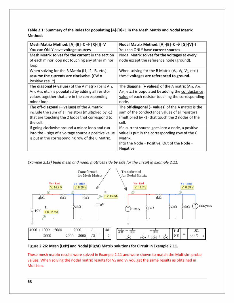
63
Table 2.1: Summary of the Rules for populating [A]∙[B]=C in the Mesh Matrix and Nodal Matrix Methods
Mesh Matrix Method: [A]∙[B]=C [R]∙[I]=V Nodal Matrix Method: [A]∙[B]=C [G]∙[V]=I You can ONLY have voltage sources You can ONLY have current sources Mesh Matrix solves for the current in the section of each minor loop not touching any other minor loop.
Nodal Matrix solves for the voltages at every node except the reference node (ground).
When solving for the B Matrix (I1, I2, I3, etc.) assume the currents are clockwise. (CW = Positive result)
When solving for the B Matrix (VA, VB, VC, etc.) these voltages are referenced to ground.
The diagonal (+ values) of the A matrix (cells A11, A22, A33, etc.) is populated by adding all resistor values together that are in the corresponding minor loop.
The diagonal (+ values) of the A matrix (A11, A22, A33, etc.) is populated by adding the conductance value of each resistor touching the corresponding node.
The off-diagonal (– values) of the A matrix include the sum of all resistors (multiplied by -1) that are touching the 2 loops that correspond to the cell.
The off-diagonal (– values) of the A matrix is the sum of the conductance values of all resistors (multiplied by -1) that touch the 2 nodes of the cell.
If going clockwise around a minor loop and run into the – sign of a voltage source a positive value is put in the corresponding row of the C Matrix.
If a current source goes into a node, a positive value is put in the corresponding row of the C Matrix. Into the Node = Positive, Out of the Node = Negative
Example 2.12) build mesh and nodal matrices side by side for the circuit in Example 2.11.
Figure 2.26: Mesh (Left) and Nodal (Right) Matrix solutions for Circuit in Example 2.11.
These mesh matrix results were solved in Example 2.11 and were shown to match the Multisim probe values. When solving the nodal matrix results for VA and VB you get the same results as obtained in Multisim.

64
When faced with a circuit that is more complicated and has multiple voltage and current sources like shown in Figure 2.27 it is important to decide whether or not it is easier to transform it to a Mesh Matrix problem (only voltage sources) or a Nodal Matrix problem (only current sources). The most important factor is the order of the A matrix that results. In this case the A matrix, when transformed to either Mesh or Nodal matrix, would both be a 3 x 3 matrix. The second thing to look at is whether there are more voltage or current sources in the circuit. In this case there are 2 of each so that factor doesn’t lead to the selection of either nodal or mesh matrix. In example 2.13 it was determined that it would be better for the circuit to be transformed into a nodal matrix problem because the 3A current source is NOT in Norton Form so an approximate source transformation would have to be performed (which is not an ideal thing to have to do).
Example 2.13) build the nodal matrix and solve for VA, VB, and VC for the circuit in Figure 2.27.
When solving the matrix equation shown in Figure 2.27 for VA, VB, and VC using [B] = [A]-1∙[C] the answers agree with the Multisim probes. If you didn’t have a calculator or another way to solve for [B] using the equation [B] = [A]-1∙[C] then you could use Cramer’s Rule (even if the A matrix is a 3 x 3). Anything larger than a 3 x 3 is not realistic to do with Cramer’s Rule, unless it is done with a computer program. This link shows how to solve a 3 x 3 matrix equation using Cramer’s Rule. Even though it was determined that using Nodal Matrix analysis was easier for the circuit in Figure 2.27, Mesh Matrix analysis is also shown for the circuit in Example 2.14 on the next page.
Figure 2.27: Circuit and Matrix for Example 2.13

65
Example 2.14) build the mesh matrix equation and solve for VA, VB, and VC for the circuit in Figure 2.28.
Solving the matrix equation in Example 2.14 gives the following results: I1 = 5.667 A, I2 = 3 A, I3 = 4.333 A. These values correspond to the currents in Loop 1 (Red wire), Loop 2 (Blue wire), and Loop 3 (Green wire), respectively, and match the Multisim current probe values. The internal mesh currents that touch multiple loops (that have black wires in the right circuit in Figure 2.28) can be calculated from KCL as follows:
• I10Ω (assumed to be going right) = I1 – I2 = 5.667 – 3 = 2.667 A • I5Ω (assumed to be going right) = I3 – I3 = 4.33 – 3 = 1.333 A • I20Ω (assumed to be going up) = I3 – I3 = 4.33 – 3 = 1.333 A
The node voltages VA, VB, and VC are calculated as follows:
• VA = 240 – I1 ∙ 40 = 13.33 V • VB = VA - I10Ω ∙ 10 = -13.33 V • VC = VB – I5Ω ∙ 5 = -20 V
Since we were asked to find the node voltages for this circuit the Mesh Matrix method involves more calculations after the matrix is solved than the Nodal Matrix that solves the matrix directly for the node voltages. This is another reason that using the Nodal Matrix method (as shown in Example 2.13) was the preferred method for this problem.
Figure 2.28: Circuit and Matrix for Example 2.14

66
Example 2.15) solve the following circuit using traditional nodal analysis and the Nodal Matrix method to determine the power supplied (or dissipated) by each source.
Figure 2.29: Circuit for Example 2.15
Traditional Nodal analysis involves writing the equations at each node (not counting the reference node) using KCL and assuming all currents are going OUT of the node. In the following equations Vref is set to 0 and left out of the equation. For example, VA – Vref = VA – 0 = VA. These equations are as follows:
• Node A: –12 + VA /2 + VA /3 + (VA – VB)/4 = 0 • Node B: +11 + (VB – VA)/4 + VB /5 + (VB – VC)/6 = 0 • Node C: +10 + VC /7 + (VC – VB)/6 = 0
After doing some algebra these equations can be put into the matrix equation below. This matrix equation can also be built from the circuit by inspection when following the Nodal Matrix method rules.
Solving the matrix equations (or the traditional nodal equations) yields approximately the same values for the node voltages as shown with the Multisim voltage probes: VA = 4.33 V, VB = -29.22 V, VC = -48.61 V.
Power can be calculated as P = V ∙ I for each of the sources (Recall: this is the only power equation that should be used for sources). The magnitudes of the powers are shown below. Multisim shows a negative sign in each power probe. This means that all 3 of the current sources are power suppliers. This is true because of the rule stated in Module 1: “A current source is a dissipater only of it is placed so that the voltage across it has a positive value in the direction of the current flow.”
• P12A = 4.33 ∙ 12 = 52 W • P11A = 29.22 ∙ 11 = 321.42 W • P10A = 48.61 ∙ 10 = 486.1 W

67
CAUTION: The reason the numbers for the node voltages (and powers) are slightly different from Multisim is due to rounding errors of the values in the A matrix. Since the fractions in the A matrix of the Nodal Matrix method often produce very small numbers (and students often don’t carry out the fractional number to enough decimal places), errors like this (or even worse) are common. As can be seen with this example, the values in the A matrix were taken out to the 4th or 5th decimal place, but there was still a significant error. For this reason, it is very important that you take the numbers in the A matrix out to more decimal places than you normally are used to doing. This is especially true if you have a small resistor combined with a large resistor. For example: 1/1MΩ + 1/1Ω = 1.000001 (if you don’t go out to 6 decimal places the 1 MΩ resistor is essentially removed from the calculation). Due to this common rounding issue it is usually preferable to use Mesh Matrix analysis if there are no other factors that make the Nodal Matrix more desirable.
Section 2.5 – Superposition: Solving a circuit by including only one source at a time Another method that can be used to solve circuits with multiple sources involves using the superposition principle. The superposition method is sometimes a preferred option when there are multiple sources that can’t be transformed without using the approximate transformation method. Before discussing this problem solving method the term linear needs to be discussed. In many different engineering disciplines, systems and components are assumed to be linear and the test for linearity is the superposition principle. For electrical systems, linearity can be discussed from the component level or from the system level. An electrical linear component obeys the following when it has one source:
[2.1] 𝑉𝑉(𝐼𝐼1 + 𝐼𝐼2) = V(I1) + 𝑉𝑉(𝐼𝐼2) or 𝐼𝐼(𝑉𝑉1 + 𝑉𝑉2) = I(V1) + 𝐼𝐼(𝑉𝑉2)
The left side version of equation 2.1 implies that if you cut the current in half the voltage should also be cut in half and the right side version implies that if the voltage is cut in half the current will also be cut in half. For a simple circuit with one current source and one resistor this relationship is shown to be true in Figure 2.30, but in Figure 2.31 the resistor component is replaced with a 1N914 switching diode and equation 2.1 is no longer valid.
Figure 2.30: Example of an electrical component that is approximated to be linear – The resistor.
The resistor is shown to be a linear component in Multisim since it obeys equation 2.1. However, in reality a resistor will heat up when current is increased and when the temperature is higher in a conductor the resistance increases. With the resistance slightly increasing at a higher temperature
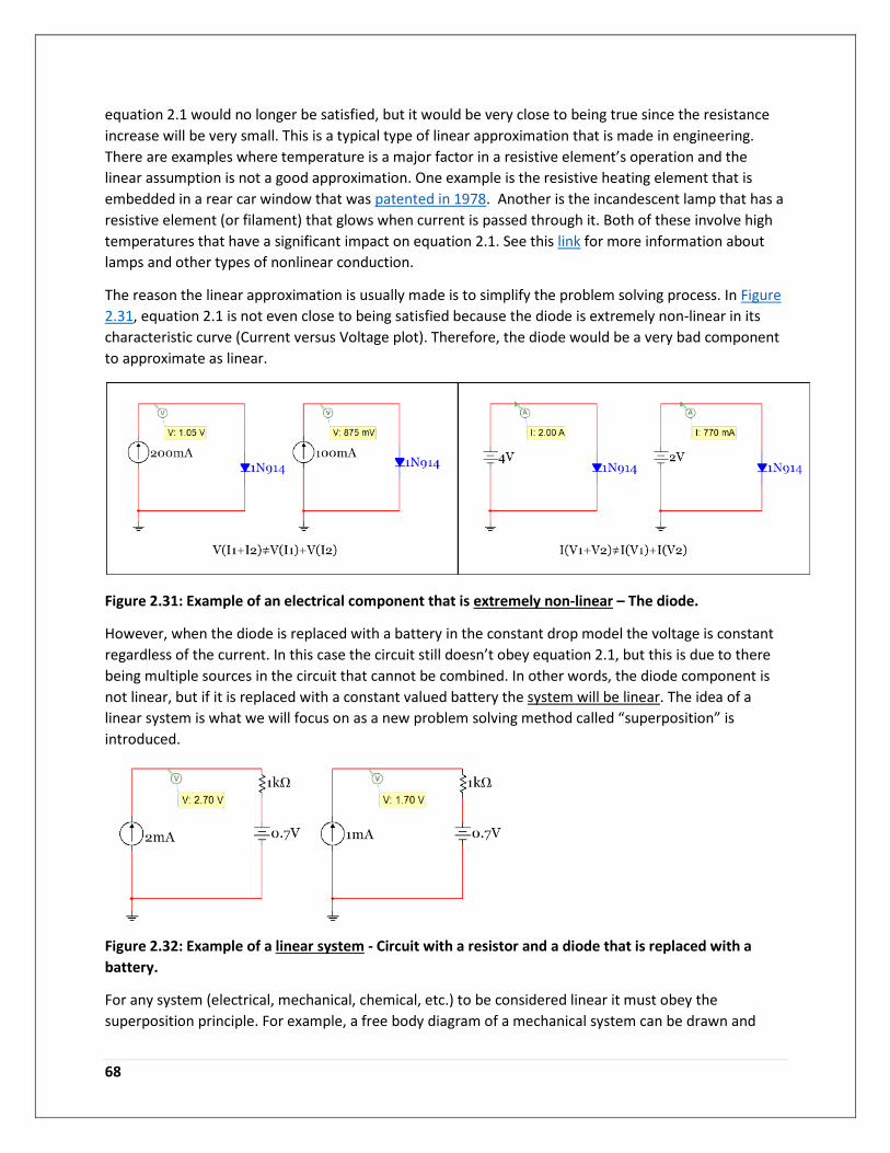
68
equation 2.1 would no longer be satisfied, but it would be very close to being true since the resistance increase will be very small. This is a typical type of linear approximation that is made in engineering. There are examples where temperature is a major factor in a resistive element’s operation and the linear assumption is not a good approximation. One example is the resistive heating element that is embedded in a rear car window that was patented in 1978. Another is the incandescent lamp that has a resistive element (or filament) that glows when current is passed through it. Both of these involve high temperatures that have a significant impact on equation 2.1. See this link for more information about lamps and other types of nonlinear conduction.
The reason the linear approximation is usually made is to simplify the problem solving process. In Figure 2.31, equation 2.1 is not even close to being satisfied because the diode is extremely non-linear in its characteristic curve (Current versus Voltage plot). Therefore, the diode would be a very bad component to approximate as linear.
Figure 2.31: Example of an electrical component that is extremely non-linear – The diode.
However, when the diode is replaced with a battery in the constant drop model the voltage is constant regardless of the current. In this case the circuit still doesn’t obey equation 2.1, but this is due to there being multiple sources in the circuit that cannot be combined. In other words, the diode component is not linear, but if it is replaced with a constant valued battery the system will be linear. The idea of a linear system is what we will focus on as a new problem solving method called “superposition” is introduced.
Figure 2.32: Example of a linear system - Circuit with a resistor and a diode that is replaced with a battery.
For any system (electrical, mechanical, chemical, etc.) to be considered linear it must obey the superposition principle. For example, a free body diagram of a mechanical system can be drawn and

69
using Newton’s 2nd Law all of the forces acting on the mechanical body result in the body having a net acceleration. If the system is linear then superposition can be used where the acceleration due to each individual force is calculated one at a time. All of the individual accelerations could then be added together and the resulting total acceleration that results would be the same as solving the system all in one step with all forces in the same calculation. This same process can also be used for independent sources in electrical linear systems. The only thing that complicates the superposition procedure for linear circuits is what to do with the “other sources” that are physically connected to the circuit as you solve the circuit one source at a time. If the sources are not ideal, then the “other sources” are replaced with their internal resistance. Recall in Figure 1.3 of Module 1 that a non-ideal voltage source is modeled as a battery in series with a small resistor. This small resistor (called Rint) is the internal resistance. A non-ideal current source is modeled as a large resistor in parallel with the current source. If the sources of the circuit in Figure 2.32 are replaced with a non-ideal current source with internal resistance of 1 MΩ for the current source and 1 Ω in series to transform the ideal voltage source to a non-ideal voltage source, the results are shown in the top circuit in Figure 2.33. The voltage across the 1 kΩ resistor is approximately 2V, which is the same value as obtained in the circuit in Figure 2.32 with ideal sources. The value is approximately the same because the values of Rint in this case for the current and voltage sources have minimal effect on the circuit.
Figure 2.33: Example of Superposition with Non-Ideal Sources - The 0.7V battery has a negligible effect
When doing superposition on this circuit the number of sub-problems that are solved is equal to the number of sources. In this case there are 2 sources so the two sub-problems are:
1. Find V1kΩ and I1kΩ due to only the 2 mA current source 2. Find V1kΩ and I1kΩ due to only the 0.7 V voltage source
For sub-problem 1 (on the left side of Figure 2.33) the voltage source must be “zeroed out” and for sub-problem 2 (on the right side of Figure 2.33) the current source must be “zeroed out” so that only the internal resistance remains for both. To zero out an independent source the following is done:
1. Voltage Sources are replaced with short circuits. 2. Current Sources are replaced with open circuits.

70
These two rules should be easy to remember and not get mixed up because the voltage across a short circuit (or just a wire) is always zero volts because the voltage doesn’t change until it goes across another component. Conversely, the current is always zero in an open circuit because the circuit is broken.
CAUTION: Students sometimes get these rules for zeroing out sources confused because they think the voltage across an open circuit is zero, but that is usually not the case. The voltage across an open circuit is the difference between the voltages at the nodes on the two sides of the open circuit, which is rarely zero.
The magnitude of the voltage and current of the 1 kΩ resistor in the bottom-left circuit in Figure 2.33 due to only the 2 mA current source (sub-problem 1) can be calculated as follows:
• I1kΩ_1 = 2 mA because the source forces 2mA through the loop (verified by Multisim in Figure 2.33).
• V1kΩ_1 = I1kΩ_1 ∙ 1 kΩ = 2 mA ∙ 1 kΩ = 2 V (as verified by Multisim in Figure 2.33).
In this example the 0.7 V has very little effect on current or voltage through the 1 kΩ resistor since there is a 1 MΩ resistance in the circuit. The magnitude of the voltage and current of the 1 kΩ resistor in the bottom-right circuit in Figure 2.33 Due to only the 0.7 V voltage source (sub-problem 2) can be calculated as follows:
• I1kΩ_2 = (0.7 V)/(1 MΩ + 1 kΩ + 1 Ω) = 6.99E-7 A or 699 nA (as verified by Multisim in Figure 2.33). • V1kΩ_2 = I1kΩ_2 ∙ 1 kΩ = 699 nA ∙ 1 kΩ = 6.99 E-4 or 699 µV (as verified by Multisim in Figure 2.33).
Notice the signs of the Multisim probes are negative for both I1kΩ_2 and V1kΩ_2. When solving a superposition problem the current and voltage polarities need to be assumed the same for each of the problems (from the different sources) so the results can be added together to get the final values due to all sources. In this example we will set the direction of the current as clockwise because that is how the current probe in Multisim is set and if we set it the same way as it is set in Multisim we can verify the answers. The differential voltage probe in Multisim has the positive sign on top of the 1 kΩ resistor and the negative sign (or reference) on the bottom side. Since the 0.7 V source will force current to go counter-clockwise the value of the current obtained will be negative (as shown in Multisim). V1kΩ_2 will also be negative because the current is travelling in a direction where it goes through the minus sign (or the reference) of the differential probe which is at the bottom of the 1 kΩ resistor. The final value for the current and voltage is equal to:
• I1kΩ = I1kΩ_1 + I1kΩ_2 = 2 mA – 699 nA = 1.9993 mA (rounded to 2 mA in Multisim, top circuit in Fig 2.33)
• V1kΩ = V1kΩ_1 + V1kΩ_2 = 2 V – 699 µV = 1.9993 V (rounded to 2 V in Multisim, top circuit in Fig 2.33)
In this course we will only deal with Ideal independent sources so the internal resistance doesn’t have to be included. For ideal voltage sources the internal resistance is zero (replace Rint in Figure 2.33 with a short circuit) and for ideal current sources the internal resistance is infinity (replace Rint in Figure 2.33 with an open circuit). If the sources in the circuit in Figure 2.33 are ideal then Figure 2.34 shows how the circuit would look and how the circuits for the 2 sub-problems would look.

71
Figure 2.34: Example of Superposition with Ideal Sources
Notice that Multisim measured the voltage to be equal to -700 pV. This is pico Volts (or 10–12 Volts). If you see a voltage (or a current) with that kind of value in Multisim, always assume it zero. Multisim often gives extremely small values when the actual value should be zero, as in a circuit like this that has an open circuit and no current (V1kΩ_2 = 0 ∙ 1 kΩ = 0 V).
Note: Programs typically have a “machine epsilon” somewhere in the 10–10 to 10–16 range. In MATLAB®, for example, you can type “eps” at the prompt and it will give you an estimated value. Anything in that range should be assumed to be zero.
So, assuming -700 pV is zero volts (due to the machine epsilon of Multisim) the current and voltage are:
• I1kΩ = I1kΩ_1 + I1kΩ_2 = 2 mA – 0 A = 2.0 mA (Matches top circuit in Fig 2.34) • V1kΩ = V1kΩ_1 + V1kΩ_2 = 2 V – 0 V = 2.0 V (Matches top circuit in Fig 2.34)
Superposition is usually more difficult and time consuming than the Mesh Matrix or Nodal Matrix methods, but it is an important concept in many engineering fields so some questions will be specified to be solved using superposition in ENGR 2431. One way to force the use of the superposition problem solving method is to only ask for one of the sub-problems to be solved. For example, a question could be to find the voltage across the 1 kΩ resistor “Due to Only” the 2 mA source. If you see those three words (Due to Only) in a problem statement it means you should do superposition, but only the sub-problem specified. Examples 2.16 and 2.17 show more difficult superposition problems.

72
Example 2.16) solve the following circuit for the voltage and current labeled Vx and Ix using superposition.
Figure 2.35: Circuit for Example 2.16
Since there are 2 independent sources this circuit requires 2 sub-problems when using the superposition solving technique. First, Vx and Ix will be solved Due to Only the 36 V source (bottom left circuit in Figure 2.35). Notice how the 9 mA source is “zeroed out” by replacing it with an open circuit.
There are many ways to solve this sub-problem. The easiest method probably would involve combining the 3k and 4k resistors in parallel and doing a 2 loop Mesh Matrix problem. Since the value for Vx_1 will not change when combining these two resistors then the simplification can be made, but if the circuit simplification causes you to not be able to solve for the current or voltage specified in the problem statement then you can’t simplify that part of the circuit. For example, once the 3k and 4k resistors are combined in parallel it would be natural to want to add the 2k resistor in series with the result to simplify the circuit further. However, if this is done Vx_1 can no longer be found. The following is the simplified circuit and the Mesh matrix equation for sub-problem 1. Notice that the section where the open circuit is located (where the current source was removed) is treated as if the two wire branches are not in the circuit because they have no effect. A common mistake is to leave that section of the circuit in and treat the two sides of it as two different minor loops, which would mistakenly make this a 3 loop circuit.

73
Figure 2.36: Circuit and Mesh Matrix equation for Sub-Problem 1 of Example 2.16
Solving the Mesh Matrix equation gives I1 = 6.220 mA and I2 = 1.319 mA (which matches the Multisim current probe values shown in Figure 2.36). Using KCL, Ix_1 can be solved as:
• Ix_1 = I1 – I2 = 6.220 mA – 1.319 mA = 4.901 mA (This matches the Multisim value) • Vx_1 = I2 ∙ 1.714 kΩ = 2.261 V (This matches the Multisim value)
Sub-problem 2 will be solved using the Nodal Matrix method. The Nodal Matrix equation is shown below along with the redrawn circuit with the nodes color coded and an extra probe added. Since it doesn’t reduce the complexity of the circuit (and could cause rounding errors) the 3 kΩ and 4 kΩ resistors were not combined like they were in sub-problem 1.
Figure 2.37: Circuit and Nodal Matrix equation for Sub-Problem 2 of Example 2.16
Solving the Nodal Matrix equation gives VA = -2.827 V and VB = -9.613 V (which matches the values in Multisim). Using Ix_2 = ΔV/R it can be solved as:
• Ix_2 = (-2.827 – 0)/1000 = -2.827 mA (This matches the Multisim value) • Vx_2 = VB = -9.613 V (This matches the Multisim value)

74
So for this circuit the final values of the current (Ix) and voltage (Vx) are:
• Ix = Ix_1 + Ix_2 = 4.901 mA – 2.827 mA = 2.074 mA (Matches top circuit in Fig 2.35) • Vx = Vx_1 + Vx_2 = 2.261 V – 9.613 V = -7.352 V (Matches top circuit in Fig 2.35)
CAUTION: You CANNOT calculate power using the superposition technique (only voltage or current).
One very important limitation of the superposition method is that power CANNOT be determined by adding up the power that was supplied or dissipated in a component due to each source. You can only find the voltage or current due to only one source and add them up. Power probes were included in the circuit in Figure 2.35 (see gray shaded probes) and the values are shown below:
• Both Sources included: P36V = -244 mW, P9mA = -66.2 mW, P5kΩ = 230 mW • Only 36V Source included: P36V_1 = -224 mW, P9mA_1 = 0 mW, P5kΩ_1 = 193 mW • Both Sources included: P36V_2 = 0 mW, P9mA_2 = -86.5 mW, P5kΩ_2 = 1.6 mW
It can be seen by the power numbers above that the superposition doesn’t work. For example:
• P5kΩ = 230 mW, which is not equal to P5kΩ_1 + P5kΩ_2 = 193 mW + 1.6 mW = 194.6 mW
However, the current and voltage can be found and the power calculated using those values. For example:
• I5kΩ = 6.79 mA = I5kΩ_1 + I5kΩ_2 = 6.22 mA + 0.57 mA = 6.79 mA and P5kΩ = I5kΩ 2 ∙ R = 230 mW
The next example shows two tricky situations that can arise when shorts and/or opens are added to circuits.
1. A short in parallel with one or more resistors causes the resistors to be removed (or shorted out) from the circuit. Knowing the fact that a short circuit is just a wire (or a resistor with a value of 0 Ω) it can be combined with resistor, R, to give a value of 0Ω which means the result is a short circuit is: Rtot = 0||R = (0∙R)/(0+R) = 0
2. An open circuit in series with one or more resistors (a resistor network) results in the resistor network having no effect on the circuit. Since an open circuit is the same thing as a resistor with a value of ∞ ohms an open circuit results when added in series with resistor, R. Rtot = ∞ + R = ∞
The two tricky situations mentioned above can be seen in the circuit in Figure 2.38. Situation 1 (described above) applies to the sub-problems 1 and 2 circuit in Figure 2.38 where the short circuit is in parallel with a resistor network. The 20 Ω and 40 Ω resistors are in series and can be added to equal 60 Ω. That 60 Ω resistor is in parallel with the short circuit (0 Ω). As stated previously the end result will be the short circuit remaining and the 20 Ω and 40 Ω resistors being shorted out (as shown in Figure 2.40).
Situation 2 (described above) applies to the sub-problem 2 and 3 circuit in Figure 2.38 where the open circuit is in series with a resistor network. The network containing the 1 Ω, 2 Ω, and 4 Ω resistors are in series with the open circuit so these resistors will have no effect on the results because no current will

75
flow through these resistors, which means the voltage across each resistor will be equal to zero. Figure 2.41 shows the sub-problem 3 circuit with the 1 Ω, 2 Ω, and 4 Ω resistor network removed.
Example 2.17) solve the following circuit for the voltage across the 5 Ω resistor using superposition.
Figure 2.38: Circuit for Example 2.17
Note: The node voltage probe is placed above the 5 Ω resistor instead of a differential probe across the 5 Ω resistor. Since the voltage at the bottom of the 5 Ω resistor is 0 (because it is connected to ground) then both of these probe options give the same result. If one side of a resistor is not connected to ground, then a differential probe (or Multimeter) would be needed to find the voltage across the resistor.
Since there are 3 independent sources in this circuit it requires 3 sub-problems when using the superposition solving technique. First, V5Ω will be solved Due to Only the 2 A source (bottom-left circuit in Figure 2.38). Notice how the 20 Ω and 40 Ω resistors are “shorted out” and the two wires from the 5 A source are removed. The 1 Ω and 2 Ω resistors are in series so they are added together and the 8 Ω and 10 Ω resistors are in series so they are also added together. By making these simplifications the number of nodes is reduced from 4 to 2 (not counting the reference node). These are allowable simplifications since the only voltage we are solving for is the voltage across the 5 Ω resistor and it is not involved in the simplification.
Figure 2.39: Circuit and Nodal Matrix equation for sub-problem 1 of Example 2.17

76
Solving the Nodal Matrix equation gives VA = 3.426 V and VB = -7.826 V (which matches the Multisim voltage probe values shown in Figure 2.39). V5Ω_1 = VB = -7.826 V
Next, V5Ω will be solved Due to Only the 5 A source (bottom-middle circuit in Figure 2.38). The 20 Ω and 40 Ω resistors are removed due to “situation 1” described previously and the network containing the 1 Ω, 2 Ω, and 4 Ω resistors are removed from the circuit due to “situation 2” described previously. After redrawing the circuit, it is also a Nodal Matrix problem with a 2 x 2 A matrix as shown below.
Figure 2.40: Circuit and Nodal Matrix equation for sub-problem 2 of Example 2.17
Solving the Nodal Matrix equation gives VA = -10.87 V and VB = -28.26 V (which matches the Multisim voltage probe values shown in Figure 2.40). V5Ω_2 = VA = -10.87 V
Finally, V5Ω will be solved Due to Only the 12 V source (bottom-right circuit in Figure 2.38). Again, the network containing the 1 Ω, 2 Ω, and 4 Ω resistors are removed from the circuit due to “situation 2” described previously. After redrawing the circuit, it is shown to be a simple 2 loop Mesh Matrix problem.
Figure 2.41: Circuit and Mesh Matrix equation for sub-problem 3 of Example 2.17
Solving the Mesh Matrix equation gives I1 = - 521.74 mA and I2 = 200 mA (which matches the Multisim current probe values shown in Figure 2.40). V5Ω_3 = – I1 ∙ 5 = 2.6087 V
The reason the voltage across the 5 Ω resistor is positive is due to the direction of the current flowing downward toward ground across the 5 Ω resistor. Since current always flows from higher voltage to lower voltage the voltage at the node on top of the 5 Ω resistor must be higher than 0 V, which is the

77
voltage at ground. When adding all of the 3 sub-problem results together the final value for V5Ω is shown as follows:
• V5Ω = V5Ω_1 + V5Ω_2 + V5Ω_3 = –7.826 V – 10.87 V + 2.6087 V = -16.088 V (Matches the value in Figure 2.38)
Since the voltage is negative at the node on top of the 5 Ω resistor then the current flows up from ground through the 5 Ω resistor (from higher voltage, 0 V, to a lower voltage, -16.088 V).
In summary, the superposition method can turn a circuit problem that is very complicated into multiple circuit sub-problems that are less complicated. Superposition is a good method to consider when there are multiple sources in a circuit that can’t be transformed without using the approximate transformation method, but for most circuits it would be easier to use the Mesh or Nodal Matrix methods. Make sure if you see the phrase “Due to Only” in a problem statement you realize you are not completely solving the circuit, but just doing one of the superposition sub-problems to show you know how to do superposition. Being able to solve problems where opens and shorts are placed in the circuit (like is done in superposition) is a really good skill to master because it is also used in section 2.6 (Thevenin and Norton Equivalent circuits) and in Module 3 when steady state analysis is performed on RLC circuits.
Section 2.6 – Thevenin and Norton Equivalent Circuits
Section 2.1 defined the Thevenin and Norton form of independent sources in circuits. The Thevenin form contains a voltage with a resistor in series and Norton form contains a current source with a resistor in parallel as seen in the figure below.
Duplicate Copy of Figure 2.1: Source Transformation: Thevenin and Norton Form
The reason finding the Thevenin equivalent circuit is an important circuit technique is that it allows a complicated circuit with multiple voltage and/or current sources and as many resistors as imaginable to be replaced with one independent source and one resistor (in either Thevenin or Norton form). There is usually not a need to solve for the Norton equivalent circuit because it is just as easy to just find the Thevenin equivalent circuit and then transform it to Norton form using the simple method explained in section 2.1. You can find the Thevenin equivalent circuit “external to” a specific resistor in a circuit by first removing that resistor from the circuit as shown in Figure 2.42.
Nubbies Nubbies

78
Figure 2.42: First step when asked to find the Thevenin equivalent circuit “external to RL”
In order to solve for the Thevenin equivalent circuit you have to do two sub-problems as described below:
1. Find Rth (or Rn) by “zeroing out” all sources (short voltage sources & open current sources) and combine resistors towards the spot in the circuit (i.e. where RL was removed in Figure 2.42) where you are finding the Thevenin equivalent circuit “external to” as shown in Figure 2.43.
2. Find Vth by calculating the open circuit voltage across the spot in the circuit where you are finding the Thevenin equivalent circuit “external to” as shown in Figure 2.43..
Figure 2.43: Sub-problem 1 (Find Vth – left circuit), Sub-problem 2 (Find Rth – right circuit)
Multisim can be used to determine Vth and Rth by using Multimeters in Volts and Ohms mode respectively. Figure 2.44 shows how to set up the measurements in Multisim.

79
Figure 2.44: Multisim used to measure Vth (5.75 V) and Rth (31.25 Ω)
RL is the resistor that you will connect to the Nubbies of the Thevenin form in Figure 2.1 after Rth and Vth are determined as shown in Figure 2.45. Norton form is also shown in Figure 2.45, where IN = Vth/Rth.
Figure 2.45: Original circuit (Left) and the Thevenin (middle) and Norton (right) equivalent circuits
Example 2.18) determine the Thevenin equivalent circuit external to RL in Figure 2.43 by calculating Vth and Rth and compare the results to those measured by Multisim in Figure 2.44.
Sub-problem 1 – Find Rth by combining resistors in a similar fashion as done in section 1.2. In Module 1 you were advised to start with combining the resistors as far away from the voltage or current source as possible. For Thevenin equivalent circuit problems you should start with combining resistors as far away from the spot in the circuit where the Rth is to be found (as shown by the arrow in Figure 2.43). The following figure shows how Rth is calculated with the circuit redrawn each time a resistor is combined. As shown in Module 1 if you become skilled in combining resistors you could write the equation for Rth by inspection as: Rth = [(8+10)||30]+20 = 31.25 Ω
CAUTION: The open circuit that resulted from removing the RL resistor is not treated as a normal open circuit. People often see a situation like this and think the 20 Ω resistor is in series with an open circuit so it has no effect on the circuit and can be removed. In any other circuit solving situation (like solving for Vth in sub-problem 2) this would be true, but when solving for Rth using the combining resistance

80
method this cannot be done. Think of the open circuit that is created when removing RL as a location where an actual Multimeter in Ohms mode (Ohmmeter) is connected. An Ohmmeter works by injecting a small current in a circuit in order to measure the resistance so the open circuit would act like a current source instead of an actual open circuit. This is in contrast to how a Voltmeter works. If a Voltmeter is connected across an open circuit, then the open circuit still behaves as an open circuit because the Voltmeter doesn’t inject current into the circuit and is assumed to have no effect on the circuit. Also, when measuring resistance with an ohmmeter all other sources must be “zeroed out” or the measured value will be wrong or the Multimeter might even be damaged. When measuring resistance with an Ohmmeter always remove the power from the circuit. See this link for more information about how Ohmmeters work: http://www.allaboutcircuits.com/worksheets/basic-ohmmeter-use/
Figure 2.46: Step by step solution for calculating Rth in Example 2.18
Sub-problem 2 – Find Vth by solving for the open circuit voltage shown in Figure 2.43. The easiest way to do this is to transform the 1A current source to a voltage source so a one loop circuit is left. Notice that the 20Ω resistor is in series with an open circuit so it has no effect on Vth (No current flowing through it means no voltage drop across it). The 20Ω resistor only has an effect on Rth in this circuit. The following figure shows the circuit transformed and the 20Ω resistor removed since it has no effect on Vth.
Figure 2.47: Original circuit (left) set up for finding Vth and transformed/simplified circuit (right)
This circuit is now a single loop circuit so a simple KVL can be done to determine the current in the loop.
• KVL1 (minor loop): – 8 + 8 I + 10 I + 30 I + 2 = 0 I = (8-2)/(8+10+30) = 0.125 A
Now that the current is known, Vth can be calculated in many different ways. One of my favorite ways to solve an open circuit voltage is to do a KVL through the open circuit voltage as shown below:

81
• KVL2 (outside path including the open circuit): – 8 + 8 I + 10 I + Vth = 0 Vth = 8 – 18∙0.125 = 5.75 V
Another way that Vth could be solved is by finding the voltage on the + side of Vth and the voltage on the – side and subtracting them (Vth = V(+) – V(–)). Since V(–) is connected to ground Vth = V(+) – 0 = V(+). By stepping around the circuit and solving for the voltage at each node using the voltage drops across the resistors the V(+) node voltage can easily be found. Vth = V(+) = 8 – 8 ∙ 0.125 – 10 ∙ 0.125 = 5.75 V
CAUTION: Students often try to use the Rth value somehow when solving for Vth. These two sub-problems are completely separate and NO information should be passed from one sub-problem to the other.
The next example shows a more complicated circuit and what happens when a resistor is “shorted out.” It also shows another way of framing a Thevenin question. Sometimes RL (or whatever resistor that you are finding the Thevenin equivalent circuit “external to”) has already been removed and the problem will simply state to “find the Thevenin equivalent circuit.” When this is asked it is implied that it is to be found at the location where the two Nubbies are present where RL could have been connected, but already removed.
Example 2.19) determine the Thevenin and Norton equivalent circuits from the circuit in Figure 2.48 and draw the original circuit and the Thevenin and Norton equivalent circuits side by side in a similar fashion that was done in Figure 2.45 (except there will be no RL, only an open circuit with two Nubbies).
Figure 2.48: Circuit for Example 2.19
Sub-problem 1 – Find Rth by zeroing out the sources and combining the resistors as shown in Figures 2.49 and 2.50.

82
Figure 2.49: Sub-problem 1 circuit with sources replaced with shorts and opens (or “zeroed out”)
Figure 2.50: Step by step solution for calculating Rth in Example 2.19
Figure 2.51: Sub-problem 2 circuit in Example 1.19 with current source transformed into a voltage source.
Solving the Mesh matrix equation yields I1 = 10 mA, I2 = 2.235 mA, I3 = .392 mA
• Vth = I3 ∙ 5k + 2 = 3.96 V
The Rth and Vth values calculated in Example 2.19 are verified in the Multisim circuits below.

83
Figure 2.52: Multisim verification of Rth in Example 1.19 (done by plugging in zero for all sources instead of replacing with shorts and opens). This method is often easier to do quickly in Multisim.
Figure 2.53: Multisim verification of Vth in Example 1.19.

84
Figure 2.54: Circuit in Example 1.19 (Left), Thevenin circuit (middle), and Norton circuit (right).
Since the original circuit in Example 1.19 didn’t have a resistor (RL) then the Thevenin and Norton equivalent circuits shouldn’t either. However, the point of this is that if you connect any resistor value to the Nubbies in any of these three circuits they will have the same current and voltage value as shown in Figure 2.55. In the demonstration in Figure 2.55 the top row of circuits have an extremely small resistor and the bottom row has an extremely large resistor. This was done to prove the point that ANY resistor value can be connected to the Nubbies and the current and voltage will be the same between the three circuits.
Figure 2.55: Demonstration that the Thevenin and Norton equivalent circuits produce the same results as the original circuit when connecting ANY resistor value to the Nubbies.
Another topic that comes up when doing Thevenin equivalent circuits is the Maximum Power Transfer Theorem. This important theorem asks the question: If connecting a resistor (let’s call it RL) to a circuit, what value of RL would result in the maximum power being transferred to RL? The answer to this questions is setting RL = Rth results in maximum power transfer to RL. A common question that might be faced on an exam or quiz is: “What value of RL should be used in the circuit to allow for maximum power transfer to RL?” If asked this question all you have to do is solve for Rth (sub-problem 1 of Thevenin equivalent circuits).

85
The reason why RL = Rth is the sweet spot (max power point) can be determined graphically by solving the circuit in Figure 2.56 for power dissipated in RL and plotting the power versus different values of RL. The equation for the power across RL is equal to: PRL = I2 ∙ RL = [Vth/(Rth + RL)]2 ∙ RL
In the chart below it can be seen that as the value of RL is close to zero on the x-axis the power dissipated by RL is also close to zero, but when RL reaches 1000 Ω, which is the value of Rth, the power dissipated in RL is at its maximum.
Figure 2.56: Graphical representation of the Maximum Transfer Theorem (RL = Rth)
The last issue with Thevenin equivalent circuits that should be discussed is the different methods that can be used to solve for Rth. The method shown in Examples 1.18 and 1.19 uses the combining-resistor method, which will be referred to as method 1 below, but there are 3 other methods than can also be used.
1. Method 1 – Zeroing Independent sources and Combining Resistors – You can’t have any dependent sources when using this method. This is the only method needed for ENGR 2431.
2. Method 2 – Find Vth from the open circuit voltage across the Nubbies (as shown in Examples 1.18 and 1.19) and find IN by putting a short across the Nubbies and finding the current through the short (IN = the short circuit current) and solve for Rth using the equation Rth = Vth/IN.
3. Method 3 – Connect a test voltage source (or test current source) to the Nubbies and solve for the source current (or source voltage if using a test current source) and solve for Rth using the equation Rth = VTest/ITest.
4. Method 4 – Start away from the Nubbies and perform source transforms of the source and combine the resistors until only one source and one resistor is left and the circuit is in either Thevenin or Norton Form.
The remainder of this document provides an overview of the 4 methods of finding the Thevenin Equivalent Circuit. If you are in ENGR 2431 you don’t need to go any further than Method 1, but you can use any of these 4 methods if you prefer one of them more than Method 1.
We will use the following example circuit shown below-left for each of the 4 methods. Below-right you can see the Thevenin Equivalent Circuit.

86
Figure 2.57: Circuit used to show the 4 different methods of finding the Thevenin Equivalent Circuit
As previously explained the following shows that once you find the correct Vth and Rth, RL will have the same current flowing through it and voltage across it as the original circuit no matter what the RL value is.
Figure 2.58: Verification that ANY resistor can be added and the same results are given.
The following shows that you can also find the Norton Equivalent circuit (Below-Right) by doing a source transformation on the Thevenin Equivalent Circuit. Set IN = Vth/Rth and set RN = Rth.
Figure 2.59: Verification that ANY resistor can be added and the same results are given.

87
Method 1: Finding the Thevenin Equivalent Circuits using the resistor combining Rth method
Note: This method is described in more detail previously in the document. This is a recap.
• Sub-Problem 1) You find Rth by removing RL first and zeroing out all independent sources (Replace Independent Voltage Sources with a Short Circuit and Independent Current Sources with an Open Circuit) and then combine resistors (starting as far away from RL and moving towards it) until there is only one resistor left. The Resistor that is left is Rth and it is put in series with the original RL.
• Sub-Problem 2) You find Vth by going back to the original circuit and removing RL and replacing the open circuit with a voltage measurement between the terminals (Vth).
The work below shows the two problems (Sub-Problem 1 – Find Rth, Sub-Problem 2 – Find Vth).
Rth found below to = 1.913 Ω
Note: This method of finding Rth can ONLY be used if there are NO dependent sources.
Figure 2.60: Sub-Problem 1 - Rth Calculation using Method 1
From the Mesh matrix equation below I2 is solved to equal 1.04 A and Vth = 4 ∙ I2 = 4.174 V
Figure 2.61: Sub-Problem 2 - Vth Calculation using Method 1 (This is also used for Methods 2 and 3)
If you want IN then IN = Vth/Rth = 2.182 A
Method 2: Finding the Thevenin Equivalent Circuits by finding IN to determine Rth
• Sub-Problem 1) You find Vth in the exact same way you did on Method 1 - remove RL and replacing the open circuit with a voltage measurement between the terminals (Vth).
• Sub-Problem 2) You find IN by going back to the original circuit and removing RL and replacing it with a short circuit and measuring the current at that short circuit.
• Once you find Vth and IN, Rth is simply the following: Rth = Vth/IN

88
Figure 2.62: Sub-Problem 2 - IN Calculation – Used in Method 2 to determine Rth = Vth/IN
• The Mesh Matrix in Figure 2.62 can be solved to give I2 = 2.182 A and I2 = IN = 2.182 A • Vth is calculated in the same way as in Method 1 to be: Vth = 4.174 V • Rth is calculated from Vth/IN. Rth = 1.913 Ω
Method 3: Finding the Thevenin Equivalent Circuit using the test voltage and current method to find Rth
• Sub-Problem 1) You find Vth in the exact same way you did on Method 1 - remove RL and replacing the open circuit with a voltage measurement between the terminals (Vth).
• Sub-Problem 2) You replace RL with either a test voltage or test current and solve the circuit for the other (if you put in a test voltage solve for the current flowing through the test voltage from – to + and if you put in a test current you solve for the voltage across the current source). Putting in a 1 Volt or 1 Amp test source is the easiest value to put in. Since you are finding Rth you must zero out the independent sources (Just like Method 1).
• Once you have VTest and ITest you solve for Rth from the following: Rth = VTest/ITest
Figure 2.63: Sub-Problem 2 - ITest Calculation – Used in Method 3 to determine Rth = VTest/ITest)
• Vth is calculated in the same way as in Method 1 to be: Vth = 4.174 V • Using the Mesh Matrix in Figure 2.63 ITest is calculated to be 523 mA. Rth =1V/.523A = 1.913 Ω
Method 4: Finding the Thevenin Equivalent Circuits using the Transform and Combine Method
• This method involves doing source transformations towards RL (or the open circuit where RL was removed) until you are left with only one resistor and either a current or a voltage source. The resistor that remains is equal to Rth and RN.

89
• If you are left with only a voltage source the voltage value you have is Vth and you can find IN by doing a source transformation.
Figure 2.64: Finding Vth, IN, and Rth using Method 4 (Transform and Combine)

90
Module 3 – DC Circuits with Resistors, Capacitors, and Inductors
Modules 1 and 2 focused on resistive circuit components, but Module 3 turns the focus to reactive components (capacitors and inductors). While resistors resist current flow, capacitors and inductors react to current flow. A circuit with capacitors and resistors is called a RC circuit and a circuit that has a resistor and an inductor is called an RL circuit. The letter L is used because it is the symbol for Inductance and C is the symbol for Capacitance. If the circuit has one or more resistors, one or more capacitors, and one or more inductors it is called a RLC circuit. This discussion on RC, RL, and RLC circuits will be simplified in this module since only DC sources are included. However, since the capacitors and inductors are energy storage devices the concepts of transient and steady state circuit behavior will be introduced. The following 6 sections make up Module 3:
• Section 3.1 – Background for Capacitors • Section 3.2 – Background for Inductors • Section 3.3 – Combining Inductors in Parallel and/or Series • Section 3.4 – Combining Capacitors in Parallel and/or Series • Section 3.5 – DC Transient Analysis with RC and RL Circuits • Section 3.6 – DC Steady State Analysis with RC, RL, and RLC Circuits • Section 3.7 – Introduction of Analog Passive Filters
Section 3.1 – Background for Capacitors Detailed background for electrical fields is covered in introductory physics courses (PHYS 2524 at OU) so this book will just focus on the essentials to help you understand how capacitors work. A capacitor is a device that stores charge and often provides a burst of energy in a circuit in a similar fashion to a battery. The difference between a battery and a capacitor is that the capacitor’s energy is expended much more rapidly. The capacity at which the capacitor can store charge is referred to as capacitance and quantified in equation 3.1.
[3.1] 𝐶𝐶 = ℰ𝑟𝑟ℰ𝑡𝑡𝐴𝐴𝑠𝑠
Figure 3.1: Illustration of a Capacitor connected to a battery and resistor (RC Circuit)
Plate (cross-sectional area, A)
Dielectric (relative permittivity, ℰr) d
Plate (cross-sectional area, A)
Cathode terminal
+
–
Anode terminal
– –
+ + + + + + +
– – – – –
Charge

91
The easiest way to visualize a capacitor is shown in Figure 3.1 where two conductive plates that have a cross-sectional area of (A meters2) sandwich a dielectric material with a thickness of (d meters). The terminals (or wires) that connect the capacitor to the circuit are attached to the plates. There are many different materials used for the dielectric material in capacitors. The relative permittivity, ℰr, of the dielectric material is proportional to the capacitance value of the capacitor. Table 3.1 shows relative permittivity values for different materials. The relative permittivity, ℰr, is multiplied by the permittivity of a vacuum, ℰ0 (8.84 x 10⁻¹² F/m), to give the permittivity (ℰ) of the dielectric material. When the switch is closed at time =0 in the circuit in Figure 3.1 the battery causes charge to accumulate on the capacitor plates, which in turn causes an electric field to be produced.
The equations linking charge and energy to capacitance and voltage are defined in equation 3.2 and 3.3. Units: C-Farads, Q-Coulombs, V-Volts, and E-Joules.
[3.2] 𝐶𝐶 = 𝑄𝑄𝑉𝑉
[3.3] 𝐸𝐸 = 12
𝐶𝐶 𝑉𝑉2
More details about charging capacitors will be described in Section 3.5 - Transient Analysis. Background info is given in this link: http://hyperphysics.phy-astr.gsu.edu/hbase/electric/capchg.html
Additionally, more details about how the charged plates of the capacitor interact with the dielectric are provided at this link: http://hyperphysics.phy-astr.gsu.edu/hbase/electric/dielec.html#c1
Table 3.1) Table of Relative Permittivity, ℰr, for Different Materials * ℰr for Mylar from: http://hyperphysics.phy-astr.gsu.edu/hbase/tables/diel.html & all other values are from: http://www.allaboutcircuits.com/textbook/direct-current/chpt-13/factors-affecting-capacitance/
Material ℰr Vacuum 1 Air 1.0006 PTFE, FEP ("Teflon") 2 Polypropylene 2.2 to 2.2 ABS resin 2.4 to 3.2 Polystyrene 2.45 to 4.0 Waxed paper 2.5 Transformer oil 2.5 to 4 Hard Rubber 2.5 to 4.8 *Mylar (PET) 3.1 Wood (Oak) 3.3 Silicones 3.4 to 4.3 Bakelite 3.5 to 6.0 Quartz, fused 3 Wood (Maple) 4.4 Glass 4.9 to 7.5 Castor oil 5 Wood (Birch) 5.2 Mica, muscovite 5.0 to 8.7 Glass-bonded mica 6.3 to 9.3 Porcelain, Steatite 6.5 Alumina 8 to 10 Distilled water 80

92
Example 3.1) if a capacitor was created with 20 mm2 plates with 1 mm thickness of mica as the dielectric, what is the range of capacitance it would have? If the voltage across the capacitor was 12 volts, calculate the magnitude of the charge that is stored on each of the capacitor plates for the minimum and maximum capacitance conditions. How much energy is stored in the capacitor for the minimum and maximum capacitance conditions?
𝐶𝐶𝑚𝑚𝑚𝑚𝑚𝑚 = ℰ𝑟𝑟ℰ𝑡𝑡𝐴𝐴𝑠𝑠
=5 ∙ 8.84−12 Fm∙20 𝑚𝑚𝑚𝑚2∙ 1𝐸𝐸−6𝑚𝑚
2
𝑚𝑚𝑚𝑚2
0.001 𝑚𝑚 = 8.84E-13 F = 0.884 pF
𝐶𝐶𝑚𝑚𝑎𝑎𝑥𝑥 = ℰ𝑟𝑟ℰ𝑡𝑡𝐴𝐴𝑠𝑠
=8.7 ∙ 8.84−12 Fm∙(20 𝑚𝑚𝑚𝑚2)∙1𝐸𝐸−6𝑚𝑚
2
𝑚𝑚𝑚𝑚2 )
0.001 𝑚𝑚 = 1.538E-12 F = 1.538 pF
𝑄𝑄𝑚𝑚𝑚𝑚𝑚𝑚 = 𝐶𝐶𝑚𝑚𝑚𝑚𝑚𝑚 ∙ 𝑉𝑉 = 0.884−12 F ∙ 12 V = 1.061E-11 C
𝑄𝑄𝑚𝑚𝑎𝑎𝑥𝑥 = 𝐶𝐶𝑚𝑚𝑎𝑎𝑥𝑥 ∙ 𝑉𝑉 = 1.538−12 F ∙ 12 V = 1.8456E-11 C
𝐸𝐸𝑚𝑚𝑚𝑚𝑚𝑚 = 12
𝐶𝐶𝑚𝑚𝑚𝑚𝑚𝑚 ∙ 𝑉𝑉2 = 12
0.884−12 F ∙ 122 V2 = 6.365E-11 J
𝐸𝐸𝑚𝑚𝑎𝑎𝑥𝑥 = 12
𝐶𝐶𝑚𝑚𝑎𝑎𝑥𝑥 ∙ 𝑉𝑉2 = 12
1.538−12 F ∙ 122 V2 = 1.1074E-10 J
How to purchase different types of capacitors and datasheets for them can be seen at the following link: http://www.mouser.com/Passive-Components/Capacitors/_/N-5g7r/
When purchasing a certain type of capacitor, the specifications that are the most important are capacitance value, tolerance, and voltage rating (max voltage before they are damaged). Different types of capacitors are used in different applications. Due to the vast number of capacitor types only some of the commonly used ones for “through-hole” applications will be discussed in this document. Through-hole capacitors have 2 wires that plug into a breadboard or into a circuit board for soldering. Surface mount capacitors have flat pads that are soldered to printed circuit boards (PCBs). Figure 3.2 shows pictures of a variety of different types of capacitors.
Figure 3.2: Different types of capacitors. From left: multilayer ceramic (MLCC), ceramic disc (see Figure 3.3a), multilayer polyester film, tubular ceramic, polystyrene, metalized polyester film, aluminum electrolytic. Photo © aka and used under a CC BY-SA 3.0 license.

93
The multilayer ceramic capacitor is often called MLCC as shown in this link: http://www.mouser.com/Passive-Components/Capacitors/Ceramic-Capacitors/MLCCs-Multilayer-Ceramic-Capacitors/_/N-bkrda
Figure 3.3a shows more information about some of the common types of capacitors.
Figure 3.3a: Description of three of the most common types of capacitors.
The following figure shows examples of damaged electrolytic capacitors. The left photo is taken from the water/ice dispenser circuit board in my refrigerator. Replacing the two “bulging” capacitors fixed the problem. The easiest way to damage a capacitor is to operate them beyond their rated voltage (also called the breakdown voltage). Power surges and excessive heat are also common sources of failure.
Figure 3.3b: Left - Bulging electrolytic capacitors. Right – Electrolytic capacitor right after it exploded.
Good Capacitors - The top is flat
Bad Capacitors - The top is “bulging”
Electrolytic Capacitors – Aluminum or Tantalum dielectric material (Polarized) - These are the only capacitors in this figure that are “polarized” (have a + & – side). The + side is the anode (longer leg). The – side is the cathode (shorter leg). - They come in large sizes, typically up to millifarads (mF). - When their breakdown voltage is reached they “pop” and are damaged (see Figure 3.3b). - These capacitors need to be placed in your circuit in the direction of current flow (+ to – pins).
47µF 50V Electrolytic Capacitor
Ceramic Disk Capacitors – non-polarized - The size of these capacitors is typically in the low picofarad (pF) to the low µF range - Usually cheaper than the other common ceramic capacitors (MLCC – see Figure 3.2) - Typically only works with low voltage ranges. - It is not a polarized capacitor so the anode changes depending on which way it is connected.
Ceramic Disk Capacitors – Mouser Link
Ceramic Disk Labeling
224 = 220000 pF
Film Capacitors (sometimes called plastic capacitors) – non-polarized - Many different dielectric types: e.g. Polyester, Polystyrene, Teflon, Polypropylene, Mylar (PET) - More expensive than ceramic capacitors, but have better performance and reliability. - Used in high current, high power, and/or high temperature applications. - They are a precision capacitor (smaller tolerances can be achieved).
0.22µF Film Capacitor – Mouser Link

94
Capacitors and inductors do not behave in a linear fashion like resistors. Instead, their current and voltage relationships are governed by differential equations as shown in equations 3.4, 3.5, 3.8, and 3.9.
[3.4] 𝑚𝑚𝐶𝐶(𝑒𝑒) = 𝐶𝐶 𝑠𝑠𝑑𝑑𝑠𝑠𝑡𝑡
or numerically as: 𝑚𝑚𝐶𝐶 = 𝐶𝐶 𝛥𝛥𝑑𝑑𝛥𝛥𝑡𝑡
[3.5] 𝑣𝑣𝐶𝐶(𝑒𝑒) = 1𝐶𝐶
∫ 𝑚𝑚𝑠𝑠𝑡𝑡𝑡𝑡0
(𝑒𝑒) ∙ 𝑑𝑑𝑑𝑑 + 𝑣𝑣𝑠𝑠(𝑒𝑒0)
The vC(t0) term in equation 3.5 is the initial voltage of the capacitor (or the initial condition). It is usually assumed to be zero and in this document we will always make this assumption. In part 3 of the project, before making any measurements you should always:
Manually discharge the capacitors (so vC(t0) will be equal to 0) by rubbing the metal end of the screwdriver on the legs so the calculations will more closely match the measurements.
When simulating capacitors in Multisim the zero initial condition is also made unless the capacitor is put in a circuit where it is charged to a non-zero voltage and a switch is pressed to release the voltage as shown in Figure 3.4. If the initial conditions are zero, vC(t) can simply be determined numerically by summing the area under the iC(t) curve. The current in equation 3.4 can also be determined numerically by dividing the change in voltage by the change in time, but this assumes iC(t) is linear (which it isn’t). Both ic(t) and vc(t) are exponential functions as shown in Section 3.5. However, if a small Δt value is selected it allows the linear approximation to be made for capacitors that are in their transient mode of operation during either the charge or discharge cycles. Table 3.3 shows an example of where a small Δt value is used and the linear assumption is made in a RC circuit. The result is a relatively small error when compared to Multisim simulation results that do not assume a linear approximation. Since DC circuits at steady state have a constant voltage across any component (ΔV = 0) the current through a capacitor is also forced to be zero due to equation 3.4 (iC = C ∙ Δv/Δt). However, in the transient region (before the voltage across a capacitor reaches steady state) the current through a capacitor is not zero. For example, if the voltage increases (approximated as linear) by 2 volts over 1 msec and the capacitor is a 1 µF capacitor then the current at that point in the transient region would be: ic (.001 sec) = C ∙ Δv/Δt = 1E-6 F ∙ 2V/.001sec = 2 mA
Equation 3.4 will be demonstrated in Multisim in Figure 3.6, but first an explanation about how a capacitor responds as it is being charged and discharged is in order.
The following statement is critical in understanding how capacitors work.
This property of capacitors makes them well suited for applications where sudden voltage changes are undesirable such as smoothing filters, surge protectors, and ripple voltage removal in AC to DC rectifier circuits. The capacitor’s charging and discharging cycles in a RC circuit are shown in Figures 3.4 and 3.5. These figures show a very common circuit. A practical example of this circuit is found in the flash circuit of a camera. When the switch is pressed to take a picture it charges a capacitor and when the switch is released the capacitor’s stored energy is used to cause the light to flash.
The voltage across a capacitor CANNOT change instantaneously.

95
Figure 3.4 shows two points in time of a capacitor being charged by a 12 V battery. The switches in these figures are normally open (NO) single pole single throw (SPST) push button switches, which are the same type that are used in the hands-on course project. Search for PB_NO in Multisim to find them. When the switch S1 is pressed the capacitor begins to charge and the voltage increases from zero towards 12 V in an exponential manner (as described in section 3.5). The left circuit of Figure 3.4 shows that shortly after switch S1 is pressed the voltage across the capacitor is slightly above its initial value of zero (1.3V in Figure 3.4) and the current drops from a max value of 12 mA at t = 0+ to 10.7 mA. Note: t = 0+ is a way of denoting the time right after the switch is pressed. In the right circuit of Figure 3.4 it shows that as switch S1 is held down for a long time the capacitor reaches a steady state voltage of 12V (as described in more detail in section 3.6) and the current goes to zero. The current can be easily determined to be zero by looking at the Δ voltage across the resistor. Recall: IR = ΔV/R so IR = (12 - 12)/1000 = 0
Figure 3.4: Charging the Capacitor in a RC circuit (Left – slightly charged, Right – fully charged)
In the circuit in Figure 3.4 the capacitor is in the charging phase (or “store” phase) because switch S2 is never pressed so the right minor loop in the circuit is never engaged and no current ever flows through it so it has no effect on the circuit. In the discharge phase (or “release” phase) in Figure 3.5 switch S1 is now left open and is disengaged from the circuit so the capacitor is no longer being charged, but since the voltage across a capacitor cannot change instantaneously it will act like a battery in the release circuit that has a rapidly declining voltage. In the left circuit of Figure 3.5 after pressing switch S2 for a short amount of time the voltage across the capacitor begins to drop (shown as 10.1V in Figure 3.5). The current is initially (at t = 0+) equal to IR = ΔV/R = (12 - 2)/1000 = ~ 10 mA
In the previous equation to solve for IR the green LED will have an approximate 2V drop at t=0+ since the LED is forward biased because current is forced to flow through the circuit due to the potential difference (ΔV) across the resistor. Recall from Module 1 that the constant drop forward bias model of a green LED is approximately 2V. As switch S2 is held down for a long time the capacitor will fully discharge resulting in the voltage across it going to zero and no more current remaining in the circuit.
Figure 3.5: Discharging a Capacitor across an LED (Left – barely discharged, Right – fully discharged)

96
The circuit shown in Figures 3.4 and 3.5 is called a store and release problem where a storage device such as a capacitor or inductor stores up energy and then a switch is used to release the energy in another part of the circuit. In section 3.5 DC transient analysis techniques are used to determine the voltage and current at any moment in time, but at this point this type of circuit is only shown to give background of how a capacitor works during its charging and discharging cycles. When a DC circuit is in the transient region where voltage and current are constantly changing it helps to look at the instantaneous current and voltage at different moments in time because at each one of those moments it acts like a DC problem where current and voltage are constant values and equations like Ohm’s Law, KVL, and KCL can easily be used to solve for unknown variable in the circuit. Looking at the instantaneous current and voltage will also help you understand AC circuits better because they also have continually changing currents and voltages. When looking at the instantaneous values you are in effect freezing time at any point while the capacitor is charging or discharging. At that moment in time the circuit is a simple DC problem. The values of different components in the circuit in Figures 3.4 and 3.5 are given in Table 3.2 to demonstrate this point. When the time is stated as 0- it means “right before a switch is pressed” and when the time is stated as 0+ it means “right after a switch is pressed”.
Table 3.2) Instantaneous Voltage and Current Values for Components in Figures 3.4 and 3.5. Variables Time = 0- Time = 0+ Time = ∞ (Steady State)
Store: Left Loop of Circuit Only, Switch S2 always Open. Switch S1 is opened at Time =0 VR1 0 V 12 V 0 V IR1 (loop current) 0 mA 12 mA 0 mA VC1 0 V 0 V 12 V VR2, IR2, VLED All Zero All Zero All Zero Release: Right Loop of Circuit Only, Switch S1 always Open. Switch S2 is opened at Time =0 VR2 0 V ~ 10 V 0 V IR2 (loop current) 0 V ~ 10 mA 0 mA VC1 12 V 12 V 0 V (Capacitor fully discharged) VLED 0 V ~ 2 V 0 V (all current in circuit is gone) VR1, IR1 All Zero All Zero All Zero
Table 3.2 shows only the voltage and current values at the end points (t = 0 and t = ∞). Section 3.5 will calculate the voltage and current during the transient region, which is the section between the initial values at t = 0 and the steady state values at t = ∞. In the transient region for RC (or RL) circuits in either the charging or discharging cycle the voltage and current functions of time are exponential, but if the Δt value in equation 3.4 is small between voltage or current measurements it can be approximated as linear. This is demonstrated in Figures 3.6 and 3.7 and in Table 3.3. A time estimate in Multisim can be tracked using the simulation time in the bottom right corner. Note: the simulation time moves much slower than actual time so if you have a slow charging capacitor it might take a long time for Multisim to show it being fully charged. Switch S1 in the figure below is a SPST toggle switch (called DIPSW1 in Multisim). This switch is needed so that the capacitor voltage goes back to zero between each Multisim simulation. By leaving this switch open in the initial run it will cause the capacitor to reset to its initial condition of zero volts. The PB_NO switch also allows the capacitor to reset to zero volts, but due to an oddity in Multisim the capacitor voltage will not go to zero when most of the switches in Multisim are used. For that reason, switch S1 is used in this circuit. Switch S_C is a single pole double throw switch (SPDT in Multisim) that allows the circuit to engage the “store” part of the circuit where the capacitor is

97
charged with one throw position and the “release” part of the circuit where the capacitor is discharged to light up an LED with the other throw position. The simulation time stamp for the circuit on the left and right circuits are shown at the bottom right edge of the circuits. It took about 0.02 simulation seconds to get the capacitor reset back to zero volts so only about half of the 0.04 second simulation time was spent charging the capacitor. If the capacitor were charged for the full 0.04 seconds the voltage would be nearly 4 V (as will be verified in section 3.5).
Linear approximations of equation 3.4 of the left and right circuits in Figures 3.6 and 3.7 are made by selecting small enough times that the slopes of ΔV/Δt can approximated as linear. Since Vc(t) is actually exponential and the simulation only has a 1 msec resolution there will be some error with this verification, but it should compare closely enough to give a sense that the equation [3.4] that governs the current versus voltage in a capacitor is valid. The method in which the verification is performed in Table 3.3 is to first solve equation 3.4 for Δt as follows:
𝛥𝛥𝑒𝑒 = 𝐶𝐶 𝛥𝛥𝑉𝑉𝑚𝑚𝐶𝐶
= 𝐶𝐶 |𝑉𝑉𝑐𝑐𝑡𝑡𝑓𝑓− 𝑉𝑉𝐶𝐶(𝑡𝑡0)|𝑚𝑚𝐶𝐶(𝑡𝑡𝑓𝑓)
= (See Table 3.3 for results)
Plugging in the Multisim instantaneous probe voltages and currents into this equation the Δt value can be calculated and compared to the Δt from the Multisim simulation time stamp.
Figure 3.6: Store Circuit activated (Charging), 2 “moments in time” early in the charging process.
Figure 3.7: Release Circuit activated (Discharging), 2 moments in time early in the discharging process.

98
The results in Table 3.3 show that the Δt calculated from equation 3.4 and the Multisim probe values are close to the simulation Δt, but not exact. As previously noted the error likely stems from the lack of resolution of the Multisim simulation time and the exponential function vc(t) being modeled as linear.
Table 3.3) Data from Figures 3.6 and 3.7 used to verify equation 3.4 𝒊𝒊𝑪𝑪 = 𝑪𝑪 𝜟𝜟𝜟𝜟𝜟𝜟𝜟𝜟
Figures 3.6 & 3.7 Store Release to 0.04 s 1.811 s tf 0.055 s 1.829 s iC(to) 0.994 A 0.895 A iC(tf) 0.873 A 0.743 A vC(to) 2.06 V 11.4 V vC(tf) 3.27 V 9.85 V dt = C(dvC)/iC(tf) 0.01386 s 0.02086 s dt_multisim 0.015 s 0.018 s
Section 3.2 – Background for Inductors Inductors are not used in circuits as regularly as capacitors because they are larger, more expensive, and for many other reasons that will not be addressed in this document. There are far fewer applications where inductors are used and when they are used capacitors are often used in conjunction with them. The primary use of inductors is in filtering applications (especially those at high frequencies where Op-Amp based active filtering with only capacitors is difficult to achieve). Even though the component called an inductor isn’t used that often in circuits there are many components that have significant inductance (e.g. sensors, motors, transformers) so having a good understanding of inductance is important. Inductance (Unit is Henry, H) is an effect resulting from the magnetic field that forms around a current carrying conductor that tends to resist changes in the current. Electric current through the conductor creates a magnetic flux proportional to the current. A change in this current creates a change in magnetic flux that, in turn, by Faraday's law generates an electromotive force (EMF) that acts to oppose this change in current. Inductance (L) is a measure of the amount of EMF generated for a unit change in current. The number of turns of wire (N), the average length (l) and area (A) of each coil are involved in determining the inductance. Additionally, the material the coil is wrapped around also affects the inductance as described mathematically in equation 3.6. If the wire is wrapped around a material with a high relative permeability (µr) then the magnetic flux linking the turns is increased, which causes an increase in inductance. Common materials to use are iron (µr = ~100) and nickel (µr = ~ 200). µ0 is the permeability of a vacuum. This constant is equal to 1.2566370614×10⁻⁶ kg∙m/A2∙s2.
[3.6] 𝐿𝐿 = 𝑁𝑁2∙ 𝜇𝜇𝑟𝑟 ∙ 𝜇𝜇0 ∙ 𝐴𝐴
𝑠𝑠
The energy of the inductor is shown in equation 3.7.
[3.7] 𝐸𝐸 = 12
𝐿𝐿 ∙ 𝑚𝑚2

99
The relationships between current and voltage for the inductor are shown in equations 3.8 and 3.9.
[3.8] 𝑣𝑣(𝑒𝑒) = 𝐿𝐿 𝑠𝑠𝑚𝑚𝐿𝐿𝑠𝑠𝑡𝑡
or numerically as 𝑉𝑉 = 𝐿𝐿 𝛥𝛥𝑚𝑚𝐿𝐿𝛥𝛥𝑡𝑡
[3.9] 𝑚𝑚𝐿𝐿(𝑒𝑒) = 1𝐿𝐿
∫ 𝑣𝑣𝐿𝐿𝑡𝑡𝑡𝑡0
∙ 𝑑𝑑𝑑𝑑 + 𝑚𝑚𝐿𝐿(𝑒𝑒0)
The iL(t0) term in equation 3.9 is the initial current through the inductor (or the initial condition). It is usually assumed to be zero and in this document we will always make this assumption. Unlike capacitors the inductor used in part 3 doesn’t need to be manually discharged because when the voltage source is removed from the inductor the current will quickly dissipate. For this reason, using 2 separate SPST (PB_NO) switches in a store/release circuit (like was used for the RC circuit in Figures 3.4 and 3.5) cannot be used because as soon as switch S1 is opened the inductor current would dissipate. Therefore, a SPDT switch is used to immediately switch between the store and release (charging and discharging) circuits. When simulating inductors in Multisim the zero initial condition is also made (iL(0) = 0) unless the inductor is put in a circuit where it is charged to a current and a SPDT switch is changed positions to release the current as shown in Figure 3.9. If the initial conditions are zero, iL(t) can simply be determined numerically by summing the area under the vL(t) curve. The current in equation 3.8 can also be determined numerically by dividing the change in voltage by the change in time, but this assumes vL(t) is linear, which it isn’t (as previously mentioned iL(t) and vL(t) are both exponential functions of time, as shown in Section 3.5). If a small Δt is selected it allows the linear approximation to be made for inductors that are in their transient mode of operation during the charge or discharge cycles as shown in Table 3.4. Since DC circuits at steady state have a constant current through any component (Δi = 0) the voltage across an inductor is also forced to be zero due to equation 3.8 (vL = L ∙ Δi/Δt). However, in the transient region (before the voltage across the inductor reaches steady state) the voltage across the inductor is not zero. For example, if the current increases (approximated as linear) by 1 mA over 2 msec and the inductor has a value of 4 mH then the voltage at that point in the transient region would be:
vL (.002 sec) = L ∙ Δi/Δt = 0.004 H ∙ 0.001 A/.002sec = 2 mV
The (Ldi/dt) term in equation 3.8 results in a lot of damage to electric circuit components. For example, most motors have internal inductance (L) and require current flowing through the motor inductance (iL) to function. When a switch is flipped to turn on or off a motor the derivative of the current increases to an incredibly large number which results in a voltage spike with little to no current. Some transistor switches (Click on the BJT and FET links below for more information) such as Bipolar Junction Transistors (BJTs) require current to activate them so they are not very susceptible to the (Ldi/dt) voltage spike, but the voltage spike is especially damaging to Field Effect Transistors (FETs) because they only require voltage to activate (current is not needed). In ENGR 2531 we will learn that a protection diode (Also referred to as a fly back, commutating, or snubber diode) can be used to protect a circuit from the (Ldi/dt) voltage spike. See this link for more information.
http://www.allaboutcircuits.com/textbook/semiconductors/chpt-3/inductor-commutating-circuits/
Note: The FET link above discusses only Junction FETs (JFETs), but they are not as common as a Metal Oxide Semiconductor FETs (MOSFETs). If you ever need to power a small DC motor, that requires less

100
than 500 mA to turn on, the BS170 MOSFET is a good choice. If you need more current you can increase the capacity by adding them in parallel or a power MOSFET (such as the IRF540) with a higher current rating could be used. Since FETs are so easily damaged by (Ldi/dt) they often have internal protection diodes as shown in the BS170 datasheet. It is still a good idea to use an additional external protection diode when using a FET in a motor switching application because the internal diode is often not sufficient protection.
A few pictures of different types of inductors are shown in Figure 3.8. The types that are wrapped around a circular ring are called toroidal inductors. As you can see most of these appear homemade. Making your own inductor is a common practice, especially if you have an LCR meter available to you that measures inductance. The following is the link to the 47 mH inductor used in project infinity: http://www.mouser.com/Search/ProductDetail.aspx?R=RCH895NP-473Kvirtualkey56750000virtualkey851-RCH895NP-473K
Figure 3.8: Inductor examples. Photo © FDominec and used under a CC BY-SA 3.0 license: https://commons.wikimedia.org/wiki/File:Electronic_component_inductors.jpg
The inductor acts oppositely to the capacitor in many ways that will be discovered throughout this document. The following statement shows that for the inductor it is the current that can’t change instantaneously in a circuit instead of the voltage, which was the case for the capacitor.
Additionally, as capacitors are charged their voltage increases to a steady state value (but current goes to zero), but for inductors their current increases during charging (but voltage goes to zero). The inductor’s charging and discharging cycles in an RL circuit are shown in Figures 3.9 through 3.11. The inductor acts similarly to the capacitor in Figures 3.6 and 3.7 except the current increases during the
The current through an inductor CANNOT change instantaneously.

101
transient region in the inductor instead of the voltage like was seen for the capacitor. Figure 3.9 shows two moments in time of an inductor being charged by a 12 V battery. The circuits in Figure 3.9 show two snap shots early in the charging process after switch S1 is pressed. The current across the inductor is just beginning its ramp up process (iL = 206 mA and 327 mA) and the voltage drops from a max value of 12 V at t = 0+ to (9.94V and 8.73V). The instantaneous current and voltage in these two snap shots and of the two discharge snapshots in Figure 3.10 will be used to verify equation 3.8 in Table 3.4, in a similar fashion as the corresponding equation for the capacitor (equation 3.4) was verified in Table 3.3.
Figure 3.9: Store Circuit activated (Charging), 2 “moments in time” early in the charging process
Figure 3.10: Release Circuit activated (Discharging), 2 “snapshots” early on in the discharging process
It is important to note that since the “current cannot change instanteously through an inductor” then the direction of the current continues in the same direction when the SPDT switch is moved to the release position. Initially the current flowed clockwise through the charging (store) loop, but it will now be forced to flow counter-clockwise through the discharging (release) loop. This will require the LED to be placed in the opposite direction in the RL circuit as it was in the RC circuit in Figures 3.6 and 3.7. Another observation is that the inductor voltage goes from a positive voltage during the charging loop to a negative voltage in the discharging loop until it eventually goes to zero at steady state. The arrow for IR2 is facing in the wrong direction so the values listed in Table 3.4 for IR2 will be listed as negative.

102
Table 3.4) Data from Figures 3.9 and 3.10 (verifying vL = LΔi/Δt) compared with Table 3.3 (Left side).
Figures 3.6 & 3.7 Store Release Figures 3.9 & 3.10 Store Release to 0.04 s 1.811 s to 0.04 s 1.811 s tf 0.055 s 1.829 s tf 0.055 s 1.829 s iC(to) 0.994 A 0.895 A iL(to) 0.206 A 1.11 A iC(tf) 0.873 A 0.743 A iL(tf) 0.327 A 0.876 A vC(to) 2.06 V 11.4 V vL(to) 9.94 V -13.5 V vC(tf) 3.27 V 9.85 V vL(tf) 8.73 V -11.2 V dt = C(dvC)/iC(tf) 0.01386 s 0.02086 s dt = L(diL)/vL(tf) 0.01386 s 0.02089 s dt_multisim 0.015 s 0.018 s dt_multisim 0.015 s 0.018 s
In the left side of Figure 3.11 it shows how the capacitor is charged by increasing its voltage to the supply voltage, but the RL circuit in Figure 3.11 shows something much different is happening. In the right circuit of Figure 3.11 it shows that as the SPDT switch is in the positon to engage the store circuit for a long time the inductor reaches a steady state current of 1.2 A (as described in section 3.6) and the voltage goes to zero. The current can be easily determined to be 1.2 A by looking at the Δ voltage across the resistor. Recall: IR = ΔV/R so IR = (12 - 0)/1000 = 1.2 A
Figure 3.11: Comparison: Charging the Capacitor and Inductor, fully charged (Steady State Condition)
The data in Table 3.2 for the RC circuit in Figure 3.4 is recreated in Table 3.5 for the RL circuit in Figure 3.9. For consistency when using the constant drop model for a forward biased LED, the LED voltage is listed as ~2V. However, since 1.2 A flows through the release loop and the actual LED voltage at that current would be closer to 2.5V (if the LED even survived that high of current) a significant error is seen due to the difference between the actual and modeled LED voltage. LEDs are typically rated for much lower currents (i.e. 20 mA for the LEDs used in the project). The inductor voltage at time = 0+ in the release circuit is equal to ~ -14 V. This value can be calculated via a KVL going clockwise around the loop as follows: - VL1 – VR2 - VLED = 0 VL1 = - 12 - 2 = -14V
The negative sign of VL1 occurs because the current is flowing from the – to the + sign as the VL1 voltage is labeled.

103
Table 3.5) Instantaneous Voltage and Current Values for Components in Figures 3.9 and 3.10. Variables Time = 0- Time = 0+ Time = ∞ (Steady State)
Store: Left Loop of Circuit Only, Switch S_C moved to charging position at time =0 VR1 0 V 0 V 12 V IR1 (loop current) 0 mA 0 mA 1.2 A VL1 0 V 12 V 0 V VR2, IR2, VLED All Zero All Zero All Zero
Release: Right Loop of Circuit Only, Switch S_C moved to discharging position at time =0 VR2 0 V 12 V 0 V IR2 (loop current) 0 V - 1.2 A 0 mA VL1 0 V ~ - 14 V 0 V (inductor fully discharged) VLED 0 V ~ 2 V 0 V (all current in circuit is gone) VR1, IR1 All Zero All Zero All Zero
Section 3.3 – Combining Inductors in Parallel and/or Series Combining inductors is an important skill to master because it is often difficult to get an inductor the exact size you want when building it yourself and you might need to combine it with another inductor to get the value you need. Another situation where combining inductors might be beneficial is if you purchased some inductors, but you don’t have the size you need. The theory behind combining inductors in series and parallel is done before capacitors in this document because inductors are combined in the exact same process as combining resistors.
Example 3.2) Each of the inductors in the circuit below was created using a circular bar of iron that has a diameter of 30 mm. If there were 100 turns of magnetic wire wrapped around the iron bar and the average length of each coil was 100 mm, what is the total inductance in the circuit?
Using equation 3.6 and the provided information (l = 0.1 m, N = 100 turns, µr_iron = 100, µr_iron = 1.2566370614×10⁻⁶ kg∙m/A2∙s2, and A = π (0.03)2/4 = 7.0685E-4 m2. the value of the inductance for each inductor can be found.
𝐿𝐿 = 𝑁𝑁2∙ 𝜇𝜇𝑟𝑟 ∙ 𝜇𝜇0 ∙ 𝐴𝐴𝑠𝑠
= 1002∙ 100 ∙ 1.2566370614−6
∙ 7.0685−4
0.1 = 8.88262 mH

104
The total inductance is equal to: Ltot = L1 + (L2 || L3 || [L4+L5+L6||L7]) = 12.5837 mH
Figure 3.12: Combining inductors for example 3.2.
Example 3.3) If a 1 kΩ resistor is placed between the 12 V battery and inductor L1 in the circuit in Example 3.2, what is the total energy stored by the inductor network at steady state.
The total energy in an inductor is equal to ½ Ltotal ∙ iL2. The total inductance was found to be equal to 12.5837 mH in Example 3.2. As shown in the inductor charging circuit in Section 3.2 the voltage across the inductor goes to zero at steady state so the current through Ltotal is equal to the following:
IL = IR = ΔV/R = (12 – 0) /1 kΩ = 12 mA.
𝐸𝐸 = 12
𝐿𝐿 ∙ 𝑚𝑚2 = 12
12.5837 𝑚𝑚𝑚𝑚 ∙ 12𝑚𝑚𝐴𝐴2 = 0.906 µ J
Section 3.4 – Combining Capacitors in Parallel and/or Series Capacitors combine in opposite fashion than resistors and inductors. When combining capacitors, the equation for combining parallel resistors is used for capacitors in series and the equation for combining resistors in series (simply adding them together) is used for capacitors in parallel. The equations for combining capacitors are shown in equations 3.10 to 3.12.
The equation for multiple capacitors in parallel is:
[3.10] 𝐶𝐶𝑇𝑇𝑎𝑎𝑡𝑡𝑎𝑎𝑠𝑠 = 𝐶𝐶1 + 𝐶𝐶2 + 𝐶𝐶3 + ∙∙∙ 𝐶𝐶𝑁𝑁
The equation for 2 capacitors in series is:
[3.11] 𝐶𝐶𝑇𝑇𝑎𝑎𝑡𝑡𝑎𝑎𝑠𝑠 = (𝐶𝐶1∙ 𝐶𝐶2)(𝐶𝐶1+ 𝐶𝐶2)
Note: This equation ONLY works with 2 capacitors.
The equation for combining 3 or more capacitors in series is:
[3.12] 𝐶𝐶𝑇𝑇𝑎𝑎𝑡𝑡𝑎𝑎𝑠𝑠 = 11𝐶𝐶1 + 1𝐶𝐶2 + 1𝐶𝐶3 +∙∙∙
1𝐶𝐶𝑁𝑁

105
Example 3.3a) Find the total capacitance Ctotal for the capacitor network in Figure 3.13
Figure 3.13: Combining capacitors for example 3.3.
Start as far away from the Nubbies. C1 and C2 on the far left side of the network are in parallel and add together from equation 3.10 to give 200 µF. All three capacitors are now in series so:
𝐶𝐶𝑇𝑇𝑎𝑎𝑡𝑡𝑎𝑎𝑠𝑠 = 11
200µ𝐹𝐹 + 1100µ𝐹𝐹 + 1
100µ𝐹𝐹 = 40 µF
The total capacitance (Ctotal) found from combining capacitors in series and parallel can not be measured directly in Multisim, but the following figure shows how you can test to see if the total capitance calculation is correct. Add in a large resistor so the voltage across the capacitor doesn’t change as fast and make a copy of the circuit with the capacitor network replaced with a single capacitor with a value equal to the calculated value of Ctotal. If the voltage is the same in both circuits at the same moments of time as they charge then you know they are equivalent and the capacitors were combined correctly. Figure 3.14 verifies Ctotal = 40 µF because the voltage reading is the same for both circuits.
Figure 3.14: Circuit that can be used in Multisim to verify results from combining capacitors.
When solving any capacitor problem, it is important to always remember equations 3.2 (Q = CV) and 3.3 (E = ½ C V2) because they are great “add-on” questions. For example, instead of asking for total capacitance the amount of energy stored in the capacitor network could be asked, which requires the total capacitance and the steady state voltage to be calculated. The steady state capacitor network voltage can easily be seen to be equal to the source voltage in Figures 3.14 and 3.15, but more extensive calculations are required for more complicated circuits like those in Section 3.6.
𝐶𝐶1
𝐶𝐶3
𝐶𝐶2
𝐶𝐶4

106
Example 3.4) In the following circuit determine the total amount of energy stored in the capacitor network as time approaches infinity (i.e. steady state).
Figure 3.15: Circuit for Example 3.4.
In order to solve this problem there are 2 unknowns in equation 3.3 (E = ½ Ctotal Vc2). Ctotal will be found
by combining all of the capacitors and Vc will be determined using knowledge gained from capacitor charging characteristics described in section 3.1. First the total capacitor needs to be calculated. Since the mathematics for combining capacitors works the opposite way as resistors we will use + symbol for parallel capacitors and the || symbol for series capacitors in this document. Also, the µ prefix is not included in the calculations, but will be added in at the end. If all capacitors have the same prefix leaving off the prefix can save a lot of time and minimize errors. The equation for the total capacitance is:
Ctotal = 1 + 6|| 8 + 2||(3+4)||5||7
Ctotal is found in a step by step fashion below. The most difficult part is visualizing that the 6 µF capacitor is in parallel with the network that includes the 2 µF, 3 µF, 4 µF, 5 µF, and 8 µF capacitors due to the tricky way it is drawn. The key to this step is that there are 2 connections (or they share 2 nodes), which is the definition of two components being in parallel. Another thing that could be done to help see this is

107
to redraw the circuit to make it easier to see they are in parallel (i.e. draw the 6 µF side by side with the combination of the other capacitors). Redrawing step 3 of Figure 3.16 could be done by making the top wire of the 8 µF capacitor connected to a different spot on the node that it is connected. Remember, as long as you connect the two ends of any component to the same nodes it doesn’t matter where you connect them. This redrawing step is shown in Figure 3.17. The nodes are color coded so you can see that the wire was only moved from one point on the “Blue Node” to another point on the Blue Node.
Figure 3.16: Determining Ctotal in Example 3.4
Figure 3.17: Simplification of Step 3 Circuit in Figure 3.16
Now, only Vc is needed in order to calculate the total energy. The capacitor charging circuits shown in section 3.1 and the data in Table 3.2 should make it clear that Vc is equal to 12 V at steady state.
𝐸𝐸 = 12
𝐶𝐶 𝑉𝑉2 = 12
∙ 4.6023−6 ∙ 122 =0.331 mJ

108
Using the method previously shown in Figure 3.14 to test the total capacitance in Multisim, the following figure shows two data points along the charging cycle and the voltage across the Nubbies where the total capacitance was found is the same for both cirucit. This verifies the total capacitance was determined correctly in Example 3.4.
Figure 3.18: Example 3.4 Multisim verification

109
Section 3.5 – DC Transient Analysis with RC and RL Circuits An overview of charging and discharging transient behavior of RC and RL circuits was discussed in Sections 3.1 and 3.2. Section 3.5 will provide the details that were left out in those sections. The RC and RL circuits will be kept from being too complex in this section. Only single loop RC or RL circuits with one voltage source will be solved. To perform transient analysis of multiple looped RC, RL, or even RLC circuits with multiple sources, Laplace Transforms should be used for transient analysis. An example of performing transient analysis with the Laplace transform will be shown in the Appendix A.2, but will not be required knowledge for quizzes or exams in ENGR 2431. The Laplace transform is used extensively to solve RLC circuits in ECE 3723 at OU.
Section 3.5.1 – Single Loop RL and RC Charging (Store) Circuits This section provides equations that can be used to solve single loop RL or RC circuits in the transient region that have only one voltage source network (where the term “network” is used here to denote multiple elements in series or parallel that can be combined to a single element – For example, two batteries in series can be replaced with a single battery that is the sum of the two individual batteries). Single loop means that all of the networks (voltage, resistor, capacitor, or inductor) have same current flows through them. The term “network” refers to a group of voltage sources, resistors, capacitors, or inductors that can be combined into one component from series and parallel combinations. For example, two 4.5 Volt battery packs that both contain 3 AA batteries could be considered a “voltage source network” and combined in series to have a 9 Volt (6 x 1.5) total source voltage. However, a circuit with a battery and an LED (that is modeled as a 2V battery) that are separated by a resistor would not be a voltage source network because they are not in series because of the resistor being placed between them.
This section does NOT provide a method to solve circuits that include capacitors AND inductors. The transient equations for both RC and RL circuits will be shown side by side in many situations so they can be easily compared. The RC and RL circuits in the charging (store) phase in Figure 3.6 and Figure 3.9 are slightly modified and shown together in Figure 3.19 and the screenshots are taken at a different time than were taken in Figure 3.6 and Figure 3.9 so the instantaneous current and voltage probe values are different. In Figure 3.6 and Figure 3.9 the screenshots are taken at a simulation time of 0.04 seconds. Using the transient equations, it was determined that t=0 (which is the time when both switches S_C and S_L were moved into the charging position) was actually at 0.0212 seconds after the Multisim run button was pressed (due to the time it took to reset the capacitor with switch, S1) so the time when the screenshot was taken was at 0.0188 seconds. In other words, the screenshot was taken 0.0188 seconds after switches S_C and S_L were moved into the charging position. Table 3.6 shows that the Multisim probe values match the transient equations for the charging circuits in Figures 3.6 and 3.9 as well as the slightly modified circuits in Figure 3.19.
Note: The current and voltage in the right side of Figure 3.19 should be approximately zero (Multisim shows them in the nA and nV range). The screenshots for Figure 3.19 were taken 0.2447 seconds after switches S_C and S_L were switched into the charging position.

110
Figure 3.19: Capacitor Charging Circuit (Left), Inductor Charging Circuit (Right)
To determine how fast the capacitor or inductor will be charged a parameter called the time constant is used. Tau (or τ) is defined as the variable for the time constant. The time constant for RC circuits is shown in equation 3.13 and time constant for RL circuits is shown in equation 3.14. These equations are valid for both charging and discharging circuits.
[3.13] Tau = τ = 𝑅𝑅𝑠𝑠𝑒𝑒 ∙ 𝐶𝐶𝑡𝑡𝑎𝑎𝑡𝑡𝑎𝑎𝑠𝑠 [3.14] Tau = τ = 𝐿𝐿𝑡𝑡𝑡𝑡𝑡𝑡𝑎𝑎𝑡𝑡𝑅𝑅𝑒𝑒𝑒𝑒
Req is the resistance “seen” by the capacitor or inductor. If there is only one resistor in the circuit (which is true for both the charging and discharging circuits in Figure 3.19) then Req is simply equal to the value of the resistor in the circuit. However, when multiple resistors are present in a single loop charging or discharging circuit they can be added together to determine Req. Since there is only one capacitor and inductor in the two circuits in Figure 3.19, Ctotal is simply equal to C1 and Ltotal is simply equal to L1. However, if there is a network of capacitors or inductors in the circuit they can be combined into one value and equations 3.13 or 3.14 are valid along with rest of the following equations.
The equations for the capacitor and inductor voltages are shown in equations 3.15 and 3.16. If given the time after the switch is pressed (t), these equations can easily be used to calculate vC(t) or vL(t), but if you are given the voltage and need to calculate the time you have to solve for the time as shown in equations 3.17 and 3.18.
[3.15] v𝐶𝐶(t) = 𝑉𝑉𝑆𝑆 (1 − 𝑒𝑒−𝑡𝑡 τ⁄ ) [3.16] v𝐿𝐿(t) = 𝑉𝑉𝑆𝑆 (𝑒𝑒−𝑡𝑡 τ⁄ )
[3.17] 𝑒𝑒 = − ln(1 −v𝐶𝐶(t)𝑉𝑉𝑆𝑆
) ∙ τ [3.18] 𝑒𝑒 = − ln( v𝐿𝐿(t)𝑉𝑉𝑆𝑆
) ∙ τ
Equations for the resistor voltage in the RC and RL circuits could be defined, but it leads to confusion because the voltage across the resistor is different for the RC and RL circuits. For RC circuits vC(t) has a 1-e-t/τ term because it starts at zero and increases to its steady state value, but all resistors will approach zero volts as time approaches infinity (i.e. steady state) so they would have an e-t/τ term. Conversely, for RL circuits vL(t) has a e-t/τ term because it starts at a non-zero value and approaches zero at steady state, but the resistors in RL circuits start at zero and increase to the steady state value so they have 1-e-t/τ
terms. To avoid this confusion and potential for the wrong exponential term to be used, the current in the loop will be defined and then Ohm’s Law will be used to determine the voltage across any resistor in

111
the loop. The current equations below are valid for any single loop RL or RC charging circuit that has only one voltage source network. If there are multiple resistor, capacitor or inductor networks that are separated by other types components then the order of the components would need to be rearranged and the resistor, capacitor or inductor networks combined into a single network and then combined into a single resistance, capacitance, or inductance value. Example 3.7 shows an example of multiple inductor networks and Example 3.8 shows an example of multiple capacitor networks. Those examples show that the only new thing that must be considered for circuits with multiple capacitor or inductor networks is how to distribute the voltage across each network. The inductors are shown in Example 3.7 to follow the same voltage distribution method as resistors have where Voltage Divider Rule (VDR) is used. The capacitors are shown in Example 3.8 to follow an opposite style of voltage distribution that is similar to CDR.
[3.19] 𝑚𝑚𝑅𝑅 (𝑒𝑒) = 𝑚𝑚𝐶𝐶 (𝑒𝑒) = Δv𝑅𝑅
= 𝑉𝑉𝑆𝑆 −𝑑𝑑𝐶𝐶(𝑡𝑡)∑ 𝑅𝑅𝑖𝑖𝑁𝑁𝑖𝑖
= 𝑉𝑉𝑆𝑆 − 𝑉𝑉𝑆𝑆 1− 𝑠𝑠−𝑡𝑡 τ⁄ ∑ 𝑅𝑅𝑖𝑖𝑁𝑁𝑖𝑖
= 𝑉𝑉𝑆𝑆 𝑠𝑠−𝑡𝑡 τ⁄ ∑ 𝑅𝑅𝑖𝑖𝑁𝑁𝑖𝑖
[3.20] 𝑚𝑚𝑅𝑅 (𝑒𝑒) = 𝑚𝑚𝐿𝐿 (𝑒𝑒) = Δv𝑅𝑅
= 𝑉𝑉𝑆𝑆 −𝑑𝑑𝐿𝐿(𝑡𝑡)∑ 𝑅𝑅𝑖𝑖𝑁𝑁𝑖𝑖
= 𝑉𝑉𝑆𝑆 − 𝑉𝑉𝑆𝑆 𝑠𝑠−𝑡𝑡 τ⁄ ∑ 𝑅𝑅𝑖𝑖𝑁𝑁𝑖𝑖
= 𝑉𝑉𝑆𝑆 1−𝑠𝑠−𝑡𝑡 τ⁄ ∑ 𝑅𝑅𝑖𝑖𝑁𝑁𝑖𝑖
Instead of using the Req variable (like was used for Tau) in equations 3.13 and 3.14, ∑ 𝑅𝑅𝑚𝑚𝑁𝑁𝑚𝑚 is used. This
more clearly shows that when finding the current in a RC or RL charging circuit that has 1 voltage source network and all components are in a single loop then all of the resistors (or resistor networks that can be combined into one resistor) in that loop are summed together. After finding the current through the loop the voltage across any of the resistors in the loop can be solve for using Ohm’s Law vRi = i(t) ∙ Ri
Table 3.6 calculates the voltage and current values for the RC and RL charging circuits in Figures 3.6, 3.9, and 3.19. The Excel versions of the transient analysis equations are shown at the bottom of the table. The calculations in Table 3.6 (shaded gray) can be seen to closely match the Multisim probe values that they correspond to in Figures 3.6, 3.9, and 3.19.
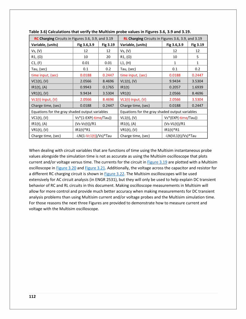
112
Table 3.6) Calculations that verify the Multisim probe values in Figures 3.6, 3.9 and 3.19. RC Charging Circuits in Figures 3.6, 3.9, and 3.19 RL Charging Circuits in Figures 3.6, 3.9, and 3.19
Variable, (units) Fig 3.6,3.9 Fig 3.19 Variable, (units) Fig 3.6,3.9 Fig 3.19 Vs, (V) 12 12 Vs, (V) 12 12 R1, (Ω) 10 20 R1, (Ω) 10 5 C1, (F) 0.01 0.01 L1, (H) 1 1 Tau, (sec) 0.1 0.2 Tau, (sec) 0.1 0.2 time input, (sec) 0.0188 0.2447 time input, (sec) 0.0188 0.2447 VC1(t), (V) 2.0566 8.4696 VL1(t), (V) 9.9434 3.5304 IR1(t), (A) 0.9943 0.1765 IR1(t) 0.2057 1.6939 VR1(t), (V) 9.9434 3.5304 VR1(t) 2.0566 8.4696 Vc1(t) input, (V) 2.0566 8.4696 VL1(t) input, (V) 2.0566 3.5304 Charge time, (sec) 0.0188 0.2447 Charge time, (sec) 0.0188 0.2447 Equations for the gray shaded output variables Equations for the gray shaded output variables VC1(t), (V) Vs*(1-EXP(-time/Tau)) VL1(t), (V) Vs*(EXP(-time/Tau)) IR1(t), (A) (Vs-Vc(t))/R1 IR1(t), (A) (Vs-VL(t))/R1 VR1(t), (V) IR1(t)*R1 VR1(t), (V) IR1(t)*R1 Charge time, (sec) -LN(1-Vc1(t))/Vs)*Tau Charge time, (sec) -LN(VL1(t)/Vs)*Tau
When dealing with circuit variables that are functions of time using the Multisim instantaneous probe values alongside the simulation time is not as accurate as using the Multisim oscilloscope that plots current and/or voltage versus time. The currents for the circuit in Figure 3.19 are plotted with a Multisim oscilloscope in Figure 3.20 and Figure 3.21. Additionally, the voltage across the capacitor and resistor for a different RC charging circuit is shown in Figure 3.22. The Multisim oscilloscopes will be used extensively for AC circuit analysis (in ENGR 2531), but they will only be used to help explain DC transient behavior of RC and RL circuits in this document. Making oscilloscope measurements in Multisim will allow for more control and provide much better accuracy when making measurements for DC transient analysis problems than using Multisim current and/or voltage probes and the Multisim simulation time. For those reasons the next three Figures are provided to demonstrate how to measure current and voltage with the Multisim oscilloscope.

113
Figure 3.20: Multisim oscilloscope plot for the current in the RC and RL charging circuits.
To plot the current on the oscilloscope “current clamps” are placed in the circuits (see XCP1 and XCP2). The red trace is the plot of iC (t) and the y-axis is set at 200 mA per division (each black dotted line square is a division). When the switch is moved into the charging position the current instantly ramps up to 600 mA (12V/20Ω) and decays at an exponential rate as shown in equation 3.19. The blue trace is the plot of iL (t) and the y axis is set at 1 Amp per division. When the switch is moved into the charging position the current starts at zero and ramps up at an exponential rate as shown in equation 3.20 and approaches 2.4 Amps (12V/5Ω) as time approaches infinity. The oscilloscope cursors can be used to determine the current or voltage for DC circuits at different times in their transient region. For example, the following figure shows one cursor the moment the switches are moved into charging position (t = 0) and a second cursor when the traces cross each other. T1 is at an absolute time value of 84.615 ms and since this is the time when the switch is pressed it is referred to as the t = 0 spot. The time (t) in the iC(t) and iL(t) equations is equal to the Multisim delta time (T2-T1 = 160.84 ms). The following figure shows how the calculations match the Multisim oscilloscope (scope) measurements.
Note on Current Clamps: The units on the Multisim scope are fixed to Volts and cannot be changed. However, since a current clamp was used with a 1 mV/mA conversion, the Volts (V) symbols can be assumed to be the same as Amps (A) symbol when looking at the scope since there is a one-to-one mapping between current and voltage using the 1mV/mA scale. If a node voltage wants to be plotted on the scope instead of current all that is needed is to delete the current clamps (labeled XCP1 and XCP2 in Figure 3.20) and wire the scope terminals directly to the nodes. Figure 3.22 shows how to measure and calculate the voltage across a capacitor network in an RC charging circuit.
Note on the (–) input of the scope: The – input of the scope can always be left unconnected for current measurements with the current clamp, but for voltage measurements the – input of the scope can only
IC (t) plot, 200 mA per division
IL (t) plot, 1 A per division

114
be left disconnected if one side of the component you are measuring the voltage across is connected to ground (which is the case for the capacitor, but not the resistor in the circuit in Figure 3.20).
Example 3.5) Use the Multisim oscilloscope cursors shown in Figure 3.21 to determine the initial currents in the RL and RC circuits in Figure 3.20 and the currents when the traces cross over each other. Perform calculations using equations 3.19 and 3.20 to verify that these numbers are accurate.
Figure 3.21: Multisim oscilloscope current measurements compared to calculations.
Multisim Measurements: - Calculations in () RC Circuit – Channel A iC (0) = 599.345 mA (600 mA) iC (160.84 ms) = 268.385 mA (268.47 mA) RL Circuit – Channel B iL (0) = 2.61 mA (0 mA) iL (160.84 ms) = 1.326 A (1.3261 A) Calculations using equations 3.19 and 3.20 Tau = RC = 20Ω ∙ 0.01F = 0.2 seconds iC (0) = 600 mA iC (160.84 ms) = 0.6 e –.16084/0.2 = 268.47 mA Tau = L/R = 1H/5Ω = 0.2 seconds iL (0) = 0 mA iL (160.84 ms) = 2.4 (1 - e –.16084/0.2) = 1.3261 A
IC (t) plot, 200 mA per division
IL (t) plot, 1 A per division

115
Example 3.6) In the circuit in Figure 3.22 determine the VCtotal and VR3 right after switch, S1, is closed (t = 0+) and when the time reaches approximately 1 time constant. At 1 time constant the capacitor will reach approximately 2/3 its total charge (1-e-t/τ = 1-e-1 = .632). The cursor on the scope plot below already has T2-T1 placed as close to the time constant as possible. Perform calculations and compare the results with those obtained from the Multisim oscilloscope.
Figure 3.22: Circuit for Example 3.6 and the measurements and calculations that are required.
Example 3.7) In the circuit in Figure 3.23 determine the VLtot1, VLtot2, VR2, and current in the loop right after switch, S1, is closed (t = 0) and when the time reaches 1 msec. The cursor on the scope plot below already has T2-T1 placed at 1 msec. Perform calculations and compare the results with those obtained from the Multisim oscilloscope.
Tau Calculation: Ctotal = 5µ+10µ+(15µ||20µ) = 23.57 µF Req = 100 + 200 + 300 = 600 Ω Τ = Req ∙ Ctotal = 14.143 msec Multisim Measurements: vC measurement – Channel A vC (0) = 100.056 mV (0 mV calculated) vC (14.188 ms) = 7.636 V (7.6 V calculated) VR3 measurement – Channel B vR3 (0) = 5.95 V (6 V calculated) vR3 (14.188 ms) = 2.182 V (2.2 V calculated) VC (t), VR3 (t), and i (t) Calculations vC (0) = 0 mV (Before switch is pressed) vC (14.188 ms) = 12 (1 - e –.014188/.014143)= 7.6 V To calculate VR3(t), we first need i(t). i(t) = 12 (e –.014188/.014143)/600 = 7.334 mA i(0) = 12/600 = 20 mA i(14.188 ms) =12(e –.014188/.014143)/600 =7.334 mA vR3 (0) = i(0)∙R3 = 20 mA ∙ 300 Ω = 6 V vR3 (14.188 ms) = 7.334 mA ∙ 300 Ω = 2.2 V
VR3 (t) plot, 5V per division
VCtot (t) plot, 5V per division

116
Figure 3.23: Circuit for Example 3.7 and oscilloscope plots.
Multisim Measurements: Scope XSC1 Channel A - vLtot1 measurement vLtot1 (0) = 7.582 V (7.636 V calculated) vLtot1 (1 ms) = 4.013 V (4.04 V calculated) Scope XSC1 Channel B - vLtot2 measurement vLtot2 (0) = 4.333 V (4.364 V calculated) vLtot2 (1 ms) = 2.293 V (2.31 V calculated)
Scope XSC2 Channel A - i measurement i (0) = 28.284 µA (0 A calculated) i (1 ms) = 1.898 mA (1.883 mA calculated) Scope XSC2 Channel B – vR2 measurement VR2 (0) = 56.569 mV (0 mV calculated) VR2 (1 ms) = 3.796 V (3.767 V calculated)
i (t) plot, 5 mA per division
VR2 (t) plot, 5V per division VLtot1 (t) plot, 5V per division
VLtot2 (t) plot, 5V per division

117
VL (t), VR (t), and i (t) Calculations i(0) = 0 (Open circuit, Switch not closed yet) [3.20] i(.001) = 12 (1 - e –.001/.00157)/3000 = 1.883 mA VR1(.001) = 1.883 mA ∙ 1kΩ = 1.883 V VR2(.001) = 1.883 mA ∙ 2kΩ = 3.767 V Initially, the resistors have no current through them so they have zero volts at time = 0 Option 1) Calculating the total inductor voltage using KVL and the previously calculated resistor voltages VLtotal(0) = Vs - VR1(0) - VR2(0) = 12 V VLtotal(.001) = Vs - VR1(.001) - VR2(.001) = 6.35 V You can split up the voltage between inductors in series just like you would do with resistors using VDR. VLtot1(0) = VLtotal(0) ∙ [Ltot1/(Ltot1 + Ltot2] = 12 V (3/(3+1.714)) = 7.636 V VLtot2(0) = VLtotal(0) ∙ [Ltot1/(Ltot1 + Ltot2] = 12 V (1.714/(3+1.714)) = 4.364 V VLtot1(.001) = VLtotal(.001) ∙ [Ltot1/(Ltot1 + Ltot2] = 6.35 V (3/(3+1.714)) = 4.04 V VLtot2(.001) = VLtotal(.001) ∙ [Ltot1/(Ltot1 + Ltot2] = 6.35 V (1.714/(3+1.714)) = 2.31 V Option 2) Calculating the total inductor voltage using equation 3.16 (same results as option 1) [3.16] vLtotal(.001) = 12 (e –.001/.00157) = 6.35 V VLtot1(.001) = 6.35 V (3/(3+1.714)) = 4.04 V VLtot2(.001) = 6.35 V (1.714/(3+1.714)) = 2.31 V
So far only one capacitor or inductor network was included in the example circuits. In Example 3.7 the two inductor networks could be combined into one network since there were no other components in between the two networks. Figure 3.24a shows that even if the two inductor networks are separated by a component the same answers will result. The only thing that would be different between these two circuits is if the node voltage with reference to ground was desired to be calculated. The node voltages would obviously give different values if the order of components was changed, but usually for DC transient analysis you are more interested in voltages across components than node voltages.
NOTE: If only the voltages across individual networks in a single looped circuit is desired (instead of the node voltages) then components (or networks of components) in series can be rearranged in whatever order is desired. This is true for ANY circuit, even circuits with multiple DC or AC voltage source networks in the loop.

118
Figure 3.24a: Left (2 inductor networks separated by a resistor), Right (1 inductor network)
Example 3.8) In the circuit in Figure 3.24b determine the voltage across each resistor and capacitor network right after switch, S1, is closed (t = 0) and when the time reaches 20 msec. The cursor on the scope plot below already has T2-T1 placed at 20 msec. Perform calculations and compare the results with those obtained from the Multisim oscilloscope.
Note on polarized capacitors: Capacitor network 2 includes electrolytic capacitors in Multisim. Notice they have a + sign showing the anode and the cathode has a curved end instead of a flat end like the anode. These capacitors must be placed in the direction of the current flow (as they are in Figure 3.25). Capacitor network 1 included non-polarized capacitors. These capacitors can be put in either direction and the anode will automatically be oriented in the direction of the current flow. Either end of the non-

119
polarized capacitor is capable of being the anode, but only the specified side of the electrolytic capacitor can be the anode.
Figure 3.24b: Circuit for Example 3.8 and oscilloscope plots.
Multisim Measurements: Scope XSC2 Channel A – VRtot1 measurement VRtot1 (0) = 1.127 V (1.132 V calculated) VRtot1 (20 ms) = .6417 V (0.644 V calculated) Scope XSC2 Channel B – vRtot2 measurement VRtot2 (0) = 10.822 V (10.87 V calculated) VRtot2 (20 ms) = 6.16 V (6.18 V calculated)
Scope XSC1 Channel A – vCtot1 measurement VCtot1 (0) = 40.363 mV (0 V calculated) VCtot1 (20 ms) = 4.144 V (4.121 V calculated) Scope XSC1 Channel B – VCtot2 measurement VCtot2 (0) = 10.274 mV (0 V calculated) VCtot2 (20 ms) = 1.055 V (1.049 V calculated)
VRtot1, VRtot2, VCtot1, VCtot2 Calculations Tau = Req ∙ Ctotal = 15.9 kΩ ∙ 2.232 µF = 35.45 ms Vctotal(0) = Vctot1(0) = Vctot2(0) = 0 V (Open circuit, Switch not closed yet) [3.15] Vctotal(.02) = 12 (1 - e –.02/.03545) = 5.17 V You can split up the voltage between capacitors in series similarly to how CDR works with resistors. Vctot1(.02) = Vctotal(.02) ∙ (Ctotal/Ctot1) = 5.17 (2.232/2.8) = 4.121 V Vctot2(.02) = Vctotal(.02) ∙ (Ctotal/Ctot2) = 5.17 (2.232/11) = 1.049 V To calculate voltage across the resistor networks it is easiest to solve for the current first and use VR=I∙R [3.19] i(t) = Vs_tot (e –t/τ)/(Rtot1 + Rtot2) = 12(e –t/.03545)/15900 VRtot1(0) = i(0) ∙ Rtot1 = [12(e –0/.03545)/15900] ∙ 1500 = 1.132 V VRtot1(.02) = i(.02) ∙ Rtot1 = [12(e –.02/.03545)/15900] ∙ 1500 = 0.644 V VRtot2(0) = i(0) ∙ Rtot2 = [12(e –0/.03545)/15900] ∙ 14400 = 10.87 V VRtot2(.02) = i(.02) ∙ Rtot2 = [12(e –.02/.03545)/15900] ∙ 14400 = 6.18 V

120
Section 3.5.2 – Single Loop RL and RC Discharging (Release) Circuits
Since the voltage across a capacitor cannot change instantaneously the voltage the capacitor is charged to at steady state (vC_charge_ss) must be its initial voltage when it is discharged. If there are only resistors in a single loop discharging circuit with one voltage source network the capacitor voltage decreases exponentially according equation 3.21 using the time constant determined from the discharge circuit (τ = Req ∙ C). vC_charge_ss is equal to the source voltage in the charging loop if there is only one capacitor network in the circuit.
[3.21] v𝐶𝐶(t) = 𝑣𝑣𝐶𝐶_𝑠𝑠ℎ𝑎𝑎𝑑𝑑𝑎𝑎𝑠𝑠_𝑠𝑠𝑠𝑠 (𝑒𝑒−𝑡𝑡 τ⁄ ) (Capacitor voltage in a discharging circuit with only resistors)
Since the current across an inductor cannot change instantaneously the current the inductor is charged to at steady state (iL_charge_ss) must be its initial current when it is discharged. If there are only resistors in the single loop discharging circuit with one voltage source network the inductor current decreases exponentially according equation 3.22 using the time constant determined from the discharge circuit (τ = L/Req). iL_charge_ss is equal to the source voltage divided by the sum of the resistors (assuming they are in series) in the charging loop if there is only one inductor network in the circuit.
[3.22] i𝐿𝐿(t) = 𝑚𝑚𝐿𝐿_𝑠𝑠ℎ𝑎𝑎𝑑𝑑𝑎𝑎𝑠𝑠_𝑠𝑠𝑠𝑠 (𝑒𝑒−𝑡𝑡 τ⁄ ) (Inductor current in a discharging circuit with only resistors)
The equations for capacitor current and inductor voltage in a single loop circuit with only resistors are:
[3.23] i𝐶𝐶(t) = 𝑑𝑑𝐶𝐶_𝑐𝑐ℎ𝑎𝑎𝑟𝑟𝑎𝑎𝑒𝑒_𝑠𝑠𝑠𝑠
𝑅𝑅𝑡𝑡𝑡𝑡𝑡𝑡𝑎𝑎𝑡𝑡(𝑒𝑒−𝑡𝑡 τ⁄ ) (Capacitor current in a discharging circuit with only resistors)
[3.24] v𝐿𝐿(t) = v𝑅𝑅𝑡𝑡𝑎𝑎𝑡𝑡𝑎𝑎𝑠𝑠(t) = 𝑚𝑚𝐿𝐿(𝑒𝑒) ∙ 𝑅𝑅𝑡𝑡𝑎𝑎𝑡𝑡𝑎𝑎𝑠𝑠 (Inductor voltage in a discharging circuit with only resistors)
Example 3.9) In the circuit in Figure 3.25, the switches S_C and S_L are initially in the charging circuit and remain there until steady state is reached. Determine the voltage and current of the capacitor and inductor right after switches S_C and S_L are moved to the discharge circuit (t = 0+) and 50 msec after the switches have been moved to the discharge circuit. The cursor on the scope plot below already has T2-T1 placed at 50 msec. Perform calculations and compare the results with those obtained from the Multisim oscilloscope.

121
Figure 3.25: RC and RL discharging circuits for Example 3.9.
Multisim Measurements:
Capacitor and Inductor Voltage and Current Calculations [3.13] RC Circuit, τ = Req ∙ Ctotal = 10 Ω ∙ .01 F = 0.1 s [3.14] RL Circuit, τ = L/Req = 1H/10 Ω = 0.1 s VC(0) = vC_charge_ss = Vs = 12 V iL(0) = iL_charge_ss = Vs/R1 = 12/5 = 2.4 A VC(.05) = vC_charge_ss e-t/τ = 12 (1-e-.05/.1) = 7.278 V iL(.05) = iL_charge_ss e-t/τ = 2.4 e-.05/.1 = 1.456 A iC(0) = vC_charge_ss/R2 = 12/10 = 1.2 A vL(0) = - iL_charge_ss ∙ (R2) = - 2.4 ∙ 10 = -24 V iC(.05) = vC_charge_ss e-t/τ = 1.2 e-.05/.1 = 0.7278 A vL(.05) = -iL(0.05)∙(R2) = 1.456∙10 = -14.56 V The calculations closely match the Multisim scope values.
Scope XSC1 Channel A – VC1 measurement VC1 (0) = 11.872 V (12 V calculated) VC1 (50 ms) = 7.201 V (7.278 V calculated) Scope XSC2 Channel A – iC1 measurement iC1 (0) = 1.187 A (1.2 A calculated) iC1 (50 ms) = 0.72 A (0.7278 A calculated)
Scope XSC1 Channel B – VL1 measurement VL1 (0) = -23.763 V (-24 V calculated) VL1 (50 ms) = -14.413 V (-14.56 V calculated) Scope XSC2 Channel B – iL1 measurement iL1 (0) = 2.376 A (2.4 A V calculated) iL1 (50 ms) = 1.441 A (1.456 A calculated)

122
Note: When adding an LED in this discharge circuit (like the circuit in Figure 3.9) equations 3.21 to 3.24 will no longer work because the requirement of only one voltage source network is violated. When the diode is forward biased the LED is modeled as a Voltage source, which gives the circuit a second component that acts as a source. The capacitor in the discharge circuit acts like a dissipating voltage source and the inductor in a RL discharge circuit acts as a dissipating current source. The circuit in Figure 3.25 is repeated with the addition of an LED and the scope below shows that the values change. The current clamps were moved in this figure so that they are across the capacitor and inductor in the RC and RL discharge circuits respectively. By moving the current clamps, the steady state values of iC and IL can be seen on the scope.
Figure 3.26: RC and RL discharging circuits in Example 3.9 with an LED added.
The disruption on the blue trace on the left circuit of Figure 3.26 (inductor voltage trace) occurs due to the LED going from forward bias to reverse bias at that point in time. When the numbers in Figure 3.26 are compared to Figure 3.25 significant differences can be seen due to the addition of the LED. Calculating the transient region values for circuits like this is beyond the scope of this document.

123
Section 3.6 – DC Steady State Analysis with RC, RL, and RLC Circuits The “steady state” value for a DC circuit is the value when time approaches infinity. In other words, it is the DC value after it stabilizes and stops changing at the end of the transient region. For example, the oscilloscope plot below, which is a duplicate of the current scope plots in Figure 3.26, has a transient region that is approximately located between the two cursors. After the time associated with the second cursor the inductor voltage (blue trace) has stabilized to approximately zero, so 0 V would be considered its steady state value. The capacitor voltage is still at -54.665 mV at the time associated with the second cursor so it is not quite at its steady state value yet, but it is getting close.
DC steady state analysis has already been performed on simple circuits with a single voltage source network and a single loop, but this section will look at how to perform steady state analysis on much more complicated circuits. With the problem solving methodology used in this section circuits can have multiple loops, capacitor and inductor networks in the same circuit, multiple voltage source networks, and even current sources. The following two rules are the only new information you need to know in order to solve complicated DC steady state circuits.
• Capacitors at DC steady state act like open circuits • Inductors at DC steady state act like short circuits
So when solving DC steady state problem, the first step is to replace all of the capacitors with open circuits and replace all of the inductors with short circuits. Once this is done the resulting circuit looks a lot like some of the difficult superposition problems solved in section 2.5. Recall the two “tricky situations” that sometimes result when shorts and opens are added into circuits. These two items from section 2.5 are copied in below.
1. A short in parallel with one or more resistors causes the resistors to be removed (or shorted out) from the circuit. Knowing the fact that a short circuit is just a wire (or a resistor with a value of 0 Ω) it can be combined with resistor, R, to give a value of 0Ω which means the result is a short circuit is: Rtot = 0||R = (0∙R)/(0+R) = 0

124
2. An open circuit in series with one or more resistors (a
resistor network) results in the resistor network having no effect on the circuit. Since an open circuit is the same thing as a resistor with a value of ∞ ohms an open circuit results when added in series with resistor, R. Rtot = ∞ + R = ∞
Once you solve a DC steady state circuit for the current and voltage across where the capacitor or inductor was removed you can use that information to determine other things in the circuit as shown in the table below.
Table 3.7) DC Steady State Summary
Capacitor in a DC steady state circuit Inductor in a DC steady state circuit Model Replace with open circuit Replace with Short circuit Voltage Voltage across open circuit terminals Forced to be 0 since it is a short circuit Current Forced to be 0 since it is an open circuit Current through the short circuit Energy Calculate voltage and plug into E = ½ C ∙ V2 Calculate current and plug into E = ½ L ∙ I2 Charge Calculate voltage and plug into Q = C ∙ V Not Applicable
Since the DC steady state problem solving method is nearly the same as superposition only a couple of examples will be shown next. Refer back to section 2.5 for more problems of a similar nature.
Example 3.10) Solve the DC steady state circuit in Figure 3.27 to determine the energy in every reactive component (i.e. capacitor or inductor).
Figure 3.27: Circuits for Example 3.10.
Step 1 in solving a DC steady state problem is to replace all of the capacitors with open circuits and all of the inductors with short circuits. Once the circuit is redrawn (as shown in Figure 3.28) it is clear that this is a 2-node nodal matrix problem. Node VA is color coded blue and node VB is color coded red in the circuit.

125
Figure 3.28: Circuit in Example 3.10 redrawn and nodal matrix solution
Solving the matrix yields VA = 20 V and VB = 12 V
In order to solve for the capacitor voltage, the voltage at the + side of VC is the node B voltage (VB) and the voltage at the – side of VC is the node A voltage (VA) so Vc = VB – VA = 12 – 20 = - 8V
EC1 = ½ C ∙ VC2 = ½ (300 µF) ∙ (-8)2 = 9.6 mJ
IL2 = IR1 = ΔV/R1 = (VA-VB)/R1 = (20-12)/5 = 1.6 A and from KCL IL1 = 4 – IL2 = 4 – 1.6 = 2.4 A
EL1 = ½ L1 ∙ IL12 = ½ (1 mH) ∙ (2.4)2 = 2.88 mJ
EL2 = ½ L2 ∙ IL22 = ½ (2 mH) ∙ (1.6)2 = 2.56 mJ
Example 3.11) Solve the DC steady state circuit in Figure 3.28 to determine the capacitor charges and perform a power analysis in the circuit and show that equation 1.10 is satisfied (∑ Psupplied = ∑ Pdissipated). Verify the power analysis with Multisim.
Figure 3.29: Circuits for Example 3.11. Different Nodes ARE given different colors (i.e. color coded).

126
Figure 3.30: Circuit in Example 3.11 redrawn and probes included (Nodes are NOT color coded).
First, notice that the power is zero for all of the capacitors and inductors. Since capacitors and inductors are reactive elements they only have what is referred to as “Reactive Power”, which has a variable of Q and units of VARs. Only resistors and sources in this circuit has “Real Power”, P, in Watts. In the ENGR 2531 AC Circuits Book the Reactive and Real power will be covered in great detail when AC circuits are studied.
Figure 3.31: Circuit in Example 3.11 redrawn and mesh matrix solution (Nodes are NOT color coded)
The circuit is simplified by removing R4 because it was in series with the open circuit left by capacitor C2 and removing resistors R5 and R6 because they are “shorted out” by the short circuit from inductor L2. Once the circuit is simplified to Figure 3.31 it is easy to see that this is a simple 2 loop mesh matrix problem. The section of the first minor that has a value of I1 is color coded red and the section of the second minor loop that has a value of I2 is color coded blue. Solving the matrix yields:
• I1 = 5.091 mA
VC2

127
• I2 = 1.636 mA
First, the capacitor voltages will be calculated so the charges can be determined.
• Since there is an open circuit across Vc1 and it is across R2 the voltage is equal to: • (I1-I2) * R2 = (5.091m - 1.636m) *2k = 6.91 V • Q1 = CV = 1 µF ∙ 6.91 V = 6.91 µC • The voltage at VC2 can also be determined by inspection. It is also equal to 0 V because both sides of
the open circuit are at the same node. If you can’t see that you can do a KVL through it also: • KVL: -12 + I1 ∙ 1000 + I2 ∙ 3000 + VC2 = 0 VC2 = 12 – (5.091mA)∙(1kΩ)–(1.636mA)∙(3kΩ) = 0 V • Q2 = CV = 2 µF ∙ 0 V = 0 C
Next, the power analysis will be performed. We know the largest battery in the circuit is a supplier and it has a negative sign in Multisim so that is verified. We also know all resistors are dissipaters, but the 2 V battery is not as obvious. Since its polarity is such that current flows through it from the + side to the – side it is a dissipater. Calculating each side of the equal sign for the power balance equation (3.10) it is shown that the total power supplied and total power dissipated are both equal to 61.1 mW, so equation 3.10 is verified.
• ∑Psupplied = Ps = Vs ∙ I1 = 12 V ∙ 5.091 mA = 61.1 mW • P2V = 2 ∙ I2 = 2 V ∙ 1.636 mA = 3.272 mW • PR1 = I12 ∙ R1 = (.005091 A) 2 ∙ (1000Ω) = 25.92 mW • PR2 = I32 ∙ R2 = (.003455 A) 2 ∙ (2000Ω) = 8.092 mW (Note: I3 calculated from KCL: I3 = I1 – I2) • PR3 = I22 ∙ R3 = (.001636 A) 2 ∙ (3000Ω) = 23.87 mW • ∑Pdissipated = 3.272 mW + 25.92 mW + 8.092 mW + 23.87 mW = 61.1 mW
Section 3.7 – Introduction to Passive Filters
Determining how a circuit that includes capacitors or inductors filters signals of different frequencies is one practical use of the DC steady state analysis method discussed in section 3.6. A filter serves the important function of removing frequencies that aren’t desired or in contrast enhancing frequencies that are desired. The term “frequency” is used to denote the number of cycles per second (Hertz) at which a waveform travels. In AC (Alternating Current) circuits, the signals are usually modeled as sinusoidal waveforms at a specified frequency. For DC circuits the term frequency doesn’t really apply since there are no “cycles”, but if you were to put a frequency value on a DC signal you would say it is at 0 Hertz, which is the lowest possible frequency magnitude. Therefore, DC steady state analysis can be used to determine if a DC input “passes through” or is “reduced” in a circuit. In general, a circuit that “passes through” DC to the output is called a Low Pass Filter (LPF) and if the DC signal is not passed through to the output it is called a High Pass Filter (HPF). An output voltage (or Vout/Vin) versus frequency plot (commonly referred to as the frequency response) can be used to characterize how a filter operates at all possible frequency inputs. This book will not go that deep into filtering since AC sources aren’t covered, but by looking at the DC output the circuits, using DC steady state techniques, the filters will be able to be classified.
The following circuits in Figure 3.22 are all considered HPF circuits because the DC input doesn’t pass through to the output as shown by the 0 Volt reading on the differential voltage probe that is placed across the output in each circuit. When steady state analysis is performed and the capacitor is open-circuited in the

128
first two circuits it is easy to see that the current is shut off to the resistor that the output is taken across, which results in Vout = 0V. When doing steady state analysis for circuits with inductors they are replaced with short circuits. Inductors produce HPF circuits when either the output is taken directly across the inductor (as seen in the 3rd circuit in Figure 3.22) or when the inductor is in parallel to the path of current flow and all of the current flows through the inductor and doesn’t reach the output (as seen in the 4th circuit in Figure 3.22).
Figure 3.32: Passive High Pass Filter (HPF) Circuit Examples
The circuits in Figure 3.33 are examples of LPF circuits. Since capacitors and inductors are opposites, when it comes to filtering, they can be switched and the circuit can be converted between HPF and LPF. The first two circuits in Figure 3.33 were created by replacing the capacitor of the corresponding circuits with an inductor. When this is done the short circuit of the inductor doesn’t inhibit the DC input voltage passing through to the output. The 3rd and 4th circuits in Figure 3.33 were created by replacing the inductor of the corresponding circuits with a capacitor. When this is done in the 3rd circuit the output voltage is taken directly across the battery because no current flows through the resistor so there is no voltage drop. In the 4th circuit the capacitor acting as an open circuit causes it to have no effect on the output. It is important to note that the voltage is reduced in the second and fourth circuit, but this reduction is due to the multiple resistors in the circuit that cause current to split into different paths instead of being reduced by the capacitor or inductor.
Figure 3.33: Passive Low Pass Filter (LPF) Circuit Examples
One last thing should be mentioned about filters. There are two categories of analog filters that are created from electrical components. The type we have been discussing in this section are called passive filters. The term passive means that external power is not required to be used to make the devices work. The input source provides all of the power needed in a passive filter. The other category is active filters. These types of filters are created with transistors or Operational Amplifiers (Op Amps) and require external power for them to function. While there are some situations where passive filters are preferred, active filters have many advantages. A good place to learn about active filters is in chapter 20 of the classic eBook “Opamps for Everyone”.

129
Module 3 – Equation List
Module 3.1 and 3.2 Equations [3.1] 𝐶𝐶 = ℰ𝑟𝑟ℰ𝑡𝑡𝐴𝐴
𝑠𝑠
[3.2] 𝐶𝐶 = 𝑄𝑄𝑉𝑉
[3.3] 𝐸𝐸 = 12
𝐶𝐶 𝑉𝑉2
[3.4] 𝑚𝑚𝐶𝐶(𝑒𝑒) = 𝐶𝐶 𝑠𝑠𝑑𝑑𝑠𝑠𝑡𝑡
[3.5] 𝑣𝑣𝐶𝐶(𝑒𝑒) = 1𝐶𝐶
∫ 𝑚𝑚𝑠𝑠𝑡𝑡𝑡𝑡0
(𝑒𝑒) ∙ 𝑑𝑑𝑑𝑑 + 𝑣𝑣𝑠𝑠(𝑒𝑒0)
[3.6] 𝐿𝐿 = 𝑁𝑁2∙ 𝜇𝜇𝑟𝑟 ∙ 𝜇𝜇0 ∙ 𝐴𝐴
𝑠𝑠
[3.7] 𝐸𝐸 = 12
𝐿𝐿 ∙ 𝑚𝑚2
[3.8] 𝑣𝑣(𝑒𝑒) = 𝐿𝐿 𝑠𝑠𝑚𝑚𝐿𝐿𝑠𝑠𝑡𝑡
[3.9] 𝑚𝑚𝐿𝐿(𝑒𝑒) = 1𝐿𝐿
∫ 𝑣𝑣𝐿𝐿𝑡𝑡𝑡𝑡0
∙ 𝑑𝑑𝑑𝑑 + 𝑚𝑚𝐿𝐿(𝑒𝑒0)
Module 3.3 to 3.5 Equations [3.10] 𝐶𝐶𝑇𝑇𝑎𝑎𝑡𝑡𝑎𝑎𝑠𝑠 = 𝐶𝐶1 + 𝐶𝐶2 + 𝐶𝐶3 + ∙∙∙ 𝐶𝐶𝑁𝑁
[3.11] 𝐶𝐶𝑇𝑇𝑎𝑎𝑡𝑡𝑎𝑎𝑠𝑠 = (𝐶𝐶1∙ 𝐶𝐶2)(𝐶𝐶1+ 𝐶𝐶2)
ONLY with 2 capacitors
[3.12] 𝐶𝐶𝑇𝑇𝑎𝑎𝑡𝑡𝑎𝑎𝑠𝑠 = 11𝐶𝐶1 + 1𝐶𝐶2 + 1𝐶𝐶3 +∙∙∙
1𝐶𝐶𝑁𝑁
[3.13] Tau = τ = 𝑅𝑅𝑠𝑠𝑒𝑒 ∙ 𝐶𝐶𝑡𝑡𝑎𝑎𝑡𝑡𝑎𝑎𝑠𝑠
[3.14] Tau = τ = 𝐿𝐿𝑡𝑡𝑡𝑡𝑡𝑡𝑎𝑎𝑡𝑡𝑅𝑅𝑒𝑒𝑒𝑒
[3.15] v𝐶𝐶(t) = 𝑉𝑉𝑆𝑆 (1 − 𝑒𝑒−𝑡𝑡 τ⁄ )
[3.16] v𝐿𝐿(t) = 𝑉𝑉𝑆𝑆 (𝑒𝑒−𝑡𝑡 τ⁄ )
[3.17] 𝑒𝑒 = − ln(1 −v𝐶𝐶(t)𝑉𝑉𝑆𝑆
) ∙ τ
[3.18] 𝑒𝑒 = − ln( v𝐿𝐿(t)𝑉𝑉𝑆𝑆
) ∙ τ
[3.19] 𝑚𝑚𝑅𝑅 (𝑒𝑒) = 𝑚𝑚𝐶𝐶 (𝑒𝑒) = Δv𝑅𝑅
= 𝑉𝑉𝑆𝑆 −𝑑𝑑𝐶𝐶(𝑡𝑡)∑ 𝑅𝑅𝑖𝑖𝑁𝑁𝑖𝑖
[3.20] 𝑚𝑚𝑅𝑅 (𝑒𝑒) = 𝑚𝑚𝐿𝐿 (𝑒𝑒) = Δv𝑅𝑅
= 𝑉𝑉𝑆𝑆 −𝑑𝑑𝐿𝐿(𝑡𝑡)∑ 𝑅𝑅𝑖𝑖𝑁𝑁𝑖𝑖

130
References and Links The following references and links provide supporting information for this module. All references in this module are either cited within the module within brackets or URL links are either embedded in hyperlinks or fully listed.
References and Links not listed in other Modules
[1] AC Circuits, Chad Davis: https://shareok.org/handle/11244/51946 [2] Multisim: http://www.ni.com/multisim/ [3] Primary referenced site: allaboutcircuits.com [4] Article about John Fagan, past professor at OU, titled “Inspiration by Design”
https://issuu.com/engineerou/docs/82586-evolve-web
Module 1 – References and Links
[1] DC background information: http://www.allaboutcircuits.com/textbook/direct-current/ [2] Hole flow versus electron flow: nk:
http://www.allaboutcircuits.com/textbook/semiconductors/chpt-2/electrons-and-holes/ [3] Sparkfun Switch Basics (including the SPST): https://learn.sparkfun.com/tutorials/switch-
basics/poles-and-throws-open-and-closed [4] Conductor overview: https://en.wikipedia.org/wiki/Electrical_conductor#Conductor_materials [5] Insulator overview: https://en.wikipedia.org/wiki/Insulator_(electricity)#Types_of_Insulators [6] American Standard Wire Gauge (AWG): https://en.wikipedia.org/wiki/American_wire_gauge [7] AWG ampacity: https://en.wikipedia.org/wiki/American_wire_gauge [8] National Electrical Code (NEC): http://www.nfpa.org/codes-and-standards/all-codes-and-
standards/list-of-codes-and-standards?mode=code&code=70 [9] Circular mils description: https://en.wikipedia.org/wiki/Circular_mil
[10] Thermal runaway: https://en.wikipedia.org/wiki/Thermal_runaway [11] Resistor color codes: http://www.allaboutcircuits.com/textbook/reference/chpt-2/resistor-color-
codes/ [12] Duracell 1.5 V battery info: http://data.energizer.com/PDFs/BatteryIR.pdf [13] Energizer 9V NiMh rechargeable battery: Energizer NH22-175 [14] Sparkfun battery tutorial: https://learn.sparkfun.com/tutorials/battery-technologies [15] More battery selection information: http://www.allaboutcircuits.com/technical-articles/how-to-
choose-the-best-battery-for-your-next-project/ [16] Battery construction: http://www.allaboutcircuits.com/textbook/direct-current/chpt-11/battery-
construction/ [17] Lithium Ion battery overview: https://en.wikipedia.org/wiki/Lithium-ion_battery [18] Node definition: https://en.wikipedia.org/wiki/Node_(circuits) [19] Current source design information: http://www.allaboutcircuits.com/technical-articles/the-basic-
mosfet-constant-current-source/ [20] Energizer E92 battery: http://data.energizer.com/PDFs/E92.pdf

131
Module 2 – References and Links
[21] Branch current method: http://www.allaboutcircuits.com/textbook/direct-current/chpt-10/branch-current-method/
[22] Mesh current method: http://www.allaboutcircuits.com/textbook/direct-current/chpt-10/mesh-current-method/
[23] GNU Octave (Like Matlab, but open source): https://en.wikipedia.org/wiki/GNU_Octave [24] Resistive heating element in car window patent: http://www.google.com/patents/US4109133 [25] Nonlinear conduction: http://www.allaboutcircuits.com/textbook/direct-current/chpt-2/nonlinear-
conduction/
Module 3 – References and Links
[26] Background information about capacitor charging: http://hyperphysics.phy-astr.gsu.edu/hbase/electric/capchg.html
[27] Capacitance information: http://www.allaboutcircuits.com/textbook/direct-current/chpt-13/factors-affecting-capacitance/
[28] Capacitor datasheets: http://www.mouser.com/Passive-Components/Capacitors/_/N-5g7r/ [29] multilayer ceramic capacitors (MLCC): http://www.mouser.com/Passive-
Components/Capacitors/Ceramic-Capacitors/MLCCs-Multilayer-Ceramic-Capacitors/_/N-bkrda [30] 747µF electrolytic Capacitor: http://www.mouser.com/ProductDetail/Lelon/REA470M1HBK-
0611P/?qs=sGAEpiMZZMvwFf0viD3Y3fqH3L9WtgZDXp1kZXUu8tQ%3d [31] Capacitors types overview: http://www.mouser.com/Passive-Components/Capacitors/Ceramic-
Capacitors/Ceramic-Disc-Capacitors/_/N-5g90 [32] Film capacitor:
http://www.mouser.com/ProductDetail/KEMET/R82DC3220Z360J/?qs=%2fha2pyFaduj8b%252bNUTxyGtRg3Af1KXo7glSFvp2MYHVB2Fw5002GO5g%3d%3d
[33] Inductor commutating circuits: http://www.allaboutcircuits.com/textbook/semiconductors/chpt-3/inductor-commutating-circuits/
[34] MOSFET overview, http://www.allaboutcircuits.com/textbook/semiconductors/chpt-2/insulated-gate-field-effect-transistors-mosfet/
[35] BS170 MOSFET datasheet: https://www.fairchildsemi.com/datasheets/BS/BS170.pdf [36] IRF520 MOSFET datasheet: http://www.vishay.com/docs/91021/91021.pdf [37] 47 mH inductor: http://www.mouser.com/Search/ProductDetail.aspx?R=RCH895NP-
473Kvirtualkey56750000virtualkey851-RCH895NP-473K [38] OpAmp reference book “Opamps for Everyone”: http://www.siongboon.com/projects/2008-04-
27_analog_electronics/op%20amps%20for%20everyone%20third%20edition%202009%20(Texas%20Instrument).pdf

132
Appendix – Dependent Sources and Laplace Transform Examples
Appendix A.1 – Solving Problems with Dependent Sources using the Matrix Method
The following handwritten example shows how to do Nodal Matrix with a dependent source.

133
The following handwritten example shows how to do Mesh Matrix with a dependent source.

134
Appendix A.2 – Solving RLC Circuits with Laplace Transforms
The following circuit is solved with the equations in section 3.5 and then verified with Laplace Transforms.
τ = 𝐿𝐿𝑅𝑅 = 0.1 10⁄ = 0.01 seconds
v𝐿𝐿(t) = 𝑉𝑉𝑆𝑆 (𝑒𝑒−𝑡𝑡 τ⁄ )= 9(𝑒𝑒−𝑡𝑡 0.01⁄ )
𝑚𝑚𝐿𝐿 (𝑒𝑒) =Δv𝑅𝑅 =
𝑉𝑉𝑆𝑆 − 𝑣𝑣𝐿𝐿(𝑒𝑒)∑ 𝑅𝑅𝑚𝑚𝑁𝑁𝑚𝑚
= .9(1 − 𝑒𝑒−𝑡𝑡 0.01⁄ )
𝑣𝑣𝑅𝑅 (𝑒𝑒) = 𝑚𝑚𝐿𝐿 (𝑒𝑒) ∙ 𝑅𝑅 = 9(1 − 𝑒𝑒−𝑡𝑡 0.01⁄ )

135
The following RC charging circuit (SPDT (switch in position 1 - in the store phase) is solved in Laplace. The solution matches what is obtained in the RC charging circuits in section 3.5.

136
The following shows how to do a multiple loop RLC circuit with Laplace. The solution on this example is left in the Laplace domain as a transfer function H(s) = Vo(s)/Vi(s) = s/(s+5)
If the input voltage is a 9 VDC source, then the output would be equal to Vo(s) = (9/s) ∙ (s/s+5)
Note: Vi(t) = 9 V = 9 u(t), where u(t) is the unit step function (basically the same as 1V).
Using partial fraction expansion and taking the inverse Laplace transform (like is shown on the previous two examples) could be done on this problem to get Vo(t).