High-Frequency Distortion Analysis of Analog Integrated Circuits
11
IEEE TRANSACTIONS ON CIRCUITS AND SYSTEMS—II: ANALOG AND DIGITAL SIGNAL PROCESSING, VOL. 46, NO. 3, MARCH 1999 335 High-Frequency Distortion Analysis of Analog Integrated Circuits Piet Wambacq, Georges G. E. Gielen, Peter R. Kinget, Member, IEEE, and Willy Sansen, Fellow, IEEE Abstract— An approach is presented for the analysis of the nonlinear behavior of analog integrated circuits. The approach is based on a variant of the Volterra series approach for frequency- domain analysis of weakly nonlinear circuits with one input port, such as amplifiers, and with more than one input port, such as analog mixers and multipliers. By coupling numerical results with symbolic results, both obtained with this method, insight into the nonlinear operation of analog integrated circuits can be gained. For accurate distortion computations, the accuracy of the transistor models is critical. A MOS transistor model is discussed that allows us to explain the measured fourth-order nonlinear behavior of a 1-GHz CMOS upconverter. Further, the method is illustrated with several examples, including the analysis of an operational amplifier up to its gain-bandwidth product. This example has also been verified experimentally. Index Terms—Analog integrated circuits, harmonic distortion, nonlinear distortion. I. INTRODUCTION I N the analog design community, many circuits are emerging in which nonlinear effects play an important role. For exam- ple, in switched-current filters [1] and in transconductance-C filters [2], [3], the amplifiers are open-loop circuits, which can cause considerable nonlinear distortion. Further, in analog radio frequency (RF) front-ends of integrated transceivers [4], [5], a knowledge of the nonlinear behavior of building blocks such as low-noise amplifiers and mixers is essential. In this paper, it is described how nonlinear effects in weakly nonlinear, continuous-time analog integrated circuits can be analyzed with the inclusion of more than one nonlinearity and with high-frequency effects. Harmonic and intermodulation distortion are computed both in numerical and symbolic form. The numerical results provide extra insight since the method used can give the contribution to the output distortion of each nonlinearity separately. The symbolic results, on the other hand, are closed-form expressions as a function of one or two input frequencies and of the circuit elements. The symbolic expressions can be simplified with a criterion based on the relative magnitudes of the circuit elements, leading to Manuscript received July 31, 1997; revised June 15, 1998. P. Wambacq was with the Department of Elektrotechniek, ESAT-MICAS, Katholieke Universiteit Leuven, Heverlee, Belgium. He is now with IMEC, Heverlee, Belgium. G. G. E. Gielen is with the National Fund of Scientific Research, Belgium. P. R. Kinget was with the Department of Elektrotechniek, ESAT-MICAS, Katholieke Universiteit Leuven, Heverlee, Belgium. He is now with Bell- Labs, Lucent Technologies, Murray Hill, NJ USA. W. Sansen is with the Department of Elektrotechniek, ESAT-MICAS, Katholieke Universiteit Leuven, Heverlee, Belgium. Publisher Item Identifier S 1057-7130(99)01767-X. interpretable expressions. In this way, circuit designers do not have to worry about how to calculate nonlinear effects. Instead they can obtain insight into those effects by concentrating upon the interpretation of the results. For an analysis of the weakly nonlinear circuit behavior, the nonlinear circuit elements in the equivalent small-signal circuit of a transistor are described with power series which are broken down after the first few terms. The coefficients in these power series, referred to as nonlinearity coefficients, occur in the symbolic expressions of harmonics and intermod- ulation products. These coefficients can be computed by taking higher order derivatives from the transistor model equations as discussed in Section II. However, the value of nonlinearity coefficients is largely influenced by oversimplifications of the model equations or by errors on the model parameters. An accurate model for the drain current of a MOS transistor is presented in Section II. This model is used to explain the measured nonlinear behavior of a 1-GHz CMOS upconverter. The method that is used here to compute harmonics and intermodulation products closely resembles the Volterra series approaches that have been used previously [6]–[9] to compute nonlinear responses numerically. Although the same results are obtained with the Volterra series approach, the method used here is simpler in the sense that it avoids redundant computations. The method is briefly explained in Section III. The symbolic expressions for harmonics or intermodulation products are generated by the coupling of the computation method with a symbolic simulator that generates symbolic expressions for network functions of linearized analog circuits [10]. This is possible since the computation method described here reduces to a repeated solution of sets of linear equations. Modern symbolic analyzers [10]–[14] are able to generate approximate expressions, where the approximation is based upon the numerical values of the circuit parameters. Aspects of the coupling of the calculation method of harmonics, and intermodulation products with the symbolic network analysis approach for linearized circuits described in [12] are discussed in Section IV. The analysis technique is illustrated in Section V with two examples: the second harmonic at the output of a CMOS Miller-compensated operational amplifier, and the third har- monic distortion of a single bipolar transistor amplifier. II. DESCRIPTION OF NONLINEARITIES Most devices commonly used in analog integrated cir- cuits can—for their small-signal behavior—be described with instances of nonlinear (trans)conductances and nonlinear ca- 1057–7130/99$10.00 1999 IEEE
-
Upload
independent -
Category
Documents
-
view
0 -
download
0
Transcript of High-Frequency Distortion Analysis of Analog Integrated Circuits

IEEE TRANSACTIONS ON CIRCUITS AND SYSTEMS—II: ANALOG AND DIGITAL SIGNAL PROCESSING, VOL. 46, NO. 3, MARCH 1999 335
High-Frequency Distortion Analysisof Analog Integrated Circuits
Piet Wambacq, Georges G. E. Gielen, Peter R. Kinget,Member, IEEE,and Willy Sansen,Fellow, IEEE
Abstract—An approach is presented for the analysis of thenonlinear behavior of analog integrated circuits. The approach isbased on a variant of the Volterra series approach for frequency-domain analysis of weakly nonlinear circuits with one input port,such as amplifiers, and with more than one input port, suchas analog mixers and multipliers. By coupling numerical resultswith symbolic results, both obtained with this method, insightinto the nonlinear operation of analog integrated circuits canbe gained. For accurate distortion computations, the accuracyof the transistor models is critical. A MOS transistor model isdiscussed that allows us to explain the measured fourth-ordernonlinear behavior of a 1-GHz CMOS upconverter. Further, themethod is illustrated with several examples, including the analysisof an operational amplifier up to its gain-bandwidth product. Thisexample has also been verified experimentally.
Index Terms—Analog integrated circuits, harmonic distortion,nonlinear distortion.
I. INTRODUCTION
I N the analog design community, many circuits are emergingin which nonlinear effects play an important role. For exam-
ple, in switched-current filters [1] and in transconductance-Cfilters [2], [3], the amplifiers are open-loop circuits, whichcan cause considerable nonlinear distortion. Further, in analogradio frequency (RF) front-ends of integrated transceivers [4],[5], a knowledge of the nonlinear behavior of building blockssuch as low-noise amplifiers and mixers is essential.
In this paper, it is described how nonlinear effects in weaklynonlinear, continuous-time analog integrated circuits can beanalyzed with the inclusion of more than one nonlinearity andwith high-frequency effects. Harmonic and intermodulationdistortion are computed both in numerical and symbolic form.The numerical results provide extra insight since the methodused can give the contribution to the output distortion ofeach nonlinearity separately. The symbolic results, on theother hand, are closed-form expressions as a function of oneor two input frequencies and of the circuit elements. Thesymbolic expressions can be simplified with a criterion basedon the relative magnitudes of the circuit elements, leading to
Manuscript received July 31, 1997; revised June 15, 1998.P. Wambacq was with the Department of Elektrotechniek, ESAT-MICAS,
Katholieke Universiteit Leuven, Heverlee, Belgium. He is now with IMEC,Heverlee, Belgium.
G. G. E. Gielen is with the National Fund of Scientific Research, Belgium.P. R. Kinget was with the Department of Elektrotechniek, ESAT-MICAS,
Katholieke Universiteit Leuven, Heverlee, Belgium. He is now with Bell-Labs, Lucent Technologies, Murray Hill, NJ USA.
W. Sansen is with the Department of Elektrotechniek, ESAT-MICAS,Katholieke Universiteit Leuven, Heverlee, Belgium.
Publisher Item Identifier S 1057-7130(99)01767-X.
interpretable expressions. In this way, circuit designers do nothave to worry about how to calculate nonlinear effects. Insteadthey can obtain insight into those effects by concentrating uponthe interpretation of the results.
For an analysis of the weakly nonlinear circuit behavior,the nonlinear circuit elements in the equivalent small-signalcircuit of a transistor are described with power series whichare broken down after the first few terms. The coefficientsin these power series, referred to asnonlinearity coefficients,occur in the symbolic expressions of harmonics and intermod-ulation products. These coefficients can be computed by takinghigher order derivatives from the transistor model equationsas discussed in Section II. However, the value of nonlinearitycoefficients is largely influenced by oversimplifications of themodel equations or by errors on the model parameters. Anaccurate model for the drain current of a MOS transistor ispresented in Section II. This model is used to explain themeasured nonlinear behavior of a 1-GHz CMOS upconverter.
The method that is used here to compute harmonics andintermodulation products closely resembles the Volterra seriesapproaches that have been used previously [6]–[9] to computenonlinear responses numerically. Although the same resultsare obtained with the Volterra series approach, the methodused here is simpler in the sense that it avoids redundantcomputations. The method is briefly explained in Section III.
The symbolic expressions for harmonics or intermodulationproducts are generated by the coupling of the computationmethod with a symbolic simulator that generates symbolicexpressions for network functions of linearized analog circuits[10]. This is possible since the computation method describedhere reduces to a repeated solution of sets of linear equations.Modern symbolic analyzers [10]–[14] are able to generateapproximate expressions, where the approximation is basedupon the numerical values of the circuit parameters. Aspectsof the coupling of the calculation method of harmonics, andintermodulation products with the symbolic network analysisapproach for linearized circuits described in [12] are discussedin Section IV.
The analysis technique is illustrated in Section V with twoexamples: the second harmonic at the output of a CMOSMiller-compensated operational amplifier, and the third har-monic distortion of a single bipolar transistor amplifier.
II. DESCRIPTION OFNONLINEARITIES
Most devices commonly used in analog integrated cir-cuits can—for their small-signal behavior—be described withinstances of nonlinear (trans)conductances and nonlinear ca-
1057–7130/99$10.00 1999 IEEE

336 IEEE TRANSACTIONS ON CIRCUITS AND SYSTEMS—II: ANALOG AND DIGITAL SIGNAL PROCESSING, VOL. 46, NO. 3, MARCH 1999
pacitances. A nonlinear conductance can be controlled by oneor more voltages.
1) Nonlinear Conductance:For a nonlinear conductance ortransconductance, the current through the element, , isa nonlinear function of up to three voltages , , and .Using a power series expansion around the quiescent value,the total value of the current can be split into a quiescent part
and an ac part.This ac part is given by
(1)
In this series, , , and denote the first-order derivativewith respect to , , and , respectively. These are nothingelse but small-signal parameters. Further, this series impliesthe introduction of the followingnonlinearity coefficients:
(2)
(3)
(4)
in which is an integer larger than 1, andand are positiveintegers. If in the number or equalsone, then this number is omitted as a subscript, as in :
(5)
The same holds for the numbers, , and in (4)such as in .
As a simple example, consider the simplified model of thecollector current of a bipolar transistor:
(6)
in which , , and are the transistor saturation current,the base–emitter voltage, and the thermal voltage, respectively.The first derivative is the transistor transconductance
. The nonlinearity coefficients are found to be
(7)
(a)
(b)
Fig. 1. Nonlinear model of a (a) bipolar and (b) MOS transistor.
2) Nonlinear Capacitance:A nonlinear capacitor is de-scribed with a nonlinear relationship between the charge uponthe capacitor and the voltage over the capacitor in the sameway as the relationship between the current and the controllingvoltage of a one-dimensional conductance. The current throughthe capacitor is obtained by taking the time derivative of thecharge.
A. Weakly Nonlinear Transistor Models
The nonlinearities described in the previous section cannow be tailored together to construct nonlinear equivalentcircuits for transistors. These are straightforward extensionsof the linear equivalent small-signal circuits. The equivalentnonlinear circuit for a bipolar and a MOS transistor are shownin Fig. 1.
The nonlinearity coefficients that are needed to describethe different nonlinearities in a transistor are determined bytaking second- and third-order derivatives, respectively, of themodel equations. Existing circuit simulators provide valuesfor the current and its first derivatives, which are the small-signal parameters, but the higher order derivatives are seldomcomputed. Therefore, routines have been developed tocompute those higher order derivatives. In these routines, thedifferent derivatives are computed as a function of the biasvoltages, the transistor dimensions, and the model parameters.The source code for these routines is derived in an automaticway, by computing symbolically with the symbolic algebraprogram [15] the derivatives of the model equations.The generated expressions are then dumped toformat.
In this way, this approach is open to models that aredifferent from the ones that are used in commercial circuitsimulators. This has the advantage that physical effects thatare poorly modeled in commercially used models can bemodeled more accurately. For example, in MOS models suchas the BSIM3 model [16], many effects are modeled withlow-order polynomials rather than with more complicatedtranscendental functions. In this way, the accuracy for thecomputation of the dc values and the small-signal parameters

WAMBACQ et al.: HF DISTORTION ANALYSIS OF ANALOG INTEGRATED CIRCUITS 337
is still acceptable, whereas the CPU time for the evaluation ofthe model equations is drastically reduced. However, the erroron the higher order derivatives can be high.
With this in mind, the accurate models are only used forthe computation of nonlinearity coefficients, whereas the dcbias point is computed with a numerical simulator using amodel that can be efficiently evaluated, yielding only minordifferences for the bias solution.
As an example, a drain current model for a MOS transistorin the triode region is considered. If velocity saturation andmobility reduction due to the vertical field are taken intoaccount, then the drain current can be written as the productof three functions:
(8)
The function models the drain currentin absence of mobility reduction and velocity saturation. Anaccurate expression for this function, derived in [17], is givenby
(9)
in which is the surface mobility in the absence of mobilityreduction, is the gate oxide capacitance per unit area,is the flat-band voltage, is the surface inversion potential,and is the body-effect coefficient. In order to have a functionthat can be evaluated more efficiently, the function isvery often approximated as follows [16], [18], [19]:
(10)
in which various values are used for the parameter. Inseveral models, is a function of only, and not of theother terminal voltages. As a result, the third-order nonlinearitycoefficient is zero, since the dependence of the currenton is quadratic. This is not correct as can be seenfrom the more accurate expression [see (9)] which containsa 3/2 power term that comprises . This illustrates that anoversimplification of a model can yield very large errors onnonlinearity coefficients.
The function models the mobilityreduction. It has the form
(11)
The factor is the mobility reduction factor [17]. In manymodels, the parameter is often as simple as
(12)
In [20] a more accurate model is used:
(13)
Fig. 2. Relative error in percentage between the nonlinearity coefficients ofan n-MOS transistor in the triode region(W = 320 �m, L = 14 �m,vDS = 0:45 V, vGS = 1:9 V, vSB = 1:3 V) computed with the simplemobility reduction model of (12) and the coefficients computed with the moreexact model of (13). With the latter model, three values of� have beenconsidered:� = 0:05 V�1, corresponding to the white bars,� = 0:065V�1, corresponding to the hatched bars, and� = 0:079 V�1, correspondingto the black bars.
The difference between the nonlinearity coefficients of thedrain current computed with the two models ofgiven aboveincreases with the order of the derivative. This is shown inFig. 2.
Finally, the function models velocitysaturation. In most MOS models that are commonly used, thisis modeled with a function of the form
(14)
Here is the critical electric field [17] that is approximatelyequal to , in which is the saturation velocity and
is the effective mobility. In [21] a moreaccurate model for the function is used:
(15)
The problem of using more accurate expressions for thefunctions , , and than the expressions thatare used in widely used MOS models, is that the draincurrent in saturation has to be computed iteratively, sincethe drain–source saturation voltage is given by animplicit equation. This would require too much CPU time forefficient circuit simulations. For the computation of nonlinear-ity coefficients, however, these models can be used withoutiteration, since it is possible to derive explicit expressionsfor the derivatives of the drain current as a function of thebias voltages and of . If, in the expressions for thederivatives, is evaluated with another, simpler MOSmodel that yields an explicit expression for , then theerror is usually very small.
The expressions for the nonlinearity coefficients are usuallyvery complicated. In order to get insight into the physicaleffects that mainly determine the value of a nonlinearitycoefficient, an approximation procedure has been developedthat can filter out the dominant terms in the expressions of the
338 IEEE TRANSACTIONS ON CIRCUITS AND SYSTEMS—II: ANALOG AND DIGITAL SIGNAL PROCESSING, VOL. 46, NO. 3, MARCH 1999
Fig. 3. Schematic of a 1-GHz CMOS upconversion mixer (22).
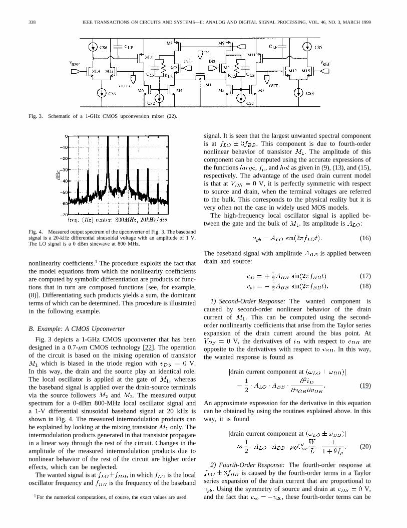
Fig. 4. Measured output spectrum of the upconverter of Fig. 3. The basebandsignal is a 20-kHz differential sinusoidal voltage with an amplitude of 1 V.The LO signal is a 0 dBm sinewave at 800 MHz.
nonlinearity coefficients.1 The procedure exploits the fact thatthe model equations from which the nonlinearity coefficientsare computed by symbolic differentiation are products of func-tions that in turn are composed functions [see, for example,(8)]. Differentiating such products yields a sum, the dominantterms of which can be determined. This procedure is illustratedin the following example.
B. Example: A CMOS Upconverter
Fig. 3 depicts a 1-GHz CMOS upconverter that has beendesigned in a 0.7-m CMOS technology [22]. The operationof the circuit is based on the mixing operation of transistor
which is biased in the triode region with V.In this way, the drain and the source play an identical role.The local oscillator is applied at the gate of , whereasthe baseband signal is applied over the drain-source terminalsvia the source followers and . The measured outputspectrum for a 0-dBm 800-MHz local oscillator signal anda 1-V differential sinusoidal baseband signal at 20 kHz isshown in Fig. 4. The measured intermodulation products canbe explained by looking at the mixing transistor only. Theintermodulation products generated in that transistor propagatein a linear way through the rest of the circuit. Changes in theamplitude of the measured intermodulation products due tononlinear behavior of the rest of the circuit are higher ordereffects, which can be neglected.
The wanted signal is at , in which is the localoscillator frequency and is the frequency of the baseband
1For the numerical computations, of course, the exact values are used.
signal. It is seen that the largest unwanted spectral componentis at . This component is due to fourth-ordernonlinear behavior of transistor . The amplitude of thiscomponent can be computed using the accurate expressions ofthe functions , , and as given in (9), (13), and (15),respectively. The advantage of the used drain current modelis that at V, it is perfectly symmetric with respectto source and drain, when the terminal voltages are referredto the bulk. This corresponds to the physical reality but it isvery often not the case in widely used MOS models.
The high-frequency local oscillator signal is applied be-tween the gate and the bulk of . Its amplitude is :
(16)
The baseband signal with amplitude is applied betweendrain and source:
(17)
(18)
1) Second-Order Response:The wanted component iscaused by second-order nonlinear behavior of the draincurrent of . This can be computed using the second-order nonlinearity coefficients that arise from the Taylor seriesexpansion of the drain current around the bias point. At
V, the derivatives of with respect to areopposite to the derivatives with respect to . In this way,the wanted response is found as
drain current component at
(19)
An approximate expression for the derivative in this equationcan be obtained by using the routines explained above. In thisway, it is found
drain current component at
(20)
2) Fourth-Order Response:The fourth-order response atis caused by the fourth-order terms in a Taylor
series expansion of the drain current that are proportional to. Using the symmetry of source and drain at V,
and the fact that , these fourth-order terms can be

WAMBACQ et al.: HF DISTORTION ANALYSIS OF ANALOG INTEGRATED CIRCUITS 339
combined in one term :
(21)
The fourth-order component in the drain current of nowbecomes
drain current component at
(22)
Using the routines described in Section II-A an approximationfor the coefficient has been computed. With these routines,it is seen that the largest term is 62 times larger than the secondlargest term. Taking into account the largest term only for,yields
(23)
with given by (13). The error on , that is made by takinginto account the largest term only is 2.8% for the given biaspoint in the given CMOS technology.
The factor arises from taking the derivative of thefunction that models velocity saturation. This means thatthe fourth-order response is almost completely determined bythe variation of the drain current due to velocity saturation.Indeed, when the instantaneous drain current becomes highduring operation, then the velocity of the carriers may saturate.
The above results can now be evaluated for the currentdesign. With m /(V s), m, m,
F/m , m/s, V , and amobility reduction factor of in the given bias point,the effective mobility is m /(V s) andMV/m. The ratio of the fourth-order and the second-ordercomponent of the drain current with the given amplitudes isthen found to be 33 dB, which is only 3 dB different fromthe measured ratio.
III. CALCULATION OF NONLINEAR RESPONSES
In weakly nonlinear analog circuits, harmonics and inter-modulation products can be computed using Volterra series [7].In [23] and [24] a similar method is derived that circumventsthe use of Volterra series. The analysis is limited to circuitswith at most two input ports or with two input frequenciesapplied at one input port. In this way, harmonic and two-tone intermodulation distortion can be computed. The methodleads to the same results as the Volterra series approach butit is simpler to use, especially for circuits with more thanone input port, such as a mixer. For such circuits, the use
TABLE INONLINEAR SECOND-ORDER CURRENT SOURCES FOR THEBASIC
NONLINEARITIES TO COMPUTE SECOND-ORDER INTERMODULATION PRODUCTS
AT |!1 � !2| AND SECOND HARMONICS AT 2!1. THE CONTROLLING VOLTAGES
ARE vi FOR THE NONLINEAR (TRANS)CONDUCTANCE AND THE NONLINEAR
CAPACITOR AND vi AND v FOR THE TWO-DIMENSIONAL CONDUCTANCE
of Volterra series requires tensors, which are not used here.Instead, only the components of the tensors are computedthat are of interest for the required response. Further, theVolterra kernel transforms of order, which are functions of
distinct frequency variables, are not computed completely.For example, when a harmonic needs to be computed, thenonly the value of the tensor element of interest needs to becomputed for all frequency variables being equal.
It is assumed that a circuit is excited by at most twosinusoidal input signals at a frequency and , respec-tively. Under steady-state conditions, every node voltageconsists of a sum of harmonic functions as shown in (24) atthe bottom of the page. In this equation, denotes the realpart of its argument, is the phasor of the component ofthe voltage on node at the frequency .
In a first step, the response of the linearized circuit to theexternal inputs is calculated. Together with the component ofthe output voltage at and , the component at and ofall voltages that control a nonlinearity are calculated as well.
In the next step, the second-order responses are calculated.Suppose, for example, that the intermodulation product atthe difference frequency has to be calculated. Tothis purpose, the physical inputs are first put to zero in thelinearized circuit. Instead, the linearized circuit is excited withhigher order correction current sources, denoted asnonlinearcurrent sources of order two. Every nonlinearity in the originalnonlinear circuit gives rise to such a current source in thelinearized circuit. The sources are placed in parallel with eachlinearized element. The output of the circuit as a result of thosecurrent sources yields the required intermodulation product.Hereby, the transfer functions from the current sources tothe output have to be evaluated at the frequency
.The value of the nonlinear current sources of order two (see
Table I) depends on the type of the basic nonlinearity and onthe first-order responses at the controlling voltages.
linear response
2nd-order response
3rd-order response
(24)

340 IEEE TRANSACTIONS ON CIRCUITS AND SYSTEMS—II: ANALOG AND DIGITAL SIGNAL PROCESSING, VOL. 46, NO. 3, MARCH 1999
TABLE IINONLINEAR THIRD-ORDER CURRENT SOURCES FOR THEBASIC NONLINEARITIES
TO COMPUTE THE THIRD HARMONIC AT 3w2. THE CONTROLLING VOLTAGES
ARE vi FOR THE NONLINEAR (TRANS)CONDUCTANCE AND THE NONLINEAR
CAPACITOR, vi, AND v FOR THETWO-DIMENSIONAL CONDUCTANCE,
AND v , vj , AND vk FOR THE THREE-DIMENSIONAL CONDUCTANCE
If one is interested in the second harmonic, a similarapproach is followed. In this case, the transfer functions fromthe current sources to the output have to be evaluated at,and the values of the current sources, which are also given inTable I, are slightly different.
The method can be explained intuitively as follows. Itis assumed that a second-order harmonic or intermodulationproduct is caused by nonlinearities of order two and notby higher-order nonlinearities. A second-order nonlinearitycombines two first-order signals (signals at one of the two fun-damental frequencies) at its controlling terminals and producesa second-order signal. This second-order signal propagatesthrough the circuit to the output. When it is fed into othersecond-order nonlinearities, then higher order signals arise,which are neglected for the computation of second-orderharmonics and intermodulation products. Hence, only thepropagation of the second-order signal through the linearizednetwork is important.
After the second-order signals of interest have been com-puted, the third-order responses can be calculated. Here again,they are computed as the response to nonlinear current sources.These are now determined by the second- and third-ordernonlinearity coefficients and by the first- and second-orderresponse at the controlling voltage(s). This can be seen inTable II, which lists the values of the nonlinear current sourcesfor the computation of the third harmonic of . For otherthird-order responses, the values of the current sources areslightly different. If one is interested in responses of orderhigher than three, then a similar procedure can be followed.
A. Interpretation of the Results
With the calculation method explained above, the harmonicsand intermodulation products of order at the frequency
with are computed as a sum ofcontributions:
(25)
In this equation, is the nonlinear current source of orderfor nonlinearity , and denotes the trans-
fer function from the applied nonlinear current source to theoutput. The sum is taken over all nonlinearities (conductancesor capacitances) in the circuit.
Fig. 5. A CMOS two-stage Miller-compensated opamp.
Fig. 6. An inverting amplifier.
The formulation of nonlinear responses in the form of (25)makes reasoning about distortion possible. Indeed, the transferfunctions which determine the nonlinear current sources, onone hand (see Tables I and II), and the transfer functionsfrom the current sources to the circuit’s output, on the otherhand, can be analyzed either numerically or symbolically andinterpreted. Moreover, since the current sources are appliedto a linear network, the effect of every current source, corre-sponding to one single nonlinearity, can be studied apart fromthe other ones.
IV. A LGORITHMIC ASPECTS
Responses of order higher than one are determined byanalyzing the same linearized network that is used for theanalysis of the linear behavior. This can be exploited inthe symbolic computations. Indeed, the admittance matrixthat arises from the network equations is always the same,apart from the value of the frequency variable. In a symbolicexpression of a network function, the denominator correspondsto the determinant of the admittance matrix. Since theexpression of a nonlinear current source depends on lower-order responses, it is not difficult to see that the denominatorof the value of a nonlinear current source is a combinationof products of admittance matrix determinants, evaluated ata different frequency. For example, it can be shown thatthe denominator of any second-order response at is
, whereas the denominatorof any second harmonic at is . Thisreasoning can be extended to order three.
From the previous paragraph, it is clear that a symbolicexpression for the denominator of a harmonic or intermod-ulation product can be computed once an expression for
has been obtained, whereas the numerator is foundby combining the numerators of several symbolic transferfunctions, either from the input to a voltage that controls anonlinearity or from a nonlinear current source to the output or

WAMBACQ et al.: HF DISTORTION ANALYSIS OF ANALOG INTEGRATED CIRCUITS 341
to another controlling voltage. The final numerator is a nestedexpression, which can be expanded afterwards. However, hugeexpressions are generated, since a practical circuit contains alot of basic nonlinearities and since each nonlinearity gives riseto a nonlinear current source, whose expression can alreadybe quite complicated. In order to manage this complexity,two simplification procedures are used. In a first step, thecontributions of the different nonlinearities are computed nu-merically as a function of one of the fundamental frequenciesin a frequency range of interest, which is discretized into aset of frequency points. Next it is checked at every frequencypoint whether any contributions can be neglected. If at everyfrequency point a nonlinearity can be neglected, then thecorresponding nonlinearity coefficient is set to zero. Thiselimination process is controlled by a user-defined error thatshould not be exceeded in a frequency range of interest. Afterthis first step, usually very few nonlinearities remain withnonzero nonlinearity coefficients.
In a second step an approximate symbolic expression forthe harmonic or intermodulation product of interest is com-puted with the nonlinearities that have not been eliminatedin the previous step. The final symbolic expression will be ahierarchical one, in the form of (25). Even with just a fewnonlinearities, the exact expression is very large for circuitsof practical size. The reason is that the number of termsof a network function increases exponentially with the sizeof the circuit. For large circuits, it is even impossible tocompute the exact expression due to a huge number of terms.This problem is solved by generating the dominant termsonly for every subexpression in (25) without first computingthe exact expression. This is performed with the so-calledsimplification during generationapproach that is described in[12]. This approach uses numerical values of the symboliccircuit parameters for the approximation. The errors that mustbe used for the approximation of every subexpression arecomputed in advance from the user-specified error for the totalexpression. This is performed with the algorithm described in[25] that has been developed for the approximation of nested(hierarchical) expressions. The final simplified expression canbe expanded on user demand.
It must be remarked that the intermediate result obtainedin the first step, namely a knowledge of the significant non-linearities, provides information which is already much morevaluable than simulation results obtained from SPICE-likesimulators with the .DISTO command [9], which do not selectthe significant nonlinearities at all. This knowledge, togetherwith a plot of the different contributions and the total responseas a function of frequency, can already yield enough insightsuch that the user does not need a symbolic analysis anymore.
Currently, symbolic network analysis programs are ableto generate interpretable expressions for linearized circuitshaving about twenty transistors, each being represented bya nine elements equivalent circuit. The same limitation ofcourse applies here. Since in many practical circuits onlya few nonlinearities play a significant role, the extra mem-ory usage and CPU time for symbolic analysis of nonlinearbehavior is limited compared to symbolic analysis of thelinear behavior only.
Fig. 7. The most important contributions to the second harmonic distortionof the output voltage of the CMOS two-stage Miller-compensated opamp ofFig. 5 in the feedback configuration of Fig. 6.
Fig. 8. Measured second and third harmonic distortion on the CMOStwo-stage Miller-compensated opamp of Fig. 5 in the feedback configurationof Fig. 6.
V. EXAMPLES
A. Example 1: A Miller-Compensated Operational Amplifier
In this example, the harmonic distortion is analyzed at theoutput of the CMOS two-stage Miller-compensated opera-tional amplifier of Fig. 5 up to its gain-bandwidth product( ). The amplifier is put in the inverting feedback con-figuration of Fig. 6. It is assumed that the transistors and
match, just like and . Small-signal parametersand nonlinearity coefficients of such matching transistors arerepresented with one symbol. For example, represents theoutput conductance of both and .
The amplifier has a gain-bandwidth of 100 kHz, the loadcapacitance is 10 pF, the load resistance in addition tothe load formed by the feedback resistors is 100 k, and thecompensation capacitance equals 1 pF.
The second harmonic distortion has sixteen contri-butions. These are first calculated as a function of the fun-damental frequency with the method explained in Section III.The most important contributions to are shown in Fig. 7.The other contributions are below70 dB.
It is seen that starts to increase from 1 kHz( ) with 20 dB per decade, and from about50 kHz ( ) with a steeper slope. Beyond the gain-bandwidth decreases rapidly. This behavior is also seenin measurements, as shown in Fig. 8. For the third harmonicdistortion, a similar increase in frequency is seen, but witha steeper slope. Differences in absolute value between thecomputed and measured distortion levels are mainly due to thepoor modeling of the output conductance with the availableSPICE level 2 models.

342 IEEE TRANSACTIONS ON CIRCUITS AND SYSTEMS—II: ANALOG AND DIGITAL SIGNAL PROCESSING, VOL. 46, NO. 3, MARCH 1999
Clearly, only one nonlinearity dominates for frequenciesbelow the gain-bandwidth product (100 kHz), namelythe second-order nonlinearity coefficient of transistor
. This can be explained by the fact that the largest contri-butions to the nonlinear distortion at the output of an amplifieroriginate from the circuit elements close to or at the output,where signal swings are large.
An expression for can be computed by consideringthe contribution of only. By omitting the other contri-butions, the error is never larger than 4%, which is the errorat kHz. At low frequencies, the error is much lower.
The contribution of is first computed in open loop.From (25) this is given by
contribution of(26)
From Table I, the value of is found:
(27)
in which is the fundamental response of the gate-source voltage of . At frequencies well below , thisis easily found to be
(28)
in which is the sum of and the output conductancesof and .
The nonlinear current source of order two that correspondsto flows from the drain of to its source. The transferfunction from this source to the output of the amplifier, whichis the drain of , is given by
(29)
In order to know the second harmonic in closed loop, thesecond harmonic in open loop needs to be divided by
, being the loop gain [27]. Thesecond harmonic distortion is obtained by dividing the secondharmonic by the fundamental response. Doing so, the poles in(28) and (29) are cancelled, and is computed with theabove method as shown in (30) at the bottom of the page.It is seen that increases with 20 dB per decade fromthe frequency . For the given design,this frequency is computed to be 2.3 kHz. At the frequency
, which equals 31 kHz here, the increase iswith 60 dB per decade.
The error between given in (30) and the exact numeri-cal value (without neglecting any contribution of a nonlinearitycoefficient) is smaller than 0.1% at low frequencies andreaches a maximum of 37% at .
Fig. 9. A single bipolar transistor amplifier with a voltage source excitation.
B. Example 2: A Single Bipolar Transistor Amplifier
Fig. 9 shows a common-emitter amplifier loaded with aresistor . The different contributions to the third harmonicat the collector of will be analyzed at high frequencies.
The ac equivalent circuit of the common emitter amplifieris shown in Fig. 10, while the linearized equivalent is shownin Fig. 11. It is seen in Fig. 10 that the collector current isdescribed as a function of two voltages in order to modelboth the exponential dependence on the base–emitter voltageand the Early effect. The different nonlinearities are modeledwith the Gummel–Poon model, with the extension that thenonlinearity of the Early effect is modeled as well [28].However, this nonlinearity plays a negligible role in thisexample. Further, the base resistance has been considered as alinear element for simplicity. This is a reasonable assumptionfor transistors with a large emitter area and at moderatebias currents. At high base currents effects such as currentcrowding, base pushout and/or base conductivity modulationmake the base resistance dependent on the base current [26],such that its nonlinear behavior needs to be taken into account.
The most important transistor parameters are:mA, , , ps, V.
Fig. 12 shows the third harmonic distortion as afunction of frequency together with the most important contri-butions. It is seen that at low frequencies two contributionsplay a role, namely the contributions of and .They partially compensate, such that the total value ofis smaller than the value of the largest contribution.
The total value of begins to increase from about 10MHz. This can be explained as follows. At low frequencies, theimaginary part of the contributions of and is zero.At about 10 MHz, however, a zero occurs in the contributionof and the phase of this contribution goes to 90. On theother hand, the frequency behavior of the contribution ofis still flat, which means that the phase is still about zero. Asa result, the two contributions will not cancel anymore; andwhen their magnitude is equal, at about 80 MHz, then the sumof the two contributions is not zero.
The third harmonic distortion reaches a maximum valuearound 200 MHz. This maximum is about 10 dB higher thanthe low-frequency value of . Beyond 200 MHz,falls off.
(30)

WAMBACQ et al.: HF DISTORTION ANALYSIS OF ANALOG INTEGRATED CIRCUITS 343
Fig. 10. AC-equivalent circuit of the one-transistor amplifier of Fig. 9 driven by a voltage source. The nonlinear capacitancesC� , C�, Ccs, and thenonlinear base and collector current are included.
Fig. 11. Linearized equivalent circuit of Fig. 10.R0
L is the parallel connec-tion of RL and the early resistance ofQ1.
Fig. 12. Third harmonic distortion at the output of the single-transistoramplifier of Fig. 10, as a function of frequency together with its contributions.HD3 has been normalized to an input amplitude of 1 V. Only the mostimportant contributions have been shown.
Around the maximum value in the vicinity of 200 MHz, themost important contribution is due to . From Table IIit is seen that this contribution is proportional to the secondharmonic at the base–emitter voltage. This secondharmonic, together with its most important contributions, isshown in Fig. 13. It is seen that around 200 MHz, the mostimportant contribution to comes from . Thenonlinear current source that corresponds to flows fromthe collector to the emitter. At low frequencies, the transferfunction from this source to the base–emitter voltage is zero,but at high frequencies there is a path from the collector tothe base along .
An approximate expression for that only takes intoaccount has been computed with the above method,resulting in (31) at the bottom of the page, in which isthe determinant of the admittance matrix, given by
(32)
Fig. 13. Second harmonic distortion of the base–emitter voltage in thesingle-transistor amplifier of Fig. 10, as a function of frequency together withits most importatnt contributions.HD2 has been normalized to an inputamplitude of 1 V.
In the given operating point, and around 200 MHz, thisexpression can be simplified to
(33)
VI. CONCLUSIONS
In this paper, the analysis of weakly nonlinear behaviorof analog integrated circuits has been addressed. The methodmakes use of a variant of the Volterra series approach to calcu-late harmonics and intermodulation products in the frequencydomain. However, it is simpler although equally accurate forcircuits with more than one input port, such as mixers andmultipliers. It has been shown how numerical and symbolicresults obtained with this method can be combined in orderto obtain more insight in the nonlinear operation of analogintegrated circuits. The numerical results yield the differentcontributions to the harmonic or intermodulation products ofinterest, and the most important ones can be retrieved. Thesymbolic expressions are generated by a symbolic networkanalysis method that can generate approximate expressions ofthe most important contributions with a user-definable error.
The results depend on nonlinearity coefficients that areproportional to higher order derivatives of model parameters.Routines have been presented for the computation of thesecoefficients, not only based on widely used transistor modelsbut also on more accurate models that can be defined by the
(31)

344 IEEE TRANSACTIONS ON CIRCUITS AND SYSTEMS—II: ANALOG AND DIGITAL SIGNAL PROCESSING, VOL. 46, NO. 3, MARCH 1999
user. The capabilities of these routines have been illustratedwith the analysis of the fourth-order nonlinear behavior in a1-GHz CMOS upconverter.
The complete approach has been illustrated with several ex-amples: the harmonic distortion in an operational amplifier inclosed loop has been analyzed as a function of frequency andcompared to experimental results; next, the main contributionsto the third harmonic distortion in a single bipolar transistoramplifier at high frequencies have been analyzed.
REFERENCES
[1] T. Fiez, G. Liang, and D. Allstot, “Switched-current circuit designissues,”IEEE J. Solid-State Circuits,vol. 26, pp. 192–202, Mar. 1991.
[2] V. Gopinathan, Y. Tsividis, K.-S. Tan, and R. Hester, “Design consid-erations for high-frequency continuous-time filters and implementationof an antialiasing filter for digital video,”IEEE J. Solid-State Circuits,vol. 25, pp. 1368–1378, Dec. 1990.
[3] G. De Veirman, S. Ueda, J. Cheng, S. Tam, K. Fukahori, M. Kurisu,and E. Shinozaki, “A 3.0 V 40 Mb/s hard disk drive read channel IC,”IEEE J. Solid-State Circuits,vol. 30, pp. 788–799, July 1995.
[4] A. Abidi, “Direct conversion radio transceivers for digital communi-cations,” IEEE J. Solid-State Circuits,vol. 30, pp. 1399–1410, Dec.1995.
[5] R. Meyer and W. Mack, “A 2.5 GHz BiCMOS transceiver for wirelessLAN,” in Proc. ISSCC 1997,1997, pp. 310–311.
[6] Y. Kuo, “Distortion analysis of bipolar transistor circuits,”IEEE Trans.Circuit Theory,vol. CT-20, pp. 709–716, Nov. 1973.
[7] J. Bussgang, L. Ehrman, and J. Graham, “Analysis of nonlinear systemswith multiple inputs,”Proc. IEEE,vol. 62, pp. 1088–1118, Aug. 1974.
[8] L. O. Chua and C.-Y. Ng, “Frequency-domain analysis of nonlinearsystems: Formulation of transfer functions,”IEE J. Electron. CircuitsSyst.,vol. 3, no. 6, pp. 257–269, Nov. 1979.
[9] J. Roychowdhury, “SPICE3 distortion analysis,” Memo. no. UCB/ERLM89/48, Univ. Calif., Berkeley, Apr. 1989.
[10] G. Gielen, H. Walscharts, and W. Sansen, “ISAAC: A symbolic sim-ulator for analog integrated circuits,”IEEE J. Solid-State Circuits,vol.24, pp. 1587–1597, Dec. 1989.
[11] F. V. Fernandez, A. Rodrıguez-Vazquez, and J. L. Huertas, “Interactiveac modeling and characterization of analog circuits via symbolic anal-ysis,” Kluwer J. Analog Integrated Circuits Signal Processing,vol. 1,pp. 183–208, Nov. 1991.
[12] P. Wambacq, F. Fernandez, G. Gielen, W. Sansen, and A. Rodrıguez-Vazquez, “Efficient symbolic computation of approximated small-signalcharacteristics,”IEEE J. Solid-State Circuits,vol. 30, pp. 327–330, Mar.1995.
[13] J. J. Hsu and C. Sechen, “DC small signal symbolic analysis of largeanalog integrated circuits,”IEEE Trans. Circuits Syst.—I,vol. 41, pp.817–828, Dec. 1994.
[14] Q. Yu and C. Sechen, “Approximate symbolic analysis of large analogintegrated circuits,” inProc. IEEE/ACM ICCAD,1994, pp. 664–671.
[15] MapleV Language Reference Manual.New York: Springer-Verlag,1991.
[16] BSIM3v3 User’s Manual,Dept. Elec. Eng. Computer Sci., Univ. Berke-ley, 1995.
[17] Y. Tsividis, Operation and Modeling of the MOS Transistor.NewYork: McGraw-Hill International Editions, 1988.
[18] S. Liu and L. Nagel, “Small-signal MOSFET models for analog circuitdesign,” IEEE J. Solid-State Circuits,vol. SC-17, pp. 983–998, Dec.1982.
[19] B. Sheu, D. Sharfetter, P.-K. Ko, and M.-C. Jeng, “BSIM: Berkeleyshort-channel IGFET model for MOS transistors,”IEEE J. Solid-StateCircuits, vol. SC-22, pp. 558–566, Aug. 1987.
[20] M. White, F. Van De Wiele, and J.-P. Lambot, “High-accuracy MOSmodels for computer-aided design,”IEEE Trans. Electron Devices,vol.ED-27, pp. 899–906, May 1980.
[21] T. Grotjohn and B. Hoefflinger, “A parametric short-channel MOStransistor model for subthreshold and strong inversion current,”IEEETrans. Electron Devices,vol. ED-31, pp. 234–246, Feb. 1984.
[22] P. Kinget and M. Steyaert, “A 1-GHz CMOS up-conversion mixer,”IEEE J. Solid-State Circuits,vol. 32, pp. 370–376, Mar. 1997.
[23] P. Wambacq, G. Gielen, and W. Sansen, “Symbolic simulation of har-monic distortion in analog integrated circuits with weak nonlinearities,”in Proc. ISCAS,May 1990, pp. 536–539.
[24] P. Wambacq and W. Sansen,Distortion Analysis of Analog IntegratedCircuits. Norwell, MA: Kluwer, 1998.
[25] F. V. Fernandez, A. Rodr´ıguez-Vazquez, and J. L. Huertas, “Formulaapproximation for flat and hierarchical symbolic analysis,”Kluwer J.Analog Integrated Circuits Signal Processing,vol. 3, no. 1, pp. 43–58,Jan. 1993.
[26] J.-S. Yuan, J. Liou, and W. Eisenstadt, “A physics-based current-dependent base resistance model for advanced bipolar transistors,”IEEETrans. Electron Devices,vol. 35, pp. 1055–1062, July 1988.
[27] S. Narayanan, “Application of Volterra series to intermodulation dis-tortion analysis of transistor feedback amplifiers,”IEEE Trans. CircuitTheory,vol. CT-17, pp. 518–527, Nov. 1970.
[28] C. Andrew and L. Nagel, “Early effect modeling in SPICE,”IEEE J.Solid-State Circuits,vol. SC-31, pp. 136–138, Jan. 1996.
Piet Wambacq was born in Asse, Belgium, in1963. He received the M.Sc. degree in electrical andmechanical engineering in 1986 from the KatholiekeUniversiteit Leuven, Belgium. From 1986 to 1996,he worked as a Research Assistant at the ESAT-MICAS Laboratory of the Katholieke UniversieitLeuven, where he received the Ph.D. degree in 1996on symbolic analysis of large and weakly nonlinearanalog integrated circuits.
Since 1996, he has been working at IMEC ondesign methodologies for mixed-signal integrated
circuits. His research interests are design and CAD of analog and mixed-signal integrated circuits. He has authored or coauthored more than 30 papersin edited books, international journals, and conference proceedings. He is theauthor of the bookDistortion Analysis of Analog Integrated Circuits.
Georges G. E. Gielenreceived the M.Sc. and Ph.D. degrees in electricalengineering from the Katholieke Universiteit Leuven, Belgium, in 1986 and1990, respectively.
From 1986 to 1990, he was appointed as a Research Assistant by the BelgianNational Fund of Scientific Research for carrying out his Ph.D. research inthe ESAT-MICAS Laboratory of the Katholieke Universieit Leuven. In 1990,he was appointed as a Postdoctoral Research Assistant and Visiting Lecturerat the Department of Electrical Engineering and Computer Science of theUnviersity of California, Berkeley. From 1991 to 1993, he was a postdoctoralResearch Assistant of the Belgian National Fund of Scientific Research at theESAT-MICAS Laboratory of the Katholieke Universiteit Leuven. In 1993,he was appointed as a tenure Research Associate of the Belgian NationalFund of Scientific Research, and at the same time as an Assistant Professorat the Katholieke Universieit Leuven. In 1995, he was promoted to AssociateProfessor at the same university. His research interests are in the design ofanalog and mixed-signal integrated circuits, especially analog and mixed-signal CAD tools and design automation (modeling, simulation, symbolicanalysis, analog synthesis, analog layout generation, and analog and mixed-signal testing). He is coordinator or partner of several (industrial) researchprojects in this area. He has authored or coauthored one book and more than100 papers in edited books, international journals, and conference proceedings.
Dr. Gielen is a regular member of the program committees of internationalconferences (ICCAD, ED&TC, etc.), he has served as Associate Editor of theIEEE TRANSACTIONS ON CIRCUITS AND SYSTEMS PART I, and is a member ofthe editorial board of theKluwer International Journal on Analog IntegratedCircuits and Signal Processing. He is a member of ACM.
Peter R. Kinget (S’88–M’90) received the engineering degree in electricaland mechanical engineering and the Ph.D. degree in electrical engineeringfrom the Katholieke Universiteit Leuven, Belgium, in 1990 and 1996, respec-tively.
From 1991 to 1995, he received a fellowship from the Belgium NationalFund for Scientific Research (NFWO) that allowed him to work as a ResearchAssistant at the ESAT-MICAS Laboratory of the Katholieke UniversiteitLeuven. In October 1996, he joined Bell Laboratories, Lucent Technologies,in Murray Hill, NJ, as a Member of the Technical Staff. His research interestsare in analog and telecommunications integrated circuits.

WAMBACQ et al.: HF DISTORTION ANALYSIS OF ANALOG INTEGRATED CIRCUITS 345
Willy Sansen(S’66–M’72–SM’86–F’95) was born in Poperinge, Belgium, onMay 16, 1943. He received the masters degree in electrical engineering fromthe Katholieke Universieit Leuven in 1967 and the Ph.D. degree in electronicsfrom the University of California, Berkeley, in 1972.
In 1968, he was employed as a Research Assistant at K.U. Leuven. In1971, he was employed as a Teaching Fellow at U.C. Berkeley. In 1972,he was appointed by the National Fund of Scientific Research (Belgium) asa Research Associate at the ESAT Laboratory of the K.U. Leuven, wherehe has been a Full Professor since 1981. During the period 1984–1990,he was head of the Electrical Engineering Department. In 1978, he spentthe winter quarter at Stanford University as a Visiting Assistant Professor.In 1981, he was a Visiting Professor at the Federal Technical UniversityLausanne, and in 1985 at the University of Pennsylvania, Philadelphia. Hehas been involved in design automation and in numerous analog integratedcircuit designs for telecom, consumer electronics, medical applications, andsensors. He has been supervisor of 25 Ph.D. theses in the same field. He hasauthored and coauthored five books and 300 papers in international journalsand conference proceedings.
Dr. Sansen is a member of several editorial committees of journals suchas the IEEE JOURNAL OF SOLID-STATE CIRCUITS, Sensors and Actuators, HighSpeed Electronics, etc. He serves regularly on the program committees ofconferences such as ISSCC, ESSCIRC, ASICTT, EUROSENSORS, TRANS-DUCERS, EDAC, etc.