Analysis and Design of Analog Integrated Circuits, 5th Edition
897
-
Upload
khangminh22 -
Category
Documents
-
view
0 -
download
0
Transcript of Analysis and Design of Analog Integrated Circuits, 5th Edition


ANALYSIS AND DESIGNOF ANALOG INTEGRATEDCIRCUITSFifth Edition
PAUL R. GRAYUniversity of California, Berkeley
PAUL J. HURSTUniversity of California, Davis
STEPHEN H. LEWISUniversity of California, Davis
ROBERT G. MEYERUniversity of California, Berkeley
New York / Chichester / Weinheim / Brisbane / Singapore / Toronto

PUBLISHER Don Fowley
ACQUISITIONS EDITOR Daniel Sayre
SENIOR PRODUCTION EDITOR Valerie A. Vargas
EXECUTIVE MARKETING MANAGER Christopher Ruel
DESIGNER Arthur Medina
PRODUCTION MANAGEMENT SERVICES Elm Street Publishing Services
EDITORIAL ASSISTANT Carolyn Weisman
MEDIA EDITOR Lauren Sapira
Cover courtesy of Chi Ho Law.
This book was set in 10/12 Times Roman by Thomson Digital and printed and bound byHamilton Printing Company. The cover was printed by Phoenix Color, Inc.
This book was printed on acid-free paper. ©∞
Copyright 2009 © John Wiley & Sons, Inc. All rights reserved.
No part of this publication may be reproduced, stored in a retrieval system or transmittedin any form or by any means, electronic, mechanical, photocopying, recording, scanningor otherwise, except as permitted under Sections 107 or 108 of the 1976 United StatesCopyright Act, without either the prior written permission of the Publisher, orauthorization through payment of the appropriate per-copy fee to the Copyright ClearanceCenter Inc., 222 Rosewood Drive, Danvers, MA 01923, website www.copyright.com.Requests to the Publisher for permission should be addressed to the PermissionsDepartment, John Wiley & Sons, Inc., 111 River Street, Hoboken, NJ 07030-5774, (201)748-6011, fax (201) 748-6008, website http://www.wiley.com/go/permissions. To orderbooks or for customer service please call 1-800-CALL-WILEY (255-5945).
http://www.wiley.com/college/gray
Library of Congress Cataloging-in-Publication Data
Analysis and design of analog integrated circuits / Paul R. Gray . . . [et al.]. — 5th ed.p. cm.
Includes bibliographical references and index.ISBN 978-0-470-24599-6 (cloth: alk. paper)1. Linear integrated circuits-Computer-aided design. 2. Metal oxide
semiconductors-Computer-aided design. 3. Bipolar transistors-Computer-aided design.I. Gray, Paul R., 1942-
TK7874.A588 2009
621.3815–dc21 08-043583
Printed in the United States of America
10 9 8 7 6 5 3 2 1

To Liz, Barbara, Robin, and Judy

Preface
Since the publication of the first edition of this book, the field of analog integrated circuits hasdeveloped and matured. The initial groundwork was laid in bipolar technology, followed bya rapid evolution of MOS analog integrated circuits. Thirty years ago, CMOS technologieswere fast enough to support applications only at audio frequencies. However, the continu-ing reduction of the minimum feature size in integrated-circuit (IC) technologies has greatlyincreased the maximum operating frequencies, and CMOS technologies have become fastenough for many new applications as a result. For example, the bandwidth in some videoapplications is about 4 MHz, requiring bipolar technologies as recently as about twenty-threeyears ago. Now, however, CMOS easily can accommodate the required bandwidth for videoand is being used for radio-frequency applications. Today, bipolar integrated circuits are used insome applications that require very low noise, very wide bandwidth, or driving low-impedanceloads.
In this fifth edition, coverage of the bipolar 741 op amp has been replaced with a low-voltage bipolar op amp, the NE5234, with rail-to-rail common-mode input range and almostrail-to-rail output swing. Analysis of a fully differential CMOS folded-cascode operationalamplifier (op amp) is now included in Chapter 12. The 560B phase-locked loop, which is nolonger commercially available, has been deleted from Chapter 10.
The SPICE computer analysis program is now readily available to virtually all electricalengineering students and professionals, and we have included extensive use of SPICE in thisedition, particularly as an integral part of many problems. We have used computer analysis asit is most commonly employed in the engineering design process—both as a more accuratecheck on hand calculations, and also as a tool to examine complex circuit behavior beyond thescope of hand analysis.
An in-depth look at SPICE as an indispensable tool for IC robust design can be found inThe SPICE Book, 2nd ed., published by J. Wiley and Sons. This text contains many workedout circuit designs and verification examples linked to the multitude of analyses available inthe most popular versions of SPICE. The SPICE Book conveys the role of simulation as anintegral part of the design process, but not as a replacement for solid circuit-design knowledge.
This book is intended to be useful both as a text for students and as a reference book forpracticing engineers. For class use, each chapter includes many worked problems; the problemsets at the end of each chapter illustrate the practical applications of the material in the text. Allof the authors have extensive industrial experience in IC design and in the teaching of courseson this subject; this experience is reflected in the choice of text material and in the problemsets.
Although this book is concerned largely with the analysis and design of ICs, a considerableamount of material also is included on applications. In practice, these two subjects are closelylinked, and a knowledge of both is essential for designers and users of ICs. The latter composethe larger group by far, and we believe that a working knowledge of IC design is a greatadvantage to an IC user. This is particularly apparent when the user must choose from among anumber of competing designs to satisfy a particular need. An understanding of the IC structureis then useful in evaluating the relative desirability of the different designs under extremes ofenvironment or in the presence of variations in supply voltage. In addition, the IC user is in a
iv

Preface v
much better position to interpret a manufacturer’s data if he or she has a working knowledgeof the internal operation of the integrated circuit.
The contents of this book stem largely from courses on analog integrated circuits given atthe University of California at the Berkeley and Davis campuses. The courses are senior-levelelectives and first-year graduate courses. The book is structured so that it can be used as thebasic text for a sequence of such courses. The more advanced material is found at the end ofeach chapter or in an appendix so that a first course in analog integrated circuits can omit thismaterial without loss of continuity. An outline of each chapter is given below with suggestionsfor material to be covered in such a first course. It is assumed that the course consists of threehours of lecture per week over a fifteen-week semester and that the students have a workingknowledge of Laplace transforms and frequency-domain circuit analysis. It is also assumedthat the students have had an introductory course in electronics so that they are familiar withthe principles of transistor operation and with the functioning of simple analog circuits. Unlessotherwise stated, each chapter requires three to four lecture hours to cover.
Chapter 1 contains a summary of bipolar transistor and MOS transistor device physics.We suggest spending one week on selected topics from this chapter, with the choice of topicsdepending on the background of the students. The material of Chapters 1 and 2 is quite importantin IC design because there is significant interaction between circuit and device design, as willbe seen in later chapters. A thorough understanding of the influence of device fabrication ondevice characteristics is essential.
Chapter 2 is concerned with the technology of IC fabrication and is largely descriptive.One lecture on this material should suffice if the students are assigned the chapter to read.
Chapter 3 deals with the characteristics of elementary transistor connections. The materialon one-transistor amplifiers should be a review for students at the senior and graduate levels andcan be assigned as reading. The section on two-transistor amplifiers can be covered in aboutthree hours, with greatest emphasis on differential pairs. The material on device mismatcheffects in differential amplifiers can be covered to the extent that time allows.
In Chapter 4, the important topics of current mirrors and active loads are considered. Theseconfigurations are basic building blocks in modern analog IC design, and this material shouldbe covered in full, with the exception of the material on band-gap references and the materialin the appendices.
Chapter 5 is concerned with output stages and methods of delivering output power to a load.Integrated-circuit realizations of Class A, Class B, and Class AB output stages are described,as well as methods of output-stage protection. A selection of topics from this chapter shouldbe covered.
Chapter 6 deals with the design of operational amplifiers (op amps). Illustrative examplesof dc and ac analysis in both MOS and bipolar op amps are performed in detail, and the limita-tions of the basic op amps are described. The design of op amps with improved characteristicsin both MOS and bipolar technologies are considered. This key chapter on amplifier designrequires at least six hours.
In Chapter 7, the frequency response of amplifiers is considered. The zero-value time-constant technique is introduced for the calculations of the –3-dB frequency of complex circuits.The material of this chapter should be considered in full.
Chapter 8 describes the analysis of feedback circuits. Two different types of analysis arepresented: two-port and return-ratio analyses. Either approach should be covered in full withthe section on voltage regulators assigned as reading.
Chapter 9 deals with the frequency response and stability of feedback circuits and shouldbe covered up to the section on root locus. Time may not permit a detailed discussion of rootlocus, but some introduction to this topic can be given.

vi Preface
In a fifteen-week semester, coverage of the above material leaves about two weeks forChapters 10, 11, and 12. A selection of topics from these chapters can be chosen as follows.Chapter 10 deals with nonlinear analog circuits and portions of this chapter up to Section10.2 could be covered in a first course. Chapter 11 is a comprehensive treatment of noisein integrated circuits and material up to and including Section 11.4 is suitable. Chapter 12describes fully differential operational amplifiers and common-mode feedback and may bebest suited for a second course.
We are grateful to the following colleagues for their suggestions for and/or evaluation ofthis book: R. Jacob Baker, Bernhard E. Boser, A. Paul Brokaw, Iwen Chao, John N. Churchill,David W. Cline, Kenneth C. Dyer, Ozan E. Erdoğan, John W. Fattaruso, Weinan Gao, EdwinW. Greeneich, Alex Gros-Balthazard, Tünde Gyurics, Ward J. Helms, Kaveh Hosseini, Tim-othy H. Hu, Shafiq M. Jamal, John P. Keane, Haideh Khorramabadi, Pak Kim Lau, ThomasW. Matthews, Krishnaswamy Nagaraj, Khalil Najafi, Borivoje Nikolić, Keith O’Donoghue,Robert A. Pease, Lawrence T. Pileggi, Edgar Sánchez-Sinencio, Bang-Sup Song, Richard R.Spencer, Eric J. Swanson, Andrew Y. J. Szeto, Yannis P. Tsividis, Srikanth Vaidianathan, T. R.Viswanathan, Chorng-Kuang Wang, Dong Wang, and Mo Maggie Zhang. We are also gratefulto Darrel Akers, Mu Jane Lee, Lakshmi Rao, Nattapol Sitthimahachaikul, Haoyue Wang, andMo Maggie Zhang for help with proofreading, and to Chi Ho Law for allowing us to use on thecover of this book a die photograph of an integrated circuit he designed. Finally, we would liketo thank the staffs at Wiley and Elm Street Publishing Services for their efforts in producingthis edition.
The material in this book has been greatly influenced by our association with the lateDonald O. Pederson, and we acknowledge his contributions.
Berkeley and Davis, CA, 2008 Paul R. GrayPaul J. HurstStephen H. LewisRobert G. Meyer

Contents
CHAPTER 1Models for Integrated-Circuit ActiveDevices 1
1.1 Introduction 1
1.2 Depletion Region of a pn Junction 1
1.2.1 Depletion-Region Capacitance 5
1.2.2 Junction Breakdown 6
1.3 Large-Signal Behavior of BipolarTransistors 8
1.3.1 Large-Signal Models in theForward-Active Region 8
1.3.2 Effects of Collector Voltage onLarge-Signal Characteristics in theForward-Active Region 14
1.3.3 Saturation and Inverse-ActiveRegions 16
1.3.4 Transistor Breakdown Voltages 20
1.3.5 Dependence of Transistor CurrentGain βF on Operating Conditions23
1.4 Small-Signal Models of BipolarTransistors 25
1.4.1 Transconductance 26
1.4.2 Base-Charging Capacitance 27
1.4.3 Input Resistance 28
1.4.4 Output Resistance 29
1.4.5 Basic Small-Signal Model of theBipolar Transistor 30
1.4.6 Collector-Base Resistance 30
1.4.7 Parasitic Elements in theSmall-Signal Model 31
1.4.8 Specification of TransistorFrequency Response 34
1.5 Large-Signal Behavior ofMetal-Oxide-SemiconductorField-Effect Transistors 38
1.5.1 Transfer Characteristics of MOSDevices 38
1.5.2 Comparison of Operating Regions ofBipolar and MOS Transistors 45
1.5.3 Decomposition of Gate-SourceVoltage 47
1.5.4 Threshold TemperatureDependence 47
1.5.5 MOS Device Voltage Limitations48
1.6 Small-Signal Models of MOSTransistors 49
1.6.1 Transconductance 50
1.6.2 Intrinsic Gate-Source andGate-Drain Capacitance 51
1.6.3 Input Resistance 52
1.6.4 Output Resistance 52
1.6.5 Basic Small-Signal Model of theMOS Transistor 52
1.6.6 Body Transconductance 53
1.6.7 Parasitic Elements in theSmall-Signal Model 54
1.6.8 MOS Transistor FrequencyResponse 55
1.7 Short-Channel Effects in MOSTransistors 59
1.7.1 Velocity Saturation from theHorizontal Field 59
1.7.2 Transconductance and TransitionFrequency 63
1.7.3 Mobility Degradation from theVertical Field 65
1.8 Weak Inversion in MOS Transistors 65
1.8.1 Drain Current in Weak Inversion 66
1.8.2 Transconductance and TransitionFrequency in Weak Inversion 69
1.9 Substrate Current Flow in MOSTransistors 71
A.1.1 Summary of Active-DeviceParameters 73
vii

viii Contents
CHAPTER 2Bipolar, MOS, and BiCMOSIntegrated-Circuit Technology 78
2.1 Introduction 78
2.2 Basic Processes in Integrated-CircuitFabrication 79
2.2.1 Electrical Resistivity of Silicon 79
2.2.2 Solid-State Diffusion 80
2.2.3 Electrical Properties of DiffusedLayers 82
2.2.4 Photolithography 84
2.2.5 Epitaxial Growth 86
2.2.6 Ion Implantation 87
2.2.7 Local Oxidation 87
2.2.8 Polysilicon Deposition 87
2.3 High-Voltage BipolarIntegrated-Circuit Fabrication 88
2.4 Advanced Bipolar Integrated-CircuitFabrication 92
2.5 Active Devices in Bipolar AnalogIntegrated Circuits 95
2.5.1 Integrated-Circuit npn Transistors96
2.5.2 Integrated-Circuit pnp Transistors107
2.6 Passive Components in BipolarIntegrated Circuits 115
2.6.1 Diffused Resistors 115
2.6.2 Epitaxial and Epitaxial PinchResistors 119
2.6.3 Integrated-Circuit Capacitors 120
2.6.4 Zener Diodes 121
2.6.5 Junction Diodes 122
2.7 Modifications to the Basic BipolarProcess 123
2.7.1 Dielectric Isolation 123
2.7.2 Compatible Processing forHigh-Performance Active Devices124
2.7.3 High-Performance PassiveComponents 127
2.8 MOS Integrated-Circuit Fabrication127
2.9 Active Devices in MOS IntegratedCircuits 131
2.9.1 n-Channel Transistors 131
2.9.2 p-Channel Transistors 144
2.9.3 Depletion Devices 144
2.9.4 Bipolar Transistors 145
2.10 Passive Components in MOSTechnology 146
2.10.1 Resistors 146
2.10.2 Capacitors in MOS Technology 148
2.10.3 Latchup in CMOS Technology 151
2.11 BiCMOS Technology 152
2.12 Heterojunction Bipolar Transistors 153
2.13 Interconnect Delay 156
2.14 Economics of Integrated-CircuitFabrication 156
2.14.1 Yield Considerations inIntegrated-Circuit Fabrication 157
2.14.2 Cost Considerations inIntegrated-Circuit Fabrication 159
A.2.1 SPICE Model-Parameter Files 162
CHAPTER 3Single-Transistor and Multiple-TransistorAmplifiers 169
3.1 Device Model Selection forApproximate Analysis of AnalogCircuits 170
3.2 Two-Port Modeling of Amplifiers 171
3.3 Basic Single-Transistor AmplifierStages 173
3.3.1 Common-Emitter Configuration174
3.3.2 Common-Source Configuration 178
3.3.3 Common-Base Configuration 182
3.3.4 Common-Gate Configuration 185
3.3.5 Common-Base and Common-GateConfigurations with Finite r0 1873.3.5.1 Common-Base and
Common-Gate InputResistance 187
3.3.5.2 Common-Base andCommon-Gate OutputResistance 189

Contents ix
3.3.6 Common-Collector Configuration(Emitter Follower) 191
3.3.7 Common-Drain Configuration(Source Follower) 194
3.3.8 Common-Emitter Amplifier withEmitter Degeneration 196
3.3.9 Common-Source Amplifier withSource Degeneration 199
3.4 Multiple-Transistor Amplifier Stages201
3.4.1 The CC-CE, CC-CC, and DarlingtonConfigurations 201
3.4.2 The Cascode Configuration 2053.4.2.1 The Bipolar Cascode 2053.4.2.2 The MOS Cascode 207
3.4.3 The Active Cascode 210
3.4.4 The Super Source Follower 212
3.5 Differential Pairs 214
3.5.1 The dc Transfer Characteristic of anEmitter-Coupled Pair 214
3.5.2 The dc Transfer Characteristic withEmitter Degeneration 216
3.5.3 The dc Transfer Characteristic of aSource-Coupled Pair 217
3.5.4 Introduction to the Small-SignalAnalysis of Differential Amplifiers220
3.5.5 Small-Signal Characteristics ofBalanced Differential Amplifiers223
3.5.6 Device Mismatch Effects inDifferential Amplifiers 2293.5.6.1 Input Offset Voltage and
Current 2303.5.6.2 Input Offset Voltage of the
Emitter-Coupled Pair 2303.5.6.3 Offset Voltage of the
Emitter-Coupled Pair:Approximate Analysis 231
3.5.6.4 Offset Voltage Drift in theEmitter-Coupled Pair 233
3.5.6.5 Input Offset Current of theEmitter-Coupled Pair 233
3.5.6.6 Input Offset Voltage of theSource-Coupled Pair 234
3.5.6.7 Offset Voltage of theSource-Coupled Pair:Approximate Analysis 235
3.5.6.8 Offset Voltage Drift in theSource-Coupled Pair 236
3.5.6.9 Small-Signal Characteristicsof Unbalanced DifferentialAmplifiers 237
A.3.1 Elementary Statistics and the GaussianDistribution 244
CHAPTER 4Current Mirrors, Active Loads, andReferences 251
4.1 Introduction 251
4.2 Current Mirrors 251
4.2.1 General Properties 251
4.2.2 Simple Current Mirror 2534.2.2.1 Bipolar 2534.2.2.2 MOS 255
4.2.3 Simple Current Mirror with BetaHelper 2584.2.3.1 Bipolar 2584.2.3.2 MOS 260
4.2.4 Simple Current Mirror withDegeneration 2604.2.4.1 Bipolar 2604.2.4.2 MOS 261
4.2.5 Cascode Current Mirror 2614.2.5.1 Bipolar 2614.2.5.2 MOS 264
4.2.6 Wilson Current Mirror 2724.2.6.1 Bipolar 2724.2.6.2 MOS 275
4.3 Active Loads 276
4.3.1 Motivation 276
4.3.2 Common-Emitter–Common-SourceAmplifier with ComplementaryLoad 277
4.3.3 Common-Emitter–Common-SourceAmplifier with Depletion Load 280
4.3.4 Common-Emitter–Common-SourceAmplifier with Diode-ConnectedLoad 282
4.3.5 Differential Pair with Current-MirrorLoad 2854.3.5.1 Large-Signal Analysis 2854.3.5.2 Small-Signal Analysis 2864.3.5.3 Common-Mode Rejection
Ratio 291

x Contents
4.4 Voltage and Current References 297
4.4.1 Low-Current Biasing 2974.4.1.1 Bipolar Widlar Current
Source 2974.4.1.2 MOS Widlar Current
Source 3004.4.1.3 Bipolar Peaking Current
Source 3014.4.1.4 MOS Peaking Current
Source 302
4.4.2 Supply-Insensitive Biasing 3034.4.2.1 Widlar Current Sources
3044.4.2.2 Current Sources Using Other
Voltage Standards 3054.4.2.3 Self-Biasing 307
4.4.3 Temperature-Insensitive Biasing3154.4.3.1 Band-Gap-Referenced
Bias Circuits in BipolarTechnology 315
4.4.3.2 Band-Gap-ReferencedBias Circuits in CMOSTechnology 321
A.4.1 Matching Considerations in CurrentMirrors 325A.4.1.1 Bipolar 325A.4.1.2 MOS 328
A.4.2 Input Offset Voltage of DifferentialPair with Active Load 330A.4.2.1 Bipolar 330A.4.2.2 MOS 332
CHAPTER 5Output Stages 341
5.1 Introduction 341
5.2 The Emitter Follower as an Output Stage341
5.2.1 Transfer Characteristics of theEmitter-Follower 341
5.2.2 Power Output and Efficiency 344
5.2.3 Emitter-Follower DriveRequirements 351
5.2.4 Small-Signal Properties of theEmitter Follower 352
5.3 The Source Follower as an Output Stage353
5.3.1 Transfer Characteristics of the SourceFollower 353
5.3.2 Distortion in the Source Follower355
5.4 Class B Push–Pull Output Stage 359
5.4.1 Transfer Characteristic of the Class BStage 360
5.4.2 Power Output and Efficiency of theClass B Stage 362
5.4.3 Practical Realizations of Class BComplementary Output Stages 366
5.4.4 All-npn Class B Output Stage 373
5.4.5 Quasi-Complementary Output Stages376
5.4.6 Overload Protection 377
5.5 CMOS Class AB Output Stages 379
5.5.1 Common-Drain Configuration 380
5.5.2 Common-Source Configuration withError Amplifiers 381
5.5.3 Alternative Configurations 3885.5.3.1 Combined Common-Drain
Common-SourceConfiguration 388
5.5.3.2 Combined Common-DrainCommon-SourceConfiguration with HighSwing 390
5.5.3.3 Parallel Common-SourceConfiguration 390
CHAPTER 6Operational Amplifiers withSingle-Ended Outputs 400
6.1 Applications of Operational Amplifiers401
6.1.1 Basic Feedback Concepts 401
6.1.2 Inverting Amplifier 402
6.1.3 Noninverting Amplifier 404
6.1.4 Differential Amplifier 404
6.1.5 Nonlinear Analog Operations 405
6.1.6 Integrator, Differentiator 406
6.1.7 Internal Amplifiers 4076.1.7.1 Switched-Capacitor
Amplifier 4076.1.7.2 Switched-Capacitor
Integrator 412

Contents xi
6.2 Deviations from Ideality in RealOperational Amplifiers 415
6.2.1 Input Bias Current 415
6.2.2 Input Offset Current 416
6.2.3 Input Offset Voltage 416
6.2.4 Common-Mode Input Range 416
6.2.5 Common-Mode Rejection Ratio(CMRR) 417
6.2.6 Power-Supply Rejection Ratio(PSRR) 418
6.2.7 Input Resistance 420
6.2.8 Output Resistance 420
6.2.9 Frequency Response 420
6.2.10 Operational-Amplifier EquivalentCircuit 420
6.3 Basic Two-Stage MOS OperationalAmplifiers 421
6.3.1 Input Resistance, Output Resistance,and Open-Circuit Voltage Gain 422
6.3.2 Output Swing 423
6.3.3 Input Offset Voltage 424
6.3.4 Common-Mode Rejection Ratio427
6.3.5 Common-Mode Input Range 427
6.3.6 Power-Supply Rejection Ratio(PSRR) 430
6.3.7 Effect of Overdrive Voltages 434
6.3.8 Layout Considerations 435
6.4 Two-Stage MOS Operational Amplifierswith Cascodes 438
6.5 MOS Telescopic-Cascode OperationalAmplifiers 439
6.6 MOS Folded-Cascode OperationalAmplifiers 442
6.7 MOS Active-Cascode OperationalAmplifiers 446
6.8 Bipolar Operational Amplifiers 448
6.8.1 The dc Analysis of the NE5234Operational Amplifier 452
6.8.2 Transistors thatAre Normally Off467
6.8.3 Small-Signal Analysis of theNE5234 Operational Amplifier 469
6.8.4 Calculation of the Input Offset Voltageand Current of the NE5234 477
CHAPTER 7Frequency Response of IntegratedCircuits 490
7.1 Introduction 490
7.2 Single-Stage Amplifiers 490
7.2.1 Single-Stage Voltage Amplifiers andthe Miller Effect 4907.2.1.1 The Bipolar Differential
Amplifier: Differential-Mode Gain 495
7.2.1.2 The MOS DifferentialAmplifier: Differential-Mode Gain 499
7.2.2 Frequency Response of theCommon-Mode Gain for aDifferential Amplifier 501
7.2.3 Frequency Response of VoltageBuffers 5037.2.3.1 Frequency Response of the
Emitter Follower 5057.2.3.2 Frequency Response of the
Source Follower 511
7.2.4 Frequency Response of CurrentBuffers 5147.2.4.1 Common-Base Amplifier
Frequency Response 5167.2.4.2 Common-Gate Amplifier
Frequency Response 517
7.3 Multistage Amplifier FrequencyResponse 518
7.3.1 Dominant-Pole Approximation 518
7.3.2 Zero-Value Time Constant Analysis519
7.3.3 Cascode Voltage-AmplifierFrequency Response 524
7.3.4 Cascode Frequency Response 527
7.3.5 Frequency Response of a CurrentMirror Loading a Differential Pair534
7.3.6 Short-Circuit Time Constants 536
7.4 Analysis of the Frequency Response ofthe NE5234 Op Amp 539
7.4.1 High-Frequency Equivalent Circuit ofthe NE5234 539
7.4.2 Calculation of the −3-dB Frequencyof the NE5234 540
7.4.3 Nondominant Poles of the NE5234542

xii Contents
7.5 Relation Between Frequency Responseand Time Response 542
CHAPTER 8Feedback 553
8.1 Ideal Feedback Equation 553
8.2 Gain Sensitivity 555
8.3 Effect of Negative Feedback onDistortion 555
8.4 Feedback Configurations 557
8.4.1 Series-Shunt Feedback 557
8.4.2 Shunt-Shunt Feedback 560
8.4.3 Shunt-Series Feedback 561
8.4.4 Series-Series Feedback 562
8.5 Practical Configurations and the Effectof Loading 563
8.5.1 Shunt-Shunt Feedback 563
8.5.2 Series-Series Feedback 569
8.5.3 Series-Shunt Feedback 579
8.5.4 Shunt-Series Feedback 583
8.5.5 Summary 587
8.6 Single-Stage Feedback 587
8.6.1 Local Series-Series Feedback 587
8.6.2 Local Series-Shunt Feedback 591
8.7 The Voltage Regulator as a FeedbackCircuit 593
8.8 Feedback Circuit Analysis Using ReturnRatio 599
8.8.1 Closed-Loop Gain Using ReturnRatio 601
8.8.2 Closed-Loop Impedance FormulaUsing Return Ratio 607
8.8.3 Summary—Return-Ratio Analysis612
8.9 Modeling Input and Output Ports inFeedback Circuits 613
CHAPTER 9Frequency Response and Stability ofFeedback Amplifiers 624
9.1 Introduction 624
9.2 Relation Between Gain and Bandwidthin Feedback Amplifiers 624
9.3 Instability and the Nyquist Criterion626
9.4 Compensation 633
9.4.1 Theory of Compensation 633
9.4.2 Methods of Compensation 637
9.4.3 Two-Stage MOS AmplifierCompensation 643
9.4.4 Compensation of Single-StageCMOS Op Amps 650
9.4.5 Nested Miller Compensation 654
9.5 Root-Locus Techniques 664
9.5.1 Root Locus for a Three-Pole TransferFunction 665
9.5.2 Rules for Root-Locus Construction667
9.5.3 Root Locus for Dominant-PoleCompensation 676
9.5.4 Root Locus for Feedback-ZeroCompensation 677
9.6 Slew Rate 681
9.6.1 Origin of Slew-Rate Limitations681
9.6.2 Methods of Improving Slew-Rate inTwo-Stage Op Amps 685
9.6.3 Improving Slew-Rate in Bipolar OpAmps 687
9.6.4 Improving Slew-Rate in MOS OpAmps 688
9.6.5 Effect of Slew-Rate Limitationson Large-Signal SinusoidalPerformance 692
A.9.1 Analysis in Terms of Return-RatioParameters 693
A.9.2 Roots of a Quadratic Equation 694
CHAPTER 10Nonlinear Analog Circuits 704
10.1 Introduction 704
10.2 Analog Multipliers Employing theBipolar Transistor 704
10.2.1 The Emitter-Coupled Pair as a SimpleMultiplier 704
10.2.2 The dc Analysis of the GilbertMultiplier Cell 706

Contents xiii
10.2.3 The Gilbert Cell as an AnalogMultiplier 708
10.2.4 A Complete Analog Multiplier 711
10.2.5 The Gilbert Multiplier Cell as aBalanced Modulator and PhaseDetector 712
10.3 Phase-Locked Loops (PLL) 716
10.3.1 Phase-Locked Loop Concepts 716
10.3.2 The Phase-Locked Loop in theLocked Condition 718
10.3.3 Integrated-Circuit Phase-LockedLoops 727
10.4 Nonlinear Function Synthesis 731
CHAPTER 11Noise in Integrated Circuits 736
11.1 Introduction 736
11.2 Sources of Noise 736
11.2.1 Shot Noise 736
11.2.2 Thermal Noise 740
11.2.3 Flicker Noise (1/f Noise) 741
11.2.4 Burst Noise (Popcorn Noise) 742
11.2.5 Avalanche Noise 743
11.3 Noise Models of Integrated-CircuitComponents 744
11.3.1 Junction Diode 744
11.3.2 Bipolar Transistor 745
11.3.3 MOS Transistor 746
11.3.4 Resistors 747
11.3.5 Capacitors and Inductors 747
11.4 Circuit Noise Calculations 748
11.4.1 Bipolar Transistor Noise Performance750
11.4.2 Equivalent Input Noise and theMinimum Detectable Signal 754
11.5 Equivalent Input Noise Generators 756
11.5.1 Bipolar Transistor Noise Generators757
11.5.2 MOS Transistor Noise Generators762
11.6 Effect of Feedback on NoisePerformance 764
11.6.1 Effect of Ideal Feedback on NoisePerformance 764
11.6.2 Effect of Practical Feedback onNoise Performance 765
11.7 Noise Performance of Other TransistorConfigurations 771
11.7.1 Common-Base Stage NoisePerformance 771
11.7.2 Emitter-Follower NoisePerformance 773
11.7.3 Differential-Pair NoisePerformance 773
11.8 Noise in Operational Amplifiers 776
11.9 Noise Bandwidth 782
11.10 Noise Figure and Noise Temperature786
11.10.1 Noise Figure 786
11.10.2 Noise Temperature 790
CHAPTER 12Fully Differential OperationalAmplifiers 796
12.1 Introduction 796
12.2 Properties of Fully DifferentialAmplifiers 796
12.3 Small-Signal Models for BalancedDifferential Amplifiers 799
12.4 Common-Mode Feedback 804
12.4.1 Common-Mode Feedback at LowFrequencies 805
12.4.2 Stability and CompensationConsiderations in a CMFBLoop 810
12.5 CMFB Circuits 811
12.5.1 CMFB Using Resistive Divider andAmplifier 812
12.5.2 CMFB Using Two DifferentialPairs 816
12.5.3 CMFB Using Transistors in theTriode Region 819
12.5.4 Switched-Capacitor CMFB 821
12.6 Fully Differential Op Amps 823
12.6.1 A Fully Differential Two-Stage OpAmp 823
12.6.2 Fully Differential Telescopic CascodeOp Amp 833
xiv Symbol Convention
12.6.3 Fully Differential Folded-Cascode OpAmp 834
12.6.4 A Differential Op Amp with TwoDifferential Input Stages 835
12.6.5 Neutralization 835
12.7 Unbalanced Fully Differential Circuits838
12.8 Bandwidth of the CMFB Loop 844
12.9 Analysis of a CMOS Fully DifferentialFolded-Cascode Op Amp 845
12.9.1 DC Biasing 848
12.9.2 Low-Frequency Analysis 850
12.9.3 Frequency and Time Responses in aFeedback Application 856
Index 871
Symbol Convention
Unless otherwise stated, the following symbol convention is used in this book. Bias or dcquantities, such as transistor collector current IC and collector-emitter voltage VCE, arerepresented by uppercase symbols with uppercase subscripts. Small-signal quantities, suchas the incremental change in transistor collector current ic, are represented by lowercasesymbols with lowercase subscripts. Elements such as transconductance gm in small-signalequivalent circuits are represented in the same way. Finally, quantities such as total col-lector current Ic, which represent the sum of the bias quantity and the signal quantity, arerepresented by an uppercase symbol with a lowercase subscript.

CHAPTER 1
Models for Integrated-CircuitActive Devices
1.1 IntroductionThe analysis and design of integrated circuits depend heavily on the utilization of suitablemodels for integrated-circuit components. This is true in hand analysis, where fairly simplemodels are generally used, and in computer analysis, where more complex models are encoun-tered. Since any analysis is only as accurate as the model used, it is essential that the circuitdesigner have a thorough understanding of the origin of the models commonly utilized and thedegree of approximation involved in each.
This chapter deals with the derivation of large-signal and small-signal models forintegrated-circuit devices. The treatment begins with a consideration of the properties of pn
junctions, which are basic parts of most integrated-circuit elements. Since this book is primarilyconcerned with circuit analysis and design, no attempt has been made to produce a comprehen-sive treatment of semiconductor physics. The emphasis is on summarizing the basic aspectsof semiconductor-device behavior and indicating how these can be modeled by equivalentcircuits.
1.2 Depletion Region of a pn JunctionThe properties of reverse-biased pn junctions have an important influence on the character-istics of many integrated-circuit components. For example, reverse-biased pn junctions existbetween many integrated-circuit elements and the underlying substrate, and these junctionsall contribute voltage-dependent parasitic capacitances. In addition, a number of importantcharacteristics of active devices, such as breakdown voltage and output resistance, dependdirectly on the properties of the depletion region of a reverse-biased pn junction. Finally, thebasic operation of the junction field-effect transistor is controlled by the width of the depletionregion of a pn junction. Because of its importance and application to many different problems,an analysis of the depletion region of a reverse-biased pn junction is considered below. Theproperties of forward-biased pn junctions are treated in Section 1.3 when bipolar-transistoroperation is described.
Consider a pn junction under reverse bias as shown in Fig. 1.1. Assume constant dopingdensities of ND atoms/cm3 in the n-type material and NA atoms/cm3 in the p-type material.(The characteristics of junctions with nonconstant doping densities will be described later.)Due to the difference in carrier concentrations in the p-type and n-type regions, there exists aregion at the junction where the mobile holes and electrons have been removed, leaving thefixed acceptor and donor ions. Each acceptor atom carries a negative charge and each donoratom carries a positive charge, so that the region near the junction is one of significant spacecharge and resulting high electric field. This is called the depletion region or space-charge
1

2 Chapter 1 � Models for Integrated-Circuit Active Devices
V1
V
x
x
x
V2
W2–W1
Electric field
Distance
Potential
(c)
(b)
(a)
(d)
�
–q NA
q ND
VR
0 + VR
p n
+
+–
–
Charge density
Applied externalreverse bias
�
�
Figure 1.1 The abrupt junctionunder reverse bias VR.(a) Schematic. (b) Chargedensity. (c) Electric field.(d ) Electrostatic potential.
region. It is assumed that the edges of the depletion region are sharply defined as shown inFig. 1.1, and this is a good approximation in most cases.
For zero applied bias, there exists a voltage ψ0 across the junction called the built-inpotential. This potential opposes the diffusion of mobile holes and electrons across the junctionin equilibrium and has a value1
ψ0 = VT lnNAND
n2i
(1.1)
where
VT = kT
q� 26 mV at 300◦K
the quantity ni is the intrinsic carrier concentration in a pure sample of the semiconductor andni � 1.5 × 1010cm−3 at 300◦K for silicon.
In Fig. 1.1 the built-in potential is augmented by the applied reverse bias, VR, and the totalvoltage across the junction is (ψ0 + VR). If the depletion region penetrates a distance W1 intothe p-type region and W2 into the n-type region, then we require
W1NA = W2ND (1.2)
because the total charge per unit area on either side of the junction must be equal in magnitudebut opposite in sign.

1.2 Depletion Region of a pn Junction 3
Poisson’s equation in one dimension requires that
d2V
dx2 = −ρ
ε= qNA
εfor −W1 < x < 0 (1.3)
where ρ is the charge density, q is the electron charge (1.6 × 10⁻¹⁹ coulomb), and ε is thepermittivity of the silicon (1.04 × 10⁻¹² farad/cm). The permittivity is often expressed as
ε = KSε0 (1.4)
where KS is the dielectric constant of silicon and ε0 is the permittivity of free space (8.86 ×10⁻¹⁴ F/cm). Integration of (1.3) gives
dV
dx= qNA
εx + C1 (1.5)
where C1 is a constant. However, the electric field � is given by
� = −dV
dx= −
(qNA
εx + C1
)(1.6)
Since there is zero electric field outside the depletion region, a boundary condition is
� = 0 for x = −W1
and use of this condition in (1.6) gives
� = −qNA
ε(x + W1) = −dV
dxfor −W1 < x < 0 (1.7)
Thus the dipole of charge existing at the junction gives rise to an electric field that varieslinearly with distance.
Integration of (1.7) gives
V = qNA
ε
(x2
2+ W1x
)+ C2 (1.8)
If the zero for potential is arbitrarily taken to be the potential of the neutral p-type region, thena second boundary condition is
V = 0 for x = −W1
and use of this in (1.8) gives
V = qNA
ε
(x2
2+ W1x + W2
1
2
)for −W1 < x < 0 (1.9)
At x = 0, we define V = V1, and then (1.9) gives
V1 = qNA
ε
W21
2(1.10)
If the potential difference from x = 0 to x = W2 is V2, then it follows that
V2 = qND
ε
W22
2(1.11)
and thus the total voltage across the junction is
ψ0 + VR = V1 + V2 = q
2ε(NAW2
1 + NDW22 ) (1.12)

4 Chapter 1 � Models for Integrated-Circuit Active Devices
Substitution of (1.2) in (1.12) gives
ψ0 + VR = qW21 NA
2ε
(1 + NA
ND
)(1.13)
From (1.13), the penetration of the depletion layer into the p-type region is
W1 =
⎡⎢⎢⎣ 2ε(ψ0 + VR)
qNA
(1 + NA
ND
)⎤⎥⎥⎦
1/2
(1.14)
Similarly,
W2 =
⎡⎢⎢⎣ 2ε(ψ0 + VR)
qND
(1 + ND
NA
)⎤⎥⎥⎦
1/2
(1.15)
Equations 1.14 and 1.15 show that the depletion regions extend into the p-type and n-typeregions in inverse relation to the impurity concentrations and in proportion to
√ψ0 + VR. If
either ND or NA is much larger than the other, the depletion region exists almost entirely inthe lightly doped region.
EXAMPLE
An abrupt pn junction in silicon has doping densities NA = 1015 atoms/cm3 and ND = 1016
atoms/cm3. Calculate the junction built-in potential, the depletion-layer depths, and the max-imum field with 10 V reverse bias.
From (1.1)
ψ0 = 26 ln1015 × 1016
2.25 × 10²⁰ mV = 638 mV at 300◦K
From (1.14) the depletion-layer depth in the p-type region is
W1 =(
2 × 1.04 × 10−12 × 10.64
1.6 × 10−19 × 1015 × 1.1
)1/2
= 3.5 × 10⁻⁴cm
= 3.5 �m (where 1 �m = 1 micrometer = 10−6 m)
The depletion-layer depth in the more heavily doped n-type region is
W2 =(
2 × 1.04 × 10−12 × 10.64
1.6 × 10−19 × 1016 × 11
)1/2
= 0.35 × 10⁻⁴ cm = 0.35 �m
Finally, from (1.7) the maximum field that occurs for x = 0 is
�max = −qNA
εW1 = −1.6 × 10−19 × 1015 × 3.5 × 10−4
1.04 × 10−12
= −5.4 × 10⁴ V/cm
Note the large magnitude of this electric field.

1.2 Depletion Region of a pn Junction 5
1.2.1 Depletion-Region Capacitance
Since there is a voltage-dependent charge Q associated with the depletion region, we cancalculate a small-signal capacitance Cj as follows:
Cj = dQ
dVR
= dQ
dW1
dW1
dVR
(1.16)
Now
dQ = AqNAdW1 (1.17)
where A is the cross-sectional area of the junction. Differentiation of (1.14) gives
dW1
dVR
=
⎡⎢⎢⎣ ε
2qNA
(1 + NA
ND
)(ψ0 + VR)
⎤⎥⎥⎦
1/2
(1.18)
Use of (1.17) and (1.18) in (1.16) gives
Cj = A
[qεNAND
2(NA + ND)
]1/2 1√ψ0 + VR
(1.19)
The above equation was derived for the case of reverse bias VR applied to the diode.However, it is valid for positive bias voltages as long as the forward current flow is small.Thus, if VD represents the bias on the junction (positive for forward bias, negative for reversebias), then (1.19) can be written as
Cj = A
[qεNAND
2(NA + ND)
]1/2 1√ψ0 − VD
(1.20)
= Cj0√1 − VD
ψ0
(1.21)
where Cj0 is the value of Cj for VD = 0.Equations 1.20 and 1.21 were derived using the assumption of constant doping in the
p-type and n-type regions. However, many practical diffused junctions more closely approacha graded doping profile as shown in Fig. 1.2. In this case, a similar calculation yields
Cj = Cj0
3
√1 − VD
ψ0
(1.22)
Charge density
= ax
x Distance+
–
�
�
Figure 1.2 Charge density versusdistance in a graded junction.
6 Chapter 1 � Models for Integrated-Circuit Active Devices
Cj
Cj0
VD 02
0
Reverse bias Forward bias
More accuratecalculation
Simple theory(Equation 1.21)
� �
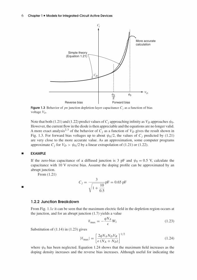
Figure 1.3 Behavior of pn junction depletion-layer capacitance Cj as a function of biasvoltage VD.
Note that both (1.21) and (1.22) predict values of Cj approaching infinity as VD approaches ψ0.However, the current flow in the diode is then appreciable and the equations are no longer valid.A more exact analysis2,3 of the behavior of Cj as a function of VD gives the result shown inFig. 1.3. For forward bias voltages up to about ψ0/2, the values of Cj predicted by (1.21)are very close to the more accurate value. As an approximation, some computer programsapproximate Cj for VD > ψ0/2 by a linear extrapolation of (1.21) or (1.22).
EXAMPLE
If the zero-bias capacitance of a diffused junction is 3 pF and ψ0 = 0.5 V, calculate thecapacitance with 10 V reverse bias. Assume the doping profile can be approximated by anabrupt junction.
From (1.21)
Cj = 3√1 + 10
0.5
pF = 0.65 pF
1.2.2 Junction Breakdown
From Fig. 1.1c it can be seen that the maximum electric field in the depletion region occurs atthe junction, and for an abrupt junction (1.7) yields a value
�max = −qNA
εW1 (1.23)
Substitution of (1.14) in (1.23) gives
|�max| =[
2qNANDVR
ε (NA + ND)
]1/2
(1.24)
where ψ0 has been neglected. Equation 1.24 shows that the maximum field increases as thedoping density increases and the reverse bias increases. Although useful for indicating the

1.2 Depletion Region of a pn Junction 7
functional dependence of �max on other variables, this equation is strictly valid for an idealplane junction only. Practical junctions tend to have edge effects that cause somewhat highervalues of �max due to a concentration of the field at the curved edges of the junction.
Any reverse-biased pn junction has a small reverse current flow due to the presence ofminority-carrier holes and electrons in the vicinity of the depletion region. These are sweptacross the depletion region by the field and contribute to the leakage current of the junction.As the reverse bias on the junction is increased, the maximum field increases and the carriersacquire increasing amounts of energy between lattice collisions in the depletion region. At acritical field �crit the carriers traversing the depletion region acquire sufficient energy to createnew hole-electron pairs in collisions with silicon atoms. This is called the avalanche processand leads to a sudden increase in the reverse-bias leakage current since the newly createdcarriers are also capable of producing avalanche. The value of �crit is about 3 × 10⁵ V/cm forjunction doping densities in the range of 1015 to 1016 atoms/cm3, but it increases slowly as thedoping density increases and reaches about 106 V/cm for doping densities of 1018 atoms/cm3.
A typical I-V characteristic for a junction diode is shown in Fig. 1.4, and the effect ofavalanche breakdown is seen by the large increase in reverse current, which occurs as thereverse bias approaches the breakdown voltage BV. This corresponds to the maximum field�max approaching �crit . It has been found empirically4 that if the normal reverse bias currentof the diode is IR with no avalanche effect, then the actual reverse current near the breakdownvoltage is
IRA = MIR (1.25)
where M is the multiplication factor defined by
M = 1
1 −(
VR
BV
)n (1.26)
In this equation, VR is the reverse bias on the diode and n has a value between 3 and 6.
I mA
V volts
–BV
–25 –20 –15 –10 –5 5 10 15
4
3
2
1
–1
–2
–3
–4
Figure 1.4 Typical I-V characteristic of a junction diode showing avalanche breakdown.

8 Chapter 1 � Models for Integrated-Circuit Active Devices
The operation of a pn junction in the breakdown region is not inherently destructive.However, the avalanche current flow must be limited by external resistors in order to preventexcessive power dissipation from occurring at the junction and causing damage to the device.Diodes operated in the avalanche region are widely used as voltage references and are calledZener diodes. There is another, related process called Zener breakdown,5 which is differentfrom the avalanche breakdown described above. Zener breakdown occurs only in very heavilydoped junctions where the electric field becomes large enough (even with small reverse-biasvoltages) to strip electrons away from the valence bonds. This process is called tunneling, andthere is no multiplication effect as in avalanche breakdown. Although the Zener breakdownmechanism is important only for breakdown voltages below about 6 V, all breakdown diodesare commonly referred to as Zener diodes.
The calculations so far have been concerned with the breakdown characteristic of planeabrupt junctions. Practical diffused junctions differ in some respects from these results andthe characteristics of these junctions have been calculated and tabulated for use by designers.5
In particular, edge effects in practical diffused junctions can result in breakdown voltages asmuch as 50 percent below the value calculated for a plane junction.
EXAMPLE
An abrupt plane pn junction has doping densities NA = 5 × 10¹⁵ atoms/cm3 and ND = 1016
atoms/cm3. Calculate the breakdown voltage if �crit = 3 × 10⁵ V/cm.The breakdown voltage is calculated using �max = �crit in (1.24) to give
BV = ε (NA + ND)
2qNAND
�2crit
= 1.04 × 10−12 × 15 × 1015
2 × 1.6 × 10−19 × 5 × 1015 × 1016 × 9 × 1010 V
= 88 V
1.3 Large-Signal Behavior of Bipolar TransistorsIn this section, the large-signal or dc behavior of bipolar transistors is considered. Large-signalmodels are developed for the calculation of total currents and voltages in transistor circuits,and such effects as breakdown voltage limitations, which are usually not included in models,are also considered. Second-order effects, such as current-gain variation with collector currentand Early voltage, can be important in many circuits and are treated in detail.
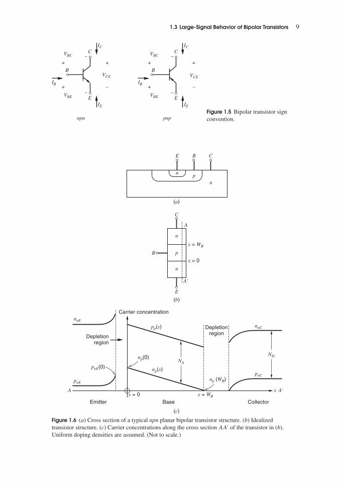
The sign conventions used for bipolar transistor currents and voltages are shown inFig. 1.5. All bias currents for both npn and pnp transistors are assumed positive going intothe device.
1.3.1 Large-Signal Models in the Forward-Active Region
A typical npn planar bipolar transistor structure is shown in Fig. 1.6a, where collector, base,and emitter are labeled C, B, and E, respectively. The method of fabricating such transistorstructures is described in Chapter 2. It is shown there that the impurity doping density in thebase and the emitter of such a transistor is not constant but varies with distance from the topsurface. However, many of the characteristics of such a device can be predicted by analyzingthe idealized transistor structure shown in Fig. 1.6b. In this structure, the base and emitter
1.3 Large-Signal Behavior of Bipolar Transistors 9
C
B
IC
IB
IE
VCE
VBC
VBE
npn
E
–
–
+
–
+
+
C
B
IC
IB
IE
VCE
VBC
VBE
pnp
E
–
–
+
–
+
+
Figure 1.5 Bipolar transistor signconvention.
E
n
(a)
(b)
(c)
B C
p
C
E
n
n
pB
A
A'
n
x = WB
x = 0
np(0)
np(x)
pp(x)
A A'x
pnE(0)
x = 0 x = WB
np (WB)
ND
pnC
nnC
pnE
nnE
NA
Depletionregion
Depletionregion
Carrier concentration
Emitter Base Collector
Figure 1.6 (a) Cross section of a typical npn planar bipolar transistor structure. (b) Idealizedtransistor structure. (c) Carrier concentrations along the cross section AA′ of the transistor in (b).Uniform doping densities are assumed. (Not to scale.)

10 Chapter 1 � Models for Integrated-Circuit Active Devices
doping densities are assumed constant, and this is sometimes called a uniform-base transistor.Where possible in the following analyses, the equations for the uniform-base analysis areexpressed in a form that applies also to nonuniform-base transistors.
A cross section AA′ is taken through the device of Fig. 1.6b and carrier concentrationsalong this section are plotted in Fig. 1.6c. Hole concentrations are denoted by p and electronconcentrations by n with subscripts p or n representing p-type or n-type regions. The n-type emitter and collector regions are distinguished by subscripts E and C, respectively. Thecarrier concentrations shown in Fig. 1.6c apply to a device in the forward-active region.That is, the base-emitter junction is forward biased and the base-collector junction is reversebiased. The minority-carrier concentrations in the base at the edges of the depletion regionscan be calculated from a Boltzmann approximation to the Fermi-Dirac distribution functionto give6
np(0) = npo expVBE
VT
(1.27)
np(WB) = npo expVBC
VT
� 0 (1.28)
where WB is the width of the base from the base-emitter depletion layer edge to the base-collector depletion layer edge and npo is the equilibrium concentration of electrons in the base.Note that VBC is negative for an npn transistor in the forward-active region and thus np(WB) isvery small. Low-level injection conditions are assumed in the derivation of (1.27) and (1.28).This means that the minority-carrier concentrations are always assumed much smaller than themajority-carrier concentration.
If recombination of holes and electrons in the base is small, it can be shown that7 theminority-carrier concentration np(x) in the base varies linearly with distance. Thus a straightline can be drawn joining the concentrations at x = 0 and x = WB in Fig. 1.6c.
For charge neutrality in the base, it is necessary that
NA + np(x) = pp(x) (1.29)
and thus
pp(x) − np(x) = NA (1.30)
where pp(x) is the hole concentration in the base and NA is the base doping density thatis assumed constant. Equation 1.30 indicates that the hole and electron concentrations areseparated by a constant amount and thus pp(x) also varies linearly with distance.
Collector current is produced by minority-carrier electrons in the base diffusing in thedirection of the concentration gradient and being swept across the collector-base depletionregion by the field existing there. The diffusion current density due to electrons in the base is
Jn = qDn
dnp(x)
dx(1.31)
where Dn is the diffusion constant for electrons. From Fig. 1.6c
Jn = −qDn
np(0)
WB
(1.32)
If IC is the collector current and is taken as positive flowing into the collector, it follows from(1.32) that
IC = qADn
np(0)
WB
(1.33)

1.3 Large-Signal Behavior of Bipolar Transistors 11
where A is the cross-sectional area of the emitter. Substitution of (1.27) into (1.33) gives
IC = qADnnpo
WB
expVBE
VT
(1.34)
= IS expVBE
VT
(1.35)
where
IS = qADnnpo
WB
(1.36)
and IS is a constant used to describe the transfer characteristic of the transistor in the forward-active region. Equation 1.36 can be expressed in terms of the base doping density by notingthat8 (see Chapter 2)
npo = n2i
NA
(1.37)
and substitution of (1.37) in (1.36) gives
IS = qADnn2i
WBNA
= qADnn2i
QB
(1.38)
where QB = WBNA is the number of doping atoms in the base per unit area of the emitter andni is the intrinsic carrier concentration in silicon. In this form (1.38) applies to both uniform-and nonuniform-base transistors and Dn has been replaced by Dn, which is an average effectivevalue for the electron diffusion constant in the base. This is necessary for nonuniform-basedevices because the diffusion constant is a function of impurity concentration. Typical valuesof IS as given by (1.38) are from 10−14 to 10−16 A.
Equation 1.35 gives the collector current as a function of base-emitter voltage. The basecurrent IB is also an important parameter and, at moderate current levels, consists of twomajor components. One of these (IB1) represents recombination of holes and electrons in thebase and is proportional to the minority-carrier charge Qe in the base. From Fig. 1.6c, theminority-carrier charge in the base is
Qe = 1
2np(0)WBqA (1.39)
and we have
IB1 = Qe
�b
= 1
2
np(0)WBqA
�b
(1.40)
where �b is the minority-carrier lifetime in the base. IB1 represents a flow of majority holesfrom the base lead into the base region. Substitution of (1.27) in (1.40) gives
IB1 = 1
2
npoWBqA
�b
expVBE
VT
(1.41)
The second major component of base current (usually the dominant one in integrated-circuit npn devices) is due to injection of holes from the base into the emitter. This currentcomponent depends on the gradient of minority-carrier holes in the emitter and is9
IB2 = qADp
Lp
pnE(0) (1.42)
where Dp is the diffusion constant for holes and Lp is the diffusion length (assumed small)for holes in the emitter. pnE(0) is the concentration of holes in the emitter at the edge of the

12 Chapter 1 � Models for Integrated-Circuit Active Devices
depletion region and is
pnE(0) = pnEo expVBE
VT
(1.43)
If ND is the donor atom concentration in the emitter (assumed constant), then
pnEo � n2i
ND
(1.44)
The emitter is deliberately doped much more heavily than the base, making ND large and pnEo
small, so that the base-current component, IB2, is minimized.Substitution of (1.43) and (1.44) in (1.42) gives
IB2 = qADp
Lp
n2i
ND
expVBE
VT
(1.45)
The total base current, IB, is the sum of IB1 and IB2:
IB = IB1 + IB2 =(
1
2
npoWBqA
�b
+ qADp
Lp
n2i
ND
)exp
VBE
VT
(1.46)
Although this equation was derived assuming uniform base and emitter doping, it givesthe correct functional dependence of IB on device parameters for practical double-diffusednonuniform-base devices. Second-order components of IB, which are important at low currentlevels, are considered later.
Since IC in (1.35) and IB in (1.46) are both proportional to exp(VBE/VT ) in this analysis,the base current can be expressed in terms of collector current as
IB = IC
βF
(1.47)
where βF is the forward current gain. An expression for βF can be calculated by substituting(1.34) and (1.46) in (1.47) to give
βF =qADnnpo
WB
1
2
npoWBqA
�b
+ qADpn2i
LpND
= 1
W2B
2 �bDn
+ Dp
Dn
WB
Lp
NA
ND
(1.48)
where (1.37) has been substituted for npo. Equation 1.48 shows that βF is maximized byminimizing the base width WB and maximizing the ratio of emitter to base doping densitiesND/NA. Typical values of βF for npn transistors in integrated circuits are 50 to 500, whereaslateral pnp transistors (to be described in Chapter 2) have values 10 to 100. Finally, the emittercurrent is
IE = −(IC + IB) = −(
IC + IC
βF
)= − IC
αF
(1.49)
where
αF = βF
1 + βF
(1.50)

1.3 Large-Signal Behavior of Bipolar Transistors 13
The value of αF can be expressed in terms of device parameters by substituting (1.48) in(1.50) to obtain
αF = 1
1 + 1
βF
= 1
1 + W2B
2 �b Dn
+ Dp
Dn
WB
Lp
NA
ND
� αT γ (1.51)
where
αT = 1
1 + W2B
2 �b Dn
(1.51a)
γ = 1
1 + Dp
Dn
WB
Lp
NA
ND
(1.51b)
The validity of (1.51) depends on W2B/2 �b Dn � 1 and (Dp/Dn)(WB/Lp)(NA/ND) � 1, and
this is always true if βF is large [see (1.48)]. The term γ in (1.51) is called the emitter injectionefficiency and is equal to the ratio of the electron current (npn transistor) injected into thebase from the emitter to the total hole and electron current crossing the base-emitter junction.Ideally γ → 1, and this is achieved by making ND/NA large and WB small. In that case verylittle reverse injection occurs from base to emitter.
The term αT in (1.51) is called the base transport factor and represents the fraction ofcarriers injected into the base (from the emitter) that reach the collector. Ideally αT → 1 andthis is achieved by making WB small. It is evident from the above development that fabricationchanges that cause αT and γ to approach unity also maximize the value of βF of the transistor.
The results derived above allow formulation of a large-signal model of the transistorsuitable for bias-circuit calculations with devices in the forward-active region. One such circuitis shown in Fig. 1.7 and consists of a base-emitter diode to model (1.46) and a controlledcollector-current generator to model (1.47). Note that the collector voltage ideally has noinfluence on the collector current and the collector node acts as a high-impedance currentsource. A simpler version of this equivalent circuit, which is often useful, is shown in Fig.1.7b, where the input diode has been replaced by a battery with a value VBE(on), which isusually 0.6 to 0.7 V. This represents the fact that in the forward-active region the base-emittervoltage varies very little because of the steep slope of the exponential characteristic. In somecircuits the temperature coefficient of VBE(on) is important, and a typical value for this is−2 mV/◦C. The equivalent circuits of Fig. 1.7 apply for npn transistors. For pnp devices thecorresponding equivalent circuits are shown in Fig. 1.8.
B C B C
E E
IB IB
ISIB =
VBE VBE (on)
VT
VBE
FIB
Fexp
(a) (b)
+ +
––
�
� FIB� Figure 1.7 Large-signalmodels of npn transistorsfor use in bias calculations.(a) Circuit incorporatingan input diode.(b) Simplified circuit withan input voltage source.

14 Chapter 1 � Models for Integrated-Circuit Active Devices
B C B C
E E
IB IB
ISIB = –
VBE VBE (on)
VT
VBE
FIB
Fexp –
(a) (b)
+
+
–
–
�
� FIB�
Figure 1.8 Large-signalmodels of pnp transistorscorresponding to thecircuits of Fig. 1.7.
1.3.2 Effects of Collector Voltage on Large-Signal Characteristicsin the Forward-Active Region
In the analysis of the previous section, the collector-base junction was assumed reverse biasedand ideally had no effect on the collector currents. This is a useful approximation for first-order calculations, but is not strictly true in practice. There are occasions when the influenceof collector voltage on collector current is important, and this will now be investigated.
The collector voltage has a dramatic effect on the collector current in two regions of deviceoperation. These are the saturation (VCE approaches zero) and breakdown (VCE very large)regions that will be considered later. For values of collector-emitter voltage VCE between theseextremes, the collector current increases slowly as VCE increases. The reason for this can beseen from Fig. 1.9, which is a sketch of the minority-carrier concentration in the base of thetransistor. Consider the effect of changes in VCE on the carrier concentration for constant VBE.Since VBE is constant, the change in VCB equals the change in VCE and this causes an increasein the collector-base depletion-layer width as shown. The change in the base width of thetransistor, �WB, equals the change in the depletion-layer width and causes an increase �IC
in the collector current.From (1.35) and (1.38) we have
IC = qADnn2i
QB
expVBE
VT
(1.52)
Carrier concentration
np(0) = npo expVBE
VT
IC
WB
IC + ΔIC
x
ΔWBEmitter Base Collector
Initialdepletion
region
Collector depletionregion widens due
to ΔVCE
Figure 1.9 Effect of increasesin VCE on the collectordepletion region and basewidth of a bipolar transistor.

1.3 Large-Signal Behavior of Bipolar Transistors 15
Differentiation of (1.52) yields
∂IC
∂VCE
= −qADnn2i
Q2B
(exp
VBE
VT
)dQB
dVCE
(1.53)
and substitution of (1.52) in (1.53) gives
∂IC
∂VCE
= − IC
QB
dQB
dVCE
(1.54)
For a uniform-base transistor QB = WBNA, and (1.54) becomes
∂IC
∂VCE
= − IC
WB
dWB
dVCE
(1.55)
Note that since the base width decreases as VCE increases, dWB/dVCE in (1.55) is negativeand thus ∂IC/∂VCE is positive. The magnitude of dWB/dVCE can be calculated from (1.18) fora uniform-base transistor. This equation predicts that dWB/dVCE is a function of the bias valueof VCE, but the variation is typically small for a reverse-biased junction and dWB/dVCE isoften assumed constant. The resulting predictions agree adequately with experimental results.
Equation 1.55 shows that ∂IC/∂VCE is proportional to the collector-bias current andinversely proportional to the transistor base width. Thus narrow-base transistors show a greaterdependence of IC on VCE in the forward-active region. The dependence of ∂IC/∂VCE on IC
results in typical transistor output characteristics as shown in Fig. 1.10. In accordance withthe assumptions made in the foregoing analysis, these characteristics are shown for constantvalues of VBE. However, in most integrated-circuit transistors the base current is dependentonly on VBE and not on VCE, and thus constant-base-current characteristics can often be usedin the following calculation. The reason for this is that the base current is usually dominatedby the IB2 component of (1.45), which has no dependence on VCE. Extrapolation of the char-acteristics of Fig. 1.10 back to the VCE axis gives an intercept VA called the Early voltage,where
VA = IC
∂IC
∂VCE
(1.56)
IC
VCE
VBE4
VBE3
VBE2
VBE1
VA
Figure 1.10 Bipolar transistor output characteristics showing the Earlyvoltage, VA.

16 Chapter 1 � Models for Integrated-Circuit Active Devices
Substitution of (1.55) in (1.56) gives
VA = −WB
dVCE
dWB
(1.57)
which is a constant, independent of IC. Thus all the characteristics extrapolate to the samepoint on the VCE axis. The variation of IC with VCE is called the Early effect, and VA isa common model parameter for circuit-analysis computer programs. Typical values of VA
for integrated-circuit transistors are 15 to 100 V. The inclusion of Early effect in dc biascalculations is usually limited to computer analysis because of the complexity introduced intothe calculation. However, the influence of the Early effect is often dominant in small-signalcalculations for high-gain circuits and this point will be considered later.
Finally, the influence of Early effect on the transistor large-signal characteristics in theforward-active region can be represented approximately by modifying (1.35) to
IC = IS
(1 + VCE
VA
)exp
VBE
VT
(1.58)
This is a common means of representing the device output characteristics for computersimulation.
1.3.3 Saturation and Inverse-Active Regions
Saturation is a region of device operation that is usually avoided in analog circuits because thetransistor gain is very low in this region. Saturation is much more commonly encountered indigital circuits, where it provides a well-specified output voltage that represents a logic state.
In saturation, both emitter-base and collector-base junctions are forward biased. Conse-quently, the collector-emitter voltage VCE is quite small and is usually in the range 0.05 to0.3 V. The carrier concentrations in a saturated npn transistor with uniform base doping areshown in Fig. 1.11. The minority-carrier concentration in the base at the edge of the depletionregion is again given by (1.28) as
np(WB) = npo expVBC
VT
(1.59)
nnE
pp(x)
WB
np(x)
nnC
pnC
x
np(WB)np1(x)
np2(x)
np(0) IC
pnE
Base CollectorEmitter
Carrier concentration
Figure 1.11 Carrier concentrations in a saturated npn transistor. (Not to scale.)

1.3 Large-Signal Behavior of Bipolar Transistors 17
ICmA
IB = 0.04 mA
IB = 0.01 mA
IB = 0.01 mA
VCEvolts
BVCEO
IB = 0
IB = 0
0.03 mA
0.02 mA
0.02 mA
0.03 mA
0.04 mA
Forward activeregion
10–2
–0.02
–0.04
–0.06
–0.08
–0.10
5
4
3
2
1
–4–6–8 20 30 40
Inverseactive region
Saturationregion
Saturationregion
Figure 1.12 Typical IC-VCE characteristics for an npn bipolar transistor. Note the different scales forpositive and negative currents and voltages.
but since VBC is now positive, the value of np(WB) is no longer negligible. Consequently,changes in VCE with VBE held constant (which cause equal changes in VBC) directly affectnp(WB). Since the collector current is proportional to the slope of the minority-carrier con-centration in the base [see (1.31)], it is also proportional to [np(0) − np(WB)] from Fig. 1.11.Thus changes in np(WB) directly affect the collector current, and the collector node of thetransistor appears to have a low impedance. As VCE is decreased in saturation with VBE heldconstant, VBC increases, as does np(WB) from (1.59). Thus, from Fig. 1.11, the collector cur-rent decreases because the slope of the carrier concentration decreases. This gives rise to thesaturation region of the IC − VCE characteristic shown in Fig. 1.12. The slope of the IC − VCE
characteristic in this region is largely determined by the resistance in series with the collectorlead due to the finite resistivity of the n-type collector material.Auseful model for the transistorin this region is shown in Fig. 1.13 and consists of a fixed voltage source to represent VBE(on),and a fixed voltage source to represent the collector-emitter voltage VCE(sat). A more accuratebut more complex model includes a resistor in series with the collector. This resistor can havea value ranging from 20 to 500 , depending on the device structure.
An additional aspect of transistor behavior in the saturation region is apparent from Fig.1.11. For a given collector current, there is now a much larger amount of stored charge in thebase than there is in the forward-active region. Thus the base-current contribution representedby (1.41) will be larger in saturation. In addition, since the collector-base junction is nowforward biased, there is a new base-current component due to injection of carriers from the

18 Chapter 1 � Models for Integrated-Circuit Active Devices
BB C C
E E
VBE (on)VBE (on) VCE (sat)VCE (sat)
(a) npn (b) pnp
Figure 1.13 Large-signal models for bipolar transistors in the saturation region.
base to the collector. These two effects result in a base current IB in saturation, which is largerthan in the forward-active region for a given collector current IC. Ratio IC/IB in saturationis often referred to as the forced β and is always less than βF . As the forced β is made lowerwith respect to βF , the device is said to be more heavily saturated.
The minority-carrier concentration in saturation shown in Fig. 1.11 is a straight line join-ing the two end points, assuming that recombination is small. This can be represented as alinear superposition of the two dotted distributions as shown. The justification for this is thatthe terminal currents depend linearly on the concentrations np(0) and np(WB). This picture ofdevice carrier concentrations can be used to derive some general equations describing tran-sistor behavior. Each of the distributions in Fig. 1.11 is considered separately and the twocontributions are combined. The emitter current that would result from np1(x) above is givenby the classical diode equation
IEF = −IES
(exp
VBE
VT
− 1
)(1.60)
where IES is a constant that is often referred to as the saturation current of the junction (noconnection with the transistor saturation previously described). Equation 1.60 predicts thatthe junction current is given by IEF � IES with a reverse-bias voltage applied. However,in practice (1.60) is applicable only in the forward-bias region, since second-order effectsdominate under reverse-bias conditions and typically result in a junction current several ordersof magnitude larger than IES . The junction current that flows under reverse-bias conditions isoften called the leakage current of the junction.
Returning to Fig. 1.11, we can describe the collector current resulting from np2(x)alone as
ICR = −ICS
(exp
VBC
VT
− 1
)(1.61)
where ICS is a constant. The total collector current IC is given by ICR plus the fraction of IEF
that reaches the collector (allowing for recombination and reverse emitter injection). Thus
IC = αFIES
(exp
VBE
VT
− 1
)− ICS
(exp
VBC
VT
− 1
)(1.62)
where αF has been defined previously by (1.51). Similarly, the total emitter current is composedof IEF plus the fraction of ICR that reaches the emitter with the transistor acting in an invertedmode. Thus
IE = −IES
(exp
VBE
VT
− 1
)+ αRICS
(exp
VBC
VT
− 1
)(1.63)
where αR is the ratio of emitter to collector current with the transistor operating inverted(i.e., with the collector-base junction forward biased and emitting carriers into the base and theemitter-base junction reverse biased and collecting carriers). Typical values of αR are 0.5 to 0.8.

1.3 Large-Signal Behavior of Bipolar Transistors 19
An inverse current gain βR is also defined
βR = αR
1 − αR
(1.64)
and has typical values 1 to 5. This is the current gain of the transistor when operated invertedand is much lower than βF because the device geometry and doping densities are designedto maximize βF . The inverse-active region of device operation occurs for VCE negative in annpn transistor and is shown in Fig. 1.12. In order to display these characteristics adequatelyin the same figure as the forward-active region, the negative voltage and current scales havebeen expanded. The inverse-active mode of operation is rarely encountered in analog circuits.
Equations 1.62 and 1.63 describe npn transistor operation in the saturation region whenVBE and VBC are both positive, and also in the forward-active and inverse-active regions.These equations are the Ebers-Moll equations. In the forward-active region, they degenerateinto a form similar to that of (1.35), (1.47), and (1.49) derived earlier. This can be shown byputting VBE positive and VBC negative in (1.62) and (1.63) to obtain
IC = αFIES
(exp
VBE
VT
− 1
)+ ICS (1.65)
IE = −IES
(exp
VBE
VT
− 1
)− αRICS (1.66)
Equation 1.65 is similar in form to (1.35) except that leakage currents that were previouslyneglected have now been included. This minor difference is significant only at high temper-atures or very low operating currents. Comparison of (1.65) with (1.35) allows us to identifyIS = αFIES , and it can be shown10 in general that
αFIES = αRICS = IS (1.67)
where this expression represents a reciprocity condition. Use of (1.67) in (1.62) and (1.63)allows the Ebers-Moll equations to be expressed in the general form
IC = IS
(exp
VBE
VT
− 1
)− IS
αR
(exp
VBC
VT
− 1
)(1.62a)
IE = − IS
αF
(exp
VBE
VT
− 1
)+ IS
(exp
VBC
VT
− 1
)(1.63a)
This form is often used for computer representation of transistor large-signal behavior.The effect of leakage currents mentioned above can be further illustrated as follows. In
the forward-active region, from (1.66)
IES
(exp
VBE
VT
− 1
)= −IE − αRICS (1.68)
Substitution of (1.68) in (1.65) gives
IC = −αFIE + ICO (1.69)
where
ICO = ICS(1 − αRαF ) (1.69a)
and ICO is the collector-base leakage current with the emitter open. Although ICO is giventheoretically by (1.69a), in practice, surface leakage effects dominate when the collector-basejunction is reverse biased and ICO is typically several orders of magnitude larger than the value

20 Chapter 1 � Models for Integrated-Circuit Active Devices
given by (1.69a). However, (1.69) is still valid if the appropriate measured value for ICO isused. Typical values of ICO are from 10−10 to 10−12 A at 25◦C, and the magnitude doublesabout every 8◦C. As a consequence, these leakage terms can become very significant at hightemperatures. For example, consider the base current IB. From Fig. 1.5 this is
IB = −(IC + IE) (1.70)
If IE is calculated from (1.69) and substituted in (1.70), the result is
IB = 1 − αF
αF
IC − ICO
αF
(1.71)
But from (1.50)
βF = αF
1 − αF
(1.72)
and use of (1.72) in (1.71) gives
IB = IC
βF
− ICO
αF
(1.73)
Since the two terms in (1.73) have opposite signs, the effect of ICO is to decrease the magnitudeof the external base current at a given value of collector current.
EXAMPLE
If ICO is 10−10 A at 24◦C, estimate its value at 120◦C.Assuming that ICO doubles every 8◦C, we have
ICO(120◦C) = 10−10 × 212
= 0.4 �A
1.3.4 Transistor Breakdown Voltages
In Section 1.2.2 the mechanism of avalanche breakdown in a pn junction was described.Similar effects occur at the base-emitter and base-collector junctions of a transistor and theseeffects limit the maximum voltages that can be applied to the device.
First consider a transistor in the common-base configuration shown in Fig. 1.14a andsupplied with a constant emitter current. Typical IC − VCB characteristics for an npn transistorin such a connection are shown in Fig. 1.14b. For IE = 0 the collector-base junction breaksdown at a voltage BVCBO, which represents collector-base breakdown with the emitter open.For finite values of IE, the effects of avalanche multiplication are apparent for values of VCB
below BVCBO. In the example shown, the effective common-base current gain αF = IC/IE
becomes larger than unity for values of VCB above about 60 V. Operation in this region (butbelow BVCBO) can, however, be safely undertaken if the device power dissipation is notexcessive. The considerations of Section 1.2.2 apply to this situation, and neglecting leakagecurrents, we can calculate the collector current in Fig. 1.14a as
IC = −αFIEM (1.74)
where M is defined by (1.26) and thus
IC = −αFIE
1
1 −(
VCB
BVCBO
)n (1.75)

1.3 Large-Signal Behavior of Bipolar Transistors 21
(a)
(b)
IC
IE VCB
IC mA
IE = 0
IE = 1.5 mA
IE = 1.0 mA
IE = 0.5 mA
BVCBO
VCBvolts
+
–
1.5
1.0
0.5
0 20 40 60 80 100 Figure 1.14 Common-basetransistor connection. (a) Testcircuit. (b) IC − VCB
characteristics.
One further point to note about the common-base characteristics of Fig. 1.14b is that forlow values of VCB where avalanche effects are negligible, the curves show very little of theEarly effect seen in the common-emitter characteristics. Base widening still occurs in thisconfiguration as VCB is increased, but unlike the common-emitter connection, it produceslittle change in IC. This is because IE is now fixed instead of VBE or IB, and in Fig. 1.9, thismeans the slope of the minority-carrier concentration at the emitter edge of the base is fixed.Thus the collector current remains almost unchanged.
Now consider the effect of avalanche breakdown on the common-emitter characteristicsof the device. Typical characteristics are shown in Fig. 1.12, and breakdown occurs at avalue BVCEO, which is sometimes called the sustaining voltage LVCEO. As in previous cases,operation near the breakdown voltage is destructive to the device only if the current (and thusthe power dissipation) becomes excessive.
The effects of avalanche breakdown on the common-emitter characteristics are more com-plex than in the common-base configuration. This is because hole-electron pairs are producedby the avalanche process and the holes are swept into the base, where they effectively con-tribute to the base current. In a sense, the avalanche current is then amplified by the transistor.The base current is still given by
IB = −(IC + IE) (1.76)
Equation 1.74 still holds, and substitution of this in (1.76) gives
IC = MαF
1 − MαF
IB (1.77)
where
M = 1
1 −(
VCB
BVCBO
)n (1.78)

22 Chapter 1 � Models for Integrated-Circuit Active Devices
Equation 1.77 shows that IC approaches infinity as MαF approaches unity. That is, theeffective β approaches infinity because of the additional base-current contribution from theavalanche process itself. The value of BVCEO can be determined by solving
MαF = 1 (1.79)
If we assume that VCB � VCE, this givesαF
1 −(
BVCEO
BVCBO
)n = 1 (1.80)
and this results inBVCEO
BVCBO
= n√
1 − αF
and thus
BVCEO � BVCBO
n√
βF
(1.81)
Equation 1.81 shows that BVCEO is less than BVCBO by a substantial factor. However, the valueof BVCBO, which must be used in (1.81), is the plane junction breakdown of the collector-basejunction, neglecting any edge effects. This is because it is only collector-base avalanche currentactually under the emitter that is amplified as described in the previous calculation. However,as explained in Section 1.2.2, the measured value of BVCBO is usually determined by avalanchein the curved region of the collector, which is remote from the active base. Consequently, fortypical values of βF = 100 and n = 4, the value of BVCEO is about one-half of the measuredBVCBO and not 30 percent as (1.81) would indicate.
Equation 1.81 explains the shape of the breakdown characteristics of Fig. 1.12 if thedependence of βF on collector current is included. As VCE is increased from zero with IB = 0,the initial collector current is approximately βFICO from (1.73); since ICO is typically severalpicoamperes, the collector current is very small. As explained in the next section, βF is smallat low currents, and thus from (1.81) the breakdown voltage is high. However, as avalanchebreakdown begins in the device, the value of IC increases and thus βF increases. From (1.81)this causes a decrease in the breakdown voltage and the characteristic bends back as shown inFig. 1.12 and exhibits a negative slope. At higher collector currents, βF approaches a constantvalue and the breakdown curve with IB = 0 becomes perpendicular to the VCE axis. The valueof VCE in this region of the curve is usually defined to be BVCEO, since this is the maximumvoltage the device can sustain. The value of βF to be used to calculate BVCEO in (1.81) is thusthe peak value of βF . Note from (1.81) that high-β transistors will thus have low values ofBVCEO.
The base-emitter junction of a transistor is also subject to avalanche breakdown. However,the doping density in the emitter is made very large to ensure a high value of βF [ND is madelarge in (1.45) to reduce IB2]. Thus the base is the more lightly doped side of the junctionand determines the breakdown characteristic. This can be contrasted with the collector-basejunction, where the collector is the more lightly doped side and results in typical values ofBVCBO of 20 to 80 V or more. The base is typically an order of magnitude more heavily dopedthan the collector, and thus the base-emitter breakdown voltage is much less than BVCBO and istypically about 6 to 8 V. This is designated BVEBO. The breakdown voltage for inverse-activeoperation shown in Fig. 1.12 is approximately equal to this value because the base-emitterjunction is reverse biased in this mode of operation.
The base-emitter breakdown voltage of 6 to 8 V provides a convenient reference voltagein integrated-circuit design, and this is often utilized in the form of a Zener diode. However,

1.3 Large-Signal Behavior of Bipolar Transistors 23
care must be taken to ensure that all other transistors in a circuit are protected against reversebase-emitter voltages sufficient to cause breakdown. This is because, unlike collector-basebreakdown, base-emitter breakdown is damaging to the device. It can cause a large degradationin βF , depending on the duration of the breakdown-current flow and its magnitude.11 If thedevice is used purely as a Zener diode, this is of no consequence, but if the device is anamplifying transistor, the βF degradation may be serious.
EXAMPLE
If the collector doping density in a transistor is 2 × 10¹⁵ atoms/cm3 and is much less than thebase doping, calculate BVCEO for β = 100 and n = 4. Assume �crit = 3 × 10⁵ V/cm.
The plane breakdown voltage in the collector can be calculated from (1.24) using�max = �crit:
BVCBO = ε (NA + ND)
2qNAND
�2crit
Since ND � NA, we have
BVCBO|plane = ε
2qND
�2crit = 1.04 × 10⁻¹²
2 × 1.6 × 10−19 × 2 × 1015 × 9 × 1010 V = 146 V
From (1.81)
BVCEO = 1464√
100V = 46 V
1.3.5 Dependence of Transistor Current Gain βF on Operating Conditions
Although most first-order analyses of integrated circuits make the assumption that βF is con-stant, this parameter does in fact depend on the operating conditions of the transistor. It wasshown in Section 1.3.2, for example, that increasing the value of VCE increases IC whileproducing little change in IB, and thus the effective βF of the transistor increases. In Section1.3.4 it was shown that as VCE approaches the breakdown voltage, BVCEO, the collector cur-rent increases due to avalanche multiplication in the collector. Equation 1.77 shows that theeffective current gain approaches infinity as VCE approaches BVCEO.
In addition to the effects just described, βF also varies with both temperature and tran-sistor collector current. This is illustrated in Fig. 1.15, which shows typical curves of βF
versus IC at three different temperatures for an npn integrated circuit transistor. It is evidentthat βF increases as temperature increases, and a typical temperature coefficient for βF is+7000 ppm/◦C (where ppm signifies parts per million). This temperature dependence of βF
is due to the effect of the extremely high doping density in the emitter,12 which causes theemitter injection efficiency γ to increase with temperature.
The variation of βF with collector current, which is apparent in Fig. 1.15, can be dividedinto three regions. Region I is the low-current region, where βF decreases as IC decreases.Region II is the midcurrent region, where βF is approximately constant. Region III is the high-current region, where βF decreases as IC increases. The reasons for this behavior of βF withIC can be better appreciated by plotting base current IB and collector current IC on a log scale

24 Chapter 1 � Models for Integrated-Circuit Active Devices
F
400
300
200
100
00.1 μA 1 μA 10 μA 100 μA 1 mA 10 mA
T = –55°C
T = 25°C
T = 125°C
Region I Region II Region III
IC
�
Figure 1.15 Typical curves of βF
versus IC for an npn integrated-circuittransistor with 6 �m2 emitter area.
as a function of VBE. This is shown in Fig. 1.16, and because of the log scale on the verticalaxis, the value of ln βF can be obtained directly as the distance between the two curves.
At moderate current levels represented by region II in Figs. 1.15 and 1.16, both IC and IB
follow the ideal behavior, and
IC = IS expVBE
VT
(1.82)
IB � IS
βFM
expVBE
VT
(1.83)
where βFM is the maximum value of βF and is given by (1.48).At low current levels, IC still follows the ideal relationship of (1.82), and the decrease in
βF is due to an additional component in IB, which is mainly due to recombination of carriersin the base-emitter depletion region and is present at any current level. However, at highercurrent levels the base current given by (1.83) dominates, and this additional component has
In I
In IS
IC IB
VBE(linear scale)
In FM
In FH
In FL
Region I II III
�
�
�
Figure 1.16 Base andcollector currents of a bipolartransistor plotted on a logscale versus VBE on a linearscale. The distance betweenthe curves is a direct measureof ln βF .

1.4 Small-Signal Models of Bipolar Transistors 25
little effect. The base current resulting from recombination in the depletion region is5
IBX � ISX expVBE
mVT
(1.84)
where
m � 2
At very low collector currents, where (1.84) dominates the base current, the current gain canbe calculated from (1.82) and (1.84) as
βFL � IC
IBX
= IS
ISX
expVBE
VT
(1 − 1
m
)(1.85)
Substitution of (1.82) in (1.85) gives
βFL � IS
ISX
(IC
IS
)[1−(1/m)]
(1.86)
If m � 2, then (1.86) indicates that βF is proportional to√
IC at very low collector currents.At high current levels, the base current IB tends to follow the relationship of (1.83), and
the decrease in βF in region III is due mainly to a decrease in IC below the value given by(1.82). (In practice the measured curve of IB versus VBE in Fig. 1.16 may also deviate from astraight line at high currents due to the influence of voltage drop across the base resistance.)The decrease in IC is due partly to the effect of high-level injection, and at high current levelsthe collector current approaches7
IC � ISH expVBE
2VT
(1.87)
The current gain in this region can be calculated from (1.87) and (1.83) as
βFH � ISH
IS
βFM exp
(−VBE
2VT
)(1.88)
Substitution of (1.87) in (1.88) gives
βFH � I2SH
IS
βFM
1
IC
Thus βF decreases rapidly at high collector currents.In addition to the effect of high-level injection, the value of βF at high currents is also
decreased by the onset of the Kirk effect,13 which occurs when the minority-carrier concentra-tion in the collector becomes comparable to the donor-atom doping density. The base regionof the transistor then stretches out into the collector and becomes greatly enlarged.
1.4 Small-Signal Models of Bipolar TransistorsAnalog circuits often operate with signal levels that are small compared to the bias currentsand voltages in the circuit. In these circumstances, incremental or small-signal models can bederived that allow calculation of circuit gain and terminal impedances without the necessityof including the bias quantities. A hierarchy of models with increasing complexity can bederived, and the more complex ones are generally reserved for computer analysis. Part of thedesigner’s skill is knowing which elements of the model can be omitted when performing handcalculations on a particular circuit, and this point is taken up again later.
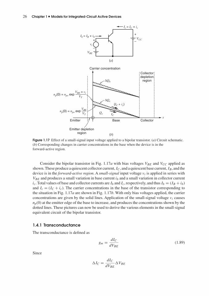
26 Chapter 1 � Models for Integrated-Circuit Active Devices
+
+
–
–VCC
VBE
Ic = IC + ic
Ib = IB + ib
vi
(a)
(b)
np(0) = npo expVBE + vi
VT
np(0) = npo expVBE
VT
Carrier concentration
ΔQe
ΔQh
Qe ICx
(IC + ic)
BaseEmitter Collector
Collectordepletion
region
Emitter depletionregion
Figure 1.17 Effect of a small-signal input voltage applied to a bipolar transistor. (a) Circuit schematic.(b) Corresponding changes in carrier concentrations in the base when the device is in theforward-active region.
Consider the bipolar transistor in Fig. 1.17a with bias voltages VBE and VCC applied asshown. These produce a quiescent collector current, IC, and a quiescent base current, IB, and thedevice is in the forward-active region. A small-signal input voltage vi is applied in series withVBE and produces a small variation in base current ib and a small variation in collector currentic. Total values of base and collector currents are Ib and Ic, respectively, and thus Ib = (IB + ib)and Ic = (IC + ic). The carrier concentrations in the base of the transistor corresponding tothe situation in Fig. 1.17a are shown in Fig. 1.17b. With only bias voltages applied, the carrierconcentrations are given by the solid lines. Application of the small-signal voltage vi causesnp(0) at the emitter edge of the base to increase, and produces the concentrations shown by thedotted lines. These pictures can now be used to derive the various elements in the small-signalequivalent circuit of the bipolar transistor.
1.4.1 Transconductance
The transconductance is defined as
gm = dIC
dVBE
(1.89)
Since
�IC = dIC
dVBE
�VBE

1.4 Small-Signal Models of Bipolar Transistors 27
we can write
�IC = gm�VBE
and thus
ic = gmvi (1.90)
The value of gm can be found by substituting (1.35) in (1.89) to give
gm = d
dVBE
IS expVBE
VT
= IS
VT
expVBE
VT
= IC
VT
= qIC
kT(1.91)
The transconductance thus depends linearly on the bias current IC and is 38 mA/V for IC =1 mA at 25◦C for any bipolar transistor of either polarity (npn or pnp), of any size, and madeof any material (Si, Ge, GaAs).
To illustrate the limitations on the use of small-signal analysis, the foregoing relation willbe derived in an alternative way. The total collector current in Fig. 1.17a can be calculatedusing (1.35) as
Ic = IS expVBE + vi
VT
= IS expVBE
VT
expvi
VT
(1.92)
But the collector bias current is
IC = IS expVBE
VT
(1.93)
and use of (1.93) in (1.92) gives
Ic = IC expvi
VT
(1.94)
If vi < VT , the exponential in (1.94) can be expanded in a power series,
Ic = IC
[1 + vi
VT
+ 1
2
(vi
VT
)2
+ 1
6
(vi
VT
)3
+ . . .
](1.95)
Now the incremental collector current is
ic = Ic − IC (1.96)
and substitution of (1.96) in (1.95) gives
ic = IC
VT
vi + 1
2
IC
V 2T
v2i + 1
6
IC
V 3T
v3i + . . . (1.97)
If vi � VT , (1.97) reduces to (1.90), and the small-signal analysis is valid. The criterionfor use of small-signal analysis is thus vi = �VBE � 26 mV at 25◦C. In practice, if �VBE isless than 10 mV, the small-signal analysis is accurate within about 10 percent.
1.4.2 Base-Charging Capacitance
Figure 1.17b shows that the change in base-emitter voltage �VBE = vi has caused a change�Qe = qe in the minority-carrier charge in the base. By charge-neutrality requirements, thereis an equal change �Qh = qh in the majority-carrier charge in the base. Since majority carriers

28 Chapter 1 � Models for Integrated-Circuit Active Devices
are supplied by the base lead, the application of voltage vi requires the supply of charge qh tothe base, and the device has an apparent input capacitance
Cb = qh
vi
(1.98)
The value of Cb can be related to fundamental device parameters as follows. If (1.39) is dividedby (1.33), we obtain
Qe
IC
= W2B
2Dn
=�F (1.99)
The quantity �F has the dimension of time and is called the base transit time in the forwarddirection. Since it is the ratio of the charge in transit (Qe) to the current flow (IC), it canbe identified as the average time per carrier spent in crossing the base. To a first order itis independent of operating conditions and has typical values 10 to 500 ps for integratednpn transistors and 1 to 40 ns for lateral pnp transistors. Practical values of �F tend to besomewhat lower than predicted by (1.99) for diffused transistors that have nonuniform basedoping.14 However, the functional dependence on base width WB and diffusion constant Dn
is as predicted by (1.99).From (1.99)
�Qe = �F�IC (1.100)
But since �Qe = �Qh, we have
�Qh = �F�IC (1.101)
and this can be written
qh = �F ic (1.102)
Use of (1.102) in (1.98) gives
Cb = �F
ic
vi
(1.103)
and substitution of (1.90) in (1.103) gives
Cb = �Fgm (1.104)
= �F
qIC
kT(1.105)
Thus the small-signal, base-charging capacitance is proportional to the collector bias current.In the inverse-active mode of operation, an equation similar to (1.99) relates stored charge
and current via a time constant �R. This is typically orders of magnitude larger than �F becausethe device structure and doping are optimized for operation in the forward-active region.Since the saturation region is a combination of forward-active and inverse-active operation,inclusion of the parameter �R in a SPICE listing will model the large charge storage that occursin saturation.
1.4.3 Input Resistance
In the forward-active region, the base current is related to the collector current by
IB = IC
βF
(1.47)

1.4 Small-Signal Models of Bipolar Transistors 29
Small changes in IB and IC can be related using (1.47):
�IB = d
dIC
(IC
βF
)�IC (1.106)
and thus
β0 = �IC
�IB
= ic
ib=[
d
dIC
(IC
βF
)]−1
(1.107)
where β0 is the small-signal current gain of the transistor. Note that if βF is constant, thenβF = β0. Typical values of β0 are close to those of βF , and in subsequent chapters littledifferentiation is made between these quantities. A single value of β is often assumed for atransistor and then used for both ac and dc calculations.
Equation 1.107 relates the change in base current ib to the corresponding change incollector current ic, and the device has a small-signal input resistance given by
rπ = vi
ib(1.108)
Substitution of (1.107) in (1.108) gives
rπ = vi
icβ0 (1.109)
and use of (1.90) in (1.109) gives
rπ = β0
gm
(1.110)
Thus the small-signal input shunt resistance of a bipolar transistor depends on the current gainand is inversely proportional to IC.
1.4.4 Output Resistance
In Section 1.3.2 the effect of changes in collector-emitter voltage VCE on the large-signalcharacteristics of the transistor was described. It follows from that treatment that small changes�VCE in VCE produce corresponding changes �IC in IC, where
�IC = ∂IC
∂VCE
�VCE (1.111)
Substitution of (1.55) and (1.57) in (1.111) gives
�VCE
�IC
= VA
IC
= ro (1.112)
where VA is the Early voltage and ro is the small-signal output resistance of the transistor.Since typical values of VA are 50 to 100 V, corresponding values of ro are 50 to 100 k forIC = 1mA. Note that ro is inversely proportional to IC, and thus ro can be related to gm, asare many of the other small-signal parameters.
ro = 1
ηgm
(1.113)
where
η = kT
qVA
(1.114)

30 Chapter 1 � Models for Integrated-Circuit Active Devices
v1rπ
rπ = ro = gm = τFgmCb =
E
gm v1 roCb
B C
+
–
βgm
1 gm
qIC
kT, , ,
�Figure 1.18 Basic bipolar transistorsmall-signal equivalent circuit.
If VA = 100 V, then η = 2.6 × 10⁻⁴ at 25◦C. Note that 1/ro is the slope of the output char-acteristics of Fig. 1.10.
1.4.5 Basic Small-Signal Model of the Bipolar Transistor
Combination of the above small-signal circuit elements yields the small-signal model of thebipolar transistor shown in Fig. 1.18. This is valid for both npn and pnp devices in the forward-active region and is called the hybrid-π model. Collector, base, and emitter nodes are labeledC, B and E, respectively. The elements in this circuit are present in the equivalent circuit ofany bipolar transistor and are specified by relatively few parameters (β, �F , η, IC). Note thatin the evaluation of the small-signal parameters for pnp transistors, the magnitude only ofIC is used. In the following sections, further elements are added to this model to account forparasitics and second-order effects.
1.4.6 Collector-Base Resistance
Consider the effect of variations in VCE on the minority charge in the base as illustratedin Fig. 1.9. An increase in VCE causes an increase in the collector depletion-layer width andconsequent reduction of base width. This causes a reduction in the total minority-carrier chargestored in the base and thus a reduction in base current IB due to a reduction in IB1 given by(1.40). Since an increase �VCE in VCE causes a decrease �IB in IB, this effect can be modeledby inclusion of a resistor rμ from collector to base of the model of Fig. 1.18. If VBE is assumedheld constant, the value of this resistor can be determined as follows.
rμ = �VCE
�IB1= �VCE
�IC
�IC
�IB1(1.115)
Substitution of (1.112) in (1.115) gives
rμ = ro�IC
�IB1(1.116)
If the base current IB is composed entirely of component IB1, then (1.107) can be used in(1.116) to give
rμ = β0ro (1.117)
This is a lower limit for rμ. In practice, IB1 is typically less than 10 percent of IB [componentIB2 from (1.42) dominates] in integrated npn transistors, and since IB1 is very small, the change�IB1 in IB1 for a given �VCE and �IC is also very small. Thus a typical value for rμ is greaterthan 10β0ro. For lateral pnp transistors, recombination in the base is more significant, and rμis in the range 2β0ro to 5β0ro.

1.4 Small-Signal Models of Bipolar Transistors 31
1.4.7 Parasitic Elements in the Small-Signal Model
The elements of the bipolar transistor small-signal equivalent circuit considered so far may beconsidered basic in the sense that they arise directly from essential processes in the device.However, technological limitations in the fabrication of transistors give rise to a number ofparasitic elements that must be added to the equivalent circuit for most integrated-circuittransistors. A cross section of a typical npn transistor in a junction-isolated process is shownin Fig. 1.19. The means of fabricating such devices is described in Chapter 2.
As described in Section 1.2, all pn junctions have a voltage-dependent capacitance asso-ciated with the depletion region. In the cross section of Fig. 1.19, three depletion-regioncapacitances can be identified. The base-emitter junction has a depletion-region capacitanceCje and the base-collector and collector-substrate junctions have capacitances Cμ and Ccs,respectively. The base-emitter junction closely approximates an abrupt junction due to thesteep rise of the doping density caused by the heavy doping in the emitter. Thus the variationof Cje with bias voltage is well approximated by (1.21). The collector-base junction behaveslike a graded junction for small bias voltages since the doping density is a function of dis-tance near the junction. However, for larger reverse-bias values (more than about a volt), thejunction depletion region spreads into the collector, which is uniformly doped, and thus fordevices with thick collectors the junction tends to behave like an abrupt junction with uniformdoping. Many modern high-speed processes, however, have very thin collector regions (of theorder of one micron), and the collector depletion region can extend all the way to the buriedlayer for quite small reverse-bias voltages. When this occurs, both the depletion region andthe associated capacitance vary quite slowly with bias voltage. The collector-base capacitanceCμ thus tends to follow (1.22) for very small bias voltages and (1.21) for large bias voltagesin thick-collector devices. In practice, measurements show that the variation of Cμ with biasvoltage for most devices can be approximated by
Cμ = Cμ0(1 − V
ψo
)n (1.117a)
where V is the forward bias on the junction and n is an exponent between about 0.2 and 0.5. Thethird parasitic capacitance in a monolithic npn transistor is the collector-substrate capacitance
p p
p
pn+
n+
rb
C
Cjerex
Cje
rc3
rc2
rc1
Ccs
Ccs
Ccs
n+
n
n Injected electronmotion
Buried layer
Substrate
EmitterBaseCollector
�
C�
Figure 1.19 Integrated-circuit npn bipolar transistor structure showing parasitic elements. (Notto scale.)

32 Chapter 1 � Models for Integrated-Circuit Active Devices
Ccs, and for large reverse bias voltages this varies according to the abrupt junction equation(1.21) for junction-isolated devices. In the case of oxide-isolated devices, however, the deepp diffusions used to isolate the devices are replaced by oxide. The sidewall component ofCcs then consists of a fixed oxide capacitance. Equation 1.117a may then be used to modelCcs, but a value of n less than 0.5 gives the best approximation. In general, (1.117a) will beused to model all three parasitic capacitances with subscripts e, c, and s on n and ψ0 usedto differentiate emitter-base, collector-base, and collector-substrate capacitances, respectively.Typical zero-bias values of these parasitic capacitances for a minimum-size npn transistor ina modern oxide-isolated process are Cje0 � 10 fF, Cμ0 � 10 fF, and Ccs0 � 20 fF. Values forother devices are summarized in Chapter 2.
As described in Chapter 2, lateral pnp transistors have a parasitic capacitance Cbs frombase to substrate in place of Ccs. Note that the substrate is always connected to the mostnegative voltage supply in the circuit in order to ensure that all isolation regions are separatedby reverse-biased junctions. Thus the substrate is an ac ground, and all parasitic capacitanceto the substrate is connected to ground in an equivalent circuit.
The final elements to be added to the small-signal model of the transistor are resistiveparasitics. These are produced by the finite resistance of the silicon between the top contactson the transistor and the active base region beneath the emitter. As shown in Fig. 1.19, thereare significant resistances rb and rc in series with the base and collector contacts, respectively.There is also a resistance rex of several ohms in series with the emitter lead that can becomeimportant at high bias currents. (Note that the collector resistance rc is actually composed ofthree parts labeled rc1, rc2, and rc3.) Typical values of these parameters are rb = 50 to 500 ,rex = 1 to 3 , and rc = 20 to 500 . The value of rb varies significantly with collector currentbecause of current crowding.15 This occurs at high collector currents where the dc base currentproduces a lateral voltage drop in the base that tends to forward bias the base-emitter junctionpreferentially around the edges of the emitter. Thus the transistor action tends to occur alongthe emitter periphery rather than under the emitter itself, and the distance from the base contactto the active base region is reduced. Consequently, the value of rb is reduced, and in a typicalnpn transistor, rb may decrease 50 percent as IC increases from 0.1 mA to 10 mA.
The value of these parasitic resistances can be reduced by changes in the device structure.For example, a large-area transistor with multiple base and emitter stripes will have a smallervalue of rb. The value of rc is reduced by inclusion of the low-resistance buried n+ layerbeneath the collector.
The addition of the resistive and capacitive parasitics to the basic small-signal circuit ofFig. 1.18 gives the complete small-signal equivalent circuit of Fig. 1.20. The internal base node
r
CB'
Ccsgmv1r
rex
v1
rb rc
ro
B C
E
+
–
�
�
�C�
Figure 1.20 Complete bipolar transistor small-signal equivalent circuit.

1.4 Small-Signal Models of Bipolar Transistors 33
is labeled B′ to distinguish it from the external base contact B. The capacitance Cπ containsthe base-charging capacitance Cb and the emitter-base depletion layer capacitance Cje.
Cπ = Cb + Cje (1.118)
Note that the representation of parasitics in Fig. 1.20 is an approximation in that lumpedelements have been used. In practice, as suggested by Fig. 1.19, Cμ is distributed across rband Ccs is distributed across rc. This lumped representation is adequate for most purposes butcan introduce errors at very high frequencies. It should also be noted that while the parasiticresistances of Fig. 1.20 can be very important at high bias currents or for high-frequencyoperation, they are usually omitted from the equivalent circuit for low-frequency calculations,particularly for collector bias currents less than 1 mA.
EXAMPLE
Derive the complete small-signal equivalent circuit for a bipolar transistor at IC = 1 mA,VCB = 3 V, and VCS = 5 V. Device parameters are Cje0 = 10 fF, ne = 0.5, ψ0e = 0.9 V, Cμ0 =10 fF, nc = 0.3, ψ0c = 0.5 V, Ccs0 = 20 fF, ns = 0.3, ψ0s = 0.65 V, β0 = 100, �F= 10 ps,VA = 20 V, rb = 300 , rc = 50 , rex = 5 , rμ = 10 β0ro.
Since the base-emitter junction is forward biased, the value of Cje is difficult to determinefor reasons described in Section 1.2.1. Either a value can be determined by computer or areasonable estimation is to double Cje0. Using the latter approach, we estimate
Cje = 20 fF
Using (1.117a) gives, for the collector-base capacitance,
Cμ = Cμ0(1 + VCB
ψ0c
)nc= 10(
1 + 3
0.5
)0.3 = 5.6 fF
The collector-substrate capacitance can also be calculated using (1.117a)
Ccs = Ccs0(1 + VCS
ψ0s
)ns= 20(
1 + 5
0.65
)0.3 = 10.5 fF
From (1.91) the transconductance is
gm = qIC
kT= 10−3
26 × 10−3 A/V = 38 mA/V
From (1.104) the base-charging capacitance is
Cb = �Fgm = 10 × 10−12 × 38 × 10−3 F = 0.38 pF
The value of Cπ from (1.118) is
Cπ = 0.38 + 0.02 pF = 0.4 pF

34 Chapter 1 � Models for Integrated-Circuit Active Devices
B'
v1 v1
50 Ω
5 Ω
20 MΩ
300 Ω
2.6 kΩ 0.4 pF
5.6 fF
20kΩ 10.5 fF
B C
E
+
–38 × 10–3
Figure 1.21 Complete small-signal equivalent circuit for a bipolar transistor at IC = 1 mA, VCB = 3 V,and VCS = 5 V. Device parameters are Cje0 = 10 fF, ne = 0.5, ψ0e = 0.9 V, Cμ0 = 10 fF, nc = 0.3,ψ0c = 0.5 V, Ccs0 = 20 fF, ns = 0.3, ψ0s = 0.65 V, β0 = 100, �F= 10 ps, VA = 20 V, rb = 300,
rc = 50 , rex = 5 , rμ = 10β0r0.
The input resistance from (1.110) is
rπ = β0
gm
= 100 × 26 = 2.6 k
The output resistance from (1.112) is
ro = 20
10−3 = 20 k
and thus the collector-base resistance is
rμ = 10β0ro = 10 × 100 × 20 k = 20 M
The equivalent circuit with these parameter values is shown in Fig. 1.21.
1.4.8 Specification of Transistor Frequency Response
The high-frequency gain of the transistor is controlled by the capacitive elements in the equiv-alent circuit of Fig. 1.20. The frequency capability of the transistor is most often specifiedin practice by determining the frequency where the magnitude of the short-circuit, common-emitter current gain falls to unity. This is called the transition frequency, fT , and is a measure ofthe maximum useful frequency of the transistor when it is used as an amplifier. The value of fT
can be measured as well as calculated, using the ac circuit of Fig. 1.22. A small-signal currentii is applied to the base, and the output current io is measured with the collector short-circuitedfor ac signals. A small-signal equivalent circuit can be formed for this situation by using theequivalent circuit of Fig. 1.20 as shown in Fig. 1.23, where rex and rμ have been neglected. Ifrc is assumed small, then ro and Ccs have no influence, and we have
v1 � rπ
1 + rπ(Cπ + Cμ)sii (1.119)
If the current fed forward through Cμ is neglected,
io � gmv1 (1.120)

1.4 Small-Signal Models of Bipolar Transistors 35
io
ii
Figure 1.22 Schematic of ac circuit for measurement of fT .
rb
ror Ccs
rc
io
C
gmv1v1ii
+
–
�
�C�
Figure 1.23 Small-signal equivalent circuit for the calculation of fT .
Substitution of (1.119) in (1.120) gives
io � iigmrπ
1 + rπ(Cπ + Cμ)s
and thus
io
ii(jω) = β0
1 + β0Cπ + Cμ
gm
jω
(1.121)
using (1.110).Now if io/ii(jω) is written as β(jω) (the high-frequency, small-signal current gain), then
β(jω) = β0
1 + β0Cπ + Cμ
gm
jω
(1.122)
At high frequencies the imaginary part of the denominator of (1.122) is dominant, and we canwrite
β(jω) � gm
jω (Cπ + Cμ)(1.123)
From (1.123), |β(jω)| = 1 when
ω = ωT = gm
Cπ + Cμ
(1.124)
and thus
fT = 1
2π
gm
Cπ + Cμ
(1.125)
The transistor behavior can be illustrated by plotting |β(jω)| using (1.122) as shown inFig. 1.24. The frequency ωβ is defined as the frequency where |β(jω)| is equal to β0/
√2

36 Chapter 1 � Models for Integrated-Circuit Active Devices
|( (j )|
T log scale
0 (low frequency value)1000
100
10
0.1 T
1
–6 dB/octave
�
�
��
�
� ��
Figure 1.24 Magnitude ofsmall-signal ac currentgain |β(jω)| versusfrequency for a typicalbipolar transistor.
(3 dB down from the low-frequency value). From (1.122) we have
ωβ = 1
β0
gm
Cπ + Cμ
= ωT
β0(1.126)
From Fig. 1.24 it can be seen that ωT can be determined by measuring |β(jω)| at some frequencyωx where |β(jω)| is falling at 6 dB/octave and using
ωT = ωx|β(jωx)| (1.127)
This is the method used in practice, since deviations from ideal behavior tend to occur as|β(jω)| approaches unity. Thus |β(jω)| is typically measured at some frequency where itsmagnitude is about 5 or 10, and (1.127) is used to determine ωT .
It is interesting to examine the time constant, �T , associated with ωT . This is defined as
�T = 1
ωT
(1.128)
and use of (1.124) in (1.128) gives
�T = Cπ
gm
+ Cμ
gm
(1.129)
Substitution of (1.118) and (1.104) in (1.129) gives
�T = Cb
gm
+ Cje
gm
+ Cμ
gm
= �F +Cje
gm
+ Cμ
gm
(1.130)
Equation 1.130 indicates that �T is dependent on IC (through gm) and approaches a constantvalue of �F at high collector bias currents. At low values of IC, the terms involving Cje andCμ dominate, and they cause �T to rise and fT to fall as IC is decreased. This behavior isillustrated in Fig. 1.25, which is a typical plot of fT versus IC for an integrated-circuit npn
transistor. The decline in fT at high collector currents is not predicted by this simple theoryand is due to an increase in �F caused by high-level injection and Kirk effect at high currents.These are the same mechanisms that cause a decrease in βF at high currents as described inSection 1.3.5.

1.4 Small-Signal Models of Bipolar Transistors 37
fTGHz
IC
10
9
8
7
6
5
4
3
2
1
10 μA 100 μA 10 mA1 mA
Figure 1.25 Typical curve of fT versusIC for an npn integrated-circuittransistor with 6 �m2 emitter area in ahigh-speed process.
EXAMPLE
A bipolar transistor has a short-circuit, common-emitter current gain at 1 GHz of 8 withIC = 0.25 mAand 9 with IC = 1 mA.Assuming that high-level injection effects are negligible,calculate Cje and �F , assuming both are constant. The measured value of Cμ is 10 fF.
From the data, values of fT are
fT1 = 8 × 1 = 8 GHz at IC = 0.25 mA
fT2 = 9 × 1 = 9 GHz at IC = 1 mA
Corresponding values of �T are
�T1 = 1
2πfT1= 19.9 ps
�T2 = 1
2πfT2= 17.7 ps
Using these data in (1.130), we have
19.9 × 10−12 = �F +104(Cμ + Cje) (1.131)
at IC = 0.25 mA. At IC = 1 mA we have
17.7 × 10−12 = �F +26(Cμ + Cje) (1.132)
Subtraction of (1.132) from (1.131) yields
Cμ + Cje = 28.2 fF
Since Cμ was measured as 10 fF, the value of Cje is given by
Cje � 18.2 fF

38 Chapter 1 � Models for Integrated-Circuit Active Devices
Substitution in (1.131) gives
�F = 17 ps
This is an example of how basic device parameters can be determined from high-frequencycurrent-gain measurements. Note that the assumption that Cje is constant is a useful approxi-mation in practice because VBE changes by only 36 mV as IC increases from 0.25 mA to 1 mA.
1.5 Large-Signal Behavior of Metal-Oxide-SemiconductorField-Effect TransistorsMetal-oxide-semiconductor field-effect transistors (MOSFETs) have become dominant in thearea of digital integrated circuits because they allow high density and low power dissipation.In contrast, bipolar transistors still provide many advantages in stand-alone analog integratedcircuits. For example, the transconductance per unit bias current in bipolar transistors is usuallymuch higher than in MOS transistors. So in systems where analog techniques are used on someintegrated circuits and digital techniques on others, bipolar technologies are often preferredfor the analog integrated circuits and MOS technologies for the digital. To reduce systemcost and increase portability, both increased levels of integration and reduced power dissipa-tion are required, forcing the associated analog circuits to use MOS-compatible technologies.One way to achieve these goals is to use a processing technology that provides both bipolarand MOS transistors, allowing great design flexibility. However, all-MOS processes are lessexpensive than combined bipolar and MOS processes. Therefore, economic considerationsdrive integrated-circuit manufacturers to use all-MOS processes in many practical cases. As aresult, the study of the characteristics of MOS transistors that affect analog integrated-circuitdesign is important.
1.5.1 Transfer Characteristics of MOS Devices
A cross section of a typical enhancement-mode n-channel MOS (NMOS) transistor is shownin Fig. 1.26. Heavily doped n-type source and drain regions are fabricated in a p-type substrate(often called the body). A thin layer of silicon dioxide is grown over the substrate material and
n+ n+
B
p-type substrate (body)
SiO2 SiO2SiO2
Source,S
Drain,D
Gate,G
Channelregion
Metal or poly silicongate contract
Figure 1.26 Typical enhancement-mode NMOS structure.

1.5 Large-Signal Behavior of Metal-Oxide-Semiconductor Field-Effect Transistors 39
a conductive gate material (metal or polycrystalline silicon) covers the oxide between sourceand drain. Note that the gate is horizontal in Fig. 1.26, and we will use this orientation in alldescriptions of the physical operation of MOS devices. In operation, the gate-source voltagemodifies the conductance of the region under the gate, allowing the gate voltage to control thecurrent flowing between source and drain. This control can be used to provide gain in analogcircuits and switching characteristics in digital circuits.
The enhancement-mode NMOS device of Fig. 1.26 shows significant conduction betweensource and drain only when an n-type channel exists under the gate. This observation is theorigin of the n-channel designation. The term enhancement mode refers to the fact that noconduction occurs for VGS = 0. Thus, the channel must be enhanced to cause conduction. MOSdevices can also be made by using an n-type substrate with a p-type conducting channel. Suchdevices are called enhancement-mode p-channel MOS (PMOS) transistors. In complementaryMOS (CMOS) technology, both device types are present.
The derivation of the transfer characteristics of the enhancement-mode NMOS device ofFig. 1.26 begins by noting that with VGS = 0, the source and drain regions are separated byback-to-back pn junctions. These junctions are formed between the n-type source and drainregions and the p-type substrate, resulting in an extremely high resistance (about 1012 )between drain and source when the device is off.
Now consider the substrate, source, and drain grounded with a positive voltage VGS appliedto the gate as shown in Fig. 1.27. The gate and substrate then form the plates of a capacitorwith the SiO2 as a dielectric. Positive charge accumulates on the gate and negative charge inthe substrate. Initially, the negative charge in the p-type substrate is manifested by the creationof a depletion region and the exclusion of holes under the gate as described in Section 1.2 fora pn-junction. The depletion region is shown in Fig. 1.27. The results of Section 1.2 can nowbe applied. Using (1.10), the depletion-layer width X under the oxide is
X =(
2εφ
qNA
)1/2
(1.133)
where φ is the potential in the depletion layer at the oxide-silicon interface, NA is the dopingdensity (assumed constant) of the p-type substrate in atoms/cm3, and ε is the permittivity ofthe silicon. The charge per area in this depletion region is
Q = qNAX =√
2qNAεφ (1.134)
S DG
L
VGS
n+
+
–
n+
p-type substrate
Channel length
Inducedn-type channel
Depletionregion
SiO2
Figure 1.27 Idealized NMOS devicecross section with positive VGS applied,showing depletion regions and theinduced channel.

40 Chapter 1 � Models for Integrated-Circuit Active Devices
When the surface potential in the silicon reaches a critical value equal to twice the Fermilevel φf , a phenomenon known as inversion occurs.16 The Fermi level φf is defined as
φf = kT
qln
[NA
ni
](1.135)
where k is Boltzmann’s constant. Also, ni is the intrinsic carrier concentration, which is
ni =√
NcNv exp
(− Eg
2kT
)(1.136)
where Eg is the band gap of silicon at T = 0◦K, Nc is the density of allowed states near theedge of the conduction band, and Nv is the density of allowed states near the edge of thevalence band, respectively. The Fermi level φf is usually about 0.3 V. After the potential inthe silicon reaches 2φf , further increases in gate voltage produce no further changes in thedepletion-layer width but instead induce a thin layer of electrons in the depletion layer at thesurface of the silicon directly under the oxide. Inversion produces a continuous n-type regionwith the source and drain regions and forms the conducting channel between source and drain.The conductivity of this channel can be modulated by increases or decreases in the gate-sourcevoltage. In the presence of an inversion layer, and without substrate bias, the depletion regioncontains a fixed charge density
Qb0 =√2qNAε2φf (1.137)
If a substrate bias voltage VSB (positive for n-channel devices) is applied between the sourceand substrate, the potential required to produce inversion becomes (2φf + VSB), and the chargedensity stored in the depletion region in general is
Qb =√2qNAε(2φf + VSB) (1.138)
The gate-source voltage VGS required to produce an inversion layer is called the thresholdvoltage Vt and can now be calculated. This voltage consists of several components. First, avoltage [2φf + (Qb/Cox)] is required to sustain the depletion-layer charge Qb, where Cox
is the gate oxide capacitance per unit area. Second, a work-function difference φms existsbetween the gate metal and the silicon. Third, positive charge density Qss always exists in theoxide at the silicon interface. This charge is caused by crystal discontinuities at the Si-SiO2interface and must be compensated by a gate-source voltage contribution of −Qss/Cox. Thuswe have a threshold voltage
Vt= φms + 2φf + Qb
Cox
− Qss
Cox
(1.139)
= φms + 2φf + Qb0
Cox
− Qss
Cox
+ Qb − Qb0
Cox
= Vt0 + γ(√
2φf + VSB −√2φf
)(1.140)
where (1.137) and (1.138) have been used, and Vt0 is the threshold voltage with VSB = 0. Theparameter γ is defined as
γ = 1
Cox
√2qεNA (1.141)
andCox = εox
tox
(1.142)
where εox and tox are the permittivity and the thickness of the oxide, respectively. A typicalvalue of γ is 0.5 V1/2, and Cox = 3.45 fF/�m2 for tox = 100 angstroms.

1.5 Large-Signal Behavior of Metal-Oxide-Semiconductor Field-Effect Transistors 41
S DG
VGS
n+
–
n+
p-type substrate
Depletionregion
V(y)
yy + dyy
+–
Channel ID
VDS
+
–
VSB
–
+Figure 1.28 NMOS device with biasvoltages applied.
In practice, the value of Vt0 is usually adjusted in processing by implanting additionalimpurities into the channel region. Extra p-type impurities are implanted in the channel toset Vt0 between 0.3 V and 1.5 V for n-channel enhancement devices. By implanting n-typeimpurities in the channel region, a conducting channel can be formed even for VGS = 0,forming a depletion device with typical values of Vt0 in the range −1 V to −4 V. If Qi is thecharge density due to the implant, then the threshold voltage given by (1.139) is shifted byapproximately Qi/Cox.
The preceding equations can now be used to calculate the large-signal characteristics ofan n-channel MOSFET. In this analysis, the source is assumed grounded and bias voltagesVGS , VDS , and VSB are applied as shown in Fig. 1.28. If VGS > Vt , inversion occurs and aconducting channel exists. The channel conductivity is determined by the vertical electric field,which is controlled by the value of (VGS − Vt). If VDS = 0, the current ID that flows fromdrain to source is zero because the horizontal electric field is zero. Nonzero VDS produces ahorizontal electric field and causes current ID to flow. The value of the current depends onboth the horizontal and the vertical electric fields, explaining the term field-effect transistor.Positive voltage VDS causes the reverse bias from the drain to the substrate to be larger thanfrom the source to substrate, and thus the widest depletion region exists at the drain. Forsimplicity, however, we assume that the voltage drop along the channel itself is small so thatthe depletion-layer width is constant along the channel.
The drain current ID is
ID = dQ
dt(1.143)
where dQ is the incremental channel charge at a distance y from the source in an incrementallength dy of the channel, and dt is the time required for this charge to cross length dy. Thecharge dQ is
dQ = QIWdy (1.144)
where W is the width of the device perpendicular to the plane of Fig. 1.28 and QI is the inducedelectron charge per unit area of the channel. At a distance y along the channel, the voltage withrespect to the source is V (y) and the gate-to-channel voltage at that point is VGS − V (y). Weassume this voltage exceeds the threshold voltage Vt . Thus the induced electron charge perunit area in the channel is
QI (y) = Cox[VGS − V (y) − Vt] (1.145)

42 Chapter 1 � Models for Integrated-Circuit Active Devices
Also,
dt = dy
vd(y)(1.146)
where vd is the electron drift velocity at a distance y from the source. Combining (1.144) and(1.146) gives
ID = WQI (y)vd(y) (1.147)
The drift velocity is determined by the horizontal electric field. When the horizontal electricfield �(y) is small, the drift velocity is proportional to the field and
vd(y) = μn�(y) (1.148)
where the constant of proportionality μn is the average electron mobility in the channel. Inpractice, the mobility depends on both the temperature and the doping level but is almostconstant for a wide range of normally used doping levels. Also, μn is sometimes called thesurface mobility for electrons because the channel forms at the surface of the silicon. Typicalvalues range from about 500 cm2/(V-s) to about 700 cm2/(V-s), which are much less than themobility of electrons in the bulk of the silicon (about 1400 cm2/V-s) because surface defectsnot present in the bulk impede the flow of electrons in MOS transistors.17 The electric field�(y) is
�(y) = dV
dy(1.149)
where dV is the incremental voltage drop along the length of channel dy at a distance y fromthe source. Substituting (1.145), (1.148), and (1.149) into (1.147) gives
ID = WCox[VGS − V − Vt]μn
dV
dy(1.150)
Separating variables and integrating gives∫ L
0ID dy =
∫ VDS
0WμnCox(VGS − V − Vt) dV (1.151)
Carrying out this integration gives
ID = k′
2
W
L[2(VGS − Vt)VDS − V 2
DS] (1.152)
where
k′ = μnCox = μnεox
tox
(1.153)
When VDS � 2(VGS − Vt), (1.152) predicts that ID is approximately proportional to VDS .This result is reasonable because the average horizontal electric field in this case is VDS/L,and the average drift velocity of electrons is proportional to the average field when the field issmall. Equation 1.152 is important and describes the I-V characteristics of an MOS transistor,assuming a continuous induced channel. A typical value of k′ for tox = 100 angstroms is about200 �A/V2 for an n-channel device.
As the value of VDS is increased, the induced conducting channel narrows at the drain endand (1.145) indicates that QI at the drain end approaches zero as VDS approaches (VGS − Vt).That is, the channel is no longer connected to the drain when VDS > VGS−Vt . This phenomenonis called pinch-off and can be understood by writing a KVL equation around the transistor:
VDS = VDG + VGS (1.154)
1.5 Large-Signal Behavior of Metal-Oxide-Semiconductor Field-Effect Transistors 43
Therefore, when VDS > VGS − Vt ,
VDG + VGS > VGS − Vt (1.155)
Rearranging (1.155) gives
VGD < Vt (1.156)
Equation 1.156 shows that when drain-source voltage is greater than (VGS − Vt), the gate-drain voltage is less than a threshold, which means that the channel no longer exists at the drain.This result is reasonable because we know that the gate-to-channel voltage at the point wherethe channel disappears is equal to Vt by the definition of the threshold voltage. Therefore, atthe point where the channel pinches off, the channel voltage is (VGS − Vt). As a result, theaverage horizontal electric field across the channel in pinch-off does not depend on the the drain-source voltage but instead on the voltage across the channel, which is (VGS − Vt). Therefore,(1.152) is no longer valid if VDS > VGS − Vt . The value of ID in this region is obtained bysubstituting VDS = VGS − Vt in (1.152), giving
ID = k′
2
W
L(VGS − Vt)
2 (1.157)
Equation 1.157 predicts that the drain current is independent of VDS in the pinch-offregion. In practice, however, the drain current in the pinch-off region varies slightly as thedrain voltage is varied. This effect is due to the presence of a depletion region between thephysical pinch-off point in the channel at the drain end and the drain region itself. If thisdepletion-layer width is Xd , then the effective channel length is given by
Leff = L − Xd (1.158)
If Leff is used in place of L in (1.157), we obtain a more accurate formula for current in thepinch-off region
ID = k′
2
W
Leff(VGS − Vt)
2 (1.159)
Because Xd (and thus Leff ) are functions of the drain-source voltage in the pinch-off region, ID
varies with VDS . This effect is called channel-length modulation. Using (1.158) and (1.159),we obtain
∂ID
∂VDS
= − k′
2
W
L2eff
(VGS − Vt)2 dLeff
dVDS
(1.160)
and thus
∂ID
∂VDS
= ID
Leff
dXd
dVDS
(1.161)
This equation is analogous to (1.55) for bipolar transistors. Following a similar procedure, theEarly voltage can be defined as
VA = ID
∂ID/∂VDS
(1.162)
and thus
VA = Leff
(dXd
dVDS
)−1
(1.163)

44 Chapter 1 � Models for Integrated-Circuit Active Devices
For MOS transistors, a commonly used parameter for the characterization of channel-length modulation is the reciprocal of the Early voltage,
λ = 1
VA
(1.164)
As in the bipolar case, the large-signal properties of the transistor can be approximated byassuming that λ and VA are constants, independent of the bias conditions. Thus we can includethe effect of channel-length modulation in the I-V characteristics by modifying (1.157) to
ID = k′
2
W
L(VGS − Vt)
2(
1 + VDS
VA
)= k′
2
W
L(VGS − Vt)
2(1 + λVDS) (1.165)
In practical MOS transistors, variation of Xd with voltage is complicated by the fact thatthe field distribution in the drain depletion region is not one-dimensional. As a result, thecalculation of λ from the device structure is quite difficult,18 and developing effective valuesof λ from experimental data is usually necessary. The parameter λ is inversely proportionalto the effective channel length and a decreasing function of the doping level in the channel.Typical values of λ are in the range 0.05 V−1 to 0.005 V−1.
Plots of ID versus VDS with VGS as a parameter are shown in Fig. 1.29 for an NMOStransistor. The device operates in the pinch-off region when VDS > (VGS − Vt). The pinch-off region for MOS devices is often called the saturation region. In saturation, the outputcharacteristics are almost flat, which shows that the current depends mostly on the gate-sourcevoltage and only to a small extent on the drain-source voltage. On the other hand, whenVDS < (VGS − Vt), the device operates in the Ohmic or triode region, where the device canbe modeled as a nonlinear voltage-controlled resistor connected between the drain and source.The resistance of this resistor is nonlinear because the V 2
DS term in (1.152) causes the resistanceto depend on VDS . Since this term is small when VDS is small, however, the nonlinearity isalso small when VDS is small, and the triode region is also sometimes called the linear region.The boundary between the triode and saturation regions occurs when VDS = (VGS − Vt).On this boundary, both (1.152) and (1.157) correctly predict ID. Since VDS = (VGS − Vt)along the boundary between triode and saturation, (1.157) shows that the boundary is ID =(k′/2)(W/L)V 2
DS . This parabolic function of VDS is shown in Fig. 1.29. For depletion n-channelMOS devices, Vt is negative, and ID is nonzero even for VGS = 0. For PMOS devices, allpolarities of voltages and currents are reversed.
ID
VDS = VGS – Vt
VDS
VGSincreases
VGS ≤ Vt
Actual
Ideal
Active orpinch-off region
Ohmic ortriode region
Figure 1.29 NMOS devicecharacteristics.

1.5 Large-Signal Behavior of Metal-Oxide-Semiconductor Field-Effect Transistors 45
+
–
VGS ID
S
G D
Figure 1.30 Large-signal model for the NMOS transistor.
The results derived above can be used to form a large-signal model of the NMOS transistorin saturation. The model topology is shown in Fig. 1.30, where ID is given by (1.152) in thetriode region and (1.157) in saturation, ignoring the effect of channel-length modulation. Toinclude the effect of channel-length modulation, (1.159) or (1.165) should be used instead of(1.157) to find the drain current in saturation.
1.5.2 Comparison of Operating Regions of Bipolar and MOS Transistors
Notice that the meaning of the word saturation for MOS transistors is quite different thanfor bipolar transistors. Saturation in bipolar transistors refers to the region of operation whereboth junctions are forward biased and the collector-emitter voltage is approximately constantor saturated. On the other hand, saturation in MOS transistors refers to the region of operationwhere the channel is attached only to the source but not to the drain and the current is approx-imately constant or saturated. To avoid confusion, the term active region will be used in thisbook to describe the flat region of the MOS transistor characteristics, as shown in Fig. 1.29.This wording is selected to form a link between the operation of MOS and bipolar transistors.This link is summarized in the table of Fig. 1.31, which reviews the operating regions of npn
bipolar and n-channel MOS transistors.When the emitter junction is forward biased and the collector junction is reverse biased,
bipolar transistors operate in the forward-active region. They operate in the reverse-activeregion when the collector junction is forward biased and the emitter junction is reverse biased.This distinction is important because integrated-circuit bipolar transistors are typically notsymmetrical in practice; that is, the collector operates more efficiently as a collector of minoritycarriers than as an emitter. Similarly, the emitter operates more efficiently as an emitter ofminority carriers than as a collector. One reason for this asymmetry is that the collector regionsurrounds the emitter region in integrated-circuit bipolar transistors, as shown in Fig. 1.19.A consequence of this asymmetry is that the current gain in the forward-active region βF isusually much greater than the current gain in the reverse-active region βR.
In contrast, the source and drain of MOS transistors are completely interchangeable basedon the preceding description. (In practice, the symmetry is good but not perfect.) Therefore,distinguishing between the forward-active and reverse-active regions of operation of an MOStransistor is not necessary.
npn Bipolar Transistor n-channel MOS Transistor
Region VBE VBC Region VGS VGD
Cutoff < VBE(on) < VBC(on) Cutoff < Vt < Vt
Forward Active ≥ VBE(on) < VBC(on) Saturation(Active) ≥ Vt < Vt
Reverse Active < VBE(on) ≥ VBC(on) Saturation(Active) < Vt ≥ Vt
Saturation ≥ VBE(on) ≥ VBC(on) Triode ≥ Vt ≥ Vt
Figure 1.31 Operating regions of npn bipolar and n-channel MOS transistors.

46 Chapter 1 � Models for Integrated-Circuit Active Devices
Figure 1.31 also shows that npn bipolar transistors operate in cutoff when both junctionsare reversed biased. Similarly, MOS transistors operate in cutoff when the gate is biased sothat inversion occurs at neither the source nor the drain. Furthermore, npn transistors operatein saturation when both junctions are forward biased, and MOS transistors operate in the trioderegion when the gate is biased so that the channel is connected to both the source and the drain.Therefore, this comparison leads us to view the voltage required to invert the surface of anMOS transistor as analogous to the voltage required to forward bias a pn junction in a bipolartransistor. To display this analogy, we will use the circuit symbols in Fig. 1.32a to representMOS transistors. These symbols are intentionally chosen to appear similar to the symbols ofthe corresponding bipolar transistors. In bipolar-transistor symbols, the arrow at the emitterjunction represents the direction of current flow when the emitter junction is forward biased.In MOS transistors, the pn junctions between the source and body and the drain and body arereverse biased for normal operation. Therefore, the arrows in Fig. 1.32a do not indicate pn
junctions. Instead, they indicate the direction of current flow when the terminals are biased sothat the terminal labeled as the drain operates as the drain and the terminal labeled as the sourceoperates as the source. In NMOS transistors, the source is the source of electrons; therefore, thesource operates at a lower voltage than the drain, and the current flows in a direction oppositethat of the electrons in the channel. In PMOS transistors, the source is the source of holes;therefore, the source operates at a higher voltage than the drain, and the current flows in thesame direction as the holes in the channel.
In CMOS technology, one device type is fabricated in the substrate, which is commonto all devices, invariably connected to a dc power-supply voltage, and usually not shown onthe circuit diagram. The other device type, however, is fabricated in separate isolation regionscalled wells, which may or may not be connected together and which may or may not beconnected to a power-supply voltage. If these isolation regions are connected to the appropriatepower supply, the symbols of Fig. 1.32a will be used, and the substrate connection will not
D
S
G
D
S
p-channeln-channel
G
D
S
G B B
D
S
p-channeln-channel
G
D
S
G
D
S
p-channeln-channel
G
(a)
(b) (c)
Figure 1.32 (a) NMOS and PMOS symbols used in CMOS circuits. (b) NMOS and PMOS symbolsused when the substrate connection is nonstandard. (c) Depletion MOS device symbols.

1.5 Large-Signal Behavior of Metal-Oxide-Semiconductor Field-Effect Transistors 47
be shown. On the other hand, if the individual isolation regions are connected elsewhere, thedevices will be represented by the symbols of Fig. 1.32b, where the substrate is labeled B.Finally, symbols for depletion-mode devices, for which a channel forms for VGS = 0, areshown in Fig. 1.32c.
1.5.3 Decomposition of Gate-Source Voltage
The gate-source voltage of a given MOS transistor is usually separated into two parts: thethreshold, Vt , and the voltage over the threshold, VGS − Vt . We will refer to this latter part ofthe gate-source voltage as the overdrive. This decomposition is used because these two com-ponents of the gate-source voltage have different properties. Assuming square-law behavioras in (1.157), the overdrive is
Vov = VGS − Vt =√
2ID
k′(W/L)(1.166)
Since the transconductance parameter k′ is proportional to mobility, and since mobility fallswith increasing temperature, the overdrive rises with temperature. In contrast, the next sectionshows that the threshold falls with increasing temperature. Furthermore, (1.140) shows thatthe threshold depends on the source-body voltage, but not on the current; (1.166) shows thatthe overdrive depends directly on the current, but not on the source-body voltage.
1.5.4 Threshold Temperature Dependence
Assume that the source-body voltage is zero. Substituting (1.138) into (1.139) gives
Vt =√
2qNAε(2φf )
Cox
+ 2φf + φms − Qss
Cox
(1.167)
Assume that φms, Qss, and Cox are independent of temperature.19 Then differentiating (1.167)gives
dVt
dT=
√2qNAε(2)
2Cox
√φf
dφf
dT+ 2
dφf
dT= dφf
dT
⎡⎣2 + 1
Cox
√qNAε
φf
⎤⎦ (1.168)
Substituting (1.136) into (1.135) gives
φf = kT
qln
⎡⎢⎢⎣
NA exp
(Eg
2kT
)√
NcNv
⎤⎥⎥⎦ (1.169)
Assume both Nc and Nv are independent of temperature.20 Then differentiating (1.169) gives
dφf
dT= kT
q
[− Eg
2kT 2
]+ k
qln
⎡⎢⎢⎣
NA exp
(Eg
2kT
)√
NcNv
⎤⎥⎥⎦ (1.170)
Substituting (1.169) into (1.170) and simplifying gives
dφf
dT= − Eg
2qT+ φf
T= − 1
T
[Eg
2q− φf
](1.171)

48 Chapter 1 � Models for Integrated-Circuit Active Devices
Substituting (1.141) and (1.171) into (1.168) gives
dVt
dT= − 1
T
[Eg
2q− φf
][2 + γ√
2φf
](1.172)
Equation 1.172 shows that the threshold voltage falls with increasing temperature if φf <
Eg/(2q). The slope is usually in the range of −0.5 mV/◦C to −4 mV/◦C.21
EXAMPLE
Assume T = 300◦K, NA = 1015 cm−3, and tox = 100 Å. Find dVt/dT .From (1.135),
φf = (25.8 mV) ln
(1015cm−3
1.45 × 1010cm−3
)= 287 mV (1.173)
Also
Eg
2q= 1.12 eV
2q= 0.56 V (1.174)
Substituting (1.173) and (1.174) into (1.171) gives
dφf
dT= − 1
300(560 − 287)
mV◦K
= −0.91mV◦K
(1.175)
From (1.142),
Cox = 3.9(8.854 × 10⁻¹⁴ F/cm
)100 × 10−8 cm
= 3.45fF
�m2 (1.176)
Also,
γ√2φf
= 1
Cox
√(2)(1.6 × 10⁻¹⁹ C)(11.7)(8.854 × 10⁻¹⁴ F/cm)(1015 cm−3)
(2)(0.287 V)
= 2.4 × 10⁻⁸ F/cm2
3.45 × 10⁻¹⁵ F/�m2 = 2.4 × 10⁻¹⁶ F/�m2
3.45 × 10⁻¹⁵ F/�m2 = 0.07
(1.177)
Substituting (1.173) – (1.177) into (1.172) gives
dVt
dT=(
−0.91mV◦K
)(2 + 0.07) � −1.9
mV◦K
= −1.9mV◦C
(1.178)
1.5.5 MOS Device Voltage Limitations
The main voltage limitations in MOS transistors are described next.22,23 Some of these limita-tions have a strong dependence on the gate length L; others have little dependence on L. Also,some of the voltage limitations are inherently destructive; others cause no damage as long asoverheating is avoided.

1.6 Small-Signal Models of MOS Transistors 49
Junction Breakdown. For long channel lengths, the drain-depletion region has little effecton the channel, and the ID-versus-VDS curves closely follow the ideal curves of Fig. 1.29.For increasing VDS , however, eventually the drain-substrate pn-junction breakdown voltageis exceeded, and the drain current increases abruptly by avalanche breakdown as described inSection 1.2.2. This phenomenon is not inherently destructive.
Punchthrough. If the depletion region around the drain in an MOS transistor touches thedepletion region around the source before junction breakdown occurs, increasing the drain-source voltage increases the drain current by reducing the barrier to electron flow betweenthe source and drain. This phenomenon is called punchthrough. Since it depends on the twodepletion regions touching, it also depends on the gate length. Punchthrough is not inherentlydestructive and causes a more gradual increase in the drain current than is caused by avalanchebreakdown. Punchthrough normally occurs below the surface of the silicon and is often pre-vented by an extra ion implantation below the surface to reduce the size of the depletionregions.
Hot Carriers. With sufficient horizontal or vertical electric fields, electrons or holes may reachsufficient velocities to be injected into the oxide, where most of them increase the gate currentand some of them become trapped. Such carriers are called hot because the required velocityfor injection into the oxide is usually greater than the random thermal velocity. Carriers trappedin the oxide shift the threshold voltage and may cause a transistor to remain on when it shouldturn off or vice versa. In this sense, injection of hot carriers into the oxide is a destructiveprocess. This process is most likely to be problematic in short-channel technologies, wherehorizontal electric fields are likely to be high.
Oxide Breakdown. In addition to VDS limitations, MOS devices must also be protectedagainst excessive gate voltages. Typical gate oxides break down with an electric field of about6 × 106 V/cm to 7 × 10⁶ V/cm,24,25 which corresponds to 6 to 7 V applied from gate tochannel with an oxide thickness of 100 angstroms. Since this process depends on the verticalelectrical field, it is independent of channel length. However, this process is destructive to thetransistor, resulting in resistive connections between the gate and the channel. Oxide breakdowncan be caused by static electricity and can be avoided by using pn diodes and resistors tolimit the voltage range at sensitive nodes internal to the integrated circuit that connect tobonding pads.
1.6 Small-Signal Models of MOS TransistorsAs mentioned in Section 1.5, MOS transistors are often used in analog circuits. To simplifythe calculation of circuit gain and terminal impedances, small-signal models can be used.As in the case for bipolar transistors, a hierarchy of models with increasing complexity canbe derived, and choosing the simplest model required to do a given analysis is important inpractice.
Consider the MOS transistor in Fig. 1.33 with bias voltagesVGS andVDD applied as shown.These bias voltages produce quiescent drain current ID. If VGS > Vt and VDD > (VGS − Vt),the device operates in the saturation or active region. A small-signal input voltage vi is appliedin series with VGS and produces a small variation in drain current id . The total value of thedrain current is Id = (ID + id).
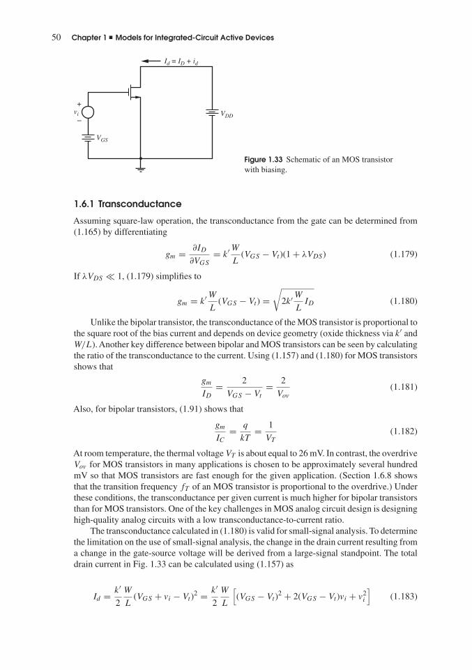
50 Chapter 1 � Models for Integrated-Circuit Active Devices
Id = ID + id
VDD
VGS
vi
+
–
Figure 1.33 Schematic of an MOS transistorwith biasing.
1.6.1 Transconductance
Assuming square-law operation, the transconductance from the gate can be determined from(1.165) by differentiating
gm = ∂ID
∂VGS
= k′ WL
(VGS − Vt)(1 + λVDS) (1.179)
If λVDS � 1, (1.179) simplifies to
gm = k′ WL
(VGS − Vt) =√
2k′ WL
ID (1.180)
Unlike the bipolar transistor, the transconductance of the MOS transistor is proportional tothe square root of the bias current and depends on device geometry (oxide thickness via k′ andW/L). Another key difference between bipolar and MOS transistors can be seen by calculatingthe ratio of the transconductance to the current. Using (1.157) and (1.180) for MOS transistorsshows that
gm
ID
= 2
VGS − Vt
= 2
Vov(1.181)
Also, for bipolar transistors, (1.91) shows that
gm
IC
= q
kT= 1
VT
(1.182)
At room temperature, the thermal voltage VT is about equal to 26 mV. In contrast, the overdriveVov for MOS transistors in many applications is chosen to be approximately several hundredmV so that MOS transistors are fast enough for the given application. (Section 1.6.8 showsthat the transition frequency fT of an MOS transistor is proportional to the overdrive.) Underthese conditions, the transconductance per given current is much higher for bipolar transistorsthan for MOS transistors. One of the key challenges in MOS analog circuit design is designinghigh-quality analog circuits with a low transconductance-to-current ratio.
The transconductance calculated in (1.180) is valid for small-signal analysis. To determinethe limitation on the use of small-signal analysis, the change in the drain current resulting froma change in the gate-source voltage will be derived from a large-signal standpoint. The totaldrain current in Fig. 1.33 can be calculated using (1.157) as
Id = k′
2
W
L(VGS + vi − Vt)
2 = k′
2
W
L
[(VGS − Vt)
2 + 2(VGS − Vt)vi + v2i
](1.183)

1.6 Small-Signal Models of MOS Transistors 51
Substituting (1.157) in (1.183) gives
Id = ID + k′
2
W
L
[2(VGS − Vt)vi + v2
i
](1.184)
Rearranging (1.184) gives
id = Id − ID = k′ WL
(VGS − Vt)vi
[1 + vi
2(VGS − Vt)
](1.185)
If the magnitude of the small-signal input |vi| is much less than twice the overdrive defined in(1.166), substituting (1.180) into (1.185) gives
id � gmvi (1.186)
In particular, if |vi| = |�VGS | is less than 20 percent of the overdrive, the small-signal analysisis accurate within about 10 percent.
1.6.2 Intrinsic Gate-Source and Gate-Drain Capacitance
If Cox is the oxide capacitance per unit area from gate to channel, then the total capacitanceunder the gate is CoxWL. This capacitance is intrinsic to the device operation and models thegate control of the channel conductance. In the triode region of device operation, the channelexists continuously from source to drain, and the gate-channel capacitance is usually lumpedinto two equal parts at the drain and source with
Cgs = Cgd = CoxWL
2(1.187)
In the saturation or active region, however, the channel pinches off before reaching thedrain, and the drain voltage exerts little influence on either the channel or the gate charge.As a consequence, the intrinsic portion of Cgd is essentially zero in the saturation region.To calculate the value of the intrinsic part of Cgs in the saturation or active region, we mustcalculate the total charge QT stored in the channel. This calculation can be carried out bysubstituting (1.145) into (1.144) and integrating to obtain
QT = WCox
∫ L
0[VGS − V (y) − Vt]dy (1.188)
Solving (1.150) for dy and substituting into (1.188) gives
QT = W2C2oxμn
ID
∫ VGS−Vt
0(VGS − V − Vt)
2dV (1.189)
where the limit y = L corresponds to V = (VGS − Vt) in the saturation or active region.Solution of (1.189) and use of (1.153) and (1.157) gives
QT = 2
3WLCox(VGS − Vt) (1.190)
Therefore, in the saturation or active region,
Cgs = ∂QT
∂VGS
= 2
3WLCox (1.191)
and
Cgd = 0 (1.192)

52 Chapter 1 � Models for Integrated-Circuit Active Devices
1.6.3 Input Resistance
The gate of an MOS transistor is insulated from the channel by the SiO2 dielectric. As a result,the low-frequency gate current is essentially zero and the input resistance is essentially infinite.This characteristic is important in some circuits such as sample-and-hold amplifiers, where thegate of an MOS transistor can be connected to a capacitor to sense the voltage on the capacitorwithout leaking away the charge that causes that voltage. In contrast, bipolar transistors havesmall but nonzero base current and finite input resistance looking into the base, complicatingthe design of bipolar sample-and-hold amplifiers.
1.6.4 Output Resistance
In Section 1.5.1, the effect of changes in drain-source voltage on the large-signal characteristicsof the MOS transistor was described. Increasing drain-source voltage in an n-channel MOStransistor increases the width of the depletion region around the drain and reduces the effectivechannel length of the device in the saturation or active region. This effect is called channel-length modulation and causes the drain current to increase when the drain-source voltage isincreased. From that treatment, we can calculate the change in the drain current �ID arisingfrom changes in the drain-source voltage �VDS as
�ID = ∂ID
∂VDS
�VDS (1.193)
Substitution of (1.161), (1.163), and (1.164) in (1.193) gives
�VDS
�ID
= VA
ID
= 1
λID
= ro (1.194)
where VA is the Early voltage, λ is the channel-length modulation parameter, ID is the draincurrent without channel-length modulation given by (1.157), and ro is the small-signal outputresistance of the transistor.
1.6.5 Basic Small-Signal Model of the MOS Transistor
Combination of the preceding small-signal circuit elements yields the small-signal model ofthe MOS transistor shown in Fig. 1.34. This model was derived for n-channel transistors inthe saturation or active region and is called the hybrid-π model. Drain, gate, and source nodesare labeled D, G, and S, respectively. When the gate-source voltage is increased, the modelpredicts that the incremental current id flowing from drain to source increases. Since the dcdrain current ID also flows from drain to source in an n-channel transistor, increasing the gate-source voltage also increases the total drain current Id . This result is reasonable physicallybecause increasing the gate-source voltage in an n-channel transistor increases the channelconductivity and drain current.
G D
S
Cgs vgsgmvgs ro
+
–
Figure 1.34 Basic small-signal model of an MOS transistor in the saturation or active region.

1.6 Small-Signal Models of MOS Transistors 53
The model shown in Fig. 1.34 is also valid for p-channel devices. Therefore, the modelagain shows that increasing the gate-source voltage increases the incremental current id flowingfrom drain to source. Unlike in the n-channel case, however, the dc current ID in a p-channeltransistor flows from source to drain because the source acts as the source of holes. Therefore,the incremental drain current flows in a direction opposite to the dc drain current when thegate-source voltage increases, reducing the total drain current Id . This result is reasonablephysically because increasing the gate-source voltage in a p-channel transistor reduces thechannel conductivity and drain current.
1.6.6 Body Transconductance
The drain current is a function of both the gate-source and body-source voltages. On theone hand, the gate-source voltage controls the vertical electric field, which controls the chan-nel conductivity and therefore the drain current. On the other hand, the body-source voltagechanges the threshold, which changes the drain current when the gate-source voltage is fixed.This effect stems from the influence of the substrate acting as a second gate and is calledthe body effect. Note that the body of an MOS transistor is usually connected to a constantpower-supply voltage, which is a small-signal or ac ground. However, the source connectioncan have a significant ac voltage impressed on it, which changes the body-source voltagewhen the body voltage is fixed. Therefore, when the body-source voltage is not constant, twotransconductance terms are required to model MOS transistors: one associated with the maingate and the other associated with the body or second gate.
Using (1.165), the transconductance from the body or second gate is
gmb = ∂ID
∂VBS
= − k′ WL
(VGS − Vt)(1 + λVDS)∂Vt
∂VBS
(1.195)
From (1.140)
∂Vt
∂VBS
= − γ
2√
2φf + VSB
= −χ (1.196)
This equation defines a factor χ, which is the rate of change of threshold voltage with bodybias voltage. Substitution of (1.141) in (1.196) and use of (1.20) gives
χ = Cjs
Cox
(1.197)
where Cjs is the capacitance per unit area of the depletion region under the channel, assuminga one-sided step junction with a built-in potential ψ0 = 2φf . Substitution of (1.196) in (1.195)gives
gmb = γ k′(W/L)(VGS − Vt)(1 + λVDS)
2√
2φf + VSB
(1.198)
If λVDS � 1, we have
gmb = γ k′(W/L)(VGS − Vt)
2√
2φf + VSB
= γ
√k′(W/L)ID
2(2φf + VSB)(1.199)
The ratio gmb/gm is an important quantity in practice. From (1.179) and (1.198), we find
gmb
gm
= γ
2√
2φf + VSB
= χ (1.200)

54 Chapter 1 � Models for Integrated-Circuit Active Devices
The factor χ is typically in the range 0.1 to 0.3; therefore, the transconductance from the maingate is typically a factor of about 3 to 10 times larger than the transconductance from the bodyor second gate.
1.6.7 Parasitic Elements in the Small-Signal Model
The elements of the small-signal model for MOS transistors described above may be consid-ered basic in the sense that they arise directly from essential processes in the device. As in thecase of bipolar transistors, however, technological limitations in the fabrication of the devicesgive rise to a number of parasitic elements that must be added to the equivalent circuit for mostintegrated-circuit transistors.Across section and top view of a typical n-channel MOS transistorare shown in Fig. 1.35. The means of fabricating such devices is described in Chapter 2.
All pn junctions in the MOS transistor should be reverse biased during normal opera-tion, and each junction exhibits a voltage-dependent parasitic capacitance associated with itsdepletion region. The source-body and drain-body junction capacitances shown in Fig. 1.35aare Csb and Cdb, respectively. If the doping levels in the source, drain, and body regions areassumed to be constant, (1.21) can be used to express these capacitances as follows:
Csb = Csb0(1 + VSB
ψ0
)1/2 (1.201)
Cdb = Cdb0(1 + VDB
ψ0
)1/2 (1.202)
These capacitances are proportional to the source and drain region areas (including sidewalls).Since the channel is attached to the source in the saturation or active region, Csb also includes
GateSource Drain Body
n+n+
p
p+
Csb
Col Col
Cdb
L
S GW D
Cgb
B
(a)
(b)
Figure 1.35 (a) Cross section and (b) top view of an n-channel MOS transistor.

1.6 Small-Signal Models of MOS Transistors 55
G D
B
Cgd
Cgs
Cdb
Cgb
SCsb
vgs
vbs
gmvgs gmbvbs ro
+
+
–
–
Figure 1.36 Small-signal MOS transistor equivalent circuit.
depletion-region capacitance from the induced channel to the body. A detailed analysis of thechannel-body capacitance is given by Tsividis.26
In practice, Cgs and Cgd , given in (1.187) for the triode region of operation and in (1.191)and (1.192) for the saturation or active region, are increased due to parasitic oxide capacitancesarising from gate overlap of the source and drain regions. These overlap capacitances Col areshown in Fig. 1.35a, and their values are calculated in Chapter 2.
Capacitance Cgb between gate and body or substrate models parasitic oxide capacitancebetween the gate-contact material and the substrate outside the active-device area. This capac-itance is independent of the gate-body voltage and models coupling from polysilicon andmetal interconnects to the underlying substrate, as shown by the shaded regions in the topview of Fig. 1.35b. Parasitic capacitance of this type underlies all polysilicon and metal traceson integrated circuits. Such parasitic capacitance should be taken into account when simulat-ing and calculating high-frequency circuit and device performance. Typical values depend onoxide thicknesses. With a silicon dioxide thickness of 100 Å , the capacitance is about 3.45 fFper square micron. Fringing capacitance becomes important for lines narrower in width thanseveral microns.
Parasitic resistance in series with the source and drain can be used to model the nonzeroresistivity of the contacts and diffusion regions. In practice, these resistances are often ignoredin hand calculations for simplicity but included in computer simulations. These parasitic resis-tances have an inverse dependence on channel width W . Typical values of these resistances are50 to 100 for devices with W of about 1 �m. Similar parasitic resistances in series withthe gate and body terminals are sometimes included but often ignored because very little cur-rent flows in these terminals, especially at low frequencies. The small-signal model includingcapacitive parasitics but ignoring resistive parasitics is shown in Fig. 1.36.
1.6.8 MOS Transistor Frequency Response
As for a bipolar transistor, the frequency capability of an MOS transistor is usually specifiedby finding the transition frequency fT . For an MOS transistor, fT is defined as the frequencywhere the magnitude of the short-circuit, common-source current gain falls to unity. Althoughthe dc gate current of an MOS transistor is essentially zero, the high-frequency behaviorof the transistor is controlled by the capacitive elements in the small-signal model, whichcause the gate current to increase as frequency increases. To calculate fT , consider the accircuit of Fig. 1.37a and the small-signal equivalent of Fig. 1.37b. Since vsb = vds = 0, gmb,

56 Chapter 1 � Models for Integrated-Circuit Active Devices
ii
ii
io
vgs
vgs
Cgs + Cgbgmvgs
ioCgd
++
––
(b)(a)
Figure 1.37 Circuits for calculating the fT of an MOS transistor: (a) ac schematic and (b) small-signal equivalent.
ro, Csb, and Cdb have no effect on the calculation and are ignored. The small-signal inputcurrent ii is
ii = s(Cgs + Cgb + Cgd)vgs (1.203)
If the current fed forward through Cgd is neglected,
io � gmvgs (1.204)
Solving (1.203) for vgs and substituting into (1.204) gives
io
ii� gm
s(Cgs + Cgb + Cgd)(1.205)
To find the frequency response, we set s = jω. Then
io
ii� gm
jω(Cgs + Cgb + Cgd)(1.206)
The magnitude of the small-signal current gain is unity when
ω = ωT = gm
Cgs + Cgb + Cgd
(1.207)
Therefore,
fT = 1
2πωT = 1
2π
gm
Cgs + Cgb + Cgd
(1.208)
Assume the intrinsic device capacitance Cgs is much greater than (Cgb + Cgd). Then substi-tuting (1.180) and (1.191) into (1.208) gives
fT = 1.5μn
2πL2 (VGS − Vt) (1.209)
Comparison of this equation with the intrinsic fT of a bipolar transistor when parasiticdepletion-layer capacitance is neglected leads to an interesting result. From (1.128) and (1.130)with �F � (Cje + Cμ)/gm,
fT = 1
2π�F
(1.210)

1.6 Small-Signal Models of MOS Transistors 57
Substituting from (1.99) for �F and using the Einstein relationship Dn/μn = kT/q = VT , wefind for a bipolar transistor
fT = 2μn
2πW2B
VT (1.211)
The similarity in form between (1.211) and (1.209) is striking. In both cases, the intrinsic devicefT increases as the inverse square of the critical device dimension across which carriers arein transit. The voltage VT = 26 mV is fixed for a bipolar transistor, but the fT of an MOStransistor can be increased by operating at high values of (VGS − Vt). Note that the basewidth WB in a bipolar transistor is a vertical dimension determined by diffusions or implantsand can typically be made much smaller than the channel length L of an MOS transistor,which depends on surface geometry and photolithographic processes. Thus bipolar transistorsgenerally have higher fT than MOS transistors made with comparable processing. Finally,(1.209) was derived assuming that the MOS transistor exhibits square-law behavior as in(1.157). However, as described in Section 1.7, submicron MOS transistors depart significantlyfrom square-law characteristics, and we find that for such devices fT is proportional to L−1
rather than L−2.
EXAMPLE
Derive the complete small-signal model for an NMOS transistor with ID = 100 �A, VSB =1 V, VDS = 2 V. Device parameters are φf = 0.3 V, W = 10 �m, L = 1 �m, γ = 0.5 V1/2,k′ = 200 �A/V2, λ = 0.02 V−1, tox = 100 angstroms, ψ0 = 0.6 V, Csb0 = Cdb0 = 10 fF.Overlap capacitance from gate to source and gate to drain is 1 fF. Assume Cgb = 5 fF.
From (1.166),
Vov = VGS − Vt =√
2ID
k′(W/L)=√
2 × 100
200 × 10� 0.316 V
Since VDS > Vov , the transistor operates in the saturation or active region. From (1.180),
gm =√
2k′ WL
ID = √2 × 200 × 10 × 100 �A/V � 632 �A/V
From (1.199),
gmb = γ
√k′(W/L)ID
2(2φf + VSB)= 0.5
√200 × 10 × 100
2 × 1.6� 125 �A/V
From (1.194),
ro = 1
λID
= 1000
0.02 × 100k = 500 k
Using (1.201) with VSB = 1 V , we find
Csb = 10(1 + 1
0.6
)1/2 fF � 6 fF
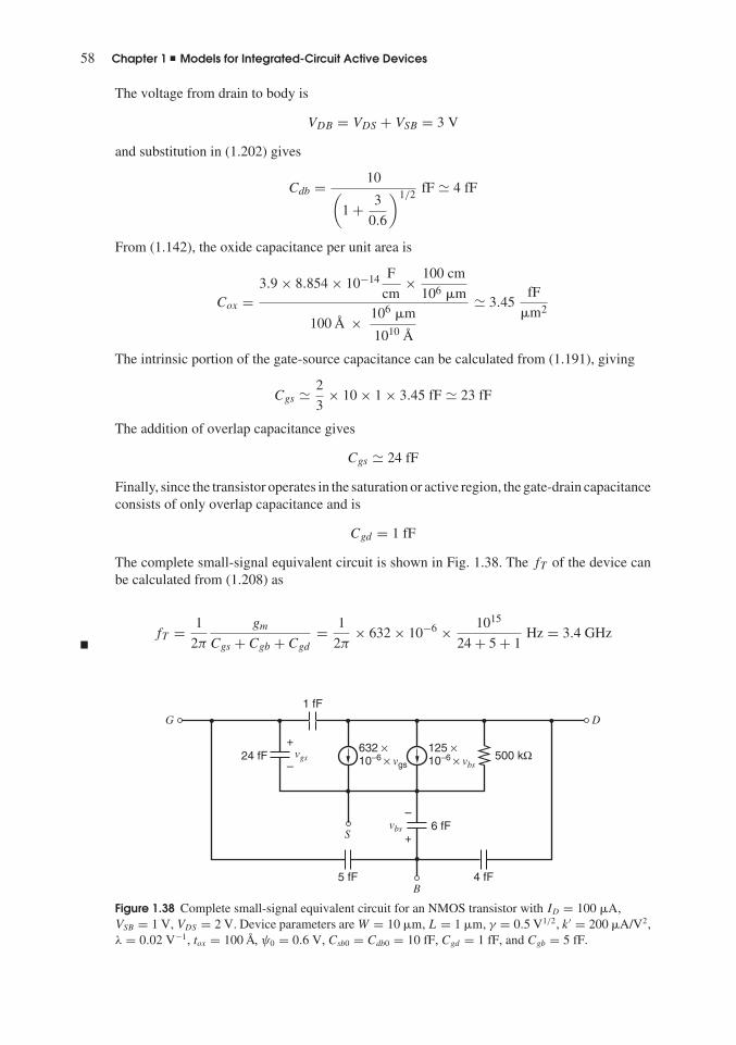
58 Chapter 1 � Models for Integrated-Circuit Active Devices
The voltage from drain to body is
VDB = VDS + VSB = 3 V
and substitution in (1.202) gives
Cdb = 10(1 + 3
0.6
)1/2 fF � 4 fF
From (1.142), the oxide capacitance per unit area is
Cox =3.9 × 8.854 × 10−14 F
cm× 100 cm
106 �m
100 Å × 106 �m
1010 Å
� 3.45fF
�m2
The intrinsic portion of the gate-source capacitance can be calculated from (1.191), giving
Cgs � 2
3× 10 × 1 × 3.45 fF � 23 fF
The addition of overlap capacitance gives
Cgs � 24 fF
Finally, since the transistor operates in the saturation or active region, the gate-drain capacitanceconsists of only overlap capacitance and is
Cgd = 1 fF
The complete small-signal equivalent circuit is shown in Fig. 1.38. The fT of the device canbe calculated from (1.208) as
fT = 1
2π
gm
Cgs + Cgb + Cgd
= 1
2π× 632 × 10−6 × 1015
24 + 5 + 1Hz = 3.4 GHz
G D
B
24 fF
6 fF
4 fF5 fF
632 ×10–6 × vgs
125 ×10–6 × vbs
1 fF
S
vgs
vbs
500 kΩ+
+
–
–
Figure 1.38 Complete small-signal equivalent circuit for an NMOS transistor with ID = 100 �A,VSB = 1 V, VDS = 2 V. Device parameters are W = 10 �m, L = 1 �m, γ = 0.5 V1/2, k′ = 200 �A/V2,λ = 0.02 V−1, tox = 100 Å, ψ0 = 0.6 V, Csb0 = Cdb0 = 10 fF, Cgd = 1 fF, and Cgb = 5 fF.

1.7 Short-Channel Effects in MOS Transistors 59
1.7 Short-Channel Effects in MOS TransistorsThe evolution of integrated-circuit processing techniques has led to continuing reductions inboth the horizontal and vertical dimensions of the active devices. (The minimum alloweddimensions of passive devices have also decreased.) This trend is driven primarily by eco-nomics in that reducing dimensions increases the number of devices and circuits that can beprocessed at one time on a given wafer. A second benefit has been that the frequency capa-bility of the active devices continues to increase, as intrinsic fT values increase with smallerdimensions while parasitic capacitances decrease.
Vertical dimensions such as the base width of a bipolar transistor in production processesmay now be on the order of 0.05 �m or less, whereas horizontal dimensions such as bipolaremitter width or MOS transistor gate length may be significantly less than 1 �m. Even withthese small dimensions, the large-signal and small-signal models of bipolar transistors given inprevious sections remain valid. However, significant short-channel effects become importantin MOS transistors at channel lengths of about 1 �m or less and require modifications to theMOS models given previously. The primary effect is to modify the classical MOS square-lawtransfer characteristic in the saturation or active region to make the device voltage-to-currenttransfer characteristic more linear. However, even in processes with submicron capability,many of the MOS transistors in a given analog circuit may be deliberately designed to havechannel lengths larger than the minimum and may be well approximated by the square-lawmodel.
1.7.1 Velocity Saturation from the Horizontal Field
The most important short-channel effect in MOS transistors stems from velocity saturation ofcarriers in the channel.27 When an MOS transistor operates in the triode region, the averagehorizontal electric field along the channel is VDS/L. When VDS is small and/or L is large, thehorizontal field is low, and the linear relation between carrier velocity and field assumed in(1.148) is valid. At high fields, however, the carrier velocities approach the thermal velocities,and subsequently the slope of the carrier velocity decreases with increasing field. This effectis illustrated in Fig. 1.39, which shows typical measured electron drift velocity vd versushorizontal electric field strength magnitude � in an NMOS surface channel. While the velocityat low field values is proportional to the field, the velocity at high field values approaches aconstant called the scattering-limited velocity vscl. A first-order analytical approximation tothis curve is
vd = μn�
1 + �/�c
(1.212)
where �c � 1.5 × 10⁶ V/m and μn � 0.07 m2/V-s is the low-field mobility close to the gate.Equation 1.212 is also plotted in Fig. 1.39. From (1.212), as � → ∞, vd → vscl = μn�c. Atthe critical field value �c, the carrier velocity is a factor of 2 less than the low-field formulawould predict. In a device with a channel length L = 0.5 �m, we need a voltage drop of only0.75 V along the channel to produce an average field equal to �c, and this condition is readilyachieved in short-channel MOS transistors. Similar results are found for PMOS devices.
Substituting (1.212) and (1.149) into (1.147) and rearranging gives
ID
(1 + 1
�c
dV
dy
)= WQI (y)μn
dV
dy(1.213)

60 Chapter 1 � Models for Integrated-Circuit Active Devices
105
105 107106
Electric field � (V/m)
104
5 × 10⁴
5 × 10³
2 × 10⁴
Drif
t vel
ocity
vd
(m/s
) vscl
Figure 1.39 Typicalmeasured electron driftvelocity vd versushorizontal electric field �in an MOS surface channel(solid plot). Also shown(dashed plot) is theanalytical approximationof Eq. 1.212 with�c = 1.5 × 10⁶ V/m andμn = 0.07 m2/V-s.
Note that as �c → ∞ and velocity saturation becomes negligible, (1.213) approaches theoriginal equation (1.147). Integrating (1.213) along the channel, we obtain∫ L
0ID
(1 + 1
�c
dV
dy
)dy =
∫ VDS
0WQI (y)μn dV (1.214)
and thus
ID = μnCox
2
(1 + VDS
�cL
)W
L[2(VGS − Vt)VDS − V 2
DS] (1.215)
In the limit as �c → ∞, (1.215) is the same as (1.152), which gives the drain current in thetriode region without velocity saturation. The quantity VDS/L in (1.215) can be interpreted asthe average horizontal electric field in the channel. If this field is comparable to �c, the draincurrent for a given VDS is less than the simple expression (1.152) would predict.
Equation 1.215 is valid in the triode region. Let VDS(act) represent the maximum value ofVDS for which the transistor operates in the triode region, which is equivalent to the minimumvalue of VDS for which the transistor operates in the active region. In the active region, thecurrent should be independent of VDS because channel-length modulation is not included here.Therefore, VDS(act) is the value of VDS that sets ∂ID/∂VDS = 0. From (1.215),
∂ID
∂VDS
= k′
2
W
L
⎡⎢⎢⎢⎣(
1 + VDS
�cL
)[2(VGS − Vt) − 2VDS] − [2(VGS − Vt)VDS − V 2
DS]
�cL(1 + VDS
�cL
)2
⎤⎥⎥⎥⎦
(1.216)where k′ = μnCox as given by (1.153). To set ∂ID/∂VDS = 0,(
1 + VDS
�cL
)[2(VGS − Vt) − 2VDS] − [2(VGS − Vt)VDS − V 2
DS]
�cL= 0 (1.217)
Rearranging (1.217) gives
V 2DS
�cL+ 2VDS − 2(VGS − Vt) = 0 (1.218)

1.7 Short-Channel Effects in MOS Transistors 61
Solving the quadratic equation gives
VDS(act) = VDS = −�cL � �cL
√1 + 2(VGS − Vt)
�cL(1.219)
Since the drain-source voltage must be greater than zero,
VDS(act) = VDS = �cL
(√1 + 2(VGS − Vt)
�cL− 1
)(1.220)
To determine VDS(act) without velocity-saturation effects, let �c → ∞ so that the driftvelocity is proportional to the electric field, and let x = (VGS − Vt)/(�cL). Then x → 0, anda Taylor series can be used to show that
√1 + 2x = 1 + x − x2
2+ · · · (1.221)
Using (1.221) in (1.220) gives
VDS(act) = (VGS − Vt)
(1 − VGS − Vt
2�cL+ · · ·
)(1.222)
When �c → ∞, (1.222) shows that VDS(act) → (VGS − Vt), as expected.28 This observation isconfirmed by plotting the ratio of VDS(act) to the overdrive Vov versus �cL in Fig. 1.40. When�c → ∞, VDS(act) → Vov = VGS − Vt , as predicted by (1.222). On the other hand, when �c
is small enough that velocity saturation is significant, Fig. 1.40 shows that VDS(act) < Vov .To find the drain current in the active region with velocity saturation, substitute VDS(act)
in (1.220) for VDS in (1.215). After rearranging, the result is
ID = μnCox
2
W
L[VDS(act)]
2 (1.223)
Equation 1.223 is in the same form as (1.157), where velocity saturation is neglected, except thatVDS(act) is less than (VGS − Vt) when velocity saturation is significant, as shown in Fig. 1.40.Therefore, the current predicted by (1.157) overestimates the current that really flows whenthe carrier velocity saturates. To examine the limiting case when the velocity is completely
Vov = 0.1 V
Vov = 0.5 V
Vov
VDS(act)
1
0.9
0.8
0.7
0.6
0.50 1 2 3 4 5
�cL (V)6 7 8 9 10
Figure 1.40 Ratio of the minimumdrain-source voltage required foroperation in the active region to theoverdrive versus the product of thecritical field and the channel length.When �c → ∞, velocity saturationis not a factor, and VDS(act) →Vov = VGS − Vt , as expected.When velocity saturation issignificant, VDS(act) < Vov .

62 Chapter 1 � Models for Integrated-Circuit Active Devices
saturated, let �c → 0. Then (1.212) shows that the drift velocity approaches the scattering-limited velocity vd → vscl = μn�c. Substituting (1.220) into (1.223) gives
lim�c→0
ID = μnCoxW(VGS − Vt)�c = WCox(VGS − Vt)vscl (1.224)
In contrast to the square-law behavior predicted by (1.157), (1.224) shows that the draincurrent is a linear function of the overdrive (VGS − Vt) when the carrier velocity saturates.Also, (1.224) shows that the drain current is independent of the channel length when thecarrier velocity saturates. In this case, both the charge in the channel and the time requiredfor the charge to cross the channel are proportional to L. Since the current is the ratio of thecharge in the channel to the time required to cross the channel, the current does not dependon L as long as the channel length is short enough to produce an electric field that is highenough for velocity saturation to occur.29 In contrast, when the carrier velocity is proportionalto the electric field instead of being saturated, the time required for channel charge to crossthe channel is proportional to L2 because increasing L both reduces the carrier velocity andincreases the distance between the source and the drain. Therefore, when velocity saturationis not significant, the drain current is inversely proportional to L, as we have come to expectthrough (1.157). Finally, (1.224) shows that the drain current in the active region is proportionalto the scattering-limited velocity vscl = μn�c when the velocity is saturated.
Substituting (1.222) into (1.223) gives
ID = μnCox
2
W
L(VGS − Vt)
2(
1 − VGS − Vt
2�cL+ · · ·
)2
= μnCox
2
W
L(VGS − Vt)
2(
1 − x
2+ · · ·
)2
= μnCox
2
W
L(VGS − Vt)
2(1 − x + · · ·)
= μnCox
2
W
L(VGS − Vt)
2(
1 − VGS − Vt
�cL+ · · ·
)(1.225)
where x = (VGS − Vt)/(�cL) as defined for (1.221). If x � 1, (1 − x) � 1/(1 + x), and
ID � μnCox
2
(1 + VGS − Vt
�cL
)W
L(VGS − Vt)
2 (1.226)
Equation 1.226 is valid without velocity saturation and at its onset, where (VGS − Vt) � �cL.The effect of velocity saturation on the current in the active region predicted by (1.226) canbe modeled with the addition of a resistance in series with the source of an ideal square-lawdevice, as shown in Fig. 1.41. Let V ′
GS be the gate-source voltage of the ideal square-law
D
S
G
RSX
ID
V'GS
VGS
+
–
+
–
Figure 1.41 Model of velocity saturation in anMOSFET by addition of series source resistanceto an ideal square-law device.

1.7 Short-Channel Effects in MOS Transistors 63
transistor. From (1.157),
ID = μnCox
2
W
L(V ′
GS − Vt)2 (1.227)
Let VGS be the sum of V ′GS and the voltage drop on RSX. Then
VGS = V ′GS + IDRSX (1.228)
This sum models the gate-source voltage of a real MOS transistor with velocity saturation.Substituting (1.228) into (1.227) gives
ID = μnCox
2
W
L(VGS − IDRSX − Vt)
2
ID = μnCox
2
W
L
((VGS − Vt)
2 − 2(VGS − Vt)IDRSX + (IDRSX)2)
(1.229)
Rearranging (1.229) while ignoring the (IDRSX)2 term gives
ID � μnCox
2
(1 + μnCox
W
LRSX(VGS − Vt)
)W
L(VGS − Vt)
2 (1.230)
Equation 1.230 has the same form as (1.226) if we identify
μnCox
W
LRSX = 1
�cL(1.231)
Rearranging (1.231) gives
RSX = 1
�cμnCoxW(1.232)
Thus the influence of velocity saturation on the large-signal characteristics of an MOS transistorcan be modeled to first order by a resistor RSX in series with the source of an ideal square-lawdevice. Note that RSX varies inversely with W , as does the intrinsic physical series resistancedue to the source and drain contact regions. Typically, RSX is larger than the physical seriesresistance. For W = 2 �m, k′ = μnCox = 200 �A/V2, and �c = 1.5 × 10⁶ V/m, we findRSX � 1700 .
1.7.2 Transconductance and Transition Frequency
The values of all small-signal parameters can change significantly in the presence of short-channel effects.30 One of the most important changes is to the transconductance. Substituting(1.220) into (1.223) and calculating ∂ID/∂VGS gives
gm = ∂ID
∂VGS
= WCoxvscl
√1 + 2(VGS − Vt)
�cL− 1√
1 + 2(VGS − Vt)
�cL
(1.233)
where vscl = μn�c as in Fig. 1.39. To determine gm without velocity saturation, let Ec → ∞and x = (VGS − Vt)/(�cL). Then substituting (1.221) into (1.233) and rearranging gives
lim�c→∞
gm = k′ WL
(VGS − Vt) (1.234)

64 Chapter 1 � Models for Integrated-Circuit Active Devices
as predicted by (1.180). In this case, the transconductance increases when the overdriveincreases or the channel length decreases. On the other hand, letting �c → 0 to determinegm when the velocity is saturated gives
lim�c→0
gm = WCoxvscl (1.235)
Equation 1.235 shows that further decreases in L or increases in (VGS − Vt) do not change thetransconductance when the velocity is saturated.
From (1.223) and (1.233), the ratio of the transconductance to the current can be cal-culated as
gm
I= 2
(�cL)
√1 + 2(VGS − Vt)
�cL
(√1 + 2(VGS − Vt)
�cL− 1
) (1.236)
As �c → 0, the velocity saturates and
lim�c→0
gm
I= 1
VGS − Vt
(1.237)
Comparing (1.237) to (1.181) shows that velocity saturation reduces the transconductance-to-current ratio for a given overdrive.
On the other hand, when x = (VGS − Vt)/(�cL) � 1, substituting (1.221) into (1.236)gives
gm
I� 2
(VGS − Vt)(1 + x)(1.238)
Therefore, as �c → ∞, x → 0, and (1.238) collapses to
lim�c→∞
gm
I= 2
VGS − Vt
(1.239)
as predicted by (1.181). Equation 1.238 shows that if x < 0.1, the error in using (1.181) tocalculate the transconductance-to-current ratio is less than about 10 percent. Therefore, wewill conclude that velocity-saturation effects are insignificant in hand calculations if
(VGS − Vt) < 0.1(�cL) (1.240)
Figure 1.42 plots the transconductance-to-current ratio versus the overdrive for three cases.The highest and lowest ratios come from (1.239) and (1.237), which correspond to asymptoteswhere velocity saturation is insignificant and dominant, respectively. In practice, the transitionbetween these extreme cases is gradual and described by (1.236), which is plotted in Fig. 1.42for an example where �c = 1.5 × 10⁶ V/m and L = 0.5 �m.
One reason the change in transconductance caused by velocity saturation is important isbecause it affects the transition frequency fT . Assuming that Cgs � Cgb + Cgd , substituting(1.235) into (1.208) shows that
fT = 1
2π
gm
Cgs
∝ WCoxvscl
WLCox
∝ vscl
L(1.241)
One key point here is that the transition frequency is independent of the overdrive once velocitysaturation is reached. In contrast, (1.209) shows that increasing (VGS − Vt) increases fT beforethe velocity saturates.Also, (1.241) shows that the transition frequency is inversely proportionalto the channel length when the velocity is saturated. In contrast, (1.209) predicts that fT is

1.8 Weak Inversion in MOS Transistors 65
Eq. 1.237 where �cL → 0
Eq. 1.236 where �cL = 0.75V
Eq. 1.239 where �cL → ∞
5
4
3
2
1
00 1 2 3
VGS – Vt (V)
gm
I(V–1) Figure 1.42
Transconductance-to-currentratio versus overdrive(VGS − Vt) where velocitysaturation is insignificant(�cL → ∞), dominant(�cL = 0), and of graduallyincreasing importance(�cL = 0.75 V).
inversely proportional to the square of the channel length before the velocity saturates. Asa result, velocity saturation reduces the speed improvement that can be achieved throughreductions in the minimum channel length.
1.7.3 Mobility Degradation from the Vertical Field
Thus far, we have considered only the effects of the horizontal field due to the VDS along thechannel when considering velocity saturation. However, a vertical field originating from thegate voltage also exists and influences carrier velocity. A physical reason for this effect is thatincreasing the vertical electric field forces the carriers in the channel closer to the surface ofthe silicon, where surface imperfections impede their movement from the source to the drain,reducing mobility.31 The vertical field at any point in the channel depends on the gate-channelvoltage. Since the gate-channel voltage is not constant from the source to the drain, the effect ofthe vertical field on mobility should be included within the integration in (1.214) in principle.32
For simplicity, however, this effect is often modeled after integration by changing the mobilityin the previous equations to an effective mobility given by
μeff = μn
1 + θ(VGS − Vt)(1.242)
where μn is the mobility with zero vertical field, and θ is inversely proportional to the oxidethickness. For tox = 100 Å , θ is typically in the range from 0.1 V−1 to 0.4 V−1.33 In practice,θ is determined by a best fit to measured device characteristics.
1.8 Weak Inversion in MOS TransistorsThe MOSFET analysis of Section 1.5 considered the normal region of operation for whicha well-defined conducting channel exists under the gate. In this region of strong inversion,changes in the gate-source voltage are assumed to cause only changes in the channel chargeand not in the depletion-region charge. In contrast, for gate-source voltages less than theextrapolated threshold voltage Vt but high enough to create a depletion region at the surfaceof the silicon, the device operates in weak inversion. In the weak-inversion region, the channelcharge is much less than the charge in the depletion region, and the drain current arising fromthe drift of majority carriers is negligible. However, the total drain current in weak inversion

66 Chapter 1 � Models for Integrated-Circuit Active Devices
is larger than that caused by drift because a gradient in minority-carrier concentration causes adiffusion current to flow. In weak inversion, an n-channel MOS transistor operates as an npn
bipolar transistor, where the source acts as the emitter, the substrate as the base, and the drainas the collector.34
1.8.1 Drain Current in Weak Inversion
To analyze this situation, assume that the source and the body are both grounded. Also assumethat VDS > 0. (If VDS < 0, the drain acts as the emitter and the source as the collector.)35 Thenincreasing the gate-source voltage increases the surface potential ψs, which tends to reduce thereverse bias across the source-substrate (emitter-base) junction and to exponentially increasethe concentration of electrons in the p-type substrate at the source np(0). From (1.27),
np(0) = npo expψs
VT
(1.243)
where npo is the equilibrium concentration of electrons in the substrate (base). Similarly, theconcentration of electrons in the substrate at the drain np(L) is
np(L) = npo expψs − VDS
VT
(1.244)
From (1.31), the drain current due to the diffusion of electrons in the substrate is
ID = qADn
np(L) − np(0)
L(1.245)
where Dn is the diffusion constant for electrons, and A is the cross-sectional area in which thediffusion current flows. The area A is the product of the transistor width W and the thickness X
of the region in which ID flows. Substituting (1.243) and (1.244) into (1.245) and rearranginggives
ID = W
LqXDnnpo exp
(ψs
VT
)[1 − exp
(−VDS
VT
)](1.246)
In weak inversion, the surface potential is approximately a linear function of the gate-source voltage.36 Assume that the charge stored at the oxide-silicon interface is independentof the surface potential. Then, in weak inversion, changes in the surface potential �ψs arecontrolled by changes in the gate-source voltage �VGS through a voltage divider between theoxide capacitance Cox and the depletion-region capacitance Cjs. Therefore,
dψs
dVGS
= Cox
Cjs + Cox
= 1
n= 1
1 + χ(1.247)
in which n = (1 + Cjs/Cox) and χ = Cjs/Cox, as defined in (1.197). Separating variables in(1.247) and integrating gives
ψs = VGS
n+ k1 (1.248)
where k1 is a constant. Equation 1.248 is valid only when the transistor operates in weakinversion. When VGS = Vt with VSB = 0, ψs = 2φf by definition of the threshold voltage.For VGS > Vt , the inversion layer holds the surface potential nearly constant and (1.248) isnot valid. Since (1.248) is valid only when VGS ≤ Vt , (1.248) is rewritten as follows:
ψs = VGS − Vt
n+ k2 (1.249)

1.8 Weak Inversion in MOS Transistors 67
where k2 = k1 + Vt/n. Substituting (1.249) into (1.246) gives
ID = W
LqXDnnpo exp
(k2
VT
)exp
(VGS − Vt
nVT
)[1 − exp
(−VDS
VT
)](1.250)
Let
It = qXDnnpo exp
(k2
VT
)(1.251)
represent the drain current with VGS = Vt , W/L = 1, and VDS � VT . Then
ID = W
LIt exp
(VGS − Vt
nVT
)[1 − exp
(−VDS
VT
)](1.252)
Figure 1.43 plots the drain current versus the drain-source voltage for three values ofthe overdrive, with W = 20 �m, L = 20 �m, n = 1.5, and It = 0.1 �A. Notice that thedrain current is almost constant when VDS > 3VT because the last term in (1.252) approachesunity in this case. Therefore, unlike in strong inversion, the minimum drain-source voltagerequired to force the transistor to operate as a current source in weak inversion is independentof the overdrive.37 Figure 1.43 and Equation 1.252 also show that the drain current is notzero when VGS ≤ Vt . To further illustrate this point, we show measured NMOS character-istics plotted on two different scales in Fig. 1.44. In Fig. 1.44a, we show
√ID versus VGS
in the active region plotted on linear scales. For this device, W = 20 �m, L = 20 �m, andshort-channel effects are negligible. (See Problem 1.21 for an example of a case in whichshort-channel effects are important.) The resulting straight line shows that the device char-acteristic is close to an ideal square law. Plots like the one in Fig. 1.44a are commonly usedto obtain Vt by extrapolation (0.7 V in this case) and also k′ from the slope of the curve(54 �A/V2 in this case). Near the threshold voltage, the curve deviates from the straight linerepresenting the square law. This region is weak inversion. The data are plotted a second time inFig. 1.44b on log-linear scales. The straight line obtained for VGS < Vt fits (1.252) with n =1.5. For ID < 10−12 A, the slope decreases because leakage currents are significant and do notfollow (1.252).
VDS = 3VT ≈ 78 mV
VDS (V)
ID (μA) VGS – Vt = –10 mV
VGS – Vt = –20 mV
VGS – Vt = 0
0.12
0.1
0.08
0.06
0.04
0.02
0 0.1 0.2 0.3 0.4 0.50
Figure 1.43 Drain current versus drain-source voltage in weak inversion.

68 Chapter 1 � Models for Integrated-Circuit Active Devices
ID (μA)1/2
VDS = 5 V
VGS (V)
W = 20 μmL = 20 μm
20
15
10
5
01 2 3 4 5
Extrapolated Vt = 0.7 V
(a)
Figure 1.44 (a) Measured NMOS transfer characteristic in the active region plotted on linear scales as√ID versus VGS , showing the square-law characteristic.
ID (A)
10–3
10–4
10–5
10–6
10–7
10–8
10–9
10–10
10–11
10–12
10–130 0.5 1 1.5 2
VDS = 5 V
VGS (V)
W = 20 μmL = 20 μm
Subthreshold exponential region
Square-law region
(b)
Figure 1.44 (b) Data from Fig. 1.44a plotted on log-linear scales showing the exponential character-istic in the subthreshold region.
The major use of transistors operating in weak inversion is in very low power applicationsat relatively low signal frequencies. The limitation to low signal frequencies occurs becausethe MOSFET fT becomes very small. This result stems from the fact that the small-signal gm
calculated from (1.252) becomes proportional to ID and therefore very small in weak inversion,as shown next.

1.8 Weak Inversion in MOS Transistors 69
1.8.2 Transconductance and Transition Frequency in Weak Inversion
Calculating ∂ID/∂VGS from (1.252) and using (1.247) gives
gm = W
L
It
nVT
exp
(VGS − Vt
nVT
)[1 − exp
(−VDS
VT
)]= ID
nVT
= ID
VT
Cox
Cjs + Cox
(1.253)
The transconductance of an MOS transistor operating in weak inversion is identical to that ofa corresponding bipolar transistor, as shown in (1.182), except for the factor of 1/n = Cox/
(Cjs + Cox). This factor stems from a voltage divider between the oxide and depletion capaci-tors in the MOS transistor, which models the indirect control of the gate on the surface potential.
From (1.253), the ratio of the transconductance to the current of an MOS transistor inweak inversion is
gm
I= 1
nVT
= 1
VT
Cox
Cjs + Cox
(1.254)
Equation 1.254 predicts that this ratio is independent of the overdrive. In contrast, (1.181)predicts that the ratio of transconductance to current is inversely proportional to the overdrive.Therefore, as the overdrive approaches zero, (1.181) predicts that this ratio becomes infinite.However, (1.181) is valid only when the transistor operates in strong inversion. To estimatethe overdrive required to operate the transistor in strong inversion, we will equate the gm/I
ratios calculated in (1.254) and (1.181). The result is
Vov = VGS − Vt = 2nVT (1.255)
which is about 78 mV at room temperature with n = 1.5. Although this analysis implies thatthe transition from weak to strong inversion occurs abruptly, a nonzero transition width occursin practice. Between weak and strong inversion, the transistor operates in a region of moderateinversion, where both diffusion and drift currents are significant.38
Figure 1.45 plots the transconductance-to-current ratio versus overdrive for an examplecase with n = 1.5. When the overdrive is negative but high enough to cause depletion at thesurface, the transistor operates in weak inversion and the transconductance-to-current ratio isconstant, as predicted by (1.254). When VGS − Vt = 0, the surface potential is 2ψf , whichmeans that the surface concentration of electrons is equal to the bulk concentration of holes.This point is usually defined as the upper bound on the region of weak inversion. When
(moderate inversion)
VGS – Vt (V)
gm
I(V–1)
30
25
20
15
10
5
0–0.5 –0.25 0 2nVT 0.25 0.5
From (1.254) with n = 1.5(weak inversion)
From (1.181)(strong inversion)
Figure 1.45 Transconductance-to-current ratio versus overdrive.

70 Chapter 1 � Models for Integrated-Circuit Active Devices
VGS − Vt > 2nVT , the transconductance-to-current ratio is given by (1.181), assuming thatvelocity saturation is negligible. If velocity saturation is significant, (1.236) should be usedinstead of (1.181) both to predict the transconductance-to-current ratio and to predict theoverdrive required to operate in strong inversion. For 0 ≤ VGS − Vt ≤ 2nVT , the transistoroperates in moderate inversion. Because simple models for moderate inversion are not knownin practice, we will ignore this region in the remainder of this book and assume that MOStransistors operate in weak inversion for overdrives less than the bound given in (1.255).
Equation 1.208 can be used to find the transition frequency. In weak inversion, Cgs �Cgd � 0 because the inversion layer contains little charge.39 However, Cgb can be thought ofas the series combination of the oxide and depletion capacitors. Therefore,
Cgs + Cgb + Cgd � Cgb = WL
(CoxCjs
Cox + Cjs
)(1.256)
Substituting (1.253) and (1.256) into (1.208) gives
fT = 1
2πωT = 1
2π
ID
VT
Cox
Cjs + Cox
WLCoxCjs
Cox + Cjs
= 1
2π
ID
VT
1
WLCjs
(1.257)
Let IM represent the maximum drain current that flows in the transistor in weak inversion.Then
IM = W
LIt (1.258)
where It is given in (1.251). Multiplying numerator and denominator in (1.257) by IM andusing (1.258) gives
fT = 1
2π
W
LIt
VT
1
WLCjs
ID
IM
= 1
2π
It
VT
1
Cjs
1
L2
ID
IM
(1.259)
From (1.251), It ∝ Dn. Using the Einstein relationship Dn = μnVT gives
fT ∝ Dn
L2
ID
IM
∝ μnVT
L2
ID
IM
(1.260)
Equation 1.260 shows that the transition frequency for an MOS transistor operating in weakinversion is inversely proportional to the square of the channel length. This result is consistentwith (1.209) for strong inversion without velocity saturation. In contrast, when velocity satu-ration is significant, the transition frequency is inversely proportional to the channel length, aspredicted by (1.241). Equation 1.260 also shows that the transition frequency in weak inversionis independent of the overdrive, unlike the case in strong inversion without velocity satura-tion, but like the case with velocity saturation. Finally, a more detailed analysis shows that theconstant of proportionality in (1.260) is approximately unity.39
EXAMPLE
Calculate the overdrive and the transition frequency for an NMOS transistor with ID = 1 �A,It = 0.1 �A, and VDS � VT . Device parameters are W = 10 �m, L = 1 �m, n = 1.5, k′ =200 �A/V2, and tox = 100 Å . Assume that the temperature is 27◦C.
From (1.166), if the transistor operates in strong inversion,
Vov = VGS − Vt =√
2ID
k′(W/L)=√
2 × 1
200 × 10� 32 mV

1.9 Substrate Current Flow in MOS Transistors 71
Since the value of the overdrive calculated by (1.166) is less than 2nVT � 78 mV, the overdrivecalculated previously is not valid except to indicate that the transistor does not operate in stronginversion. From (1.252), the overdrive in weak inversion with VDS � VT is
Vov = nVT ln
(ID
It
L
W
)= (1.5)(26 mV) ln
(1
0.1
1
10
)= 0
From (1.253),
gm = 1 �A
1.5(26 mV)� 26
�A
V
From (1.247),
Cjs = (n − 1)Cox = (0.5)Cox
From (1.256),
Cgs + Cgb + Cgd � Cgb = WLCox(0.5Cox)
Cox + 0.5Cox
= WLCox
3
= 10 �m2
3
3.9 × 8.854 × 10−14 F
cm× 100 cm
106�m
100 Å × 106 �m
1010� 11.5 fF
From (1.208),
fT = 1
2πωT = 1
2π
26 �A/V
11.5 fF� 360 MHz
Although 360 MHz may seem to be a high transition frequency at first glance, this resultshould be compared with the result of the example at the end of Section 1.6, where the sametransistor operating in strong inversion with an overdrive of 316 mV had a transition frequencyof 3.4 GHz.
1.9 Substrate Current Flow in MOS TransistorsIn Section 1.3.4, the effects of avalanche breakdown on bipolar transistor characteristics weredescribed. As the reverse-bias voltages on the device are increased, carriers traversing thedepletion regions gain sufficient energy to create new electron-hole pairs in lattice collisionsby a process known as impact ionization. Eventually, at sufficient bias voltages, the processresults in large avalanche currents. For collector-base bias voltages well below the breakdownvalue, a small enhanced current flow may occur across the collector-base junction due to thisprocess, with little apparent effect on the device characteristics.
Impact ionization also occurs in MOS transistors but has a significantly different effect onthe device characteristics. This difference is because the channel electrons (for the NMOS case)create electron-hole pairs in lattice collisions in the drain depletion region, and some of theresulting holes then flow to the substrate, creating a substrate current. (The electrons created inthe process flow out the drain terminal.) The carriers created by impact ionization are thereforenot confined within the device as in a bipolar transistor. The effect of this phenomenon can bemodeled by inclusion of a controlled current generator IDB from drain to substrate, as shown

72 Chapter 1 � Models for Integrated-Circuit Active Devices
IDB
B
D
S
G
Figure 1.46 Representation of impact ionization in anMOSFET by a drain-substrate current generator.
in Fig. 1.46 for an NMOS device. The magnitude of this substrate current depends on thevoltage across the drain depletion region (which determines the energy of the ionizing channelelectrons) and also on the drain current (which is the rate at which the channel electronsenter the depletion region). Empirical investigation has shown that the current IDB can beexpressed as
IDB = K1(VDS − VDS(act))ID exp
(− K2
VDS − VDS(act)
)(1.261)
where K1 and K2 are process-dependent parameters and VDS(act) is the minimum value of VDS
for which the transistor operates in the active region.40 Typical values for NMOS devices areK1 = 5 V−1 and K2 = 30 V. The effect is generally much less significant in PMOS devicesbecause the holes carrying the charge in the channel are much less efficient in creating electron-hole pairs than energetic electrons.
The major impact of this phenomenon on circuit performance is that it creates a parasiticresistance from drain to substrate. Because the common substrate terminal must always beconnected to the most negative supply voltage in the circuit, the substrate of an NMOS devicein a p-substrate process is an ac ground. Therefore, the parasitic resistance shunts the drain toac ground and can be a limiting factor in many circuit designs. Differentiating (1.261), we findthat the drain-substrate small-signal conductance is
gdb = ∂IDB
∂VD
= IDB
VDS − VDS(act)
(K2
VDS − VDS(act)+ 1
)� K2IDB
(VDS − VDS(act))2 (1.262)
where the gate and the source are assumed to be held at fixed potentials.
EXAMPLE
Calculate rdb = 1/gdb for VDS = 2 V and 4 V, and compare with the device ro. AssumeID = 100 �A, λ = 0.05 V−1, VDS(act) = 0.3 V, K1 = 5 V−1, and K2 = 30 V.
For VDS = 2 V, we have from (1.261)
IDB = 5 × 1.7 × 100 × 10−6 × exp
(− 30
1.7
)� 1.8 × 10⁻¹¹ A
From (1.262),
gdb � 30 × 1.8 × 10−11
1.72 � 1.9 × 10⁻¹⁰ A
V
and thus
rdb = 1
gdb
� 5.3 × 109 = 5.3 G

Appendix 73
This result is negligibly large compared with
ro = 1
λID
= 1
0.05 × 100 × 10−6 = 200 k
However, for VDS = 4 V,
IDB = 5 × 3.7 × 100 × 10−6 × exp
(− 30
3.7
)� 5.6 × 10⁻⁷ A
The substrate leakage current is now about 0.5 percent of the drain current. More important,we find from (1.262)
gdb � 30 × 5.6 × 10−7
3.72 � 1.2 × 10⁻⁶ A
V
and thus
rdb = 1
gdb
� 8.15 × 105 = 815 k
This parasitic resistor is now comparable to ro and can have a dominant effect on high-output-impedance MOS current mirrors, as described in Chapter 4.
APPENDIXA.1.1 SUMMARY OF ACTIVE-DEVICE PARAMETERS
(a) npn Bipolar Transistor Parameters
Quantity Formula
Large-Signal Forward-Active Operation
Collector current Ic = IS expVbe
VT
Small-Signal Forward-Active Operation
Transconductance gm = qIC
kT= IC
VT
Transconductance-to-current ratiogm
IC
= 1
VT
Input resistance rπ = β0
gm
Output resistance ro = VA
IC
= 1
ηgm
Collector-base resistance rμ = β0ro to 5β0ro
Base-charging capacitance Cb = �F gm
Base-emitter capacitance Cπ = Cb + Cje
Emitter-base junction depletion capacitance Cje � 2Cje0

74 Chapter 1 � Models for Integrated-Circuit Active Devices
(continued )
Quantity Formula
Small-Signal Forward-Active Operation
Collector-base junctioncapacitance
Cμ = Cμ0(1 − VBC
ψ0c
)nc
Collector-substrate junctioncapacitance
Ccs = Ccs0(1 − VSC
ψ0s
)ns
Transition frequency fT = 1
2π
gm
Cπ + Cμ
Effective transit time �T = 1
2πfT
=�F +Cje
gm
+ Cμ
gm
Maximum gain gmro = VA
VT
= 1
η
(b) NMOS Transistor Parameters
Quantity Formula
Large-Signal Operation
Drain current (activeregion)
Id = μCox
2
W
L(Vgs − Vt)
2
Drain current (trioderegion)
Id = μCox
2
W
L[2(Vgs − Vt)Vds − Vds
2]
Threshold voltage Vt = Vt0 + γ[√
2φf + Vsb −√2φf
]Threshold voltage
parameterγ = 1
Cox
√2qεNA
Oxide capacitance Cox = εox
tox
= 3.45 fF/�m2 for tox = 100 Å
Small-Signal Operation (Active Region)
Top-gate transconductance gm = μCox
W
L(VGS − Vt) =
√2IDμCox
W
L
Transconductance-to-current ratio
gm
ID
= 2
VGS − Vt
Body-effecttransconductance
gmb = γ
2√
2φf + VSB
gm = χgm
Channel-length modulationparameter
λ = 1
VA
= 1
Leff
dXd
dVDS

Problems 75
(continued )
Quantity Formula
Small-Signal Operation (Active Region)
Output resistance ro = 1
λID
= Leff
ID
(dXd
dVDS
)−1
Effective channel length Leff = Ldrwn − 2Ld − Xd
Maximum gain gmro = 1
λ
2
VGS − Vt
= 2VA
VGS − Vt
Source-body depletioncapacitance
Csb = Csb0(1 + VSB
ψ0
)0.5
Drain-body depletioncapacitance
Cdb = Cdb0(1 + VDB
ψ0
)0.5
Gate-source capacitance Cgs = 2
3WLCox
Transition frequency fT = gm
2π(Cgs + Cgd + Cgb)
PROBLEMS1.1(a) Calculate the built-in potential, depletion-
layer depths, and maximum field in a plane-abrupt pn
junction in silicon with doping densities NA = 8 ×10¹⁵ atoms/cm3 and ND = 1017 atoms/cm3. Assume areverse bias of 5 V.
(b) Repeat (a) for zero external bias and 0.3 Vforward bias.
1.2 Calculate the zero-bias junction capacitancefor the example in Problem 1.1, and also calculatethe value at 5 V reverse bias and 0.3 V forward bias.Assume a junction area of 2 × 10⁻⁵ cm2.
1.3 Calculate the breakdown voltage for the junc-tion of Problem 1.1 if the critical field is �crit =4 × 10⁵ V/cm.
1.4 If junction curvature causes the maximum fieldat a practical junction to be 1.5 times the theoreticalvalue, calculate the doping density required to givea breakdown voltage of 150 V with an abrupt pn
junction in silicon. Assume that one side of the junc-tion is much more heavily doped than the other and�crit = 3 × 10⁵ V/cm.
1.5 If the collector doping density in a transis-tor is 6 × 10¹⁵ atoms/cm3, and is much less than thebase doping, find BVCEO for βF = 200 and n = 4. Use�crit = 3 × 10⁵ V/cm.
1.6 Repeat Problem 1.5 for a doping density of1015 atoms/cm3 and βF = 400.
1.7(a) Sketch the IC-VCE characteristics in theforward-active region for an npn transistor with βF =100 (measured at low VCE), VA = 50 V, BVCBO =120 V, and n = 4. Use
IC =(
1 + VCE
VA
)MαF
1 − MαF
IB
where M is given by (1.78). Plot IC from 0 to 10 mAand VCE from 0 to 50 V. Use IB = 1 �A, 10 �A, 30 �A,and 60 �A.
(b) Repeat (a), but sketch VCE from 0 to 10 V.
1.8 Derive and sketch the complete small-signalequivalent circuit for a bipolar transistor at IC =0.2 mA, VCB = 3 V, VCS = 4 V. Device parametersare Cje0 = 20 fF, Cμ0 = 10 fF, Ccs0 = 20 fF, β0 =100, �F= 15 ps, η = 10−3, rb = 200 , rc = 100 ,rex = 4 , and rμ = 5β0ro. Assume ψ0 = 0.55 V forall junctions.
1.9 Repeat Problem 1.8 for IC = 1 mA, VCB =1 V, and VCS = 2 V.
1.10 Sketch the graph of small-signal, common-emitter current gain versus frequency on log scalesfrom 0.1 MHz to 1000 MHz for the examples of

76 Chapter 1 � Models for Integrated-Circuit Active Devices
Problems 1.8 and 1.9. Calculate the fT of the devicein each case.
1.11 An integrated-circuit npn transistor has thefollowing measured characteristics: rb = 100 , rc =100 , β0 = 100, ro = 50 k at IC = 1 mA,fT = 600 MHz with IC = 1 mA and VCB =10 V, fT = 1 GHz with IC = 10 mA and VCB =10 V, Cμ = 0.15 pF with VCB = 10 V, and Ccs
= 1 pF with VCS = 10 V. Assume ψ0 = 0.55 V for alljunctions, and assume Cje is constant in the forward-bias region. Use rμ = 5β0ro.
(a) Form the complete small-signal equivalent cir-cuit for this transistor at IC = 0.1 mA, 1 mA, and 5mA with VCB = 2 V and VCS = 15 V.
(b) Sketch the graph of fT versus IC for thistransistor on log scales from 1 �A to 10 mA withVCB = 2 V.
1.12 A lateral pnp transistor has an effective basewidth of 10 �m (1 �m = 10−4 cm).
(a) If the emitter-base depletion capacitance is2 pF in the forward-bias region and is constant, cal-culate the device fT at IC = −0.5 mA. (Neglect Cμ.)Also, calculate the minority-carrier charge stored in thebase of the transistor at this current level. Data : DP =13 cm2/s in silicon.
(b) If the collector-base depletion layer widthchanges 0.11 �m per volt of VCE, calculate ro for thistransistor at IC = −0.5 mA.
1.13 If the area of the transistor in Problem 1.11is effectively doubled by connecting two transistors inparallel, which model parameters in the small-signalequivalent circuit of the composite transistor woulddiffer from those of the original device if the total col-lector current is unchanged? What is the relationshipbetween the parameters of the composite and originaldevices?
1.14 An integrated npn transistor has the fol-lowing characteristics: �F= 0.25 ns, small-signal,short-circuit current gain is 9 with IC = 1 mA atf = 50 MHz, VA = 40 V, β0 = 100, rb = 150 ,rc = 150 , Cμ = 0.6 pF, Ccs = 2 pF at the biasvoltage used. Determine all elements in the small-signal equivalent circuit at IC = 2 mA and sketch thecircuit.
1.15 An NMOS transistor has parameters W =10 �m, L = 1 �m, k′ = 194 �A/V2, λ = 0.024 V−1,tox = 80 Å , φf = 0.3 V, Vt0 = 0.6 V, and NA =5 × 10¹⁵ atoms/cm3. Ignore velocity saturationeffects.
(a) Sketch the ID-VDS characteristics for VDS from0 to 3 V and VGS = 0.5 V, 1.5 V, and 3 V. AssumeVSB = 0.
(b) Sketch the ID-VGS characteristics for VDS =2 V as VGS varies from 0 to 2 V with VSB = 0, 0.5 V,and 1 V.
1.16 Derive and sketch the complete small-signalequivalent circuit for the device of Problem 1.15 withVGS = 1 V, VDS = 2 V, and VSB = 1 V. Use ψ0 =0.7 V, Csb0 = Cdb0 = 20 fF, and Cgb = 5 fF. Overlapcapacitance from gate to source and gate to drain is2 fF.
1.17 Use the device data of Problems 1.15 and 1.16to calculate the frequency of unity current gain of thistransistor with VDS = 3 V, VSB = 0 V, VGS = 1 V, 1.5V, and 2 V.
1.18 Examine the effect of velocity saturation onMOSFET characteristics by plotting ID − VDS curvesfor VGS = 1 V, 2 V, and 3 V, and VDS = 0 to 3 V in thefollowing cases, and by comparing the results withand without inclusion of velocity saturation effects.Assume VSB = 0, Vt0 = 0.6 V, k′ = 194 �A/V2, λ =0, and �c = 1.5 × 10⁶ V/m.
(a) W = 100 �m and L = 10 �m.
(b) W = 10 �m and L = 1 �m.
(c) W = 5 �m and L = 0.5 �m.
1.19 Consider an NMOS transistor with W =2 �m, L = 0.5 �m, k′ = 194 �A/V2, λ = 0, Vt0 =0.6 V, and �c = 1.5 × 10⁶ V/m. Compare the draincurrent predicted by the model of Fig. 1.41 to the draincurrent predicted by direct calculation using the equa-tions including velocity saturation for VGS from 0 to3 V. Assume VDS = 3 V and VSB = 0. For what rangeof VGS is the model of Fig. 1.41 accurate within 10percent?
1.20 Calculate the transconductance of ann-channel MOSFET with W = 10 �m, μn =450 cm2/(V-s), and �c = 1.5 × 10⁶ V/m using chan-nel lengths from 10 �m to 0.4 �m. Assume thattox = L/50 and that the device operates in the activeregion with VGS − Vt = 0.1 V. Compare the result toa calculation that ignores velocity saturation. For whatrange of channel lengths is the model without velocitysaturation accurate within 10 percent?
1.21 Plot√
ID versus VGS for an n-channelMOSFET with W = 1 �m, L = 1 �m, k′ = 54�A/V2, λ = 0, VDS = 5 V, VSB = 0, Vt0 = 0.7 V, and�c = 1.5 × 10⁶ V/m. Ignore subthreshold conduction.Compare the plot with Fig. 1.44a and explain the maindifference for large VGS .
1.22 Calculate the transconductance of ann-channel MOSFET at ID = 10 nA and VDS =1 V, assuming subthreshold operation and n = 1.5.Assuming (Cgs + Cgd + Cgb) = 10 fF, calculate thecorresponding device fT .

General References 77
REFERENCES1. P. E. Gray, D. DeWitt, A. R. Boothroyd, J. F.
Gibbons. Physical Electronics and Circuit Models ofTransistors. Wiley, New York, 1964, p. 20.
2. H. C. Poon and H. K. Gummel. “Modelingof Emitter Capacitance,” Proc. IEEE, Vol. 57, pp.2181–2182, December 1969.
3. B. R. Chawla and H. K. Gummel. “TransitionRegion Capacitance of Diffused pn Junctions,” IEEETrans. Electron Devices, Vol. ED-18, pp. 178–195,March 1971.
4. S. L. Miller. “Avalanche Breakdown in Ger-manium,” Phys. Rev., Vol. 99, p. 1234, 1955.
5. A. S. Grove. Physics and Technology of Semi-conductor Devices. Wiley, New York, 1967, Ch. 6.
6. A. S. Grove. Op. cit., Ch. 4.7. A. S. Grove. Op. cit., Ch. 7.8. P. E. Gray et al. Op. cit., p. 10.9. P. E. Gray et al. Op. cit., p. 129.10. P. E. Gray et al. Op. cit., p. 180.11. B. A. McDonald. “Avalanche Degradation of
hFE,” IEEE Trans. Electron Devices, Vol. ED-17, pp.871–878, October 1970.
12. H. DeMan. “The Influence of Heavy Dopingon the Emitter Efficiency of a Bipolar Transis-tor,” IEEE Trans. Electron Devices, Vol. ED-18, pp.833–835, October 1971.
13. R. J. Whittier and D. A. Tremere. “CurrentGain and Cutoff Frequency Falloff at High Currents,”IEEE Trans. Electron Devices, Vol. ED-16, pp. 39–57,January 1969.
14. J. L. Moll and I. M. Ross. “The Dependenceof Transistor Parameters on the Distribution of BaseLayer Resistivity,” Proc. IRE, Vol. 44, p. 72, 1956.
15. P. E. Gray et al. Op. cit., Ch. 8.16. R. S. Muller and T. I. Kamins. Device Elec-
tronics for Integrated Circuits. Second Edition, Wiley,New York, 1986, p. 386.
17. Y. P. Tsividis. Operation and Modeling ofthe MOS Transistor. McGraw-Hill, New York, 1987,p. 141.
18. D. Frohman-Bentchkowsky and A. S. Grove.“Conductance of MOS Transistors in Saturation,”IEEE Trans. Electron Devices, Vol. ED-16, pp. 108–113, January 1969.
19. S. M. Sze. Physics of Semiconductor Devices.Second Edition, Wiley, New York, 1981, pp.451– 452.
20. R. S. Muller and T. I. Kamins. Op. cit., p. 17.21. Y. P. Tsividis. Op. cit., p. 148.22. R. S. Muller and T. I. Kamins. Op. cit., pp.
490–496.23. Y. P. Tsividis. Op. cit., pp. 150–151 and
198–200.24. R. S. Muller and T. I. Kamins. Op. cit., p. 496.25. Y. P. Tsividis. Op. cit., p. 151.26. Y. P. Tsividis. Op. cit., pp. 310–328.27. R. S. Muller and T. I. Kamins. Op. cit., p. 480.28. R. S. Muller and T. I. Kamins. Op. cit., p. 482.29. Y. P. Tsividis. Op. cit., p. 181.30. Y. P. Tsividis. Op. cit., p. 294.31. Y. P. Tsividis. Op. cit., p. 142.32. R. S. Muller and T. I. Kamins. Op. cit., p. 484.33. Y. P. Tsividis. Op. cit., p. 146.34. S. M. Sze. Op. cit., p. 446.35. Y. P. Tsividis. Op. cit., p. 136.36. Y. P. Tsividis. Op. cit., p. 83.37. Y. P. Tsividis. Op. cit., p. 139.38. Y. P. Tsividis. Op. cit., p. 137.39. Y. P. Tsividis. Op. cit., p. 324.40. K. Y. Toh, P. K. Ko, and R. G. Meyer.
“An Engineering Model for Short-Channel MOSDevices,” IEEE Journal of Solid-State Circuits, Vol.23, pp. 950–958, August 1988.
GENERAL REFERENCESI. Getreu. Modeling the Bipolar Transistor.
Tektronix Inc., 1976.P. E. Gray and C. L. Searle, Electronic Principles.
Wiley, New York, 1969.
R. S. Muller and T. I Kamins. Device Electronicsfor Integrated Circuits. Wiley, New York, 1986.
Y. P. Tsividis. Operation and Modeling of the MOSTransistor. McGraw-Hill, New York, 1987.

CHAPTER 2
Bipolar, MOS, and BiCMOSIntegrated-CircuitTechnology
2.1 IntroductionFor the designer and user of integrated circuits, a knowledge of the details of the fabrica-tion process is important for two reasons. First, IC technology has become pervasive becauseit provides the economic advantage of the planar process for fabricating complex circuitryat low cost through batch processing. Thus a knowledge of the factors influencing the costof fabrication of integrated circuits is essential for both the selection of a circuit approachto solve a given design problem by the designer and the selection of a particular circuitfor fabrication as a custom integrated circuit by the user. Second, integrated-circuit tech-nology presents a completely different set of cost constraints to the circuit designer from thoseencountered with discrete components. The optimum choice of a circuit approach to realize aspecified circuit function requires an understanding of the degrees of freedom available with thetechnology and the nature of the devices that are most easily fabricated on the integrated-circuit chip.
At the present time, analog integrated circuits are designed and fabricated in bipolartechnology, in MOS technology, and in technologies that combine both types of devices in oneprocess. The necessity of combining complex digital functions on the same integrated circuitwith analog functions has resulted in an increased use of digital MOS technologies for analogfunctions, particularly those functions such as analog-digital conversion required for interfacesbetween analog signals and digital systems. However, bipolar technology is now used and willcontinue to be used in a wide range of applications requiring high-current drive capability andthe highest levels of precision analog performance.
In this chapter, we first enumerate the basic processes that are fundamental in the fab-rication of bipolar and MOS integrated circuits: solid-state diffusion, lithography, epitaxialgrowth, ion implantation, selective oxidation, and polysilicon deposition. Next, we describethe sequence of steps that are used in the fabrication of bipolar integrated circuits and describethe properties of the passive and active devices that result from the process sequence. Also,we examine several modifications to the basic process. In the next subsection, we con-sider the sequence of steps in fabricating MOS integrated circuits and describe the typesof devices resulting in that technology. This is followed by descriptions of BiCMOS technol-ogy, silicon-germanium heterojunction transistors, and interconnect materials under study toreplace aluminum wires and silicon-dioxide dielectric. Next, we examine the factors affectingthe manufacturing cost of monolithic circuits and, finally, present packaging considerationsfor integrated circuits.
78

2.2 Basic Processes in Integrated-Circuit Fabrication 79
2.2 Basic Processes in Integrated-Circuit FabricationThe fabrication of integrated circuits and most modern discrete component transistors is basedon a sequence of photomasking, diffusion, ion implantation, oxidation, and epitaxial growthsteps applied to a slice of silicon starting material called a wafer.1,2 Before beginning a descrip-tion of the basic process steps, we will first review the effects produced on the electricalproperties of silicon by the addition of impurity atoms.
2.2.1 Electrical Resistivity of Silicon
The addition of small concentrations of n-type or p-type impurities to a crystalline siliconsample has the effect of increasing the number of majority carriers (electrons for n-type, holesfor p-type) and decreasing the number of minority carriers. The addition of impurities is calleddoping the sample. For practical concentrations of impurities, the density of majority carriersis approximately equal to the density of the impurity atoms in the crystal. Thus for n-typematerial,
nn � ND (2.1)
where nn (cm−3) is the equilibrium concentration of electrons and ND (cm−3) is the concen-tration of n-type donor impurity atoms. For p-type material,
pp � NA (2.2)
where pp (cm−3) is the equilibrium concentration of holes and NA (cm−3) is the concentrationof p-type acceptor impurities. Any increase in the equilibrium concentration of one type ofcarrier in the crystal must result in a decrease in the equilibrium concentration of the other. Thisoccurs because the holes and electrons recombine with each other at a rate that is proportionalto the product of the concentration of holes and the concentration of electrons. Thus the numberof recombinations per second, R, is given by
R = γnp (2.3)
where γ is a constant, and n and p are electron and hole concentrations, respectively, in thesilicon sample. The generation of the hole-electron pairs is a thermal process that dependsonly on temperature; the rate of generation, G, is not dependent on impurity concentration. Inequilibrium, R and G must be equal, so that
G = constant = R = γnp (2.4)
If no impurities are present, then
n = p = ni(T ) (2.5)
where ni (cm−3) is the intrinsic concentration of carriers in a pure sample of silicon. Equations2.4 and 2.5 establish that, for any impurity concentration, γnp = constant = γn2
i , and thus
np = n2i (T ) (2.6)
Equation 2.6 shows that as the majority carrier concentration is increased by impurity dop-ing, the minority carrier concentration is decreased by the same factor so that product np isconstant in equilibrium. For impurity concentrations of practical interest, the majority carriersoutnumber the minority carriers by many orders of magnitude.
The importance of minority- and majority-carrier concentrations in the operation of thetransistor was described in Chapter 1. Another important effect of the addition of impurities is

80 Chapter 2 � Bipolar, MOS, and BiCMOS Integrated-Circuit Technology
10211020101910181017101610151014
102
10
103
Mob
ility
(cm
2 /V
-s)
Total impurity concentration (cm–3)
Electrons
Holes
μ
Figure 2.1 Hole and electronmobility as a function ofdoping in silicon.3
an increase in the ohmic conductivity of the material itself. This conductivity is given by
σ = q (μnn + μpp) (2.7)
where μn (cm2/V-s) is the electron mobility, μp (cm2/V-s) is the hole mobility, and σ
(-cm)−1 is the electrical conductivity. For an n-type sample, substitution of (2.1) and (2.6)in (2.7) gives
σ = q
(μnND + μp
n2i
ND
)� qμnND (2.8)
For a p-type sample, substitution of (2.2) and (2.6) in (2.7) gives
σ = q
(μn
n2i
NA
+ μpNA
)� qμpNA (2.9)
The mobility μ is different for holes and electrons and is also a function of the impurityconcentration in the crystal for high impurity concentrations. Measured values of mobility insilicon as a function of impurity concentration are shown in Fig. 2.1. The resistivity ρ (-cm)is usually specified in preference to the conductivity, and the resistivity of n- and p-type siliconas a function of impurity concentration is shown in Fig. 2.2. The conductivity and resistivityare related by the simple expression ρ = 1/σ.
2.2.2 Solid-State Diffusion
Solid-state diffusion of impurities in silicon is the movement, usually at high temperature, ofimpurity atoms from the surface of the silicon sample into the bulk material. During this high-temperature process, the impurity atoms replace silicon atoms in the lattice and are termedsubstitutional impurities. Since the doped silicon behaves electrically as p-type or n-typematerial depending on the type of impurity present, regions of p-type and n-type material canbe formed by solid-state diffusion.
The nature of the diffusion process is illustrated by the conceptual example shown in Figs.2.3 and 2.4. We assume that the silicon sample initially contains a uniform concentration of n-type impurity of 1015 atoms per cubic centimeter. Commonly used n-type impurities in siliconare phosphorus, arsenic, and antimony. We further assume that by some means we depositatoms of p-type impurity on the top surface of the silicon sample. The most commonly used

2.2 Basic Processes in Integrated-Circuit Fabrication 81
1020101910181017101610151014
100
10
1
0.1
0.01
0.001
0.0001
Res
istiv
ity (Ω
-cm
)
Impurity concentration (cm–3)
p type
n type
ρ
Figure 2.2 Resistivity ofp- and n-type silicon as afunction of impurityconcentration.4
1019
1018
1017
1016
1015
Depth, x (μm)
NA
x
n
ND
n-type sampleBoron
atoms onsurface
Impurity concentration, atoms/cm3
Figure 2.3 An n-type silicon sample with borondeposited on the surface.
p-type impurity in silicon device fabrication is boron. The distribution of impurities prior tothe diffusion step is illustrated in Fig. 2.3. The initial placement of the impurity atoms on thesurface of the silicon is called the predeposition step and can be accomplished by a number ofdifferent techniques.
If the sample is now subjected to a high temperature of about 1100◦C for a time of aboutone hour, the impurities diffuse into the sample, as illustrated in Fig. 2.4. Within the silicon, theregions in which the p-type impurities outnumber the original n-type impurities display p-typeelectrical behavior, whereas the regions in which the n-type impurities are more numerous

�� �������� ������������� ��������������� �� ������������������ ���!���"���# $%&'()*+,-./01
230425'6&%+78.&9%:;<;=8';.7+>?@@A7%?=';+'(%+78.&9%
B.&A<?'6+C;=C%='<8'?;=)+8';.7DC.EF ���GHIJKLMJNOLJPQPRJSTOMJLJUKVRLUMWJRROKJPQXWJKTYVZ2[LZTUUYU\LMJ\VYNU]V̂JPMX_]UWJRROKJPQTMP\UKK]VKVYYP̀UWL]URPMSVLJPQPRV32aOQ\LJPQ̀ JL]JQL]U\PQLJQOPOK\MZKLVYPRKJYJ\PQSVLUMJVYX_]UWUTL]PRL]JKaOQ\LJPQRMPSL]UKOMRV\ÛVMJUKRMPSbXcdSLP�bdSRPMKJYJ\PQJQLUeMVLUW[\JM\OJLWJRROKJPQKf̀]UMUcdSgcSJ\MPSULUMgcbhiSjXGGkl���� ���m���� �n�op oo�n��q���n_]UMUKOYLPRL]UWJRROKJPQTMP\UKKJKPRLUQVL]JQYVZUMQUVML]UKOMRV\UPRL]UKJYJ\PQKVSTYUL]VL]VKNUUQ\PQ̂UMLUWRMPSPQUJSTOMJLZLZTULPVQPL]UMXrJYJ\PQWÛJ\UKVQWJQLUeMVLUW\JM\OJLKVMU\PQKLMO\LUWTMJSVMJYZRMPSL]UKUYVZUMKXsMPSVQUYU\LMJ\VYKLVQWTPJQLtJRL]U32aOQ\LJPQRPMSUWNZL]JKWJRROKJPQJKMÛUMKUNJVKUWtL]UQL]UYVZUMJKUYU\LMJ\VYYZJKPYVLUWRMPSL]UOQWUMYZJQeSVLUMJVYNZL]UMÛUMKU[NJVKUWaOQ\LJPQtVQWL]UUYU\LMJ\VYTMPTUMLJUKPRL]UYVZUMJLKUYR\VQNUSUVKOMUWX_]UUYU\LMJ\VYTVMVSULUMSPKLPRLUQOKUWLP\]VMV\LUMJuUKO\]YVZUMKJKL]Uvwxxyzxv{vy|2}xX_PWU~QUL]JK�OVQLJLZt\PQKJWUML]UMUKJKLVQ\UPRVOQJRPMSYZWPTUWKVSTYUPRYUQeL]�t̀JWL]�tL]J\�QUKK�tVQW2[LZTUWPTJQe\PQ\UQLMVLJPQ��tVKK]P̀QJQsJeX�X�X_]UMUKJKLVQ\UJK �g ����gc����
� � � F ���G��U\LVQeOYVMKVSTYURPM\VY\OYVLJPQPRK]UULMUKJKLVQ\UX

2.2 Basic Processes in Integrated-Circuit Fabrication 83
Substitution of the expression for conductivity σ from (2.8) gives
R =(
1
qμnND
)L
WT= L
W
(1
qμnNDT
)= L
WR� (2.10)
Quantity R� is the sheet resistance of the layer and has units of Ohms. Since the sheet resistanceis the resistance of any square sheet of material with thickness T, its units are often given asOhms per square (/�) rather than simply Ohms. The sheet resistance can be written in termsof the resistivity of the material, using (2.8), as
R� = 1
qμnNDT= ρ
T(2.11)
The diffused layer illustrated in Fig. 2.6 is similar to this case except that the impurityconcentration is not uniform. However, we can consider the layer to be made up of a parallelcombination of many thin conducting sheets. The conducting sheet of thickness dx at depth xhas a conductance
dG = q
(W
L
)μnND(x) dx (2.12)
To find the total conductance, we sum all the contributions.
G =∫ xj
0qW
LμnND(x) dx = W
L
∫ xj
0qμnND(x) dx (2.13)
Inverting (2.13), we obtain
R = L
W
⎡⎢⎢⎣ 1∫ xj
0qμnND(x) dx
⎤⎥⎥⎦ (2.14)
T
T
A dx
dx
ND(x)
x
x
W
L
A'
A A'
Impurity concentration, atoms/cm3
Net impurity concentration,ND(x) –NA(x) ≈ ND(x)
Figure 2.6 Calculation of theresistance of a diffused layer.

84 Chapter 2 � Bipolar, MOS, and BiCMOS Integrated-Circuit Technology
Comparison of (2.10) and (2.14) gives
R� =[∫ xj
0qμnND(x) dx
]−1
�[qμn
∫ xj
0ND(x) dx
]−1
(2.15)
where μn is the average mobility. Thus (2.10) can be used for diffused layers if the appropri-ate value of R� is used. Equation 2.15 shows that the sheet resistance of the diffused layerdepends on the total number of impurity atoms in the layer per unit area. The depth xj in(2.13), (2.14), and (2.15) is actually the distance from the surface to the edge of the junctiondepletion layer, since the donor atoms within the depletion layer do not contribute to con-duction. Sheet resistance is a useful parameter for the electrical characterization of diffusionprocesses and is a key parameter in the design of integrated resistors. The sheet resistance ofa diffused layer is easily measured in the laboratory; the actual evaluation of (2.15) is seldomnecessary.
EXAMPLE
Calculate the resistance of a layer with length 50 �m and width 5 �m in material of sheetresistance 200 /�.
From (2.10)
R = 50
5× 200 = 2 k
Note that this region constitutes 10 squares in series, and R is thus 10 times the sheetresistance.
In order to use these diffusion process steps to fabricate useful devices, the diffusion mustbe restricted to a small region on the surface of the sample rather than the entire planar surface.This restriction is accomplished with photolithography.
2.2.4 Photolithography
When a sample of crystalline silicon is placed in an oxidizing environment, a layer of silicondioxide will form at the surface. This layer acts as a barrier to the diffusion of impurities, sothat impurities separated from the surface of the silicon by a layer of oxide do not diffuse intothe silicon during high-temperature processing. A pn junction can thus be formed in a selectedlocation on the sample by first covering the sample with a layer of oxide (called an oxidationstep), removing the oxide in the selected region, and then performing a predeposition anddiffusion step. The selective removal of the oxide in the desired areas is accomplished withphotolithography. This process is illustrated by the conceptual example of Fig. 2.7. Again weassume the starting material is a sample of n-type silicon. We first perform an oxidation stepin which a layer of silicon dioxide (SiO2) is thermally grown on the top surface, usually ofthickness of 0.2 �m to 1 �m. The wafer following this step is shown in Fig. 2.7a. Then thesample is coated with a thin layer of photosensitive material called photoresist. When thismaterial is exposed to a particular wavelength of light, it undergoes a chemical change and, inthe case of positive photoresist, becomes soluble in certain chemicals in which the unexposedphotoresist is insoluble. The sample at this stage is illustrated in Fig. 2.7b. To define the desireddiffusion areas on the silicon sample, a photomask is placed over the surface of the sample;this photomask is opaque except for clear areas where the diffusion is to take place. Light ofthe appropriate wavelength is directed at the sample, as shown in Fig. 2.7c, and falls on thephotoresist only in the clear areas of the mask. These areas of the resist are then chemically

2.2 Basic Processes in Integrated-Circuit Fabrication 85
SiO2 n-type wafer Mask
Light
n n n n n n
p
Photoresist
“Window”p-type
impurities
(a) (b) (c) (d ) (e) ( f )
Figure 2.7 Conceptual example of the use of photolithography to form a pn junction diode. (a) GrowSiO2. (b) Apply photoresist. (c) Expose through mask. (d ) Develop photoresist. (e) Etch SiO2 andremove photoresist. (f ) Predeposit and diffuse impurities.
dissolved in the development step, as shown in Fig. 2.7d. The unexposed areas of the photoresistare impervious to the developer.
Since the objective is the formation of a region clear of SiO2, the next step is the etchingof the oxide. This step can be accomplished by dipping the sample in an etching solution, suchas hydrofluoric acid, or by exposing it to an electrically produced plasma in a plasma etcher. Ineither case, the result is that in the regions where the photoresist has been removed, the oxideis etched away, leaving the bare silicon surface.
The remaining photoresist is next removed by a chemical stripping operation, leaving thesample with holes, or windows, in the oxide at the desired locations, as shown in Fig. 2.7e.The sample now undergoes a predeposition and diffusion step, resulting in the formation ofp-type regions where the oxide had been removed, as shown in Fig. 2.7f. In some instances,the impurity to be locally added to the silicon surface is deposited by using ion implantation(see Section 2.2.6). This method of insertion can often take place through the silicon dioxideso that the oxide-etch step is unnecessary.
The minimum dimension of the diffused region that can be routinely formed with thistechnique in device production has decreased with time, and at present is approximately0.1 �m × 0.1 �m. The number of such regions that can be fabricated simultaneously canbe calculated by noting that the silicon sample used in the production of integrated circuits isa round slice, typically 4 inches to 12 inches in diameter and 250 �m thick. Thus the numberof electrically independent pn junctions of dimension 0.1 �m × 0.1 �m spaced 0.1 �m apartthat can be formed on one such wafer is on the order of 1012. In actual integrated circuits,a number of masking and diffusion steps are used to form more complex structures such astransistors, but the key points are that photolithography is capable of defining a large numberof devices on the surface of the sample and that all of these devices are batch fabricated atthe same time. Thus the cost of the photomasking and diffusion steps applied to the waferduring the process is divided among the devices or circuits on the wafer. This ability to fab-ricate hundreds or thousands of devices at once is the key to the economic advantage of ICtechnology.

86 Chapter 2 � Bipolar, MOS, and BiCMOS Integrated-Circuit Technology
EBC
n p n
p-type substrate
Impurity concentration atoms/cm3
1021
1020
1019
1018
1017
1016
1015
Emitter diffusion (n)
Base diffusion (p)
Background (p)
Collector diffusion (n)
2 Depth x (μm)4 6
Figure 2.8 Triple-diffused transistor and resulting impurity profile.
2.2.5 Epitaxial Growth
Early planar transistors and the first integrated circuits used only photomasking and diffusionsteps in the fabrication process. However, all-diffused integrated circuits had severe limitationscompared with discrete component circuits. In a triple-diffused bipolar transistor, as illustratedin Fig. 2.8, the collector region is formed by an n-type diffusion into the p-type wafer. Thedrawbacks of this structure are that the series collector resistance is high and the collector-to-emitter breakdown voltage is low. The former occurs because the impurity concentration inthe portion of the collector diffusion below the collector-base junction is low, giving the regionhigh resistivity. The latter occurs because the concentration of impurities near the surface ofthe collector is relatively high, resulting in a low breakdown voltage between the collectorand base diffusions at the surface, as described in Chapter 1. To overcome these drawbacks,the impurity concentration should be low at the collector-base junction for high breakdownvoltage but high below the junction for low collector resistance. Such a concentration profilecannot be realized with diffusions alone, and the epitaxial growth technique was adopted as aresult.
Epitaxial (epi) growth consists of formation of a layer of single-crystal silicon on thesurface of the silicon sample so that the crystal structure of the silicon is continuous acrossthe interface. The impurity concentration in the epi layer can be controlled independently andcan be greater or smaller than in the substrate material. In addition, the epi layer is often ofopposite impurity type from the substrate on which it is grown. The thickness of epi layersused in integrated-circuit fabrication varies from 1 �m to 20 �m, and the growth of the layer isaccomplished by placing the wafer in an ambient atmosphere containing silicon tetrachloride(SiCl4) or silane (SiH4) at an elevated temperature. A chemical reaction takes place in whichelemental silicon is deposited on the surface of the wafer, and the resulting surface layer of

2.2 Basic Processes in Integrated-Circuit Fabrication 87
silicon is crystalline in structure with few defects if the conditions are carefully controlled.Such a layer is suitable as starting material for the fabrication of bipolar transistors. Epitaxy isalso utilized in some CMOS and most BiCMOS technologies.
2.2.6 Ion Implantation
Ion implantation is a technique for directly inserting impurity atoms into a silicon wafer.5,6
The wafer is placed in an evacuated chamber, and ions of the desired impurity species aredirected at the sample at high velocity. These ions penetrate the surface of the silicon wafer toan average depth of from less than 0.1 �m to about 0.6 �m, depending on the velocity withwhich they strike the sample. The wafer is then held at a moderate temperature for a periodof time (for example, 800◦C for 10 minutes) in order to allow the ions to become mobile andfit into the crystal lattice. This is called an anneal step and is essential to allow repair of anycrystal damage caused by the implantation. The principal advantages of ion implantation overconventional diffusion are (1) that small amounts of impurities can be reproducibly deposited,and (2) that the amount of impurity deposited per unit area can be precisely controlled. Inaddition, the deposition can be made with a high level of uniformity across the wafer. Anotheruseful property of ion-implanted layers is that the peak of the impurity concentration profilecan be made to occur below the surface of the silicon, unlike with diffused layers. This allowsthe fabrication of implanted bipolar structures with properties that are significantly better thanthose of diffused devices. This technique is also widely applied in MOS technology wheresmall, well-controlled amounts of impurity are required at the silicon surface for adjustmentof device thresholds, as described in Section 1.5.1.
2.2.7 Local Oxidation
In both MOS and bipolar technologies, the need often arises to fabricate regions of the siliconsurface that are covered with relatively thin silicon dioxide, adjacent to areas covered byrelatively thick oxide. Typically, the former regions constitute the active-device areas, whereasthe latter constitute the regions that electrically isolate the devices from each other. A secondrequirement is that the transition from thick to thin regions must be accomplished withoutintroducing a large vertical step in the surface geometry of the silicon, so that the metallizationand other patterns that are later deposited can lie on a relatively planar surface. Local oxidationis used to achieve this result. The local oxidation process begins with a sample that alreadyhas a thin oxide grown on it, as shown in Fig. 2.9a. First a layer of silicon nitride (SiN) isdeposited on the sample and subsequently removed with a masking step from all areas wherethick oxide is to be grown, as shown in Fig. 2.9b. Silicon nitride acts as a barrier to oxygenatoms that might otherwise reach the Si-SiO2 interface and cause further oxidation. Thus whena subsequent long, high-temperature oxidation step is carried out, a thick oxide is grown in theregions where there is no nitride, but no oxidation takes place under the nitride. The resultinggeometry after nitride removal is shown in Fig. 2.9c. Note that the top surface of the silicondioxide has a smooth transition from thick to thin areas and that the height of this transitionis less than the oxide thickness difference because the oxidation in the thick oxide regionsconsumes some of the underlying silicon.
2.2.8 Polysilicon Deposition
Many process technologies utilize layers of polycrystalline silicon that are deposited duringfabrication. After deposition of the polycrystalline silicon layer on the wafer, the desired fea-tures are defined by using a masking step and can serve as gate electrodes for silicon-gate MOS

88 Chapter 2 � Bipolar, MOS, and BiCMOS Integrated-Circuit Technology
SiO2
SiO2
Thick SiO2 Thin SiO2
Si
Si
SiN
(b)
(a)
Si
(c)
Figure 2.9 Local oxidation process. (a) Sili-con sample prior to deposition of nitride.(b) After nitride deposition and definition.(c) After oxidation and nitride removal.
transistors, emitters of bipolar transistors, plates of capacitors, resistors, fuses, and interconnectlayers. The sheet resistance of such layers can be controlled by the impurity added, much likebulk silicon, in a range from about 20 /� up to very high values. The process that is used todeposit the layer is much like that used for epitaxy. However, since the deposition is usuallyover a layer of silicon dioxide, the layer does not form as a single-crystal extension of the under-lying silicon but forms as a granular (or polysilicon) film. Some MOS technologies contain asmany as three separate polysilicon layers, separated from one another by layers of SiO2.
2.3 High-Voltage Bipolar Integrated-Circuit FabricationIntegrated-circuit fabrication techniques have changed dramatically since the invention ofthe basic planar process. This change has been driven by developments in photolithography,processing techniques, and also the trend to reduce power-supply voltages in many systems.Developments in photolithography have reduced the minimum feature size attainable from tensof microns to the submicron level. The precise control allowed by ion implantation has resultedin this technique becoming the dominant means of predepositing impurity atoms. Finally, manycircuits now operate from 3 V or 5 V power supplies instead of from the � 15 V supplies usedearlier to achieve high dynamic range in stand-alone integrated circuits, such as operationalamplifiers. Reducing the operating voltages allows closer spacing between devices in an IC. Italso allows shallower structures with higher frequency capability. These effects stem from thefact that the thickness of junction depletion layers is reduced by reducing operating voltages,as described in Chapter 1. Thus the highest-frequency IC processes are designed to operatefrom 5-V supplies or less and are generally not usable at higher supply voltages. In fact, afundamental trade-off exists between the frequency capability of a process and its breakdownvoltage.
In this section, we examine first the sequence of steps used in the fabrication of high-voltage bipolar integrated circuits using junction isolation. This was the original IC process

2.3 High-Voltage Bipolar Integrated-Circuit Fabrication 89
p-type substrate
n-type impurities n+ buried layer
Figure 2.10 Buried-layer diffusion.
and is useful as a vehicle to illustrate the basic methods of IC fabrication. It is still used invarious forms to fabricate high-voltage circuits.
The fabrication of a junction-isolated bipolar integrated circuit involves a sequence offrom six to eight masking and diffusion steps. The starting material is a wafer of p-type silicon,usually 250 �m thick and with an impurity concentration of approximately 1016 atoms/cm3.We will consider the sequence of diffusion steps required to form an npn integrated-circuittransistor. The first mask and diffusion step, illustrated in Fig. 2.10, forms a low-resistancen-type layer that will eventually become a low-resistance path for the collector current of thetransistor. This step is called the buried-layer diffusion, and the layer itself is called the buriedlayer. The sheet resistance of the layer is in the range of 20 to 50 /�, and the impurity usedis usually arsenic or antimony because these impurities diffuse slowly and thus do not greatlyredistribute during subsequent processing.
After the buried-layer step, the wafer is stripped of all oxide and an epi layer is grown, asshown in Fig. 2.11. The thickness of the layer and its n-type impurity concentration determinethe collector-base breakdown voltage of the transistors in the circuit since this material formsthe collector region of the transistor. For example, if the circuit is to operate at a power-supplyvoltage of 36 V, the devices generally are required to have BVCEO breakdown voltages abovethis value. As described in Chapter 1, this implies that the plane breakdown voltage in thecollector-base junction must be several times this value because of the effects of collectoravalanche multiplication. For BVCEO = 36 V, a collector-base plane breakdown voltage ofapproximately 90 V is required, which implies an impurity concentration in the collector ofapproximately 1015 atoms/cm3 and a resistivity of 5 -cm. The thickness of the epitaxiallayer then must be large enough to accommodate the depletion layer associated with thecollector-base junction. At 36 V, the results of Chapter 1 can be used to show that the depletion-layer thickness is approximately 6 �m. Since the buried layer diffuses outward approximately8 �m during subsequent processing, and the base diffusion will be approximately 3 �m deep,a total epitaxial layer thickness of 17 �m is required for a 36-V circuit. For circuits with loweroperating voltages, thinner and more heavily doped epitaxial layers are used to reduce thetransistor collector series resistance, as will be shown later.
Following the epitaxial growth, an oxide layer is grown on the top surface of the epitaxiallayer. A mask step and boron (p-type) predeposition and diffusion are performed, resulting inthe structure shown in Fig. 2.12. The function of this diffusion is to isolate the collectors ofthe transistors from each other with reverse-biased pn junctions, and it is termed the isolation
p-type substrate
n-type epitaxial layer
n+
Figure 2.11 Bipolar integrated-circuit wafer following epitaxial growth.

90 Chapter 2 � Bipolar, MOS, and BiCMOS Integrated-Circuit Technology
p-type substrate
p-type impurities
p p
n+
n
SiO2
Figure 2.12 Structure following isolation diffusion.
p-type substrate
p-type impurities
p pn
SiO2
n+
Figure 2.13 Structure following base diffusion.
diffusion. Because of the depth to which the diffusion must penetrate, this diffusion requiresseveral hours in a diffusion furnace at temperatures of about 1200◦C. The isolated diffusedlayer has a sheet resistance from 20 /� to 40 /�.
The next steps are the base mask, base predeposition, and base diffusion, as shown inFig. 2.13. The latter is usually a boron diffusion, and the resulting layer has a sheet resistanceof from 100 /� to 300 /� , and a depth of 1 �m to 3 �m at the end of the process. Thisdiffusion forms not only the bases of the transistors, but also many of the resistors in the circuit,so that control of the sheet resistance is important.
Following the base diffusion, the emitters of the transistors are formed by a mask step,n-type predeposition, and diffusion, as shown in Fig. 2.14. The sheet resistance is between2 /� and 10 /�, and the depth is 0.5 �m to 2.5 �m after the diffusion. This diffusionstep is also used to form a low-resistance region, which serves as the contact to the collectorregion. This is necessary because ohmic contact is difficult to accomplish between aluminummetallization and the high-resistivity epitaxial material directly. The next masking step, thecontact mask, is used to open holes in the oxide over the emitter, the base, and the collector ofthe transistors so that electrical contact can be made to them. Contact windows are also opened
p-type substrate
p-type basen-type impurities
p pn
SiO2
n+
Figure 2.14 Structure following emitter diffusion.

2.3 High-Voltage Bipolar Integrated-Circuit Fabrication 91
p-type substrate
BaseEmitterCollector contact
p pn
SiO2
n+Figure 2.15 Finalstructure followingcontact mask andmetallization.
Figure 2.16 Scanning electron microscope photograph of npn transistor structure.
for the passive components on the chip. The entire wafer is then coated with a thin (about1 �m) layer of aluminum that will interconnect the circuit elements. The actual interconnectpattern is defined by the last mask step, in which the aluminum is etched away in the areaswhere the photoresist is removed in the develop step. The final structure is shown in Fig. 2.15.A microscope photograph of an actual structure of the same type is shown in Fig. 2.16. Theterraced effect on the surface of the device results from the fact that additional oxide is grownduring each diffusion cycle, so that the oxide is thickest over the epitaxial region, where nooxide has been removed, is less thick over the base and isolation regions, which are bothopened at the base mask step, and is thinnest over the emitter diffusion. A typical diffusionprofile for a high-voltage, deep-diffused analog integrated circuit is shown in Fig. 2.17.
This sequence allows simultaneous fabrication of a large number (often thousands) ofcomplex circuits on a single wafer. The wafer is then placed in an automatic tester, whichchecks the electrical characteristics of each circuit on the wafer and puts an ink dot on circuitsthat fail to meet specifications. The wafer is then broken up, by sawing or scribing and breaking,into individual circuits. The resulting silicon chips are called dice, and the singular is die. Eachgood die is then mounted in a package, ready for final testing.

92 Chapter 2 � Bipolar, MOS, and BiCMOS Integrated-Circuit Technology
Emitterdiffusion (ND)
Base (NA)diffusion
Substratebackground
concentration(NA)
Impurityconcentration, cm–3
(cross section A–A' )
Epitaxial layerbackground
concentration(ND)
(ND)Buried layer
C
B
E
C B EA
A'
n+ n+
n+
np p
p
p
20
1021
1020
1019
1018
1017
1016
1015
1014
1013
15105 932.5
x (μm)
Figure 2.17 Typical impurity concentration for a monolithic npn transistor in a high-voltage,deep-diffused process.
2.4 Advanced Bipolar Integrated-Circuit FabricationA large fraction of bipolar analog integrated circuits currently manufactured uses the basictechnology described in the previous section, or variations thereof. The fabrication sequenceis relatively simple and low in cost. However, many of the circuit applications of commercialimportance have demanded steadily increasing frequency response capability, which translatesdirectly to a need for transistors of higher frequency-response capability in the technology. Thehigher speed requirement dictates a device structure with thinner base width to reduce basetransit time and smaller dimensions overall to reduce parasitic capacitances. The smaller devicedimensions require that the width of the junction depletion layers within the structure be reducedin proportion, which in turn requires the use of lower circuit operating voltages and higherimpurity concentrations in the device structure. To meet this need, a class of bipolar fabricationtechnologies has evolved that, compared to the high-voltage process sequence described in thelast section, use much thinner and more heavily doped epitaxial layers, selectively oxidizedregions for isolation instead of diffused junctions, and a polysilicon layer as the source ofdopant for the emitter. Because of the growing importance of this class of bipolar process, thesequence for such a process is described in this section.
The starting point for the process is similar to that for the conventional process, with amask and implant step resulting in the formation of a heavily-doped n+ buried layer in a p-type

2.4 Advanced Bipolar Integrated-Circuit Fabrication 93
SiO2
n+
n-type epitaxial layer
p-type substrate
1 μm
Figure 2.18 Device cross section following initial buried-layer mask, implant, and epitaxial-layergrowth.
substrate. Following this step, a thin n-type epitaxial layer is grown, about 1 �m in thickness andabout 0.5 -cm in resistivity. The result after these steps is shown in cross section in Fig. 2.18.
Next, a selective oxidation step is carried out to form the regions that will isolate thetransistor from its neighbors and also isolate the collector-contact region from the rest of thetransistor. The oxidation step is as described in Section 2.2.7, except that prior to the actualgrowth of the thick SiO2 layer, an etching step is performed to remove silicon material fromthe regions where oxide will be grown. If this is not done, the thick oxide growth results inelevated humps in the regions where the oxide is grown. The steps around these humps causedifficulty in coverage by subsequent layers of metal and polysilicon that will be deposited.The removal of some silicon material before oxide growth results in a nearly planar surfaceafter the oxide is grown and removes the step coverage problem in subsequent processing. Theresulting structure following this step is shown in Fig. 2.19. Note that the SiO2 regions extendall the way down to the p-type substrate, electrically isolating the n-type epi regions from oneanother. These regions are often referred to as moats. Because growth of oxide layers thickerthan a micron or so requires impractically long times, this method of isolation is practical onlyfor very thin transistor structures.
Next, two mask and implant steps are performed. A heavy n+ implant is made in thecollector-contact region and diffused down to the buried layer, resulting in a low-resistancepath to the collector. A second mask is performed to define the base region, and a thin-basep-type implant is performed. The resulting structure is shown in Fig. 2.20.
A major challenge in fabricating this type of device is the formation of very thin base andemitter structures, and then providing low-resistance ohmic contact to these regions. This ismost often achieved using polysilicon as a doping source. An n+ doped layer of polysilicon isdeposited and masked to leave polysilicon only in the region directly over the emitter. Duringsubsequent high-temperature processing steps, the dopant (usually arsenic) diffuses out of thepolysilicon and into the crystalline silicon, forming a very thin, heavily doped emitter region.Following the poly deposition, a heavy p-type implant is performed, which results in a more
n+
n– n–
p-type substrate
SiO2 moats
Figure 2.19 Device cross section following selective etch and oxidation to form thick-oxide moats.

94 Chapter 2 � Bipolar, MOS, and BiCMOS Integrated-Circuit Technology
n+n+n–
p-type substrate
p– base layer
Figure 2.20 Device cross section following mask, implant, and diffusion of collector n+ region, andmask and implant of base p-type region.
n+n+
p+ base layer
n+ polysilicon emittern– epi layer
p+ implant
p-type substrate
Figure 2.21 Device cross section following poly deposition and mask, base p-type implant, and thermaldiffusion cycle.
heavily doped p-type layer at all points in the base region except directly under the polysilicon,where the polysilicon itself acts as a mask to prevent the boron atoms from reaching this partof the base region. The structure that results following this step is shown in Fig. 2.21.
This method of forming low-resistance regions to contact the base is called a self-alignedstructure because the alignment of the base region with the emitter happens automatically anddoes not depend on mask alignment. Similar processing is used in MOS technology, describedlater in this chapter.
The final device structure after metallization is shown in Fig. 2.22. Since the moats aremade of SiO2, the metallization contact windows can overlap into them, a fact that dramaticallyreduces the minimum achievable dimensions of the base and collector regions. All exposed
n+n+
Base contactmetal
Polysilicon emitter Collector contactmetal
p-type substrate
Figure 2.22 Final device cross section. Note that collector and base contact windows can overlap moatregions. Emitter contact for the structure shown here would be made on an extension of the polysiliconemitter out of the device active area, allowing the minimum possible emitter size.

2.5 Active Devices in Bipolar Analog Integrated Circuits 95
(a) (b)
Figure 2.23 Scanning-electron-microscope photographs of a bipolar transistor in an advanced,polysilicon-emitter, oxide-isolated process. (a) After polysilicon emitter definition and first-metalcontact to the base and collector. The polysilicon emitter is 1 �m wide. (b) After oxide deposition,contact etch, and second-metal interconnect. [QUBic process photograph courtesy of Signetics.]
silicon and polysilicon is covered with a highly conductive silicide (a compound of siliconand a refractory metal such as tungsten) to reduce series and contact resistance. For minimum-dimension transistors, the contact to the emitter is made by extending the polysilicon to aregion outside the device active area and forming a metal contact to the polysilicon there.A photograph of such a device is shown in Fig. 2.23, and a typical impurity profile is shownin Fig. 2.24. The use of the remote emitter contact with polysilicon connection does add someseries emitter resistance, so for larger device geometries or cases in which emitter resistanceis critical, a larger emitter is used and the contact is placed directly on top of the polysiliconemitter itself. Production IC processes7,8 based on technologies similar to the one just describedyield bipolar transistors having fT values well in excess of 10 GHz, compared to a typicalvalue of 500 MHz for deep-diffused, high-voltage processes.
2.5 Active Devices in Bipolar Analog Integrated CircuitsThe high-voltage IC fabrication process described previously is an outgrowth of the one usedto make npn double-diffused discrete bipolar transistors, and as a result the process inherentlyproduces double-diffused npn transistors of relatively high performance. The advanced tech-nology process improves further on all aspects of device performance except for breakdownvoltage. In addition to npn transistors, pnp transistors are also required in many analog circuits,and an important development in the evolution of analog IC technologies was the invention ofdevice structures that allowed the standard technology to produce pnp transistors as well. Inthis section, we will explore the structure and properties of npn, lateral pnp, and substrate pnptransistors. We will draw examples primarily from the high-voltage technology. The availablestructures in the more advanced technology are similar, except that their frequency responseis correspondingly higher. We will include representative device parameters from these newertechnologies as well.
Administrator
高亮

96 Chapter 2 � Bipolar, MOS, and BiCMOS Integrated-Circuit Technology
Emitter (As)
Base (B)
Substrate (B)
Impurityconcentration, cm–3
(cross sectionA–A' )
Epi layer (As)
Buried layer (Sb)
1020
1019
1015
1018
1017
10161.51.00.50.20.1
Depth, μm
B CE
A
A'
Silicon surface
n+ n+
p
Figure 2.24 Typical impurity profile in a shallow oxide-isolated bipolar transistor.
2.5.1 Integrated-Circuit npn Transistors
The structure of a high-voltage, integrated-circuit npn transistor was described in the lastsection and is shown in plan view and cross section in Fig. 2.25. In the forward-active regionof operation, the only electrically active portion of the structure that provides current gainis that portion of the base immediately under the emitter diffusion. The rest of the structureprovides a top contact to the three transistor terminals and electrical isolation of the devicefrom the rest of the devices on the same die. From an electrical standpoint, the principal effectof these regions is to contribute parasitic resistances and capacitances that must be includedin the small-signal model for the complete device to provide an accurate representation ofhigh-frequency behavior.
An important distinction between integrated-circuit design and discrete-component cir-cuit design is that the IC designer has the capability to utilize a device geometry that isspecifically optimized for the particular set of conditions found in the circuit. Thus the circuit-design problem involves a certain amount of device design as well. For example, the needoften exists for a transistor with a high current-carrying capability to be used in the out-put stage of an amplifier. Such a device can be made by using a larger device geometrythan the standard one, and the transistor then effectively consists of many standard devicesconnected in parallel. The larger geometry, however, will display larger base-emitter, collector-base, and collector-substrate capacitance than the standard device, and this must be taken into

2.5 Active Devices in Bipolar Analog Integrated Circuits 97
p-type substrate
Collector Base Emitter
n+
n+n+n–
p
C
B
E
EBC
Buried layer
Isolation
Base
Emitter
Contact opening
Metal
0
10
20
30
40
50
60
70
80
90
100
110
120
Distance,μm
Figure 2.25 Integrated-circuit npn transistor. The mask layers are coded as shown.
account in analyzing the frequency response of the circuit. The circuit designer then mustbe able to determine the effect of changes in device geometry on device characteristics andto estimate the important device parameters when the device structure and doping levels areknown. To illustrate this procedure, we will calculate the model parameters of the npn deviceshown in Fig. 2.25. This structure is typical of the devices used in circuits with a 5--cm,17-�m epitaxial layer. The emitter diffusion is 20 �m × 25 �m, the base diffusion is 45�m × 60 �m, and the base-isolation spacing is 25 �m. The overall device dimensions are140 �m × 95 �m. Device geometries intended for lower epi resistivity and thickness canbe much smaller; the base-isolation spacing is dictated by the side diffusion of the isola-tion region plus the depletion layers associated with the base-collector and collector-isolationjunctions.
Saturation Current IS. In Chapter 1, the saturation current of a graded-base transistor wasshown to be
IS = qA Dnn2i
QB
(2.16)

98 Chapter 2 � Bipolar, MOS, and BiCMOS Integrated-Circuit Technology
where A is the emitter-base junction area, QB is the total number of impurity atoms per unitarea in the base, ni is the intrinsic carrier concentration, and Dn is the effective diffusionconstant for electrons in the base region of the transistor. From Fig. 2.17, the quantity QB
can be identified as the area under the concentration curve in the base region. This could bedetermined graphically but is most easily determined experimentally from measurements ofthe base-emitter voltage at a constant collector current. Substitution of (2.16) in (1.35) gives
QB
Dn
= Aqn2
i
IC
expVBE
VT
(2.17)
and QB can be determined from this equation.
EXAMPLE
Abase-emitter voltage of 550 mV is measured at a collector current of 10 �Aon a test transistorwith a 100 �m × 100 �m emitter area. Estimate QB if T = 300◦K. From Chapter 1, we haveni = 1.5 × 1010 cm−3. Substitution in (2.17) gives
QB
Dn
= (100 × 10−4)2 1.6 × 10−19 × 2.25 × 1020
10−5 exp(550/26)
= 5.54 × 1011cm−4s
At the doping levels encountered in the base, an approximate value of Dn, the electrondiffusivity, is
Dn = 13 cm2s−1
Thus for this example,
QB = 5.54 × 1011 × 13 cm−2 = 7.2 × 10¹² atoms/cm2
Note that QB depends on the diffusion profiles and will be different for different types ofprocesses. Generally speaking, fabrication processes intended for lower voltage operation usethinner base regions and display lower values of QB. Within one nominally fixed process,QB can vary by a factor of two or three to one because of diffusion process variations. Theprincipal significance of the numerical value for QB is that it allows the calculation of thesaturation current IS for any device structure once the emitter-base junction area is known.
Series Base Resistance rb. Because the base contact is physically removed from the activebase region, a significant series ohmic resistance is observed between the contact and the activebase. This resistance can have a significant effect on the high-frequency gain and on the noiseperformance of the device. As illustrated in Fig. 2.26a, this resistance consists of two parts.The first is the resistance rb1 of the path between the base contact and the edge of the emitter
(a)
rb1 rb2
B E
Figure 2.26 (a) Base resistancecomponents for the npn transistor.

2.5 Active Devices in Bipolar Analog Integrated Circuits 99
10 μm
3 μm
25 μmEmitter
diffusion
Basecontact
(b)
Figure 2.26 (b) Calculation of rb1. The rb1
component of base resistance can beestimated by calculating the resistance ofthe rectangular block above.
diffusion. The second part rb2 is that resistance between the edge of the emitter and the sitewithin the base region at which the current is actually flowing. The former component can beestimated by neglecting fringing and by assuming that this component of the resistance is thatof a rectangle of material as shown in Fig. 2.26b. For a base sheet resistance of 100 /� andtypical dimensions as shown in Fig. 2.26b, this would give a resistance of
rb1 = 10 �m
25 �m100 = 40
The calculation of rb2 is complicated by several factors. First, the current flow in this regionis not well modeled by a single resistor because the base resistance is distributed throughoutthe base region and two-dimensional effects are important. Second, at even moderate currentlevels, the effect of current crowding9 in the base causes most of the carrier injection fromthe emitter into the base to occur near the periphery of the emitter diffusion. At higher currentlevels, essentially all of the injection takes place at the periphery and the effective value ofrb approaches rb1. In this situation, the portion of the base directly beneath the emitter is notinvolved in transistor action. A typically observed variation of rb with collector current for thenpn geometry of Fig. 2.25 is shown in Fig. 2.27. In transistors designed for low-noise and/orhigh-frequency applications where low rb is important, an effort is often made to maximize theperiphery of the emitter that is adjacent to the base contact. At the same time, the emitter-base
0.001 0.01 0.1Collector current, mA
1 10
100
200
300
400
500
Bas
e re
sist
ance
, rb
(Ω)
Figure 2.27 Typical variation of effectivesmall-signal base resistance with collectorcurrent for integrated-circuit npn transistor.

100 Chapter 2 � Bipolar, MOS, and BiCMOS Integrated-Circuit Technology
C B E
(a)
rc3 rc1
rc2
Figure 2.28 (a) Components of collector resistance rc.
junction and collector-base junction areas must be kept small to minimize capacitance. In thecase of high-frequency transistors, this usually dictates the use of an emitter geometry thatconsists of many narrow stripes with base contacts between them. The ease with which thedesigner can use such device geometries is an example of the flexibility allowed by monolithicIC construction.
Series Collector Resistance rc. The series collector resistance is important both in high-frequency circuits and in low-frequency applications where low collector-emitter saturationvoltage is required. Because of the complex three-dimensional shape of the collector regionitself, only an approximate value for the collector resistance can be obtained by hand analysis.From Fig. 2.28, we see that the resistance consists of three parts: that from the collector-basejunction under the emitter down to the buried layer, rc1; that of the buried layer from the regionunder the emitter over to the region under the collector contact, rc2; and finally, that portionfrom the buried layer up to the collector contact, rc3. The small-signal series collector resistancein the forward-active region can be estimated by adding the resistance of these three paths.
EXAMPLE
Estimate the collector resistance of the transistor of Fig. 2.25, assuming the doping profile ofFig. 2.17. We first calculate the rc1 component. The thickness of the lightly doped epi layerbetween the collector-base junction and the buried layer is 6 �m. Assuming that the collector-base junction is at zero bias, the results of Chapter 1 can be used to show that the depletionlayer is about 1 �m thick. Thus the undepleted epi material under the base is 5 �m thick.
The effective cross-sectional area of the resistance rc1 is larger at the buried layer than atthe collector-base junction. The emitter dimensions are 20 �m × 25 �m, while the buried layerdimensions are 41 �m × 85 �m on the mask. Since the buried layer side-diffuses a distanceroughly equal to the distance that it out-diffuses, about 8 �m must be added on each edge,giving an effective size of 57 �m × 101 �m. An exact calculation of the ohmic resistance ofthis three-dimensional region would require a solution of Laplace’s equation in the region, witha rather complex set of boundary conditions. Consequently, we will carry out an approximateanalysis by modeling the region as a rectangular parallelepiped, as shown in Fig. 2.28b. Underthe assumptions that the top and bottom surfaces of the region are equipotential surfaces, andthat the current flow in the region takes place only in the vertical direction, the resistance ofthe structure can be shown to be
R = ρT
WL
ln(a
b
)(a − b)
(2.18)

2.5 Active Devices in Bipolar Analog Integrated Circuits 101
(b)
T
L
W
Figure 2.28 (b) Model for calculation of collectorresistance.
where
T = thickness of the regionρ = resistivity of the material
W, L = width, length of the top rectanglea = ratio of the width of the bottom rectangle to the width of the top rectangleb = ratio of the length of the bottom rectangle to the length of the top rectangle
Direct application of this expression to the case at hand would give an unrealistically low valueof resistance, because the assumption of one-dimensional flow is seriously violated when thedimensions of the lower rectangle are much larger than those of the top rectangle. Equation2.18 gives realistic results when the sides of the region form an angle of about 60◦ or less withthe vertical. When the angle of the sides is increased beyond this point, the resistance does notdecrease very much because of the long path for current flow between the top electrode and theremote regions of the bottom electrode. Thus the limits of the bottom electrode should be deter-mined either by the edges of the buried layer or by the edges of the emitter plus a distance equalto about twice the vertical thickness T of the region, whichever is smaller. For the case of rc1,
T = 5 �m = 5 × 10⁻⁴ cm
ρ = 5 -cm
We assume that the effective emitter dimensions are those defined by the mask plus approxi-mately 2 �m of side diffusion on each edge. Thus
W = 20 �m + 4 �m = 24 × 10−4 cm
L = 25 �m + 4 �m = 29 × 10−4 cm
For this case, the buried-layer edges are further away from the emitter edge than twice thethickness T on all four sides when side diffusion is taken into account. Thus the effectiveburied-layer dimensions that we use in (2.18) are
WBL = W + 4T = 24 �m + 20 �m = 44 �m
LBL = L + 4T = 29 �m + 20 �m = 49 �m
and
a = 44 �m
24 �m= 1.83
b = 49 �m
29 �m= 1.69
Thus from (2.18),
rc1 = (5)(5 × 10⁻⁴)
(24 × 10−4)(29 × 10−4)(0.57) = 204

102 Chapter 2 � Bipolar, MOS, and BiCMOS Integrated-Circuit Technology
We will now calculate rc2, assuming a buried-layer sheet resistance of 20 /�. The distancefrom the center of the emitter to the center of the collector-contact diffusion is 62 �m, and thewidth of the buried layer is 41 �m. The rc2 component is thus, approximately,
rc2 = (20 /�)
(L
W
)= 20 /�
(62 �m
41 �m
)= 30
Here the buried-layer side diffusion was not taken into account because the ohmic resistance ofthe buried layer is determined entirely by the number of impurity atoms actually diffused [see(2.15)] into the silicon, which is determined by the mask dimensions and the sheet resistanceof the buried layer.
For the calculation of rc3, the dimensions of the collector-contact n+ diffusion are18 �m × 49 �m, including side diffusion. The distance from the buried layer to the bottomof the n+ diffusion is seen in Fig. 2.17 to be 6.5 �m, and thus T = 6.5 �m in this case. Onthe three sides of the collector n+ diffusion that do not face the base region, the out-diffusedburied layer extends only 4 �m outside the n+ diffusion, and thus the effective dimension ofthe buried layer is determined by the actual buried-layer edge on these sides. On the side facingthe base region, the effective edge of the buried layer is a distance 2T , or 13 �m, away fromthe edge of the n+ diffusion. The effective buried-layer dimensions for the calculation of rc3are thus 35 �m × 57 �m. Using (2.18),
rc3 = (5)(6.5 × 10⁻⁴)
(18 × 10−4)(49 × 10−4)0.66 = 243
The total collector resistance is thus
rc = rc1 + rc2 + rc3 = 531
The value actually observed in such devices is somewhat lower than this for three reasons.First, we have approximated the flow as one-dimensional, and it is actually three-dimensional.Second, for larger collector-base voltages, the collector-base depletion layer extends furtherinto the epi, decreasing rc1. Third, the value of rc that is important is often that for a saturateddevice. In saturation, holes are injected into the epi region under the emitter by the forward-biased, collector-base function, and they modulate the conductivity of the region even atmoderate current levels.10 Thus the collector resistance one measures when the device is insaturation is closer to (rc2 + rc3), or about 250 to 300 . Thus rc is smaller in saturation thanin the forward-active region.
Collector-Base Capacitance. The collector-base capacitance is simply the capacitance ofthe collector-base junction including both the flat bottom portion of the junction and the side-walls. This junction is formed by the diffusion of boron into an n-type epitaxial materialthat we will assume has a resistivity of 5 -cm, corresponding to an impurity concentra-tion of 1015 atoms/cm3. The uniformly doped epi layer is much more lightly doped than theρ-diffused region, and as a result, this junction is well approximated by a step junction inwhich the depletion layer lies almost entirely in the epitaxial material. Under this assumption,the results of Chapter 1 regarding step junctions can be applied, and for convenience thisrelationship has been plotted in nomograph form in Fig. 2.29. This nomograph is a graphicalrepresentation of the relation
Cj
A=√
qεNB
2(ψ0 + VR)(2.19)

2.5 Active Devices in Bipolar Analog Integrated Circuits 103
100100.0
10.0
1.0
0.1
0.01
60402086421 10Voltage (V)
8010–6
10–5
10–4
10–3
10–2
1019
1015
1014
1018
1017
1016
Cap
acita
nce
per
unit
area
Dep
letio
n la
yer
dept
h X
d
pF/μm2 μm
Impurity concentration
Breakdown region
Figure 2.29 Capacitance and depletion-layer width of an abrupt pn junction as a function of appliedvoltage and doping concentration on the lightly doped side of the junction.11
where NB is the doping density in the epi material and VR is the reverse bias on the junction.The nomograph of Fig. 2.29 can also be used to determine the junction depletion-region widthas a function of applied voltage, since this width is inversely proportional to the capacitance.The width in microns is given on the axis on the right side of the figure.
Note that the horizontal axis in Fig. 2.29 is the total junction potential, which is the appliedpotential plus the built-in voltage ψ0. In order to use the curve, then, the built-in potential mustbe calculated. While this would be an involved calculation for a diffused junction, the built-inpotential is actually only weakly dependent on the details of the diffusion profile and can beassumed to be about 0.55 V for the collector-base junction, 0.52 V for the collector-substratejunction, and about 0.7 V for the emitter-base junction.
EXAMPLE
Calculate the collector-base capacitance of the device of Fig. 2.25. The zero-bias capacitanceper unit area of the collector-base junction can be found from Fig. 2.29 to be approximately10−4 pF/�m2. The total area of the collector-base junction is the sum of the area of the bottomof the base diffusion plus the base sidewall area. From Fig. 2.25, the bottom area is
Abottom = 60 �m × 45 �m = 2700 �m2
The edges of the base region can be seen from Fig. 2.17 to have the shape similar to one-quarterof a cylinder. We will assume that the region is cylindrical in shape, which yields a sidewallarea of
Asidewall = P × d × π
2
104 Chapter 2 � Bipolar, MOS, and BiCMOS Integrated-Circuit Technology
whereP = base region peripheryd = base diffusion depth
Thus we have
Asidewall = 3 �m × (60 �m + 60 �m + 45 �m + 45 �m) × π
2= 989 �m2
and the total capacitance is
Cμ0 = (Abottom + Asidewall)(10−4 pF/�m2) = 0.36 pF
Collector-Substrate Capacitance. The collector-substrate capacitance consists of three por-tions: that of the junction between the buried layer and the substrate, that of the sidewall ofthe isolation diffusion, and that between the epitaxial material and the substrate. Since thesubstrate has an impurity concentration of about 1016 cm−3, it is more heavily doped than theepi material, and we can analyze both the sidewall and epi-substrate capacitance under theassumption that the junction is a one-sided step junction with the epi material as the lightlydoped side. Under this assumption, the capacitance per unit area in these regions is the sameas in the collector-base junction.
EXAMPLE
Calculate the collector-substrate capacitance of the standard device of Fig. 2.25. The area ofthe collector-substrate sidewall is
Asidewall = (17 �m)(140 �m + 140 �m + 95 �m + 95 �m)(π
2
)= 12, 550 �m2
We will assume that the actual buried layer covers the area defined by the mask, indicatedon Fig. 2.25 as an area of 41 �m × 85 �m, plus 8 �m of side-diffusion on each edge. Thisgives a total area of 57 �m × 101 �m. The area of the junction between the epi material andthe substrate is the total area of the isolated region, minus that of the buried layer.
Aepi-substrate = (140 �m × 95 �m) − (57 �m × 101 �m)
= 7543 �m2
The capacitances of the sidewall and epi-substrate junctions are, using a capacitance per unitarea of 10−4pF/�m2
Ccs0 (sidewall) = (12, 550 �m2)(10−4pF/�m2) = 1.26 pFCcs0(epi-substrate) = (7543 �m2)(10−4 pF/�m2) = 0.754 pF
For the junction between the buried layer and the substrate, the lightly doped side ofthe junction is the substrate. Assuming a substrate doping level of 1016 atoms/cm3, and abuilt-in voltage of 0.52 V, we can calculate the zero-bias capacitance per unit area as 3.3 ×10⁻⁴ pF/�m2. The area of the buried layer is
ABL = 57 �m × 101 �m = 5757 �m2
and the zero-bias capacitance from the buried layer to the substrate is thus
Ccs0(BL) = (5757 �m2)(3.3 × 10⁻⁴ pF/�m2) = 1.89 pF
The total zero-bias, collector-substrate capacitance is thus
Ccs0 = 1.26 pF + 0.754 pF + 1.89 pF = 3.90 pF

2.5 Active Devices in Bipolar Analog Integrated Circuits 105
Emitter-Base Capacitance. The emitter-base junction of the transistor has a doping profilethat is not well approximated by a step junction because the impurity concentration on bothsides of the junction varies with distance in a rather complicated way. Furthermore, the sidewallcapacitance per unit area is not constant but varies with distance from the surface because thebase impurity concentration varies with distance. A precise evaluation of this capacitance canbe carried out numerically, but a first-order estimate of the capacitance can be obtained bycalculating the capacitance of an abrupt junction with an impurity concentration on the lightlydoped side that is equal to the concentration in the base at the edge of the junction. The sidewallcontribution is neglected.
EXAMPLE
Calculate the zero-bias, emitter-base junction capacitance of the standard device of Fig. 2.25.We first estimate the impurity concentration at the emitter edge of the base region. From
Fig. 2.17, it can be seen that this concentration is approximately 1017 atoms/cm3. From thenomograph of Fig. 2.29, this abrupt junction would have a zero-bias capacitance per unit area of10−3 pF/�m2. Since the area of the bottom portion of the emitter-base junction is 25 �m × 20�m, the capacitance of the bottom portion is
Cbottom = (500 �m2)(10−3 pF/�m2) = 0.5 pF
Again assuming a cylindrical cross section, the sidewall area is given by
Asidewall = 2 (25 �m + 20 �m)(π
2
)(2.5 �m) = 353 �m2
Assuming that the capacitance per unit area of the sidewall is approximately the same as thebottom,
Csidewall = (353 �m2)(10−3 pF/�m2) = 0.35 pF
The total emitter-base capacitance is
Cje0 = 0.85 pF
Current Gain. As described in Chapter 1, the current gain of the transistor depends onminority-carrier lifetime in the base, which affects the base transport factor, and on the diffu-sion length in the emitter, which affects the emitter efficiency. In analog IC processing, the baseminority-carrier lifetime is sufficiently long that the base transport factor is not a limiting factorin the forward current gain in npn transistors. Because the emitter region is heavily doped withphosphorus, the minority-carrier lifetime is degraded in this region, and current gain is limitedprimarily by emitter efficiency.12 Because the doping level, and hence lifetime, vary with dis-tance in the emitter, the calculation of emitter efficiency for the npn transistor is difficult, andmeasured parameters must be used. The room-temperature current gain typically lies between200 and 1000 for these devices. The current gain falls with decreasing temperature, usually toa value of from 0.5 to 0.75 times the room temperature value at −55◦C.
Summary of High-Voltage npn Device Parameters. A typical set of device parameters forthe device of Fig. 2.25 is shown in Fig. 2.30. This transistor geometry is typical of that used forcircuits that must operate at power supply voltages up to 40 V. For lower operating voltages,

106 Chapter 2 � Bipolar, MOS, and BiCMOS Integrated-Circuit Technology
Typical Value, Typical Value,5--cm,17-�m epi 1--cm,10-�m epi
Parameter 44-V Device 20-V Device
βF 200 200BR 2 2VA 130 V 90 Vη 2 × 10⁻⁴ 2.8 × 10⁻⁴
IS 5 × 10⁻¹⁵A 1.5 × 10⁻¹⁵ AICO 10−10A 10−10 ABVCEO 50 V 25 VBVCBO 90 V 50 VBVEBO 7 V 7 V�F 0.35 ns 0.25 ns�R 400 ns 200 nsβ0 200 150rb 200 200
rc (saturation) 200 75
rex 2 2 {Base-emitter junction Cje0 1 pF 1.3 pF
ψ0e 0.7 V 0.7 Vne 0.33 0.33{
Base-collector junction Cμ0 0.3 pF 0.6 pFψ0c 0.55 V 0.6 Vnc 0.5 0.5{
Collector-substrate junction Ccs0 3 pF 3 pFψ0s 0.52 V 0.58 Vns 0.5 0.5
Figure 2.30 Typical parameters for high-voltage integrated npn transistors with 500 �m2
emitter area. The thick epi device is typical of those used in circuits operating at up to 44 Vpower-supply voltage, while the thinner device can operate up to about 20 V. While thegeometry of the thin epi device is smaller, the collector-base capacitance is larger because ofthe heavier epi doping. The emitter-base capacitance is higher because the base is shallower,and the doping level in the base at the emitter-base junction is higher.
thinner epitaxial layers can be used, and smaller device geometries can be used as a result. Alsoshown in Fig. 2.30 are typical parameters for a device made with 1--cm epi material, whichis 10 �m thick. Such a device is physically smaller and has a collector-emitter breakdownvoltage of about 25 V.
Advanced-Technology Oxide-Isolated npn Bipolar Transistors. The structure of anadvanced oxide-isolated, poly-emitter npn bipolar transistor is shown in plan view and crosssection in Fig. 2.31. Typical parameters for such a device are listed in Fig. 2.32. Note theenormous reduction in device size, transit time, and parasitic capacitance compared to thehigh-voltage, deep-diffused process. These very small devices achieve optimum performancecharacteristics at relatively low bias currents. The value of β for such a device typically peaksat a collector current of about 50 �A. For these advanced-technology transistors, the use ofion implantation allows precise control of very shallow emitter (0.1 �m) and base (0.2 �m)

2.5 Active Devices in Bipolar Analog Integrated Circuits 107
Buried layer
Thick oxide edge
n+ Collector
p+ Base
Polysilicon
Contact regions
Metal
n+n+
Base Emitter
p-type substrate
Collector
SiO2 SiO2SiO2
0 1 2 3 4 5 6 7 8 9 10 11 12Distance, μm
B
C
E
Figure 2.31 Plan view and cross section of a typical advanced-technology bipolar transistor. Note themuch smaller dimensions compared with the high-voltage device.
regions. The resulting base width is of the order of 0.1 �m, and (1.99) predicts a base transittime about 25 times smaller than the deep-diffused device of Fig. 2.17. This is observed inpractice, and the ion-implanted transistor has a peak fT of about 13 GHz.
2.5.2 Integrated-Circuit pnp Transistors
As mentioned previously, the integrated-circuit bipolar fabrication process is an outgrowthof that used to build double-diffused epitaxial npn transistors, and the technology inherentlyproduces npn transistors of high performance. However, pnp transistors of comparable perfor-mance are not easily produced in the same process, and the earliest analog integrated circuitsused no pnp transistors. The lack of a complementary device for use in biasing, level shifting,and as load devices in amplifier stages proved to be a severe limitation on the performanceattainable in analog circuits, leading to the development of several pnp transistor structures

108 Chapter 2 � Bipolar, MOS, and BiCMOS Integrated-Circuit Technology
Vertical npn Lateral pnpTransistor with 2 �m2 Transistor with 2 �m2
Parameter Emitter Area Emitter Area
βF 120 50βR 2 3VA 35 V 30 VIS 6 × 10⁻¹⁸A 6 × 10⁻¹⁸AICO 1 pA 1 pABVCEO 8 V 14 VBVCBO 18 V 18 VBVEBO 6 V 18 V�F 10 ps 650 ps�R 5 ns 5 nsrb 400 200
rc 100 20
rex 40 10
Cje0 5 fF 14 fFψ0e 0.8 V 0.7 Vne 0.4 0.5Cμ0 5 fF 15 fFψ0c 0.6 V 0.6 Vnc 0.33 0.33Ccs0 (Cbs0) 20 fF 40 fFψ0s 0.6 V 0.6 Vns 0.33 0.4
Figure 2.32 Typical device parameters for bipolar transistors in a low-voltage, oxide-isolated,ion-implanted process.
that are compatible with the standard IC fabrication process. Because these devices utilize thelightly doped n-type epitaxial material as the base of the transistor, they are generally inferiorto the npn devices in frequency response and high-current behavior, but are useful nonetheless.In this section, we will describe the lateral pnp and substrate pnp structures.
Lateral pnp Transistors. A typical lateral pnp transistor structure fabricated in a high-voltageprocess is illustrated in Fig. 2.33a.13 The emitter and collector are formed with the samediffusion that forms the base of the npn transistors. The collector is a p-type ring aroundthe emitter, and the base contact is made in the n-type epi material outside the collector ring.The flow of minority carriers across the base is illustrated in Fig. 2.33b. Holes are injected fromthe emitter, flow parallel to the surface across the n-type base region, and ideally are collectedby the p-type collector before reaching the base contact. Thus the transistor action is lateralrather than vertical as in the case for npn transistors. The principal drawback of the structure isthe fact that the base region is more lightly doped than the collector. As a result, the collector-base depletion layer extends almost entirely into the base. The base region must then be madewide enough so that the depletion layer does not reach the emitter when the maximum collector-emitter voltage is applied. In a typical analog IC process, the width of this depletion layer is6 �m to 8 �m when the collector-emitter voltage is in the 40-V range. Thus the minimum basewidth for such a device is about 8 �m, and the minimum base transit time can be estimatedfrom (1.99) as
�F = W2B
2Dp
(2.20)
Administrator
高亮
Administrator
高亮
Administrator
高亮

2.5 Active Devices in Bipolar Analog Integrated Circuits 109
p-type substrate
CollectorBase Emitter
n+
n+ n–p pp
E
B
C ECB
0
10
20
30
40
50
60
70
80
90
100
110
120
Distance,μm
(a)
Figure 2.33 (a) Lateral pnp structure fabricated in a high-voltage process.
B C E
n+
n+
n
x'xp p
C
p
Injected holes
(b)
Figure 2.33 (b) Minority-carrier flow in the lateral pnp transistor.

110 Chapter 2 � Bipolar, MOS, and BiCMOS Integrated-Circuit Technology
Use of WB = 8 �m and Dp = 10 cm2/s (for holes) in (2.20) gives
�F= 32 ns
This corresponds to a peak fT of 5 MHz, which is a factor of 100 lower than a typical npntransistor in the same process.
The current gain of lateral pnp transistors tends to be low for several reasons. First, minoritycarriers (holes) in the base are injected downward from the emitter as well as laterally, andsome of them are collected by the substrate, which acts as the collector of a parasitic verticalpnp transistor. The buried layer sets up a retarding field that tends to inhibit this process, but itstill produces a measurable degradation of βF . Second, the emitter of the pnp is not as heavilydoped as is the case for the npn devices, and thus the emitter injection efficiency given by(1.51b) is not optimized for the pnp devices. Finally, the wide base of the lateral pnp results inboth a low emitter injection efficiency and also a low base transport factor as given by (1.51a).
Another drawback resulting from the use of a lightly doped base region is that the currentgain of the device falls very rapidly with increasing collector current due to high-level injection.The minority-carrier distribution in the base of a lateral pnp transistor in the forward-activeregion is shown in Fig. 2.34. The collector current per unit of cross-sectional area can beobtained from (1.32) as
Jp = qDp
pn(0)
WB
(2.21)
Inverting this relationship, we can calculate the minority-carrier density at the emitter edge ofthe base as
pn(0) = JpWB
qDp
(2.22)
As long as this concentration is much less than the majority-carrier density in the base, low-levelinjection conditions exist and the base minority-carrier lifetime remains constant. However,when the minority-carrier density becomes comparable with the majority-carrier density, themajority-carrier density must increase to maintain charge neutrality in the base. This causes adecrease in βF for two reasons. First, there is a decrease in the effective lifetime of minoritycarriers in the base since there is an increased number of majority carriers with which recom-bination can occur. Thus the base transport factor given by (1.51a) decreases. Second, theincrease in the majority-carrier density represents an effective increase in base doping density.This causes a decrease in emitter injection efficiency given by (1.51b). Both these mechanismsare also present in npn transistors, but occur at much higher current levels due to the higherdoping density in the base of the npn transistor.
pEmitter
nBase
pCollector
Minority-carrierconcentration
Emitter-basedepletion layer
Collection-basedepletion layer
WB
pn (0)
pn (x)Figure 2.34 Minority-carrierdistribution in the base of a lateral pnptransistor in the forward-active region.This distribution is that observedthrough section x-x′ in Fig. 2.33b.
Administrator
高亮

2.5 Active Devices in Bipolar Analog Integrated Circuits 111
The collector current at which these effects become significant can be calculated for alateral pnp transistor by equating the minority-carrier concentration given by (2.22) to theequilibrium majority-carrier concentration. Thus
JpWB
qDp
= nn � ND (2.23)
where (2.1) has been substituted for nn, and ND is the donor density in the pnp base (npncollector). From (2.23), we can calculate the collector current for the onset of high-levelinjection in a pnp transistor as
IC = qANDDp
WB
(2.24)
where A is the effective area of the emitter-base junction. Note that this current depends directlyon the base doping density in the transistor, and since this is quite low in a lateral pnp transistor,the current density at which this fall-off begins is quite low.
Lateral pnp transistors are also widely used in shallow oxide-isolated bipolar IC technolo-gies. The device structure used is essentially identical to that of Fig. 2.33, except that the devicearea is orders of magnitude smaller and the junction isolation is replaced by oxide isolation.Typical parameters for such a device are listed in Fig. 2.32. As in the case of npn transistors,we see dramatic reductions in device transit time and parasitic capacitance compared to thehigh-voltage, thick-epi process. The value of β for such a device typically peaks at a collectorcurrent of about 50 nA.
EXAMPLE
Calculate the collector current at which the current gain begins to fall for the pnp structureof Fig. 2.33a. The effective cross-sectional area A of the emitter is the sidewall area of theemitter, which is the p-type diffusion depth multiplied by the periphery of the emitter multipliedby π/2.
A = (3 �m)(30 �m + 30 �m + 30 �m + 30 �m)(π
2
)= 565 �m2 = 5.6 × 10⁻⁶ cm2
The majority-carrier density is 1015 atoms/cm3 for an epi-layer resistivity of 5 -cm. In addi-tion, we can assume WB = 8 �m and Dp = 10 cm2/s. Substitution of this data in (2.24) gives
IC = 5.6 × 10−6 × 1.6 × 10−19 × 1015 × 101
8 × 10⁻⁴ A = 11.2 �A
The typical lateral pnp structure of Fig. 2.33a shows a low-current beta of approximately 30to 50, which begins to decrease at a collector current of a few tens of microamperes, and hasfallen to less than 10 at a collector current of 1 mA. A typical set of parameters for a structureof this type is shown in Fig. 2.35. Note that in the lateral pnp transistor, the substrate junctioncapacitance appears between the base and the substrate.
Substrate pnp Transistors. One reason for the poor high-current performance of the lateralpnp is the relatively small effective cross-sectional area of the emitter, which results fromthe lateral nature of the injection. A common application for a pnp transistor is in a Class-Boutput stage where the device is called on to operate at collector currents in the 10-mA range.A lateral pnp designed to do this would require a large amount of die area. In this application, adifferent structure is usually used in which the substrate itself is used as the collector instead ofa diffused p-type region. Such a substrate pnp transistor in a high-voltage, thick-epi process is

112 Chapter 2 � Bipolar, MOS, and BiCMOS Integrated-Circuit Technology
Typical Value, Typical Value,5--cm,17-�m epi 1--cm, 10-�m epi
Parameter 44-V Device 20-V Device
βF 50 20βR 4 2VA 50 V 50 Vη 5 × 10⁻⁴ 5 × 10⁻⁴
IS 2 × 10⁻¹⁵A 2 × 10⁻¹⁵AICO 10−10A 5 × 10⁻⁹ABVCEO 60 V 30 VBVCBO 90 V 50 VBVEBO 90 V 50 V�F 30 ns 20 ns�R 3000 ns 2000 nsβ0 50 20rb 300 150
rc 100 75
rex 10 10 {Base-emitter Cje0 0.3 pF 0.6 pFjunction ψ0e 0.55 V 0.6 V
ne 0.5 0.5{Base-collector Cμ0 1 pF 2 pFjunction ψ0c 0.55 V 0.6 V
nc 0.5 0.5{Base-substrate Cbs0 3 pF 3.5 pFjunction ψ0s 0.52 V 0.58 V
ns 0.5 0.5
Figure 2.35 Typical parameters for lateral pnp transistors with 900 �m2 emitter area in a high-voltage, thick-epi process.
shown in Fig. 2.36a. The p-type emitter diffusion for this particular substrate pnp geometry isrectangular with a rectangular hole in the middle. In this hole an n+ region is formed with thenpn emitter diffusion to provide a contact for the n-type base. Because of the lightly doped basematerial, the series base resistance can become quite large if the base contact is far removedfrom the active base region. In this particular structure, the n+ base contact diffusion is actuallyallowed to come in contact with the p-type emitter diffusion, in order to get the low-resistancebase contact diffusion as close as possible to the active base. The only drawback of this, in asubstrate pnp structure, is that the emitter-base breakdown voltage is reduced to approximately7 V. If larger emitter-base breakdown is required, then the p-emitter diffusion must be separatedfrom the n+ base contact diffusion by a distance of about 10 �m to 15 �m. Many variationsexist on the substrate pnp geometry shown in Fig. 2.36a. They can also be realized in thin-epi,oxide-isolated processes.
The minority-carrier flow in the forward-active region is illustrated in Fig. 2.36b. Theprincipal advantage of this device is that the current flow is vertical and the effective cross-sectional area of the emitter is much larger than in the case of the lateral pnp for the same overalldevice size. The device is restricted to use in emitter-follower configurations, however, sincethe collector is electrically identical with the substrate that must be tied to the most negativecircuit potential. Other than the better current-handling capability, the properties of substratepnp transistors are similar to those for lateral pnp transistors since the base width is similar
Administrator
高亮

2.5 Active Devices in Bipolar Analog Integrated Circuits 113
p-type substrate collector
n-type epi layer
Emittercontact
Basecontact
Emittercontact
n+
pp
E
B
EBE
0
10
20
30
40
50
60
70
80
90
100
110
120
SubstrateDistance,
μm
(a)
p p
Figure 2.36 (a) Substrate pnp structure in a high-voltage, thick-epi process.
EB
n+
n
p p
pp Injectedholes
(b)
p-type substrate collector
Figure 2.36 (b) Minority-carrier flow in the substrate pnp transistor.

114 Chapter 2 � Bipolar, MOS, and BiCMOS Integrated-Circuit Technology
in both cases. An important consideration in the design of substrate pnp structures is that thecollector current flows in the p-substrate region, which usually has relatively high resistivity.Thus, unless care is taken to provide an adequate low-resistance path for the collector current,a high series collector resistance can result. This resistance can degrade device performancein two ways. First, large collector currents in the pnp can cause enough voltage drop in thesubstrate region itself that other substrate-epitaxial layer junctions within the circuit can becomeforward biased. This usually has a catastrophic effect on circuit performance. Second, theeffects of the collector-base junction capacitance on the pnp are multiplied by the Millereffect resulting from the large series collector resistance, as described further in Chapter 7.To minimize these effects, the collector contact is usually made by contacting the isolationdiffusion immediately adjacent to the substrate pnp itself with metallization. For high-currentdevices, this isolation diffusion contact is made to surround the device to as great an extent aspossible.
The properties of a typical substrate pnp transistor in a high-voltage, thick-epi processare summarized in Fig. 2.37. The dependence of current gain on collector current for a typicalnpn, lateral pnp, and substrate pnp transistor in a high-voltage, thick-epi process are shownin Fig. 2.38. The low-current reduction in β, which is apparent for all three devices, is due torecombination in the base-emitter depletion region, described in Section 1.3.5.
Typical Value, Typical Value,5--cm, 17-�m epi 1--cm, 10-�m epi
44-V Device 20-V Device5100 �m2 5100 �m2
Parameter Emitter Area Emitter Area
βF 50 30βR 4 2VA 50 V 30 Vη 5 × 10⁻⁴ 9 × 10⁻⁴
IS 10−14 A 10−14 AICO 2 × 10⁻¹⁰A 2 × 10⁻¹⁰ ABVCEO 60 V 30 VBVCBO 90 V 50 VBVEBO 7 V or 90 V 7 V or 50 V�F 20 ns 14 ns�R 2000 ns 1000 nsβ0 50 30rb 150 50
rc 50 50
rex 2 2 {Base-emitter Cje0 0.5 pF 1 pFjunction ψ0e 0.55 V 0.58 V
ne 0.5 0.5{Base-collector Cμ0 2 pF 3 pFjunction ψ0c 0.52 V 0.58 V
nc 0.5 0.5
Figure 2.37 Typical device parameters for a substrate pnp with 5100 �m2 emitter area in a high-voltage, thick-epi process.

2.6 Passive Components in Bipolar Integrated Circuits 115
0.1 μA
F
1 μA 10 μA 100 μA 1 mACollector current
10 mA 100 mA10
100Substrate pnp transistor
with 5100 μm2 emitter area
Lateral pnp transistor with900 μm2 emitter area
npn transistor with 500 μm2
emitter area
1000
β
Figure 2.38 Current gain as afunction of collector currentfor typical lateral pnp, sub-strate pnp, and npn transistorgeometries in a high-voltage,thick-epi process.
2.6 Passive Components in Bipolar Integrated CircuitsIn this section, we describe the structures available to the integrated-circuit designer for realiza-tion of resistance and capacitance. Resistor structures include base-diffused, emitter-diffused,ion-implanted, pinch, epitaxial, and pinched epitaxial resistors. Other resistor technologies,such as thin-film resistors, are considered in Section 2.7.3. Capacitance structures includeMOS and junction capacitors. Inductors with values larger than a few nanohenries have notproven to be feasible in monolithic technology. However, such small inductors are useful invery high frequency integrated circuits.14,15,16
2.6.1 Diffused Resistors
In an earlier section of this chapter, the sheet resistance of a diffused layer was calculated.Integrated-circuit resistors are generally fabricated using one of the diffused or ion-implantedlayers formed during the fabrication process, or in some cases a combination of two layers.The layers available for use as resistors include the base, the emitter, the epitaxial layer, theburied layer, the active-base region layer of a transistor, and the epitaxial layer pinched betweenthe base diffusion and the p-type substrate. The choice of layer generally depends on the value,tolerance, and temperature coefficient of the resistor required.

116 Chapter 2 � Bipolar, MOS, and BiCMOS Integrated-Circuit Technology
p-type substrate
p-typediffusion
n
Isolationpocketcontact
Resistorcontact
Resistorcontact
n+
n+
0
10
20
30
40
50
60
70
80
90
Distance,μm
epi
epi
R
W
R
R R
L
Figure 2.39 Base-diffused resistor structure.
Base and Emitter Diffused Resistors. The structure of a typical base-diffused resistor in ahigh-voltage process is shown in Fig. 2.39. The resistor is formed from the p-type base diffusionfor the npn transistors and is situated in a separate isolation region. The epitaxial region intowhich the resistor structure is diffused must be biased in such a way that the pn junctionbetween the resistor and the epi layer is always reverse biased. For this reason, a contact ismade to the n-type epi region as shown in Fig. 2.39, and it is connected either to that end ofthe resistor that is most positive or to a potential that is more positive than either end of theresistor. The junction between these two regions contributes a parasitic capacitance betweenthe resistor and the epi layer, and this capacitance is distributed along the length of the resistor.For most applications, this parasitic capacitance can be adequately modeled by separating itinto two lumped portions and placing one lump at each end of the resistor as illustrated inFig. 2.40.
The resistance of the structure shown in Fig. 2.39 is given by (2.10) as
R = L
WR�
where L is the resistor length and W is the width. The base sheet resistance R� lies in therange 100 to 200 /�, and thus resistances in the range 50 to 50 k are practical usingthe base diffusion. The resistance contributed by the clubheads at each end of the resistor canbe significant, particularly for small values of L/W . The clubheads are required to allow spacefor ohmic contact to be made at the ends of the resistor.

2.6 Passive Components in Bipolar Integrated Circuits 117
Isolationregioncontact
Resistorcontact
Resistorcontact
V1
+
–
V2
+
–
Cj
2Cj
2
LW
Figure 2.40 Lumped model for the base-diffusedresistor.
Since minimization of die area is an important objective, the width of the resistor is keptas small as possible, the minimum practical width being limited to about 1 �m by photolitho-graphic considerations. Both the tolerance on the resistor value and the precision with whichtwo identical resistors can be matched can be improved by the use of wider geometries. How-ever, for a given base sheet resistance and a given resistor value, the area occupied by theresistor increases as the square of its width. This can be seen from (2.10) since the ratio L/W
is constant.In shallow ion-implanted processes, the ion-implanted base can be used in the same way
to form a resistor.
EXAMPLE
Calculate the resistance and parasitic capacitance of the base-diffused resistor structure shownin Fig. 2.39 for a base sheet resistance of 100 /�, and an epi resistivity of 2.5 -cm. Neglectend effects. The resistance is simply
R = 100 /�
(100 �m
10 �m
)= 1 k
The capacitance is the total area of the resistor multiplied by the capacitance per unit area. Thearea of the resistor body is
A1 = (10 �m)(100 �m) = 1000 �m2
The area of the clubheads is
A2 = 2 (30 �m × 30 �m) = 1800 �m2
The total zero-bias capacitance is, from Fig. 2.29,
Cj0 = (10−4 pF/�m2)(2800 �m2) = 0.28 pF
As a first-order approximation, this capacitance can be divided into two parts, one placed ateach end. Note that this capacitance will vary depending on the voltage at the clubhead withrespect to the epitaxial pocket.
Emitter-diffused resistors are fabricated using geometries similar to the base resistor, butthe emitter diffusion is used to form the actual resistor. Since the sheet resistance of this dif-fusion is in the 2 to 10 /� range, these resistors can be used to advantage where very lowresistance values are required. In fact, they are widely used simply to provide a crossun-der beneath an aluminum metallization interconnection. The parasitic capacitance can be

118 Chapter 2 � Bipolar, MOS, and BiCMOS Integrated-Circuit Technology
p-type substrate
p-type diffusionn+ diffusion
n
Isolationpocketcontact
Resistorcontact
Resistorcontact
n+
epi/isolation pocket
epi/isolation pocket
RRR R
PinchedregionSiO2
Figure 2.41 Pinch resistor structure.
calculated in a way similar to that for the base diffusion. However, these resistors have differ-ent temperature dependence from base-diffused resistors and the two types do not track withtemperature.
Base Pinch Resistors. A third layer available for use as a resistor is the layer that formsthe active base region in the npn transistor. This layer is pinched between the n+ emitterand the n-type collector regions, giving rise to the term pinch resistor. The layer can beelectrically isolated by reverse biasing the emitter-base and collector-base junctions, which isusually accomplished by connecting the n-type regions to the most positive end of the resistor.The structure of a typical pinch resistor is shown in Fig. 2.41; the n+ diffusion overlaps thep-diffusion so that the n+ region is electrically connected to the n-type epi region. The sheetresistance is in the 5 k/� to 15 k/� range. As a result, this resistor allows the fabricationof large values of resistance. Unfortunately, the sheet resistance undergoes the same process-related variations as does the QB of the transistor, which is approximately � 50 percent. Also,because the material making up the resistor itself is relatively lightly doped, the resistancedisplays a relatively large variation with temperature. Another significant drawback is that themaximum voltage that can be applied across the resistor is limited to around 6 V because of thebreakdown voltage between the emitter-diffused top layer and the base diffusion. Nonetheless,this type of resistor has found wide application where the large tolerance and low breakdownvoltage are not significant drawbacks.

2.6 Passive Components in Bipolar Integrated Circuits 119
2.6.2 Epitaxial and Epitaxial Pinch Resistors
The limitation of the pinch resistor to low operating voltages disallows its use in circuits wherea small bias current is to be derived directly from a power-supply voltage of more than about7 V using a large-value resistor. The epitaxial layer itself has a sheet resistance much larger thanthe base diffusion, and the epi layer is often used as a resistor for this application. For example,the sheet resistance of a 17-�m thick, 5--cm epi layer can be calculated from (2.11) as
R� = ρepi
T= 5 -cm
(17 �m) × (10−4 cm/�m)= 2.9 k/� (2.25)
Large values of resistance can be realized in a small area using structures of the type shownin Fig. 2.42. Again, because of the light doping in the resistor body, these resistors display arather large temperature coefficient. A still larger sheet resistance can be obtained by puttinga p-type base diffusion over the top of an epitaxial resistor, as shown in Fig. 2.42. The depthof the p-type base and the thickness of the depletion region between the p-type base and the
p-type substrate
Optional p cap
n
Resistorcontact
Resistorcontact
n+ n+
epi resistor(no top p+
diffusion)
epi-FET with top plate(two alternate symbols)
R
R
R
R
R
R
RR
Substrate
Figure 2.42 Epitaxial resistor structure. The p-cap diffusion is optional and forms an epitaxial pinchresistor.

120 Chapter 2 � Bipolar, MOS, and BiCMOS Integrated-Circuit Technology
Sheet ρ Absolute MatchingResistor Type /� Tolerance (%) Tolerance (%) Temperature Coefficient
Base diffused 100 to 200 � 20 � 2(5 �m wide) (+1500 to +2000) ppm/◦C� 0.2(50 �m wide)
Emitter diffused 2 to 10 � 20 � 2 +600 ppm/◦C
Ion implanted 100 to 1000 � 3 � 1(5 �m wide) Controllable� 0.1(50 �m wide) to � 100ppm/◦C
Base pinch 2k to 10k � 50 � 10 +2500 ppm/◦C
Epitaxial 2k to 5k � 30 � 5 +3000 ppm/◦C
Epitaxial pinch 4k to 10k � 50 � 7 +3000 ppm/◦C
Thin film 0.1k to 2k � 5 to � 20 � 0.2 to � 2 (� 10 to � 200) ppm/◦C
Figure 2.43 Summary of resistor properties for different types of IC resistors.
n-type epi together reduce the thickness of the resistor, increasing its sheet resistance. Such astructure actually behaves as a junction FET, in which the p-type gate is tied to the substrate.17
The properties of the various diffused and pinch-resistor structures are summarized inFig. 2.43.
2.6.3 Integrated-Circuit Capacitors
Early analog integrated circuits were designed on the assumption that capacitors of usablevalue were impractical to integrate on the chip because they would take too much area, andexternal capacitors were used where required. Monolithic capacitors of value larger than afew tens of picofarads are still expensive in terms of die area. As a result, design approacheshave evolved for monolithic circuits that allow small values of capacitance to be used toperform functions that previously required large capacitance values. The compensation ofoperational amplifiers is perhaps the best example of this result, and monolithic capacitorsare now widely used in all types of analog integrated circuits. These capacitors fall into twocategories. First, pn junctions under reverse bias inherently display depletion capacitance, andin certain circumstances this capacitance can be effectively utilized. The drawbacks of junctioncapacitance are that the junction must always be kept reverse biased, that the capacitance varieswith reverse voltage, and that the breakdown voltage is only about 7 V for the emitter-basejunction. For the collector-base junction, the breakdown voltage is higher, but the capacitanceper unit area is quite low.
By far the most commonly used monolithic capacitor in bipolar technology is the MOScapacitor structure shown in Fig. 2.44. In the fabrication sequence, an additional mask step isinserted to define a region over an emitter diffusion on which a thin layer of silicon dioxideis grown. Aluminum metallization is then placed over this thin oxide, producing a capacitorbetween the aluminum and the emitter diffusion, which has a capacitance of 0.3 fF/�m2 to0.5 fF/�m2 and a breakdown voltage of 60 V to 100 V. This capacitor is extremely linear andhas a low temperature coefficient. A sizable parasitic capacitance CISO is present between then-type bottom plate and the substrate because of the depletion capacitance of the epi-substratejunction, but this parasitic is unimportant in many applications.

2.6 Passive Components in Bipolar Integrated Circuits 121
p-substrate
n-type epitaxial layer
n+
p
C1
C2
C
CISO
C1
C2
Thin oxide mask
Substrate
Aluminum contact SiO2SiO2
p
Figure 2.44 MOS capacitorstructure.
2.6.4 Zener Diodes
As described in Chapter 1, the emitter-base junction of the npn transistor structure displays areverse breakdown voltage of between 6 V and 8 V, depending on processing details. When thetotal supply voltage is more than this value, the reverse-biased, emitter-base junction is usefulas a voltage reference for the stabilization of bias reference circuits, and for such functions aslevel shifting. The reverse bias I-V characteristic of a typical emitter-base junction is illustratedin Fig. 2.45a.
An important aspect of the behavior of this device is the temperature sensitivity of thebreakdown voltage. The actual breakdown mechanism is dominated by quantum mechanicaltunneling through the depletion layer when the breakdown voltage is below about 6 V; it isdominated by avalanche multiplication in the depletion layer at the larger breakdown voltages.Because these two mechanisms have opposite temperature coefficients of breakdown voltage,the actually observed breakdown voltage has a temperature coefficient that varies with thevalue of breakdown voltage itself, as shown in Fig. 2.45b.

122 Chapter 2 � Bipolar, MOS, and BiCMOS Integrated-Circuit Technology
(a)
V
I
I
V
6.2 VFigure 2.45 (a) Current-voltage characteristic of a typicalemitter-base Zener diode.
(b)
Junction breakdownvoltage
–3
–2
–12 4 6 8 100
1
2
3
4
5
6
Typi
cal t
empe
ratu
re c
oeffi
cien
t mV
/°C
Figure 2.45 (b) Temperature coefficient ofjunction breakdown voltage as a function ofbreakdown voltage.
2.6.5 Junction Diodes
Junction diodes can be formed by various connections of the npn and pnp transistor structures,as illustrated in Fig. 2.46. When the diode is forward biased in the diode connections a, b,and d of Fig. 2.46, the collector-base junction becomes forward biased as well. When thisoccurs, the collector-base junction injects holes into the epi region that can be collected bythe reverse-biased, epi-isolation junction or by other devices in the same isolation region. Asimilar phenomenon occurs when a transistor enters saturation. As a result, substrate currentscan flow that can cause voltage drops in the high-resistivity substrate material, and other epi-isolation junctions within the circuit can become inadvertently forward biased. Thus the diodeconnections of Fig. 2.46c are usually preferable since they keep the base-collector junction atzero bias. These connections have the additional advantage of resulting in the smallest amountof minority charge storage within the diode under forward-bias conditions.

2.7 Modifications to the Basic Bipolar Process 123
(a)
(b)
(c)
(d )Figure 2.46 Diode connections for npn and pnptransistors.
2.7 Modifications to the Basic Bipolar ProcessThe basic high-voltage bipolar IC fabrication process described previously can be modifiedby the addition of extra processing steps to produce special devices or characteristics.
2.7.1 Dielectric Isolation
We first consider a special isolation technique—dielectric isolation—that has been used indigital and analog integrated circuits that must operate at very high speed and/or must operatein the presence of large amounts of radiation. The objective of the isolation technique is toelectrically isolate the collectors of the devices from each other with a layer of silicon dioxiderather than with a pn junction. This layer has much lower capacitance per unit area than a pnjunction, and as a result, the collector-substrate capacitance of the transistors is greatly reduced.Also, the reverse photocurrent that occurs with junction-isolated devices under intense radiationis eliminated.
The fabrication sequence used for dielectric isolation is illustrated in Figs. 2.47a–d. Thestarting material is a wafer of n-type material of resistivity appropriate for the collector regionof the transistor. The first step is to etch grooves in the back side of the starting wafer, whichwill become the isolation regions in the finished circuit. These grooves are about 20 �m deepfor typical analog circuit processing. This step, called moat etch, can be accomplished with avariety of techniques, including a preferential etch that allows precise definition of the depth ofthe moats. Next, an oxide is grown on the surface and a thick layer of polycrystalline silicon isdeposited on the surface. This layer will be the mechanical support for the finished wafer andthus must be on the order of 200 �m thick. Next, the starting wafer is etched or ground from thetop side until it is entirely removed except for the material left in the isolated islands betweenthe moats, as illustrated in Fig. 2.47c. After the growth of an oxide, the wafer is ready for therest of the standard process sequence. Note that the isolation of each device is accomplishedby means of an oxide layer.

124 Chapter 2 � Bipolar, MOS, and BiCMOS Integrated-Circuit Technology
(a)
(b)
(c)
(d )
Polycrystalline silicon
Oxide isolation
n n n
n n
n
n
SiO2
Emitter Base
Grind off starting wafer
Collector
SiO2
SiO2
n-type wafer
Moat etch
Polycrystalline silicon
Figure 2.47 Fabrication steps in dielectric isolation. (a) Moat etch on bottom of starting wafer.(b) Deposit polycrystalline silicon support layer. (c) Grind off starting wafer and polish. (d) Carry outstandard process, starting with base mask.
2.7.2 Compatible Processing for High-Performance Active Devices
Many specialized circuit applications require a particular type of active device other than thenpn and pnp transistors that result from the standard process schedule. These include high-beta(superbeta) npn transistors for low-input-current amplifiers, MOSFETs for analog switchingand low-input-current amplifiers, and high-speed pnp transistors for fast analog circuits. Thefabrication of these devices generally requires the addition of one or more mask steps to thebasic fabrication process. We now describe these special structures.
Superbeta Transistors. One approach to decreasing the input bias current in amplifiers is toincrease the current gain of the input stage transistors.18 Since a decrease in the base width

2.7 Modifications to the Basic Bipolar Process 125
of a transistor improves both the base transport factor and the emitter efficiency (see Section1.3.1), the current gain increases as the base width is made smaller. Thus the current gainof the devices in the circuit can be increased by simply increasing the emitter diffusion timeand narrowing the base width in the resulting devices. However, any increase in the currentgain also causes a reduction in the breakdown voltage BVCEO of the transistors. Section 1.3.4shows that
BVCEO = BVCBO
n√
β(2.26)
where BVCBO is the plane breakdown voltage of the collector-base junction. Thus for a givenepitaxial layer resistivity and corresponding collector-base breakdown voltage, an increase inbeta gives a decrease in BVCEO. As a result, using such a process modification to increasethe beta of all the transistors in an operational amplifier is not possible because the modifiedtransistors could not withstand the required operating voltage.
The problem of the trade-off between current gain and breakdown voltage can be avoidedby fabricating two different types of devices on the same die. The standard device is similarto conventional transistors in structure. By inserting a second diffusion, however, high-betadevices also can be formed. A structure typical of such devices is shown in Fig. 2.48. Thesedevices may be made by utilizing the same base diffusion for both devices and using separateemitter diffusions, or by using two different base diffusions and the same emitter diffusion.Both techniques are used. If the superbeta devices are used only as the input transistors in anoperational amplifier, they are not required to have a breakdown voltage of more than about1 V. Therefore, they can be diffused to extremely narrow base widths, giving current gain onthe order of 2000 to 5000. At these base widths, the actual breakdown mechanism is oftenno longer collector multiplication at all but is due to the depletion layer of the collector-basejunction depleting the whole base region and reaching the emitter-base depletion layer. Thisbreakdown mechanism is called punchthrough. An application of these devices in op-ampdesign is described in Section 6.9.2.
MOS Transistors. MOS transistors are useful in bipolar integrated-circuit design because theyprovide high-performance analog switches and low-input-current amplifiers, and particularlybecause complex digital logic can be realized in a small area using MOS technology. Thelatter consideration is important since the partitioning of subsystems into analog and digitalchips becomes more and more cumbersome as the complexity of the individual chips becomesgreater.
E B
Super– transistor, 2000–5000≅
Standard transistor, 200–500
C E B C
p-type substrate
p p pn n
n+n+
Base widthWB 0.1 μm–0.2 μm
Base widthWB 0.5 μm–1 μm
ββ β ≅
≅ ≅
Figure 2.48 Superbeta device structure.

126 Chapter 2 � Bipolar, MOS, and BiCMOS Integrated-Circuit Technology
E B C Source Gate Drain
p-type substrate
p-channelMOS transistor
npn transistor
Thin oxidepn
nn+
SiO2SiO2
Al
Figure 2.49 Compatible p-channel MOS transistor.
Metal-gate p-channel MOS transistors can be formed in a standard high-voltage bipolaranalog IC process with one extra mask step.19 If a capacitor mask is included in the originalsequence, then no extra mask steps are required. As illustrated in Fig. 2.49, the source anddrain are formed in the epi material using the base diffusion. The capacitor mask is used todefine the oxide region over the channel and the aluminum metallization forms the metal gate.
A major development in IC processing in recent years has been the combination on thesame chip of high-performance bipolar devices with CMOS devices in a BiCMOS process.This topic is considered in Section 2.11.
Double-Diffused pnp Transistors. The limited frequency response of the lateral pnp transistorplaces a limitation on the high-frequency performance attainable with certain types of analogcircuits. While this problem can be circumvented by clever circuit design in many cases, theresulting circuit is often quite complex and costly. An alternative approach is to use a morecomplex process that produces a high-speed, double-diffused pnp transistor with propertiescomparable to those of the npn transistor.20 The process usually utilizes three additional masksteps and diffusions: one to form a lightly doped p-type region, which will be the collector ofthe pnp; one n-type diffusion to form the base of the pnp; and one p-type diffusion to form theemitter of the pnp. A typical resulting structure is shown in Fig. 2.50. This process requires
C CB BE E
p-type substrate
pp nn
nn+
Base n– region for pnp,predeposition is aphosphorous implant
Base n+ contact diffusion,same as emitter diffusionfor npn
n+ collector sink for npn, (phosphorous)done after second epi
p well for pnp and third isolation, done after secondepi. Predeposition is a boron implant
Base and emitter of npnnpnpnp
Buried layer for npn, done afterfirst epi (arsenic predeposition)
First isolation diffusion, doneon starting wafer before first epi
pnp buried layer and second isolation, doneafter first epi. Predeposition is a boron implant
Emitter p+ diffusion forpnp, also forms collectorp+ contact
Second epitaxial growth (n type)
First epitaxial growth (n type)
Figure 2.50 Compatible double-diffused pnp process.

2.8 MOS Integrated-Circuit Fabrication 127
Tantalum resistor
Tantalumthin-film
layer
Plan
Silicon substrate
Section
Aluminumcontact
Aluminumcontact SiO2
Deposited oxidepassivation layer
Figure 2.51 Typical thin-film resistor structure.
CermetNichrome Tantalum (Cr-SiO)
Range of sheet resistance (/�) 10 to 1000 10 to 1000 30 to 2500Temperature coefficient (ppm/◦C) ±10 to ±150 ±5 to ±200 ±50 to ±150
Figure 2.52 Properties of monolithic thin-film resistors.
ten masking steps and two epitaxial growth steps. Oxide isolation and poly-emitter technologyhave been incorporated into more advanced versions of this process.
2.7.3 High-Performance Passive Components
Diffused resistors have three drawbacks: They have high temperature coefficients, they havepoor tolerance, and they are junction-isolated. The latter means that a parasitic capacitance isassociated with each resistor, and exposure to radiation causes photocurrents to flow across theisolating junction. These drawbacks can be overcome by the use of thin-film resistors depositedon the top surface of the die over an insulating layer of oxide. After the resistor material itself isdeposited, the individual resistors are defined in a conventional way using a masking step. Theyare then interconnected with the rest of the circuit using the standard aluminum interconnectprocess. The most common materials for the resistors are nichrome and tantalum, and a typicalstructure is shown in Fig. 2.51. The properties of the resulting resistors using these materialsare summarized in Fig. 2.52.
2.8 MOS Integrated-Circuit FabricationFabrication technologies for MOS integrated circuits span a considerably wider spectrum ofcomplexity and performance than those for bipolar technology. CMOS technologies providetwo basic types of transistors: enhancement-mode n-channel transistors (which have positivethresholds) and enhancement-mode p-channel transistors (which have negative thresholds).The magnitudes of the threshold voltages of these transistors are typically set to be 0.6 V to0.8 V so that the drain current resulting from subthreshold conduction with zero gate-sourcevoltage is very small. This property gives standard CMOS digital circuits high noise mar-gins and essentially zero static power dissipation. However, such thresholds do not alwaysminimize the total power dissipation because significant dynamic power is dissipated by

128 Chapter 2 � Bipolar, MOS, and BiCMOS Integrated-Circuit Technology
charging and discharging internal nodes during logical transitions, especially for high clockrates and power-supply voltages.21 To reduce the minimum required supply voltage and thetotal power dissipation for some applications, low-threshold, enhancement-mode devices ordepletion-mode devices are sometimes used instead of or along with the standard-threshold,enhancement-mode devices. For the sake of illustration, we will consider an example pro-cess that contains enhancement-mode n- and p-channel devices along with a depletion-moden-channel device.
CMOS technologies can utilize either a p-type or n-type substrate, with the complementarydevice type formed in an implanted well of the opposite impurity type. We will take as anexample a process in which the starting material is p-type. The starting material is a siliconwafer with a concentration in the range of 1014 to 1015 atoms/cm3. In CMOS technology, thefirst step is the formation of a well of opposite impurity-type material where the complementarydevice will be formed. In this case, the well is n-type and is formed by a masking operationand ion implantation of a donor species, typically phosphorus. Subsequent diffusion results inthe structure shown in Fig. 2.53. The surface concentration in the well following diffusion istypically between 1015 and 1016 atoms/cm3.
Next, a layer of silicon nitride is deposited and defined with a masking operation so thatnitride is left only in the areas that are to become active devices. After this masking operation,additional ion implantations are carried out, which increase the surface concentrations in theareas that are not covered by nitride, called the field regions. This often involves an extra mask-ing operation so that the surface concentration in the well and that in the substrate areas can beindependently controlled by means of separate implants. This increase in surface concentrationin the field is necessary because the field regions themselves are MOS transistors with verythick gate oxide. To properly isolate the active devices from one another, the field devices musthave a threshold voltage high enough that they never turn on. This can be accomplished byincreasing the surface concentration in the field regions. Following the field implants, a localoxidation is performed, which results in the structure shown in Fig. 2.54.
p-type substrate
n-type wellSiO2 (thin)
Figure 2.53 Cross section of sample following implantation and diffusion of the n-type well. Sub-sequent processing will result in formation of an n-channel device in the unimplanted p-type por-tions of the substrate and a p-type transistor in the n-type well region.
p-type substrate
Implanted n-layerImplanted p-layerThick SiO2
SiO2
Figure 2.54 Cross section of the sample following field implant steps and field oxidation.

2.8 MOS Integrated-Circuit Fabrication 129
p-type substrate
Polysilicon
Buried contact
n-type implanted layerfor depletion device
SiO2
Figure 2.55 Cross section of the sample following deposition and definition of the polysilicon gatelayer. Ion implantations have been performed in the thin-oxide regions to adjust the thresholds of thedevices.
After field-oxide growth, the nitride is removed from the active areas, and implantationsteps are carried out, which adjust the surface concentrations in what will become the chan-nel of the MOS transistors. Equation 1.139, applied to the doping levels usually found inthe active-device areas, gives an n-channel threshold of within a few hundred millivolts ofzero, and p-channel threshold of about −2 V. To shift the magnitudes of the device thresholdvoltages to 0.6 V to 0.8 V, an implantation step that changes the impurity concentration atthe surface in the channel regions of the two transistor types is usually included. This shift inthreshold can sometimes be accomplished by using a single sheet implant over the entire wafer,which simultaneously shifts the thresholds of both types of devices. More typically, however,two separate masked implants are used, one for each device type. Also, if a depletion-moden-channel device is included in the process, it is defined at this point by a masking operationand subsequent implant to shift the threshold of the selected devices to a negative value so thatthey are normally on.
Next, a layer of polysilicon is deposited, and the gates of the various devices are definedwith a masking operation. The resulting structure is shown in Fig. 2.55. Silicon-gate MOStechnology provides three materials that can be used for interconnection: polysilicon, diffusion,and several layers of metal. Unless special provision is made in the process, connectionsbetween polysilicon and diffusion layers require a metallization bridge, since the polysiliconlayer acts as a mask for the diffused layers. To provide a direct electrical connection betweenpolysilicon and diffusion layers, a buried contact can be included just prior to the polysilicondeposition. This masking operation opens a window in the silicon dioxide under the polysilicon,allowing it to touch the bare silicon surface when it is deposited, forming a direct polysilicon-silicon contact. The depletion device shown in Fig. 2.55 has such a buried contact connectingits source to its gate.
Next, a masking operation is performed such that photoresist covers the p-channel devices,and the wafer is etched to remove the oxide from the source and drain areas of the n-channeldevices. Arsenic or phosphorus is then introduced into these areas, using either diffusion orion implantation. After a short oxidation, the process is repeated for the p-channel source anddrain areas, where boron is used. The resulting structure is shown in Fig. 2.56.
At this point in the process, a layer of silicon dioxide is usually deposited on the wafer, usingchemical vapor deposition or some other similar technique. This layer is required to reduce theparasitic capacitance of the interconnect metallization and cannot be thermally grown becauseof the redistribution of the impurities within the device structures that would result duringthe growth. Following the oxide deposition, the contact windows are formed with a maskingoperation, and metallization is deposited and defined with a second masking operation. Thefinal structure is shown in Fig. 2.57. A microscope photograph of such a device is shown inFig. 2.58. Subsequent fabrication steps are as described in Section 2.3 for bipolar technology.

130 Chapter 2 � Bipolar, MOS, and BiCMOS Integrated-Circuit Technology
p-type substrate
n+ implant ordiffusion
p+ implant ordiffusion
SiO2
n-type well
Figure 2.56 Cross section of the sample following the source drain masking and diffusion operations.
p-type substrate
Depletion-mode
n-channel
transistor
Enhancement-mode
n-channel
transistor
Enhancement-mode
p-channel
transistor
SiO2
Metallization
Figure 2.57 Cross section of the sample after final process step. The enhancement and depletionn-channel devices are distinguished from each other by the fact that the depletion device has re-ceived a channel implantation of donor impurities to lower its threshold voltage, usually to therange of −1.5 V to −3 V.
Figure 2.58 Photomicrograph of a silicon-gateMOS transistor. Visible in this picture are thepolysilicon gate, field-oxide region boundary,source and drain metallization, and contactwindows. In this particular device, the contactwindows have been broken into two smallerrectangular openings rather than a single longone as shown in Fig. 2.59. Large contactwindows are frequently implemented with anarray of small openings so that all individualcontact holes in the integrated circuit have thesame nominal geometry. This results in betteruniformity of the etch rate of the contactwindows and better matching.

2.9 Active Devices in MOS Integrated Circuits 131
2.9 Active Devices in MOS Integrated CircuitsThe process sequence described in the previous section results in a variety of device typeshaving different threshold voltages, channel mobilities, and parasitic capacitances. In addition,the sequence allows the fabrication of a bipolar emitter follower, using the well as a base. Inthis section, we explore the properties of these different types of devices.
2.9.1 n-Channel Transistors
A typical layout of an n-channel MOS transistor is shown in Fig. 2.59. The electrically activeportion of the device is the region under the gate; the remainder of the device area simplyprovides electrical contact to the terminals. As in the case of integrated bipolar transistors,these areas contribute additional parasitic capacitance and resistance.
In the case of MOS technology, the circuit designer has even greater flexibility than inthe bipolar case to tailor the properties of each device to the role it is to play in the individualcircuit application. Both the channel width (analogous to the emitter area in bipolar) and thechannel length can be defined by the designer. The latter is analogous to the base width of abipolar device, which is not under the control of the bipolar circuit designer since it is a processparameter and not a mask parameter. In contrast to a bipolar transistor, the transconductance
p-type substrate
SiO2
D
D
D
S
G
G
S
S
G
Nitride
Polysilicon
Contact opening
Metal
0
6 μm
5
10
15
20
25
30
35
40
45
50
55
60
65
70
Scale,μm
Figure 2.59 Example layout of ann-channel silicon-gate MOS tran-sistor. The mask layers are coded asshown.

132 Chapter 2 � Bipolar, MOS, and BiCMOS Integrated-Circuit Technology
of an MOS device can be made to vary over a wide range at a fixed drain current by simplychanging the device geometry. The same is true of the gate-source voltage. In making thesedesign choices, the designer must be able to relate changes in device geometry to changesin the electrical properties of the device. To illustrate this procedure, we will calculate themodel parameters of the device shown in Fig. 2.59. This device has a drawn channel lengthof 6 �m and channel width of 50 �m. We will assume the process has the parameters that aresummarized in Table 2.1. This is typical of processes with minimum allowed gate lengths of3 �m. Parameters for more advanced processes are given in Tables 2.2, 2.3, 2.4, 2.5, and 2.6.
Table 2.1 Summary of Process Parameters for a Typical Silicon-Gate n-Well CMOS Process with3 �m Minimum Allowed Gate Length
Value Valuen-Channel p-Channel
Parameter Symbol Transistor Transistor Units
Substrate doping NA, ND 1 × 10¹⁵ 1 × 10¹⁶ Atoms/cm3
Gate oxide thickness tox 400 400 ÅMetal-silicon work function φms −0.6 −0.1 VChannel mobility μn, μp 700 350 cm2/V-sMinimum drawn channel length Ldrwn 3 3 �mSource, drain junction depth Xj 0.6 0.6 �mSource, drain side diffusion Ld 0.3 0.3 �mOverlap capacitance per unit
gate widthCol 0.35 0.35 fF/�m
Threshold adjust implant(box dist)
impurity type P Peffective depth Xi 0.3 0.3 �meffective surface
concentrationNsi 2 × 10¹⁶ 0.9 × 10¹⁶ Atoms/cm3
Nominal threshold voltage Vt 0.7 −0.7 VPolysilicon gate doping
concentrationNdpoly 1020 1020 Atoms/cm3
Poly gate sheet resistance Rs 20 20 /�Source, drain-bulk junction
capacitances (zero bias)Cj0 0.08 0.20 fF/�m2
Source, drain-bulk junction n 0.5 0.5capacitance gradingcoefficient
Source, drain periphery Cjsw0 0.5 1.5 fF/�mcapacitance (zero bias)
Source, drain periphery n 0.5 0.5capacitance gradingcoefficient
Source, drain junction ψ0 0.65 0.65 Vbuilt-in potential
Surface-state densityQSS
q1011 1011 Atoms/cm2
Channel-length modulationparameter
∣∣∣∣ dXd
dVDS
∣∣∣∣ 0.2 0.1 �m/V

2.9 Active Devices in MOS Integrated Circuits 133
Table 2.2 Summary of Process Parameters for a Typical Silicon-Gate n-Well CMOS Process with1.5 �m Minimum Allowed Gate Length
Value Valuen-Channel p-Channel
Parameter Symbol Transistor Transistor Units
Substrate doping NA, ND 2 × 10¹⁵ 1.5 × 10¹⁶ Atoms/cm3
Gate oxide thickness tox 250 250 ÅMetal-silicon work function φms −0.6 −0.1 VChannel mobility μn, μp 650 300 cm2/V-sMinimum drawn channel length Ldrwn 1.5 1.5 �mSource, drain junction depth Xj 0.35 0.4 �mSource, drain side diffusion Ld 0.2 0.3 �mOverlap capacitance per unit gate
widthCol 0.18 0.26 fF/�m
Threshold adjust implant(box dist)
impurity type P Peffective depth Xi 0.3 0.3 �meffective surface
concentrationNsi 2 × 10¹⁶ 0.9 × 10¹⁶ Atoms/cm3
Nominal threshold voltage Vt 0.7 −0.7 VPolysilicon gate doping
concentrationNdpoly 1020 1020 Atoms/cm3
Poly gate sheet resistance Rs 20 20 /�Source, drain-bulk junction
capacitances (zero bias)Cj0 0.14 0.25 fF/�m2
Source, drain-bulk junctioncapacitance gradingcoefficient
n 0.5 0.5
Source, drain peripherycapacitance (zero bias)
Cjsw0 0.8 1.8 fF/�m
Source, drain peripherycapacitance gradingcoefficient
n 0.5 0.5
Source, drain junction built-inpotential
ψ0 0.65 0.65 V
Surface-state densityQSS
q1011 1011 Atoms/cm2
Channel-length modulationparameter
∣∣∣∣ dXd
dVDS
∣∣∣∣ 0.12 0.06 �m/V
Threshold Voltage. In Chapter 1, an MOS transistor was shown to have a threshold volt-age of
Vt = φms + 2φf + Qb
Cox
− Qss
Cox
(2.27)
where φms is the metal-silicon work function, φf is the Fermi level in the bulk silicon, Qb
is the bulk depletion layer charge, Cox is the oxide capacitance per unit area, and Qss is the

134 Chapter 2 � Bipolar, MOS, and BiCMOS Integrated-Circuit Technology
Table 2.3 Summary of Process Parameters for a Typical Silicon-Gate n-Well CMOS Process with0.8�m Minimum Allowed Gate Length
Value Valuen-Channel p-Channel
Parameter Symbol Transistor Transistor Units
Substrate doping NA, ND 4 × 10¹⁵ 3 × 10¹⁶ Atoms/cm3
Gate oxide thickness tox 150 150 ÅMetal-silicon work function φms −0.6 −0.1 VChannel mobility μn, μp 550 250 cm2/V-sMinimum drawn channel
lengthLdrwn 0.8 0.8 �m
Source, drain junction depth Xj 0.2 0.3 �mSource, drain side diffusion Ld 0.12 0.18 �mOverlap capacitance per unit gate
widthCol 0.12 0.18 fF/�m
Threshold adjust implant(box dist)
impurity type P Peffective depth Xi 0.2 0.2 �meffective surface
concentrationNsi 3 × 10¹⁶ 2 × 10¹⁶ Atoms/cm3
Nominal threshold voltage Vt 0.7 −0.7 VPolysilicon gate doping
concentrationNdpoly 1020 1020 Atoms/cm3
Poly gate sheet resistance Rs 10 10 /�Source, drain-bulk junction
capacitances (zero bias)Cj0 0.18 0.30 fF/�m2
Source, drain-bulk junctioncapacitance gradingcoefficient
n 0.5 0.5
Source, drain peripherycapacitance (zero bias)
Cjsw0 1.0 2.2 fF/�m
Source, drain peripherycapacitance gradingcoefficient
n 0.5 0.5
Source, drain junction built-inpotential
ψ0 0.65 0.65 V
Surface-state densityQSS
q1011 1011 Atoms/cm2
Channel-length modulationparameter
∣∣∣∣ dXd
dVDS
∣∣∣∣ 0.08 0.04 �m/V
concentration of surface-state charge. An actual calculation of the threshold is illustrated inthe following example.
Often the threshold voltage must be deduced from measurements, and a useful approachto doing this is to plot the square root of the drain current as a function of VGS , as shown inFig. 2.60. The threshold voltage can be determined as the extrapolation of the straight portion

2.9 Active Devices in MOS Integrated Circuits 135
Table 2.4 Summary of Process Parameters for a Typical Silicon-Gate n-Well CMOS Process with0.4 �m Minimum Allowed Gate Length
Value Valuen-Channel p-Channel
Parameter Symbol Transistor Transistor Units
Substrate doping NA, ND 5 × 10¹⁵ 4 × 10¹⁶ Atoms/cm3
Gate oxide thickness tox 80 80 ÅMetal-silicon work function φms −0.6 −0.1 VChannel mobility μn, μp 450 150 cm2/V-sMinimum drawn channel
lengthLdrwn 0.4 0.4 �m
Source, drain junction depth Xj 0.15 0.18 �mSource, drain side diffusion Ld 0.09 0.09 �mOverlap capacitance per unit gate
widthCol 0.35 0.35 fF/�m
Threshold adjust implant(box dist)
impurity type P Peffective depth Xi 0.16 0.16 �meffective surface
concentrationNsi 4 × 10¹⁶ 3 × 10¹⁶ Atoms/cm3
Nominal threshold voltage Vt 0.6 −0.8 VPolysilicon gate doping
concentrationNdpoly 1020 1020 Atoms/cm3
Poly gate sheet resistance Rs 5 5 /�Source, drain-bulk junction
capacitances (zero bias)Cj0 0.2 0.4 fF/�m2
Source, drain-bulk junctioncapacitance gradingcoefficient
n 0.5 0.4
Source, drain peripherycapacitance (zero bias)
Cjsw0 1.2 2.4 fF/�m
Source, drain peripherycapacitance gradingcoefficient
n 0.4 0.3
Source, drain junction built-inpotential
ψ0 0.7 0.7 V
Surface-state densityQSS
q1011 1011 Atoms/cm2
Channel-length modulationparameter
∣∣∣∣ dXd
dVDS
∣∣∣∣ 0.02 0.04 �m/V
of the curve to zero current. The slope of the curve also yields a direct measure of the quantityμnCoxW/Leff for the device at the particular drain-source voltage at which the measurement ismade. The measured curve deviates from a straight line at low currents because of subthresholdconduction and at high currents because of mobility degradation in the channel as the carriersapproach scattering-limited velocity.

136 Chapter 2 � Bipolar, MOS, and BiCMOS Integrated-Circuit Technology
Table 2.5 Summary of Process Parameters for a Typical CMOS Process with 0.2 �m MinimumAllowedGate Length
Value Valuen-Channel p-Channel
Parameter Symbol Transistor Transistor Units
Substrate doping NA, ND 8 × 10¹⁶ 8 × 10¹⁶ Atoms/cm3
Gate oxide thickness tox 42 42 AngstromsMetal-silicon work function φms −0.6 −0.1 VChannel mobility μn, μp 300 80 cm2/V-sMinimum drawn channel length Ldrwn 0.2 0.2 �mSource, drain junction depth Xj 0.16 0.16 �mSource, drain side diffusion Ld 0.01 0.015 �mOverlap capacitance per unit gate
widthCol 0.36 0.33 fF/�m
Threshold adjust implant(box dist.)
impurity type P Peffective depth Xi 0.12 0.12 �meffective surface
concentrationNsi 2 × 10¹⁷ 2 × 10¹⁷ Atoms/cm3
Nominal threshold voltage Vt 0.5 −0.45 VPolysilicon gate doping
concentrationNdpoly 1020 1020 Atoms/cm3
Poly gate sheet resistance Rs 7 7 /�Source, drain-bulk junction
capacitances (zero bias)Cj0 1.0 1.1 fF/�m2
Source, drain-bulk junctioncapacitance grading coefficient
n 0.36 0.45
Source, drain peripherycapacitance (zero bias)
Cjsw0 0.2 0.25 fF/�m
Source, drain peripherycapacitance grading coefficient
n 0.2 0.24
Source, drain junction built-inpotential
ψ0 0.68 0.74 V
Surface-state densityQSS
q1011 1011 Atoms/cm2
Channel-length modulationparameter
∣∣∣∣ dXd
dVDS
∣∣∣∣ 0.028 0.023 �m/V
ID
VGS
VGS
VDS > VGS
ID√⎯⎯High-field
carrier mobilityfalloff
Subthresholdconduction
Extrapolatedthreshold
Figure 2.60 Typicalexperimental variation of draincurrent as a function of thesquare root of gate-sourcevoltage in the active region.

2.9 Active Devices in MOS Integrated Circuits 137
Table 2.6 Summary of Process Parameters for a Typical CMOS Process with 0.1 �m MinimumAllowedGate Length
Value Valuen-Channel p-Channel
Parameter Symbol Transistor Transistor Units
Substrate doping NA, ND 1 × 10¹⁷ 1 × 10¹⁷ Atoms/cm3
Gate oxide thickness tox 25 25 AngstromsGate leakage current density JG 1.2 0.4 nA/�m2
Metal-silicon work function φms −0.6 −0.1 VChannel mobility μn, μp 390 100 cm2/V-sMinimum drawn channel length Ldrwn 0.1 0.1 �mSource, drain junction depth Xj 0.15 0.16 �mSource, drain side diffusion Ld 0.005 0.005 �mOverlap capacitance per unit gate
widthCol 0.10 0.07 fF/�m
Threshold adjust implant (box dist.)impurity type P Peffective depth Xi 0.1 0.1 �meffective surface concentration Nsi 5 × 10¹⁷ 5 × 10¹⁷ Atoms/cm3
Nominal threshold voltage Vt 0.27 −0.28 VPolysilicon gate doping
concentrationNdpoly 1020 1020 Atoms/cm3
Poly gate sheet resistance Rs 10 10 /�Source, drain-bulk junction
capacitances (zero bias)Cj0 1.0 1.1 fF/�m2
Source, drain-bulk junctioncapacitance grading coefficient
n 0.25 0.35
Source, drain periphery capacitance(zero bias)
Cjsw0 0.05 0.06 fF/�m
Source, drain periphery capacitancegrading coefficient
n 0.05 0.05
Source, drain junction built-inpotential
ψ0 0.6 0.65 V
Surface-state densityQSS
q1011 1011 Atoms/cm2
Channel-length modulationparameter
∣∣∣∣ dXd
dVDS
∣∣∣∣ 0.06 0.05 �m/V
EXAMPLE
Calculate the zero-bias threshold voltage of the unimplanted and implanted NMOS transistorsfor the process given in Table 2.1.
Each of the four components in the threshold voltage expression (2.27) must be calculated.The first term is the metal-silicon work function. For an n-channel transistor with an n-typepolysilicon gate electrode, this has a value equal to the difference in the Fermi potentials inthe two regions, or approximately −0.6 V.
The second term in the threshold voltage equation represents the band bending in thesemiconductor that is required to strongly invert the surface. To produce a surface concentrationof electrons that is approximately equal to the bulk concentration of holes, the surface potential

138 Chapter 2 � Bipolar, MOS, and BiCMOS Integrated-Circuit Technology
must be increased by approximately twice the bulk Fermi potential. The Fermi potential in thebulk is given by
φf = kT
qln
(NA
ni
)(2.28)
For the unimplanted transistor with the substrate doping given in Table 2.1, this value is0.27 V. Thus the second term in (2.27) takes on a value of 0.54 V. The value of this term willbe the same for the implanted transistor since we are defining the threshold voltage as thevoltage that causes the surface concentration of electrons to be the same as that of holes in thebulk material beneath the channel implant. Thus the potential difference between the surfaceand the bulk silicon beneath the channel implant region that is required to bring this conditionabout is still given by (2.30), independent of the details of the channel implant.
The third term in (2.27) is related to the charge in the depletion layer under the channel. Wefirst consider the unimplanted device. Using (1.137), with a value of NA of 1015 atoms/cm3,
Qb0 =√2 qNAε2φf =√
2 (1.6 × 10⁻¹⁹)(1015)(11.6 × 8.86 × 10−14)(0.54)
= 1.34 × 10⁻⁸ C/cm2 (2.29)
Also, the capacitance per unit area of the 400-Å gate oxide is
Cox = εox
tox
= 3.9 × 8.86 × 10−14 F/cm
400 × 10−8 cm= 8.6 × 10⁻⁸ F
cm2 = 0.86fF
�m2 (2.30)
The resulting magnitude of the third term is 0.16 V.The fourth term in (2.27) is the threshold shift due to the surface-state charge. This positive
charge has a value equal to the charge of one electron multiplied by the density of surface states,1011 atoms/cm2, from Table 2.1. The value of the surface-state charge term is then
Qss
Cox
= 1.6 × 10−19 × 1011
8.6 × 10−8 = 0.19 V (2.31)
Using these calculations, the threshold voltage for the unimplanted transistor is
Vt = −0.6 V + 0.54 V + 0.16 V − 0.19 V = −0.09 V (2.32)
For the implanted transistor, the calculation of the threshold voltage is complicated by thefact that the depletion layer under the channel spans a region of nonuniform doping. A precisecalculation of device threshold voltage would require consideration of this nonuniform profile.The threshold voltage can be approximated, however, by considering the implanted layer tobe approximated by a box distribution of impurities with a depth Xi and a specified impurityconcentration Ni. If the impurity profile resulting from the threshold-adjustment implant andsubsequent process steps is sufficiently deep so that the channel-substrate depletion layer liesentirely within it, then the effect of the implant is simply to raise the effective substrate doping.For the implant specified in Table 2.1, the average doping in the layer is the sum of the implantdoping and the background concentration, or 2.1 × 10¹⁶ atoms/cm3. This increases the Qb0term in the threshold voltage to 0.71 V and gives device threshold voltage of 0.47 V. Thevalidity of the assumption regarding the boundary of the channel-substrate depletion layer canbe checked by using Fig. 2.29. For a doping level of 2.1 × 10¹⁶ atoms/cm3, a one-sided stepjunction displays a depletion region width of approximately 0.2 �m. Since the depth of thelayer is 0.3 �m in this case, the assumption is valid.
Alternatively, if the implantation and subsequent diffusion had resulted in a layer that wasvery shallow, and was contained entirely within the depletion layer, the effect of the implantedlayer would be simply to increase the effective value of Qss by an amount equal to the effective

2.9 Active Devices in MOS Integrated Circuits 139
implant dose over and above that of the unimplanted transistor. The total active impurity dosefor the implant given in Table 2.1 is the product of the depth and the impurity concentration,or 6 × 10¹¹ atoms/cm2. For this case, the increase in threshold voltage would have been1.11 V, giving a threshold voltage of 1.02 V.
Body-Effect Parameter. For an unimplanted, uniform-channel transistor, the body-effectparameter is given by (1.141).
γ = 1
Cox
√2qεNA (2.33)
The application of this expression is illustrated in the following example.
EXAMPLE
Calculate the body-effect parameter for the unimplanted n-channel transistor in Table 2.1.Utilizing in (2.33) the parameters given in Table 2.1, we obtain
γ =√
2 (1.6 × 10⁻¹⁹)(11.6 × 8.86 × 10−14)(1015)
8.6 × 10−8 = 0.21 V1/2 (2.34)
The calculation of body effect in an implanted transistor is complicated by the fact thatthe channel is not uniformly doped and the preceding simple expression does not apply. Thethreshold voltage as a function of body bias voltage can be approximated again by consideringthe implanted layer to be approximated by a box distribution of impurity of depth Xi andconcentration Ni. For small values of body bias where the channel-substrate depletion layerresides entirely within the implanted layer, the body effect is that corresponding to a transistorwith channel doping (Ni + NA). For larger values of body bias for which the depletion layerextends into the substrate beyond the implanted distribution, the incremental body effect cor-responds to a transistor with substrate doping NA. A typical variation of threshold voltage asa function of substrate bias for this type of device is illustrated in Fig. 2.61.
1 2
–0.5
0
+0.5
+1.0
+1.5
+2.0
+2.5
3 4Vt0
Vt (
V)
Vt0
Unimplanted transistor
Implanted transistor
2 f + VSBφ
Figure 2.61 Typical variation of threshold voltage as a function of substrate bias for n-channel deviceswith uniform channel doping (no channel implant) and with nonuniform channel doping resulting fromthreshold adjustment channel implant.

140 Chapter 2 � Bipolar, MOS, and BiCMOS Integrated-Circuit Technology
Effective Channel Length. The gate dimension parallel to current flow that is actually drawnon the mask is called the drawn channel length Ldrwn. This is the length referred to on cir-cuit schematics. Because of exposure variations and other effects, the physical length of thepolysilicon strip defining the gate may be somewhat larger or smaller than this value. Theactual channel length of the device is the physical length of the polysilicon gate electrodeminus the side or lateral diffusions of the source and the drain under the gate. This lengthwill be termed the metallurgical channel length and is the distance between the metallurgicalsource and drain junctions. Assuming that the lateral diffusion of the source and drain are eachequal to Ld , the metallurgical channel length is L = (Ldrwn − 2Ld).
When the transistor is biased in the active or saturation region, a depletion region existsbetween the drain region and the end of the channel. In Chapter 1, the width of this region wasdefined as Xd . Thus for a transistor operating in the active region, the actual effective channellength Leff is given by
Leff = Ldrwn − 2Ld − Xd (2.35)
A precise determination of Xd is complicated by the fact that the field distribution in thedrain region is two-dimensional and quite complex. The drain depletion width Xd can beapproximated by assuming that the electric field in the drain region is one-dimensional and thatthe depletion width is that of a one-sided step junction with an applied voltage of VDS − Vov ,where Vov = VGS − Vt is the potential at the drain end of the channel with respect to thesource. This assumption is used in the following example.
As shown in Chapter 1, the small-signal output resistance of the transistor is inverselyproportional to the effective channel length. Because the performance of analog circuits oftendepends strongly on the transistor small-signal output resistance, analog circuits often usechannel lengths that are longer than the minimum channel length for digital circuits. Thisstatement is particularly true for unimplanted transistors.
EXAMPLE
Estimate the effective channel length for the unimplanted and implanted transistors for theprocess shown in Table 2.1 and the device geometry shown in Fig. 2.59. Assume the device isbiased at a drain-source voltage of 5 V and a drain current of 10 �A. Calculate the transcon-ductance and the output resistance. For the calculation of Xd , assume that the depletion regionbetween the drain and the end of the channel behaves like a step junction.At the given drain biasvoltage, assume that the values of dXd/dVDS have been deduced from other measurements tobe 0.1 �m/V for the unimplanted device and 0.02 �m/V for the implanted device.
The metallurgical channel length is given by
L = Ldrwn − 2Ld = 6 �m − (2 × 0.3 �m) = 5.4 �m (2.36)
The effective channel length is this length minus the width of the depletion region at thedrain Xd . In the active region, the voltage at the drain end of the channel is approximately(VGS − Vt). From (1.166),
VGS − Vt =√
2ID
μnCoxW/L= Vov (2.37)
If we ignore Xd at first and assume that L � Leff , we obtain a Vov of 0.16 V using thedata from Table 2.1. Thus the voltage across the drain depletion region is approximately4.84 V. To estimate the depletion-region width, assume it is a one-sided step junction thatmainly exists in the lightly doped side. Since the channel and the drain are both n-type regions,

2.9 Active Devices in MOS Integrated Circuits 141
the built-in potential of the junction is near zero. The width of the depletion layer can becalculated using (1.14) or the nomograph in Fig. 2.29. Using (1.14), and assuming ND � NA,
Xd =√
2ε (VDS − Vov )
qNA
(2.38)
For the unimplanted device, this equation gives a depletion width of 2.4 �m. For the implanteddevice, the result is 0.5 �m, assuming an effective constant channel doping of 2.1 × 10¹⁶
atoms/cm3. Thus the effective channel lengths of the two devices would be approximately3.0 �m and 4.9 �m, respectively.
From (1.180), the device transconductance is given by
gm =√
2μnCox(W/L)ID (2.39)
Assuming that μn = 700 cm2/V-s, we find
gm =√
2 (700)(8.6 × 10⁻⁸)(50/3.0)(10 × 10−6) = 141 �A/V (2.40)
for the unimplanted transistor and
gm =√
2 (700)(8.6 × 10⁻⁸)(50/4.9)(10 × 10−6) = 111 �A/V (2.41)
for the implanted transistor.The output resistance can be calculated by using (1.163) and (1.194). For the unimplanted
device,
ro = Leff
ID
(dXd
dVDS
)−1
=(
3.0 �m
10 �A
)1
0.1 �m/V= 3.0 M (2.42)
For the implanted device,
ro =(
4.9 �m
10 �A
)1
0.02 �m/V= 25 M (2.43)
Because the depletion region for unimplanted devices is much wider than for implanted devices,the channel length of unimplanted devices must be made longer than for implanted devices toachieve comparable punchthrough voltages and small-signal output resistances under identicalbias conditions.
Effective Channel Width. The effective channel width of an MOS transistor is determined bythe gate dimension parallel to the surface and perpendicular to the channel length over whichthe gate oxide is thin. Thick field oxide regions are grown at the edges of each transistor byusing the local-oxidation process described in Sections 2.2.7 and 2.8. Before the field oxide isgrown, nitride is deposited and patterned so that it remains only in areas that should becometransistors. Therefore, the width of a nitride region corresponds to the the drawn width of atransistor. To minimize the width variation, the field oxide should grow only vertically; that is,the oxide thickness should increase only in regions where nitride does not cover the oxide. Inpractice, however, some lateral growth of oxide also occurs near the edges of the nitride duringfield-oxide growth. As a result, the edges of the field oxide are not vertical, as shown in Figures2.9 and 2.54. This lateral growth of the oxide reduces the effective width of MOS transistorscompared to their drawn widths. It is commonly referred to as the bird’s beak because thegradually decreasing oxide thickness in the cross sections of Figures 2.9 and 2.54 resemblesthe corresponding portion of the profile of a bird.

142 Chapter 2 � Bipolar, MOS, and BiCMOS Integrated-Circuit Technology
As a result, both the effective lengths and the effective widths of transistors differ fromthe corresponding drawn dimensions. In analog design, the change in the effective length isusually much more important than the change in the effective width because transistors usuallyhave drawn lengths much less than their drawn widths. As a result, the difference between thedrawn and effective width is often ignored. However, this difference is sometimes important,especially when the matching between two ratioed transistors limits the accuracy of a givencircuit. This topic is considered in Section 4.2.
Intrinsic Gate-Source Capacitance. As described in Chapter 1, the intrinsic gate-sourcecapacitance of the transistor in the active region of operation is given by
Cgs = 2
3WLeff Cox (2.44)
The calculation of this parameter is illustrated in the next example.
Overlap Capacitance. Assuming that the source and drain regions each diffuse under thegate by Ld after implantation, the gate-source and gate-drain overlap capacitances are given by
Col = WLdCox (2.45)
This parasitic capacitance adds directly to the intrinsic gate-source capacitance. It constitutesthe entire drain-gate capacitance in the active region of operation.
Junction Capacitances. Source-substrate and drain-substrate capacitances result from thejunction-depletion capacitance between the source and drain diffusions and the substrate. Acomplicating factor in calculating these capacitances is the fact that the substrate doping aroundthe source and drain regions is not constant. In the region of the periphery of the source anddrain diffusions that border on the field regions, a relatively high surface concentration existson the field side of the junction because of the field threshold adjustment implant. Althoughapproximate calculations can be carried out, the zero-bias value and grading parameter ofthe periphery capacitance are often characterized experimentally by using test structures. Thebulk-junction capacitance can be calculated directly by using (1.21) or can be read from thenomograph in Fig. 2.29.
An additional capacitance that must be accounted for is the depletion capacitance betweenthe channel and the substrate under the gate, which we will term Ccs. Calculation of thiscapacitance is complicated by the fact that the channel-substrate voltage is not constant butvaries along the channel. Also, the allocation of this capacitance to the source and drain varieswith operating conditions in the same way as the allocation of Cgs. A reasonable approach is todevelop an approximate total value for this junction capacitance under the gate and allocate it tosource and drain in the same ratio as the gate capacitance is allocated. For example, in the activeregion, a capacitance of two-thirds of Ccs would appear in parallel with the source-substratecapacitance and none would appear in parallel with the drain-substrate capacitance.
EXAMPLE
Calculate the capacitances of an implanted device with the geometry shown in Fig. 2.59. Usethe process parameters given in Table 2.1 and assume a drain-source voltage of 5 V, draincurrent of 10 �A, and no substrate bias voltage. Neglect the capacitance between the channeland the substrate. Assume that Xd is negligibly small.

2.9 Active Devices in MOS Integrated Circuits 143
From (2.44), the intrinsic gate-source capacitance is
Cgs = 2
3WLeff Cox =
(2
3
)50 �m × 5.4 �m × 0.86 fF/�m2 = 155 fF (2.46)
From (2.45), the overlap capacitance is given by
Col = WLdCox = 50 �m × 0.3 �m × 0.86 fF/�m2 = 12.9 fF (2.47)
Thus the total gate-source capacitance is (Cgs + Col) or 168 fF. The gate-drain capacitance isequal to the overlap capacitance, or 12.9 fF.
The source- and drain-to-substrate capacitances consist of two portions. The periphery orsidewall part Cjsw is associated with that portion of the edge of the diffusion area that is adjacentto the field region. The second portion Cj is the depletion capacitance between the diffusedjunction and the bulk silicon under the source and drain. For the bias conditions given, thesource-substrate junction operates with zero bias and the drain-substrate junction has a reversebias of 5 V. Using Table 2.1, the periphery portion for the source-substrate capacitance is
Cjsw (source) = (50 �m + 9 �m + 9 �m)(0.5 fF/�m) = 34 fF (2.48)
Here, the perimeter is set equal to W + 2L because that is the distance on the surface of thesilicon around the part of the source and drain regions that border on field-oxide regions. Sincethe substrate doping is high along this perimeter to increase the magnitude of the thresholdvoltage in the field regions, the sidewall capacitance here is dominant. The bulk capacitanceis simply the source-diffusion area multiplied by the capacitance per unit area from Table 2.1.
Cj(source) = (50 �m)(9 �m)(0.08 fF/�m2) = 36 fF (2.49)
The total capacitance from source to bulk is the sum of these two, or
Csb = 70 fF (2.50)
For the geometry given for this example, the transistor is symmetrical, and the sourceand drain areas and peripheries are the same. From Table 2.1, both the bulk and peripherycapacitances have a grading coefficient of 0.5. As a result, the drain-bulk capacitance is thesame as the source-bulk capacitance modified to account for the 5 V reverse bias on the junction.Assuming ψ0 = 0.65 V,
Cdb = (70 fF)√1 + VDB/ψ0
= (70 fF)√1 + 5/0.65
= 24 fF (2.51)
As the minimum channel length decreases, second-order effects cause the operation ofshort-channel MOS transistors to deviate significantly from the simple square-law modelsin Chapters 1 and 2.22 Equations that include these second-order effects are complicatedand make hand calculations difficult. Therefore, simple models and equations that ignorethese effects are often used as a design aid and to develop intuition. SPICE simulationswith highly accurate device models are used to verify circuit peformance and to refine adesign.
For processes with minimum allowed channel length less than 0.2�m, the gate-oxidethickness can fall below 30 Angstroms (for example, see Table 2.6). With such thin gate oxide,enough carriers in the channel can tunnel through the gate oxide and create nonzero dc gatecurrent that is sometimes important. 23 This current is referred to as gate-leakage current and is acomplicated function of the operating point and oxide thickness.24,25 The gate-leakage currentIG is the product of the gate-leakage-current density JG and the gate area. SPICE modelsare available that include gate-leakage current and accurately predict short-channel-deviceoperation.26,27

144 Chapter 2 � Bipolar, MOS, and BiCMOS Integrated-Circuit Technology
2.9.2 p-Channel Transistors
The p-channel transistor in most CMOS technologies displays dc and ac properties that arecomparable to the n-channel transistor. One difference is that the transconductance parameterk′ of a p-channel device is about one-half to one-third that of an n-channel device because holeshave correspondingly lower mobility than electrons. As shown in (1.209), this difference inmobility also reduces the fT of p-channel devices by the same factor. Another difference is thatfor a CMOS technology with a p-type substrate and n-type wells, the substrate terminal of thep-channel transistors can be electrically isolated since the devices are made in an implantedwell. Good use can be made of this fact in analog circuits to alleviate the impact of thehigh body effect in these devices. For a CMOS process made on an n-type substrate withp-type wells, the p-channel devices are made in the substrate material, which is connectedto the highest power-supply voltage, but the n-channel devices can have electrically isolatedsubstrate terminals.
The calculation of device parameters for p-channel devices proceeds exactly as for n-channel devices. An important difference is the fact that for the p-channel transistors thethreshold voltage that results if no threshold adjustment implant is used is relatively high,usually in the range of 1 to 3 V. This occurs because the polarities of the Qss term and thework-function term are such that they tend to increase the p-channel threshold voltages whiledecreasing the n-channel threshold voltages. Thus the p-type threshold adjustment implant isused to reduce the surface concentration by partially compensating the doping of the n-typewell or substrate. Thus in contrast to the n-channel device, the p-channel transistor has aneffective surface concentration in the channel that is lower than the bulk concentration, and asa result, often displays a smaller incremental body effect for low values of substrate bias anda larger incremental body effect for larger values of substrate bias.
2.9.3 Depletion Devices
The properties of depletion devices are similar to those of the enhancement device already con-sidered, except that an implant has been added in the channel to make the threshold negative(for an n-channel device). In most respects a depletion device closely resembles an enhance-ment device with a voltage source in series with the gate lead of value (VtD − VtE), where VtD
is the threshold voltage of the depletion-mode transistor and VtE is the threshold voltage ofthe enhancement-mode transistor. Depletion transistors are most frequently used with the gatetied to the source. Because the device is on with VGS = 0, if it operates in the active region, itoperates like a current source with a drain current of
IDSS = ID|VGS = 0 = μnCox
2
W
LV 2
tD (2.52)
An important aspect of depletion-device performance is the variation of IDSS with processvariations. These variations stem primarily from the fact that the threshold voltage variessubstantially from its nominal value due to processing variations. Since the transistor IDSS
varies as the square of the threshold voltage, large variations in IDSS due to process variationsoften occur. Tolerances of �40 percent or more from nominal due to process variations arecommon. Because IDSS determines circuit bias current and power dissipation, the magnitudeof this variation is an important factor. Another important aspect of the behavior of depletiondevices stems from the body effect. Because the threshold voltage varies with body bias, adepletion device with VGS = 0 and vsb /= 0 displays a finite conductance in the active regioneven if the effect of channel-length modulation is ignored. In turn, this finite conductancehas a strong effect on the performance of analog circuits that use depletion devices as loadelements.

2.9 Active Devices in MOS Integrated Circuits 145
2.9.4 Bipolar Transistors
Standard CMOS technologies include process steps that can be used to form a bipolar transistorwhose collector is tied to the substrate. The substrate, in turn, is tied to one of the powersupplies. Fig. 2.62a shows a cross section of such a device. The well region forms the baseof the transistor, and the source/drain diffusion of the device in the well forms the emitter.Since the current flow through the base is perpendicular to the surface of the silicon, the deviceis a vertical bipolar transistor. It is a pnp transistor in processes that utilize p-type substratesas in Fig. 2.62a and an npn transistor in processes that use an n-type substrate. The deviceis particularly useful in band-gap references, described in Chapter 4, and in output stages,considered in Chapter 5. The performance of the device is a strong function of well depth anddoping but is generally similar to the substrate pnp transistor in bipolar technology, describedin Section 2.5.2.
The main limitation of such a vertical bipolar transistor is that its collector is the substrateand is connected to a power supply to keep the substrate p-n junctions reverse biased. StandardCMOS processes also provide another bipolar transistor for which the collector need not beconnected to a power supply.28 Figure 2.62b shows a cross section of such a device. As inthe vertical transistor, the well region forms the base and a source/drain diffusion forms theemitter. In this case, however, another source/drain diffusion forms the collector C1. Since the
IC1
C2C1
B
E
IC2
E
p+
B
n+
C
p+
p-type substrate
n-type well
E
p+
C1
p+
B
Gate (connect to highest supply)
n+
C2
p+
p-type substrate
n-type well
(a)
(b)
(c)
SiO2
(connect tolowest supply)
(connect tolowest supply)
Figure 2.62 (a) Cross section of avertical pnp transistor in an n-wellCMOS process. (b) Cross section oflateral and vertical pnp transistors inan n-well CMOS process. (c) Sche-matic of the bipolar transistors in (b).

146 Chapter 2 � Bipolar, MOS, and BiCMOS Integrated-Circuit Technology
current flow through the base is parallel to the surface of the silicon, this device is a lateralbipolar transistor. Again, it is a pnp transistor in processes that utilize n-type wells and an npntransistor in processes that use p-type wells. The emitter and collector of this lateral devicecorrespond to the source and drain of an MOS transistor. Since the goal here is to build abipolar transistor, the MOS transistor is deliberately biased to operate in the cutoff region. InFig. 2.62b, for example, the gate of the p-channel transistor must be connected to a voltagesufficient to bias it in the cutoff region. A key point here is that the base width of the lateralbipolar device corresponds to the channel length of the MOS device.
One limitation of this structure is that when a lateral bipolar transistor is intentionallyformed, a vertical bipolar transistor is also formed. In Fig. 2.62b, the emitter and base connec-tions of the vertical transistor are the same as for the lateral transistor, but the collector is thesubstrate, which is connected to the lowest supply voltage. When the emitter injects minoritycarriers into the base, some flow parallel to the surface and are collected by the collector ofthe lateral transistor C1. However, others flow perpendicular to the surface and are collectedby the substrate C2. Figure 2.62c models this behavior by showing a transistor symbol withone emitter and one base but two collectors. The current IC1 is the collector current of thelateral transistor, and IC2 is the collector current of the vertical transistor. Although the basecurrent is small because little recombination and reverse injection occur, the undesired cur-rent IC2 is comparable to the desired current IC1. To minimize the ratio, the collector of thelateral transistor usually surrounds the emitter, and the emitter area as well as the lateral basewidth are minimized. Even with these techniques, however, the ratio of IC2/IC1 is poorlycontrolled in practice.28,29 If the total emitter current is held constant as in many conventionalcircuits, variation of IC2/IC1 changes the desired collector current and associated small-signalparameters such as the transconductance. To overcome this problem, the emitter current can beadjusted by negative feedback so that the desired collector current is insensitive to variationsin IC2/IC1.30
Some important properties of the lateral bipolar transistor, including itsβF andfT , improveas the base width is reduced. Since the base width corresponds to the channel length of an MOStransistor, the steady reduction in the minimum channel length of scaled MOS technologiesis improving the performance and increasing the importance of the available lateral bipolartransistor.
2.10 Passive Components in MOS TechnologyIn this section, we describe the various passive components that are available in CMOStechnologies. Resistors include diffused, poly-silicon, and well resistors. Capacitors includepoly-poly, metal-poly, metal-silicon, silicon-silicon, and vertical and lateral metal-metal.
2.10.1 Resistors
Diffused Resistors. The diffused layer used to form the source and drain of the n-channel andp-channel devices can be used to form a diffused resistor. The resulting resistor structure andproperties are very similar to the resistors described in Section 2.6.1 on diffused resistors inbipolar technology. The sheet resistances, layout geometries, and parasitic capacitances aresimilar.
Polysilicon Resistors. At least one layer of polysilicon is required in silicon-gate MOS tech-nologies to form the gates of the transistors, and this layer is often used to form resistors. Thegeometries employed are similar to those used for diffused resistors, and the resistor exhibits a

2.10 Passive Components in MOS Technology 147
0
5
10
15
20
25
30
35
Scale, (μm)
Metal MetalPolysilicon Fieldoxide
Substrate
(a)
Figure 2.63 (a) Plan viewand cross section ofpolysilicon resistor.
parasitic capacitance to the underlying layer much like a diffused resistor. In this case, however,the capacitance stems from the oxide layer under the polysilicon instead of from a reverse-biased pn junction. The nominal sheet resistance of most polysilicon layers that are utilizedin MOS processes is on the order of 20 /� to 80 /� and typically displays a relativelylarge variation around the nominal value due to process variations. The matching propertiesof polysilicon resistors are similar to those of diffused resistors. A cross section and plan viewof a typical polysilicon resistor are shown in Fig. 2.63a.
The sheet resistance of polysilicon can limit the speed of interconnections, especially insubmicron technologies. To reduce the sheet resistance, a silicide layer is sometimes depositedon top of the polysilicon. Silicide is a compound of silicon and a metal, such as tungsten, thatcan withstand subsequent high-temperature processing with little movement. Silicide reducesthe sheet resistance by about an order of magnitude.Also, it has little effect on the oxidation rateof polysilicon and is therefore compatible with conventional CMOS process technologies.31
Finally, silicide can be used on the source/drain diffusions as well as on the polysilicon.
Well Resistors. In CMOS technologies the well region can be used as the body of a resistor.It is a relatively lightly doped region and when used as a resistor provides a sheet resistanceon the order of 10 k/�. Its properties and geometrical layout are much like the epitaxialresistor described in Section 2.6.2 and shown in Fig. 2.42. It displays large tolerance, highvoltage coefficient, and high temperature coefficient relative to other types of resistors. Highersheet resistance can be achieved by the addition of the pinching diffusion just as in the bipolartechnology case.
MOS Devices as Resistors. The MOS transistor biased in the triode region can be used inmany circuits to perform the function of a resistor. The drain-source resistance can be calculatedby differentiating the equation for the drain current in the triode region with respect to thedrain-source voltage. From (1.152),
R =(
∂ID
∂VDS
)−1
= L
W
1
k′(VGS − Vt − VDS)(2.53)

148 Chapter 2 � Bipolar, MOS, and BiCMOS Integrated-Circuit Technology
Since L/W gives the number of squares, the second term on the right side of this equationgives the sheet resistance. This equation shows that the effective sheet resistance is a functionof the applied gate bias. In practice, this sheet resistance can be much higher than polysiliconor diffused resistors, allowing large amounts of resistance to be implemented in a small area.Also, the resistance can be made to track the transconductance of an MOS transistor operatingin the active region, allowing circuits to be designed with properties insensitive to variationsin process, supply, and temperature. An example of such a circuit is considered in Section9.4.3. The principal drawback of this form of resistor is the high degree of nonlinearity of theresulting resistor element; that is, the drain-source resistance is not constant but depends onthe drain-source voltage. Nevertheless, it can be used very effectively in many applications.
2.10.2 Capacitors in MOS Technology
As a passive component, capacitors play a much more important role in MOS technology thanthey do in bipolar technology. Because of the fact that MOS transistors have virtually infiniteinput resistance, voltages stored on capacitors can be sensed with little leakage using MOSamplifiers. As a result, capacitors can be used to perform many functions that are traditionallyperformed by resistors in bipolar technology.
Poly-Poly Capacitors. Many MOS technologies that are used to implement analog functionshave two layers of polysilicon. The additional layer provides an efficient capacitor structure,an extra layer of interconnect, and can also be used to implement floating-gate memory cellsthat are electrically programmable and optically erasable with UV light (EPROM). A typicalpoly-poly capacitor structure is shown in cross section and plan view in Fig. 2.63b. The plateseparation is usually comparable to the gate oxide thickness of the MOS transistors.
An important aspect of the capacitor structure is the parasitic capacitance associated witheach plate. The largest parasitic capacitance exists from the bottom plate to the underlyinglayer, which could be either the substrate or a well diffusion whose terminal is electricallyisolated. This bottom-plate parasitic capacitance is proportional to the bottom-plate area andtypically has a value from 10 to 30 percent of the capacitor itself.
Si-Substrate
(b)
First poly layer Second poly layerSiO2
Figure 2.63 (b) Plan viewand cross section of typicalpoly-poly capacitor.

2.10 Passive Components in MOS Technology 149
The top-plate parasitic is contributed by the interconnect metallization or polysiliconthat connects the top plate to the rest of the circuit, plus the parasitic capacitance of thetransistor to which it is connected. In the structure shown in Fig. 2.63b, the drain-substratecapacitance of an associated MOS transistor contributes to the top-plate parasitic capacitance.The minimum value of this parasitic is technology dependent but is typically on the order of 5 fFto 50 fF.
Other important parameters of monolithic capacitor structures are the tolerance, voltagecoefficient, and temperature coefficient of the capacitance value. The tolerance on the abso-lute value of the capacitor value is primarily a function of oxide-thickness variations and isusually in the 10 percent to 30 percent range. Within the same die, however, the matchingof one capacitor to another identical structure is much more precise and can typically be inthe range of 0.05 percent to 1 percent, depending on the geometry. Because the plates of thecapacitor are a heavily doped semiconductor rather than an ideal conductor, some variationin surface potential relative to the bulk material of the plate occurs as voltage is applied tothe capacitor.32 This effect is analogous to the variation in surface potential that occurs inan MOS transistor when a voltage is applied to the gate. However, since the impurity con-centration in the plate is usually relatively high, the variations in surface potential are small.The result of these surface potential variations is a slight variation in capacitance with appliedvoltage. Increasing the doping in the capacitor plates reduces the voltage coefficient. Forthe impurity concentrations that are typically used in polysilicon layers, the voltage coef-ficient is usually less than 50 ppm/V, 32,33 a level small enough to be neglected in mostapplications.
Avariation in the capacitance value also occurs with temperature variations. This variationstems primarily from the temperature variation of the surface potential in the plates previouslydescribed.32 Also, secondary effects include the temperature variation of the dielectric constantand the expansion and contraction of the dielectric. For heavily doped polysilicon plates, thistemperature variation is usually less than 50 ppm/◦C.32,33
MOS Transistors as Capacitors. The MOS transistor itself can be used as a capacitor whenbiased in the triode region, the gate forming one plate and the source, drain, and channel forminganother. Unfortunately, because the underlying substrate is lightly doped, a large amount ofsurface potential variation occurs with changes in applied voltage and the capacitor displays ahigh voltage coefficient. In noncritical applications, however, it can be used effectively undertwo conditions. The circuit must be designed in such a way that the device is biased in thetriode region when a high capacitance value is desired, and the high sheet resistance of thebottom plate formed by the channel must be taken into account.
Other Vertical Capacitor Structures. In processes with only one layer of polysilicon, alter-native structures must be used to implement capacitive elements. One approach involves theinsertion of an extra mask to reduce the thickness of the oxide on top of the polysilicon layerso that when the interconnect metallization is applied, a thin-oxide layer exists between themetal layer and the polysilicon layer in selected areas. Such a capacitor has properties that aresimilar to poly-poly capacitors.
Another capacitor implementation in single-layer polysilicon processing involves theinsertion of an extra masking and diffusion operation such that a diffused layer with lowsheet resistance can be formed underneath the polysilicon layer in a thin-oxide area. This isnot possible in conventional silicon-gate processes because the polysilicon layer is depositedbefore the source-drain implants or diffusions are performed. The properties of such capaci-tors are similar to the poly-poly structure, except that the bottom-plate parasitic capacitance

150 Chapter 2 � Bipolar, MOS, and BiCMOS Integrated-Circuit Technology
is that of a pn junction, which is voltage dependent and is usually larger than in the poly-polycase. Also, the bottom plate has a junction leakage current that is associated with it, which isimportant in some applications.
To avoid the need for extra processing steps, capacitors can also be constructed usingthe metal and poly layers with standard oxide thicknesses between layers. For example, in aprocess with one layer of polysilicon and two layers of metal, the top metal and the poly can beconnected together to form one plate of a capacitor, and the bottom metal can be used to formthe other plate. A key disadvantage of such structures, however, is that the capacitance perunit area is small because the oxide used to isolate one layer from another is thick. Therefore,such capacitors usually occupy large areas. Furthermore, the thickness of this oxide changeslittle as CMOS processes evolve with reduced minimum channel length. As a result, the arearequired by analog circuits using such capacitors undergoes a much smaller reduction thanthat of digital circuits in new technologies. This characteristic is important because reducingthe area of an integrated circuit reduces its cost.
Lateral Capacitor Structures. To reduce the capacitor area, and to avoid the need for extraprocessing steps, lateral capacitors can be used.34 A lateral capacitor can be formed in onelayer of metal by separating one plate from another by spacing s, as shown in Fig. 2.64a.If w is the width of the metal and t is the metal thickness, the capacitance is (wtε/s), whereε is the dielectric constant. As technologies evolve to reduced feature sizes, the minimummetal spacing shrinks but the thickness changes little; therefore, the die area required for agiven lateral capacitance decreases in scaled technologies.35 Note that the lateral capacitanceis proportional to the perimeter of each plate that is adjacent to the other in a horizontal plane.Geometries to increase this perimeter in a given die area have been proposed.35
Lateral capacitors can be used in conjunction with vertical capacitors, as shown inFig. 2.64b.34 The key point here is that each metal layer is composed of multiple pieces,and each capacitor node is connected in an alternating manner to the pieces in each layer.
(a)
(b)
s
w
t
s
w
t
tox
L
A
A
A
B
B
B=
Figure 2.64 (a) Lateral capacitor in one levelof metal. (b) Capacitor using two levels ofmetal in which both lateral and vertical capac-itance contribute to the desired capacitance.

2.10 Passive Components in MOS Technology 151
As a result, the total capacitance includes vertical and lateral components arising between alladjacent pieces. If the vertical and lateral dielectric constants are equal, the total capacitance isincreased compared to the case in which the same die area is used to construct only a verticalcapacitor when the minimum spacing s <
√2t (tox), where t is the metal thickness and tox is
the oxide thickness between metal layers. This concept can be extended to additional piecesin each layer and additional layers.
2.10.3 Latchup in CMOS Technology
The device structures that are present in standard CMOS technology inherently comprise a pnpnsandwich of layers. For example, consider the typical circuit shown in Fig. 2.65a. It uses onen-channel and one p-channel transistor and operates as an inverter if the two gates are connectedtogether as the inverter input. Figure 2.65b shows the cross section in an n-well process. Whenthe two MOS transistors are fabricated, two parasitic bipolar transistors are also formed: alateral npn and a vertical pnp. In this example, the source of the n-channel transistor forms theemitter of the parasitic lateral npn transistor, the substrate forms the base, and the n-well formsthe collector. The source of the p-channel transistor forms the emitter of a parasitic vertical pnptransistor, the n-well forms the base, and the p-type substrate forms the collector. The electricalconnection of these bipolar transistors that results from the layout shown is illustrated in Fig.2.65c. In normal operation, all the pn junctions in the structure are reverse biased. If the twobipolar transistors enter the active region for some reason, however, the circuit can displaya large amount of positive feedback, causing both transistors to conduct heavily. This devicestructure is similar to that of a silicon-controlled rectifier (SCR), a widely used component in
PFB
Output
Output
G2
R1
R1
R2
R2
G2G1
V+
G1
V+ V+
V+
p+ n n p
n
p n+
(a)
(b)
(c)
Figure 2.65 (a) Schematic of a typical CMOS device pair. (b) Cross section illustrating the parasiticbipolar transistors. (c) Schematic of the parasitic bipolar transistors.

152 Chapter 2 � Bipolar, MOS, and BiCMOS Integrated-Circuit Technology
power-control applications. In power-control applications, the property of the pnpn sandwichto remain in the on state with no externally supplied signal is a great advantage. However, theresult of this behavior here is usually a destructive breakdown phenomenon called latchup.
The positive feedback loop is labeled in Fig. 2.65c. Feedback is studied in detail in Chapters8 and 9. To explain why the feedback around this loop is positive, assume that both transistorsare active and that the base current of the npn transistor increases by i for some reason. Thenthe collector current of the npn transistor increases by βnpni. This current is pulled out of thebase of the pnp transistor if R2 is ignored. As a result, the current flowing out of the collectorof the pnp transistor increases by βnpnβpnpi. Finally, this current flows into the base of the npntransistor if R1 is ignored. This analysis shows that the circuit generates a current that flowsin the same direction as the initial disturbance; therefore, the feedback is positive. If the gainaround the loop is more than unity, the response of the circuit to the initial disturbance continuesto grow until one or both of the bipolar transistors saturate. In this case, a large current flowsfrom the positive supply to ground until the power supply is turned off or the circuit burns out.This condition is called latchup. If R1 and R2 are large enough that base currents are largecompared to the currents in these resistors, the gain around the loop is βnpnβpnp. Therefore,latchup can occur if the product of the betas is greater than unity.
For latchup to occur, one of the junctions in the sandwich must become forward biased.In the configuration illustrated in Fig. 2.65, current must flow in one of the resistors betweenthe emitter and the base of one of the two transistors in order for this to occur. This currentcan come from a variety of causes. Examples are an application of a voltage that is largerthan the power-supply voltage to an input or output terminal, improper sequencing of thepower supplies, the presence of large dc currents in the substrate or p- or n-well, or the flowof displacement current in the substrate or well due to fast-changing internal nodes. Latchupis more likely to occur in circuits as the substrate and well concentration is made lighter, asthe well is made thinner, and as the device geometries are made smaller. All these trends inprocess technology tend to increase R1 and R2 in Fig. 2.65b. Also, they tend to increase thebetas of the two bipolar transistors. These changes increase the likelihood of the occurrenceof latchup.
The layout of CMOS-integrated circuits must be carried out with careful attention paidto the prevention of latchup. Although the exact rules followed depend on the specifics ofthe technology, the usual steps are to keep R1 and R2, as well as the product of the betas,small enough to avoid this problem. The beta of the vertical bipolar transistor is determined byprocess characteristics, such as the well depth, that are outside the control of circuit designers.However, the beta of the lateral bipolar transistor can be decreased by increasing its base width,which is the distance between the source of the n-channel transistor and the n-type well. Toreduce R1 and R2, many substrate and well contacts are usually used instead of just one each,as shown in the simple example of Fig. 2.65. In particular, guard rings of substrate and wellcontacts are often used just outside and inside the well regions. These rings are formed byusing the source/drain diffusion and provide low-resistance connections in the substrate andwell to reduce series resistance. Also, special protection structures at each input and outputpad are usually included so that excessive currents flowing into or out of the chip are safelyshunted.
2.11 BiCMOS TechnologyIn Section 2.3, we showed that to achieve a high collector-base breakdown voltage in a bipo-lar transistor structure, a thick epitaxial layer is used (17 �m of 5 -cm material for 36-Voperation). This in turn requires a deep p-type diffusion to isolate transistors and other devices.

2.12 Heterojunction Bipolar Transistors 153
On the other hand, if a low breakdown voltage (say about 7 V to allow 5-V supply operation)can be tolerated, then a much more heavily doped (on the order of 0.5 -cm) collector regioncan be used that is also much thinner (on the order of 1 �m). Under these conditions, thebipolar devices can be isolated by using the same local-oxidation technique used for CMOS,as described in Section 2.4. This approach has the advantage of greatly reducing the bipolartransistor collector-substrate parasitic capacitance because the heavily doped high-capacitanceregions near the surface are now replaced by low-capacitance oxide isolation. The devices canalso be packed much more densely on the chip. In addition, CMOS and bipolar fabricationtechnologies begin to look rather similar, and the combination of high-speed, shallow, ion-implanted bipolar transistors with CMOS devices in a BiCMOS technology becomes feasible(at the expense of several extra processing steps).36 This technology has performance advan-tages in digital applications because the high current-drive capability of the bipolar transistorsgreatly facilitates driving large capacitive loads. Such processes are also attractive for analogapplications because they allow the designer to take advantage of the unique characteristics ofboth types of devices.
We now describe the structure of a typical high-frequency, low-voltage, oxide-isolatedBiCMOS process. A simplified cross section of a high-performance process37 is shown inFig. 2.66. The process begins with masking steps and the implantation of n-type antimonyburied layers into a p-type substrate wherever an npn bipolar transistor or PMOS deviceis to be formed. A second implant of p-type boron impurities forms a p-well wherever anNMOS device is to be formed. This is followed by the growth of about 1 �m of n− epi,which forms the collectors of the npn bipolar devices and the channel regions of the PMOSdevices. During this and subsequent heat cycles, the more mobile boron atoms out-diffuseand the p-well extends to the surface, whereas the antimony buried layers remain essentiallyfixed.
A masking step defines regions where thick field oxide is to be grown and these regionsare etched down into the epi layer. Field-oxide growth is then carried out, followed by aplanarization step where the field oxide that has grown above the plane of the surface is etchedback level with the other regions. This eliminates the lumpy surface shown in Fig. 2.57 and helpsto overcome problems of ensuring reliable metal connections over the oxide steps (so-calledstep coverage). Finally, a series of masking steps and p- and n-type implants are carried out toform bipolar base and emitter regions, low-resistance bipolar collector contact, and source anddrain regions for the MOSFETs. In this sequence, gate oxide is grown, polysilicon gates andemitters are formed, and threshold-adjusting implants are made for the MOS devices. Metalcontacts are then made to the desired regions, and the chip is coated with a layer of depositedSiO2. A second layer of metal interconnects is formed on top of this oxide with connectionswhere necessary to the first layer of metal below. A further deposited layer of SiO2 is thenadded with a third layer of metal interconnect and vias to give even more connection flexibilityand thus to improve the density of the layout.
2.12 Heterojunction Bipolar TransistorsA heterojunction is a pn junction made of two different materials. Until this point, all thejunctions we have considered have been homojunctions because the same material (silicon)has been used to form both the n-type and the p-type regions. In contrast, a junction betweenan n-type region of silicon and a p-type region of germanium or a compound of silicon andgermanium forms a heterojunction.
In homojunction bipolar transistors, the emitter doping is selected to be much greaterthan the base doping to give an emitter injection efficiency γ of about unity, as shown by

n+
n+ n+ n+
n+ buried layer
n– epi n– epip+ p
p– substrate
p well
p– base
n well
Metalp+p+
Base contactCollectorcontact
Polysiliconemitter
Polysilicongate
Sourcecontact
Sourcecontact
Draincontact
Polysilicongate
Draincontact
Deposited oxide
Gate oxide Field oxide
Bipolar npn transistor NMOS PMOS
Figure 2.66 Cross section of a high-performance BiCMOS process.
154

2.12 Heterojunction Bipolar Transistors 155
(1.51b). As a result, the base is relatively lightly doped while the emitter is heavily doped inpractice. Section 1.4.8 shows that the fT of bipolar devices is limited in part by �F , whichis the time required for minority carriers to cross the base. Maximizing fT is important insome applications such as radio-frequency electronics. To increase fT , the base width can bereduced. If the base doping is fixed to maintain a constant γ , however, this approach increasesthe base resistance rb. In turn, this base resistance limits speed because it forms a time constantwith capacitance attached to the base node. As a result, a tradeoff exists in standard bipolartechnology between high fT on the one hand and low rb on the other, and both extremes limitthe speed that can be attained in practice.
One way to overcome this tradeoff is to add some germanium to the base of bipolartransistors to form heterojunction transistors. The key idea is that the different materials onthe two sides of the junction have different band gaps. In particular, the band gap of silicon isgreater than for germanium, and forming a SiGe compound in the base reduces the band gapthere. The relatively large band gap in the emitter can be used to increase the potential barrierto holes that can be injected from the base back to the emitter. Therefore, this structure does notrequire that the emitter doping be much greater than the base doping to give γ � 1. As a result,the emitter doping can be decreased and the base doping can be increased in a heterojunctionbipolar transistor compared to its homojunction counterpart. Increasing the base doping allowsrb to be constant even when the base width is reduced to increase fT . Furthermore, this changealso reduces the width of the base-collector depletion region in the base when the transistoroperates in the forward active region, thus decreasing the effect of base-width modulation andincreasing the early voltage VA. Not only does increasing the base doping have a beneficialeffect on performance, but also decreasing the emitter doping increases the width of the base-emitter, space-charge region in the emitter, reducing the Cje capacitance and further increasingthe maximum speed.
The base region of the heterojunction bipolar transistors can be formed by growing a thinepitaxial layer of SiGe using ultra-high vacuum chemical vapor deposition (UHV/CVD).38
Since this is an epi layer, it takes on the crystal structure of the silicon in the substrate.Because the lattice constant for germanium is greater than that for silicon, the SiGe layerforms under a compressive strain, limiting the concentration of germanium and the thicknessof the layer to avoid defect formation after subsequent high-temperature processing used atthe back end of conventional technologies.39 In practice, with a base thickness of 0.1 �m, theconcentration of germanium is limited to about 15 percent so that the layer is unconditionallystable.40 With only a small concentration of germanium, the change in the band gap and theresulting shift in the potential barrier that limits reverse injection of holes into the emitteris small. However, the reverse injection is an exponential function of this barrier; therefore,even a small change in the barrier greatly reduces the reverse injection and results in thesebenefits.
In practice, the concentration of germanium in the base need not be constant. In partic-ular, the UHV/CVD process is capable of increasing the concentration of germanium in thebase from the emitter end to the collector end. This grading of the germanium concentrationresults in an electric field that helps electrons move across the base, further reducing �F andincreasing fT .
The heterojunction bipolar transistors described above can be included as the bipolartransistors in otherwise conventional BiCMOS processes. The key point is that the device pro-cessing sequence retains the well-established properties of silicon integrated-circuit processingbecause the average concentration of germanium in the base is small.39 This characteristic isimportant because it allows the new processing steps to be included as a simple addition to anexisting process, reducing the cost of the new technology. For example, a BiCMOS processwith a minimum drawn CMOS channel length of 0.3 �m and heterojunction bipolar transistors

156 Chapter 2 � Bipolar, MOS, and BiCMOS Integrated-Circuit Technology
with a fT of 50 GHz has been reported.40 The use of the heterojunction technology increasesthe fT by about a factor of two compared to a comparable homojunction technology.
2.13 Interconnect DelayAs the minimum feature size allowed in integrated-circuit technologies is reduced, the maxi-mum operating speed and bandwidth have steadily increased. This trend stems partly from thereductions in the minimum base width of bipolar transistors and the minimum channel lengthof MOS transistors, which in turn increase the fT of these devices. While scaling has increasedthe speed of the transistors, however, it is also increasing the delay introduced by the intercon-nections to the point where it could soon limit the maximum speed of integrated circuits.41 Thisdelay is increasing as the minimum feature size is reduced because the width of metal linesand spacing between them are both being reduced to increase the allowed density of intercon-nections. Decreasing the width of the lines increases the number of squares for a fixed length,increasing the resistance. Decreasing the spacing between the lines increases the lateral capac-itance between lines. The delay is proportional to the product of the resistance and capacitance.To reduce the delay, alternative materials are being studied for use in integrated circuits.
First, copper is replacing aluminum in metal layers because copper reduces the resistivityof the interconnection by about 40 percent and is less susceptible to electromigration andstress migration than aluminum. Electromigration and stress migration are processes in whichthe material of a conductor moves slightly while it conducts current and is under tension,respectively. These processes can cause open circuits to appear in metal interconnects andare important failure mechanisms in integrated circuits. Unfortunately, however, copper cannot simply be substituted for aluminum with the same fabrication process. Two key problemsare that copper diffuses through silicon and silicon dioxide more quickly than aluminum,and copper is difficult to plasma etch.42 To overcome the diffusion problem, copper must besurrounded by a thin film of another metal that can endure high-temperature processing withlittle movement. To overcome the etch problem, a damascene process has been developed.43
In this process, a layer of interconnection is formed by first depositing a layer of oxide. Thenthe interconnect pattern is etched into the oxide, and the wafer is uniformly coated by a thindiffusion-resistant layer and then copper. The wafer is then polished by a chemical-mechanicalprocess until the surface of the oxide is reached, which leaves the copper in the cavities etchedinto the oxide. A key advantage of this process is that it results in a planar structure after eachlevel of metalization.
Also, low-permittivity dielectrics are being studied to replace silicon dioxide to reduce theinterconnect capacitance. The dielectric constant of silicon dioxide is 3.9 times more than forair. For relative dielectric constants between about 2.5 and 3.0, polymers have been studied.For relative dielectric constants below about 2.0, the proposed materials include foams andgels, which include air.42 Other important requirements of low-permittivity dielectric materialsinclude low leakage, high breakdown voltage, high thermal conductivity, stability under high-temperature processing, and adhesion to the metal layers.41 The search for a replacement forsilicon dioxide is difficult because it is an excellent dielectric in all these ways.
2.14 Economics of Integrated-Circuit FabricationThe principal reason for the growing pervasiveness of integrated circuits in systems of all typesis the reduction in cost attainable through integrated-circuit fabrication. Proper utilization of thetechnology to achieve this cost reduction requires an understanding of the factors influencing

2.14 Economics of Integrated-Circuit Fabrication 157
the cost of an integrated circuit in completed, packaged form. In this section, we consider thesefactors.
2.14.1 Yield Considerations in Integrated-Circuit Fabrication
As pointed out earlier in this chapter, integrated circuits are batch-fabricated on single wafers,each containing up to several thousand separate but identical circuits. At the end of the process-ing sequence, the individual circuits on the wafer are probed and tested prior to the breaking upof the wafer into individual dice. The percentage of the circuits that are electrically functionaland within specifications at this point is termed the wafer-sort yield Yws and is usually in therange of 10 percent to 90 percent. The nonfunctional units can result from a number of fac-tors, but one major source of yield loss is point defects of various kinds that occur during thephotoresist and diffusion operations. These defects can result from mask defects, pinholes inthe photoresist, airborne particles that fall on the surface of the wafer, crystalline defects in theepitaxial layer, and so on. If such a defect occurs in the active region on one of the transistorsor resistors making up the circuit, a nonfunctional unit usually results. The frequency of occur-rence per unit of wafer area of such defects is usually dependent primarily on the particularfabrication process used and not on the particular circuit being fabricated. Generally speaking,the more mask steps and diffusion operations that the wafer is subjected to, the higher will bethe density of defects on the surface of the finished wafer.
The existence of these defects limits the size of the circuit that can be economicallyfabricated on a single die. Consider the two cases illustrated in Fig. 2.67, where two identicalwafers with the same defect locations have been used to fabricate circuits of different area.Although the defect locations in both cases are the same, the wafer-sort yield of the large diewould be zero. When the die size is cut to one-fourth of the original size, the wafer sort yieldis 62 percent. This conceptual example illustrates the effect of die size on wafer-sort yield.Quantitatively, the expected yield for a given die size is a strong function of the complexity ofthe process, the nature of the individual steps in the process, and perhaps, most importantly, thematurity and degree of development of the process as a whole and the individual steps withinit. Since the inception of the planar process, a steady reduction in defect densities has occurredas a result of improved lithography, increased use of low-temperature processing steps such asion implantation, improved manufacturing environmental control, and so forth. Three typicalcurves derived from yield data on bipolar and MOS processes are shown in Fig. 2.68. Theseare representative of yields for processes ranging from a very complex process with manyyield-reducing steps to a very simple process carried out in an advanced VLSI fabricationfacility. Also, the yield curves can be raised or lowered by more conservative design rules, andother factors. Uncontrolled factors such as testing problems and design problems in the circuitcan cause results for a particular integrated circuit to deviate widely from these curves, butstill the overall trend is useful.
Yws = 0 Yws = = 62%
Defects
1016
Figure 2.67 Conceptual exam-ple of the effect of die size onyield.

158 Chapter 2 � Bipolar, MOS, and BiCMOS Integrated-Circuit Technology
10 20 30 40 50
Yw
s (yi
eld,
%)
Die size (mil2 × 103)
1
2
4
6
810
20
40
60
80100
60 70 80 90 100
Process A
Process B
Process C
Figure 2.68 Typically observed yieldversus die size for the three differentprocesses, ranging from a very simple,well-developed process (curve A), to avery complex process with many yield-reducing steps (curve C).
In addition to affecting yield, the die size also affects the total number of dice that canbe fabricated on a wafer of a given size. The total number of usable dice on the wafer, calledthe gross die per wafer N, is plotted in Fig. 2.69 as a function of die size for several wafersizes. The product of the gross die per wafer and the wafer-sort yield gives the net good dieper wafer, plotted in Fig. 2.70 for the yield curve of Fig. 2.68, assuming a 4-inch wafer.
Gro
ss d
ie/w
afer
Die size (mil2)
10103 104 105 106 107
10,000
100
1,000
100,000
12" Diameter wafer
8" Diameter wafer
4" Diameter wafer
Figure 2.69 Gross die per wafer for 4-in., 8-in., and 12-in. wafers.

2.14 Economics of Integrated-Circuit Fabrication 159
10 20 30 40 50
Net
goo
d di
e/w
afer
NY
ws
Die size (mil2 × 103)
1
1000
10
100
10,000
60 70 80 90 100
Process A
Process C
Process B
Figure 2.70 Net good die perwafer for the three processes inFig. 2.66, assuming a 4-in. wafer.The same curve can be obtainedapproximately for other wafer sizesby simply scaling the vertical axisby a factor equal to the wafer area.
Once the wafer has undergone the wafer-probe test, it is separated into individual diceby sawing or scribing and breaking. The dice are visually inspected, sorted, and readied forassembly into packages. This step is termed die fab, and some loss of good dice occurs inthe process. Of the original electrically good dice on the wafer, some will be lost in the diefab process due to breakage and scratching of the surface. The ratio of the electrically gooddice following die fab to the number of electrically good dice on the wafer before die fab iscalled the die fab yield Ydf . The good dice are then inserted in a package, and the electricalconnections to each die are made with bonding wires to the pins on the package. The packagedcircuits then undergo a final test, and some loss of functional units usually occurs because ofimproper bonding and handling losses. The ratio of the number of good units at final test tothe number of good dice into assembly is called the final test yield Yft .
2.14.2 Cost Considerations in Integrated-Circuit Fabrication
The principal direct costs to the manufacturer can be divided into two categories: those associ-ated with fabricating and testing the wafer, called the wafer fab cost Cw , and those associatedwith packaging and final testing the individual dice, called the packaging cost Cp. If weconsider the costs incurred by the complete fabrication of one wafer of dice, we first have thewafer cost itself Cw . The number of electrically good dice that are packaged from the wafer isNYwsYdf . The total cost Ct incurred once these units have been packaged and tested is
Ct = Cw + CpNYwsYdf (2.54)
The total number of good finished units Ng is
Ng = NYwsYdf Yft (2.55)

160 Chapter 2 � Bipolar, MOS, and BiCMOS Integrated-Circuit Technology
Thus the cost per unit is
C = Ct
Ng
= Cw
NYwsYdf Yft
+ Cp
Yft
(2.56)
The first term in the cost expression is wafer fab cost, while the second is associated withassembly and final testing. This expression can be used to calculate the direct cost of thefinished product to the manufacturer as shown in the following example.
EXAMPLE
Plot the direct fabrication cost as a function of die size for the following two sets of assumptions.
(a) Wafer-fab cost of $75.00, packaging and testing costs per die of $0.06, a die-fab yield of0.9, and a final-test yield of 0.9. Assume yield curve B in Fig. 2.68. This set of conditions mightcharacterize an operational amplifier manufactured on a medium-complexity bipolar processand packaged in an inexpensive 8 or 14 lead package.
From (2.56),
C = $75.00
(NYws)(0.81)+ 0.06
0.9= $92.59
NYws
+ 0.066 (2.57)
This cost is plotted versus die size in Fig. 2.71a.
(b) A wafer-fab cost of $100.00, packaging and testing costs of $1.00, die-fab yield of 0.9, andfinal-test yield of 0.8. Assume yield curve A in Fig. 2.68. This might characterize a complexanalog/digital integrated circuit, utilizing an advanced CMOS process and packaged in a large,multilead package. Again, from (2.56),
C = $100.00
(NYws)(0.72)+ $1.00
0.8= $138.89
NYws
+ $1.25 (2.58)
This cost is plotted versus die size in Fig. 2.71b.
Cos
t of p
acka
ged
unit
$0.10
$1.00
$2.00
$0.50
Die size (mil2 × 103)(a)
10 20 30 40 50
4-inch wafer yieldcurve B
Package costlimited
Die cost limited
Figure 2.71 (a) Cost curve forexample a.

2.14 Economics of Integrated-Circuit Fabrication 161
Fin
ishe
d pr
oduc
t cos
t
$1.00
$2.00
$3.00
$4.00
$5.00
$6.00
$7.00
$8.00
$9.00
$10.00
Die size (mil2 × 103)
(b)
10 20 30 40 80706050
4-inch wafer yieldcurve A
Package costlimited
Die cost limited
Figure 2.71 (b) Cost curvefor example b.
This example shows that most of the cost comes from packaging and testing for small diesizes, whereas most of the cost comes from wafer-fab costs for large die sizes. This relationshipis made clearer by considering the cost of the integrated circuit in terms of cost per unit areaof silicon in the finished product, as illustrated in Fig. 2.72 for the examples previously given.These curves plot the ratio of the finished-product cost to the number of square mils of siliconon the die. The minimum cost per unit area of silicon results midway between the package-cost and die-cost limited regions for each example. Thus the fabrication of excessively large
Cos
t per
10
k m
il2 of
Si a
rea
in fi
nish
ed p
rodu
ct $0.90
$0.80
$0.70
$0.60
$0.50
$0.40
$0.30
$0.20
$0.10
Die area (mil2 × 103)10 20 30 40 6050
Example a
Example b
Package costlimited
Die costlimited
Figure 2.72 Cost of finishedproduct in terms of cost per unitof silicon area for the twoexamples. Because the packageand testing costs are lower inexample a, the minimum costpoint falls at a much smaller diesize. The cost per unit of siliconarea at large die sizes is smallerfor example b because processA gives higher yield at large diesizes.

162 Chapter 2 � Bipolar, MOS, and BiCMOS Integrated-Circuit Technology
or small dice is uneconomical in terms of utilizing the silicon die area at minimum cost.The significance of these curves is that, for example, if a complex analog/digital system,characterized by example b in Fig. 2.72 with a total silicon area of 80,000 square mils is to befabricated in silicon, it probably would be most economical to build the system on two chipsrather than on a single chip. This decision would also be strongly affected by other factorssuch as the increase in the number of total package pins required for the two chips to beinterconnected, the effect on performance of the required interconnections, and the additionalprinted circuit board space required for additional packages. The shape of the cost curves isalso a strong function of the package cost, test cost of the individual product, yield curve forthe particular process, and so forth.
The preceding analysis concerned only the direct costs to the manufacturer of the fabri-cation of the finished product; the actual selling price is much higher and reflects additionalresearch and development, engineering, and selling costs. Many of these costs are fixed, how-ever, so that the selling price of a particular integrated circuit tends to vary inversely with thequantity of the circuits sold by the manufacturer.
APPENDIXA.2.1 SPICE MODEL-PARAMETER FILES
In this section, SPICE model-parameter symbols are compared with the symbols employed inthe text for commonly used quantities.
Bipolar Transistor Parameters
SPICESymbol Text Symbol Description
IS IS Transport saturation currentBF βF Maximum forward current gainBR βR Maximum reverse current gainVAF VA Forward Early voltageRB rb Base series resistanceRE rex Emitter series resistanceRC rc Collector series resistanceTF �F Forward transit timeTR �R Reverse transit timeCJE Cje0 Zero-bias base-emitter depletion capacitanceVJE ψ0e Base-emitter junction built-in potentialMJE ne Base-emitter junction-capacitance exponentCJC Cμ0 Zero-bias base-collector depletion capacitanceVJC ψ0c Base-collector junction built-in potentialMJC nc Base-collector junction-capacitance exponentCJS CCS0 Zero-bias collector-substrate depletion capacitanceVJS ψ0s Collector-substrate junction built-in potentialMJS ns Collector-substrate junction-capacitance exponent
Note: Depending on which version of SPICE is used, a separate diode may have tobe included to model base-substrate capacitance in a lateral pnp transistor.

Problems 163
MOSFET Parameters
SPICESymbol Text Symbol Description
VTO Vi Threshold voltage with zero source-substrate voltageKP k′ = μCox Transconductance parameter
GAMMA γ =√
2qεNA
Cox
Threshold voltage parameter
PHI 2φf Surface potential
LAMBDA λ = 1
Leff
dXd
dVDS
Channel-length modulation parameter
CGSO Col Gate-source overlap capacitance per unit channel widthCGDO Col Gate-drain overlap capacitance per unit channel width
CJ Cj0 Zero-bias junction capacitance per unit area from source and drainbottom to bulk (substrate)
MJ n Source-bulk and drain-bulk junction capacitance exponent (gradingcoefficient)
CJSW Cjsw0 Zero-bias junction capacitance per unit junction perimeter fromsource and drain sidewall (periphery) to bulk
MJSW n Source-bulk and drain-bulk sidewall junction capacitance exponentPB ψ0 Source-bulk and drain-bulk junction built-in potential
TOX tox Oxide thicknessNSUB NA, ND Substrate dopingNSS Qss/q Surface-state densityXJ Xj Source, drain junction depthLD Ld Source, drain lateral diffusion
PROBLEMS2.1 What impurity concentration corresponds to a
1 -cm resistivity in p-type silicon? In n-type silicon?
2.2 What is the sheet resistance of a layer of 1-cm material that is 5 �m thick?
2.3 Consider a hypothetical layer of silicon thathas an n-type impurity concentration of 1017 cm−3 atthe top surface, and in which the impurity concen-tration decreases exponentially with distance into thesilicon. Assume that the concentration has decreasedto 1/e of its surface value at a depth of 0.5 �m, andthat the impurity concentration in the sample beforethe insertion of the n-type impurities was 1015 cm−3
p-type. Determine the depth below the surface of thepn junction that results and determine the sheet resis-tance of the n-type layer. Assume a constant electronmobility of 800 cm2/V-s. Assume that the width of thedepletion layer is negligible.
2.4 A diffused resistor has a length of 200 �mand a width of 5 �m. The sheet resistance of the
base diffusion is 100 /� and the emitter diffusion is5 /�. The base pinched layer has a sheet resistance of5 k/�. Determine the resistance of the resistorif it is an emitter-diffused, base-diffused, or pinchresistor.
2.5 A base-emitter voltage of from 520 mV to580 mV is measured on a test npn transistor structurewith 10 �A collector current. The emitter dimensionson the test transistor are 100 �m × 100 �m. Determinethe range of values of QB implied by this data. Use thisinformation to calculate the range of values of sheetresistance that will be observed in the pinch resistorsin the circuit. Assume a constant electron diffusiv-ity, Dn, of 13 cm2/s, and a constant hole mobility of150 cm2/V-s. Assume that the width of the depletionlayer is negligible.
2.6 Estimate the series base resistance, seriescollector resistance rc, base-emitter capacitance,base-collector capacitance, and collector-substrate

164 Chapter 2 � Bipolar, MOS, and BiCMOS Integrated-Circuit Technology
E
B
C
Buried layer
Isolation
Base
Emitter
Contact opening
Metal
0
10
20
30
40
50
60
70
80
90
100
110
120
130
140
150
160
Distance,μm
Figure 2.73 Device structure for Problem 2.6.
capacitance of the high-current npn transistor structureshown in Fig. 2.73. This structure is typical of thoseused as the output transistor in operational amplifiersthat must supply up to about 20 mA. Assume a dopingprofile as shown in Fig. 2.17.
2.7 If the lateral pnp structure of Fig. 2.33a isfabricated with an epi layer resistivity of 0.5 -cm,determine the value of collector current at which thecurrent gain begins to fall off. Assume a diffusivityfor holes of: Dp = 10 cm2/s. Assume a base width of8 �m.
2.8 The substrate pnp of Fig. 2.36a is to be usedas a test device to monitor epitaxial layer thickness.Assume that the flow of minority carriers across thebase is vertical, and that the width of the emitter-base and collector-base depletion layers is negligible.Assume that the epi layer resistivity is known tobe 2 -cm by independent measurement. The base-emitter voltage is observed to vary from 525 mV to560 mV over several wafers at a collector current of10 �A. What range of epitaxial layer thickness does
this imply? What is the corresponding range of sheetresistance that will be observed in the epitaxial pinchresistors?Assume a hole diffusivity of 10 cm2/s, and anelectron mobility of 800 cm2/V-s. Neglect the deple-tion layer thickness. Assume a junction depth of 3 �mfor the base diffusion.
2.9 Calculate the total parasitic junction capaci-tance associated with a 10-k base-diffused resistorif the base sheet resistance is 100 /� and the resis-tor width is 6 �m. Repeat for a resistor width of12 �m. Assume the doping profiles are as shown inFig. 2.17. Assume the clubheads are 26 �m × 26 �m,and that the junction depth is 3 �m. Account for side-wall effects.
2.10 For the substrate pnp structure shown in Fig.2.36a, calculate IS ,Cje,Cμ, and �F .Assume the dopingprofiles are as shown in Fig. 2.17.
2.11 A base-emitter voltage of 480 mV is mea-sured on a super-β test transistor with a 100 �m ×100 �m emitter area at a collector current of 10 �A.Calculate the QB and the sheet resistance of the

Problems 165
base region. Estimate the punch-through voltage inthe following way. When the base depletion regionincludes the entire base, charge neutrality requires thatthe number of ionized acceptors in the depletion regionin the base be equal to the number of ionized donors inthe depletion region on the collector side of the base.[See (1.2).] Therefore, when enough voltage is appliedthat the depletion region in the base region includes thewhole base, the depletion region in the collector mustinclude a number of ionized atoms equal to QB. Sincethe density of these atoms is known (equal to ND), thewidth of the depletion layer in the collector region atpunch-through can be determined. If we assume thatthe doping in the base NA is much larger than that inthe collector ND, then (1.15) can be used to find thevoltage that will result in this depletion layer width.Repeat this problem for the standard device, assum-ing a VBE measured at 560 mV. Assume an electrondiffusivity Dn of 13 cm2/s, and a hole mobility μp
of 150 cm2/V-s. Assume the epi doping is 1015 cm−3.Use ε=1.04 × 10⁻¹²F/cm for the permittivity of sil-icon. Also, assume ψo for the collector-base junctionis 0.55 V.
2.12 An MOS transistor biased in the active regiondisplays a drain current of 100 �A at a VGS of 1.5 Vand a drain current of 10 �A at a VGS of 0.8 V. Deter-mine the threshold voltage and μnCox(W/L). Neglectsubthreshold conduction and assume that the mobilityis constant.
2.13 Calculate the threshold voltage of the p-channel transistors for the process given in Table 2.1.First do the calculation for the unimplanted transistor,then for the case in which the device receives the chan-nel implant specified. Note that this is a p-type implant,so that the effective surface concentration is thedifference between the background substrate concen-tration and the effective concentration in the implantlayer.
2.14 An n-channel implanted transistor from theprocess described in Table 2.1 displays a measuredoutput resistance of 5 M at a drain current of 10 �A,biased in the active region at a VDS of 5 V. The drawndimensions of the device are 100 �m by 7 �m. Findthe output resistance of a second device on the sametechnology that has drawn dimensions of 50 �m by12 �m and is operated at a drain current of 30 �A anda VDS of 5 V.
2.15 Calculate the small-signal model parametersof the device shown in Fig. 2.74, including gm, gmb, ro,Cgs, Cgd , Csb, and Cdb. Assume the transistor is biasedat a drain-source voltage of 2 V and a drain current of20 �A. Use the process parameters that are specifiedin Table 2.4. Assume VSB = 1 V.
DrainGateSource
1 μm
10 μm
1 μm 1 μm
Figure 2.74 Transistor for Problem 2.15.
2.16 The transistor shown in Fig. 2.74 is connectedin the circuit shown in Fig. 2.75. The gate is grounded,the substrate is connected to −1.5 V, and the drain isopen circuited. An ideal current source is tied to thesource, and this source has a value of zero for t < 0and 10 �A for t > 0. The source and drain are at aninitial voltage of +1.5 V at t = 0. Sketch the voltage atthe source and drain from t = 0 until the drain voltagereaches −1.5 V. For simplicity, assume that the source-substrate and drain-substrate capacitances are constantat their zero-bias values. Assume the transistor has athreshold voltage of 0.6 V.
10 μA
–1.5 V
D
i(t )
i(t )
t
Figure 2.75 Circuit for Problem 2.16.
2.17 Show that two MOS transistors connected inparallel with channel widths of W1 and W2 and identi-cal channel lengths of L can be modeled as one equiv-alent MOS transistor whose width is W1 + W2 andwhose length is L, as shown in Fig. 2.76. Assume thetransistors are identical except for their channelwidths.

166 Chapter 2 � Bipolar, MOS, and BiCMOS Integrated-Circuit Technology
M1 W1L
M2 W2L
W1 + W2L
=
Figure 2.76 Circuit for Problem 2.17.
2.18 Show that two MOS transistors connected inseries with channel lengths of L1 and L2 and identicalchannel widths of W can be modeled as one equivalentMOS transistor whose width is W and whose length isL1 + L2, as shown in Fig. 2.77.Assume the transistorsare identical except for their channel lengths. Ignorethe body effect and channel-length modulation.
M1
M2 W
L2
W
L1
WL1 + L2
=
Figure 2.77 Circuit for Problem 2.18.2.19 An integrated electronic subsystem is to be
fabricated, which requires 40,000 square mils of sil-icon area. Determine whether the system should beput on one or two chips, assuming that the fabrica-tion cost of the two chips is the only consideration.Assume that the wafer-fab cost is $100.00, the pack-aging and testing costs are $0.60, the die-fab yield is0.9, and the final-test yield is 0.8. Assume the processused follows curve B in Fig. 2.68. Repeat the prob-lem assuming yield curve A, and then yield curve C.Assume a 4-inch wafer.
2.20 Determine the direct fabrication cost of anintegrated circuit that is 150 mils on a side in size.Assume a wafer-fab cost of $130.00, a package andtesting cost of $0.40, a die-fab yield of 0.8, and a final-test yield of 0.8. Work the problem for yield curvesA, B, and C in Fig. 2.68. Assume a 4-inch wafer.
2.21(a) A frequently used empirical approxima-tion for the yield of an IC process as a function of diesize is
Yws = exp (−A/A0)
where A is the die area and A0 is a constant. Using Fig.2.68, determine approximate values of A0 for each ofthe three processes shown. Use the point on the curveat which the yield is e−1 to determine A0. Plot theyield predicted by this expression and compare withthe curves shown in Fig. 2.68.
(b) Use the expression derived in (a), together withthe gross-die-per-wafer curves shown in Fig. 2.69, todevelop an analytical expression for the cost of siliconper unit area as a function of die size, Ydf , Yft , Cp, andCw for each of the three processes A, B, and C.
2.22 Calculate the small-signal model parame-ters gm, ro, Cgs, and Cgd for a NMOS transistor.Assume the transistor operates in the active region withID = 100 �A, VDS = 1 V, VBS = 0 V, W = 0.9 �m,and L = 0.2 �m. Use the transistor model data inTable 2.5.
2.23 Calculate the small-signal model parametersgm, ro, Cgs, and Cgd for a NMOS transistor. Alsocalculate the gate-leakage current IG.Assume the tran-sistor operates in the active region with ID = 100 �A,VDS = 1 V, VBS = 0 V, W = 0.5 �m, and L = 0.1�m. Use the transistor model data in Table 2.6.
REFERENCES1. A. S. Grove. Physics and Technology of Semi-
conductor Devices. Wiley, New York, 1967.2. R. S. Muller and T. I. Kamins. Device Elec-
tronics for Integrated Circuits. Wiley, New York,1986.
3. E. M. Conwell. “Properties of Silicon and Ger-manium,” Proc. IRE, Vol. 46, pp. 1281–1300, June1958.
4. J. C. Irvin. “Resistivity of Bulk Silicon and ofDiffused Layers in Silicon,” Bell System Tech. Jour-nal, Vol. 41, pp. 387–410, March 1962.
5. R. W. Russell and D. D. Culmer. “Ion-Implanted JFET-Bipolar MonolithicAnalog Circuits,”
Digest of Technical Papers, 1974 International Solid-State Circuits Conference, Philadelphia, PA, pp.140–141, February 1974.
6. D. J. Hamilton and W. G. Howard. Basic Inte-grated Circuit Engineering. McGraw-Hill, New York,1975.
7. Y. Tamaki, T. Shiba, I. Ogiwara, T. Kure, K.Ohyu, and T. Nakamura. “Advanced Device ProcessTechnology for 0.3 �m Self-Aligned Bipolar LSI,”Proceedings of the IEEE Bipolar Circuits and Tech-nology Meeting, pp. 166–168, September 1990.
8. M. Kurisu, Y. Sasyama, M. Ohuchi, A.Sawairi, M. Sigiyama, H. Takemura, and T. Tashiro.

References 167
“A Si Bipolar 21 GHz Static Frequency Divider,”Digest of Technical Papers, 1991 International Solid-State Circuits Conference, pp. 158–159, February1991.
9. R. M. Burger and R. P. Donovan. Fundamen-tals of Silicon Integrated Device Technology. Vol. 2,pp. 134–136. Prentice-Hall, Englewood Cliffs, NJ,1968.
10. R. J. Whittier and D. A. Tremere. “CurrentGain and Cutoff Frequency Falloff at High Currents,”IEEE Transactions Electron Devices, Vol. ED-16, pp.39–57, January 1969.
11. H. R. Camenzind. Electronic Integrated Sys-tems Design. Van Nostrand Reinhold, New York,1972. Copyright © 1972 Litton Educational Publish-ing, Inc. Reprinted by permission of Van NostrandReinhold Company.
12. H. J. DeMan. “The Influence of Heavy Dop-ing on the Emitter Efficiency of a Bipolar Transistor,”IEEE Transactions on Electron Devices, Vol. ED-18,pp. 833–835, October 1971.
13. H. C. Lin. Integrated Electronics. Holden-Day, San Francisco, 1967.
14. N. M. Nguyen and R. G. Meyer. “Si IC-Compatible Inductors and LC Passive Filters,” IEEEJournal of Solid-State Circuits, Vol. 25, pp. 1028–1031, August 1990.
15. J. Y.-C. Chang, A. A. Abidi, and M. Gai-tan. “Large Suspended Inductors on Silicon and TheirUse in a 2 �m CMOS RF Amplifier,” IEEE ElectronDevice Letters, Vol. 14, pp. 246–248, May 1993.
16. K. Negus, B. Koupal, J. Wholey, K. Carter,D. Millicker, C. Snapp, and N. Marion. “Highly Inte-grated Transmitter RFIC with Monolithic NarrowbandTuning for Digital Cellular Handsets,” Digest of Tech-nical Papers, 1994 International Solid-State CircuitsConference, San Francisco, CA, pp. 38–39, February1994.
17. P. R. Gray and R. G. Meyer. Analysis andDesign of Analog Integrated Circuits, Third Edition,Wiley, New York, 1993.
18. R. J. Widlar. “Design Techniques for Mono-lithic Operational Amplifiers,” IEEE Journal ofSolid-State Circuits, Vol. SC-4, pp. 184–191, August1969.
19. K. R. Stafford, P. R. Gray, and R.A. Blanchard.“A Complete Monolithic Sample/Hold Amplifier,”IEEE Journal of Solid-State Circuits, Vol. SC-9, pp.381–387, December 1974.
20. P. C. Davis, S. F. Moyer, and V. R. Saari. “HighSlew Rate Monolithic Operational Amplifier UsingCompatible Complementary pnp’s,” IEEE Journal ofSolid-State Circuits, Vol. SC-9, pp. 340–346, Decem-ber 1974.
21. A. P. Chandrakasan, S. Sheng, and R. W.Brodersen. “Low-Power CMOS Digital Design,”IEEE Journal of Solid-State Circuits, Vol. 27, pp. 473–484, April 1992.
22. Y. P. Tsividis, Operation and Modeling of theMOS Transistor. McGraw-Hill, 1987.
23. S.-H. Lo, D. A. Buchanan, Y. Taur and W.Wang, “Quantum-Mechanical Modeling of ElectronTunneling from the Inversion Layer of Ultra-Thin-Oxide nMOSFET’s,” IEEE Electron Device Letters,pp. 209–211, May 1997.
24. K. F. Schuegraf, C. C. King, and C. Hu, “Ultra-thin Silicon Dioxide Leakage Current and ScalingLimits,” Symp. on VLSI Technology, Digest of Techni-cal Papers, pp. 18–19, 1992.
25. W-C. Lee, C. Hu, “Modeling Gate and Sub-strate Currents due to Conduction- and Valence-BandElectron and Hole Tunneling,” Symp. on VLSI Tech-nology, Digest of Technical Papers, pp. 198–199,2000.
26. www-device.eecs.berkeley.edu/∼bsim3/.27. D. P. Foty, MOSFET Modeling with SPICE,
Prentice-Hall, Upper Saddle River, NJ, 1997.28. E.A. Vittoz. “MOS Transistors Operated in the
Lateral Bipolar Mode and TheirApplication in CMOSTechnology,” IEEE Journal of Solid-State Circuits,Vol. SC-18, pp. 273–279, June 1983.
29. W. T. Holman and J. A. Connelly. “A CompactLow-Noise Operational Amplifier for a 1.2 �m Digi-tal CMOS Technology,” IEEE Journal of Solid-StateCircuits, Vol. 30, pp. 710–714, June 1995.
30. C. A. Laber, C. F. Rahim, S. F. Dreyer, G. T.Uehara, P. T. Kwok, and P. R. Gray. “Design Consider-ations for a High-Performance 3-�m CMOS AnalogStandard-Cell Library,” IEEE Journal of Solid-StateCircuits, Vol. SC-22, pp. 181–189, April 1987.
31. B. L. Crowder and S. Zirinsky. “1 �m MOS-FET VLSI Technology: Part VII—Metal SilicideInterconnection Technology—A Future Perspective,”IEEE Journal of Solid-State Circuits, Vol. SC-14,pp. 291–293, April 1979.
32. J. L. McCreary. “Matching Properties, andVoltage and Temperature Dependence of MOS Capac-itors,” IEEE Journal of Solid-State Circuits, Vol.SC-16, pp. 608–616, December 1981.
33. D. J. Allstot and W. C. Black, Jr. “Techno-logical Design Considerations for Monolithic MOSSwitched-Capacitor Filtering Systems,” Proceedingsof the IEEE, Vol. 71, pp. 967–986, August 1983.
34. O. E. Akcasu. “High Capacitance Structure ina Semiconductor Device,” U.S. Patent 5,208,725, May1993.
35. H. Samavati, A. Hajimiri, A. R. Shahani, G.N. Nasserbakht, and T. H. Lee. “Fractal Capacitors,”

168 Chapter 2 � Bipolar, MOS, and BiCMOS Integrated-Circuit Technology
IEEE Journal of Solid-State Circuits, Vol. 33,pp. 2035–2041, December 1998.
36. A. R. Alvarez. BiCMOS Technology andApplications. Kluwer Academic Publishers, Dor-drecht, The Netherlands, 1989.
37. J. L. de Jong, R. Lane, B. van Schravendijk,and G. Conner. “Single Polysilicon Layer AdvancedSuper High-speed BiCMOS Technology,” Proceed-ings of the IEEE Bipolar Circuits and TechnologyMeeting, pp. 182–185, September 1989.
38. D. L. Harame, J. H. Comfort, J. D. Cressler,E. F. Crabbé, J. Y.-C. Sun, B. S. Meyerson, and T. Tice.“Si/SiGe Epitaxial-Base Transistors–Part I: Materials,Physics, and Circuits,” IEEE Transactions on ElectronDevices, Vol. 42, pp. 455–468, March 1995.
39. J. D. Cressler, D. L. Harame, J. H. Comfort, J.M. C. Stork, B. S. Meyerson, and T. E. Tice. “Silicon-Germanium Heterojunction Bipolar Technology:The Next Leap in Silicon?” Digest of TechnicalPapers, 1994 International Solid-State Circuits Con-ference, San Francisco, CA, pp. 24–27, February1994.
40. D. L. Harame, J. H. Comfort, J. D. Cressler, E.F. Crabbé, J. Y.-C. Sun, B. S. Meyerson, and T. Tice.“Si/SiGe Epitaxial-Base Transistors—Part II: ProcessIntegration and Analog Applications,” IEEE Trans-actions on Electron Devices, Vol. 42, pp. 469–482,March 1995.
41. M. T. Bohr. “Interconnect Scaling—TheReal Limiter to High Performance ULSI,” Techni-cal Digest, International Electron Devices Meeting,pp. 241–244, December 1995.
42. C. S. Chang, K. A. Monnig, and M. Melliar-Smith. “Interconnection Challenges and the NationalTechnology Roadmap for Semiconductors,” IEEEInternational Interconnect Technology Conference,pp. 3–6, June 1998.
43. D. Edelstein, J. Heidenreich, R. Goldblatt, W.Cote, C. Uzoh, N. Lustig, P. Roper, T. McDevitt,W. Motsiff, A. Simon, J. Dukovic, R. Wachnik, H.Rathore, R. Schulz, L. Su, S. Luce, and J. Slattery.“Full Copper Wiring in a Sub-0.25 �m CMOS ULSITechnology,” IEEE International Electron DevicesMeeting, pp. 773–776, December 1997.

CHAPTER 3
Single-Transistor and Multiple-Transistor Amplifiers
The technology used to fabricate integrated circuits presents a unique set of component-costconstraints to the circuit designer. The most cost-effective circuit approach to accomplish agiven function may be quite different when the realization of the circuit is to be in monolithicform as opposed to discrete transistors and passive elements.1 As an illustration, consider thetwo realizations of a three-stage audio amplifier shown in Figs. 3.1 and 3.2. The first reflectsa cost-effective solution in the context of discrete-component circuits, since passive com-ponents such as resistors and capacitors are less expensive than the active components, thetransistors. Hence, the circuit contains a minimum number of transistors, and the interstagecoupling is accomplished with capacitors. However, for the case of monolithic construction,a key determining factor in cost is the die area used. Capacitors of the values used in mostdiscrete-component circuits are not feasible and would have to be external to the chip, increas-ing the pin count of the package, which increases cost. Therefore, a high premium is placedon eliminating large capacitors, and a dc-coupled circuit realization is very desirable. A sec-ond constraint is that the cheapest component that can be fabricated in the integrated circuitis the one that occupies the least area, usually a transistor. Thus a circuit realization thatcontains the minimum possible total resistance while using more active components may beoptimum.2,3 Furthermore, an important application of analog circuits is to provide interfacesbetween the real world and digital circuits. In building digital integrated circuits, CMOStechnologies have become dominant because of their high densities and low power dissipa-tions. To reduce the cost and increase the portability of mixed-analog-and-digital systems,both increased levels of integration and reduced power dissipations are required. As a result,we are interested in building analog interface circuits in CMOS technologies. The circuitof Fig. 3.2 reflects these constraints. It uses a CMOS technology and many more transis-tors than in Fig. 3.1, has less total resistance, and has no coupling capacitors. A differentialpair is used to allow direct coupling between stages, while transistor current sources pro-vide biasing without large amounts of resistance. In practice, feedback would be requiredaround the amplifier shown in Fig. 3.2 but is not shown for simplicity. Feedback is describedin Chapter 8.
The next three chapters analyze various circuit configurations encountered in linear inte-grated circuits. In discrete-component circuits, the number of transistors is usually minimized.The best way to analyze such circuits is usually to regard each individual transistor as a stageand to analyze the circuit as a collection of single-transistor stages.A typical monolithic circuit,however, contains a large number of transistors that perform many functions, both passive andactive. Thus monolithic circuits are often regarded as a collection of subcircuits that performspecific functions, where the subcircuits may contain many transistors. In this chapter, we firstconsider the dc and low-frequency properties of the simplest subcircuits: common-emitter,common-base, and common-collector single-transistor amplifiers and their counterparts using
169

170 Chapter 3 � Single-Transistor and Multiple-Transistor Amplifiers
VCC
vi
+
–
vo
+
–
Figure 3.1 Typical discrete-component realization of an audio amplifier.
VDD
VSS
vi
+
– vo
+
–
Figure 3.2 Typical CMOS integrated-circuit realization of an audio amplifier.
MOS transistors. We then consider some multi-transistor subcircuits that are useful as ampli-fying stages. The most widely used of these multi-transistor circuits are the differential pairs,which are analyzed extensively in this chapter.
3.1 Device Model Selection for Approximate Analysisof Analog CircuitsMuch of this book is concerned with the salient performance characteristics of a variety ofsubcircuits commonly used in analog circuits and of complete functional blocks made up ofthese subcircuits. The aspects of the performance that are of interest include the dc currentsand voltages within the circuit, the effect of mismatches in device characteristics on thesevoltages and currents, the small-signal, low-frequency input and output resistance, and thevoltage gain of the circuit. In later chapters, the high-frequency, small-signal behavior of

3.2 Two-Port Modeling of Amplifiers 171
circuits is considered. The subcircuit or circuit under investigation is often one of considerablecomplexity, and the most important single principle that must be followed to achieve successin the hand analysis of such circuits is selecting the simplest possible model for the deviceswithin the circuit that will result in the required accuracy. For example, in the case of dcanalysis, hand analysis of a complex circuit is greatly simplified by neglecting certain aspectsof transistor behavior, such as the output resistance, which may result in a 10 to 20 percent errorin the dc currents calculated. The principal objective of hand analysis, however, is to obtain anintuitive understanding of factors affecting circuit behavior so that an iterative design procedureresulting in improved performance can be carried out. The performance of the circuit can atany point in this cycle be determined precisely by computer simulation, but this approach doesnot yield the intuitive understanding necessary for design.
Unfortunately, no specific rules can be formulated regarding the selection of the simplestdevice model for analysis. For example, in the dc analysis of bipolar biasing circuits, assum-ing constant base-emitter voltages and neglecting transistor output resistances often providesadequate accuracy. However, certain bias circuits depend on the nonlinear relation betweenthe collector current and base-emitter voltage to control the bias current, and the assumptionof a constant VBE will result in gross errors in the analyses of these circuits. When analyzingthe active-load stages in Chapter 4, the output resistance must be considered to obtain mean-ingful results. Therefore, a key step in every analysis is to inspect the circuit to determine whataspects of the behavior of the transistors strongly affect the performance of the circuit, and thensimplify the model(s) to include only those aspects. This step in the procedure is emphasizedin this and the following chapters.
3.2 Two-Port Modeling of AmplifiersThe most basic parameter of an amplifier is its gain. Since amplifiers may be connected toa wide variety of sources and loads, predicting the dependence of the gain on the sourceand load resistance is also important. One way to observe this dependence is to includethese resistances in the amplifier analysis. However, this approach requires a completelynew amplifier analysis each time the source or load resistance is changed. To simplifythis procedure, amplifiers are often modeled as two-port equivalent networks. As shown inFig. 3.3, two-port networks have four terminals and four port variables (a voltage and a currentat each port). A pair of terminals is a port if the current that flows into one terminal is equalto the current that flows out of the other terminal. To model an amplifier, one port representsthe amplifier input characteristics and the other represents the output. One variable at eachport can be set independently. The other variable at each port is dependent on the two-portnetwork and the independent variables. This dependence is expressed by two equations.We will focus here on the admittance-parameter equations, where the terminal currents areviewed as dependent variables controlled by the independent terminal voltages because weusually model transistors with voltage-controlled current sources. If the network is linear and
i1
i1
i2
i2
Two-portnetwork
v2
+
–v1
+
–
Figure 3.3 Two-port-network block diagram.

172 Chapter 3 � Single-Transistor and Multiple-Transistor Amplifiers
i1 i2
v1 y11 y12 v2
+
–
v2y22y21 v1
+
–
Figure 3.4 Admittance-parameter, two-port equivalentcircuit.
contains no independent sources, the admittance-parameter equations are:
i1 = y11v1 + y12v2 (3.1)
i2 = y21v1 + y22v2 (3.2)
The voltages and currents in these equations are deliberately written as small-signal quantitiesbecause transistors behave in an approximately linear way only for small signals arounda fixed operating point. An equivalent circuit for these equations is shown in Fig. 3.4. Theparameters can be found and interpreted as follows:
y11 = i1
v1
∣∣∣∣v2 = 0
= Input admittance with the output short-circuited (3.3)
y12 = i1
v2
∣∣∣∣v1 = 0
= Reverse transconductance with the input short-circuited (3.4)
y21 = i2
v1
∣∣∣∣v2 = 0
= Forward transconductance with the output short-circuited (3.5)
y22 = i2
v2
∣∣∣∣v1 = 0
= Output admittance with the input short-circuited (3.6)
The y12 parameter represents feedback in the amplifier. When the signal propagates backfrom the output to the input as well as forward from the input to the output, the amplifier issaid to be bilateral. In many practical cases, especially at low frequencies, this feedback isnegligible and y12 is assumed to be zero. Then the amplifier is unilateral and characterizedby the other three parameters. Since the model includes only one transconductance wheny12 = 0, y21 is usually referred to simply as the short-circuit transconductance, which willbe represented by Gm in this book. When an amplifier is unilateral, the calculation of y11 issimplified from that given in (3.3) because the connections at the output port do not affect theinput admittance when y12 = 0.
Instead of calculating y11 and y22, we will often calculate the reciprocals of these parame-ters, or the input and output impedances Zi = 1/y11 and Zo = 1/y22, as shown in the unilateraltwo-port model of Fig. 3.5a. Also, instead of calculating the short-circuit transconductanceGm = y21, we will sometimes calculate the open-circuit voltage gain av . This substitutionis justified by conversion of the Norton-equivalent output model shown in Fig. 3.5a to theThévenin-equivalent output model shown in Fig. 3.5b. In general, finding any two of the threeparameters including Gm, Zo, and av specifies the third parameter because
av = v2
v1
∣∣∣∣i2 = 0
= −GmZo (3.7)
Once two of these parameters and the input impedance are known, calculation of the effectsof loading at the input and output ports is possible. At low frequencies, the input and outputimpedances are usually dominated by resistances. Therefore, we will characterize the low-frequency behavior of many amplifiers in this book by finding the input and output resistances,Ri and Ro, as well as Gm or av .

3.3 Basic Single-Transistor Amplifier Stages 173
i1 i2
Ziv1
+
–
v2Gm v1
+
–
(a)
i1 i2
Zi av v1v1
+
–
+
–
v2
Zo
Zo
+
–
(b)
Figure 3.5 Unilateral two-port equivalentcircuits with (a) Norton output model(b) Thévenin output model.
i1 i2
v1
+
–
v2 = voutRLRoGmv1
+
–
vin
+
–
RS
Ri
Figure 3.6 Example of loading at the input and output of an amplifier modeled by a two-port equivalentcircuit.
EXAMPLE
Atwo-port model of a unilateral amplifier is shown in Fig. 3.6.Assume Ri = 1 k, Ro = 1 M,and Gm = 1 mA/V. Let RS and RL represent the source resistance of the input generator andload resistance, respectively. Find the low-frequency gain vout/vin, assuming that the inputis an ideal voltage source and the output is unloaded. Repeat, assuming that RS = 1 k andRL = 1 M.
The open-circuit voltage gain of the two-port amplifier model by itself from v1 to vout is
vout
v1
∣∣∣∣RL→∞
= v2
v1
∣∣∣∣i2=0
= −GmRo = −(1 mA/V)(1000 k) = −1000
Since the source and input resistances form a voltage divider, and since the output resistanceappears in parallel with the load resistance, the overall gain from vin to vout is
vout
vin= v1
vin
vout
v1= − Ri
Ri + RS
Gm (Ro ‖ RL)
With an ideal voltage source at the input and no load at the output, RS = 0, RL → ∞, andvout/vin = −1000. With RS = 1 k and RL = 1 M, the gain is reduced by a factor of fourto vout/vin = −0.5(1 mA/V)(500 k) = −250.
3.3 Basic Single-Transistor Amplifier StagesBipolar and MOS transistors are capable of providing useful amplification in three differentconfigurations. In the common-emitter or common-source configuration, the signal is appliedto the base or gate of the transistor and the amplified output is taken from the collector or drain.

174 Chapter 3 � Single-Transistor and Multiple-Transistor Amplifiers
In the common-collector or common-drain configuration, the signal is applied to the base orgate and the output signal is taken from the emitter or source. This configuration is often referredto as the emitter follower for bipolar circuits and the source follower for MOS circuits. In thecommon-base or common-gate configuration, the signal is applied to the emitter or the source,and the output signal is taken from the collector or the drain. Each of these configurationsprovides a unique combination of input resistance, output resistance, voltage gain, and currentgain. In many instances, the analysis of complex multistage amplifiers can be reduced to theanalysis of a number of single-transistor stages of these types.
We showed in Chapter 1 that the small-signal equivalent circuits for the bipolar and MOStransistors are very similar, with the two devices differing mainly in the values of some oftheir small-signal parameters. In particular, MOS transistors have essentially infinite inputresistance from the gate to the source, in contrast with the finite rπ of bipolar transistors. Onthe other hand, bipolar transistors have a gm that is usually an order of magnitude larger thanthat of MOS transistors biased with the same current. These differences often make one or theother device desirable for use in different situations. For example, amplifiers with very highinput impedance are more easily realized with MOS transistors than with bipolar transistors.However, the higher gm of bipolar transistors makes the realization of high-gain amplifierswith bipolar transistors easier than with MOS transistors. In other applications, the exponentiallarge-signal characteristics of bipolar transistors and the square-law characteristics of MOStransistors may each be used to advantage.
As described in Chapter 2, integrated-circuit processes of many varieties now exist. Exam-ples include processes with bipolar or MOS transistors as the only active devices and combinedbipolar and CMOS devices in BiCMOS processes. Because the more complex processesinvolve more masking steps and are thus somewhat more costly to produce, integrated-circuitdesigners generally use the simplest process available that allows the desired circuit specifi-cations to be achieved. Therefore, designers must appreciate the similarities and differencesbetween bipolar and MOS transistors so that appropriate choices of technology can be made.
3.3.1 Common-Emitter Configuration
The resistively loaded common-emitter (CE) amplifier configuration is shown in Fig. 3.7. Theresistor RC represents the collector load resistance. The short horizontal line labeled VCC atthe top of RC implies that a voltage source of value VCC is connected between that pointand ground. This symbol will be used throughout the book. We first calculate the dc transfercharacteristic of the amplifier as the input voltage is increased in the positive direction from
Ib
Ic
RC
VCC
Vo
Vi
+
–
+
–
Figure 3.7 Resistively loaded common-emitter amplifier.

3.3 Basic Single-Transistor Amplifier Stages 175
Ib
Vi
+
–
Vo
+
–
Vbe
RC
VCC
+
–Ic = IS exp ( ) = FIb
Vbe
VT
This diode has asaturation current of
IS
Fβ
β
Figure 3.8 Large-signalequivalent circuit validwhen the transistor is in theforward-active region. Thesaturation current of theequivalent base-emitterdiode is IS/βF .
zero. We assume that the base of the transistor is driven by a voltage source of value Vi. WhenVi is zero, the transistor operates in the cutoff state and no collector current flows other than theleakage current ICO. As the input voltage is increased, the transistor enters the forward-activeregion, and the collector current is given by
Ic = IS expVi
VT
(3.8)
The equivalent circuit for the amplifier when the transistor operates in the forward-active regionwas derived in Chapter 1 and is repeated in Fig. 3.8. Because of the exponential relationshipbetween Ic and Vbe, the value of the collector current is very small until the input voltagereaches approximately 0.5 V. As long as the transistor operates in the forward-active region,the base current is equal to the collector current divided by βF , or
Ib = Ic
βF
= IS
βF
expVi
VT
(3.9)
The output voltage is equal to the supply voltage, VCC, minus the voltage drop across thecollector resistor:
Vo = VCC − IcRC = VCC − RCIS expVi
VT
(3.10)
When the output voltage approaches zero, the collector-base junction of the transistor becomesforward biased and the device enters saturation. Once the transistor becomes saturated, theoutput voltage and collector current take on nearly constant values:
Vo = VCE(sat) (3.11)
Ic = VCC − VCE(sat)
RC
(3.12)
The base current, however, continues to increase with further increases in Vi. Therefore, theforward current gain Ic/Ib decreases from βF as the transistor leaves the forward-active regionof operation and moves into saturation. In practice, the current available from the signal sourceis limited. When the signal source can no longer increase the base current, Vi is maximum. Theoutput voltage and the base current are plotted as a function of the input voltage in Fig. 3.9.Note that when the device operates in the forward-active region, small changes in the inputvoltage can give rise to large changes in the output voltage. The circuit thus provides voltagegain. We now proceed to calculate the voltage gain in the forward-active region.

176 Chapter 3 � Single-Transistor and Multiple-Transistor Amplifiers
0.5 1 1.5Vi, V
Ib, A
VCE (sat)
VCC
Forward-activeregion
0.5 1 1.5Vi, V
Vo, V
Saturationregion
Saturationregion
Saturationregion
Forward-activeregion
Figure 3.9 Output voltage and base current as afunction of Vi for the common-emitter circuit.
While incremental performance parameters such as the voltage gain can be calculated fromderivatives of the large-signal analysis, the calculations are simplified by using the small-signalhybrid-π model for the transistor developed in Chapter 1. The small-signal equivalent circuitfor the common-emitter amplifier is shown in Fig. 3.10. Here we have neglected rb, assumingthat it is much smaller than rπ. We have also neglected rμ. This equivalent circuit does notinclude the resistance of the load connected to the amplifier output. The collector resistor RC
is included because it is usually present in some form as a biasing element. Our objective is tocharacterize the amplifier alone so that the voltage gain can then be calculated under arbitraryconditions of loading at the input and output. Since the common-emitter amplifier is unilateralwhen rμ is neglected, we will calculate the small-signal input resistance, transconductance,and output resistance of the circuit as explained in Section 3.2.
The input resistance is the Thévenin-equivalent resistance seen looking into the input. Forthe CE amplifier,
Ri = vi
ii= rπ = β0
gm
(3.13)
vi
ii io
+
–
+
–
vo
+
–
v1 gmv1 ro RCrπ
Figure 3.10 Small-signalequivalent circuit for the CEamplifier.

3.3 Basic Single-Transistor Amplifier Stages 177
The transconductance Gm is the change in the short-circuit output current per unit change ofinput voltage and is given by
Gm = io
vi
∣∣∣∣vo = 0
= gm (3.14)
Equation 3.14 shows that the transconductance of the CE amplifier is equal to the transcon-ductance of the transistor. The output resistance is the Thévenin-equivalent resistance seenlooking into the output with the input shorted, or
Ro = vo
io
∣∣∣∣vi = 0
= RC ‖ ro (3.15)
The open-circuit, or unloaded, voltage gain is
av = vo
vi
∣∣∣∣io = 0
= −gm(ro ‖ RC) (3.16)
If the collector load resistor RC is made very large, then av becomes
limRC→∞ av = −gmro = − IC
VT
VA
IC
= −VA
VT
= −1
η(3.17)
where IC is the dc collector current at the operating point, VT is the thermal voltage, VA isthe Early voltage, and η is given in (1.114). This gain represents the maximum low-frequencyvoltage gain obtainable from the transistor. It is independent of the collector bias current forbipolar transistors, and the magnitude is approximately 5000 for typical npn devices.
Another parameter of interest is the short-circuit current gain ai. This parameter is theratio of io to ii when the output is shorted. For the CE amplifier,
ai = io
ii
∣∣∣∣vo = 0
= Gmvi
vi
Ri
= gmrπ = β0 (3.18)
EXAMPLE
(a) Find the input resistance, output resistance, voltage gain, and current gain of the common-emitter amplifier in Fig. 3.11a. Assume that IC = 100 �A, β0 = 100, rb = 0, and ro → ∞.
Ri = rπ = β0
gm
� 100 (26 mV)
100 �A= 26 k
Ro = RC = 5 k
av = −gmRC � −(
100 �A
26 mV
)(5 k) � −19.2
ai = β0 = 100
(b) Calculate the voltage gain of the circuit of Fig. 3.11b. Assume that VBIAS is adjusted sothat the dc collector current is maintained at 100 �A.
v1 = vs
(Ri
RS + Ri
)vo = −Gmv1(Ro ‖ RL) = −Gm
(Ri
RS + Ri
)(Ro ‖ RL) vs
vo
vs
= −(
1
260
)(26 k
26 k + 20 k
)[(10 k)(5 k)
10 k + 5 k
]� −7.25

178 Chapter 3 � Single-Transistor and Multiple-Transistor Amplifiers
vi
VCC
+
–
IC = 100 μA
RC = 5 kΩ
ii
io
vo
+
–
(a)
vs
+
–
vs
VBIAS
VCC
+
–
vo
+
–
v1 r = 26 kΩ
RS = 20 kΩ
RL = 10 kΩ
RC = 5 kΩ
RS = 20 kΩ
RC = 5 kΩ RL = 10 kΩGmv1
+
–
(b)
Gm = ( ) A/V1260
π
Figure 3.11 (a) Example amplifier circuit. (b) Circuit for calculation of voltage gain with typical sourceand load resistance values.
3.3.2 Common-Source Configuration
The resistively loaded common-source (CS) amplifier configuration is shown in Fig. 3.12ausing an n-channel MOS transistor. The corresponding small-signal equivalent circuit is shownin Fig. 3.12b. As in the case of the bipolar transistor, the MOS transistor is cutoff for Vi = 0 andthus Id = 0 and Vo = VDD. As Vi is increased beyond the threshold voltage Vt , nonzero draincurrent flows and the transistor operates in the active region (which is often called saturationfor MOS transistors) when Vo > VGS − Vt . The large-signal model of Fig. 1.30 can then be

3.3 Basic Single-Transistor Amplifier Stages 179
Vi
VDD
+
–
Id
RD
Ii
Io
Vo
+
–
(a)
Figure 3.12 (a) Resistively loaded, common-sourceamplifier. (b) Small-signal equivalent circuit for thecommon-source amplifier.
ii io
vo
+
–
vi
+
–
gmvi ro RD
(b)
used together with (1.157) to derive
Vo = VDD − IdRD (3.19)
= VDD − μnCox
2
W
LRD (Vi − Vt)
2 (3.20)
The output voltage is equal to the drain-source voltage and decreases as the input increases.When Vo < VGS − Vt , the transistor enters the triode region, where its output resistancebecomes low and the small-signal voltage gain drops dramatically. In the triode region, the out-put voltage can be calculated by using (1.152) in (3.19). These results are illustrated in the plotof Fig. 3.13. The slope of this transfer characteristic at any operating point is the small-signal
Vo
VDD
VDS = VGS – Vt
Vi(V)
Vt
3210
Cutoff region
Active region
Triode region
Figure 3.13 Output voltageversus input voltage for thecommon-source circuit.

180 Chapter 3 � Single-Transistor and Multiple-Transistor Amplifiers
voltage gain at that point. The MOS transistor has much lower voltage gain in the active regionthan does the bipolar transistor; therefore, the active region for the MOS CS amplifier extendsover a much larger range of Vi than in the bipolar common-emitter amplifier.
Since the source and body of the MOS transistor both operate at ac ground, vbs = 0 inFig. 1.36; therefore, the gmb generator is omitted in Fig. 3.12b. As a result, this circuit istopologically identical to the small-signal equivalent circuit for the common-emitter amplifiershown in Fig. 3.10. The CS amplifier is unilateral because it contains no feedback. Therefore,the low-frequency behavior of this circuit can be characterized using the transconductance,input resistance, and output resistance as described in Section 3.2.
The transconductance Gm is
Gm = io
vi
∣∣∣∣vo = 0
= gm (3.21)
Equation 3.21 shows that the transconductance of the CS amplifier is equal to the transconduc-tance of the transistor, as in a common-emitter amplifier. Since the input of the CS amplifier isconnected to the gate of an MOS transistor, the dc input current and its low-frequency, small-signal variation ii are both assumed to equal zero. Under this assumption, the input resistanceRi is
Ri = vi
ii→ ∞ (3.22)
Another way to see this result is to let β0 → ∞ in (3.13) because MOS transistors behave likebipolar transistors with infinite β0. The output resistance is the Thévenin-equivalent resistanceseen looking into the output with the input shorted, or
Ro = vo
io
∣∣∣∣vi = 0
= RD ‖ ro (3.23)
The open-circuit, or unloaded, voltage gain is
av = vo
vi
∣∣∣∣io = 0
= −gm(ro ‖ RD) (3.24)
If the drain load resistor RD is replaced by a current source, RD → ∞ and av becomes
limRD→∞ av = −gmro (3.25)
Equation 3.25 gives the maximum possible voltage gain of a one-stage CS amplifier. Thisresult is identical to the first part of (3.17) for a common-emitter amplifier. In the case ofthe CS amplifier, however, gm is proportional to
√ID from (1.180) whereas ro is inversely
proportional to ID from (1.194). Thus, we find in (3.25) that the maximum voltage gain perstage is proportional to 1/
√ID. In contrast, the maximum voltage gain in the common-emitter
amplifier is independent of current. A plot of the maximum voltage gain versus ID for a typicalMOS transistor is shown in Fig. 3.14. At very low currents, the gain approaches a constantvalue comparable to that of a bipolar transistor. This region is sometimes called subthreshold,where the transistor operates in weak inversion and the square-law characteristic in (1.157) isno longer valid. As explained in Section 1.8, the drain current becomes an exponential functionof the gate-source voltage in this region, resembling the collector-current dependence on thebase-emitter voltage in a bipolar transistor.

3.3 Basic Single-Transistor Amplifier Stages 181
10–8101
102
103
10–7 10–6 10–5 10–4 10–3
Maximum MOSFETvoltage gain
Subthresholdregion
Square-law region
ID(A)
Figure 3.14 Typical variationof maximum MOSFET voltagegain with bias current.
Using (1.194), the limiting gain given by (3.25) can also be expressed as
limRD→∞ av = −gmro = −gm
ID
IDro = −gm
ID
VA (3.26)
In the square-law region in Fig. 3.14, substituting (1.181) into (3.26) gives
limRD→∞ av = − VA
(VGS − Vt)/2= −2VA
Vov(3.27)
where Vov = VGS − Vt is the gate overdrive. Since the gate overdrive is typically an order ofmagnitude larger than the thermal voltage VT , the magnitude of the maximum gain predictedby (3.27) is usually much smaller than that predicted by (3.17) for the bipolar case. Substituting(1.163) into (3.27) gives
limRD→∞ av = − 2Leff
VGS − Vt
(dXd
dVDS
)−1
(3.28)
EXAMPLE
Find the voltage gain of the common-source amplifier of Fig 3.12a with VDD = 5 V,RD = 5 k, k′ = μnCox = 100 �A/V2,W = 50 �m,L = 1 �m,Vt = 0.8V,Ld = 0,Xd = 0,and λ = 0. Assume that the bias value of Vi is 1 V.
To determine whether the transistor operates in the active region, we first find the dc outputvoltage VO = VDS . If the transistor operates in the active region, (1.157) gives
ID = k′
2
W
L(VGS − Vt)
2 = 100
2× 10−6 × 50
1(1 − 0.8)2 = 100 �A
Then
VO = VDS = VDD − IDRD = 5 V − (0.1 mA)(5 k) = 4.5 V
Since VDS = 4.5 V > VGS − Vt = 0.2 V, the transistor does operate in the active region, asassumed. Then from (1.180),
gm = k′ WL
(VGS − Vt) = 100 × 10−6 × 50
1(1 − 0.8) = 1000
�A
V
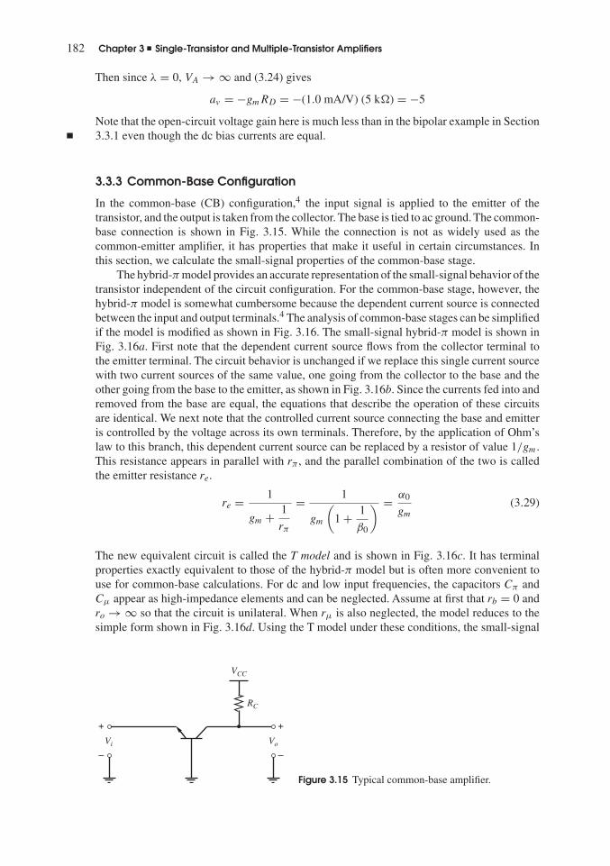
182 Chapter 3 � Single-Transistor and Multiple-Transistor Amplifiers
Then since λ = 0, VA → ∞ and (3.24) gives
av = −gmRD = −(1.0 mA/V) (5 k) = −5
Note that the open-circuit voltage gain here is much less than in the bipolar example in Section3.3.1 even though the dc bias currents are equal.
3.3.3 Common-Base Configuration
In the common-base (CB) configuration,4 the input signal is applied to the emitter of thetransistor, and the output is taken from the collector. The base is tied to ac ground. The common-base connection is shown in Fig. 3.15. While the connection is not as widely used as thecommon-emitter amplifier, it has properties that make it useful in certain circumstances. Inthis section, we calculate the small-signal properties of the common-base stage.
The hybrid-π model provides an accurate representation of the small-signal behavior of thetransistor independent of the circuit configuration. For the common-base stage, however, thehybrid-π model is somewhat cumbersome because the dependent current source is connectedbetween the input and output terminals.4 The analysis of common-base stages can be simplifiedif the model is modified as shown in Fig. 3.16. The small-signal hybrid-π model is shown inFig. 3.16a. First note that the dependent current source flows from the collector terminal tothe emitter terminal. The circuit behavior is unchanged if we replace this single current sourcewith two current sources of the same value, one going from the collector to the base and theother going from the base to the emitter, as shown in Fig. 3.16b. Since the currents fed into andremoved from the base are equal, the equations that describe the operation of these circuitsare identical. We next note that the controlled current source connecting the base and emitteris controlled by the voltage across its own terminals. Therefore, by the application of Ohm’slaw to this branch, this dependent current source can be replaced by a resistor of value 1/gm.This resistance appears in parallel with rπ, and the parallel combination of the two is calledthe emitter resistance re.
re = 1
gm + 1
rπ
= 1
gm
(1 + 1
β0
) = α0
gm
(3.29)
The new equivalent circuit is called the T model and is shown in Fig. 3.16c. It has terminalproperties exactly equivalent to those of the hybrid-π model but is often more convenient touse for common-base calculations. For dc and low input frequencies, the capacitors Cπ andCμ appear as high-impedance elements and can be neglected. Assume at first that rb = 0 andro → ∞ so that the circuit is unilateral. When rμ is also neglected, the model reduces to thesimple form shown in Fig. 3.16d. Using the T model under these conditions, the small-signal
VCC
RC
Vo
+
–
Vi
+
–
Figure 3.15 Typical common-base amplifier.

3.3 Basic Single-Transistor Amplifier Stages 183
(a)
(b)
(c)
(d )
gmv1v1
rb
ro
C
+
–
Base Collector
Emitter
gmv1
v1
gmv1
v1
re
re
ro
+
+
–
–
Base
Collector
Emitter
gmv1
gmv1
v1
rb
rb
ro
C
B
+
–
Base Collector
Emitter
E C
B
E
μ
Cμ
Cμ
Cπ
rμ
rμCπrπ
Cπrπ
rμ
Figure 3.16 Generation of emitter-current-controlled T model from the hybrid-π. (a) Hybrid-π model.(b) The collector current source gmv1 is changed to two current sources in series, and thepoint between them attached to the base. This change does not affect the current flowing in thebase. (c) The current source between base and emitter is converted to a resistor of value 1/gm.(d) T model for low frequencies, neglecting ro, rμ, and the charge-storage elements.

184 Chapter 3 � Single-Transistor and Multiple-Transistor Amplifiers
vire gmveve
+
–
+
–
+
–
voRC
Figure 3.17 Small-signal equivalentcircuit of the common-base stage; ro,rb, and rμ are assumed negligible.
equivalent circuit of the common-base stage is shown in Fig. 3.17. By inspection of Fig. 3.17,the short-circuit transconductance is
Gm = gm (3.30)
The input resistance is just the resistance re:
Ri = re (3.31)
The output resistance is given by
Ro = RC (3.32)
Using these parameters, the open-circuit voltage gain and the short-circuit current gain are
av = GmRo = gmRC (3.33)
ai = GmRi = gmre = α0 (3.34)
Comparing (3.31) and (3.13) shows that the input resistance of the common-base config-uration is a factor of (β0 + 1) less than in the common-emitter configuration. Also, comparing(3.34) and (3.18) shows that the current gain of the common-base configuration is reduced bya factor of (β0 + 1) compared to that of the common-emitter configuration.
Until now, we have assumed that rb is negligible. In practice, however, the base resistancehas a significant effect on the transconductance and the input resistance when the common-basestage is operated at sufficiently high current levels. To recalculate these parameters with rb > 0,assume the transistor operates in the forward-active region and consider the small-signal modelshown in Fig. 3.18. Here, the transconductance is
Gm = io
vi
∣∣∣∣vo = 0
= gm
(ve
vi
)(3.35)
To find the relationship between ve and vi, Kirchoff’s current law (KCL) and Kirchoff’svoltage law (KVL) can be applied at the internal base node (node 1 ) and around the inputloop, respectively. From KCL at node 1 ,
gmve + vb
rb− ve
re= 0 (3.36)
1vi
ii io
ve gmvere
rb
+
–
+
–
vb
+
–
voRC
+
–
Figure 3.18 Small-signal model of thecommon-base stage with rb > 0.

3.3 Basic Single-Transistor Amplifier Stages 185
From KVL around the input loop,
vi = ve + vb (3.37)
Solving (3.37) for vb, substituting into (3.36), and rearranging gives
vi
ve
= 1 + gm
β0rb = 1 + rb
rπ(3.38)
Substituting (3.38) into (3.35) gives
Gm = gm
1 + rb
rπ
(3.39)
Similarly, the input resistance in Fig. 3.18 is
Ri = vi
ii= vi
ve/re= re
(vi
ve
)(3.40)
Substituting (3.38) into (3.40) gives
Ri = re
(1 + rb
rπ
)= α0
gm
(1 + rb
rπ
)(3.41)
Thus if the dc collector current is large enough that rπ is comparable with rb, then the effectsof base resistance must be included. For example, if rb = 100 and β0 = 100, then a collectorcurrent of 26 mA makes rb and rπ equal.
The main motivation for using common-base stages is twofold. First, the collector-basecapacitance does not cause high-frequency feedback from output to input as in the common-emitter amplifier. As described in Chapter 7, this change can be important in the design ofhigh-frequency amplifiers. Second, as described in Chapter 4, the common-base amplifier canachieve much larger output resistance than the common-emitter stage in the limiting case whereRC → ∞. As a result, the common-base configuration can be used as a current source whosecurrent is nearly independent of the voltage across it.
3.3.4 Common-Gate Configuration
In the common-gate configuration, the input signal is applied to the source of the transistor, andthe output is taken from the drain while the gate is connected to ac ground. This configurationis shown in Fig. 3.19, and its behavior is similar to that of a common-base stage.
As in the analysis of common-base amplifiers in Section 3.3.3, the analysis of common-gate amplifiers can be simplified if the model is changed from a hybrid-π configuration to a Tmodel, as shown in Fig. 3.20. In Fig. 3.20a, the low-frequency hybrid-π model is shown. Notethat both transconductance generators are now active. If the substrate or body connection isassumed to operate at ac ground, then vbs = vgs because the gate also operates at ac ground.
VDD
RD
Vi
+
–Vo
+
–
Figure 3.19 Common-gate configuration.

186 Chapter 3 � Single-Transistor and Multiple-Transistor Amplifiers
(a)
(b)
(c)
(d )
(gm + gmb) vsg
+
–vsg
ro
1gm + gmb
G
S D
(gm + gmb) vsg(gm + gmb) vsg
ro
G
S D
(gm + gmb) vsg
ro
S D
gmbvbs
gmvgs
ro
S D
Figure 3.20 Conversion from hybrid-π to T model.(a) Low-frequency hybrid-π model. (b) The twodependent sources are combined. (c) The combinedsource is converted into two sources. (d) The currentsource between the source and gate is converted intoa resistor.
Therefore, in Fig. 3.20b, the two dependent current sources are combined. In Fig. 3.20c, thecombined current source from the source to the drain is replaced by two current sources: onefrom the source to the gate and the other from the gate to the drain. Since equal currents arepushed into and pulled out of the gate, the equations that describe the operation of the circuitsin Figs. 3.20b and 3.20c are identical. Finally, because the current source from the source tothe gate is controlled by the voltage across itself, it can be replaced by a resistor of value1/(gm + gmb), as in Fig. 3.20d.
If ro is finite, the circuit of Fig. 3.20d is bilateral because of feedback provided throughro. At first, we will assume that ro → ∞ so that the circuit is unilateral. Using the T modelunder these conditions, the small-signal equivalent circuit of the common-gate stage is shownin Fig. 3.21. By inspection of Fig. 3.21,
Gm = gm + gmb (3.42)
Ri = 1
gm + gmb
(3.43)
Ro = RD (3.44)

3.3 Basic Single-Transistor Amplifier Stages 187
(gm + gmb) vsg
+
–vsg
1gm + gmb
vi
+
–
vo
+
–
RD
Figure 3.21 Small-signal equiv-alent circuit of the common-gatestage; ro is assumed negligible.
Using these parameters, the open-circuit voltage gain and the short-circuit current gain are
av = GmRo = (gm + gmb)RD (3.45)
ai = GmRi = 1 (3.46)
3.3.5 Common-Base and Common-Gate Configurations with Finite ro
In calculating the expressions for Gm, Ri, and Ro of the common-base and common-gateamplifiers, we have neglected the effects of ro. Since ro is connected from each amplifieroutput back to its input, finite ro causes each circuit to be bilateral, making the input resistancedepend on the connection at the amplifier output. Let R = RC in Fig. 3.17 or R = RD inFig. 3.21, depending on which circuit is under consideration. When R becomes large enoughthat it is comparable with ro, ro must be included in the small-signal model to accuratelypredict not only the input resistance, but also the output resistance. On the other hand, sincethe transconductance is calculated with the output shorted, the relationship between ro and Rhas no effect on this calculation, and the effect of finite ro on transconductance can be ignoredif ro � 1/Gm.
3.3.5.1 Common-Base and Common-Gate Input ResistanceFigure 3.22a shows a small-signal T model of a common-base or common-gate stage includingfinite ro, where Ri(ideal) is given by (3.31) for a common-base amplifier or by (3.43) for acommon-gate amplifier. Also, R represents RC in Fig. 3.17 or RD in Fig. 3.21. Connectionsto the load and the input source are shown in Fig. 3.22a to include their contributions to theinput and output resistance, respectively. In Fig. 3.22a, the input resistance is Ri = v1/ii. Tofind the input resistance, a simplified equivalent circuit such as in Fig. 3.22b is often used.Here, a test voltage source vt is used to drive the amplifier input, and the resulting test currentit is calculated. KCL at the output node in Fig. 3.22b gives
vo
R ‖ RL
+ vo − vt
ro= Gmvt (3.47)
KCL at the input in Fig. 3.22b gives
it = vt
Ri(ideal)+ vt − vo
ro(3.48)
Solving (3.47) for vo and substituting into (3.48) gives
it
vt
= 1
Ri(ideal)+ 1
ro
⎛⎜⎜⎝1 −
Gm + 1
ro1
R ‖ RL
+ 1
ro
⎞⎟⎟⎠ (3.49)

188 Chapter 3 � Single-Transistor and Multiple-Transistor Amplifiers
RS ro
Ri (ideal)
ii io
Ri Ro
v1 vo
v1 vo
v1 vovs
++–
–RGmv1
RL
+
–
(a)
(b)
(c)
Input generatormodel
Load modelAmplifier model
ro
Ri (ideal)
it
vt
++–
vt+–
–RGmv1 RL
+
–
roRS
Ri (ideal)
it
+
–RGmv1
+
–
Figure 3.22 (a) Model of common-base and common-gate amplifiers with finite ro, showing con-nections to the input source and load. (b) Equivalent circuit for calculation of Ri. (c) Equivalentcircuit for calculation of Ro.
Rearranging (3.49) gives
Ri = vt
it= ro + R ‖ RL
1 − Gm(R ‖ RL) + ro + R ‖ RL
Ri(ideal)
(3.50)
Common-Base Input Resistance. For the common-base amplifier, Gm = gm from (3.30),and Ri(ideal) = re = α0/gm from (3.31). Substituting (3.30) and (3.31) into (3.50) with R = RC
and rearranging gives
Ri = vt
it= ro + RC ‖ RL
1 + gm(RC ‖ RL)
β0+ gmro
α0
= ro + RC ‖ RL
1 + gm
β0(RC ‖ RL + (β0 + 1) ro)
(3.51)
From (3.51), when (β0 + 1)ro � RC ‖ RL,
Ri � ro + RC ‖ RL
1 + gmro
α0
(3.52)
From (3.52), when gmro � α0,
Ri � α0
gm
+ α0 (RC ‖ RL)
gmro= re + α0 (RC ‖ RL)
gmro(3.53)

3.3 Basic Single-Transistor Amplifier Stages 189
The first term on the right side of (3.53) is the same as in (3.31), where the common-baseamplifier was unilateral because infinite ro was assumed. The second term shows that the inputresistance now depends on the connection to the output (because finite ro provides feedbackand makes the amplifier bilateral). The second term is about equal to the resistance at theamplifier output divided by the Gmro product. When ro � (RC ‖ RL), the effect of the secondterm can be neglected.
Common-Gate Input Resistance. For the common-gate amplifier, Gm = (gm + gmb) from(3.42) and Ri(ideal) = 1/(gm + gmb) from (3.43). Substituting (3.42) and (3.43) into (3.50) withR = RD and rearranging gives
Ri = vt
it= ro + RD ‖ RL
1 + (gm + gmb) ro(3.54)
When (gm + gmb) ro � 1,
Ri � 1
gm + gmb
+ RD ‖ RL
(gm + gmb) ro(3.55)
The first term on the right side of (3.55) is the same as in (3.43), where the common-gateamplifier was unilateral because infinite ro was assumed. The second term is about equal to theresistance at the amplifier output divided by the Gmro product and shows the effect of finitero, which makes the circuit bilateral. When ro � (RD ‖ RL), the effect of the second term canbe neglected. Neglecting the second term usually causes only a small error when RD here orRC in the common-base case is built as a physical resistor even if the amplifier is unloaded(RL → ∞). However, when RD or RC is replaced by a transistor current source, the effect ofthe second term can be significant. Chapter 4 describes techniques used to construct transistorcurrent sources that can have very high equivalent resistance.
3.3.5.2 Common-Base and Common-Gate Output ResistanceThe output resistance in Fig. 3.22a is Ro = vo/io with vs = 0. For this calculation, considerthe equivalent circuit shown in Fig. 3.22c, where vs = 0. A test voltage vt is used to drive theamplifier output, and the resulting test current it can be calculated. Since R appears in parallelwith the amplifier output, the calculation will be done in two steps. First, the output resistancewith R → ∞ is calculated. Second, this result is placed in parallel with R to give the overalloutput resistance. From KCL at the input node in Fig. 3.22c,
v1
RS
+ v1
Ri(ideal)+ v1 − vt
ro= 0 (3.56)
With R → ∞, KCL at the output node gives
it = −Gmv1 + vt − v1
ro(3.57)
Solving (3.56) for v1 and substituting into (3.57) gives
it
vt
= 1
ro− 1
ro
⎛⎜⎜⎝
Gm + 1
ro1
RS
+ 1
Ri(ideal)+ 1
ro
⎞⎟⎟⎠ (3.58)

190 Chapter 3 � Single-Transistor and Multiple-Transistor Amplifiers
Rearranging (3.58) gives
vt
it=
ro
(1
RS
+ 1
Ri(ideal)+ 1
ro
)1
RS
+ 1
Ri(ideal)− Gm
(3.59)
With finite R, the output resistance is
Ro = R ‖(
vt
it
)= R ‖
⎡⎢⎢⎣
ro
(1
RS
+ 1
Ri(ideal)+ 1
ro
)1
RS
+ 1
Ri(ideal)− Gm
⎤⎥⎥⎦ (3.60)
Common-Base Output Resistance. For the common-base amplifier, Gm = gm from (3.30)and Ri(ideal) = re = α0/gm from (3.31). Substituting (3.30) and (3.31) into (3.60) and rear-ranging gives
Ro = R ‖
⎡⎢⎢⎣
ro + RS
(1 + gmro
α0
)1 + RS
rπ
⎤⎥⎥⎦ (3.61)
The term in brackets on the right side of (3.61) shows that the output resistance of the common-base amplifier depends on the resistance of the input source RS when ro is finite. For example,if the input comes from an ideal voltage source, RS = 0 and
Ro = R ‖ ro (3.62)
On the other hand, if the input comes from an ideal current source, RS → ∞ and
Ro = R ‖[(
1 + gmro
α0
)rπ
](3.63)
From (3.61), when RS � rπ,
Ro � R ‖[ro + RS
(1 + gmro
α0
)](3.64)
From (3.64), when gmro � α0 and gmRS � α0,
Ro � R ‖(
gmro
α0RS
)(3.65)
The term in parentheses in (3.65) is about equal to the input source resistance multiplied bythe Gmro product. Therefore, (3.65) and (3.53) together show that the common-base amplifiercan be thought of as a resistance scaler, where the resistance is scaled up from the emitter tothe collector and down from the collector to the emitter by a factor approximately equal to theGmro product in each case.
Common-Gate Output Resistance. For the common-gate amplifier, Gm = (gm + gmb)from (3.42) and Ri(ideal) = 1/(gm + gmb) from (3.43). Substituting (3.42) and (3.43) into (3.60)and rearranging gives
Ro = R ‖ [ro + RS (1 + (gm + gmb) ro)] (3.66)

3.3 Basic Single-Transistor Amplifier Stages 191
From (3.66), when (gm + gmb) ro � 1 and (gm + gmb) RS � 1,
Ro � R ‖ ((gm + gmb) roRS
)(3.67)
The term in parentheses in (3.67) is equal to the input source resistance multiplied by the Gmroproduct. Therefore, (3.67) and (3.55) together show that the common-gate amplifier is also aresistance scaler, where the resistance is scaled up from the source to the drain and down fromthe drain to the source by a factor approximately equal to the Gmro product in each case.
3.3.6 Common-Collector Configuration (Emitter Follower)
The common-collector connection is shown in Fig. 3.23a. The distinguishing feature of thisconfiguration is that the signal is applied to the base and the output is taken from the emitter.4
From a large-signal standpoint, the output voltage is equal to the input voltage minus thebase-emitter voltage. Since the base-emitter voltage is a logarithmic function of the collectorcurrent, the base-emitter voltage is almost constant even when the collector current varies. Ifthe base-emitter voltage were exactly constant, the output voltage of the common-collectoramplifier would be equal to the input voltage minus a constant offset, and the small-signal gainof the circuit would be unity. For this reason, the circuit is also known as an emitter followerbecause the emitter voltage follows the base voltage. In practice, the base-emitter voltage is notexactly constant if the collector current varies. For example, (1.82) shows that the base-emittervoltage must increase by about 18 mV to double the collector current and by about 60 mV toincrease the collector current by a factor of 10 at room temperature. Furthermore, even if thecollector current were exactly constant, the base-emitter voltage depends to some extent onthe collector-emitter voltage if the Early voltage is finite. These effects are most easily studiedusing small-signal analysis.
(a)
vs
iiio
RS
VCC
–VEE
RL
+
–vo
+
–BIAS
(b)
vs
ii
io
RS
gmv1 = oii
RLRo
Ri
+
–
vo
ro
+
–
vi
+
–
+
–rv1 π β
Figure 3.23 (a) Common-collector configuration. (b) Small-signal equivalent circuit of the emitter-follower circuit including RL and RS .

192 Chapter 3 � Single-Transistor and Multiple-Transistor Amplifiers
The appropriate small-signal transistor model is the hybrid-π, and the small-signal equiv-alent circuit is shown in Fig. 3.23b. When the input voltage vs increases, the base-emittervoltage of the transistor increases, which increases the output current io. However, increasingio increases the output voltage vo, which decreases the base-emitter voltage by negative feed-back. Negative feedback is covered thoroughly in Chapter 8. The key point here is that thecommon-collector configuration is not unilateral. As a result, the input resistance depends onthe load resistor RL and the output resistance depends on the source resistance RS . Therefore,the characterization of the emitter follower by the corresponding equivalent two-port networkis not particularly useful for intuitive understanding. Instead, we will analyze the entire emitter-follower circuit of Fig. 3.23b, including both the source resistance RS and the load resistorRL. From KCL at the output node, we find
vs − vo
RS + rπ+ β0
(vs − vo
RS + rπ
)− vo
RL
− vo
ro= 0 (3.68)
from which we find
vo
vs
= 1
1 + RS + rπ
(β0 + 1)(RL ‖ ro)
(3.69)
If the base resistance rb is significant, it can simply be added to RS in these expressions. Thevoltage gain is always less than unity and will be close to unity if β0 (RL ‖ ro) � (RS + rπ).In most practical circuits, this condition holds. Note that because we have included the sourceresistance in this calculation, the value of vo/vs is not analogous to av calculated for the CEand CB stages. When rπ � RS , β0 � 1, and ro � RL, (3.69) can be approximated as
vo
vs
� gmRL
1 + gmRL
(3.70)
We calculate the input resistance Ri by removing the input source, driving the input witha test current source it , and calculating the resulting voltage vt across the input terminals. Thecircuit used to do this calculation is shown in Fig. 3.24a. From KCL at the output node,
vo
RL
+ vo
ro= it + β0it (3.71)
Then the voltage vt is
vt = itrπ + vo = itrπ + it + β0it
1
RL
+ 1
ro
(3.72)
and thus
Ri = vt
it= rπ + (β0 + 1)(RL ‖ ro) (3.73)
A general property of emitter followers is that the resistance looking into the base is equal torπ plus (β0 + 1) times the incremental resistance connected from the emitter to small-signalground. The factor of β0 + 1 in (3.73) stems from the current gain of the common-collectorconfiguration from the base to the emitter, which increases the voltage drop on the resistanceconnected from the emitter to small-signal ground and its contribution to the test voltage vt
in (3.72).We now calculate the output resistance Ro by removing the load resistance RL and finding
the Thévenin-equivalent resistance looking into the output terminals. We can do this by eitherinserting a test current and calculating the resulting voltage or applying a test voltage and

3.3 Basic Single-Transistor Amplifier Stages 193
(a)
it
ib
ib
RL
vo
ro
+
–
vt
+
– rπ β
(b)
vt
RS
rov1 gmv1
+
+
–
–
r
it
π
(c)
vs
IC
RoRi
VCC
–VEE
RS = 1 kΩ
RL = 1 kΩ
+
–
vo
+
– Figure 3.24 (a) Circuit for calculation of the inputresistance of the emitter follower. (b) Circuit forcalculation of the output resistance of the emitterfollower. (c) Example emitter follower.
calculating the current. In this case, the calculation is simpler if a test voltage vt is applied asshown in Fig. 3.24b. The voltage v1 is given by
v1 = −vt
(rπ
rπ + RS
)(3.74)
The total output current it is thus
it = vt
rπ + RS
+ vt
ro+ gmvt
(rπ
rπ + RS
)(3.75)
Therefore,
Ro = vt
it=(
rπ + RS
β0 + 1
)‖ ro (3.76)
If β0 � 1 and ro � (1/gm) + RS/(β0 + 1),
Ro � 1
gm
+ RS
β0 + 1(3.77)

194 Chapter 3 � Single-Transistor and Multiple-Transistor Amplifiers
Equation 3.77 shows that the resistance at the output is about equal to the resistance in thebase lead, divided by (β0 + 1), plus 1/gm. In (3.77), RS is divided by β0 + 1 because the basecurrent flows in RS , and the base current is β0 + 1 times smaller than the emitter current.
Therefore, the emitter follower has high input resistance, low output resistance, and near-unity voltage gain. It is most widely used as an impedance transformer to reduce loading of apreceding signal source by the input impedance of a following stage. It also finds applicationas a unity-voltage-gain level shift because the dc output voltage is shifted from the dc inputvoltage by VBE(on).
EXAMPLE
Calculate the input resistance, output resistance, and voltage gain of the emitter follower ofFig. 3.24c. Assume that β0 = 100, rb = 0, ro → ∞, and IC = 100 �A.
Ri = rπ + RL (1 + β0) = 26 k + (1 k)(101) = 127 k
vo
vs
= 1
1 + rπ + RS
(β0 + 1)RL
= 1
1 + 26 k + 1 k
(101)(1 k)
� 0.79
Ro = RS + rπ
1 + β0= 1 k + 26 k
101� 270
3.3.7 Common-Drain Configuration (Source Follower)
The common-drain configuration is shown in Fig. 3.25a. The input signal is applied to the gateand the output is taken from the source. From a large-signal standpoint, the output voltageis equal to the input voltage minus the gate-source voltage. The gate-source voltage consistsof two parts: the threshold and the overdrive. If both parts are constant, the resulting output
VoRL
+
–
Vi
VDD
+
–
(a)Figure 3.25 (a) Common-drain configuration. (b) Small-signalequivalent circuit of the common-drain configuration.
RL
ro
vi
vgs
–
gmvgs gmbvbs = –gmbvs
vo = vs
+
–
+
–
+
io
(b)

3.3 Basic Single-Transistor Amplifier Stages 195
voltage is simply offset from the input, and the small-signal gain would be unity. Therefore, thesource follows the gate, and the circuit is also known as a source follower. In practice, the bodyeffect changes the threshold voltage, and the overdrive depends on the drain current, whichchanges as the output voltage changes unless RL → ∞. Furthermore, even if the current wereexactly constant, the overdrive depends to some extent on the drain-source voltage unless theEarly voltage is infinite. We will use small-signal analysis to study these effects.
The small-signal equivalent circuit is shown in Fig. 3.25b. Since the body terminal is notshown in Fig. 3.25a, we assume that the body is connected to the lowest supply voltage (groundhere) to keep the source-body pn junction reverse biased. As a result, vbs changes when theoutput changes because the source is connected to the output, and the gmb generator is activein general.
From KVL around the input loop,
vi = vgs + vo (3.78)
With the output open circuited, io = 0, and KCL at the output node gives
gmvgs − gmbvo − vo
RL
− vo
ro= 0 (3.79)
Solving (3.78) for vgs, substituting into (3.79), and rearranging gives
vo
vi
∣∣∣∣io = 0
= gm
gm + gmb + 1
RL
+ 1
ro
= gmro
1 + (gm + gmb) ro + ro
RL
(3.80)
If RL → ∞, (3.80) simplifies to
limRL→∞
vo
vi
∣∣∣∣io = 0
= gmro
1 + (gm + gmb) ro(3.81)
Equation 3.81 gives the open-circuit voltage gain of the source follower with the load resistorreplaced by an ideal current source. If ro is finite, this gain is less than unity even if the bodyeffect is eliminated by connecting the source to the body to deactivate the gmb generator. In thiscase, variation in the output voltage changes the drain-source voltage and the current throughro. From a large-signal standpoint, solving (1.165) for VGS − Vt shows that the overdrive alsodepends on the drain-source voltage unless the channel-length modulation parameter λ is zero.This dependence causes the small-signal gain to be less than unity.
A significant difference between bipolar and MOS followers is apparent from (3.80). IfRL → ∞ and ro → ∞,
limRL→∞ro→∞
vo
vi
= gm
gm + gmb
= 1
1 + χ(3.82)
Equation 3.82 shows that the source-follower gain is less than unity under these conditions andthat the gain depends on χ = gmb/gm, which is typically in the range of 0.1 to 0.3. In contrast,the gain of an emitter follower would be unity under these conditions. As a result, the source-follower gain is not as well specified as that of an emitter follower when body effect is a factor.Furthermore, (1.200) shows that χ depends on the source-body voltage which is equal to Vo
when the body is connected to ground. Therefore, the gain calculated in (3.82) depends on theoutput voltage, causing distortion to arise for large-signal changes in the output as shown inSection 5.3.2. To overcome these limitations in practice, the type of source follower (n-channelor p-channel) can be chosen so that it can be fabricated in an isolated well. Then the well canbe connected to the source of the transistor, setting VSB = 0 and vsb = 0. Unfortunately, theparasitic capacitance from the well to the substrate increases the capacitance attached to the

196 Chapter 3 � Single-Transistor and Multiple-Transistor Amplifiers
source with this connection, reducing the bandwidth of the source follower. The frequencyresponse of source followers is covered in Chapter 7.
The output resistance of the source follower can be calculated from Fig. 3.25b by settingvi = 0 and driving the output with a voltage source vo. Then vgs = −vo and io is
io = vo
ro+ vo
RL
+ gmvo + gmbvo (3.83)
Rearranging (3.83) gives
Ro = vo
io= 1
gm + gmb + 1
ro+ 1
RL
(3.84)
Equation 3.84 shows that the body effect reduces the output resistance, which is desirablebecause the source follower produces a voltage output. This beneficial effect stems from thenonzero small-signal current conducted by the gmb generator in Fig. 3.25b, which increasesthe output current for a given change in the output voltage. As ro → ∞ and RL → ∞, thisoutput resistance approaches 1/(gm + gmb). The common-gate input resistance given in (3.54)approaches the same limiting value.
As with emitter followers, source followers are used as voltage buffers and level shifters.When used as a level shifter, they are more flexible than emitter followers because the dc valueof VGS can be altered by changing the W/L ratio.
3.3.8 Common-Emitter Amplifier with Emitter Degeneration
In the common-emitter amplifier considered earlier, the signal is applied to the base, the outputis taken from the collector, and the emitter is attached to ac ground. In practice, however,the common-emitter circuit is often used with a nonzero resistance in series with the emitteras shown in Fig. 3.26a. The resistance has several effects, including reducing the transcon-ductance, increasing the output resistance, and increasing the input resistance. These changesstem from negative feedback introduced by the emitter resistor RE. When Vi increases, thebase-emitter voltage increases, which increases the collector current. As a result, the voltagedropped across the emitter resistor increases, reducing the base-emitter voltage compared tothe case where RE = 0. Therefore, the presence of nonzero RE reduces the base-emitter volt-age through a negative-feedback process termed emitter degeneration. This circuit is examinedfrom a feedback standpoint in Chapter 8.
In this section, we calculate the input resistance, output resistance, and transconductance ofthe emitter-degenerated, common-emitter amplifier. To find the input resistance and transcon-ductance, consider the small-signal equivalent circuit shown in Fig. 3.26b, and focus on vi, ib,and io. From KCL at the emitter,
ve
RE
+ ve + ioRC
ro= (β0 + 1) ib (3.85)
From KCL at the collector,
io + ve + ioRC
ro= β0ib (3.86)
From KVL around the input loop,
ib = vi − ve
rπ(3.87)

3.3 Basic Single-Transistor Amplifier Stages 197
(a)
Vo
RC
RE
VCC
+
–
Vi
+
–
(b)
vo
ro
RC
RE
r
+
–
vi
ve
ibio
+
–
+
–
v1
+
–
gmv1 = oibβπ
(c)
ror
RE
vt
+
–
+
–
i1
v1 gmv1
it
π
(d )
RoRi Gmv1
+
–
v1
Ri r (1 + gmRE)
Ro ro (1 + gmRE)
gm
1 + gmRE
π
⎛⎝
⎞⎠Gm
Figure 3.26 (a) Common-emitter amplifier with emitter degeneration. (b) Small-signal equivalentcircuit for emitter-degenerated, common-emitter amplifier. (c) Circuit for calculation of outputresistance. (d) Small-signal, two-port equivalent of emitter-degenerated CE amplifier.

198 Chapter 3 � Single-Transistor and Multiple-Transistor Amplifiers
Solving (3.85) for io, substituting into (3.86) and rearranging gives
ve = ib
⎛⎜⎜⎝
1 + (β0 + 1)ro
RC
1
RC
+ 1
RE
+ ro
RCRE
⎞⎟⎟⎠ (3.88)
Substituting (3.88) into (3.87) and rearranging gives
Ri = vi
ib= rπ + (β0 + 1) RE
⎛⎜⎜⎝
ro + RC
β0 + 1ro + RC + RE
⎞⎟⎟⎠ (3.89)
If ro � RC and ro � RE, the last term in parentheses in (3.89) is approximately equal to unityand
Ri � rπ + (β0 + 1) RE (3.90)
Because the last term in parentheses in (3.89) is less than one, comparing (3.89) and (3.90)shows that finite ro reduces the input resistance of the common-emitter amplifier with emitterdegeneration. This reduction stems from nonzero current that flows in ro when ro is finite. Ifvi increases, ve follows vi because the base-emitter voltage is approximately constant, but thecollector voltage (−ioRC) decreases by an amount determined by the small-signal gain fromthe base to the collector. Therefore, the current that flows in ro from the emitter to the collectorincreases, increasing the base current and reducing the input resistance. In practice, (3.90) isusually used to calculate the input resistance. The error in the approximation is usually smallunless the resistances represented by RC or RE are large, such as when implemented withtransistors in active-load configurations. Active loads are considered in Chapter 4.
Now we will calculate the transconductance of the stage. First, set RC = 0 in Fig. 3.26bbecause Gm = io/vi with the output shorted. Substituting (3.87) into (3.85) with RC = 0 andrearranging gives
ve = vi
⎛⎜⎜⎝
(β0 + 1)
rπ1
RE
+ 1
ro+ β0 + 1
rπ
⎞⎟⎟⎠ (3.91)
Substituting (3.87) and (3.91) into (3.86) with RC = 0 and rearranging gives
Gm = io
vi
= gm
⎡⎢⎢⎣
1 − RE
β0ro
1 + gmRE
(1 + 1
β0+ 1
gmro
)⎤⎥⎥⎦ (3.92)
In most practical cases, β0 � 1, ro � RE, and gmro � 1. Then
Gm � gm
1 + gmRE
(3.93)
Equation 3.93 is usually used to calculate the transconductance of a common-emitter amplifierwith emitter degeneration.
The output resistance is calculated using the equivalent circuit of Fig. 3.26c. For the timebeing, assume that RC is very large and can be neglected. The test current it flows in the parallelcombination of rπ and RE, so that
v1 = −it(rπ ‖ RE) (3.94)

3.3 Basic Single-Transistor Amplifier Stages 199
The current through ro is
i1 = it − gmv1 = it + itgm (rπ ‖ RE) (3.95)
As a result, the voltage vt is
vt = −v1 + i1ro = it (rπ ‖ RE) + itro [1 + gm (rπ ‖ RE)] (3.96)
Thus
Ro = vt
it= (rπ ‖ RE) + ro [1 + gm (rπ ‖ RE)] (3.97)
In this equation, the first term is much smaller than the second. If the first term is neglected,we obtain,
Ro � ro
(1 + gm
rπRE
rπ + RE
)= ro
⎛⎜⎜⎝1 + gmRE
1 + RE
rπ
⎞⎟⎟⎠ = ro
⎛⎜⎜⎝1 + gmRE
1 + gmRE
β0
⎞⎟⎟⎠ (3.98)
If gmRE � β0, then
Ro � ro (1 + gmRE) (3.99)
Thus the output resistance is increased by a factor (1 + gmRE). This fact makes the use ofemitter degeneration desirable in transistor current sources. If the collector load resistor RC
is not large enough to neglect, it must be included in parallel with the expressions in (3.97)–(3.99). A small-signal equivalent circuit, neglecting RC, is shown in Fig. 3.26d. On the otherhand, if gmRE � β0, (3.98) shows that
Ro � ro (1 + β0) (3.100)
The output resistance is finite even when RE → ∞ because nonzero test current flows in rπwhen β0 is finite.
3.3.9 Common-Source Amplifier with Source Degeneration
Source degeneration in MOS transistor amplifiers is not as widely used as emitter degenerationin bipolar circuits for at least two reasons. First, the transconductance of MOS transistors isnormally much lower than that of bipolar transistors so that further reduction in transconduc-tance is usually undesirable. Second, although degeneration increases the input resistance inthe bipolar case, Ri → ∞ even without degeneration in the MOS case. However, examiningthe effects of source degeneration is important in part because it is widely used to increase theoutput resistance of MOS current sources. Also, because small-geometry MOS transistors canbe modeled as ideal square-law devices with added source resistors as shown in Section 1.7.1,we will consider the effects of source degeneration below.
A common-source amplifier with source degeneration is shown in Fig. 3.27. Its small-signal equivalent circuit is shown in Fig. 3.28. Because the input is connected to the gate of theMOS transistor, Ri → ∞. To calculate the transconductance, set RD = 0 because Gm = io/vi
with the output shorted. Also, since a connection to the body is not shown in Fig. 3.27,we assume that the body is connected to the lowest power-supply voltage, which is ground.Therefore, the dc body voltage is constant and vb = 0. From KCL at the source with RD = 0,
vs
RS
+ vs
ro= gm (vi − vs) + gmb (0 − vs) (3.101)

200 Chapter 3 � Single-Transistor and Multiple-Transistor Amplifiers
Vo
RD
RS
+
–Vi
VDD
+
–Figure 3.27 Common-source amplifier with sourcedegeneration.
vo
io
ro
RS
gmbvbsgmvgs RD
+
–
vs
+
–
vgs
+
–vi
+
–
Figure 3.28 Small-signalequivalent of the source-degenerated, common-source amplifier.
From KCL at the drain with RD = 0,
io + vs
ro= gm (vi − vs) + gmb (0 − vs) (3.102)
Solving (3.101) for vs, substituting into (3.102), and rearranging gives
Gm = io
vi
= gm
1 + (gm + gmb) RS + RS
ro
(3.103)
If ro � RS ,
Gm � gm
1 + (gm + gmb) RS
(3.104)
For large RS , (3.104) shows that the value of Gm approaches 1/[(1 + χ) RS]. Even in this limit-ing case, the transconductance of the common-source amplifier with degeneration is dependenton an active-device parameter χ. Since χ is typically in the range of 0.1 to 0.3, the body effectcauses the transconductance in this case to deviate from 1/RS by about 10 to 20 percent. Incontrast, (3.92) indicates that the value of Gm for a common-emitter amplifier with degener-ation approaches β0/[(β0 + 1) RE] for large RE, assuming that ro � RE and gmro � 1. Ifβ0 > 100, the transconductance of this bipolar amplifier is within 1 percent of 1/RE. There-fore, the transconductance of a common-source amplifier with degeneration is usually muchmore dependent on active-device parameters than in its bipolar counterpart.
The output resistance of the circuit can be calculated from the equivalent circuit ofFig. 3.29, where RD is neglected. Since the entire test current flows in RS ,
vs = itRS (3.105)
Then
vt = vs + i1ro = vs + ro [it − gm (0 − vs) − gmb (0 − vs)] (3.106)
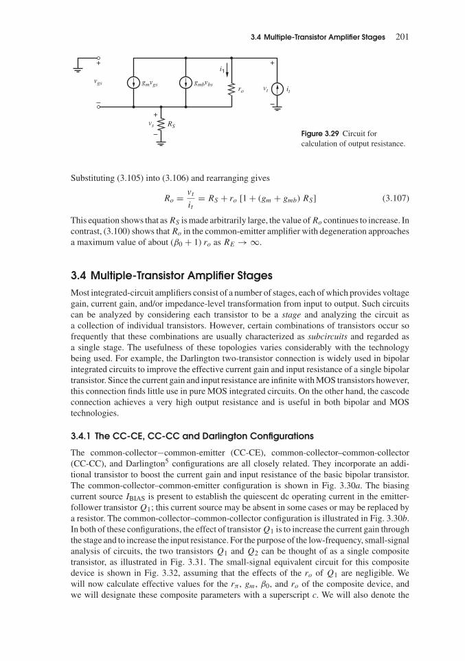
3.4 Multiple-Transistor Amplifier Stages 201
ro
RS
gmbvbsgmvgsitvt
+
–
vs
+
–
vgs
+
–
i1
Figure 3.29 Circuit forcalculation of output resistance.
Substituting (3.105) into (3.106) and rearranging gives
Ro = vt
it= RS + ro [1 + (gm + gmb) RS] (3.107)
This equation shows that as RS is made arbitrarily large, the value of Ro continues to increase. Incontrast, (3.100) shows that Ro in the common-emitter amplifier with degeneration approachesa maximum value of about (β0 + 1) ro as RE → ∞.
3.4 Multiple-Transistor Amplifier StagesMost integrated-circuit amplifiers consist of a number of stages, each of which provides voltagegain, current gain, and/or impedance-level transformation from input to output. Such circuitscan be analyzed by considering each transistor to be a stage and analyzing the circuit asa collection of individual transistors. However, certain combinations of transistors occur sofrequently that these combinations are usually characterized as subcircuits and regarded asa single stage. The usefulness of these topologies varies considerably with the technologybeing used. For example, the Darlington two-transistor connection is widely used in bipolarintegrated circuits to improve the effective current gain and input resistance of a single bipolartransistor. Since the current gain and input resistance are infinite with MOS transistors however,this connection finds little use in pure MOS integrated circuits. On the other hand, the cascodeconnection achieves a very high output resistance and is useful in both bipolar and MOStechnologies.
3.4.1 The CC-CE, CC-CC and Darlington Configurations
The common-collector−common-emitter (CC-CE), common-collector–common-collector(CC-CC), and Darlington5 configurations are all closely related. They incorporate an addi-tional transistor to boost the current gain and input resistance of the basic bipolar transistor.The common-collector–common-emitter configuration is shown in Fig. 3.30a. The biasingcurrent source IBIAS is present to establish the quiescent dc operating current in the emitter-follower transistor Q1; this current source may be absent in some cases or may be replaced bya resistor. The common-collector–common-collector configuration is illustrated in Fig. 3.30b.In both of these configurations, the effect of transistor Q1 is to increase the current gain throughthe stage and to increase the input resistance. For the purpose of the low-frequency, small-signalanalysis of circuits, the two transistors Q1 and Q2 can be thought of as a single compositetransistor, as illustrated in Fig. 3.31. The small-signal equivalent circuit for this compositedevice is shown in Fig. 3.32, assuming that the effects of the ro of Q1 are negligible. Wewill now calculate effective values for the rπ, gm, β0, and ro of the composite device, andwe will designate these composite parameters with a superscript c. We will also denote the

202 Chapter 3 � Single-Transistor and Multiple-Transistor Amplifiers
(a) (b)
VCC
In Q1
Q2
Out
IBIAS
VCC
In Q1
Q2
OutIBIAS
Figure 3.30 (a) Common-collector–common-emitter cascade. (b) Common-collector– common-collector cascade.
VCC
Q1
Q2
Cc
Bc
Ec
Cc
Bc
Ec
IBIAS Figure 3.31 The compositetransistor representation of theCC-CE and CC-CC connections.
Cc
Bc
Ec
+
–
gm2v2
gm1v1
v2 ro2
+
–
r 1v1 π
r 2π
Figure 3.32 Small-signal equivalentcircuit for the CC-CE and CC-CCconnected transistors.
terminal voltages and currents of the composite device with a superscript c. We assume thatβ0 is constant.
The effective value of rπ, rcπ, is the resistance seen looking into the composite base Bc with
the composite emitter Ec grounded. Referring to Fig. 3.32, we see that the resistance lookinginto the base of Q2 with Ec grounded is simply rπ2. Thus (3.73) for the input resistance of theemitter follower can be used. Substituting rπ2 for RL and allowing ro → ∞ gives
rcπ = rπ1 + (β0 + 1) rπ2 (3.108)
The effective transconductance of the configurationgcm is the change in the collector current
of Q2, icc, for a unit change in vcbe with Cc and Ec grounded. To calculate this transconductance,
we first find the change in v2 that occurs for a unit change in vcbe. Equation 3.69 can be used

3.4 Multiple-Transistor Amplifier Stages 203
directly, giving
v2
vcbe
= 1
1 +(
rπ1
(β0 + 1) rπ2
) (3.109)
Also
icc = gcmvc
be = gm2v2 = gm2vcbe
1 +(
rπ1
(β0 + 1) rπ2
) (3.110)
Thus
gcm = icc
vcbe
= gm2
1 +(
rπ1
(β0 + 1) rπ2
) (3.111)
For the special case in which the biasing current source IBIAS is zero, the emitter currentof Q1 is equal to the base current of Q2. Thus the ratio of rπ1 to rπ2 is (β0 + 1), and (3.111)reduces to
gcm = gm2
2(3.112)
The effective current gain βc is the ratio
βc = icc
icb= ic2
ib1(3.113)
The emitter current of Q1 is given by
ie1 = (β0 + 1) ib1 (3.114)
Since ie1 = ib2,
ic2 = icc = β0ib2 = β0 (β0 + 1) ib1 = β0 (β0 + 1) icb (3.115)
Therefore,
βc = β0 (β0 + 1) (3.116)
Equation 3.116 shows that the current gain of the composite transistor is approximately equalto β2
0. Also, by inspection of Fig. 3.32, assuming rμ is negligible, we have
rco = ro2 (3.117)
The small-signal, two-port network equivalent for the CC-CE connection is shown in Fig. 3.33,where the collector resistor RC has not been included. This small-signal equivalent can be usedto represent the small-signal operation of the composite device, simplifying the analysis ofcircuits containing this structure.
The Darlington configuration, illustrated in Fig. 3.34, is a composite two-transistor devicein which the collectors are tied together and the emitter of the first device drives the baseof the second. A biasing element of some sort is used to control the emitter current of Q1.The result is a three-terminal composite transistor that can be used in place of a single tran-sistor in common-emitter, common-base, and common-collector configurations. When usedas an emitter follower, the device is identical to the CC-CC connection already described.When used as a common-emitter amplifier, the device is very similar to the CC-CE con-nection, except that the collector of Q1 is connected to the output instead of to the powersupply. One effect of this change is to reduce the effective output resistance of the device

204 Chapter 3 � Single-Transistor and Multiple-Transistor Amplifiers
Ri
Ri = r = r 1 + ( 0 + 1) r 2
Gmv1
+
–
v1
Ro = ro = ro2
1 +r 1
( 0 + 1) r 2
Gm = gm = gm2
π π π
π
πβ
β
c
c
c c
c c
c
Rocc
Figure 3.33 Two-port representation,CC-CE connection.
Q1
Q2
Cc
Bc
Ec
IBIAS
Figure 3.34 The Darlington configuration.
because of feedback through the ro of Q1. Also, this change increases the input capacitancebecause of the connection of the collector-base capacitance of Q1 from the input to the output.Because of these drawbacks, the CC-CE connection is normally preferable in integrated small-signal amplifiers. The term Darlington is often used to refer to both the CC-CE and CC-CCconnections.
As mentioned previously, Darlington-type connections are used to boost the effectivecurrent gain of bipolar transistors and have no significant application in pure-MOS circuits.In BiCMOS technologies, however, a potentially useful connection is shown in Fig. 3.35,where an MOS transistor is used for Q1. This configuration not only realizes the infinite inputresistance and current gain of the MOS transistor, but also the large transconductance of thebipolar transistor.
M1
Q2
IBIAS
Figure 3.35 Compound Darlington connectionavailable in BiCMOS technology.

3.4 Multiple-Transistor Amplifier Stages 205
EXAMPLE
Find the effective rcπ, βc, and gc
m for the composite transistor shown in Fig. 3.31. For bothdevices, assume that β0 = 100, rb = 0, and ro → ∞. For Q2, assume that IC = 100 �A andthat IBIAS = 10 �A.
The base current of Q2 is 100 �A/100 = 1 �A. Thus the emitter current of Q1 is 11 �A.Then
rπ1 = β0gm
= 100
11 �A/26 mV= 236 k
gm1 = (2.36 k)−1
rπ2 = 26 k
gm2 = (260 )−1
rcπ = 236 k + (101)(26 k) = 2.8 M
βc = (101)(100) = 10,100
gcm = gm2 (0.916) = (283 )−1
Thus the composite transistor has much higher input resistance and current gain than a singletransistor.
3.4.2 The Cascode Configuration
The cascode configuration was first invented for vacuum-tube circuits.6,7 With vacuum tubes,the terminal that emits electrons is the cathode, the terminal that controls current flow is the grid,and the terminal that collects electrons is the anode. The cascode is a cascade of common-cathode and common-grid stages joined at the anode of the first stage and the cathode ofthe second stage. The cascode configuration is important mostly because it increases out-put resistance and reduces unwanted capacitive feedback in amplifiers, allowing operation athigher frequencies than would otherwise be possible. The high output resistance attainable isparticularly useful in desensitizing bias references from variations in power-supply voltageand in achieving large amounts of voltage gain. These applications are described further inChapter 4. The topic of frequency response is covered in Chapter 7. Here, we will focus onthe low-frequency, small-signal properties of the cascode configuration.
3.4.2.1 The Bipolar CascodeIn bipolar form, the cascode is a common-emitter–common-base (CE-CB) amplifier, as shownin Fig. 3.36. We will assume here that rb in both devices is zero. Although the base resistanceshave a negligible effect on the low-frequency performance, the effects of nonzero rb areimportant in the high-frequency performance of this combination. These effects are consideredin Chapter 7.
The small-signal equivalent for the bipolar cascode circuit is shown in Fig. 3.37. Since weare considering the low-frequency performance, we neglect the capacitances in the model ofeach transistor. We will determine the input resistance, output resistance, and transconductanceof the cascode circuit. By inspection of Fig. 3.37, the input resistance is simply
Ri = rπ1 (3.118)

206 Chapter 3 � Single-Transistor and Multiple-Transistor Amplifiers
Vi
R
+
–VDD
Vo
+
–
VBIAS
RoQ2
Q1
Figure 3.36 The cascode amplifier usingbipolar transistors.
vi
R
+
–
gm2v2
gm1v1
vo
+
–
Ro
+
–
v2 r 2
+
–
v1
ro2
ro1
π
r 1π Figure 3.37 Small-signalequivalent circuit for thebipolar-transistor cascodeconnection.
Since the current gain from the emitter to the collector of Q2 is nearly unity, the transconduc-tance of the circuit from input to output is
Gm � gm1 (3.119)
The output resistance can be calculated by shorting the input vi to ground and applying a testsignal at the output. Then v1 = 0 in Fig. 3.37 and the gm1v1 generator is inactive. The circuit isthen identical to that of Fig. 3.26c for a bipolar transistor with emitter degeneration. Therefore,using (3.98) with RE = ro1 shows that the output resistance is
Ro � ro2
⎛⎜⎝1 + gm2ro1
1 + gm2ro1
β0
⎞⎟⎠ (3.120)
If gm2ro1 � β0 and β0 � 1,
Ro � β0ro2 (3.121)
Therefore, the CE-CB connection displays an output resistance that is larger by a factor ofabout β0 than the CE stage alone. If this circuit is operated with a hypothetical collector loadthat has infinite incremental resistance, the voltage gain is
Av = vo
vi
= −GmRo � −gm1ro2β0 = −β0
η(3.122)
Thus the magnitude of the maximum available voltage gain is higher by a factor β0 than forthe case of a single transistor. For a typical npn transistor, the ratio of β0/η is approximately2 × 105. In this analysis, we have neglected rμ. As described in Chapter 1, the value of rμfor integrated-circuit npn transistors is usually much larger than β0ro, and then rμ has littleeffect on Ro. For lateral pnp transistors, however, rμ is comparable with β0ro and decreasesRo somewhat.

3.4 Multiple-Transistor Amplifier Stages 207
Vi
R
+
–VDD
Vo
+
–
VBIAS
RoM2
M1
Figure 3.38 Cascode amplifier usingMOSFETs.
vi
+
–
vds1
gmb2vbs2= –gmb2vds1
gm2vgs2= –gm2vds1
gm1vi
+
–
ro2
ro1
io
voR
+
–Figure 3.39 Small-signalequivalent circuit for theMOS-transistor cascodeconnection.
3.4.2.2 The MOS CascodeIn MOS form, the cascode is a common-source−common-gate (CS-CG) amplifier, as shown inFig. 3.38. The small-signal equivalent circuit is shown in Fig. 3.39. Since the input is connectedto the gate of M1, the input resistance is
Ri → ∞ (3.123)
To find the transconductance, set R = 0 to short the output and calculate the current io.From KCL at the output,
io + gm2vds1 + gmb2vds1 + vds1
ro2= 0 (3.124)
From KCL at the source of M2,
gm1vi + gm2vds1 + gmb2vds1 + vds1
ro1+ vds1
ro2= 0 (3.125)
Solving (3.125) for vds1, substituting into (3.124), and rearranging gives
Gm = io
vi
∣∣∣∣vo = 0
= gm1
⎛⎜⎝1 − 1
1 + (gm2 + gmb2) ro1 + ro1
ro2
⎞⎟⎠ � gm1 (3.126)
Equation 3.126 shows that the transconductance of the simple cascode is less than gm1. If(gm2 + gmb2) ro1 � 1, however, the difference is small, and the main point here is that thecascode configuration has little effect on the transconductance. This result stems from theobservation that Ri2, the resistance looking in the source of M2, is much less than ro1. From(3.54) and (3.55) with R = RD ‖ RL,
Ri2 = ro2 + R
1 + (gm2 + gmb2) ro2� 1
gm2 + gmb2+ R
(gm2 + gmb2) ro2(3.127)

208 Chapter 3 � Single-Transistor and Multiple-Transistor Amplifiers
In finding the transconductance, we set R = 0 so that vo = 0. Then Ri2 � 1/(gm + gmb), andmost of the gm1vi current flows in the source of M2 because Ri2 � ro1. Finally, the currentgain from the source to the drain of M2 is unity. Therefore, most of the gm1vi current flows inthe output, and Gm � gm1, as shown in (3.126).
To find the output resistance, set vi = 0, which deactivates the gm1 generator in Fig. 3.39and reduces the model for common-source transistor M1 to simply ro1. Therefore, the outputresistance of the cascode can be found by substituting RS = ro1 in (3.66), which was derived fora common-gate amplifier. To focus on the output resistance of the cascode itself, let R → ∞.The result is
Ro = ro1 + ro2 + (gm2 + gmb2) ro1ro2 � (gm2 + gmb2) ro1ro2 (3.128)
Equation 3.128 shows that the MOS cascode increases the output resistance by a factor ofabout (gm + gmb) ro compared to a common-source amplifier.
The increase in the output resistance can be predicted in another way that provides insightinto the operation of the cascode. Let io represent the current that flows in the output node inFig. 3.39 when the output is driven by voltage vo. Since vds1 = ioro1 when vi = 0, the outputresistance is
Ro = vo
io
∣∣∣∣vi = 0
= vo
(vds1/ro1)
∣∣∣∣vi = 0
= ro1
(vds1
vo
)−1∣∣∣∣∣
vi = 0
(3.129)
To find the ratio vds1/vo, consider the modified small-signal circuits shown in Fig. 3.40. InFig. 3.40a, R → ∞ so we can concentrate on the output resistance of the cascode circuit itself.Also, the gm1vi generator is eliminated because vi = 0, and the two generators gm2vds1 andgmb2vds1 have been combined into one equivalent generator (gm2 + gmb2) vds1. In Fig. 3.40b,
(gm2 + gmb2)vds1 ro2
io
vo
+
–vds1
(gm2 + gmb2)vds1
(gm2 + gmb2)vds1
+
–
ro2
ro1vds1
+
–
ro1
io
vo
+
–
(a) (b)
vds1
(gm2 + gmb2)vds1
+
–
ro2
io
vo
+
–
(c)
1(gm2 + gmb2) ||ro1
Figure 3.40 Construction of a cascode model to find vds1/vo. (a) The dependent sources are com-bined. (b) The combined source is converted into two sources. (c) The current source between thesource of M2 and ground is converted into a resistor.

3.4 Multiple-Transistor Amplifier Stages 209
the (gm2 + gmb2) vds1 generator from the source to the drain of M2 has been replaced by twoequal-valued generators: one from ground to the drain of M2 and the other from the source ofM2 to ground. This replacement is similar to the substitution made in Fig. 3.20 to convert thehybrid-π model to a T model for a common-gate amplifier. Because the equations that describethe operation of the circuits in Fig. 3.40a and Fig. 3.40b are identical, the circuit in Fig. 3.40bis equivalent to that in Fig. 3.40a. Finally, in Fig. 3.40c, the current source from the sourceof M2 to ground, which is controlled by the voltage across itself, is replaced by an equivalentresistor of value 1/(gm2 + gmb2). The current (gm2 + gmb2) vds1 in Fig. 3.40c flows into thetest source vo. The two resistors in Fig. 3.40c form a voltage divider, giving
vds1
vo
=
(1
gm2 + gmb2
)‖ ro1[(
1
gm2 + gmb2
)‖ ro1
]+ ro2
� 1
(gm2 + gmb2) ro2(3.130)
Substituting (3.130) into (3.129) and rearranging gives the same result as in (3.128). In (3.130),the term 1/(gm2 + gmb2) represents the resistance looking into the source of the common-gatetransistor M2 when the output in Fig. 3.39 is voltage driven. The key point here is that the outputresistance of the cascode can be increased by reducing the input resistance of the common-gatetransistor under these conditions because this change reduces both vds1 and io.
Unlike in the bipolar case, the maximum value of the output resistance in the MOS cascodedoes not saturate at a level determined by β0; therefore, further increases in the output resistancecan be obtained by using more than one level of cascoding. This approach is used in practice.Ultimately, the maximum output resistance is limited by impact ionization as described inSection 1.9 or by leakage current in the reverse-biased junction diode at the output. Also,the number of levels of cascoding is limited by the power-supply voltage and signal-swingrequirements. Each additional level of cascoding places one more transistor in series with theinput transistor between the power supply and ground. To operate all the transistors in theactive region, the drain-source voltage of each transistor must be greater than its overdriveVGS − Vt . Since the cascode transistors operate in series with the input transistor, additionallevels of cascoding use some of the available power-supply voltage, reducing the amount bywhich the output can vary before pushing one or more transistors into the triode region. Thistopic is considered further in Chapter 4.
In BiCMOS technologies, cascodes are sometimes used with the MOS transistor M2 in Fig.3.38 replaced by a bipolar transistor, such as Q2 in Fig. 3.36. This configuration has the infiniteinput resistance given by M1. Also, the resistance looking into the emitter of the common-base stage Q2 when the output is grounded is Ri2 � 1/gm2 in this configuration. Since thetransconductance for a given bias current of bipolar transistors is usually much greater thanfor MOS transistors, the BiCMOS configuration is often used to reduce the load resistancepresented to M1 and to improve the high-frequency properties of the cascode amplifier. Thefrequency response of a cascode amplifier is described in Chapter 7.
EXAMPLE
Calculate the transconductance and output resistance of the cascode circuit of Fig. 3.38.Assumethat both transistors operate in the active region with gm = 1 mA/V, χ = 0.1, and ro = 20 k.
From (3.126),
Gm =(
1mA
V
)(1 − 1
1 + (1.1)(20) + 1
)= 960
�A
V

210 Chapter 3 � Single-Transistor and Multiple-Transistor Amplifiers
From (3.128),
Ro = 20 k + 20 k + (1.1)(20) 20 k = 480 k
The approximations in (3.126) and (3.128) give Gm � 1 mA/V and Ro � 440 k. Theseapproximations deviate from the exact results by about 4 percent and 8 percent, respectively,and are usually close enough for hand calculations.
3.4.3 The Active Cascode
As mentioned in the previous section, increasing the number of levels of cascoding increasesthe output resistance of MOS amplifiers. In practice, however, the power-supply voltage andsignal-swing requirements limit the number of levels of cascoding that can be applied. Oneway to increase the output resistance of the MOS cascode circuit without increasing the numberof levels of cascoding is to use the active-cascode circuit, as shown in Fig. 3.41.8,9
This circuit uses an amplifier in a negative feedback loop to control the voltage from thegate of M2 to ground. If the amplifier gain a is infinite, the negative feedback loop adjusts thegate of M2 until the voltage difference between the two amplifier inputs is zero. In other words,the drain-source voltage of M1 is driven to equal VBIAS. If the drain-source voltage of M1 isconstant, the change in the drain current in response to changes in the output voltage Vo is zero,and the output resistance is infinite. In practice, the amplifier gain a is finite, which means thatthe drain-source voltage of M1 is not exactly constant and the output resistance is finite. Theeffect of negative feedback on output resistance is considered quantitatively in Chapter 8. In thissection, we will derive the small-signal properties of the active-cascode circuit by comparingits small-signal model to that of the simple cascode described in the previous section.
Qualitatively, when the output voltage increases, the drain current of M2 increases, whichincreases the drain current and drain-source voltage of M1. This voltage increase is amplifiedby −a, causing the voltage from the gate of M2 to ground to fall. The falling gate voltage ofM2 acts to reduce the change in its drain current, increasing the output resistance compared toa simple cascode, where the voltage from the gate of M2 to ground is held constant.
Figure 3.42 shows the low-frequency, small-signal equivalent circuit. The body-effecttransconductance generator for M1 is inactive because vbs1 = 0. The gate-source voltage ofM2 is
vgs2 = vg2 − vs2 = vg2 − vds1 = −(a) vds1 − vds1 = −(a + 1) vds1 (3.131)
VBIAS
VDD
M2
R
M1
a+
–
Vo
+
–Vi
+
–
Figure 3.41 Active cascode amplifierusing MOSFETs.
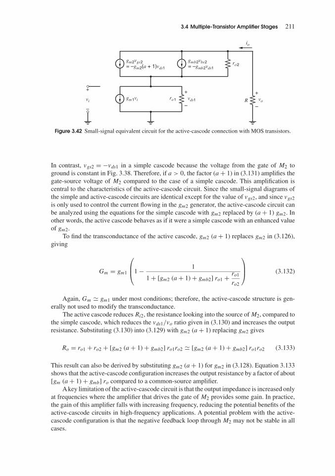
3.4 Multiple-Transistor Amplifier Stages 211
vi
+
–
vds1
gmb2vbs2= –gmb2vds1
gm2vgs2= –gm2(a + 1)vds1
gm1vi
+
–
ro2
ro1
io
voR
+
–
Figure 3.42 Small-signal equivalent circuit for the active-cascode connection with MOS transistors.
In contrast, vgs2 = −vds1 in a simple cascode because the voltage from the gate of M2 toground is constant in Fig. 3.38. Therefore, if a > 0, the factor (a + 1) in (3.131) amplifies thegate-source voltage of M2 compared to the case of a simple cascode. This amplification iscentral to the characteristics of the active-cascode circuit. Since the small-signal diagrams ofthe simple and active-cascode circuits are identical except for the value of vgs2, and since vgs2is only used to control the current flowing in the gm2 generator, the active-cascode circuit canbe analyzed using the equations for the simple cascode with gm2 replaced by (a + 1) gm2. Inother words, the active cascode behaves as if it were a simple cascode with an enhanced valueof gm2.
To find the transconductance of the active cascode, gm2 (a + 1) replaces gm2 in (3.126),giving
Gm = gm1
⎛⎜⎝1 − 1
1 + [gm2 (a + 1) + gmb2] ro1 + ro1
ro2
⎞⎟⎠ (3.132)
Again, Gm � gm1 under most conditions; therefore, the active-cascode structure is gen-erally not used to modify the transconductance.
The active cascode reduces Ri2, the resistance looking into the source of M2, compared tothe simple cascode, which reduces the vds1/vo ratio given in (3.130) and increases the outputresistance. Substituting (3.130) into (3.129) with gm2 (a + 1) replacing gm2 gives
Ro = ro1 + ro2 + [gm2 (a + 1) + gmb2] ro1ro2 � [gm2 (a + 1) + gmb2] ro1ro2 (3.133)
This result can also be derived by substituting gm2 (a + 1) for gm2 in (3.128). Equation 3.133shows that the active-cascode configuration increases the output resistance by a factor of about[gm (a + 1) + gmb] ro compared to a common-source amplifier.
Akey limitation of the active-cascode circuit is that the output impedance is increased onlyat frequencies where the amplifier that drives the gate of M2 provides some gain. In practice,the gain of this amplifier falls with increasing frequency, reducing the potential benefits of theactive-cascode circuits in high-frequency applications. A potential problem with the active-cascode configuration is that the negative feedback loop through M2 may not be stable in allcases.

212 Chapter 3 � Single-Transistor and Multiple-Transistor Amplifiers
3.4.4 The Super Source Follower
Equation 3.84 shows that the output resistance of a source follower is approximately 1/(gm +gmb). Because MOS transistors usually have much lower transconductance than their bipolarcounterparts, this output resistance may be too high for some applications, especially whena resistive load must be driven. One way to reduce the output resistance is to increase thetransconductance by increasing the W/L ratio of the source follower and its dc bias current.However, this approach requires a proportionate increase in the area and power dissipationto reduce Ro. To minimize the area and power dissipation required to reach a given outputresistance, the super source follower configuration shown in Fig. 3.43 is sometimes used. Thiscircuit uses negative feedback through M2 to reduce the output resistance. Negative feedbackis studied quantitatively in Chapter 8. From a qualitative standpoint, when the input voltageis constant and the output voltage increases, the magnitude of the drain current of M1 alsoincreases, in turn increasing the gate-source voltage of M2. As a result, the drain current ofM2 increases, reducing the output resistance by increasing the total current that flows into theoutput node under these conditions.
From a dc standpoint, the bias current in M2 is the difference between I1 and I2; therefore,I1 > I2 is required for proper operation. This information can be used to find the small-signalparameters of both transistors. The small-signal equivalent circuit is shown in Fig. 3.44. Thebody-effect transconductance generator for M2 is inactive because vbs2 = 0.Also, the polaritiesof the voltage-controlled current sources for n- and p-channel devices are identical. Finally,the output resistances of current sources I1 and I2 are represented by r1 and r2, respectively.
VDD
Vi
+
–
Vo
+
–
M1
M2
I2
I1
Figure 3.43 Super-source-follower configuration.
vo
io
ro1 ro2
v2
–gmb1vo gm2v2gm1(vi – vo)
+
–
r2
+
–
vi
+
–
r1v2r2
Figure 3.44 Small-signal equivalent circuit of the super-source follower.

3.4 Multiple-Transistor Amplifier Stages 213
If the current sources are ideal, r1 → ∞ and r2 → ∞. In practice, these resistances are largebut finite. Techniques to build high-resistance current sources are considered in Chapter 4.
To find the output resistance, set vi = 0 and calculate the current io that flows in the outputnode when the output is driven by a voltage vo. From KCL at the output under these conditions,
io = vo
r1+ vo
ro2+ gm2v2 + v2
r2(3.134)
From KCL at the drain of M1 with vi = 0,
v2
r2− gm1vo − gmb1vo + v2 − vo
ro1= 0 (3.135)
Solving (3.135) for v2, substituting into (3.134), and rearranging gives
Ro = vo
io
∣∣∣∣vi = 0
= r1 ‖ ro2 ‖(
ro1 + r2
[1 + (gm1 + gmb1) ro1](1 + gm2r2)
)(3.136)
Assume I1 and I2 are ideal current sources so that r1 → ∞ and r2 → ∞. If ro2 → ∞, and if
(gm1 + gmb1) ro1 � 1,
Ro � 1
gm1 + gmb1
(1
gm2ro1
)(3.137)
Comparing (3.84) and (3.137) shows that the negative feedback through M2 reduces the output
resistance by a factor of about gm2ro1.Now we will calculate the open-circuit voltage gain of the super-source follower. With
the output open circuited, KCL at the output node gives
vo
r1+ vo
ro2+ gm2v2 + v2
r2= 0 (3.138)
From KCL at the drain of M1,
v2
r2+ gm1 (vi − vo) − gmb1vo + v2 − vo
ro1= 0 (3.139)
Solving (3.138) for v2, substituting into (3.139), and rearranging gives
vo
vi
∣∣∣∣io=0
= gm1ro1
1 + (gm1 + gmb1) ro1 + (r2 + ro1)
(r1 ‖ ro2)(1 + gm2r2)
(3.140)
With ideal current sources,
limr1→∞r2→∞
vo
vi
∣∣∣∣io=0
= gm1 ro1
1 + (gm1 + gmb1) ro1 + 1
gm2ro2
(3.141)
Comparing (3.141) and (3.81) shows that the deviation of this gain from unity is greater thanwith a simple source follower. If gm2ro2 � 1, however, the difference is small and the mainconclusion is that the super-source-follower configuration has little effect on the open-circuitvoltage gain.
As mentioned earlier, the super-source follower is sometimes used in MOS technologiesto reduce the source-follower output resistance. It is also used in bipolar technologies in outputstages to reduce the current conducted in a weak lateral pnp transistor. This application is

214 Chapter 3 � Single-Transistor and Multiple-Transistor Amplifiers
described in Chapter 5. The main potential problem with the super-source-follower configu-ration is that the negative feedback loop through M2 may not be stable in all cases, especiallywhen driving a capacitive load. The stability of feedback amplifiers is considered in Chapter 9.
3.5 Differential PairsThe differential pair is another example of a circuit that was first invented for use with vacuumtubes.10 The original circuit uses two vacuum tubes whose cathodes are connected together.Modern differential pairs use bipolar or MOS transistors coupled at their emitters or sources,respectively, and are perhaps the most widely used two-transistor subcircuits in monolithicanalog circuits. The usefulness of the differential pair stems from two key properties. First,cascades of differential pairs can be directly connected to one another without interstagecoupling capacitors. Second, the differential pair is primarily sensitive to the difference betweentwo input voltages, allowing a high degree of rejection of signals common to both inputs.11,12
In this section, we consider the properties of emitter-coupled pairs of bipolar transistors andsource-coupled pairs of MOS transistors in detail.
3.5.1 The dc Transfer Characteristic of an Emitter-Coupled Pair
The simplest form of an emitter-coupled pair is shown in Fig. 3.45. The biasing circuit in thelead connected to the emitters of Q1 and Q2 can be a transistor current source, which is calleda tail current source, or a simple resistor. If a simple resistor RTAIL is used alone, ITAIL = 0in Fig. 3.45. Otherwise, ITAIL and RTAIL together form a Norton-equivalent model of the tailcurrent source.
The large-signal behavior of the emitter-coupled pair is important in part because it illus-trates the limited range of input voltages over which the circuit behaves almost linearly. Also,the large-signal behavior shows that the amplitude of analog signals in bipolar circuits canbe limited without pushing the transistors into saturation, where the response time would beincreased because of excess charge storage in the base region. For simplicity in the analysis, weassume that the output resistance of the tail current source RTAIL → ∞, that the output resis-tance of each transistor ro → ∞, and that the base resistance of each transistor rb = 0. These
–VEE
+VCC
RC RC
RTAILITAIL
Vo2
Ic1 Ic2
+
–Vo1
+
–
Vi2
+
–
Vi1
Q1 Q2+
–
Figure 3.45 Emitter-coupled pair circuitdiagram.

3.5 Differential Pairs 215
assumptions do not strongly affect the low-frequency, large-signal behavior of the circuit. FromKVL around the input loop,
Vi1 − Vbe1 + Vbe2 − Vi2 = 0 (3.142)
Assume the collector resistors are small enough that the transistors do not operate in saturation ifVi1 ≤ VCC and Vi2 ≤ VCC. If Vbe1 � VT and Vbe2 � VT , the Ebers-Moll equations show that
Vbe1 = VT lnIc1
IS1(3.143)
Vbe2 = VT lnIc2
IS2(3.144)
Assume the transistors are identical so that IS1 = IS2. Then combining (3.142), (3.143), and(3.144), we find
Ic1
Ic2= exp
(Vi1 − Vi2
VT
)= exp
(Vid
VT
)(3.145)
where Vid = Vi1 − Vi2. Since we have assumed that the transistors are identical, αF1 =αF2 = αF . Then KCL at the emitters of the transistors shows
−(Ie1 + Ie2) = ITAIL = Ic1 + Ic2
αF
(3.146)
Combining (3.145) and (3.146), we find that
Ic1= αFITAIL
1 + exp
(−Vid
VT
) (3.147)
Ic2= αFITAIL
1 + exp
(Vid
VT
) (3.148)
These two currents are shown as a function of Vid in Fig. 3.46. When the magnitude of Vid
is greater than about 3VT , which is approximately 78 mV at room temperature, the collectorcurrents are almost independent of Vid because one of the transistors turns off and the otherconducts all the current that flows. Furthermore, the circuit behaves in an approximately
–4VT 4VT–3VT 3VT–2VT 2VTVT–VT 0Vid
Ic1, Ic2
Ic2
F ITAIL
0.5 F ITAIL
Ic1
α
α
Figure 3.46 Emitter-coupled paircollector currents as a function ofdifferential input voltage.

216 Chapter 3 � Single-Transistor and Multiple-Transistor Amplifiers
–4VT –3VT –2VT –VT
– FITAILRC
FITAILRC
VTVid
Vod
2VT 3VT 4VT
α
α Figure 3.47 Emitter-coupled pair,differential output voltage as afunction of differential inputvoltage.
linear fashion only when the magnitude of Vid is less than about VT . We can now computethe output voltages as
Vo1 = VCC − Ic1RC (3.149)
Vo2 = VCC − Ic2RC (3.150)
The output signal of interest is often the difference between Vo1 and Vo2, which we define asVod . Then
Vod = Vo1 − Vo2 = αFITAILRC tanh
(−Vid
2VT
)(3.151)
This function is plotted in Fig. 3.47. Here a significant advantage of differential amplifiers isapparent: When Vid is zero, Vod is zero if Q1 and Q2 are identical and if identical resistors areconnected to the collectors of Q1 and Q2. This property allows direct coupling of cascadedstages without offsets.
3.5.2 The dc Transfer Characteristic with Emitter Degeneration
To increase the range of Vid over which the emitter-coupled pair behaves approximately asa linear amplifier, emitter-degeneration resistors are frequently included in series with theemitters of the transistors, as shown in Fig. 3.48. The analysis of this circuit proceeds in thesame manner as without degeneration, except that the voltage drop across these resistors mustbe included in the KVL equation corresponding to (3.142). A transcendental equation resultsfrom this analysis and a closed-form solution like that of (3.151) does not exist, but the effectof the resistors may be understood intuitively from the examples plotted in Fig. 3.49. For largevalues of emitter-degeneration resistors, the linear range of operation is extended by an amountapproximately equal to ITAILRE. This result stems from the observation that all of ITAIL flowsin one of the degeneration resistors when one transistor turns off. Therefore, the voltage dropis ITAILRE on one resistor and zero on the other, and the value of Vid required to turn onetransistor off is changed by the difference of the voltage drops on these resistors. Furthermore,since the voltage gain is the slope of the transfer characteristic, the voltage gain is reducedby approximately the same factor that the input range is increased. In operation, the emitterresistors introduce local negative feedback in the differential pair. This topic is considered inChapter 8.

3.5 Differential Pairs 217
–VEE
+VCC
RC RC
RERE
Vod
ITAIL
– +
+
–Q1 Q2
+
–
Vid
2Vid
2
Figure 3.48 Circuit diagram ofemitter-coupled pair with emitterdegeneration.
–10VT–20VT
– FITAILRC
FITAILRCITAILRE = 0
ITAILRE = 10VT
ITAILRE = 20VT
Vid
Vod
10VT 20VT
α
α
Figure 3.49 Output voltage as a function of input voltage, emitter-coupled pair with emitterdegeneration.
3.5.3 The dc Transfer Characteristic of a Source-Coupled Pair
Consider the n-channel MOS-transistor source-coupled pair shown in Fig. 3.50. The followinganalysis applies equally well to a corresponding p-channel source-coupled pair with appropriatesign changes. In monolithic form, a transistor current source, called a tail current source, isusually connected to the sources of M1 and M2. In that case, ITAIL and RTAIL together form aNorton-equivalent model of the tail current source.
For this large-signal analysis, we assume that the output resistance of the tail currentsource is RTAIL → ∞. Also, we assume that the output resistance of each transistor ro → ∞.Although these assumptions do not strongly affect the low-frequency, large-signal behavior ofthe circuit, they could have a significant impact on the small-signal behavior. Therefore, wewill reconsider these assumptions when we analyze the circuit from a small-signal standpoint.From KVL around the input loop,
Vi1 − Vgs1 + Vgs2 − Vi2 = 0 (3.152)
We assume that the drain resistors are small enough that neither transistor operates in the trioderegion if Vi1 ≤ VDD and Vi2 ≤ VDD. Furthermore, we assume that the drain current of each

218 Chapter 3 � Single-Transistor and Multiple-Transistor Amplifiers
–VSS
+VDD
RD RD
RTAILITAIL
Vo2
+
–Vo1
+
–
Vi2
+
–Vi1
M1 M2+
–
Figure 3.50 n-channel MOSFETsource-coupled pair.
transistor is related to its gate-source voltage by the approximate square-law relationship givenin (1.157). If the transistors are identical, applying (1.157) to each transistor and rearranginggives
Vgs1 = Vt +√
2Id1
k′ (W/L)(3.153)
and
Vgs2 = Vt +√
2Id2
k′ (W/L)(3.154)
Substituting (3.153) and (3.154) into (3.152) and rearranging gives
Vid = Vi1 − Vi2 =√
Id1 − √Id2√
k′
2
W
L
(3.155)
From KCL at the source of M1 and M2,
Id1 + Id2 = ITAIL (3.156)
Solving (3.156) for Id2, substituting into (3.155), rearranging, and using the quadratic formulagives
Id1 = ITAIL
2�
k′
4
W
LVid
√4ITAIL
k′ (W/L)− V 2
id (3.157)
Since Id1 > ITAIL/2 when Vid > 0, the potential solution where the second term is subtractedfrom the first in (3.157) cannot occur in practice. Therefore,
Id1 = ITAIL
2+ k′
4
W
LVid
√4ITAIL
k′ (W/L)− V 2
id (3.158)

3.5 Differential Pairs 219
Substituting (3.158) into (3.156) gives
Id2 = ITAIL
2− k′
4
W
LVid
√4ITAIL
k′ (W/L)− V 2
id (3.159)
Equations 3.158 and 3.159 are valid when both transistors operate in the active or saturationregion. Since we have assumed that neither transistor operates in the triode region, the limitationhere stems from turning off one of the transistors. When M1 turns off, Id1 = 0 and Id2 = ITAIL.On the other hand, Id1 = ITAIL and Id2 = 0 when M2 turns off. Substituting these values in(3.155) shows that both transistors operate in the active region if
|Vid | ≤√
2ITAIL
k′ (W/L)(3.160)
Since Id1 = Id2 = ITAIL/2 when Vid = 0, the range in (3.160) can be rewritten as
|Vid | ≤√
2
(√2Id1
k′ (W/L)
)∣∣∣∣∣Vid=0
=√
2 (Vov )| Vid=0 (3.161)
Equation 3.161 shows that the range of Vid for which both transistors operate in the activeregion is proportional to the overdrive calculated when Vid = 0. This result is illustrated inFig. 3.51. The overdrive is an important quantity in MOS circuit design, affecting not onlythe input range of differential pairs, but also other characteristics including the speed, offset,and output swing of MOS amplifiers. Since the overdrive of an MOS transistor depends onits current and W/L ratio, the range of a source-coupled pair can be adjusted to suit a givenapplication by adjusting the value of the tail current and/or the aspect ratio of the input devices.In contrast, the input range of the bipolar emitter-coupled pair is about � 3VT , independent ofbias current or device size. In fact, the source-coupled pair behaves somewhat like an emitter-coupled pair with emitter-degeneration resistors that can be selected to give a desired inputvoltage range.
–0.5 –0.25 0 0.25 0.5
Vov = 0.1 V
Vov = 0.2 V
Vov = 0.4 V
Vov = 0.1 V
Id2 Id1
Id1, Id2
Vid(V)
Vov = 0.2 V
Vov = 0.4 V
ITAIL
ITAIL/2
Figure 3.51 dc transfer characteristic of the MOS source-coupled pair. The parameter is the overdriveVov = VGS − Vt determined when Vid = 0.

220 Chapter 3 � Single-Transistor and Multiple-Transistor Amplifiers
In many practical cases, the key output of the differential pair is not Id1 or Id2 alone butthe difference between these quantities. Subtracting (3.159) from (3.158) gives
�Id = Id1 − Id2 = k′
2
W
LVid
√4ITAIL
k′ (W/L)− V 2
id (3.162)
We can now compute the differential output voltage as
Vod = Vo1 − Vo2 = VDD − Id1RD − VDD + Id2RD = −(�Id) RD (3.163)
Since �Id = 0 when Vid = 0, (3.163) shows that Vod = 0 when Vid = 0 if M1 and M2 areidentical and if identical resistors are connected to the drains of M1 and M2. This propertyallows direct coupling of cascaded MOS differential pairs, as in the bipolar case.
3.5.4 Introduction to the Small-Signal Analysis of Differential Amplifiers
The features of interest in the performance of differential pairs are often the small-signalproperties for dc differential input voltages near zero volts. In the next two sections, we assumethat the dc differential input voltage is zero and calculate the small-signal parameters. If theparameters are constant, the small-signal model predicts that the circuit operation is linear.The results of the small-signal analysis are valid for signals that are small enough to causeinsignificant nonlinearity.
In previous sections, we have considered amplifiers with two input terminals (Vi andground) and two output terminals (Vo and ground). Small-signal analysis of such circuits leadsto one equation for each circuit, such as
vo = Avi (3.164)
Here, A is the small-signal voltage gain under given loading conditions. In contrast, differentialpairs have three input terminals (Vi1, Vi2, and ground) and three output terminals (Vo1, Vo2,and ground). Therefore, direct small-signal analysis of differential pairs leads to two equationsfor each circuit (one for each output), where each output depends on each input:
vo1 = A11vi1 + A12vi2 (3.165)
vo2 = A21vi1 + A22vi2 (3.166)
Here, four voltage gains, A11, A12, A21, and A22, specify the small-signal operation of thecircuit under given loading conditions. These gains can be interpreted as
A11 = vo1
vi1
∣∣∣∣vi2=0
(3.167)
A12 = vo1
vi2
∣∣∣∣vi1=0
(3.168)
A21 = vo2
vi1
∣∣∣∣vi2=0
(3.169)
A22 = vo2
vi2
∣∣∣∣vi1=0
(3.170)
Although direct small-signal analysis of differential pairs can be used to calculate these fourgain values in a straightforward way, the results are difficult to interpret because differential

3.5 Differential Pairs 221
pairs usually are not used to react to vi1 or vi2 alone. Instead, differential pairs are used mostoften to sense the difference between the two inputs while trying to ignore the part of thetwo inputs that is common to each. Desired signals will be forced to appear as differences indifferential circuits. In practice, undesired signals will also appear. For example, mixed-signalintegrated circuits use both analog and digital signal processing, and the analog signals arevulnerable to corruption from noise generated by the digital circuits and transmitted throughthe common substrate. The hope in using differential circuits is that undesired signals willappear equally on both inputs and be rejected.
To highlight this behavior, we will define new differential and common-mode variables atthe input and output as follows. The differential input, to which differential pairs are sensitive, is
vid = vi1 − vi2 (3.171)
The common-mode or average input, to which differential pairs are insensitive, is
vic = vi1 + vi2
2(3.172)
These equations can be inverted to give vi1 and vi2 in terms of vid and vic:
vi1 = vic + vid
2(3.173)
vi2 = vic − vid
2(3.174)
The physical significance of these new variables can be understood by using (3.173) and(3.174) to redraw the input connections to a differential amplifier as shown in Fig. 3.52.The common-mode input is the input component that appears equally in vi1 and vi2. Thedifferential input is the input component that appears between vi1 and vi2.
New output variables are defined in the same way. The differential output is
vod = vo1 − vo2 (3.175)
The common-mode or average output is
voc = vo1 + vo2
2(3.176)
Solving these equations for vo1 and vo2, we obtain
vo1 = voc + vod
2(3.177)
vo2 = voc − vod
2(3.178)
(a)
vi1
+
–+
–vi2
+
–
vic
+
–
(b)
+
–+
–+
–
–vid
2
vid
2
Figure 3.52 A differentialamplifier with its inputs (a)shown as independent ofeach other and (b) redrawnin terms of the differentialand common-modecomponents.

222 Chapter 3 � Single-Transistor and Multiple-Transistor Amplifiers
We have now defined two new input variables and two new output variables. By substitutingthe expressions for vi1, vi2, vo1, and vo2 in terms of the new variables back into (3.165) and(3.166), we find
vod =(
A11 − A12 − A21 + A22
2
)vid + (A11 + A12 − A21 − A22) vic (3.179)
voc =(
A11 − A12 + A21 − A22
4
)vid +
(A11 + A12 + A21 + A22
2
)vic (3.180)
Defining four new gain factors that are equal to the coefficients in these equations, (3.179) and(3.180) can be rewritten as
vod = Admvid + Acm − dmvic (3.181)
voc = Adm − cmvid + Acmvic (3.182)
The differential-mode gain Adm is the change in the differential output per unit change indifferential input:
Adm = vod
vid
∣∣∣∣vic = 0
= A11 − A12 − A21 + A22
2(3.183)
The common-mode gain Acm is the change in the common-mode output voltage per unit changein the common-mode input:
Acm = voc
vic
∣∣∣∣vid = 0
= A11 + A12 + A21 + A22
2(3.184)
The differential-mode-to-common-mode gain Adm−cm is the change in the common-modeoutput voltage per unit change in the differential-mode input:
Adm−cm = voc
vid
∣∣∣∣vic = 0
= A11 − A12 + A21 − A22
4(3.185)
The common-mode-to-differential-mode gain Acm−dm is the change in the differential-modeoutput voltage per unit change in the common-mode input:
Acm−dm = vod
vic
∣∣∣∣vid = 0
= A11 + A12 − A21 − A22 (3.186)
The purpose of a differential amplifier is to sense changes in its differential input whilerejecting changes in its common-mode input. The desired output is differential, and its variationshould be proportional to the variation in the differential input. Variation in the common-modeoutput is undesired because it must be rejected by another differential stage to sense the desireddifferential signal. Therefore, an important design goal in differential amplifiers is to make Adm
large compared to the other three gain coefficients in (3.181) and (3.182).In differential amplifiers with perfect symmetry, each component on the side of one out-
put corresponds to an identical component on the side of the other output. With such perfectlybalanced amplifiers, when vi1 = −vi2, vo1 = −vo2. In other words, when the input is purelydifferential (vic = 0), the output of a perfectly balanced differential amplifier is purely dif-ferential (voc = 0), and thus Adm−cm = 0. Similarly, pure common-mode inputs (for whichvid = 0) produce pure common-mode outputs and Acm−dm = 0 in perfectly balanced differ-ential amplifiers. Even with perfect symmetry, however, Acm /= 0 is possible. Therefore, theratio Adm/Acm is one figure of merit for a differential amplifier, giving the ratio of the desired

3.5 Differential Pairs 223
differential-mode gain to the undesired common-mode gain. In this book, we will define themagnitude of this ratio as the common-mode-rejection ratio, CMRR:
CMRR ≡∣∣∣∣Adm
Acm
∣∣∣∣ (3.187)
Furthermore, since differential amplifiers are not perfectly balanced in practice, Adm−cm /= 0and Acm−dm /= 0. The ratios Adm/Acm−dm and Adm/Adm−cm are two other figures of meritthat characterize the performance of differential amplifiers. Of these, the first is particularlyimportant because ratio Adm/Acm−dm determines the extent to which the differential outputis produced by the desired differential input instead of by the undesired common-mode input.This ratio is important because once a common-mode input is converted to a differentialoutput, the result is treated as the desired signal by subsequent differential amplifiers. In fact,in multistage differential amplifiers, the common-mode-to-differential-mode gain of the firststage is usually an important factor in the overall CMRR. In Section 3.5.5, we consider perfectlybalanced differential amplifiers from a small-signal standpoint; in Section 3.5.6.9, imperfectlybalanced differential amplifiers from the same standpoint.
3.5.5 Small-Signal Characteristics of Balanced Differential Amplifiers
In this section, we will study perfectly balanced differential amplifiers. Therefore, Acm−dm = 0and Adm−cm = 0 here, and our goal is to calculate Adm and Acm. Although calculating Adm andAcm from the entire small-signal equivalent circuit of a differential amplifier is possible, thesecalculations are greatly simplified by taking advantage of the symmetry that exists in perfectlybalanced amplifiers. In general, we first find the response of a given circuit to pure differentialand pure common-mode inputs separately. Then the results can be superposed to find the totalsolution. Since superposition is valid only for linear circuits, the following analysis is strictlyvalid only from a small-signal standpoint and approximately valid only for signals that causenegligible nonlinearity. In previous sections, we carried out large-signal analyses of differentialpairs and assumed that the Norton-equivalent resistance of the tail current source was infinite.Since this resistance has a considerable effect on the small-signal behavior of differential pairs,however, we now assume that this resistance is finite.
Because the analysis here is virtually the same for both bipolar and MOS differentialpairs, the two cases will be considered together. Consider the bipolar emitter-coupled pairof Fig. 3.45 and the MOS source-coupled pair of Fig. 3.50 from a small-signal standpoint.Then Vi1 = vi1 and Vi2 = vi2. These circuits are redrawn in Fig. 3.53a and Fig. 3.53b with thecommon-mode input voltages set to zero so we can consider the effect of the differential-modeinput by itself. The small-signal equivalent circuit for both cases is shown in Fig. 3.54 with Rused to replace RC in Fig. 3.53a and RD in 3.53b. Note that the small-signal equivalent circuitneglects finite ro in both cases. Also, in the MOS case, nonzero gmb is ignored and rπ → ∞because β0 → ∞.
Because the circuit in Fig. 3.54 is perfectly balanced, and because the inputs are drivenby equal and opposite voltages, the voltage across RTAIL does not vary at all. Another wayto see this result is to view the two lower parts of the circuit as voltage followers. When oneside pulls up, the other side pulls down, resulting in a constant voltage across the tail currentsource by superposition. Since the voltage across RTAIL experiences no variation, the behaviorof the small-signal circuit is unaffected by the placement of a short circuit across RTAIL, asshown in Fig. 3.55. After placing this short circuit, we see that the two sides of the circuitare not only identical, but also independent because they are joined at a node that operatesas a small-signal ground. Therefore, the response to small-signal differential inputs can bedetermined by analyzing one side of the original circuit with RTAIL replaced by a short circuit.

224 Chapter 3 � Single-Transistor and Multiple-Transistor Amplifiers
–VEE
+ vod –
+VCC
(a)
RC RC
RTAILITAIL
Q1 Q2
–vid
2
+
–
+
–
vid
2
–VSS
+VDD
(b)
RD RD
RTAILITAIL
+
–
M1 M2+
––
vid
2vid
2
+ vod –
Figure 3.53 (a) Emitter-coupled pair withpure differential input. (b) Source-coupledpair with pure differential input.
R
RTAIL
gmv1
+
–+
–
+
–
v1 rvid
2
+
–
+
–
v2
vod
2
R
gmv2
+
–
vod
2–
vid
2–π rπ
Figure 3.54 Small-signal equivalent circuit for differential pair with pure differential-mode input.

3.5 Differential Pairs 225
R
RTAILix = 0
gmv1
+
–
+
–
v1 rvid
2
+
–
+
–
v2
R
gmv2vid
2–π rπ
Figure 3.55 Differential-mode circuit with the tail current source grounded. Because of the symmetryof the circuit, ix = 0.
gmv1
+
–
+
–
v1r vid
2R vod
2
ib+
–
π
Figure 3.56 Differential-mode halfcircuit.
This simplified circuit, shown in Fig. 3.56, is called the differential-mode half circuit and isuseful for analysis of both the low- and high-frequency performance of all types of differentialamplifiers. By inspection of Fig. 3.56, we recognize this circuit as the small-signal equivalentof a common-emitter or common-source amplifier. Therefore,
vod
2= −gmR
vid
2(3.188)
and
Adm = vod
vid
∣∣∣∣vic = 0
= −gmR (3.189)
To include the output resistance of the transistor in the above analysis, R in (3.189) shouldbe replaced by R ‖ ro. Finally, note that neglecting gmb from this analysis for MOS source-coupled pairs has no effect on the result because the voltage from the source to the body ofthe input transistors is the same as the voltage across the tail current source, which is constantwith a pure differential input.
The circuits in Fig. 3.45 and Fig. 3.50 are now reconsidered from a small-signal, common-mode standpoint. Setting Vi1 = Vi2 = vic, the circuits are redrawn in Fig. 3.57a and Fig. 3.57b.The small-signal equivalent circuit is shown in Fig. 3.58, but with the modification that theresistor RTAIL has been split into two parallel resistors, each of value twice the original. AlsoR has been used to replace RC in Fig. 3.57a and RD in 3.57b. Again ro is neglected in bothcases, and gmb is neglected in the MOS case, where rπ → ∞ because β0 → ∞.
Because the circuit in Fig. 3.58 is divided into two identical halves, and because eachhalf is driven by the same voltage vic, no current ix flows in the lead connecting the halfcircuits. The circuit behavior is thus unchanged when this lead is removed as shown inFig. 3.59. As a result, we see that the two halves of the circuit in Fig. 3.58 are not only identical,but also independent because they are joined by a branch that conducts no small-signal current.Therefore, the response to small-signal, common-mode inputs can be determined by analyzing
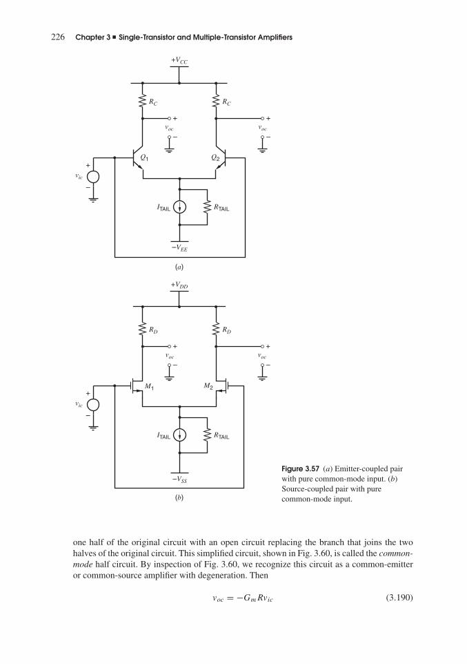
226 Chapter 3 � Single-Transistor and Multiple-Transistor Amplifiers
RC RC
+VCC
(a)
voc
RTAILITAIL
+
–voc
+
–
vic
+
–
Q1 Q2
–VEE
RD RD
+VDD
(b)
voc
RTAILITAIL
+
–voc
+
–
vic
+
–
M1 M2
–VSS
Figure 3.57 (a) Emitter-coupled pairwith pure common-mode input. (b)Source-coupled pair with purecommon-mode input.
one half of the original circuit with an open circuit replacing the branch that joins the twohalves of the original circuit. This simplified circuit, shown in Fig. 3.60, is called the common-mode half circuit. By inspection of Fig. 3.60, we recognize this circuit as a common-emitteror common-source amplifier with degeneration. Then
voc = −GmRvic (3.190)

3.5 Differential Pairs 227
R
2RTAIL
gmv1
R
2RTAIL
gmv2ix
vic
+
–
v2r+
–
v1
+
–π rπ
Figure 3.58 Small-signal equivalentcircuit, pure common-mode input.
R
2RTAIL
gmv1
R
2RTAIL
gmv2vic
+
–
v2r
+
–v1
+
–π rπ
Figure 3.59 Modifiedcommon-mode equivalentcircuit.
2RTAIL
gmv1
Rvic
voc
ib+
–
r+
–
v1+
–
π
Figure 3.60 Common-mode halfcircuit.
and
Acm = voc
vic
∣∣∣∣vid = 0
= −GmR (3.191)
where Gm is the transconductance of a common-emitter or common-source amplifier withdegeneration and will be considered quantitatively below. Since degeneration reduces thetransconductance, and since degeneration occurs only in the common-mode case, (3.189) and(3.191) show that |Adm| > |Acm|; therefore, the differential pair is more sensitive to differ-ential inputs than to common-mode inputs. In other words, the tail current source provideslocal negative feedback to common-mode inputs (or local common-mode feedback). Negativefeedback is studied in Chapter 8.

228 Chapter 3 � Single-Transistor and Multiple-Transistor Amplifiers
Bipolar Emitter-Coupled Pair. For the bipolar case, substituting (3.93) for Gm with RE =2RTAIL into (3.191) and rearranging gives
Acm � − gmR
1 + gm (2RTAIL)= − gmR
1 + 2gmRTAIL(3.192)
To include the effect of finite ro in the above analysis, R in (3.192) should be replaced by R ‖ Ro,where Ro is the output resistance of a common-emitter amplifier with emitter degeneration ofRE = 2RTAIL, given in (3.97) or (3.98). This substitution ignores the effect of finite ro on Gm,which is shown in (3.92) and is usually negligible.
The CMRR is found by substituting (3.189) and (3.192) into (3.187), which gives
CMRR = 1 + 2gmRTAIL (3.193)
This expression applies to the particular case of a single-stage, emitter-coupled pair. It showsthat increasing the output resistance of the tail current source RTAIL improves the common-mode-rejection ratio. This topic is considered in Chapter 4.
Since bipolar transistors have finite β0, and since differential amplifiers are often used asthe input stage of instrumentation circuits, the input resistance of emitter-coupled pairs is alsoan important design consideration. The differential input resistance Rid is defined as the ratioof the small-signal differential input voltage vid to the small-signal input current ib when apure differential input voltage is applied. By inspecting Fig. 3.56, we find that
vid
2= ibrπ (3.194)
Therefore, the differential input resistance of the emitter-coupled pair is
Rid = vid
ib
∣∣∣∣vic = 0
= 2rπ (3.195)
Thus the differential input resistance depends on the rπ of the transistor, which increases withincreasing β0 and decreasing collector current. High input resistance is therefore obtainedwhen an emitter-coupled pair is operated at low bias current levels. Techniques to achievesmall bias currents are considered in Chapter 4.
The common-mode input resistance Ric is defined as the ratio of the small-signal, common-mode input voltage vic to the small-signal input current ib in one terminal when a pure common-mode input is applied. Since the common-mode half circuit in Fig. 3.60 is the same as that fora common-emitter amplifier with emitter degeneration, substituting RE = 2RTAIL into (3.90)gives Ric as
Ric = vic
ib
∣∣∣∣vid = 0
= rπ + (β0 + 1)(2RTAIL) (3.196)
The small-signal input current that flows when both common-mode and differential-modeinput voltages are applied can be found by superposition and is given by
ib1 = vid
Rid
+ vic
Ric
(3.197)
ib2 = − vid
Rid
+ vic
Ric
(3.198)
where ib1 and ib2 represent the base currents of Q1 and Q2, respectively.The input resistance can be represented by the π equivalent circuit of Fig. 3.61a or by
the T-equivalent circuit of Fig. 3.61b. For the π model, the common-mode input resistance isexactly Ric independent of Rx. To make the differential-mode input resistance exactly Rid , the

3.5 Differential Pairs 229
(b)
Rx = Rid || (–2Ric) Rid
(a)
Ric
RicRid2
Rid2
Ry = –Rid4
Ric2
Ric2
~
~
Figure 3.61 (a) General low-frequency, small-signal, π-equivalent input circuit for the differentialamplifier. (b) T-equivalent input circuit.
value of Rx should be more than Rid to account for nonzero current in Ric. On the other hand,for the T model, the differential-mode input resistance is exactly Rid independent of Ry, andthe common-mode input resistance is Ric if Ry is chosen to be less than Ric/2 as shown. Theapproximations in Fig. 3.61 are valid if Ric is much larger than Rid .
MOS Source-Coupled Pair. For the MOS case, substituting (3.104) for Gm with gmb = 0and RS = 2RTAIL into (3.191) and rearranging gives
Acm � − gmR
1 + gm (2RTAIL)= − gmR
1 + 2gmRTAIL(3.199)
Although (3.199) and the common-mode half circuit in Fig. 3.60 ignore the body-effecttransconductance gmb, the common-mode gain depends on gmb in practice because the bodyeffect changes the source-body voltage of the transistors in the differential pair. Since nonzerogmb was included in the derivation of the transconductance of the common-source amplifierwith degeneration, a simple way to include the body effect here is to allow nonzero gmb whensubstituting (3.104) into (3.191). The result is
Acm � − gmR
1 + (gm + gmb)(2RTAIL)= − gmR
1 + 2 (gm + gmb) RTAIL(3.200)
To include the effect of finite ro in the above analysis, R in (3.199) and (3.200) should bereplaced by R ‖ Ro, where Ro is the output resistance of a common-source amplifier withsource degeneration of RS = 2RTAIL, given in (3.107). This substitution ignores the effect offinite ro on Gm, which is shown in (3.103) and is usually negligible.
The CMRR is found by substituting (3.189) and (3.200) into (3.187), which gives
CMRR � 1 + 2(gm + gmb) RTAIL (3.201)
Equation 3.201 is valid for a single-stage, source-coupled pair and shows that increasing RTAILincreases the CMRR. This topic is studied in Chapter 4.
3.5.6 Device Mismatch Effects in Differential Amplifiers
An important aspect of the performance of differential amplifiers is the minimum dc andac differential voltages that can be detected. The presence of component mismatches withinthe amplifier itself and drifts of component values with temperature produce dc differentialvoltages at the output that are indistinguishable from the dc component of the signal beingamplified. Also, such mismatches and drifts cause nonzero common-mode-to-differential-mode gain as well as nonzero differential-to-common-mode gain to arise. Nonzero Acm−dm isespecially important because it converts common-mode inputs to differential outputs, which

230 Chapter 3 � Single-Transistor and Multiple-Transistor Amplifiers
VID VOD
+
–
+
–
Differentialamplifier withmismatches
(a)
VID
VOS
VOD
++
–
–
+
–
Differentialamplifier without
mismatches
IOS
2
(b)
Figure 3.62 Equivalent input offset voltage (VOS) and current (IOS) for a differential amplifier.(a) Actual circuit containing mismatches. (b) Equivalent dc circuit with identically matched devicesand the offset voltage and current referred to the input.
are treated as the desired signal by subsequent stages. In many analog systems, these typesof errors pose the basic limitation on the resolution of the system, and hence consideration ofmismatch-induced effects is often central to the design of analog circuits.
3.5.6.1 Input Offset Voltage and CurrentFor differential amplifiers, the effect of mismatches on dc performance is most convenientlyrepresented by two quantities, the input offset voltage and the input offset current. These quan-tities represent the input-referred effect of all the component mismatches within the amplifieron its dc performance.11,12 As illustrated in Fig. 3.62, the dc behavior of the amplifier con-taining the mismatches is identical to an ideal amplifier with no mismatches but with the inputoffset voltage source added in series with the input and the input offset current source in shuntacross the input terminals. Both quantities are required to represent the effect of mismatch ingeneral so that the model is valid for any source resistance. For example, if the input terminalsare driven by an ideal voltage source with zero resistance, the input offset current does notcontribute to the amplifier output, and the offset voltage generator is needed to model the effectof mismatch. On the other hand, if the input terminals are driven by an ideal current sourcewith infinite resistance, the input offset voltage does not contribute to the amplifier output, andthe offset current generator is needed to model the effect of mismatch. These quantities areusually a function of both temperature and common-mode input voltage. In the next severalsections, we calculate the input offset voltage and current of the emitter-coupled pair and thesource-coupled pair.
3.5.6.2 Input Offset Voltage of the Emitter-Coupled PairThe predominant sources of offset error in the emitter-coupled pair are the mismatches inthe base width, base doping level, and collector doping level of the transistors, mismatchesin the effective emitter area of the transistors, and mismatches in the collector load resistors.To provide analytical results simple enough for intuitive interpretation, the analysis will becarried out assuming a uniform-base transistor. The results are similar for the nonuniform case,although the analytical procedure is more tedious. In most instances the dc base current is lowenough that the dc voltage drop in rb is negligible, so we neglect rb.
Consider Fig. 3.45 with dc signals so that Vi1 = VI1, Vi2 = VI2, Vo1 = VO1, and Vo2 =VO2. Let VID = VI1 − VI2. Also, assume that the collector resistors may not be identical. LetRC1 and RC2 represent the values of the resistors attached to Q1 and Q2, respectively. FromKVL around the input loop,
VID − VBE1 + VBE2 = 0 (3.202)

3.5 Differential Pairs 231
Therefore,
VID = VT lnIC1
IS1− VT ln
IC2
IS2= VT ln
IC1
IC2
IS2
IS1(3.203)
The factors determining the saturation current IS of a bipolar transistor are described in Chapter1. There it was shown that if the impurity concentration in the base region is uniform, thesesaturation currents can be written
IS1= qn2i Dn
NAWB1(VCB)A1 = qn2
i Dn
QB1(VCB)A1 (3.204)
IS2= qn2i Dn
NAWB2(VCB)A2 = qn2
i Dn
QB2(VCB)A2 (3.205)
where WB(VCB) is the base width as a function of VCB, NA is the acceptor density in thebase, and A is the emitter area. We denote the product NAWB(VCB) as QB(VCB), the total baseimpurity doping per unit area.
The input offset voltage VOS is equal to the value of VID = VI1 − VI2 that must be appliedto the input to drive the differential output voltage VOD = VO1 − VO2 to zero. For VOD to bezero, IC1RC1 = IC2RC2; therefore,
IC1
IC2= RC2
RC1(3.206)
Substituting (3.204), (3.205), and (3.206) into (3.203) gives
VOS = VT ln
[(RC2
RC1
)(A2
A1
)(QB1(VCB)
QB2(VCB)
)](3.207)
This expression relates the input offset voltage to the device parameters and RC mismatch.Usually, however, the argument of the log function is very close to unity and the equation canbe interpreted in a more intuitively satisfying way. In the following section we perform anapproximate analysis, valid if the mismatches are small.
3.5.6.3 Offset Voltage of the Emitter-Coupled Pair: Approximate AnalysisIn cases of practical interest involving offset voltages and currents, the mismatch between anytwo nominally matched circuit parameters is usually small compared with the absolute valueof that parameter. This observation leads to a procedure by which the individual contributionsto offset voltage can be considered separately and summed.
First, define new parameters to describe the mismatch in the components, using therelations
�X = X1 − X2 (3.208)
X = X1 + X2
2(3.209)
Thus �X is the difference between two parameters, and X is the average of the two nominallymatched parameters. Note that �X can be positive or negative. Next invert (3.208) and (3.209)to give
X1 = X + �X
2(3.210)
X2 = X − �X
2(3.211)

232 Chapter 3 � Single-Transistor and Multiple-Transistor Amplifiers
These relations can be applied to the collector resistances, the emitter areas, and the basedoping parameters in (3.207) to give
VOS = VT ln
⎡⎢⎣⎛⎜⎝RC − �RC
2
RC + �RC
2
⎞⎟⎠⎛⎜⎝A − �A
2
A + �A
2
⎞⎟⎠⎛⎜⎝QB + �QB
2
QB − �QB
2
⎞⎟⎠⎤⎥⎦ (3.212)
With the assumptions that �RC � RC, �A � A, and �QB � QB, (3.212) can besimplified to
VOS � VT ln
[(1 − �RC
RC
)(1 − �A
A
)(1 + �QB
QB
)]
� VT
[ln
(1 − �RC
RC
)+ ln
(1 − �A
A
)+ ln
(1 + �QB
QB
)](3.213)
If x � 1, a Taylor series can be used to show that
ln (1 + x) = x − x2
2+ x3
3− · · · (3.214)
Applying (3.214) to each logarithm in (3.213) and ignoring terms higher than first order in theexpansions gives
VOS � VT
(−�RC
RC
− �A
A+ �QB
QB
)(3.215)
Thus, under the assumptions made, we have obtained an approximate expression for theinput offset voltage, which is the linear superposition of the effects of the different components.It can be shown that this can always be done for small component mismatches. Note that thesigns of the individual terms of (3.215) are not particularly significant, since the mismatch fac-tors can be positive or negative depending on the direction of the random parameter variation.The worst-case offset occurs when the terms have signs such that the individual contributionsadd.
Equation 3.215 relates the offset voltage to mismatches in the resistors and in the structuralparameters A and QB of the transistors. For the purpose of predicting the offset voltage fromdevice parameters that are directly measurable electrically, we rewrite (3.215) to express theoffset in terms of the resistor mismatch and the mismatch in the saturation currents of thetransistors:
VOS � VT
(−�RC
RC
− �IS
IS
)(3.216)
where
�IS
IS
= �A
A− �QB
QB
(3.217)
is the offset voltage contribution from the transistors themselves, as reflected in the mismatchin saturation current. Mismatch factors �RC/RC and �IS/IS are actually random parametersthat take on a different value for each circuit fabricated, and the distribution of the observedvalues is described by a probability distribution. For large samples the distribution tends towarda normal, or Gaussian, distribution with zero mean. Typically observed standard deviationsfor the preceding mismatch parameters for small-area diffused devices are
σ�R/R = 0.01 σ�IS/IS= 0.05 (3.218)

3.5 Differential Pairs 233
In the Gaussian distribution, 68 percent of the samples have a value within � σ of the meanvalue. If we assume that the mean value of the distribution is zero, then 68 percent of the resistorpairs in a large sample will match within 1 percent, and 68 percent of the transistor pairs willhave saturation currents that match within 5 percent for the distributions described by (3.218).These values can be heavily influenced by device geometry and processing. If we pick onesample from each distribution so that the parameter mismatch is equal to the correspondingstandard deviation, and if the mismatch factors are chosen in the direction so that they add, theresulting offset from (3.216) would be
VOS � (26mV)(0.01 + 0.05) � 1.5mV (3.219)
Large ion-implanted devices with careful layout can achieve VOS � 0.1 mV. A parameter ofmore interest to the circuit designer than the offset of one sample is the standard deviation ofthe total offset voltage. Since the offset is the sum of two uncorrelated random parameters,the standard deviation of the sum is equal to the square root of the sum of the squares of thestandard deviation of the two mismatch contributions, or
σVOS= VT
√(σ�R/R)2 + (σ�IS/IS
)2 (3.220)
The properties of the Gaussian distribution are summarized in Appendix A.3.1.
3.5.6.4 Offset Voltage Drift in the Emitter-Coupled PairWhen emitter-coupled pairs are used as low-level dc amplifiers where the offset voltage iscritical, provision is sometimes made to manually adjust the input offset voltage to zero withan external potentiometer. When this adjustment is done, the important parameter becomesnot the offset voltage itself, but the variation of this offset voltage with temperature, oftenreferred to as drift. For most practical circuits, the sensitivity of the input offset voltage totemperature is not zero, and the wider the excursion of temperature experienced by the circuit,the more error the offset voltage drift will contribute. This parameter is easily calculated forthe emitter-coupled pair by differentiating (3.207) as follows
dVOS
dT= VOS
T(3.221)
using VT = kT/q and assuming the ratios in (3.207) are independent of temperature. Thusthe drift and offset are proportional for the emitter-coupled pair. This relationship is observedexperimentally. For example, an emitter-coupled pair with a measured offset voltage of 2 mVwould display a drift of 2mV/300◦K or 6.6�V/◦C under the assumptions we have made.
Equation 3.221 appears to show that the drift also would be nulled by externally adjustingthe offset to zero. This observation is only approximately true because of the way in whichthe nulling is accomplished.13 Usually an external potentiometer is placed in parallel with aportion of one of the collector load resistors in the pair.The temperature coefficient of the nullingpotentiometer generally does not match that of the diffused resistors, so a resistor-mismatchtemperature coefficient is introduced that can make the drift worse than it was without nulling.Voltage drifts in the 1�V/◦C range can be obtained with careful design.
3.5.6.5 Input Offset Current of the Emitter-Coupled PairThe input offset current IOS is measured with the inputs connected only to current sourcesand is the difference in the base currents that must be applied to drive the differential outputvoltage VOD = VO1 − VO2 to zero. Since the base current of each transistor is equal to thecorresponding collector current divided by beta, the offset current is
IOS = IC1
βF1− IC2
βF2(3.222)

234 Chapter 3 � Single-Transistor and Multiple-Transistor Amplifiers
when VOD = 0. As before, we can write
IC1 = IC + �IC
2IC2 = IC − �IC
2(3.223)
βF1= βF + �βF
2βF2 = βF − �βF
2(3.224)
Inserting (3.223) and (3.224) into (3.222), the offset current becomes
IOS =
⎛⎜⎝ IC + �IC
2
βF + �βF
2
−IC − �IC
2
βF − �βF
2
⎞⎟⎠ (3.225)
Neglecting higher-order terms, this becomes
IOS � IC
βF
(�IC
IC
− �βF
βF
)(3.226)
For VOD to be zero, IC1RC1 = IC2RC2; therefore, from (3.206), the mismatch in collectorcurrents is
�IC
IC
= −�RC
RC
(3.227)
Equation 3.227 shows that the fractional mismatch in the collector currents must be equal inmagnitude and opposite in polarity from the fractional mismatch in the collector resistors toforce VOD = 0. Substituting (3.227) into (3.226) gives
IOS � − IC
βF
(�RC
RC
+ �βF
βF
)(3.228)
A typically observed beta mismatch distribution displays a deviation of about 10 percent.Assuming a beta mismatch of 10 percent and a mismatch in collector resistors of 1 percent,we obtain
IOS � − IC
βF
(�RC
RC
+ �βF
βF
)= − IC
βF
(0.11) = −0.11 (IB) (3.229)
In many applications, the input offset current as well as the input current itself must beminimized. A good example is the input stage of operational amplifiers. Various circuit andtechnological approaches to reduce these currents are considered in Chapter 6.
3.5.6.6 Input Offset Voltage of the Source-Coupled PairAs mentioned earlier in the chapter, MOS transistors inherently provide higher input resistanceand lower input bias current than bipolar transistors when the MOS gate is used as the input.This observation also applies to differential-pair amplifiers. The input offset current of anMOS differential pair is the difference between the two gate currents and is essentially zerobecause the gates of the input transistors are connected to silicon dioxide, which is an insulator.However, MOS transistors exhibit lower transconductance than bipolar transistors at the samecurrent, resulting in poorer input offset voltage and common-mode rejection ratio in MOSdifferential pairs than in the case of bipolar transistors. In this section we calculate the inputoffset voltage of the source-coupled MOSFET pair.
Consider Fig. 3.50 with dc signals so that Vi1 = VI1, Vi2 = VI2, Vo1 = VO1, and Vo2 =VO2. Let VID = VI1 − VI2. Also, assume that the drain resistors may not be identical. Let RD1and RD2 represent the values of the resistors attached to M1 and M2, respectively. KVL aroundthe input loop gives
VID − VGS1 + VGS2 = 0 (3.230)

3.5 Differential Pairs 235
Solving (1.157) for the gate-source voltage and substituting into (3.230) gives
VID= VGS1 − VGS2
= Vt1 +√
2ID1
k′ (W/L)1− Vt2 −
√2ID2
k′ (W/L)2(3.231)
As in the bipolar case, the input offset voltage VOS is equal to the value of VID = VI1 − VI2that must be applied to the input to drive the differential output voltage VOD = VO1 − VO2 tozero. For VOD to be zero, ID1RD1 = ID2RD2; therefore,
VOS = Vt1 − Vt2 +√
2ID1
k′ (W/L)1−√
2ID2
k′ (W/L)2(3.232)
subject to the constraint that ID1RD1 = ID2RD2.
3.5.6.7 Offset Voltage of the Source-Coupled Pair: Approximate AnalysisThe mismatch between any two nominally matched circuit parameters is usually small com-pared with the absolute value of that parameter in practice. As a result, (3.232) can be rewrittenin a way that allows us to understand the contributions of each mismatch to the overall offset.
Defining difference and average quantities in the usual way, we have
�ID = ID1 − ID2 (3.233)
ID = ID1 + ID2
2(3.234)
�(W/L) = (W/L)1 − (W/L)2 (3.235)
(W/L) = (W/L)1 + (W/L)2
2(3.236)
�Vt = Vt1 − Vt2 (3.237)
Vt = Vt1 + Vt2
2(3.238)
�RL = RL1 − RL2 (3.239)
RL = RL1 + RL2
2(3.240)
Rearranging (3.233) and (3.234) as well as (3.235) and (3.236) gives
ID1 = ID + �ID
2ID2 = ID − �ID
2(3.241)
(W/L)1 = (W/L) + �(W/L)
2(W/L)2 = (W/L) − �(W/L)
2(3.242)
Substituting (3.237), (3.241), and (3.242) into (3.232) gives
VOS = �Vt +√
2 (ID + �ID/2)
k′ [(W/L) + �(W/L)/2]−√
2 (ID − �ID/2)
k′ [(W/L) − �(W/L)/2](3.243)
Rearranging (3.243) gives
VOS = �Vt + (VGS − Vt)
⎛⎜⎜⎜⎝√√√√√1 + �ID/2ID
1 + �(W/L)
2 (W/L)
−√√√√√1 − �ID/2ID
1 − �(W/L)
2 (W/L)
⎞⎟⎟⎟⎠ (3.244)

236 Chapter 3 � Single-Transistor and Multiple-Transistor Amplifiers
If the mismatch terms are small, the argument of each square root in (3.244) is approximatelyunity. Using
√x � (1 + x)/2 when x � 1 for the argument of each square root in (3.244), we
have
VOS � �Vt + (VGS − Vt)
2
⎛⎜⎜⎝1 + �ID/2ID
1 + �(W/L)
2 (W/L)
− 1 − �ID/2ID
1 − �(W/L)
2 (W/L)
⎞⎟⎟⎠ (3.245)
Carrying out the long divisions in (3.245) and ignoring terms higher than first order gives
VOS � �Vt + (VGS − Vt)
2
(�ID
ID
− �(W/L)
(W/L)
)(3.246)
When the differential input voltage is VOS , the differential output voltage is zero; therefore,ID1RL1 = ID2RL2, and
�ID
ID
= −�RL
RL
(3.247)
In other words, the mismatch in the drain currents must be opposite of the mismatch of theload resistors to set VOD = 0. Substituting (3.247) into (3.246) gives
VOS = �Vt + (VGS − Vt)
2
(−�RL
RL
− �(W/L)
(W/L)
)(3.248)
The first term on the right side of (3.248) stems from threshold mismatch. This mismatchcomponent is present in MOS devices but not in bipolar transistors. This component resultsin a constant offset component that is bias-current independent. Threshold mismatch is astrong function of process cleanliness and uniformity and can be substantially improved bythe use of careful layout. Measurements indicate that large-geometry structures are capable ofachieving threshold-mismatch distributions with standard deviations on the order of 2 mV ina modern silicon-gate MOS process. This offset component alone limits the minimum offsetin the MOS case and is an order of magnitude larger than the total differential-pair offset inmodern ion-implanted bipolar technologies.
The second term on the right side of (3.248) shows that another component of the offsetscales with the overdrive Vov = (VGS − Vt) and is related to a mismatch in the load elements orin the device W/L ratio. In the bipolar emitter-coupled pair offset, the corresponding mismatchterms were multiplied by VT , typically a smaller number than Vov/2. Thus source-coupled pairsof MOS transistors display higher input offset voltage than bipolar pairs for the same levelof geometric mismatch or process gradient even when threshold mismatch is ignored. Thekey reason for this limitation is that the ratio of the transconductance to the bias current ismuch lower with MOS transistors than in the bipolar case. The quantities VT in (3.216) and(VGS − Vt)/2 = Vov/2 in (3.248) are both equal to IBIAS/gm for the devices in question. Thisquantity is typically in the range 50 mV to 500 mV for MOS transistors instead of 26 mV forbipolar transistors.
3.5.6.8 Offset Voltage Drift in the Source-Coupled PairOffset voltage drift in MOSFET source-coupled pairs does not show the high correlationwith offset voltage observed in bipolar pairs. The offset consists of several terms that havedifferent temperature coefficients. Both Vt and Vov have a strong temperature dependence,affecting VGS in opposite directions. The temperature dependence of Vov stems primarily fromthe mobility variation, which gives a negative temperature coefficient to the drain current,while the threshold voltage depends on the Fermi potential. As shown in Section 1.5.4, the

3.5 Differential Pairs 237
latter decreases with temperature and contributes a positive temperature coefficient to the draincurrent. The drift due to the �Vt term in VOS may be quite large if this term itself is large.These two effects can be made to cancel at one value of ID, which is a useful phenomenon fortemperature-stable biasing of single-ended amplifiers. In differential amplifiers, however, thisphenomenon is not greatly useful because differential configurations already give first-ordercancellation of VGS temperature variations.
3.5.6.9 Small-Signal Characteristics of Unbalanced Differential Amplifiers11
As mentioned in Section 3.5.4, the common-mode-to-differential-mode gain and differential-mode-to-common-mode gain of unbalanced differential amplifiers are nonzero. The directapproach to calculation of these cross-gain terms requires analysis of the entire small-signaldiagram. In perfectly balanced differential amplifiers, the cross-gain terms are zero, and thedifferential-mode and common-mode gains can be found by using two independent half cir-cuits, as shown in Section 3.5.5. With imperfect matching, exact half-circuit analysis is stillpossible if the half circuits are coupled instead of independent. Furthermore, if the mismatchesare small, a modified version of half-circuit analysis gives results that are approximately valid.This modified half-circuit analysis not only greatly simplifies the required calculations, butalso gives insight about how to reduce Acm−dm and Adm−cm in practice.
First consider a pair of mismatched resistors R1 and R2 shown in Fig. 3.63.Assume that thebranch currents are i1 and i2, respectively. From Ohm’s law, the differential and common-modevoltages across the resistors can be written as
vd = v1 − v2 = i1R1 − i2R2 (3.249)
and
vc = v1 + v2
2= i1R1 + i2R2
2(3.250)
Define id = i1 − i2, ic = (i1 + i2)/2, �R = R1 − R2, and R = (R1 + R2)/2. Then (3.249)and (3.250) can be rewritten as
vd =(
ic + id
2
)(R + �R
2
)−(
ic − id
2
)(R − �R
2
)= idR + ic (�R) (3.251)
and
vc =
(ic + id
2
)(R + �R
2
)+(
ic − id
2
)(R − �R
2
)2
= icR + id (�R)
4(3.252)
These equations can be used to draw differential and common-mode half circuits for thepair of mismatched resistors. Since the differential half circuit should give half the differentialvoltage dropped across the resistors, the two terms on the right-hand side of (3.251) are eachdivided by two and used to represent one component of a branch voltage of vd/2. The differen-tial half circuit is shown in Fig. 3.64a. The first component of the branch voltage is the voltage
+
–
i1
v1R1
+
–
i2
v2R2
Figure 3.63 A pair of mismatched resistors.

238 Chapter 3 � Single-Transistor and Multiple-Transistor Amplifiers
ic+
–
+
–
id2
id2
vd
2
ΔR2
(a)
+
–
+
–
ic
vc
ΔR2
(b)
R R
Figure 3.64 (a) Differential and(b) common-mode half circuits fora pair of mismatched resistors.
dropped across R and is half the differential current times the average resistor value. The secondcomponent is the voltage across the dependent voltage source controlled by the current flowingin the common-mode half circuit and is proportional to half the mismatch in the resistor values.The common-mode half circuit is constructed from (3.252) and is shown in Fig. 3.64b. Herethe total branch voltage vc is the sum of the voltages across a resistor and a dependent voltagesource controlled by the current flowing in the differential half circuit. In the limiting case where�R = 0, the voltage across each dependent source in Fig. 3.64 is zero, and each half circuitcollapses to simply a resistor of value R. Therefore, the half circuits are independent in this case,as expected. In practice, however, �R /= 0, and Fig. 3.64 shows that the differential voltagedepends not only on the differential current, but also on the common-mode current. Similarly,the common-mode voltage depends in part on the differential current. Thus the behavior of apair of mismatched resistors can be represented exactly by using coupled half circuits.
Next consider a pair of mismatched voltage-controlled current sources as shown inFig. 3.65. Assume that the control voltages are v1 and v2, respectively. Then the differentialand common-mode currents can be written as
id = i1 − i2 = gm1v1 − gm2v2
=(
gm + �gm
2
)(vc + vd
2
)−(
gm − �gm
2
)(vc − vd
2
)= gmvd + �gmvc (3.253)
and
ic = i1 + i2
2= gm1v1 + gm2v2
2
=
(gm + �gm
2
)(vc+
vd
2
)+(
gm − �gm
2
)(vc−
vd
2
)2
= gmvc + �gmvd
4(3.254)
where vd = v1 − v2, vc = (v1 + v2)/2, �gm = gm1 − gm2, and gm = (gm1 + gm2)/2.
gm2v2
i2
gm1v1
i1
Figure 3.65 A pair of mismatched voltage-controlledcurrent sources.

3.5 Differential Pairs 239
(a) (b)
gm
id2
vd
2vd
2
Δgm
2vc
gmvc
ic
Δgm
2
Figure 3.66 (a) Differential and(b) common-mode half circuitsfor a pair of mismatched voltage-controlled current sources.
The corresponding differential and common-mode half circuits each use two voltage-controlled current sources, as shown in Fig. 3.66. In each case, one dependent source isproportional to the average transconductance and the other to half the mismatch in the transcon-ductances. With perfect matching, the mismatch terms are zero, and the two half circuits areindependent. With imperfect matching, however, the mismatch terms are nonzero. In the dif-ferential half circuit, the mismatch current source is controlled by the common-mode controlvoltage. In the common-mode half circuit, the mismatch current source is controlled by halfthe differential control voltage. Thus, as for mismatched resistors, the behavior of a pair ofmismatched voltage-controlled current sources can be represented exactly by using coupledhalf circuits.
With these concepts in mind, construction of the differential and common-mode halfcircuits of unbalanced differential amplifiers is straightforward. In the differential half circuit,mismatched resistors are replaced by the circuit shown in Fig. 3.64a, and mismatched voltage-controlled current sources are replaced by the circuit in Fig. 3.66a. Similarly, the circuitsshown in Fig. 3.64b and Fig. 3.66b replace mismatched resistors and voltage-controlled currentsources in the common-mode half circuit. Although mismatches change the differential andcommon-mode components of signals that appear at various points in the complete unbalancedamplifier, the differential components are still equal and opposite while the common-modecomponents are identical by definition. Therefore, small-signal short and open circuits inducedby the differential and common-mode signals are unaffected by these replacements.
For example, the differential and common-mode half circuits of the unbalanced differentialamplifier shown in Fig. 3.67 are shown in Fig. 3.68. KCL at the output of the differential half
R1
+
–
–
++
–
gm1v1 gm2v2
vo1 R2
–
+
vo2
v1
+
–
v2vi1
+
–
vi2
rtail Figure 3.67 The small-signal dia-gram of an unbalanced differentialamplifier.

240 Chapter 3 � Single-Transistor and Multiple-Transistor Amplifiers
R
+
–
+
–
+
–
gmvid
2Δgm
2v
vod
2vid
2
iRd
2
ΔR2
iRc
(a)
R
+
–
++
––
+
–
+
–
gmvΔgm
2vocvic v
vtail 2rtail
iRc
iRd
2ΔR2
(b)
vid
2
Figure 3.68 (a) Differential and (b)common-mode half circuits of thedifferential amplifier shown in Fig. 3.67.
circuit in Fig. 3.68a gives
iRd
2+ gm
vid
2+ �gm
2v = 0 (3.255)
KCL at the output of the common-mode half circuit in Fig. 3.68b gives
gmv + �gm
2
vid
2+ iRc = 0 (3.256)
Also, KVL around the input loop in the common-mode half circuit gives
v = vic − vtail = vic + 2iRcrtail (3.257)
Substituting (3.257) into (3.256) and rearranging gives
iRc = −gmvic + �gm
2
vid
21 + 2gmrtail
(3.258)
Substituting (3.257) and (3.258) into (3.255) and rearranging gives
iRd
2= vid
2
⎛⎜⎝−gm +
�gmrtail�gm
21 + 2gmrtail
⎞⎟⎠+ vic
(−�gm
2+ �gmrtailgm
1 + 2gmrtail
)(3.259)

3.5 Differential Pairs 241
From KVL in the R branch in the differential half circuit in Fig. 3.68a,
vod
2= iRc
�R
2+ iRd
2R (3.260)
Substituting (3.258) and (3.259) into (3.260) and rearranging gives
vod = Admvid + Acm−dmvic (3.261)
where Adm and Acm−dm are
Adm = vod
vid
∣∣∣∣vic = 0
= −gmR +�gmrtail
�gm
2R − �gm
2
�R
21 + 2gmrtail
(3.262)
Acm−dm = vod
vic
∣∣∣∣vid = 0
= −(
gm�R + �gmR
1 + 2gmrtail
)(3.263)
From KVL in the R branch in the common-mode half circuit in Fig. 3.68b,
voc = iRd
2
�R
2+ iRcR (3.264)
Substituting (3.258) and (3.259) into (3.264) and rearranging gives
voc = Adm−cmvid + Acmvic (3.265)
where Adm−cm and Acm are
Adm−cm = voc
vid
∣∣∣∣vic=0
= −1
4
⎡⎢⎢⎢⎢⎣gm�R +
�gmR − gm�R
(2gmrtail
(�gm
2gm
)2)
1 + 2gmrtail
⎤⎥⎥⎥⎥⎦ (3.266)
Acm = voc
vic
∣∣∣∣vid = 0
= −
⎛⎜⎝gmR + �gm
2
�R
21 + 2gmrtail
⎞⎟⎠ (3.267)
The calculations in (3.255) through (3.267) are based on the half circuits in Fig. 3.68and give exactly the same results as an analysis of the entire differential amplifier shown inFig. 3.67. Because the half circuits are coupled, however, exact half-circuit analysis requiresthe simultaneous consideration of both half circuits, which is about as complicated as the directanalysis of the entire original circuit.
In practice, the mismatch terms are usually a small fraction of the corresponding averagevalues. As a result, the dominant contributions to the differential signals that control the mis-match generators in the common-mode half circuit stem from differential inputs. Similarly,the dominant part of the common-mode signals that control the mismatch generators in thedifferential half circuit arise from common-mode inputs. Therefore, we will assume that thesignals controlling the mismatch generators can be found approximately by analyzing eachhalf circuit independently without mismatch. The signals that control the mismatch generatorsin Fig. 3.68 are iRc, iRd/2, v, and vid/2. We will find approximations to these quantities, îRc,îRd/2, v̂, and v̂id/2 using the half circuits shown in Fig. 3.69, where the inputs are the same asin Fig. 3.68 but where the mismatch terms are set equal to zero. By ignoring the second-order

242 Chapter 3 � Single-Transistor and Multiple-Transistor Amplifiers
R
+
–
+
–
gmvid
2vid
2
R
+
–
+
–
2rtail
vic
iRc
gmvv
(a) (b)
‹
‹
‹‹
vid
2
‹
iRd
2
‹
Figure 3.69 (a) Differential and (b) common-mode half circuits of the differential amplifier shown inFig. 3.67 with mismatch terms set equal to zero.
interactions in which the mismatch generators influence the values of the control signals, thisprocess greatly simplifies the required calculations, as shown next.
From inspection of the differential half circuit in Fig. 3.69a,
v̂id
2= vid
2(3.268)
andîRd
2= −gm
vid
2(3.269)
From the common-mode half circuit in Fig. 3.69b,
v̂ = vic − gmv̂ (2rtail) = vic
1 + 2gmrtail(3.270)
Therefore,
îRc = − gmvic
1 + 2gmrtail(3.271)
Now reconsider the differential half circuit with mismatch shown in Fig. 3.68a. Assumethat iRc � îRc and v � v̂. Then
vod
2� −�R
2
(gmvic
1 + 2gmrtail
)− gm
vid
2R − �gm
2
vic
1 + 2gmrtailR (3.272)
From (3.272),
Adm = vod
vid
∣∣∣∣vic = 0
� −gmR (3.273)
and
Acm−dm = vod
vic
∣∣∣∣vid = 0
� −(
gm�R + �gmR
1 + 2gmrtail
)(3.274)
Equation 3.274 shows that the ratioAdm/Acm−dm is approximately proportional to 1 + 2gmrtail.Also, (3.274) agrees exactly with (3.263) in this case because the gm generator in Fig. 3.68a iscontrolled by a purely differential signal. In other examples, the common-mode-to-differential-mode gain calculated in this way will be only approximately correct.

3.5 Differential Pairs 243
Now reconsider the common-mode half circuit with mismatch shown in Fig. 3.68b andassume that iRd � îRd . From KCL at the tail node,
vtail �(
gmv + �gm
2
vid
2
)2rtail (3.275)
Then
v = vic − vtail �vic − �gm
2
vid
2(2rtail)
1 + 2gmrtail(3.276)
From KCL at the output node in Fig. 3.68b,
voc − iRd
2
�R
2R
+ gmv + �gm
2
vid
2= 0 (3.277)
Assume that iRd � îRd . Substituting (3.269) and (3.276) into (3.277) and rearranging gives
voc � −1
4
(gm�R + �gmR
1 + 2gmrtail
)vid − gmR
1 + 2gmrtailvic (3.278)
From (3.278),
Adm−cm = voc
vid
∣∣∣∣vic = 0
� −1
4
(gm�R + �gmR
1 + 2gmrtail
)(3.279)
and
Acm = voc
vic
∣∣∣∣vid = 0
� − gmR
1 + 2gmrtail(3.280)
These equations show that increasing the degeneration to common-mode inputs represented bythe quantity 1 + 2gmrtail reduces the magnitude of Acm−dm, Adm−cm, and Acm. As rtail → ∞in this case, Acm−dm → 0 and Acm → 0. On the other hand, Adm−cm does not approach zerowhen rtail becomes infinite. Instead,
limrtail→∞ Adm−cm � −gm�R
4(3.281)
With finite and mismatched transistor output resistances, Acm−dm also approaches a nonzerovalue as rtail becomes infinite. Therefore, rtail should be viewed as an important parameterbecause it reduces the sensitivity of differential pairs to common-mode inputs and helps reducethe effects of mismatch. However, even an ideal tail current source does not overcome all theproblems introduced by mismatch. In Chapter 4, we will consider transistor current sourcesfor which rtail can be quite large.
EXAMPLE
Consider the unbalanced differential amplifier in Fig. 3.67. Assume that
gm1 = 1.001 mA/V gm2 = 0.999 mA/V
R1 = 101 k R2 = 99 k rtail = 1 M
Find Adm, Acm, Acm−dm, and Adm−cm.

244 Chapter 3 � Single-Transistor and Multiple-Transistor Amplifiers
Calculating average and mismatch quantities gives
gm = gm1 + gm2
2= 1
mA
V�gm = gm1 − gm2 = 0.002
mA
V
R = R1 + R2
2= 100k �R = R1 − R2 = 2k
From (3.269)
îRd
2= −1
mA
V
vid
2= − vid
2k
From (3.271)
îRc = −1
mA
Vvic
1 + 2 (1)(1000)= − vic
2001k
From (3.273), (3.274), (3.279), and (3.280),
Adm � −1 (100) = −100
Acm−dm � −1 (2) + 0.002 (100)
1 + 2 (1)(1000)� −0.0011
Adm−cm � −1
4
(1 (2) + 0.002 (100)
1 + 2 (1)(1000)
)� −0.5
Acm � − 1 (100)
1 + 2 (1)(1000)� −0.05
APPENDIX
A.3.1 ELEMENTARY STATISTICS AND THE GAUSSIAN DISTRIBUTION
From the standpoint of a circuit designer, many circuit parameters are best regarded as randomvariables whose behavior is described by a probability distribution. This view is particularlyimportant in the case of a parameter such as offset voltage. Even though the offset may bezero with perfectly matched components, random variations in resistors and transistors causea spread of offset voltage around the mean value, and the size of this spread determines thefraction of circuits that meet a given offset specification.
Several factors cause the parameters of an integrated circuit to show random variations.One of these factors is the randomness of the edge definition when regions are defined to formresistors and active devices. In addition, random variations across the wafer in the diffusionof impurities can be a significant factor. These processes usually give rise to a Gaussiandistribution (sometimes called a normal distribution) of the parameters.AGaussian distributionof a parameter x is specified by a probability density function p(x) given by
p(x) = 1√2πσ
exp
[− (x − m)2
2σ2
](3.282)
where σ is the standard deviation of the distribution and m is the mean or average value of x.The significance of this function is that, for one particular circuit chosen at random from a largecollection of circuits, the probability of the parameter having values between x and (x + dx)is given by p(x)dx, which is the area under the curve p(x) in the range x to (x + dx). For

Appendix 245
x linear scale
p(x)linearscale
0.5
2
m – 2m –
m
σ
0.4σ
0.3σ
σ
σσ m + σ
m + 2σ
0.2σ
0.1σ
Figure 3.70 Probability density function p(x) for a Gaussian distribution with mean value m andstandard deviation σ. p(x) = exp[−(x − m)2/(2σ2)]/(
√2πσ).
example, the probability that x has a value less than X is obtained by integrating (3.282) to give
P(x < X) =∫ X
−∞p(x) dx (3.283)
=∫ X
−∞1√2πσ
exp
[− (x − m)2
2σ2
]dx (3.284)
In a large sample, the fraction of circuits where x is less than X will be given by the probabilityP(x < X), and thus this quantity has real practical significance. The probability density func-tion p(x) in (3.282) is sketched in Fig. 3.70 and shows a characteristic bell shape. The peakvalue of the distribution occurs when x = m, where m is the mean value of x. The standard devi-ation σ is a measure of the spread of the distribution, and large values of σ give rise to a broaddistribution. The distribution extends over −∞ < x < ∞, as shown by (3.282), but most of thearea under the curve is found in the range x = m � 3σ, as will be seen in the following analysis.
The development thus far has shown that the probability of the parameter x having valuesin a certain range is just equal to the area under the curve of Fig. 3.70 in that range. Sincex must lie somewhere in the range � ∞, the total area under the curve must be unity, andintegration of (3.282) will show that this is so. The most common specification of interest tocircuit designers is the fraction of a large sample of circuits that lies inside a band aroundthe mean. For example, if a circuit has a gain x that has a Gaussian distribution with meanvalue 100, what fraction of circuits have gain values in the range 90 to 110? This fraction canbe found by evaluating the probability that x takes on values in the range x = m � 10 wherem = 100. This probability could be found from (3.282) if σ is known by integrating as follows:
P(m − 10 < x < m + 10) =∫ m+10
m−10
1√2πσ
exp
[− (x − m)2
2σ2
]dx (3.285)
This equation gives the area under the Gaussian curve in the range x = m � 10.

246 Chapter 3 � Single-Transistor and Multiple-Transistor Amplifiers
Area under the Gaussian curvek in the range m � kσ
0.2 0.1590.4 0.3110.6 0.4510.8 0.5761.0 0.6831.2 0.7661.4 0.8381.6 0.8901.8 0.9282.0 0.9542.2 0.9722.4 0.9842.6 0.9912.8 0.9953.0 0.997
Figure 3.71 Values of the integral in (3.286) forvarious values of k. This integral gives the areaunder the Gaussian curve of Fig. 3.70 in the rangex =� kσ.
To simplify calculations of the kind described above, values of the integral in (3.285)have been calculated and tabulated. To make the tables general, the range of integration isnormalized to σ to give
P(m − kσ < x < m + kσ) =∫ m+kσ
m−kσ
1√2πσ
exp
[− (x − m)2
2σ2
]dx (3.286)
Values of this integral for various values of k are tabulated in Fig. 3.71. This table shows thatP = 0.683 for k = 1 and thus 68.3 percent of a large sample of a Gaussian distribution lieswithin a range x = m � σ. For k = 3, the value of P = 0.997 and thus 99.7 percent of a largesample lies within a range x = m � 3σ.
Circuit parameters such as offset or gain often can be expressed as a linear combinationof other parameters as shown in (3.216) and (3.248) for offset voltage. If all the parameters areindependent random variables with Gaussian distributions, the standard deviations and meanscan be related as follows. Assume that the random variable x can be expressed in terms ofrandom variables a, b, and c using
x = a + b − c (3.287)
Then it can be shown that
mx = ma + mb − mc (3.288)
σ2x = σ2
a + σ2b + σ2
c (3.289)
where mx is the mean value of x and σx is the standard deviation of x. Equation 3.289 showsthat the square of the standard deviation of x is the sum of the square of the standard deviationsof a, b, and c. This result extends to any number of variables.
These results were treated in the context of the random variations found in circuit param-eters. The Gaussian distribution is also useful in the treatment of random noise, as describedin Chapter 11.
EXAMPLE
The offset voltage of a circuit has a mean value of m = 0 and a standard deviation of σ = 2mV. What fraction of circuits will have offsets with magnitudes less than 4 mV?

Problems 247
A range of offset of � 4 mV corresponds to � 2σ. From Fig. 3.71, we find that the areaunder the Gaussian curve in this range is 0.954, and thus 95.4 percent of circuits will haveoffsets with magnitudes less than 4 mV.
PROBLEMSFor the npn bipolar transistors in these problems, usethe high-voltage bipolar device parameters given inFig. 2.30, unless otherwise specified.
3.1 Determine the input resistance, transconduc-tance, and output resistance of the CE amplifier ofFig. 3.7 if RC = 20 k and IC = 250 �A.Assume thatrb = 0.
3.2 A CE transistor is to be used in the amplifierof Fig. 3.72 with a source resistance RS and collectorresistor RC. First, find the overall small-signal gainvo/vi as a function of RS , RC, β0, VA, and the collec-tor current IC. Next, determine the value of dc collectorbias current IC that maximizes the small-signal voltagegain. Explain qualitatively why the gain falls at veryhigh and very low collector currents. Do not neglectro in this problem. What is the voltage gain at theoptimum IC? Assume that rb = 0.
RC
RS
VCC
vi
vo
+
–
+
–
Figure 3.72 Circuit for Problem 3.2.
3.3 Assume that RS = RC = 50k in Problem3.2, and calculate the optimum IC. What is the dcvoltage drop across RC? What is the voltage gain?
3.4 For the common-source amplifier of Fig. 3.12,calculate the small-signal voltage gain and the biasvalues of Vi and Vo at the edge of the triode region.Also calculate the bias values of Vi and Vo where thesmall-signal voltage gain is unity with the transistoroperating in the active region. What is the maxi-mum voltage gain of this stage? Assume VDD = 3V,RD = 5 k, μnCox = 200 �A/V2, W = 10 �m, L =1 �m, Vt = 0.6 V, and λ = 0. Check your answer withSPICE.
3.5 Determine the input resistance, transconduc-tance, and output resistance of the CB amplifier ofFig. 3.15 if IC = 250 �A and RC = 10 k. Neglect rb
and ro.
3.6 Assume that RC is made large compared withro in the CB amplifier of Fig. 3.15. Use the equiva-lent circuit of Fig. 3.17 and add ro between the input(emitter terminal) and the output (collector terminal)to calculate the output resistance when
(a) The amplifier is driven by an ideal currentsource.
(b) The amplifier is driven by an ideal voltagesource. Neglect rb.
3.7 Determine the input resistance of the CGamplifier of Fig. 3.19 if the transistor operatesin the active region with ID = 100 �A. Let RD =10 k, μnCox = 200 �A/V2, λ = 0.01 V−1, W =100 �m, and L = 1 �m. Ignore the body effect.Repeat with RD = 1 M. If the 100 �A current flowsthrough RD in this case, a power-supply voltage ofat least 100 V would be required. To overcome thisproblem, assume that an ideal 100-�A current sourceis placed in parallel with RD here.
3.8 Determine the input resistance, voltage gainvo/vs, and output resistance of the CC amplifier ofFig. 3.23a if RS = 5k, RL = 500, and IC = 1mA.Neglect rb and ro. Do not include RS in calculating theinput resistance. In calculating the output resistance,however, include RL. Include both RS and RL in thegain calculation.
3.9 For the common-drain amplifier of Fig. 3.73,assume W/L = 10 and λ = 0. Use Table 2.2 forother parameters. Find the dc output voltage VO
and the small-signal gain vo/vi under the followingconditions:
(a) Ignoring the body effect and with R → ∞.
(b) Including the body effect and with R → ∞.
(c) Including the body effect and withR = 100k.
(d) Including the body effect and with R = 10k.
VDD = 5 V
R Vo
vi+
–
+
–200 μA
3 V
Figure 3.73 Circuit for Problem 3.9.

248 Chapter 3 � Single-Transistor and Multiple-Transistor Amplifiers
3.10 Determine the dc collector currents in Q1
and Q2, and then the input resistance and voltagegain for the Darlington emitter follower of Fig. 3.74.Neglect rμ, rb, and ro. Assume that VBE(on) = 0.7 V.Check your answer with SPICE and also use SPICEto determine the output resistance of the stage.
VCC = 10 V
vo
+
–
vi
Q1
Q2+
–
5 V1 kΩ
50 Ω
Figure 3.74 Circuit for Problem 3.10.
3.11 Calculate the output resistance rco of the
common-emitter Darlington transistor of Fig. 3.75as a function of IBIAS. Do not neglect either ro1 orro2 in this calculation, but you may neglect rb andrμ. If IC2 = 1mA, what is rc
o for IBIAS = 1mA? ForIBIAS = 0?
roc
IBIAS
Q1
Q2
Ic2
ac ground
Figure 3.75 Circuit for Problem 3.11.
3.12 A BiCMOS Darlington is shown in Fig. 3.76.The bias voltage VB is adjusted for a dc output voltageof 2 V. Calculate the bias currents in both devicesand then calculate the small-signal voltage gain vo/vi
of the circuit. For the MOS transistor, assume W =10 �m, L = 1 �m, μnCox = 200 �A/V2, Vt = 0.6 V,γ = 0.25 V1/2, φf = 0.3 V, and λ = 0. For the bipo-lar transistor, assume IS = 10−16A, βF = 100, rb = 0,and VA → ∞. Use SPICE to check your result. Thenadd λ = 0.05 V−1, rb = 100, and VA = 20 V andcompare the original result to the result with this newtransistor data. Finally, use SPICE to compute the dctransfer characteristic of the circuit.
VCC = 3 V
vi
M1
Q2
+
– vo
+
–
VB
RB1 kΩ
RL = 1 kΩ
Figure 3.76 BiCMOS Darlington circuit for Prob-lem 3.12.
3.13 Determine the input resistance, transconduc-tance, output resistance, and maximum open-circuitvoltage gain for the CE-CB circuit of Fig. 3.36 ifIC1 = IC2 = 250 �A.
3.14 Determine the input resistance, transconduc-tance, output resistance, and maximum open-circuitvoltage gain for the CS-CG circuit of Fig.3.38 if ID1 = ID2 = 250 �A. Assume W/L = 100,λ = 0.1V−1, and χ = 0.1. Use Table 2.2 for otherparameters.
3.15 Find the output resistance for the active-cascode circuit of Fig. 3.77 excluding resistor R.Assume that all the transistors operate in the activeregion with dc drain currents of 100 �A. Use thetransistor parameters in Table 2.4. Ignore the bodyeffect. Assume W = 10 �m, Ldrwn = 0.4 �m, andXd = 0.1 �m for all transistors. Check your answerwith SPICE.
Vi
+
–
Vo
+
–
Ro
I R
M2
M1
M3
VDD
Figure 3.77 Active-cascode circuit for Problem 3.15.
3.16 Find the short-circuit transconductance ofthe super-source follower shown in Fig. 3.43. As-sume I1 = 200 �A, I2 = 100 �A, W1 = 30 �m, andW2 = 10 �m. Also, assume that both transistors

Problems 249
vi
RL2
Q3
Q2
Q1
+
–
vo
+
–
10 kΩ
RL3
1 kΩ
30 kΩ
5 V
RL1 1 kΩ
10 kΩ
M13001
M2201
Figure 3.78 BiCMOS amplifier for Problem 3.17.
operate in the active region, and ignore the bodyeffect. Use the transistor parameters in Table 2.4.Assume Ldrwn = 0.4 �m and Xd = 0.1 �m for all tran-sistors.
3.17 A BiCMOS amplifier is shown in Fig. 3.78.Calculate the small-signal voltage gain vo/vi. AssumeIS = 10−16A, βF = 100, rb = 0, VA → ∞, μnCox =200 �A/V2, Vt = 0.6 V, and λ = 0. Check youranswer with SPICE and then use SPICE to investigatethe effects of velocity saturation by including sourcedegeneration in the MOS transistors as shown inFig. 1.41 using �c = 1.5 × 10⁶ V/m.
3.18 Determine the differential-mode gain,common-mode gain, differential-mode input resis-tance, and common-mode input resistance for thecircuit of Fig. 3.45 with ITAIL = 20 �A, RTAIL =10 M, RC = 100 k, and VEE = VCC = 5 V. Neg-lect rb, ro, and rμ. Calculate the CMRR. Check withSPICE and use SPICE to investigate the effects ofadding nonzero rb and finite VA as given in Fig. 2.30.
3.19 Repeat Problem 3.18, but with the additionof emitter-degeneration resistors of value 4 k each.
3.20 Determine the overall input resistance, volt-age gain, and output resistance of the CC-CBconnection of Fig. 3.79. Neglect ro, rμ, and rb. Notethat the addition of a 10-k resistor in the collector ofQ1 would not change the results, so that the results ofthe emitter-coupled pair analysis can be used.
3.21 Use half-circuit concepts to determine thedifferential-mode and common-mode gain of the cir-cuit shown in Fig. 3.80. Neglect ro, rμ, and rb.Calculate the differential-mode and common-modeinput resistance.
vi
+
–
vo
VCC = +15 V
VEE = –15 V
RTAIL = 10 kΩ
+
–Q1 Q2
10 kΩ
Figure 3.79 Circuit for Problem 3.20.
3.22 Consider the circuit of Fig. 3.80 exceptreplace both npn transistors with n-channel MOS tran-sistors. Neglect the body effect, and assume λ = 0.Use half-circuit concepts to determine the differential-mode and common-mode gain of this modified circuit.
3.23 Design an emitter-coupled pair of the typeshown in Fig. 3.53a. Assume ITAIL = 0 and selectvalues of RC and RTAIL to give a differential inputresistance of 2M, a differential voltage gain of 500,and a CMRR of 500. What are the minimum valuesof VCC and VEE that will yield this performance whilekeeping the transistors biased in the forward-activeregion under zero-signal conditions? Assume that thedc common-mode input voltage is zero. Neglect rb, rμ,and ro.

250 Chapter 3 � Single-Transistor and Multiple-Transistor Amplifiers
vi1 vi2
vo2vo1
+VCC
IEE IEE
RLRCRC
RE
–VEE
Q1 Q2
Figure 3.80 Circuit for Problem 3.21.
3.24 Determine the required bias current anddevice sizes to design a source-coupled pair to have thefollowing two characteristics. First, the small-signaltransconductance with zero differential input voltageshould be 1.0 mA/V. Second, a differential input volt-age of 0.2 V should result in a differential outputcurrent of 85 percent of the maximum value. Assumethat the devices are n-channel transistors that are made
with the technology summarized in Table 2.4. Use adrawn device channel length of 1�m. Neglect channel-length modulation, and assume Xd = 0.
3.25 For the circuit of Fig. 3.45, determine theinput offset voltage if the transistor base widths mis-match by 10 percent but otherwise the circuit isbalanced. Let RTAIL → ∞.
3.26 Determine the input offset voltage of thesource-coupled pair in Fig. 3.50 for which ITAIL =50 �A. The drawn device dimensions are W = 10 �mand L = 1 �m. Use the process parameters given inTable 2.4. Assume that the worst-case W/L mismatchis 2 percent and the device thresholds are identical.Also assume that Xd = 0, RTAIL → ∞ and the loadresistors are identical.
3.27 Use half-circuit analysis to determine Adm,Acm, Acm−dm, and Adm−cm for a resistively loadeddifferential pair with mismatched resistive loads, R1
and R2. Assume that R1 = 10.1 k and R2 = 9.9 k.Also assume that gm1 = gm2 = 1 mA/V, ro1 → ∞,and ro2 → ∞. Finally, assume that the equiva-lent resistance of the tail current source rtail =1 M.
3.28 Repeat Problem 3.27 but with matched loadsand mismatched transistor output resistances. AssumeR1 = R2 = 10 k, ro1 = 505 k, and ro2 = 495 k.What happens when rtail → ∞?
BIBLIOGRAPHY1. R. J. Widlar. “Some Circuit Design Tech-
niques for Linear Integrated Circuits,” IEEE Trans-actions on Circuit Theory, Vol. CT-12, pp. 586–590,December 1965.
2. H. R. Camenzind and A. B. Grebene. “AnOutline of Design Techniques for Linear IntegratedCircuits,” IEEE Journal of Solid-State Circuits, Vol.SC-4, pp. 110–122, June 1969.
3. J. Giles. Fairchild Semiconductor Linear Inte-grated Circuits Applications Handbook. FairchildSemiconductor, 1967.
4. C. L. Searle, A. R. Boothroyd, E. J. Angelo,P. E. Gray, and D. O. Pederson. Elementary CircuitProperties of Transistors. Chapter 7, Wiley, NewYork,1964.
5. S. Darlington. “Semiconductor SignalTranslating Device,” U.S. Patent 2,663,806, May1952.
6. F. V. Hunt and R. W. Hickman. “On ElectronicVoltage Stabilizers,” Review of Scientific Instruments,Vol. 10, pp. 6–21, January 1939.
7. H. Wallman,A. B. Macnee, and C. P. Gadsden.“A Low-Noise Amplifier,” Proceedings of the I.R.E.,Vol. 36, pp. 700–708, June 1948.
8. B. J. Hosticka. “Improvement of the Gainof MOS Amplifiers,” IEEE Journal of Solid-StateCircuits, Vol. SC-14, pp. 1111–1114, December 1979.
9. E. Säckinger and W. Guggenbühl. “A High-Swing, High-Impedance MOS Cascode Circuit,”IEEE Journal of Solid-State Circuits, Vol. 25, pp. 289–298, February 1990.
10. A. D. Blumlein. “Improvements in orRelating to Thermionic Valve Amplifying CircuitArrangements,” British Patent 482,740, July, 1936.
11. R. D. Middlebrook. Differential Amplifiers.Wiley, New York, 1963.
12. L. J. Giacoletto. Differential Amplifiers.Wiley, New York, 1970.
13. G. Erdi. “A Low-Drift, Low-Noise Mono-lithic Operational Amplifier for Low Level SignalProcessing,” Fairchild Semiconductor ApplicationsBrief. No. 136, July 1969.

CHAPTER 4
Current Mirrors, ActiveLoads, and References
4.1 IntroductionCurrent mirrors made by using active devices have come to be widely used in analog integratedcircuits both as biasing elements and as load devices for amplifier stages. The use of currentmirrors in biasing can result in superior insensitivity of circuit performance to variations inpower supply and temperature. Current mirrors are frequently more economical than resistorsin terms of the die area required to provide bias current of a certain value, particularly when therequired value of bias current is small. When used as a load element in transistor amplifiers,the high incremental resistance of the current mirror results in high voltage gain at low power-supply voltages.
The first section of this chapter describes the general properties of current mirrors andcompares various bipolar and MOS mirrors to each other using these properties. The nextsection deals with the use of current mirrors as load elements in amplifier stages. The last sectionshows how current mirrors are used to construct references that are insensitive to variations insupply and temperature. Finally, the appendix analyzes the effects of device mismatch.
4.2 Current Mirrors4.2.1 General Properties
A current mirror is an element with at least three terminals, as shown in Fig. 4.1. The commonterminal is connected to a power supply, and the input current source is connected to the inputterminal. Ideally, the output current is equal to the input current multiplied by a desired currentgain. If the gain is unity, the input current is reflected to the output, leading to the name currentmirror. Under ideal conditions, the current-mirror gain is independent of input frequency, andthe output current is independent of the voltage between the output and common terminals.Furthermore, the voltage between the input and common terminals is ideally zero because thiscondition allows the entire supply voltage to appear across the input current source, simplifyingits transistor-level design. More than one input and/or output terminals are sometimes used.
In practice, real transistor-level current mirrors suffer many deviations from this idealbehavior. For example, the gain of a real current mirror is never independent of the inputfrequency. The topic of frequency response is covered in Chapter 7, and mainly dc and low-frequency ac signals are considered in the rest of this chapter. Deviations from ideality thatwill be considered in this chapter are listed below.
1. One of the most important deviations from ideality is the variation of the current-mirroroutput current with changes in voltage at the output terminal. This effect is characterized
251

252 Chapter 4 � Current Mirrors, Active Loads, and References
IIN
Ro
Ro
VIN
VOUT
VOUT
VSUP
VSUP
IOUT
IOUT
IIN
IN
COMMON
COMMON
OUT
IN OUT
Currentmirror
Currentmirror
+
–
VIN
+
–
(a)
(b)
Figure 4.1 Current-mirror block diagramsreferenced to (a) ground and (b) thepositive supply.
by the small-signal output resistance, Ro, of the current mirror. A Norton-equivalent modelof the output of the current mirror includes Ro in parallel with a current source controlledby the input current. The output resistance directly affects the performance of many circuitsthat use current mirrors. For example, the common-mode rejection ratio of the differentialamplifier depends directly on this resistance, as does the gain of the active-load circuits.Increasing the output resistance reduces the dependence of the output current on the outputvoltage and is therefore desirable. Generally speaking, the output resistance increases inpractical circuits when the output current decreases. Unfortunately, decreasing the outputcurrent also decreases the maximum operating speed. Therefore, when comparing the outputresistance of two current mirrors, they should be compared at identical output currents.
2. Another important error source is the gain error, which is the deviation of the gain ofa current mirror from its ideal value. The gain error is separated into two parts: (1) thesystematic gain error and (2) the random gain error. The systematic gain error, ε, is thegain error that arises even when all matched elements in the mirror are perfectly matchedand will be calculated for each of the current mirrors presented in this section. The randomgain error is the gain error caused by unintended mismatches between matched elements.
3. When the input current source is connected to the input terminal of a real current mirror,it creates a positive voltage drop, VIN, that reduces the voltage available across the inputcurrent source. Minimizing VIN is important because it simplifies the design of the inputcurrent source, especially in low-supply applications. To reduce VIN, current mirrorssometimes have more than one input terminal. In that case, we will calculate an inputvoltage for each input terminal. An example is the MOS high-swing cascode current mirrorconsidered in Section 4.2.5.

4.2 Current Mirrors 253
4. A positive output voltage, VOUT, is required in practice to make the output currentdepend mainly on the input current. This characteristic is summarized by the minimumvoltage across the output branch, VOUT(min), that allows the output device(s) to operatein the active region. Minimizing VOUT(min) maximizes the range of output voltages forwhich the current-mirror output resistance is almost constant, which is important inapplications where current mirrors are used as active loads in amplifiers (especially withlow power-supply voltages). This topic is covered in Section 4.3. When current mirrorshave more than one output terminal, each output must be biased above its VOUT(min) tomake the corresponding output current depend mainly on the input current.
In later sections, the performance of various current mirrors will be compared to each otherthrough these four parameters: Ro, ε, VIN, and VOUT(min).
4.2.2 Simple Current Mirror
4.2.2.1 BipolarThe simplest form of a current mirror consists of two transistors. Fig. 4.2 shows a bipolarversion of this mirror. Transistor Q1 is diode connected, forcing its collector-base voltageto zero. In this mode, the collector-base junction is off in the sense that no injection takesplace there, and Q1 operates in the forward-active region. Assume that Q2 also operates in theforward-active region and that both transistors have infinite output resistance. Then IOUT iscontrolled by VBE2, which is equal to VBE1 by KVL. A KVL equation is at the heart of theoperation of all current mirrors. Neglecting junction leakage currents,
VBE2 = VT lnIC2
IS2= VBE1 = VT ln
IC1
IS1(4.1)
where VT = kT/q is the thermal voltage and IS1 and IS2 are the transistor saturation currents.From (4.1),
IC2 = IS2
IS1IC1 (4.2)
If the transistors are identical, IS1 = IS2 and (4.2) shows that the current flowing in the collectorof Q1 is mirrored to the collector of Q2. KCL at the collector of Q1 yields
IIN − IC1 − IC1
βF
− IC2
βF
= 0 (4.3)
VCC
IC1
IB1
IIN
IOUT = IC2
IB2
Q2Q1VOUT
VIN
+
+
––Figure 4.2 A simple bipolar currentmirror.

254 Chapter 4 � Current Mirrors, Active Loads, and References
Therefore, with identical transistors,
IOUT = IC2 = IC1 = IIN
1 + 2
βF
(4.4)
If βF is large, the base currents are small and
IOUT = IC1 � IIN (4.5)
Thus for identical devices Q1 and Q2, the gain of the current mirror is approximately unity.This result holds for both dc and low-frequency ac currents. Above the 3-dB frequency ofthe mirror, however, the base current increases noticeably because the impedance of the base-emitter capacitance decreases, reducing the gain of the current mirror. Frequency response isstudied in Chapter 7. The rest of this section considers dc currents only.
In practice, the devices need not be identical. Then from (4.2) and (4.3),
IOUT = IS2
IS1IC1 =
(IS2
IS1IIN
)⎛⎜⎜⎝ 1
1 + 1 + (IS2/IS1)
βF
⎞⎟⎟⎠ (4.6)
When IS2 = IS1, (4.6) is the same as (4.4). Since the saturation current of a bipolar transistor isproportional to its emitter area, the first term in (4.6) shows that the gain of the current mirrorcan be larger or smaller than unity because the emitter areas can be ratioed. If the desiredcurrent-mirror gain is a rational number, M/N, the area ratio is usually set by connecting Midentical devices called units in parallel to form Q2 and N units in parallel to form Q1 tominimize mismatch arising from lithographic effects in forming the emitter regions. However,area ratios greater than about five to one consume a large die area dominated by the area of thelarger of the two devices. Thus other methods described in later sections are preferred for thegeneration of large current ratios. The last term in (4.6) accounts for error introduced by finiteβF . Increasing IS2/IS1 increases the magnitude of this error by increasing the base current ofQ2 compared to that of Q1.
In writing (4.1) and (4.2), we assumed that the collector currents of the transistors areindependent of their collector-emitter voltages. If a transistor is biased in the forward-activeregion, its collector current actually increases slowly with increasing collector-emitter voltage.Fig. 4.3 shows an output characteristic for Q2. The output resistance of the current mirror atany given operating point is the reciprocal of the slope of the output characteristic at that point.In the forward-active region,
Ro = ro2 = VA
IC2(4.7)
IOUT = IC2
VOUT = VCE2
VBE2 = VBE1
VCE1–VA
IS2IC1IS1
Figure 4.3 npn output characteristic.

4.2 Current Mirrors 255
The point where VCE2 = VCE1 and VBE2 = VBE1 is labeled on the characteristic. Becausethe collector current is controlled by the base-emitter and collector-emitter voltages, IC2 =(IS2/IS1)IC1 at this point. If the slope of the characteristic in saturation is constant, the vari-ation in IC2 for changes in VCE2 can be predicted by a straight line that goes through thelabeled point. As described in Chapter 1, extrapolation of the output characteristic in theforward-active region back to the VCE2 axis gives an intercept at −VA, where VA is the Earlyvoltage. If VA � VCE1, the slope of the straight line is about equal to (IS2/IS1)(IC1/VA).Therefore,
IOUT = IS2
IS1IC1
(1 + VCE2 − VCE1
VA
)=
IS2
IS1IIN
(1 + VCE2 − VCE1
VA
)1 + 1 + (IS2/IS1)
βF
(4.8)
Since the ideal gain of the current mirror is IS2/IS1, the systematic gain error, ε, of the currentmirror can be calculated from (4.8).
ε =
⎛⎜⎜⎝1 + VCE2 − VCE1
VA
1 + 1 + (IS2/IS1)
βF
⎞⎟⎟⎠− 1 � VCE2 − VCE1
VA
− 1 + (IS2/IS1)
βF
(4.9)
The first term in (4.9) stems from finite output resistance and the second term from finite βF . IfVCE2 > VCE1, the polarities of the two terms are opposite. Since the two terms are independent,however, cancellation is unlikely in practice. The first term dominates when the difference inthe collector-emitter voltages and βF are large. For example, with identical transistors andVA = 130 V, if the collector-emitter voltage of Q1 is held at VBE(on), and if the collector-emitter voltage of Q2 is 30 V, then the systematic gain error (30 − 0.6)/130 − 2/200 � 0.22.Thus for a circuit operating at a power-supply voltage of 30 V, the current-mirror currents candiffer by more than 20 percent from those values calculated by assuming that the transistoroutput resistance and βF are infinite. Although the first term in (4.9) stems from finite outputresistance, it does not depend on ro2 directly but instead on the collector-emitter and Earlyvoltages. The Early voltage is independent of the bias current, and
VIN = VCE1 = VBE1 = VBE(on) (4.10)
Since VBE(on) is proportional to the natural logarithm of the collector current, VIN changeslittle with changes in bias current. Therefore, changing the bias current in a current mirrorchanges systematic gain error mainly through changes in VCE2.
Finally, the minimum output voltage required to keep Q2 in the forward-active region is
VOUT(min) = VCE2(sat) (4.11)
4.2.2.2 MOSFigure 4.4 shows an MOS version of the simple current mirror. The drain-gate voltage ofM1 is zero; therefore, the channel does not exist at the drain, and the transistor operates inthe saturation or active region if the threshold is positive. Although the principle of operationfor MOS transistors does not involve forward biasing any diodes, M1 is said to be diodeconnected in an analogy to the bipolar case. Assume that M2 also operates in the active regionand that both transistors have infinite output resistance. Then ID2 is controlled by VGS2, whichis equal to VGS1 by KVL. A KVL equation is at the heart of the operation of all current mirrors.As described in Section 1.5.3, the gate-source voltage of a given MOS transistor is usually

256 Chapter 4 � Current Mirrors, Active Loads, and References
VDD
IIN IOUT = ID2
M2M1VOUT
VIN
+
+
––
Figure 4.4 A simple MOS current mirror.
separated into two parts: the threshold Vt and the overdrive Vov .Assuming square-law behavioras in (1.157), the overdrive for M2 is
Vov2 = VGS2 − Vt =√
2ID2
k′(W/L)2(4.12)
Since the transconductance parameter k′ is proportional to mobility, and since mobility fallswith increasing temperature, the overdrive rises with temperature. In contrast, Section 1.5.4shows that the threshold falls with increasing temperature. From KVL and (1.157),
VGS2 = Vt +√
2ID2
k′(W/L)2= VGS1 = Vt +
√2ID1
k′(W/L)1(4.13)
Equation 4.13 shows that the overdrive of M2 is equal to that of M1.
Vov2 = Vov1 = Vov (4.14)
If the transistors are identical, (W/L)2 = (W/L)1, and therefore
IOUT = ID2 = ID1 (4.15)
Equation 4.15 shows that the current that flows in the drain of M1 is mirrored to the drain ofM2. Since βF → ∞ for MOS transistors, (4.15) and KCL at the drain of M1 yield
IOUT = ID1 = IIN (4.16)
Thus for identical devices operating in the active region with infinite output resistance, thegain of the current mirror is unity. This result holds when the gate currents are zero; that is,(4.16) is at least approximately correct for dc and low-frequency ac currents. As the inputfrequency increases, however, the gate currents of M1 and M2 increase because each transistorhas a nonzero gate-source capacitance. The part of the input current that flows into the gateleads does not flow into the drain of M1 and is not mirrored to M2; therefore, the gain of thecurrent mirror decreases as the frequency of the input current increases. The rest of this sectionconsiders dc currents only.
In practice, the devices need not be identical. Then from (4.13) and (4.16),
IOUT = (W/L)2
(W/L)1ID1 = (W/L)2
(W/L)1IIN (4.17)

4.2 Current Mirrors 257
Equation 4.17 shows that the gain of the current mirror can be larger or smaller than unitybecause the transistor sizes can be ratioed. To ratio the transistor sizes, either the widths or thelengths can be made unequal in principle. In practice, however, the lengths of M1 and M2 arerarely made unequal. The lengths that enter into (4.17) are the effective channel lengths givenby (2.35). Equation 2.35 shows that the effective channel length of a given transistor differsfrom its drawn length by offset terms stemming from the depletion region at the drain and lateraldiffusion at the drain and source. Since the offset terms are independent of the drawn length,a ratio of two effective channel lengths is equal to the drawn ratio only if the drawn lengthsare identical. As a result, a ratio of unequal channel lengths depends on process parametersthat may not be well controlled in practice. Similarly, Section 2.9.1 shows that the effectivewidth of a given transistor differs from the drawn width because of lateral oxidation resultingin a bird’s beak. Therefore, a ratio of unequal channel widths will also be process dependent.In many applications, however, the shortest channel length allowed in a given technologyis selected for most transistors to maximize speed and minimize area. In contrast, the drawnchannel widths are usually many times larger than the minimum dimensions allowed in a giventechnology. Therefore, to minimize the effect of the offset terms when the current-mirror gainis designed to differ from unity, the widths are ratioed rather than the lengths in most practicalcases. If the desired current-mirror gain is a rational number, M/N, the ratio is usually set byconnecting M identical devices called units in parallel to form M2 and N units in parallel toform M1 to minimize mismatch arising from lithographic effects in forming the gate regions.As in the bipolar case, ratios greater than about five to one consume a large die area dominatedby the area of the larger of the two devices. Thus other methods described in later sections arepreferred for the generation of large current ratios.
In writing (4.13) and (4.15), we assumed that the drain currents of the transistors areindependent of their drain-source voltages. If a transistor is biased in the active region, its draincurrent actually increases slowly with increasing drain-source voltage. Figure 4.5 shows anoutput characteristic for M2. The output resistance of the current mirror at any given operatingpoint is the reciprocal of the slope of the output characteristic at that point. In the active region,
Ro = ro2 = VA
ID2= 1
λID2(4.18)
The point where VDS2 = VDS1 and VGS2 = VGS1 is labeled on the characteristic. Becausethe drain current is controlled by the gate-source and drain-source voltages, ID2 =[(W/L)2/(W/L)1]ID1 at this point. If the slope of the characteristic in saturation is constant,the variation in ID2 for changes in VDS2 can be predicted by a straight line that goes through the
IOUT = ID2
VOUT = VDS2
VGS2 = VGS1
VDS1
ID1(W/L)2
(W/L)1
Figure 4.5 Output characteristic of simple MOS current mirror.

258 Chapter 4 � Current Mirrors, Active Loads, and References
labeled point. As described in Chapter 1, extrapolation of the output characteristic in the activeregion back to the VDS2 axis gives an intercept at −VA = −1/λ, where VA is the Early volt-age. If VA � VDS1, the slope of the straight line is about equal to [(W/L)2/(W/L)1][ID1/VA].Therefore,
IOUT = (W/L)2
(W/L)1IIN
(1 + VDS2 − VDS1
VA
)(4.19)
Since the ideal gain of the current mirror is (W/L)2/(W/L)1, the systematic gain error, ε, ofthe current mirror can be calculated from (4.19).
ε = VDS2 − VDS1
VA
(4.20)
For example, if the drain-source voltage of M1 is held at 1.2 V, and if the drain-source voltageof M2 is 5 V, then the systematic gain error is (5 − 1.2)/10 � 0.38 with VA = 10 V. Thus for acircuit operating at a power-supply voltage of 5 V, the current-mirror currents can differ by morethan 35 percent from those values calculated by assuming that the transistor output resistanceis infinite. Although ε stems from finite output resistance, it does not depend on ro2 directlybut instead on the drain-source and Early voltages. Since the Early voltage is independent ofthe bias current, this observation shows that changing the input bias current in a current mirrorchanges systematic gain error mainly through changes to the drain-source voltages.
For the simple MOS current mirror, the input voltage is
VIN = VGS1 = Vt + Vov1 = Vt + Vov (4.21)
With square-law behavior, the overdrive in (4.21) is proportional to the square root of the inputcurrent. In contrast, (4.10) shows that the entire VIN in a simple bipolar mirror is proportionalto the natural logarithm of the input current. Therefore, for a given change in the input current,the variation in VIN in a simple MOS current mirror is generally larger than in its bipolarcounterpart.
Finally, the minimum output voltage required to keep M2 in the active region is
VOUT(min) = Vov2 = Vov =√
2IOUT
k′(W/L)2(4.22)
Equation 4.22 predicts that VOUT(min) depends on the transistor geometry and can be madearbitrarily small in a simple MOS mirror, unlike in the bipolar case. However, if the overdrivepredicted by (4.22) is less than 2nVT , where n is defined in (1.247) and VT is a thermal voltage,the result is invalid except to indicate that the transistors operate in weak inversion. At roomtemperature with n = 1.5, 2nVT � 78 mV. If the transistors operate in weak inversion,
VOUT(min) � 3VT (4.23)
as shown in Fig. 1.43.1
4.2.3 Simple Current Mirror with Beta Helper
4.2.3.1 BipolarIn addition to the variation in output current due to finite output resistance, the second term in(4.9) shows that the collector current IC2 differs from the input current because of finite βF .To reduce this source of error, an additional transistor can be added, as shown in Fig. 4.6. IfQ1 and Q3 are identical, the emitter current of transistor Q2 is
IE2 = −IC1
βF
− IC3
βF
= − 2
βF
IC1 (4.24)

4.2 Current Mirrors 259
VCC
IC1
IE2
IOUT = IC3
IB2
IIN
Q3Q1
Q2
VOUTVIN
+
+
––Figure 4.6 Simple current mirror withbeta helper.
where IE, IC, and IB are defined as positive when flowing into the transistor, and where wehave neglected the effects of finite output resistance. The base current of transistor Q2 isequal to
IB2 = − IE2
βF + 1= 2
βF (βF + 1)IC1 (4.25)
Finally, KCL at the collector of Q1 gives
IIN − IC1 − 2
βF (βF + 1)IC1 = 0 (4.26)
Since IC1 and IC3 are equal when Q1 and Q3 are identical,
IOUT = IC3 = IIN
1 + 2
βF (βF + 1)
� IIN
(1 − 2
βF (βF + 1)
)(4.27)
Equation 4.27 shows that the systematic gain error from finite βF has been reduced by a factorof [βF + 1], which is the current gain of emitter follower Q2. As a result, Q2 is often referredto as a beta helper.
Although the beta helper has little effect on the output resistance and the minimum outputvoltage of the current mirror, it increases the input voltage by the base-emitter voltage of Q2:
VIN = VBE1(on) + VBE2(on) (4.28)
If multiple emitter followers are cascaded to further reduce the gain error arising from finiteβF , VIN increases by an extra base-emitter voltage for each additional emitter follower, posingone limit to the use of cascaded emitter followers.
Current mirrors often use a beta helper when they are constructed with pnp transistorsbecause the value of βF for pnp transistors is usually less than for npn transistors. Anotherapplication of the beta-helper configuration is in current mirrors with multiple outputs. Anexample with two independent outputs is shown in Fig. 4.7. At first, ignore Q2 and imaginethat Q1 is simply diode connected. Also, let R1 = R3 = R4 = 0 here. (The effects of nonzeroresistances will be considered in Section 4.2.4.) Then the gain from the input to each outputis primarily determined by the area ratios IS3/IS1 and IS4/IS1. Because the bases of threeinstead of two transistors are connected together, the total base current is increased here, whichincreases the gain error from the input to either output arising from finite βF . Furthermore, the

260 Chapter 4 � Current Mirrors, Active Loads, and References
VCC
IOUT 1 = IC3 IOUT 2 = IC4
IIN
Q3Q1
Q2
Q4
R4R3R1Figure 4.7 Simple current mirror withbeta helper, multiple outputs, andemitter degeneration.
gain errors worsen as the number of independent outputs increases. Since the beta helper, Q2,reduces the gain error from the input to each output by a factor of [βF + 1], it is often used inbipolar current mirrors with multiple outputs.
4.2.3.2 MOSSince βF → ∞ for an MOS transistor, beta helpers are not used in simple MOS currentmirrors to reduce the systematic gain error. However, a beta-helper configuration can increasethe bandwidth of MOS and bipolar current mirrors.
4.2.4 Simple Current Mirror with Degeneration
4.2.4.1 BipolarThe performance of the simple bipolar transistor current mirror of Fig. 4.6 can be improvedby the addition of emitter degeneration as shown in Fig. 4.7 for a current mirror with twoindependent outputs. The purpose of the emitter resistors is twofold. First, Appendix A.4.1shows that the matching between IIN and outputs IC3 and IC4 can be greatly improved byusing emitter degeneration. Second, as shown in Section 3.3.8, the use of emitter degenerationboosts the output resistance of each output of the current mirror. Transistors Q1 and Q2combine to present a very low resistance at the bases of Q3 and Q4. Therefore, from (3.99),the small-signal output resistance seen at the collectors of Q3 and Q4 is
Ro � ro(1 + gmRE) (4.29)
if rπ � RE. Taking Q3 as an example and using gm3 = IC3/VT , we find
Ro � ro3
(1 + IC3R3
VT
)(4.30)
This increase in the output resistance for a given output current also decreases the componentof systematic gain error that stems from finite output resistance by the same factor. From (4.9)and (4.30) with infinite βF ,
ε � VCE2 − VCE1
VA
(1 + IC3R3
VT
) (4.31)

4.2 Current Mirrors 261
The quantity IC3R3 is just the dc voltage drop across R3. If this quantity is 260 mV, forexample, then Ro is about 10ro at room temperature, and ε is reduced by a factor of abouteleven. Unfortunately, this improvement in Ro is limited by corresponding increases in theinput and minimum output voltages of the mirror:
VIN � VBE1(on) + VBE2(on) + IINR1 (4.32)
and
VOUT(min) = VCE3(sat) + IC3R3 (4.33)
The emitter areas of Q1, Q3, and Q4 may be matched or ratioed. For example, if we wantIOUT1 = IIN and IOUT2 = 2IIN, we would make Q3 identical to Q1, and Q4 consist of twocopies of Q1 connected in parallel so that IS4 = 2IS1. In addition, we could make R3 = R1,and R4 consist of two copies of R1 connected in parallel so that R4 = R1/2. Note that all thedc voltage drops across R1, R3, and R4 would then be equal. Using KVL around the loopincluding Q1 and Q4 and neglecting base currents, we find
IC1R1 + VT lnIC1
IS1= IC4R4 + VT ln
IC4
IS4(4.34)
from which
IOUT2 = IC4 = 1
R4
(IINR1 + VT ln
IIN
IC4
IS4
IS1
)(4.35)
Since IS4 = 2IS1, the solution to (4.35) is
IOUT2 = R1
R4IIN = 2IIN (4.36)
because the last term in (4.35) goes to zero. If we make the voltage drops IINR1 and IC4R4much greater than VT , the current-mirror gain to the Q4 output is determined primarily bythe resistor ratio R4/R1, and only to a secondary extent by the emitter area ratio, because thenatural log term in (4.35) varies slowly with its argument.
4.2.4.2 MOSSource degeneration is rarely used in MOS current mirrors because, in effect, MOS transistorsare inherently controlled resistors. Thus, matching in MOS current mirrors is improved simplyby increasing the gate areas of the transistors.2,3,4 Furthermore, the output resistance can beincreased by increasing the channel length. To increase the output resistance while keeping thecurrent and VGS − Vt constant, the W/L ratio must be held constant. Therefore, the channelwidth must be increased as much as the length, and the price paid for the improved outputresistance is that increased chip area is consumed by the current mirror.
4.2.5 Cascode Current Mirror
4.2.5.1 BipolarSection 3.4.2 shows that the cascode connection achieves a very high output resistance. Sincethis is a desirable characteristic for a current mirror, exploring the use of cascodes for high-performance current mirrors is natural.Abipolar-transistor current mirror based on the cascodeconnection is shown in Fig. 4.8. Transistors Q3 and Q1 form a simple current mirror, and emitterresistances can be added to improve the matching. Transistor Q2 acts as the common-base partof the cascode and transfers the collector current of Q1 to the output while presenting a high

262 Chapter 4 � Current Mirrors, Active Loads, and References
VCC
VOUTVIN
IIN
IOUT = IC2
IC1 = IC3
Q4
IE4
IC3
Q3
Q2
Q1
++
––
Figure 4.8 Cascode current mirrorwith bipolar transistors.
output resistance. Transistor Q4 acts as a diode level shifter and biases the base of Q2 so thatQ1 operates in the forward-active region with VCE1 � VCE3 = VBE3(on). If we assume thatthe small-signal resistances of diodes Q3 and Q4 are small, a direct application of (3.98) withRE = ro1 concludes that
Ro = ro2
⎛⎜⎝1 + gm2ro1
1 + gm2ro1
β0
⎞⎟⎠ � β0ro2 (4.37)
because gm2ro1 � gm1ro1 � β0. This calculation assumes that almost all of the small-signalcurrent that flows into the collector of Q2 flows out its base because the small-signal resistanceconnected to the emitter of Q2 is much greater than that connected to its base. A key problemwith this calculation, however, is that it ignores the effect of the simple current mirror formedby Q3 and Q1. Let ib2 and ie2 represent increases in the base and emitter currents flowingout of Q2 caused by increasing output voltage. Then the simple mirror forces ie2 � ib2. As aresult, the variation in the collector current of Q2 splits into two equal parts and half flows inrπ2. A small-signal analysis shows that Ro in (4.37) is reduced by half to
Ro � β0ro2
2(4.38)
Thus, the cascode configuration boosts the output resistance by approximately β0/2. Forβ0 = 100, VA = 130 V, and IC2 = 1 mA,
Ro = β0VA
2IC2= 100(130)
2 mA= 6.5 M (4.39)
In this calculation of output resistance, we have neglected the effects of rμ. Although thisassumption is easy to justify in the case of the simple current mirror, it must be reexaminedhere because the output resistance is so high. The collector-base resistance rμ results frommodulation of the base-recombination current as a consequence of the Early effect, as describedin Chapter 1. For a transistor whose base current is composed entirely of base-recombinationcurrent, the percentage change in base current when VCE is changed at a constant VBE wouldequal that of the collector current, and rμ would be equal to β0ro. In this case, the effect of

4.2 Current Mirrors 263
rμ would be to reduce the output resistance of the cascode current mirror given in (4.38) by afactor of 1.5.
In actual integrated-circuit npn transistors, however, only a small percentage of the basecurrent results from recombination in the base. Since only this component is modulated by theEarly effect, the observed values of rμ are a factor of 10 or more larger than β0ro. Therefore, rμhas a negligible effect here with npn transistors. On the other hand, for lateral pnp transistors,the feedback resistance rμ is much smaller than for npn transistors because most of the basecurrent results from base-region recombination. The actual value of this resistance dependson a number of process and device-geometry variables, but observed values range from 2 to 5times β0ro. Therefore, for a cascode current mirror constructed with lateral pnp transistors, theeffect of rμ on the output resistance can be significant. Furthermore, when considering currentmirrors that give output resistances higher than β0ro, the effects of rμ must be considered.
In the cascode current mirror, the base of Q1 is connected to a low-resistance point becauseQ3 is diode connected. As a result, feedback from rμ1 is greatly attenuated and has negligibleeffect on the output resistance. On the other hand, if the resistance from the base of Q1 toground is increased while all other parameters are held constant, local feedback from rμ1significantly affects the base-emitter voltage of Q1 and reduces the output resistance. In thelimit where the resistance from the base of Q1 to ground becomes infinite, Q1 acts as if it werediode connected. Local feedback is considered in Chapter 8.
The input voltage of the cascode current mirror is
VIN = VBE3 + VBE4 = 2VBE(on) (4.40)
Although VIN is higher here than in (4.10) for a simple current mirror, the increase becomes alimitation only if the power-supply voltage is reduced to nearly two diode drops.
The minimum output voltage for which the output resistance is given by (4.38) must allowboth Q1 and Q2 to be biased in the forward-active region. Since VCE1 � VCE3 = VBE(on),
VOUT(min) = VCE1 + VCE2(sat) � VBE(on) + VCE2(sat) (4.41)
Comparing (4.41) and (4.11) shows that the minimum output voltage for a cascode currentmirror is higher than for a simple current mirror by a diode drop. This increase poses animportant limitation on the minimum supply voltage when the current mirror is used as anactive load for an amplifier.
Since VCE1 � VCE3, IC1 � IC3, and the systematic gain error arising from finite transistoroutput resistance is almost zero. A key limitation of the cascode current mirror, however, isthat the systematic gain error arising from finite βF is worse than for a simple current mirror.From KCL at the collector of Q3,
−IE4 = IC3 + 2IC3
βF
(4.42)
From KCL at the collector of Q4,
IIN = −IE4 + IC2
βF
(4.43)
The collector current of Q2 is
IC2 = βF
βF + 1IC3 (4.44)
Substituting (4.42) and (4.44) into (4.43) gives
IIN = IC3 + 2IC3
βF
+ IC3
βF + 1(4.45)

264 Chapter 4 � Current Mirrors, Active Loads, and References
Rearranging (4.45) to find IC3 and substituting back into (4.44) gives
IOUT = IC2 =(
βF
βF + 1
)⎛⎜⎜⎝ IIN
1 + 2
βF
+ 1
βF + 1
⎞⎟⎟⎠ (4.46)
Equation 4.46 can be rearranged to give
IOUT = IIN
(1 − 4βF + 2
βF2 + 4βF + 2
)(4.47)
Equation 4.47 shows that the systematic gain error is
ε = − 4βF + 2
βF2 + 4βF + 2
(4.48)
When βF � 1, (4.48) simplifies to
ε � − 4
βF + 4(4.49)
In contrast, the systematic gain error stemming from finite βF in a simple current mirror withidentical transistors is about −2/βF , which is less in magnitude than (4.49) predicts for acascode current mirror if βF > 4. This limitation of a cascode current mirror is overcome bythe Wilson current mirror described in Section 4.2.6.
4.2.5.2 MOSThe cascode current mirror is widely used in MOS technology, where it does not suffer fromfinite βF effects. Figure 4.9 shows the simplest form. From (3.107), the small-signal outputresistance is
Ro = ro2[1 + (gm2 + gmb2)ro1] + ro1 (4.50)
As shown in the previous section, the bipolar cascode current mirror cannot realize an outputresistance larger than β0ro/2 because β0 is finite and nonzero small-signal base current flowsin the cascode transistor. In contrast, the MOS cascode is capable of realizing arbitrarilyhigh output resistance by increasing the number of stacked cascode devices because β0 → ∞for MOS transistors. However, the MOS substrate leakage current described in Section 1.9can create a resistive shunt to ground from the output node, which can dominate the outputresistance for VOUT > VOUT(min).5
EXAMPLE
Find the output resistance of the double-cascode current mirror shown in Fig. 4.10. Assumeall the transistors operate in the active region with ID = 10 �A, VA = 50 V, and gmro = 50.Neglect body effect.
The output resistance of each transistor is
ro = VA
ID
= 50 V
10 �A= 5 M
From (4.50), looking into the drain of M2:
Ro2 = ro2(1 + gm2ro1) + ro1 (4.51)

4.2 Current Mirrors 265
VDD
IOUT
M1
M2
M3
IIN
M4
VOUT
VOUT
IOUT
VOUT(min)
Vov1
VIN
–
++
–
(a)
(b)
M1 active, M2 in triode region
Both M1 and M2 in triode region
Figure 4.9 (a) Cascode current mirror using MOS transistors. (b) I-V characteristic.
VDD
IOUT
M1
M2
IIN
M3
M4
M5
M6
Figure 4.10 Example of a double-cascode current mirror.

266 Chapter 4 � Current Mirrors, Active Loads, and References
Similarly, looking into the drain of M3:
Ro = ro3[1 + gm3Ro2] + Ro2 (4.52)
Each cascode stage increases the output resistance by a factor of about (1 + gmro). Therefore,
Ro � ro(1 + gmro)2 � 5(51)2 M � 13 G (4.53)
With such a large output resistance, other parasitic leakage paths, such as the substrate leakagepath, could be comparable to this resistance in practice.
From KVL in Fig. 4.9,
VDS1 = VGS3 + VGS4 − VGS2 (4.54)
Since VDS3 = VGS3, (4.54) shows that VDS1 = VDS3 when VGS2 = VGS4. Under this condi-tion, the systematic gain error of the cascode current mirror is zero because M1 and M3 areidentically biased, and because βF → ∞ for MOS transistors. In practice, VGS2 is not exactlyequal to VGS4 even with perfect matching unless VOUT = VIN because of channel-lengthmodulation. As a result, VDS1 � VDS3 and
ε � 0 (4.55)
The input voltage of the MOS cascode current mirror in Fig. 4.9 is
VIN = VGS3 + VGS4
= Vt3 + Vov3 + Vt4 + Vov4 (4.56)
The input voltage here includes two gate-source drops, each composed of threshold andoverdrive components. Ignoring the body effect and assuming the transistors all have equaloverdrives,
VIN = 2Vt + 2Vov (4.57)
Also, adding extra cascode levels increases the input voltage by another threshold and anotheroverdrive component for each additional cascode. Furthermore, the body effect increasesthe threshold of all transistors with VSB > 0. Together, these facts increase the difficulty ofdesigning the input current source for low power-supply voltages.
When M1 and M2 both operate in the active region, VDS1 � VDS3 = VGS3. For M2 tooperate in the active region, VDS2 > Vov2 is required. Therefore, the minimum output voltagefor which M1 and M2 operate in the active region is
VOUT(min) = VDS1 + Vov2
� VGS3 + Vov2 = Vt + Vov3 + Vov2 (4.58)
If the transistors all have equal overdrives,
VOUT(min) � Vt + 2Vov (4.59)
On the other hand, M2 operates in the triode region if VOUT < VOUT(min), and both M1 and M2operate in the triode region if VOUT < Vov1. These results are shown graphically in Fig. 4.9b.
Although the overdrive term in (4.59) can be made small by using large values of W for agiven current, the threshold term represents a significant loss of voltage swing when the currentmirror is used as an active load in an amplifier. The threshold term in (4.59) stems from thebiasing of the drain-source voltage of M1 so that
VDS1 = VIN − VGS2 (4.60)

4.2 Current Mirrors 267
Ignoring the body effect and assuming that M1-M4 all operate in the active region with equaloverdrives,
VDS1 = Vt + Vov (4.61)
Therefore, the drain-source voltage of M1 is a threshold larger than necessary to operate M1in the active region. To reduce VDS1, the voltage from the gate of M2 to ground can be levelshifted down by a threshold as shown in Fig. 4.11a. In practice, a source follower is used toimplement the level shift, as shown in Fig. 4.11b.6 Transistor M5 acts as the source followerand is biased by the output of the simple current mirror M3 and M6. Because the gate-sourcevoltage of M5 is greater than its threshold by the overdrive, however, the drain-source voltageof M1 would be zero with equal thresholds and overdrives on all transistors. To bias M1 at the
VDD
VDD
Vt
2(Vt + Vov) (Vt + 2Vov)
(Vt + Vov)
(Vt + Vov)
(Vt + 2Vov)
(2Vt + 3Vov)
Vov =
Vov
IOUT
M1
M4 M5
M3 M6
M2
M1
M2
M3
IIN
M4
VOUT
2Vov
VOUT
IOUT
IOUT
Vov
+
–
+ –+
–
VOUT
IIN
+
–
2 IIN
nCoxW/L
(a)
(b)
(c)
WL
WL
WL
14 W
L
WL
WL
+
–
μ
Figure 4.11 (a) MOS cascode current mirror with improved biasing for maximum voltage swing.(b) Practical implementation. (c) I-V characteristic.

268 Chapter 4 � Current Mirrors, Active Loads, and References
boundary between the active and triode regions,
VDS1 = Vov (4.62)
is required. Therefore, the overdrive on M4 is doubled by reducing its W/L by a factor of fourto satisfy (4.62). As a result, the threshold term in (4.59) is eliminated and
VOUT(min) � 2Vov (4.63)
Because the minimum output voltage does not contain a threshold component, the range ofoutput voltages for which M1 and M2 both operate in the active region is significantly improved.Therefore, the current mirror in Fig. 4.11 places much less restriction on the range of outputvoltages that can be achieved in an amplifier using this current mirror as an active load thanthe mirror in Fig. 4.9. For this reason, the mirror in Fig. 4.11 is called a high-swing cascodecurrent mirror. This type of level shifting to reduce VOUT(min) can also be applied to bipolarcircuits.
The output resistance of the high-swing cascode current mirror is the same as in (4.50) whenboth M1 and M2 operate in the active region. However, the input voltage and the systematicgain error are worsened compared to the cascode current mirror without level shift. The inputvoltage is still given by (4.56), but the overdrive component of the gate-source voltage ofM4 has increased by a factor of two because its W/L has been reduced by a factor of four.Therefore,
VIN = 2Vt + 3Vov (4.64)
Since M3 and M1 form a simple current mirror with unequal drain-source voltages, thesystematic gain error is
ε = VDS1 − VDS3
VA
� Vov1 − (Vt + Vov1)
VA
= − Vt
VA
(4.65)
The negative sign in (4.65) shows that IOUT < IIN. For example, if IIN = 100 �A, Vt = 1 V,and VA = 10 V, ε � −0.1, which means that IOUT � 90 �A.
In practice, (W/L)4 < (1/4)(W/L) is usually selected for two reasons. First, MOS tran-sistors display an indistinct transition from the triode to active regions. Therefore, increasingthe drain-source voltage of M1 by a few hundred millivolts above Vov1 is usually required torealize the incremental output resistance predicted by (4.50). Second, although the body effectwas not considered in this analysis, it tends to reduce the drain-source voltage on M1, whichis determined by the following KVL loop
VDS1 = VGS3 + VGS4 − VGS5 − VGS2 (4.66)
Each of the gate-source voltage terms in (4.66) contains a threshold component. Since thesource-body voltage of M5 is higher than that of M4, Vt5 > Vt4. Also, Vt2 > Vt3 because thesource-body voltage of M2 is higher than that of M3. Simulations with high-accuracy modelsare usually required to find the optimum (W/L)4.
One drawback of the current mirror in Fig. 4.11 is that the input current is mirroredto a new branch to do the level shift. Combining the input branches eliminates the possi-bility of mismatch between the two branch currents and may reduce the power dissipation.In a single combined input branch, some element must provide a voltage drop equal to thedesired difference between the gate voltages of M1 and M2. To bias M1 at the edge of theactive region, the required voltages from the gates M1 and M2 to ground are Vt + Vov andVt + 2Vov , respectively. Therefore, the desired difference in the gate voltages is Vov . Thisvoltage difference can be developed across the drain to the source of a transistor deliberatelyoperated in the triode region, as shown in Fig. 4.12a.7 Since M6 is diode connected, it operates

4.2 Current Mirrors 269
IIN
M6
M5
IIN
VDD
VDD
Vt + 2Vov
Vt + Vov
VIN
VOUT
IOUT
M6
M5
M2
M3
M4
M1
(b)
(a)
13
WL
WL
WL
WL
WL
WL
+
+
––
Figure 4.12 (a) Circuit that forces M5 to operate in the triode region. (b) Sooch cascode current mirrorusing the circuit in (a).
in the active region as long as the input current and threshold are positive. However, since thegate-source voltage of M6 is equal to the gate-drain voltage of M5, a channel exists at the drainof M5 when it exists at the source of M6. In other words, M6 forces M5 to operate in the trioderegion.
To use the circuit in Fig. 4.12a in a current mirror, we would like to choose the aspectratios of the transistors so that the drain-source voltage of M5 is Vov . Since M6 operates in theactive region,
IIN = k′
2
(W
L
)6(VGS6 − Vt)
2 (4.67)
Since M5 operates in the triode region,
IIN = k′
2
(W
L
)5
(2(VGS5 − Vt)VDS5 − (VDS5)2
)(4.68)

270 Chapter 4 � Current Mirrors, Active Loads, and References
The goal is to set
VDS5 = Vov (4.69)
when
VGS6 = Vt + Vov (4.70)
From (4.69) and (4.70),
VGS5 = VGS6 + VDS5 = Vt + 2Vov (4.71)
Substituting (4.68) - (4.71) into (4.67) gives
k′
2
(W
L
)6(Vov )2 = k′
2
(W
L
)5
(2(2Vov )Vov − (Vov )2
)(4.72)
Equation 4.72 can be simplified to (W
L
)5
= 1
3
(W
L
)6
(4.73)
The circuit of Fig. 4.12a is used in the current mirror of Fig. 4.12b,7 which is called theSooch cascode current mirror after its inventor. At first, ignore transistor M4 and assume thatM3 is simply diode connected. The difference between the voltages to ground from the gatesof M1 and M2 is set by the drain-source voltage of M5. By choosing equal aspect ratios forall devices except M5, whose aspect ratio is given by (4.73), the drain-source voltage of M5 isVov and M1 is biased at the edge of the active region. The output resistance, minimum outputvoltage, input voltage, and systematic gain error are the same as in (4.50), (4.63), (4.64), and(4.65) respectively.
Now we will consider the effect of transistor M4. The purpose of M4 is to set the drain-source voltage of M3 equal to that of M1. Without M4, these drain-source voltages differ by athreshold, causing nonzero systematic gain error. With M4,
VDS3 = VG2 − VGS4 (4.74)
where
VG2 = VGS3 + VDS5 (4.75)
Ignoring channel-length modulation,
VG2 = (Vt + Vov ) + Vov = Vt + 2Vov (4.76)
Ignoring the body effect and assuming that M4 operates in the active region,
VGS4 = Vt + Vov (4.77)
Then substituting (4.76) and (4.77) into (4.74) gives
VDS3 = Vov (4.78)
If M2 also operates in the active region under these conditions, VDS3 = VDS1. As a result, thesystematic gain error is
ε = 0 (4.79)
Therefore, the purpose of M4 is to equalize the drain-source voltages of M3 and M1 to reducethe systematic gain error.

4.2 Current Mirrors 271
For M4 to operate in the active region, VDS4 > Vov is required. Since
VDS4 = VGS3 − VDS3 = (Vt + Vov ) − Vov = Vt (4.80)
Equation 4.80 shows that M4 operates in the active region if Vt > Vov . Although this conditionis usually satisfied, a low threshold and/or high overdrive may cause M4 to operate in thetriode region. If this happens, the gate-source voltage of M4 depends strongly on its drain-source voltage, increasing the systematic gain error. Since increasing temperature causes thethreshold to decrease, but the overdrive to increase, checking the region of operation of M4 insimulation at the maximum expected operating temperature is important in practice.
The main limitation of the high-swing cascode current mirrors just presented, is that theinput voltage is large. In Fig. 4.11, the input voltage is the sum of the gate-source voltages ofM3 and M4 and is given by (4.64) ignoring body effect. In Fig. 4.12, the input voltage is
VIN = VGS3 + VDS5 + VGS6
= Vt + Vov + Vov + Vt + Vov
= 2Vt + 3Vov (4.81)
Equation 4.81 shows that the input voltage of the high-swing cascode current mirror inFig. 4.12 is the same as in (4.64) for Fig. 4.11. The large input voltages may limit the minimumpower-supply voltage because a transistor-level implementation of the input current sourcerequires some nonzero drop for proper operation. With threshold voltages of about 1 V, thecascode current mirrors in Figs. 4.11 and 4.12 can operate properly for power-supply voltagesgreater than about 3 V. Below about 2 V, however, reduced thresholds or a new configurationis required. Reducing the magnitude of the threshold for all transistors increases the difficultyin turning off transistors that are used as switches. This problem can be overcome by usinglow-threshold devices in the current mirror and high-threshold devices as switches, but thissolution increases process complexity and cost. Therefore, circuit techniques to reduce theinput voltage are important to minimize cost.
To reduce the input voltage, the input branch can be split into two branches, as shownin Fig. 4.13. If M1 and M2 are biased in the active region, the output resistance is still givenby (4.50). Also, the minimum output voltage for which (4.50) applies is still given by (4.63).Furthermore, if M4 operates in the active region, the drain-source voltage of M3 is equal tothat of M1, and the systematic gain error is still zero as in (4.79).
VDD
IIN
VIN1
VIN2
VOUT
M6 M4
M5 M3 M1
M2
IOUT
IIN
+
+
–
+
–
–WL
WL
WL
WL
WL
WL
13
Figure 4.13 MOS high-swing current mirror with two input branches.

272 Chapter 4 � Current Mirrors, Active Loads, and References
Since the mirror in Fig. 4.13 has two input branches, an input voltage can be calculatedfor each:
VIN1 = VDS5 + VGS6 = Vt + 2Vov (4.82)
VIN2 = VGS3 = Vt + Vov (4.83)
Both VIN1 and VIN2 are less than the input voltage given in (4.64) for Fig. 4.12b by more thana threshold, allowing the input current sources to operate properly with power-supply voltagesgreater than about 2 V, assuming thresholds of about 1 V.
Finally, in Fig. 4.13, the drain-source voltage of M5 is only used to bias the source of M6.Therefore, M5 and M6 can be collapsed into one diode-connected transistor whose source isgrounded. Call this replacement transistor M7. The aspect ratio of M7 should be a factor offour smaller than the aspect ratios of M1-M4 to maintain the bias conditions as in Fig. 4.13. Inpractice, the aspect ratio of M7 is further reduced to bias M1 past the edge of the active regionand to overcome a mismatch in the thresholds of M7 and M2 caused by body effect.
4.2.6 Wilson Current Mirror
4.2.6.1 BipolarThe main limitation of the bipolar cascode current mirror is that the systematic gain error stem-ming from finiteβF was large, as given in (4.49).To overcome this limitation, theWilson currentmirror can be used as shown in Fig. 4.14a.8 This circuit uses negative feedback through Q1,activating Q3 to reduce the base-current error and raise the output resistance. (See Chapter 8.)
From a qualitative standpoint, the difference between the input current and IC3 flows intothe base of Q2. This base current is multiplied by (βF + 1) and flows in the diode-connectedtransistor Q1, which causes current of the same magnitude to flow in Q3. A feedback pathis thus formed that regulates IC3 so that it is nearly equal to the input current, reducing thesystematic gain error caused by finite βF . Similarly, when the output voltage increases, thecollector current of Q2 also increases, in turn increasing the collector current of Q1.As a result,the collector current of Q3 increases, which reduces the base current of Q2. The decrease inthe base current of Q2 caused by negative feedback reduces the original change in the collectorcurrent of Q2 and increases the output resistance.
To find the output resistance of the Wilson current mirror when all transistors operate inthe active region, we will analyze the small-signal model shown in Fig. 4.14b, in which a
IIN
VOUT
IOUT = IC2
IC3IE2
Q2
Q1Q3
+VCC
VIN
(a) (b)
+
+
– –
r 2 v 2
ro3 1 i1
ro2
i1 it
it
vt
gm2v 2
gm1
1
+ +
–
–2 1π π π
Figure 4.14 (a) Bipolar Wilson current mirror. (b) Small-signal model.

4.2 Current Mirrors 273
test current source it is applied at the output. Transistors Q1 and Q3 form a simple currentmirror. Since Q1 is diode connected, the small-signal resistance from the base of Q1 to groundis (1/gm1)||rπ1||rπ3||ro1. Assume that an unknown current i1 flows in this resistance. Whengm1rπ1 � 1, gm1rπ3 � 1, and gm1ro1 � 1, this resistance is approximately equal to 1/gm1.Transistor Q3 could be modeled as a voltage-controlled current source of value gm3vπ3 inparallel with ro3. Since vπ3 = vπ1 � i1/gm1, the voltage-controlled current source in the modelfor Q3 can be replaced by a current-controlled current source of value (gm3/gm1)(i1) = 1(i1),as shown in Fig. 4.14b. This model represents the behavior of the simple current mirror directly:The input current i1 is mirrored to the output by the current-controlled current source.
Using this model, the resulting voltage vt is
vt = i1
gm1+ (it − gm2vπ2)ro2 (4.84)
To find the relationship between i1 and vπ2, note that the voltage across ro3 is (i1/gm1 + vπ2)and use KCL at node 2 in Fig. 4.14b to show that
vπ2
rπ2+ i1 +
i1
gm1+ vπ2
ro3= 0 (4.85)
Rearranging (4.85) gives
vπ2 = −i1rπ2
⎛⎜⎜⎝
1 + 1
gm1ro3
1 + rπ2
ro3
⎞⎟⎟⎠ (4.86)
To find the relationship between i1 and it , use KCL at node 1 in Fig. 4.14b to show that
it = i1 − vπ2
rπ2(4.87)
Substituting (4.86) into (4.87) and rearranging gives
i1 = it
1 +
⎛⎜⎜⎝
1 + 1gm1ro3
1 + rπ2
ro3
⎞⎟⎟⎠
(4.88)
Substituting (4.88) into (4.86) and rearranging gives
vπ2 = −itrπ2
⎛⎜⎜⎝
1 + 1
gm1ro3
2 + rπ2
ro3+ 1
gm1ro3
⎞⎟⎟⎠ (4.89)
Substituting (4.88) and (4.89) into (4.84) and rearranging gives
Ro = vt
it= 1
gm1
⎡⎢⎣1 +
⎛⎜⎝1 + 1
gm1ro3
1 + rπ2
ro3
⎞⎟⎠⎤⎥⎦
+ ro2 +gm2rπ2ro2
(1 + 1
gm1ro3
)2 + rπ2
ro3+ 1
gm1ro3
(4.90)

274 Chapter 4 � Current Mirrors, Active Loads, and References
If ro3 → ∞, the small-signal current that flows in the collector of Q3 is equal to i1 and (4.90)reduces to
Ro = 1
gm1(2)+ ro2 + gm2rπ2ro2
2� β0ro2
2(4.91)
This result is the same as (4.38) for the cascode current mirror. In the cascode currentmirror, the small-signal current that flows in the base of Q2 is mirrored through Q3 to Q1 sothat the small-signal base and emitter currents leaving Q2 are approximately equal. On theother hand, in the Wilson current mirror, the small-signal current that flows in the emitter ofQ2 is mirrored through Q1 to Q3 and then flows in the base of Q2. Although the cause andeffect relationship here is opposite of that in a cascode current mirror, the output resistance isunchanged because the small-signal base and emitter currents leaving Q2 are still forced to beequal. Therefore, the small-signal collector current of Q2 that flows because of changes in theoutput voltage still splits into two equal parts with half flowing in rπ2.
For the purpose of dc analysis, we assume that VA → ∞ and that the transistors areidentical. Then the input voltage is
VIN = VCE3 = VBE1 + VBE2 = 2VBE(on) (4.92)
which is the same as in (4.40) for a cascode current mirror. Also, the minimum output voltagefor which both transistors in the output branch operate in the forward-active region is
VOUT(min) = VCE1 + VCE2(sat) = VBE(on) + VCE2(sat) (4.93)
The result in (4.93) is the same as in (4.41) for a cascode current mirror.To find the systematic gain error, start with KCL at the collector of Q1 to show that
−IE2 = IC1 + IB1 + IB3 = IC1
(1 + 1
βF
)+ IC3
βF
(4.94)
Since we assumed that the transistors are identical and VA → ∞,
IC3 = IC1 (4.95)
Substituting (4.95) into (4.94) gives
−IE2 = IC1
(1 + 2
βF
)(4.96)
Using (4.96), the collector current of Q2 is then
IC2 = −IE2
(βF
1 + βF
)= IC1
(1 + 2
βF
)(βF
1 + βF
)(4.97)
Rearranging (4.97) we obtain
IC1 = IC2
⎡⎢⎢⎣ 1(
1 + 2
βF
)(βF
1 + βF
)⎤⎥⎥⎦ (4.98)
From KCL at the base of Q2,
IC3 = IIN − IC2
βF
(4.99)

4.2 Current Mirrors 275
Inserting (4.98) and (4.99) into (4.95), we find that
IOUT = IC2 = IIN
(1 − 2
β2F + 2βF + 2
)= IIN
1 + 2
βF (βF + 2)
(4.100)
In the configuration shown in Fig. 4.14a, the systematic gain error arising from finiteoutput resistance is not zero because Q3 and Q1 operate with collector-emitter voltages thatdiffer by the base-emitter voltage of Q2. With finite VA and finite βF ,
IOUT � IIN
(1 − 2
β2F + 2βF + 2
)(1 + VCE1 − VCE3
VA
)
� IIN
(1 − 2
β2F + 2βF + 2
)(1 − VBE2
VA
)(4.101)
Therefore, the systematic gain error is
ε � −(
2
β2F + 2βF + 2
+ VBE2
VA
)(4.102)
Comparing (4.102) to (4.49) shows two key points. First, the systematic gain error arising fromfinite βF in a Wilson current mirror is much less than in a cascode current mirror. Second,the systematic gain error arising from finite output resistance is worse in the Wilson currentmirror shown in Fig. 4.14a than in the cascode current mirror shown in Fig. 4.9. However, thislimitation is not fundamental because it can be overcome by introducing a new diode-connectedtransistor between the collector of Q3 and the base of Q2 to equalize the collector-emittervoltages of Q3 and Q1.
4.2.6.2 MOSWilson current mirrors are also used in MOS technology, as shown in Fig. 4.15. Ignoring M4,the circuit operation is essentially identical to the bipolar case with βF → ∞. One way tocalculate the output resistance is to let rπ2 → ∞ in (4.90), which gives
Ro = 1
gm1+ ro2 + gm2ro2
(1 + 1
gm1ro3
)ro3 � (1 + gm2ro3)ro2 (4.103)
VDD
IOUT = ID2
IIN
VOUTVIN
M4 M2
M3 M1
+
–
+
–
Figure 4.15 Improved MOSWilson current mirror with anadditional device such that thedrain voltages of M1 and M3 areequal.

276 Chapter 4 � Current Mirrors, Active Loads, and References
Since the calculation in (4.103) is based on the small-signal model for the bipolar Wilsoncurrent mirror in Fig. 4.14b, it ignores the body effect in transistor M2. Repeating the analysiswith a body-effect generator in parallel with ro2 gives
Ro � (2 + gm2ro3)ro2 (4.104)
The body effect on M2 has little effect on (4.104) because M1 is diode connected and thereforethe voltage from the source of M2 to ground is almost constant.
Although βF → ∞ for MOS transistors, the systematic gain error is not zero without M4because the drain-source voltage of M3 differs from that of M1 by the gate-source voltage ofM2. Therefore, without M4,
ε = VDS1 − VDS3
VA
= −VGS2
VA
(4.105)
Transistor M4 is inserted in series with M3 to equalize the drain-source voltages of M3 andM1 so that
ε � 0 (4.106)
With M4, the output resistance is still given by (4.104) if all transistors operate in the activeregion. Also, insertion of M4 does not change either the minimum output voltage for which(4.104) applies or the input voltage. Ignoring body effect and assuming equal overdrives onall transistors, the minimum output voltage is
VOUT(min) = VGS1 + Vov2 = Vt + 2Vov (4.107)
Under the same conditions, the input voltage is
VIN = VGS1 + VGS2 = 2Vt + 2Vov (4.108)
4.3 Active Loads4.3.1 Motivation
In differential amplifiers of the type described in Chapter 3, resistors are used as the loadelements. For example, consider the differential amplifier shown in Fig. 3.45. For this circuit,the differential-mode (dm) voltage gain is
Adm = −gmRC (4.109)
Large gain is often desirable because it allows negative feedback to make the gain with feedbackinsensitive to variations in the parameters that determine the gain without feedback. This topic iscovered in Chapter 8. In Chapter 9, we will show that the required gain should be obtained in asfew stages as possible to minimize potential problems with instability. Therefore, maximizingthe gain of each stage is important.
Multiplying the numerator and denominator of (4.109) by I gives
Adm = −I(RC)
I/gm
(4.110)
With bipolar transistors, let I represent the collector current IC of each transistor in thedifferential pair. From (1.91), (4.110) can be rewritten as
Adm = −ICRC
VT
(4.111)

4.3 Active Loads 277
To achieve large voltage gain, (4.111) shows that the ICRC product must be made large, whichin turn requires a large power-supply voltage. Furthermore, large values of resistance arerequired when low current is used to limit the power dissipation. As a result, the required diearea for the resistors can be large.
A similar situation occurs in MOS amplifiers with resistive loads. Let I represent the draincurrent ID of each transistor in the differential pair, and let the resistive loads be RD. From(1.157) and (1.180), (4.110) can be rewritten as
Adm = − IDRD
(VGS − Vt)/2= −2IDRD
Vov(4.112)
Equation 4.112 shows that the IDRD product must be increased to increase the gain withconstant overdrive. As a result, a large power supply is usually required for large gain, andlarge resistance is usually required to limit power dissipation. Also, since the overdrive isusually much larger than the thermal voltage, comparing (4.111) and (4.112) shows that thegain of an MOS differential pair is usually much less than the gain of its bipolar counterpart withequal resistive drops. This result stems from the observation that bipolar transistors providemuch more transconductance for a given current than MOS transistors provide.
If the power-supply voltage is only slightly larger than the drop on the resistors, the rangeof common-mode input voltages for which the input transistors would operate in the activeregion would be severely restricted in both bipolar and MOS amplifiers. To overcome thisproblem and provide large gain without large power-supply voltages or resistances, the ro of atransistor can be used as a load element.9 Since the load element in such a circuit is a transistorinstead of a resistor, the load element is said to be active instead of passive.
4.3.2 Common-Emitter–Common-Source Amplifierwith Complementary Load
Acommon-emitter amplifier with pnp current-mirror load is shown in Fig. 4.16a. The common-source counterpart with a p-channel MOS current-mirror load is shown in Fig. 4.16b. In bothcases, there are two output variables: the output voltage, Vout, and the output current, Iout.The relationship between these variables is governed by both the input transistor and the loadtransistor. From the standpoint of the input transistor T1,
Iout = Ic1 or Iout = Id1 (4.113)
Vout = Vce1 Vout = Vds1
Vce2 Vds2
Iout = Ic1 Iout = Id1
IREF IREF
+
+
–
+
–
+
– –
+
–Vi
+
–Vi
T2 T3 T2
T1T1
T3
VCC VDD
(a) (b)
Figure 4.16 (a) Common-emitter amplifier with active load. (b) Common-source amplifier withactive load.

278 Chapter 4 � Current Mirrors, Active Loads, and References
and
Vout = Vce1 or Vout = Vds1 (4.114)
Equations 4.113 and 4.114 show that the output I-V characteristics of T1 can be used directlyin the analysis of the relationship between the output variables. Since the input voltage isthe base-emitter voltage of T1 in Fig. 4.16a and the gate-source voltage of T1 in Fig. 4.16b,the input voltage is the parameter that determines the particular curve in the family of outputcharacteristics under consideration at any point, as shown in Fig. 4.17a.
In contrast, the base-emitter or gate-source voltage of the load transistor T2 is fixed bydiode-connected transistor T3. Therefore, only one curve in the family of output I-V character-istics needs to be considered for the load transistor, as shown in Fig. 4.17b. From the standpointof the load transistor,
Iout = −Ic2 or Iout = −Id2 (4.115)
and
Vout = VCC + Vce2 or Vout = VDD + Vds2 (4.116)
Equation 4.115 shows that the output characteristic of the load transistor should be mirroredalong the horizontal axis to plot in the same quadrant as the output characteristics of the input
Vi5
Vi4
Vi5
Vi4
VCC – VCE(sat)or VDD
VCE(sat)or Vov Vi
Vi3
Vi2Vi = Vi1
VCC, VDD
Vout = Vce1Vout = Vds1
Vout
Vi3
Vi2Vi = Vi1
Vce1,Vds1
IREF
Ic2 or Id2
Vce2 or Vds2
VBE2 or VGS2held constant
Ic1, Id1
Ic1,– Ic2Id1,– Id2
(a) (b)
(c) (d)
2
34
1
Figure 4.17 (a) I-V characteristics of the input transistor. (b) I-V characteristic of the active load. (c) I-Vcharacteristics with load characteristic superimposed. (d) dc transfer characteristic of common- emitteror common-source amplifier with current-mirror load.

4.3 Active Loads 279
transistor. Equation 4.116 shows that the load curve should be shifted to the right by an amountequal to the power-supply voltage.
We now consider the dc transfer characteristic of the circuits. Initially, assume that Vi = 0.Then the input transistor is turned off, and the load is saturated in the bipolar case and linear inthe MOS case, corresponding to point 1 in Fig. 4.17c. As Vi is increased, the input transistoreventually begins to conduct current but the load remains saturated or linear until point 2 isreached. Here the load enters the active region and a small further increase in Vi moves the oper-ating point through point 3 to point 4 , where the input transistor saturates in the bipolar caseor enters the linear region in the MOS case. The change in Vi required to move from point 2to point 4 is small because the slopes of the output I-V characteristics in the active region aresmall for both transistors. The transfer curve (Vout as a function of Vi) is sketched in Fig. 4.17d.
A key point of this analysis is that the slope of the output characteristic is not constant,which is important because the slope is the gain of the amplifier. Since the gain of the amplifierdepends on the input voltage, the amplifier is nonlinear in general, causing distortion to appearin the amplifier output. For low Vi, the output is high and the gain is low because the loadtransistor does not operate in the active region. Similarly, for large Vi, the output is low andthe gain is low because the input transistor does not operate in the active region. To minimizedistortion while providing gain, the amplifier should be operated in the intermediate regionof Vi, where all transistors operate in the active region. The range of outputs for which alltransistors operate in the active region should be maximized to use the power-supply voltage tothe maximum extent. The active loads in Fig. 4.16 maintain high incremental output resistanceas long as the drop across the load is more than VOUT(min) of the current mirror, which is|VCE2(sat)| in the bipolar case and |Vov2| in the MOS case here. Therefore, minimizing VOUT(min)of the mirror maximizes the range of outputs over which the amplifier provides high and nearlyconstant gain. In contrast, an ideal passive load requires a large voltage drop to give high gain,as shown in (4.111) and (4.112). As a result, the range of outputs for which the gain is highand nearly constant is much less than with an active load.
The gain at any output voltage can be found by finding the slope in Fig. 4.17d. In general,this procedure requires writing equations for the various curves in all of Fig. 4.17. Althoughthis process is required to study the nonlinear behavior of the circuits, it is so complicatedanalytically that it is difficult to carry out for more than just a couple of transistors at a time.Furthermore, after completing such a large-signal analysis, the results are often so complicatedthat the effects of the key parameters are difficult to understand, increasing the difficulty ofdesigning with these results. Since we are ultimately interested in being able to analyze anddesign circuits with a large number of transistors, we will concentrate on the small-signalanalysis, which is much simpler to carry out and interpret than the large-signal analysis.Unfortunately, the small-signal analysis provides no information about nonlinearity becauseit assumes that all transistor parameters are constant.
The primary characteristics of interest in the small-signal analysis here are the voltagegain and output resistance when both devices operate in the active region. The small-signalequivalent circuit is shown in Fig. 4.18. It is drawn for the bipolar case but applies for theMOS case as well when rπ1 → ∞ and rπ2 → ∞ because β0 → ∞. Since IREF in Fig. 4.16 isassumed constant, the large-signal base-emitter or gate-source voltage of the load transistor isconstant. Therefore, the small-signal base-emitter or gate-source voltage of the load transistor,v2, is zero. As a result, the small-signal voltage-controlled current gm2v2 = 0. To find theoutput resistance of the amplifier, we set the input to zero. Therefore, v1 = 0 and gm1v1 = 0,and the output resistance is
Ro = ro1||ro2 (4.117)

280 Chapter 4 � Current Mirrors, Active Loads, and References
+
+
+
–
– –
vo
viv1 gmv1
gmv2
+
–
v2
v2 = 0
r 2
ro1
ro2π
r 1π
Figure 4.18 Small-signal equivalent circuit forcommon-emitter amplifier with active load.
Equation 4.117 together with (1.112) and (1.194) show that the output resistance is inverselyproportional to the current in both the bipolar and MOS cases.
Since v2 = 0, gm1v1 flows in ro1||ro2 and
Av = −gm1(ro1||ro2) (4.118)
Substituting (1.91) and (1.112) into (4.118) gives for the bipolar case,
Av = − 1VT
VA1+ VT
VA2
(4.119)
Equation 4.119 shows that the gain is independent of the current in the bipolar case becausethe transconductance is proportional to the current while the output resistance is inverselyproportional to the current. Typical values for this voltage gain are in the 1000 to 2000 range.Therefore, the actively loaded bipolar stage provides very high voltage gain.
In contrast, (1.180) shows that the transconductance is proportional to the square root ofthe current in the MOS case assuming square-law operation. Therefore, the gain in (4.118)is inversely proportional to the square root of the current. With channel lengths less than1 �m, however, the drain current is almost linearly related to the gate-source voltage, asshown in (1.224). Therefore, the transconductance is almost constant, and the gain is inverselyproportional to the current with very short channel lengths. Furthermore, typical values for thevoltage gain in the MOS case are between 10 and 100, which is much less than with bipolartransistors.
4.3.3 Common-Emitter–Common-Source Amplifier with Depletion Load
Actively loaded gain stages using MOS transistors can be realized in processes that include onlyn-channel or only p-channel transistors if depletion devices are available.Adepletion transistoris useful as a load element because it behaves like a current source when the transistor operatesin the active region with the gate shorted to the source.

4.3 Active Loads 281
The I-V characteristic of an n-channel MOS depletion-load transistor is illustrated inFig. 4.19. Neglecting body effect, the device exhibits a very high output resistance (equalto the device ro) as long as the device operates in the active region. When the body effectis included, the resistance seen across the device drops to approximately 1/gmb. A completegain stage is shown in Fig. 4.20 together with its dc transfer characteristic. The small-signalequivalent model when both transistors operate in the active region is shown in Fig. 4.21. Fromthis circuit, we find that the gain is
vo
vi
= −gm1
(ro1||ro2|| 1
gmb2
)� − gm1
gmb2(4.120)
For a common-source amplifier with a depletion load, rearranging (4.120) and using (1.180)and (1.200) gives
vo
vi
� − gm1gmb2
gm2gm2
= − 1
χ
√(W/L)1
(W/L)2(4.121)
(VDD – |VtD|)V
VDD
VDDV
I
IActive
(b)(a)
Triode
With body effect
Without body effect
+
–Figure 4.19 (a) n-channeldepletion-mode load transistor.(b) I-V characteristic.
VDD
VDD
(VDD – |VtD|)
VtE
Vi
VDS(act)
Vo
Vo
Vi
M2
M1+
+
––
(a) (b)
M2 active
Both transistors active
M1 in triode region
M2 in triode regionM1 active
M1 off
Figure 4.20 (a) Common-source amplifier with depletion-mode transistor load. (b) dc transfercharacteristic.

282 Chapter 4 � Current Mirrors, Active Loads, and References
+ ++
–– –
vi vgs1vo
ro2
ro1gm1vgs1
–gmb2vo
Figure 4.21 Small-signal equivalent circuit of thecommon-source amplifier with depletion load,including the body effect in the load and thechannel-length modulation in the load and thecommon-source device.
From (1.196) and (1.141),
1
χ= 2√
2φf Cox
√1 + VSB/(2φf )
2qεNA
(4.122)
Since χ depends on Vo = VSB, the incremental voltage gain varies with output voltage, givingthe slope variation shown in the active region of Fig. 4.20b.
Equation 4.120 applies for either a common-emitter or common-source driver with adepletion MOS load. If this circuit is implemented in a p-well CMOS technology, M2 can bebuilt in an isolated well, which can be connected to the source of M2. Since this connectionsets the source-body voltage in the load transistor to zero, it eliminates the body effect. Settinggmb2 = 0 in (4.120) gives
vo
vi
= −gm1(ro1||ro2) (4.123)
Although the gain predicted in (4.123) is much higher than in (4.120), this connection reducesthe bandwidth of the amplifier because it adds extra capacitance (from the well of M2 to thesubstrate of the integrated circuit) to the amplifier output node.
4.3.4 Common-Emitter–Common-Source Amplifier withDiode-Connected Load
In this section, we examine the common-emitter/source amplifier with diode-connected loadas shown in MOS form in Fig. 4.22. Since the load is diode connected, the load resistance isno more than the reciprocal of the transconductance of the load. As a result, the gain of thiscircuit is low, and it is often used in wideband amplifiers that require low gain.
For input voltages that are less than one threshold voltage, transistor M1 is off and nocurrent flows in the circuit. When the input voltage exceeds a threshold, transistor M1 turnson, and the circuit provides amplification. Assume that both transistors operate in the activeregion. From (1.157), the drain currents of M1 and M2 are
I1 = k′
2
(W
L
)1(Vgs1 − Vt1)2 (4.124)
and
I2 = k′
2
(W
L
)2(Vgs2 − Vt2)2 (4.125)

4.3 Active Loads 283
VDD
Vo
Vi
M2
M1+
+
––
VDD
(VDD – Vt2)
VDDV
Vi
Vo
VDD
(VDD – Vt2)
Vt1
VDS(act)
V
I
I
+
–
(a) (b)
(c)
(W/L)2
nCox (VDD – Vt2)WL 2
2
Both transistors in cutoff
Both transistors active
Transistor M2 activeTransistor M1 in triode region
μ
Figure 4.22 (a) Common-source amplifier with enhancement-mode load. (b) I-V characteristic of loadtransistor. (c) Transfer characteristic of the circuit.
From KVL in Fig. 4.22,
Vo = VDD − Vgs2 (4.126)
Solving (4.125) for Vgs2 and substituting into (4.126) gives
Vo = VDD − Vt2 −√
2I2
k′(W/L)2(4.127)
Since I2 = I1, (4.127) can be rewritten as
Vo = VDD − Vt2 −√
2I1
k′(W/L)2(4.128)
Substituting (4.124) into (4.128) with Vgs1 = Vi gives
Vo = VDD − Vt2 −√
(W/L)1
(W/L)2(Vi − Vt1) (4.129)
Equation 4.129 shows that the slope of the transfer characteristic is the square root of the aspectratios, assuming that the thresholds are constant. Since the slope of the transfer characteristicis the gain of the amplifier, the gain is constant and the amplifier is linear for a wide range

284 Chapter 4 � Current Mirrors, Active Loads, and References
+ ++
–– –
vi vgs1
vs2 = vo
vo
ro2
ro1gm1vgs1
–gmb2vs2–gm2vs2
Figure 4.23 Small-signal equivalent circuit for thecommon-source amplifier with enhancement-mode load,including output resistance and body effect in the load.
of inputs if the thresholds are constant. This amplifier is useful in implementing broadband,low-gain amplifiers with high linearity.
Equation 4.129 holds when both transistors operate in the active region and whenchannel-length modulation and body effect are negligible. In practice, the requirement thatboth transistors operate in the active region leads to an important performance limitation inenhancement-load inverters. The load device remains in the active region only if the drain-source voltage of the load is at least a threshold voltage. For output voltages more positive thanVDD − Vt2, the load transistor enters the cutoff region and carries no current. Therefore, theamplifier is incapable of producing an output more positive than one threshold voltage belowthe positive supply. Also, in practice, channel-length modulation and body effect reduce thegain as shown in the following small-signal analysis.
The small-signal voltage gain can be determined by using the small-signal equivalentcircuit of Fig. 4.23, in which both the body effect and the output resistance of the two transistorshave been included. From KCL at the output node,
gm1vi + vo
ro1+ vo
ro2+ gm2vo + gmb2vo = 0 (4.130)
Rearranging (4.130) gives
vo
vi
= −gm1
(1
gm2|| 1
gmb2||ro1||ro2
)
= −gm1
gm2
⎛⎜⎜⎝ 1
1 + gmb2
gm2+ 1
gm2ro1+ 1
gm2ro2
⎞⎟⎟⎠ (4.131)
If gm2/gmb2 � 1, gm2ro1 � 1, and gm2ro2 � 1,
vo
vi
� −gm1
gm2= −
√(W/L)1
(W/L)2(4.132)
as in (4.129). For practical device geometries, this relationship limits the maximum voltagegain to values on the order of 10 to 20.
The bipolar counterpart of the circuit in Fig. 4.22 is a common-emitter amplifier with adiode-connected load. The magnitude of its gain would be approximately equal to the ratioof the transconductances, which would be unity. However, the current that would flow in thiscircuit would be extremely large for inputs greater than Vbe(on) because the collector current ina bipolar transistor is an exponential function of its base-emitter voltage. To limit the current

4.3 Active Loads 285
but maintain unity gain, equal-value resistors can be placed in series with the emitter of eachtransistor. Alternatively, the input transistors can be replaced by a differential pair, where thecurrent is limited by the tail current source. In this case, emitter degeneration is used in the dif-ferential pair to increase the range of inputs for which all transistors operate in the active region,as in Fig. 3.49. In contrast, source degeneration is rarely used in MOS differential pairs becausetheir transconductance and linear range can be controlled through the device aspect ratios.
4.3.5 Differential Pair with Current-Mirror Load
4.3.5.1 Large-Signal AnalysisA straightforward application of the active-load concept to the differential pair would yieldthe circuit shown in Fig. 4.24a. Assume at first that all n-channel transistors are identical
IREF1
VDD
VDD
VSS
VSS
IREF2
IREF2
IREF1
M5
M3 M4
M5 M3
M1
M8 M6
M1 M2
M8 M7 M6
Vo2Vo1
Vic
Vi2Vi1
(a)
(b)
+
–
+
–
–
+
++
––
Figure 4.24 (a) Differential pair with active load. (b) Common-mode half circuit for differential pairwith active load.

286 Chapter 4 � Current Mirrors, Active Loads, and References
and that all p-channel transistors are identical. Then the differential-mode half circuit for thisdifferential pair is just a common-source amplifier with an active-load, as in Fig. 4.16b. Thusthe differential-mode voltage gain is large when all the transistors are biased in the activeregion. The circuit as it stands, however, has the drawback that the quiescent value of thecommon-mode output voltage is very sensitive to changes in the drain currents of M3, M4,M7, and M8. As a result, some transistors may operate in or near the triode region, reducingthe differential gain or the range of outputs for which the differential gain is high.
This fact is illustrated by the dc common-mode half-circuit shown in Fig. 4.24b. In thecommon-mode half circuit, the combination of M1, M6, and M8 form a cascode current mirror,which is connected to the simple current mirror formed by M3 and M5. If all transistors operatein the active region, M3 pushes down a current about equal to IREF1, and M8 pulls down acurrent about equal to IREF2. KCL requires that the current in M3 must be equal to the currentin M8. If IREF2 = IREF1, KCL can be satisfied while all transistors operate in the active region.In practice, however, IREF2 is not exactly equal to IREF1, and the current mirrors containnonzero mismatch, causing changes in the common-mode output to satisfy KCL. Since theoutput resistance of each current mirror is high, the required change in the common-modeoutput voltage can be large even for a small mismatch in reference currents or transistors, andone or more transistors can easily move into or near the triode region. For example, supposethat the current pushed down by M3 when it operates in the active region is more than thecurrent pulled down by M8 when it operates in the active region. Then the common-modeoutput voltage must rise to reduce the current in M3. If the common-mode output voltage riseswithin Vov3 of VDD, M3 operates in the triode region. Furthermore, even if all the transistorscontinue to be biased in the active region, any change in the common-mode output voltagefrom its desired value reduces the range of outputs for which the differential gain is high.
Since M1 and M2 act as cascodes for M7 and M8, shifts in the common-mode input voltagehave little effect on the common-mode output unless the inputs become low enough that M7and M8 are forced to operate in the triode region. Therefore, feedback to the inputs of the circuitin Fig. 4.24a is not usually adequate to overcome the common-mode bias problem. Instead,this problem is usually overcome in practice through the use of a separate common-modefeedback circuit, which either adjusts the sum of the currents in M3 and M4 to be equal to thesum of the currents in M7 and M8 or vice versa for a given common-mode output voltage.This topic is covered in Chapter 12.
An alternative approach that avoids the need for common-mode feedback is shown inFig. 4.25. For simplicity in the bipolar circuit shown in Fig. 4.25a, assume that βF → ∞.The circuit in Fig. 4.25b is the MOS counterpart of the bipolar circuit in Fig. 4.25a becauseeach npn and pnp transistor has been replaced by n-channel and p-channel MOS transistors,respectively. Then under ideal conditions in both the bipolar and MOS circuits, the active loadis a current mirror that forces the current in its output transistor T4 to equal the current in itsinput transistor T3. Since the sum of the currents in both transistors of the active load mustequal ITAIL by KCL, ITAIL/2 flows in each side of the active load. Therefore, these circuitseliminate the common-mode bias problem by allowing the currents in the active load to be setby the tail current source. Furthermore, these circuits each provide a single output with muchbetter rejection of common-mode input signals than a standard resistively loaded differentialpair with the output taken off one side only. Although these circuits can be analyzed from alarge-signal standpoint, we will concentrate on the small-signal analysis for simplicity.
4.3.5.2 Small-Signal AnalysisWe will analyze the low-frequency small-signal behavior of the bipolar circuit shownin Fig. 4.25a because these results cover both the bipolar and MOS cases by lettingβ0 → ∞ and rπ → ∞. Key parameters of interest in this circuit include the small-signal

4.3 Active Loads 287
VEE
VCC
T3 T4
T2T1
ITAIL
VI1 + vi1
VI1 + vi1
VI2 + vi2
VO + vo
+
–
+
+
–
–
VSS
VDD
T3 T4
T1 T2
ITAIL
VI2 + vi2
VO + vo
+
–
+
+
–
–
(a)
(b)
Figure 4.25 (a) Emitter-coupled pair with current-mirror load. (b) Source-coupled pair withcurrent-mirror load (MOS counterpart).
transconductance and output resistance. (The product of these two quantities gives the small-signal voltage gain with no load.) Since only one transistor in the active load is diode connected,the circuit is not symmetrical and a half-circuit approach is not useful. Therefore, we will ana-lyze the small-signal model of this circuit directly. Assume that all transistors operate in theactive region with rμ → ∞ and rb = 0. Let rtail represent the output resistance of the tailcurrent source ITAIL. The resulting small-signal circuit is shown in Fig. 4.26a.
Since T3 and T4 form a current mirror, we expect the mirror output current to be approxi-mately equal to the mirror input current. Therefore, we will write
gm4v3 = i3(1 − εm) (4.133)

288 Chapter 4 � Current Mirrors, Active Loads, and References
3
2
1
rtail
ro2
ro4ro3
ro1r 1
r 3 v3 r 4
r 2vavi1
i2i1
i3
gm2vb
vo
gm4v3
vbgm1va
+
–
+
+–
–
+
–
+
(a)
–
vi2
+
–
1gm3
π
π
π
π
3
2
1
rtailitail
ro(dp)ro(dp)r (dp) r (dp)vavi1
i2
i1
i3
gm(dp)vb
gm(dp)va
vb
+
–
+
–
+
–vi2
+
–
gm(mir)
1(1 – m)i3
iout
ππ
(b)
Figure 4.26 (a) Small-signal equivalent circuit, differential pair with current-mirror load. (b) Simplifieddrawing of small-signal model of differential pair with current-mirror load.
where εm is the systematic gain error of the current mirror calculated from small-signalparameters. Let r3 represent the total resistance connected between the base or gate of T3 andthe power supply. Then r3 is the parallel combination of 1/gm3, rπ3, rπ4, and ro3. Under the sim-plifying assumptions that β0 � 1 and gmro � 1, this parallel combination is approximatelyequal to 1/gm3. Then the drop across rπ4 is
v3 = i3r3 � i3
gm3(4.134)
We will also assume that the two transistors in the differential pair match perfectly and operatewith equal dc currents, as do the two transistors in the current-mirror load. Then gm(dp) = gm1

4.3 Active Loads 289
= gm2, gm(mir) = gm3 = gm4, rπ(dp) = rπ1 = rπ2, rπ(mir) = rπ3 = rπ4, ro(dp) = ro1 = ro2, andro(mir) = ro3 = ro4. From (4.134), the resulting voltage-controlled current gm4v3 is
gm4v3 = gm(mir)v3 � gm(mir)i3
gm(mir)= i3 (4.135)
Equations 4.133 and 4.135 show that εm � 0 and thus the active load acts as a current mirrorin a small-signal sense, as expected. Using (4.133), the small-signal circuit is redrawn in Fig.4.26b with the output grounded to find the transconductance. Note that ro4 is omitted becauseit is attached to a small-signal ground on both ends.
From KCL at node 1 ,
(vi1 − v1 + vi2 − v1)
(1
rπ(dp)+ gm(dp)
)+ v3 − v1
ro(dp)− v1
ro(dp)||rtail= 0 (4.136)
where v1 and v3 are the voltages to ground from nodes 1 and 3 . To complete an exactsmall-signal analysis, KCL equations could also be written at nodes 2 and 3 , and these KCLequations plus (4.136) could be solved simultaneously. However, this procedure is complicatedalgebraically and leads to an equation that is difficult to interpret. To simplify the analysis, wewill assume at first that rtail → ∞ and ro(dp) → ∞ since the transistors are primarily controlledby their base-emitter or gate-source voltages. Then from (4.136)
v1 = vi1 + vi2
2= vic (4.137)
where vic is the common-mode component of the input. Let vid = vi1 − vi2 represent thedifferential-mode component of the input. Then vi1 = vic + vid/2 and vi2 = vic − vid/2, andthe small-signal collector or drain currents
i1 = gm(dp)(vi1 − v1) = gm(dp)vid
2(4.138)
and
i2 = gm(dp)(vi2 − v1) = −gm(dp)vid
2(4.139)
With a resistive load and a single-ended output, only i2 flows in the output. Therefore, thetransconductance for a differential-mode (dm) input with a passive load is
Gm[dm] = iout
vid
∣∣∣∣vout = 0
= − i2
vid
= gm(dp)
2(4.140)
On the other hand, with the active loads in Fig. 4.25, not only i2 but also most of i3 flowsin the output because of the action of the current mirror, as shown by (4.135). Therefore, theoutput current in Fig. 4.26b is
iout = −(1 − εm)i3 − i2 (4.141)
Assume at first that the current mirror is ideal so that εm = 0. Then since i3 = −i1, substituting(4.138) and (4.139) in (4.141) gives
iout = gm(dp)vid (4.142)
Therefore, with an active load,
Gm[dm] = iout
vid
∣∣∣∣vout = 0
= gm(dp) (4.143)
Equation 4.143 applies for both the bipolar and MOS amplifiers shown in Fig. 4.25. Comparing(4.140) and (4.143) shows that the current-mirror load doubles the differential transconductance

290 Chapter 4 � Current Mirrors, Active Loads, and References
compared to the passive-load case. This result stems from the fact that the current mirror createsa second signal path to the output. (The first path is through the differential pair.) Althoughfrequency response is not analyzed in this chapter, note that the two signal paths usually havedifferent frequency responses, which is often important in high-speed applications.
The key assumptions that led to (4.142) and (4.143) are that the current mirror is idealso εm = 0 and that rtail → ∞ and ro(dp) → ∞. Under these assumptions, the output currentis independent of the common-mode input. In practice, none of these assumptions is exactlytrue, and the output current depends on the common-mode input. However, this dependence issmall because the active load greatly enhances the common-mode rejection ratio of this stage,as shown in Section 4.3.5.3.
Another important parameter of the differential pair with active load is the output resis-tance. The output resistance is calculated using the circuit of Fig. 4.27, in which a test voltagesource vt is applied at the output while the inputs are connected to small-signal ground. Theresulting current it has four components. The current in ro4 is
it1 = vt
ro4(4.144)
The resistance in the emitter or source lead of T2 is rtail in parallel with the resistance seenlooking into the emitter or source of T1, which is approximately 1/gm1. Thus, using (3.99)for a transistor with degeneration, we find that the effective output resistance looking into thecollector or drain of T2 is
Ro2 � ro2
(1 + gm2
1
gm1
)= 2ro2 (4.145)
Hence
it2 + it4 � vt
2ro2(4.146)
If rtail � 1/gm1, this current flows into the emitter or source of T1, and is mirrored to the outputwith a gain of approximately unity to produce
it3 � it2 + it4 � vt
2ro2(4.147)
1rtail
ro2
ro4
[ro3||
it2
it1
it
vt
it4
it3
ro1
|| r 3 || r 4 ]
r 2va gm2 vb
gm4 v3
v3
gm1 va vb
+
–
++
–
–
+
–
1gm3 π
πr 1π
π
Figure 4.27 Circuit for calculation of the output resistance of the differential pair with current-mirrorload.

4.3 Active Loads 291
Thus
it = it1 + it2 + it3 + it4 � vt
(1
ro4+ 1
ro2
)(4.148)
Since ro2 = ro(dp) and ro4 = ro(mir),
Ro = vt
it
∣∣∣∣ vi1=0vi2=0
� 11
ro(dp)+ 1
ro(mir)
= ro(dp)||ro(mir) (4.149)
The result in (4.149) applies for both the bipolar and MOS amplifiers shown in Fig. 4.25. Inmultistage bipolar amplifiers, the low-frequency gain of the loaded circuit is likely to be reducedby the input resistance of the next stage because the output resistance is high. In contrast, low-frequency loading is probably not an issue in multistage MOS amplifiers because the nextstage has infinite input resistance if the input is the gate of an MOS transistor.
Finally, although the source-coupled pair has infinite input resistance, the emitter-coupledpair has finite input resistance because β0 is finite. If the effects of the ro of T2 and T4 areneglected, the differential input resistance of the actively loaded emitter-coupled pair is simply2rπ(dp) as in the resistively loaded case. In practice, however, the asymmetry of the circuittogether with the high voltage gain cause feedback to occur through the output resistance ofT2 to node 1 . This feedback causes the input resistance to differ slightly from 2rπ(dp).
In summary, the actively loaded differential pair is capable of providing differential-to-single-ended conversion, that is, the conversion from a differential voltage to a voltagereferenced to the ground potential. The high output resistance of the circuit requires that thenext stage must have high input resistance if the large gain is to be realized. A small-signaltwo-port equivalent circuit for the stage is shown in Fig. 4.28.
4.3.5.3 Common-Mode Rejection RatioIn addition to providing high voltage gain, the circuits in Fig. 4.25 provide conversion from adifferential input signal to an output signal that is referenced to ground. Such a conversion isrequired in all differential-input, single-ended output amplifiers.
The simplest differential-to-single-ended converter is a resistively loaded differential pairin which the output is taken from only one side, as shown in Fig. 4.29a. In this case, Adm > 0,Acm < 0, and the output is
vo = −vod
2+ voc = −Admvid
2+ Acmvic (4.150)
RoRi
Ri = 2r
Ro = ro(dp) || ro(mir)
vid
+
–
Gm[dm]vid
Gm[dm] = gm
π
Figure 4.28 Two-port representation ofsmall-signal properties of differential pairwith current-mirror load. The effects ofasymmetrical input resistance have beenneglected.

292 Chapter 4 � Current Mirrors, Active Loads, and References
VCC
VEE
T5T6
T1 T2
i1 i2
IBIAS
ITAIL + itail
RL RL
vi1 vi2
vo
+
–
+
–
+
–
VDD
VSS
T6 T5
T1 T2
i1 i2
IBIAS
ITAIL + itail
RL RL
vi1 vi2
vo
+
–
+
–
+
–
(a)
VCC
VEE
T6 T5
T1 T2
T4
T3
i1 i2
i4IBIAS
ITAIL + itail
vi1 vi2
vo
+
–
+
–
+
–
VDD
VSS
T5T6
T1 T2
T4
T3
i1 i2
i4IBIAS
ITAIL + itail
vi1 vi2
vo
+
–
+
–
+
–
(b)
Figure 4.29 Differential-to-single-ended conversion using (a) resistively loaded differential pairs and(b) actively loaded differential pairs.
vo = −Adm
2
(vid − 2Acm
Adm
vic
)= −Adm
2
(vid + 2
∣∣∣∣Acm
Adm
∣∣∣∣ vic
)(4.151)
= −Adm
2
(vid + 2vic
CMRR
)(4.152)
Thus, common-mode signals at the input will cause changes in the output voltage. The common-mode rejection ratio (CMRR) is
CMRR =∣∣∣∣Adm
Acm
∣∣∣∣ =∣∣∣∣Gm[dm]Ro
Gm[cm]Ro
∣∣∣∣ =∣∣∣∣Gm[dm]
Gm[cm]
∣∣∣∣ (4.153)

4.3 Active Loads 293
where the common-mode (cm) transconductance is
Gm[cm] = iout
vic
∣∣∣∣vout=0
(4.154)
Since the circuits in Fig. 4.29a are symmetrical, a common-mode half circuit can be usedto find Gm[cm]. The common-mode half circuit is a common-emitter/source amplifier withdegeneration. From (3.93) and (3.104),
Gm[cm] = − i2
vic
� − gm(dp)
1 + gm(dp)(2rtail)(4.155)
where gm(dp) = gm1 = gm2 and rtail represents the output resistance of the tail current sourceT5. The negative sign appears in (4.155) because the output current is defined as positivewhen it flows from the output terminal into the small-signal ground to be consistent with thedifferential case, as in Fig. 4.26b. Equation 4.155 applies for both the bipolar and MOS casesif the base current is ignored in the bipolar case, the body effect is ignored in the MOS case,and ro1 and ro2 are ignored in both cases. Substituting (4.140) and (4.155) into (4.153) gives
CMRR = 1 + 2gm(dp)rtail
2� gm(dp)rtail = gm1ro5 (4.156)
Equation 4.156 shows that the common-mode rejection ratio here is about half that in (3.193)because the outputs in Fig. 4.29 are taken only from one side of each differential pair insteadof from both sides, reducing the differential-mode gain by a factor of two. The result in (4.156)applies for both the bipolar and MOS amplifiers shown in Fig. 4.29a. Because gmro is muchhigher for bipolar transistors than MOS transistors, the CMRR of a bipolar differential pairwith resistive load is much higher than that of its MOS counterpart.
On the other hand, the active-load stages shown in Fig 4.29b have common-mode rejectionratios much superior to those of the corresponding circuits in Fig. 4.29a.Assume that the outputsin Fig. 4.29b are connected to small-signal ground to allow calculation of the common-modetransconductance. The small-signal model is the same as shown in Fig. 4.26b with vi1 = vi2 =vic. For simplicity, let β0 → ∞ and rπ → ∞ at first. As with a resistive load, changes in thecommon-mode input will cause changes in the tail bias current itail because the output resistanceof T5 is finite. If we assume that the currents in the differential-pair transistors are controlledonly by the base-emitter or gate-source voltages, the change in the current in T1 and T2 is
i1 = i2 = itail
2(4.157)
If εm = 0, the gain of the current mirror is unity. Then substituting (4.157) into (4.141) withi3 = −i1 gives
iout = −i3 − i2 = i1 − i2 = 0 (4.158)
As a result,
Gm[cm] = iout
vic
∣∣∣∣vout = 0
= 0 (4.159)
Therefore,
CMRR → ∞ (4.160)
The common-mode rejection ratio in (4.160) is infinite because the change in the current in T4cancels that in T2 even when rtail is finite under these assumptions.
The key assumptions that led to (4.160) are that ro(dp) → ∞ so i1 = i2 and that the currentmirror is ideal so εm = 0. In practice, the currents in the differential-pair transistors are not

294 Chapter 4 � Current Mirrors, Active Loads, and References
only controlled by their base-emitter or gate-source voltages, but also to some extent by theircollector-emitter or drain-source voltages. As a result, i1 is not exactly equal to i2 because offinite ro(dp) in T1 and T2. Furthermore, the gain of the current mirror is not exactly unity, whichmeans that εm is not exactly zero in practice because of finite ro(mir) in T3 and T4. Finite β0also affects the systematic gain error of the current mirror when bipolar transistors are used.For these reasons, the common-mode rejection ratio is finite in practice. However, the use ofthe active load greatly improves the common-mode rejection ratio compared to the resistiveload case, as we will show next.
Suppose that
i1 = i2(1 − εd) (4.161)
where εd can be thought of as the gain error in the differential pair. Substituting (4.161) into(4.141) with i3 = −i1 gives
iout = i1(1 − εm) − i2 = i2 ((1 − εd)(1 − εm) − 1) (4.162)
Rearranging (4.162) gives
iout = −i2(εd + εm − εdεm) (4.163)
If εd � 1 and εm � 1, the product term εdεm is a second-order error and can be neglected.Therefore,
iout � −i2(εd + εm) (4.164)
Substituting (4.164) into (4.154) gives
Gm[cm] � −(
i2
vic
)(εd + εm) (4.165)
Equation 4.165 applies for the active-load circuits shown in Fig. 4.29b; however, the first termhas approximately the same value as in the passive-load case. Therefore, we will substitute(4.155) into (4.165), which gives
Gm[cm] � −(
gm(dp)
1 + gm(dp)(2rtail)
)(εd + εm) (4.166)
Substituting (4.166) and (4.143) into (4.153) gives
CMRR =∣∣∣∣Gm[dm]
Gm[cm]
∣∣∣∣ � 1 + 2gm(dp)rtail
(εd + εm)(4.167)
Comparing (4.167) and (4.156) shows that the active load improves the common-mode rejec-tion ratio by a factor of 2/(εd + εm). The factor of 2 in the numerator of this expression stemsfrom the increase in the differential transconductance, and the denominator stems from thedecrease in the common-mode transconductance.
To find εd , we will refer to Fig. 4.26b with vi1 = vi2 = vic. First, we write
i1 = gm(dp)(vic − v1) + v3 − v1
ro(dp)(4.168)
and
i2 = gm(dp)(vic − v1) − v1
ro(dp)(4.169)
Substituting (4.134) and i3 = −i1 into (4.168) gives
i1 � gm(dp)(vic − v1) − v1
ro(dp)− i1
gm(mir)ro(dp)(4.170)

4.3 Active Loads 295
Equation 4.170 can be rearranged to give(1 + gm(mir)ro(dp)
gm(mir)ro(dp)
)i1 � gm(dp)(vic − v1) − v1
ro(dp)(4.171)
Substituting (4.169) into (4.171) gives
i1 �(
gm(mir)ro(dp)
1 + gm(mir)ro(dp)
)i2 (4.172)
Substituting (4.161) into (4.172) gives
εd � 1
1 + gm(mir)ro(dp)(4.173)
To find εm, we will again refer to Fig. 4.26b with vi1 = vi2 = vic. In writing (4.134), weassumed that r3 � 1/gm3. We will now reconsider this assumption and write
r3 = 1
gm3||rπ3||rπ4||ro3 (4.174)
We will still assume that the two transistors in the differential pair match perfectly and operatewith equal dc currents, as do the two transistors in the active load. Then (4.174) can be rewrittenas
r3 = rπ(mir)ro(mir)
rπ(mir) + 2ro(mir) + gm(mir)rπ(mir)ro(mir)(4.175)
Substituting (4.175) into (4.135) gives
gm4v3 = gm4i3r3 = gm(mir)rπ(mir)ro(mir)i3
rπ(mir) + 2ro(mir) + gm(mir)rπ(mir)ro(mir)(4.176)
Substituting (4.133) into (4.176) gives
εm = rπ(mir) + 2ro(mir)
rπ(mir) + 2ro(mir) + gm(mir)rπ(mir)ro(mir)(4.177)
For bipolar transistors, rπ is usually much less than ro; therefore,
εm[bip] =2 + rπ(mir)
ro(mir)
2 + rπ(mir)
ro(mir)+ gm(mir)rπ(mir)
� 1
1 + gm(mir)rπ(mir)
2
= 1
1 + β0
2
(4.178)
Since rπ → ∞ for MOS transistors,
εm[MOS] = 1
1 + gm(mir)ro(mir)(4.179)
For the bipolar circuit in Fig. 4.29b, substituting (4.173) and (4.178) into (4.167) gives
CMRR � 1 + 2gm(dp)rtail⎛⎜⎝ 1
1 + gm(mir)ro(dp)+ 1
1 + gm(mir)rπ(mir)
2
⎞⎟⎠
(4.180)

296 Chapter 4 � Current Mirrors, Active Loads, and References
If (gm(mir)ro(dp)) � 1 and (gm(mir)rπ(mir)/2) � 1, (4.180) can be simplified to give
CMRR � (1 + 2gm(dp)rtail)gm(mir)
(ro(dp)|| rπ(mir)
2
)� (2gm(dp)rtail)gm(mir)
(ro(dp)|| rπ(mir)
2
)(4.181)
Comparing (4.181) and (4.156) shows that the active load increases the common-mode rejec-tion ratio by a factor of about 2gm(mir)
(ro(dp)||(rπ(mir)/2)
)for the bipolar circuit in Fig. 4.29b
compared to its passive-load counterpart in Fig. 4.29a.On the other hand, for the MOS circuit in Fig. 4.29b, substituting (4.173) and (4.179) into
(4.167) gives
CMRR � 1 + 2gm(dp)rtail(1
1 + gm(mir)ro(dp)+ 1
1 + gm(mir)ro(mir)
) (4.182)
If (gm(mir)ro(dp)) � 1 and (gm(mir)ro(mir)) � 1, (4.182) can be simplified to give
CMRR � (1 + 2gm(dp)rtail)gm(mir)(ro(dp)||ro(mir))
� (2gm(dp)rtail)gm(mir)(ro(dp)||ro(mir)) (4.183)
Comparing (4.183) and (4.156) shows that the active load increases the common-mode rejec-tion ratio by a factor of about 2gm(mir)(ro(dp)||ro(mir)) for the MOS circuit in Fig. 4.29b comparedto its passive-load counterpart in Fig. 4.29a.
For these calculations, perfect matching was assumed so that gm1 = gm2, gm3 = gm4,ro1 = ro2, and ro3 = ro4. In practice, however, nonzero mismatch occurs. With mismatch in aMOS differential pair using a current-mirror load, the differential-mode transconductance is
Gm[dm] � gm1−2
⎡⎢⎢⎢⎣
1 −(
�gm1−2
2gm1−2
)2
1 +(
�gm3−4
2gm3−4
)⎤⎥⎥⎥⎦ (4.184)
where �gm1−2 = gm1 − gm2, gm1−2 = (gm1 + gm2)/2, �gm3−4 = gm3 − gm4, and gm3−4 =(gm3 + gm4)/2. See Problem 4.18. The approximation in (4.184) is valid to the extent thatgmro � 1 for each transistor and (gm1 + gm2)rtail � 1 for the tail current source. Equation4.184 shows that the mismatch between gm1 and gm2 has only a minor effect on Gm[dm]. Thisresult stems from the fact that the small-signal voltage across the tail current source, vtail, iszero with a purely differential input only when gm1 = gm2, assuming ro1 → ∞ and ro2 → ∞.For example, increasing gm1 compared to gm2 tends to increase the small-signal drain currenti1 if vgs1 is constant. However, this change also increases vtail, which reduces vgs1 for a fixedvid . The combination of these two effects causes i1 to be insensitive to gm1 − gm2. On theother hand, mismatch between gm3 and gm4 directly modifies the contribution of i1 throughthe current mirror to the output current. Therefore, (4.184) shows that Gm[dm] is most sensitiveto the mismatch between gm3 and gm4.
With mismatch in a MOS differential pair using a current-mirror load, the common-modetransconductance is
Gm[cm] � − 1
2rtail(εd + εm) (4.185)

4.4 Voltage and Current References 297
where εd is the gain error in the source-coupled pair with a pure common-mode input definedin (4.161) and εm is the gain error in the current mirror defined in (4.133). From Problem 4.19,
εd � 1
gm3ro(dp)− �gm1−2
gm1−2
(1 + 2rtail
ro(dp)
)− 2rtail
ro(dp)
�ro(dp)
ro(dp)(4.186)
Each term in (4.186) corresponds to one source of gain error by itself, and interactions betweenterms are ignored. The first term in (4.186) is consistent with (4.173) when gm3ro(dp) � 1 andstems from the observation that the drain of T1 is not connected to a small-signal groundduring the calculation of Gm[dm], unlike the drain of T2. The second term in (4.186) stemsfrom mismatch between gm1 and gm2 alone. The third term in (4.186) stems from the mismatchbetween ro1 and ro2 alone. The contribution of this mismatch to Gm[cm] is significant becausethe action of the current mirror nearly cancels the contributions of the input gm generatorsto Gm[cm] under ideal conditions, causing Gm[cm] � 0 in (4.166). In contrast, Gm[dm] isinsensitive to the mismatch between ro1 and ro2 because the dominant contributions to Gm[dm]arising from the input gm generators do not cancel at the output. From Problem 4.19,
εm = 1
1 + gm3ro3+ (gm3 − gm4)ro3
1 + gm3ro3� 1
gm3ro3+ �gm3−4
gm3−4(4.187)
Each term in (4.187) corresponds to one source of gain error by itself, and interactions betweenterms are ignored. The first term in (4.187), which is consistent with (4.179) when gm3ro3 � 1,stems from the observation that the small-signal input resistance of the current mirror is notexactly 1/gm3 but (1/gm3)||ro3. The second term in (4.187) stems from mismatch betweengm3 and gm4 alone. The CMRR with mismatch is the ratio of Gm[dm] in (4.184) to Gm[cm]in (4.185), using (4.186) and (4.187) for εd and εm, respectively. Since the common-modetransconductance is very small without mismatch (as a result of the behavior of the current-mirror load), mismatch usually reduces the CMRR by increasing |Gm[cm]|.
4.4 Voltage and Current References4.4.1 Low-Current Biasing
4.4.1.1 Bipolar Widlar Current SourceIn ideal operational amplifiers, the current is zero in each of the two input leads. However,the input current is not zero in real op amps with bipolar input transistors because βF is finite.Since the op-amp inputs are usually connected to a differential pair, the tail current must usuallybe very small in such op amps to keep the input current small. Typically, the tail current ison the order of 5 �A. Bias currents of this magnitude are also required in a variety of otherapplications, especially where minimizing power dissipation is important. The simple currentmirrors shown in Fig. 4.30 are usually not optimum for such small currents. For example,using a simple bipolar current mirror as in Fig. 4.30a and assuming a maximum practicalemitter area ratio between transistors of ten to one, the mirror would need an input currentof 50 �A for an output current of 5 �A. If the power-supply voltage in Fig. 4.30a is 5 V,and if VBE(on) = 0.7 V, R = 86 k would be required. Resistors of this magnitude are costlyin terms of die area. Currents of such low magnitude can be obtained with moderate valuesof resistance, however, by modifying the simple current mirror so that the transistors operatewith unequal base-emitter voltages. In the Widlar current source of Fig. 4.31a, resistor R2is inserted in series with the emitter of Q2, and transistors Q1 and Q2 operate with unequalbase emitter voltages if R2 /= 0.10,11 This circuit is referred to as a current source rather thana current mirror because the output current in Fig. 4.31a is much less dependent on the input
liberal
高亮
liberal
高亮
liberal
高亮
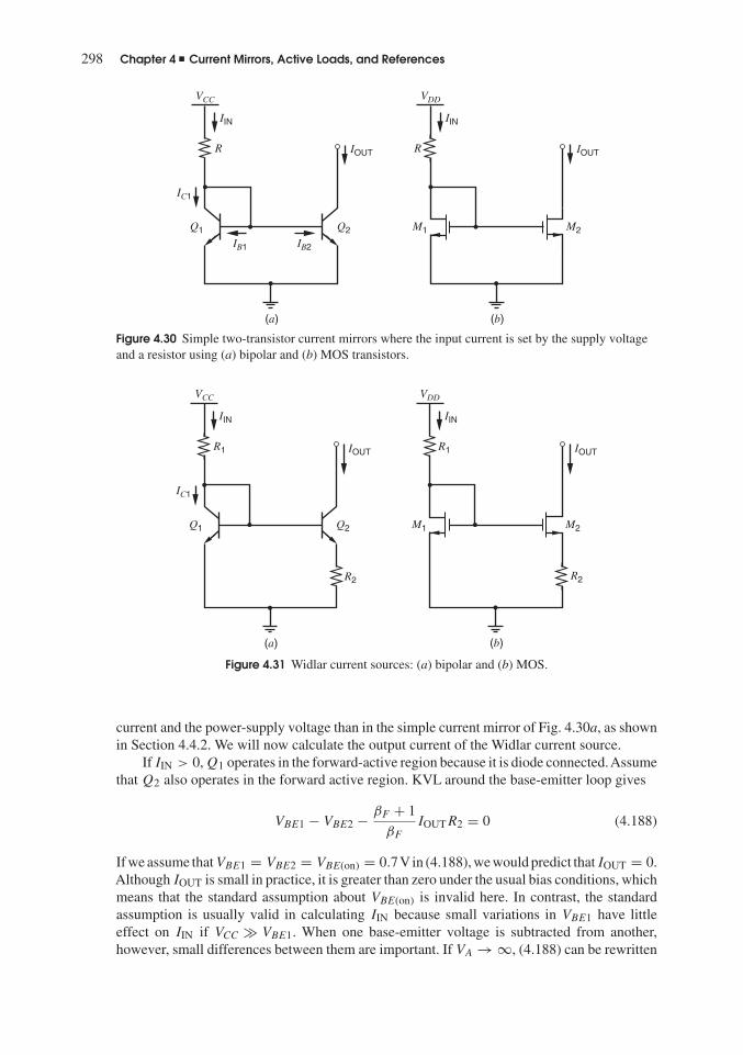
298 Chapter 4 � Current Mirrors, Active Loads, and References
(a)
IB1
IC1
R
IB2
Q2Q1
VCC
IIN
IOUT
(b)
R
M2M1
VDD
IIN
IOUT
Figure 4.30 Simple two-transistor current mirrors where the input current is set by the supply voltageand a resistor using (a) bipolar and (b) MOS transistors.
(a)
IC1
R1 R1
R2R2
Q2Q1
VCC
IIN
IOUT IOUT
(b)
M2M1
VDD
IIN
Figure 4.31 Widlar current sources: (a) bipolar and (b) MOS.
current and the power-supply voltage than in the simple current mirror of Fig. 4.30a, as shownin Section 4.4.2. We will now calculate the output current of the Widlar current source.
If IIN > 0, Q1 operates in the forward-active region because it is diode connected.Assumethat Q2 also operates in the forward active region. KVL around the base-emitter loop gives
VBE1 − VBE2 − βF + 1
βF
IOUTR2 = 0 (4.188)
If we assume thatVBE1 = VBE2 = VBE(on) = 0.7Vin (4.188), we would predict that IOUT = 0.Although IOUT is small in practice, it is greater than zero under the usual bias conditions, whichmeans that the standard assumption about VBE(on) is invalid here. In contrast, the standardassumption is usually valid in calculating IIN because small variations in VBE1 have littleeffect on IIN if VCC � VBE1. When one base-emitter voltage is subtracted from another,however, small differences between them are important. If VA → ∞, (4.188) can be rewritten

4.4 Voltage and Current References 299
using (1.35) as
VT lnIC1
IS1− VT ln
IOUT
IS2− βF + 1
βF
IOUTR2 = 0 (4.189)
If βF → ∞, (4.189) simplifies to
VT lnIIN
IS1− VT ln
IOUT
IS2− IOUTR2 = 0 (4.190)
For identical transistors, IS1 and IS2 are equal, and (4.190) becomes
VT lnIIN
IOUT= IOUTR2 (4.191)
This transcendental equation can be solved by trial and error to find IOUT if R2 and IIN areknown, as in typical analysis problems. Because the logarithm function compresses changes inits argument, attention can be focused on the linear term in (4.191), simplifying convergence ofthe trial-and-error process. In design problems, however, the desired IIN and IOUT are usuallyknown, and (4.191) provides the required value of R2.
EXAMPLE
In the circuit of Fig. 4.31a, determine the proper value of R2 to give IOUT = 5 �A. Assumethat VCC = 5 V, R1 = 4.3 k, VBE(on) = 0.7 V, and βF → ∞.
IIN = 5 V − 0.7 V
4.3 k= 1 mA
VT lnIIN
IOUT= 26 mV ln
(1 mA
5 �A
)= 137 mV
Thus from (4.191)
IOUTR2 = 137 mV
and
R2 = 137 mV
5 �A= 27.4 k
The total resistance in the circuit is 31.7 k.
EXAMPLE
In the circuit of Fig. 4.31a, assume that IIN = 1 mA, R2 = 5 k, and βF → ∞. Find IOUT.From (4.191),
VT ln1 mA
IOUT− 5 k(IOUT) = 0
TryIOUT = 15 �A
108 mV − 75 mV /= 0
The linear term IOUTR2 is too small; therefore, IOUT > 15 �A should be tried. Try
IOUT = 20 �A
101.7 mV − 100 mV � 0

300 Chapter 4 � Current Mirrors, Active Loads, and References
Therefore, the output current is close to 20 �A. Notice that while the linear term increased by25 mV from the first to the second trial, the logarithm term decreased by only about 6 mVbecause the logarithm function compresses changes in its argument.
4.4.1.2 MOS Widlar Current SourceThe Widlar configuration can also be used in MOS technology, as shown in Fig. 4.31b.
If IIN > 0, M1 operates in the active region because it is diode connected. Assume thatM2 also operates in the forward active region. KVL around the gate-source loop gives
VGS1 − VGS2 − IOUTR2 = 0 (4.192)
If we ignore the body effect, the threshold components of the gate-source voltages cancel and(4.192) simplifies to
IOUTR2 + Vov2 − Vov1 = 0 (4.193)
If the transistors operate in strong inversion and VA → ∞,
IOUTR2 +√
2IOUT
k′(W/L)2− Vov1 = 0 (4.194)
This quadratic equation can be solved for√
IOUT.
√IOUT =
−√
2
k′(W/L)2�
√2
k′(W/L)2+ 4R2Vov1
2R2(4.195)
where Vov1 = √2IIN/[k′(W/L)1]. From (1.157),
√IOUT =
√k′(W/L)2
2(VGS2 − Vt) (4.196)
Equation 4.196 applies only when M2 operates in the active region, which means thatVGS2 > Vt . As a result,
√IOUT > 0 and the potential solution where the second term in the
numerator of (4.195) is subtracted from the first, cannot occur in practice. Therefore,
√IOUT =
−√
2
k′(W/L)2+√
2
k′(W/L)2+ 4R2Vov1
2R2(4.197)
Equation 4.197 shows that a closed-form solution for the output current can be written fora Widlar current source that uses MOS transistors operating in strong inversion, unlike thebipolar case where trial and error is required to find IOUT.
EXAMPLE
In Fig. 4.31b, find IOUT if IIN = 100 �A, R2 = 4 k, k′ = 200 �A/V2, and (W/L)1 =(W/L)2 = 25. Assume the temperature is 27◦C and that n = 1.5 in (1.247).Then R2 = 0.004 M, Vov1 = √
200/(200 × 25) V = 0.2 V,
√IOUT =
−√
2
200(25)+√
2
200(25)+ 4(0.004)(0.2)
2(0.004)
√�A = 5
√�A
liberal
高亮
liberal
高亮
对4.194采用求根公式所得

4.4 Voltage and Current References 301
and IOUT = 25 �A. Also,
Vov2 = Vov1 − IOUTR2 = 0.2 − 25 × 0.004 = 0.1 V > 2nVT � 78 mV
Therefore, both transistors operate in strong inversion, as assumed.
4.4.1.3 Bipolar Peaking Current SourceThe Widlar source described in Section 4.4.1.1 allows currents in the microamp range to berealized with moderate values of resistance. Biasing integrated-circuit stages with currents onthe order of nanoamps is often desirable. To reach such low currents with moderate valuesof resistance, the circuit shown in Fig. 4.32 can be used.12,13,14 Neglecting base currents, wehave
VBE1 − IINR = VBE2 (4.198)
If VA → ∞, (4.198) can be rewritten using (1.35) as
VT lnIIN
IS1− VT ln
IOUT
IS2= IINR (4.199)
If Q1 and Q2 are identical, (4.199) can be rewritten as
IOUT = IIN exp
(−IINR
VT
)(4.200)
Equation 4.200 is useful for analysis of a given circuit. For design with identical Q1 and Q2,(4.199) can be rewritten as
R = VT
IINln
IIN
IOUT(4.201)
For example, for IIN = 10 �A and IOUT = 100 nA, (4.201) can be used to show that R �12 k.
A plot of IOUT versus IIN from (4.200) is shown in Fig. 4.33. When the input current issmall, the voltage drop on the resistor is small, and VBE2 � VBE1 so IOUT � IIN. As the inputcurrent increases, VBE1 increases in proportion to the logarithm of the input current whilethe drop on the resistor increases linearly with the input current. As a result, increases in theinput current eventually cause the base-emitter voltage of Q2 to decrease. The output current
VCC
R
IIN
IOUT
Q2Q1
Figure 4.32 Bipolar peaking current source.
liberal
高亮
widlar电流源可以采用阻值适当的电阻实现微安级的电流。·

��� �������� ��������������������������������� !�����"� !�����#� !����$��%��&��'��(��#��)��"������� � " ) # ' & % $ ��(*+,�-./0* 123�-4/0 5�6 �7889:;<=>?:@A;:;@B?:C=BC@=D>BA?ECFDG;:F?;HC<I@J::?<B=DJ:@?KCBALM�NOPQ:?;@A?=;R;SCRJRKA?<TUV�C=R;SCRJRQ9A?<;R?WXYZ[\]̂ _̀ X̀\abc_̀ X̂=B?R=>:DRBAC=E?A;dCD:e;<fBA?GD@;BCD<;<fR;I<CBJf?D>BA?F?;HEDBAf?F?<fD<�Q�7�7g7��hij�k��6� ��i� �9A?F?;HC<Il@J::?<B@D<mIJ:;BCD<@;<;G=DE?J=?fC<nopB?@A<DGDIqe;==ADK<C<rCIQsQ�sQt>utvC==R;GG;<fFD=CBCd?eBA?dDGB;I?f:DFD<�C==R;GG;<fwxDF?:;B?=C<BA?;@BCd?:?ICD<Qy==JR?BA;Bw�;G=DDF?:;B?=C<BA?;@BCd?:?ICD<Qz{|;:DJ<fBA?I;B?l=DJ:@?GDDFICd?=T}~x�utv��T}~�M� �sQ����pC<@?BA?=DJ:@?=D>wx;<fw�;:?@D<<?@B?fBDI?BA?:eBA?BA:?=ADGf=@;<@?G;<f�sQ����=CRFGCm?=BD T���MT��x�utv� �sQ����r:DR�xQx�N�e uo�9M��������� �T�����M��������� �T��x�utv��� �sQ��s���� *+,�� �"*123�
5�6 �78�nopF?;HC<I@J::?<B=DJ:@?Q
liberal
线条

4.4 Voltage and Current References 303
n = 1.5T = 27°CR =10 kΩk' = 200 μA/V2
(W/L)2 = (W/L)1 = 25
Weak inversion
Strong inversion
1500
1250
1000
750
500
250
00 1 2 3 4 5 6 7 8 9 10
I OU
T (
nA)
IIN (μA)
Figure 4.35 Transfercharacteristics of the MOS peakingcurrent source assuming bothtransistors operate in weakinversion or in strong inversion.
where Vov1 = √2IIN/[k′(W/L)1]. Equation 4.204 assumes that the transistors operate in
strong inversion. In practice, the input current is usually small enough that the overdrive of M1is less than 2nVT , where n is defined in (1.247) and VT is a thermal voltage. Equation 4.203shows that the overdrive of M2 is even smaller than that of M1. Therefore, both transistorsusually operate in weak inversion, where the drain current is an exponential function of the gate-source voltage as shown in (1.252). IfVDS1 > 3VT , applying (1.252) toM1 and substituting into(4.202) gives
VGS2 − Vt � nVT ln
(IIN
(W/L)1It
)− IINR (4.205)
Then if the transistors are identical and VDS2 > 3VT , substituting (4.205) into (1.252) gives
IOUT � W
LIt exp
(VGS2 − Vt
nVT
)� IIN exp
(−IINR
nVT
)(4.206)
where It is given by (1.251) and represents the drain current of M2 with VGS2 = Vt , W/L = 1,and VDS � VT . Comparing (4.206) with (4.200) shows that the output current in an MOSpeaking current source where both transistors operate in weak inversion is the same as in thebipolar case except that 1.3 ≤ n ≤ 1.5 in the MOS case and n = 1 in the bipolar case.
Plots of (4.206) and (4.204) are shown in Fig. 4.35 for n = 1.5, T = 27◦C, R = 10 k,k′ = 200 �A/V2, and (W/L)2 = (W/L)1 = 25. In both cases, when the input current is small,the voltage drop on the resistor is small, and IOUT � IIN. As the input current increases, VGS1increases more slowly than the drop on the resistor. As a result, increases in the input currenteventually cause the gate-source voltage of M2 to decrease. The output current reaches amaximum when VGS2 is maximum. As in the bipolar case, the name peaking current sourcestems from this behavior, and the location and magnitude of the peak both depend on R. Becausethe overdrives on both transistors are usually very small, the strong-inversion equation (4.204)usually underestimates the output current.
4.4.2 Supply-Insensitive Biasing
Consider the simple current mirror of Fig. 4.30a, where the input current source has beenreplaced by a resistor. Ignoring the effects of finite βF and VA, (4.5) shows that the output
liberal
高亮
liberal
线条
liberal
线条
liberal
线条
liberal
线条

304 Chapter 4 � Current Mirrors, Active Loads, and References
current is
IOUT � IIN = VCC − VBE(on)
R(4.207)
If VCC � VBE(on), this circuit has the drawback that the output current is proportional to thepower-supply voltage. For example, if VBE(on) = 0.7 V, and if this current mirror is used in anoperational amplifier that has to function with power-supply voltages ranging from 3 V to 10 V,the bias current would vary over a four-to-one range, and the power dissipation would varyover a thirteen-to-one range.
One measure of this aspect of bias-circuit performance is the fractional change in thebias current that results from a given fractional change in supply voltage. The most usefulparameter for describing the variation of the output current with the power-supply voltage isthe sensitivity S. The sensitivity of any circuit variable y to a parameter x is defined as follows:
Syx = lim
�x→0
�y/y
�x/x= x
y
∂y
∂x(4.208)
Applying (4.208) to find the sensitivity of the output current to small variations in the power-supply voltage gives
SIOUTVSUP
= VSUP
IOUT
∂IOUT
∂VSUP(4.209)
The supply voltage VSUP is usually called VCC in bipolar circuits and VDD in MOS circuits. IfVCC � VBE(on) in Fig. 4.30a, and if VDD � VGS1 in Fig. 4.30b,
SIOUTVSUP
� 1 (4.210)
Equation 4.210 shows that the output currents in the simple current mirrors in Fig. 4.30 dependstrongly on the power-supply voltages. Therefore, this configuration should not be used whensupply insensitivity is important.
4.4.2.1 Widlar Current SourcesFor the case of the bipolar Widlar source in Fig. 4.31a, the output current is given implicitlyby (4.191). To determine the sensitivity of IOUT to the power-supply voltage, this equation isdifferentiated with respect to VCC:
VT
∂
∂VCC
lnIIN
IOUT= R2
∂IOUT
∂VCC
(4.211)
Differentiating yields
VT
(IOUT
IIN
)(1
IOUT
∂IIN
∂VCC
− IIN
I2OUT
∂IOUT
∂VCC
)= R2
∂IOUT
∂VCC
(4.212)
Solving this equation for ∂IOUT/∂VCC, we obtain
∂IOUT
∂VCC
=
⎛⎜⎜⎝ 1
1 + IOUTR2
VT
⎞⎟⎟⎠ IOUT
IIN
∂IIN
∂VCC
(4.213)
Substituting (4.213) into (4.209) gives
SIOUTVCC
=
⎛⎜⎜⎝ 1
1 + IOUTR2
VT
⎞⎟⎟⎠ VCC
IIN
∂IIN
∂VCC
=
⎛⎜⎜⎝ 1
1 + IOUTR2
VT
⎞⎟⎟⎠ S
IINVCC
(4.214)
liberal
线条
liberal
线条
liberal
高亮

4.4 Voltage and Current References 305
If VCC � VBE(on), IIN � VCC/R1 and the sensitivity of IIN to VCC is approximately unity, asin the simple current mirror of Fig. 4.30a. For the example in Section 4.4.1.1 where IIN =1 mA, IOUT = 5 �A, and R2 = 27.4 k, (4.214) gives
SIOUTVCC
= VCC
IOUT
∂IOUT
∂VCC
� 1
1 + 137 mV
26 mV
� 0.16 (4.215)
Thus for this case, a 10 percent power-supply voltage change results in only 1.6 percent changein IOUT.
For the case of the MOS Widlar source in Fig. 4.31b, the output current is given by (4.197).Differentiating with respect to VDD gives
1
2√
IOUT
∂IOUT
∂VDD
= 1
4R2
1√2
k′(W/L)2+ 4R2Vov1
4R2∂Vov1
∂VDD
(4.216)
where
∂Vov1
∂VDD
=√
2
k′(W/L)1
1
2√
IIN
∂IIN
∂VDD
= Vov1
2IIN
∂IIN
∂VDD
(4.217)
Substituting (4.216) and (4.217) into (4.209) gives
SIOUTVDD
= Vov1√V 2
ov2 + 4IOUTR2Vov1
SIINVDD
(4.218)
Since IOUT is usually much less than IIN, Vov2 is usually small and IOUTR2 � Vov1 and (4.218)simplifies to
SIOUTVDD
� Vov1√4V 2
ov1
SIINVDD
= 0.5SIINVDD
(4.219)
If VDD � VGS1, IIN � VDD/R1 and the sensitivity of IIN to VDD is approximately unity, as inthe simple current mirror of Fig. 4.30b. Thus for this case, a 10 percent power-supply voltagechange results in a 5 percent change in IOUT.
4.4.2.2 Current Sources Using Other Voltage StandardsThe level of power-supply independence provided by the bipolar and MOS Widlar currentsources is not adequate for many types of analog circuits. Much lower sensitivity can beobtained by causing bias currents in the circuit to depend on a voltage standard other than thesupply voltage. Bias reference circuits can be classified according to the voltage standard bywhich the bias currents are established. The most convenient standards are the base-emitter orthreshold voltage of a transistor, the thermal voltage, or the breakdown voltage of a reverse-biased pn junction (a Zener diode). Each of these standards can be used to reduce supplysensitivity, but the drawback of the first three standards is that the reference voltage is quitetemperature dependent. Both the base-emitter and threshold voltages have negative tempera-ture coefficients of magnitude 1 to 2 mV/◦C, and the thermal voltage has a positive temperaturecoefficient of k/q � 86 �V/◦C. The Zener diode has the disadvantage that at least 7 to 10 Vof supply voltage are required because standard integrated-circuit processes produce a min-imum breakdown voltage of about 6 V across the most highly doped junctions (usually npntransistor emitter-base junctions). Furthermore, pn junctions produce large amounts of voltage

306 Chapter 4 � Current Mirrors, Active Loads, and References
T1
T2
R2
R1
IOUT
IIN
VCC
(a)
T1
T2
R2
R1
IOUT
IIN
VDD
(b)
Figure 4.36 (a) Base-emitter referencedcurrent source. (b) Threshold referencedcurrent source.
noise under the reverse-breakdown conditions encountered in a bias reference circuit. Noisein avalanche breakdown is considered further in Chapter 11.
We now consider bias reference circuits based on the base-emitter or gate-source voltage.The circuit in simplest form in bipolar technology is shown in Fig. 4.36a. This circuit is similarto a Wilson current mirror where the diode-connected transistor is replaced by a resistor. Forthe input current to flow in T1, transistor T2 must supply enough current into R2 so that thebase-emitter voltage of T1 is
VBE1 = VT lnIIN
IS1(4.220)
If we neglect base currents, IOUT is equal to the current flowing through R2. Since the voltagedrop on R2 is VBE1, the output current is proportional to this base-emitter voltage. Thus,neglecting base currents, we have
IOUT = VBE1
R2= VT
R2ln
IIN
IS1(4.221)
Differentiating (4.221) and substituting into (4.209) gives
SIOUTVCC
= VT
IOUTR2S
IINVCC
= VT
VBE(on)S
IINVCC
(4.222)
If VCC � 2VBE(on), IIN � VCC/R1 and the sensitivity of IIN to VCC is approximately unity.With VBE(on) = 0.7 V,
SIOUTVCC
= 0.026 V
0.7 V� 0.037 (4.223)
Thus for this case, a 10 percent power-supply voltage change results in a 0.37 percent changein IOUT. The result is significantly better than for a bipolar Widlar current source.

4.4 Voltage and Current References 307
The MOS counterpart of the base-emitter reference is shown in Fig. 4.36b. Here
IOUT = VGS1
R2= Vt + Vov1
R2=
Vt +√
2IIN
k′(W/L)1
R2(4.224)
The case of primary interest is when the overdrive of T1 is small compared to the thresholdvoltage. This case can be achieved in practice by choosing sufficiently low input current andlarge (W/L)1. In this case, the output current is determined mainly by the threshold voltageand R2. Therefore, this circuit is known as a threshold-referenced bias circuit. Differentiating(4.224) with respect to VDD and substituting into (4.209) gives
SIOUTVDD
= Vov1
2IOUTR2S
IINVDD
= Vov1
2VGS1S
IINVDD
(4.225)
For example, if Vt = 1 V, Vov1 = 0.1 V, and SIINVDD
� 1
SIOUTVDD
� 0.1
2(1.1)� 0.045 (4.226)
These circuits are not fully supply independent because the base-emitter or gate-sourcevoltages of T1 change slightly with power-supply voltage. This change occurs because the col-lector or drain current of T1 is approximately proportional to the supply voltage. The resultingsupply sensitivity is often a problem in bias circuits whose input current is derived from aresistor connected to the supply terminal, since this configuration causes the currents in someportion of the circuit to change with the supply voltage.
4.4.2.3 Self-BiasingPower-supply sensitivity can be greatly reduced by the use of the so-called bootstrap biastechnique, also referred to as self-biasing. Instead of developing the input current by connectinga resistor to the supply, the input current is made to depend directly on the output current of thecurrent source itself. The concept is illustrated in block-diagram form in Fig. 4.37a. Assumingthat the feedback loop formed by this connection has a stable operating point, the currentsflowing in the circuit are much less sensitive to power-supply voltage than in the resistivelybiased case. The two key variables here are the input current, IIN, and the output current, IOUT.The relationship between these variables is governed by both the current source and the current
COMMON
COMMON
(a) (b)
OUT IN
IN OUT
Current mirror
Current source
VSUP
IOUTIIN
IIN
IOUT
Current mirror
IIN = IOUT
Current source
Desired operating point
(Point A)
Undesired operating point
(Point B)
Figure 4.37 (a) Block diagram of a self-biased reference. (b) Determination of operating point.

308 Chapter 4 � Current Mirrors, Active Loads, and References
mirror. From the standpoint of the current source, the output current is almost independent ofthe input current for a wide range of input currents as shown in Fig. 4.37b. From the standpointof the current mirror, IIN is set equal to IOUT, assuming that the gain of the current mirroris unity. The operating point of the circuit must satisfy both constraints and hence is at theintersection of the two characteristics. In the plot of Fig. 4.37b, two intersections or potentialoperating points are shown. Point A is the desired operating point, and point B is an undesiredoperating point because IOUT = IIN = 0.
If the output current in Fig. 4.37a increases for any reason, the current mirror increasesthe input current by the same amount because the gain of the current mirror is assumed to beunity. As a result, the current source increases the output current by an amount that depends onthe gain of the current source. Therefore, the loop responds to an initial change in the outputcurrent by further changing the output current in a direction that reinforces the initial change.In other words, the connection of a current source and a current mirror as shown in Fig. 4.37aforms a positive feedback loop, and the gain around the loop is the gain of the current source.In Chapter 9, we will show that circuits with positive feedback are stable if the gain around theloop is less than unity. At point A, the gain around the loop is quite small because the outputcurrent of the current source is insensitive to changes in the input current around point A. Onthe other hand, at point B, the gain around the feedback loop is deliberately made greater thanunity so that the two characteristics shown in Fig. 4.37b intersect at a point away from theorigin. As a result, this simplified analysis shows that point B is an unstable operating point inprinciple, and the circuit would ideally tend to drive itself out of this state.
In practice, however, point B is frequently a stable operating point because the currents inthe transistors at this point are very small, often in the picoampere range. At such low currentlevels, leakage currents and other effects reduce the current gain of both bipolar and MOStransistors, usually causing the gain around the loop to be less than unity. As a result, actualcircuits of this type are usually unable to drive themselves out of the zero-current state. Thus,unless precautions are taken, the circuit may operate in the zero-current condition. For thesereasons, self-biased circuits often have a stable state in which zero current flows in the circuiteven when the power-supply voltage is nonzero. This situation is analogous to a gasolineengine that is not running even though it has a full tank of fuel. An electrical or mechanicaldevice is required to start the engine. Similarly, a start-up circuit is usually required to preventthe self-biased circuit from remaining in the zero-current state.
The application of this technique to the VBE-referenced current source is illustrated inFig. 4.38a, and the threshold-referenced MOS counterpart is shown in Fig. 4.38b. We assumefor simplicity that VA → ∞. The circuit composed of T1, T2, and R dictates that the currentIOUT depends weakly on IIN, as indicated by (4.221) and (4.224). Second, the current mirrorcomposed of matched transistors T4 and T5 dictates that IIN is equal to IOUT. The operatingpoint of the circuit must satisfy both constraints and hence is at the intersection of the twocharacteristics as in Fig. 4.37b. Except for the effects of finite output resistance of the transistors,the bias currents are independent of supply voltage. If required, the output resistance of thecurrent source and mirror could be increased by the use of cascode or Wilson configurationsin the circuits. The actual bias currents for other circuits are supplied by T6 and/or T3, whichare matched to T5 and T1, respectively.
The zero-current state can be avoided by using a start-up circuit to ensure that somecurrent always flows in the transistors in the reference so that the gain around the feedbackloop at point B in Fig. 4.37b does not fall below unity. An additional requirement is that thestart-up circuit must not interfere with the normal operation of the reference once the desiredoperating point is reached. The VBE-referenced current source with a typical start-up circuitused in bipolar technologies is illustrated in Fig. 4.39a. We first assume that the circuit is inthe undesired zero-current state. If this were true, the base-emitter voltage of T1 would be

4.4 Voltage and Current References 309
IOUT
T6T4
T3
IBIAS1
IBIAS2
T1
T2
R
T5
VCC
IIN
(a)
VDD
T5
T2
R
IIN IOUT
IBIAS2
IBIAS1
T6T4
T3T1
(b)
Figure 4.38 (a) Self-biasing VBE reference. (b) Self-biasing Vt reference.
zero. The base-emitter voltage T2 would be tens of millivolts above ground, determined by theleakage currents in the circuit. However, the voltage on the left-hand end of D1 is four diodedrops above ground, so that a voltage of at least three diode drops would appear across Rx, anda current would flow through Rx into the T1-T2 combination. This action would cause currentto flow in T4 and T5, avoiding the zero-current state.
The bias reference circuit then drives itself toward the desired stable state, and we requirethat the start-up circuit not affect the steady-state current values. This can be accomplishedby causing Rx to be large enough that when the steady-state current is established in T1, thevoltage drop across Rx is large enough to reverse bias D1. In the steady state, the collector-emitter voltage of T1 is two diode drops above ground, and the left-hand end of D1 is fourdiode drops above ground. Thus if we make IINRx equal to two diode drops, D1 will have zerovoltage across it in the steady state. As a result, the start-up circuit composed of Rs, D2–D5,and D1 is, in effect, disconnected from the circuit for steady-state operation.
Floating diodes are not usually available in MOS technologies. The threshold-referencedcurrent source with a typical start-up circuit used in MOS technologies is illustrated inFig. 4.39b. If the circuit is in the undesired zero-current state, the gate-source voltage ofT1 would be less than a threshold voltage. As a result, T7 is off and T8 operates in the trioderegion, pulling the gate-source voltage of T9 up to VDD. Therefore, T9 is on and pulls downon the gates of T4 and T5. This action causes current to flow in T4 and T5, avoiding the zero-current state.
In steady state, the gate-source voltage of T7 rises to IOUTR, which turns on T7 andreduces the gate-source voltage of T9. In other words, T7 and T8 form a CMOS inverterwhose output falls when the reference circuit turns on. Since the start-up circuit should notinterfere with normal operation of the reference in steady state, the inverter output shouldfall low enough to turn T9 off in steady state. Therefore, the gate-source voltage of T9 mustfall below a threshold voltage when the inverter input rises from zero to IOUTR. In practice,

310 Chapter 4 � Current Mirrors, Active Loads, and References
VCC
IIN IOUT
IBIAS2
IBIAS1
D1
D2
Rs
Rx
R
D3
D4
D5
T1 T3
T4 T6
T2
T5
+4 VBE (on)
(a)VDD
IBIAS2
IIN IOUT
IBIAS1
T5T4T8
T7 T1
R
T9
T6
T3
T2
(b)
Figure 4.39 (a) Self-biasing VBE reference with start-up circuit. (b) Self-biasing Vt reference withstart-up circuit.
this requirement is satisfied by choosing the aspect ratio of T7 to be much larger than thatof T8.
Another important aspect of the performance of biasing circuits is their dependence ontemperature. This variation is most conveniently expressed in terms of the fractional changein output current per degree centigrade of temperature variation, which we call the fractionaltemperature coefficient TCF :
TCF = 1
IOUT
∂IOUT
∂T(4.227)

4.4 Voltage and Current References 311
For the VBE-referenced circuit of Fig. 4.38a,
IOUT = VBE1
R(4.228)
∂IOUT
∂T= 1
R
∂VBE1
∂T− VBE1
R2
∂R
∂T(4.229)
= IOUT
(1
VBE1
∂VBE1
∂T− 1
R
∂R
∂T
)(4.230)
Therefore,
TCF = 1
IOUT
∂IOUT
∂T= 1
VBE1
∂VBE1
∂T− 1
R
∂R
∂T(4.231)
Thus the temperature dependence of the output current is related to the difference between theresistor temperature coefficient and that of the base-emitter junction. Since the former has apositive and the latter a negative coefficient, the net TCF is quite large.
EXAMPLE
Design a bias reference as shown in Fig. 4.38a to produce 100 �A output current. Findthe TCF . Assume that for T1, IS = 10−14 A. Assume that ∂VBE/∂T = −2mV/◦C and that(1/R)(∂R/∂T ) = +1500 ppm/◦C.
The current in T1 will be equal to IOUT, so that
VBE1 = VT ln100 �A
10−14 A= 598 mV
Thus from (4.228),
R = 598 mV
0.1 mA= 5.98 k
From (4.231),
TCF � −2 mV/◦C
598 mV− 1.5 × 10⁻³ � −3.3 × 10⁻³ − 1.5 × 10⁻³
and thus
TCF � −4.8 × 10⁻³/◦C = −4800 ppm/◦C
The term ppm is an abbreviation for parts per million and implies a multiplier of 10−6.
For the threshold-referenced circuit of Fig. 4.38b,
IOUT = VGS1
R� Vt
R(4.232)
Differentiating (4.232) and substituting into (4.227) gives
TCF = 1
IOUT
∂IOUT
∂T� 1
Vt
∂Vt
∂T− 1
R
∂R
∂T(4.233)
Since the threshold voltage of an MOS transistor and the base-emitter voltage of a bipolartransistor both change at about −2 mV/◦C, (4.233) and (4.231) show that the temperaturedependence of the threshold-referenced current source in Fig. 4.38b is about the same as theVBE-referenced current source in Fig. 4.38a.
VBE-referenced bias circuits are also used in CMOS technology. An example is shownin Fig. 4.40, where the pnp transistor is the parasitic device inherent in p-substrate CMOS

312 Chapter 4 � Current Mirrors, Active Loads, and References
VDD
IBIAS
R
M3M2
M5 M6
IOUTIIN
M4
Q1
Figure 4.40 Example of aVBE-referenced self-biased circuit inCMOS technology.
technologies.Acorresponding circuit utilizing npn transistors can be used in n-substrate CMOStechnologies. The feedback circuit formed by M2, M3, M4, and M5 forces the current intransistor Q1 to be the same as in resistor R. Assuming matched devices, VGS2 = VGS3 andthus
IOUT = VBE1
R(4.234)
An alternate source for the voltage reference is the thermal voltage VT . The difference injunction potential between two junctions operated at different current densities can be shownto be proportional to VT . This voltage difference must be converted to a current to provide thebias current. For the Widlar source shown in Fig. 4.31a, (4.190) shows that the voltage acrossthe resistor R2 is
IOUTR2 = VT lnIIN
IOUT
IS2
IS1(4.235)
Thus if the ratio of the input to the output current is held constant, the voltage across R2 isindeed proportional to VT . This fact is utilized in the self-biased circuit of Fig. 4.41. Here Q3and Q4 are selected to have equal areas. Therefore, if we assume that βF → ∞ and VA → ∞,the current mirror formed by Q3 and Q4 forces the collector current of Q1 to equal that of Q2.Figure 4.41 also shows that Q2 has two emitters and Q1 has one emitter, which indicates thatthe emitter area of Q2 is twice that of Q1 in this example. This selection is made to force thegain around the positive feedback loop at point B in Fig. 4.37b to be more than unity so thatpoint B is an unstable operating point and a stable nonzero operating point exists at point A.As in other self-biased circuits, a start-up circuit is required to make sure that enough currentflows to force operation at point A in Fig. 4.37b in practice. Under these conditions, IS2 = 2IS1and the voltage across R2 is
IOUTR2 = VT lnIIN
IOUT
IS2
IS1= VT ln 2 (4.236)
Therefore, the output current is
IOUT = VT
R2ln 2 (4.237)

4.4 Voltage and Current References 313
VCC
VX
Q3
Q1
Q4
Q2
R2
IBIAS2
IBIAS1
IIN IOUT
+
–
Figure 4.41 Bias current source using thethermal voltage.
The temperature variation of the output current can be calculated as follows. From (4.237)
∂IOUT
∂T= (ln 2)
R2∂VT
∂T− VT
∂R2
∂T
R22
= VT
R2(ln 2)
(1
VT
∂VT
∂T− 1
R2
∂R2
∂T
)(4.238)
Substituting (4.237) in (4.238) gives
TCF = 1
IOUT
∂IOUT
∂T= 1
VT
∂VT
∂T− 1
R2
∂R2
∂T(4.239)
This circuit produces much smaller temperature coefficient of the output current than the VBE
reference because the fractional sensitivities of both VT and that of a diffused resistor R2 arepositive and tend to cancel in (4.239). We have chosen a transistor area ratio of two to one asan example. In practice, this ratio is often chosen to minimize the total area required for thetransistors and for resistor R2.
EXAMPLE
Design a bias reference of the type shown in Fig. 4.41 to produce an output current of100 �A. Find the TCF of IOUT. Assume the resistor temperature coefficient (1/R)(∂R/∂T ) =+1500 ppm/◦C.
From (4.237)
R2 = VT (ln 2)
IOUT= (26 mV)(ln 2)
100 �A� 180

314 Chapter 4 � Current Mirrors, Active Loads, and References
From (4.239)
1
IOUT
∂IOUT
∂T= 1
VT
∂VT
∂T− 1500 × 10−6 = 1
VT
VT
T− 1500 × 10−6
= 1
T− 1500 × 10−6
Assuming operation at room temperature, T = 300◦K and
1
IOUT
∂IOUT
∂T� 3300 × 10−6 − 1500 × 10−6 = 1800 ppm/◦C
VT -referenced bias circuits are also commonly used in CMOS technology.Asimple exam-ple is shown in Fig. 4.42, where bipolar transistors Q1 and Q2 are parasitic devices inherent inp-substrate CMOS technologies. Here the emitter areas of these transistors differ by a factor n,and the feedback loop forces them to operate at the same bias current. As a result, the differencebetween the two base-emitter voltages must appear across resistor R. The resulting current is
IOUT = VT ln(n)
R(4.240)
In the circuit of Fig. 4.42, small differences in the gate-source voltages of M3 and M4 resultin large variations in the output current because the voltage drop across R is only on the orderof 100 mV. Such gate-source voltage differences can result from device mismatches or fromchannel-length modulation in M3 and M4 because they have different drain-source voltages.Practical implementations of this circuit typically utilize large geometry devices for M3 andM4 to minimize offsets and cascode or Wilson current sources to minimize channel-lengthmodulation effects. A typical example of a practical circuit is shown in Fig. 4.43. In general,cascoding is often used to improve the performance of reference circuits in all technologies.The main limitation of the application of cascoding is that it increases the minimum requiredpower-supply voltage to operate all transistors in the active region.
VDD
M6
M4
R
IIN IOUT
IBIAS
M7M5
M3
Q1 Q2
n1
Figure 4.42 Example of a CMOSVT -referenced self-biased circuit.

4.4 Voltage and Current References 315
VDD
IBIAS
M5 M6 M7
M10 M11
M8 M9
M3
Q1 Q2
n1
M4
R
M12
Figure 4.43 Example of a CMOSVT -referenced self-biased referencecircuit with cascoded devices to improvepower-supply rejection and initialaccuracy.
4.4.3 Temperature-Insensitive Biasing
As illustrated by the examples in Section 4.4.2, the base-emitter-voltage- and thermal-voltage-referenced circuits have rather high temperature coefficients of output current. Although thetemperature sensitivity is reduced considerably in the thermal-voltage circuit, even its temper-ature coefficient is not low enough for many applications. Thus we are led to examine otherpossibilities for the realization of a biasing circuit with low temperature coefficient.
4.4.3.1 Band-Gap-Referenced Bias Circuits in Bipolar TechnologySince the bias sources referenced to VBE(on) and VT have opposite TCF , the possibility existsfor referencing the output current to a composite voltage that is a weighted sum of VBE(on) andVT . By proper weighting, zero temperature coefficient should be attainable.
In the biasing sources described so far, we have concentrated on the problem of obtaininga current with low temperature coefficient. In practice, requirements often arise for low-temperature-coefficient voltage bias or reference voltages. The voltage reference for a voltageregulator is a good example. The design of these two types of circuits is similar except thatin the case of the current source, a temperature coefficient must be intentionally introducedinto the voltage reference to compensate for the temperature coefficient of the resistor thatwill define the current. In the following description of the band-gap reference, we assume forsimplicity that the objective is a voltage source of low temperature coefficient.
First consider the hypothetical circuit of Fig. 4.44. An output voltage is developed that isequal to VBE(on) plus a constant M times VT . To determine the required value for M, we mustdetermine the temperature coefficient of VBE(on). Neglecting base current,
VBE(on) = VT lnI1
IS
(4.241)

316 Chapter 4 � Current Mirrors, Active Loads, and References
VBE(on)
VBE(on)
I1
VCC
+
–
–2 mV/°C
T
T
MVTM
VTVTgenerator
VT
VOUT = VBE(on) + MVT
+3300 ppm/°C = + 0.085 mV/°C
Sum
Figure 4.44 Hypotheticalband-gap reference circuit.
As shown in Chapter 1, the saturation current IS can be related to the device structure by
IS = qAn2i Dn
QB
= Bn2i Dn = B′n2
i Tμn (4.242)
where ni is the intrinsic minority-carrier concentration, QB is the total base doping per unitarea, μn is the average electron mobility in the base, A is the emitter-base junction area,and T is the temperature. Here, the constants B and B′ involve only temperature-independentquantities. The Einstein relation μn = (q/kT )Dn was used to write IS in terms of μn and n2
i .The quantities in (4.242) that are temperature dependent are given by15
μn = CT−n (4.243)
n2i = DT 3 exp
(−VG0
VT
)(4.244)
where VG0 is the band-gap voltage of silicon extrapolated to 0◦K. Here again C and D aretemperature-independent quantities whose exact values are unimportant in the analysis. Theexponent n in the expression for base-region electron mobility μn is dependent on the dopinglevel in the base. Combining (4.241), (4.242), (4.243), and (4.244) yields
VBE(on) = VT ln
(I1T
−γE expVG0
VT
)(4.245)
where E is another temperature-independent constant and
γ = 4 − n (4.246)
In actual band-gap circuits, the current I1 is not constant but varies with temperature. Weassume for the time being that this temperature variation is known and that it can be written

4.4 Voltage and Current References 317
in the form
I1 = GTα (4.247)
where G is another temperature-independent constant. Combining (4.245) and (4.247) gives
VBE(on) = VG0 − VT [(γ − α) ln T − ln(EG)] (4.248)
From Fig. 4.44, the output voltage is
VOUT = VBE(on) + MVT (4.249)
Substitution of (4.248) into (4.249) gives
VOUT = VG0 − VT (γ − α) ln T + VT [M + ln(EG)] (4.250)
This expression gives the output voltage as a function of temperature in terms of the circuitparameters G, α, and M, and the device parameters E and γ . Our objective is to make VOUTindependent of temperature. To this end, we take the derivative of VOUT with respect to tem-perature to find the required values of G, γ , and M to give zero TCF . Differentiating (4.250)gives
0 = dVOUT
dT
∣∣∣∣T=T0
= VT0
T0[M + ln(EG)] − VT0
T0(γ − α) ln T0 − VT0
T0(γ − α) (4.251)
where T0 is the temperature at which the TCF of the output is zero and VT0 is the thermalvoltage VT evaluated at T0. Equation 4.251 can be rearranged to give
[M + ln(EG)] = (γ − α) ln T0 + (γ − α) (4.252)
This equation gives the required values of circuit parameters M, α, and G in terms of thedevice parameters E and γ . In principle, these values could be calculated directly from (4.252).However, further insight is gained by back-substituting (4.252) into (4.250). The result is
VOUT = VG0 + VT (γ − α)
(1 + ln
T0
T
)(4.253)
Thus the temperature dependence of the output voltage is entirely described by the singleparameter T0, which in turn is determined by the constants M, E, and G.
Using (4.253), the output voltage at the zero TCF temperature (T = T0) is given by
VOUT | T = T0= VG0 + VT0(γ − α) (4.254)
For example, to achieve zero TCF at 27◦C, assuming that γ = 3.2 and α = 1,
VOUT | T = T0 = 25◦C = VG0 + 2.2VT0 (4.255)
The band-gap voltage of silicon is VG0 = 1.205 V so that
VOUT | T = T0 = 25◦C = 1.205 V + (2.2)(0.026 V) = 1.262 V (4.256)
Therefore, the output voltage for zero temperature coefficient is close to the band-gap voltageof silicon, which explains the name given to these bias circuits.
Differentiating (4.253) with respect to temperature yields
dVOUT
dT= 1
T
[VT (γ − α)
(1 + ln
T0
T
)]− VT
T(γ − α)
= (γ − α)VT
T
(ln
T0
T
)(4.257)

318 Chapter 4 � Current Mirrors, Active Loads, and References
(a)
(b)
(c)
1.290
1.280
1.250
1.240
1.270
1.260
To = 200°K
To = 300°K
To = 400°K
VOUT (V)
T (°C)
∂VOUT
∂T= 0
∂VOUT
∂T= 0
∂VOUT
∂T= 0
–60 –40 –20 0 20 40 60 100 12080
Figure 4.45 Variation of band-gap reference output voltage with temperature.
Equation 4.257 gives the slope of the output as a function of temperature. A typical familyof output-voltage-variation characteristics is shown in Fig. 4.45 for different values of T0 forthe special case in which α = 0 and I1 is temperature independent. The slope of each curveis zero at T = T0. When T < T0, the slope is positive because the argument of the logarithmin (4.257) is more than unity. Similarly, the slope is negative when T > T0. For values of Tnear T0,
lnT0
T= ln
(1 + T0 − T
T
)� T0 − T
T(4.258)
and we have
dVOUT
dT� (γ − α)
VT
T
(T0 − T
T
)(4.259)
As shown by (4.257) and (4.259), the temperature coefficient of the output is zero only atone temperature T = T0. This result stems from the addition of a weighted thermal voltage toa base-emitter voltage as in Fig. 4.44. Since the temperature coefficient of base-emitter voltageis not exactly constant, the gain M can be chosen to set the temperature coefficient of the outputto zero only at one temperature. In other words, the thermal voltage generator is used to cancelthe linear dependence of the base-emitter voltage with temperature. After this cancellation, thechanging outputs in Fig. 4.45 stem from the nonlinear dependence of the base-emitter voltagewith temperature. Band-gap references that compensate for this nonlinearity are said to becurvature compensated.16,17,18
EXAMPLE
A band-gap reference is designed to give a nominal output voltage of 1.262 V, which gives zeroTCF at 27◦C. Because of component variations, the actual room temperature output voltage is1.280 V. Find the temperature of actual zero TCF of VOUT. Also, write an equation for VOUTas a function of temperature, and calculate the TCF at room temperature. Assume that γ = 3.2and α = 1.

4.4 Voltage and Current References 319
From (4.253) at T = 27◦C = 300◦K ,
1.280 V = 1.205 + (0.026 V)(2.2)
(1 + ln
T0
300◦K
)and thus
T0 = 300◦K
(exp
18 mV
57 mV
)= 411◦K
Therefore, the TCF will be zero at T0 = 411◦K = 138◦C, and we can express VOUT as
VOUT = 1.205 V + 57 mV
(1 + ln
411◦K
T
)From (4.259) with T = 300◦K and T0 = 411◦K,
dVOUT
dT� (2.2)
26 mV
300◦K
(411 − 300
300
)� 70 �V/◦K = 70 �V/◦C
Therefore, the TCF at room temperature is
TCF = 1
VOUT
dVOUT
dT� 70�V/◦C
1.280 V� 55 ppm/◦C
To reduce the TCF , the constant M in (4.249)–(4.252) is often trimmed at one temperatureso that the band-gap output is set to a desired target voltage.19 In principle, the target voltageis given by (4.253). In practice, however, significant inaccuracy in (4.253) stems from anapproximation in (4.244).20 As a result, the target voltage is usually determined experimentallyby measuring the TCF directly for several samples of each band-gap reference in a givenprocess.21,22 This procedure reduces the TCF at the reference temperature to a level of about10 ppm/◦C.
Akey parameter of interest in reference sources is the variation of the output that is encoun-tered over the entire temperature range. Since the TCF expresses the temperature sensitivityonly at one temperature, a different parameter must be used to characterize the behavior of thecircuit over a broad temperature range. An effective temperature coefficient can be defined fora voltage reference as
TCF (eff) = 1
VOUT
(VMAX − VMIN
TMAX − TMIN
)(4.260)
where VMAX and VMIN are the largest and smallest output voltages observed over the tem-perature range, and TMAX − TMIN is the temperature excursion. VOUT is the nominal outputvoltage. By this standard, TCF (eff ) over the −55 to 125◦C range for case (b) of Fig. 4.45 is44 ppm/◦C. If the temperature range is restricted to 0 to 70◦C, TCF (eff ) improves to 17 ppm/◦C.Thus over a restricted temperature range, this reference is comparable with the standard cellin temperature stability once the zero TCF temperature has been set at room temperature.Saturated standard cells (precision batteries) have a TCF of about �30 ppm/◦C.
Practical realizations of band-gap references in bipolar technologies take on severalforms.15,19,23 One such circuit is illustrated in Fig. 4.46a.15 This circuit uses a feedback loopto establish an operating point in the circuit such that the output voltage is equal to a VBE(on)plus a voltage proportional to the difference between two base-emitter voltages. The operationof the feedback loop is best understood by reference to Fig. 4.46b, in which a portion of thecircuit is shown. We first consider the variation of the output voltage V2 as the input voltage V1is varied from zero in the positive direction. Initially, with V1 = 0, devices Q1 and Q2 do not

320 Chapter 4 � Current Mirrors, Active Loads, and References
I
VCC
Q4
Q3
Q2VOUTQ1
R2
R3
V2
V1
R1
–
+
+
––
+
(a)
4
32
1
V2
V1
V1
V2
R1
Q1 Q2
R2
R3
VBE(on)
+
–
(b)
I2 I1R2
R3
Q2 Q1
R1
–
+
(c)
+
VOUT
–Figure 4.46 (a) Widlar band-gapreference. (b) Band-gap subcircuit.(c) Improved band-gap reference.
conduct and V2 = 0. As V1 is increased, Q1 and Q2 do not conduct significant current until theinput voltage reaches about 0.6 V. When V1 < 0.6 V, V2 = V1 since the voltage drop on R2 iszero. When V1 exceeds 0.6 V, however, Q1 begins to conduct current, corresponding to point1 in Fig. 4.46b. The magnitude of the current in Q1 is roughly equal to (V1 − 0.6 V)/R1.
For small values of this current, Q1 and Q2 carry the same current because the drop acrossR3 is negligible at low currents. Since R2 is much larger than R1, the voltage drop across R2is much larger than (V1 − 0.6 V), and transistor Q2 saturates, corresponding to point 2 inFig. 4.46b. Because of the presence of R3, the collector current that would flow in Q2 if it werein the forward-active region has an approximately logarithmic dependence on V1, exactly asin the Widlar source. Thus as V1 is further increased, a point is reached at which Q2 comes outof saturation because V1 increases faster than the voltage drop across R2. This point is labeledpoint 3 in Fig. 4.46b.

4.4 Voltage and Current References 321
Now consider the complete circuit of Fig. 4.46a. If transistor Q3 is initially turned off,transistor Q4 will drive V1 in the positive direction. This process will continue until enoughvoltage is developed at the base of Q3 to produce a collector current in Q3 approximatelyequal to I. Thus the circuit stabilizes with voltage V2 equal to one diode drop, the base-emittervoltage of Q3, which can occur at point 1 or point 4 in Fig. 4.46b. Appropriate start-upcircuitry must be included to ensure operation at point 4 .
Assuming that the circuit has reached a stable operating point at point 4 , the outputvoltage VOUT is the sum of the base-emitter voltage of Q3 and the voltage drop across R2.The drop across R2 is equal to the voltage drop across R3 multiplied by R2/R3 because thecollector current of Q2 is approximately equal to its emitter current. The voltage drop acrossR3 is equal to the difference in base-emitter voltages of Q1 and Q2. The ratio of currents inQ1 and Q2 is set by the ratio of R2 to R1.
A drawback of this reference is that the current I is set by the power supply and may varywith power-supply variations. A self-biased band-gap reference circuit is shown in Fig. 4.46c.Assume that a stable operating point exists for this circuit and that the op amp is ideal. Thenthe differential input voltage of the op amp must be zero and the voltage drops across resistorsR1 and R2 are equal. Thus the ratio of R2 to R1 determines the ratio of I1 to I2. These twocurrents are the collector currents of the two diode-connected transistors Q2 and Q1, assumingbase currents are negligible. The voltage across R3 is
VR3 = �VBE = VBE1 − VBE2 = VT lnI1
I2
IS2
IS1= VT ln
R2
R1
IS2
IS1(4.261)
Since the same current that flows in R3 also flows in R2, the voltage across R2 must be
VR2 = R2
R3VR3 = R2
R3�VBE = R2
R3VT ln
R2
R1
IS2
IS1(4.262)
This equation shows that the voltage across R2 is proportional to absolute temperature (PTAT)because of the temperature dependence of the thermal voltage. Since the op amp forces thevoltages acrossR1 andR2 to be equal, the currents I1 and I2 are both proportional to temperatureif the resistors have zero temperature coefficient. Thus for this reference, α = 1 in (4.247). Theoutput voltage is the sum of the voltage across Q2, R3, and R2:
VOUT = VBE2 + VR3 + VR2 = VBE2 +(
1 + R2
R3
)�VBE
= VBE2 +(
1 + R2
R3
)VT ln
R2
R1
IS2
IS1= VBE2 + MVT (4.263)
The circuit thus behaves as a band-gap reference, with the value of M set by the ratios ofR2/R3, R2/R1, and IS2/IS1.
4.4.3.2 Band-Gap-Referenced Bias Circuits in CMOS TechnologyBand-gap-referenced biasing also can be implemented using the parasitic bipolar devicesinherent in CMOS technology. For example, in a n-well process, substrate pnp transistors canbe used to replace the npn transistors in Fig. 4.46c, as shown in Fig. 4.47. Assume that theCMOS op amp has infinite gain but nonzero input-referred offset voltage VOS . (The input-referred offset voltage of an op amp is defined as the differential input voltage required todrive the output to zero.) Because of the threshold mismatch and the low transconductance percurrent of CMOS transistors, the offset of op amps in CMOS technologies is usually largerthan in bipolar technologies. With the offset voltage, the voltage across R3 is
VR3 = VEB1 − VEB2 + VOS = �VEB + VOS (4.264)

322 Chapter 4 � Current Mirrors, Active Loads, and References
R2 R1 VOS
R3
Q2 Q1
VOUT
+–
++
–
–
Figure 4.47 A band-gapreference in n-well CMOS.
The emitter-base voltages are used here because the base-emitter voltages of the pnp transistorsoperating in the forward-active region are negative. Then the voltage across R2 is
VR2 = R2
R3VR3 = R2
R3(VEB1 − VEB2 + VOS) = R2
R3(�VEB + VOS) (4.265)
and the output voltage is 18
VOUT = VEB2 + VR3 + VR2
= VEB2 +(
1 + R2
R3
)(�VEB + VOS) (4.266)
Since the difference in the base-emitter voltages is proportional to the thermal voltage, compar-ing (4.266) with VOS = 0 to (4.249) shows that the gain M here is proportional to (1 + R2/R3).Rearranging (4.266) gives
VOUT = VEB2 +(
1 + R2
R3
)(�VEB) + VOS(out) (4.267)
where the output-referred offset is
VOS(out) =(
1 + R2
R3
)VOS (4.268)
Equations 4.267 and 4.268 show that the output contains an offset voltage that is a factor of(1 + R2/R3) times bigger than the input-referred offset voltage. Therefore, the same gain thatis applied to the difference in the base-emitter voltages is also applied to the input-referredoffset voltage.
Assume that the offset voltage is independent of temperature. To set TCF of the outputequal to zero, the gain must be changed so that temperature coefficients of the VEB and �VEB
terms cancel. Since the offset is assumed to be temperature independent, this cancellationoccurs when the output is equal to the target, where zero offset was assumed, plus the output-referred offset. If the gain is trimmed at T = T0 to set the output to a target voltage assumingthe offset is zero, (4.267) shows that the gain is too small if the offset voltage is positive andthat the gain is too big if the offset voltage is negative. Since the gain is applied to the PTATterm, the resulting slope of the output versus temperature is negative when the offset is positiveand the gain is too small. On the other hand, this slope is positive when the offset is negativeand the gain is too big.

4.4 Voltage and Current References 323
We will now calculate the magnitude of the slope of the output versus temperature atT = T0. With zero offset and a target that assumes zero offset, trimming R2 and/or R3 to setthe output in (4.267) to the target forces the slope of the �VEB term to cancel the slope ofthe VEB term. With nonzero offset but the same target, the factor (1 + R2/R3) differs fromits ideal value after trimming by −VOS(out)/�VEB. Since this error is multiplied by �VEB in(4.267), the resulting slope of the output versus temperature is
dVOUT
dT
∣∣∣∣T = T0
= −(
VOS(out)
�VEB
)d�VEB
dT(4.269)
Since �VEB is proportional to the thermal voltage VT ,
�VEB = HVT (4.270)
where H is a temperature-independent constant. Substituting (4.270) into (4.269) gives
dVOUT
dT
∣∣∣∣T = T0
= −VOS(out)
HVT
HVT
T
∣∣∣∣T = T0
= −VOS(out)
T0(4.271)
Therefore, when the gain is trimmed at one temperature to set the band-gap output to a desiredtarget voltage, variation in the op-amp offset causes variation in the output temperaturecoefficient. In practice, the op-amp offset is usually the largest source of nonzero temperaturecoefficient.18 Equation 4.271 shows that the temperature coefficient at T = T0 is proportionalto the output-referred offset under these circumstances. Furthermore, (4.268) shows that theoutput-referred offset is equal to the gain that is applied to the �VEB term times the input-referred offset. Therefore, minimizing this gain minimizes the variation in the temperaturecoefficient at the output. Since the reference output at T = T0 for zero TCF is approximatelyequal to the band-gap voltage, the required gain can be minimized by maximizing the �VEB
term.To maximize the �VEB term, designers generally push a large current into a small transistor
and a small current into a large transistor, as shown in Fig. 4.48. Ignoring base currents,
�VEB = VEB1 − VEB2 = VT ln
(I1
I2
IS2
IS1
)(4.272)
Equation 4.272 shows that maximizing the product of the ratios I1/I2 and IS2/IS1 maximizes�VEB. In Fig. 4.48, I1 > I2 is emphasized by drawing the symbol for I1 larger than thesymbol for I2. Similarly, the emitter area of Q2 is larger than that of Q1 to make IS2 > IS1,
I2
Q2 Q1
I1
VDD
– +ΔVEB
Figure 4.48 A circuit that increases �VEB byincreasing I1/I2 and IS2/IS1.

324 Chapter 4 � Current Mirrors, Active Loads, and References
Q4
I2
Q2
Q3
I3 = I1I4 = I2
Q1
I1
VDD
– +ΔVEB
Figure 4.49 A circuit that cascades emitter followers to double �VEB if IS3 = IS1 and IS4 = IS2.
and this relationship is shown by drawing the symbol of Q2 larger than the symbol of Q1.24 Inpractice, these ratios are often each set to be about equal to ten, and the resulting �VEB � 120mV at room temperature. Because the logarithm function compresses its argument, however,a limitation of this approach arises. For example, if the argument is increased by a factorof ten, �VEB increases by only VT ln(10) � 60 mV. Therefore, to double �VEB to 240 mV,(I1/I2)(IS2/IS1) must be increased by a factor of 100 to 10,000. On the other hand, if Q1and the transistors that form I2 are minimum-sized devices when (I1/I2)(IS2/IS1) = 100, therequired die area would be dominated by the biggest devices (Q2 and/or the transistors thatform I1). Therefore, increasing (I1/I2)(IS2/IS1) from 100 to 10,000 would increase the diearea by about a factor of 100 but only double �VEB.
To overcome this limitation, stages that each contribute to �VEB can be cascaded.25 Forexample, consider Fig. 4.49, where two emitter-follower stages are cascaded. Here
�VEB = VEB3 − VEB4 + VEB1 − VEB2 (4.273)
Assume the new devices in Fig. 4.49 are identical to the corresponding original devices in Fig.4.48 so that I3 = I1, I4 = I2, IS3 = IS1, and IS4 = IS2. Then ignoring base currents
�VEB = 2(VEB1 − VEB2) = 2VT ln
(I1
I2
IS2
IS1
)(4.274)
Thus cascading two identical emitter followers doubles �VEB while only doubling the requireddie area.
The effect of the offset in a band-gap reference can also be reduced by using offsetcancellation. An example of offset cancellation in a CMOS band-gap reference with curvaturecorrection in addition to an analysis of other high-order effects arising from finite βF , βF
mismatch, βF variation with temperature, nonzero base resistance, and nonzero temperaturecoefficient in the resistors is presented in Ref. 18.
Ahigh-performance CMOS band-gap reference is shown in Fig. 4.50, where cascoded cur-rent mirrors are used to improve supply rejection. A VT -dependent current from M11 developsa VT -dependent voltage across resistor xR. A proper choice of the ratio x can give a band-gap voltage at VOUT. If desired, a temperature-independent output current can be realized bychoosing x to give an appropriate temperature coefficient to VOUT to cancel the temperaturecoefficient of resistor R2.

Appendix 325
VDD
VOUT
VOUT = VBE + xVT In n
M12 M13 M14
M9 M10
M8 M7
M4
Q1 Q2
n
Q3
R2n1
M5
R
M6
xR
M11
IOUT =
+ +
–
–
VOUT
R2
Figure 4.50 Example of a VBE-referenced self-biased reference circuit in CMOS technology.
APPENDIXA.4.1 MATCHING CONSIDERATIONS IN CURRENT MIRRORS
In many types of circuits, an objective of current-mirror design is generation of two or morecurrent sources whose values are identical. This objective is particularly important in the designof digital-to-analog converters, operational amplifiers, and instrumentation amplifiers. We firstexamine the factors affecting matching in active current mirrors in bipolar technologies andthen in MOS technologies.
A.4.1.1 BIPOLARConsider the bipolar current mirror with two outputs in Fig. 4.51. If the resistors and transistorsare identical and the collector voltages are the same, the collector currents will match precisely.However, mismatch in the transistor parameters αF and IS and in the emitter resistors willcause the currents to be unequal. For Q3,
VT lnIC3
IS3+ IC3
αF3R3 = VB (4.275)
For Q4,
VT lnIC4
IS4+ IC4
αF4R4 = VB (4.276)
Subtraction of these two equations gives
VT lnIC3
IC4− VT ln
IS3
IS4+ IC3
αF3R3 − IC4
αF4R4 = 0 (4.277)

326 Chapter 4 � Current Mirrors, Active Loads, and References
VCC
VB
IINIC4IC3
Q1
R1
Q4
Q2
Q3
R3 R4
_
+
Figure 4.51 Matched bipolar current sources.
We now define average and mismatch parameters as follows:
IC = IC3 + IC4
2(4.278)
�IC = IC3 − IC4 (4.279)
IS = IS3 + IS4
2(4.280)
�IS = IS3 − IS4 (4.281)
R = R3 + R4
2(4.282)
�R = R3 − R4 (4.283)
αF = αF3 + αF4
2(4.284)
�αF = αF3 − αF4 (4.285)
These relations can be inverted to give the original parameters in terms of the average andmismatch parameters. For example,
IC3 = IC + �IC
2(4.286)
IC4 = IC − �IC
2(4.287)
This set of equations for the various parameters is now substituted into (4.277). The result is
VT ln
⎛⎜⎝IC + �IC
2
IC − �IC
2
⎞⎟⎠− VT ln
⎛⎜⎝IS + �IS
2
IS − �IS
2
⎞⎟⎠
+
(IC + �IC
2
)(R + �R
2
)αF + �αF
2
−
(IC − �IC
2
)(R − �R
2
)αF − �αF
2
= 0 (4.288)

Appendix 327
The first term in this equation can be rewritten as
VT ln
⎛⎜⎝IC + �IC
2
IC − �IC
2
⎞⎟⎠ = VT ln
⎛⎜⎜⎝
1 + �IC
2IC
1 − �IC
2IC
⎞⎟⎟⎠ (4.289)
If �IC/2IC � 1, this term can be rewritten as
VT ln
⎛⎜⎜⎝
1 + �IC
2IC
1 − �IC
2IC
⎞⎟⎟⎠ � VT ln
[(1 + �IC
2IC
)(1 + �IC
2IC
)](4.290)
� VT ln
[1 + �IC
IC
+(
�IC
2IC
)2]
(4.291)
� VT ln
(1 + �IC
IC
)(4.292)
where the squared term is neglected. The logarithm function has the infinite series
ln(1 + x) = x − x2
2+ · · · (4.293)
If x � 1,
ln(1 + x) � x (4.294)
To simplify (4.292) when �IC/IC � 1, let x = �IC/IC. Then
VT ln
⎛⎜⎝IC + �IC
2
IC − �IC
2
⎞⎟⎠ � VT
�IC
IC
(4.295)
Applying the same approximations to the other terms in (4.288), we obtain
�IC
IC
�
⎛⎜⎜⎝ 1
1 + gmR
αF
⎞⎟⎟⎠ �IS
IS
+gmR
αF
1 + gmR
αF
(−�R
R+ �αF
αF
)(4.296)
We will consider two important limiting cases. First, since gm = IC/VT , when gmR � 1, thevoltage drop on an emitter resistor is much smaller than the thermal voltage. In this case, thesecond term in (4.296) is small and the mismatch is mainly determined by the transistor IS
mismatch in the first term. Observed mismatches in IS typically range from �10 to �1 percentdepending on geometry. Second, when gmR � 1, the voltage drop on an emitter resistor ismuch larger than the thermal voltage. In this case, the first term in (4.296) is small and themismatch is mainly determined by the resistor mismatch and transistor αF mismatch in thesecond term. Resistor mismatch typically ranges from �2 to �0.1 percent depending ongeometry, and αF matching is in the �0.1 percent range for npn transistors. Thus for npncurrent sources, the use of emitter resistors offers significantly improved current matching. Onthe other hand, for pnp current sources, the αF mismatch is larger due to the lower βF , typicallyaround �1 percent. Therefore, the advantage of emitter degeneration is less significant withpnp than npn current sources.

328 Chapter 4 � Current Mirrors, Active Loads, and References
ID1
M1 M2
ID2
VDD
VGS
Figure 4.52 Matched MOS current sources.
A.4.1.2 MOSMatched current sources are often required in MOS analog integrated circuits. The factorsaffecting this mismatch can be calculated using the circuit of Fig. 4.52. The two transistors M1and M2 will have mismatches in their W/L ratios and threshold voltages. The drain currentsare given by
ID1 = 1
2μnCox
(W
L
)1(VGS − Vt1)2 (4.297)
ID2 = 1
2μnCox
(W
L
)2(VGS − Vt2)2 (4.298)
Defining average and mismatch quantities, we have
ID = ID1 + ID2
2(4.299)
�ID = ID1 − ID2 (4.300)W
L= 1
2
[(W
L
)1+(
W
L
)2
](4.301)
�W
L=(
W
L
)1−(
W
L
)2
(4.302)
Vt = Vt1 + Vt2
2(4.303)
�Vt = Vt1 − Vt2 (4.304)
Substituting these expressions into (4.297) and (4.298) and neglecting high-order terms, weobtain
�ID
ID
=�
W
LW
L
− �Vt
(VGS − Vt)/2(4.305)
The current mismatch consists of two components. The first is geometry dependent and con-tributes a fractional current mismatch that is independent of bias point. The second is dependenton threshold voltage mismatch and increases as the overdrive (VGS − Vt) is reduced. Thischange occurs because as the overdrive is reduced, the fixed threshold mismatch progressivelybecomes a larger fraction of the total gate drive that is applied to the transistors and thereforecontributes a progressively larger percentage error to the current mismatch. In practice, these

Appendix 329
IIN
IOUT1
M1 M2 M3
RS2RS1
IOUT2
VDD
Figure 4.53 Current mirror with twooutputs used to compare voltage- andcurrent-routing techniques.
observations are important because they affect the techniques used to distribute bias signalson integrated circuits.
Consider the current mirror shown in Fig. 4.53, which has one input and two outputs. Atfirst, assume that RS1 = RS2 = 0. Also, assume that the input current is generated by a circuitwith desirable properties. For example, a self-biased band-gap reference might be used to makeIIN insensitive to changes in the power supply and temperature. Finally, assume that each outputcurrent is used to provide the required bias in one analog circuit on the integrated circuit (IC).For example, M2 and M3 could each act as the tail current source of a differential pair.
One way to build the circuit in Fig. 4.53 is to place M1 on the IC near the input currentsource IIN, while M2 and M3 are placed near the circuits that they bias, respectively. Sincethe gate-source voltage of M1 must be routed to M2 and M3 here, this case is referred to as anexample of the voltage routing of bias signals. An advantage of this approach is that by routingonly two nodes (the gate and the source of M1) around the IC, any number of output currentscan be produced. Furthermore the gains from the input to each output of the current mirrorare not affected by the number of outputs in MOS technologies because βF → ∞. (In bipolartechnologies, βF is finite, and the gain error increases as the number of outputs increase, buta beta-helper configuration can be used to reduce such errors as described in Section 4.2.3.)
Unfortunately, voltage routing has two important disadvantages. First, the input and out-put transistors in the current mirror may be separated by distances that are large compared tothe size of the IC, increasing the potential mismatches in (4.305). In particular, the thresholdvoltage typically displays considerable gradient with distance across a wafer. Therefore, whenthe devices are physically separated by large distances, large current mismatch can result frombiasing current sources sharing the same gate-source bias, especially when the overdrive issmall. The second disadvantage of voltage routing is that the output currents are sensitive tovariations in the supply resistances RS1 and RS2. Although these resistances were assumed tobe zero above, they are nonzero in practice because of imperfect conduction in the interconnectlayers and their contacts. Since IOUT2 flows in RS2 and (IOUT1 + IOUT2) flows in RS1, nonzeroresistances cause VGS2 < VGS1 and VGS3 < VGS1 when IOUT1 > 0 and IOUT2 > 0. Therefore,with perfectly matched transistors, the output currents are less than the input current, and theerrors in the output currents can be predicted by an analysis similar to that presented in Section4.4.1 for Widlar current sources. The key point here is that RS1 and RS2 increase as the distancesbetween the input and output transistors increase, increasing the errors in the output currents.As a result of both of these disadvantages, the output currents may have considerable variationfrom one IC to another with voltage routing, increasing the difficulty of designing the circuitsbiased by M2 and M3 to meet the required specifications even if IIN is precisely controlled.
To overcome these problems, the circuit in Fig. 4.53 can be built so that M1–M3 areclose together physically, and the current outputs IOUT1 and IOUT2 are routed as required onthe IC. This case is referred to as an example of the current routing of bias signals. Currentrouting reduces the problems with mismatch and supply resistance by reducing the distances

330 Chapter 4 � Current Mirrors, Active Loads, and References
VDD
VDD
VDD
M4 M5
M6
M8 M9
M10M3M2M1
IIN
M11
M7
IOUT1
IOUT2
Currentrouting
bus
Figure 4.54 Bias-distributioncircuit using both currentrouting and voltage routing.
between the input and output transistors in the current mirror in Fig. 4.53 compared to voltagerouting. One disadvantage of current routing is that it requires one node to be routed for eachbias signal. Therefore, when the number of bias outputs is large, the die area required for theinterconnect to distribute the bias currents can be much larger than that required with voltagerouting. Another disadvantage of current routing is that it can increase the parasitic capacitanceon the drains of M2 and M3. If these nodes are connected to circuits that process high-frequencysignals, increased parasitic capacitance can reduce performance in some ways. For example, ifM2 and M3 act as the tail current sources of differential pairs, increased parasitic capacitancewill increase the common-mode gain and reduce the common-mode rejection ratio of eachdifferential pair at high frequencies.
In practice, many ICs use a combination of current- and voltage-routing techniques. Forexample, Fig. 4.54 shows a circuit with five current mirrors, where the input and output currentsare still referenced as in Fig. 4.53. If the current routing bus in Fig. 4.54 travels over a largedistance, the parasitic capacitances on the drains of M2 and M3 may be large. However, the par-asitic capacitances on the drains of M7 and M11 are minimized by using voltage routing withineach current mirror. Although simple current mirrors are shown in Fig. 4.54, cascoding is oftenused in practice to reduce gain errors stemming from a finite Early voltage. In ICs using bothcurrent and voltage routing, currents are routed globally and voltages locally, where the differ-ence between global and local routing depends on distance. When the distance is large enoughto significantly worsen mismatch or supply-resistance effects, the routing is global. Otherwise,it is local. An effective combination of these bias distribution techniques is to divide an IC intoblocks, where bias currents are routed between blocks and bias voltages within the blocks.
A.4.2 INPUT OFFSET VOLTAGE OF DIFFERENTIAL PAIR WITH ACTIVE LOAD
A.4.2.1 BIPOLARFor the resistively loaded emitter-coupled pair, we showed in Chapter 3 that the input offsetvoltage arises primarily from mismatches in IS in the input transistors and from mismatches inthe collector load resistors. In the active-load case, the input offset voltage results from nonzero

Appendix 331
base current of the load devices and mismatches in the input transistors and load devices. Referto Fig. 4.25a. Assume the inputs are grounded. If the matching is perfect and if βF → ∞ inT3 and T4,
VOUT = VCC − |VBE3| (4.306)
Equation 4.306 holds because only this output voltage forces VCE3 = VCE4, where IC1 = IC2and VBE1 = VBE2, which is required by KVL when VI1 = VI2.
The differential input required to drive the output to the value given by (4.306) is the input-referred offset voltage. With finite βF in the active-load transistors and/or device mismatch,the offset is usually nonzero. In the active-load, KVL shows that
VBE3 = VBE4 (4.307)
Solving (1.58) for VBE3 and VBE4 and substituting in (4.307) gives
IC3
IS3
⎛⎜⎜⎝ 1
1 + VCE3
VA3
⎞⎟⎟⎠ = IC4
IS4
⎛⎜⎜⎝ 1
1 + VCE4
VA4
⎞⎟⎟⎠ (4.308)
Assume that the Early voltages of T3 and T4 are identical. Since VCE3 = VCE4 when (4.306)is satisfied, (4.308) can be simplified to
IC4 = IC3
(IS4
IS3
)(4.309)
Since IC2 = −IC4, (4.309) can be written as
IC2 = −IC3
(IS4
IS3
)(4.310)
From KCL at the collector of T3,
IC1 = −IC3
[1 +(
2
βF
)](4.311)
where βF is the ratio of the collector to base current in the active-load devices. From KVL inthe input loop,
VID = VI1 − VI2 = VBE1 − VBE2 (4.312)
Then the input offset voltage, VOS , is the value of VID for which the output voltage is givenby (4.306). If the Early voltages of T1 and T2 are identical, solving (1.58) for VBE1 and VBE2and substituting into (4.312) gives
VOS = VID = VT ln
(IC1
IC2
IS2
IS1
)(4.313)
because VCE1 = VCE2 when (4.306) is satisfied. Substituting (4.310) and (4.311) in (4.313)gives
VOS = VT ln
[IS3
IS4
IS2
IS1
(1 + 2
βF
)](4.314)
If the mismatches are small, this expression can be approximated as
VOS � VT
(�ISP
ISP
− �ISN
ISN
+ 2
βF
)(4.315)

332 Chapter 4 � Current Mirrors, Active Loads, and References
using the technique described in Section 3.5.6.3, where
�ISP = IS3 − IS4 (4.316)
ISP = IS3 + IS4
2(4.317)
�ISN = IS1 − IS2 (4.318)
ISN = IS1 + IS2
2(4.319)
In the derivation of (4.315), we assumed that the Early voltages of matched transistors areidentical. In practice, mismatch in Early voltages also contributes to the offset, but the effectis usually negligible when the transistors are biased with collector-emitter voltages much lessthan their Early voltages.
Assuming a worst-case value for �IS/IS of �5 percent and a pnp beta of 20, the worst-caseoffset voltage is
VOS � VT (0.05 + 0.05 + 0.1) = 0.2VT � 5 mV (4.320)
To find the worst-case offset, we have added the mismatch terms for the pnp and npn transistorsin (4.320) instead of subtracting them as shown in in (4.315) because the mismatch terms arerandom and independent of each other in practice. Therefore, the polarity of the mismatch termsis unknown in general. Comparing (4.320) to (3.219) shows that the actively loaded differentialpair has significantly higher offset than the resistively loaded case under similar conditions.The offset arising here from mismatch in the load devices can be reduced by inserting resistorsin series with the emitters of T3 and T4 as shown in Section A.4.1. To reduce the offset arisingfrom finite βF in the load devices, the current mirror in the load can use a beta helper transistoras described in Section 4.2.3.
A.4.2.2 MOSThe offset in the CMOS differential pair with active load shown in Fig. 4.25b is similar to thebipolar case. If the matching is perfect with the inputs grounded,
VOUT = VDD − |VGS3| (4.321)
Equation 4.321 holds because only this output voltage forces VDS3 = VDS4, where I1 = I2and VGS1 = VGS2, which is required by KVL when VI1 = VI2.
The differential input required to drive the output to the value given by (4.321) is theinput-referred offset voltage. With device mismatch, the offset is usually nonzero.
VID = VGS1 − VGS2 = Vt1 + Vov1 − Vt2 − Vov2 (4.322)
Assume that the Early voltages of T1 and T2 are identical. Since VDS1 = VDS2 = VDSN whenVID = VOS , applying (1.165) to Vov1 and Vov2 in (4.322) gives
VOS = Vt1 − Vt2 +√
1
1 + λNVDSN
(√2I1
k′(W/L)1−√
2I2
k′(W/L)2
)(4.323)
If the mismatches are small, this expression can be approximated as
VOS � Vt1 − Vt2 + VovN
2
(�IN
IN
− �(W/L)N(W/L)N
)(4.324)
using the technique described in Section 3.5.6.7, where
VovN =√
2IN
k′(W/L)N (1 + λNVDSN )(4.325)

Appendix 333
�IN = I1 − I2 (4.326)
IN = I1 + I2
2(4.327)
�(W/L)N = (W/L)1 − (W/L)2 (4.328)
(W/L)N = (W/L)1 + (W/L)2
2(4.329)
Since I1 = −I3 and I2 = −I4
�IN
IN
= �IP
IP
(4.330)
where
�IP = I3 − I4 (4.331)
IP = I3 + I4
2(4.332)
To find �IP/IP , we will use KVL in the gate-source loop in the load as follows
0 = VGS3 − VGS4 = Vt3 + Vov3 − Vt4 − Vov4 (4.333)
Since T3 and T4 are p-channel transistors, their overdrives are negative. Assume that the Earlyvoltages of T3 and T4 are identical. Since VDS3 = VDS4 = VDSP when VID = VOS (4.333) canbe rewritten as
0 = Vt3 − Vt4 −√
1
1 + |λPVDSP |
(√2|I3|
k′(W/L)3−√
2|I4|k′(W/L)4
)(4.334)
In (4.334), absolute value functions have been used so that the arguments of the square-rootfunctions are positive. If the mismatches are small, this expression can be approximated as
�IP
IP
� Vt3 − Vt4
|VovP |2
+ �(W/L)P(W/L)P
(4.335)
using the technique described in Section 3.5.6.7, where
|VovP | =√
2|IP |k′(W/L)P (1 + |λPVDSP |) (4.336)
�(W/L)P = (W/L)3 − (W/L)4 (4.337)
(W/L)P = (W/L)3 + (W/L)4
2(4.338)
Substituting (4.335) and (4.330) into (4.324) gives
VOS � Vt1 − Vt2 + VovN
2
⎛⎜⎝Vt3 − Vt4
|VovP |2
+ �(W/L)P(W/L)P
− �(W/L)N(W/L)N
⎞⎟⎠ (4.339)

334 Chapter 4 � Current Mirrors, Active Loads, and References
Comparing (4.339) to (4.315) shows that the MOS differential pair with active load includesterms to account for threshold mismatch but excludes a term to account for finite beta in theactive load because βF → ∞ in MOS transistors.
EXAMPLE
Find the input-referred offset voltage of the circuit in Fig. 4.25b using the transistor parametersin the table below.
Transistor Vt (V ) W (�m) L (�m) k′ (�A/V2)
T1 0.705 49 1 100T2 0.695 51 1 100T3 -0.698 103 1 50T4 -0.702 97 1 50
Assume that ITAIL = 200 �A and that λNVDSN � 1 and |λPVDSP | � 1. From (4.327) andKCL,
IN = I1 + I2
2= ITAIL
2= 100 �A (4.340)
Substituting (4.340) and (4.329) into (4.325) gives
VovN �√
200
100(49 + 51)/2V = 0.2 V (4.341)
Similarly, from (4.332) and KCL
IP = I3 + I4
2= −ITAIL
2= −100 �A (4.342)
Substituting (4.342) and (4.338) into (4.336) gives
|VovP | �√
200
50(103 + 97)/2V = 0.2 V (4.343)
Substituting (4.337) and (4.328) into (4.339) gives
VOS � 0.705 V − 0.695 V
+ 0.1
(−0.698 + 0.702
0.1+ 103 − 97
(103 + 97)/2− 49 − 51
(49 + 51)/2
)V
� 0.01 V + 0.1(0.04 + 0.06 + 0.04) V = 0.024 V (4.344)
In this example, the mismatches have been chosen so that the individual contributions to theoffset add constructively to give the worst-case offset.
PROBLEMSFor the bipolar transistors in these problems, use thehigh-voltage device parameters given in Fig. 2.30 andFig. 2.35, unless otherwise specified. Assume thatrb = 0 and rμ → ∞ in all problems. Assume all bipo-lar transistors operate in the forward-active region,and neglect base currents in bias calculations unlessotherwise specified.
4.1 Determine the output current and output resis-tance of the bipolar current mirror shown in Fig. 4.55.Find the output current if VOUT = 1 V, 5 V, and 30 V.Ignore the effects of nonzero base currents. Compareyour answer with a SPICE simulation.
4.2 Repeat Problem 4.1 including the effects ofnonzero base currents.

Problems 335
IOUT
VOUT
Q5Q4Q3Q2
VCC = 15 V
R = 10 kΩ
Q1
+
–
Figure 4.55 Circuit for Problem 4.1.
4.3 Design a simple MOS current mirror of thetype shown in Fig. 4.4 to meet the following con-straints:
(a) Transistor M2 must operate in the active regionfor values of VOUT to within 0.2 V of ground.
(b) The output current must be 50 �A.
(c) The output current must change less than 1percent for a change in output voltage of 1 V.
Make M1 and M2 identical. You are to mini-mize the total device area within the given constraints.Here the device area will be taken to be the total gatearea (W × L product). Assume Xd = 0 and take otherdevice data from Table 2.4.
4.4 Calculate an analytical expression for thesmall-signal output resistance Ro of the bipolar cas-code current mirror of Fig. 4.8. Assume that the inputcurrent source is not ideal and that the nonideal-ity is modeled by placing a resistor R1 in parallelwith IIN. Show that for large R1, the output resis-tance approaches β0ro/2. Calculate the value of Ro ifVCC = 5 V, IIN = 0, and R1 = 10 k, and estimate thevalue of VOUT below which Ro will begin to decreasesubstantially. Use SPICE to check your calculationsand also to investigate the βF sensitivity by varyingβF by −50 percent and examining IOUT. Use SPICEto plot the large-signal IOUT-VOUT characteristic.
4.5 Calculate the output resistance of the circuit ofFig. 4.9, assuming that IIN = 100 �A and the deviceshave drawn dimensions of 100 �m/1 �m. Use the pro-cess parameters given in Table 2.4, and assume forall devices that Xd = 0. Also, ignore the body effectfor simplicity. Compare your answer with a SPICEsimulation and also use SPICE to plot the IOUT-VOUT
characteristic for VOUT from 0 to 3 V.
4.6 Using the data given in the example of Sec-tion 1.9, include the effects of substrate leakage in the
calculation of the output resistance for the circuit ofProblem 4.5. Let VOUT = 2 V and 3 V.
4.7 Design the circuit of Fig. 4.11b to satisfy theconstraints in Problem 4.3 except the output resistanceobjective is that the output current change less than0.02 percent for a 1 V change in the output voltage.Ignore the body effect for simplicity. Make all devicesidentical except for M4. Use SPICE to check yourdesign and also to plot the IOUT-VOUT characteristicfor VOUT from 0 to 3 V.
4.8 For the circuit of Fig. 4.56, assume that(W/L)8 = (W/L). Ignoring the body effect, find(W/L)6 and (W/L)7 so that VDS6 = VDS7 = Vov8.Draw the schematic of a double-cascode current mirrorthat uses the circuit of Fig. 4.56 to bias both cascodedevices in the output branch. For this current mirror,calculate the output resistance, the minimum outputvoltage for which all three transistors in the outputbranch operate in the active region, the total voltageacross all the devices in the input branch, and thesystematic gain error.
VDD
IIN
M8
M7
M6
Figure 4.56 Circuit forProblem 4.8.
4.9 Calculate the output resistance of the Wilsoncurrent mirror shown in Fig. 4.57. What is the per-centage change in IOUT for a 5-V change in VOUT?Compare your answer with a SPICE simulation using afull device model. Use SPICE to check the βF sensitiv-ity by varying βF by −50 percent and examining IOUT.Also, use SPICE to plot the large-signal IOUT-VOUT
characteristic for VOUT from 0 to 15 V.
4.10 Calculate the small-signal voltage gain ofthe common-source amplifier with active load in Fig.4.16b. Assume that VDD = 3 V and that all the transis-tors operate in the active region. Do the calculationsfor values of IREF of 1 mA, 100 �A, 10 �A, and 1 �A.

336 Chapter 4 � Current Mirrors, Active Loads, and References
Q3
Q2
Q1
IOUT
VOUT
13.7 kΩ
+15 V
–
+
Figure 4.57Circuit forProblem 4.9.
Assume that the drawn dimensions of each transistorare W = 100 �m and L = 1 �m. Assume Xd = 0 anduse Table 2.4 for other parameters.
(a) At first, assume the transistors operate in stronginversion in all cases.
(b) Repeat part (a) including the effects of weakinversion by using (1.253) with n = 1.5 to calculatethe transconductance of M1. Assume that a transistoroperates in weak inversion when its overdrive is lessthan 2nVT , as given in (1.255).
(c) Use SPICE to check your calculations for bothparts (a) and (b).
4.11 Calculate the small-signal voltage gain of acommon-source amplifier with depletion load in Fig.4.20, including both the body effect and channel-length modulation. Assume that VDD = 3 V and thatthe dc input voltage is adjusted so that the dc outputvoltage is 1 V. Assume that M1 has drawn dimen-sions of W = 100 �m and L = 1 �m. Also, assumethat M2 has drawn dimensions of W = 10 �m andL = 1 �m. For M2, assume Vt0 = −1V. For both tran-sistors, assume that Xd = 0. Use Table 2.4 for otherparameters of both transistors.
4.12 Determine the unloaded voltage gain vo/vi
and output resistance for the circuit of Fig. 4.58. Checkwith SPICE and also use SPICE to plot out the large-signal VO-VI transfer characteristic for VSUP = 2.5 V.Use SPICE to determine the CMRR if the current-source output resistance is 1 M.
4.13 Repeat Problem 4.12, but now assuming that2-k resistors are inserted in series with the emittersof Q3 and Q4.
4.14 Repeat Problem 4.12 except replace Q1 andQ2 with n-channel MOS transistors M1 and M2. Also,replace Q3 and Q4 with p-channel MOS transistorsM3 and M4. Assume Wn = 50 �m and Wp = 100 �m.
+VSUP
–VSUP
Vi = VI + vi
Vo = VO + vo
Q4Q3
Q1 Q2
+
–
+
–
100 μA
Figure 4.58 Circuit for Problem 4.12.
For all transistors, assume Ldrwn = 1 �m and Xd = 0.Use Table 2.3 for other parameters.
4.15 Repeat Problem 4.14, but now assuming that2 k resistors are inserted in series with the sourcesof M3 and M4. Ignore the body effect.
4.16 Determine the unloaded voltage gain vo/vi
and output resistance for the circuit of Fig. 4.59.Neglect rμ. Verify with SPICE and also use SPICEto plot the large-signal VO-VI transfer characteristicfor VSUP = 2.5 V.
+VSUP
–VSUP
ITAIL
Vi = VI + vi
Q8Q7
Q6Q5
Q4Q3
Q1 Q2
+
–
Vo = VO + vo
+
+
–1.3 V
–
Figure 4.59 Cascode active-load circuit for Prob-lem 4.16.
4.17 Repeat Problem 4.16 except replace the npnand pnp transistors with n-channel and p-channel MOStransistors, respectively. Assume Wn = 50 �m andWp = 100 �m. For all transistors, assume Ldrwn =1 �m and Xd = 0. Let ITAIL = 100 �A. Ignore
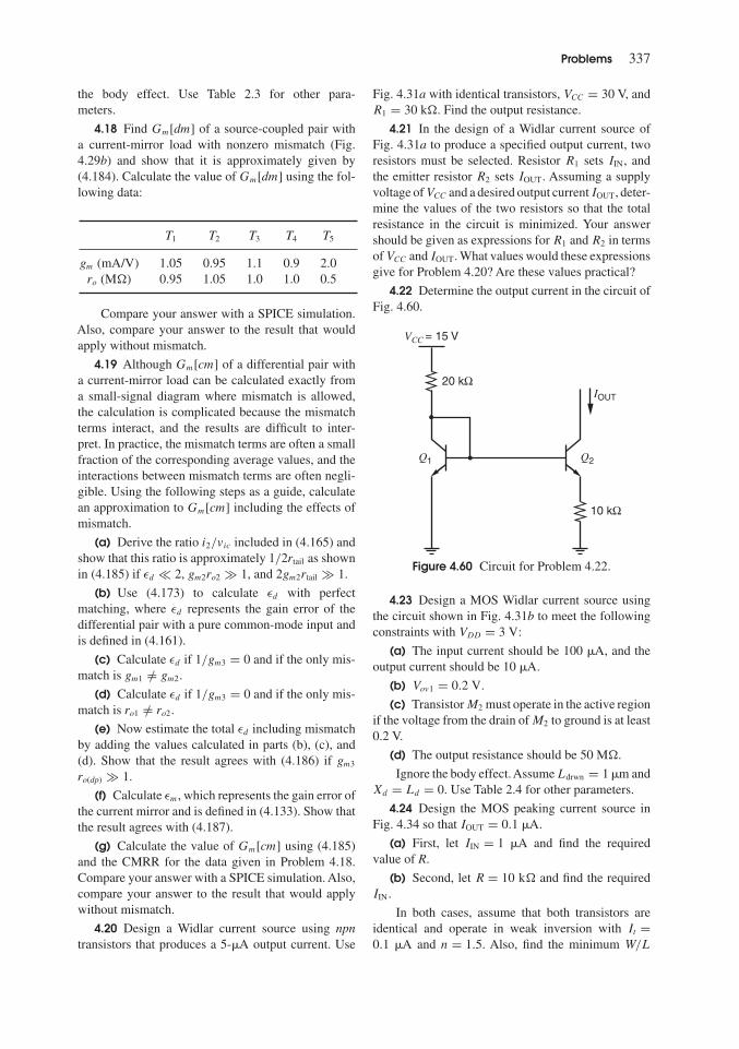
Problems 337
the body effect. Use Table 2.3 for other para-meters.
4.18 Find Gm[dm] of a source-coupled pair witha current-mirror load with nonzero mismatch (Fig.4.29b) and show that it is approximately given by(4.184). Calculate the value of Gm[dm] using the fol-lowing data:
T1 T2 T3 T4 T5
gm (mA/V) 1.05 0.95 1.1 0.9 2.0ro (M) 0.95 1.05 1.0 1.0 0.5
Compare your answer with a SPICE simulation.Also, compare your answer to the result that wouldapply without mismatch.
4.19 Although Gm[cm] of a differential pair witha current-mirror load can be calculated exactly froma small-signal diagram where mismatch is allowed,the calculation is complicated because the mismatchterms interact, and the results are difficult to inter-pret. In practice, the mismatch terms are often a smallfraction of the corresponding average values, and theinteractions between mismatch terms are often negli-gible. Using the following steps as a guide, calculatean approximation to Gm[cm] including the effects ofmismatch.
(a) Derive the ratio i2/vic included in (4.165) andshow that this ratio is approximately 1/2rtail as shownin (4.185) if εd � 2, gm2ro2 � 1, and 2gm2rtail � 1.
(b) Use (4.173) to calculate εd with perfectmatching, where εd represents the gain error of thedifferential pair with a pure common-mode input andis defined in (4.161).
(c) Calculate εd if 1/gm3 = 0 and if the only mis-match is gm1 /= gm2.
(d) Calculate εd if 1/gm3 = 0 and if the only mis-match is ro1 /= ro2.
(e) Now estimate the total εd including mismatchby adding the values calculated in parts (b), (c), and(d). Show that the result agrees with (4.186) if gm3
ro(dp) � 1.
(f) Calculate εm, which represents the gain error ofthe current mirror and is defined in (4.133). Show thatthe result agrees with (4.187).
(g) Calculate the value of Gm[cm] using (4.185)and the CMRR for the data given in Problem 4.18.Compare your answer with a SPICE simulation. Also,compare your answer to the result that would applywithout mismatch.
4.20 Design a Widlar current source using npntransistors that produces a 5-�A output current. Use
Fig. 4.31a with identical transistors, VCC = 30 V, andR1 = 30 k. Find the output resistance.
4.21 In the design of a Widlar current source ofFig. 4.31a to produce a specified output current, tworesistors must be selected. Resistor R1 sets IIN, andthe emitter resistor R2 sets IOUT. Assuming a supplyvoltage of VCC and a desired output current IOUT, deter-mine the values of the two resistors so that the totalresistance in the circuit is minimized. Your answershould be given as expressions for R1 and R2 in termsof VCC and IOUT. What values would these expressionsgive for Problem 4.20? Are these values practical?
4.22 Determine the output current in the circuit ofFig. 4.60.
IOUT
VCC = 15 V
Q1 Q2
20 kΩ
10 kΩ
Figure 4.60 Circuit for Problem 4.22.
4.23 Design a MOS Widlar current source usingthe circuit shown in Fig. 4.31b to meet the followingconstraints with VDD = 3 V:
(a) The input current should be 100 �A, and theoutput current should be 10 �A.
(b) Vov1 = 0.2 V.
(c) Transistor M2 must operate in the active regionif the voltage from the drain of M2 to ground is at least0.2 V.
(d) The output resistance should be 50 M.
Ignore the body effect.Assume Ldrwn = 1 �m andXd = Ld = 0. Use Table 2.4 for other parameters.
4.24 Design the MOS peaking current source inFig. 4.34 so that IOUT = 0.1 �A.
(a) First, let IIN = 1 �A and find the requiredvalue of R.
(b) Second, let R = 10 k and find the requiredIIN.
In both cases, assume that both transistors areidentical and operate in weak inversion with It =0.1 �A and n = 1.5. Also, find the minimum W/L

338 Chapter 4 � Current Mirrors, Active Loads, and References
in both cases, assuming that VGS − Vt < 0 is requiredto operate a transistor in weak inversion as shown inFig. 1.45.
4.25 Determine the output current and outputresistance of the circuit shown in Fig. 4.61.
IOUT
+ 15 V
Q2
Q1
Q3
13.7 kΩ
700 Ω
Figure 4.61 Circuit for Problem 4.25.
4.26 Determine the value of sensitivity S of outputcurrent to supply voltage for the circuit of Fig. 4.62,where S = (VCC/IOUT)(∂IOUT/∂VCC).
IOUT
VCC = 15 V
Q1
R1
R2
Q2
10 kΩ
1 kΩ
Figure 4.62 Circuit for Problem 4.26.
4.27 In the analysis of the hypothetical referenceof Fig. 4.44, the current I1 was assumed proportionalto temperature. Assume instead that this current isderived from a diffused resistor, and thus has a TCF
of −1500 ppm/◦C. Determine the new value of VOUT
required to achieve zero TCF at 25◦C. Neglect basecurrent.
4.28 The circuit of Fig. 4.46c is to be used as aband-gap reference. If the op amp is ideal, its dif-ferential input voltage and current are both zero and
VOUT= (VBE1 + I1R1) = (VBE1 + I2R2)
VOUT= VBE1 + R2
(VBE1 − VBE2
R3
)Assume that I1 is to be made equal to 200 �A, and that(VBE1 − VBE2) is to be made equal to 100 mV. Deter-mine R1, R2, and R3 to realize zero TCF of VOUT at25◦C. Neglect base currents.
4.29 A band-gap reference like that of Fig. 4.47 isdesigned to have nominally zero TCF at 25◦C. Dueto process variations, the saturation current IS of thetransistors is actually twice the nominal value.AssumeVOS = 0. What is dVOUT/dT at 25◦C? Neglect basecurrents.
4.30 Simulate the band-gap reference from Prob-lem 4.29 on SPICE. Assume that the amplifier isjust a voltage-controlled voltage source with an open-loop gain of 10,000 and that the resistor values areindependent of temperature. Also assume that IS1 =1.25 × 10⁻¹⁷ A and IS2 = 1 × 10⁻¹⁶ A. In SPICE,adjust the closed-loop gain of the amplifier (by choos-ing suitable resistor values) so that the output TCF
is zero at 25◦C. What is the resulting target value ofVOUT? Now double IS1 and IS2. Use SPICE to adjustthe gain so that VOUT is equal to the target at 25◦C. Findthe new dVOUT/dT at 25◦C with SPICE. Compare thisresult with the calculations from Problem 4.29.
4.31 Repeat Problem 4.29 assuming that the val-ues of IS , R2, and R1 are nominal but that R3 is 1percent low. Assume VBE(on) = 0.6 V.
4.32 A band-gap reference circuit is shown in Fig.4.63. Assume that βF → ∞, VA → ∞, IS1 = 1 ×10⁻¹⁵ A, and IS2 = 8 × 10⁻¹⁵ A.Assume the op amp isideal except for a possibly nonzero offset voltage VOS ,which is modeled by a voltage source in Fig. 4.63.
Q1 Q2
R2VOS
VOUT
R11 kΩ
R31 kΩ
+
+
+
––
–
Figure 4.63 Band-gap reference circuit forProblem 4.32.

Problems 339
(a) Suppose that R2 is trimmed to set VOUT equalto the target voltage for which dVOUT/dT = 0 at T =25◦C when VOS = 0. Find dVOUT/dT at T = 25◦Cwhen VOS = 30 mV.
(b) Under the conditions in part (a), is dVOUT/dT
positive or negative? Explain.
4.33 For the circuit of Fig. 4.64, find the value ofW/L for which dVGS/dT = 0 at 25◦C.Assume that thethreshold voltage falls 2 mV for each 1◦C increase intemperature. Also, assume that the mobility temper-ature dependence is given by (4.243) with n = 1.5.Finally, use Table 2.4 for other parameters at 25◦C,and let I = 200 �A.
I
VGS
VDD
+
–
Figure 4.64 Circuit for Problem 4.33.
4.34 Calculate the bias current of the circuit shownin Fig. 4.65 as a function of R, μnCox, (W/L)1, and(W/L)2. Comment on the temperature behavior of thebias current. For simplicity, assume that Xd = Ld = 0and ignore the body effect. Assume M4 is identicalto M3.
VDD
IBIAS
M3 M4
M2M1WL
R
1
WL 2
WL 1
>
Figure 4.65 Circuit for Problem 4.34.
4.35 The circuit of Fig. 4.65 produces a supply-insensitive current. Calculate the ratio of small-signal
variations in IBIAS to small-signal variations in VDD
at low frequencies. Ignore the body effect but includefinite transistor ro in this calculation.
4.36 For the bias circuit shown in Fig. 4.66, deter-mine the bias current. Assume that Xd = Ld = 0.Neglect base currents and the body effect. Commenton the temperature dependence of the bias current.Assume a channel mobility and oxide thickness fromTable 2.4. Compare your calculations to a SPICE sim-ulation using a full circuit model from Table 2.4, andalso use SPICE to determine the supply-voltage sen-sitivity of IBIAS.
+3V
IBIAS
M3 M4
M2M1
Q2 Q1
1001
501
50
10×1×
Bipolartransistors
1
501
Figure 4.66 Circuit for Problem 4.36.
4.37 A pair of bipolar current sources is to bedesigned to produce output currents that match with�1 percent. If resistors display a worst-case mismatchof �0.5 percent, and transistors a worst-case VBE mis-match of 2 mV, how much voltage must be droppedacross the emitter resistors?
4.38 Determine the worst-case input offset volt-age for the circuit of Fig. 4.58. Assume the worst-caseIS mismatches in the transistors are �5 percent andβF = 15 for the pnp transistors. Assume the dc outputvoltage is VSUP − |VBE(on)|.
4.39 Repeat Problem 4.38, but assume that 2-k
resistors are placed in series with the emitters of Q3
and Q4. Assume the worst-case resistor mismatch is�0.5 percent and the worst-case pnp βF mismatch is�10 percent.
4.40 Repeat Problem 4.38 but replace the bipo-lar transistors with MOS transistors as in Problem4.14. Assume the worst-case W/L mismatches in
340 Chapter 4 � Current Mirrors, Active Loads, and References
the transistors are �5 percent and the worst-caseVt mismatches are �10 mV. Assume the dc out-put voltage to ground is VSUP − |VGS3|. Also, assume
that (W/L)1 + (W/L)2 =20 and (W/L)3 + (W/L)4 =60. Use Table 2.4 to calculate the transconductanceparameters.
REFERENCES1. Y. P. Tsividis. Operation and Modeling of
the MOS Transistor, McGraw Hill, New York, 1987,p. 139.
2. J.-B. Shyu, G. C. Temes, and F.Krummenacher. “Random Error Effects in MatchedMOS Capacitors and Current Sources,” IEEE Jour-nal of Solid-State Circuits, Vol. SC-19, pp. 948–955,December 1984.
3. K. R. Lakshmikumar, R. A. Hadaway, andM. A. Copeland. “Characterisation and Modeling ofMismatch in MOS Transistors for Precision AnalogDesign,” IEEE Journal of Solid-State Circuits, Vol.SC-21, pp. 1057–1066, December 1986.
4. M. J. M. Pelgrom, A. C. J. Duinmaijer, and A.P. G. Welbers. “Matching Properties of MOS Transis-tors,” IEEE Journal of Solid-State Circuits, Vol. 24,pp. 1433–1440, October 1989.
5. W.-J. Hsu, B. J. Sheu, and S. M. Gowda.“Design of Reliable VLSI Circuits Using SimulationTechniques,” IEEE Journal of Solid-State Circuits,Vol. 26, pp. 452–457, March 1991.
6. T. C. Choi, R. T. Kaneshiro, R. W. Brodersen,P. R. Gray, W. B. Jett, and M. Wilcox. “High-Frequency CMOS Switched-Capacitor Filters forCommunications Application,” IEEE Journal ofSolid-State Circuits, Vol. SC-18, pp. 652–664,December 1983.
7. N. S. Sooch. “MOS Cascode Current Mirror,”U.S. Patent 4,550,284, October 1985.
8. G. R. Wilson. “A Monolithic Junction FET—n-p-n Operational Amplifier,” IEEE Journal of Solid-State Circuits, Vol. SC-3, pp. 341–348, December1968.
9. D. Fullagar. “A New-Performance MonolithicOperational Amplifier,” Fairchild SemiconductorApplications Brief. May 1968.
10. R. J. Widlar. “Some Circuit Design Tech-niques for Linear Integrated Circuits,” IEEE Trans-actions on Circuit Theory, Vol. CT-12, pp. 586–590,December 1965.
11. R. J. Widlar. “Design Techniques for Mono-lithic Operational Amplifiers,” IEEE Journal of
Solid-State Circuits, Vol. SC-4, pp. 184–191, August1969.
12. M. Nagata. “Constant Current Circuits,”Japanese Patent 628,228, May 6, 1971.
13. T. M. Frederiksen. “Constant Current Source,”U.S. Patent 3,659,121, April 25, 1972.
14. C. Y. Kwok. “Low-Voltage Peaking Com-plementary Current Generator,” IEEE Journal ofSolid-State Circuits, Vol. SC-20, pp. 816–818, June1985.
15. R. J. Widlar. “New Developments in IC Volt-age Regulators,” IEEE Journal of Solid-State Circuits,Vol. SC-6, pp. 2–7, February 1971.
16. C. R. Palmer and R. C. Dobkin. “A CurvatureCorrected Micropower Voltage Reference,” Interna-tional Solid-State Circuits Conference, pp. 58–59,February 1981.
17. G. C. M. Meijer, P. C. Schmale, and K. vanZalinge. “A New Curvature-Corrected Bandgap Ref-erence,” IEEE Journal of Solid-State Circuits, Vol.SC-17, pp. 1139–1143, December 1982.
18. B.-S. Song and P. R. Gray. “A PrecisionCurvature-Compensated CMOS Bandgap Refer-ence,” IEEE Journal of Solid-State Circuits, Vol.SC-18, pp. 634–643, December 1983.
19. A. P. Brokaw. “A Simple Three-Terminal ICBandgap Reference,” IEEE Journal of Solid-State Cir-cuits, Vol. SC-9, pp. 388–393, December 1974.
20. Y. P. Tsividis. “Accurate Analysis of Tem-perature Effects in IC − VBE Characteristics withApplication to Bandgap Reference Sources,” IEEEJournal of Solid-State Circuits, Vol. SC-15, pp.1076–1084, December 1980.
21. A. P. Brokaw. Private Communication.22. R. A. Pease. Private Communication.23. K. E. Kuijk. “A Precision Reference Voltage
Source,” IEEE Journal of Solid-State Circuits, Vol.SC-8, pp. 222–226, June 1973.
24. T. R. Viswanathan. Private Communication.25. E. A. Vittoz and O. Neyroud. “A Low-Voltage
CMOS Bandgap Reference,” IEEE Journal of Solid-State Circuits, Vol. SC-14, pp. 573–577, June 1979.

CHAPTER 5
Output Stages
5.1 IntroductionThe output stage of an amplifier must satisfy a number of special requirements. One of themost important requirements is to deliver a specified amount of signal power to a load withacceptably low levels of signal distortion. Another common objective of output-stage designis to minimize the output impedance so that the voltage gain is relatively unaffected by thevalue of load impedance. A well-designed output stage should achieve these performancespecifications while consuming low quiescent power and, in addition, should not be a majorlimitation on the frequency response of the amplifier.
In this chapter, several output-stage configurations will be considered to satisfy the aboverequirements. The simplest output-stage configurations are the emitter and source follow-ers. More complex output stages employing multiple output devices are also treated, andcomparisons are made of power-output capability and efficiency.
Because of their excellent current-handling capability, bipolar transistors are the preferreddevices for use in output stages. Although parasitic bipolar transistors can be used in someCMOS output stages, output stages in CMOS technologies are usually constructed withoutbipolar transistors and are also described in this chapter.
5.2 The Emitter Follower as an Output StageAn emitter-follower output stage is shown in Fig. 5.1. To simplify the analysis, positive andnegative bias supplies of equal magnitude VCC are assumed, although these supplies may havedifferent values in practice. When output voltage Vo is zero, output current Io is also zero. Theemitter-follower output device Q1 is biased to a quiescent current IQ by current source Q2.The output stage is driven by voltage Vi, which has a quiescent dc value of Vbe1 for Vo = 0 V.The bias components R1, R3, and Q3 can be those used to bias other stages in the circuit. Sincethe quiescent current IQ in Q2 will usually be larger than the reference current IR, resistor R2is usually smaller than R1 to accommodate this difference.
This circuit topology can also be implemented in CMOS technologies using an MOScurrent source for bias and the parasitic bipolar-transistor emitter follower available in standardCMOS processes. Because any large current flow to the substrate can initiate the pnpn latch-upphenomenon described in Chapter 2, however, this configuration should be used carefully inCMOS technologies with lightly doped substrates. Extensive substrate taps in the vicinity ofthe emitter follower are essential to collect the substrate current flow.
5.2.1 Transfer Characteristics of the Emitter-Follower
The circuit of Fig. 5.1 must handle large signal amplitudes; that is, the current and voltageswings resulting from the presence of signals may be a large fraction of the bias values. As
341

342 Chapter 5 � Output Stages
+VCC
–VCC
Q1
Q2
Q3
R2R1
R3
Io
Vo
Vi
IQ
IR
RL
+
+
–
–
Figure 5.1 Emitter-follower output stage with current-mirror bias.
a result, the small-signal analyses that have been used extensively up to this point must beused with care in this situation. For this reason, we first determine the dc transfer characteristicof the emitter follower. This characteristic allows calculation of the gain of the circuit andalso gives important information on the linearity and thus on the distortion performance ofthe stage.
Consider the circuit of Fig. 5.1. The large-signal transfer characteristic can be derived asfollows:
Vi = Vbe1 + Vo (5.1)
In this case, the base-emitter voltage Vbe1 of Q1 cannot be assumed constant but must beexpressed in terms of the collector current Ic1 of Q1 and the saturation current IS . If the loadresistance RL is small compared with the output resistance of the transistors,
Vbe1 = kT
qln
(Ic1
IS
)(5.2)
if Q1 is in the forward-active region. Also
Ic1 = IQ + Vo
RL
(5.3)
if Q2 is in the forward-active region and βF is assumed large. Substitution of (5.3) and (5.2)in (5.1) gives
Vi = kT
qln
⎛⎜⎜⎝IQ + Vo
RL
IS
⎞⎟⎟⎠+ Vo (5.4)
Equation 5.4 is a nonlinear equation relating Vo and Vi if both Q1 and Q2 are in the forward-active region.
The transfer characteristic from (5.4) has been plotted in Fig. 5.2. First, consider the casewhere RL is large, which is labeled RL1. In this case, the first term on the right-hand side of(5.4), which represents the base-emitter voltage Vbe1 of Q1, is almost constant as Vo changes.This result stems from the observation that the current in the load is small for a large RL;

5.2 The Emitter Follower as an Output Stage 343
Vo
RL2
RL1
Q2 saturated
(VCC – VCE1(sat) + Vbe1)
–VCC + VCE2(sat)
–IQRL2
[–VCC + VCE1(sat) + Vbe1]
VCC – VCE1(sat)
ViVBE1
Q1 saturated
Q1 cutoff
Figure 5.2 Transfer characteristic of the circuit of Fig. 5.1 for a low (RL2) and a high (RL1) value ofload resistance.
therefore, the current in Q1 and Vbe1 are both almost constant as Vo changes in this case. As aresult, the center part of the transfer characteristic for RL = RL1 is nearly a straight line withunity slope that is offset on the Vi axis by VBE1, the quiescent value of Vbe1. This near-linearregion depends on both Q1 and Q2 being in the forward-active region. However, as Vi ismade large positive or negative, one of these devices saturates and the transfer characteristicabruptly changes slope.
Consider Vi made large and positive. Output voltage Vo follows Vi until Vo = VCC −VCE1(sat) at which point Q1 saturates. The collector-base junction of Q1 is then forward biasedand large currents flow from base to collector. In practice, the transistor base resistance (andany source resistance present) limit the current in the forward-biased collector-base junctionand prevent the voltage at the internal transistor base from rising appreciably higher. Furtherincreases in Vi thus produce little change in Vo and the characteristic flattens out, as shownin Fig. 5.2. The value of Vi required to cause this behavior is slightly larger than the supplyvoltage because Vbe1 is larger than the saturation voltage VCE(sat). Consequently, the precedingstage often limits the maximum positive output voltage in a practical circuit because a voltagelarger than VCC usually cannot be generated at the base of the output stage. (The portion ofthe curve for Vi large positive where Q1 is saturated actually has a positive slope if the effectof the collector series resistance rc of Q1 is included. In any event, this portion of the transfercharacteristic must be avoided, because the saturation of Q1 results in large nonlinearity anda major reduction of power gain.)
Now consider Vi made large and negative. The output voltage follows the input untilVo = −VCC + VCE2(sat), at which point Q2 saturates. (The voltage drop across R2 is assumedsmall and is neglected. It could be lumped in with the saturation voltage VCE2(sat) of Q2 ifnecessary.) When Q2 saturates, another discontinuity in the transfer curve occurs, and the slopeabruptly decreases. For acceptable distortion performance in the circuit, the voltage swing mustbe limited to the region between these two break points. As mentioned above, the driver stagesupplying Vi usually cannot produce values of Vi that have a magnitude exceeding VCC (if itis connected to the same supply voltages) and the driver itself then sets the upper limit.
Next consider the case where RL in Fig. 5.1 has a relatively small value. Then when Vo
is made large and negative, the first term in (5.4) can become large. In particular, this term

344 Chapter 5 � Output Stages
2
1
2
1
V2
V2
V1
V1
–V1
–V1
–IQRL2
t
t
–V2(a)
(b)
ac in
put v
olta
geac
out
put v
olta
ge
Waveform clipping
Figure 5.3 (a) ac input signalsapplied to the circuit of Fig. 5.1.(b) ac output waveformscorresponding to the inputs in(a) with RL = RL2.
approaches minus infinity when Vo approaches the critical value
Vo = −IQRL (5.5)
In this situation, the current drawn from the load (−Vo/RL) is equal to the current IQ, anddevice Q1 cuts off, leaving Q2 to draw the current IQ from the load. Further decreases in Vi
produce no change in Vo, and the transfer characteristic is the one labeled RL2 in Fig. 5.2. Thetransfer characteristic for positive Vi is similar for both cases.
For the case RL = RL2, the stage will produce severe waveform distortion if Vi is asinusoid with amplitude exceeding IQRL2. Consider the two sinusoidal waveforms in Fig. 5.3a.Waveform 1 has an amplitude V1 < IQRL2 and waveform 2 has an amplitude V2 > IQRL2.If these signals are applied as inputs at Vi in Fig. 5.1 (together with a bias voltage), the outputwaveforms that result are as shown in Fig. 5.3b for RL = RL2. For the smaller input signal, thecircuit acts as a near-linear amplifier and the output is near sinusoidal. The output waveformdistortion, which is apparent for the larger input, is termed “clipping” and must be avoided innormal operation of the circuit as a linear output stage. For a given IQ and RL, the onset ofclipping limits the maximum signal that can be handled. Note that if IQRL is larger than VCC,the situation shown for RL = RL1 in Fig. 5.2 holds, and the output voltage can swing almostto the positive and negative supply voltages before excessive distortion occurs.
5.2.2 Power Output and Efficiency
Further insight into the operation of the circuit of Fig. 5.1 can be obtained from Fig. 5.4 wherethree different load lines are drawn on the Ic − Vce characteristics of Q1. The equation for the

5.2 The Emitter Follower as an Output Stage 345
A
C
B
Q
VCC
VCC + IQRL2
RL = RL1
RL = RL3
RL = RL2
Ic1
PL max for RL2
PL max for RL3
Vce1
Iom for RL = RL1PL max for RL1
IQ
[2VCC – VCE2(sat)]
VCE1(sat)
Maximum possiblevalue of Vce1
Curves ofconstant Vbe1
‹
Figure 5.4 Load lines in the Ic1 − Vce1 plane for emitter follower Q1 of Fig. 5.1.
load lines can be written from Fig. 5.1 and is
Vce1 = VCC − (Ic1 − IQ)RL (5.6)
when both Q1 and Q2 are in the forward-active region. The values of Vce1 and Ic1 are relatedby (5.6) for any value of Vi and the line includes the quiescent point Q, where Ic1 = IQ andVce1 = VCC. Equation 5.6 is plotted in Fig. 5.4 for load resistances RL1, RL2, and RL3 and thedevice operating point moves up and down these lines as Vi varies. As Vi increases and Vce1decreases, Q1 eventually saturates, as was illustrated in Fig. 5.2. As Vi decreases and Vce1increases, there are two possibilities as described above. If RL is large (RL1), Vo decreasesand Vce1 increases until Q2 saturates. Thus the maximum possible value that Vce1 can attainis [2VCC − VCE2(sat)] and this value is marked on Fig. 5.4. However, if RL is small (RL2), themaximum negative value of Vo as illustrated in Fig. 5.2 is −IQRL2 and the maximum possiblevalue of Vce1 is (VCC + IQRL2).
Thus far no mention has been made of the maximum voltage limitations of the outputstage. As described in Chapter 1, avalanche breakdown of a bipolar transistor occurs forVce = BVCEO in the common-emitter configuration, which is the worst case for breakdownvoltage. In a conservative design, the value of Vce in the circuit of Fig. 5.1 should always beless than BVCEO by an appropriate safety margin. In the preceding analysis, the maximumvalue that Vce1 can attain in this circuit for any load resistance was calculated as approximately2VCC, and thus BVCEO must be greater than this value.
Consider now the power relationships in the circuit. When sinusoidal signals are present,the power dissipated in various elements varies with time. We are concerned both with theinstantaneous power dissipated and with the average power dissipated. Instantaneous power

346 Chapter 5 � Output Stages
is important when considering transistor dissipation with low-frequency or dc signals. Thejunction temperature of the transistor will tend to rise and fall with the instantaneous powerdissipated in the device, limiting the maximum allowable instantaneous power dissipation forsafe operation of any device.
Average power levels are important because the power delivered to a load is usuallyspecified as an average value. Also note that if an output stage handles only high-frequencysignals, the transistor junction temperature will not vary appreciably over a cycle and theaverage device power dissipation will then be the limiting quantity.
Consider the output signal power that can be delivered to load RL when a sinusoidalinput is applied at Vi. Assuming that Vo is approximately sinusoidal, the average output powerdelivered to RL is
PL = 1
2V̂oÎo (5.7)
where V̂o and Îo are the amplitudes (zero to peak) of the output sinusoidal voltage and current.As described previously, the maximum output signal amplitude that can be attained beforeclipping occurs depends on the value of RL. If PL|max is the maximum value of PL that canbe attained before clipping occurs with sinusoidal signals, then
PL|max = 1
2V̂omÎom (5.7a)
where V̂om and Îom are the maximum values of V̂o and Îo that can be attained before clipping.Consider the case of the large load resistance, RL1. Figures 5.2 and 5.4 show that clipping
occurs symmetrically in this case, and we have
V̂om = VCC − VCE(sat) (5.8)
assuming equal saturation voltages in Q1 and Q2. The corresponding sinusoidal output currentamplitude is Îom = V̂om/RL1. The maximum average power that can be delivered to RL1is calculated by substituting these values in (5.7a). This value of power can be interpretedgeometrically as the area of the triangle A in Fig. 5.4 since the base of the triangle equalsV̂om and its height is Îom. As RL1 is increased, the maximum average output power that canbe delivered diminishes because the triangle becomes smaller. The maximum output voltageamplitude remains essentially the same but the current amplitude decreases as RL1 increases.
If RL = RL2 in Fig. 5.4, the maximum output voltage swing before clipping occurs is
V̂om = IQRL2 (5.9)
The corresponding current amplitude is Îom = IQ. Using (5.7a), the maximum average outputpower PL|max that can be delivered is given by the area of triangle B, shown in Fig. 5.4. AsRL2 is decreased, the maximum average power that can be delivered is diminished.
An examination of Fig. 5.4 shows that the power-output capability of the stage is maxi-mized for RL = RL3, which can be calculated from (5.6) and Fig. 5.4 as
RL3 = VCC − VCE(sat)
IQ
(5.10)
This load line gives the triangle of largest area (C) and thus the largest average output power.In this case, V̂om = [VCC − VCE(sat)] and Îom = IQ. Using (5.7a), we have
PL|max = 1
2V̂omÎom = 1
2[VCC − VCE(sat)]IQ (5.11)
To calculate the efficiency of the circuit, the power drawn from the supply voltages mustnow be calculated. The current drawn from the positive supply is the collector current of Q1,

5.2 The Emitter Follower as an Output Stage 347
which is assumed sinusoidal with an average value IQ. The current flowing in the negativesupply is constant and equal to IQ (neglecting bias current IR). Since the supply voltagesare constant, the average power drawn from the supplies is constant and independent of thepresence of sinusoidal signals in the circuit. The total power drawn from the two supplies is thus
Psupply = 2VCCIQ (5.12)
The power conversion efficiency (ηC) of the circuit at an arbitrary output power level isdefined as the ratio of the average power delivered to the load to the average power drawnfrom the supplies.
ηC = PL
Psupply(5.13)
Since the power drawn from the supplies is constant in this circuit, the efficiency increasesas the output power increases. Also, since the previous analysis shows that the power-outputcapability of the circuit depends on the value of RL, the efficiency also depends on RL. Thebest efficiency occurs for RL = RL3 since this value gives maximum average power output.If RL = RL3 and V̂o = V̂om, then substitution of (5.11) and (5.12) in (5.13) gives for themaximum possible efficiency
ηmax = 1
4
(1 − VCE(sat)
VCC
)(5.14)
Thus if VCE(sat) � VCC, the maximum efficiency of the stage is 1/4 or 25 percent.Another important aspect of circuit performance is the power dissipated in the active
device. The current and voltage waveforms in Q1 at maximum signal swing and with RL = RL3are shown in Fig. 5.5 (assuming VCE(sat) � 0 for simplicity) together with their product, which
VCC
Vce1
Ic1
Vom
2VCC
‹
Iom
IQ
2IQ
‹
Quiescent voltage
Quiescent current
Quiescent power
t
t
t
(a)
(b)
(c)
IQVCC
Pc1
= I
c1V
ce1 Figure 5.5 Waveforms for the
transistor Q1 of Figure 5.1at full output with RL = RL3.(a) Collector-emitter voltagewaveform. (b) Collector currentwaveform. (c) Collector powerdissipation waveform.

348 Chapter 5 � Output Stages
is the instantaneous power dissipation in the transistor. The curve of instantaneous powerdissipation in Q1 as a function of time varies at twice the signal frequency and has an averagevalue of one-half the quiescent value. This result can be shown analytically as follows. Theinstantaneous power dissipation in Q1 is
Pc1 = Vce1Ic1 (5.15)
At maximum signal swing with a sinusoidal signal, Pc1 can be expressed as (from Fig. 5.5)
Pc1 = VCC(1 + sin ωt)IQ(1 − sin ωt) = VCCIQ
2(1 + cos 2ωt) (5.15a)
The average value of Pc1 from (5.15a) is VCCIQ/2. Thus at maximum output the averagepower dissipated in Q1 is half its quiescent value, and the average device temperature whendelivering power with RL = RL3 is less than its quiescent value.
Further information on the power dissipated in Q1 can be obtained by plotting curves ofconstant device dissipation in the Ic − Vce plane. Equation 5.15 indicates that such curves arehyperbolas, which are plotted in Fig. 5.6 for constant transistor instantaneous power dissipationvalues P1, P2, and P3 (where P1 < P2 < P3). The power hyperbola of value P2 passes throughthe quiescent point Q, and the equation of this curve can be calculated from (5.15) as
Ic1 = P2
Vce1(5.16)
The slope of the curve is
dIc1
dVce1= − P2
V 2ce1
RL = 0
RL = RL3
RL → ∞IQ
VCC Vce1
P1
P2
P3 = Ic1Vce1
[2VCC – VCE2(sat)]
Q
High transistorpower dissipation
Low transistorpower dissipation
Ic1
Figure 5.6 Hyperbolas of constant instantaneous transistor power dissipation P1, P2, and P3 in theIc1 − Vce1 plane for emitter follower Q1 of Fig. 5.1. Load lines are included for RL = 0, RL = RL3, andRL → ∞. Note that P1 < P2 < P3.

5.2 The Emitter Follower as an Output Stage 349
and substitution of (5.16) in this equation gives
dIc1
dVce1= − Ic1
Vce1(5.17)
At the quiescent point Q, we have Ic1 = IQ and Vce1 = VCC. Thus the slope is
dIc1
dVce1
∣∣∣∣Q
= − IQ
VCC
(5.18)
From (5.6), the slope of the load line with RL = RL3 is −(1/RL3). Using (5.10) for RL3 gives
− 1
RL3� − IQ
VCC
(5.19)
Comparing (5.18) with (5.19) shows that the load line with RL = RL3 is tangent to the powerhyperbola passing through the quiescent point, since both curves have the same slope at thatpoint. This result is illustrated in Fig. 5.6. As the operating point leaves the quiescent point andmoves on the load line with RL = RL3, the load line then intersects constant-power hyper-bolas representing lower power values; therefore, the instantaneous device power dissipationdecreases. This point of view is consistent with the power waveform shown in Fig. 5.5.
The load line for RL → ∞ (open-circuit load) is also shown in Fig. 5.6. In that case,the transistor collector current does not vary over a period but is constant. For values of Vce1greater than the quiescent value, the instantaneous device power dissipation increases. Themaximum possible value of Vce1 is (2VCC − VCE2(sat)). At this value, the instantaneous powerdissipation in Q1 is approximately 2VCCIQ if VCE2(sat) � VCC. This dissipation is twice thequiescent value of VCCIQ, and this possibility should be taken into account when consideringthe power-handling requirements of Q1. At the other extreme of the swing where Vce1 � 0,the power dissipation in Q2 is also 2VCCIQ.
A situation that is potentially even more damaging can occur if the load is short circuited.In that case, the load line is vertical through the quiescent point, as shown in Fig. 5.6. Withlarge input signals, the collector current (and thus the device power dissipation) of Q1 canbecome quite large. The limit on collector current is set by the ability of the driver to supplythe base current to Q1, and also by the high-current fall-off in βF of Q1, described in Chapter 1.In practice, these limits may be sufficient to prevent burnout ofQ1, but current-limiting circuitrymay be necessary. An example of such protection is given in Section 5.4.6.
A useful general result can be derived from the calculations above involving load lines andconstant-power hyperbolas. Figure 5.6 shows that the maximum instantaneous device powerdissipation for RL = RL3 occurs at the quiescent point Q (since P1 < P2 < P3), which is themidpoint of the load line if VCE2(sat) � VCC. (The midpoint of the load line is assumed tobe midway between its intersections with the Ic and Vce axes.) It can be seen from (5.17)that any load line tangent to a power hyperbola makes contact with the hyperbola at themidpoint of the load line. Consequently, the midpoint is the point of maximum instantaneousdevice power dissipation with any load line. For example, in Fig. 5.4 with RL = RL2, themaximum instantaneous device power dissipation occurs at the midpoint of the load linewhere Vce1 = 1
2 (VCC + IQRL2).An output stage of the type described in this section, where the output device always con-
ducts appreciable current, is called a Class A output stage. This type of operation can be realizedwith different transistor configurations but always has a maximum efficiency of 25 percent.
Finally, the emitter follower in this analysis was assumed to have a current source IQ inits emitter as a bias element. In practice, the current source is sometimes replaced by a resistorconnected to the negative supply, and such a configuration will give some deviations from theabove calculations. In particular, the output power available from the circuit will be reduced.

350 Chapter 5 � Output Stages
EXAMPLE
An output stage such as shown in Fig. 5.1 has the following parameters: VCC = 10 V,
R3 = 5 k, R1 = R2 = 0, VCE(sat) = 0.2 V, RL = 1 k. Assume that the dc input voltage isadjusted so that the dc output voltage is 0 volts.(a) Calculate the maximum average output power that can be delivered to RL before clippingoccurs, and the corresponding efficiency. What is the maximum possible efficiency with thisstage and what value of RL is required to achieve this efficiency? Assume the signals aresinusoidal.(b) Calculate the maximum possible instantaneous power dissipation in Q1. Also calculatethe average power dissipation in Q1 when V̂o = 1.5 V and the output voltage is sinusoidal.
The solution proceeds as follows.(a) The bias current IQ is first calculated.
IQ = IR = VCC − VBE3
R3= 10 − 0.7
5mA = 1.86 mA
The product, IQRL, is given by
IQRL = 1.86 × 1 = 1.86 V
Since the dc output voltage is assumed to be 0 volts, and since IQRL is less than VCC, themaximum sinusoidal output voltage swing is limited to 1.86 V by clipping on negative voltageswings and the situation corresponds to RL = RL2 in Fig. 5.4. The maximum output voltageand current swings are thus V̂om = 1.86 V and Îom = 1.86 mA. The maximum average outputpower available from the circuit for sinusoidal signals can be calculated from (5.7a) as
PL|max = 1
2V̂omÎom = 1
2× 1.86 × 1.86 mW = 1.73 mW
The power drawn from the supplies is calculated from (5.12) as
Psupply = 2VCCIQ = 2 × 10 × 1.86 mW = 37.2 mW
The efficiency of the circuit at the output power level calculated above can be determined from(5.13)
ηC = PL|max
Psupply= 1.73
37.2= 0.047
The efficiency of 4.7 percent is quite low and is due to the limitation on the negative voltageswing.
The maximum possible efficiency with this stage occurs for RL = RL3 in Fig. 5.4, andRL3 is given by (5.10) as
RL3 = VCC − VCE(sat)
IQ
= 10 − 0.2
1.86k = 5.27 k
In this instance, the maximum average power that can be delivered to the load before clippingoccurs is found from (5.11) as
PL|max = 1
2[VCC − VCE(sat)]IQ = 1
2(10 − 0.2)1.86 mW = 9.11 mW

5.2 The Emitter Follower as an Output Stage 351
The corresponding efficiency using (5.14) is
ηmax = 1
4
[1 − VCE(sat)
VCC
]= 1
4
(1 − 0.2
10
)= 0.245
This result is close to the theoretical maximum of 25 percent.
(b) The maximum possible instantaneous power dissipation in Q1 occurs at the midpoint ofthe load line. Reference to Fig. 5.4 and the load line RL = RL2 shows that this occurs for
Vce1 = 1
2(VCC + IQRL) = 1
2(10 + 1.86) = 5.93 V
The corresponding collector current in Q1 is Ic1 = 5.93/RL = 5.93 mA since RL = 1 k.Thus the maximum instantaneous power dissipation in Q1 is
Pc1 = Ic1Vce1 = 35.2 mW
This power dissipation occurs for Vce1 = 5.93 V, which represents a signal swing beyondthe linear limits of the circuit [clipping occurs when the output voltage reaches −1.86 V ascalculated in (a)]. However, this condition could easily occur if the circuit is overdriven by alarge input signal.
The average power dissipation in Q1 can be calculated by noting that for sinusoidal signals,the average power drawn from the two supplies is constant and independent of the presenceof signals. Since the power input to the circuit from the supplies is constant, the total averagepower dissipated in Q1, Q2, and RL must be constant and independent of the presence ofsinusoidal signals. The average power dissipated in Q2 is constant because IQ is constant, andthus the average power dissipated in Q1 and RL together is constant. Thus as V̂o is increased,the average power dissipated in Q1 decreases by the same amount as the average power in RL
increases. With no input signal, the quiescent power dissipated in Q1 is
PCQ = VCCIQ = 10 × 1.86 mW = 18.6 mW
For V̂o = 1.5 V, the average power delivered to the load is
PL = 1
2
V̂ 2o
RL
= 1
2
2.25
1mW = 1.13 mW
Thus the average power dissipated in Q1 when V̂o = 1.5 V with a sinusoidal signal is
Pav = PCQ − PL = 17.5 mW
5.2.3 Emitter-Follower Drive Requirements
The calculations above have been concerned with the performance of the emitter-followeroutput stage when driven by a sinusoidal input voltage. The stage preceding the output stageis called the driver stage, and in practice it may introduce additional limitations on the circuitperformance. For example, it was shown that to drive the output voltage Vo of the emitterfollower to its maximum positive value required an input voltage slightly greater than thesupply voltage. Since the driver stage is connected to the same supplies as the output stage inmost cases, the driver stage generally cannot produce voltages greater than the supply, furtherreducing the possible output voltage swing.
The above limitations stem from the observation that the emitter follower has a voltage gainof unity and thus the driver stage must handle the same voltage swing as the output. However,the driver can be a much lower power stage than the output stage because the current it must

352 Chapter 5 � Output Stages
RS
Ro
RL
gmv1
vi
v1
vo
r
+
+
+
–
–
–
π
Figure 5.7 Low-frequency, small-signal equivalent circuit for the emitterfollower of Fig. 5.1.
deliver is the base current of the emitter follower, which is about 1/βF times the emitter current.Consequently, the driver bias current can be much lower than the output-stage bias current,and a smaller geometry can be used for the driver device. Although it has only unity voltagegain, the emitter follower has substantial power gain, which is a requirement of any outputstage.
5.2.4 Small-Signal Properties of the Emitter Follower
A simplified low-frequency, small-signal equivalent circuit of the emitter follower of Fig. 5.1is shown in Fig. 5.7. As described in Chapter 7, the emitter follower is an extremely widebandcircuit and rarely is a source of frequency limitation in the small-signal gain of an amplifier.Thus the equivalent circuit of Fig. 5.7 is useful over a wide frequency range and an analysisof this circuit shows that the voltage gain Av and the output resistance Ro can be expressedapproximately for β0 � 1 as
Av = vo
vi
� RL
RL + 1
gm
+ RS
β0
(5.20)
Ro = 1
gm
+ RS
β0(5.21)
These quantities are small-signal quantities, and since gm = qIC/kT is a function of biaspoint, both Av and Ro are functions of IC. Since the emitter follower is being consideredhere for use as an output stage where the signal swing may be large, (5.20) and (5.21) mustbe applied with caution. However, for small to moderate signal swings, these equations maybe used to estimate the average gain and output resistance of the stage if quiescent bias valuesare used for transistor parameters in the equations. Equation 5.20 can also be used as a meansof estimating the nonlinearity1 in the stage by recognizing that it gives the incremental slopeof the large-signal characteristic of Fig. 5.2 at any point. If this equation is evaluated at theextremes of the signal swing, an estimate of the curvature of the characteristic is obtained, asillustrated in the following example.
EXAMPLE
Calculate the incremental slope of the transfer characteristic of the circuit of Fig. 5.1 as thequiescent point and at the extremes of the signal swing with a peak sinusoidal output of 0.6 V.Use data as in the previous example and assume that RS = 0.

5.3 The Source Follower as an Output Stage 353
From (5.20) the small-signal gain with RS = 0 is
Av = RL
RL + 1
gm
(5.22)
Since IQ = 1.86 mA, 1/gm = 14 at the quiescent point and the quiescent gain is
AvQ = 1000
1000 + 14= 0.9862
Since the output voltage swing is 0.6 V, the output current swing is
Îo = V̂o
RL
= 0.6
1000= 0.6 mA
Thus at the positive signal peak, the transistor collector current is
IQ + Îo = 1.86 + 0.6 = 2.46 mA
At this current, 1/gm = 10.6 and use of (5.22) gives the small-signal gain as
A+v = 1000
1010.6= 0.9895
This gain is 0.3 percent more than the quiescent value.At the negative signal peak, the transistorcollector current is
IQ − Îo = 1.86 − 0.6 = 1.26 mA
At this current, 1/gm = 20.6 and use of (5.22) gives the small-signal gain as
A−v = 1000
1020.6= 0.9798
This gain is 0.7 percent less than the quiescent value. Although the collector-current signalamplitude is one-third of the bias current in this example, the small-signal gain variation isextremely small. This circuit thus has a high degree of linearity. Since the nonlinearity issmall, the resulting distortion can be determined from the three values of the small-signal gaincalculated in this example. See Problem 5.8.
5.3 The Source Follower as an Output StageThe small-signal properties of the source follower are calculated in Chapter 3. Since this circuithas low output resistance, it is often used as an output stage. The large signal properties of thesource follower are considered next.
5.3.1 Transfer Characteristics of the Source Follower
A source-follower output stage is shown in Fig. 5.8 with equal magnitude positive and negativepower supplies for simplicity. The large-signal transfer characteristic can be derived as follows:
Vi = Vo + Vgs1 = Vo + Vt1 + Vov1 (5.23)
If the threshold and overdrive terms are exactly constant, the output voltage follows the inputvoltage with a constant difference. In practice, however, the body effect changes the thresholdvoltage. Also, the overdrive is not constant mainly because the drain current is not constant.

354 Chapter 5 � Output Stages
VDD
–VDD
IQ
Vi
VoRL
IR
M3
M1
M2
+
+
–
–
Figure 5.8 Source-follower output stagewith current-mirror bias.
Substituting (1.140) with Vsb = Vo + VDD and (1.166) with Id1 = IQ + Vo/RL into (5.23)gives
Vi = Vo + Vt0 + γ(√
2φf + Vo + VDD −√2φf
)+
√√√√√2
(IQ + Vo
RL
)k′(W/L)1
(5.24)
This equation is valid provided that M1 and M2 operate in the active region with outputresistances much larger than RL.
The transfer characteristic is plotted in Fig. 5.9. It intersects the x axis at the input-referredoffset voltage, which is
Vi|Vo = 0 = Vt0 + γ(√
2φf + VDD −√2φf
)+√
2IQ
k′(W/L)1(5.25)
The slope at this point is the incremental gain calculated in (3.80). With ro → ∞, the slope is
vo
vi
= gmRL
1 + (gm + gmb)RL
(5.26)
–VDD
VDD
Vo
Vi
–VDD + Vov2
–VDD + Vov2 + Vgs1
VDD + Vt1
M1 triode
RL1
RL2
VDD – Vov1
–IQRL2
VGS1
M1 cutoff
M2 triode
Figure 5.9 Transfer characteristic of the circuit of Fig. 5.8 for a low (RL2) and a high (RL1) value ofload resistance.

5.3 The Source Follower as an Output Stage 355
When RL → ∞,
vo
vi
= gm
gm + gmb
= 1
1 + χ(5.27)
Since χ is typically in the range of 0.1 to 0.3, the slope typically ranges from about 0.7 to0.9. In contrast, the slope of the emitter-follower transfer characteristic is unity under theseconditions. Furthermore, (1.200) shows that χ depends on the source-body voltage, which isVo + VDD in Fig. 5.8. Therefore, the slope calculated in (5.27) changes as Vo changes evenwhen M1 operates in the active region, causing distortion. Fig. 5.9 ignores this variation in theslope, but it is considered in Section 5.3.2.
When the output voltage rises within an overdrive of the positive supply, M1 enters thetriode region, dramatically reducing the slope of the transfer characteristic. The overdrive atthis break point is calculated using the total drain current, which exceeds IQ if RL is finite.Therefore, the location of the break point depends on RL, but this effect is not shown in Fig. 5.9.Unlike in the emitter follower, the output can pull up asymptotically to the supply voltage withunlimited input voltage. In practice, however, the input must be larger than VDD by at least thethreshold voltage to bias M1 in the triode region. If the input voltage is limited to VDD, M1never reaches the triode region.
For negative input voltages, the minimum value of the output voltage depends on RL, as inthe emitter follower. If IQRL > VDD, the slope of the transfer characteristic is approximatelyconstant until M2 enters the triode region, which happens when
Vo = −VDD + Vov2 = −VDD +√
2IQ
k′(W/L)2(5.28)
This case is labeled as RL1 in Fig. 5.9. On the other hand, if IQRL < VDD, the slope is almostconstant until M1 turns off. The corresponding minimum output voltage is
Vo = −IQRL (5.29)
This case is labeled as RL2 in Fig. 5.9. From a design standpoint, IQRL is usually set largerthan VDD, so that the situation shown for RL = RL1 in Fig. 5.9 holds. Under this condition, theoutput voltage can swing almost to the positive and negative supply voltages before excessivedistortion occurs.
5.3.2 Distortion in the Source Follower
The transfer function of the source-follower stage was calculated in (5.23), where Vi isexpressed as a function of Vo. The calculation of signal distortion from a nonlinear transferfunction will now be illustrated using the source-follower stage as an example.
Using a Taylor series, the input voltage can be written as
Vi = VI + vi =∞∑
n=0
f (n)(Vo = VO)(Vo − VO)n
n!(5.30)
where f (n) represents the nth derivative of f. Since vo = Vo − VO, (5.30) can be rewritten as
Vi = VI + vi =∞∑
n=0
bn(vo)n (5.31)

356 Chapter 5 � Output Stages
where bn = f (n)(Vo = VO)/(n!). For simplicity, assume that RL → ∞. From (1.140) and(5.23),
Vi = f (Vo) = Vo + Vt0 + γ(√
Vo + VDD + 2φf −√2φf
)+ Vov1 (5.32)
Then
f ′(Vo) = 1 + γ
2(Vo + VDD + 2φf )−1/2 (5.33)
f ′′(Vo) = −γ
4(Vo + VDD + 2φf )−3/2 (5.34)
f ′′′(Vo)= 3γ
8(Vo + VDD + 2φf )−5/2 (5.35)
Therefore,
b0= f (Vo = VO) = VO + Vt0 + γ(√
VO + VDD + 2φf −√2φf
)+ Vov1 (5.36)
b1= f ′(Vo = VO) = 1 + γ
2(VO + VDD + 2φf )−1/2 (5.37)
b2= f ′′(Vo = VO)
2= −γ
8(VO + VDD + 2φf )−3/2 (5.38)
b3= f ′′′(Vo = VO)
3!= γ
16(VO + VDD + 2φf )−5/2 (5.39)
Since the constant b0 is the dc input voltage VI , (5.31) can be rewritten as
vi =∞∑
n=1
bn(vo)n = b1vo + b2v2o + b3v3
o + . . . (5.40)
To find the distortion, we would like to rearrange this equation into the following form
vo =∞∑
n=1
an(vi)n = a1vi + a2v2
i + a3v3i + . . . (5.41)
Substituting (5.41) into (5.40) gives
vi = b1(a1vi + a2v2i + a3v3
i + . . .) + b2(a1vi + a2v2i + a3v3
i + . . .)2
+ b3(a1vi + a2v2i + a3v3
i + . . .)3 + . . .
= b1a1vi + (b1a2 + b2a21)v2
i + (b1a3 + 2b2a1a2 + b3a31)v3
i + . . . (5.42)
Matching coefficients in (5.42) shows that
1 = b1a1 (5.43)
0 = b1a2 + b2a21 (5.44)
0 = b1a3 + 2b2a1a2 + b3a31 (5.45)
From (5.43),
a1 = 1
b1(5.46)
Substituting (5.46) into (5.44) and rearranging gives
a2 = −b2
b31
(5.47)

5.3 The Source Follower as an Output Stage 357
Substituting (5.46) and (5.47) into (5.45) and rearranging gives
a3 = 2b22
b51
− b3
b41
(5.48)
For the source follower, substituting (5.37) into (5.46) gives
a1 = 1
1 + γ
2(VO + VDD + 2φf )−1/2
(5.49)
Substituting (5.37) and (5.38) into (5.47) and rearranging gives
a2 =γ
8(VO + VDD + 2φf )−3/2
(1 + γ
2(VO + VDD + 2φf )−1/2
)3 (5.50)
Substituting (5.37), (5.38), and (5.39) into (5.48) and rearranging gives
a3 = −γ
16(VO + VDD + 2φf )−5/2
(1 + γ
2(VO + VDD + 2φf )−1/2
)5 (5.51)
Equations 5.41, 5.49, 5.50, and 5.51 can be used to calculate the distortion of the source-follower stage. For small values of vi such that a2vi
2 � a1vi, the first term on the right-handside of (5.41) dominates and the circuit is essentially linear. However, as vi becomes comparableto a1/a2, other terms become significant and distortion products are generated, as is illustratednext.Acommon method of describing the nonlinearity of an amplifier is the specification of har-monic distortion, which is defined for a single sinusoidal input applied to the amplifier. Thus let
vi = v̂i sin ωt (5.52)
Substituting (5.52) into (5.41) gives
vo= a1v̂i sin ωt + a2v̂2i sin2 ωt + a3v̂3
i sin3 ωt + . . .
= a1v̂i sin ωt + a2v̂2i
2(1 − cos 2ωt) + a3v̂3
i
4(3 sin ωt − sin 3ωt) + . . . (5.53)
Equation 5.53 shows that the output voltage contains frequency components at the funda-mental frequency, ω (the input frequency), and also at harmonic frequencies 2ω, 3ω, and so on.The latter terms represent distortion products that are not present in the input signal. Second-harmonic distortion HD2 is defined as the ratio of the amplitude of the output-signal componentat frequency 2ω to the amplitude of the first harmonic (or fundamental) at frequency ω. Forsmall distortion, the term (3/4)a3v̂3
i sin ωt in (5.53) is small compared to a1v̂i sin ωt, and theamplitude of the fundamental is approximately a1v̂i. Again for small distortion, higher-orderterms in (5.53) may be neglected and
HD2 = a2v̂2i
2
1
a1v̂i
= 1
2
a2
a1v̂i (5.54)
Under these assumptions, HD2 varies linearly with the peak signal level v̂i. The value of HD2can be expressed in terms of known parameters by substituting (5.49) and (5.50) in (5.54) togive
HD2 = γ
16
(VO + VDD + 2φf )−3/2(v̂i)(1 + γ
2(VO + VDD + 2φf )−1/2
)2 (5.55)

358 Chapter 5 � Output Stages
If γ � 2√
VO + VDD + 2φf , then
HD2 � γ
16(VO + VDD + 2φf )−3/2v̂i (5.56)
This equation shows that the second-harmonic distortion can be reduced by increasing thedc output voltage VO. This result is reasonable because this distortion stems from the bodyeffect. Therefore, increasing VO decreases the variation of the source-body voltage comparedto its dc value caused by an input with fixed peak amplitude.2 Equation 5.56 also shows thatthe second-harmonic distortion is approximately proportional to γ , neglecting the effect ofγ on VO.
Similarly, third-harmonic distortion HD3 is defined as the ratio of the output signalcomponent at frequency 3ω to the first harmonic. From (5.53) and assuming small distortion,
HD3 = a3v̂3i
4
1
a1v̂i
= 1
4
a3
a1v̂2i (5.57)
Under these assumptions, HD3 varies as the square of the signal amplitude. The value of HD3can be expressed in terms of known parameters by substituting (5.49) and (5.51) in (5.57) to give
HD3 = − γ
64
(VO + VDD + 2φf )−5/2(v̂2i )(
1 + γ
2(VO + VDD + 2φf )−1/2
)4 (5.58)
Since the distortion calculated above stems from the body effect, it can be eliminated byplacing the source follower in an isolated well and connecting the source to the well. However,this approach specifies the type of source-follower transistor because it must be opposite thetype of the doping in the well. Also, this approach adds the well-substrate parasitic capacitanceto the output load of the source follower, reducing its bandwidth.
EXAMPLE
Calculate second- and third-harmonic distortion in the circuit of Fig. 5.8 for a peak sinusoidalinput voltage v̂i = 0.5 V.Assume that VI = 0, VDD = 2.5 V, IQ = 1 mA, and RL → ∞.Also,assume that (W/L)1 = 1000, k′ = 200 �A/V2, Vt0 = 0.7 V, φf = 0.3 V, and γ = 0.5 V1/2.
First, the dc output voltage VO is
VO = VI − Vt0 − γ(√
VO + VDD + 2φf −√2φf
)− Vov1 (5.59)
Rearranging (5.59) gives
(VO + VDD + 2φf ) + γ√
VO + VDD + 2φf
−VI + Vov1 + Vt0 − γ√
2φf − VDD − 2φf = 0 (5.60)
This quadratic equation can be solved for√
VO + VDD + 2φf . Since the result must bepositive,√
VO + VDD + 2φf =
−γ
2+√(γ
2
)2 + VI − Vov1 − Vt0 + γ√
2φf + VDD + 2φf (5.61)

5.4 Class B Push–Pull Output Stage 359
Squaring both sides and rearranging gives
VO =−VDD − 2φf
+(
− γ
2+√(γ
2
)2 + VI − Vov1 − Vt0 + γ√
2φf + VDD + 2φf
)2
(5.62)
In this example,
Vov1 =√
2IQ
k′(W/L)1=√
2(1000)
200(1000)V = 0.1 V (5.63)
Since VDD + 2φf = 3.1 V and VI − Vov1 − Vt0 = −0.8 V,
VO = −3.1 V +(
−0.25 +√
(0.25)2 − 0.8 + 0.5√
0.6 + 3.1
)2
V
= −1.117 V
Therefore,
VO + VDD + 2φf = (−1.117 + 2.5 + 0.6) V = 1.983 V
From (5.55),
HD2 = 0.5
16
(1.983)−3/2(0.5)(1 + 0.5
2(1.983)−1/2
)2 = 0.0040 (5.64)
From (5.58),
HD3 = −0.5
64
(1.983)−5/2(0.5)2(1 + 0.5
2(1.983)−1/2
)4 = −1.8 × 10⁻⁴ (5.65)
Thus the second-harmonic distortion is 0.40 percent and the third-harmonic distortion is 0.018percent. In practice, the second-harmonic distortion is usually dominant.3
5.4 Class B Push–Pull Output Stage 4,5
The major disadvantage of Class A output stages is that large power dissipation occurs evenfor no ac input. In many applications of power amplifiers, the circuit may spend long periodsof time in a standby condition with no input signal, or with intermittent inputs as in the caseof voice signals. Power dissipated in these standby periods is wasted, which is important fortwo reasons. First, in battery-operated equipment, supply power must be conserved to extendthe battery life. Second, any power wasted in the circuit is dissipated in the active devices,increasing their operating temperatures and thus the chance of failure. Furthermore, the powerdissipated in the devices affects the physical size of device required, and larger devices aremore expensive in terms of silicon area.
AClass B output stage alleviates this problem by having essentially zero power dissipationwith zero input signal. Two active devices are used to deliver the power instead of one, and eachdevice conducts for alternate half cycles. This behavior is the origin of the name push–pull.Another advantage of Class B output stages is that the efficiency is much higher than for aClass A output stage (ideally 78.6 percent at full output power).

360 Chapter 5 � Output Stages
Q1
Q2
Vi
–VCC
+VCC
RL Vo
++
––
Figure 5.10 Simple integrated-circuit Class B outputstage.
A typical integrated-circuit realization of the Class B output stage is shown in Fig. 5.10 inbipolar technology. This circuit uses both pnp and npn devices and is known as a complemen-tary output stage. The pnp transistor is usually a substrate pnp. Note that the load resistance RL
is connected to the emitters of the active devices; therefore, the devices act as emitter followers.
5.4.1 Transfer Characteristic of the Class B Stage
The transfer characteristic of the circuit of Fig. 5.10 is shown in Fig. 5.11. For Vi equal to zero,Vo is also zero and both devices are off with Vbe = 0. As Vi is made positive, the base-emittervoltage of Q1 increases until it reaches the value VBE(on), when appreciable current will startto flow in Q1. At this point, Vo is still approximately zero, but further increases in Vi will causesimilar increases in Vo because Q1 acts as an emitter follower. When Vi > 0, Q2 is off witha reverse bias of VBE(on) across its base-emitter junction. As Vi is made even more positive,Q1 eventually saturates (for Vi = VCC + Vbe1 − VCE1(sat)), and the characteristic flattens outas for the conventional emitter follower considered earlier.
As Vi is taken negative from Vi = 0, a similar characteristic is obtained except that Q2now acts as an emitter follower for Vi more negative than −VBE(on). In this region, Q1 is heldin the off condition with a reverse bias of VBE(on) across its base-emitter junction.
Vo
Vi
[VCC + Vbe1 – VCE1(sat)]
[–VCC + Vbe2 – VCE2(sat)]
VCC – VCE1(sat)
–VBE(on) VBE(on)
Q2 saturates
Q1 saturates
Slope ≅ 1Q1 off,Q2 on
Slope ≅ 1Q1 on, Q2 off
–VCC + VCE2(sat)||Figure 5.11 Transfer char-acteristic of the Class Boutput stage of Fig. 5.10.

5.4 Class B Push–Pull Output Stage 361
2
2
3
3
1
1
Vo
VCC – VCE (sat)
–VCC + VCE (sat)
2VBE(on)
Vo
Vi
Vi
t
t
Figure 5.12 Outputwaveforms for variousamplitude input signalsapplied to the Class Bcircuit of Fig. 5.10.
The characteristic of Fig. 5.11 shows a notch (or deadband) of 2VBE(on) in Vi centeredaround Vi = 0. This deadband is common in Class B output stages and gives rise to crossoverdistortion, which is illustrated in Fig. 5.12, where the output waveforms from the circuit areshown for various amplitude input sinusoidal signals. In this circuit, the distortion is high forsmall input signals with amplitudes somewhat larger than VBE(on). The effect of this source ofdistortion diminishes as the input signal becomes larger and the deadband represents a smallerfraction of the signal amplitude. Eventually, for very large signals, saturation of Q1 and Q2occurs and distortion rises sharply again due to clipping. This behavior is characteristic ofClass B output stages and is why distortion figures are often quoted for both low and highoutput power operation.
The crossover distortion described above can be reduced by using Class AB operation ofthe circuit. In this scheme, the active devices are biased so that each conducts a small quiescentcurrent for Vi = 0. Such biasing can be achieved as shown in Fig. 5.13, where the current sourceIQ forces bias current in diodes Q3 and Q4. Since the diodes are connected in parallel with thebase-emitter junctions of Q1 and Q2, the output transistors are biased on with a current that isdependent on the area ratios of Q1, Q2, Q3, and Q4. A typical transfer characteristic for thiscircuit is shown in Fig. 5.14, and the deadband has been effectively eliminated. The remainingnonlinearities due to crossover in conduction from Q1 to Q2 can be reduced by using negativefeedback, as described in Chapter 8.
The operation of the circuit in Fig. 5.13 is quite similar to that of Fig. 5.11. As Vi is takennegative from its quiescent value, emitter follower Q2 forces Vo to follow. The load currentflows through Q2, whose base-emitter voltage will increase slightly. Since the diodes maintaina constant total bias voltage across the base-emitter junctions of Q1 and Q2, the base-emittervoltage of Q1 will decrease by the same amount that Q2 increased. Thus during the negativeoutput voltage excursion, Q1 stays on but conducts little current and plays no part in delivering

362 Chapter 5 � Output Stages
Q1
Q3
Q4
Q2Vi
–VCC
+VCC
IQ
RL Vo
+
–
+
–
Figure 5.13 Class AB output stage. The diodes reducecrossover distortion.
Vo
Vi
VCC – VCE1 (sat)
–VCC + VCE2 (sat)
(–VBE2)
Slope ≅ 1
Figure 5.14 Transfer characteristic ofthe circuit of Fig. 5.13.
output power. For Vi taken positive, the opposite occurs, and Q1 acts as the emitter followerdelivering current to RL with Q2 conducting only a very small current. In this case, the currentsource IQ supplies the base-current drive to Q1.
In the derivation of the characteristics of Figures 5.11 and 5.14, we assumed that the mag-nitude of the input voltage Vi was unlimited. In the characteristic of Fig. 5.11, the magnitudeof Vi required to cause saturation of Q1 or Q2 exceeds the supply voltage VCC. However, asin the case of the single emitter follower described earlier, practical driver stages generallycannot produce values of Vi exceeding VCC if they are connected to the same supply volt-ages as the output stage. For example, the current source IQ in Fig. 5.13 is usually realizedwith a pnp transistor and thus the voltage at the base of Q1 cannot exceed (VCC − VCE(sat)),at which point saturation of the current-source transistor occurs. Consequently, the positiveand negative limits of Vo where clipping occurs are generally somewhat less than shown inFig. 5.11 and Fig. 5.14, and the limitation usually occurs in the driver stage. This point will beinvestigated further when practical output stages are considered in later sections.
5.4.2 Power Output and Efficiency of the Class B Stage
The method of operation of a Class B stage can be further appreciated by plotting the collectorcurrent waveforms in the two devices, as in Fig. 5.15, where crossover distortion is ignored.Note that each transistor conducts current to RL for half a cycle.

5.4 Class B Push–Pull Output Stage 363
(a)
(b)
(c)
(d)
Vi
VoVo
Ic1
Ic2
Tt
t
t
t
T
T
T
‹
Io =Vo
RL
‹
‹
Io = ––Vo
RL
‹
‹
Figure 5.15 Voltage and current waveformsfor a Class B output stage. (a) Input voltage.(b) Output voltage. (c) Q1 collector current.(d ) Q2 collector current.
The collector current waveforms of Fig. 5.15 also represent the waveforms of the currentdrawn from the two supplies. If the waveforms are assumed to be half-sinusoids, then theaverage current drawn from the +VCC supply is
Isupply = 1
T
∫ T
0Ic1(t)dt = 1
T
∫ T/2
0
V̂o
RL
sin
(2πt
T
)dt = 1
π
V̂o
RL
= 1
πÎo (5.66)
where T is the period of the input signal. Also, V̂o and Îo are the zero-to-peak amplitudes of theoutput sinusoidal voltage and current. Since each supply delivers the same current magnitude,the total average power drawn from the two supplies is
Psupply = 2VCCIsupply = 2
π
VCC
RL
V̂o (5.67)
where (5.66) has been substituted. Unlike in the Class A case, the average power drawn fromthe supplies does vary with signal level for a Class B stage, and is directly proportional to V̂o.
The average power delivered to RL is given by
PL = 1
2
V̂ 2o
RL
(5.68)

364 Chapter 5 � Output Stages
From the definition of circuit efficiency in (5.13),
ηC = PL
Psupply= π
4
V̂o
VCC
(5.69)
where (5.67) and (5.68) have been substituted. Equation 5.69 shows that η for a Class B stageis independent of RL but increases linearly as the output voltage amplitude V̂o increases.
The maximum value that V̂o can attain before clipping occurs with the characteristic ofFig. 5.14 is V̂om = (VCC − VCE(sat)) and thus the maximum average signal power that can bedelivered to RL for sinusoidal signals can be calculated from (5.68) as
PL|max = 1
2
[VCC − VCE(sat)]2
RL
(5.70)
From (5.69), the corresponding maximum efficiency is
ηmax = π
4
(VCC − VCE(sat)
VCC
)(5.71)
If VCE(sat) is small compared with VCC, the circuit has a maximum efficiency of 0.786 or 78.6percent. This maximum efficiency is much higher than the value of 25 percent achieved inClass A circuits. In addition, the standby power dissipation is essentially zero in the Class Bcircuit. These advantages explain the widespread use of Class B and Class AB output stages.
The load line for one device in a Class B stage is shown in Fig. 5.16. For values of Vce lessthan the quiescent value (which is VCC), the load line has a slope of (−1/RL). For values of Vce
greater than VCC, the load line lies along the Vce axis because the device under considerationturns off and the other device conducts. As a result, the Vce of the device under considerationincreases while its collector current is zero. The maximum value of Vce is (2VCC − VCE(sat)).As in the case of a ClassAstage, a geometrical interpretation of the average power PL deliveredto RL can be obtained by noting that PL = 1
2 ÎoV̂o, where Îo and V̂o are the peak sinusoidalcurrent and voltage delivered to RL. Thus PL is the area of the triangle in Fig. 5.16 betweenthe Vce axis and the portion of the load line traversed by the operating point.
Peak devicedissipation
Q
VCE(sat)2VCC – VCE(sat)
VceVCC VCC
2
VCC
RL
1RL
Load line
Quiescent point
P = Ic Vce = constant
Ic
Load lineslope = –
Figure 5.16 Load line for one device in a Class B stage.
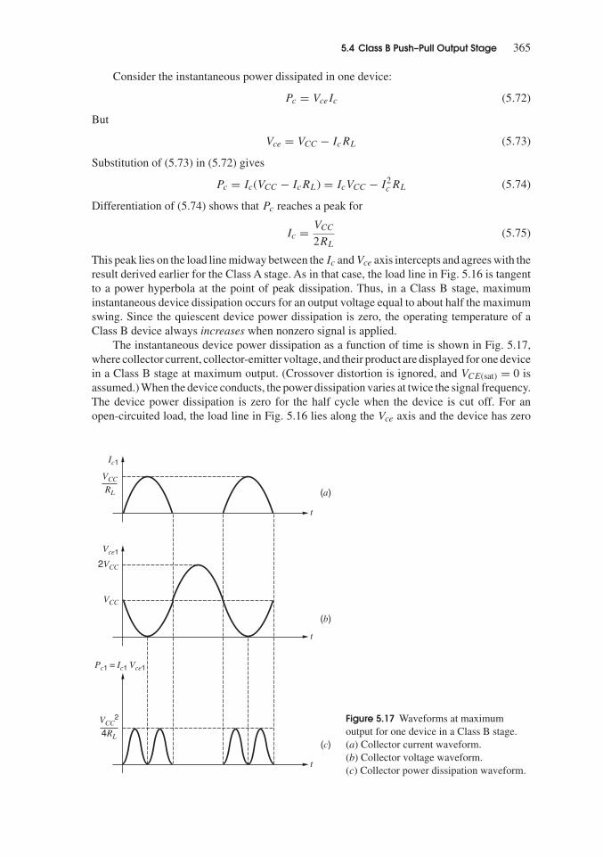
5.4 Class B Push–Pull Output Stage 365
Consider the instantaneous power dissipated in one device:
Pc = VceIc (5.72)
But
Vce = VCC − IcRL (5.73)
Substitution of (5.73) in (5.72) gives
Pc = Ic(VCC − IcRL) = IcVCC − I2c RL (5.74)
Differentiation of (5.74) shows that Pc reaches a peak for
Ic = VCC
2RL
(5.75)
This peak lies on the load line midway between the Ic and Vce axis intercepts and agrees with theresult derived earlier for the Class A stage. As in that case, the load line in Fig. 5.16 is tangentto a power hyperbola at the point of peak dissipation. Thus, in a Class B stage, maximuminstantaneous device dissipation occurs for an output voltage equal to about half the maximumswing. Since the quiescent device power dissipation is zero, the operating temperature of aClass B device always increases when nonzero signal is applied.
The instantaneous device power dissipation as a function of time is shown in Fig. 5.17,where collector current, collector-emitter voltage, and their product are displayed for one devicein a Class B stage at maximum output. (Crossover distortion is ignored, and VCE(sat) = 0 isassumed.) When the device conducts, the power dissipation varies at twice the signal frequency.The device power dissipation is zero for the half cycle when the device is cut off. For anopen-circuited load, the load line in Fig. 5.16 lies along the Vce axis and the device has zero
(a)
(b)
(c)
t
t
t
Ic1
Vce1
Pc1 = Ic1 Vce1
VCC
2VCC
VCC
RL
VCC2
4RL
Figure 5.17 Waveforms at maximumoutput for one device in a Class B stage.(a) Collector current waveform.(b) Collector voltage waveform.(c) Collector power dissipation waveform.

366 Chapter 5 � Output Stages
dissipation. As in the case of Class A stage, the load line in Fig. 5.16 becomes vertical throughthe quiescent point for a short-circuited load, and the instantaneous device power dissipationcan then become excessive. Methods of protection against such a possibility are described inSection 5.4.6.
EXAMPLE
A Class B stage of the type shown in Fig. 5.10 drives a load RL = 500 . If the positiveand negative supplies have magnitudes of 15 V, calculate the maximum average power that isdelivered to RL for V̂o = 14.4 V, the corresponding efficiency, and the maximum instantaneousdevice dissipation. Assume that Vo is sinusoidal.
From (5.66), the average of supply current is
Isupply = 1
π
V̂o
RL
= 1
π
14.4
500= 9.17 mA
Use of (5.67) gives the average power drawn from the supplies as
Psupply = Isupply × 2VCC = 9.17 × 30 mW = 275 mW
From (5.68), the average power delivered to RL is
PL = 1
2
V̂ 2o
RL
= 1
2
14.42
500= 207 mW
From (5.13), the corresponding efficiency is
ηC = PL
Psupply= 207
275= 75.3 percent
This result is close to the theoretical maximum of 78.6 percent. From (5.75), the maximuminstantaneous device power dissipation occurs when
Ic = VCC
2RL
= 15 V
1000 = 15 mA
The corresponding value of Vce is VCC/2 = 7.5 V and thus the maximum instantaneous devicedissipation is
Pc = IcVce = 15 × 7.5 mW = 112.5 mW
By conservation of power, the average power dissipated per device is
Pav = 1
2(Psupply − PL) = 1
2(275 − 207) mW = 34 mW
5.4.3 Practical Realizations of Class B Complementary Output Stages6
The practical aspects of Class B output-stage design will now be illustrated by consideringtwo examples. One of the simplest realizations is the output stage of the 709 op amp, and asimplified schematic of this is shown in Fig. 5.18. Transistor Q3 acts as a common-emitterdriver stage for output devices Q1 and Q2.
The transfer characteristic of this stage can be calculated as follows. In the quiescentcondition, Vo = 0 and V1 = 0. Since Q1 and Q2 are then off, there is no base current in thesedevices. Therefore, for VCC = 10 V, the bias current in Q3 is
IC3 = VCC − V1
R1= VCC
R1= 10 V
20 k= 0.50 mA

5.4 Class B Push–Pull Output Stage 367
Q1V1
R1
Q3
Q2
Vi
–VCC
+VCC
RL Vo
+
–
+
–
20 kΩ
Figure 5.18 Simplified schematic of theoutput stage of the 709 op amp.
The limiting values that Vo can take are determined by the driver stage. When Vi is takenlarge positive, V1 decreases until Q3 saturates, at which point the negative voltage limit V−
o isreached:
V−o = −VCC + VCE3(sat) − Vbe2 (5.76)
For values of V1 between (−VCC + VCE3(sat)) and (−VBE(on)), both Q3 and Q2 are in theforward-active region, and Vo follows V1 with Q2 acting as an emitter follower.
As Vi is taken negative, the current in Q3 decreases and V1 rises, turning Q1 on. Thepositive voltage limit V+
o is reached when Q3 cuts off and the base of Q1 is simply fed fromthe positive supply via R1. Then
VCC = Ib1R1 + Vbe1 + V+o (5.77)
If βF1 is large then
V+o = Ic1RL = βF1Ib1RL
where βF1 is the current gain of Q1. Thus
Ib1 = V+o
βF1RL
(5.78)
Substituting (5.78) in (5.77) and rearranging gives
V+o = VCC − Vbe1
1 + R1
βF1RL
(5.79)
For RL = 10 k and βF1 = 100, (5.79) gives
V+o = 0.98(VCC − Vbe1)
In this case, the limit on Vo is similar for positive and negative swings. However, if RL = 1 k
and βF1 = 100, (5.79) gives
V+o = 0.83(VCC − Vbe1)

368 Chapter 5 � Output Stages
Vo
RL = 1 kΩ
RL = 10 kΩ
Volts
ViVolts0.60 0.61 0.62 0.63 0.64 0.65 0.66
65
43
10
–1–2–3–4–5–6–7–8–9
2
Figure 5.19 SPICE-generated transfer characteristic for the circuit of Fig. 5.18 with VCC = 10 V andRL = 1 k and 10 k.
For this lower value of RL, the maximum positive value of Vo is reduced, and clipping on asine wave occurs first for Vo going positive.
Computer-generated transfer curves using SPICE for this circuit with VCC = 10 V areshown in Fig. 5.19 for RL = 1 k and RL = 10 k. (βF = 100 is assumed for all devices.)The reduced positive voltage capability for RL = 1 k is apparent, as is the deadband presentin the transfer characteristic. The curvature in the characteristic is due to the exponentialnonlinearity of the driver Q3. In practice, the transfer characteristic may be even more nonlinearthan shown in Fig. 5.19 because βF for the npn transistor Q1 is generally larger than βF forthe pnp transistor Q2, causing the positive and negative sections of the characteristic to differsignificantly. This behavior can be seen by calculating the small-signal gain �Vo/�Vi forpositive and negative Vo. In the actual 709 integrated circuit, negative feedback is appliedaround this output stage to reduce these nonlinearities in the transfer characteristic.
A second example of a practical Class B output stage is shown Fig. 5.20, where SPICE-calculated bias currents are included. This circuit is a simplified schematic of the 741 op ampoutput circuitry. The output devices Q14 and Q20 are biased to a collector current of about0.17 mA by the diodes Q18 and Q19. The value of the bias current in Q14 and Q20 dependson the effective area ratio between diodes Q18 and Q19 and the output devices. (Q18 andQ19 are implemented with transistors in practice.) The output stage is driven by lateral pnpemitter-follower Q23, which is driven by common-emitter stage Q17 biased to 0.68 mA bycurrent source Q13B.
The diodes in Fig. 5.20 essentially eliminate crossover distortion in the circuit, whichcan be seen in the SPICE-generated transfer characteristic of Fig. 5.21. The linearity of thisstage is further improved by the fact that the output devices are driven from a low resistanceprovided by the emitter follower Q23. Consequently, differences in βF between Q14 and Q20produce little effect on the transfer characteristic because small-signal gain �Vo/�V1 � 1 forany practical value of βF with either Q14 or Q20 conducting.
The limits on the output voltage swing shown in Fig. 5.21 can be determined as follows.As Vi is taken positive, the voltage V1 at the base of Q23 goes negative, and voltages V2 and

5.4 Class B Push–Pull Output Stage 369
+VCC
RL Vo
Vi
–VCC
+VCC
–VCC
Q13B
V1
V2
Q13A
Q20
Q14
Q17
Q14
Q20
Q19
Q18
Q23
Q13A
Q19
Q18
R1040 kΩ
Q23
BIAS
BIAS
0.17 mA
0.68 mA
0.22 mA
0.22 mA
0.17 mA(for Vo = 0)
+
–
+
–
RL Vo
+
–
V1
+
–
(a)
(b)
Figure 5.20 (a) Simplifiedschematic of the 741 op ampoutput stage. (b) Schematic ofthe 741 output stage showingthe detail of Q18 and Q19.
Vo follow with Q20 drawing current from RL. When Q17 saturates, the output voltage limitfor negative excursions is reached at
V−o = −VCC + VCE17(sat) − Vbe23 − Vbe20 (5.80)
This limit is about 1.4 V more positive than the negative supply. Thus V−o is limited by saturation
in Q17, which is the stage preceding driver stage Q23.As Vi is taken negative from its quiescent value (where Vo = 0), voltage V1 rises and
voltages V2 and Vo follow with Q14 delivering current to the load. The positive output voltage

370 Chapter 5 � Output Stages
VoVolts
ViVolts
14.2 V
–13.6 V
0.650.640.6350.630.625 0.655 0.66 0.6650.645
16
14
12
10
8
6
2
–2
–4
–6
–8
–10
–12
–14
–16
4
Figure 5.21 SPICE-generated transfer curve for the circuit of Fig. 5.20a with VCC = 15 V andRL = 1 k.
limit V+o is reached when current source Q13A saturates and
V+o = VCC + VCE13A(sat) − Vbe14 (5.81)
This limit is about 0.8 V below the positive supply because VCE13A(sat) � −0.1 V for the pnpdevice. Thus V+
o is also limited by the driver stage.The power requirements of the driver circuits in a configuration such as shown in
Fig. 5.20 require some consideration. The basic requirement of the driver is to supply suf-ficient drive to the output stage so that it can supply the desired power to RL. As Vo is takennegative, Q23 draws current from the base of Q20 with essentially no limit. In fact, the circuitmust be protected in case of a short-circuited load. Otherwise in this case, a large input signalcould cause Q23 and Q20 to conduct such heavy currents that they burn out. As explainedbefore, the negative voltage limit is reached when Q17 saturates and can no longer drive thebase of Q23 negative.
As Vo is taken positive (by Vi going negative and V1 going positive), Q23 conducts less,and current source Q13A supplies base current to Q14. The maximum output current is limitedby the current of 0.22 mA available for driving Q14. As V1, V2, and Vo go positive, the currentin Q14 increases, and the current in Q13A is progressively diverted to the base of Q14. Themaximum possible output current delivered by Q14 is thus
Io = βF14 × 0.22 mA

5.4 Class B Push–Pull Output Stage 371
If βF14 = 100, the maximum output current is 22 mA. The driver stage may thus limit the maxi-mum positive current available from the output stage. However, this output current level is onlyreached if RL is small enough so that Q13A does not saturate on the positive voltage excursion.
The stage preceding the driver in this circuit is Q17. As mentioned above, the negativevoltage limit of Vo is reached when Q17 saturates. The bias current of 0.68 mA in Q17 ismuch greater than the base current of Q23, and thus Q23 produces very little loading on Q17.Consequently, voltage V1 at the base of Q23 can be driven to within VCE(sat) of either supplyvoltage with only a very small fractional change in the collector current of Q17.
Finally, we will now examine the detail of the fabrication of diodes Q18 and Q19 in the 741.The actual circuit is shown in Fig. 5.20b with the output protection circuitry omitted. DiodeQ19 conducts only a current equal to the base current of Q18 plus the bleed current in pinchresistor R10. Transistor Q18 thus conducts most of the bias current of current source Q13A. Thisarrangement is used for two reasons. First, the basic aim of achieving a voltage drop equal totwo base-emitter voltages is achieved. Since Q18 and Q19 have common collectors, however,they can be placed in the same isolation region, reducing die area. Second, since Q19 conductsonly a small current, the bias voltage produced by Q18 and Q19 across the bases of Q14 andQ20 is less than would result from a connection as shown in Fig. 5.20a. This observation isimportant because output transistors Q14 and Q20 generally have emitter areas larger than thestandard device geometry (typically four times larger or more) so that they can maintain highβF while conducting large output currents. Thus in the circuit of Fig. 5.20a, the bias current inQ14 and Q20 would be about four times the current in Q18 and Q19, which would be excessivein a 741-type circuit. However, the circuit of Fig. 5.20b can be designed to bias Q14 and Q20 toa current comparable to the current in the diodes, even though the output devices have a largearea. The basic reason for this result is that the small bias current in Q19 in Fig. 5.20b gives ita smaller base-emitter voltage than for the same device in Fig. 5.20a, reducing the total biasvoltage between the bases of Q14 and Q20.
The results described above can be illustrated quantitatively by calculating the bias currentsin Q14 and Q20 of Fig. 5.20b. From KVL,
VBE19 + VBE18 = VBE14 + |VBE20|and thus
VT lnIC19
IS19+ VT ln
IC18
IS18= VT ln
IC14
IS14+ VT ln
∣∣∣∣IC20
IS20
∣∣∣∣ (5.82)
If we assume that the circuit is biased for Vo = 0 V and also that βF14 � 1 and βF20 � 1,then |IC14| = |IC20| and (5.82) becomes
IC19IC18
IS18IS19= I2
C14
IS14IS20
from which
IC14 = −IC20 =√
IC19IC18
√IS14IS20
IS18IS19(5.83)
Equation 5.83 may be used to calculate the output bias current in circuits of the type shown inFig. 5.20b. The output-stage bias current from (5.83) is proportional to
√IC18 and
√IC19. For
this specific example, the collector current in Q19 is approximately equal to the current in R10if βF is large and thus
IC19 � VBE18
R10� 0.6
40mA = 15 �A

372 Chapter 5 � Output Stages
If the base currents of Q14 and Q20 are neglected, the collector current of Q18 is
IC18 � |IC13A| − IC19 = (220 − 15) �A = 205 �A
To calculate the output-stage bias currents from (5.83), values for the various reverse saturationcurrents are required. These values depend on the particular IC process used, but typical val-ues are IS18 = IS19 = 2 × 10⁻¹⁵ A, IS14 = 4IS18 = 8 × 10⁻¹⁵ A, and IS20 = 4 × 10⁻¹⁵ A.Substitution of these data in (5.83) gives IC14 = −IC20 = 0.16 mA.
EXAMPLE
For the output stage of Fig. 5.20a, calculate bias currents in all devices for Vo = +10 V.Assumethat VCC = 15 V, RL = 2 k, and βF = 100. For simplicity, assume all devices have equalarea and for each device
|IC| = 10−14 exp
∣∣∣∣Vbe
VT
∣∣∣∣ (5.84)
Assuming that Q14 supplies the load current for positive output voltages, we have
Ic14 = Vo
RL
= 10 V
2 k= 5 mA
Substitution in (5.84) and rearranging gives
Vbe14 = (26 mV) ln
(5 × 10⁻³
10−14
)= 700 mV
Also
Ib14 = Ic14
βF14= 5 mA
100= 0.05 mA
Thus
Ic19 � Ic18 � −Ic23 = (0.22 − 0.05) mA = 0.17 mA
Substitution in (5.84) and rearranging gives
Vbe19 = Vbe18 = −Vbe23 = (26 mV) ln
(0.17 × 10⁻³
10−14
)= 613 mV
Thus
Vbe20 = −(Vbe19 + Vbe18 − Vbe14) = −525 mV
Use of (5.84) gives
Ic20 = −5.9 �A
and the collector current in Q20 is quite small as predicted. Finally
Ic17 = 0.68 mA − Ic23
βF23=(
0.68 − 0.17
100
)mA = 0.68 mA
and also
V2 = Vo − |Vbe20| = (10 − 0.525) V = 9.475 V
and
V1 = V2 − |Vbe23| = (9.475 − 0.613) V = 8.862 V

5.4 Class B Push–Pull Output Stage 373
5.4.4 All-npn Class B Output Stage7,8,9
The Class B circuits described above are adequate for many integrated-circuit applicationswhere the output power to be delivered to the load is of the order of several hundred milliwattsor less. However, if output-power levels of several watts or more are required, these circuitsare inadequate because the substrate pnp transistors used in the output stage have a limitedcurrent-carrying capability. This limit stems from the fact that the doping levels in the emitter,base, and collector of these devices are not optimized for pnp structures because the npn devicesin the circuit have conflicting requirements.
A circuit design that uses high-power npn transistors in both halves of a Class B config-uration is shown in Fig. 5.22. In this circuit, common-emitter transistor Q1 delivers powerto the load during the negative half-cycle, and emitter follower Q2 delivers power during thepositive half-cycle.
To examine the operation of this circuit, consider Vi taken negative from its quiescentvalue so that Q1 is off and Ic1 = 0. Then diodes D1 and D2 must both be off and all of thecollector current of Q3 is delivered to the base of Q2. The output voltage then has its maximumpositive value V+
o . If RL is big enough, Q3 saturates and
V+o = VCC − |VCE3(sat)| − Vbe2 (5.85)
To attain this maximum positive value, transistor Q3 must saturate in this extreme condition.In contrast, Q2 in this circuit cannot saturate because the collector of Q2 is connected to thepositive supply and the base voltage of Q2 cannot exceed the positive supply voltage. The con-dition for Q3 to be saturated is that the nominal collector bias current IQ3 in Q3 (when Q3 is notsaturated) should be larger than the required base current ofQ2 whenVo = V+
o . Thus we require
IQ3 > Ib2 (5.86)
Since Q2 supplies the current to RL for Vo > 0, we have
V+o = −Ie2RL = (β2 + 1)Ib2RL (5.87)
+
–
Vi
+
–
Vo
VCC
–VCC
RLV1
V2
D1
D2
Q3
Q2
Q1
Ic2
IQ3
Ic1
Figure 5.22 All-npn Class B outputstage.

374 Chapter 5 � Output Stages
Substitution of (5.87) and (5.85) in (5.86) gives the requirement on the bias current of Q3 as
IQ3 >VCC − VCE3(sat) − Vbe2
(β2 + 1)RL
(5.88)
Equation 5.88 also applies to the circuit of Fig. 5.20a. It gives limits on IC3, β2, and RL for Vo
to be able to swing close to the positive supply. If IQ3 is less than the value given by (5.88), Vo
will begin clipping at a positive value less than that given by (5.85) and Q3 will never saturate.Now consider Vi made positive to turn Q1 on and produce nonzero Ic1. Since the base of
Q2 is more positive than its emitter, diode D1 will turn on in preference to D2, which will beoff with zero volts across its junction. The current Ic1 will flow through D1 and will be drawnfrom Q3, which is assumed saturated at first. As Ic1 increases, Q3 will eventually come outof saturation, and voltage V2 at the base of Q2 will then be pulled down. Since Q2 acts as anemitter follower, Vo will follow V2 down. This behavior occurs during the positive half of thecycle, and Q1 acts as a driver with Q2 as the output device.
When Vo is reduced to 0 V, the load current is zero and Ic2 = 0. This point correspondsto Ic1 = |IC3|, and all of the bias current in Q3 passes through D1 to Q1. If Ic1 is increasedfurther, Vo stays constant at 0 V while V2 is reduced to 0 V also. Therefore, V1 is negative byan amount equal to the diode voltage drop of D1, and thus power diode D2 turns on. Sincethe current in D1 is essentially fixed by Q3, further increases in Ic1 cause increasing currentto flow through D2. The negative half of the cycle consists of Q1 acting as the output deviceand feeding RL through D2. The maximum negative voltage occurs when Q1 saturates and is
V−o = −VCC + VCE1(sat) + Vd2 (5.89)
where Vd2 is the forward voltage drop across D2.The sequence just described gives rise to a highly nonlinear transfer characteristic, as
shown in Fig. 5.23, where Vo is plotted as a function of Ic1 for convenience. When Vo ispositive, the current Ic1 feeds into the base of Q2 and the small-signal gain is
�Vo
�Ic1� �V2
�Ic1= ro1 ‖ ro3 ‖ [rπ2 + (β2 + 1)RL]
Slope = ro1 || ro3 || [ r 2 + ( 2 + 1) RL]
Slope = RL || ro1
IC3Ic2
IQ3 – 2
Ic1
Q3 saturated
Q1 saturated
Vo = [–VCC + Vd2 + VCE1(sat)]–
Vo
β
βπ
Vo = [VCC – Vbe2 – VCE3(sat) ]+
Figure 5.23 Transfer characteristic of the circuit of Fig. 5.22 from Ic1 to Vo.

5.4 Class B Push–Pull Output Stage 375
where the impedance of D1 is assumed negligible. That is, the impedance at the base of Q2is equal to the parallel combination of the output resistances of Q1 and Q3 and the inputresistance of emitter follower Q2.
When Vo in Fig. 5.22 is negative, Ic1 feeds RL directly and the small-signal gain is
�Vo
�Ic1� ro1 ‖ RL
where the impedance of D2 is assumed negligible.Note the small deadband in Fig. 5.23 where diode D2 turns on. This deadband can
be eliminated by adding a second diode in series with D1. In practice, negative feedbackmust be used around this circuit to linearize the transfer characteristic, and such feedbackwill reduce any crossover effects. The transfer characteristic of the circuit from Vi to Vo iseven more nonlinear than shown in Fig. 5.23 because it includes the exponential nonlinearityof Q1.
In integrated-circuit fabrication of the circuit of Fig. 5.22, devices Q1 and Q2 are identicallarge-power transistors. In high-power circuits (delivering several watts or more), they mayoccupy 50 percent of the whole die. Diode D2 is a large-power diode that also occupiesconsiderable area. These features are illustrated in Fig. 5.24, which is a die photo of the 791high-power op amp. This circuit can dissipate 10 W of power and can deliver 15 W of outputpower into an 8- load. The large power transistors in the output stage can be seen on theright-hand side of the die.
Finally, the power and efficiency results derived previously for the complementary ClassB stage apply equally to the all-npn Class B stage if allowance is made for the voltage drop inD2. Thus the ideal maximum efficiency is 79 percent.
Figure 5.24 Die photo of the 791 high-power op amp.

376 Chapter 5 � Output Stages
5.4.5 Quasi-Complementary Output Stages10
The all-npn stage described above is one solution to the problem of the limited power-handlingcapability of the substrate pnp. Another solution is shown in Fig. 5.25, where a composite pnphas been made from a lateral pnp Q3 and a high-power npn transistor Q4. This circuit is calleda quasi-complementary output stage.
The operation of the circuit of Fig. 5.25 is almost identical to that of Fig. 5.20. The pairQ3-Q4 is equivalent to a pnp transistor as shown in Fig. 5.26, and the collector current of Q3 is
IC3 = −IS exp
(−VBE
VT
)(5.90)
The composite collector current IC is the emitter current of Q4, which is
IC = (βF4 + 1)IC3 = −(βF4 + 1)IS exp
(−VBE
VT
)(5.91)
The composite device thus shows the standard relationship between IC and VBE for a pnptransistor. However, most of the current is carried by the high-power npn transistor. Note thatthe magnitude of the saturation voltage of the composite device is (|VCE3(sat)| + VBE4). This
Q2
Q8
Q7
Q6
Q5
Q1
Q3
Q4
–VCC
VCC
RL Vo
Vi
+
–
+
–Figure 5.25Quasi-complementary Class Boutput stage.
Q3B
C
IC3
VBE
Q4
IE
VBE
B
EIE
IC
E
IC
_
+
–
+
Figure 5.26 Equivalence ofthe composite connectionand a pnp transistor.

5.4 Class B Push–Pull Output Stage 377
G G
S S
D
D
ID
ID
ID3
VGSVGS
M3
Q4
– –
+ +
Figure 5.27 Compound high-currentPMOS connection.
magnitude is higher than normal because saturation occurs when Q3 saturates, and VBE4 mustbe added to this voltage.
The major problem with the configuration of Fig. 5.25 is potential instability of the localfeedback loop formed by Q3 and Q4, particularly with capacitive loads on the amplifier. Thestability of feedback loops is considered in Chapter 9.
The quasi-complementary Class B stage can also be effectively implemented in BiCMOStechnology. In the circuit of Fig. 5.25, the compound bipolar device Q3-Q4 can be replacedby the MOS-bipolar combination11 of Fig. 5.27, where Q4 is a large-area high-current bipolardevice. The overall transfer characteristic is
ID = (βF4 + 1)ID3 = −(βF4 + 1)μnCox
2
(W
L
)3
(VGS − Vt)2 (5.92)
Equation 5.92 shows that the composite PMOS device appears to have a W/L ratio (βF4 + 1)times larger than the physical PMOS device M3. With this circuit, one of the diodes Q5 orQ6 in Fig. 5.25 would now be replaced by a diode-connected PMOS transistor to set up atemperature-stable standby current in the output stage. A bias bleed resistor can be connectedfrom the base to the emitter of Q4 to optimize the bias current in M3 and to speed up the turn-off of Q4 in high-frequency applications by allowing reverse base current to remove the basecharge. Such a resistor can also be connected from the base to the emitter of Q4 in Fig. 5.25.
5.4.6 Overload Protection
The most common type of overload protection in integrated-circuit output stages is short-circuitcurrent protection.As an example, consider the 741 output stage shown in Fig. 5.28 with partialshort-circuit protection included. Initially assume that R6 = 0 and ignore Q15. The maximumpositive drive delivered to the output stage occurs for Vi large positive. If RL = 0 then Vo isheld at zero volts and Va in Fig. 5.28 is equal to Vbe14. Thus, as Vi is taken positive, Q23, Q18,and Q19 will cut off and all of the current of Q13A is fed to Q14. If this is a high-βF device,then the output current can become destructively large:
Ic14 = βF14|IC13A| (5.93)
If
βF14 = 500
then
Ic14 = 500 × 0.22 = 110 mA

378 Chapter 5 � Output Stages
BIAS
0.22 mAQ13A
Q18
Q19
Q15
Q20
Q23
R6
R7
Q14Va
Vo
Vi
–VCC
+VCC
RL
+
+
–
–
Figure 5.28 Schematic of the 741 op ampshowing partial short-circuit protection.
If VCC = 15 V, this current level gives a power dissipation in Q14 of
Pc14 = VceIc = 15 × 110 mW = 1.65 W
which is sufficient to destroy the device. Thus the current under short-circuit conditions mustbe limited, and this objective is achieved using R6 and Q15 for positive Vo.
The short-circuit protection operates by sensing the output current with resistor R6 ofabout 25 . The voltage developed across R6 is the base-emitter voltage of Q15, which isnormally off. When the current through R6 reaches about 20 mA (the maximum safe level),Q15 begins to conduct appreciably and diverts any further drive away from the base of Q14.The drive current is thus harmlessly passed to the output instead of being multiplied by the βF
of Q14.The operation of this circuit can be seen by calculating the transfer characteristic of Q14
when driving a short-circuit load. This can be done using Fig. 5.29.
Ii = Ib14 + Ic15 (5.94)
Ic15 = IS15 expVbe15
VT
(5.95)
Also
Vbe15 � Ic14R (5.96)
From (5.94)
Ib14 = Ii − Ic15
But
Ic14 = βF14Ib14 = βF14(Ii − Ic15) (5.97)

5.5 CMOS Class AB Output Stages 379
+VCC
Ic14
Ib14
Ic15
Q15
Q14
R
Ii
Figure 5.29 Equivalent circuit for the calculation of the effectof Q15 on the transfer characteristic of Q14 in Fig. 5.28 whenRL = 0.
40
30
20
10
0.1Ii(mA)
I c14
(mA
)
Ic14 = F14Ii
0.2
No protection
With protection
β
Figure 5.30 Transfer characteristic of thecircuit of Fig. 5.29 with and withoutprotection transistor Q15 (βF14 = 500).
Substitution of (5.95) and (5.96) in (5.97) gives
Ic14 + βF14IS15 expIc14R
VT
= βF14Ii (5.98)
The second term on the left side of (5.98) stems from Q15. If this term is negligible, thenIc14 = βF14Ii as expected. The transfer characteristic of the stage is plotted from (5.98) inFig. 5.30, using βF14 = 500, IS15 = 10−14 A, and R = 25 . For a maximum drive ofIi = 0.22 mA, the value of Ic14 is effectively limited to 24 mA. For values of Ic14 below20 mA, Q15 has little effect on circuit operation.
Similar protection for negative output voltages in Fig. 5.29 is achieved by sensing thevoltage across R7 and diverting the base drive away from one of the preceding stages.
5.5 CMOS Class AB Output StagesThe classical Class AB topology of Fig. 5.13 can also be implemented in standard CMOStechnology. However, the output swing of the resulting circuit is usually much worse than inthe bipolar case. Although the swing can be improved using a common-source configuration,this circuit suffers from poor control of the quiescent current in the output devices. These issuesare described below.

380 Chapter 5 � Output Stages
5.5.1 Common-Drain Configuration
Figure 5.31 shows the common-drain Class AB output configuration. From KVL,
VSG5 + VGS4 = Vgs1 + Vsg2 (5.99)
Ignoring the body effect, VSG5 + VGS4 is constant if the bias current from M3 is constant.Under these conditions, increasing Vgs1 decreases Vsg2 and vice versa.
For simplicity, assume at first that a short circuit is connected from the drain of M4to the drain of M5. Then VSG5 + VGS4 = 0 and Vgs1 = Vgs2 from (5.99). For M1 to con-duct nonzero drain current, Vgs1 > Vt1 is required. Similarly, Vgs2 < Vt2 is required for M2to conduct nonzero drain current. With standard enhancement-mode devices, Vt1 > 0 andVt2 < 0. Therefore, M1 and M2 do not both conduct simultaneously under these conditions,which is a characteristic of a Class B output stage. When Vo > 0, M1 operates as a sourcefollower and M2 is off. Similarly, M2 operates as a source follower and M1 is off whenVo < 0.
In Fig. 5.31, however, VSG5 + VGS4 > 0 and both M1 and M2 are biased to conductnonzero drain current when Vo = 0, which is a characteristic of a Class AB output stage. IfVt1 = Vt4 and Vt2 = Vt5, using (1.157) in (5.99) with ID5 = −ID4 gives√
2ID4
k′p(W/L)5
+√
2ID4
k′n(W/L)4
=√
2Id1
k′n(W/L)1
+√
2|Id2|k′p(W/L)2
(5.100)
If Vo = 0, then Id2 = −Id1 and (5.100) can be rearranged to give
ID1 = ID4
(√1
k′n(W/L)4
+√
1
k′p(W/L)5
)2
(√1
k′n(W/L)1
+√
1
k′p(W/L)2
)2 (5.101)
where ID1 = Id1 with Vo = 0. The key point of this equation is that the quiescent currentin the output transistors is well controlled with respect to the bias current that flows in thediode-connected transistors, as in the bipolar case.
M3
M6
M5
M4
M2
M1
Vi
–VSS
RL Vo
VDD
BIAS
+
+
–
–Figure 5.31 Complementary source-follower CMOS output stage based ontraditional bipolar implementation.

5.5 CMOS Class AB Output Stages 381
An important problem with this circuit is that its output swing can be much less than thecorresponding bipolar circuit with equal supply voltages. For Vo > 0, Vgs1 > Vt1 and M1 actsas a source follower. Therefore,
Vo = VDD − Vsd3 − Vgs1 (5.102)
The minimum Vsd3 required to operate M3 as a current source is |Vov3| = |VGS3 − Vt3|. From(5.102), the maximum output voltage V+
o is
V+o = VDD − |Vov3| − Vgs1 (5.103)
The minimum output voltage can be found by similar reasoning. (See Problem 5.21.) Although(5.103) appears to be quite similar to (5.81) if VCC in Fig. 5.20 is equal to VDD in Fig. 5.31,the limit in (5.103) is usually much less than in (5.81) for three reasons. First, the gate-sourcevoltage includes a threshold component that is absent in the base-emitter voltage. Second, thebody effect increases the threshold voltage Vt1 as Vo increases. Finally, the overdrive part ofthe gate-source voltage rises more steeply with increasing current than the entire base-emittervoltage because the overdrive is proportional to the square root of the current and the base-emitter voltage is proportional to the logarithm of the current. In practice, the output voltageswing can be increased by increasing the W/L ratios of the output devices to reduce theiroverdrives. However, the required transistor sizes are sometimes so large that the parasiticcapacitances associated with the output devices can dominate the overall performance at highfrequencies. Thus the circuit of Fig. 5.31 is generally limited to much smaller currents than itsbipolar equivalent.
EXAMPLE
An output stage such as shown in Fig. 5.31 is required to produce a maximum output volt-age of 0.7 V with RL = 35 and VDD = VSS = 1.5 V. Using the transistor parameters inTable 2.4, find the required W/L of M1. Assume |Vov3| = 100 mV, and ignore the body effect.
From (5.103),
Vgs1 = VDD − |Vov3| − V+o = (1.5 − 0.1 − 0.7) V = 0.7 V
Since Table 2.4 gives Vt1 = 0.6 V,
Vov1 = Vgs1 − Vt1 = (0.7 − 0.6) V = 0.1 V
With Vo = 0.7 V, the current in the load is (0.7 V)/(35 ) = 20 mA. If Id2 = 0 under theseconditions, Id1 = 20 mA. Rearranging (1.157) gives(
W
L
)1
= 2I
k′nVov1
2 = 2(20000)
194(0.1)2 � 20, 000 (5.104)
which is a very large transistor.
5.5.2 Common-Source Configuration with Error Amplifiers
Another alternative is the use of quasi-complementary configurations. In this case, acommon-source transistor together with an error amplifier replaces an output source-followerdevice. A circuit with this substitution for both output transistors is shown conceptually inFig. 5.32.12,13,14 The combination of the error amplifier and the common-source device mim-ics the behavior of a source follower with high dc transconductance. The function of theamplifiers is to sense the voltage difference between the input and the output of the stage anddrive the gates of the output transistors so as to make the difference as small as possible. This

382 Chapter 5 � Output Stages
VDD
RL Vo
–VSS
M1
M2
Vi
+
–
–
–
+
+
–
+
Error amplifier
Error amplifier
A
A Figure 5.32 A complementaryClass AB output stage usingembedded common-sourceoutput devices.
vgs1
gm1vgs1
gm2vgs2 ro2vt
ro1
Ro
it
+–
+
+
–
–
vgs2
+
–
A
A
+
–
Figure 5.33 Small-signalmodel of the output stage inFig. 5.32 used to find Ro.
operation can be viewed as negative feedback. A key advantage of the use of negative feedbackhere is that it reduces the output resistance. Since negative feedback is covered in Chapter 8,we will analyze this structure with straightforward circuit analysis.
To find the output resistance, consider the small-signal model of this output stage shownin Fig. 5.33. The current it is
it = vt
ro1+ vt
ro2+ gm1Avt + gm2Avt (5.105)
Rearranging this equation to solve for vt/ it gives
Ro = vt
it
∣∣∣∣vi=0
= 1
(gm1 + gm2)A‖ ro1 ‖ ro2 (5.106)
This equation shows that increasing the gain A of the error amplifiers reduces Ro and that Ro
is much less than the drain-source resistance of M1 or M2 because of the negative feedback.To find the transfer characteristic, consider the dc model of the output stage shown in
Fig. 5.34. The model includes the input-referred offset voltages of the error amplifiers as voltagesources. Assume k′
p(W/L)1 = k′n(W/L)2 = k′(W/L) and −Vt1 = Vt2 = Vt . Also assume that
the error amplifiers are designed so that −ID1 = ID2 = IQ when Vi = 0, VOSP = 0, andVOSN = 0. Under these conditions, Vo = 0 and
Vgs1 = −Vt − Vov (5.107)
Vgs2 = Vt + Vov (5.108)

5.5 CMOS Class AB Output Stages 383
–
+
+
+
– –A
A
+
+ –
+ –
_Vi
VOSPVDD
M1
M2
–VSSVOSN
RL Vo
IoId1
Id2
Figure 5.34 A dc modelof the output stage inFig. 5.32 used to find thetransfer characteristic.
where
Vov =√
2IQ
k′(W/L)(5.109)
With nonzero input and offsets, the output may not be zero. As a result, the differential inputto the top error amplifier changes from zero to Vo − (Vi − VOSP ). Similarly, the differentialinput to the bottom error amplifier changes from zero to Vo − (Vi − VOSN ). Assuming that theoutput of each error amplifier changes by its gain A times the change in its input,
Vgs1 = −Vt − Vov + A[Vo − (Vi − VOSP )] (5.110)
Vgs2 = Vt + Vov + A[Vo − (Vi − VOSN )] (5.111)
If M1 and M2 operate in the active region,
Id1 = −k′p
2
(W
L
)1(Vgs1 − Vt1)2 = − k′
2
W
L(Vgs1 + Vt)
2 (5.112)
Id2 = k′n
2
(W
L
)2(Vgs2 − Vt2)2 = k′
2
W
L(Vgs2 − Vt)
2 (5.113)
Also,
Io = Vo
RL
(5.114)
From KCL at the output,
Io + Id1 + Id2 = 0 (5.115)
Substituting (5.110)–(5.114) into (5.115) and rearranging gives
Vo =Vi − VOSP + VOSN
2
1 + 1
k′ WL
A[2Vov − A(VOSP − VOSN )]RL
(5.116)
If VOSP = VOSN = 0,
Vo = Vi
1 + 1
k′ WL
A2VovRL
= Vi
1 + 1
2AgmRL
� Vi
(1 − 1
2AgmRL
)(5.117)

384 Chapter 5 � Output Stages
where gm = k′(W/L)Vov as shown in (1.180). The term (2AgmRL) is the gain around thefeedback loop or the loop gain and is usually chosen to be high enough to make the slope ofthe transfer characteristic to be unity within an allowable gain error. (The concept of loop gainis described in Chapter 8.) The gain error here is approximately 1/(2AgmRL). The key pointis that the error is reduced if A, gm, or RL are increased.
With nonzero offsets, (5.116) shows that the circuit also displays an offset error. IfA(VOSP − VOSN ) � 2Vov and 2AgmRL � 1,
Vo �Vi − VOSP + VOSN
2
1 + 1
k′ WL
A2VovRL
=Vi − VOSP + VOSN
2
1 + 1
2AgmRL
� Vi − VOSP + VOSN
2(5.118)
Therefore, the input offset voltage of the buffer is about −(VOSP + VOSN )/2.Equation 5.116 is valid as long as both M1 and M2 operate in the active region. If the
magnitude of the output voltage is large enough, however, one of the two output transistorsturns off. For example, when Vi increases, Vo also increases but the gain is slightly less thanunity. As a result, the differential inputs to the error amplifiers both decrease, decreasing Vgs1and Vgs2. In turn, these changes increase |Id1| but reduce Id2, and M2 turns off for large enoughVi. To find the portion of the transfer characteristic with M1 in the active region but M2 off,the above analysis can be repeated with Id2 = 0. See Problem 5.23.
The primary motivation for using the quasi-complementary configuration is to increasethe output swing. If the output transistors are not allowed to operate in the triode region, theoutput voltage can pull within an overdrive of either supply. This result is an improvementcompared to the limit given in (5.103) for the common-drain output stage mostly because thethreshold voltages of the output transistors do not limit the output swing in the common-sourceconfiguration.
Although quasi-complementary circuits improve the output swing, they suffer from twomain problems. First, the error amplifiers must have large bandwidth to prevent crossoverdistortion problems for high input frequencies. Unfortunately, increasing the bandwidth of theerror amplifiers worsens the stability margins, especially in the presence of large capacitiveloads. As a result, these circuits present difficult design problems in compensation. The topicsof stability and compensation are covered in Chapter 9. Second, nonzero offset voltages inthe error amplifiers change the quiescent current flowing in the output transistors. From adesign standpoint, the quiescent current is chosen to be barely high enough to limit crossoverdistortion to an acceptable level. Although further increases in the quiescent current reduce thecrossover distortion, such increases also increase the power dissipation and reduce the outputswing. Therefore, proper control of the quiescent current with nonzero offsets is also a keydesign constraint.
One way to control the quiescent current is to sense and feedback a copy of the current.12
This method is not considered further here. Another way to limit the variation in the quiescentcurrent is to design the error amplifiers to have low gain.13,14 The concept is that the quiescentcurrent is controlled by the gate-source voltages on the output transistors, which in turn arecontrolled by the outputs of the error amplifiers. Therefore, reducing the error-amplifier gainreduces the variation of gate-source voltages and the quiescent current for a given variation inthe offset voltages.
To study this situation quantitatively, define the quiescent current in the output devices asthe common-mode component of the current flowing from VDD to −VSS with Vi = 0. Then
IQ = ID2 − ID1
2(5.119)

5.5 CMOS Class AB Output Stages 385
Subtraction is used in the above equation because the drain current of each transistor is definedas positive when it flows into the transistor. Substituting (5.110)–(5.113) into (5.119) gives
IQ = k′
4
W
L
((Vov + A[Vo + VOSN ])2 + (−Vov + A[Vo + VOSP ])2
)(5.120)
Since Vo = 0 if VOSP = VOSN = 0, (5.120) shows that
IQ
∣∣VOSP =0VOSN=0
= k′
4
W
L
((Vov )2 + (−Vov )2
)= k′
2
W
L(Vov )2 (5.121)
From (5.118) with Vi = 0,
Vo + VOSP � VOSP − VOSN
2(5.122)
Vo + VOSN � −VOSP − VOSN
2(5.123)
Substituting (5.122) and (5.123) into (5.120) gives
IQ = k′
2
W
L
(Vov − A
[VOSP − VOSN
2
])2
(5.124)
Define �IQ as the change in IQ caused by nonzero offsets; that is,
�IQ = IQ
∣∣VOSP =0VOSN=0
− IQ (5.125)
Substituting (5.124) and (5.121) into (5.125) gives
�IQ = k′
2
W
LA (VOSP − VOSN )
[Vov − A
(VOSP − VOSN
4
)](5.126)
To evaluate the magnitude of �IQ, we will compare it to the quiescent current with zero offsetsby dividing (5.126) by (5.121). The result is
�IQ
IQ
∣∣ VOSP =0VOSN=0
= A
(VOSP − VOSN
Vov
)[1 − A
(VOSP − VOSN
4Vov
)](5.127)
If A(VOSP − VOSN ) � 4Vov ,
�IQ
IQ
∣∣ VOSP =0VOSN=0
� A
(VOSP − VOSN
Vov
)(5.128)
Therefore, to keep the fractional change in the quiescent current less than a given amount, themaximum error-amplifier gain is
A <
(Vov
VOSP − VOSN
)⎛⎝�IQ
IQ
∣∣ VOSP =0VOSN=0
⎞⎠ (5.129)
For example, if Vov = 200 mV, VOSP − VOSN = 5 mV, and up to 20 percent variation in thequiescent current is allowed, (5.129) shows that the error amplifier gain should be less thanabout 8.13,14
Figure 5.35 shows a schematic of the top error amplifier and M1 from Fig. 5.32.14 Acomplementary structure used to drive M2 is not shown. The difference between Vi and Vo issensed by the differential pair M11 and M12, which is biased by the tail current source ITAIL.The load of the differential pair consists of two parts: current mirror M13 and M14 and common-drain transistors M15 and M16. The purpose of the common-drain transistors is to reduce the

386 Chapter 5 � Output Stages
VDD
–VSS
ITAILIBIAS
Vi Vo
M15
M11 M12
M13 M14
M1M17
M16
+ +
––
Figure 5.35 Schematic of the top error amplifier and output transistor M1.
output resistance of the error amplifier to set its gain to a well-defined low value. The gates of thecommon-drain transistors are biased by a negative feedback loop including M13, M17, IBIAS,and M15. This circuit adjusts the voltage at the gate of M15 so that M17 operates in the activeregion and conducts IBIAS. Although negative feedback is studied in Chapter 8, the basic ideacan be understood here as follows. If |ID17| is less than IBIAS, current source IBIAS pulls the gatevoltage ofM15 down. SinceM15 operates as a source follower, the source ofM15 is pulled down,increasing |ID13|. Because M13 and M17 together form a current mirror, |ID17| also increasesuntil |ID17| = IBIAS. Similar reasoning shows that this equality is established when |ID17| isinitially greater than IBIAS. If M15 and M17 are enhancement-mode devices, M17 operates in theactive region because VGD17 = VSG15 = |Vt15| + |Vov15| > 0 > Vt17; therefore, the channeldoes not exist at the drain of M17.
Since M13 and M17 form a current mirror,
ID13 = ID17(W/L)13
(W/L)17= −IBIAS
(W/L)13
(W/L)17(5.130)
Since M13 and M14 also form a current mirror, and since (W/L)14 = (W/L)13,
ID14 = ID13 = −IBIAS(W/L)13
(W/L)17(5.131)
With Vi = Vo,
ID11 = ID12 = ITAIL
2(5.132)
From KCL,
ID16 = ID14 + ID11 (5.133)

5.5 CMOS Class AB Output Stages 387
Substituting (5.131) and (5.132) into (5.133) gives
ID16 = −IBIAS(W/L)13
(W/L)17+ ITAIL
2(5.134)
Since ID15 = ID16 when ID11 = ID12,
VSD14 = VSD13 = VSG13 = VSG1 (5.135)
Therefore, ignoring channel-length modulation,
ID1 = ID13(W/L)1
(W/L)13(5.136)
Substituting (5.130) into (5.136) and rearranging gives
ID1 = −IBIAS(W/L)1
(W/L)17(5.137)
This equation shows that the drain current in M1 is controlled by IBIAS and a ratio of transistorsizes if the offset voltage of the error amplifier is zero so that Vo = 0 when Vi = 0. In practice,(W/L)1 � (W/L)17 so that little power is dissipated in the bias circuits.
Another design consideration comes out of these equations. To keep the gain of the erroramplifier low under all conditions, M16 must never cut off. Therefore, from (5.133), |ID14|should be greater than the maximum value of ID11. Since the maximum value of ID11 is ITAIL,(5.131) and (5.133) show that
|ID14| = IBIAS(W/L)13
(W/L)17> ITAIL (5.138)
To find the gain of the error amplifier, the key observation is that the small-signal resistancelooking into the source of of M15 is zero, ignoring channel-length modulation. This resultstems from the operation of the same negative feedback loop that biases the gate of M15. Ifthe small-signal voltage at the source of M15 changes, the negative feedback loop works toundo the change. For example, suppose that the source voltage of M15 increases. This changereduces the gate voltage of M15 because M17 operates as a common-source amplifier. Then thesource voltage of M15 falls because M15 operates as a source follower. Ignoring channel-lengthmodulation, the source voltage of M15 must be held exactly constant because id17 = 0 if IBIASis constant. Therefore, the small-signal resistance looking into the source of M15 is zero. Asa result, none of the small-signal drain current from M12 flows in M13. Instead, it all flowsin the source of M15. To calculate the transconductance of the error amplifier, the output atthe drain of M16 is connected to a small-signal ground. Since M15 and M16 share the samegate connection, and since their sources each operate at small-signal grounds, the small-signalcurrent in M15 is copied to M16. Therefore, the entire small-signal current from the differentialpair flows at the error-amplifier output and the transconductance is
Gm = gm11 = gm12 (5.139)
Ignoring channel-length modulation, the output resistance is set by common-drain transistorM16. From (3.84),
Ro = 1
gm16 + gmb16(5.140)
Therefore, the gain of the error amplifier is
A = GmRo = gm11
gm16 + gmb16(5.141)

388 Chapter 5 � Output Stages
5.5.3 Alternative Configurations
The main potential advantage of the common-source output stage described in the last sectionis that it can increase the output swing compared to the common-drain case. However, thecommon-source configuration suffers from an increase in harmonic distortion, especially athigh frequencies, for two main reasons. First, the bandwidth of the error amplifiers is usuallylimited, to avoid stability problems. Second, the gain of these amplifiers is limited to establishadequate control on the quiescent output current.
5.5.3.1 Combined Common-Drain Common-Source ConfigurationOne way to overcome this problem is to use a combination of the common-drain and common-source configurations shown in Fig. 5.31 and Fig. 5.32.15 The combined schematic is shownin Fig. 5.36. The key aspect of this circuit is that it uses two buffers connected to the output: aClass AB common-drain buffer (M1-M2) and a Class B quasi-complementary common-sourcebuffer (M11-M12 and the error amplifiers A). The common-source buffer is dominant whenthe output swing is maximum, but off with zero output. On the other hand, the common-drain buffer controls the quiescent output current and improves the frequency response, asdescribed next.
From KVL,
Vo = V1 + Vgs4 − Vgs1 (5.142)
If Vt1 = Vt4, this equation can be rewritten as
Vo = V1 + Vov4 − Vov1 (5.143)
Therefore, when Vi is adjusted so that V1 = 0, M1-M5 force Vo = 0 if Vov1 = Vov4. From(1.166), Vov1 = Vov4 if
ID1
(W/L)1= ID4
(W/L)4(5.144)
Substituting (5.101) into (5.144) and rearranging shows that Vov1 = Vov4 if
(W/L)1
(W/L)2= (W/L)4
(W/L)5(5.145)
VDD
–VSS
VOS
Vi
VOS
– +
+
+
+
–
–
––
+
++
––
VoRLA
A
M2M5
M1M4
V1
M6
M3
M11
M12
BIAS
Figure 5.36 Combined common-drain, common-source output stage.

5.5 CMOS Class AB Output Stages 389
We will assume that this condition holds so that Vo = 0 when V1 = 0. In this case, M11 andM12 are designed to be cut off. This characteristic stems from small offsets designed intothe error amplifiers. These offsets are shown as voltage sources VOS in Fig. 5.36 and canbe introduced by intentionally mismatching the input differential pair in each error amplifier.With V1 = Vo = 0 and VOS > 0, the error amplifiers are designed to give Vgs11 > Vt11 andVgs12 < Vt12 so that M11 and M12 are off. As a result, the quiescent output current is controlledby the common-drain stage and its biasing circuit M1-M5, as shown in (5.101).
As Vi decreases from the value that forces V1 = 0, V1 increases and Vo follows but withless than unity gain if RL is finite. Therefore V1 − Vo increases, and both Vgs11 and Vgs12decrease, eventually turning on M11 but keeping M12 off. After M11 turns on, both Id1 and|Id11| increase as Vo rises until Vgs1 − Vt1 reaches its maximum value. Such a maximum occurswhen the output swing from the common-source stage is greater than that of the common-drainstage. As Vo rises beyond this point, |Id11| increases but Id1 decreases, and the common-sourcestage becomes dominant.
From (5.103), the output swing allowed by the common-drain stage in Fig. 5.31 is limitedin part by Vgs1, which includes a threshold component. On the other hand, the output swinglimitation of common-source stage in Fig. 5.32 does not include a threshold term, and thiscircuit can swing within an overdrive of the positive supply. So with proper design, we expectthe common-source stage to have a larger output swing than the common-drain stage. Whenthe two circuits are combined as in Fig. 5.36, however, the output swing is limited by thedriver stage that produces V1. Define V+
1 as the maximum value of V1 for which M3 operatesin the active region. Then
V+1 = VDD − |Vov3| − Vgs4 (5.146)
Since V1 is the input to the common-source stage, the maximum output V+o can be designed
to be
V+o � V+
1 = VDD − |Vov3| − Vgs4 (5.147)
Comparing (5.147) with (5.103) shows that the positive swing of the combined output stage inFig. 5.36 exceeds that of the common-drain output stage in Fig. 5.31 provided that Vgs4 < Vgs1when Vo = V+
o . This condition is usually satisfied because Id4 � Id1 when the output ismaximum with finite RL. Therefore, the circuit in Fig. 5.36 can be designed to increase theoutput swing.
Since the common-source stage in Fig. 5.36 is not responsible for establishing the quiescentoutput current, the gain of the error amplifiers in Fig. 5.36 is not limited as in (5.129). Inpractice, the error amplifiers are often designed as one-stage amplifiers with a gain related tothe product of gm and ro that can be achieved in a given technology. This increase in gainreduces the harmonic distortion because it reduces the error between the input and the outputof the common-source stage.
Finally, we will consider the frequency response of the circuit in Fig. 5.36 qualitatively.The circuit has two paths from V1 to the output. The path through the common-source tran-sistors M11 and M12 may be slow because of the need to limit the bandwidth of the erroramplifiers to guarantee that the circuit is stable. (Stability is studied in Chapter 9.) On theother hand, the path through the common-drain transistors M1 and M2 is fast because sourcefollowers are high-bandwidth circuits, as shown in Chapter 7. Since the circuit sums thecurrent from the common-drain and common-source stages in the load to produce the out-put voltage, the fast path will dominate for high-frequency signals. This technique is calledfeedforward, and other instances are described in Chapter 9. It causes the circuit to take onthe characteristics of the source followers for high frequencies, reducing the phase shift thatwould otherwise be introduced by the slow error amplifiers. As a result, the design required

390 Chapter 5 � Output Stages
VDD
–VSS
VOS
Vi
VOS
– +
+
+
+
–
–
––
+
++
––
VoRLA
A
V1
M4
M5 M2
M1
M8
M3
M6
M7
M11
M12
BIAS
Figure 5.37 Combined common-drain, common-source output stage with improved swing.
to guarantee stability is simplified,15 and the harmonic distortion for high-frequency signals isreduced.
5.5.3.2 Combined Common-Drain Common-Source Configuration with High SwingAlthough the swing of the circuit in Fig. 5.36 is improved compared to the circuit in Fig. 5.31,it can be improved even further. As shown in (5.147), the main limitation to the positive swingin Fig. 5.36 stems from Vgs4. This voltage includes a threshold component, which increaseswith increasing V1 and Vo because of the body effect. Similarly, the negative swing is limitedby Vgs5, whose threshold component increases in magnitude as V1 and Vo decrease. In practice,these terms alone reduce the available output swing by about 1.5 V to 2 V.
Figure 5.37 shows a circuit that overcomes this limitation.16 The circuit is the same as inFig. 5.36 except that one extra branch is included. The new branch consists of transistors M7and M8 and operates in parallel with the branch containing M3-M6 to produce voltage V1. Theswing of V1 in Fig. 5.36 is limited by the threshold voltages of M4 and M5 as described above.In contrast, the new branch in Fig. 5.37 can drive V1 within an overdrive of either supply whileM7 and M8 operate in the active region. Since the output swing in Fig. 5.36 is limited by theswing of V1, improving the swing of V1 as in Fig. 5.37 also improves the output swing.
5.5.3.3 Parallel Common-Source ConfigurationAnother circuit that overcomes the problem described in the introduction of Section 5.5.3 isshown in Fig. 5.38.17 Like the circuit in Fig. 5.37, this circuit combines two buffers in parallelat the output. The error amplifiers with gain A1 along with M1 and M2 form one buffer,which controls the operation of the output stage with Vi = 0. The error amplifiers with gainA2 together with M11 and M12 form the other buffer, which dominates the operation of theoutput stage for large-magnitude output voltages.
This behavior stems from small offset voltages intentionally built into the A1 amplifiers.These offsets are shown as voltage sources VOS in Fig. 5.38 and are introduced in practice byintentionally mismatching the input differential pairs in the A1 amplifiers. At first, assume thatthese offsets have little effect on the drain currents of M1 and M2 because A1 is intentionallychosen to be small. Therefore, M1 and M2 operate in the active region when Vi = 0, and thebuffer that includes these transistors operates in a ClassAB mode. On the other hand, the offsetsforce M11 and M12 to operate in cutoff when Vi = 0 because the gates of these transistors

5.5 CMOS Class AB Output Stages 391
+
–
+
–
– –
+
+
–
+
+ +
–
–– +
+
+
–
–
–
+
–
+
A2
A2
A1
A1
Vg11
Vo
–VSS
VDD
V2t
RL
VOS
VOS
Vi
M2 M12
M1 M11
Figure 5.38 Output stage with a Class AB common-source buffer and a Class B common-source buffer.
IBIAS IBIAS
ITAIL
Vi
–VSS
VDD
M3 M4
M1
M6M5
+
–
Vo
+
–
Figure 5.39 Schematic of the top A1 amplifier and output transistor M1.
are driven by the outputs of the A2 amplifiers, which in turn are driven by the differentialoutputs of the A1 amplifiers. In particular, the product VOSA1A2 is chosen by design to be bigenough to force Vgs11 > Vt11 and Vgs12 < Vt12 so that M11 and M12 are off when Vi = 0. Asa result, the quiescent output current of this output stage is controlled by M1, M2, and the A1amplifiers.
Figure 5.39 shows a schematic of the top A1 amplifier and M1 from Fig. 5.38.17 A com-plementary configuration is used for the bottom A1 amplifier but is not shown for simplicity.The difference between Vi and Vo is sensed by the differential pair M3 and M4. The load ofthe differential pair consists of two parts: diode-connected transistors M5 and M6 and currentsources IBIAS, which are implemented by the outputs of p-channel current mirrors in practice.The purpose of the diode-connected transistors is to limit the gain of the error amplifier to asmall value so that the output quiescent current is well controlled. Ignoring channel-lengthmodulation, the gain of this error amplifier is
A1 = gm3
gm5(5.148)

392 Chapter 5 � Output Stages
where A1 is the gain from the differential input to the differential output of the error amplifier.This equation shows that the gain is determined by the ratios of the transconductance of adifferential-pair transistor to that of a load transistor. Substituting (1.180) into (5.148) for eachtransistor, and rearranging gives
A1 =√
k′n
k′p
(W/L)3
(W/L)5
ID3
|ID5| (5.149)
This equation shows that the gain is determined by the product of the ratios of the transcon-ductance parameters, the transistor sizes, and the bias currents. From KCL at the drain of M5,
−ID5 = ID3 − IBIAS (5.150)
where ID3 > IBIAS. Substituting (5.150) into (5.149) gives
A1 =√
k′n
k′p
(W/L)3
(W/L)5
(ID3
ID3 − IBIAS
)(5.151)
This equation shows that the purpose of the IBIAS current sources is to allow the bias currentin a transistor in the differential pair to exceed that in a diode-connected load. As a result, theterm in parentheses in (5.151) is greater than unity and contributes to the required gain.
Now consider the effect of the offset VOS in Fig. 5.38. In practice, the offset is implementedin Fig. 5.39 by choosing the width of M3 to be less than the width of M4 by about 20 percent.17
Assume that Vo = 0 when Vi = 0. Increasing VOS reduces ID3, making |ID5| less than thevalue given in (5.150). Since M5 and M1 form a current mirror, a positive offset reduces |ID1|.Under the assumption that Vo = 0 when Vi = 0, the differential pair in the error amplifieroperates with Vgs3 = Vgs4. Therefore, if Vt3 = Vt4, Vov3 = Vov4. From (1.166),
ID3
(W/L)3= ID4
(W/L)4(5.152)
Substituting ID3 + ID4 = ITAIL into (5.152) and rearranging gives
ID3 = (W/L)3
(W/L)3 + (W/L)4ITAIL (5.153)
when Vo = Vi = 0. Similarly, a positive offset in the bottom A1 amplifier as labeled in Fig. 5.38reduces ID2. If the tail and bias current in the top A1 amplifier are identical to the correspondingvalues in the bottom A1 amplifier, and if the fractional mismatches in the differential pairs areidentical, the reductions in |ID1| and ID2 caused by the mismatches intentionally introducedinto the differential pairs are equal and Vo = 0 when Vi = 0 is assumed. In other words, theoffset of the entire output stage shown in Fig. 5.38 is zero even with nonzero VOS in the erroramplifiers.
Because a design goal is to bias M1 in the active region when Vi = 0, the offset must bechosen to be small enough that ID3 > 0 when Vo = Vi = 0. Also, the error amplifiers containsome unintentional mismatches stemming from random effects in practice. Because anotherdesign goal is to bias M11 in cutoff, the random component must not be allowed to be largerthan the systematic offset in magnitude and opposite in polarity. Therefore, VOS is chosen tobe bigger than the expected random offset.
Since the quiescent output current is controlled by the A1 error amplifiers along with M1and M2, the gain of the A2 error amplifiers driving M11 and M12 need not be small. With largeA2, M11 or M12 becomes the dominant output device for large output magnitudes if the aspectratios of M11 and M12 are at least as big as M1 and M2, respectively. Furthermore, increasingA2 has the advantage of increasing the loop gain when M11 or M12 turns on. This loop gain

5.5 CMOS Class AB Output Stages 393
BIAS BIAS
M25 M26
–VSS
VDD
V2t
Vg11
M21
M23 M24
M22
–
+
+
–
Figure 5.40 Schematic of the topA2 amplifier.
is related to the product of A2, gm11 or gm12, and RL. Increasing the loop gain reduces theerror between the input and output, as shown in Chapter 8. If M11 conducts, increasing A2allows the output stage to drive reduced loads with constant gm11 and error. If the load is fixed,increasing A2 allows the transconductance to be reduced, which in turn allows (W/L)11 to bereduced. One potential concern here is that reducing the transistor sizes also reduces the rangeof outputs for which the devices operate in the active region. If M11 operates in the trioderegion, its drain-source resistance ro11 is finite, and the loop gain is proportional to the productA2gm11(ro11 ‖ RL). Thus, operation of M11 in the triode region increases the error by reducinggm11 and ro11. However, increasing A2 compensates for this effect. Therefore, a key advantageof the output-stage configuration shown in Fig. 5.38 is that it allows the output swing with agiven level of nonlinearity to be increased by allowing the dominant transistor to operate inthe triode region.
The A1 and A2 amplifiers together form the two-stage error amplifiers that drive M11and M12. The A2 amplifiers operate on the differential outputs of the A1 amplifiers. Sincethe common-mode components of the outputs of the A1 amplifiers are well controlled bydiode-connected loads, differential pairs are not required at the inputs of the A2 amplifiers.Figure 5.40 shows a schematic of the top A2 amplifier.17 A complementary configurationused for the bottom A2 amplifier is not shown for simplicity. The inputs are applied to thegates of common-source transistors M21 and M22. The cascode current mirror M23-M26 thenconverts the differential signal into a single-ended output. Because the output resistance ofthe cascode-current mirror is large compared to the output resistance of the common-sourcetransistor M22,
A2 � gm22ro22 (5.154)
and A2 � 70 in Ref.17.To determine the range of input voltages for which M11 and M12 are both off, let Vg11
represent the voltage from the gate of M11 to ground. Assuming that the gains A1 and A2 areconstant,
Vg11 = [Vo − (Vi − VOS)]A1A2 + K (5.155)
where K is a constant. If the differential input voltage to the top A2 amplifier shown in Fig. 5.40is zero, Vg11 = −VSS + Vt25 + Vov25 so that Id21 = Id22. Substituting this boundary condition

394 Chapter 5 � Output Stages
From (5.159)
From (5.157)
ViVi(min)
–VOS
Vo
Figure 5.41 Graphical interpretation of Vi(min),which is the minimum Vi needed to turn on M11
in Fig. 5.38.
into (5.155) gives K = −VSS + Vt25 + Vov25; therefore,
Vg11 = [Vo − (Vi − VOS)]A1A2 − VSS + Vt25 + Vov25 (5.156)
Also, (5.117) with gm = gm1 = gm2 gives Vo in terms of Vi for the output stage in Fig. 5.38as long as the random offset is negligible, both M1 and M2 operate in the active region, andM11 and M12 are off. Since the gates of M1 and M2 are each driven by only one output of thecorresponding A1 amplifiers, A = A1/2. With these substitutions, (5.117) gives
Vo = Vi
1 + 1
A1gm1RL
(5.157)
To turn M11 on, Vg11 < VDD − |Vt11|. Substituting this condition and (5.157) into (5.156) gives
Vi(min) = VOS(1 + A1gm1RL) − (VDD + VSS − |Vt11| − Vt25 − Vov25)(1 + A1gm1RL)
A1A2(5.158)
where Vi(min) is the minimum value of Vi for which M11 conducts nonzero drain current.To interpret this result, let A2 → ∞. Then to turn M11 on, the required differential inputvoltage of the top A2 amplifier V2t = 0. Therefore, the required differential input of the topA1 amplifier is zero; that is,
Vo = Vi − VOS (5.159)
This equation and (5.157) are both plotted in Fig. 5.41. As the input voltage increases, theoutput voltage follows with a slope less than unity if RL is finite, as shown by the solid plot.Therefore, as Vi increases, Vi − Vo also increases. To turn M11 barely on, this difference mustbe equal to VOS so that the circuit operates at the intersection of the two lines in Fig. 5.41.Substituting (5.157) into (5.159) gives
Vi(min) = VOS(1 + A1gm1RL) (5.160)
This equation agrees with the result that would be obtained by allowing A2 → ∞ in (5.158).The term in parentheses in (5.160) is equal to the reciprocal of the difference in the slopes ofthe two lines in Fig. 5.41.
EXAMPLE
Find the minimum input voltage in Fig. 5.38 for which M11 turns on, assuming at first thatA2 → ∞ and then that A2 = 70. Let VOS = 10 mV, A1 = 8, gm1 = 5 mA/V, RL = 60 ,VDD = VSS = 2.5 V, Vt11 = −0.7 V, Vt25 = 0.7 V, and Vov25 = 0.1 V.

Problems 395
From (5.160),
Vi(min) = 10 mV[1 + 8(0.005)(60)] = 34 mV
when A2 → ∞. On the other hand, when A2 = 70, (5.158) shows that
Vi(min) = 10 mV[1 + 8(0.005)(60)] − 3.5[1 + 8(0.005)(60)]
8(70)� 0.13 mV
This example shows that the minimum input voltage required to turn on M11 is reducedfrom the value given in (5.160) when A2 is finite, because the fractional term in (5.158) ispositive.
The key point of this analysis is that M11 and M12 in Fig. 5.38 remain off for only a smallrange of input voltages. Therefore, the nonlinearity introduced by turning on M11 or M12 occurswhen |Vi| is small.As a result, this circuit is well suited for the ISDN (Integrated Service DigitalNetwork) line-driving application for which it was designed because the required four-leveloutput code does not include zero, avoiding distortion that would be introduced by turningM11 and M12 on or off17 if a zero-level output pulse were required.
PROBLEMS5.1 A circuit as shown in Fig. 5.1 has VCC = 15V,
R1 = R2 = 0, R3 = 5 k, RL = 2k, VCE(sat) =0.2 V, and VBE(on) = 0.7 V. All device areas areequal.
(a) Sketch the transfer characteristic from Vi to Vo.
(b) Repeat (a) if RL = 10 k.
(c) Sketch the waveform of Vo if a sinusoidal inputvoltage with an amplitude (zero to peak) of 10 V isapplied at Vi in (a) and (b) above.
(d) Use SPICE to verify (a), (b), and (c) and alsoto determine second and third harmonic distortion inVo for the conditions in (c).
5.2 (a) For the circuit of Problem 5.1, sketchload lines in the Ic-Vce plane for RL = 2 k andRL = 10 k.
(b) Calculate the maximum average sinusoidaloutput power that can be delivered to RL (both values)before clipping occurs in (a) above. Sketch corre-sponding waveforms for Ic1, Vce1, and Pc1.
(c) Calculate the circuit efficiency for each valueof RL in (b). (Neglect power dissipated in Q3 and R3.)
(d) Select RL for maximum efficiency in this cir-cuit and calculate the corresponding average outputpower with sinusoidal signals.
5.3 (a) Prove that any load line tangent to a powerhyperbola makes contact with the hyperbola at themidpoint of the load line.
(b) Calculate the maximum possible instanta-neous power dissipation in Q1 for the circuit ofProblem 5.1 with RL = 2 k and RL = 10 k.
(c) Calculate the average power dissipated in Q1
for the circuit of Problem 5.1 with RL = 2 k andRL = 10 k. Assume that Vo is sinusoidal with anamplitude equal to the maximum possible before clip-ping occurs.
5.4 If βF = 100 for Q1 in Problem 5.1, calculatethe average signal power delivered to Q1 by its driverstage if Vo is sinusoidal with an amplitude equal tothe maximum possible before clipping occurs. Repeatfor RL = 10 k. Thus calculate the power gain of thecircuit.
5.5 Calculate the incremental slope of the trans-fer characteristic of the circuit of Problem 5.1 atthe quiescent point and at the extremes of the sig-nal swing with a peak sinusoidal output of 1 V andRL = 2 k.
5.6 (a) For the circuit of Problem 5.1, draw loadlines in the Ic-Vce plane for RL = 0 and RL → ∞.Use an Ic scale from 0 to 30 mA. Also draw constantpower hyperbolas for Pc = 0.1 W, 0.2 W, and 0.3 W.What is the maximum possible instantaneous powerdissipation in Q1 for the above values of RL?Assume that the driver stage can supply a maxi-mum base current to Q1 of 0.3 mA and βF = 100for Q1.
(b) If the maximum allowable instantaneouspower dissipation in Q1 is 0.2 W, calculate the mini-mum allowable value of RL. (A graphical solution isthe easiest.)
5.7 Calculate the incremental slope of the trans-fer characteristic of the circuit of Fig. 5.8 at the

396 Chapter 5 � Output Stages
quiescent point and at the extremes of the signal swingwith vi = v̂i sin ωt and v̂i = 0.5 V:
(a) Let A+v = Av when vi is maximum.
(b) Let AvQ = Av when vi = 0.
(c) Let A−v = Av when vi is minimum.
Assume that VI = 0, VDD = 2.5 V, IQ = 1 mA,and RL → ∞. Also, assume that (W/L)1 = 1000,k′ = 200 �A/V2, Vt0 = 0.7 V, φf = 0.3 V, andγ = 0.5 V1/2.
5.8 When the distortion is small, the second andthird harmonic-distortion terms of an amplifier can becalculated from the small-signal gains at the quiescentand extreme operating points. Starting with the powerseries given in (5.41),
(a) Calculate an expression for the small-signalgain Av = dvo/dvi.
(b) Let vi = v̂i sin ωt as in (5.52), and deriveexpressions forA+
v ,AvQ, andA−v as defined in Problem
5.7.
(c) Define two normalized differential gain errorterms as
(i) E+ = (A+v − AvQ)/AvQ
(ii) E− = (A−v − AvQ)/AvQ
and calculate expressions for (E+ + E−) and(E+ − E−).
(d) Compare the results of part (c) with (5.54)and (5.57) to calculate HD2 and HD3 in terms of E+
and E−.
(e) Use the results of part (d) and Problem 5.7to calculate HD2 and HD3 for the circuit of Fig. 5.8under the conditions given in Problem 5.7. Comparethe results to the results of the Example in Section5.3.2.
5.9 Calculate second-harmonic distortion in thecommon-source amplifier with a depletion load shownin Fig. 4.20a for a peak sinusoidal input voltage v̂i =0.01 V and VDD = 3 V. Assume that the dc input volt-age is adjusted so that the dc output voltage is 1 V. Forsimplicity, assume that the two transistors have identi-cal parameters except for unequal threshold voltages.Let W/L = 100, k′ = 200 �A/V2, and λ = 0. AssumeVt1|VSB1=0 = 0.6 V, Vt2|VSB2=0 = −0.6 V, φf = 0.3 V,and γ = 0.5 V1/2. Use SPICE to verify the result.
5.10 The circuit of Fig. 5.10 has VCC = 15 V,RL = 2 k, VBE(on) = 0.6 V, and VCE(sat) = 0.2 V.
(a) Sketch the transfer characteristic from Vi toVo assuming that the transistors turn on abruptly forVbe = VBE(on).
(b) Sketch the output voltage waveform and thecollector current waveform in each device for a sinu-soidal input voltage of amplitude 1 V, 10 V, 20 V.
(c) Check (a) and (b) using SPICE with IS =10−16 A, βF = 100, rb = 100 , and rc = 20 foreach device. Use SPICE to determine second and thirdharmonic distortion in Vo for the conditions in (b).
5.11 For the circuit of Fig. 5.10, assume thatVCC =12 V, RL = 1 k, and VCE(sat) = 0.2 V. Assume thatthere is sufficient sinusoidal input voltage available atVi to drive Vo to its limits of clipping. Calculate themaximum average power that can be delivered to RL
before clipping occurs, the corresponding efficiency,and the maximum instantaneous device dissipation.Neglect crossover distortion.
5.12 For the circuit of Problem 5.10, calculate andsketch the waveforms of Ic1, Vce1, and Pc1 for deviceQ1 over one cycle. Do this for output voltage ampli-tudes (zero to peak) of 11.5 V, 6 V, and 3 V. Neglectcrossover distortion and assume sinusoidal signals.
5.13 In the circuit of Fig. 5.13, VCC = 12 V, IQ =0.1 mA, RL = 1 k, and for all devices IS = 10−15A,βF = 150. Calculate the value of Vi and the currentin each device for Vo = 0, � 5 V, and � 10 V. Thensketch the transfer characteristic from Vo = 10 V toVo = −10 V.
5.14 For the output stage of Fig. 5.18, assumethat VCC = 15 V and for all devices VCE(sat) = 0.2 V,VBE(on) = 0.7 V, and βF = 50.
(a) Calculate the maximum positive and negativelimits of Vo for RL = 10 k and RL = 2 k.
(b) Calculate the maximum average power thatcan be delivered to RL before clipping occurs for RL =10 k and RL = 2 k. Calculate the correspondingcircuit efficiency (for the output devices only) and theaverage power dissipated per output device. Neglectcrossover distortion and assume sinusoidal signals.
5.15 For the output stage of Fig. 5.20a, assumethat VCC = 15 V, βF (pnp) = 50, βF (npn) = 200, andfor all devices VBE(on) = 0.7 V, VCE(sat) = 0.2 V, IS =10−14 A. Assume that the magnitude of the collectorcurrent in Q13A is 0.2 mA.
(a) Calculate the maximum positive and nega-tive limits of Vo for RL = 10 k, RL = 1 k, andRL = 200 .
(b) Calculate the maximum average power thatcan be delivered to RL = 1 k before clipping occurs,and the corresponding circuit efficiency (for the outputdevices only). Also calculate the peak instantaneouspower dissipation in each output device. Assume sinu-soidal signals.
5.16 (a) For the circuit of Problem 5.15, calculatethe maximum possible average output power than canbe delivered to a load RL if the instantaneous powerdissipation per device must be less than 100 mW. Also

Problems 397
BIAS
+12 V
–12 V
2 mA
Q3
D3
D2D1
Q4
Q2
Q1
Q5
Vi
RL Vo
+
+
–
–
Figure 5.42 All-npn Darlington output stage.
specify the corresponding value of RL and the circuitefficiency (for the output devices only). Assume sinu-soidal signals.
(b) Repeat (a) if the maximum instantaneouspower dissipation per device is 200 mW.
5.17 For the circuit of Problem 5.15, calculate biascurrents in Q23, Q20, Q19, Q18, and Q14 for Vo = −10V with RL = 1 k. Use IS = 10−14 A for all devices.
5.18 An all-npn Darlington output stage is shownin Fig. 5.42. For all devices VBE(on) = 0.7 V, VCE(sat) =0.2 V, βF = 100. The magnitude of the collector cur-rent in Q3 is 2 mA.
(a) If RL = 8 , calculate the maximum positiveand negative limits of Vo.
(b) Calculate the power dissipated in the circuitfor Vo = 0 V.
(c) Calculate the maximum average power thatcan be delivered to RL = 8 before clipping occursand the corresponding efficiency of the completecircuit. Also calculate the maximum instantaneouspower dissipated in each output transistor. Assumethat feedback is used around the circuit so that Vo isapproximately sinusoidal.
(d) Use SPICE to plot the dc transfer character-istic from Vi to Vo as Vo is varied over the completeoutput voltage range with RL = 8 . For Q1, Q5, andD1 assume IS = 10−15 A, rb = 1 , rc = 0.2 , βF =100, and VA = 30 V. Assume Q4, Q2, D2, and D3 are1/100 the size of the large devices. For Q3 assumerc = 50 and VA = 30 V.
5.19 For the circuit of Fig. 5.25, assume thatVCC = 15 V, βF (pnp) = 30, βF (npn) = 150, IS(npn)= 10−14 A, IS(pnp) = 10−15 A, and for all devicesVBE(on) = 0.7 V, VCE(sat) = 0.2 V. Assume that Q5 andQ6 are npn devices and the collector current in Q7 is0.15 mA.
(a) Calculate the maximum positive and negativelimits of Vo for RL = 1 k .
(b) Calculate quiescent currents in Q1-Q7 forVo = 0 V.
(c) Calculate the maximum average output power(sine wave) that can be delivered to RL if the maximuminstantaneous dissipation in any device is 100 mW.Calculate the corresponding value of RL, and the peakcurrents in Q3 and Q4.
5.20 A BiCMOS Class AB output stage isshown in Fig. 5.43. Device parameters are βF (npn)= 80, βF (pnp) = 20, VBE(on) = 0.8 V, μpCox = 26�A/V2, and Vt = −0.7 V.
(a) Calculate bias currents in all devices forVo = 0.
(b) Calculate the positive and negative limits of Vo
for RL = 200 . Thus calculate the maximum aver-age power that can be delivered to RL before clippingoccurs.
(c) Use SPICE to check (a) and also to plot thecomplete dc transfer characteristic of the circuit fromVi to Vo. Also plot the waveforms of Ic1, Ic2, and Id2
for a sinusoidal output voltage at Vo of 2 V and then4 V zero-to-peak. In the simulation, assume bipolar

398 Chapter 5 � Output Stages
+5 V
–5 V
R3500
R4100
R1
Vi
M1
M2
M3
×5Q6
Q3×25
Q1×25
Q2×25
×1Q5
100 μA
10 kΩ
R210 kΩ
5001
5001
22
+
–
VoRL
200
+
–
Figure 5.43 BiCMOS Class ABoutput stage.
parameters as in Fig. 2.32 and MOS parameters as inTable 2.3 (apart from the values of βF and μpCox givenabove).
5.21 Find the minimum output voltage for the cir-cuit in Fig. 5.31.
5.22 Design a CMOS output stage based on thecircuit of Fig. 5.31 to deliver � 1 V before clippingat Vo with RL =1 k and VDD =VSS =2.5 V. Use10 �A bias current in M3 and 100 �A idling current inM1 and M2. Set (W/L)3 = 50/1 and (W/L)6 = 25/1.Specify the W/L for M1-M6 that minimizes the totalchip area. Use the transistor parameters in Table 2.3except assume that Leff = Ldrwn for simplicity. Theminimum channel length is 1 �m. Assume the bodyof each n-channel transistor is connected to −VSS , andthe body of each p-channel transistor is connected toVDD. Use SPICE to verify your design by plotting theVo versus Vi characteristic.
5.23 For the circuit in Fig. 5.34, assume that theinput voltage Vi is high enough that M1 operates inthe active region but M2 is cut off. Using the sameassumptions as in the derivation of (5.116), show thatVo is related to Vi by the following expression
Vo = Vi + Vov
A− VOSP + 1
k′ WL
A2RL
− 1
k′ WL
A2
√1
R2L
+ 2k′ WL
A2
RL
(Vi + Vov
A− VOSP
)
5.24 Using a circuit that is the complement ofthe one in Fig. 5.35, draw the schematic for the bot-tom error amplifier and output transistor M2, whichare shown in block diagram form in Fig. 5.32. Inthe error amplifier, label the transistors as M21-M27,where M21 is the complement of M11, M22 is the com-plement of M12, etc. Also, label the current sourcescomplementary to IBIAS and ITAIL as IBIASP and ITAILP ,respectively.
5.25 Using the schematics from Fig. 5.35 andProblem 5.24, design the output stage shown inFig. 5.32 to satisfy the following requirements.
(a) VDD = VSS = 2.5 V.
(b) The standby power dissipation should be nomore than 70 mW.
(c) RL = 100 .
(d) The maximum allowed gain error with zerooffsets and all transistors operating in the active regionis 1 percent.
(e) In Fig.5.35,(W/L)17 = (W/L)1/100 and (W/L)13
= (W/L)14 = (W/L)1/10. Similarly, in Problem5.24, (W/L)27 = (W/L)2/100and (W/L)23 = (W/L)24
= (W/L)2/10.
(f) To control the quiescent current, the maximumallowed error-amplifier gain is 5.
(g) Your solution is allowed to use four ideal cur-rent sources, two in each error amplifier. To allow theseideal current sources to be replaced by real transis-tors in a design step not required in this problem, the

References 399
voltage across each ideal current source in Fig. 5.35must be at least 0.5 V when Vo ≥ 0. Similarly, thevoltage across each ideal current source in the com-plementary circuit from Problem 5.24 must be at least0.5 V when Vo ≤ 0.
(h) To guarantee that M16 and M26 do not cutoff under these conditions, assume ITAIL = 5IBIAS
in Fig. 5.35 and ITAILP = 5IBIASP in Problem 5.24.
(i) For both n- and p-channel transistors, assumethat λ = 0, Ld = Xd = 0, and ignore the body effect.Use Ldrwn = 1 �m for all transistors, and use Table 2.3for other transistor parameters.
(j) The distortion of the output stage should beminimized under the above conditions.
Verify your design using SPICE.
REFERENCES1. E. M. Cherry and D. E. Hooper. Amplifying
Devices and Low-Pass Amplifier Design. Wiley, NewYork, 1968, Ch. 9.
2. E. Fong and R. Zeman. “Analysis of Har-monic Distortion in Single-Channel MOS IntegratedCircuits,” IEEE Journal of Solid-State Circuits, Vol.SC-17, pp. 83–86, February 1982.
3. Y. P. Tsividis and D. L. Fraser, Jr. “Har-monic Distortion in Single-Channel MOS IntegratedCircuits,” IEEE Journal of Solid-State Circuits, Vol.SC-16, pp. 694–702, December 1981.
4. E. M. Cherry and D. E. Hooper. Op. cit.,Ch. 16.
5. J. Millman and C. C. Halkias. Integrated Elec-tronics. McGraw-Hill, New York, 1972, Ch. 18.
6. A. B. Grebene. Analog Integrated CircuitDesign. Van Nostrand Reinhold, New York, 1972,Ch. 5–6.
7. T. M. Frederiksen and J. E. Solomon. “AHigh-Performance 3-Watt Monolithic Class B PowerAmplifier,” IEEE Journal of Solid-State Circuits, Vol.SC-3, pp. 152–160, June 1968.
8. P. R. Gray. “A 15-W Monolithic PowerOperational Amplifier,” IEEE Journal of Solid-StateCircuits, Vol. SC-7, pp. 474–480, December 1972.
9. R. G. Meyer and W. D. Mack. “A WidebandClass AB Monolithic Power Amplifier,” IEEE Jour-nal of Solid-State Circuits, Vol. 24, pp. 7–12, February1989.
10. E. L. Long and T. M. Frederiksen. “High-Gain15-W Monolithic Power Amplifier with Internal Fault
Protection,” IEEE Journal of Solid-State Circuits, Vol.SC-6, pp. 35–44, February 1971.
11. K. Tsugaru, Y. Sugimoto, M. Noda, T. Ito,and Y. Suwa. “A Single-Power-Supply 10-b VideoBiCMOS Sample-and-Hold IC,” IEEE Journal ofSolid-State Circuits, Vol. 25, pp. 653–659, June1990.
12. K. E. Brehmer and J. B. Wieser. “Large-Swing CMOS Power Amplifier,” IEEE Journalof Solid-State Circuits, Vol. SC-18, pp. 624–629,December 1983.
13. B. K. Ahuja, P. R. Gray, W. M. Baxter, andG. T. Uehara. “A Programmable CMOS Dual ChannelInterface Processor for Telecommunications Appli-cations,” IEEE Journal of Solid-State Circuits, Vol.SC-19, pp. 892–899, December 1984.
14. H. Khorramabadi. “ACMOS Line Driver with80 dB Linearity for ISDN Applications,” IEEE Jour-nal of Solid-State Circuits, Vol. 27, pp. 539–544, April1992.
15. J. A. Fisher. “A High-Performance CMOSPower Amplifier,” IEEE Journal of Solid-State Cir-cuits, Vol. SC-20, pp. 1200–1205, December 1985.
16. K. Nagaraj. “Large-Swing CMOS BufferAmplifier,” IEEE Journal of Solid-State Circuits,Vol. 24, pp. 181–183, February 1989.
17. H. Khorramabadi, J. Anidjar, and T. R.Peterson. “A Highly Efficient CMOS Line Driverwith 80-dB Linearity for ISDN U-Interface Applica-tions,” IEEE Journal of Solid-State Circuits, Vol. 27,pp. 1723–1729, December 1992.

CHAPTER 6
Operational Amplifiers withSingle-Ended Outputs
In the previous three chapters, the most important circuit building blocks utilized in analogintegrated circuits (ICs) have been studied. Most analog ICs consist primarily of these basiccircuits connected in such a way as to perform the desired function. Although the variety ofstandard and special-purpose custom ICs is almost limitless, a few standard circuits stand outas perhaps having the widest application in systems of various kinds. These include opera-tional amplifiers, voltage regulators, and analog-to-digital (A/D) and digital-to-analog (D/A)converters. In this chapter, we will consider monolithic operational amplifiers (op amps) withsingle-ended outputs, both as an example of the utilization of the previously described circuitbuilding blocks and as an introduction to the design and application of this important classof analog circuit. Op amps with fully differential outputs are considered in Chapter 12, andvoltage-regulator circuits are considered in Chapter 8. The design of A/D and D/A convertersis not covered, but it involves application of the circuit techniques described throughout thebook.
An ideal op amp with a single-ended output has a differential input, infinite voltage gain,infinite input resistance, and zero output resistance. A conceptual schematic diagram is shownin Fig. 6.1. While actual op amps do not have these ideal characteristics, their performance isusually sufficiently good that the circuit behavior closely approximates that of an ideal op ampin most applications.
In op-amp design, bipolar transistors offer many advantages over their CMOS counter-parts, such as higher transconductance for a given current, higher gain (gmro), higher speed,lower input-referred offset voltage and lower input-referred noise voltage. (The topic of noiseis considered in Chapter 11.) As a result, op amps made from bipolar transistors offer the bestperformance in many cases, including for example dc-coupled, low-offset, low-drift applica-tions. For these reasons, bipolar op amps became commercially significant first and still usuallyoffer superior analog performance. However, CMOS technologies have become dominant inbuilding the digital portions of signal-processing systems because CMOS digital circuits aresmaller and dissipate less power than their bipolar counterparts. Since these systems oftenoperate on signals that originate in analog form, analog circuits such as op amps are requiredto interface to the digital CMOS circuits. To reduce system cost and increase portability, analogand digital circuits are now often integrated together, providing a strong economic incentiveto use CMOS op amps.
In this chapter, we first explore several applications of op amps to illustrate their versatilityin analog circuit and system design. CMOS op amps are considered next. Then a general-purpose bipolar monolithic op amp, the NE5234, is analyzed, and the ways in which theperformance of the circuit deviates from ideality are described. Design considerations forimproving the various aspects of monolithic op-amp low-frequency performance are described.The high-frequency and transient response of op amps are covered in Chapters 7 and 9.
400

6.1 Applications of Operational Amplifiers 401
+
+ +
––
+
––
vi
avi vo
a → ∞ Figure 6.1 Ideal operationalamplifier.
6.1 Applications of Operational Amplifiers6.1.1 Basic Feedback Concepts
Virtually all op-amp applications rely on the principles of feedback. The topic of feedbackamplifiers is covered in detail in Chapter 8; we now consider a few basic concepts neces-sary for an understanding of op-amp circuits. A generalized feedback amplifier is shown inFig. 6.2. The block labeled a is called the forward or basic amplifier, and the block labeledf is called the feedback network. The gain of the basic amplifier when the feedback networkis not present is called the open-loop gain, a, of the amplifier. The function of the feedbacknetwork is to sense the output signal So and develop a feedback signal Sfb, which is equal tofSo, where f is usually less than unity. This feedback signal is subtracted from the input signalSi, and the difference Sε is applied to the basic amplifier. The gain of the system when thefeedback network is present is called the closed-loop gain. For the basic amplifier we have
So = aSε = a(Si − Sfb) = a(Si − fSo) (6.1)
and thus
So
Si
= a
1 + af= 1
f
(af
1 + af
)= 1
f
(T
1 + T
)(6.2)
whereT = af is called the loop gain. When T becomes large compared to unity, the closed-loopgain becomes
limT→∞
So
Si
= 1
f(6.3)
a
f
Si So
S
Sfb
+
–
∋
Figure 6.2 A conceptual feedbackamplifier.

402 Chapter 6 � Operational Amplifiers with Single-Ended Outputs
Since the feedback network is composed of passive components, the value of f can be set to anarbitrary degree of accuracy and will establish the gain at a value of 1/f if T � 1, independentof any variations in the open-loop gain a. This independence of closed-loop performance fromthe parameters of the active amplifier is the primary factor motivating the wide use of op ampsas active elements in analog circuits.
For the circuit shown in Fig. 6.2, the feedback signal tends to reduce the magnitude ofSε below that of the open-loop case (for which f = 0) when a and f have the same sign. Thiscase is called negative feedback and is the case of practical interest in this chapter.
With this brief introduction to feedback concepts, we proceed to a consideration of severalexamples of useful op-amp configurations. Because these example circuits are simple, directanalysis with Kirchoff’s laws is easier than attempting to consider them as feedback amplifiers.In Chapter 8, more complicated feedback configurations are considered in which the use offeedback concepts as an analytical tool is more useful than in these examples.
6.1.2 Inverting Amplifier
The inverting amplifier connection is shown in Fig. 6.3a.1,2,3 We assume that the op-amp inputresistance is infinite, and that the output resistance is zero as shown in Fig. 6.1. From KCL atnode X,
Vs − Vi
R1+ Vo − Vi
R2= 0 (6.4)
Since R2 is connected between the amplifier output and the inverting input, the feedback isnegative. Therefore, Vi would be driven to zero with infinite open-loop gain. On the otherhand, with finite open-loop gain a,
Vi = −Vo
a(6.5)
(a)
R1
I1 I2
Vi
Vs
Vo = –aVi
X R2
+
+
––
+
+
–
–
(b)
R1
Vi
Ii
Vs
Vx
Vo
R2
+
––
+
–
+
–
+
(c)
VsVo–
++
–
–
+
Figure 6.3 (a) Inverting amplifier configuration. (b) Noninverting amplifier configuration. (c) Voltage-follower configuration.

6.1 Applications of Operational Amplifiers 403
Substituting (6.5) into (6.4) and rearranging gives
Vo
Vs
= −R2
R1
⎡⎢⎢⎣ 1
1 + 1
a
(1 + R2
R1
)⎤⎥⎥⎦ (6.6)
If the gain of the op amp is large enough that
a
(R1
R1 + R2
)� 1 (6.7)
then the closed-loop gain is
Vo
Vs
� −R2
R1(6.8)
When the inequality in (6.7) holds, (6.8) shows that the closed-loop gain depends primarilyon the external passive components R1 and R2. Since these components can be selected witharbitrary accuracy, a high degree of precision can be obtained in closed-loop performanceindependent of variations in the active device (op-amp) parameters. For example, if the op-amp gain were to change from 5 × 10⁴ to 105, this 100 percent increase in gain would havealmost no observable effect on closed-loop performance provided that (6.7) is valid.
EXAMPLE
Calculate the gain of the circuit Fig. 6.3a, for a = 104 and a = 105, and R1 = 1 k, R2 =10 k.
From (6.6) with a = 104,
A = Vo
Vs
= −10
⎛⎜⎝ 1
1 + 11
104
⎞⎟⎠ = −9.9890 (6.9a)
From (6.6) with a = 105,
A = Vo
Vs
= −10
⎛⎜⎝ 1
1 + 11
105
⎞⎟⎠ = −9.99890 (6.9b)
The large gain of op amps allows the approximate analysis of circuits like that of Fig. 6.3ato be performed by the use of summing-point constraints.1 If the op amp is connected in anegative-feedback circuit, and if the gain of the op amp is very large, then for a finite value ofoutput voltage the input voltage must approach zero since
Vi = −Vo
a(6.10)
Thus one can analyze such circuits approximately by assuming a priori that the op-amp inputvoltage is driven to zero. An implicit assumption in doing so is that the feedback is negative,and that the circuit has a stable operating point at which (6.10) is valid.
The assumption that Vi = 0 is called a summing-point constraint. A second constraint isthat no current can flow into the op-amp input terminals, since no voltage exists across theinput resistance of the op amp if Vi = 0. This summing-point approach allows an intuitiveunderstanding of the operation of the inverting amplifier configuration of Fig. 6.3a. Since the

404 Chapter 6 � Operational Amplifiers with Single-Ended Outputs
inverting input terminal is forced to ground potential, the resistor R1 serves to convert thevoltage Vs to an input current of value Vs/R1. This current cannot flow in the input terminalof an ideal op amp; therefore, it flows through R2, producing a voltage drop of VsR2/R1.Because the op-amp input terminal operates at ground potential, the input resistance of theoverall circuit as seen by Vs is equal to R1. Since the inverting input of the amplifier is forcedto ground potential by the negative feedback, it is sometimes called a virtual ground.
6.1.3 Noninverting Amplifier
The noninverting amplifier is shown in Fig. 6.3b.1,2,3 Using Fig. 6.1, assume that no currentflows into the inverting op-amp input terminal. If the open-loop gain is a, Vi = Vo/a and
Vx = Vo
(R1
R1 + R2
)= Vs − Vo
a(6.11)
Rearranging (6.11) gives
Vo
Vs
=(
1 + R2
R1
) aR1
R1 + R2
1 + aR1
R1 + R2
�(
1 + R2
R1
)(6.12)
The approximation in (6.12) is valid to the extent that aR1/(R1 + R2) � 1.In contrast to the inverting case, this circuit displays a very high input resistance as seen
by Vs because of the type of feedback used. (See Chapter 8.) Also unlike the inverting case, thenoninverting connection causes the common-mode input voltage of the op amp to be equal toVs. An important variation of this connection is the voltage follower, in which R1 → ∞ andR2 = 0. This circuit is shown in Fig. 6.3c, and its gain is close to unity if a � 1.
6.1.4 Differential Amplifier
The differential amplifier is used to amplify the difference between two voltages. The circuitis shown in Fig. 6.4.1,2 For this circuit, Ii1 = 0 and thus resistors R1 and R2 form a voltage
+
+
–
+
–
+
–
–
+
+
–
–
–
+
R2
R2R1V2
V1 Vx
Vi
Vo
Vy
I1
Ii1
I2
R1
Figure 6.4 Differential amplifierconfiguration.

6.1 Applications of Operational Amplifiers 405
divider. Voltage Vx is then given by
Vx = V1
(R2
R1 + R2
)(6.13)
The current I1 is
I1 =(
V2 − Vy
R1
)= I2 (6.14)
The output voltage is given by
Vo = Vy − I2R2 (6.15)
If the open-loop gain is infinite, the summing-point constraint that Vi = 0 is valid and forcesVy = Vx. Substituting Vy = Vx, (6.13), and (6.14) into (6.15) and rearranging gives
Vo = R2
R1(V1 − V2) (6.16)
The circuit thus amplifies the difference voltage (V1 − V2).Differential amplifiers are often required to detect and amplify small differences between
two sizable voltages. For example, a typical application is the measurement of the differencevoltage between the two arms of a Wheatstone bridge. As in the case of the noninvertingamplifier, the op amp of Fig. 6.4 experiences a common-mode input that is almost equal to thecommon-mode voltage (V1 + V2)/2 applied to the input terminals when R2 � R1.
6.1.5 Nonlinear Analog Operations
By including nonlinear elements in the feedback network, op amps can be used to perform non-linear operations on one or more analog signals. The logarithmic amplifier, shown in Fig. 6.5,is an example of such an application. Log amplifiers find wide application in instrumentationsystems where signals of very large dynamic range must be sensed and recorded. The opera-tion of this circuit can again be understood by application of the summing-point constraints.Because the input voltage of the op amp must be zero, the resistor R serves to convert the inputvoltage Vs into a current. This same current must then flow into the collector of the transistor.Thus the circuit forces the collector current of the transistor to be proportional to the input volt-age. Furthermore, the transistor operates in the forward-active region because VCB � 0. Sincethe base-emitter voltage of a bipolar transistor in the forward-active region is logarithmicallyrelated to the collector current, and since the output voltage is just the emitter-base voltage ofthe transistor, a logarithmic transfer characteristic is produced. In terms of equations,
I1 = Vs
R= Ic = IS
[exp
(Vbe
VT
)− 1
]� IS exp
(Vbe
VT
)(6.17)
Ic
Vs
Vo
R
I1
+
+
–
–
Figure 6.5 Logarithmic amplifierconfiguration.

406 Chapter 6 � Operational Amplifiers with Single-Ended Outputs
and
Vo = −Vbe (6.18)
Thus
Vo = −VT ln
(Vs
ISR
)(6.19)
The log amplifier is only one example of a wide variety of op-amp applications in which anonlinear feedback element is used to develop a nonlinear transfer characteristic. For example,two log amplifiers can be used to develop the logarithm of two different signals. These voltagescan be summed, and then the exponential function of the result can be developed using aninverting amplifier connection with R1 replaced with a diode. The result is an analog multiplier.Other nonlinear operations such as limiting, rectification, peak detection, squaring, squarerooting, raising to a power, and division can be performed in conceptually similar ways.
6.1.6 Integrator, Differentiator
The integrator and differentiator circuits, shown in Fig. 6.6, are examples of using op ampswith reactive elements in the feedback network to realize a desired frequency response or time-domain response.1,2 In the case of the integrator, the resistor R is used to develop a current I1that is proportional to the input voltage. This current flows into the capacitor C, whose voltageis proportional to the integral of the current I1 with respect to time. Since the output voltage isequal to the negative of the capacitor voltage, the output is proportional to the integral of theinput voltage with respect to time. In terms of equations,
I1 = Vs
R= I2 (6.20)
and
Vo = − 1
C
∫ t
0I2d� +Vo(0) (6.21)
Combining (6.20) and (6.21) yields
Vo(t) = − 1
RC
∫ t
0Vs(�)d� +Vo(0) (6.22)
The performance limitations of real op amps limit the range of Vo and the rate of change of Vo
for which this relationship is maintained.In the case of the differentiator, the capacitor C is connected between Vs and the inverting
op-amp input. The current through the capacitor is proportional to the time derivative of the
(a)
VsI1 I2
CR
Vo
+
+
–
–
+–
(b)
VsI1 I2
C R
Vo
+
+
–+
–
–
Figure 6.6 (a) Integrator configuration. (b) Differentiator configuration.

6.1 Applications of Operational Amplifiers 407
voltage across it, which is equal to the input voltage. This current flows through the feedbackresistor R, producing a voltage at the output proportional to the capacitor current, which isproportional to the time rate of change of the input voltage. In terms of equations,
I1 = CdVs
dt= I2 (6.23)
Vo = −RI2 = −RCdVs
dt(6.24)
6.1.7 Internal Amplifiers
The performance objectives for op amps to be used within a monolithic analog subsystemare often quite different from those of general-purpose op amps that use external feedbackelements. In a monolithic analog subsystem, only a few of the amplifiers must drive a signaloff-chip where the capacitive and resistive loads are significant and variable. These amplifierswill be termed output buffers, and the amplifiers whose outputs do not go off chip will be termedinternal amplifiers. Perhaps the most important difference is that the load an internal amplifierhas to drive is well defined and is often purely capacitive with a value of a few picofarads. Incontrast, stand-alone general-purpose amplifiers usually must be designed to achieve a certainlevel of performance that is independent of changes in capacitive loads up to several hundredpicofarads and resistive loads down to 2 k or less.
6.1.7.1 Switched-Capacitor AmplifierIn MOS technologies, capacitors instead of resistors are often used as passive elementsin feedback amplifiers in part because capacitors are often the best available passivecomponents. Also, capacitors can store charge proportional to analog signals of interest, andMOS transistors can act as switches to connect to the capacitors without offset and with littleleakage, allowing the discrete-time signal processing of analog quantities. The topic of MOSswitched-capacitor amplifiers is one important application of internal amplifiers. Here, weintroduce the application to help explain the construction of MOS op amps.
Figure 6.7 shows the schematic of an inverting amplifier with capacitive feedback incontrast to the resistive feedback shown in Fig. 6.3a. If the op amp is ideal, the gain froma change in the input �Vs to a change in the output �Vo is still given by the ratio of theimpedance of the feedback element C2 to the impedance of the input element C1, or
�Vo
�Vs
= −1
ωC21
ωC1
= −C1
C2(6.25)
Unlike the case when resistors are used as passive elements, however, this circuit does notprovide dc bias for the inverting op-amp input because the impedances of both capacitors are
Vs
C2C1
Vo
+
+
–+
–
–
Figure 6.7 Inverting amplifier configuration withcapacitive feedback without dc bias for the invertingop-amp input.

408 Chapter 6 � Operational Amplifiers with Single-Ended Outputs
infinite at dc. To overcome this problem, switches controlled by a two-phase nonoverlappingclock are used to control the operation of the above circuit. The resulting circuit is known asa switched-capacitor amplifier.
Figure 6.8a shows the schematic of a switched-capacitor amplifier. Each switch in theschematic is controlled by one of two clock phases φ1 and φ2, and the timing diagram is shown
1
C1
C2
C2
C1
C1
C2
Vs
S1
S3 S4
S5
S2
t
t
+
–
Vs
+
+
–
+
–
–
Vo
++
–
–
Vo
+
–
(a)
(b)
(c)
(d)
φ
1φ
1φ
2φ
2φ
1φ
2φ
Figure 6.8 (a) Schematic of a switched-capacitor amplifier with ideal switches. (b) Timing diagram ofclock signals. (c) Connections during φ1. (d) Connections during φ2.

6.1 Applications of Operational Amplifiers 409
in Fig. 6.8b. We will assume that each switch is closed when its controlling clock signal is high,and open when its clock signal is low. Since φ1 and φ2 are never both high at the same time,the switches controlled by one clock phase are never closed at the same time as the switchescontrolled by the other clock phase. Because of this property, the clock signals in Fig. 6.8bare known as nonoverlapping. For example, the left side of C1 is connected to the input Vs
through switch S1 when φ1 is high and to ground through switch S2 when φ2 is high, but thisnode is never simultaneously connected to both the input and ground.
To simplify the description of the operation of switched-capacitor circuits, they are oftenredrawn twice, once for each nonoverlapping clock phase. Figures 6.8c and 6.8d show theconnections when φ1 is high (duringφ1) and whenφ2 is high (duringφ2), respectively. Switchesthat are closed are assumed to be short circuits, and switches that are open are assumed to beopen circuits.
To find the output for a given input, an analysis based on charge conservation is used.After switch S3 opens, the charge on the plates of the capacitors that connect to the op-ampinput node is conserved until this switch closes again. This property stems partly from the factthat the passive elements connected to the op-amp input node are capacitors, which conductzero dc current. Also, if the op amp is constructed with an MOS differential input pair, theop-amp input is connected to the gate of one transistor in the differential pair, and the gateconducts zero dc current. Finally, if we assume that switch S3 conducts zero current when it isopen, the charge stored cannot leak away while S3 is open.
Since both sides of C2 are grounded in Fig. 6.8c, the charge stored on the plates of thecapacitors that connect to the the op-amp input node during φ1 is
Q1 = (0 − Vs)C1 + (0)C2 = (0 − Vs)C1 (6.26)
Because the input voltage is sampled or stored onto capacitor C1 during φ1, this phase is knownas the input sample phase. If the op amp is ideal, the voltage Vi from the inverting op-ampinput to ground is driven to zero by negative feedback during φ2. Therefore, the charge storedduring φ2 is
Q2 = (0)C1 + (0 − Vo)C2 = (0 − Vo)C2 (6.27)
Because the sampled charge appears on C1 during φ1 and on C2 during φ2, φ2 is known as thecharge-transfer phase. By charge conservation, Q2 = Q1; therefore,
Vo
Vs
= C1
C2(6.28)
In (6.28), Vs represents the input voltage at the end of φ1, and Vo represents the output voltageat the end of φ2. The shape of the output voltage waveform is not predicted by (6.28) anddepends on the rates at which the capacitors are charged and discharged. In practice, theserates depend on the bandwidth of the op amp and the resistances of the closed switches. Theresult in (6.28) is valid as long as the op amp is ideal, the input Vs is dc, and the intervals overwhich φ1 and φ2 are high are long enough to completely charge and discharge the associatedcapacitors. The ratio of Vo/Vs in (6.28) is positive because if Vs > 0 during φ1, the voltageapplied between the left side of C1 and ground decreases from a positive value to zero duringφ2. Therefore, this negative change in the applied voltage during φ2 is multiplied by a negativeclosed-loop amplifier gain, giving a positive ratio in (6.28).
MOS technologies are well suited to building switched-capacitor circuits for two keyreasons. First, the dc current that flows into the input terminals of MOS op amps is zero aslong as the inputs are connected only to the gates of MOS transistors. In contrast, bipolar opamps have nonzero dc input currents that stem from finite βF in bipolar transistors. Second,the switches in Fig. 6.8 can be implemented without offset by using MOS transistors, as shown
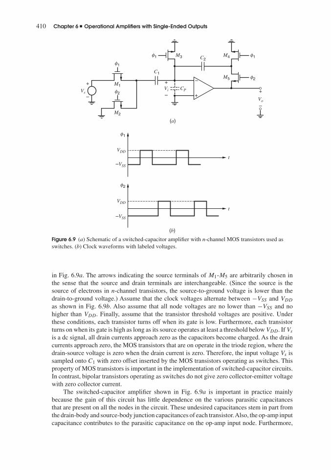
410 Chapter 6 � Operational Amplifiers with Single-Ended Outputs
1
M1
M3 M4
M5
C1
CP
Vo
C2
M2
Vs
VDD
VDD
–VSS
–VSS
Vi
(a)
(b)
t
t
+ +
+
–
+–
–
–
φ
1φ
1φ
2φ
2φ
1φ
2φ
Figure 6.9 (a) Schematic of a switched-capacitor amplifier with n-channel MOS transistors used asswitches. (b) Clock waveforms with labeled voltages.
in Fig. 6.9a. The arrows indicating the source terminals of M1-M5 are arbitrarily chosen inthe sense that the source and drain terminals are interchangeable. (Since the source is thesource of electrons in n-channel transistors, the source-to-ground voltage is lower than thedrain-to-ground voltage.) Assume that the clock voltages alternate between −VSS and VDD
as shown in Fig. 6.9b. Also assume that all node voltages are no lower than −VSS and nohigher than VDD. Finally, assume that the transistor threshold voltages are positive. Underthese conditions, each transistor turns off when its gate is low. Furthermore, each transistorturns on when its gate is high as long as its source operates at least a threshold below VDD. If Vs
is a dc signal, all drain currents approach zero as the capacitors become charged. As the draincurrents approach zero, the MOS transistors that are on operate in the triode region, where thedrain-source voltage is zero when the drain current is zero. Therefore, the input voltage Vs issampled onto C1 with zero offset inserted by the MOS transistors operating as switches. Thisproperty of MOS transistors is important in the implementation of switched-capacitor circuits.In contrast, bipolar transistors operating as switches do not give zero collector-emitter voltagewith zero collector current.
The switched-capacitor amplifier shown in Fig. 6.9a is important in practice mainlybecause the gain of this circuit has little dependence on the various parasitic capacitancesthat are present on all the nodes in the circuit. These undesired capacitances stem in part fromthe drain-body and source-body junction capacitances of each transistor.Also, the op-amp inputcapacitance contributes to the parasitic capacitance on the op-amp input node. Furthermore,

6.1 Applications of Operational Amplifiers 411
as described in Section 2.10.2, the bottom plates of capacitors C1 and C2 exhibit at least somecapacitance to the underlying layer, which is the substrate or a well diffusion. Since the gainof the circuit is determined by charge conservation at the op-amp input node, the presenceof parasitic capacitance from any node except the op-amp input to any node with a constantvoltage to ground makes no difference to the accuracy of the circuit. (Such parasitics do reducethe maximum clock rate, however.) On the other hand, parasitic capacitance on the op-ampinput node does affect the accuracy of the circuit gain, but the error is inversely proportionalto the op-amp gain, as we will now show.
Let CP represent the total parasitic capacitance from the op-amp input to all nodes withconstant voltage to ground. If the op-amp gain is a, the voltage from the inverting op-amp inputto ground during φ2 is given by (6.10). Therefore, with finite op-amp gain, C1 and CP are notcompletely discharged during φ2. Under these conditions, the charge stored on the op-ampinput node during φ2 becomes
Q2 =(
−Vo
a
)C1 +
(−Vo
a
)CP +
(−Vo
a− Vo
)C2 (6.29)
When the op-amp gain becomes infinite, (6.29) collapses to (6.27), as expected. Setting Q2 in(6.29) equal to Q1 in (6.26) by charge conservation gives
Vo
Vs
= C1
C2
⎡⎣ 1
1 + 1
a
(C1 + C2 + CP
C2
) ⎤⎦ (6.30)
This closed-loop gain can be written as
Vo
Vs
= C1
C2(1 − ε) (6.31)
where ε is a gain error given by
ε = 1
1 + a
(C2
C1 + C2 + CP
) (6.32)
As a → ∞, ε → 0, and the gain of the switched-capacitor amplifier approaches C1/C2 aspredicted in (6.28). As a result, the circuit gain is said to be parasitic insensitive to an extentthat depends on the op-amp gain.
One important parameter of the switched-capacitor amplifier shown in Fig. 6.9a is theminimum clock period. This period is divided into two main parts, one for each clock phase.The duration of φ2 must be long enough for the op-amp output to reach and stay within agiven level of accuracy. This time is defined as the op-amp settling time and depends on theswitch resistances, the circuit capacitances, and the op-amp properties. The settling time isusually determined by SPICE simulations. Such simulations should be run for both clockphases because the op-amp output voltage during φ1 is not well controlled in practice. If theop amp is ideal, this output voltage is zero. With nonzero offset voltage, however, the outputvoltage will be driven to a nonzero value during φ1 that depends on both the offset voltageand the op-amp gain. If the op-amp gain is large, the offset can easily be large enough to forcethe output voltage to clip near one of the supplies. The output voltage at the end of φ1 canbe thought of as an initial condition for the circuit during φ2. If the initial condition and thedesired final output at the end of φ2 happen to have far different values, the time required forthe output to reach a given level of accuracy during φ2 can be increased. Furthermore, nonzerooffset can increase the time required for the op-amp output voltage to reach a constant levelduring φ1. Although the circuit output voltage defined in (6.30) only appears during φ2, failure

412 Chapter 6 � Operational Amplifiers with Single-Ended Outputs
to reach a constant output voltage during φ1 causes the initial condition defined above to vary,depending on the value of Vo at the end of the preceding φ2. As a result of this memory effect,the circuit can behave as a filter (which is possibly nonlinear), weighting together the resultsof more than one previous input sample to determine any given output. The key point is that anincrease in the minimum duration of either phase requires an increase in the minimum clockperiod. This effect should be included in simulation by intentionally simulating with nonzerooffset voltages.
One way to reduce the effect of nonzero offset voltage on the minimum clock period is toinclude a reset switch at the op-amp output. If the op amp has a single-ended output as shown inFig. 6.9a, such a switch can be connected between the op-amp output and a bias point betweenthe two supplies. On the other hand, if the op amp has differential outputs as described inChapter 12, such a reset switch can be connected between the two op-amp outputs. In eithercase, the reset switch would be turned on during φ1 and off during φ2. The main value of sucha reset switch is that it can reduce both the maximum output voltage produced by a nonzerooffset voltage during φ1 and the time required to reach this value, in turn reducing the effectof nonzero offset on the minimum durations of both phases.
The accuracy of the switched-capacitor amplifier shown in Fig. 6.9a is limited by severalother factors that we will now consider briefly. First, even with an ideal op amp, the gaindepends on the ratio of capacitors C1/C2, which is not controlled perfectly in practice becauseof random-mismatch effects. Second, op-amp offset limits the minimum signal that can bedistinguished from the offset in the switched-capacitor amplifier. As shown in Section 3.5.6,the input-referred offset of CMOS differential pairs is usually worse than for bipolar differentialpairs. This property extends to op amps and stems partly from the reduced transconductance-to-current ratio of MOS transistors compared to their bipolar counterparts and partly from thethreshold mismatch term, which appears only in the MOS case. Third, the charge-conservationequation and accuracy of the switched-capacitor amplifier are affected by the charge storedunder the gates of some of the MOS transistors acting as switches in Fig. 6.9a. For example,some of the charge stored under the gate of transistor M3 in Fig. 6.9a is injected onto theop-amp input node after M3 is turned off. Techniques to overcome these limitations are oftenused in practice but are not considered here.
6.1.7.2 Switched-Capacitor IntegratorAnother application of an internal op amp, a switched-capacitor integrator, is illustrated in itssimplest form in Fig. 6.10a. This circuit is widely utilized as the basic element of monolithicswitched-capacitor filters for two main reasons. First, the frequency response of the integratoris insensitive to the various parasitic capacitances that are present on all nodes in the circuit.4,5
Second, using switched-capacitor integrators as the basic elements, the synthesis of desiredfilter frequency responses is relatively straightforward. In this section, we will analyze thefrequency response of the switched-capacitor integrator.
The integrator consists of an op amp, a sampling capacitor CS , an integrating capacitorCI , and four MOS transistor switches. The load capacitance shown represents the samplingcapacitor of the following integrator, plus any parasitic capacitances that may be present.Typical values for the sampling, integrating, and load capacitances are labeled in Fig. 6.10a.
Figure 6.10b shows the timing diagram of two nonoverlapping clock signals, φ1 and φ2,that control the operation of the circuit as well as typical input and output waveforms. Duringthe interval when clock phase φ1 is high, transistors M1 and M3 operate in the triode regionand serve to charge the sampling capacitor to a voltage that is equal to the input voltage.Subsequently, clock signal φ1 falls. Then clock signal φ2 rises, causing transistors M2 and M4to turn on and the sampling capacitor to be connected between the inverting op-amp input,which is sometimes called the summing node, and ground. If the op amp is ideal, the resulting

6.1 Applications of Operational Amplifiers 413
1
Vo
Vs
Vo[n]
Vs[n]
M1 M2
M3
CS ≈1 pF
Vs
M4
Vo
(a)
(b)
(c)
+
–
Top
CI ≈ 5 pF
CL ≈ 2 pF
+
–
–
+
t
t
t
t
Vo [n+1] = Vo[n] + CS
CIVs [n]
TimenT T T
Timen + 1
2
Time (n + 1)
++
–
–
+
–Vs Vo
CI
R = 1fCS
φ
1φ
2φ
2φ
Figure 6.10 (a) Schematic of aswitched-capacitor integrator.(b) Timing diagram. (c) Continuous-time equivalent circuit for inputfrequencies much less than the clockfrequency.
change in the summing-node voltage causes the op-amp output to move so that the summing-node voltage is driven back to ground. After the transient has gone to completion, the voltageacross CS is driven to zero.
To find the relationship between the input and output, a charge-conservation analysisis used. After transistor M1 opens in Fig. 6.10a, the charge on the plates of the capacitorsconnected to node Top and the inverting op-amp input is conserved until M1 closes again.Define time points [n] and [n + 1/2] as the time indexes at which φ1 and φ2 first fall inFig. 6.10b, respectively. Point [n + 1] is defined as the next time index at which φ1 falls. Thepoints [n] and [n + 1] are separated by one clock period T. If the switches and the op amp are
414 Chapter 6 � Operational Amplifiers with Single-Ended Outputs
ideal, the charge stored at time index [n] is
Q[n] = (0 − Vs[n])CS + (0 − Vo[n])CI (6.33)
Under the same conditions, the charge stored at time index [n + 1/2] is
Q[n + 1/2] = (0)CS + (0 − Vo[n + 1/2])CI (6.34)
From charge conservation, Q[n + 1/2] = Q[n]. Also, the charge stored on CI is constant dur-ing φ1 under these conditions; therefore, Vo[n + 1] = Vo[n + 1/2]. Combining these relationsgives
Vo[n + 1] = Vo[n] +(
CS
CI
)Vs[n] (6.35)
Thus, one complete clock cycle results in a change in the integrator output voltage that isproportional to the value of the input voltage and to the capacitor ratio.
Equation 6.35 can be used to find the frequency response of the integrator by using the factthat the operation of delaying a signal by one clock period T in the time domain correspondsto multiplication by the factor e−jωT in the frequency domain. Thus
Vo(jω) = Vo(jω)e−jωT +(
CS
CI
)Vs(jω)e−jωT (6.36)
Therefore, the integrator frequency response is
Vo
Vs
(jω) = −CS
CI
(1
1 − ejωT
)= CS
CI
(2j
ejωT/2 − e−jωT/2
)(e−jωT/2
2j
)(6.37)
Using the identity
sin x = 1
2j(ejx − e−jx) (6.38)
in (6.37) with x = ωT/2 we find
Vo
Vs
(jω) = CS
CI
(ωT/2
sin ωT/2
)(e−jωT/2
2jωT/2
)= 1
jω
ωo
(ωT/2
sin ωT/2e−jωT/2
)(6.39)
where
ωo = CS
TCI
= fCS
CI
= 1
�(6.40)
where � is the time constant of the integrator. Here f is the clock frequency, equal to 1/T . Forinput frequencies that are much less than the clock frequency, the quantity ωT is much less thanunity, and the right-most term in parentheses in (6.39) reduces to unity. The remaining termis simply the frequency response of an analog integrator, as desired. In practical designs, theexcess phase and magnitude error contributed by the term in parentheses in (6.39) must oftenbe taken into account. From a conceptual standpoint, however, the circuit can be thought of asproviding an analog integration of the signal. Note that the time constant of the integrator is thesame as would occur if the sampling capacitor and switches were replaced by a continuous-value resistor of value (1/fCS). This equivalence is illustrated in Fig. 6.10c.
A key advantage of a switched-capacitor integrator compared to its continuous-timecounterpart is that the time constant of the switched-capacitor integrator can be much bet-ter controlled in practice. The time constant of a continuous-time integrator depends on theproduct of a resistance and a capacitance as in (6.22). In monolithic technologies, resistance and

6.2 Deviations from Ideality in Real Operational Amplifiers 415
capacitance values do not track each other. Therefore, the time constant of a continuous-timeintegrator is not well controlled over variations in process, supply, and temperature in general.However, the time constant of a switched-capacitor integrator is determined by the ratio oftwo capacitor values and the clock frequency, as in (6.40). If the two capacitors have the sameproperties, the ratio is well controlled even when the absolute values are poorly controlled.Since the clock frequency can be precisely determined by a crystal-controlled clock genera-tor, the time constant of a switched-capacitor integrator can be well controlled in monolithictechnologies.
A key requirement for the op amps in Figs. 6.9a and 6.10a is that dc currents at the inputterminals must be extremely small to minimize the loss of charge over the time when theabove analyses assumed that charge was conserved. Therefore, switched-capacitor amplifiersand integrators are ideally suited to the use of op amps with MOS transistors in the input stage.
6.2 Deviations from Ideality in Real Operational AmplifiersReal op amps deviate from ideal behavior in significant ways. The main effects of thesedeviations are to limit the frequency range of the signals that can be accurately amplified,to place a lower limit on the magnitude of dc signals that can be detected, and to place anupper limit on the magnitudes of the impedance of the passive elements that can be used in thefeedback network with the amplifier. This section summarizes the most important deviationsfrom ideality and their effects in applications.
6.2.1 Input Bias Current
An input stage for a bipolar transistor op amp is shown in Fig. 6.11. Here Q1 and Q2 are theinput transistors of the amplifier. The base currents of Q1 and Q2 flow into the amplifier inputterminals, and the input bias current is defined as the average of the two input currents:
IBIAS = IB1 + IB2
2(6.41)
Nonzero bias current violates the assumption made in summing-point analysis that the currentinto the input terminals is zero. Typical magnitudes for the bias current are 10 to 100 nA
Q1 Q2
IB2IB1
RC1 RC2
IEE
–VEE
+VCC
Figure 6.11 Typical op-amp input stage.

416 Chapter 6 � Operational Amplifiers with Single-Ended Outputs
for bipolar input devices and less than 0.001 pA for MOS input devices. In dc inverting andnoninverting amplifiers, this bias current can cause undesired voltage drops in the resistorsforming the feedback network, with the result that a residual dc voltage appears at the outputwhen the amplifier is ideal in all other ways and the external input voltage is zero. In integratorcircuits, the input bias current is indistinguishable from the current being integrated and causesthe output voltage to change at a constant rate even when Vs is zero. To the extent that thecurrents are equal in the two input leads, however, their effects can be canceled in someapplications by including a balancing resistor in series with one of the input leads so that thesame resistance is seen looking away from each op-amp input. For example, the differentialamplifier of Fig. 6.4 produces zero output with V1 = V2 = 0 if identical currents flow in bothop-amp input leads. In practice, however, the two input currents are not exactly equal becauseof random mismatches, causing nonzero output in Fig. 6.4 when V1 = V2 = 0.
6.2.2 Input Offset Current
For the emitter-coupled pair shown in Fig. 6.11, the two input bias currents will be equal onlyif the two transistors have equal betas. Geometrically identical devices on the same IC dietypically display beta mismatches that are described by a normal distribution with a standarddeviation of a few percent of the mean value. Since this mismatch in the two currents variesrandomly from circuit to circuit, it cannot be compensated by a fixed resistor. This aspect ofop-amp performance is characterized by the input offset current, defined as
IOS = IB1 − IB2 (6.42)
Consider the differential amplifier in Fig. 6.4. Repeating the analysis in Section 6.1.4 forthat circuit with nonzero IOS and V1 = V2 = 0 gives a dc output voltage of
VO = (IB2 − IB1)R2 = −IOSR2 (6.43)
If IOS = 0, then VO = 0 here. This equation shows that the error in the dc output voltage isproportional to both the input offset current and the feedback resistance under these conditions.The key point is that the size of the feedback resistance is limited by the maximum offset currentthat can arise and by the allowed error in the dc output voltage in practice. See Problem 6.6.
6.2.3 Input Offset Voltage
As described in Chapter 3, mismatches result in nonzero input offset voltage in amplifiers.The input offset voltage is the differential input voltage that must be applied to drive theoutput to zero. For untrimmed monolithic op amps, this offset is typically 0.1 to 2 mV forbipolar input devices and 1 to 20 mV for MOS input devices. This offset can be nulled withan external potentiometer in the case of stand-alone op amps; however, the variation of offsetwith temperature (called drift) does not necessarily go to zero when the input offset is nulled.In dc amplifier applications, the offset and drift place a lower limit on the magnitude of the dcvoltage that can be accurately amplified. In some sampled-data applications such as switched-capacitor filters, the input offset voltage of the op amp is sampled and stored on the capacitorsevery clock cycle. Thus the input offset is effectively canceled and is not a critical parameter.This same principle is used in chopper-stabilized op amps.
6.2.4 Common-Mode Input Range
The common-mode input range is the range of dc common-mode input voltages for which an opamp behaves normally with its key parameters, including offset voltage and input bias current,

6.2 Deviations from Ideality in Real Operational Amplifiers 417
within specifications. Many years ago, op amps were usually designed to use large equal-and-opposite power-supply voltages. For example, the 741 op amp, described in previous editions ofthis book, often operated with supply voltages of �15 V, with a corresponding common-modeinput range of about �13 V. In contrast, modern op amps often operate between ground andone positive power-supply voltage of 3 V or less. If the common-mode input range were limitedto be 2 V above ground and 2 V below the positive supply in this case, the input stage in suchop amps would not operate properly for any common-mode input voltage. Although reducingthe gap between the common-mode input range and the supplies overcomes this problem,the inverting amplifier configuration shown in Fig. 6.3a cannot be used without modificationwhen the op amp operates from a single nonzero supply voltage unless the common-mode inputrange is extended to include ground. In practice, including both power-supply voltages in thecommon-mode input range is often important. For example, in the noninverting amplifier andvoltage follower shown in Fig. 6.3b and Fig. 6.3c, respectively, the op-amp common-modeinput voltage is approximately equal to Vs. Extending the common-mode input range to includeboth supplies avoids an unnecessary limit to op-amp performance in these configurations.Section 6.8 describes an example op amp with this property, which is called a rail-to-railcommon-mode input range.
6.2.5 Common-Mode Rejection Ratio (CMRR)
If an op amp has a differential input and a single-ended output, its small-signal output voltagecan be described in terms of its differential and common-mode input voltages (vid and vic) bythe following equation
vo = Admvid + Acmvic (6.44)
where Adm is the differential-mode gain and Acm is the common-mode gain. As defined in(3.187), the common-mode rejection ratio of the op amp is
CMRR =∣∣∣∣Adm
Acm
∣∣∣∣ (6.45)
From an applications standpoint, the CMRR can be regarded as the change in input offsetvoltage that results from a unit change in common-mode input voltage. For example, assumethat we apply zero common-mode input voltage to the amplifier and then apply just enoughdifferential voltage to the input to drive the output voltage to zero. The dc voltage we haveapplied is just the input offset voltage VOS . If we keep the applied differential voltage constantand increase the common-mode input voltage by an amount �Vic, the output voltage willchange, by an amount
vo = �Vo = Acm�Vic = Acmvic (6.46)
To drive the output voltage back to zero, we will have to change the differential input voltageby an amount
vid = �Vid = �Vo
Adm
= Acm�Vic
Adm
(6.47)
Thus we can regard the effect of finite CMRR as causing a change in the input offset voltagewhenever the common-mode input voltage is changed. Using (6.45) and (6.47), we obtain
CMRR =∣∣∣∣Adm
Acm
∣∣∣∣ =(
�Vid
�Vic
∣∣∣∣Vo=0
)−1
=(
�VOS
�Vic
)−1
�(
∂VOS
∂Vic
∣∣∣∣Vo=0
)−1
(6.48)

418 Chapter 6 � Operational Amplifiers with Single-Ended Outputs
In circuits such as the differential amplifier of Fig. 6.11, an offset voltage is produced thatis a function of the common-mode signal input, producing a voltage at the output that isindistinguishable from the desired signal. For a common-mode rejection ratio of 104 (or80 dB), (6.48) shows that a 10-V common-mode signal produces a 1-mV change in the inputoffset voltage.
6.2.6 Power-Supply Rejection Ratio (PSRR)
In (6.44), we assumed that the power-supply voltages are constant so that the op-amp outputvoltage depends only on the differential and common-mode input voltages provided to the opamp. In practice, however, the power-supply voltages are not exactly constant, and variations inthe power-supply voltages contribute to the op-amp output. Figure 6.12 shows a block diagramof an op amp with varying power-supply voltages. The small-signal variation on the positiveand negative power supplies is vdd and vss, respectively. If vic = 0 is assumed for simplicity,the resulting small-signal op-amp output voltage is
vo = Admvid + A+vdd + A−vss (6.49)
where A+ and A− are the small-signal gains from the positive and negative power-suppliesto the output, respectively. Since op amps should be sensitive to changes in their differential-mode input voltage but insensitive to changes in their supply voltages, this equation is rewrittenbelow in a form that simplifies comparison of these gains:
vo = Adm
(vid + A+
Adm
vdd + A−
Adm
vss
)(6.50)
= Adm
(vid + vdd
PSRR+ + vss
PSRR−)
where
PSRR+ = Adm
A+ and PSRR− = Adm
A− (6.51)
Figure 6.13 shows one way to interpret (6.50), where the diagram in Fig. 6.12 is redrawn usingan op amp with constant power supplies. To set the output in Fig. 6.13 equal to that in Fig.6.12, the power-supply variations from Fig. 6.12 are included as equivalent differential inputs
vid
2
vid
2
++
–
–
+
–
+
–vic
+
+
–
–vdd
+
–vss
vo
–VSS
VDD
Figure 6.12 Block diagram of an op amp with varying power- supply voltages.

6.2 Deviations from Ideality in Real Operational Amplifiers 419
vid
2
vdd
PSRR+
vss
PSRR–
vid
2
++
–
–
+
–
–
+
–vo
VSS
VDD
+–+–
Figure 6.13 Block diagram of an op amp with supply variations modeled in the input differential loopand with vic = 0.
in Fig. 6.13. Equation 6.50 and Fig. 6.13 show that the power-supply rejection ratios should bemaximized to minimize the undesired contributions to the op-amp output voltage. In practice,the power-supply rejection ratios are functions of frequency and often decrease for increasingfrequency.
Power-supply rejection ratio has become an increasingly important parameter in MOSamplifier design as the level of integration increases. With small-scale integration, few tran-sistors could be integrated on one integrated circuit. Therefore, analog and digital functionswere isolated from each other on separate chips, avoiding some coupling from the digitalcircuits to the analog supplies. Also, such separation provides an opportunity to filter interfer-ence generated by the digital circuits at the printed-circuit-board level with external capacitorsconnected in parallel with the supplies. With large-scale integration, however, many transis-tors can be integrated on one integrated circuit. Integrating analog and digital functions onthe same chip reduces cost but increases the coupling from the digital circuits to the ana-log supplies. In principle, monolithic filter capacitors can be used to reduce the resultingsupply variations; however, the required areas of such capacitors are large in practice. Forexample, if the oxide thickness is 100 Å, the capacitance per unit area is 3.45 fF/�m2. Fora capacitor of 0.01 �F (a commonly used value to filter supplies on printed-circuit boards),the required area is 1.7 mm2. Since many integrated circuits occupy areas less than 100 mm2,this single capacitor would account for a significant fraction of the cost of many integratedcircuits.
To reduce the cost, instead of concentrating only on reducing supply variations through fil-tering, another option is to build circuits with low sensitivities to power-supply variations. Theuse of fully differential circuit techniques has emerged as an important tool in this effort. Fullydifferential circuits represent all signals of interest as differences between two correspondingquantities such as voltages or currents. If two identical signal paths are used to determinecorresponding quantities, and if the coupling from supply variations to one quantity is thesame as to the other quantity, the difference can be independent of the supply variations andthe coupling in principle. In practice, mismatches cause differences in the two signal paths,and the coupling may not be identical, causing imperfect cancellation. Also, if the power-supply noise is large enough, nonlinearity may result and limit the extent of the cancellation.Although the op amps considered in this chapter have differential inputs, they are not fullydifferential because their outputs are single-ended. Fully differential op amps are considered inChapter 12.

420 Chapter 6 � Operational Amplifiers with Single-Ended Outputs
6.2.7 Input Resistance
In bipolar transistor input stages, the input resistance is typically in the 100 k to 1 M range.Usually, however, the voltage gain is large enough that this input resistance has little effect oncircuit performance in closed-loop feedback configurations.
Op amps whose inputs are connected to the gates of MOS transistors have essentiallyinfinite input resistance in principle. In practice, however, MOS-transistor gates connectedthrough package pins to the outside world must be protected against damage by static electricity.This protection is typically achieved by connecting back-biased clamping diodes from VDD
and VSS to the gate, and thus the effective input leakage currents are determined by junctionleakage and are of the order of picoamps. However, protection is required only at the inputs andoutputs of integrated circuits. In internal applications, where op-amp inputs are not connectedto the external pins of an integrated circuit, protection is not required and op amps with MOStransistor gates as inputs do realize ultra-high input resistance.
6.2.8 Output Resistance
General-purpose bipolar op amps usually use a buffer as an output stage, which typicallyproduces an output resistance on the order of 40 to 100 . On the other hand, in MOStechnologies, internal op amps usually do not have to drive resistive loads. Therefore, internalMOS op amps usually do not use a buffer output stage, and the resulting output resistance canbe much larger than in the bipolar case. In both cases, however, the output resistance does notstrongly affect the closed-loop performance except as it affects stability under large capacitiveloading, and in the case of power op amps that must drive a small load resistance.
6.2.9 Frequency Response
Because of the capacitances associated with devices in the op amp, the voltage gain decreases athigh frequencies. This fall-off must usually be controlled by the addition of extra capacitance,called compensation capacitance, to ensure that the circuit does not oscillate when connectedin a feedback loop. (See Chapter 9.) This aspect of op-amp behavior is characterized by theunity-gain bandwidth, which is the frequency at which the magnitude of the open-loop voltagegain is equal to unity. For general-purpose amplifiers, this frequency is typically in the 1 to100 MHz range. This topic is considered in detail in Chapters 7 and 9.
A second aspect of op-amp high-frequency behavior is a limitation of the rate at which theoutput voltage can change under large-signal conditions. This limitation stems from the limitedcurrent available within the circuit to charge the compensation capacitor. This maximum rate,called the slew rate, is described more extensively in Chapter 9.
6.2.10 Operational-Amplifier Equivalent Circuit
The effect of some of these deviations from ideality on the low-frequency performance of an opamp in a particular application can be calculated using the equivalent circuit shown in Fig. 6.14.(This model does not include the effects of finite PSRR or CMRR.) Here, the two current sourceslabeled IBIAS represent the average value of dc current flowing into the input terminals. Thepolarity of these current sources shown in Fig. 6.14 applies for an npn transistor input stage. Thecurrent source labeled IOS represents the difference between the currents flowing into the ampli-fier terminals. For example, if a particular circuit displayed a current of 1.5 �A flowing intothe noninverting input terminal and a current of 1 �A flowing into the inverting input terminal,then the value of IBIAS in Fig. 6.14 would be 1.25 �A, and the value of IOS would be 0.5 �A.

6.3 Basic Two-Stage MOS Operational Amplifiers 421
++ –
+
–
–
Ro
Ri
VOS
IOS
IBIAS
IBIAS
2vi
a(j )viω
Figure 6.14 Equivalent circuit for the operational amplifier including input offset voltage and current,input and output resistance, and voltage gain.
6.3 Basic Two-Stage MOS Operational AmplifiersFigure 6.15 shows a schematic of a basic two-stage CMOS op amp.6,7,8 A differential inputstage drives an active load followed by a second gain stage. An output stage is usually notused but may be added for driving heavy loads off-chip. This circuit configuration providesgood common-mode range, output swing, voltage gain, and CMRR in a simple circuit that canbe compensated with a single capacitor. The circuit is redrawn in Fig. 6.16, where the idealcurrent sources are replaced with transistor current mirrors. In this section, we will analyze thevarious performance parameters of this CMOS op-amp circuit.
VDD
–VSS
CC
vo
vi
I1 I2
+
–
Figure 6.15 Basic two-stage CMOSoperational amplifier.

422 Chapter 6 � Operational Amplifiers with Single-Ended Outputs
+
+
–
–
+
–
–VSS
M8 M5 M7
M1
M3 M4 M6
CC
M2
VDD
IBIAS
vi
VO1 + vo1
VO + vo
Figure 6.16 More detailedschematic diagram of atypical two-stage CMOSoperational amplifier.
6.3.1 Input Resistance, Output Resistance, and Open-Circuit Voltage Gain
The first stage in Fig. 6.16 consists of a p-channel differential pair M1-M2 with an n-channelcurrent mirror load M3-M4 and a p-channel tail current source M5. The second stage con-sists of an n-channel common-source amplifier M6 with a p-channel current-source load M7.Because the op-amp inputs are connected to the gates of MOS transistors, the input resistanceis essentially infinite when the op amp is used in internal applications, which do not requirethe protection diodes described in Section 6.2.7. For the same reason, the input resistance ofthe second stage of the op amp is also essentially infinite.
The output resistance is the resistance looking back into the second stage with the op-ampinputs connected to small-signal ground:
Ro = ro6||ro7 (6.52)
Although this output resistance is almost always much larger than in general-purpose bipolarop amps, low output resistance is usually not required when driving purely capacitive loads.
Since the input resistance of the second stage is essentially infinite, the voltage gain of theamplifier in Fig. 6.16 can be found by considering the two stages separately. The first stage isprecisely the same configuration as that considered in Section 4.3.5. The small-signal voltagegain is
Av1 = vo1
vi
= Gm1Ro1 (6.53)
where Gm1 and Ro1 are the transconductance and output resistance of the first stage, respec-tively. From (4.143) and (4.149),
Av1 = gm1(ro2||ro4) (6.54)

6.3 Basic Two-Stage MOS Operational Amplifiers 423
Similarly, the second-stage voltage gain is
Av2 = −gm6Ro (6.55)
where Ro is given in (6.52). As a result, the overall gain of the amplifier is
Av = Av1Av2 = −gm1(ro2||ro4)gm6(ro6||ro7) (6.56)
This equation shows that the overall gain is related to the quantity (gmro)2. Recall from (3.27)that
gmro = 2VA
Vov(6.57)
Therefore, the overall voltage gain is a strong function of the Early voltage (which is propor-tional to the effective channel length) and the overdrive (which is set by the bias conditions).
EXAMPLE
Calculate the gain of the op amp in Fig. 6.16 assuming that it uses the 0.8-�m process technol-ogy described in Table 2.3. Also, assume that Leff = 0.8 �m and |Vov | = |VGS − Vt| = 0.2 Vfor all devices.
Let ID2, ID4, ID6, and ID7 represent the bias currents flowing into the drains of M2, M4,M6, and M7, respectively. Since ID4 = −ID2 and ID7 = −ID6, (6.56) shows that
Av = −gm1
⎛⎜⎜⎝
|VA2||ID2|
VA4
|ID2||VA2||ID2| + VA4
|ID2|
⎞⎟⎟⎠ gm6
⎛⎜⎜⎝
VA6
ID6
|VA7|ID6
VA6
ID6+ |VA7|
ID6
⎞⎟⎟⎠
(6.58)
= − gm1
|ID2|gm6
ID6
( |VA2|VA4
|VA2| + VA4
)(VA6|VA7|
VA6 + |VA7|)
where the absolute-value function has been used so that each quantity in (6.58) is positive.From (1.181),
Av = − 2
|Vov1|2
Vov6
( |VA2|VA4
|VA2| + VA4
)(VA6|VA7|
VA6 + |VA7|)
(6.59)
because ID1 = ID2 with zero differential input. From (1.163),
VA = Leff
(dXd
dVDS
)−1
(6.60)
Substituting (6.60) into (6.59) with the given data and dXd/dVDS from Table 2.3 gives
Av = − 2
0.2
2
0.2
⎛⎜⎝
0.8
0.04× 0.8
0.080.8
0.04+ 0.8
0.08
⎞⎟⎠
2
� −4400
The overall gain can be increased by either increasing the channel lengths of the devicesto increase the Early voltages or by reducing the bias current to reduce the overdrives.
6.3.2 Output Swing
The output swing is defined to be the range of output voltages Vo = VO + vo for which alltransistors operate in the active region so that the gain calculated in (6.56) is approximately

424 Chapter 6 � Operational Amplifiers with Single-Ended Outputs
constant. From inspection of Fig. 6.16, M6 operates in the triode region if the output voltage isless than Vov6 − VSS . Similarly, M7 operates in the triode region if the output voltage is morethan VDD − |Vov7|. Therefore, the output swing is
Vov6 − VSS ≤ Vo ≤ VDD − |Vov7| (6.61)
This inequality shows that the op amp can provide high gain while its output voltage swingswithin one overdrive of each supply. Beyond these limits, one of the output transistors entersthe triode region, where the overall gain of the amplifier would be greatly diminished. As aresult, the output swing can be increased by reducing the overdrives of the output transistors.
6.3.3 Input Offset Voltage
In Sections 3.5.6 and 6.2.3, the input offset voltage of a differential amplifier was defined asthe differential input voltage for which the differential output voltage is zero. Because the opamp in Fig. 6.16 has a single-ended output, this definition must be modified here. Referring tothe voltage between the output node and ground as the output voltage, the most straightforwardmodification is to define the input offset voltage of the op amp as the differential input voltagefor which the op-amp output voltage is zero. This definition is reasonable if VDD = VSS becausesetting the output voltage to zero maximizes the allowed variation in the output voltage beforeone transistor operates in the triode region provided thatVov6 = |Vov7|. IfVDD /= VSS , however,the output voltage should be set midway between the supply voltages to maximize the outputswing. Therefore, we will define the input offset voltage of op amps with differential inputsand single-ended outputs as the differential input voltage for which the dc output voltage ismidway between the supplies.
The offset voltage of an op amp is composed of two components: the systematic offsetand the random offset. The former results from the design of the circuit and is present evenwhen all the matched devices in the circuit are identical. The latter results from mismatches insupposedly identical pairs of devices.
Systematic Offset Voltage. In bipolar technologies, the gain of each stage in an op amp canbe quite high (on the order of 500) because the gmro product is usually greater than 1000. Asa result, the input-referred offset voltage of a bipolar op amp usually depends mainly on thedesign of the first stage. In MOS technologies, however, the gmro product is usually betweenabout 20 and 100, reducing the gain per stage and sometimes causing the offset of the secondstage to play an important role in determining the op-amp offset voltage.
To study the systematic offset, Fig. 6.17 shows the op amp of Fig. 6.16 split into twoseparate stages. If the inputs of the first stage are grounded, and if the matching is perfect, thenthe dc drain-source voltage of M4 must be equal to the dc drain-source voltage of M3. This resultstems from the observation that if VDS3 = VDS4, then VDS1 = VDS2 and ID1 = ID2 = ID5/2.Therefore, with VDS3 = VDS4, ID3 = ID4 = −ID5/2. As a result, VDS3 must be equal to VDS4because this operating point is the only point for which the current flowing out of the drainof M2 is equal to the current flowing into the drain of M4. For example, increasing the drain-source voltage of M4 would increase the current flowing into the drain of M4 but decrease thecurrent flowing out of the drain of M2 because of the effects of channel-length modulation.Therefore, the dc drain-source voltages of M3 and M4 must be equal under these conditions.
On the other hand, the value of the gate-source voltage of M6 required to set the amplifieroutput voltage midway between the supplies may differ from the dc output voltage of the firststage. If the first stage gain is 50, for example, each 50-mV difference in these voltages resultsin 1 mV of input-referred systematic offset. Ignoring channel-length modulation in M5 andM7, the current in these transistors is independent of their drain-source voltages if they operate

6.3 Basic Two-Stage MOS Operational Amplifiers 425
M5 M7
M6
M3 M4
vo
vo1 vi2
M1 M2
BIAS
VDD
–VSS
+ +
– –
Figure 6.17 Two-stage amplifierwith first and second stagesdisconnected to show the effectof interstage coupling on input-referred offset voltage.
in the active region. To set the output voltage midway between the supplies, the gate-sourcevoltage of M6 should be chosen so that the drain current of M6 is equal to the drain current ofM7 while both transistors operate in the active region. When the input of the second stage isconnected to the output of the first stage, VGS6 = VDS4. With perfect matching and zero inputvoltages, VDS4 = VDS3 = VGS3 and Vt3 = Vt4 = Vt6. Therefore,
Vov3 = Vov4 = Vov6 (6.62)
is required. Substituting (1.166) into (6.62) gives
ID3
(W/L)3= ID4
(W/L)4= ID6
(W/L)6(6.63)
In other words, requiring that the transistors have equal overdrives is equivalent to requiring thatthey have equal drain-current-to-W/L ratios (or current densities). Since ID3 = ID4 = |ID5|/2and ID6 = |ID7|,
|ID5|2(W/L)3
= |ID5|2(W/L)4
= |ID7|(W/L)6
(6.64)
Since M5 and M7 have equal gate-source voltages,
ID5
ID7= (W/L)5
(W/L)7(6.65)
Substituting (6.65) into (6.64) gives
(W/L)3
(W/L)6= (W/L)4
(W/L)6= 1
2
(W/L)5
(W/L)7(6.66)
With the aspect ratios chosen to satisfy (6.66), M3, M4, and M6 operate with equal currentdensities. In the active region, the current density of a device depends not only on its gate-sourcevoltage, but also on its drain-source voltage to some extent. Since the gate-source voltages andcurrent densities of M3, M4, and M6 are equal, the drain-source voltages of these transistors

426 Chapter 6 � Operational Amplifiers with Single-Ended Outputs
must also be equal. Therefore, the dc output voltage under these conditions is
VO = VDS6 − VSS = VDS3 − VSS = VGS3 − VSS = Vt3 + Vov3 − VSS (6.67)
To find the systematic offset voltage at the op-amp output, the output voltage in (6.67) should besubtracted from a voltage midway between the supplies. To refer the systematic offset voltageto the op-amp input, this difference should be divided by the op-amp gain. The result is
VOS(sys) =VDD − VSS
2− (Vt3 + Vov3 − VSS)
Av(6.68)
where Av is the op-amp gain given in (6.56). In most cases, the dc output voltage will notbe midway between the supplies because VGS3 = Vt3 + Vov3 /= (VDD + VSS)/2. Therefore,the systematic offset is usually nonzero. Although the systematic offset voltage is nonzero ingeneral, the choice of aspect ratios as given in (6.66) can result in an operating point that isinsensitive to process variations, as explained next.
Equation 2.35 shows that the effective channel length of a MOS transistor differs fromits drawn length by offset terms caused by the side diffusion of the source and drain (Ld) andthe depletion region width around the drain (Xd). Similarly, the effective width of a MOStransistor differs from the drawn width by an offset term dW caused by the bird’s-beak effectin the oxide described in Section 2.9.1. To keep the ratio in (6.66) constant in the presenceof process-induced variations in Ld , Xd , and dW, the drawn channel lengths and widths ofthe ratioed transistors can each be chosen to be identical. In this case, the ratio in (6.66) canbe set equal to any rational number J/K by connecting J identical devices called n-channelunits in parallel to form M3 and M4 while K n-channel units in parallel form M6. Then ifM5 is constructed of 2J identical devices called p-channel units, M7 should be constructedfrom K p-channel units. In practice for matched devices, the channel lengths are almost neverratioed directly because the use of small channel lengths for high-speed operation would resultin a large sensitivity to process variations. On the other hand, the channel widths of matcheddevices are sometimes ratioed directly when the width is large enough to make the resultingsensitivity to process variations insignificant.
A key point of this analysis is that the use of identical channel lengths for M3, M4, andM6 conflicts with a combination of other requirements. First, for stability reasons described inChapter 9, M6 should have a large transconductance and thus a short channel length. Second, forlow noise and random input offset voltage, M3 and M4 should have a small transconductanceand therefore a long channel length. Noise is considered in Chapter 11, and random input offsetvoltage is considered next.
Random Input Offset Voltage. As described in Section 3.5.6, source-coupled pairs generallydisplay a higher random offset than their bipolar counterparts. Ignoring the contribution of thesecond stage in the op amp to the input-referred random offset, a straightforward analysis forthe offset voltage of the circuit of Fig. 6.16, which is analogous to the analysis leading to(3.248), gives
VOS � �Vt(1−2) + �Vt(3−4)
(gm3
gm1
)
(6.69)
+Vov(1−2)
2
⎡⎢⎢⎢⎣
�
(W
L
)(3−4)(
W
L
)(3−4)
−�
(W
L
)(1−2)(
W
L
)(1−2)
⎤⎥⎥⎥⎦

6.3 Basic Two-Stage MOS Operational Amplifiers 427
The first term represents the threshold mismatch of the input transistors. The second is thethreshold mismatch of the current-mirror-load devices and is minimized by choosing the W/L
ratio of the load devices so that their transconductance is small compared to that of the inputtransistors. For this reason, selecting a longer channel length for M3 and M4 than for M1and M2 reduces the random input offset voltage. The third term represents the effects of W/L
mismatches in the input transistors and loads and is minimized by operating the input transistorsat low values of overdrive, typically on the order of 50 to 200 mV.
6.3.4 Common-Mode Rejection Ratio
For the op amp in Fig. 6.16, (6.45) gives
CMRR =∣∣∣∣Adm
Acm
∣∣∣∣ =∣∣∣∣∣∣∣
vo
vo1
vo1
vidvo
vo1
vo1
vic
∣∣∣∣∣∣∣ = CMRR1 (6.70)
where CMRR1 is the common-mode rejection ratio of the first stage. The second stage doesnot contribute to the common-mode rejection ratio of the op amp because the second stagehas a single-ended input and a single-ended output. In (4.182) and (4.183), the common-moderejection ratio of a stage with a differential pair and a current-mirror load was calculatedassuming perfect matching. Applying (4.183) here gives
CMRR � (2gm(dp)rtail)gm(mir)(ro(dp)||ro(mir)) (6.71)
where gm(dp) and ro(dp) are the transconductance and output resistance of M1 and M2, gm(mir)and ro(mir) are the transconductance and output resistance of M3 and M4, and rtail is the outputresistance of M5. By a process similar to the derivation of (6.59), this equation can be simplifiedto give
CMRR �∣∣∣∣ 2
Vov(dp)
2
Vov(mir)
(VA(dp)VA(mir)
|VA(dp)| + |VA(mir)|)∣∣∣∣ (6.72)
where Vov(dp) and VA(dp) are the overdrive and Early voltage of the differential pair, andVov(mir) and VA(mir) are the overdrive and Early voltage of the mirror. Equation 6.72 showsthat the common-mode rejection ratio of the op amp can be increased by reducing the overdrivevoltages.
Another way to increase the common-mode rejection ratio is to replace the simple currentmirror M5 and M8 with one of the high-output-resistance current mirrors considered in Chap-ter 4. Unfortunately, such a replacement would also worsen the common-mode input range.
6.3.5 Common-Mode Input Range
The common-mode input range of the op amp in Fig. 6.16 is the range of dc common-modeinput voltages for which all transistors in the first stage operate in the active region. To operatein the active region, the gate-drain voltages of n-channel transistors must be less than theirthresholds so that their channels do not exist at their drains. Similarly, p-channel transistorsoperate in the active region only if their gate-drain voltages are more than their thresholds,again so that their channels do not exist at their drains. With a pure common-mode input VIC
applied to the inputs of the op amp in Fig. 6.16,
VDS4 = VDS3 = VGS3 = Vt3 + Vov3 (6.73)

428 Chapter 6 � Operational Amplifiers with Single-Ended Outputs
The gate-drain voltage of M1 and M2 is
VGD1 = VGD2 = VIC − Vt3 − Vov3 + VSS (6.74)
When VIC is reduced to the point at which VGD1 = VGD2 = Vt1 = Vt2, M1 and M2 operateat the edge between the the triode and active regions. This point defines the lower end of thecommon-mode range, which is
VIC > Vt1 + Vt3 + Vov3 − VSS (6.75)
If VIC is too high, however, M5 operates in the triode region. The drain-source voltage ofM5 is
VDS5 = VIC − VGS1 − VDD = VIC − Vt1 − Vov1 − VDD (6.76)
From the standpoint of drain-source voltages, n-channel transistors operate in the active regiononly if their drain-source voltage is more than their overdrive. On the other hand, p-channeltransistors operate in the active region only if their drain-source voltage is less than theiroverdrive. Therefore, the upper end of the common-mode input range is
VIC < Vt1 + Vov1 + Vov5 + VDD (6.77)
Since M1 and M5 are p-channel transistors, their overdrives are negative; that is, theirgate-source voltages must be less than their thresholds for the channel to exist at the source.Furthermore, if M1 is an enhancement-mode device, its threshold is negative because it isp-type. Under this assumption, the common-mode range limits in (6.75) and (6.77) can berewritten as
Vt3 − |Vt1| + Vov3 − VSS < VIC < VDD − |Vt1| − |Vov1| − |Vov5| (6.78)
This inequality shows that the magnitudes of the overdrive terms should be minimized tomaximize the common-mode range. Also, the body effect on the input transistors can be usedto increase the range. If the bodies of M1 and M2 are connected to VDD as implied in Fig. 6.16,the source-body voltage of these transistors is low when VIC is high. Therefore, the upper limitin (6.78) can be found approximately by using the zero-bias value of Vt1. On the other hand,when VIC decreases, the source-body voltage of M1 and M2 becomes more negative, wideningthe depletion region around the source and making the threshold voltage of these transistorsmore negative. Therefore, the body effect can be used to include the negative supply in thecommon-mode range.
EXAMPLE
For the two-stage CMOS op amp in Fig. 6.16, choose the device sizes to give a dc voltagegain greater than 5000 and a peak output swing of at least 1 V. Use the 0.4 �m CMOS modelparameters in Table 2.4. Use bias currents of |ID1| = |ID2| = 100 �A, and ID6 = 400 �A.Assume VDD = VSS = 1.65 V � 0.15 V. Assume perfect matching and that all transistorsoperate in the active (or saturation) region with dc voltages VIC = 0 (where VIC is the common-mode input voltage), VI = 0 and VO � 0. Ignore the body effect.
To simplify the design, a drawn channel length L = 1 �m will be used for all transistors.This selection avoids short-channel effects that degrade output resistance and cause transistoroperation to deviate from the square-law equations.
Since the peak output swing should be 1 V and the magnitude of each supply is at least1.5 V, (6.61) shows that
Vov6 = |Vov7| ≤ 0.5 V

6.3 Basic Two-Stage MOS Operational Amplifiers 429
To maximize the transition frequency fT of each device subject to this constraint, we willchoose Vov6 = |Vov7| = 0.5 V. Using (1.157) with |ID7| = ID6 = 400 �A gives
(W
L
)7
= 2|ID7|k′p(Vov7)2 = 2(400)
64.7(−0.5)2 � 50
and (W
L
)6
= 2ID6
k′n(Vov6)2 = 2(400)
194(0.5)2 � 16
Since Vov5 = Vov7 by KVL and ID1 + ID2 = ID7/2,
(W
L
)5
= 1
2
(W
L
)7
� 25
From (6.66),
(W
L
)3
=(
W
L
)4
= 1
2
(W/L)5
(W/L)7(W/L)6 � 1
2
(25
50
)16 = 4
Since the common-mode input range should include VIC = 0, the allowed overdrives on M1and M2 are limited by (6.77), and rearranging this equation with VIC = 0 and VDD = 1.5 Vgives
Vov1 > VIC − Vt1 − Vov5 − VDD = 0 − (−0.8 V) − (−0.5 V) − 1.5 V = −0.2 V
Therefore, (W
L
)1
=(
W
L
)2
>2|ID1|
k′p(Vov1)2 = 2(100)
64.7(−0.2)2 � 77
From (6.59) and (6.60) with Leff � Ldrwn − 2Ld , and using data from Table 2.4,
Av = − 2
|Vov1|2
Vov6
( |VA2|VA4
|VA2| + VA4
)(VA6|VA7|
VA6 + |VA7|)
= − 2
0.2
2
0.5
⎛⎜⎝
0.82
0.04× 0.82
0.020.82
0.04+ 0.82
0.02
⎞⎟⎠
2
� −7500
This calculation assumes that dXd/dVDS and Leff are constant for each type of transistor,allowing us to use constant Early voltages. In practice, however, dXd/dVDS and Leff bothdepend on the operating point, and accurate values of the Early voltages are rarely availableto circuit designers when channel lengths are less than about 1.5 �m. As a result, circuitsimulations are an important part of the design process. SPICE simulation of the op ampunder the conditions described above gives a gain of about 6200, which shows that the handcalculations are accurate within about 20 percent.

430 Chapter 6 � Operational Amplifiers with Single-Ended Outputs
6.3.6 Power-Supply Rejection Ratio (PSRR)
To calculate the PSRR from the Vdd supply for the op amp in Fig. 6.16, we will divide the small-signal gain A+ = vo/vdd into the gain from the input. For this calculation, assume that the Vss
supply voltage is constant and that both op-amp inputs in Fig. 6.16 are connected to small-signalgrounds. The current in M8 is equal to IBIAS. If this current is constant, the gate-source voltageof M8 must be constant because M8 is diode connected. Therefore, vgs8 = vgs5 = vgs7 = 0,and the gm generators in M5 and M7 are inactive. As a result, if ro5 = rtail → ∞ and ro7 → ∞,vo/vdd = 0. To find the gain with finite rtail and ro7, consider the small-signal diagrams shownin Fig. 6.18, where the gm generators for M5 and M7 are omitted because they are inactive.In Fig. 6.18a, the output is defined as voa, and the vdd supply variation is set equal to zeroat the point where rtail is connected. In Fig. 6.18b, the output is defined as vob, and the vdd
supply variation is set equal to zero at the point where ro7 is connected. We will find voa andvob separately and use superposition to find the total gain vo/vdd = (voa + vob)/vdd .
In Fig. 6.18a, the first stage experiences no variation, and vgs6 = 0. Therefore, gm6 isinactive, and the output stage appears as a simple voltage divider to the supply variation. Sincethe dc drain current in M6 is equal and opposite to that in M7,
voa
vdd
= ro6
ro6 + ro7=
VA6
ID6VA6
ID6+ |VA7|
ID6
= VA6
VA6 + |VA7| (6.79)
In Fig. 6.18b,
vob
vdd
= vgs6
vdd
vob
vgs6(6.80)
where the first term on the right side represents the gain of the first stage, and the second termrepresents the gain of the second stage. The vdd input to the first stage in Fig. 6.18b is appliedbetween the top of rtail and ground while the gates of M1 and M2 are grounded. This situationis equivalent to grounding the top of rtail and applying a voltage of −vdd between the gates ofM1 and M2 and ground. In other words, the vdd input in Fig. 6.18b appears as a common-mode
rtail ro7
voa
vdd
M1 M2
M3 M4 M6
(a)
rtail ro7
vob
vdd
M1 M2
M3 M4 M6
(b)
+
–
+
–
Figure 6.18 Small-signal diagrams of the two-stage op amp used to calculate the coupling from vdd tothe output (a) through the second stage and (b) through the first stage.

6.3 Basic Two-Stage MOS Operational Amplifiers 431
input vic = −vdd to the first stage. Therefore, the gain of the first stage can be expressed asvgs6
vdd
= −vgs6
vic
= −Gm[cm]Ro1 (6.81)
where Gm[cm] is the common-mode transconductance of the first stage and Ro1 is the outputresistance of the first stage. Substituting (4.149), (4.166), (4.173), and (4.179) into (6.81) gives
vgs6
vdd
� gm(dp)(ro(dp)||ro(mir))
1 + 2gm(dp)rtail
(1
1 + gm(mir)ro(dp)+ 1
1 + gm(mir)ro(mir)
)(6.82)
If 2gm(dp)rtail � 1, gm(mir)ro(dp) � 1, and gm(mir)ro(mir) � 1,
vgs6
vdd
� ro(dp)||ro(mir)
2rtailgm(mir)(ro(dp)||ro(mir))= 1
2gm(mir)rtail(6.83)
Substituting (6.83), (6.55), and (6.52) into (6.80) gives
vob
vdd
� −gm6(ro6||ro7)
2gm(mir)rtail(6.84)
If Vov3 = Vov6 as in (6.62) to control the systematic offset, gm6/gm(mir) = ID6/ID3. Since thedc drain current in M6 is equal and opposite to that in M7,
vob
vdd
� − ID6
2ID3
⎛⎜⎜⎝
VA6
ID6
|VA7|ID6
VA6
ID6+ |VA7|
ID6
⎞⎟⎟⎠ |ID5|
|VA5| = −|ID5|2ID3
(VA6
VA6 + |VA7|) |VA7|
|VA5|(6.85)
= − VA6
VA6 + VA7
because VA5 = VA7 and |ID5| = 2ID3. Combining (6.79) and (6.85) gives
A+ = vo
vdd
= voa + vob
vdd
� 0 (6.86)
Therefore, from (6.51), PSRR+ → ∞ for low frequencies with perfect matching because thecoupling from vdd to the output through the first stage cancels that through the second stage. Inpractice, mismatch can increase the common-mode transconductance of the first stage as shownat the end of Section 4.3.5.3, disrupting this cancellation and decreasing the low-frequencyPSRR+.
To calculate the PSRR from the Vss supply for the op amp in Fig. 6.16, we will calculatethe small-signal gain A− = vo/vss and then normalize to the gain from the input. For thiscalculation, assume that the Vdd supply voltage is constant and that both op-amp inputs inFig. 6.16 are connected to small-signal grounds. Under these conditions, M1 and M2 act ascommon-gate amplifiers, attempting to keep the bias current in M3 and M4 constant. If thedrain current of M3 is constant, the gate-source voltage of M3 must be constant because M3is diode connected. Therefore, vgs3 = 0. Since vds3 = vgs3, and since vds4 = vds3 under theseconditions, vds4 = vgs6 = 0. Therefore, gm6 is inactive, and the output stage appears as a simplevoltage divider to the supply variation. Since the drain current in M6 is equal and opposite tothat in M7,
A− = vo
vss
= ro7
ro6 + ro7=
|VA7|ID6
VA6
ID6+ |VA7|
ID6
= |VA7|VA6 + |VA7| (6.87)

432 Chapter 6 � Operational Amplifiers with Single-Ended Outputs
Substituting (6.59) and (6.87) into (6.51) gives
PSRR− = Adm
A− =vo
vidvo
vss
= − 2
|Vov1|2
Vov6
( |VA2|VA4
|VA2| + VA4
)VA6 (6.88)
This equation gives the low-frequency supply rejection from the negative supply. Thisrejection worsens as frequency increases. The topic of frequency response is covered in detailin Chapters 7 and 9, but the essence of this behavior can be understood without a completefrequency-response analysis. As the applied frequency increases, the impedance of the com-pensation capacitor CC in Fig. 6.16 decreases, effectively shorting the gate of M6 to its drainfor high-frequency ac signals. If the gate-source voltage on M6 is constant, the variation onthe negative supply is fed directly to the output at high frequencies. Therefore, A− � 1 atfrequencies high enough to short circuit CC, assuming that CC � CL, where CL is the loadcapacitance of the op amp connected between the op-amp output and ground. The same phe-nomenon causes the gains Adm and A+ to decrease as frequency increases, so that the PSRR+remains relatively constant with increasing frequency. Since A− increases to unity as Adm
decreases, however, PSRR− decreases and reaches unity at the frequency where |Adm| = 1.
Power-Supply Rejection and Supply Capacitance. Another important contribution tononzero gain between the power supplies and the op-amp output is termed supplycapacitance.9,10 This phenomenon manifests itself as a capacitive coupling between one orboth of the power supplies and the op-amp input leads when the op amp is connected withcapacitive feedback CI as shown in Fig. 6.19. For simplicity, assume that the op-amp open-loopgain is infinite. If the supply-coupling capacitance is Csup, the gain from Csup to the op-ampoutput is −Csup/CI . Figure 6.19 shows two possible sources of supply capacitance, whichare the gate-drain and gate-source capacitance of M1. Four important ways in which supplycapacitance can occur are described below.
Vi
+
–
Vo
+
–
Vdd
CC
Vss
ITAIL I7
M2
M6M4M3
Cgs1
Cgd1
M1
CS
CI
Figure 6.19 Supply capacitance in a two-stage MOS amplifier with capacitive feedback.

6.3 Basic Two-Stage MOS Operational Amplifiers 433
VDD
ITAIL + itail
VS + vs
+
–
(a)
itail
vs
+
–
(b)
rogmvgs
= –gmvs
Figure 6.20 (a) Source follower and(b) small-signal diagram to calculatethe dependence of vs on itail.
1. If the drain current of M3 is constant, a variation on Vss causes the voltage from the drain ofM1 to ground to vary to hold the gate-source voltage of M3 constant. This variation couplesto the summing node through the gate-drain capacitance of M1; that is, the supply capaci-tance Csup = Cgd1. This problem is usually overcome by the use of cascode transistors inseries with the drains of the input transistors.
2. A variation on Vdd or Vss causes the current flowing in the tail current source to vary. Tounderstand the effect of this bias-current variation, consider Fig. 6.20a, which shows ap-channel source follower whose biasing current source Itail = ITAIL + itail is not constant.The source follower models the behavior of M1 in Fig. 6.19 from the standpoint of variationin Itail for two reasons. First, the voltage from the gate of M1 to ground is held to small-signal ground by negative feedback. Second, MOS transistors that operate in the activeregion are controlled mainly by their gate-source voltages. For simplicity, ignore the bodyeffect because it is not needed to demonstrate the problem here. The small-signal diagramof the source follower is shown in Fig. 6.20b. From KCL at the source,
itail = gmvs + vs
ro(6.89)
Rearranging this equation gives
vs = itailro
1 + gmro� itail
gm
(6.90)
Therefore, nonzero itail arising from supply variations causes nonzero vs in the sourcefollower. Similarly, in Fig. 6.19, the voltage from the source of M1 to ground varies withItail, and this variation couples to the summing node through the gate-source capacitanceof M1; that is, the supply capacitance Csup = Cgs1. A supply-independent bias reference isusually used to overcome this problem.
3. If the substrate terminal of the input transistors is connected to a supply or a supply-relatedvoltage, then the substrate bias changes as the supply voltage changes. In turn, substratebias variation changes the threshold through the body effect, which changes the gate-sourcevoltage. Again, this mechanism can be studied with the help of a source follower, as shownin Fig. 6.21a. Here ITAIL is assumed to be constant, but Vdd = VDD + vdd is assumed tovary. The small-signal diagram is shown in Fig. 6.21b. From KCL at the source,
gmbvdd = gmvs + gmbvs + vs
ro(6.91)

434 Chapter 6 � Operational Amplifiers with Single-Ended Outputs
VDD + vdd
ITAIL
VS + vs
+
–
(a)
vs
+
–
(b)
rogmvgs
= –gmvs
gmbvsb= gmb(vs– vdd)
Figure 6.21 (a) Source follower and (b) small-signal diagram to calculate the dependence of vs on vdd
through the body effect.
Rearranging this equation gives
vs = gmbro
1 + (gm + gmb)rovdd � gmb
gm + gmb
vdd (6.92)
Therefore, nonzero vdd in the source follower in Fig. 6.21 causes nonzero vs. Similarly, inFig. 6.19, the voltage from the source of M1 to ground varies with Vdd , and this variationcouples to the summing node through the gate-source capacitance of M1; that is, the supplycapacitance Csup = Cgs1.
A solution to this problem is to place the input transistors in a well and connect the wellto the sources of the input transistors to eliminate the body effect. This solution has twopotential disadvantages. First, it disallows the use of the body effect on the input devicesto increase the common-mode input range of the op amp, as described in Section 6.3.5.Second, this solution dictates the polarity of the input transistors in a given process. Forexample, in a p-well process, the input devices must be n-channel devices to place themin a p well. This requirement might conflict with the polarity of the input transistors thatwould be chosen for other reasons. For example, p-channel input transistors would be usedto minimize the input-referred flicker noise. (See Chapter 11.)
4. Interconnect crossovers in the op-amp and system layout can produce undesired capacitivecoupling between the supplies and the summing node. In this case, the supply capacitance isa parasitic or undesired capacitance. This problem is usually overcome with careful layout.In particular, one important layout technique is to shield the op-amp inputs with metal linesconnected to ground.
The result of supply capacitance can be quite poor power-supply rejection in switched-capacitor filters and other sampled-data analog circuits that use capacitive feedback. In additionto the solutions to this problem mentioned above, another solution is to use fully differential opamps, which have two outputs. The output voltage of interest is the voltage difference betweenthese outputs. Fully differential op amps, which are considered in Chapter 12, overcome thesupply capacitance problem to the extent that the coupling from a given supply to one outputis the same as to the other output.
6.3.7 Effect of Overdrive Voltages
The overdrive of a MOS transistor can be reduced by reducing the ratio of its drain currentto its W/L. Reducing the overdrive voltages in the op amp in Fig. 6.16 improves the op-amp

6.3 Basic Two-Stage MOS Operational Amplifiers 435
performance by increasing the voltage gain as shown by (6.59), increasing the swing as shownby (6.61), reducing the input offset voltage as shown by (6.69), increasing the CMRR asshown by (6.72), increasing the common-mode range as shown by (6.78), and increasing thepower-supply rejection ratio as shown by (6.88). These observations are valid provided thatthe transistors in the op amp operate in strong inversion. Also, increasing the channel lengthsincreases the corresponding Early voltages as shown by (1.163), and thereby increases the op-amp gain, common-mode rejection ratio, and power-supply rejection ratio as shown by (6.59),(6.72), and (6.88). Unfortunately, the transition frequency of MOS transistors is proportionalto the overdrive and inversely proportional to the square of the channel length from (1.209).Therefore, reducing overdrives and increasing the channel lengths degrades the frequencyresponse of the transistors and in turn the amplifier. Thus we find a fundamental trade-offbetween the frequency response and the other measures of performance in CMOS op-ampdesign.
6.3.8 Layout Considerations
A basic objective in op-amp design is to minimize the mismatch between the two signal pathsin the input differential pair so that common-mode input signals are rejected to the greatestpossible extent. Mismatch affects the performance of the differential pair not only at dc, where itcauses nonzero offset voltage, but also at high frequencies where it reduces the common-modeand power-supply rejection ratios.
Figure 6.22a shows a possible layout of a differential pair. Five nodes are labeled: twogates, two drains, and one source. Connections to each region are omitted for simplicity. The
D1
CP1 CP2
G1 S G2 D2
D1 G1 S G2 D2
(b)
(a)
Figure 6.22 Differential-pair layoutswith mirror symmetry.
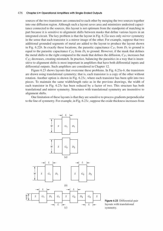
436 Chapter 6 � Operational Amplifiers with Single-Ended Outputs
sources of the two transistors are connected to each other by merging the two sources togetherinto one diffusion region. Although such a layout saves area and minimizes undesired capaci-tance connected to the sources, this layout is not optimum from the standpoint of matching inpart because it is sensitive to alignment shifts between masks that define various layers in anintegrated circuit. The key problem is that the layout in Fig. 6.22a uses only mirror symmetryin the sense that each transistor is a mirror image of the other. For example, suppose that twoadditional grounded segments of metal are added to the layout to produce the layout shownin Fig. 6.22b. In exactly these locations, the parasitic capacitance CP1 from D1 to ground isequal to the parasitic capacitance CP2 from D2 to ground. However, if the mask that definesthe metal shifts to the right compared to the mask that defines the diffusion, CP1 increases butCP2 decreases, creating mismatch. In practice, balancing the parasitics in a way that is insen-sitive to alignment shifts is most important in amplifiers that have both differential inputs anddifferential outputs. Such amplifiers are considered in Chapter 12.
Figure 6.23 shows layouts that overcome these problems. In Fig. 6.23a-b, the transistorsare drawn using translational symmetry; that is, each transistor is a copy of the other withoutrotation. Another option is shown in Fig. 6.23c, where each transistor has been split into twopieces. To maintain the same width/length ratio as in the previous drawings, the width ofeach transistor in Fig. 6.23c has been reduced by a factor of two. This structure has bothtranslational and mirror symmetry. Structures with translational symmetry are insensitive toalignment shifts.
One limitation of these layouts is that they are sensitive to process gradients perpendicularto the line of symmetry. For example, in Fig. 6.23c, suppose the oxide thickness increases from
S
L
W
W G1 D1
(a)
S G2 D2
S
L
W G1 D1
(b)
S G2 D2
L
S
L
W2
G1 D1
(c)
G1 S
L
G2 D2
L L
G2 S
Figure 6.23 Differential-pairlayouts with translationalsymmetry.

6.3 Basic Two-Stage MOS Operational Amplifiers 437
D1
D1
D1
M4M2
M3M1
D2
D2
D2
M4 M2
S
M3M1G1
G1S
G2
G2
Figure 6.24 Common-centroidstructure for the MOS differentialpair.
left to right. Then the gate stripes connected to G1 have thinner oxide than those connected toG2, causing the transistors to have unequal thresholds and unequal transconductance parame-ters. The effects of process-related gradients across the die can be partially alleviated by use ofcommon-centroid geometries. Figure 6.24 shows a common-centroid layout of the differentialpair. Each side of the differential pair is split into two components that are cross connected inthe layout. In a geometric sense, the centroid of both composite devices lies at center of thestructure. Because any gradient can be decomposed into horizontal and vertical components,this layout overcomes the effect of linear process gradients in any direction.
Figure 6.24 also shows two layers of metal used to cross connect the devices. One layer ofmetal is drawn with solid lines. The other is drawn with dashed lines. The two layers connectat intersections only where dots are drawn. The interconnect drawn here is shift insensitive andbalanced in the sense that any signal line that crosses a node on one side of the differential pairalso crosses the corresponding node on the other side. This balance helps to keep undesiredsignals in common-mode form so they can be rejected by the differential pair. Finally, the onlyline that crosses the metal connected to the two input gates is the metal line to the sourcesof the differential pair. This characteristic is important because such crossings create a smallparasitic capacitance between the two layers that cross, and can allow undesired signals tocouple to the op-amp inputs. Since op amps are designed to have high gain, op-amp inputs are

438 Chapter 6 � Operational Amplifiers with Single-Ended Outputs
the most sensitive nodes in analog integrated circuits. Therefore, if any signal line is allowedto cross one gate, it should also cross the other to balance the parasitic capacitances. Since theparasitics may not be perfectly matched in practice, however, avoiding crossings is better thanbalancing them. In Fig. 6.24, the gates are allowed to cross the source of the differential pairbecause the transistors themselves already provide a large capacitance between each gate andthe source in the form of the gate-source capacitance of each transistor.
A disadvantage of common-centroid layouts is also apparent in Fig. 6.24. That is, theneed to cross-connect the devices increases the separation between matched devices and mayworsen matching in cases where linear process gradients are not the main limitation. Therefore,the value of a common-centroid layout must be determined on a case-by-case basis.
6.4 Two-Stage MOS Operational Amplifiers with CascodesThe basic two-stage op amp described above is widely used with many variations that optimizecertain aspects of the performance. In this section, we consider an important variation on thebasic circuit to increase the voltage gain.
The voltage gain that is available from the basic circuit shown in Fig. 6.16 may be inad-equate in a given application to achieve the required accuracy in the closed-loop gain. Forexample, suppose the basic op amp uses transistors with gmro = 20 and is connected in thevoltage-follower configuration shown in Fig. 6.3c. The op-amp gain is given in (6.56) and isless than (gmro)2 in practice. For simplicity, assume that the op-amp gain is about (gmro)2, or400 in this case. The closed-loop gain is given by (6.12) and is approximately unity becauseR2 = 0 in the follower configuration. The error in this approximation is one part in the op-ampgain or at least 0.25 percent. In precision applications, this error may be too large to meet thegiven specifications, requiring an increase in the op-amp gain.
One approach to increasing the op-amp gain is to add another common-source gain stageto the op amp so that the overall gain is approximately (gmro)3 instead of (gmro)2.An importantproblem with this approach, however, stems from the fact that op amps are intended to be usedin negative-feedback configurations. In practice, op-amp frequency response is not constant.If the op amp introduces an additional phase shift of 180o at some frequency, the negativefeedback that was intended becomes positive feedback at that frequency, and the op amp maybe unstable. The topics of frequency response and stability are covered in detail in Chapters 7and 9, respectively. The key point here is that if an op amp is unstable in a given feedbackconfiguration, it does not act as an amplifier but as a latch or oscillator. To avoid this problem,op amps are usually designed with no more than two gain stages because each stage containsa node for which the impedance to ground is high and as a result contributes a significantpole to the op-amp transfer function. Since the phase shift from one pole approaches −90o
asymptotically, an op amp with no more than two poles cannot provide the 180o phase shiftthat is required to convert negative feedback into positive feedback.
To increase the voltage gain without adding another common-source gain stage, common-gate transistors can be added. Together with a common-source transistor, a common-gatetransistor forms a cascode that increases the output resistance and gain of the stage whilecontributing a less significant pole to the amplifier transfer function than would be contributedby another common-source stage. Figure 6.25 illustrates the use of cascodes to increasethe voltage gain of a two-stage amplifier. Here, a series connection of two transistors, onein the common-source connection and one in the common-gate connection, replace eachcommon-source transistor in the first stage. Therefore, M1 and M1A in Fig. 6.25 replace M1 inFig. 6.16. Similarly, M2 and M2A in Fig. 6.25 replace M2 in Fig. 6.16. Transistor M9 andcurrent source IC have also been added to bias the gates of M1A and M2A. In practice, the

6.5 MOS Telescopic-Cascode Operational Amplifiers 439
VDD
IBIAS CCIC
vo
Vo1
–VSS
–VSS
M7M5M8
M1
M1A
M3A
M2A
M4A M10
M4 M11 M6M3
M9 M2
+
+ –
–
vi
+
–
Figure 6.25 Two-stage amplifier with cascoded first stage.
W/L of M9 is chosen so that M1 and M2 are operated barely in the active region. The effectof these replacements is to increase the unloaded output impedance of the differential pair bya factor that is approximately equal to gmro of the cascode device.
If the current mirror M3-M4 were not also cascoded, however, the output resistance ofthe first stage including the current-mirror load would be limited by the mirror. To overcomethis limitation, a cascode current mirror shown in Fig. 4.9 is used instead. As a result, thestage gain and output resistance including the load are increased by approximately a factorgmro. In this circuit, M10 and M11 are included to level shift the output of the first stage downby VGS10 so that the second stage input is driven by a signal whose dc level is VGS3 above−VSS . If the aspect ratios are chosen to satisfy (6.66), and if each common-gate transistor isidentical to its common-source counterpart, the systematic offset voltage with this level shiftis given by (6.68), where the op-amp gain here is on the order of (gmro)3 instead of (gmro)2 inFig. 6.16. One disadvantage of this circuit is a substantial reduction in the common-mode inputrange. (See Problem 6.16.) To overcome this problem, cascoding could be added instead tothe second stage. In that case, however, the output swing of the op amp would be degraded bythe cascodes.
6.5 MOS Telescopic-Cascode Operational AmplifiersAs mentioned in the previous section, cascode configurations may be used to increase thevoltage gain of CMOS transistor amplifier stages. In many applications, the stage gain canbe increased enough so that a single common-source–common-gate stage can provide enoughvoltage gain to meet the accuracy requirements. The first stage of Fig. 6.25 is sometimes usedby itself as an op amp and provides a gain comparable to the gain of the two-stage op-amp inFig. 6.16. This structure has been called a telescopic-cascode op amp11 because the cascodesare connected between the power supplies in series with the transistors in the differential pair,
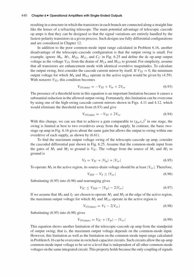
440 Chapter 6 � Operational Amplifiers with Single-Ended Outputs
resulting in a structure in which the transistors in each branch are connected along a straight linelike the lenses of a refracting telescope. The main potential advantage of telescopic cascodeop amps is that they can be designed so that the signal variations are entirely handled by thefastest-polarity transistors in a given process. Such designs use fully differential configurationsand are considered in Chapter 12.
In addition to the poor common-mode input range calculated in Problem 6.16, anotherdisadvantage of the telescopic-cascode configuration is that the output swing is small. Forexample, ignore M6, M7, M10, M11, and CC in Fig. 6.25 and define the dc op-amp outputvoltage as the voltage VO1 from the drains of M2A and M4A to ground. For simplicity, assumethat all transistors are enhancement mode with identical overdrive magnitudes. To calculatethe output swing, first consider the cascode current mirror by itself. If VSS = 0, the minimumoutput voltage for which M4 and M4A operate in the active region would be given by (4.59).With nonzero VSS , this condition becomes
VO1(min) = −VSS + Vtn + 2Vov (6.93)
The presence of a threshold term in this equation is an important limitation because it causes asubstantial reduction in the allowed output swing. Fortunately, this limitation can be overcomeby using one of the high-swing cascode current mirrors shown in Figs. 4.11 and 4.12, whichwould eliminate the threshold term from (6.93) and give
VO1(min) = −VSS + 2Vov (6.94)
With this change, we can see that to achieve a gain comparable to (gmro)2 in one stage, theswing is limited at best to two overdrives away from the supply. In contrast, the basic two-stage op amp in Fig. 6.16 gives about the same gain but allows the output to swing within oneoverdrive of each supply, as shown by (6.61).
To find the maximum output voltage swing of the telescopic-cascode op amp, considerthe cascoded differential pair shown in Fig. 6.25. Assume that the common-mode input fromthe gates of M1 and M2 to ground is VIC. The voltage from the source of M1 and M2 toground is
VS = VIC + |Vtp| + |Vov | (6.95)
To operate M5 in the active region, its source-drain voltage should be at least |Vov |. Therefore,
VDD − VS ≥ |Vov | (6.96)
Substituting (6.95) into (6.96) and rearranging gives
VIC ≤ VDD − |Vtp| − 2|Vov | (6.97)
If we assume that M9 and IC are chosen to operate M1 and M2 at the edge of the active region,the maximum output voltage for which M2 and M2A operate in the active region is
VO1(max) = VS − 2|Vov | (6.98)
Substituting (6.95) into (6.98) gives
VO1(max) = VIC + |Vtp| − |Vov | (6.99)
This equation shows another limitation of the telescopic-cascode op amp from the standpointof output swing; that is, the maximum output voltage depends on the common-mode input.However, this limitation as well as the limitation on the common-mode input range calculatedin Problem 6.16 can be overcome in switched-capacitor circuits. Such circuits allow the op-ampcommon-mode input voltage to be set to a level that is independent of all other common-modevoltages on the same integrated circuit. This property holds because the only coupling of signals

6.5 MOS Telescopic-Cascode Operational Amplifiers 441
to the op-amp inputs is through capacitors, which conduct zero dc current even with a nonzerodc voltage drop. Assuming that the op-amp inputs are biased to the maximum common-modeinput voltage for which M5 operates in the active region, the maximum output voltage can befound by substituting the maximum VIC from (6.97) into (6.99), which gives
VO1(max) = VDD − 3|Vov | (6.100)
This equation shows that the maximum output voltage of a telescopic op amp that consistsof the first stage of Fig. 6.25 with optimum common-mode input biasing is three overdrivesless than the positive supply. This result stems from the observation that three transistors (M5,M2, and M2A) are connected between VDD and the output. In contrast, (6.94) shows that theminimum output swing is limited by two overdrives.
To determine the minimum required supply voltage difference, we will subtract (6.94)from (6.100), which gives
VO1(max) − VO1(min) = VDD − (−VSS) − 5|Vov | (6.101)
assuming that the magnitudes of all the overdrives are all equal. Rearranging this equationgives
VDD − (−VSS) = VO1(max) − VO1(min) + 5|Vov | (6.102)
This equation shows that the minimum difference between the supply voltages in a telescopiccascode op amp must be at least equal to the peak-to-peak output signal swing plus fiveoverdrive voltages to operate all transistors in the active region. For example, with a peak-to-peak output swing of 1 V and |Vov | = 100 mV for each transistor, the minimum differencebetween the supply voltages is 1.5 V.
In practice, this calculation has two main limitations. First, if transistors are deliberatelybiased at the edge of the active region, a small change in the process, supply, or temperaturemay cause one or more transistors to operate in the triode region, reducing the output resistanceand gain of the op amp. To avoid this problem, transistors in practical op amps are usuallybiased so that the magnitude of the drain-source voltage of each transistor is more than thecorresponding overdrive by a margin of typically at least one hundred millivolts. The marginallowed for each transistor directly adds to the minimum required supply voltage difference.Second, this calculation determines the supply requirements only for transistors between theoutput node and each supply, and other branches may require a larger supply difference thangiven in (6.102). For example, consider the path from one supply to the other through M5,M1, M1A, M3A, and M3 in Fig. 6.25. Ignore the body effect for simplicity. Since M3A and M3are diode connected, the drain-source voltage of each is Vt + Vov . Furthermore, if the W/L ofM3A is reduced by a factor of four to build the high-swing cascode current mirror shown inFig. 4.11, the voltage drop from the drain of M3A to the source of M3 is 2Vt + 3Vov . If the otherthree transistors in this path are biased so that |VDS | = |Vov |, the required supply difference forall the transistors in this path to operate in the active region is 2Vt + 6|Vov |. This requirementexceeds the requirement given in (6.102) if 2Vt + |Vov | is more than the peak-to-peak outputswing. However, this result does not pose a fundamental limitation to the minimum requiredpower-supply voltage because low-threshold devices are sometimes available.
The minimum supply voltage difference in (6.102) includes five overdrive terms. In con-trast, the corresponding equation for the op amp in Fig. 6.16 would include only two overdriveterms, one for M6 and the other for M7. The presence of the three extra overdrive termsincreases the minimum required supply difference or reduces the allowed overdrives for agiven supply difference. The extra three overdrive terms in (6.102) stem from the two cascodedevices and the tail current source. The overdrives from the cascodes should be viewed as the

442 Chapter 6 � Operational Amplifiers with Single-Ended Outputs
cost of using cascodes; however, the overdrive of the tail current source can be eliminatedfrom the minimum required supply difference using the circuit described in the next section.
6.6 MOS Folded-Cascode Operational AmplifiersFigure 6.26 shows two cascode circuits where VDD = 0 for simplicity. In Fig. 6.26a, both M1and M1A are p-channel devices. In Fig. 6.26b, M1 is still a p-channel device but M1A is now ann-channel device. In both cases, however, M1 is connected in a common-source configuration,and M1A is connected in a common-gate configuration. Small-signal variations in the draincurrent of M1 are conducted primarily through M1A in both cases because IBIAS is a constantcurrent source. Therefore, both circuits are examples of cascodes. The cascode in Fig. 6.26bis said to be folded in the sense that it reverses the direction of the signal flow back towardground. This reversal has two main advantages when used with a differential pair. First, itincreases the output swing. Second, it increases the common-mode input range.
Figure 6.27 shows a simplified schematic of a circuit that applies the folded-cascodestructure to both sides of a differential pair. As in Fig. 6.26b, M1 and M1A form one cascodestructure in Fig. 6.27. Also, M2 and M2A form another. The current mirror converts the differ-ential signal into a single-ended output by sending variations in the drain current of M1A tothe output. The resulting op amp is called a folded-cascode op amp.7,12 A complete schematicis shown in Fig. 6.28. Bias is realized by making the currents in current sources M11 and M12larger than |ID5|/2. Thus
ID1A = ID2A = ID11 − |ID5|2
= ID12 − |ID5|2
= IBIAS − ITAIL
2(6.103)
Compared to the other op-amp configurations we have considered, the folded-cascodeconfiguration improves the common-mode input range. The upper end of the range is the sameas in the basic two-stage op amp and the telescopic cascode op amp. On the other hand, thelower end of the range can be reduced significantly compared to both of the other configurationsif VBIAS2 is adjusted so that M11 and M12 operate at the edge of the active region. Under thiscondition, the bias voltage from the drain of M1 to −VSS is Vov11, which can be much lessthan in the other configurations. See (6.75), (6.77), and Problem 6.18.
M1
M1A
R
VBIAS
–VSS
VI + vi
VO + vo
++
–
–
(a)
M1
M1A
R
VBIAS
IBIAS
–VSS
VI + vi VO + vo
+ +
––
(b)
Figure 6.26 (a) Standard cascode configuration. (b) Folded-cascode configuration.

6.6 MOS Folded-Cascode Operational Amplifiers 443
VDD
–VSS
ITAIL
IBIAS IBIAS
VBIAS2 VBIAS2
CL
vi
vo
M1 M2
M1A M2A
+
–
+
–
COMMON
Currentmirror
IN OUT
Figure 6.27 Simplified schematic of a folded-cascode op amp.
VDD
VBIAS1
VBIAS2
CL
VBIAS3
VBIAS2
VBIAS3
vi
M5 M3 M4
M3A M4A
M1A M2A
M11 M12
M1 M2
–VSS
+
–
vo
+
–
Figure 6.28 More detailed schematic of a folded-cascode op amp.

444 Chapter 6 � Operational Amplifiers with Single-Ended Outputs
To calculate the output swing, first consider the p-type cascode current mirror by itself.Since M3 and M3A are diode connected, the voltage from VDD to the gate of M4A is 2|Vtp| +2|Vov |. Therefore, the source-drain voltage of M4 is |Vtp| + |Vov |, and the maximum outputfor which both M4 and M4A operate in the active region is
VOUT(max) = VDD − |Vtp| − 2|Vov | (6.104)
This equation is analogous to (6.93) where an n-type cascode current mirror limits the minimumoutput swing of the telescopic op amp. The threshold term in this equation can be eliminatedby using a p-type version of one of the high-swing cascode current mirrors shown in Figs. 4.11and 4.12. The result is
VOUT(max) = VDD − 2|Vov | (6.105)
To find the minimum output voltage, assume that VBIAS2 is adjusted so that M12 operates atthe edge of the active region. Then the drain-source voltage of M12 is Vov and the minimumoutput voltage for which both M2A and M12 operate in the active region is
VOUT(min) = −VSS + 2Vov (6.106)
Therefore, a folded-cascode op amp can provide nearly constant voltage gain while its outputswings within two overdrives of each supply. In contrast, the output of a telescopic-cascodeop amp can swing within two overdrives of one supply and three overdrives of the other whileproviding nearly constant gain.
The small-signal voltage gain of this circuit at low frequencies is
Av = GmRo (6.107)
where Gm is the transconductance and Ro is the output resistance. When all the transistorsoperate in the active region, the range of typical gain magnitudes is from several hundred toseveral thousand. Because of the action of the current mirror M3-M4, variation in the draincurrent of M1 and M2 contribute constructively to the transconductance. Therefore,
Gm = gm1 = gm2 (6.108)
To find Ro, both inputs are connected to ac ground. Although the input voltages do notmove in this case, the sources of M1-M2 do not operate at ac ground. However, connectingthis node to small-signal ground as shown in Fig. 6.29a causes little change in Ro because ofthe action of the current mirror M3-M4, as explained next.
Let id1 and id2 represent the small-signal drain currents of M1 and M2 respectively. Also,let �id1 and �id2 represent the corresponding changes in id1 and id2 caused by connecting thesources of M1-M2 to a small-signal ground as shown in Fig. 6.29a. If ro → ∞, �id1 = �id2because this connection introduces equal changes in the gate-source voltages of M1 and M2.Then �id1 flows in the source of M1A, where it is mirrored to the output with a gain of unity ifro → ∞ in M3-M4. Therefore, KCL at the output shows that �id1 and �id2 cancel, causingno change to the output current ix or the output resistance Ro. As a result, Ro can be found,assuming that the sources of M1-M2 operate at ac ground. In practice, ro in all the transistorsis finite, and Ro is altered slightly by connecting this point to ac ground for two reasons. First,�id1 and �id2 are not exactly equal with finite ro because vds1 and vds2 are not exactly equal.Differences between vds1 and vds2 stem from finite ro in M1A and M2A because M3 and M3A
are diode connected but their counterparts M4 and M4A are not diode connected. Second,the small-signal current gain of the current mirror is not exactly unity with finite ro becausevds3 and vds4 are not exactly equal. However, the change in the output resistance introducedby these considerations is usually negligible. (These effects are related to the explanation of

6.6 MOS Folded-Cascode Operational Amplifiers 445
M3 M4
M3A M4A
M4A
M2A
M12
M4
M2Ro
M1A M2A
M11 M12
M1 M2
vx
ix
+
–
Ro
vx
ix
+
–
(a) (b)
Figure 6.29 (a) Test voltage source applied to the output to calculate the output resistance.(b) Simplified circuit.
how a current-mirror load increases the common-mode rejection ratio of a differential pairpresented in Section 4.3.5.3.)
With the sources of M1-M2 connected to ac ground, the drain current of M1 is constant.Furthermore, the Thévenin equivalent resistances presented to the gates of M4 and M4A aresmall because M3 and M3A are diode connected. So little error is introduced by assuming thatthe gates of M4 and M4A are connected to small-signal ground. Therefore, the calculation ofRo can be carried out using the circuit of Fig. 6.29b. By inspection,
Ro = (Rout|M2A) ‖ (Rout|M4A) (6.109)
The output resistance of transistor current sources with nonzero source resistance was con-sidered in Chapter 4. The result is the same as for a common-source amplifier with sourcedegeneration. The incremental resistance in the source of M2A is the ro of M2 in parallel withthe ro of M12 while the incremental resistance in the source of M4A is the ro of M4. From(3.107),
Rout|M2A = (ro2||ro12) + ro2A[1 + (gm2A + gmb2A)(ro2||ro12)](6.110)� [gm2A(ro2 ‖ ro12)]ro2A
and
Rout|M4A = ro4 + ro4A[1 + (gm4A + gmb4A)(ro4)](6.111)� (gm4Aro4)ro4A
An important advantage of this circuit is that the load capacitance CL performs the com-pensation function (see Chapter 9). Thus no additional capacitance (such as CC in previouscircuits) need be added to keep the amplifier from oscillating when connected in a feedback

446 Chapter 6 � Operational Amplifiers with Single-Ended Outputs
loop. Furthermore, in the basic two-stage op amp, CC feeds the variation from one powersupply forward to the op-amp output at high frequencies, as described in Section 6.3.6. Thisfeedforward does not occur in one-stage op amps such as the folded-cascode and telescopic-cascode structures, improving their high-frequency power-supply rejection ratios from the Vss
supply.
6.7 MOS Active-Cascode Operational AmplifiersOne way to increase the gain of the folded-cascode op amp without cascading additional stagesis to add another layer of cascodes. See Problem 6.21. Although this approach gives a gain onthe order of (gmro)3, it reduces the output swing by at least another overdrive in each direction.This reduction becomes increasingly important as the difference between the power-supplyvoltages is reduced in scaled technologies. To increase the op-amp gain without reducing theoutput swing, the active-cascode technique described in Chapter 3 can be used.13
Figure 6.30a shows the schematic of a folded-cascode op amp with active cascodes. Thegates of each of the four cascode transistors M1A, M2A, M3A, and M4A are no longer connectedto a constant bias source but instead to the output of an amplifier. These auxiliary amplifiersare themselves connected in negative feedback loops to increase the resistance looking intothe drain of each cascode transistor. As shown by (3.133), the active-cascode configurationincreases the output resistance by increasing the effective transconductance of the cascodetransistor by (a + 1), where a is the voltage gain of the auxiliary amplifier. Let the gains ofthe auxiliary amplifiers driving M3A and M4A be A1. Applying (3.133) to (6.111) to find the
(a)
P N
P N
A1
A2
O
O
P NA2
O
P NA1
O
VBIAS4VBIAS4
VBIAS3
VBIAS2VBIAS2
VBIAS1
VBIAS3
CL
CC2CC2
CC1CC1
vo
–VSS–VSS
VDDVDD
VDD
–VSS
M12M11
M2A
M4AM3A
M2M1
M5
M1A
M4M3
+
–
vi
–
+
Figure 6.30 (a) Folded-cascode op amp with active-cascode gain-enhancement auxiliary amplifiers.

6.7 MOS Active-Cascode Operational Amplifiers 447
output resistance looking into the drain of M4A gives
Rout|M4A = ro4 + ro4A{1 + [gm4A(A1 + 1) + gmb4A](ro4)}(6.112)� (A1 + 1)(gm4Aro4)ro4A
Let the gains of the auxiliary amplifiers driving M1A and M2A be A2. Applying (3.133) to(6.110) to find the output resistance looking into the drain of M2A gives
Rout|M2A = (ro2||ro12) + ro2A{1 + [gm2A(A2 + 1) + gmb2A](ro2||ro12)}(6.113)� (A2 + 1)[gm2A(ro2 ‖ ro12)]ro2A
To find the overall op-amp gain, (6.112) and (6.113) can be substituted into (6.109) and theresult in (6.107). This analysis shows that the gain enhancement in the folded-cascode op ampdoes not rely on the use of auxiliary amplifiers driving the gates of M1A and M3A. However,these auxiliary amplifiers are included in Fig. 6.30a because they reduce the systematic offsetof the folded-cascode op amp. Also, using identical auxiliary amplifiers to drive the gates ofboth M1A and M2A balances the two signal paths until the differential signal is converted intosingle-ended form by the current mirror.
In Fig. 6.30a, the auxiliary amplifiers with gain A1 drive the gates of M3A and M4A
so that the voltages from the drains of M3 and M4 to ground are approximately equal toVBIAS2. For simplicity, assume that the overdrive voltages for all p- and n-channel transistorsoperating in the active region are Vovp and Vovn, respectively. Also assume that all n-channeltransistors have positive thresholds and all p-channel transistors have negative thresholds. Tomaximize the positive output swing of the folded-cascode amplifier, the voltage drop fromVDD to VBIAS2 is chosen to be about |Vovp|. Therefore, the A1 amplifiers must operate with ahigh common-mode input voltage. If these amplifiers use a p-channel differential input pair,the maximum common-mode input voltage would be no more than VDD − |Vtp| − 2|Vovp|. Toovercome this limitation, the A1 amplifiers use an n-channel differential pair M21 and M22 asshown in Fig. 6.30b. In operation, the dc voltage from VDD to the output of the A1 amplifiersis about |Vtp| + 2|Vovp| so that the source-drain voltages of M3 and M4 are |Vovp|. Therefore,the gate-drain voltage of M22 is approximately |Vtp| + |Vovp|, and M22 operates in the activeregion only if its threshold (with the body effect) is greater than this value.
A similar argument can be made to explain the use of p-channel differential pairs in theauxiliary amplifiers with gain A2. The schematic is shown in Fig. 6.30c, and the common-modeinputs are close to VSS in this case.
Figure 6.30d shows a circuit that produces the bias voltages needed in Fig. 6.30a–c. Thevoltage from VDD to VBIAS1 is |Vtp| + |Vovp|, and the voltage from VBIAS4 to VSS is Vtn + Vovn.Transistor M105 forces M106 to operate in the triode region, and the voltage from VDD to VBIAS2is at least |Vovp| if (
W
L
)106
≤ 1
3
(W
L
)105
(6.114)
ignoring body effect as in (4.73). Similarly, the voltage from VBIAS3 to VSS is at least Vovn if(W
L
)114
≤ 1
3
(W
L
)113
(6.115)
One potential problem with the structure shown in Fig. 6.30a is instability in the feedbackloops around the auxiliary amplifiers. To avoid instability, a compensation capacitor can beplaced from each auxiliary-amplifier output to a small-signal ground. Since the A1 amplifiersare used to improve the performance of a p-channel current mirror, where signals are referencedto VDD, compensation capacitors for the A1 amplifiers CC1 are connected to VDD. Similarly,

448 Chapter 6 � Operational Amplifiers with Single-Ended Outputs
VDD VDD
–VSS
VBIAS4
–VSS
M25
M22
M33
M31
VBIAS1
M34
M32
M35
M21
M23 M24
NP N
O
P
(b)
(d)
(c)
VDD
IBIAS
VBIAS4 VBIAS3
VBIAS1VBIAS2
M111
M109
M110
M108
M107
M103
M104
M102
M101
M105
M106
M112
M113
M114
–VSS
Figure 6.30 (b) Auxiliary amplifier with gain A1. (c) Auxiliary amplifier with gain A2. (d) Biascircuit.
compensation capacitors for the A2 amplifiers CC2 are connected to VSS . The need for suchcapacitors stems from the observation that the capacitance looking into the gates of M1A, M2A,M3A, and M4A can be quite small because the gate-source capacitances of these transistors arebootstrapped. This expression means that the source of each of these transistors follows itsgate when the corresponding drain current is constant. If the gate-source voltages are exactlyconstant, zero ac current flows into the gate-source capacitances, and the capacitances lookinginto the gates of the cascode transistors are independent of their gate-source capacitances. Inpractice, the gate-source voltages are not exactly constant because of variations in the draincurrents caused by variations in the differential input voltage of the folded-cascode op amp,but the bootstrapping effect is significant. As a result, the load capacitances of the auxiliaryamplifiers are dominated by parasitics that may vary considerably over variations in processingunless a capacitor is added at the output of each auxiliary amplifier. The issue of stability infeedback amplifiers is considered in detail in Chapter 9.
6.8 Bipolar Operational AmplifiersA basic topology for the input stage of bipolar-transistor op amps is shown in Fig. 6.31a. As inthe case of the basic MOS op amp, the input stage consists of a differential pair, a tail currentsource, and a current-mirror load. The common-mode input range of op amps with this input

6.8 Bipolar Operational Amplifiers 449
stage is the range of dc common-mode input voltages for which all transistors in Fig. 6.31aoperate in the forward-active region. Assume that a pure common-mode voltage VIC is appliedfrom the op-amp inputs to ground. Also, assume that Q1 is identical to Q2, and Q3 is identicalto Q4. Then the collector-emitter voltage of Q5 is
VCE5 = VIC − VBE1 − VCC (6.116)
This equation shows that increasing VIC increases VCE5. Since Q5 is a pnp transistor, it operatesin the active region when VCE5 < VCE5(sat). Therefore, (6.116) can be rearranged to give thefollowing upper limit for the common-mode input range
VIC < VCC + VBE1 + VCE5(sat) (6.117)
For example, if VBE1 = −0.7 V and VCE5(sat) = −0.1 V, VIC < VCC − 0.8 V is required tooperate Q5 in the forward-active region.
To find the lower limit for the common-mode range, ignore base currents for simplicity.Then with a pure common-mode input,
VCE4 = VCE3 = VBE3 (6.118)
As a result, the collector-emitter voltages of Q1 and Q2 are
VCE1 = VCE2 = −VEE + VBE3 − (VIC − VBE1) (6.119)
Because Q1 and Q2 are pnp transistors, they operate in the forward-active region when VCE1 <
VCE1(sat) and VCE2 < VCE2(sat). Therefore, the lower end of the common-mode range is
VIC > −VEE + VBE3 + VBE1 − VCE1(sat) (6.120)
For example, if VBE3 = 0.7 V, VBE1 = −0.7 V, and VCE5(sat) = −0.1 V, VIC > −VEE +0.1 V is required to operate Q1 and Q2 in the forward-active region.
This inequality shows that the common-mode input range of the op amp in Fig. 6.31aalmost includes −VEE. A simple way to see this result is to let VIC = −VEE in Fig. 6.31a.Then the collector-base voltages of Q1 and Q2 are
VCB1 = VCB2 = VBE3 (6.121)
Bias1Bias1
(a) (b)
Q1 Q1
Q5IBIAS
VR1
VCC
vod
VCC
VR2
Q3
Q2
R2R1
Q2
Q5
Q4 ++
+ +
+
–
–VEE = 0 –VEE = 0
–
– –
–
Figure 6.31 (a) Input stage in a basic bipolar operational amplifier. (b) Input stage with resistive loadsto include −VEE in the input common-mode range. Assume R1 = R2.

450 Chapter 6 � Operational Amplifiers with Single-Ended Outputs
Since Q3 is diode connected and conducts current from its collector to its emitter, VBE3 is bigenough to forward bias the base-emitter junction of Q3. Therefore, VBE3 is also big enoughto forward bias the collector-base junctions of Q1 and Q2, pushing these transistors intosaturation.
To extend the common-mode input range to include −VEE (which is important in single-supply applications with VEE = 0), the VBE3 term in (6.120) and (6.121) can be reduced byreplacing the Q3-Q4 current mirror by resistive loads,14 as shown in Fig. 6.31b. The voltagedrops across the resistors VR1 and VR2 are chosen to be too small to forward bias the collector-base junctions of Q1 and Q2 when VIC = −VEE. In practice, these drops are usually set toabout 200 mV with a pure common-mode input so that the common-mode input range extendsa few hundred millivolts below −VEE. One example in which this property is useful is in theinverting amplifier configuration shown in Fig. 6.3a when VEE = 0. Since the configuration isinverting, Vs < 0 causes Vo > 0, and single-supply op amps can have high gain with positiveoutputs and VCC > 0. However, if the op amp has zero offset and its gain a is finite, (6.5) showsthat Vi < 0 when Vo > 0. As a result, the op-amp common-mode input voltage is negative,requiring that the common-mode input range extend below ground to handle this case.
The main drawback of the circuit in Fig. 6.31b is that its gain is low.15 If the matching isperfect and VR1 = VR2 = 0.2 V,
vod
vid
= gm1R1 = IBIAS
2VT
R1 = VR1
VT
= 0.2
0.026� 7.7 (6.122)
To increase the gain, the input stage can use the folded-cascode structure shown in Fig. 6.32.Transistors Q3 and Q4 are connected in a common-base configuration. Combined with theinput differential pair, this circuit forms a folded-cascode amplifier. The gain is
vod
vid
= gm1ρ1Ro1 (6.123)
vod
Bias1
BiasCM
Q5
Q1 Q2
Q3 Q4
Q6 Q7
VCC
R3
R5 R6 R7
R4
–VEE = 0
+ +– –
Figure 6.32 Folded-cascode inputstage.

6.8 Bipolar Operational Amplifiers 451
where ρ1 represents the fraction of the small-signal collector current in Q1 that flows intothe emitter of Q3 and Ro1 represents the output resistance of this stage. To find ρ1, the small-signal resistance looking into the emitter of Q3 is needed. Since Q3 operates as a common-baseamplifier, this resistance can be found using (3.53) and is approximately equal to re3, ignoringthe last term in (3.53) for simplicity. Then
ρ1 � R3
R3 + re3(6.124)
Assume that Bias1 and BiasCM are adjusted so that Q6, Q7, Q9, and Q10 operate in theforward-active region. Then the output resistance of the stage is
Ro1 = Rup1||Rdown1 (6.125)
where
Rup1 � ro6(1 + gm6R6) (6.126)
and
Rdown1 � ro3(1 + gm3R3) (6.127)
assuming gm6R6 � βpnp, gm3R3 � βnpn, and the resistance looking back into the collectorof Q1 is much greater than R3. Although the folded-cascode circuit in Fig. 6.32 increases thestage gain significantly and allows proper operation for common-mode inputs slightly below−VEE, it does not allow operation with common-mode inputs up to VCC as shown by (6.117).
To extend the common-mode input range to VCC, an npn differential pair can be added,as shown in Fig. 6.33.16 Assume that the dc voltage drops on R5-R10 are 200 mV each. Then
vod
Bias1
Bias2 BiasCM
Q7Q6
Q3
Q2
Q5
Q1
Q4
Q8 Q9 Q10
VCC
R8 R9
R6R5 R7
R10
–VEE = 0
+++ –––
Figure 6.33 Rail-to-rail folded-cascode input stage.

452 Chapter 6 � Operational Amplifiers with Single-Ended Outputs
the pnp differential pair operates normally for common-mode inputs slightly below groundto about 1 V below VCC. Similarly, the npn differential pair operates normally for common-mode inputs slightly above VCC to about 1 V above ground. Therefore, if VCC < 2 V, neitherdifferential pair operates normally when VIC = VCC/2 because both Q5 and Q8 operate insaturation under these conditions. On the other hand, if VCC ≥ 2 V, at least one of the twodifferential pairs operates normally for any common-mode input voltage from just below −VEE
to just above VCC. In other words, the stage has a rail-to-rail common-mode input range forVCC ≥ 2 V.
However, an important disadvantage of this input stage is that its small-signal transcon-ductance is not constant. The stage transconductance is the sum of the transconductances fromboth differential pairs. In the center of the common-mode range, both differential pairs operatenormally, and the stage transconductance is high. On the other hand, when the common-modeinput voltage is within about 1 V of either supply, the tail current source in one of the differen-tial pairs saturates, reducing that current as well as the transconductances of that differentialpair and the input stage. This variation in the stage transconductance causes variation in theopen-loop gain and frequency response of the op amp, compromising its performance whenit is designed to be stable in a closed-loop configuration. (The topic of stability is coveredin Chapter 9.) This disadvantage is overcome in the NE5234 op amp, which is describedbelow.17,18 This stand-alone op amp is widely used, and its popularity stems from the fact thatit can operate with VEE = 0 and VCC as low as 2 V, giving constant input transconductanceover a common-mode input range slightly beyond the power-supply voltages (or rails) andalmost a rail-to-rail output swing.
6.8.1 The dc Analysis of the NE5234 Operational Amplifier
Bias Circuit. Figure 6.34 shows the schematic of the NE5234 bias circuit. On the bottomof the circuit, Q49, Q60, and R60 form a Widlar current mirror. Instead of diode connectingQ49, the bases of Q49 and Q60 are driven by a unity-gain buffer formed by Q50-Q53 tofollow the collector of Q49. This buffer is used as a beta helper as in Fig. 4.6 to reduce thebase-current error in the Q49-Q60 current mirror. In Fig. 4.6, the buffer is simply an npnemitter follower. As a result, VCE1 = VBE1 + VBE2 = 2VBE(on) there. In contrast, if Q1 werediode connected, VCE1 would equal VBE(on). Increasing VCE1 increases the minimum valueof VCC needed to operate the transistors that implement IIN in the forward-active region.To reduce the required VCC, the corresponding buffer in Fig. 6.34 is a complementary emitterfollower, which means that it consists of a pnp emitter follower (Q50-Q51) and an npn follower(Q52-Q53). If VBE51 = −VBE52, VCE49 = VBE49 = VBE(on), which is reduced by about 0.7 Vin practice compared to a conventional beta helper through the use of the complementaryfollower. Similarly, Q54-Q57 in Fig. 6.34 act as a complementary follower to drive the basesof Q47 and Q58. Also, Q48 and Q59 serve as common-base stages or cascodes, reducing thedependence of the currents in Q47 and Q60 on VCC.
To concentrate on the core of the bias circuit, Fig. 6.35 shows a simplified bias circuit inwhich the beta helpers, cascodes, and associated elements are removed. This simplificationshows that the core circuit is a self-biased current source using the thermal voltage, as inFig. 4.41. In that circuit, corresponding transistors are matched except that the emitter area ofQ2 is twice that of Q1. Similar conditions hold in Figs. 6.34 and 6.35, where the emitter areaof Q60 is twice that of Q49. As a result, the collector currents of the transistors in Fig. 6.35can be found assuming βF → ∞ and VA → ∞ using (4.237)
|IC47| = IC49 = |IC58| = IC60 = VT
R60ln2 = 0.026 V
3 kln2 = 6 �A (6.128)

6.8 Bipolar Operational Amplifiers 453
Q47
Q48
Q52
Q55
Q57
Q51
Q53
Q49
C49
Q56
Q54
VCC
Q58
Q59
Q60
Q50
R57 R60
–VEE = 0
Bias1
Bias5
1 pF
C58
1 pF
1 MΩ 3 kΩ
R47
33 kΩR50
33 kΩ
R54
33 kΩR58
33 kΩ
Figure 6.34 Schematic of the NE5234 bias circuit.
VCC
Q47 Q58
Q60Q49
–VEE = 0
Bias1
Bias5
R60
3 kΩ
R47
33 kΩR58
33 kΩ
Figure 6.35 Simplified schematic of the NE5234 bias circuit.
If R60 is constant, these currents are proportional to absolute temperature (PTAT). AlthoughβF and VA are finite in practice, this equation also gives the corresponding currents inFig. 6.34 because that circuit uses the beta helpers and cascodes mentioned above. The biascircuit produces dc voltages at two nodes, Bias1 and Bias5, that are used to establish scaledcopies of the 6 �A current in pnp and npn transistors in the op amp, respectively. Since these

454 Chapter 6 � Operational Amplifiers with Single-Ended Outputs
scaled currents are also PTAT, the transconductances of transistors conducting these currentsare independent of temperature.
Resistor R57 in Fig. 6.34 prevents the transistors in the bias circuit from conducting zerocurrent when the power supply is applied.18 Without R57, the transistors could conduct zerocurrent because the voltage from node Bias1 to ground could be close to VCC. However, withR57, Q55 pulls Bias1 low enough to start the flow of nonzero current. In steady state, nonzerocurrent in R57 increases the collector current in Q56 but has little overall effect on the operationof the bias circuit.
Input Stage. Figure 6.36 shows a simplified schematic of the NE5234 input stage. This circuituses a folded-cascode structure with complementary input pairs to give rail-to-rail common-mode input range as in Fig. 6.33; however, the input-stage transconductance in Fig. 6.36 doesnot depend on the common-mode input voltage.
Node Bias1 comes from the bias circuit in Fig. 6.34, and Q58 and R58 there plus Q11 andR11 in Fig. 6.36 form a current mirror with degeneration. From (4.36) and (6.128),
|IC11| = R58
R11|IC58| =
(33 k
33 k
)6 �A = 6 �A (6.129)
Similarly, |IC12| = 3 �A, and |IC13| = |IC14| = 6 �A. Ignoring base currents for simplic-ity, the 3 �A from Q12 flows in Q8 and R8, setting the voltage from the base of Q5 to ground to
VB5 = |IC12|R8 + VBE8(on) � 3 �A(33 k) + 0.7 V = 0.8 V (6.130)
Assume that the op-amp inputs are driven by a pure common-mode voltage VIC. TransistorsQ3 and Q4 together can be viewed as forming one half of a differential pair with Q5 formingthe other half of this pair. This differential pair is unbalanced because Q3 and Q4 togetherhave a larger emitter area (and saturation current) than Q5 by itself, causing a nonzero offsetvoltage. Ignore this offset for simplicity. Then if VIC � 0.8 V, the 6 �A current from Q11flows in the pnp input pair Q3-Q4, and Q5-Q7 plus Q1-Q2 are off. On the other hand, ifVIC � 0.8 V, the pnp pair is off and the 6 �A current from Q11 flows in Q5, where it is copiedby the Q7-Q6 current mirror to activate the npn input pair Q1-Q2.
vod1
Q2Q1
Q6
Q3 Q4 Q5
Q8Q7
Q12Q11 Q13 Q14
Q9 Q10
VCC
–VEE = 0
+++ 10
4
43
21
3
9
1 2
–––
R11
33 kΩR13
33 kΩR14
33 kΩ
R10
22 kΩR9
22 kΩR8
33 kΩR6
10 kΩR7
10 kΩ
R12
66 kΩ
BiasCM
Bias1
Figure 6.36 Simplified schematic of the NE5234 input stage.
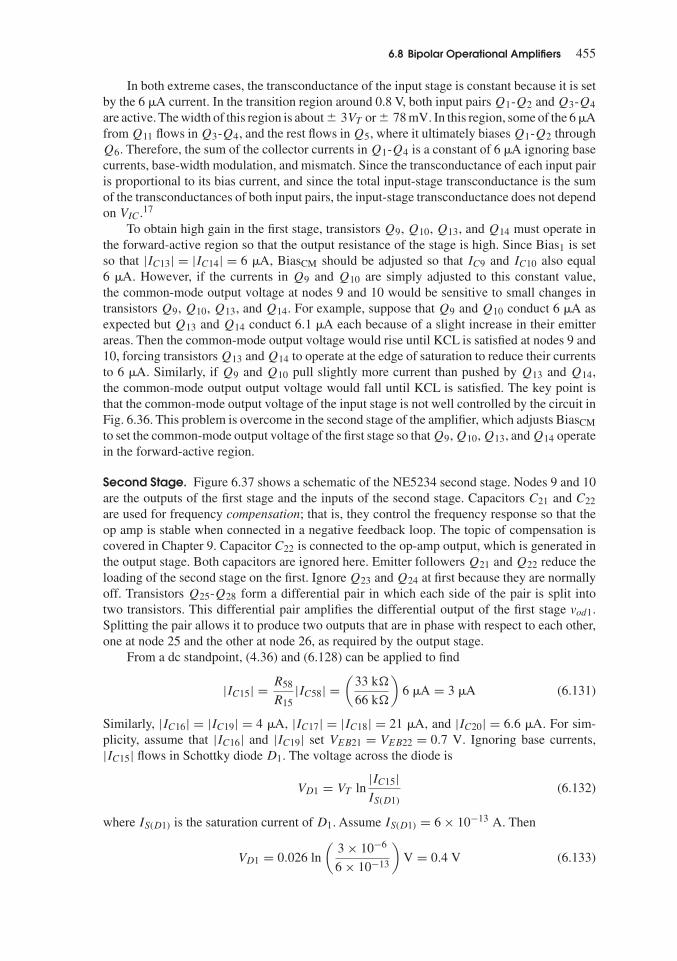
6.8 Bipolar Operational Amplifiers 455
In both extreme cases, the transconductance of the input stage is constant because it is setby the 6 �A current. In the transition region around 0.8 V, both input pairs Q1-Q2 and Q3-Q4are active. The width of this region is about � 3VT or � 78 mV. In this region, some of the 6 �Afrom Q11 flows in Q3-Q4, and the rest flows in Q5, where it ultimately biases Q1-Q2 throughQ6. Therefore, the sum of the collector currents in Q1-Q4 is a constant of 6 �A ignoring basecurrents, base-width modulation, and mismatch. Since the transconductance of each input pairis proportional to its bias current, and since the total input-stage transconductance is the sumof the transconductances of both input pairs, the input-stage transconductance does not dependon VIC.17
To obtain high gain in the first stage, transistors Q9, Q10, Q13, and Q14 must operate inthe forward-active region so that the output resistance of the stage is high. Since Bias1 is setso that |IC13| = |IC14| = 6 �A, BiasCM should be adjusted so that IC9 and IC10 also equal6 �A. However, if the currents in Q9 and Q10 are simply adjusted to this constant value,the common-mode output voltage at nodes 9 and 10 would be sensitive to small changes intransistors Q9, Q10, Q13, and Q14. For example, suppose that Q9 and Q10 conduct 6 �A asexpected but Q13 and Q14 conduct 6.1 �A each because of a slight increase in their emitterareas. Then the common-mode output voltage would rise until KCL is satisfied at nodes 9 and10, forcing transistors Q13 and Q14 to operate at the edge of saturation to reduce their currentsto 6 �A. Similarly, if Q9 and Q10 pull slightly more current than pushed by Q13 and Q14,the common-mode output output voltage would fall until KCL is satisfied. The key point isthat the common-mode output voltage of the input stage is not well controlled by the circuit inFig. 6.36. This problem is overcome in the second stage of the amplifier, which adjusts BiasCMto set the common-mode output voltage of the first stage so that Q9, Q10, Q13, and Q14 operatein the forward-active region.
Second Stage. Figure 6.37 shows a schematic of the NE5234 second stage. Nodes 9 and 10are the outputs of the first stage and the inputs of the second stage. Capacitors C21 and C22are used for frequency compensation; that is, they control the frequency response so that theop amp is stable when connected in a negative feedback loop. The topic of compensation iscovered in Chapter 9. Capacitor C22 is connected to the op-amp output, which is generated inthe output stage. Both capacitors are ignored here. Emitter followers Q21 and Q22 reduce theloading of the second stage on the first. Ignore Q23 and Q24 at first because they are normallyoff. Transistors Q25-Q28 form a differential pair in which each side of the pair is split intotwo transistors. This differential pair amplifies the differential output of the first stage vod1.Splitting the pair allows it to produce two outputs that are in phase with respect to each other,one at node 25 and the other at node 26, as required by the output stage.
From a dc standpoint, (4.36) and (6.128) can be applied to find
|IC15| = R58
R15|IC58| =
(33 k
66 k
)6 �A = 3 �A (6.131)
Similarly, |IC16| = |IC19| = 4 �A, |IC17| = |IC18| = 21 �A, and |IC20| = 6.6 �A. For sim-plicity, assume that |IC16| and |IC19| set VEB21 = VEB22 = 0.7 V. Ignoring base currents,|IC15| flows in Schottky diode D1. The voltage across the diode is
VD1 = VT ln|IC15|IS(D1)
(6.132)
where IS(D1) is the saturation current of D1. Assume IS(D1) = 6 × 10⁻¹³ A. Then
VD1 = 0.026 ln
(3 × 10⁻⁶
6 × 10⁻¹³
)V = 0.4 V (6.133)

456 Chapter 6 � Operational Amplifiers with Single-Ended Outputs
Q15 Q16 Q17 Q18 Q19 Q20
Q21
Q23
Q25 Q26 Q27 Q28
Q22
Q24Q29
R29
D1
Q30
C22
VCC
–VEE = 0
925 26
10
18
5.5 pF
C21
5.2 pF
50 Ω
R15
66 kΩR16
50 kΩR17
9.3 kΩR18
9.3 kΩR19
50 kΩR20
30 kΩ
Bias2
Bias1
Out
Bias3BiasCM
Figure 6.37 Schematic of the NE5234 second stage. Node Out is the output of the third stage (shown inFig. 6.39).
Resistor R29 along with transistors Q29-Q30 form a Widlar current mirror. If βF → ∞,(4.190) gives
VT lnIC30
IS30− VT ln
IC29
IS29− IC29R29 = 0 (6.134)
In the NE5234 op amp, IS29/IS30 = 7 and
VT ln7IC30
IC29= IC29R29 (6.135)
Since IC30 = |IC20| = 6.6 �A, a trial-and-error solution of this equation gives IC29 = 42 �A.Therefore, the current available for Q25-Q28 is IC29 − ID1 = 39 �A. Let V9 and V10 repre-sent the voltages from nodes 9 and 10 to ground, respectively, and assume V9 = V10. ThenIC25 = IC26 = IC27 = IC28 = 39/4 �A � 10 �A. For simplicity, assume that these currentsset VBE25 = VBE26 = VBE27 = VBE28 = 0.7 V.
Let Vcmout1 represent the common-mode output voltage of the first stage, including bothdc and ac components. It is the average of the voltages from nodes 9 and 10 to ground:
Vcmout1 = 1
2(V9 + V10) (6.136)
Similarly, let Vbiascm represent the voltage from node BiasCM to ground. Elements in the firstand second stages work together to set both of these voltages, as explained below.

6.8 Bipolar Operational Amplifiers 457
Consider the first stage, where Vbiascm is an input and Vcmout1 is an output. The relationshipbetween these voltages here is controlled by the common-emitter amplifiers with degeneration(Q9 and Q10) and active loads (Q13 and Q14). Let vbiascm, v9, and v10 represent the changes inthe voltages from nodes BiasCM, 9, and 10 to ground, respectively. Let the small-signal gainv9/vbiascm equal A. Then A = v10/vbiascm from symmetry. In other words, A is the common-mode gain from BiasCM to the first-stage output. The polarity of A is negative because pullingup on BiasCM increases the collector currents in Q9 and Q10, reducing the common-modeoutput voltage. The magnitude of A is large, but its magnitude is not calculated here because itis not important to a first-order analysis that finds the operating point. For simplicity, assumeA → −∞ when Q9, Q10, Q13, and Q14 operate in the forward-active region.
Assume the op-amp common-mode input voltage VIC is much less than the 0.8 V thresholdgiven in (6.130). Then Q1 and Q2 are off. Since |IC13| = |IC14| = 6 �A, the dc voltages acrossR13 and R14 are
VR13 = VR14 = 6 �A(33 k) = 0.2 V (6.137)
If VCE13(sat) = VCE14(sat) = −0.1 V, Q13 and Q14 operate in the forward-active region ifVcmout1 < VCC − 0.3 V.
To satisfy KCL at nodes 9 and 10, Q9 and Q10 must adapt to pull the same current pushedby Q13 and Q14, which is 6 �A under nominal conditions.Assume that this current sets VBE9 =VBE10 = 0.7 V. Also, since VIC � 0.8 V is assumed, |IC3| = |IC4| = |IC11|/2 = 3 �A, andthe dc currents in R9 and R10 are
IR9 = IR10 = IC9 + |IC3| = IC10 + |IC4| = 9 �A (6.138)
As a result, the dc voltages across these resistors are
VR9 = VR10 = 9 �A(22 k) = 0.2 V (6.139)
Assume VCE9(sat) = VCE10(sat) = 0.1 V. Then Q9 and Q10 operate in the forward active regionif Vcmout1 > 0.3 V and Vbiascm is
Vbiascm = VR9 + VBE9 = VR10 + VBE10 = 0.9 V (6.140)
This behavior is summarized in Fig. 6.38, which shows two plots of Vcmout1 versus Vbiascm.One plot is labeled Amplifier Characteristic. For Vbiascm < 0.9 V, it shows that Vcmout1 isconstant at VCC − 0.3 V because Q13 and Q14 saturate. For Vbiascm > 0.9 V, this plot showsthat Vcmout1 is constant at 0.3 V because Q9 and Q10 saturate. For Vbiascm = 0.9 V, Vcmout1falls from VCC − 0.3 V to 0.3 V because A → −∞ is assumed above.
Amplifier Characteristic
Slope = A → –∞
0.5
0.3
VCC – 0.3
Vcmout1 (V)
Vbiascm (V)
Vbiascm = Vcmout1 + 0.4 V
0.9
Feedback Characteristic
Operating Point Figure 6.38 Plots of Vcmout1
versus Vbiascm. The amplifiercharacteristic comes fromstage 1, and the feedbackcharacteristic comes from stage 2.

458 Chapter 6 � Operational Amplifiers with Single-Ended Outputs
Now consider the second stage, where Vcmout1 is an input and Vbiascm is an output. Assumethat the first-stage common-mode output voltage increases by vcmout1. Then the voltagesfrom the emitters of Q21 and Q22 to ground also increase by approximately vcmout1 becausethese transistors act as emitter followers. These changes cause the voltage from the collector ofQ29 to ground to rise by approximately vcmout1 because the base-emitter voltages of Q25-Q28are almost constant. This result stems from the fact that the combination of Q25-Q26 on the onehand and Q27-Q28 on the other hand forms a differential pair. Since the input to this differentialpair is a pure common-mode signal under the conditions given above, the collector currentsof the individual transistors are approximately constant assuming that the tail current sourceQ29 has high output resistance. Furthermore, from a dc standpoint, the emitter followers Q21and Q22 level shift V9 and V10 up by 0.7 V, and the split differential pair Q25-Q28 level shiftsthe emitter follower outputs back down by the same amount. Then because the voltage acrossSchottky diode D1 is constant as shown by (6.133), the voltage from BiasCM to ground is thefirst-stage common-mode output voltage shifted up by 0.4 V. Since the collector voltage ofQ29 rises by vcmout1 in this example, the voltage from BiasCM to ground also rises by the sameamount. As a result, the voltage from node BiasCM to ground is
Vbiascm = Vcmout1 + 0.4 V (6.141)
This equation is plotted in Fig. 6.38. It is labeled as the Feedback Characteristic because the roleof the second stage is to sense, level shift, and feed the first-stage common-mode output voltageback to the first stage to control the common-mode operating point. This loop is an example ofnegative feedback because increasing Vcmout1 increases Vbiascm, which then reduces Vcmout1through the action of the common-mode amplifiers with gain A in the first stage describedabove. Although this negative feedback loop operates on the first-stage common-mode outputvoltage, it does not operate on the first-stage differential output. For example, suppose that V9increases incrementally and V10 decreases by the same amount. Then the voltage from node 29to ground is constant because Q25 and Q26 pull up while Q27 and Q28 pull down with equalstrength. As a result, Vbiascm is constant, and the loop is inactive. Therefore, the loop underconsideration is called a common-mode feedback loop. The topic of common-mode feedbackis covered in detail in Chapter 12.
Figure 6.38 presents a graphical analysis to explain how the bias point is set here. Twovariables, Vbiascm and Vcmout1, are central to this analysis. These variables are related to eachother in two ways, by the amplifier and feedback characteristics described above. Since bothcharacteristics must be satisfied, the circuits operate at their intersection, where the averagevalue of Vbiascm = 0.9 V and the average value of Vcmout1 = 0.5 V. In principle, finite A andVEB21 = VEB22 /= VBE25 = VBE26 = VBE27 = VBE28 alter the operating point slightly, butQ9, Q10, Q13, and Q14 still operate in the forward-active region for a wide range of process,supply, and temperature conditions in practice.
Output Stage. In many op amps, the output stage uses transistors operating in a common-collector configuration to drive the output node. For example, the 741 op amp uses the circuitshown in Fig. 5.20.TransistorsQ14 andQ20 there operate as emitter followers, giving the outputstage low output resistance, as desired. These transistors are biased by Q13A, Q18, and Q19 tooperate in a Class AB mode, giving high-power efficiency and low-crossover distortion. How-ever, the output swing available with this structure is low. Equations 5.80 and 5.81 show that theoutput can swing from about 1.4 V above the low supply (−VEE) to about 0.8 V below the highsupply (VCC). This limitation was not a major concern when the supply voltages were � 15 V.However, it would mean that the output could not swing at all with VCC = 2 V and VEE = 0.
To overcome this limitation, the NE5234 op amp does not use transistors in a common-collector configuration to drive its output. Figure 6.39 shows a schematic of the NE5234 output

6.8 Bipolar Operational Amplifiers 459
VCC
Q61
Q64
Pbase
Q65
C65
C25
C26C68
Q73
Q70
Q74
Q72
IL
Q71
Q68
Q69Q67Q63Q62
R62
Q75
Q66
R25
R26
R71
Nbase
–VEE = 0
14 kΩ
R61
Bias1
Bias5
33 kΩR65
7.5 kΩ
1.3 kΩ
1.3 kΩ
50 Ω
4.6 pF
10 pF
Out
4.6 pF1 pF
18
25
26
R70
1.6 kΩ
R63
1.2 kΩR67
1.5 kΩ
Figure 6.39 Schematic of the NE5234 output stage.
stage. Nodes 25 and 26 are the inputs of this stage and outputs of the second stage. CapacitorsC25 and C26 along with resistors R25 and R26 are for frequency compensation and are ignoredhere. The output is driven by common-emitter transistors Q74 and Q75. Although the resultingoutput resistance of the stage is high, the output resistance is reduced dramatically by negativefeedback around the op amp. Negative feedback is covered in Chapter 8. The main reason touse such an output stage is that it can drive the output node to within VCE75(sat) or about 0.1 Vof the low supply and to within |VCE74(sat)| or about 0.1 V of the high supply. In other words,this output stage gives almost rail-to-rail output swing.
A design goal is for Q74 to be able to push up to 10 mA into a load connected to the output.Similarly, Q75 should be able to pull the same current out of the load.18 The bias currents ofQ25 and Q26 in Fig. 6.37 are about 10 �A each. To limit the current required to flow into orout of nodes 25 and 26 to this amount, the output stage should provide a current gain of at least1000. To meet this requirement when Q75 pulls current from the load, emitter follower Q68is used. The current gain from node 26 to the output is approximately βF68βF75 = β2
F (npn),which is greater than 1000 because the minimum value of βF (npn) is about 40 in this process.On the other hand, when Q74 pushes current into the load, the current gain might be less than1000 if Q74 were driven by only a pnp emitter follower because the minimum value of βF (pnp)is about 10 in this process. To overcome this problem, the buffer that drives the base of Q74consists of a complementary emitter follower Q64-Q65, giving a current gain from node 25 tothe output of approximately βF64βF65βF74 = β2
F (pnp)βF (npn).

460 Chapter 6 � Operational Amplifiers with Single-Ended Outputs
Nodes Bias1 and Bias5 in Fig. 6.39 come from the bias circuit in Fig. 6.34. From a dcstandpoint, (4.36) and (6.128) can be applied to find
|IC61| = R58
R61|IC58| = 33 k
33 k6 �A = 6 �A (6.142)
Transistors Q62 and Q63 along with R62 and R63 form a current mirror with emitter degenera-tion. Transistor Q67 is normally off and is ignored at first. Applying (4.136) and (6.128) givesIC63 = (R62/R63)6 �A = 70 �A. However, this equation assumes that the voltage drop onR62 is equal to that on R63 because the difference in the base-emitter voltages of Q62 and Q63is negligible. With the currents calculated above, the difference in the base-emitter voltages isVT ln(IC62/IC63) = 64 mV assuming Q62 and Q63 are identical. Since the voltage drop on R62is 6 �A(14 k) = 84 mV, VBE62 − VBE63 is not negligible here. From KVL with βF → ∞,
IC62R62 − IC63R63 = VBE63 − VBE62 = VT ln(IC63/IC62) (6.143)
A trial-and-error solution of this equation gives IC63 = 33 �A. Ignoring base currents,IC64 = IC63 = 33 �A. The current in R65 is IR65 = VEB74/R65, which equals |IC65| ignoringbase currents. In practice, VEB74 depends on |IC74|. A case in which |IC74| is large (> 1 mA) isconsidered below. In this case, VEB74 is also large. For example, let VEB74 = 0.75 V. Therefore,
VCC
Q32 Q33 Q36
Q39
Q37
Q38
Q41 Q45
Q42
Q46Q35Q34Q31
R40R39
Q40
Q43
Q44
–VEE = 0
Bias2
Bias3 Bias5
Bias1
Nbase
25 26
Pbase
R32
3.5 kΩR33
3.5 kΩR36
14 kΩR43
1.3 kΩR44
33 kΩ
R42
1.3 kΩ
2.5 kΩ 2.5 kΩ
Figure 6.40 Schematic of the bias circuit for the output stage.
6.8 Bipolar Operational Amplifiers 461
|IC65| = IR65 = 100 �A. Since the base-emitter voltage of Q69 is equal to that of Q49 inFig. 6.34, IC69 = IC49 = 6 �A. Ignoring base currents, IC68 = IC69 = 6 �A. However,nonzero base currents often have a significant effect in the output stage, especially on IC64,|IC65|, and IC68, which are recalculated below after |IC74| and IC75 are found. Transistors Q70,Q72, and Q73 are normally off and ignored at first.
The dc currents in the other transistors in the output stage are set by the bias circuit forthe output stage, which is shown in Fig. 6.40. Nodes Pbase and Nbase are outputs of theoutput stage and inputs to this bias circuit. Node Bias2 is an output that becomes an input to thesecond stage in Fig. 6.37 and is ignored at first. Node Bias3 comes from the second stage. SinceVBE31 = VBE30, IC31 = IC30 = 6.6 �A. This current is mirrored through Q32-Q33 and thenQ34-Q35 so that IC35 = 6.6 �A ignoring base currents and base-width modulation. Applying(4.136) and (6.128) gives |IC44| = 6 �A. Similarly, |IC36| = (R58/R36)6 �A = 14 �A. ThenIC37 = IC38 = |IC36| − IC35 = 7.4 �A. Node Bias5 comes from the bias circuit in Fig. 6.34.Since VBE41 = VBE49, and since IS41/IS49 = 3 in the NE5234 op amp, IC41 = 3IC49 = 18 �A.
To focus on the interaction between the circuits of Figs. 6.39 and 6.40, Fig. 6.41 shows asimplified schematic of the NE5234 output stage with its bias circuit. For simplicity here, thetransistors that are normally off are omitted, and the bias currents calculated above are set bycurrent sources. As in many output stages, this stage operates in a Class AB mode. However,the basic relationship between the collector currents of the two output transistors differs herecompared to that in many op amps, as explained below.
In op amps with common-collector output drivers, the classical ClassAB biasing techniquesets the product of the collector currents of the two output transistors to a constant. For example,
VCC
–VEE = 0
––
+ +
R43
Q43Q64
Q65
Q68
Q74
Q75
IL
|IC44|
Nbase
Pbase
Q46Q45Q42
Q37
Q38
Q39 Q40
1.3 kΩ
6 μA
IC41
18 μA
IC63
VB45 VB46
33 μA
IC69
6 μA
IREF = |IC36| – IC35
7.4 μA
25
26
R40
2.5 kΩR39
2.5 kΩ
R42
1.3 kΩ
R65
7.5 kΩ
Out
Figure 6.41 Simplified schematic of the NE5234 output stage with its bias circuit.

462 Chapter 6 � Operational Amplifiers with Single-Ended Outputs
in the 741 op amp, Q14 and Q20 in Fig. 5.20 are the output transistors. These transistors arebiased by Q18 and Q19 through a KVL loop, as shown in (5.82). Manipulating this equationgives
IC14|IC20| = IC18IC19
(IS14|IS20|IS18IS19
)= constant (6.144)
As a result, neither IC14 nor |IC20| goes to zero in principle even when the other is large.However, in practice, the KVL loop includes terms omitted from (5.82) for simplicity. Forexample, voltage drops appear on nonzero resistances in the base and emitter regions ofthe driving transistor. These extra drops increase the |VBE| of the driving transistor as themagnitude of the load current increases, turning the inactive transistor off at some point. As aresult, the time required to turn this transistor back on increases the delay in driving the outputin the other direction, worsening crossover distortion.19
To overcome this problem, the output transistors in the NE5234 op amp are biased sothat neither turns off even for extreme signal swings.19,20 The circuit compares the collectorcurrents of the two output transistors and controls the smaller current through negative feedbackwhen the driving current is large. The collector currents can be sensed by placing elementsin series with the collectors or emitters of the output transistors; however, the voltage dropsacross such elements would not be zero and would reduce the output swing. To maximizethe output swing, the collector currents are sensed through the base-emitter voltages of theoutput transistors. These voltages are manipulated and sent to differential pair Q45-Q46 forcomparison. This differential pair operates on the voltages from the bases of these transistorsto ground, VB45 and VB46. For VB46,
VB46 = VBE75 = VT lnIC75
IS75(6.145)
In other words, the natural log function maps the collector current of Q75 to its base-emittervoltage, which equals VB46 by KVL.
For VB45, the emitter-base voltage of Q74 is converted into the collector current of Q43and then back into a voltage across Q42 and R42. From KVL,
VB45 = VBE42 + |IC43|R42 (6.146)
where
|IC43| = VEB74 − VEB43
R43(6.147)
Since R42 = R43, substituting (6.147) into (6.146) gives
VB45 = VBE42 + VEB74 − VEB43 = VEB74 + VT ln
( |IS43|IS42
)= VT ln
|IC74|IS75
(6.148)
where IS75 = |IS74|IS42/|IS43| is assumed. This equation shows that VB45 is equal to the base-emitter voltage of a transistor equivalent to Q75 whose collector current equals |IC74|. Thisconversion allows |IC74| to be compared to IC75 by Q45-Q46 in a way that is not sensitive todifferences in the saturation currents of pnp and npn transistors.
If |VB45 − VB46| > 3VT , the transistor in the Q45-Q46 pair with the higher base voltageturns off. Under this condition, the voltage from the emitters of these transistors to ground iscontrolled by the output transistor that conducts the least current.This voltage becomes the inputto one side of differential pair Q39-Q40. The other input is a constant voltage set by IREF =|IC36| − IC35 flowing in diode-connected transistors Q37 and Q38. Transistors Q39-Q40form the core of a differential amplifier, and this amplifier operates in a negative feedback

6.8 Bipolar Operational Amplifiers 463
loop. For example, assume that Q75 conducts a large current to pull the op-amp output low.Then the loop controls the collector current of Q74. If the voltage from the base of Q40 risesfor some reason, IC40 is increased and IC39 is reduced. As a result, the voltage from node 25to ground increases, which increases the voltage from node Pbase to ground because Q64 andQ65 are emitter followers. This change reduces VB45 because common-emitter amplifier Q43provides inverting gain at low frequencies. Finally, reducing VB45 reduces the voltage fromthe base of Q40 to ground because VEB45 is almost constant. In other words, the loop respondsto a change in the voltage at the base of Q40 by driving this voltage in the opposite direction ofthe original change. Similar reasoning applies if Q74 conducts a large current to pull the op-amp output high. Therefore, the loop has negative gain, which means that it is a negative feed-back loop, as stated above. Negative feedback is covered in Chapter 8. The key point here isthat if the magnitude of the gain around this loop is high enough, the loop drives the voltagefrom the base of Q40 to ground to equal the voltage from the base of Q39 to ground. This resultcan be viewed as an example of the summing-point constraints used to analyze ideal op-ampcircuits such as those in Fig. 6.3.
When Q45 and Q46 are both on, the relationship between the collector currents of Q74and Q75 is determined by the interaction of one KCL equation and two KVL equations inFig. 6.41. First, from KCL
|IC45| + |IC46| = |IC44| (6.149)
Also, from KVL,
VBE75 + VEB46 − VEB45 − VB45 = 0 (6.150)
Finally, from KVL,
VBE75 + VEB46 − VBE40 − IR40R40 + IR39R39 + VBE39 − VBE37 − VEB38 = 0
(6.151)
where IR39 and IR40 are the currents in R39 and R40, respectively. Since the voltage from thebase of Q40 is driven to equal the voltage from the base of Q39 by negative feedback,
VBE40 + IR40R40 = VBE39 + IR39R39 (6.152)
and (6.151) reduces to
VBE75 + VEB46 − VBE37 − VEB38 = 0 (6.153)
Substituting (1.82) for each term in this equation gives
VT lnIC75
IS75+ VT ln
|IC46||IS46| − VT ln
IC37
IS37− VT ln
|IC38||IS38| = 0 (6.154)
Ignoring base currents, IC37 = |IC38| = IREF = |IC36| − IC35. Therefore,
(IC75
IREF
)IS37
IS75=(
IREF
|IC46|) |IS46|
|IS38| (6.155)

464 Chapter 6 � Operational Amplifiers with Single-Ended Outputs
Also, substituting (1.82) for the first three terms in (6.150) and (6.148) for the last term gives
VT lnIC75
IS75+ VT ln
|IC46||IS46| − VT ln
|IC45||IS45| − VT ln
|IC74|IS75
= 0 (6.156)
Assuming Q45 and Q46 are identical, this equation becomes
IC75
|IC74| = |IC45||IC46| (6.157)
Substituting (6.149) into (6.157) gives
IC75
|IC74| = |IC44| − |IC46||IC46| (6.158)
Solving for |IC46| gives
|IC46| = |IC44||IC74|IC75 + |IC74| (6.159)
Substituting this equation into (6.155) gives
IC75|IC74|IC75 + |IC74| = (IREF )2
|IC44|IS75
IS37
|IS46||IS38| (6.160)
In the NE5234 op amp, IREF = 7.4 �A and |IC44| = 6 �A as calculated above. Also,IS75/IS37 = 10 and |IS46|/|IS38| = 2. When the load current IL = 0, (6.160) gives
IC75 = |IC74| = 2(7.4 �A)2
6 �A20 = 360 �A (6.161)
When IL is big and negative, it flows in Q75, and VBE75 is big enough to turn off Q46. Therefore,the negative feedback loop in Fig. 6.41 sets the collector current in Q74. To find |IC74|, thelimit of (6.160) with IC75 → ∞ gives
limIC75→∞
(IC75|IC74|IC75 + IC74
)= |IC74| = (IREF )2
|IC44|IS75
IS37
|IS46||IS38| = (7.4 �A)2
6 �A20 = 180 �A
(6.162)
Similarly, when IL is big and positive, it comes from Q74, and Q45 turns off. Then
lim|IC74|→∞
(IC75|IC74|IC75 + IC74
)= IC75 = (IREF )2
|IC44|IS75
IS37
|IS46||IS38| = 180 �A (6.163)
These equations give the currents flowing in the inactive output transistor when the othertransistor drives a load current large enough to turn either Q45 or Q46 off. These currents arehalf the bias current that flows in both output transistors when the load current is zero.
The output either sources or sinks current, depending on the output voltage and load. As aresult, the properties of the output stage are dependent on the particular value of output voltageand current. For example, assume that the load current IL = 1 mA and that this current flows outof the output terminal. Further assume that the load resistance is 2 k. From KCL at the output,
|IC74| = IC75 + IL = IC75 + 1 mA (6.164)
Substituting this equation into (6.160) and solving for IC75 in the NE5234 op amp givesIC75 = 210 �A. Therefore, |IC74| = 1.2 mA. If the load current increases to 1.1 mA, IC75decreases by only a few �A and is still about 210 �A while |IC74| becomes about 1.3 mA. Inother words, the current in Q75 is almost constant under these conditions because its currentis regulated by the loop described above.

6.8 Bipolar Operational Amplifiers 465
Now that the collector currents of Q74 and Q75 have been calculated, we are able tocalculate the collector currents in Q42, Q43, Q45, and Q46. Ignoring base currents, KVLacross the emitter-base junctions of Q43 and Q74 gives
|IC43|R43 = VT ln|IC74||IC43|
|IS43||IS74| (6.165)
The ratio of the emitter area of Q43 to that of Q74 is 3/32. Therefore,
|IC43|(1.3 k) = VT ln1200 �A
|IC43|3
32(6.166)
Solving this equation by trial and error as in a Widlar current mirror gives |IC43| = 28 �A. Asa result, IC42 = 28 �A, and the differential input voltage to the Q45-Q46 differential pair is
VB45 − VB46 = VBE42 + IC42R42 − VBE75
= VT lnIC42
IC75
IS75
IS42+ IC42R42
= (26 mV)ln
(28
210· 10
1
)+ (28 �A)(1.3 k) = 44 mV (6.167)
because the ratio of the emitter area of Q75 to that of Q42 is 10. From (3.147) and (3.148) withαF = 1,
|IC45| = |IC44|1 + exp
VB45 − VB46
VT
= 6 �A
1 + exp44
26
= 0.93 �A (6.168)
and
|IC46| = |IC44|1 + exp
VB46 − VB45
VT
= 6 �A
1 + exp−44
26
= 5.1 �A (6.169)
where |IC46| > |IC45| because VB45 > VB46.Finally, with |IC74| = 1.2 mA and IC75 = 210 �A, we will recalculate the collector cur-
rents of Q64, Q65, and Q68, taking nonzero base currents into account. Assume βF (npn) = 40and βF (pnp) = 10. Then |IB74| = 1.2 mA/10 = 120 �A. Therefore,
|IC65| =(
βF (pnp)
βF (pnp) + 1
)(IR65 + |IB74|) =
(10
11
)(100 + 120) �A = 200 �A (6.170)
This equation ignores the base current in Q66, which is reasonable because the emitter area ofQ66 is 32 times smaller than that of Q74. Therefore, |IB65| = 20 �A and
IC64 =(
βF (npn)
βF (npn) + 1
)(IC63 − |IB65|) =
(40
41
)(33 − 20) �A � 13 �A (6.171)
Similarly, IB75 = 210 �A/40 = 5.3 �A and
IC68 =(
βF (npn)
βF (npn) + 1
)(IC69 + IB75) =
(40
41
)(6 + 5.3) �A � 11 �A (6.172)
ignoring the base current in Q71, which is ten times smaller than Q75.Figure 6.42 shows the relative emitter areas of the transistors in the NE5234 op amp,
the dc collector currents calculated above, and the dc collector currents predicted by SPICEsimulations under the conditions described above. The calculated collector currents of Q55

466 Chapter 6 � Operational Amplifiers with Single-Ended Outputs
Rel. IC (�A) IC (�A) Rel. IC (�A) IC (�A)Trans. Area (Calc.) (Sim.) Trans. Area (Calc.) (Sim.)
Q1 2 0 0 Q37 1 7.4 7.29Q1d 4 0 0 Q38 1 −7.4 −6.79Q2 2 0 0 Q39 1 9.0 8.33Q2d 4 0 0 Q40 1 9.0 8.48Q3 2 −3.0 −2.65 Q41 3 18 17.2Q3d 4 0 0 Q42 1 28 27.3Q4 2 −3.0 −2.63 Q43 3 −28 −27.9Q4d 4 0 0 Q44 1 −6.0 −5.79Q5 1 0 0 Q45 2 −0.93 −0.939Q6 1 0 0 Q46 2 −5.1 −4.15Q7 1 0 0 Q47 1 −6.0 −5.76Q8 1 3.0 3.06 Q48 1 −6.0 −5.25Q9 2 6.0 6.16 Q49 1 6.0 5.74Q10 2 6.0 6.17 Q50 1 −6.0 −5.80Q11 1 −6.0 −5.81 Q51 1 −6.0 −5.01Q12 1 −3.0 −3.14 Q52 1 6.0 6.73Q13 1 −6.0 −5.84 Q53 1 6.0 5.74Q14 1 −6.0 −5.84 Q54 1 −6.0 −5.76Q15 1 −3.0 −3.13 Q55 1 −6.0 −15.9Q16 1 −4.0 −4.01 Q56 1 6.0 5.01Q17 1 −21 −17.6 Q57 1 6.0 5.85Q18 1 −21 −17.7 Q58 1 −6.0 −5.76Q19 1 −4.0 −4.01 Q59 1 6.0 5.64Q20 1 −6.6 −6.35 Q60 2 6.0 5.78Q21 1 −4.0 −3.25 Q61 1 −6.0 −5.83Q22 1 −4.0 −3.38 Q62 1 6.0 5.08Q23 1 0 0 Q63 1 33 25.3Q24 1 0 0 Q64 1 13 5.04Q25 1 10 9.13 Q65 8 −200 −216Q26 1 10 8.94 Q66 1 −37 −43.2Q27 1 10 6.19 Q67 1 0 0Q28 1 10 6.19 Q68 1 11 12.0Q29 7 42 34.0 Q69 1 6.0 5.75Q30 1 6.6 5.23 Q70 1 0 0Q31 1 6.6 5.50 Q71 1 21 25.9Q32 1 −6.6 −4.59 Q72 3 0 0Q33 1 −6.6 −4.81 Q73 1 0 0Q34 1 6.6 4.58 Q74 32 −1200 −1260Q35 1 6.6 4.70 Q75 10 210 264Q36 1 −14 −12.4
Figure 6.42 Relative emitter areas, calculated collector currents, and simulated collectorcurrents of transistors in the NE5234 op amp with VIC � 0.8 V and IL = 1 mA.
and Q64 have large errors. Transistor Q55 is an emitter follower that drives the node Bias1in Fig. 6.34. The calculation of IC55 ignores the base currents in all the transistors with basesconnected to Bias1. This calculation is not repeated here because it makes little difference tothe parameters calculated in this book. Similarly, Q64 is an emitter follower that drives emitterfollower Q65 in Fig. 6.39. The error in IC64 stems from the calculation of IC62. Ignoring basecurrents, IC62 is estimated as 6 �A, and (6.143) is solved by trial and error to estimate IC63 as

6.8 Bipolar Operational Amplifiers 467
33 �A. However, the combined base current of Q62 and Q63 is then (39 �A)/βF (npn), whichis about 1 �A with βF (npn) = 40. As a result, IC62 is about 5 �A instead of 6 �A. WhenIC63 is recalculated by trial and error from (6.143) with the new value of IC62, the result isIC63 = 24 �A. Although the change from 33 �A to 24 �A does not seem large, the collectorcurrent of Q64 is significantly reduced by this change because it is determined by the differencebetween two currents. From KCL,
IC64 =(
βF (npn)
βF (npn) + 1
)(IC63 − |IB65|) =
(40
41
)(24 − 200
10
)�A � 4 �A (6.173)
instead of 13 �A as calculated in (6.171).Of course, improved estimates of IC55 and IC64 could have been calculated in the first
place by including base currents in the original calculations. However, that approach wouldhave added a significant level of complexity to those calculations. In practice, the first level ofanalysis usually makes broad simplifying assumptions. For example, base currents are normallyignored in dc analysis. Then the results are compared to SPICE simulations, and the comparisonmay lead to some further calculations including previously ignored parameters, exactly asdone here. This approach has the advantage of simplicity. Simplifying analysis is important inpractice because design is the inverse of analysis. Simplifying assumptions allow designers toimprove designs by quickly repeating analysis under modified conditions. This approach allowsdesigners to focus on parameters that limit performance at every step in the design process.
6.8.2 Transistors that Are Normally Off 18
Consider Fig. 6.36, and assume that the common-mode input voltage is set at a level at whichQ1, Q2, and Q6 operate in the forward-active region. If the differential op-amp input voltageincreases, the collector current of Q2 increases and that of Q1 decreases. Therefore, the voltagefrom node 2 to ground falls and the voltage from node 1 to ground rises. The key point is thatwhen Q1 and Q2 operate in the forward-active region, they introduce 180◦ of phase shift fromtheir bases to their collectors. Now assume that the common-mode input voltage is raisedabove VCC by more than a few hundred millivolts so that Q1 and Q2 saturate. Under thiscondition, the collector-base junctions of these transistors become forward biased, keeping thecollector-base voltages approximately constant. Therefore, increasing the differential op-ampinput voltage increases the voltage from node 2 to ground and decreases the voltage fromnode 1 to ground. In other words, operating the transistors in saturation eliminates the 180◦ ofphase shift normally introduced. Reversing the polarity of the gain through the input transistorsreverses the polarity of the op-amp gain, converting negative feedback to positive feedbackand potentially causing instability. A similar problem happens when the common-mode inputvoltage is lowered below −VEE until Q3 and Q4 saturate.
This problem occurs at common-mode input voltages beyond the common-mode range.In principle, this problem can be avoided by specifying that the op amp must not operate withcommon-mode input voltages that saturate any of the input transistors. However, preventingthe polarity reversal through circuit design extends the applications in which the op amp canbe used.
Figure 6.43 shows a schematic of part of the NE5234 input stage with transistors Q1d , Q2d ,Q3d , and Q4d , which were omitted from Fig. 6.36 for simplicity. The base-emitter junctionsof these transistors are short circuited; therefore, each of these transistors operates as a diodebetween its collector and base. When Q1 and Q2 saturate, their collector-base junctions becomeforward biased. The base of Q1d is connected to the base of Q1. The base of Q2d is connectedto the base of Q2. The collectors of Q1d and Q2d are connected to the collectors of Q2 andQ1, respectively. Therefore, with perfect matching and a pure common-mode input voltage,

468 Chapter 6 � Operational Amplifiers with Single-Ended Outputs
VCC
+ +
–VEE
–
1 2 1 2
3 4 3 4
–
Bias1
Q1 Q1d Q2d
Q3d Q4d Q4
Q11 Q12
Q5
Q7 Q8
Q2
Q6
Q3
R610 kΩ
R710 kΩ
R833 kΩ
R12
66 kΩR11
33 kΩ
Figure 6.43 Partial schematic of the NE5234 input stage with diodes in both differential pairs.Transistors Q9, Q10, Q13, and Q14 and their degeneration resistors have been omitted for simplicity.
VBC1 = VBC1d = VBC2 = VBC2d , and the collector-base junctions of these four transistors areequally biased. To prevent the polarity reversal described above, Q1d and Q2d have larger areasthan Q1 and Q2. (In the NE5234 op amp, the area ratio is 2.) Then when the collector-basejunctions become forward biased, the collector-base junctions of Q1d and Q2d conduct morecurrent than those of Q1 and Q2. Therefore, changes in the noninverting op-amp input voltageexert more influence on node 1 than on node 2, and changes in the inverting op-amp inputvoltage exert more influence on node 2 than on node 1.As a result, when the differential op-ampinput voltage increases, the voltage from node 1 to ground rises, and the voltage from node 2 toground falls, as in normal operation. Similar statements apply to the pnp differential pair. Thiscircuit allows the common-mode input voltage to range from about 700 mV above VCC to about700 mV below −VEE. In the top and bottom few hundred millivolts of this range, transistorsin the input stage operate in saturation, and some op-amp specifications are not met. However,the polarity of the op-amp gain is not reversed in this range. Beyond this range, damage totransistors Q1d , Q2d , Q3d , and Q4d could occur. Resistors in series with each op-amp input canbe added to avoid damage by limiting the current that flows in the diodes when they turn on.14
Transistors Q23 and Q24 in Fig. 6.37 are normally off. Their bases are connected to nodeBias2, which is an output of the bias circuit in Fig. 6.40. The voltage from Bias2 to ground isVEB38 � 0.7 V. Therefore, if the voltage from node 9 to ground or node 10 to ground rises toabout 1.4 V when a large differential voltage is provided to the op-amp inputs, Q23 or Q24turn on to prevent further increases in these voltages. This limitation is important to avoidsaturating Q16 and Q19, reducing the delay required to properly handle a sudden reduction inthe magnitude of the differential op-amp input voltage.
Transistors Q67 and Q70 in Fig. 6.39 are normally off. These transistors turn on to limit|IL| to prevent destruction of Q74 and Q75. For example, if Q67 is off, its base-emittervoltage is
VBE67 = |IC66|R67 − IC63R63 (6.174)

6.8 Bipolar Operational Amplifiers 469
Transistor Q67 turns on when VBE67 = VBE(on). Rearranging (6.174) with this condition gives
|IC66| = VBE(on)
R67+ IC63
(R63
R67
)= 0.7 V
1.5 k+ 33 �A
(1.2 k
1.5 k
)= 490 �A (6.175)
Since the emitter area of Q74 is thirty-two times larger than that of Q66, Q67 turns on when
|IC74| = 32(490 �A) = 16 mA (6.176)
Once Q67 turns on, it raises the voltage across R63, decreasing IC63. This change reduces theability of Q63 to pull down on the base of Q65, which then limits the ability of Q65 to pulldown on the base of Q74. As a result, the maximum |IC74| is limited to about 16 mA.
Similar reasoning applies to limiting the current in Q75. The current is sensed by Q71.When IC71 is large enough, Q70 turns on and pulls down on the emitter of Q18 in Fig. 6.37.This change reduces |IC18|, limiting the current that it can provide to pull up on node 26,thereby limiting IC75. See Problem 6.25.
Transistors Q72 and Q73 in Fig. 6.39 are normally off. Their purpose is to limit the extentto which Q74 and Q75 can saturate.21 This limitation is important because allowing eitheroutput transistor to thoroughly saturate fills its base region with minority carriers and increasesthe delay required to drive the output in the other direction, worsening crossover distortion.
If Q74 begins to saturate, its collector-base junction becomes forward biased. As a result,the collector-base junction of Q72 also becomes forward biased. Since the voltage from node25 to ground is level shifted down about 0.7 V by Q64 and up about the same amount by Q65,VEB72 � 0. Therefore, Q72 operates in the reverse-active mode when Q74 begins to saturate.In this mode, the current in Q72 flows into its collector, out its emitter, and into node 25.This current raises the voltage from node 25 to ground, which reduces the output voltage andthe extent to which Q74 saturates. Similarly, when Q75 begins to saturate, its base-collectorjunction becomes forward biased, which forward biases the base-collector junction of Q73.This transistor then operates in the reverse-active region, pulling current out of node 26 toreduce the voltage from node 26 to ground and limit the extent of the saturation in Q75.
6.8.3 Small-Signal Analysis of the NE5234 Operational Amplifier
Our next objective is to determine the small-signal properties of the amplifier. We will break thecircuit up into its three stages—the input stage, second stage, and output stage—and analyzeeach. In this section, we will assume that β0(npn) = 40, β0(pnp) = 10, VA(npn) = 30 V, andVA(pnp) = 20 V unless otherwise stated. These numbers are estimates of the minimum valuesthat occur in practice.
Input Stage. The input stage of the NE5234 op amp is a fully differential circuit with twoemitter-coupled pairs, and the input resistance depends on which pair or pairs are conducting.Assume that VIC � 0.8 V. Then the npn pair Q1-Q2 is off, and Q11 biases the pnp pair Q3-Q4.Figure 6.44 shows the differential-mode half circuit under this condition. The load resistance isRin2/2, which is half the input resistance of the second stage. Since the emitter of Q3 operatesat a small-signal ground, the input resistance of the differential-mode half circuit is rπ3, asshown in Fig. 3.56. From (3.195), the differential input resistance is
Rid = 2rπ3 (6.177)
Since |IC11| = 6 �A, |IC3| = |IC4| = 3 �A, and
Rid = 2
(β0(pnp)
gm3
)= 2
(β0(pnp)
|IC3|)
VT = 2
(10
3 �A
)26 mV = 170 k (6.178)

470 Chapter 6 � Operational Amplifiers with Single-Ended Outputs
vod1
2
vid
2
3
9
Rin2
2
Q13
Q9
R9
Q3
++
– –
–
22 kΩ
R13
33 kΩ
Figure 6.44 Differential-mode halfcircuit of the input stage withVIC � 0.8 V.
With a pure differential-mode input, the bases of Q9 and Q13 also operate as small-signalgrounds, as shown in Fig. 6.44. As a result, Q9 and Q13 are common-base amplifiers. Fromthe term in brackets in (3.61), the output resistance looking up into the collector of Q13 is
Rup1 =ro13 + R13
(1 + gm13ro13(β0(pnp) + 1)
β0(pnp)
)1 + gm13R13
gm13rπ13
�ro13
(1 + gm13R13
β0(pnp) + 1
β0(pnp)
)1 + gm13R13
β0(pnp)
(6.179)
because R13 � ro13. Then,
Rup1 =20 V
6 �A
[1 +(
6 �A
26 mV
)33 k
(11
10
)]
1 +
(6 �A
26 mV
)33 k
10
= 18 M (6.180)
Similarly, if the resistance looking back into the collector of Q3 is much greater than R9, theoutput resistance looking down into the collector of Q9 is
Rdown1 �ro9
(1 + gm9R9
β0(npn) + 1
β0(npn)
)1 + gm9R9
β0(npn)
� ro9 (1 + gm9R9)
1 + gm9R9
β0(npn)
(6.181)
because R9 � ro9 and β0(npn) + 1 � β0(npn). Then,
Rdown1 �30 V
6 �A
[1 +(
6 �A
26 mV
)22 k
]
1 +
(6 �A
26 mV
)22 k
40
= 27 M (6.182)

6.8 Bipolar Operational Amplifiers 471
Therefore, the output resistance of the first stage is
Ro1 = Rup1||Rdown1 = 18 M||27 M = 11 M (6.183)
The transconductance of the input stage is
Gm1 = gm3ρ3 (6.184)
where gm3 is the transconductance of Q3 and ρ3 represents the fraction of the small-signalcollector current in Q3 that flows into the emitter of Q9. As in (6.124),
ρ3 � R9
R9 + re9= R9
R9 +(
β0(npn)
β0(npn) + 1
)VT
IC9
= 22 k
22 k +(
40
41
)26 mV
6 �A
= 0.84 (6.185)
Therefore,
Gm1 =( |IC3|
VT
)ρ3 =
(3 �A
26 mV
)0.84 = 97
�A
V(6.186)
As pointed out in Section 6.8.1, the transconductance of the input stage does not depend onthe common-mode input voltage.
Second Stage. Since nodes 9 and 10 move equally but in opposite directions with a puredifferential input, the emitters of Q25-Q28 operate at a small-signal ground. Therefore, theresistance looking in the second stage (Fig. 6.37) is
Ri2 = 2[rπ21 + (β0(pnp) + 1)(rπ25||rπ26)
](6.187)
assuming the resistance looking into the collector of Q16 is much bigger than rπ25||rπ26. Sincerπ25 = rπ26 = β0(npn)/gm25,
Ri2 = 2
[β0(pnp)
gm21+ β0(pnp) + 1
2
(β0(npn)
gm25
)]
= 2
[10(26 mV)
4 �A+ 11
2
(40(26 mV)
10 �A
)]= 1.3 M (6.188)
To find the stage output resistance, we first calculate the resistance looking up into thecollector of Q17 or Q18, which is Rup2. Since these transistors can be viewed as operating ascommon-base amplifiers, the term in brackets in (3.61) can be used to give
Rup2 =ro17 + R17
(1 + gm17ro17(β0(pnp) + 1)
β0(pnp)
)1 + gm17R17
gm17rπ17
�ro17
(1 + gm17R17
β0(pnp) + 1
β0(pnp)
)1 + gm17R17
β0(pnp)
(6.189)
because R17 � ro17. Then,
Rup2 =20 V
21 �A
[1 +(
21 �A
26 mV
)9.3 k
(11
10
)]
1 +
(21 �A
26 mV
)9.3 k
10
= 5.0 M (6.190)

472 Chapter 6 � Operational Amplifiers with Single-Ended Outputs
Now looking down into the collector of Q25 or Q26, we see
Rdown2 = ro25(1 + gm25RE25) (6.191)
where RE25 is the small-signal resistance looking away from the emitter of Q25. Assumingthat the resistance looking into the collector of Q29 is high enough to be ignored, RE25 is theresistance looking into the emitters of Q26-Q28. Since the collectors of Q27 and Q28 are con-nected to a small-signal ground (VCC), the resistance looking into each of their emitters is justre27 = re28 from (3.53) with RC = 0. However, for Q26, the calculation is more complicatedthan for Q27 or Q28 because the resistance connected to the collector of Q26 can be large. LetRin3(26) represent the input resistance of the third stage at node 26. Then from (3.53),
RE25 =[re26 +
(β0(npn)
β0(npn) + 1
)(Rup2||Rin3(26))
gm26ro26
]||re27||re28 (6.192)
If Rin3(26)/(gm26ro26) � re26, which turns out to be true with the small value of β0(npn) assumedhere, then
RE25 �(
β0(npn)
β0(npn) + 1
)[1
gm26|| 1
gm27|| 1
gm28
]
=(
40
41
)[26 mV
10 �A||26 mV
10 �A||26 mV
10 �A
]= 0.85 k (6.193)
Substituting this result into (6.191) gives
Rdown2 = 30 V
10 �A
[1 +(
10 �A
26 mV
)0.85 k
]= 4.0 M (6.194)
As a result, the output resistance of the second stage looking back into node 25 is
Ro2 = Rup2||Rdown2 = 5.0 M||4.0 M = 2.2 M (6.195)
Let Rin3(25) represent the input resistance of the third stage at node 25. If Rin3(25) � Rin3(26),then (6.195) also gives the output resistance of the second stage looking back into node 26.
Figure 6.45 shows a small-signal model of the second stage for finding its transconduc-tance. The resistors labeled Rup2 represent the small-signal resistance looking into the collectorof Q17 or Q18 in Fig. 6.37. As shown in (6.190), these resistances are 5 M each. The resis-tances labeled Rin3(25) and Rin3(26) are the input resistances of the third stage from nodes 25 and26, respectively. Let v9, v10, and v25 represent the small-signal voltages to ground from nodes9, 10, and 25, respectively. The emitters of Q25-Q28 are floating in Fig. 6.45 because Q29 inFig. 6.37 operates as a current source with an output resistance that is much higher than theresistances looking into the emitters of Q25-Q28. Let av21 and av22 represent the small-signal
25 26
Rup2
Rin3(26)Rin3(25)
av21 v9
Q25 Q26 Q27 Q28
+
–av22 v10
+
–
5 MΩRup2
io5 MΩ
Figure 6.45 Small-signal model of second stage to find its transconductance.

6.8 Bipolar Operational Amplifiers 473
gains of emitter followers Q21 and Q22 in Fig. 6.37, respectively. Each emitter follower drivesa load of RL = rπ25||rπ26 = rπ27||rπ28 = rπ25/2. From (3.69) with RS = 0,
av21 = av22 = 1
1 + rπ21
(β0(pnp) + 1)[(rπ25/2)||ro21]
= 1
1 +10(26 mV)
4 �A
(11)
[(40(26 mV)
2(10 �A)
)||(
20 V
4 �A
)]= 0.90 (6.196)
The transconductance of the second stage is
Gm2 = io
v9 − v10
∣∣∣∣v25=0
(6.197)
Because the common-mode output voltage of the first stage is set to a constant as shown inFig. 6.38, v9 = vod1/2 and v10 = −vod1/2, where vod1 is the small-signal differential outputvoltage of the first stage. For simplicity in finding the stage transconductance, assume thatv10 = 0. This change introduces a nonzero common-mode input voltage to the second stage.However, this common-mode input causes a negligible change in Gm2 because the tail currentsource Q29 has high output resistance. Setting v10 = 0 also halves the differential input voltageto the second stage. However, since the small-signal model is linear, halving the input voltagehalves io but does not change Gm2. As a result,
Gm2 = io
v9
∣∣∣∣v25=0
(6.198)
Since the circuit is linear from a small-signal standpoint, superposition can be used to findio. Figure 6.46 shows the circuit configuration to find the first component of io. The bases ofQ25 and Q26 are driven separately, and the base of Q26 is connected to a small-signal groundhere. The resistances connected to node 25 are removed because zero small-signal currentflows in them. To find io1, Q25 is viewed as a common-emitter amplifier with degeneration.The small-signal resistance looking away from the emitter of Q25 is RE25 = 0.85 k as shownin (6.193). From (3.93),
io1 = gm25
1 + gm25RE25av21v9 (6.199)
Figure 6.47 shows the circuit configuration to find the second component of io. Herethe base of Q25 is connected to small-signal ground. To find ic26, Q26 is viewed as another
io1
RE25
25 26
Rin3(26)Q25 Q27 Q28Q26
av21 v9
+
–
Rup2
5 MΩ
Figure 6.46 Modified small-signal model to find the first component of io.
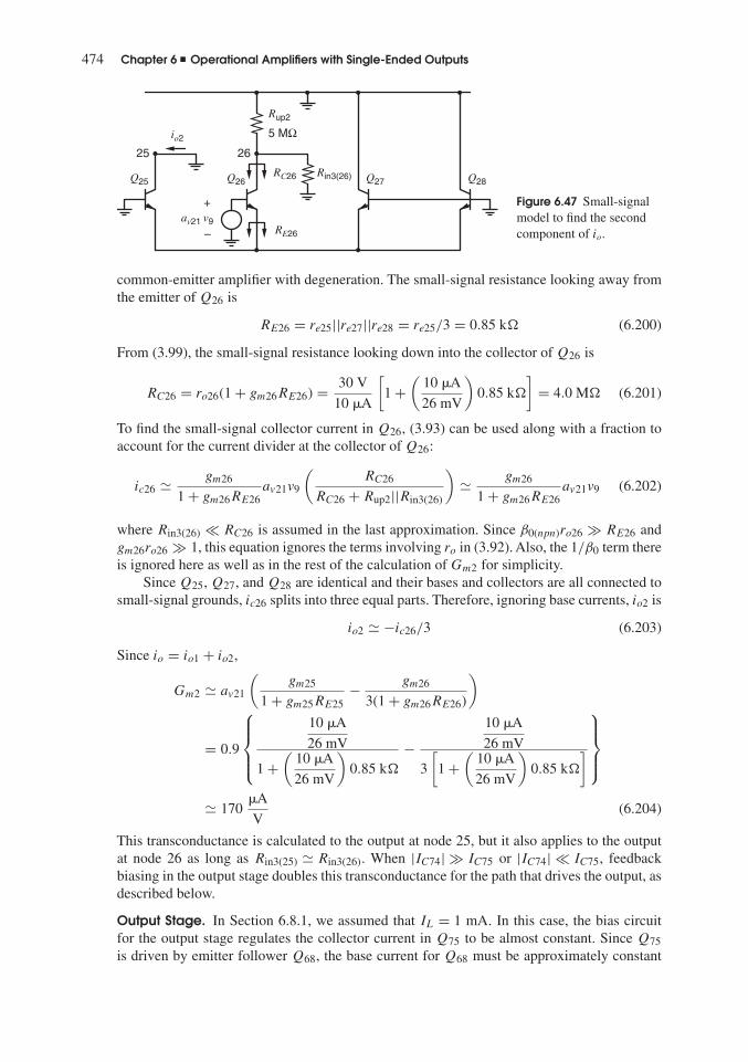
474 Chapter 6 � Operational Amplifiers with Single-Ended Outputs
io2
RE26
25 26
Rin3(26)RC26Q25 Q26 Q27 Q28
av21 v9
+
–
Rup2
5 MΩ
Figure 6.47 Small-signalmodel to find the secondcomponent of io.
common-emitter amplifier with degeneration. The small-signal resistance looking away fromthe emitter of Q26 is
RE26 = re25||re27||re28 = re25/3 = 0.85 k (6.200)
From (3.99), the small-signal resistance looking down into the collector of Q26 is
RC26 = ro26(1 + gm26RE26) = 30 V
10 �A
[1 +(
10 �A
26 mV
)0.85 k
]= 4.0 M (6.201)
To find the small-signal collector current in Q26, (3.93) can be used along with a fraction toaccount for the current divider at the collector of Q26:
ic26 � gm26
1 + gm26RE26av21v9
(RC26
RC26 + Rup2||Rin3(26)
)� gm26
1 + gm26RE26av21v9 (6.202)
where Rin3(26) � RC26 is assumed in the last approximation. Since β0(npn)ro26 � RE26 andgm26ro26 � 1, this equation ignores the terms involving ro in (3.92). Also, the 1/β0 term thereis ignored here as well as in the rest of the calculation of Gm2 for simplicity.
Since Q25, Q27, and Q28 are identical and their bases and collectors are all connected tosmall-signal grounds, ic26 splits into three equal parts. Therefore, ignoring base currents, io2 is
io2 � −ic26/3 (6.203)
Since io = io1 + io2,
Gm2 � av21
(gm25
1 + gm25RE25− gm26
3(1 + gm26RE26)
)
= 0.9
⎧⎪⎪⎨⎪⎪⎩
10 �A
26 mV
1 +(
10 �A
26 mV
)0.85 k
−10 �A
26 mV
3
[1 +(
10 �A
26 mV
)0.85 k
]⎫⎪⎪⎬⎪⎪⎭
� 170�A
V(6.204)
This transconductance is calculated to the output at node 25, but it also applies to the outputat node 26 as long as Rin3(25) � Rin3(26). When |IC74| � IC75 or |IC74| � IC75, feedbackbiasing in the output stage doubles this transconductance for the path that drives the output, asdescribed below.
Output Stage. In Section 6.8.1, we assumed that IL = 1 mA. In this case, the bias circuitfor the output stage regulates the collector current in Q75 to be almost constant. Since Q75is driven by emitter follower Q68, the base current for Q68 must be approximately constant

6.8 Bipolar Operational Amplifiers 475
ib64 = 2i
ib68 = 0
i
i i
i25
26
Q25 Q26 Q27 Q28
R39 R40
Q39 Q40
av21 v9
+
–av22 v10
+
–vb40
+
–2.5 kΩ 2.5 kΩ
Rup2
5 MΩRup2
5 MΩ
Figure 6.48 Small-signal model of the interaction between the second stage and differential pairQ39-Q40 in the bias circuit for the third stage when IC75 is almost constant.
under this condition. To explain this result, consider Fig. 6.48, which shows a small-signalmodel of the key part of the second stage plus differential pair Q39-Q40 from the bias circuitthat controls the output stage. The outputs of this model are nodes 25 and 26, which drive thebases of Q64 and Q68 in Fig. 6.39.
First consider the second stage. The two outputs are driven by matched circuits in thesecond stage, and the loading placed on these two nodes in the third stage is almost identical.Therefore, the small-signal currents drawn into nodes 25 and 26 from the second stage arealmost identical and labeled as i in Fig. 6.48.
Now consider differential pair Q39-Q40. This pair forms the input of a differential amplifierthat operates in a negative feedback loop and keeps IC75 almost constant when |IC74| �IC75, as described in Section 6.8.1. The base of Q39 is connected to a small-signal ground inFig. 6.48 because the collector currents of Q37 and Q38 in Fig. 6.40 are constant. On the otherhand, the base of Q40 is driven by vb40, which is the small-signal voltage from the base of Q40to ground. Since Q75 is driven by Q68, keeping IC75 constant means that the small-signal basecurrent of Q68, ib68, is approximately zero. Therefore, Q40 must inject a small-signal currentof i into node 26 under these conditions, as shown in Fig. 6.48. Since the total current in thedifferential pair is constant, Q39 pulls the same current i out of node 25. This result doubles thesmall-signal base current of Q64, ib64, to 2i, effectively doubling Gm2 to node 25 and settingGm2 to node 26 to approximately zero when |IC74| � IC75. Therefore, in the analysis of theoutput stage below, we will focus on the path from node 25 to the output. In the opposite case(when |IC74| � IC75), the path from node 26 to the output is dominant. When |IC74| � IC75,both paths must be considered.
Ignoring the resistance looking down into the collector of Q39, the input resistance of thethird stage (Fig. 6.39) at node 25 is
Ri3(25) = rπ64 + (β0(npn) + 1)RE64 (6.205)
In this equation, RE64 is the incremental resistance from the emitter of Q64 to small-signalground, which is
RE64 = [ro63(1 + gm63R63)]||[rπ65 + (β0(pnp) + 1)RE65] (6.206)
Similarly, RE65 is the incremental resistance from the emitter of Q65 to small-signal ground.Ignoring the resistance looking into the base of Q43 in Fig. 6.40, RE65 is
RE65 = R65||rπ66||rπ74 = R65||β0(pnp)VT
|IC66| ||β0(pnp)VT
|IC74| (6.207)

476 Chapter 6 � Operational Amplifiers with Single-Ended Outputs
Since the emitter area of Q74 is thirty-two times larger than that of Q66,
|IC66| = |IC74|/32 = 1200 �A/32 = 37 �A (6.208)
So
RE65 = 7.5 k||10(26 mV)
37 �A||10(26 mV)
1200 �A= 200 (6.209)
Then
RE64 =[
30 V
33 �A
(1 + 33 �A
26 mV1.2 k
)]||[
10(26 mV)
200 �A+ (11)200
]= 3.5 k
(6.210)
Finally, from (6.205) with IC64 = 4 �A as calculated in (6.173),
Ri3(25) = 40(26 mV)
4 �A+ (41)3.5 k = 404 k (6.211)
The output resistance of the stage is
Ro3 = ro74||ro75 = 20 V
1200 �A|| 30 V
210 �A= 15 k (6.212)
The transconductance of the stage is
Gm3 = av64av65gm74 (6.213)
where av64, and av65 are the gains of emitter followers Q64 and Q65, respectively.Since ro64 � RE64, (3.69) gives
av64 = 1
1 + rπ64
(β0(npn) + 1)RE64
= 1
1 +40(26 mV)
4 �A41 (3.5 k)
= 0.36 (6.214)
Since ro65 � RE65, (3.69) gives
av65 = 1
1 + rπ65
(β0(pnp) + 1)RE65
= 1
1 +10(26 mV)
200 �A11 (200 )
= 0.63 (6.215)
Therefore,
Gm3 = 0.36(0.63)
(1200 �A
26 mV
)= 1
96 (6.216)
Overall Gain. The voltage gain of the input stage when loaded by the second stage is
av1 = Gm1
(Ro1||Ri2
2
)= 97
�A
V
(11 M||1.3 M
2
)= 60 (6.217)
The voltage gain of the second stage when loaded by the third stage is
av2 = 2Gm2(Ro2||Ri3(25)) = 2 × 170�A
V(2.2 M||404 k) = 120 (6.218)

6.8 Bipolar Operational Amplifiers 477
In this equation, Gm2 is multiplied by two because of the effect of feedback biasing explainedabove. The voltage gain of the third stage when loaded by a 2 k resistor conducting a currentof 1 mA is
av3 = Gm3(Ro3||RL) = 1
96 (15 k||2 k) = 18 (6.219)
Therefore, the overall gain of the NE5234 op amp is
av = av1av2av3 = 130, 000 (6.220)
This gain is an estimate of the minimum gain of the op amp because the load is usually largerthan 2 k and because the values of Early voltages and betas used are the minimum valuesexpected to occur when building many op amps. In practice, the gain is usually much higherthan this value. See Problem 6.28.
6.8.4 Calculation of the Input Offset Voltage and Current of the NE5234
Two important aspects of the performance of op amps are the input offset voltage and current.Since the offsets are indistinguishable from the dc component in the signal of interest, thesedeviations from ideality limit the ability of the circuit to amplify small dc signals accurately.Furthermore, calculation of these parameters is fundamentally different from calculation ofother parameters such as voltage gain. Offset voltage and current are random parameters withmean values that are usually near zero. These offsets arise from randomly occurring mismatchesbetween pairs of matched elements in the input stage of the circuit, and are best described by aprobability distribution with (ideally) zero mean and some standard deviation. The parametersof interest from the designer’s standpoint are the standard deviations of the offset voltageand current distributions, which determine the limits that can be placed on the offset voltageand current of production units being tested while maintaining an acceptable yield. From theuser’s standpoint, the details of the distribution are of little significance except as they affectthe specified maximum offset voltage chosen by the designer. The information available tothe designer at the design stage is the distribution of mismatches in resistor values, transistorsaturation currents, and transistor betas. Given these distributions, the task is to design an inputstage with the minimum offset while meeting the other circuit requirements. We will calculatethe offset voltage and current of the NE5234 op amp under the assumption that the variousdevice mismatches are described by normal or Gaussian distributions.
In this analysis, we will assume that the voltage and current gains of the input stage are largeenough that other stages have negligible effect on the input offset voltage and current of theop amp. Provided that the mismatches are small enough that they only slightly perturb thecurrents in the circuit, we can simplify the problem by considering each device pair indepen-dently. Figure 6.49 shows a simplified schematic of the input stage of the NE5234. This figureassumes that the common-mode input voltage to the op amp is low enough that Q3 and Q4are active but Q1 and Q2 are off. The collector currents of Q3 and Q4 are modeled here bycurrent sources |IC3| and |IC4|. The first problem is to determine the difference between |IC3|and |IC4| required to set IC9 − IC10 = 0 in the presence of mismatches between Q9 and Q10as well as between R9 and R10.
From KVL,
VB = VT ln
(IC9
IS9
)+(
IC9
αF9+ |IC3|
)R9 (6.221)

478 Chapter 6 � Operational Amplifiers with Single-Ended Outputs
Q9
R9
Q10
22 kΩR10
22 kΩ
34
VCC
VB
|IC3| |IC4|
IC10IC9
–VEE = 0
Figure 6.49 A model of the NE5234 inputstage for finding |IC3| − |IC4| to setIC9 − IC10 = 0.
and
VB = VT ln
(IC10
IS10
)+(
IC10
αF10+ |IC4|
)R10 (6.222)
Subtracting these equations gives
0 = VT ln
(IC9
IC10
)− VT ln
(IS9
IS10
)+ IC9
αF9R9 − IC10
αF10R10 + |IC3|R9 − |IC4|R10 (6.223)
To simplify the first two terms on the right side of this equation, use standard defini-tions of average and mismatch quantities as in Section A.4.1.1: IC9,10 = (IC9 + IC10)/2,�IC9,10 = IC9 − IC10, IS9,10 = (IS9 + IS10)/2, and �IS9,10 = IS9 − IS10. Also, assume that�IC9,10/2IC9,10 � 1, �IS9,10/2IS9,10 � 1, and ln(1 + x) � x for x � 1. Then
VT ln
(IC9
IC10
)− VT ln
(IS9
IS10
)� VT
(�IC9,10
IC9,10− �IS9,10
IS9,10
)(6.224)
With corresponding definitions and assumptions for other parameters, the next two terms in(6.223) become
IC9
αF9R9 − IC10
αF10R10 � IC9,10R9,10
αF9,10
(�IC9,10
IC9,10+ �R9,10
R9,10− �αF9,10
αF9,10
)(6.225)
Similarly, the last two terms in (6.223) become
|IC3|R9 − |IC4|R10 � |IC3,4|R9,10
(�|IC3,4||IC3,4| + �R9,10
R9,10
)(6.226)
Substituting (6.224), (6.225), and (6.226) into (6.223) and finding �|IC3,4|/|IC3,4| needed toset �IC9,10/IC9,10 = 0 gives
�|IC3,4||IC3,4| � 1
gm3,4R9,10
�IS9,10
IS9,10−(
1 + gm9,10
αF9,10gm3,4
)�R9,10
R9,10+ gm9,10
αF9,10gm3,4
�αF9,10
αF9,10
(6.227)
Now consider Fig. 6.50, which shows a slightly more complicated model of the NE5234input stage. This figure includes |IC13| and |IC14| to model the currents produced by Q13, Q14,R13, and R14. These elements form the outputs of a pair of current mirrors, and the effect of

6.8 Bipolar Operational Amplifiers 479
R9
22 kΩR10
22 kΩ
9 10
43
VCC
VB
|IC13|
|IC4||IC3|
|IC14|
IC10IC9
Q9 Q10
–VEE = 0
Figure 6.50 A model of the NE5234input stage for finding |IC3| − |IC4| toset IC9 − IC10 = |IC13| − |IC14|.
mismatch in these elements is considered in Section A.4.1.1. From (4.296),
�|IC13,14||IC13,14| �
⎛⎜⎜⎝ 1
1 + gm13,14R13,14
αF13,14
⎞⎟⎟⎠ �|IS13,14|
|IS13,14|
(6.228)
+gm13,14R13,14
αF13,14
1 + gm13,14R13,14
αF13,14
(−�R13,14
R13,14+ �αF13,14
αF13,14
)
To include these mismatches in the stage offsets, we substitute (6.224), (6.225), and (6.226)into (6.223) and find �|IC3,4|/|IC3,4| needed to set �IC9,10/IC9,10 = �|IC13,14|/|IC13,14|,which causes the differential output voltage of the stage to be zero and gives
�|IC3,4||IC3,4| � 1
gm3,4R9,10
�IS9,10
IS9,10−(
1 + gm9,10
αF9,10gm3,4
)�R9,10
R9,10+ gm9,10
αF9,10gm3,4
�αF9,10
αF9,10
−
⎛⎜⎜⎝
1 + gm9,10R9,10
αF9,10
gm3,4R9,10
⎞⎟⎟⎠⎛⎜⎜⎝
gm13,14R13,14
αF13,14
1 + gm13,14R13,14
αF13,14
⎞⎟⎟⎠(
−�R13,14
R13,14+ �αF13,14
αF13,14
)
−
⎛⎜⎜⎝
1 + gm9,10R9,10
αF9,10
gm3,4R9,10
⎞⎟⎟⎠⎛⎜⎜⎝ 1
1 + gm13,14R13,14
αF13,14
⎞⎟⎟⎠ �|IS13,14|
|IS13,14| (6.229)
Now the problem is to refer �|IC3,4|/|IC3,4| to the input of the op amp. Fig. 6.51 showsa model of the input stage used to find the input offset voltage. From KVL,
V4 − V3 = VEB3 − VEB4 = VT ln
( |IS4||IS3|
|IC3||IC4|
)(6.230)

480 Chapter 6 � Operational Amplifiers with Single-Ended Outputs
Q3 Q4V3 V4
3 4
|IC11|
|IC3| |IC4|
VCC
+
–
+
– Figure 6.51 A model of the NE5234 inputstage for finding VOS when the common-mode input voltage is low enough that Q1
and Q2 are off.
Using standard definitions of average and mismatch quantities and similar assumptions tothose made to simplify (6.223) gives
V4 − V3 � VT
(−�|IS3,4|
|IS3,4| + �|IC3,4||IC3,4|
)(6.231)
Then the input offset voltage, VOS , is the differential input voltage, V4 − V3, for which thedifferential output voltage of the stage is zero. This condition is satisfied when �|IC3,4|/|IC3,4|is given by (6.229). Substituting (6.229) into (6.231) with gm3,4 = 3 �A/26 mV, gm9,10 =gm13,14 = 6 �A/26 mV, R9,10 = 22 k, R13,14 = 33 k, αF9,10 = 40/41, and αF13,14 =10/11 gives
VOS � VT
[−(
�|IS3,4||IS3,4|
)+ 0.39
(�IS9,10
IS9,10
)− 3.1
(�R9,10
R9,10
)+ 2.1
(�αF9,10
αF9,10
)
− 2.2
(−�R13,14
R13,14+ �αF13,14
αF13,14
)− 0.26
(�|IS13,14||IS13,14|
)](6.232)
For a given set of mismatches, this expression gives the input offset voltage. However,the information of interest to the designer is the distribution of observed offset voltages overa large number of samples, and the information available is the distribution of the mismatchfactors. If each of the quantities
�|IS3,4||IS3,4|
�IS9,10
IS9,10
�R9,10
R9,10
�αF9,10
αF9,10
�R13,14
R13,14
�αF13,14
αF13,14
�|IS13,14||IS13,14|
are regarded as independent random variables with normal distributions, the standard deviationof the sum is given by
σsum =√∑
n
σ2n (6.233)
as described in Appendix A3.1. Thus the standard deviation of the distribution for VOS iscalculated by taking the square root of the sum of the squares of the individual contributions.
Assuming that the standard deviation of resistor matching is 1 percent, that of IS matchingis 5 percent, and that of beta matching is 10 percent, we obtain
σVOS
VT
=√
(0.050)2 + (0.020)2 + (0.031)2 + (0.0050)2 + (0.022)2 + (0.020)2 + (0.013)2
σVOS= VT (0.070) = 1.8 mV (6.234)

6.8 Bipolar Operational Amplifiers 481
Q3 Q4
3 4
|IC11|
|IB3| |IB4|
|IC3| |IC4|
VCC
Figure 6.52 A model of the NE5234 inputstage for finding IOS when the common-mode input voltage is low enough that Q1
and Q2 are off.
The largest single offset contribution is thus the saturation current mismatch of the input devices
Q3 and Q4. If the offset voltage has a standard deviation of 1.8 mV, then the fraction, Y, ofall devices fabricated that will have an offset voltage of less than the NE5234 specification of5 mV can be found using (3.285) and is
Y =∫ 5
−5
1
1.8√
2πexp
[− x2
2(1.8)2
]dx (6.235)
Evaluating this integral with the aid of Fig. 3.71 gives Y = 0.995. Thus a 0.5 percent yieldloss will be suffered from offset voltage variations with the 5-mV offset specification.
Figure 6.52 shows a model of the input stage used to find the input offset current. Thedifference of the magnitudes of the base currents is
|IB4| − |IB3| = |IC4|βF4
− |IC3|βF3
= |IC3,4|βF3,4
⎛⎜⎜⎝
1 − �|IC3,4|2|IC3,4|
1 − �βF3,4
2βF3,4
−1 + �|IC3,4|
2|IC3,4|1 + �βF3,4
2βF3,4
⎞⎟⎟⎠
� |IB3,4|(
�βF3,4
βF3,4− �|IC3,4|
|IC3,4|)
(6.236)
Then the input offset current, IOS , is the differential input current, |IB4| − |IB3|, for which thedifferential output voltage of the stage is zero. This condition is satisfied when �|IC3,4|/|IC3,4|is given by (6.229). Substituting (6.229) into (6.236) with the same parameter values as in(6.232) gives
IOS � |IB3,4|[(
�βF3,4
βF3,4
)− 0.39
(�IS9,10
IS9,10
)+ 3.1
(�R9,10
R9,10
)− 2.1
(�αF9,10
αF9,10
)
+ 2.2
(−�R13,14
R13,14+ �αF13,14
αF13,14
)+ 0.26
(�|IS13,14||IS13,14|
)](6.237)
Under the same conditions used to calculate σVOS, we obtain
σIOS
|IB3,4| =√
(0.10)2 + (0.020)2 + (0.031)2 + (0.0050)2 + (0.022)2 + (0.020)2 + (0.013)2
σIOS= 3 �A
10(0.11) = 33 nA (6.238)
and is dominated by the beta mismatch between Q3 and Q4.

482 Chapter 6 � Operational Amplifiers with Single-Ended Outputs
PROBLEMS6.1 For the circuit of Fig. 6.53, determine the out-
put current as a function of the input voltage. Assumethat the transistor operates in the active region.
Ideal++
––Vin
R
Iout
Figure 6.53 Circuit for Problem 6.1.
6.2 Determine the output voltage as a function ofthe input voltage for the circuit of Fig. 6.54. Assumethe op amp is ideal.
–
+
Vin Vout
+
–
+
–
1 kΩ 1 kΩ
Figure 6.54 Circuit for Problem 6.2.
6.3 In the circuit of Fig. 6.55, determine the cor-rect value of Rx so that the output voltage is zero whenthe input voltage is zero. Assume a nonzero input biascurrent, but zero input offset current and input offsetvoltage.
–
+
+
–Vin
Vout
R1 R2
Rx
Figure 6.55 Circuit for Problem 6.3.
6.4 The differential instrumentation amplifiershown in Fig. 6.56 must have a voltage gain of 103
with an accuracy of 0.1 percent. What is the minimumrequired open-loop gain of the op amp?Assume the opamp open-loop gain has a tolerance of +100 percent,
–50 percent. Neglect the effects of Rin and Rout in theop amp.
–
+
+
+
––
vin
vout1 kΩ 1 MΩ
1 kΩ 1 MΩ
Figure 6.56 Circuit for Problem 6.4.
6.5 Once the offset voltage of the differentialamplifier in Problem 6.4 is adjusted to zero, the input-referred offset voltage must remain less than 1 mV inmagnitude for common-mode input voltages between� 10 V. What is the minimum CMRR allowable forthe amplifier to meet this requirement?
6.6 Consider the differential amplifier shown inFig. 6.4. Choose values of R1 and R2 for which thegain is equal to −10 and the magnitude of the dcoutput voltage is less than or equal to −10 mV withV1 = V2 = 0. Assume that the op amp is ideal exceptthat |IOS | = 100 nA.
6.7 Suppose an op amp with PSRR+ = 10 is con-nected in the voltage-follower configuration shown inFig. 6.3c. The input VS is set to zero, but a low- fre-quency ac signal with peak magnitude vsup = 20 mVis superimposed on the positive power supply. Calcu-late the peak magnitude of the output voltage.
6.8 In the switched-capacitor amplifier of Fig.6.9a, assume that the source of M4 is connected toVS instead of to ground. Calculate the output volt-age that appears during φ2 for a given VS . Assumethe op amp is ideal except that it has a finite gain aand a nonzero input capacitance CP . Assume idealMOS switches with zero on-resistance and infiniteoff-resistance.
6.9(a) Calculate and sketch the output voltagewaveform of the switched-capacitor integrator of Fig.6.10a from t = 0 to t = 20 �s assuming a fixed Vs =1 V and a clock rate of 1 MHz. Assume an ideal MOSop amp with infinite gain and zero output rise time.Assume ideal MOS switches with zero on-resistanceand infinite off-resistance.
(b) Compare the result for (a) with the outputwaveform of the continuous-time equivalent circuitof Fig. 6.10c.

Problems 483
(c) Investigate the effect on the output voltagewaveform in (a) of a finite voltage gain of 1000 inthe MOS op amp.
6.10 Calculate the low-frequency PSRR from theVdd and Vss power supplies for the common-sourceamplifier shown in Fig. 6.57. Assume the transistor isbiased in the active region.
VDD + vdd
VSS + vss
R
vo
vi
+
+
–
–
Figure 6.57 Circuit for Problem 6.10.
6.11 Draw a two-stage op amp similar to the opamp in Fig. 6.16 except reverse the polarity of everytransistor. For example, the resulting op amp shouldhave an n-channel input pair. Calculate the followingparameters: (a) low-frequency voltage gain, (b) outputswing, (c) systematic input offset voltage assuming(6.66) is satisfied, (d) common-mode rejection ratio,(e) common-mode input range, and (f) low-frequencypower-supply rejection ratio from both supplies.
6.12(a) Equation 6.69 gives the random input off-set voltage of the op amp in Fig. 6.16. Explain thepolarity of each term in (6.69) by assuming that thematching is perfect except for the term under consid-eration. Keep in mind that the overdrive is negative forp-channel transistors. Therefore, (6.69) predicts thatthe offset stemming from W3 > W4 is negative.
(b) Repeat (a) for an op amp that uses an n-channeldifferential pair and a p-channel current-mirror load.Equation 6.69 still applies in this case.
6.13(a) Calculate the random input offset voltagefor the op amp in Fig. 6.16. Assume the matching isperfect except that Vt3 − Vt4 = 10mV. Also assumethat all transistors have equal W/L and operate in theactive region. Ignore short-channel effects and use thedata in Table 2.4.
(b) Repeat (a) for an op amp that uses an n-channeldifferential pair and a p-channel current-mirror load.
(c) Which of these two configurations gives lowerinput offset voltage? Explain.
6.14 List and explain at least three reasons toselect a two-stage op amp with an n-channel inputpair instead of with a p-channel input pair for a givenapplication.
6.15 Calculate bias currents and the low-frequencysmall-signal voltage gain for the CMOS op amp ofFig. 6.58. Use the parameters given in Table 2.4,and assume that Xd = 0.1 �m and dXd/dVDS =0.04 �m/V for all the transistors at the operating point.Calculate the input common-mode range assumingthat the wells of M1 and M2 are connected to theircommon-source point. Calculate the low-frequencygain from each supply to the output. Check these cal-culations with SPICE simulations.
6.16 Calculate the common-mode input range ofthe op amp in Fig. 6.25. Assume that all the transistorsare enhancement-mode devices with |Vt | = 1 V, andignore the body effect. Also assume that the biasingis arranged so that |Vov | = 0.2 V for each transistorexcept M9. Finally, assume that M1 and M2 are biasedat the edge of the active region by M9 and IC.
6.17 Draw a telescopic-cascode op amp similar tothe first stage in Fig. 6.25 except use an n-channelinput pair and a high-swing p-type cascode current-mirror load. Calculate the maximum output swingin terms of the common-mode input voltage. Deter-mine the optimum common-mode input voltage formaximizing the output swing, and calculate the swingwith this common-mode input voltage under the sameassumptions given in Problem 6.16.
6.18 Calculate the common-mode input range ofthe folded-cascode op amp in Fig. 6.28. Assume thatall the transistors are enhancement-mode devices with|Vt | = 1 V, and ignore the body effect. Also assumethat the biasing is arranged so that |Vov | = 0.2 V foreach transistor. Finally, assume that M11 and M12 arebiased at the edge of the active region.
6.19 Find the low-frequency voltage gain fromvariation on each power supply to the op-amp out-put in Fig. 6.28. Assume that the bias voltages VBIAS1,VBIAS2, and VBIAS3 are produced by the circuit shown inFig. 6.59, where M106 is the only transistor that oper-ates in the triode region. Assume that the W/L ratiosare chosen so that all transistors in the op amp oper-ate in the active region. Compare your calculations toSPICE simulations. Use models and supply voltagesof your choice provided that the above conditions aresatisfied.
6.20 Design a CMOS op amp based on the folded-cascode architecture of Fig. 6.28 using supply voltagesof � 1.5 V. Use the bias circuit of Fig. 4.42 (withM3 and M4 cascoded) to generate the bias currentIBIAS. Then design an extension to this bias circuit that

484 Chapter 6 � Operational Amplifiers with Single-Ended Outputs
–VDD = –1.5 V
VDD = 1.5 V
M7M5M8
M2
M9
M6
M4M3
M11501
1001
501
501
1501
1501
1501
1501
+
–
vi
+
–vo
200 μA
5 pF
Figure 6.58 Circuit for Problem 6.15.
M102 M103 M109
M101 M104
M105
M106
IBIAS
VBIAS1
VBIAS2
VBIAS3
–VSS
VDD
M107
M108
Figure 6.59 Bias circuit for Problem 6.19.

Problems 485
produces the bias voltages VBIAS1, VBIAS2, and VBIAS3
based on IBIAS. The output current-drive capability isto be � 100 �A, the output voltage-swing capabil-ity 1.5 Volts peak-peak, and the input common-moderange should extend from 0.5 V to the negative supply.Matching requirements dictate a minimum effectivechannel length of 1 �m. To make the gain insensitiveto small shifts in the operating point, design the circuitso that the magnitude of the drain-source voltage foreach transistor operating in the active region exceedsthe magnitude of its overdrive by at least 100 mV.Specify all device geometries and bias currents. Theprocess is the n-well process with parameters givenin Table 2.4. Assume Xd = 0 and γ = 0.25V1/2 forboth n- and p-channel transistors, but ignore the bodyeffect in the hand calculations. Use SPICE to verifyand refine your design as well as to determine the gain.
6.21 Draw the schematic of a folded-cascode opamp similar to the op amp in Fig. 6.28 except with twolayers of both n- and p-type cascodes. Choose a currentmirror that maximizes the output swing. Assume thatall transistors have equal overdrive magnitudes exceptwhere changes are needed to maximize the outputswing. Use the models in Table 2.4 and ignore the bodyeffect. Specify the W/L ratios in multiples of (W/L)1.
6.22 For the folded-active-cascode op amp in Fig.6.30, choose the device sizes to give a peak-peakoutput swing of at least 2.5 V. Use the 0.4 �mCMOS model parameters in Table 2.4 except let γ =0.25 V1/2 and Xd = 0 for all transistors and Vt0 = 0.7V and −0.7 V for n-channel and p-channel transis-tors, respectively. Assume the drawn channel lengthis L = 1 �m is used for all transistors to simplify the
design. With IBIAS = 25 �A, the bias currents shouldbe |ID5| = ID11 = ID12 = ID25 = |ID35| = 200 �A.Assume VDD = VSS = 1.65 V and that the matchingis perfect. When the dc input voltage VI = 0, assumethat all transistors except M106 and M114 operate inthe active region with equal overdrive magnitudes. Tomake the gain insensitive to small shifts in the operat-ing point, design the circuit so that the magnitude ofthe drain-source voltage for each transistor operatingin the active region exceeds the magnitude of its over-drive by at least 100 mV. Ignore the body effect in thehand calculations. Use SPICE to verify your design,to choose the widths of M106 and M114, and to deter-mine the gain.Also, use SPICE to determine the gain ifVt0 = 0.6V for n-channel transistors and Vt0 = −0.8V for p-channel transistors, as given in Table 2.4.Explain the resulting change in the op-amp again.
6.23 Suppose that the peak-peak output swingrequirement in Problem 6.22 is reduced while the otherconditions are held constant. This change allows theoverdrive magnitude to be increased. Which transis-tor in the bias circuit of Fig. 6.30d enters the trioderegion first if the overdrive magnitudes are increaseduniformly? Explain. Exclude M106 and M114 from con-sideration because they are deliberately operated in thetriode region. How can the bias circuit be redesigned toincrease the allowed overdrive magnitude while oper-ating all transistors except M106 and M114 in the activeregion? What are the disadvantages of the modifiedbias circuit?
6.24(a) Figure 6.60a shows a folded version ofthe op amp in Fig. 6.15. A differential interstagelevel-shifting network composed of voltage sources V
I3 I3 I2
II4
M2
M1I4
I1
vi
vo
–VSS
VDD
VDD
–VSS
VCC
IB
VV+
–
+
–
+
–
(a) (b)
+
–
Figure 6.60 Circuits for Problem 6.24.

486 Chapter 6 � Operational Amplifiers with Single-Ended Outputs
Q37
Q38
Q39 Q40
Q46
Q68
Q74
IL
Q75
Q65
Out
Q43Q64
Pbase
Nbase
R43
1.3 kΩ
R39
2.5 kΩR40
2.5 kΩR46
1.3 kΩ
R65
7.5 kΩ
25
26
IREF = |IC36| – IC35
7.4 μA
IC69
6 μA
IC63
33 μA
IC41
18 μA
VCC
–VEE = 0
Figure 6.61 Circuit for Problem 6.26.
has been inserted between the first and second stages.Assume that current source I1 is implemented using ann-channel transistor with overdrive of Vovn, which isequal to the overdrives of the other n-channel transis-tors shown in Fig. 6.60a. Assume that current sourcesI2 and I3 are each implemented using one p-channeltransistor with an overdrive of Vovp. In the resulting opamp, only n-channel transistors conduct time-varyingcurrents. Find the input common-mode range and themaximum output swing of the op-amp in terms ofVDD, −VSS , the level-shift voltage V, the thresholdvoltages of individual transistors, and the overdrivesVovn and Vovp.
(b) Figure 6.60b shows a realization of an activefloating level shift (active battery). Design this level-shift circuit to give a battery voltage of 1.5 V witha small-signal resistance less than 1 k at I = 100�A dc. Ignore the body effect. Use IB = 100 �A andVDD = VSS = 1.65 V. Use SPICE to plot the large-signal I − V characteristic for V = 0 to 1.65 V. UseμnCox = 194 �A/V2, λ = 0, and Vt = 0.6 V. ForSPICE simulations, connect the lower end of the bat-tery to the negative supply.
6.25 Assume that Q75 does not saturate and cal-culate the maximum value of IC75 in the NE5234 opamp. Assume VEB70(on) = 0.7 V, IS71 = 6 × 10⁻¹⁸Aand IS75 = 6 × 10⁻¹⁷A.
6.26 Fig. 6.61 shows an alternate scheme for bias-ing the NE5234 output stage.17 Ignoring all basecurrents, find |IC74|IC75. Use Fig. 6.42 for the rela-tive emitter areas of all the transistors except assumethat Q46 is identical to Q43.
6.27 Determine the small-signal voltage gain ofthe NE5234 if all the values of all the resistors in theinput stage are doubled. Assume the common-modeinput voltage is low enough that Q1 and Q2 are off.Assume the output stage is biased as described in thischapter.
6.28 Find the small-signal voltage gain of theNE5234 op amp under the same conditions givenin this chapter except use βF (npn) = β0(npn) = 80 andβF (pnp) = β0(pnp) = 20. Ignore βF (npn) and βF (pnp) fromdc bias calculations except in calculating revised esti-mates of IC64, |IC65|, and IC68, as at the end ofSection 6.8.1.

Problems 487
6.29 In Fig. 6.31b, resistive loads were used toextend the common-mode input range to include−VEE. Fig. 6.62 shows another circuit with thischaracteristic.22 Find the common-mode range of thiscircuit. Assume that VBE(on) = 0.7 V and VCE(sat) =0.1 V for the npn transistors. Also, assume thatVBE(on) = −0.7 V and VCE(sat) = −0.1 V for the pnptransistors. Ignore base currents for simplicity.
Q3
Q1
Q4
Q2
Q7Q6
Q8 Q5 Q9
VCC
Bias1
+
–VEE = 0
–
Figure 6.62 Circuit for Problem 6.29.
6.30 Repeat Problem 6.29 except replace each pnptransistor with a p-channel MOS transistor and replaceeach npn transistor with an n-channel MOS transistor.Assume Vt = 0.5 V and Vov = 0.1 V for all n-channelMOS transistors. Also, assume Vt = −0.5 V andVov = −0.1 V for all p-channel MOS transistors.
6.31(a) Suppose that the npn and pnp transis-tors in the input stage of the NE5234 op amp
are changed into n-channel and p-channel MOStransistors, respectively. If transistors conductingnonzero current operate in strong inversion, thetransconductance of the revised circuit dependson the common-mode input voltage, VIC. Explainwhy.
(b) Fig. 6.63 shows one circuit that overcomes thisproblem.23 Let R represent the gains of the M8-M7
and the M11-M12 current mirrors. When VB1 � VIC �VDD − VB2, M5-M8 as well as M11 and M12 are off.Therefore, the tail current for M1-M2 is IB1, and thetail current for M3-M4 is IB2. On the other hand, when0 ≤ VIC � VB1, M1 and M2 are off, and the tail currentin M3 and M4 becomes RIB1 + IB2. Similarly, whenVDD ≥ VIC � VDD − VB2, M3 and M4 are off, and thetail current in M1 and M2 becomes IB1 + RIB2. Findthe value of R for which the transconductance of theinput stage when only one differential pair is active isthe same as when both pairs are active. Assume thatIB1 = IB2 and �n Cox,n(W/L)n = �p Cox,p(W/L)p forM1-M4. Also, assume that M9, M10, M13, and M14
operate in saturation.
6.32 Find the minimum value of VCC for properoperation of the NE5234 op amp. For simplicity,assume VEE = 0, |VBE(on)| = 0.7 V, and |VCE(sat)| =0.1 V. Also, ignore base currents. Assume the bias cir-cuits in Figures 6.34 and 6.40 operate properly eventhough some transistors in these circuits may operatein or near saturation with low VCC.
6.33 In BiCMOS technology, MOS source follow-ers can be used to drive a bipolar differential pairto reduce the average current flowing in the stageinput leads. See Fig. 6.64. Calculate the input-referred
M5
M13
M10M9
M14
M4M3
M8M7
M6 M1
M11M2
M12
IB2
IB1VB1
vod1
VB2
R13
R9 R10
R14
3 4
43
9
21
1 2
10
VDD
+ + +– – –
Bias1
BiasCM
Figure 6.63 Circuit for Problem 6.31.

488 Chapter 6 � Operational Amplifiers with Single-Ended Outputs
–VSS = –VEE
VDD = VCC
VOD
VID
Q1
R1 R2
M3 M4
Q2
IBIAS ITAIL IBIAS
++
–
–
Figure 6.64 Circuit for Problem 6.33.
random offset voltage of this structure. Assumenonzero mismatch occurs in the following parameters:the thresholds of the MOS transistors, the W/L of the
MOS transistors, the bias currents, the saturation cur-rents of the bipolar transistors, and the load resistors.Ignore the body effect.
REFERENCES
1. G. E. Tobey, J. G. Graeme, and L. P. Huelsman.Operational Amplifiers. McGraw-Hill, New York,1971.
2. J. V. Wait, L. P. Huelsman, and G. A. Korn.Introduction to Operational Amplifier Theory andApplications. McGraw-Hill, New York, 1975.
3. D. Fullagar. ‘‘A New High-PerformanceMonolithic OpAmp,” Fairchild Semiconductor Appli-cations Brief, May 1968.
4. G. M. Jacobs, D. J. Allstot, R. W. Brodersen,and P. R. Gray, ‘‘Design Techniques for MOSSwitched Capacitor Ladder Filters,” IEEE Transac-tions on Circuits and Systems, Vol. CAS-25, pp. 1014–1021, December 1978.
5. K. Martin, ‘‘Improved Circuits for theRealization of Switched-Capacitor Filters,” IEEETransactions on Circuits and Systems, Vol. CAS-27,pp. 237–244, April 1980.
6. D.A. Hodges, P. R. Gray, and R. W. Brodersen.‘‘Potential of MOS Technologies for Analog Inte-grated Circuits,” IEEE Journal of Solid-State Circuits,Vol. SC-13, pp. 285–294, June 1978.
7. P. R. Gray and R. G. Meyer. ‘‘MOS Opera-tional Amplifier Design-A Tutorial Overview,” IEEEJournal of Solid-State Circuits, Vol. SC-17, pp. 969–982, December 1982.
8. Y. P. Tsividis. ‘‘Design Considerations inSingle-Channel MOS Analog Circuits,” IEEE Jour-nal of Solid- State Circuits, Vol. SC-13, pp. 383–391,June 1978.
9. W. C. Black, D. J. Allstot, and R. A. Reed. ‘‘AHigh Performance Low Power CMOS Channel Fil-ter,” IEEE Journal of Solid-State Circuits, Vol. SC-15,pp. 929–938, December 1980.
10. H. Ohara, P. R. Gray, W. M. Baxter, C. F.Rahim, and J. L. McCreary. ‘‘A Precision Low-PowerPCM Channel Filter with On-Chip Power Supply Reg-ulation,” IEEE Journal of Solid-State Circuits, Vol.SC-15, pp. 1005–1013, December 1980.
11. G. Nicollini, P. Confalonieri, and D.Senderowicz. "A Fully Differential Sample-and-HoldCircuit for High-Speed Applications," IEEE JournalSolid-State Circuits, Vol. 24, pp. 1461–1465, October1989.
References 489
12. T. C. Choi, R. T. Kaneshiro, R. W. Brodersen,P. R. Gray, W. B. Jett, and M. Wilcox. ‘‘High-Frequency CMOS Switched-Capacitor Filters forCommunications Application,” IEEE Journal ofSolid-State Circuits, Vol. SC-18, pp. 652–664,December 1983.
13. K. Bult and G. J. G. M. Geelen. ‘‘A Fast-Settling CMOS Op Amp for SC Circuits with 90-dBDC Gain,” IEEE Journal of Solid-State Circuits,Vol. 25, pp. 1379–1384, December 1990.
14. R. J. Widlar. ‘‘Low Voltage Techniques,”IEEE Journal of Solid-State Circuits, Vol. SC-13,pp. 838–846, Dec. 1978.
15. D. F. Bowers and S. A. Wurcer. ‘‘RecentDevelopments in Bipolar Operational Amplifiers,”Proceedings of the IEEE Bipolar/BiCMOS Circuitsand Technology Meeting, pp. 38–45, 1999.
16. R.A. Blauschild. ‘‘DifferentialAmplifier withRail-to-Rail Capability,” U.S. Patent 4,532,479, July1985.
17. J. H. Huijsing and D. Linebarger. ‘‘Low-Voltage Operational Amplifier with Rail-to-RailInput and Output Ranges,” IEEE Journal of Solid-State Circuits, Vol. SC-20, pp. 1144–1150, Dec.1985.
18. M. J. Fonderie and J. H. Huijsing. Design ofLow-Voltage Bipolar Operational Amplifiers, KluwerAcademic Publishers, Boston, 1993.
19. E. Seevinck, W. de Jager, and P. Buitendijk.‘‘A Low-Distortion Output Stage with ImprovedStability for Monolithic Power Amplifiers,” IEEEJournal of Solid-State Circuits, Vol. 23, pp. 794–801,June 1988.
20. J. H. Huijsing. Operational Amplifiers The-ory and Design, KluwerAcademic Publishers, Boston,2001.
21. J. Fonderie, M. M. Maris, E. J. Schnitger, andJ. H. Huijsing. ‘‘1-V Operational Amplifier with Rail-to-Rail Input and Output Ranges,” IEEE Journal ofSolid-State Circuits, Vol. 24, pp. 1551–1159, Dec.1989.
22. K. Fukahori, Y. Nishikawa, and A. R.Hamade. ‘‘A High Precision Micropower OperationalAmplifier,” IEEE Journal of Solid-State Circuits,Vol. SC-14, pp. 1048–1058, December 1979.
23. R. Hogervorst, J. P. Tero, R. G. H. Eschauzier,and J. H. Huijsing. ‘‘A Compact Power-Efficient 3 VCMOS Rail-to-Rail Input/Output Operational Ampli-fier for VLSI Cell Libraries,” IEEE Journal of Solid-State Circuits, Vol. 29, pp. 1505–1513, Dec. 1994.

CHAPTER 7
Frequency Response ofIntegrated Circuits
7.1 IntroductionThe analysis of integrated-circuit behavior in previous chapters was concerned with low-frequency performance, and the effects of parasitic capacitance in transistors were notconsidered. However, as the frequency of the signal being processed by a circuit increases, thecapacitive elements in the circuit eventually become important.
In this chapter, the small-signal behavior of integrated circuits at high frequencies is consid-ered. The frequency response of single-stage amplifiers is treated first, followed by an analysisof multistage amplifiers. Finally, the frequency response of the NE5234 operational amplifieris considered, and those parts of the circuit that limit its frequency response are identified.
7.2 Single-Stage AmplifiersThe basic topology of the small-signal equivalent circuits of bipolar and MOS single-stageamplifiers are similar. Therefore in the following sections, the frequency-response analysis foreach type of single-stage circuit is initially carried out using a general small-signal model thatapplies to both types of transistors, and the general results are then applied to each type oftransistor. The general small-signal transistor model is shown in Fig. 7.1. Table 7.1 lists theparameters of this small-signal model and the corresponding parameters that transform it intoa bipolar or MOS model. For example, Cin in the general model becomes Cπ in the bipolarmodel and Cgs in the MOS model. However, some device-specific small-signal elements arenot included in the general model. For example, the gmb generator and capacitors Csb and Cgb
in the MOS models are not incorporated in the general model. The effect of such device-specificelements will be handled separately in the bipolar and MOS sections.
The common-emitter and common-source stages are analyzed in the sections below ondifferential amplifiers.
7.2.1 Single-Stage Voltage Amplifiers and the Miller Effect
Single-transistor voltage-amplifier stages are widely used in integrated circuits. Figures 7.2aand 7.2b show the ac schematics for common-emitter and common-source amplifiers withresistive loads, respectively. Resistance RS is the source resistance, and RL is the load resis-tance. A simple linear model that can be applied to both of these circuits is shown in Fig. 7.2c.The elements in the dashed box form the general small-signal transistor model from Fig. 7.1without ro. We will assume that the output resistance of the transistor ro is much larger than RL.Since these resistors are connected in parallel in the small-signal circuit, ro can be neglected.An approximate analysis of this circuit can be made using the Miller-effect approximation.
490

7.2 Single-Stage Amplifiers 491
rin
rx
roCin
Cf
v1 gmv1
B or G C or D
E or S
+
–
Figure 7.1 A general small-signaltransistor model.
This analysis is done by considering the input impedance seen looking across the plane AA inFig. 7.2c. To find this impedance, we calculate the current i1 produced by the voltage v1.
i1 = (v1 − vo)sCf (7.1)KCL at the output node gives
gmv1 + vo
RL
+ (vo − v1)sCf = 0 (7.2)
From (7.2), the voltage gain Av from v1 to vo can be expressed as
Av (s) = vo
v1= −gmRL
⎛⎜⎜⎝
1 − sCf
gm
1 + sRLCf
⎞⎟⎟⎠ (7.3)
Using vo = Av (s)v1 from (7.3) in (7.1) gives
i1 = [1 − Av (s)]sCf v1 (7.4)
Equation 7.4 indicates that the admittance seen looking across the plane AA has a value[1 − Av (s)]sCf . This modification to the admittance sCf stems from the voltage gain acrossCf and is referred to as the Miller effect. Unfortunately, this admittance is complicated, dueto the frequency dependence of Av (s). Replacing the voltage gain Av (s) in (7.4) with itslow-frequency value Av0 = Av (0), (7.4) indicates that a capacitance of value
CM = (1 − Av0)Cf (7.5)
is seen looking across plane AA. The use of the low-frequency voltage gain here is called theMiller approximation, and CM is called the Miller capacitance. From (7.3), Av0 = Av (0) =−gmRL; therefore, (7.5) can be written as
CM = (1 + gmRL)Cf (7.6)
The Miller capacitance is often much larger than Cf because usually gmRL � 1.
Table 7.1 Small-Signal Model Elements
General Model Bipolar Model MOS Model
rx rb 0
rin rπ ∞Cin Cπ Cgs
Cf Cμ Cgd
ro ro ro

492 Chapter 7 � Frequency Response of Integrated Circuits
RLvi
vi
Cinrin
RS
RL
RS
rxCfi1
v1 gmv1
vo
(c)
(a) (b)
+
+
–
–
+
–
A
A
vi
vo vo
RL
RS
+
–
Figure 7.2 (a) An ac schematic of a common-emitter amplifier. (b) An ac schematic of a common-source amplifier. (c) A general model for both amplifiers.
We can now form a new equivalent circuit that is useful for calculating the forwardtransmission and input impedance of the circuit. This is shown in Fig. 7.3 using the Miller-effectapproximation. Note that this equivalent circuit is not useful for calculating high-frequencyreverse transmission or output impedance. From this circuit, we can see that at high frequenciesthe input impedance will eventually approach rx.
The physical origin of the Miller capacitance is found in the voltage gain of the circuit.At low frequencies, a small input voltage v1 produces a large output voltage vo = Av0v1 =−gmRLv1 of opposite polarity. Thus the voltage across Cf in Fig. 7.2c is (1 + gmRL)v1 anda correspondingly large current i1 flows in this capacitor. The voltage across CM in Fig. 7.3 isonly v1, but CM is larger than Cf by the factor (1 + gmRL); therefore, CM conducts the samecurrent as Cf .
RLvi Cin CMrinv1
RS rx
gmv1
vo
+
–
+
–
Figure 7.3 Equivalent circuit for Fig. 7.2c using the Miller approximation.

7.2 Single-Stage Amplifiers 493
In Fig. 7.3, the Miller capacitance adds directly to Cin and thus reduces the bandwidth ofthe amplifier, which can be seen by calculating the gain of the amplifier as follows:
v1 =rin
1 + srinCtrin
1 + srinCt
+ RS + rx
vi (7.7)
vo = −gmRLv1 (7.8)
where
Ct = CM + Cin (7.9)
Substitution of (7.7) in (7.8) gives the gain
A(s) = vo
vi
= −gmRL
rin
RS + rx + rin
1
1 + sCt
(RS + rx)rin
RS + rx + rin
(7.10a)
= K1
1 − s
p1
(7.10b)
where K is the low-frequency voltage gain and p1 is the pole of the circuit. Comparing (7.10a)and (7.10b) shows that
K = −gmRL
rin
RS + rx + rin(7.11a)
p1 = −RS + rx + rin
(RS + rx)rin· 1
Ct
= − 1
[(RS + rx)||rin]Ct
= − 1
[(RS + rx)||rin] · [Cin + Cf (1 + gmRL)](7.11b)
This analysis indicates that the circuit has a single pole, and setting s = jω in (7.10b)shows that the voltage gain is 3 dB below its low-frequency value at a frequency
ω−3dB = |p1| = RS + rx + rin
(RS + rx)rin· 1
Ct
= 1
[(RS + rx)||rin] · [Cin + Cf (1 + gmRL)](7.12)
As Ct, RL, or RS increase, the −3-dB frequency of the amplifier is reduced.The exact gain expression for this circuit can be found by analyzing the equivalent circuit
shown in Fig. 7.4. The poles from an exact analysis can be compared to the pole found usingthe Miller effect. In Fig. 7.4, a Norton equivalent is used at the input where
R = (RS + rx)||rin (7.13)
ii = vi
RS + rx(7.14)
RLii CinR
Cf
v1 gmv1 vo
+
+
–
–
X Y
Figure 7.4 Figure 7.2c redrawn usinga Norton equivalent circuit at the input.

494 Chapter 7 � Frequency Response of Integrated Circuits
KCL at node X gives
ii = v1
R+ v1sCin + (v1 − vo)sCf (7.15)
KCL at node Y gives
gmv1 + vo
RL
+ (vo − v1)sCf = 0 (7.16a)
Equation 7.16a can be written as
v1(gm − sCf ) = −vo
(1
RL
+ sCf
)(7.16b)
and thus
v1 = −vo
1
RL
+ sCf
gm − sCf
(7.17)
Substitution of (7.17) in (7.15) gives
ii = −(
1
R+ sCin + sCf
) 1
RL
+ sCf
gm − sCf
vo − sCf vo
and the transfer function can be calculated as
vo
ii= − RRL(gm − sCf )
1 + s(Cf RL + Cf R + CinR + gmRLRCf ) + s2RLRCf Cin(7.18)
Substitution of ii from (7.14) in (7.18) gives
vo
vi
= − gmRLR
RS + rx
1 − sCf
gm
1 + s(Cf RL + Cf R + CinR + gmRLRCf ) + s2RLRCf Cin(7.19)
Substitution of R from (7.13) into (7.19) gives, for the low-frequency gain,
vo
vi
∣∣∣∣ω = 0
= −gmRL
rin
RS + rx + rin(7.20)
as obtained in (7.10).Equation 7.19 shows that the transfer function vo/vi has a positive real zero with magnitude
gm/Cf . This zero stems from the transmission of the signal directly through Cf to the output.The effect of this zero is small except at very high frequencies, and it will be neglected here.However, this positive real zero can be important in the stability analysis of some operationalamplifiers, and it will be considered in detail in Chapter 9. The denominator of (7.19) showsthat the transfer function has two poles, which are usually real and widely separated in practice.If the poles are at p1 and p2, we can write the denominator of (7.19) as
D(s) =(
1 − s
p1
)(1 − s
p2
)(7.21)
and thus
D(s) = 1 − s
(1
p1+ 1
p2
)+ s2
p1p2(7.22)

7.2 Single-Stage Amplifiers 495
We now assume that the poles are real and widely separated, and we let the lower frequencypole be p1 (the dominant pole) and the higher frequency pole be p2 (the nondominant pole).Then |p2| � |p1| and (7.22) becomes
D(s) ≈ 1 − s
p1+ s2
p1p2(7.23)
If the coefficient of s in (7.23) is compared with that in (7.19), we can identify
p1 = − 1
CinR + Cf (R + gmRLR + RL)
= − 1
R
[Cin + Cf
(1 + gmRL + RL
R
)] (7.24)
If the value of R from (7.13) is substituted in (7.24), then the dominant pole is
p1 = −RS + rx + rin
(RS + rx)rin
1[Cin + Cf
(1 + gmRL + RL
R
)]
= − 1
[(RS + rx)||rin] ·[Cin + Cf
(1 + gmRL + RL
R
)] (7.25)
This value of p1 is almost identical to that given in (7.11b) by the Miller approximation. Theonly difference between these equations is in the last term in the denominator of (7.25), RL/R,and this term is usually small compared to the (1 + gmRL) term. This result shows that theMiller-effect calculation is nearly equivalent to calculating the dominant pole of the amplifierand neglecting higher frequency poles. The Miller approximation gives a good estimate ofω−3dB in many circuits.
Let us now calculate the nondominant pole by equating the coefficient of s2 in (7.23) withthat in (7.19), giving
p2 = 1
p1
1
RLRCf Cin(7.26)
Substitution of p1 from (7.24) in (7.26) gives
p2 = −(
1
RLCf
+ 1
RCin+ 1
RLCin+ gm
Cin
)(7.27)
The results in this section were derived using a general small-signal model. The generalmodel parameters and the corresponding parameters for a bipolar and MOS transistor are listedin Table 7.1. By substituting values from Table 7.1, the general results of this section will beextended to the bipolar common-emitter and MOS common-source amplifiers, which appearin the half-circuits for differential amplifiers in the following sections.
7.2.1.1 The Bipolar Differential Amplifier: Differential-Mode GainA basic building block of analog bipolar integrated circuits is the differential stage shownin Fig. 7.5. For small-signal differential inputs at vi, the node E is a virtual ground, and wecan form the differential-mode (DM) ac half-circuit of Fig. 7.6a. The gain of this common-emitter circuit is equal to the DM gain of the full circuit. The circuit analysis that followsapplies to this DM half-circuit as well as any single-stage common-emitter amplifier of theform shown in Fig. 7.6a. The small-signal equivalent circuit of Fig. 7.6a is shown in Fig. 7.6b

496 Chapter 7 � Frequency Response of Integrated Circuits
VCC
–VEE
IEE
RS
RL RL
RS
Evi
vo
+
+ –
–
Figure 7.5 Bipolar differential amplifiercircuit.
and, for compactness, the factor of 1/2 has been omitted from the input and output voltages.This change does not alter the analysis in any way. Also, for simplicity, the collector-substratecapacitance of the transistor has been omitted. Since this capacitance would be connected inparallel with RL, its effect could be included in the following analysis by replacing RL withZL, where ZL equals RL in parallel with Ccs.
RL
RS
RS rb
RL
vo
2
vi
vi vo
2+
–
(a)
(b)
+
–
v1 r
C
+
–
+
–
gmv1
μ
π Cπ
Figure 7.6 (a) Differential-mode ac half-circuit for Fig. 7.5. (b) Small-signal equivalent circuit for (a).

7.2 Single-Stage Amplifiers 497
p2 p1
s plane
j
σ
ω
× ×
Figure 7.7 Typical pole positionsfor the circuit in Fig. 7.4.
The small-signal circuit in Fig. 7.2c becomes the circuit in Fig. 7.6b when the bipolar modelparameters in the second column of Table 7.1 are substituted for the general model parameters inFig. 7.2c. Therefore, the analysis results from the previous section can be used here. Substitutingthe values in the second column of Table 7.1 into (7.19), the voltage gain is given by
vo
vi
= −gmRLR
RS + rb
(1 − s
Cμ
gm
)1 + s(CμRL + CμR + CπR + gmRLRCμ) + s2RLRCμCπ
(7.28)
where R = (RS + rb)||rπ. Using (7.25), the dominant pole is given by
p1 = − 1
[(RS + rb)||rπ]
[Cπ + Cμ
(1 + gmRL + RL
R
)] (7.29)
Calculation of p1 using (7.11b), which is based on the Miller-effect approximation, gives
p1 = − 1
[(RS + rb)||rπ][Cπ + Cμ(1 + gmRL)
] = − 1
[(RS + rb)||rπ](Cπ + CM)(7.30)
where
CM = Cμ(1 + gmRL) (7.31)
is the Miller capacitance. Equation 7.30 gives virtually the same p1 as (7.29) if RL/R �(1 + gmRL), which is usually true. This result shows that the Miller approximation is usefulfor finding the dominant pole. From (7.27), the nondominant pole is given by
p2 = −(
1
RLCμ
+ 1
RCπ
+ 1
RLCπ
+ gm
Cπ
)(7.32)
The last term of (7.32) is gm/Cπ > gm/(Cπ + Cμ) = ωT and thus |p2| > ωT . (Recall that ωT
is the transition frequency for the transistor, as defined in Chapter 1.) Consequently, |p2| is avery high frequency; therefore, |p1| is almost always much less than |p2|, as assumed. In thes plane, the poles of the amplifier are thus widely separated, as shown in Fig. 7.7.
EXAMPLE
Using the Miller approximation, calculate the −3-dB frequency of a common-emitter transistorstage using the following parameters:
RS = 1 k rb = 200 IC = 1 mA β0 = 100fT = 400 MHz (at IC = 1 mA) Cμ = 0.5 pF RL = 5 k

498 Chapter 7 � Frequency Response of Integrated Circuits
The transistor small-signal parameters are
rπ = β0
gm
= 100 × 26 = 2.6 k
� T = 1
2πfT
= 398 ps
Using (1.129) gives
Cπ + Cμ = gm � T =(
1 mA
26 mV
)398 ps = 15.3 pF
Thus
Cπ = 14.8 pF
Substitution of data in (7.31) gives for the Miller capacitance
CM = (1 + gmRL)Cμ =(
1 + 1 mA
26 mV(5 k)
)(0.5 pF) = 96.7 pF
This term is much greater than Cπ and dominates the frequency response. Substitution ofvalues in (7.30) gives
f−3dB = |p1|2π
= 1
2π
1000 + 200 + 2600
(1000 + 200)2600
1012
14.8 + 96.7= 1.74 MHz
For comparison, using (7.29) gives |p1| = 10.7 Mrad/s and f−3dB = 1.70 MHz, which isin close agreement with the value using the Miller effect. The low-frequency gain can becalculated from (7.28) as
vo
vi
∣∣∣∣ω = 0
= −gmRL
rπ
RS + rb + rπ= −5000
26
2.6
5 + 0.2 + 2.6= −64.1
The gain magnitude at low frequency is thus 36.1 dB and the gain versus frequency on logscales is plotted in Fig. 7.8 for frequencies below and slightly above |p1|.
40
30
20
10
103 104 105 106 107 108 109 f (Hz)
0
|Adm
| dB
1.74 MHz
36.1 dB
–6 dB/octave
Figure 7.8 Gain magnitude versus frequency for the circuit in Fig. 7.3 using typical bipolartransistor data.

7.2 Single-Stage Amplifiers 499
VDD
–VSS
ISS
RS
RL RL
RS
vi
vo
+
+ –
–
Figure 7.9 MOS differential amplifiercircuit.
7.2.1.2 The MOS Differential Amplifier: Differential-Mode GainA MOS differential amplifier with resistive loads is shown in Fig. 7.9. The differential-mode(DM) ac half-circuit and the corresponding small-signal circuit are shown in Figs. 7.10a and7.10b, respectively. For compactness, the factor of 1/2 has been omitted from the input andoutput voltages in Fig. 7.10b, but this change does not alter the analysis in any way. Thiscircuit is a common-source amplifier. The gmb generator and source-body capacitance Csb arenot shown; they have no effect because vbs = 0 here. For simplicity, the drain-body capacitanceCdb of the transistor has been omitted. Since this capacitance would be connected in parallelwith RL, its effect could be handled in the following analysis by replacing RL with ZL, whereZL equals RL in parallel with Cdb. For simplicity, the gate-body capacitance Cgb is ignored.It could be included by simply adding it to Cgs since Cgb appears in parallel with Cgs in thecommon-source amplifier. However, usually Cgs � Cgb, so Cgs + Cgb ≈ Cgs. The analysisof this ac circuit applies to this DM half-circuit as well as any single-stage common-sourceamplifier of the form shown in Fig. 7.10a. The small-signal circuit in Fig. 7.10b is the same asthe circuit in Fig. 7.2c if we rename the model parameters as listed in Table 7.1. Therefore, wecan use the results of the analysis of Fig. 7.2c. Substituting the values from the third columnin Table 7.1 in (7.19), the exact transfer function is given by
vo
vi
= −gmRL
(1 − s
Cgd
gm
)1 + s(CgdRL + CgdRS + CgsRS + gmRLRSCgd) + s2RLRSCgdCgs
(7.33)
Using (7.25), the dominant pole is given by
p1 = − 1
RS
[Cgs + Cgd(1 + gmRL + RL
RS
)
] (7.34)
Calculation of p1 using (7.11b), which is based on the Miller-effect approximation, gives
p1 ≈ − 1
RS[Cgs + Cgd(1 + gmRL)]= − 1
RS(Cgs + CM)(7.35)
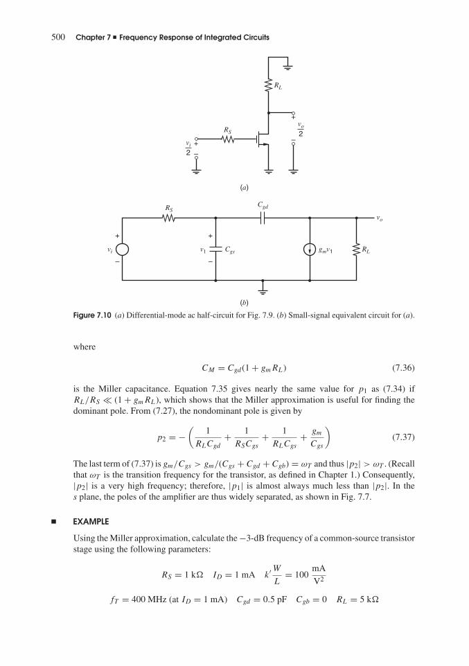
500 Chapter 7 � Frequency Response of Integrated Circuits
RL
RS
RS
RL
vo
2vi
vi
vo
2+
+
–
–
(a)
(b)
+
–
Cgd
Cgsv1
+
–
gmv1
Figure 7.10 (a) Differential-mode ac half-circuit for Fig. 7.9. (b) Small-signal equivalent circuit for (a).
where
CM = Cgd(1 + gmRL) (7.36)
is the Miller capacitance. Equation 7.35 gives nearly the same value for p1 as (7.34) ifRL/RS � (1 + gmRL), which shows that the Miller approximation is useful for finding thedominant pole. From (7.27), the nondominant pole is given by
p2 = −(
1
RLCgd
+ 1
RSCgs
+ 1
RLCgs
+ gm
Cgs
)(7.37)
The last term of (7.37) is gm/Cgs > gm/(Cgs + Cgd + Cgb) = ωT and thus |p2| > ωT . (Recallthat ωT is the transition frequency for the transistor, as defined in Chapter 1.) Consequently,|p2| is a very high frequency; therefore, |p1| is almost always much less than |p2|. In thes plane, the poles of the amplifier are thus widely separated, as shown in Fig. 7.7.
EXAMPLE
Using the Miller approximation, calculate the −3-dB frequency of a common-source transistorstage using the following parameters:
RS = 1 k ID = 1 mA k′ WL
= 100mA
V2
fT = 400 MHz (at ID = 1 mA) Cgd = 0.5 pF Cgb = 0 RL = 5 k

7.2 Single-Stage Amplifiers 501
The small-signal transconductance is
gm =√
2
(100
mA
V2
)(1 mA) = 14.1
mA
V
Using (1.207) from Chapter 1 and Cgb = 0 gives
Cgs + Cgd = gm
ωT
= 14.1 mA/V
2π(400 MHz)= 5.6 pF
Thus
Cgs = 5.6 pF − Cgd = 5.1 pF
Substitution of data in (7.36) gives for the Miller capacitance
CM = (1 + gmRL)Cgd =[
1 +(
14.1mA
V
)(5 k)
](0.5 pF) = 35.7 pF
This capacitance is much greater than Cgs and dominates the frequency response. Substitutionof values in (7.35) gives
f−3dB = |p1|2π
= 1
2π
1
(1000 )(5.1 pF + 35.7 pF)= 3.9 MHz
For comparison, using (7.34) gives |p1| = 23.1 Mrad/s and f−3dB = 3.7 MHz, which is closeto the result using the Miller effect. The low-frequency gain can be calculated from (7.33) as
vo
vi
∣∣∣∣ω = 0
= −gmRL = −(
14.1mA
V
)(5000 ) = −70.5
7.2.2 Frequency Response of the Common-Mode Gainfor a Differential Amplifier
In Chapter 3, the importance of the common-mode (CM) gain of a differential amplifier wasdescribed. It was shown that low values of CM gain are desirable so that the circuit can rejectundesired signals that are applied equally to both inputs. Because undesired CM signals mayhave high-frequency components, the frequency response of the CM gain is important. TheCM frequency response of the differential circuits in Figures 7.5 and 7.9 can be calculated fromthe CM half-circuits shown in Figs. 7.11a and 7.11b. In Fig. 7.11, RT and CT are the equivalentoutput resistance and capacitance of the tail current source. Since impedances common to thetwo devices are doubled in the CM half-circuit, RT and CT become 2RT and CT /2, respectively.A general small-signal equivalent circuit for Fig. 7.11a-b is shown in Fig. 7.11c. The parallelcombination of 2RT and CT /2 will be referred to as ZT .
The complete analysis of Fig. 7.11c is quite complex. However, the important aspects ofthe frequency response can be calculated by making some approximations. Consider the timeconstant RT CT . The resistance RT is the output resistance of the current source and is usuallygreater than or equal to the ro of a transistor. Let us assume that this resistance is on the orderof 1 M. The capacitor CT includes Ccs of the bipolar current-source transistor or Cdb of thecurrent-source transistor plus Csb of the input transistors in the MOS circuit. Typically, CT
is 1 pF or less. Using RT = 1 M and CT = 1 pF, the time constant RT CT is 1 �s, and thebreak frequency corresponding to this time constant is 1/(2πRT CT ) = 166 kHz. Below thisfrequency the impedance ZT is dominated by RT , and above this frequency CT dominates.Thus as the frequency of operation is increased, the impedance ZT will exhibit frequencyvariation before the rest of the circuit. We now calculate the frequency response assuming

502 Chapter 7 � Frequency Response of Integrated Circuits
RL
RS
CT
2
vic
voc
+
+
–
–
2 RT
(a)
RL
RS
CT
2
vic
voc
+
+
–
–
2 RT
(b)
rin RL
2 RT
Cin
CT
2
rxCf
vic vocgmv1v1
RS
(c)
+
–
+
–
+
–
Figure 7.11 (a) Common-mode ac half-circuit for Fig. 7.5. (b) Common-mode ac half-circuit forFig. 7.9. (c) A general model for both half-circuits.
that CT is the only significant capacitance. Since the impedance ZT is high, almost all of vic
appears across ZT if RS is small. Therefore, we can approximate the CM gain as
Acm = voc
vic
≈ −RL
ZT
(7.38)
where
ZT = 2RT
1 + sCT RT
(7.39)
Substitution of (7.39) in (7.38) gives
Acm(s) = voc
vic
(s) ≈ − RL
2RT
(1 + sCT RT ) (7.40)
Equation 7.40 shows that the CM gain expression contains a zero, which causes the CM gainto rise at 6 dB/octave above a frequency ω = 1/RT CT . This behavior is undesirable becausethe CM gain should ideally be as small as possible. The increase in CM gain cannot continueindefinitely, however, because the other capacitors in the circuit of Fig. 7.11c eventually becomeimportant. The other capacitors cause the CM gain to fall at very high frequencies, and thisbehavior is shown in the plot of CM gain versus frequency in Fig. 7.12a.

7.2 Single-Stage Amplifiers 503
|Acm|dB
|Adm|dB
CMRRdB
+6 dB/octave
–6 dB/octave
flog scale
flog scale
flog scale
(a)
(c)
(b)
–6 dB/octave
–12 dB/octave
2 RCt
1
2 RTCT
1
π
π
Figure 7.12 Variation withfrequency of the gainparameters for the differentialamplifier in Fig. 7.5 or Fig. 7.9.(a) Common-mode gain.(b) Differential-mode gain.(c) Common-mode rejectionratio.
The differential-mode (DM) gain Adm of the circuit of Fig. 7.5 or Fig. 7.9 is plottedversus frequency in Fig. 7.12b using (7.10). As described earlier, |Adm| begins to fall off at afrequency given by f = 1/2πRCt , where R = (RS + rx)||rin and Ct = Cin + CM . As pointedout in Chapter 3, an important differential amplifier parameter is the common-mode rejectionratio (CMRR) defined as
CMRR = |Adm||Acm| (7.41)
The CMRR is plotted as a function of frequency in Fig. 7.12c by simply taking the magni-tude of the ratio of the DM and CM gains. This quantity begins to decrease at frequencyf = 1/2πRT CT when |Acm| begins to increase. The rate of decrease of CMRR furtherincreases when |Adm| begins to fall with increasing frequency. Thus differential amplifiersare far less able to reject CM signals as the frequency of those signals increases.
7.2.3 Frequency Response of Voltage Buffers
Single-stage voltage buffers are often used in integrated circuits. The ac circuits for bipolar andMOS voltage buffers are shown in Figs. 7.13a and 7.13b, respectively. A small-signal model

504 Chapter 7 � Frequency Response of Integrated Circuits
(a)
vi
vo
RS
RL
+
+
–
–
(b)
vi
vo
RS
RL
+
+
–
–
Cinrin gmv1
RS
ii
vi
voRL
+
+
–
–
v1
+
–
rx
(c)
Figure 7.13 (a) An ac schematic of an emitter-follower amplifier. (b) An ac schematic of asource-follower amplifier. (c) A general model for both amplifiers.
that can be used to model both of these circuits is shown in Fig. 7.13c. Resistance RS is thesource resistance, and RL is the load resistance. We will assume that the output resistance ofthe transistor ro is much larger than RL. Since these resistors are in parallel in the small-signalcircuit, ro can be neglected. The series input resistance in the transistor model and the sourceresistance are in series and can be lumped together as R′
S = RS + rx. For simplicity, the effectof capacitor Cf in Fig. 7.1 is initially neglected, a reasonable approximation if R′
S is small.The effect of Cf is to form a low-pass circuit with R′
S and to cause the gain to decrease at veryhigh frequencies. From Fig. 7.13c,
vi = iiR′S + v1 + vo (7.42)
ii = v1
zin(7.43)
zin = rin
1 + sCinrin(7.44)
ii + gmv1 = vo
RL
(7.45)
Using (7.43) and (7.44) in (7.45) gives
v1
rin(1 + sCinrin) + gmv1 = vo
RL

7.2 Single-Stage Amplifiers 505
and thus
v1 = vo
RL
1
gm + 1
rin(1 + sCinrin)
(7.46)
Using (7.46) and (7.43) in (7.42) gives
vi =(
R′S
zin+ 1
)vo
RL
1
gm + 1
rin(1 + sCinrin)
+ vo
Collecting terms in this equation, we find
vo
vi
=gmRL + RL
rin
1 + gmRL + R′S + RL
rin
⎡⎢⎣ 1 − s
z1
1 − s
p1
⎤⎥⎦ (7.47)
where
z1 = −gm + 1
rin
Cin(7.48)
p1 = − 1
R1Cin(7.49)
with
R1 = rin|| R′S + RL
1 + gmRL
(7.50)
Equation 7.47 shows that, as expected, the low-frequency voltage gain is about unityif gmRL � 1 and gmRL � (R′
S + RL)/rin. The high-frequency gain is controlled by thepresence of a pole at p1 and a zero at z1.
7.2.3.1 Frequency Response of the Emitter FollowerThe small-signal circuit for the emitter follower in Fig. 7.13a is shown in Fig. 7.14. We initiallyignore Cμ, as in the general analysis in Section 7.2.3. The transfer function for the emitterfollower can be found by substituting the appropriate values in Table 7.1 into (7.47) through
B' C
r gmv1
RS
ii
vi
voRL
E
+
+
–
–
v1
+
–
'
RS = RS + rb'
π Cπ
Figure 7.14 Small-signalmodel for the emitterfollower in Fig. 7.13a.

506 Chapter 7 � Frequency Response of Integrated Circuits
(7.50). If gmRL � 1 and gmRL � (R′S + RL)/rπ, where R′
S = RS + rb, the low-frequencygain is about unity. The zero and pole are given by
z1 = −gm + 1
rπCπ
≈ −gm
Cπ
≈ −ωT (7.51)
p1 = − 1
CπR1(7.52)
where
R1 = rπ|| R′S + RL
1 + gmRL
(7.53)
Typically, the zero has a magnitude that is slightly larger than the pole, and both are approx-imately equal to ωT of the device. In particular, if gmRL � 1 and R′
S � RL in (7.53), thenR1 ≈ 1/gm and (7.52) gives p1 ≈ −gm/Cπ ≈ −ωT . However, if RS is large, then R′
S in (7.53)becomes large compared to RL, and the pole magnitude will be significantly less than ωT .
EXAMPLE
Calculate the transfer function for an emitter follower with Cπ = 10 pF, Cμ = 0, RL = 2 k,RS = 50 , rb = 150 , β = 100, and IC = 1 mA.
From the data, gm = 38 mA/V, rπ = 2.6 k, and R′S = RS + rb = 200 . Since Cμ = 0,
ωT of the device is
ωT = gm
Cπ
= 1 mA
26 mV
1
10 pF= 3.85 × 10⁹ rad/s (7.54)
and thus fT = 612 MHz. From (7.51) and (7.54), the zero of the transfer function is
z1 ≈ −ωT = −3.85 × 10⁹ rad/s
From (7.53)
R1 = 2.6 k ||
⎛⎜⎝200 + 2000
1 + 2000
26
⎞⎟⎠ ≈ 28
Using (7.52), the pole is
p1 = −1012
10
1
28rad/s = −3.57 × 10⁹ rad/s
The pole and zero are thus quite closely spaced, as shown in the s-plane plot of Fig. 7.15a.The low-frequency gain of the circuit from (7.47) is
vo
vi
=gmRL + RL
rπ
1 + gmRL + R′S + RL
rπ
=2000
26+ 2000
2600
1 + 2000
26+ 2200
2600
= 0.986
The parameters derived above are used in (7.47) to plot the circuit gain versus frequency inFig. 7.15b. The gain is flat with frequency until near fT = 612 MHz where a decrease of0.4 dB occurs. The analysis predicts that the gain is then flat as frequency is increased further.
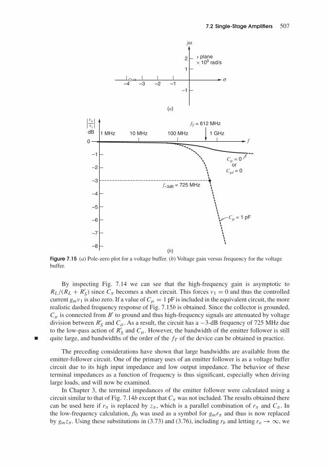
7.2 Single-Stage Amplifiers 507
(a)
–1–1
1
2
–2–3–4
j
s plane× 109 rad/s
×
fT = 612 MHz
f
f–3dB = 725 MHz
1 GHz100 MHz10 MHz1 MHz
vovi
dB
0
–1
–2
–3
–4
–5
–6
–7
–8
C = 0or
Cgd = 0
C = 1 pF
(b)
σ
μ
μ
ω
Figure 7.15 (a) Pole-zero plot for a voltage buffer. (b) Voltage gain versus frequency for the voltagebuffer.
By inspecting Fig. 7.14 we can see that the high-frequency gain is asymptotic toRL/(RL + R′
S) since Cπ becomes a short circuit. This forces v1 = 0 and thus the controlledcurrent gmv1 is also zero. If a value of Cμ = 1 pF is included in the equivalent circuit, the morerealistic dashed frequency response of Fig. 7.15b is obtained. Since the collector is grounded,Cμ is connected from B′ to ground and thus high-frequency signals are attenuated by voltagedivision between R′
S and Cμ. As a result, the circuit has a −3-dB frequency of 725 MHz dueto the low-pass action of R′
S and Cμ. However, the bandwidth of the emitter follower is stillquite large, and bandwidths of the order of the fT of the device can be obtained in practice.
The preceding considerations have shown that large bandwidths are available from theemitter-follower circuit. One of the primary uses of an emitter follower is as a voltage buffercircuit due to its high input impedance and low output impedance. The behavior of theseterminal impedances as a function of frequency is thus significant, especially when drivinglarge loads, and will now be examined.
In Chapter 3, the terminal impedances of the emitter follower were calculated using acircuit similar to that of Fig. 7.14b except that Cπ was not included. The results obtained therecan be used here if rπ is replaced by zπ, which is a parallel combination of rπ and Cπ. Inthe low-frequency calculation, β0 was used as a symbol for gmrπ and thus is now replacedby gmzπ. Using these substitutions in (3.73) and (3.76), including rb and letting ro → ∞, we

508 Chapter 7 � Frequency Response of Integrated Circuits
obtain for the emitter follower
zi = rb + zπ + (gmzπ + 1)RL (7.55)
zo = zπ + RS + rb
1 + gmzπ
(7.56)
where
zπ = rπ
1 + sCπrπ(7.57)
Consider first the input impedance. Substituting (7.57) in (7.55) gives
zi = rb + rπ
1 + sCπrπ+(
gmrπ
1 + sCπrπ+ 1
)RL
(7.58)= rb + (1 + gmRL)rπ1 + sCπrπ
+ RL
= rb + (1 + gmRL)rπ
1 + sCπ
1 + gmRL
(1 + gmRL)rπ
+ RL
= rb + R
1 + sCR+ RL (7.59)
where
R = (1 + gmRL)rπ (7.59a)
and
C = Cπ
1 + gmRL
(7.59b)
Thus zi can be represented as a parallel R-C circuit in series with rb and RL as shown inFig. 7.16. The effective input capacitance is Cπ/(1 + gmRL) and is much less than Cπ
for typical values of gmRL. The collector-base capacitance Cμ may dominate the inputcapacitance and can be added to this circuit from B′ to ground. Thus, at high frequencies, theinput impedance of the emitter follower becomes capacitive and its magnitude decreases.
The emitter-follower high-frequency output impedance can be calculated by substituting(7.57) in (7.56). Before proceeding, we will examine (7.57) to determine the high and low
1 + gmRL
RL
C(1 + gmRL) r
B B'rb
zi ππ
Figure 7.16 Equivalent circuit forthe input impedance of an emitterfollower with Cμ = 0.

7.2 Single-Stage Amplifiers 509
frequency limits on |zo|. At low frequencies, zπ = rπ and
zo|ω = 0 ≈ 1
gm
+ RS + rb
β0(7.60)
At high frequencies, zπ → 0 because Cπ becomes a short circuit and thus
zo|ω = ∞ = RS + rb (7.61)
Thus zo is resistive at very low and very high frequencies and its behavior in between dependson parameter values. At very low collector currents, 1/gm is large. If 1/gm > (RS + rb), acomparison of (7.60) and (7.61) shows that |zo| decreases as frequency increases and the outputimpedance appears capacitive. However, at collector currents of more than several hundredmicro amperes, we usually find that 1/gm < (RS + rb). Then |zo| increases with frequency,which represents inductive behavior that can have a major influence on the circuit behavior,particularly when driving capacitive loads. If 1/gm = (RS + rb) then the output impedanceis resistive and independent of frequency over a wide bandwidth. To maintain this conditionover variations in process, supply, and temperature, practical design goals are RS ≈ 1/gm andrb � RS .
Assuming that the collector bias current is such that zo is inductive, we can postulate anequivalent circuit for zo as shown in Fig. 7.17. At low frequencies the inductor is a short circuitand
zo|ω = 0 = R1||R2 (7.62)
At high frequencies the inductor is an open circuit and
zo|ω = ∞ = R2 (7.63)
If we assume that zo|ω = 0 � zo|ω = ∞ then R1 � R2, and we can simplify (7.62) to
zo|ω = 0 ≈ R1 (7.64)
The impedance of the circuit of Fig. 7.17 can be expressed as
zo = (R1 + sL)R2
R1 + R2 + sL≈ (R1 + sL)R2
R2 + sL(7.65)
assuming that R1 � R2.
R1
R2
zo
L
Figure 7.17 Equivalent circuit for the output impedanceof an emitter follower at moderate current levels.

510 Chapter 7 � Frequency Response of Integrated Circuits
The complete emitter-follower output impedance can be calculated by substituting (7.57)in (7.56) with R′
S = rb + RS , which gives
zo =rπ
1 + sCπrπ+ R′
S
1 + gmrπ
1 + sCπrπ
= rπ + R′S + sCπrπR′
S
β0 + 1 + sCπrπ
(7.66)
≈
(1
gm
+ R′S
β0+ sCπrπ
R′S
β0
)R′
S
R′S + sCπrπ
R′S
β0
where β0 � 1 is assumed.Comparing (7.66) with (7.65) shows that, under the assumptions made in this analysis,
the emitter-follower output impedance can be represented by the circuit of Fig. 7.17 with
R1 = 1
gm
+ R′S
β0(7.67)
R2 = R′S (7.68)
L = CπrπR′
S
β0(7.69)
The effect of Cμ was neglected in this calculation, which is a reasonable approximation forlow to moderate values of R′
S .The preceding calculations have shown that the input and output impedances of the emitter
follower are frequency dependent. One consequence of this dependence is that the variationof the terminal impedances with frequency may limit the useful bandwidth of the circuit.
EXAMPLE
Calculate the elements in the equivalent circuits for input and output impedance of the emitterfollower in the previous example. In Fig. 7.16 the input capacitance can be calculated from(7.59)
Cπ
1 + gmRL
= 10
1 + 2000
26
pF = 0.13 pF
The resistance in shunt with this capacitance is
(1 + gmRL)rπ =(
1 + 2000
26
)(2.6 k) = 202 k
In addition, rb = 150 and RL = 2 k. The elements in the output equivalent circuit ofFig. 7.17 can be calculated from (7.67), (7.68), and (7.69) as
R1 =(
26 + 200
100
) = 28
R2 = 200
L = 10−11 × 2600 × 200
100H = 52 nH
Note that the assumption R1 � R2 is valid in this case.

7.2 Single-Stage Amplifiers 511
vi
RS
Cgs
Cgd + Cgb
RL Csb
G
v1 gmv1 gmbvsb = gmbvo
vo
++
+
–
––
Figure 7.18 Small-signal modelfor the source follower inFig. 7.13b.
7.2.3.2 Frequency Response of the Source FollowerThe small-signal circuit for the source follower in Fig. 7.13b is shown in Fig. 7.18. Here, Cgd ,Cgb, and Csb are ignored initially. One key difference between Figures 7.18 and 7.13c is thegmb generator. Since the current through the gmb generator is controlled by the voltage acrossit, this generator can be replaced with a resistor of value 1/gmb from vo to ground, which isin parallel with RL. Therefore, the total effective load resistance is R′
L = RL||(1/gmb). Thetransfer function for the source follower can be found by substituting the appropriate valuesfrom Table 7.1 into (7.47), (7.48), and (7.49). If gmR′
L � 1, the low-frequency gain is aboutunity. The zero and pole are given by
z1 = − gm
Cgs
≈ −ωT (7.70)
p1 = − 1
CgsR1(7.71)
where
R1 = RS + R′L
1 + gmR′L
(7.72)
Typically, the zero has a magnitude that is slightly larger than the pole. If gmR′L � 1 and
RS � R′L in (7.72), then R1 ≈ 1/gm and (7.71) gives p1 ≈ −gm/Cgs ≈ −ωT . However, if
RS in (7.72) becomes large compared to RL or if gmR′L is not much larger than one, the pole
magnitude will be significantly less than ωT .
EXAMPLE
Calculate the transfer function for a source follower with Cgs = 7.33 pF, k′W/L = 100 mA/V2,RL = 2 k, RS = 190 , and ID = 4 mA. Ignore body effect, and let Cgd = 0, Cgb = 0, andCsb = 0.
From the data, gm = √2(100)4 mA/V = 28.2 mA/V. Ignoring body effect, we have R′
L =RL||(1/gmb) = RL. Since Cgd = 0, ωT of the device is
ωT = gm
Cgs
=28.2
mA
V7.33 pF
= 3.85 × 10⁹ rad/s (7.73)
and thus fT = 612 MHz. From (7.70) and (7.73), the zero of the transfer function is
z1 = − gm
Cgs
= −3.85 × 10⁹ rad/s

512 Chapter 7 � Frequency Response of Integrated Circuits
From (7.72)
R1 = 190 + 2000
1 + 0.0282 × 2000 = 38.2
The pole from (7.71) is
p1 = −1012
7.33
1
38.2rad/s = −3.57 × 10⁹ rad/s
The pole and zero are thus quite closely spaced, as shown in Fig. 7.15a.The low-frequency gain of the circuit from (7.67) is
vo
vi
= gmR′L
1 + gmR′L
= 28.2 × 10−3 × 2000
1 + 28.2 × 10−3 × 2000= 0.983
The parameters derived above can be used in (7.47) to plot the circuit gain versus frequency,and this plot is similar to the magnitude plot shown in Fig. 7.15b for Cgd = 0. The gain isflat with frequency until near fT = 612 MHz, where a decrease of about 0.4 dB occurs. Theanalysis predicts that the gain is then flat as frequency is increased further because the inputsignal is simply fed forward to R′
L via Cgs at very high frequencies. In practice, capacitorsCgd , Cgb, and Csb that were assumed to be zero in this example cause the gain to roll off athigh frequencies, as will be demonstrated in the next example.
When capacitors Cgd , Cgb, and Csb that were ignored above are included in the analy-sis, the voltage-gain expression becomes more complicated than (7.47). An exact analysis,with all the capacitors included, follows the same steps as the analysis of Fig. 7.13c andyields
vo
vi
= gmR′L
1 + gmR′L
1 + sCgs
gm
1 + as + bs2 (7.74a)
with
a= R′L(Cgs + Csb) + RS(Cgs + C′
gd) + RSgmR′LC′
gd
1 + gmRL′
≈ R′L(Cgs + Csb) + RSCgs + RSgmR′
LC′gd
1 + gmR′L
(7.74b)
b = RSR′L[Csb(Cgs + C′
gd) + CgsC′gd]
1 + gmR′L
≈ RSR′L[CsbCgs + CgsC
′gd]
1 + gmR′L
(7.74c)
where C′gd = Cgd + Cgb. The approximations for a and b use Cgs + C′
gd ≈ Cgs sinceCgs � C′
gd . This exact transfer function has a zero at −gm/Cgs, in agreement with (7.70),and two poles. If C′
gd and Csb are set to zero, (7.74) has one pole as given by (7.71). Makingapproximations in (7.74) that lead to simple, useful expressions for the poles is difficult sincea dominant real pole does not always exist. In fact, the poles can be complex.
EXAMPLE
Calculate the transfer function for a source follower with Cgs = 7.33 pF, Cgd = 0.1 pF,Cgb = 0.05 pF, Csb = 0.5 pF, k′W/L = 100 mA/V2, RL = 2 k, RS = 190 , and ID =4 mA. Ignore body effect.

7.2 Single-Stage Amplifiers 513
These data are the same as in the last example, except we now have non-zero Cgd , Cgb, andCsb. From the data, gm = 28.2 mA/V and C′
gd = Cgd + Cgb = 0.15 pF. Also, ignoring bodyeffect, we have R′
L = RL||(1/gmb) = RL. The low-frequency gain of the circuit, as calculatedin the previous example, is 0.983. From (7.74a), the zero is
z = − gm
Cgs
= −28.2
mA
V7.33 pF
= −3.85 × 10⁹ rad/s
From (7.74b) and (7.74c), the coefficients of the denominator of the transfer function are
a ≈ 2k (7.33p + 0.5p) + 190 (7.33p) + 190 (0.0282)(2k)(0.15p)
1 + (0.0282)(2k)s = 0.324 ns
b ≈ 190(2k)[(0.5p)(7.33p) + (7.33p)(0.15p)]
1 + (0.0282)(2k)s2 = 0.0315 (ns)2
Using the quadratic formula to solve for the poles, we find that the poles are
p1,2 = −5.1 × 10⁹ � j2.3 × 109 rad/s
The poles and zero are fairly close together, as shown in Fig. 7.19a. The gain magnitude andphase are plotted in Fig. 7.19. The −3-dB bandwidth is 1.6 GHz. Because the two poles andzero are fairly close together, the gain versus frequency approximates a one-pole roll-off.
High-frequency input signals are attenuated by capacitors Cgd and Cgb that connectbetween the gate and ground, causing the gain to roll off and approach zero as ω → ∞.However, the bandwidth of the source follower is still quite large, and bandwidths of the orderof the fT of the device can be obtained in practice.
If the source follower drives a load capacitance in parallel with the load resistance, its valuecan be added to Csb in (7.74). Such a load capacitance is present whenever the source-followertransistor is fabricated in a well and its source is connected to its well to avoid body effect.The well-body capacitance can be large and may significantly affect the 3-dB bandwidth ofthe circuit.
In Section 7.2.3.1, calculations were carried out for the input and output impedances ofthe emitter follower. Since the equivalent circuit for the MOSFET is similar to that for the
(a)
×
×
× 109
j
σ
ω
rad/s
–5 –4 –3 –2 –1
2
1
–1
–2
Figure 7.19 (a) Pole-zero plot for the source-follower example using (7.74).

514 Chapter 7 � Frequency Response of Integrated Circuits
100M100k10010 10k1k 1G 10G 100G10M1MFrequency (Hz)
(b)
0
–10
–20
–30
|Gain|(dB)
100M100k10010 10k1k 1G 10G 100G10M1M
Frequency (Hz)
(c)
0°
–30°
–60°
–90°
Gain(degrees)<
Figure 7.19 (b) Magnitude and (c) phase of the gain versus frequency for this source follower.
bipolar transistor (apart from the gmb generator), similar results can be found for the sourcefollower by substituting the appropriate values from Table 7.1 in the formulas for zi and zo
in Section 7.2.3.1. One major difference is that the MOSFET has a gm that is usually muchlower than for the bipolar transistor with the same bias current. Therefore, the condition thatproduces an inductive output impedance (1/gm < RS) occurs less often with source followersthan emitter followers.
7.2.4 Frequency Response of Current Buffers
The common-base (CB) and common-gate (CG) amplifier configurations are shown in acschematic form in Fig. 7.20. These stages have a low input impedance, high output impedance,approximately unity current gain, and wide bandwidth. They find use in wideband applica-tions and also in applications requiring low input impedance. As described in Chapter 1, thebipolar transistor breakdown voltage is maximum in this configuration. The combination of

7.2 Single-Stage Amplifiers 515
+
–
–
+
vi vo
RS
RL
(a)
+
–
–
vi vo
RS
RL
(b)
+
(c)
Cinrin
RS
rx
Cf
RL
gmv1
v1
vo
ioW
+
–RS
= iivi
–
+
Figure 7.20 (a) An ac schematic of a common-base amplifier. (b) An ac schematic of a common-gateamplifier. (c) A general model for both amplifiers.
this property and the wideband property make the CB stages useful in high-voltage widebandoutput stages driving oscilloscope deflection plates.
A small-signal equivalent circuit that can model both the CB and CG stage by using a gen-eral small-signal model is shown in Fig. 7.20c. The input voltage source and source resistanceare represented by a Norton equivalent. Resistance RS is neglected in the following analysissince the input impedance of the amplifier is quite low. Another good approximation if rx issmall is that Cf simply shunts RL, as shown in Fig. 7.20c. In this analysis, ro will be neglectedand the output signal io will be taken as the output of the gm controlled source. The approximateoutput voltage vo is obtained by assuming io flows in the parallel combination of RL and Cf .
The analysis of the circuit of Fig. 7.20c proceeds by applying KCL at node W . Ne-glecting RS ,
ii + v1
zin+ gmv1 = 0 (7.75)
where
zin = rin
1 + sCinrin(7.76)

516 Chapter 7 � Frequency Response of Integrated Circuits
From (7.75) and (7.76)
ii = −v1
(gm + 1
rin+ sCin
)(7.77)
Now
io = −gmv1 (7.78)
Substituting (7.77) into (7.78) gives
io
ii= gmrin
gmrin + 1
1
1 + srin
gmrin + 1Cin
(7.79)
7.2.4.1 Common-Base Amplifier Frequency ResponseThe small-signal circuit for the common-base (CB) amplifier of Fig. 7.20a is shown inFig. 7.21. Substituting the values in Table 7.1 into (7.79) gives for the current gain
io
ii= gmrπ
gmrπ + 1
1
1 + srπ
gmrπ + 1Cπ
(7.80)
Using β0 = gmrπ and assuming β0 � 1, (7.80) simplifies to
io
ii≈ β0
β0 + 1
1
1 + sCπ
gm
= α01
1 + sCπ
gm
(7.81)
where α0 = β0/(β0 + 1). This analysis shows that the CB stage current gain has a low-frequency value α0 ≈ 1 and a pole at p1 = −gm/Cπ ≈ −ωT . The CB stage is thus a wide-bandunity-current gain amplifier with low input impedance and high output impedance. It can beseen from the polarities in Fig. 7.20a that the phase shift between vi and vo in the CB stageis zero at low frequencies. This result can be compared with the case of the common-emitterstage of Fig. 7.2a, which has 180
◦phase shift between vi and vo at low frequencies.
If the desired output is the current flowing through RL, then Cμ and RL form a currentdivider from io to this desired current (under the assumption that Cμ is in parallel with RL
because rb is very small). When included in the analysis, this current divider introduces anadditional pole p2 = −1/RLCμ in the transfer function.
Comparing Fig. 7.20a with Fig. 7.13a shows that the input impedance of the common-base stage is the same as the output impedance of the emitter follower with RS = 0. Thus the
C
B'
B
RS
rb
C
RL
gmv1
v1
vo
io CE+
–
ii
ii =RS
vi
–
+μπrπ
Figure 7.21 Small-signal model for the common-base circuit in Fig. 7.20a.

7.2 Single-Stage Amplifiers 517
common-base stage input impedance is low at low frequencies and becomes inductive at highfrequencies for collector bias currents of several hundred microamperes or more. As shown inChapter 3, the output resistance of the common-base stage at low frequencies with large RS
is approximately β0ro, which is extremely large. At high frequencies the output impedance iscapacitive and is dominated by Cμ (and Ccs for npn transistors).
Unlike the common-emitter stage where Cμ is Miller multiplied, the common-base stagedoes not contain a feedback capacitance from collector to emitter to cause the Miller effect. Asa consequence, the effect of large values of RL on the frequency response of the common-basestage is much less than in the common-emitter stage.
7.2.4.2 Common-Gate Amplifier Frequency ResponseThe small-signal circuit for the common-gate (CG) amplifier of Fig. 7.20b is shown inFig. 7.22. One element in this circuit that does not appear in the general model in Fig. 7.20cis the gmb generator. Since vbs = vgs and the gm and gmb generators are in parallel here, thesecontrolled sources can be combined. Also, capacitors Cgb, Cdb, and Csb are not included in thegeneral model. Here, Cgb is shorted and can be ignored. Capacitance Cdb is in parallel with RL
and therefore can be ignored if the output variable of interest is the current io. Capacitance Csb
appears in parallel with Cgs in the small-signal circuit since the body and gate both connect tosmall-signal ground. Using the combined transconductance and input capacitance and valuesfrom Table 7.1 in (7.79) gives
io
ii= 1
1 + sCgs + Csb
gm + gmb
(7.82)
From this equation, the current gain of the common-gate stage has a low-frequency valueof unity and a pole at p1 = −(gm + gmb)/(Cgs + Csb). If Cgs � Csb, then |p1| ≈ (gm +gmb)/Cgs > gm/Cgs ≈ ωT . The CG stage is thus a wideband unity-current-gain amplifierwith low input impedance and high output impedance. It can be seen from the polarities inFig. 7.20b that there is zero phase shift between vi and vo in the CG stage at low frequencies.This phase shift can be compared with the case of the common-source stage of Fig. 7.2b, whichhas 180◦ phase shift between vi and vo at low frequencies.
If the desired output is the current flowing through RL, then Cdb, Cgd , and RL form acurrent divider from io to this desired current. When included in the analysis, this currentdivider introduces an additional pole p2 = −1/RL(Cdb + Cgd) in the transfer function.
Cgs + Csb
RS
Cgd
RL
gmv1
gmbv1
v1
vo
ioS D
G
+
–RS
= iivi
–
+
Figure 7.22 Small-signal model for the common-gate circuit in Fig. 7.20b.

518 Chapter 7 � Frequency Response of Integrated Circuits
Unlike the common-source stage where Cgd is Miller multiplied, the common-gate stagedoes not contain a feedback capacitance from drain to source to cause the Miller effect. As aconsequence, the effect of large values of RL on the frequency response of the common-gatestage is much less than in the common-source stage.
7.3 Multistage Amplifier Frequency ResponseThe above analysis of the frequency behavior of single-stage circuits indicates the complexitythat can arise even with simple circuits. The complete analysis of the frequency responseof multistage circuits with many capacitive elements rapidly becomes very difficult and theanswers become so complicated that little use can be made of the results. For this reasonapproximate methods of analysis have been developed to aid in the circuit design phase, andcomputer simulation is used to verify the final design. One such method of analysis is the zero-value time constant analysis that will now be described. First some ideas regarding dominantpoles are developed.
7.3.1 Dominant-Pole Approximation
For any electronic circuit we can derive a transfer function A(s) by small-signal analysis togive
A(s) = N(s)
D(s)= a0 + a1s + a2s
2 + · · · + amsm
1 + b1s + b2s2 + · · · + bnsn(7.83)
where a0, a1, . . . , am, and b1, b2, . . . , bn are constants. Very often the transfer function con-tains poles only (or the zeros are unimportant). In this case we can factor the denominator of(7.83) to give
A(s) = K(1 − s
p1
)(1 − s
p2
)· · ·(
1 − s
pn
) (7.84)
where K is a constant and p1, p2 , . . . , pn are the poles of the transfer function.It is apparent from (7.84) that
b1 =n∑
i = 1
(− 1
pi
)(7.85)
An important practical case occurs when one pole is dominant. That is, when
|p1| � |p2|, |p3|, . . . so that
∣∣∣∣ 1
p1
∣∣∣∣�∣∣∣∣∣
n∑i = 2
(− 1
pi
)∣∣∣∣∣This situation is shown in the s plane in Fig. 7.23 and in this case it follows from (7.85) that
b1 �∣∣∣∣ 1
p1
∣∣∣∣ (7.86)
If we return now to (7.84) and calculate the gain magnitude in the frequency domain, we obtain
|A(jω)| = K√√√√[1 +(
ω
p1
)2][
1 +(
ω
p2
)2]
· · ·[
1 +(
ω
pn
)2] (7.87)

7.3 Multistage Amplifier Frequency Response 519
×××p3 p2 p1
j
σ
ω
s plane
Figure 7.23 Pole diagram for a circuitwith a dominant pole.
If a dominant pole exists, then (7.87) can be approximated by
|A(jω)| � K√1 +(
ω
p1
)2(7.88)
This approximation will be quite accurate at least until ω � |p1|, and thus (7.88) will accuratelypredict the −3-dB frequency and we can write
ω−3dB � |p1| (7.89)
Use of (7.86) in (7.89) gives
ω−3dB � 1
b1(7.90)
for a dominant-pole situation.
7.3.2 Zero-Value Time Constant Analysis
This is an approximate method of analysis that allows an estimate to be made of the dominantpole (and thus the −3-dB frequency) of complex circuits. Considerable saving in computationaleffort is achieved because a full analysis of the circuit is not required. The method will bedeveloped by considering a practical example.
Consider the equivalent circuit shown in Fig. 7.24. This is a single-stage bipolar transistoramplifier with resistive source and load impedances. The feedback capacitance is split into twoparts (Cx and Cμ) as shown. This is a slightly better approximation to the actual situation thanthe single collector-base capacitor we have been using, but is rarely used in hand calculationsbecause of the analysis complexity. For purposes of analysis, the capacitor voltages v1, v2,and v3 are chosen as variables. The external input vi is removed and the circuit excited withthree independent current sources i1, i2, and i3 across the capacitors, as shown in Fig. 7.24.We can show that with this choice of variables the circuit equations are of the form
i1 = (g11 + sCπ)v1 + g12v2 + g13v3 (7.91)
i2 = g21v1 + (g22 + sCμ)v2 + g23v3 (7.92)
i3 = g31v1 + g32v2 + (g33 + sCx)v3 (7.93)
where the g terms are conductances. Note that the terms involving s contributed by the capac-itors are associated only with their respective capacitor voltage variables and only appear onthe diagonal of the system determinant.

520 Chapter 7 � Frequency Response of Integrated Circuits
i3
i1
i2v3
v2
v1 vovi
Cx
rb
C
r
RS
+
+ +
+
–
– –
–
+ –
gmv1 RL
μ
πCπ
Figure 7.24 Small-signal equivalent circuit of a common-emitter stage with internal feedbackcapacitors Cμ and Cx.
The poles of the circuit transfer function are the zeros of the determinant � of the circuitequations, which can be written in the form
�(s) = K3s3 + K2s
2 + K1s + K0 (7.94)
where the coefficients K are composed of terms from the above equations. For example, K3is the sum of the coefficients of all terms involving s3 in the expansion of the determinant.Equation 7.94 can be expressed as
�(s) = K0(1 + b1s + b2s2 + b3s
3) (7.95)
where this form corresponds to (7.83). Note that this is a third-order determinant because thereare three capacitors in the circuit. The term K0 in (7.94) is the value of �(s) if all capacitorsare zero (Cx = Cμ = Cπ = 0). This can be seen from (7.91), (7.92), and (7.93). Thus
K0 = �|Cπ = Cμ = Cx = 0
and it is useful to define
K0�= �0 (7.96)
Consider now the term K1s in (7.94). This is the sum of all the terms involving s thatare obtained when the system determinant is evaluated. However, from (7.91) to (7.93) it isapparent that s only occurs when associated with a capacitance. Thus the term K1s can bewritten as
K1s = h1sCπ + h2sCμ + h3sCx (7.97)
where the h terms are constants. The term h1 can be evaluated by expanding the determinantof (7.91) to (7.93) about the first row:
�(s) = (g11 + sCπ)�11 + g12�12 + g13�13 (7.98)
where �11, �12, and �13 are cofactors of the determinant. Inspection of (7.91), (7.92), and(7.93) shows that Cπ occurs only in the first term of (7.98). Thus the coefficient of Cπs in (7.98)is found by evaluating �11 with Cμ = Cx = 0, which will eliminate the other capacitive terms

7.3 Multistage Amplifier Frequency Response 521
in �11. But this coefficient of Cπs is just h1 in (7.97), and so
h1 = �11|Cμ = Cx = 0 (7.99)
Now consider expansion of the determinant about the second row. This must give thesame value for the determinant, and thus
�(s) = g21�21 + (g22 + sCμ)�22 + g23�23 (7.100)
In this case Cμ occurs only in the second term of (7.100). Thus the coefficient of Cμs inthis equation is found by evaluating �22 with Cπ = Cx = 0, which will eliminate the othercapacitive terms. This coefficient of Cμs is just h2 in (7.97), and thus
h2 = �22|Cπ = Cx = 0 (7.101)
Similarly by expanding about the third row it follows that
h3 = �33|Cπ = Cμ = 0 (7.102)
Combining (7.97) with (7.99), (7.101), and (7.102) gives
K1 = (�11|Cμ = Cx = 0 × Cπ) + (�22|Cπ = Cx = 0 × Cμ) + (�33|Cμ = Cπ = 0 × Cx) (7.103)
and
b1 = K1
K0= �11|Cμ
�0
= Cx = 0 × Cπ + �22|Cπ
�0
= Cx = 0 × Cμ
+�33|Cμ
�0
= Cπ = 0 × Cx (7.104)
where the boundary conditions on the determinants are the same as in (7.103). Now considerputting i2 = i3 = 0 in Fig. 7.24. Solving (7.91) to (7.93) for v1 gives
v1 = �11i1
�(s)
and thus
v1
i1= �11
�(s)(7.105)
Equation 7.105 is an expression for the driving-point impedance at the Cπ node pair. Thus
�11|Cμ
�0
= Cx = 0
is the driving-point resistance at the Cπ node pair with all capacitors equal to zero because
�11|Cμ
�0
= Cx = 0 = �11
�
∣∣∣∣Cμ = Cx = Cπ = 0
(7.106)
We now define
Rπ0 = �11
�0
∣∣∣∣Cμ = Cx = 0
(7.107)
Similarly,
�22|Cπ
�0
= Cx = 0

522 Chapter 7 � Frequency Response of Integrated Circuits
is the driving-point resistance at the Cμ node pair with all capacitors put equal to zero and isrepresented by Rμ0. Thus we can write from (7.104)
b1 = Rπ 0Cπ + Rμ0Cμ + Rx 0Cx (7.108)
The time constants in (7.108) are called zero-value time constants because all capacitorsare set equal to zero to perform the calculation.Although derived in terms of a specific example,this result is true in any circuit for which the various assumptions made in this analysis arevalid. In its most general form, (7.108) becomes
b1 = �T0 (7.109)
where �T0 is the sum of the zero-value time constants.We showed previously that if there are no dominant zeros in the circuit transfer function,
and if there is a dominant pole p1, then
ω−3dB ≈ |p1| (7.110)
Using (7.90), (7.109), and (7.110) we can write
ω−3dB ≈ |p1| ≈ 1
b1= 1
�T0(7.111)
For example, consider the circuit of Fig. 7.24. By inspection,
Rπ0 = rπ||(RS + rb) (7.112)
In order to calculate Rμ0 it is necessary to write some simple circuit equations. We apply a testcurrent i at the Cμ terminals as shown in Fig. 7.25 and calculate the resulting v.
v1 = Rπ0i (7.113)
vo = −(i + gmv1)RL (7.114)
Substituting (7.113) in (7.114) gives
vo = −(i + gmRπ0i)RL (7.115)
Now
Rμ0 = v
i
and
Rμ0 = v1 − vo
i(7.116)
+
+
+
–
–
–v
i
v1 vor RLRS + rb gmv1π
Figure 7.25 Equivalent circuit forthe calculation of Rμ0 for Fig. 7.24.

7.3 Multistage Amplifier Frequency Response 523
Substitution of (7.113) and (7.115) in (7.116) gives
Rμ0 = Rπ0 + RL + gmRLRπ0 (7.117)
Rx 0 can be calculated in a similar fashion, and it is apparent that Rx 0 � Rμ0 if rb � rπ. Thisjustifies the common practice of lumping Cx in with Cμ if rb is small. Assuming that this isdone, (7.111) gives, for the −3-dB frequency,
ω−3dB = 1
Rπ0Cπ + Rμ 0Cμ
(7.118)
Using (7.117) in (7.118) gives
ω−3dB = 1
Rπ0
{Cπ + Cμ
[(1 + gmRL) + RL
Rπ 0
]} (7.119)
Equation 7.119 is identical with the result obtained in (7.29) by exact analysis. [Recall that(RS + rb)||rπ in (7.29) is the same as Rπ0 in (7.119).] However, the zero-value time-constantanalysis gives the result with much less effort. It does not give any information on the non-dominant pole.
As a further illustration of the uses and limitations of the zero-value time-constantapproach, consider the emitter-follower circuit of Fig. 7.13a, where only the capacitance Cπ
has been included. The value of Rπ0 can be calculated by inserting a current source i as shownin Fig. 7.26 and calculating the resulting voltage v1:
i = v1
rπ+ v1 + vo
RS + rb(7.120)
v1
rπ− i + gmv1 = vo
RL
(7.121)
Substituting (7.121) in (7.120) gives
i = v1
rπ+ v1
RS + rb+ RL
RS + rb
(v1
rπ+ gmv1 − i
)and this equation can be expressed as
i = v1
rπ+ v1
1 + gmRL
RS + rb + RL
gmv1
RL
RS
rb
v1
vo
ri
+
+
–
–
π
Figure 7.26 Equivalent circuitfor the calculation of Rπ0 for theemitter follower.

524 Chapter 7 � Frequency Response of Integrated Circuits
Finally, Rπ0 can be calculated as
Rπ0 = v1
i= rπ
∣∣∣∣∣∣RS + rb + RL
1 + gmRL
(7.122)
Thus the dominant pole of the emitter follower is at
|p| = 1
Rπ0Cπ
(7.123)
This is in agreement with the result obtained in (7.52) by exact analysis and requires lesseffort. However, the zero-value time-constant approach tells us nothing of the zero that exactanalysis showed. Because of the dominant zero, the dominant-pole magnitude is not the –3-dBfrequency in this case. This shows that care must be exercised in interpreting the results ofzero-value time-constant analysis. However, it is a useful technique, and with experience thedesigner can recognize circuits that are likely to contain dominant zeros. Such circuits usuallyhave a capacitive path directly coupling input and output as Cπ does in the emitter follower.
7.3.3 Cascade Voltage-Amplifier Frequency Response
The real advantages of the zero-value time-constant approach appear when circuits containingmore than one device are analyzed. For example, consider the two-stage common-sourceamplifier shown in Fig. 7.27. This circuit could be a drawing of a single-ended amplifier orthe differential half-circuit of a fully differential amplifier. Exact analysis of this circuit to findthe −3-dB frequency is extremely arduous, but the zero-value time-constant analysis is quitestraightforward, as shown below. To show typical numerical calculations, specific parametervalues are assumed. In the example below, as in others in this chapter, parasitic capacitanceassociated with resistors is neglected. This approximation is often reasonable for monolithicresistors of several thousand ohms or less, but should be checked in each case.
The zero-value time-constant analysis for Fig. 7.27 is carried out in the following example.Analysis of a two-stage common-emitter amplifier would follow similar steps.
EXAMPLE
Calculate the −3-dB frequency of the circuit of Fig. 7.27 assuming the following parametervalues:
RS = 10 k RL1 = 10 k RL2 = 5 k
Cgs1 = 5 pF Cgs2 = 10 pF Cgd1= Cgd2 = 1 pF
Cdb1 = Cdb2 = 2 pF gm1 = 3 mA/V gm2 = 6 mA/V
Ignore Cgb (which is in parallel with Cgs and is much smaller than Cgs).
RS
vs
voRL1
RL2M1
M2
+
–
+
–Figure 7.27 Two-stage,common-source cascadeamplifier.

7.3 Multistage Amplifier Frequency Response 525
(a)
v1 v2vs Cgs1 Cdb1 Cdb2Cgs2
Cgd2Cgd1
RL1 RL2gm1v1 gm2v2
RS
+
–
+
–
+
–
vo
+
–
(b)
vx RAgmvx RB
Rgd0
+
–
Figure 7.28 Small-signal equivalent circuit of Fig. 7.27.
The small-signal equivalent circuit of Fig. 7.27 is shown in Fig. 7.28a. The zero-value timeconstants for this circuit are determined by calculating the resistance seen by each capacitoracross its own terminals. However, significant effort can be saved by recognizing that somecapacitors in the circuit are in similar configurations and the same formula can be applied tothem. For example, consider Cgd1 and Cgd2. The resistance seen by either Cgd capacitor canbe found by calculating the resistance Rgd0 in the circuit in Fig. 7.28b. This circuit is the sameas the circuit in Fig. 7.25 if we let RA = Rπ0 and RB = RL. Therefore, the resistance Rgd0 inFig. 7.28b is given by substituting RA for Rπ0 and RB for RL in (7.117):
Rgd0 = RA + RB + gmRBRA (7.124)
This equation can be used to find the zero-value time constants for both gate-drain capacitors:
Cgd1Rgd01 = Cgd1 (RS + RL1 + gm1RL1RS)
= (1p)[10k + 10k + (3 × 10⁻³)(10k)(10k)] s = 320 ns
Cgd2Rgd02 = Cgd2 (RL1 + RL2 + gm2RL2RL1)
= (1p)[10k + 5k + (6 × 10⁻³)(10k)(5k)] s = 315 ns
The value of Rgs0 for each device can be found by inspection
Rgs01 = RS
Rgs02 = RL1
The corresponding time constants are
Cgs1Rgs01 = Cgs1RS = (5p)(10k) s = 50 ns
Cgs2Rgs02 = Cgs2RL1 = (10p)(10k) s = 100 ns
Also, the value for Rdb0 for each device can also be found without computation
Rdb01 = RL1
Rdb02 = RL2

526 Chapter 7 � Frequency Response of Integrated Circuits
Thus
Cdb1Rdb01 = (2p)(10k) s = 20 ns
Cdb2Rdb02 = (2p)(5k) s = 10 ns
Assuming that the circuit transfer function has a dominant pole, the −3-dB frequency can beestimated as
ω−3dB = 1∑T0
= 109
320 + 315 + 50 + 100 + 20 + 10rad/s
(7.125)= 109
815rad/s = 1.2 × 10⁶ rad/s
and therefore
f−3dB = 196 kHz
A computer simulation of this circuit using SPICE gave a −3-dB frequency of 205 kHz,which is close to the calculated value. The simulation gave three negative real poles withmagnitudes 205 kHz, 4.02 MHz, and 39.98 MHz. There were two positive real zeros withmagnitudes 477 MHz and 955 MHz. From the simulation, the sum of the reciprocals of thepole magnitudes was 815 ns, which exactly equals the sum of the zero-value time constants ascalculated by hand.
An exact analysis of Fig. 7.28a would first apply KCL at three nodes and produce a transferfunction with a third-order denominator, in which some coefficients would consist of a sumof many products of small-signal model parameters. Many simplifying approximations wouldbe needed to give useful design equations. As the circuit complexity increases, the numberof equations increases and the order of the denominator increases, eventually making exactanalysis by hand impractical and making time-constant analysis quite attractive.
The foregoing analytical result was obtained with relatively small effort and the calcula-tion has focused on the contributions to the −3-dB frequency from the various capacitors in thecircuit. In this example, as is usually the case in a cascade of this kind, the time constants asso-ciated with the gate-drain capacitances are the major contributors to the −3-dB frequency ofthe circuit. One of the major benefits of the zero-value time-constant analysis is the informationit gives on the circuit elements that most affect the −3-dB frequency of the circuit.
In the preceding calculation, we assumed that the circuit of Fig. 7.28 had a dominant pole.The significance of this assumption will now be examined in more detail. For purposes ofillustration, assume that capacitors Cgd1, Cgd2, Cdb1, and Cdb2 in Fig. 7.28 are zero and thatRS = RL1 = RL2 and Cgs1 = Cgs2. Then the circuit has two identical stages, and each willcontribute a pole with the same magnitude; that is, a dominant-pole situation does not existbecause the circuit has two identical poles. However, inclusion of nonzero Cgd1 and Cgd2 tendsto cause these poles to split apart and produces a dominant-pole situation. (See Chapter 9.) Forthis reason, most practical circuits of this kind do have a dominant pole, and the zero-valuetime-constant analysis gives a good estimate of ω−3dB. Even if the circuit has two identicalpoles, however, the zero-value time-constant analysis is still useful. Equations 7.85 and 7.109are valid in general, and thus
�T0 =n∑
i=1
(− 1
pi
)(7.126)
is always true. That is, the sum of the zero-value time constants equals the sum of the negativereciprocals of all the poles whether or not a dominant pole exists. Consider a circuit with two

7.3 Multistage Amplifier Frequency Response 527
identical negative real poles with magnitudes ωx. Then the gain magnitude of the circuit is
|G(jω)| = G0
1 +(
ω
ωx
)2 (7.127)
The −3-dB frequency of this circuit is the frequency where |G(jω)| = G0 /√
2, which can beshown to be
ω−3dB = ωx
√√2 − 1 = 0.64ωx (7.128)
The zero-value time-constant approach predicts
�T0 = 2
ωx
and thus
ω−3dB = 1
�T0= 0.5ωx (7.129)
Even in this extreme case, the prediction is only 22 percent in error and gives a pessimisticestimate.
7.3.4 Cascode Frequency Response
The cascode connection is a multiple-device configuration that is useful in high-frequencyapplications. An ac schematic of a bipolar version, shown in Fig. 7.29a, consists of a
RS
vs vi
+
–
+
+
–
–
Q1 = T1
Q2 = T2vx
vo
Ri2
RL
(a)
RS
vs vi
+
–
+
+
–
–
M1 = T1
M2 = T2vx
vo
Ri2
RL
(b)
Figure 7.29 Cascode circuit connections (a) bipolar and (b) MOS.

528 Chapter 7 � Frequency Response of Integrated Circuits
common-emitter stage driving a common-base stage. An MOS version, shown in Fig. 7.29b,consists of a common-source stage driving a common-gate stage. In both circuits, transistor T2operates as a current buffer. Therefore, the voltage gain of the cascode circuit is approximately
vo
vi
≈ −gm1RL (7.130)
assuming that the output resistance of the cascode circuit is large compared to RL. This resultis the same as the voltage gain for a common-emitter or common-source stage without thecurrent buffer T2. The cascode derives its advantage at high frequencies from the fact that theload for transistor T1 is the low input impedance of the current buffer. This impedance at lowfrequencies was shown in Sections 3.3.3 and 3.3.4 to be
Ri2 ≈ 1
gm2(7.131)
if ro2 → ∞, ignoring body effect in the MOS transistor and assuming rb/(β0 + 1) � 1/gm2and β0 � 1 for the bipolar transistor. If transistors T1 and T2 have equal bias currents anddevice dimensions, then gm1 = gm2. Since the load resistance seen by T1 is about 1/gm2, themagnitude of the voltage gain from vi to vx is about unity. Thus the influence of the Millereffect on T1 is minimal, even for fairly large values of RL. Since the current-buffer stage T2has a wide bandwidth (see Section 7.2.4), the cascode circuit overall has good high-frequencyperformance when compared to a single common-emitter or common-source stage, especiallyfor large RL. (See Problems 7.29 and 7.30.)
If the assumption that ro2 → ∞ is removed, the magnitude of the voltage gain from vi
to vx can be larger than one. For example, RL might be the output resistance of a cascodedcurrent source in an amplifier stage. In this case, RL is large compared to ro2, and the inputresistance of the current buffer T2 is given by
Ri2 ≈ 1
gm2+ 1
gm2
RL
ro2(7.132)
from Section 3.3.5.1 [ignoring body effect in the MOS transistor and assuming rb/(β0 + 1) �1/gm2 and β0 � 1 for the bipolar transistor]. Since this resistance is significantly bigger than1/gm2 when RL � ro2, the magnitude of the gain from vi to vx can be significantly largerthan one. However, this gain is still much smaller in magnitude than the gain from vi to vo;therefore, the Miller effect on T1 is smaller with the cascode transistor T2 than without it. Tofurther reduce the Miller effect when RL is large, the input resistance of the current buffer in(7.132) can be reduced by replacing the cascode transistor with the active cascode shown inChapter 3.
A useful characteristic of the cascode is the small amount of reverse transmission thatoccurs in the circuit. The current-buffer stage provides good isolation that is required in high-frequency tuned-amplifier applications. Another useful characteristic of the cascode is its highoutput resistance. This characteristic is used to advantage in current-source design, as describedin Chapter 4, and in operational amplifier design, as described in Chapter 6.
As an example of the calculation of the −3-dB frequency of a cascode amplifier, considerthe circuit of Fig. 7.30. The input differential pair is biased using a resistor R3. If common-mode rejection is an important consideration, R3 can be replaced with an active current source.The resistive divider composed of R1 and R2 sets the bias voltage at the bases of Q3 and Q4,and this voltage is chosen to give adequate collector-emitter bias voltage for each device.
For purposes of analysis, the circuit is assumed driven with source resistance RS fromeach base to ground. If the base of Q2 is grounded, the frequency response of the circuit is notgreatly affected if RS is small. The circuit of Fig. 7.30 can be analyzed using the ac differential

7.3 Multistage Amplifier Frequency Response 529
R2
Q1 Q2
Q4Q3
R3
R1RL RL
RE RE RS
RS
+VCC
–VEE
vs
vo
+
+ –
–
Figure 7.30 Cascode differential amplifier.
half-circuit of Fig. 7.31a. Note that in forming the differential half-circuit, the common-basepoint of Q3 and Q4 is assumed to be a virtual ground for differential signals. The frequencyresponse (vo/vs)(jω) of the circuit of Fig. 7.31a will be the same as that of Fig. 7.30 if R3 inFig. 7.30 is large enough to give a reasonable value of common-mode rejection. The small-signal equivalent circuit of Fig. 7.31a is shown in Fig. 7.31b.
(a)
(b)
RS
RS + rb1
C 3 C 3Ccs1
rc3
Ccs3
RE rb3
rc1
gm1v1
gm3v3
RE
RL
Q1
Q3
RLvo
2vs
2
+
+
–
vs v1 v32
+
–
vo
2
+
–
–
+
– +
–
μ
C 1μ
πC 1πr 1π r 3π
Figure 7.31 (a) The ac differential half-circuit of Fig. 7.30. (b) Small-signal equivalent of the circuitin (a).

530 Chapter 7 � Frequency Response of Integrated Circuits
EXAMPLE
Calculate the low-frequency, small-signal gain and −3-dB frequency of the circuit ofFig. 7.30 using the following data: RS = 1 k, RE = 75 , R3 = 4 k, RL = 1 k,R1 = 4 k, R2 = 10 k, and VCC = VEE = 10 V. Device data are β = 200, VBE(on) = 0.7 V,�F= 0.25 ns, rb = 200 , rc(active region) = 150 , Cje0 = 1.3 pF, Cμ0 = 0.6 pF, ψ0c =0.6 V, Ccs 0 = 2 pF, ψ0s = 0.58 V, and ns = 0.5.
The dc bias conditions are first calculated neglecting transistor base currents. The voltageat the base of Q3 and Q4 is
VB3 = VCC − R1
R1 + R2(VCC + VEE) = 10 − 4
14× 20 = 4.3 V
The voltage at the collectors of Q1 and Q2 is
VC1 = VB3 − VBE3(on) = 3.6 V
Assuming that the bases of Q1 and Q2 are grounded, we can calculate the collector currentsof Q1 and Q2 as
IC1 = VEE − VBE(on)
2R3 + RE
= 10 − 0.7
8.075mA = 1.15 mA
Therefore, we have
IC1 = IC2 = IC3 = IC4 = 1.15 mA
The dc analysis is completed by noting that the voltage at the collectors of Q3 and Q4 is
VC3 = VCC − IC3RL = 10 V − 1.15 V = 8.85 V
The low-frequency gain can be calculated from the ac differential half-circuit of Fig. 7.31a,using the results derived in Chapter 3 for a stage with emitter resistance. If we neglect baseresistance, the small-signal transconductance of Q1 including RE is given by (3.93) as
Gm1 ≈ gm1
1 + gm1RE
= 10.24 mA/V
The small-signal input resistance of Q1 including RE is given by (3.90) as
Ri1 ≈ rπ1 + (β + 1)RE = 19.5 k
As shown in Chapter 3, the common-base stage has a current gain of approximately unity, andthus the small-signal collector current of Q1 appears in the collector of Q3. By inspection, thevoltage gain of the circuit of Fig. 7.31a is
vo
vs
= − Ri1
Ri1 + RS
Gm1RL = − 19.5
19.5 + 1× 10.24 × 1 = −9.74
To calculate the −3-dB frequency of the circuit, the parameters in the small-signal equiv-alent circuit of Fig. 7.31b must be determined. The resistive parameters are gm1 = gm3 =qIC1/kT = 44.2 mA/V, rπ1 = rπ3 = β/gm1 = 4525 , rc1 = rc3 = 150 , rb1 = rb3 =200 , and RS + rb = 1.2 k. Because of the low resistances in the circuit, transistor outputresistances are neglected.
The capacitive elements in Fig. 7.31b are calculated as described in Chapter 1. Firstconsider base-emitter, depletion-layer capacitance Cje. As described in Chapter 1, the value ofCje in the forward-active region is difficult to estimate, and a reasonable approximation is todouble Cje0. This gives Cje = 2.6 pF. From (1.104) the base-charging capacitance for Q1 is
Cb1 = �F gm1 = 0.25 × 10−9 × 44.2 × 10−3 F = 11.1 pF

7.3 Multistage Amplifier Frequency Response 531
Use of (1.118) gives
Cπ1 = Cb1 + Cje1 = 13.7 pF
Since the collector currents of Q1 and Q3 are equal, Cπ3 = Cπ1 = 13.7 pF.The collector-base capacitance Cμ1 of Q1 can be calculated using (1.117a) and noting
that the collector-base bias voltage of Q1 is VCB1 = 3.6 V. Thus
Cμ1 = Cμ0√1 + VCB
ψ0c
= 0.6√1 + 3.6
0.6
pF = 0.23 pF
The collector-substrate capacitance of Q1 can also be calculated using (1.117a) with a collector-substrate voltage of VCS = VC1 + VEE = 13.6 V. (The substrate is assumed connected to thenegative supply voltage.) Thus we have
Ccs1 = Ccs0√1 + VCS
ψ0s
= 2√1 + 13.6
0.58
pF = 0.40 pF
Similar calculations show that the parameters of Q3 are Cμ3 = 0.20 pF and Ccs3 =0.35 pF.
The −3-dB frequency of the circuit can now be estimated by calculating the zero-valuetime constants for the circuit. First consider Cπ1. The resistance seen across its terminals isgiven by (7.122), which was derived for the emitter follower. The presence of resistance inseries with the collector of Q1 makes no difference to the calculation because of the infiniteimpedance of the current generator gm1v1. Thus from (7.122)
Rπ01 = rπ1||RS + rb1 + RE
1 + gm1RE
=(
4525|| 1000 + 200 + 75
1 + 44.2 × 0.075
) = (4525||295) = 277
Note that the effect of RE is to reduce Rπ01, which increases the bandwidth of the circuit byreducing the zero-value time constant associated with Cπ1. This time constant has a value
Cπ1Rπ01 = 13.7 × 0.277 ns = 3.79 ns
The collector-substrate capacitance of Q1 sees a resistance equal to rc1 plus the common-basestage input resistance, which is
Ri3 = 1
gm3+ rb3
β + 1= 23.6
and thus Ccs1 sees a resistance
Rcs 01 = Ri3 + rc1 = 174
The zero-value time constant is
Ccs1Rcs 01 = 0.4 × 0.174 ns = 0.07 ns
The zero-value time constant associated with Cμ1 of Q1 can be determined by calculating theresistance Rμ01 seen across the terminals of Cμ1 using the equivalent circuit of Fig. 7.32a.To simplify the analysis, the circuit in Fig. 7.32a is transformed into the circuit of Fig. 7.32b,where the transistor with emitter degeneration is represented by parameters Ri1 and Gm1,which were defined previously. The circuit of Fig. 7.32b is in the form of a common-emitterstage as shown in Fig. 7.25, and the formula derived for that case can be used now. Thus from(7.117)
Rμ01 = R1 + RL1 + Gm1RL1R1 (7.133)

532 Chapter 7 � Frequency Response of Integrated Circuits
(a)
v1
+
–
RE
r 1RS + rb
R 01
RL1gm1v1
μ
π
(b)
RS + rb Ri1
R 01
RL1Gm1vivi
+
–
μ
Figure 7.32 (a) Circuit for the calculation of Rμ01 for Q1. (b) Equivalent circuit for the circuit in (a).
where
R1 = Ri1||(RS + rb) = (19.5||1.2) k = 1.13 k
The load resistance RL1 is just rc1 plus the input resistance of Q3. Using the previouslycalculated values, we obtain
RL1 = 174
Substituting into (7.133) gives
Rμ01 = [1.13 + 0.17 + (10.24 × 1.13 × 0.17)] k = 3.27 k
The zero-value time constant associated with Cμ1 is thus
Cμ1Rμ01 = 0.23 × 3.27 ns = 0.75 ns
Because the input impedance of the common-base stage is small, the contribution of Cμ1 tothe sum of the zero value time constants is much smaller than that due to Cπ1.
The time constant associated with Cπ3 of Q3 can be calculated by recognizing that (7.122)derived for the emitter follower also applies here. The effective source resistance RS is zero asthe base is grounded, and the effective emitter resistance RL is infinite because the collectorof Q1 is connected to the emitter of Q3. Thus (7.122) gives
Rπ03 = rπ3|| 1
gm3= 22.6

7.3 Multistage Amplifier Frequency Response 533
The zero-value time constant associated with Cπ3 is thus
Cπ3Rπ03 = 13.7 × 0.0023 ns = 0.32 ns
The time constant associated with collector-base capacitance Cμ3 of Q3 can be calculatedusing (7.133) with Gm1 equal to zero since the effective value of RE is infinite in this case. In(7.133) the effective value of R1 is just rb and thus
Rμ03 = rb + RL3
where
RL3 = rc3 + RL
and RL3 is the load resistance seen by Q3. Thus
Rμ03 = [200 + 150 + 1000] = 1.35 k
and the time constant is
Cμ3Rμ03 = 0.2 × 1.35 ns = 0.27 ns
Finally, the collector-substrate capacitance of Q3 sees a resistance
Rcs 03 = rc3 + RL = 1.15 k
and
Ccs3Rcs03 = 0.35 × 1.15 ns = 0.4 ns
The sum of the zero-value time constants is thus
�T0 = (3.79 + 0.07 + 0.75 + 0.32 + 0.27 + 0.4) ns = 5.60 ns
The −3-dB frequency is estimated as
f−3dB = 1
2π�T0= 28.4 MHz
Computer simulation of this circuit using SPICE gave a −3-dB frequency of 34.7 MHz. Thecomputer simulation showed six poles, of which the first two were negative real poles withmagnitudes 35.8 MHz and 253 MHz. The zero-value time constant analysis has thus given areasonable estimate of the −3-dB frequency and has also shown that the major limitation onthe circuit frequency response comes from Cπ1 of Q1. The circuit can thus be broadbandedeven further by increasing resistance RE in the emitter of Q1, since the calculation of Rπ 01showed that increasing RE will reduce the value of Rπ 01. Note that this change will reducethe gain of the circuit.
Further useful information regarding the circuit frequency response can be obtained fromthe previous calculations by recognizing that Q3 in Fig. 7.31 effectively isolates Cμ3 andCcs3 from the rest of the circuit. In fact, if rb3 is zero then these two capacitors are connectedin parallel across the output and will contribute a separate pole to the transfer function. Themagnitude of this pole can be estimated by summing zero-value time constants for Cμ3 andCcs3 alone to give �T0 = 0.67 ns. This time constant corresponds to a pole with magnitude1/(2π�T0) = 237 MHz, which is very close to the second pole calculated by the computer.The dominant pole would then be estimated by summing the rest of the time constants to give�T0 = 4.93 ns, which corresponds to a pole with magnitude 32.3 MHz and is also close tothe computer-calculated value. This technique can be used any time a high degree of isolation

534 Chapter 7 � Frequency Response of Integrated Circuits
exists between various portions of a circuit. To estimate the dominant pole of a given section,the zero-value time constants may be summed for that section.
In this example, the bandwidth of the differential-mode gain was estimated by computingthe zero-value time constants for the differential half-circuit. The bandwidth of the common-mode gain could be estimated by computing the zero-value time constants for the common-mode half-circuit.
7.3.5 Frequency Response of a Current Mirror Loading a Differential Pair
A CMOS differential pair with current-mirror load is shown in Fig. 7.33a. The current mirrorhere introduces a pole and a zero that are not widely separated. To show this result, considerthe simplified small-signal circuit in Fig. 7.33b for finding the transconductance Gm = io/vid
with vo = 0. The circuit has been simplified by letting ro → ∞ for all transistors and ignoring
VDD
–VSS
ITAIL
Y
X
in+ in–
M4
Vo
M3
M2M1
(a)
Y
X
vid v1
gm1v1 gm2v2
gm4vgs4
vgs4gm3
2vid
vo = 0
2
++
–
v2
++
––
––
(b)
id1 id2
Cx
id4 io
1
+
–
Figure 7.33 (a) Differential pair with current-mirror load and (b) a simplified small-signal model.

7.3 Multistage Amplifier Frequency Response 535
all capacitors except Cx. Here Cx models the total capacitance from node X to ground, whichconsists of Cgs3, Cgs4, and other smaller capacitances. With a purely differential input, node Y
is an ac ground. The zero-value time constant associated with Cx is T0 = Cx/gm3; therefore,
p = −gm3
Cx
(7.134)
An exact analysis of this circuit yields a transfer function with a pole given by (7.134) and azero at z = −2gm3/Cx. (See Problem 7.48.) The magnitudes of the pole and zero are separatedby one octave. The magnitude and phase responses for Gm(s) are plotted in Fig. 7.34. Thephase shift from this pole-zero pair is between 0 and −19.4 degrees.
The frequency-response plot can be explained as follows. The drain currents in the differ-ential pair are id1 = gm1vid/2 and id2 = −gm1vid/2. At low frequencies, M3 and M4 mirrorid1, giving for the output current
io = −id2 − id4 = −id2 + id1 = gm1vid (7.135)
|p||z|
|Gm|
gm1
gm1/2
Frequency (rad/s)
(a)
|p||z|
Frequency (rad/s)
(b)
Gm(degrees)
–19.4°
0°
–90°
�
Figure 7.34 (a) Magnitude and (b) phase versus frequency of the transconductance Gm = io/vid for thecircuit in Fig. 7.33.

536 Chapter 7 � Frequency Response of Integrated Circuits
At high frequencies (ω → ∞), Cx becomes a short, so vgs4 → 0 and id4 → 0. Therefore,
io = −id2 − id4 = −id2 − 0 = gm1vid
2(7.136)
These equations show that the transconductance falls from gm1 at low frequencies to gm1/2at high frequencies. This result stems from the observation that the current mirror does notcontribute to the output current when Cx becomes a short. The change in the transconductanceoccurs between frequencies |p| and |z|. This analysis shows that the pole and zero are bothimportant in this circuit. Since Cx ≈ Cgs3 + Cgs4 = 2Cgs3, (7.134) gives |p| ≈ gm3/2Cgs3 ≈ωT (M3)/2. Therefore, the pole-zero pair has an effect only at very high frequencies, and theeffect of this pair is much less than that of either an isolated pole or zero.
Analysis of a bipolar version of the circuit in Fig. 7.33a gives a similar result.
7.3.6 Short-Circuit Time Constants
Zero-value time-constant analysis (which is sometimes called open-circuit time-constant anal-ysis) can be used to estimate the smallest-magnitude pole of an amplifier. This estimated polemagnitude is approximately equal to the −3-dB frequency of the gain of a dc-coupled amplifierwith a low-pass transfer function. Another type of time-constant analysis is called short-circuittime-constant analysis. Short-circuit time constants can be used to estimate the location of thelargest-magnitude pole. While short-circuit time-constant analysis is often used to estimatethe lower −3-dB frequency in ac-coupled amplifiers,1,2 we will use these time constants toestimate the magnitude of the nondominant pole in dc-coupled amplifiers that have only twowidely spaced, real poles.
The short-circuit time-constant formulas will be derived for the small-signal circuit inFig. 7.24. Equations 7.91 to 7.93 describe this circuit, and (7.94) is the determinant �(s) ofthese equations. This determinant can be written as
�(s)= K3
(s3 + K2
K3s2 + K1
K3s + K0
K3
)(7.137)
= K3(s − p1)(s − p2)(s − p3)
since the zeros of �(s) are the poles of the transfer function. Expanding the right-mostexpression and equating the coefficients of s2 gives
K2
K3= −
3∑i = 1
pi (7.138)
Now a formula for calculating K2/K3 will be derived. Evaluating the determinant of thecircuit equations in (7.91) to (7.93), the term K3 that multiplies s3 in (7.94) is given by
K3 = CπCμCx (7.139)
and the K2 term is
K2 = g11CμCx + g22CπCx + g33CπCμ (7.140)
From (7.139) and (7.140), the ratio K2/K3 is
K2
K3= g11
Cπ
+ g22
Cμ
+ g33
Cx
= 1
r11Cπ
+ 1
r22Cμ
+ 1
r33Cx
(7.141)

7.3 Multistage Amplifier Frequency Response 537
where rii = 1/gii. Now, let us examine each term in the right-most expression. The first termis 1/(r11Cπ). Using (7.91), r11 = 1/g11 can be found as
r11 = 1
g11= v1
i1
∣∣∣v2 = v3 = 0, Cπ = 0
(7.142)
That is, r11 is the resistance in parallel with Cπ, computed with Cπ removed from the circuitand with the other capacitors Cμ and Cx shorted. (Note that shorting Cμ makes v2 = 0; shortingCx makes v3 = 0.) Therefore, the product r11Cπ is called the short-circuit time constant forcapacitor Cπ. Similarly, from (7.92)
r22 = 1
g22= v2
i2
∣∣∣v1 = v3 = 0, Cμ = 0
(7.143)
This r22 is the resistance in parallel with Cμ, computed with Cμ removed from the circuit andwith the other capacitors Cπ and Cx shorted. Finally, from (7.93)
r33 = 1
g33= v3
i3
∣∣∣v1 = v2 = 0, Cx = 0
(7.144)
So r33 is the resistance in parallel with Cx, computed with Cx removed from the circuit and withthe other capacitors Cπ and Cμ shorted. Using (7.142) to (7.144), (7.141) can be rewritten as
K2
K3=
3∑i=1
1
�si
(7.145)
where �si is the short-circuit time constant associated with the ith capacitor in the circuit. Theshort-circuit time constant for the ith capacitor is found by multiplying its capacitance by thedriving-point resistance in parallel with the ith capacitor, computed with all other capacitorsshorted.
Combining (7.138) and (7.145) gives
3∑i=1
pi = −3∑
i=1
1
�si
(7.146)
This key equation relates the sum of the poles and the sum of the reciprocals of the short-circuittime constants. This relationship holds true for any small-signal circuit that consists of resistors,capacitors, and controlled sources, assuming that the circuit has no loops of capacitors.1
If a circuit has n poles and pole pn has a magnitude that is much larger than the magnitudeof every other pole, then a general version of (7.146) can be written as
pn ≈n∑
i=1
pi = −∑ 1
�si
(7.147)
For a circuit that has only two widely spaced, real poles, (7.147) simplifies to
p2 ≈ −∑ 1
�si
(7.148)
This simple relationship allows the magnitude of the nondominant pole to be readily estimatedfrom the short-circuit time constants.
EXAMPLE
Estimate the nondominant pole magnitude for the circuit in Fig. 7.35 with
RS = 10 k RL = 10 k
Cgs = 1 pF Cf = 20 pF gm = 3 mA/V

538 Chapter 7 � Frequency Response of Integrated Circuits
Cf
Cgs
RS
vs
+
–
v1
vo
gmv1 RL
+
–
Figure 7.35 Example circuit for calculating short-circuit time constants.
This circuit has two poles because it has two independent capacitors. First, we will calculatethe short-circuit time constant �s1 for Cf . With Cgs shorted and the independent source set tozero, we have v1 = 0, so the current through the dependent source is also zero. Therefore, theresistance seen by Cf is just RL, and the corresponding time constant is
�s1= Cf RL = (20 pF)(10 k) = 200 ns
To find the short-circuit time constant for Cgs, we short Cf and find the resistance seen by Cgs.With Cf shorted, the dependent source is controlled by the voltage across it; therefore, it actsas a resistance of 1/gm. This resistance is in parallel with RL and RS , so the short-circuit timeconstant for Cgs is
�s2= Cgs[RS ||1/gm||RL] = (1 pF)[10 k||333 ||10 k] = 0.312 ns (7.149)
From (7.148),
p2 ≈ −∑ 1
�si
= −(
1
200 ns+ 1
0.312 ns
)= −3.21 Grad/s (7.150)
if the poles are real and widely spaced. An exact analysis of this circuit gives p2 =−3.20 Grad/s, which is very close to the estimate above, and p1 = −156 krad/s.
Using zero-value time constants, the dominant-pole magnitude can be estimated. From(7.124), the zero-value time constant for Cf is
Cf Rf0 = Cf (RS + RL + gmRLRS) (7.151)
= (20p)[10k + 10k + (3 × 10⁻³)(10k)(10k)] s = 6.4 �s
The zero-value time constant for Cgs is simply
CgsRS = (1 pF)(10 k) = 10 ns
Therefore, (7.111) gives
p1 ≈ − 1
6.4 �s + 10 ns= −156 krad/s
Exact analysis of this circuit gives p1 = −156 krad/s, which is the same as the estimate above.This example demonstrates that for circuits with two widely spaced, real poles, time constantanalyses can give accurate estimates of the magnitudes of the dominant and nondominant poles.
In this case of widely spaced poles, note that p1 and p2 can be accurately estimated usingonly one time constant for each pole. Since Cf is large compared to Cgs and the resistance Cf
sees when computing its zero-value time constant is large compared to the resistance seen byCgs, a reasonable conclusion is that Cgs has negligible effect near the frequency |p1|. Therefore,

7.4 Analysis of the Frequency Response of the NE5234 Op Amp 539
the most important zero-value time constant in (7.111) for estimating p1 is the time constantfor Cf (computed with Cgs replaced with an open circuit). Using only that time constant from(7.151), we estimate
p1 ≈ − 1
6.4 �s= −156 krad/s
which is a very accurate estimate of p1.If the real poles are widely separated and the dominant pole was set by Cf , a reasonable
assumption is that Cf is a short circuit near the frequency |p2|. Therefore, the important short-circuit time constant in (7.150) is the time constant for Cgs, computed with Cf shorted. Usingonly that time constant from (7.149) in (7.148) gives
p2 ≈ − 1
0.312 ns= −3.21 Grad/s
which is an accurate estimate of p2.
This last set of calculations shows that if two real poles are widely spaced and if onecapacitor is primarily responsible for p1 and another capacitor is responsible for p2, we needonly compute one zero-value time constant to estimate p1 and one short-circuit time constantto estimate p2.
7.4 Analysis of the Frequency Response of the NE5234 Op AmpUp to this point, the analysis of the frequency response of integrated circuits has been limitedto fairly simple configurations. The reason for this is apparent in previous sections, where thelarge amount of calculation required to estimate the dominant pole of some simple circuitswas illustrated. A complete frequency analysis by hand of a large integrated circuit is thus outof the question. However, a circuit designer often needs insight into the frequency response oflarge circuits such as the NE5234 op amp, and, by making some sensible approximations, themethods of analysis described previously can be used to provide such information. We willnow illustrate this point by analyzing the frequency response of the NE5234.
7.4.1 High-Frequency Equivalent Circuit of the NE5234
Schematics of the stages in the NE5234 are shown Chapter 6. Its frequency response is domi-nated by the 5.5-pF integrated capacitor C22 in Fig. 6.37, which is a compensation capacitordesigned to prevent the circuit from oscillating when connected in a feedback loop. The choiceof C22 and its function are described in Chapter 9.
Since the NE5234 contains more than seventy interconnected transistors, a completeanalysis is not attempted even using zero-value time-constant techniques. In order to obtainan estimate of the frequency response of this circuit, the circuit designer must be able torecognize those parts of the circuit that have little or no influence on the frequency responseand to discard them from the analysis. As a general rule, elements involved in the bias circuitcan often be eliminated. This approach leads to the ac schematic of Fig. 7.36, which is adequatefor an approximate calculation of the high-frequency behavior of the NE5234 assuming thatthe common-mode input voltage, VIC, is low enough that Q1 and Q2 in Fig. 6.36 are off.
All bias elements have been eliminated. When the magnitude of the load current is large,either Q74 or Q75 in the output stage will be regulated by the circuit in Fig. 6.41 to conduct acurrent that is almost constant as shown by (6.162) and (6.163), depending on the polarity of theload current. The frequency response of the circuit will be slightly different in these two cases.

540 Chapter 7 � Frequency Response of Integrated Circuits
Q74
Q65
Q63
Q22
Q21
Q13
Q3 Q4
Q9C21
R9
R13 R14 R16 R17 R19
R25C22 C25
C65
R65
R10
Q10
Q14 Q16 Q17 Q19
Q64
Q25 Q27
25
10
9
R63
IL
RL
+
–
+–
vo
Figure 7.36 An ac schematic of the high-frequency gain path of the NE5234 assuming that VIC is lowenough that Q1 and Q2 in Fig. 6.36 are off.
Here, the dc load current is assumed to be IL = 1 mA as in the calculations in Chapter 6.Therefore, Q75 conducts a nearly constant current and is omitted in Fig. 7.36 along with thecircuits that control it for simplicity. From the standpoint of finding the op-amp bandwidth,the major effect of these circuits is to double the transconductance of the second stage in theNE5234, as explained with Fig. 6.48 and included in the calculation below. This simplificationis the major approximation in Fig. 7.36, and computer simulation shows that it is a reasonableapproximation.
As mentioned above, the frequency response of the NE5234 is dominated by C22, andthe −3-dB frequency can be estimated by considering the effect of this capacitance alone.However, as described in Chapter 9, the presence of poles other than the dominant one has acrucial effect on the behavior of the circuit when feedback is applied. The magnitude of thenondominant poles is thus of considerable interest, and their magnitudes can be determinedby simulation.
7.4.2 Calculation of the −3-dB Frequency of the NE5234
The −3-dB frequency of the circuit of Fig. 7.36 can be estimated by calculating the zero-value resistance Rc22,0 seen by C22. This capacitor is connected between the input of thesecond stage at node 10 and the op-amp output. Resistance Rc22,0 can be calculated from theequivalent circuit of Fig. 7.37. Here, Ro1 is the output resistance of the first stage of the NE5234,and Ri2, Gm2, and Ro2 are the input resistance, transconductance, and output resistance of the

7.4 Analysis of the Frequency Response of the NE5234 Op Amp 541
RL
Rc22,0
Ro1Ri2 Ro2vi22 –
+
–
+
–
+vi3 Gm3vi3Gm2vi2 Ro3Ri3(25) vo
Figure 7.37 Circuit for the calculation of the zero-value time constantfor C22.
second stage, respectively. Similarly, Ri3(25), Gm3, and Ro3, are the input resistance from node25, transconductance, and output resistance of the third stage. Finally, RL is the load resis-tance connected to the op-amp output. These quantities were calculated or given in Chapter 6as follows:
Ro1 = 11 M Ri3(25) = 404 k
Ri2/2 = 650 k Gm3 = 1/96 A/V
Gm2 = 2 × 170 �A/V Ro3 = 15 k
Ro2 = 2.2 M RL = 2 k
The circuit of Fig. 7.37 is similar to the circuit in Fig. 7.25 except that the output voltage-controlled current source, Gm3vi3, is not controlled directly by the input voltage, vi2. Instead,vi2 controls the voltage-controlled current source in the model of the second stage, Gm2vi2. Thecurrent from this source flows in Ro2||Ri3(25), generating the input voltage of the third stage, vi3,which controls Gm3vi3. As a result, the effective transconductance from the input to the outputin Fig. 7.37 is Gm(eff ) = Gm2(Ro2||Ri3(25))Gm3 = 2 × 170 × (2.2||0.404)/(96 ) = 1.2 A/V.Then Rc22,0 can be found using this effective transconductance in (7.117)
Rc22,0 = Ro1
∣∣∣∣∣∣∣∣Ri2
2+ Ro3||RL + Gm(eff )
(Ro1
∣∣∣∣∣∣∣∣Ri2
2
)(Ro3||RL)
= [11||0.65 + 0.015||0.002 + (1.2 × (11||0.65) × (15||2) × 103)] M
= 1.3 × 10⁹ (7.152)
This extremely large resistance when combined with C22 = 5.5 pF gives a time constant
C22Rc22,0 = 5.5 × 10−12 × 1.3 × 109 s = 7.2 × 10⁻³ s
This totally dominates the sum of the zero-value time constants and gives a −3-dB frequency of
f−3dB = 1
2πC22Rc22,0= 22 Hz
A computer simulation of the complete NE5234 gave f−3dB = 21 Hz.An alternative means of calculating the effect of the frequency compensation is using the
Miller effect as described in Section 7.2.1. The compensation capacitor is connected from node10 to the output, and the voltage gain between these two points can be calculated from theequivalent circuit of Fig. 7.37:
Av = vo
vi2= −Gm(eff )(Ro3||RL) (7.153)
From (7.5) the Miller capacitance seen at node 10 is
CM = (1 − Av )C22 (7.154)

542 Chapter 7 � Frequency Response of Integrated Circuits
and substitution of (7.153) in (7.154) gives
CM = [1 + Gm(eff )(Ro3||RL)]C22 (7.155)
= [1 + (1.2 × (15||2) × 103)] × 5.5 pF
= 12,000 pF
This extremely large effective capacitance swamps all other capacitances and, when combinedwith resistance Ro1||(Ri2/2) = 610 k from node 10 to ground, gives a −3-dB frequency forthe circuit of
f−3dB = 1
2πCM
(Ro1
∣∣∣∣∣∣∣∣Ri2
2
)
= 1
2π × 12,000 × 10−12 × 610 × 103 Hz
= 22 Hz
This is the same value as predicted by the zero-value time-constant approach.
7.4.3 Nondominant Poles of the NE5234
The foregoing calculations have shown that the 5.5-pF compensation capacitor produces adominant pole in the NE5234 with a magnitude of about 2π(22) rad/sec. From the complexityof the circuit, it is evident that there will be a large number of poles with larger magnitudes.Although calculation of the locations of these higher frequency poles is quite difficult, computersimulations show that they contribute negative phase shift at the unity-gain frequency of theamplifier.
7.5 Relation Between Frequency Response and Time ResponseIn this chapter the effect of increasing signal frequency on circuit performance has been illus-trated by considering the circuit response to a sinusoidal input signal. In practice, however, anamplifier may be required to amplify nonsinusoidal signals such as pulse trains or square waves.In addition, such signals are often used in testing circuit frequency response. The response ofa circuit to such input signals is thus of some interest and will now be calculated.
Initially we consider a circuit whose small-signal transfer function can be approximatedby a single-pole expression
vo
vi
(s) = K
1 − s
p1
(7.156)
where K is the low-frequency gain and p1 is the pole of the transfer function. As described ear-lier, the −3-dB frequency of this circuit for sinusoidal signals is ω−3dB = −p1. Now considera small input voltage step of amplitude va applied to the circuit. If we assume that the circuitresponds linearly, we can use (7.156) to calculate the circuit response using vi(s) = va/s. Thus
vo(s) = Kva
s
1
1 − s
p1
= Kva
(1
s− 1
s − p1
)

7.5 Relation Between Frequency Response and Time Response 543
vi
vo
K va
0.9 K va
0.1 K va
t1
tr = 10% – 90% rise time
t2t
t
va
(a)
Figure 7.38 (a) Step response of alinear circuit with gain K and asingle-pole transfer function.
and the circuit response to a step input is
vo(t) = Kva(1 − ep1t) (7.157)
The output voltage thus approaches Kva and the time constant of the exponential in (7.157) is−1/p1. Equation 7.157 is sketched in Fig. 7.38a together with vi. The rise time of the outputis usually specified by the time taken to go from 10 percent to 90 percent of the final value.From (7.157) we have
0.1Kva = Kva(1 − ep1t1 ) (7.158)
0.9Kva = Kva(1 − ep1t2 ) (7.159)
From (7.158) and (7.159) we obtain, for the 10 percent to 90 percent rise time,
tr = t2 − t1 = − 1
p1ln 9 = 2.2
ω−3dB= 0.35
f−3dB(7.160)
This equation shows that the pulse rise time is directly related to the −3-dB frequency of thecircuit. For example, if f−3dB = 10 MHz, then (7.160) predicts tr = 35 ns. If a square wave isapplied to a circuit with a single-pole transfer function, the response is as shown in Fig. 7.38b.The edges of the square wave are rounded as described above for a single pulse.
The calculations in this section have shown the relation between frequency response andtime response for small signals applied to a circuit with a single-pole transfer function. Forcircuits with multiple-pole transfer functions, the same general trends apply, but the pulseresponse may differ greatly from that shown in Fig. 7.38. In particular, if the circuit trans-fer function contains complex poles leading to a frequency response with a high-frequencypeak (see Chapter 9), then the pulse response will exhibit overshoot3 and damped sinusoidaloscillation as shown in Fig. 7.39. Such a response is usually undesirable in pulse amplifiers.
Finally, it should be pointed out that all the foregoing results were derived on the assump-tion that the applied signals were small in the sense that the amplifier acted linearly. If theapplied pulse is large enough to cause nonlinear operation of the circuit, the pulse responsemay differ significantly from that predicted here. This point is discussed further in Chapter 9.

544 Chapter 7 � Frequency Response of Integrated Circuits
(b)
t
t
vi
vo
Figure 7.38 (b) Response of alinear circuit with a single-polewhen a square-wave input isapplied.
t
vo
vi
t
Figure 7.39 Typical step response of a linearcircuit whose transfer function containscomplex poles.
PROBLEMS7.1(a) Use the Miller approximation to calculate
the −3-dB frequency of the small-signal voltage gainof a common-emitter transistor stage as shown inFig. 7.2a using RS = 5 k, RL = 3 k, and thefollowing transistor parameters: rb = 300 , IC =0.5 mA, β = 200, fT = 500 MHz (at IC = 0.5 mA),Cμ = 0.3 pF, Ccs = 0, and VA = ∞.
(b) Calculate the nondominant pole magnitude forthe circuit in (a). Compare your answer with a SPICEsimulation.
7.2 Repeat Problem 7.1 for the MOS common-source stage shown in Fig. 7.2b using RS = 10 k,RL = 5 k, ID = 0.5 mA, and the following NMOStransistor data: NMOS: W = 100 �m, Ldrwn = 2 �m,Ld = 0.2 �m, Xd = 0, λ = 0, k′
n = 60 �A/V2, γ = 0,Csb = Cdb = 0, Cox = 0.7 fF/(�m2), and Cgd = 14 fF.
7.3 Calculate an expression for the outputimpedance of the circuit in Problem 7.1 as seen byRL and form an equivalent circuit. Plot the magnitudeof this impedance on log scales from f = 1 kHz tof = 100 MHz.

Problems 545
7.4 Repeat Problem 7.3 for RS = 0 and RS = ∞.
7.5 Repeat Problem 7.3 for the MOS circuit inProblem 7.2.
7.6 A bipolar differential amplifier as shown inFig. 7.5 has IEE = 1 mA. The resistor values and tran-sistor data are as given in Problem 7.1. If the tail currentsource has an associated resistance RT = 300 k andcapacitance CT = 2 pF as defined in Fig. 7.11a, cal-culate the CM and DM gain and CMRR as a functionof frequency. Sketch the magnitude of these quantitiesin decibels from f = 10 kHz to f = 20 MHz, usinga log frequency scale. Compare your answer with aSPICE simulation.
7.7 A MOS differential amplifier is shown inFig. 7.9. For this circuit, carry out the calculationsin Problem 7.6. Use ISS = 1 mA, the values of RT =300 k and CT = 2 pF as defined in Fig. 7.11b, andthe transistor data in Problem 7.2.
7.8 A lateral pnp emitter follower has RS =250 , rb = 200 , β = 50, IC = −300 �A, fT =4 MHz, RE = 4 k, Cμ = 0, and ro = ∞. Calculatethe small-signal voltage gain as a function of fre-quency. Sketch the magnitude of the voltage gain indecibels from f = 10 kHz to f = 20 MHz, using alog frequency scale.
7.9 Calculate the values of the elements in thesmall-signal equivalent circuits for the input and out-put impedances of the emitter follower of Problem7.8. Sketch the magnitudes of these impedances as afunction of frequency from f = 10 kHz to f = 20MHz, using log scales. Use SPICE to determine thesmall-signal step response of the circuit for a resistiveload of 1 k and then a capacitive load of 400 pF.Use a 1-mV input pulse amplitude with zero rise time.Comment on the shape of the time-domain responses.(Bias the circuit with an ideal 300-�A current sourceconnected to the emitter for the capacitive loadtest.)
7.10 For the source follower in Fig. 7.13b, findthe low-frequency gain and plot the magnitude andphase of its voltage gain versus frequency from f =10 kHz to f = 20 GHz, using log scales. Compareyour plot with a SPICE simulation. Use the transistordata given in Problem 7.2 with a resistive load of 1 k
and then a capacitive load of 400 pF. In both cases,take ID = 0.5 mA. Use a 1-mV input pulse ampli-tude with zero rise time. Comment on the shape of thetime-domain responses. (Bias the circuit with an ideal0.5 mA current source connected to the source for thecapacitive load test.)
7.11(a) Find expressions for R1, R2, and L in theoutput impedance model for a MOS source followerassuming RS � 1/gm, γ /= 0, and vsb = vo.
(b) Plot the magnitude of the output impedanceversus frequency from f = 10 kHz to f = 10 GHz,using log scales, when RS = 1 M, gm = 0.3 mA/V,and γ = 0.
7.12 A common-base stage has the followingparameters: IC = 0.5 mA, Cπ = 10 pF, Cμ = 0.3 pF,rb = 200 , β = 100, ro = ∞, RL = 0, and RS = ∞.
(a) Calculate an expression for the small-signalcurrent gain of the stage as a function of frequencyand thus determine the frequency where the currentgain is 3 dB below its low-frequency value.
(b) Calculate the values of the elements in thesmall-signal equivalent circuits for the input and out-put impedances of the stage and sketch the magnitudesof these impedances from f = 100 kHz to f = 100MHz using log scales.
7.13 Repeat Problem 7.12 for a NMOS common-gate stage using RL = 0 and RS = ∞. Use ID =0.5 mA and the MOS transistor data in Problem 7.2.Plot the impedance magnitudes from f = 100 kHz tof = 100 GHz.
7.14 The ac schematic of a common-emitter stageis shown in Fig. 7.2a. Calculate the low-frequencysmall-signal voltage gain vo/vi and use the zero-value time-constant method to estimate the −3-dBfrequency for RS = 10 k and RL = 5 k. Data: β =200, fT = 600 MHz (at IC = 1 mA), Cμ = 0.2 pF, Cje
= 2 pF, Ccs = 1 pF, rb = 0, ro = ∞, and IC = 1 mA.
7.15 Repeat Problem 7.14 if an emitter degenera-tion resistor of value 300 is included in the circuit.
7.16 Repeat Problem 7.14 if a resistor of value30 k is connected between collector and base of thetransistor.
7.17 Repeat the calculations in Problem 7.14 forthe common-source stage in Fig. 7.2b. Take VDB =7.5 V and ID = 0.5 mA. Use the same transistor dataand resistor values as in Problem 7.2 with the follow-ing exceptions:
1. Cox and Cgd are not given, but fT = 3 GHz.
2. Cdb is not equal to 0. Calculate the zero-bias drain-bulk capacitance as Cdb0 = AD(Cj0) +PD(Cjsw0), where AD = (5 �m)W , and use PD = W .Let Cj0 = 0.4 fF/(�m2) and Cjsw0 = 0.4 fF/�m. Thenuse (1.202) with ψ0 = 0.6 V to calculate Cdb.
7.18 Repeat Problem 7.14 using a NMOS transis-tor in place of the bipolar transistor. Use ID = 0.5 mAand the transistor data in Problem 7.2.
7.19 Repeat Problem 7.18 if a 900 source-degeneration resistor is included in the circuit.
7.20 Repeat Problem 7.18 if a resistor of value50 k is connected between drain and gate of thetransistor.

546 Chapter 7 � Frequency Response of Integrated Circuits
7.21 A Darlington stage and a common-collector–common-emitter cascade are shown schematically inFig. 7.40, where RS = 100 k and RL = 3 k.
(a) Calculate the low-frequency small-signal volt-age gain vo/vi for each circuit.
(b) Use the zero-value time-constant method tocalculate the −3-dB frequency of the gain of each cir-cuit. Data: β = 100, fT = 500 MHz at IC = 1 mA,Cμ = 0.4 pF, Cje = 2 pF, Ccs = 1 pF, rb = 0, ro = ∞,IC1 = 10 �A, and IC2 = 1 mA. (Values of Cμ, Ccs, andCje are at the bias point.)
RS
RL
Q1
Q2
vo
vi
+
+
– –
(a)
RS
RL
Q1
Q2vo
vi
++
–
–
(b)
Figure 7.40 The ac schematics of (a) Darlington stageand (b) common-collector–common-emitter stage.
7.22 Repeat Problem 7.21 if a bleed resistor of15 k is added from the emitter ofQ1 to ground, whichincreases the collector bias current in Q1 to 50 �A.
7.23 Repeat Problem 7.21 if the input signal is acurrent source of value ii applied at the base of Q1.(That is, ii replaces the voltage source vi and resistanceRS .) The transfer function is then a transresistancevo/ii.
7.24 Replace the bipolar transistors in Fig. 7.40with NMOS transistors. Repeat the calculations inProblem 7.21, using RS = 100 k, RL = 3 k, andthe NMOS transistor model data in Problem 7.2, butuse Cdb = 200 fF and Csb = 180 fF here. Take ID1 =50 �A and ID2 = 1 mA.
7.25 An amplifier stage is shown in Fig. 7.41 wherebias current IB is adjusted so that VO = 0 V dc. TakeVSUPPLY = 10 V.
(a) Calculate the low-frequency, small-signaltransresistance vo/ii and use the zero-value time-
constant method to estimate the −3-dB frequency.Data: npn: β = 100, fT = 500 MHz at IC = 1 mA,Cμ0 = 0.7 pF, Cje = 3 pF (at the bias point), Ccs0 =2 pF, rb = 0, and VA = 120 V. Assume n = 0.5 andψ0 = 0.55 V for all junctions. pnp: β = 50, fT = 4MHz at IC = −0.5 mA, Cμ0 = 1.0 pF, Cje = 3 pF (atthe bias point), Cbs0 = 2 pF, rb = 0, and |VA| = 50 V.Assume n = 0.5 and ψ0 = 0.55 V for all junctions.
(b) Repeat (a) if a 20-pF capacitor is connectedfrom collector to base of Q1.
VSUPPLY
–VSUPPLY
Q1
Q2
Q3
vo
IB + ii
30 kΩ
+
–
Figure 7.41 Amplifier stage.
7.26 Repeat Problem 7.25 with the followingchanges:
1. Replace Q1 with a p-channel MOS transistor,M1. Replace Q2 and Q3 with n-channel MOS transis-tors, M2 and M3.
2. Add a resistor of value 1/gm1 from the gate tothe source of M1.
3. Take VSUPPLY = 2.5 V.
4. Use the formula for Cdb0 given in Problem 7.17.
5. For all transistors: Ldrwn = 2 �m, Ld = 0.2 �m,Xd = 1 �m, and γ = 0. W1 = 200 �m and W2 =W3 = 100 �m. Use (1.201) and (1.202) with ψ0 = 0.6V for the junction capacitances. Use the equations inProblem 7.17 for Cdb0. NMOS data: Vtn = 1 V, k′
n =60 �A/V2, λn = 1/(100 V), Cox = 0.7 fF/(�m2),Cj0 = 0.4 fF/(�m2), and Cjsw0 = 0.4 fF/�m. PMOSdata: Vtp = −1 V, k′
p = 20 �A/V2, |λp| = 1/(50 V),Cox = 0.7 fF/(�m2), Cj0 = 0.2 fF/(�m2), and Cjsw0 =0.2 fF/�m.
7.27 A differential circuit employing active loadsis shown in Fig. 7.42. Bias voltage VB is adjusted

Problems 547
vo
vi
+
+
–
–
VB
Q4Q3
Q1
Q5
Q6
RB2
RB1
Q2
+10 V
20 kΩ 20 kΩ
–10 V
Figure 7.42 Differential circuit with active loads.
RS
vi
vo vo
vi
RL RL
RS
M1 M1
M2
+
+
+
–
–
+
–
–
(a) (b)
Figure 7.43 An ac schematic of (a) common-source stage and (b) cascode stage.
so that the collectors of Q1 and Q2 are at +5 Vdc. Biasing resistors are RB1 = 10 k and RB2 =20 k. Calculate the low-frequency, small-signalvoltage gain vo/vi, and use the zero-value time-constant method in the DM half-circuit to estimatethe −3-dB frequency of the DM gain. Use the devicedata in Problem 7.25.
7.28 Repeat Problem 7.27, replacing the bipolartransistors with MOS transistors. Assume that thevalues of RB1 and RB2 set ID5 = 1 mA. Use W1 =W2 = W5 = W6 = 100 �m, W3 = W4 = 50 �m, andLdrwn = 2 �m. See Problem 7.26 for all other MOStransistor data.
7.29 The ac schematics of a common-source stageand a common-source–common-gate (cascode) stage
are shown in Fig. 7.43 with RS = 10 k and RL =20 k. Using the transistor and operating-point datain Problem 7.2:
(a) Calculate the low-frequency, small-signalvoltage gain vo/vi for each circuit.
(b) Use the zero-value time-constant method tocalculate and compare the −3-dB frequencies of thegain of the two circuits.
(c) Estimate the 10 to 90 percent rise time for eachcircuit for a small step input and sketch the outputvoltage waveform over 0 to 300 ns for a 1-mV stepinput.
7.30 Replace the NMOS transistors in Fig. 7.43with npn transistors. The resulting ac schematics areof a common-emitter stage and a common-emitter–

548 Chapter 7 � Frequency Response of Integrated Circuits
vi
vo+
–
+ –
10 kΩ 5 kΩ
+6 V
–6 V
10 kΩ5 kΩ
10 A
1 mA
Q1
Q2 Q3
Q4
μ 10 Aμ
Figure 7.44 Amplifier stage.
common-base (cascode) stage. Repeat the calculationsin Problem 7.29 using RS = 5 k, RL = 3 k, andthe following data. Data: IC = 1 mA, β = 100, rb = 0,Ccs = 1 pF, Cμ = 0.4 pF, fT = 500 MHz (at IC =1 mA), and ro = ∞.
7.31 An amplifier stage is shown in Fig. 7.44.
(a) Calculate the low-frequency, small-signalvoltage gain vo/vi.
(b) Apply the zero-value time-constant methodto the DM half-circuit to calculate the −3-dB fre-quency of the gain. Data: Ccs0 = 2 pF, Cμ0 = 0.5 pF,Cje = 4 pF (at the bias point), fT = 500 MHz (atIC = 2 mA), β = 200, rb = 0, and ro = ∞. Assumen = 0.5 and ψ0 = 0.55 V for all junctions.
(c) Use SPICE to find the small-signal gain andbandwidth of the amplifier and also the magnitude andphase of the transfer function at 100 MHz.
(d) Investigate the influence of base resistance byrepeating (c) with rb = 200 and comparing theresults.
7.32 Repeat Problem 7.31 with n-channel MOStransistors replacing all bipolar transistors. AssumeW = 100 �m, Ldrwn = 2 �m, Ld = 0.2 �m, Xd =0, λ = 0, k′
n = 60 �A/V2, γ = 0, Vt = 1 V, Cox =0.7 fF/�m2, Col = 0.15 fF/�m, Cj0 = 0.4 fF/�m2,and Cjsw0 = 0.4 fF/�m. Use (1.201) and (1.202) withψ0 = 0.6 V for the junctions. Use the information inProblem 7.17 to calculate Cdb0 = Csb0. Skip part (d)in Problem 7.31.
7.33 The ac schematic of a wideband MOS cur-rent amplifier is shown in Fig. 7.45. The W/L ofM2 is four times that of M1 and corresponding biascurrents are ID1 = 1 mA and ID2 = 4 mA. Calcu-late the low-frequency, small-signal current gain io/iiand use the zero-value time-constant method to esti-
mate the −3-dB frequency. Calculate the 10 to 90percent rise time for a small step input. Data at theoperating point: M1: Cgd = 0.05 pF, Cgs = 0.2 pF,Csb = Cdb = 0.09 pF, Vov = 0.3 V, and ro = ∞. M2:Cgd = 0.2 pF, Cgs = 0.8 pF, Csb = Cdb = 0.36 pF,Vov = 0.3 V, and ro = ∞.
ii
io
M1
M2
Figure 7.45 An ac schematic of a MOS currentamplifier.
7.34 Replace the MOS transistors in the amplifierin Fig. 7.45 with bipolar npn transistors. The emitterarea of Q2 is four times that of Q1 and correspondingbias currents are IC1 = 1 mA and IC2 = 4 mA. Repeatthe calculations in Problem 7.33 using the followingdata. Data at the operating point: Q1 : β = 200, �F=0.2 ns, Cμ = 0.2 pF, Cje = 1 pF, Ccs = 1 pF, rb = 0,and ro = ∞. Q2 : β = 200, �F= 0.2 ns, Cμ = 0.8 pF,Cje = 4 pF, Ccs = 4 pF, rb = 0, and ro = ∞.
7.35 A two-stage amplifier is shown in Fig. 7.46.Calculate the low-frequency, small-signal gain anduse the zero-value time-constant method to estimatethe −3-dB frequency. Calculate the 10 to 90 percentrise time for a small step input. Use SPICE to deter-mine the −3-dB frequency and also the frequencywhere the phase shift in the transfer function is −135◦
beyond the low-frequency value. Data: β = 200,

Problems 549
Q1
Q5
Q6
Q2 Q3 Q4
5 kΩ5 kΩ
1 kΩ
10 kΩ 10 kΩ 5 kΩ 5 kΩ
2 kΩ
20 kΩ
20 kΩ
–6 V
+6 V
+
–vo
+
–vi
Figure 7.46 Two-stage amplifier.
fT = 600 MHz at IC = 1 mA, Cμ = 0.2 pF, Cje =2 pF, Ccs = 1 pF, rb = 0, VBE(on) = 0.6 V, and ro = ∞.(Values of Cμ, Ccs, and Cje are at the bias point.)
7.36 A two-stage bipolar amplifier is shown inFig. 7.47. Calculate the low-frequency, small-signalvoltage gain vo/vi and use the zero-value time-
constant method to estimate the −3-dB frequency. Usea DM half-circuit for the differential pair. Use SPICEto estimate the first and second most dominant polesof the circuit. Data: npn: β = 200, fT = 400 MHz (atIC = 1 mA), Cμ = 0.3 pF, Cje = 3 pF, Ccs = 1.5 pF,rb = 0, VBE(on) = 0.6 V, and ro = ∞. pnp: β = 100,
Q1
Q4
Q5
Q2
Q3
10 kΩ
10 kΩ
1 kΩ
12.5 kΩ 12.5 kΩ 1 kΩ
2.5 kΩ
10 kΩ
10 kΩ
–6 V
+6 V
+
–vi
+
–vo
Figure 7.47 Two-stage amplifier with pnp second stage.

550 Chapter 7 � Frequency Response of Integrated Circuits
VDD = 5 V
41
1001
M2
M1
RS = 1 kΩ
CL = 100 fF
Vi
+
–
+
–
Vo
Figure 7.48 Wideband MOS amplifier stage.
fT = 6 MHz (at IC = −0.5 mA), Cμ = 0.3 pF, Cje =3 pF, Cbs = 1.5 pF, rb = 0, VBE(on) = −0.6 V, andro = ∞. (All values of Cμ, Ccs, Cbs, and Cje are atthe bias point.)
7.37(a) A wideband MOS amplifier stage isshown in Fig. 7.48. Calculate the small-signal,low-frequency gain and use the zero-value time-constant method to estimate the −3-dB bandwidth.Use μnCox = 60 �A/V2, tox = 20 nm, Col =0.3 fF/(�m of gate width), ψo = 0.6 V, Vt = 0.7 V,γ = 0.4 V1/2, λ = 0, and VO = 2.5 V dc. For Cdb
and Csb, use Cdb0 = Csb0 = 0.8 fF/(�m of gate width).
Assume that the substrate is grounded. Compare yourcalculation with a SPICE simulation, and also useSPICE to estimate the second most dominant pole.Use SPICE to plot the small-signal bandwidth as thedc input voltage is varied from 0 to 5 V.
(b) Calculate the small-signal gain and −3-dBbandwidth including short-channel effects with�c = 1.5 × 10⁶ V/m. Assume the same bias currentsas in (a) and model MOSFET short-channel effectswith a resistor in series with the source. Connect thedevice capacitances to the lower end of the addedsource resistor.
1002
1002 100
2
1002
1002
M6
M7
M1
M3
M2
M5
M4
Vi
Vo
+
–
–
+
VDD = 5 V
Figure 7.49 CMOS amplifier stage.

Problems 551
7.38 A CMOS amplifier stage is shown in Fig.7.49. Select W/L for M1 and M5 to give Vi = VO =2.5 V dc and |ID| = 100 �A bias in all devices. Theminimum value of L and W is 2 �m. Calculatethe small-signal, low-frequency gain and the −3-dBfrequency of the stage. Verify with SPICE. Use devicedata from Problem 7.37(a) with |λ| = 0.03 V−1,μpCox = 30 �A/V2, and Vtp = −0.7 V.
7.39 For the BiCMOS circuit of Fig. 3.78, usethe zero-value time-constant method to estimate thefirst and second most dominant poles of the circuit.Assume an input voltage drive. Use bipolar transistordata from Fig. 2.32 and MOSFET parameters Cgd =90 fF, Csb = Cdb = 200 fF, and Cgs = 200 fF at thebias point. Further assume μnCox = 40 �A/V2, Vt =0.8 V, λ = 0, and γ = 0. Use SPICE to check yourresult.
7.40 Use the zero-value time-constant method toestimate the small-signal dominant pole for the currentgain of the MOS cascode current mirror of Fig. 4.9.Assume an input ac current source in parallel with IIN
and a zero load impedance with Vout = VGS3 + VGS4.The bias current IIN = 100 �A. Compare your answerwith the fT value of the devices. Device parametersare μnCox = 60 �A/V2, γ = 0, λ = 0, Vt = 0.7 V,W = 10 �m, Leff = 1 �m, Cgs = 20 fF, Cgd = 3 fF,Csb = Cdb = 10 fF at the bias point. Compare youranswer with a SPICE simulation of the bandwidth ofthe circuit and use SPICE to find the bandwidth forIIN = 50 �A and IIN = 200 �A.
7.41 Repeat Problem 7.40 including short-channeleffects with �c = 1.5 × 10⁶ V/m.
7.42 Use the short-circuit time-constant method toestimate the nondominant pole that originates at thedrain nodes of M1 and M2 in the CMOS folded cas-code of Fig. 6.28. Assume the gates of M1A, M2A,M5, M11, and M12 are biased from low-impedancepoints and that a voltage drive is applied at vi. Alldevice sizes and parameters are as given in Problem7.40 except for M11 and M12, which have twice thewidth of the other transistors. All bias currents are100 �A except for M5, M11, and M12, which have|ID| = 200 �A. Assume VGD of M11 and M12 is zerovolts. Use CL = 1 pF and μpCox = 30 �A/V2. Howmuch phase shift is contributed to the amplifier trans-fer function by this nondominant pole at the amplifierunity-gain frequency? Check your calculations withSPICE simulations.
7.43 A MOS cascode stage is shown in Fig. 7.43b.Replace the load resistor with a load capacitor CL =2 pF. Assume the total capacitance that connects to thedrain ofM1 can be modeled by a capacitorCp = 0.2 pFfrom that drain to ac ground. Ignore all other capac-
itors. Therefore, the gain for this circuit has onlytwo poles. For both transistors, take ID = 100 �A,W = 20 �m, Leff = 0.5 �m, k′ = 180 �A/V2, andλ = 0.04 V−1.
(a) Use zero-value time constants to estimate thedominant pole.
(b) Use short-circuit time constants to estimate thenondominant pole.
(c) Compare your answers with a SPICE simula-tion.
7.44(a) For the common-emitter amplifier inProblem 7.1, use zero-value time constants to estimatethe dominant pole and short-circuit time constants toestimate the nondominant pole.
(b) Compare your estimates with a SPICE simu-lation.
7.45(a) Use zero-value time constants to estimatethe dominant pole and short-circuit time constants toestimate the nondominant pole for the common-sourceamplifier in Problem 7.2.
(b) Compare your answers with a SPICE simula-tion.
7.46(a) An integrator is shown in Fig. 7.50. Usezero-value time constants to estimate the dominantpole and short-circuit time constants to estimate thenondominant pole for this circuit. Use R = 20 k,C = 50 pF, Cin = 0.2 pF, av = 1000, and Ro = 5 k.
(b) Compare your answers with a SPICE simula-tion.
7.47 Add a 0.5 pF load capacitor from the out-put to ground to the integrator in Fig. 7.50. Whenthis capacitor is added, the circuit has a loop of threecapacitors. Direct application of the short-circuit time-constant method here gives zero for each short-circuittime-constant. (Verify this.)
The problem here is that three short-circuit timeconstants are being calculated for the three capacitors,and the sum of the reciprocal of these time constantsequals the sum of three poles, as shown in (7.146).However, this circuit has only two poles because onlytwo of the capacitor voltages are independent.
An alternative approach to estimating the non-dominant pole is to calculate the zero-value timeconstants and determine if one zero-value time con-stant is much larger than the others. If so, the capacitorassociated with the largest zero-value time constantis shorted, and one time constant for the remainingcapacitors, which are in parallel, is the short-circuittime constant. Carry out these steps, and com-pare the estimated nondominant pole with a SPICEsimulation.

552 Chapter 7 � Frequency Response of Integrated Circuits
–
+
+ +
––
+
–
avvx
vx Cin
vi
vo
R
C
Ro
Figure 7.50 An integrator stage.
7.48 Find an expression for Gm(s) = io(s)/vid(s)for the circuit in Fig. 7.33 and verify the equations forthe pole and zero given in Section 7.3.5.
7.49 Calculate the pole and zero associated withthe current-mirror load in Fig. 7.33 if ID3 = −100 �A,|Vov3| = 0.2 V, and Cx = 0.1 pF.
REFERENCES1. P. E. Gray and C. L. Searle. Electronic Princi-
ples: Physics, Models, and Circuits. Wiley, New York,1969.
2. A. S. Sedra and K. C. Smith. MicroelectronicCircuits. Oxford University Press, New York, 1998.
3. K. Ogata. Modern Control Engineering. Sec-ond Edition, Prentice-Hall, Englewood Cliffs, N.J.,1990.

CHAPTER 8
Feedback
Negative feedback is widely used in amplifier design because it produces several importantbenefits. One of the most significant is that negative feedback stabilizes the gain of the amplifieragainst parameter changes in the active devices due to supply voltage variation, temperaturechanges, or device aging. A second benefit is that negative feedback allows the designer tomodify the input and output impedances of the circuit in any desired fashion.Another significantbenefit of negative feedback is the reduction in signal waveform distortion that it produces,and for this reason almost all high-quality audio amplifiers employ negative feedback aroundthe power output stage. Finally, negative feedback can produce an increase in the bandwidthof circuits and is widely used in broadband amplifiers.
However, the benefits of negative feedback listed above are accompanied by two dis-advantages. First, the gain of the circuit is reduced in almost direct proportion to the otherbenefits achieved. Thus, it is often necessary to make up the decrease in gain by adding extraamplifier stages with a consequent increase in hardware cost. The second potential problemassociated with the use of feedback is the tendency for oscillation to occur in the circuit, andcareful attention by the designer is often required to overcome this problem.
In this chapter, the various benefits of negative feedback are considered, together witha systematic classification of feedback configurations. Two different methods for analyzingfeedback circuits are presented. The problem of feedback-induced oscillation and its solutionare considered in Chapter 9.
8.1 Ideal Feedback EquationConsider the idealized feedback configuration of Fig. 8.1. In this figure Si and So are input andoutput signals that may be voltages or currents. The feedback network (which is usually linearand passive) has a transfer function f and feeds back a signal Sfb to the input. At the input,signal Sfb is subtracted from input signal Si at the input differencing node. Error signal Sε isthe difference between Si and Sfb, and Sε is fed to the basic amplifier with transfer functiona. Note that another common convention is to assume that Si and Sfb are added together in aninput summing node, and this leads to some sign changes in the analysis. It should be pointedout that negative-feedback amplifiers in practice have an input differencing node and thus theconvention assumed here is more convenient for amplifier analysis.
From Fig. 8.1
So = aSε (8.1)
assuming that the feedback network does not load the basic amplifier. Also
Sfb = fSo (8.2)
Sε = Si − Sfb (8.3)
553

554 Chapter 8 � Feedback
Si
Sfb
Soa
f
+–
Basic amplifier
Feedback network
S
Figure 8.1 Ideal feedback configuration.
Substituting (8.2) in (8.3) gives
Sε = Si − fSo (8.4)
Substituting (8.4) in (8.1) gives
So = aSi − afSo
and thus
So
Si
= A = a
1 + af(8.5)
Equation 8.5 is the fundamental equation for negative feedback circuits where A is the overallgain with feedback applied. (A is often called the closed-loop gain.)
It is useful to define a quantity T called the loop gain such that
T = af (8.6)
and
So
Si
= A = a
1 + T(8.7)
T is the total gain around the feedback loop. If T � 1, then, from (8.5), gain A is given by
A � 1
f(8.8)
That is, for large values of loop gain T , the overall amplifier gain is determined by the feedbacktransfer functionf . Since the feedback network is usually formed from stable, passive elements,the value of f is well defined and so is the overall amplifier gain.
The feedback loop operates by forcing Sfb to be nearly equal to Si. This is achieved byamplifying the difference Sε = Si − Sfb, and the feedback loop then effectively minimizeserror signal Sε. This can be seen by substituting (8.5) in (8.4) to obtain
Sε = Si − faSi
1 + af
and this leads to
Sε
Si
= 1
1 + af= 1
1 + T(8.9)

8.3 Effect of Negative Feedback on Distortion 555
As T becomes much greater than 1, Sε becomes much less than Si. In addition, substituting(8.5) in (8.2) gives
Sfb = fSi
a
1 + af
and thusSfb
Si
= T
1 + T(8.10)
If T � 1, then Sfb is approximately equal to Si. That is, feedback signal Sfb is a replica of theinput signal. Since Sfb and So are directly related by (8.2), it follows that if |f | < 1, then So isan amplified replica of Si. This is the aim of a feedback amplifier.
8.2 Gain SensitivityIn most practical situations, gain a of the basic amplifier is not well defined. It is dependenton temperature, active-device operating conditions, and transistor parameters. As mentionedpreviously, the negative-feedback loop reduces variations in overall amplifier gain due tovariations in a. This effect may be examined by differentiating (8.5) to obtain
dA
da= (1 + af ) − af
(1 + af )2
and this reduces to
dA
da= 1
(1 + af )2 (8.11)
If a changes by δa, then A changes by δA where
δA = δa
(1 + af )2
The fractional change in A is
δA
A= 1 + af
a
δa
(1 + af )2
This can be expressed as
δA
A=
δa
a1 + af
=δa
a1 + T
(8.12)
Equation 8.12 shows that the fractional change in A is reduced by (1 + T ) compared to thefractional change in a. For example, if T = 100 and a changes by 10 percent due to temperaturechange, then the overall gain A changes by only 0.1 percent using (8.12).
8.3 Effect of Negative Feedback on DistortionThe foregoing results show that even if the basic-amplifier gain a changes, the negative feed-back keeps overall gain A approximately constant. This suggests that feedback should beeffective in reducing distortion because distortion is caused by changes in the slope of the

556 Chapter 8 � Feedback
So
So1
So2
–So1
–So2
a3 = 0
a3 = 0
a2
a2
Slope a1
So1a1
S
Figure 8.2 Basic-amplifier transfer characteristic.
basic-amplifier transfer characteristic. The feedback should tend to reduce the effect of theseslope changes since A is relatively independent of a. This is explained next.
Suppose the basic amplifier has a transfer characteristic with a nonlinearity as shown inFig. 8.2. It is assumed that two regions exist, each with constant but different slopes a1 and a2.When feedback is applied, the overall gain will still be given by (8.5) but the appropriate valueof a must be used, depending on which region of Fig. 8.2 is being traversed. Thus the overalltransfer characteristic with feedback applied will also have two regions of different slope, asshown in Fig. 8.3. However, slopes A1 and A2 are almost equal because of the effect of thenegative feedback. This can be seen by substituting in (8.5) to give
A1 = a1
1 + a1f� 1
f(8.13)
A2 = a2
1 + a2f� 1
f(8.14)
Thus the transfer characteristic of the feedback amplifier of Fig. 8.3 shows much less nonlin-earity than the original basic-amplifier characteristics of Fig. 8.2.
So2
So
So1
–So1
–So2
Si
A3 = 0
A3 = 0
A2
A2
Slope A1
So1a1
(1 + a1f )
Figure 8.3 Feedback-amplifier transfer characteristic corresponding to the basic-amplifiercharacteristic of Fig. 8.2.

8.4 Feedback Configurations 557
Note that the horizontal scale in Fig. 8.3 has been compressed as compared to Fig. 8.2in order to allow easy comparison of the two graphs. This scale change is necessary becausethe negative feedback reduces the gain. The reduction in gain by the factor (1 + T ), whichaccompanies the use of negative feedback, presents few serious problems, since the gain caneasily be made up by placing a preamplifier in front of the feedback amplifier. Since thepreamplifier handles much smaller signals than does the output amplifier, distortion is usuallynot a problem in that amplifier.
One further point that should be made about Figs. 8.2 and 8.3 is that both show hardsaturation of the output amplifier (i.e., the output becomes independent of the input) at anoutput signal level of So2. Since the incremental slope a3 = 0 in that region, negative feedbackcannot improve the situation as A3 = 0 also, using (8.5).
8.4 Feedback ConfigurationsThe treatment in the previous sections was based on the idealized configuration shown in Fig.8.1. Practical feedback amplifiers are composed of circuits that have current or voltage signalsas inputs and produce output currents or voltages. In order to pursue feedback amplifier designat a practical level, it is necessary to specify the details of the feedback sampling process andthe circuits used to realize this operation. There are four basic feedback amplifier connections.These are specified according to whether the output signal So is a current or a voltage andwhether the feedback signal Sfb is a current or a voltage. It is apparent that four combinationsexist and these are now considered.
8.4.1 Series-Shunt Feedback
Suppose it is required to design a feedback amplifier that stabilizes a voltage transfer function.That is, a given input voltage should produce a well-defined proportional output voltage.This will require sampling the output voltage and feeding back a proportional voltage forcomparison with the incoming voltage. This situation is shown schematically in Fig. 8.4. Thebasic amplifier has gain a, and the feedback network is a two-port with transfer function f thatshunts the output of the basic amplifier to sample vo. Ideally, the impedance z22f = ∞, andthe feedback network does not load the basic amplifier. The feedback voltage vfb is connectedin series with the input to allow comparison with vi and, ideally, z11f = 0. The signal vε isthe difference between vi and vfb and is fed to the basic amplifier. The basic amplifier andfeedback circuits are assumed unilateral in that the basic amplifier transmits only from vε tovo and the feedback network transmits only from vo to vfb. This point will be taken up later.
This feedback is called series-shunt feedback because the feedback network is connectedin series with the input and shunts the output.
a
f
Basic amplifier
Feedback network
vfb
+
–
+
–
vo
+
–
vi
+
–
+
–z11 f = 0 z22 f = ∞
v
Figure 8.4 Series-shunt feedbackconfiguration.

558 Chapter 8 � Feedback
a
f–
vi
+vo
+
–
vs
zs
+
–
Figure 8.5 Series-shuntconfiguration fed from a finitesource impedance.
From Fig. 8.4
vo = avε (8.15)
vfb = f vo (8.16)
vε = vi − vfb (8.17)
From (8.15), (8.16), and (8.17),
vo
vi
= a
1 + af(8.18)
Thus the ideal feedback equation applies. Equation 8.18 indicates that the transfer functionthat is stabilized is vo/vi, as desired. If the circuit is fed from a high source impedance asshown in Fig. 8.5, the ratio vo/vi is still stabilized [and given by (8.18)], but now vi is given by
vi = Zi
Zi + zs
vs (8.19)
where Zi is the input impedance seen by vi. If zs ≈ Zi, then vi depends on Zi, which is notusually well defined since it often depends on active-device parameters. Thus the overall gainvo/vs will not be stabilized. Consequently, the full benefits of gain stabilization are achievedfor a series-shunt feedback amplifier when the source impedance is low compared to the inputimpedance of the closed-loop amplifier. The ideal driving source is a voltage source.
Consider now the effect of series-shunt feedback on the terminal impedances of theamplifier. Assume the basic amplifier has input and output impedances zi and zo as shown inFig. 8.6. Again assume the feedback network is ideal and feeds back a voltage f vo as shown.Both networks are unilateral. The applied voltage vi produces input current ii and outputvoltage vo. From Fig. 8.6
vo = avε (8.20)
vi = vε + f vo (8.21)
zizo
ii
–
+vo
+
–
vi
+
–
+
–
fvo
+
–
Basic amplifier
Feedback network
avv
Figure 8.6 Series-shuntconfiguration with finiteimpedances in the basicamplifier.

8.4 Feedback Configurations 559
Substituting (8.20) in (8.21) gives
vi = vε + af vε = vε(1 + af ) (8.22)
Also
ii = vε
zi
(8.23)
Substituting (8.22) in (8.23) gives
ii = vi
zi
1
1 + af(8.24)
Thus, from (8.24), input impedance Zi with feedback applied is
Zi = vi
ii= (1 + T )zi (8.25)
Series feedback at the input always raises the input impedance by (1 + T ).The effect of series-shunt feedback on the output impedance can be calculated using the
circuit of Fig. 8.7. The input voltage is removed (the input is shorted) and a voltage v appliedat the output. From Fig. 8.7
vε + f v = 0 (8.26)
i = v − avε
zo
(8.27)
Substituting (8.26) in (8.27) gives
i = v + af v
zo
(8.28)
From (8.28) output impedance Zo with feedback applied is
Zo = v
i= zo
1 + T(8.29)
Shunt feedback at the output always lowers the output impedance by (1 + T ). This makes theoutput a better voltage source so that series-shunt feedback produces a good voltage amplifier.It stabilizes vo/vi, raises Zi, and lowers Zo.
The original series-shunt feedback amplifier of Fig. 8.6 can now be represented as shownin Fig. 8.8a using (8.18), (8.25), and (8.29). As the forward gain a approaches infinity, theequivalent circuit approaches that of Fig. 8.8b, which is an ideal voltage amplifier.
zizo
i
av
–
v
+v
+
–
+
–
fv+
–
Figure 8.7 Circuit for thecalculation of the outputimpedance of the series-shuntfeedback configuration.
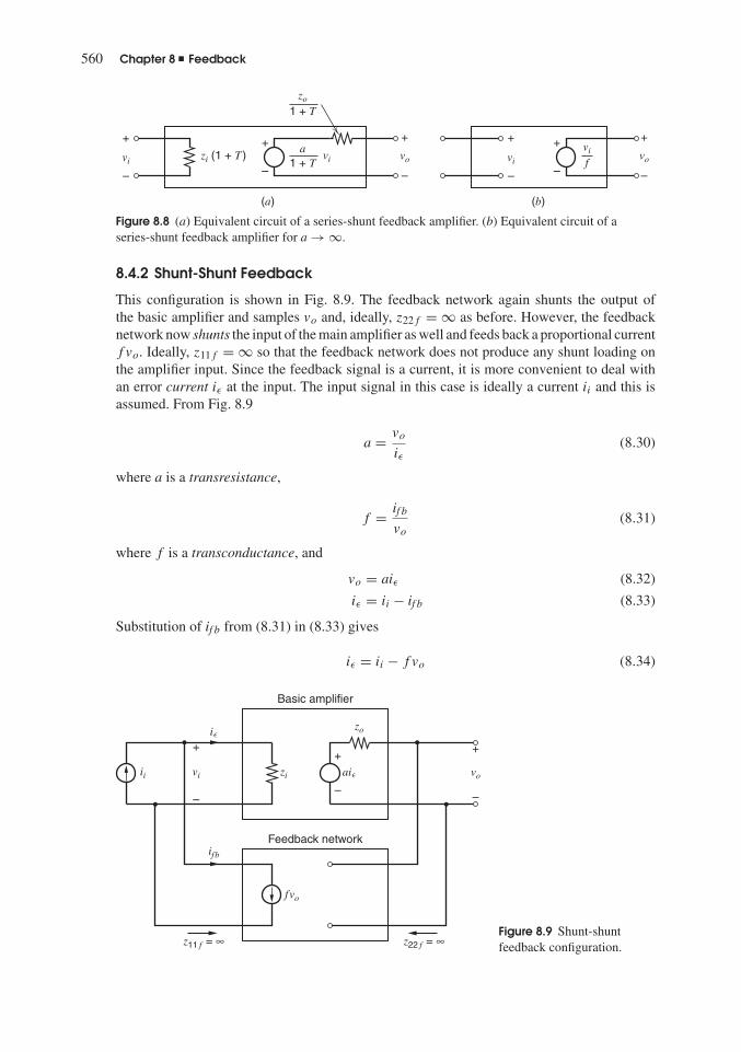
560 Chapter 8 � Feedback
zi (1 + T )
–
vivi
+
–
vi
+
vo
+
–
vo
+
–
+
–
zo
1 + T
a1 + T
+
–
vi
f
(a) (b)
Figure 8.8 (a) Equivalent circuit of a series-shunt feedback amplifier. (b) Equivalent circuit of aseries-shunt feedback amplifier for a → ∞.
8.4.2 Shunt-Shunt Feedback
This configuration is shown in Fig. 8.9. The feedback network again shunts the output ofthe basic amplifier and samples vo and, ideally, z22f = ∞ as before. However, the feedbacknetwork now shunts the input of the main amplifier as well and feeds back a proportional currentf vo. Ideally, z11f = ∞ so that the feedback network does not produce any shunt loading onthe amplifier input. Since the feedback signal is a current, it is more convenient to deal withan error current iε at the input. The input signal in this case is ideally a current ii and this isassumed. From Fig. 8.9
a = vo
iε(8.30)
where a is a transresistance,
f = ifb
vo
(8.31)
where f is a transconductance, and
vo = aiε (8.32)
iε = ii − ifb (8.33)
Substitution of ifb from (8.31) in (8.33) gives
iε = ii − f vo (8.34)
vo
fvo
ii zivi
ifb
+
–
zo
Basic amplifier
Feedback network
z11 f = ∞ z22 f = ∞
++
––
ai
i
Figure 8.9 Shunt-shuntfeedback configuration.

8.4 Feedback Configurations 561
Substitution of (8.32) in (8.34) gives
vo
a= ii − f vo
Rearranging terms we find
vo
ii= a
1 + af= A (8.35)
Again the ideal feedback equation applies. Note that although a and f have dimensions ofresistance and conductance, the loop gain T = af is dimensionless. This is always true.
In this configuration, if the source impedance zs is finite, a division of input current iioccurs between zs and the amplifier input, and the ratio vo/ii will not be as well defined as(8.35) suggests. The full benefits of negative feedback for a shunt-shunt feedback amplifierare thus obtained for zs � Zi, which approaches a current-source drive.
The input impedance of the circuit of Fig. 8.9 can be calculated using (8.32) and (8.35) togive
iε = ii
1 + af(8.36)
The input impedance Zi with feedback is
Zi = vi
ii(8.37)
Substituting (8.36) in (8.37) gives
Zi = vi
iε
1
1 + af= zi
1 + T(8.38)
Thus shunt feedback at the input reduces the amplifier input impedance by (1 + T ). This isalways true.
It is easily shown that the output impedance in this case is
Zo = zo
1 + T(8.39)
as before, for shunt feedback at the output.Shunt-shunt feedback has made this amplifier a good transresistance amplifier. The trans-
fer function vo/ii has been stabilized and both Zi and Zo are lowered.The original shunt-shunt feedback amplifier of Fig. 8.9 can now be represented as shown in
Fig. 8.10a using (8.35), (8.38), and (8.39).As forward gain a approaches infinity, the equivalentcircuit approaches that of Fig. 8.10b, which is an ideal transresistance amplifier.
8.4.3 Shunt-Series Feedback
The shunt-series configuration is shown in Fig. 8.11. The feedback network samples io andfeeds back a proportional current ifb = fio. Since the desired output signal is a current io, itis more convenient to represent the output of the basic amplifier with a Norton equivalent. Inthis case both a and f are dimensionless current ratios, and the ideal input source is a current

562 Chapter 8 � Feedback
ii
ii
ii
zo
1 + T
zi
1 + Ta
1 + T
iif
(a)
(b)
vo
+
–
+
–
+
–vo
+
–
Figure 8.10 (a) Equivalent circuitof a shunt-shunt feedback amp-lifier. (b) Equivalent circuit of ashunt-shunt feedback amplifier fora → ∞.
fi o
ii
io
zi
ifb
zo
Basic amplifier
Feedback network
z11 f = ∞
z22 f = 0
ai
i
Figure 8.11 Shunt-series feedback configuration.
source ii. It can be shown that
io
ii= a
1 + af(8.40)
Zi = zi
1 + T(8.41)
Zo = zo(1 + T ) (8.42)
This amplifier is a good current amplifier and has stable current gain io/ii, low Zi, and high Zo.
8.4.4 Series-Series Feedback
The series-series configuration is shown in Fig. 8.12. The feedback network samples io andfeeds back a proportional voltage vfb in series with the input. The forward gain a is a transcon-ductance and f is a transresistance, and the ideal driving source is a voltage source vi. It can

8.5 Practical Configurations and the Effect of Loading 563
fi o
io
zi zoavv
Basic amplifier
Feedback network
z11 f = 0 z22 f = 0
vi
+
–
+
–
vfb
+
–
+
–
Figure 8.12 Series-series feedback configuration.
be shown thatio
vi
= a
1 + af(8.43)
Zi = zi(1 + T ) (8.44)
Zo = zo(1 + T ) (8.45)
This amplifier is a good transconductance amplifier and has a stabilized gain io/vi, as well ashigh Zi and Zo.
8.5 Practical Configurations and the Effect of LoadingIn practical feedback amplifiers, the feedback network causes loading at the input and outputof the basic amplifier, and the division into basic amplifier and feedback network is not asobvious as the above treatment implies. In such cases, the circuit can always be analyzedby writing circuit equations for the whole amplifier and solving for the transfer function andterminal impedances. However, this procedure becomes very tedious and difficult in mostpractical cases, and the equations so complex that one loses sight of the important aspects ofcircuit performance. Thus it is profitable to identify a basic amplifier and feedback networkin such cases and then to use the ideal feedback equations derived above. In general it willbe necessary to include the loading effect of the feedback network on the basic amplifier, andmethods of including this loading in the calculations are now considered. The method will bedeveloped through the use of two-port representations of the circuits involved, although thismethod of representation is not necessary for practical calculations, as we will see.
8.5.1 Shunt-Shunt Feedback
Consider the shunt-shunt feedback amplifier of Fig. 8.9. The effect of nonideal networks maybe included as shown in Fig. 8.13a, where finite input and output admittances are assumed inboth forward and feedback paths, as well as reverse transmission in each. Finite source and loadadmittances yS and yL are assumed. The most convenient two-port representation in this caseis the short-circuit admittance parameters or y parameters,1 as used in Fig. 8.13a. The reasonfor this is that the basic amplifier and the feedback network are connected in parallel at inputand output, and thus have identical voltages at their terminals. The y parameters specify theresponse of a network by expressing the terminal currents in terms of the terminal voltages, and

564 Chapter 8 � Feedback
(a)
vo
+
–y21a vi
y22ay11a yLvi
+
–
ySis
y12a vo
Basic amplifier
y21f vi
y22fy11f
y12f vo
Feedback network
(b)
vo
+
–
y21a vi y22a y22fy11f y11a yLvi
+
–
ySis
New basic amplifier
y12f vo
New feedback network
Figure 8.13 (a) Shunt-shunt feedback configuration using the y-parameter representation. (b) Circuit of(a) redrawn with generators y21f vi and y12avo omitted.
this results in very simple calculations when two networks have identical terminal voltages.This will be evident in the circuit calculations to follow. The y-parameter representation isillustrated in Fig. 8.14.
From Fig. 8.13a, at the input
is = (yS + y11a + y11f )vi + (y12a + y12f )vo (8.46)
v2
+
–
v1
+
–
i2i1
i1 = y11 v1 + y12 v2
y11 =i1v1 v2 = 0
i2 = y21 v1 + y22 v2
y21 =i2v1 v2 = 0
y12 =i1v2 v1 = 0
y22 =i2v2 v1 = 0
Figure 8.14 The y-parameterrepresentation of a two-port.

8.5 Practical Configurations and the Effect of Loading 565
Summation of currents at the output gives
0 = (y21a + y21f )vi + (yL + y22a + y22f )vo (8.47)
It is useful to define
yi = yS + y11a + y11f (8.48)
yo = yL + y22a + y22f (8.49)
Solving (8.46) and (8.47) by using (8.48) and (8.49) gives
vo
is= −(y21a + y21f )
yiyo − (y21a + y21f )(y12a + y12f )(8.50)
The equation can be put in the form of the ideal feedback equation of (8.35) by dividing byyiyo to give
vo
is=
−(y21a + y21f )
yiyo
1 + −(y21a + y21f )
yiyo
(y12a + y12f )(8.51)
Comparing (8.51) with (8.35) gives
a = −y21a + y21f
yiyo
(8.52)
f = y12a + y12f (8.53)
At this point, a number of approximations can be made that greatly simplify the calcula-tions. First, we assume that the signal transmitted by the basic amplifier is much greater thanthe signal fed forward by the feedback network. Since the former has gain (usually large) whilethe latter has loss, this is almost invariably a valid assumption. This means that
|y21a| � |y21f | (8.54)
Second, we assume that the signal fed back by the feedback network is much greater than thesignal fed back through the basic amplifier. Since most active devices have very small reversetransmission, the basic amplifier has a similar characteristic, and this assumption is almostinvariably quite accurate. This assumption means that
|y12a| � |y12f | (8.55)
Using (8.54) and (8.55) in (8.51) gives
vo
is= A �
−y21a
yiyo
1 +(−y21a
yiyo
)y12f
(8.56)
Comparing (8.56) with (8.35) gives
a = −y21a
yiyo
(8.57)
f = y12f (8.58)

566 Chapter 8 � Feedback
A circuit representation of (8.57) and (8.58) can be found as follows. Equations 8.54 and8.55 mean that in Fig. 8.13a the feedback generator of the basic amplifier and the forward-transmission generator of the feedback network may be neglected. If this is done the circuitmay be redrawn as in Fig. 8.13b, where the terminal admittances y11f and y22f of the feedbacknetwork have been absorbed into the basic amplifier, together with source and load impedancesyS and yL. The new basic amplifier thus includes the loading effect of the original feedbacknetwork, and the new feedback network is an ideal one as used in Fig. 8.9. If the transferfunction of the basic amplifier of Fig. 8.13b is calculated (by first removing the feedbacknetwork), the result given in (8.57) is obtained. Similarly, the transfer function of the feedbacknetwork of Fig. 8.13b is given by (8.58). Thus Fig. 8.13b is a circuit representation of (8.57)and (8.58).
Since Fig. 8.13b has a direct correspondence with Fig. 8.9, all the results derived inSection 8.4.2 for Fig. 8.9 can now be used. The loading effect of the feedback network onthe basic amplifier is now included by simply shunting input and output with y11f and y22f ,respectively. As shown in Fig. 8.14, these terminal admittances of the feedback network arecalculated with the other port of the network short-circuited. In practice, loading term y11f
is simply obtained by shorting the output node of the amplifier and calculating the feedbackcircuit input admittance. Similarly, term y22f is calculated by shorting the input node in theamplifier and calculating the feedback circuit output admittance. The feedback transfer functionf given by (8.58) is the short-circuit reverse transfer admittance of the feedback network andis defined in Fig. 8.14. This is readily calculated in practice and is often obtained by inspection.Note that the use of y parameters in further calculations is not necessary. Once the circuit ofFig. 8.13b is established, any convenient network analysis method may be used to calculategain a of the basic amplifier. We have simply used the two-port representation as a generalmeans of illustrating how loading effects may be included in the calculations.
For example, consider the common shunt-shunt feedback circuit using an op amp as shownin Fig. 8.15a. The equivalent circuit is shown in Fig. 8.15b and is redrawn in 8.15c to allowfor loading of the feedback network on the basic amplifier. The y parameters of the feedbacknetwork can be found from Fig. 8.15d.
y11f = i1
v1
∣∣∣∣v2 = 0
= 1
RF
(8.59)
y22f = i2
v2
∣∣∣∣v1 = 0
= 1
RF
(8.60)
y12f = i1
v2
∣∣∣∣v1 = 0
= − 1
RF
= f (8.61)
Using (8.54), we neglect y21f .The basic-amplifier gain a can be calculated from Fig. 8.15c by putting ifb = 0 to give
v1 = ziRF
zi + RF
ii (8.62)
vo = − R
R + zo
avv1 (8.63)
where
R = RF ||RL (8.64)

8.5 Practical Configurations and the Effect of Loading 567
(a)
vo–
+
RF
ii
(b)
v1ii zi RL
+
–
vo
+
–
+
–
RF
zo
–avv1
Feedback network
(c)
v1ii zi RFRF RL
+
–
vo
+
–
+
–
zo
–avv1
Basic amplifier
Feedback network
ifb = –vo
RF
(d )
+
–
RF
v1
+
–v2
i1 i2
Figure 8.15 (a) Shunt-shunt feedback circuit using anop amp as the gain element. (b) Equivalent circuit of(a) including load resistance RL. (c) Division of thecircuit in (b) into forward and feedback paths. (d)Circuit for the calculation of the y parameters of thefeedback network of the circuit in (b).

568 Chapter 8 � Feedback
Substituting (8.62) in (8.63) gives
vo
ii= a = − R
R + zo
avziRF
zi + RF
(8.65)
Using the formulas derived in Section 8.4.2 we can now calculate all parameters of the feedbackcircuit. The input and output impedances of the basic amplifier now include the effect offeedback loading, and it is these impedances that are divided by (1 + T ) as described inSection 8.4.2. Thus the input impedance of the basic amplifier of Fig. 8.15c is
zia = RF ||zi = RFzi
RF + zi
(8.66)
When feedback is applied, the input impedance is
Zi = zia
1 + T(8.67)
Similarly for the output impedance of the basic amplifier
zoa = zo||RF ||RL (8.68)
When feedback is applied, this becomes
Zo = zo||RF ||RL
1 + T(8.69)
Note that these calculations can be made using the circuit of Fig. 8.15c without further needof two-port y parameters.
Since the loop gain T is of considerable interest, this is now calculated using (8.61)and (8.65):
T = af = RFRL
RFRL + zoRF + zoRL
avzi
zi + RF
(8.70)
EXAMPLE
Assuming that the circuit of Fig. 8.15a is realized using a NE5234 op amp with RF = 1 M
and RL = 10 k, calculate the terminal impedances, loop gain, and overall gain of thefeedback amplifier at low frequencies. The NE5234 data are zi = 170 k, zo = 15 k, andav = 130,000.
From (8.66) the low-frequency input impedance of the basic amplifier including loading is
zia = 106 × 170 × 103
106 + 170 × 103 = 145 k (8.71)
From (8.68), the low-frequency output impedance of the basic amplifier is
zoa = 15 k||1 M||10 k � 5.96 k (8.72)
The low-frequency loop gain can be calculated from (8.70) as
T = 106 × 104
106 × 104 + 15 × 103 × 106 + 15 × 103 × 104 × 130,000 × 170 × 103
170 × 103 + 106
= 7510 (8.73)

8.5 Practical Configurations and the Effect of Loading 569
The loop gain in this case is large. Note that a finite source resistance at the input could reducethis significantly.
The input impedance with feedback applied is found by substituting (8.71) and (8.73) in(8.67) to give
Zi = 145 × 103
7511 = 19.3
The output impedance with feedback applied is found by substituting (8.72) and (8.73) in(8.69) to give
Zo = 5.96 × 10³
7511 = 0.794
In practice, second-order effects in the circuit may result in a larger value of Zo.The overall transfer function with feedback can be found approximately from (8.8) as
vo
ii= A � 1
f(8.74)
Using (8.61) in (8.74) gives
vo
ii= A � −RF
Substituting for RF we obtain
vo
ii= A � −1 M (8.75)
A more exact value of A can be calculated from (8.5). Since the loop gain is large in thiscase, it is useful to transform (8.5) as follows:
A = 1
f
1
1 + 1
af
(8.76)
= 1
f
1
1 + 1
T
(8.77)
Since T is high in this example, A differs little from 1/f . Substituting T = 7510 and 1/f =−1 M in (8.77), we obtain
A = −999,867 (8.78)
For most practical purposes, (8.75) is sufficiently accurate.
8.5.2 Series-Series Feedback
Consider the series-series feedback connection of Fig. 8.12. The effect of nonideal networkscan be calculated using the representation of Fig. 8.16a. In this case the most convenienttwo-port representation is the use of the open-circuit impedance parameters or z parametersbecause the basic amplifier and the feedback network are now connected in series at inputand output and thus have identical currents at their terminals. As shown in Fig. 8.17, the z

570 Chapter 8 � Feedback
(a )
z11a
z12a io
+
–
z22a
z21a ii
+
–
zS
zL
z22f
z21f ii
+
–
z11f
z12f io
+
–
+
–
Basic amplifier
Feedback network
io
ii
vs
(b )
z11f z22f
z11a z22a
z21a ii
+
–
zS
zL
z12f io
+
–
+
–
New basic amplifier
New feedback network
ioii
vs
Figure 8.16 (a) Series-series feedback configuration using the z-parameter representation.(b) Circuit of (a) redrawn with generators z21f ii and z12aio omitted.
parameters specify the network by expressing terminal voltages in terms of terminal currents,and this results in simple calculations when the two networks have common terminal currents.The calculation in this case proceeds as the exact dual of that in Section 8.5.1. From Fig. 8.16,summation of voltages at the input gives
vs = (zS + z11a + z11f )ii + (z12a + z12f )io (8.79)

8.5 Practical Configurations and the Effect of Loading 571
v2
+
–
v1
v1 = z11i1 + z12i2
z11 =v1i1 i2 = 0
v2 = z21i1 + z22i2
+
–
i2i1
z21 =v2i1 i2 = 0
z12 =v1i2 i1 = 0
z22 =v2i2 i1 = 0
Figure 8.17 The z-parameterrepresentation of a two-port.
Summing voltages at the output we obtain
0 = (z21a + z21f )ii + (zL + z22a + z22f )io (8.80)
It is useful to define
zi = zS + z11a + z11f (8.81)
zo = zL + z22a + z22f (8.82)
Again neglecting reverse transmission through the basic amplifier, we assume that
|z12a| � |z12f | (8.83)
Also neglecting feed-forward through the feedback network, we can write
|z21a| � |z21f | (8.84)
With these assumptions it follows that
io
vs
= A �−z21a
zizo
1 +(−z21a
zizo
)z12f
= a
1 + af(8.85)
where
a = −z21a
zizo
(8.86)
f = z12f (8.87)
A circuit representation of a in (8.86) and f in (8.87) can be found by removing generatorsz21f ii and z12aio from Fig. 8.16a in accord with (8.83) and (8.84). This gives the approximaterepresentation of Fig. 8.16b, where the new basic amplifier includes the loading effect of theoriginal feedback network. The new feedback network is an ideal one as used in Fig. 8.12. Thetransfer function of the basic amplifier of Fig. 8.16b is the same as in (8.86), and the transferfunction of the feedback network of Fig. 8.16b is given by (8.87). Thus Fig. 8.16b is a circuitrepresentation of (8.86) and (8.87).
Since Fig. 8.16b has a direct correspondence with Fig. 8.12, all the results of Section 8.4.4can now be used. The loading effect of the feedback network on the basic amplifier is included

572 Chapter 8 � Feedback
by connecting the feedback-network terminal impedances z11f and z22f in series at input andoutput of the basic amplifier. Terms z11f and z22f are defined in Fig. 8.17 and are obtainedby calculating the terminal impedances of the feedback network with the other port open cir-cuited. Feedback function f given by (8.87) is the reverse transfer impedance of the feedbacknetwork.
Consider, for example, the series-series feedback triple of Fig. 8.18a, which is useful asa wideband feedback amplifier. RE2 is usually a small resistor that samples the output currentio, and the resulting voltage across RE2 is sampled by the divider RF and RE1 to produce afeedback voltage across RE1. Usually RF � RE1 and RE2.
The two-port theory derived earlier cannot be applied directly in this case because the basicamplifier cannot be represented by a two-port. However, the techniques developed previouslyusing two-port theory can be used with minor modification by first noting that the feedbacknetwork can be represented by a two-port as shown in 8.18b. One problem with this circuit isthat the feedback generator z12f ie3 is in the emitter of Q1 and not in the input lead where it canbe compared directly with vs. This problem can be overcome by considering the small-signalequivalent of the input portion of this circuit as shown in Fig. 8.19. For this circuit
vs = iizS + vbe + ie1z11f + z12f ie3 (8.88)
Using
ie3 = io
α3(8.89)
in (8.88) gives
vs − z12f
io
α3= iizS + vbe + ie1z11f (8.90)
where the quantities in these equations are small-signal quantities. Equation 8.90 shows thatthe feedback voltage generator z12f (io/α3) can be moved back in series with the input lead; ifthis was done, exactly the same equation would result. (See Fig. 8.18c.) Note that the common-base current gain α3 of Q3 appears in this feedback expression because the output current issampled by RE2 in the emitter of Q3 in order to feed back a correcting signal to the input. Thisproblem is common to most circuits employing series feedback at the output, and the α3 of Q3is outside the feedback loop. There are many applications where this is not a problem, sinceα � 1. However, if high gain precision is required, variations in α3 can cause difficulties.
The z parameters of the feedback network can be determined from Fig. 8.20 as
z12f = v1
i2
∣∣∣∣i1= 0
= RE1RE2
RE1 + RE2 + RF
(8.91)
z22f = v2
i2
∣∣∣∣i1= 0
= RE2||(RE1 + RF ) (8.92)
z11f = v1
i1
∣∣∣∣i2= 0
= RE1||(RF + RE2) (8.93)
Using (8.84), we neglect z21f .
From the foregoing results we can redraw the circuit of Fig. 8.18b as shown in Fig. 8.18c.As in previous calculations, the signal fed forward via the feedback network (in this casez21f ie1) is neglected. The feedback voltage generator is placed in series with the input lead
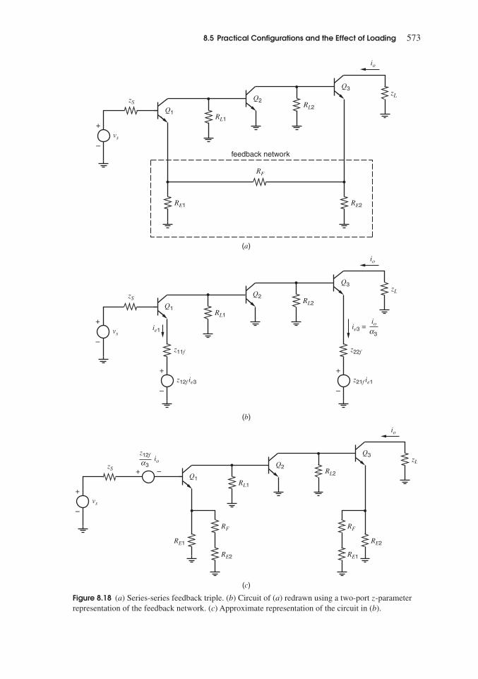
8.5 Practical Configurations and the Effect of Loading 573
(a)
Q1
RE1 RE2
RL1
Q2RL2
zL
io
Q3
vs
+
–
zS
RF
feedback network
(b)
Q1
z11f
z12f ie3
RL1
Q2RL2
zL
io
Q3
vs
+
–
+
–
z22f
z21f ie1
+
–
ie1
zS
ie3 = io 3α
(c)
Q1
RE1
RF
RE2
RE2
RF
RE1
RL1
Q2RL2
zL
io
Q3
vs
+
–
+ –zS
ioz12f
3α
Figure 8.18 (a) Series-series feedback triple. (b) Circuit of (a) redrawn using a two-port z-parameterrepresentation of the feedback network. (c) Approximate representation of the circuit in (b).

574 Chapter 8 � Feedback
zS
rπ1
ii
vbe gm1vbevs
+
–
+
–
+
–
ie1
z11f
z12f ie3 Figure 8.19 Small-signalequivalent circuit of the inputstage of the circuit in Fig. 8.18b.
and an ideal differencing node then exists at the input. The effect of feedback loading on thebasic amplifier is represented by the impedances in the emitters of Q1 and Q3. Note that thiscase does differ somewhat from the example of Fig. 8.16b in that the impedances z11f and z22f
of the feedback network appear in series with the input and output leads in Fig. 8.16b, whereasin Fig. 8.18c these impedances appear in the emitters of Q1 and Q3. This is due to the fact thatthe basic amplifier of the circuit of Fig. 8.18a cannot be represented by two-port z parametersbut makes no difference to the method of analysis. Since the feedback voltage generator inFig. 8.18c is directly in series with the input and is proportional to io, a direct correspondencewith Fig. 8.16b can be established and the results of Section 8.4.4 can be applied. There is nofurther need of the z parameters, and by inspection we can write
io
vs
= A � a
1 + af(8.94)
where
f = z12f
α3= 1
α3
RE1RE2
RE1 + RE2 + RF
(8.95)
and a is the transconductance of the circuit of Fig. 8.18c with the feedback generator[(z12f /α3)io] removed.
The input impedance seen by vs with feedback applied is (1 + af )× (input impedance ofthe basic amplifier of Fig. 8.18c including feedback loading).
The output impedance with feedback applied is (1 + af ) times the output impedance ofthe basic amplifier including feedback loading.
i1 i2RE1
RF
RE2
+
–
v1
+
–
v2
Figure 8.20 Circuit for the calculation of the z parameters of the feedback network of the circuit inFig 8.18a.
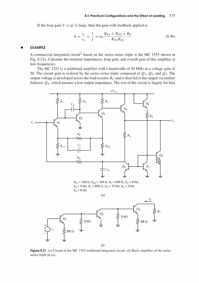
8.5 Practical Configurations and the Effect of Loading 575
If the loop gain T = af is large, then the gain with feedback applied is
A = io
vs
� 1
f= α3
RE1 + RE2 + RF
RE1RE2(8.96)
EXAMPLE
A commercial integrated circuit2 based on the series-series triple is the MC 1553 shown inFig. 8.21a. Calculate the terminal impedances, loop gain, and overall gain of this amplifier atlow frequencies.
The MC 1553 is a wideband amplifier with a bandwidth of 50 MHz at a voltage gain of50. The circuit gain is realized by the series-series triple composed of Q1, Q2, and Q3. Theoutput voltage is developed across the load resistor RC and is then fed to the output via emitterfollower Q4, which ensures a low output impedance. The rest of the circuit is largely for bias
+VCC
VsVo
CP
CB
CF
Q1
Q2
Q7
Q8
Q6
RA RB
RE1 RE2
RE1 = 100 Ω, RE2 = 100 Ω, RF = 640 Ω, RA = 9 kΩ,RB = 5 kΩ, RC = 600 Ω, RD = 12 kΩ, RG = 3 kΩ,RK = 6 kΩ
RF
RD
Q3
Q4
Q5RC
RK
RG
(a)
Q19 kΩ
5 kΩ88 Ω
88 Ω
Q2RC
i3
Q3
vs
+
–
(b)
Figure 8.21 (a) Circuit of the MC 1553 wideband integrated circuit. (b) Basic amplifier of the series-series triple in (a).

576 Chapter 8 � Feedback
v1
+
–
v3
+
–v2
+
–
v4
+
–
vs
+
–
gm1v1 gm2v2 gm3v3
88 Ω 88 Ω9 kΩ 5 kΩ
r 3
IC1
r 1
gm1
i3
(c)
143.3
= 0.6 mA
= 4.33 kΩ
=Ω
IC2
r 2
gm21
26
= 1 mA
= 2.6 kΩ
=Ω
IC3
r 3
gm3
RC
426
= 4 mA
= 650 Ω
=Ω
πr 2πr 1π
π ππ
Figure 8.21 (c) Small-signal equivalent circuit of the basic amplifier in (b).
purposes except capacitors CP , CF , and CB. Capacitors CP and CF are small capacitors ofseveral picofarads and are included on the chip. They ensure stability of the feedback loop,and their function will be described in Chapter 9. Capacitor CB is external to the chip and is alarge bypass capacitor used to decouple the bias circuitry at the signal frequencies of interest.
Bias Calculation. The analysis of the circuit begins with the bias conditions. The bias currentlevels are set by the reference current IRK in the resistor RK, and assuming VBE(on) = 0.6 Vand VCC = 6 V, we obtain
IRK = VCC − 2VBE(on)
RK
(8.97)
Substituting data in (8.97) gives
IRK = 6 − 1.2
6000A = 0.80 mA
The current in the output emitter follower Q4 is determined by the currents in Q6 and Q8.Transistor Q8 has an area three times that of Q7 and Q6 and thus
IC8 = 3 × 0.8 mA = 2.4 mA
IC6 = 0.8 mA
where βF is assumed large in these bias calculations. If the base current of Q1 is small, all ofIC6 and IC8 flow through Q4 and
IC4 � IC6 + IC8 (8.98)
Thus
IC4 � 3.2 mA
Transistor Q8 supplies most of the bias current to Q4, and this device functions as a Class Aemitter-follower output stage of the type described in Section 5.2. The function of Q6 is toallow formation of a negative-feedback bias loop for stabilization of the dc operating point,and resistor RG is chosen to cause sufficient dc voltage drop to allow connection of RD backto the base of Q1. Transistors Q1, Q2, Q3, and Q4 are then connected in a negative-feedbackbias loop and the dc conditions can be ascertained approximately as follows.

8.5 Practical Configurations and the Effect of Loading 577
If we assume that Q2 is on, the voltage at the collector of Q1 is about 0.6 V and the voltageacross RA is 5.4 V. Thus the current through RA is
IRA = 5.4
RA
= 5.4
9000= 0.6 mA (8.99)
If βF is assumed high, it follows that
IC1 � IRA = 0.6 mA (8.100)
Since the voltage across RE1 is small, the voltage at the base of Q1 is approximately 0.6 V,and if the base current of Q1 is small, this is also the voltage at the collector of Q6 since anyvoltage across RD will be small. The dc output voltage can be written
VO = VC6 + IC6RG (8.101)
Substitution of data gives
VO = (0.6 + 0.8 × 3) V = 3 V
The voltage at the base of Q4 (collector of Q3) is VBE above VO and is thus 3.6 V. Thecollector current of Q3 is
IC3 � VCC − VC3
RC
(8.102)
Substitution of parameter values gives
IC3 � 6 − 3.6
600A = 4 mA
The voltage at the base of Q3 (collector of Q2) is
VB3 � −IE3RE2 + VBE(on) (8.103)
Thus
VB3 = VC2 � (4 × 0.1 + 0.6) V = 1 V
IC2 may be calculated from
IC2 � VCC − VC2
RB
(8.104)
and substitution of parameter values gives
IC2 � 6 − 1
5000A = 1 mA
The ac Calculation. The ac analysis can now proceed using the methods previously developedin this chapter. For purposes of ac analysis, the feedback triple composed of Q1, Q2, and Q3in Fig. 8.21a is identical to the circuit in Fig. 8.18a, and the results derived previously for thelatter circuit are directly applicable to the triple in Fig. 8.21a. To obtain the voltage gain of thecircuit of Fig. 8.21a, we simply multiply the transconductance of the triple by the load resistorRC, since the gain of the emitter follower Q4 is almost exactly unity. Note that resistor RD is

578 Chapter 8 � Feedback
assumed grounded for ac signals by the large capacitor CB, and thus has no influence on theac circuit operation, except for a shunting effect at the input that will be discussed later. From(8.95) the feedback factor f of the series-series triple of Fig. 8.21a is
f = 1
0.99
100 × 100
100 + 100 + 640 = 12.0 (8.105)
where β0 = 100 has been assumed.If the loop gain is large, the transconductance of the triple of Fig. 8.21a can be calculated
from (8.96) as
io3
vs
� 1
f= 1
12A/V (8.106)
where io3 is the small-signal collector current in Q3 in Fig. 8.21a. If the input impedance ofthe emitter follower Q4 is large, the load resistance seen by Q3 is RC = 600 and the voltagegain of the circuit is
vo
vs
= − io3
vs
× RC (8.107)
Substituting (8.106) in (8.107) gives
vo
vs
= −50.0 (8.108)
Consider now the loop gain of the circuit of Fig. 8.21a. This can be calculated by using thebasic-amplifier representation of Fig. 8.18c to calculate the forward gaina. Fig. 8.18c is redrawnin Fig. 8.21b using data from this example, assuming that zS = 0 and omitting the feedbackgenerator. The small-signal, low-frequency equivalent circuit is shown in Fig. 8.21c assumingβ0 = 100, and it is a straightforward calculation to show that the gain of the basic amplifier is
a = i3
vs
= 20.3 A/V (8.109)
Combination of (8.105) and (8.109) gives
T = af = 12 × 20.3 = 243.6 (8.110)
The transconductance of the triple can now be calculated more accurately from (8.94) as
io3
vs
= a
1 + T= 20.3
244.6A/V = 0.083 A/V (8.111)
Substitution of (8.111) in (8.107) gives for the overall voltage gain
vo
vs
= − io3
vs
RC = −0.083 × 600 = −49.8 (8.112)
This is close to the approximate value given by (8.108).The input resistance of the basic amplifier is readily determined from Fig. 8.21c to be
ria = 13.2 k (8.113)
The input resistance when feedback is applied is
Ri = ria(1 + T ) (8.114)

8.5 Practical Configurations and the Effect of Loading 579
Substituting (8.113) and (8.110) in (8.114) gives
Ri = 13.2 × 244.6 k = 3.23 M (8.115)
As expected, series feedback at the input results in a high input resistance. In this example,however, the bias resistor RD directly shunts the input for ac signals and is outside the feedbackloop. Since RD = 12 k and is much less than Ri, the resistor RD determines the inputresistance for this circuit.
Finally, the output resistance of the circuit is of some interest. The output resistance of thetriple can be calculated from Fig. 8.21c by including output resistance ro in the model for Q3.The resistance obtained is then multiplied by (1 + T ) and the resulting value is much greaterthan the collector load resistor of Q3, which is RC = 600 . The output resistance of the fullcircuit is thus essentially the output resistance of emitter follower Q4 fed from a 600- sourceresistance, and this is
Ro = 1
gm4+ RC
β4=(
26
3.2+ 600
100
) = 14 (8.116)
8.5.3 Series-Shunt Feedback
Series-shunt feedback is shown schematically in Fig. 8.4. The basic amplifier and the feedbacknetwork have the same input current and the same output voltage. A two-port representationthat uses input current and output voltage as the independent variables is the hybrid h-parameterrepresentation shown in Fig. 8.22. The h parameters can be used to represent nonideal circuitsin a series-shunt feedback as shown in Fig. 8.23a. Summation of voltages at the input of thisfigure gives
vs = (zS + h11a + h11f )ii + (h12a + h12f )vo (8.117)
Summing currents at the output yields
0 = (h21a + h21f )ii + (yL + h22a + h22f )vo (8.118)
We now definezi = zS + h11a + h11f (8.119)
yo = yL + h22a + h22f (8.120)
v2
+
–
v1
+
–
i2i1
v1 = h11i1 + h12v2
i2 = h21i1 + h22v2
h11 =v1
i1 v2 = 0h12 =
v1
v2 i1 = 0
h21 =i2i1 v2 = 0
h22 =i2v2 i1 = 0
Figure 8.22 The h-parameterrepresentation of a two-port.

580 Chapter 8 � Feedback
(a )
h11a
h12a vo
+
–
h22ah21a ii
zS
yL
h22fh21f ii
h11f
h12f vo
+
–
+
–
Basic amplifier
Feedback network
ii
vs
+
–
vo
(b)
h11a
h11f
h22ah21a ii
zS
yLh22f
h12f vo
+
–
+
–
New basic amplifier
New feedback network
ii
vs
+
–
vo
Figure 8.23 (a) Series-shunt feedback configuration using the h-parameter representation. (b) Circuitof (a) redrawn with generators h21f ii and h12avo omitted.
and make the same assumptions as in previous examples:
|h12a| � |h12f | (8.121)
|h21a| � |h21f | (8.122)

8.5 Practical Configurations and the Effect of Loading 581
RE zi
zo
RF
vs
vo
+
–
+
–
v1 zL
+
––av v1
+
–
Feedback network
Figure 8.24 Series-shunt feedback circuit using an op amp as the gain element.
It can then be shown that
vo
vs
= A �−h21a
ziyo
1 +(
−h21a
ziyo
)h12f
= a
1 + af(8.123)
wherea = −h21a
ziyo
(8.124)
f = h12f (8.125)
Acircuit representation of a in (8.124) and f in (8.125) can be found by removing the generatorsh12avo and h21f ii from Fig. 8.23a as suggested by the approximations of (8.121) and (8.122).This gives the approximate representation of Fig. 8.23b, where the new basic amplifier includesthe loading effect of the original feedback network. As in previous examples, the circuit ofFig. 8.23b is a circuit representation of (8.123), (8.124), and (8.125) and has the form of anideal feedback loop. Thus all the equations of Section 8.4.1 can be applied to the circuit.
For example, consider the common series-shunt op amp circuit of Fig. 8.24, which fitsexactly the model described above. We first determine the h parameters of the feedback networkfrom Fig. 8.25:
h22f = i2
v2
∣∣∣∣i1= 0
= 1
RF + RE
(8.126)
h12f = v1
v2
∣∣∣∣i1= 0
= RE
RE + RF
(8.127)
v1 v2i1 RE
RF
+
–
+
–
i2
Figure 8.25 Circuit for the deter-mination of the h parameters of thefeedback network in Fig. 8.24.

582 Chapter 8 � Feedback
RE||RF zizL
zo
vo
vs
+
–
+
–
+
–
v1–avv1 RE + RF
+
–
+
–
voRE
RE + RF
Figure 8.26 Equivalent circuit for Fig. 8.24.
h11f = v1
i1
∣∣∣∣v2= 0
= RE||RF (8.128)
Using (8.122), we neglect h21f . The complete feedback amplifier including loading effects isshown in Fig. 8.26 and has a direct correspondence with Fig. 8.23b. (The only difference isthat the op amp output is represented by a Thévenin rather than a Norton equivalent.)
The gain a of the basic amplifier can be calculated from Fig. 8.26 by initially disregardingthe feedback generator to give
a = zi
zi + Rav
zLX
zLX + zo
(8.129)
where
R = RE||RF (8.130)
zLX = zL||(RE + RF ) (8.131)
Also
f = RE
RE + RF
(8.132)
Thus the overall gain of the feedback circuit is
A = vo
vs
= a
1 + af(8.133)
and A can be evaluated using (8.129) and (8.132).
EXAMPLE
Assume that the circuit of Fig. 8.24 is realized, using a differential amplifier with low-frequencyparameters zi = 100 k, zo = 10 k, and av = 3000. Calculate the input impedance of thefeedback amplifier at low frequencies if RE = 5 k, RF = 20 k, and zL = 10 k. Note thatzo in this case is not small as is usually the case for an op amp, and this situation can arise insome applications.
This problem is best approached by first calculating the input impedance of the basicamplifier and then multiplying by (1 + T ) as indicated by (8.25) to calculate the inputimpedance of the feedback amplifier. By inspection from Fig. 8.26 the input impedance ofthe basic amplifier is
zia = zi + RE||RF = (100 + 5||20) k = 104 k

8.5 Practical Configurations and the Effect of Loading 583
RL1
RE
Q1RL2
RF
zS
zL
Q2
Q3
vs vo
+
–+
–
Feedback network
Figure 8.27 Series-shunt feedback circuit.
The parallel combination of zL and (RF + RE) in Fig. 8.27 is
zLX = 10 × 25
35= 7.14 k
Substitution in (8.129) gives, for the gain of the basic amplifier of Fig. 8.26,
a = 100
100 + 4× 3000 × 7.14
7.14 + 10= 1202
From (8.127) the feedback factor f for this circuit is
f = 5
5 + 20= 0.2
and thus the loop gain is
T = af = 1202 × 0.2 = 240
The input impedance of the feedback amplifier is thus
Zi = zia(1 + T ) = 104 × 241 k = 25 M
In this example the loading effect produced by (RF + RE) on the output has a significant effecton the gain a of the basic amplifier and thus on the input impedance of the feedback amplifier.
As another example of a series-shunt feedback circuit, consider the series-series triple ofFig. 8.18a but assume that the output signal is taken as the voltage at the emitter of Q3, as shownin Fig. 8.27. This is an example of how the same circuit can realize two different feedbackfunctions if the output is taken from different nodes. As in the case of Fig. 8.18a, the basicamplifier of Fig. 8.27 cannot be represented as a two-port. However, the feedback network canbe represented as a two-port and the appropriate parameters are the h parameters as shownin Fig. 8.28. The h parameters for this feedback network are given by (8.126), (8.127), and(8.128) and h21f is neglected. The analysis of Fig. 8.28 then proceeds in the usual manner.
8.5.4 Shunt-Series Feedback
Shunt-series feedback is shown schematically in Fig. 8.11. In this case the basic amplifierand the feedback network have common input voltages and output currents, and hybrid g
parameters as defined in Fig. 8.29 are best suited for use in this case. The feedback circuit is

584 Chapter 8 � Feedback
RL1
Q1RL2
zS
zL
Q2
Q3
vs
+
– +
–
RE||RF
(RF + RE)
voRE
RE + RF
vo
+
–
Figure 8.28 Circuit equivalent to that of Fig. 8.27 using a two-port representation of the feedbacknetwork.
v2
+
–
v1
+
–
i2i1
i1 = g11v1 + g12i2v2 = g21v1 + g22i2
g11 =i1v1 i2 = 0
g12 =i1i2 v1 = 0
g21 =v2
v1 i2 = 0g22 =
v2
i2 v1 = 0Figure 8.29 The g-parameterrepresentation of a two-port.
shown in Fig. 8.30a, and, at the input, we find that
is = (yS + g11a + g11f )vi + (g12a + g12f )io (8.134)
At the output
0 = (g21a + g21f )vi + (zL + g22a + g22f )io (8.135)
Defining
yi = yS + g11a + g11f (8.136)
zo = zL + g22a + g22f (8.137)
and making the assumptions
|g12a| � |g12f | (8.138)
|g21a| � |g21f | (8.139)
we find
io
is= A �
−g21a
yizo
1 +(
−g21a
yizo
)g12f
= a
1 + af(8.140)

8.5 Practical Configurations and the Effect of Loading 585
is
(a )
g22a
g12a io
+
–
+
–
zL
g12f io
+
–
Basic amplifier
Feedback network
io
vi g11a
g11f
g22f
yS g21a vi
g21f vi
is
(b )
g11a
g22f
g22a
g21a vi
+
–
zL
g12f io
+
–
New basic amplifier
New feedback network
io
vi g11fyS
Figure 8.30 (a) Shunt-series feedback configuration using the g-parameter representation. (b) Circuit of(a) redrawn with generators g21f vi and g12aio omitted.
where
a = −g21a
yizo
(8.141)
f = g12f (8.142)
Following the procedure for the previous examples, we can find a circuit representa-tion for this case by eliminating the generators g21f vi and g12aio to obtain the approximate

586 Chapter 8 � Feedback
RF
is
io
yS
RL1
RE
zLQ1
Q2
io 2
Feedback network
α
Figure 8.31 Current feedback pair.
RF
RE i2v1
+
–
v2
+
–
i1
Figure 8.32 Circuit for the calculationof the g parameters of the feedbacknetwork in Fig. 8.31.
representation of Fig. 8.30b. Since this has the form of an ideal feedback circuit, all the resultsof Section 8.4.3 may now be used.
A common shunt-series feedback amplifier is the current-feedback pair of Fig. 8.31. Sincethe basic amplifier of Fig. 8.31 cannot be represented by a two-port, the representation ofFig. 8.30b cannot be used directly. However, as in previous examples, the feedback networkcan be represented by a two-port, and the g parameters can be calculated using Fig. 8.32 to give
g11f = i1
v1
∣∣∣∣i2= 0
= 1
RF + RE
(8.143)
g12f = i1
i2
∣∣∣∣v1= 0
= − RE
RE + RF
(8.144)
g22f = v2
i2
∣∣∣∣v1= 0
= RE||RF (8.145)
Using (8.139), we neglect g21f . Assuming that g21f vi is negligible, we can redraw the circuitof Fig. 8.31 as shown in Fig. 8.33. This circuit has an ideal input differencing node, and the
io
isio 2
yS
RL1
zLQ1
Q2
RE||RF(RE + RF)–RE
RE + RF α
Figure 8.33 Circuit equivalent to that of Fig. 8.31 using a two-port representation of the feedbacknetwork.

8.6 Single-Stage Feedback 587
feedback function can be identified as
f = − RE
RE + RF
1
α2(8.146)
The gain a of the basic amplifier is determined by calculating the current gain of the circuit ofFig. 8.33 with the feedback generator removed. The overall current gain with feedback appliedcan then be calculated from (8.40).
8.5.5 Summary
The results derived above regarding practical feedback circuits and the effect of feedbackloading can be summarized as follows.
First, input and output variables must be identified and the feedback identified as shunt orseries at input and output.
The feedback function f is found by the following procedure. If the feedback is shuntat the input, short the input feedback node to ground and calculate the feedback current. Ifthe feedback is series at the input, open circuit the input feedback node and calculate thefeedback voltage. In both these cases, if the feedback is shunt at the output, drive the feedbacknetwork with a voltage source. If the feedback is series at the output, drive with a currentsource.
The effect of feedback loading on the basic amplifier is found as follows. If the feed-back is shunt at the input, short the input feedback node to ground to find the feedbackloading on the output. If the feedback is series at the input, open circuit the input feedbacknode to calculate output feedback loading. Similarly, if the feedback is shunt or series at theoutput, then short or open the output feedback node to calculate feedback loading on theinput.
These results along with other information are summarized in Table 8.1.
8.6 Single-Stage FeedbackThe considerations of feedback circuits in this chapter have been mainly directed toward thegeneral case of circuits with multiple stages in the basic amplifier. However, in dealing withsome of these circuits (such as the series-series triple of Fig. 8.18a), equivalent circuits werederived in which one or more stages contained an emitter resistor. (See Fig. 8.18c.) Such astage represents in itself a feedback circuit as will be shown. Thus the circuit of Fig. 8.18ccontains feedback loops within a feedback loop, and this has a direct effect on the amplifierperformance. For example, the emitter of Q3 in Fig. 8.18c has a linearizing effect on Q3,and so does the overall feedback when the loop is closed. It is thus important to calculate theeffects of both local and overall feedback loops. The term local feedback is often used insteadof single-stage feedback. Local feedback is often used in isolated stages as well as being foundinside overall feedback loops. In this section, the low-frequency characteristics of two basicsingle-stage feedback circuits will be analyzed.
8.6.1 Local Series-Series Feedback
A local series-series feedback stage in bipolar technology (emitter degeneration) is shownin Fig. 8.34a. The characteristics of this circuit were considered previously in Section 3.3.8,

Table 8.1 Summary of Feedback Configurations
To CalculateTwo-Port Transfer Feedback Loading
Feedback Parameter Output Input FunctionConfiguration Representation Variable Variable Stabilized Zi Zo At Input At Output
To CalculateFeedback Function f
Shunt-shunt y vo isvo
isTransresistance
Low Low Short circuitoutputfeedbacknode
Short circuitinputfeedbacknode
Drive the feedbacknetwork with a voltageat its output andcalculate the currentflowing into a short atits input
Shunt-series g io isio
isCurrent gain
Low High Open circuitoutputfeedbacknode
Short circuitinputfeedbacknode
Drive the feedbacknetwork with a currentand calculate thecurrent flowing into ashort
Series-shunt h vo vs
vo
vs
Voltage gain
High Low Short circuitoutputfeedbacknode
Open circuitinputfeedbacknode
Drive the feedbacknetwork with a voltageand calculate thevoltage produced intoan open circuit
Series-series z io vs
io
vs
Transconductance
High High Open circuitoutputfeedbacknode
Open circuitinputfeedbacknode
Drive the feedbacknetwork with a currentand calculate thevoltage produced intoan open circuit
588

8.6 Single-Stage Feedback 589
(a)
zL
io
RE
vs
+
–
(b)
rb
zL
ii io
RE
rvs
+
–
+
–
A
A
v1 gmv1π
(c)
rb
RE
vfb = ioRE
r
vs
+
–
+
–
+
–
v1π
Figure 8.34 (a) Single-stage series-seriesfeedback circuit. (b) Low-frequency equivalentcircuit of (a). (c) Circuit equivalent to (b) using aThévenin equivalent across the plane AA.
and it will be considered again here from the feedback viewpoint. Similar results are found forMOS transistors with source degeneration.
The circuit of Fig. 8.34a can be recognized as a degenerate series-series feedback config-uration as described in Sections 8.4.4 and 8.5.2. Instead of attempting to use the generalizedforms of those sections, we can perform a more straightforward calculation in this simplecase by working directly from the low-frequency, small-signal equivalent circuit shown inFig. 8.34b. For simplicity, source impedance is assumed zero but can be lumped in with rb ifdesired. If a Thévenin equivalent across the plane AA is calculated, Fig. 8.34b can be redrawnas in Fig. 8.34c. The existence of an input differencing node is apparent, and quantity ioRE isidentified as the feedback voltage vfb. Writing equations for Fig. 8.34c we find
v1 = rπ
rπ + rb + RE
(vs − vfb) (8.147)
io = gmv1 (8.148)
vfb = ioRE (8.149)

590 Chapter 8 � Feedback
These equations are of the form of the ideal feedback equations where v1 is the error volt-age, io is the output signal, and vfb is the feedback signal. From (8.147) and (8.148) weknow that
io = gmrπ
rπ + rb + RE
(vs − vfb) (8.150)
and thus we can identify
a = gmrπ
rπ + rb + RE
= gm
1 + rb + RE
rπ
(8.151)
From (8.149)
f = RE (8.152)
Thus for the complete circuit
io
vs
= A = a
1 + af= 1
RE
1
1 + 1
RE
(1
gm
+ rb + RE
β0
) (8.153)
and A � 1/RE for large loop gain.The loop gain is given by T = af and thus
T = gmRE
1 + rb + RE
rπ
(8.154)
If (rb + RE) � rπ we find
T � gmRE (8.155)
The input resistance of the circuit is given by
Input resistance = (1 + T ) × (input resistance with vfb = 0)
= (1 + T )(rb + rπ + RE) (8.156)
Using (8.154) in (8.156) gives
Input resistance = rb + RE + rπ(1 + gmRE) (8.157)
= rb + rπ + (β0 + 1)RE (8.158)
We can also show that if the output resistance ro of the transistor is included, the outputresistance of the circuit is given by
Output resistance � ro
⎛⎜⎜⎝1 + gmRE
1 + rb + RE
rπ
⎞⎟⎟⎠ (8.159)
Both input and output resistance are increased by the application of emitter feedback, asexpected.

8.6 Single-Stage Feedback 591
EXAMPLE
Calculate the low-frequency parameters of the series-series feedback stage represented by Q3in Fig. 8.21b. The relevant parameters are as follows:
RE = 88 rπ = 650 gm = 4
26A/V β0 = 100 rb = 0
The loading produced by Q3 at the collector of Q2 is given by the input resistance expressionof (8.158) and is
Ri3 = (650 + 101 × 88) = 9.54 k (8.160)
The output resistance seen at the collector of Q3 can be calculated from (8.159) using rb =5 k to allow for the finite source resistance in Fig. 8.21b. If we assume that ro = 25 k atIC = 4 mA for Q3, then from (8.159) we find that
Ro3 = 25
⎛⎜⎝1 +
4
2688
1 + 5088
650
⎞⎟⎠ k = 63 k (8.161)
In the example of Fig. 8.21b, the above output resistance would be multiplied by the loop gainof the series-series triple.
Finally, when ac voltage v4 at the collector of Q2 in Fig. 8.21c is determined, outputcurrent i3 in Q3 can be calculated using (8.153):
i3
v4= 1
88
1
1 + 1
88
(26
4+ 88
100
) A/V = 1
95.4A/V (8.162)
Note that since the voltage v4 exists at the base of Q3, the effective source resistance in theabove calculation is zero.
8.6.2 Local Series-Shunt Feedback
Another example of a local feedback stage is the common-drain stage shown in Fig. 8.35a. Thiscircuit is a series-shunt feedback configuration. The small-signal model is shown in Fig. 8.35b.The current through the gmb controlled source is controlled by the voltage across it; therefore,it can be replaced by a resistor of value 1/gmb. Using this transformation, the small-signalmodel in Fig. 8.35b is redrawn in Fig. 8.35c, where
R′L = RL||ro|| 1
gmb
(8.163)
The feedback network is taken to be R′L. Using Fig. 8.35d, the h two-port parameters for the
feedback network are
h11f = v1
i1
∣∣∣∣v2= 0
= 0 (8.164)
h22f = i2
v2
∣∣∣∣i1 = 0
= 1
R′L
(8.165)

592 Chapter 8 � Feedback
(a)
VDD
RS
RLVs
+
–Vo
+
–
(b)
RS
RL
rovs
+
–
vo
+
–
vx gmvx gmbvsb = gmbvo
+
–
(c)
RS
RL
vs
+
–
vo
+
–
vx gmvx
+
–
Feedback network
'
(d )
i1 RL
+
–
+
–
i2
v2v1 '
(e)
RS
RL
vs
+
–+
–
vo
+
–
vxgmvx
vfb = 1vo
+
–
Feedback network
'
Figure 8.35 (a) A source followerdriving a resistive load. (b) Asmall-signal model for the circuit in(a). (c) A simplified small-signalmodel. (d) Circuit for finding thetwo-port parameters for thefeedback network. (e) The circuit in(c) with the feedback networkreplaced by a two-port model.

8.7 The Voltage Regulator as a Feedback Circuit 593
and the feedback factor is
f = h12f = v1
v2
∣∣∣∣i1= 0
= 1 (8.166)
Here we neglect the forward transmission through the feedback network, h21f , as was done inSection 8.5.3.
Figure 8.35b is redrawn in Fig. 8.35e with the feedback network replaced by a two-portmodel. The gain of the basic amplifier a is found by setting the feedback to zero in Fig. 8.35e
a = vo
vs
∣∣∣∣vfb= 0
= gmR′L (8.167)
Using (8.166) and (8.167), the closed-loop gain is
A = a
1 + af= gmR′
L
1 + gmR′L
(8.168)
This closed-loop gain is always less than one and approaches unity as gmR′L → ∞.
From Fig. 8.35e, the output resistance without feedback is R′L, and the closed-loop output
resistance is
Ro = R′L
1 + af= R′
L
1 + gmR′L
= 11
R′L
+ gm
= 11
RL
+ 1
ro+ gmb + gm
(8.169)
where (8.163) is used in the right-most expression. The output resistance is reduced because ofthe feedback. The input resistance is infinite because the resistance from the gate to the sourcein the model in Fig. 8.35 is infinite.
8.7 The Voltage Regulator as a Feedback CircuitAs an example of a practical feedback circuit, the operation of a voltage regulator will beexamined. This section is introduced for the dual purpose of illustrating the use of feedback inpractice and for describing the elements of voltage regulator design.
Voltage regulators are widely used components that accept a poorly specified (possiblyfluctuating) dc input voltage and produce from it a constant, well-specified output voltage thatcan then be used as a supply voltage for other circuits.3 In this way, fluctuations in the supplyvoltage are essentially eliminated, and this usually results in improved performance for circuitspowered from such a supply.
A common type of voltage regulator is the series regulator shown schematically inFig. 8.36. The name series comes from the fact that the output voltage is controlled by apower transistor in series with the output. This is the last stage of a high-gain voltage amplifier,as shown in Fig. 8.36.
Many of the techniques discussed in previous chapters are utilized in the design of circuitsof this kind. A stable reference voltage VR can be generated using a Zener diode or a bandgapreference, as described in Chapter 4. This is then fed to the noninverting input of the high-gainamplifier, where it is compared with a sample of the output taken by resistors R1 and R2. Thisis recognizable as a series-shunt feedback arrangement, and using (8.132) we find that for largeloop gain
VO = VR
R1 + R2
R2(8.170)
The output voltage can be varied by changing ratio R1/R2.

594 Chapter 8 � Feedback
VO
VR
R1
R2
+
–
Referencevoltage
generator
Reference voltage = VR
Voltage amplifierwith gain a
Regulatedoutputvoltage
Unregulatedinput
Figure 8.36 Schematic of a series voltage regulator.
The characteristics required in the amplifier of Fig. 8.36 are those of a good op amp,as described in Chapter 6. In particular, low drift and offset are essential so that the outputvoltage VO is as stable as possible. Note that the series-shunt feedback circuit will presenta high input impedance to the reference generator, which is desirable to minimize loadingeffects. In addition, a very low output impedance will be produced at VO, which is exactly therequirement for a good voltage source. If the effects of feedback loading are neglected (usuallya good assumption in such circuits), the low-frequency output resistance of the regulator isgiven by (8.29) as
Ro = roa
1 + T(8.171)
where
T = aR2
R1 + R2(8.172)
roa = output resistance of the amplifier without feedback
a = magnitude of the forward gain of the regulator amplifier
If the output voltage of the regulator is varied by changing ratio R1/R2, then (8.171) and(8.172) indicate that T and thus Ro also change. Assuming that VR is constant and T � 1, wecan describe this behavior by substituting (8.170) and (8.172) in (8.171) to give
Ro = roa
aVR
VO (8.173)
which shows Ro to be a function of VO if a, VR, and roa are fixed. If the output current drawnfrom the regulator changes by �IO, then VO changes by �VO, where
�VO = Ro�IO (8.174)

8.7 The Voltage Regulator as a Feedback Circuit 595
Substitution of (8.173) in (8.174) gives
�VO
VO
= roa
aVR
�IO (8.175)
This equation allows calculation of the load regulation of the regulator. This is a widely usedspecification, which gives the percentage change in VO for a specified change in IO and shouldbe as small as possible.
Another common regulator specification is the line regulation, which is the percentagechange in output voltage for a specified change in input voltage. Since VO is directly pro-portional to VR, the line regulation is determined by the change in reference voltage VR withchanges in input voltage and depends on the particular reference circuit used.
As an example of a practical regulator, consider the circuit diagram of the 723 monolithicvoltage regulator shown in Fig. 8.37. The correspondence to Fig. 8.36 can be recognized, withthe portion of Fig. 8.37 to the right of the dashed line being the voltage amplifier with feedback.The divider resistors R1 and R2 in Fig. 8.36 are labeled RA and RB in Fig. 8.37 and are externalto the chip. The output power transistor Q15 is on the chip and is Darlington connected withQ14 for high gain. Differential pair Q11 and Q12, together with active load Q8, contribute mostof the gain of the amplifier. Resistor RC couples the reference voltage to the amplifier and C2is an external capacitor, which is needed to prevent oscillation in the high-gain feedback loop.Its function is discussed in Chapter 9.
EXAMPLE
Calculate the bias conditions and load regulation of the 723. Assume the total supply voltageis 15 V.
The bias calculation begins at the left-hand side of Fig. 8.37. Current source I1 models atransistor current source that uses a junction field-effect transistor (JFET)4 that behaves likean n-channel MOS transistor with a negative threshold voltage. Diodes D1 and D2 are Zenerdiodes.4 When operating in reverse breakdown, the voltage across a Zener diode is nearlyconstant as described in Chapter 2.
The Zener diode D1 produces a voltage drop of about 6.2 V, which sets up a referencecurrent in Q2:
IC2 = −6.2 − |VBE2|R1 + R2
= −6.2 − 0.6
16,000A
= −348 �A (8.176)
Note that IC2 is almost independent of supply voltage because it is dependent only on theZener diode voltage.
The voltage across R1 and Q2 establishes the currents in current sources Q3, Q7, and Q8.
IC7 = IC8 = −174 �A (8.177)
IC3 = −10.5 �A (8.178)
Current source Q3 establishes the operating current in the voltage reference circuit com-posed of transistors Q4, Q5, Q6, resistors R6, R7, R8, and Zener diode D2. This circuitcan be recognized as a variation of the Wilson current source described in Chapter 4, and

R8 R10
Q9
Q5
Q4
Q11
Q8
Q14
Q15C2
C1
Q10Q6
Q12
Q13
R11
V+
RC
VR
+
–
I1
5 kΩ
30 kΩ
R9 300 Ω
R6 100 Ω
20 kΩ
R12 15 kΩ
RB
RA
VO
RL
150 Ω
R5 1 kΩ
Q7
R4 1 kΩ
Q3Q2
R3 25 kΩR1 500 Ω
R2 15.5 kΩ
R7
D26.2 V
+
–
D16.2 V
5 pF
RARB
RA + RBRC = (external)
C2 = 100 pF (external)
Figure 8.37 Circuit diagram of the 723 monolithic voltage regulator.
596

8.7 The Voltage Regulator as a Feedback Circuit 597
the negative feedback loop forces the current in Q6 to equal IC3 so that
IC6 = 10.5 �A (8.179)
where the base current of Q4 has been neglected.The output reference voltage VR is composed of the sum of the Zener diode voltage D2
plus the base-emitter voltage of Q6, giving a reference voltage of about 6.8 V. The current inthe Zener is established by VBE6 and R8 giving
ID2 = VBE6
R8= 600
5�A = 120 �A (8.180)
The Darlington pair Q4, Q5 helps give a large loop gain that results in a very low outputimpedance at the voltage reference node. Resistor R6 limits the current and protects Q5 in caseof an accidental grounding of the voltage reference node. Resistor R7 and capacitor C1 formthe high-frequency compensation required to prevent oscillation in the feedback loop. Notethat the feedback is shunt at the output node. Any changes in reference-node voltage (due toloading for example) are detected at the base of Q6, amplified, and fed to the base of Q4 andthus back to the output where the original change is opposed.
The biasing of the amplifier is achieved via current sources Q7 and Q8. The current in Q7also appears in Q10 (neglecting the base current of Q9). Transistor Q13 has an area twice thatof Q10 and one half the emitter resistance. Thus
IC13 = 2IC10 = 2IC7 = 348 �A (8.181)
Transistor Q9 provides current gain to minimize the effect of base current in Q10 and Q13.This beta-helper current mirror was described in Chapter 4.
The bias current in each half of the differential pair Q11, Q12 is thus
IC11 = IC12 = 1
2IC13 = 174 �A (8.182)
Since Q8 and R5 are identical to Q7 and R4, the current in Q8 is given by
IC8 = −174 �A (8.183)
Transistor Q8 functions as an active load for Q12, and, since the collector currents in these twodevices are nominally equal, the input offset voltage for the differential pair is nominally zero.
The current in output power transistor Q15 depends on the load resistance but can go ashigh as 150 mA before a current-limit circuit (not shown) prevents further increase. ResistorR12 provides bleed current so that Q14 always has at least 0.04 mA of bias current, even whenthe current in Q15 is low and/or its current gain is large.
In order to calculate the load regulation of the 723, (8.175) indicates that it is necessary tocalculate the open-loop gain and output resistance of the regulator amplifier. For this purpose,a differential ac equivalent circuit of this amplifier is shown in Fig. 8.38. Load resistance RL12is the output resistance presented by Q8, which is
RL12 � ro8(1 + gm8R5) (8.184)
Assuming that the magnitude of the Early voltage of Q8 is 100 V and IC8 = −174 �A, wecan calculate the value of RL12 as
RL12 = 100
0.174
(1 + 0.174
261000
)k = 4.42 M (8.185)

598 Chapter 8 � Feedback
vi
+
–
vo
+
–
v1
+
–
Q12
Q14
RL12
RL
R12
Q15
1gm11
Figure 8.38 An ac equivalent circuit of the regulator amplifier of the 723 voltage regulator.
Since gm11 = gm12, the impedance in the emitter of Q12 halves the transconductance and givesan effective output resistance of
Ro12 =(
1 + gm121
gm11
)ro12 (8.186)
where ro12 is the output resistance of Q12 alone and is 575 k if the Early voltage is 100 V.Thus
Ro12 = 1.15 M (8.187)
The external load resistance RL determines the load current and thus the bias currents inQ14 and Q15. However, RL is not included in the small-signal calculation of output resistancebecause this quantity is the resistance seen by RL looking back into the circuit. Thus, forpurposes of calculating the ac output resistance, RL may be assumed infinite and the outputDarlington pair then produces no loading at the collector of Q12. The voltage gain of the circuitmay then be calculated as
a =∣∣∣∣vo
vi
∣∣∣∣ =∣∣∣∣v1
vi
∣∣∣∣ = gm12
2(Ro12||RL12)
= 0.174
26
1
2(1.15||4.42) × 106
= 3054 (8.188)
The output resistance roa of the circuit of Fig. 8.38 is the output resistance of a Darlingtonemitter follower. If R12 is assumed large compared with rπ15 then
roa = 1
gm15+ 1
β0(15)
(1
gm14+ RS
β0(14)
)(8.189)
where
RS = Ro12||RL12 = 913 k (8.190)
If we assume collector bias currents of 20 mA in Q15 and 0.5 mA in Q14 together withβ0(15) = β0(14) = 100, then substitution in (8.189) gives
roa =[
1.3 + 1
100
(52 + 913,000
100
)]
= (1.3 + 92)
= 93 (8.191)

8.8 Feedback Circuit Analysis Using Return Ratio 599
Substituting for roa and a in (8.175) and using VR = 6.8 V, we obtain, for the loadregulation,
�VO
VO
= 93
3054 × 6.8�IO
= 4.5 × 10⁻³�IO (8.192)
where �IO is in Amps.If �IO is 50 mA, then (8.192) gives
�VO
VO
= 2 × 10−4 = 0.02 percent (8.193)
This answer is close to the value of 0.03 percent given on the specification sheet. Note theextremely small percentage change in output voltage for a 50-mA change in load current.
8.8 Feedback Circuit Analysis Using Return RatioThe feedback analysis presented so far has used two-ports to manipulate a feedback circuitinto unilateral forward amplifier and feedback networks. Since real feedback circuits havebilateral feedback networks and possibly bilateral amplifiers, some work is required to findthe amplifier a and feedback f networks. The correct input and output variables and the typeof feedback must be identified, and the correct two-port representation (y, z, h, or g) must beused. After this work, the correspondence between the original circuit and modified two-portsis small, which can make these techniques difficult to use.
Alternatively, a feedback circuit can be analyzed in a way that does not use two-ports.This alternative analysis, which is often easier than two-port analysis, is called return-ratioanalysis.5,6,7 Here, the closed-loop properties of a feedback circuit are described in termsof the return ratio for a dependent source in the small-signal model of an active device.The return ratio for a dependent source in a feedback loop is found by the followingprocedure:
1. Set all independent sources to zero.
2. Disconnect the dependent source from the rest of the circuit, which introduces a break inthe feedback loop.
3. On the side of the break that is not connected to the dependent source, connect an indepen-dent test source st of the same sign and type as the dependent source.
4. Find the return signal sr generated by the dependent source.
Then the return ratio (�) for the dependent source is � = −sr/st , where the variable s representseither a current or a voltage.
Figure 8.39a shows a negative feedback amplifier that includes a dependent voltage source.Figure 8.39b shows how the circuit is modified to find the return ratio. The dependent sourceis disconnected from the rest of the circuit by breaking the connections at the two X’s markedin Fig. 8.39a. A test signal vt is connected on the side of the break that is not connected to thecontrolled source. The return signal vr is measured at the open circuit across the controlledsource to find the return ratio � = −vr/vt .
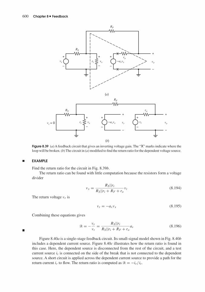
600 Chapter 8 � Feedback
RS
ri –avvxvs vx
+
–
+
–
ro
vo
+
–
+
–
(a)
RF
X
X
RS
ri –avvxvs = 0 vx
+
–vr
+
–
+
–
ro
vt vo
+
–
+
–
(b)
RF
Figure 8.39 (a) A feedback circuit that gives an inverting voltage gain. The “X” marks indicate where theloop will be broken. (b) The circuit in (a) modified to find the return ratio for the dependent voltage source.
EXAMPLE
Find the return ratio for the circuit in Fig. 8.39b.The return ratio can be found with little computation because the resistors form a voltage
divider
vx = RS ||riRS ||ri + RF + ro
vt (8.194)
The return voltage vr is
vr = −avvx (8.195)
Combining these equations gives
� = −vr
vt
= RS ||riRS ||ri + RF + ro
av (8.196)
Figure 8.40a is a single-stage feedback circuit. Its small-signal model shown in Fig. 8.40bincludes a dependent current source. Figure 8.40c illustrates how the return ratio is found inthis case. Here, the dependent source is disconnected from the rest of the circuit, and a testcurrent source it is connected on the side of the break that is not connected to the dependentsource. A short circuit is applied across the dependent current source to provide a path for thereturn current ir to flow. The return ratio is computed as � = −ir/it .

8.8 Feedback Circuit Analysis Using Return Ratio 601
(a)
RF = 20 kΩ
RC = 10 kΩ
iin
Q1
Vo
VDD
rπ roiin RC
gmvbevbe
+
–
vo
+
–
(b)
RF
X
X
ir
iπ
rπ = 5 kΩ ro = 1 MΩ RC = 10 kΩgmvbevbe
+
–
it vo
+
–
(c)
RF = 20 kΩ
gm = 40mAV
Figure 8.40 (a) A transresistance feedback circuit. (b) The small-signal model for the circuit in (a). The“X” marks indicate where the loop will be broken. (c) The circuit in (b) modified to find the return ratiofor the dependent current source.
8.8.1 Closed-Loop Gain Using Return Ratio
A formula for the closed-loop gain of a feedback amplifier in terms of the return ratio willnow be derived. Consider a feedback amplifier as shown in Fig. 8.41. The feedback amplifierconsists of linear elements: passive components, controlled sources, and transistor small-signalmodels. A controlled source with value k that is part of the small-signal model of an activedevice is shown explicitly. The output of the controlled source is soc, and the controlling signalis sic. The equation that describes the controlled source is
soc = ksic (8.197)
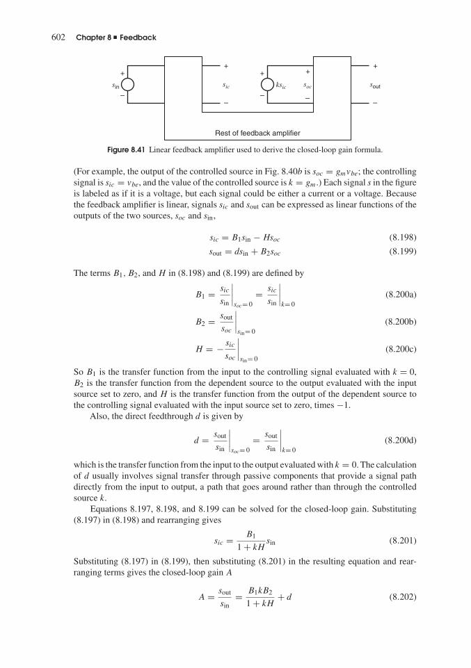
602 Chapter 8 � Feedback
+
–sin
+ +
–
sic
+
–ksic
–
sout
+
–
soc
Rest of feedback amplifier
Figure 8.41 Linear feedback amplifier used to derive the closed-loop gain formula.
(For example, the output of the controlled source in Fig. 8.40b is soc = gmvbe; the controllingsignal is sic = vbe, and the value of the controlled source is k = gm.) Each signal s in the figureis labeled as if it is a voltage, but each signal could be either a current or a voltage. Becausethe feedback amplifier is linear, signals sic and sout can be expressed as linear functions of theoutputs of the two sources, soc and sin,
sic = B1sin − Hsoc (8.198)
sout = dsin + B2soc (8.199)
The terms B1, B2, and H in (8.198) and (8.199) are defined by
B1 = sic
sin
∣∣∣∣soc= 0
= sic
sin
∣∣∣∣k= 0
(8.200a)
B2 = sout
soc
∣∣∣∣sin= 0
(8.200b)
H = − sic
soc
∣∣∣∣sin= 0
(8.200c)
So B1 is the transfer function from the input to the controlling signal evaluated with k = 0,B2 is the transfer function from the dependent source to the output evaluated with the inputsource set to zero, and H is the transfer function from the output of the dependent source tothe controlling signal evaluated with the input source set to zero, times −1.
Also, the direct feedthrough d is given by
d = sout
sin
∣∣∣∣soc= 0
= sout
sin
∣∣∣∣k= 0
(8.200d)
which is the transfer function from the input to the output evaluated with k = 0. The calculationof d usually involves signal transfer through passive components that provide a signal pathdirectly from the input to output, a path that goes around rather than through the controlledsource k.
Equations 8.197, 8.198, and 8.199 can be solved for the closed-loop gain. Substituting(8.197) in (8.198) and rearranging gives
sic = B1
1 + kHsin (8.201)
Substituting (8.197) in (8.199), then substituting (8.201) in the resulting equation and rear-ranging terms gives the closed-loop gain A
A = sout
sin= B1kB2
1 + kH+ d (8.202)

8.8 Feedback Circuit Analysis Using Return Ratio 603
The term kH in the denominator is equal to the return ratio, as will be shown next. The returnratio is found by setting sin = 0, disconnecting the dependent source from the circuit, andconnecting a test source st where the dependent source was connected. After these changes,soc = st and (8.198) becomes
sic = −Hst (8.203)
Then the output of the dependent source is the return signal sr = ksic = −kHst . Therefore
� = − sr
st= kH (8.204)
So the closed-loop gain in (8.202) can be rewritten as
A = sout
sin= B1kB2
1 + �+ d (8.205a)
or
A = sout
sin= g
1 + �+ d (8.205b)
where
g = B1kB2 (8.206)
Here g is the gain from sin to sout if H = 0 and d = 0, and d is the direct signal feedthrough,which is the value of A when the controlled source is set to zero (k = 0).
The closed-loop gain formula in (8.205a) requires calculations of four terms: B1, B2, d,and �. That equation can be manipulated into a more convenient form with only three terms.Combining terms in (8.205b) using a common denominator 1 + � gives
A = g + d(1 + �)
1 + �= g + d�
1 + �+ d
1 + �=
( g
�+ d)
�
1 + �+ d
1 + �(8.207)
Defining
A∞ = g
�+ d (8.208)
allows (8.207) to be rewritten as
A = A∞�
1 + �+ d
1 + �(8.209)
This is a useful expression for the closed-loop gain. Here, if � → ∞, then A = A∞ because�/(1 + �) → 1 and d/(1 + �) → 0. So A∞ is the closed-loop gain when the feedback circuitis ideal (that is, when � → ∞).
A block-diagram representation of (8.209) is shown in Fig. 8.42. The gain around thefeedback loop is �, and the effective forward gain in the loop is �A∞. A key differencebetween the two-port and return-ratio analyses can be seen by comparing Figs. 8.1 and 8.42.In the two-port analysis, all forward signal transfer through the amplifier and the feedbacknetwork is lumped into a. In the return-ratio analysis, there are two forward signal paths: one

604 Chapter 8 � Feedback
sin soutΣ Σ
1A∞
d
–
Figure 8.42 A block diagramfor the closed-loop gainformula in (8.209).
path (d) for the feedforward through the feedback network and another path (�A∞) for theeffective forward gain.
Typically, A∞ is determined by a passive feedback network and is equal to 1/f from two-port analysis. The value of A∞ can be found readily since A∞ = A when k → ∞. Lettingk → ∞ causes � = kH → ∞. (Here we assumed k > 0. If k < 0 in a negative feedbackcircuit, then � → ∞ when k → −∞.) When k → ∞, the controlling signal sic for the depen-dent source must be zero if the output of the dependent source is finite. The controlled sourceoutput will be finite if the feedback is negative. These facts can be used to find A∞ with littlecomputation in many circuits, as is demonstrated in the next example.
EXAMPLE
Compute the closed-loop gain for the circuit of Fig. 8.40 using (8.209). Use the componentvalues given in the figure.
To use (8.209), A∞, �, and d are needed. Here, the only controlled source is the gm
source, so k = gm. Also, sin = iin, sout = vo, and sic = vbe. To find A∞, let gm → ∞, whichforces the controlling voltage vbe to equal zero, assuming that the output current from the gm
generator is finite. With vbe = 0, no current flows through rπ, and therefore the input currentiin flows through RF to produce vo. Thus
A∞ = vo
iin
∣∣∣∣gm = ∞
= −RF = −20 k. (8.210)
Next, d is found by setting k = gm = 0 and computing the transfer function from input tooutput
d = vo
iin
∣∣∣∣gm = 0
= (ro||RC) · rπ
rπ + RF + ro||RC
= (1 M||10 k) · 5 k
5 k + 10 k + 1 M||100 k(8.211)
= 1.4 k
Finally, the return ratio for the gm generator can be calculated using Fig. 8.40c. Applying acurrent-divider formula gives the current iπ through rπ as
iπ = − ro||RC
ro||RC + RF + rπit (8.212)
The return current is
ir = gmvbe = gmrπiπ (8.213)

8.8 Feedback Circuit Analysis Using Return Ratio 605
Combining these equations gives
� = − ir
it= gmrπ · ro||RC
ro||RC + RF + rπ(8.214)
= (40 mA/V) · 5 k · 1 M||10 k
1 M||10 k + 20 k + 5 k= 56.7 (8.215)
Then, using (8.209),
A = A∞�
1 + �+ d
1 + �= −20 k
56.7
1 + 56.7+ 1.4 k
1 + 56.7= −19.6 k (8.216)
In (8.209), the second term that includes d can be neglected whenever |d| � |A∞�|. Thiscondition usually holds at low frequencies because d is the forward signal transfer through apassive network, while |A∞�| is large because it includes the gain through the active device(s).For example, ignoring the d/(1 + �) term in (8.216) gives A ≈ −19.7 k, which is close tothe exact value. As the frequency increases, however, the gain provided by the transistors falls.As a result, d may become significant at high frequencies.
The effective forward gain A∞� can be computed after A∞ and � have been found.Alternatively, this effective forward gain can be found directly from the feedback circuit.8 Callthis forward gain b, so
b = A∞ · � (8.217)
Then the closed-loop gain in (8.209) can be written as
A = b
1 + �+ d
1 + �(8.218)
Using (8.206), (8.208), and � = kH , b can be expressed as
b = A∞ · � =( g
�+ d)
· � = (B1kB2 + d�)
= (B1kB2 + dkH) =[B1 + dH
B2
]kB2 (8.219)
This final expression breaks b into parts that can be found by analyzing the feedback circuit.In (8.200b), B2 is defined as the transfer function from the output of the controlled source soc
to sout evaluated with sin = 0. The term in brackets in (8.219) is equal to the transfer functionfrom sin to sic when sout = 0, as will be shown next.
If sout = 0, then (8.199) simplifies to
B2soc = −dsin (8.220)
Substituting (8.220) into (8.198) gives
sic = B1sin + dH
B2sin (8.221)
Therefore
sic
sin
∣∣∣∣sout = 0
= B1 + dH
B2(8.222)

606 Chapter 8 � Feedback
r
RF
iin
vo = 0
vbe
+
–
(a)
π
r ro
RF
ioc
vo
vbe
+
–
(b)
RCπ
Figure 8.43 Circuits for finding theeffective forward gain b. (a) The circuitfor the input side. (b) The circuit for theoutput side.
which is the expression in brackets in (8.219). Substituting (8.222) and (8.200b) into (8.219)gives
b = sic
sin
∣∣∣∣sout = 0
· k · sout
soc
∣∣∣∣sin = 0
(8.223)
The effective forward gain b can be found using this formula.
EXAMPLE
Compute the effective forward gain b = A∞� for the circuit in Fig. 8.40.As in the previous example, k = gm, sin = iin, sout = vo, sic = vbe, and soc = ioc = gmvbe.
To compute the first term in (8.223), the output vo must be set to zero by shorting the outputto ground. The resulting circuit is shown in Fig. 8.43a. The calculation gives
sic
sin
∣∣∣∣sout = 0
= vbe
iin
∣∣∣∣vo = 0
= rπ||RF = 5 k||20 k = 4.0 k (8.224)
The last term in (8.223) is found by setting the input iin to zero. This input current can beset to zero by replacing the source iin with an open circuit, as shown in Fig. 8.43b. Treatingthe gm generator as an independent source with value ioc for this calculation, the result is
sout
soc
∣∣∣∣sin = 0
= vo
ioc
∣∣∣∣iin = 0
= −[ro||Rc||(RF + rπ)]
= −[1 M||10 k||(20 k + 5 k)] = −7.09 k (8.225)
Substituting (8.224) and (8.225) into (8.223) gives
b = 4.0 k(gm)(−7.09 k) = 4.0 k(40 mA/V)(−7.09 k) = −1134 k

8.8 Feedback Circuit Analysis Using Return Ratio 607
For comparison, we can find b using (8.217) and the values of A∞ and � computed in theprevious example:
b = A∞� = −20 k (56.7) = −1134 k
Both calculations give the same value for the effective forward gain b.
8.8.2 Closed-Loop Impedance Formula Using Return Ratio
Feedback affects the input and output impedance of a circuit. In this section, a useful expres-sion for the impedance at any port in a feedback circuit in terms of return ratio9 is derived.Consider the feedback circuit shown in Fig. 8.44. This feedback amplifier consists of linearelements: passive components, controlled sources, and transistor small-signal models. A con-trolled source k that is part of the small-signal model of an active device is shown explicitly.The derivation is carried out for the impedance Zport looking into an arbitrary port that islabeled as port X in Fig. 8.44a. The port impedance can be found by driving the port by anindependent current source as shown in Fig. 8.44b and computing Zport = vx/ix. Since thecircuit in Fig. 8.44b is linear, the signals sic and vx are linear functions of the signals ix and syapplied to the ports labeled X and Y. Therefore, we can write
vx = a1ix + a2sy (8.226)
sic = a3ix + a4sy (8.227)
From (8.226), the impedance looking into the port when k = 0 is
Zport(k = 0) = vx
ix
∣∣∣∣k = 0
= vx
ix
∣∣∣∣sy = 0
= a1 (8.228)
Next we compute two return ratios for the controlled source k under different conditions. Bothare used in the final formula for the closed-loop impedance. The first return ratio is found
+
–
vx
+
–
+
sic
ix
+
–ksic
–
sy
Rest of feedback amplifier
Port X
Zport
Port Y
(a)
+
–
vx
+ +
–
sici
ix
+
–ksic
–
sy
Rest of feedback amplifier
Port X
Port Y
(b)
Figure 8.44 (a) The linear feedback circuit used to derive Blackman’s impedance formula with respectto port X. (b) The circuit with port X driven by an independent current source.

608 Chapter 8 � Feedback
with the port open. With port X open, ix = 0. The return ratio is found by disconnecting thecontrolled source from the circuit and connecting a test source st where the dependent sourcewas connected. With these changes to the circuit, sy = st and (8.227) becomes
sic = a4st (8.229)
The output of the controlled source is the return signal
sr = ksic (8.230)
From the last two equations, we find
�(port open) = − sr
st= −ka4 (8.231)
The other return ratio is found with the port shorted. With port X shorted, the voltage vx
is zero. To find the return ratio, we disconnect the controlled source and connect test source stwhere the dependent source was connected. With these changes, (8.226) gives
ix = −a2
a1st (8.232)
Substituting (8.232) into (8.227), using sy = st , and rearranging terms gives
sic =(
a4 − a2a3
a1
)st (8.233)
The return signal is
sr = ksic (8.234)
Combining these last two equations gives the return ratio with the port shorted
�(port shorted) = − sr
st= −k
(a4 − a2a3
a1
)(8.235)
Shortly, we will see that (8.228), (8.231), and (8.235) can be combined to give a useful formulafor the port impedance.
To complete the derivation, we find the impedance looking into the port in Fig. 8.44busing
Zport = vx
ix(8.236)
Using (8.226), (8.227), and sy = ksic, we get (after some manipulation)
Zport = vx
ix= a1
⎛⎜⎜⎝
1 − k
(a4 − a2a3
a1
)1 − ka4
⎞⎟⎟⎠ (8.237)
Substituting (8.228), (8.231), and (8.235) into (8.237) yields
Zport = Zport(k = 0)
[1 + �(port shorted)
1 + �(port open)
](8.238)
This expression is called Blackman’s impedance formula.9 The two return ratios, with the portopen and shorted, are computed with respect to the same controlled source k. Equation 8.238

8.8 Feedback Circuit Analysis Using Return Ratio 609
can be used to compute the impedance at any port, including the input and output ports. A keyadvantage of this formula is that it applies to any feedback circuit, regardless of the type offeedback. Usually, one of the two return ratios in (8.238) is zero, and in those cases Blackman’sformula shows that feedback either increases or decreases the impedance by a factor (1 + �).
EXAMPLE
Use Blackman’s formula to find the output resistance for the feedback circuit in Fig. 8.40.From Blackman’s formula, the output resistance is given by
Rout = Rout(gm = 0)
[1 + �(output port shorted)
1 + �(output port open)
](8.239)
Shorting the output port in Fig. 8.40c causes vbe = 0 so ir = gmvbe = 0; therefore,�(output port shorted) = 0. The �(output port open) is the same return ratio that was com-puted in (8.215), so �(output port open) = 56.7. The only remaining value to be computed isthe resistance at the output port when gm = 0:
Rout(gm = 0) = ro||RC||(RF + rπ) = 1 M||10 k||(20 k + 5 k)
= 7.1 k (8.240)
Substituting into (8.239) yields
Rout = 7.1 k
[1 + 0
1 + 56.7
]= 120 (8.241)
The negative feedback reduces the output resistance, which is desirable because the output isa voltage, and a low output resistance is desired in series with a voltage source.
EXAMPLE
Find the output resistance for the MOS super-source follower shown in Fig. 8.45a. Ignorebody effect here to simplify the analysis.
The super-source follower uses feedback to reduce the output impedance. Ideal currentsources I1 and I2 bias the transistors and are shown rather than transistor current sourcesto simplify the circuit. With current source I1 forcing the current in M1 to be constant, M2provides the output current when driving a load. There is feedback from vout to vgs2 throughM1. The small-signal model for this circuit is shown in Fig. 8.45b. In this circuit, either gm1or gm2 could be chosen as k. Here, we will use k = gm2. In all the following calculations, theinput source vin is set to zero. First, the output resistance when gm2 = 0 is
Rout(gm2 = 0) = ro2 (8.242)
This result may seem surprising at first, since the output is connected to the source of M1, whichis usually a low-impedance point. However, an ideal current source, which is a small-signalopen circuit, is connected to the drain of M1. Therefore the current in the gm1 generator flowsonly in ro1, so M1 has no effect on the output resistance when gm2 = 0.
The return ratio for the gm2 source with the output port open is found to be
�(output open) = gm2ro2(1 + gm1ro1) (8.243)
The return ratio with the output port shorted is
�(output shorted) = 0 (8.244)

610 Chapter 8 � Feedback
(a)
Vin
Vout
VDD
M1
I2
I1
M2
I2 – I1
(b)
vin
vout
ro2gm2v2
ro1gm1v1
v2
+
–
+
–
v1
+
–
Figure 8.45 (a) The super-source-follower circuit. (b) The circuit with each transistor replaced by itssmall-signal model.
because shorting the output port forces vout = 0 and v1 = −vout = 0. Hence no current flowsin M1, so v2 = 0 and therefore the return ratio is zero. Substituting the last three equationsinto (8.238) gives the closed-loop output resistance
Rout = ro2
[1 + 0
1 + gm2ro2(1 + gm1ro1)
](8.245)
Assuming gmro � 1, then
Rout ≈ ro2
gm2ro2gm1ro1= 1
gm2gm1ro1(8.246)
which is much lower than the output resistance of a conventional source follower, which isabout 1/gm. This result agrees with (3.137), which was derived without the use of feedbackprinciples. Although gmb1 appears in (3.137), it does not appear in (8.246) because the bodyeffect is ignored here.
The next example demonstrates an unusual case where neither return ratio vanishes inBlackman’s impedance formula.
EXAMPLE
In the Wilson current source in Fig. 8.46a, assume that the three bipolar transistors are identicalwith β0 � 1 and are biased in the forward-active region. Find the output resistance.
Blackman’s impedance formula can be used here because there is a feedback loop formedby the current mirror Q1-Q3 with Q2. With all transistors forward active and βF � 1,

8.8 Feedback Circuit Analysis Using Return Ratio 611
(a)
Q2
Q1Q3
Io
IREF
VCC
(b)
Rout
r 2
vx
+
–
vy
+
–
ro2gm2vy
gm3vx1
gm1
π
(c)
rπ2
vx
+
–
vy
+
–
ro2gm2vy
it
ir
1gm1
Outputport
gm3vx
Figure 8.46 (a) The Wilson current mirror. (b) The circuit with each transistor replaced by itssmall-signal model. (c) The small-signal model modified for calculation of � for gm1.
IC1 = IC2 = IC3 = IREF . (The output is connected to other circuitry that is not shown, soIC2 is nonzero.) The small-signal model is shown in Fig. 8.46b, where diode-connected Q1 ismodeled by a resistor of value 1/gm1. Resistor rπ3, which is in parallel with 1/gm1, is ignored(since rπ3 = β0/gm3 = β0/gm1 � 1/gm1). Also ro3 is ignored, assuming that it is much largerthan the resistance looking into the base of Q2. Selecting k = gm3 and calculating the firstterm in (8.238) gives
Rout(gm3 = 0) = ro2 + 1
gm1≈ ro2 (8.247)
since setting gm3 = 0 forces the current through rπ2 to be zero. Therefore, the voltage acrossrπ2 is zero, which causes the current through the gm2 source to be zero.
The return ratios in Blackman’s formula can be found using the circuit shown inFig. 8.46c. First, let us find �(output port open). When the output port is open, the currentin the gm2 generator can only flow through the parallel resistor ro2, so the currents through rπ2and 1/gm1 are equal and are supplied by the test source it . Therefore,
vx = −it1
gm1(8.248)

612 Chapter 8 � Feedback
Also
ir = gm3vx (8.249)
Combining these two equations gives
�(output open) = − ir
it= gm3
gm1= 1 (8.250)
where gm1 = gm3 because IC1 = IC3.When the output port is shorted, the current through the gm2 generator is not restricted
to flow only through ro2. First, notice that with the output port shorted, ro2 is in parallel with1/gm1, so ro2 can be ignored. With this simplification, the current through the resistance 1/gm1is from the test and gm2 sources, so
vx = 1
gm1(−it + gm2vy) (8.251)
Now
vy = −itrπ2 (8.252)
Combining these two equations gives
vx = 1
gm1(−it − itgm2rπ2) = − it
gm1(1 + β0) (8.253)
where the relation β0 = gm2rπ2 has been used. The return current is
ir = gm3vx (8.254)
Therefore
�(output shorted) = − ir
it= gm3
gm1(1 + β0) = 1 + β0 (8.255)
Substituting in Blackman’s formula gives
Rout(closed loop) = ro2 · 1 + (β0 + 1)
1 + 1= ro2(β0 + 2)
2≈ β0ro2
2(8.256)
This approximate result agrees with (4.91), which was derived without the use of Blackman’sformula.
8.8.3 Summary—Return-Ratio Analysis
Return-ratio analysis is an alternative approach to feedback circuit analysis that does not usetwo-ports. The loop transmission is measured by the return ratio �. The return ratio is a differentmeasure of loop transmission than af from two-port analysis. (The return ratio � is referred toas loop gain in some textbooks. That name is not associated with � here to avoid confusion withT = af , which is called loop gain in this chapter.) For negative feedback circuits, � > 0. In anideal feedback circuit, � → ∞ and the closed-loop gain is A∞, which typically depends onlyon passive components. The actual gain of a feedback circuit is close to A∞ if � � 1. Black-man’s impedance formula (8.238) gives the closed-loop impedance in terms of two return ratios.
Return-ratio analysis is often simpler than two-port analysis of feedback circuits. Forexample, return-ratio analysis uses equations that are independent of the type of feedback, and

8.9 Modeling Input and Output Ports in Feedback Circuits 613
simple manipulations of the circuit allow computation of the various terms in the equations. Incontrast, two-port analysis uses different two-port representations for each of the four feedbackconfigurations (series-series, series-shunt, shunt-series, and shunt-shunt). Therefore, the typeof feedback must be correctly identified before undertaking two-port analysis. The resultingtwo-ports for the amplifier and feedback networks must be manipulated to find the open-loop forward gain a and the open-loop input and output impedances. With two-port analysis,the open-loop impedance is either multiplied or divided by (1 + T ) to give the closed-loopimpedance, depending upon the type of feedback. In contrast, Blackman’s formula gives anequation for finding the closed-loop impedance, and this one equation applies to any port inany feedback circuit.
8.9 Modeling Input and Output Ports in Feedback CircuitsThroughout this chapter, the source and load impedances have been included when analyzinga feedback circuit. For instance, the inverting voltage-gain circuit in Fig. 8.47a, with sourceresistance RS and load resistance RL, can be analyzed using the two-port or return-ratiomethods described in this chapter. The resulting model is shown in Fig. 8.47b. The source andload resistances do not appear explicitly in the model, but the gain A, input resistance Ri, andoutput resistance Ro are functions of the source and load resistances. Therefore, use of thismodel requires that both the source and load resistances are known. However, both the sourceand load are not always known or fixed in value. For example, a feedback amplifier might haveto drive a range of load resistances. In that case, it would be desirable to have a simple modelof the amplifier with the following properties: the elements in the model do not depend on theload, and the effect of a load on the gain can be easily calculated.
If only one of the resistances RS and RL is known, a useful model can be generated.First, consider Fig. 8.47a when the source resistance is unknown but the load is known. Then,the model in Fig. 8.47c can be used. Here, the key differences from the model in Fig. 8.47bare that R′
i and A′ are used rather than Ri and A, RS is shown explicitly, and the controllingvoltage for A′ is the voltage vi across R′
i rather than the source voltage vs. (The single-primemark here denotes that the quantity is computed with RS unknown.) The input resistance R′
i
and gain A′ are computed with the load connected and with an ideal input driving network.Here, the Thévenin driving network is ideal if the source resistance RS is zero. (If the input isa Norton equivalent consisting of a current source and parallel source resistance, R′
i and A′ arefound with RS → ∞.) The resulting A′ and R′
i are not functions of RS . The source resistanceRS in Fig. 8.47c forms a voltage divider with R′
i; therefore, the overall voltage gain can befound by
vo
vs
= vo
vi
· vi
vs
= A′ R′i
R′i + RS
(8.257)
Next, consider Fig. 8.47a when the load is unknown but the source resistance is known.Fig. 8.47d shows the appropriate model. Here, the key differences from the model in Fig. 8.47bare that R
′′o and A
′′are used rather than Ro and A, and RL is shown explicitly. (The double-
prime mark denotes that the quantity is computed with RL unknown.) The output resistanceR
′′o and gain A
′′for this Thévenin model are computed assuming an ideal load, which is an
open circuit here (RL → ∞). The load resistance RL in Fig. 8.47d forms a voltage dividerwith R
′′o, so the loaded voltage gain is
vo
vs
= A′′ RL
R′′o + RL
(8.258)

614 Chapter 8 � Feedback
RL
(a)
RF
RS
rovs
+
–
+
–
vi –avviri
+
–
vo
Ro
(b)
vs
vo+
–
+
–
AvsRi
(c)
RS Ro
vs
+
–
vi
+
–
+
–
+
–
A viRi vo' '
(d )
Ro
vs
+
–
+
–
A vsRi RL
vo
"
"
Figure 8.47 (a) Aninverting-gain feedbackamplifier. (b) A model for(a) based on feedbackanalysis with known loadand source resistances.(c) Another model for (a)based on known loadresistance and unknownsource resistance. (d) Adifferent model for (a)based on known sourceresistance and unknownload.
EXAMPLE
Model Fig. 8.47a with the circuit in Fig. 8.47d, assuming the load resistance is unknown.The model in Fig. 8.47d can be used when RL is unknown. Using return-ratio analysis, the
calculations of R′′o and A
′′are as follows. With RL → ∞, the circuit in Fig. 8.47a is identical
to Fig. 8.39a, and therefore the return ratio is given by (8.196):
�′′ = �(RL → ∞) = RS ||ri
RS ||ri + RF + roav (8.259)

Problems 615
The output resistance with RL → ∞, R′′o, can be found using Blackman’s formula. First, the
output resistance with the controlled source set to zero is
R′′o(av = 0) = ro||(RF + ri||RS) (8.260)
The return ratio with the output port open is given in (8.259). The return ratio with the outputport shorted is zero because shorting the output eliminates the feedback. Therefore, for theclosed-loop output resistance, (8.238) gives
R′′o = ro||(RF + ri||RS)
1 + 0
1 + RS ||riRS ||ri + RF + ro
av
(8.261)
Calculation of A′′
requires that A′′∞ and d
′′be found with RL → ∞.
A′′∞ = vo
vs
∣∣∣∣av = ∞ & RL = ∞
= −RF
RS
(8.262)
and
d′′ = vo
vs
∣∣∣∣av = 0 & RL = ∞
= (RF + ro)||riRS + (RF + ro)||ri · ro
RF + ro(8.263)
Using the results for A′′∞, �
′′, and d
′′, we can compute
A′′ = A
′′∞
�′′
1 + �′′ + d
′′
1 + �′′ (8.264)
[Typically, the d′′/(1 + �
′′) term is small and can be ignored.] The voltage gain when a resistive
load is connected can be found using (8.258). The only element of the model that was notcomputed is the input resistance Ri. It is a function of RL, so it can only be computed onceRL is known.
The output-port model in Fig. 8.47d could be drawn as a Thévenin or Norton equivalent.With the Thévenin equivalent shown (a controlled voltage source in series with an outputresistance), R
′′o and A
′′are computed with RL → ∞. When the output port is modeled by a
Norton equivalent with a controlled current source and parallel output resistance, their valuesare found with RL = 0.
PROBLEMSNote: In these problems, loop transmission is usedgenerically to refer to loop gain T = af or returnratio �.
8.1(a) In a feedback amplifier, forward gain a =100, 000 and feedback factor f = 10−3. Calculateoverall gain A and the percentage change in A if a
changes by 10 percent.
(b) Repeat (a) if f = 0.1.
8.2 For the characteristic of Fig. 8.2 the followingdata apply:
So2 = 15 V So1 = 7 V a1 = 50,000
a2 = 20,000
(a) Calculate and sketch the overall transfer char-acteristic of Fig 8.3 for the above amplifier whenplaced in a feedback loop with f = 10−4.
(b) Repeat (a) with f = 0.1.
8.3(a) For the conditions in Problem 8.2(b), sketchthe output voltage waveform So and the error volt-age waveform Sε if a sinusoidal input voltage Si withamplitude 1.5 V is applied.
(b) Repeat (a) with an input amplitude of 2 V.
8.4 Verify (8.40), (8.41), and (8.42) for a shunt-series feedback amplifier.
8.5 Verify (8.43), (8.44), and (8.45) for a series-series feedback amplifier.

616 Chapter 8 � Feedback
ii
vo
+
–
M1 5 kΩ
10 kΩ
M2 5 kΩ M3 5 kΩ
Figure 8.48 An ac schematic of a shunt-shunt feedback amplifier.
8.6 For the shunt-shunt feedback amplifier ofFig. 8.15a, take RF = 100 k and RL = 15 k. Forthe op amp, assume that Ri = 500 k, Ro = 200 ,and av = 75,000. Calculate input resistance, outputresistance, loop transmission, and closed-loop gain:
(a) Using the formulas from two-port analysis(Section 8.5).
(b) Using the formulas from return-ratio analysis(Section 8.8).
8.7 The ac schematic of a shunt-shunt feed-back amplifier is shown in Fig. 8.48. All transistorshave ID = 1 mA, W/L = 100, k′ = 60 �A/V2, andλ = 1/(50 V).
(a) Calculate the overall gain vo/ii, the looptransmission, the input impedance, and the outputimpedance at low frequencies. Use the formulas fromtwo-port analysis (Section 8.5).
(b) If the circuit is fed from a source resistanceof 1 k in parallel with ii, what is the new outputresistance of the circuit?
8.8(a) Repeat Problem 8.7(a) with all NMOS tran-sistors in Fig. 8.48 replaced by bipolar npn transistors.All collector currents are 1 mA and β = 200, VA =50 V, and rb = 0.
(b) If the circuit is fed from a source resistanceof 1 k in parallel with ii, what is the new outputresistance of the circuit?
8.9 Repeat Problem 8.7 using the formulas fromreturn-ratio analysis (Section 8.8).
8.10 Repeat Problem 8.8 using the formulas fromreturn-ratio analysis (Section 8.8).
8.11 The half-circuit of a balanced monolithicseries-series triple is shown in Fig. 8.18a. Calculatethe input impedance, output impedance, loop gain, andoverall gain of the half-circuit at low frequencies usingthe following data:
RE1 = RE2 = 290 RF = 1.9 k
RL1 = 10.6 k RL2 = 6 k
For the transistors, IC1 = 0.5 mA, IC2 = 0.77 mA,IC3 = 0.73 mA, β = 120, rb = 0, and VA = 40 V.
8.12 Repeat Problem 8.11 if the output signal istaken as the voltage at the emitter of Q3.
8.13 A feedback amplifier is shown in Fig. 8.49.Device data are as follows: βnpn = 200, βpnp = 100,|VBE(on)| = 0.7 V, rb = 0, and |VA| = ∞. If the dcinput voltage is zero, calculate the overall gain vo/vi,the loop gain, and the input and output impedance atlow frequencies. Compare your answers with a SPICEsimulation.Also use SPICE to plot the complete large-signal transfer characteristic and find the second andthird harmonic distortion in vo for a sinusoidal inputvoltage with peak-peak amplitude of 0.5 V at vi.
Q1 Q2
Q3
vi
+
–
vo
+
–
1.25 kΩ
10 kΩ
+6 V
–6 V
5 kΩ
1 kΩ6 kΩ
Figure 8.49 Feedback amplifier circuit.

Problems 617
Q1
Q2
Q4
Q3
vi
+
–
500 Ω
500 Ω
500 Ω
500 Ω
78 Ω 280 Ω
+3 V
–3 V
+3 V
50 Ω
50 Ω
200 Ω
200 Ω
vo
+
–
Figure 8.50 Balanced series-shuntfeedback amplifier.
8.14 Replace npn transistors Q1-Q2 in Fig. 8.49with NMOS transistors M1-M2, and replace the pnp
transistor Q3 with PMOS transistor M3. Also, replacethe 1.25 k resistor in the drain of M1 with a 4.35 k
resistor. Repeat the calculations and simulations inProblem 8.13. For all transistors, use W/L = 100,γ = 0, and |λ| = 0. Also, Vtn = −Vtp = 1 V, k′
n =60 �A/V2, and k′
p = 20 �A/V2.
8.15 A balanced monolithic series-shunt feedbackamplifier is shown in Fig. 8.50.
(a) If the common-mode input voltage is zero, cal-culate the bias current in each device. Assume that βF
is large.
(b) Calculate the voltage gain, input impedance,output impedance, and loop gain of the circuit at lowfrequencies using the following data:
β = 100 rb = 50 VA = ∞ VBE(on) = 0.7 V
(c) Compare your answers with a SPICE simu-lation (omit the loop gain) and also use SPICE toplot the complete large-signal transfer characteris-tic. If the resistors have a temperature coefficient of+1000 ppm/◦C, use SPICE to determine the temper-ature coefficient of the circuit gain over the range−55◦C to +125◦C.
8.16 How does the loop gain T = af of the circuitof Fig. 8.50 change as the following circuit elementschange? Discuss qualitatively.
(a) 50 emitter resistor of the input stage
(b) 500 feedback resistor
(c) 200 load resistor on the output
8.17 The ac schematic of a shunt-series feedbackamplifier is shown in Fig. 8.31. Element values areRF = 1 k, RE = 100 , RL1 = 4 k, RS = 1/yS =1 k, and zL = 0. Device data: β = 200, rb = 0,IC1 = IC2 = 1 mA, VA = 100 V.
(a) Calculate the overall gain io/ii, the loop trans-mission, and the input and output impedances at lowfrequencies.
(b) If the value of RL1 changes by +10 percent,what is the approximate change in overall transmisionand input impedance?
8.18(a) Repeat Problem 8.17(a) with RF = 5 k,RE = 200 , RL1 = 10 k, and ys = 0.
(b) If the collector current of Q1 increases by 20percent, what will be the approximate change in over-all gain and output resistance?
8.19 Calculate the transconductance, input im-pedance, output impedance, and loop transmissionat low frequencies of the local series-feedback stageof Fig. 8.34 with parameters RE = 200 , β = 150,IC = 1 mA, rb = 200 , and VA = 80 V.
8.20 Acommercial wideband monolithic feedbackamplifier (the 733) is shown in Fig. 8.51. This consistsof a local series-feedback stage feeding a two-stageshunt-shunt feedback amplifier. The current output of
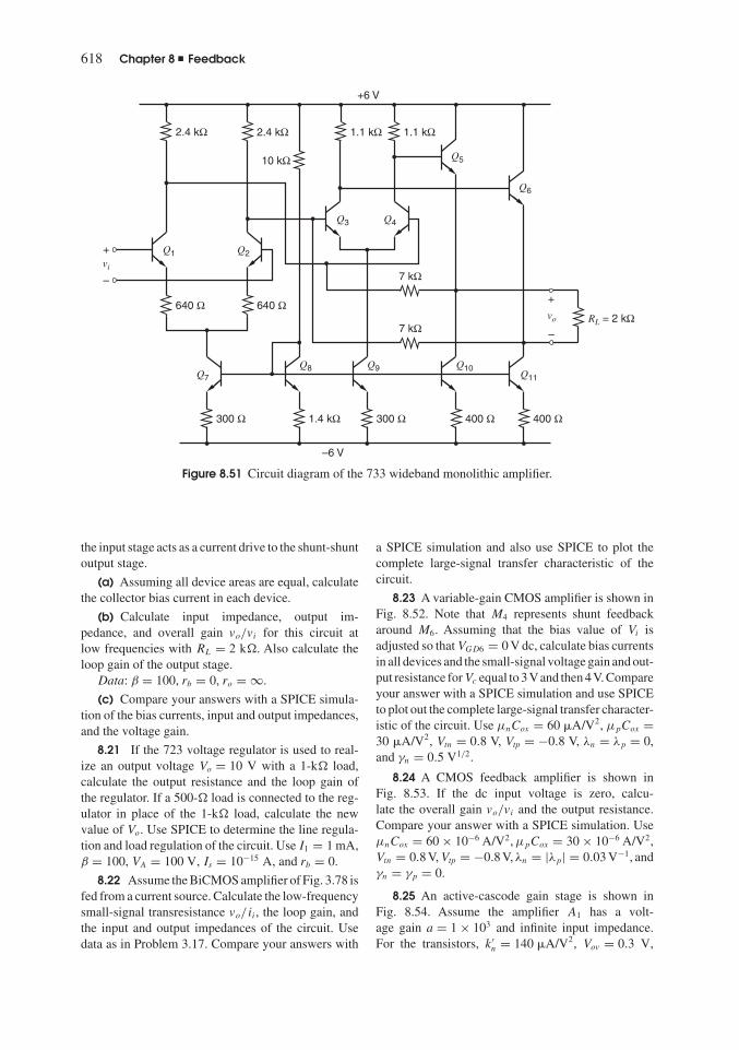
618 Chapter 8 � Feedback
Q11
vi
+
–
7 kΩ
7 kΩ
400 Ω
Q10
400 Ω
Q9
RL = 2 kΩ
300 Ω
Q8
1.4 kΩ
1.1 kΩ1.1 kΩ
10 kΩ
2.4 kΩ2.4 kΩ
Q7
Q3
Q6
Q5
Q4
Q1 Q2
300 Ω
640 Ω 640 Ωvo
+
–
+6 V
–6 V
Figure 8.51 Circuit diagram of the 733 wideband monolithic amplifier.
the input stage acts as a current drive to the shunt-shuntoutput stage.
(a) Assuming all device areas are equal, calculatethe collector bias current in each device.
(b) Calculate input impedance, output im-pedance, and overall gain vo/vi for this circuit atlow frequencies with RL = 2 k. Also calculate theloop gain of the output stage.
Data: β = 100, rb = 0, ro = ∞.
(c) Compare your answers with a SPICE simula-tion of the bias currents, input and output impedances,and the voltage gain.
8.21 If the 723 voltage regulator is used to real-ize an output voltage Vo = 10 V with a 1-k load,calculate the output resistance and the loop gain ofthe regulator. If a 500- load is connected to the reg-ulator in place of the 1-k load, calculate the newvalue of Vo. Use SPICE to determine the line regula-tion and load regulation of the circuit. Use I1 = 1 mA,β = 100, VA = 100 V, Is = 10−15 A, and rb = 0.
8.22 Assume the BiCMOS amplifier of Fig. 3.78 isfed from a current source. Calculate the low-frequencysmall-signal transresistance vo/ii, the loop gain, andthe input and output impedances of the circuit. Usedata as in Problem 3.17. Compare your answers with
a SPICE simulation and also use SPICE to plot thecomplete large-signal transfer characteristic of thecircuit.
8.23 A variable-gain CMOS amplifier is shown inFig. 8.52. Note that M4 represents shunt feedbackaround M6. Assuming that the bias value of Vi isadjusted so that VGD6 = 0 V dc, calculate bias currentsin all devices and the small-signal voltage gain and out-put resistance forVc equal to 3Vand then 4V. Compareyour answer with a SPICE simulation and use SPICEto plot out the complete large-signal transfer character-istic of the circuit. Use μnCox = 60 �A/V2, μpCox =30 �A/V2, Vtn = 0.8 V, Vtp = −0.8 V, λn = λp = 0,and γn = 0.5 V1/2.
8.24 A CMOS feedback amplifier is shown inFig. 8.53. If the dc input voltage is zero, calcu-late the overall gain vo/vi and the output resistance.Compare your answer with a SPICE simulation. UseμnCox = 60 × 10−6 A/V2, μpCox = 30 × 10−6 A/V2,Vtn = 0.8 V, Vtp = −0.8 V, λn = |λp| = 0.03 V−1, andγn = γp = 0.
8.25 An active-cascode gain stage is shown inFig. 8.54. Assume the amplifier A1 has a volt-age gain a = 1 × 10³ and infinite input impedance.For the transistors, k′
n = 140 �A/V2, Vov = 0.3 V,

Problems 619
Vi
Vo
Vc
VDD = 5 V
M2
M3
M4
M5
M6M1
R110 kΩ
+
–+
–
+
–
201
201
201
52
201 20
1
Figure 8.52 Variable-gain CMOS amplifier for Problem 8.23.
vi
VDD = 5 V
VSS = –5 V
M4
M1 M2
M3
M6M5
+
–
vo
+
–
201
401
M7
401
201
M8401
201
401
401
I1100 μA
R21 kΩ
R120 kΩ
Figure 8.53 CMOS feedback amplifier for Problem 8.24.
γ = 0, and λn = 0.03 V−1. Assume all transistors areactive. Calculate the output resistance using Black-man’s impedance formula. Then calculate the voltagegain vo/vi.
8.26 Use Blackman’s impedance formula to findthe output resistance of the active-cascode currentsource in Fig. 8.55. Express the result in terms of gm1,gm2, ro1, ro2, and a, which is the voltage gain of the opamp. Assume all transistors are active with (W/L)1 =(W/L)2 = (W/L)3 and γ = 0. (The drain of M2 con-nects to other circuitry that is not shown.)Also, assume
that the op amp has infinite input impedance and zerooutput impedance.
(a) Carry out the calculations with respect to con-trolled source gm2.
(b) Repeat the calculations with respect to thevoltage-controlled voltage source a in the amplifier.
(c) Compare the results of (a) and (b).
8.27 Use return-ratio analysis and Blackman’simpedance formula to find the closed-loop gain, return

620 Chapter 8 � Feedback
VBIAS
VDD
M1
Vi
M2A1
Vo
+
+
– –
+
–
100 μA
Figure 8.54 An active-cascode gain stage.
VBIAS
Rout
R
VDD
–VSS
M1M3
M2a+
–
Figure 8.55 An active-cascodecurrent source.
ratio, input resistance, and output resistance for theinverting gain amplifier in Fig. 8.56. For the opamp, assume that Ri = 1 M, Ro = 10 k, andav = 200.
8.28 An ac schematic of a local shunt-shunt feed-back circuit is shown in Fig. 8.57. Take RF = 100 k
and RL = 15 k. For the MOS transistor, ID =0.5 mA, W/L = 100, k′ = 180 �A/V2, and ro = ∞.
Ri
Ro
avvxvxvi
+
–
vo
+
–
+
–
+
–
10 kΩ
100 kΩ
Figure 8.56 An inverting feedbackamplifier.

Problems 621
ii
RL
RF
vo
+
–
Figure 8.57 A local shunt-shunt feedback amplifier.
Calculate input resistance, output resistance, looptransmission, and closed-loop gain:
(a) Using the formulas from two-port analysis(Section 8.5).
(b) Using the formulas from return-ratio analysis(Section 8.8).
8.29 Replace the MOS transistor in Fig. 8.57 bya npn transistor. Take RF = 2 k, RL = 2 k, β =200, IC = 1 mA, rb = 0, and VA = 100 V.
(a) Repeat Problem 8.28(a).
(b) Repeat Problem 8.28(b).
8.30 A voltage-follower feedback circuit is shownin Fig. 8.58. For the MOS transistor, ID =0.5 mA, k′ = 180 �A/V2, ro = ∞, W/L = 100,|φf | = 0.3 V, and γ = 0.3 V1/2. For the op amp,assume that Ri = 1 M, Ro = 10 k, and av =1,000. Calculate input resistance, output resistance,loop transmission, and closed-loop gain:
(a) Using the formulas from two-port analysis(Section 8.5).
(b) Using the formulas from return-ratio analysis(Section 8.8).
8.31 Replace the MOS transistor in Fig. 8.58 witha npn transistor. For the transistor, IC = 0.5 mA andro = ∞.
(a) Repeat the calculations in Problem 8.30(a).
(b) Repeat the calculations in Problem 8.30(b).
8.32 For the noninverting amplifier shown inFig. 8.59, R1 = 1 k, and R2 = 5 k. For the opamp, take Ri = 1 M, Ro = 100 , and av = 1 ×10⁴. Calculate input resistance, output resistance, looptransmission, and closed-loop gain:
(a) Using the formulas from two-port analysis(Section 8.5).
(b) Using the formulas from return-ratio analysis(Section 8.8).
8.33 Calculation of return ratio begins by break-ing a feedback loop at a controlled source. However,breaking a feedback loop at a controlled source isoften impossible in a SPICE simulation because thecontrolled source (e.g., the gm source in a transistor’ssmall-signal model) is embedded in a small-signalmodel. Therefore, it cannot be accessed or discon-nected in simulation. A technique that can be used tosimulate the return ratio with SPICE is illustrated inFig. 8.60 for the circuit in Fig. 8.59. First, the indepen-dent source Vi is set to zero. Next, ac test signals vt and
Vo
Vi
ID
VDD
+
– +
–
+
–
Figure 8.58 A voltage follower.
VoVi
R1
R2
+
–
+
–
+
–
X
Figure 8.59 A noninverting feedback amplifier.

622 Chapter 8 � Feedback
it
id im
R1
R2
+
–
X
(a)Figure 8.60 The feedback circuit in Fig. 8.59modified to calculate (a) �′
i and (b) �′v .
R1
R2
+
–
X
(b)
vd
vt+
+ –
–
vm
+
–
it are injected into the loop at a convenient point (e.g.,at the “X” in Fig. 8.59), creating two modified ver-sions of the circuit as shown in Fig. 8.60a and 8.60b.Using Fig. 8.60a, calculate �′
i = −im/id . UsingFig. 8.60b, calculate �′
v = −vm/vd . The amplitudesof test signals it and vt do not affect �′
i or �′v . Also,
these ac test signals do not affect the dc operatingpoint of the feedback circuit. The return ratio � forthe controlled source is related to �′
i and �′v by10
1
1 + �= 1
1 + �′i
+ 1
1 + �′v
(a) Compute �′i and �′
v for the circuit in Fig.8.60. Use element values from Problem 8.32. Then
combine these values using the equation above tofind �.
(b) Compute � directly by breaking the loop atthe av controlled source. Compare the results in (a)and (b).
(c) Carry out a SPICE simulation to find �′i
and �′v . Then combine these values using the equa-
tion above to find �. Compare with your resultsfrom (a).
8.34(a) Calculate the loop gain T = af for theseries-shunt feedback circuit in Fig. 8.59 using h-parameter two-ports. Take R1 = 200 k, and R2 =100 k. For the op amp, assume Ri = 50 k, Ro =1 M, and av = 1 × 10³.
R1
R2
+
–
VoIi
+
–Figure 8.61 The feedback circuit in Fig. 8.59with a different input-signal source.

References 623
(b) If the input source location and type in Fig.8.59 are changed as shown in Fig. 8.61, the feedbackis now shunt-shunt. Calculate the loop gain T = af
for this shunt-shunt feedback circuit usingy-parametertwo-ports. Use the element values in (a).
(c) Calculate the return ratio � for the circuit inFig. 8.61, again using the element values in (a). Thisreturn ratio is the same as the return ratio for the circuitin Fig. 8.59. Why?
(d) Compare the results in (a), (b), and (c).
REFERENCES1. C. A. Desoer and E. S. Kuh, Basic Circuit
Theory, McGraw-Hill, New York, 1969.2. J. E. Solomon and G. R. Wilson, “A Highly
Desensitized, Wideband Monolithic Amplifier,” IEEEJ. Solid State Circuits, Vol. SC-1, pp. 19–28,September 1966.
3. A. B. Grebene, Analog Integrated CircuitDesign, Van Nostrand Reinhold, New York, 1972,Chapter 6.
4. R. S. Muller and T. I. Kamins, Device Elec-tronics for Integrated Circuits, Wiley, New York,1977.
5. H. W. Bode, Network Analysis and FeedbackAmplifier Design, Van Nostrand, New York, 1945.
6. E. S. Kuh and R. A. Rohrer, Theory of LinearActive Networks, Holden-Day, San Francisco, 1967.
7. S. Rosenstark, Feedback Amplifier Principles,MacMillan, New York, 1986.
8. B. Nikolic and S. Marjanovic, “A Gen-eral Method of Feedback Amplifier Analysis,” IEEEInt’l Symp. on Circuits and Systems, pp. 415–418,Monterey, CA, 1998.
9. R. B. Blackman, “Effect of Feedback onImpedance,” Bell Sys. Tech. J., Vol. 23, pp. 269–277,October 1943.
10. R. D. Middlebrook, “Measurement of LoopGain in Feedback Systems,” Int. J. Electronics,Vol. 38, no. 4, pp. 485–512, 1975.

CHAPTER 9
Frequency Response andStability of FeedbackAmplifiers
9.1 IntroductionIn Chapter 8, we considered the effects of negative feedback on circuit parameters such as gainand terminal impedance. We saw that application of negative feedback resulted in a numberof performance improvements, such as reduced sensitivity of gain to active-device parameterchanges and reduction of distortion due to circuit nonlinearities.
In this chapter, we see the effect of negative feedback on the frequency response of a circuit.The possibility of oscillation in feedback circuits is illustrated, and methods of overcomingthese problems by compensation of the circuit are described. Finally, the effect of compensationon the large-signal high-frequency performance of feedback amplifiers is investigated.
Much of the analysis in this chapter is based on the ideal block diagram in Fig. 9.1. Thisblock diagram includes the forward gain a and feedback factor f, which are the parameters usedin two-port analysis of feedback circuits in Chapter 8. The equations and results in this chaptercould be expressed in terms of the parameters used in the return-ratio analysis in Chapter 8 byan appropriate change of variables, as shown in Appendix A9.1.
The equations and relationships in this chapter are general and can be applied to anyfeedback circuit. However, for simplicity we will often assume the feedback factor f is apositive, unitless constant. One circuit that has such an f is the series-shunt feedback circuitshown in Fig 8.24. In this circuit, the feedback network is a resistive voltage divider, so fis a constant with 0 ≤ f ≤ 1. The forward gain a is a voltage gain that is positive at lowfrequencies. This circuit gives a noninverting closed-loop voltage gain.
9.2 Relation Between Gain and Bandwidth in FeedbackAmplifiersChapter 8 showed that the performance improvements produced by negative feedback wereobtained at the expense of a reduction in gain by a factor (1 + T ), where T is the loop gain.The performance specifications that were improved were also changed by the factor (1 + T ).
In addition to the foregoing effects, negative feedback also tends to broadband the ampli-fier. Consider first a feedback circuit as shown in Fig. 9.1 with a simple basic amplifier whosegain function contains a single pole
a(s) = a0
1 − s
p1
(9.1)
624

9.2 Relation Between Gain and Bandwidth in Feedback Amplifiers 625
f
a(s)vi vo
v
vfb
+
–
Figure 9.1 Feedback circuitconfiguration.
where a0 is the low-frequency gain of the basic amplifier and p1 is the basic-amplifier pole inradians per second. Assume that the feedback path is purely resistive and thus the feedbackfunction f is a positive constant. Since Fig. 9.1 is an ideal feedback arrangement, the overallgain is
A(s) = vo
vi
= a(s)
1 + a(s)f(9.2)
where the loop gain is T (s) = a(s)f . Substitution of (9.1) in (9.2) gives
A(s) =
a0
1 − s
p1
1 + a0f
1 − s
p1
= a0
1 − s
p1+ a0f
= a0
1 + a0f
1
1 − s
p1
1
1 + a0f
(9.3)
From (9.3) the low-frequency gain A0 is
A0 = a0
1 + T0(9.4)
where
T0 = a0f = low-frequency loop gain (9.5)
The −3-dB bandwidth of the feedback circuit (i.e., the new pole magnitude) is (1 + aof ) · |p1|from (9.3). Thus the feedback has reduced the low-frequency gain by a factor (1 + T0), which isconsistent with the results of Chapter 8, but it is now apparent that the −3-dB frequency of thecircuit has been increased by the same quantity (1 + T0). Note that the gain-bandwidth productis constant. These results are illustrated in the Bode plots of Fig. 9.2, where the magnitudes of
Gain magnitude dB
20 log10 a0
20 log10 |a( j )|
20 log10 |A( j )|20 log10
| p1 |(1 + T0) | p1 |
a0
1 + T0
log scale
–6 dB/octave
ω
ω
ω
Figure 9.2 Gain magnitude versus frequency for the basic amplifier and the feedback amplifier.

626 Chapter 9 � Frequency Response and Stability of Feedback Amplifiers
(1 + T0) p1
T0 = 0
p1
σ
j
X
Pole positionfor finite T0
s plane
ω
Figure 9.3 Locus of the pole of thecircuit of Fig. 9.1 as loop gain T0
varies.
a(jω) and A(jω) are plotted versus frequency on log scales. It is apparent that the gain curvesfor any value of T0 are contained in an envelope bounded by the curve of |a(jω)|.
Because the use of negative feedback allows the designer to trade gain for bandwidth,negative feedback is widely used as a method for designing broadband amplifiers. The gainreduction that occurs is made up by using additional gain stages, which in general are alsofeedback amplifiers.
Let us now examine the effect of the feedback on the pole of the overall transfer functionA(s). It is apparent from (9.3) that as the low-frequency loop gain T0 is increased, the magnitudeof the pole of A(s) increases. This is illustrated in Fig. 9.3, which shows the locus of the poleof A(s) in the s plane as T0 varies. The pole starts at p1 for T0 = 0 and moves out alongthe negative real axis as T0 is made positive. Figure 9.3 is a simple root-locus diagram andwill be discussed further in Section 9.5.
9.3 Instability and the Nyquist Criterion1
In the above simple example the basic amplifier was assumed to have a single-pole trans-fer function, and this situation is closely approximated in practice by internally compensatedgeneral-purpose op amps. However, many amplifiers have multipole transfer functions thatcause deviations from the above results. The process of compensation overcomes these prob-lems, as will be seen later.
Consider an amplifier with a three-pole transfer function
a(s) = a0(1 − s
p1
)(1 − s
p2
)(1 − s
p3
) (9.6)
where |p1|, |p2|, and |p3| are the pole magnitudes in rad/s. The poles are shown in the s planein Fig. 9.4 and gain magnitude |a(jω)| and phase ph a(jω) are plotted versus frequency inFig. 9.5 assuming about a factor of 10 separation between the poles. Only asymptotes are
p1
σ
jω
Xp2
Xp3
X
s plane
Figure 9.4 Poles of an amplifier inthe s plane.

9.3 Instability and the Nyquist Criterion 627
(a)
(b)
20 log10 a0
|a( j )| dB
Ph a( j )
| p1| | p2 | | p3 | log scale
ω180
ω180
a180
–18 dB/octave
–6 dB/octave
–12 dB/octave
–270°
–225°
–180°
–135°
–90°
–45°
ω
ω
ω
log scaleω
Figure 9.5 Gain and phase versus frequency for a circuit with a three-pole transfer function.
shown for the magnitude plot. At frequencies above the first pole magnitude |p1|, the plotof |a(jω)| falls at 6 dB/octave and ph a(jω) approaches −90◦. Above |p2| these become 12dB/octave and −180◦, and above |p3| they become 18 dB/octave and −270◦. The frequencywhere ph a(jω) = −180◦ has special significance and is marked ω180, and the value of |a(jω)|at this frequency is a180. If the three poles are fairly widely separated (by a factor of 10 ormore), the phase shifts at frequencies |p1|, |p2|, and |p3| are approximately −45◦, −135◦, and−225◦, respectively. This will now be assumed for simplicity. In addition, the gain magnitudewill be assumed to follow the asymptotic curve and the effect of these assumptions in practicalcases will be considered later.
Now consider this amplifier connected in a feedback loop as in Fig. 9.1 with f a positiveconstant. Since f is constant, the loop gain T (jω) = a(jω)f will have the same variation withfrequency as a(jω). A plot of af (jω) = T (jω) in magnitude and phase on a polar plot (with ω
as a parameter) can thus be drawn using the data of Fig. 9.5 and the magnitude of f. Such a plotfor this example is shown in Fig. 9.6 (not to scale) and is called a Nyquist diagram. The variableon the curve is frequency and varies from ω = −∞ to ω = ∞. For ω = 0, |T (jω)| = T0 andph T (jω) = 0, and the curve meets the real axis with an intercept T0. As ω increases, asFig. 9.5 shows, |a(jω)| decreases and ph a(jω) becomes negative and thus the plot is in thefourth quadrant. As ω → ∞, ph a(jω) → −270◦ and |a(jω)| → 0. Consequently, the plot isasymptotic to the origin and is tangent to the imaginary axis. At the frequency ω180 the phase is−180◦ and the curve crosses the negative real axis. If |a(jω180)f | > 1 at this point, the Nyquistdiagram will encircle the point (−1, 0) as shown, and this has particular significance, as will
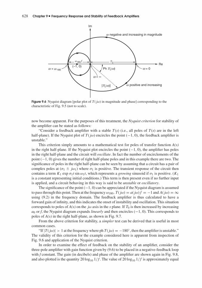
628 Chapter 9 � Frequency Response and Stability of Feedback Amplifiers
T0a180 f
Im
(–1, 0)
= ∞
= 0 = 180
RePh T( j )
|T( j )|
negative and increasing in magnitude
positive and increasing
ωωω
ω
ω
ω
ω
ω
Figure 9.6 Nyquist diagram [polar plot of T (jω) in magnitude and phase] corresponding to thecharacteristic of Fig. 9.5 (not to scale).
now become apparent. For the purposes of this treatment, the Nyquist criterion for stability ofthe amplifier can be stated as follows:
“Consider a feedback amplifier with a stable T (s) (i.e., all poles of T (s) are in the lefthalf-plane). If the Nyquist plot of T (jω) encircles the point (−1, 0), the feedback amplifier isunstable.”
This criterion simply amounts to a mathematical test for poles of transfer function A(s)in the right half-plane. If the Nyquist plot encircles the point (−1, 0), the amplifier has polesin the right half-plane and the circuit will oscillate. In fact the number of encirclements of thepoint (−1, 0) gives the number of right half-plane poles and in this example there are two. Thesignificance of poles in the right half-plane can be seen by assuming that a circuit has a pair ofcomplex poles at (σ1 � jω1) where σ1 is positive. The transient response of the circuit thencontains a term K1 exp σ1t sin ω1t, which represents a growing sinusoid if σ1 is positive. (K1is a constant representing initial conditions.) This term is then present even if no further inputis applied, and a circuit behaving in this way is said to be unstable or oscillatory.
The significance of the point (−1, 0) can be appreciated if the Nyquist diagram is assumedto pass through this point. Then at the frequency ω180, T (jω) = a(jω)f = −1 and A(jω) = ∞using (9.2) in the frequency domain. The feedback amplifier is thus calculated to have aforward gain of infinity, and this indicates the onset of instability and oscillation. This situationcorresponds to poles of A(s) on the jω axis in the s plane. If T0 is then increased by increasinga0 or f, the Nyquist diagram expands linearly and then encircles (−1, 0). This corresponds topoles of A(s) in the right half-plane, as shown in Fig. 9.7.
From the above criterion for stability, a simpler test can be derived that is useful in mostcommon cases.
“If |T (jω)| > 1 at the frequency where ph T (jω) = −180◦, then the amplifier is unstable.”The validity of this criterion for the example considered here is apparent from inspection ofFig. 9.6 and application of the Nyquist criterion.
In order to examine the effect of feedback on the stability of an amplifier, consider thethree-pole amplifier with gain function given by (9.6) to be placed in a negative-feedback loopwith f constant. The gain (in decibels) and phase of the amplifier are shown again in Fig. 9.8,and also plotted is the quantity 20 log10 1/f . The value of 20 log10 1/f is approximately equal

9.3 Instability and the Nyquist Criterion 629
XX
XX
σ
ωj
s plane
Nyquist diagram passesthrough (–1, 0) whenpoles are here
Nyquist diagramencircles (–1, 0) whenpoles are here
Figure 9.7 Pole positions corresponding to different Nyquist diagrams.
20 log10a0
|a( j )| dB
|a( j )|
Ph a( j )
| p1 | | p2 | | p3 | log scale
0
Phase margin
x = Loop gain in dB
Loop gain = 0 dB
–270°
–225°
–180°
–135°
–90°
–45°
x20 log10 ≈ 20 log10A0
1f
ω
ω
ω
0ω
ω
ω
ω
Figure 9.8 Amplifier gain and phase versus frequency showing the phase margin.
to the low-frequency gain in decibels with feedback applied since
A0 = a0
1 + a0f(9.7)
and thus
1
f≈ A0 (9.8)

630 Chapter 9 � Frequency Response and Stability of Feedback Amplifiers
if
T0 = a0f � 1
Consider the vertical distance between the curve of 20 log10 |a(jω)| and the line20 log10 1/f in Fig. 9.8. Since the vertical scale is in decibels this quantity is
x = 20 log10 |a(jω)| − 20 log10 1/f(9.9)
= 20 log10 |a(jω)f |= 20 log10 |T (jω)| (9.10)
Thus the distance x is a direct measure in decibels of the loop-gain magnitude, |T (jω)|.The point where the curve of 20 log10 |a(jω)| intersects the line 20 log10 1/f is the point wherethe loop-gain magnitude |T (jω)| is 0 dB or unity, and the curve of |a(jω)| in decibels inFig. 9.8 can thus be considered a curve of |T (jω)| in decibels if the dotted line at 20 log10 1/f
is taken as the new zero axis.The simple example of Section 9.1 showed that the gain curve versus frequency with
feedback applied (20 log10 |A(jω)|) follows the 20 log10 A0 line until it intersects the gaincurve 20 log10 |a(jω)|. At higher frequencies the curve 20 log10 |A(jω)| simply follows thecurve of 20 log10 |a(jω)| for the basic amplifier. The reason for this is now apparent in that atthe higher frequencies the loop gain |T (jω)| → 0 and the feedback then has no influence onthe gain of the amplifier.
Figure 9.8 shows that the loop-gain magnitude |T (jω)| is unity at frequency ω0. At thisfrequency the phase of T (jω) has not reached −180◦ for the case shown, and using themodified Nyquist criterion stated above we conclude that this feedback loop is stable. Obvi-ously |T (jω)| < 1 at the frequency where ph T (jω) = −180◦. If the polar Nyquist diagram issketched for this example, it does not encircle the point (−1, 0).
As |T (jω)| is made closer to unity at the frequency where ph T (jω) = −180◦, the amplifierhas a smaller margin of stability, and this can be specified in two ways. The most common isthe phase margin, which is defined as follows:
Phase margin = 180◦+ (ph T (jω) at frequency where |T (jω)| = 1). The phase margin isindicated in Fig. 9.8 and must be greater than 0◦ for stability.
Another measure of stability is the gain margin. This is defined to be 1/|T (jω)| in decibelsat the frequency where ph T (jω) = −180◦, and this must be greater than 0 dB for stability.
The significance of the phase-margin magnitude is now explored. For the feedback ampli-fier considered in Section 9.1, where the basic amplifier has a single-pole response, the phasemargin is obviously 90◦ if the low-frequency loop gain is reasonably large. This is illustratedin Fig. 9.9 and results in a very stable amplifier. A typical lower allowable limit for the phasemargin in practice is 45◦, with a value of 60◦ being more common.
Consider a feedback amplifier with a phase margin of 45◦ and a feedback function f thatis real (and thus constant). Then
ph T (jω0) = −135◦ (9.11)
where ω0 is the frequency defined by
|T (jω0)| = 1 (9.12)
Now |T (jω0)| = |a(jω0)f | = 1 implies that
|a(jω0)| = 1
f(9.13)
assuming that f is positive real.

9.3 Instability and the Nyquist Criterion 631
20 log10A0
|a( j )| dB
Ph a( j )
log scale
ω
ω
ω
ω
Phase margin 90°
Loop gain = 0 dB
–6 dB/octave
Loop gain
–180°
–135°
–90°
–45°
T0
Figure 9.9 Gain and phase versus frequency for a single-pole basic amplifier showing the phasemargin for a low-frequency loop gain T0.
The overall gain is
A(jω) = a(jω)
1 + T (jω)(9.14)
Substitution of (9.11) and (9.12) in (9.14) gives
A(jω0) = a(jω0)
1 + e−j135◦ = a(jω0)
1 − 0.7 − 0.7j= a(jω0)
0.3 − 0.7j
and thus
|A(jω0)| = |a(jω0)|0.76
= 1.3
f(9.15)
using (9.13).The frequency ω0, where |T (jω0)| = 1, is the nominal −3-dB point for a single-pole basic
amplifier, but in this case there is 2.4 dB (1.3×) of peaking above the low-frequency gain of 1/f .Consider a phase margin of 60◦. At the frequency ω0 in this case
ph T (jω0) = −120◦ (9.16)
and
|T (jω0)| = 1 (9.17)
Following a similar analysis we obtain
|A(jω0)| = 1
f
In this case there is no peaking at ω = ω0, but there has also been no gain reduction at thisfrequency.
Finally, the case where the phase margin is 90◦ can be similarly calculated. In this case
ph T (jω0) = −90◦ (9.18)

632 Chapter 9 � Frequency Response and Stability of Feedback Amplifiers
and
|T (jω0)| = 1 (9.19)
A similar analysis gives
|A(jω0)| = 0.7
f(9.20)
As expected in this case, the gain at frequency ω0 is 3 dB below the midband value.These results are illustrated in Fig. 9.10, where the normalized overall gain versus fre-
quency is shown for various phase margins. The plots are drawn assuming the response isdominated by the first two poles of the transfer function, except for the case of the 90◦ phasemargin, which has one pole only. As the phase margin diminishes, the gain peak becomeslarger until the gain approaches infinity and oscillation occurs for phase margin = 0◦. The gainpeak usually occurs close to the frequency where |T (jω)| = 1, but for a phase margin of 60◦there is 0.2 dB of peaking just below this frequency. Note that after the peak, the gain curvesapproach an asymptote of −12 dB/octave for phase margins other than 90◦. This is because theopen-loop gain falls at −12 dB/octave due to the presence of two poles in the transfer function.
The simple tests for stability of a feedback amplifier (i.e., positive phase and gain margins)can only be applied when the phase and gain margins are uniquely defined. The phase marginis uniquely defined if there is only one frequency at which the magnitude of the loop gainequals one. Similarly, the gain margin is uniquely defined if there is only one frequency atwhich the phase of the loop gain equals −180◦. In most feedback circuits, these margins areuniquely defined. However, if either of these margins is not uniquely defined, then stabilityshould be checked using a Nyquist diagram and the Nyquist criterion.
–15
–10
–5
105210.50.2
5
10
Rel
ativ
e ga
in, d
B
Relativefrequency
Phase margin = 30°
45°
45°
60°
30°
60°
90°
–6 dB/octave
–12 dB/octave
Figure 9.10 Normalized overall gain for feedback amplifiers versus normalized frequency for variousphase margins. Frequency is normalized to the frequency where the loop gain is unity.

9.4 Compensation 633
The loop gain T = af can be examined to determine the stability of a feedback circuit, asexplained in this section. Alternatively these measures of stability can be applied to the returnratio �, as explained in Appendix A9.1. Techniques for simulating �2–5 and T = af 4 usingSPICE have been developed, based on methods for measuring loop transmission.6,7 Thesetechniques measure the loop transmission at the closed-loop dc operating point. An advantageof SPICE simulation of the loop transmission is that parasitics that might have an importanteffect are included. For example, parasitic capacitance at the op-amp input introduces frequencydependence in the feedback network in Fig. 8.24, which may degrade the phase margin.
9.4 Compensation9.4.1 Theory of Compensation
Consider again the amplifier whose gain and phase is shown in Fig. 9.8. For the feedbackcircuit in which this was assumed to be connected, the forward gain was A0, as shown in Fig.9.8, and the phase margin was positive. Thus the circuit was stable. It is apparent, however, thatif the amount of feedback is increased by making f larger (and thus A0 smaller), oscillationwill eventually occur. This is shown in Fig. 9.11, where f1 is chosen to give a zero phasemargin and the corresponding overall gain is A1 � 1/f1. If the feedback is increased to f2(and A2 � 1/f2 is the overall gain), the phase margin is negative and the circuit will oscillate.Thus if this amplifier is to be used in a feedback loop with loop gain larger than a0f1, efforts
20 log10a0
|a( j )| dB
Ph a( j )
| p1 | | p2 | | p3 | log scale
ω
ω
–270°
–225°
–180°
–135°
–90°
–45°
20 log10 ≅ 20 log10A11f1
1f2
20 log10 ≅ 20 log10A2
ω
ω
Figure 9.11 Gain and phase versus frequency for a three-pole basic amplifier. Feedback factor f1
gives a zero phase margin and factor f2 gives a negative phase margin.

634 Chapter 9 � Frequency Response and Stability of Feedback Amplifiers
must be made to increase the phase margin. This process is known as compensation. Note thatwithout compensation, the forward gain of the feedback amplifier cannot be made less thanA1 � 1/f1 because of the oscillation problem.
The simplest and most common method of compensation is to reduce the bandwidth ofthe amplifier (often called narrowbanding). That is, a dominant pole is deliberately introducedinto the amplifier to force the phase shift to be less than −180◦ when the loop gain is unity.This involves a direct sacrifice of the frequency capability of the amplifier.
If f is constant, the most difficult case to compensate is f = 1, which is a unity-gainfeedback configuration. In this case the loop-gain curve is identical to the gain curve of the basicamplifier. Consider this situation and assume that the basic amplifier has the same characteristicas in Fig. 9.11. To compensate the amplifier, we introduce a new dominant pole with magnitude|pD|, as shown in Fig. 9.12, and assume that this does not affect the original amplifier poleswith magnitudes |p1|, |p2|, and |p3|. This is often not the case but is assumed here for purposesof illustration.
The introduction of the dominant pole with magnitude |pD| into the amplifier gain functioncauses the gain magnitude to decrease at 6 dB/octave until frequency |p1| is reached, and overthis region the amplifier phase shift asymptotes to −90◦. If frequency |pD| is chosen so that thegain |a(jω)| is unity at frequency |p1| as shown, then the loop gain is also unity at frequency|p1| for the assumed case of unity feedback with f = 1. The phase margin in this case is then45◦, which means that the amplifier is stable. The original amplifier would have been unstablein such a feedback connection.
20 log10 a0
|a( j )| dB
Ph a( j )
| p1 || pD | | p2 | | p3 |ω
ω
ωω logscale
–12 dB/octave
–6 dB/octave
–6 dB/octave
Gain curve aftercompensation
–12 dB/octave
–270°
–315°
–360°
–225°
–180°
–135°
–90°
90°
–45°
Original gain curve
Original phase
Phase margin= 45°
Phase aftercompensation
Figure 9.12 Gain and phase versus frequency for a three-pole basic amplifier. Compensation forunity-gain feedback operation (f = 1) is achieved by introduction of a negative real pole withmagnitude |pD|.

9.4 Compensation 635
The price that has been paid for achieving stability in this case is that with the feedbackremoved, the basic amplifier has a unity-gain bandwidth of only |p1|, which is much lessthan before. Also, with feedback applied, the loop gain now begins to decrease at a frequency|pD|, and all the benefits of feedback diminish as the loop gain decreases. For example, inChapter 8 it was shown that shunt feedback at the input or output of an amplifier reduces thebasic terminal impedance by [1 + T (jω)]. Since T (jω) is frequency dependent, the terminalimpedance of a shunt-feedback amplifier will begin to rise when |T (jω)| begins to decrease.Thus the high-frequency terminal impedance will appear inductive, as in the case of z0 for anemitter follower, which was calculated in Chapter 7. (See Problem 9.8.)
EXAMPLE
Calculate the dominant-pole magnitude required to give unity-gain compensation of the 702op amp with a phase margin of 45◦. The low-frequency gain is a0 = 3600 and the circuit haspoles at −(p1/2π) = 1 MHz, −(p2/2π) = 4 MHz, and −(p3/2π) = 40 MHz.
In this example, the second pole p2 is sufficiently close to p1 to produce significantphase shift at the amplifier −3-dB frequency. The approach to this problem will be to use theapproximate results developed above to obtain an initial estimate of the required dominant-polemagnitude and then to empirically adjust this estimate to obtain the required results.
The results of Fig. 9.12 indicate that a dominant pole with magnitude |pD| should beintroduced so that gain a0 = 3600 is reduced to unity at |p1/2π| = 1 MHz with a 6-dB/octavedecrease as a function of frequency. The product |a|ω is constant where the slope of thegain-magnitude plot is −6 dB/octave; therefore∣∣∣pD
2π
∣∣∣ = 1
a0
∣∣∣p1
2π
∣∣∣ = 106
3600Hz = 278 Hz
This would give a transfer function
a(jω) = 3600(1 + jω
|pD|)(
1 + jω
|p1|)(
1 + jω
|p2|)(
1 + jω
|p3|) (9.21)
where the pole magnitudes are in radians per second. Equation 9.21 gives a unity-gain fre-quency [where |a(jω)| = 1] of 780 kHz. This is slightly below the design value of 1 MHzbecause the actual gain curve is 3 dB below the asymptote at the break frequency |p1|. At780 kHz the phase shift obtained from (9.21) is −139◦ instead of the desired −135◦ and thisincludes a contribution of −11◦ from pole p2. Although this result is close enough for mostpurposes, a phase margin of precisely 45◦ can be achieved by empirically reducing |pD| until(9.21) gives a phase shift of −135◦ at the unity gain frequency. This occurs for |pD/2π| =260 Hz, which gives a unity-gain frequency of 730 kHz.
Consider now the performance of the amplifier whose characteristic is shown in Fig.9.12 (with dominant pole magnitude |pD|) when used in a feedback loop with f < 1 (i.e.,overall gain A0 > 1). This case is shown in Fig. 9.13. The loop gain now falls to unity atfrequency ωx and the phase margin of the circuit is now approximately 90◦. The −3-dBbandwidth of the feedback circuit is ωx. The circuit now has more compensation than isneeded, and, in fact, bandwidth is being wasted. Thus, although it is convenient to compensatean amplifier for unity gain and then use it unchanged for other applications (as is done inmany op amps), this procedure is quite wasteful of bandwidth. Fixed-gain amplifiers that aredesigned for applications where maximum bandwidth is required are usually compensated fora specified phase margin (typically 45◦ to 60◦) at the required gain value. However, op amps are
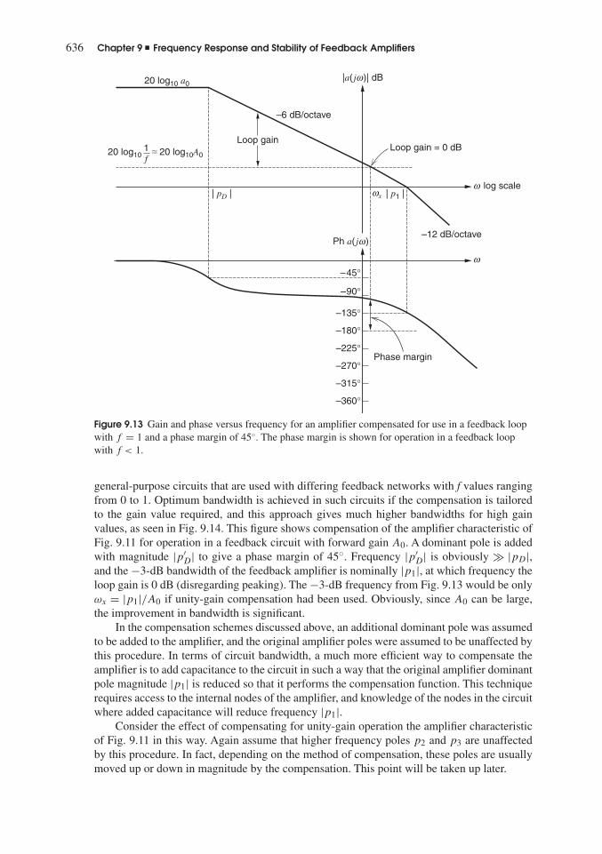
636 Chapter 9 � Frequency Response and Stability of Feedback Amplifiers
20 log10 ≅ 20 log10A0
20 log10 a0|a( j )| dB
Ph a( j )
| p1 || pD | log scale
ω
ω
ωω
ω
x
–12 dB/octave
–6 dB/octave
–270°
–315°
–360°
–225°
–180°
–135°
–90°
Loop gainLoop gain = 0 dB
–45°
Phase margin
1f
Figure 9.13 Gain and phase versus frequency for an amplifier compensated for use in a feedback loopwith f = 1 and a phase margin of 45◦. The phase margin is shown for operation in a feedback loopwith f < 1.
general-purpose circuits that are used with differing feedback networks with f values rangingfrom 0 to 1. Optimum bandwidth is achieved in such circuits if the compensation is tailoredto the gain value required, and this approach gives much higher bandwidths for high gainvalues, as seen in Fig. 9.14. This figure shows compensation of the amplifier characteristic ofFig. 9.11 for operation in a feedback circuit with forward gain A0. A dominant pole is addedwith magnitude |p′
D| to give a phase margin of 45◦. Frequency |p′D| is obviously � |pD|,
and the −3-dB bandwidth of the feedback amplifier is nominally |p1|, at which frequency theloop gain is 0 dB (disregarding peaking). The −3-dB frequency from Fig. 9.13 would be onlyωx = |p1|/A0 if unity-gain compensation had been used. Obviously, since A0 can be large,the improvement in bandwidth is significant.
In the compensation schemes discussed above, an additional dominant pole was assumedto be added to the amplifier, and the original amplifier poles were assumed to be unaffected bythis procedure. In terms of circuit bandwidth, a much more efficient way to compensate theamplifier is to add capacitance to the circuit in such a way that the original amplifier dominantpole magnitude |p1| is reduced so that it performs the compensation function. This techniquerequires access to the internal nodes of the amplifier, and knowledge of the nodes in the circuitwhere added capacitance will reduce frequency |p1|.
Consider the effect of compensating for unity-gain operation the amplifier characteristicof Fig. 9.11 in this way. Again assume that higher frequency poles p2 and p3 are unaffectedby this procedure. In fact, depending on the method of compensation, these poles are usuallymoved up or down in magnitude by the compensation. This point will be taken up later.

9.4 Compensation 637
′
20 log10 a0
|a( j )| dB
Ph a( j )
| p1 || pD | | p2 | | p3 |
ω
ω
ω
ω logscale
–6 dB/octave
Gain curve after compensation
–6 dB/octave–12 dB/octave
–18 dB/octave–12dB/octave
–270°
–315°
–360°
–225°
–180°
–135°
–90°
Loopgain
–45°
Original gain curve
Original phase
Phase margin= 45°
Phase aftercompensation
20 log10 ≅ 20 log10A01f
–18dB/octave
Figure 9.14 Gain and phase versus frequency for an amplifier compensated for use in a feedback loopwith f < 1 and a phase margin of 45◦. Compensation is achieved by adding a new pole p′
D to theamplifier.
Compensation of the amplifier by reducing |p1| is shown in Fig. 9.15. For a 45◦-phasemargin in a unity-gain feedback configuration, dominant pole magnitude |p′
1| must cause thegain to fall to unity at frequency |p2| (the second pole magnitude). Thus the nominal bandwidthin a unity-gain configuration is |p2|, and the loop gain is unity at this frequency. This resultcan be contrasted with a bandwidth of |p1|, as shown in Fig. 9.12 for compensation achievedby adding another pole with magnitude |pD| to the amplifier. In practical amplifiers, frequency|p2| is often 5 or 10 times frequency |p1| and substantial improvements in bandwidth are thusachieved.
The results of this section illustrate why the basic amplifier of a feedback circuit is usuallydesigned with as few stages as possible. Each stage of gain inevitably adds more poles to thetransfer function, complicating the compensation problem, particularly if a wide bandwidth isrequired.
9.4.2 Methods of Compensation
In order to compensate a circuit by the common method of narrowbanding described above,it is necessary to add capacitance to create a dominant pole with the desired magnitude. Onemethod of achieving this is shown in Fig. 9.16, which is a schematic of the first two stagesof a simple amplifier. A large capacitor C is connected between the collectors of the inputstage. The output stage, which is assumed relatively broadband, is not shown. A differentialhalf-circuit of Fig. 9.16 is shown in Fig. 9.17, and it should be noted that the compensation

638 Chapter 9 � Frequency Response and Stability of Feedback Amplifiers
20 log10 a0
|a( j )| dB
Ph a( j )
| p1 || p1 | | p2 | | p3 |
ω
ω
ω
ωlog scale
–6 dB/octave
–6 dB/octave–12 dB/octave
–18 dB/octave
–270°
–225°
–180°
–135°
–90°
–45°
Original gain curve
Gain curveafter compensation
Original phase
Phase margin= 45°
Phase aftercompensation
′
Figure 9.15 Gain and phase versus frequency for an amplifier compensated for use in a feedback loopwith f = 1 and a phase margin of 45◦. Compensation is achieved by reducing the magnitude |p1| ofthe dominant pole of the original amplifier.
+VCC
RL1 RL1 RL2
–VEE
Q1 Q2
Q3 Q4C
To outputstage
Figure 9.16 Compensation of an amplifier by introduction of a large capacitor C.
capacitor is doubled in the half-circuit. The major contributions to the dominant pole of acircuit of this type (if RS is not large) come from the input capacitance of Q4 and Millercapacitance associated with Q4. Thus the compensation as shown will reduce the magnitudeof the dominant pole of the original amplifier so that it performs the required compensationfunction. Almost certainly, however, the higher frequency poles of the amplifier will also bechanged by the addition of C. In practice, the best method of approaching the compensation

9.4 Compensation 639
RL1
Q2
Q4RS
RL2 vo
+
–
vs
+
–
2C
Figure 9.17 Differential half-circuit of Fig. 9.16.
design is to use computer simulation to determine the original pole positions. A first estimate ofC is made on the assumption that the higher frequency poles do not change in magnitude and anew computer simulation is made with C included to check this assumption. Another estimateof C is then made on the basis of the new simulation, and this process usually converges afterseveral iterations.
The magnitude of the dominant pole of Fig. 9.17 can be estimated using zero-value timeconstant analysis. However, if the value of C required is very large, this capacitor will dominateand a good estimate of the dominant pole can be made by considering C only and ignoringother circuit capacitance. In that case the dominant-pole magnitude is
|pD| = 1
2CR(9.22)
where
R = RL1||Ri4 (9.23)
and
Ri4 = rb4 + rπ4 (9.24)
One disadvantage of the above method of compensation is that the value of C required is quitelarge (typically > 1000 pF) and cannot be realized on a monolithic chip.
Many general-purpose op amps have unity-gain compensation included on the monolithicchip and require no further compensation from the user. (The sacrifice in bandwidth caused bythis technique when using gain other than unity was described earlier.) In order to realize aninternally compensated monolithic op amp, compensation must be achieved using capacitanceless than about 50 pF. This can be achieved using Miller multiplication of the capacitance asin the 741 op amp, which uses a 30 pF compensation capacitor and was analyzed in previouseditions of this book.
As well as allowing use of a small capacitor that can be integrated on the monolithic chip,this type of compensation has another significant advantage. This is due to the phenomenonof pole splitting,8 in which the dominant pole moves to a lower frequency while the nextpole moves to a higher frequency. The splitting of the two low-frequency poles in practicalop amps is often a rather complex process involving other higher frequency poles and zerosas well. However, the process involved can be illustrated with the two-stage op-amp model inFig. 9.18. The input is from from a current is, which stems from the transconductance of the firststage times the op-amp differential input voltage. Resistors R1 and R2 represent the total shuntresistances at the output of the first and second stages, including transistor input and outputresistances. Similarly, C1 and C2 represent the total shunt capacitances at the same places.Capacitor C represents transistor collector-base capacitance of the amplifying transistor in thesecond stage plus the compensation capacitance.

640 Chapter 9 � Frequency Response and Stability of Feedback Amplifiers
C
C1is
ic
gmv1 C2 R2R1 vo
+
–
+
–
v1
Figure 9.18 Small-signal equivalent circuit of a single transistor stage. Feedback capacitor C includescompensation capacitance.
For the circuit of Fig. 9.18,
−is = v1
R1+ v1C1s + (v1 − vo)Cs (9.25)
gmv1 + vo
R2+ voC2s + (vo − v1)Cs = 0 (9.26)
From (9.25) and (9.26)
vo
is= (gm − Cs)R2R1
1 + s[(C2 + C)R2 + (C1 + C)R1 + gmR2R1C] + s2R2R1(C2C1 + CC2 + CC1)
(9.27)
The circuit transfer function has a positive real zero at
z = gm
C(9.27a)
which usually has such a large magnitude in bipolar circuits that it can be neglected. This isoften not the case in MOS circuits because of their lower gm. This point is taken up later.
The circuit has a two-pole transfer function. If p1 and p2 are the poles of the circuit, thenthe denominator of (9.27) can be written
D(s) =(
1 − s
p1
)(1 − s
p2
)(9.28)
= 1 − s
(1
p1+ 1
p2
)+ s2
p1p2(9.29)
and thus
D(s) � 1 − s
p1+ s2
p1p2(9.30)
if the poles are real and widely separated, which is usually true. Note that p1 is assumed to bethe dominant pole.
If the coefficients in (9.27) and (9.30) are equated then
p1 = − 1
(C2 + C)R2 + (C1 + C)R1 + gmR2R1C(9.31)
and this can be approximated by
p1 � − 1
gmR2R1C(9.32)

9.4 Compensation 641
since the Miller effect due to C will be dominant if C is large and gmR1, gmR2 � 1. Equation9.31 is the same result for the dominant pole as is obtained using zero-value time constantanalysis.
The nondominant pole p2 can now be estimated by equating coefficients of s2 in (9.27)and (9.30) and using (9.32).
p2 � − gmC
C2C1 + C(C2 + C1)(9.33)
Equation 9.32 indicates that the dominant-pole magnitude |p1| decreases as C increases,whereas (9.33) shows that |p2| increases as C increases. Thus, increasing C causes the polesto split apart. The dominant pole moves to a lower frequency because increasing C increasesthe time constant associated with the output node of the first stage in Fig. 9.18. The reason thenondominant pole moves to a higher frequency is explained below.
Equation 9.33 can be interpreted physically by associating p2 with the output node in Fig.9.18. Then
p2 = − 1
RoCT
(9.33a)
where Ro is the output resistance including negative feedback around the second stage throughC, and CT is the total capacitance from the output node to ground. The output resistance is
Ro = R2
1 + T(9.33b)
where R2 is the open-loop output resistance, and T is the loop gain around the second stagethrough capacitor C, which is the open-loop gain, gmR2, times the feedback factor, f. Therefore,
Ro = R2
1 + gmR2f� 1
gmf(9.33c)
assuming that T = gmR2f � 1. Since p2 is a high frequency, we will find f at high frequencyω, where 1/ωC1 � R1. Then the feedback around the second stage is controlled by a capacitivevoltage divider and
f � C
C + C1(9.33d)
Thus,
Ro � C + C1
gmC(9.33e)
The total capacitance from the output node to ground is C2 in parallel with the series combi-nation of C and C1:
CT = C2 + CC1
C + C1= CC2 + C1C2 + CC1
C + C1(9.33f)
Substituting (9.33e) and (9.33f) into (9.33a) gives (9.33).Equations 9.33d and 9.33f show that increasing C increases the feedback factor but has
little effect on the total capacitance in shunt with the output node because C is in series withC1. As a result, increasing C reduces the output resistance and increases the frequency ofthe nondominant pole. In the limit as C → ∞, the feedback factor approaches unity, andp2 → −gm/(C2 + C1). In practice, however, (9.33d) shows that the feedback factor is lessthan unity, which limits the increase in the magnitude of the nondominant pole frequency.

642 Chapter 9 � Frequency Response and Stability of Feedback Amplifiers
Poles split
s plane
gmC
C2C1 + C(C2 + C1)–
1
gmR1R2C–
1
R2C2
–
× ×1
R1C1
–
jw
s
Figure 9.19 Locus of the poles of the circuit of Fig. 9.18 as C is increased from zero, for the case−1/(R1C1) > −1/(R2C2).
On the other hand, with C = 0, the poles of the circuit of Fig. 9.18 are
p1 = − 1
R1C1(9.34a)
p2 = − 1
R2C2(9.34b)
Thus as C increases from zero, the locus of the poles of the circuit of Fig. 9.18 is as shown inFig. 9.19.
Another explanation of pole splitting is as follows. The circuit in Fig. 9.18 has two poles.The compensation capacitor across the second stage provides feedback and causes the secondstage to act like an integrator. The two poles split apart as C increases. One pole moves to a lowfrequency (toward dc), and the other moves to a high frequency (toward −∞) to approximatean ideal integrator, which has only one pole at dc.
The previous calculations have shown how compensation of an amplifier by addition ofa large Miller capacitance to a single transistor stage causes the nondominant pole to moveto a much higher frequency. For the sake of comparison, consider compensating the circuit inFig. 9.18 without adding capacitance to C by making C1 large enough to produce a dominantpole. Then the pole can be calculated from (9.31) as p1 � −1/R1C1. The nondominant polecan be estimated by equating coefficients of s2 in (9.27) and (9.30) and using this value of p1.This gives p2 � −1/R2(C2 + C). This value of p2 is approximately the same as that given by(9.34b), which is for C = 0 and is before pole splitting occurs. Thus, creation of a dominantpole in the circuit of Fig. 9.18 by making C1 large will result in a second pole magnitude|p2| that is much smaller than that obtained if the dominant pole is created by increasingC. As a consequence, the realizable bandwidth of the circuit when compensated in this wayis much smaller than that obtained with Miller-effect compensation. Also, without using theMiller effect, the required compensation capacitor often would be too large to be included ona monolithic chip. The same general conclusions are true in the more complex situation thatexists in many practical op amps.
The results derived in this section are useful in further illuminating the considerations ofSection 7.3.3. In that section, it was stated that in a common-source cascade, the existence ofdrain-gate capacitance tends to cause pole splitting and to produce a dominant-pole situation. Ifthe equivalent circuit of Fig. 9.18 is taken as a representative section of a cascade of common-source stages (C2 is the input capacitance of the following stage) and capacitor C is taken asCgd , the calculations of this section show that the presence of Cgd does, in fact, tend to producea dominant-pole situation because of the pole splitting that occurs. Thus, the zero-value timeconstant approach gives a good estimate of ω−3dB in such circuits.
The theory of compensation that was developed in this chapter was illustrated with somebipolar-transistor circuit examples. The theory applies in general to any active circuit, but theunique device parameters of MOSFETs cause some of the approximations that were made in

9.4 Compensation 643
the preceding analyses to become invalid. The special aspects of MOS amplifier compensationare now considered.
9.4.3 Two-Stage MOS Amplifier Compensation
The basic two-stage CMOS op amp topology shown in Fig. 6.16 is essentially identical toits bipolar counterpart. As a consequence, the equivalent circuit of Fig. 9.18 can be used torepresent the second stage with its compensation capacitance. The poles of the circuit areagain given by (9.32) and (9.33) and the zero by (9.27a). In the case of the MOS transistor,however, the value of gm is typically an order of magnitude lower than for a bipolar transistor,and the break frequency caused by the right half-plane zero in (9.27) may actually fall belowthe nominal unity-gain frequency of the amplifier. The effect of this is shown in Fig. 9.20. Atthe frequency |z| the gain characteristic of the amplifier flattens out because of the contributionto the gain of +6 dB/octave from the zero. In the same region the phase is made 90◦ morenegative by the positive real zero. As a consequence, the amplifier will have negative phasemargin and be unstable when the influence of the next most dominant pole is felt. In effect,the zero halts the gain roll-off intended to stabilize the amplifier and simultaneously pushesthe phase in the negative direction. Note also from (9.33) that the low gm of the MOSFET willtend to reduce the value of |p2| relative to a bipolar amplifier.
Another way to view this problem is to note from Fig. 9.18 that at high frequencies,feedforward through C tends to overwhelm the normal gain path via gm of the second stage
dB
|p1| |p2| (log scale)
–180°
–135°
–90°
–45°
–6 dB/octave
vovi| ( j )|
vovi
ph ( j )
|z| =gm
C
ω
ω
(log scale)ω
ω
Figure 9.20 Typical gain and phase of the CMOS op amp of Fig. 6.16.
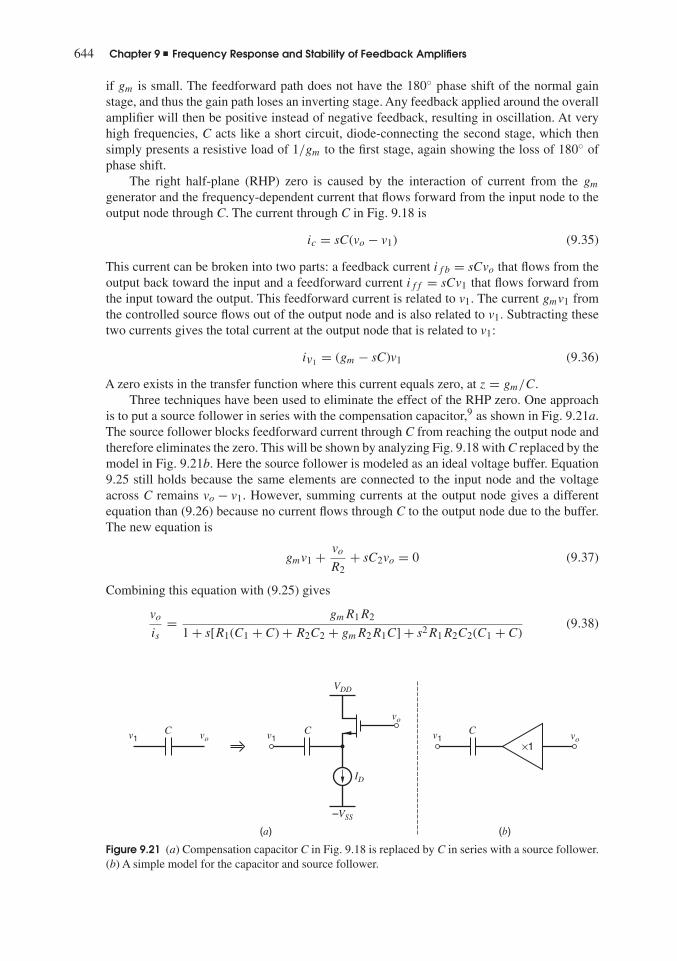
644 Chapter 9 � Frequency Response and Stability of Feedback Amplifiers
if gm is small. The feedforward path does not have the 180◦ phase shift of the normal gainstage, and thus the gain path loses an inverting stage. Any feedback applied around the overallamplifier will then be positive instead of negative feedback, resulting in oscillation. At veryhigh frequencies, C acts like a short circuit, diode-connecting the second stage, which thensimply presents a resistive load of 1/gm to the first stage, again showing the loss of 180◦ ofphase shift.
The right half-plane (RHP) zero is caused by the interaction of current from the gm
generator and the frequency-dependent current that flows forward from the input node to theoutput node through C. The current through C in Fig. 9.18 is
ic = sC(vo − v1) (9.35)
This current can be broken into two parts: a feedback current ifb = sCvo that flows from theoutput back toward the input and a feedforward current iff = sCv1 that flows forward fromthe input toward the output. This feedforward current is related to v1. The current gmv1 fromthe controlled source flows out of the output node and is also related to v1. Subtracting thesetwo currents gives the total current at the output node that is related to v1:
iv1 = (gm − sC)v1 (9.36)
A zero exists in the transfer function where this current equals zero, at z = gm/C.Three techniques have been used to eliminate the effect of the RHP zero. One approach
is to put a source follower in series with the compensation capacitor,9 as shown in Fig. 9.21a.The source follower blocks feedforward current through C from reaching the output node andtherefore eliminates the zero. This will be shown by analyzing Fig. 9.18 with C replaced by themodel in Fig. 9.21b. Here the source follower is modeled as an ideal voltage buffer. Equation9.25 still holds because the same elements are connected to the input node and the voltageacross C remains vo − v1. However, summing currents at the output node gives a differentequation than (9.26) because no current flows through C to the output node due to the buffer.The new equation is
gmv1 + vo
R2+ sC2vo = 0 (9.37)
Combining this equation with (9.25) gives
vo
is= gmR1R2
1 + s[R1(C1 + C) + R2C2 + gmR2R1C] + s2R1R2C2(C1 + C)(9.38)
(a) (b)
–VSS
VDD
ID
C Cv1 v1Cv1vo
vo
vo×1
Figure 9.21 (a) Compensation capacitor C in Fig. 9.18 is replaced by C in series with a source follower.(b) A simple model for the capacitor and source follower.

9.4 Compensation 645
The zero has been eliminated. Assuming gmR1, gmR2 � 1 and C is large, the same steps thatled from (9.27) to (9.32) and (9.33) give
p1≈ − 1
gmR2R1C(9.39a)
p2≈ − gmC
(C1 + C)C2≈ −gm
C2(9.39b)
The dominant pole p1 is unchanged, and p2 is about the same as before if C2 � C1. Thisapproach eliminates the zero, but the follower requires extra devices and bias current. Also,the source follower has a nonzero dc voltage between its input and output. This voltage willaffect the output voltage swing since the source-follower transistor must remain in the activeregion to maintain the desired feedback through C.
Asecond approach to eliminate the RHP zero is to block the feedforward current through Cusing a common-gate transistor, 10 as illustrated in Fig. 9.22a. This figure shows a two-stage opamp, with the addition of two current sources of value I2 and transistor M11. The compensationcapacitor is connected from the op-amp output to the source of M11. Here, common-gate M11allows capacitor current to flow from the output back toward the input of the second stage.However, the impedance looking into the drain of M11 is very large. Therefore, feedforwardcurrent through C is very small. If the feedforward current is zero, the RHP zero is eliminated.A simplified small-signal model for the common-gate stage and compensation capacitor isshown in Fig. 9.22b. Here common-gate M11 is modeled as an ideal current buffer. ReplacingC in Fig. 9.18 with the model in Fig. 9.22b yields
−is = v1
R1+ v1C1s − voCs (9.40a)
gmv1 + vo
R2+ voCs + voC2s = 0 (9.40b)
(a)
VDD
VB
C
Vo
I2
I2
I1 I3
–VSS
V1
M11
M6+
–
in– in+1
(b)
ic
1 · ic
C
vo
1v1
Figure 9.22 (a) A two-stage CMOS op amp withcommon-gate M11 connected to compensationcapacitor C. (b) Simple small-signal model for M11
and C.

646 Chapter 9 � Frequency Response and Stability of Feedback Amplifiers
Combining these equations gives
vo
is= gmR1R2
1 + s[R1C1 + R2(C + C2) + gmR1R2C] + s2R1R2C1(C2 + C)(9.41)
The zero has been eliminated. Again assuming gmR1, gmR2 � 1 and C is large, the poles are
p1≈ − 1
gmR2R1C(9.42a)
p2≈ − gm
C + C2· C
C1(9.42b)
The dominant pole is the same as before. However, the nondominant pole p2 is different. Thisp2 is at a higher frequency than in the two previous approaches because C � C1 when Cand C2 are comparable. (In this section, we assume that the two-stage MOS op amp in Fig.9.18 drives a load capacitor C2 that is much larger than parasitic capacitance C1; thereforeC2 � C1.) Therefore, a smaller compensation capacitor C can be used here for a given loadcapacitance C2, when compared to the previous approaches. The increase in |p2| arises becausethe input node is not connected to, and therefore is not loaded by, the compensation capacitor.An advantage of this scheme is that it provides better high-frequency negative-power-supplyrejection than Miller compensation. (Power-supply rejection was introduced in Section 6.3.6.)With Miller compensation, C is connected from the gate to drain of M6, and it shorts thegate and drain at high frequencies. Assuming Vgs6 is approximately constant, high-frequencyvariations on the negative supply are coupled directly to the op-amp output. Connecting C tocommon-gate M11 eliminates this coupling path. Drawbacks of this approach are that extradevices and dc current are needed to implement the scheme in Fig. 9.22a. Also, if there is amismatch between the I2 current sources, the difference current must flow in the input stage,which disrupts the balance in the input stage and affects the input-offset voltage of the op amp.
When the first stage of the op amp uses a cascode transistor, the compensation capacitorcan be connected to the source of the cascode device as shown in Fig. 9.23.11 This connectionreduces the feedforward current through C, when compared to connecting C to node ©Y , if the
VDD
VBBVBB
CVo
I1 I3
–VSS
in– in+
Y
+
–
Figure 9.23 A two-stage CMOS op amp with a cascoded current-mirror load in the input stage, andwith the compensation capacitor C connected to the cascode node.

9.4 Compensation 647
(a)
jω
(b)
R1 C1 R2
CRZ
C2is v1
+
–
vo
+
–
gmv1
σ
Increasing RZ
s plane
RZ = 0RZ >1gm
Figure 9.24 (a) Small-signal equivalent circuit of a compensation stage with nulling resistor.(b) Pole-zero diagram showing movement of the transmission zero for various values of RZ.
voltage swing at the source of the cascode device is smaller than the swing at its drain. Thisapproach eliminates the feedforward path, and therefore the zero, if the voltage swing at thesource of the cascode device is zero. An advantage of this approach is that it avoids the extradevices, bias current, and mismatch problems in Fig. 9.22a.
A third way to deal with the RHP zero is to insert a resistor in series with the compensationcapacitor, as shown in Fig. 9.24a.12,13 Rather than eliminate the feedforward current, theresistor modifies this current and allows the zero to be moved to infinity. If the zero moves toinfinity, the total forward current at the output node that is related to v1 must go to zero whenω → ∞. When ω → ∞, capacitor C is a short circuit and therefore the feedforward currentis only due to RZ:
iff (ω → ∞) = − v1
RZ
(9.43)
When this current is added to the current from the gm source, the total current at the outputnode that is related to v1 is
iv1 =(
gm − 1
RZ
)v1 (9.44)
when ω → ∞. If RZ = 1/gm, this term vanishes, and the zero is at infinity.The complete transfer function can be found by carrying out an analysis similar to that
performed for Fig. 9.18, which gives
vo
is=
gmR1R2
[1 − sC
(1
gm
− RZ
)]1 + bs + cs2 + ds3 (9.45)

648 Chapter 9 � Frequency Response and Stability of Feedback Amplifiers
where
b = R2(C2 + C) + R1(C1 + C) + RZC + gmR1R2C (9.46a)
c = R1R2(C1C2 + CC1 + CC2) + RZC(R1C1 + R2C2) (9.46b)
d = R1R2RZC1C2C (9.46c)
Again assuming gmR1, gmR2 � 1 and C is large, the poles can be approximated by
p1 ≈ − 1
gmR2R1C(9.47a)
p2 ≈ − gmC
C1C2 + C(C1 + C2)≈ − gm
C1 + C2(9.47b)
p3 ≈ − 1
RZC1(9.47c)
The first two poles, p1 and p2, are the same as for the original circuit in Fig. 9.18. The thirdpole is at a very high frequency with |p3| � |p2| because typically C1 � C2 (since C1 is asmall parasitic capacitor and C2 is the load capacitor) and RZ will be about equal to 1/gm ifthe zero is moved to a high frequency [from (9.44)]. This circuit has three poles because thereare three independent capacitors. In contrast, Fig. 9.18 has three capacitors that form a loop, soonly two of the capacitor voltages are independent. Thus there are only two poles associatedwith that circuit.
The zero of (9.45) is
z = 1(1
gm
− RZ
)C
(9.48)
This zero moves to infinity when RZ equals 1/gm. Making the resistor greater than 1/gm
moves the zero into the left half-plane, which can be used to provide positive phase shift athigh frequencies and improve the phase margin of a feedback circuit that uses this op amp.13
The movement of the zero for increasing RZ is shown in Fig. 9.24b.Figure 9.25 shows a Miller-compensated op amp using a resistor RZ in series with the
compensation capacitor. In practice, resistor RZ is usually implemented using a MOS transistor
VDD
ViC VoCLRZ
–VSS
X
+
–
IBIAS M6
M1
M5 M7
M3 M4
M2
M8
+
–
Figure 9.25 A two-stage CMOS op amp.

9.4 Compensation 649
biased in the triode region. From (1.152), a MOS transistor operating in the triode regionbehaves like a linear resistor if Vds � 2(VGS − Vt). The on-resistance RZ of the triode devicecan be made to track 1/gm of common-source transistor M6 if the two transistors are identicaland have the same VGS − Vt . When this MOS transistor is placed to the left of the compensationcapacitor as shown in Fig. 9.25, its source voltage is set by Vgs6, which is approximatelyconstant. Therefore, VGS of the triode transistor can be set by connecting its gate to a dc biasvoltage, which can be generated using replica biasing.13 (See Problem 9.23.)
Another way to shift the zero location that can be used in multistage op amps will bepresented in Section 9.4.5.
In all the compensation approaches described so far, the dominant pole is set by com-pensation capacitor C and is independent of the load capacitor C2. However, the second poleis a function of C2. If the op amp will be used in different applications with a range of loadcapacitors, the compensation capacitor should be selected to give an acceptable phase marginfor the largest C2. Then the phase margin will increase as the load capacitor decreases because|p2| is inversely proportional to C2.
EXAMPLE
Compensate the two-stage CMOS op amp from the example in Section 6.3.5 (Fig. 6.16) toachieve a phase margin of 45◦ or larger when driving a load capacitance of 5 pF, assuming theop amp is connected in unity-gain feedback.
With the op amp in unity-gain feedback, f = 1 and the loop gain T = af = a (or, equiv-alently, A∞ = 1 and the return ratio � = a). Therefore, the phase and gain margins can bedetermined from Bode plots of |a| and ph(a).
The two-stage op amp and a simplified model for this op amp are shown in Fig. 9.25. Inthe model, all capacitances that connect to node ©X are lumped into C1, and all capacitancesthat connect to the output node are lumped into C2. If we apply an input voltage vi in Fig. 9.26,a current i1 = gm1vi is generated. This i1 drives a circuit that is the same as the circuit that isdrives in Fig. 9.18. Therefore, the equations for the two poles and one zero for the circuit inFig. 9.18 apply here with is = gm1vi, gm = gm6, R1 = ro2||ro4, and R2 = ro6||ro7.
We will use Miller compensation with a series resistance to eliminate the zero. To achievea 45◦ phase margin, the compensation capacitor C should be chosen so that |p2| equals theunity-gain frequency (assuming the zero has been eliminated and |p3| � |p2|). Since the gainroll-off from |p1| to |p2| is −6 dB/octave, |a(jω)| · ω is constant from |p1| to |p2|. Therefore,
ao · |p1| = 1 · |p2| (9.49)
where
ao = gm1(ro2||ro4)gm6(ro6||ro7) = gm1R1gm6R2 (9.50)
vi
+
–
C1 R2 = ro6||ro7R1 = ro2||ro4
CRZ
vx vo
C2
i1
gm6vxgm1vi
X
Cin
Figure 9.26 A small-signal model for the op amp in Fig. 9.25.

650 Chapter 9 � Frequency Response and Stability of Feedback Amplifiers
is the dc gain of the op amp. Substitution of (9.47) and (9.50) into (9.49) gives
gm1R1gm6R2 · 1
gm6R2R1C= 1 · gm6
C1 + C2
orgm1
C= gm6
C1 + C2(9.51)
The capacitance C2 at the output is dominated by the 5-pF load capacitance, and the internalparasitic capacitance C1 is much smaller than 5 pF (SPICE simulation gives C1 ≈ 120 fF).Therefore C1 + C2 ≈ 5 pF. From the example in Section 6.3.5, we find
gm1 = k′p(W/L)1|Vov1| = (64.7 �A/V2)(77)(0.2 V) = 1 mA/V
and
gm6 = k′n(W/L)6(Vov6) = (194 �A/V2)(16)(0.5 V) = 1.55 mA/V
Substituting these values into (9.51) and rearranging gives
C = gm1
gm6(C1 + C2) ≈ 1 mA/V
1.55 mA/V(5 pF) = 3.2 pF
To eliminate the zero due to feedforward through C, a resistor RZ of value 1/gm6 = 645 canbe connected in series with the compensation capacitor C. (In practice, this resistance shouldbe implemented with an NMOS transistor that is a copy of M6 biased in the triode region, sothat RZ = 1/gm6. See Problem 9.23.)
SPICE simulations (using models based on Table 2.4) of the op amp before and aftercompensation give the magnitude and phase plots shown in Fig. 9.27. Before compensation,the amplifier is unstable and has a phase margin of −6◦. After compensation with RZ = 645
and C = 3.2 pF the phase margin improves to 41◦ with a unity-gain frequency of 35 MHz, andthe gain margin is 15 dB. This phase margin is less than the desired 45◦. The simulated value ofgm6 is 1.32 mA/V and differs somewhat from the calculated gm6, because the formulas used tocalculate gm are based on square-law equations that are only approximately correct. ChangingRZ to 1/gm6(SPICE) = 758 gives a phase margin of 46◦ with a unity-gain frequency of35 MHz, and the gain margin is 22 dB. Without RZ, the phase margin is 14◦, so eliminatingthe right-half-plane zero significantly improves the phase margin.
Two earlier assumptions can be checked from SPICE simulations. First, C1 ≈ 120 fF fromSPICE and C2 ≈ 5 pF; therefore, the assumption that C1 � C2 is valid. Also, |p3| � |p2|follows from |p3| ≈ 1/(RZC1) = gm6/C1, |p2| ≈ gm6/C2, and C1 � C2.
9.4.4 Compensation of Single-Stage CMOS Op Amps
Single-stage op amps, such as the telescopic cascode or folded cascode, have only one gainstage; therefore Miller compensation is not possible. These op amps have high open-loopoutput resistance and are typically used in switched-capacitor circuits, where the load is purelycapacitive. Therefore, the dominant pole is associated with the output node, and the loadcapacitor provides the compensation.
A simplified, fully differential, telescopic-cascode op amp is shown in Fig. 9.28a. Thesimplifications here are that ideal current sources replace biasing transistors and all capacitanceshave been lumped into the load capacitors CL and the parasitic capacitors Cp at the cascodenodes. The differential-mode (DM) voltage gain can be found by analyzing the half-circuitshown in Fig. 9.28b. Since there are two independent capacitors, the DM gain has two poles.
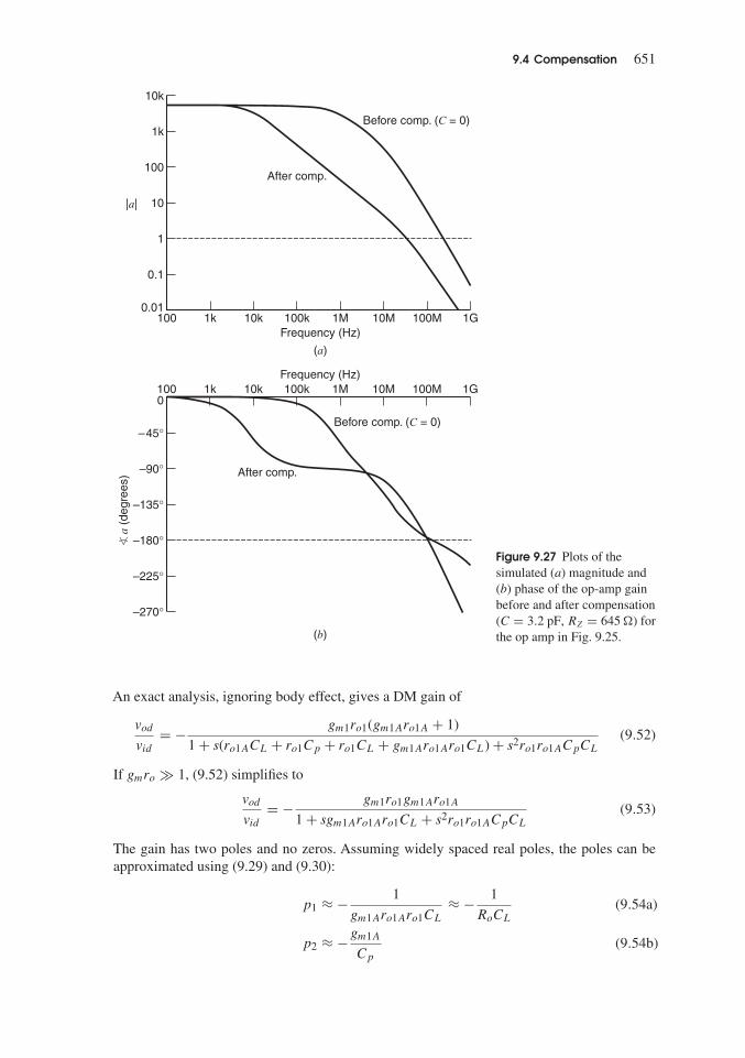
9.4 Compensation 651
(a)
1G100M10M1M100kFrequency (Hz)
10k1k1000.01
0.1
1
10
100
1k
10k
|a|
Before comp. (C = 0)
After comp.
(b)
1G100M10M1M100kFrequency (Hz)
10k1k100
–270°
–225°
–180°
–135°
–90°
–45°
0
a (d
egre
es)
Before comp. (C = 0)
After comp.
�
Figure 9.27 Plots of thesimulated (a) magnitude and(b) phase of the op-amp gainbefore and after compensation(C = 3.2 pF, RZ = 645 ) forthe op amp in Fig. 9.25.
An exact analysis, ignoring body effect, gives a DM gain of
vod
vid
= − gm1ro1(gm1Aro1A + 1)
1 + s(ro1ACL + ro1Cp + ro1CL + gm1Aro1Aro1CL) + s2ro1ro1ACpCL
(9.52)
If gmro � 1, (9.52) simplifies to
vod
vid
= − gm1ro1gm1Aro1A
1 + sgm1Aro1Aro1CL + s2ro1ro1ACpCL
(9.53)
The gain has two poles and no zeros. Assuming widely spaced real poles, the poles can beapproximated using (9.29) and (9.30):
p1 ≈ − 1
gm1Aro1Aro1CL
≈ − 1
RoCL
(9.54a)
p2 ≈ −gm1A
Cp
(9.54b)

652 Chapter 9 � Frequency Response and Stability of Feedback Amplifiers
VDD
VBBVBBCL CL
Cp Cp
II
2I
–VSS
M1A M2A
M1 M2in+ in–
vovo
(a)
+ –
(b)
CLM1A
M1Cp
vid
2
vod
2
Figure 9.28 (a) Simplified CMOStelescopic-cascode op amp. (b) Thedifferential-mode half-circuit.
where Ro is the output resistance of the DM half-circuit and Ro ≈ gm1Aro1Aro1. Alternatively,these poles can be estimated using time-constant analysis as shown in Chapter 7. The dominantpole is set by the zero-value time constant for CL, which is computed with Cp open and equalsRoCL. The nondominant pole can be approximated using the short-circuit time constant forCp, which is computed with CL shorted. When CL is shorted, the resistance seen by Cp is theresistance looking into the source of M1A, which is 1/gm1A (ignoring body effect). Typically,|p1| � |p2| because Ro � 1/gm1A and CL � Cp. If the phase margin is not large enough fora given feedback application, additional capacitance can be added at the output node to increaseCL, which decreases |p1| without affecting p2 and therefore increases the phase margin.
Capacitance Cp consists of Cgs1A plus smaller capacitances such as Cdb1 and Csb1A.Assuming Cp ≈ Cgs1A, then |p2| ≈ gm1A/Cp ≈ gm1A/Cgs1A ≈ ωT of M1A. Thus, the fre-quency at which the magnitude of the op-amp gain equals one, which is called the unity-gainbandwidth, can be very high with this op amp.
A simplified, fully differential, folded-cascode op amp is shown in Fig. 9.29a. As above,the simplifications are that ideal current sources replace biasing transistors and all capacitanceshave been lumped into the load capacitors CL and the parasitic capacitors C′
p at the cascodenodes. With these simplifications, the DM voltage gain can be found by analyzing the half-circuit shown in Fig. 9.29b. This circuit is identical to Fig. 9.28b except that the cascode deviceis p-channel rather than n-channel and C′
p replaces Cp. Therefore, the gain is identical to (9.52)

9.4 Compensation 653
+VDD
vo vo
VBB
CL CL
Cp
I1 + I2 I1 + I2
2I1I2 I2
–VSS
M2A M1A
M1 M2in+ in–
(a)
′Cp
′
– +
(b)
CLM1A
M1Cp
vid
2
vod
2
′
Figure 9.29 (a) Simplified CMOSfolded-cascode op amp. (b) Thedifferential-mode half-circuit.
with Cp replaced by C′p. Hence the dominant pole has the same form as (9.54a)
p1 ≈ − 1
gm1Aro1Aro1CL
≈ − 1
RoCL
(9.55a)
The second pole is associated with C′p and is approximately given by
p2 ≈ −gm1A
C′p
(9.55b)
Equations 9.55b and 9.54b look similar, but |p2| for the folded-cascode op amp will usuallybe smaller than |p2| for the telescopic-cascode op amp. The reason is that, while thetransconductances of the cascode devices in the two circuits are often comparable, C′
p willbe significantly larger than Cp. One cause of the higher capacitance is that more devices areconnected to the node associated with C′
p in the folded-cascode op amp than are connectedto the node associated with Cp in the telescopic cascode. (Recall that the output of each idealcurrent source in Fig. 9.29a is the drain of a transistor.) Also, W/L of the p-channel cascodetransistor M1A in Fig. 9.29b must be larger than W/L of the n-channel cascode device in Fig.9.28b to make their transconductances comparable. The larger W/L will cause C′
p to be largerthan Cp. The smaller |p2| for the folded cascode leads to a smaller unity-gain bandwidth, if thetwo op amps are compensated to give the same phase margin in a given feedback application.
The circuits in Figs. 9.28 and 9.29 are fully differential. These op amps can be convertedto single-ended op amps by replacing a pair of matched current sources with a current mirror.In Fig. 9.28a, the two I current sources would be replaced with a p-channel current mirror. In
654 Chapter 9 � Frequency Response and Stability of Feedback Amplifiers
Fig. 9.29a, the two I2 current sources would be replaced with a n-channel current mirror. Asshown in Section 7.3.5, a current mirror introduces a closely spaced pole-zero pair, in additionto the poles p1 and p2 in (9.54) and (9.55).
Active cascodes can be used to increase the low-frequency gain of an op amp, as shown inFig. 6.30a. There are four active cascodes in Fig. 6.30a; each consists of a cascode transistor(M1A – M4A) and an auxiliary amplifier (A1 or A2) in a feedback loop. When such an op ampis placed in feedback, multiple feedback loops are present. There are four local feedback loopsassociated with the active cascodes in the op amp and one global feedback loop that consistsof the op amp and a feedback network around the op amp. All these feedback loops must bestable to avoid oscillation. The stability of each local feedback loop can be determined fromits loop gain or return ratio. Since the auxiliary amplifiers in these loops are op amps, eachauxiliary amplifier can be compensated using the techniques described in this chapter to ensurestability of these local loops. Then the global feedback loop can be compensated to guaranteeits stability.
9.4.5 Nested Miller Compensation
Many feedback circuits require an op amp with a high voltage gain. While cascoding is com-monly used to increase the gain in op amps with a total supply voltage of 5 V or more,cascoding becomes increasingly difficult as the power-supply voltage is reduced. (See Chap-ter 4.) To overcome this problem, simple gain stages without cascoding can be cascaded toachieve high gain. When three or more voltage-gain stages must be cascaded to achieve thedesired gain, the op amp will have three or more poles, and frequency compensation becomescomplicated. Nested Miller compensation can be used with more than two gain stages.14,15
This compensation scheme involves repeated, nested application of Miller compensation. Anexample of nested Miller compensation applied to three cascaded gain stages is shown in Fig.9.30a. Two noninverting gain stages are followed by an inverting gain stage. Each voltage-gainstage is assumed to have a high-output resistance and therefore is labeled as a gm block. Thesign of the dc voltage gain of each stage is given by the sign of the transconductance. TwoMiller compensation capacitors are used: Cm1, which is placed around the last gain stage, andCm2, which is connected across the last two gain stages. Because the dc gain of the secondstage is positive and the dc gain of the third stage is negative, both capacitors are in negativefeedback loops.
A simplified circuit schematic is shown in Fig. 9.30b. Each noninverting gain stage iscomposed of a differential pair with a current-source load. The inverting gain stage consistsof a common-source amplifier with a current-source load. A simplified small-signal model isshown in Fig. 9.30c. The main simplification here is that all capacitances associated with thegain stages are modeled by C0, C1, and C2.
Without the compensation capacitors, this amplifier has three real poles that are not widelyspaced if the RiCi time constants are comparable. When Cm1 is added, the two poles associatedwith the output nodes of the second and third stages split apart along the real axis due to theMiller compensation, but the pole associated with output of the first stage does not change.From a design standpoint, the goal of this pole splitting is to cause one pole to dominate thefrequency response of the second and third stages together. Assume at first that this goal ismet. Then adding Cm2 across the second and third stages is similar to adding Cm1 across thethird stage. Pole splitting occurs again, and the pole associated with the output node of thefirst stage becomes dominant because the Miller-multiplied Cm2 loads this node. Meanwhile,the pole associated with the output of the second stage moves to higher frequency because ofnegative feedback through Cm2. The polarity of this feedback does not become positive at anyfrequency where the gain around the loop is at least unity because the frequency response ofof the second and third stages is dominated by one pole.

9.4 Compensation 655
(a)
Vin Vo+gm0
++gm1
Cm2
Cm1
–gm2
–
(b)
VBB
Vo
Vin
Cm2
Cm1
I1 I2 I3
2I1 2I2
+
–
(c)
R0 C0vin
vo
+
–
v1 v2
is = gm0vin R1 C1 R2 C2gm1v1 gm2v2
Cm2
Cm1
Figure 9.30 (a) Block diagram for a three-stage op amp with nested Miller compensation. (b) Asimplified schematic for such an op amp in CMOS. (c) A small-signal model.
In practice, the exact movement of the poles is complicated by the nondominant pole in thefeedback loop though Cm2. Also, zeros are introduced by feedforward through Cm1 and Cm2.The pole and zero locations can be found from an exact analysis of the small-signal circuit.The analysis can be carried out by summing currents at the outputs of the gm generators, thenmanipulating the resulting three equations. These steps are not conceptually difficult but arenot shown here. The exact transfer function from the output of the current generator in theinput stage, is = gm0vin, to the output voltage vo is
vo
is= −N(s)
D(s)(9.56)
= −R0gm1R1gm2R2 − (gm1R1Cm1 + Cm2)R0R2s − R0R1R2Cm2(C1 + Cm1)s2
1 + a1s + a2s2 + a3s3

656 Chapter 9 � Frequency Response and Stability of Feedback Amplifiers
where
a1 = K + R0(Cm2 + C0) + gm1R1gm2R2R0Cm2 (9.57a)
a2 = R1R2(C2 + Cm1 + Cm2)(C1 + Cm1) − R1R2C2m1 + R0(Cm2 + C0)K
−gm1R1Cm1Cm2R0R2 − R0R2C2m2 (9.57b)
a3 = R0R1R2[(C2Cm2 + C0C2 + C0Cm2)(C1 + Cm1) + C1Cm1Cm2
+ C0C1Cm1] (9.57c)
with
K = R2(C2 + Cm1 + Cm2) + R1(C1 + Cm1) + R1Cm1gm2R2 (9.57d)
Equation 9.56 is the transfer function from is to vo. The transfer function of the voltagegain from vin to vo is found by multiplying (9.56) by gm0 (since is = gm0vin); therefore, thevoltage gain and (9.56) have the same poles and zeros. The transfer function in (9.56) has twozeros and three poles. Let us first examine the poles. The expressions for the ai coefficientsare complicated and involve many terms. Therefore assumptions are needed to simplify theequations. If gm1R1gm2R2 � 1, which is usually true, then
a1 ≈ gm1R1gm2R2R0Cm2 (9.58)
Assuming there is a dominant pole p1, then
p1 ≈ − 1
a1= − 1
gm1R1gm2R2R0Cm2(9.59)
Another way to arrive at this estimate of p1 is to apply the Miller effect to Cm2. The effectiveMiller capacitor is about Cm2 times the negative of the gain across Cm2, which is gm1R1gm2R2.This capacitor appears in parallel with R0, giving a time constant of (gm1R1gm2R2)R0Cm2.
The other poles p2 and p3 could be found by factoring the third-order denominator in(9.56), which can be done using a computer but is difficult by hand. However, these poles canbe estimated from a quadratic equation under certain conditions. If there is a dominant polep1, then |p2|, |p3| � |p1|. At high frequencies, where |s| � |p1| ≈ 1/a1, we have |a1s| � 1,so the denominator in (9.56) can be approximated by dropping the constant “1” to give
D(s) ≈ a1s + a2s2 + a3s
3 = a1s
(1 + a2
a1s + a3
a1s2)
(9.60)
This equation gives three poles. One pole is at dc, which models the effect of the dominantpole p1 for frequencies well above |p1|. Poles p2 and p3 are the other roots of (9.60). Theycan be found by concentrating on the quadratic term in parenthesis in (9.60), which is
D′(s) = D(s)
a1s≈ 1 + a2
a1s + a3
a1s2 ≈
(1 − s
p2
)(1 − s
p3
)(9.61)

9.4 Compensation 657
Assuming that R0, R1, R2 � |1/(gm2 − gm1)| and Co is small compared to the othercapacitors, (9.57b) and (9.57c) simplify to
a2 ≈ R0R1R2(gm2 − gm1)Cm1Cm2 (9.62)
a3 ≈ R0R1R2(C1C2Cm2 + C2Cm1Cm2 + C1Cm1Cm2) (9.63)
Using (9.58), (9.62), and (9.63), the coefficients in D′(s) are
a2
a1≈ gm2 − gm1
gm1gm2Cm1 (9.64)
a3
a1≈ C1C2 + Cm1C1 + C2Cm1
gm1gm2(9.65)
To ensure that the high-frequency poles are in the left half-plane (LHP), a2/a1 must be positive(see Appendix A9.2). Therefore, gm2 must be larger than gm1. Poles p2 and p3 can be real orcomplex, and in general the quadratic formula must be used to solve for these poles. However, ifthese poles are real and widely spaced and if Cm1 � C1, C2, then approximate expressions canbe found. If |p2| � |p3|, then −1/p2 is approximately equal to the coefficient of s in D′(s), so
p2 ≈ −a1
a2= − gm1gm2
(gm2 − gm1)Cm1(9.66a)
Also 1/(p2p3) is equal to the coefficient of s2 in D′(s), so
p3 ≈ a1
a3
1
p2= − gm1gm2
C1C2 + Cm1C1 + C2Cm1· (gm2 − gm1)Cm1
gm1gm2(9.66b)
= − (gm2 − gm1)Cm1
C1C2 + Cm1(C1 + C2)≈ −gm2 − gm1
C1 + C2
The final approximation here follows if Cm1 is large. Equations 9.66a and 9.66b are accurateif |p2| � |p3|. Substituting (9.66a) and (9.66b) into this inequality produces an equivalentcondition
|p2| ≈ gm1gm2
(gm2 − gm1)Cm1� (gm2 − gm1)Cm1
C1C2 + Cm1(C1 + C2)≈ |p3| (9.67)
If this condition is not satisfied, p2 and p3 are either complex conjugates or real but closelyspaced. Cm1 can always be chosen large enough to satisfy the inequality in (9.67). Whileit is possible to make the high-frequency poles real and widely separated, higher unity-gainbandwidth may be achievable when p2 and p3 are not real and widely separated.16
In the simplified equations 9.66a and 9.66b, poles p2 and p3 are dependent on Cm1 butnot on Cm2. In contrast, dominant pole p1 is inversely proportional to Cm2 and is independentof Cm1. The poles can be positioned to approximate a two-pole op amp by making |p1| �|p2| � |p3| and positioning |p3| well beyond the unity-gain frequency of the op amp.
The zero locations can be found by factoring the second-order numerator N(s) in (9.56).The coefficients of s and s2 in the numerator are negative and the constant term is positive. Asa result, the zeros are real. One is positive and the other is negative, as is shown in AppendixA9.2.
The zeros will be found using some simplifying assumptions. First, the numerator of (9.56)can be rewritten as
N(s) = R0gm1R1gm2R2
[1 − s
(Cm1
gm2+ Cm2
gm1R1gm2
)− s2 Cm2(C1 + Cm1)
gm1gm2
](9.68)

658 Chapter 9 � Frequency Response and Stability of Feedback Amplifiers
Assuming that Cm1 � C1 and Cm1 � Cm2/(gm1R1), then
N(s) ≈ R0gm1R1gm2R2
[1 − s
Cm1
gm2− s2 Cm2Cm1
gm1gm2
](9.69)
The zeros are the roots of N(s) = 0. Using the quadratic formula and (9.69), the zeros are
z1,2 = − gm1
2Cm2�
√(gm1
2Cm2
)2
+ gm1gm2
Cm1Cm2= − gm1
2Cm2
(1 �
√1 + 4gm2Cm2
gm1Cm1
)(9.70)
Taking the positive square root in the right-most formula in (9.70) yields a value that is largerthan one. Adding this value to 1 gives a positive value for the term in parentheses; subtractingthis value from 1 gives a negative quantity with a smaller magnitude than the sum. Therefore,one zero is in the LHP and has a magnitude greater than gm1/(2Cm2). The other zero is in theRHP and has a smaller magnitude than the LHP zero. As a result, the effect of the RHP zero isfelt at a lower frequency than the LHP zero.
The magnitude of one or both zeros can be comparable to |p2|. Because the RHP zero isat a lower frequency than the LHP zero, the RHP zero can cause significant negative phaseshift for frequencies at or below |p2|, which would degrade the phase margin of a feedbackloop. This undesired negative phase shift would not occur if the transfer function did not havezeros. Unfortunately, the three techniques considered in Section 9.4.3 to eliminate a RHP zerohave important limitations in a low-supply application. First, the zeros could be eliminatedby adding a source-follower buffer between the op-amp output and the right-hand side ofcapacitors Cm1 and Cm2 (as in Fig. 9.21), thereby eliminating the feedforward paths throughthe capacitors. However, the source follower has a nonzero dc voltage between its input andoutput. This voltage may limit the op-amp output swing to an unacceptably low value in alow-power-supply application. Second, cascode stages could be used to eliminate the zeros, asshown in Fig. 9.23. However, the requirement that all transistors in the cascode stage operatein the active region may limit the minimum supply voltage. Finally, a series zero-cancelingresistance (as in Fig. 9.24a) implemented with a transistor may require a large gate voltagethat exceeds the power supply.
The NE5234 op amp uses nested Miller-effect compensation. Figure 9.31 repeats thesimplified ac schematic of the high-frequency gain path of the NE5234 shown in Fig. 7.36.Here, the common-mode input voltage is assumed to be low enough that Q1 and Q2 inFig. 6.36 are off. Also, the dc load current is assumed to be IL = 1 mA as in the calculationsin Chapter 6. Therefore, Q75 in Fig. 6.39 conducts a nearly constant current and is omitted inFig. 9.31 along with the circuits that control it for simplicity. In practice, these transistors areimportant under other bias conditions. Also, note that the transconductance of the output stagedepends on the bias point assumed. The key point here is that this op amp uses three nestedcompensation loops: through C22, C25, and C65. The loop through C25 includes series resistorR25 = 1.3 k to reduce the effects of the zero introduced through C25 and increase the phasemargin.17 This structure has one more level of nesting than shown in Fig. 9.30. The extra levelis introduced through C65 in the third stage, and its purpose is explained next.
Chapter 6 pointed out that the output transistors Q74 and Q75 in Fig. 6.39 are driven byemitter followers to increase the current gain of the output stage and reduce its load on thesecond stage. Because the integrated-circuit process is optimized to build much higher qualitynpn transistors than pnp transistors, βpnp < βnpn in practice. To provide adequate current gainwhen Q74 controls the output as shown in Fig. 9.31, two emitter followers Q64-Q65 driveQ74. In contrast, Fig. 6.39 shows that only one emitter follower Q68 is used to drive Q75.Furthermore, Q64 and Q65 use opposite polarity transistors to avoid introducing a large dclevel shift that would increase the minimum required power-supply voltage.

9.4 Compensation 659
Q74
Q65
Q63
Q22
Q21
Q13
Q3 Q4
Q9C21
R9
R13 R14 R16 R17 R19
R25C22
C25
C65
R65
R10
Q10
Q14 Q16 Q17 Q19
Q64
Q25 Q27
25
10
9
R63
IL
RL
+
–
+–
vo
Figure 9.31 An ac schematic of the high-frequency gain path of the NE5234 op amp assuming that thecommon-mode input voltage is low enough that Q1 and Q2 in Fig. 6.36 are off and assuming that Q75
in Fig. 6.39 conducts a constant current and can be ignored along with the elements that drive it.
Ideally, these emitter followers give unity gain and do not limit the frequency responseof the third stage. In practice, however, they introduce extra poles that contribute unwantedphase shift at high frequency that reduces the phase margin when the op amp is connected in afeedback loop. This problem is especially severe in driving Q74 because two emitter followersare used instead of one and because the output transistor and one of the emitter followers are pnptransistors, which have much lower fT than npn transistors operating at the same bias currents.If Miller compensation were not applied through C65, the presence of the extra poles in theoutput stage due to the emitter followers would introduce extra undesired phase shift near theunity-gain frequency of the op amp and significantly reduce the phase margin. To overcome thisproblem, the extra level of Miller-effect compensation through C65 is introduced. It forces onepole to be dominant in the output stage when feedback is applied through C25. The minimumrequired value of C65 must be able to cope with all possible bias currents in the output stage.From a stability standpoint, the worst case is when the bias current and transconductance ofQ74 are maximum because the op-amp bandwidth is increased in this case, which increasesthe importance of poles introduced by the emitter followers. In practice, C65 is chosen fromsimulations to be 10 pF.17 The corresponding capacitor on the npn side of the output stage isC68 in Fig. 6.39, and this capacitor is only 1 pF. In practice, C68 � C65 because the npn sideuses only one emitter follower and because the transistors on this side are both npn transistors.

660 Chapter 9 � Frequency Response and Stability of Feedback Amplifiers
Frequency (Hz)
|Loo
p G
ain|
(dB
)
−40
−20
0
20
40
60
80
100
101 102 103 104 105 106 107
2.7 MHz
−6 dB/octave
<)Lo
op G
ain
−225°
−180°
−135°
−90°
− 45°
0°
101 102 103 104 105 106 107
Phase Margin = 43°
Figure 9.32 Gain and phase versus frequency for the NE5234 op amp from SPICE.
The presence of an extra level of Miller compensation reduces the bandwidth of the outputstage to make one pole dominant. Although it allows a simple compensation scheme for theop amp, it also limits the high-frequency performance of the op amp with compensation.
As shown in Chapter 7, the frequency response of the NE5234 is dominated by the Millermultiplied C22. With unity-gain feedback as in Fig. 6.3c, the resulting gain and phase plots forthe NE5234 are shown in Fig. 9.32. These plots were generated using SPICE with transistorparameters as shown in Fig. 2.32 except βF = 40 and VA = 30 V for npn transistors andβF = 10 and VA = 20 V for pnp transistors. The bias conditions are the same as assumed inChapter 6. The resulting unity-gain frequency is 2.7 MHz, and the phase margin is 43 degrees.Return ratio simulations give the same results.
Fig. 9.33a shows another technique for eliminating a RHP zero that can be used withcascaded stages in a low-supply application.16,18 Two gain stages and one Miller compensationcapacitor are shown.Atransconductance stage, gmf , is included. It provides a feedforward paththat can be used to move the zero to infinity. The small-signal circuit is shown in Fig. 9.33b. Toallow a simple explanation of this circuit, initially assume that C1 = C2 = 0. The circuit hasone pole due to Cm and one zero due to the feedforward current through Cm. If the zero movesto infinity, the total forward current must go to zero when ω → ∞. Also, if the zero moves to

9.4 Compensation 661
(a)
vov1
–gmf
+gm1
Cm
–gm2
(b)
v1
vo
+
–
v2
R1 C1 R2 C2gm1v1 gm2v2
Cm
gmfv1
Figure 9.33 (a) Block diagram of a two-stage op amp with Miller compensation and a feedforwardtransconductor. (b) A small-signal model.
infinity, the output voltage will go to zero as ω → ∞ due to the pole in the transfer function.When ω → ∞, capacitor Cm becomes a short circuit, so v2 = 0 when ω → ∞. Thereforeat infinite frequency, the current gm1v1 from the gm1 source flows through Cm. Adding thisfeedforward current to the current gmf v1 from the gmf generator gives the total current at theoutput node that is related to v1
iff (ω → ∞) = (−gm1 + gmf )v1 (9.71)
If gmf = gm1, this current equals zero, which means the zero is at infinity.An exact analysis of the circuit in Fig. 9.33 gives a transfer function
vo
v1= (9.72)
−gm1R1gm2R2 − gmf R2 − sR1R2[gmf (C1 + Cm) − gm1Cm]
1 + s[gm2R1R2Cm + R2(C2 + Cm) + R1(C1 + Cm)] + s2R1R2(C1C2 + C1Cm + C2Cm)
The zero can be moved to infinity by choosing gmf so that the coefficient of s in the numeratoris zero, which occurs when
gmf = gm1Cm
C1 + Cm
= gm1
1 + C1
Cm
(9.73)
This value of gmf depends on the ratio of an internal parasitic capacitance C1, which is notwell controlled, and compensation capacitor Cm. Using gmf = gm1 moves the zero into theLHP to about −gm2/C1; the magnitude of this zero is usually above the unity-gain frequencyof the op amp. If the gm1 stage has a differential input, the −gmf stage can be realized using areplica of the gm1 stage with the inputs reversed to change the sign of the transconductance.
This zero-cancellation scheme can be used repeatedly in a three-stage op amp to eliminatethe zeros, as shown in Fig. 9.34a. A small-signal model is shown in Fig. 9.34b. Analysis of

662 Chapter 9 � Frequency Response and Stability of Feedback Amplifiers
(a)
vin
v1 v2vo
gm0 +gm1
Cm2
Cm1
–gm2
–gmf1
–gmf0
+
(b)
R0 C0vin
vo
+
–
v1 v2
is = gm0vin R1 C1 R2 C2gm1v1 gm2v2
Cm2
Cm1
gmf 0vin gmf1v1
Figure 9.34 (a) Block diagram of a three-stage op amp with nested Miller compensation and twofeedforward transconductors. (b) Small-signal model.
this circuit gives a voltage gain of
vo
vin
= R2(n0 + n1s + n2s2)
1 + b1s + b2s2 + b3s3 (9.74)
where b1-b3 are related to a1-a3 in (9.57) by
b1 = a1 + gmf1R0R2Cm2 (9.75a)
b2 = a2 + gmf1R0R1R2(C1 + Cm1)Cm2 (9.75b)
b3 = a3 (9.75c)
and the coefficients in the numerator are
n0 = −gm0gm1gm2R0R1 − gmf0 − gm0gmf1R0 (9.76a)
n1 = gm0(gm1 − gmf1)R0R1Cm1 + (gm0 − gmf0)R0Cm2
−gmf0R1(C1 + Cm1) − gmf0R0C0 − gm0gmf1R0R1C1 (9.76b)
n2 = (gm0 − gmf0)R0R1(C1 + Cm1)Cm2 − gmf0R0R1(C1 + Cm1)C0 (9.76c)
The coefficients of s and s2 in the numerator include both positive and negative terms.Therefore,they can be set to zero, which eliminates the zeros, by properly choosing gmf0 and gmf1. As

9.4 Compensation 663
in (9.73) above, these values depend on parasitic capacitances C0 and C1, which are not wellcontrolled in practice. An alternative choice is to set gmf0 = gm0 and gmf1 = gm1. When thesevalues are substituted into (9.76a)–(9.76c), n0, n1, and n2 are negative. Therefore, both zerosare in the LHP (see Appendix A9.2), and the RHP zero has been eliminated.
With gmf1 = gm1 and gmf0 = gm0, the term added to a1 in (9.75a) is small compared tothe dominant term in a1, which is gm1R1gm2R2R0Cm2, if gm2R1 � 1. Therefore b1 ≈ a1, andthe dominant pole p1 is still given by (9.59). However, b2 can be significantly different froma2, and therefore p2 and p3 will be different from the values given by (9.66a) and (9.66b). Thenew values of the high frequency poles can be found by solving the quadratic equation thatresults when b1-b3 are substituted for a1-a3 in (9.60).
The selection of the nested Miller compensation capacitors is complicated because thevalues of two compensation capacitors must be chosen, and they affect the pole and zerolocations. The compensation capacitors can be chosen with the aid of a computer to achieve aparticular settling-time or phase-margin goal in a feedback application. Computer optimizationcan be carried out on the closed-loop transfer function based on the op-amp transfer function oron the loop gain or return ratio, if the small-signal model parameters are known. Alternatively,the capacitor values can be estimated using approximations and the equations presented above.Then SPICE simulations can be run on the transistor circuit starting with the initial estimatesof the compensation capacitors and varying the capacitors by small amounts to determine thebest values. This approach is used in the following example.
EXAMPLE
Design the 3-stage op amp in Fig. 9.34 to give a low-frequency gain of 86 dB and 45◦ phasemargin for unity feedback (f = 1) when driving a 5 pF load. Compensate the op amp so thatall the poles are real and widely spaced. To simplify this example, assume that the outputresistance of each stage is 5 k and the internal node capacitances C0 and C1 are each 0.05 pF.Determine the compensation capacitors and the transconductances for the op amp.
The feedforward transconductances gmf0 and gmf1 will be used to move the zeros towell beyond the unity-gain frequency. To simplify the design equations, let gmf0 = gm0 andgmf1 = gm1, based on (9.73)–(9.76) and the assumption that C0 and C1 are small comparedto Cm1 and Cm2.
When gmf0 = gmf1 = 0, the coefficients ai of the denominator of the transfer functionare given by (9.57). With nonzero gmf0 and gmf1, however, the coefficients of s and s2 in thedenominator of the transfer function change and are given by (9.75). From (9.75c), b3 = a3.Also, as noted in the text following (9.76), the term added to a1 in (9.75a) is small comparedto a1, so b1 ≈ a1 and p1 is given by (9.59). Hence, poles p2 and p3 are changed due to theadded term that includes gmf1 in b2 in (9.75b). Assuming C1 � Cm1, (9.75b) reduces to
b2 ≈ a2 + gmf1R0R1R2Cm1Cm2
Substituting the approximate expression for a2 in (9.62) and using gmf1 = gm1, this equationbecomes
b2 ≈ gm2R0R1R2Cm1Cm2
Following the analysis from (9.60) to (9.67), we find
p2 ≈ −b1
b2≈ − gm1
Cm1(9.77a)
p3 ≈ b1
b3
1
p2≈ −gm2
C2(9.77b)

664 Chapter 9 � Frequency Response and Stability of Feedback Amplifiers
To satisfy |p2| � |p3|, let |p3| = 10|p2|. Substituting (9.77) in this equality and rearrangingyields
Cm1 = 10gm1
gm2C2 (9.78)
To ensure that Cm1 is not much larger than C2 = 5 pF we need gm1/gm2 � 1 in (9.78). Here,we chose gm1/gm2 = 0.2. Substituting this value into (9.78) gives
Cm1 = 10(0.2)(5 pF) = 10 pF
With widely spaced poles, placing |p2| at the unity-gain frequency gives a 45◦ phasemargin. Since |gain| × frequency is constant for frequencies between |p1| and |p2|, we canwrite
|a0| · |p1| = 1 · |p2| (9.79)
where
|a0| = gm0R0gm1R1gm2R2 (9.80)
is the low-frequency gain. Substitution of (9.59), (9.77a), and (9.80) into (9.79) gives
gm0
Cm2= gm1
Cm1
If the first two gain stages are made identical to reduce the circuit-design effort, gm0 = gm1,and the last equation reduces to
Cm2 = Cm1 = 10 pF
Now the transconductances can be found from the low-frequency gain requirement and (9.80),
|a0| = gm0R0gm1R1gm2R2 = g3m1
0.2(5 k)3 = 20,000 = 86 dB
since gm0 = gm1 = 0.2gm2 has been selected. Solving gives gm1 = gm0 = gmf1 = gmf0 =3.2 mA/V and gm2 = gm1/0.2 = 16 mA/V.
SPICE simulation of this op amp gives a dc gain of 86.3 dB and a phase margin of52 degrees with a unity-gain frequency of 40 MHz. These values are close enough to thespecifications to illustrate the usefulness of the calculations. The pole locations are |p1|/2π =2.3 kHz, |p2|/2π = 59 MHz, and |p3|/2π = 464 MHz. The zero locations are complex with amagnitude much larger than the unity-gain frequency, at z1,2/2π = −345 MHz � j1.58 GHz.Running simulations with slight changes to the compensation capacitors, we find that usingCm1 = 10.4 pF and Cm2 = 8.3 pF gives a phase margin of 47 degrees with a unity-gainfrequency of 45 MHz.
9.5 Root-Locus Techniques1,19
To this point the considerations of this chapter have been mainly concerned with calculationsof feedback amplifier stability and compensation using frequency-domain techniques. Suchtechniques are widely used because they allow the design of feedback amplifier compensationwithout requiring excessive design effort. The root-locus technique involves calculation ofthe actual poles and zeros of the amplifier and of their movement in the s plane as the low-frequency, loop-gain magnitude T0 is changed. This method thus gives more information aboutthe amplifier performance than is given by frequency-domain techniques, but also requires

9.5 Root-Locus Techniques 665
more computational effort. In practice, some problems can be solved equally well using eithermethod, whereas others yield more easily to one or the other. The circuit designer needs skill inapplying both methods. The root-locus technique will be first illustrated with a simple example.
9.5.1 Root Locus for a Three-Pole Transfer Function
Consider an amplifier whose transfer function has three identical poles. The transfer functioncan be written as
a(s) = a0(1 − s
p1
)3 (9.81)
where a0 is the low-frequency gain and |p1| is the pole magnitude. Consider this amplifierplaced in a negative-feedback loop as in Fig. 9.1, where the feedback network has a transferfunction f, which is a constant. If we assume that the effects of feedback loading are small, theoverall gain with feedback is
A(s) = a(s)
1 + a(s)f(9.82)
Using (9.81) in (9.82) gives
A(s) =
a0(1 − s
p1
)3
1 + a0f(1 − s
p1
)3
= a0(1 − s
p1
)3
+ T0
(9.83)
where T0 = a0f is the low-frequency loop gain.The poles of A(s) are the roots of the equation(
1 − s
p1
)3
+ T0 = 0 (9.84)
That is (1 − s
p1
)3
= −T0
and thus
1 − s
p1= 3
√−T0 = − 3√
T0 or 3√
T0ej60◦
or 3√
T0e−j60◦
Thus the three roots of (9.84) are
s1 = p1(1 + 3
√T0)
s2 = p1
(1 − 3
√T0e
j60◦)(9.85)
s3 = p1
(1 − 3
√T0e
−j60◦)These three roots are the poles of A(s) and (9.83) can be written as
A(s) = a0
1 + T0
1(1 − s
s1
)(1 − s
s2
)(1 − s
s3
) (9.86)

666 Chapter 9 � Frequency Response and Stability of Feedback Amplifiers
s plane
j
T0 = 0
T0 = 8
60° 0
σ
ω
ωp1
Figure 9.35 Root locus for a feedbackamplifier with three identical polesin T (s).
The equations in (9.85) allow calculation of the poles of A(s) for any value of low-frequencyloop gain T0. For T0 = 0, all three poles are at p1 as expected. As T0 increases, one pole movesout along the negative real axis while the other two leave the axis at an angle of 60◦ and movetoward the right half-plane. The locus of the roots (or the root locus) is shown in Fig. 9.35, andeach point of this root locus can be identified with the corresponding value of T0. One pointof significance on the root locus is the value of T0 at which the two complex poles cross intothe right half-plane, as this is the value of loop gain causing oscillation. From the equation fors2 in (9.85), this is where Re(s2) = 0, from which we obtain
1 − Re( 3√
T0ej60◦
) = 0
That is,
3√
T0 cos 60◦ = 1
and
T0 = 8
Thus, any amplifier with three identical poles becomes unstable for low-frequency loop gain T0greater than 8. This is quite a restrictive condition and emphasizes the need for compensationif larger values of T0 are required. Note that not only does the root-locus technique give thevalue of T0 causing instability, it also allows calculation of the amplifier poles for values ofT0 < 8, and thus allows calculation of both sinusoidal and transient response of the amplifier.
The frequency of oscillation can be found from Fig. 9.35 by calculating the distance
ω0 = |p1| tan 60◦ = 1.732|p1| (9.87)
Thus, when the poles just enter the right half-plane, their imaginary part has a magnitude1.732|p1| and this will be the frequency of the increasing sinusoidal response. That is, if thecomplex poles are at (σ � jω0) where σ is small and positive, the transient response of thecircuit contains a term Keσt sin ω0t, which represents a growing sinusoid. (K is set by an initialcondition.)
It is useful to calculate the value ofT0 causing instability in this case by using the frequency-domain approach and the Nyquist criterion. From (9.81) the loop gain is
T (jω) = a0f(1 + jω
|p1|)3 = T0(
1 + jω
|p1|)3 (9.88)

9.5 Root-Locus Techniques 667
20 log10 T0
|T( j )| dB
|T( j 180)|
Ph T( j ) degrees
| p1 | log scale
180
ω
ωω
ω
ω
ω
–18 dB/octave
–270°
–225°
–180°
–135°
–90°
–45°
Figure 9.36 Magnitude and phase of T (jω) for a feedback amplifier with three identical poles in T (s).
The magnitude and phase of T (jω) as a function of ω are sketched in Fig. 9.36. The frequencyω180 where the phase shift of T (jω) is −180◦ can be calculated from (9.88) as
180◦ = 3 arctanω180
|p1|and this gives
ω180 = 1.732|p1| (9.89)
Comparing (9.87) with (9.89) shows that
ω180 = ω0 (9.90)
The loop-gain magnitude at ω180 can be calculated from (9.88) as
|T (jω180)| = T0∣∣∣∣1 + jω180
|p1|∣∣∣∣3
= T0
8(9.91)
using (9.89). The Nyquist criterion for stability indicates it is necessary that |T (jω180)| < 1.This requires that T0 < 8, the same result as obtained using root-locus techniques.
9.5.2 Rules for Root-Locus Construction
In the above simple example, it was possible to calculate exact expressions for the amplifierpoles as a function of T0, and thus to plot the root loci exactly. In most practical cases this

668 Chapter 9 � Frequency Response and Stability of Feedback Amplifiers
is quite difficult since the solution of third- or higher order polynomial equations is required.Consequently, rules have been developed that allow the root loci to be sketched without requir-ing exact calculation of the pole positions, and much of the useful information is thus obtainedwithout extensive calculation.
In general, the basic-amplifier transfer function and the feedback function may beexpressed as a ratio of polynomials in s.
a(s) = a01 + a1s + a2s
2 + · · ·1 + b1s + b2s2 + · · · (9.92)
This can be written as
a(s) = a0Na(s)
Da(s)(9.93)
Also assume that
f (s) = f01 + c1s + c2s
2 + · · ·1 + d1s + d2s2 + · · · (9.94)
This can be written as
f (s) = f0Nf (s)
Df (s)(9.95)
Loading produced by the feedback network on the basic amplifier is assumed to be includedin (9.92). It is further assumed that the low-frequency loop gain a0f0 can be changed withoutchanging the poles and zeros of a(s) or f (s).
The overall gain when feedback is applied is
A(s) = a(s)
1 + a(s)f (s)(9.96)
Using (9.93) and (9.95) in (9.96) gives
A(s) = a0Na(s)Df (s)
Df (s)Da(s) + T0Na(s)Nf (s)(9.97)
where
T0 = a0f0 (9.98)
is the low-frequency loop gain.Equation 9.97 shows that the zeros of A(s) are the zeros of a(s) and the poles of f (s). From
(9.97) it is apparent that the poles of A(s) are the roots of
Df (s)Da(s) + T0Na(s)Nf (s) = 0 (9.99)
Consider the two extreme cases.
(a) Assume that there is no feedback and that T0 = 0. Then, from (9.99), the poles of a(s)are the poles of a(s) and f (s). However, the poles of f (s) are also zeros of A(s) and thesecancel, leaving the poles of A(s) composed of the poles of a(s) as expected. The zeros ofA(s) are the zeros of a(s) in this case.
(b) Let T0 → ∞. Then (9.99) becomes
Na(s)Nf (s) = 0 (9.100)
This equation shows that the poles of A(s) are now the zeros of a(s) and the zeros of f (s).However, the zeros of a(s) are also zeros of A(s) and these cancel, leaving the poles of A(s)composed of the zeros of f (s). The zeros of A(s) are the poles of f (s) in this case.

9.5 Root-Locus Techniques 669
Rule 1. The branches of the root locus start at the poles of T (s) = a(s)f (s) where T0 = 0,and terminate on the zeros of T (s) where T0 = ∞. If T (s) has more poles than zeros, some ofthe branches of the root locus will terminate at infinity.
Examples of loci terminating at infinity are shown in Figs. 9.3 and 9.35. More rules for theconstruction of root loci can be derived by returning to (9.99) and dividing it by Df (s)Da(s).Poles of A(s) are roots of
1 + T0Na(s)
Da(s)
Nf (s)
Df (s)= 0
That is
T0Na(s)
Da(s)
Nf (s)
Df (s)= −1
The complete expression including poles and zeros is
T0
(1 − s
za1
)(1 − s
za2
)· · ·(
1 − s
zf1
)(1 − s
zf2
)· · ·(
1 − s
pa1
)(1 − s
pa2
)· · ·(
1 − s
pf1
)(1 − s
pf2
)· · ·
= −1 (9.101)
where
za1, za2 · · · are zeros of a(s)
zf1, zf2 · · · are zeros of f (s)
pa1, pa2 · · · are poles of a(s)
pf1, pf2· · · are poles of f (s)
Equation 9.101 can be written as
T0(−pa1)(−pa2) · · · (−pf1)(−pf2) · · ·(−za1)(−za2) · · · (−zf1)(−zf2) · · ·
× (s − za1)(s − za2) · · · (s − zf1)(s − zf2) · · ·(s − pa1)(s − pa2) · · · (s − pf1)(s − pf2) · · · = −1 (9.102)
If the poles and zeros of a(s) and f (s) are restricted to the left half-plane [this does not restrictthe poles of A(s)], then −pa1, −pa2, and so on are positive numbers and (9.102) can be written
T0|pa1| · |pa2| · · · |pf1| · |pf2| · · ·|za1| · |za2| · · · |zf1| · |zf2| · · · × (s − za1)(s − za2) · · · (s − zf1)(s − zf2) · · ·
(s − pa1)(s − pa2) · · · (s − pf1)(s − pf2) · · · = −1
(9.103)
Values of complex variable s satisfying (9.103) are poles of closed-loop function A(s). Equation9.103 requires the fulfillment of two conditions simultaneously, and these conditions are usedto determine points on the root locus.
The phase condition for values of s satisfying (9.103) is
/s − za1 + /s − za2 · · · + /s − zf1 + /s − zf2 + · · ·
−(/s − pa1 + /s − pa2 · · · + /s − pf1 + /s − pf2 · · · ) = (2n − 1)π (9.104)

670 Chapter 9 � Frequency Response and Stability of Feedback Amplifiers
s plane
σ
ωj
X
sx (sx – p1)
(sx – p2)
(sx – p3)
(sx – p4)
(sx – z1)
sx – p4 sx – z1
p4 z1 p3 p2 Z Yp1
Figure 9.37 Poles and zeros of loop gain T (s) of a feedback amplifier. Vectors are drawn to the point Xto determine if this point is on the root locus.
The magnitude condition for values of s satisfying (9.103) is
T0|pa1| · |pa2| · · · |pf1| · |pf2| · · ·|za1| · |za2| · · · |zf1| · |zf2| · · ·
|s − za1| · |s − za2| · · · |s − zf1| · |s − zf2| · · ·|s − pa1| · |s − pa2| · · · |s − pf1| · |s − pf2| · · · = 1
(9.105)
Consider an amplifier with poles and zeros of T (s) as shown in Fig. 9.37. In order to determineif some arbitrary point X is on the root locus, the phase condition of (9.104) is used. Note thatthe vectors of (9.104) are formed by drawing lines from the various poles and zeros of T (s) tothe point X and the angles of these vectors are then substituted in (9.104) to check the phasecondition. This is readily done for points Y and Z on the axis.
At Y
/sY − z1 = 0◦
/sY − p1 = 0◦
and so on. All angles are zero for point Y and thus the phase condition is not satisfied. This isthe case for all points to the right of p1.
At Z
/sZ − z1 = 0◦
/sZ − p1 = 180◦
/sZ − p2 = 0◦
/sZ − p3 = 0◦
/sZ − p4 = 0◦
In this case, the phase condition of (9.104) is satisfied, and points on the axis between p1 andp2 are on the locus. By similar application of the phase condition, the locus can be shown toexist on the real axis between p3 and z1 and to the left of p4.
In general, if T (s) has all its zeros and poles in the LHP, the locus is situated along thereal axis where there is an odd number of poles and zeros of T (s) to the right. In some cases,however, all the zeros of T (s) are not in the LHP. For example, an op amp that uses Millercompensation can have a RHP zero in a(s) and therefore in T (s). If a(s) has at least one RHPzero, at least one of the −zai terms in (9.102) is negative, rather than positive as assumed in(9.103). If the number of RHP zeros is even, an even number of −zai terms that are negativeappear in the denominator of (9.102). The product of these negative terms is positive, and

9.5 Root-Locus Techniques 671
therefore (9.103) and (9.104) remain correct. However, if the number of RHP zeros is odd,the product of the −zai terms in (9.102) is negative. As a result, a minus sign appears on theleft-hand side of (9.103) that causes a π term to be added on the left side of (9.104). Thischange to the phase condition is reflected in the following rule.
Rule 2. If T (s) has all its zeros in the LHP or if T (s) has an even number of RHP zeros,the locus is situated along the real axis wherever there is an odd number of poles and zerosof T (s) to the right. However, if T (s) has an odd number of RHP zeros, the locus is situ-ated along the real axis wherever there is an even number of poles and zeros of T (s) to the right.
Consider again the situation in Fig. 9.37. Rule 1 indicates that branches of the locus muststart at p1, p2, p3, and p4. Rule 2 indicates that the locus exists between p3 and z1, and thusthe branch beginning at p3 ends at z1. Rule 2 also indicates that the locus exists to the left ofp4, and thus the branch beginning at p4 moves out to negative infinity. The branches beginningat p1 and p2 must also terminate at infinity, which is possible only if these branches breakaway from the real axis as shown in Fig. 9.38. This can be stated as follows.
Rule 3. All segments of loci that lie on the real axis between pairs of poles (or pairs ofzeros) of T (s) must, at some internal break point, branch out from the real axis.
The following rules can be derived.20
Rule 4. The locus is symmetrical with respect to the real axis (because complex roots occuronly in conjugate pairs).
s plane
σ
ωj
p4 z1 p3 p2 p1
60°
Figure 9.38 Root-locus construction for the poles and zeros of Fig. 9.37.

672 Chapter 9 � Frequency Response and Stability of Feedback Amplifiers
Rule 5. Branches of the locus that leave the real axis do so at right angles, as illustrated inFig. 9.38.
Rule 6. If branches of the locus break away from the real axis, they do so at a point where thevector sum of reciprocals of distances to the poles of T (s) equals the vector sum of reciprocalsof distances to the zeros of T (s).
Rule 7. If T (s) has no RHP zeros or an even number of RHP zeros, branches of the locusthat terminate at infinity do so asymptotically to straight lines with angles to the real axis of[(2n − 1)π]/(Np − Nz) for n = 0, 1, . . . , Np − Nz − 1, where Np is the number of poles andNz is the number of zeros. However, if T (s) has an odd number of RHP zeros, the asymptotesintersect the real axis at angles given by (2nπ)/(Np − Nz).
Rule 8. The asymptotes of branches that terminate at infinity all intersect on the real axis ata point given by
σa =∑
[poles of T (s)] −∑[zeros of T (s)]
Np − Nz
(9.106)
A number of other rules have been developed for sketching root loci, but those describedabove are adequate for most requirements in amplifier design. The rules are used to obtain arapid idea of the shape of the root locus in any situation, and to calculate amplifier performancein simple cases. More detailed calculation on circuits exhibiting complicated pole-zero patternsgenerally require computer calculation of the root locus.
Note that the above rules are all based on the phase condition of (9.104). Once the locus hasbeen sketched, it can then be calibrated with values of low-frequency loop gain T0 calculatedat any desired point using the magnitude condition of (9.105).
The procedures described above will now be illustrated with examples.
EXAMPLE
In Section 9.5.1 the root locus was calculated for an amplifier with three identical poles. Thisexample was chosen because it was analytically tractable. Now consider a more practical casewhere the amplifier has three nonidentical poles and resistive feedback is applied. It is requiredto plot the root locus for this amplifier as feedback factor f is varied (thus varying T0), and itis assumed that variations in f do not cause significant changes in the basic-amplifier transferfunction a(s).
Assume that the basic amplifier has a transfer function
a(s) = 100(1 − s
p1
)(1 − s
p2
)(1 − s
p3
) (9.107)
where
p1 = −1 × 10⁶ rad/s
p2 = −2 × 10⁶ rad/s
p3 = −4 × 10⁶ rad/s
Since the feedback circuit is assumed resistive, loop gain T (s) contains three poles. The rootlocus is shown in Fig. 9.39, and, for convenience, the numbers are normalized to 106 rad/s.

9.5 Root-Locus Techniques 673
s plane × 106 rad/sec
σ
ωj
60°
–8 –7 –6 –5 –4 –3 –2 –1 1 2 3 4
45°T0 = 25 T0 = 5
T0 = 1.5T0 = 0.86
T0 = 13.2
6j
5j
4j
2j
j
–j
–2j
–4j
–5j
3j
–3j
Figure 9.39 Root-locus example for poles of T (s) at −1 × 10⁶, −2 × 10⁶, and −4 × 10⁶ rad/s.
Rules 1 and 2 indicate that branches of the locus starting at poles p1 and p2 move towardeach other and then split out and asymptote to infinity. The branch starting at pole p3 movesout along the negative real axis to infinity.
The breakaway point for the locus between p1 and p2 can be calculated using rule 6. Ifσi is the coordinate of the breakaway point, then
1
σi + 1+ 1
σi + 2+ 1
σi + 4= 0 (9.108)
Solving this quadratic equation for σi gives σi = −3.22 or −1.45. The value −1.45 is the onlypossible solution because the breakaway point lies between −1 and −2 on the real axis.
The angles of the asymptotes to the real axis can be found using rule 7 and are � 60◦ and180◦. The asymptotes meet the real axis at a point whose coordinate is σa given by (9.106),and using (9.106) gives
σa = (−1 − 2 − 4) − 0
3= −2.33
When these asymptotes are drawn, the locus can be sketched as in Fig. 9.39 noting, from rule 5,that the locus leaves the real axis at right angles. The locus can now be calibrated for loopgain by using the magnitude condition of (9.105). Aspects of interest about the locus may bethe loop gain required to cause the poles to become complex, the loop gain required for poleswith an angle of 45◦ to the negative real axis, and the loop gain required for oscillation (righthalf-plane poles).

674 Chapter 9 � Frequency Response and Stability of Feedback Amplifiers
Consider first the loop gain required to cause the poles to become complex. This is a pointon the locus on the real axis at σi = −1.45. Substituting s = −1.45 in (9.105) gives
T01 × 2 × 4
0.45 × 0.55 × 2.55= 1 (9.109)
where
|p1| = 1 |p2| = 2 |p3| = 4
|s − p1| = 0.45 |s − p2| = 0.55 |s − p3| = 2.55
and
s = −1.45 at the point being considered
From (9.109), T0 = 0.08. Thus a very small loop-gain magnitude causes poles p1 and p2 tocome together and split.
The loop gain required to cause right half-plane poles can be estimated by assuming thatthe locus coincides with the asymptote at that point. Thus we assume the locus crosses theimaginary axis at the point
j2.33 tan 60◦ = 4.0j
Then the loop gain at this point can be calculated using (9.105) to give
T01 × 2 × 4
4.1 × 4.5 × 5.7= 1 (9.110)
where
|s − p1| = 4.1 |s − p2| = 4.5 |s − p3| = 5.7
and
s = 4j at this point on the locus
From (9.110), T0 = 13.2. Since a0 = 100 for this amplifier [from (9.107)], the overall gain ofthe feedback amplifier to T0 = 13.2 is
A0 = a0
1 + T0= 7.04
and
f = T0
a0= 0.132
The loop gain when the complex poles make an angle of 45◦ with the negative real axiscan be calculated by making the assumption that this point has the same real-axis coordinateas the breakaway point. Then, using (9.105) with s = (−1.45 + 1.45j), we obtain
T01 × 2 × 4
1.52 × 1.55 × 2.93= 1
and thus
T0 = 0.86
Finally, the loop gain required to move the locus out from pole p3 is of interest. When thereal-axis pole is at −5, the loop gain can be calculated using (9.105) with s = −5 to give
T01 × 2 × 4
1 × 3 × 4= 1

9.5 Root-Locus Techniques 675
That is,
T0 = 1.5
When this pole is at −6, the loop gain is
T01 × 2 × 4
2 × 4 × 5= 1
and thus
T0 = 5
These values are marked on the root locus of Fig. 9.39.In this example, it is useful to compare the prediction of instability at T0 = 13.2 with the
results using the Nyquist criterion. The loop gain in the frequency domain is
T (jω) = T0(1 + jω
106
)(1 + jω
2 × 10⁶
)(1 + jω
4 × 10⁶
) (9.111)
A series of trial substitutions shows that \ T (jω) = −180◦ for ω = 3.8 × 10⁶ rad/s. Note thatthis is close to the value of 4 × 10⁶ rad/s where the root locus was assumed to cross the jω
axis. Substitution of ω = 3.8 × 10⁶ in (9.111) gives, for the loop gain at that frequency,
|T (jω)| = T0
11.6(9.112)
Thus, for stability, the Nyquist criterion requires that T0 < 11.6 and this is close to the answerobtained from the root locus. If the point on the jω axis where the root locus crossed hadbeen determined more accurately, it would have been found to be at 3.8 × 10⁶ rad/s, and bothmethods would predict instability for T0 > 11.6.
It should be pointed out that the root locus for Fig. 9.39 shows the movement of the polesof the feedback amplifier as T0 changes. The theory developed in Section 9.5.2 showed that thezeros of the feedback amplifier are the zeros of the basic amplifier and the poles of the feedbacknetwork. In this case there are no zeros in the feedback amplifier, but this is not always thecase. It should be kept in mind that if the basic amplifier has zeros in its transfer function, thesemay be an important part of the overall transfer function.
The rules for drawing a root locus were presented for varying T0, assuming that the polesand zeros of a(s) and f (s) do not change when T0 changes. This assumption is often not validin practice, since changing the circuit to change T0 = a0f usually affects at least some of thepoles and zeros. Alternatively, these rules can be used to draw a root locus of the poles of atransfer function as the value x of an element in the circuit changes if the closed-loop gain A(s)can be written in the form
A(s) = M(s)
G(s) + xH(s)(9.113)
where M(s), G(s), and H(s) are polynomials in s, and G(s) and H(s) are not functions of x. Thepoles of A(s) are the roots of G(s) = 0 when x = 0 and the roots of H(s) = 0 when x → ∞.The roots of G(s) = 0 are the starting points of the root locus, and the roots of H(s) = 0 arethe ending points of the root locus. The complete locus for all values of x can be drawn byfollowing the rules given in this section. For example, this approach could be used to plot alocus of the poles of the transfer function in (9.27) as the compensation capacitor C varies. (Inthis case, x = C.)

676 Chapter 9 � Frequency Response and Stability of Feedback Amplifiers
s plane
σ
σ
ω
1
j
p2
(s – p2)
(s – p1)
p1
45°
X
Y
Figure 9.40 Root locus for anop amp with two poles in itstransfer function. The feed-back is assumed resistive.
9.5.3 Root Locus for Dominant-Pole Compensation
Consider an op amp that has been compensated by creation of a dominant pole at p1. If weassume the second most dominant pole is at p2 and neglect the effect of higher order poles,the root locus when resistive feedback is applied is as shown in Fig. 9.40. Using rules 1 and 2indicates that the root locus exists on the axis between p1 and p2, and the breakaway point isreadily shown to be
σi = p1 + p2
2(9.114)
using rule 6. Using rules 7 and 8 shows that the asymptotes are at 90◦ to the real axis and meetthe axis at σi.
As T0 is increased, the branches of the locus come together and then split out to becomecomplex. As T0 becomes large, the imaginary part of the poles becomes large, and the circuitwill then have a high-frequency peak in its overall gain function A(jω). This is consistent withthe previous viewpoint of gain peaking that occurred with diminishing phase margin.
Assume that maximum bandwidth in this amplifier is required, but that little or no peakingis allowed. This means that with maximum loop gain applied, the poles should not go beyondthe points marked X and Y on the locus where an angle of 45◦ is made between the negativereal axis and a line drawn from X or Y to the origin. At X, the loop gain can be calculated using(9.105)
T0|p1| · |p2|
|s − p1| · |s − p2| = 1 (9.115)
If p1 is a dominant pole, we can assume that |p1| � |p2| and σi = p2/2. For poles at 45◦,|s − p1| = |s − p2| � √
2|p2|/2. Thus (9.115) becomes
T0 = 1
|p1| · |p2|(√
2|p2|
2
)2
This gives
T0 = 1
2
|p2||p1| (9.116)

9.5 Root-Locus Techniques 677
for the value of T0 required to produce poles at X and Y in Fig. 9.40. The effect of narrow-banding the amplifier is now apparent. As |p1| is made smaller, it requires a larger value ofT0 to move the poles out to 45◦. From (9.116), the dominant-pole magnitude |p1| required toensure adequate performance with a given T0 and |p2| can be calculated.
9.5.4 Root Locus for Feedback-Zero Compensation
The techniques of compensation described earlier in this chapter involved modification of thebasic amplifier only. This is the universal method used with op amps that must be compensatedfor use with a wide variety of feedback networks chosen by the user. However, this method isquite wasteful of bandwidth, as was apparent in the calculations.
In this section, a different method of compensation will be described that involves modifi-cation of the feedback path and is generally limited to fixed-gain amplifiers. This method findsapplication in the compensation of wideband feedback amplifiers where bandwidth is of primeimportance. An example is the shunt-series feedback amplifier of Fig. 8.31, which is knownas a current feedback pair. The method is generally useful in amplifiers of this type, where thefeedback is over two stages, and in circuits such as the series-series triple of Fig. 8.18a.
A shunt-series feedback amplifier including a feedback capacitor CF is shown in Fig. 9.41.The basic amplifier including feedback loading for this circuit is shown in Fig. 9.42. CapacitorsCF at input and output have only a minor effect on the circuit transfer function. The feedbackcircuit for this case is shown in Fig. 9.43 and feedback function f is given by
f = ii
i2= − RE
RF + RE
1 + RFCFs
1 + RERF
RE + RF
CFs
(9.117)
Feedback function f thus contains a zero with a magnitude
ωz = 1
RFCF
(9.118)
and a pole with a magnitude
ωp = RE + RF
RE
1
RFCF
(9.119)
Quantity (RE + RF )/RE is approximately the low-frequency gain of the overall circuit withfeedback applied, and, since it is usually true that (RE + RF )/RE � 1, the pole magnitude
RF
RE
RL1
zL
Q1
Q2
is
io
CF
Figure 9.41 Shunt-series feedback amplifier including a feedback capacitor CF .

678 Chapter 9 � Frequency Response and Stability of Feedback Amplifiers
RF
RERF
RL1
RE
zL
Q1
Q2
is
io
CF
CF
Figure 9.42 Basic amplifier including feedback loading for the circuit of Fig. 9.41.
RFRE
i2
i1
CF
Figure 9.43 Circuit for the calculation offeedback function f for the amplifierof Fig. 9.41.
given by (9.119) is usually much larger than the zero magnitude. This will be assumed and theeffects of the pole will be neglected, but if (RE + RF )/RE becomes comparable to unity, thepole will be important and must be included.
The basic amplifier of Fig. 9.42 has two significant poles contributed by Q1 and Q2.Although higher magnitude poles exist, these do not have a dominant influence and will beneglected. The effects of this assumption will be investigated later. The loop gain of the cir-cuit of Fig. 9.41 thus contains two forward-path poles and a feedback zero, giving rise to theroot locus of Fig. 9.44. For purposes of illustration, the two poles are assumed to be p1 =−10 × 106 rad/s and p2 = −20 × 106 rad/s and the zero is z = −50 × 106 rad/s. For conve-nience in the calculations, the numbers will be normalized to 106 rad/s.
Assume now that the loop gain of the circuit of Fig. 9.41 can be varied without changingthe parameters of the basic amplifier of Fig. 9.42. Then a root locus can be plotted as the loopgain changes, and using rules 1 and 2 indicates that the root locus exists on the axis betweenp1 and p2, and to the left of z. The root locus must thus break away from the axis between p1and p2 at σ1 as shown, and return again at σ2. One branch then extends to the right along theaxis to end at the zero while the other branch heads toward infinity on the left. Using rule 6gives
1
σ1 + 10+ 1
σ1 + 20= 1
σ1 + 50(9.120)
Solution of (9.120) for σ1 gives
σ1 = −84.6 or − 15.4

9.5 Root-Locus Techniques 679
s plane × 106 rad/sec
σ
ω
σ
p2z p1
1σ 2
j
–50 –20 –10
Figure 9.44 Root locus for the circuit of Fig. 9.41 assuming the basic amplifier contributes two polesto T (s) and the feedback circuit contributes one zero.
Obviously σ1 = −15.4 and the other value is σ2 = −84.6. Note that these points are equidistantfrom the zero, and, in fact, it can be shown that in this example the portion of the locus that isoff the real axis is a circle centered on the zero. An aspect of the root-locus diagrams that isa useful aid in sketching the loci is apparent from Fig. 9.39 and Fig. 9.44. The locus tends tobend toward zeros as if attracted and tends to bend away from poles as if repelled.
The effectiveness of the feedback zero in compensating the amplifier is apparent fromFig. 9.44. If we assume that the amplifier has poles p1 and p2 and there is no feedback zero,then when feedback is applied the amplifier poles will split out and move parallel to the jω
axis. For practical values of loop gain T0, this would result in “high Q” poles near the jω axis,which would give rise to an excessively peaked response. In practice, oscillation can occurbecause higher magnitude poles do exist and these would tend to give a locus of the kind ofFig. 9.39, where the remote poles cause the locus to bend and enter the right half-plane. (Notethat this behavior is consistent with the alternative approach of considering a diminished phasemargin to be causing a peaked response and eventual instability.) The inclusion of the feedbackzero, however, bends the locus away from the jω axis and allows the designer to position thepoles in any desired region.
An important point that should be stressed is that the root locus of Fig. 9.44 gives thepoles of the feedback amplifier. The zero in that figure is a zero of loop gain T (s) and thusmust be included in the root locus. However, the zero is contributed by the feedback networkand is not a zero of the overall feedback amplifier. As pointed out in Section 9.5.2, the zeros ofthe overall feedback amplifier are the zeros of basic amplifier a(s) and the poles of feedbacknetwork f (s). Thus the transfer function of the overall feedback amplifier in this case has twopoles and no zeros, as shown in Fig. 9.45, and the poles are assumed placed at 45◦ to the axisby appropriate choice of z. Since the feedback zero affects the root locus but does not appearas a zero of the overall amplifier, it has been called a phantom zero.
On the other hand, if the zero z were contributed by the basic amplifier, the situation wouldbe different. For the same zero, the root locus would be identical but the transfer function ofthe overall feedback amplifier would then include the zero as shown in Fig. 9.46. This zerowould then have a significant effect on the amplifier characteristics. This point is made simplyto illustrate the difference between forward path and feedback-path zeros. There is no practicalway to introduce a useful forward-path zero in this situation.
Before leaving this subject, we mention the effect of higher magnitude poles on the rootlocus of Fig. 9.44, and this is illustrated in Fig. 9.47. A remote pole p3 will cause the locus to

680 Chapter 9 � Frequency Response and Stability of Feedback Amplifiers
σ
ωj
45°
s plane
Figure 9.45 Poles of the transfer function of thefeedback amplifier of Fig. 9.41. The transferfunction contains no zeros.
σ
ωj
45°
s plane
z
Figure 9.46 Poles and zeros of the transfer functionof the feedback amplifier of Fig. 9.41 if the zero isassumed contributed by the basic amplifier.
s plane
σ
ω
p2p3 p1
j
z
Figure 9.47 Root locus of the circuit of Fig. 9.41 when an additional pole of the basic amplifier isincluded. (Not to scale.)
deviate from the original as shown and produce poles with a larger imaginary part than expected.The third pole, which is on the real axis, may also be significant in the final amplifier.Acceptableperformance can usually be obtained by modifying the value of z from that calculated above.
Finally, the results derived in this chapter explain the function of capacitors CP and CF inthe circuit of the MC 1553 series-series triple of Fig. 8.21a, which was described in Chapter 8.Capacitor CP causes pole splitting to occur in stage Q2 and produces a dominant pole in thebasic amplifier, which aids in the compensation. However, as described above, a large value
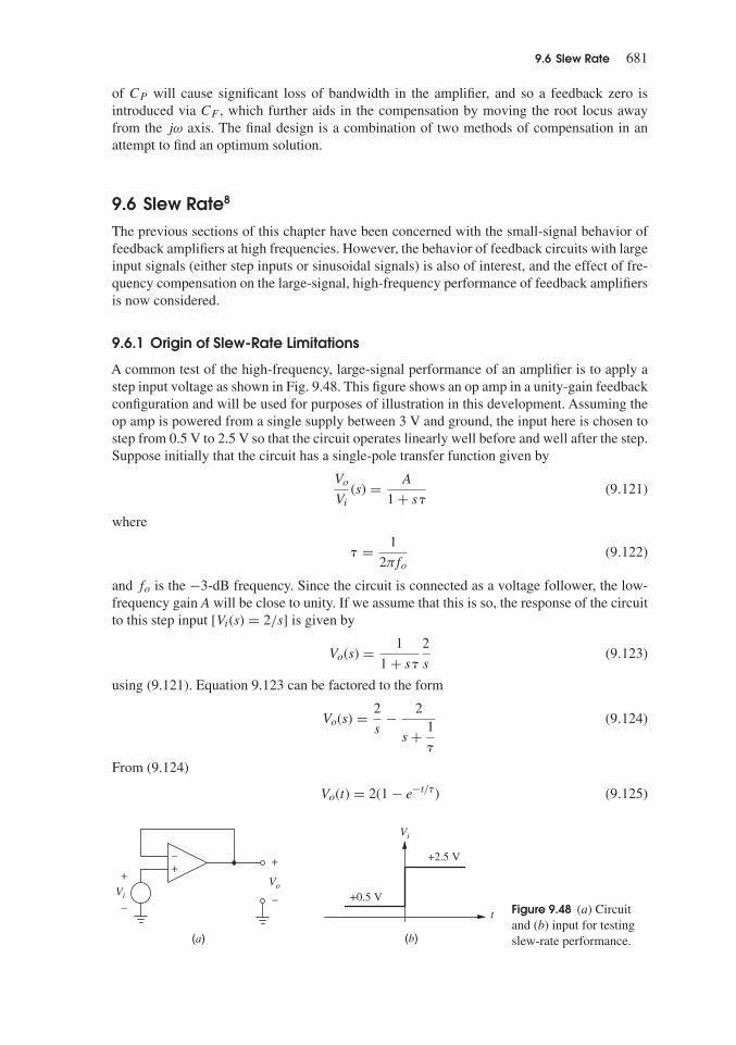
9.6 Slew Rate 681
of CP will cause significant loss of bandwidth in the amplifier, and so a feedback zero isintroduced via CF , which further aids in the compensation by moving the root locus awayfrom the jω axis. The final design is a combination of two methods of compensation in anattempt to find an optimum solution.
9.6 Slew Rate8
The previous sections of this chapter have been concerned with the small-signal behavior offeedback amplifiers at high frequencies. However, the behavior of feedback circuits with largeinput signals (either step inputs or sinusoidal signals) is also of interest, and the effect of fre-quency compensation on the large-signal, high-frequency performance of feedback amplifiersis now considered.
9.6.1 Origin of Slew-Rate Limitations
A common test of the high-frequency, large-signal performance of an amplifier is to apply astep input voltage as shown in Fig. 9.48. This figure shows an op amp in a unity-gain feedbackconfiguration and will be used for purposes of illustration in this development. Assuming theop amp is powered from a single supply between 3 V and ground, the input here is chosen tostep from 0.5 V to 2.5 V so that the circuit operates linearly well before and well after the step.Suppose initially that the circuit has a single-pole transfer function given by
Vo
Vi
(s) = A
1 + s�(9.121)
where
� = 1
2πfo
(9.122)
and fo is the −3-dB frequency. Since the circuit is connected as a voltage follower, the low-frequency gain A will be close to unity. If we assume that this is so, the response of the circuitto this step input [Vi(s) = 2/s] is given by
Vo(s) = 1
1 + s�
2
s(9.123)
using (9.121). Equation 9.123 can be factored to the form
Vo(s) = 2
s− 2
s + 1
�
(9.124)
From (9.124)
Vo(t) = 2(1 − e−t/�) (9.125)
(a)
VoVi
++
+
–
–
–
Vi
t
+2.5 V
+0.5 V
(b)
Figure 9.48 (a) Circuitand (b) input for testingslew-rate performance.

682 Chapter 9 � Frequency Response and Stability of Feedback Amplifiers
0.0
0.5
1.0
1.5
2.0
2.5
0 0.1 0.2 0.3 0.4 0.5t (μs)
t (μs)
(a)
0.0
0.5
1.0
1.5
2.0
2.5
0 1 2 3 4 5
(b)
Vo(V)
Vo(V)
Figure 9.49 Response of the circuit ofFig. 9.48 when a 2-V step input isapplied. (a) Response predicted by(9.125) for the NE5234 op amp.(b) Simulated response for the NE5234.
The predicted response from (9.125) is shown in Fig. 9.49a using data for the NE5234 op ampwith fo � 2.7 MHz. This shows an exponential rise of Vo(t) by 2 V and the output reaches90 percent of its final value in about 0.14 �s.
A typical output for the NE5234 op amp in such a test is shown in Fig. 9.49b and exhibitsa completely different response. The output voltage is a slow ramp of almost constant slopeand takes about 2.6 �s to reach 90 percent of its final value. Obviously the small-signal linearanalysis is inadequate for predicting the circuit behavior under these conditions. The responseshown in Fig. 9.49b is typical of op-amp performance with a large input step voltage applied.The rate of change of output voltage dVo/dt in the region of constant slope is called the slewrate and is usually specified in V/�s.
The reason for the discrepancy between predicted and observed behavior noted abovecan be appreciated by examining the circuit of Fig. 9.48a and considering the responses inFig. 9.49. At t = 0, the input voltage steps up by +2 V, but the output voltage cannot respondinstantaneously and is initially unchanged. Thus the op-amp differential input is Vid = 2 V,which drives the input stage completely out of its linear range of operation. This can be seen byconsidering a two-stage op amp; simplified schematics for a bipolar and CMOS op amp for usein this analysis are shown in Fig. 9.50 a and b. The Miller compensation capacitor C connectsaround the high-gain second stage and causes this stage to act as an integrator. The currentfrom the input stage, which charges the compensation capacitor, is Ix. The large-signal transfercharacteristic from the op-amp differential input voltage Vid to Ix is that of a differential pair,which is shown in Fig. 9.50c. From Fig. 9.50c, the maximum current available to charge Cis 2I1, which is the tail current in the input stage. For a bipolar differential pair, |Ix| ≈ 2I1

9.6 Slew Rate 683
(a)
VCC
–VEE
Ix
CQ1
2I1
Q2
Q4Q3
Vid
Vo–Av
+
–
(b)
VDD
–VSS
Ix
CM1
2I1
M2
M4M3
Vid
Vo–Av
+
–
Vid
Ix
2I1
–2I1
–VIL VIL
(c)
Figure 9.50 Simplifiedschematics of a two-stage(a) bipolar and (b) MOS op ampfor slew rate calculations and(c) approximate large signaltransfer characteristic for theinput stages in (a) and (b). Forthe bipolar differential pair,VIL ≈ 3VT . For the MOSdifferential pair,VIL ≈ √
2|Vov1|.

684 Chapter 9 � Frequency Response and Stability of Feedback Amplifiers
if |Vid | > 3VT . For a MOS differential pair, |Ix| ≈ 2I1 if |Vid | >√
2|Vov1|. (See Chapter 3.)Thus, when Vid = 2 V as described above, the input stage limits and Ix ≈ 2I1 (assuming that√
2|Vov1| < 2 V for the MOS circuit). The circuit thus operates nonlinearly, and linear analysisfails to predict the behavior. If the input stage did act linearly, the input voltage change of 2 Vwould produce a very large current Ix to charge the compensation capacitor. The fact that thiscurrent is limited to the fairly small value of 2I1 is the reason for the slew rate being much lessthan a linear analysis would predict.
Consider a large input voltage applied to the circuits of Fig. 9.50 so that Ix = 2I1. Thenthe second stage acts as an integrator with an input current 2I1, and the output voltage Vo canbe written as
Vo = 1
C
∫2I1dt (9.126)
and thusdVo
dt= 2I1
C(9.127)
Equation 9.127 predicts a constant rate of change of Vo during the slewing period, which is inagreement with the experimental observation.
The above calculation of slew rate was performed on the circuits of Fig. 9.50, which haveno overall feedback. Since the input stage produces a constant output current that is independentof its input during the slewing period, the presence of a feedback connection to the input doesnot affect the circuit operation during this time. Thus, the slew rate of the amplifier is the samewhether feedback is applied or not.
The NE5234 op amp does not quite fit the model shown in Fig. 9.50a because the output ofits first stage is differential. Figure 9.51 shows a model that assumes the op-amp common-modeinput voltage is low enough that Q1, Q2, and Q5-Q7 in Fig. 6.36 are off. In practice, the inputstep in Fig. 9.48a changes the op-amp common-mode input voltage. Although this changeaffects the biasing of the input stage in the NE5234, it has little effect on the currents that limitthe slew rate because the total current that biases the two differential pairs Q1-Q4 in Fig. 6.36
Vo
VCC
IC9 IC10
Vid
Vbiascm
BiasCM
Q10Q9
Q3 Q4
I21
I4
I3
I22
C21 =5.2 pF
R922 kΩ
R1022 kΩ
910
6 μA 6 μA6 μA
+
+––
C22 =5.5 pF
–VEE = 0
Figure 9.51 Simplified schematic of the NE5234 op amp.

9.6 Slew Rate 685
is constant. Therefore, the change in the op-amp common-mode input voltage is ignored here.The three current sources at the top of Fig. 9.51 model the dc currents set by transistors Q11,Q13, and Q14 in Fig. 6.36 and are assumed constant here. When Vid = 0, IC3 = IC4 = −3 �A,ignoring base currents (as is done throughout this analysis for simplicity). The negative signshere stem from the convention that defines transistor collector current as positive when it flowsinto the collector. To simplify the following description, let I3 = −IC3 and I4 = −IC4. Thenwith Vid = 0, I3 = I4 = 3 �A, IC9 = IC10 = 6 �A, and capacitor currents I21 = I22 = 0, asshown in Fig. 9.51 and calculated in Chapter 6. Immediately after the step input in Fig. 9.48, Q4turns off, I3 = 6 �A and I4 = 0. Note that the changes in I3 and I4 are differential in the sensethat one increases and the other decreases while their average value is constant. So we willignore the common-mode feedback circuit that controls the average voltage to ground at thefirst-stage outputs and assume the voltage from node BiasCM to ground (Vbiascm) is constant.
First, we calculate IC9 immediately after the input step using the assumption that Vbiascm
is constant by setting VR9 + Vbe9 before and after the step equal to each other.
(3 �A + 6 �A)22 k + VT ln
(6 �A
IS9
)= (6 �A + IC9)22 k + VT ln
(IC9
IS9
)(9.128a)
Simplifying this equation gives
0 = (IC9 − 3 �A)22 k + VT ln
(IC9
6 �A
)(9.128b)
Solving this equation by trial and error gives IC9 = 3.6 �A. Then from KCL at node 9,I21 = 6 �A − IC9 = 2.4 �A. As a result, dV9/dt = 2.4 �A/5.2 pF = 0.46 V /�s, where V9 isthe voltage from node 9 to ground.
Next, we calculate IC10 immediately after the input step in a similar manner.
(3 �A + 6 �A)22 k + VT ln
(6 �A
IS10
)= (IC10)22 k + VT ln
(IC10
IS10
)(9.128c)
Simplifying this equation gives
0 = (IC10 − 9 �A)22 k + VT ln
(IC10
6 �A
)(9.128d)
Solving this equation by trial and error gives IC9 = 8.6 �A. Then from KCL at node 10,I22 = IC10 − 6 �A = 2.6 �A. Therefore, the voltage across C22 increases at a rate of d(Vo −V10)/dt = 2.6 �A/5.5 pF = 0.47 V/�s, where V10 is the voltage from node 10 to ground. InFig. 9.51, the amplifier that represents the second and third stages in the NE5234 has negativefeedback connected around it through capacitor C22. Assuming that the gain of this amplifieris large and that it operates linearly, Vo is driven so that V10 � V9. Therefore, the slew rate ofthe NE5234 is
dVo/dt = dV9/dt + d(Vo − V10)/dt = (0.46 + 0.47) V/�s = 0.93 V/�s (9.128e)
In contrast, the plot in Fig. 9.49b shows that the simulated slew rate is about 0.68 V/�s, andthe difference stems partly from ignoring base currents in the calculations above.
9.6.2 Methods of Improving Slew-Rate in Two-Stage Op Amps
In order to examine methods of slew-rate improvement, a more general analysis is required.This can be performed using the circuit of Fig. 9.52, which is a general representation of an opamp circuit. The input stage has a small-signal transconductance gmI and, with a large inputvoltage, can deliver a maximum current Ixm to the next stage. The compensation is shown

686 Chapter 9 � Frequency Response and Stability of Feedback Amplifiers
gmI Vo
Ix
Ixm
C
Vi
+
–
Largevoltage
gain
Available
Figure 9.52 Generalized representation of an op amp for slew-rate calculations.
as the Miller effect using the capacitor C, since this representation describes most two-stageintegrated-circuit op amps.
From Fig. 9.52 and using (9.127), we can calculate the slew rate for a large input voltage as
dVo
dt= Ixm
C(9.129)
Consider now small-signal operation. For the input stage, the small-signal transconductance is
�Ix
�Vi
= gmI (9.130)
For the second stage (which acts as an integrator) the transfer function at high frequencies is
�Vo
�Ix
= 1
sC(9.131a)
and in the frequency domain
�Vo
�Ix
(jω) = 1
jωC(9.131b)
Combining (9.130) and (9.131b) gives
�Vo
�Vi
(jω) = gmI
jωC(9.131c)
In our previous consideration of compensation, it was shown that the small-signal, open-loopvoltage gain (�Vo/�Vi)(jω) must fall to unity at or before a frequency equal to the magnitudeof the second most dominant pole (ω2). If we assume, for ease of calculation, that the circuitis compensated for unity-gain operation with 45◦ phase margin as shown in Fig. 9.15, thegain (�Vo/�Vi)(jω) as given by (9.131c) must fall to unity at frequency ω2. (Compensationcapacitor C must be chosen to ensure that this occurs.) Thus from (9.131c)
1 = gmI
ω2C
and thus1
C= ω2
gmI
(9.132)
Note that (9.132) was derived on the basis of a small-signal argument. This result can now besubstituted in the large-signal equation (9.129) to give
Slew rate = dVo
dt= Ixm
gmI
ω2 (9.133)

9.6 Slew Rate 687
Equation 9.133 allows consideration of the effect of circuit parameters on slew rate, and itis apparent that, for a given ω2, the ratio Ixm/gml must be increased if slew rate is to be increased.
9.6.3 Improving Slew-Rate in Bipolar Op Amps
The analysis of the previous section can be applied to a bipolar op amp that uses Millercompensation. In the case of the op amp in Fig. 9.50a, we have Ixm = 2I1, gmI = qI1/kT ,and substitution in (9.133) gives
Slew rate = 2kT
qω2 (9.134)
Since both Ixm and gmI are proportional to bias current I1, the influence of I1 cancels in theequation and slew rate is independent of I1 for a given ω2. However, increasing ω2 will increasethe slew rate, and this course is followed in most high-slew-rate circuits. The limit here is setby the frequency characteristics of the transistors in the IC process, and further improvementsdepend on circuit modifications as described below.
The above calculation has shown that varying the input-stage bias current of a two-stagebipolar op amp does not change the circuit slew rate. However, (9.133) indicates that for agiven Ixm, slew rate can be increased by reducing the input-stage transconductance. One waythis can be achieved is by including emitter-degeneration resistors to reduce gmI as shown inFig. 9.53. The small-signal transconductance of this input stage can be shown to be
gmI = �Ix
�Vid
= gm11
1 + gm1RE
(9.135)
where
gm1 = qI1
kT(9.136)
The value of Ixm is still 2I1. Substituting (9.135) in (9.133) gives
Slew rate = 2kT
qω2 (1 + gm1RE) (9.137)
+VCC
–VEE
RE
Ix
Q1
Q4
Q2
Q3
2I1
VidRE
+
–
Figure 9.53 Inclusion of emitter resistors in theinput stage in Fig. 9.50a to improve slew rate.

688 Chapter 9 � Frequency Response and Stability of Feedback Amplifiers
Thus the slew rate is increased by the factor [1 + (gm1RE)] over the value given by (9.134).The fundamental reason for this is that, for a given bias current I1, reducing gmI reduces thecompensation capacitor C required, as shown by (9.132).
The practical limit to this technique is due to the fact that the emitter resistors of Fig. 9.53have a dc voltage across them, and mismatches in the resistor values give rise to an input dcoffset voltage. The use of large-area resistors can give resistors whose values match to within0.2 percent (1 part in 500). If the maximum contribution to input offset voltage allowed fromthe resistors is l mV, then these numbers indicate that the maximum voltage drop allowed is
I1RE|max = 500 mV (9.138)
Thus
gm1RE|max = q
kTI1RE|max = 500
26= 20 (9.139)
Using (9.139) in (9.137) shows that given these data, the maximum possible improvement inslew rate by use of emitter resistors is a factor of 21 times.
Finally, in this description of methods of slew-rate improvement, we mention the Class ABinput stage described by Hearn.21 In this technique, the small-signal transconductance of theinput stage is left essentially unchanged, but the limit Ixm on the maximum current available forcharging the compensation capacitor is greatly increased. This is done by providing alternativepaths in the input stage that become operative for large inputs and deliver large charging currentsto the compensation point. This has resulted in slew rates of the order of 30 V/�s in bipolar opamps, and, as in the previous cases, the limitation is an increase in input offset voltage.
9.6.4 Improving Slew-Rate in MOS Op Amps
A two-stage Miller-compensated MOS op amp is shown in Fig. 9.50b, and its slew rate isgiven by (9.127). From the analysis in Section 9.6.2, (9.133) shows that the slew rate can beincreased by increasing ω2. On the other hand, if ω2 is fixed, increasing the ratio Ixm/gmI
improves the slew rate. Using (1.180), (9.133) can be rewritten as
Slew rate = Ixm
gmI
ω2 = 2I1√2k′(W/L)1I1
ω2 =√
2I1
k′(W/L)1ω2 (9.140)
This equation shows that the slew rate increases if (W/L)1 decreases with I1 constant. In thiscase, gmI = gm1 decreases. From (9.132), a smaller compensation capacitor can then be used;therefore, the slew rate in (9.127) increases because I1 is unchanged. Equation 9.140 alsoshows that the slew rate can be increased by increasing I1. Assume that I1 increases by a factorx where x > 1. Then the ratio Ixm/gmI increases by the factor
√x because gm1 is proportional
to√
I1. From (9.132), the compensation capacitor must be increased by the factor√
x if ω2 isfixed. With these changes, the slew rate in (9.127) becomes
dVo
dt= 2xI1
C√
x= 2I1
√x
C(9.141)
Since x > 1, the slew rate is increased.Alternatively, the ratio Ixm/gmI of the input stage can be increased by adding degeneration
resistors RS in series with the sources of M1 and M2 to give
gmI = gm1
1 + (gm1 + gmb1)RS
(9.142)

9.6 Slew Rate 689
For fixed I1, increasing RS decreases gmI and increases Ixm/gmI , which increases theslew rate.
These approaches increase the slew rate but have some drawbacks. First, decreasing gmI
of the input stage while keeping its bias current constant will usually lower the dc gain of thefirst stage and hence reduce the dc gain of the entire op amp. Also, increasing I1 or reducing(W/L)1 tends to increase the input-offset voltage of the op amp, as can be seen from (3.248).Finally, if source-degeneration resistors are added, mismatch between these resistors degradesthe input-offset voltage.
For single-stage MOS op amps, such as the telescopic-cascode and folded-cascode opamps, the slew rate is set by the maximum output current divided by the capacitance that loadsthe output. The maximum output current is equal to the tail current in these op amps.
EXAMPLE
Find the output slew rate for the cascode op amp shown in Fig. 9.54.Assuming the op amp has a large positive differential input voltage applied, M2 is cutoff
and ITAIL flows through M1. Therefore the drain current in M2A is zero, and the drain currentin M3 is Id3 = −ITAIL. The current mirror M3-M4 forces Id3 = Id4. It follows that Id4A =Id4 = −ITAIL. The current flowing into the load capacitor CL is
Io = −Id2A − Id4A = −0 − (−ITAIL) = ITAIL
Therefore the positive output slew rate is
dVo
dt= Io
CL
= ITAIL
CL
(9.143)
Application of a large negative input forces M1 into cutoff so ITAIL must flow through M2.Therefore, Id4A = Id4 = Id3 = 0 and Id2A = Id2 = ITAIL. The current Io flowing throughCL is
Io = −Id2A − Id4A = −ITAIL − 0 = −ITAIL
Hence, the negative slew rate is the opposite of the value in (9.143), −ITAIL/CL.
VB1
M4M3
M2M1
M4A
M2A
Id4A
Id2A
ITAIL
M3A
M1A
CLVB2
–VSS
VDD
Io
in–in+
Vo
+
–
Figure 9.54 A CMOStelescopic-cascode op amp.

690 Chapter 9 � Frequency Response and Stability of Feedback Amplifiers
CS
CI
Cip
CL Vo
+
–
+
–
Figure 9.55 An op amp with capacitiveload and feedback. This is the switched-capacitor integrator of Fig. 6.10a during φ2,assuming ideal MOS switches.
CMOS op amps are often used without an output stage when the output loading is purelycapacitive, as is the case in switched-capacitor circuits. Avoiding an output stage saves powerand is possible because low-output resistance is not needed to drive a capacitive load. Anexample of such a circuit is the switched-capacitor integrator shown in Fig. 6.10a. This circuitis redrawn in Fig. 9.55 when clock phase φ2 is high and φ1 is low, assuming that MOStransistors M1-M4 behave like ideal switches. The additional capacitor Cip here models thetotal parasitic capacitance at the op-amp input and includes the input capacitance of the opamp. A question that arises is: “For the feedback circuit in Fig. 9.55, what value of output loadcapacitance should be used to compute the slew rate for a single-stage op amp?” When theop amp is slewing, its behavior is nonlinear. Therefore the feedback is not effective and thevirtual ground at the negative op-amp input is lost. With the feedback loop broken, the totalcapacitance seen from the output to ground is
CL + CI ||(CS + Cip) (9.144)
This is the capacitance seen looking from the op-amp output node to ground, with the con-nection to the op-amp inverting input replaced with an open circuit. The effective output loadcapacitance in (9.144) is the same as the output load found when the feedback loop is brokento find the return ratio.
For the CMOS op amps considered so far in this section, the slew rate is proportional to abias current in the op amp.ACMOS op amp with a ClassAB input stage can give a slew rate thatis not limited by a dc bias current in the op amp.An example22,23 is shown in Fig. 9.56. The inputvoltage is applied between the gates of M1, M2 and M3, M4. Transistors M1 and M4 act simplyas unity-gain source followers to transfer the input voltage to the gates of M6 and M7. Diode-connected transistors M5 and M8 act as level shifts, which, together with bias current sources I1,set the quiescent ClassAB current in M2, M3, M6, and M7. The currents in M3 and M7 are deliv-ered to the output via cascode current mirrors M9, M10, M13, M14 and M11, M12, M15, M16.Bias currents can be determined by assuming that the input voltage Vi = 0, giving
VGS1 + |VGS5| = |VGS6| + VGS3 (9.145)
Assuming that (1.157) is valid we have
Vtn +√
2I1
k′n
(L
W
)1+ |Vtp| +
√2
I1
k′p
(L
W
)5
= |Vtp| +√
2IB
k′P
(L
W
)6+ Vtn +
√2IB
k′n
(L
W
)3
(9.146)
where IB = |ID6| = ID3 = ID2 = |ID7| is the bias current and subscripts n and p indicateNMOS and PMOS, respectively. The two sides of the input stage are assumed symmetrical.From (9.146) we have
√IB
[√2
k′p
(L
W
)6+√
2
k′n
(L
W
)3
]= √
I1
[√2
k′p
(L
W
)5+√
2
k′n
(L
W
)1
](9.147)
Equation 9.147 is the design equation for the input-stage bias current IB.

9.6 Slew Rate 691
M1
M13M9
M14M10
M6
M16M12
M15
I1I1
M11
M8M7M5
M2 M3 M4
Vo
Io
VDD
id3
id7
–VSS
in+in–
Figure 9.56 CMOS amplifier with a Class AB input stage.
Assuming that the cascode current mirrors in Fig. 9.56 have unity current gain, the biascurrents in M9-M16 all equal IB. To analyze this circuit, we will connect a voltage Vi to thenoninverting op-amp input and ground the inverting op-amp input. If a positive Vi is applied,the magnitude of the currents in M3 and M6 increase, while the magnitude of the currents inM2 and M7 decrease. When mirrored to the output, these changes drive Io and Vo positive. Tocalculate the small-signal gain, we neglect body effect. We can consider M6 to act as sourcedegeneration for M3. The resistance looking into the source of M6 is 1/gm6, thus
id3 = gm3
1 + gm3
gm6
vi (9.148)
Similarly, M2 acts as source degeneration for M7, so
id7 = gm7
1 + gm7
gm2
vi = gm2
1 + gm2
gm7
vi (9.149)
where the right-most expression is found by rearranging. Thus, the transconductance of theamplifier is
Gm = io
vi
∣∣∣∣vo = 0
= id3 + id7
vi
= 2gm3
1 + gm3
gm6
(9.150)
using gm2 = gm3 and gm6 = gm7. If gm3 = gm6, then Gm = gm3.

692 Chapter 9 � Frequency Response and Stability of Feedback Amplifiers
The output resistance of this op amp is just the output resistance of the cascodes in paralleland is
Ro ≈ (ro14gm14ro13)||(ro15gm15ro16) (9.151)
Finally, the small-signal voltage gain is
Av = GmRo (9.152)
The small-signal analysis above showed that a small positive Vi causes a positive Io. IfVi continues to increase beyond the small-signal linear range of the input stage, M2 and M7will be cut off, while M3 and M6 will be driven to larger values of |Vgs|. The currents in M3and M6 can increase to quite large values, which gives a correspondingly large positive Io. Forlarge negative values of Vi, M3 and M6 turn off, M2 and M7 conduct large currents, and Io
becomes large negative. Thus this circuit is capable of supplying large positive and negativecurrents to a load capacitance, and the magnitude of these output currents can be much largerthan the bias current IB in the input stage. Therefore, this op amp does not display slew-ratelimiting in the usual sense.
One disadvantage of this structure is that about half the transistors turn completely offduring slewing. As a result, the time required to turn these transistors back on can be animportant limitation to the high-frequency performance. To overcome this problem, the opamp can be designed so that the minimum drain currents are set to a nonzero value.24
9.6.5 Effect of Slew-Rate Limitations on Large-Signal Sinusoidal Performance
The slew-rate limitations described above can also affect the performance of the circuit whenhandling large sinusoidal signals at higher frequencies. Consider the circuit of Fig. 9.48 witha large sinusoidal signal applied as shown in Fig. 9.57a. Since the circuit is connected as avoltage follower, the output voltage Vo will be forced to follow the Vi waveform. The maximumvalue of dVi/dt occurs as the waveform crosses the axis, and if Vi is given by
Vi = V̂ i sin ωt (9.153)
then
dVi
dt= ωV̂ i cos ωt
and
dVi
dt
∣∣∣∣max
= ωV̂ i (9.154)
As long as the value of dVi/dt|max given by (9.154) is less than the slew-rate limit, the outputvoltage will closely follow the input. However, if the product ωV̂ i is greater than the slew-ratelimit, the output voltage will be unable to follow the input, and waveform distortion of the kindshown in Fig. 9.57b will result. If a sine wave with V̂ i equal to the supply voltage is applied tothe amplifier, slew limiting will eventually occur as the sine-wave frequency is increased. Thefrequency at which this occurs is called the full-power bandwidth of the circuit. (In practice,a value of V̂ i slightly less than the supply voltage is used to avoid clipping distortion of thetype described in Chapter 5.)

Appendix 693
(a)
(b)
Vi
t
dVi
dtmax
Viˆ
Vo
t
Actual waveform
Sinewave
Figure 9.57 (a) Large sinusoidal input voltageapplied to the circuit of Fig. 9.48. (b) Outputvoltage resulting from input (a) showing slewlimiting.
EXAMPLE
Calculate the full-power bandwidth of the NE5234. Use V̂ i = 1 V. From (9.154) put
ωV̂ i = slew rate
Using the slew rate of 0.68 V/�s found in simulation gives
ω = 0.68 V/�s
1 V= 680 × 103 rad/s
Thus
f = 110 kHz
This means that a NE5234 op amp with a sinusoidal output of 1 V amplitude will begin toshow slew-limiting distortion if the frequency exceeds 110 kHz.
APPENDIX
A.9.1 ANALYSIS IN TERMS OF RETURN-RATIO PARAMETERS
Much of the analysis in this chapter is based on the ideal block diagram in Fig. 9.1. This blockdiagram includes the forward gain a and feedback f, which are the parameters used in two-portanalysis of feedback circuits in Chapter 8. The resulting closed-loop gain expression is
A = a
1 + T= a
1 + af(9.155)

694 Chapter 9 � Frequency Response and Stability of Feedback Amplifiers
The block diagram from return-ratio analysis in Fig. 8.42 is the same as Fig. 9.1 if ais replaced by b, f is replaced by 1/A∞, and the direct feedforward d is negligible. (Thecontribution of feedforward through the feedback network to a is also neglected in the analysisin Sections 9.2–9.5, since feedforward introduces one or more zeros into a(s), but only one-and two-pole a(s) are considered in these sections. Neglecting the feedforward in a or the directfeedthrough d is reasonable if its effect is negligible at and below the frequency where themagnitude of the loop transmission falls to 1.) The corresponding equations from return-ratioanalysis are
A = b
1 + �+ d
1 + �≈ b
1 + �= b
1 + b
A∞
(9.156)
For the circuit in Fig. 8.24, 0 ≤ 1/A∞ ≤ 1, and b is positive at low frequencies. Therefore,the equations, graphs, and relationships in Sections 9.2–9.5 can be expressed in terms of thereturn-ratio variables by making the following substitutions:
a → b (9.157a)
f → 1/A∞ (9.157b)
T → � (9.157c)
af→ b/A∞ (9.157d)
The return ratio can be used to check stability of an amplifier with a single feedback loopbecause A∞ and d are stable transfer functions associated with passive networks, and �(s) isstable because it is the signal transfer around a loop that consists of one gain stage or a cascadeof stable gain stages. Therefore the zeros of 1 + �(s), which are poles of the closed-loop gainA, determine the stability of the feedback circuit.25 From the Nyquist stability criterion, thesezeros are in the left half-plane if a polar plot of �(jω) does not encircle the point (−1,0). Inmost cases, this stability condition is equivalent to having a positive phase margin. The phasemargin is measured at the frequency where |�(jω)| = 1.
Since the equations for two-port and return-ratio analyses are not identical, T (s) and �(s)may be different for a given circuit.26 In general, the phase margins using T and � may differ,but both will have the same sign and therefore will agree on the stability of the feedback circuit.
A.9.2 ROOTS OF A QUADRATIC EQUATION
A second-order polynomial often appears in the denominator or numerator of a transfer func-tion, and the zeros of this polynomial are the poles or zeros of the transfer function. In thisappendix, the relationships between the zeros of a quadratic and its coefficients are exploredfor a few specific cases of interest. Also, the conditions under which a dominant root exists arederived.
Consider the roots of the quadratic equation
as2 + bs + c = 0 (9.158)
The two roots of this equation, r1 and r2, are given by the quadratic formula:
r1,2 = −b �√
b2 − 4ac
2a(9.159)

Appendix 695
where it is understood that the square root of a positive quantity is positive. Factoring b out ofthe square root and rearranging gives
r1,2 = − b
2a
(1 �
√1 − 4ac
b2
)(9.160a)
= − b
2a
(1 �
√D)
(9.160b)
The quantity under the square root in (9.160a) has been replaced by D in (9.160b), where
D = 1 − 4ac
b2 (9.161)
Now, consider the locations of the roots if coefficients a, b, and c all have the same sign.In this case, both roots are in the left half-plane (LHP), as will be shown next. First, note thatif all the coefficients have the same sign, then
b
2a> 0 (9.162)
and4ac
b2 > 0. (9.163)
Let us divide (9.163) into two different regions. First, if
0 <4ac
b2 ≤ 1 (9.164)
then D will be positive and less than one. Therefore,√
D < 1, so 1 + √D and 1 − √
D areboth positive. As a result, the roots are both negative and real, because −b/2a < 0.
Now, consider the other region for (9.163), which is
4ac
b2 > 1 (9.165)
In this case, D < 0; therefore√
D is imaginary. The roots are complex conjugates with areal part of −b/2a, which is negative. So the roots are again in the LHP. Therefore, whencoefficients a, b, and c all have the same sign, both roots are in the LHP.
Next, consider the locations of the roots if coefficients a and b have the same sign and chas a different sign. In this case, one real root is in the right half-plane (RHP) and the other is inthe LHP. To prove this, first note from (9.161) that D > 1 here because 4ac/b2 < 0. Thereforeboth roots are real and
√D > 1, so
1 +√
D > 0 (9.166a)
and
1 −√
D < 0 (9.166b)
Substituting into (9.160), one root will be positive and the other negative (the sign of −b/2a
is negative here).Finally, let us consider the conditions under which LHP roots are real and widely spaced.
From (9.160), real LHP roots are widely spaced if
− b
2a(1 +
√D) � − b
2a(1 −
√D) (9.167)
or
1 +√
D � 1 −√
D (9.168)

696 Chapter 9 � Frequency Response and Stability of Feedback Amplifiers
Substituting the expression for D in (9.161) into (9.168) and simplifying leads to an equivalentcondition for widely spaced roots, which is
4ac
b2 � 1 (9.169)
Under this condition, one root is
r2 = − b
2a(1 +
√D) ≈ − b
2a(1 + 1) = −b
a(9.170a)
The other root is
r1 = − b
2a(1 −
√D)
= − b
2a
(1 −√
1 − 4ac
b2
)(9.170b)
≈ − b
2a
(1 −(
1 − 4ac
2b2
))= − c
b
where the approximation√
1 − x ≈ 1 − x
2for |x| � 1 (9.171)
has been used. Here, |r1| � |r2| because |r1| ≈ c/b � b/a ≈ |r2| (which follows from4ac/b2 � 1). If these roots are poles, r1 corresponds to the dominant pole, and r2 gives thenondominant pole. Equations 9.170a and 9.170b are in agreement with (9.30) through (9.33).
Table 9.1 summarizes the location of the roots of (9.158) for the cases considered in thisappendix. When both roots are in the LHP, the roots are both real if (9.164) is satisfied. Theseroots are widely spaced if (9.169) is satisfied.
Table 9.1
Sign of Coefficient Values in (9.158)a b c Roots
+ + + Both in LHP− − − Both in LHP+ + − One in LHP, one in RHP− − + One in LHP, one in RHP
PROBLEMS9.1 An amplifier has a low-frequency forward
gain of 200 and its transfer function has three neg-ative real poles with magnitudes 1 MHz, 2 MHz,and 4 MHz. Calculate and sketch the Nyquist dia-gram for this amplifier if it is placed in a negativefeedback loop with f = 0.05. Is the amplifier stable?Explain.
9.2 For the amplifier in Problem 9.1, calculateand sketch plots of gain (in decibels) and phase versus
frequency (log scale) with no feedback applied. Deter-mine the value of f that just causes instability and thevalue of f giving a 60◦ phase margin.
9.3 If an amplifier has a phase margin of 20◦, howmuch does the closed-loop gain peak (above the low-frequency value) at the frequency where the loop-gainmagnitude is unity?
9.4 An amplifier has a low-frequency forward gainof 40,000 and its transfer function has three negative

Problems 697
real poles with magnitudes 2 kHz, 200 kHz, and4 MHz.
(a) If this amplifier is connected in a feedbackloop with f constant and with low-frequency gainA0 = 400, estimate the phase margin.
(b) Repeat (a) if A0 is 200 and then 100.
9.5 An amplifier has a low-frequency forward gainof 5000 and its transfer function has three negativereal poles with magnitudes 300 kHz, 2 MHz, and25 MHz.
(a) Calculate the dominant-pole magnitude re-quired to give unity-gain compensation of this ampli-fier with a 45◦ phase margin if the original amplifierpoles remain fixed. What is the resulting bandwidth ofthe circuit with the feedback applied?
(b) Repeat (a) for compensation in a feedback loopwith a closed-loop gain of 20 dB and 45◦ phase margin.
9.6 The amplifier of Problem 9.5 is to be compen-sated by reducing the magnitude of the most dominantpole.
(a) Calculate the dominant-pole magnitude re-quired for unity-gain compensation with 45◦ phasemargin, and the corresponding bandwidth of the circuitwith the feedback applied. Assume that the remainingpoles do not move.
(b) Repeat (a) for compensation in a feedback loopwith a closed-loop gain of 20 dB and 45◦ phase margin.
9.7 Repeat Problem 9.6 for the amplifier of Prob-lem 9.4.
9.8 An op amp has a low-frequency open-loopvoltage gain of 100,000 and a frequency response witha single negative-real pole with magnitude 5 Hz. Thisamplifier is to be connected in a series-shunt feedbackloop with f = 0.01 giving a low-frequency closed-loop voltage gain A0 ≈ 100. If the output impedancewithout feedback is resistive with a value of 100 ,show that the output impedance of the feedback circuitcan be represented as shown in Fig. 9.58, and calculatethe values of these elements. Sketch the magnitude ofthe output impedance of the feedback circuit on logscales from 1 Hz to 100 kHz.
L
R1
R2
zo
Figure 9.58 Circuit representation of the outputimpedance of a series-shunt feedback circuit.
9.9 An op amp with low-frequency gain of 108dB has three negative real poles with magnitudes30 kHz, 500 kHz, and 10 MHz before compensation.The circuit is compensated by placing a capaci-tance across the second stage, causing the secondmost dominant pole to become negligible becauseof pole splitting. Assume the small-signal transcon-ductance of the second stage is 6.39 mA/V and thesmall-signal resistances to ground from the inputand output are 1.95 M and 86.3 k, respec-tively. Calculate the value of capacitance requiredto achieve a 60◦ phase margin in a unity-gain feed-back connection and calculate the frequency wherethe resulting open-loop gain is 0 dB. Assume that thepole with magnitude 10 MHz is unaffected by thecompensation.
9.10 Repeat Problem 9.9 if the circuit is compen-sated by using shunt capacitance to ground at the inputof the second stage. Assume that this affects only themost dominant pole.
9.11 An amplifier has gain a0 = 200 and itstransfer function has three negative real poles withmagnitudes 1 MHz, 3 MHz, and 4 MHz. Calculateand sketch the root locus when feedback is applied asf varies from 0 to 1. Estimate the value of f causinginstability.
9.12 Calculate and sketch the root locus for theamplifier of Problem 9.4 as f varies from 0 to 1. Esti-mate the value of f causing instability and check usingthe Nyquist criterion.
9.13 For the circuit of Fig. 9.41, parameter valuesare RF = 5 k, RE = 50 , and CF = 1.5 pF. Thebasic amplifier of the circuit is shown in Fig. 9.42and has two negative real poles with magnitudes3 MHz and 6 MHz. The low-frequency current gainof the basic amplifier is 4000. Assuming that the loopgain of the circuit of Fig. 9.41 can be varied withoutchanging the parameters of the basic amplifier, sketchroot loci for this circuit as f varies from 0 to 0.01 bothwith and without CF . Estimate the pole positions of thecurrent-gain transfer function of the feedback ampli-fier of Fig. 9.41 with the values of RF and RE specifiedboth with and without CF . Sketch graphs in each caseof gain magnitude versus frequency on log scales fromf = 10 kHz to f = 100 MHz.
9.14 An op amp has two negative real open-looppoles with magnitudes 100 Hz and 120 kHz and anegative real zero with magnitude 100 kHz. The low-frequency open-loop voltage gain of the op amp is100 dB. If this amplifier is placed in a negative feed-back loop, sketch the root locus as f varies from 0 to 1.Calculate the poles and zeros of the feedback amplifierfor f = 10−3 and f = 1.

698 Chapter 9 � Frequency Response and Stability of Feedback Amplifiers
Q1
Q3
Q5
Q6
Q4
Q2
IEE
Vi
+
+15 V
10 pF
–15 V
–
Vo
+
–
300 μA
50 kΩ
20 μA
Figure 9.59 Input stages of an op amp.
9.15 Repeat Problem 9.14 if the circuit has nega-tive real poles with magnitudes 100 Hz and 100 kHzand a negative real zero with magnitude 120 kHz.
9.16 The input stages of an op amp are shown inthe schematic of Fig. 9.59.
(a) Assuming that the frequency response is dom-inated by a single pole, calculate the frequencywhere the magnitude of the small-signal voltage gain|vo(jω)/vi(jω)| is unity and also the output slew rateof the amplifier.
(b) Sketch the response Vo(t) from 0 to 20 �s fora step input at Vi from −5 V to +5 V. Assume thatthe circuit is connected in a noninverting unity-gainfeedback loop.
(c) Compare your results with a SPICE simu-lation using parameters β = 100, VA = 130 V, andIS = 10−15 A for all devices.
9.17 Repeat Problem 9.16 if the circuit of Fig. 9.59is compensated by a capacitor of 0.05 �F connectedfrom the base of Q5 to ground.Assume that the voltagegain from the base of Q5 to Vo is −500.
9.18 The slew rate of the circuit of Fig. 9.59 isto be increased by using 10 k resistors in the emit-ters Q1 and Q2. If the same unity-gain frequency is tobe achieved, calculate the new value of compensationcapacitor required and the improvement in slew rate.Check your result with SPICE simulations.
9.19 Repeat Problem 9.18 if PMOS transistorsreplace Q1 and Q2 (with no degeneration resistors).Assume that the PMOS transistors are biased to300 �A each (IEE = 600 �A), at which bias valuethe MOS transistors have gm = 300 �A/V.
9.20(a) Calculate the full-power bandwidth of thecircuit of Fig. 9.59.
(b) If this circuit is connected in a noninvertingunity-gain feedback loop, sketch the output waveformVo if Vi is a sinusoid of 10 V amplitude and frequency45 kHz.
9.21 For the CMOS operational amplifier shown inFig. 9.60, calculate the open-loop voltage gain, unity-gain bandwidth, and slew rate. Assume the parametersof Table 2.1 with Xd = 1 �m. Assume that the gate ofM9 is connected to the positive power supply and thatthe W/L of M9 has been chosen to cancel the righthalf-plane zero. Compare your results with a SPICEsimulation.
9.22 Repeat Problem 9.21 except use the aspectratios, supply voltages, and bias current given inFig. 6.58 instead of the values in Fig. 9.60. Also,assume that Xd = 0.1 �m for all transistors operat-ing in the active region, and use Table 2.4 for otherparameters.
9.23 If the circuit of Fig. 9.61 is used to generatethe voltage to be applied to the gate of M9 in Fig. 9.60,calculate the W/L of M9 required to move the righthalf-plane zero to infinity. Use data from Table 2.1with Xd = 1 �m. Check your result with SPICE.
9.24 Repeat Problem 9.23, but skip the SPICEsimulation. Here, M9 will be used in the op amp in Fig.6.58. Let VDD = VSS = 1.5 V and IS = 200 �A. UseL = 1 �m for all transistors, W8 = W10 = 150 �m,and W11 = W12 = 100 �m.Assume that Xd = 0.1 �mfor all transistors operating in the active region, and useTable 2.4 for other parameters.

Problems 699
M8 M5
M1vi M2
M6
M4M3
M7
M9
+
–
vo–
1008
1008
1008
1008
1008
1008
508
508
5 pF
20 μA
+5 V
–5 V
+
Figure 9.60 Circuit forProblem 9.21.
M8 M10
M12M9
1008
1008
1008
M11
1008
20 μA
+5 V
–5 V
Is
Figure 9.61 Circuit for Problem 9.23.
9.25 Assuming that the zero has been moved toinfinity, determine the maximum load capacitance thatcan be attached directly to the output of the circuit ofFig. 9.60 and still maintain a phase margin of 45◦.Neglect all higher order poles except any due to theload capacitance. Use the value of W/L obtained inProblem 9.23 for M9 with the bias circuit of Fig. 9.61.
9.26 Repeat Problem 9.25 except, for the op amp,use the aspect ratios, supply voltages, and bias currentgiven in Fig. 6.58 instead of the values in Fig. 9.60.Also, for the bias circuit, use the aspect ratios, sup-ply voltages, and bias current given in Problem 9.24.Ignore junction capacitance for all transistors. Also,
assume that Xd = 0.1 �m for all transistors operat-ing in the active region, and use Table 2.4 for otherparameters.
9.27 For the CMOS op amp of Fig. 9.60, assumethat M9 and the compensation capacitor are removedand the output is loaded with a 1 M resistor. Usingthe data of Table 2.1, use SPICE to determine the gainand phase versus frequency of the small-signal circuitvoltage gain.
The amplifier is to be connected in a negativefeedback loop with the 1-M resistor connected fromthe output to the gate of M1, and a resistor Rx from theM1 gate to ground. An input voltage is applied from

700 Chapter 9 � Frequency Response and Stability of Feedback Amplifiers
the gate of M2 to ground. From your previous simu-lated data, determine the forward voltage gain of thefeedback configuration and the corresponding valuesof Rx giving phase margins of 80◦, 60◦, 45◦, and 20◦.For each case use SPICE to plot out the correspondingoverall small-signal voltage gain versus frequency forthe feedback circuit and also the step response for anoutput voltage step of 100 mV. Compare and commenton the results obtained. Assume Xd = 1 �m and thatthe drain and source regions are 2 �m wide.
9.28 The CMOS circuit of Fig. 9.56 is to be usedas a high-slew-rate op amp. A load capacitance ofCL = 10 pF is connected from Vo to ground. Supplyvoltages are � 5 V and I1 = 20 �A. Devices M1–M4
have W = 20 �m and L = 1 �m and devices M5–M8
have W = 60 �m and L = 1 �m. All other NMOSdevices have W = 60 �m and L = 1 �m, and all otherPMOS devices have W = 300 �m and L = 1 �m.Device data are μnCox = 60 �A/V2, Vtn = 0.7 V,Vtp = −0.7 V, γ = 0, and |λ| = 0.05 V−1.
(a) Calculate the small-signal open-loop gain andunity-gain bandwidth of the circuit. Derive an expres-sion for the large-signal transfer function Io/Vi whenall four devices M2, M3, M6, and M7 are on, and alsofor larger Vi when two of them cut off. At what valueof Vi does the transition occur?
(b) Connect the circuit in a unity-gain negativefeedback loop (Vo to the gate of M1) and drive thecircuit with a voltage step from −1.5 V to + 1.5 V atthe gate of M4. Calculate and sketch the correspond-ing output waveform Vo assuming linear operation,and compare all your results with a SPICE simulation.What is the peak current delivered to CL during thetransient?
9.29 Using the basic topology of Fig. 8.53, designa CMOS feedback amplifier with Ri = ∞, Ro <
30 , Av = vo/vi = 10, and small-signal bandwidthf−3dB > 2 MHz. No peaking is allowed in the gain-versus-frequency response. Supply current must beless than 2 mA from each of � 5 V supplies. Thecircuit operates with RL = 1 k to ground and mustbe able to swing Vo =� 1 V before clipping occurs.Use the process data of Table 2.1 with Xd = 0.5 �mand γn = 0.5 V1/2. Source and drain regions are9 �m wide. Verify your hand calculations with SPICEsimulations.
9.30 Determine the compensation capacitor for thetwo-stage op amp in the example in Section 9.4.3 thatgives a 60◦ phase margin.
9.31 The Miller-compensated two-stage op ampin Fig. 9.25 can be modeled as shown in Fig. 9.26. Inthe model, let gm1 = 0.5 mA/V, R1 = 200 k, gm6 =2 mA/V, R2 = 100 k, C1 = 0.1 pF, and C2 = 8 pF.
(a) Assume the op amp is connected in negativefeedback with f = 0.5. What is the value of C thatgives a 45◦ phase margin? Assume the right half-plane(RHP) zero has been eliminated, and assume the feed-back network does not load the op amp.
(b) What value of Rz in Fig. 9.26 eliminates theRHP zero?
9.32 Repeat Problem 9.31(a) for the common-gatecompensation scheme in Fig. 9.22a.
9.33 The simple model for the common-gate M11
in Fig. 9.22b has zero input impedance. Show that ifthe common-gate stage M11 is modeled with nonzeroinput impedance, the compensation scheme in Fig.9.22a introduces a zero at −gm11/C in the amplifiergain. To simplify this analysis, assume that ro11 = ∞,γ = 0, and ignore all device capacitances.
9.34 Plot a locus of the poles of (9.27) as C variesfrom 0 to ∞. Use R1 = 200 k, gm = 2 mA/V,R2 = 100 k, C1 = 0.1 pF, and C2 = 8 pF.
9.35 For the three-stage op amp with nested Millercompensation in Fig. 9.30c, determine the values ofthe compensation capacitors that give a 45◦ phasemargin when the op amp is in a unity-gain negativefeedback loop (f = 1). Assume that the zeros due tofeedforward have been eliminated. Design for widelyspaced real poles. Take R0 = R1 = R2 = 5 k, C0 =C1 = 0.5 pF, and C2 = 6 pF. Use gm0 = gm1 andgm2 = 6gm1.
9.36 For the three-stage op amp with nested Millercompensation in Fig. 9.30c, determine the values ofthe compensation capacitors that give a 60◦ phasemargin when the op amp is in a unity-gain negativefeedback loop (f = 1). Assume that the zeros due tofeedforward have been eliminated. Design for com-plex poles p2 and p3. Use R0 = R1 = R2 = 5 k,C0 = C1 = 0.5 pF, and C2 = 6 pF. Use gm0 = gm1 andgm2 = 6gm1.
9.37 The single-stage op amp in Fig. 9.54 has a45◦ phase margin when the op amp is in a unity-gain negative feedback loop (f = 1) with an outputload capacitance CL = 2 pF. What value of CL willgive a 60◦ phase margin? (Assume that the capaci-tance at the op-amp output is dominated by CL andthe op-amp gain av (s) can be modeled as having twopoles.)
9.38 The single-stage op amp in Fig. 9.54 has anondominant pole p2 with |p2| =200 Mrad/s. Theop amp is in a unity-gain negative feedback loop(f = 1).
(a) If gm1 = 0.3 mA/V, what value of CL givesa 45◦ phase margin? (Assume that the capacitance atthe op amp output is dominated by CL and the op-ampgain a(s) can be modeled as having two poles.)

Problems 701
Vs
Vo
Z1
Z2
vx
–
+
+
–
+
–
avvx
+
–Figure 9.62 Feedback circuit forProblem 9.40.
ViVo
R
C
vx
–
+
+
–
+
–
av(s)·vx
+
–Figure 9.63 Circuit for Problem9.41.
Vi Cin
Vo
100 kΩ
100 kΩ
vx
–
+
+
–
+
–
av(s)vx
+
–Figure 9.64 Circuit for Problem9.42.
(b) If ITAIL = 0.5 mA, what is the output slew ratewith this CL?
9.39 The feedback circuit in Fig. 9.55 is aswitched-capacitor circuit during one clock phase.Assume the op amp is the telescopic-cascode op amp inFig. 9.54. Take CL = 1.5 pF, CI = 4 pF, CS = 0.4 pF,and Cip = 0.1 pF.
(a) If ITAIL = 0.2 mA, what is the output slewrate?
(b) Assume that gm1 = 0.1 mA/V, the loop trans-mission [loop gain T (s) or return ratio �(s)] canbe modeled as having two poles, and the magnitudeof the nondominant pole p2 is |p2| =200 Mrad/s.What is the phase margin of this feedbackcircuit?
9.40 Calculate the return ratio for the feedbackcircuit in Fig. 9.62. Assume that the amplifier voltagegain is constant with av > 0. Show that this feedbackcircuit is always stable if each impedance is either aresistor or a capacitor.
9.41 Calculate the return ratio for the integrator inFig. 9.63. Show that this feedback circuit is stable forall values of R and C if av (s) has two left half-planepoles and av (s = 0) > 0.
9.42 Calculate the return ratio for the invertingamplifier in Fig. 9.64. Here, the controlled source andCin form a simple op-amp model. Assume av (s) =1000/[(1 + s/100)(1 + s/106)].
(a) Assume the op-amp input capacitance Cin = 0.What is the frequency at which |�(jω)| = 1? Howdoes this frequency compare to the frequency at which|av (jω)| = 1?
(b) Find the phase margin for the cases Cin = 0,Cin = 4 pF, and Cin = 20 pF.
9.43 A technique that allows the return ratio tobe simulated using SPICE without disrupting the dcoperating point is shown in Fig. 8.60 and explained inProblem 8.33.
(a) Use that technique to simulate the return ratiofor the op amp from Problem 9.21 connected in anoninverting unity-gain configuration for f = 1 kHz,100 kHz, 10 MHz, and 1 GHz.
(b) Use that technique to plot the magnitude andphase of the return ratio. Determine the unity-gain fre-quency for the return ratio and the phase and gainmargins. [Note: This calculation requires combiningthe complex values of �
′i(jω) and �
′v (jω) to find the
complex quantity �(jω).]

702 Chapter 9 � Frequency Response and Stability of Feedback Amplifiers
Vo
is
+
–
20 kΩ
5 V
0.5 mA
2 pF
Figure 9.65 Circuit for Problem 9.45.
9.44 Repeat Problem 9.43 for the circuit inFig. 9.64 with Cin = 4 pF. Inject the test sources on theleft-hand side of the feedback resistor. Use av (s) fromProblem 9.42. Compare the simulation results with thecalculated values from Problem 9.42.
9.45 Repeat Problem 9.43 for the local feed-back circuit in Fig. 9.65. For the transistor, W =50 �m and Leff = 0.6 �m. Use the device data inTable 2.4. Ignore the drain-body junction capacitance(assuming it is small compared to the 2-pF loadcapacitor).
9.46 Consider a two-stage CMOS op amp mod-eled by the equivalent circuit in Fig. 9.18, whereis = gmvid and vid is the differential op-amp input.Let gm = 19.7 mA/V, R1 = R2 = 6.67 k, and C1 =C2 = C = 2 pF. Calculate and sketch the root locuswhen feedback is applied as f varies from 0 to 1. Cal-culate the real component of s for which the polesbecome complex. Is the amplifier unconditionally sta-ble? If yes, calculate the pole positions for unity-gainfeedback. If no, find the loop gain required to causeinstability.
REFERENCES1. K. Ogata. Modern Control Engineering,
2nd Edition. Prentice-Hall, Englewood Cliffs, NJ,1990.
2. P. W. Tuinenga. SPICE: A Guide to CircuitSimulation and Analysis using PSPICE, 3rd Edition.Prentice-Hall, Englewood Cliffs, NJ, 1995.
3. G. W. Roberts and A. S. Sedra. SPICE, 2ndEdition. Oxford Press, New York, 1997.
4. P. J. Hurst. “Exact Simulation of FeedbackCircuit Parameters,” IEEE Trans. on Circuits and Sys-tems, Vol. CAS-38, No. 11, pp. 1382–1389, November1991.
5. P. J. Hurst and S.H. Lewis. “Determina-tion of Stability Using Return Ratios in BalancedFully Differential Feedback Circuits,” IEEE Trans.on Circuits and Systems II, pp. 805–817, December1995.
6. S. Rosenstark. Feedback Amplifier Principles,MacMillan, New York, 1986.
7. R. D. Middlebrook. “Measurement of LoopGain in Feedback Systems,” Int. J. Electronics,Vol. 38, No. 4, pp. 485–512, 1975.
8. J. E. Solomon. “The Monolithic Op Amp:A Tutorial Study,” IEEE J. Solid-State Circuits, Vol.SC-9, pp. 314–332, December 1974.
9. Y. P. Tsividis and P.R. Gray. “An IntegratedNMOS Operational Amplifier with Internal Compen-sation,” IEEE J. Solid-State Circuits, Vol. SC-11,pp. 748–753, December 1976.
10. B. K. Ahuja. “An Improved FrequencyCompensation Technique for CMOS OperationalAmplifiers,” IEEE J. Solid-State Circuits, Vol. SC-18,pp. 629–633, December 1983.
11. D. B. Ribner and M. A. Copeland. “DesignTechniques for Cascoded CMOS Op Amps withImproved PSRR and Common-Mode Input Range,”IEEE J. Solid-State Circuits, pp. 919–925, December1984.
12. D. Senderowicz, D. A. Hodges, and P. R.Gray. “A High-Performance NMOS OperationalAmplifier,” IEEE J. Solid-State Circuits, Vol. SC-13,pp. 760–768, December 1978.
13. W. C. Black, D. J. Allstot, and R. A. Reed.“A High Performance Low Power CMOS Chan-nel Filter,” IEEE J. Solid-State Circuits, Vol. SC-15,pp. 929–938, December 1980.
14. E. M. Cherry. “A New Result in NegativeFeedback Theory and Its Application to Audio PowerAmplifiers,” Int. J. Circuit Theory, Vol. 6, pp. 265–288, July 1978.

References 703
15. J. H. Huijsing and D. Linebarger. “Low-Voltage Operational Amplifier with Rail-to-Rail Inputand Output Ranges,” IEEE J. Solid-State Circuits,Vol. 20, pp. 1144–1150. December 1985.
16. R. G. H. Eschauzier and J. H. Huijsing.Frequency Compensation Techniques for Low-PowerOperational Amplifiers. Kluwer, Dordrecht, TheNetherlands, 1995.
17. M. J. Fonderie and J. H. Huijsing. Design ofLow-Voltage Bipolar Operational Amplifiers. KluwerAcademic Publishers, Boston, 1993.
18. F. You, H. K. Embabi, and E. Sanchez-Sinencio. “A Multistage Amplifier Topology withNested Gm-C Compensation,” IEEE J. Solid-State Circuits, Vol. 32, pp. 2000–2011, December1997.
19. P. E. Gray and C. L. Searle. Electronic Princi-ples: Physics, Models, and Circuits. Wiley, New York,1969.
20. J. D’Azzo and C. Houpis. Linear Control Sys-tem Analysis and Design: Conventional and Modern.McGraw-Hill, New York, 1975.
21. W. E. Hearn. “Fast Slewing Monolithic Oper-ational Amplifier,” IEEE J. Solid-State Circuits,Vol. SC-6, pp. 20–24, February 1971.
22. P. W. Li, M. J. Chin, P. R. Gray, and R.Castello. “A Ratio-Independent Algorithmic Analog-to-Digital Conversion Technique,” IEEE J. Solid-StateCircuits, Vol. SC-19, pp. 828–836, December 1984.
23. E. Seevinck and R. Wassenaar. “A VersatileCMOS Linear Transconductor/Square-Law FunctionCircuit,” IEEE J. Solid-State Circuits, Vol. SC-22, pp.366–377, June 1987.
24. F. N. L. O. Eynde, P. F. M.Ampe, L. Verdeyen,and W. M. C. Sansen. “A CMOS Large-Swing Low-Distortion Three-Stage Class AB Power Amplifier,”IEEE J. Solid-State Circuits, Vol. SC-25, pp. 265–273,February 1990.
25. H. W. Bode. Network Analysis and FeedbackAmplifier Design. Van Nostrand, New York, 1945.
26. P. J. Hurst. “A Comparison of TwoApproaches to Feedback Circuit Analysis,” IEEETrans. on Education, Vol. 35, No. 3, pp. 253–261,August 1992.

CHAPTER 10
Nonlinear Analog Circuits
10.1 IntroductionChapters 1 through 9 dealt almost entirely with analog circuits whose primary function islinear amplification of signals. Although some of the circuits discussed (such as Class ABoutput stages) were actually nonlinear in their operation, the operations performed on thesignal passing through the amplifier were well approximated by linear relations.
Nonlinear operations on continuous-valued analog signals are often required in instru-mentation, communication, and control-system design. These operations include modulation,demodulation, frequency translation, multiplication, and division. In this chapter, we analyzethe most commonly used techniques for performing these operations within a monolithic inte-grated circuit. We first discuss the use of the bipolar transistor to synthesize nonlinear analogcircuits and analyze the Gilbert multiplier cell, which is the basis for a wide variety of such cir-cuits. Next we consider the application of this building block as a small-signal analog multiplier,as a modulator, as a phase comparator, and as a large-signal, four-quadrant multiplier.
Following the multiplier discussion, we introduce a highly useful circuit technique forperforming demodulation of FM and AM signals and, at the same time, performing bandpassfiltering. This circuit, the phase-locked-loop (PLL), is particularly well-suited to monolithicconstruction. After exploring the basic concepts involved, we analyze the behavior of the PLLin the locked condition, and then consider the capture transient. Finally, some methods ofrealizing arbitrary nonlinear transfer functions using bipolar transistors are considered.
10.2 Analog Multipliers Employing the Bipolar TransistorIn analog-signal processing the need often arises for a circuit that takes two analog inputs andproduces an output proportional to their product. Such circuits are termed analog multipliers.In the following sections we examine several analog multipliers that depend on the exponentialtransfer function of bipolar transistors.
10.2.1 The Emitter-Coupled Pair as a Simple Multiplier
The emitter-coupled pair, shown in Fig. 10.1, was shown in Chapter 3 to produce outputcurrents that are related to the differential input voltage by
Ic1 = IEE
1 + exp
(−Vid
VT
) (10.1)
Ic2 = IEE
1 + exp
(Vid
VT
) (10.2)
704

10.2 Analog Multipliers Employing the Bipolar Transistor 705
Ic1
IEE
Vid
Q1 Q2
Ic2
+
–
Figure 10.1 Emitter-coupled pair.
where base current has been neglected. Equations 10.1 and 10.2 can be combined to give thedifference between the two output currents:
�Ic = Ic1 − Ic2 = IEE tanh
(Vid
2VT
)(10.3)
This relationship is plotted in Fig. 10.2 and shows that the emitter-coupled pair by itself can beused as a primitive multiplier. We first assume that the differential input voltage Vid is muchless than VT . If this is true, we can utilize the approximation
tanhVid
2VT
≈ Vid
2VT
Vid
2VT
� 1 (10.4)
And (10.3) becomes
�Ic ≈ IEE
(Vid
2VT
)(10.5)
The current IEE is actually the bias current for the emitter-coupled pair. With the additionof more circuitry, we can make IEE proportional to a second input signal Vi2, as shown in
IEE
–IEE
–VT +VTVid
ΔIc
Figure 10.2 The dc transfer character-istic of the emitter-coupled pair.

706 Chapter 10 � Nonlinear Analog Circuits
IEE
RC RC
–VEE
Vo
VCC
Q4
Q1 Q2
Q3Vi2
Vid
R
+
+
–
–
Figure 10.3 Two-quadrant analog multiplier.
Fig. 10.3. Thus we have
IEE ≈ Ko(Vi2 − VBE(on)) (10.6)
The differential output current of the emitter-coupled pair can be calculated by substituting(10.6) in (10.5) to give
�Ic = KoVid(Vi2 − VBE(on))
2VT
(10.7)
Thus we have produced a circuit that functions as a multiplier under the assumption that Vid
is small, and that Vi2 is greater than VBE(on). The latter restriction means that the multiplierfunctions in only two quadrants of the Vid–Vi2 plane, and this type of circuit is termed a two-quadrant multiplier. The restriction to two quadrants of operation is a severe one for manycommunications applications, and most practical multipliers allow four-quadrant operation.The Gilbert multiplier cell,1 shown in Fig. 10.4, is a modification of the emitter-coupled cell,which allows four-quadrant multiplication. It is the basis for most integrated-circuit balancedmultiplier systems. The series connection of an emitter-coupled pair with two cross-coupled,emitter-coupled pairs produces a particularly useful transfer characteristic, as shown in thenext section.
10.2.2 The dc Analysis of the Gilbert Multiplier Cell
In the following analysis, we assume that the transistors are identical, that the output resistanceof the transistors and that of the biasing current source can be neglected, and the base currentscan be neglected. For the Gilbert cell shown in Fig. 10.4, the collector currents of Q3 and Q4
10.2 Analog Multipliers Employing the Bipolar Transistor 707
IEE
Ic1 Ic2
Ic3 Ic4 Ic5
Ic3–5
Iout = Ic3–5 – Ic4–6Ic4–6
Ic6
V2
V1
Q1
Q3 Q4 Q5 Q6
Q2+
–
–
+
Figure 10.4 Gilbert multipliercircuit.
are, using (10.1) and (10.2),
Ic3 = Ic1
1 + exp
(− V1
VT
) (10.8)
Ic4 = Ic1
1 + exp
(V1
VT
) (10.9)
Similarly, the collector currents of Q5 and Q6 are given by
Ic5 = Ic2
1 + exp
(V1
VT
) (10.10)
Ic6 = Ic2
1 + exp
(− V1
VT
) (10.11)
The two currents Ic1 and Ic2 can be related to V2 by again using (10.1) and (10.2)
Ic1 = IEE
1 + exp
(− V2
VT
) (10.12)
Ic2 = IEE
1 + exp
(V2
VT
) (10.13)

708 Chapter 10 � Nonlinear Analog Circuits
Combining (10.8) through (10.13), we obtain expressions for collector currents Ic3, Ic4, Ic5,and Ic6 in terms of input voltages V1 and V2.
Ic3 = IEE[1 + exp
(− V1
VT
)][1 + exp
(− V2
VT
)] (10.14)
Ic4 = IEE[1 + exp
(− V2
VT
)][1 + exp
(V1
VT
)] (10.15)
Ic5 = IEE[1 + exp
(V1
VT
)][1 + exp
(V2
VT
)] (10.16)
Ic6 = IEE[1 + exp
(V2
VT
)][1 + exp
(− V1
VT
)] (10.17)
The differential output current is then given by
�I = Ic3−5 − Ic4−6 = Ic3 + Ic5 − (Ic6 + Ic4)
= (Ic3 − Ic6) − (Ic4 − Ic5) (10.18)
= IEE
[tanh
(V1
2VT
)][tanh
(V2
2VT
)](10.19)
The dc transfer characteristic, then, is the product of the hyperbolic tangent of the two inputvoltages.
Practical applications of the multiplier cell can be divided into three categories accordingto the magnitude relative to VT of applied signals V1 and V2. If the magnitude of V1 and V2 arekept small with respect to VT , the hyperbolic tangent function can be approximated as linearand the circuit behaves as a multiplier, developing the product of V1 and V2. However, byincluding nonlinearity to compensate for the hyperbolic tangent function in series with eachinput, the range of input voltages over which linearity is maintained can be greatly extended.This technique is used in so-called four-quadrant analog multipliers.
The second class of applications is distinguished by the application to one of the inputsof a signal that is large compared to VT , causing the transistors to which that signal is appliedto behave like switches rather than near-linear devices. This effectively multiplies the appliedsmall signal by a square wave, and in this mode of operation the circuit acts as a modulator.
In the third class of applications, the signals applied to both inputs are large compared toVT ,and all six transistors in the circuit behave as nonsaturating switches. This mode of operationis useful for the detection of phase differences between two amplitude-limited signals, as isrequired in phase-locked loops, and is sometimes called the phase-detector mode.
We first consider the application of the circuit as an analog multiplier of two continuoussignals.
10.2.3 The Gilbert Cell as an Analog Multiplier
As mentioned earlier, the hyperbolic tangent function may be represented by the infinite series:
tanh x = x − x3
3· · · (10.20)

10.2 Analog Multipliers Employing the Bipolar Transistor 709
IEE
Ic1 Ic2
Ic3 Ic4 Ic5
Ic3–5
Iout = Ic3–5 – Ic4–6Ic4–6
Ic6
V2
V1
Q1
R R
Q3 Q4 Q5 Q6
Q2+
–
–
+
Figure 10.5 Gilbert multiplierwith emitter degenerationapplied to improve inputvoltage range on V2 input.
Assuming that x is much less than one, the hyperbolic tangent can then be approximated by
tanh x ≈ x (10.21)
Applying this relation to (10.19), we have
�I ≈ IEE
(V1
2VT
)(V2
2VT
)V1, V2 � VT (10.22)
Thus for small-amplitude signals, the circuit performs an analog multiplication. Unfortunately,the amplitudes of the input signals are often much larger than VT , but larger signals can beaccommodated in this mode in a number of ways. In the event that only one of the signalsis large compared to VT , emitter degeneration can be utilized in the lower emitter-coupledpair, increasing the linear input range for V2 as shown in Fig. 10.5. Unfortunately, this cannotbe done with the cross-coupled pairs Q3-Q6 because the degeneration resistors destroy therequired nonlinear relation between Ic and Vbe in those devices.
An alternate approach is to introduce a nonlinearity that predistorts the input signals to com-pensate for the hyperbolic tangent transfer characteristic of the basic cell. The required nonlin-earity is an inverse hyperbolic tangent characteristic, and a hypothetical example of such a sys-tem is shown in Fig. 10.6. Fortunately, this particular nonlinearity is straightforward to generate.
Referring to Fig. 10.7, we assume for the time being that the circuitry within the boxdevelops a differential output current that is linearly related to the input voltage V1. Thus
I1 = Io1 + K1V1 (10.23)
I2 = Io1 − K1V1 (10.24)

710 Chapter 10 � Nonlinear Analog Circuits
Q3
Ic3–5
ΔIout = Ic3–5 – Ic4–6Ic4–6
V1
V2 V2
Q1 Q2
IEE
Q4 Q5 Q6
'
V1'Tanh–1
Tanh–1
Figure 10.6 Gilbert multiplier with predistortion circuits.
VCC
Q7
I1
V1
ΔV
I2
Q8
+
–
Voltage–currentconverter
Figure 10.7 Inverse hyperbolic tangent circuit.
Here Io1 is the dc current that flows in each output lead if V1 is equal to zero, and K1 isthe transconductance of the voltage-to-current converter. The differential voltage developedacross the two diode-connected transistors is
�V = VT ln
(Io1 + K1V1
IS
)− VT ln
(Io1 − K1V1
IS
)(10.25)
= VT ln
(Io1 + K1V1
Io1 − K1V1
)

10.2 Analog Multipliers Employing the Bipolar Transistor 711
This function can be transformed using the identity
tanh−1x = 1
2ln
(1 + x
1 − x
)(10.26)
into the desired relationship.
�V = 2VT tanh−1(
K1V1
Io1
)(10.27)
Thus if this functional block is used as the compensating nonlinearity in series with each inputas shown in Fig. 10.6, the overall transfer characteristic becomes, using (10.19),
�I = IEE
(K1V1
Io1
)(K2V2
Io2
)(10.28)
where Io2 and K2 are the parameters of the functional block following V2.Equation 10.28 shows that the differential output current is directly proportional to the
product V1V2, and, in principle, this relationship holds for all values of V1 and V2 for whichthe two output currents of the differential voltage-to-current converters are positive. For thisto be true, I1 and I2 must always be positive, and from (10.23) and (10.24), we have
−Io1
K1< V1 <
Io1
K1(10.29)
−Io2
K2< V2 <
Io2
K2(10.30)
Note that the inclusion of a compensating nonlinearity on the V2 input simply makes thecollector currents of Q1 and Q2 directly proportional to input voltage V2 rather than to itshyperbolic tangent. Thus the combination of the pair Q1-Q2 and the compensating nonlinearityon the V2 input is redundant, and the output currents of the voltage-to-current converter on theV2 input can be fed directly into the emitters of the Q3-Q4 and Q5-Q6 pairs with exactly thesame results. The multiplier then takes on the form shown in Fig. 10.8.
10.2.4 A Complete Analog Multiplier2
In order to be useful in a wide variety of applications, the multiplier circuit must developan output voltage that is referenced to ground and can take on both positive and negativevalues. The transistors Q3, Q4, Q5, Q6, Q7, and Q8, shown in Fig. 10.8, are referred to as themultiplier core and produce a differential current output that then must be amplified, convertedto a single-ended signal, and referenced to ground. An output amplifier is thus required, andthe complete multiplier consists of two voltage-current converters, the core transistors, and anoutput current-to-voltage amplifier. While the core configuration of Fig. 10.8 is common tomost four-quadrant transconductance multipliers, the rest of the circuitry can be realized in avariety of ways.
The most common configurations used for the voltage-current converters are emitter-coupled pairs with emitter degeneration as shown in Fig. 10.5. The differential-to-single-endedconverter of Fig. 10.8 is often realized with an op amp circuit of the type shown in Fig. 6.4. Ifthis circuit has a transresistance given by
Vout
�I= K3 (10.31)

712 Chapter 10 � Nonlinear Analog Circuits
Multiplier core
Vout
Ic3–5
Q3Q8Q7
V1
Q4 Q5 Q6
Ic4–6
Differential-to-single-ended converter
+
–V2
+
–
Io1 + K1V1 Io1 – K1V1 Io2 + K2V2 Io2 – K2V2
Differential voltage-to-current converter
Differential voltage-to-current converter
Figure 10.8 Complete four-quadrant multiplier.
then substitution in (10.28) gives for the overall multiplier characteristic
Vout = IEEK3K1
Io1
K2
Io2V1V2 (10.32)
The output voltage is thus proportional to the product V1V2 over a wide range. The constantsin (10.32) are usually chosen so that
Vout = 0.1V1V2 (10.33)
and all voltages have a � 10-V range.
10.2.5 The Gilbert Multiplier Cell as a Balanced Modulator and Phase Detector
The four-quadrant multiplier just described is an example of an application of the multiplier cellin which all the devices remain in the active region during normal operation. Used in this waythe circuit is capable of performing precise multiplication of one continuously varying analogsignal by another. In communications systems, however, the need frequently arises for themultiplication of a continuously varying signal by a square wave. This is easily accomplishedwith the multiplier circuit by applying a sufficiently large signal (i.e., large compared to 2VT )directly to the cross-coupled pair so that two of the four transistors alternately turn completelyoff and the other two conduct all the current. Since the transistors in the circuit do not entersaturation, this process can be accomplished at high speed. A set of typical waveforms thatmight result when a sinusoid is applied to the small-signal input and a square wave to thelarge-signal input is shown in Fig. 10.9. Note that since the devices in the multiplier are beingswitched on and off by the incoming square wave, the amplitude of the output waveform isindependent of the amplitude of the square wave as long as it is large enough to cause thedevices in the multiplier circuit to be fully on or fully off. Thus the circuit in this mode doesnot perform a linear multiplication of two waveforms, but actually causes the output voltageof the circuit produced by the small-signal input to be alternately multiplied by +1 and −1.

10.2 Analog Multipliers Employing the Bipolar Transistor 713
Vm(t) Vc(t)
Vo(t)
t t
t
Output
Small – signal input Large – signal modulating input
Figure 10.9 Input and output waveforms for a phase detector with large input signals.
The spectrum of the output may be developed directly from the Fourier series of the twoinputs. For the low-frequency modulating sinusoidal input,
Vm(t) = Vm cos ωmt (10.34)
and for the high-frequency square wave input, which we assume has an amplitude of �1 asdiscussed above,
Vc(t) =∞∑
n=1
An cos nωct, An =sin
nπ
2nπ
4
(10.35)
Thus the output signal is
Vo(t) = K[Vc(t)Vm(t)] = K
∞∑n=1
AnVm cos ωnt cos nωct (10.36)
= K
∞∑n=1
AnVm
2[cos(nωc + ωm)t + cos(nωc − ωm)t] (10.37)
where K is the magnitude of the gain of the multiplier from the small-signal input to the output.The spectrum has components located at frequencies ωm above and below each of the
harmonics of ωc, but no component at the carrier frequency ωc or its harmonics. The spectrumof the input signals and the resulting output signal is shown in Fig. 10.10. The lack of anoutput component at the carrier frequency is a very useful property of balanced modulators.The signal is usually filtered following the modulation process so that only the componentsnear ωc are retained.
If a dc component is added to the modulating input, the result is a signal component inthe output at the carrier frequency and its harmonics. If the modulating signal is given by
Vm(t) = Vm(1 + M cos ωmt) (10.38)

714 Chapter 10 � Nonlinear Analog Circuits
ω
ωω ω
ω
ω m
Vc( )
ωVo( )
ωωω c
c – m c + m
3 c – m 3 c + m 5 c – m 5 c + m
2 c 3 c 4 c 5 c
ωω ωω
ω ω ω ω
ω ω ω ω
ωωω ω
ωω c 2 c 3 c 4 c 5 c
Vm( )ω
Figure 10.10 Input and outputspectra for a balanced modulator.
where the parameter M is called the modulation index, then the output is given by
Vo(t) = K
∞∑n=1
AnVm
[cos (nωct) + M
2cos (nωc + ωm)t + M
2cos (nωc − ωm)t
](10.39)
This dc component can be introduced intentionally to provide conventional amplitude mod-ulation or it can be the result of offset voltages in the devices within the modulator, whichresults in undesired carrier feedthrough in suppressed-carrier modulators.
Note that the balanced modulator actually performs a frequency translation. Informa-tion contained in the modulating signal Vm(t) was originally concentrated at the modulatingfrequency ωm. The modulator has translated this information so that it is now contained inspectral components located near the harmonics of the high-frequency signal Vc(t), usuallycalled the carrier. Balanced modulators are also useful for performing demodulation, which isthe extraction of information from the frequency band near the carrier and retranslation of theinformation back down to low frequencies.
In frequency translation, signals at two different frequencies are applied to the two inputs,and the sum or the difference frequency component is taken from the output. If unmodulatedsignals of identical frequency ωo are applied to the two inputs, the circuit behaves as a phasedetector and produces an output whose dc component is proportional to the phase differencebetween the two inputs. For example, consider the two input waveforms in Fig. 10.11, whichare applied to the Gilbert multiplier shown in the same figure. We assume first for simplicitythat both inputs are large in magnitude so that all the transistors in the circuit are behavingas switches. The output waveform that results is shown in Fig. 10.11c and consists of a dccomponent and a component at twice the incoming frequency. The dc component of this

10.2 Analog Multipliers Employing the Bipolar Transistor 715
53
Vin1
Vin2
Vo
φ
2 3 4 π π π πω
2
2π πππ π
φ
4
3 4 5
0t
ω 0t
ω 0t
(a)
(b)
(c)
π π ππ π
A2
A1
Output voltage
+IEERC
–IEERC
IEE
–VEE
VCC
Vin1
Vin2
Vo
RC RC
+
+ –
+
–
–
Figure 10.11 Typical input and output waveforms for a phase detector.
waveform is given by
Vaverage = 1
2π
∫ 2π
0Vo(t)d(ω0t) (10.40)
= −1
π(A1 − A2) (10.41)
where areas A1 and A2 are as indicated in Fig. 10.11c. Thus,
Vaverage = −[IEERC
(π − φ)
π− IEERCφ
π
](10.42)
= IEERC
(2φ
π− 1
)(10.43)

716 Chapter 10 � Nonlinear Analog Circuits
Vo = dc component in phase detector output
IEERC
–IEERC
πφπ
2
Figure 10.12 Phase detectoroutput versus phase difference.
This phase relationship is plotted in Fig. 10.12. This phase demodulation technique is widelyused in phase-locked loops.
We assumed above that the input waveforms were large in amplitude and were squarewaves. If the input signal amplitude is large, the actual waveform shape is unimportant since themultiplier simply switches from one state to the other at the zero crossings of the waveform. Forthe case in which the amplitude of one or both of the input signals has an amplitude comparableto or smaller than VT , the circuit still acts as a phase detector. However, the output voltagethen depends both on the phase difference and on the amplitude of the two input waveforms.The operation of the circuit in this mode is considered further in Section 10.3.3.
10.3 Phase-Locked Loops (PLL)The phase-locked loop concept was first developed in the 1930s.3 It has since been used incommunications systems of many types, particularly in satellite communications systems.Until recently, however, phase-locked systems have been too complex and costly for use inmost consumer and industrial systems, where performance requirements are more modestand other approaches are more economical. The PLL is particularly amenable to monolithicconstruction, however, and integrated-circuit phase-locked loops can now be fabricated at verylow cost.4 Their use has become attractive for many applications such as FM demodulators,stereo demodulators, tone detectors, frequency synthesizers, and others. In this section we firstexplore the basic operation of the PLL, and then consider analytically the performance of theloop in the locked condition. We then discuss the design of monolithic PLLs.
10.3.1 Phase-Locked Loop Concepts
A block diagram of the basic phase-locked loop system is shown in Fig. 10.13. The elementsof the system are a phase comparator, a loop filter, an amplifier, and a voltage-controlledoscillator. The voltage-controlled oscillator, or VCO, is simply an oscillator whose frequencyis proportional to an externally applied voltage. When the loop is locked on an incomingperiodic signal, the VCO frequency is exactly equal to that of the incoming signal. The phasedetector produces a dc or low-frequency signal proportional to the phase difference betweenthe incoming signal and the VCO output signal. This phase-sensitive signal is then passedthrough the loop filter and amplifier and is applied to the control input of the VCO. If, forexample, the frequency of the incoming signal shifts slightly, the phase difference between

10.3 Phase-Locked Loops (PLL) 717
OutputAmplifierInput
signalPhase
detectorLoopfilter
Voltage-controlledoscillator
Figure 10.13 Phase-locked-loop system.
the VCO signal and the incoming signal will begin to increase with time. This will change thecontrol voltage on the VCO in such a way as to bring the VCO frequency back to the samevalue as the incoming signal. Thus the loop can maintain lock when the input signal frequencychanges, and the VCO input voltage is proportional to the frequency of the incoming signal.This behavior makes PLLs particularly useful for the demodulation of FM signals, where thefrequency of the incoming signal varies in time and contains the desired information. The rangeof input signal frequencies over which the loop can maintain lock is called the lock range.
An important aspect of PLL performance is the capture process, by which the loop goesfrom the unlocked, free-running condition to that of being locked on a signal. In the unlockedcondition, the VCO runs at the frequency corresponding to zero applied dc voltage at its controlinput. This frequency is called the center frequency, or free-running frequency. When a periodicsignal is applied that has a frequency near the free-running frequency, the loop may or maynot lock on it depending on a number of factors. The capture process is inherently nonlinearin nature, and we will describe the transient in only a qualitative way.
First assume that the loop is opened between the loop filter and the VCO control input,and that a signal whose frequency is near, but not equal to, the free-running frequency isapplied to the input of the PLL. The phase detector is usually of the type discussed in thelast section, but for this qualitative discussion we assume that the phase detector is simply ananalog multiplier that multiplies the two sinusoids together. Thus the output of the multiplier-phase detector contains the sum and difference frequency components, and we assume thatthe sum frequency component is sufficiently high in frequency that it is filtered out by thelow-pass filter. The output of the low-pass filter, then, is a sinusoid with a frequency equal tothe difference between the VCO free-running frequency and the incoming signal frequency.
Now assume that the loop is suddenly closed, and the difference frequency sinusoidis now applied to the VCO input. This will cause the VCO frequency itself to become asinusoidal function of time. Let us assume that the incoming frequency was lower than thefree-running frequency. Since the VCO frequency is varying as a function of time, it willalternately move closer to the incoming signal frequency and farther away from the incomingsignal frequency. The output of the phase detector is a near-sinusoid whose frequency is thedifference between the VCO frequency and the input frequency. When the VCO frequencymoves away from the incoming frequency, this sinusoid moves to a higher frequency. Whenthe VCO frequency moves closer to the incoming frequency, the sinusoid moves to a lowerfrequency. If we examine the effect of this on the phase detector output, we see that thefrequency of this sinusoidal difference-frequency waveform is reduced when its incrementalamplitude is negative, and increased when its amplitude is positive. This causes the phasedetector output to have an asymmetrical waveform during capture, as shown in Fig. 10.14.This asymmetry in the waveform introduces a dc component in the phase detector output thatshifts the average VCO frequency toward the incoming signal frequency, so that the differencefrequency gradually decreases. Once the system becomes locked, of course, the differencefrequency becomes zero and only a dc voltage remains at the loop-filter output.

718 Chapter 10 � Nonlinear Analog Circuits
Free–running
dc output
dc outputin lockedcondition
Loop closedhere
t
Vo
Figure 10.14 Typical phasedetector output duringcapture transient.
The capture range of the loop is that range of input frequencies around the center frequencyonto which the loop will become locked from an unlocked condition. The pull-in time is thetime required for the loop to capture the signal. Both these parameters depend on the amountof gain in the loop itself, and the bandwidth of the loop filter. The objective of the loop filter isto filter out difference components resulting from interfering signals far away from the centerfrequency. It also provides a memory for the loop in case lock is momentarily lost due to alarge interfering transient. Reducing the loop filter bandwidth thus improves the rejection ofout-of-band signals, but, at the same time, the capture range is decreased, the pull-in timebecomes longer, and the loop phase margin becomes poorer.
10.3.2 The Phase-Locked Loop in the Locked Condition
Under locked conditions, a linear relationship exists between the output voltage of the phasedetector and the phase difference between the VCO and the incoming signal. This fact allowsthe loop to be analyzed using standard linear feedback concepts when in the locked condition.A block diagram representation of the system in this mode is shown in Fig. 10.15. The gain ofthe phase comparator is KD V/rad of phase difference, the loop-filter transfer function is F (s),and any gain in the forward loop is represented by A. The VCO gain is Ko rad/s per volt.
If a constant input voltage is applied to the VCO control input, the output frequency of theVCO remains constant. However, the phase comparator is sensitive to the difference betweenthe phase of the VCO output and the phase of the incoming signal. The phase of the VCOoutput is actually equal to the time integral of the VCO output frequency, since
ωosc(t) = dφosc(t)
dt(10.44)
and thus
φosc(t) = φosc|t=0 +∫ t
0ωosc(t)dt (10.45)
AF(s)KD V/radφ
i
osc osc
+
–
1/s rad/sV
KO
Vo
ωφ
φ
Figure 10.15 Block diagram of the PLL system.

10.3 Phase-Locked Loops (PLL) 719
Thus an integration inherently takes place within the phase-locked loop. This integration isrepresented by the 1/s block in Fig. 10.15.
For practical reasons, the VCO is actually designed so that when the VCO input voltage(i.e., Vo) is zero, the VCO frequency is not zero. The relation between the VCO output frequencyωosc and Vo is actually
ωosc = ωo + KOVo
where ωo is the free-running frequency that results when Vo = 0.The system can be seen from Fig. 10.15 to be a classical linear feedback control system.5
The closed-loop transfer function is given by
Vo
φi
= KDF (s)A
1 + KDF (s)AKo
s
(10.46)
= sKDF (s)A
s + KDKOAF (s)(10.47)
Usually we are interested in the response of this loop to frequency variations at the input, sothat the input variable is frequency rather than phase. Since
ωi = dφi
dt(10.48)
then
ωi(s) = sφi(s) (10.49)
and
Vo
ωi
= 1
s
Vo
φi
= KDF (s)A
s + KDKOAF (s)(10.50)
We first consider the case in which the loop filter is removed entirely, and F (s) is unity. Thisis called a first-order loop and we have
Vo
ωi
=(
Kv
s + Kv
)(1
KO
)(10.51)
where
Kv = KOKDA (10.52)
Thus the loop inherently produces a first-order, low-pass transfer characteristic. Rememberthat we regard the input variable as the frequency ωi of the incoming signal. The responsecalculated above, then, is really the response from the frequency modulation on the incomingcarrier to the loop voltage output.
The constant above (Kv ) is termed the loop bandwidth. If the loop is locked on a carriersignal, and the frequency of that carrier is made to vary sinusoidally in time with a frequencyωm, then a sinusoid of frequency ωm will be observed at the loop output. When ωm is increasedabove Kv , the magnitude of the sinusoid at the output falls. The loop bandwidth Kv , then, isthe effective bandwidth for the modulating signal that is being demodulated by the PLL. Interms of the loop parameters, Kv is simply the product of the phase detector gain, VCO gain,and any other electrical gain in the loop. The root locus of this single pole as a function ofloop gain Kv is shown in Fig. 10.16a. The frequency response is also shown in this figure. Theresponse of the loop to variations in input frequency is illustrated in Fig. 10.16b and by thefollowing example.

720 Chapter 10 � Nonlinear Analog Circuits
××
j(j )
Root locus Closed–loop response
σ
ω ω
Open–looppole position
Closed–looppole position
ω
Vo
i(log scale)
(log scale)
Kv
KO
1
(a)
ω
i = 2 (500 Hz) i = 2 (1 kHz) i = 2 (250 Hz) i = 2 (1 kHz)
t
t
Vi
Vo
V
0.5
0.25
0
–0.25
–0.5
KOV = = 0.5 V
i – o
KOV = = 0.25 V
1Kv
τ = 2 ms
Parameters for example:
o = Oscillator free–run frequency = 500 HzKO = 1 kHz/VKv = 500 s–1
(b)
ω π ω π ω π ω π
ω
ω ω
i – oω ω
=
Figure 10.16 (a) Root locus and frequency response of a first-order, phase-locked loop. (b) Response ofthe loop output voltage to step changes in input frequency, example first-order loop.

10.3 Phase-Locked Loops (PLL) 721
EXAMPLE
A PLL has a KO of 2π (1 kHz/V), a Kv of 500 s−1, and a free-running frequency of 500 Hz.
(a) For a constant input signal frequency of 250 Hz and 1 kHz, find Vo.
Vo = ωi − ωo
KO
where
ωo = oscillator free-running frequency
At 250 Hz
Vo = 2π (250 Hz) − 2π (500 Hz)
2π (1 kHz/V)= −0.25V
At 1 kHz
Vo = 2π (1 kHz) − 2π (500 Hz)
2π (1 kHz/V)= +0.5V
(b) Now the input signal is frequency modulated, so that
ωi(t) = (2π) 500 Hz [1 + 0.1 sin (2π × 102) t]
Find the output signal Vo(t). From (10.51) we have
Vo(jω)
ωi(jω)= 1
KO
(Kv
Kv + jω
)= 1
KO
[Kv
Kv + j(2π × 102)
]
= 1
2π (1 kHz/V)
(500
500 + j628
)
= 1
2π (1 kHz/V)(0.39 − j0.48)
The magnitude of ωi(jω) is
|ωi(jω)| = (0.1) (500 Hz) (2π) = (50) (2π)
Therefore
Vo(jω) = 50 Hz
1 kHz(0.39 − j0.48) = 50
1000(0.62\ −51◦)
and
Vo(t) = 0.031 sin [(2π × 102t) − 51◦]
Operating the loop with no loop filter has several practical drawbacks. Since the phasedetector is really a multiplier, it produces a sum frequency component at its output as well asthe difference frequency component. This component at twice the carrier frequency will befed directly to the output if there is no loop filter. Also, all the out-of-band interfering signalspresent at the input will appear, shifted in frequency, at the output. Thus, a loop filter is verydesirable in applications where interfering signals are present.
The most common configuration for integrated circuit PLLs is the second-order loop.Here, loop filter F(s) is simply a single-pole, low-pass filter, usually realized with a single

722 Chapter 10 � Nonlinear Analog Circuits
R
C
Single–poleloop filter
1RC 1 =
1KO
~Kv
Vo
i
(log scale)
(j ) (log scale)
Closed–loop response
×
×
× × 1
σ
ω2
–
1ω
ω
ω
ω
ω
ω
–
Root locus
j
Figure 10.17 Root locus and frequency response of second-order, phase-locked loop.
resistor and capacitor. Thus
F (s) =
⎛⎜⎝ 1
1 + s
ω1
⎞⎟⎠ (10.53)
By substituting into (10.50), the transfer function becomes
Vo
ω1(s) = 1
KO
⎛⎜⎜⎝ 1
1 + s
Kv+ s2
ω1Kv
⎞⎟⎟⎠ (10.54)
The root locus for this feedback system as Kv varies is shown in Fig. 10.17, along with thecorresponding frequency response. The roots of the transfer function are
s = −ω1
2
(1 �
√1 − 4Kv
ω1
)(10.55)
Equation 10.54 can be expressed as
Vo
ωi
= 1
KO
⎛⎜⎜⎜⎝ 1
s2
ω2n
+ 2ζ
ωn
s + 1
⎞⎟⎟⎟⎠ (10.56)
where
ωn =√
Kvω1 (10.57)
ζ = 1
2
√ω1
Kv(10.58)

10.3 Phase-Locked Loops (PLL) 723
The basic factor setting the loop bandwidth is Kv as in the first-order case. The magnitudeω1 of the additional pole is then made as low as possible without causing an unacceptableamount of peaking in the frequency response. This peaking is of concern both because itdistorts the demodulated FM output and because it causes the loop to ring, or experience apoorly damped oscillatory response, when a transient disturbs the loop. A good compromiseis using a maximally flat low-pass pole configuration in which the poles are placed on radialsangled 45◦ from the negative real axis. For this response, the damping factor ζ should be equalto 1/
√2. Thus
1√2
= 1
2
√ω1
Kv(10.59)
and
ω1 = 2Kv (10.60)
The −3-dB frequency of the transfer function (Vo/ωi)(jω) is then
ω−3dB = ωn =√
Kvω1 =√
2Kv (10.61)
A disadvantage of the second-order loop as discussed thus far is that the −3-dB bandwidth ofthe loop is basically dictated by loop gain Kv as shown by (10.61). As we will show, the loopgain also sets the lock range, so that with the simple filter used above these two parameters areconstrained to be comparable. Situations do arise in phase-locked communications in whicha wide lock range is desired for tracking large signal-frequency variations, yet a narrow loopbandwidth is desired for rejecting out-of-band signals. Using a very small ω1 would accomplishthis were it not for the fact that this produces underdamped loop response. By adding a zeroto the loop filter, the loop filter pole can be made small while still maintaining good loopdampening.
The effect of the addition of a zero on the loop response is best seen by examining theopen-loop response of the circuit. Shown in Fig. 10.18a is the open-loop response of thecircuit with no loop filter. Because of the integration inherent in the loop, the response has a−20-dB/decade slope throughout the frequency range and crosses unity gain at Kv . In Fig.10.18b, a loop filter in which ω1 is much less than Kv has been added, and, as a result, the loop
Loop gain with no loop filter (log scale)
Phase
1Kv
ω
ω
–90°
–180°
0°
(a)Figure 10.18 (a) PLL open-loopresponse with no loop filter.

724 Chapter 10 � Nonlinear Analog Circuits
Loop gain with single–pole loop filter (log scale)
Phase
1Kv
ωω 1
ω
–90°
–180°
0°
(b)
Crossover frequency
Figure 10.18 (b) PLL open-loopresponse with a single-pole filterand ω1 � Kv .
Loop gain with single–pole–single–zero loopfilter (log scale)
1
0°–90°
–180°
Phase
ωω
ω
1
ω2Kv
Crossover frequency
(c)
Figure 10.18 (c) PLL open-loopresponse with a zero added in loopfilter at s = −ω2.
phase shift is very nearly 180◦ at the crossover frequency. The result is a sharp peak in theclosed-loop frequency response at the crossover frequency. By adding a zero in the loop filterat ω2, as shown in Fig. 10.18c, the loop phase margin can be greatly improved. Note that forthis case the loop bandwidth, which is equal to the crossover frequency, is much lower thanKv . This ability to set loop bandwidth and Kv independently is an advantage of this type ofloop filter. An R-C circuit that provides the necessary pole and zero in the filter response isshown in Fig. 10.18d. The root locus for this loop filter and the resulting closed-loop responseare also shown.
Loop Lock Range. The loop lock range is the range of input frequencies about the centerfrequency for which the loop maintains lock. In most cases, it is limited by the fact that thephase comparator has a limited phase comparison range; once the phase difference between

10.3 Phase-Locked Loops (PLL) 725
R1
Single–pole, single–zeroloop filter
F(s) =
s
2
1 –3dB ≈ Kv
1 +
s
1CR2
R2
C
2 =
1C(R1 + R2)
– 1σ
j
– 2
1 +
× ×
Closed–looppole location
Closed–looppole location
Root locus for single–pole,single–zero loop filter Closed–loop response
(log scales)
Vo
i(j )
1KO
(d)
ω
1ω
ω
ω
ω 2ωω
ω
ω ω
ω
ω
1 =ω
Figure 10.18 (d) Root locus and frequency response of a second-order PLL with a zero. Frequencyresponse shown is for large loop gain such that poles are located as shown in the root locus.
the input signal and the VCO output reaches some critical value, the phase comparator ceasesto behave linearly. The transfer characteristic of a typical analog phase comparator is shownin Fig. 10.12. It is clear from this figure that in order to maintain lock, the phase differencebetween the VCO output and the incoming signal must be kept between zero and π. If thephase difference is equal to either zero or π, then the magnitude of the dc voltage at the outputof the phase comparator is
Vo(max) =� KD
(π
2
)(10.62)
This dc voltage is amplified by the electrical gain A, and the result is applied to the VCO input,producing a frequency shift away from the free-running center frequency of
�ωosc = KDAKO
(π
2
)=(
Kvπ
2
)(10.63)
If the input frequency is now shifted away from the free-running frequency, more voltage willhave to be applied to the VCO in order for the VCO frequency to shift accordingly. However,the phase detector can produce no more dc output voltage to shift the VCO frequency further,

726 Chapter 10 � Nonlinear Analog Circuits
Vout
fin
fin
2 L
2 Cω
ω
Figure 10.19 PLL output versusfrequency of input.
so the loop will lose lock. The lock range ωL is then given by
ωL = Kvπ
2(10.64)
This is the frequency range on either side of the free-running frequency for which the loop willtrack input frequency variations. It is a parameter that depends only on the dc gain in the loopand is independent of the properties of the loop filter. Other types6 of phase detectors can givelarger linear ranges of phase-comparator operation.
The capture range is the range of input frequencies for which the initially unlocked loopwill lock on an input signal when initially in an unlocked condition and is always less than thelock range. When the input frequency is swept through a range around the center frequency,the output voltage as a function of input frequency displays a hysteresis effect, as shown inFig. 10.19. As discussed earlier, the capture range is difficult to predict analytically. As a veryrough rule of thumb, the approximate capture range can be estimated using the followingprocedure: Refer to Fig. 10.13 and assume that the loop is opened at the loop-amplifier outputand that a signal with a frequency not equal to the free-running VCO frequency is applied atthe input of the PLL. The sinusoidal difference frequency component that appears at the outputof the phase detector has the value
Vp(t) = π
2KD cos (ωi − ωosc)t (10.65)
where ωi is the input signal frequency and ωosc is the VCO free-running frequency. Thiscomponent is passed through the loop filter, and the output from the loop amplifier resulting

10.3 Phase-Locked Loops (PLL) 727
from this component is
Vo(t) = π
2KDA|F [j(ωi − ωosc)]| cos [(ωi − ωosc)t + φ] (10.66)
where
φ = \F [j(ωi − ωosc)]
The output from the loop amplifier thus consists of a sinusoid at the difference frequencywhose amplitude is reduced by the loop filter. In order for capture to occur, the magnitude ofthe voltage that must be applied to the VCO input is
|Vosc | = ωi − ωosc
KO
(10.67)
The capture process itself is rather complex, but the capture range can be estimated by settingthe magnitudes of (10.66) and (10.67) equal. The result is that capture is likely to occur if thefollowing inequality is satisfied:
|(ωi − ωosc)| <π
2KDKOA|F [j(ωi − ωosc)]| (10.68)
This equation implicitly gives an estimation of the capture range. For the first-order loop,where F (s) is unity, it predicts that the lock range and capture range are approximately equal,and that for the second-order loop the capture range is significantly less than the lock rangebecause |F [j(ωi − ωosc)]| is then less than unity.
10.3.3 Integrated-Circuit Phase-Locked Loops
The principal reason that PLLs have come to be widely used as system components is thatthe elements of the phase-locked loop are particularly suited to monolithic construction, andcomplete PLL systems can be fabricated on a single chip. We now discuss the design of theindividual PLL components.
Phase Detector. Phase detectors for monolithic PLL applications are generally of the Gilbertmultiplier configuration shown in Fig. 10.4. As illustrated in Fig. 10.11, if two signals largeenough in amplitude to cause limiting in the emitter-coupled pairs making up the circuit areapplied to the two inputs, the output will contain a dc component given by
Vaverage = −IEERC
(1 − 2φ
π
)(10.69)
where φ is the phase difference between the input signals. An important aspect of the per-formance of this phase detector is that if the amplitude of the applied signal at Vin2 is smallcompared to the thermal voltage VT , the circuit behaves as a balanced modulator, and thedc compartment of the output depends on the amplitude of the low-level input. The outputwaveform is then a sinusoid multiplied by a synchronous square wave, as shown in Fig. 10.20.In the limiting case when the small input is small compared to VT , the dc component in theoutput becomes, referring to Fig. 10.20,
Vaverage = 1
πgmRCVi
[∫ φ
0(sin ωt) d(ωt) −
∫ π
φ
(sin ωt) d(ωt)
](10.70)
= −2gmRCVi cos φ
π(10.71)
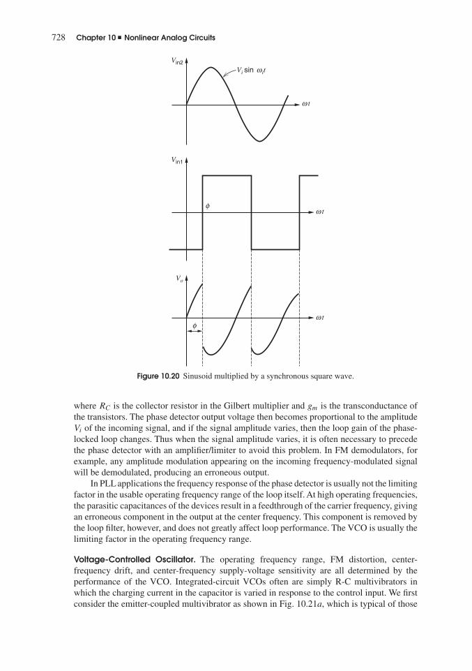
728 Chapter 10 � Nonlinear Analog Circuits
Vin2
Vin1
Vo
t
φ
φ
Vi sin it
ω
tω
tω
ω
Figure 10.20 Sinusoid multiplied by a synchronous square wave.
where RC is the collector resistor in the Gilbert multiplier and gm is the transconductance ofthe transistors. The phase detector output voltage then becomes proportional to the amplitudeVi of the incoming signal, and if the signal amplitude varies, then the loop gain of the phase-locked loop changes. Thus when the signal amplitude varies, it is often necessary to precedethe phase detector with an amplifier/limiter to avoid this problem. In FM demodulators, forexample, any amplitude modulation appearing on the incoming frequency-modulated signalwill be demodulated, producing an erroneous output.
In PLL applications the frequency response of the phase detector is usually not the limitingfactor in the usable operating frequency range of the loop itself. At high operating frequencies,the parasitic capacitances of the devices result in a feedthrough of the carrier frequency, givingan erroneous component in the output at the center frequency. This component is removed bythe loop filter, however, and does not greatly affect loop performance. The VCO is usually thelimiting factor in the operating frequency range.
Voltage-Controlled Oscillator. The operating frequency range, FM distortion, center-frequency drift, and center-frequency supply-voltage sensitivity are all determined by theperformance of the VCO. Integrated-circuit VCOs often are simply R-C multivibrators inwhich the charging current in the capacitor is varied in response to the control input. We firstconsider the emitter-coupled multivibrator as shown in Fig. 10.21a, which is typical of those

10.3 Phase-Locked Loops (PLL) 729
(a)
VCC
IB
I1 I1
IBC
R Q5
Q3
Q1 Q2
Q4
Q6 R
Vin
Vout
+
–
+
–
Figure 10.21 (a) Voltage-controlled, emitter-coupledmultivibrator.
(b)
VCC
I1I1
C
R Q5
Q3
Q1 Q2
Q4
Q6 R
I ≈ 2I1
2I1
I1 Vc2
Vb2
Vout
Vc
+
+
–
+
–
+ –
–
Figure 10.21 (b) Equivalentcircuit during one half-cycle.
used in this application. We calculate the period by first assuming that Q1 is turned off andQ2 is turned on. The circuit then appears as shown in Fig. 10.21b. We assume that current I
is large so that the voltage drop IR is large enough to turn on diode Q6. Thus the base of Q4is one diode drop below VCC, the emitter is two diode drops below VCC, and the base of Q1 istwo diode drops below VCC. If we can neglect the base current of Q3, its base is at VCC and its

730 Chapter 10 � Nonlinear Analog Circuits
t
t
t
t
Q2 on
Voltage at base of Q2 (Vb2)
VCC
VCC – 0.6VCC – 1.2
VCC
VCC – 1.2
VCC – 0.6
+0.6
–0.6
VCC – 1.8
VCC
Vout
Q1 on
Q2 on
Q1 on
Voltage at emitter of Q2 (Ve2)
Capacitor voltage (Vc)
(c)
Figure 10.21 (c) Waveforms within the emitter-coupled multivibrator.
emitter is one diode drop below VCC. Thus the emitter of Q2 is two diode drops below VCC.Since Q1 is off, the current I1 is charging the capacitor so that the emitter of Q1 is becomingmore negative. Q1 will turn on when the voltage at its emitter becomes equal to three diodedrops below VCC. Transistor Q1 will then turn on, and the resulting collector current in Q1turns on Q5. As a result, the base of Q3 moves in the negative direction by one diode drop,causing the base of Q2 to move in the negative direction by one diode drop. Q2 will turn off,causing the base of Q1 to move positive by one diode drop because Q6 also turns off. As aresult, the emitter-base junction of Q2 is reverse biased by one diode drop because the voltageon C cannot change instantaneously. Current I1 must now charge the capacitor voltage in thenegative direction by an amount equal to two diode drops before the circuit will switch backagain. Since the circuit is symmetrical, the half period is given by the time required to charge

10.4 Nonlinear Function Synthesis 731
the capacitor and is
T
2= Q
I1(10.72)
where Q = C�V = 2CVBE(on) is the charge on the capacitor. The frequency of the oscillatoris thus
f = 1
T= I1
4CVBE(on)(10.73)
The various waveforms in the circuit are shown in Fig. 10.21c. This emitter-coupled configura-tion is nonsaturating and contains only npn transistors. Furthermore, the voltage swings withinthe circuit are small. As a result, the circuit is capable of operating up to approximately 1 GHzfor typical integrated-circuit transistors. However, the usable frequency range is limited to avalue lower than this because the center frequency drift with temperature variations becomeslarge at the higher frequencies. This drift occurs because the switching transients themselvesbecome a large percentage of the period of the oscillation, and the duration of the switchingtransients depends on circuit parasitics, circuit resistances, transistor transconductance, andtransistor input resistance, which are all temperature sensitive.
Although the emitter-coupled configuration is capable of high operating speed, it displaysconsiderable sensitivity of center frequency to temperature even at low frequencies, since theperiod is dependent on VBE(on). Utilizing (10.73) we can calculate the temperature coefficientof the center frequency as
1
ωosc
dωosc
dT= − 1
VBE(on)
dVBE(on)
dT= +2 mV/◦C
600 mV= +3300 ppm/◦C (10.74)
This temperature sensitivity of center frequency can be compensated by causing current I1 tobe temperature sensitive in such a way that its effect is equal and opposite to the effect of thevariation of VBE(on).
10.4 Nonlinear Function SynthesisThe need often arises in electronic systems for circuits with arbitrary nonlinear transfer func-tions. For example, a common need is for square-law and square-root transfer characteristics inorder to generate true rms quantities. The unique, precision exponential transfer characteristicof the bipolar transistor can be used7,8 to generate these and many other nonlinear functions.
Consider the circuit shown in Fig. 10.22a. We have
VBE1 + VBE2 − VBE3 − VBE4 = 0 (10.75)
Neglecting base currents and assuming all devices are forward active, we find
VT lnIB
IS1+ VT ln
Ii
IS2− VT ln
Io
IS3− VT ln
Io
IS4= 0
and thus
Io =√
Ii
√IB
√IS3IS4
IS1IS2(10.76)
This circuit thus realizes a square-root transfer function with a scale factor set only by thebias current IB (which could be another input signal) and device area ratios. There is no(first-order) dependence on supply voltage or temperature. Not that the input current source

732 Chapter 10 � Nonlinear Analog Circuits
(a)
VCC
IB
Io
Ii
Q2
Q1
Q3
Q4
VCC
Io
Ii
IB1
IB2
Q2Q3
Q4
Q6
Q5
Q1
(b)
Figure 10.22 Bipolarnonlinear function circuits.(a) Square root. (b) Square law.
Ii must be capable of working into a dc bias voltage of one VBE set by Q1. The small-signalinput impedance of the circuit is very low due to the feedback provided by Q1 and Q2. Sinceall nodes in the circuit are low impedance, parasitic capacitance has little influence, and thebandwidth of the circuit can be on the order of the device fT .
For the circuit in Fig. 10.22b we have
VBE1 + VBE5 + VBE2 = VBE3 + VBE4 + VBE6 (10.77)
from which
Io = I2i
IB1
I2B2
IS3IS4IS6
IS1IS5IS2(10.78)
Thus this circuit realizes the square-law transfer function with very wide bandwidth and insen-sitivity to temperature and supply voltage. Simpler versions of this circuit can be derived ifthe current source IB1 is used as a signal input. However, this requires that IB1 be realized byan active pnp current source (or a PMOS current source in BiCMOS technology), which willusually restrict the circuit bandwidth.

Problems 733
PROBLEMS10.1 Sketch the dc transfer curve Iout versus V2
for the Gilbert multiplier of Fig. 10.4 for V1 equal to0.1VT , 0.5VT , and VT .
10.2 For the emitter-coupled pair of Fig. 10.1,determine the magnitude of the dc differential inputvoltage required to cause the slope of the transfer curveto be different by 1 percent from the slope through theorigin.
10.3 Assume that a sinusoidal voltage signal isapplied to the emitter-coupled pair of Fig. 10.1.Determine the maximum allowable magnitude of thesinusoid such that the magnitude of the third harmonicin the output is less than 1 percent of the fundamental.To work this problem, approximate the transfer char-acteristic of the pair with the first two terms of theTaylor series for the tanh function. Then assume thatall the other harmonics in the output are negligible andthat the output is approximately
Iout(t) = Io(sin ωot + δ sin 3ωot)
where δ = fractional third-harmonic distortion. UseSPICE to check your result. For the same sinusoidalinput voltage amplitude, use SPICE to find the thirdharmonic distortion in the output if emitter resistorsRE
are added to each device such that IE1RE = IE2RE =100 mV.
10.4 Determine the worst-case input offset voltageof the voltage-current converter shown in Fig. 10.23.
Assume that the op amps are ideal, that the resistorsmismatch by �0.3 percent, and that transistor IS val-ues mismatch by �2 percent. Neglect base currents.Use SPICE to determine the second and third harmonicdistortion in the output for a sinusoidal input drive ofamplitude 20 V peak-peak. Assume IS = 10−16 A forthe transistor and approximate the op amps by voltage-controlled voltage sources with a gain of 10,000.
10.5 Determine the dc transfer characteristic of thecircuit of Fig. 10.24. Assume that Z = 0.1XY for themultiplier.
Analogmultiplier
++
–
+
–
–
Vin
Vout
Vref
R
Z X
YR
Figure 10.24 Circuit for Problem 10.5. The op ampis ideal.
10.6 A phase-locked loop has a center frequencyof 105 rad/s, a KO of 103 rad/V-s, and a KD of 1V/rad. There is no other gain in the loop. Determine theloop bandwidth in the first-order loop configuration.
+
–
I1 I2
VCC
–VEE
Vin+
–
10 kΩ
1 kΩ 1 kΩ 1 kΩ
1 mA
Figure 10.23 Circuit for Problem 10.4. All op amps are ideal.

734 Chapter 10 � Nonlinear Analog Circuits
+
Vi
VDD = 5 V
M1 M2 M3 M4
M6
I150 μA
I150 μA
M7 M8
M10Io
M9
M5–
Figure 10.25 CMOS square-law circuit.
Determine the single-pole, loop-filter pole location togive the closed-loop poles located on 45◦ radials fromthe origin.
10.7 For the same PLL of Problem 10.6, design aloop filter with a zero that gives a crossover frequencyfor the loop gain of 100 rad/s. The loop phase shift atthe loop crossover frequency should be −135◦.
10.8 Estimate the capture range of the PLL ofProblem 10.7, assuming that it is not artificially limitedby the VCO frequency range.
10.9 An FM demodulator using a PLL has a centerfrequency of 2 kHz and is implemented as a first-orderloop. The input signal alternates between 1.95 kHz and2.05 kHz at a rate of 200 Hz with instantaneous tran-sitions between the two frequency values. Sketch thedemodulated output voltage waveform, ignoring theterm related to the sum of the frequencies at the PLLinput and the VCO output. For the PLL, use A = 1,KD = 2.55 V/rad and KO = 0.93ωosc, where ωosc isthe free-running frequency in rad/sec.
10.10 Design a voltage-controlled oscillator basedon the circuit of Fig. 10.21a. The center frequency is tobe 10 kHz, C = 0.01 �F, and VCC = 5 V. For the tran-sistors β = 100 and IS = 10−16 A. The frequency is tobe varied by 2:1 by an input �Vin = 200 mV. Spec-
ify all resistors and the dc value of Vin. Use SPICE tocheck your design and also to produce a plot of thetransfer characteristic from Vin to frequency.
10.11 Using the methods of Section 10.4, designa circuit with a transfer characteristic Io = KI
3/2i for
Ii ≥ 0. The input bias voltage must be ≥ VBE, and theoutput bias voltage is equal to 2VBE. The value of Io
should be 100 �Afor Ii = 100 �A. The supply voltageavailable is VCC = 5 V and device data are β = 100and IS = 10−17A. Use SPICE to verify your designand then examine the effect of finite rb = 200 andre = 2 .
10.12 Show that the CMOS circuit of Fig. 10.25realizes a square-law transfer characteristic from Vi toIo assuming that the MOSFETs have square-law char-acteristics. Specify the range of Vi over which thisholds. (The bias analysis of Section 9.6.4 applies.)All PMOS devices have W/L = 60 and all NMOShave W/L = 20. Device data are μnCox = 60 �A/V2,μpCox = 20 �A/V2, Vtn = 0.7 V, Vtp = −0.7 V, γ =0, and λ = 0.
Use SPICE to verify your result by plotting andevaluating the dc transfer characteristic. Then apply aninput sine-wave voltage drive at Vi within the square-law range and examine the first and second harmonicsin Io and comment.
REFERENCES
1. B. Gilbert. “A Precise Four-Quadrant Mul-tiplier with Subnanosecond Response,” IEEE J.Solid-State Circuits, Vol. SC-3, pp. 365–373, Decem-ber 1968.
2. B. Gilbert. “A New High-Performance Mono-lithic Multiplier Using Active Feedback,” IEEE J.Solid-State Circuits, Vol. SC-9, pp. 364–373, Decem-ber 1974.

References 735
3. F. M. Gardner. Phase-Lock Techniques. Wiley,New York, 1966.
4. A. B. Grebene and H. R. Camenzind.“Frequency Selective Integrated Circuits UsingPhase-Locked Techniques,” IEEE J. Solid-State Cir-cuits, Vol. SC-4, pp. 216–225, August 1969.
5. Applications of Phase-Locked Loops, Signet-ics Corporation, 1974.
6. M. Soyuer and R. G. Meyer. “Frequency Limi-tations of a Conventional Phase-Frequency Detector,”
IEEE J. Solid-State Circuits, Vol. 25, pp. 1019–1022,August 1990.
7. B. Gilbert. “General Technique for N-Dimensional Vector Summation of Bipolar Signals,”Electronics Letters, Vol. 12, pp. 504–505, September16, 1976.
8. E. Seevinck. Analysis and Synthesis ofTranslinear Integrated Circuits. Elsevier, Amsterdam,1988.

CHAPTER 11
Noise in IntegratedCircuits
11.1 IntroductionThis chapter deals with the effects of electrical noise in integrated circuits. The noise phe-nomena considered here are caused by the small current and voltage fluctuations that aregenerated within the devices themselves, and we specifically exclude extraneous pickup ofhuman-made signals that can also be a problem in high-gain circuits. The existence of noiseis basically due to the fact that electrical charge is not continuous but is carried in discreteamounts equal to the electron charge, and thus noise is associated with fundamental processesin the integrated-circuit devices.
The study of noise is important because it represents a lower limit to the size of electricalsignal that can be amplified by a circuit without significant deterioration in signal quality. Noisealso results in an upper limit to the useful gain of an amplifier, because if the gain is increasedwithout limit, the output stage of the circuit will eventually begin to limit (that is, a transistorwill leave the active region) on the amplified noise from the input stages.
In this chapter the various sources of electronic noise are considered, and the equivalentcircuits of common devices including noise generators are described. Methods of circuit anal-ysis with noise generators as inputs are illustrated, and the noise analysis of complex circuitssuch as op amps is performed. Methods of computer analysis of noise are examined, and,finally, some common methods of specifying circuit noise performance are described.
11.2 Sources of Noise11.2.1 Shot Noise1,2,3,4
Shot noise is always associated with a direct-current flow and is present in diodes, MOStransistors, and bipolar transistors. The origin of shot noise can be seen by considering thediode of Fig. 11.1a and the carrier concentrations in the device in the forward-bias regionas shown in Fig. 11.1b. As explained in Chapter 1, an electric field � exists in the depletionregion and a voltage (ψ0 − V ) exists between the p-type and the n-type regions, where ψ0 isthe built-in potential and V is the forward bias on the diode. The forward current of the diode I
is composed of holes from the p region and electrons from the n region, which have sufficientenergy to overcome the potential barrier at the junction. Once the carriers have crossed thejunction, they diffuse away as minority carriers.
The passage of each carrier across the junction, which can be modeled as a randomevent, is dependent on the carrier having sufficient energy and a velocity directed toward thejunction. Thus external current I, which appears to be a steady current, is, in fact, composed of
736

11.2 Sources of Noise 737
pp
pn
nn
p nx
np
V
I
Depletion region
Carrier concentration
Distance(b)
(a)
+ –
�
Figure 11.1 (a) Forward-biased pn junction diode. (b) Carrier concentrations in the diode(not to scale).
Dio
de c
urre
nt I
t
ID
Figure 11.2 Diode current I
as a function of time (not toscale).
a large number of random independent current pulses. If the current is examined on a sensitiveoscilloscope, the trace appears as in Fig. 11.2, where ID is the average current.
The fluctuation in I is termed shot noise and is generally specified in terms of its mean-square variation about the average value. This is written as i2, where
i2= (I − ID)2
= limT→∞
1
T
∫ T
0(I − ID)2 dt (11.1)
It can be shown that if a current I is composed of a series of random independent pulses withaverage value ID, then the resulting noise current has a mean-square value
i2 = 2qID �f (11.2)
where q is the electronic charge (1.6 × 10⁻¹⁹ C) and �f is the bandwidth in hertz. Thisequation shows that the noise current has a mean-square value that is directly proportional tothe bandwidth �f (in hertz) of the measurement. Thus a noise-current spectral density i2/�f
(with units square amperes per hertz) can be defined that is constant as a function of frequency.Noise with such a spectrum is often called white noise. Since noise is a purely random signal,the instantaneous value of the waveform cannot be predicted at any time. The only informationavailable for use in circuit calculations concerns the mean square value of the signal given by(11.2). Bandwidth �f in (11.2) is determined by the circuit in which the noise source is acting.
Equation 11.2 is valid until the frequency becomes comparable to 1/�, where � is the carriertransit time through the depletion region. For most practical electronic devices, � is extremely

738 Chapter 11 � Noise in Integrated Circuits
2qID
0.5 1.5f
1
i2 ΔfLi
near
sca
le
Linear scale
Figure 11.3 Spectral densityof shot noise in a diode withtransit time � (not to scale).
small and (11.2) is accurate well into the gigahertz region. A sketch of noise-current spectraldensity versus frequency for a diode is shown in Fig. 11.3 assuming that the passage of eachcharge carrier across the depletion region produces a square pulse of current with width �.
EXAMPLE
Calculate the shot noise in a diode current of 1 mA in a bandwidth of 1 MHz. Using (11.2) wehave
i2 = 2 × 1.6 × 10−19 × 10−3 × 10⁶ A2 = 3.2 × 10⁻¹⁶ A2
and thus
i = 1.8 × 10⁻⁸A rms
where i represents the root-mean-square (rms) value of the noise current.
The effect of shot noise can be represented in the low-frequency, small-signal equivalentcircuit of the diode by inclusion of a current generator shunting the diode, as shown in Fig.11.4. Since this noise signal has random phase and is defined solely in terms of its mean-square value, it also has no polarity. Thus the arrow in the current source in Fig. 11.2 has nosignificance and is included only to identify the generator as a current source. This practice isfollowed in this chapter where we deal only with noise generators having random phase.
The noise-current signal produced by the shot noise mechanism has an amplitude thatvaries randomly with time and that can only be specified by a probability-density function.It can be shown that the amplitude distribution of shot noise is Gaussian and the probability-density function p(I) of the diode current is plotted versus current in Fig. 11.5 (not to scale).The probability that the diode current lies between values I and (I + dI) at any time is givenby p(I)dI. If σ is the standard deviation of the Gaussian distribution, then the diode current
ID
i2 = 2q ID Δfrd =kTqID
Figure 11.4 Junction diode small-signalequivalent circuit with noise.

11.2 Sources of Noise 739
ID Diode current I
Pro
babi
lity
dens
ityfu
nctio
n p(
I)
Figure 11.5 Probability densityfunction for the diode current I
(not to scale).
amplitude lies between limits ID � σ for 68 percent of the time. By definition, variance σ2 isthe mean-square value of (I − ID) and thus, from (11.1),
σ2 = i2
and
σ =√
2qID �f (11.3)
using (11.2). Note that, theoretically, the noise amplitude can have positive or negative valuesapproaching infinity. However, the probability falls off very quickly as amplitude increasesand an effective limit to the noise amplitude is �3σ. The noise signal is within these limits for99.7 percent of the time. A brief description of the Gaussian distribution is given in AppendixA.3.1 in Chapter 3.
It is important to note that the distribution of noise in frequency as shown in Fig. 11.3 is dueto the random nature of the hole and electron transitions across the pn junction. Consider thesituation if all the carriers made transitions with uniform time separation. Since each carrierhas a charge of 1.6 × 10⁻¹⁹ C, a 1-mA current would then consist of current pulses every1.6 × 10−16 s. The Fourier analysis of such a waveform would give the spectrum of Fig. 11.6,which shows an average or dc value ID and harmonics at multiples of 1/�t, where �t is theperiod of the waveform and equals 1.6 × 10⁻¹⁶ s. Thus the first harmonic is at 6 × 10⁶ GHz,which is far beyond the useful frequency of the device. There would be no noise produced inthe normal frequency range of operation.
6 × 10⁶ GHz 12 × 106 GHz
Linear scale
f
ID
Am
plitu
de o
f Fou
rier
com
pone
nt
Figure 11.6 Shot-noisespectrum assuming uniformemission of carriers.

740 Chapter 11 � Noise in Integrated Circuits
R
v2
R i2
(a) (b)Figure 11.7 Alternative representations ofthermal noise.
11.2.2 Thermal Noise1,3,5
Thermal noise is generated by a completely different mechanism from shot noise. In conven-tional resistors it is due to the random thermal motion of the electrons and is unaffected bythe presence or absence of direct current, since typical electron drift velocities in a conductorare much less than electron thermal velocities. Since this source of noise is due to the thermalmotion of electrons, we expect that it is related to absolute temperature T . In fact thermalnoise is directly proportional to T (unlike shot noise, which is independent of T) and, as T
approaches zero, thermal noise also approaches zero.In a resistorR, thermal noise can be shown to be represented by a series voltage generator v2
as shown in Fig. 11.7a, or by a shunt current generator i2 as in Fig. 11.7b. These representationsare equivalent and
v2 = 4kTR �f (11.4)
i2 = 4kT1
R�f (11.5)
where k is Boltzmann’s constant. At room temperature 4kT = 1.66 × 10⁻²⁰ V-C. Equations11.4 and 11.5 show that the noise spectral density is again independent of frequency and, forthermal noise, this is true up to 1013 Hz. Thus thermal noise is another source of white noise.Note that the Norton equivalent of (11.5) can be derived from (11.4) as
i2 = v2
R2 (11.6)
A useful number to remember for thermal noise is that at room temperature (300◦K), thethermal noise spectral density in a 1-k resistor is v2/�f � 16 × 10−18 V2/Hz. This can bewritten in rms form as v � 4 nV/
√Hz where the form nV/
√Hz is used to emphasize that the
rms noise voltage varies as the square root of the bandwidth. Another useful equivalence isthat the thermal noise-current generator of a 1-k resistor at room temperature is the same asthat of 50 �A of direct current exhibiting shot noise.
Thermal noise as described above is a fundamental physical phenomenon and is presentin any linear passive resistor. This includes conventional resistors and the radiation resistanceof antennas, loudspeakers, and microphones. In the case of loudspeakers and microphones, thesource of noise is the thermal motion of the air molecules. In the case of antennas, the sourceof noise is the black-body radiation of the object at which the antenna is directed. In all cases,(11.4) and (11.5) give the mean-square value of the noise.

11.2 Sources of Noise 741
The amplitude distribution of thermal noise is again Gaussian. Since both shot and thermalnoise each have a flat frequency spectrum and a Gaussian amplitude distribution, they areindistinguishable once they are introduced into a circuit. The waveform of shot and thermalnoise combined with a sinewave of equal power is shown in Fig. 11.21.
11.2.3 Flicker Noise6,7,8 (1/f Noise)
This is a type of noise found in all active devices, as well as in some discrete passive elementssuch as carbon resistors. The origins of flicker noise are varied, but it is caused mainly by trapsassociated with contamination and crystal defects. These traps capture and release carriers ina random fashion and the time constants associated with the process give rise to a noise signalwith energy concentrated at low frequencies.
Flicker noise, which is always associated with a flow of direct current, displays a spectraldensity of the form
i2 = K1Ia
f b�f (11.7)
where
�f = small bandwidth at frequency f
I = direct currentK1 = constant for a particular device
a = constant in the range 0.5 to 2b = constant of about unity
If b = 1 in (11.7), the noise spectral density has a 1/f frequency dependence (hence thealternative name 1/f noise), as shown in Fig. 11.8. It is apparent that flicker noise is mostsignificant at low frequencies, although in devices exhibiting high flicker noise levels, thisnoise source may dominate the device noise at frequencies well into the megahertz range.
It was noted above that flicker noise only exists in association with a direct current. Thus,in the case of carbon resistors, no flicker noise is present until a direct current is passed throughthe resistor (however, thermal noise always exists in the resistor and is unaffected by any directcurrent as long as the temperature remains constant). Consequently, carbon resistors can beused if required as external elements in low-noise, low-frequency integrated circuits as long asthey carry no direct current. If the external resistors for such circuits must carry direct current,however, metal film resistors that have no flicker noise should be used.
In earlier sections of this chapter, we saw that shot and thermal noise signals have well-defined mean-square values that can be expressed in terms of current flow, resistance, and a
f
f1
Log scale
Log
scal
eΔ
fi2
Figure 11.8 Flicker noise spectraldensity versus frequency.

742 Chapter 11 � Noise in Integrated Circuits
number of well-known physical constants. By contrast, the mean-square value of a flicker noisesignal as given by (11.7) contains an unknown constant K1. This constant not only varies byorders of magnitude from one device type to the next, but it can also vary widely for differenttransistors or integrated circuits from the same process wafer. This is due to the dependenceof flicker noise on contamination and crystal imperfections, which are factors that can varyrandomly even on the same silicon wafer. However, experiments have shown that if a typicalvalue of K1 is determined from measurements on a number of devices from a given process,then this value can be used to predict average or typical flicker noise performance for integratedcircuits from that process.9
The final characteristic of flicker noise that is of interest is its amplitude distribution, whichis often non-Gaussian, as measurements have shown.
11.2.4 Burst Noise7 (Popcorn Noise)
This is another type of low-frequency noise found in some integrated circuits and discretetransistors. The source of this noise is not fully understood, although it has been shown to berelated to the presence of heavy-metal ion contamination. Gold-doped devices show very highlevels of burst noise.
Burst noise is so named because an oscilloscope trace of this type of noise shows bursts ofnoise on a number (two or more) of discrete levels, as illustrated in Fig. 11.9a. The repetitionrate of the noise pulses is usually in the audio frequency range (a few kilohertz or less) andproduces a popping sound when played through a loudspeaker. This has led to the name popcornnoise for this phenomenon.
Noi
se a
mpl
itude
(a)
(b)Log scale
Log
scal
eΔ
fi2
fcf 2
1f
t
Figure 11.9 (a) Typicalburst noise waveform.(b) Burst noise spectraldensity versus frequency.

11.2 Sources of Noise 743
Log scale
Log
scal
eΔ
fi2
f 2
1
f
Burst noise humps
∝Figure 11.10 Spectral density ofcombined multiple burst noisesources and flicker noise.
The spectral density of burst noise can be shown to be of the form
i2 = K2Ic
1 +(
f
fc
)2 �f (11.8)
where
K2 = constant for a particular deviceI = direct currentc = constant in the range 0.5 to 2
fc = particular frequency for a given noise process
This spectrum is plotted in Fig. 11.9b and illustrates the typical hump that is characteristicof burst noise. At higher frequencies the noise spectrum falls as 1/f 2.
Burst noise processes often occur with multiple time constants, and this gives rise tomultiple humps in the spectrum. Also, flicker noise is invariably present as well so that thecomposite low-frequency noise spectrum often appears as in Fig. 11.10. As with flicker noise,factor K2 for burst noise varies considerably and must be determined experimentally. Theamplitude distribution of the noise is also non-Gaussian.
11.2.5 Avalanche Noise10
This is a form of noise produced by Zener or avalanche breakdown in a pn junction. Inavalanche breakdown, holes and electrons in the depletion region of a reverse-biased pn
junction acquire sufficient energy to create hole-electron pairs by colliding with silicon atoms.This process is cumulative, resulting in the production of a random series of large noise spikes.The noise is always associated with a direct-current flow, and the noise produced is muchgreater than shot noise in the same current, as given by (11.2). This is because a single carriercan start an avalanching process that results in the production of a current burst containingmany carriers moving together. The total noise is the sum of a number of random bursts ofthis type.
The most common situation where avalanche noise is a problem occurs when Zenerdiodes are used in the circuit. These devices display avalanche noise and are generally avoidedin low-noise circuits. If Zener diodes are present, the noise representation of Fig. 11.11 canbe used, where the noise is represented by a series voltage generator v2. The dc voltage Vz isthe breakdown voltage of the diode, and the series resistance R is typically 10 to 100 . The

744 Chapter 11 � Noise in Integrated Circuits
++
–
–
VZ
R
v2
Figure 11.11 Equivalent circuit of a Zener diode including noise.
magnitude of v2 is difficult to predict as it depends on the device structure and the uniformity ofthe silicon crystal, but a typical measured value is v2/�f � 10−14 V2/Hz at a dc Zener currentof 0.5 mA. Note that this is equivalent to the thermal noise voltage in a 600-k resistor andcompletely overwhelms thermal noise in R. The spectral density of the noise is approximatelyflat, but the amplitude distribution is generally non-Gaussian.
11.3 Noise Models of Integrated-Circuit ComponentsIn the above sections, the various physical sources of noise in electronic circuits were described.In this section, these sources of noise are brought together to form the small-signal equivalentcircuits including noise for diodes and for bipolar and MOS transistors.
11.3.1 Junction Diode
The equivalent circuit for a forward-biased junction diode was considered briefly in the con-sideration of shot noise. The basic equivalent circuit of Fig. 11.4 can be made complete byadding series resistance rs as shown in Fig. 11.12. Since rs is a physical resistor due to theresistivity of the silicon, it exhibits thermal noise. Experimentally it has been found that anyflicker noise present can be represented by a current generator in shunt with rd , and can be
ID
rs
rd = i2
v2
kTqID
s
Figure 11.12 Complete diode small-signalequivalent circuit with noise sources.
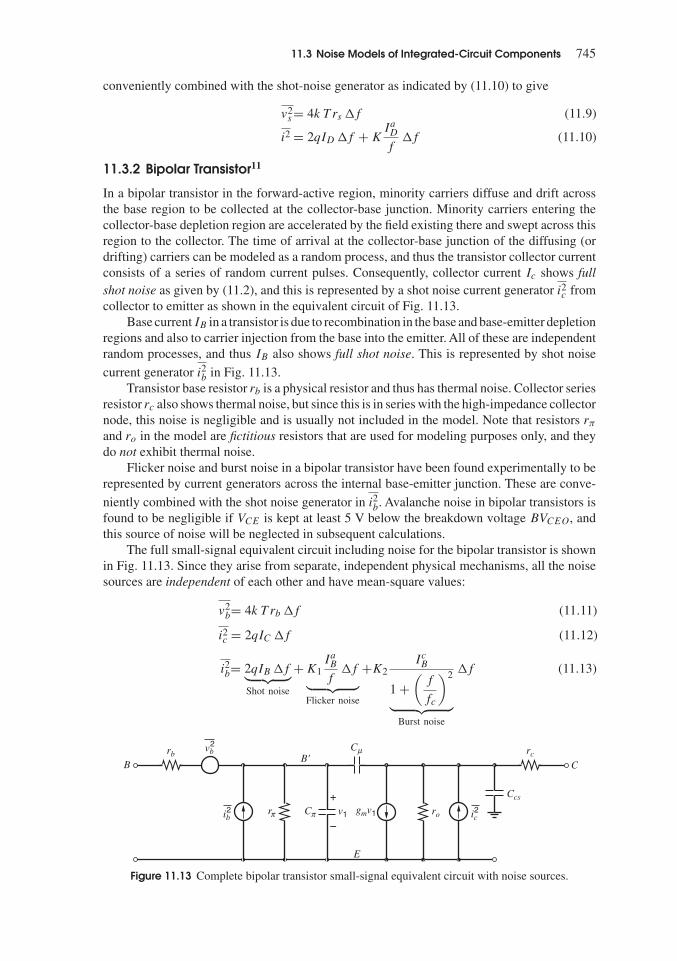
11.3 Noise Models of Integrated-Circuit Components 745
conveniently combined with the shot-noise generator as indicated by (11.10) to give
v2s= 4k T rs �f (11.9)
i2 = 2qID �f + KIaD
f�f (11.10)
11.3.2 Bipolar Transistor11
In a bipolar transistor in the forward-active region, minority carriers diffuse and drift acrossthe base region to be collected at the collector-base junction. Minority carriers entering thecollector-base depletion region are accelerated by the field existing there and swept across thisregion to the collector. The time of arrival at the collector-base junction of the diffusing (ordrifting) carriers can be modeled as a random process, and thus the transistor collector currentconsists of a series of random current pulses. Consequently, collector current Ic shows fullshot noise as given by (11.2), and this is represented by a shot noise current generator i2c fromcollector to emitter as shown in the equivalent circuit of Fig. 11.13.
Base current IB in a transistor is due to recombination in the base and base-emitter depletionregions and also to carrier injection from the base into the emitter. All of these are independentrandom processes, and thus IB also shows full shot noise. This is represented by shot noise
current generator i2b in Fig. 11.13.Transistor base resistor rb is a physical resistor and thus has thermal noise. Collector series
resistor rc also shows thermal noise, but since this is in series with the high-impedance collectornode, this noise is negligible and is usually not included in the model. Note that resistors rπand ro in the model are fictitious resistors that are used for modeling purposes only, and theydo not exhibit thermal noise.
Flicker noise and burst noise in a bipolar transistor have been found experimentally to berepresented by current generators across the internal base-emitter junction. These are conve-
niently combined with the shot noise generator in i2b. Avalanche noise in bipolar transistors isfound to be negligible if VCE is kept at least 5 V below the breakdown voltage BVCEO, andthis source of noise will be neglected in subsequent calculations.
The full small-signal equivalent circuit including noise for the bipolar transistor is shownin Fig. 11.13. Since they arise from separate, independent physical mechanisms, all the noisesources are independent of each other and have mean-square values:
v2b= 4k T rb �f (11.11)
i2c = 2qIC �f (11.12)
i2b= 2qIB �f︸ ︷︷ ︸Shot noise
+ K1IaB
f�f︸ ︷︷ ︸
Flicker noise
+K2IcB
1 +(
f
fc
)2
︸ ︷︷ ︸Burst noise
�f (11.13)
C
Ccs
rogmv1v1r
rb rc
B
CB'
E
+
–ib2 ic
2
vb2
π Cπ
μ
Figure 11.13 Complete bipolar transistor small-signal equivalent circuit with noise sources.

746 Chapter 11 � Noise in Integrated Circuits
Log scale
Log
scal
eΔ
f
i2
faf
2qIB
K1 f
b
IBa
Figure 11.14 Spectral densityof the base-current noisegenerator in a bipolartransistor.
This equivalent circuit is valid for both npn and pnp transistors. For pnp devices, the magnitudesof IB and IC are used in the above equations.
The base-current noise spectrum can be plotted using (11.13), and this has been done inFig. 11.14, where burst noise has been neglected for simplicity. The shot noise and flicker noiseasymptotes meet at a frequency fa, which is called the flicker noise corner frequency. In sometransistors using careful processing, fa can be as low as 100 Hz. In other transistors, fa canbe as high as 10 MHz.
11.3.3 MOS Transistor12
The structure of MOS transistors was described in Chapter 1. We showed there that the resistivechannel under the gate is modulated by the gate-source voltage so that the drain current iscontrolled by the gate-source voltage. Since the channel material is resistive, it exhibits thermal
noise, which is a major source of noise in MOS transistors. This noise source can be represented
by a noise-current generator i2d from drain to source in the small-signal equivalent circuit ofFig. 11.15.
Another source of noise in MOS transistors is flicker noise. Because MOS transistorsconduct current near the surface of the silicon where surface states act as traps that cap-ture and release current carriers, their flicker noise component can be large. Flicker noise inthe MOS transistor is also found experimentally to be represented by a drain-source current
Cgd
S
G D
Cgs gmvi rovi
+
–id2ig
2
Figure 11.15MOSFET small-signalequivalent circuit withnoise sources.

11.3 Noise Models of Integrated-Circuit Components 747
generator, and the flicker and thermal noise can be lumped into one noise generator i2d inFig. 11.15 with
i2d = 4kT
(2
3gm
)�f︸ ︷︷ ︸
Thermal noise
+ KIaD
f�f︸ ︷︷ ︸
Flicker noise
(11.14)
where
ID = drain bias currentK = constant for a given devicea = constant between 0.5 and 2
gm = device transconductance at the operating point
This equation is valid for long-channel devices. For channel lengths less than 1 �m, thermalnoise 2 to 5 times larger than given by the first term in (11.14) has been measured.13 Thisincrease in thermal noise may be attributed to hot electrons in short-channel devices.
Another source of noise in the MOS transistor is shot noise generated by the gate leakagecurrent. This noise can be represented by i2g in Fig. 11.15, with
i2g = 2qIG�f (11.15)
This noise current is usually very small since the dc gate current IG is typically less than 10−15
A. The noise terms in (11.14) and (11.15) are all independent of each other.There is one other component of noise that is usually insignificant at low frequencies
but important in very high-frequency MOS circuits, such as radio-frequency amplifiers, forexample. At an arbitrary point in the channel, the gate-to-channel voltage has a random com-ponent due to fluctuations along the channel caused by thermal noise. These voltage variationsgenerate a noisy ac gate current ig due to the capacitance between the gate and channel.The mean-squared value of this gate current for a long-channel device in the active regionis
i2g = 16
15kTω2C2
gs �f (11.16)
where Cgs = (2/3)CoxWL. The gate-current noise in (11.16) is correlated with the thermal-noise term in (11.14) because both noise currents stem from thermal fluctuations in the channel.The magnitude of the correlation between these currents is 0.39.12 For channel lengths lessthan 1 �m, this component of gate-current noise may be larger than given by (11.16) if thermalnoise associated with the channel increases due to hot electrons as noted above.14 The totalgate-current noise is the sum of the terms in (11.15) and (11.16).
11.3.4 Resistors
Monolithic and thin-film resistors display thermal noise as given by (11.4) and (11.5), and thecircuit representation of this is shown in Fig. 11.7. As mentioned in Section 11.2.3, discretecarbon resistors also display flicker noise, and this should be considered if such resistors areused as external components to the integrated circuit.
11.3.5 Capacitors and Inductors
Capacitors are common elements in integrated circuits, either as unwanted parasitics or aselements introduced for a specific purpose. Inductors are sometimes realized on the silicondie in integrated high-frequency communication circuits. There are no sources of noise in

748 Chapter 11 � Noise in Integrated Circuits
ideal capacitors or inductors. In practice, real components have parasitic resistance that doesdisplay noise as given by the thermal noise formulas of (11.4) and (11.5). In the case ofintegrated-circuit capacitors, the parasitic resistance usually consists of a small value in serieswith the capacitor. Parasitic resistance in inductors can be modeled by either series or shuntelements.
11.4 Circuit Noise Calculations15,16
The device equivalent circuits including noise that were derived in Section 11.3 can be used forthe calculation of circuit noise performance. First, however, methods of circuit calculation withnoise generators as sources must be established, and attention is now given to this problem.
Consider a noise current source with mean-square value
i2 = S(f ) �f (11.17)
where S(f ) is the noise spectral density. The value of S(f ) is plotted versus frequency inFig. 11.16a for an arbitrary noise generator. In a small bandwidth �f , the mean-square valueof the noise current is given by (11.17), and the rms values can be written as
i =√
S(f )�f (11.18)
The noise current in bandwidth �f can be represented approximately15 by a sinusoidal currentgenerator with rms value i as shown in Fig. 11.16b. If the noise current in bandwidth �f isnow applied as an input signal to a circuit, its effect can be calculated by substituting thesinusoidal generator and performing circuit analysis in the usual fashion. When the circuitresponse to the sinusoid is calculated, the mean-square value of the output sinusoid gives themean-square value of the output noise in bandwidth �f . Thus network noise calculationsreduce to familiar sinusoidal circuit-analysis calculations. The only difference occurs whenmultiple noise sources are applied, as is usually the case in practical circuits. Each noise sourceis then represented by a separate sinusoidal generator, and the output contribution of each one isseparately calculated. The total output noise in bandwidth �f is calculated as a mean-squarevalue by adding the individual mean-square contributions from each output sinusoid. This
Am
plitu
de
(a)
(b)
f
f
f
i =
Δ
Δ
Figure 11.16 Representation ofnoise in a bandwidth �f by anequivalent sinusoid with the samerms value.

11.4 Circuit Noise Calculations 749
R1
R2
v12
v22
vT2
+
–Figure 11.17 Circuit for the calculation of the total noise v2
T producedby two resistors in series.
depends, however, on the original noise sources being independent, as will be shown below.This requirement is usually satisfied if the equivalent noise circuits derived in previous sectionsare used, as all the noise sources except the induced gate noise in (11.16) arise from separatemechanisms and are thus independent.
For example, consider two resistors R1 and R2 connected in series as shown in Fig. 11.17.Resistors R1 and R2 have respective noise generators
v21 = 4k TR1 �f (11.19a)
v22 = 4k TR2 �f (11.19b)
In order to calculate the mean-square noise voltage v2T produced by the two resistors in series, let
vT (t) be the instantaneous value of the total noise voltage and v1(t) and v2(t) the instantaneousvalues of the individual generators. Then
vT (t) = v1(t) + v2(t) (11.20)
and thus
vT (t)2= [v1(t) + v2(t)]2
= v1(t)2 + v2(t)2 + 2v1(t)v2(t) (11.21)
Now, since noise generators v1(t) and v2(t) arise from separate resistors, they must be inde-pendent. Thus the average value of their product v1(t)v2(t) will be zero and (11.21) becomes
v2T = v2
1 + v22 (11.22)
Thus the mean-square value of the sum of a number of independent noise generators is thesum of the individual mean-square values. Substituting (11.19a) and (11.19b) in (11.22) gives
v2T = 4k T (R1 + R2) �f (11.23)
Equation 11.23 is just the value that would be predicted for thermal noise in a resistor (R1 + R2)using (11.4), and thus the results are consistent. These results are also consistent with therepresentation of the noise generators by independent sinusoids as described earlier. It is easilyshown that when two or more such generators are connected in series, the mean-square valueof the total voltage is equal to the sum of the individual mean-square values.

750 Chapter 11 � Noise in Integrated Circuits
In the above calculation, two noise voltage sources were considered connected in series.It can be similarly shown that an analogous result is true for independent noise current sourcesconnected in parallel. The mean-square value of the combination is the sum of the individualmean-square values. This result was assumed in the modeling of Section 11.3 where, forexample, three independent noise-current generators (shot, flicker, and burst) were combinedinto a single base-emitter noise source for a bipolar transistor.
11.4.1 Bipolar Transistor Noise Performance
As an example of the manipulation of noise generators in circuit calculations, consider thenoise performance of the simple transistor stage with the ac schematic shown in Fig. 11.18a.The small-signal equivalent circuit including noise is shown in Fig. 11.18b. (It should bepointed out that, for noise calculations, the equivalent circuit analyzed must be the actualcircuit configuration used. That is, Fig. 11.18a cannot be used as a half-circuit representationof a differential pair for the purposes of noise calculation because noise sources in each halfof a differential pair affect the total output noise.)
In the equivalent circuit of Fig. 11.18b, the external input signal vi has been ignored so thatoutput signal vo is due to noise generators only. Cμ is assumed small and is neglected. Outputresistance ro is also neglected. The transistor noise generators are as described previously andin addition
v2s= 4k T RS �f (11.24)
i2l = 4k T1
RL
�f (11.25)
The total output noise can be calculated by considering each noise source in turn andperforming the calculation as if each noise source were a sinusoid with rms value equal to thatof the noise source being considered. Consider first the noise generator vs due to RS . Then
v1 = Z
Z + rb + RS
vs (11.26)
RS
RL vovi
+
+
––
(a)
(b)
vo
ilRL
rb
RS gmv1r v12ic
2ib2
vb2
vs2
+
–π Cπ
Figure 11.18 (a) Simple transistor amplifier ac schematic. (b) Small-signal equivalent circuit withnoise sources.

11.4 Circuit Noise Calculations 751
where
Z = rπ
∥∥∥∥ 1
jωCπ
(11.27)
The output noise voltage due to vs is
vo1 = −gmRLv1 (11.28)
Use of (11.26) in (11.28) gives
vo1 = −gmRL
Z
Z + rb + RS
vs (11.29)
The phase information contained in (11.29) is irrelevant because the noise signal has randomphase and the only quantity of interest is the mean-square value of the output voltage producedby vs. From (11.29) this is
v2o1 = g2
mR2L
|Z|2|Z + rb + RS |2 v2
s (11.30)
By similar calculations it is readily shown that the noise voltage produced at the output by v2b
and i2b is
v2o2 = g2
mR2L
|Z|2|Z + rb + RS |2 v2
b (11.31)
v2o3 = g2
mR2L
(RS + rb)2|Z|2|Z + rb + RS |2 i2b (11.32)
Noise at the output due to i2l and i2c is
v2o4= i2l R
2L (11.33)
v2o5= i2cR
2L (11.34)
Since all five noise generators are independent, the total output noise is
v2o =
5∑n = 1
v2on (11.35)
= g2mR2
L
|Z|2|Z + rb + RS |2
[v2s + v2
b + (RS + rb)2i2b
](11.36)
+ R2L(i2l + i2c)
Substituting expressions for the noise generators we obtain
v2o
�f= g2
mR2L
|Z|2|Z + rb + RS |2 [4kT (RS + rb) + (RS + rb)22qIB]
(11.37)+ R2
L
(4k T
1
RL
+ 2qIC
)

752 Chapter 11 � Noise in Integrated Circuits
5 × 10–15
5 × 10–16
10–15
5.0 × 10⁻¹⁵
0.88 × 10⁻¹⁵
105 20 50 100 200 MHz
f1 = 23.3 MHz
f
V2/Hz
So( f ) =vo
2
fΔ
Figure 11.19 Noise voltage spectrum at the output of the circuit of Fig. 11.18.
where flicker noise has been assumed small and neglected. Substituting for Z from (11.27) in(11.37) we find
v2o
�f= g2
mR2L
r2π
(rπ + RS + rb)2
1
1 +(
f
f1
)2 [4k T (RS + rb) + (RS + rb)22qIB]
+ R2L
(4k T
1
RL
+ 2qIC
)(11.38)
where
f1 = 1
2π[rπ||(RS + rb)]Cπ
(11.39)
The output noise-voltage spectral density represented by (11.38) has a frequency-dependent part and a constant part. The frequency dependence arises because the gain of
the stage begins to fall above frequency f1, and noise due to generators v2s , v2
b, and i2b, whichappears amplified in the output, also begins to fall. The constant term in (11.38) is due to noise
generators i2l and i2c . Note that this noise contribution would also be frequency dependent if theeffect of Cμ had not been neglected. The noise-voltage spectral density represented by (11.38)has the form shown in Fig. 11.19.
EXAMPLE
In order to give an appreciation of the numbers involved, specific values will now beassigned to the parameters of (11.38), and the various terms in the equation will be evaluated.Assume that
IC = 100 �A β = 100 rb= 200
RS = 500 Cπ = 10 pF
RL= 5 k
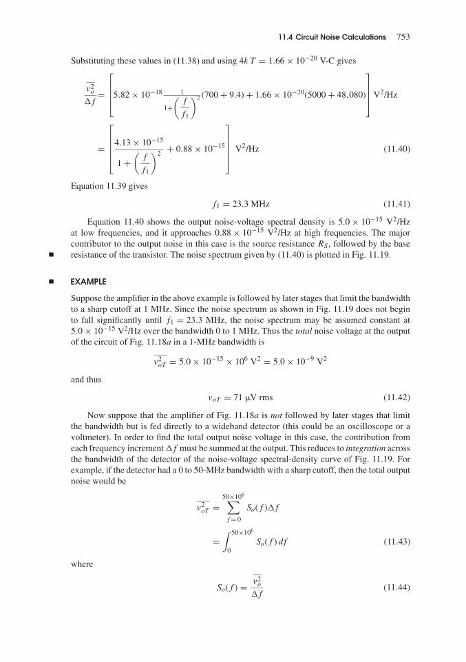
11.4 Circuit Noise Calculations 753
Substituting these values in (11.38) and using 4k T = 1.66 × 10⁻²⁰ V-C gives
v2o
�f=
⎡⎢⎢⎣5.82 × 10⁻¹⁸ 1
1+(
f
f1
)2 (700 + 9.4) + 1.66 × 10⁻²⁰(5000 + 48,080)
⎤⎥⎥⎦V2/Hz
=
⎡⎢⎢⎢⎣4.13 × 10⁻¹⁵
1 +(
f
f1
)2 + 0.88 × 10⁻¹⁵
⎤⎥⎥⎥⎦ V2/Hz (11.40)
Equation 11.39 gives
f1 = 23.3 MHz (11.41)
Equation 11.40 shows the output noise-voltage spectral density is 5.0 × 10⁻¹⁵ V2/Hzat low frequencies, and it approaches 0.88 × 10⁻¹⁵ V2/Hz at high frequencies. The majorcontributor to the output noise in this case is the source resistance RS , followed by the baseresistance of the transistor. The noise spectrum given by (11.40) is plotted in Fig. 11.19.
EXAMPLE
Suppose the amplifier in the above example is followed by later stages that limit the bandwidthto a sharp cutoff at 1 MHz. Since the noise spectrum as shown in Fig. 11.19 does not beginto fall significantly until f1 = 23.3 MHz, the noise spectrum may be assumed constant at5.0 × 10−15 V2/Hz over the bandwidth 0 to 1 MHz. Thus the total noise voltage at the outputof the circuit of Fig. 11.18a in a 1-MHz bandwidth is
v2oT = 5.0 × 10−15 × 106 V2 = 5.0 × 10⁻⁹ V2
and thus
voT = 71 �V rms (11.42)
Now suppose that the amplifier of Fig. 11.18a is not followed by later stages that limitthe bandwidth but is fed directly to a wideband detector (this could be an oscilloscope or avoltmeter). In order to find the total output noise voltage in this case, the contribution fromeach frequency increment �f must be summed at the output. This reduces to integration acrossthe bandwidth of the detector of the noise-voltage spectral-density curve of Fig. 11.19. Forexample, if the detector had a 0 to 50-MHz bandwidth with a sharp cutoff, then the total outputnoise would be
v2oT =
50×106∑f= 0
So(f )�f
=∫ 50×106
0So(f ) df (11.43)
where
So(f ) = v2o
�f(11.44)

754 Chapter 11 � Noise in Integrated Circuits
is the noise spectral density defined by (11.40). In practice, the exact evaluation of suchintegrals is often difficult and approximate methods are often used. Note that if the integrationof (11.43) is done graphically, the noise spectral density versus frequency must be plotted onlinear scales.
11.4.2 Equivalent Input Noise and the Minimum Detectable Signal
In the previous section, the output noise produced by the circuit of Fig. 11.18 was calculated.The significance of the noise performance of a circuit is, however, the limitation it places on thesmallest input signals the circuit can handle before the noise degrades the quality of the outputsignal. For this reason, the noise performance is usually expressed in terms of an equivalentinput noise signal, which gives the same output noise as the circuit under consideration. Inthis way, the equivalent input noise can be compared directly with incoming signals and theeffect of the noise on those signals is easily determined. For this purpose, the circuit of Fig.
11.18 can be represented as shown in Fig. 11.20, where v2iN is an input noise-voltage generator
that produces the same output noise as all of the original noise generators. All other sourcesof noise in Fig. 11.20 are considered removed. Using the same equivalent circuit as in Fig.11.18b, we obtain, for the output noise from Fig. 11.20,
v2o = g2
mR2L
|Z|2|Z + rb + RS |2 v2
iN (11.45)
If this noise expression is equated to v2o from (11.37), the equivalent input noise voltage for
the circuit can be calculated as
v2iN
�f= 4k T (RS + rb) + (RS + rb)22qIB
+ 1
g2mR2
L
|Z + rb + RS |2|Z|2 R2
L
(4kT
1
RL
+ 2qIC
)(11.46)
Note that the noise-voltage spectral density given by (11.46) rises at high frequencies becauseof the variation of |Z| with frequency. This is due to the fact that as the gain of the device falls
with frequency, output noise generators i2c and i2l have a larger effect when referred back tothe input.
Noiseless
voviN
RS RL
2
Figure 11.20 Representation of circuit noiseperformance by an equivalent input noisevoltage.

11.4 Circuit Noise Calculations 755
EXAMPLE
Calculate the total input noise voltage v2iNT for the circuit of Fig. 11.18 in a bandwidth of 0 to
1 MHz.This could be calculated using (11.46), derived above. Alternatively, since the total out-
put noise voltage v2oT has already been calculated, this can be used to calculate v2
iNT (in a1-MHz bandwidth) by dividing by the circuit voltage gain squared. If Av is the low-frequency,small-signal voltage gain of Fig. 11.18, then
Av = rπ
rb + rπ + RS
gmRL
Use of the previously specified data for this circuit gives
Av = 26,000
200 + 26,000 + 500
5000
260= 18.7
Since the noise spectrum is flat up to 1 MHz, the low-frequency gain can be used to calculate
v2iNT as
v2iNT = v2
oT
A2v
= 5 × 10⁻⁹
18.72 V2 = 14.3 × 10⁻¹² V2
Thus we have
viNT = 3.78 �V rms
The above example shows that in a bandwidth of 0 to 1 MHz, the noise in the circuitappears to come from a 3.78-�V rms noise-voltage source in series with the input. This noisevoltage can be used to estimate the smallest signal that the circuit can effectively amplify,sometimes called the minimum detectable signal (MDS). This depends strongly on the natureof the signal and the application. If no special filtering or coding techniques are used, the MDS
Figure 11.21 Output voltage waveform of the circuit of Fig. 11.18 with a 3.78-�V rms sinewaveapplied at the input. The circuit bandwidth is limited to 1 MHz, which gives an equivalent input noisevoltage of 3.78 �V rms.

756 Chapter 11 � Noise in Integrated Circuits
can be taken as equal to the equivalent input noise voltage in the passband of the amplifier.Thus, in this case
MDS = 3.78 �V rms
If a sinewave of magnitude 3.78 �V rms were applied to this circuit, and the output in a 1-MHzbandwidth examined on an oscilloscope, the sine wave would be barely detectable in the noise,as shown in Fig. 11.21. The noise waveform in this figure is typical of that produced by shotand thermal noise.
11.5 Equivalent Input Noise Generators17
In the previous section, the equivalent input noise voltage for a particular configuration wascalculated. This gave rise to an expression for an equivalent input noise-voltage generator thatwas dependent on the source resistance RS , as well as the transistor parameters. This method isnow extended to a more general and more useful representation in which the noise performanceof any two-port network is represented by two equivalent input noise generators. The situationis shown in Fig. 11.22, where a two-port network containing noise generators is representedby the same network with internal noise sources removed (the noiseless network) and with
a noise voltage v2i and current generator i2i connected at the input. It can be shown that this
representation is valid for any source impedance, provided that correlation between the twonoise generators is considered. That is, the two noise generators are not independent in generalbecause they are both dependent on the same set of original noise sources.
The inclusion of correlation in the noise representation results in a considerable increasein the complexity of the calculations, and if correlation is important, it is often easier to returnto the original network with internal noise sources to perform the calculations. However, in alarger number of practical circuits, the correlation is small and may be neglected. In addition,
if either equivalent input generator v2i or i2i dominates, the correlation may be neglected in
any case. The use of this method of representation is then extremely useful, as will becomeapparent.
The need for both an equivalent input noise voltage generator and an equivalent input noisecurrent generator to represent the noise performance of the circuit for any source resistancecan be appreciated as follows. Consider the extreme case of source resistance RS equal to zero
or infinity. If RS = 0, i2i in Fig. 11.22 is shorted out, and since the original circuit will still
show output noise in general, we need an equivalent input noise voltage v2i to represent this
behavior. Similarly, if RS → ∞, v2i in Fig. 11.22 cannot produce output noise and i2i represents
the noise performance of the original noisy network. For finite values of RS , both v2i and i2i
contribute to the equivalent input noise of the circuit.
RSRS
vi2
ii2≡Noisy
networkNoiselessnetwork
Figure 11.22 Representation of noise in a two-port network by equivalent input voltage and currentgenerators.

11.5 Equivalent Input Noise Generators 757
The values of the equivalent input generators of Fig. 11.22 are readily determined. Thisis done by first short-circuiting the input of both circuits and equating the output noise in each
case to calculate v2i . The value of i2i is found by open-circuiting the input of each circuit and
equating the output noise in each case. This will now be done for the bipolar transistor and theMOS transistor.
11.5.1 Bipolar Transistor Noise Generators
The equivalent input noise generators for a bipolar transistor can be calculated from the equiv-alent circuit of Fig. 11.23a. The output noise is calculated with a short-circuited load, and Cμ
is neglected. This will be justified later. The circuit of Fig. 11.23a is to be equivalent to that ofFig. 11.23b in that each circuit should give the same output noise for any source impedance.
The value of v2i can be calculated by short-circuiting the input of each circuit and equating
the output noise io. We use rms noise quantities in the calculations, but make no attempt topreserve the signs of the noise quantities as the noise generators are all independent and haverandom phase. The polarity of the noise generators does not affect the answer. Short-circuitingthe inputs of both circuits in Fig. 11.23, assuming that rb is small (� rπ) and equating io, weobtain
gmvb + ic = gmvi (11.47)
which gives
vi = vb + ic
gm
(11.48)
Since rb is small, the effect of i2b is neglected in this calculation.
vb
ic
io
rogmv1v1Cr+
–
vi
ii
io
rogmv1v1Cr
rb
rb
+
–
(a)
(b)
π π
π π
2
2
2
2
ib2
Figure 11.23 (a) Bipolar transistor small-signal equivalent circuit with noise generators.(b) Representation of the noise performance of (a) by equivalent input generators.

758 Chapter 11 � Noise in Integrated Circuits
Using the fact that vb and ic are independent, we obtain, from (11.48),
v2i = v2
b + i2c
g2m
(11.49)
Substituting in (11.49) for v2b and i2c from (11.11) and (11.12) gives
v2i = 4k T rb�f + 2qIC �f
g2m
and thus
v2i
�f= 4k T
(rb + 1
2gm
)(11.50)
The equivalent input noise-voltage spectral density of a bipolar transistor thus appears to comefrom a resistor Req such that
v2i
�f= 4k TReq (11.51)
where
Req = rb + 1
2gm
(11.52)
and this is called the equivalent input noise resistance. Of this fictitious resistance, portion rbis, in fact, a physical resistor in series with the input, whereas portion 1/2gm represents theeffect of collector current shot noise referred back to the input. Equations 11.50 and 11.52are extremely useful approximations, although the assumption that rb � rπ may not be validat high collector bias currents, and the calculation should be repeated without restrictions inthose circumstances.
Equation 11.50 allows easy comparison of the relative importance of noise from rb and IC
in contributing to v2i . For example, if IC = 1 �A, then 1/2gm = 13 k and this will dominate
typical rb values of about 100 . Alternately, if IC = 10 mA, then 1/2gm = 1.3 and noise
from rb will totally dominate v2i . Since v2
i is the important noise generator for low source
impedance (since i2i then tends to be shorted), it is apparent that good noise performancefrom a low source impedance requires minimization of Req. This is achieved by designing thetransistor to have a low rb and running the device at a large collector bias current to reduce1/2gm. Finally, it should be noted from (11.50) that the equivalent input noise-voltage spectraldensity of a bipolar transistor is independent of frequency.
In order to calculate the equivalent input noise current generator i2i , the inputs of bothcircuits in Fig. 11.23 are open-circuited and output noise currents io are equated. Using rmsnoise quantities, we obtain
β(jω)ii = ic + β(jω)ib (11.53)
which gives
ii = ib + ic
β(jω)(11.54)
Since ib and ic are independent generators, we obtain, from (11.54),
i2i = i2b + i2c
|β(jω)|2 (11.55)

11.5 Equivalent Input Noise Generators 759
where
β(jω) = β0
1 + jω
ωβ
(11.56)
and β0 is the low-frequency, small-signal current gain. [See (1.122) and (1.126)].
Substituting in (11.55) for i2b and i2c from (11.13) and (11.12) gives
i2i
�f= 2q
[IB + K′
1IaB
f+ IC
|β(jω)|2]
(11.57)
where
K′1 = K1
2q(11.57a)
and the burst noise term has been omitted for simplicity. The last term in parentheses in (11.57)is due to collector current noise referred to the input. At low frequencies this becomes IC/β2
0
and is negligible compared with IB for typical β0 values. When this is true, i2i and v2i do not
contain common noise sources and are totally independent. At high frequencies, however, the
last term in (11.57) increases and can become dominant, and correlation between v2i and i2i
may then be important since both contain a contribution from i2c .The equivalent input noise current spectral density given by (11.57) appears to come from
a current Ieq showing full shot noise, such that
i2i
�f= 2qIeq (11.58)
where
Ieq = IB + K′1IaB
f+ IC
|β(jω)|2 (11.59)
and this is called the equivalent input shot noise current. This is a fictitious current composedof the base current of the device plus a term representing flicker noise and one representingcollector-current noise transformed to the input. It is apparent from (11.59) that Ieq is minimized
by utilizing low bias currents in the transistor, and also using high-β transistors. Since i2i isthe dominant equivalent input noise generator in circuits where the transistor is fed from ahigh source impedance, low bias currents and high β are obviously required for good noiseperformance under these conditions. Note that the requirement for low bias currents to minimize
i2i conflicts with the requirement for high bias current to minimize v2i .
Spectral density i2i /�f of the equivalent input noise current generator can be plottedas a function of frequency using (11.57). This is shown in Fig. 11.24 for typical transistorparameters. In this case, the spectral density is frequency dependent at both low and highfrequencies, the low-frequency rise being due to flicker noise and the high-frequency risebeing due to collector-current noise referred to the input. This input-referred noise rises athigh frequencies because the transistor current gain begins to fall, and this is the reason fordegradation in transistor noise performance observed at high frequencies.
Frequency fb in Fig. 11.24 is the point where the high-frequency noise asymptote intersectsthe midband asymptote. This can be calculated from (11.57) as follows:
β(jf ) = β0
1 + jf
fT
β0
(11.60)

760 Chapter 11 � Noise in Integrated Circuits
3 × 10–23
3 × 10–24
3 × 10–25
3 × 10–26
10210 103 104 105 106 107 108 109
fb = 50 MHzfa
f 2
f1
fHz
Δfii
2
A2/Hz
Figure 11.24 Equivalent input noise current spectral density of a bipolar transistor withIC = 100 �A, β0 = βF = 100, fT = 500 MHz. Typical flicker noise is included.
where β0 is the low-frequency, small-signal current gain. Thus the collector current noise termin (11.57) is
2qIC
|β(jf )|2 = 2qIC
β20
(1 + f 2
f 2T
β20
)� 2qIC
f 2
f 2T
(11.61)
at high frequencies. Equation 11.61 shows that the equivalent input noise current spectrumrises as f 2 at high frequencies. Frequency fb can be calculated by equating (11.61) to themidband noise, which is 2q[IB + (IC/β2
0)]. For typical values of β0, this is approximately2qIB, and equating this quantity to (11.61) we obtain
2qIB = 2qIC
f 2b
f 2T
and thus
fb = fT
√IB
IC
(11.62)
The large-signal (or dc) current gain is defined as
βF = IC
IB
(11.63)
and thus (11.62) becomes
fb = fT√βF
(11.64)
Using the data given in Fig. 11.24, we obtain fb = 50 MHz for that example.Once the above input noise generators have been calculated, the transistor noise perfor-
mance with any source impedance is readily calculated. For example, consider the simplecircuit of Fig. 11.25a with a source resistance RS . The noise performance of this circuit can be

11.5 Equivalent Input Noise Generators 761
vs vi viN
ii
RLRS
RLRS
(a) (b)
≡
22 2
2
Figure 11.25 Representation of circuit noise by a single equivalent input noise voltage generator.(a) Original circuit. (b) Equivalent representation.
represented by the total equivalent noise voltage v2iN in series with the input of the circuit as
shown in Fig. 11.25b. Neglecting noise in RL (this will be discussed later), and equating thetotal noise voltage at the base of the transistor in Figs. 11.25a and 11.25b, we obtain
viN = vs + vi + iiRS
If correlation between vi and ii is neglected this equation gives
v2iN = v2
s + v2i + i2i R
2S (11.65)
Using (11.50) and (11.57) in (11.65) and neglecting flicker noise, we find
v2iN
�f= 4k TRS + 4k T
(rb + 1
2gm
)+ R2
S2q
[IB + IC
|β(jf )|2]
(11.66)
Equation 11.66 is similar to (11.46) if rb is small, as has been assumed.
EXAMPLE
Using data from the example in Section 11.4.1, calculate the total input noise voltage for thecircuit of Fig. 11.25a in a bandwidth 0 to 1 MHz neglecting flicker noise and using (11.66). Atlow frequencies, (11.66) becomes
v2iN
�f= 4k T
(RS + rb + 1
2gm
)+ R2
S2qIB
= [1.66 × 10⁻²⁰(500 + 200 + 130) + 5002 × 3.2 × 10−19 × 10−6] V2/Hz
= (13.8 + 0.08) × 10−18 V2/Hz
= 13.9 × 10⁻¹⁸ V2/Hz
The total input noise in a 1-MHz bandwidth is
v2iNT = 13.9 × 10−18 × 106 V2
= 13.9 × 10⁻¹² V2
and thus
viNT = 3.73 �V rms
This is almost identical to the answer obtained in Section 11.4.1. However, the method describedabove has the advantage that once the equivalent input generators are known for any particulardevice, the answer can be written down almost by inspection and requires much less labor.

762 Chapter 11 � Noise in Integrated Circuits
Also, the relative contributions of the various noise generators are more easily seen. In thiscase, for example, the equivalent input noise current is obviously a negligible factor.
11.5.2 MOS Transistor Noise Generators
The equivalent input noise generators for a MOS field-effect transistor (MOSFET) can becalculated from the equivalent circuit of Fig. 11.26a. This circuit is to be made equivalent tothat of Fig. 11.26b. The output noise in each case is calculated with a short-circuit load andCgd is neglected.
If the input of each circuit in Fig. 11.26 is short-circuited and resulting output noise currentsio are equated, we obtain
id = gmvi
and thus
v2i = i2d
g2m
(11.67)
Substituting i2d from (11.14) in (11.67) gives
v2i
�f= 4k T
2
3
1
gm
+ KIaD
g2mf
(11.68a)
The equivalent input noise resistance Req of the MOS transistor is defined as
v2i
�f= 4k TReq
where
Req = 2
3
1
gm
+ K′ IaD
g2mf
(11.68b)
ig id
ioDG
rdgmvgvgCgs
Cgs
+
–
vi
ii
io
rdgmvgvg
+
–
(a)
(b)
2 2
2
2
Figure 11.26 (a) MOSFET small-signal equivalent circuit with noise generators. (b) Representation of(a) by two input noise generators.

11.5 Equivalent Input Noise Generators 763
102
10–17
10–18
10–16
10–15
10–14
10 103 104 105 106 107 108
V2/Hz
1f
fHz
vi
Δf
2
Figure 11.27 Typical equivalent input noise voltage spectral density for a MOSFET.
and
K′ = K
4k T
At frequencies above the flicker noise region, Req = (2/3)(1/gm). For gm = 1 mA/V, thisgives Req = 667 , which is significantly higher than for a bipolar transistor at a comparablebias current (about 1 mA). The equivalent input noise-voltage spectral density for a typicalMOS transistor is plotted versus frequency in Fig. 11.27. Unlike the bipolar transistor, theequivalent input noise-voltage generator for a MOS transistor contains flicker noise, and it isnot uncommon for the flicker noise to extend well into the megahertz region.
In MOS field-effect transistors, the presence of electron energy states at the Si-SiO2interface tends to result in an input-referred flicker noise component that is larger than thethermal noise component for frequencies below 1 to 10 kHz for most bias conditions and devicegeometries. Thus, an accurate representation of the input-referred flicker noise component inMOS transistors is important for the optimization of the noise performance of MOS analogcircuits.
The physical mechanisms giving rise to 1/f noise in MOS transistors have receivedextensive study.18 The exact dependence of the magnitude of the input-referred flicker noiseon transistor bias conditions and device geometry is dependent on the details of the processthat is used to fabricate the device. In most cases, the magnitude of the input-referred flickernoise component is approximately independent of bias current and voltage and is inverselyproportional to the active gate area of the transistor. The latter occurs because as the transistoris made larger, a larger number of surface states are present under the gate, so that an averagingeffect occurs that reduces the overall noise. It is also observed that the input-referred flickernoise is an inverse function of the gate-oxide capacitance per unit area. This is physicallyreasonable since the surface states can be thought of as a time-varying component of the surface-state charge Qss. From (1.139) this produces a time-varying component in the threshold voltagethat is inversely proportional to Cox. For a MOS transistor, then, the equivalent input-referredvoltage noise can often be written as
v2i
�f= 4k T
2
3
1
gm
+ Kf
WLCoxf(11.69)
A typical value for Kf is 3 × 10⁻²⁴ V2-F, or 3 × 10⁻¹² V2-pF.

764 Chapter 11 � Noise in Integrated Circuits
The equivalent input noise-current generator i2i for the MOSFET can be calculated byopen-circuiting the input of each circuit in Fig. 11.26 and equating the output noise. This gives
iigm
jωCgs
= iggm
jωCgs
+ id
and thus
ii = ig + jωCgs
gm
id (11.70)
Since ig and id represent independent generators, (11.70) can be written as
i2i = i2g + ω2C2gs
g2m
i2d (11.71)
Ignoring (11.16) and substituting (11.14) and (11.15) in (11.17) gives
i2i
�f= 2qIG + ω2C2
gs
g2m
(4k T
2
3gm + K
IaD
f
)(11.72)
In (11.72) the ac current gain of the MOS transistor can be identified as
AI = gm
ωCgs
(11.73)
and thus the noise generators at the output are divided by A2I when referred back to the input. At
low frequencies the input noise-current generator is determined by the gate leakage current IG,which is very small (10−15 A or less). For this reason, MOS transistors have noise performancethat is much superior to bipolar transistors when the driving source impedance is large. Underthese circumstances the input noise-current generator is dominant and is much smaller for aMOS transistor than for a bipolar transistor. It should be emphasized, however, that the inputnoise-voltage generator of a bipolar transistor in (11.50) is typically smaller than that of a MOStransistor in (11.68a) because the bipolar transistor has a larger gm for a given bias current.Thus for low source impedances, a bipolar transistor often has noise performance superior tothat of a MOS transistor.
11.6 Effect of Feedback on Noise PerformanceThe representation of circuit noise performance with two equivalent input noise generators isextremely useful in the consideration of the effect of feedback on noise performance. This willbe illustrated by considering first the effect of ideal feedback on the noise performance of anamplifier. Practical aspects of feedback and noise performance will then be considered.
11.6.1 Effect of Ideal Feedback on Noise Performance
In Fig. 11.28a a series-shunt feedback amplifier is shown where the feedback network is idealin that the signal feedback to the input is a pure voltage source and the feedback network is
unilateral. Noise in the basic amplifier is represented by equivalent input generators v2ia and
i2ia. The noise performance of the overall circuit is represented by equivalent input generators
v2i and i2i as shown in Fig. 11.28b. The value of v2
i can be found by short-circuiting the input ofeach circuit and equating the output signal. However, since the output of the feedback networkhas a zero impedance, the current generators in each circuit are then short-circuited and the

11.6 Effect of Feedback on Noise Performance 765
via
fvo
vi
iia
ii
vo
+
+
–fvo
+
–
–vo
+
–a a
(a) (b)
2
2
2
2
Figure 11.28 (a) Series-shunt feedback amplifier with noise generators. (b) Equivalent representationof (a) with two input noise generators.
two circuits are identical only if
v2i = v2
ia (11.74)
If the input terminals of each circuit are open-circuited, both voltage generators have afloating terminal and thus no effect on the circuit, and for equal output it is necessary that
i2i = i2ia (11.75)
Thus, for the case of ideal feedback, the equivalent input noise generators can be movedunchanged outside the feedback loop and the feedback has no effect on the circuit noiseperformance. Since the feedback reduces the circuit gain, the output noise is reduced by thefeedback, but desired signals are reduced by the same amount and the signal-to-noise ratio willbe unchanged. The above result is easily shown for all four possible feedback configurationsdescribed in Chapter 8.
11.6.2 Effect of Practical Feedback on Noise Performance
The idealized series-shunt feedback circuit considered in the previous section is usually realizedin practice as shown in Fig. 11.29a. The feedback circuit is a resistive divider consisting of RE
and RF . If the noise of the basic amplifier is represented by equivalent input noise generators
i2ia and v2ia and the thermal noise generators in RF and RE are included, the circuit is as shown
in Fig. 11.29b. The noise performance of the circuit is to be represented by two equivalent
input generators v2i and i2i , as shown in Fig. 11.29c.
In order to calculate v2i , consider the inputs of the circuits of Fig. 11.29b and 11.29c
short-circuited, and equate the output noise. It is readily shown that
vi = via + iiaR + RF
RF + RE
ve + RE
RF + RE
vf (11.76)
where
R = RF‖RE (11.77)
Assuming that all noise sources in (11.76) are independent, we have
v2i = v2
ia + i2iaR2 + 4k TR�f (11.78)

766 Chapter 11 � Noise in Integrated Circuits
+ +
––
v1 vo = av1a a
a
RERF RF
RF
RE
RE
(a) (b)
(c)
via2
vi2
ii2
iia2
ve2
vf2
Figure 11.29 (a) Series-shunt feedback circuit. (b) Series-shunt feedback circuit including noisegenerators. (c) Equivalent representation of (b) with two input noise generators.
where the following substitutions have been made:
v2e = 4k TRE �f (11.79)
v2f = 4k TRF �f (11.80)
Equation 11.78 shows that in this practical case, the equivalent input noise voltage of theoverall amplifier contains the input noise voltage of the basic amplifier plus two other terms.The second term in (11.78) is usually negligible, but the third term represents thermal noise inR = RE‖RF and is often significant.
The equivalent input noise current i2i is calculated by open-circuiting both inputs andequating output noise. It is apparent that
i2i � i2ia (11.81)
since noise in the feedback resistors is no longer amplified, but appears only in shunt with theoutput. Thus the equivalent input noise current is unaffected by the application of feedback.The above results are true in general for series feedback at the input. For single-stage seriesfeedback, the above equations are valid with RF → ∞ and R = RE.
If the basic amplifier in Fig. 8.29 is an op amp, the calculation is slightly modified. Thisis due to the fact (shown in Section 11.8 and Fig. 11.39) that an op amp must be considered athree-port device for noise representation. However, if the circuit of Fig. 11.39 is used as thebasic amplifier in the above calculation, expressions very similar to (11.78) and (11.81) areobtained.
Consider now the case of shunt feedback at the input, and as an example consider theshunt-shunt feedback circuit of Fig. 11.30a. This is shown in Fig. 11.30b with noise sources

11.6 Effect of Feedback on Noise Performance 767
+
–
v1
vo = av1
a a
a
RFRF
RF
(a) (b)
(c)
vi2
ii2
iia2
if2
via2
Figure 11.30 (a) Shunt-shunt feedback circuit. (b) Shunt-shunt feedback circuit including noisegenerators. (c) Equivalent representation of (b) with two input noise generators.
v2ia and i2ia of the basic amplifier, and noise source i2f due to RF . These noise sources are
referred back to the input to give v2i and i2i as shown in Fig. 11.30c.
Open-circuiting the inputs of Fig. 11.30b and 11.30c, and equating output noise, wecalculate
ii = iia + via
RF
+ if (11.82)
Assuming that all noise sources in (11.82) are independent, we find
i2i = i2ia + v2ia
R2F
+ 4k T1
RF
�f (11.83)
Thus the equivalent input noise current with shunt feedback applied consists of the inputnoise current of the basic amplifier together with a term representing thermal noise in thefeedback resistor. The second term in (11.83) is usually negligible. These results are true ingeneral for shunt feedback at the input. A general rule for calculating the equivalent input noisecontribution due to thermal noise in the feedback resistors is to follow the two-port methodsdescribed in Chapter 8 for calculating feedback-circuit loading on the basic amplifier. Oncethe shunt or series resistors representing feedback loading at the input have been determined,these same resistors may be used to calculate the thermal noise contribution at the input dueto the feedback resistors.
If the inputs of the circuits of Fig. 11.30b and 11.30c are short-circuited, and the outputnoise is equated, it follows that
v2i � v2
ia (11.84)
Equations 11.83 and 11.84 are true in general for shunt feedback at the input. They applydirectly when the basic amplifier of Fig. 11.30 is an op amp, since one input terminal of thebasic amplifier is grounded and the op amp becomes a two-port device.

768 Chapter 11 � Noise in Integrated Circuits
The above results allow justification of some assumptions made earlier. For example,in the calculation of the equivalent input noise generators for a bipolar transistor in Section11.5.1, collector-base capacitance Cμ was ignored. This capacitance represents single-stageshunt feedback and thus does not significantly affect the equivalent input noise generators of atransistor, even if the Miller effect is dominant. Note that there is no thermal noise contributionfrom the capacitor as there was from RF in Fig. 11.30.Also, the second term in (11.83) becomes
v2ia/|ZF |2 where ZF is the impedance of Cμ. Since |ZF | is quite large at all frequencies of
interest, this term is negligible.
EXAMPLE
As an example of calculations involving noise in feedback amplifiers, consider the widebandcurrent-feedback pair whose ac schematic is shown in Fig. 11.31. The circuit is fed from acurrent source and the frequency response |(io/ii)(jω)| is flat with frequency to 100 MHz,where it falls rapidly. We calculate the minimum input signal is required for an output signal-to-noise ratio greater than 20 dB. Data are as follows: β1 = β2 = 100,fT1 = 300 MHz, IC1 =0.5 mA, IC2 = 1 mA, fT2 = 500 MHz, rb1 = rb2 = 100 . Flicker noise is neglected.
The methods developed above allow the equivalent input noise generators for this cir-cuit to be written down by inspection. A preliminary check shows that the noise due to the20-k interstage resistor and the base current noise of Q2 are negligible. Using the rule statedin Section 11.2.2, we find that the 20-k resistor contributes an equivalent noise current of2.5 �A. The base current of Q2 is 10 �A. Both of these can be neglected when comparedto the 500 �A collector current of Q1. Thus the input noise generators of the whole circuitare those of Q1 moved outside the feedback loop, together with the noise contributed by thefeedback resistors.
Using the methods of Chapter 8, we can derive the basic amplifier including feedbackloading and noise sources for the circuit of Fig. 11.31 as shown in Fig. 11.32. The equivalentinput noise-current generator for the overall circuit can be calculated from Fig. 11.32 or byusing (11.83) with RF = 5.5 k. Since the circuit is assumed to be driven from a current
5 kΩ500 Ω
20 kΩQ1
is
ioQ2
Figure 11.31 An ac schematic of acurrent feedback pair.
5 kΩ || 500 Ω20 kΩ5.5 kΩ
Q1
if iia
ioQ2
2
via2
2
Figure 11.32 Basicamplifier for the circuitof Fig. 11.31 includingfeedback loading andnoise sources.

11.6 Effect of Feedback on Noise Performance 769
source, the equivalent input noise voltage is not important. From (11.83)
i2i = i2ia + v2ia
(5500)2 + 4k T1
5500�f (11.85)
Using (11.57) and neglecting flicker noise, we have for i2ia
i2ia = 2q
(IB + IC
|β(jf )|2)
�f
and thus
i2ia
�f= 2q
(5 + 500
|β|2)
× 10−6 A2/Hz (11.86)
Substitution of (11.86) in (11.85) gives
i2i
�f= 2q
(5 + 500
|β|2)
× 10−6 + v2ia
(5500)2�f+ 2q(9.1) × 10−6 (11.87)
where the noise in the 5.5-k resistor has been expressed in terms of the equivalent noisecurrent of 9.1 �A.
Use of (11.50) gives
v2ia
�f= 4k T
(rb1 + 1
2gm
)= 4k T (126)
Division of this equation by (5500)2 gives
v2ia
(5500)2 �f= 4k T
1
240,000(11.88)
= 2q(0.2) × 10−6 (11.89)
Thus the term involving v2ia in (11.87) is seen to be equivalent to thermal noise in a 240-k
resistor using (11.88), and this can be expressed as noise in 0.2 �A of equivalent noise current,as shown in (11.89). This term is negligible in this example, as is usually the case.
Combining all these terms we can express (11.87) as
i2i
�f= 2q
(5 + 500
|β|2 + 0.2 + 9.1
)× 10−6 A2/Hz
= 2q
(14.3 + 500
|β|2)
× 10−6 A2/Hz (11.90)
Equation 11.90 shows that the equivalent input noise-current spectral density rises at highfrequencies (as |β| falls) as expected for a transistor. In a single transistor without feedback,the equivalent input noise current also rises with frequency, but because the transistor gainfalls with frequency, the output noise spectrum of a transistor without feedback always fallsas frequency rises (see Section 11.4.1). However, in this case, the negative feedback holds thegain constant with frequency, and thus the output noise spectrum of this circuit will rise asfrequency increases, until the amplifier band edge is reached. This is illustrated in Fig. 11.33,where the input noise-current spectrum, the amplifier frequency response squared, and theoutput noise-current spectrum (product of the first two) are shown. The current gain of thecircuit is AI � 11.

770 Chapter 11 � Noise in Integrated Circuits
103 105 106 107 108 109104
103 105 106 107 108 109104
103 105
10–20
10–22
10–21
10–22
10–24
10–23
1000
10
100
106 107 108 109104
4.6 × 10⁻²⁴
5.6 × 10⁻²²
fHz
fHz
fHz
121
(a)
(b)
(c)
iiΔf
2
A2/Hz
|AI|2
ioΔf
2
A2/Hz
Figure 11.33 Noiseperformance of thecircuit of Fig. 11.32.(a) Equivalent input noisespectrum. (b) Frequencyresponse squared.(c) Output noise spectrum.
The total output noise from the circuit i2oT is obtained by integrating the output noisespectral density, which is
i2o
�f= A2
I
i2i
�f(11.91)
Thus
i2oT =∫ B
0A2
I
i2i
�fdf
= A2I
∫ B
02q
(14.3 + 500
|β(jf )|2)
× 10−6df (11.92)
where (11.90) has been used and A2I is assumed constant up to B = 108 Hz as specified earlier.
The current gain is
β(jf ) = β0
1 + jβ0f
fT1
(11.93)

11.7 Noise Performance of Other Transistor Configurations 771
and
1
|β(jf )|2 = 1
β20
(1 + β2
0f2
f 2T1
)(11.94)
Substitution of (11.94) in (11.92) gives
i2oT = A2I2q × 10−6
∫ B
0
[14.3 + 500
β20
(1 + β2
0f2
f 2T1
)]df (11.95)
= A2I2q × 10−6
[14.3f + 500
β20
f + 500
f 2T1
f 3
3
]B0
(11.96)
Using β0 = 100 and B = 100 MHz = fT1/3 gives
i2oT = A2I × 2q × 10−6(14.3B + 18.6B) (11.97)
i2oT = A2I × 1.05 × 10−15 A2 (11.98)
The equivalent input noise current is
i2iT = i2oT
A2I
= 1.05 × 10⁻¹⁵ A2
and from this
iiT = 32.4 nA rms (11.99)
Thus the equivalent input noise current is 32.4 nA rms and (11.97) shows that the frequency-dependent part of the equivalent input noise is dominant. For a 20-dB signal-to-noise ratio,input signal current is must be greater than 0.32 �A rms.
11.7 Noise Performance of Other Transistor ConfigurationsTransistor configurations other than the common-emitter and common-source stages consid-ered so far are often used in integrated-circuit design. The noise performance of other importantconfigurations will now be considered. To avoid repetition, the discussion will be directedtoward bipolar devices only. However, all the results carry over directly to FET circuits.
11.7.1 Common-Base Stage Noise Performance
The common-base stage is sometimes used as a low-input-impedance current amplifier. Acommon-base stage is shown in Fig. 11.34a and the small-signal equivalent circuit is shown inFig. 11.34b together with the equivalent input noise generators derived for a common-emitterstage. Since these noise generators represent the noise performance of the transistor in anyconnection, Fig. 11.34b is a valid representation of common-base noise performance. In Fig.11.34c the noise performance of the common-base stage is represented in the standard fashion
with equivalent input noise generators v2iB and i2iB. These can be related to the common-emitter
input generators by alternately short circuiting and open circuiting the circuits of Fig. 11.34band 11.34c and equating output noise. It then follows that
i2iB = i2i (11.100)
v2iB = v2
i (11.101)
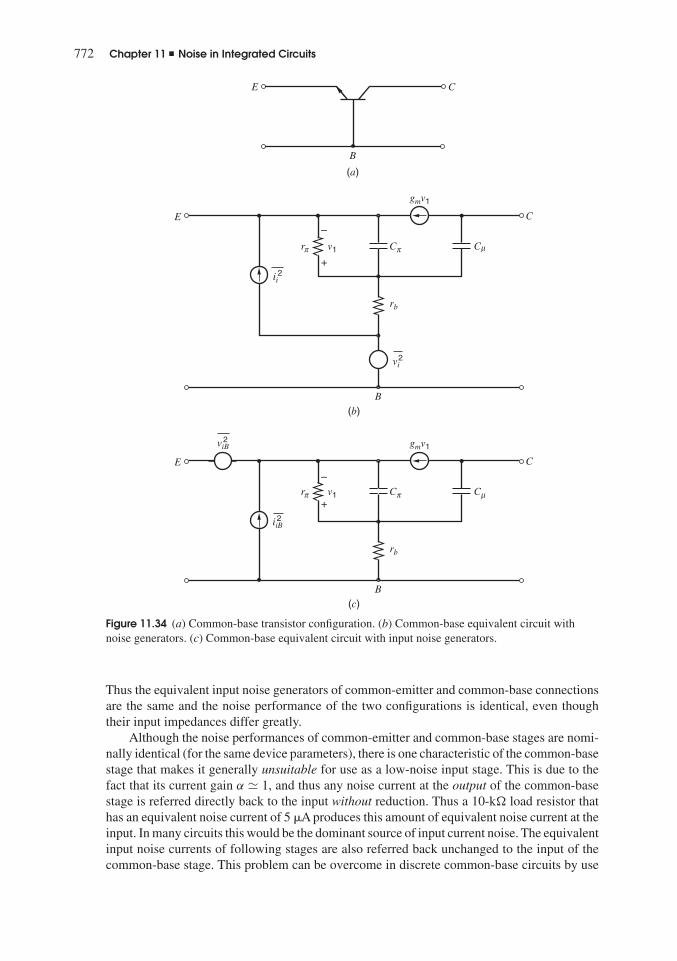
772 Chapter 11 � Noise in Integrated Circuits
E C
B
(a)
E C
B
rb
gmv1
v1r
+
–
vi2
ii2
(b)
π Cπ Cμ
E C
B
rb
gmv1
v1r+
–
viB2
iiB2
(c)
π Cπ Cμ
Figure 11.34 (a) Common-base transistor configuration. (b) Common-base equivalent circuit withnoise generators. (c) Common-base equivalent circuit with input noise generators.
Thus the equivalent input noise generators of common-emitter and common-base connectionsare the same and the noise performance of the two configurations is identical, even thoughtheir input impedances differ greatly.
Although the noise performances of common-emitter and common-base stages are nomi-nally identical (for the same device parameters), there is one characteristic of the common-basestage that makes it generally unsuitable for use as a low-noise input stage. This is due to thefact that its current gain α � 1, and thus any noise current at the output of the common-basestage is referred directly back to the input without reduction. Thus a 10-k load resistor thathas an equivalent noise current of 5 �A produces this amount of equivalent noise current at theinput. In many circuits this would be the dominant source of input current noise. The equivalentinput noise currents of following stages are also referred back unchanged to the input of thecommon-base stage. This problem can be overcome in discrete common-base circuits by use

11.7 Noise Performance of Other Transistor Configurations 773
+
+
––
zL vo
vi
Figure 11.35 Emitter-follower circuit.
of a transformer that gives current gain at the output of the common-base stage. This option isnot available in integrated-circuit design unless resort is made to external components.
11.7.2 Emitter-Follower Noise Performance
Consider the emitter follower shown in Fig. 11.35. The noise performance of this circuit can becalculated using the results of previous sections. The circuit can be viewed as a series-feedbackstage and the equivalent input noise generators of the transistor can be moved unchanged backto the input of the complete circuit. Thus, if noise in zL is neglected, the emitter followerhas the same equivalent input noise generators as the common-emitter and common-basestages. However, since the emitter follower has unity voltage gain, the equivalent input noisevoltage of the following stage is transformed unchanged to the input, thus degrading the noiseperformance of the circuit. Noise due to zL must also be included, but since the follower outputis taken at the emitter, which is a low impedance point, the noise due to zL is greatly attenuatedcompared with its effect on a series-feedback stage.
11.7.3 Differential-Pair Noise Performance
The differential pair is the basic building block of linear integrated circuits and, as such, itsnoise performance is of considerable importance. A bipolar differential pair is shown in Fig.11.36a, and the base of each device is generally independently accessible, as shown. Thusthis circuit cannot in general be represented as a two-port, and its noise performance cannotbe represented in the usual fashion by two input noise generators. However, the techniquesdeveloped previously can be used to derive an equivalent noise representation of the circuitthat employs two noise generators at each input. This is illustrated in Fig. 11.36b, and a simplerversion of this circuit, which employs only three noise generators, is shown in Fig. 11.36c.
The noise representation of Fig. 11.36b can be derived by considering noise due to eachdevice separately. Consider first noise in Q1, which can be represented by input noise generators
v2i and i2i as shown in Fig. 11.37a. These noise generators are those for a single transistor as
given by (11.50) and (11.57). Transistor Q2 is initially assumed noiseless and the impedanceseen looking in its emitter is zE2. Note that zE2 will be a function of the impedance connectedfrom the base of Q2 to ground. As described in previous sections, the noise generators of Fig.11.37a can be moved unchanged to the input of the circuit (independent of zE2) as shown inFig. 11.37b. This representation can then be used to calculate the output noise produced by Q1in the differential pair for any impedances connected from the base of Q1 and Q2 to ground.
Now consider noise due to Q2. In similar fashion this can be represented by noise gener-
ators v2i and i2i , as shown in Fig. 11.37c. In this case Q1 is assumed noiseless and zE1 is the

774 Chapter 11 � Noise in Integrated Circuits
impedance seen looking in at the emitter of Q1. If Q1 and Q2 are identical, the equivalent inputnoise generators of Fig. 11.37b and 11.37c are identical. However, since they are produced bydifferent transistors, the noise generators of Fig. 11.37b and 11.37c are independent. The totalnoise performance of the differential pair including noise due to both Q1 and Q2 can thus berepresented as shown in Fig. 11.36b, and this representation is valid for any source resistance
connected to either input terminal. Noise generators v2i and i2i are basically those due to each
transistor alone. If noise due to RL or following stages is significant, it should be referred backsymmetrically to the appropriate input. In practice, current source IEE will also contain noise,and this can be included in the representation. However, if the circuit is perfectly balanced, thecurrent-source noise represents a common-mode signal and will produce no differential output.
Q1
RL RL
IEE
–VEE
(a)
+VCC
Q2
Q1
RL RL
IEE
–VEE
(b)
+VCC
Q2
vi2 vi
2
ii2 ii
2
Figure 11.36(a) Differential-pair circuit.(b) Complete differential pairnoise representation.

11.7 Noise Performance of Other Transistor Configurations 775
Q1
RL RL
IEE
–VEE
(c)
+VCC
Q2
vdp2 vi
2= 2
idp2 ii
2= idp2 ii
2=
Figure 11.36 (c) Simplifiednoise representation.
RL
Q1
zE2
ii2
vi2
(a)
RL
Q1
zE2
ii2
vi2
(b)
RL
Q2
zE1
ii2
vi2
(c)
Figure 11.37 (a) ac schematic of a differential pair including noisedue to Q1 only. (b) ac schematic of a differential pair with noisedue to Q1 referred to the input. (c) ac schematic of a differentialpair including noise due to Q2 only.

776 Chapter 11 � Noise in Integrated Circuits
The noise representation of Fig. 11.36b can be simplified somewhat if the common-moderejection of the circuit is high. In this case, one of the noise-voltage generators can be movedto the other side of the circuit, as shown in Fig. 11.36c. This can be justified if equal noise-voltage generators are added in series with each input and these generators are chosen suchthat the noise voltage at the base of Q2 is canceled. This leaves two independent noise-voltagegenerators in series with the base of Q1, and these can be represented as a single noise-voltage
generator of value 2v2i . Thus for the circuit of Fig. 11.36c we can write
v2dp = 2v2
i (11.102)
i2dp = i2i (11.103)
where v2dp and i2dp are the equivalent input noise generators of the differential pair.
The differential pair is often operated with the base of Q2 grounded, and in this case thenoise-current generator at the base of Q2 is short circuited. The noise performance of the circuitis then represented by the two noise generators connected to the base of Q1 in Fig. 11.36c.In this case the equivalent input noise-current generator of the differential pair is simply thatdue to one transistor alone, whereas the equivalent input noise-voltage generator has a mean-square value twice that of either transistor. Thus from a low source impedance, a differentialpair has an equivalent input noise voltage 3 dB higher than a common-emitter stage with thesame collector current as the devices in the pair.
11.8 Noise in Operational AmplifiersIntegrated-circuit amplifiers designed for low-noise operation generally use a simple common-emitter or common-source differential-pair input stage with resistive loads. Since the inputstage has both current and voltage gain, the noise of following stages is generally not sig-nificant, and the resistive loads make only a small noise contribution. The noise analysis ofsuch circuits is quite straightforward using the techniques described in this chapter. However,circuits of this type (the 725 op amp is an example) are inefficient in terms of optimizingimportant op amp parameters such as gain and bandwidth. To improve the gain, active loadscan be used as in the first stage of the NE5234 op amp. However, by their very nature,active loads amplify their own internal noise and cause considerable degradation of circuitnoise performance. To illustrate these points and show the compromises involved in thedesign of general-purpose circuits, an approximate noise analysis of the NE5234 will nowbe made.19
A simplified schematic of the input stage of the NE5234 is shown in Fig. 11.38a. Thecommon-mode input voltage, VIC, is assumed to be low enough that the npn input pair Q1-Q2in Fig. 6.36 is off and can be ignored here. The differential output current is io. ComponentsQ13 and R13 of the active load generate noise and contribute to the output noise at io. Sincetransistor Q9 presents a high impedance to the active load, the noise due to the active loadcan be calculated from the isolated portion of the circuit shown in Fig. 11.38b. Noise due to
Q13 and R13 is represented by equivalent input noise generators v2i13 and i2i13. The impedance
looking back into the Bias1 output of the bias circuit is small and ignored. Therefore, i2i13may be neglected. Also, noise generated in the bias circuit may be ignored because it couplesinto Q13 and Q14 equally and does not affect the differential output current io with perfect
matching. Start with (11.78). Using (11.50) for v2ia and neglecting the i2ia term as well as flicker

11.8 Noise in Operational Amplifiers 777
(a)
(b)
R9
Q4Q3
Q9 Q10
Q13
Q13 Q14Q11
–VEE = 0
– 9 10+
VCC
Bias1
BiasCM
io
ioA
vi132
ii132
io
22 kΩ
R11
33 kΩR13
33 kΩR14
33 kΩ
R13
33 kΩ
R10
22 kΩ
Figure 11.38 (a) Simplified schematic of the NE5234 op amp input stage with VIC � 0.8 V.(b) ac schematic (including noise) of Q13 and R13.
noise gives
v2i13
�f= 4kT
(rb13 + 1
2gm13+ R13
)(11.104)
This noise generator can be evaluated as follows. The dc collector current in Q13 is approx-imately 6 �A, giving 1/2gm13 = 2.17 k. Also, R13 = 33 k, and a typical value of rb forpnp transistors is 200 . Thus (11.104) becomes
v2i13
�f= 4kT (35,000) (11.105)
This noise generator produces a noise output ioA where
ioA � 11
gm13+ R13
vi13 � vi13
37,000(11.106)
Using (11.105) in (11.106) gives
i2oA
�f= 4kT
35,000
37,0002 (11.107)
A similar analysis done to find v2i9, the noise due to Q9 and R9 in series with the base of Q9,
gives
v2i9
�f= 4kT
(rb9 + 1
2gm9+ R9
)(11.108)

778 Chapter 11 � Noise in Integrated Circuits
The dc collector current in Q9 is approximately 6 �A, giving 1/2gm9 = 2.17 k. Also, R9 =22 k, and a typical value of rb for npn transistors is 400 . Thus (11.108) becomes
v2i9
�f= 4kT (25,000) (11.109)
This noise generator produces a noise output ioB where
ioB � 11
gm9+ R9
vi9 � vi9
26,000(11.110)
Using (11.109) in (11.110) gives
i2oB
�f= 4kT
25,000
26,0002 (11.111)
The total mean-square noise current in the output at node 9 due to the active loads is i2oA + i2oB.Components Q14, R14, Q10, and R10 generate an equal mean-square noise current in the outputat node 10. Although Fig. 11.38a shows that the deterministic current io flows out of node 9and into node 10, the polarities of the noise currents are not known, and the mean-squarenoise contributions add because the noise sources are uncorrelated with each other. Therefore,the total mean-square output current density stemming from the active loads attached to bothnodes 9 and 10 is
i2oAB
�f= 2
(i2oA
�f+ i2oB
�f
)(11.112)
This result can be referred back to the input of the complete circuit of Fig. 11.38a in the standardmanner. Consider the contribution to the equivalent input noise voltage. A voltage applied atthe input of the full circuit of Fig. 11.38a gives
io
vid
= Gm1
where Gm1 = 97 �A/V from (6.186). Therefore,
i2o = G2m1v2
id (11.113)
Equating output noise current in (11.112) and (11.113), we obtain an equivalent input noisevoltage due to the active loads as
v2iAB
�f= 4kT
[2
(35,000
37,0002 + 25,000
26,0002
)](1
97 × 10−6
)2
= 4kT (13,000) (11.114)
Thus the active load causes a contribution of 13 k to the equivalent input noise resistance ofthe NE5234 op amp. Finally, the results of Section 11.7.3 show that the equivalent input noisevoltage squared of the differential pair Q3-Q4 is just the sum of the values from each half ofthe circuit. This gives an input noise-voltage contribution due to Q3-Q4 of
v2iC
�f= 4kT
(1
2gm3+ 1
2gm4+ rb3 + rb4
)(11.115)
Assuming a collector bias current of 3 �A for each device, and rb = 200 in (11.115), wecalculate
v2iC
�f= 4kT (9,000) (11.116)

11.8 Noise in Operational Amplifiers 779
vi2
ii2
ii2
Figure 11.39 Complete op amp noiserepresentation.
For the total input noise voltage of the NE5234, combining (11.114) and (11.116) gives
v2i
�f= v2
iAB
�f+ v2
iC
�f= 4kT (22,000) (11.117)
Thus the input noise voltage of the NE5234 is represented by an equivalent input noise resis-tance of 22 k. This is a large value and is close to the measured and computer-calculatedresult. Note that the active load is the main contributor to the noise. The magnitude of the noisevoltage can be appreciated by noting that if this op amp is fed from a 1-k source resistancefor example, the circuit adds twenty-two times as much noise power as is contributed by thesource resistance itself.
The calculations above concerned the equivalent input noise voltage of the NE5234. Asimilar calculation performed to determine the equivalent input noise current shows that it isdominated by the base current of the input device. The current gain of the input differentialpair is sufficient to ensure that following stage noise, including noise in the active loads,gives a negligible contribution to input current noise. Since the circuit is differential, thecomplete noise representation consists of the equivalent input noise voltage calculated aboveplus two equivalent input noise-current generators as shown in Fig. 11.39. This follows fromthe discussion of differential-pair noise performance in Section 11.7.3. The equivalent inputnoise-current generators are (neglecting flicker noise)
i2i
�f� 2qIB
where IB is the base current of Q1 or Q2 in Fig. 11.38a. With βF (pnp) = 10,
i2i
�f� 2q(0.3 × 10⁻⁶) (11.118)
Increasing βF reduces the input mean-square current noise. When VIC � 0.8 V, the inputstage of the NE5234 turns off Q3-Q4 and turns on Q1-Q2 with the same collector bias currentsas assumed above. Therefore, the input mean-square current density depends on VIC unlessβF (npn) = βF (pnp).
Consider the case of the CMOS input stage shown in Fig. 11.40. If the noise in each MOStransistor is represented as shown by its equivalent input noise voltage generator, the equivalent
input noise voltage of the circuit v2eqT can be calculated by equating the output current noise

780 Chapter 11 � Noise in Integrated Circuits
veq12 veq2
2
veq32 veq4
–VSS
VDD
2
io2
M1
M3 M4
M2
(a)
veqT2
–VSS
VDD
io2
M1
M3 M4
M2
(b)
Figure 11.40 (a) CMOS input stage device noise contributions. (b) Equivalent input noiserepresentation.

11.8 Noise in Operational Amplifiers 781
i2o for the circuits in Fig. 11.40a and Fig. 11.40b giving
v2eqT = v2
eq1 + v2eq2 +
(gm3
gm1
)2
(v2eq3 + v2
eq4) (11.119)
where it has been assumed that gm1 = gm2 and that gm3 = gm4. Thus, the input transistorscontribute to the input noise directly while the contribution of the loads is reduced by thesquare of the ratio of their transconductance to that of the input transistors. The significance ofthis in the design can be further appreciated by considering the input-referred 1/f noise andthe input-referred thermal noise separately.
The dependence of the 1/f portion of the device equivalent input noise-voltage spectrumon device geometry and bias conditions was considered earlier. Considerable discrepancyexists in the published data on 1/f noise, indicating that it arises from a mechanism that isstrongly affected by details of device fabrication. The most widely accepted model for 1/f
noise is that, for a given device, the gate-referred equivalent mean-square voltage noise isapproximately independent of bias conditions in saturation and is inversely proportional to thegate capacitance of the device. The following analytical results are based on this model, but itshould be emphasized that the actual dependence must be verified for each process technologyand device type. Thus we let
v2eq = Kf �f
CoxWLf(11.120)
where the parameter Kf is the flicker-noise coefficient. Utilizing this assumption, and using(11.119), we obtain for the equivalent input 1/f noise generator for the circuit of Fig. 11.40a
v21/f = 2Kp
fW1L1Cox
(1 + KnμnL
21
KpμpL23
)�f (11.121)
where Kn and Kp are the flicker noise coefficients for the n-channel and p-channel devices,respectively. Depending on processing details, these may be comparable or different by a factorof two or more. Note that the first term in (11.121) is the equivalent input noise of the inputtransistors alone, and the term in parentheses is the increase in noise over and above this valuedue to the loads. The second term shows that the load contribution can be made small by simplymaking the channel lengths of the loads longer than those of the input transistors by a factor ofabout two or more. The input transistors can then be made wide enough to achieve the desiredperformance. It is interesting to note that changing the width of the channel in the loads doesnot effect the 1/f noise performance.
The thermal noise performance of the circuit of Fig. 11.40a can be calculated as fol-lows. As discussed in Section 11.5.2, the input-referred thermal noise of a MOS transistor isgiven by
v2eq = 4kT
(2
3gm
)�f (11.122)
Utilizing the same approach as for the flicker noise, we obtain for the equivalent input thermalnoise of the circuit of Fig. 11.40a
v2Th = 4kT
4
3√
2μpCox(W/L)1ID
(1 +√
μn(W/L)3
μp(W/L)1
)�f (11.123)
where ID is the bias current in each device. Again, the first term represents the thermal noisefrom the input transistors and the term in parentheses represents the fractional increase in noisedue to the loads. The term in parentheses will be small if the W/L ratios are chosen so that the

782 Chapter 11 � Noise in Integrated Circuits
transconductance of the input devices is much larger than that of the loads. If this conditionis satisfied, then the input noise is simply determined by the transconductance of the inputtransistors.
11.9 Noise BandwidthIn the noise analysis performed thus far, the circuits considered were generally assumed tohave simple gain-frequency characteristics with abrupt band edges as shown in Fig. 11.33b.The calculation of total circuit noise then reduced to an integration of the noise spectral densityacross this band. In practice, many circuits do not have such ideal gain-frequency character-istics, and the calculation of total circuit noise can be much more complex in those cases.However, if the equivalent input noise spectral density of a circuit is constant and independentof frequency (i.e., if the noise is white), we can simplify the calculations using the concept ofnoise bandwidth described below.
Consider an amplifier as shown in Fig. 11.41, and assume it is fed from a low source
impedance so that the equivalent input noise voltage v2i determines the noise performance.
Assume initially that the spectral density v2i /�f = Si(f ) = Si0 of the input noise voltage is
flat as shown in Fig. 11.42a. Further assume that the magnitude squared of the voltage gain|Av (jf )|2 of the circuit is as shown in Fig. 11.42b. The output noise-voltage spectral densitySo(f ) = v2
o/�f is the product of the input noise-voltage spectral density and the square of thevoltage gain and is shown in Fig. 11.42c. The total output noise voltage is obtained by summingthe contribution from So(f ) in each frequency increment �f between zero and infinity to give
v2oT =
∞∑f=0
So(f ) �f =∫ ∞
0So(f )df =
∫ ∞
0|Av (jf )2|Si0df
= Si0
∫ ∞
0|Av (jf )|2df (11.124)
The evaluation of the integral of (11.124) is often difficult except for very simple transferfunctions. However, if the problem is transformed into a normalized form, the integrals ofcommon circuit functions can be evaluated and tabulated for use in noise calculations. Forthis purpose, consider a transfer function as shown in Fig. 11.43 with the same low-frequencyvalue Av0 as the original circuit but with an abrupt band edge at a frequency fN . FrequencyfN is chosen to give the same total output noise voltage as the original circuit when the sameinput noise voltage is applied. Thus
v2oT = Si0A
2v0fN (11.125)
If (11.124) and (11.125) are equated, we obtain
fN = 1
A2v0
∫ ∞
0|Av (jf )|2df (11.126)
vi2
vo
+
– Figure 11.41 Circuit with equivalent inputnoise voltage generator.

11.9 Noise Bandwidth 783
Si0Si(f ) =
vi2
Δ f
flog scale
V2/Hz
(a)
Av0 Si0
Av0
f1
f1
vo
Δf
flog scale
flog scale
(c)
(b)
log scale
log scale
2
22
Figure 11.42 Assumedparameters for the circuit ofFig. 11.41. (a) Equivalentinput noise-voltage spectraldensity. (b) Circuit transferfunction squared. (c) Outputnoise-voltage spectral density.
Av0
fNf
2
Figure 11.43 Transfer function of a circuit giving thesame output noise as a circuit with a transfer functionas specified in Fig. 11.42b.
where fN is the equivalent noise bandwidth of the circuit. Although derived for the case of avoltage transfer function, this result can be used for any type of transfer function. Note that theintegration of (11.126) can be performed numerically if measured data for the circuit transferfunction is available.

784 Chapter 11 � Noise in Integrated Circuits
Once the noise bandwidth is evaluated using (11.126), the total output noise of the circuitis readily calculated using (11.125). The advantage of the form of (11.126) is that the circuitgain is normalized to its low-frequency value and thus the calculation of fN concerns only thefrequency response of the circuit. This can be done in a general way so that whole classes ofcircuits are covered by one calculation. For example, consider an amplifier with a single-polefrequency response given by
Av (jf ) = Av0
1 + jf
f1
(11.127)
where f1 is the −3-dB frequency. The noise bandwidth of this circuit can be calculated from(11.126) as
fN =∫ ∞
0
df
1 +(
f
f1
)2 = π
2f1 = 1.57f1 (11.128)
This gives the noise bandwidth of any single-pole circuit and shows that it is larger than the−3-dB bandwidth by a factor of 1.57. Thus a circuit with the transfer function of (11.127)produces noise as if it had an abrupt band edge at a frequency 1.57f1.
As the steepness of the transfer function fall-off with frequency becomes greater, the noisebandwidth approaches the −3-dB bandwidth. For example, a two-pole transfer function withcomplex poles at 45◦ to the negative real axis has a noise bandwidth only 11 percent greaterthan the −3-dB bandwidth.
EXAMPLE
As an example of noise bandwidth calculations, suppose a NE5234 op amp is used in a feedbackconfiguration with a low-frequency gain of Av0 = 100 and it is desired to calculate the totaloutput noise voT from the circuit with a zero source impedance and neglecting flicker noise.If the unity-gain bandwidth of the op amp is 2.7 MHz, then the transfer function in a gain of100 configuration will have a −3-dB frequency of 27 kHz with a single-pole response. From(11.128) the noise bandwidth is
fN = 1.57 × 27 kHz = 42 kHz (11.129)
Assuming that the circuit is fed from a zero source impedance, and using the previouslycalculated value of 22 k as the equivalent input noise resistance, we can calculate the low-frequency input noise voltage spectral density of the NE5234 as
Si0 = v2i
�f= 4kT (22,000) = 3.7 × 10⁻¹⁶ V2/Hz (11.130)
Using Av0 = 100 together with substitution of (11.129) and (11.130) in (11.125) gives, for thetotal output noise voltage,
v2oT = 3.7 × 10−16 × (100)2 × 42 × 103 V2 = 1.6 × 10⁻⁷ V2
and thus voT = 390 �V rms.
The calculations of noise bandwidth considered above were based on the assumption of aflat input noise spectrum. This is often true in practice and the concept of noise bandwidth isuseful in those cases, but there are also many examples where the input noise spectrum varies
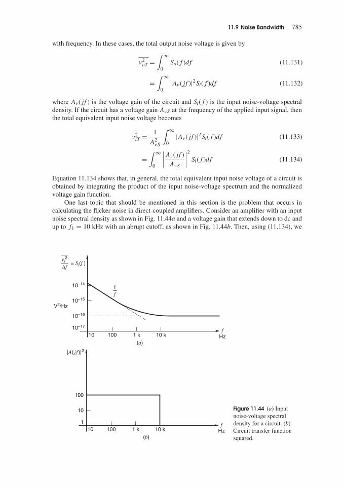
11.9 Noise Bandwidth 785
with frequency. In these cases, the total output noise voltage is given by
v2oT =
∫ ∞
0So(f )df (11.131)
=∫ ∞
0|Av (jf )|2Si(f )df (11.132)
where Av (jf ) is the voltage gain of the circuit and Si(f ) is the input noise-voltage spectraldensity. If the circuit has a voltage gain AvS at the frequency of the applied input signal, thenthe total equivalent input noise voltage becomes
v2iT = 1
A2vS
∫ ∞
0|Av (jf )|2Si(f )df (11.133)
=∫ ∞
0
∣∣∣∣Av (jf )
AvS
∣∣∣∣2 Si(f )df (11.134)
Equation 11.134 shows that, in general, the total equivalent input noise voltage of a circuit isobtained by integrating the product of the input noise-voltage spectrum and the normalizedvoltage gain function.
One last topic that should be mentioned in this section is the problem that occurs incalculating the flicker noise in direct-coupled amplifiers. Consider an amplifier with an inputnoise spectral density as shown in Fig. 11.44a and a voltage gain that extends down to dc andup to f1 = 10 kHz with an abrupt cutoff, as shown in Fig. 11.44b. Then, using (11.134), we
= Si(f )vi
2
Δf
fHz
(a)
1f
V2/Hz10–15
10–14
10–16
10–17
10 100 1 k 10 k
fHz
(b)
100
10
110 100 1 k 10 k
Figure 11.44 (a) Inputnoise-voltage spectraldensity for a circuit. (b)Circuit transfer functionsquared.

786 Chapter 11 � Noise in Integrated Circuits
can calculate the total equivalent input noise voltage as
v2iT =
∫ f1
0Si(f )df
=∫ f1
0
(1 + 1000
f
)× 10−16df
= 10−16[f + 1000 ln f ]f10 (11.135)
Evaluating (11.135) produces a problem since v2iT is infinite when a lower limit of zero is
used on the integration. This suggests infinite power in the 1/f noise signal. In practice,measurements of 1/f noise spectra show a continued 1/f dependence to as low a frequencyas is measured (cycles per day or less). This problem can be resolved only by noting that 1/f
noise eventually becomes indistinguishable from thermal drift and that the lower limit of theintegration must be specified by the period of observation. For example, taking a lower limitto the integration of f2 = 1 cycle/day, we have f2 = 1.16 × 10⁻⁵ Hz. Changing the limit in(11.135) we find
v2iT = 10−16[f + 1000 ln f ]f1
f2
= 10−16[
(f1 − f2) + 1000 lnf1
f2
](11.136)
Using f1 = 10 kHz and f2 = 1.16 × 10⁻⁵ Hz in (11.136) gives
v2iT = 10−16(10,000 + 20,600)
= 3.06 × 10⁻¹² V2
and thus
viT = 1.75 �V rms
If the lower limit of integration is changed to 1 cycle/year = 3.2 × 10⁻⁸ Hz, then (11.136)becomes
v2iT = 10−16(10,000 + 26,500)
= 3.65 × 10⁻¹² V2
and thus
viT = 1.9 �V rms
The noise voltage changes very slowly as f2 is reduced further because of the ln function in(11.136).
11.10 Noise Figure and Noise Temperature11.10.1 Noise Figure
The most general method of specifying the noise performance of circuits is by specifying inputnoise generators as described above. However, a number of specialized methods of specifyingnoise performance have been developed that are convenient in particular situations. Two ofthese methods are now described.

11.10 Noise Figure and Noise Temperature 787
Circuit So, NoSi, Ni
Figure 11.45 Signal and noise power at theinput and output of a circuit.
The noise figure (F ) is a commonly used method of specifying the noise performanceof a circuit or a device. Its disadvantage is that it is limited to situations where the sourceimpedance is resistive, and this precludes its use in many applications where noise performanceis important. However, it is widely used as a measure of noise performance in communicationsystems where the source impedance is often resistive.
The definition of the noise figure of a circuit is
F = input S/N ratio
output S/N ratio(11.137)
and F is usually expressed in decibels. The utility of the noise-figure concept is apparent fromthe definition, as it gives a direct measure of the signal-to-noise (S/N) ratio degradation thatis caused by the circuit. For example, if the S/N ratio at the input to a circuit is 50 dB, and thecircuit noise figure is 5 dB, then the S/N ratio at the output of the circuit is 45 dB.
Consider a circuit as shown in Fig. 11.45, where S represents signal power and N representsnoise power. The input noise power Ni is always taken as the noise in the source resistance.The output noise power No is the total output noise including the circuit contribution and noisetransmitted from the source resistance. From (11.137) the noise figure is
F = Si
Ni
No
So
(11.138)
For an ideal noiseless amplifier, all output noise comes from the source resistance at theinput, and thus if G is the circuit power gain, then the output signal So and the output noiseNo are given by
So = GSi (11.139)
No = GNi (11.140)
Substituting (11.139) and (11.140) in (11.138) gives F = 1 or 0 dB in this case.A useful alternative definition of F may be derived from (11.138) as follows:
F = Si
Ni
No
So
= No
GNi
(11.141)
Equation 11.141 can be written as
F = total output noise
that part of the output noise due to the source resistance(11.142)
Note that since F is specified by a power ratio, the value in decibels is given by 10 log10(numerical ratio).
The calculations of the previous sections have shown that the noise parameters of mostcircuits vary with frequency, and thus the bandwidth must be specified when the noise figure of acircuit is calculated. The noise figure is often specified for a small bandwidth �f at a frequencyf where �f � f . This is called the spot noise figure and applies to tuned amplifiers and alsoto broadband amplifiers that may be followed by frequency-selective circuits. For broadbandamplifiers whose output is utilized over a wide bandwidth, an average noise figure is often

788 Chapter 11 � Noise in Integrated Circuits
isignal RS is2 ii
2
vi
vx vozi RLGvx
2
+
–
+
–
+
–
Figure 11.46 Equivalent input noise representation for the calculation of noise figure.
specified. This requires calculation of the total output noise over the frequency band of interestusing the methods described in previous sections.
In many cases, the most convenient way to calculate noise figure is to return to the originalequivalent circuit of the device with its basic noise generators to perform the calculation.However, some insight into the effect of circuit parameters on the noise figure can be obtainedby using the equivalent input noise generator representation of Fig. 11.46. In this figure, acircuit with input impedance zi and voltage gain G = vo/vx is fed from a source resistance RS
and drives a load RL. The source resistance shows thermal noise i2s , and the noise of the circuit
itself is represented by i2i and v2i , assumed uncorrelated. The noise at the input terminals due
to v2i and i2i is
vxA = vi
zi
zi + RS
+ iiRSzi
RS + zi
and thus
v2xA = v2
i
|zi|2|zi + RS |2 + i2i
|RSzi|2|RS + zi|2 (11.143)
The noise power in RL produced by v2i and i2i is
NoA = |G|2RL
v2xA = |G|2
RL
(v2i
|zi|2|zi + RS |2 + i2i
|RSzi|2|RS + zi|2
)(11.144)
The noise power in RL produced by source resistance noise generator i2s is
NoB = |G|2RL
|RSzi|2|RS + zi|2 i2s (11.145)
The noise in the source resistance in a narrow bandwidth �f is
i2s = 4kT1
RS
�f (11.146)
Substituting (11.146) in (11.145) gives
NoB = |G|2RL
|RSzi|2|RS + zi|2 4kT
1
RS
�f (11.147)

11.10 Noise Figure and Noise Temperature 789
Using the definition of noise figure in (11.142) and substituting from (11.147) and (11.144),we find
F = NoA + NoB
NoB
= 1 + NoA
NoB
(11.148)
= 1 + v2i
4kTRS �f+ i2i
4kT1
RS
�f
(11.149)
Equation 11.149 gives the circuit spot noise figure assuming negligible correlation between
v2i and i2i . Note that F is independent of all circuit parameters (G, zi, RL) except the source
resistance RS and the equivalent input noise generators.It is apparent from (11.149) that F has a minimum as RS varies. For very low values of
RS , the v2i generator is dominant, whereas for large RS the i2i generator is most important. By
differentiating (11.149) with respect to RS , we can calculate the value of RS giving minimum F :
R2S(opt) = v2
i
i2i
(11.150)
This result is true in general, even if correlation is significant. A graph of F in decibels versusRS is shown in Fig. 11.47.
The existence of a minimum in F as RS is varied is one reason for the widespread useof transformers at the input of low-noise tuned amplifiers. This technique allows the sourceimpedance to be transformed to the value that simultaneously gives the lowest noise figureand causes minimal loss in the circuit.
For example, consider the noise figure of a bipolar transistor at low-to-moderate frequen-cies, where both flicker noise and high-frequency effects are neglected. From (11.50) and(11.57),
v2i = 4kT
(rb + 1
2gm
)�f
i2i = 2qIB �f = 2qIC
βF
�f
10 dB/decade 10 dB/decade
RS (opt)
RSlog scale
Noi
se fi
gure
F (
dB)
Figure 11.47 Variation innoise figure F with sourceresistance RS .

790 Chapter 11 � Noise in Integrated Circuits
Substitution of these values in (11.150) gives
RS(opt) =√
βF
gm
√1 + 2gmrb (11.151)
At this value of RS , the noise figure is given by (11.149) as
Fopt � 1 + 1√βF
√1 + 2gmrb (11.152)
At a collector current of IC = 1 mA, and with βF = 100 and rb = 50 , (11.151) givesRS(opt) = 572 andFopt = 1.22. In decibels the value is 10 log10 1.22 = 0.9 dB. Note thatFoptdecreases as βF increases and as rb and gm decrease. However, increasing βF and decreasinggm result in an increasing value of RS(opt), and this may prove difficult to realize in practice.
As another example, consider the MOSFET at low frequencies. Neglecting flicker noise,we can calculate the equivalent input generators from Section 11.5.2 as
v2i � 4kT
2
3
1
gm
�f (11.153)
i2i � 0 (11.154)
Using these values in (11.149) and (11.150), we find that RS(opt) → ∞ and Fopt → 0 dB. Thusthe MOS transistor has excellent noise performance from a high source resistance. However,if the source resistance is low (kilohms or less) and transformers cannot be used, the noisefigure for the MOS transistor may be worse than for a bipolar transistor. For source resistancesof the order of megohms or higher, the MOS transistor usually has significantly lower noisefigure than a bipolar transistor.
11.10.2 Noise Temperature
Noise temperature is an alternative noise representation and is closely related to noise figure.The noise temperature Tn of a circuit is defined as the temperature at which the source resistanceRS must be held so that the noise output from the circuit due to RS equals the noise output due tothe circuit itself. If these conditions are applied to the circuit of Fig. 11.46, the output noiseNoA due to the circuit itself is unchanged but the output noise due to the source resistancebecomes
N ′oB = |G|2
RL
|RSzi|2|RS + zi|2 4kTn
1
RS
�f (11.155)
Substituting for NoB from (11.147) in (11.155), we obtain
N ′oB = NoB
Tn
T(11.156)
where T is the circuit temperature at which the noise performance is specified (usually takenas 290◦K). Substituting (11.156) in (11.148) gives
Tn
T= (F − 1) (11.157)
where F is specified as a ratio and is not in decibels.Thus noise temperature and noise figure are directly related. The main application of noise
temperature provides a convenient expanded measure of noise performance near F = 1 forvery-low-noise amplifiers. A noise figure of F = 2 (3 dB) corresponds to Tn = 290◦K andF = 1.1 (0.4 dB) corresponds to Tn = 29◦K.

Problems 791
PROBLEMS11.1 Calculate the noise-voltage spectral density
in V2/Hz at vo for the circuit in Fig. 11.48, and thus cal-culate the total noise in a 100-kHz bandwidth. Neglectcapacitive effects, flicker noise, and series resistancein the diode.
11.2 If the diode in Fig. 11.48 shows flicker noise,calculate and plot the output noise voltage spec-tral density at vo in V2/Hz on log scales from f =1 Hz to f = 10 MHz. Flicker noise data: in (11.7) usea = b = 1, K1 = 3 × 10⁻¹⁶ A.
+10 V
20 kΩ
+
–
vo Figure 11.48 Diodecircuit for Problems11.1 and 11.2.
11.3 Repeat Problem 11.2 if a 1000-pF capacitor isconnected across the diode. Compare your result witha SPICE simulation.
11.4 The ac schematic of an amplifier is shown inFig. 11.49. The circuit is fed from a current source iSand data are as follows:
RS = 1 k RL = 10 k IC = 1 mA
β = 50 rb = 0 ro = ∞Neglecting capacitive effects and flicker noise, cal-culate the total noise voltage spectral density at vo inV2/Hz. Thus calculate the MDS at iS if the circuit band-width is limited to a sharp cutoff at 2 MHz. Compareyour result with a SPICE simulation. (This will requiresetting up a bias circuit.)
RS RLisvo
+
–
Figure 11.49 Amplifier ac schematic for Problems11.4 and 11.6.
11.5 Calculate the total input- and output-referrednoise voltages at 10 Hz, 100 kHz, and 1 GHz for thecommon-source amplifier shown in Fig. 7.2b. Assumethat W = 100 �m, L = 1 �m, ID = 100 �A, Vt =
0.6 V , k′ = 194 �A/V2, tox = 80 Å , Ld = 0, Xd = 0,and Kf = 3 × 10⁻²⁴ F-V2. Ignore gate-current noisein (11.15) and (11.16). Let RS = 100 k and RL =10 k. Verify your result using SPICE. (Add dcsources for SPICE.)
11.6 Calculate equivalent input noise voltage andcurrent generators for the circuit of Fig. 11.49 (omit-ting RS). Using these results, calculate the totalequivalent input noise current in a 2-MHz bandwidthfor the circuit of Fig. 11.49 with RS = 1 k andcompare with the result of Problem 11.4. Neglect cor-relation between the noise generators.
11.7 Four methods of achieving an inputimpedance greater than 100 k are shown in theac schematics of Fig. 11.50.
(a) Neglecting flicker noise and capacitive effects,derive expressions for the equivalent input noise volt-age and current generators of these circuits. For circuit(i) this will be on the source side of the 100-k
resistor.
(b) Assuming that following stages limit the band-width to dc-20 kHz with a sharp cutoff, calculate themagnitude of the total equivalent input noise voltagein each case. Then compare these circuits for use aslow-noise amplifiers from low source impedances.
11.8 Neglecting capacitive effects, calculateequivalent input noise voltage and current genera-tors for circuit (iv) of Fig. 11.50, assuming that thespectral density of the flicker noise in the MOS tran-sistor drain current equals that of the thermal noiseat 100 kHz. Assuming that following stages limit thebandwidth to 0.001 kHz to 20 kHz with a sharp cutoff,calculate the magnitude of the total equivalent inputnoise voltage. Ignore gate-current noise in (11.15) and(11.16). (Assume Cgs = 0.)
11.9 A BiCMOS Darlington is shown inFig. 11.51. Neglecting frequency effects, calculatethe equivalent input noise voltage and current gen-erators for this circuit, assuming that the dc valueof Vi is adjusted for IC1 = 1 mA. Device data isμnCox = 60 �A/V2, Vt = 0.7 V, λ = 0, γ = 0, W =100 �m, L = 1 �m for the MOSFET and IS = 10−16
A, VA = ∞, β = 100, rb = 100 for the bipolar tran-sistor. Use SPICE to check your calculation. Thenadd Cgs = 150 fF, Csb = 50 fF for the MOSFET andCμ = 50 fF, fT = 10 GHz for the bipolar transistorand use SPICE to determine the frequency where thespectral density of the equivalent input noise voltagegenerator v2
i has doubled.Also use SPICE to determinethe equivalent input noise current spectral density atthat frequency.

792 Chapter 11 � Noise in Integrated Circuits
vovo
+ +
– –
vo vs
+
+
–
vs
+
–
vs
+
–vs
+
–
–
10 kΩ vo
+
–
10 kΩ
10 kΩ10 kΩ
100 kΩ
1 kΩ
IC = 0.5 mA, = 100, rb = 100 Ω(i)
β
β
IC = 0.5 mA, = 100, rb = 100 Ω(ii)
IC = 13 μA, = 50, rb = 100 Ω(iii)
gm = 1 mA/V(iv)
β
Figure 11.50 Four ac schematics of circuits realizing an input resistance Ri > 100 k.
Vi
+
–
Vo
R3
Q1
M1
R2R1
+
–
100 Ω
2 kΩ
300 Ω
5 V
Figure 11.51 BiCMOS Darlington circuit forProblem 11.9.
11.10 The ac schematic of a low-input-impedancecommon-base amplifier is shown in Fig. 11.52.
(a) Calculate the equivalent noise voltage and cur-rent generators of this circuit at the emitter of Q1
using IC1 = IC2 = 1 mA, rb1 = rb2 = 0, β1 = β2 =100, fT1 = fT2 = 400 MHz. Neglect flicker noise butinclude capacitive effects in the transistors. Use SPICEto check your result.
(b) If RS = 5 k, and later stages limit the band-width to a sharp cutoff at 150 MHz, calculate the valueof iS giving an output signal-to-noise ratio of 10 dB.
11.11 A super-β input stage is shown inFig. 11.53a.
(a) Neglecting flicker noise and capacitive effects,calculate the equivalent input noise voltage and currentgenerators v2 and i2 for this stage. Data: IEE = 1 �A;β1 = β2 = 5000; rb1 = rb2 = 500 .
(b) If the circuit is fed from source resistancesRS = 100 M as shown in Fig. 11.53b, calculate thetotal equivalent input noise voltage at vs in a bandwidthof 1 kHz.
11.12 Repeat Problem 11.11 if the bipolar transis-tors are replaced by MOS transistors with IG = 0.1 fAand gm = 0.5 mA/V. Assume Cgs = 0.
RS
Q1 Q2
5 kΩis
Figure 11.52 An ac schematic of acommon-base amplifier for Problem 11.10.

Problems 793
Q1
RS
RSvs
i2
Q2
Q1 Q2
v2
i2
IEE
IEE
–V
–V
(a)
(b)
+
–
Figure 11.53 Super-β input stage forProblem 11.11.
11.13 If a 100-pF capacitor is connected acrossthe diode in Fig. 11.48, calculate the noise bandwidthof the circuit and thus calculate the total output noiseat vo. Neglect flicker noise and series resistance in thediode.
11.14 A differential input stage is shown inFig. 11.54.
(a) Neglecting flicker noise, calculate expressionsfor the equivalent input noise voltage and current gen-erators at the base of Q1. Use SPICE to check yourresult.
(b) Assuming the circuit has a dominant pole inits frequency response at 30 MHz and RS = 50 ,calculate the total equivalent input and output noisevoltages. Data: β = 100; rb = 200 .
11.15 Calculate the source resistance giving min-imum noise figure and the corresponding noise figurein decibels for a bipolar transistor with parameters
(a) IC = 2 mA βF = 50 rb = 100
(b) IC = 10 �A βF = 100 rb = 300
RS
vs
vo
Q1 Q2
–10 V
+10 V
100 kΩ
20 kΩ 20 kΩ
500 Ω500 Ω
+
+
–
–
Figure 11.54 Differential-pair input stage forProblem 11.14.

794 Chapter 11 � Noise in Integrated Circuits
11.16 Repeat Problem 11.15 if the transistor hasa flicker noise corner frequency of 1 kHz. Calculatespot noise figure at 500 Hz.
11.17 Repeat Problem 11.15 if the transistor has a1-k emitter resistor.
11.18 (a) Neglecting flicker noise and capacitiveeffects, calculate the noise figure in decibels of thecircuit of Fig. 11.54 with RS = 50 .
(b) If RS were made equal to (i) 100 or (ii)200 k, would the noise figure increase or decrease?Explain.
(c) If RS = 200 k, and each device has a flickernoise corner frequency of 10 kHz, calculate the lowfrequency where the circuit spot noise figure is 20 dB.
11.19 (a) A shunt-feedback amplifier is shown inFig. 11.55. Using equivalent input noise generators forthe device, calculate the spot noise figure of this circuitin decibels for RS = 10 k using the following data.
IC = 0.5 mA β = 50 rb = 100
Neglect flicker noise and capacitive effects.
(b) If the device has fT = 500 MHz, calculate thefrequency where the noise figure is 3 dB above itslow-frequency value.
11.20 (a) Neglecting capacitive effects, calculatethe noise figure in decibels of the circuit of Fig. 11.52with RS = 5 k. Use data as in Problem 11.10.
(b) If the flicker noise corner frequency for eachdevice is 1 kHz, calculate the low frequency where thespot noise figure is 3 dB above the value in (a).
11.21 Neglecting flicker noise, calculate the totalequivalent input noise voltage for the MC1553 shownin Figure 8.21a. Use β = 100, rb = 100 and assumea sharp cutoff in the frequency response at 50 MHz.Then calculate the average noise figure of the circuitwith a source resistance of 50 .
11.22 Calculate the total equivalent input noisecurrent for the shunt-shunt feedback circuit ofFig. 8.48 in a bandwidth from 0.01 Hz to 100 kHz.Use the MOS transistor data in Problem 11.5. Ignoregate-current noise in (11.15) and (11.16).
11.23 Repeat Problem 11.22 if the MOS transis-tors in Fig. 8.48 are replaced by bipolar transistors.Assume that β = 200, rb = 300 , IC = 1 mA and theflicker noise corner frequency is fa = 5 kHz. Neglectcapacitive effects.
11.24 The BiCMOS amplifier of Fig. 3.78 is tobe used as a low-noise transimpedance amplifier. Theinput is fed from a current source with a shunt sourcecapacitance of CS = 1 pF. Assuming that CS andCgs1 = 0.5 pF dominate the frequency response, calcu-late the equivalent input noise current spectral densityof the circuit at low frequencies and at the −3-dBfrequency of the transfer function. Use data as in Prob-lem 3.17. Use SPICE to check your result, and alsoto investigate the effect of adding rb = 200 to thebipolar model.
11.25 A MOS current source of the type shown inFig. 4.4 is to be designed to achieve minimum outputcurrent noise. The two transistors must be identicaland the total gate area of the two transistors combinedmust not exceed 10 �m2. Choose the W and L of thedevices under two different assumptions:
(a) 1/f noise dominates.
(b) Thermal noise dominates.Assume that Ld and Xd are zero. The minimum
allowed transistor length or width is 0.6 �m. Verifyyour design using SPICE.
11.26 Calculate the equivalent input noise volt-age at 100 Hz, 1 kHz, and 10 kHz for the CMOS opamp shown in Fig. 6.58. Use the MOS parameters inTable 2.4, and assume that Xd = 0.1 �m at the oper-ating point for all transistors operating in the activeregion. For this problem, assume that the gate of M9
is attached to the positive power supply, and that theW /L of M9 has been optimally chosen to cancel theright-half-plane zero. The flicker-noise coefficient forall transistors is Kf = 3 × 10⁻²⁴ F-V2. Ignore gate-current noise in (11.15) and (11.16). Verify your resultusing SPICE.
11.27 Use SPICE to verify the noise analysis ofthe NE5234 op amp given in Section 11.8. Then addflicker noise generators assuming a = 1 in (11.13) and
RSisvo
+
–
10 kΩ
10 kΩ
Figure 11.55 An ac schematic of a single-stageshunt-feedback amplifier for Problem 11.19.

References 795
the transistor flicker noise corner frequency is 1 kHz.Which device dominates the noise performance at1 Hz?
11.28 (a) At what frequency are the noise spec-tral densities, i2
g/�f , for the gate-current noise in(11.15) and (11.16) equal? Assume that W = 50 �m,L = 0.5 �m, IG = 0.05 fA, ID = 100 �A, Vt = 0.6 V,
k′ = 194 �A/V2, tox = 80 Å, Ld = 0, Xd = 0, andKf = 3 × 10⁻²⁴ F-V2.
(b) For this transistor, considering only the gate-current noise, in what bandwidth (from 0 to fBW )are the total input noise currents due to shot noisein (11.15) and coupled thermal noise in (11.16)equal?
REFERENCES1. M. Schwartz. Information Transmission,
Modulation, and Noise. McGraw-Hill, New York,1959, Chapter 5.
2. W. B. Davenport, Jr., and W. L. Root. An Intro-duction to the Theory of Random Signals and Noise.McGraw-Hill, New York, 1958, Chapter 7.
3. J. L. Lawson and G. E. Uhlenbeck. ThresholdSignals. McGraw-Hill, New York, 1950, Chapter 4.
4. A. van der Ziel. Noise. Prentice-Hall, NewYork, 1954, Chapter 5.
5. W. B. Davenport, Jr., and W. L. Root, op. cit.,Chapter 9.
6. J. L. Plumb and E. R. Chenette. “Flicker NoiseTransistors,” IEEE Transactions on Electron Devices,Vol. ED-10, pp. 304–308, September 1963.
7. R. C. Jaeger and A. J. Broderson. “Low-Frequency Noise Sources in Bipolar JunctionTransistors,” IEEE Transactions on Electron Devices,Vol. ED-17, pp. 128–134, February 1970.
8. M. Nishida. “Effects of Diffusion-InducedDislocations on the Excess Low-Frequency Noise,”IEEE Transactions on Electron Devices, Vol. ED-20,pp. 221–226, March 1973.
9. R. G. Meyer, L. Nagel, and S. K. Lui.“Computer Simulation of 1/f Noise Performance ofElectronic Circuits,” IEEE Journal of Solid-State Cir-cuits, Vol. SC-8, pp. 237–240, June 1973.
10. R. H. Haitz. “Controlled Noise Generationwith Avalanche Diodes,” IEEE Transactions on Elec-tron Devices, Vol. ED-12, pp. 198–207, April 1965.
11. D. G. Peterson. “Noise Performance of Tran-sistors,” IRE Transactions on Electron Devices, Vol.Ed-9, pp. 296–303, May 1962.
12. A. van der Ziel. Noise in Solid State Devicesand Circuits. Wiley, New York, 1986.
13. A. A. Abidi. “High-Frequency Noise Mea-surements on FETs with Small Dimensions,” IEEETransactions on Electron Devices, Vol. 33, no. 11, pp.1801–1805, November 1986.
14. D. K. Shaeffer and T. H. Lee. “A 1.5-V,1.5-GHz CMOS Low Noise Amplifier,” IEEE Jour-nal of Solid-State Circuits, Vol. 32, no. 5, pp. 745–759,May 1997.
15. W. R. Bennett. “Methods of Solving NoiseProblems,” Proceedings, IRE, Vol. 44, pp. 609–638,May 1956.
16. E. M. Cherry and D. E. Hooper. AmplifyingDevices and Low-Pass Amplifier Design. Wiley, NewYork, 1968, Chapter 8.
17. H. A. Haus, et al. “Representation of Noisein Linear Twoports,” Proceedings, IRE, Vol. 48, pp.69–74, January 1960.
18. M. B. Das and J. M. Moore. “Measurementsand Interpretation of Low-Frequency Noise in FETS,”IEEE Transactions on Electron Devices, Vol. ED-21,pp. 247–257, April 1974.
19. M. J. Fonderie and J. H. Huijsing.Design of Low-Voltage Bipolar Operational Ampli-fiers. Kluwer Academic Publishers, Boston, 1993,pp. 20–22.

CHAPTER 12
Fully DifferentialOperational Amplifiers
12.1 IntroductionThe analysis of integrated-circuit operational amplifiers (op amps) in Chapter 6 focused onop amps with single-ended outputs. The topic of this chapter is fully differential op amps,which have a differential input and produce a differential output. Fully differential op ampsare widely used in modern integrated circuits because they have some advantages over theirsingle-ended counterparts. They provide a larger output voltage swing and are less susceptibleto common-mode noise. Also, even-order nonlinearities are not present in the differentialoutput of a balanced circuit. (A balanced circuit is symmetric with perfectly matched elementson either side of an axis of symmetry.) A disadvantage of fully differential op amps is that theyrequire two matched feedback networks and a common-mode feedback circuit to control thecommon-mode output voltage.
In this chapter, the properties of fully differential amplifiers are presented first, followedby some common-mode feedback approaches. A number of fully differential CMOS op ampsare covered. Some of the terminology used in this chapter was introduced for a simple fullydifferential amplifier (a differential pair with resistive loads) in Section 3.5. In most of thechapter, the circuits are assumed to be perfectly balanced. The effects of imbalance are consid-ered in Section 12.7. The circuits in this chapter are CMOS; however, most of the techniquesand topologies described can be readily extended to bipolar technologies.
12.2 Properties of Fully Differential Amplifiers1,2
A fully differential feedback amplifier is shown in Fig. 12.1a. It differs from the single-endedfeedback amplifier in Fig. 12.1b in the following two ways. The op amp has two outputs,and two identical resistive networks provide feedback. While many fully differential op-amptopologies exist, the simple fully differential amplifier in Fig. 12.2 will be used for illustrationpurposes. It consists of a differential pair M1-M2, active loads M3 and M4, and tail currentsource M5.
Fully differential op amps provide a larger output voltage swing than their single-endedcounterparts, which is important when the power-supply voltage is small. The larger outputvoltage swing provided by a fully differential op amp can be explained using the two feedbackcircuits in Fig. 12.1. Assume that each op-amp output, Vo1, Vo2, or Vo, can swing up to Vmaxand down to Vmin. For the single-ended-output circuit in Fig. 12.1b, the peak-to-peak outputvoltage can be as large as Vmax − Vmin. In the fully differential circuit in Fig. 12.1a, if Vo1swings up to Vmax and Vo2 swings down to Vmin, the peak differential output is Vmax − Vmin.Therefore, the peak-to-peak differential output is 2(Vmax − Vmin). Thus, the output swing of
796

12.2 Properties of Fully Differential Amplifiers 797
Vsd
Vs1 Vo1
Vo1
Vo2Vs2
Vi1
Vi2
+
–Vod
Vmax
t
Vmin
Vo2
Vmax
t
Vmin
Vod
Vmax–Vmin
–(Vmax–Vmin)
t
+
–
+
–+
–
R3
R3
R1
R1
(a)
Vs
Vo
+
– Vo
Vmax
t
Vmin
+
–+
–
R3
R1
(b)
Figure 12.1 (a) Fullydifferential and (b)single-ended invertingamplifiers.
VDD
M1
M5
M2
M4M3
Vo1
Vi1
Vo2
Vi2
Vcmc
VBIAS
–VSS
Figure 12.2 A simple, one-stage, fullydifferential op amp.
a fully differential op amp is twice as large as that of a similar op amp with a single-endedoutput.
This larger output swing can result in a higher signal-to-noise ratio. Ignoring the noisefrom the op amp and from the feedback resistor R3, we see that thermal noise associated withthe R1 input resistors is the only source of noise. In the single-ended circuit in Fig. 12.1b, the

798 Chapter 12 � Fully Differential Operational Amplifiers
output noise power due to resistor R1 is
v2oN (s.e.) =
(R3
R1
)2
4kTR1(BWN ) (12.1)
where BWN is the equivalent noise bandwidth of the closed-loop amplifier. In the fully differ-ential amplifier in Fig. 12.1a, the differential output noise power due to the two R1 resistorsis
v2oN (diff) = 2
(R3
R1
)2
4kTR1(BWN ) (12.2)
because the output noise terms from the two R1 resistors are uncorrelated and hence theircontributions add together to give the total output noise power. From (12.1) and (12.2), theoutput noise power in the fully differential circuit is twice that in the single-ended circuit.Since the peak output signal in the differential circuit is twice that in the single-ended circuit,the maximum output signal power is four times that in the single-ended circuit. The maximumoutput signal-to-noise ratio (SNR) for a maximum sinusoidal output signal with amplitudeVsig(peak) is given by
SNRmax = maximum output signal power
output noise power=
V 2sig(peak)
2v2oN
(12.3)
This SNR is twice as large, or 3 dB larger, for the fully differential circuit when compared tothe single-ended circuit if the same resistance R1 is used in both circuits and R1 is the dominantnoise source.
Fully differential circuits are less susceptible than their single-ended counterparts tocommon-mode (CM) noise, such as noise on the power supplies that is generated by dig-ital circuits that are integrated on the same substrate as the analog circuits. To explain thereduced sensitivity to CM noise, consider the circuit in Fig. 12.3. This circuit is the sameas Fig. 12.1a with two capacitors Cip added. Each capacitor connects from an op-amp inputto voltage source vn. Here Cip models parasitic capacitance from the substrate to each op-amp input, and vn models noise that exists on the power-supply voltage that connects to thesubstrate. The parasitic capacitors couple equal signals to the op-amp inputs, causing a CMdisturbance at the op-amp input. If the op amp is perfectly balanced and has zero CM gain,this CM noise does not affect the CM output voltage. If the op-amp CM gain is nonzero butsmall, vn causes a small CM output voltage but does not affect the differential output voltage
vn
Vs1
Vo1
Vo2
Vs2
Cip
Cip
+
– + –
– +
R3
R3
R1
R1
Figure 12.3 The invertingamplifier of Fig. 12.1aincluding parasitic capacitorsCip and noise source vn.

12.3 Small-Signal Models for Balanced Differential Amplifiers 799
if the circuit is perfectly balanced. This capacitive coupling to the op-amp inputs can causea nonzero differential-mode (DM) output voltage if the circuit is not perfectly balanced. Forexample, mismatch between the Cip capacitors causes the coupled noise at the two op-ampinputs to be unequal and introduces a differential noise signal across the op-amp inputs.
Even without the capacitive coupling to the substrate in Fig. 12.3, noise on the positiveor negative power supply can couple to the op-amp outputs through the transistors in the opamp (see Section 6.2.6). If the circuit is balanced, such coupling is the same at each op-ampoutput. Therefore, power-supply noise in a balanced circuit alters the CM output but does notaffect the DM output.
Even-order nonlinearities are not present in the differential output of a balanced circuit.The cancellation of even-order nonlinearities can be explained using Fig. 12.1a. Assume thatthe circuit is perfectly balanced but is not perfectly linear. First, consider the case when theinputs are Vs1 = Va and Vs2 = Vb, and let the resulting output voltages be Vo1 = Vx andVo2 = Vy. In this case, the differential input and output are
Vsd = Va − Vb and Vod = Vx − Vy (12.4)
Next, consider the circuit with the inputs swapped; that is, Vs1 = Vb and Vs2 = Va. Then theoutput voltages will also be swapped (Vo1 = Vy and Vo2 = Vx) because the circuit is symmetric.In this second case,
Vsd = Vb − Va = −(Va − Vb) and Vod = Vy − Vx = −(Vx − Vy) (12.5)
Equations 12.4 and 12.5 show that changing the polarity of the differential input of a bal-anced circuit causes only a polarity change in the differential output voltage. Therefore, thedifferential input-output characteristic f () is an odd function; that is, if Vod = f (Vid), then−Vod = f (−Vid). Hence, the differential transfer characteristic of a balanced amplifier exhibitsonly odd-order nonlinearities, so only odd-order distortion can appear in the differential outputwhen a differential input is applied. Even-order distortion may exist in each individual outputVo1 and Vo2, but such distortion in these output voltages is identical and cancels when they aresubtracted to form Vod .
In a balanced, fully differential amplifier, the small-signal differential output voltage isproportional to the small-signal differential input voltage but is independent of the CM inputvoltage, as was shown in Section 3.5.4. Similarly, the small-signal CM output voltage isproportional to the small-signal CM input voltage but is independent of the differential inputvoltage.
12.3 Small-Signal Models for Balanced Differential AmplifiersA balanced signal source driving a balanced, fully differential amplifier is shown in Fig. 12.4. AT-network small-signal model for the balanced signal source is shown in Fig. 12.5. Equationsthat describe this model are found as follows. Applying KVL from vs1 to ground,
vs1 = v′sd
2+ v′
sc + Rsd
2is1 +
(Rsc
2− Rsd
4
)(is1 + is2) (12.6)
Rearranging gives
vs1 = v′sd
2+ v′
sc + Rsd
2
is1 − is2
2+ Rsc
is1 + is2
2(12.7)
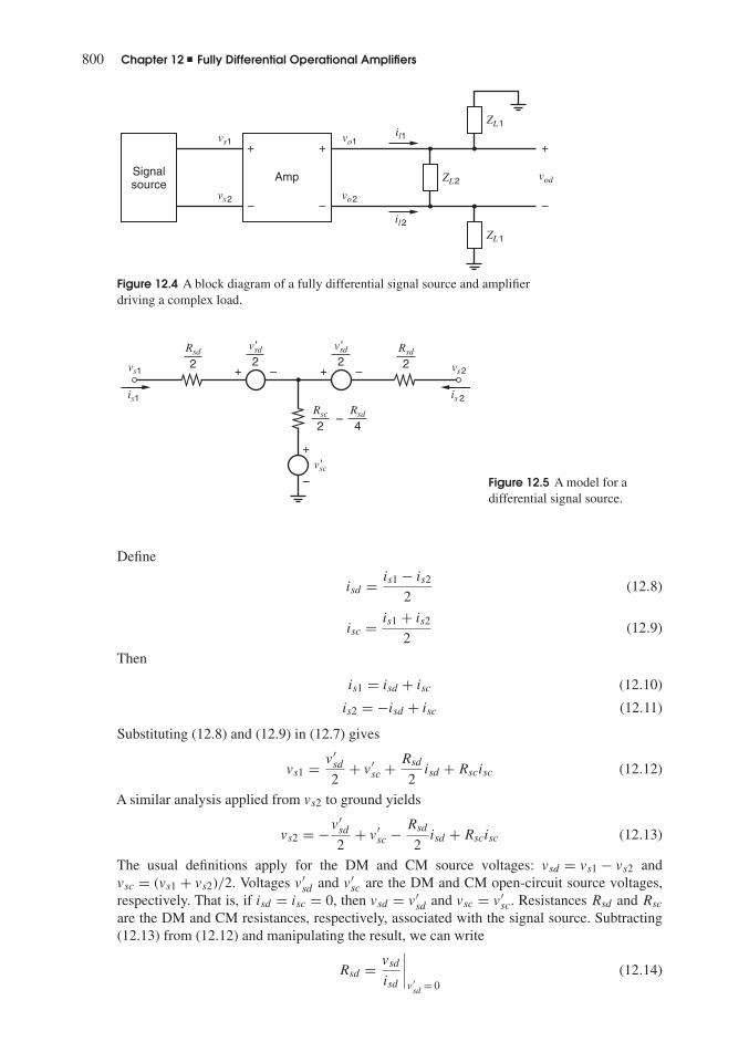
800 Chapter 12 � Fully Differential Operational Amplifiers
ZL2
ZL1
ZL1
vo1
vod
vo2
vs1
vs2
+
–
+
–
+
–
il1
il2
Signalsource
Amp
Figure 12.4 A block diagram of a fully differential signal source and amplifierdriving a complex load.
vs1
is1
vs2
is 2
–
+ –
v'sc
+
–
Rsd
2
Rsc
2Rsd
4
Rsd
2
v'sd
2+ –
v'sd
2
Figure 12.5 A model for adifferential signal source.
Define
isd = is1 − is2
2(12.8)
isc = is1 + is2
2(12.9)
Then
is1 = isd + isc (12.10)
is2 = −isd + isc (12.11)
Substituting (12.8) and (12.9) in (12.7) gives
vs1 = v′sd
2+ v′
sc + Rsd
2isd + Rscisc (12.12)
A similar analysis applied from vs2 to ground yields
vs2 = −v′sd
2+ v′
sc − Rsd
2isd + Rscisc (12.13)
The usual definitions apply for the DM and CM source voltages: vsd = vs1 − vs2 andvsc = (vs1 + vs2)/2. Voltages v′
sd and v′sc are the DM and CM open-circuit source voltages,
respectively. That is, if isd = isc = 0, then vsd = v′sd and vsc = v′
sc. Resistances Rsd and Rsc
are the DM and CM resistances, respectively, associated with the signal source. Subtracting(12.13) from (12.12) and manipulating the result, we can write
Rsd = vsd
isd
∣∣∣∣v ′sd
= 0(12.14)

12.3 Small-Signal Models for Balanced Differential Amplifiers 801
(a)
vi1 vi2
–
Zid
2Zid
2
Zic
2Zid
4
ii1 ii2
(b)
vi1 vi2
Zic Zic
Zid ||(–2 Zic)
ii1 ii2
Figure 12.6 Models for the input impe-dance of a fully differential amplifier: (a) aT-network model and (b) a π-network model.
Adding (12.12) and (12.13), we find
Rsc = vsc
isc
∣∣∣∣v ′sc = 0
(12.15)
These simple expressions result from the definitions of the CM and DM currents in (12.8) and(12.9), and the standard definitions for the CM and DM voltages.
Two equivalent models for the inputs of the amplifier in Fig. 12.4 are shown in Fig. 12.6.These models are extensions of Fig. 3.61 and (3.197) and (3.198), which were derived to modelthe inputs for a differential pair with resistive loads. Two equivalent models for the output portsof the amplifier are shown in Fig. 12.7. The equations that describe the model in Fig. 12.7a,
vo1
io1
vo2
io 2
–
+ –
acmvic
+
–
Rod
2
Roc
2Rod
4
Rod
2+ –
(a)
vid
2adm
vid
2adm
(b)
vo2vo1
io2io1
Gmdvid GmcvicGmcvic RocRoc
Rod||(–2Roc)
Figure 12.7 Models for the output ports of a fully differential amplifier: (a) a Thévenin-network modeland (b) a Norton-network model.

802 Chapter 12 � Fully Differential Operational Amplifiers
which uses voltage-controlled voltage sources, are
vo1 = adm
vid
2+ acmvic + Rod
2iod + Rocioc (12.16)
vo2 = −adm
vid
2+ acmvic − Rod
2iod + Rocioc (12.17)
where
adm = vod
vid
∣∣∣∣iod = 0
acm = voc
vic
∣∣∣∣ioc = 0
(12.18)
Rod = vod
iod
∣∣∣∣vid = 0
Roc = voc
ioc
∣∣∣∣vic = 0
(12.19)
and vid = vi1 − vi2, vic = (vi1 + vi2)/2, vod = vo1 − vo2, voc = (vo1 + vo2)/2, iod =(io1 − io2)/2, and ioc = (io1 + io2)/2. Figure 12.7b shows an alternative model that usesvoltage-controlled current sources, and the corresponding equations are
io1 = iod + ioc = Gmdvid + Gmcvic + vod
Rod
+ voc
Roc
(12.20)
io2 = −iod + ioc = −Gmdvid + Gmcvic − vod
Rod
+ voc
Roc
(12.21)
where
Gmd = iod
vid
∣∣∣∣vod = 0
(12.22)
Gmc = ioc
vic
∣∣∣∣voc = 0
(12.23)
The parameters for the models in Fig. 12.7 can be computed from the corresponding half-circuits.
The DM and CM output-load impedances can be computed using
ZLd = vod
ild(12.24)
and
ZLc = voc
ilc(12.25)
where ild = (il1 − il2)/2, ilc = (il1 + il2)/2, and il1 and il2 are defined in Fig. 12.4. A fullybalanced output load can be modeled using a passive network of the form shown in Fig. 12.6aor Fig. 12.6b, with Zid and Zic replaced by ZLd and ZLc, respectively.
The DM and CM half-circuits for the amplifier, signal source, and output load in Fig. 12.4are shown in Figs. 12.8 and 12.9. The DM load ZLd and the CM load ZLc can be found using(12.24) and (12.25) for the load network in Fig. 12.4, and the resulting load elements are
ZLd = ZL2||(2ZL1) (12.26)
ZLc = ZL1 (12.27)
The DM and CM loads are different for the following reason. The axis of symmetry in Fig. 12.4passes through the middle of ZL2. For purely DM signals, points along the axis of symmetryare ac grounds (see Section 3.5.5). Therefore, the load for the DM half-circuit is half of ZL2

12.3 Small-Signal Models for Balanced Differential Amplifiers 803
(a)
iid+
–
Rsd
2vid
2
vsd
2Zid
2
(b)
iod+
–
Rod
2vod
2
admvid
2ZLd
2
(c)
iod
Rod
2
vod
2
GmdvidZLd
2 Figure 12.8 DM half-circuits for a fullydifferential signal source and amplifier: (a) theinput port, (b) the output port using a Théveninequivalent, (c) the output port using a Nortonequivalent.
(a)
iic+
–
Rsc vic
vsc Zic
(b)
ioc+
–
Roc voc
acmvic ZLc
(c)
ioc
Roc
voc
Gmcvic ZLc
Figure 12.9 CM half-circuits for a fully differential signal source and amplifier: (a) the input port,(b) the output port using a Thévenin equivalent, (c) the output port using a Norton equivalent.

804 Chapter 12 � Fully Differential Operational Amplifiers
vi1
vi2
vo1
vo2
+
–
+
–
+
–acmvic
vid
2adm
vid
2adm
Figure 12.10 A simple small-signalmodel for a balanced fully differentialop amp, assuming infinite inputimpedance and zero output impedance.
in parallel with ZL1. However, points along the axis of symmetry are open circuits for purelyCM signals (see Section 3.5.5). Therefore, ZL2 does not affect the load in the CM half-circuit.
These amplifier models can be used to model any balanced, fully differential amplifier,including an op amp. If the model is simplified to just the dependent sources (assuming infiniteinput impedance and zero output impedance), the equations that describe the model reduce to
vod = vo1 − vo2 = admvid (12.28)
and
voc = vo1 + vo2
2= acmvic (12.29)
In an ideal, fully differential op amp, acm = 0 and adm → −∞. If acm = 0, then voc = 0 ifvic is finite. If adm → −∞, then vid → 0 if vod is finite. A simple small-signal model for abalanced, fully differential op amp that is based on (12.28) and (12.29) is shown in Fig. 12.10.Because of its simplicity, this model will be used to illustrate some key points in the followingsections.
12.4 Common-Mode FeedbackThe fully differential feedback amplifier in Fig. 12.1a is redrawn in Fig. 12.11a using the idealop-amp model from Fig. 12.10. In Fig. 12.11a, the axis of symmetry is shown as a dashedline. The acm controlled source is shown twice, once on each side of the axis of symmetry. TheDM half-circuit is shown in Fig. 12.11b. Here all nodes intersecting the axis of symmetry areconnected to ac ground. Using this half-circuit and letting adm → −∞, the differential gain is
vod
vsd
= vod
vs1 − vs2= −R3
R1(12.30)
Thus, the DM output voltage is determined by the DM gain, which is accurately set by the DMfeedback loop in Fig. 12.11b. However, the CM output voltage is set by a different feedbackloop. The CM half-circuit for Fig. 12.1a is shown in Fig. 12.11c. If acm = 0, the closed-loopCM gain voc/vsc is zero, and the loop gain (or return ratio) for the CM feedback loop in Fig.12.11c is zero. Therefore, the CM output voltage voc is independent of the CM op-amp inputvoltage vic and the CM source voltage vsc. In practice, |acm| is nonzero but small in op ampsthat use an input differential pair with a tail current source because the tail current sourceprovides local feedback for CM signals and makes the CM gain of the input stage small. If|acm| is small, the magnitude of the loop gain (or return ratio) for the CM feedback loop inFig. 12.11c is small, and this feedback loop exerts little control on the CM output voltage. As a

12.4 Common-Mode Feedback 805
vs1vi1
R3
R1
+
–+–
vs2
vo1
vo2
vi2
R3
R1
acmvic
+–
acmvic
vid
2adm
+
–
vid
2adm
Axis of symmetry
(a)
R3
R1
+
–
+
–
+
–
+
–
vid
2vsd
2
vid
2vod
2adm
(b)
R3
R1
+
–
+
–
voc
+
–
vicvsc acmvic
+
–
(c)
Figure 12.11 (a) Theinverting feedbackamplifier of Fig. 12.1a,using the op-amp modelin Fig. 12.10. (b) The DMhalf-circuit. (c) The CMhalf-circuit.
result, a different feedback loop with high loop gain is used to control the CM output voltage,as described next.
12.4.1 Common-Mode Feedback at Low Frequencies
For the op amp in Fig. 12.2, the ideal operating point biases M1–M5 in the active regionand sets the dc CM output voltage VOC to the value that maximizes the swing at the op-ampoutputs for which all transistors operate in the active region. However, as described in Section4.3.5.1, VOC is very sensitive to mismatches and component variations, and the circuit is notpractical from a bias stability standpoint. (Section 4.3.5.1 describes the circuit in Fig. 4.24a,

806 Chapter 12 � Fully Differential Operational Amplifiers
which is Fig. 12.2 with the addition of two diode-connected transistors and two ideal currentsources that set the dc drain currents.) Accurately setting VOC in Fig. 12.2 to a desired voltageis impossible in practice because ID5 is set independently of |ID3| + |ID4|.
To set VOC to a desired dc voltage VCM that biases all transistors in the active regionand maximizes the output voltage swing, either VBIAS or VGS5 must be adjusted so that ID5 =|ID3| + |ID4| when VSD3 = VSD4 = VDD − VCM , which makes VOC = VCM . We will focus onadjusting VGS5. Adjusting VGS5 to force VOC = VCM requires the use of feedback in practice.Circuitry is added to form a negative feedback loop that adjusts VGS5 to set VOC = VCM .Figure 12.12 shows a block diagram of such a feedback loop, which will be referred to as thecommon-mode feedback (CMFB) loop. The added blocks will be called the CM-sense blocks.One CM-sense block, the CM detector, calculates the CM output voltage, Voc = (Vo1 + Vo2)/2.This voltage is subtracted from the desired CM output voltage, VCM . The difference Voc − VCM
is scaled by an amplifier with gain acms. Then a dc voltage VCSBIAS is added, and the result isVcms, where
Vcms = acms(Voc − VCM) + VCSBIAS (12.31)
Vcms drives a new op-amp input labeled CMC (for common-mode control). The CMC inputis chosen so that changing Vcmc changes Voc but does not affect Vod if the circuit is perfectlybalanced. (The voltages Vcms and Vcmc are equal in Fig. 12.12. The label Vcmc will be usedwhen referring to the CMC input of the op amp, while Vcms will be used to refer to the outputof the CM-sense circuit.) For the op amp in Fig. 12.2, the CMC input is the gate of M5. Ifthe gain in this CMFB loop is high, the negative feedback forces Voc ≈ VCM and Vcmc to beapproximately constant with Vcmc ≈ VCSBIAS. Transistor M5 supplies the tail current for thepair M1 and M2. Bias voltage VCSBIAS is added to provide the nominal dc component of Vcmc
that sets |ID3| + |ID4| = ID5 when Voc = VCM .The magnitude of the small-signal gain from Vcmc to Voc is typically much larger than
unity. For example, in the op amp in Fig. 12.2, this gain magnitude is high because it is the gainof common-source M5 with a large load resistance at the op-amp output. (This gain is computedin the next example.) Often the magnitude of the gain from Vcmc to Voc is large enough toprovide all the gain needed in the CMFB loop. Therefore, the CM-sense amplifier acms can have
Vo1
Voc
Vo2
Voc–VCM
Vcmc = VCMC + vcmc
Vcms
VCSBIAS VCM
+
–
+
–
+
–
acmcvcmc
acmsΣ Σ
CMC
CMdetector
CM-sense blocks
Figure 12.12 A conceptualblock diagram of the CMFBloop.

12.4 Common-Mode Feedback 807
vi1
vi2
vo1
vo2
+
–
+
–
+
–
acmvic
+
–
+
–
acmcvcmc
admvid
2
admvid
2
(a)
vcmc
vi1
vi2
vo1
vo2
+
–
+
–
+
–
a'cmvic
admvid
2
admvid
2
(b)
Figure 12.13 The simple op-ampmodel of Fig. 12.10 (a) including theCMC gain acmc and (b) replacing theacm and acmc controlled sources withan equivalent controlled source a′
cm.
low gain, and, as a result, a wide bandwidth. Because the CM-sense amplifier is in the CMFBloop, wide bandwidth in this amplifier simplifies the frequency compensation of the CMFBloop. If Voc = VCM in Fig. 12.12, Vcmc = VCSBIAS. In practice, the bias voltage VCSBIAS isusually generated in the CM-sense-amplifier circuit. Hence, the CM-sense amplifier is designedso that when its differential input voltage is zero, its output voltage equals the nominal biasvoltage required at the single-ended CMC input. For the op amp in Fig. 12.2, this bias voltageis VGS5 − VSS . Practical CM-sense amplifiers that can generate such an output bias voltagewill be shown in Section 12.5.
The simple op-amp model in Fig. 12.10 is modified to include the CM control (CMC)input in Fig. 12.13a. Controlled source acmc models the small-signal voltage gain from thisnew input to voc. That is,
acmc = voc
vcmc
∣∣∣∣vic = 0
(12.32)
When this gain is included, the equation for the CM output voltage in (12.29) becomes
voc = acmvic + acmcvcmc (12.33)
EXAMPLE
Compute the three voltage gains in the model in Fig. 12.13a for the op amp in Fig. 12.2. Use the0.8-�m CMOS model data in Table 2.3 with |Vov | = |VGS − Vt| = 0.2 V and Leff = 0.8 �mfor all devices. Take ID5 = 200 �A, |VAp| = 20 V, and VAn = 10 V. (These VA values followfrom (1.163) and the data in Table 2.3 with Leff = 0.8 �m.) Ignore body effect.

808 Chapter 12 � Fully Differential Operational Amplifiers
(a)
CLd
M3
M1
+
–
vod
2
vid
2
(b)
CLc
M3
M1
+
–
voc
vic
M5h
+
–vcmc Figure 12.14 (a) The DM half-circuit for Fig.
12.2, explicitly showing the output load capacitance.(b) The CM half-circuit for Fig. 12.2, explicitlyshowing the output load capacitance.
The DM half-circuit is shown in Fig. 12.14a. It is a common-source amplifier with anactive load. The low-frequency DM gain is
adm = vod
vid
= −gm1(ro1||ro3) (12.34)
Using (1.181) and ID1 = |ID3| in (12.34),
adm = −2ID1
Vov1
(VA1
ID1|| |VA3|
|ID3|)
= − 2
Vov1
VA1|VA3|VA1 + |VA3| = − 2
0.2
10 × 20
10 + 20= −66.7
The CM half-circuit is shown in Fig. 12.14b. To form this half-circuit, the original circuitwas transformed into a symmetric circuit by splitting M5 into two identical halves in parallel,each called M5h with (W/L)5h = (W/L)5/2 (W5h = W5/2, L5h = L5) and ID5h = ID5/2.This half-circuit has two inputs, vic and vcmc. First, we find the gain from vcmc to voc withvic = 0. This circuit consists of common-source M5h, common-gate M1, and active load M3.The low-frequency gain is
acmc = voc
vcmc
= −gm5h(Ro(down)||ro3) (12.35)
where Ro(down) is the resistance looking into the drain of M1, which is given by
Ro(down) = ro1(1 + gm1ro5h) ≈ ro1(gm1ro5h) (12.36)

12.4 Common-Mode Feedback 809
Using the approximation in (12.36), (1.181), and ID1 = |ID3| = ID5h in (12.35), we find
acmc = −2ID5h
Vov5h
{[VA1
ID1
(2ID1
Vov1
VA5h
ID5h
)] ∣∣∣∣ |VA3||ID3|
}= − 2
Vov5h
VA1
(2VA5h
Vov1
)|VA3|
VA1
(2VA5h
Vov1
)+ |VA3|
= − 2
0.2
10
(2(10)
0.2
)20
10
(2(10)
0.2
)+ 20
= −196
Finally, we calculate the gain from vic to voc with vcmc = 0. In this circuit, M1 is a common-source amplifier with a degeneration resistance that is the output resistance of M5h. The gain is
acm = voc
vic
= − gm1
1 + gm1ro5h
(Ro(down)||ro3) ≈ − 1
ro5h
(Ro(down)||ro3) (12.37)
The approximation is accurate if gm1ro5h � 1. Using the approximation in (12.36),(1.181), and ID1 = |ID3| = ID5h in (12.37),
acm = − ID5h
VA5h
{[VA1
ID1
(2ID1
Vov1
VA5h
ID5h
)] ∣∣∣∣ |VA3||ID3|
}= − 1
VA5h
VA1
(2VA5h
Vov1
)|VA3|
VA1
(2VA5h
Vov1
)+ |VA3|
= − 1
10
10
(2(10)
0.2
)20
10
(2(10)
0.2
)+ 20
= −1.96 (12.38)
In this example, |acmc| is much larger than |acm| because the transconductance in (12.35) ismuch larger than the degenerated transconductance in (12.37).
The CMFB loop uses negative feedback to make Voc ≈ VCM . If VCM changes by a smallamount from its design value due to parameter variations in the circuit that generates VCM ,Voc should change by an equal amount so that Voc tracks VCM . The ratio �Voc/�VCM is theclosed-loop small-signal gain of the CMFB loop, which from Fig. 12.12 is
ACMFB = �Voc
�VCM
= voc
vcm
= acms(−acmc)
1 + acms(−acmc)(12.39)
If acms(−acmc) � 1, ACMFB ≈ 1 and �Voc ≈ �VCM .The CM gain from vic to voc is affected by the CMFB loop. This gain can be calculated
using the CMFB block diagram in Fig. 12.12 and the op-amp model in Fig. 12.13a. The op-ampCM gain when the CMFB is present, which we will call a′
cm, is found with the DM input signalset to zero. Using (12.31), the small-signal CM-sense voltage is related to the small-signal CMoutput voltage by
vcms = acmsvoc (12.40)
Using this equation, (12.33), and vcms = vcmc, we find
a′cm = voc
vic
∣∣∣∣with CMFB
= acm
1 + acms(−acmc)(12.41)
Therefore, |a′cm| � |acm| if |acms(−acmc)| � 1.

810 Chapter 12 � Fully Differential Operational Amplifiers
The CM gain for a balanced differential amplifier with CMFB can be found using eitherthe model in Fig. 12.13a or 12.13b with a′
cm given by (12.41). These models are equivalentbecause the effect of the controlled source acmc that is part of the CMFB loop is included in a′
cm.
EXAMPLE
Compute the CM gain from vic to voc when the CMFB loop is active, a′cm, for the op amp in
the last example. Assume that acms = 1.Substituting values from the last example in (12.41) with acms = 1 gives
a′cm = voc
vic
∣∣∣∣with CMFB
= −1.96
1 + (1)(196)= −0.01
Comparing this result with (12.38), we see that the CMFB has reduced the CM gain by morethan two orders of magnitude.
12.4.2 Stability and Compensation Considerations in a CMFB Loop
Since the CMFB loop is a negative feedback loop, stability is a key issue. For illustrationpurposes, consider the op amp in Fig. 12.2 driving a load capacitance and using the CMFBscheme shown in Fig. 12.12. The gain in the CMFB loop is (−acmc)acms. The dominant polep1c in the CMFB loop is set by the load capacitance and the output resistance in the CMhalf-circuit in Fig. 12.14b. Ignoring all nondominant poles and using (12.35), we find
acmc(s) = − gm5h(Ro(down)||ro3)
1 + s(Ro(down)||ro3)CLc
(12.42)
At high frequencies [ω � |p1c| = 1/(Ro(down)||ro3)CLc], (12.42) reduces to
acmc(jω)
∣∣∣∣ω�|p1c|
≈ − gm5h
jωCLc
(12.43)
This equation follows from the observation that the drain current from M5h flows into the loadcapacitor at high frequencies. From (12.43), |acmc| = 1 at the frequency
ωu,cm = gm5h
CLc
(12.44)
Nondominant poles exist in the CMFB loop, due to capacitance at the source of M1 inFig. 12.14b and due to poles in the gain acms(s) of the CM-sense circuit. If the gain roll-offin (12.43) due to the dominant pole does not provide adequate phase margin for the CMFBloop, the unity-gain frequency for the CMFB loop gain can be decreased to increase the phasemargin. From (12.44), increasing the CM load capacitance CLc decreases ωu,cm. However,adding capacitance to the op-amp outputs increases both the CM and DM load capacitances,as can be seen from (12.26) and (12.27). The CMFB loop gain may need a smaller unity-gainfrequency than the DM loop gain because the CMFB loop may have more high frequencypoles than the DM loop. For example, poles of acms(s) of the CM-sense amplifier and the poleassociated with the capacitance at the source of M1 in Fig. 12.14b are poles in the CMFB loop.However, they are not poles in the DM feedback loop since the source of M1 is an ac ground inthe DM half-circuit. As a result, the load capacitance required in (12.43) to provide adequatephase margin for the CMFB loop may result in a larger DM load capacitance than desired,thereby overcompensating the DM feedback loop. While such overcompensation increases thephase margin of the DM feedback loop, it also decreases the unity-gain bandwidth of the DM

12.5 CMFB Circuits 811
M3 M4
M2
M52
M1
M51
VDD
VBB2
–VSS
Vo2
Vi2
Vo1
Vi1
Vcmc
VBIAS
Figure 12.15 The op amp of Fig. 12.2modified by replacing M5 with M51 withVg51 constant, and M52 with Vg52 = Vcmc.
loop gain and the 3-dB bandwidth of the DM closed-loop gain, which is undesirable whenhigh bandwidth is desired in the DM feedback circuit to amplify a wide-band DM signal.
To overcome this problem, (12.44) shows that decreasing gm5h = gm5/2 decreases theunity-gain frequency of the gain acmc in the CMFB loop and therefore increases the phasemargin of the CMFB loop. Assuming that the tail bias current ID5 cannot be changed, thisdecrease could be achieved by decreasing (W/L)5. However, decreasing (W/L)5 increasesVov5, which affects the CM input range of the op amp. Alternatively, a reduction in gm5h canbe realized by splitting M5 into two parallel transistors, which are labeled M51 and M52 inFig. 12.15. Transistor M51 has its gate connected to a bias voltage and carries a constant draincurrent. The gate of M52 acts as the CMC input. To keep the bias currents in the op amp thesame as in Fig. 12.2, we want
ID51 + ID52 = ID5 (12.45)
To keep the CM input range of the op amp unchanged, we need
Vov51 = Vov52 = Vov5 (12.46)
From (1.181), (12.45), and (12.46),
gm52 = 2ID52
Vov52< gm5 = 2ID5
Vov5(12.47)
as desired. For the circuit in Fig. 12.15, gm52h = gm52/2 replaces gm5h = gm5/2 in (12.42),(12.43), and (12.44). A disadvantage of this approach is that reducing the transconductance in(12.42) reduces the magnitude of the CMC gain, |acmc|, at dc.
12.5 CMFB CircuitsIn this section, circuits that detect the CM output voltage and generate a signal (a current ora voltage) that is a function of Voc − VCM are described. These circuits are part of the CMFBloop and will be referred to as CM-sense circuits. For simplicity, these circuits are describedusing the simple, fully differential amplifier shown in Fig. 12.2.

812 Chapter 12 � Fully Differential Operational Amplifiers
12.5.1 CMFB Using Resistive Divider and Amplifier
A straightforward way to detect the CM output voltage is to use two equal resistors, as shownin Fig. 12.16a.3,4 The voltage between the two resistors is
Voc = Vo1 + Vo2
2(12.48)
This voltage is subtracted from the desired CM output voltage, VCM , and scaled by the dif-ferencing CM-sense amplifier in Fig. 12.16b that consists of source-coupled pair M21-M22,diode-connected loads M23 and M24, and tail-current source M25. The output of this amplifier,which drives the CMC input of the op amp, is
Vcms = acms(Voc − VCM) + VCSBIAS (12.49)
If Voc = VCM , then Vcms = VCSBIAS. Therefore, for the circuit of Fig. 12.16b, VCSBIAS =VGS23 − VSS when ID23 = ID25/2. The value of VGS23 [or, equivalently, ID23 and (W/L)23]is chosen so that ID5 is equal to the design value of |ID3| + |ID4| in Fig. 12.2 when Voc = VCM .
(a)
Vcmc
Vcms
Voc
Rcs
Rcs
VCM
Vo2
Vo1+
–
+
–
CM SenseAmp
M21 M22
M24M23
M25
VDD
–VSS
Voc
VB
Vcmc = Vcms
VCM
– +
(b)
Figure 12.16 (a) CMFB using aresistive divider to detect Voc and aCM-sense amplifier. (b) A schematicfor the CM-sense amplifier that canbe used with the op amp in Fig. 12.2.

12.5 CMFB Circuits 813
In (12.49), acms is the small-signal voltage gain of the CM-sense amplifier
acms = vcms
voc
∣∣∣∣CMFB loop open
= 1
2
gm21
gm23(12.50)
Here, we have assumed that the CM gain of the CM-sense amplifier is much smaller in mag-nitude than its DM gain. The factor of 1/2 multiplies gm21/gm23 in (12.50) because the outputis taken from only one side of the differential amplifier.
EXAMPLE
Determine the value of VCM that maximizes the output swing for the differential op amp in Fig.12.2. Use the CMFB scheme in Fig. 12.16a, and design the CM-sense amplifier in Fig. 12.16b.Assume that the CM-sense resistors Rcs are very large and can be neglected when computingsmall-signal voltage gains for the op amp. Use the data and assumptions in the next-to-lastexample with VDD = VSS = 2.5 V. Assume Vic = 0. Ignore the body effect.
For the op amp in Fig. 12.2, if the magnitude of its DM gain is large and if the op ampoperates in a DM negative feedback loop (for example, as shown in Fig. 12.1a), Vid ≈ 0.Therefore, both op-amp inputs will be close to ground since Vic = 0; that is, Vi1 = Vic +Vid/2 ≈ 0 and Vi2 = Vic − Vid/2 ≈ 0. The output Vo1 reaches its lower limit when M1 entersthe triode region, which occurs when Vgd1 = Vt1; therefore,
Vo1(min) = −Vt1 + Vi1 ≈ −Vt1 = −0.7 V
(Body effect would increase Vt1 and decrease Vo1(min).) The upper output swing limit occurswhen M3 enters the triode region, and
Vo1(max) = VDD − |Vov3| = 2.5 − 0.2 = 2.3 V
To maximize the output swing, the dc CM output voltage VOC should be halfway between theswing limits:
VOC = Vo1(max) + Vo1(min)
2= 2.3 + (−0.7)
2= 0.8 V
Therefore, we choose VCM = 0.8 V. The resulting peak differential output voltage is
Vod(peak) = Vo1(max) − Vo2(min) = Vo1(max) − Vo1(min) = 2.3 − (−0.7) = 3.0 V
To design the CM-sense amplifier in Fig. 12.16b, we must choose a value for its low-frequency gain. In the CMFB loop, the loop gain is (−acmc)acms. From the previous example,acmc = −196. If we design for acms = 1, the CMFB loop gain is 196, and (12.39) givesACMFB = 0.995. Therefore, Voc closely tracks changes in VCM . With this choice of gain inthe CM-sense amplifier in Fig. 12.16b, (12.50) gives
acms = 1
2
gm21
gm23= 1
2
√2k′
p(W/L)21|ID21|√2k′
n(W/L)23ID23= 1
2
√k′p(W/L)21√
k′n(W/L)23
= 1 (12.51)
The dc output voltage of the CM-sense amplifier when Voc = VCM should equal the dcvoltage needed at the CMC op-amp input, which is
−VSS + VGS5 = −VSS + Vt5 + Vov5
This dc voltage is produced by the CM-sense amplifier if M5 and M23 have equal overdrivevoltages. Assuming that ro → ∞, matching Vov5 and Vov23 requires that M5 and M23 have

814 Chapter 12 � Fully Differential Operational Amplifiers
equal drain-current-to-W/L ratios:
ID5
(W/L)5= ID23
(W/L)23(12.52)
In (12.51) and (12.52), there are three unknowns: ID23, (W/L)23, and (W/L)21. Therefore,many possible solutions exist. [Note that (W/L)5 can be determined from Vov5 = 0.2 V (byassumption) and ID5 = 200 �A.]
One simple solution is ID23 = ID5 and (W/L)23 = (W/L)5. Then (W/L)21 can be deter-mined from (12.51).While this solution is simple, it requires as much dc current in the CM-senseamplifier as in the op amp. Equations 12.51 and 12.52 can be solved with ID23 < ID5, whichreduces the power dissipation in the CM-sense amplifier. However, the magnitude of the poleassociated with the M5-M23 current mirror decreases as ID23 decreases. To illustrate thispoint, we will ignore all capacitors except the gate-source capacitors for M5 and M23 andassume L23 is fixed. Then the magnitude of the nondominant pole associated with the currentmirror is
|pnd | = gm23
Cgs5 + Cgs23=
2ID23
Vov23
Cgs5 + (2/3)CoxW23L23(12.53)
since the small-signal resistance of diode-connected M23 is 1/gm23 (assuming that ro23 �1/gm23). If ID23 is scaled by a factor x (x < 1) and if M5 is unchanged, W23 must also scaleby the factor x to satisfy (12.52). With this scaling, the pole magnitude in (12.53) decreasesbecause the numerator scales by the factor x, but the denominator scales by a factor greater thanx due to the constant Cgs5 term in the denominator. This pole appears in the CMFB loop gain.Therefore, the phase margin of the CMFB loop decreases as this pole magnitude decreases dueto a decrease in ID23.
Finally, we must verify that the CM input range of the CM-sense amplifier includes itsCM input voltage, which is VCM = 0.8 V. The upper limit of the CM input voltage occurswhen M25 enters the triode region, when |VDS25| = |Vov25|; therefore, we want
VIC < VDD − |Vov25| − |VGS21| = VDD − |Vov25| − |Vtp| − |Vov21|= 2.5 − 0.2 − 0.7 − 0.2 = 1.4 V
The lower limit of the CM input voltage occurs when M21 (or M22) enters the triode region(when VGD21 = Vt21); hence,
VIC > −VSS + VGS23 − |Vt21| = −VSS + (Vtn + Vov23) − |Vtp|= −2.5 + (0.7 + 0.2) − 0.7 = −2.3 V
The applied CM input voltage of 0.8 V falls between these limits; therefore, all transistorsoperate in the active region as assumed.
In this CMFB approach, the inputs to the CM-sense amplifier are ideally constant, whichsimplifies its design. One disadvantage of this CM-sense circuit is that the Rcs resistors andthe input capacitance of the CM-sense amplifier introduce a pole in the transfer function ofthe CM-sense circuit and therefore in the CMFB loop. A capacitor Ccs can be connected inparallel with each sense resistor to introduce a left-half-plane zero in the CM-sense circuit toreduce the effect of the pole at high frequencies. (See Problem 12.18.)
Another disadvantage of this CM-sense circuit is that the sense resistor Rcs loads theop-amp output in the DM half-circuit, since the node between the resistors is a DM ac ground.This loading reduces the open-loop differential voltage gain unless Rcs is much larger than theoutput resistance of the DM half-circuit.

12.5 CMFB Circuits 815
Vcmc
Vcms
Rcs
Rcs
VCM
VCM – VGS
≈Voc – VGS
Vo2
Vo1+
–
+
–
I
I
I
Figure 12.17 The CMFB scheme of Fig. 12.16 with source followers added as buffers between theop-amp outputs and the Rcs resistors.
To avoid this resistive output loading, voltage buffers can be added between the op-ampoutputs and the Rcs resistors. Source followers are used as buffers in Fig. 12.17. One potentialproblem is that each source follower introduces a dc offset of VGS between its input andoutput. To avoid a shift in the CM operating point caused by these offsets, voltage VCM can bebuffered by an identical source follower so that the op-amp output voltages and VCM experienceequal offsets. However, these offsets limit the op-amp output swing since each source-followertransistor that connects to an op-amp output must remain in the active region over the entireoutput voltage swing.
The CMFB scheme in Fig. 12.16 can be modified to eliminate the M23-M5 current mirrorfrom the CMFB loop, as shown in Fig. 12.18. This modified CM-sense amplifier directlyinjects currents to control the op-amp CM output.5 Here, M21 in Fig. 12.16b is split into twomatched transistors, M21A and M21B, and the drain of each transistor connects to an op-ampoutput. The current injected by M21A and M21B into either output is
Icms = I26
4− gm21A
2(Voc − VCM)
Transistors M3-M5 act as current sources. The CMFB loop will adjust Icms so that
|ID3| + |ID4| + 2Icms = ID5
If Voc = VCM , M21A, M21B, and M22 give 2Icms = I26/2. Therefore, I26 should be chosenso that
|ID3| + |ID4| + I26
2= ID5
when all devices are active.An advantage of this approach is that it avoids the pole associated with the M5-M23 current
mirror in Figs. 12.2 and 12.16. However, M21A and M21B add resistive and capacitive loading

816 Chapter 12 � Fully Differential Operational Amplifiers
VBIAS
–VSS –VSS
Vo1
VB2
M3
M1
M5
M2
M4
Vo2
Vi1 Vi2
I26
Icms Icms
VCM
VDD
Voc
VDD
M21A M21B M22
CMDetect
op amp CM sense
Figure 12.18 A CM-sense amplifier that injects currents into the op amp to control the op-amp CMoutput voltage. In the CM-sense circuit, (W/L)21A = (W/L)21B = 0.5(W/L)22.
at the op-amp outputs. If an op amp uses cascoded devices, M21A and M21B can connect tolow-impedance cascode nodes to reduce the impact of this loading.
12.5.2 CMFB Using Two Differential Pairs
A CMFB scheme that uses only transistors is shown in simplified form in Fig. 12.19. HereM21-M24 are matched. The source-coupled pairs M21-M22 and M23-M24 together sense theCM output voltage and generate an output that is proportional to the difference between Voc
and VCM .5,6,7 To show this, assume at first that the differential inputs to the two source-coupledpairs, which are Vo1 − VCM and Vo2 − VCM , are small enough to allow the use of small-signal
–VSS
I20
Icms
Vcmc
Vo1
Vo2
VDD
VCM
M23
M25
M24
I20
M21 M22
Figure 12.19 A CMFB approach that uses two differential pairs. This circuit can be used with the opamp in Fig. 12.2.

12.5 CMFB Circuits 817
analysis. Also, assume that the CM gain of these source-coupled pairs is zero. Under theseassumptions, the drain currents in M22 and M23 are
Id22 = −I20
2− gm22
(Vo2 − VCM)
2(12.54)
Id23 = −I20
2− gm23
(Vo1 − VCM)
2(12.55)
These currents are summed in diode-connected M25 to give the CM sensor output current
Icms = Id25 = −Id22 − Id23 = I20 + gm22
(Vo1 + Vo2
2− VCM
)= I20 + gm22(Voc − VCM) (12.56)
since gm22 = gm23. This last expression shows that the current through M25 includes a dcterm I20 plus a term that is proportional to Voc − VCM . The current Id25 is mirrored by M5 inFig. 12.2 to produce the tail current in the op amp, which controls the CM output voltage.
The dc output of the CM-sense circuit should provide the dc voltage needed at the CMCinput to give Voc = VCM . If Voc = VCM , the drain current in M25 is
ID25 = |ID22| + |ID23| = I20
2+ I20
2= I20 (12.57)
Choosing I20 = |ID3| + |ID4| and (W/L)25 = (W/L)5 is one design option. Again, as for theCM-sense amplifier in Fig. 12.16b, a smaller value of I20 can be used, but such current reductioncauses the magnitude of the pole associated with the M5-M25 current mirror to decrease. [Seethe text associated with (12.53).] This scheme does not resistively load the op-amp outputs,but the source-coupled pairs M21-M24 capacitively load the op-amp outputs.
The above analysis of this CM-sense circuit assumed that M21-M24 always operate in theactive region and that voltages Vo1 − VCM and Vo2 − VCM could be treated as small-signalinputs. Even if these voltages become large, the CMFB loop continues to operate as long asM21-M24 remain on. However, the small-signal analysis is not valid if the transistors leave theactive region. If the op-amp outputs become large enough to turn off any of M21-M24 duringa portion of the output swing, the CMFB loop will not operate properly during that part of theoutput swing. The requirement that M21-M24 remain on during the entire output swing imposesa limit on the output swing of the op amp. The input voltage range for which both transistorsin a differential pair remain on is related to the gate overdrive voltage of those transistors.[See (3.161).] Therefore, to keep M21-M24 on for a large Vo1 and Vo2, M21-M24 require largeoverdrives. In contrast, the scheme that uses resistors to detect the CM output voltage doesnot impose such an output-swing limit since the CM-sense amplifier is driven by Voc, whichis ideally constant, rather than Vo1 and Vo2, which include CM and DM components.
Equation 12.56 implies that this CM-sense circuit is nearly perfect since it produces anoutput current that includes a constant term plus a term that is proportional to Voc − VCM . Thisresult is based on a linear small-signal analysis. However, the inputs to the differential pairsin the CM-sense circuit can include large signals because the op-amp DM output voltage canbe large. Next, a large signal analysis of this circuit is carried out.
The drain current in M25 is
Id25 = −Id22 − Id23 (12.58)

818 Chapter 12 � Fully Differential Operational Amplifiers
The differential input of the M21-M22 pair is Vo2 − VCM . Using (3.159) and (1.166) gives
−Id22 = I20
2+ k′
p
4
(W
L
)22
(Vo2 − VCM)√
4V 2ov22 − (Vo2 − VCM)2
≈ I20
2+ k′
p
4
(W
L
)22
(−Vod
2+ Voc − VCM
)√4V 2
ov22 − (Vod/2)2 + (Voc − VCM)Vod
= I20
2+ k′
p
4
(W
L
)22
(−Vod
2+ Voc − VCM
)√4V 2
ov22 − (Vod/2)2
√1 + (Voc − VCM)Vod
4V 2ov22 − (Vod/2)2
≈ I20
2+ k′
p
4
(W
L
)22
(−Vod
2+ Voc − VCM
)√4V 2
ov22 − (Vod/2)2
×⎡⎣1 + 1
2
((Voc − VCM)Vod
4V 2ov22 − (Vod/2)2
)− 1
8
((Voc − VCM)Vod
4V 2ov22 − (Vod/2)2
)2
+ · · ·⎤⎦(12.59)
where |Voc − VCM | � |Vod | was assumed in the first approximation above and√
1 + x ≈1 + x/2 − x2/8 + · · ·, where x = [(Voc − VCM)Vod]/[4V 2
ov22 − (Vod/2)2], was used in thelast line.
The differential input of the M23-M24 pair is Vo1 − VCM . A similar analysis to that abovefor this differential pair yields
−Id23 ≈ I20
2+ k′
p
4
(W
L
)23
(Vod
2+ Voc − VCM
)√4V 2
ov23 − (Vod/2)2
×⎡⎣1 − 1
2
((Voc − VCM)Vod
4V 2ov23 − (Vod/2)2
)− 1
8
((Voc − VCM)Vod
4V 2ov23 − (Vod/2)2
)2
+ · · ·⎤⎦ (12.60)
Substituting (12.59) and (12.60) in (12.58) with Vov22 = Vov23 and (W/L)22 = (W/L)23 gives
Icms = Id25 ≈ I20 + k′p
2
(W
L
)23
(Voc − VCM)√
4V 2ov23 − (Vod/2)2
×⎡⎣1 − 1
4
(V 2
od
4V 2ov23 − (Vod/2)2
)− 1
8
((Voc − VCM)Vod
4V 2ov23 − (Vod/2)2
)2
+ · · ·⎤⎦(12.61)
If |Vod/2| � |2Vov23|, this equation reduces to (12.56). To interpret (12.61), first considerthe case when Voc = VCM . Then (12.61) shows that the CM-sense output current is constantwith Icms = I20. Whereas Icms is constant, (12.59) and (12.60) show that Id22 and Id23 arenot constant if Vod is nonzero and time-varying, and Id22 and Id23 are nonlinear functions ofVod (see the plot in Fig. 3.51). However, the variation in Id22 due to nonzero Vod is equaland opposite to the variation in Id23 due to Vod ; therefore, these variations cancel when thesecurrents are summed to form Icms. Next, consider the case when Voc /= VCM . Voc may notequal VCM due to device mismatch, finite gain in the CMFB loop, or the presence of an accomponent in Voc. Equation 12.61 shows that Icms has terms that include V 2
od that affect Icms
when Voc /= VCM . Therefore, even if the transistors are perfectly matched, this CM sensor doesnot behave like an ideal CM sensor as described by (12.49). The terms that include V 2
od stemfrom the (square-law) nonlinearity associated with the M21-M22 and M23-M24 differentialpairs that convert Vo1 − VCM and Vo2 − VCM into currents. The dependence of Icms on V 2
od
can cause a shift in the dc CM output voltage. Moreover, if Vod is not constant, this dependencecan produce an ac component in Voc.

12.5 CMFB Circuits 819
VDD
–VSS
VB
Icms
VCMVCM
M3 M4
M2
M30 M33
M1
M32M31 M35M34
M36
Vi1 Vi2
Vo1 Vo2 2I1
I1 I1
Figure 12.20 A CMFB approach that uses transistors M31, M32, M34, and M35 biased in the trioderegion.
12.5.3 CMFB Using Transistors in the Triode Region
Another CMFB scheme is shown in Fig. 12.20.8 The simple op amp of Fig. 12.2 is redrawnhere, with M5 replaced by M30-M32. Transistors M30-M35 are part of the CMFB loop. Here,M31, M32, M34, and M35 operate in the triode region, while M30, M33, and M36 operate inthe active region. The desired CM output voltage VCM is connected to the gates of M34 andM35. To simplify the description of this circuit, assume that M30-M35 are matched and ignorebody effect. Before this CMFB approach is mathematically analyzed, its operation will beexplained intuitively. At first, assume that the op-amp outputs in Fig. 12.20 have only a CMcomponent; that is, Vo1 = Vo2 = Voc. Then the gate voltages of M31 and M32 equal Voc.Since |ID3| = |ID4| = I1, the drain current in M30 must equal 2I1 to satisfy KCL. TransistorsM30-M35 form a degenerated current mirror and give ID30 = ID33 = 2I1 when Voc = VCM
because M30-M35 are matched. Therefore, Voc = VCM is a possible operating point for thiscircuit. Negative feedback forces the circuit to this operating point, as described below. Sofar, we have assumed that only CM signals are present. Differential signals do not affect theoperation of this feedback loop, as shown by the following analysis.
Since M31 and M32 are matched and operate in the triode region, the sum of their draincurrents Icms is [using (1.152)]
Icms = Id31 + Id32 = k′n
(W
L
)31
((Vo1 + VSS − Vt31)Vds31 − V 2
ds31
2
)
+ k′n
(W
L
)32
((Vo2 + VSS − Vt32)Vds32 − V 2
ds32
2
)
= 2k′n
(W
L
)31
(Voc + VSS − Vtn − Vds31
2
)Vds31 (12.62)
since Vds31 = Vds32, Vt31 = Vt32 = Vtn, and (W/L)31 = (W/L)32. This equation shows thatIcms is dependent on the CM output voltage and independent of the differential output voltage

820 Chapter 12 � Fully Differential Operational Amplifiers
because changes in the drain currents in M31 and M32 due to nonzero Vod are equal in magnitudeand opposite in sign. Therefore, these changes cancel when the drain currents are summedin (12.62).
Applying KVL around the lower transistors M30-M35 gives
Vds31 = Vds35 + Vgs33 − Vgs30 (12.63)
Assuming that Id30 ≈ Id33, we have Vgs30 ≈ Vgs33, and (12.63) reduces to
Vds31 ≈ Vds35 (12.64)
Since M35 operates in the triode region with ID35 = I1, rearranging (1.152) gives
Vds35 = I1
k′n
(W
L
)35
(VCM + VSS − Vtn − Vds35
2
) (12.65)
Using (12.64) and (12.65) in (12.62) with (W/L)31 = (W/L)35 gives
Icms ≈ I1
2k′n
(W
L
)35
(Voc + VSS − Vtn − Vds35
2
)
k′n
(W
L
)35
(VCM + VSS − Vtn − Vds35
2
) = 2I1
Voc + VSS − Vtn − Vds35
2
VCM + VSS − Vtn − Vds35
2
= 2I1
VCM + VSS − Vtn − Vds35
2
VCM + VSS − Vtn − Vds35
2
+ 2I1Voc − VCM
VCM + VSS − Vtn − Vds35
2
(12.66)
= 2I1 + 2I1Voc − VCM
VCM + VSS − Vtn − Vds35
2
This last expression shows that the op-amp tail current Icms consists of a constant term 2I1 plusa term that depends on Voc − VCM . If |Id3| = |Id4| = I1, then KCL requires that Icms = 2I1.Using this value in (12.66) gives Voc ≈ VCM , as desired. In practice, mismatches can causeVoc to deviate from VCM . For example, if the drain currents in M3 and M4 are larger than I1,then (12.66) shows that Voc must be larger than VCM to force Icms to be larger than 2I1.
To see that the CMFB loop here is a negative feedback loop, assume that Voc increases.Then the gate-source voltages onM31 andM32 increase, which in turn increases Icms. IncreasingIcms causes Vsd3 = Vsd4 to increase since M3 and M4 have fixed gate-source voltages. Thisincrease in Vsd3 = Vsd4 causes Voc to fall and counteract the assumed increase in Voc. In steadystate, this CMFB loop forces Voc ≈ VCM .
One limitation of this scheme is that the CMFB loop will not function properly wheneverthe output voltage swing is large enough to turn off either M31 or M32. Therefore, neitherop-amp output is allowed to swing within a threshold voltage of −VSS . Thus, the op-ampoutput swing is limited by this CMFB scheme. Another limitation is that the magnitude of thesmall-signal gain in the CMFB loop is smaller here than in the previous approaches becausethe transconductance of M31 or M32 in the triode region is smaller than it is in the active region.(See Problem 12.19.) Reducing the CMFB loop gain reduces the control that the CMFB loopexerts on the CM output voltage. Also, the bandwidth of the CMFB loop is lower here than inother cases due to the low transconductance of M31 and M32. Bandwidth requirements for theCMFB loop are considered in Section 12.8.

12.5 CMFB Circuits 821
+–
acmcvcmc
acmcvcmc
+–
Axis ofsymmetry Vcmc
VCM
VCS BIAS
VCM
Vo1
Vo2
C2
C2
C1
S4
2
S1
S5 S2
S6 S3
C1
φ 1φ
1φ
1φ
2φ
2φ
Figure 12.21 A CMFB scheme that uses switched capacitors.
12.5.4 Switched-Capacitor CMFB
To overcome the op-amp output swing limitations imposed by the last two CMFB approachesand to avoid resistive output loading of the op amp, capacitors can be used to detect the CMoutput voltage. If the CM-sense resistors Rcs in Fig. 12.16 are replaced with capacitors, theresistive output loading is eliminated, but these capacitors are open circuits at dc. To avoid adc bias problem, switched capacitors can be used as the CM detector.9 A switched-capacitor(SC) CMFB scheme that is often used in switched-capacitor amplifiers and filters (see Section6.1.7) is shown in Fig. 12.21. Here the network that consists of switches S1-S6 and capacitorsC1 and C2 sense the CM output voltage and subtract it from the desired CM output voltageVCM . Voltage VCSBIAS is a dc bias voltage. As in Fig. 6.8, assume that each switch is on whenits control signal is high and is off when its control signal is low. The switches are controlledby two nonoverlapping clocks, φ1 and φ2 (that is, φ1 and φ2 are never high at the same time).In this section, we will assume that these switches are ideal. In practice, switches S1-S6 areimplemented with MOS transistors. As in the previous section, we use the simple op amp inFig. 12.2 as the op amp in Fig. 12.21.
The SC CMFB circuit is a linear, balanced, discrete-time circuit. Therefore, all points onthe axis of symmetry (shown as a dashed line in Fig. 12.21) operate at ac ground for differentialsignals. The op-amp CMC input is along the axis of symmetry, so Vcmc has a CM componentbut zero DM component. Therefore, the switched-capacitor circuit is a good CM sensor. Toshow that voltage Vcmc depends on the difference between the actual and desired CM outputvoltages, consider the CM half-circuit shown in Fig. 12.22a. Capacitor C2 is not switched andconnects from Vcmc to Voc. Since Vcmc is the gate voltage of M5 in Fig. 12.2, there is voltagegain from Vcmc to Voc, which is modeled by controlled source acmc. Comparing this half-circuitto Fig. 6.10a, we see that C2 connected across the gain stage and switched-capacitor C1 forma switched-capacitor integrator. This integrator is in a negative feedback loop since its outputVoc is connected back to a switch that connects to C1.
When φ1 is high, C1 charges to VCM − VCSBIAS. When φ2 is high, C1 connects betweenVoc and Vcmc. In steady state, Voc is constant because the applied voltages VCM and VCSBIAS areboth dc voltages and because the switched-capacitor integrator operates in a negative feedbackloop. After Voc becomes constant, C1 does not transfer charge onto C2 when φ2 is high. This

822 Chapter 12 � Fully Differential Operational Amplifiers
(a)
VocVoc
VCM
Vcmc = VCMC + vcmc
VCSBIAS
C1
C2
2
+
–
+
–acmcvcmc
φ
1φ
2φ
1φ
VBIAS
VCSBIAS
VDD
(b)
–VSS
Copy of M3
Copy of M5
Copy of M4
|ID3| + |ID4|
Figure 12.22 (a) A CM half-circuit for Fig. 12.21. (b) Replica bias circuit for generating VCSBIAS for thedifferential op amp in Fig. 12.2.
condition is satisfied if the charge on C1 when φ1 is high is the same when φ2 is high, or
Q(φ1) = C1(VCM − VCSBIAS) = Q(φ2) = C1(Voc − Vcmc) (12.67)
This equation reduces to
VCM − Voc = VCSBIAS − Vcmc (12.68)
If VCSBIAS equals the nominal bias voltage required at the CMC input and if |acmc| � 1, Vcmc
is about constant with Vcmc ≈ VCSBIAS. Then (12.68) reduces to
Voc ≈ VCM (12.69)
as desired. For the op amp in Fig. 12.2, bias voltage VCSBIAS could be generated by passing acurrent equal to |ID3| + |ID4| through a diode-connected copy of M5 connected to −VSS , asshown in Fig. 12.22b. The copies of M3 and M4 have the same source and gate connectionsas in the op amp and duplicate the currents |ID3| and |ID4| that flow in Fig. 12.2. The voltageVCSBIAS is the gate voltage of the copy of M5. Since this bias circuit uses copies or replicas ofthe transistors in the op amp to generate VCSBIAS, this technique is referred to as replica biasing.
An advantage of this CMFB approach is that the op-amp output voltage swing is notlimited by this CM-sense circuit because it consists only of passive elements (capacitors) andswitches. (If a switch is constructed of n-channel and p-channel transistors in parallel driven by

12.6 Fully Differential Op Amps 823
clock φ and its inverse, respectively, it can pass any signal that falls between the power-supplyvoltages if VDD + VSS > Vtn + |Vtp|.10) In practice, an MOS transistor is not an ideal switch.It must have a W/L that is large enough to give a sufficiently low drain-source resistancewhen it is on. However, when each transistor turns off, charge from its channel and chargeassociated with its gate overlap capacitance transfer onto its drain and source nodes. Therefore,the MOS transistors acting as switches will transfer charge onto C1. Let �Q represent the netcharge transferred onto C1 each clock period. Including the effect of this charge, (12.67)becomes
C1(VCM − VCSBIAS) = C1(Voc − Vcmc) + �Q (12.70)
or
VCM − Voc = VCSBIAS − Vcmc + �Q
C1(12.71)
Comparing (12.71) with (12.68) shows that �Q/C1 introduces an offset in Voc, making Voc
differ from VCM when VCSBIAS = Vcmc. If VCM was chosen to maximize the op-amp outputswing, a shift in Voc will reduce the op-amp output swing. The magnitude of the chargetransferred by each switch transistor increases with its width W [since the gate-channel andoverlap capacitances are proportional to W as shown in (1.187) and (2.45)], so a trade-offexists between low switch on-resistance and small charge transfer. From (12.71), increasingC1 reduces the effect of the transferred charge on Voc, but increasing C1 increases the capacitiveloading at the op-amp outputs when φ2 is high.
12.6 Fully Differential Op AmpsSome fully differential op amps are presented in this section. The singled-ended counterpartof each op amp was covered in previous chapters (low-frequency operation in Chapter 6and compensation in Chapter 9). The two-stage op amp will be covered first, followed bysingle-stage op amps.
12.6.1 A Fully Differential Two-Stage Op Amp
A fully differential two-stage op amp is shown in Fig. 12.23. Compared to its single-endedcounterpart in Fig. 6.16, two differences are the addition of M9-M10, which is a copy of thecommon-source stage M6-M7, to generate the second output, and the removal of the gate-to-drain connection on M3 to give a symmetric input stage. The input stage is a complementaryversion of the differential stage in Fig. 12.2. The common-mode control (CMC) input is thegate of tail current source M5. If the voltage at the gate of M5 changes, the magnitudes ofthe drain currents in M1-M4 change by equal amounts. Therefore, Vds3 and Vds4 change byequal amounts. These voltage changes are amplified by the common-source stages M6-M7 andM9-M10 to cause equal changes in output voltages Vo1 and Vo2, which changes Voc. Therefore,the CM output voltage can be controlled by a CMFB loop that connects to the gate of M5.
In Fig. 12.23, two Miller compensation capacitors C are connected across the symmetricsecond stages. These capacitors compensate both the DM and CM half-circuits, which areshown in Fig. 12.24. Although not shown, any of the approaches described in Chapter 9 foreliminating the right-half-plane zero associated with feedforward through the compensationcapacitor could be used here.

824 Chapter 12 � Fully Differential Operational Amplifiers
VDD
–VSS
Vcmc
VB1
VB2
VB1
M7M5
Vi1
Vo1Vi2
Vo2
M1
M4 M6
M2
M3M9
M10
C C
Figure 12.23 A fullydifferential two-stageCMOS op amp.
(a)
C
ro7
ro4
M2
M6
+
–
+
–vid
2
vod
2–
(b)
C
ro7
ro4
M2
M5h
M6
+
–
+
–vic
–
+vcmc
voc
Figure 12.24 (a) The DMhalf-circuit and (b) the CMhalf-circuit for the op amp inFig. 12.23.
The DM half-circuit in Fig. 12.24a is a cascade of two common-source amplifiers withactive loads. The low-frequency DM gain is
adm0 = vod
vid
= −gm2(ro2||ro4)gm6(ro6||ro7) (12.72)
The Miller-compensated second stage can be modeled by the circuit in Fig. 9.21 with R1 =ro2||ro4, gm = gm6, R2 = ro6||ro7, C1 = C1d , and C2 = C2d . (The input capacitance C1d ofthe second stage and load capacitance C2d of the second stage are not shown explicitly in

12.6 Fully Differential Op Amps 825
Fig. 12.24a.) Therefore, the poles p1d and p2d of the DM half-circuit are given by (9.32)and (9.33). Assume that the op amp is operating in a feedback loop, the feedback factor fdm
for the DM feedback loop is frequency-independent, and the right-half-plane zero has beeneliminated. Then to achieve 45◦ phase margin, the magnitude of the DM loop gain should beunity at the frequency |p2d |. Since |gain|×frequency is constant from |p1d | to |p2d | due to theone-pole roll-off there, we can write
|adm0fdmp1d | = 1 · |p2d | (12.73)
Substituting (12.72), (9.32), and (9.33) in (12.73) givesgm2
Cfdm ≈ gm6
C2d
(12.74)
assuming that the DM load capacitance C2d and the compensation capacitor C are muchlarger than the internal node capacitance C1d . If the other values are known, the compensationcapacitor is determined by (12.74).
The CM half-circuit is shown in Fig. 12.24b. The first stages of the CM and DM half-circuits are different, but the second stages are identical. To focus on the CMFB loop, wewill assume vic = 0. (Nonzero vic will be considered later.) In the CM half-circuit, the firststage consists of common-source M5h with common-gate M2 and active load M4. As in Fig.12.14b, M5h is one half of M5, with (W/L)5h = (W/L)5/2 and ID5h = ID5/2. The first stageis followed by the common-source second stage, M6-M7. The low-frequency CMC gain is
acmc0 = voc
vcmc
≈ gm5h[(ro2gm2ro5h)||ro4]gm6(ro6||ro7) (12.75)
Capacitance associated with the source of cascode M1 introduces a pole px in the CMC gain. If|px| is much larger than the magnitude of the nondominant pole |p2c| in (9.33) from the Miller-compensated second stage, pole px can be ignored, and the gain acmc can be approximatedas having two poles that are given by (9.32) and (9.33). These poles can be different thanthe poles in the DM gain for two reasons. First the output load capacitances in the DM andCM half-circuits can be different, and second the output resistances of the first stages in thehalf-circuits can be different. The zero due to feedforward is the same as for DM gain and canbe eliminated as described in Chapter 9. To simplify the following analysis, we will assumethat all poles and zeros in the CMFB loop other than the two poles associated with the Millercompensation can be ignored. To achieve 45◦ phase margin, the magnitude of the CMFB loopgain should fall to unity at |p2c|. Therefore,
|acmc0acms0p1c| = 1 · |p2c| (12.76)
where acms0 is the low-frequency gain through the CM-sense circuit
acms0 = vcmc
voc
∣∣∣∣ω = 0, CMFB loop open
= vcms
voc
∣∣∣∣ω = 0, CMFB loop open
(12.77)
Substituting (12.75), (9.32), and (9.33) in (12.76) and using R1 ≈ ro2gm2ro5h givesgm5h
C|acms0| ≈ gm6
C2c
(12.78)
assuming that the CM load capacitance C2c and the compensation capacitor C are much largerthan the internal node capacitance C1c. The compensation capacitor required for the CMFBloop can be found from (12.78).
Ideally, the compensation capacitor values calculated in (12.74) and (12.78) would beequal, and the CMFB and DM loops would each have a phase margin of 45◦. In practice,these values are rarely equal. If the value of C is chosen to be the larger of the values given

826 Chapter 12 � Fully Differential Operational Amplifiers
by (12.74) and (12.78), one feedback loop will have a phase margin of 45◦, and the otherloop will have a phase margin larger than 45◦ and will be overcompensated. A drawbackof overcompensation is that the unity-gain frequency of the loop gain and the closed-loopbandwidth are smaller than they would be if the loop were optimally compensated. If thelarger C is required to compensate the DM feedback loop, using that compensation capacitorwill overcompensate the CMFB loop. Since the CMFB ideally operates on only dc signals,reducing its bandwidth may be acceptable. (See Section 12.8 for more on this topic.) If thelarger C is required to compensate the CMFB feedback loop, using that compensation capacitorwill overcompensate the DM loop. However, reducing the bandwidth of the DM feedback loopby overcompensation is usually undesirable because this loop operates on the DM input signal,which may have a wide bandwidth.
An alternative to using the larger C value that optimally compensates the CMFB loop butovercompensates the DM loop is the following. The value of C that gives a 45◦ phase margin inthe DM loop from (12.74) can be used if gm5h is scaled down to satisfy (12.78). This approachgives a 45◦ phase margin for both feedback loops without sacrificing bandwidth in the DM loop.Scaling ofgm5h = gm5/2 could be achieved by reducing (W/L)5, but such scaling would reducethe CM input range of the op amp because decreasing (W/L)5 increases |Vov5|.Another solutionis to split M5 into two parallel transistors, one that has its gate connected to a bias voltage andthe other with its gate connected to CMC, as described in Section 12.4.2 and Fig. 12.15. Adrawback of this approach is that reducing gm5h reduces |acmc0|, as can be seen in (12.75).
Ignoring limitations imposed by the CM-sense circuit, we see that each op-amp outputin Fig. 12.23 can swing until a transistor in the second stage enters the triode region. Themaximum value of Vo1 is VDD − |Vov7|, and its minimum value is −VSS + Vov6. Therefore,the peak differential output voltage is
Vod(peak) = Vo1(max) − Vo2(min) = Vo1(max) − Vo1(min) = VDD − |Vov7| − (−VSS + Vov6)
= VDD + VSS − Vov6 − |Vov7| (12.79)
The CM input range of the op amp is limited in the positive direction by the tail currentsource, which transitions from active to triode when |Vds5| = |Vov5|; therefore, we want
VIC < VDD − |VGS1| − |Vov5| (12.80)
The lower limit of the CM input range occurs when input transistor M1 (or M2) enters thetriode region, so
VIC > −VSS + VGS6 + Vt1 (12.81)
EXAMPLE
Modify the single-ended two-stage op amp from the examples in Section 6.3.5 and Section 9.4.3into a fully differential op amp. It will be used in the feedback circuit shown in Fig. 12.25, whichrepresents the connections in a switched-capacitor circuit when one clock is high (assuming theswitches are ideal). The capacitor values are CS = 2 pF, CF = 5 pF, and CL = 2 pF. Designfor 1-V peak output swing and phase margins of 45◦ or greater in the DM and CMFB loops.Use VDD = VSS = 1.65 V, and design for a CM output voltage of 0 V.
First, we will design the devices to satisfy the bias and low-frequency requirements. Thenwe will compensate the amplifier. Using the device sizes and bias currents from the examplein Section 6.3.5, we have
(W/L)1 = (W/L)2 = 77 (W/L)3 = (W/L)4 = 4 (W/L)5 = 25
(W/L)6 = (W/L)9 = 16 (W/L)7 = (W/L)10 = 50

12.6 Fully Differential Op Amps 827
Vs1
Vo1
Vo2
Vi1
Vi2
CF
CL
CL
CS
CS
CF
Vsd
+
–
Vod
+
–+ –
– ++
–
Vs2
–
+
Figure 12.25 A fully differential op amp with capacitive load and feedback.
with Ldrwn = 1 �m, |ID1| = |ID2| = 100 �A, and ID6 = 400 �A. In that example, these val-ues gave a calculated dc gain of adm0 = −7500 and a simulated gain of adm0 = −6200.
For CMFB, we will use two differential pairs as shown in Fig. 12.26. Since the input stagein Fig. 12.23 is the complement of the op amp in Fig. 12.2, the CMFB circuit in Fig. 12.26is the complement of the circuit in Fig. 12.19 to allow control of the op-amp tail current ID5through a current mirror formed by M5 and M25. Also, the CM-sense output Vcms is takenfrom the drains of M21 and M24, which makes the gain acms negative. This inversion is neededhere to give negative feedback in the CMFB loop because the CMC gain acmc is positive atlow frequencies in this two-stage op amp. We choose M25 to be matched to M5, so they forma unity-gain current mirror. Since the desired tail current is |ID5| = 200 �A, we want
|ID25| = ID26 = ID27 = 200 �A
Therefore, each transistor M21-M24 nominally carries 100 �A of drain current. These transis-tors must remain active over the entire range of the op-amp output swing. For a differential
VDD
Vcmc = Vcms
Icms
–VSS
VB1VB1
M7 M25M5
Vi1 Vi2
Vo2
M1
M4 M6
M2
M21 M22
M26
M23 M24
M3M9
M10
C CVB2
VCM
VB3
M27
VB3
Vo1
op amp CM sense
Figure 12.26 A fully differential two-stage CMOS op amp using the CMFB scheme from Fig. 12.19.

828 Chapter 12 � Fully Differential Operational Amplifiers
output voltage of 1 V peak, each op-amp output (Vo1 or Vo2) must swing � 0.5 V. From (3.161),the transistors in a differential pair remain active as long as the magnitude of the differentialinput voltage is less than
√2Vov . Therefore, we want
√2Vov = 0.5V
or Vov = 0.35 V for M21-M24. From (1.157), we get(W
L
)21
=(
W
L
)22
=(
W
L
)23
=(
W
L
)24
= 2ID21
k′n(Vov21)2 = 2(100)
(194)(0.35)2 = 8.4
The only remaining device sizes to be determined are for matched transistors M26 andM27. Each device acts as a current source carrying 200 �A. For those transistors to act ascurrent sources, they should always be active. Focusing on M26, we want Vov26 < Vds26(min).To determine Vds26(min), consider an extreme case when M21 just turns off as Vo1 swings downto its lowest value. In this case, M22 carries 200 �A, and
Vgs22(max) = Vt22 +√
2ID22(max)
k′n(W/L)22
= Vt22 +√
2(200)
194(8.4)= Vt22 + 0.5 V
The gate voltage of M22 is VCM = 0. Therefore, the minimum source-body voltage for M22,which is the minimum drain-source voltage of M26, is
Vsb22(min) = Vds26(min) = Vs22(min) − (−VSS) = VCM − Vgs22(max) + VSS
= 0 − (0.5 + Vt22) + 1.65 = 1.15 − Vt22 (12.82)
Since Vsb22 is not zero, the threshold voltage of M22 is given by (1.140) as
Vt22 = Vtn0 + γ[√
Vsb22 + 2φf −√2φf
](12.83)
Using the data in Table 2.4, (1.141), and (2.28), we calculate |φf | = 0.33 V and γ = 0.28 V1/2
[assuming Vsb22 is small and using NA + Nsi as the effective substrate doping in (1.141)].Solving (12.82) and (12.83) gives Vt22 = 0.67 V, Vs22(min) = −1.17 V, and
Vsb22(min) = Vds26(min) = 1.15 − Vt22 = 1.15 − 0.67 = 0.48 V
If we chose Vov26 = 0.38 V (to allow for a −0.1 V shift in VCM), then(W
L
)26
= 2ID26
k′n(Vov26)2 = 2(200)
(194)(0.38)2 ≈ 14
Also, (W/L)27 = 14 since M26 and M27 are matched.In the example in Section 9.4.3, a compensation capacitor of 3.2 pF provided a 45◦ phase
margin for a feedback factor of unity and a 5-pF load. The DM half-circuits for this examplewith the independent voltage sources Vs1 and Vs2 set to zero are shown in Fig. 12.27a. Here,we have assumed that CL is much larger than the input capacitance of the CM-sense devicesM21-M24. The two feedback networks connect between the two half-circuits in this negativefeedback circuit. The feedback factor is less than one because it is set by the capacitive dividerformed by CF and CS . Also, the feedback networks affect the capacitive loading at the outputs.The upper DM half-circuit in Fig. 12.27a is redrawn in Fig. 12.27b with the feedback loopbroken. Here, capacitor Cidh is the capacitance looking into the gate of M1 in the DM half-circuit, which is the same as the capacitance looking into the gate of M2. Looking into the gateof M2, we see Cgs2 and overlap capacitance Cgd2 increased by the Miller effect as in (7.5);

12.6 Fully Differential Op Amps 829
(a)
CM2
M6ro4
ro7
CL
+
–
+
–
–vid
2
vod
2
CS
CF
CF
CM1
M9ro3
ro10 CL
+
–
–
+
–
vid
2
vod
2CS
(b)
CM2
M6ro4
ro7
CL
+
–+–
+
–
–vid
2
vod
2
vfb
2
CS
CF
Cidh
Figure 12.27 (a) The DM half-circuits for Figs. 12.25 and 12.26. (b) The upper DM half-circuit in(a) with the feedback loop broken.
therefore,
Cidh= Cgs2 + Cgd2(1 − adm1) ≈ 2
3CoxW2L2 + ColW2(1 − adm1)
= 2
3
(4.43
fF
�m2
)(77 �m)(0.82 �m) +
(0.35
fF
�m
)(77 �m)(1 + 137) = 3.9 pF
Here, we used L2 = 1�m − 2Ld = 0.82 �m and adm1 = −gm2(ro2||ro4) = −137 for thelow-frequency gain of the first stage. These values follow from the example in Section 6.3.5.

830 Chapter 12 � Fully Differential Operational Amplifiers
The total capacitive load from the output to ground in the DM half-circuit is
C2d = CL + CF (CS + Cidh)
CF + CS + Cidh
= 2 + 5(2 + 3.9)
5 + 2 + 3.9= 4.7 pF (12.84)
Here, we have assumed that CL is much larger than the junction capacitance and other parasiticcapacitances at the op-amp output. The DM feedback factor is
fdm = vfb/2
vod/2
∣∣∣∣loop broken
= CF
CF + CS + Cidh
= 5
5 + 2 + 3.9= 0.459 (12.85)
Substituting (12.84), (12.85), and values for gm2 = gm1 and gm6 from the example in Section9.4.3 into (12.74), we have
C ≈ gm2
gm6C2dfdm = 1.0
1.55(4.7 pF)(0.459) = 1.39 pF (12.86)
This compensation capacitor gives a 45◦ phase margin in the DM half-circuit (ignoring theright-half-plane zero).
The CM half-circuits are shown in Fig. 12.28a with the source voltages Vs1 and Vs2 setto zero. Only the upper CM half-circuit is shown in detail. The capacitive feedback networksconnect between the two CM half-circuits. A simplified drawing of the upper CM half-circuitis shown in Fig. 12.28b. The key simplification here is that capacitor CF , which was connectedto the input of the lower CM half-circuit (which is the gate of M1) in Fig. 12.28a, now connectsto the gate of M2. This change does not affect the CM analysis because the elements and signalsin the two CM half-circuits are identical.
In the CM half-circuit in Fig. 12.28b, there are two feedback loops. One loop is the CMFBloop that includes the CM-sense block. We will refer to this loop as loop #1. This loop isa negative feedback loop, since there are three inverting stages in the loop: actively loadedcommon-source stages M5h and M6, and the inverting CM-sense circuit. The magnitude of thelow-frequency gain in this loop is large because each common-source stage provides significantvoltage gain. The other feedback loop goes through the op amp from vic to voc and then backfrom voc to the input vic through the capacitive divider formed by CF and CS , and it will becalled loop #2. Here, loop #2 is a positive feedback loop because it contains two inverting gainstages. This feedback loop is stable, however, because the loop gain in loop #2, which is theproduct of the forward gain a′
cm and the feedback factor through the capacitive divider, has amagnitude that is less than one at all frequencies. The forward gain a′
cm in this loop, which isa′cm = voc/vic with the CMFB (loop #1) active, has a magnitude that is less than unity due to
the presence of the CMFB loop (loop #1), which works to force voc ≈ 0. (See Problem 12.27.)To explain this low gain, first consider the CM half-circuit with loop #1 disabled. In this case, ifvic is nonzero, Id2 changes, which changes Vgs6 and produces a nonzero voc. When the CMFBloop #1 is enabled, this loop senses any nonzero voc and adjusts Vcmc to produce a change inId5 that counteracts the change in Id2 to give voc ≈ 0.
The magnitude responses of the loop gains for these two loops are plotted in Fig. 12.29,ignoring any zeros and poles other than the dominant and nondominant poles, p1c and p2c,associated with the Miller-compensated gain stage in Fig. 12.28b. Here, loop #1 is assumedto be compensated so that its unity-gain frequency is equal to |p2c|, which gives a 45◦ phasemargin. Since loop #2 is stable, we need only focus on the stability and compensation of thehigh-gain CMFB loop (loop #1).
This CMFB loop is shown in Fig. 12.28c. Here, the lumped load capacitance C2c includesthe output loading due to CL and the capacitive feedback network, including the capacitanceCich looking into the gate of M2 in Fig. 12.28b. This capacitance is smaller than Cidh becauseM2 has a large source degeneration resistance (ro5h) that provides local CM feedback. This

12.6 Fully Differential Op Amps 831
(a)
CM2
M5h
M6ro4
ro7
CL
vic
vic voc
voc
vcmc
vcmc
CS
CF
CF
CS
CM half-circuitfor CM sense
CM half-circuitfor CM sense
Other CM half-circuitfor op amp (M1, M3, ... M10)
(b)
CM2
M5h
M6
half of M21 – M27
ro4
ro7
CL
vic
voc
vcmc
CS
CF
CM half-circuitfor CM sense
Cich
Loop #2
Loop #1
Figure 12.28 (a) The CM half-circuits for Figs. 12.25 and 12.26. (b) The upper CM half-circuit in(a) simplified.
feedback increases the impedance (decreases the capacitance) looking into the gate of M2.Also,this feedback reduces the magnitude of the voltage gain from the gate to the drain of M2, whichdecreases the Miller input capacitance due to Cgd2. Therefore, assuming Cich � CS , we find
C2c = CL + CF (CS + Cich)
CF + CS + Cich
≈ CL + CFCS
CF + CS
= 2 + 5(2)
5 + 2= 3.43 pF

832 Chapter 12 � Fully Differential Operational Amplifiers
(c)
CM2
M5h
M6ro4
ro7
C2c
vic = 0voc
vcmc
CM half-circuit for CM sense
Figure 12.28 (c) The CM half-circuit in (b), focusing on the CMFB loop (loop #1).
|T| (dB)
|TCMFB| = |Tloop1|
|p1| |p2 |
|Tloop2 |
ω0 dB
Figure 12.29 Plots of theloop gains for the twofeedback loops in the CMhalf-circuit in Fig. 12.28b.
Here, we also assumed that CL is much larger than the input capacitance of the CM-sensehalf-circuit. To use (12.78) to calculate the compensation capacitor that gives a 45◦ phasemargin in the CMFB loop, we must find the dc small-signal gain through the CM-sense circuit.In Fig. 12.26, Icms flows through diode-connected M25; therefore,
vcmc = − icms
gm25(12.87)
if ro25 � 1/gm25. A small-signal version of (12.56) is icms = gm22voc = gm21voc. Using thisexpression and (12.87), the gain acms at low frequency is
|acms0| = |vcmc||voc|
∣∣∣∣CMFB loop open
= |vcmc||icms|
|icms||voc|
∣∣∣∣CMFB loop open
= gm21
gm25=
2ID21
Vov212|ID25||Vov25|
=2(100)
0.352(200)
0.5
= 0.71 (12.88)
12.6 Fully Differential Op Amps 833
Solving (12.78) for a 45◦ phase margin in the CMFB loop, using (12.88) and the value ofgm6 from the example in Section 9.4.3, gives
C = gm5h
gm6|acms0|C2c = (gm5/2)
gm6|acms0|C2c
=2(200 �A)
0.5 V
1
21.55 mA/V
(0.71)(3.43 pF) = 0.63 pF (12.89)
From (12.86) and (12.89), a larger compensation capacitor is required to compensate the DMloop than the CMFB loop. Therefore, using C = 1.39 pF will give phase margins of 45◦ forthe DM feedback loop and greater than 45◦ for the CMFB loop, which is acceptable.
To verify this design, SPICE simulations of this op amp were carried out with C = 1.39 pFin series with RZ = 758 , which was found to eliminate the right-half-plane zero in theexample in Section 9.4.3. The SPICE models are based on the data in Table 2.4. The phasemargins of the DM and CMFB loops were simulated using techniques developed for fullydifferential circuits.11 The DM feedback loop has a simulated phase margin of 43◦ and unity-gain frequency of 53 MHz. The CMFB loop has a simulated phase margin of 62◦ and unity-gainfrequency of 24 MHz. Thus, the CMFB loop is overcompensated. Changing the compensationcapacitor to 0.63 pF, which is the value calculated from (12.89) to give a 45◦ phase margin inthe CMFB loop, we find the simulated phase margin of the CMFB loop changes to 41◦, but theDM phase margin drops to an unacceptably low 29◦. These simulation results verify that theformulas in this section give a reasonable estimate for the compensation capacitor.
In the previous example, the op-amp output swing is limited by the linear input range ofthe CMFB circuit. The output swing could be increased by using either a switched-capacitoror resistive-divider CM detector.
An alternative CMFB approach for the op amp in Fig. 12.23 is to connect the gate of M5to a dc bias voltage and to use the gates of M3-M4 as the CMC input. In this case, the first gainstage of the CM half-circuit in Fig. 12.28c consists of common-source M4 with a cascodedactive load. Also, the pole associated with the capacitance at the source of M2 is not in thesignal path of the CMFB loop.
12.6.2 Fully Differential Telescopic Cascode Op Amp
A fully differential cascode op amp is shown in Fig. 12.30. Compared to its single-endedcomplementary counterpart, which is the first stage in Fig. 6.25, the main difference is thatdiode connections are removed from transistors M3 and M3A. Also, the gates of cascodetransistors M1A-M4A are connected to bias voltages here. The op-amp outputs are taken fromthe drains of M1A and M2A. The resulting circuit is symmetric with each output loaded by acascoded current source. An advantage of the topology in Fig. 12.30 is that the DM signal pathconsists only of n-channel transistors. That is, only the n-channel transistors conduct time-varying currents. The p-channel transistors conduct constant currents. Such a configurationmaximizes the op-amp speed because n-channel transistors have higher mobility and fT thantheir p-channel counterparts (if the channel lengths and overdrive voltages are the same). OneCMFB approach is to set the currents through M3-M4 by connecting their gates to a dc biasvoltage (set by a diode-connected transistor that is the input of a current mirror) and use thegate of M5 as the CMC input. In this case, the magnitude of the low-frequency CMC gain|acmc0| can be large since M1-M2 and M1A-M2A provide two levels of NMOS cascoding,and M3A-M4A provide one level of PMOS cascoding. This cascoding increases the outputresistance, but the two levels of NMOS cascoding introduce high-frequency poles in acmc(s).

834 Chapter 12 � Fully Differential Operational Amplifiers
M3
M3A
M1A
M4A
M2A
M2M1
M5
–VSS
VBB2
VBB1
VDD
VBIAS
Vcmc
Vi1 Vi2
Vo1 Vo2
M4
Figure 12.30 A fully differential CMOStelescopic-cascode op amp.
An alternative CMFB approach is to set the current through M5 by connecting its gateto a dc bias voltage and use the gates of M3 and M4 as the CMC input. This approach hasone level of cascoding in the CMC gain path, which introduces one high-frequency pole inacmc(s). Here, however, the amplifying devices in the CMFB loop are p-channel M3 and M4,which have lower mobility and fT than n-channel M5 if they have the same channel lengthsand overdrive voltages.
The DM and CMFB feedback loops are compensated by the load capacitances at the op-amp outputs. The phase margin of the CMFB loop can be changed without changing the loadcapacitance, by splitting the transistor(s) that connect to the CMC input into parallel transistors,as described in Section 12.4.2 and shown in Fig. 12.15.
12.6.3 Fully Differential Folded-Cascode Op Amp
Afully differential folded-cascode op amp is shown in Fig. 12.31. Compared to its single-endedcounterpart shown in Fig. 6.28, the main difference is that the diode connections on M3 andM3A have been eliminated. The resulting circuit is symmetric, and the outputs are taken fromthe drains of M1A and M2A.
To satisfy KCL, the sum of the currents flowing through M3, M4, and M5 must equal thesum of the drain currents flowing through M11 and M12. To satisfy KCL with all transistorsactive and to accurately set Voc, CMFB is used. The CMC input could be taken as the gateof M5, the gates of M3-M4, or the gates of M11-M12, which is shown in Fig. 12.31. With thislast option, the CMFB loop contains less nodes than the other two cases, and the gain acmc isprovided by common-source n-channel transistor M11 (or M12), which has a larger gm thanp-channel M3 (or M4) if (W/L)11 ≈ (W/L)3 because k′
n > k′p and ID11 > |ID3|.
The DM and CMFB feedback loops are compensated by the capacitances at the op-ampoutputs.
The folded-cascode op amp with active cascodes that is shown in Fig. 6.30 can also beconverted to a fully differential op amp.12 As for the folded-cascode op amp, there are threechoices for the CMC input.

12.6 Fully Differential Op Amps 835
M3
M3A M4A
M5
M1
M1A M2A
M4
M2
M11 M12
VDD
–VSS
Vo2
Vi1 Vi2
Vo1
Vcmc
VBB4
VBB3
VB1
VB2
Figure 12.31 A fully differential CMOS folded-cascode op amp.
12.6.4 A Differential Op Amp with Two Differential Input Stages
The fully differential op amps presented above have two input terminals that accept one differ-ential input. Those op amps can be used in the amplifier, integrator, and differentiator shownin Fig. 12.32. To implement a fully differential non-inverting gain stage with a very largeinput impedance, an op amp with four input terminals is needed. Two inputs connect to thefeedback networks and the other two inputs connect to the differential signal source, as shownin Fig. 12.33. Assuming the magnitudes of the op amp gains from vid1 and vid2 to vod are large,negative feedback forces vid1 ≈ 0 and vid2 ≈ 0. The two pairs of inputs are produced by twosource-coupled pairs, as shown for a two-stage op amp in Fig. 12.34. The two source-coupledpairs, M1-M2 and M1X-M2X, share a pair of current-source loads. Assuming the input pairsare matched, the differential small-signal voltage gain is the same from either input; therefore,
vod = adm(vid1 + vid2) (12.90)
The CM input range for the op amp must be large enough to include the full range of theinput signals, Vs1 and Vs2, because they connect directly to op-amp inputs. In this op amp, theCMFB loop could adjust either I1 or I2 by controlling the gate voltages of the transistors thatgenerate those currents.
12.6.5 Neutralization
In a fully differential op amp, a technique referred to as capacitive neutralization can be used toreduce the component of the op-amp input capacitance due to the Miller effect (see Chapter 7).Reducing the input capacitance increases the input impedance, which is desirable. Neutraliza-tion is illustrated in Fig. 12.35a. The gate-to-drain overlap capacitances are shown explicitlyfor M1 and M2. First, ignore the neutralization capacitors Cn. Then the DM capacitance lookinginto either op-amp input (with respect to ground) is
Cidh = Cgs1 + Cgd1(1 − adm1) (12.91)

��� ������� ���������������������������������� �!�"�#$%&'( $)&'('(('�*��� ++$%&'( $)&'('(('�,���++$%&'( $)&'('((' ��-���./�0122345667879:5;2<�=59>78:59??;59@:;?7A<*=59:7?8;:B8A;94<,=45667879:5;:B8C$D&" $)"$D&# $)#( $)&'('('('('('( ���
�*��E�E
�F$+G$+G �F$%&'( $)&'('('('($%"$%# �E�FH)&H%& IJ"J' ��-���.//<�=K9BL;MLN5:O:NBL;58@B659L1:@C<*=K9B959>78:59?6122345667879:5;26774P;QR;ML25S78C

12.6 Fully Differential Op Amps 837
VDD
–VSS
Vid2
Vo2
I1 I1
I2 I2
M2
M9
CC RZ
+
–
Vid1
Vo1
M1
M6
M1X M2X
CCRZ
+
–
I3I3
Figure 12.34 A simplified schematic of a two-stage op amp with two pairs of inputs.
–VSS
(a)
CnCn
VB
VDD
I1
I2
Vd1 Vd2
I1
M1 M2
Cgd1 Cgd2
Vo1 Vo2
vid
2Vi1 =
vid
2Vi2 = –
(b)
M1 M2
M22
M21
vid
2Vi1 =
vid
2Vi2 = –
Figure 12.35 (a) An example of capacitive neutralization. (b) Using transistors M21 and M22 in cutoffto implement the neutralization capacitors.

838 Chapter 12 � Fully Differential Operational Amplifiers
where adm1 is the low-frequency DM gain from the gate to drain of M1:
adm1 = vd1
(vid/2)
∣∣∣∣ω = 0
(12.92)
Because the op amp is balanced, the low-frequency voltage gain across each capacitor Cn is−adm1. Therefore, when Cn is included, the capacitance in (12.91) becomes
Cidh = Cgs1 + Cgd1(1 − adm1) + Cn(1 + adm1) (12.93)
If Cn = Cgd1, (12.93) reduces to
Cidh = Cgs1 + 2Cgd1 (12.94)
which is less than the value in (12.91) if |adm1| > 1. The Miller effect on Cgd1 is canceledhere when Cn = Cgd1 because the gain across Cn is exactly the opposite of the gain acrossCgd1. To set Cn = Cgd1, matched transistors M21 and M22 can be used to implement the Cn
capacitors as shown in Fig. 12.35b.13,14 These transistors operate in the cutoff region becauseVGD1 < Vt1 and VGD2 < Vt2 since M1 and M2 operate in the active region. The capacitanceCn is the sum of the gate-to-drain and gate-to-source overlap capacitances. Setting Cn = Cgd1gives
Cgd1 = ColW1 = Cn = Cgd21 + Cgs21 = 2ColW21 (12.95)
where Col is the overlap capacitance per unit width. Therefore, if W21 = W1/2, Cn = Cgd1.Precise matching of Cn and Cgd1 is not crucial here. For example, if Cn is slightly larger thanCgd1, the capacitance Cidh will be slightly less than the value in (12.94). A drawback of thistechnique is that junction capacitances associated with M21 and M22 increase the capacitancesat the nodes where their sources and drains are connected, reducing the magnitude of thenon-dominant pole associated with those nodes.
12.7 Unbalanced Fully Differential Circuits1,2
In practice, every fully differential circuit is somewhat imbalanced, due to mismatches intro-duced by imperfect fabrication. When mismatches are included, the models and analysis offully differential circuits become more complicated because the mismatches introduce inter-action between the CM and DM signals. The DM-to-CM and CM-to-DM cross-gain terms, asdefined in Section 3.5.4, are
Adm−cm = voc
vid
∣∣∣∣vic = 0
(12.96)
Acm−dm = vod
vic
∣∣∣∣vid = 0
(12.97)
These cross gains are zero if a circuit is perfectly balanced and nonzero otherwise, as shownin Section 3.5.4. In a feedback circuit such as the inverting amplifier in Fig. 12.32a, imbalancein the op amp or in the feedback network generates nonzero cross-gain terms.
EXAMPLE
Compute the small-signal gains for the inverting amplifier shown in Fig. 12.32a. For simplicity,assume the op amp is balanced, has infinite input impedance, zero output impedance, adm →−∞ and a′
cm = −0.1. (This a′cm is the CM gain, including the effect of the CMFB loop.) The

12.7 Unbalanced Fully Differential Circuits 839
(a)
R
R3
+ –+
–
+
–
iRd
2vid
2adm
vsd
2
+
–
vid
2
vod
2
ΔR2
iRc
DM:
(b)
R
R3
+ –+
–
+
–
iRd
2
iRca'cmvicvsc
+
–
vic
voc
ΔR2
CM:
Figure 12.36 Coupled (a) DM and (b) CM half-circuits for the gain stage in Fig. 12.32a with abalanced op amp and mismatch in the feedback network.
resistors across the op amp are matched with R3 = R4 = 5 k, but the resistors that connectto the signal source are mismatched with R1 = 1.01 k and R2 = 0.99 k. Therefore, theonly imbalance in this circuit stems from the mismatch between R1 and R2.
We will analyze this circuit using coupled half-circuits, which were introduced in Section3.5.6.9. The two coupled half-circuits are shown in Fig. 12.36. The circuits are coupled by thenonzero resistor mismatch
�R = R1 − R2 = 0.02 k
The resistance R in the figure is the average value of the mismatched resistors
R = R1 + R2
2= 1 k
Letting adm → −∞ in the DM half-circuit gives
vod
2= −R3
R
(vsd
2− iRc
�R
2
)(12.98)
Analysis of the CM half-circuit gives
voc = −R3
R
(vsc − iRd
2
�R
2
)1
1 +[
R + R3
(−a′cm)R
] (12.99)
From these equations and the coupled half-circuits, exact input-output relationships could befound. However, for small mismatches, the approximate method described in Section 3.5.6.9simplifies the analysis and provides sufficient accuracy for hand calculations. The key simpli-fication in the approximate analysis is that the currents iRd and iRc are estimated from theirrespective half-circuits, ignoring mismatch effects. If the mismatch is ignored in Fig. 12.36a

840 Chapter 12 � Fully Differential Operational Amplifiers
(i.e., if �R = 0), then
iRd
2≈ îRd
2= vsd
2R(12.100)
since vid/2 = 0 (because adm → −∞). Ignoring resistor mismatch in Fig. 12.36b, we find
iRc ≈ îRc = vsc
R + R3
⎛⎜⎜⎝1 + R3
R· 1
1 +[
R + R3
(−a′cm)R
]⎞⎟⎟⎠ (12.101)
Using (12.101) in (12.98) gives
vod
2= −R3
R
⎧⎪⎪⎨⎪⎪⎩
vsd
2− vsc
�R
2(R + R3)
⎛⎜⎜⎝1 + R3
R· 1
1 +[
R + R3
(−a′cm)R
]⎞⎟⎟⎠⎫⎪⎪⎬⎪⎪⎭ (12.102)
Substituting (12.100) into (12.99) gives
voc = −R3
R
(vsc − vsd
�R
4R
)1
1 +[
R + R3
(−a′cm)R
] (12.103)
From (12.102),
Adm = vod
vsd
∣∣∣∣vsc = 0
= −R3
R= −5
1= −5
Acm−dm = vod
vsc
∣∣∣∣vsd = 0
= R3
R
�R
(R + R3)
⎛⎜⎜⎝1 + R3
R· 1
1 +[
R + R3
(−a′cm)R
]⎞⎟⎟⎠
= 5
1· 0.02
(1 + 5)
⎛⎜⎜⎝1 + 5
1· 1
1 +[
1 + 5
0.1(1)
]⎞⎟⎟⎠ = 0.018
From (12.103),
Acm = voc
vsc
∣∣∣∣vsd = 0
= −R3
R
1
1 +[
R + R3
(−a′cm)R
] = −5
1· 1
1 +[
1 + 5
0.1(1)
] = −0.082
Adm−cm = voc
vsd
∣∣∣∣vsc = 0
= R3
R
�R
4R
1
1 +[
R + R3
(−a′cm)R
] = 5
1
0.02
4(1)
1
1 +[
1 + 5
0.1(1)
] = 0.00041
The resistor mismatch causes nonzero cross-gain terms in the closed-loop amplifier. Exactanalysis of this circuit gives essentially the same gain values as above.
A model for an op amp with mismatch (but assuming infinite input impedance and zerooutput impedance, for simplicity) is shown in Fig. 12.37. The equations corresponding to this

12.7 Unbalanced Fully Differential Circuits 841
vo1
vo2
vcmc
vcmc
vi1
vi2
vi1
vi2
vo1
vo2
+
–
++
–
+
–
+
–
+
–
+
–+
–
–+
–+
–
acmvic
adm-cmvid
acmcvcmcvid
2adm
vcmc
2acmc-dm
vcmc
2acmc-dm
vic
2acm-dm
vic
2acm-dm
vid
2adm
Figure 12.37 A simplesmall-signal model of a fullydifferential amplifier includingcross-gain terms, assuminginfinite input impedance andzero output impedance.
model are
vod = admvid + acm−dmvic + acmc−dmvcmc (12.104)
voc = acmvic + adm−cmvid + acmcvcmc (12.105)
The cross-gain terms acm−dm, adm−cm, and acmc−dm are zero when the op amp is perfectlybalanced. If the CM-sense circuit is not perfectly balanced, its output vcms, which ideally isproportional to the CM output, contains a component that depends on the DM output:
vcms = acmsvoc + adm−cmsvod (12.106)
Also, vcmc = vcms when the CMFB loop is closed.To illustrate the effect of feedback on the open-loop op-amp gains, consider the inverting
amplifier in Fig. 12.32a with a balanced feedback network (R1 = R2 and R3 = R4) but withimbalances in the op amp. The circuit could be analyzed exactly to find the closed-loop gains,but the analysis is difficult. Therefore, we will use the approximate, coupled half-circuit analysisthat was used in the last example. The coupled DM and CM half-circuits are shown in Fig.12.38. The imbalances in the op amp are modeled by the acm−dm, adm−cm, and acmc−dm
controlled sources in Fig. 12.38, based on (12.104) and (12.105). To simplify the analysis, wewill assume that the CM-sense circuit is balanced (i.e., adm−cms = 0). Under this assumption,(12.106) reduces to
vcmc = vcms = acmsvoc (12.107)

842 Chapter 12 � Fully Differential Operational Amplifiers
+
–
+
– +
–+
–
+
–acm-dm
acmc-dm
(a)
DM: R3
R1
vid
2admvsd
2
vid
2
vod
2
vic
2
vcmc
2
+
–
+
– +
–+
–
acmvic+
–vsc
voc
vic
adm-cmvid
acmcvcmc
(b)
CM: R3
R1
Figure 12.38 Coupled (a) DMand (b) CM half-circuits for thegain stage in Fig. 12.32a withan unbalanced op amp and abalanced feedback network.
Substituting (12.107) in (12.104) and (12.105) gives
vod = admvid + acm−dmvic + acmc−dmacmsvoc (12.108)
voc = acmvic + adm−cmvid + acmcacmsvoc (12.109)
To carry out the approximate analysis, each half-circuit is first analyzed with the couplingbetween the half-circuits eliminated. Then the results of these analyses are used to find theclosed-loop cross gains. The coupling in the DM half-circuit is eliminated by setting acm−dm =0 and acmc−dm = 0. With these changes, analysis of Fig. 12.38a gives
v̂id = −R3
R1· 1
1 + R1 + R3
(−adm)R1
vsd
adm
(12.110)
Similarly, the coupling in the CM half-circuit is eliminated by setting adm−cm = 0. With thiscoupling eliminated, analysis of Fig. 12.38b gives
v̂ic = v̂oc
a′cm
= −R3
R1· 1
1 + R1 + R3
(−a′cm)R1
vsc
a′cm
(12.111)

12.7 Unbalanced Fully Differential Circuits 843
where
a′cm = acm
1 + (−acmcacms)(12.112)
Assuming v̂id ≈ vid , v̂ic ≈ vic, and v̂oc ≈ voc, (12.110) and (12.111) can be used in (12.108)to give
vod = −R3
R1· 1
1 + R1 + R3
(−adm)R1
vsd + a′cm−dm
1 + (−adm)R1
R1 + R3
R3
R3 + R1
1 + (−a′cm)R1
R1 + R3
vsc (12.113)
where
a′cm−dm = acm−dm + a′
cmacmsacmc−dm (12.114)
This gain has two components. The first term is acm−dm, which is the CM-to-DM gain of theop amp. The second term is the product of three gains: 1) a′
cm, which is the gain from vic
to voc including the effect of the CMFB loop, 2) acms, which is the CM-sense gain from voc
to vcms = vcmc, and 3) acmc−dm, which is the gain from vcmc to vod (due to mismatch in theop amp). Therefore, the second term in (12.114) is the gain through an indirect path from vic
to vod .Again assuming v̂id ≈ vid , v̂ic ≈ vic, and v̂oc ≈ voc, (12.110) and (12.111) can be used in
(12.109) to give
voc =a′cmR3
R1 + R3
1 + (−a′cm)R1
R1 + R3
vsc + a′dm−cm
1 + (−a′cm)R1
R1 + R3
R3
R1 + R3
1 + (−adm)R1
R1 + R3
vsd (12.115)
where
a′dm−cm = adm−cm
1 + (−acmcacms)(12.116)
Equations 12.113 and 12.115 relate the DM and CM source and output voltages for the feed-back amplifier. The open-loop-gain and cross-gain terms in (12.108) and (12.109) have beenmodified by the feedback. To allow simplification of these gain terms, define
Tdm = (−adm)R1
R1 + R3(12.117)
Tcm = (−a′cm)R1
R1 + R3(12.118)
Tcmfb = −acmcacms (12.119)
which are the loop gains around the DM, CM, and CMFB loops, respectively. Using (12.117)–(12.119), the closed-loop gain terms in (12.113) can be written as
Adm = vod
vsd
∣∣∣∣vsc=0
= −R3
R1· 1
1 + 1
Tdm
≈ −R3
R1(12.120)
where |Tdm| � 1 has been used, and
Acm−dm = vod
vsc
∣∣∣∣vsd = 0
=a′cm−dm
(R3
R3 + R1
)(1 + Tdm) (1 + Tcm)
(12.121)

844 Chapter 12 � Fully Differential Operational Amplifiers
As |Tdm| increases, |Acm−dm| decreases. Therefore, |Tdm| � 1 is desired to reduce the magni-tude of the closed-loop CM-to-DM cross gain. The (1 + Tcm) term has little effect here since(12.112) usually gives |a′
cm| � 1; therefore, (1 + Tcm) ≈ 1.Using (12.116)–(12.119), the closed-loop gain terms in (12.115) can be written as
Acm = voc
vsc
∣∣∣∣vsd = 0
=a′cmR3
R1 + R3
1 + Tcm
≈ a′cmR3
R1 + R3(12.122)
where (1 + Tcm) ≈ 1 has been used, and
Adm−cm = voc
vsd
∣∣∣∣vsc = 0
= a′dm−cm
1 + Tcm
R3
R1 + R3
1 + Tdm
=adm−cm
R3
R1 + R3
(1 + Tcmfb) (1 + Tdm) (1 + Tcm)(12.123)
As |Tdm| or |Tcmfb| increases, |Adm−cm| decreases. Therefore, the DM and CMFB loops workto reduce the closed-loop DM-to-CM cross gain. Again, the (1 + Tcm) term has little effecthere since |1 + Tcm| ≈ 1.
The analysis in this section shows how the closed-loop cross-gain terms for the feedbackamplifier in Fig. 12.32a are affected by imbalances in the op amp and feedback network. In prac-tice, the imbalances are usually caused by random mismatches between components, and theeffect of such mismatches on circuit performance is often evaluated through SPICE simulations.
12.8 Bandwidth of the CMFB LoopIdeally, a fully differential circuit processes a DM input signal and produces a purely DM outputsignal. The closed-loop bandwidth required for the DM gain is set by the bandwidth of theDM signal. For example, consider the differential gain stage in Fig. 12.32a. To avoid filteringthe signal, the closed-loop bandwidth of the DM gain must be larger than the highest frequencyin the applied DM input signal. Since the closed-loop bandwidth is approximately equal to theunity-gain frequency of the DM loop gain (or return ratio), this unity-gain frequency shouldbe about equal to the required closed-loop bandwidth. However, the unity-gain frequencyrequired for the CMFB loop is not so easily determined. Consider a fully differential feedbackcircuit that is linear and perfectly balanced. If no ac CM signals are present in the circuit, theac CM output voltage will be zero and the CM output voltage is constant. In such a case, thebandwidth of the CMFB loop is unimportant since it only operates on dc signals.
In practice, there are many sources of ac CM signals. For example, an ac CM signal canbe present in the signal source, or CM noise can be introduced by coupling from a noisy powersupply. Furthermore, even when the signal source is purely differential, an ac CM signal can becreated by circuit imbalance that causes DM-to-CM conversion. Regardless of the source of anac CM signal, the CMFB works to suppress the ac CM output signal and to give a CM outputvoltage that is about constant. Suppression of the ac CM output component is important for tworeasons. First, if the CM output varies, the DM output swing must be reduced to allow for theCM output swing. Second, if two feedback amplifiers are cascaded, any ac CM output voltagefrom the first amplifier is a CM input voltage for the second amplifier, and any imbalance inthe second amplifier will convert some of its CM input voltage into a DM output voltage.
To see how the CMFB suppresses the ac CM output signal, consider the small-signal blockdiagram in Fig. 12.39. Here, vn is a CM disturbance (for example, an ac signal on the power

12.9 Analysis of a CMOS Fully Differential Folded-Cascode Op Amp 845
vn
vocvcmc
vcm = 0
–
acmc
an
acms
Σ
Σ
Figure 12.39 A model for the CMFBloop with injected noise vn.
supply). The signal vcm, which is the small-signal component of the applied dc voltage VCM ,is zero. Also, an is the voltage gain from the CM disturbance to the CM output voltage whenthe CMFB loop is disabled. That is,
an = voc
vn
∣∣∣∣no CMFB
= voc
vn
∣∣∣∣vcmc = 0
(12.124)
When the CMFB is active, the small-signal gain from vn to voc becomes
An = voc
vn
∣∣∣∣with CMFB
= an
1 + acms(−acmc)(12.125)
The CMFB gives |An| � |an| at frequencies where |acms(−acmc)| � 1. Therefore,|acms(−acmc)| � 1 is desired at frequencies where a significant ac CM output voltage wouldbe generated without CMFB. One possible objective is to satisfy this condition over the band-width of DM input signal, or equivalently to make the unity-gain frequencies of the DM andCMFB loops about equal.15 While desirable, this goal can be difficult to achieve in practicebecause the CMFB loop often includes more transistors and has more nondominant poles thanthe DM loop. In any case, suppression of spurious CM signals is an important consideration indetermining the required bandwidth of the CMFB loop in practical fully differential amplifiers.
12.9 Analysis of a CMOS Fully DifferentialFolded-Cascode Op AmpIn this section, we analyze an example fully differential folded-cascode op amp. The particularop amp considered here is similar to an op amp used in an analog-to-digital converter that usesswitched-capacitor gain stages.16
The core of the op amp is shown in Fig. 12.40. The op amp is a complementary versionof the folded-cascode op amp shown in Fig. 12.31. Transistors M1-M2 form the NMOS inputdifferential pair. NMOS transistors are used here because they have larger k′ than PMOSdevices and therefore yield larger gm for the same device dimensions and currents. TransistorsM3-M5 and M11-M12 act as current sources. Transistors M1A, M2A, M3A and M4A are cascode

846 Chapter 12 � Fully Differential Operational Amplifiers
VDD
M12M11
M1A M2A
M3A M4A
M3 M4M5M6
M1 M2
CMC
Vi1Vi2
BiasB
BiasA
BiasC
BiasD
Vo1 Vo2
Figure 12.40 Folded-cascode op-amp circuit.
devices that boost the output resistance and also the dc voltage gain of the op amp. Finally, M6is a transistor that does not appear in Fig. 12.31. The gate of M6 is the common-mode control(CMC) input. The common-mode sense circuit, which will be described later, connects to theCMC node.
The op amp makes repeated use of unit transistors to assure good matching, accurate ratiosof W/L values, and process insensitivity, as described in Section 6.3.3 [see the paragraph after(6.68)]. Multiple unit transistors are connected either in parallel to increase the W/L or inseries to decrease the W/L. The unit transistor has W = 40 �m and L = 0.4 �m.
The bias circuits for the op amp in Fig. 12.40 are shown in Fig. 12.41. The nodes BiasAthrough BiasD of the bias circuit connect to the nodes with the same labels in the op amp inFig. 12.40.
The dimensions of the transistors in Figures 12.40 and 12.41 are given in Tables 12.1and 12.2, respectively. In these tables, m is a factor that multiplies the W/L of a unittransistor to give the aspect ratio of a transistor. For example, m = 10 for M1 (i.e., m1 = 10),which means that M1 consists of ten unit transistors connected in parallel. Therefore,(W/L)1 = 10 · [W/L of a unit transistor]. For M23, m23 = 1/3, which means thatM23 consists of three unit transistors connected in series. Therefore, (W/L)23 =(1/3) · [W/L of a unit transistor].
The bias circuit consists of three branches: M21-M24, M25-M30, and M31-M33. The biascircuit makes extensive use of the Sooch cascode current mirror, which was described inSection 4.2.5.2 and shown in Fig. 4.12. For simplicity, first consider transistors M21-M26. Thetopology here is the PMOS counterpart of the Sooch current mirror in Fig. 4.12b. Input biascurrent IBIAS flows through the left-hand branch that contains M21-M24. Since M21-M22 andM25-M26 are all identical, these transistors form a 1:1 current mirror, so IBIAS flows throughM25-M26 and then through M27-M30. Since M21-M22 and M31-M32 are identical, IBIAS alsoflows through M31-M33. The value of IBIAS is 0.2 mA.

12.9 Analysis of a CMOS Fully Differential Folded-Cascode Op Amp 847
M31
M26 M32
M28
M33
M29M24
M27M23
BiasB
BiasE
BiasC
BiasD
VDD
M25
M30
BiasA
M21
IBIAS
M22
Figure 12.41 Bias circuit for the op amp.
Table 12.1 Op-amp transistor data. A unit transistor has W = 40 �m, L = 0.4 �m andLeff = 0.3 �m.
M1,M2 M1A,M2A M3,M3A,M4,M4A M5,M6 M11,M12
m (W/L scale factor) 10 24 12 10 44
calculated |ID| (mA) 2.0 2.4 2.4 2.0 4.4
simulated |ID| (mA) 2.01 2.40 2.40 2.05,1.97 4.41
Table 12.2 Bias-circuit transistor data. A unit transistor has W = 40 �m, L = 0.4 �m andLeff = 0.3 �m.
M21,M22,M25,M26,M31,M32 M23 M24,M27 M28 M29,M30 M33
m (W/L scale factor) 2 1/3 3 1/9 1 1/14
calculated |ID| (mA) 0.20 0.20 0.20 0.20 0.20 0.20
simulated |ID| (mA) 0.20 0.20 0.20 0.20 0.20 0.20

848 Chapter 12 � Fully Differential Operational Amplifiers
In the following analysis, we will ignore body effect for simplicity and assume the square-law equations describe the transistor operation. Typical process parameters λn = 0.15 V−1,λp = 0.17 V−1, k′
n = 170 �A/V, k′p = 45 �A/V, and Vtn = −Vtp = 0.50 V are used. For
simplicity, �W is assumed negligible (i.e., �W = 0), and Leff = 0.3 �m will be used fortransistors with L = 0.4 �m. The supply voltage for the op amp is VDD = 2 V.
12.9.1 DC Biasing
The gates of M11-M12 and M1A-M2A in the op amp are biased by voltages BiasB and BiasC,respectively, developed in the bias circuit. M11 and M12 mirror the current flowing in M21,with a current gain of
ID11
ID21= ID12
ID21= (W/L)11
(W/L)21= m11
m21= (W/L)12
(W/L)21= m12
m21= 44
2= 22 (12.126)
Here we have used the fact that the ratio of transistor W/L values is equal to the ratio of thecorresponding m values when unit devices are used. Therefore,
ID11 = ID12 = 22IBIAS = 22(0.2 mA) = 4.4 mA (12.127)
Transistors M27-M30 form the input branch of a NMOS Sooch cascode current mirrorwith three output branches: cascode mirrors M3-M3A and M4-M4A, and simple current sourceM5. Transistor M5 mirrors the current flowing in M30 with a current gain of
ID5
ID30= m5
m30= 10
1(12.128)
Hence
ID5 = 10ID30 = 10(0.2 mA) = 2.0 mA (12.129)
Transistors M3 and M4 mirror the current flowing in M30 with a current gain of
ID3
ID30= ID4
ID30= m3
m30= m4
m30= 12
1(12.130)
so
ID3 = ID4 = 12ID30 = 12(0.2 mA) = 2.4 mA (12.131)
The M31-M33 branch is included to generate a dc voltage at node BiasE. This voltage isused to bias nodes in the switched-capacitor feedback application, which is described later inthis section.
In the bias circuit in Fig. 12.41, the drain current of each transistor is 0.2 mA. In theop amp, the drain currents range from 2.0 mA to 4.4 mA. Lower current is used in the biascircuit to reduce power dissipation there. While low-power dissipation in the bias circuit isdesirable, the impedances associated with the bias nodes BiasA-BiasE increase as the currentIBIAS decreases. The device dimensions are scaled based on the drain currents. Two transistorswill have the same Vov if they have the same ratios of drain current to W/L, or the same currentdensities (as defined in Section 6.3.3). The W/L values in the bias circuit were chosen to makethe VDS of each transistor in the op amp greater than its Vov , so it operates in the active (orsaturation) region with high output resistance as explained in Section 4.2.5.2.
Calculated and simulated drain currents are given in Tables 12.1 and 12.2.To estimate the output voltage swing of the op amp, the voltages VBiasC and VBiasD at
nodes BiasC and BiasD, respectively, are needed. To find BiasD, we first find the voltage atnode BiasA, VBiasA:
VBiasA = VGS30 = Vt30 + Vov30 (12.132)

12.9 Analysis of a CMOS Fully Differential Folded-Cascode Op Amp 849
where
Vov30 =√
2(ID30)
k′n(W/L)30
=√
2(0.2 mA)
(170 �A/V2)(40/0.3)= 0.13 V (12.133)
Therefore,
VBiasA = VGS30 = Vt30 + Vov30 = (0.50 + 0.13) V = 0.63 V (12.134)
Now, we will find VBiasD. Using KVL,
VBiasD = VGS30 + VDS28 (12.135)
The drain currents in M27 and M28 are equal:
ID27 = ID28 (12.136)
Since M27 operates in the active or saturation region and M28 operates in the triode region,(12.136) can be rewritten as
k′n
2
(W
L
)27
(VGS27 − Vt27)2 = k′n
2
(W
L
)28
[2(VGS28 − Vt28)VDS28 − V 2
DS28
](12.137)
Using KVL,
VGS28 = VDS28 + VGS27 (12.138)
Substituting (12.138) into (12.137) and using Vt27 = Vt28 yields
k′n
2
(W
L
)27
(VGS27 − Vt27)2 = k′n
2
(W
L
)28
[2(VDS28 + VGS27 − Vt27)VDS28 − V 2
DS28
](12.139)
Dividing both sides by k′n/2 and replacing VGS27 − Vt27 with Vov27 gives(
W
L
)27
(Vov27)2 =(
W
L
)28
[2(VDS28 + Vov27)VDS28 − V 2
DS28
](12.140)
The unknowns in (12.140) are VDS28 and Vov27. The overdrive voltage Vov27 is
Vov27 =√
2(ID27)
k′n(W/L)27
=√
2(0.2 mA)
(170 �A/V2)(40/0.3)(3)= 0.077 V (12.141)
Substituting this overdrive voltage and W/L values from Table 12.2 into (12.140) gives
VDS28 = 0.33 V (12.142)
Finally, substituting (12.134) and (12.142) into (12.135) gives
VBiasD = 0.63 V + 0.33 V = 0.96 V (12.143)
A similar analysis could be carried out to find the voltage at node BiasC. However, analternative approach is used next to find this voltage. First, we find the voltage at node BiasB,VBiasB, which is VSG21 below VDD:
VBiasB = VDD − VSG21 (12.144)

850 Chapter 12 � Fully Differential Operational Amplifiers
A component of VSG21 is
|Vov21| =√
2|ID21|k′p(W/L)21
=√
2(0.2 mA)
(45 �A/V2)(40/0.3)(2)= 0.18 V (12.145)
Hence
VSG21 = |Vt21| + |Vov21| = (0.50 + 0.18) V = 0.68 V (12.146)
Using KVL,
VBiasC = VBiasB − VSG23⊕24 + VSG24 (12.147)
Here, the symbol ⊕ means “in series with.” Therefore, VSG23⊕24 is the gate-to-source voltageof a transistor M23⊕24 that is equivalent to M23 in series with M24. The aspect ratio of thisequivalent transistor M23⊕24 can be found by adding the lengths of the series transistors, afterscaling to match their W values:(
W
L
)23⊕24
= 1
3
(W
L
)u
⊕ 3
1
(W
L
)u
= 3
9
(W
L
)u
⊕ 3
1
(W
L
)u
= 3
10
(W
L
)u
(12.148)
Hence
|Vov23⊕24| =√
2|ID23⊕24|k′p(W/L)23⊕24
=√
2(0.2 mA)
(45 �A/V2)(40/0.3)(3/10)= 0.47 V
(12.149)
The overdrive voltage for M24, which is active, is
|Vov24| =√
2|ID24|k′n(W/L)24
=√
2(0.2 mA)
(45 �A/V2)(40/0.3)(3)= 0.15 V (12.150)
Using (12.144), (12.145), (12.147), (12.149), and (12.150), the voltage at node BiasC is
VBiasC = VBiasB − VSG23⊕24 + VSG24
= VDD − VSG21 − (|Vt23⊕24| + |Vov23⊕24|) + (|Vt24| + |Vov24|)= [2.0 − 0.68 − (0.50 + 0.47) + (0.50 + 0.15)] V = 1.0 V (12.151)
12.9.2 Low-Frequency Analysis
The low-frequency DM gain of the op amp can be found using the DM half-circuit inFig. 12.42 and is given by
adm0 = −gm1 × Rodh (12.152)
where Rodh is the output resistance of the DM half-circuit. This resistance is the parallelcombination of the resistance looking into the drain of M1A and the resistance looking into thedrain of M3A. It is given by
Rodh ≈ [ro1Agm1A(ro11||ro1)] || (ro3Agm3Aro3) (12.153)
We now compute transconductance values that will be used in this section:
gm1 =√2k′n(W/L)1ID1
=√
2(170 × 10−6)[10(40/0.3)]0.002A
V= 30 mA/V (12.154)

12.9 Analysis of a CMOS Fully Differential Folded-Cascode Op Amp 851
VDD
M11
M1A
M3A
M3
M1
BiasB
BiasA
BiasC
BiasDVid
2 CL
Vod
2
Figure 12.42 DM half-circuit for the op amp.
gm1A =√
2k′p(W/L)1A|ID1A|
=√
2(45 × 10−6)[24(40/0.3)]0.0024A
V= 26 mA/V (12.155)
gm3 = gm3A =√2k′n(W/L)3AID3
=√
2(170 × 10−6)[12(40/0.3)]0.0024A
V= 36 mA/V (12.156)
gm6 =√2k′n(W/L)6ID6
=√
2(170 × 10−6)[10(40/0.3)]0.002A
V= 30 mA/V (12.157)
gm11 =√
2k′p(W/L)11|ID11|
=√
2(45 × 10−6)[44(40/0.3)]0.0044A
V= 48 mA/V (12.158)
The output resistances, using ro = 1/(|ID|λ), are
ro1 = 1
(2.0 mA)(0.15 V−1)= 3330 (12.159)
ro1A = 1
(2.4 mA)(0.17 V−1)= 2450 (12.160)
ro3 = ro3A = 1
(2.4 mA)(0.15 V−1)= 2780 (12.161)

852 Chapter 12 � Fully Differential Operational Amplifiers
ro5 = ro6 = 1
(2.0 mA)(0.15 V−1)= 3330 (12.162)
ro11 = 1
(4.4 mA)(0.17 V−1)= 1340 (12.163)
Plugging values into (12.153) and (12.152) gives:
Rodh ≈ [ro1Agm1A(ro11||ro1)] || (ro3Agm3Aro3)
= [2450(0.026)(1340||3330)] || [2780(0.036)2780]
= (60.9 k) || (278 k) = 50.0 k (12.164)
and
adm0 = −gm1 × Rodh ≈ −0.030 × 50.0 k = −1500 (12.165)
The CM half-circuit is shown in Fig. 12.43. The transistor labeled “1/2 · M5” is half of M5,that is, it has half the W, half the drain current, and the same L as M5. Therefore, “1/2 · M5” hashalf the transconductance of M5 and twice the output resistance of M5. Similarly, the transistorlabeled “1/2 · M6” is half of M6. The CM gain of the op amp is the gain of the half-circuitfrom vic to voc with vcmc = 0:
acm0 = voc
vic
∣∣∣∣vcmc = 0
= − gm1
1 + gm1Rt
· Roch ≈ − 1
Rt
· Roch (12.166)
This gain is the product of the transconductance of M1 degenerated by resistance Rt and theoutput resistance of the CM half-circuit, Roch. Here Rt is the resistance looking down intothe drains of “1/2 · M5” and “1/2 · M6”; therefore, Rt is the parallel connection of the outputresistances of “1/2 · M5” (= 2ro5) and “1/2 · M6” (= 2ro6). The approximation in (12.166) is
VDD
M11
M1A
M3A
M3
M1
Vcmc
BiasB
BiasA
BiasC
BiasD
Voc
BiasA
M512
M612
Vic
Figure 12.43 CM half-circuit for the op amp, for finding the CM and CMC gains.

12.9 Analysis of a CMOS Fully Differential Folded-Cascode Op Amp 853
BiasE
BiasE
BiasA
Vo1
Ca
Ca
Cb
Cb
CMC
Vo2
Figure 12.44 The switched-capacitor CM sensenetwork. Ca = Cb = 0.1 pF. The nodes labeled VCM
are connected to BiasE in Fig. 12.41.
based on the assumption that gm1Rt � 1. Resistance Roch is the parallel combination of theresistance looking into the drain of M1A, and the resistance looking into the drain of M3A inthe CM half-circuit. Hence
Roch ≈ [ro1Agm1A(ro11||Ro(M1))] || (ro3Agm3Aro3)
≈ [ro1Agm1A(ro11)] || (ro3Agm3Aro3)
= [2450(0.026)1340] || [2780(0.036)2780]
= (85.0 k)||(278 k) = 65.3 k (12.167)
where Ro(M1) ≈ ro1gm1 [(2ro5)||(2ro6)] is the resistance looking into the drain of M1. Theassumption Ro(M1) � ro11 was used in (12.167), which yields ro11||Ro(M1) ≈ ro11. Substi-tuting values into (12.166) gives
acm0 ≈ − 1
Rt
· Roch = − 1
(2ro5)||(2ro6)· Roch (12.168)
= − 1
(2 · 3330)||(2 · 3330)· (65.3 k) = − 1
3330· (65.3 k) = −19.6
The CM sense circuit consists of four capacitors and six switches and is shown inFig. 12.44. This switched-capacitor network was described in Section 12.5.4 and shown pre-viously in Fig. 12.21. Here, the switches, which are implemented with MOS transistors inpractice, are drawn as ideal switches for simplicity. For a purely CM output, the gain of theCM sense circuit in Fig. 12.44 is close to unity, so vcmc ≈ voc. The CMC node of the CM sensecircuit connects to the gate of M6 in the op amp, which is also labeled CMC in Figure 12.40.The CM sense network and the op amp form a negative feedback loop that forces the CMoutput voltage of the op amp to approximately equal the voltage VBiasE, which is generated inFig. 12.41 and is about 0.9 V.
The common-mode control (CMC) gain of the op amp is the gain from vcmc to voc withvic = 0. It can be found using the CM half-circuit in Fig. 12.43:
acmc0 = voc
vcmc
∣∣∣∣vic = 0
= −gm6
2× Roch (12.169)
where Roch is the output resistance of the CM half-circuit as given by (12.167). Substitutingvalues into (12.169) yields
acmc0 = −gm6
2× Roch ≈ −
(0.030
2
)(65.3 k) (12.170)
= −980
The low-frequency DM, CM, and CMC gains calculated above and from SPICEsimulations are listed in Table 12.3. Reasons for the differences between calculated and sim-ulated values include short-channel effects (the transistor behavior deviates from the simple

854 Chapter 12 � Fully Differential Operational Amplifiers
Table 12.3 Calculated and simulated op-amp gains.
Calculated Simulated
|adm0| 1500 1280
|acm0| 19.6 20.5
|acmc0| 980 660
square-law equations on which our small-signal formulas are based), errors in ro (λn andλp are not constant in practice and depend on VDS), body effect (which was ignored in thecalculations), and approximations used to simplify the calculations.
The output voltage swing of the op amp is now estimated. Consider the output swing ofVo1 in Fig. 12.40. The upper swing limit occurs when M1A enters the triode region. This occurswhen the gate-to-drain voltage of M1A equals a threshold voltage. Thus, using (12.151), theupper swing limit of Vo1 is
Vo1(max) = VBiasC + |Vt1A| = 1.0 V + 0.50 V = 1.50 V (12.171)
The lower swing limit of Vo1 occurs when M3A enters the triode region. This occurs when thegate-to-drain voltage of M3A equals a threshold voltage. Using (12.143), the lower swing limitof Vo1 is
Vo1(min) = VBiasD − Vt3A = 0.96 V − 0.50 V = 0.46 V (12.172)
Therefore the peak-to-peak output swing of Vo1 is
Vo1,pp = Vo1(max) − Vo1(min) = 1.50 V − 0.46 V = 1.04 V (12.173)
if the CMFB circuit biases Vo1 midway between the swing limits. In that case, the peak-to-peakdifferential output swing, which is twice the swing of either Vo1 or Vo2, is
Vod,pp = 2Vo1,pp = 2(1.04) V = 2.08 V (12.174)
Simulation gives a differential output swing of 2.4 V.The common-mode input range (CMIR) of the op amp is the range of CM input voltage
over which the transistors associated with the input differential pair remain in the active orsaturation region. The lower limit of the CMIR occurs when the CM input voltage forces eitherM5 or M6 into the triode region. Since M5 and M6 have equal drain currents and aspect ratios,they both enter the triode region when VDS5 = VDS6 = Vov5. The corresponding CM inputvoltage is
VIC(min) = VGS1 + Vov5 = Vt1 + Vov1 + Vov5
= Vt1 +√
2(ID1)
k′n(W/L)1
+√
2(ID5)
k′n(W/L)5
= 0.50 V +√
2(2.0 mA)
(170 �A/V2)(40/0.3)(10)+√
2(2.0 mA)
(170 �A/V2)(40/0.3)(10)
= 0.50 V + 0.13 V + 0.13 V = 0.76 V (12.175)
The upper limit of the CMIR occurs when the CM input voltage forces either M1 or M2 intothe triode region. Since M1 and M2 are matched with equal drain currents, they both enter thetriode region when the CM input voltage is a threshold voltage above the voltage at the drain

12.9 Analysis of a CMOS Fully Differential Folded-Cascode Op Amp 855
of M1 or M2. Considering M1, its drain voltage is also the voltage at the source of M1A, VS1A.Therefore, using (12.151):
VIC(max) = VS1A + Vt1 = VBiasC + VSG1A + Vt1
= VBiasC + |Vt1A| + |Vov1A| + Vt1
= VBiasC + |Vt1A| +√
2|ID1A|k′p(W/L)1A
+ Vt1 (12.176)
= 1.0 V + 0.50 V +√
2(2.4 mA)
(45 �A/V2)(40/0.3)(24)+ 0.50 V = 2.2 V
From (12.175) and (12.176), the CMIR is from 0.76 V to 2.2 V. The bias circuit generatesVBiasE = 0.9 V. As described in the next subsection, this voltage sets the CM input voltage ofthe op amp to 0.9 V, which falls within the CMIR of the op amp. The CMIR for this folded-cascode op amp is fairly large. The CMIR for a folded-cascode op amp is usually larger thanthe CMIR for a telescopic-cascode op amp designed in the same CMOS technology, due tothe “folded” topology.
The input-referred noise of the op amp can be found by considering a DM half-circuit,summing the contributions of the device noise-current generators to the output current when theoutput node is shorted to small-signal ground, and then referring the output noise to the op-ampinput. These calculations are carried out next. Flicker noise is ignored for simplicity here.
Fig. 12.45 shows the DM small-signal half-circuit including a noise generator for eachtransistor. Here, the output is shorted to ground to allow calculation of the output noise current.For simplicity, let ro → ∞ for all transistors and ignore all capacitors. The drain currents ofM1, M3, and M11 all flow into the short at the output. Therefore, noise in these currents directly
M11
M1A
M3A
v2i3
v2i3A
v2i1A
v2i11
vod
v
v2i1
M3
M1id
2
io1
2= 0
Figure 12.45 DM small-signal half-circuit of the op amp showing the noise-voltage generators.

856 Chapter 12 � Fully Differential Operational Amplifiers
contributes to the noise in the output current io1. However, M1A and M3A do not contribute tothe output noise current. To understand why, first consider M3A. Using superposition, consideronly the noise-voltage source connected to its gate. The drain current of M3A is the productof this noise voltage and the transconductance of M3A degenerated by the resistance ro3. With
ro3 → ∞, the degenerated transconductance is zero, and therefore v2i3A does not contribute
to the noise in the output current io1. Similarly, M1A does not contribute to the noise in theoutput current. Therefore, the total noise current at the output is the sum of the noise-currentcontributions from M1, M3, and M11 in Fig. 12.45:
i2o1
�f= g2
m1v2i1
�f+ g2
m11v2i11
�f+ g2
m3v2i3
�f(12.177)
Using the thermal-noise voltage expression from (11.68a):
v2i
�f= 4kT
2
3
1
gm
(12.178)
for each noise-voltage generator, the total output noise current in (12.177) can be written:
i2o1
�f= g2
m14kT2
3
1
gm1+ g2
m114kT2
3
1
gm11+ g2
m34kT2
3
1
gm3(12.179)
At T = 300◦K, 4kT = 1.66 × 10⁻¹⁶ V-C. Substituting 4kT and gm values into (12.179) andevaluating gives
i2o1
�f= (3.32 + 5.32 + 3.98) × 10−22 A2/Hz = 12.6 × 10⁻²² A2/Hz (12.180)
Referring this output noise current to an equivalent noise voltage veqH at the input of the DMhalf-circuit yields
v2eqH
�f= i2o1
�f· 1
g2m1
= 12.6 × 10⁻²² A2/Hz · 1
(30 mA/V)2 = 1.40 × 10⁻¹⁸ V2/Hz
(12.181)
Analysis of the other DM half-circuit yields the same input-referred noise, and the noisevoltages in each half-circuit are uncorrelated.Therefore, the total equivalent input-noise voltagefor the fully differential op amp, veqT , is
v2eqT
�f= 2
v2eqH
�f= 2 × 1.40 × 10−18 V2/Hz = 2.80 × 10⁻¹⁸ V2/Hz (12.182)
or √√√√v2eqT
�f=√
2.80 × 10⁻¹⁸ V2/Hz = 1.67nV√Hz
(12.183)
SPICE simulation gives 1.9 nV/√
Hz. The flicker noise could be included in the above calcu-lations using the formulas in Chapter 11.
12.9.3 Frequency and Time Responses in a Feedback Application
The DM gain of the op amp is frequency dependent due to poles and zeros caused by the capaci-tances associated with the transistors in the op amp. Hand calculation of the frequency response
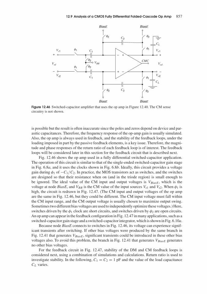
12.9 Analysis of a CMOS Fully Differential Folded-Cascode Op Amp 857
Vod
C2
C2
C1
C1
VBB
BiasE
BiasE
BiasE
Vsd
BiasE
Vs1f1
f1
f1
f1
f2
f2
f2
f2 f2
f2
+
–
+ +
+ – –
–
Vs2
Vo1
Vo2
CMC
CL
CL
Figure 12.46 Switched-capacitor amplifier that uses the op amp in Figure 12.40. The CM sensecircuitry is not shown.
is possible but the result is often inaccurate since the poles and zeros depend on device and par-asitic capacitances. Therefore, the frequency response of the op-amp gain is usually simulated.Also, the op amp is always used in feedback, and the stability of the feedback loops, under theloading imposed in part by the passive feedback elements, is a key issue. Therefore, the magni-tude and phase responses of the return ratio of each feedback loop is of interest. The feedbackloops will be considered later in this section for the feedback circuit that is described next.
Fig. 12.46 shows the op amp used in a fully differential switched-capacitor application.The operation of this circuit is similar to that of the single-ended switched-capacitor gain stagein Fig. 6.8a, and it uses the clocks shown in Fig. 6.8b. Ideally, this circuit provides a voltagegain during φ1 of −C1/C2. In practice, the MOS transistors act as switches, and the switchesare designed so that their resistance when on (and in the triode region) is small enough tobe ignored. The ideal value of the CM input and output voltages is VBiasE, which is thevoltage at node BiasE, and VBB is the CM value of the input sources Vs1 and Vs2. When φ1 ishigh, the circuit is redrawn in Fig. 12.47. (The CM input and output voltages of the op ampare the same in Fig. 12.46, but they could be different. The CM input voltage must fall withinthe CM input range, and the CM output voltage is usually chosen to maximize output swing.Sometimes two different bias voltages are used to independently optimize these voltages.) Here,switches driven by the φ1 clock are short circuits, and switches driven by φ2 are open circuits.An op amp can appear in the feedback configuration in Fig. 12.47 in many applications, such as aswitched-capacitor gain stage and a switched-capacitor integrator, which is shown in Fig. 6.10a.
Because node BiasE connects to switches in Fig. 12.46, its voltage can experience signif-icant transients after switching. If other bias voltages were produced by the same branch inFig. 12.41 that generates VBiasE, significant transients could be introduced in these other biasvoltages also. To avoid this problem, the branch in Fig. 12.41 that generates VBiasE generatesno other bias voltages.
For the feedback circuit in Fig. 12.47, stability of the DM and CM feedback loops isconsidered next, using a combination of simulations and calculations. Return ratio is used toinvestigate stability. In the following, C1 = C2 = 1 pF and the value of the load capacitanceCL varies.

858 Chapter 12 � Fully Differential Operational Amplifiers
CM
+ –
+–
Sense
CMC
Vo1Vs1
Vo2
C2
C2
C1
C1
Vs2
CL
CL Figure 12.47 The switched-capacitor amplifier of Figure12.46 when phase φ1 is high.
The return ratio can be simulated using an extension of the technique described in Prob-lem 8.33, which allows exact simulation of the return ratio when a controlled source is notaccessible.11 For example, with the feedback broken at the × marks in Fig. 12.48, the quan-tities R′
v,dm and R′i,dm are simulated, and then these quantities are combined to calculate the
return ratio Rdm using the equation in Problem 8.33.For the return-ratio simulation, a dc path to each op-amp input is provided by each resistor
RBIG in Fig. 12.48. A very large resistance, RBIG = 1 × 10¹², is used that has little effect onthe simulation results at frequencies where ω � 1/(RBIGC1). The dc voltage at each op-ampinput is VBiasE, which is developed at node BiasE in the bias circuit in Fig. 12.41. Withoutthese resistors, the dc op-amp input voltages are undefined, and therefore, SPICE would notbe able to simulate the circuit. In normal operation, one plate of each switched capacitor isalternately connected to BiasE or an op-amp input as shown in Fig. 12.46. This switchingmakes the dc voltage at the op-amp inputs equal the voltage VBiasE.
The simulated magnitude and phase responses of the return ratio for the DM feedbackloop are plotted in Fig. 12.49. Here, the load capacitance in the DM half-circuit is CL = 2 pF.The phase margin is 72◦, and the gain margin is 38 dB. The frequency fr where the magnitudeof the return ratio is unity is 390 MHz.
For comparison to simulation, the DM return ratio will now be calculated. The feedbackcircuit in Fig. 12.47 is shown in Fig. 12.50a with two capacitors Cia added; these capacitors
CMSense
CMC
Vo1Vs1
Vo2
X
X
C2
C2
C1
+ –
+–C1
Vs2
BiasE
RBIG
RBIG
BiasE
CL
CL
Figure 12.48 The feedbackcircuit in Figure 12.47, withresistors RBIG added to biasthe op-amp inputs.

12.9 Analysis of a CMOS Fully Differential Folded-Cascode Op Amp 859
Frequency (Hz)
(a)
|Ret
urn
Rat
io|
1000
100
10
1
0.1
0.01
100 1k 10k 100k 1M 10M 100M 1G 10 G
fr = 380 MHz
GM = 38 dB
Frequency (Hz)
(b)
<)R
etur
n R
atio
(de
gree
s)
−225°
−180°
−135°
−90°
−45°
0°
100 1k 10k 100k 1M 10M 100M 1G 10G
380 MHz
PM = 72°
Figure 12.49 Simulated DM return ratio for CL = 2 pF. (a) Magnitude and (b) phase responses.
model the op-amp input impedance. The corresponding DM small-signal half-circuit is shownin Fig. 12.50b, where the op-amp output port is modeled simply by a transconductance gm1and resistance Rodh [based on (12.165)]. This model ignores all poles and zeros except thepole associated with the RC time constant at the op-amp output node.
If the feedback is broken at the × in Fig. 12.50b and the input voltage Vsd/2 is set to zerofor calculation of the DM return ratio, the total load capacitance from the op-amp output toground is
CLeff = CL + C2(C1 + Cia)
C2 + C1 + Cia
(12.184)
Here the capacitors in the CM sense block are ignored for simplicity; in practice, they are smallcompared to the capacitors C1, C2 and CL. The right-most term in (12.184) is the capacitanceassociated with C2 in series with the parallel connection of C1 and Cia. Based on a simulation

860 Chapter 12 � Fully Differential Operational Amplifiers
CM
(a)
Sense
CMC
Vo1Vs1
Vo2
C2
+ –
+–
C2
C1
C1
Vs2
Cia
Cia
CL
CL
Rodh
C2
C1vsd ve vod
Cia
CL
2gm1ve
= 0
2+
+
–
–
X
(b)
Figure 12.50 (a) The feedbackcircuit with the op-amp inputimpedance modeled by the Cia
capacitors, which are shownexplicitly. (b) The DM small-signal half-circuit. The nodebetween the two Cia capacitorsis a ground for DM signals.The × marks a break point forcalculating the DM return ratio.
of the input impedance of the op amp (by applying an ac voltage across the op-amp input,measuring the op-amp input current, and then computing the input capacitance), Cia ≈ 2.58 pF.Capacitance Cia is the sum of Cgs1 and Cgd1 increased by the Miller effect. Substituting valuesinto (12.184) gives
CLeff = CL + C2(C1 + Cia)
C2 + C1 + Cia
= 2 pF + 1(1 + 2.58)
1 + 1 + 2.58pF = 2.72 pF (12.185)
For comparison, the DM return ratio can be calculated with the feedback loop broken inthe simplified circuit in Fig. 12.50b. Following Section 8.8, the calculated return ratio is:
Rdm(ω) = gm1Rodh · 1
1 + jωRodhCLeff· C2
C2 + C1 + Cia
(12.186)
The pole here is −1/(RodhCLeff ), due to the RC time constant at the op-amp output in Fig.12.50b. Here CLeff is the effective output load capacitance with the loop broken, as given by(12.184). At dc, (12.186) reduces to
Rdm0 = Rdm(ω = 0) = gm1Rodh · 1 · C2
C2 + C1 + Cia
(12.187)
At high frequencies [ω � 1/(RodhCLeff )], (12.186) reduces to
Rdm(ω) ≈ gm1 · 1
jωCLeff· C2
C2 + C1 + Cia
(12.188)
12.9 Analysis of a CMOS Fully Differential Folded-Cascode Op Amp 861
The unity-gain frequency ωr of the return ratio [i.e., the frequency where |Rdm(ωr)| = 1]can be found using (12.185) and (12.188):
ωr ≈ gm1
CLeff· C2
C2 + C1 + Cia
= 0.030
2.72 × 10−12 · 1
1 + 1 + 2.58rad/s
= 2.4 Grad/s = 2π(380 MHz) (12.189)
This calculated unity-gain frequency is in good agreement with the simulated value of390 MHz.
The DM return ratio in (12.186), which is based on the simplified op-amp model in Fig.12.50b, would give a phase margin of at least 90◦, since Rdm(ω) has only one pole that willintroduce at most −90◦ of phase shift at ωr. However, poles and zeros associated with internalnodes in the op amp, along with the dominant pole −1/(RodhCLeff ), contribute to the return-ratio magnitude and phase responses at high frequencies. Therefore, the return ratio may haveunacceptable gain or phase margin due to these poles and zeros. In practice, CL, which is asignificant component of CLeff in (12.185), is chosen to assure good gain and phase marginsfor the CM and DM feedback loops.
For the DM feedback loop in Fig. 12.47 with CL = 1 pF, the phase margin is 65◦, and thegain margin is 35 dB. The frequency where the magnitude of the return ratio is unity is fr =550 MHz.
For the DM feedback loop in Fig. 12.47 withCL = 0 pF, the capacitanceCLeff is dominatedby capacitors C1, C2, and Cia. The phase margin is 55◦ and the gain margin is 31 dB. Thefrequency where the magnitude of the return ratio is unity is fr = 810 MHz.
Note that as CL increases, the phase margin increases and the unity-gain frequency ofthe DM return ratio (ωr = 2πfr) decreases. This is as expected, since increasing CL increasesCLeff , which reduces the magnitude of the dominant pole in the return ratio without affectingthe other poles and zeros.
The low-frequency closed-loop DM gain is given by
Acl0,dm = vod
vsd
= A∞ · Rdm0
1 + Rdm0(12.190)
from (8.209). The direct feedthrough d = 0 for this circuit, due to the capacitive feedbackelements that are open circuits at dc, and hence block signal feedthrough at dc. The idealclosed-loop gain is A∞ = −C1/C2 = −1. Using the simulated value of Rdm0 in (12.190)yields
Acl0,dm = A∞ · Rdm0
1 + Rdm0= −1 · 280
1 + 280= −0.996 (12.191)
SPICE simulation agrees exactly with this closed-loop gain. The simulated −3-dB bandwidthof the closed-loop gain is 630 MHz with CL =2 pF.
The CM return ratio can be simulated11 by breaking the feedback at the × marks inFig. 12.48, simulating the quantities R′
v,cm and R′i,cm, and then combining these quantities
to calculate the CM return ratio Rcm using the equation in Problem 8.33. There are two CMfeedback loops in Fig. 12.48. One includes the CM sense circuit and the gain from the op-amp CMC input to the op-amp CM output voltage. The other includes the feedback elementsC1 and C2 and the CM gain from the op-amp CM input voltage to the op-amp CM outputvoltage. When the feedback is broken at the × marks in Fig. 12.48, both of these CM loopsare broken.11 The simulated CM return ratio is shown in Fig. 12.51 for CL = 2 pF. The phasemargin is 76◦, and the gain margin is 41 dB. So the CM loop is stable with good margins forCL = 2 pF. The unity-gain frequency for this return ratio is 420 MHz.

862 Chapter 12 � Fully Differential Operational Amplifiers
Frequency (Hz)(a)
|Ret
urn
Rat
io|
1000
100
10
1
0.1
0.01
100 1k 10k 100k 1M 10M 100M 1G 10G
fr = 420 MHz
GM = 41 dB
Frequency (Hz)
(b)
<)R
etur
n R
atio
(de
gree
s)
−225°
−180°
−135°
−90°
−45°
0°
100 1k 10k 100k 1M 10M 100M 1G 10G
420 MHz
PM = 76°
Figure 12.51 Simulated CM return ratio for CL = 2 pF. (a) Magnitude and (b) phase responses.
The CM return ratio differs from the DM return ratio because the small-signal half-circuitsdiffer; points of symmetry are open circuits for CM signals but are small-signal grounds forDM signals. For example, the node between the two Cia capacitors in Fig. 12.50a is a groundfor DM signals but is an open circuit for CM signals. Differences between the return ratioscan be seen by comparing Figs. 12.49 and 12.51. For example, a left-half-plane zero existsin the CM return ratio at about 60 MHz. It causes the magnitude response to flatten and thephase response to increase. It was determined through simulations that this zero is related tothe nonzero output impedances in the bias circuit at the BiasC and BiasD nodes. When theimpedance at nodes BiasC and BiasD was decreased by connecting a large capacitor from thosebias nodes to ground, the effect of the zero was not visible in the magnitude or phase response,and the general shape of the CM return-ratio response resembled the plots in Fig. 12.49. Withthese bypass capacitors, the CM return-ratio phase margin is 54◦, and the gain margin is 16 dB.
The step responses of the DM op-amp output voltage Vod for three values of CL are plottedin Fig. 12.52. The ideal output Vod is also shown; ideally Vod is the differential input invertedsince the closed-loop DM gain is −C1/C2 = −1. The overshoot/ringing in the step response

12.9 Analysis of a CMOS Fully Differential Folded-Cascode Op Amp 863
Time (ns)
Vod
(V)
0.2
0.1
0.0
0 2 4 6
•••••••••••••
•
•
•
•
••••••••••••••••••••••••••••••••••••••••••••••••••••••••••••••••••••••••••••••••••••••••••••••••••••••••
CL = 2 pF
CL = 1 pF
CL = 0 pFIdeal Vod
Figure 12.52 Step responses(Vod versus t) for CL = 0, 1and 2 pF. The ideal output isplotted with a dashed line. Theinput is a −0.2 V step appliedat t = 0.4 ns.
increases as CL decreases (and the phase margin decreases). As the phase margin decreases,the poles of the closed-loop transfer function move toward the jω axis. (In a two-pole system,the closed-loop poles will be on the jω axis when the phase margin is zero. In that case, the stepresponse contains a sinusoid in steady state.) In switched-capacitor applications, the output ofthe op amp must settle to its final value within one-half clock period. For example, the outputvoltage of the op amp in Fig. 12.46 must settle during the time when clock φ1 is high. Thesettling time is usually found by applying a step input. Then the settling time is measured fromthe time the input changes until the output voltage remains within a specified band around itssteady-state value. For the step responses in Fig. 12.52, the 1 percent settling times (the timeuntil the output remains within 1 percent of the final output voltage) are 1.67 ns for CL =2 pF, 1.35 ns for CL = 1 pF, and 1.37 ns for CL = 0 pF.
Equation 12.189 shows that ωr can be increased by increasing gm1, by decreasing CLeff(by decreasing some or all of the capacitances that contribute to it), or by increasing the termC2/(C2 + C1 + Cia), which is sometimes called “the feedback factor.” Assuming a constantphase margin, if ωr increases, the closed-loop −3-dB bandwidth increases (see Fig. 9.10)and the settling time of the step response decreases. Also, if the phase margin is larger thanrequired, ωr could be increased (and phase margin decreased) by increasing the magnitude ofthe dominant pole. This can be achieved by reducing CL.
During slewing, a large voltage appears between op-amp inputs and causes one of theinput transistors (M1 or M2) in Fig. 12.40 to turn off while the other remains on. In that case,the sum of the drain currents from M5 and M6 flows through the input transistor that is on.This causes a current change in both M1 and M2 of magnitude Islew = (ID5 + ID6)/2; thiscurrent flows from the op-amp outputs and through the differential load. The op-amp inputsare not virtually shorted during slewing because one of the op-amp input transistors is off,and thus the op-amp operation is highly nonlinear. Therefore, the total load capacitance fromeach op-amp output to ground is equal to CLeff as given in (12.184). The differential loadcapacitance between the two op-amp outputs will be half of CLeff , since two CLeff capacitorsare in series between the two op-amp outputs. Therefore, the DM output slew rate is
dVod
dt= Io(max)
CLeff
2
= Islew
CLeff
2
=ID5 + ID6
2CLeff
2
=4.0
2mA
2.72 pF
2
= 1.47V
ns(12.192)

864 Chapter 12 � Fully Differential Operational Amplifiers
assuming all current-source transistors remain in the active region during slewing. A SPICEsimulation gives a slew rate of 1.2 V/ns.
PROBLEMS12.1 What are the swing limits for each output of
the differential amplifier in Fig. 12.2? Use |Vov | =0.2 V for all transistors and Vtn = −Vtp = 0.6 V.Assume VDD = VSS = 2.5 V, Vic = 0 and γ = 0.Also,assume that the common-mode feedback circuit doesnot limit the output swing. What value of VOC givesthe largest symmetric differential output swing? Whatis the peak value of Vod in this case?
12.2 Repeat 12.1 for the two-stage op amp in Fig.12.23. Assume that switched-capacitor CMFB is used,which does not limit the output swing. Use the data inProblem 12.1.
12.3 A balanced fully differential circuit displaysonly odd-order nonlinearity. Use SPICE to verify thisfact for the op amp in the example in Section 12.6.1.
(a) Either use SPICE to find the distortion in theoutput waveform for a low-frequency differential sinu-soidal input, or use SPICE to plot the dc transfercharacteristic Vod versus Vid and verify that the char-acteristic is odd.
(b) Repeat (a) with a 1 percent mismatch betweenW1 and W2. Observe that even-order nonlinearity nowexists.
12.4 For the op amp in Fig. 12.2, use the devicedata and operating point from the first example in Sec-tion 12.4.1.Assume all transistors operate in the activeregion.
(a) Find the element values in the two models forthe output ports in Fig. 12.7.
(b) Find the element values in the two models forthe input ports in Fig. 12.6. (The elements are capaci-tors.) Use Cgs = 180 fF and Cgd = 20 fF.
12.5 For the op amp in Fig. 12.2, use the datafrom Problem 12.4 except use ID5 = 100 �A and|Vov | = 0.1 V for all transistors. Assume all transis-tors operate in the active region with Cgs = 180 fFand Cgd = 20 fF.
(a) Find the element values in the two models forthe output ports in Fig. 12.7.
(b) Find the element values in the two models forthe input ports in Fig. 12.6. (The elements are capaci-tors.)
(c) Calculate the common-mode control gain acmc.
12.6 (a) For the op amp in Problem 12.5, calculatea′
cm. Assume that the CMFB scheme in Fig. 12.17 isused and that acms = 1. Recall that a′
cm = voc/vic whenthe CMFB loop is active.
(b) Use SPICE to plot |a′cm| from 100 Hz to
100 MHz.
12.7 Repeat Problem 12.5c when the gates of M3
and M4 are the CMC input, and the gate of M5 connectsto a bias voltage.
12.8 The op amp in Problem 12.5 is con-nected in feedback as shown in Fig. 12.32a. TheCMFB is as described in Problem 12.6. Com-pute the low-frequency closed-loop gains Adm =vod/vsd and Acm = voc/vsc if R1 = R2 = R3 = R4 =100 M.
12.9 Calculate the DM output slew rate dVod/dt
for the op amp in Fig. 12.2. Assume ID5 = 200 �Aand a 5-pF capacitor is connected from each op-ampoutput to ground.
12.10 Calculate the CM output slew rate dVoc/dt
for the op amp in Fig. 12.2. Assume ID5 = 200 �Aand a 5-pF capacitor is connected from each op-ampoutput to ground.
12.11 Compute the output slew rate dVod/dt forthe op amp in the example in Section 12.6.1. Use thebias currents from the example and C = 1.39 pF.
12.12 For this problem, use the op amp in Fig.12.23 and the CMFB scheme in Fig. 12.17. Use thecomplement of the amplifier in Fig. 12.16b as theCM-sense amplifier, modified to give a negative dcgain. Assume the source followers in Fig. 12.17 havea low-frequency gain of 0.95 and Rcs = 15 k. Usethe transistor and op-amp operating-point data givenin the example in Section 12.6.1.
(a) Design the CM-sense amplifier so that the totallow-frequency gain acms0 = voc/vcms = −0.71, whichis the same value as in the example in Section 12.6.1.
(b) With this CMFB circuit, what are the swinglimits for each op-amp output voltage (Vo1 and Vo2)?Assume that the biasing current source in each sourcefollower in Fig. 12.17 is implemented with a NMOStransistor, and the current-source and source-followertransistors operate with VGS = 0.8 V and Vov = 0.2 V.For simplicity, assume VGS is constant and take γ = 0.
(c) What value of VCM gives the largest symmetricoutput swing?
(d) Verify that this CMFB circuit works correctlyby running a SPICE simulation. Use the value of VCM
from part (c).
12.13 Compute the op-amp CM and DM loadcapacitances for the output loading in Fig. 12.53a and

Problems 865
(a)
Vo1
Vo2
6 pF
7 pF
7 pF
op amp
(b)
Vo1
Vo2
–1
–15 pF
5 pF
3 pF
3 pF
op amp
Figure 12.53 Output load networks for Problem 12.13.
12.53b. Assume the inverting voltage buffers in Fig.12.53b are ideal.
12.14 (a) For the amplifier in Fig. 12.16b, esti-mate the pole associated with the RC time constantat the Vcms output node. Assume |ID25| = 0.4 mA,Vov23 = 0.2 V, and VOC = VCM . Ignore all capaci-tances except Cgs23 in parallel with a fixed capacitanceof 90 fF. Take Leff = 0.8 �m. Use the data in Table 2.3.
(b) Repeat (a) except use |ID25| = 0.1 mA.
(c) Compare the results in (a) and (b). Explain thedifference.
12.15 A differential amplifier with local CMFB isshown in Fig. 12.54. Use |Vov | = 0.2 V for all transis-tors,Vtn = −Vtp = 0.6V, ID5 = 200 �A,VAn = 10V,|VAp| = 20 V, and γ = 0.Assume VDD = VSS = 2.5 Vand Vic = 0.
(a) What is the dc common-mode output voltageof this amplifier?
(b) Compute the low-frequency gains adm and acm.Compare these gains with the gains calculated in thefirst example in Section 12.4.1.
12.16 A differential amplifier that does not use atail current source is shown in Fig. 12.55.
(a) Compute the low-frequency gains adm and acm.For all transistors, drain currents are 100 �A and|Vov | = 0.2 V. Also, VAn = 10 V, and |VAp| = 20 V.
(b) Compare these gains with the gains calculatedin the first example in Section 12.4.1.
12.17 (a) For the op amp in Fig. 12.2, assume theCM and DM load capacitances are CLc = CLd = 2pF. Calculate the frequencies at which |adm(jω)| = 1and |acmc(jω)| = 1, ignoring other capacitors. Use|Vov | = 0.25 V for all transistors, Vtn = −Vtp = 0.6V, ID5 = 200 �A, VAn = 20 V, |VAp| = 25 V, andγ = 0.
(b) Calculate the unity-gain frequencies in part (a)if CLc = 2 pF and CLd = 4 pF.
(c) The unity-gain frequency for the CMC gaincan be made equal to the DM unity-gain frequency inpart (b) by splitting M5 as shown in Fig. 12.15. Howshould the 200 �A current be split between M51 andM52? Assume Vov51 = Vov52 = 0.25 V.

866 Chapter 12 � Fully Differential Operational Amplifiers
VDD
M1 M2
M4
M5
M3
Vo1
Vi1
Vo2
Vi2
VBIAS
–VSS
20 kΩ 20 kΩ
Figure 12.54 A differential amplifier with localcommon-mode feedback.
VDD
M1 M2
M4M3
Vo1
Vi1
Vo2
Vi2
VBIAS
–VSS
Figure 12.55 A differential amplifier without atail current source.
12.18 For the CM-detector in Fig. 12.56, findacms(s) = vcms(s)/voc(s), assuming the CM-senseamplifier is ideal with unity gain. Then find acms(s)when a capacitor Ccs is connected in parallel witheach resistor Rcs. What is the effect of the Ccs
capacitors?
12.19 A NMOS transistor is operating in the trioderegion. Find a formula for its transconductance gm =∂Id/∂Vgs. Compare it with gm in the active region atthe same dc drain current. Which is larger?
12.20 For the fully differential circuit in Fig.12.32a, assume the op amp is ideal with Ri = ∞,Ro = 0, adm = −∞, and acm = 0. Find the closed-loop gains Adm = vod/vsd , Acm = voc/vsc, Adm−cm =voc/vsd , and Acm−dm = vod/vsc, under the followingconditions.
(a) R1 = R2 = 1 k and R3 = R4 = 5 k.
(b) R1 = 1.01 k, R2 = 0.99 k, R3 = R4 =5 k.
12.21 For the circuit in Problem 12.20a, theapplied source voltage is a single-ended signalwith Vs1 = 0.2 V sin(100t) and Vs2 = 0. Assume aCMFB loop forces VOC = 0. What are Vo1(t), Vo2(t),Vod(t), and Voc(t)? What are Vi1(t), Vi2(t), Vid(t),and Vic(t)?
12.22 The op amp in Problem 12.4 is used with theCMFB scheme shown in Fig. 12.17. The circuit is per-fectly balanced except that the CM-sense resistors aremismatched with the upper resistor Rcs1 = 10.1 k
and the lower resistor Rcs2 = 9.9 k. Assume thesource followers and the CM-sense amplifier are idealwith gains of unity.

Problems 867
VCM
Vcms
Rcs
Rcs
Vo1
Vo2
C1
+× 1
–
op amp
Figure 12.56 Circuit for Problem 12.18.
(a) Compute the gains acms and adm−cms in(12.106).
(b) Compute the low-frequency op-amp gainsvod/vid , voc/vic, vod/vic, and voc/vid with the CMFBactive.
(c) Use SPICE to simulate these gains.
12.23 A fully differential op amp with CMFBis shown in Fig. 12.57. For M1, M1C, M2, andM2C, use W/L = (64 �m)/(0.8 �m). For M3-M4,
M26-M27 and M11, W/L = (96 �m)/(1.4 �m). ForM21-M24, W/L = (6 �m)/(0.8 �m). For M14, M25,andM52,W/L = (16 �m)/(0.8 �m). ForM13,W/L =(1.4 �m)/(0.8 �m). Take VCM = −0.65 V.
(a) Choose W values for M12 and M51 so that|ID13| = 20 �A. Use L = 0.8 �m for M51 and L =1.4 �m for M12.
(b) Use SPICE to find the low-frequency op-ampgains vod/vid , voc/vic, vod/vic, and voc/vid with theCMFB active.
VDD = +1.65V
IDC = 100 μA
–VSS = –1.65V
VCM
Vo2Vo1
Vi2
M23
M51 M25
M24
M27
M21 M22
M2
M13
Vi1 M1
M52M14
M26M4M3M12M11
M2CM1C
Figure 12.57 Circuit for Problem 12.23.

868 Chapter 12 � Fully Differential Operational Amplifiers
Vod
Vs1
Vs2
+ –
– ++
–
+
–
+
–
1.5 pF
1 pF
1 pF
0.5 pF
1.5 pF 0.5 pF
Figure 12.58 Circuit for Problem 12.24.
(c) Calculate the output slew rate dVod/dt if a4-pF capacitor is connected from each op-amp outputto ground.
(d) What is the differential output voltage swingof this op amp? Assume Vic = VCM , and ignore bodyeffect for this calculation.
(e) Repeat (b) when the input transistors are mis-matched with W1 = 63 �m and W2 = 65 �m. (Note:With mismatch, the op-amp offset voltage is not zero.)
(f) Repeat (b) when the load transistors are mis-matched with W3 = 95 �m and W4 = 97 �m.
12.24 The feedback circuit in Fig. 12.58 is aswitched-capacitor circuit during one clock phase.Assume the op amp is the folded-cascode op amp inFig. 12.31.
(a) Calculate the DM and CM output load capac-itances, considering only the capacitances in theFig. 12.58.
(b) If the op-amp bias currents are |ID3| = |ID4| =100 �A and |ID5| = ID11 = ID12 = 200 �A, calculatethe DM output slew rate dVod/dt.
(c) If all transistors have |Vov | = 0.15 V andVDD = VSS = 2 V, what is the maximum peak differ-ential output swing?Assume VBB3 and VBB4 are chosento give maximum swing.
12.25 In the switched-capacitor CMFB scheme inFig. 12.21, C1 = 0.1 pF and C2 = 0.5 pF.
(a) With VCSBIAS = −1 V, VOC = VCM = 0.5 V.If VCSBIAS changes to −1.1 V, what is the new valueof VOC? Assume |acmc| � 1.
(b) Ignoring all capacitors except C1 and C2,what are the CM and DM output load capacitorswhen the φ1 switches are on and the φ2 switches areoff?
(c) Repeat (b) when the φ2 switches are on and theφ1 switches are off.
12.26 A current-mirror op amp is shown in Fig.12.59. Assume all NMOS transistors are matchedand all PMOS transistors are matched. Use |Vov | =0.2 V for all transistors, Vtn = −Vtp = 0.6 V, ID5 =200 �A, VAn = 10 V, |VAp| = 20 V, and γ = 0.Assume VDD = VSS = 1.65 V and Vic = 0.
VDD
–VSS
VB1 VB2
Vi2 Vo1Vi1Vo2
M3 M6M4
M1
M5 M7
M2
M9
M8
Figure 12.59 A fully differential current-mirror op amp.

References 869
(a) Calculate the model parameters in Fig. 12.7a.Assume the gates of M5, M7, and M9 connect to biasvoltages.
(b) If the CMC input is the gate of M5 and the gatesof M7 and M9 connect to a bias voltage, compute acmc.
(c) If the CMC input connects to the gates of M7
and M9 and the gate of M5 connects to a bias voltage,compute acmc.
(d) What are the output swing limits for each out-put? What value of VOC gives the maximum symmetricoutput swing?
12.27 Find the low-frequency value of a′cm for the
two-stage op amp in the example in Section 12.6.1.Use the data in that example. Recall that a′
cm = voc/vic
when the CMFB loop is active.12.28 Assume that the CMFB circuit in the exam-
ple in Section 12.6.1 is changed so that the CM-senseamplifier has a low-frequency gain |acms0| = 2.5.Determine the compensation capacitor C needed inthe op amp to assure that the CMC and DM feedbackloops in the example have a phase margin of 45◦ orlarger.
12.29 Neutralization capacitors Cn are to be addedto cancel the Miller effect on Cgd1 and Cgd2 in thetwo-stage op amp in the example in Section 12.6.1.
(a) Show how the Cn capacitors should be con-nected in the op amp. What value of Cn should beused?
(b) If these capacitors are constructed from MOStransistors operating in the cutoff region, what typeof transistor and what device dimensions should beused?
12.30 Modify the CMFB schematic in Fig. 12.26to inject currents at the drains of M1 and M2, in amanner similar to that shown in Fig. 12.18. Give aset of bias current values on the schematic. AssumeID3 = ID4 = 150 �A and ID6 = ID9 = 400 �A.
12.31 A fully differential op amp with mismatchis connected in the feedback circuit in Fig. 12.32awith R1 = R2 = 10 k and R3 = R4 = 40 k. Theop amp model is shown in Fig. 12.37 where adm =−181, acm = −2.89, acmc = −226, adm−cm = 8.95,acm−dm = 0.15, and acmc−dm = 11.6. If the gain ofthe CMFB circuit is acms = 0.76, find the closed-
loop gains Adm = vod/vsd , Acm = voc/vsc, Adm−cm =voc/vsd , and Acm−dm = vod/vsc.
12.32 For the op amp in Fig. 12.40, what is thecommon-mode input range (CMIR) if only M1 and M2
are changed to low-threshold devices with thresholdvoltages Vt1 = Vt2 = 0.3 V?
12.33 For the op amp in Fig. 12.40, what are theoutput voltage swing limits of Vo1 and Vo2 if the thresh-old voltages of only M1A, M2A, M3A, and M4A arechanged to Vt1A = Vt2A = −0.3 V and Vt3A = Vt4A =0.3 V?
12.34 For the feedback circuit in Fig. 12.46,the capacitor values are C1 = C2 = 4 pF and CL =6 pF. The op amp is the folded-cascode amplifier inFig. 12.40 with low-frequency gain adm0 = 1280 andgm1 = 30 mA/V.
(a) What is the low-frequency value of thedifferential-mode return ratio?
(b) What is the approximate unity-gain frequencyof the differential-mode return ratio?
12.35 For the feedback circuit in Fig. 12.46 usingthe op amp in Fig. 12.40, the capacitor values are C1 =C2 = 4 pF and CL = 6 pF. What is the differential-mode output slew rate?
12.36 For the feedback circuit in Fig. 12.46, C1 =C2 = 4 pF. The op amp is the folded-cascode amplifierin Fig. 12.40 with low-frequency gain adm0 = 1280and gm1 = 30 mA/V. What value of CL will giveωr = 1.0 Grad/s for the unity-gain frequency of thedifferential-mode return ratio?
12.37 If W/L is doubled for M1 = M2 (i.e., m1 =m2 = 20), what is the new low-frequency DM op-ampgain adm0 for the op amp in Fig. 12.40?Assume the biasconditions and operating regions do not change.
12.38 Calculate the spectrum of the input-referred1/f voltage noise for the op amp in Fig. 12.40.Use (11.69) with Kf = 4.8 × 10⁻²⁵ V2-F for NMOSdevices and Kf = 8.3 × 10⁻²⁶ V2-F for PMOSdevices. Use Cox = 6.9 × 10⁻¹⁵ F/(�m)2.
12.39 Calculate the spectrum of the input-referredthermal noise voltage for the op amp in Fig. 12.40 ifW/L is doubled for M1 = M2 (i.e., m1 = m2 = 20).Assume the bias conditions and operating regions arenot changed.
REFERENCES1. R. D. Middlebrook. Differential Amplifiers.
Wiley, New York, 1963.2. L. J. Giacoletto. Differential Amplifiers.
Wiley, New York, 1970.
3. W. G. Garrett and T. G. Maxfield. “A Mono-lithic Differential-Output Operational Amplifier,”Digest of Technical Papers, International Solid-State Circuits Conf., pp. 174–175, Philadelphia, PA,February 1972.

870 Chapter 12 � Fully Differential Operational Amplifiers
4. M. Banu, J. M. Khoury, and Y. Tsividis.“Fully Differential Operational Amplifiers with Accu-rate Output Balancing,” IEEE Journal of Solid-StateCircuits, Vol. 23, no. 6, pp. 1410–1414, December1988.
5. P. W. Li, M. J. Chin, P. R. Gray, and R.Castello. “A Ratio Independent Algorithmic Analog-to-Digital Conversion Technique,” IEEE Journal ofSolid-State Circuits, Vol. 19, no. 6, pp. 828–836,December 1984.
6. R.A. Whatley. “Fully Differential OperationalAmplifier with DC Common-Mode Feedback,” U.S.Patent 4,573,020, February 1986.
7. C. -C. Shih and P. R. Gray. “ReferenceRefreshing Cyclic Analog-to-Digital and Digital-to-Analog Converters,” IEEE Journal of Solid-StateCircuits, Vol. 21, no. 4, pp. 544–554, August1986.
8. T. C. Choi, R. T. Kaneshiro, R. W. Broderson,P. R. Gray, W. B. Jett, and M. Wilcox. “High-Frequency CMOS Switched-Capacitor Filters forCommunications Application,” IEEE Journal ofSolid-State Circuits, Vol. 18, no. 6, pp. 652–664,December 1983.
9. D. Senderowicz, S. F. Dreyer, J. H. Huggins,C. F. Rahim, and C. A. Laber. “A Family of Differen-tial NMOS Analog Circuits for a PCM Codec FilterChip,” IEEE Journal of Solid-State Circuits, Vol. 17,no. 6, pp. 1014–1023, December 1982.
10. D. J. Allstot and W. C. Black, Jr. “Techno-logical Design Considerations for Monolithic MOS
Switched-Capacitor Filtering Systems,” Proceedingsof the IEEE, Vol. 71, no. 8, pp. 967–986, August1983.
11. P. J. Hurst and S. H. Lewis. “Determinationof Stability Using Return Ratios in Balanced FullyDifferential Feedback Circuits,” IEEE Trans. on Cir-cuits and Systems II, pp. 805–817, December 1995.
12. K. Bult and G. J. G. M. Geelen. “A Fast-Setting CMOS Op Amp for SC Circuits with 90-dBDC Gain,” IEEE Journal of Solid-State Circuits, Vol.25, no. 6, pp. 1379–1384, December 1990.
13. B. -S. Song, M. F. Thompsett, and K. R.Lakshmikumar. “A 12-bit 1-Msample/s CapacitorError-Averaging Pipelined A/D Converter,” IEEEJournal of Solid-State Circuits, Vol. 23, no. 6, pp.1324–1333, December 1988.
14. J. A. Mataya, G. W. Haines, and S. B.Marshall. “IF Amplifier Using Cc Compensated Tran-sistors,” IEEE Journal of Solid-State Circuits, Vol. 3,pp. 401–407, December 1968.
15. J. F. Duque-Carrillo. “Control of theCommon-Mode Component in CMOS Continuous-Time Fully Differential Signal Processing,” AnalogIntegrated Circuits and Signal Processing, An Inter-national Journal, pp. 131–140, Kluwer AcademicPublishers, September 1993.
16. X. Wang, P. Hurst, and S. Lewis. “A 12-bit20-Msample/s Pipelined Analog-to-Digital Converterwith Nested Digital Background Calibration,” IEEEJournal of Solid-State Circuits, pp. 1799–1808,November 2004.

IndexAbrupt junction, 4Active cascode, 210Active-cascode op amp, 446Active-device parameter summary, 73Active level shift, 439, 458, 469, 485Active load, 276, 421, 448, 457, 546
common-emitter amplifier, 277, 280, 284common-mode rejection ratio, 291common-source amplifier, 277, 280, 282complementary, 277current-mirror, 285depletion, 280diode-connected, 282enhancement, 284noise, 776offset voltage, 330
Advanced bipolar integrated-circuitfabrication, 92, 106
All-npn output stage, 375Amplifier:
current, 557fully differential, 799, 811operational, see Operational amplifiertransconductance, 562transresistance, 560voltage, 557wideband, 514, 527, 575, 617
Amplifier stages:Class A, 349, 576Class AB, 361, 461, 688Class B, 362multiple-transistor, 201single-transistor, 173
Analog multiplier, 708, 711Anneal, 87Avalanche breakdown, 7, 21, 49, 71Avalanche noise, 743Average power, 345
Balanced circuit, 796Balanced differential amplifier, 799Balanced modulator, 712Band-gap reference, 315, 321
curvature compensated, 318Bandwidth of feedback amplifiers, 624Base-charging capacitance, 27
Base-diffused resistors, 118Base diffusion, 86Base-emitter voltage temperature coefficient,
11, 315Base resistance, 30, 98Base transport factor, 13Base width, 12Beta, see Current gainBias reference circuit:
band-gap, 315, 321bootstrap, 307current routing, 329low-current, 297proportional to absolute temperature,
321self-biased, 307start-up circuit, 308, 312supply-insensitive, 303temperature-insensitive, 315threshold-referenced, 307VBE-referenced, 308, 311voltage routing, 329VT -referenced, 314, 315
BiCMOS, 152amplifier, 249, 618, 794cascode, 209Darlington, 204, 791output stage, 377, 398technology, 152
Bilateral amplifier, 172Bipolar transistor:
advanced technology, 95, 106base-charging capacitance, 27base resistance, 30, 98base transit time, 28breakdown voltage, 20, 86in CMOS technology, 144, 151collector-base resistance, 30collector series resistance, 89, 100current-mirror matching, 325cutoff region, 146diffusion profile, 91fabrication, 88, 92forward-active region, 45frequency response, 34heterojunction, 153
871

872 Index
Bipolar transistor (Continued )input resistance, 28inverse-active region, 16large-signal models, 8lateral, 140noise, 745, 750output characteristics, 15output resistance, 29parameter summary (functional), 73parameter summary (numerical), 106,
108, 112, 114parasitic capacitance, 31, 106, 111, 116reverse-active region, see Inverse-active
regionsaturation current, 18, 97, 316saturation region, 17self-aligned structure, 94small-signal model, 25SPICE model parameters, 162transconductance, 26
Bird’s beak, 141, 257, 426Blackman’s impedance formula, 608Body effect in MOS transistors, 53, 139Boltzmann approximation, 10Bootstrap bias technique, 307Breakdown, 6
in bipolar transistors, 38in MOSFETs, 49in superbeta transistors, 124
Breakdown voltage:base-emitter, 22collector-base, 20, 86collector-emitter, 21drain-substrate, 49junction-diode, 7MOS transistor, 45superbeta transistors, 124Zener diode, 8
Built-in potential, 2Buried layer, 89Burst noise, 745
Capacitance:base-charging, 27base-collector, 31, 97base-emitter, 31, 96channel-substrate, 138collector-substrate, 31, 103depletion region, 5, 31, 54, 103, 140, 530drain-body, 54
gate-body, 55gate-drain, 51gate-source, 51gate-substrate, see Capacitance: gate-bodyoverlap, 55, 142sidewall, 143source-body, 54
Capacitive neutralization, 835Capacitors:
in bipolar integrated circuits, 115lateral, 150in MOS integrated circuits, 148MOS transistors, 148poly-poly, 146vertical, 146
Capture range, 718, 726Cascode configuration, 205, 207, 439, 442,
446, 527active, 210, 446
Cascode current mirror, 261, 690Bipolar, 261MOS, 264
Cascode frequency response, 527Channel-length modulation, 43Class A output stage, 349, 576Class AB input stage, 688Class AB output stage, 364Class B output stage, 361Clipping, 346, 361Closed-loop gain, 401, 554, 601Clubhead, 116CMFB, see Common-mode feedbackCMOS operational amplifier:
fully differential, 834with single-ended output, 421, 439, 442,
446CMOS output stage, 379CMOS technology, 46, 128Collector-base capacitance, 102Collector-base resistance, 30Collector-series resistance, 32, 100Common-base configuration, 182, 184, 185,
514, 529Common-base frequency response, 514Common-base stage noise performance, 771Common centroid geometry, 437Common-collector-common-collector
configuration, 201Common-collector-common-emitter
configuration, 201

Index 873
Common-collector configuration, 191, 505Common-drain configuration, 194, 511,
591Common-emitter-common-base
configuration, see cascode configurationCommon-emitter configuration, 174, 490,
495Common-emitter frequency response, 490,
498Common-emitter output stage, 576Common-gate configuration, 185, 187,
514Common-gate frequency response, 514Common-mode feedback, 227, 286, 458, 804
circuits, 796using a resistive divider, 812using switched capacitors, 821using transistors in the triode region, 812using two differential pairs, 816
Common-mode feedback loop, 804bandwidth, 844stability and compensation, 810
Common-mode gain, 222, 804Common-mode half-circuit, 226, 239,
804Common-mode input range, 854Common-mode input resistance, 228Common-mode rejection ratio, 223, 228,
234, 417, 427of active-load stage, 293frequency response, 501
Common-mode-to-differential-mode gain,222
Common-source amplifier, 181, 490, 499Common-source-common-gate
configuration, see cascode configurationCommon-source frequency response, 490,
498, 500Compensation:
of amplifiers, 633capacitor, 597, 637, 682by feedback zero, 677methods, 637of MOS amplifiers, 643, 650of NE5234 op amp, 658nested Miller method, 654theory, 633
Complementary load, 277Complementary output stage, 360Composite pnp, 377
Conductivity, 80Copper, 156Correlation, 747, 756, 789Critical field, 7, 59Crossover distortion, 362, 365, 368, 375, 384Crossunder, 117Crowding, 32, 99Current amplifier, 562Current crowding, 32, 99Current density, 425Current-feedback pair, 586, 677, 768Current gain:
dependence on operating conditions, 23,110
forced, 18forward, 12inverse, 19npn transistor, 105pnp transistor, 107short-circuit, 177small-signal, 29small-signal high-frequency, 34temperature coefficient, 23
Current mirror, 251with beta helper, 258cascode, 261, 264current routing, 329with degeneration, 260, 261gain error, 252general properties, 251high-swing cascode, 268input voltage, 252load, 285matching, 325minimum output voltage, 255output resistance, 252, 254, 257, 258, 260,
261, 264, 266, 272, 275simple, 253, 255Sooch cascode, 269, 270voltage routing, 329Wilson, 272, 275, 595, 610
Current routing, 329Current source, 297, 300, 301, 302, 303,
304, 307Peaking, 301, 302Widlar, 297, 300, 304
Cutoff, 46
Darlington configuration, 201, 203, 397,595, 791

874 Index
dc analysis of the NE5234 op amp, 452Deadband, 361, 368, 375Depletion-mode load, 281Depletion region:
capacitance, 5, 31, 54, 103, 530collector-base, 14, 89of pn junction, 1
Deviation from ideality in real op amps, 415Die, 91Dielectric isolation, 123Differential amplifier, 220, 404
perfectly balanced, 222unbalanced, 237
Differential-mode gain, 222, 804Differential-mode half-circuit, 225, 239,
804Differential-mode input resistance, 228Differential-mode-to-common-mode gain,
222, 838Differential pair:
bipolar transistor, 214MOS, 217noise performance, 773with current-mirror load, 285, 534
Differential signal source, 800Differential-to-single-ended conversion, 291Differentiator, 406Diffused-layer sheet resistance, 82Diffused resistors, 115Diffusion constant, 10Diffusion current, 10Diffusion of impurities, 80Diffusion profile of a bipolar transistor, 91,
92, 96, 98Diode:
Junction, 121Zener, see Zener diode
Diode-connected load, 282Diode-connected MOS transistor, 255Distortion, 358, 399Distortion in the source follower, 355Distortion reduction by negative feedback,
553Dominant pole, 495, 497, 499, 518,
522, 524Doping, 79Double-diffused npn transistors, 95Double-diffused pnp transistors, 126Drift, emitter-coupled pair, 234
source-coupled pair, 238
Driver stage, 343, 351, 366, 367, 369, 370,371, 389, 395
Early effect, 16, 21, 262Early voltage, 15, 29, 43, 52, 255, 258Ebers-Moll equations, 19Economics of IC fabrication, 156Effective channel length, 43, 140Effective channel width, 141Efficiency:
Class A, 347, 349, 350Class B, 360, 362, 366, 375
Electromigration, 156Emitter-coupled multivibrator, 728Emitter-coupled pair, 214, 704, 773
emitter degeneration, effect of, 216frequency response, 495input offset current, 230, 234input offset voltage, 230, 231offset voltage drift, 233small-signal analysis, 220, 237transfer characteristics, 214
Emitter degeneration, 196, 216, 260, 587Emitter-diffused resistors, 117Emitter-follower, 191
drive requirements, 351frequency response, 505noise performance, 773output stage, 341, 344, 576small-signal properties, 192, 352terminal impedances, 507transfer characteristics, 341
Emitter injection efficiency, 13Emitter resistance, 32Enhancement load, 284Epitaxial growth, 86Epitaxial resistor, 119Equivalent circuit of an op amp, 420Equivalent input noise generators, 756Equivalent input noise resistance, 758Equivalent input shot noise current,
759Etching, 85
Fabrication of integrated circuits, 78Feedback, 403, 553
bandwidth, 624common mode, 227, 286, 458, 804configurations, 557effect on distortion, 555

Index 875
effect on gain sensitivity, 555effect on noise, 764effect on terminal impedances, 558, 561,
562, 563, 607ideal analysis, 553latchup, 151loading, effect of, 563local, 227, 263loop gain, 384, 401, 554practical configurations, 563return ratio, 599, 612series-series, 562, 569series-shunt, 557, 579shunt-series, 561, 583shunt-shunt, 560, 563single-stage, 587table of relationships, 588
Feedback-zero compensation, 677Feedforward, 389, 644–650, 660Field-effect transistor, see MOS transistorField region, 128First-order phase-locked loop, 720Flicker noise, 741Flicker noise corner frequency, 746Folded-cascode op amp, 446, 652Forward-active region, 8, 26, 45, 112, 175Free-running frequency, 717, 726Frequency response:
bipolar transistor, 33, 56cascode, 527common-base, 514common-drain, 511common-emitter, 495common-emitter cascode, 527common-gate, 514common-mode, 501common-source, 499common-source cascode, 527of CMRR, 503of current mirror, 251, 256differential-mode, 495, 496, 500of differential pair with current-mirror
load, 290, 534emitter follower, 505MOS amplifier, 643, 650MOS transistor, 55multistage amplifier, 518NE5234 op amp, 539single stage, 490source follower, 511
Full-power bandwidth, 692Fully differential amplifiers, 796
cross gains, 838Fully differential op amps, 796, 823, 845
folded cascode, 834telescopic cascode, 855two-stage, 823
Gain-bandwidth product, 625Gain margin, 630Gaussian distribution, 232, 244, 738Generation, 79Gilbert multiplier, 704g-parameters, 583Graded junction, 5Guard ring, 152
Half circuit:of balanced amplifier, 225, 226, 799coupled, 237of unbalanced amplifier, 239, 240independent, 238
Harmonic distortion, 357, 399Heterojunction, 153High-frequency equivalent circuit of the
NE5234 op amp, 540, 659High-level injection, 36, 110High-voltage integrated-circuit fabrication,
88Homojunction, 53Hot carriers, 49h-parameter, 579Hybrid-π model, 30, 52
Ideal feedback analysis, 553Impact ionization, 71, 209Impurity concentration, 79Instability in amplifiers, 626, 666Instantaneous power, 345–351, 365Integrated circuit:
advanced bipolar fabrication, 92, 107biasing, 251capacitors, 120, 146cost considerations, 156, 159current mirrors, 251device models, 1economics, 156fabrication, 78fabrication yield, 157frequency response, 490

876 Index
Integrated circuit (Continued )mixed-signal, 221noise, 736op amps, 402, 796, 823output stages, 341packaging, 159passive components, 115, 146phase-locked loop, 727resistors, 115, 119, 146
Integrator:continuous-time, 406switched-capacitor, 412
Interconnect delay, 156Internal amplifier, 407Intrinsic carrier concentration, 2, 79Inverse-active region of bipolar transistors,
19, 45Inversion, 40Inverting amplifier, 402Ion implantation, 85, 87Isolation diffusion, 89, 90
Junction breakdown, 6, 49Junction diodes, 122
KCL, 184Kirk effect, 25, 36KVL, 184
Large-signal model:bipolar transistor, 8MOS transistor, 45
Latchup in CMOS, 151, 341Lateral bipolar transistor, 146Lateral pnp transistor, 108, 368,
376Layout, 435Leakage current, 7, 18, 19
collector base, 19Level shifting, 194, 196, 439, 485Lifetime of minority carriers, 11Line regulation, 595Load line, 345–351, 364, 365Load regulation, 595Local feedback, 587Local oxidation, 87Lock range, 717, 724Logarithmic amplifier, 405Loop gain, 384, 401, 552Low-current biasing, 297
Low-level injection, 10, 110Low-permittivity dielectric, 156
Matching in transistor current mirrors, 325Miller capacitance, 491, 498, 500, 638, 641,
831Miller effect, 114, 490, 492, 497, 499, 828Minimum detectable signal, 754Minority-carrier lifetime, 11Mismatch effects in differential amplifiers,
229Moat, 93Moat etch, 123Mobility, 80Mobility degradation, 65Model selection for IC analysis, 170Modulator, 712MOS transistor:
active region, 45bird’s beak, 141, 257, 426body effect, 53, 139breakdown voltage, 149channel-length modulation, 43complementary MOS (CMOS), 39, 46,
127critical field, 59current density, 425current-mirror matching, 328cutoff region, 46depletion mode, 47, 144, 281diode connected, 255effective channel length, 43, 140effective channel width, 141enhancement-mode, 38, 127fabrication, 127field-effect transistor, 41field region, 128frequency response, 55hot carriers, 49impact ionization, 71input resistance, 52inversion, 40junction breakdown, 49large-signal model, 45mobility, 42mobility degradation, 65, 135moderate inversion, 69n-channel, 38, 131, 144noise, 750, 762ohmic region, 44

Index 877
operational amplifier, 421output resistance, 52output stages, 379overdrive, 47, 181, 434oxide breakdown, 49parameter summary (functional), 73parameter summary (numerical), 132,
133, 134, 135parasitic elements, 54p-channel, 39, 144punchthrough, 49saturation region, 44, 51short-channel effects, 59silicon gate, 129small-signal model, 49source-coupled pairs, 217source follower, 194SPICE model parameters, 162strong inversion, 65substrate current, 71subthreshold conduction, see Weak
inversionthreshold temperature dependence, 47threshold voltage, 40, 129, 131transconductance, 50, 63transfer characteristic, 38triode region, 44weak inversion, 65, 180velocity saturation, 59
Multiplication factor, 7Multiplier circuits, 704Multistage amplifier frequency response,
518
Negative feedback, see FeedbackNeutralization, 835NMOS, 38Noise:
in active loads, 776amplitude distribution, 738avalanche, 743bandwidth, 776burst, 742in capacitors and inductors, 747circuit calculations, 750common-base stage, 771differential pair, 773in diodes, 736in direct-coupled amplifiers, 785emitter follower, 773
equivalent input noise, 7541/f , 741feedback, effect of, 764figure, 786flicker noise, 741generator, 738models, 744MOS amplifier, 746, 762, 779in NE5234 op amp, 776operational amplifier, 776, 855popcorn noise, 742in resistors, 747shot, 736spectral density, 737, 748temperature, 786thermal, 740white, 737in Zener diodes, 743
Nondominant pole, 495, 497, 500, 536of NE5234 op amp, 542
Noninverting amplifier, 404Nonlinear analog operations, 405Nonlinearity, 343, 352, 353, 357, 368, 375,
393, 395, 708Nonoverlapping clock signals, 409, 412
charge-transfer phase, 409input sample phase, 409
Normal distribution, see Gaussiandistribution
Nyquist criterion, 626, 666Nyquist diagram, 627
Offset current, 416emitter-coupled pair, 231, 233NE5234 op amp, 477, 481
Offset voltage, 424differential pair with active load, 330emitter-coupled pair, 231, 233emitter-coupled pair with active load, 330NE5234 op amp, 477source-coupled pair, 235source-coupled pair with active load, 337
Open-circuit time constants, 519, 536also see Zero-value time constants
Open-loop gain, 401Operational amplifier:
active-cascode, 446applications, 401bipolar, 448with cascodes, 438

878 Index
Operational amplifier (Continued )CMOS, 421common-mode input range, 416, 427common-mode rejection ratio, 417,
427compensation, 420, 633, 676deviations from ideality, 415differential amplifier, 404effect of overdrive voltages, 434equivalent circuit, 420folded-cascode, 442, 652, 845frequency response, 420fully differential op amps, 796, 823input bias current, 415input resistance, 420, 422internal amplifier, 407inverting amplifier, 402layout considerations, 435MOS, 421, 438, 442, 446NE5234 op amp analysis, 452noise, 776offset current, 416offset drift, 416offset voltage, 416, 424open-circuit voltage gain, 422output buffer, 407output resistance, 420, 422output swing, 423power-supply rejection ratio, 418, 430,
435random offset voltage, 426settling time, 411with single-ended outputs, 400slew rate, 420, 681small-signal characteristics, 422supply capacitance, 432systematic offset voltage, 424telescopic-cascode, 439, 650
Oscillation, 624, 666, 679Output buffer, 407Output resistance of current mirror, 252,
254, 257, 258, 260, 261, 264, 266,272, 275
Output stage, 341all-npn, 375BiCMOS, 377, 397Class A, 349, 576Class AB, 361, 379Class B, 360CMOS, 379
combined common-drain common-source,388, 390
common-drain, 353, 380common emitter, 576common-source, with error amplifiers,
381complementary, 360Darlington, 397emitter follower, 341NE5234 op amp, 458, 474overload protection, 377parallel common-source, 390push-pull, 359quasi-complementary, 376, 381, 384, 388709 op amp, 366741 op amp, 368short-circuit protection, 377source follower, 353, 380
Overdrive, 47Overload protection, 377Oxidation, 84Oxide breakdown, 49
Packaging considerations, 159Parasitic elements:
bipolar transistor, 31, 98MOS transistor, 54, 141
Passive components:in bipolar integrated circuits, 115in MOS technology, 144
Permittivity, 3Phase detector, 712, 716, 725, 727Phase-locked loop:
basic concepts, 718capture range, 718, 726first-order loop, 720integrated circuit, 721, 727lock range, 717, 724loop bandwidth, 719, 724root locus, 719, 722second-order loop, 723
Phase margin, 629–638, 643, 648, 652, 658,663, 676, 686, 694
Photolithography, 84Photoresist, 84Pinch-off in MOSFETs, 43Pinch resistors, 118, 119PMOS, 39pn junction depletion region, 1Pole splitting, 639, 642, 654, 680

Index 879
Polysilicon, 87, 93, 129Popcorn noise, 742Power conversion efficiency, 347Power hyperbola, 348Power output:
Class A, 349Class B, 362
Practical Class B output stages, 368Predeposition, 81, 84Probability distribution, 244Protection of output stages, 377Punchthrough, 49, 125Push-pull output stage, 359
Quasi-complementary output stages, 376,381, 384, 388
Reciprocity condition, 19Recombination, 10, 11, 79References, 297Regulated cascode, see Active cascodeRegulator, 593Replica biasing, 822Resistivity, 79Resistor:
base-diffused, 116base-pinch, 118diffused, 146emitter-diffused, 117epitaxial, 119MOS device, 146in MOS technology, 146polysilicon, 146well, 144
Return ratio, 599simulation of, 621, 857
Reverse-active region, see Inverse-activeregion of bipolar transistors
Reverse injection, 13Rise time, 543Root locus, 626, 642, 664
for dominant-pole compensation,676
for feedback-zero compensation,677
for three-pole transfer function, 665Root locus rules, 667
Saturation current, of bipolar transistor, 11,97, 316
Saturation region:of bipolar transistor, 16, 175of MOSFET, 44, 45
Scattering-limited velocity, 59, 135Second-harmonic distortion, 358, 396Second-order phase-locked loop, 722Self-aligned structure, 94Self-biasing, 307Sensitivity to power-supply voltage, 304Series-series feedback, 562, 569Series-series triple, 575, 578, 583Series-shunt feedback, 557, 579Sheet resistance, 82Short-channel effects in MOS Transistors, 59Short-circuit current gain, 177Short-circuit protection, 377, 468Short-circuit time-constants, 536Shot noise, 736Shunt-series feedback, 561, 583Shunt-shunt feedback, 560, 563Signal-to-noise ratio, 798Silicide, 95, 147Silicon dioxide, 84, 87Silicon nitride, 87Single-stage feedback, 587Single-stage frequency response, 490Slew rate, 681
effect on sinusoidal signals, 692in fully differential folded-cascode op
amp, 863improvement, 685, 687
Small-signal analysis of NE5234 op amp,469
Small-signal model:bipolar transistor, 25MOS transistor, 49
Source-coupled pair, 217frequency response, 499input offset voltage, 236offset voltage drift, 236small-signal analysis, 220, 237transfer characteristics, 217
Source degeneration, 199, 261Source follower, 194, 511, 592
distortion, 355frequency response, 511output stage, 353small-signal properties, 194super, 212, 609transfer characteristics, 353

880 Index
Space-charge region, see Depletion regionSpectral density of noise, 737, 748SPICE parameter summary, 162Square-law characteristic of MOSFETs,
43Square-law circuit, 734Start-up circuit, 308, 310Step coverage, 153Step response, 543, 862Stress migration, 156Substitutional impurities, 80Substrate contact, 152Substrate current in MOSFETs, 71Substrate pnp transistors, 111Subthreshold conduction, 135
also see MOS transistor: weak inversionSumming node, 412, 553Summing-point constraints, 403, 405Super source follower, 212, 609Superbeta transistors, 124Supply-insensitive biasing, 303Sustaining voltage, 21Switched-capacitor amplifier, 407
parasitic insensitive, 411, 857Switched-capacitor common-mode
feedback, 821, 853Switched-capacitor filter, 412Switched-capacitor integrator, 412Symmetry:
mirror, 436translational, 436
T model, 182, 185Tail current source, 214, 217Telescopic-cascode op amp, 439, 650Temperature coefficient:
of band-gap reference, 317, 319, 324of base-emitter voltage, 13, 311, 315of bias reference circuits, 311, 319of bipolar transistor current gain, 23effective, 319of integrated-circuit resistors, 120of threshold voltage, 48of Zener diodes, 121, 122
Temperature-insensitive biasing, 315Thermal noise, 747Thin-film resistors, 127Third-harmonic distortion, 358, 396Threshold-referenced bias circuit, 307
Threshold voltage of MOS transistors, 40,129, 131
Threshold voltage temperature dependence,47
Time constant, 36open circuit, 519, 536short circuit, 536zero value, 519
Time response, 542Transconductance amplifier, 563Transfer characteristic:
Class B stage, 360common-emitter amplifier, 176emitter-coupled pair, 214emitter-coupled pair with emitter
degeneration, 216emitter follower, 341source-coupled pair, 217source follower, 353
Transit time, 28Transition frequency fT , 34, 55, 64Transresistance amplifier, 561Tunneling, 8, 121Two-port representation, 171, 563, 584
Unbalanced fully differential circuits, 838Uniform-base transistor, 10Unilateral amplifier, 173Unit devices, 254, 257, 426Unity-gain feedback configuration, 404, 634,
649, 660, 681
VBE-referenced bias circuit, 307, 311VCO, 716, 725, 734Velocity saturation, 59Virtual ground, 404Voltage amplifier, 559Voltage-controlled oscillator, 716, 728, 734Voltage gain, 176, 422
open-circuit, 177, 180Voltage regulator, 593Voltage regulator analysis, 593Voltage routing, 329VT -referenced bias circuit, 314
Wafer, 79Well, 46, 128Well contact, 152White noise, 737

Index 881
Wideband amplifier, 514, 527, 575, 618,677, 753
Widlar current source, 297, 300, 304Wilson current mirror, 272, 275, 595, 611
Yield considerations, 157y-parameters, 563
Zener diode, 8, 22, 121, 593, 595, 743Zener diode noise, 743Zener diode temperature coefficient, 120,
122Zener-referenced bias circuit, 595Zero-value time constant analysis, 519z-parameters, 569