RF Integrated Circuits - VEMU INSTITUTE OF TECHNOLOGY
79
RF Integrated Circuits (15A04804) LECTURE NOTES B.TECH (IV YEAR – II SEM) (2019-20) Prepared by: Mr.G.SIVA KOTESWARA RAO, Assistant Professor Department of Electronics and Communication Engineering VEMU INSTITUTE OF TECHNOLOGY (Approved by AICTE, New Delhi and affiliated to JNTUA, Ananthapuramu) NEAR PAKALA, P.KOTHAKOTA, CHITTOOR- TIRUPATHI HIGHWAY CHITTOOR-517512 Andhra Pradesh WEB SITE: www.Vemu.Org
-
Upload
khangminh22 -
Category
Documents
-
view
1 -
download
0
Transcript of RF Integrated Circuits - VEMU INSTITUTE OF TECHNOLOGY

RF Integrated Circuits
(15A04804)
LECTURE NOTES
B.TECH
(IV YEAR – II SEM)
(2019-20)
Prepared by:
Mr.G.SIVA KOTESWARA RAO, Assistant Professor
Department of Electronics and Communication Engineering
VEMU INSTITUTE OF TECHNOLOGY
(Approved by AICTE, New Delhi and affiliated to JNTUA, Ananthapuramu)
NEAR PAKALA, P.KOTHAKOTA, CHITTOOR- TIRUPATHI HIGHWAY
CHITTOOR-517512 Andhra Pradesh
WEB SITE: www.Vemu.Org

B.Tech (ECE) R-15
VEMU INSTITUTE OF TECHNOLOGY
JAWAHARLAL NEHRU TECHNOLOGICAL UNIVERSITY ANANTAPUR
B.Tech IV-II Sem (E.C.E) T Tu C
3 1 3
(15A04804) RF INTEGRATED CIRCUITS
C422_1: Explain the Basic architectures of RF Transceivers.
C422_2: Explain the MOS device Review, High frequency Amplifiers and Bandwidth Estimation
Techniques.
C422_3: Explain the Noise present in the Active and Passive Elements, LNA and Mixers.
C422_4: Design the RF power amplifiers, Negative Resistance Oscillators and PLL.
C422_5: Explain the Frequency Synthesizers and Radio architectures.
UNIT – I
Introduction RF systems – basic architectures, Transmission media and reflections, Maximum
power transfer , Passive RLC Networks, Parallel RLC tank, Q, Series RLC networks, matching,
Pi match, T match, Passive IC Components Interconnects and skin effect, Resistors, capacitors
Inductors
UNIT – II
Review of MOS Device Physics - MOS device review, Distributed Systems, Transmission
lines, reflection coefficient, the wave equation, examples, Lossy transmission lines, Smith
charts – plotting Gamma, High Frequency Amplifier Design, Bandwidth estimation using open-
circuit time constants, Bandwidth estimation, using short-circuit time constants, Rise time,
delay and bandwidth, Zeros to enhance bandwidth, Shunt-series amplifiers, tuned amplifiers,
Cascaded amplifiers
UNIT - III
Noise - Thermal noise, flicker noise review, Noise figure, LNA Design, Intrinsic MOS noise
parameters, Power match versus, noise match, large signal performance, design examples &
Multiplier based mixers. Mixer Design, Sub sampling mixers.
UNIT – IV
RF Power Amplifiers, Class A, AB, B, C amplifiers, Class D, E, F amplifiers, RF Power
amplifier design examples, Voltage controlled oscillators, Resonators, Negative resistance
oscillators, Phase locked loops, Linearized PLL models, Phase detectors, charge pumps, Loop
filters, and PLL design examples
UNIT - V
Frequency synthesis and oscillators, Frequency division, integer-N synthesis, Fractional
frequency, synthesis, Phase noise, General considerations, and Circuit examples, Radio
architectures, GSM radio architectures, CDMA, UMTS radio architectures
Text books: 1. The design of CMOS Radio frequency integrated circuits by Thomas H. Lee Cambridge
university press, 2004.
2. RF Micro Electronics by Behzad Razavi, Prentice Hall, 1997.

B.Tech (ECE) R-15
VEMU INSTITUTE OF TECHNOLOGY
UNIT-I
Introduction RF systems
1. INTRODUCTION RF SYSTEMS – BASIC ARCHITECTURE:
The first and for most thing that it has is something called an antenna. This is the symbol for
the antenna. The cell phone has inside it an antenna. Now, there is a transmitter and there is a
receiver. So, there is a transmitter and there is a receiver; both are going to be using the same
antenna. How is it possible? How can both the transmitter and the receiver use the same antenna?
Now, for this, there is something called it is like a switch; it is called a duplexer. Now, this switch
separates the transmit path from the receive path. Duplexer is a surface acoustic wave kind of
component, that is why this duplexer has to be a very good duplexer – something that separates the
transmit chain from the receive chain; it could be a filter; in which case, it has to have an extremely
good isolation. It could be a switch maybe when the transmitter is working, the receiver is not
working. In that case also, it has to have very low attenuation; typically, it is a semi-mechanical
switch.
Let us look at the receiver side now, The first thing that you need is something called a low
noise amplifier, receiving a tiny signal from the atmosphere, this tiny signal has to be amplified, so
that you can make sense of what was spoken on the other side. So, it has got to be an amplifier,
Second thing is it has to be low noise. Low noise here means that, it does not add too much noise on
its own, A low noise amplifier does not add too much noise, Therefore, a low noise amplifier cannot
throw out the noise and keep the signal; it has to handle both the noise and the signal that it has
already received. Every system unless it is a passive lossless system, every other system adds noise.
If it burns power, it adds noise.

B.Tech (ECE) R-15
VEMU INSTITUTE OF TECHNOLOGY
So, a low noise amplifier is most probably going to burn power; Just before throwing out the
signal to the antenna to the duplexer, what we need is something called a power amplifier, We want
to blast as much power as possible into the atmosphere, so that the base station can here me clearly.
So, that is a power amplifier. That is the last block on the transmit chain, let us try to understand
that, a cell phone; when you are receiving signal, it is probably going to use 800 megahertz or a
1600 megahertz or some extremely high frequency. If it is an extremely high frequency, we do not
like these extremely high frequencies, because it is hard to work with them. So, the first thing that
we need to do is to bring it down to a lower frequency. So, how do we bring it down to a lower
frequency? We use something called a multiplier. Or, in other words, it is called a mixer. it down
converts the high frequency that you received to something that is more manageable, LO stands for
local oscillator. The local oscillator for the transmitter is typically different from the local oscillator
of the receiver, you do not want transmit and receive to be working at the same frequency band. So,
these two frequencies are generated on chip; they are different. And these two frequencies mix with
the RF signal or with the baseband signal and create the low frequency or the high frequency
whatever you want depending on Rx or Tx. the transmit side local oscillator will be oscillating at a
frequency different from the receive side local oscillator, Why cannot I transmit and receive at the
same frequency? Because if I do not have them different, then mostly, what I am going to be hearing
on the receive is an echo of what I transmitted.
2.TRANSMISSION MEDIA AND REFLECTIONS:-
an electromagnetic waveguide could be a wire; it could be a real waveguide; it could be the
atmosphere; could be anything, Gamma is the reflection coefficient. So, if there is a wave – it is a
waveguide; there is a wave hitting a certain object; a portion of the wave gets absorbed into the
object; a portion of the wave reflects back from the object.

B.Tech (ECE) R-15
VEMU INSTITUTE OF TECHNOLOGY
at the load, this reflection coefficient is Z L minus Z 0 divided by Z L plus Z 0; where, Z L is
basically R L in the case that I have drawn;
and Z 0 is the characteristic impedance of the waveguide in question. So, this is how we are going to
understand the reflections.
So, the reflection coefficient happens to be equal to this. At the source side, it is going to be
something very similar – Z S minus Z 0 divided by Z S plus Z 0; Z S in this case is the source
resistance of the voltage that has been applied, the antenna is passing over the signal to the low
noise amplifier. If the low noise amplifier has an input impedance of Z L; and if the antenna –
receive antenna has the characteristic impedance of Z naught; and if Z naught equal to Z l, then all
the signal that hits the low noise amplifier is going to be absorbed by the low noise amplifier;
nothing of that signal is going to be reflected back, the characteristics impedance of the antenna is
chosen to be 50 ohms.
3. PASSIVE RLC NETWORKS:
3.1.INTRODUCTION:- One characteristic of R F circuits is the relatively large ratio of passive
to active components. In stark contrast with digital VLSI circuits (or even with other analog
circuits. such as op-amps), many of those passive components may be inductors or even
transformers, This chapter hopes to convey some underlying intuition that it is useful in the
design of RLC networks. As we build up that intuition, we'll begin to understand the many good
reasons for the preponderance of RLC networks in RFcircuits. Among the mOSIcompelling of
these are that they can be used to match or
Otherwise modify impedances (important for efficient power transfer. for example), cancel transistor
parasitic to provide high gain at high frequencies and filler out unwanted signals. To understand how RLC
networks may confer these and other benefits. let's revisit some simple second-order examples from
undergraduate introductory network theory. By looking a: how these networks behave from a couple of
different viewpoints .well build up intuition that will prove useful in understanding networks of much
higher order.
3.2.PARALLEL RLC TANK: - Let's just jump right into the study of a parallel R LC circuit. As
you probably know. This circuit exhibits resonant behavior: we'll see what this implies
momentarily. This circuit is also often called a tank circuit \ (or simply tank), We begin by
studying its complex impedance. or more directly. its admittance (more convenient for a parallel
network: see Figure 1.1. For this network, we know that the admittance is simply
Figure 1.1 Parallel RLC network
Therefore say that. at very low frequencies. the network's admittance is essentially that of the inductor
(since its admittance dominates the combination) and is also that of the capacitor at very high frequencies.

B.Tech (ECE) R-15
VEMU INSTITUTE OF TECHNOLOGY
What divides "low" from "high" is the frequency at which the inductive and capacitive admittances cancel.
Known as the resonant frequency. this is given by
3.3. QUALITY FACTOR:-
specific about what stores or dissipates the energy. So. as we'll see later on, it applies perfectly well even
to distributed systems, such as microwave resonant cavities, where it is not possible to identify individual
inductances, capacitances, and resistances. It should also be clear that the notion of Q applies both to
resonant and nonresonant systems, so one may talk of the Q of an RC circuit. A high-order system may
exhibit multiple resonances, each with its own peak Q value. From the fundamental definition, we also sec
that the value we compute depends on whether or not
we include external loading, and perhaps also on how that load connects to the network in question. If we
neglect the loading then we refer to the computed value as the unloaded Q, and if we include it then we
call it the loaded Q. whenever the context is ambiguous and the distinction mailers. it is important to
identify explicitly the type of Q under discussion.
Let's now use this definition to derive expressions for the Q of our parallel RLCcircuit at resonance. At the
resonant frequency, which we'll denote by Wo the voltage across the net• work is simply linR. Recall that
energy in such a network sloshes back and forth between the inductor and capacitor, with a constant sum at
resonance. As a consequence then network energy and power is given by
Then the Q of the network is given by
Where The quantity of √L/C is called characteristic impedance
3.4. SERIES RLC NETWORKS:- We may follow an exactly analogous dual approach to
deduce the properties of scries R LC circuits. The details of the derivations arc relatively
uninteresting. so here we simply present the relevant observations and equations.The resonant
condition corresponds again to the frequency where the capacitance and inductance cancel.

B.Tech (ECE) R-15
VEMU INSTITUTE OF TECHNOLOGY
Rather than resulting in an admittance minimum, though. resonance here results in an impedance
minimum, with a value of R. The equation for Q involves the same terms as for the parallel case. but in
reciprocal form:
At resonance. the voltage across either the inductor or capacitor is Q times as great as that across the
resistor. Thus. if a series RLC network with a Q of 1000 is driven at resonance with a one- volt source.
then the resistor will have that one volt across it yet a thrilling one thousand volts will appear across the
inductor and capacitor.
3.5. OTHER RESONANT RLC NETWORKS :- Purely parallel or series R LC networks rarely
exist in practice. so it's important to take a look at configurations that might be more realistically
representative. Consider. for example. the case sketched in Figure 1.2. Because inductors tend to
be significantly lossier than capacitors. the model shown in the figure is often a more realistic
approximation to typical parallel RLC circuits. Since we've already analyzed the purely parallel
RLC network in detail. it would be nice if we could re-use as much of this work as possible. So,
let's convert the
Figure 1.2 not a quite parallel RLC circuits
circuit of Figure 3.2 to a purely parallel RLC network by replacing the series LR section with ,1 parallel
one. Clearly. such a substitution cannot be valid in general. but over a suitably restricted frequency range
(e.g .. near resonance) the equivalence is pretty reasonable. To show this formally. let 's equate the
impedances of the series and parallel L R sections:

B.Tech (ECE) R-15
VEMU INSTITUTE OF TECHNOLOGY
we may also derive a similar set of equations for computing series and parallel RC equivalents:
Let's pause for a moment and look at these transformation formulas, Upon closer examination. it's clear
that we may express them in a universal form that applies to both RC and LR networks:
where X is the imaginary part of the impedance. This way, one need only remember a single pair of
"universal" formulas in order to convert any "impure" RLC network into a purely parallel (or series) one
that is straightforward to analyze. However. One must bear in mind that/he equivalences hold only over a
narrow range of frequencies centered about W0.
3.6. RLC NETWORKS AS IMPEDANCE TRANSFORMERS:- The relative abundance of power
gain at low frequencies allows designers to treat it essentially as an infinite resource. Design
specifications are thus often expressed simply in terms of a voltage gain. for example, without
any explicit reference to or concern for power gain. Hence. circuit design at low frequencies
usually proceeds in blissful ignorance of the maximum power transfer theorem derived in every
undergraduate network theory course. In striking contrast with that insouciance. RF circuit design
is frequently preoccupied with power gain because of its relative scarcity. Irnpedancc-
rransforming networks thus play a prominent role in the radio frequency domain. figure1.3
maximum power transfer
3.6.1 THE MAXIMUM POWER TRANSFER THEOREM :- To understand more explicitly
the value of impedance transformers. we now review the maximum power transfer theorem as
shown in Figure 1.3. The problem is this: Given a fixed source impedance Zs. what load impedance ZL
maximizes the power delivered to the load? The power delivered to the load impedance is entirely due to
RL. since reactive elements do not dissipate power. Hence. the power delivered is simply
figure1.3 maximum power transfer

B.Tech (ECE) R-15
VEMU INSTITUTE OF TECHNOLOGY
where VR and Vs are the rrnx voltages across the load resistance and source respectively. To maximize the
power delivered to RL. it's clear that XL and Xs should be inverses so that they sum to zero. In addition.
Maximizing above Eqn. under that condition leads to the result that RL should equal Rs. Hence. the
maximum power transfer from a fixed source impedance to a load occurs when the load and source
impedances are complex conjugates. Having established mathematically the condition for maximum
power transfer, we now consider practical methods for achieving it .
3.6.2 THE L-MATCH :- The multiplication by Q of voltages or currents in resonant RLe
networks hints at their impedance-modifying potential. Indeed. the series-parallel RClLR network
conversion formulas developed in the previous section actually show this property explicitly. To
make this clearer. Consider once again the circuit of Figure 1.2. Redrawn slightly as Figure 1.4.
Here we treat Rs as a load resistance for the network. When this resistance is viewed across the
capacitor. it is transformed to an equivalent
1.4 Upward impedance transformer 1.5 Downward impedance transformer
R>>1 according to the formulas developed in the previous section. From inspection of those
"universal" equations. il is clear that Rp will always be larger them Rs. so the network of Figure
1.4 transforms resistances upward. To get a downward impedance conversion. just interchange ports as
shown in the Figure 3.5.
This circuit is known as an L-match because of its shape (perhaps you have to be lying on your side and
dyslexic to see this). and it docs have the attribute of simplicity. However, there are only two degrees of
freedom (one can choose only L and e).Hence. once the impedance transformation ratio and resonant
frequency have been specified, network Q is automatically determined. If you want a different value of Q
then you must use a network that offers additional degrees of freedom: we'll study some of these shortly. As
a final note on the L-match the "universal" equations can be simplified if Q' >>l. If this inequality is
satisfied. then the following approximate equations hold is

B.Tech (ECE) R-15
VEMU INSTITUTE OF TECHNOLOGY
Which may be written as
where Zo is the characteristic impedance of the network. One may also deduce that Q is approximately the
square root of the transformation ratio is given by
Finally. the reactance’s don't vary much in undergoing the transformation is
As long as Q is greater than about 3 or4. the error incurred will be under about 10%.If Q is greater than 10.
the maximum error will be in the neighborhood of 1% or 50.Hence. for quick. Back-of-the-envelope
calculations. these simplified equations are adequate. Final design values can be computed using the full
"universal" equations.
3.6.3 THE Pi-MATCH :- one limitation of the L-match is that one can specify only two of center
frequency. Impedance transformation ratio. and Q. To acquire a third degree of freedom. one can
employ the network shown in Figure 1.6.This circuit is known as a Pi -match, again because of its
shape. The most expedient way to understand this matching network is to view it as two L
matches connected in cascade. one that transforms down and one that transforms up; see Figure
1.7. Here. the load resistance Rp is transformed to a lower resistance (known as the image or
intermediate resistance, here denoted R,) at the junction of the two inductances. The image
resistance is then transformed up to a value Rin by a second L-match section.
figure 1.6 The Pi match figure 1.7 The Pi match as cascaded of two L-matches
In order to derive the design equations. first transform the parallel RC subnetwork of the right- hand L-
section into its series equivalent. as shown in Figure 1.8, When we replace the output parallel LC network
with its series equivalent. the series resistance is. of course. R,. Hence. the Q of the right-hand L-scction
may be written as

B.Tech (ECE) R-15
VEMU INSTITUTE OF TECHNOLOGY
Figure 1.8Pi-match with transformed right hand L-section.
At the same Time. recognize that the left-hand L section about series a resistance of R, at the center
frequency. Therefore. its Q is given by
The overall network of Q is given by
Above equation is allows us to find the image resistance. given Q and the transformation resistances. Once
R, is computed. the total inductance is quickly found is
The values of capacitances are given by
As a practical matter. note that finding Ri generally requires iteration. A good starting value can be
obtained by assuming that Q is large . In that case. Ri is approximately given by
If Q is very large, or if you're just doing some preliminary "cocktail napkin" calculations. then iteration
may not even be necessary. And that's all there is to it .As a parting note. one final bit of trivial deserves
mention. An additional reason that the Pi -match is popular is that the parasitic capacitances of whatever
connects to it can be absorbed into the network design. This property is particularly valuable because
capacitance is the dominant parasitic clement in many practical cases.

B.Tech (ECE) R-15
VEMU INSTITUTE OF TECHNOLOGY
3.6.4 THE T·MATCH :- The zr-march results from cascading two L-sections in one particular
way. Connecting up the L-sections another way leads to the dual of the Pi-match as shown in
Figure 1.9. Here what would be a single capacitor in a practical implementation has been
decomposed explicitly into two separate ones. The (parallel) image resistance is seen across these
capacitors. Either looking to the right or looking to the left as in the Pi-match.
Figure 1.9 T-match
The design equations are readily derived by following an approach analogous to that used for the Pi-match.
The overall network Q is simply
From which image resistance may be found then
the T-match is particularly useful when the source and termination parasitic." are primarily inductive in
nature. Allowing them to be absorbed into the network.

B.Tech (ECE) R-15
VEMU INSTITUTE OF TECHNOLOGY
4. PASSIVE IC COMPONENTS:-
4.1 INTRODUCTION:- We've seen that RF circuits generally have many passive components.
Successful design therefore depends critically on a detailed understanding of their characteristics
.Since main~treall1integrated circuit (IC) processes have evolved largely to satisfy the demands of digital
electronics, the RF IC designer has been left with a limited palette of passive devices, For example,
inductors larger than about 10 nH consume significant die area and have relatively poor Q (typically below
10) and low self-resonant frequency. Capacitors with high Q and low temperature coefficient are available.
But tolerances are relatively loose (e.g.. order of 20% or worse). Additionally. the most area-efficient
capacitors also tend to have high loss and poor voltage coefficients. Resistors with low self-capacitance
and temperature coefficient are hard to come by and one must also occasionally contend with high voltage
coefficients, loose tolerances. and a limited range of values .

B.Tech (ECE) R-15
VEMU INSTITUTE OF TECHNOLOGY
4.2 INTERCONNECT AT RADIO FREQUENCIES: SKIN EFFECT
At low frequencies, the properties of interconnect we care about most are resistivity, current-
handling ability, and perhaps capacitance. As frequency increases. we find that inductance might become
important. Furthermore, we invariably discover that the resistance increases owing to a phenomenon
known as the skill effect.
Skin effect is usually described as the tendency of current to now primarily on the surface (skill) of a
conductor as frequency increases. Because the inner regions of the conductor are thus less effective at
carrying current than at low frequencies, the useful cross-sectional area of a conductor is reduced. thereby
producing a corresponding increase in resistance.
To develop a deeper understanding of the phenomenon. we need to appreciate explicitly the role of the
magnetic field in producing the skin effect. To do so qualitatively. let's consider a solid cylindrical
conductor carrying a time-varying current, as shown in Figure 4.1. Assume for now that the return current
(there must always be one in any real system) is far enough away that its influence may be neglected. A
time varying current I generate a time-varying magnetic field H. That lime-varying field induces a voltage
around the rectangular path shown. in accordance with Faraday's law. Ohm's law then tells us that the
induced voltage in turn produces a current flow along that same rectangular path. as indicated by the
arrows. Now here's the key observation: The direction of the induced current along path A is opposite that
along8. The induced current thus adds to the current flowing along one side of the rectangle and subtracts
from the other. Taking care to keep track of algebraic signs. We see that the current along the surface is the
one that is augmented whereas the current below the surface is diminished. In other words. current flow is
strongest near the surface; that's the skin effect
figure 4.1. Illustration 01 skin effect with isolated cylindrical conductor

B.Tech (ECE) R-15
VEMU INSTITUTE OF TECHNOLOGY
To develop this idea a little more quantitatively. let's apply Kirchhoff's voltage law (with proper
accounting for the induced voltage term. both in magnitude and sign) around the rectangular path to obtain
where J is the current density. p is the resistivity. and ¢. the flux. is perpendicular to the rectangle
shown.We see that. as deduced earlier. the current density along path A is indeed larger than along 8 by an
amount that increases as either the depth, frequency. or magnetic field strength increases and also as the
resistivity decreases. Any of these mechanisms acts to exacerbate the skin effect. Furthermore. the
presence of the derivative tells us that the current undergoes more than a simple decrease with increasing
depth; there is a phase shift as well.
if we now increase the radius of curvature to infinity. we may convert the cylinder into the rectangular
structure that is more commonly analyzed to introduce skin effect; sec Figure 4:2. We will provide only
{he barest outline of how to set up the problem. and then Simply present the solution. Computing the
voltage induced by H around the rectangular contour proceeds th Kirchhoff's voltage law is given by
Figure 4.2. Subsection of semi 'infinite conductive block.

B.Tech (ECE) R-15
VEMU INSTITUTE OF TECHNOLOGY
here the subscript 0 denotes the value at the surface of the conducting block... Now express land H (and
thus B) explicitly as sinusoidally time-varying quantities. Based on this we can states the equation of skin
effects is given by
Notice that the current density decays exponentially from its surface value, Notice also (from the second
exponential factor) that there is indeed a phase shift. as argued earlier, with a l-rad lag at a depth equal to δ.
For this case of an infinitely wide. Infinitely long. and infinitely deep conductive block. the skin depth is
the distance below the surface at which the current density has dropped by a factor of e. For copper at I
GHz. the skin depth is approximately211m. For aluminum. that number increases a little bit. to about 2.5
urn. What this exponential decay implies is that making a conductor much thicker than a skin depth
provides negligible resistance reduction because the added material carries very little current. Furthermore.
we may compute the effective resistance as that of a conductor of thickness li in which the current density
is uniform. This fact is often used to simplify computation of the AC resistance of conductors. To make
sure that the result is valid. however. the boundary conditions must match those used in deriving our
system of equations: The return currents must be infinitely far away. and the conductor must resemble a
semi-infinite block. The latter criterion is satisfied reasonably well if all radii of curvature, and all
thicknesses. are at least 3-4 skin depths.
4.3 RESISTORS:- are relatively few good resistor options in standard CMOS (complementary
metal-oxide silicon) processes. One possibility is to use polysilicon poly interconnect material.
Since it is more resistive than metal. However, most poly these days is solicited specifically to
reduce resistance. Resistivity’s tend to be in the vicinity of roughly S-IO ohms per square (within
a factor of about 2-4. usually). so poly is appropriate mainly for moderately small-valued
resistors. Its tolerance is often poor (e.g., 35%), and the temperature coefficient, defined as
depends on doping and composition and is typically in the neighborhood of 1000ppm/°C.
Unsolicited poly has a higher resistivity (by approximately an order of magnitude, depending on doping), and
the TC can vary widely (even to zero, in cer• tain cases) as a function of processing details. It is usually not
tightly controlled. So unsolicited poly, if available as an option at all. Frequently Possesses very loose tol•
erances (e.g., 50%). Advanced bipolar technologies use self- aligned poly emitters, so poly resistors are an
option there, too. In addition to their moderate TC.

B.Tech (ECE) R-15
VEMU INSTITUTE OF TECHNOLOGY
poly resistors have a reasonably low parasitic ca• pacitance per unit area and the lowest voltage coefficient
of all the resistor materials available in a standard CMOS technology, Resistors made from source-drain
diffusions are also an option. The resistivity’s and temperature coefficients are generally similar (within a
factor of 2, typically) to those of solicited poly silicon, with lower TC associated with heavier doping.
There is also significant parasitic (junction) capacitance as well as a noticeable voltage coefficient. The
former limits the useful frequency range of the resistor, while the latter limits the dynamic range of voltages
that may be applied without introducing sig• nificant distortion. Additionally, care must be taken to avoid
forward-biasing either end of the resistor. These characteristics usually limit the use of diffused resistors to
noncritical circuits.In modern VLSI (very large-scale integration) technologies. source-drain "diffusions" arc
defined by ion implantation. The source-drain regions formed in this way are quite shallow (usually no
deeper than about 200-300 nrn, scaling roughly with channel length), quite heavily doped, and almost
universally silicided, leading to moderately low temperature coefficients (order of SOO-IOOO
ppm/oC).Wells may be used for high-value resistors. since resistivities are typically in the range of 1-10 kQ
per square. Unfortunately, the parasitic capacitance is substantial because of the large-area junction formed
between the well and the substrate; the resulting resistor has poor initial tolerance (±SO -80%), large
temperature coefficient (typically about 3000-S000 ppm/oC. owing to the light doping). and large voltage
coefficient. Well resistors must therefore be used with care.Sometimes, a MOS transistor is used as a
resistor, even a variable one. With a suitable gate-to-source voltage. a compact resistor can be formed.
From first-ordertheory, recall that the incremental resistance of a long-channel MOS transistor in the triode
region is
Unfortunately, implicit in this equation is that a MOS resistor has loose tolerance (because it depends on
the mobility and threshold), high temperature coefficient (because of mobility and threshold variation with
temperature) and is quite nonlinear (because it depends on VDS). These characteristics frequently limit its
use to noncritical circuits outside of the signal path. An exception is use of such a resistor in certain gain
control applications in which the gate drive is derived from a feedback loop so that variations in device
characteristics are automatically compensated.One other option that is occasionally useful, particularly to
prevent thermal runway in bipolar power stages with paralleled devices. is to use metal interconnect asa
small resistor. In most interconnect technologies, metal resistivities are usually onthe order 01SOmQ
/square, so resistances up to around 10 Q are practical.Aluminum is most commonly used in interconnect
and has a temperature coefficient of about 3900 ppm/°C. The TC varies little with temperature and the
resistance may be considered PTAT (proportional 10 absolute temperature) over the military temperature
range (-SSOC to 125°C) to a reasonable approximation is

B.Tech (ECE) R-15
VEMU INSTITUTE OF TECHNOLOGY
where one data point, the resistance Roat temperature To, is known.Some processes offer one or more
layers of interconnect made of some silicide(mainly for its superior electrornigrution properties). The
resistivity is about an order of magnitude larger than that of pure aluminum or copper, while the TC is
about the same.A few companies that specialize in analog circuits have modified their processes to provide
excellent resistors, such as those made ofNiCr(nichrome) or SiCr (sichrome). These resistors possess low
TC (order of 100 ppm/oC or Jess). and thin-film versions arc easily trimmed with a laser to absolute
accuracies better than a percent. Unfortunately, these processes are not universally available. and the
additional process steps increase die cost significantly.
4.4 CAPACITORS:- the interconnect layers may be used to make traditional parallel plate
capacitors as shown in figure 4.8 However ordinary interlevel dielectric tends to be rather thick
(order of 0.5-1 lim). precisely 10 reduce the capacitance between layers. so the capacitance per
unit area is small (a typical value is 5 x 10⁻⁵ pF/J..I.m2). Additionally .one must be aware of the
capacitance formed by the bottom plate and any conductors (especially the substrate) beneath it.
This parasitic bottom plate capacitance is frequently as large as 1O-30o/c (or more) of the main
capacitance and often severely limits circuit performance.
Figure 4.8 parallel plate capacitor The standard capacitance
formula is given by
Somewhat underestimates capacitance because it does not take fringing into account. but it is accurate as
long as the plate dimensions are much larger than the plate separation H. In cases where this inequality is
not well satisfied. a rough first-order correction for the fringing may be provided by adding between H and
2H to each of W and L in computing the area of the plates, Choosing the maximum yields

B.Tech (ECE) R-15
VEMU INSTITUTE OF TECHNOLOGY
One of the few bits of good news in IC passive components is that the TC metal capacitors are quite low.
Usually in the range of approximately 30-50 ppm/f'C.and is dominated by the TC of the oxide's dielectric
constant itself. as dimensional variations with temperature are negligible.
A simple structure that illustrates the general idea is shown in Figure 4.9, where th two terminals of the
capacitor are distinguished by different shadings. As can be seen. the "top" and "bottom" plates.
constructed out of the same metal layer. Alternate to exploit the lateral flux. Ordinary vertical flux may
also be exploited by arranging the segments of a different metal layer in a complementary pattern, as
shown in figure 4.10.
figure 4.9 example of lateral flux capacitor (top-view) figure 4.10 example of lateral flux capacitor (side-
view)

B.Tech (ECE) R-15
VEMU INSTITUTE OF TECHNOLOGY
An important attribute of a lateral flux capacitor is that the parasitic bottom plate capacitance IS much
smaller than for an ordinary parallel plate structure, since it consumes less area for a given value of total
capacitance. In addition, adjacent plates help steal flux away from the substrate, further reducing bottom
plate parasitic capacitance, as seen in Figure 4.11.
4.5 INDUCTORS:- From the point of view of R F circuits. the lack of a good inductor is by far
the most conspicuous shortcoming of standard Ie processes. Although active circuits can
sometimes synthesize the equivalent of an inductor. they always have higher noise. distortion, and
power consumption than "real" inductors made with some number of turns of wire.
4.5.1. SPIRAL INDUCTORS:- The most widely used on-chip inductor is the planar spiral,
which can assume many shapes as shown in Figure 412. The choice of shape is more often made
on the basis of convenience (e.g., whether the layout tool accommodates non-Manhattan geometries) or
habit than anything else. Despite stubborn lore 10 the contrary. the inductance and Q values attainable are
very much second-order functions of shape, so engineers should feel free to usc their favorite shape with
relative impunity. Octagonal or circular spirals are moderately better than squares (typically on the order
of 10'70)and hence arc favored when layout tools permit their use - or when that modest difference
represents the margin between success and failure, The most common realizations use the topmost metal
layer for the main part of the inductor (occasionally with two or more levels strapped together to reduce
resistance) and provide a connection to the center of the spiral with a cross under implemented with some
lower level of meta\. These conventions arise from quite practical considerations: the topmost metal layers
in an integrated circuit are usually the thickest and thus generally the lowest in resistance. Furthermore.
maximizing the distance to the substrate minimizes the parasitic capacitance between the inductor and the
substrate.

B.Tech (ECE) R-15
VEMU INSTITUTE OF TECHNOLOGY
Figure 4.12 planar spiral inductors
the inductance of an arbitrary spiral is a complicated function of geometry, and accurate computations
require the use of field solvers or Greenhouse's method." However, a (very) crude zeroth-order estimate.
suitable for quick hand calculations, is
where L is in henries, II is the number of turns. and r is the radius of the spiral in meters. This equation
typically yields numbers on the high side, but generally within 30% of the correct value (and often better
than that).For shapes other than square spirals, multiply the value given by the square spiral formula by the
square root of the area ratio to obtain a crude estimate of the correct value Thus. for circular spirals,
multiply the square-spiral value by (π/4)0.5 ~ 0.89, and by 0.91 for octagonal spirals. Perhaps more useful
for the approximate design of a square spiral inductor is the following equation is
where P is the winding pitch ill turns/meter: wc have assumed that the permeability is that of free space.
The first of these. which applies to a hollow square spiral inductor is shown in figure 4,22 is

B.Tech (ECE) R-15
VEMU INSTITUTE OF TECHNOLOGY
where dout is the outer diameter and davg is the arithmetic mean of the inner and outer diameters.
Checks with a field solver reveal that this modified Wheeler formulae exhibits errors below 5% for
typical IC inductors. The inductance of planar spirals of all regular shapes can be cast in a simple
unified form if we base a derivation on the properties of a uniform current sheet is
here p is the fill factor, defined as
Figure 4.13 shows a relatively complete model for on-chip spirals. 17 The model is symmetrical. even
though actual spirals are not. Fortunately. the error introduced is negligible in most instances. An
estimate for the series resistance may be obtained from the following equation is
Figure 4.14 model for on-chip inductors
B.Tech (ECE) R-15
VEMU INSTITUTE OF TECHNOLOGY
UNIT-2
REVIEW OF MOS DEVICE PHYSICS
Review of MOS Device Physics - MOS device review, Distributed Systems, Transmission lines,
reflection coefficient, the wave equation, examples, Lossy transmission lines, Smith charts –
plottingGamma, High Frequency Amplifier Design, Bandwidth estimation using open-circuit
time constants, Bandwidth estimation, using short-circuit time constants, Rise time, delay and
bandwidth, Zeros to enhance bandwidth, Shunt-series amplifiers, tuned amplifiers, Cascaded
amplifiers
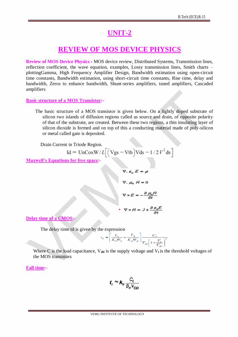
Basic structure of a MOS Transistor:-
The basic structure of a MOS transistor is given below. On a lightly doped substrate of
silicon two islands of diffusion regions called as source and drain, of opposite polarity
of that of the substrate, are created. Between these two regions, a thin insulating layer of
silicon dioxide is formed and on top of this a conducting material made of poly-silicon
or metal called gate is deposited.
Drain Current in Triode Region.
Maxwell’s Equations for free space:-
Delay time of a CMOS:-
The delay time td is given by the expression
Where C is the load capacitance, Vdd is the supply voltage and Vt is the threshold voltages of
the MOS transistors
Fall time:-

B.Tech (ECE) R-15
VEMU INSTITUTE OF TECHNOLOGY
Gauss Law:-
The total of the electric flux out of a closed surface is equal to the charge enclosed divided by
the permittivity. The electric flux through an area is defined as the electric field multiplied by
the area of the surface projected in a plane perpendicular to the field.
Characteristic Impedance:-
The characteristic impedance or surge impedance (usually written Z0) of a uniform
transmission line is the ratio of the amplitudes of voltage and current of a single wave
propagating along the line; that is, a wave travelling in one direction in the absence of
reflections in the other direction.
Smith chart:-
Smith chart is a graphical aid or monogram designed for electrical and electronics
engineers specializing in radio frequency (RF) engineering to assist in solving problems with
transmission lines and matching circuits.
Open circuit time constant:-
The open-circuit time constant method is an approximate analysis technique used in
Electronic circuit design to determine the corner frequency of complex circuits. It also is known
as the zero-value time constant technique.
Short circuit Time Constant:-
The short circuit time constant method to determine the low frequency band limit in case
of Multi stage amplifier.
Propagation constant:-
The propagation constant of a sinusoidal electromagnetic wave is a measure of the
change Undergone by the amplitude and phase of the wave as it propagates in a given direction.
The Quantity being measured can be the voltage or current in a circuit or a field vector such as
Electric field strength or flux density.
Cascaded Amplifiers:-
A cascade amplifier is any two-port network constructed from a series of amplifiers,
where each amplifier sends its output to the input of the next amplifier in a daisy chain.
Tuned Amplifiers:-
A tuned amplifier is an electronic amplifier which includes band pass filtering
components within the amplifier circuitry. They are widely used in all kinds of wireless
applications. The response of tuned amplifier is maximum at resonant frequency and it falls
sharply for frequencies below and above the resonant frequency

B.Tech (ECE) R-15
VEMU INSTITUTE OF TECHNOLOGY
UNIT-III
NOISE
1. NOISE–INTRODUCTION:-
The sensitivity of communications systems is limited by noise. The broadest definition of
noise as "everything except the desired signal" is most emphatically notwhat we will use
herehowever, because it does not separate say, artificial noisesources (e.g .. 60-Hz power-line
hum) from more fundamental (and therefore irreducible) sources of noise that we discuss in
this.
That these fundamental noise sources exist was widely appreciated only after theinvention of the
vacuum tube amplifier. when engineers finally had access to enoughgain to make these noise sources
noticeable. It became obvious that simply cascadingmore amplifiers eventually produces no further
improvement in sensitivity because a mysterious noise exists that is amplified along with the signal.
In audio systems, thisnoise is recognizable as a continuous hiss while, in video, the noise manifests
itselfas the characteristic "snow" of analog TV systems.
1.1 THERMAL NOISE:-
Johnson was the first to report careful measurements of noise in resistors, and his colleague
Nyquist J explained them as a consequence of Brownian motion: thermally agitated charge
carriers in a conductor constitute a randomly varying current that gives rise to a random
voltage (via Ohm's law). In honor of these fellows. Thermal noise is often called Johnson
noise or less frequently Nyquist noise.
Because the noise process is random. one cannot identify a specific value of voltage at a particular
time (in fact. the amplitude has a Gaussian distribution) and the only recourse is to characterize the
noise with statistical measures. such ax the mean square or root-mean-square values.
Because of the thermal origin, we would expect a dependence on the absolute temperature. It turns out
that thermal noise power is exactly proportional to T (the astutemight even guess that it is proportional
to kTJ. Specifically. a quantity called the available noise power is given by
(1) wherek is Boltzmann's constant (about 1.38 x 10⁻²³J/K). T is the absolute temperature in kelvins,
and Δfthe noise bandwidth in hertz (equivalent brickwall bandwidth) over which the measurement is
made.

B.Tech (ECE) R-15
VEMU INSTITUTE OF TECHNOLOGY
We will clarify shortly what is meant by the terms "available noise power" and" noise
bandwidth:' but for now simply note that the noise source is very broadband (infinitely so in fact in
the simplified picture presented here"), so that the total noise power depends on the measurement
bandwidth.
With Eqn. 1, we can compute that the available noise power over a 1-Hz bandwidth is about 4 x
10-21 W (or -174 dBm) s at room temperature. Further note that the constancy of the noise density
implies that the thermal noise power is the same over any given absolute bandwidth. Therefore the
noise power in the interval between 1 MHz and 2 MHz is the same as between 1 GHz and
1.001 GHz. Because of this constancy, thermal noise is often described as "white," by analogy with
white light. However the analogy is not exact, since white light consists of constant energy per
wavelength whereas white noise has constant energy per hertz.
The term "available noise power" is simply the maximum power that can be delivered to a load.
Recall that the condition for maximum power transfer (for a resistive network) is equality of the load
and source resistances. This suggests the use of the network shown in Figure 1.1 to compute the
available noise power.
The model of the noisy resistor is enclosed within the dashed box and is here shown as a noise
voltage generator in series with the resistor itself. The power delivered by this noisy resistor to
another resistor of equal value is by definition theavailable noise power is
Figure 1.1 network for computing the thermal noise of resistor.
Where en- is the open-circuit rrns noise voltage generated by the resistor R over the bandwidth Δf
at a given temperature, The mean-square open-circuit noise voltage is therefore
The two noise models for a resistor are displayed in Figure 1.2. Note that the polarity indications on
the noise voltage source and the arrow on the noise current.

B.Tech (ECE) R-15
VEMU INSTITUTE OF TECHNOLOGY
Figure 1. 2, Resistor thermal noise model
Source is simply references. They do not imply that the noise has a particular constant polarity (in
fact, the noise has a zero mean).
The two noise models for a resistor are displayed in Figure 1.2. Note that thepolarity
indications on the noise voltage source and the arrow on the noise current
figure 1. 2, Resistor thermal noise model
Source is simply references. They do not imply that the noise has a particular constant polarity (in
fact, the noise has a zero mean). Also note that, since the noise arises from the random thermal
agitation of charge in the conductor, the only ways to reduce the noise of a given resistance are to
keep the temperature as low as possible and to limit the bandwidth to the minimum useful value as
well.
The distinction is made to underscore that the noise bandwidth Δf generally is not the same as the
-3-dBbandwidth. Rather. the noise bandwidth is that of a perfect. brick wall (rectangular) filter that
possesses the same area and peak value as the actual power gain-versus frequency characteristic of the
system. including that of the measurement apparatus. The noise bandwidth is therefore
Where Hpk is the peak value of the magnitude of the filter voltage transfer function H(f)·
This normalization concept allows comparisons to be made on a standard basis. As a specific
example, consider a single-pole RC low-pass filter. We know that the-3-dB bandwidth (in hertz) is
simply 1/2piRC but the equivalent noise bandwidth is computed as

B.Tech (ECE) R-15
VEMU INSTITUTE OF TECHNOLOGY
We see that a single-pole low-pass filter (LPF) has a noise bandwidth that is about1.57 times
the -3-dB bandwidth. That the noise bandwidth exceeds the -3-dBbandwidth makes sense,
since the lazy roll off of a single-pole filter allows spectral components of noise beyond the
filter's -3-dB frequency to contribute significantly to the output energy of the filter.
This result follows from a more detailed derivation that takes into account the actual
distribution of carrier energies modified by considerations related to the He is
enberguncertainty principle." A more general expression for the thermal noise voltage is as
follows
1.2 .THERMAL NOISE IN MOSFETs:-
(a)Drain Current Noise:-Since FETs (both junction and MOS) are essentially voltage-
controlled resistors,they exhibit thermal noise. In the triode region of operation particularly
one would expect noise commensurate with the resistance value. Indeed detailed theoretical
considerations" lead to the following expression for the drain current noise of FETs:
Where gdD is the drain-source conductance at zero VDS. The parameter y has a value of
unity at zero VDS and, in long devices decreases toward a value of 2/3 in saturation. Note that
the drain current noise at zero VDS is precisely that of an ordinary conductance of value gdo
Figure1.3.Simplified illustration of substrate thermal noise
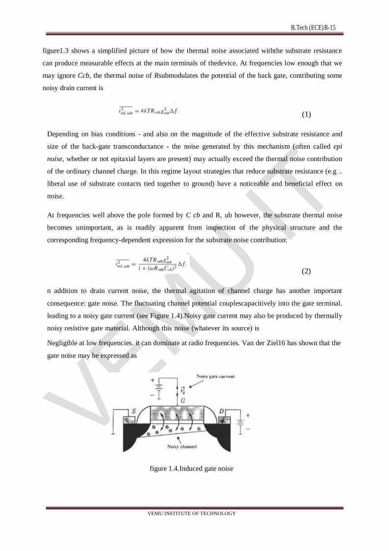
B.Tech (ECE) R-15
VEMU INSTITUTE OF TECHNOLOGY
figure1.3 shows a simplified picture of how the thermal noise associated withthe substrate resistance
can produce measurable effects at the main terminals of thedevice. At frequencies low enough that we
may ignore Ccb, the thermal noise of Rsubmodulates the potential of the back gate, contributing some
noisy drain current is
(1)
Depending on bias conditions - and also on the magnitude of the effective substrate resistance and
size of the back-gate transconductance - the noise generated by this mechanism (often called epi
noise, whether or not epitaxial layers are present) may actually exceed the thermal noise contribution
of the ordinary channel charge. In this regime layout strategies that reduce substrate resistance (e.g ..
liberal use of substrate contacts tied together to ground) have a noticeable and beneficial effect on
noise.
At frequencies well above the pole formed by C cb and R, ub however, the substrate thermal noise
becomes unimportant, as is readily apparent from inspection of the physical structure and the
corresponding frequency-dependent expression for the substrate noise contribution:
(2)
n addition to drain current noise, the thermal agitation of channel charge has another important
consequence: gate noise. The fluctuating channel potential couplescapacitively into the gate terminal.
leading to a noisy gate current (see Figure 1.4).Noisy gate current may also be produced by thermally
noisy resistive gate material. Although this noise (whatever its source) is
Negligible at low frequencies. it can dominate at radio frequencies. Van der Ziel16 has shown that the
gate noise may be expressed as
figure 1.4.Induced gate noise

B.Tech (ECE) R-15
VEMU INSTITUTE OF TECHNOLOGY
figure 1.5.gate noise circuit model
Van der Ziel gives a value of 4/3 (twice y) for the gate noise coefficient, 8. in long channel devices.
The circuit model for gate noise that follows directly from Eqn. 8 and Eqn. 9 is a conductance
connected between gate and source, shunted by a noise current source(see Figure 11.5). The gate
noise current clearly has a spectral density that is not constant. In fact it increases with frequency. so
perhaps it ought to be called "blue noise" to continue the optical analogy.
For those who prefer not to analyze systems that have blue noise sources. It is possible to recast the
model in a form with a noise voltage source that possesses a constant spectral density." To derive this
alternative model first transforms the parallel RC network into an equivalent series RC network. If one
assumes a reasonably high Q, then the capacitance stays roughly constant during the transformation.
The parallel resistance becomes a series resistance whose value is
which is independent of frequencyFinally equate the short-circuit currents of the original network and
the transformed version again with the assumption of high Q. The equivalent series noisevoltage
source is then found to be
which possesses a constant spectral density. Hence this alternative gate noise modelconsists of
elements whose values arc independent of frequency; see Figure 1.6.
figure 1.6.alternate gate noise model
Although the noise behavior of long-channel devices is fairly well understood. Theprecise behavior of
δ in the short-channel regime is unknown at present. Given thatboth the gate noise and drain noise
share a common origin, however it is probablyreasonable as a crude approximation to assume that 8
continues to be about twice aslarge as y. Hence, just as y is typically 1-2 for short-channel NMOS
devices δ maybe taken as 2-4.
B.Tech (ECE) R-15
VEMU INSTITUTE OF TECHNOLOGY
1.3. SHOT NOISE:-
The fundamental basis for shot noise is the granular nature of the electronic charge, but how
this granularity translates into noise is perhaps not as straightforward as one might think.
Two conditions must be satisfied for shot noise to occur. There must be a direct current flow and there
must also be a potential barrier over which the charge carriers hop. The second condition tells us that
ordinary, linear resistors do not generates hot noise despite the quantized nature of electronic charge.
The fact that charge comes in discrete bundles means that there arc discontinuous pulses of current
every time electron hops energy barrier. It is the randomness of the arrival limes that gives rise to the
whiteness of shot noise. If all the carrier shopped simultaneously shot noise would have a much more
benign character. As we’ll see in a later example.
We would expect the shot noise current to depend on the charge of the electron (since smaller charge
would result in less lumpiness and therefore less noise). The total DC current Row (less
current also means fewer lumps) and the bandwidth (justas with thermal noise). In facts hot noise
does depend on all of those quantities. As seen in the following equation:
wherein
- is the rms noise current. qis the electronic charge (about 1.6 x 10⁻¹⁹ C), IDC is the DC current
in amperes. and/o"fis again the noise bandwidth in hertz. Note that. like thermal noise. Shot noise
(ideally) is white and has amplitude that possesses a Gaussian distribution. As a reference point.
therrns current noise density is approximately 18 pA/-/Hz for a I-rnA value of IDC.
The requirement for a potential barrier implies that shot noise will only be associated with nonlinear
devices, although not all nonlinear devices necessarily exhibit hot noise. For example whereas both
the base and collector currents are sources of shot noise in a bipolar transistor because potential
barriers arc definitely involved there (two junctions) only the DC gate leakage current of FETs (both
MOS adjunction types of FETs) contributes shot noise. Because this gate current is normally very
small, it is rarely a significant noise source (sadly. though. the same cannot be said of base current).

B.Tech (ECE) R-15
VEMU INSTITUTE OF TECHNOLOGY
1.4. FLICKER NOISE:-
The most mysterious type of noise is flicker noise (also known as 1/f noise or pink-" noise).
No universal mechanism for flicker noise has been identified, yet it is ubiquitous. Phenomena
that have no obvious connection, such as cell membrane potentials, the earth's rotation rate,
galactic radiation noise, and transistor noise all have fluctuations with a 1/f character.
As the term "1/f” suggests, the noise is characterized by a spectral density that increases, apparently
without limit, as frequency decreases. Measurements have verified this behavior in electronic systems
down to a small fraction of a micro hertz. One unfortunate implication of the increasing noise with
decreasing frequency is the failure of averaging (band limiting) to improve measurement accuracy,
since the noise power increases just as fast as the averaging interval. Because of the lack of a unifying
theory, mathematical expressions for "1/f” noise invariably contain various empirical parameters (in
contrast with the theoretical cleanliness of the equations for thermal and shot noise). as can be seen in
the following equation is
Here N-is the rms noise (either voltage or current). K is an empirical parameter that is device- specific
(and generally also bias-dependent), and n is an exponent that is usually (but not always) close to
unity.
A question that often arises in connection with "1/f” noise concerns the infinity at DC implied by a
"1/f” functional dependency. It's instructive to carry out a calculation with typical numbers to see why
there is no problem, practically speaking.
First, let the parameter II have its commonly occurring value of unity. Then, integrate the density to
find the total noise in a frequency band bounded by a lower frequency fl and an upper frequency fh.
This equation tells us that the total mean-square noise depends on the log of the frequency ratio,
rather than simply on the frequency difference (as in thermal and shot noise). Hence, the mean- square
value of l/f noise is the same for equal frequency ratios; there is thus a certain constant amount of
mean-square noise per decade of frequency, say, or some specific amount of rms noise per root
decade of frequency (units again for rrns quantities).
As a specific numerical example, suppose measurements on an amplifier reveal that its 1/f noise has a

B.Tech (ECE) R-15
VEMU INSTITUTE OF TECHNOLOGY
density of 10uVrrns per root decade. Thus, for the 16-decadefrequency interval below I Hz, the total
1/f noise would be just four times larger, or 40uVrrns. Recognize that 16decades below 1 hertz is
equal to one cycle about every 320 million years." and you have to concede that "DC" infinities are
simply not a practical problem. The resolution of the apparent paradox thus lies in recognizing that
true DC implies an infinitely long observation interval, and that humans’ and the electronic age have
been around for only a finite time. For any finite observation interval, the infinities simply don't
materialize.
1.4.2. FLICKER NOISE IN RESISTORS:-
Flicker noise also shows up in ordinary resistors, where it is often called "excess noise," since
this noise is in addition to what is expected from thermal noise considerations. It is found that
a resistor exhibits 1/f noise only when there is DC current flowing through it, with the noise
increasing with the current. In the discrete world, garden-variety carbon composition resistors
are the most conspicuous offenders, while metal- film and wire wound resistors exhibit the
smallest amounts of excess noise.
The current-dependent excess noise of carbon composition resistors has been explained by some as
the result of the random formation and extinction of "micro-arcs" among neighboring carbon granules.
“carbon film “resistors, which are made differently, exhibit much less excess noise than do carbon
composition types. Whatever the explanation, it is certainly true that excess noise increases with the
DC bias, so one should minimize the DC drop across a resistor.
The following approximate expression shows explicitly the dependency of thisnoise on various
parameters is
Where A is the area of the resistorRis the sheet resistivity, V is the voltage acrossthe resistor, and K is
a material-specific parameter. For diffused and ion-implantedresistors, K has a value of roughly 5 x
10-28 S2-m2, whereas for thick-film resistors (not normally available in CMOS processes), K is about
an order of magnitude larger.

B.Tech (ECE) R-15
VEMU INSTITUTE OF TECHNOLOGY
1.4.2.FLICKER NOISE IN MOSFETS:-
In electronic devices 1/f noise arises from a number of different mechanisms and is most prominent in
devices that are sensitive to surface phenomena. Hence, MOSFETs exhibit significantly more 1/f
noise than do bipolar devices. One means of comparison is to specify a "corner frequency." where the
1/f and thermal or shot noise components are equal, All other things held equal. a lower 1/f corner
implies less total noise. It is relatively trivial to build bipolar devices whose 1/f corners are below tens
or hundreds of hertz, and many MOS devices routinely exhibit 1/f corners of tens of kilohertz to a
megahertz or more.
Charge trapping phenomena are usually invoked to explain 1/f noise in transistors. Some types
of defects and certain impurities (most plentiful at a surface orinterface of some kind) can randomly
trap and release charge. The trapping times are distributed in a way that can lead to a 1/f noise
spectrum in both MOS and bipolar transistors. Since MOSFETs are surface devices (at least in the
way that they are conventionally fabricated), they exhibit this type of noise to a much greater degree
than bipolar transistors (which are bulk devices). Larger MOSFETs exhibit less 1/f noise because their
larger gate capacitance smooths the fluctuations in channel charge. Hence, if good 1/f noise
performance is to be obtained from MOSFETs, thelargest practical device sizes must be used (for a
given gm)
The mean-square 1/fdrain noise current is given by
Where A is the area of the gate (= WL) and K is a device-specific constant. Thus for a fixed trans
conductance. a larger gate area and a thinner dielectric reduce this noise term
For PMOS devices, K is typically about 10-28 C2/m2 whereas for NMOS devices it is about 50 times
larger." One should keep in mind that these constants vary considerably from process to process, and
even from run to run, so the values of K given here should be treated as crude estimates. In particular
the superior 1/f performance of PMOS devices may be a temporary situation, as it is due to the use of
buried channels that may cease to be widely used in the future.

B.Tech (ECE) R-15
VEMU INSTITUTE OF TECHNOLOGY
1.4.3. FLICKER NOISE IN JUNCTIONS:-
Forward-biased junctions also exhibit 1/fnoise. The noise is proportional to the biascurrent and
inversely proportional to the junction area
where the constant K typically has a value of around 10-25A.m2. Once again however, considerable
variation from process to process is not uncommon."Flicker noise in bipolar transistors is attributed
entirely to the base-emitter junction (since it is the only one in forward bias). It has been established
experimentally that only the base current exhibits 1/f noise.
1.5. CLASSICAL TWO-PORT NOISE THEORY (NOISE FIGURE):-
1.5.1 NOISE FACTOR:-
A useful measure of the noise performance of a system is the noise factor. Usually denoted F.
To define it and understand why it is useful, consider a noisy (but linear) two-port driven by a
source that has an admittance Y and an equivalent shunt noise current as shown in Figure 1.1.
If we are concerned only with overall input-output behavior, it is an unnecessary complication to keep
track of all of the internal noise sources. Fortunately, the net effect of all of those sources can be
represented by just one pair of external sources, a noise voltage and a noise current. This huge
simplification allows rapid evaluation ofhow the source admittance affects the overall noise
performance. As a consequence,we can identify the criteria one must satisfy for optimum noise
performance.
The noise factor is defined a (1)
where by convention the source is at a temperature of 290 K. The noise factor isa measure of the
degradation in signal-to-noise ratio that a system introduces. Thelarger the degradation the larger the
noise factor. If a system adds no noise of itsown then the total output noise is due entirely to the
source and the noise factor istherefore unity.
figure1.1 noisy two-port driven by noise source

B.Tech (ECE) R-15
VEMU INSTITUTE OF TECHNOLOGY
figure 1.2 equivalent noise model
In the model of Figure 11.8, all of the noise appears as inputs to the noiseless network, so we may
compute the noise figure there. A calculation based directly on equation (1) requires the computation
of the total power due to all of the sources and dividing that result by the power due to the input
source. An equivalent (and simpler)method is to compute the total short-circuit mean-square noise
current and then divide that total by the short-circuit mean-square noise current due to the input
source. This alternative method is equivalent because the individual power contributions
areproportional to the short-circuit mean-square current. with a proportionality constant(which
involves the current division ratio between the source and two- port) that isthe same for all of the
terms.
In carrying out this computation, one generally encounters the problem of combining noise sources
that have varying degrees of correlation with one another. In thespecial case of zero correlation the
individual powers superpose. For example, if weassume as seems reasonable. That the noise powers
of the source and of the two-portare uncorrelated, then the expression for noise figure becomes
(2)
Although we have assumed that the noise of the source is uncorrelated withthe two equivalent noise
generators of the two-port equation 2 does notassume thatthe two-port 's generators are also
uncorrelated with each other.
In order to accommodate the possibility of correlations between enand In expressInas the sum of two
components. One icis correlated with en and the otheriu is given by
(3)
Since icis correlated with enit may be treated as proportional to it through a constant whose dimensions
are those of admittance is given
(4)
the constant Ycis known as the correlation admittance

B.Tech (ECE) R-15
VEMU INSTITUTE OF TECHNOLOGY
Submit the equations 2,3.4 in equation 1,the noise factor is then
(5)
The expression in Equation 5 contains three independent noise sources, each of whichmay be treated
us thermal noise produced by an equivalent resistance or conductance(whether or not such a
resistance or conductance actually is the source of the noise)
Using these equivalences, the expression for noise factor can be written purely interms of impedances
and admittances is
(6)
where we have explicitly decomposed each admittance into a sum of a conductanceC and a
susceptanceB.
1.5.2 OPTIMUM SOURCE ADMITTANCE:-
Once a given two-port's noise has been characterized with its four noise parameters
(Gr,Bc,Rn,Bs)Eqn. 6 allows us to identify the general conditions forminimizing the noise
factor. Taking the first derivative with respect to the source admittance and selling it equal to
zero yields
(7),(8)

B.Tech (ECE) R-15
VEMU INSTITUTE OF TECHNOLOGY
Hence.to minimize the noise factor. the source susceptance should be made equal tothe inverse of the
correlation susceptance. while the source conductance should beset equal to the value in Eqn. 8
The noise factor corresponding to this choice is found by direct substitution ofEqn. 7 and Eqn. 8 into
Eqn. 6
(9)
We may also express the noise factor in terms of Fmin and the source admittance is
(10)
Thus contours of constant noise factor are non-overlapping circles in the admittanceplane.
The ratio Rn/Gs, appears as a multiplier in front of the second term of Eqn. 10. Fora fixed source
conductance Rn tells us something about the relative sensitivity of thenoise figure to departures from
the optimum conditions. A large Rn implies a high sensitivity; circuits or devices with high R"
obligate us to work harder to identifyachieve, and maintain optimum conditions. We will shortly see
that operation at lowbias currents is associated with large R", in keeping with the general intuition
thatachieving high performance only gets more difficult as the power budget tightens.
It is important to recognize thatalthough minimizing the noise factor has something of the flavor of
maximizing power transfer. the source admittances leading tothese conditions are generally not the
same - as is apparent by inspection of Eqn. 7 and Eqn. 8. For example there is no reason to expect the
correlation susceptance to equal the input susceptance (except by coincidence). As a consequence one
must generally accept less than maximum power gain if noise performance is to be optimized, and
vice versa.
1.5.3 LIMITATIONS OF CLASSICALNOISE OPTIMIZATION:-
The classical theory just presented implicitly assumes that one is given a device with
particular fixed characteristics and defines the source admittance that will yield
theminimum noise figure given such a device.

B.Tech (ECE) R-15
VEMU INSTITUTE OF TECHNOLOGY
Although one starts with fixed devices indiscrete RF design. The freedom to choose device
dimensions in IC realizations points out a serious shortcoming of the classical approach: There are no
specific guidelines about what device size will minimize noise. Further more power consumption is
frequently a parameter of great interest (even an obsessive one in many portable applications) but
power is simply not considered at all in classical noise optimization. We will return to these themes in
great detail in the chapter on LNA design. But for now simply be aware of the incompleteness of the
classical approach.
1.5.4 NOISE FIGURE AND NOISE TEMPERATURE:-
In addition to noise factor, other figures of merit that often crop up in the literature are noise
figure and noise temperature. The noise figure (NF) is simply the noise factor expressed in
decibels.
Noise temperature, TN, is an alternative way of expressing the effect of an amplifier's noise
contribution and is defined as the increase in temperature required of the source resistance for it to
account for all of the output noise at the reference temperature Tref (which is 290 K). It is related to
the noise factor as follows
An amplifier that adds no noise of its own has a noise temperature of 0 K.Noise temperature is
particularly useful for describing the performance of cascaded amplifiers and those whose noise factor
isquite close to unity (or whose noise figure is very close to 0 dB), since the noise temperature offers a
higher-resolution description of noise performance in such cases Noise figures in the range of 2-3 dB
are generallyconsidered very good, with values around or below 1 dB considered outstanding.
2. LNA DESIGN:-
2.1 DERIVATION OF INTRINSIC MOSFETTWO-PORT NOISE PARAMETERS:-
The MOSFET noise model consists of two sources. The mean-square drain current noise is
(1)

B.Tech (ECE) R-15
VEMU INSTITUTE OF TECHNOLOGY
Gate current noise is
Further recall that the gate noise is correlated with the drain noise, with a correlationcoefficient defined
formally as
then the reference direction for the gate noise is from the source 10 gate (as in Fig• ure 1.5)and that
for the drain noise is from the drain to the source (as in Figure 1.4), then the long-channel value of c is
theoretically - jO.395.
we will neglect the thermal noise due to the resistive gate materialalthough this source of noise can
actually dominate the gate noise when operating device well below fT,where nonquasistatic effects
(such as induced gate noise) willbe less prominent.' We will also neglect Cgd to simplify the
derivation. While theachievable noise figure is little affected by Cgd the input impedance can be a
strong function of Cgd and this effect must be taken into account when designing the inputmatching
network.
To derive the four equivalent two-port noise parameters repeated here for convenience
we first reflect the two fundamental MOSFET noise sources back to the input port as a different pair
of equivalent input generators (one voltage and one current source).The equivalent input noise voltage
generator accounts for the output noise observed when the input port is short- circuited (incrementally
speaking). To determineits value, reflect the drain current noise back to the input as a noise voltage
and recognize that the ratio of these quantities is simply gm,. Thus,

B.Tech (ECE) R-15
VEMU INSTITUTE OF TECHNOLOGY
From which it is apparent that the equivalent input noise voltage is completely correlated, and in
phase, with the drain current noise. Thus, we can immediately determinethat
he equivalent input noise voltage generator by itself does not fully account for thedrain current noise.
however because a noisy drain current also flows even when theinput is open-circuited and induced
gate current noise is ignored. Under this opencircuit condition. dividing the drain current noise by the
transconductance yields anequivalent input voltage which. when multiplied in turn by the input
admittance,gives us the value of an equivalent input current noise that completes the modelingof imdis
given by
(2)
In this step of the derivation, we have assumed that the input admittance of a MOSFETis purely
capacitive. This assumption is a good approximation for frequencies well below Wr, if appropriate
high-frequency layout practice is observed to minimize gateresistance. Given this assumption, Eqn. 2
shows that the input noise current in1 isin quadrature and therefore completely correlated, with the
equivalent input noise voltage en
The total equivalent input current noise is the sum of the reflected drain noisecontribution of Eqn. 2
and the induced gate current noise. The induced gate noisecurrent itself consists of two terms. One
which we'll denote ingc is fully correlatedwith the drain current noise, while the other, inguis
completely uncorrelated with thedrain current noise. Hence we may express the correlation
admittance as follows:
(3)

B.Tech (ECE) R-15
VEMU INSTITUTE OF TECHNOLOGY
To express Yc in a more useful form we need to incorporate the gate noise correlationfactor explicitly.
To do so, we must manipulate the last term ofEqn. 3 in waysthat will initially appear mysterious.
First, we express it in terms of cross-correlationsby multiplying both numerator and denominator by
the conjugate of the drain noise current and then averaging each one is
(4)
The last equality, in which ing replaces ings is valid because the uncorrellatcd portionof the gate noise
current necessarily contributes nothing to the cross-correlation.Using Eqn. 3, we may write the
correlation admittance as
(5)
(6)
which explains all of the maneuvering, since the correlation coefficient has finallymade an explicit
appearance.Substituting for the term under the radical yields
(7)
If we assume that e continues to be purely imaginary, even in the short-channelregime. We finally
obtain a useful expression for the correlation admittance is
(8)

B.Tech (ECE) R-15
VEMU INSTITUTE OF TECHNOLOGY
(9)
Since α is unity for long-channel devices and progressively decreases as channellengths shrink. it is
one measure of the departure from the long-channel regime.
We see from Eqn.8 that the correlation admittance is purely imaginary. so that G; =0More significant,
however, is the fact that Yc does not equal the admittanceof Cgs although it is some multiple of it.
Hence one cannot maximize power transferand minimize noise figure simultaneously. To investigate
further the importantimplications of this impossibility though we need to derive the last remaining
noise parameter Gh.
Using the definition of the correlation coefficient, we may express the induced gate noise as follows
on
(10)
The very last term in Eqn. 10 is the uncorrelated portion of the gate noise current, sothat, finally,
(11)
we can determine both the source impedance that minimizes the noise figureas well as the minimum
noise figure itself is
(12)
From Eqn. 12 we see that the optimum source susceptance is essentially inductivein character except
that it has the wrong frequency behavior. Hence achieving abroadband noise match is fundamentally
difficult.Continuing the real part of the optimum source admittance is

B.Tech (ECE) R-15
VEMU INSTITUTE OF TECHNOLOGY
(13)
(14)
In Eqn, 14 the approximation is exact if one treats Wτ as simply the ratio of gmto CS" Note that if
there were no gate current noise the minimum noise figure would be 0 dB. That unrealistic prediction
alone should be enough to suspect that gate noise must indeed exist. Also note that, in principle,
increasing the correlation between drain and gate current noise would improve noise figure, although
correlation coefficients unrealistically near unity would be required to effect large reductions in noise
figure.
Generalizing, the noise parameters for a device of width Ware
(15)
2.2. LNA TOPOLOGIES: POWER MATCHVERSUS NOISE MATCH:-
One straightforward approach to providing a reasonably broadband 50-Q termination is simply to put
a 50-Q resistor across the input terminals of a common-source amplifier; this is shown in Figure 1.
Figure1.1. Common-source amplifier with shunt input resistor (biasing not shown)

B.Tech (ECE) R-15
VEMU INSTITUTE OF TECHNOLOGY
Unfortunately the resistor Rl adds thermal noise of its own and so attenuates the signal (by a factor of
2) ahead of the transistor. The combination of these two effects generally produces unacceptably high
noise figures. More formally it is straight forward to establish the following lower bound on the noise
figure of this circuit is
(1)
Where Rs = R1 = R. This bound applies only in the low-frequency limit and ignores gate current noise
altogether. Naturally, the noise figure is worse at higher frequencies and when gate noise is taken into
account.
The shunt-series amplifier, is another circuit that provide broadband real input Impedance Since it
does not reduce the signal with a noisy attenuators before amplifying, we expect its noise figure to be
substantially better than that of the circuit of Figure 1.2.
Figure 1.2 shunt-series amplifier as bias is not shown figure 1.3 common gate amplifier
The amplifier sketched in Figure 1.3 suffers from fewer problems than the previous circuit, yet the
resistive feedback network continues to generate thermal noise of its own and also fails to present to
the transistor an impedance that equals Zopts at all frequencies (.perhaps at any frequency). As a
consequence, the overall amplifier's noise figure while usually much better than that of Figure 1.2 still
generally exceeds the device F min by a considerable amount (typically a few decibels), Nonetheless
the broad band capability of this circuit is frequently enough of a compensating advantage that the
shunt-series amplifier is found in many LNA applications even though Its noise figure is not the
minimum possible.
Another method for realizing a resistive input impedance is to use a common-sate configuration,
Since the resistance looking into the source terminal is 1/gm a proper selection of device size and bias
current can provide the desired 50ohm resistance' see Figure 1.4.

B.Tech (ECE) R-15
VEMU INSTITUTE OF TECHNOLOGY
Figure 1.4 impedance transformation model
lower bound on the noise figure of the common-gate amplifier (again. at low frequencies and
neglecting gate current noise) with the circuit shown in figure 1.2.
(2)
This bound assumes that (he resistance looking into the source terminal is adjusted toequal the source
resistance. and is about 2.2 dB in the long-channel limit and perhapsas high as 4.8 dB for
short devices ( = 2). The noise figure will be significantlyworse at high frequencies and when
gate current noise is taken into account.
The essential features of this mechanism may be understood by examining the abstractionof Figure
1.4. The amplifier is ideal in all respects except for a frequencydependentgain A(s),

B.Tech (ECE) R-15
VEMU INSTITUTE OF TECHNOLOGY
Theinput terminal is analogous to the gate (or grid) terminaland the amplifier output is connected to the
bottom plate of the gate capacitance. Theinput impedance of this circuit is
(3)
Now let A(s) have gain and phase shift is
(4,5,6)
from which it is apparent that the input admittance indeed possesses a real part whosevalue depends
on the phase lag ¢. With zero phase lug.the admittance is purely capacitive.as anticipated from
quasistatic analyses. If the more realistic scenario of anonzero phase lag is considered. the equivalent
shunt conductance is seen to increasewith frequency. Perhaps it is no surprise that measurements
show that the phase lagitself grows with frequency, and the equivalent shunt conductance typically
increasesas the square of frequency. to a good approximation.
Transit-lime effects also cause a resistive component of input impedance in vacuum tubes where the
phenomenon was first observed. Because of the finite velocity of charge. Then a real term is an
unavoidable reality in charge-controlled devicessuch as vacuum tubes and FETs.In the context of
low-noise amplifiers we actually seek to enhance this effect, forit can be used to create a resistive
input impedance without the noise of real resistors.From the foregoing. it is clear that one possible
method is to modify the device (e.g ..elongate it) in order to enhance transit time effects directly.
However, this approachhas the undesirable side effect of degrading high- frequency gain.

B.Tech (ECE) R-15
VEMU INSTITUTE OF TECHNOLOGY
A better method is to employ inductive source degeneration. With such an inductance current flow
lags behind an applied gate voltage behavior that is qualitativelysimilar to the mechanism described.
An important advantage of this met bod is thatone then has control over the value of to be real part of
the impedance through choiceof inductance, as is clear from computing the input resistance of the
circuit shown in 1.5
Figure 1.5.Induclivelydegeneratedcommon-source amplifier.
(7)
Hence the input impedance is that of a series RLC network with a resistive ten that is directly
proportional to the inductance value. More generally an arbitrary source degeneration impedance Z is
modified by afactor equal to [B(jw+1)] when reflected to the gate circuit where B(jw) is the current
gain is
(8)
The current gain magnitude goes to unity at WT (as it should), and it has a capacitivephase angle
because of Cgs. Hence, for the general case.
(9)

B.Tech (ECE) R-15
VEMU INSTITUTE OF TECHNOLOGY
Note that capacitive degeneration contributes a negative resistance to the input impedance. Hence any
source-to-substrate capacitance offsets the positive resistancefrom inductive degeneration. It is
important to take this effect into account in anyactual design.
Whatever the value of this resistive term it is important to emphasize that itdoesnot bring with it the
thermal noise of an ordinary resistor because a pure reactanceis noiseless. We may therefore exploit
this property to provide specified input impedancewithout degrading the noise performance of the
amplifier.
The form of Eqn. 7 clearly shows that the input impedance is purely resistiveat only one frequency (at
resonance) however so this method can provide only a narrowband impedance match. Fortunately,
there are numerous instances whennarrowband operation is not only acceptable but actually desirable.
So inductive degenerationis certainly a valuable technique. The LNA topology we will examine forthe
rest of this chapter is therefore as shown in Figure 1.6
.
Figure 1.6Narrowband LNAwith inductive sourcedegeneration.
The inductance Ls
is chosen to provide the desired input resistance (equal to Rsthe source resistance). Since the input
impedance is purely resistive only at resonance.an additional degree of freedom, provided by
inductance Lg. is needed toguarantee this condition. Now, at resonance, the gate-to-source voltage is
Q timesas large as the input voltage. The overall stage transconductanceGm, under this conditionis
therefore
(10)

B.Tech (ECE) R-15
VEMU INSTITUTE OF TECHNOLOGY
where we have used the approximation that WT is the ratio of gml to Cgs
Let us continue to neglect Cgd,gmb and Csb. Then it is straightforward to showthat the input impedance
of the circuit in Figure 1.5 is
(11)
where ZL is the impedance attached to the drain. Comparing this result with our previous equation,
we see that finite output resistance alters the third term in the impedanceequation.
2.3.POWER CONSTRAINED NOISE OPTIMIZATION:-
To develop the desired noise optimization technique, we must express noise figurein a way that takes
power consumption explicitly into account. Given a specifiedbound on power consumption. the
method should then yield the optimum device thatminimizes noise. Although the detailed derivations
are somewhat complex. the endresults are remarkably simple. Readers interested primarily in
applying the methodare invited to skip to the end of this section.
We start with the general expression for noise figure as given by classical noisetheory is
(1)
The goal here is ultimately to reformulate the expression for noise figure in terms ofpower
consumption. Once we derive such an equation,we'll minimize it subject tothe constraint of fixed
power and then solve for the width of the transistor that correspondsto this optimum condition.
To simplify the development let us assume that the source susceptance Bs is chosen sufficiently close
to Bopt that we may neglect the difference between the two. Wewill justify this step formally at a later
time. Given this assumption, the expressionfor noise figure reduces to
(2)

B.Tech (ECE) R-15
VEMU INSTITUTE OF TECHNOLOGY
The goal here is ultimately to reformulate the expression for noise figure in terms ofpower
consumption. Once we derive such an equation. we'll minimize it subject tothe constraint of fixed
power and then solve for the width of the transistor that correspondsto this optimum condition.
To simplify the development. let us assume that the source susceptance Bs is chosensufficiently close
to Bopt that we may neglect the difference between the two. Wewill justify this step formally at a later
time. Given this assumption, the expressionfor noise figure reduces to
(3)
Next rearrange the expression for Gopt to define a parameter with the dimensionsof a quality factor.
This maneuver will help reduce clutter in the equations to come
(4)
To accommodate the possibility of operation with source conductance’s other than Gopt we also
define a similar Q in which Gopt is replaced by Gs the actual source conductance is
(5)
Now re-express and the noise parameters of
(6)
The parameters α ,gm, Qopt and Qs in Eqn. 6 are linked to power dissipation.We need to make the
linkage explicit. However, and rewrite those terms directly interms of power. To do so, first recall that
a simple expression for the drain current is
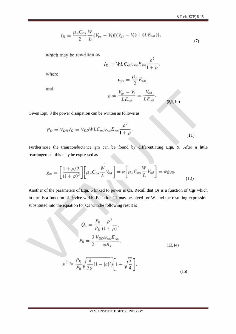
B.Tech (ECE) R-15
VEMU INSTITUTE OF TECHNOLOGY
(7)
(8,9,10)
Given Eqn. 8 the power dissipation can be written as follows as
(11)
Furthermore the transconductance gm can be found by differentiating Eqn, 9. After a little
rearrangement this may be expressed as
(12)
Another of the parameters of Eqn, 6 linked to power is Qs. Recall that Qs is a function of Cgs which
in turn is a function of device width. Equation 11 may besolved for W. and the resulting expression
substituted into the equation for Qs withthe following result is
(13,14)
(15)

B.Tech (ECE) R-15
VEMU INSTITUTE OF TECHNOLOGY
(16)
(17)
(18)
(19)
3. DESIGN EXAMPLES:-
3.1 SINGLE-ENDED LNA:-
To complete the design largely requires only the addition of bias and output circuitry. For
narrowband applications it is advantageous to tune out the output capacitance to increase
gain. Hence a typical single-ended LNA might appear as shown in Figure 1.
Figure 1 single ended LNA figure 2 Complete 1.5-GHz, 8-mW single-ended LNA

B.Tech (ECE) R-15
VEMU INSTITUTE OF TECHNOLOGY
The cascoding transistor is chosen here to have the same width as the main device. This choice is
common, but it is somewhat arbitrary and thus not necessarily ideal. Two competing considerations
constrain the size of the cascoding transistor.The gate-drain overlap capacitance can reduce the
impedance looking into the gate and drain of MI considerably, degrading both the noise performance
and input match.It is a straightforward matter to show that, for equal-sized common-source and
cascading devices, the resistive component at the input is given by
(1)
Another potential source of NF degradation is the thermal noise of the substrate, as discussed in the
previous chapter. Recall that this epi noise produces a drain noise component whose value is given by
(2)
At frequencies well below the pole frequency of 1/RsubCcb this extrinsic noise contribution can
nonetheless remain negligible if model parameters satisfy the following inequality is
(3)
3.2 DIFFERENTIAIL LNA:-
fig 1.Differential LNA

B.Tech (ECE) R-15
VEMU INSTITUTE OF TECHNOLOGY
Fig.2.Complete 12-mW, 1.5·GHz differential LNA.
The incremental ground located at the symmetrical point of a differential structure. See Figure 1
where the source degenerating inductances return to a virtual ground (for differential signals). Any
parasitic reactance in series with the bias current source is largely irrelevant, since a current source in
series with impedance is still a current source. Hence, the real part of the input impedance is
controlled only by Ls and is unaffected by parasitics in the current source's ground return path.
The circuit of Figure 1 ignores biasing details - in particular, it doesn't show how the DC gate
potentials are established. Furthermore, the gate bias for the cascading transistors is the supply
voltage, and such a choice may impress enough voltage across the bottom transistors to increase the
values of gamma and alpha at higher supply voltages. To mitigate such hot-electron noise
degradation, it is prudent to use only enough drain bias to keep transistors comfortably out of the
triode region, and no more.
One of many possible methods for achieving the desired results is shown in Figure 2 In this circuit
transistors M I through M ~ are the LNA core of the previous simplified schematic. The output of this
first stage is AC-coupled through Cc to M7and Ms, which provide additional gain. To save power the
current through the second gain stage is re-used to supply the four core

B.Tech (ECE) R-15
VEMU INSTITUTE OF TECHNOLOGY
transistors. Hence, the output tuning inductors Ld return to the common source connection of M7
and M8 rather than to the positive supply.
To keep all of the transistors in the stack in saturation with a low supply voltage, a common- mode
bias feedback loop sets the drain voltage of M1 and M2 equal to a fixed fraction of Vgs1 To the extent
that Vdsat roughly tracks Vgs1 this strategy guarantees that no more than the minimum supply voltage
is consumed.
The bias loop works as follows. The voltage at the top of resistor R) is equal to the common- mode
gate voltage of MI and M2 because, with no current flowing through junction of R...and R~ is
therefore some fraction of the common-mode gate-to-source voltage of the input pair. The operational
amplifier+' compares this voltage with the common-mode drain voltage of the input pair (measured at
the midpoint of RI/R2) and drives the gates of the cascoding transistors to make the two voltages
equal. Hence we have
(1)
where the voltages are referenced to the common source connection of the input pair. Transistor M9
guarantees start-up of the bias loop by providing some default gate voltage for the cascoding
transistors until the op-arnp has a chance to act. Finally because of the modest performance required
of the op-amp, negligibly low bias currents may be used there.
3. MIXER

B.Tech (ECE) R-15
VEMU INSTITUTE OF TECHNOLOGY

B.Tech (ECE) R-15
VEMU INSTITUTE OF TECHNOLOGY

B.Tech (ECE) R-15
VEMU INSTITUTE OF TECHNOLOGY

B.Tech (ECE) R-15
VEMU INSTITUTE OF TECHNOLOGY

B.Tech (ECE) R-15
VEMU INSTITUTE OF TECHNOLOGY

B.Tech (ECE) R-15
VEMU INSTITUTE OF TECHNOLOGY

B.Tech (ECE) R-15
VEMU INSTITUTE OF TECHNOLOGY

B.Tech (ECE) R-15
VEMU INSTITUTE OF TECHNOLOGY

B.Tech (ECE) R-15
VEMU INSTITUTE OF TECHNOLOGY

B.Tech (ECE) R-15
VEMU INSTITUTE OF TECHNOLOGY

B.Tech (ECE) R-15
VEMU INSTITUTE OF TECHNOLOGY

B.Tech (ECE) R-15
VEMU INSTITUTE OF TECHNOLOGY

B.Tech (ECE) R-15
VEMU INSTITUTE OF TECHNOLOGY
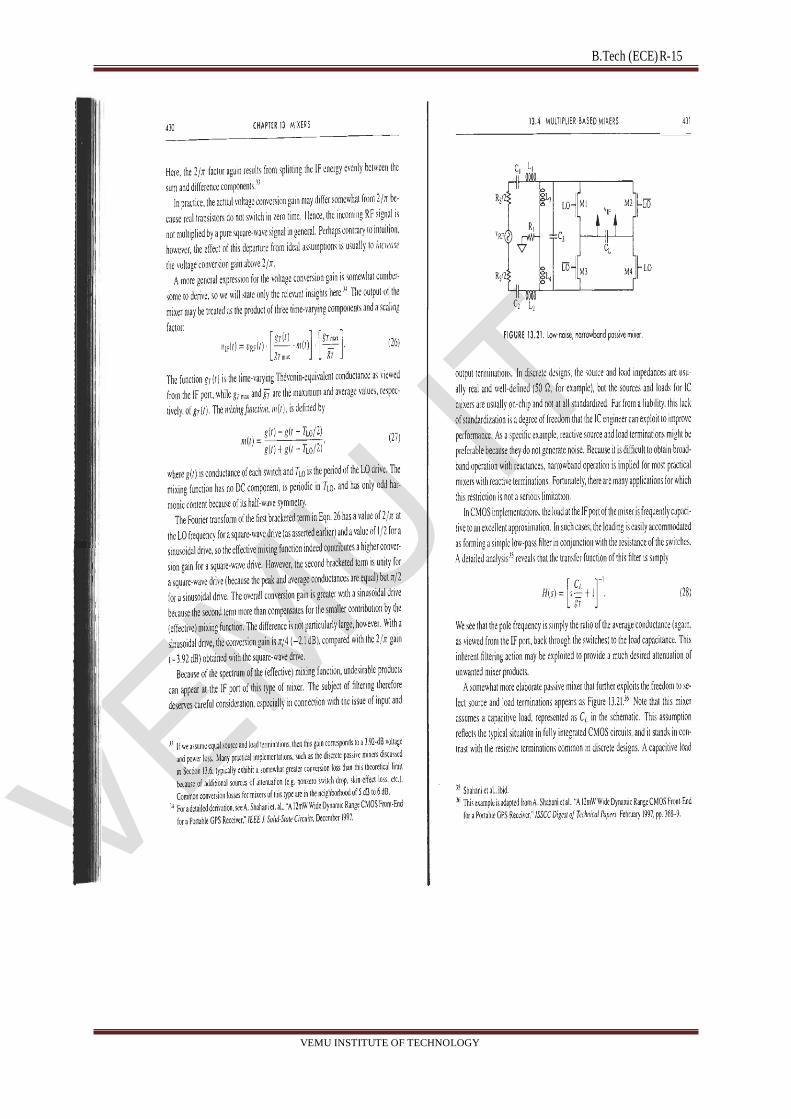
B.Tech (ECE) R-15
VEMU INSTITUTE OF TECHNOLOGY

B.Tech (ECE) R-15
VEMU INSTITUTE OF TECHNOLOGY

B.Tech (ECE) R-15
VEMU INSTITUTE OF TECHNOLOGY
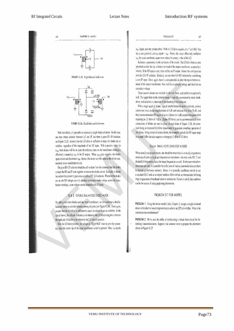
RF Integrated Circuits Lecture Notes Introduction RF systems
VEMU INSTITUTE OF TECHNOLOGY
Page 73

RF Integrated Circuits Lecture Notes Introduction RF systems
VEMU INSTITUTE OF TECHNOLOGY
Page 74
UNIT-4
RF POWER AMPLIFIERS
RF Power Amplifiers, Class A, AB, B, C amplifiers, Class D, E, F amplifiers, RF Power amplifier
design examples, Voltage controlled oscillators, Resonators, Negative resistance oscillators, Phase
locked loops, Linear zed PLL models, Phase detectors, charge pumps, Loop filters, and PLL design
examples
Power Amplifiers:-
An audio power amplifier (or power amp) is an electronic amplifier that amplifies low-
power electronic audio signals (signals composed primarily of frequencies between 20 - 20 000 Hz,
the human range of hearing) to a level that is strong enough for driving loudspeakers and making
the signal–whether it is recorded music.
Types:-
Class-A, B, C, AB, D, E, F Power amplifiers.
E Amplifiers:-
The class-E/F amplifier is a highly efficient switching power amplifier, typically used at
such high frequencies that the switching time becomes comparable to the duty time. As said in the
class-D amplifier, the transistor is connected via a serial LC circuit to the load, and connected via a
large L (inductor) to the supply voltage. The supply voltage is connected to ground via a large
capacitor to prevent any RF signals leaking into the supply. The class-E amplifier adds a C
(capacitor) between the transistor and ground and uses a defined L1 to connect to the supply
voltage.
F Amplifiers:-For a Class F power amplifier where the active device is biased under Class B
conditions (with conduction angle equal to p), the one-half sine-wave current waveform contains
only even harmonics.
Voltage Controlled Oscillator (VCO):-
A voltage-controlled oscillator or VCO is an electronic oscillator whose oscillation
frequency is controlled by a voltage input. The applied input voltage determines the instantaneous
oscillation frequency.
Voltage Controlled Oscillator (VCO) A VCO is a voltage controlled oscillator, whose output
frequency ωo is linearly proportional to the control voltage VC generated by the PD.
Resonators:-
1) Crystal Resonators 2) Ceramic Resonators 3) Dielectric Resonators

RF Integrated Circuits Lecture Notes Introduction RF systems
VEMU INSTITUTE OF TECHNOLOGY
Page 75
Quartz Crystal Resonator:-
Quartz crystals can be used as high-quality electromechanical resonators. Their piezoelectric
properties allow them to be used as frequency-control elements in crystal oscillators. Quartz crystals
offer high Q and superior frequency stability. In fact, their high Q is the main reason why crystal
oscillators are often employed instead of LC oscillators.Piezoelectric materials have the capability
to convert mechanical energy into electrical energy and vice versa. When a mechanical stress is
applied, an electric charge is generated. This electric charge is proportional to the applied
mechanical stress. The same material becomes strained when an electric field is applied.
Negative Resistance Oscillator:-
These are dynatron and tunnel diode oscillators. Dynatron operates in the negative
resistance region of the characteristics of a tutored, which is coupled to an L-C tank circuit. Tunnel
diode oscillator makes use of a tunnel diode for producing oscillations.
PLL (Phase-Locked Loop):-
It is basically a flip flop consisting of a phase detector, a low pass filter (LPF), and a Voltage
Controlled Oscillator (VCO). The input signal Vi with an input frequency fi is passed through a
phase detector. The DC level is then passed on to a VCO.
Phase Detectors:-
A phase detector or phase comparator is a frequency mixer, analog multiplier or logic
circuit that generates a voltage signal which represents the difference in phasebetween two signal
inputs. It is an essential element of thephase-locked loop (PLL).
Loop Filters:-
Loop Filter (LF) The filtering operation of the error voltage (coming out from the PD) is
performed by the loop filter (LF). The output of PD consists of a dc component superimposed with
an ac component.
The sum frequency is also produced and this will fall at a point equal to twice the frequency
of the reference. If this signal is not attenuated it will reach the control voltage input to the VCO
and give rise to spurious signals.
Charge Pumps:-
A charge pump is a kind of DC to DC converter that uses capacitors as energy-storage
elements to create either a higher- or lower-voltage power source.

RF Integrated Circuits Lecture Notes Introduction RF systems
VEMU INSTITUTE OF TECHNOLOGY
Page 76
Block diagram of loop filter with PLL:-
The inclusion of a loop filter at the output of the charge pump serves two functions.
UNIT-5
FREQUENCY SYNTHESIS AND OSCILLATORS
Frequency synthesis and oscillators, Frequency division, integer-N synthesis, Fractional frequency,
synthesis, Phase noise, General considerations, and Circuit examples, Radio architectures, GSM
radio architectures, CDMA, UMTS radio architectures.
Frequency Divider:-
The IDT clock buffer (fan-out buffer), clock divider and clock multiplexer portfolio includes
devices with up to 27 outputs. Differential outputs such as LVPECL, LVDS, HCSL, CML, HSTL,
as well as selectable outputs, are supported for output frequencies up to 3.2 GHz and single-ended
LVCMOS outputs for frequencies up to 350 MHz. Some buffers are available with mixed output
signaling.
Applications of PLL’s:-
The PLL is a very versatile building block and is suitable for a variety of applications
including:
1.) Demodulation and modulation
2.) Signal Conditioning
3.) Frequency synthesis
4.) Clock and data recovery
5.) Frequency translation
Fractional-N PLL
An unavoidable occurrence in digital PLL synthesis is that frequency multiplication (by N),
raises the signal’s phase noise by 20Log(N) dB. The main source of this noise is the noise
characteristics of the phase detector’s active circuitry. Because the phase detectors are typically the
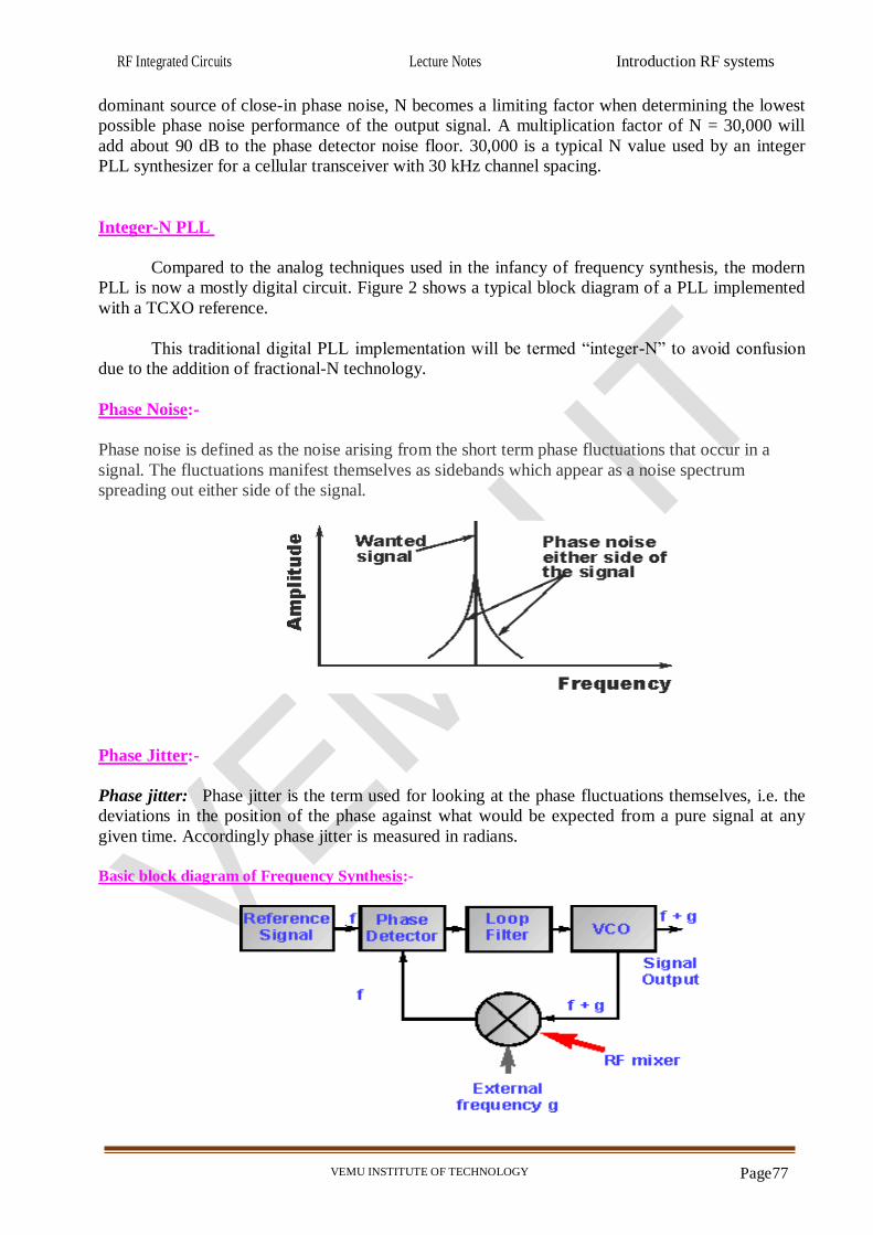
RF Integrated Circuits Lecture Notes Introduction RF systems
VEMU INSTITUTE OF TECHNOLOGY
Page 77
dominant source of close-in phase noise, N becomes a limiting factor when determining the lowest
possible phase noise performance of the output signal. A multiplication factor of N = 30,000 will
add about 90 dB to the phase detector noise floor. 30,000 is a typical N value used by an integer
PLL synthesizer for a cellular transceiver with 30 kHz channel spacing.
Integer-N PLL
Compared to the analog techniques used in the infancy of frequency synthesis, the modern
PLL is now a mostly digital circuit. Figure 2 shows a typical block diagram of a PLL implemented
with a TCXO reference.
This traditional digital PLL implementation will be termed “integer-N” to avoid confusion
due to the addition of fractional-N technology.
Phase Noise:-
Phase noise is defined as the noise arising from the short term phase fluctuations that occur in a
signal. The fluctuations manifest themselves as sidebands which appear as a noise spectrum
spreading out either side of the signal.
Phase Jitter:-
Phase jitter: Phase jitter is the term used for looking at the phase fluctuations themselves, i.e. the
deviations in the position of the phase against what would be expected from a pure signal at any
given time. Accordingly phase jitter is measured in radians.
Basic block diagram of Frequency Synthesis:-

RF Integrated Circuits Lecture Notes Introduction RF systems
VEMU INSTITUTE OF TECHNOLOGY
Page 78
Where:
Neff = overall division ratio
A = number of cycles divided by N
B = number of VCO cycles divided by N+1
Radio Architecture:-
The Architecture of Radio is data visualization, based on global open datasets of cell
tower, Wi-Fi and satellite locations. The dataset includes almost 7 million cell towers, 19 million
Wi-Fi routers and hundreds of satellites. The Architecture of Radio is data visualization, based on
global open datasets of cell tower, Wi-Fi and satellite locations. Based on your GPS location the
app shows a 360 degree visualization of signals around you.
GSM(Global System for Mobile):-
1. If you are in Europe or Asia and using a mobile phone, then most probably you are using
GSM technology in your mobile phone.
2. GSM stands for Global System for Mobile Communication. It is a digital cellular
technology used for transmitting mobile voice and data services.
3. The concept of GSM emerged from a cell-based mobile radio system at Bell Laboratories in
the early 1970s.
Applications of GSM:-
Listed below are the features of GSM that account for its popularity and wide acceptance.
1) Improved spectrum efficiency
2) International roaming
3) Low-cost mobile sets and base stations (BSs)
4) High-quality speech.
CDMA (Code-Division Multiple Accesses):-
CDMA (Code-Division Multiple Access) refers to any of several protocols used in second-
generation (2G) and third-generation (3G) wireless communications. As the term implies, CDMA is
a form of multiplexing, which allows numerous signals to occupy a single transmission channel,
optimizing the use of available bandwidth. The technology is used in ultra-high-frequency (UHF)
cellular telephone systems in the 800-MHz and 1.9-GHz bands.

RF Integrated Circuits Lecture Notes Introduction RF systems
VEMU INSTITUTE OF TECHNOLOGY
Page 79
CDMA employs analog-to-digital conversion (ADC) in combination with spread spectrum
technology.
The CDMA channel is nominally 1.23 MHz wide. CDMA networks use a scheme called
soft handoff, which minimizes signal breakup as a handset passes from one cell to another. The
combination of digital and spread-spectrum modes supports several times as many signals per unit
bandwidth as analog modes. CDMA is compatible with other cellular technologies; this allows for
nationwide roaming.
UMTS:-
The UMTS 3G architecture is required to provide a greater level of performance to that of
the original GSM network. However as many networks had migrated through the use of GPRS and
EDGE, they already had the ability to carry data. Accordingly many of the elements required for the
WCDMA / UMTS network architecture were seen as a migration.
UMTS network architecture:-
The UMTS network architecture can be divided into three main elements:
1. User Equipment (UE): The User Equipment or UE is the name given to what was previous
termed the mobile, or cellphone. The new name was chosen because the considerably
greater functionality that the UE could have. It could also be anything between a mobile
phone used for talking to a data terminal attached to a computer with no voice capability.
2. Radio Network Subsystem (RNS): The RNS also known as the UMTS Radio Access
Network, UTRAN, is the equivalent of the previous Base Station Subsystem or BSS in
GSM.
3. Core Network: The core network provides all the central processing and management for
the system. It is the equivalent of the GSM Network Switching Subsystem or NSS.
The core network is then the overall entity that interfaces to external networks including the public
phone network and other cellular telecommunications networks.