SEMICONDUCTOR INTEGRATED CIRCUITS: An undersampling 14-bit cyclic ADC with over 100dB SFDR
6
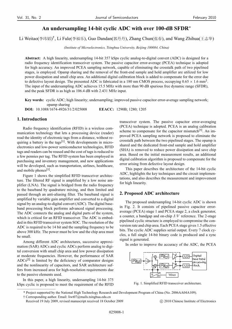
Vol. 31, No. 2 Journal of Semiconductors February 2010 An undersampling 14-bit cyclic ADC with over 100-dB SFDR Li Weitao(李玮韬) , Li Fule(李福乐), Guo Dandan(郭丹丹), Zhang Chun(张春), and Wang Zhihua(王志华) (Institute of Microelectronics, Tsinghua University, Beijing 100084, China) Abstract: A high linearity, undersampling 14-bit 357 kSps cyclic analog-to-digital convert (ADC) is designed for a radio frequency identification transceiver system. The passive capacitor error-average (PCEA) technique is adopted for high accuracy. An improved PCEA sampling network, capable of eliminating the crosstalk path of two pipelined stages, is employed. Opamp sharing and the removal of the front-end sample and hold amplifier are utilized for low power dissipation and small chip area. An additional digital calibration block is added to compensate for the error due to defective layout design. The presented ADC is fabricated in a 180 nm CMOS process, occupying 0.65 1.6 mm 2 . The input of the undersampling ADC achieves 15.5 MHz with more than 90 dB spurious free dynamic range (SFDR), and the peak SFDR is as high as 106.4 dB with 2.431 MHz input. Key words: cyclic ADC; high linearity; undersampling; improved passive capacitor error-average sampling network; opamp sharing DOI: 10.1088/1674-4926/31/2/025008 EEACC: 1290B; 1280; 1205 1. Introduction Radio frequency identification (RFID) is a wireless com- munication technology that lets a processing device (reader) read the identity of electronic tags from a distance, without re- quiring a battery in the tags Œ1 . With developments in micro- electronics and low-power semiconductor technologies, RFID tags and readers can be reused and the cost of tags is reduced to a few pennies per tag. The RFID system has been employed in purchasing and inventory management, and new applications will be developed, such as transportation, airlines, healthcare, and mobile phones Œ1 . Figure 1 shows the simplified RFID transceiver architec- ture. The filtered RF signal is amplified by a low noise am- plifier (LNA). The signal is bridged from the radio frequency to the baseband by quadrature mixing, and then limited and passed through an anti-aliasing filter. The baseband signal is amplified by variable gain amplifier and converted to a digital signal by an analog-to-digital convert (ADC). The digital base- band processing block performs advanced signal processing. The ADC connects the analog and digital parts of the system, which is critical for an RFID transceiver. The ADC is embed- ded in this RFID transceiver system SOC. The resolution of the ADC is required to be 14 bit and the sampling frequency to be above 300 kHz. The power must be low and the chip area must be small. Among different ADC architectures, successive approxi- mation (SAR) ADCs and cyclic ADCs perform analog to digi- tal conversion with small chip area and low power dissipation at moderate frequencies. However, the performance of SAR ADCs Œ2 is limited by the deficiency of comparator designs and the nonlinearity of capacitors, and SAR architecture suf- fers from increased area for high-resolution requirements due to the passive elements used. In this paper, a high linearity, undersampling 14-bit 375 kSps cyclic is proposed to meet the requirement of the RFID transceiver system. The passive capacitor error-averaging (PCEA) technique is adopted. PCEA is an analog calibration scheme to compensate for the capacitor mismatch Œ3 . An im- proved PCEA sampling network is proposed to eliminate the crosstalk path between the two pipelined stages. The opamp is shared and the dedicated front-end sample and hold amplifier (SHA) is removed to reduce power dissipation and save chip area. Based on the initial measurement results, an additional digital calibration algorithm is proposed to compensate for the error arising from defective layout design. This paper describes the architecture of the 14-bit cyclic ADC, highlights the key techniques and the circuit implemen- tations, and also describes the measurement and improvement for high linearity. 2. Proposed ADC architecture The proposed undersampling 14-bit cyclic ADC is shown in Fig. 2. It consists of pipelined passive capacitor error- average (PCEA) stage 1 and PCEA stage 2, a clock generator, a counter, a bandgap and on-chip I /V reference. The 2-stage pipelined cyclic structure is employed to compromise the con- version rate and chip area. Each PCEA stage gives 1.5 effective bits. The cyclic ADC supplies serial output. Every 7 clock cy- cles, a full single 14-bit binary code is produced and a sync signal is generated. In order to improve the accuracy of the ADC, the PCEA Fig. 1. Simplified RFID transceiver architecture. * Project supported by the National High Technology Research and Development Program of China (No. 2006AA04A109). Corresponding author. Email: [email protected] Received 19 July 2009, revised manuscript received 18 October 2009 c 2010 Chinese Institute of Electronics 025008-1
-
Upload
independent -
Category
Documents
-
view
1 -
download
0
Transcript of SEMICONDUCTOR INTEGRATED CIRCUITS: An undersampling 14-bit cyclic ADC with over 100dB SFDR
Vol. 31, No. 2 Journal of Semiconductors February 2010
An undersampling 14-bit cyclic ADC with over 100-dB SFDR�
Li Weitao(李玮韬)�, Li Fule(李福乐), Guo Dandan(郭丹丹), Zhang Chun(张春), and Wang Zhihua(王志华)
(Institute of Microelectronics, Tsinghua University, Beijing 100084, China)
Abstract: A high linearity, undersampling 14-bit 357 kSps cyclic analog-to-digital convert (ADC) is designed for aradio frequency identification transceiver system. The passive capacitor error-average (PCEA) technique is adoptedfor high accuracy. An improved PCEA sampling network, capable of eliminating the crosstalk path of two pipelinedstages, is employed. Opamp sharing and the removal of the front-end sample and hold amplifier are utilized for lowpower dissipation and small chip area. An additional digital calibration block is added to compensate for the error dueto defective layout design. The presented ADC is fabricated in a 180 nm CMOS process, occupying 0.65 � 1.6 mm2.The input of the undersampling ADC achieves 15.5 MHz with more than 90 dB spurious free dynamic range (SFDR),and the peak SFDR is as high as 106.4 dB with 2.431 MHz input.
Key words: cyclic ADC; high linearity; undersampling; improved passive capacitor error-average sampling network;opamp sharing
DOI: 10.1088/1674-4926/31/2/025008 EEACC: 1290B; 1280; 1205
1. Introduction
Radio frequency identification (RFID) is a wireless com-munication technology that lets a processing device (reader)read the identity of electronic tags from a distance, without re-quiring a battery in the tagsŒ1�. With developments in micro-electronics and low-power semiconductor technologies, RFIDtags and readers can be reused and the cost of tags is reduced toa few pennies per tag. The RFID system has been employed inpurchasing and inventory management, and new applicationswill be developed, such as transportation, airlines, healthcare,and mobile phonesŒ1�.
Figure 1 shows the simplified RFID transceiver architec-ture. The filtered RF signal is amplified by a low noise am-plifier (LNA). The signal is bridged from the radio frequencyto the baseband by quadrature mixing, and then limited andpassed through an anti-aliasing filter. The baseband signal isamplified by variable gain amplifier and converted to a digitalsignal by an analog-to-digital convert (ADC). The digital base-band processing block performs advanced signal processing.The ADC connects the analog and digital parts of the system,which is critical for an RFID transceiver. The ADC is embed-ded in this RFID transceiver system SOC. The resolution of theADC is required to be 14 bit and the sampling frequency to beabove 300 kHz. The power must be low and the chip area mustbe small.
Among different ADC architectures, successive approxi-mation (SAR) ADCs and cyclic ADCs perform analog to digi-tal conversion with small chip area and low power dissipationat moderate frequencies. However, the performance of SARADCsŒ2� is limited by the deficiency of comparator designsand the nonlinearity of capacitors, and SAR architecture suf-fers from increased area for high-resolution requirements dueto the passive elements used.
In this paper, a high linearity, undersampling 14-bit 375kSps cyclic is proposed to meet the requirement of the RFID
transceiver system. The passive capacitor error-averaging(PCEA) technique is adopted. PCEA is an analog calibrationscheme to compensate for the capacitor mismatchŒ3�. An im-proved PCEA sampling network is proposed to eliminate thecrosstalk path between the two pipelined stages. The opamp isshared and the dedicated front-end sample and hold amplifier(SHA) is removed to reduce power dissipation and save chiparea. Based on the initial measurement results, an additionaldigital calibration algorithm is proposed to compensate for theerror arising from defective layout design.
This paper describes the architecture of the 14-bit cyclicADC, highlights the key techniques and the circuit implemen-tations, and also describes the measurement and improvementfor high linearity.
2. Proposed ADC architecture
The proposed undersampling 14-bit cyclic ADC is shownin Fig. 2. It consists of pipelined passive capacitor error-average (PCEA) stage 1 and PCEA stage 2, a clock generator,a counter, a bandgap and on-chip I /V reference. The 2-stagepipelined cyclic structure is employed to compromise the con-version rate and chip area. Each PCEA stage gives 1.5 effectivebits. The cyclic ADC supplies serial output. Every 7 clock cy-cles, a full single 14-bit binary code is produced and a syncsignal is generated.
In order to improve the accuracy of the ADC, the PCEA
Fig. 1. Simplified RFID transceiver architecture.
* Project supported by the National High Technology Research and Development Program of China (No. 2006AA04A109).� Corresponding author. Email: [email protected] 19 July 2009, revised manuscript received 18 October 2009 c 2010 Chinese Institute of Electronics
025008-1
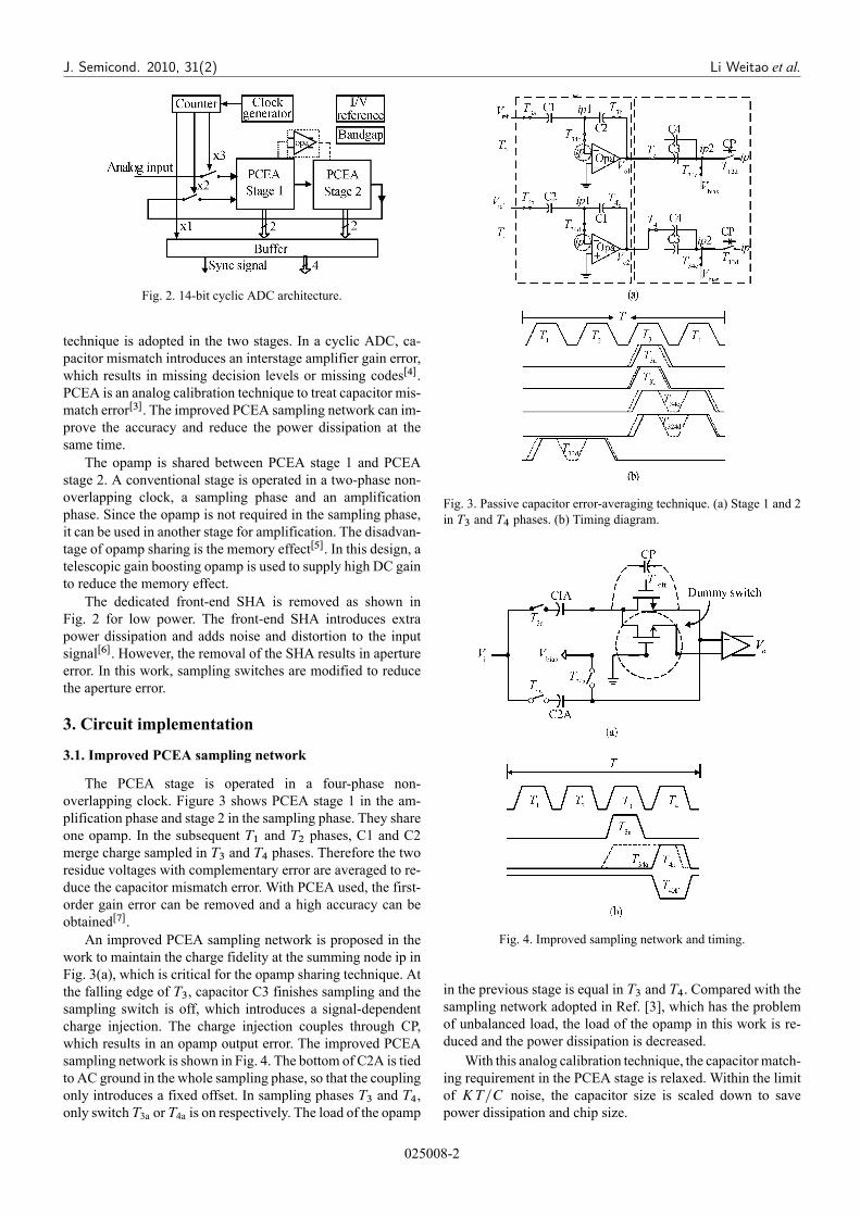
J. Semicond. 2010, 31(2) Li Weitao et al.
Fig. 2. 14-bit cyclic ADC architecture.
technique is adopted in the two stages. In a cyclic ADC, ca-pacitor mismatch introduces an interstage amplifier gain error,which results in missing decision levels or missing codesŒ4�.PCEA is an analog calibration technique to treat capacitor mis-match errorŒ3�. The improved PCEA sampling network can im-prove the accuracy and reduce the power dissipation at thesame time.
The opamp is shared between PCEA stage 1 and PCEAstage 2. A conventional stage is operated in a two-phase non-overlapping clock, a sampling phase and an amplificationphase. Since the opamp is not required in the sampling phase,it can be used in another stage for amplification. The disadvan-tage of opamp sharing is the memory effectŒ5�. In this design, atelescopic gain boosting opamp is used to supply high DC gainto reduce the memory effect.
The dedicated front-end SHA is removed as shown inFig. 2 for low power. The front-end SHA introduces extrapower dissipation and adds noise and distortion to the inputsignalŒ6�. However, the removal of the SHA results in apertureerror. In this work, sampling switches are modified to reducethe aperture error.
3. Circuit implementation
3.1. Improved PCEA sampling network
The PCEA stage is operated in a four-phase non-overlapping clock. Figure 3 shows PCEA stage 1 in the am-plification phase and stage 2 in the sampling phase. They shareone opamp. In the subsequent T1 and T2 phases, C1 and C2merge charge sampled in T3 and T4 phases. Therefore the tworesidue voltages with complementary error are averaged to re-duce the capacitor mismatch error. With PCEA used, the first-order gain error can be removed and a high accuracy can beobtainedŒ7�.
An improved PCEA sampling network is proposed in thework to maintain the charge fidelity at the summing node ip inFig. 3(a), which is critical for the opamp sharing technique. Atthe falling edge of T3, capacitor C3 finishes sampling and thesampling switch is off, which introduces a signal-dependentcharge injection. The charge injection couples through CP,which results in an opamp output error. The improved PCEAsampling network is shown in Fig. 4. The bottom of C2A is tiedto AC ground in the whole sampling phase, so that the couplingonly introduces a fixed offset. In sampling phases T3 and T4,only switch T3a or T4a is on respectively. The load of the opamp
Fig. 3. Passive capacitor error-averaging technique. (a) Stage 1 and 2in T3 and T4 phases. (b) Timing diagram.
Fig. 4. Improved sampling network and timing.
in the previous stage is equal in T3 and T4. Compared with thesampling network adopted in Ref. [3], which has the problemof unbalanced load, the load of the opamp in this work is re-duced and the power dissipation is decreased.
With this analog calibration technique, the capacitormatch-ing requirement in the PCEA stage is relaxed. Within the limitof KT=C noise, the capacitor size is scaled down to savepower dissipation and chip size.
025008-2

J. Semicond. 2010, 31(2) Li Weitao et al.
Fig. 5. Schematic of opamp.
Fig. 6. Die micrograph.
3.2. Opamp
For a high accuracy and low power cyclic ADC, high DCgain and a low power dissipation opamp is required. Comparedwith a folded cascode opamp, a telescopic cascode opamp canprovide higher speed with lower power dissipation. The tele-scopic cascode opamp shown in Fig. 5 is employed in this de-sign. The length of the input NMOS devices is designed to bevery small, such that the parasitic capacitor is decreased andthe speed of the opamp is improved. Gain-boosting stages areadded to satisfy the gain requirements of a 14-bit ADC. Theopamp achieves a DC gain of 106 dB, and the output differen-tial swing range is 3.08 V. The high DC gain and small par-asitic capacitance of the input node reduce the memory effectintroduced by opamp sharing.
4. Measurement and improvement
The 14-bit undersampling cyclic 357 kSPs ADC is fabri-cated in 180 nm CMOS mixed-signal technology. It occupiesa die area of 0:65 � 1:6 mm2, which includes PCEA stage 1,stage 2, bandgap, clock generator, counter and on-chip I /V ref-erences. The die micrograph is shown in Fig. 6. The measure-ments are performed with a 3 V supply at room temperature(27 ıC), including static performance and FFT measurement.A 2.431 MHz full-scale sinusoidal signal is selected to mea-sure the static performance. The measured integral nonlinear-ity (INL) errors and differential nonlinearity (DNL) errors areshown in Fig. 7, and they are less than 0.2 LSB and 2 LSBrespectively. With �0:0864 dBFS 2.431 MHz, 5.03 MHz and15.59 MHz input signal, the measured FFT plots are shown inFigs. 11(a), 12(a) and 13(a), respectively.
Fig. 7. Measured DNL and INL.
Fig. 8. Ideal transfer curve of the 1.5-b stage (�V D 0, Vref D 1).
Fig. 9. Simulated INL with different error terms.
As shown in Fig. 7, the measured INL errors are nonlin-ear and there is a jump at the codes around 10000. Based onthe transfer curve of the 1.5-b stage in Fig. 8, the jump in themeasured INL occurs where the reference voltage of the firstPCEA stage changes from 0 to �Vref, which supplies impor-tant calibration information. Due to defective layout design,an inaccurate residue calculation exists in the first stage of thecyclic ADC. The error is independent of the input signal andis only introduced when the reference voltage is �Vref, whichis also verified by the simulation results in Fig. 9. Error term�V is added to the residue voltage described by the formula inFig. 8. As an example, �V is set to 0, 0.0003 and 0.0005 forthe simulation, respectively. With the error term �V added,the simulated INL errors in Fig. 9 are similar to the measured
025008-3
J. Semicond. 2010, 31(2) Li Weitao et al.
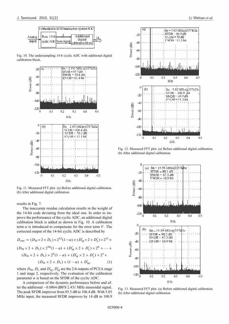
Fig. 10. The undersampling 14-b cyclic ADC with additional digitalcalibration block.
Fig. 11. Measured FFT plot. (a) Before additional digital calibration.(b) After additional digital calibration.
results in Fig. 7.The inaccurate residue calculation results in the weight of
the 14-bit code deviating from the ideal one. In order to im-prove the performance of the cyclic ADC, an additional digitalcalibration block is added as shown in Fig. 10. A calibrationterm ˛ is introduced to compensate for the error term V . Thecorrected output of the 14-bit cyclic ADC is described by
Doutc D .DM�2CDL/�212.1�˛/C.D0M�2CD0
L/�211C
.DM � 2 C DL/ � 210.1 � ˛/ C .D0M � 2 C D0
L/ � 29C � � � C
.DM � 2 C DL/ � 22.1 � ˛/ C .D0M � 2 C D0
L/ � 21C
.DM � 2 C DL/ � .1 � ˛/ C D0M; .1/
whereDM,DL andD0M,D0
M are the 2-b outputs of PCEA stage1 and stage 2, respectively. The evaluation of the calibrationparameter ˛ is based on the SFDR of the cyclic ADC.
A comparison of the dynamic performance before and af-ter the additional �0:0864 dBFS 2.431 MHz sinusoidal signal.The peak SFDR improves from 85.5 dB to 106.4 dB.With 5.03MHz input, the measured SFDR improves by 14 dB to 100.9
Fig. 12. Measured FFT plot. (a) Before additional digital calibration.(b) After additional digital calibration.
Fig. 13. Measured FFT plot. (a) Before additional digital calibration.(b) After additional digital calibration.
025008-4
J. Semicond. 2010, 31(2) Li Weitao et al.
Table 1. Performance summary.Parameter ValueTechnology 180 nm CMOSResolution 14 bitConversion rate 357 kSpsSupply voltage 3 VInput range 2 VDNL, INL 0.2 LSB, 2 LSBSNDR 70.1 dB @ fin D 2:431 MHz 69.5 dB @ fin D 5:03 MHzSFDR 67.1 dB @ fin D 15:59 MHz 85.5 dB @ fin D 2:431 MHz 86.9 dB @ fin D 5:03 MHz
88.1 dB @ fin D 15:59 MHz 106.4 dB (after calibration) @ fin D 2:431 MHz 100.9 dB(after calibration) @ fin D 5:03 MHz 90.2 dB (after calibration) @ fin D 15:59 MHz
Power consumption 4.2 mWFOM 4.3 pJ/stepArea (ADC core) 0:65 � 1:6 mm2
Table 2. Comparison with some previous work.Parameter Ref. [2] Ref. [8] Ref. [9] Ref. [10] This workResolution (bit) 10 12 12 10 14Sampling rate (MSps) > 1 0.143 2 2.3 0.357SNDR/SFDR (dB) 56/NA NA/NA 70.9/81.7 NA/74.95 70.1/106.4
@ fin D 100 kHz @ fin D 100 kHz @ fin D 2:431 MHzPower (mW) < 100 3.94 3.6 NA 4.2
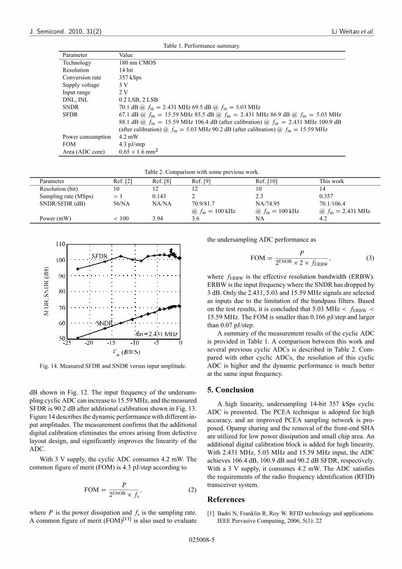
Fig. 14. Measured SFDR and SNDR versus input amplitude.
dB shown in Fig. 12. The input frequency of the undersam-pling cyclic ADC can increase to 15.59MHz, and themeasuredSFDR is 90.2 dB after additional calibration shown in Fig. 13.Figure 14 describes the dynamic performance with different in-put amplitudes. The measurement confirms that the additionaldigital calibration eliminates the errors arising from defectivelayout design, and significantly improves the linearity of theADC.
With 3 V supply, the cyclic ADC consumes 4.2 mW. Thecommon figure of merit (FOM) is 4.3 pJ/step according to
FOM DP
2ENOB � fs; .2/
where P is the power dissipation and fs is the sampling rate.A common figure of merit (FOM)Œ11� is also used to evaluate
the undersampling ADC performance as
FOM DP
2ENOB � 2 � fERBW; .3/
where fERBW is the effective resolution bandwidth (ERBW).ERBW is the input frequency where the SNDR has dropped by3 dB. Only the 2.431, 5.03 and 15.59 MHz signals are selectedas inputs due to the limitation of the bandpass filters. Basedon the test results, it is concluded that 5.03 MHz < fERBW <
15.59 MHz. The FOM is smaller than 0.166 pJ/step and largerthan 0.07 pJ/step.
A summary of the measurement results of the cyclic ADCis provided in Table 1. A comparison between this work andseveral previous cyclic ADCs is described in Table 2. Com-pared with other cyclic ADCs, the resolution of this cyclicADC is higher and the dynamic performance is much betterat the same input frequency.
5. Conclusion
A high linearity, undersampling 14-bit 357 kSps cyclicADC is presented. The PCEA technique is adopted for highaccuracy, and an improved PCEA sampling network is pro-posed. Opamp sharing and the removal of the front-end SHAare utilized for low power dissipation and small chip area. Anadditional digital calibration block is added for high linearity.With 2.431 MHz, 5.03 MHz and 15.59 MHz input, the ADCachieves 106.4 dB, 100.9 dB and 90.2 dB SFDR, respectively.With a 3 V supply, it consumes 4.2 mW. The ADC satisfiesthe requirements of the radio frequency identification (RFID)transceiver system.
References[1] Badri N, Franklin R, Roy W. RFID technology and applications.
IEEE Pervasive Computing, 2006, 5(1): 22
025008-5
J. Semicond. 2010, 31(2) Li Weitao et al.
[2] Wang D Y, Chou H P. A two-stage pipelined cyclic ADC forX/Gamma spectroscopy. IEEENuclear Science SymposiumCon-ference Record, 2003, 2: 1238
[3] Chiu Y, Gray P R, Nikolic B. A 14-b 12-MS/s CMOS pipelineADCwith over 100-dB SFDR. IEEE J Solid-State Circuits, 2004,39: 2139
[4] Li Fule, Duan Jingbo, Wang Zhihua. A high linearity, 13bitpipelined CMOS ADC. Journal of Semiconductors, 2008, 29(3):497
[5] Lee B G, Min B M, Manganaro G, et al. A 14-b 100-MS/spipelined ADC with a merged SHA and first MDAC. IEEE JSolid-State Circuits, 2008, 43: 2613
[6] Jeon Y D, Lee S C, Kim K D, et al. A 4.7 mW 0.32 mm2 10 b 30MS/s pipelined ADC without a front-end S/H in 90 nm CMOS.Digest of Technical Papers of IEEE International Solid-State Cir-cuits Conference, 2007: 456
[7] GuoDandan, Li Fule, Duan Jingbo, et al. A 13-bit CMOS pipeline
analog-to-digital converter with improved sampling circuits. In-ternational Conference on Communications, Circuits and Sys-tems, 2008: 1048
[8] Manen S, Royer L, Gay P. A custom 12-bit cyclic ADC forthe electromagnetic calorimeter of the international linear col-lider. Nuclear Science Symposium, Medical Imaging Conferenceand 16th Room Temperature Semiconductor Detector Workshop,2008
[9] Kim Y J, Choi H C, Yoo P S, et al. A low offset rail-to-rail 12 b 2MS/s 0.18�mCMOS cyclic ADC. IEEEAsia Pacific Conferenceon Circuits and Systems, 2008: 17
[10] Soufi B, Malik S Q, Geiger R L. A capacitor sharing techniquefor RSD cyclic ADC. 48th Midwest Symposium on Circuits andSystems, 2005, 1: 859
[11] Geelen G. A 6 b 1.1 GSample/s CMOS A/D converter. Digest ofTechnical Papers of IEEE International Solid-State Circuits Con-ference, 2001: 128
025008-6