RF & Microwave Circuits for Wireless Communications
41
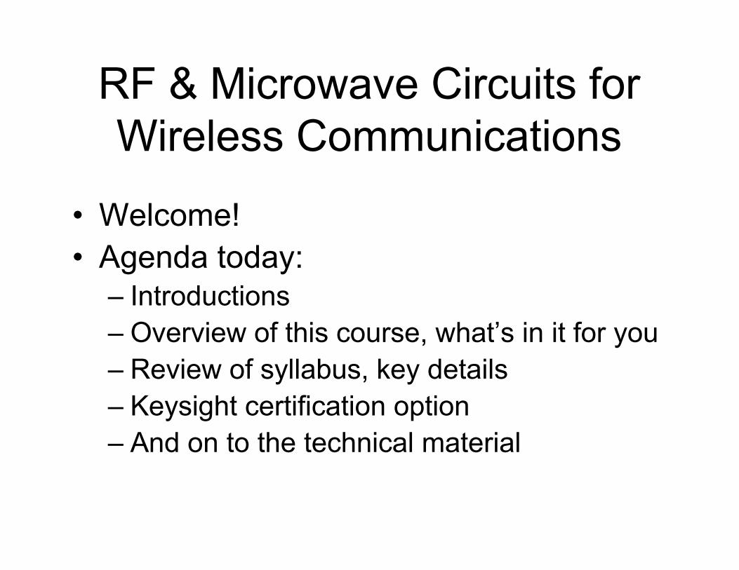
RF & Microwave Circuits for Wireless Communications • Welcome! • Agenda today: – Introductions – Overview of this course, what’s in it for you – Review of syllabus, key details – Keysight certification option – And on to the technical material
-
Upload
khangminh22 -
Category
Documents
-
view
3 -
download
0
Transcript of RF & Microwave Circuits for Wireless Communications
RF & Microwave Circuits for Wireless Communications
• Welcome! • Agenda today:
– Introductions– Overview of this course, what’s in it for you– Review of syllabus, key details– Keysight certification option– And on to the technical material

Introductions
• My contact details:[email protected], 631-5693Office: 261 Fitzpatrick Hall
• Email is the best way to reach me, or just drop by my office any time
Course Overview
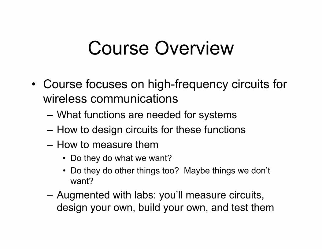
• Course focuses on high-frequency circuits for wireless communications– What functions are needed for systems– How to design circuits for these functions– How to measure them
• Do they do what we want?• Do they do other things too? Maybe things we don’t
want?– Augmented with labs: you’ll measure circuits,
design your own, build your own, and test them
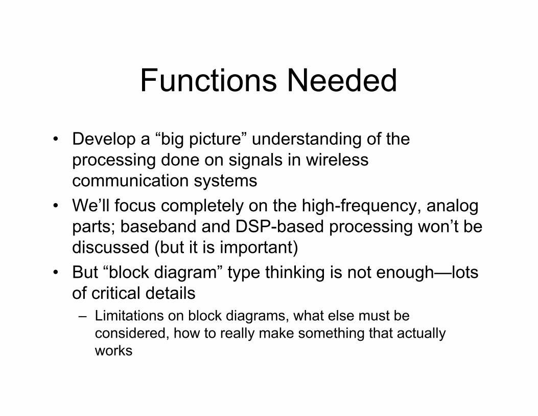
Functions Needed• Develop a “big picture” understanding of the
processing done on signals in wireless communication systems
• We’ll focus completely on the high-frequency, analog parts; baseband and DSP-based processing won’t be discussed (but it is important)
• But “block diagram” type thinking is not enough—lots of critical details– Limitations on block diagrams, what else must be
considered, how to really make something that actually works
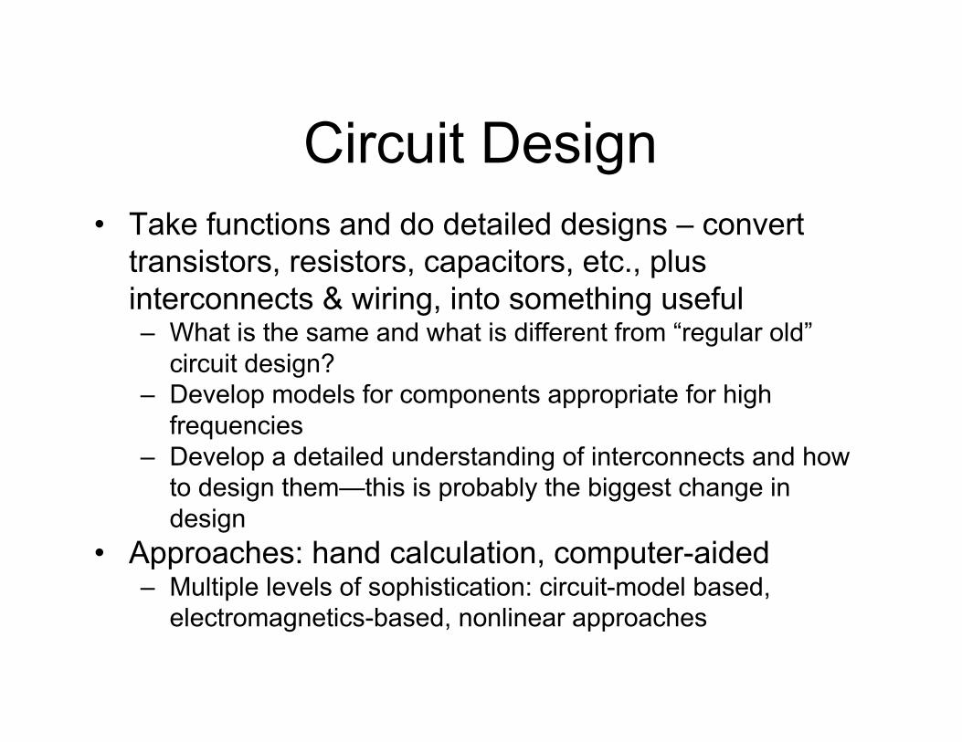
Circuit Design• Take functions and do detailed designs – convert
transistors, resistors, capacitors, etc., plus interconnects & wiring, into something useful– What is the same and what is different from “regular old”
circuit design?– Develop models for components appropriate for high
frequencies– Develop a detailed understanding of interconnects and how
to design them—this is probably the biggest change in design
• Approaches: hand calculation, computer-aided– Multiple levels of sophistication: circuit-model based,
electromagnetics-based, nonlinear approaches
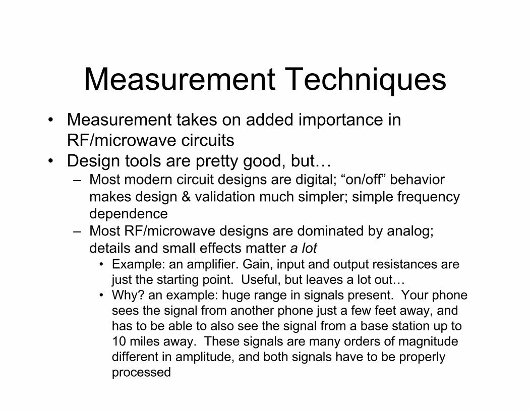
Measurement Techniques• Measurement takes on added importance in
RF/microwave circuits• Design tools are pretty good, but…
– Most modern circuit designs are digital; “on/off” behavior makes design & validation much simpler; simple frequency dependence
– Most RF/microwave designs are dominated by analog; details and small effects matter a lot
• Example: an amplifier. Gain, input and output resistances are just the starting point. Useful, but leaves a lot out…
• Why? an example: huge range in signals present. Your phone sees the signal from another phone just a few feet away, and has to be able to also see the signal from a base station up to 10 miles away. These signals are many orders of magnitude different in amplitude, and both signals have to be properly processed
Measurement Techniques (cont).– So we need measurement capabilities to capture
both “big picture” and nuances in circuit function– A complication: frequencies are high
• Circuit probing (e.g. oscilloscopes) don’t work well• Adding the probe changes the circuit (details matter…),
and changes the performance. Sometimes (usually) a lot• Need to accurately measure extremely high frequency
signals, often at very low amplitudes. – Result: different techniques
• Workhorse tools become vector network analyzer, spectrum analyzer; mostly work in frequency domain
• Often must analyze circuits “from the outside”—and infer from that what is going on inside
• Lab is well-equipped; you’ll get first-hand experience
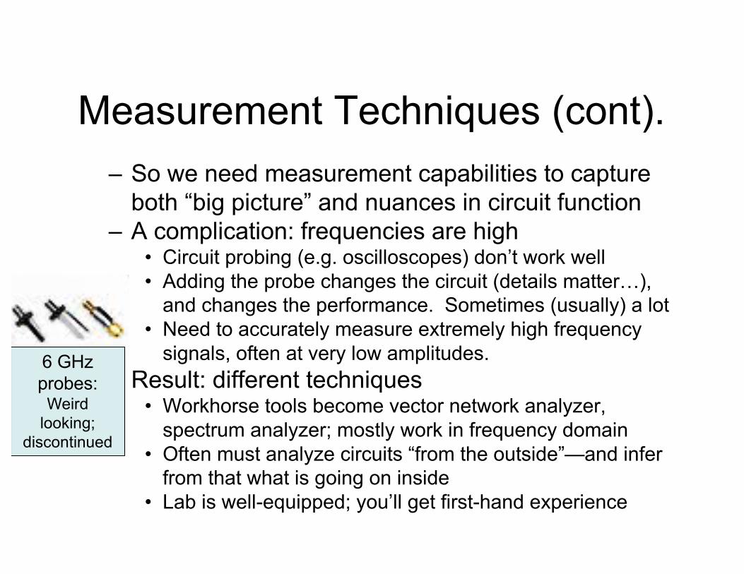
6 GHz probes:
Weird looking;
discontinued
Lab Component– The lab work cuts across these topics– Focus mostly on measurement techniques &
design; some circuit construction• Hands-on; work in small groups (usually 2)• Make sure you’re registered for both lecture and lab
(40458 and 41458)– The lab is your chance to get real hands-on
experience with RF/microwave test & measurement hardware, as well as industrial-strength CAD software
• About $300k worth of toys (not counting the software; a single license for that is $250k)—take advantage of it
Syllabus• Walk through a few key
parts—this course is not necessarily “normal”
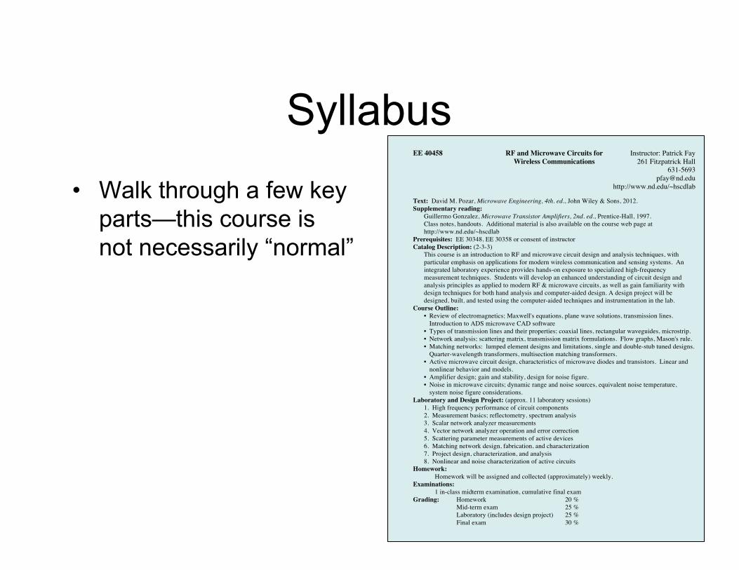
EE 40458 RF and Microwave Circuits for Instructor: Patrick Fay Wireless Communications 261 Fitzpatrick Hall 631-5693 [email protected] http://www.nd.edu/~hscdlab Text: David M. Pozar, Microwave Engineering, 4th. ed., John Wiley & Sons, 2012. Supplementary reading:
Guillermo Gonzalez, Microwave Transistor Amplifiers, 2nd. ed., Prentice-Hall, 1997. Class notes, handouts. Additional material is also available on the course web page at http://www.nd.edu/~hscdlab
Prerequisites: EE 30348, EE 30358 or consent of instructor Catalog Description: (2-3-3)
This course is an introduction to RF and microwave circuit design and analysis techniques, with particular emphasis on applications for modern wireless communication and sensing systems. An integrated laboratory experience provides hands-on exposure to specialized high-frequency measurement techniques. Students will develop an enhanced understanding of circuit design and analysis principles as applied to modern RF & microwave circuits, as well as gain familiarity with design techniques for both hand analysis and computer-aided design. A design project will be designed, built, and tested using the computer-aided techniques and instrumentation in the lab.
Course Outline: • Review of electromagnetics; Maxwell's equations, plane wave solutions, transmission lines.
Introduction to ADS microwave CAD software • Types of transmission lines and their properties; coaxial lines, rectangular waveguides, microstrip. • Network analysis; scattering matrix, transmission matrix formulations. Flow graphs, Mason's rule. • Matching networks: lumped element designs and limitations, single and double-stub tuned designs.
Quarter-wavelength transformers, multisection matching transformers. • Active microwave circuit design, characteristics of microwave diodes and transistors. Linear and
nonlinear behavior and models. • Amplifier design; gain and stability, design for noise figure. • Noise in microwave circuits; dynamic range and noise sources, equivalent noise temperature,
system noise figure considerations. Laboratory and Design Project: (approx. 11 laboratory sessions)
1. High frequency performance of circuit components 2. Measurement basics; reflectometry, spectrum analysis 3. Scalar network analyzer measurements 4. Vector network analyzer operation and error correction 5. Scattering parameter measurements of active devices 6. Matching network design, fabrication, and characterization 7. Project design, characterization, and analysis 8. Nonlinear and noise characterization of active circuits
Homework: Homework will be assigned and collected (approximately) weekly. Examinations: 1 in-class midterm examination, cumulative final exam Grading: Homework 20 % Mid-term exam 25 % Laboratory (includes design project) 25 % Final exam 30 %
Text BookKey point #1: becareful about text book editions.•We will use Pozar’s 4th edition, 2012•Older ones are organized differently, are missing material•International versions are not the same. Do not use them—we have found many sneaky changes•There are two versions of Pozar—a “thin” and “thick” version. Both are OK—only difference is portability•Gonzales’ book is an excellent resource, provides good alternative approaches if Pozar is unclear
EE 40458/60558 RF and Microwave Circuits for Instructor: Patrick Fay Wireless Communications 261 Fitzpatrick Hall 631-5693 [email protected] http://www.nd.edu/~hscdlab Text: David M. Pozar, Microwave Engineering, 4th. ed., John Wiley & Sons, 2012. Supplementary reading:
Guillermo Gonzalez, Microwave Transistor Amplifiers, 2nd. ed., Prentice-Hall, 1997. Class notes, handouts. Additional material is also available on the course web page at http://www.nd.edu/~hscdlab
Prerequisites: EE 30348, EE 30358 or consent of instructor Catalog Description: (2-3-3)
This course is an introduction to RF and microwave circuit design and analysis techniques, with particular emphasis on applications for modern wireless communication and sensing systems. An integrated laboratory experience provides hands-on exposure to specialized high-frequency measurement techniques. Students will develop an enhanced understanding of circuit design and analysis principles as applied to modern RF & microwave circuits, as well as gain familiarity with design techniques for both hand analysis and computer-aided design. A design project will be designed, built, and tested using the computer-aided techniques and instrumentation in the lab.
Course Outline: • Review of electromagnetics; Maxwell's equations, plane wave solutions, transmission lines.
Introduction to ADS microwave CAD software • Types of transmission lines and their properties; coaxial lines, rectangular waveguides, microstrip. • Network analysis; scattering matrix, transmission matrix formulations. Flow graphs, Mason's rule. • Matching networks: lumped element designs and limitations, single and double-stub tuned designs.
Quarter-wavelength transformers, multisection matching transformers. • Active microwave circuit design, characteristics of microwave diodes and transistors. Linear and
nonlinear behavior and models. • Amplifier design; gain and stability, design for noise figure. • Noise in microwave circuits; dynamic range and noise sources, equivalent noise temperature,
system noise figure considerations. Laboratory and Design Project: (approx. 11 laboratory sessions)
1. High frequency performance of circuit components 2. Measurement basics; reflectometry, spectrum analysis 3. Scalar network analyzer measurements 4. Vector network analyzer operation and error correction 5. Scattering parameter measurements of active devices 6. Matching network design, fabrication, and characterization 7. Project design, characterization, and analysis 8. Nonlinear and noise characterization of active circuits
Homework: Homework will be assigned and collected (approximately) weekly. Examinations: 1 in-class midterm examination, cumulative final exam Grading: Homework 20 % Mid-term exam 25 % Laboratory (includes design project) 25 % Final exam 30 %
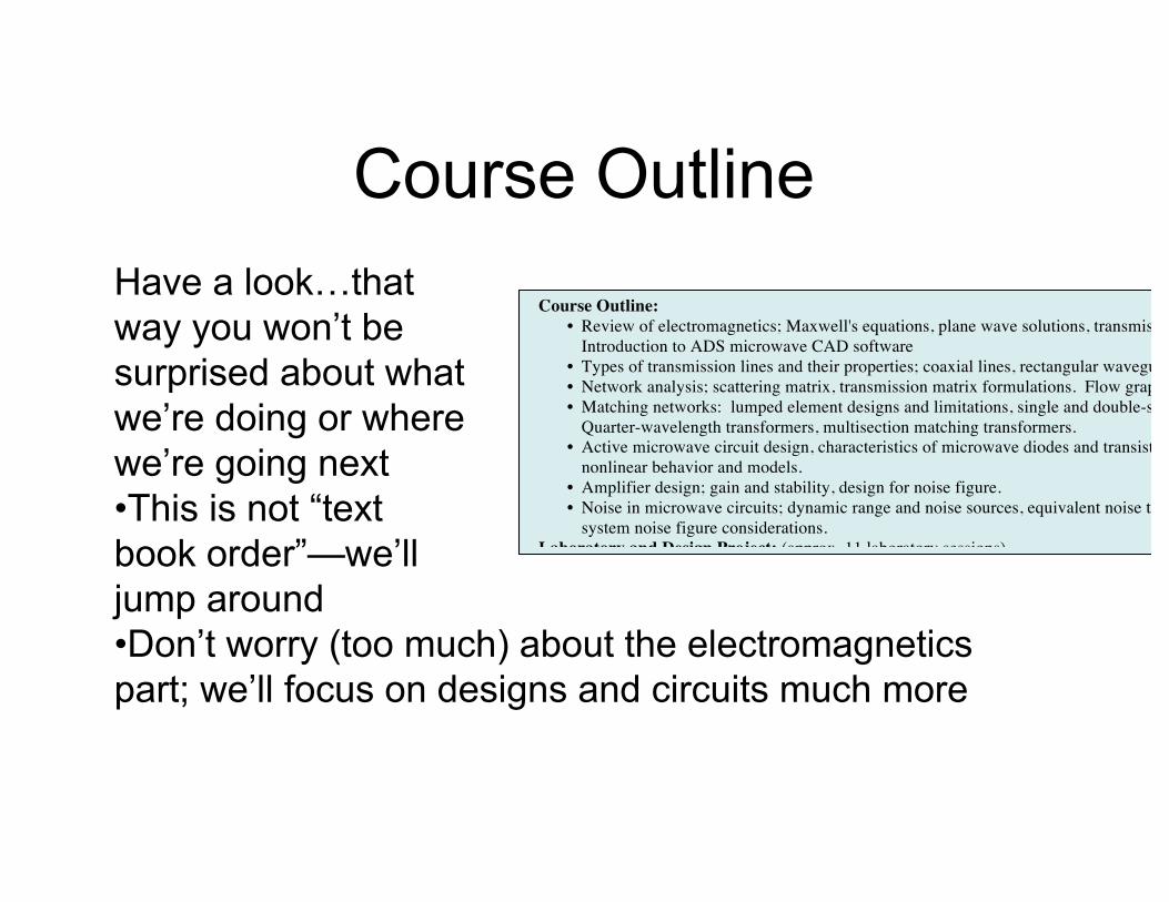
Course OutlineHave a look…thatway you won’t be surprised about whatwe’re doing or wherewe’re going next•This is not “textbook order”—we’lljump around•Don’t worry (too much) about the electromagnetics part; we’ll focus on designs and circuits much more
EE 40458/60558 RF and Microwave Circuits for Instructor: Patrick Fay Wireless Communications 261 Fitzpatrick Hall 631-5693 [email protected] http://www.nd.edu/~hscdlab Text: David M. Pozar, Microwave Engineering, 4th. ed., John Wiley & Sons, 2012. Supplementary reading:
Guillermo Gonzalez, Microwave Transistor Amplifiers, 2nd. ed., Prentice-Hall, 1997. Class notes, handouts. Additional material is also available on the course web page at http://www.nd.edu/~hscdlab
Prerequisites: EE 30348, EE 30358 or consent of instructor Catalog Description: (2-3-3)
This course is an introduction to RF and microwave circuit design and analysis techniques, with particular emphasis on applications for modern wireless communication and sensing systems. An integrated laboratory experience provides hands-on exposure to specialized high-frequency measurement techniques. Students will develop an enhanced understanding of circuit design and analysis principles as applied to modern RF & microwave circuits, as well as gain familiarity with design techniques for both hand analysis and computer-aided design. A design project will be designed, built, and tested using the computer-aided techniques and instrumentation in the lab.
Course Outline: • Review of electromagnetics; Maxwell's equations, plane wave solutions, transmission lines.
Introduction to ADS microwave CAD software • Types of transmission lines and their properties; coaxial lines, rectangular waveguides, microstrip. • Network analysis; scattering matrix, transmission matrix formulations. Flow graphs, Mason's rule. • Matching networks: lumped element designs and limitations, single and double-stub tuned designs.
Quarter-wavelength transformers, multisection matching transformers. • Active microwave circuit design, characteristics of microwave diodes and transistors. Linear and
nonlinear behavior and models. • Amplifier design; gain and stability, design for noise figure. • Noise in microwave circuits; dynamic range and noise sources, equivalent noise temperature,
system noise figure considerations. Laboratory and Design Project: (approx. 11 laboratory sessions)
1. High frequency performance of circuit components 2. Measurement basics; reflectometry, spectrum analysis 3. Scalar network analyzer measurements 4. Vector network analyzer operation and error correction 5. Scattering parameter measurements of active devices 6. Matching network design, fabrication, and characterization 7. Project design, characterization, and analysis 8. Nonlinear and noise characterization of active circuits
Homework: Homework will be assigned and collected (approximately) weekly. Examinations: 1 in-class midterm examination, cumulative final exam Grading: Homework 20 % Mid-term exam 25 % Laboratory (includes design project) 25 % Final exam 30 %
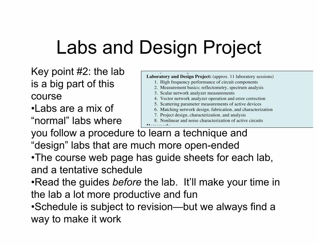
Labs and Design ProjectKey point #2: the labis a big part of this course•Labs are a mix of “normal” labs whereyou follow a procedure to learn a technique and “design” labs that are much more open-ended•The course web page has guide sheets for each lab, and a tentative schedule•Read the guides before the lab. It’ll make your time in the lab a lot more productive and fun•Schedule is subject to revision—but we always find a way to make it work
EE 40458/60558 RF and Microwave Circuits for Instructor: Patrick Fay Wireless Communications 261 Fitzpatrick Hall 631-5693 [email protected] http://www.nd.edu/~hscdlab Text: David M. Pozar, Microwave Engineering, 4th. ed., John Wiley & Sons, 2012. Supplementary reading:
Guillermo Gonzalez, Microwave Transistor Amplifiers, 2nd. ed., Prentice-Hall, 1997. Class notes, handouts. Additional material is also available on the course web page at http://www.nd.edu/~hscdlab
Prerequisites: EE 30348, EE 30358 or consent of instructor Catalog Description: (2-3-3)
This course is an introduction to RF and microwave circuit design and analysis techniques, with particular emphasis on applications for modern wireless communication and sensing systems. An integrated laboratory experience provides hands-on exposure to specialized high-frequency measurement techniques. Students will develop an enhanced understanding of circuit design and analysis principles as applied to modern RF & microwave circuits, as well as gain familiarity with design techniques for both hand analysis and computer-aided design. A design project will be designed, built, and tested using the computer-aided techniques and instrumentation in the lab.
Course Outline: • Review of electromagnetics; Maxwell's equations, plane wave solutions, transmission lines.
Introduction to ADS microwave CAD software • Types of transmission lines and their properties; coaxial lines, rectangular waveguides, microstrip. • Network analysis; scattering matrix, transmission matrix formulations. Flow graphs, Mason's rule. • Matching networks: lumped element designs and limitations, single and double-stub tuned designs.
Quarter-wavelength transformers, multisection matching transformers. • Active microwave circuit design, characteristics of microwave diodes and transistors. Linear and
nonlinear behavior and models. • Amplifier design; gain and stability, design for noise figure. • Noise in microwave circuits; dynamic range and noise sources, equivalent noise temperature,
system noise figure considerations. Laboratory and Design Project: (approx. 11 laboratory sessions)
1. High frequency performance of circuit components 2. Measurement basics; reflectometry, spectrum analysis 3. Scalar network analyzer measurements 4. Vector network analyzer operation and error correction 5. Scattering parameter measurements of active devices 6. Matching network design, fabrication, and characterization 7. Project design, characterization, and analysis 8. Nonlinear and noise characterization of active circuits
Homework: Homework will be assigned and collected (approximately) weekly. Examinations: 1 in-class midterm examination, cumulative final exam Grading: Homework 20 % Mid-term exam 25 % Laboratory (includes design project) 25 % Final exam 30 %
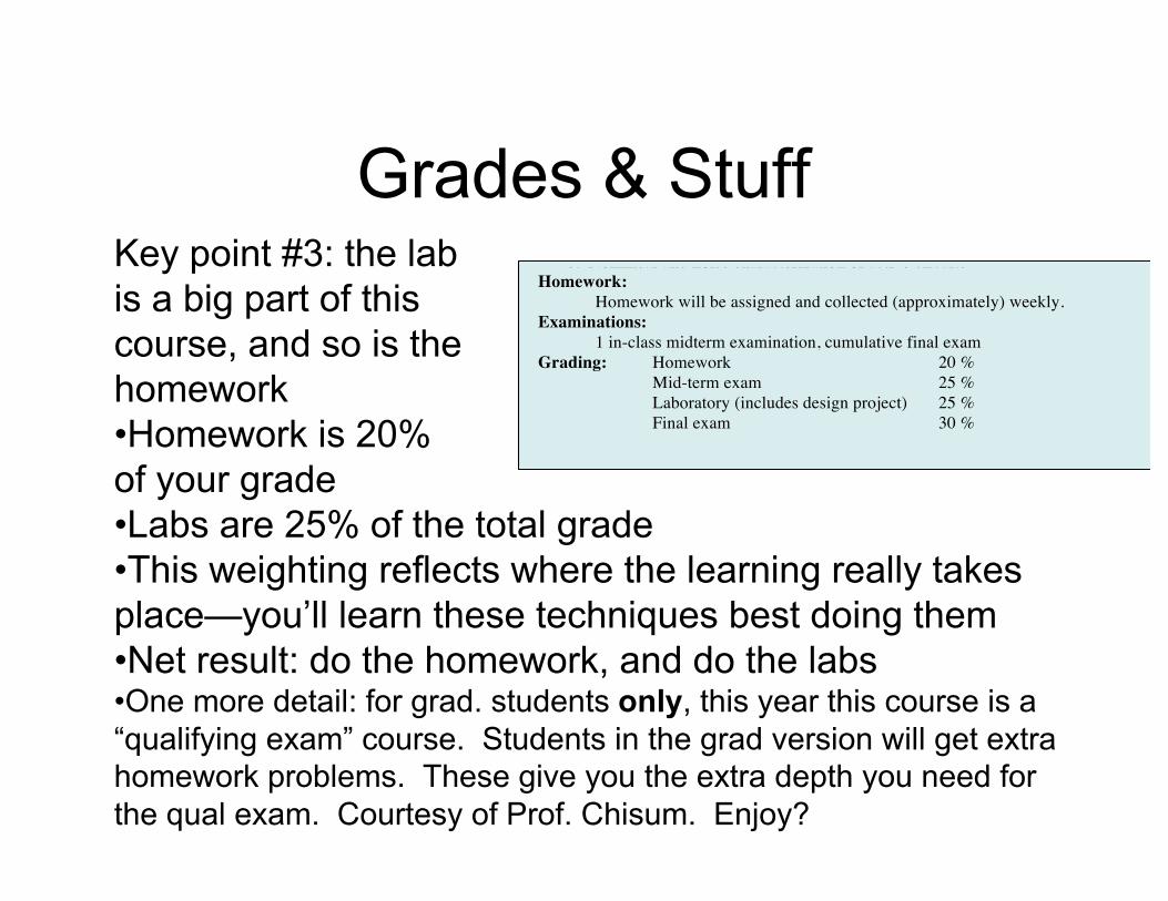
Grades & StuffKey point #3: the labis a big part of this course, and so is the homework•Homework is 20% of your grade•Labs are 25% of the total grade•This weighting reflects where the learning really takes place—you’ll learn these techniques best doing them•Net result: do the homework, and do the labs•One more detail: for grad. students only, this year this course is a “qualifying exam” course. Students in the grad version will get extra homework problems. These give you the extra depth you need for the qual exam. Courtesy of Prof. Chisum. Enjoy?
EE 40458/60558 RF and Microwave Circuits for Instructor: Patrick Fay Wireless Communications 261 Fitzpatrick Hall 631-5693 [email protected] http://www.nd.edu/~hscdlab Text: David M. Pozar, Microwave Engineering, 4th. ed., John Wiley & Sons, 2012. Supplementary reading:
Guillermo Gonzalez, Microwave Transistor Amplifiers, 2nd. ed., Prentice-Hall, 1997. Class notes, handouts. Additional material is also available on the course web page at http://www.nd.edu/~hscdlab
Prerequisites: EE 30348, EE 30358 or consent of instructor Catalog Description: (2-3-3)
This course is an introduction to RF and microwave circuit design and analysis techniques, with particular emphasis on applications for modern wireless communication and sensing systems. An integrated laboratory experience provides hands-on exposure to specialized high-frequency measurement techniques. Students will develop an enhanced understanding of circuit design and analysis principles as applied to modern RF & microwave circuits, as well as gain familiarity with design techniques for both hand analysis and computer-aided design. A design project will be designed, built, and tested using the computer-aided techniques and instrumentation in the lab.
Course Outline: • Review of electromagnetics; Maxwell's equations, plane wave solutions, transmission lines.
Introduction to ADS microwave CAD software • Types of transmission lines and their properties; coaxial lines, rectangular waveguides, microstrip. • Network analysis; scattering matrix, transmission matrix formulations. Flow graphs, Mason's rule. • Matching networks: lumped element designs and limitations, single and double-stub tuned designs.
Quarter-wavelength transformers, multisection matching transformers. • Active microwave circuit design, characteristics of microwave diodes and transistors. Linear and
nonlinear behavior and models. • Amplifier design; gain and stability, design for noise figure. • Noise in microwave circuits; dynamic range and noise sources, equivalent noise temperature,
system noise figure considerations. Laboratory and Design Project: (approx. 11 laboratory sessions)
1. High frequency performance of circuit components 2. Measurement basics; reflectometry, spectrum analysis 3. Scalar network analyzer measurements 4. Vector network analyzer operation and error correction 5. Scattering parameter measurements of active devices 6. Matching network design, fabrication, and characterization 7. Project design, characterization, and analysis 8. Nonlinear and noise characterization of active circuits
Homework: Homework will be assigned and collected (approximately) weekly. Examinations: 1 in-class midterm examination, cumulative final exam Grading: Homework 20 % Mid-term exam 25 % Laboratory (includes design project) 25 % Final exam 30 %

More Important StuffCourse web site hassome useful stuff onit•Homeworks willbe posted there (with solutions)•Lab procedures and write-ups, files that are helpful for the lab and computer work (design model files, etc.). Look on the “lab” page•Other aids: copy of the syllabus, lab policy sheet, Smith charts, old tests. Look on the “homework” page
EE 40458/60558 RF and Microwave Circuits for Instructor: Patrick Fay Wireless Communications 261 Fitzpatrick Hall 631-5693 [email protected] http://www.nd.edu/~hscdlab Text: David M. Pozar, Microwave Engineering, 4th. ed., John Wiley & Sons, 2012. Supplementary reading:
Guillermo Gonzalez, Microwave Transistor Amplifiers, 2nd. ed., Prentice-Hall, 1997. Class notes, handouts. Additional material is also available on the course web page at http://www.nd.edu/~hscdlab
Prerequisites: EE 30348, EE 30358 or consent of instructor Catalog Description: (2-3-3)
This course is an introduction to RF and microwave circuit design and analysis techniques, with particular emphasis on applications for modern wireless communication and sensing systems. An integrated laboratory experience provides hands-on exposure to specialized high-frequency measurement techniques. Students will develop an enhanced understanding of circuit design and analysis principles as applied to modern RF & microwave circuits, as well as gain familiarity with design techniques for both hand analysis and computer-aided design. A design project will be designed, built, and tested using the computer-aided techniques and instrumentation in the lab.
Course Outline: • Review of electromagnetics; Maxwell's equations, plane wave solutions, transmission lines.
Introduction to ADS microwave CAD software • Types of transmission lines and their properties; coaxial lines, rectangular waveguides, microstrip. • Network analysis; scattering matrix, transmission matrix formulations. Flow graphs, Mason's rule. • Matching networks: lumped element designs and limitations, single and double-stub tuned designs.
Quarter-wavelength transformers, multisection matching transformers. • Active microwave circuit design, characteristics of microwave diodes and transistors. Linear and
nonlinear behavior and models. • Amplifier design; gain and stability, design for noise figure. • Noise in microwave circuits; dynamic range and noise sources, equivalent noise temperature,
system noise figure considerations. Laboratory and Design Project: (approx. 11 laboratory sessions)
1. High frequency performance of circuit components 2. Measurement basics; reflectometry, spectrum analysis 3. Scalar network analyzer measurements 4. Vector network analyzer operation and error correction 5. Scattering parameter measurements of active devices 6. Matching network design, fabrication, and characterization 7. Project design, characterization, and analysis 8. Nonlinear and noise characterization of active circuits
Homework: Homework will be assigned and collected (approximately) weekly. Examinations: 1 in-class midterm examination, cumulative final exam Grading: Homework 20 % Mid-term exam 25 % Laboratory (includes design project) 25 % Final exam 30 %

Keysight Certification Option• Students that do well in this class can also receive Keysight
Technologies’ “Ready for Industry” certification • This is entirely optional, but if you’re considering an RF/microwave
career, it might help in interviews• Main emphasis is on experience/competence with test & measurement
gear and techniques, and design/simulation tools and techniques• The course more than satisfies the “level 1” requirements• More details are online—but don’t focus on their requirements. I take
care of the details for you

Questions on Administrative Stuff?
• On to technical discussion…
RF and Microwave Circuits for Wireless Communications
• Modern wireless communications relies on high-performance, high-frequency circuits
• Lots of other applications do too…– Radar– Medical therapies (RF-induced hyperthermia treatments for
cardiac arrhythmia)– Imaging for avionics, security (airport scanners, theft prevention
at warehouses)– Digital circuits
• Our job: figure out how to make circuits that do what is needed
RF and Microwave Design• So what’s the big deal? How is this any different from
“regular old” circuit design?• Key issue: at high frequencies, some fundamental
(maybe even forgotten) assumptions in “regular old” circuit design fall apart– Normally, circuit layout is not so important; at RF/microwaves,
layout is very important– RF/microwave: basically short-hand for “high frequency”—RF is
~10 MHz – 1 GHz; microwave is 1 GHz and up• Where does this come from? Finite speed of light• “Regular old” circuit design assumes that changes in
signals propagate instantly. But we know really this isn’t possible—nothing, not even signals, moves faster than light. So why does this break at high frequencies?
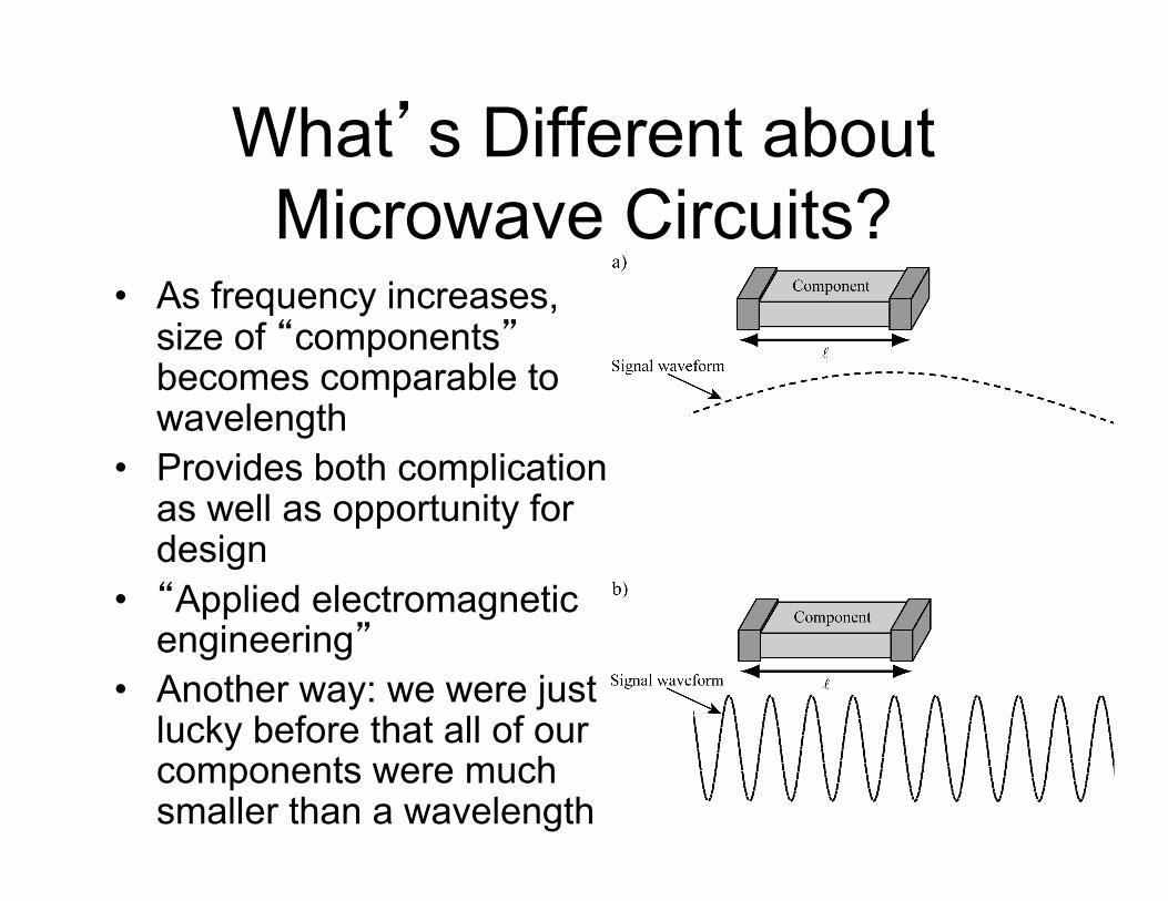
What’s Different about Microwave Circuits?
• As frequency increases, size of “components”becomes comparable to wavelength
• Provides both complication as well as opportunity for design
• “Applied electromagnetic engineering”
• Another way: we were just lucky before that all of our components were much smaller than a wavelength
Conclusion: “nodes” aren’t nodes anymore…
• Wires, interconnections matter—a lot• Shape of the circuit matters—a lot
– Makes for funny-looking circuits– Opens up many design opportunities– “Distributed” circuit concepts—explicitly use wave
propagation to do things that “shouldn’t work”• Many technologies can be used
– CMOS, BJTs, more exotic III-V electronics, vacuum tubes (honest!), magnetic devices
– Classic engineering—use what is available, just make it work (and on time and under budget)
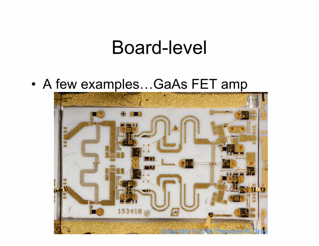
Board-level
• A few examples…GaAs FET amp
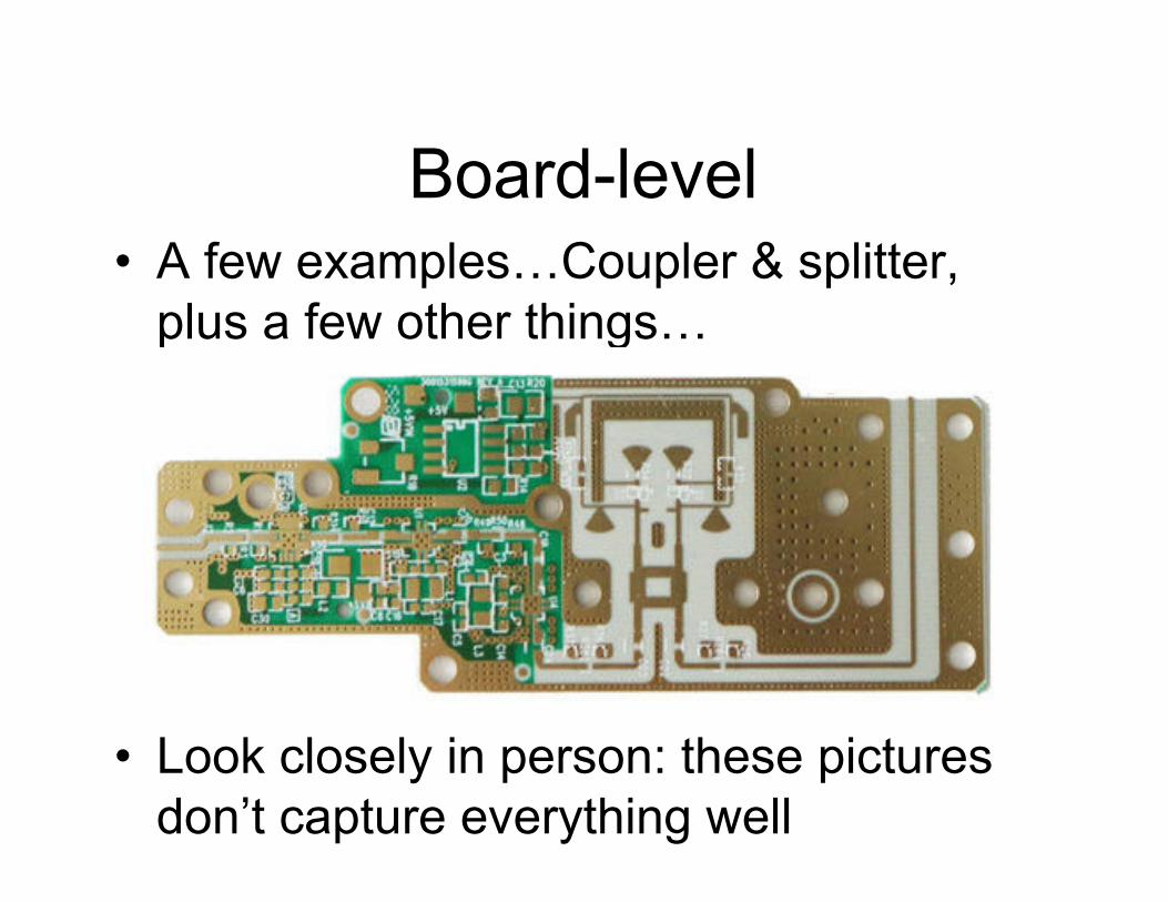
Board-level • A few examples…Coupler & splitter,
plus a few other things…
• Look closely in person: these pictures don’t capture everything well
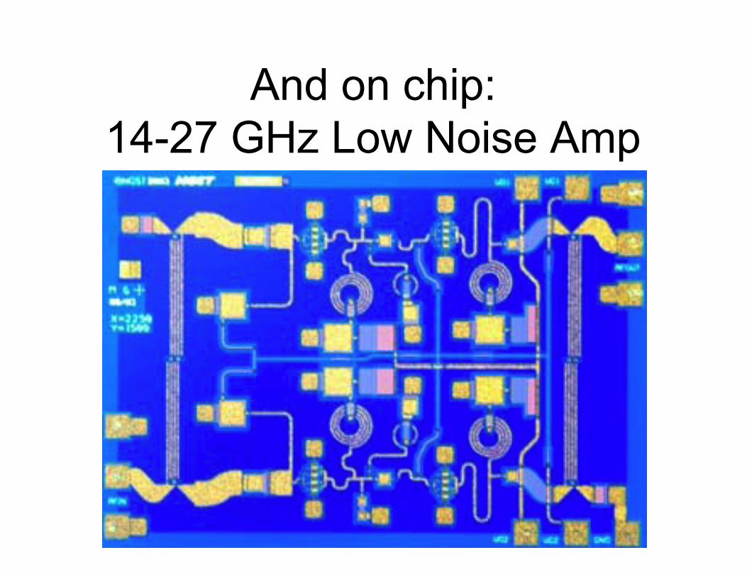
And on chip:14-27 GHz Low Noise Amp
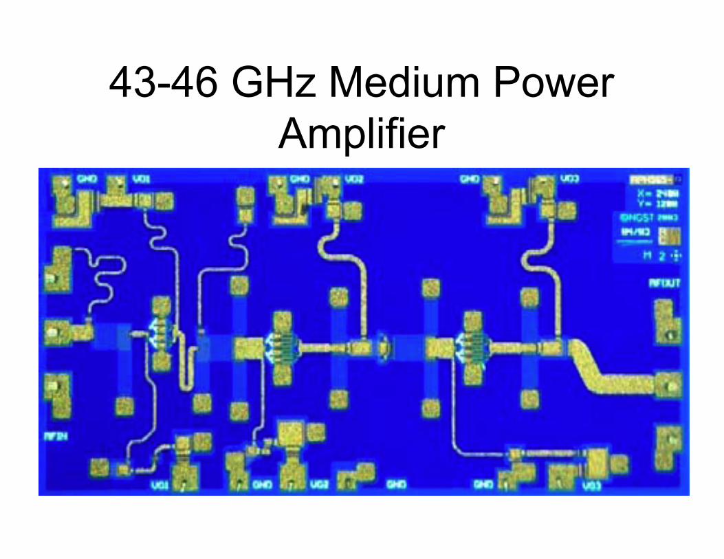
43-46 GHz Medium Power Amplifier
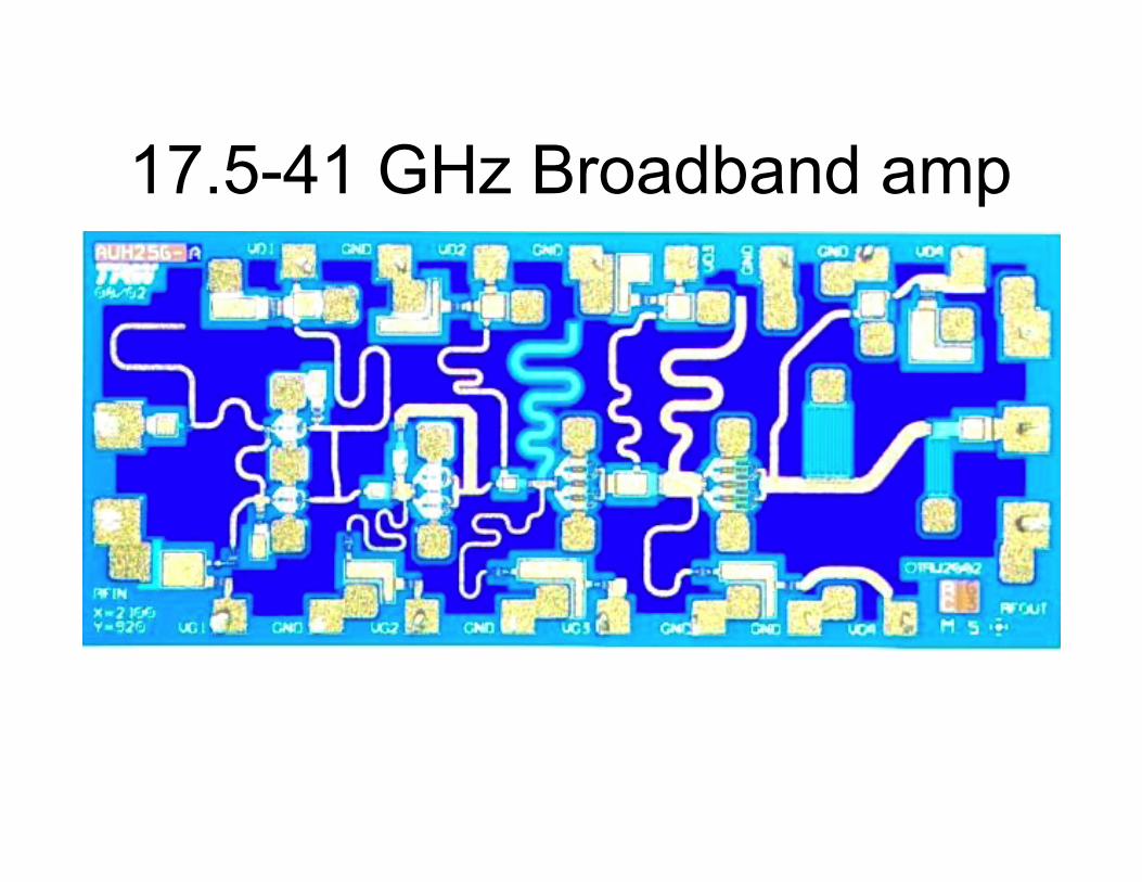
17.5-41 GHz Broadband amp
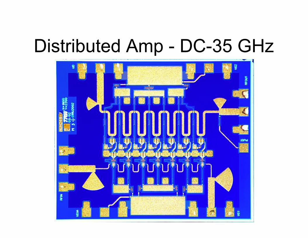
Distributed Amp - DC-35 GHz
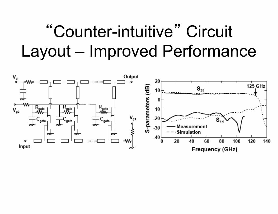
“Counter-intuitive” Circuit Layout – Improved Performance
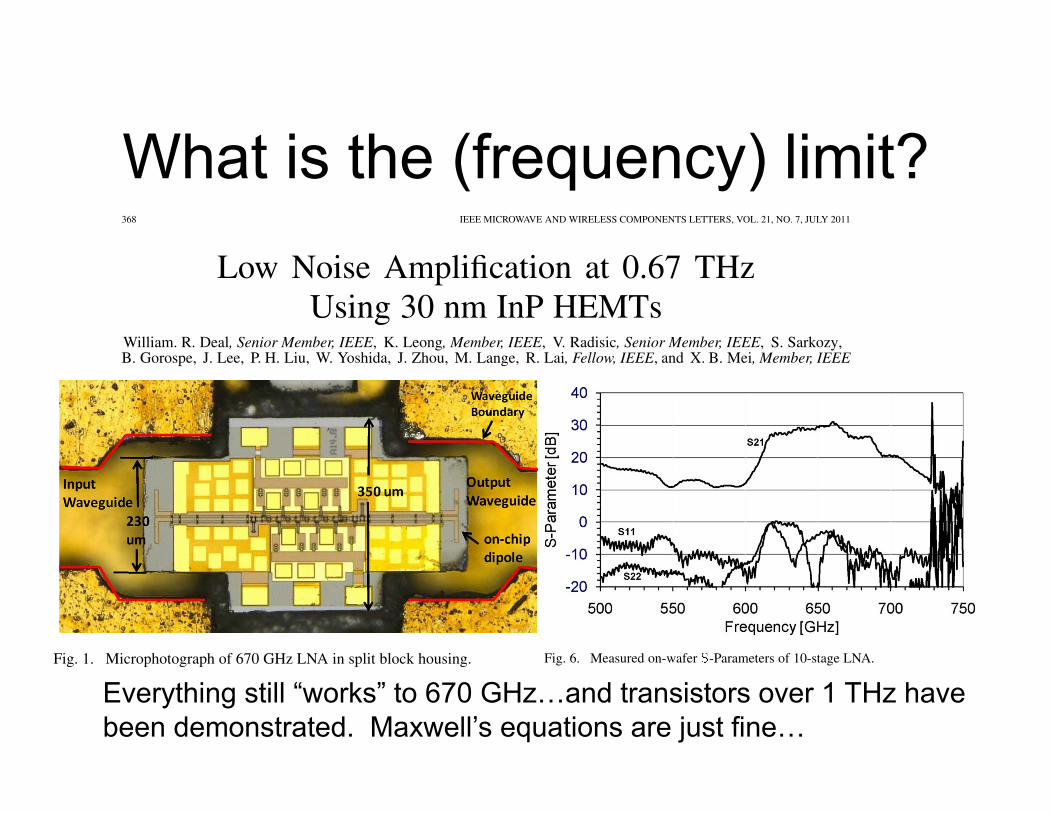
What is the (frequency) limit?368 IEEE MICROWAVE AND WIRELESS COMPONENTS LETTERS, VOL. 21, NO. 7, JULY 2011
Low Noise Amplification at 0.67 THzUsing 30 nm InP HEMTs
William. R. Deal, Senior Member, IEEE, K. Leong, Member, IEEE, V. Radisic, Senior Member, IEEE, S. Sarkozy,B. Gorospe, J. Lee, P. H. Liu, W. Yoshida, J. Zhou, M. Lange, R. Lai, Fellow, IEEE, and X. B. Mei, Member, IEEE
Abstract—In this letter, low noise amplification at 0.67 THz isdemonstrated for the first time. A packaged InP High ElectronMobility Transistor (HEMT) amplifier is reported to achieve anoise figure of 13 dB with an associated gain greater than 7 dB at670 GHz using a high InP HEMT transistors in a 5 stagecoplanar waveguide integrated circuit. A 10-stage version is alsoreported to reach a peak gain of 30 dB. These results indicatethat InP HEMT integrated circuits can be useful at frequenciesapproaching a terahertz.
Index Terms—Coplanar waveguide (CPW), high electronmobility transistor (HEMT), low noise amplifier (LNA), mil-limeter-wave (MM-Wave), monolithic microwave integratedcircuit (MMIC), sub-millimeter wave.
I. INTRODUCTION
I N the last few years, the development of Terahertztransistor technologies [1] has pushed operating frequen-
cies of amplifiers well into the sub-millimeter wave range. Thefirst demonstrations of sub-millimeter amplification were un-dertaken at the 340 GHz atmospheric window using InP HEMT[2] and MHEMT [3] technologies. Amplification has now beendemonstrated above 500 GHz with a cascode amplifier reportedin [4], which reached a packaged gain of 10 dB at 550 GHz.In this letter, the operating range is pushed to 670 GHz. We re-port a packaged low noise amplifier (LNA) with peak gain of 8dB and noise figure (NF) 13 dB (5500 K) for a 5 stage ampli-fier, and a second 10-stage amplifier with a peak measured gainof 30 dB. Note that GaAs double side band (DSB) Schottkymixers have recently been reported at 520–590 GHz demon-strated a 3000–4000 K noise temperature [5] at room temper-ature. In a Single Side Band (SSB) application, the reportedInP LNA would therefore provide competitive performance to aGaAs Schottky receiver at this frequency range.
A microphotograph of the five stage amplifier in split-blockwaveguide housing is shown in Fig. 1 with the signal electro-magnetically coupled from the waveguide to the amplifier die,thus avoiding RF wirebonds. The basic concept
is described in [6], but modifications have been made to thestructure to accommodate the wider electrical length necessary
Manuscript received January 06, 2011; accepted March 19, 2011. Date ofpublication June 07, 2011; date of current version July 07, 2011. This workwas supported by the DARPA THz Electronics Program and Army ResearchLaboratory under the DARPA contract no. HR0011-09-C-0062.
The authors are with Northrop Grumman Corporation, Redondo Beach, CA90278 USA (e-mail: [email protected]).
Color versions of one or more of the figures in this letter are available onlineat http://ieeexplore.ieee.org.
Digital Object Identifier 10.1109/LMWC.2011.2143701
Fig. 1. Microphotograph of 670 GHz LNA in split block housing.
to accommodate dc biasing circuitry bonded at the top andbottom of the circuit. In particular, sections of InP substratehave been removed at the corners of the substrate to preventovermoding in the waveguide cavity containing the on-chipdipole used to couple the signal to the integrated circuit.
II. THZ INP HEMT TECHNOLOGY
Critical for realizing amplifiers at the target design frequencyof 0.67 THz is a transistor with sufficiently high gain at thedesign frequency. To achieve the target operating frequency,we use an InP HEMT epitaxial profile with a composite In-GaAs/InAs channel and a 30 nm Electron Beam Lithography(EBL) gate process. The device is then passivated with SiN.This process has produced InP HEMTs with greater than 2300mS/mm transconductance, maximum channel current above900 mA/mm, MAG/MSG values as high as 14.5 dB at 110 GHzand of 1.2 THz and . The MMIC process[1] employs two metal interconnection layers with a secondlayer airbridge, precision thin film resistors and MIM capac-itors. The 3 in InP wafers are thinned to 25 micron thicknessand grounding slot vias are reactive ion etched with a platedTi/Au back metal.
III. FIVE STAGE PACKAGED LNA
A variety of challenges exist with designing amplifiers at fre-quencies described in this letter. In addition to the requirementfor an extremely high transistor, the short wavelength andhigh conductor losses at these frequencies give the requirementthat dimensions must be both physically and electrically com-pact. This requires scaled photolithographic processes, whichmust be well controlled to allow predicable and repeatable cir-cuit features (trace and airbridge geometries and substrate etchfeatures). Due to the extremely small feature size of these chips,
1531-1309/$26.00 © 2011 IEEE
368 IEEE MICROWAVE AND WIRELESS COMPONENTS LETTERS, VOL. 21, NO. 7, JULY 2011
Low Noise Amplification at 0.67 THzUsing 30 nm InP HEMTs
William. R. Deal, Senior Member, IEEE, K. Leong, Member, IEEE, V. Radisic, Senior Member, IEEE, S. Sarkozy,B. Gorospe, J. Lee, P. H. Liu, W. Yoshida, J. Zhou, M. Lange, R. Lai, Fellow, IEEE, and X. B. Mei, Member, IEEE
Abstract—In this letter, low noise amplification at 0.67 THz isdemonstrated for the first time. A packaged InP High ElectronMobility Transistor (HEMT) amplifier is reported to achieve anoise figure of 13 dB with an associated gain greater than 7 dB at670 GHz using a high InP HEMT transistors in a 5 stagecoplanar waveguide integrated circuit. A 10-stage version is alsoreported to reach a peak gain of 30 dB. These results indicatethat InP HEMT integrated circuits can be useful at frequenciesapproaching a terahertz.
Index Terms—Coplanar waveguide (CPW), high electronmobility transistor (HEMT), low noise amplifier (LNA), mil-limeter-wave (MM-Wave), monolithic microwave integratedcircuit (MMIC), sub-millimeter wave.
I. INTRODUCTION
I N the last few years, the development of Terahertztransistor technologies [1] has pushed operating frequen-
cies of amplifiers well into the sub-millimeter wave range. Thefirst demonstrations of sub-millimeter amplification were un-dertaken at the 340 GHz atmospheric window using InP HEMT[2] and MHEMT [3] technologies. Amplification has now beendemonstrated above 500 GHz with a cascode amplifier reportedin [4], which reached a packaged gain of 10 dB at 550 GHz.In this letter, the operating range is pushed to 670 GHz. We re-port a packaged low noise amplifier (LNA) with peak gain of 8dB and noise figure (NF) 13 dB (5500 K) for a 5 stage ampli-fier, and a second 10-stage amplifier with a peak measured gainof 30 dB. Note that GaAs double side band (DSB) Schottkymixers have recently been reported at 520–590 GHz demon-strated a 3000–4000 K noise temperature [5] at room temper-ature. In a Single Side Band (SSB) application, the reportedInP LNA would therefore provide competitive performance to aGaAs Schottky receiver at this frequency range.
A microphotograph of the five stage amplifier in split-blockwaveguide housing is shown in Fig. 1 with the signal electro-magnetically coupled from the waveguide to the amplifier die,thus avoiding RF wirebonds. The basic concept
is described in [6], but modifications have been made to thestructure to accommodate the wider electrical length necessary
Manuscript received January 06, 2011; accepted March 19, 2011. Date ofpublication June 07, 2011; date of current version July 07, 2011. This workwas supported by the DARPA THz Electronics Program and Army ResearchLaboratory under the DARPA contract no. HR0011-09-C-0062.
The authors are with Northrop Grumman Corporation, Redondo Beach, CA90278 USA (e-mail: [email protected]).
Color versions of one or more of the figures in this letter are available onlineat http://ieeexplore.ieee.org.
Digital Object Identifier 10.1109/LMWC.2011.2143701
Fig. 1. Microphotograph of 670 GHz LNA in split block housing.
to accommodate dc biasing circuitry bonded at the top andbottom of the circuit. In particular, sections of InP substratehave been removed at the corners of the substrate to preventovermoding in the waveguide cavity containing the on-chipdipole used to couple the signal to the integrated circuit.
II. THZ INP HEMT TECHNOLOGY
Critical for realizing amplifiers at the target design frequencyof 0.67 THz is a transistor with sufficiently high gain at thedesign frequency. To achieve the target operating frequency,we use an InP HEMT epitaxial profile with a composite In-GaAs/InAs channel and a 30 nm Electron Beam Lithography(EBL) gate process. The device is then passivated with SiN.This process has produced InP HEMTs with greater than 2300mS/mm transconductance, maximum channel current above900 mA/mm, MAG/MSG values as high as 14.5 dB at 110 GHzand of 1.2 THz and . The MMIC process[1] employs two metal interconnection layers with a secondlayer airbridge, precision thin film resistors and MIM capac-itors. The 3 in InP wafers are thinned to 25 micron thicknessand grounding slot vias are reactive ion etched with a platedTi/Au back metal.
III. FIVE STAGE PACKAGED LNA
A variety of challenges exist with designing amplifiers at fre-quencies described in this letter. In addition to the requirementfor an extremely high transistor, the short wavelength andhigh conductor losses at these frequencies give the requirementthat dimensions must be both physically and electrically com-pact. This requires scaled photolithographic processes, whichmust be well controlled to allow predicable and repeatable cir-cuit features (trace and airbridge geometries and substrate etchfeatures). Due to the extremely small feature size of these chips,
1531-1309/$26.00 © 2011 IEEE
370 IEEE MICROWAVE AND WIRELESS COMPONENTS LETTERS, VOL. 21, NO. 7, JULY 2011
Fig. 5. Measured (solid) and simulated (dash) response of 1000 CPW linemeasured with on-wafer TRL calibration.
by the University of Virginia. These probes cover the entireWR1.5 waveguide band with an insertion loss of 7-8 dB for eachprobe at the center of the band. These probes are a scaled pro-totype of the probes presented in [7].
Full 2-Port -Parameter measurements have been obtainedon the packaged amplifier. This was done using a set of WR1.5frequency extension modules developed by Virginia Diodes,Inc. The frequency extension modules were calibrated usingan on-wafer TRL calibration for accurate probetip response.To demonstrate the usefulness of this technique, the measuredresponse of a 1000 long CPW through line is shown aftercalibration in Fig. 5 as a calibration verification. The measuredinsertion loss of the probe is predicted within 1–2 dB to afrequency of approximately 700 GHz. Additionally, the phaseresponse of the line also agrees well with measurement. Atthis time, no systematic accuracy measurements have beenperformed, but agreement is generally good and shows thaton-wafer measurement techniques can be applied at frequenciesapproaching one terahertz. Note that the dynamic range of thetest set falls off above 725 GHz, which results in the jaggedresponse shown in the range above 725 GHz.
The measured -Parameter data for the ten stage LNA isshown in Fig. 6. Peak gain of 30 dB is obtained at ,which represents a realized amplifier gain of 3 dB/stage. Thehigher realized gain compared to the five stage amplifier is at-tributed to both improved transistor matching, and eliminationof the CPW feedlines at the input and output which are visiblein Fig. 1. Each of these improvements should lower the ampli-fier NF.
V. CONCLUSION
In this letter, a five-stage amplifier module and an iterated10-stage design operating at 0.67 THz have been presented. Themodule demonstrates 7–8 dB packaged gain at 670 GHz and
Fig. 6. Measured on-wafer -Parameters of 10-stage LNA.
13 dB NF. An iterated 10-stage shows 30 dB peak gain of 30 dBat 660 GHz measured on wafer, for a realized gain per stage of3 dB. We project the high-gain design should show improvedNF when packaged and fully characterized.
ACKNOWLEDGMENT
The authors would like to thank Dr. J. Albrecht, DARPA andDr. A. Hung, ARL, and to acknowledge NGAS contributorsin HEMT, EBL, MBE, processing, layout, machining, and testgroups, the staff of the ARL THz Laboratory for providing testsupport, the staff of the Far Infrared Receiver Laboratory, Uni-versity of Virginia, for developing the WR-1.5 coplanar waferprobes used in this work, as well as R. Lin and G. Chattopad-hyay, Jet Propulsion Laboratory, California Institute of Tech-nology, for making NF measurements.
REFERENCES
[1] R. Lai, X. B. Mei, W. R. Deal, W. Yoshida, Y. M. Kim, P. H. Liu, J.Lee, J. Uyeda, V. Radisic, M. Lange, T. Gaier, L. Samoska, and A.Fung, “Sub 50 nm InP HEMT device with Fmax greater than 1 THz,”in IEEE IEDM Conf. Dig., Dec. 2007, pp. 609–611.
[2] W. R. Deal, X. B. Mei, V. Radisic, W. Yoshida, P. H. Liu, J. Uyeda,Barsky, T. Gaier, A. Fung, and R. Lai, “Demonstration of a S-MMICLNA with 16-dB gain at 340-GHz,” in IEEE CSIC Conf. Dig., Oct.2007, pp. 1–4.
[3] A. Tessmann, A. Leuther, V. Hurm, H. Massler, M. Zink, M. Kuri, M.Riessle, R. Losch, M. Schlechtweg, and O. Ambacher, “A 300 GHzmHEMT amplifier module,” in IEEE IRPM Conf. Dig., May 2009, pp.196–199.
[4] W. R. Deal, K. Leong, X. B. Mei, S. Sarkozy, V. Radisic, J. Lee, P.H. Liu, W. Yoshida, J. Zhou, and M. Lange, “Scaling of InP HEMTcascode integrated circuits to THz frequencies,” in IEEE CSIC Conf.Dig., Oct. 2010, pp. 195–198.
[5] E. Schlecht, J. Gill, R. Dengler, R. Lin, R. Tsang, and I. Mehdi,“A unique 520–590 GHz biased subharmonically-pumped Schottkymixer,” IEEE Microw. Wireless Compon. Lett., vol. 17, no. 12, pp.879–881, Dec. 2007.
[6] K. Leong, W. R. Deal, V. Radisic, X. B. Mei, J. Uyeda, L.Samoska, A. Fung, T. Gaier, and R. Lai, “A 340–380 GHz inte-grated CB-CPW-to-waveguide transition for sub millimeter-waveMMIC Packaging,” IEEE Microw. Wireless Compon. Lett., vol. 19,no. 6, pp. 413–415, Jun. 2009.
[7] T. J. Reck, L. Chen, C. Zhang, C. Groppi, H. Xu, H. Arsenovic, N.S. Barker, A. Lichtenberger, and R. M. Weikle, “Micromachinedon-wafer probes,” in IEEE MTT-S Int. Dig., May 2010, pp. 65–68.
Everything still “works” to 670 GHz…and transistors over 1 THz have been demonstrated. Maxwell’s equations are just fine…
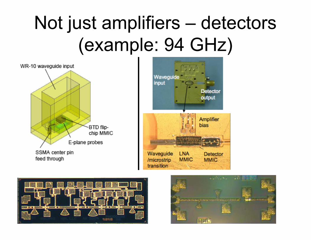
Not just amplifiers – detectors (example: 94 GHz)
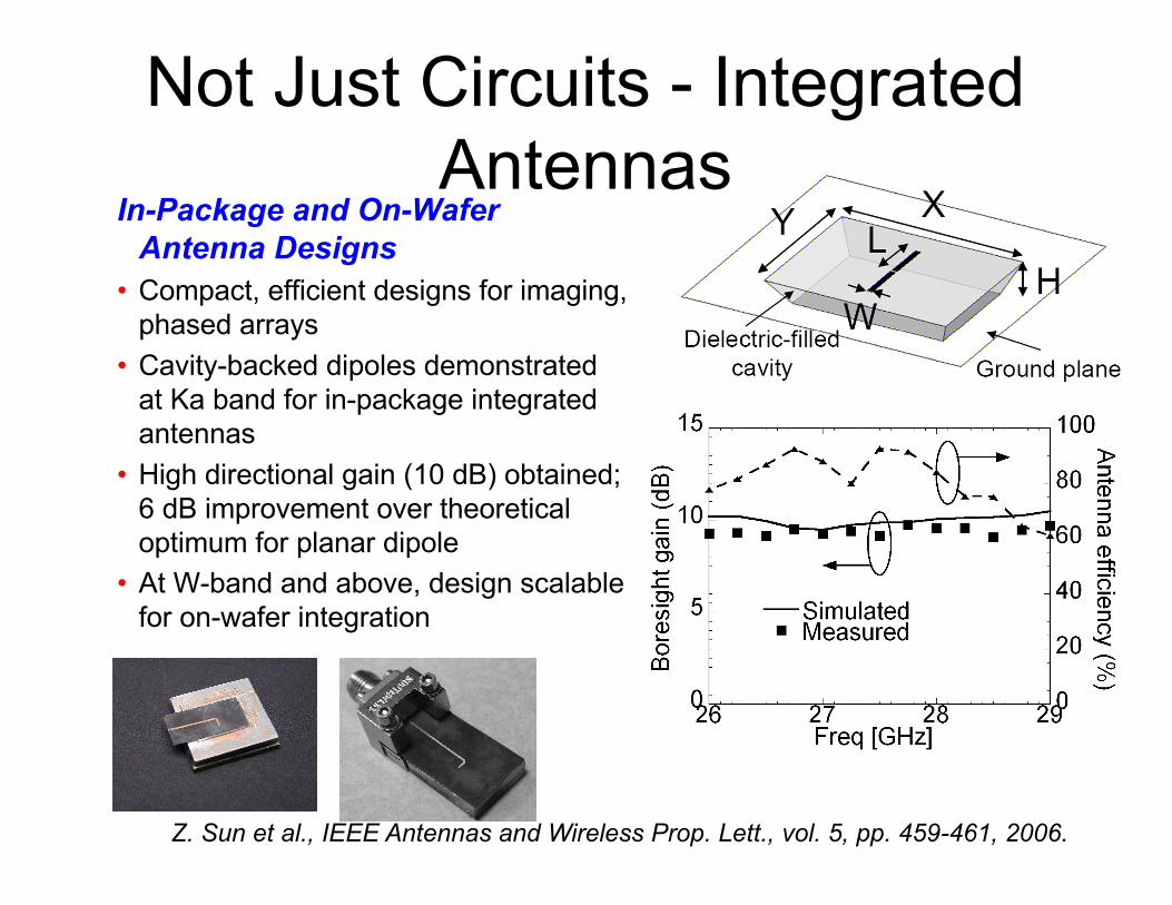
Not Just Circuits - Integrated Antennas
In-Package and On-Wafer Antenna Designs
• Compact, efficient designs for imaging, phased arrays
• Cavity-backed dipoles demonstrated at Ka band for in-package integrated antennas
• High directional gain (10 dB) obtained; 6 dB improvement over theoretical optimum for planar dipole
• At W-band and above, design scalable for on-wafer integration
Z. Sun et al., IEEE Antennas and Wireless Prop. Lett., vol. 5, pp. 459-461, 2006.
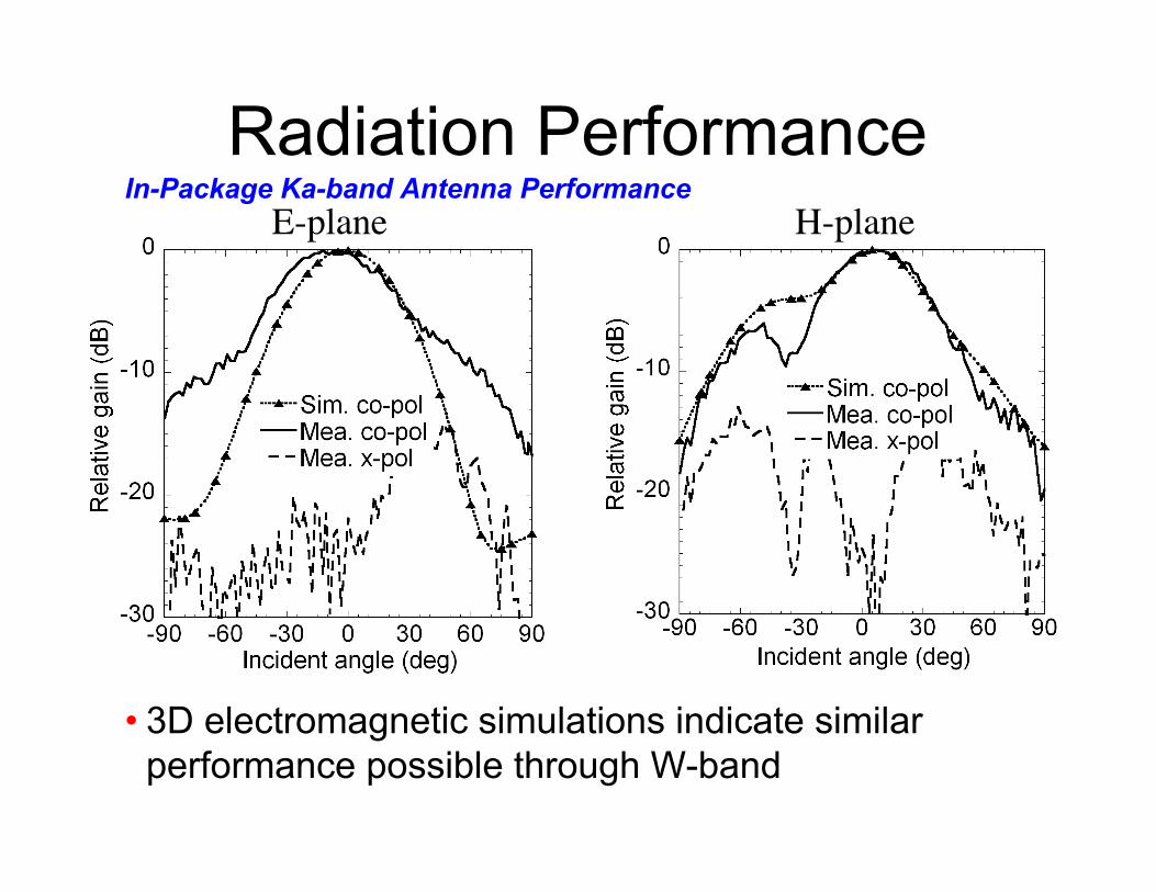
Radiation PerformanceIn-Package Ka-band Antenna Performance
• 3D electromagnetic simulations indicate similar performance possible through W-band
E-plane H-plane
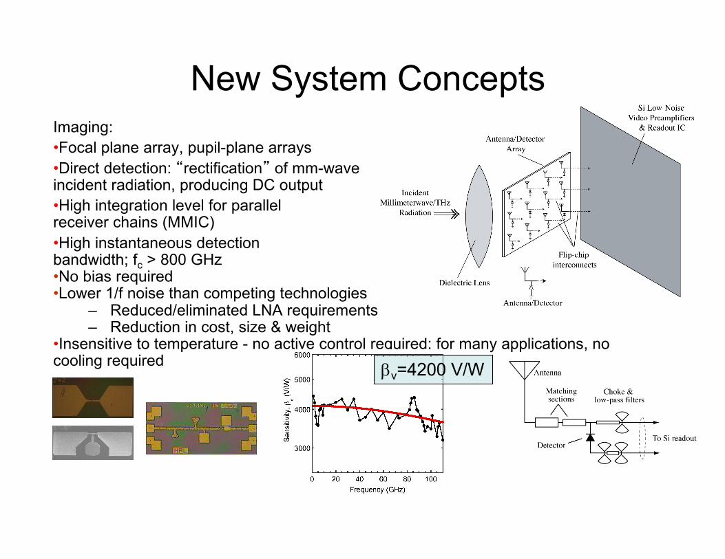
New System ConceptsImaging:•Focal plane array, pupil-plane arrays•Direct detection: “rectification” of mm-waveincident radiation, producing DC output •High integration level for parallel receiver chains (MMIC)•High instantaneous detection bandwidth; fc > 800 GHz•No bias required •Lower 1/f noise than competing technologies
– Reduced/eliminated LNA requirements– Reduction in cost, size & weight
•Insensitive to temperature - no active control required; for many applications, no cooling required bv=4200 V/W
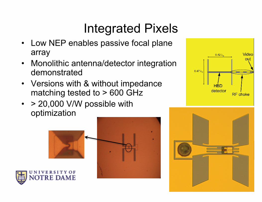
Integrated Pixels• Low NEP enables passive focal plane
array• Monolithic antenna/detector integration
demonstrated• Versions with & without impedance
matching tested to > 600 GHz• > 20,000 V/W possible with
optimization
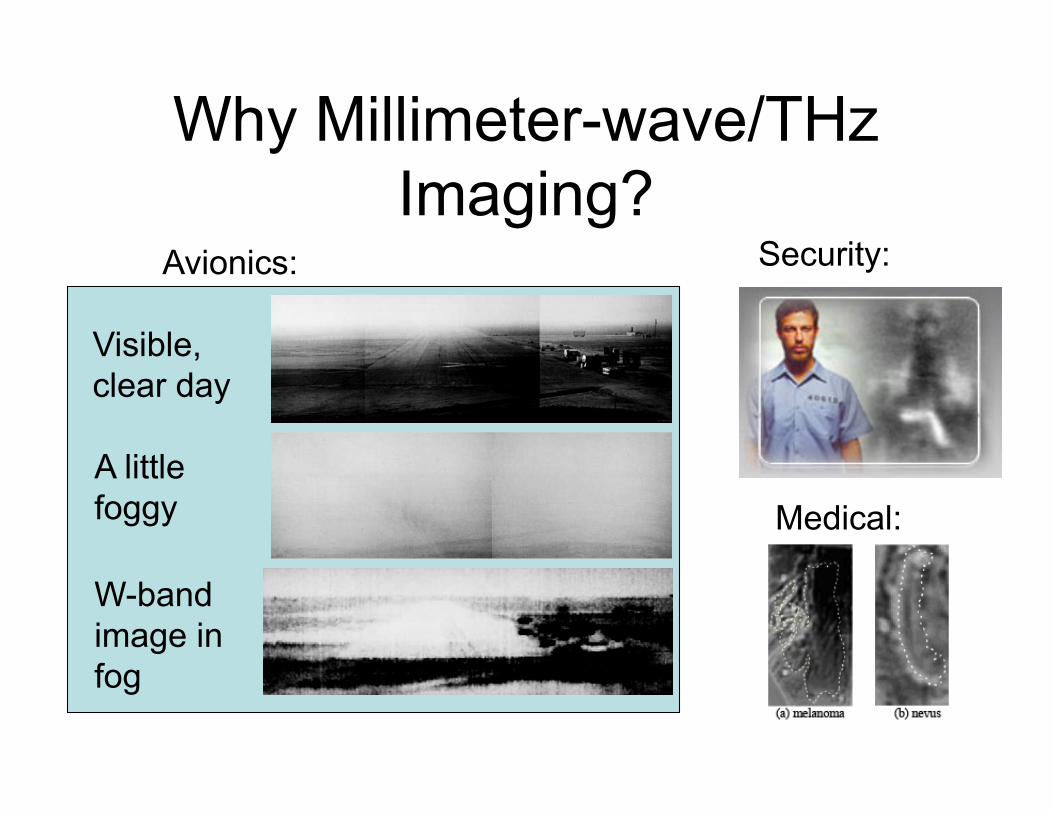
Why Millimeter-wave/THz Imaging?
Visible, clear day
A little foggy
W-band image in fog
Avionics: Security:
Medical:
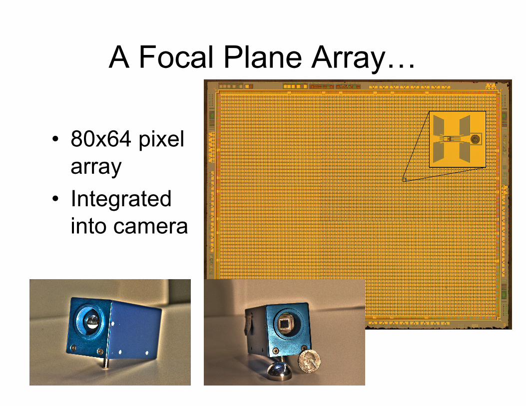
A Focal Plane Array…
• 80x64 pixelarray
• Integratedinto camera
Up Next—Some Definitions• Our focus is communications systems—so a few
definitions• All wireless systems work by broadcasting a signal,
which propagates as electromagnetic waves before being picked up and reconverted into useful signals
• We’re going to focus on electronics for the transmit and receive part; generating the data, etc., is somebody else’s problem– In modern systems, nearly always digital signal processing;
more code than circuit design
Frequency Bands• Important to have a handle on what bands are used
for what purposes; cell phones ≠ satellite uplinks ≠ GPS ≠ …
• And there are things that are not communications that we have to worry about too—radar, microwave ovens (i.e., kW transmitters at 2.45 GHz)
• To keep all of this straight, “standardized” band designations have been developed—sort of
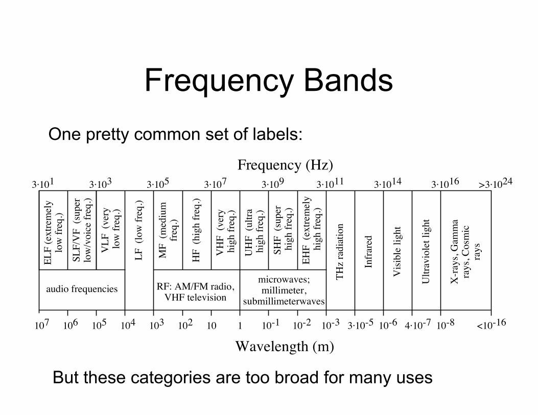
Frequency Bands
3⋅101 3⋅103 3⋅105 3⋅107 3⋅109 3⋅1011 3⋅1014
audio frequencies
ELF
(ext
rem
ely
low
freq
.)SL
F/V
F (s
uper
lo
w/v
oice
freq
.)V
LF (
very
low
freq
.)
LF (
low
freq
.)
MF
(med
ium
fre
q.)
VH
F (v
ery
hig
h fre
q.)
HF
(hig
h fre
q.)
RF: AM/FM radio, VHF television
UH
F (u
ltra
hig
h fre
q.)
SHF
(sup
er h
igh
freq.
)EH
F (e
xtre
mel
y h
igh
freq.
)
microwaves; millimeter,
submillimeterwaves
Infra
red
Visi
ble l
ight
Ultr
avio
let l
ight
X-ra
ys, G
amm
a ra
ys, C
osm
ic
rays
3⋅1016 >3⋅1024
THz r
adia
tion
Frequency (Hz)
Wavelength (m)107 106 105 104 103 102 10 1 10-1 10-2 10-3 3⋅10-5 <10-1610-6 4⋅10-7 10-8
One pretty common set of labels:
But these categories are too broad for many uses
Y
G
D
W
E
V
Q
Ka
K1
K†
K
Ku
X
C
S
L
0 1 2 3
Band
Des
igna
tion
0.39 GHz
1.55 GHz
2 GHz
4 GHz
5.2 GHz
8 GHz3.9 GHz
6.2 GHz10.9 GHz
12.4 GHz
12 GHz
15.35 GHz
17.25 GHz
18 GHz
26 GHz
27 GHz
36 GHz
24.5 GHz
40 GHz33 GHz
36 GHz46 GHz
50 GHz
75 GHz
110 GHz
56 GHz
0.1 1 10 100Frequency (GHz)
60 GHz
170 GHz
140 GHz325 GHz
220 GHz
90 GHz
NMLKJI
HGFEDCBA
0 1 2 3
Band
Des
igna
tion
Frequency (GHz)0.1 1 10 100Frequency (GHz)
0.25 GHz
0.1 GHz
0.5 GHz
2 GHz 3 GHz
4 GHz 6 GHz
8 GHz
20 GHz
40 GHz 60 GHz
140 GHz
1 GHz
10 GHz
100 GHz
a.)
b.)
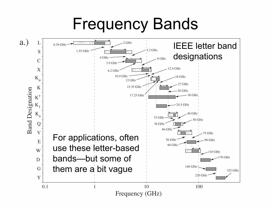
Frequency Bands
For applications, often use these letter-based bands—but some of them are a bit vague
IEEE letter band designations
Y
G
D
W
E
V
Q
Ka
K1
K†
K
Ku
X
C
S
L
0 1 2 3
Band
Des
igna
tion
0.39 GHz
1.55 GHz
2 GHz
4 GHz
5.2 GHz
8 GHz3.9 GHz
6.2 GHz10.9 GHz
12.4 GHz
12 GHz
15.35 GHz
17.25 GHz
18 GHz
26 GHz
27 GHz
36 GHz
24.5 GHz
40 GHz33 GHz
36 GHz46 GHz
50 GHz
75 GHz
110 GHz
56 GHz
0.1 1 10 100Frequency (GHz)
60 GHz
170 GHz
140 GHz325 GHz
220 GHz
90 GHz
NMLKJI
HGFEDCBA
0 1 2 3
Band
Des
igna
tion
Frequency (GHz)0.1 1 10 100Frequency (GHz)
0.25 GHz
0.1 GHz
0.5 GHz
2 GHz 3 GHz
4 GHz 6 GHz
8 GHz
20 GHz
40 GHz 60 GHz
140 GHz
1 GHz
10 GHz
100 GHz
a.)
b.)
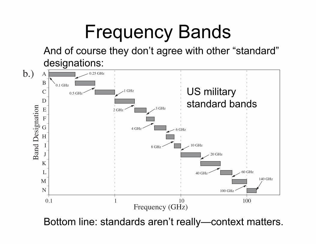
Frequency BandsAnd of course they don’t agree with other “standard”designations:
US military standard bands
Bottom line: standards aren’t really—context matters.

Administrative Wrap-Up• Be sure you’re registered for the course and lab
(40458 and 41458)• No lab this week, no lab next week• Need to adjust labs…a few people will be lonely
• Question: would it be possible to “stretch” classes by 10 minutes (2:00-2:50 à 2:00-3:00)? If we do this, we can recover from my stupid travel schedule without make-up classes. I will follow up with email—if this is a problem, be sure to let me know
• Reminder: class is 1:50-2:50