Site-Specific Variations in RNA Folding Thermodynamics Visualized by 2-Aminopurine Fluorescence †
The Relationship between Nanoscale Architecture andFunction in Photovoltaic Multichromophoric Arrays as
Visualized by Kelvin Probe Force Microscopy
Vincenzo Palermo,† Matthijs B. J. Otten,‡ Andrea Liscio,† Erik Schwartz,‡
Pieter A. J. de Witte,‡ Maria Angela Castriciano,§ Martijn M. Wienk,| Fabian Nolde,⊥
Giovanna De Luca,† Jeroen J. L. M. Cornelissen,‡ Rene A. J. Janssen,|
Klaus Mullen,⊥ Alan E. Rowan,*,‡ Roeland J. M. Nolte,‡ and Paolo Samorı*,†,#
Istituto per la Sintesi Organica e la FotoreattiVita, Consiglio Nazionale delle Ricerche,Via Gobetti 101, I-40129 Bologna, Italy, Institute for Molecules and Materials, Radboud
UniVersity Nijmegen, ToernooiVeld 1, 6525 ED Nijmegen, The Netherlands, Istituto per lo Studiodei Materiali Nanostruttrati ISMN-CNR, Salita Sperone 31, 98166 Vill. S. Agata, Messina, Italy,
Laboratory of Macromolecular and Organic Chemistry, TU EindhoVen, P.O. Box 513,5600 MB EindhoVen, The Netherlands, Max-Planck Institute for Polymer Research,
Ackermannweg 10, 55124 Mainz, Germany, and Nanochemistry Laboratory, ISIS, UniVersiteLouis Pasteur and CNRS (UMR 7006), 8 allee Gaspard Monge, F-67000 Strasbourg, France
Received June 4, 2008; E-mail: [email protected]; [email protected]
Abstract: The physicochemical properties of organic (multi)component films for optoelectronic applicationsdepend on both the mesoscopic and nanoscale architectures within the semiconducting material. Twomain classes of semiconducting materials are commonly used: polymers and (liquid) crystals of smallaromatic molecules. Whereas polymers (e.g., polyphenylenevinylenes and polythiophenes) are easy toprocess in solution in thin and uniform layers, small molecules can form highly defined (liquid) crystalsfeaturing high charge mobilities. Herein, we combine the two material types by employing structurally well-defined polyisocyanopeptide polymers as scaffolds to precisely arrange thousands of electron-acceptingmolecules, namely, perylenebis(dicarboximides) (PDIs), in defined chromophoric wires with lengths ofhundreds of nanometers. The polymer backbone enforces high control over the spatial location of PDIdyes, favoring both enhanced exciton and charge transfer. When blended with an electron-donor systemsuch as regioregular poly(3-hexylthiophene), this polymeric PDI shows a relative improvement in chargegeneration and diffusion with respect to monomeric, aggregated PDI. In order to correlate this enhancedbehavior with respect to the architecture, atomic force microscopy investigations on the mixtures werecarried out. These studies revealed that the two polymers form interpenetrated bundles having a nanophase-segregated character and featuring a high density of contact points between the two different phases. Inorder to visualize the relationship between the architecture and the photovoltaic efficiency, Kelvin probeforce microscopy measurements were carried out on submonolayer-thick films. This technique allowed forthe first time the direct visualization of the photovoltaic activity occurring in such a nanoscale phase-segregated ultrathin film with true nanoscale spatial resolution, thus making possible a study of the correlationbetween function and architecture with nanoscale resolution.
Introduction
In a world of increasing demand for energy and a decliningreserve of conventional energy resources, it is of pivotalimportance to find and develop new sources of energy supply,such as solar energy.1 Among the different kinds of photovoltaicdevices, organic solar cells have the advantage of beinginexpensive and easily processable, but their power conversion,
which at present reaches up to 6.5%,2 remains low comparedto their silicon counterparts. The use of bulk heterojunction(BHJ) solar cells, in which the electron-donor and electron-acceptor materials are mixed in order to allow maximal chargeseparation, represented a breakthrough in the field.3,4 In thistype of solar cell, the high contact area between the twomaterials enhances the ability of photogenerated excitons toeffectively reach the interface between the acceptor and thedonor; ideally, the interpenetration length should be on a scale
† Istituto per la Sintesi Organica e la Fotoreattivita.‡ Radboud University Nijmegen.§ Stituto per lo Studio dei Materiali Nanostruttrati.| TU Eindhoven.⊥ Max-Planck Institute for Polymer Research.# Universite Louis Pasteur.
(1) Armaroli, N.; Balzani, V. Angew. Chem., Int. Ed. 2007, 46, 52–66.
(2) Kim, J. Y.; Lee, K.; Coates, N. E.; Moses, D.; Nguyen, T. Q.; Dante,M.; Heeger, A. J. Science 2007, 317, 222–225.
(3) Halls, J. J. M.; Walsh, C. A.; Greenham, N. C.; Marseglia, E. A.;Friend, R. H.; Moratti, S. C.; Holmes, A. B. Nature 1995, 376, 498–500.
(4) Yu, G.; Gao, J.; Hummelen, J. C.; Wudl, F.; Heeger, A. J. Science1995, 270, 1789–1791.
Published on Web 10/10/2008
10.1021/ja804069n CCC: $40.75 2008 American Chemical Society J. AM. CHEM. SOC. 2008, 130, 14605–14614 9 14605
comparable to the mean exciton diffusion length, which istypically on the order of 5-6 nm.5 Moreover, the structureswithin the active layer need to provide efficient pathways forthe photogenerated charges to migrate to the correspondingelectrodes, thereby promoting charge transport over chargerecombination. Thus, the “ideal” blend for BHJ solar cells needsto feature the following well-defined characteristics: (i) Theacceptor and donor materials must be interpenetrated on thenanometer scale, and hence phase separation on macroscopicscales must be hindered. (ii) The acceptor and donor materialsmust form continuous paths to the electrodes, and chargeaccumulation or recombination in dead ends and bottlenecksmust be avoided. (iii) Charge transport must be efficient, withgood charge mobility and a small number of defects within eachphase. In the case of molecular materials, this requires goodcrystalline order with optimal overlap between stacked π orbitalsin order to attain efficient charge-hopping transport.
Two different classes of materials are commonly employedto meet these requirements: long polymeric chains and highlycrystalline assemblies of small polyaromatic molecules. Whilepolymeric blends are easy to process and give good uniformlayers, the highest charge mobilities have typically been obtainedwith molecular crystals of small molecules.6 The most efficientBHJ solar cells consist of a blend of p-type polythiophene andn-type fullerene derivatives,7-10 taking advantage of the forma-
tion of semicrystalline fullerene networks acting as percolationpaths for electrons.
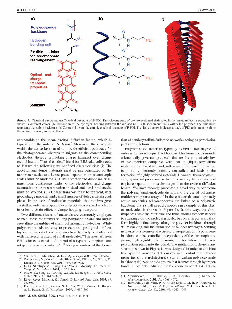
Polymer-based materials typically exhibit a low degree oforder at the mesoscopic level because film formation is usuallya kinetically governed process11 that results in relatively lowcharge mobility compared with that in (liquid-)crystallinematerials. On the other hand, self-assembly of small moleculesis primarily thermodynamically controlled and leads to theformation of highly ordered materials. However, thermodynami-cally governed processes on bicomponent systems often leadto phase separation on scales larger than the exciton diffusionlength. We have recently presented a novel way to overcomethe polymer/small-molecule dichotomy: the use of polymericmultichromophoric arrays.12 In these materials, small opticallyactive molecules (chromophores) are linked to a polymericbackbone via a small peptidic spacer (an example of this classof molecules is shown in Figure 1). In this way, the chro-mophores have the rotational and translational freedom neededto rearrange on the molecular scale, but on a larger scale theyform highly defined arrays along the polymer backbone throughπ-π stacking and the formation of -sheet hydrogen-bondingnetworks. Furthermore, the structural properties of the polymericbackbone can be controlled independently of the chromophores,giving high rigidity and ensuring the formation of efficientpercolation paths into the blend. The multichromophoric arraystructure shown in Figure 1a was designed in order to combinefive specific moieties that convey and control well-definedproperties of the architecture: (i) an all-carbon polyisocyanidebackbone; (ii) peptide side groups that interact through hydrogenbonding, not only inducing the backbone to adopt a 41 helical
(5) Scully, S. R.; McGehee, M. D. J. Appl. Phys. 2006, 100, 034907.(6) Coropceanu, V.; Cornil, J.; da Silva, D. A.; Olivier, Y.; Silbey, R.;
Bredas, J. L. Chem. ReV. 2007, 107, 926–952.(7) Li, G.; Shrotriya, V.; Huang, J. S.; Yao, Y.; Moriarty, T.; Emery, K.;
Yang, Y. Nat. Mater. 2005, 4, 864–868.(8) Ma, W. L.; Yang, C. Y.; Gong, X.; Lee, K.; Heeger, A. J. AdV. Funct.
Mater. 2005, 15, 1617–1622.(9) Reyes-Reyes, M.; Kim, K.; Carroll, D. L. Appl. Phys. Lett. 2005, 87,
083506.(10) Peet, J.; Kim, J. Y.; Coates, N. E.; Ma, W. L.; Moses, D.; Heeger,
A. J.; Bazan, G. C. Nat. Mater. 2007, 6, 497–500.
(11) Strawhecker, K. E.; Kumar, S. K.; Douglas, J. F.; Karim, A.Macromolecules 2001, 34, 4669–4672.
(12) Hernando, J.; de Witte, P. A. J.; van Dijk, E. M. H. P.; Korterik, J.;Nolte, R. J. M.; Rowan, A. E.; Garcia-Parajo, M. F.; van Hulst, N. F.Angew. Chem., Int. Ed. 2004, 43, 4045–4049.
Figure 1. Chemical structures. (a) Chemical structure of P-PDI. The relevant parts of the molecule and their roles in the macromolecular properties areshown in different colors. (b) Illustration of the hydrogen bonding between the nth and (n + 4)th monomeric units within the polymer. The blue helixrepresents the carbon backbone. (c) Cartoon showing the complete helical structure of P-PDI. The dashed arrow indicates a stack of PDI units running alongthe central polyisocyanide backbone.
14606 J. AM. CHEM. SOC. 9 VOL. 130, NO. 44, 2008
A R T I C L E S Palermo et al.
conformation (four repeats per turn) but also providing greaterrigidity to the polymer;13 (iii) a flexible linker that forces thechromophores to remain close to the polymeric chain but atthe same time allows them to move, rotate, and interact on amolecular scale to maximize their π-π interactions; (iv) thechromophore that provides electronic and optical function tothe architecture; and (v) the alkyl side chains, which offerincreased solubility in organic solvents. The combination ofthese moieties leads to a macromolecular system featuring highrigidity, good processability, and the capacity to generate andtransport charges through π-π interactions, as described below.
In this work, we have focused our attention on the nanoscalestructural architecture and electronic properties of perylenebi-s(dicarboximide) (PDI)-functionalized polyisocyanide (P-PDI)-based blends (Figure 1) for photovoltaics. This work intention-ally was not aimed at using a high-performing photovoltaicblend. Instead, its purpose was to explore the roles of archi-tecture and chromophore-chromophore interactions within theacceptor component of the blend through a comparison of thephotovoltaic activities (as determined by new force-microscopytechniques) of blends of a regioregular poly(3-hexylthiophene)(P3HT) with monomeric PDI (M-PDI) and with P-PDI.
PDI was used as the chromophore because it has been widelystudied and employed in organic electronics in view of its highelectron affinity, stability, and charge mobility, as measured in
both crystals and liquid crystals.14-16 In a previous work, BHJsolar cells based on PDI with hexa-peri-hexabenzocoronene asa p-type material exhibited high external quantum efficiencies.17
In these cells, a key role is played by the PDI nanocrystals inspanning the distance between the two electrodes, therebyallowing efficient electron transport. The best power conversionefficiency for a BHJ solar cell incorporating PDIs was reportedusing PDI as the n-type material and poly(2,7-carbazole) as thep-type material.18 In all of these studies, the PDI formed large,mesoscopic aggregates within the BHJ film.
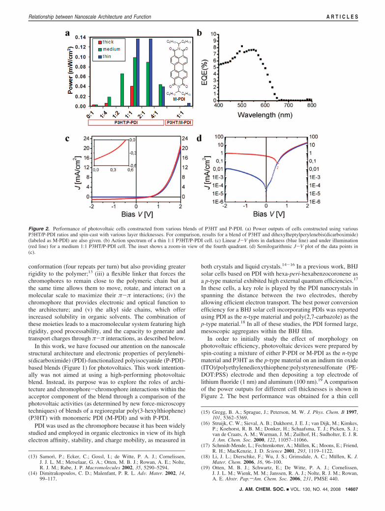
In order to initially study the effect of morphology onphotovoltaic efficiency, photovoltaic devices were prepared byspin-coating a mixture of either P-PDI or M-PDI as the n-typematerial and P3HT as the p-type material on an indium tin oxide(ITO)/polyethylenedioxythiophene:polystyrenesulfonate (PE-DOT:PSS) electrode and then depositing a top electrode oflithium fluoride (1 nm) and aluminum (100 nm).19 A comparisonof the power outputs for different cell thicknesses is shown inFigure 2. The best performance was obtained for a thin cell
(13) Samorı, P.; Ecker, C.; Gossl, I.; de Witte, P. A. J.; Cornelissen,J. J. L. M.; Metselaar, G. A.; Otten, M. B. J.; Rowan, A. E.; Nolte,R. J. M.; Rabe, J. P. Macromolecules 2002, 35, 5290–5294.
(14) Dimitrakopoulos, C. D.; Malenfant, P. R. L. AdV. Mater. 2002, 14,99–117.
(15) Gregg, B. A.; Sprague, J.; Peterson, M. W. J. Phys. Chem. B 1997,101, 5362–5369.
(16) Struijk, C. W.; Sieval, A. B.; Dakhorst, J. E. J.; van Dijk, M.; Kimkes,P.; Koehorst, R. B. M.; Donker, H.; Schaafsma, T. J.; Picken, S. J.;van de Craats, A. M.; Warman, J. M.; Zuilhof, H.; Sudholter, E. J. R.J. Am. Chem. Soc. 2000, 122, 11057–11066.
(17) Schmidt-Mende, L.; Fechtenkotter, A.; Mullen, K.; Moons, E.; Friend,R. H.; MacKenzie, J. D. Science 2001, 293, 1119–1122.
(18) Li, J. L.; Dierschke, F.; Wu, J. S.; Grimsdale, A. C.; Mullen, K. J.Mater. Chem. 2006, 16, 96–100.
(19) Otten, M. B. J.; Schwartz, E.; De Witte, P. A. J.; Cornelissen,J. J. L. M.; Wienk, M. M.; Janssen, R. A. J.; Nolte, R. J. M.; Rowan,A. E. Abstr. Pap.sAm. Chem. Soc. 2006, 231, PMSE 440.
Figure 2. Performance of photovoltaic cells constructed from various blends of P3HT and P-PDI. (a) Power outputs of cells constructed using variousP3HT/P-PDI ratios and spin-cast with various layer thicknesses. For comparison, results for a blend of P3HT and dihexylheptylperylenebis(dicarboximide)(labeled as M-PDI) are also given. (b) Action spectrum of a thin 1:1 P3HT/P-PDI cell. (c) Linear J-V plots in darkness (blue line) and under illumination(red line) for a medium 1:1 P3HT/P-PDI cell. The inset shows a zoom-in view of the fourth quadrant. (d) Semilogarithmic J-V plot of the data points in(c).
J. AM. CHEM. SOC. 9 VOL. 130, NO. 44, 2008 14607
Relationship between Nanoscale Architecture and Function A R T I C L E S
with a 1:1 ratio of the two materials, which gave an externalquantum efficiency (EQE) of 8.2% at 500 nm (see Figure 2b-dfor an action spectrum and J-V plots for this cell). Althoughthis device provided a modest overall efficiency of ∼0.2%,which is far from the state-of-the-art for organic solar cells, itwas noticeable that there was a 20-fold efficiency improvementfor the thin cell when the P-PDI was used instead of the M-PDI.The essence of the present study is the correlation between thisefficiency increase and the device and material architecture.Higher efficiencies for similar PDI monomers and P3HT havebeen reported, although to obtain these results, a considerablyhigher PDI content was needed.20
The relative improvement in efficiency obtained using thePDI multichromophoric wires is probably due to the interplayof several factors. First, the polymeric backbone may hinderthe formation of mesoscopic PDI crystals of the type commonlyobserved in self-assembled PDI architectures,17,21 and as a result,the interpenetration of P-PDI and P3HT, which is favorable forefficient charge separation between the donor and acceptor, canbe increased. Second, the linear structure of the PDI wires isexpected to preserve the percolation continuity of the electron-accepting phase, forming a continuous network and thusdecreasing the presence of dead ends and bottlenecks.
Recently, Kelvin probe force microscopy22 (KPFM), alsoknown as scanning Kelvin probe microscopy (SKPM), has beenextensively employed to characterize organic transistors23 andsolar cells.24-27 KPFM is a contactless technique that allowsthe quantitative measurement of the electric surface potential(SP) with nanoscale resolution without significantly perturbingthe potential of the system under study, thereby making possiblean in situ exploration of the operation of electronic devices.The SP of a sample can to a first approximation be consideredas the work function of the sample by taking into account effectsdue to the surface polarizability as well as band bending.
The goal of the research described below was to study moreclosely the origin of the increased photocurrent in devicescontaining P-PDI polymer compared with those incorporatingM-PDI. To this end, we present an “architecture versus function”study of simple donor-acceptor blends having PDI (in eitherin its “classical” monomeric form or the polymeric form) asthe electron acceptor and P3HT as the electron donor. Ultrathinlayers of both P-PDI/P3HT and M-PDI/P3HT blends have beenstudied using KPFM, allowing the observation of the differences
in photogeneration of charges and potential buildup for the twodifferent PDI morphologies with nanoscale spatial resolution.
Results and Discussion
Structural Characterization. The structural properties ofP-PDI have previously been characterized by several spectro-scopic techniques.12,19,28 Absorption spectroscopy measurementson P-PDI solutions revealed the presence of strong absorptionbands in the region 400-600 nm for the S0-S1 transition. Ablue shift of the absorption maximum with respect to that ofthe monomer precursor was detected, which is reminiscent ofexciton-coupled PDIs in a face-to-face geometry. In line withthis geometry, an excimer-like fluorescence was observed,29,30
indicating strong π-π interactions along the PDI stacks.The resulting polymers are extremely stiff, and in atomic force
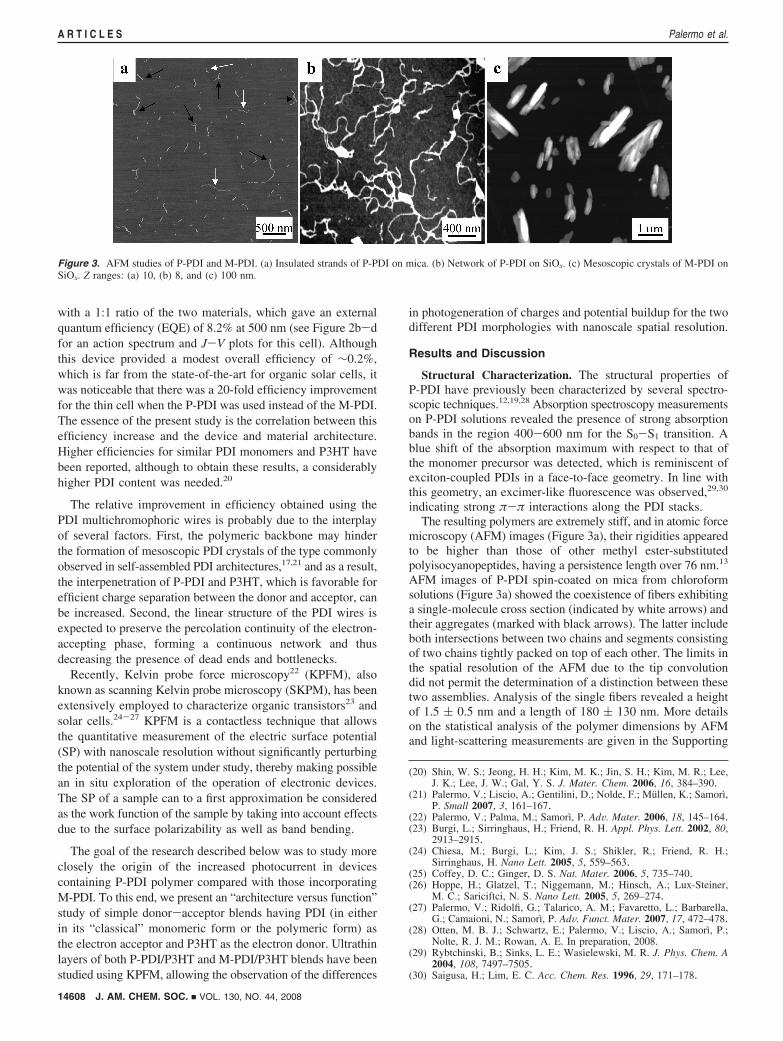
microscopy (AFM) images (Figure 3a), their rigidities appearedto be higher than those of other methyl ester-substitutedpolyisocyanopeptides, having a persistence length over 76 nm.13
AFM images of P-PDI spin-coated on mica from chloroformsolutions (Figure 3a) showed the coexistence of fibers exhibitinga single-molecule cross section (indicated by white arrows) andtheir aggregates (marked with black arrows). The latter includeboth intersections between two chains and segments consistingof two chains tightly packed on top of each other. The limits inthe spatial resolution of the AFM due to the tip convolutiondid not permit the determination of a distinction between thesetwo assemblies. Analysis of the single fibers revealed a heightof 1.5 ( 0.5 nm and a length of 180 ( 130 nm. More detailson the statistical analysis of the polymer dimensions by AFMand light-scattering measurements are given in the Supporting
(20) Shin, W. S.; Jeong, H. H.; Kim, M. K.; Jin, S. H.; Kim, M. R.; Lee,J. K.; Lee, J. W.; Gal, Y. S. J. Mater. Chem. 2006, 16, 384–390.
(21) Palermo, V.; Liscio, A.; Gentilini, D.; Nolde, F.; Mullen, K.; Samorı,P. Small 2007, 3, 161–167.
(22) Palermo, V.; Palma, M.; Samorı, P. AdV. Mater. 2006, 18, 145–164.(23) Burgi, L.; Sirringhaus, H.; Friend, R. H. Appl. Phys. Lett. 2002, 80,
2913–2915.(24) Chiesa, M.; Burgi, L.; Kim, J. S.; Shikler, R.; Friend, R. H.;
Sirringhaus, H. Nano Lett. 2005, 5, 559–563.(25) Coffey, D. C.; Ginger, D. S. Nat. Mater. 2006, 5, 735–740.(26) Hoppe, H.; Glatzel, T.; Niggemann, M.; Hinsch, A.; Lux-Steiner,
M. C.; Sariciftci, N. S. Nano Lett. 2005, 5, 269–274.(27) Palermo, V.; Ridolfi, G.; Talarico, A. M.; Favaretto, L.; Barbarella,
G.; Camaioni, N.; Samorı, P. AdV. Funct. Mater. 2007, 17, 472–478.(28) Otten, M. B. J.; Schwartz, E.; Palermo, V.; Liscio, A.; Samorı, P.;
Nolte, R. J. M.; Rowan, A. E. In preparation, 2008.(29) Rybtchinski, B.; Sinks, L. E.; Wasielewski, M. R. J. Phys. Chem. A
2004, 108, 7497–7505.(30) Saigusa, H.; Lim, E. C. Acc. Chem. Res. 1996, 29, 171–178.
Figure 3. AFM studies of P-PDI and M-PDI. (a) Insulated strands of P-PDI on mica. (b) Network of P-PDI on SiOx. (c) Mesoscopic crystals of M-PDI onSiOx. Z ranges: (a) 10, (b) 8, and (c) 100 nm.
14608 J. AM. CHEM. SOC. 9 VOL. 130, NO. 44, 2008
A R T I C L E S Palermo et al.
Information. This type of morphology was also obtained onother substrates, such as graphite and silicon. In particular, byspin-coating a concentrated (30 mg/L) P-PDI solution onto SiOx,a continuous, well-defined network of fiber bundles was obtained(Figure 3b). For the sake of comparison, M-PDI films were alsoprepared using similar conditions. AFM images of these filmsshowed the presence of mesoscopic crystals (some microns longand tens of nanometers thick; see Figure 3c), pointing to agreater aggregation tendency for the monomeric compound.
By and large, the characterizations in solution and on surfacesrevealed that the multichromophoric arrays exhibit differenteffects on different length scales. While the PDI packing is nothindered and strong π-π interactions are present on a molecularlevel, allowing rapid exciton diffusion, on a larger scale, theaggregation of the dye molecules is hampered, with themorphology on the micron scale being dictated by the polymericbackbone, which hinders the formation of large PDI crystals.
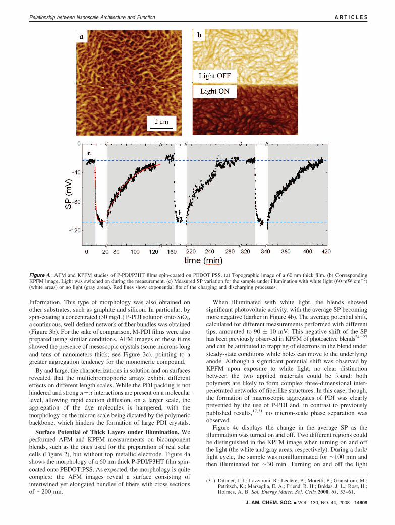
Surface Potential of Thick Layers under Illumination. Weperformed AFM and KPFM measurements on bicomponentblends, such as the ones used for the preparation of real solarcells (Figure 2), but without top metallic electrode. Figure 4ashows the morphology of a 60 nm thick P-PDI/P3HT film spin-coated onto PEDOT:PSS. As expected, the morphology is quitecomplex: the AFM images reveal a surface consisting ofintertwined yet elongated bundles of fibers with cross sectionsof ∼200 nm.
When illuminated with white light, the blends showedsignificant photovoltaic activity, with the average SP becomingmore negative (darker in Figure 4b). The average potential shift,calculated for different measurements performed with differenttips, amounted to 90 ( 10 mV. This negative shift of the SPhas been previously observed in KPFM of photoactive blends24-27
and can be attributed to trapping of electrons in the blend understeady-state conditions while holes can move to the underlyinganode. Although a significant potential shift was observed byKPFM upon exposure to white light, no clear distinctionbetween the two applied materials could be found: bothpolymers are likely to form complex three-dimensional inter-penetrated networks of fiberlike structures. In this case, though,the formation of macroscopic aggregates of PDI was clearlyprevented by the use of P-PDI and, in contrast to previouslypublished results,17,31 no micron-scale phase separation wasobserved.
Figure 4c displays the change in the average SP as theillumination was turned on and off. Two different regions couldbe distinguished in the KPFM image when turning on and offthe light (the white and gray areas, respectively). During a dark/light cycle, the sample was nonilluminated for ∼100 min andthen illuminated for ∼30 min. Turning on and off the light
(31) Dittmer, J. J.; Lazzaroni, R.; Leclere, P.; Moretti, P.; Granstrom, M.;Petritsch, K.; Marseglia, E. A.; Friend, R. H.; Bredas, J. L.; Rost, H.;Holmes, A. B. Sol. Energy Mater. Sol. Cells 2000, 61, 53–61.
Figure 4. AFM and KPFM studies of P-PDI/P3HT films spin-coated on PEDOT:PSS. (a) Topographic image of a 60 nm thick film. (b) CorrespondingKPFM image. Light was switched on during the measurement. (c) Measured SP variation for the sample under illumination with white light (60 mW cm-2)(white areas) or no light (gray areas). Red lines show exponential fits of the charging and discharging processes.
J. AM. CHEM. SOC. 9 VOL. 130, NO. 44, 2008 14609
Relationship between Nanoscale Architecture and Function A R T I C L E S
caused the measured SP to switch between two asymptoticvalues. From fits of the measured SP trends with exponentialcurves (the first two curves of which are shown in red), thetime constants for charge separation and recombination werecalculated to be ∼45 and 1500 s, respectively, revealing thatthe surface can remain charged for tens of minutes. Theseintervals are much longer than the photoinduduced charge-generation (∼10-12 s) and charge-collection (∼10-6 s) timesand hence point to the dynamics of charge trapping anddetrapping (see the Supporting Information for more details).The charging/discharging dynamics on the second-to-minutescale suggest that the high, stable potential differences observedby KPFM are influenced by the presence of traps.
The experimental setup used to obtain these results requiredthe samples to be prepared and measured in air. Thus, in orderto assess whether degradation of the material due to photooxi-dative processes might have taken place, each sample wassubjected to several dark/light cycles (Figure 4c), and the samemeasurements were then repeated after several days of storagein air. No significant differences were found in the measuredpotentials, indicating that if photooxidation was present, it hadalready taken place in the first minutes of exposure to air anddid not influence the variations observed in the subsequentKPFM experiments. It is reasonable to expect that similar KPFMexperiments performed in vacuum could exhibit even higherspatial and potential resolution also, in view of the more distinctphotovoltaic activity under an inert atmosphere.
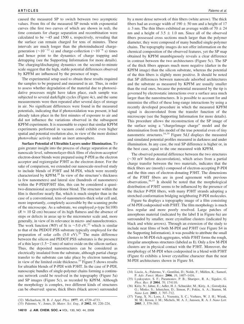
Surface Potential of Ultrathin Layers under Illumination. Togain greater insight into the process of charge separation at thenanoscale level, submonolayer-thick films of electron-acceptor/electron-donor blends were prepared using P-PDI as the electronacceptor and regioregular P3HT as the electron donor. For thesake of comparison, we extended our nanoscale-resolved studyto include blends of P3HT and M-PDI, which were recentlycharacterized by KPFM.28 In view of the structure’s thickness(a few nanometers) and lateral size (hundreds of nanometers)within the P-PDI/P3HT film, this can be considered a quasi-two-dimensional acceptor/donor blend. The structure within thefilm is therefore nearly flat, which is much simpler than in thecase of a conventional, tens-of-nanometers-thick solar cell and,more importantly, completely accessible by the scanning probeof the microscope. As a substrate, we employed p-type Si(100)(R ≈ 10 Ω cm) because of its high flatness and the absence ofsteps or defects in areas up to the micrometer scale and, moregenerally, in view of its relevance in micro- and nanoelectronics.The work function (WF) of Si is ∼5.0 eV,32 which is similarto that of the PEDOT:PSS substrate typically employed for thepreparation of solar cells (5.0 eV).20 The main differencebetween the silicon and PEDOT:PSS substrates is the presenceof a thin layer (1.5-2 nm) of native oxide on the silicon surface.Thus, the deposited nanostructures can be considered aselectrically insulated from the substrate, although partial chargetransfer to the substrate can take place by electron tunneling,in view of the limited oxide thickness.33 Figure 5 shows resultsfor ultrathin blends of P-PDI with P3HT. In the case of P-PDI,nanoscopic bundles of single-polymer chains forming a continu-ous network could be resolved in the topography (Figure 5a)and SP images (Figure 5c), as recorded by KPFM. Althoughthe morphology is complex, two different kinds of structurescan be observed: sparse, thick fibers (black arrow) surrounded
by a more dense network of thin fibers (white arrow). The thickfibers had an average width of 190 ( 50 nm and a height of 17( 3 nm. The thin fibers exhibited an average width of 70 ( 24nm and a height of 3.5 ( 1.0 nm. Since all of the observedfibers possessed cross sections much larger than the polymerdiameter, they were composed of many bundled single-polymerchains. The topography images do not offer information on thechemical composition of the observed features, yet the SP mapobtained by KPFM unambiguously reveals a clear differencein contrast between the two architectures (Figure 5c). The SPof the thick fibers appears much more negative (darker in theKPFM image) than the silicon substrate, whereas the potentialof the thin fibers is slightly more positive. It should be notedthat SP differences between nanoscale adsorbed architecturesand the substrate as measured by KPFM are usually smallerthan the real ones, because the potential measured by the tip isgoverned by electrostatic interactions over a surface area muchlarger than the nanostructures. It is possible to account for andminimize the effect of these long-range interactions by using arecently developed procedure in which the measured KPFMsignal is deconvoluted from the transfer function of themicroscope (see the Supporting Information for more details).This procedure allows the reconstruction of the SP image ofthe surface using a “charge/image charge” model and thedetermination from this model of the true potential even of tinynanometric structures.34,35 Figure 5d,f displays the measuredand simulated potential profiles measured in darkness and underillumination. In any case, the real SP difference is higher or, inthe best case, equal to the one measured with KPFM.
The observed potential difference between the two structures(∼30 mV before deconvolution), which arises from a partialcharge transfer between the two materials, indicates that thethick fibers are (mostly) composed of electron-accepting P-PDIand the thin ones of electron-donating P3HT. The dimensionsof the P3HT fibers are in good agreement with previousobservations,36,37 It should be noted that the morphologicaldistribution of P3HT seems to be influenced by the presence ofthe thicker P-PDI fibers, with many P3HT strands adopting astretched conformation bridging neighboring P-PDI molecules.
Figure 6a displays a topography image of a film consistingof M-PDI codeposited with P3HT. The film morphology is muchless regular and more poorly resolved. Large patches ofamorphous material (indicated by the label 1 in Figure 6a) aresurrounded by smaller, more crystalline clusters (indicated byblack and white arrows). Through an extension of the study toinclude neat films of both M-PDI and P3HT (see Figure S4 inthe Supporting Information), it was possible to attribute the smallclusters to M-PDI-rich aggregates, while P3HT forms the rough,irregular amorphous structures (labeled as 1). Only a few M-PDIclusters are in physical contact with the P3HT. Moreover, themorphology of M-PDI when codeposited in a blend with P3HT(Figure 6) exhibits a lower crystalline character than the neatM-PDI architectures shown in Figure S4.
(32) Michaelson, H. B. J. Appl. Phys. 1977, 48, 4729–4733.(33) Palermo, V.; Jones, D. Mater. Sci. Eng., B 2002, 88, 220–224.
(34) Liscio, A.; Palermo, V.; Gentilini, D.; Nolde, F.; Mullen, K.; Samorı,P. AdV. Funct. Mater. 2006, 16, 1407–1416.
(35) Lyuksyutov, S. F.; Paramonov, P. B.; Sharipov, R. A.; Sigalov, G.Phys. ReV. B 2004, 70, 174110.
(36) Kiriy, N.; Jahne, E.; Adler, H. J.; Schneider, M.; Kiriy, A.; Gorodyska,G.; Minko, S.; Jehnichen, D.; Simon, P.; Fokin, A. A.; Stamm, M.Nano Lett. 2003, 3, 707–712.
(37) Yang, X. N.; Loos, J.; Veenstra, S. C.; Verhees, W. J. H.; Wienk,M. M.; Kroon, J. M.; Michels, M. A. J.; Janssen, R. A. J. Nano Lett.2005, 5, 579–583.
14610 J. AM. CHEM. SOC. 9 VOL. 130, NO. 44, 2008
A R T I C L E S Palermo et al.
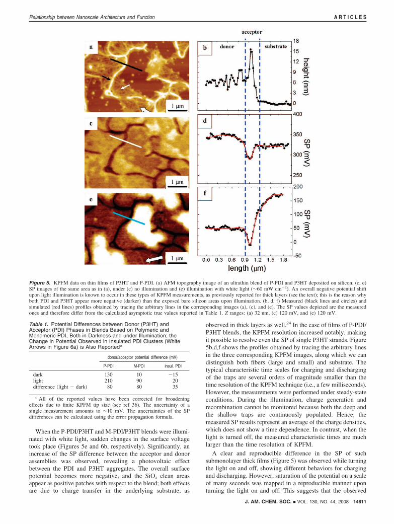
When the P-PDI/P3HT and M-PDI/P3HT blends were illumi-nated with white light, sudden changes in the surface voltagetook place (Figures 5e and 6b, respectively). Significantly, anincrease of the SP difference between the acceptor and donorassemblies was observed, revealing a photovoltaic effectbetween the PDI and P3HT aggregates. The overall surfacepotential becomes more negative, and the SiOx clean areasappear as positive patches with respect to the blend; both effectsare due to charge transfer in the underlying substrate, as
observed in thick layers as well.24 In the case of films of P-PDI/P3HT blends, the KPFM resolution increased notably, makingit possible to resolve even the SP of single P3HT strands. Figure5b,d,f shows the profiles obtained by tracing the arbitrary linesin the three corresponding KPFM images, along which we candistinguish both fibers (large and small) and substrate. Thetypical characteristic time scales for charging and dischargingof the traps are several orders of magnitude smaller than thetime resolution of the KPFM technique (i.e., a few milliseconds).However, the measurements were performed under steady-stateconditions. During the illumination, charge generation andrecombination cannot be monitored because both the deep andthe shallow traps are continuously populated. Hence, themeasured SP results represent an average of the charge densities,which does not show a time dependence. In contrast, when thelight is turned off, the measured characteristic times are muchlarger than the time resolution of KPFM.
A clear and reproducible difference in the SP of suchsubmonolayer thick films (Figure 5) was observed while turningthe light on and off, showing different behaviors for chargingand discharging. However, saturation of the potential on a scaleof many seconds was mapped in a reproducible manner uponturning the light on and off. This suggests that the observed
Figure 5. KPFM data on thin films of P3HT and P-PDI. (a) AFM topography image of an ultrathin blend of P-PDI and P3HT deposited on silicon. (c, e)SP images of the same area as in (a), under (c) no illumination and (e) illumination with white light (∼60 mW cm-2). An overall negative potential shiftupon light illumination is known to occur in these types of KPFM measurements, as previously reported for thick layers (see the text); this is the reason whyboth PDI and P3HT appear more negative (darker) than the exposed bare silicon areas upon illumination. (b, d, f) Measured (black lines and circles) andsimulated (red lines) profiles obtained by tracing the arbitrary lines in the corresponding images (a), (c), and (e). The SP values depicted are the measuredones and therefore differ from the calculated asymptotic true values reported in Table 1. Z ranges: (a) 32 nm, (c) 120 mV, and (e) 120 mV.
Table 1. Potential Differences between Donor (P3HT) andAcceptor (PDI) Phases in Blends Based on Polymeric andMonomeric PDI, Both in Darkness and under Illumination; theChange in Potential Observed in Insulated PDI Clusters (WhiteArrows in Figure 6a) is Also Reporteda
donor/acceptor potential difference (mV)
P-PDI M-PDI insul. PDI
dark 130 10 -15light 210 90 20difference (light - dark) 80 80 35
a All of the reported values have been corrected for broadeningeffects due to finite KPFM tip size (see ref 36). The uncertainty of asingle measurement amounts to ∼10 mV. The uncertainties of the SPdifferences can be calculated using the error propagation formula.
J. AM. CHEM. SOC. 9 VOL. 130, NO. 44, 2008 14611
Relationship between Nanoscale Architecture and Function A R T I C L E S
potential differences were due to charging of deep traps presentin both materials by photogenerated holes and electrons. Theuniform charging observed on thick and thin fibers shows thatthe photogenerated charges travel even tens of microns awayfrom the visible P-PDI/P3HT interfaces.
The surface potential measured at different points on theP-PDI fibers appeared to be uniform within experimental error,indicating a uniform level of charging of the material. The AFMand KPFM results shown above indicate that when depositedin ultrathin layers, P-PDI and P3HT form architectures that areeffectively phase-segregated yet interdigitated on a scale ofhundreds of nanometers, with both a high contact area betweenthe two materials and defined percolation paths for the charges.
A photovoltaic effect was also observed on M-PDI/P3HTblends,28 but there were significant differences with the resultsobtained for the P-PDI/P3HT system. First, the observedpotential difference between the two phases with the light offwas much smaller than in the case of P-PDI. Second, thecharging of the M-PDI clusters obtained upon light irradiationvaried greatly. Figure 6b displays the KPFM image correspond-ing to the topographic image shown in Figure 6a. In particular,upon light irradiation, the PDI clusters in contact with the P3HTisland (black arrows) became much more negatively charged(they appear more dark in the KPFM image) than the clustersat a larger distance from any P3HT island (white arrows). Figure6c,d shows in greater detail the morphology and SP images,respectively, of M-PDI agglomerates in contact with P3HT.Individual aggregates are marked by dotted contours in the SP
image. The part of the cluster in connection with P3HT has ahigher negative charge, while the other part of the same cluster,which is in contact with SiOx, has a lower charge. This evidenceindicates that the charges that are generated at the M-PDI/P3HTinterface are strongly localized and do not diffuse very far fromthe acceptor-donor interface.
Table 1 summarizes the potential differences observed forthe P-PDI/P3HT and M-PDI/P3HT blends both in darkness andunder illumination. All of the reported values have beencorrected for broadening effects due to the finite KPFM tipsize.34 Thin films of neat P-PDI or M-PDI adsorbed on nativesilicon oxide surfaces did not exhibit any change in potentialupon light irradiation, whereas thin films of P3HT showed onlya small, uniform (∼70 mV) potential change, as can be expectedas a result of the alignment of the P3HT HOMO level with theSP of the silicon substrate.20,32
Although the acceptor-donor potential differences (rows 1and 2 in Table 1) observed for the P-PDI-based blend are muchgreater than those for the M-PDI blend, the voltage buildupupon illumination (the light-dark difference, row 3 in Table1) is the same, indicating that the electronic properties of P-PDIare not significantly different from those of M-PDI.
Thus, in the particular case of ultrathin layers, the use ofP-PDI instead of M-PDI gives a blend which features (i) a goodcontact area between the two phases, (ii) a continuous percola-tion network for both types of polymeric bundles, and (iii) goodcharge diffusion, even at large distances from the acceptor-donorinterface. Comparison of the results obtained for M-PDI and
Figure 6. AFM and KPFM studies of M-PDI/P3HT blends. (a) Topographic and (b) corresponding KPFM images of a M-PDI/P3HT blend on native siliconoxide. The potential image was recorded under illumination with white light (60 mW cm-2). M-PDI agglomerates are isolated (white arrows) or in contact(black arrows) with P3HT islands (marked as 1). The regions inside the boxes in (a) and (b) are displayed at higher resolution in (c) and (d), respectively,showing in greater detail the morphology of the M-PDI agglomerates, which are marked by the dotted contours in the KPFM image. Z ranges: (a) 17 nm,(b) 63 mV, (c) 17 nm, and (d) 63 mV.
14612 J. AM. CHEM. SOC. 9 VOL. 130, NO. 44, 2008
A R T I C L E S Palermo et al.
P-PDI in solution, thin layers, and blends permits someconclusions to be drawn. In solution, the main effect of havinga polymeric backbone that bridges the PDI is that π-πinteractions (and hence electron migration) are more favored,leading to a blue shift in absorption and an excimer-likeemission, even in very dilute conditions (see refs 12 and 19).On surfaces, the morphologies obtained with the two PDImolecules are notably different: the presence of a polymericbackbone prevents aggregation of the dyes and formation oflarge crystals, giving a percolated network instead of the largeneedles observed with M-PDI. Finally, in blends with P3HT,the morphology and self-assembly behavior of M-PDI isperturbed, yielding clusters with low crystallinity and moredisordered crystals, whereas P-PDI forms well-defined networksin which the two components form bundles having differentdimensions.
It is likely that the HOMO and LUMO of a single PDIchromophore in P-PDI do not differ from those of a singleM-PDI because the N atoms of the imide groups are located atnodes in the π orbitals,38,39 and thus, the aromatic core isseparated from the polyisocyanide backbone by a peptide-propyllinker (Figure 1a) that does not influence the electronic structureof the PDI moiety.40 The only difference, observed by charac-terization in solution,12 is a stronger interaction between PDIsalong the polymeric backbone. Although the chemical andelectronic structures of the chromophores are not modified, thechanges in morphology and self-assembly properties in P-PDIas compared with M-PDI lead to a considerable difference inthe photovoltaic behaviors of the respective blends. Phasesegregation and clustering are absent in P-PDI, and its photo-induced potential difference (as measured by KPFM) is muchlarger; also, in contrast to the M-PDI blends, uniform chargingis obtained in each phase of the P-PDI blends over the wholesurface.
Conclusion and Outlook
In summary, we have employed a polyisocyanide-basedscaffold to form multichromophoric arrays of PDIs. When theseelectron-accepting and ultrarigid polymers were blended withan electron-donating system such as poly(3-hexylthiophene), acontinuous path of nanophase-segregated yet interdigitatedelectron-accepting and electron-donating nanostructures wasformed. Its morphological characterization was accomplishedby AFM and KPFM. Most significantly, in contrast to previousKPFM studies reporting on the characterization of mesoscopicfilms (with a layer thickness >100 nm), which could not offerdirect insight into the correlation between surface-potentialvariations and molecular structure, the KPFM measurementsperformed here show for the first time the nanoscale photovoltaicactivity in polymeric bundles of electron-accepting PDI wiresand bundles of electron-donating P3HT chains.
The use of rigid polymer chains as scaffolds to control theposition of dyes is not limited to PDI on polyisocyanides, anda whole class of ultrastiff nanowires based on different chro-
mophores is accessible.41 The possibility of independently tuningthe mechanical properties of the polymer [i.e., the rigidity ofthe wire (on the nanometer scale) and the linker flexibility anddye stacking (on the molecular scale)] by chemical modificationwill add to the continuously growing toolbox of nanoelectronicsa new class of materials with much improved mechanical andelectronic properties.
The ability to obtain highly resolved and quantitative mappingof the photovoltaic activity on a nanoscale has a huge potentialfor gaining a greater understanding of the processes of chargeseparation and charge mobility in polymer chains. This is crucialfor the optimization of various fundamental photophysicalproperties of a functional bicomponent macromolecular systemand ultimately for the improvement of the performance oforganic solar cells (e.g., with respect to power conversionefficiency). Ongoing research in our laboratories is directedtoward the study of high-performance photovoltaic blends viathe combination of scaffold materials and KPFM techniques.
Experimental Section
Photovoltaic devices were prepared by spin-coating a mixtureof P-PDI (as the n-type material) and regioregular P3HT (as thep-type material) on an ITO/PEDOT:PSS electrode and theneventually depositing a top electrode of lithium fluoride (1 nm)and aluminum (100 nm).19 P-PDI/P3HT) blends with weight ratiosvarying between 1/0 and 4/1 were spin-coated at different rotationspeeds (1500, 2500 and 4000 rpm) from chloroform solutions,giving films with different thicknesses, designated as thin (∼30nm), medium (∼60 nm), and thick (∼120 nm). The current-voltage(J-V) characteristics of the cells were measured in darkness andunder illumination with a tungsten halogen lamp. UV and IRcontributions were removed by Schott GG380 and Schott KG1filters, respectively. The final intensity of 75 mW/cm2 generated acurrent density in these devices that was within (20% of the currentdensity under solar illumination. This was confirmed by convolutionof the spectral responses with AM1.5 spectrum. For comparison,two cells in which P-PDI was replaced by M-PDI were prepared.
The thin layers were prepared by drop-casting ∼10 µL of achloroform solution containing both P-PDI (30 mg/L) and P3HT(7.5 mg/L) on silicon. On the other hand, films of M-PDI:P3HTblends were prepared in a two-step procedure starting from a 0.53mg/mL M-PDI solution and a 7.5 mg/L P3HT solution, both inCHCl3. First, a 10 µL drop of the M-PDI solution was drop-caston SiOx. After ∼3 h, a 10 µL drop of the P3HT solution was appliedon top of the M-PDI, and the film was left to dry in air. The blendfilms were prepared in atmosphere saturated with vapors of CHCl3
in order to slow down solvent evaporation and improve self-assembly. The silicon substrate was cleaned prior to use with astandard RCA procedure. In the ultrathin layers used here, verylow concentrations of both materials were deposited on the surfaces.The concentration of adsorbate on the surface can feature a highlocal compositional variability on the nanoscale, while on the scaleof hundreds of nanometers it complies with the ratio of the depositedmaterials. This behavior is different from that of classical thicklayers.
AFM/KPFM. AFM measurements on the P-PDI fibers foranalysis of heights and lengths were performed with a commercialAFM apparatus (Nanoscope III, Digital Instruments). A solutionof P-PDI (∼10-6 M in CHCl3) was spun (1600 rpm) onto freshlycleaved graphite or Muscovite mica. All of the images wererecorded with the AFM operating in tapping mode in air at roomtemperature, with a resolution of 512 × 512 pixels and moderatescan rates (1-2 lines/s). Commercial tapping-mode tips (NT-MDT,NSG10) with resonance frequencies of 190-325 kHz were used.
(38) Cotlet, M.; Masuo, S.; Luo, G. B.; Hofkens, J.; Van der Auweraer,M.; Verhoeven, J.; Mullen, K.; Xie, X. L. S.; De Schryver, F. Proc.Natl. Acad. Sci. U.S.A. 2004, 101, 14343–14348.
(39) De Schryver, F. C.; Vosch, T.; Cotlet, M.; Van der Auweraer, M.;Mullen, K.; Hofkens, J. Acc. Chem. Res. 2005, 38, 514–522.
(40) Balakrishnan, K.; Datar, A.; Naddo, T.; Huang, J. L.; Oitker, R.; Yen,M.; Zhao, J. C.; Zang, L. J. Am. Chem. Soc. 2006, 128, 7390–7398.
(41) de Witte, P. A. J.; Castriciano, M.; Cornelissen, J. J. L. M.; Scolaro,L. M.; Nolte, R. J. M.; Rowan, A. E. Chem.sEur. J. 2003, 9, 1775–1781.
J. AM. CHEM. SOC. 9 VOL. 130, NO. 44, 2008 14613
Relationship between Nanoscale Architecture and Function A R T I C L E S
In order to reduce surface contamination due to air and, inparticular, water and oxygen adsorption, the scanning probemeasurements were performed under an N2 atmosphere at a relativehumidity (RH) of < 10%.
Lengths and heights were evaluated using “Scanning Adventure”image-recognition software, which was developed by Jaques Barbet.For all of the values derived from AFM data presented in this paper,the error was evaluated as the standard deviation, as measured inmany different measurement sessions.
Measurements combining AFM with KPFM were performed atroom temperature in a sealed chamber filled with N2 (RH < 10%)using a commercial apparatus (Veeco Multimode IIIA equippedwith the Extender Electronics module). Antimony (n)-doped silicontips were used. In order to obtain sufficiently large and detectablemechanical deflections, we employed soft (k < 4 N/m) cantileverswith oscillating frequencies in the range 60 kHz < ω < 100 kHz(SCM, Veeco). Both sides of the cantilever were coated with 20nm of PtIr, using a buffer layer (3 nm) of Cr to improve theadhesion. To acquire “simultaneous” AFM and KPFM images, atopographic line scan was first obtained by AFM operating intapping mode, and then that same line was rescanned in lift modewith the tip raised to a lift height of ∼20 nm. The basic principlesof KPFM have been described in detail elsewhere.34 In brief, KPFMprovides a local measure of the SP differences between the con-ductive tip and the sample under investigation. The SP is definedas (WFtip - WFsample - ∆pol)/q, where WFtip and WFsample are thework functions of the tip and sample, respectively, ∆pol is thepolarization induced by the tip, and q is the magnitude ofthe elementary charge. In the KPFM experiments performed in thiswork, a bias voltage Vtip ) VDC + VAC sin ωt, where ω is theresonant frequency of the cantilever and VDC and VAC are continuousand alternate biases, respectively, was applied directly to the tip,and the sample was held at the ground potential. A feedback loopcontinually adjusted VDC to nullify the force component betweenthe tip and the sample at frequency ω. VDC was recorded as afunction of the position, yielding a map of the sample SP.Calibration and optimization of the experimental parameters wereachieved using the procedure proposed by Jacobs et al.42
Scanning probe microscopies are local probe techniques thatreveal local features, which are not necessarily representative ofthe whole sample surface. Because of this, it is appropriate to recordand process several images on different points of the sample surface.This makes it possible to minimize the influence of a particularsample area and to determine an average behavior. All of theevaluations were carried out quantitatively and averaged over a largenumber of samples. Widths measured with AFM were correctedfor tip broadening.43
Acknowledgment. We thank Dr. Giampaolo Zuccheri for hishelp in the analysis of the persistence length of P-PDI, Dr. ValentinaVillari and Dr. Norberto Micali for light-scattering measurements,and Jaques Barbet for developing and providing the ScanningAdventure image-processing software. This work was supportedby the chemistry section of The Netherlands Organization forScientific Research (top grant for R.J.M.N. and V.I.C.I. for A.E.R.),Nanoned STW (A.E.R.), the Royal Netherlands Academy for Artsand Sciences (KNAW), the ESF-SONS2-SUPRAMATES and ESF-SONS-BIONICS projects, the EU through the Marie Curie EST-SUPER (MEST-CT-2004-008128) and ForceTool (NMP4-CT-2004-013684) projects, the ERA-Chemistry project SurConFold,and the Regione Emilia-Romagna PRIITT Nanofaber Net-Labora-tory.
Supporting Information Available: Determination of polymerlength by AFM and light scattering, AFM studies of neat thinfilms of M-PDI and P3HT on SiOx, deconvolution proceduresfor the KPFM measurements, and optoelectronic characterizationof thick P-PDI/P3HT blends. This material is available free ofcharge via the Internet at http://pubs.acs.org.
JA804069N
(42) Jacobs, H. O.; Leuchtmann, P.; Homan, O. J.; Stemmer, A. J. Appl.Phys. 1998, 84, 1168–1173.
(43) Samorı, P.; Francke, V.; Mangel, T.; Mullen, K.; Rabe, J. P. Opt.Mater. 1998, 9, 390–393.
14614 J. AM. CHEM. SOC. 9 VOL. 130, NO. 44, 2008
A R T I C L E S Palermo et al.
Copyright © 2022 FDOKUMEN