
TRENCHSTOP™ 5 IGBT in a Kelvin Emitter Configuration
12
1 Revision 1.0, 2014-10-16 About this document Scope and purpose Introduction of new package TO-247 4pin with Kelvin Emitter connection, including performance comparison and design-in guidelines. Intended audience Development Engineers in the field of UPS, photovoltaic inverters and welding machines. Table of Contents 1 Introduction ............................................................................................................... 2 2 The Kelvin Emitter Configuration .................................................................................. 3 2.1 TO-247 4pin Package........................................................................................................................... 4 3 Electrical Switching Performance ................................................................................. 5 3.1 Behavior during Turn-on..................................................................................................................... 5 3.2 Behavior during Turn-off..................................................................................................................... 5 3.3 Total switching losses ......................................................................................................................... 7 4 Design guidelines ........................................................................................................ 8 4.1 Package Compatibility ........................................................................................................................ 8 4.2 Recommended Gate Driver ................................................................................................................. 8 4.3 Paralleling devices .............................................................................................................................. 9 5 Summary ................................................................................................................. 10 6 References ............................................................................................................... 11 IGBT Discrete TRENCHSTOP™ 5 TRENCHSTOP™ 5 IGBT in a Kelvin Emitter Configuration Performance Comparison and Design Guidelines Application Note
-
Upload
khangminh22 -
Category
Documents
-
view
1 -
download
0
Transcript of TRENCHSTOP™ 5 IGBT in a Kelvin Emitter Configuration

1 Revision 1.0, 2014-10-16
About this document
Scope and purpose
Introduction of new package TO-247 4pin with Kelvin Emitter connection, including performance
comparison and design-in guidelines.
Intended audience
Development Engineers in the field of UPS, photovoltaic inverters and welding machines.
Table of Contents
1 Introduction ............................................................................................................... 2
2 The Kelvin Emitter Configuration .................................................................................. 3
2.1 TO-247 4pin Package ........................................................................................................................... 4
3 Electrical Switching Performance ................................................................................. 5
3.1 Behavior during Turn-on ..................................................................................................................... 5 3.2 Behavior during Turn-off..................................................................................................................... 5 3.3 Total switching losses ......................................................................................................................... 7
4 Design guidelines ........................................................................................................ 8
4.1 Package Compatibility ........................................................................................................................ 8 4.2 Recommended Gate Driver ................................................................................................................. 8 4.3 Paralleling devices .............................................................................................................................. 9
5 Summary ................................................................................................................. 10
6 References ............................................................................................................... 11
IGB T Dis cr ete TRENCHSTOP™ 5
TR EN CHS T OP™ 5 I GB T i n a Kel v in Em itt er
Con figur at io n Performance Comparison and Design Guidelines
Application Note
TRENCHSTOP™ 5 IGBT in a Kelvin Emitter Configuration Performance Comparison and Design Guidelines
Introduction
Application Note 2 Revision 1.0, 2014-10-16
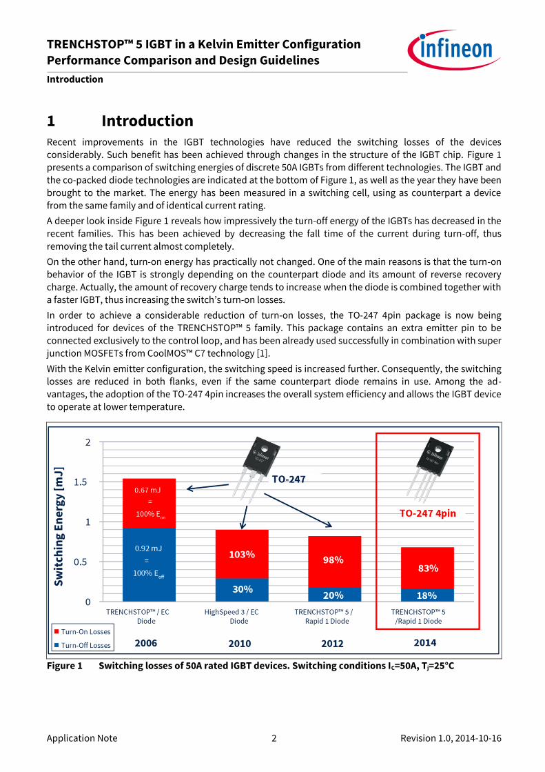
1 Introduction Recent improvements in the IGBT technologies have reduced the switching losses of the devices
considerably. Such benefit has been achieved through changes in the structure of the IGBT chip. Figure 1 presents a comparison of switching energies of discrete 50A IGBTs from different technologies. The IGBT and the co-packed diode technologies are indicated at the bottom of Figure 1, as well as the year they have been
brought to the market. The energy has been measured in a switching cell, using as counterpart a device from the same family and of identical current rating.
A deeper look inside Figure 1 reveals how impressively the turn-off energy of the IGBTs has decreased in the recent families. This has been achieved by decreasing the fall time of the current during turn-off, thus
removing the tail current almost completely.
On the other hand, turn-on energy has practically not changed. One of the main reasons is that the turn-on behavior of the IGBT is strongly depending on the counterpart diode and its amount of reverse recovery charge. Actually, the amount of recovery charge tends to increase when the diode is combined together with
a faster IGBT, thus increasing the switch’s turn-on losses.
In order to achieve a considerable reduction of turn-on losses, the TO-247 4pin package is now being
introduced for devices of the TRENCHSTOP™ 5 family. This package contains an extra emitter pin to be connected exclusively to the control loop, and has been already used successfully in combination with super
junction MOSFETs from CoolMOS™ C7 technology [1].
With the Kelvin emitter configuration, the switching speed is increased further. Consequently, the switching
losses are reduced in both flanks, even if the same counterpart diode remains in use. Among the ad-vantages, the adoption of the TO-247 4pin increases the overall system efficiency and allows the IGBT device to operate at lower temperature.
Figure 1 Switching losses of 50A rated IGBT devices. Switching conditions IC=50A, Tj=25°C

TRENCHSTOP™ 5 IGBT in a Kelvin Emitter Configuration Performance Comparison and Design Guidelines
The Kelvin Emitter Configuration
Application Note 3 Revision 1.0, 2014-10-16
2 The Kelvin Emitter Configuration In standard through-hole packages, as for instance TO-220 or TO-247, each lead pad resembles a parasitic
inductance. The inductance from the emitter pad in particular is a part of both, power and control loops.
As indicated in Figure 2, the power loop also includes the parasitic inductances coming from the collector lead and from the PCB tracks which connect the switching devices to the DC-link capacitor. The gate loop
contains the inductances coming from the gate lead and from the PCB tracks which connect the gate and emitter pads to the gate resistor and the gate driver.
(a) (b)
Figure 2 Emitter current variation and induced voltage over the emitter stray inductance during (a)
turn-on and (b) turn-off of the IGBT
The impact of the emitter lead inductance Le to the effective gate to emitter voltage during both, turn-on
and turn-off can be quantified respectively as:
𝑉𝐺𝐸.𝐸𝑓𝑓(𝑇𝑢𝑟𝑛−𝑜𝑛) = 𝑉𝐷𝑅𝑉.𝑂𝑁 − 𝑅𝐺 ∙ 𝐼𝐺 − 𝐿𝑒 ∙ 𝑑𝐼𝐶/𝑑𝑡⏟ 𝑉𝐿𝑒
(1) 1
𝑉𝐺𝐸.𝐸𝑓𝑓(𝑇𝑢𝑟𝑛−𝑜𝑓𝑓) = 𝑉𝐷𝑅𝑉.𝑂𝐹𝐹 − 𝑅𝐺 ∙ 𝐼𝐺 + 𝐿𝑒 ∙ 𝑑𝐼𝐶/𝑑𝑡⏟ 𝑉𝐿𝑒
(2) 2
As it can be deduced by equations (1) and (2), the effective gate to emitter voltage is attenuated during
transient conditions in both, turn-on and turn-off. Due to this attenuating, the commutation time is exten-ded, leading to higher switching losses.
VLe
dI/dt
Emitter
Collector
Gate
VDRV
C
E
RG
IG
PWM
Turn-ON
IE
Package
Turn-OFF
VLe
dI/dt
Emitter
Collector
Gate
VDRV
C
E
RG
IG
PWM
IE

TRENCHSTOP™ 5 IGBT in a Kelvin Emitter Configuration Performance Comparison and Design Guidelines
The Kelvin Emitter Configuration
Application Note 4 Revision 1.0, 2014-10-16
2.1 TO-247 4pin Package
The newly introduced TO-247 4pin package has an extra connection to the IGBT’s emitter, labeled E2 in Figure 3. This point shall be connected to the gate driver as shown in Fig. 3. Also known as Kelvin emitter terminal, this pin is not subject to the attenuation coming from the power loop. The current coming from
the IGBT’s collector is solely conducted by the power emitter lead E1.
Another difference from the TO-247 4pin package is the pin-out, which is different from the standard TO-247-3, as it can be seen in Figure 3. This is done to keep the creepage distance between the high voltage pins. In addition, the pins which are connected to the power loop, C and E1, are put side by side, so are those for the control loop E2 and G.
Figure 3 IGBT connection in Kelvin emitter configuration
This package will be identified in the Infineon’s IGBT nomenclature with the Letter “Z” at the third position.
This is indicated by the nomenclature scheme in Figure 4.
Figure 4 Example of the nomenclature of an IKZ50N65EH5. The letter “Z” at the third digit
identifies the TO-247 4pin package
50 65 E H5Z

TRENCHSTOP™ 5 IGBT in a Kelvin Emitter Configuration Performance Comparison and Design Guidelines
Electrical Switching Performance
Application Note 5 Revision 1.0, 2014-10-16
3 Electrical Switching Performance Without the attenuation of the gate voltage coming from the power emitter, the switching of the IGBT
becomes faster than in the standard TO-247 package. The impact on the switching energy is quantified in the next sections, firstly during turn-on and later for turn-off.
3.1 Behavior during Turn-on
To quantify the benefit of the Kelvin emitter configuration during turn-on, the IGBT IKZ50N65EH5 has been
used as the device under test (DUT). It is a 50A rated IGBT from the TRENCHSTOP™ 5 family in TO-247 4pin package.
In the first set of tests, the emitter pin E2 has not been connected. The output of the gate driver has been connected to pins G and E1. This emulates the standard TO-247 package and is referred to as 3-pin
configuration in Figure 5. In the second set, pins E1 and E2 have been connected as in Figure 3. This configuration is referred to as 4pin in Figure 5.
The comparison of the turn-on losses between both configurations is shown in Figure 5. A part available on the market with the same rated current in standard TO-247 has been included as reference. By switching at
the nominal current, 50A, the benefit of the Kelvin emitter configuration reaches 23% lower turn-on losses.
The IKZ50N65EH5 reveals 14% less turn-on losses than the part compared to.
Figure 5 Turn-off losses of an IKZ50N65EH5 in both 3pin and 4pin configurations. The losses from a
state-of-the-art part of the same current rating are also shown as reference
3.2 Behavior during Turn-off
As for the turn-on, the IGBT’s turn-off becomes faster inside the TO-247 4pin as well. Consequently, the current change rate dIC/dt is increased. In case the loop inductance is not improved, this will lead to a higher
overvoltage peak. Due to its very short rise time and low output capacity, the TRENCHSTOP™ 5 IGBTs are likely to present overvoltage peaks during turn-off [2]. This effect increases with the loop inductance Lloop according to:
𝛥𝑉𝐶𝐸 = 𝐿𝑙𝑜𝑜𝑝 ∙𝑑𝐼𝐶
𝑑𝑡⁄ (3)
0
1000
2000
3000
4000
5000
6000
0 A 25 A 50 A 75 A 100 A
E ON
[µJ]
IC,SW [A]
IKZ50N65H5 -EONComp. F
3-pin
4-pin
23% lower than 3-pin14% lower than Comp.

TRENCHSTOP™ 5 IGBT in a Kelvin Emitter Configuration Performance Comparison and Design Guidelines
Electrical Switching Performance
Application Note 6 Revision 1.0, 2014-10-16
This effect shall be considered in depth, since some applications like SMPS and UPS reserve a safety margin of 20% to the nominal breakdown voltage.
Figure 6 presents the impact of the package on the turn-off of the IKZ50N65H5, where the commutation voltage and current are 400V and 100A respectively. The junction temperature was Tj=25 °C. On the left side of Figure 6, the IGBT device is switched in the 3pin configuration. The maximum change rate of the collector current is 1.5A/ns, leading to an overvoltage peak of 530V.
On the right side of Figure 6, the same device is now switched in the 4pin configuration. The commutation speed is increased up to 2A/ns, leading to lower losses. However, the overvoltage peak reaches 570V, a value which is well above the margin of 20% to the breakdown voltage of the IGBT.
(a) (b)
Figure 6 Waveforms during the turn-off of an IKZ50N65EH5 in both (a) 3pin and (b) 4pin
configurations
To avoid such a high overvoltage, the loop inductance has to be reduced. This is done by optimizing the PCB
tracks and the placement of the components [2]. Alternatively, the gate resistor RG.OFF can be increased, leading to a slower commutation and lower dIC/dt. Figure 7 presents the overshoot voltage during turn-off of an IKZ50N65EH5 for different gate resistors and collector currents.
Figure 7 Voltage overshoot at turn-off for the 50A TRENCHSTOP™ 5 H5 IGBT as a function of the
collector current and gate resistor
As a consequence of increasing RG.OFF, the turn-off losses will increase and the benefit given by the TO-247 4pin will be partially cancelled at turn-off as depicted in the graph of Figure 8. By comparing the
530V
VCE
IC (Mirrored)
VG (G-E1)
50ns
Eoff=2.09 mJ
VG (G-E1)
VCE
570VIC (Mirrored)
50ns
Eoff=1.24 mJ
460
500
540
580
620
0 A 25 A 50 A 75 A 100 A
VC
E.M
AX
@ T
urn
-OFF
[V
]
IC,SW [A]
IKW50N65H5 (3Pin)
Roff=33 Ohm
Roff=39 Ohm
Roff=20 Ohm
80% VCE.MAX
460
500
540
580
620
0 A 25 A 50 A 75 A 100 AVC
E.M
AX
@ T
urn
-OFF
[V
]
IC,SW [A]
IKZ50N65EH5 (4Pin)
Roff=39 Ohm
Roff=47 Ohm
80% VCE.MAX

TRENCHSTOP™ 5 IGBT in a Kelvin Emitter Configuration Performance Comparison and Design Guidelines
Electrical Switching Performance
Application Note 7 Revision 1.0, 2014-10-16
turn-off losses of the 50A TRENCHSTOP™ 5 H5 IGBT, it is possible that a considerable benefit of the Kelvin emitter configuration is reached only for values exceeding the IGBT’s nominal current.
Figure 8 Turn-off losses of an IKZ50N65EH5 in both 3pin and 4pin configurations. The losses from a
comparable part of the same current rating are also shown as a reference
3.3 Total switching losses
The sum of switching losses of the three devices tested is presented in Figure 9 (a). The advantage of the
Kelvin emitter configuration is bigger for the highest currents. These are the conditions where highest current change rates are expected. Therefore, the lead inductance will attenuate the gate voltage the most in the 3-pin configuration.
(a) (b)
Figure 9 (a) Total switching energy of an IKZ50N65EH5, in both 3pin and 4pin configurations
(b) Switching energy reduction from 4pin configuration in both absolute and relative
values
As a consequence, in applications where the current is higher than the rated current of the IGBT, the switching loss reduction can be higher than 20%. This often is the case in Uninterruptable Power Supplies. For applications where the current is typically around half the IGBT’s current rating, like for example
photovoltaic inverters or switch mode power supplies (SMPS), the benefit is slightly lower but is still there, in the form of up to 15% lower switching losses.
0
1000
2000
3000
4000
5000
0 A 25 A 50 A 75 A 100 A
E OFF
[µJ]
IC,SW [A]
IKZ50N65H5 - EOFFComp. F3-pin4-pin
18% lower than 3-pin61% lower than Comp.

TRENCHSTOP™ 5 IGBT in a Kelvin Emitter Configuration Performance Comparison and Design Guidelines
Design guidelines
Application Note 8 Revision 1.0, 2014-10-16
4 Design guidelines To achieve a correct design-in of the new package, some points shall be considered. They are especially
valid when a migration from traditional TO-247 is taking place. Those points will be discussed in the following sections.
4.1 Package Compatibility
TRENCHSTOP™ 5 is so far the only IGBT generation in TO-247 4pin offered on the market. In case a second source is required, an arrangement on the part’s socket would enable to use a part in standard TO-247. One
possibility is presented in Figure 10.
For a correct thermal design, the difference in losses between the two packages shall be considered.
Figure 10 Possible arrangement of the IGBT socket to accept both TO-247 and TO-247 4pin packages
4.2 Recommended Gate Driver
Some recommendations with respect to the gate driver are:
The driver’s local ground, referenced to the auxiliary emitter, must be isolated from the power ground.
This is mandatory to prevent shortening pins E1 and E2
Separated RG.ON and RG.OFF are recommended since the optimized resistance for turn-on and turn-off can be very different from each other. This prevents an unnecessary increase in switching losses
Considering the above points, a good match for the driver IC is the EiceDRIVER™ Compact, recently launched [3]. Figure 11 depicts a typical connection between the driver and an IGBT in TO-247 4pin package.
Figure 11 Typical connection of EiceDRIVER™ Compact to an IGBT in TO-247 4pin package
G GC E1 E2
200 mils 100 mils
TO-247-3
TO-247-4
IGBT Socket
Emitter
Collector
Gate
VDRV
C
RG.ONPWM
E2
VLOGIC
RG.OFF
E1
EiceDRIVERTM
Compact
VCC1
GND1
IN +
IN -
VCC1
OUTH
OUTL
GND2

TRENCHSTOP™ 5 IGBT in a Kelvin Emitter Configuration Performance Comparison and Design Guidelines
Design guidelines
Application Note 9 Revision 1.0, 2014-10-16
4.3 Paralleling devices
When devices in TO-247 4pin package are paralleled, a further path exists for the circulating current between the devices. This path is through the connected Kelvin emitter terminals of the devices, as it can be seen in Figure 12 (a) Due to the low impedance of the path, a minor difference in the induced emitter voltage
VLe can generate an extremely high circulating current. This can happen for instance if the paralleled IGBTs have different switching times, therefore different dIC/dt ratios.
To limit the circulating current, a possible reconfiguration of the parallel circuit is shown in Figure 12 (b). The gate resistors are now split between RG and RE. This way, the extra path features a higher resistance, limiting the potentially dangerous current to non-critical values.
(a) (b)
Figure 12 (a) Parallel connection of three IGBTs and equalization current through the Kelvin emitter
connections (b) reconfiguration of the circuit with the split of gate resistor
As the total resistance seen by the driver will be the sum of RG and RE, these must be chosen accordingly. As a
rule of thumb, the ratio RE/RG is between 1/5 and 1/10. In order to achieve proper limitations, RE shall not be chosen lower than 0.5Ω.
C
E1E1 E1
E2 E2 E2
G G G
Driv
er
VLeVLe VLe
RG1 RG2 RG3
C CCurrent
Current
Circulating
current
C
E1 E1 E1
E2 E2 E2
G G G
Driv
er
VLe VLe VLe
RG1 RG2 RG3
RE1 RE3RE2
Current
Current
C C

TRENCHSTOP™ 5 IGBT in a Kelvin Emitter Configuration Performance Comparison and Design Guidelines
Summary
Application Note 10 Revision 1.0, 2014-10-16
5 Summary This application note has introduced the new TRENCHSTOP™ 5 IGBTs in a Kelvin emitter configuration using
a TO-247 4pin package. The benefit in terms of switching energy reduction in comparison to the standard TO-247 package has been obtained from practical measurements. It has been quantified as up to 20% lower switching energy for the nominal current.
This achievement helps TRENCHSTOP™ 5 to even further increase its distance to comparable parts and to
set itself as a benchmark in terms of switching losses.
The document also includes general hints on the driver IC to be used to drive the new IGBTs, so as how to implement a socket able to handle both, 3pin and 4pin packages.
Finally, the paralleling of two or more devices in TO-247 4pin has been discussed, including some hints to reduce the circulating current between devices.

TRENCHSTOP™ 5 IGBT in a Kelvin Emitter Configuration Performance Comparison and Design Guidelines
References
Application Note 11 Revision 1.0, 2014-10-16
6 References [1] Infineon Technologies AG: AN 2013-05, “CoolMOSTM C7 650 V Switch in a Kelvin Source Configuration”
[2] Brucchi, F., “How to Deal with TRENCHSTOP™ 5 IGBT in Power Applications”, Bodo’s Power, October 2013
[3] http://www.infineon.com/cms/en/product/power/gate-driver/eicedrivershigh-voltage-gate-driver-ics-and-boards/gate-driver-ic-eicedriver-compact/channel.html?channel=ff80808112ab681d0112ab6a547004ac
Revision History
Major changes since the last revision
Page or Reference Description of change
-- First Release

Published by
Infineon Technologies AG
81726 Munich, Germany
© 2014 Infineon Technologies AG. All Rights Reserved.
Do you have a question about any
aspect of this document?
Email: [email protected]
Legal Disclaimer THE INFORMATION GIVEN IN THIS APPLICATION NOTE (INCLUDING BUT NOT LIMITED TO CONTENTS OF REFERENCED WEBSITES) IS GIVEN AS A HINT FOR THE IMPLEMENTATION OF THE INFINEON TECHNOLOGIES COMPONENT ONLY AND SHALL NOT BE REGARDED AS ANY DESCRIPTION OR WARRANTY OF A CERTAIN FUNCTIONALITY, CONDITION OR QUALITY OF THE INFINEON TECHNOLOGIES COMPONENT. THE RECIPIENT OF THIS APPLICATION NOTE MUST VERIFY ANY FUNCTION DESCRIBED HEREIN IN THE REAL APPLICATION. INFINEON TECHNOLOGIES HEREBY DISCLAIMS ANY AND ALL WARRANTIES AND LIABILITIES OF ANY KIND (INCLUDING WITHOUT LIMITATION WARRANTIES OF NON-INFRINGEMENT OF INTELLECTUAL PROPERTY RIGHTS OF ANY THIRD PARTY) WITH RESPECT TO ANY AND ALL INFORMATION GIVEN IN THIS APPLICATION NOTE.
Information For further information on technology, delivery terms and conditions and prices, please contact the nearest Infineon Technologies Office (www.infineon.com).
Warnings Due to technical requirements, components may contain dangerous substances. For information on the types in question, please contact the nearest Infineon Technologies Office. Infineon Technologies components may be used in life-support devices or systems only with the express written approval of Infineon Technologies, if a failure of such components can reasonably be expected to cause the failure of that life-support device or system or to affect the safety or effectiveness of that device or system. Life support devices or systems are intended to be implanted in the human body or to support and/or maintain and sustain and/or protect human life. If they fail, it is reasonable to assume that the health of the user or other persons may be endangered.
www.infineon.com
Trademarks of Infineon Technologies AG AURIX™, C166™, CanPAK™, CIPOS™, CIPURSE™, CoolMOS™, CoolSET™, CORECONTROL™, CROSSAVE™, DAVE™, DI-POL™, EasyPIM™, EconoBRIDGE™, EconoDUAL™, EconoPIM™, EconoPACK™, EiceDRIVER™, eupec™, FCOS™, HITFET™, HybridPACK™, I²RF™, ISOFACE™, IsoPACK™, MIPAQ™, ModSTACK™, my-d™, NovalithIC™, OptiMOS™, ORIGA™, POWERCODE™, PRIMARION™, PrimePACK™, PrimeSTACK™, PRO-SIL™, PROFET™, RASIC™, ReverSave™, SatRIC™, SIEGET™, SINDRION™, SIPMOS™, SmartLEWIS™, SOLID FLASH™, TEMPFET™, thinQ!™, TRENCHSTOP™, TriCore™.
Other Trademarks Advance Design System™ (ADS) of Agilent Technologies, AMBA™, ARM™, MULTI-ICE™, KEIL™, PRIMECELL™, REALVIEW™, THUMB™, µVision™ of ARM Limited, UK. AUTOSAR™ is licensed by AUTOSAR development partnership. Bluetooth™ of Bluetooth SIG Inc. CAT-iq™ of DECT Forum. COLOSSUS™, FirstGPS™ of Trimble Navigation Ltd. EMV™ of EMVCo, LLC (Visa Holdings Inc.). EPCOS™ of Epcos AG. FLEXGO™ of Microsoft Corporation. FlexRay™ is licensed by FlexRay Consortium. HYPERTERMINAL™ of Hilgraeve Incorporated. IEC™ of Commission Electrotechnique Internationale. IrDA™ of Infrared Data Association Corporation. ISO™ of INTERNATIONAL ORGANIZATION FOR STANDARDIZATION. MATLAB™ of MathWorks, Inc. MAXIM™ of Maxim Integrated Products, Inc. MICROTEC™, NUCLEUS™ of Mentor Graphics Corporation. MIPI™ of MIPI Alliance, Inc. MIPS™ of MIPS Technologies, Inc., USA. muRata™ of MURATA MANUFACTURING CO., MICROWAVE OFFICE™ (MWO) of Applied Wave Research Inc., OmniVision™ of OmniVision Technologies, Inc. Openwave™ Openwave Systems Inc. RED HAT™ Red Hat, Inc. RFMD™ RF Micro Devices, Inc. SIRIUS™ of Sirius Satellite Radio Inc. SOLARIS™ of Sun Microsystems, Inc. SPANSION™ of Spansion LLC Ltd. Symbian™ of Symbian Software Limited. TAIYO YUDEN™ of Taiyo Yuden Co. TEAKLITE™ of CEVA, Inc. TEKTRONIX™ of Tektronix Inc. TOKO™ of TOKO KABUSHIKI KAISHA TA. UNIX™ of X/Open Company Limited. VERILOG™, PALLADIUM™ of Cadence Design Systems, Inc. VLYNQ™ of Texas Instruments Incorporated. VXWORKS™, WIND RIVER™ of WIND RIVER SYSTEMS, INC. ZETEX™ of Diodes Zetex Limited. Last Trademarks Update 2011-11-11
Edition 2014-10-16