HCPL-314J - 0.4 Amp Output Current IGBT Gate Drive ...
15
Features • 0.4 A minimum peak output current • High speed response: 0.7 µs max. propagation delay over temp. range • Ultra high CMR: min. 25 kV/µs at V CM = 1.5 kV • Bootstrappable supply current: max. 3 mA • Wide operating temp. range: -40°C to 100°C • Wide V CC operating range: 10 V to 30 V over temp. range • Available in DIP8 (single) and SO16 (dual) package • Safety approvals: UL recognized, 3750 Vrms for 1 minute. CSA approval. IEC/EN/DIN EN 60747-5-2 approval VIORM=891 Vpeak Applications • Isolated IGBT/power MOSFET gate drive • AC and brushless dc motor drives • Inverters for appliances • Industrial inverters • Switch Mode Power Supplies (SMPS) • Uninterruptable Power Supplies (UPS) Functional Diagram Truth Table LED V O OFF LOW ON HIGH HCPL-314J A 0.1 µF bypass capacitor must be connected between pins V CC and V EE . 1 3 SHIELD 2 8 16 14 15 9 N/C CATHODE ANODE N/C V CC V EE V O V EE 7 6 10 11 CATHODE ANODE V O V CC SHIELD Description The HCPL-314J family of devices consists of an Al- GaAs LED optically coupled to an integrated circuit with a power output stage. These optocouplers are ideally suited for driving power IGBTs and MOSFETs used in motor control inverter applications. The high operating voltage range of the output stage provides the drive voltages required by gate controlled devices. The voltage and current supplied by this optocou- pler makes it ideally suited for directly driving small or medium power IGBTs. For IGBTs with higher ratings the HCPL-3150(0.5A) or HCPL-3120 (2.0A) optocouplers can be used. HCPL-314J 0.4 Amp Output Current IGBT Gate Drive Optocoupler Data Sheet CAUTION: It is advised that normal static precautions be taken in handling and assembly of this component to prevent damage and/or degradation which may be induced by ESD. Selection Guide Package Type Part Number Number of Channels SO16 HCPL-314J 2 Lead (Pb) Free RoHS 6 fully compliant RoHS 6 fully compliant options available; -xxxE denotes a lead-free product
-
Upload
khangminh22 -
Category
Documents
-
view
1 -
download
0
Transcript of HCPL-314J - 0.4 Amp Output Current IGBT Gate Drive ...

Features• 0.4Aminimumpeakoutputcurrent• Highspeedresponse:
0.7µsmax.propagationdelayovertemp.range• UltrahighCMR:min.25kV/µsatVCM=1.5kV• Bootstrappablesupplycurrent:max.3mA• Wideoperatingtemp.range:-40°Cto100°C• WideVCCoperatingrange:10Vto30Vovertemp.
range• AvailableinDIP8(single)andSO16(dual)package• Safetyapprovals:ULrecognized,3750Vrmsfor
1minute.CSAapproval.IEC/EN/DINEN60747-5-2approvalVIORM=891Vpeak
Applications• IsolatedIGBT/powerMOSFETgatedrive• ACandbrushlessdcmotordrives• Invertersforappliances• Industrialinverters• SwitchModePowerSupplies(SMPS)• UninterruptablePowerSupplies(UPS)
Functional Diagram
Truth Table
LED VO
OFF LOW
ON HIGH
HCPL-314J
A0.1µFbypasscapacitormustbeconnectedbetweenpinsVCCandVEE.
1
3SHIELD
2
8
16
14
15
9
N/C
CATHODE
ANODE
N/C
VCC
VEE
VO
VEE
7
6
10
11
CATHODE
ANODE
VO
VCC
SHIELD
DescriptionThe HCPL-314J family of devices consists of an Al-GaAsLED optically coupled to an integrated circuitwith a power output stage. These optocouplers areideally suited for driving power IGBTs and MOSFETsused in motor control inverter applications. The highoperating voltage range of the output stage providesthedrivevoltages requiredbygatecontrolleddevices.The voltage and current supplied by this optocou-pler makes it ideally suited for directly driving smallor medium power IGBTs. For IGBTs with higher ratingstheHCPL-3150(0.5A)orHCPL-3120(2.0A)optocouplerscanbeused.
HCPL-314J0.4 Amp Output Current IGBT Gate Drive Optocoupler
Data Sheet
CAUTION: It is advised that normal static precautions be taken in handling and assembly of this component to prevent damage and/or degradation which may be induced by ESD.
Selection GuidePackage Type Part Number Number of Channels
SO16 HCPL-314J 2
Lead (Pb) FreeRoHS 6 fullycompliant
RoHS 6 fully compliant options available;-xxxE denotes a lead-free product
user
新建印章
2
Package Outline Drawing
HCPL-314J SO16 Package:
HCPL-314J8.76 ± 0.20(0.345 ± 0.008)
7.49 ± 0.10(0.295 ± 0.004)
0.016 ± 0.0003(0.406 ± 0.007)
3.51 ± 0.13(0.138 ± 0.005)
0.457(0.018)
1.27(0.050)
9°
16 15 14 11 10 9
1 2 3 6 7 8
VIEWFROMPIN 16
VIEWFROMPIN 1
0.64(0.025 MIN.)
10.36 ± 0.20(0.408 ± 0.008)
0.23(0.0091)
8.76 ± 0.20(0.345 ± 0.008)
ALL LEADS TO BE COPLANAR ± 0.05 mm (0.002 INCHES) .
DIMENSIONS IN MILLIMETERS AND (INCHES).
NOTE: FLOATING LEAD PROTRUSION IS 0.25 mm (10 mils) MAX.
0 - 8°
VC
C1
VO
1
GN
D1
VC
C2
VO
2
GN
D2
NC
VIN
1
V1
VIN
2
V2
NC
0.10 - 0.30(0.004 - 0.0118)
STANDOFF
TOP VIEW
11.63 (0.458)
2.16 (0.085)
0.64 (0.025)
LAND PATTERN RECOMMENDATION
Ordering Information
HCPL-314JisULRecognizedwith3750Vrmsfor1minuteperUL1577.
Part number
Option
PackageSurfaceMount
Tape& Reel
IEC/EN/DIN EN 60747-5-2 Quantity
RoHSCompliant
Non RoHSCompliant
HCPL-314J-000E No option
SO-16X X 45 per tube
-500E #500 X X X 850 per reel
Toorder,chooseapartnumberfromthepartnumbercolumnandcombinewiththedesiredoptionfromtheoptioncolumntoformanorderentry.
Example1:
HCPL-314J-500EtoorderproductofSO-16SurfaceMountpackageinTapeandReelpackagingwithIEC/EN/DINEN60747-5-2SafetyApprovalinRoHScompliant.
Example2:
HCPL-314JtoorderproductofSO-16SurfaceMountpackageintubepackagingwithIEC/EN/DINEN60747-5-2SafetyApprovalandnonRoHScompliant.
Optiondatasheetsareavailable.ContactyourAvagosalesrepresentativeorauthorizeddistributorforinformation.
Remarks:Thenotation‘#XXX’isusedforexistingproducts,while(new)productslaunchedsince15thJuly2001andRoHScompliantoptionwilluse‘-XXXE‘.
user
新建印章

3
Regulatory InformationThe HCPL-314J has been approvedbythefollowingorganizations:
IEC/EN/DIN EN 60747-5-2Approvedunder:IEC60747-5-2:1997+A1:2002EN60747-5-2:2001+A1:2002DINEN60747-5-2(VDE0884 Teil2):2003-01.UL
ApprovalunderUL1577,componentrecognition program up to VISO =3750Vrms.FileE55361.
CSA
ApprovedunderCSAComponentAc-ceptanceNotice#5,FileCA88324.
Solder Reflow Thermal Profile
Recommended Pb-Free IR Profile
0
TIME (SECONDS)
TE
MP
ER
AT
UR
E (
°C)
200
100
50 150100 200 250
300
0
30SEC.
50 SEC.
30SEC.
160°C
140°C150°C
PEAKTEMP.245°C
PEAKTEMP.240°C
PEAKTEMP.230°C
SOLDERINGTIME200°C
PREHEATING TIME150°C, 90 + 30 SEC.
2.5°C ± 0.5°C/SEC.
3°C + 1°C/–0.5°C
TIGHTTYPICALLOOSE
ROOMTEMPERATURE
PREHEATING RATE 3°C + 1°C/–0.5°C/SEC.REFLOW HEATING RATE 2.5°C ± 0.5°C/SEC.
217 °C
RAMP-DOWN6 °C/SEC. MAX.
RAMP-UP3 °C/SEC. MAX.
150 - 200 °C
260 +0/-5 °C
t 25 °C to PEAK
60 to 150 SEC.
20-40 SEC.
TIME WITHIN 5 °C of ACTUALPEAK TEMPERATURE
tp
tsPREHEAT
60 to 180 SEC.
tL
TL
TsmaxTsmin
25
Tp
TIME
TE
MP
ER
AT
UR
E
NOTES:THE TIME FROM 25 °C to PEAK TEMPERATURE = 8 MINUTES MAX.Tsmax = 200 °C, Tsmin = 150 °C
Note: Non-halide flux should be used.
Note: Non-halide flux should be used.
user
新建印章
4
OU
TP
UT
PO
WE
R –
PS
, IN
PU
T C
UR
RE
NT
– I S
00
TS – CASE TEMPERATURE – °C
200
600
400
25
HCPL-J314
800
50 75 100
200
150 175
PS (mW)
125
100
300
500
700IS (mA)
IEC/EN/DIN EN 60747-5-2 Insulation Characteristics Description Symbol Characteristic Unit
InstallationclassificationperDINVDE0110/1.89,Table1 forratedmainsvoltage≤150Vrms I-IV forratedmainsvoltage≤300Vrms I-IV forratedmainsvoltage≤600Vrms I-III
ClimaticClassification 55/100/21
PollutionDegree(DINVDE0110/1.89) 2
MaximumWorkingInsulationVoltage VIORM 891 Vpeak
InputtoOutputTestVoltage,Methodb* VIORMx1.875=VPR,100%ProductionTestwith VPR 1670 Vpeak tm=1sec,Partialdischarge<5pC
InputtoOutputTestVoltage,Methoda* VIORMx1.5=VPR,TypeandSampleTest,tm=60sec, VPR 1336 VpeakPartialdischarge<5pC
HighestAllowableOvervoltage VIOTM 6000 Vpeak (TransientOvervoltagetini=10sec)
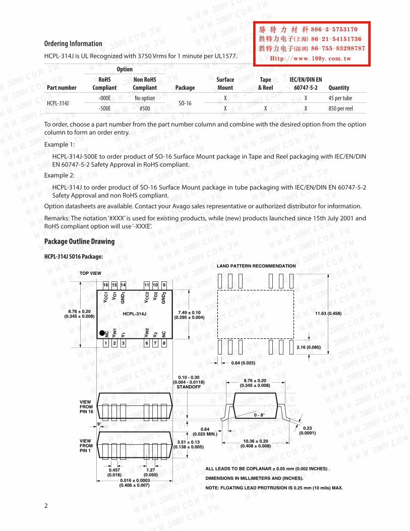
Safety-limitingvalues-maximumvaluesallowedinthe eventofafailure. CaseTemperature TS 175 °C InputCurrent** IS,INPUT 400 mA OutputPower** PS,OUTPUT 1200 mW
InsulationResistanceatTS,VIO=500V RS >109 Ω
*RefertotheoptocouplersectionoftheIsolationandControlComponentsDesigner’sCatalog,underProductSafetyRegulationssection, IEC/EN/DINEN60747-5-2,foradetaileddescriptionofMethodaandMethodbpartialdischargetestprofiles.
**RefertothefollowingfigurefordependenceofPSandISonambienttemperature.
user
新建印章
5
Insulation and Safety Related Specifications Parameter Symbol HCPL-314J Units Conditions
MinimumExternalAirGap L(101) 8.3 mm Measuredfrominputterminalstooutput (Clearance) terminals,shortestdistancethroughair.
MinimumExternalTracking L(102) 8.3 mm Measuredfrominputterminalstooutput (Creepage) terminals,shortestdistancepathalongbody.
MinimumInternalPlasticGap 0.5 mm Throughinsulationdistanceconductorto (InternalClearance) conductor,usuallythestraightlinedistance thicknessbetweentheemitteranddetector.
TrackingResistance CTI >175 V DINIEC112/VDE0303Part1 (ComparativeTrackingIndex)
IsolationGroup IIIa MaterialGroup(DINVDE0110,1/89,Table1)
Recommended Operating Conditions Parameter Symbol Min. Max. Units Note
PowerSupply VCC -VEE 10 30 V
InputCurrent(ON) IF(ON) 8 12 mA
InputVoltage(OFF) VF(OFF) -3.6 0.8 V
OperatingTemperature TA -40 100 °C
Absolute Maximum Ratings Parameter Symbol Min. Max. Units Note StorageTemperature TS -55 125 °C
OperatingTemperature TA -40 100 °C
AverageInputCurrent IF(AVG) 25 mA 1
PeakTransientInputCurrent(<1µspulse IF(TRAN) 1.0 A width,300pps)
ReverseInputVoltage VR 5 V
“High”PeakOutputCurrent IOH(PEAK) 0.6 A 2
“Low”PeakOutputCurrent IOL(PEAK) 0.6 A 2
SupplyVoltage VCC-VEE -0.5 35 V
OutputVoltage VO(PEAK) -0.5 VCC V
OutputPowerDissipation PO 260 mW 3
InputPowerDissipation PI 105 mW 4
LeadSolderTemperature 260°Cfor10sec.,1.6mmbelowseatingplane
SolderReflowTemperatureProfile SeePackage Outline Drawingssection
user
新建印章
6
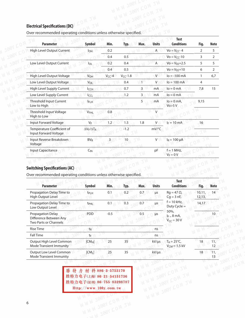
Electrical Specifications (DC)Overrecommendedoperatingconditionsunlessotherwisespecified.
Test Parameter Symbol Min. Typ. Max. Units Conditions Fig. Note
HighLevelOutputCurrent IOH 0.2 A Vo=VCC-4 2 5
0.4 0.5 Vo=VCC-10 3 2
LowLevelOutputCurrent IOL 0.2 0.4 A Vo=VEE+2.5 5 5
0.4 0.5 Vo=VEE+10 6 2
HighLevelOutputVoltage VOH VCC-4 VCC-1.8 V Io=-100mA 1 6,7
LowLevelOutputVoltage VOL 0.4 1 V Io=100mA 4
HighLevelSupplyCurrent ICCH 0.7 3 mA Io=0mA 7,8 15
LowLevelSupplyCurrent ICCL 1.2 3 mA Io=0mA
ThresholdInputCurrent IFLH 5 mA Io=0mA, 9,15 LowtoHigh Vo>5V
ThresholdInputVoltage VFHL 0.8 V HightoLow
InputForwardVoltage VF 1.2 1.5 1.8 V IF=10mA 16
TemperatureCoefficientof ∆VF/∆TA -1.2 mV/°C InputForwardVoltage
InputReverseBreakdown BVR 3 10 V IR=100µA Voltage
InputCapacitance CIN pF f=1MHz, VF=0V
Switching Specifications (AC)Overrecommendedoperatingconditionsunlessotherwisespecified.
Test Parameter Symbol Min. Typ. Max. Units Conditions Fig. Note
PropagationDelayTimeto tPLH 0.1 0.2 0.7 µs Rg=47Ω, 10,11, 14 HighOutputLevel Cg=3nF, 12,13,
PropagationDelayTimeto tPHL 0.1 0.3 0.7 µs f=10kHz, 14,17 LowOutputLevel DutyCycle=
PropagationDelay PDD -0.5 0.5 µs50%,
10 DifferenceBetweenAny
IF=8mA,
TwoPartsorChannels VCC=30V
RiseTime tR ns
FallTime tF ns
OutputHighLevelCommon |CMH| 25 35 kV/µs TA=25°C, 18 11, ModeTransientImmunity VCM=1.5kV 12
OutputLowLevelCommon |CML| 25 35 kV/µs 18 11, ModeTransientImmunity 13
user
新建印章

7
Package CharacteristicsForeachchannelunlessotherwisespecified.
Test Parameter Symbol Min. Typ. Max. Units Conditions Fig. Note
Input-OutputMomentary VISO 3750 Vrms TA=25°C, 8,9 WithstandVoltage RH<50%
Output-OutputMomentary VO-O 1500 Vrms for1min. 16 WithstandVoltage
Input-OutputResistance RI-O 1012 Ω VI-O=500V 9
Input-OutputCapacitance CI-O 1.2 pF Freq=1MHz
Notes: 1. Deratelinearlyabove70°Cfreeairtemperatureatarateof0.3mA/°C. 2. Maximumpulsewidth=10µs,maximumdutycycle=0.2%.ThisvalueisintendedtoallowforcomponenttolerancesfordesignswithIO
peakminimum=0.4A.SeeApplicationsectionforadditionaldetailsonlimitingIOLpeak. 3. Deratelinearlyabove85°C,freeairtemperatureattherateof4.0mW/°C. 4. Inputpowerdissipationdoesnotrequirederating. 5. Maximumpulsewidth=50µs,maximumdutycycle=0.5%. 6. Inthistest,VOHismeasuredwithaDCloadcurrent.WhendrivingcapacitiveloadVOHwillapproachVCCasIOHapproacheszeroamps. 7. Maximumpulsewidth=1ms,maximumdutycycle=20%. 8. InaccordancewithUL1577,eachHCPL-314Joptocouplerisprooftestedbyapplyinganinsulationtestvoltage≥5000Vrmsfor1second
(leakagedetectioncurrentlimitII-O≤5µA).Thistestisperformedbefore100%productiontestforpartialdischarge(methodB)shownintheIEC/EN/DINEN60747-5-2InsulationCharacteristicsTable,ifapplicable.
9. Deviceconsideredatwo-terminaldevice:pinsoninputsideshortedtogetherandpinsonoutputsideshortedtogether.10. PDDisthedifferencebetweentPHLandtPLHbetweenanytwopartsorchannelsunderthesametestconditions.11. Pins3and4(HCPL-314J)needtobeconnectedtoLEDcommon.12. Commonmodetransientimmunityinthehighstateisthemaximumtolerable|dVcm/dt|ofthecommonmodepulseVCMtoassurethatthe
outputwillremaininthehighstate(i.e.Vo>6.0V).13. Commonmodetransientimmunityinalowstateisthemaximumtolerable|dVCM/dt|ofthecommonmodepulse,VCM,toassurethatthe
outputwillremaininalowstate(i.e.Vo<1.0V).14. Thisloadconditionapproximatesthegateloadofa1200V/25AIGBT.15. Foreachchannel.ThepowersupplycurrentincreaseswhenoperatingfrequencyandQgofthedrivenIGBTincreases.16. Deviceconsideredatwoterminaldevice:Channeloneoutputsidepinsshortedtogether,andchanneltwooutputsidepinsshortedtogeth-
er.
user
新建印章
8
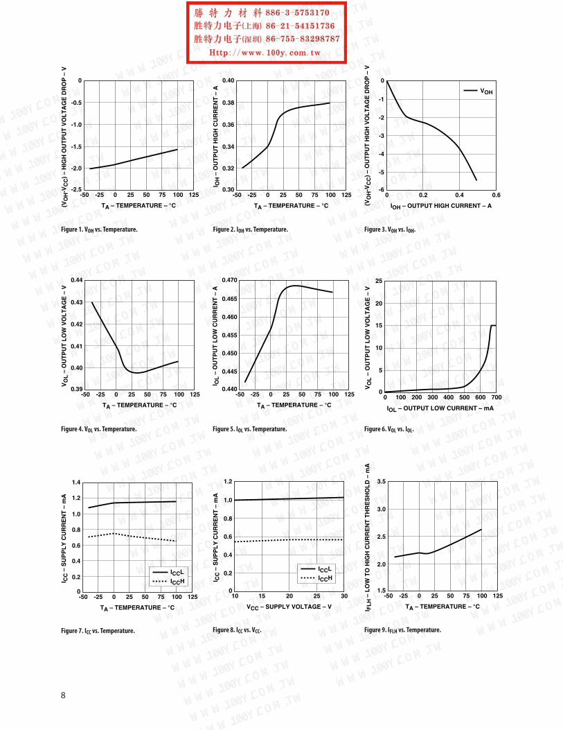
Figure 1. VOH vs. Temperature. Figure 2. IOH vs. Temperature. Figure 3. VOH vs. IOH.
Figure 4. VOL vs. Temperature. Figure 5. IOL vs. Temperature. Figure 6. VOL vs. IOL.
Figure 7. ICC vs. Temperature. Figure 8. ICC vs. VCC. Figure 9. IFLH vs. Temperature.
(VO
H-V
CC
) –
HIG
H O
UT
PU
T V
OL
TA
GE
DR
OP
– V
-50-2.5
TA – TEMPERATURE – °C
125-25
HCPL-J314 fig 01
0
0 25 75 10050
-2.0
-1.5
-1.0
-0.5
I OH
– O
UT
PU
T H
IGH
CU
RR
EN
T –
A
-500.30
TA – TEMPERATURE – °C
125-25
HCPL-J314 fig 02
0.40
0 25 75 10050
0.32
0.34
0.36
0.38
0-6
IOH – OUTPUT HIGH CURRENT – A
0.6
HCPL-J314 fig 03
0
0.2 0.4
-5
-4
-3
-1
(VO
H-V
CC
) –
OU
TP
UT
HIG
H V
OL
TA
GE
DR
OP
– V
-2
VOH
VO
L –
OU
TP
UT
LO
W V
OL
TA
GE
– V
-500.39
TA – TEMPERATURE – °C
125-25
HCPL-J314 fig 04
0.44
0 25 75 10050
0.40
0.41
0.42
0.43
I OL
– O
UT
PU
T L
OW
CU
RR
EN
T –
A
-500.440
TA – TEMPERATURE – °C
125-25
HCPL-J314 fig 05
0.470
0 25 75 10050
0.450
0.455
0.460
0.465
0.445
I CC
– S
UP
PL
Y C
UR
RE
NT
– m
A
-500
TA – TEMPERATURE – °C
125-25
HCPL-J314 fig 07
1.4
0 25 75 10050
0.4
0.6
0.8
1.2
0.2
1.0
ICCL
ICCH I CC
– S
UP
PL
Y C
UR
RE
NT
– m
A
100
VCC – SUPPLY VOLTAGE – V
3015
HCPL-J314 fig 08
1.2
20 25
0.4
0.8
0.2
0.6
1.0
ICCL
ICCH
I FL
H –
LO
W T
O H
IGH
CU
RR
EN
T T
HR
ES
HO
LD
– m
A
-501.5
TA – TEMPERATURE – °C
125-25
HCPL-J314 fig 09
3.5
0 25 75 10050
2.0
2.5
3.0
VO
L –
OU
TP
UT
LO
W V
OL
TA
GE
– V
00
IOL – OUTPUT LOW CURRENT – mA
700100
HCPL-J314 fig 06
25
400 500
5
20
200 300 600
15
10
user
新建印章
9
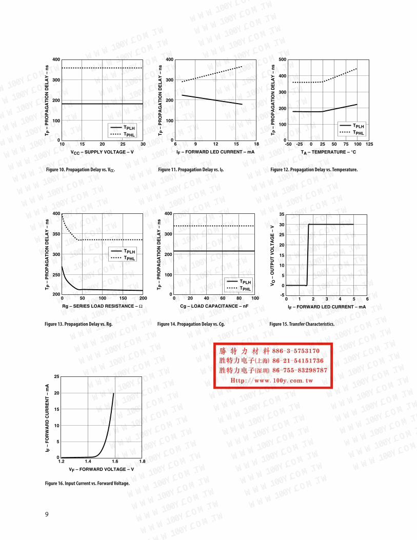
Figure 10. Propagation Delay vs. VCC. Figure 11. Propagation Delay vs. IF. Figure 12. Propagation Delay vs. Temperature.
Figure 13. Propagation Delay vs. Rg. Figure 14. Propagation Delay vs. Cg. Figure 15. Transfer Characteristics.
Figure 16. Input Current vs. Forward Voltage.
TP
– P
RO
PA
GA
TIO
N D
EL
AY
– n
s
60
IF – FORWARD LED CURRENT – mA
18
HCPL-J314 fig 11
400
9 1512
100
200
300
-500
TA – TEMPERATURE – °C
125-25
HCPL-J314 fig 12
500
0 25 75 10050
100
200
300
400
TP
– P
RO
PA
GA
TIO
N D
EL
AY
– n
s
TPLHTPHL
TP
– P
RO
PA
GA
TIO
N D
EL
AY
– n
s
0200
Rg – SERIES LOAD RESISTANCE – Ω
200
HCPL-J314 fig 13
400
50 150100
250
300
350
TPLHTPHL
VO
– O
UT
PU
T V
OL
TA
GE
– V
0-5
IF – FORWARD LED CURRENT – mA
6
25
15
1
HCPL-J314 fig 15
35
2 3 4
5
5
0
10
20
30
I F –
FO
RW
AR
D C
UR
RE
NT
– m
A
1.20
VF – FORWARD VOLTAGE – V
1.8
HCPL-J314 fig 16
25
1.4 1.6
5
10
15
20
TP
– P
RO
PA
GA
TIO
N D
EL
AY
– n
s
00
Cg – LOAD CAPACITANCE – nF
100
HCPL-J314 fig 14
400
20 8060
100
200
300
TPLHTPHL
40
TP
– P
RO
PA
GA
TIO
N D
EL
AY
– n
s
100
VCC – SUPPLY VOLTAGE – V
30
HCPL-J314 fig 10
400
15 2520
100
200
300
TPLHTPHL
user
新建印章
10
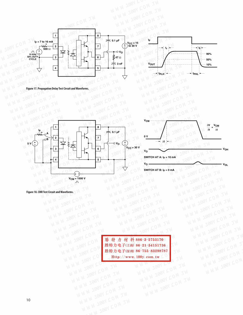
Figure 17. Propagation Delay Test Circuit and Waveforms.
Figure 18. CMR Test Circuit and Waveforms.
0.1 µFVCC = 15to 30 V
47 Ω
1
3
IF = 7 to 16 mA
VO
+–
+–
2
4
8
6
7
5
10 KHz50% DUTY
CYCLE
500 Ω
3 nF
IF
VOUT
tPHLtPLH
tftr
10%
50%
90%
0.1 µF
VCC = 30 V
1
3
IF
VO+–
+–
2
4
8
6
7
5
A
+ –
B
VCM = 1500 V
5 V
VCM
∆t
0 V
VO
SWITCH AT B: IF = 0 mA
VO
SWITCH AT A: IF = 10 mA
VOL
VOH
∆t
VCMδV
δt=
user
新建印章
11
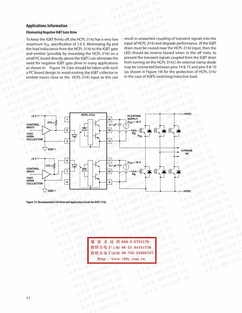
Applications InformationEliminating Negative IGBT Gate Drive
TokeeptheIGBTfirmlyoff,theHCPL-314JhasaverylowmaximumVOLspecificationof1.0V.MinimizingRgandtheleadinductancefromtheHCPL-314JtotheIGBTgateandemitter(possiblybymountingtheHCPL-314JonasmallPCboarddirectlyabovetheIGBT)caneliminatetheneedfornegativeIGBTgatedriveinmanyapplicationsasshowninFigure19.CareshouldbetakenwithsuchaPCboarddesigntoavoidroutingtheIGBTcollectororemittertracesclosetotheHCPL-314Jinputasthiscan
resultinunwantedcouplingoftransientsignalsintotheinputofHCPL-314Janddegradeperformance.(IftheIGBTdrainmustberoutedneartheHCPL-314Jinput,thentheLED should be reverse biased when in the off state, topreventthetransientsignalscoupledfromtheIGBTdrainfromturningontheHCPL-314J.)Anexternalclampdiodemaybeconnectedbetweenpins14&15andpins9&10(asshowninFigure19)fortheprotectionofHCPL-314JinthecaseofIGBTsswitchinginductiveload.
Figure 19. Recommended LED Drive and Application Circuit for HCPL-314J.
+ HVDC
3-PHASE AC
0.1 µF
FLOATINGSUPPLYVCC = 18 V
1
3
+–
2
16
14
15
270 Ω
HCPL-314J+5 V
CONTROLINPUT
Rg74XXOPENCOLLECTOR
GND 1
7
6
8
10
11
9
- HVDC
0.1 µFVCC = 18 V
+–
Rg
270 Ω
+5 V
CONTROLINPUT
74XXOPENCOLLECTOR
GND 1
VOL
user
新建印章
12
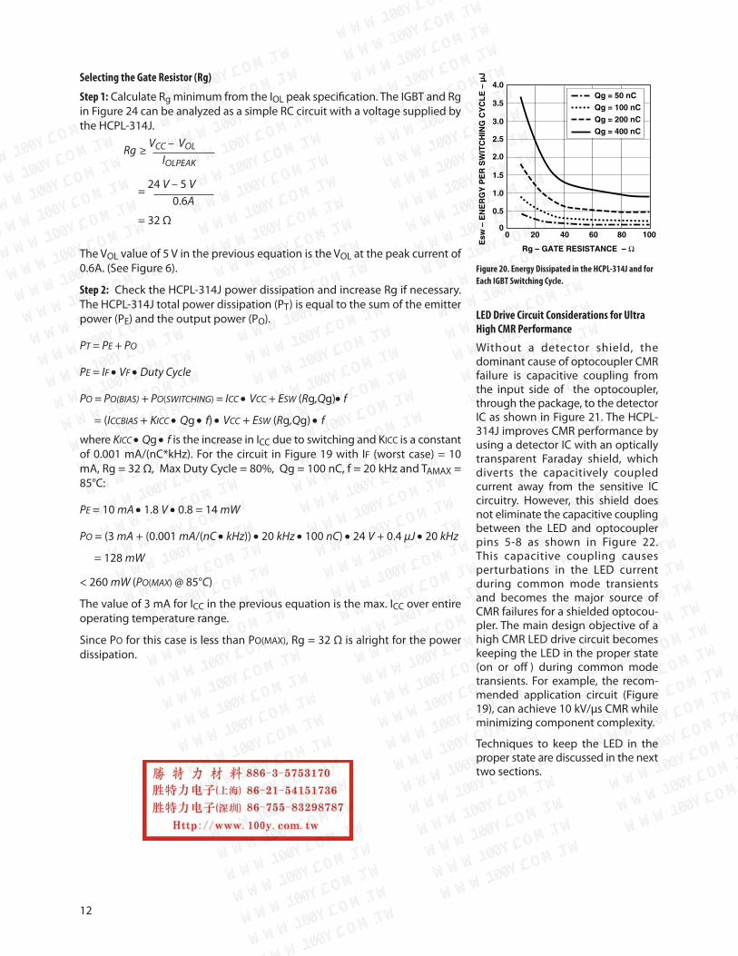
Figure 20. Energy Dissipated in the HCPL-314J and for Each IGBT Switching Cycle.
=24V–5V 0.6A
=32Ω
Rg ≥ VCC – VOL IOLPEAK
LED Drive Circuit Considerations for Ultra High CMR Performance Without a detector shield, thedominantcauseofoptocouplerCMRfailure is capacitive coupling fromthe input side of the optocoupler,throughthepackage,tothedetectorICasshowninFigure21.TheHCPL-314JimprovesCMRperformancebyusingadetectorICwithanopticallytransparent Faraday shield, whichdiverts the capacitively coupledcurrent away from the sensitive ICcircuitry. However, this shield doesnoteliminatethecapacitivecouplingbetween the LED and optocouplerpins 5-8 as shown in Figure 22.This capacitive coupling causesperturbations in the LED currentduring common mode transientsand becomes the major source ofCMRfailuresforashieldedoptocou-pler.ThemaindesignobjectiveofahighCMRLEDdrivecircuitbecomeskeepingtheLEDintheproperstate(on or off ) during common modetransients. For example, the recom-mended application circuit (Figure19),canachieve10kV/µsCMRwhileminimizingcomponentcomplexity.
Techniques to keep the LED in theproperstatearediscussedinthenexttwosections.
Selecting the Gate Resistor (Rg)
Step 1:CalculateRgminimumfromtheIOLpeakspecification.TheIGBTandRginFigure24canbeanalyzedasasimpleRCcircuitwithavoltagesuppliedbytheHCPL-314J.
TheVOLvalueof5VinthepreviousequationistheVOLatthepeakcurrentof0.6A.(SeeFigure6).
Step 2:ChecktheHCPL-314JpowerdissipationandincreaseRgifnecessary.TheHCPL-314Jtotalpowerdissipation(PT)isequaltothesumoftheemitterpower(PE)andtheoutputpower(PO).
PT = PE + PO
PE = IF • VF • Duty Cycle
PO = PO(BIAS) + PO(SWITCHING) = ICC • VCC + ESW (Rg,Qg)• f
=(ICCBIAS+KICC • Qg • f) • VCC+ESW(Rg,Qg) • f
whereKICC • Qg • fistheincreaseinICCduetoswitchingandKICC isaconstantof0.001mA/(nC*kHz).Forthecircuit inFigure19with IF (worstcase)=10mA,Rg=32Ω,MaxDutyCycle=80%,Qg=100nC,f=20kHzandTAMAX=85°C:
PE =10mA • 1.8V• 0.8=14mW
PO=(3mA+(0.001mA/(nC • kHz))• 20kHz• 100nC)• 24V+0.4µJ• 20kHz
=128mW
<260mW (PO(MAX)@85°C)
Thevalueof3mAforICCinthepreviousequationisthemax.ICCoverentireoperatingtemperaturerange.
SincePOforthiscaseislessthanPO(MAX),Rg=32Ωisalrightforthepowerdissipation.
Esw
– E
NE
RG
Y P
ER
SW
ITC
HIN
G C
YC
LE
– µ
J
00
Rg – GATE RESISTANCE – Ω
100
1.5
20
4.0
40
1.0
60 80
3.5Qg = 50 nC
Qg = 100 nC
Qg = 200 nC
Qg = 400 nC3.0
2.0
0.5
2.5
user
新建印章

13
Figure 21. Optocoupler Input to Output Capacitance Model for Un-shielded Optocouplers.
Figure 22. Optocoupler Input to Output Capacitance Model for Shielded Optocouplers.
Figure 23. Equivalent Circuit for Figure 17 During Common Mode Transient.
Figure 24. Not Recommended Open Collector Drive Circuit. Figure 25. Recommended LED Drive Circuit for Ultra-High CMR IPM Dead Time and Propagation Delay Specifications.
HCPL-J314 fig 23
1
3
2
4
8
6
7
5
CLEDP
CLEDN
SHIELD
CLEDO1
CLEDO2
HCPL-J314 fig 24
Rg
1
3
VSAT
2
4
8
6
7
5
+
VCM
ILEDP
CLEDP
CLEDN
SHIELD
* THE ARROWS INDICATE THE DIRECTIONOF CURRENT FLOW DURING –dVCM/dt.
+5 V
+– VCC = 18 V
• • •
• • •
0.1µF
+
–
–
HCPL-J314 fig 25
1
3
2
4
8
6
7
5
CLEDP
CLEDN
SHIELD
+5 V
Q1ILEDN
HCPL-J314 fig 26
1
3
2
4
8
6
7
5
CLEDP
CLEDN
SHIELD
+5 V
HCPL-J314 fig 22
1
3
2
4
8
6
7
5
CLEDP
CLEDN
user
新建印章
14
CMR with the LED On (CMRH)
A high CMR LED drive circuit must keep the LED onduring common mode transients. This is achieved byoverdrivingtheLEDcurrentbeyondtheinputthresholdso that it is not pulled below the threshold during atransient. A minimum LED current of 8 mA providesadequate margin over the maximum IFLH of 5 mA toachieve10kV/µsCMR.
CMR with the LED Off (CMRL)
AhighCMRLEDdrivecircuitmustkeeptheLEDoff(VF≤VF(OFF))duringcommonmodetransients.Forexample,during a -dVCM/dt transient in Figure 23, the currentflowingthroughCLEDPalsoflowsthroughtheRSATandVSATofthe logicgate.As longasthe lowstatevoltagedevelopedacrossthelogicgateislessthanVF(OFF)theLED will remain off and no common mode failure willoccur.
Theopencollectordrivecircuit,showninFigure24,cannotkeeptheLEDoffduringa+dVCM/dttransient,sinceallthecurrentflowingthroughCLEDNmustbesuppliedbytheLED,anditisnotrecommendedforapplicationsrequiringultrahighCMR1performance.Thealternativedrive circuit which like the recommended applicationcircuit (Figure19),doesachieveultrahighCMRperfor-mancebyshuntingtheLEDintheoffstate.
IPM Dead Time and Propagation Delay Specifications
The HCPL-314J includes a Propagation Delay Dif-ference (PDD) specification intended to helpdesigners minimize “dead time” in their powerinverter designs. Dead time is the time high andlow side power transistors are off. Any overlapin Ql and Q2 conduction will result in large currentsflowing through the power devices from the high-voltagetothelow-voltagemotorrails.Tominimizedeadtime in a given design, the turn on of LED2 should bedelayed(relativetotheturnoffofLED1)sothatunderworst-caseconditions,transistorQ1has justturnedoffwhentransistorQ2turnson,asshowninFigure26.Theamountofdelaynecessary toachieve thiscondition isequal to themaximumvalueof thepropagationdelaydifference specification, PDD max, which is specifiedto be 500 ns over the operating temperature range of-40°to100°C.
Delaying the LED signal by the maximum propaga-tion delay difference ensures that the minimum deadtime is zero, but it does not tell a designer what themaximum dead time will be. The maximum deadtime is equivalent to the difference between themaximum and minimum propagation delay dif-ference specification as shown in Figure 27. Themaximum dead time for the HCPL-314J is 1 µs (= 0.5µs - (-0.5µs))over theoperatingtemperature rangeof- 40°Cto100°C.
NotethatthepropagationdelaysusedtocalculatePDDanddeadtimearetakenatequaltemperaturesandtestconditionssincetheoptocouplersunderconsiderationare typicallymounted incloseproximity toeachotherandareswitchingidenticalIGBTs.
user
新建印章
For product information and a complete list of distributors, please go to our website: www.avagotech.com
Avago, Avago Technologies, and the A logo are trademarks of Avago Technologies Limited in the United States and other countries.Data subject to change. Copyright © 2005-2008 Avago Technologies Limited. All rights reserved. Obsoletes 5989-2943ENAV02-0169EN - April 9, 2008
Figure 26. Minimum LED Skew for Zero Dead Time.
Figure 27. Waveforms for Dead Time.
tPHL MAX
tPLH MIN
PDD* MAX = (tPHL- tPLH)MAX = tPHL MAX - tPLH MIN
*PDD = PROPAGATION DELAY DIFFERENCENOTE: FOR PDD CALCULATIONS THE PROPAGATION DELAYSARE TAKEN AT THE SAME TEMPERATURE AND TEST CONDITIONS.
VOUT1
ILED2
VOUT2
ILED1
Q1 ON
Q2 OFF
Q1 OFF
Q2 ON
HCPL-J314 fig 27
tPLHMIN
MAXIMUM DEAD TIME(DUE TO OPTOCOUPLER)= (tPHL MAX - tPHL MIN) + (tPLH MAX - tPLH MIN)= (tPHL MAX - tPLH MIN) – (tPHL MIN - tPLH MAX)= PDD* MAX – PDD* MIN
*PDD = PROPAGATION DELAY DIFFERENCENOTE: FOR DEAD TIME AND PDD CALCULATIONS ALL PROPAGATIONDELAYS ARE TAKEN AT THE SAME TEMPERATURE AND TEST CONDITIONS.
VOUT1
ILED2
VOUT2
ILED1
Q1 ON
Q2 OFF
Q1 OFF
Q2 ON
HCPL-J314 fig 28
tPHL MIN
tPHL MAX
tPLH MAX
PDD* MAX
(tPHL-tPLH) MAX
user
新建印章