AMP-Activated Protein Kinase Induces a p53Dependent Metabolic Checkpoint
Upload
khangminh22Category
view
2download
0
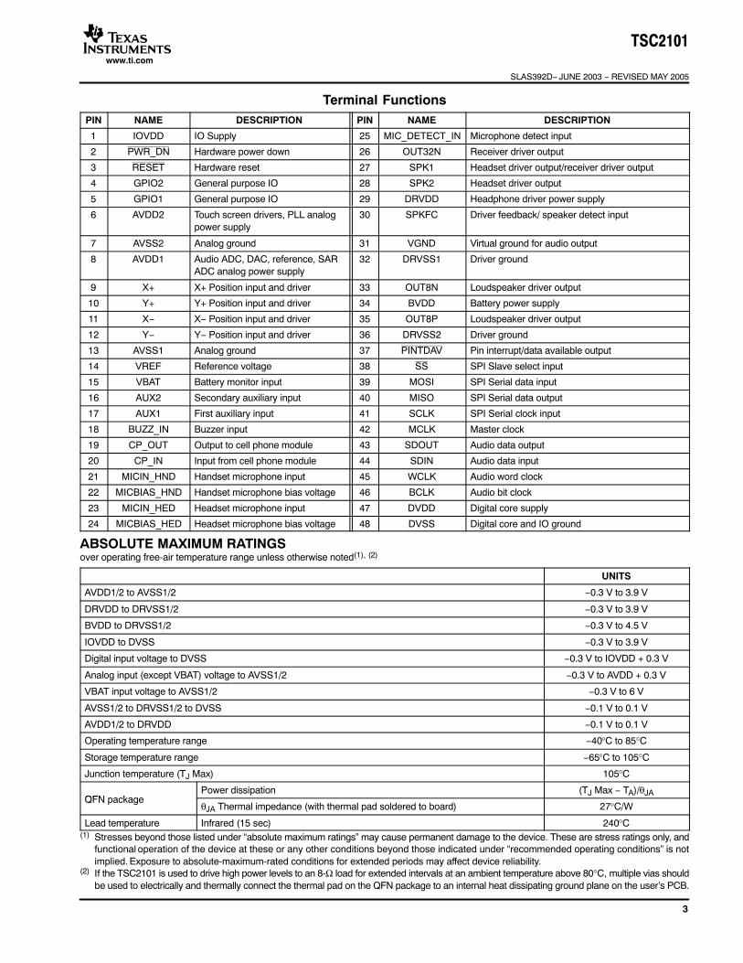
TSC2101
SLAS392D− JUNE 2003 − REVISED MAY 2005
AUDIO CODEC WITH INTEGRATED HEADPHONE, SPEAKER
AMPLIFIER AND TOUCH SCREEN CONTROLLER
FEATURES
Stereo Audio Playback Up to 48 ksps
Mono Audio Record up to 48 ksps
Integrated PLL for Audio Clock Generation
Programmable Gain Amplifiers
Hardware Automatic Gain Control
Programmable Digital Audio EffectsProcessing
Stereo Headset Interface
Cellular Headset Interface
8-Ω Speaker Driver
32-Ω Receiver Driver
Interface with Microphone
Auto-Detection of Headset and Button Press
Supports Both Cap and Cap-Less Interfacefor Headset
Programmable Audio Routing
4-Wire Touch Screen Interface
Integrated Touch Screen Processor WithFully Automated Modes of Operation
Programmable Converter Resolution, Speed,and Averaging
Programmable Autonomous Timing Control
Direct Battery Measurement
Built-In Buffer for Touch Screen Data
SPI™ Serial Interface
Low Power
Full Power-Down Control
48-Pin QFN Package
APPLICATIONS Personal Digital Assistants
Smart Cellular Phones
MP3 Players
DESCRIPTION
The TSC2101 is a low-power highly integrated highperformance codec and touch screen controller, whichsupports stereo audio DAC, mono audio ADC and SARADC.
The TSC2101 features a high-performance audio codecwith 16, 20, 24, or 32-bit stereo playback, mono recordfunctionality at up to 48 ksps. The device integratesseveral analog features such as support for headsetinterface, cellular headset interface, microphone interface,and speaker and receiver drivers. The device supportsauto detection of headset and button press without anyglue logic. The TCS2101 has fully programmable audio.The digital audio data format is programmable to work withpopular audio standard protocols (I2S, DSP, left/rightjustified) in master or slave mode, and also includes anon-chip PLL for flexible clock generation capability.
The TSC2101 contains a 12-bit 4-wire resistive touchscreen converter complete with drivers, and interfaces tothe host controller through a standard SPI™ serialinterface. The on-chip processor provides extensivefeatures specifically designed to reduce host processorand bus overhead, with capabilities that include fullyautomated operating modes, programmable conversionresolution up to 12 bits, programmable sampling rates upto 125 kHz, programmable conversion averaging, andprogrammable on-chip timing generation.
The TSC2101 offers battery measurement inputs capableof reading battery voltages up to 6 V, while operating atonly 3 V. It also has an on-chip temperature sensorcapable of reading 0.3°C resolution. The TSC2101 isavailable in a 48-lead QFN.
US Patent No. 6246394
SPI is a trademark of Motorola.
PRODUCTION DATA information is current as of publication date. Productsconform to specifications per the terms of Texas Instruments standard warranty.Production processing does not necessarily include testing of all parameters.
Please be aware that an important notice concerning availability, standard warranty, and use in critical applications of Texas Instrumentssemiconductor products and disclaimers thereto appears at the end of this data sheet.
www.ti.com
Copyright © 2004 − 2005, Texas Instruments Incorporated

TSC2101
SLAS392D− JUNE 2003 − REVISED MAY 2005
www.ti.com
2
This integrated circuit can be damaged by ESD. Texas Instruments recommends that all integrated circuits be handled with appropriateprecautions. Failure to observe proper handling and installation procedures can cause damage.
ESD damage can range from subtle performance degradation to complete device failure. Precision integrated circuits may be more susceptible todamage because very small parametric changes could cause the device not to meet its published specifications.
PACKAGE/ORDERING INFORMATION
PRODUCT PACKAGEPACKAGE
DESIGNATOROPERATING
TEMPERATURE RANGEORDERING NUMBER TRANSPORT MEDIA
TSC2101 QFN 48 RGZ 40°C t 85°CTSC2101IRGZ Rails, 52
TSC2101 QFN-48 RGZ −40°C to +85°CTSC2101IRGZR Tape and Reel, 2500
PIN ASSIGNMENTS
QFN PACKAGE(TOP VIEW)
13
DRVSS2OUT8PBVDDOUT8NDRVSS1VGNDSPKFCDRVDDSPK2SPK1OUT32NMIC_DETECT_IN
36
35
34
33
32
31
30
29
28
27
26
25
1
2
3
4
5
6
7
8
9
10
11
12
IOVDDPWR_DN
RESETGPIO2GPIO1AVDD2AVSS2AVDD1
X+Y+X−Y−
14 15 16 17 18 19 20 21 22 23 24
48 47 46 45 44 43 42 41 40 39 38 37
AV
SS
1V
RE
FV
BA
TA
UX
2A
UX
1B
UZ
Z_I
NC
P_O
UT
CP
_IN
MIC
IN_H
ND
MIC
BIA
S_H
ND
MIC
IN_H
ED
MIC
BIA
S_H
ED
DV
SS
DV
DD
BC
LKW
CLK
SD
INS
DO
UT
MC
LKS
CLK
MIS
OM
OS
IS
SP
INT
DAV
TSC2101
SLAS392D− JUNE 2003 − REVISED MAY 2005
www.ti.com
3
Terminal FunctionsPIN NAME DESCRIPTION PIN NAME DESCRIPTION
1 IOVDD IO Supply 25 MIC_DETECT_IN Microphone detect input
2 PWR_DN Hardware power down 26 OUT32N Receiver driver output
3 RESET Hardware reset 27 SPK1 Headset driver output/receiver driver output
4 GPIO2 General purpose IO 28 SPK2 Headset driver output
5 GPIO1 General purpose IO 29 DRVDD Headphone driver power supply
6 AVDD2 Touch screen drivers, PLL analogpower supply
30 SPKFC Driver feedback/ speaker detect input
7 AVSS2 Analog ground 31 VGND Virtual ground for audio output
8 AVDD1 Audio ADC, DAC, reference, SARADC analog power supply
32 DRVSS1 Driver ground
9 X+ X+ Position input and driver 33 OUT8N Loudspeaker driver output
10 Y+ Y+ Position input and driver 34 BVDD Battery power supply
11 X− X− Position input and driver 35 OUT8P Loudspeaker driver output
12 Y− Y− Position input and driver 36 DRVSS2 Driver ground
13 AVSS1 Analog ground 37 PINTDAV Pin interrupt/data available output
14 VREF Reference voltage 38 SS SPI Slave select input
15 VBAT Battery monitor input 39 MOSI SPI Serial data input
16 AUX2 Secondary auxiliary input 40 MISO SPI Serial data output
17 AUX1 First auxiliary input 41 SCLK SPI Serial clock input
18 BUZZ_IN Buzzer input 42 MCLK Master clock
19 CP_OUT Output to cell phone module 43 SDOUT Audio data output
20 CP_IN Input from cell phone module 44 SDIN Audio data input
21 MICIN_HND Handset microphone input 45 WCLK Audio word clock
22 MICBIAS_HND Handset microphone bias voltage 46 BCLK Audio bit clock
23 MICIN_HED Headset microphone input 47 DVDD Digital core supply
24 MICBIAS_HED Headset microphone bias voltage 48 DVSS Digital core and IO ground
ABSOLUTE MAXIMUM RATINGSover operating free-air temperature range unless otherwise noted(1), (2)
UNITS
AVDD1/2 to AVSS1/2 −0.3 V to 3.9 V
DRVDD to DRVSS1/2 −0.3 V to 3.9 V
BVDD to DRVSS1/2 −0.3 V to 4.5 V
IOVDD to DVSS −0.3 V to 3.9 V
Digital input voltage to DVSS −0.3 V to IOVDD + 0.3 V
Analog input (except VBAT) voltage to AVSS1/2 −0.3 V to AVDD + 0.3 V
VBAT input voltage to AVSS1/2 −0.3 V to 6 V
AVSS1/2 to DRVSS1/2 to DVSS −0.1 V to 0.1 V
AVDD1/2 to DRVDD −0.1 V to 0.1 V
Operating temperature range −40°C to 85°C
Storage temperature range −65°C to 105°C
Junction temperature (TJ Max) 105°C
QFN packagePower dissipation (TJ Max − TA)/θJA
QFN packageθJA Thermal impedance (with thermal pad soldered to board) 27°C/W
Lead temperature Infrared (15 sec) 240°C(1) Stresses beyond those listed under “absolute maximum ratings” may cause permanent damage to the device. These are stress ratings only, and
functional operation of the device at these or any other conditions beyond those indicated under “recommended operating conditions” is notimplied. Exposure to absolute-maximum-rated conditions for extended periods may affect device reliability.
(2) If the TSC2101 is used to drive high power levels to an 8-Ω load for extended intervals at an ambient temperature above 80°C, multiple vias shouldbe used to electrically and thermally connect the thermal pad on the QFN package to an internal heat dissipating ground plane on the user’s PCB.

TSC2101
SLAS392D− JUNE 2003 − REVISED MAY 2005
www.ti.com
4
ELECTRICAL CHARACTERISTICSAt +25°C, AVDD1, AVDD2, DRVDD, IOVDD = 3.3 V, BVDD = 3.9 V, DVDD = 1.8 V, Vref = 2.5 V, Fs (Audio) = 48 kHz, unless otherwise noted
PARAMETER TEST CONDITIONS MIN TYP MAX UNITS
TOUCH SCREEN
AUXILIARY ANALOG INPUT
Input voltage range 0 +VREF V
Input capacitance AUX1/2 input selected as input by touch-screen 25 pF
Input leakage current
AUX1/2 input selected as input by touch screen
±1 µA
BATTERY MONITOR INPUTS
Input voltage range 0.5 6.0 V
Input leakage current Battery conversion not selected ±1 µA
AccuracyVariation across temperature after systemcalibration at 4 V battery voltage and roomtemperature
±15 mV
TOUCH SCREEN A/D CONVERTER
Resolution Programmable: 8-, 10-,12-bits 8 12 Bits
No missing codes 12-Bit resolution 11 Bits
Integral nonlinearity −5 5 LSB
Offset error −6 6 LSB
Gain error −6 6 LSB
Noise 50 µVrms
VOLTAGE REFERENCE (VREF)
VREF output programmed = 2.5 V 2.3 2.5 2.7V
Voltage range VREF output programmed = 1.25 V 1.25V
Voltage range
External reference 1.1 2.5 V
Reference drift Internal VREF = 1.25 V 50 ppm/°C
Current drainExtra current drawn when the internal reference isturned on.
750 µA
AUDIO CODEC
ADC DECIMATION FILTER CHARACTERISTICS
Filter gain from 0 to 0.39 Fs ±0.1 dB
Filter gain at 0.4125 Fs −0.25 dB
Filter gain at 0.45 Fs −3.0 dB
Filter gain at 0.5 Fs −17.5 dB
Filter gain from 0.55 Fs to 64 Fs −75 dB
Group delay 17/Fs sec

TSC2101
SLAS392D− JUNE 2003 − REVISED MAY 2005
www.ti.com
5
ELECTRICAL CHARACTERISTICS (continued)At +25°C, AVDD1, AVDD2, DRVDD, IOVDD = 3.3 V, BVDD = 3.9 V, DVDD = 1.8 V, Int. Vref = 2.5 V, Fs (Audio) = 48 kHz, unless otherwisenoted (continued)
PARAMETER TEST CONDITIONS MIN TYP MAX UNITS
MICROPHONE INPUT TO ADCMICIN_HED 1020 Hz sine wave input,Fs = 48 ksps
Full-scale input voltage (0 dB) 0.707 Vrms
Input common mode 1.5 V
SNRMeasured as idle channel noise, 0 dB gain,A-weighted
80 90 dBA
THD 0.63 Vrms input, 0-dB gain −81 −72 dB
PSRR217 Hz, 100 mV on AVDD1/2(1) 55 dB
PSRR1020 Hz, 100 mV on AVDD1/2(1) 55 dB
Mute attenuationOutput code with 0.63 Vrms sine wave input at1 kHz
0000H
Input resistanceOnly ADC on 15 50 kΩ
Input resistanceADC and Sidetone on 8 16 kΩ
Input capacitance 10 pF
HEADSET MICROPHONE BIAS
Register 1DH/Page 2, D7−D8=00 3.3
Voltage range Register 1DH/Page 2, D7−D8=01 2.5 VVoltage range
Register 1DH/Page 2, D7−D8=1X 2
V
217 Hz, 100 mV on AVDD1/2 55
PSRR217 Hz, 100 mV on BVDD 74
dBPSRR1020 Hz, 100 mV on AVDD1/2 55
dB
1020 Hz, 100 mV on BVDD 74
Sourcing current Voltage drop <25 mV 5 mA
HANDSET MICROPHONE BIAS
Voltage rangeRegister 1DH/Page 2, D6=0 2.5
VVoltage rangeRegister 1DH/Page 2, D6=1 2
V
PSRR217 Hz, 100 mV on AVDD1/2 55
dBPSRR1020 Hz, 100 mV on AVDD1/2 55
dB
Sourcing current Voltage drop <25 mV 5 mA
DAC INTERPOLATION FILTER
Pass band 20 0.45Fs Hz
Pass band ripple ±0.06 dB
Transition band 0.45Fs 0.5501Fs Hz
Stop band 0.5501Fs 7.455Fs Hz
Stop band attenuation 65 dB
Filter group delay 21/Fs Sec
De-emphasis error ±0.1 dB(1) ADC PSRR measurement is calculated as:
PSRR 20 log10 VSIGsupVADCOUT
where VSIGsup is the ac signal applied on AVDD1/2, which is 100 mVPP at 1020 Hz, and
VADCOUT Amplitude of Digital Output
Max Possible Digital Amplitude

TSC2101
SLAS392D− JUNE 2003 − REVISED MAY 2005
www.ti.com
6
ELECTRICAL CHARACTERISTICS (continued)At +25°C, AVDD1, AVDD2, DRVDD, IOVDD = 3.3 V, BVDD = 3.9 V, DVDD = 1.8 V, Vref = 2.5 V, Fs (Audio) = 48 kHz, unless otherwise noted(continued)
PARAMETER TEST CONDITIONS MIN TYP MAX UNITS
DAC HEADPHONE OUTPUT Load = 16 Ω (single-ended), 50 pF
Full-scale output voltage (0dB) 0.848 Vrms
Output common mode 1.5 V
SNR Measured as idle channel noise, A-weighted 85 95 dBA
THD −1 dBFS Input, 0-dB gain −80 −60 dB
PSRR
217 Hz, 100 mV onAVDD1/AVDD2/DRVDD(1) 55 dB
PSRR1020 Hz, 100 mV onAVDD1/AVDD2/DRVDD(1) 55 dB
Interchannel isolation Coupling from ADC to DAC 80 dB
Mute attenuation 100 dB
Maximum output power Per channel 44 mW
Digital volume control −63.5 0 dB
Digital volume control step size 0.5 dB
Channel separation Between SPK1 and SPK2 −75 dB
DAC SPEAKER OUTPUT Load = 8 Ω (differential), 50 pF
Full-scale output voltage (0 dB) 1.838 Vrms
Output common mode 1.75 V
SNR Measured as idle channel noise, A-weighted 90 98 dBA
THD −1 dBFS Input, 0-dB gain −74 −55 dB
217 Hz, 100 mV on AVDD1/2 70
PSRR217 Hz, 100 mV on BVDD 70
dBPSRR1020 Hz, 100 mV on AVDD1/2 70
dB
1020 Hz, 100 mV on BVDD 70
Interchannel isolation Coupling from ADC to DAC 90 dB
Mute attenuation 100 dB
Maximum output power 400 mW
CELLPHONE
MIC INPUT TO CPOUT1020-Hz Sine wave input on MICIN_HND,load on CP_OUT = 10 kΩ, 50 pF
Full-scale input voltage (0 dB) 0.707 Vrms
Input common mode 1.5 V
Full-scale output voltage (0 dB) 0.707 Vrms
Output common mode 1.5 V
SNR Measured as idle channel noise, A-weighted 80 89 dBA
THD 0 dBFS Input, 0-dB gain −73 −60 dB
217 Hz, 100 mV on AVDD1/AVDD2/DRVDD 43
PSRR 1020 Hz, 100 mV onAVDD1/AVDD2/DRVDD
43dB
Interchannel isolation CP_IN to CP_OUT 75 dB
Mute attenuation CP_OUT muted 100 dB
(1) DAC PSRR measurement is calculated as:
PSRR 20 log10VSIGsupVSPK12

TSC2101
SLAS392D− JUNE 2003 − REVISED MAY 2005
www.ti.com
7
ELECTRICAL CHARACTERISTICS (continued)At +25°C, AVDD1, AVDD2, DRVDD, IOVDD = 3.3 V, BVDD = 3.9 V, DVDD = 1.8 V, Vref = 2.5 V, Fs (Audio) = 48 kHz, unless otherwise noted(continued)
PARAMETER TEST CONDITIONS MIN TYP MAX UNITS
CP_IN TO 32Ω RECEIVER (SPK1−OUT32N)1020-Hz Sine wave input on CP_IN, Load onSPK1−OUT32N = 32 Ω (differential), 50 pF
Full-scale input voltage (0 dB) 0.707 Vrms
Input common mode 1.5 V
Full-scale output voltage (0 dB) 1.697 Vrms
Output common mode 1.5 V
SNR Measured as idle channel noise, A-weighted 85 97 dBA
THD 0 dBFs input, 0 dB gain −77 −60 dB
217 Hz, 100 mV on AVDD1/AVDD2/DRVDD 43
PSRR 1020 Hz, 100 mV onAVDD1/AVDD2/DRVDD
43dB
Interchannel isolation MICIN to RECEIVER 75 dB
Mute attenuation 100 dB
Maximum output power 82 mW
DIGITAL INPUT/OUTPUT
Logic family CMOS
Logic level: VIH IIH = +5 µA 0.7IOVDD V
VIL IIL = +5 µA −0.3 0.3IOVDD V
VOH IOH = 2 TTL loads 0.8IOVDD V
VOL IOL = 2 TTL loads 0.1IOVDD V
Capacitive load 10 pF

TSC2101
SLAS392D− JUNE 2003 − REVISED MAY 2005
www.ti.com
8
ELECTRICAL CHARACTERISTICS (continued)At +25°C, AVDD1, AVDD2, DRVDD, IOVDD = 3.3 V, BVDD = 3.9 V, DVDD = 1.8 V, Vref = 2.5 V, Fs (Audio) = 48 kHz, unless otherwise noted(continued)
PARAMETER TEST CONDITIONS MIN TYP MAX UNITS
POWER SUPPLY REQUIREMENTS
Power supply voltage
AVDD1, AVDD2 3 3.3 3.6 V
DRVDD 3 3.3 3.6 V
BVDD 3 4.2 V
IOVDD Max MCLK = 100 MHz 2 3.6 V
Max MCLK = 50 MHz 1.1 3.6 V
DVDD 1.65 1.8 1.95 V
Touch screen ADC quiescent current
IAVDD1, host controlled AUX1 conversion at10 ksps with external reference(2) 67
ATouch-screen ADC quiescent currentIDVDD, host controlled AUX1 conversion at10 ksps
82µA
IAVDD1 with loudspeaker output (no signal),PLL off
3.1
Analog supply current audio play back only
IBVDD with loudspeaker output (no signal),PLL off
7.5
mAAnalog supply current – audio play back onlyIAVDD1 with headphone output (no signal),VGND off, PLL off
2.5mA
IDRVDD with headphone output (no signal),VGND off, PLL off
3.5
Digital supply current – audio play back only IDVDD, PLL off 2.5 mA
IAVDD1, headset mic, PLL off 5.2 mA
Analog supply current − mic record only(1) IBVDD, headset mic, PLL off 270 µAAnalog supply current mic record only
IAVDD1, handset mic, PLL off 5.6 mA
Digital supply current – mic record only IDVDD, PLL off 1.4 mA
Analog supply current IAVDD2, PLL on 1.3 mA
Digital supply current IDVDD, PLL on 0.9 mA
Hardware power down 27
Only headset/button detection enabled 50
Total current(2)Only auto temperature measurement with5.59 min delay
50 µA
Headset/button detection and autotemperature measurement with 5.59 mindelay
65
µ
Default current(3)IAVDD1 + IAVDD2 66
ADefault current(3)IBVDD 9
µA
(1) Mic record currents measured with no load on MICBIAS.(2) Current measured with MICBIAS_HED voltage programmed to 2 V (Page 2, Register 1DH, BIt D8=1).(3) Default currents measured with device in default mode after reset.

TSC2101
SLAS392D− JUNE 2003 − REVISED MAY 2005
www.ti.com
9
FUNCTIONAL BLOCK DIAGRAM
Σ−∆
Σ−∆
TouchPanelDrivers
BatteryMonitor
SARADC
InternalReference
−1
−1
Sidetone
DAC
ADC
AGC
Vol Ctl
Vol Ctl
DigitalAudio
Processing
and SerialInterface
TouchScreen
Processing
and SPIInterface
PLL
Headsetdetect and
Buttondetect
X−Y+
Y−X+
VBAT
VREF
MICBIAS_HED
MICBIAS_HND
2.0/2.5/3.3
2.0/2.5
AUX1
MICIN_HED
MICIN_HND
CP_IN
BUZZ_IN
OUT8P
OUT8N
CP_OUT
OUT32NSPK1
SPK2
To Detection blockSPKFC
VGND1.5V
SCLK
SSMOSI
MISO
PINTDAV
RESET
MCLK
PWR_DN
SDOUT
WCLK
SDIN
BCLK
0 to 59.5dB(0.5dB steps)
0 to 59.5dB(0.5dB steps)
12 to −34.5dB(0.5dB steps)
0 to −45dB(3dB steps)
12 to −34.5dB(0.5dB steps)
MIC_DETECT_IN To Detectionblock
GPIO1
GPIO2
AVDD1 AVDD2 DRVDD BVDD DVDD IOVDD
AVSS2 DRVSS1 DRVSS2 DVSSAVSS1
To ADC and DAC
0 to −63.5dB(0.5dB steps)
0 to −63.5dB(0.5dB steps)
AUX2
TemperatureMeasurement
OSC
Σ
Σ
Σ
Σ
ΣΣ−∆DAC
GPIOInterface

TSC2101
SLAS392D− JUNE 2003 − REVISED MAY 2005
www.ti.com
10
SPI TIMING DIAGRAM
ttdSSSSSSSEL ta
MSB OUT BIT 6 . . . 1 LSB OUT
tscktLeadtLag
twsck
twscktrtf
tv tho tdis
MSB IN BIT 6 . . . 1 LSB IN
thitsu
/SS
SPISELZ
SCLK
SPISELZ
SPICLKMISO
SPISELZ
MOSI
SPISELZ
TYPICAL TIMING REQUIREMENTSAll specifications typical at 25°C, DVDD = 1.8 V(1)
PARAMETERIOVDD = 1.1 V IOVDD = 3.3 V
UNITSPARAMETERMIN MAX MIN MAX
UNITS
twsck SCLK Pulse width 30 18 ns
tLead Enable Lead Time 18 15 ns
tLag Enable Lag Time 18 15 ns
ttd Sequential Transfer Delay 18 15 ns
ta Slave MISO access time 18 15 ns
tdis Slave MISO disable time 18 15 ns
tsu MOSI data setup time 6 6 ns
thi MOSI data hold time 6 6 ns
tho MISO data hold time 4 4 ns
tv MISO data valid time 25 13 ns
tr Rise Time 6 4 ns
tf Fall Time 6 4 ns(1) These parameters are based on characterization and are not tested in production.

TSC2101
SLAS392D− JUNE 2003 − REVISED MAY 2005
www.ti.com
11
AUDIO INTERFACE TIMING DIAGRAMS
ts(DI) th(DI)
td(DO−BCLK)td(DO−WS)
WCLK
BCLK
SDOUT
SDIN
td(WS)
Figure 1. I2S/LJ/RJ in Master Mode
Typical Timing Requirements (see Figure 1)
PARAMETER(1)IOVDD = 1.1 V IOVDD = 3.3 V
UNITSPARAMETER(1)MIN MAX MIN MAX
UNITS
td(WS) WCLK delay 30 15 ns
td(DO−WS) WCLK to DOUT delay (for LJF mode) 30 15 ns
td(DO−BCLK) BCLK to DOUT delay 30 15 ns
ts(DI) SDIN setup 6 6 ns
th(DI) SDIN hold 6 6 ns
tr Rise time 18 6 ns
tf Fall time 18 6 ns(1) These parameters are based on characterization and are not tested in production.
ts(DI) th(DI)
td(DO−BCLK)
WCLK
BCLK
SDOUT
SDIN
td(WS)td(WS)
Figure 2. DSP Timing in Master Mode
Typical Timing Requirements (see Figure 2)
PARAMETER(1)IOVDD = 1.1 V IOVDD = 3.3 V
UNITSPARAMETER(1)MIN MAX MIN MAX
UNITS
td(WS) WCLK delay 30 15 ns
td(DO−BCLK) BCLK to DOUT delay 30 15 ns
ts(DI) SDIN setup 6 6 ns
th(DI) SDIN hold 6 6 ns
tr Rise time 18 6 ns
tf Fall time 18 6 ns(1) These parameters are based on characterization and are not tested in production.

TSC2101
SLAS392D− JUNE 2003 − REVISED MAY 2005
www.ti.com
12
th(WS)ts(WS)
ts(DI) th(DI)
td(DO−BCLK)td(DO−WS)
WCLK
BCLK
SDOUT
SDIN
tL(BCLK) tH(BCLK)
tP(BCLK)
Figure 3. I2S/LJF/RJF Timing in Slave Mode
Typical Timing Requirements (see Figure 3)
PARAMETER(1)IOVDD = 1.1 V IOVDD = 3.3 V
UNITSPARAMETER(1)MIN MAX MIN MAX
UNITS
tH(BCLK) BCLK high period 40 35 ns
tL(BCLK) BCLK low period 40 35 ns
ts(WS) WCLK setup 6 6 ns
th(WS) WCLK hold 6 6 ns
td (DO−WS) WCLK to DOUT delay (for LJF mode) 30 18 ns
td(DO−BCLK) BCLK to DOUT delay 30 15 ns
ts(DI) SDIN setup 6 6 ns
th(DI) SDIN hold 6 6 ns
tr Rise time 5 4 ns
tr Fall time 5 4 ns(1) These parameters are based on characterization and are not tested in production.

TSC2101
SLAS392D− JUNE 2003 − REVISED MAY 2005
www.ti.com
13
th(WS) ts(WS)
ts(DI) th(DI)
td(DO−BCLK)
WCLK
BCLK
SDOUT
SDIN
tH(BCLK) tL(BCLK)
tP(BCLK)
ts(WS)th(WS)
Figure 4. DSP Timing in Slave Mode
Typical Timing Requirements (see Figure 4)
PARAMETER(1)IOVDD = 1.1 V IOVDD = 3.3 V
UNITSPARAMETER(1)MIN MAX MIN MAX
UNITS
tH(BCLK) BCLK high period 40 35 ns
tL(BCLK) BCLK low period 40 35 ns
tP(BCLK) BCLK period 80 80 ns
ts(WS) WCLK setup 6 6 ns
th(WS) WCLK hold 6 6 ns
td(DO−BCLK) BCLK to DOUT delay 30 15 ns
ts(DI) SDIN setup 6 6 ns
th(DI) SDIN hold 6 6 ns
tr Rise time 5 4 ns
tf Fall time 5 4 ns(1) These parameters are based on characterization and are not tested in production.

TSC2101
SLAS392D− JUNE 2003 − REVISED MAY 2005
www.ti.com
14
TYPICAL CHARACTERISTICS
−1.5
−1
−0.5
0
0.5
1
1.5
0 500 1000 1500 2000 2500 3000 3500 4000CODE
LS
B
AVDD1/AVDD2 = 3.3 V,TA = 25C,IR = 2.5 V
Figure 5. SAR INL (TA = 25C, Internal Reference = 2.5 V, 12 bit, AVDD1/AVDD2 = 3.3 V)
−1
−0.5
0
0.5
1
0 500 1000 1500 2000 2500 3000 3500 4000CODE
LS
B
AVDD1/AVDD2 = 3.3 V,TA = 25C,IR = 2.5 V
Figure 6. SAR DNL (TA = 25C, Internal Reference = 2.5 V, 12 bit, AVDD1/AVDD2 = 3.3 V)
0
0.2
0.4
0.6
0.8
1
1.2
1.4
1.6
1.8
2
2.2
2.4
0 10 20 30 40 50 60 70 80
Po
wer
− m
W
Sampling Rate − Ksps
AVDD1/AVDD2 = 3.3 V,TA = 25C
Figure 7. SAR ADC Power Consumption vs Speed (TA = 25C, External Reference, Host Controlled AUXConversion, AVDD1/AVDD2 = 3.3 V)

TSC2101
SLAS392D− JUNE 2003 − REVISED MAY 2005
www.ti.com
15
−160
−140
−120
−100
−80
−60
−40
−20
0
0 500 1000 1500 2000 2500 3000 3500 4000
dB
f − Frequency − Hz
AVDD1/AVDD2 = 3.3 V,TA = 25C,
Figure 8. ADC FFT Plot at 8 ksps (TA = 25C, −1 dB, 1 kHz input, AVDD1/AVDD2 = 3.3 V)
−160
−140
−120
−100
−80
−60
−40
−20
0
0 5000 10000 15000 20000f − Frequency − Hz
dB
AVDD1/AVDD2 = 3.3 V,TA = 25C,
Figure 9. ADC FFT Plot at 48 ksps (TA = 25C, −1 dB, 1 kHz input, AVDD1/AVDD2 = 3.3 V)
86
86.5
87
87.5
88
88.5
89
89.5
90
8 18 28 38 48
Dyn
amic
Ran
ge −
dB
Sampling Rate − Ksps
AVDD1/AVDD2 = 3.3 V,TA = 25C,
Figure 10. ADC Dynamic Range vs Sampling Rate (TA = 25C, AVDD1/AVDD2 = 3.3 V)

TSC2101
SLAS392D− JUNE 2003 − REVISED MAY 2005
www.ti.com
16
−160
−140
−120
−100
−80
−60
−40
−20
0
20
0 5000 10000 15000 20000
dB
f − Frequency − Hz
AVDD1/AVDD2 = 3.3 V,TA = 25C,RL = 16
Figure 11. DAC FFT Plot (TA = 25C, −1 dB, 1 kHz Input, AVDD1/AVDD2/DRVDD = 3.3 V, RL = 16 Ω)
−84
−83
−82
−81
−80
−79
−78
−77
5 10 15 20 25 30 35 40 45Power − mW
TH
D −
To
tal H
orm
on
ic D
isto
rtio
n −
dB
AVDD1/AVDD2 = 3.3 V,TA = 25C,RL = 16
Figure 12. THD vs Power on SPK1/2 (TA = 25C, 1 kHz Input, AVDD1/AVDD2/DRVDD = 3.3 V, RL = 16 Ω)

TSC2101
SLAS392D− JUNE 2003 − REVISED MAY 2005
www.ti.com
17
−90
−85
−80
−75
−70
−65
−60
0 50 100 150 200 250 300 350 400
Power − mW
TH
D −
To
tal H
orm
on
ic D
isto
rtio
n −
dB
AVDD1/AVDD2/DRDD = 3.3 V,BVDD = 3.9 VTA = 25C,RL = 8
Figure 13. THD vs Power on Loudspeaker Driver (TA = 25C, 1 kHz Input, AVDD1/AVDD2/DRVDD = 3.3 V,BVDD = 3.9 V, RL = 8 Ω)
150
200
250
300
350
400
450
2.7 2.9 3.1 3.3 3.5 3.7 3.9 4.1BVDD − V
Max
Po
wer
Ou
tpu
t − m
W
Figure 14. Loudspeaker Driver Output Power vs BVDD (TA = 25C, 1 kHz Input,AVDD1/AVDD2/DRVDD = 3.3 V, RL = 8 Ω, THD −40 dB)

TSC2101
SLAS392D− JUNE 2003 − REVISED MAY 2005
www.ti.com
18
OVERVIEW
The TSC2101 is a highly integrated stereo audio DAC and mono audio ADC with touch screen controller forportable computing, communication and entertainment applications. A register-based architecture easesintegration with microprocessor-based systems through a standard SPI bus. All peripheral functions arecontrolled through the registers and on-board state machines.
The TSC2101 consists of the following blocks:
Audio Codec
Headset and Button Detection
Touch Screen Interface
Battery Monitors
Auxiliary Inputs
Temperature Monitor
Communication to the TSC2101 is via a standard SPI serial interface. This interface requires that the SlaveSelect signal (SS) be driven low to communicate with the TSC2101. Data is then shifted into or out of theTSC2101 under control of the host microprocessor, which also provides the serial data clock.
Control of the TSC2101 and its functions is accomplished by writing to different registers in the TSC2101. Asimple command protocol is used to address the 16-bit registers. Registers control the operation of the SARADC and audio codec.
OPERATION—AUDIO CODEC
AUDIO ANALOG I/O
The TSC2101 has stereo audio DAC and mono audio ADC. It supports a wide range of analog interface tosupport different headsets and analog outputs. The TSC2101 has features to interface output drivers (8-Ω,16-Ω, 32-Ω) and Microphone PGA to Cell-phone. The TSC2101 also has a virtual ground (VGND) output, whichcan be optionally used to connect to the ground terminal of a speaker of headphone to eliminate the ac-couplingcapacitor needed at the speaker or headphone output. A special circuit has also been included in the TSC2101to insert a short keyclick sound into the stereo audio output, even when the audio DAC is powered down. Theykeyclick sound is used to provide feedback to the used when a particular button is pressed or item is selected.The specific sound of the keyclick can be adjusted by varying several register bits that control its frequency,duration, and amplitude.
AUDIO DIGITAL I/O INTERFACE
Digital audio data samples can be transmitted between the TSC2101 and the CPU via the serial bus (BCLK,WCLK, SDOUT, SDIN) that can be configured to transfer digital data in four different formats: Right justified(RJF), Left justified (LJF), I2S and DSP. The four modes are MSB first and operate with variable word lengthbetween 16/20/24/32 bits. The TSC2101’s audio codec can operate in master or slave mode, depending onthe setting of D11 at the register 06h of page 2. The word-select signal (WCLK) and bit clock signal (BCLK) areconfigured as inputs when the bus is in slave mode (D11 = 0). They are configured as outputs when the busis in master mode (D11 = 1). Under master mode, both clocks start running when the I2S bus needs to be active(one of the analog input/output paths has been configured and powered up). The WCLK is representative ofthe sampling rate of the audio ADC/DAC and is synchronized with SDOUT. Although the SDOUT signal cancontain two channels of information (a left and right channel), the TSC2101 sends the same ADC data in bothchannels.
ADC/DAC Sampling RateThe audio-control-1 register (Register 00H, Page 2) determines the sampling rates of DAC and ADC. Thesampling frequency is scaled down from the reference rate (Fsref). The reference rate is usually either 44.1kHz or 48 kHz which can be selectable using bit D13 of the register Audio Control 3 (06H/Page2). The ADCand DAC can operate with either common WCLK (equal sampling rates) or separate GPIO1 (For ADC) andWCLK (For DAC) for unequal sampling rates. When the audio codec is powered up, it is by default configuredas an I2S slave with both the DAC and ADC operating at Fsref.

TSC2101
SLAS392D− JUNE 2003 − REVISED MAY 2005
www.ti.com
19
Word Select Signals
The word select signal (WCLK) indicates the channel being transmitted:
— WCLK = 0: left channel for I2S mode;
— WCLK = 1: right channel for I2S mode.
For other modes refer to the timing diagrams below.
Bitclock (BCLK) Signal
In addition to being programmable as master or slave mode, the BCLK can also be configured in two transfermodes, 256-S transfer mode and continuous transfer mode, which are described below. These modes areset using bit D12 of control register 06H/page 2.
256-S Transfer Mode
In the 256-S mode, the BCLK rate always equals 256 times the WCLK frequency. In the 256-S mode, thecombination of ADC/DAC sampling rate equal to Fsref (as selected by bit D5D0 of control register 00H/page2) and left-justified mode is not supported. If IOVDD is equal to 1.1 V, then ADC/DAC sampling rate should beless than 39 kHz for all modes except the left justified mode where it should be less than 24 kHz.
Continuous Transfer Mode
In the continuous transfer mode, the BCLK rate always equals two-word length times the frequency ofWCLK.
Right Justified Mode
In right-justified mode, the LSB of left channel is valid on the rising edge of BCLK preceding, the falling edgeon WCLK. Similarly the LSB of right channel is valid on the rising edge of BCLK preceding the rising edge ofWCLK.
BCLK
WCLK
SDIN/SDOUT n n−1 1 00 n n−1 1 0
1/fs
LSBMSB
Left Channel Right Channel
n−2 2 2n−2
Figure 15. Timing Diagram for Right-Justified Mode

TSC2101
SLAS392D− JUNE 2003 − REVISED MAY 2005
www.ti.com
20
Left Justified Mode
In left-justified mode, the MSB of right channel is valid on the rising edge of BCLK, following the falling edge onWCLK. Similarly the MSB of left channel is valid on the rising edge of BCLK following the rising edge ofWCLK.
BCLK
WCLK
SDIN/SDOUT n n−1 1 0 n n−1 1 0
1/fs
LSBMSB
Left Channel Right Channel
n n−1n−2 2 n−2 2
Figure 16. Timing Diagram for Left-Justified Mode
I2S Mode
In I2S mode, the MSB of left channel is valid on the second rising edge of BCLK, after the falling edge onWCLK. Similarly the MSB of right channel is valid on the second rising edge of BCLK, after the rising edge ofWCLK.
BCLK
WCLK
SDIN/SDOUT n n−1 1 0 n n−1 1 0
1/fs
LSBMSB
Left Channel Right Channel
n
1 clock before MSB
n−2 2 n−2 2
Figure 17. Timing Diagram for I2S Mode
DSP Mode
In DSP mode, the falling edge of WCLK starts the data transfer with the left channel data first and immediatelyfollowed by the right channel data. Each data bit is valid on the falling edge of BCLK.
BCLK
WCLK
SDIN/SDOUT n n−1 1 0 n n−1 1 0
1/fs
LSBMSB
Left Channel Right Channel
n n−11 0
MSB LSB
n−2 2 n−2 2 n−2
MSBLSB
Figure 18. Timing Diagram for DSP Mode

TSC2101
SLAS392D− JUNE 2003 − REVISED MAY 2005
www.ti.com
21
AUDIO DATA CONVERTERS
The TSC2101 includes a stereo audio DAC and a mono audio ADC. Both ADC and DAC can operate with amaximum sampling rate of 53 kHz and support all audio standard rates of 8 kHz, 11.025 kHz, 12 kHz, 16 kHz,22.05 kHz, 24 kHz, 32 kHz, 44.1 kHz, and 48 kHz. By utilizing the flexible clock generation capability and internalprogrammable interpolation, a wide variety of sampling rates up to 53 kHz can be obtained from many possibleMCLK inputs. In addition, the DAC and ADC can independently operate at different sampling rates as indicatedin control register 00H/page 2.
When the ADC or DAC is operating, the TSC2101 requires an applied audio MCLK input. The user should alsoset bit D13 of control register 06H/page 2 to indicate which Fsref rate is being used. If the codec ADC or DACis powered up, then the touch screen ADC uses MCLK and BCLK for its internal clocking, and the internaloscillator is powered down to save power.
Typical audio DACs can suffer from poor out-of-band noise performance when operated at low sampling rates,such as 8 kHz or 11.025 kHz. The TSC2101 includes programmable interpolation circuitry to provide improvedaudio performance at such low sampling rates, by first upsampling low-rate data to a higher rate, filtering toreduce audible images, and then passing the data to the internal DAC, which is actually operating at the Fsrefrate. This programmable interpolation is determined using bit D5D3 of control register 00H/page 2.
For example, if playback of 11.025 kHz data is required, the TSC2101 can be configured such that Fsref = 44.1kHz. Then using bit D5D3 of control register/page 2, the DAC sampling rate (Fs) can be set to Fsref/4, or FS= 11.025 kHz. In operation, the 11.025 kHz digital input data is received by the TSC2101, upsampled to 44.1kHz, and filtered for images. It is then provided to the audio DAC operating at 44.1 kHz for playback. In reality,the audio DAC further upsamples the 44.1 kHz data by a ratio of 128 x and performs extensive interpolationfiltering and processing on this data before conversion to a stereo analog output signal.
Phase Locked Loop (PLL)
The TSC2101 has an on chip PLL to generate the needed internal ADC and DAC operational clocks from awide variety of clocks that may be available in the system. The PLL supports an MCLK varying from 2 MHz to100 MHz and is register programmable to enable generation of required sampling rates with fine precision.
ADC and DAC sampling rates are given by
DAC_Fs FsrefN1
and
ADC_Fs FsrefN2
Where, Fsref must fall between 39 kHz and 53 kHz, and N1, N2=1, 1.5, 2, 3, 4, 5, 5.5, 6 are registerprogrammable.
The PLL can be enabled or disabled using register programming.
When PLL is disabled
Fsref MCLK128 Q
Q = 2, 3…17
— Note: For ADC, with N2 = 1.5 or 5.5, odd values of Q are not allowed.— In this mode, the MCLK can operate up to 100 MHz, and Fsref should fall between 39 kHzand 53 kHz.

TSC2101
SLAS392D− JUNE 2003 − REVISED MAY 2005
www.ti.com
22
When PLL is enabled
Fsref MCLK K2048 P
P = 1, 2, 3 … 8K = J.DJ = 1, 2, 3 ….64D = 0, 1, 2 … 9999P, J and D are register programmable. where J is integer part of K before the decimal point, and Dis four-digit fractional part of K after the decimal point, including lagging zeros.
Examples: If K = 8.5, then J = 8, D = 5000 If K = 7.12, then J = 7, D = 1200 If K = 7.012, then J = 7, D = 120
The PLL is programmed through Registers 1BH and 1CH of Page 2.
When PLL is enabled and D = 0, the following conditions must be satisfied
2 MHz MCLKP
20 MHz
80 MHz MCLK KP
110 MHz
4 J 55
When PLL is enabled D ≠ 0, the following conditions must be satisfied
10 MHz MCLKP
20 MHz
80 MHz MCLK KP
110 MHz
4 J 11
Example 1:
For MCLK = 12 MHz and Fsref = 44.1 kHz
P = 1, K = 7.5264
J = 7, D = 5264
Example 2:
For MCLK = 12 MHz and Fsref = 48 kHz
P = 1, K = 8.192
J = 8, D = 1920
To externally observe the PLL function, the GPIO2 pin can be set up as the clock monitor (set D2 = 1, register22h, page 2). Note that besides setting up the PLL and GPIO2, the audio ADC or DAC must be enabled forthe PLL output to appear at the GPIO2.Example 1: Start from power up (with the proper sequence)
Make sure MCLK is provided and /PWR_DWN and /RESET are both high
Set and enable PLL
Connect and power up (do not unmute anything) ADC or DAC or both, for instance:− Page2/Reg03h to C530h or C510h (default is C500h) to connect MICSEL to ADC
− Page2/Reg05h to FDFCh (default is FFFCh) to power up ADC.
Set Page2/Reg22h to 0004h to output PLL to GPIO2 pin.

TSC2101
SLAS392D− JUNE 2003 − REVISED MAY 2005
www.ti.com
23
MONO AUDIO ADC
Analog Front End
The analog front end of the audio ADC consists of an analog MUX and a programmable gain amplifier (PGA).The MUX can connect either of the Headset Input (MICIN_HED), Handset Input (MICIN_HND), AUX1 andAUX2 signal through the PGA to the ADC for audio recording. The Cell-phone Input (CP_IN) can also beconnected to ADC through a PGA at the same time. This enables recording of conversation during a cell-phonecall. The TSC2101 also has an option of choosing MICIN_HED/MICIN_HND and AUX1/AUX2 as differentialinput pair. The TSC2101 also includes two microphone bias circuits which can source up to 5 mA of current,and are programmable to a 2 V, 2.5 V or 3.3 V level for Headset and 2 V or 3.3 V level for handset.
Because of the oversampling nature of the audio ADC and the integrated digital decimation filtering,requirements for analog anti-aliasing filtering are very relaxed. The TSC2101 integrates a second order analoganti-aliasing filter with 20-dB attenuation at 1 MHz. This filter, combined with the digital decimal filter, providessufficient anti-aliasing filtering without requiring any external components.
The PGA, for microphone and AUX Inputs, allows analog gain control from 0 dB to 59.5 dB in steps of 0.5 dB.The PGA gain changes are implemented with an internal soft-stepping. This soft-stepping ensures that volumecontrol changes occur smoothly with no audible artifacts. Upon reset, the PGA gain defaults to a mute condition,and upon power down, the PGA soft-steps the volume to mute before shutting down. A read-only flag (D0control register 04H/Page 2) is set whenever the gain applied by PGA equals the desired value set by theregister. The soft-stepping control can be disabled by programming D15=1 in register 1DH of Page 2. Whensoft stepping is enabled and ADC power down register is written, MCLK should be running to ensure thatsoft-stepping to mute has completed. MCLK can be shut down once Mic PGA power down flag is set.
The PGA, for Cell phone Input (CP_IN) allows gain control from –34.5 dB to 12 dB in steps of 0.5 dB. The PGAgain changes are implemented with an internal soft−stepping. This soft-stepping ensures that volume controlchanges occur smoothly with no audible artifacts. Upon reset, the PGA gain defaults to a mute condition, andupon power down, the PGA soft-steps the volume to mute before shutting down. A read−only flag (D7 controlregister 1FH/Page 2) is set whenever the gain applied by PGA equals the desired value set by the register. Thesoft-stepping control can be disabled by the programming D12=1 in register 1DH of Page 2. When soft-steppingis enabled and ADC power down register is written, MCLK should be running to ensure that soft-stepping tomute has completed. MCLK can be shut down once Cell PGA power down flag is set.
Delta-Sigma ADC
The analog-to-digital converter has a delta-sigma modulator with a 128 times oversampling ratio. The ADC cansupport maximum output rate of 53 kHz.
Decimation Filter
The audio ADC includes an integrated digital decimation filter that removes high frequency content anddownsamples the audio data from an initial sampling rate of 128 times Fs to the final output sampling rate ofFs. The decimation filter provides a linear phase output response with a group delay of 17/Fs. The –3 dBbandwidth of the decimation filter extends to 0.45 Fs and scales with the sample rate (Fs).
Programmable High Pass Filter
The ADC channel has a programmable high-pass filter whose cutoff frequency can be programmed throughcontrol register. By default the high pass filter is off. The high-pass filter is a first order IIR filter. This filter canbe used to remove the DC component of the input signal and offset of the ADC channel.
Automatic Gain Control (AGC)
The TSC2101 includes Automatic gain control (AGC) for Microphone Inputs (MICIN_HED or MICIN_HND) andCell-phone input (CP_IN). AGC can be used to maintain nominally constant output signal amplitude whenrecording speech signals. This circuitry automatically adjusts the PGA gain as the input signal becomes overlyloud or very weak, such as when a person speaking into a microphone moves closer or farther from themicrophone. The AGC algorithm has several programmable settings, including target gain, attack and decaytime constants, noise threshold, and max PGA applicable that allow the algorithm to be fine tuned for anyparticular application. The algorithm uses the absolute average of the signal (which is the average of theabsolute value of the signal) as a measure of the nominal amplitude of the output signal.

TSC2101
SLAS392D− JUNE 2003 − REVISED MAY 2005
www.ti.com
24
Target gain represents the nominal output level at which the AGC attempts to hold the ADC output signal level.The TSC2101 allows programming of eight different target gains, which can be programmed from –5.5 dB to–24 dB relative to a full-scale signal. Since the TSC2101 reacts to the signal absolute average and not to peaklevels, it is recommended that the target gain be set with enough margin to avoid clipping at the occurrenceof loud sounds.
Attack time determines how quickly the AGC circuitry reduces the PGA gain when the input signal is too loud.It can be varied from 8 ms to 20 ms.
Decay time determines how quickly the PGA gain is increased when the input signal is too low. It can be variedin the range from 100 ms to 500 ms.
Noise threshold determines level below which if the input speech average value falls, AGC considers it as asilence and hence brings down the gain to 0 dB in steps of 0.5 dB every FS and sets noise threshold flag. Thegain stays at 0 dB unless the input speech signal average rises above noise threshold setting. This ensuresthat noise does not get gained up in the absence of speech. Noise threshold level in the AGC algorithm isprogrammable from −30dB to −90 dB for microphone input, and from −30 dB to −60 dB for cell-phone input.When AGC Noise Threshold is set to −70 dB, −80 dB, or −90 dB, the microphone input Max PGA applicablesetting must be greater than or equal to 11.5 dB, 21.5 dB, or 31.5 dB respectively. This operation includesdebounce and hysteresis to avoid the AGC gain from cycling between high gain and 0 dB when signals are nearthe noise threshold level. When noise threshold flag is set, status of gain applied by AGC and saturation flagshould be ignored.
Max PGA applicable allows user to restrict maximum gain applied by AGC. This can be used for limiting PGAgain in situations where environment noise is greater than programmed noise threshold. Microphone input MaxPGA can be programmed from 0 dB to 59.5 dB in steps of 0.5 dB. Cell-phone input Max PGA can beprogrammed from −34.5 dB to −0.5 dB in steps of 0.5 dB, as well as +12 dB.
See Table 1 for various AGC programming options. AGC can be used only if microphone input or Cell-phoneinput is routed to the ADC channel. When both microphone input and Cell-phone input are connected to theADC, AGC is automatically disabled.
Decay Time
TargetGain
InputSignal
OutputSignal
AGCGain
AttackTime
Figure 19. AGC Characteristics

TSC2101
SLAS392D− JUNE 2003 − REVISED MAY 2005
www.ti.com
25
Table 1. AGC Settings
MIC HEADSET INPUT MIC HANDSET INPUT CELL-PHONE INPUT
BITCONTROLREGISTER
BITCONTROLREGISTER
BITCONTROLREGISTER
AGC enable D0 01H D0 1EH D0 24H
Target gain D7−D5 01H D7−D5 1EH D7−D5 24H
Time constants (attack and decay time) D4−D1 01H D4−D1 1EH D4−D1 24H
Noise threshold D13−D11 24H D13−D11 24H D13−D11 24H
Noise threshold flag D11 04H D11 04H D14 24H
Hysteresis D10−D9 1DH D10−D9 1DH D10−D9 24H
Debounce time (normal to silence mode) D8−D6 26H D8−D6 26H D8−D6 27H
Debounce time (silence to normal mode) D5−D3 26H D5−D3 26H D5−D3 27H
Max PGA applicable D15−D9 26H D15−D9 26H D15−D9 27H
Gain applied by AGC D15−D8 01H D15−D8 1EH D14−D8 1FH
Saturation flag D0 04H D0 04H D7 1FH
Clip stepping disable D3 06H D3 06H D8 24H
NOTE: All settings shown in Table 1 are located in Page 2 of control registers.
Stereo Audio DAC
Each channel of the stereo audio DAC consists of a digital audio processing block, a digital interpolation filter,digital delta-sigma modulator, and an analog reconstruction filter. The DAC is designed to provide enhancedperformance at low sample rates through increased oversampling and image filtering, thereby keepingquantization noise generated within the delta-sigma modulator and signal images strongly suppressed withinthe audio band to beyond 20 kHz. This is realized by keeping the upsampled rate constant at 128 x Fsref andchanging the oversampling ratio as the input sample rate is changed. For Fsref of 48 kHz, the digital delta−sigmamodulator always operates at a rate of 6.144 MHz. This ensures that quantization noise generated within thedelta-sigma modulator stays within the frequency band below 20 kHz at all sample rates. Similarly, for Fsrefrate of 44.1 kHz, the digital delta-sigma modulator always operates at a rate of 5.6448 MHz.
Digital Audio Processing
The DAC channel consists of optional filters for de-emphasis and bass, treble, midrange level adjustment, orspeaker equalization. The de-emphasis function is only available for sample rates of 32 kHz, 44.1 kHz, and 48kHz. The transfer function consists of a pole with time constant of 50ms and a zero with time constant of 15ms.Frequency response plots are given in the Audio Codec Filter Frequency Responses section of this data sheet.
The DAC digital effects processing block consists of a fourth order digital IIR filter with programmablecoefficients (one set per channel). The filter is implemented as cascade of two biquad sections with frequencyresponse given by:
N0 2 N1 z1 N2 z2
32768 2 D1 z1 D2 z2 N3 2 N4 z1 N5 z2
32768 2 D4 z1 D5 z2
The N and D coefficients are fully programmable, and the entire filter can be enabled or bypassed. Thecoefficients for this filter implement a variety of sound effects, with bass-boost or treble boost being the mostcommonly used in portable audio applications. The default N and D coefficients in the part are given by:
N0 = N3 = 27619
N1 = N4 = −27034
N2 = N5 = 26461
D1 = D4 = 32131
D2 = D5 = −31506

TSC2101
SLAS392D− JUNE 2003 − REVISED MAY 2005
www.ti.com
26
These coefficients implement a shelving filter with 0 dB gain from dc to approximately 150 Hz, at which pointit rolls off to 3 dB attenuation for higher frequency signals, thus giving a 3-dB boost to signals below 150 Hz.The N and D coefficients are represented by 16−bit twos complement numbers with values ranging from –32768to +32767. Frequency response plots are given in the Audio Codec Filter Frequency Responses section of thisdata sheet.
Interpolation Filter
The interpolation filter upsamples the output of the digital audio processing block by the required oversamplingratio. It provides a linear phase output with a group delay of 21/Fs.
In addition, the digital interpolation filter provides enhanced image filtering to reduce signal images caused bythe upsampling process that are below 20 kHz. For example, upsampling an 8-kHz signal produces signalimages at multiples of 8 kHz, i.e., 8 kHz, 16 kHz, 24 kHz, etc. The images at 8 kHz and 16 kHz are below 20kHz and still audible to the listener, therefore, they must be filtered heavily to maintain a good quality output.The interpolation filter is designed to maintain at least 65 dB rejection of images that land below 7.455 Fs. Inorder to utilize the programmable interpolation capability, the Fsref should be programmed to a higher rate(restricted to be in the range of 39 kHz to 53 kHz when the PLL is in use), and the actual FS is set using thedividers in bits D5D3 of control register 00H/page 2. For example, if Fs = 8 kHz is required, then Fsref can beset to 48 kHz, and the DAC Fs set to Fsref/6. This ensures that all images of the 8-kHz data are sufficientlyattenuated well beyond a 20-kHz audible frequency range. Passband ripple for all sample-rate cases (from 20Hz to 0.45 Fs) is +0.06 dB maximum.
Delta-Sigma DAC
The audio digital-to-analog converter incorporates a third order multi-bit delta-sigma modulator followed by ananalog reconstruction filter. The DAC provides high-resolution, low−noise performance, using oversamplingand noise shaping techniques. The analog reconstruction filter design consists of a 6 tap analog FIR filterfollowed by a continuous time RC filter. The analog FIR operates at 6.144 MHz (128x48 kHz, for Fsref of 48kHz) or at 5.6448 MHz (128x44.1 kHz, for Fsref of 44.1 kHz). The DAC analog performance may be degradedby excessive clock jitter on the MCLK input. Therefore, care must be taken to keep jitter on this clock to aminimum (less than 50 ps).
DAC Digital Volume Control
The DAC has a digital volume control block, which implements programmable gain. The volume level can bevaried from 0 dB to –63.5 dB in 0.5 dB steps, in addition to a mute bit, independently for each channel. Thevolume level of both channels can also be changed simultaneously by the master volume control. The gain isimplemented with a soft−stepping algorithm, which only changes the actual volume by one step per inputsample, either up or down, until the desired volume is reached. The rate of soft-stepping can be slowed to onestep per two input samples through D1 of control register 04H/Page 2.
Because of soft-stepping, the host does not know when the DAC has been completely muted. This may beimportant if the host wishes to mute the DAC before making a significant change, such as changing samplerates. In order to help with this situation, the part provides a flag back to the host via a read-only register bit(D2−D3 of control register 04H/page 2) that alerts the host when the part has completed the soft-stepping, andthe actual volume has reached the desired volume level. The soft-stepping feature can be disabled byprogramming D14=1 in register 1DH in Page 2. If soft-stepping is enabled, the MCLK signal should be keptapplied to the device, until the DAC power-down flag is set. When this flag is set, the internal soft-steppingprocess and power down sequence is complete, and the MCLK can be stopped if desired.
The TSC2101 also includes functionality to detect when the user switches on or off the de-emphasis or digitalaudio processing functions, then (1) soft-mute the DAC volume control, (2) change the operation of the digitaleffects processing and (3) soft-unmute the part. This avoids any possible pop/clicks in the audio output due toinstantaneous changes in the filtering. A similar algorithm is used when first powering up or down the DAC. Thecircuit begins operation at power-up with the volume control muted, then soft-steps it up to the desired volumelevel. At power-down, the logic first soft-steps the volume down to a mute level, then powers down the circuitry.

TSC2101
SLAS392D− JUNE 2003 − REVISED MAY 2005
www.ti.com
27
DAC Powerdown
The DAC powerdown flag (D4D3 of control register 05H/page 2) along with D10 of control register 05H/page2 denotes the powerdown status of the DAC according to Table 2.
Table 2. DAC Powerdown Status
D10, D4, D3 POWERUP/POWERDOWN STATE OF DAC
0,0,0 DAC left and right are in stable powerup state.
0,0,1 DAC left is in stable powerup state.DAC right is in the process of powering up. The length of this state is determined by PLL and output driver powerup delayscontrolled by register programming.
0,1,0 DAC left is in the process of powering up. The length of this state is determined by PLL and output driver powerup delayscontrolled by register programming.DAC right is in stable powerup state.
0,1,1 DAC left and right are in the process of powering up. The length of this state is determined by PLL and output driverpowerup delays controlled by register programming.
1,0,0 DAC left and right are in the process of powering down. The length of this state is determined by soft−stepping of volumecontrol block.
1,0,1 DAC left is in the process of powering down. The length of this state is determined by soft−stepping of volume control block.DAC right is in stable powerdown state.
1,1,0 DAC left is in stable powerdown state.DAC right is in the process of powering down. The length of this state is determined by soft−stepping of volume controlblock.
1,1,1 DAC left and right are in stable powerdown state.
Analog Outputs
The TSC2101 has the capability to route the DAC output to any of the selected analog outputs. The TSC2101provides various analog routing capabilities. All analog outputs other than the selected ones are powered downfor optimal power consumption.
Headphone Drivers
The TSC2101 features stereo headphone drivers (SPK1 and SPK2) that can deliver 44 mW per channel at3.3-V supply, into 16-Ω loads. The TSC2101 provides flexibility to connect either of the DAC channels to eitherof the headphone driver outputs. It also allows mixing of signals from different DAC channels. The headphonescan be connected in a single ended configuration using ac-coupling capacitors, or the capacitors can beremoved and virtual ground (VGND) powered for a cap-less output connection. Note that the VGND amplifiermust be powered up if the cap-less configuration is used.
In the case of an ac-coupled output, the value of the capacitors is typically chosen based on the amount oflow−frequency cut that can be tolerated. The capacitor in series with the load impedance forms a high-passfilter with –3 dB cutoff frequency of 1/(2πRC) in Hz, where R is the impedance of the headphones. Use of anoverly small capacitor reduces low-frequency components in the signal output and lead to low-quality audio.When driving 16-Ω headphones, capacitors of 220-µF (a commonly used value) result in a high-pass filter cutofffrequency of 45 Hz, although reducing these capacitors to 50 µF results in a cutoff frequency of 199 Hz, whichis generally considered noticeable when playing music. The cutoff frequency is reduced to half of the abovevalues if 32-Ω headphones are used instead of 16-Ω.
The TSC2101 programmable digital effects block can be used to help reduce the size of capacitors needed byimplementing a low frequency boost function to help compensate for the high-pass filter introduced by theac-coupling capacitors. For example, by using 50-µF capacitors and setting the TSC2101 programmable filtercoefficients as shown below, the frequency response can be improved as shown in Figure 21.
Filter coefficients (use the same for both channels):
N0 = 32767, N1 = −32346, N2 = 31925, N3 = 32767, N4 = 0, N5 = 0
D0 = 32738, D1 = −32708, D4 = 0, D5 =0

TSC2101
SLAS392D− JUNE 2003 − REVISED MAY 2005
www.ti.com
28
−20
−18
−16
−14
−12
−10
−8
−6
−4
−2
0
0 200 400 600 800 1000f − Frequency − Hz
Gai
n −
dB
Figure 20. Uncompensated Response For 16-Ω Load and 50-F Decoupling Capacitor
−20
−18
−16
−14
−12
−10
−8
−6
−4
−2
0
0 200 400 600 800 1000f − Frequency − Hz
Gai
n −
dB
Figure 21. Frequency Response For 16-Ω Load and 50-F Decoupling Capacitor After GainCompensation Using Above Set of Coefficients For Audio Effects Filter
Using the capless output configuration eliminates the need for these capacitors and removes the accompanyinghigh-pass filter entirely. However, this configuration does have one drawback – if the RETURN terminal of theheadphone jack (which is wired to the TSC2101 VGND pin) is ever connected to a ground that is shorted tothe TSC2101 ground pin, then the VGND amplifier enters short-circuit protection, and the audio output doesnot function properly.
The TSC2101 incorporates a programmable short-circuit detection/protection function. In case of short circuit,all analog outputs are disabled and a read only bit D1 of control register 1DH/page 2 is set. In such cases, thereare two ways to return to normal operation:
− Hardware or software reset− Power down all the output drivers, which can be achieved by setting bits D12, D11, D 8, D7, and D6 of control
register 05H/page 2 and then wait for driver power down status flags (bits D15−D10 of control register25H/page 2) to become 1. The wait time is typically less than 50 ms after which, output drivers can beprogrammed as desired.

TSC2101
SLAS392D− JUNE 2003 − REVISED MAY 2005
www.ti.com
29
For the cap interface, this feature can be disabled by setting bit D0 of control register 20H/page 2. In the caseof the cap-less interface, VGND short circuit protection must also be disabled, which can be achieved by settingbit D4 of control register 21H/page 2.
The TSC2101 implements a pop reduction scheme to reduce audible artifacts during powerup and powerdownof headphone drivers. The scheme can be controlled by programming bits D5 and D4 of control register25H/page 2. By default, the driver pop reduction scheme is enabled and can be disabled by programming bitD5 of control register 25H/page 2 to 1. When this scheme is enabled and the virtual ground connection is notused (VGND amplifier is powered down), the audio output driver slowly charges up any external ac-couplingcapacitors to reduce audible artifacts. Bit D4 of control register 25H/page 2 provides control of the charging timefor the ac-coupling capacitor as either 0.8 sec or 4 sec. When the virtual ground amplifier is powered up andused, the external ac-coupling capacitor is eliminated, and the powerup time becomes 1 ms. This scheme takeseffect whenever any of the headphone drivers are powered up.
Speaker Driver
The TSC2101 has an integrated speaker driver (OUT8P−OUT8N) capable of driving an 8 Ω differential load.The speaker driver, powered directly from the battery supply (3.5 V to 4.2 V) on the BVDD pin can deliver 400mW at 3.9 V supply. It allows connecting one or both DAC channel to speaker driver. The TSC2101 also has ashort circuit protection feature for the speaker driver which can be enabled by setting bit D5 of control register21H/page 2.
Receiver Driver
The TSC2101 includes a receiver driver (SPK1−OUT32N), which can drive a 32 Ω differential load. It iscapable of delivering 82 mW into a 32 Ω load. The TSC2101 does not allow both the receiver driver andheadphone drivers to be turned on at the same time. Also, when the receiver driver is being used, theheadphone driver load must be disconnected.
Headset Interface
The TSC2101 supports all standard headset interfaces. It is capable of interfacing with 3-wire stereo headset,3-wire cellular headset and 4-wire stereo-cellular headsets. It supports both capacitor-coupled (cap) andcapacitor-less (capless) interface for headset through software programming.
Capless Interface
Figure 22 shows the connection diagram to the TSC2101 for capless interface. VGND acts as a ground ofheadset jack. Voltage at VGND is 1.5 V and MICBIAS_HED voltage is programmed to 3.3 V. With this, thevoltage across microphone is configured to be 1.8 V. In order to minimize the effect of routing resistance onVGND inside the device and on the printed circuit board (PCB), SPKFC should be shorted to VGND at thejack. This reduces crosstalk from speaker to microphone because of common ground as VGND.

TSC2101
SLAS392D− JUNE 2003 − REVISED MAY 2005
www.ti.com
30
−1
−1
MICBIAS_HED
MICBIAS_HND
2.5
MICIN_HED
MICIN_HND
OUT8P
OUT8N
OUT32N
SPK1
SPK2
To Detectionblock
SPKFC
VGND1.5 V
MIC_DETECT_INTo Detection block
LOUDSPEAKER
RECEIVER
s
sg m
sg m s
sgStereo
Cellular
Stereo +Cellular
m = mics = stere
g = ground/midbias
3.3V
Figure 22. Connection Diagram for Capless Interface
Cap Interface
Figure 23 shows connection diagram to device for cap interface.

TSC2101
SLAS392D− JUNE 2003 − REVISED MAY 2005
www.ti.com
31
−1
−1
MICBIAS_HED
MICBIAS_HND
2.5V
MICIN_HED
MICIN_HND
OUT8P
OUT8N
OUT32N
SPK1
SPK2
To Detectionblock
SPKFC
VGND1.5 V
MIC_DETECT_INTo Detection block
LOUDSPEAKER
RECEIVER
s
sg m
sg m s
sgStereo
Cellular
Stereo +Cellular
m = mics = stere
g = ground/midbias
2.5V
Figure 23. Connection Diagram for Cap Interface
Auto Detection
The TSC2101 has built in monitors to automatically detect the insertion and removal of headsets. The detectionscheme can differentiate between stereo, cellular and stereo-cellular headsets. Upon detection of headsetinsertion or removal, the TSC2101 updates read-only bit D12 of control register 22H/Page 2. The TSC2101 canbe programmed to send an active high interrupt for insertion and removal of headsets to the host-processorover GPIO1 using bit D3 of control register 22H/Page 2 and GPIO2 using bit D4 of control register 22H/Page2. The headset detection feature can be enabled by setting bit D15 of control register 22H/Page 2. Whenheadset detection is enabled and headset is not detected, SPK1, VGND and MICBIAS_HED are turned offirrespective of control register settings. The TSC2101 also has the capability to detect button press on theheadset microphone. It consumes less than 50 µA while waiting for button press with everything else powereddown. Upon button press, the TSC2101 updates read-only bit D11 of control register 22H/Page 2. It can alsosend an active high interrupt for indicating button press to the processor over GPIO1 using bit D1D0 of controlregister 22H/Page 2. The TSC2101 provides debounce programmability for headset and button detect.Debounce programmability can be used to reject glitches generated, and hence avoids false detection, whileinserting headset or pressing button.
Figure 24 shows terminal connections and jack configuration required for various headsets. Care should betaken to avoid any dc path from MIC_DETECT_IN to ground, when a headset is not inserted.

TSC2101
SLAS392D− JUNE 2003 − REVISED MAY 2005
www.ti.com
32
s
g
s
m m
s
g g
s s
sg m sStereo +Cellular ssgStereosg mCellular
Figure 24. Connection Diagram for Jacks
Headset Detection− Interrupt polarity: Active high.− Typical interrupt duration: 1.75 ms.− Debounce programmability on bits D10 and D9 in control register 22H/Page 2:
− 00 => 16 ms duration (with 2 ms clock resolution)− 01 => 32 ms duration (with 4 ms clock resolution)− 10 => 64 ms duration (with 8 ms clock resolution)− 11 => 128 ms duration (with 16 ms clock resolution)
− Headset detect flag is available till headset is connected.
Button Detection− Interrupt polarity: Active high.− Typical interrupt duration: Button pressed time + clock resolution. Clock resolution depends upon
debounce programmability.− Typical interrupt delay from button: Debounce duration + 0.5ms− Debounce programmability:
− 00 => No glitch rejection− 01 => 8 ms duration (with 1 ms clock resolution)− 10 => 16 ms duration (with 2 ms clock resolution)− 11 => 32 ms duration (with 4 ms clock resolution)
− Button detect flag is set when button is pressed. It gets clear when flag read is done after button pressremoval.
AUDIO ROUTING
Audio Interface for Smart-Phone Applications
The TSC2101 supports audio routing features to combine various analog inputs and route them to analogoutputs or the ADC for smart−phone applications. In smart-phone applications, the TSC2101 can be used tointerface the cell-phone module to microphones and speakers. The TSC2101 allows the input from thecell-phone module to be routed to different speakers through a PGA which supports a range of 12 dB to –34.5dB in steps of 0.5 dB. The cell-phone input can also be mixed with the microphone input for recording throughthe ADC. The microphone or DAC audio can be routed to the cell-phone output. The buzzer input fromcell-phone can be routed to the speakers through a PGA. The buzzer input supports PGA range of 0 dB to –45dB in steps of 3 dB. The mixing and PGA are under full software control. The mixing feature can be used evenwhen both ADC and DAC are powered down. Cell-phone PGA, microphone PGA and buzzer PGA includessoft-stepping logic. Soft-stepping logic works on Fsref if DAC is powered up otherwise; it works on internaloscillator clocks.

TSC2101
SLAS392D− JUNE 2003 − REVISED MAY 2005
www.ti.com
33
Analog Mixer
The analog mixer can be used to route the analog input selected for the ADC through an analog volume controland then mix it with the audio DAC output. The analog mixer feature is available only if the single endedmicrophone input or the AUX input is selected as the input to the ADC, not when the ADC input is configuredin fully-differential mode. This feature is available even if the ADC and DAC are powered down. The analogvolume control has a range from +12 dB to –34.5 dB in 0.5 dB steps plus mute and includes soft−stepping logic.The internal oscillator is used for soft−stepping whenever the ADC and DAC are powered down.
Keyclick
A special circuit has been included for inserting a square−wave signal into the analog output signal path basedon register control. This functionality is intended for generating keyclick sounds for user feedback. Register04H/Page 2 contains bits that control the amplitude, frequency, and duration of the square−wave signal. Thefrequency of the signal can be varied from 62.5 Hz to 8 kHz and its duration can be programmed from 2 periodsto 32 periods. Whenever this register is written, the square wave is generated and coupled into the audio output.The keyclick enable bit D15 of control register 04H/Page 2 is reset after the duration of a keyclick is played out.This capability is available even when the ADC and DAC are powered down.
OPERATION—TOUCH SCREEN
A resistive touch screen works by applying a voltage across a resistor network and measuring the change inresistance at a given point on the matrix where a screen is touched by an input stylus, pen, or finger. The changein the resistance ratio marks the location on the touch screen.
The TSC2101 supports the resistive 4-wire configurations (see Figure 25). The circuit determines location intwo coordinate pair dimensions, although a third dimension can be added for measuring pressure.
The 4-Wire Touch Screen Coordinate Pair Measurement
A 4-wire touch screen is constructed as shown in Figure 25. It consists of two transparent resistive layersseparated by insulating spacers.
Conductive Bar
Transparent Conductor (ITO)Bottom Side
X+
X−
Y+
Y−
Transparent Conductor (ITO)Top Side
Insulating Material (Glass)
ITO= Indium Tin Oxide
Silver Ink
Figure 25. 4-Wire Touch Screen Construction
The 4-wire touch screen panel works by applying a voltage across the vertical or horizontal resistive network.The ADC converts the voltage measured at the point the panel is touched. A measurement of the Y positionof the pointing device is made by connecting the X+ input to an ADC, turning on the Y drivers, and digitizingthe voltage seen at the X+ input. The voltage measured is determined by the voltage divider developed at thepoint of touch. For this measurement, the horizontal panel resistance in the X+ lead does not affect theconversion due to the high input impedance of the ADC.
Voltage is then applied to the other axis, and the ADC converts the voltage representing the X position on thescreen. This provides the X and Y coordinates to the associated processor.

TSC2101
SLAS392D− JUNE 2003 − REVISED MAY 2005
www.ti.com
34
Measuring touch pressure (Z) can also be done with the TSC2101. To determine pen or finger touch, thepressure of the touch needs to be determined. Generally, it is not necessary to have very high performancefor this test; therefore, the 8-bit resolution mode is recommended (however, calculations are shown with the12-bit resolution mode). There are several different ways of performing this measurement. The TSC2101supports two methods. The first method requires knowing the X-plate resistance, measurement of theX-Position, and two additional cross panel measurements (Z 2 and Z1) of the touch screen (see Figure 26).Using Equation (1) calculates the touch resistance:
RTOUCH RX–plate X–position4096
Z2Z1
–1The second method requires knowing both the X-plate and Y-plate resistance, measurement of X-Position andY-Position, and Z1. Using Equation (2) also calculates the touch resistance:
RTOUCH RX−plate X−position
40964096
Z1 1 RY−plate 1Y−position
4096
i
Measure X-PositionY+
Y−
X-Position
X−
X+
Touch
Measure Z1-Position
Touch
Y+
Y−X−
X+
Z1-Position
Y+
Y−X−
X+
Touch
Z2-Position
Measure Z2-Position
Figure 26. Pressure Measurement
When the touch panel is pressed or touched, and the drivers to the panel are turned on, the voltage across thetouch panel often overshoots and then slowly settles (decays) down to a stable DC value. This is due tomechanical bouncing which is caused by vibration of the top layer sheet of the touch panel when the panel ispressed. This settling time must be accounted for, or else the converted value will be in error. Therefore, a delaymust be introduced between the time the driver for a particular measurement is turned on, and the timemeasurement is made.
In some applications, external capacitors may be required across the touch screen for filtering noise picked upby the touch screen, i.e., noise generated by the LCD panel or back-light circuitry. The value of these capacitorsprovides a low-pass filter to reduce the noise, but causes an additional settling time requirement when the panelis touched.
Several solutions to this problem are available in the TSC2101. A programmable delay time is available whichsets the delay between turning the drivers on and making a conversion. This is referred to as the panel voltagestabilization time, and is used in some of the modes available in the TSC2101. In other modes, the TSC2101can be commanded to turn on the drivers only without performing a conversion. Time can then be allowed beforethe command is issued to perform a conversion.
The TSC2101 touch screen interface can measure position (X, Y) and pressure (Z). Determination of thesecoordinates is possible under three different modes of the ADC: (1) conversion controlled by the TSC2101,initiated by detection of a touch; (2) conversion controlled by the TSC2101, initiated by the host responding tothe PINTDAV signal; or (3) conversion completely controlled by the host processor.
Touch Screen ADC Converter
The analog inputs of the TSC2101 are shown in Figure 27. The analog inputs (X, Y, and Z touch panelcoordinates, battery voltage monitors, chip temperature and auxiliary input) are provided via a multiplexer tothe successive approximation register (SAR) analog-to-digital (A/D) converter. The ADC architecture is basedon capacitive redistribution architecture, which inherently includes a sample/hold function.
A unique configuration of low on-resistance switches allows an unselected ADC input channel to provide powerand an accompanying pin to provide ground for driving the touch panel. By maintaining a differential input tothe converter and a differential reference input architecture, it is possible to negate errors caused by the driverswitch on- resistances.
(1)
(2)

TSC2101
SLAS392D− JUNE 2003 − REVISED MAY 2005
www.ti.com
35
The ADC is controlled by an ADC control register. Several modes of operation are possible, depending uponthe bits set in the control register. Channel selection, scan operation, averaging, resolution, and conversion ratemay all be programmed through this register. These modes are outlined in the sections below for each type ofanalog input. The results of conversions made are stored in the appropriate result register.
VREF
IN+
IN−
REFP
REFM
CONVERTER
AVSS1
AUX2
AUX1
VBAT
Y−Y+
X−X+
PINTDAV AVDD1 VREF
Figure 27. Simplified Diagram of the Analog Input Section
Data Format
The TSC2101 output data is in unsigned Binary format and can be read from registers over the SPI interface.
Reference
The TSC2101 has an internal voltage reference that can be set to 1.25 V or 2.5 V, through the reference controlregister.

TSC2101
SLAS392D− JUNE 2003 − REVISED MAY 2005
www.ti.com
36
The internal reference voltage should only be used in the single-ended mode for battery monitoring,temperature measurement, and for utilizing the auxiliary inputs. Optimal touch-screen performance is achievedwhen using a ratiometric conversion, thus all touch-screen measurements are done automatically in theratiometric mode.
An external reference can also be applied to the VREF pin, and the internal reference can be turned off.
Variable Resolution
The TSC2101 provides three different resolutions for the ADC: 8, 10 or 12 bits. Lower resolutions are oftenpractical for measurements such as touch pressure. Performing the conversions at lower resolution reduce theamount of time it takes for the ADC to complete its conversion process, which lowers power consumption.
Conversion Clock and Conversion Time
The TSC2101 contains an internal 8 MHz clock, which is used to drive the state machines inside the devicethat perform the many functions of the part. This clock is divided down to provide a clock to run the ADC. Thedivision ratio for this clock is set in the ADC control register. The ability to change the conversion clock rateallows the user to choose the optimal value for resolution, speed, and power. If the 8 MHz clock is used directly,the ADC is limited to 8-bit resolution; using higher resolutions at this speed does not result in accurateconversions. Using a 4 MHz conversion clock is suitable for 10-bit resolution; 12-bit resolution requires that theconversion clock run at 1 or 2 MHz.
Regardless of the conversion clock speed, the internal clock runs nominally at 8 MHz. The conversion time ofthe TSC2101 is dependent upon several functions (see the section Touch Screen Conversion Initiated at TouchDetect in this data sheet). While the conversion clock speed plays an important role in the time it takes for aconversion to complete, a certain number of internal clock cycles are needed for proper sampling of the signal.Moreover, additional times, such as the panel voltage stabilization time, can add significantly to the time it takesto perform a conversion. Conversion time can vary depending upon the mode in which the TSC2101 is used.Throughout this data sheet, internal and conversion clock cycles are used to describe the times that manyfunctions take to execute. Considering the total system design, these times must be taken into account by theuser.
When both the audio ADC and DAC are powered down, the touch screen ADC uses an internal oscillator forconversions. However, to save power whenever audio ADC or DAC are powered up, the internal oscillator ispowered down and MCLK and BCLK are used to clock the touch screen ADC.
The TSC2101 uses the programmed value of bit D13 in control register 06H/page 2 and the PLLprogrammability to derive a clock from MCLK. The various combinations are listed in Table 3.
Table 3. Conversion Clock Frequency
D13=0 (in control register 06H/page 2) D13=1 (in control register 06H/page 2)
PLL enabled160
13×
××P
KMCLK
192
17×
××P
KMCLK
PLL disabled10
13
××
Q
MCLK
12
17
××
Q
MCLK
Touch Detect/Data Available
The pen interrupt/data available (PINTDAV) output function is detailed in Figure 28. While in the power-downmode, the Y– driver is ON and connected to AVSS2 and the X+ pin is connected through an on−chip pull-upresistor to AVDD2. In this mode, the X+ pin is also connected to a digital buffer and mux to drive the PINTDAVoutput. When the panel is touched, the X+ input is pulled to ground through the touch screen and pen-interruptsignal goes LOW due to the current path through the panel to AVSS2, initiating an interrupt to the processor.During the measurement cycles for X− and Y− position, the X+ input is disconnected from the pen-interruptcircuit to prevent any leakage current from the pull-up resistor flowing through the touch screen, and thuscausing conversion errors.
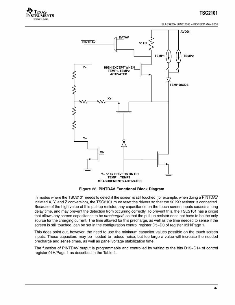
TSC2101
SLAS392D− JUNE 2003 − REVISED MAY 2005
www.ti.com
37
Y+
X+
Y−
ON
Y+ or X+ DRIVERS ON ORTEMP1 , TEMP2
MEASUREMENTS ACTIVATED
TEMP DIODE
HIGH EXCEPT WHENTEMP1. TEMP2
ACTIVATED
PINTDAV
DATAV
TEMP1 TEMP2
AVDD1
50 kΩ
Figure 28. PINTDAV Functional Block Diagram
In modes where the TSC2101 needs to detect if the screen is still touched (for example, when doing a PINTDAVinitiated X, Y, and Z conversion), the TSC2101 must reset the drivers so that the 50 KΩ resistor is connected.Because of the high value of this pull-up resistor, any capacitance on the touch screen inputs causes a longdelay time, and may prevent the detection from occurring correctly. To prevent this, the TSC2101 has a circuitthat allows any screen capacitance to be precharged, so that the pull-up resistor does not have to be the onlysource for the charging current. The time allowed for this precharge, as well as the time needed to sense if thescreen is still touched, can be set in the configuration control register D5−D0 of register 05H/Page 1.
This does point out, however, the need to use the minimum capacitor values possible on the touch screeninputs. These capacitors may be needed to reduce noise, but too large a value will increase the neededprecharge and sense times, as well as panel voltage stabilization time.
The function of PINTDAV output is programmable and controlled by writing to the bits D15−D14 of controlregister 01H/Page 1 as described in the Table 4.

TSC2101
SLAS392D− JUNE 2003 − REVISED MAY 2005
www.ti.com
38
Table 4. Programmable PINTDAV Functionality
D15−D14 PINTDAV FUNCTION
00 Acts as PEN interrupt (active low) only. When PEN touch is detected, PINTDAV goes low.
01 Acts as data available (active low) only. The PINTDAV goes low as soon as one set of ADC conversions are completed for dataof X,Y, XYZ, battery input, or auxiliary input selected by D13−D10 in control register 00H/Page 1. The resulting ADC output is storedin the appropriate registers. The PINTDAV remains low and goes high only after this complete set of registers selected by D13−D10in control register 00H/Page 1 is read out.
1011
Acts as both PEN interrupt and data available. When PEN touch is detected, PINTDAV goes low and remains low. The PINTDAVgoes high only after one set of A/D conversions is completed for data of X,Y, XYZ, battery input, or auxiliary input selected byD13−D10 in control register 00H/Page 1.
NOTE: See the section, Conversion Time Calculations for the TSC2101 in this data sheet for the timing diagrams.
Pen-touch detect circuit is disabled during hardware power down.
Touch Screen Measurements
The touch screen ADC can be either controlled by the host processor or can be self−controlled to offloadprocessing from the host processor. Bit D12 of control register 01H/Page 1 sets the control mode of theTSC2101 touch screen ADC.
Conversion Controlled by the TSC2101 Initiated at Touch Detect
In this mode, the TSC2101 detects when the touch panel is touched and causes the PINTDAV line to go low.At the same time, the TSC2101 starts up its internal clock. Assuming the part was configured to convert XYcoordinates, it then turns on the Y drivers, and after a programmed panel voltage stabilization time, powers upthe ADC and converts the Y coordinate. If averaging is selected, several conversions may take place; whendata averaging is complete, the Y coordinate result is stored in the Y register.
If the screen is still touched at this time, the X drivers are enabled, and the process repeats, but measuringinstead the X coordinate, storing the result in the X register.
If only X and Y coordinates are to be measured, then the conversion process is complete. The time it takes tocomplete this process depends upon the selected resolution, internal conversion clock rate, averaging selected,panel voltage stabilization time, and precharge and sense times.
If the pressure of the touch is also to be measured, the process continues in the same way, measuring the Z1and Z2 values, and placing them in the Z1 and Z2 registers. As before, this process time depends upon thesettings described above.
See the section Conversion Time Calculation for the TSC2101 in this data sheet for timing diagrams andconversion time calculations.
Conversion Controlled by the TSC2101 Initiated by the Host
In this mode, the TSC2101 detects when the touch panel is touched and causes the PINTDAV line to go low.The host recognizes the interrupt request, and then writes to the ADC control register (D13−D10 of controlregister 00H/Page 1) to select one of the touch screen scan functions. The host can either choose to initiateone of the scan functions, in which case the TSC2101 controls the driver turn−on and wait times (e.g. uponreceiving the interrupt the host can initiate the continuous scan function X−Y−Z1−Z2 after which the TSC2101controls the rest of conversion). The host can also choose to control each aspect of conversion by controllingthe driver turn-on and start of conversions. For example, upon receiving the interrupt request, the host turnson the X drivers. After waiting for the settling time, the host then addresses the TSC2101 again, this timerequesting an X coordinate conversion, and so on.
The main difference between this mode and the previous mode is that the host, not the TSC2101, controls thetouch screen scan functions.
See the section Conversion Time Calculation for the TSC2101 in this data sheet for timing diagrams andconversion time calculations.

TSC2101
SLAS392D− JUNE 2003 − REVISED MAY 2005
www.ti.com
39
Temperature Measurement
In some applications, such as battery charging, a measurement of ambient temperature is required. Thetemperature measurement technique used in the TSC2101 relies on the characteristics of a semiconductorjunction operating at a fixed current level. The forward diode voltage (VBE) has a well-defined characteristicversus temperature. The ambient temperature can be predicted in applications by knowing the 25°C value ofthe VBE voltage and then monitoring the variation of that voltage as the temperature changes.
The TSC2101 offers two modes of temperature measurement. The first mode requires a single reading topredict the ambient temperature. A diode, as shown in Figure 29, is used during this measurement cycle. Thisvoltage is typically 600 mV at +25°C with a 20-µA current through it. The absolute value of this diode voltagecan vary a few millivolts. The temperature coefficient of this voltage is typically 2 mV/°C. During the final testof the end product, the diode voltage at a known room temperature should be stored in nonvolatile memory.Further calibration can be done to calculate the precise temperature coefficient of the particular. This methodhas a temperature resolution of approximately 0.3°C/LSB and accuracy of approximately ±2°C withtwo-temperature calibration. Figure 30 and Figure 31 shows typical plots with single and two-temperaturecalibration respectively.
TEMP0 TEMP1
Temperature Select
X+
MUX A/DConverter
Figure 29. Functional Block Diagram of Temperature Measurement Mode
−10
−8
−6
−4
−2
0
2
4
6
8
10
−40 −20 0 20 40 60 80 100
Err
or
in M
easu
rem
ent −
TA − Free-Air Temperature − C
C°
Figure 30. Typical Plot of Single Measurement Method After Calibrating for Offset at Room Temperature

TSC2101
SLAS392D− JUNE 2003 − REVISED MAY 2005
www.ti.com
40
−1.20
−1
−0.80
−0.60
−0.40
−0.20
0
0.20
−40 −20 0 20 40 60 80 100
Err
or
in M
easu
rem
ent −
TA − Free-Air Temperature − C
C°
Figure 31. Typical Plot of Single Measurement Method After Calibrating for Offset and Gain At TwoTemperatures
The second mode uses a two-measurement (differential) method. This mode requires a second conversion witha current 82 times larger. The voltage difference between the first (TEMP1) and second (TEMP2) conversion,using 82 times the bias current, is represented by:
kTq ln(N)
where:N is the current ratio = 82k = Boltzmann’s constant (1.38054 • 10−23 electrons volts/degrees Kelvin)q = the electron charge (1.602189 • 10−19 °C)T = the temperature in degrees Kelvin
The equation for the relation between differential code and temperature may vary slightly from device to deviceand can be calibrated at final system test by the user. This method provides resolution of approximately1.5°C/LSB and accuracy of approximately ±4°C after calibrating at room temperature.

TSC2101
SLAS392D− JUNE 2003 − REVISED MAY 2005
www.ti.com
41
−4
−3
−2
−1
0
1
2
3
4
−40 −20 0 20 40 60 80 100
Err
or
in M
easu
rem
ent −
TA − Free-Air Temperature − C
C°
Figure 32. Typical Plot of Differential Measurement Method After Calibrating for Offset at RoomTemperature
The TSC2101 supports programmable auto-temperature measurement mode, which can be enabled usingcontrol register 0CH/page 1. In this mode, the TSC2101 can auto-start the temperature measurement after aprogrammable interval. The user can program minimum and maximum threshold values through a register. Ifthe measurement goes outside the threshold range, the TSC2101 sets a flag in the read only control register0CH/page 1, which gets cleared after the flag is read. The TSC2101 can also be configured to send and activehigh interrupt over GPIO1 by setting D9 in control register 0CH/page 1. The duration of the interrupt isapproximately 2 ms.
Temperature measurement can only be done in host controlled mode.
Battery Measurement
An added feature of the TSC2101 is the ability to monitor the battery voltage on the other side of a voltageregulator (dc/dc converter), as shown in Figure 33. The battery voltage can vary from 0.5 V to 6 V whilemaintaining the analog supply voltage to the TSC2101 at 3.0 V to 3.6 V. The input voltage (VBAT) is divideddown by a factor of 5 so that a 6.0 V battery voltage is represented as 1.2 V to the ADC. In order to minimizethe power consumption, the divider is only on during the sampling of the battery input.
If the battery conversion results in A/D output code of B, the voltage at the battery pin can be calculated as:
VBAT B2N 5 VREF
Where:
N is the programmed resolution of A/D
VREF is the programmed value of internal reference or the applied external reference.

TSC2101
SLAS392D− JUNE 2003 − REVISED MAY 2005
www.ti.com
42
ADCVBAT
8 kΩ2 kΩ
R
LDO or DC-DCConverter
3.0 V to 3.6 V
VDD
+
−Battery
0.5 to 6 V
Figure 33. Battery Measurement Functional Block Diagram
Battery measurement can only be done in host−controlled mode.
See the section Conversion Time Calculation for the TSC2101 and subsection Non Touch MeasurementOperation in this data sheet for timing diagrams and conversion time calculations.
For increased protection and robustness, TI recommends a minimum 100−Ω resistor be added in seriesbetween the system battery and the VBAT pin. The 100-Ω resistor will cause an approximately 1% gain changein the battery voltage measurement, which can easily be corrected in software when the battery conversion datais read by the operating system.
Auxiliary Measurement
The auxiliary voltage inputs (AUX1 and AUX2) can be measured in much the same way as the battery inputsexcept the difference that input voltage is not divided. Applications might include external temperature sensing,ambient light monitoring for controlling the backlight, or sensing the current drawn from the battery. The auxiliaryinput can also be monitored continuously in scan mode.
The TSC2101 provides feature to measure resistance using auxiliary inputs. It has two modes of operation:(1) External bias resistance measurement (2) Internal bias resistance measurement. Internal bias resistancemeasurement mode does not need an external bias resistance of 50 kΩ, but provides less accuracy becauseof on chip resistance variation, which is typically ±20%. Figure 34 shows connection diagram for resistancemeasurement mode on AUX1.
AUX1
R
SAR
VREF
a. Internal bias, Resistance Measurement
VsarSAR
VREF
b. External bias, Resistance Measurement
VsarAUX1
R
50 kΩ
50 kΩ
50 kΩ
Figure 34. Connection DIagram for Resistance Measurement
Resistance can be calculated using following formula:
R 50 K VsarVREF Vsar

TSC2101
SLAS392D− JUNE 2003 − REVISED MAY 2005
www.ti.com
43
Where:
VREF is the SAR ADC reference
Vsar is input to the SAR ADC
The TSC2101 supports programmable auto−auxiliary measurement mode, which can be enabled using controlregister 0CH/page 1. In this mode, the TSC2101 can auto start the auxiliary measurement after aprogrammable interval. The user can program minimum and maximum threshold values through a register. Ifthe measurement goes outside the threshold range, the TSC2101 sets a flag in the read only control register0CH/page 1, which gets cleared after the flag is read. The TSC2101 can also be configured to send an activehigh interrupt over GPIO1 by setting D9 of control register 0CH/page 1. The duration of the interrupt isapproximately 2 ms.
Auxiliary measurement can only be done in host−controlled mode.
See the section Conversion Time Calculation for the TSC2101 and subsection Non Touch MeasurementOperation in this data sheet for timing diagram and conversion time calculation
Port Scan
If making measurements of VBAT, AUX1, and AUX2 is desired on a periodic basis, the Port Scan mode canbe used. This mode causes the TSC2101 to sample and convert battery input and both auxiliary inputs. At theend of this cycle, the battery and auxiliary result registers contain the updated values. Thus, with one write tothe TSC2101, the host can cause three different measurements to be made.
Port Scan can only be done in host-controlled mode. See the section Issues at the end of this data sheet fordetails of a known issue with this mode.
See the section Conversion Time Calculation for the TSC2101 and subsection Port Scan Operation in this datasheet for timing diagrams and conversion time calculations.
Buffer Mode
The TSC2101 supports a programmable buffer mode, which is applicable for both touch screen relatedconversion (X, Y, Z1, Z2) and nontouch screen related conversion (BAT, AUX1, AUX2, TEMP1, TEMP2). Buffermode is implemented using a circular FIFO with a depth of 64. The number of interrupts required to be servicedby a host processor can be reduced significantly buffer mode. Buffer mode can be enabled using control register02H/page1.
Figure 35. Circular Buffer

TSC2101
SLAS392D− JUNE 2003 − REVISED MAY 2005
www.ti.com
44
Converted data is automatically written into the FIFO. To control the writing, reading and interrupt process, awrite pointer (WRPTR), a read pointer (RDPTR) and a trigger pointer (TGPTR) are used. The read pointeralways shows the location, which will be read next. The write pointer indicates the location, in which the nextconverted data is going to be written. The trigger pointer indicates the location at which an interrupt will begenerated if the write pointer reaches that location. Trigger level is the number of the data points needed to bepresent in the FIFO before generating an interrupt. For e.g., X−Y continuous scan mode with trigger level setto 8, the TSC2101 generates interrupt after writing (X1, Y1), (X2, Y2), (X3, Y3), (X4, Y4) i.e. 4 data-pairs or8 data. Figure 35 shows the case when trigger level is programmed as 32. On resetting buffer mode, RDPTRmoves to location 1, WRPTR moves to location 1, and TGPTR moves to location equal to programmed triggerlevel.
The user can select the input or input sequence, which needs to be converted, from the ADCSM bits of controlregister 00H/page 1. The converted values are written in a predefined sequence to the circular buffer. The userhas flexibility to program a specific trigger level in order to choose the configuration which best fits theapplication. When the number of converted data, written in FIFO, becomes equal to the programmed triggerlevel then the device generates an interrupt signal on /PINTDAV pin. In buffer mode, the user should programthis pin as Data Available (DATA_AVA). In buffer mode, touch screen related conversions (X, Y, Z1, Z2) areallowed only in self-controlled mode and nontouch screen related conversions (BAT, AUX1, AUX2, TEMP1,TEMP2) are allowed only in host-controlled mode.
Buffer mode can be used in single-shot conversion or continuous conversion mode.
In single shot conversion mode, once the number of data written reaches programmed trigger level, theTSC2101 generates an interrupt and waits for the user to start reading. As soon as the user starts reading thefirst data from the last converted set, the TSC2101 clears the interrupt and starts a new set of conversions andthe trigger pointer is incremented by the programmed trigger level. An interrupt is generated again when thetrigger condition is satisfied.
In continuous conversion mode, once number of data written reaches the programmed trigger level, theTSC2101 generates an interrupt. It immediately starts a new set of conversions and the trigger pointer isincremented by the programmed trigger level. An interrupt gets cleared either by writing the next converted datainto the FIFO or by starting to read from the FIFO.
See the section Conversion Time Calculation for the TSC2101 and subsection Buffer Mode Operation in thisdata sheet for timing diagrams and conversion time calculations.
Depending upon how the user is reading data, the FIFO can become empty or full. If the user is trying to readdata even if the FIFO is empty, then RDPTR keeps pointing to same location. If the FIFO gets full then the nextlocation is overwritten with newly converted data and the read pointer is incremented by one.
While reading the FIFO, the TSC2101 provides FIFO empty and full status flags along with the data. The usercan also read a status flag from control register 02H/page 1.
DIGITAL INTERFACE
RESET
The device requires reset after power up. This requires a low-to-high transition on the RESET pin after powerup for correct operation. Reset initializes all the internal registers, counters and logic.
Hardware Power-Down
Hardware power-down powers down all the internal circuitry to save power. All the register contents aremaintained. Putting the TSC2101 into hardware power-down circuit also disables the pen-touch detect circuit.
General Purpose I/O
The TSC2101 has two general purpose I/O (GPIO1 and GPIO2), which can be programmed either as inputsor outputs. As outputs they can be programmed to control external logic through the TSC2101 registers or sendinterrupts to the host processor on events like button detect, headset insertion, headset removal,Auxiliary/temperature outside threshold range etc. As inputs they can be used by the host-processor to monitorlogic states of signals on the system through the TSC2101 registers.
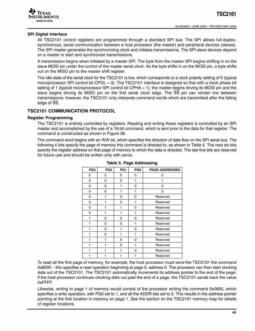
TSC2101
SLAS392D− JUNE 2003 − REVISED MAY 2005
www.ti.com
45
SPI Digital InterfaceAll TSC2101 control registers are programmed through a standard SPI bus. The SPI allows full-duplex,synchronous, serial communication between a host processor (the master) and peripheral devices (slaves).The SPI master generates the synchronizing clock and initiates transmissions. The SPI slave devices dependon a master to start and synchronize transmissions.
A transmission begins when initiated by a master SPI. The byte from the master SPI begins shifting in on theslave MOSI pin under the control of the master serial clock. As the byte shifts in on the MOSI pin, a byte shiftsout on the MISO pin to the master shift register.
The idle state of the serial clock for the TSC2101 is low, which corresponds to a clock polarity setting of 0 (typicalmicroprocessor SPI control bit CPOL = 0). The TSC2101 interface is designed so that with a clock phase bitsetting of 1 (typical microprocessor SPI control bit CPHA = 1), the master begins driving its MOSI pin and theslave begins driving its MISO pin on the first serial clock edge. The SS pin can remain low betweentransmissions; however, the TSC2101 only interprets command words which are transmitted after the fallingedge of SS.
TSC2101 COMMUNICATION PROTOCOLRegister Programming
The TSC2101 is entirely controlled by registers. Reading and writing these registers is controlled by an SPImaster and accomplished by the use of a 16-bit command, which is sent prior to the data for that register. Thecommand is constructed as shown in Figure 36.
The command word begins with an R/W bit, which specifies the direction of data flow on the SPI serial bus. Thefollowing 4 bits specify the page of memory this command is directed to, as shown in Table 5. The next six bitsspecify the register address on that page of memory to which the data is directed. The last five bits are reservedfor future use and should be written only with zeros.
Table 5. Page Addressing
PG3 PG2 PG1 PG0 PAGE ADDRESSED
0 0 0 0 0
0 0 0 1 1
0 0 1 0 2
0 0 1 1 3
0 1 0 0 Reserved
0 1 0 1 Reserved
0 1 1 0 Reserved
0 1 1 1 Reserved
1 0 0 0 Reserved
1 0 0 1 Reserved
1 0 1 0 Reserved
1 0 1 1 Reserved
1 1 0 0 Reserved
1 1 0 1 Reserved
1 1 1 0 Reserved
1 1 1 1 Reserved
To read all the first page of memory, for example, the host processor must send the TSC2101 the command0x8000 – this specifies a read operation beginning at page 0, address 0. The processor can then start clockingdata out of the TSC2101. The TSC2101 automatically increments its address pointer to the end of the page;if the host processor continues clocking data out past the end of a page, the TSC2101 sends back the value0xFFFF.
Likewise, writing to page 1 of memory would consist of the processor writing the command 0x0800, whichspecifies a write operation, with PG0 set to 1, and all the ADDR bits set to 0. This results in the address pointerpointing at the first location in memory on page 1. See the section on the TSC2101 memory map for detailsof register locations.

TSC2101
SLAS392D− JUNE 2003 − REVISED MAY 2005
www.ti.com
46
BIT 15MSB
BIT 14 BIT 13 BIT 12 BIT 11 BIT 10 BIT 9 BIT 8 BIT 7 BIT 6 BIT 5 BIT 4 BIT 3 BIT 2 BIT 1 BIT 0LSB
R/W* PG3 PG2 PG1 PG0 ADDR5 ADDR4 ADDR3 ADDR2 ADDR1 ADDR0 0 0 0 0 0
Figure 36. TSC2101 Command Word
COMMAND WORD DATA DATA
SS
SCLK
MOSI
Figure 37. Register Write Operation
COMMAND WORD
SS
SCLK
MOSI
DATA DATA
MOSO
Figure 38. Register Read Operation
TSC2101 Memory Map
The TSC2101 has several 16-bit registers which allow control of the device as well as providing a location forresults from the TSC2101 to be stored until read by the host microprocessor. These registers are separatedinto four pages of memory in the TSC2101: a data page (page 0), control pages (page 1 and page 2) and a bufferdata page (page 3). The memory map is shown in Table 6.
Table 6. Memory Map
PAGE 0: TOUCHSCREEN DATA
REGISTER
PAGE 1: TOUCH SCREENCONTROL REGISTERS
PAGE 2: AUDIO CONTROL REGISTERSPAGE 3: BUFFERDATA REGISTERS
ADDR REGISTER ADDR REGISTER ADDR REGISTER ADDR REGISTER
00 X 00 TSC ADC 00 Audio Control 1 00 Buffer Location
01 Y 01 Status 01 Headset PGA Control 01 Buffer Location
02 Z1 02 Buffer Mode 02 DAC PGA Control 02 Buffer Location
03 Z2 03 Reference 03 Mixer PGA Control 03 Buffer Location
04 Reserved 04 Reset Control Register 04 Audio Control 2 04 Buffer Location
05 BAT 05 Configuration 05 Power Down Control 05 Buffer Location
06 Reserved 06 Temperature Max 06 Audio Control 3 06 Buffer Location
07 AUX1 07 Temperature Min 07 Digital Audio Effects Filter Coefficients 07 Buffer Location
08 AUX2 08 AUX1 Max 08 Digital Audio Effects Filter Coefficients 08 Buffer Location
09 TEMP1 09 AUX1 Min 09 Digital Audio Effects Filter Coefficients 09 Buffer Location
0A TEMP2 0A AUX2 Max 0A Digital Audio Effects Filter Coefficients 0A Buffer Location
0B Reserved 0B AUX2 Min 0B Digital Audio Effects Filter Coefficients 0B Buffer Location

TSC2101
SLAS392D− JUNE 2003 − REVISED MAY 2005
www.ti.com
47
PAGE 3: BUFFERDATA REGISTERSPAGE 2: AUDIO CONTROL REGISTERS
PAGE 1: TOUCH SCREENCONTROL REGISTERS
PAGE 0: TOUCHSCREEN DATA
REGISTER
REGISTERADDRREGISTERADDRREGISTERADDRREGISTERADDR
0C Reserved 0C Measurement Configuration 0C Digital Audio Effects Filter Coefficients 0C Buffer Location
0D Reserved 0D Programmable Delay 0D Digital Audio Effects Filter Coefficients 0D Buffer Location
0E Reserved 0E Reserved 0E Digital Audio Effects Filter Coefficients 0E Buffer Location
0F Reserved 0F Reserved 0F Digital Audio Effects Filter Coefficients 0F Buffer Location
10 Reserved 10 Reserved 10 Digital Audio Effects Filter Coefficients 10 Buffer Location
11 Reserved 11 Reserved 11 Digital Audio Effects Filter Coefficients 11 Buffer Location
12 Reserved 12 Reserved 12 Digital Audio Effects Filter Coefficients 12 Buffer Location
13 Reserved 13 Reserved 13 Digital Audio Effects Filter Coefficients 13 Buffer Location
14 Reserved 14 Reserved 14 Digital Audio Effects Filter Coefficients 14 Buffer Location
15 Reserved 15 Reserved 15 Digital Audio Effects Filter Coefficients 15 Buffer Location
16 Reserved 16 Reserved 16 Digital Audio Effects Filter Coefficients 16 Buffer Location
17 Reserved 17 Reserved 17 Digital Audio Effects Filter Coefficients 17 Buffer Location
18 Reserved 18 Reserved 18 Digital Audio Effects Filter Coefficients 18 Buffer Location
19 Reserved 19 Reserved 19 Digital Audio Effects Filter Coefficients 19 Buffer Location
1A Reserved 1A Reserved 1A Digital Audio Effects Filter Coefficients 1A Buffer Location
1B Reserved 1B Reserved 1B PLL Programmability 1B Buffer Location
1C Reserved 1C Reserved 1C PLL Programmability 1C Buffer Location
1D Reserved 1D Reserved 1D Audio Control 4 1D Buffer Location
1E Reserved 1E Reserved 1E Handset PGA Control 1E Buffer Location
1F Reserved 1F Reserved 1F Cell & Buzzer PGA Control 1F Buffer Location
20 Reserved 20 Reserved 20 Audio Control 5 20 Buffer Location
21 Reserved 21 Reserved 21 Audio Control 6 21 Buffer Location
22 Reserved 22 Reserved 22 Audio Control 7 22 Buffer Location
23 Reserved 23 Reserved 23 GPIO Control 23 Buffer Location
24 Reserved 24 Reserved 24 AGC−CP_IN Control 24 Buffer Location
25 Reserved 25 Reserved 25 Driver Powerdown Status 25 Buffer Location
26 Reserved 26 Reserved 26 Mic AGC control 26 Buffer Location
27 Reserved 27 Reserved 27 Cell-phone AGC Control 27 Buffer Location
28 Reserved 28 Reserved 28 Reserved 28 Buffer Location
29 Reserved 29 Reserved 29 Reserved 29 Buffer Location
2A Reserved 2A Reserved 2A Reserved 2A Buffer Location
2B Reserved 2B Reserved 2B Reserved 2B Buffer Location
2C Reserved 2C Reserved 2C Reserved 2C Buffer Location
2D Reserved 2D Reserved 2D Reserved 2D Buffer Location
2E Reserved 2E Reserved 2E Reserved 2E Buffer Location
2F−3F Reserved 2F−3F Reserved 2F−3F Reserved 2F−3F BufferLocations
TSC2101 Control Registers
This section describes each of the registers shown in the memory map of Table 6. The registers are groupedaccording to the function they control. Note that in the TSC2101, bits in control registers may refer to slightlydifferent functions depending upon if you are reading the register or writing to it.
TSC2101 Data Registers (Page 0)
The data registers of the TSC2101 hold data results from conversion of touch screen ADC. All of these registersdefault to 0000H upon reset. These registers are read only.

TSC2101
SLAS392D− JUNE 2003 − REVISED MAY 2005
www.ti.com
48
X, Y, Z1, Z2, BAT, AUX1, AUX2, TEMP1 and TEMP2 Registers
The results of all ADC conversions are placed in the appropriate data register. The data format of the resultword, R, of these registers is right-justified, as follows:
Bit 15MSB
Bit 14 Bit 13 Bit 12 Bit 11 Bit 10 Bit 9 Bit 8 Bit 7 Bit 6 Bit 5 Bit 4 Bit 3 Bit 2 Bit 1 Bit 0LSB
0 0 0 0 R11MSB
R10 R9 R8 R7 R6 R5 R4 R3 R2 R1 R0LSB
PAGE 1 CONTROL REGISTER MAP
REGISTER 00H: Touch-Screen ADC Control
BIT NAMERESETVALUE
READ/WRITE
FUNCTION
D15 PSTCM 0 R/W Pen Status/Control Mode.READ0 => There is no screen touch (default).1 => The pen is downWRITE0 => Host controlled touch screen conversions (default).1 => The TSC2101 controlled touch screen conversions.
D14 ADST 1(for read)0 (for write)
R/W ADC STATUS.READ0 =>ADC is busy1 => ADC is not busy (default).WRITE0 => Normal mode (default).1 => Stop conversion and power down.
D13−D10 ADCSM 0000 R/W ADC Scan Mode.0000 => No scan0001 => Touch screen scan function: X and Y coordinates are converted and the results returned
to X and Y data registers. Scan continues until either the pen is lifted or a stop bit issent.
0010 => Touch screen scan function: X, Y, Z1 and Z2 coordinates are converted and the resultsreturned to X, Y, Z1 and Z2 data registers. Scan continues until either the pen is liftedor a stop bit is sent.
0011 => Touch screen scan function: X coordinate is converted and the results returned to X dataregister.
0100 => Touch screen scan function: Y coordinate is converted and the results returned to Y dataregister.
0101 => Touch screen scan function: Z1 and Z2 coordinates are converted and the resultsreturned to Z1 and Z2 data registers
0110 => BAT input is converted and the results returned to the BAT data register.0111 => AUX2 input is converted and the results returned to the AUX2 data register1000 => AUX1 input is converted and the results returned to the AUX1 data register.1001 => Auto Scan function: For AUX1, AUX2, TEMP1 or TEMP2 as chosen using control
register 0CH/page 1. Scan continues until stop bit is sent or D13−D10 are changed.1010 => TEMP1 input is converted and the results returned to the TEMP1 data register.1011 => Port scan function: BAT, AUX1, AUX2 inputs are measured and the results returned to
the appropriate data registers.1100 => TEMP2 input is converted and the results returned to the TEMP2 data register.1101 => Turn on X+, X− drivers1110 => Turn on Y+, Y− drivers1111 => Turn on Y+, X− drivers
D9−D8 RESOL 00 R/W Resolution Control. The ADC resolution is specified with these bits.00 => 12-bit resolution01 => 8-bit resolution10 => 10-bit resolution11 => 12-bit resolution

TSC2101
SLAS392D− JUNE 2003 − REVISED MAY 2005
www.ti.com
49
BIT FUNCTIONREAD/WRITE
RESETVALUENAME
D7−D6 ADAVG 00 R/W Converter Averaging Control. These two bits allow user to specify the number of averages theconverter will perform selected by bit D0, which selects either Mean Filter or Median Filter.
Mean Filter Median Filter00 => No average No average01 => 4-data average 5-data average10 => 8-data average 9-data average11 => 16-data average 15-data average
D5−D4 ADCR 00 R/W Conversion Rate Control. These two bits specify the internal clock rate, which the ADC uses tocontrol performing a single conversion. These bits are the same whether reading or writing.
tconv N 4
ƒINTCLKWhere fINTCLK is the internal clock frequency. For example, with 12-bit resolution and a 2 MHzinternal clock frequency, the conversion time is 8 µs. This yields an effective throughput rate of125 kHz.
00 => 8 MHz internal clock rate (use for 8-bit resolution only)01 =>4 MHz internal clock rate (use for 8-bit/10-bit resolution only)10 =>2 MHz internal clock rate11 =>1 MHz internal clock rate
D3−D1 PVSTC 000 R/W Panel Voltage Stabilization Time Control. These bits allow user to specify a delay time from thetime the touch screen drivers are enabled to the time the voltage is sampled and a conversionis started. This allows the user to adjust for the settling of the individual touch panel and externalcapacitances.000 => 0 µs stabilization time001 => 100 µs stabilization time010 => 500 µs stabilization time011 => 1 ms stabilization time100 => 5 ms stabilization time101 => 10 ms stabilization time110 => 50 ms stabilization time111 => 100 ms stabilization time
D0 AVGFS 0 R/W Average Filter Select0 => Mean Filter1 => Median Filter
REGISTER 01H: Status Register
BIT NAMERESETVALUE
READ/WRITE
FUNCTION
D15−D14 PINTDAV 10 R/W Pen Interrupt or Data Available. These two bits program the function of the PINTDAV pin.00 => Acts as PEN interrupt (active low) only. When PEN touch is detected, PINTDAV goes low.01 => Acts as data available (active low) only. The PINTDAV goes low as soon as one set of ADC
conversion(s) is completed. For scan mode, PINTDAV remains low as long as all theappropriate registers have not been read out.
10 => Acts as both PEN interrupt and data available. When PEN touch is detected, PINTDAV goeslow. PINTDAV goes high once all the selected conversions are over.
11 => Same as 10
D13 PWRDN 0 R TSC−ADC Power down status0 => TSC−ADC is active1 => TSC−ADC stops conversion and powers down
D12 HCTLM 0 R Host Controlled Mode Status0 => Host controlled mode1 => Self (TSC2101) controlled mode
D11 DAVAIL 0 R Data Available Status0 => No data available.1 => Data is available(i.e one set of conversion is done)Note:− This bit gets cleared only after all the converted data have been completely read out. This bit
is not valid in case of buffer mode.

TSC2101
SLAS392D− JUNE 2003 − REVISED MAY 2005
www.ti.com
50
BIT FUNCTIONREAD/WRITE
RESETVALUENAME
D10 XSTAT 0 R X Data Register Status0 => No new data is available in X−data register1 => New data for X−coordinate is available in register
Note: This bit gets cleared only after the converted data of X coordinate has been completely readout of the register. This bit is not valid in case of buffer mode.
D9 YSTAT 0 R Y Data Register Status0 => No new data is available in Y−data register1 => New data for Y−coordinate is available in register
Note: This bit gets cleared only after the converted data of Y coordinate has been completely readout of the register. This bit is not valid in case of buffer mode.
D8 Z1STAT 0 R Z1 Data Register Status0 => No new data is available in Z1−data register1 => New data is available in Z1−data register
Note: This bit gets cleared only after the converted data of Z1 coordinate has been completely readout of the register. This bit is not valid in case of buffer mode.
D7 Z2STAT 0 R Z2 Data Register Status0 => No new data is available in Z2−data register1 => New data is available in Z2−data register
Note: This bit gets cleared only after the converted data of Z2 coordinate has been completely readout of the register. This bit is not valid in case of buffer mode.
D6 BSTAT 0 R BAT Data Register Status0 => No new data is available in BAT data register1 => New data is available in BAT data register
Note: This bit gets cleared only after the converted data of BAT has been completely read out of theregister. This bit is not valid in case of buffer mode.
D5 0 R Reserved
D4 AX1STAT 0 R AUX1 Data Register Status0 => No new data is available in AUX1−data register1 => New data is available in AUX1−data register
Note: This bit gets cleared only after the converted data of AUX1 has been completely read out ofthe register. This bit is not valid in case of buffer mode.
D3 AX2STAT 0 R AUX2 Data Register Status0 => No new data is available in AUX2−data register1 => New data is available in AUX2−data register
Note: This bit gets cleared only after the converted data of AUX2 has been completely read out ofthe register. This bit is not valid in case of buffer mode.
D2 T1STAT 0 R TEMP1 Data Register Status0 => No new data is available in TEMP1−data register1 => New data is available in TEMP1−data register
Note: This bit gets cleared only after the converted data of TEMP1 has been completely read out ofthe register. This bit is not valid in case of buffer mode.
D1 T2STAT 0 R TEMP2 Data Register Status0 => No new data is available in TEMP2−data register1 => New data is available in TEMP2−data register
Note: This bit gets cleared only after the converted data of TEMP2 has been completely read out ofthe register. This bit is not valid in case of buffer mode.
D0 0 R Reserved

TSC2101
SLAS392D− JUNE 2003 − REVISED MAY 2005
www.ti.com
51
REGISTER 02H: Buffer Control
BIT NAMERESETVALUE
READ/WRITE
FUNCTION
D15 BUFRES 0 R/W Buffer Reset.0 => Buffer mode is disabled and RDPTR, WRPTR & TGPTR set to their reset value.1 => Buffer mode is enabled.
D14 BUFCONT 0 R/W Buffer Mode Selection0 => Continuous conversion mode.1 => Single shot mode.
D13−D11 BUFTL 000 R/W Trigger Level TL selection of Buffer used for SAR ADC000 => 8001 => 16010 => 24011 => 32100 => 40101 => 48110 => 56111 => 64
D10 BUFOVF 0 R Buffer Full Flag0 => Buffer is not full.1 => Buffer is full. This means buffer contains 64 unread converted data.
D9 BUFEMF 1 R Buffer Empty Flag0 => Buffer is not empty.1 => Buffer is empty. This means there is no unread converted data in the buffer.
D8−D0 0’s R Reserved
REGISTER 03H: Reference Control
BIT NAMERESETVALUE
READ/WRITE
FUNCTION
D15−D6 0’s R Reserved
D5 0 R/W Reserved. Always write 0 to this bit.
D4 VREFM 0 R/W Voltage Reference Mode. This bit configures the VREF pin as either external reference or internalreference. 0 => External reference 1 => Internal reference
D3−D2 RPWUDL 00 R/W Reference Power Up Delay. These bits allow for a delay time for measurements to be made afterthe reference powers up, thereby assuring that the reference has settled00 => 0 µs01 => 100 µs10 => 500 µs11 => 1000 µsNote: This will be valid only when device is programmed for internal reference and Bit D1 = 1, i.e.,reference is powered down between the conversions if not required.
D1 RPWDN 1 R/W Reference Power Down. This bit controls the power down of the internal reference voltage.0 => Powered up at all times.1 => Powered Down between conversions.Note: When D4 = 0 i.e. device is in external reference mode then the internal reference is powereddown always.
D0 IREFV 0 R/W Internal Reference Voltage. This bit selects the internal voltage for TSC ADC.0 => VREF = 1.25 V1 => VREF = 2.50 V

TSC2101
SLAS392D− JUNE 2003 − REVISED MAY 2005
www.ti.com
52
REGISTER 04H: Reset Control
BIT NAMERESETVALUE
READ/WRITE
FUNCTION
D15−D0 RSALL R/W FFFFH Reset All. Writing the code 0xBB00, as shown below, to this register causes the TSC2101 to resetall its control registers to their default, power−up values.1011101100000000 => Reset all control registersOthers => Do not write other sequences to the register.
REGISTER 05H: Configuration Control
BIT NAMERESETVALUE
READ/WRITE
FUNCTION
D15−D7 0’s R Reserved
D6 SWPDTD 0 R/W Software Powerdown Control for Pen Touch Detection0 => Pen touch detection is enabled.1 => Pen touch detection is disabled.
D5−D3 PRECTM 000 R/W Precharge Time. These bits set the amount of time allowed for precharging any pin capacitance onthe touch screen prior to sensing if a screen touch is happening.000 => 20 µs001 => 84 µ010 => 276 µ011 => 340 µs100 => 1.044 ms101 => 1.108 ms110 => 1.300 m111 => 1.364 ms
D2−D0 RPWUDL 000 R/W Sense Time. These bits set the amount of time the TSC2101 need to wait to sense a screen touchbetween coordinate axes.000 => 32 µs001 => 96 µs010 => 544 µs011 => 608 µs100 => 2.080 ms101 => 2.144 m110 => 2.592 ms111 => 2.656 ms
REGISTER 06H: Temperature Max Threshold Measurement
BIT NAMERESETVALUE
READ/WRITE
FUNCTION
D15−D13 0’s R Reserved
D12 TMXES 0 R/W Max Temperature (TEMP1 or TEMP2) threshold check enable for Auto/Non−Auto−ScanMeasurement.0 => Max Temperature threshold check is disabled.1 => Max Temperature threshold check is enabled.Only valid for TEMP1 or TEMP2. Depends on bit TSCAN of control register 0CH/page 1 in caseof auto−scan measurement and depends on bits ADCSM of control register 00H/page 1 in caseof non−auto−scan measurement.
D11−D0 TTHRESH FFFH R/W Temperature Max Threshold. When code due to temperature measurement goes above or equalto programmed threshold value, interrupt is generated.

TSC2101
SLAS392D− JUNE 2003 − REVISED MAY 2005
www.ti.com
53
REGISTER 07H: Temperature Min Threshold Measurement
BIT NAMERESETVALUE
READ/WRITE
FUNCTION
D15−D13 0’s R Reserved
D12 TMNES 0 R/W Min Temperature (TEMP1 or TEMP2) threshold check enable for Auto/Non−Auto−ScanMeasurement.0 => Min Temperature threshold check is disabled.1 => Min Temperature threshold check is enabled.Only valid for TEMP1 or TEMP2. Depends on bit TSCAN of control register 0CH/page 1 in caseof auto−scan measurement and depends on bits ADCSM of control register 00H/page 1 in caseof non−auto−scan measurement.
D11−D0 TTHRESL 000H R/W Temperature Min Threshold. When code due to temperature measurement goes below or equal toprogrammed threshold value, interrupt is generated.
REGISTER 08H: AUX1 Max Threshold Measurement
BIT NAMERESETVALUE
READ/WRITE
FUNCTION
D15−D13 0’s R Reserved
D12 A1MXES 0 R/W Max AUX1 threshold check enable for Auto/Non−Auto−Scan Measurement.0 => Max AUX1 threshold check is disabled.1 => Max AUX1 threshold check is enabled.
D11−D0 A1THRESH FFFH R/W AUX1 Threshold. When code due to AUX1 measurement goes above or equal to programmedthreshold value, interrupt is generated.
REGISTER 09H: AUX1 Min Threshold Measurement
BIT NAMERESETVALUE
READ/WRITE
FUNCTION
D15−D13 0’s R Reserved
D12 A1MNES 0 R/W Min AUX1 threshold check enable for Auto/Non−Auto−Scan Measurement.0 => Min AUX1 threshold check is disabled.1 => Min AUX1 threshold check is enabled.
D11−D0 A1THRESL 000H R/W AUX1 Threshold. When code due to AUX1 measurement goes below or equal to programmedthreshold value, interrupt is generated.
REGISTER 0AH: AUX2 Max Threshold Measurement
BIT NAMERESETVALUE
READ/WRITE
FUNCTION
D15−D13 0’s R Reserved
D12 A2MXES 0 R/W Max AUX2 threshold check enable for Auto/Non−Auto−Scan Measurement.0 => Max AUX2 threshold check is disabled.1 => Max AUX2 threshold check is enabled.
D11−D0 A1THRESH FFFH R/W AUX2 Threshold. When code due to AUX2 measurement goes above or equal toprogrammed threshold value, interrupt is generated.
REGISTER 0BH: AUX2 Max Threshold Measurement
BIT NAMERESETVALUE
READ/WRITE
FUNCTION
D15−D13 0’s R Reserved
D12 A2MNES 0 R/W Min AUX2 threshold check enable for Auto/Non−Auto−Scan Measurement.0 => Min AUX2 threshold check is disabled.1 => Min AUX2 threshold check is enabled.
D11−D0 A2THRESL 000H R/W AUX2 Threshold. When code due to AUX2 measurement goes below or equal to programmedthreshold value, interrupt is generated.

TSC2101
SLAS392D− JUNE 2003 − REVISED MAY 2005
www.ti.com
54
REGISTER 0CH: Measurement ConfigurationBIT NAME RESET
VALUEREAD/WRITE
FUNCTION
D15 TSCAN 0 R/W TEMP Configuration when Auto−Temperature is selected0 => TEMP1 is used for auto−temperature function1 => TEMP2 is used for auto−temperature function
D15 A1CONF 0 R/W AUX1 Configuration.0 => AUX1 is used for voltage measurement.1 => AUX1 is used for resistance measurement.
D14 A2CONF 0 R/W AUX2 Configuration.0 => AUX2 is used for voltage measurement.1 => AUX2 is used for resistance measurement.
D12 ATEMES 0 R/W Auto Temperature (TEMP1 or TEMP2) measurement enable0 => Auto temperature measurement is disabled.1 => Auto temperature measurement is enabled.TEMP1 or TEMP2 selection is depends on TSCAN bit.
D11 AA1MES 0 R/W Auto AUX1 measurement enable0 => Auto AUX1 measurement is disabled.1 => Auto AUX1 measurement is enabled.
D10 AA2MES 0 R/W Auto AUX2 measurement enable0 => Auto AUX2 measurement is disabled.1 => Auto AUX2 measurement is enabled.
D9 IGPIO1 0 R/W Enable GPIO1 for Auto/Non−Auto−Scan interrupt (this programmability is valid only if D11 & D9of control register 23H/page 2 are 0’s)0 => GPIO1 is not selected for interrupt.1 => GPIO1 is used to send an interrupt. Interrupt is generated when any of TEMP (TEMP1 orTEMP2), AUX1 or AUX2 are not passing threshold
D8 THMXFL 0 R Max threshold flag for Temperature (TEMP1 or TEMP2) measurement.0 => Temperature measurement is less than max threshold setting.1 => Temperature measurement is greater than or equal to max threshold setting.
D7 THMNFL 0 R Min threshold flag for Temperature (TEMP1 or TEMP2) measurement.0 => Temperature measurement is greater than min threshold setting.1 => Temperature measurement is less than or equal to max threshold setting.
D6 A1HMXFL 0 R Max threshold flag for AUX1measurement.0 => AUX1 measurement is less than max threshold setting.1 => AUX1 measurement is greater than or equal to max threshold setting.
D5 A1HMNFL 0 R Min threshold flag for AUX1 measurement.0 => AUX1 measurement is greater than min threshold setting.1 => AUX1 measurement is less than or equal to max threshold setting.
D4 A2HMXFL 0 R Max threshold flag for AUX2measurement.0 => AUX2 measurement is less than max threshold setting.1 => AUX2 measurement is greater than or equal to max threshold setting.
D3 A2HMNFL 0 R Min threshold flag for AUX2 measurement.0 => AUX2 measurement is greater than min threshold setting.1 => AUX2 measurement is less than or equal to max threshold setting.
D2 EXTRES 0 R/W External Bias Resistance Measurement mode0 => Internal bias resistance measurement mode is enabled.1 => External bias resistance measurement mode is enabled.
D1−D0 0’s R Reserved

TSC2101
SLAS392D− JUNE 2003 − REVISED MAY 2005
www.ti.com
55
REGISTER 0DH: Programmable Delay In-Between Continuous Conversion
BIT NAMERESETVALUE
READ/WRITE
FUNCTION
D15 NTSPDELEN
0 R/W Programmable delay for non−touch screen auto measurement mode0 => Programmable delay is disabled for non−touch screen auto measurement mode.1 => Programmable delay is enabled for non−touch screen auto measurement mode.
D14−D12 NTSPDINTV 010 R/W Programming delay in−between conversion for non−touch screen auto measurementmode000 => 1.12 min001 => 3.36 min010 => 5.59 min011 => 7.83 min100 => 10.01 min101 => 12.30 min110 => 14.54 min111 => 16.78 minNote: These delays are from end of one set of conversion to the start of another set ofconversion.
D11 TSPDELEN 0 R/W Programmable delay for touch screen measurement0 => Programmable delay mode is disabled for touch screen measurement.1 => Programmable delay mode is enabled for touch screen measurement.Note: This mode is valid only for touch screen related conversion in self−controlled modeand in host−controlled mode valid for only continuous scan for X & Y coordinates or forX, Y, Z1 & Z2 coordinates.
D10−D8 TSPDINTV 010 R/W Programming delay in−between conversion for touch screen measurement000 => 1 ms001 => 3 ms010 => 5 ms011 => 6.5 ms100 => 8.5 ms101 => 10 ms110 => 12.5 ms111 => 15 msNote: These delays are from end of one set of conversion to the start of another set ofconversion.
D7 CLKSEL 0 R/W Clock selection for the touch screen controller0 => Internal oscillator clock is selected.1 => External MCLK is selected.Note: External clock is used only to control the delay programmed in between theconversion.
D6−D0 CLKDIV 0000001 R/W Clock Division used to divide MCLK for getting 1 MHz clock for programmable delay, i.e.MCLK/CLKDIV = 1 MHz,0000000 => 128,0000001 => 1,0000010 => 2,……1111110 => 126,1111111 => 127
REGISTER 0EH: Reserved
BIT NAMERESETVALUE
READ/WRITE
FUNCTION
D15−D8 RESV FFh R/W Reserved. Write only FFh to these bits.

TSC2101
SLAS392D− JUNE 2003 − REVISED MAY 2005
www.ti.com
56
PAGE 2 CONTROL REGISTER MAP
REGISTER 00H: Audio Control 1
BIT NAMERESETVALUE
READ/WRITE
FUNCTION
D15−D14 ADCHPF 00 R/W ADC High Pass Filter00 => Disabled01 => −3db point = 0.0045xFs10 => −3dB point = 0.0125xFs11 => −3dB point = 0.025xFsNote: Fs is ADC sample rate
D13−D12 0’s R Reserved
D11−D10 WLEN 00 R/W Codec Word Length00 => Word length = 16−bit01 => Word length = 20−bit10 => Word length = 24−bit11 => Word length = 32−bit
D9−D8 DATFM 00 R/W Digital Data Format00 => I2S Mode01 => DSP Mode10 => Right Justified11 => Left JustifiedNote: Right justified valid only when the ratio between DAC and ADC sample rate is an integer. e.g.ADC = 32 kHz and DAC = 24 kHz or vice−versa is invalid for right justified Mode.
D7−D6 0’s R Reserved
D5−D3 DACFS 000 R/W DAC Sampling Rate000 => DAC FS = Fsref/1001 => DAC FS = Fsref/(1.5)010 => DAC FS = Fsref/2011 => DAC FS = Fsref/3100 => DAC FS = Fsref/4101 => DAC FS = Fsref/5110 => DAC FS = Fsref/(5.5)111 => DAC FS = Fsref/6Note: Fsref is set between 39 kHz and 53 kHz
D2−D0 ADCFS 000 R/W ADC Sampling Rate000 => ADC FS = Fsref/1001 => ADC FS = Fsref/(1.5)010 => ADC FS = Fsref/2011 => ADC FS = Fsref/3100 => ADC FS = Fsref/4101 => ADC FS = Fsref/5110 => ADC FS = Fsref/(5.5)111 => ADC FS = Fsref/6Note: Fsref is set between 39 kHz and 53 kHz

TSC2101
SLAS392D− JUNE 2003 − REVISED MAY 2005
www.ti.com
57
REGISTER 01H: Gain Control for Headset/Aux Input
BIT NAMERESETVALUE
READ/WRITE
FUNCTION
D15 ADMUT_HED 1 R/W Headset/Aux Input Mute1 => Headset/Aux Input Mute 0 => Headset/Aux Input not mutedNote: If AGC is enabled and Headset/Aux Input is selected then ADMUT_HED+ADPGA_HEDreflects gain being applied by AGC.
D14−D8 ADPGA_HED 1111111 R/W ADC Headset/Aux PGA Settings0000000 => 0 dB0000001 => 0.5 dB0000010 => 1.0 dB………1110110 => 59.0 dB..........1111111 => 59.5 dBNote: If AGC is enabled and Headset/Aux Input is selected then ADMUT_HED+ADPGA_HEDreflects gain being applied by AGC.If AGC is on, the decoding for read values is as follows01110111 => +59.5 dB01110110 => +59.0 dB………00000000 => 0 dB……….11101001 => −11.5 dB11101000 => −12 dB
D7−D5 AGCTG_HED 000 R/W AGC Target Gain for Headset/Aux Input. These three bits set the AGC’s targeted ADC outputlevel.000 => −5.5 dB001 => −8.0 dB010 => −10 dB011 => −12 dB100 => −14 dB101 => −17 dB110 => −20 dB111 => −24 dB
D4−D1 AGCTC_HED 0000 R/W AGC Time Constant for Headset/Aux Input. These four bits set the AGC attack and decay timeconstants. Time constants remain same irrespective of any sampling frequency
Attack time Decay time (ms) (ms)0000 8 1000001 11 1000010 16 1000011 20 1000100 8 2000101 11 2000110 16 2000111 20 2001000 8 4001001 11 4001010 16 4001011 20 4001100 8 5001101 11 5001110 16 5001111 20 500
D0 AGCEN_HED 0 R/W AGC Enable for Headset/Aux Input0 => AGC is off for Headset/Aux Input (ADC Headset/Aux PGA is controlled by ADMUT_HED+ADPGA_HED)1 => AGC is on for Headset/Aux Input (ADC Headset/Aux PGA is controlled by AGC)

TSC2101
SLAS392D− JUNE 2003 − REVISED MAY 2005
www.ti.com
58
REGISTER 02H: CODEC DAC Gain Control
BIT NAMERESETVALUE
READ/WRITE
FUNCTION
D15 DALMU 1 R/W DAC Left Channel Mute1 => DAC Left Channel Muted0 => DAC Left Channel not muted
D14−D8 DALVL 1111111 R/W DAC Left Channel Volume Control0000000 => DAC left channel volume = 0 dB0000001 => DAC left channel volume = −0.5 dB…..1111110 => DAC left channel volume = −63.0 dB1111111 => DAC left channel volume = −63.5 dB
D7 DARMU 1 R/W DAC Right Channel Mute1 => DAC Right Channel Muted0 => DAC Right Channel not muted
D6−D0 DARVL 1111111 R/W DAC Right Channel Volume Control0000000 => DAC right channel volume = 0 dB0000001 => DAC right channel volume = −0.5 dB…..1111110 => DAC right channel volume = −63.0 dB1111111 => DAC right channel volume = −63.5 dB
REGISTER 03H: Mixer PGA Control
BIT NAMERESETVALUE
READ/WRITE
FUNCTION
D15 ASTMU 1 R/W Analog Sidetone Mute Control1 => Analog sidetone mute0 => Analog sidetone not muted
D14−D8 ASTG 1000101 R/W Analog Sidetone Gain Setting 0000000 => Analog sidetone = −34.5 dB 0000001 => Analog sidetone = −34 dB 0000010 => Analog sidetone = −33.5 dB ... 1000101 => Analog sidetone = 0 dB 1000110 => Analog sidetone = 0.5 dB ... 1011100 => Analog sidetone = 11.5 dB 1011101 => Analog sidetone = 12 dB 1011110 => Analog sidetone = 12 dB 1011111 => Analog sidetone = 12 dB 11xxxxx => Analog sidetone = 12 dB
D7−D5 MICSEL 000 R/W Selection for Mic Input and Aux Input for ADC/Cell phone−output/Analog side−tone.000 => Single-ended input MICIN_HED selected001 => Single-ended input MICIN_HND selected010 => Single-ended input AUX1 selected011 => Single-ended input AUX2 selected100 => Differential input MICIN_HED and AUX1 connected to ADC.101 => Differential input MICIN_HED and AUX2 connected to ADC.110 => Differential input MICIN_HND and AUX1 connected to ADC.111 => Differential input MICIN_HND and AUX2 connected to ADC.Note: When D7=1 (differential input selected), analog side−tone path is not valid
D4 MICADC 0 R/W Selection of ADC input0 => Nothing connected1 => Input selected by MICSEL connected to ADC.
D3 CPADC 0 R/W Connects Cell phone input to ADC0 => Cell phone input not connected to ADC.1 => Cell phone input connected to ADC.
D2−D1 Reserved 0’s R Reserved
D0 ASTGF 0 R Analog Sidetone PGA Flag (Read Only) 0 => Gain Applied ≠ PGA Register setting 1 => Gain Applied = PGA register setting.Note: This flag indicates when the soft−stepping for analog sidetone is completed.

TSC2101
SLAS392D− JUNE 2003 − REVISED MAY 2005
www.ti.com
59
REGISTER 04H: Audio Control 2
BIT NAMERESETVALUE
READ/WRITE
FUNCTION
D15 KCLEN 0 R/W Keyclick Enable 0 => Keyclick Disabled 1 => Keyclick EnabledNote: This bit is automatically cleared after giving out the keyclick signal length equal to theprogrammed value.
D14−D12 KCLAC 100 R/W Keyclick Amplitude Control 000 => Lowest Amplitude …. 100 => Medium Amplitude …. 111 => Highest Amplitude
D11 APGASS 0 R/W Headset/Aux or Handset PGA Soft−stepping control 0 => 0.5 dB change every WCLK or ADWS 1 => 0.5 dB change every 2 WCLK or 2 ADWS
When AGC is enabled for Headset/Aux or Handset, this bit is read only and acts as Noise ThresholdFlag. The read value indicates the following0 => signal power greater than noise threshold1 => signal power is less than noise threshold
D10−D8 KCLFRQ 100 R/W Keyclick Frequency 000 => 62.5 Hz 001 => 125 Hz 010 => 250 Hz 011 => 500 Hz 100 => 1 kHz 101 => 2 kHz 110 => 4 kHz 111 => 8 kHz
D7−D4 KCLLN 0001 R/W Keyclick Length0000 => 2 periods key click0001 => 4 periods key click0010 => 6 periods key click0011 => 8 periods key click0100 => 10 periods key click0101 => 12 periods key click0110 => 14 periods key click0111 => 16 periods key click1000 => 18 periods key click1001 => 20 periods key click1010 => 22 periods key click1011 => 24 periods key click1100 => 26 periods key click1101 => 28 periods key click1110 => 30 periods key click1111 => 32 periods key click
D3 DLGAF 0 R DAC Left Channel PGA Flag0 => Gain applied ≠ PGA register setting1 => Gain applied = PGA register setting.Note: This flag indicates when the soft−stepping for DAC left channel is completed
D2 DRGAF 0 R DAC Right Channel PGA Flag0 => Gain applied ≠ PGA register setting1 => Gain applied = PGA register setting. Note: This flag indicates when the soft−stepping for DAC right channel is completed

TSC2101
SLAS392D− JUNE 2003 − REVISED MAY 2005
www.ti.com
60
BIT FUNCTIONREAD/WRITE
RESETVALUENAME
D1 DASTC 0 R/W DAC Channel PGA Soft−stepping control0 => 0.5 dB change every WCLK1 => 0.5 dB change every 2 WCLK
D0 ADGAF 0 R Headset/Aux or Handset PGA Flag1 => Gain applied = PGA register setting.0 => Gain applied ≠ PGA Register settingNote: This flag indicates when the soft−stepping for PGA is completed.
When AGC is enabled for Headset/Aux or Handset, this bit is read−only and acts as SaturationFlag. The read value of this bit indicates the following0 => AGC is not saturated1 => AGC is saturated (PGA has reached –12 dB or max PGA applicable).
REGISTER 05H: CODEC Power Control
BIT NAME RESET VALUE READ/WRITE FUNCTION
D15 MBIAS_HND 1 R/W MICBIAS_HND Power−down Control 0 => MICBIAS_HND is powered up. 1 => MICBIAS_HND is powered down.
D14 MBIAS_HED 1 R/W MICBIAS_HED Power−down Control 0 => MICBIAS_HED is powered up. 1 => MICBIAS_HED is powered down.
D13 ASTPWD 1 R/W Analog Sidetone Power−down Control 0 => Analog sidetone powered up 1 => Analog sidetone powered down
D12 SP1PWDN 1 R/W SPK1(Single−Ended)/OUT32N(Differential) Power−down Control 0 => SPK1/OUT32N is powered up 1 => SPK1/OUT32N is powered down
D11 SP2PWDN 1 R/W SPK2 Power−down Control 0 => SPK2 is powered up 1 => SPK2 is powered down
D10 DAPWDN 1 R/W DAC Power−down Control 0 => DAC powered up 1 => DAC powered down
D9 ADPWDN 1 R/W ADC Power−down Control 0 => ADC powered up 1 => ADC powered down
D8 VGPWDN 1 R/W Driver Virtual Ground Power−down Control 0 => VGND is powered up 1 => VGND is powered down
D7 COPWDN 1 R/W CP_OUT Power−down Control 0 => CP_OUT is powered up 1 => CP_OUT is powered down
D6 LSPWDN 1 R/W Loudspeaker (8−Ω Driver) Power−down Control 0 => Loudspeaker (8−Ω driver) is powered up 1 => Loudspeaker (8−Ω driver) is powered down
D5 ADPWDF 1 R ADC Power Down Flag 0 => ADC power down is not complete 1 => ADC power down is complete
D4 LDAPWDF 1 R DAC Left Power Down Flag 0 => DAC left power down is not complete 1 => DAC left power down is complete
D3 RDAPWDF 1 R DAC Right Power Down Flag 0 => DAC right power down is not complete 1 => DAC right power down is complete
D2 ASTPWF 1 R Analog Sidetone Power Down Flag 0 => Analog sidetone power down is not complete 1 => Analog sidetone power down is complete

TSC2101
SLAS392D− JUNE 2003 − REVISED MAY 2005
www.ti.com
61
BIT FUNCTIONREAD/WRITERESET VALUENAME
D1 EFFCTL 0 R/W Digital Audio Effects Filter 0 => Disable digital audio effects filter 1 => Enable digital audio effects filter
D0 DEEMPF 0 R/W De−emphasis Filter Enable 0 => Disable de−emphasis filter 1 => Enable de−emphasis filter
NOTE: D15−D6 are all 1’s, then full codec section is powered down.
REGISTER 06H: Audio Control 3
BIT NAMERESETVALUE
READ/WRITE
FUNCTION
D15−D14 DMSVOL 00 R/W DAC Channel Master Volume Control00 => Left channel and right channel have independent volume controls01 => Left channel volume control is the programmed value of the right channel volume control.10 => Right channel volume control is the programmed value of the left channel volume control.11 => same as 00
D13 REFFS 0 R/W Reference Sampling RateNote: This setting controls the coefficients in the de−emphasis filter, the time−constants in AGC,and internal divider values that generate the clock for the touch screen measurement ADC. If anFsref above 48 kHz is being used, then it is recommended to set this to the 48−kHz setting,otherwise either setting can be used. 0 => Fsref = 48.0 kHz 1 => Fsref = 44.1 kHz
D12 DAXFM 0 R/W Master Transfer Mode 0 => Continuous data transfer mode 1 => 256−s data transfer mode
D11 SLVMS 0 R/W CODEC Master Slave Selection 0 => The TSC2101 is slave codec 1 => The TSC2101 is master codec
D10−D9 0’s R Reserved
D8 ADCOVF 0 R ADC Channel Overflow Flag 0 => ADC channel data is within saturation limits 1 => ADC channel data has exceeded saturation limits.Note: This flag gets reset after register read.
D7 DALOVF 0 R DAC Left Channel Overflow Flag 0 => DAC left channel data is within saturation limits 1 => DAC left channel data has exceeded saturation limitsNote: This flag gets reset after register read.
D6 DAROVF 0 R DAC Right Channel Overflow Flag 0 => DAC right channel data is within saturation limits 1 => DAC right channel data has exceeded saturation limitsNote: This flag gets reset after register read.
D5−D4 00 R/W Reserved.
D3 CLPST 0 R/W MIC AGC Clip Stepping Disable0 => Disabled1 => EnabledNote: Valid only when AGC is selected for the Headset/Aux or Handset input.
D2−D0 REVID XXX R TSC2101 Device Revision ID
REGISTER 07H: Digital Audio Effects Filter Coefficients
BIT NAMERESET VALUE(IN DECIMAL)
READ/WRITE
FUNCTION
D15−D0 L_N0 27619 R/W Left channel bass-boost coefficient N0.
REGISTER 08H: Digital Audio Effects Filter Coefficients
BIT NAMERESET VALUE(IN DECIMAL)
READ/WRITE
FUNCTION
D15−D0 L_N1 −27034 R/W Left channel bass-boost coefficient N1.

TSC2101
SLAS392D− JUNE 2003 − REVISED MAY 2005
www.ti.com
62
REGISTER 09H: Digital Audio Effects Filter Coefficients
BIT NAMERESET VALUE(IN DECIMAL)
READ/WRITE
FUNCTION
D15−D0 L_N2 26461 R/W Left channel bass-boost coefficient N2.
REGISTER 0AH: Digital Audio Effects Filter Coefficients
BIT NAMERESET VALUE(IN DECIMAL)
READ/WRITE
FUNCTION
D15−D0 L_N3 27619 R/W Left channel bass-boost coefficient N3.
REGISTER 0BH: Digital Audio Effects Filter Coefficients
BIT NAMERESET VALUE(IN DECIMAL)
READ/WRITE
FUNCTION
D15−D0 L_N4 −27034 R/W Left channel bass-boost coefficient N4.
REGISTER 0CH: Digital Audio Effects Filter Coefficients
BIT NAMERESET VALUE(IN DECIMAL)
READ/WRITE
FUNCTION
D15−D0 L_N5 26461 R/W Left channel bass-boost coefficient N5.
REGISTER 0DH: Digital Audio Effects Filter Coefficients
BIT NAMERESET VALUE(IN DECIMAL)
READ/WRITE
FUNCTION
D15−D0 L_D1 32131 R/W Left channel bass-boost coefficient D1.
REGISTER 0EH: Digital Audio Effects Filter Coefficients
BIT NAMERESET VALUE(IN DECIMAL)
READ/WRITE
FUNCTION
D15−D0 L_D2 −31506 R/W Left channel bass-boost coefficient D2.
REGISTER 0FH: Digital Audio Effects Filter Coefficients
BIT NAMERESET VALUE(IN DECIMAL)
READ/WRITE
FUNCTION
D15−D0 L_D4 32131 R/W Left channel bass-boost coefficient D4.
REGISTER 10H: Digital Audio Effects Filter Coefficients
BIT NAMERESET VALUE(IN DECIMAL)
READ/WRITE
FUNCTION
D15−D0 L_D5 −31506 R/W Left channel bass-boost coefficient D5.
REGISTER 11H: Digital Audio Effects Filter Coefficients
BIT NAMERESET VALUE(IN DECIMAL)
READ/WRITE
FUNCTION
D15−D0 R_N0 27619 R/W Right channel bass-boost coefficient N0.
REGISTER 12H: Digital Audio Effects Filter Coefficients
BIT NAMERESET VALUE(IN DECIMAL)
READ/WRITE
FUNCTION
D15−D0 R_N1 −27034 R/W Right channel bass-boost coefficient N1.
REGISTER 13H: Digital Audio Effects Filter Coefficients
BIT NAMERESET VALUE(IN DECIMAL)
READ/WRITE
FUNCTION
D15−D0 R_N2 26461 R/W Right channel bass-boost coefficient N2.
REGISTER 14H: Digital Audio Effects Filter Coefficients
BIT NAMERESET VALUE(IN DECIMAL)
READ/WRITE
FUNCTION
D15−D0 R_N3 27619 R/W Right channel bass-boost coefficient N3.

TSC2101
SLAS392D− JUNE 2003 − REVISED MAY 2005
www.ti.com
63
REGISTER 15H: Digital Audio Effects Filter Coefficients
BIT NAMERESET VALUE(IN DECIMAL)
READ/WRITE
FUNCTION
D15−D0 R_N4 −27034 R/W Right channel bass-boost coefficient N4.
REGISTER 16H: Digital Audio Effects Filter Coefficients
BIT NAMERESET VALUE(IN DECIMAL)
READ/WRITE
FUNCTION
D15−D0 R_N5 26461 R/W Right channel bass-boost coefficient N5.
REGISTER 17H: Digital Audio Effects Filter Coefficients
BIT NAMERESET VALUE(IN DECIMAL)
READ/WRITE
FUNCTION
D15−D0 R_D1 32131 R/W Right channel bass-boost coefficient D1.
REGISTER 18H: Digital Audio Effects Filter Coefficients
BIT NAMERESET VALUE(IN DECIMAL)
READ/WRITE
FUNCTION
D15−D0 R_D2 −31506 R/W Right channel bass-boost coefficient D2.
REGISTER 19H: Digital Audio Effects Filter Coefficients
BIT NAMERESET VALUE(IN DECIMAL)
READ/WRITE
FUNCTION
D15−D0 R_D4 32131 R/W Right channel bass-boost coefficient D4.
REGISTER 1AH: Digital Audio Effects Filter Coefficients
BIT NAMERESET VALUE(IN DECIMAL)
READ/WRITE
FUNCTION
D15−D0 R_D5 −31506 R/W Right channel bass-boost coefficient D5.
REGISTER 1BH: PLL Programmability
BIT NAME RESET VALUE READ/WRITE FUNCTION
D15 PLLSEL 0 R/W PLL Enable0 => Disable PLL.1 => Enable PLL.
D14−D11 QVAL 0010 R/W Q value: Valid when PLL is disabled0000 => 16,0001 => 17,0010 => 2,0011 => 3,…….1100 => 12,1101 => 13,1110 => 14,1111 => 15,
D10−D8 PVAL 000 R/W P value: Valid when PLL is enabled000 => 8,001 => 1,010 => 2,011 => 3,100 => 4,101 => 5,110 => 6,111 => 7

TSC2101
SLAS392D− JUNE 2003 − REVISED MAY 2005
www.ti.com
64
D7−D2 J_VAL 000001 R/W J value: Valid when PLL is enabled000000 => Not valid,000001 => 1,000010 => 2,000011 => 3,……..111100 => 60,111101 => 61,111110 => 62,111111 => 63
D1−D0 00 R Reserved (Write only 00)
REGISTER ICH: PLL Programmability
BIT NAME RESET VALUE READ/WRITE FUNCTION
D15−D2 D_VAL 0(decimal)
R/W D value: Valid when PLL is enabledD value is valid from 0000 to 9999 in decimal.Greater than 9999 is treated as 9999.
D1−D0 Reserved 0 R Reserved (Write only 00)
REGISTER IDH: Audio Control 4
BIT NAME RESET VALUE READ/WRITE FUNCTION
D15 ADSTPD 0 R/W Headset/Aux or Handset PGA Soft−stepping Control0 => Enable soft−stepping1 => Disable soft−stepping
D14 DASTPD 0 R/W DAC PGA Soft−stepping Control0 => Enable soft−stepping1 => Disable soft−stepping
D13 ASSTPD 0 R/W Analog Sidetone PGA Soft−stepping Control0 => Enable soft−stepping1 => Disable soft−steppingNote: When soft−stepping is enabled gain is changed 0.5 dB per Fsref.
D12 CISTPD 0 R/W Cell−phone PGA Soft−stepping Control0 => Enable soft−stepping1 => Disable soft−steppingNote: When soft−stepping is enabled gain is changed 0.5 dB per Fsref.
D11 BISTPD 0 R/W Buzzer PGA Soft−stepping Control0 => Enable soft−stepping1 => Disable soft−steppingNote: When soft−stepping is enabled gain is changed 3 dB per Fsref.
D10−D9 AGCHYS 00 R/W MIC AGC Hysteresis selection00 => 1 dB01 => 2 dB10 => 4 dB11 => No HysteresisNote: Valid only when AGC is selected for Headset/Aux or Handset input
D8−D7 MB_HED 00 R/W Micbias for Headset00 => MICBIAS_HED = 3.3 V01 => MICBIAS_HED = 2.5 V10 => MICBIAS_HED = 2.0 V11 => MICBIAS_HED = 2.0 V
D6 MB_HND 0 R/W Micbias for Handset0 => MICBIAS_HND = 2.5 V1 => MICBIAS_HND = 2.0 V
D5−D2 0’s R Reserved (Write only 0000)
D1 SCPFL 0 R Driver Short Circuit Protection Flag.0 => No short circuit happened.1 => Short circuit detected on headphone outputs.
D0 X R Reserved (Write only 0)

TSC2101
SLAS392D− JUNE 2003 − REVISED MAY 2005
www.ti.com
65
REGISTER 1EH: Gain Control for Handset InputBIT NAME RESET VALUE READ/WRITE FUNCTION
D15 ADMUT_HND 1 R/W Handset Input Mute 1 => Handset Input Mute 0 => Handset Input not mutedNote: If AGC is enabled and handset Input is selected thenADMUT_HND+ADPGA_HND will reflect gain being applied by AGC.
D14−D8 ADPGA_HND 1111111 R/W ADC Handset PGA Settings0000000 => 0 dB0000001 => 0.5 dB0000010 => 1.0 dB ....1110110 => 59.0 dB.............1111111 => 59.5 dBNote: If AGC is enabled and handset Input is selected thenADMUT_HND+ADPGA_HND will reflect gain being applied by AGC.If AGC is on, the decoding for read values is as follows01110111 => +59.5 dB01110110 => +59.0 dB………00000000 => 0 dB……….11101000 => −12 dB
D7−D5 AGCTG_HND 000 R/W AGC Target Gain for Handset Input.These three bits set the AGC’s targeted ADC output level.000 => −5.5 dB001 => −8.0 dB010 => −10 dB011 => −12 dB100 => −14 dB101 => −17 dB110 => −20 dB111 => −24 dB
D4−D1 AGCTC_HND 0000 R/W AGC Time Constant for Handset Input.These four bits set the AGC attack and decay time constants. Timeconstants remain the same irrespective of any sampling frequency. Attack time Decay time (ms) (ms)0000 8 1000001 11 1000010 16 1000011 20 1000100 8 2000101 11 2000110 16 2000111 20 2001000 8 4001001 11 4001010 16 4001011 20 4001100 8 5001101 11 5001110 16 5001111 20 500
D0 AGCEN_HND 0 R/W AGC Enable for Handset Input0 => AGC is off for Handset Input (ADC PGA is controlled by ADMUT_HND+ADPGA_HND)1 => AGC is on for Handset Input (ADC PGA is controlled by AGC)
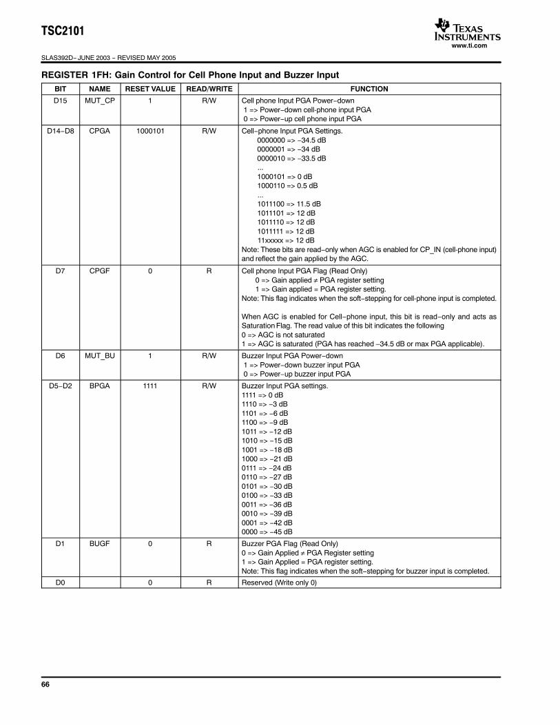
TSC2101
SLAS392D− JUNE 2003 − REVISED MAY 2005
www.ti.com
66
REGISTER 1FH: Gain Control for Cell Phone Input and Buzzer InputBIT NAME RESET VALUE READ/WRITE FUNCTION
D15 MUT_CP 1 R/W Cell phone Input PGA Power−down 1 => Power−down cell-phone input PGA 0 => Power−up cell phone input PGA
D14−D8 CPGA 1000101 R/W Cell−phone Input PGA Settings. 0000000 => −34.5 dB 0000001 => −34 dB 0000010 => −33.5 dB ... 1000101 => 0 dB 1000110 => 0.5 dB ... 1011100 => 11.5 dB 1011101 => 12 dB 1011110 => 12 dB 1011111 => 12 dB 11xxxxx => 12 dBNote: These bits are read−only when AGC is enabled for CP_IN (cell-phone input)and reflect the gain applied by the AGC.
D7 CPGF 0 R Cell phone Input PGA Flag (Read Only) 0 => Gain applied ≠ PGA register setting 1 => Gain applied = PGA register setting.Note: This flag indicates when the soft−stepping for cell-phone input is completed.
When AGC is enabled for Cell−phone input, this bit is read−only and acts asSaturation Flag. The read value of this bit indicates the following0 => AGC is not saturated1 => AGC is saturated (PGA has reached –34.5 dB or max PGA applicable).
D6 MUT_BU 1 R/W Buzzer Input PGA Power−down 1 => Power−down buzzer input PGA 0 => Power−up buzzer input PGA
D5−D2 BPGA 1111 R/W Buzzer Input PGA settings.1111 => 0 dB1110 => −3 dB1101 => −6 dB1100 => −9 dB1011 => −12 dB1010 => −15 dB1001 => −18 dB1000 => −21 dB0111 => −24 dB0110 => −27 dB0101 => −30 dB0100 => −33 dB0011 => −36 dB0010 => −39 dB0001 => −42 dB0000 => −45 dB
D1 BUGF 0 R Buzzer PGA Flag (Read Only)0 => Gain Applied ≠ PGA Register setting1 => Gain Applied = PGA register setting.Note: This flag indicates when the soft−stepping for buzzer input is completed.
D0 0 R Reserved (Write only 0)

TSC2101
SLAS392D− JUNE 2003 − REVISED MAY 2005
www.ti.com
67
REGISTER 20H: Audio Control 5
BIT NAMERESETVALUE
READ/WRITE
FUNCTION
D15 DIFFIN 0 R/W Single-ended or Differential Output Selection.0 => Single-ended output (headset/lineout) selected for SPK1 and SPK2 drivers1 => Differential output (handset) selected for SPK1 and OUT32N driversNote: When bit D15=1, both SPK1 and OUT32N drivers should be power−up. Otherwise theTSC2101 automatically power−down both SPK1 and OUT32N drivers.
D14−D13 DAC2SPK1 00 R/W DAC Channel Routing to SPK1 (Single-ended)/ SPK1−OUT32N (Differential)00 => No routing from DAC to SPK1/ SPK1−OUT32N01 => DAC left routed to SPK1/SPK1−OUT32N10 => DAC right routed to SPK1/SPK1−OUT32N11 => DAC (left + right)/2 routed to SPK1/SPK1−OUT32N
D12 AST2SPK1 0 R/W Analog Sidetone Routing to SPK1 (Single-ended)/SPK1−OUT32N (Differential)0 => No routing from analog sidetone to SPK1/SPK1−OUT32N1 => Analog sidetone routed to SPK1/SPK1−OUT32N
D11 BUZ2SPK1 0 R/W Buzzer PGA Routing to SPK1 (Single-ended)/ SPK1−OUT32N (Differential)0 => No routing from buzzer PGA to SPK1/SPK1−OUT32N1 => Buzzer PGA routed to SPK1/ SPK1−OUT32N
D10 KCL2SPK1 0 R/W Keyclick Routing to SPK1 (Single-ended)/SPK1−OUT32N (Differential)0 => No routing from keyclick to SPK1/SPK1−OUT32N1 => Keyclick routed to SPK1/SPK1−OUT32N
D9 CPI2SPK1 0 R/W Cell−phone Input Routing to SPK1 (Single-ended)/SPK1−OUT32N (Differential)0 => No routing from cell-phone input to SPK1/SPK1−OUT32N1 => Cell phone input routed to SPK1/SPK1−OUT32N
D8−D7 DAC2SPK2 00 R/W DAC Channel Routing to SPK2 (Valid for Only Single-ended)00 => No routing from DAC to SPK201 => DAC left routed to SPK210 => DAC right routed to SPK211 => DAC (left + right)/2 routed to SPK2
D6 AST2SPK2 0 R/W Analog Sidetone Routing to SPK2 (Valid for Only Single-ended)0 => No routing from analog sidetone to SPK21 => Analog sidetone routed to SPK2
D5 BUZ2SPK2 0 R/W Buzzer PGA Routing to SPK2 (Valid for Only Single-ended)0 => No routing from buzzer PGA to SPK21 => Buzzer PGA routed to SPK2
D4 KCL2SPK2 0 R/W Keyclick Routing to SPK2 (Valid for Only Single-ended)0 => No routing from keyclick to SPK21 => Keyclick routed to SPK2
D3 CPI2SPK2 0 R/W Cell−phone Input Routing to SPK2 (Valid for Only Single-ended)0 => No routing from cell-phone input to SPK21 => Cell−phone input routed to SPK2
D2 MUTSPK1 1 R/W Mute Control for SPK1 (Single-ended)/SPK1−OUT32N (Differential)0 => SPK1/SPK1−OUT32N is not muted.1 => SPK1/SPK1−OUT32N is muted.
D1 MUTSPK2 1 R/W Mute Control for SPK2 (Valid for Only Single-ended)0 => SPK2 is not muted.1 => SPK2 is muted.
D0 HDSCPTC 0 W Headphone Short−circuit Protection Control0 => Enable short−circuit protection1 => Disable short−circuit protection

TSC2101
SLAS392D− JUNE 2003 − REVISED MAY 2005
www.ti.com
68
REGISTER 21H: Audio Control 6
BIT NAMERESETVALUE
READ/WRITE
FUNCTION
D15 SPL2LSK 0 R/W Routing Selected for SPK1 Goes to OUT8P−OUT8N (Loudspeaker) Also.0 => None of the routing selected for SPK1 goes to OUT8P−OUT8N.1 => Routing selected for SPK1 using D14−D9 of control register 20H/page 2 goes toOUT8P−OUT8N.Note: This programming is valid only if SPK1/OUT32N and SPK2 are powered down.
D14 AST2LSK 0 R/W Analog Sidetone Routing to OUT8P−OUT8N (Loudspeaker)0 => No routing from analog sidetone to OUT8P−OUT8N1 => Analog sidetone routed to OUT8P−OUT8N
D13 BUZ2LSK 0 R/W Buzzer PGA Routing to OUT8P−OUT8N (Loudspeaker)0 => No routing from buzzer PGA to OUT8P−OUT8N1 => Buzzer PGA routed to OUT8P−OUT8N
D12 KCL2LSK 0 R/W Keyclick Routing to OUT8P−OUT8N (Loudspeaker)0 => No routing from keyclick to OUT8P−OUT8N1 => Keyclick routed to OUT8P−OUT8N
D11 CPI2LSK 0 R/W Cell−phone Input Routing to OUT8P−OUT8N (Loudspeaker)0 => No routing from cell-phone input to OUT8P−OUT8N1 => Cell−phone input routed to OUT8P−OUT8N
D10 MIC2CPO 0 R/W MICSEL (Programmed Using Control Register 04H/Page 2) Routed to Cell-phone Output.0 => No routing from MICSEL to CP_OUT.1 => MICSEL routed to CP_OUT.
D9 SPL2CPO 0 R/W Routing Selected for SPK1 (Other Than Cell−phone Input) Goes to Cell-phone Output Also.0 => None of the routing selected for SPK1 goes to cell-phone output.1 => Routing selected for SPK1 using D14−D10 of control register 20H/page 2 goes toCP_OUT.Note: This programming is valid even if SPK1/OUT32N and SPK2 are powered down.
D8 SPR2CPO 0 R/W Routing Selected for SPK2 Goes to Cell−phone Output Also (Valid for Only Single-ended).0 => None of the routing selected for SPK2 goes to cell-phone output.1 => Routing selected for SPK2 using D8−D3 of control register 20H/page2 goes to CP_OUT.Note: 1. This programming is valid even if SPK2 is power-down. 2. This programming is not valid when routing selected for SPK1 is routed to loudspeaker
D7 MUTLSPK 1 R/W Mute Control for OUT8P−OUT8N Loudspeaker0 => OUT8P−OUT8N is not muted.1 => OUT8P−OUT8N is muted.
D6 MUTSPK2 1 R/W Mute Control for Cell−phone Output0 => CPOUT is not muted.1 => CPOUT is muted.
D5 LDSCPTC 1 R/W Loudspeaker Short−circuit Protection Control0 => Enable short−circuit protection for loudspeaker1 => Disable short−circuit protection for loudspeaker
D4 VGNDSCPTC 0 R/W VGND Short−circuit Protection Control0 => Enable short−circuit protection for VGND driver1 => Disable short−circuit protection for VGND driver
D3 CAPINTF 0 R/W Cap/Cap−less Interface Select for Headset.0 => Select cap−less interface.1 => Select cap interface.
D2−D0 0’s R Reserved (Write only 000)

TSC2101
SLAS392D− JUNE 2003 − REVISED MAY 2005
www.ti.com
69
REGISTER 22H: Audio Control 7
BIT NAMERESETVALUE
READ/WRITE
FUNCTION
D15 DETECT 0 R/W Headset Detection0 => Disable headset detection1 => Enable headset detection
D14−D13 HESTYPE 00 R Type of Headset Detected.00 => No headset detected.01 => Stereo headset detected.10 => Cellular headset detected11 => Stereo+cellular headset detectedNote: These two bits are valid only if the headset detection is enabled.
D12 HDDETFL 0 R Headset Detection Flag.0 => Headset is not detected1 => Headset is detected.
D11 BDETFL 0 R Button Press Detection Flag.0 => Button press is not detected1 => Button press is detected.
D10−D9 HDDEBNPG 01 R/W De−bouncing Programmability for Glitch Rejection During Headset Detection.00 => 16 ms duration (with 2 ms clock resolution)01 => 32 ms duration (with 4 ms clock resolution)10 => 64 ms duration (with 8 ms clock resolution)11 => 128 ms duration (with 16 ms clock resolution)
D8 0 R Reserved (Write only 0)
D7−D6 BDEBNPG 00 R/W De−bouncing Programmability for Glitch Rejection During Button Press Detection.00 => No glitch rejection.01 => 8 ms duration (with 1 ms clock resolution)10 => 16 ms duration (with 2 ms clock resolution)11 => 32 ms duration (with 4 ms clock resolution)
D5 0 R Reserved (Write only 0)
D4 DGPIO2 0 R/W Enable GPIO2 for Headset Detection Interrupt0 => Disable GPIO2 for headset detection interrupt1 => Enable GPIO2 for headset detection interruptNote: This programmability is valid only if D15 and D13 of control register 23H/page 2 are set to0
D3 DGPIO1 0 R/W Enable GPIO1 for Headset Detection Interrupt0 => Disable GPIO1 for Detection interrupt1 => Enable GPIO1 for Detection interruptNote: This programmability is valid only if D11 and D9 of control register 23H/page 2 are set to0
D2 CLKGPIO2 0 R/W Enable GPIO2 for CLKOUT0 => Disable GPIO2 for CLKOUT mode.1 => Enable GPIO2 for CLKOUT mode.In CLKOUT mode the frequency of output signal is equal to the 256xDAC_FS if DAC_FS is fasterthan ADC_FS otherwise equal to the 256xADC_FS.Note: This programmability is valid only if PLL is enabled, D15 and D13 of register 23H/page 2are set to 0 and GPIO2 is not enabled for detection interrupt.
D1−D0 ADWSF 00 R/W ADWS Selection 0X => GPIO1 pin output is three−stated. 10 => GPIO1 pin acts as button press detect interrupt. 11 => GPIO1 pin acts as ADC word−select (ADWS).Note: 1. This programmability is valid only if D11 and D9 of control register 23H/page 2 are setto 0.2. These bits should be programmed ‘11’ only if different ADC and DAC sample rates are desired.In this mode WCLK acts as DAWS i.e. DAC sample rate and GPIO1 acts as ADWS i.e. ADCsample rate.

TSC2101
SLAS392D− JUNE 2003 − REVISED MAY 2005
www.ti.com
70
REGISTER 23H: GPIO Control
BIT NAMERESETVALUE
READ/WRITE
FUNCTION
D15 GPO2EN 0 R/W GPIO2 Enable for General Purpose Output Port0 => GPIO2 is not programmed as general purpose output port1 => GPIO2 programmed as general purpose output port
D14 GPO2SG 0 R/W GPIO2 Output Signal Programmability0 => GPIO2 goes to low if GPIO2 enable for general purpose output port1 => GPIO2 goes to high if GPIO2 enable for general purpose output port
D13 GPI2EN 0 R/W GPIO2 Enable for General Purpose Input Port0 => GPIO2 is not programmed as general purpose input port1 => GPIO2 programmed as general purpose input port
D12 GPI2SGF 0 R GPIO2 Input Signal Flag0 => GPIO2 input is low.1 => GPIO2 input is high.Note: Valid only if GPIO2 is enable for general purpose input port
D11 GPO1EN 0 R/W GPIO1 Enable for General Purpose Output Port0 => GPIO1 is not programmed as general purpose output port1 => GPIO1 programmed as general purpose output port
D10 GPO1SG 0 R/W GPIO1 Output Signal Programmability0 => GPIO1 goes to low if GPIO1 enable for general purpose output port1 => GPIO1 goes to high if GPIO1 enable for general purpose output port
D9 GPI1EN 0 R/W GPIO1 Enable for General Purpose Input Port0 => GPIO1 is not programmed as general purpose input port1 => GPIO1 programmed as general purpose input port
D8 GPI1SGF 0 R GPIO1 Input Signal Flag0 => GPIO1 input is low.1 => GPIO1 input is high.Note: Valid only if GPIO1 is enable for general purpose input port
D7−D0 0 R Reserved (Write only 00000000)
REGISTER 24H: AGC for Cell-Phone Input Control
BIT NAMERESETVALUE
READ/WRITE
FUNCTION
D15 0 R Reserved (Write only 0)
D14 AGCNF_CELL 0 R Noise Threshold Flag.The read values indicate the following0 => Signal power greater than noise threshold1 => Signal power is less than noise thresholdNote: Valid only if AGC is selected for the Cell−phone input (CP_IN).
D13−D11 AGCNL 000 R/W AGC Noise Threshold.These settings apply to both Headset/Aux/Handset and Cell−phone input. 000 => −30 dB 001 => −30 dB 010 => −40 dB 011 => −50 dB 100 => −60 dB 101 => −70 dB (not valid for Cell−phone AGC) 110 => −80 dB (not valid for Cell−phone AGC) 111 => −90 dB (not valid for Cell−phone AGC)
D10−D9 AGCHYS_CELL 00 R/W AGC Hysteresis Selection for Cell−phone Input00 => 1 dB01 => 2 dB10 => 4 dB11 => No Hysteresis
D8 CLPST_CELL 0 R/W AGC Clip Stepping Disable for Cell−phone Input0 => Disable clip stepping for cell-phone input1 => Enable clip stepping for cell-phone input

TSC2101
SLAS392D− JUNE 2003 − REVISED MAY 2005
www.ti.com
71
BIT FUNCTIONREAD/WRITE
RESETVALUENAME
D7−D5 AGCTG_CELL 000 R/W AGC Target Gain for Cell−phone Input.These three bits set the AGC’s targeted ADC output level.000 => −5.5 dB001 => −8.0 dB010 => −10 dB011 => −12 dB100 => −14 dB101 => −17 dB110 => −20 dB111 => −24 dB
D4−D1 AGCTC_CELL 0000 R/W AGC Time Constant for Cell Input.These four bits set the AGC attack and decay time constants. Time constants remainthe same irrespective of any sampling frequency Attack time Decay time (ms) (ms)0000 8 100001 11 1000010 16 1000011 20 1000100 8 2000101 11 2000110 16 2000111 20 2001000 8 4001001 11 4001010 16 4001011 20 4001100 8 5001101 11 5001110 16 5001111 20 500
D0 AGCEN_CELL 0 R/W AGC Enable for Cell−phone Input0 => AGC is off for Cell−phone input1 => AGC is on for Cell−phone input (Cell PGA is controlled by AGC
REGISTER 25H: Driver Power-Down Status
Note: All values reflected in control register 25H/page2 are valid only if short circuit is not detected (bit D1 ofcontrol register 1DH/page2 is set to 0)
BIT NAMERESETVALUE
READ/WRITE
FUNCTION
D15 SPK1FL 1 R SPK1 Driver Power-down Status0 => SPK1 driver not powered down.1 => SPK1 driver powered down.
D14 SPK2FL 1 R SPK2 Driver Power-down Status0 => SPK2 driver not powered down.1 => SPK2 driver powered down.
D13 HNDFL 1 R OUT32N (Handset) Driver Power-down Status0 => OUT32N driver not powered down.1 => OUT32N driver powered down.
D12 VGNDFL 1 R VGND Driver Power-down Status0 => VGND driver not powered down.1 => VGND driver powered down.
D11 LSPKFL 1 R Loudspeaker Driver Power-down Status0 => Loudspeaker driver not powered down.1 => Loudspeaker driver powered down.
D10 CELLFL 1 R Cell−phone Output (CP_OUT) Driver Power-down Status0 => Cell-phone output driver not powered down.1 => Cell-phone output driver powered down.
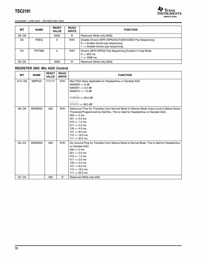
TSC2101
SLAS392D− JUNE 2003 − REVISED MAY 2005
www.ti.com
72
BIT FUNCTIONREAD/WRITE
RESETVALUENAME
D9−D6 0000 R Reserved (Write only 0000)
D5 PSEQ 0 R/W Disable Drivers (SPK1/SPK2/OUT32N/VGND) Pop Sequencing0 => Enable drivers pop sequencing1 => Disable drivers pop sequencing
D4 PSTIME 0 R/W Drivers (SPK1/SPK2) Pop Sequencing Duration in Cap Mode0 => 802 ms.1 => 4006 ms.
D3−D0 0000 R Reserved (Write only 0000)
REGISTER 26H: Mic AGC Control
BIT NAMERESETVALUE
READ/WRITE
FUNCTION
D15−D9 MMPGA 1111111 R/W Max PGA Value Applicable for Headset/Aux or Handset AGC0000000 => 0 dB0000001 => 0.5 dB0000010 => 1.0 dB ....1110110 => 59.0 dB............1111111 => 59.5 dB
D8−D6 MDEBNS 000 R/W Debounce Time for Transition from Normal Mode to Silence Mode (Input Level is Below NoiseThreshold Programmed by AGCNL). This is Valid for Headset/Aux or Handset AGC.000 => 0 ms001 => 0.5 ms010 => 1.0 ms011 => 2.0 ms100 => 4.0 ms101 => 8.0 ms110 => 16.0 ms111 => 32.0 ms
D5−D3 MDEBSN 000 R/W De−bounce Time for Transition from Silence Mode to Normal Mode. This is Valid for Headset/Auxor Handset AGC.000 => 0 ms001 => 0.5 ms010 => 1.0 ms011 => 2.0 ms100 => 4.0 ms101 => 8.0 ms110 => 16.0 ms111 => 32.0 ms
D2−D0 000 R Reserved (Write only 000)

TSC2101
SLAS392D− JUNE 2003 − REVISED MAY 2005
www.ti.com
73
REGISTER 27H: Cell-Phone AGC Control
BIT NAMERESETVALUE
READ/WRITE
FUNCTION
D15−D9 CMPGA 1111111 R/W Max. Cell‘−phone input PGA value applicable for Cell‘−phone AGC0000000 => −34.5 dB0000001 => −34 dB0000010 => −33.5 dB ...1000100 => −0.5 dB1000101 => invalid1000110 => invalid ...1011100 => Invalid1011101 => 12 dB1011110 => 12 dB1011111 => 12 dB11xxxxx => 12 dB
D8−D6 CDEBNS 000 R De−bounce Time for Transition from Normal Mode to Silence Mode (Input Level isBelow Noise Threshold Programmed by AGCNL). This is Valid for Cell−phone AGC.000 => 0 ms001 => 0.5 ms010 => 1.0 ms011 => 2.0 ms100 => 4.0 ms101 => 8.0 ms110 => 16.0 ms111 => 32.0 ms
D5−D3 CDEBSN 000 R De−bounce Time for Transition from Silence Mode to Normal Mode. This is Valid forCell−phone AGC.000 => 0 ms001 => 0.5 ms010 => 1.0 ms011 => 2.0 ms100 => 4.0 ms101 => 8.0 ms110 => 16.0 ms111 => 32.0 ms
D2−D0 000 R Reserved (Write only 000)
TSC2101 Buffer Data Registers (Page 3)
The buffer data registers of the TSC2101 hold data results from the SAR ADC conversions in buffer mode. Uponreset, bit D15 is set to 0, bit D14 is set to 1 and the remaining bits are don’t−care. These registers are read only.
If buffer mode is enabled, then the results of all ADC conversions are placed in the buffer data register. Thedata format of the result word (R) of these registers is right-justified which is as follows:
D15MSB
D14 D13 D12 D11 D10 D9 D8 D7 D6 D5 D4 D3 D2 D1 D0LSB
FUF EMF X ID R11MSB
R10 R9 R8 R7 R6 R5 R4 R3 R2 R1 R0LSB
BIT NAMERESETVALUE
READ/WRITE
FUNCTION
D15 FUF 0 R Buffer Full FlagThis flag indicates that all the 64 locations of the buffer are having unread data.
D14 EMF 1 R Buffer Empty FlagThis flag indicates that there is no unread data available in FIFO. This is generated while reading thelast converted data.
D13 X R Reserved

TSC2101
SLAS392D− JUNE 2003 − REVISED MAY 2005
www.ti.com
74
BIT FUNCTIONREAD/WRITE
RESETVALUENAME
D12 ID X R Data Identification 0 => X or Z1 coordinate or BAT or AUX2 data in R11−R0 1 => Y or Z2 coordinate or AUX1 or TEMP data in R11−R0
Order for Writing Data in Buffer When Multiple Inputs are Selected For XY Conversion: Y, X For XYZ1Z2 Conversion: Y, X, Z1, Z2 For Z1Z2 Conversion: Z1, Z2 For Auto Scan Conversion: AUX1 (if selected), AUX2 (if selected), TEMP (if selected) For Port Scan Conversion: BAT, AUX1, AUX2
D11−D0 R11−R0 X’s R Converted Data
LAYOUT
The following layout suggestions should provide optimum performance from the TSC2101. However, manyportable applications have conflicting requirements concerning power, cost, size, and weight. In general, mostportable devices have fairly clean power and grounds because most of the internal components are very lowpower. This situation would mean less bypassing for the converter’s power and less concern regardinggrounding. Still, each situation is unique and the following suggestions should be reviewed carefully.
For optimum performance, care should be taken with the physical layout of the TSC2101 circuitry. The basicSAR architecture is sensitive to glitches or sudden changes on the power supply, reference, groundconnections, and digital inputs that occur just prior to latching the output of the analog comparator. Therefore,during any single conversion for an n-bit SAR converter, there are n windows in which large external transientvoltages can easily affect the conversion result. Such glitches might originate from switching power supplies,nearby digital logic, and high power devices. The degree of error in the digital output depends on the referencevoltage, layout, and the exact timing of the external event. The error can change if the external event changesin time with respect to the timing of the critical n windows.
With this in mind, power to the TSC2101 should be clean and well bypassed. A 0.1 µF ceramic bypass capacitorshould be placed as close to the device as possible. A 1 µF to 10 µF capacitor may also be needed if theimpedance of the connection between the TSC2101 supply pins and system power supply is high.
A bypass capacitor on the VREF pin is generally not needed because the reference is buffered by an internalop amp, although it can be useful to reduce reference noise level. If an external reference voltage originatesfrom an op amp, make sure that it can drive any bypass capacitor that is used without oscillation.
The TSC2101 architecture offers no inherent rejection of noise or voltage variation in regards to using anexternal reference input. This is of particular concern when the reference input is tied to the power supply. Anynoise and ripple from the supply appears directly in the digital results. While high frequency noise can be filteredout, voltage variation due to line frequency (50 Hz or 60 Hz) can be difficult to remove.
The ground pins should be connected to a clean ground point. In many cases, this is the analog ground. Avoidconnections, which are too near the grounding point of a microcontroller or digital signal processor. If needed,run a ground trace directly from the converter to the power supply entry or battery connection point. The ideallayout includes an analog ground plane dedicated to the converter and associated analog circuitry.
In the specific case of use with a resistive touch screen, care should be taken with the connection between theconverter and the touch screen. Since resistive touch screens have fairly low resistance, the interconnectionshould be as short and robust as possible. Loose connections can be a source of error when the contactresistance changes with flexing or vibrations.
As indicated previously, noise can be a major source of error in touch-screen applications (e.g., applicationsthat require a back-lit LCD panel). This EMI noise can be coupled through the LCD panel to the touch screenand cause flickering of the converted ADC data. Several things can be done to reduce this error, such as utilizinga touch screen with a bottom−side metal layer connected to ground. This couples the majority of noise toground. Additionally, filtering capacitors, from Y+, Y–, X+, and X– to ground, can also help. Note, however, thatthe use of these capacitors increases screen settling time and require longer panel voltage stabilization times,as well as increased precharge and sense times for the PINTDAV circuitry of the TSC2101.

TSC2101
SLAS392D− JUNE 2003 − REVISED MAY 2005
www.ti.com
75
CONVERSION TIME CALCULATIONS FOR THE TSC2101
Touch Screen Conversion Initiated at Touch Detect
The time needed to get a converted X/Y coordinate for reading can be calculated by (not including the timeneeded to send the command over the SPI bus):
tcoordinate 2 tPRE tSNS tPVS
125 ns
tOSC 2 NAVGNBITS 1 8 MHz
ƒconv n1 12 1
tOSC 18 tOSC n2 tOSC n3 tOSC
where:
tcoordinate = time to convert X/Y coordinate
tPVS = Panel voltage stabilization time
tPRE = precharge time
tSNS = sense time
NAVG = number of averages; for no averaging, NAVG = 1
NBITS = number of bits of resolution
ƒconv = A/D converter clock frequency
tOSC = Oscillator clock period
n1 = 6 ; if ƒconv = 8 MHz
7 ; if ƒconv ≠ 8 MHz
n2 = 4 ; if tPVS = 0 µs
0 ; if tPVS ≠ 0 µs
n3 = 0 ; if tSNS = 32 µs
2 ; if tSNS ≠ 32 µs
tPGDEL = Programmable delay in between conversion for touch screen measurement
= 0: if programmable delay mode is disabled for touch screen measurement
(1) tPGDEL delay is generated by using: Internal oscillator clock whose typical frequency is 1 MHz, in internal clockmode, or MCLK/CLKDIV (as programmed in control register 14H/pag1) in external clock mode.
(2) The above formula is valid exactly only when the codec is powered down. Also after touch detect the formula holdstrue from second conversion onwards.
(3) If D15−D14 of control register 01H/page 1 = 00, then in case of continuous touch PINTDAV remains high for
tPRE tSNS tOSC125 ns
. If D15−D14 of control register 01H/page 1 = 10/11, then in case of continuous touch
PINTDAC remains high for tPRE tSNS
tOSC125 ns tPGDEL .
Programmedfor Self
ControlledX−Y Scan
Mode
Detecting TouchSample,Conversion &
Averaging forY−Coordinate
ReadingX−Data
Register
ReadingY−Data
Register
DetectingTouch
Sample,Conversion &Averaging forX−Coordinate
DetectingTouch
Sample,Conversion &Averaging forY−Coordinate
DetectingTouch
SS DEACTIVATED
Touch Is Detected
(As PENIRQ [D15−D14 = 00])
PINTDAV(As PENIRQ & DATA_AVA
[D15−D14 = 10/11])
PINTDAV Touch Is Detected
Touch Is Detected
(As DATA_AVA[D15−D14 = 01])
PINTDAV

TSC2101
SLAS392D− JUNE 2003 − REVISED MAY 2005
www.ti.com
76
The time for a complete X/Y/Z1/Z2 coordinate conversion is given by(not including the time needed to sendthe command over the SPI bus):
Programmedfor Host
ControlledMode
Detecting TouchSample,Conversion &
Averaging forY−Coordinate
ReadingX−Data
Register
ReadingY−Data
Register
DetectingTouch
Sample,Conversion &Averaging forX−Coordinate
DetectingTouch
Sample,Conversion &Averaging forY−Coordinate
DetectingTouch
Touch Is DetectedTouch Is Detected
REG−00 ofPAGE−01
Is Updatedfor
X−Y ScanMode
Waiting for Host toWrite into REG−00 of
PAGE−01
SS DEACTIVATED
(As PENIRQ [D15−D14 = 00])
PINTDAV(As PENIRQ & DATA_AVA
[D15−D14 = 10/11])
PINTDAV
Touch Is Detected
(As DATA_AVA[D15−D14 = 01])
PINTDAV
tcoordinate 3 tPRE tSNS tPVS
125 ns
tOSC 4 NAVGNBITS 1 8 MHz
ƒconv n1 12 1
tOSC 33 tOSC n2 tOSC n3 tOSC tPGDEL
n1 = 6 ; if ƒconv = 8 MHz
7 ; if ƒconv ≠ 8 MHzn2 = 4 ; if tPVS = 0 µs
0 ; if tPVS ≠ 0 µs
n3 = 0 ; if tSNS = 32 µs 3 ; if tSNS ≠ 32 µs
Programmedfor Self
ControlledX−Y−Z1−Z2
ScanMode
Detecting TouchSample,Conversion &
Averaging forY−Coordinate
ReadingX−Data
Register
ReadingY−Data
Register
DetectingTouch
Sample,Conversion &Averaging forX−Coordinate
DetectingTouch
Sample,Conversion &Averaging for
Z1−Coordinate & Z2−Coordinate
ReadingZ1−DataRegister
ReadingZ2−DataRegister
DetectingTouch
Sample,Conversion &Averaging forY−Coordinate
DetectingTouch
SS DEACTIVATED
(As PENIRQ [D15−D14 = 00])
PINTDAV(As PENIRQ & DATA_AVA
[D15−D14 = 10/11])
PINTDAV
Touch Is Detected Touch Is Detected Touch Is Detected
Touch Is Detected
(As DATA_AVA[D15−D14 = 01])
PINTDAV
The time needed to convert any single coordinate either X or Y under self-controlled (not including the time needed to sendthe command over the SPI bus) is given by:
tcoordinate tPRE tSNS tPVS
125 ns
tOSC NAVGNBITS 1 8 MHz
ƒconv n1 12 1
tOSC 16 tOSC n2 tOSC n3 tOSC tPGDEL
n1 = 6 ; if ƒconv = 8 MHz
7 ; if ƒconv ≠ 8 MHz

TSC2101
SLAS392D− JUNE 2003 − REVISED MAY 2005
www.ti.com
77
n2 = 2 ; if tPVS = 0 µs
0 ; if tPVS ≠ 0 µs
n3 = 0 ; if tSNS = 32 µs
0 ; if tSNS ≠ 32 µs
Programmedfor Self
ControlledX ScanMode
Detecting TouchSample,Conversion &
Averaging forX−Coordinate
ReadingX−Data Register
DetectingTouch
Sample,Conversion &Averaging forX−Coordinate
Touch is detected
/SS DEACTIVATED
Touch is detected/PINTDAV
(As /PENIRQ [D15−D14 = 00])
/PINTDAV(As DATA_AVA[D15−D14 = 01]) /PINTDAV
(As /PENIRQ & DATA_AVA[D15−D14 = 10/11])
Touch is detected
The time needed to convert the Z coordinate under self-controlled mode (not including the time needed to send thecommand over the SPI bus) is given by:
tcoordinate tPRE tSNS tPVS
125 ns
tOSC 2 NAVGNBITS 1 8 MHz
ƒconv n1 12 1
tOSC 22 tOSC n2 tOSC n3 tOSC tPGDEL
n1 = 6 ; if ƒconv = 8 MHz
7 ; if ƒconv ≠ 8 MHz
n2 = 2 ; if tPVS = 0 µs
0 ; if tPVS ≠ 0 µs
n3 = 0 ; if tSNS = 32 µs
1 ; if tSNS ≠ 32 µs
Programmedfor Self
ControlledZ ScanMode
Detecting TouchSample,Conversion &
Averaging forZ1−Coordinate & Z2−Coordinate
ReadingZ1−DataRegister
DetectingTouch
Sample,Conversion &Averaging for
Z1−Coordinate & Z2−Coordinate
Touch is detected
/SS DEACTIVATED
Touch is detected/PINTDAV
(As /PENIRQ [D15−D14 = 00])
/PINTDAV(As DATA_AVA[D15−D14 = 01]) /PINTDAV
(As /PENIRQ & DATA_AVA[D15−D14 = 10/11])
Touch is detected
ReadingZ2−DataRegister
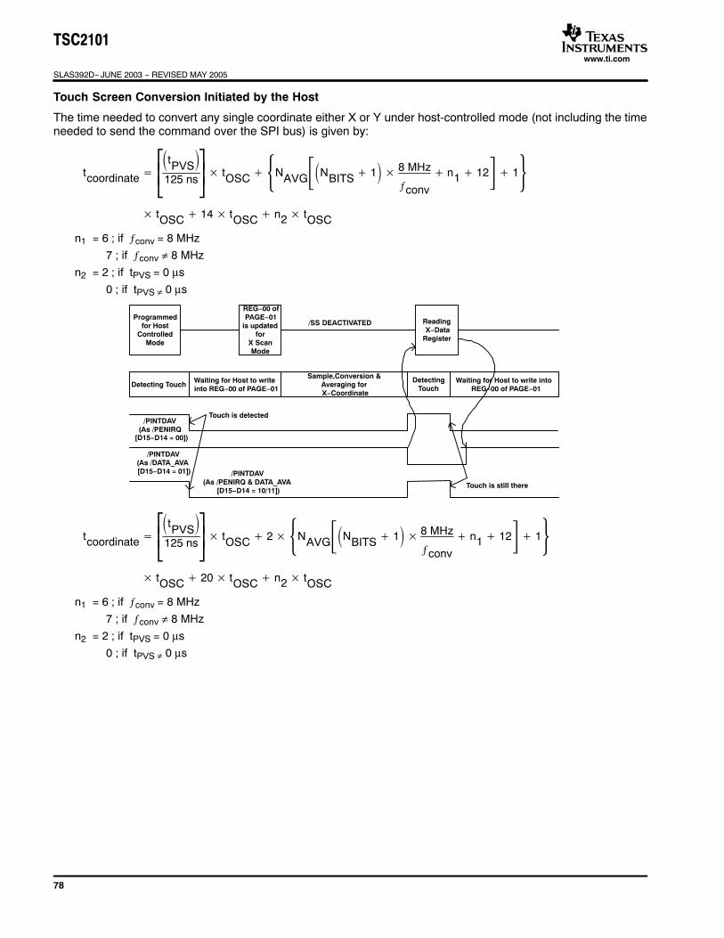
TSC2101
SLAS392D− JUNE 2003 − REVISED MAY 2005
www.ti.com
78
Touch Screen Conversion Initiated by the Host
The time needed to convert any single coordinate either X or Y under host-controlled mode (not including the timeneeded to send the command over the SPI bus) is given by:
tcoordinate tPVS
125 ns
tOSC NAVGNBITS 1 8 MHz
ƒconv
n1 12 1 tOSC 14 tOSC n2 tOSC
n1 = 6 ; if ƒconv = 8 MHz
7 ; if ƒconv ≠ 8 MHz
n2 = 2 ; if tPVS = 0 µs
0 ; if tPVS ≠ 0 µs
Programmedfor Host
ControlledMode
Detecting TouchSample,Conversion &
Averaging forX−Coordinate
ReadingX−Data
Register
Touch is still there
Touch is detected/PINTDAV
(As /PENIRQ [D15−D14 = 00])
/PINTDAV(As /DATA_AVA[D15−D14 = 01]) /PINTDAV
(As /PENIRQ & DATA_AVA[D15−D14 = 10/11])
Waiting for Host to writeinto REG−00 of PAGE−01
Waiting for Host to write intoREG−00 of PAGE−01
REG−00 ofPAGE−01
is updatedfor
X ScanMode
/SS DEACTIVATED
DetectingTouch
tcoordinate tPVS
125 ns
tOSC 2 NAVGNBITS 1 8 MHz
ƒconv
n1 12 1 tOSC 20 tOSC n2 tOSC
n1 = 6 ; if ƒconv = 8 MHz
7 ; if ƒconv ≠ 8 MHz
n2 = 2 ; if tPVS = 0 µs
0 ; if tPVS ≠ 0 µs

TSC2101
SLAS392D− JUNE 2003 − REVISED MAY 2005
www.ti.com
79
Programmedfor Host
ControlledMode
Detecting TouchSample,Conversion &
Averaging forZ1−Coordinate & Z2−Coordinate
ReadingZ1−DataRegister
Touch is still there
Touch is detected/PINTDAV
(As /PENIRQ [D15−D14 = 00])
/PINTDAV(As /DATA_AVA[D15−D14 = 01]) /PINTDAV
(As /PENIRQ & DATA_AVA[D15−D14 = 10/11])
Waiting for Host to writeinto REG−00 of PAGE−01
Waiting for Host to write intoREG−00 of PAGE−01
REG−00 ofPAGE−01
is updatedfor
Z1−Z2 ScanMode
ReadingZ2−DataRegister
/SS DEACTIVATED
DetectingTouch
Programmedfor Host
ControlledMode
Detecting TouchSample,Conversion &
Averaging forY−Coordinate
ReadingX−Data
Register
ReadingY−Data
Register
DetectingTouch
Sample,Conversion &Averaging forX−Coordinate
DetectingTouch
Sample,Conversion &Averaging forY−Coordinate
DetectingTouch
Touch Is DetectedTouch Is Detected
REG−00 ofPAGE−01
Is Updatedfor
X−Y ScanMode
Waiting for Host toWrite into REG−00 of
PAGE−01
SS DEACTIVATED
(As PENIRQ [D15−D14 = 00])
PINTDAV(As PENIRQ & DATA_AVA
[D15−D14 = 10/11])
PINTDAV
Touch Is Detected
(As DATA_AVA[D15−D14 = 01])
PINTDAV
Non-Touch Screen Measurement Operation
The time needed to make temperature, auxiliary, or battery measurements is given by:
t NAVGNBITS 1 8 MHz
ƒconv
n1 n2 1 tOSC 15 tOSC n3 tOSC
where:
n1 = 6 ; if ƒconv = 8 MHz
7 ; if ƒconv ≠ 8 MHz
n2 = 24 ; if measurement is for TEMP1 case
12 ; if measurement is for other than TEMP1 case
400 ns; if measurement is for the external/internal resistance using AUX1/AUX2
n3 = 0 ; if external reference mode is selected
3 ; if tREF = 0 µs or reference is programmed for power up all the time.
1 + tREF /125 ns; if tREF ≠ 0 µs and reference needs to power down between conversions.
tREF is the reference power up delay time.

TSC2101
SLAS392D− JUNE 2003 − REVISED MAY 2005
www.ti.com
80
Programmed forHost Controlled
Mode With InvalidA/D Function
Selected
Detecting TouchSample,Conversion &
Averaging forBAT1 input
ReadingBAT1−Data
Register
Waiting for Host to Writeinto REG−00 of PAGE−01
Waiting for Host toWrite into REG−00
of PAGE−01
REG−00 ofPAGE−01
Is Updatedfor
BAT1 ScanMode
Wait for Reference Power-Up Delay in Caseof Internal Ref Mode if Applicable
(As DATA_AVA[D15−D14 = 01])
PINTDAV
SS DEACTIVATED
The time needed for continuous autoscan mode is given by:
t NINP NAVGNBITS 1 8 MHz
ƒconv
n1 12 1 tOSC 8 tOSC n2 tOSC tDEL n3 tOSC n4 tOSC
where:
NINP = 1; if autoscan is selected for only one input AUX1, AUX2, TEMP1 or TEMP2
= 2; if autoscan is selected for two inputs AUX1−AUX2, AUX1−TEMP1, AUX1−TEMP2 etc
= 3; if autoscan is selected for three inputs AUX1−AUX2−TEMP1 or AUX1−AUX2−TEMP2
n1 = 6 ; if fconv = 8 MHz
7 ; if fconv p 8 MHz
n2 = 12 ; if one of the input selected is TEMP1
0 ; if measurement is for other than TEMP1
n3 = 0 ; if external reference mode is selected or tDEL = 0.
3 ; if tREF = 0 ms or reference is programmed for power up all the times.
1 + tREF/125 ns ; if tREF p 0us and reference needs to power down between conversions.
tREF is the reference power up delay time.
n4 = 0 ; if tDEL = 0.
= 7 ; if tDEL p 0
tDEL = Programmable delay in between conversion for nontouchscreen measurement
= 0 ; if programmable delay mode is disabled for nontouchscreen measurement
(1) The above equation is valid only from second conversion onwards.(2) tDEL delay is generated by using internal oscillator clock whose typical frequency is 1 MHz in internal clock mode,
or MCLK/CLKDIV (as programmed in control register 14H/page 1) in external clock mode.
Programmed forHost Controlled
Mode With InvalidA/D Function
Selected
Detecting TouchSample,Conversion &
Averaging for AUX input
Waiting for Host toWrite into REG−00
of PAGE−01
REG−00 ofPAGE−01
Is Updatedfor ContinousAUX SCAN
Mode
ReadingAUX−DataRegister
Sample,Conversion &Averaging for
AUX input
Sample,Conversion &Averaging for
AUX input
ReadingAUX−DataRegister
(As DATA_AVA[D15−D14 = 01])
PINTDAV
SS DEACTIVATED
Wait for Reference Power-Up Delay in Caseof Internal Ref Mode if Applicable

TSC2101
SLAS392D− JUNE 2003 − REVISED MAY 2005
www.ti.com
81
Port Scan Operation
The time needed to complete one set of port scan conversions is given by:
tcoordinate 3 NAVGNBITS 1 8 MHz
ƒconv
n1 12 1 tOSC 31 tOSC n2 tOSC
where:
n1 = 6 ; if ƒconv = 8 MHz
7 ; if ƒconv ≠ 8 MHz
n2 = 0 ; if external reference mode is selected
3 ; if tREF = 0 µs or reference is programmed for power up all the time.
1 + tREF /125 ns; if tREF ≠ 0 µs and reference needs to power down between conversions.
tREF is the reference power up delay time.
Programmed forHost Controlled
Mode With InvalidA/D Function
Selected
Detecting TouchSample,Conversion &
Averaging forBAT1 & BAT2 & AUX input
ReadingBAT1−Data
Register
Waiting for Host toWrite into REG−00
of PAGE−01
Waiting for Host to Write into REG−00of PAGE−01
REG−00 ofPAGE−01
is updatedfor
PORT SCANMode
ReadingBAT2−Data
Register
ReadingAUX−Data
Register
(As DATA_AVA[D15−D14 = 01])
PINTDAV
SS DEACTIVATED
Wait for Reference Power-Up Delay in Caseof Internal Ref Mode if Applicable
ADC CHANNEL DIGITAL FILTER FREQUENCY RESPONSES
Figure 39. Pass-Band Frequency Response of ADC Digital Filter

TSC2101
SLAS392D− JUNE 2003 − REVISED MAY 2005
www.ti.com
82
Figure 40. Frequency Response of ADC High-Pass Filter (Fcutoff = 0.0045 Fs)
Figure 41. Frequency Response of ADC High-Pass Filter (Fcutoff = 0.0125 Fs)
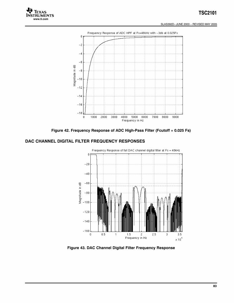
TSC2101
SLAS392D− JUNE 2003 − REVISED MAY 2005
www.ti.com
83
Figure 42. Frequency Response of ADC High-Pass Filter (Fcutoff = 0.025 Fs)
DAC CHANNEL DIGITAL FILTER FREQUENCY RESPONSES
Figure 43. DAC Channel Digital Filter Frequency Response
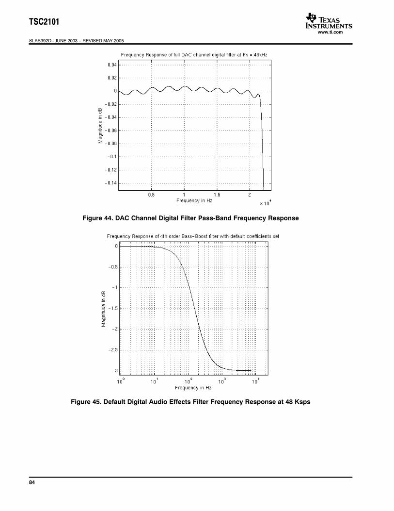
TSC2101
SLAS392D− JUNE 2003 − REVISED MAY 2005
www.ti.com
84
Figure 44. DAC Channel Digital Filter Pass-Band Frequency Response
Figure 45. Default Digital Audio Effects Filter Frequency Response at 48 Ksps

TSC2101
SLAS392D− JUNE 2003 − REVISED MAY 2005
www.ti.com
85
Figure 46. De-Emphasis Filter Response at 32 Ksps
Figure 47. De-Emphasis Error at 32 Ksps

TSC2101
SLAS392D− JUNE 2003 − REVISED MAY 2005
www.ti.com
86
Figure 48. De-Emphasis Filter Frequency Response at 44.1 Ksps
Figure 49. De-Emphasis Error at 44.1 Ksps

TSC2101
SLAS392D− JUNE 2003 − REVISED MAY 2005
www.ti.com
87
Figure 50. De-Emphasis Frequency Response at 48 Ksps
Figure 51. De-Emphasis Error at 48 Ksps

TSC2101
SLAS392D− JUNE 2003 − REVISED MAY 2005
www.ti.com
88
PLL PROGRAMMING
The on-chip PLL in the TSC2101 can be used to generate sampling clocks from a wide range of MCLK’savailable in a system. The PLL works by generating oversampled clocks with respect to Fsref (44.1 kHz or48 kHz). Frequency division generates all other internal clocks. Table 7 and Table 8 gives a sampleprogramming for PLL registers for some standard MCLK’s when PLL is required. Whenever the MCLK is of theform of N × 128 × Fsref (N=2,3,...), the PLL is not required.
Table 7. Fsref = 44.1 kHz
MCLK (MHz) P J D ACHIEVED FSREF % ERROR
2.8224 1 32 0 44100.00 0.0000
5.6448 1 16 0 44100.00 0.0000
12 1 7 5264 44100.00 0.0000
13 1 6 9474 44099.71 0.0007
16 1 5 6448 44100.00 0.0000
19.2 1 4 7040 44100.00 0.0000
19.68 1 4 5893 44100.30 −0.0007
48 4 7 5264 44100.00 0.0000
Table 8. Fsref = 48 kHz
MCLK (MHz) P J D ACHIEVED FSREF % ERROR
2.048 1 48 0 48000.00 0.0000
3.072 1 32 0 48000.00 0.0000
4.096 1 24 0 48000.00 0.0000
6.144 1 16 0 48000.00 0.0000
8.192 1 12 0 48000.00 0.0000
12 1 8 1920 48000.00 0.0000
13 1 7 5618 47999.71 0.0006
16 1 6 1440 48000.00 0.0000
19.2 1 5 1200 48000.00 0.0000
19.68 1 4 9951 47999.79 0.0004
48 4 8 1920 48000.00 0.0000

PACKAGE OPTION ADDENDUM
www.ti.com 10-Dec-2020
Addendum-Page 1
PACKAGING INFORMATION
Orderable Device Status(1)
Package Type PackageDrawing
Pins PackageQty
Eco Plan(2)
Lead finish/Ball material
(6)
MSL Peak Temp(3)
Op Temp (°C) Device Marking(4/5)
Samples
TSC2101IRGZ ACTIVE VQFN RGZ 48 52 RoHS & Green Call TI | NIPDAU Level-2-260C-1 YEAR -40 to 85 TSC2101I
(1) The marketing status values are defined as follows:ACTIVE: Product device recommended for new designs.LIFEBUY: TI has announced that the device will be discontinued, and a lifetime-buy period is in effect.NRND: Not recommended for new designs. Device is in production to support existing customers, but TI does not recommend using this part in a new design.PREVIEW: Device has been announced but is not in production. Samples may or may not be available.OBSOLETE: TI has discontinued the production of the device.
(2) RoHS: TI defines "RoHS" to mean semiconductor products that are compliant with the current EU RoHS requirements for all 10 RoHS substances, including the requirement that RoHS substancedo not exceed 0.1% by weight in homogeneous materials. Where designed to be soldered at high temperatures, "RoHS" products are suitable for use in specified lead-free processes. TI mayreference these types of products as "Pb-Free".RoHS Exempt: TI defines "RoHS Exempt" to mean products that contain lead but are compliant with EU RoHS pursuant to a specific EU RoHS exemption.Green: TI defines "Green" to mean the content of Chlorine (Cl) and Bromine (Br) based flame retardants meet JS709B low halogen requirements of <=1000ppm threshold. Antimony trioxide basedflame retardants must also meet the <=1000ppm threshold requirement.
(3) MSL, Peak Temp. - The Moisture Sensitivity Level rating according to the JEDEC industry standard classifications, and peak solder temperature.
(4) There may be additional marking, which relates to the logo, the lot trace code information, or the environmental category on the device.
(5) Multiple Device Markings will be inside parentheses. Only one Device Marking contained in parentheses and separated by a "~" will appear on a device. If a line is indented then it is a continuationof the previous line and the two combined represent the entire Device Marking for that device.
(6) Lead finish/Ball material - Orderable Devices may have multiple material finish options. Finish options are separated by a vertical ruled line. Lead finish/Ball material values may wrap to twolines if the finish value exceeds the maximum column width.
Important Information and Disclaimer:The information provided on this page represents TI's knowledge and belief as of the date that it is provided. TI bases its knowledge and belief on informationprovided by third parties, and makes no representation or warranty as to the accuracy of such information. Efforts are underway to better integrate information from third parties. TI has taken andcontinues to take reasonable steps to provide representative and accurate information but may not have conducted destructive testing or chemical analysis on incoming materials and chemicals.TI and TI suppliers consider certain information to be proprietary, and thus CAS numbers and other limited information may not be available for release.
In no event shall TI's liability arising out of such information exceed the total purchase price of the TI part(s) at issue in this document sold by TI to Customer on an annual basis.

TUBE
*All dimensions are nominal
Device Package Name Package Type Pins SPQ L (mm) W (mm) T (µm) B (mm)
TSC2101IRGZ RGZ VQFN 48 52 381 8.92 2286 0
PACKAGE MATERIALS INFORMATION
www.ti.com 5-Jan-2022
Pack Materials-Page 1

www.ti.com
GENERIC PACKAGE VIEW
Images above are just a representation of the package family, actual package may vary.Refer to the product data sheet for package details.
VQFN - 1 mm max heightRGZ 48PLASTIC QUADFLAT PACK- NO LEAD7 x 7, 0.5 mm pitch
4224671/A
NOTES:
1. All linear dimensions are in millimeters. Any dimensions in parenthesis are for reference only. Dimensioning and tolerancingper ASME Y14.5M.
2. This drawing is subject to change without notice.3. The package thermal pad must be soldered to the printed circuit board for optimal thermal and mechanical performance.
PACKAGE OUTLINE
4219044/C 09/2020
www.ti.com
VQFN - 1 mm max height
PLASTIC QUADFLAT PACK- NO LEAD
RGZ0048A
A
0.08 C
0.1 C A B0.05 C
B
SYMM
SYMM
PIN 1 INDEX AREA
7.16.9
7.16.9
1 MAX
0.050.00
SEATING PLANE
C
5.15±0.1
2X 5.5
2X5.5
44X 0.5
48X 0.50.3
48X 0.300.18PIN1 ID
(OPTIONAL)
(0.2) TYP
1
12
13 24
25
36
3748
(0.1) TYP
SIDE WALL DETAILOPTIONAL METAL THICKNESS
SEE SIDE WALLDETAIL
CHAMFERED LEADCORNER LEAD OPTION
(0.45) TYP
SEE LEAD OPTION

NOTES: (continued)
4. This package is designed to be soldered to a thermal pad on the board. For more information, see Texas Instruments literaturenumber SLUA271 (www.ti.com/lit/slua271) .
5. Vias are optional depending on application, refer to device data sheet. If any vias are implemented, refer to their locations shown on this view. It is recommended that vias under paste be filled, plugged or tented.
EXAMPLE BOARD LAYOUT
4219044/C 09/2020
www.ti.com
VQFN - 1 mm max height
RGZ0048A
PLASTIC QUADFLAT PACK- NO LEAD
SYMM
SYMM
LAND PATTERN EXAMPLESCALE: 15X
( 5.15)
2X (6.8)
2X(6.8)
48X (0.6)
48X (0.24)
44X (0.5)
2X (5.5)
2X(5.5)
21X (Ø0.2) VIATYP
(R0.05)TYP
NON SOLDER MASKDEFINED
(PREFERRED)
SOLDER MASKDEFINED
METAL
SOLDER MASKOPENING
EXPOSED METAL
SOLDER MASK DETAILS
SOLDER MASKOPENING
METAL UNDERSOLDER MASK
EXPOSED METAL
0.07 MAXALL AROUND
0.07 MINALL AROUND
2X(1.26)
2X (1.26) 2X (1.065)
2X(1.065)
1
12
13 22
23
34
3548
NOTES: (continued)
6. Laser cutting apertures with trapezoidal walls and rounded corners may offer better paste release. IPC-7525 may have alternatedesign recommendations.
EXAMPLE STENCIL DESIGN
4219044/C 09/2020
www.ti.com
VQFN - 1 mm max height
RGZ0048A
PLASTIC QUADFLAT PACK- NO LEAD
SOLDER PASTE EXAMPLEBASED ON 0.125 mm THICK STENCIL
EXPOSED PAD67% PRINTED COVERAGE BY AREA
SCALE: 15X
SYMM
SYMM ( 1.06)
2X (6.8)
2X(6.8)
48X (0.6)
48X (0.24)
44X (0.5)
2X (5.5)
2X(5.5)
(R0.05)TYP
2X(0.63)
2X (0.63) 2X(1.26)
2X(1.26)

IMPORTANT NOTICE AND DISCLAIMERTI PROVIDES TECHNICAL AND RELIABILITY DATA (INCLUDING DATA SHEETS), DESIGN RESOURCES (INCLUDING REFERENCE DESIGNS), APPLICATION OR OTHER DESIGN ADVICE, WEB TOOLS, SAFETY INFORMATION, AND OTHER RESOURCES “AS IS” AND WITH ALL FAULTS, AND DISCLAIMS ALL WARRANTIES, EXPRESS AND IMPLIED, INCLUDING WITHOUT LIMITATION ANY IMPLIED WARRANTIES OF MERCHANTABILITY, FITNESS FOR A PARTICULAR PURPOSE OR NON-INFRINGEMENT OF THIRD PARTY INTELLECTUAL PROPERTY RIGHTS.These resources are intended for skilled developers designing with TI products. You are solely responsible for (1) selecting the appropriate TI products for your application, (2) designing, validating and testing your application, and (3) ensuring your application meets applicable standards, and any other safety, security, regulatory or other requirements.These resources are subject to change without notice. TI grants you permission to use these resources only for development of an application that uses the TI products described in the resource. Other reproduction and display of these resources is prohibited. No license is granted to any other TI intellectual property right or to any third party intellectual property right. TI disclaims responsibility for, and you will fully indemnify TI and its representatives against, any claims, damages, costs, losses, and liabilities arising out of your use of these resources.TI’s products are provided subject to TI’s Terms of Sale or other applicable terms available either on ti.com or provided in conjunction with such TI products. TI’s provision of these resources does not expand or otherwise alter TI’s applicable warranties or warranty disclaimers for TI products.TI objects to and rejects any additional or different terms you may have proposed. IMPORTANT NOTICE
Mailing Address: Texas Instruments, Post Office Box 655303, Dallas, Texas 75265Copyright © 2022, Texas Instruments Incorporated
Copyright © 2022 FDOKUMEN