Low Power Stereo Audio Codec With Embedded miniDSP
169
ADC DAC DAC ADC HPL HPR RECL LINEOUT _LP LINEOUT _LM LINEOUT _RP LINEOUT _RM LINEIN_L MIC1_P MIC1_M EXTMIC _P EXTMIC _M MIC2_P MIC2_M LINEIN_R Audio Serial Bus DIN DOUT BCLK WCLK Control SCL SDA I2C_ADR0 I2C_ADR1 GPIO MCLK RESETB Microphone Support DETECT GPIO3 GPIO4 INTMIC_BIAS EXTMIC_BIAS Charge Pump AVDD2 FC_POS FC_NEG GND_ADC AVDD1 AVSS1 AVDD_CP GND_CP DVDD DVSS IOVDD Voltage Regulators Digital Supplies GPIO1 GPIO2 AVDD _ADC AVSS_DAC HP_COM AVSS_REG AVDD_REG GND_REG Signal Grounds VCM_ADC GND_DAC GND_HP AVDD_BIAS GND_BIAS RECR HOOK GPIO5 GPIO6 GND AVDD _DAC AVDD _HP AVSS_HP PGA PGA ADC Filter Engine DAC Filter Engine TLV320AIC36 www.ti.com SBAS387A – MAY 2009 – REVISED JUNE 2010 Low Power Stereo Audio Codec With Embedded miniDSP Check for Samples: TLV320AIC36 1 INTRODUCTION 1.1 Features 1234 Generators • Stereo Audio DAC • Programmable PLL for Flexible Clock – 100-dBA Signal-to-Noise Ratio Generation – 16/20/24/32-Bit Data • Advanced Microphone Impedance Detection – Supports Rates From 8 to 192 kHz • I 2 C™ Control Bus – Programmable DAC Filter Engine • Audio Serial Data Bus Supports I 2 S™, • Stereo Audio ADC Left/Right Justified, DSP, and TDM Modes – 92-dBA Signal-to-Noise Ratio • Alternate Serial PCM/I2S Data Bus – Supports Rates from 8 to 192 kHz • Stereo Digital Microphone Input – Programmable ADC Filter Engine • Extensive Modular Power Control • Three Dedicated Microphone Inputs – Integrated Charge Pump – Supports Single-Ended, Balanced – Integrated Programmable LDOs Differential, and Unbalanced Differential • Package: 5 x 5 mm 80-VFBGA Configurations • Stereo Line-Level Inputs 1.2 Applications • Audio Output Drivers • Portable Navigation Devices (PND) – Ground-Referenced Cap-Free Stereo 16Ω • Portable Media Players (PMP) Single-Ended Headphone Drivers • Mobile Handsets – Ground-Referenced Cap-Free Stereo 16Ω Single-Ended Receiver Drivers • Communication – Fully Differential Stereo Line Outputs • Portable Computing • Programmable Input/Output Gains • Automatic Gain Control (AGC) for Record • Dual Programmable Microphone Bias Figure 1-1. Simplified Block Diagram 1 Please be aware that an important notice concerning availability, standard warranty, and use in critical applications of Texas Instruments semiconductor products and disclaimers thereto appears at the end of this data sheet. 2MicroStar Junior is a trademark of Texas Instruments. 3I 2 C, I 2 S are trademarks of NXP Semiconductors. 4All other trademarks are the property of their respective owners. PRODUCTION DATA information is current as of publication date. Copyright © 2009–2010, Texas Instruments Incorporated Products conform to specifications per the terms of the Texas Instruments standard warranty. Production processing does not necessarily include testing of all parameters.
-
Upload
khangminh22 -
Category
Documents
-
view
0 -
download
0
Transcript of Low Power Stereo Audio Codec With Embedded miniDSP

ADC DAC
DACADC
HPL
HPR
RECL
LINEOUT_LPLINEOUT_LM
LINEOUT_RPLINEOUT_RM
LINEIN_L
MIC1_PMIC1_M
EXTMIC _PEXTMIC _M
MIC2_PMIC2_M
LINEIN_R
Audio Serial
Bus
DIN
DO
UT
BC
LK
WC
LK
Control
SC
LS
DA
I2C
_A
DR
0I2
C_
AD
R1
GPIO
MC
LK
RE
SE
TB
Microphone
Support
DE
TE
CT
GP
IO3
GP
IO4
INT
MIC
_B
IAS
EX
TM
IC_B
IAS
Charge
Pump
AV
DD
2
FC
_P
OS
FC
_N
EG
GND_ADC
AV
DD
1A
VS
S1
AV
DD
_C
PG
ND
_C
P
DV
DD
DV
SS
IOV
DD
Voltage
Regulators
Digital
Supplies
GP
IO1
GP
IO2
AVDD _ADC
AVSS_DAC
HP_COM
AV
SS
_R
EG
AV
DD
_R
EG
GN
D_R
EG
Signal
Grounds
VC
M_
AD
CG
ND
_D
AC
GN
D_
HP
AV
DD
_B
IAS
GN
D_
BIA
S
RECR
HO
OK
GP
IO5
GP
IO6
GN
D
AVDD _DAC
AVDD _HP
AVSS_HP
PGA
PGA
AD
CF
ilter
Eng
ine
DA
CF
ilter
Eng
ine
TLV320AIC36
www.ti.com SBAS387A–MAY 2009–REVISED JUNE 2010
Low Power Stereo Audio Codec With Embedded miniDSPCheck for Samples: TLV320AIC36
1 INTRODUCTION
1.1 Features1234
Generators• Stereo Audio DAC• Programmable PLL for Flexible Clock– 100-dBA Signal-to-Noise Ratio
Generation– 16/20/24/32-Bit Data• Advanced Microphone Impedance Detection– Supports Rates From 8 to 192 kHz• I2C™ Control Bus– Programmable DAC Filter Engine• Audio Serial Data Bus Supports I2S™,• Stereo Audio ADC
Left/Right Justified, DSP, and TDM Modes– 92-dBA Signal-to-Noise Ratio• Alternate Serial PCM/I2S Data Bus– Supports Rates from 8 to 192 kHz• Stereo Digital Microphone Input– Programmable ADC Filter Engine• Extensive Modular Power Control• Three Dedicated Microphone Inputs
– Integrated Charge Pump– Supports Single-Ended, Balanced– Integrated Programmable LDOsDifferential, and Unbalanced Differential
• Package: 5 x 5 mm 80-VFBGAConfigurations• Stereo Line-Level Inputs 1.2 Applications• Audio Output Drivers • Portable Navigation Devices (PND)
– Ground-Referenced Cap-Free Stereo 16Ω• Portable Media Players (PMP)Single-Ended Headphone Drivers• Mobile Handsets– Ground-Referenced Cap-Free Stereo 16Ω
Single-Ended Receiver Drivers • Communication– Fully Differential Stereo Line Outputs • Portable Computing
• Programmable Input/Output Gains• Automatic Gain Control (AGC) for Record• Dual Programmable Microphone Bias
Figure 1-1. Simplified Block Diagram
1
Please be aware that an important notice concerning availability, standard warranty, and use in critical applications of TexasInstruments semiconductor products and disclaimers thereto appears at the end of this data sheet.
2MicroStar Junior is a trademark of Texas Instruments.3I2C, I2S are trademarks of NXP Semiconductors.4All other trademarks are the property of their respective owners.
PRODUCTION DATA information is current as of publication date. Copyright © 2009–2010, Texas Instruments IncorporatedProducts conform to specifications per the terms of the TexasInstruments standard warranty. Production processing does notnecessarily include testing of all parameters.

TLV320AIC36
SBAS387A–MAY 2009–REVISED JUNE 2010 www.ti.com
1.3 Description
The TLV320AIC36 (sometimes referred to as the AIC36) is a flexible, low-power, low-voltage stereo audio codecwith programmable inputs and outputs, fully programmable miniDSP, fixed predefined and parameterizable signalprocessing blocks, integrated PLL, integrated LDOs, and flexible digital interfaces.
1.3.1 Detailed Description
The TLV320AIC36 features two fully programmable miniDSP cores that support application-specificalgorithms in the record and/or the playback path of the device. The miniDSP cores are fully softwarecontrolled.
Extensive Register based control of power, input/output channel configuration, gains, effects,pin-multiplexing, and clocks is included, allowing the device to be precisely targeted to its application. Thedevice can cover operations from 8-kHz mono voice playback to audio stereo 192-kHz DAC playback,making it ideal for portable battery-powered audio and telephony applications.
The record path of the TLV320AIC36 covers operations from 8-kHz mono to 192-kHz stereo recording,and contains programmable input channel configurations covering single-ended and differential setups, aswell as floating or mixing input signals. It also includes a digitally controlled stereo microphone preamplifierand integrated microphone bias. Digital signal processing blocks can remove audible noise that may beintroduced by mechanical coupling (for example, optical zooming in a digital camera).
The playback path offers signal-processing blocks for filtering and effects, and supports flexible mixing ofDAC and analog input signals as well as programmable volume controls. The playback path has fourground-referenced capacitor-free 16Ω output drivers to support single-ended headphone and receivers.
Two fully differential ground-centered 10KΩ line output drivers are also available.
An extensive power-management unit with an integral charge pump and three programmable LDOs isavailable to create all positive and negative analog supply voltages required by the TLV320AIC36 from asingle positive 2.1-V to 2.8-V supply. Alternatively, the charge pump and LDOs may be individuallybypassed to support a wide variety of power supply configurations.
The required internal clock of the TLV320AIC36 can be derived from multiple sources, including the MCLKpin, the BCLK pin, the GPIO pin, or the output of the internal PLL, where the input to the PLL again canbe derived from the MCLK pin, the BCLK or GPIO pins. Although using the PLL makes sure that asuitable clock signal is available, it is not recommended for the lowest power settings. The PLL is highlyprogrammable and can accept available input clocks in the range of 512 kHz to 50 MHz.
The device is available in the 5-mm × 5-mm, MicroStar Junior™ 80-VFBGA package.
2 INTRODUCTION Copyright © 2009–2010, Texas Instruments Incorporated
Submit Documentation FeedbackProduct Folder Link(s): TLV320AIC36
B
C
D
E
F
G
H
J
A
= NC
1 2 3 4 5 6 7 8 9
5x5 mm 80 Pin BGA (ZQE) Package(Bottom View)
TLV320AIC36
www.ti.com SBAS387A–MAY 2009–REVISED JUNE 2010
This integrated circuit can be damaged by ESD. Texas Instruments recommends that all integrated circuits be handled withappropriate precautions. Failure to observe proper handling and installation procedures can cause damage.
ESD damage can range from subtle performance degradation to complete device failure. Precision integrated circuits may be moresusceptible to damage because very small parametric changes could cause the device not to meet its published specifications.
2 PACKAGE AND SIGNAL DESCRIPTIONS
2.1 Packaging/Ordering Information (1)
PRODUCT PACKAGE PACKAGE OPERATING ORDERING TRANSPORT MEDIA,DESIGNATOR TEMPERATURE NUMBER QUANTITY
RANGE
TLV320AIC36IZQE Trays, 360TLV320AIC36 BGA-80 ZQE –40°C to 85°C
TLV320AIC36IZQER Tape and reel, 2500
(1) For the most current package and ordering information see the Package Option Addendum at the end of this document, or visit theTLV320AIC36 product folder at www.ti.com.
2.2 Pin Assignments
Figure 2-1. Pin Assignments (not to scale)
Copyright © 2009–2010, Texas Instruments Incorporated PACKAGE AND SIGNAL DESCRIPTIONS 3Submit Documentation Feedback
Product Folder Link(s): TLV320AIC36
TLV320AIC36
SBAS387A–MAY 2009–REVISED JUNE 2010 www.ti.com
Pin FunctionsPIN
DESCRIPTIONBALL NAME
G9 AVDD_ADC Positive supply for ADC and PLL
G6 LINEIN_L Left line input
J6 MIC1_P Internal mic #1 input (plus)
H6 MIC1_M Internal mic #1 input (minus)
H7 EXTMIC_P External mic input (plus)
J7 EXTMIC_M External mic input (minus)
H8 MIC2_P Internal mic #2 input (plus)
G8 MIC2_M Internal mic #2 input (minus)
G7 LINEIN_R Right line input
J9 VCM_ADC ADC common mode level
H9 GND_ADC Analog ground for ADC and PLL
E8,E9 AVDD_HP Positive supply for headphone amps
F9 HPL Left headphone output
J8 HP_COM Headphone amp common (signal ground)
F7 HPR Right headphone output
F8, C9 AVSS_HP Negative supply for headphone amps
D8 RECL Left receiver out
E7 GND_HP Signal ground for HP and receiver amps
D9 RECR Right receiver out
A6 AVDD_DAC Positive supply for DAC and lineout amps
B7 GND_DAC Signal ground for DAC
B6 LINEOUT_LP Left line output (Pos)
A7 LINEOUT_LM Left line output (Neg)
C6 LINEOUT_RP Right line out (Pos)
A8 LINEOUT_RM Right line out (Neg)
B8 AVSS_DAC Negative supply for DAC and lineout amps
A9 AVDD_BIAS Supply for mic bias and detect blocks
C8 EXTMIC_BIAS Bias voltage for external microphone
B9 INTMIC_BIAS Bias voltage for internal microphone
C7 DETECT Microphone impedance detect
D6 HOOK Hookswitch detect
D7 GND_BIAS Ground for mic bias and detect blocks
A1, B2 AVDD_CP Charge pump supply
C1,D2 GND_CP Charge pump ground
B1,C2 FC_POS Flying capacitor for charge pump
D1, E2 FC_NEG Flying capacitor for charge pump
H1,G3 AVDD_REG Positive regulator supply input
F3 GND_REG Regulator ground
E1, E3 AVSS_REG Negative regulator supply input/charge pump output
G1,G2 AVDD1 Primary positive LDO output (DAC VDD LDO)
F1, F2 AVSS1 Primary negative LDO output (DAC VSS LDO)
J1 AVDD2 Secondary positive LDO output (ADC VDD LDO)
A3 BCLK Audio serial bus bit clock
B4 WCLK Audio serial bus word clock
C5 DIN Audio serial bus data input (DAC Data)
B3 DOUT Audio serial bus data output (ADC Data)
4 PACKAGE AND SIGNAL DESCRIPTIONS Copyright © 2009–2010, Texas Instruments Incorporated
Submit Documentation FeedbackProduct Folder Link(s): TLV320AIC36

TLV320AIC36
www.ti.com SBAS387A–MAY 2009–REVISED JUNE 2010
Pin Functions (continued)
PINDESCRIPTION
BALL NAME
H4 SCL I2C serial clock
G5 SDA I2C data I/O
F5 I2C_ADR1 I2C address Pin 1
G4 I2C_ADR0 I2C address Pin 0
A4 MCLK Master clock
C4 GPIO1 Interrupt request/GPIO
D4 GPIO2 External amplifier power control/GPIO/Secondary serial WCLK
J3 GPIO3/DIGMIC_CLK Clock for digital mic/GPIO/Secondary serial BCLK/PLL Clock Output
H3 GPIO4/DIGMIC_DATA Data from digital mic/GPIO/Secondary serial DIN
J2 GPIO5/BITSTREAM_CLK Clock for class-D amp/GPIO
H2 GPIO6/BITSTREAM_DATA Data for class-D amp/GPIO
E5 RESETB Reset
H5,B5 DVDD Core digital supply
J5, A5 DVSS Digital Ground
J4,A2 IOVDD I/O digital supply
D5,E6,E4,F4 GND Substrate ground. Connect to analog ground
F6 Reserved
D3 N/C No connect
Copyright © 2009–2010, Texas Instruments Incorporated ELECTRICAL SPECIFICATIONS 5Submit Documentation Feedback
Product Folder Link(s): TLV320AIC36

TLV320AIC36
SBAS387A–MAY 2009–REVISED JUNE 2010 www.ti.com
3 ELECTRICAL SPECIFICATIONS
3.1 Absolute Maximum RatingsOver operating free-air temperature range (unless otherwise noted) (1)
VALUE UNIT
Supply voltage range (2) AVDD_REG, AVDD_CP, AVDD_BIAS –0.5 to 3.6 V
AVSS_REG –3.6 to +0.5 V
AVDD_DAC, AVDD_ADC, AVDD_AMP –0.5 to +1.8 V
All other AVSS –1.8 to +0.5 V
DVDD –0.5 to 1.95 V
IOVDD –0.5 to 3.6 V
Voltage between AGND and DGND –0.3 to 0.5 V
AVDD to DVDD –3.6 to 3.6 V
Digital input voltage to DVSS –0.3 to IOVDD + 0.3 V
Analog input voltage to GND –0.3-AVSS to AVDD + 0.3 V
Operating free-air temperature range, TA –40 to +85 °C
Storage temperature range –65 to +105 °C
Junction temperature, TJMax 125 °C
Power dissipation (TJMax – TA)/qJA W
Thermal impedance, BGA package, qJA 55 °C/W
CDM All Pins 1
HBM All Pins except the following: 2
HBM IOVDD, AVDD_BIAS, VCM_ADC 1.5ESD Ratings kVAVDD_HP, HOOK, LINEIN_L, LINEIN_R, MIC1_P,
HBM MIC1_M, EXTMIC_P, EXTMIC_M, MIC2_P, MIC2_M, 1AVDD_ADC
(1) Stresses beyond those listed under “absolute maximum ratings” may cause permanent damage to the device. These are stress ratingsonly, and functional operation of the device at these or any other conditions beyond those indicated under “recommended operatingconditions” is not implied. Exposure to absolute-maximum-rated conditions for extended periods may affect device reliability.
(2) AVDD_REG-AVSS_REG must be less than 5.6V.
3.2 Recommended Operating ConditionsMIN TYP MAX UNIT
SUPPLIES
TA Operating free-air temperature –40 85 °C
AVDD_CP Charge pump supply voltage 1.7 (1) 2.5 2.8 V
AVDD_BIAS Mic bias supply voltage 1.7 (2) 2.5 2.8 V
AVDD_REG Positive regulator input voltage (3) 1.7 (1) 2.5 2.8 V
AVSS_REG Negative regulator input voltage (3) –1.7 –2.5 –2.8 V
AVDD_ADC Positive supply voltages (4) 1.65 (5) 1.8 1.9 V
AVDD_DAC, AVDD_HP Positive supply voltages (4) 1.4 1.65 1.8 V
AVSS_DAC, AVSS_HP Negative supply voltages (4) –1.4 –1.65 –1.8 V
DVDD Digital supply voltage 1.65 (5) 1.8 1.95 V
IOVDD Output driver supply voltage 1.1 1.8 3.6 V
(1) Valid for lowest power mode when bypassing negative regulator. Otherwise, MIN=2.1V.(2) Minimum 2.0 V for 1.8 V bias voltage(3) Only relevant if charge pump is not used(4) Only relevant if charge pump and voltage regulators are not used(5) AVDD_ADC, DVDD min =1.4V for low power modes (see section 5.18.3)
6 ELECTRICAL SPECIFICATIONS Copyright © 2009–2010, Texas Instruments Incorporated
Submit Documentation FeedbackProduct Folder Link(s): TLV320AIC36

TLV320AIC36
www.ti.com SBAS387A–MAY 2009–REVISED JUNE 2010
3.3 Electrical Characteristics – ADC ChannelAt 25°C, AVDD_REG=AVDD_CP = 2.5 V, IOVDD = 3.3 V, DVDD = 1.8 V, Fs = 48-kHz, 16-bit audio data (unless otherwisenoted)
PARAMETER CONDITIONS MIN TYP MAX UNITS
Full-scale input signal, differential inputs 0 dB gain 1 VRMS
Full-scale input, single ended 6 dB gain 0.5 VRMS
0 dB gain 92Signal-to-noise ratio, mic inputs (1) (2) dB
+38 dB gain (3) 69
0 dB gain 80 92 dBSignal-to-noise ratio, line inputs (1) (2)
+38 dB gain (4) 66 dB
Dynamic range, all inputs (1) (2) 0 dB gain, –60 dB input at 1-kHz 92 dB
Total harmonic distortion, line, internal mic, and 0 dB gain, –1 dB input at 1-kHz –85 –75 dBexternal mic inputs
PSRR, all inputs < 1-kHz, single-ended input 78 dB
< 1-kHz, differential input 100
10-kHz, differential input 80
< 1-kHz, single-ended input 55PSRR, all inputs, unregulated (5) dB
< 1-kHz, differential input 55
Channel separation (6) 0 dB gain, –2 dB input at 1-kHz –70 dB
Gain error 0 dB gain, 1-kHz input 0.7 dB
Programmable Gain Amplifier (PGA) maximum 59.5 dBgain
PGA gain step 0.5 dB
0 dB input mix gain 10 kΩInput resistance, line inputs
–12 dB input mix gain 40
6 dB input mix gain 10 kΩInput resistance, mic inputs
-6 dB input mix gain 40
Input capacitance, all inputs 10 pF
DIGITAL DECIMATION FILTER (7)
Filter gain from 0 to 0.39 Fs 0.1 dB
Filter gain at 0.4125 Fs –0.25 dB
Filter gain at 0.45 Fs –3 dB
Filter gain at 0.5 Fs –17.5 dB
Filter gain from 0.55 Fs to 64 Fs –75 dB
Filter group delay 17/Fs sec
MICROPHONE BIAS GENERATORS
1.3
Bias voltage Programmable settings, 1 kΩ load 1.5 V
1.6 1.8 2.0
Current sourcing 2 mA
Power supply rejection ratio < 1-kHz 80 dB
(1) Ratio of output level with 1-kHz full-scale sine wave input, to the output level with the inputs short circuited, measured A weighted over a20-Hz to 20-kHz bandwidth using an audio analyzer.
(2) All performance measurements done with 20-kHz low-pass filter and, where noted, A-weighted filter. Failure to use such a filter mayresult in higher THD+N and lower SNR and dynamic range readings than shown in the Electrical Characteristics. The low-pass filterremoves out-of-band noise, which, although not audible, may affect dynamic specification values.
(3) +6 dB input mix gain, +26 dB PGA gain(4) 0 dB input mix gain, +38 dB PGA gain(5) AVDD_DAC and AVSS_DAC connected directly to supply(6) Channel separation for any input connected to the ADC left channel and any other input connected to the ADC right channel(7) Default filter configuration
Copyright © 2009–2010, Texas Instruments Incorporated ELECTRICAL SPECIFICATIONS 7Submit Documentation Feedback
Product Folder Link(s): TLV320AIC36
TLV320AIC36
SBAS387A–MAY 2009–REVISED JUNE 2010 www.ti.com
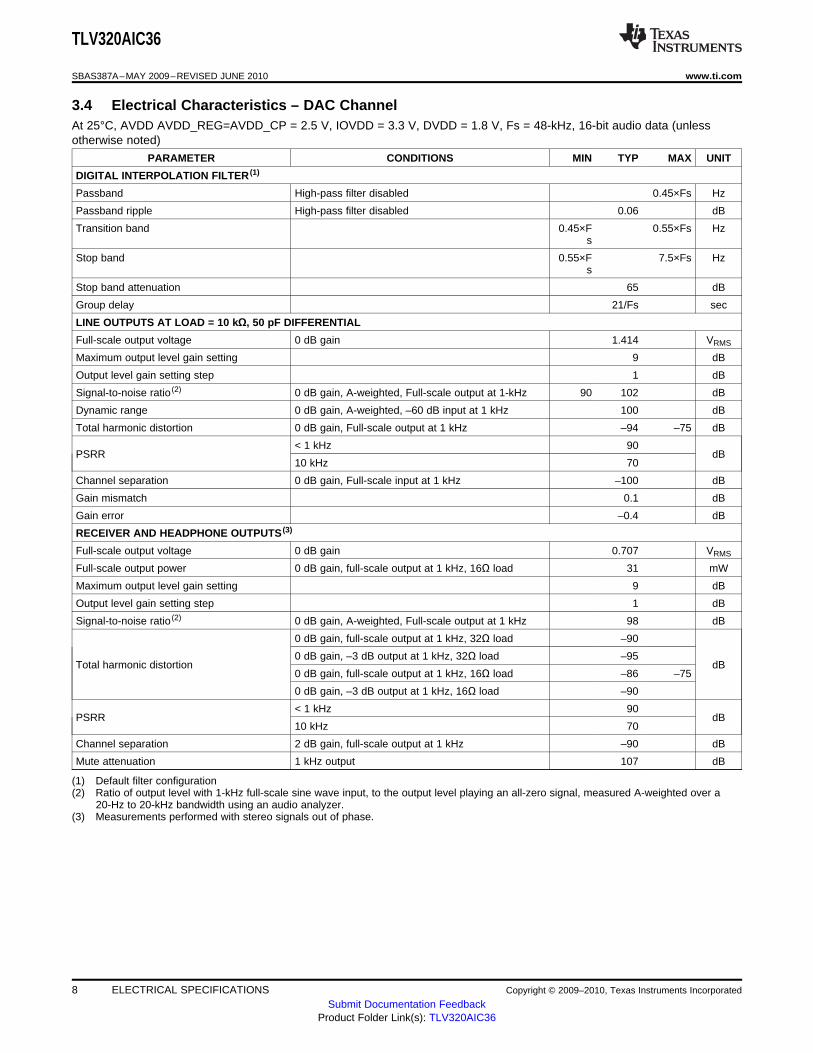
3.4 Electrical Characteristics – DAC ChannelAt 25°C, AVDD AVDD_REG=AVDD_CP = 2.5 V, IOVDD = 3.3 V, DVDD = 1.8 V, Fs = 48-kHz, 16-bit audio data (unlessotherwise noted)
PARAMETER CONDITIONS MIN TYP MAX UNIT
DIGITAL INTERPOLATION FILTER (1)
Passband High-pass filter disabled 0.45×Fs Hz
Passband ripple High-pass filter disabled 0.06 dB
Transition band 0.45×F 0.55×Fs Hzs
Stop band 0.55×F 7.5×Fs Hzs
Stop band attenuation 65 dB
Group delay 21/Fs sec
LINE OUTPUTS AT LOAD = 10 kΩ, 50 pF DIFFERENTIAL
Full-scale output voltage 0 dB gain 1.414 VRMS
Maximum output level gain setting 9 dB
Output level gain setting step 1 dB
Signal-to-noise ratio (2) 0 dB gain, A-weighted, Full-scale output at 1-kHz 90 102 dB
Dynamic range 0 dB gain, A-weighted, –60 dB input at 1 kHz 100 dB
Total harmonic distortion 0 dB gain, Full-scale output at 1 kHz –94 –75 dB
< 1 kHz 90PSRR dB
10 kHz 70
Channel separation 0 dB gain, Full-scale input at 1 kHz –100 dB
Gain mismatch 0.1 dB
Gain error –0.4 dB
RECEIVER AND HEADPHONE OUTPUTS (3)
Full-scale output voltage 0 dB gain 0.707 VRMS
Full-scale output power 0 dB gain, full-scale output at 1 kHz, 16Ω load 31 mW
Maximum output level gain setting 9 dB
Output level gain setting step 1 dB
Signal-to-noise ratio (2) 0 dB gain, A-weighted, Full-scale output at 1 kHz 98 dB
0 dB gain, full-scale output at 1 kHz, 32Ω load –90
0 dB gain, –3 dB output at 1 kHz, 32Ω load –95Total harmonic distortion dB
0 dB gain, full-scale output at 1 kHz, 16Ω load –86 –75
0 dB gain, –3 dB output at 1 kHz, 16Ω load –90
< 1 kHz 90PSRR dB
10 kHz 70
Channel separation 2 dB gain, full-scale output at 1 kHz –90 dB
Mute attenuation 1 kHz output 107 dB
(1) Default filter configuration(2) Ratio of output level with 1-kHz full-scale sine wave input, to the output level playing an all-zero signal, measured A-weighted over a
20-Hz to 20-kHz bandwidth using an audio analyzer.(3) Measurements performed with stereo signals out of phase.
8 ELECTRICAL SPECIFICATIONS Copyright © 2009–2010, Texas Instruments Incorporated
Submit Documentation FeedbackProduct Folder Link(s): TLV320AIC36

TLV320AIC36
www.ti.com SBAS387A–MAY 2009–REVISED JUNE 2010
3.5 Electrical Characteristics – PowerAt 25°C, AVDD_REG=AVDD_CP = 2.5 V, IOVDD = 3.3 V, DVDD = 1.8 V, Fs = 48-kHz, 16-bit audio data (unless otherwisenoted)
PARAMETER CONDITIONS MIN TYP MAX UNIT
SUPPLY CURRENT (1)
Mono ADC channel, 8 kHz AVDD_2P5 (1) PLL off, AGC off 4.6 mA
DVDD 0.4
Stereo ADC channel, 8 kHz AVDD_2P5 (1) PLL off, AGC off 7.2 mA
DVDD 0.5
Stereo ADC channel, 48 kHz AVDD_2P5 (1) PLL off, AGC off 8.6 mA
DVDD 2.1
Stereo DAC headphone, 48 AVDD_2P5 (1) Quiescent current (no signal) 10.4 mAkHz DVDD 2.4
Stereo DAC headphone (2), 48 AVDD_HP, AVDD_DAC Quiescent current (no signal) 4.0 mAkHz AVSS_HP, AVSS_DAC –4.1
DVDD 2.4
Stereo DAC headphone, Low AVDD_2P5 1.8V operation. See section 5.18.3. 5.7 mAPower Mode DVDD 2.1
Stereo DAC headphone, Ultra AVDD_2P5 1.5V operation. See section 5.18.3. 4.8 mALow Power Mode DVDD 1.9
Stereo line in to lineout AVDD_2P5 (1) Quiescent current (no signal) 11 mA
DVDD 0.2
PLL AVDD_ADC Additional power consumed when 1.3 mAPLL is poweredDVDD 0.6
Power down AVDD_2P5 (1) All supply voltages applied, all 0.2 mAblocks programmed in lowest powerDVDD 0.5state
(1) Charge pump and regulators used. AVDD_2P5=AVDD_CP=AVDD_REG=AVDD_BIAS=2.5V(2) Charge pump and regulators not used. AVDD_ADC=AVDD_HP=AVDD_DAC=AVDD_BIAS=1.65, AVSS_HP=AVSS_DAC=–1.65
Copyright © 2009–2010, Texas Instruments Incorporated ELECTRICAL SPECIFICATIONS 9Submit Documentation Feedback
Product Folder Link(s): TLV320AIC36

TLV320AIC36
SBAS387A–MAY 2009–REVISED JUNE 2010 www.ti.com
3.6 Electrical Characteristics – I/OAt 25°C, DVDD = 1.8 V
PARAMETER TEST CONDITIONS MIN TYP MAX UNIT
LOGIC FAMILY CMOS
VIH Logic level IIH = 5 mA, IOVDD > 1.6 V 0.7 × IOVDD V
IIH = 5 mA, 1.2 V ≤ IOVDD <1.6 V 0.9 × IOVDD V
IIH = 5 mA, IOVDD < 1.2 V IOVDD V
VIL IIL = 5 mA, IOVDD > 1.6 V –0.3 0.3 × IOVDD V
IIL = 5 mA, 1.2 V ≤ IOVDD <1.6 V 0.1 × IOVDD V
IIL = 5 mA, IOVDD < 1.2 V 0 V
VOH IOH = 2 TTL loads 0.8 × IOVDD V
VOL IOL = 2 TTL loads 0.1 × IOVDD V
Capacitive load 10 pF
CLOCK INPUT MCLK
Rate 50 MHz
tw(H) Clock pulse width high 10 ns
tw(L) Clock pulse width low 10 ns
DIGMIC INPUT
Setup relative tots 25 nsDIGMIC_CLK edge
Hold relative toth 0 nsDIGMIC_CLK edge
10 ELECTRICAL SPECIFICATIONS Copyright © 2009–2010, Texas Instruments Incorporated
Submit Documentation FeedbackProduct Folder Link(s): TLV320AIC36
WCLK
BCLK
DOUT
DIN
t (WS)d
t (DO-WS)dt (DO-BCLK)d
t (DI)St (DI)h
I2S/LJF Timing in Master Mode
TLV320AIC36
www.ti.com SBAS387A–MAY 2009–REVISED JUNE 2010
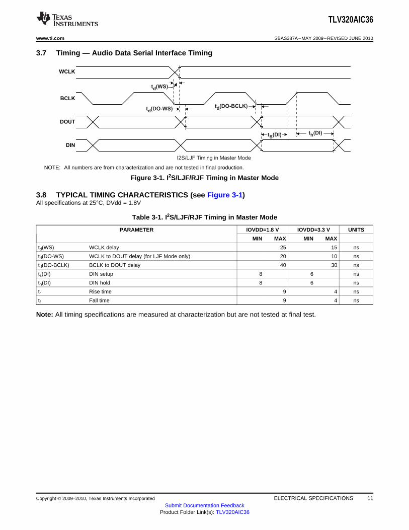
3.7 Timing — Audio Data Serial Interface Timing
NOTE: All numbers are from characterization and are not tested in final production.
Figure 3-1. I2S/LJF/RJF Timing in Master Mode
3.8 TYPICAL TIMING CHARACTERISTICS (see Figure 3-1)All specifications at 25°C, DVdd = 1.8V
Table 3-1. I2S/LJF/RJF Timing in Master Mode
PARAMETER IOVDD=1.8 V IOVDD=3.3 V UNITS
MIN MAX MIN MAX
td(WS) WCLK delay 25 15 ns
td(DO-WS) WCLK to DOUT delay (for LJF Mode only) 20 10 ns
td(DO-BCLK) BCLK to DOUT delay 40 30 ns
ts(DI) DIN setup 8 6 ns
th(DI) DIN hold 8 6 ns
tr Rise time 9 4 ns
tf Fall time 9 4 ns
Note: All timing specifications are measured at characterization but are not tested at final test.
Copyright © 2009–2010, Texas Instruments Incorporated ELECTRICAL SPECIFICATIONS 11Submit Documentation Feedback
Product Folder Link(s): TLV320AIC36
WCLK
BCLK
DOUT
DIN
t (WS)h
tL(BCLK) tH(BCLK)
t (DO-WS)dtP(BCLK)
t (DO-BCLK)d
t (DI)st (DI)h
t (WS)h
TLV320AIC36
SBAS387A–MAY 2009–REVISED JUNE 2010 www.ti.com
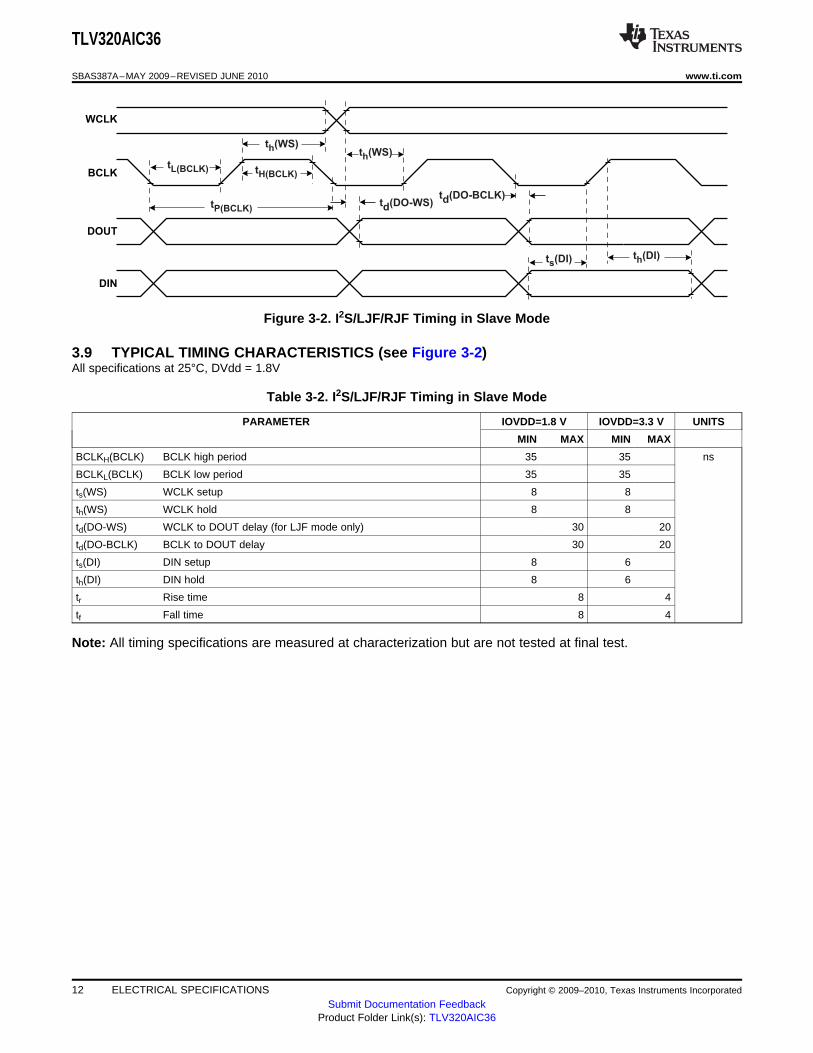
Figure 3-2. I2S/LJF/RJF Timing in Slave Mode
3.9 TYPICAL TIMING CHARACTERISTICS (see Figure 3-2)All specifications at 25°C, DVdd = 1.8V
Table 3-2. I2S/LJF/RJF Timing in Slave Mode
PARAMETER IOVDD=1.8 V IOVDD=3.3 V UNITS
MIN MAX MIN MAX
BCLKH(BCLK) BCLK high period 35 35 ns
BCLKL(BCLK) BCLK low period 35 35
ts(WS) WCLK setup 8 8
th(WS) WCLK hold 8 8
td(DO-WS) WCLK to DOUT delay (for LJF mode only) 30 20
td(DO-BCLK) BCLK to DOUT delay 30 20
ts(DI) DIN setup 8 6
th(DI) DIN hold 8 6
tr Rise time 8 4
tf Fall time 8 4
Note: All timing specifications are measured at characterization but are not tested at final test.
12 ELECTRICAL SPECIFICATIONS Copyright © 2009–2010, Texas Instruments Incorporated
Submit Documentation FeedbackProduct Folder Link(s): TLV320AIC36

WCLK
BCLK
DOUT
DIN
t (WS)d t (WS)d
t (DO-BCLK)d
t (DI)st (DI)h
TLV320AIC36
www.ti.com SBAS387A–MAY 2009–REVISED JUNE 2010
Figure 3-3. DSP Timing in Master Mode
3.9.1 Typical Timing Characteristics (see Figure 3-3)All specifications at 25°C, DVdd = 1.8 V
Table 3-3. DSP Timing in Master Mode
PARAMETER IOVDD=1.8 V IOVDD=3.3 V UNITS
MIN MAX MIN MAX
td(WS) WCLK delay 30 15 ns
td(DO-BCLK) BCLK to DOUT delay 35 20 ns
ts(DI) DIN setup 8 6 ns
th(DI) DIN hold 8 6 ns
tr Rise time 9 4 ns
tf Fall time 9 4 ns
Note: All timing specifications are measured at characterization but are not tested at final test.
Copyright © 2009–2010, Texas Instruments Incorporated ELECTRICAL SPECIFICATIONS 13Submit Documentation Feedback
Product Folder Link(s): TLV320AIC36
WCLK
BCLK
DOUT
DIN
t (BCLK)H
t (BCLK)P
t (ws)h
t (BCLK)L
t (ws)st (ws)h
t (DO-BCLK)d
t (ws)h
t (DI)st (DI)h
TLV320AIC36
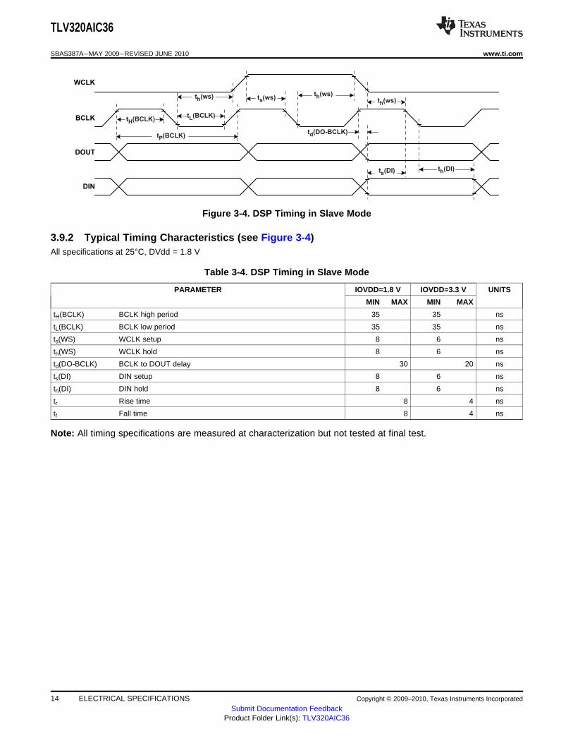
SBAS387A–MAY 2009–REVISED JUNE 2010 www.ti.com
Figure 3-4. DSP Timing in Slave Mode
3.9.2 Typical Timing Characteristics (see Figure 3-4)All specifications at 25°C, DVdd = 1.8 V
Table 3-4. DSP Timing in Slave Mode
PARAMETER IOVDD=1.8 V IOVDD=3.3 V UNITS
MIN MAX MIN MAX
tH(BCLK) BCLK high period 35 35 ns
tL(BCLK) BCLK low period 35 35 ns
ts(WS) WCLK setup 8 6 ns
th(WS) WCLK hold 8 6 ns
td(DO-BCLK) BCLK to DOUT delay 30 20 ns
ts(DI) DIN setup 8 6 ns
th(DI) DIN hold 8 6 ns
tr Rise time 8 4 ns
tf Fall time 8 4 ns
Note: All timing specifications are measured at characterization but not tested at final test.
14 ELECTRICAL SPECIFICATIONS Copyright © 2009–2010, Texas Instruments Incorporated
Submit Documentation FeedbackProduct Folder Link(s): TLV320AIC36
TLV320AIC36
www.ti.com SBAS387A–MAY 2009–REVISED JUNE 2010
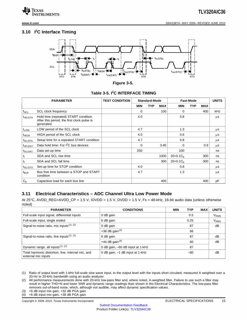
3.10 I2C Interface Timing
Figure 3-5.
Table 3-5. I2C INTERFACE TIMING
PARAMETER TEST CONDITION Standard-Mode Fast-Mode UNITS
MIN TYP MAX MIN TYP MAX
fSCL SCL clock frequency 0 100 0 400 kHz
tHD;STA Hold time (repeated) START condition. 4.0 0.8 msAfter this period, the first clock pulse isgenerated.
tLOW LOW period of the SCL clock 4.7 1.3 ms
tHIGH HIGH period of the SCL clock 4.0 0.6 ms
tSU;STA Setup time for a repeated START condition 4.7 0.8 ms
tHD;DAT Data hold time: For I2C bus devices 0 3.45 0 0.9 ms
tSU;DAT Data set-up time 250 100 ns
tr SDA and SCL rise time 1000 20+0.1Cb 300 ns
tf SDA and SCL fall time 300 20+0.1Cb 300 ns
tSU;STO Set-up time for STOP condition 4.0 0.8 ms
tBUF Bus free time between a STOP and START 4.7 1.3 mscondition
Cb Capacitive load for each bus line 400 400 pF
3.11 Electrical Characteristics – ADC Channel Ultra Low Power ModeAt 25°C, AVDD_REG=AVDD_CP = 1.5 V, IOVDD = 1.5 V, DVDD = 1.5 V, Fs = 48-kHz, 16-bit audio data (unless otherwisenoted)
PARAMETER CONDITIONS MIN TYP MAX UNITS
Full-scale input signal, differential inputs 0 dB gain 0.5 VRMS
Full-scale input, single ended 6 dB gain 0.25 VRMS
Signal-to-noise ratio, mic inputs (1) (2) 0 dB gain 87 dB
+38 dB gain (3) 66
Signal-to-noise ratio, line inputs (1) (2) 6 dB gain 87 dB
+44 dB gain (4) 60 dB
Dynamic range, all inputs (1) (2) 0 dB gain, –60 dB input at 1-kHz 87
Total harmonic distortion, line, internal mic, and 0 dB gain, –1 dB input at 1-kHz –80 dBexternal mic inputs
(1) Ratio of output level with 1-kHz full-scale sine wave input, to the output level with the inputs short circuited, measured A weighted over a20-Hz to 20-kHz bandwidth using an audio analyzer.
(2) All performance measurements done with 20-kHz low-pass filter and, where noted, A-weighted filter. Failure to use such a filter mayresult in higher THD+N and lower SNR and dynamic range readings than shown in the Electrical Characteristics. The low-pass filterremoves out-of-band noise, which, although not audible, may affect dynamic specification values.
(3) +6 dB input mix gain, +32 dB PGA gain(4) +6 dB input mix gain, +38 dB PGA gain
Copyright © 2009–2010, Texas Instruments Incorporated ELECTRICAL SPECIFICATIONS 15Submit Documentation Feedback
Product Folder Link(s): TLV320AIC36
TLV320AIC36
SBAS387A–MAY 2009–REVISED JUNE 2010 www.ti.com
Electrical Characteristics – ADC Channel Ultra Low Power Mode (continued)
At 25°C, AVDD_REG=AVDD_CP = 1.5 V, IOVDD = 1.5 V, DVDD = 1.5 V, Fs = 48-kHz, 16-bit audio data (unless otherwisenoted)
PARAMETER CONDITIONS MIN TYP MAX UNITS
PSRR, all inputs, unregulated (5) < 1-kHz, single-ended input 50 dB
< 1-kHz, differential input 50
Channel separation (6) 0 dB gain, –2 dB input at 1-kHz –70 dB
Gain error 0 dB gain, 1-kHz input 0.7 dB
Programmable Gain Amplifier (PGA) maximum gain 59.5 dB
PGA gain step 0.5 dB
Input resistance, line inputs 0 dB input mix gain 10 kΩ–12 dB input mix gain 40
Input resistance, mic inputs 6 dB input mix gain 10 kΩ–6 dB input mix gain 40
Input capacitance, all inputs 10 pF
DIGITAL DECIMATION FILTER (7)
Filter gain from 0 to 0.39 Fs 0.1 dB
Filter gain at 0.4125 Fs –0.25 dB
Filter gain at 0.45 Fs –3 dB
Filter gain at 0.5 Fs –17.5 dB
Filter gain from 0.55 Fs to 64 Fs -75 dB
Filter group delay 17/Fs sec
MICROPHONE BIAS GENERATORS
Bias voltage Programmable settings, 1 kΩ load 1.3 V
Current sourcing 2 mA
Power supply rejection ratio < 1-kHz 48 dB
(5) AVDD_DAC and AVSS_DAC connected directly to supply(6) Channel separation for any input connected to the ADC left channel and any other input connected to the ADC right channel(7) Default filter configuration
3.12 Electrical Characteristics – DAC Channel Ultra Low Power ModeAt 25°C, AVDD AVDD_REG=AVDD_CP = 1.5 V, IOVDD = 1.5 V, DVDD = 1.5 V, Fs = 48-kHz, 16-bit audio data (unlessotherwise noted)
PARAMETER CONDITIONS MIN TYP MAX UNIT
DIGITAL INTERPOLATION) FILTER (1)
Passband High-pass filter disabled 0.45×Fs Hz
Passband ripple High-pass filter disabled 0.06 dB
Transition band 0.45×Fs 0.55×Fs Hz
Stop band 0.55×Fs 7.5×Fs Hz
Stop band attenuation 65 dB
Group delay 21/Fs sec
LINE OUTPUTS AT LOAD = 10 kΩ, 50 pF DIFFERENTIAL
Full-scale output voltage –5 dB gain 0.8 VRMS
Maximum output level gain setting –5 dB
Output level gain setting step 1 dB
Signal-to-noise ratio (2) –5 dB gain, A-weighted, Full-scale output at 1-kHz 94 dB
Dynamic range 0 dB gain, A-weighted, –60 dB input at 1 kHz 94 dB
Total harmonic distortion –5 dB gain, Full-scale output at 1 kHz 90 dB
(1) Default filter configuration(2) Ratio of output level with 1-kHz full-scale sine wave input, to the output level playing an all-zero signal, measured A-weighted over a
20-Hz to 20-kHz bandwidth using an audio analyzer.
16 ELECTRICAL SPECIFICATIONS Copyright © 2009–2010, Texas Instruments Incorporated
Submit Documentation FeedbackProduct Folder Link(s): TLV320AIC36

-10 0 10 20 30 40 50 60
Channel Gain - dB
50
55
60
65
70
75
80
85
90
95
SN
R -
Sig
nal-
to-N
ois
e R
ati
o -
dB
20 k single endedW
10 kW single ended
20 kW differential
20 kW differential
-90
-80
-70
-60
-50
-40
-30
-20
-10
0
0 20 40 60 80 100
Headphone Output Power - mW
THD = 16 W
THD = 32 W
TH
D -
To
tal H
arm
on
ic D
isto
rtio
n -
dB
c
TLV320AIC36
www.ti.com SBAS387A–MAY 2009–REVISED JUNE 2010
Electrical Characteristics – DAC Channel Ultra Low Power Mode (continued)
At 25°C, AVDD AVDD_REG=AVDD_CP = 1.5 V, IOVDD = 1.5 V, DVDD = 1.5 V, Fs = 48-kHz, 16-bit audio data (unlessotherwise noted)
PARAMETER CONDITIONS MIN TYP MAX UNIT
PSRR < 1 kHz 70 dB
10 kHz 50
Channel separation -5 dB gain, Full-scale input at 1 kHz –50 dB
Gain mismatch 0.1 dB
Gain error –0.4 dB
RECEIVER AND HEADPHONE OUTPUTS (3)
Full-scale output voltage –5 dB gain 0.4 VRMS
Full-scale output power –5 dB gain, full-scale output at 1 kHz, 16Ω load 10 mW
Maximum output level gain setting –5 dB
Output level gain setting step 1 dB
Signal-to-noise ratio (2) –5 dB gain, A-weighted, Full-scale output at 1 kHz 89 dB
Total harmonic distortion –5 dB gain, full-scale output at 1 kHz, 32Ω load –80 dB
–5 dB gain, –3 dB output at 1 kHz, 32Ω load –80
–5 dB gain, full-scale output at 1 kHz, 16Ω load –7
–5 dB gain, –3 dB output at 1 kHz, 16Ω load –77
PSRR < 1 kHz 50 dB
10 kHz 35
Channel separation –5 dB gain, full-scale output at 1 kHz –65 dB
Mute attenuation 1 kHz output 107 dB
(3) Measurements performed with stereo signals out of phase.
4 TYPICAL CHARACTERISTICS
4.1 Typical PerformanceADC SNR TOTAL HARMONIC DISTORTION
vs vsCHANNEL GAIN HEADPHONE OUTPUT POWER
Figure 4-1. Figure 4-2.
Copyright © 2009–2010, Texas Instruments Incorporated TYPICAL CHARACTERISTICS 17Submit Documentation Feedback
Product Folder Link(s): TLV320AIC36

-120
-100
-80
-60
-40
-20
0
0 0.5 1 1.5 2 2.5 3 3.5 4 4.5Load Current - mA
Ch
an
ge in
Ou
tpu
t V
olt
ag
e -
mV
0 2000 4000 6000 8000 10000 12000 14000 16000 18000 20000
f - Frequency - Hz
-140
-120
-100
-80
-60
-40
-20
0
Am
plitu
de -
dB
Vrm
s
-140
-120
-100
-80
-60
-40
-20
0A
mp
litu
de -
dB
Vrm
s
0 2000 4000 6000 8000 10000 12000 14000 16000 18000 20000
f - Frequency - Hz
-140
-120
-100
-80
-60
-40
-20
0
Am
plitu
de -
dB
FS
/bin
0 2000 4000 6000 8000 10000 12000 14000 16000 18000 20000
f - Frequency - Hz
-140
-120
-100
-80
-60
-40
-20
0
Am
plitu
de -
dB
Vrm
s
0 2000 4000 6000 8000 10000 12000 14000 16000 18000 20000
f - Frequency - Hz
TLV320AIC36
SBAS387A–MAY 2009–REVISED JUNE 2010 www.ti.com
CHANGE IN MICBIAS VOLTAGEvs
MICBIAS LOAD
Figure 4-3.
4.2 FFTMIC1 TO HPR @ 8 dB GAIN, MIC1 TO HPR @ 0 dB GAIN,
920 mVrms into 16 ohms 380 mVrms into 16 ohms
Figure 4-4. Figure 4-5.MIC1 TO LINEOUT @ 0 dB GAIN
MIC1 DIFFERENTIAL INPUT TO ADC @ –1 dBFS 775 mVrms into 1kΩ
Figure 4-6. Figure 4-7.
18 TYPICAL CHARACTERISTICS Copyright © 2009–2010, Texas Instruments Incorporated
Submit Documentation FeedbackProduct Folder Link(s): TLV320AIC36

-140
-120
-100
-80
-60
-40
-20
0
Am
plitu
de -
dB
Vrm
s
0 2000 4000 6000 8000 10000 12000 14000 16000 18000 20000
f - Frequency - Hz0 2000 4000 6000 8000 10000 12000 14000 16000 18000 20000
f - Frequency - Hz
-140
-120
-100
-80
-60
-40
-20
0
Am
plitu
de -
dB
V
20
-60
-50
-40
-30
-20
-10
0
0 50 100 150 200 250 300 350
Load Current - mA
Ch
an
ge in
ou
tpu
t V
olt
ag
e -
mV
-140
-120
-100
-80
-60
-40
-20
0
Am
plitu
de -
dB
Vrm
s
20
0 2000 4000 6000 8000 10000 12000 14000 16000 18000 20000
f - Frequency - Hz
0
50
100
150
200
250
300
350
400
450
500
0 50 100 150 200 250 300 350
Dro
po
ut
Vo
ltag
e -
mV
Load Current - mA
TLV320AIC36
www.ti.com SBAS387A–MAY 2009–REVISED JUNE 2010
MIC1 TO LINE OUT @ 6 dB GAIN, DAC PLAYBACK TO HEADPHONE,1.5 Vrms into 1kΩ 0 dB gain, 0.7 Vrms into 16Ω
Figure 4-8. Figure 4-9.CHANGE IN AVDD1 LDO VOLTAGE
DAC PLAYBACK TO LINE-OUT, vs1.5 Vrms into 1kΩ LDO LOAD
Figure 4-10. Figure 4-11.AVDD1 LDO DROPOUT VOLTAGE
vsLOAD CURRENT
Figure 4-12.
Copyright © 2009–2010, Texas Instruments Incorporated TYPICAL CHARACTERISTICS 19Submit Documentation Feedback
Product Folder Link(s): TLV320AIC36

RESETB MCLK SCL SDA BCLK WCLK DIN DOUT
HPL
HP_COM
HPR
LINEOUT_LP
LINEOUT_LM
510 W
4700 pF
LINEOUT_RP
LINEOUT_RM
TPA2012
Class D Amp
RECL
RECR
MIC1_P
MIC1_M
DETECT
EXTMIC_P
EXTMIC_M
EXT_MICBIAS
Earjack,
Microphone
and Headset
Speakers
HOOK
MIC2_P
MIC2_M
LINEIN_L
LINEIN_R
INT_MICBIAS
GPIO1
GPIO2
GPIO3/DIGMIC_CLK
GPIO4/DIGMIC_DATA
GPIO5/BITSTREAM_CLK
GPIO6/BITSTREAM_DATA
GeneralPurpose I/O
TLV320AIC36
Host Processor
1 kW
0.1 Fm
0.1 Fm
1 kW
0.1 Fm
0.1 Fm
0.1 Fm
0.1 Fm
510 W
510 W
510 W
4700 pF
0.1 Fm
1 kW
0.1 Fm
0.1 Fm
0.1 Fm
1 kW
1 kW
1 kW
0.1 Fm
0.1 Fm
Line In/FM
TLV320AIC36
SBAS387A–MAY 2009–REVISED JUNE 2010 www.ti.com
5 APPLICATION INFORMATION
5.1 Typical Circuit Configuration
Figure 5-1. Typical Circuit Configuration
5.2 Overview
The TLV320AIC36 offers a wide range of configuration options. Figure 1-1 shows the basic functionalblocks of the device.
5.2.1 Digital Pins
Only a small number of digital pins are dedicated to a single function; whenever possible, the digital pinshave a default function, and also can be reprogrammed to cover alternative functions for variousapplications.
The fixed-function pins are RESETB, SDA, SCL, DIN, I2C_ADDR1, I2C_ADDR0, and MCLK. Other digitalpins such as GPIO1–GPIO6, BCLK, WCLK, and DOUT, can be configured for various functions usingregister control.
20 APPLICATION INFORMATION Copyright © 2009–2010, Texas Instruments Incorporated
Submit Documentation FeedbackProduct Folder Link(s): TLV320AIC36

TLV320AIC36
www.ti.com SBAS387A–MAY 2009–REVISED JUNE 2010
5.2.2 Analog Pins
Analog functions can also be configured to a large degree. For minimum power consumption, analogblocks are powered down by default. The blocks can be powered up with fine granularity according to theapplication needs.
The possible analog routings of analog input pins to ADCs and output amplifiers as well as the routingfrom DACs to output amplifiers can be seen in Figure 5-2.
5.2.3 Power Supply
The TLV320AIC36 power management unit generates all of the analog supply voltages from a singlenominal 2.5 V supply. The power management unit consists of two positive LDOs, one which generates anominal +1.75 V supply for the input PGA and ADC section and another which generates a nominal +1.65V for the DAC and audio amplifier section. A negative charge pump generates an unregulated negativevoltage from the unregulated positive supply; a negative LDO generates a nominal –1.65 V supply for theDAC and audio amplifier section from this unregulated negative voltage. See Figure 5-48 for details ontypical power supply connections.
5.2.4 Clocking
To minimize power consumption, the system ideally provides a master clock that is a suitable integermultiple of the desired sampling frequencies. In such cases, internal dividers can be programmed to setup the required internal clock signals at very low power consumption. For cases where such master clocksare not available, the built-in PLL can be used to generate a clock signal that serves as an internal masterclock. In fact, this master clock can also be routed to an output pin and can be used elsewhere in thesystem. The clock system is flexible enough that it allows the internal clocks to be derived directly from anexternal clock source, while the PLL generates an other clock that is used only outside the TLV320AIC36.
5.3 miniDSP
The TLV320AIC36 features two miniDSP cores. The first miniDSP core is tightly coupled to the ADC, thesecond miniDSP core is tightly coupled to the DAC. The fully programmable algorithms for the miniDSPmust be loaded into the device after power up. The miniDSPs have direct access to the digital stereoaudio stream on the ADC and on the DAC side, offering the possibility for advanced, very low group delayDSP algorithms.
5.3.1 Software
Software development for the TLV320AIC36 is supported through TI's comprehensive PurePath StudioDevelopment Environment. A powerful, easy-to-use tool designed specifically to simplify softwaredevelopment on the TI miniDSP audio platform. The Graphical Development Environment consists of alibrary of common audio functions that can be dragged-and-dropped into an audio signal flow andgraphically connected together. The DSP code can then be assembled from the graphical signal flow withthe click of a mouse.
Visit the TLV320AIC36 product folder on www.ti.com to learn more about PurePath Studio and the lateststatus on available, ready-to-use DSP algorithms.
Copyright © 2009–2010, Texas Instruments Incorporated APPLICATION INFORMATION 21Submit Documentation Feedback
Product Folder Link(s): TLV320AIC36

(P2R48)
(P2R46)
(P2R49)
(P2R45)
(P2R50)
(P2R47)
HPR Volume
(0 to -78dB)
(P2R62)
(P2R60)
(P2R63)
(P2R59)
(P2R64)
(P2R61)DAC_L
DAC_R
LINEIN_L
LINEIN_R
PGA_L
PGA_R
RECL Volume
(0 to -78dB)
(P2R55)
(P2R53)
(P2R56)
(P2R52)
(P2R57)
(P2R54)
HPL Volume
(0 to -78dB)
(P2R69)
(P2R67)
(P2R70)
(P2R66)
(P2R71)
(P2R68)
RECR Volume
(0 to -78dB)
(P2R86)
LINEOUT_L Volume
(0 to -78dB)Gain:
0 to +9 dB
(P2R90)
(P2R88)
(P2R91)
(P2R87)
(P2R92)
(P2R89)
(P2R93)
LINEOUT_R Volume
(0 to -78dB)
(P2R83)
(P2R81)
(P2R84)
(P2R80)
(P2R85)
(P2R82)
Gain:
0 to +9 dB
(P2R65)
+
DAC_L
DAC_R
LINEIN_L
LINEIN_R
PGA_L
PGA_R
Gain:
0 to +9 dB
(P2R58)
+
DAC_L
DAC_R
LINEIN_L
LINEIN_R
PGA_L
PGA_R
Gain:
0 to +9 dB
(P2R51)
+
DAC_L
DAC_R
LINEIN_L
LINEIN_R
PGA_L
PGA_R
Gain:
0 to +9 dB
(P2R72)
+
(P2R36)
DAC_L
DAC_R
LINEIN_L
LINEIN_R
PGA_L
PGA_R
DAC_L
DAC_R
LINEIN_L
LINEIN_R
PGA_L
PGA_R
+
+
Gain:
0 to +9 dB
(P1R59)
Gain:
0 to +46.5 dB
LINEIN_L
Input MUX
(P1R52)
MIC1_P
EXTMIC_P
MIC1_M
Input MUX
(P1R54)
EXTMIC_M
VCM_ADC
(P1R60)
Gain:
0 to +46.5 dB
VCM_ADC
Input MUX
(P1R57)
EXTMIC_M
MIC2_M
EXTMIC_P
Input MUX
(P1R55)
MIC2_P
LINEIN_R
VC
M
(P
1R
10)
ADC
L
+
+
+
+
ADC
R
DAC
L
DAC
R
(P2R40)
(P2R40)
LINEIN_R (G7)
MIC 2_P (H8)
MIC2_M (G8)
EXTMIC_M (J7)
VCM_ADC (J9)
MIC1_M (H6)
EXTMIC_P (H7)
MIC1_P (J6)
LINEIN_L (G6)
LINEOUT _RM (A8)
LINEOUT _RP (C6)
LINEOUT _LM (A7)
LINEOUT _LP (B6)
HPL (F7)
HPR(F9)
HP_COM (J8)
GND_HP (E7)
RECL (D8)
RECR (D9)
DAC Pwr (P2R37)
DAC Current Ctrl
(P2R107)
ADC Pwr (P0R81)
Open Circuit
Detect
(P2R108)
Open Circuit
Detect
(P2R108)
Open Circuit
Detect
(P2R108)
Open Circuit
Detect
(P2R108)
All output Volume
Gains are in 0.5dB steps
All output Gainsare positive in 1dB steps
Common Controls:
· SC Protection: (P2R38)
· Gain Soft-Stepping: (P2R40)
· Pop Reduction: (P2R42)
miniDSP miniDSP
TLV320AIC36
SBAS387A–MAY 2009–REVISED JUNE 2010 www.ti.com
5.4 Analog Routing
Figure 5-2. Analog Routing Diagram
5.4.1 Analog Bypass
The TLV320AIC36 offers two analog-bypass modes, line input bypass and PGA bypass mode. For thesemodes, all LDOs and the ADC must be enabled. The DAC does not need to be enabled to save power.
5.4.2 Line Input Bypass
This mode routes LINEINL/R to any of the output amplifiers by configuring Page 2, Register 40 and byprogramming the output amplifiers to select one or both line inputs. See Figure 5-2. Under normal bypassoperation, the line inputs are AC-coupled to the LINEIN_L/LINEIN_R pins. The ADC generates an internalcommode mode voltage for these signals before the bypass amplifiers. The bypass amplifiers have a fixedgain of 0 dB for single-ended output to HPL_R and RECL_R, and 6-dB gain for differential output toLINEOUT_L/LINEOUT_R.
To save power, the ADC can be disabled and an external common mode voltage can be generated forthese pins. A simple 20kΩ/20kΩ resistor divider from AVDD_ADC to GND_ADC is sufficient with somecompromise in performance.
5.4.3 PGA Bypass
In this mode, the mic or line input signals are amplified by the PGA and routed to the output amplifiers.See figure 5-2. This mode is enabled by selecting the input mux, setting the PGA gain, and programmingthe output amplifiers to select one or both PGA outputs.
22 APPLICATION INFORMATION Copyright © 2009–2010, Texas Instruments Incorporated
Submit Documentation FeedbackProduct Folder Link(s): TLV320AIC36
TLV320AIC36
www.ti.com SBAS387A–MAY 2009–REVISED JUNE 2010
The ADC must be enabled to supply biasing to the PGA. The bypass amplifiers have a fixed gain of –6 dBfor single-ended output to HP_L/HP_R and REC_L/REC_R, and 0 dB gain for differential output toLINEOUT_L/LINEOUT_R
5.4.4 Line Input Routing
To avoid excessive internal DC offset, the line inputs should be routed to the Headphone Outputswhenever the line inputs are activated, even if the bypass paths to the Headphone Outputs are notneeded. This can be accomplished by writing 1 to bit D7 of registers 45 and 55 in Page 2. If the lineinput-to-headphone output bypass paths are not needed, they can be muted in the same registers.
5.5 Device Initialization
5.5.1 Reset
The TLV320AIC36 internal logic must be initialized to a known condition for proper device function. Toinitialize the device in its default operating condition, the hardware reset pin (RESETB) must be pulled lowfor at least 100 ns. For this initialization to work, the IOVDD and DVdd supplies must be powered up. It isrecommended that while the DVdd supply is being powered up, the RESETB pin be pulled low.
The device can also be reset through software by writing 1 into Page 0, Register 1 followed by writing 0into Page 0, Register 1. After a device reset, all registers are initialized with default values as listed in theRegister Map section.
5.5.2 Device Startup Lockout Times
After the is initialized through hardware reset at power-up or software reset, the internal memories areinitialized to default values. This initialization occurs within 1 ms after pulling the RESETB signal high.During this initialization phase, no Register read or Register write operation should be performed on ADCor DAC coefficient buffers. Also, no block within the codec should be powered up during the initializationphase.
5.5.3 PLL Startup
Whenever the PLL is powered up, a startup delay of approximately of 10 ms is involved after the power upcommand of the PLL and before the clocks are available to the codec. This delay enables stable operationof PLL and clock-divider logic.
5.6 ADC
5.6.1 Concept
The TLV320AIC36 includes a stereo audio ADC, which uses a delta-sigma modulator with aprogrammable oversampling ratio, followed by a digital decimation filter. The ADC supports sampling ratesfrom 8 to 192 kHz. To provide optimal system power management, the stereo ADC can be powered upone channel at a time, to support the case where only mono record capability is required. In addition, bothchannels can be fully powered or entirely powered down. Because of the oversampling nature of the audioADC and the integrated digital decimation filtering, requirements for analog anti-aliasing filtering are veryrelaxed. The TLV320AIC36 integrates a second-order analog anti-aliasing filter with 28-dB attenuation at 6MHz. This filter, combined with the digital decimation filter, provides sufficient anti-aliasing filtering withoutrequiring additional external components.
5.6.2 Routing
As shown in Figure 5-2, the TLV320AIC36 includes eight analog inputs that can be connected to two fullydifferential input amplifiers (one per ADC/PGA channel). By turning on only one set of switches peramplifier at a time, the inputs can be effectively multiplexed to each ADC/PGA channel. By turning onmultiple sets of switches per amplifier at a time, audio sources can be mixed.
Copyright © 2009–2010, Texas Instruments Incorporated APPLICATION INFORMATION 23Submit Documentation Feedback
Product Folder Link(s): TLV320AIC36

Analog
In
Input
SelectionAnalog Gain
ADC
PGA
Digital
Volume
Control
Digital Gain
Adjust
Frequency
Response/
Gain
ADC
Filtering
Audio
Interface
+6, 0, -6 dB0...47.5 dB
Step = 0.5 dB
-12 .. 20 dB
Step = 0.5 dB
0 .. -0.4 dB
Step = 0.1 dB
Fully
Programmable
Coefficients
TLV320AIC36
SBAS387A–MAY 2009–REVISED JUNE 2010 www.ti.com
In most applications, high-input impedance is desired for analog inputs. However when used with highgain, as in the case of microphone inputs, the higher-input impedance results in higher noise or lowerdynamic range. The TLV320AIC36 gives the user the flexibility of choosing the input impedance from10kΩ, 20kΩ and 40kΩ. When multiple inputs are mixed together, by choosing different input impedances,level adjustment can be achieved. For example, if one input is selected with 10kΩ input impedance andthe second input is selected with 20kΩ input impedance, then the second input is attenuated by half ascompared to the first input. This input level control is intended to be a volume control, but instead used forlevel setting.
Mixing of multiple inputs can easily lead to PGA outputs that exceed the range of the internal amplifiers,resulting in saturation and clipping of the mixed output signal. Whenever mixing is being implemented, thesystem designer is advised to take adequate precautions to avoid such a saturation from occurring. Ingeneral, the mixed (summed) signal should not exceed 0 dB.
Typically, voice or audio signal inputs are capacitively coupled to the device. This allows the device toindependently set the common mode of the input signals to values chosen by register control of Page 1,Register 10, D(6) to either 0.9 V or 0.75 V. The correct value maximizes the dynamic range across theentire analog-supply range. Failure to capacitively connect the input to the device can cause high offsetdue to mismatch in source common-mode and device common-mode setting. In extreme cases it couldalso saturate the analog channel, causing distortion.
5.7 ADC Gain Setting
When the gain of the ADC channel is kept at 6 dB and the common mode is set to 0.75 V, a single-endedinput of 0.375 VRMS results in a full-scale digital signal at the output of ADC channel. Similarly, when thegain is kept at 6 dB, and common mode is set to 0.9 V, a single-ended input of 0.5 VRMS results in afull-scale digital signal at the output of the ADC channel. However various block functions control the gainthrough the channel. The gain applied by the PGA is described in Table 5-1. Additionally, the digitalvolume control adjusts the gain through the channel, as described in Section 5.7.2. A finer level of gain iscontrolled by fine gain control, as described in Section 5.7.3. The decimation filters A, B, and C along withthe delta-sigma modulator contribute to a DC gain of 1.0 through the channel.
5.7.1 Analog PGA
The TLV320AIC36 features a built-in low-noise PGA for boosting low-level signals, such as directmicrophone inputs, to full-scale to achieve high SNR. This PGA can provide a gain in the range of 0 dB to47.5 dB for single-ended inputs or 6 dB to 53.5 dB for fully differential inputs (gain calculated with respectto input impedance setting of 10kΩ; 20kΩ input impedance will result in 6 dB lower and 40kΩ will result in12 dB lower gain). This gain can be user controlled by writing to Page 1, Register 59 and Page 1, Register60. In the AGC mode this gain can also be automatically controlled by the built-in hardware AGC.
24 APPLICATION INFORMATION Copyright © 2009–2010, Texas Instruments Incorporated
Submit Documentation FeedbackProduct Folder Link(s): TLV320AIC36
TLV320AIC36
www.ti.com SBAS387A–MAY 2009–REVISED JUNE 2010
Table 5-1. Analog PGA vs Input Configuration
Page 1, EFFECTIVE GAIN APPLIED BY PGARegister 59, D(6:0) SINGLE-ENDED DIFFERENTIALPage 1,
RIN = 10K RIN = 20K RIN = 40K RIN = 10K RIN = 20K RIN = 40KRegister 60, D(6:0)
000 0000 0 dB –6 dB –12 dB 6.0 dB 0 dB –6.0 dB
000 0001 0.5 dB –5.5 dB –11.5 dB 6.5 dB 0.5 dB –5.5 dB
000 0010 1.0 dB –5.0 dB –11.0 dB 7.0 dB 7.5 dB –5.0 dB
… … … … … … …
101 1110 47.0 dB 41.0 dB 35.0 dB 53.0 dB 47.0 dB 41.0 dB
101 1111 47.5 dB 41.5 dB 35.5 dB 53.5 dB 47.5 dB 41.5 dB
The gain changes are implemented with an internal soft-stepping algorithm that only changes the actualvolume level by one 0.5-dB step every one or two ADC output samples, depending on the register value(see registers Page 0, Reg 81, D(1:0)). This soft-stepping enables smooth volume-control changes with noaudible artifacts. On reset, the PGA gain defaults to a mute condition, and at power down, the PGAsoft-steps the volume to mute before shutting down. A read-only flag Page 0, Reg 36, D(7) and D(3) is setwhenever the gain applied by the PGA equals the desired value set by the register. The soft-steppingcontrol can also be disabled by programming Page 0, Reg 81, D(1:0).
5.7.2 Digital Volume Control
The TLV320AIC36 also has a digital volume-control block with a range from –12 dB to +20 dB in steps of0.5-dB. It is set by programming Page 0, Register 83 and 84, respectively, for left and right channels.
Table 5-2. Digital Volume Control for ADC
Desired Gain Left/Right Channel(dB) Page 1, Register 83/84,
D(6:0)
–12.0 110 1000
–11.5 110 1001
–11.0 110 1010
..
–0.5 111 1111
0.0 000 0000 (default)
+0.5 000 0001
..
+19.5 010 0111
+20.0 010 1000
During volume control changes, the soft-stepping feature is used to avoid audible artifacts. Thesoft-stepping rate can be set to either 1 or 2 gain steps per sample. Soft-stepping can also be entirelydisabled. This soft-stepping is configured using Page 1, Register 81, D(1:0), and is common tosoft-stepping control for the analog PGA. During power-down of an ADC channel, this volume controlsoft-steps down to –12.0 dB before powering down. Due to the soft-stepping control, soon after changingthe volume control setting or powering down the ADC channel, the actual applied gain may be differentfrom the one programmed through the control register. The TLV320AIC36 gives feedback to the user,through read-only flags Page 1, Reg 36, D(7) for the Left Channel and Page 1, Reg 36, D(3) for the rightchannel.
Copyright © 2009–2010, Texas Instruments Incorporated APPLICATION INFORMATION 25Submit Documentation Feedback
Product Folder Link(s): TLV320AIC36
TLV320AIC36
SBAS387A–MAY 2009–REVISED JUNE 2010 www.ti.com
5.7.3 Fine Digital Gain Adjustment
Additionally, the gains in each of the channels is finely adjustable in steps of 0.1 dB. This is useful whentrying to match the gain between channels. By programming Page 0, Register 82 the gain can be adjustedfrom 0 dB to -0.4 dB in steps of 0.1 dB. This feature, in combination with the regular digital volume controlallows the gains through the left and right channels be matched in the range of -0.5 dB to +0.5 dB with aresolution of 0.1 dB.
5.7.4 AGC
The TLV320AIC36 includes Automatic Gain Control (AGC) for ADC recording. AGC can be used tomaintain a nominally-constant output level when recording speech. As opposed to manually setting thePGA gain, in the AGC mode, the circuitry automatically adjusts the PGA gain as the input signal becomesoverly loud or very weak, such as when a person speaking into a microphone moves closer or farther fromthe microphone. The AGC algorithm has several programmable parameters, including target gain, attackand decay time constants, noise threshold, and max PGA applicable, that allow the algorithm to be finetuned for any particular application. The algorithm uses the absolute average of the signal (which is theaverage of the absolute value of the signal) as a measure of the nominal amplitude of the output signal.Since the gain can be changed at the sample interval time, the AGC algorithm operates at the ADCsample rate.• Target level represents the nominal output level at which the AGC attempts to hold the ADC output
signal level. The TLV320AIC36 allows programming of eight different target levels, which can beprogrammed from –5.5 to –24 dB relative to a full-scale signal. Since the TLV320AIC36 reacts to thesignal absolute average and not to peak levels, it is recommended that the target level be set withenough margin to avoid clipping at the occurrence of loud sounds.
• Attack time determines how quickly the AGC circuitry reduces the PGA gain when the output signallevel exceeds the target level due to increase in input signal level. Wide range of attack timeprogrammability is supported in terms of number of samples (i.e. number of ADC sample frequencyclock cycles).
• Decay time determines how quickly the PGA gain is increased when the output signal level falls belowthe target level due to reduction in input signal level. Wide range of decay time programmability issupported in terms of number of samples (i.e., number of ADC sample frequency clock cycles).
• Noise threshold determines the level below which if the input signal level falls, the AGC considers itas silence, and thus brings down the gain to 0 dB in steps of 0.5 dB every FS and sets the noisethreshold flag. The gain stays at 0 dB unless the input speech signal average rises above the noisethreshold setting. This s that noise is not 'gained up' in the absence of speech. Noise threshold level inthe AGC algorithm is programmable from -30 dB to -90 dB of full-scale. When AGC Noise Threshold isset to –70 dB, –80 dB, or –90 dB, the microphone input Max PGA applicable setting must be greaterthan or equal to 11.5 dB, 21.5 dB, or 31.5 dB respectively. This operation includes hysteresis anddebounce to avoid the AGC gain from cycling between high gain and 0 dB when signals are near thenoise threshold level. The noise (or silence) detection feature can be entirely disabled by the user.
• Max PGA applicable allows the designer to restrict the maximum gain applied by the AGC. This canbe used for limiting PGA gain in situations where environmental noise is greater than the programmednoise threshold. Microphone input Max PGA can be programmed from 0 dB to 63.5 dB in steps of 0.5dB.
• Hysteresis, as the name suggests, determines a window around the Noise Threshold which must beexceeded to either detect that the recorded signal is indeed noise or signal. If initially the energy of therecorded signal is greater than the Noise Threshold, then the AGC recognizes it as noise only whenthe energy of the recorded signal falls below the Noise Threshold by a value given by Hysteresis.Similarly, after the recorded signal is recognized as noise, for the AGC to recognize it as a signal, itsenergy must exceed the Noise Threshold by a value given by the Hysteresis setting. In order toprevent the AGC from jumping between noise and signal states, (which can happen when the energyof recorded signal is very close to the Noise threshold) a non-zero hysteresis value should be chosen.The Hysteresis feature can also be disabled.
26 APPLICATION INFORMATION Copyright © 2009–2010, Texas Instruments Incorporated
Submit Documentation FeedbackProduct Folder Link(s): TLV320AIC36

1
1
15
1
10
zD2
zNN)z(H
-
-
-
+=
TLV320AIC36
www.ti.com SBAS387A–MAY 2009–REVISED JUNE 2010
• Debounce time (noise and signal) determines the hysteresis in time domain for noise detection. TheAGC continuously calculates the energy of the recorded signal. If the calculated energy is less than theset Noise Threshold, then the AGC does not increase the input gain to achieve the Target Level.However, to handle audible artifacts which can occur when the energy of the input signal is very closeto the Noise Threshold, the AGC checks if the energy of the recorded signal is less than the NoiseThreshold for a time greater than the Noise Debounce Time. Similarly the AGC starts increasing theinput-signal gain to reach the Target Level when the calculated energy of the input signal is greaterthan the Noise Threshold. Again, to avoid audible artifacts when the input-signal energy is very closeto Noise Threshold, the energy of the input signal needs to continuously exceed the Noise Thresholdvalue for the Signal Debounce Time. If the debounce times are kept very small, then audible artifactscan result by rapidly enabling and disabling the AGC function. At the same time, if the Debounce timeis kept too large, then the AGC may take time to respond to changes in levels of input signals withrespect to Noise Threshold. Both noise and signal debounce time can be disabled.
• The AGC noise threshold flag is a read-only flag indicating that the input signal has levels lower thanthe Noise Threshold, and thus is detected as noise (or silence). In such a condition the AGC applies again of 0 dB.
• Gain applied by AGC is a read-only register setting which gives a real-time feedback to the system onthe gain applied by the AGC to the recorded signal. This, along with the Target Setting, can be used todetermine the input signal level. In a steady state situationTarget Level (dB) = Gain Applied by AGC (dB) + Input Signal Level (dB)When the AGC noise threshold flag is set, then the status of gain applied by AGC should be ignored.
• The AGC saturation flag is a read-only flag indicating that the ADC output signal has not reached itsTarget Level. However, the AGC is unable to increase the gain further because the required gain ishigher than the Maximum Allowed PGA gain. Such a situation can happen when the input signal hasvery low energy and the Noise Threshold is also set very low. When the AGC noise threshold flag isset, the status of AGC saturation flag should be ignored.
• The ADC saturation flag is a read-only flag indicating an overflow condition in the ADC channel. Onoverflow, the signal is clipped and distortion results. This typically happens when the AGC Target Levelis kept very high and the energy in the input signal increases faster than the Attack Time.
• An AGC low-pass filter is used to help determine the average level of the input signal. This averagelevel is compared to the programmed detection levels in the AGC to provide the correct functionality.This low-pass filter is in the form of a first-order IIR filter. Two 8-bit registers are used to form the 16-bitdigital coefficient as shown on the register map. In this way, a total of six registers are programmed toform the three IIR coefficients. The transfer function of the filter implemented for signal level detectionis given by:
(1)
Where:Coefficient N0 can be programmed by writing into Page 4, Registers 2 and 3.Coefficient N1 can be programmed by writing into Page 4, Registers 4 and 5.Coefficient D1 can be programmed by writing into Page 4, Registers 6 and 7.N0, N1, and D1 are 16-bit 2’s complement numbers and their default values implement a low-passfilter with cut-off at 0.002735*ADC_FS.
See Table 5-3 for various AGC programming options. AGC can be used only if analog microphoneinput is routed to the ADC channel.
Table 5-3. AGC Parameter Settings
Function Control Register Control Register BitLeft ADC Right ADC
AGC enable Page 0, Register 86 Page 0, Register 94 D(7)
Target level Page 0, Register 86 Page 0, Register 94 D(6:4)
Copyright © 2009–2010, Texas Instruments Incorporated APPLICATION INFORMATION 27Submit Documentation Feedback
Product Folder Link(s): TLV320AIC36

Decay Time
Target
Level
Input
Signal
Output
Signal
AGC
Gain
AttackTime
TLV320AIC36
SBAS387A–MAY 2009–REVISED JUNE 2010 www.ti.com
Table 5-3. AGC Parameter Settings (continued)
Function Control Register Control Register BitLeft ADC Right ADC
Hysteresis Page 0, Register 87 Page 0, Register 95 D(7:6)
Noise threshold Page 0, Register 87 Page 0, Register 95 D(5:1)
Max PGA applicable Page 0, Register 88 Page 0, Register 96 D(6:0)
Time constants (attack time) Page 0, Register 89 Page 0, Register 97 D(7:0)
Time constants(decay time) Page 0, Register 90 Page 0, Register 98 D(7:0)
Debounce time (Noise) Page 0, Register 91 Page 0, Register 99 D(4:0)
Debounce time (Signal) Page 0, Register 92 Page 0, Register 100 D(3:0)
Gain applied by AGC Page 0, Register 93 Page 0, Register 101 D(7:0) (Read Only)
AGC Noise Threshold Flag Page 0, Register 42 (sticky flag), Page 0, Register 42 (sticky flag), D(3:2) (Read Only)Page 0, Register 43 (nonsticky flag) Page 0, Register 43 (nonsticky flag)
AGC Saturation flag Page 0, Register 36 (sticky flag) Page 0, Register 36 (sticky flag) D(5), D(1) (Read Only)
ADC Saturation flag Page 0, Register 38 (sticky flag), Page 0, Register 38 (sticky flag), D(4:3) (Read Only)Page 0, Register 39 (nonsticky flag) Page 0, Register 39 (nonsticky flag)
Figure 5-3. AGC Characteristics
28 APPLICATION INFORMATION Copyright © 2009–2010, Texas Instruments Incorporated
Submit Documentation FeedbackProduct Folder Link(s): TLV320AIC36

TLV320AIC36
www.ti.com SBAS387A–MAY 2009–REVISED JUNE 2010
5.8 ADC Decimation Filtering and Signal Processing
The TLV320AIC36 ADC channel includes a built-in digital decimation filter to process the oversampleddata from the sigma-delta modulator to generate digital data at Nyquist sampling rate with high dynamicrange. The decimation filter can be chosen from three different types, depending on the requiredfrequency response, group delay and sampling rate.
5.8.1 Processing Blocks
The TLV320AIC36 offers a range of processing blocks which implement various signal processingcapabilities along with decimation filtering. These processing blocks give users the choice of how muchand what type of signal processing they may use and which decimation filter is applied.
The choice between these processing blocks is part of a strategy to balance power conservation andsignal-processing flexibility. Less signal-processing capability reduces the power consumed by the device.Table 5-4 gives an overview of the available processing blocks of the ADC channel and their properties.The Resource Class (RC) Column gives an approximate indication of power consumption. Page 0,Register 61 is used to select one of the 18 processing blocks.
The signal processing blocks available are:• First-order IIR• Scalable number of biquad filters• Variable-tap FIR filter• AGC
The processing blocks are tuned for common cases and can achieve high anti-alias filtering or low-groupdelay in combination with various signal processing effects such as audio effects and frequency shaping.The available first-order IIR, BiQuad, and FIR filters have fully user programmable coefficients.
Table 5-4. ADC Processing Blocks
Processing Channel Decimation First-Order Number FIR Required ResourceBlocks Filter IIR Available BiQuads AOSR Value Class
PRB_R1 Stereo A Yes 0 No 128,64 6
PRB_R2 Stereo A Yes 5 No 128,64 8
PRB_R3 Stereo A Yes 0 25-Tap 128,64 8
PRB_R4 Right A Yes 0 No 128,64 3
PRB_R5 Right A Yes 5 No 128,64 4
PRB_R6 Right A Yes 0 25-Tap 128,64 4
PRB_R7 Stereo B Yes 0 No 64 3
PRB_R8 Stereo B Yes 3 No 64 4
PRB_R9 Stereo B Yes 0 20-Tap 64 4
PRB_R10 Right B Yes 0 No 64 2
PRB_R11 Right B Yes 3 No 64 2
PRB_R12 Right B Yes 0 20-Tap 64 2
PRB_R13 Stereo C Yes 0 No 32 3
PRB_R14 Stereo C Yes 5 No 32 4
PRB_R15 Stereo C Yes 0 25-Tap 32 4
PRB_R16 Right C Yes 0 No 32 2
PRB_R17 Right C Yes 5 No 32 2
PRB_R18 Right C Yes 0 25-Tap 32 2
Copyright © 2009–2010, Texas Instruments Incorporated APPLICATION INFORMATION 29Submit Documentation Feedback
Product Folder Link(s): TLV320AIC36

To AudioInterface
1st
OrderIIR´
AGCGain
Compen
Sation
AGC
To Analog PGA
Filter A
From Delta-SigmaModulator or
Digital Microphone
FromDigital Vol. Ctrl
1st
Order
IIR
AGC
Gain
Compen
sation
AGC
Filter A H EH DH CHBH A
To Audio
Interface
To Analog PGA
From Delta-Sigma
Modulator or
Digital Microphone
FromDigital Vol. Ctrl
´
1st
OrderIIR
AGCGain
Compen
sation
AGC
Filter A 25-Tap FIR
From Delta-SigmaModulator or
Digital Microphone
FromDigital Vol. Ctrl
To Analog PGA
To Audio
Interface´
To AudioInterface
1st
OrderIIR
AGCGain
Compen
sation
AGC
Filter B
FromDigital Vol. Ctrl
To AudioInterface
To Analog PGA
From Delta-SigmaModulator or
Digital Microphone´
TLV320AIC36
SBAS387A–MAY 2009–REVISED JUNE 2010 www.ti.com
5.8.2 Processing Blocks – Details
5.8.2.1 First-Order IIR, AGC, Filter A
Figure 5-4. Signal Chain for PRB_R1 and PRB_R4
5.8.2.2 Five Biquads, First-Order IIR, AGC, Filter A
Figure 5-5. Signal Chain PRB_R2 and PRB_R5
5.8.2.3 25-Tap FIR, First-Order IIR, AGC, Filter A
Figure 5-6. Signal Chain for PRB_R3 and PRB_R6
5.8.2.4 First-Order IIR, AGC, Filter B
Figure 5-7. Signal Chain for PRB_R7 and PRB_R10
30 APPLICATION INFORMATION Copyright © 2009–2010, Texas Instruments Incorporated
Submit Documentation FeedbackProduct Folder Link(s): TLV320AIC36
1st
OrderIIR
AGCGain
Compensation
AGC
Filter B HCHBHA
From Delta-SigmaModulator or
Digital Microphone
FromDigital Vol. Ctrl
To Analog PGA
To Audio
Interface´
1st
OrderIIR
AGCGain
Compen
sation
AGC
Filter B 20-Tap FIR
From Delta-SigmaModulator or
Digital Microphone
FromDigital Vol. Ctrl
To Analog PGA
To Audio
Interface´
1st
OrderIIR
AGCGain
Compen
sation
AGC
Filter C
From Delta-SigmaModulator or
Digital Microphone
FromDigital Vol. Ctrl
To Analog PGA
To AudioInterface
´
TLV320AIC36
www.ti.com SBAS387A–MAY 2009–REVISED JUNE 2010
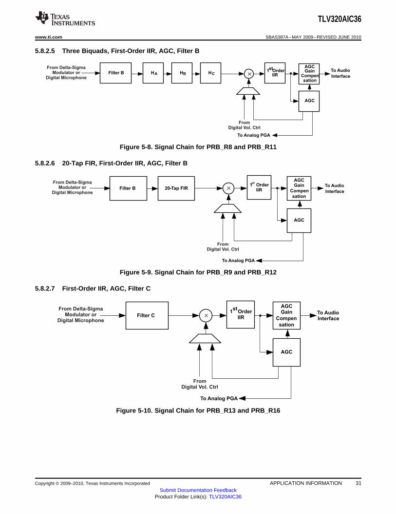
5.8.2.5 Three Biquads, First-Order IIR, AGC, Filter B
Figure 5-8. Signal Chain for PRB_R8 and PRB_R11
5.8.2.6 20-Tap FIR, First-Order IIR, AGC, Filter B
Figure 5-9. Signal Chain for PRB_R9 and PRB_R12
5.8.2.7 First-Order IIR, AGC, Filter C
Figure 5-10. Signal Chain for PRB_R13 and PRB_R16
Copyright © 2009–2010, Texas Instruments Incorporated APPLICATION INFORMATION 31Submit Documentation Feedback
Product Folder Link(s): TLV320AIC36

1st
OrderIIR
AGCGain
Compensation
AGC
Filter C H EH DH CHBH A
From Delta-SigmaModulator or
Digital Microphone
FromDigital Vol. Ctrl
To Analog PGA
To Audio
Interface´
1st
OrderIIR
AGCGain
Compen
sation
AGC
Filter C 25-Tap FIR
From Delta-SigmaModulator or
Digital Microphone
FromDigital Vol. Ctrl
To Analog PGA
To Audio
Interface´
1
1
15
1
10
zD2
zNN)z(H
-
-
-
+=
TLV320AIC36
SBAS387A–MAY 2009–REVISED JUNE 2010 www.ti.com
5.8.2.8 Five Biquads, First-Order IIR, AGC, Filter C
Figure 5-11. Signal Chain for PRB_R14 and PRB_R17
5.8.2.9 25-Tap FIR, First-Order IIR, AGC, Filter C
Figure 5-12. Signal for PRB_R15 and PRB_R18
5.8.3 User Programmable Filters
Depending on the selected processing block, different types and orders of digital filtering are available. Afirst-order IIR filter is always available, and is useful to efficiently filter out possible DC components of thesignal. Up to 5 biquad section or alternatively up to 25-tap FIR filters are available for specific processingblocks. The coefficients of the available filters are arranged as sequentially indexed coefficients in Page 4.
The coefficients of these filters are each 16-bits wide, in twos complement and occupy 2 consecutive 8-bitregisters in the register space. For default values please see the Register Map section.
5.8.3.1 First-Order IIR Section
The transfer function for the first-order IIR Filter is give by:
(2)
The frequency response for the first-order IIR section with default coefficients is flat at a gain of 0 dB.
Table 5-5. ADC First-Order IIR Filter Coefficients
Filter Filter ADC Coefficient Left Channel ADC Coefficient Right ChannelCoefficient
N0 C4 (Pg 4, Reg 8 and 9) C36 (Pg4, Reg 72 and 73)First-Order N1 C5 (Pg 4, Reg 10 and 11) C37 (Pg4, Reg 74 and 75)IIR
D1 C6 (Pg 4, Reg 12 and 13) C38 (Pg4, Reg 76 and 77)
32 APPLICATION INFORMATION Copyright © 2009–2010, Texas Instruments Incorporated
Submit Documentation FeedbackProduct Folder Link(s): TLV320AIC36

2
2
1
1
15
2
2
1
10
zDzD*22
zNzN*2N)z(H
--
--
--
++=
TLV320AIC36
www.ti.com SBAS387A–MAY 2009–REVISED JUNE 2010
5.8.3.2 Biquad Section
The transfer function of each of the biquad filters is given by
(3)
The frequency response for each of the biquad section with default coefficients is flat at a gain of 0 dB.
Table 5-6. ADC Biquad Filter Coefficients
Filter Filter ADC Coefficient Left ADC Coefficient Right ChannelCoefficient Channel
BIQUAD A N0 C7 (Pg 4, Reg 14 and 15) C39 (Pg 4, Reg 78 and 79)
N1 C8 (Pg 4, Reg 16 and 17) C40 (Pg 4, Reg 80 and 81)
N2 C9 (Pg 4, Reg 18 and 19) C41 (Pg 4, Reg 82 and 83)
D1 C10 (Pg 4, Reg 20 and 21) C42 (Pg 4, Reg 84 and 85)
D2 C11 (Pg 4, Reg 22 and 23) C43 (Pg 4, Reg 86 and 87)
BIQUAD B N0 C12 (Pg 4, Reg 24 and 25) C44 (Pg 4, Reg 88 and 89)
N1 C13 (Pg 4, Reg 26 and 27) C45 (Pg 4, Reg 90 and 91)
N2 C14 (Pg 4, Reg 28 and 29) C46 (Pg 4, Reg 92 and 93)
D1 C15 (Pg 4, Reg 30 and 31) C47 (Pg 4, Reg 94 and 95)
D2 C16 (Pg 4, Reg 32 and 33) C48 (Pg 4, Reg 96 and 97)
BIQUAD C N0 C17 (Pg 4, Reg 34 and 35) C49 (Pg 4, Reg 98 and 99)
N1 C18 (Pg 4, Reg 36 and 37) C50 (Pg 4, Reg 100 and 101)
N2 C19 (Pg 4, Reg 38 and 39) C51 (Pg 4, Reg 102 and 103)
D1 C20 (Pg 4, Reg 40 and 41) C52 (Pg 4, Reg 104 and 105)
D2 C21 (Pg 4, Reg 42 and 43) C53 (Pg 4, Reg 106 and 107)
BIQUAD D N0 C22 (Pg 4, Reg 44 and 45) C54 (Pg 4, Reg 108 and 109)
N1 C23 (Pg 4, Reg 46 and 47) C55 (Pg 4, Reg 110 and 111)
N2 C24 (Pg 4, Reg 48 and 49) C56 (Pg 4, Reg 112 and 113)
D1 C25 (Pg 4, Reg 50 and 51) C57 (Pg 4, Reg 114 and 115)
D2 C26 (Pg 4, Reg 52 and 53) C58 (Pg 4, Reg 116 and 117)
BIQUAD E N0 C27 (Pg 4, Reg 54 and 55) C59 (Pg 4, Reg 118 and 119)
N1 C28 (Pg 4, Reg 56 and 57) C60 (Pg 4, Reg 120 and 121)
N2 C29 (Pg 4, Reg 58 and 59) C61 (Pg 4, Reg 122 and 123)
D1 C30 (Pg 4, Reg 60 and 61) C62 (Pg 4, Reg 124 and 125)
D2 C31 (Pg 4, Reg 62 and 63) C63 (Pg 4, Reg 126 and 127)
Copyright © 2009–2010, Texas Instruments Incorporated APPLICATION INFORMATION 33Submit Documentation Feedback
Product Folder Link(s): TLV320AIC36
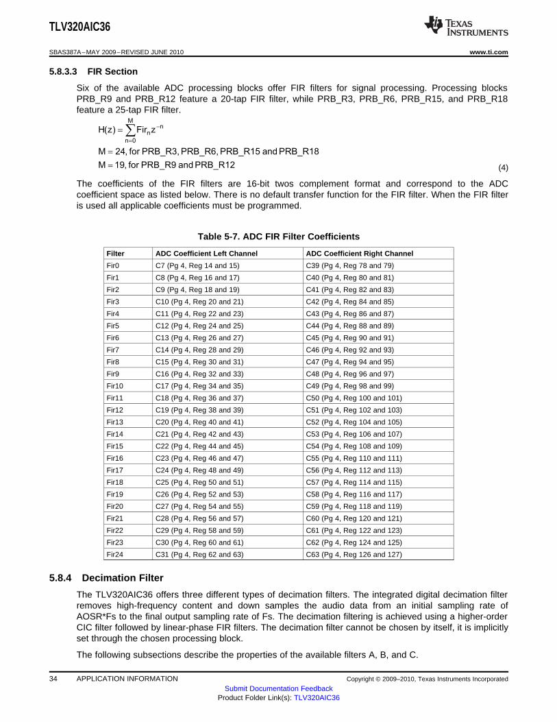
PRB_R12andPRB_R9for,19M
PRB_R18andPRB_R15PRB_R6,PRB_R3,for,24M
zFir)z(H
M
0n
n
n
=
=
= å=
-
TLV320AIC36
SBAS387A–MAY 2009–REVISED JUNE 2010 www.ti.com
5.8.3.3 FIR Section
Six of the available ADC processing blocks offer FIR filters for signal processing. Processing blocksPRB_R9 and PRB_R12 feature a 20-tap FIR filter, while PRB_R3, PRB_R6, PRB_R15, and PRB_R18feature a 25-tap FIR filter.
(4)
The coefficients of the FIR filters are 16-bit twos complement format and correspond to the ADCcoefficient space as listed below. There is no default transfer function for the FIR filter. When the FIR filteris used all applicable coefficients must be programmed.
Table 5-7. ADC FIR Filter Coefficients
Filter ADC Coefficient Left Channel ADC Coefficient Right Channel
Fir0 C7 (Pg 4, Reg 14 and 15) C39 (Pg 4, Reg 78 and 79)
Fir1 C8 (Pg 4, Reg 16 and 17) C40 (Pg 4, Reg 80 and 81)
Fir2 C9 (Pg 4, Reg 18 and 19) C41 (Pg 4, Reg 82 and 83)
Fir3 C10 (Pg 4, Reg 20 and 21) C42 (Pg 4, Reg 84 and 85)
Fir4 C11 (Pg 4, Reg 22 and 23) C43 (Pg 4, Reg 86 and 87)
Fir5 C12 (Pg 4, Reg 24 and 25) C44 (Pg 4, Reg 88 and 89)
Fir6 C13 (Pg 4, Reg 26 and 27) C45 (Pg 4, Reg 90 and 91)
Fir7 C14 (Pg 4, Reg 28 and 29) C46 (Pg 4, Reg 92 and 93)
Fir8 C15 (Pg 4, Reg 30 and 31) C47 (Pg 4, Reg 94 and 95)
Fir9 C16 (Pg 4, Reg 32 and 33) C48 (Pg 4, Reg 96 and 97)
Fir10 C17 (Pg 4, Reg 34 and 35) C49 (Pg 4, Reg 98 and 99)
Fir11 C18 (Pg 4, Reg 36 and 37) C50 (Pg 4, Reg 100 and 101)
Fir12 C19 (Pg 4, Reg 38 and 39) C51 (Pg 4, Reg 102 and 103)
Fir13 C20 (Pg 4, Reg 40 and 41) C52 (Pg 4, Reg 104 and 105)
Fir14 C21 (Pg 4, Reg 42 and 43) C53 (Pg 4, Reg 106 and 107)
Fir15 C22 (Pg 4, Reg 44 and 45) C54 (Pg 4, Reg 108 and 109)
Fir16 C23 (Pg 4, Reg 46 and 47) C55 (Pg 4, Reg 110 and 111)
Fir17 C24 (Pg 4, Reg 48 and 49) C56 (Pg 4, Reg 112 and 113)
Fir18 C25 (Pg 4, Reg 50 and 51) C57 (Pg 4, Reg 114 and 115)
Fir19 C26 (Pg 4, Reg 52 and 53) C58 (Pg 4, Reg 116 and 117)
Fir20 C27 (Pg 4, Reg 54 and 55) C59 (Pg 4, Reg 118 and 119)
Fir21 C28 (Pg 4, Reg 56 and 57) C60 (Pg 4, Reg 120 and 121)
Fir22 C29 (Pg 4, Reg 58 and 59) C61 (Pg 4, Reg 122 and 123)
Fir23 C30 (Pg 4, Reg 60 and 61) C62 (Pg 4, Reg 124 and 125)
Fir24 C31 (Pg 4, Reg 62 and 63) C63 (Pg 4, Reg 126 and 127)
5.8.4 Decimation Filter
The TLV320AIC36 offers three different types of decimation filters. The integrated digital decimation filterremoves high-frequency content and down samples the audio data from an initial sampling rate ofAOSR*Fs to the final output sampling rate of Fs. The decimation filtering is achieved using a higher-orderCIC filter followed by linear-phase FIR filters. The decimation filter cannot be chosen by itself, it is implicitlyset through the chosen processing block.
The following subsections describe the properties of the available filters A, B, and C.
34 APPLICATION INFORMATION Copyright © 2009–2010, Texas Instruments Incorporated
Submit Documentation FeedbackProduct Folder Link(s): TLV320AIC36

0
-10
-20
-30
-40
-50
-60
-70
-80
-90
-100
0 0.2 0.4 0.6 0.8 1 1.2 1.4 1.6 1.8 2
Frequency Normalized w.r.t. FS
Mag
nit
ud
e -
dB
ADC Channel Response for Decimation Filter A
(Red line corresponds to -73 dB)
TLV320AIC36
www.ti.com SBAS387A–MAY 2009–REVISED JUNE 2010
5.8.4.1 Decimation Filter A
This filter is intended for use at sampling rates up to 48 kHz. When configuring this filter, the oversamplingratio of the ADC can either be 128 or 64. For highest performance the oversampling ratio must be set to128.
Filter A can also be used for 96 kHz at an AOSR of 64.
Table 5-8. ADC Decimation Filter A, Specification
Parameter Condition Value (Typical) Units
AOSR = 128
Filter Gain Pass Band 0…0.39 Fs 0.062 dB
Filter Gain Stop Band 0.55…64 Fs –73 dB
Filter Group Delay 17/Fs Sec.
Pass Band Ripple, 8 ksps 0…0.39 Fs 0.062 dB
Pass Band Ripple, 44.1 ksps 0…0.39 Fs 0.05 dB
Pass Band Ripple, 48 ksps 0…0.39 Fs 0.05 dB
AOSR = 64
Filter Gain Pass Band 0…0.39 Fs 0.062 dB
Filter Gain Stop Band 0.55…32 Fs –73 dB
Filter Group Delay 17/Fs Sec.
Pass Band Ripple, 8 ksps 0…0.39 Fs 0.062 dB
Pass Band Ripple, 44.1 ksps 0…0.39 Fs 0.05 dB
Pass Band Ripple, 48 ksps 0…0.39 Fs 0.05 dB
Pass Band Ripple, 96 ksps 0…20 kHz 0.1 dB
Figure 5-13. ADC Decimation Filter A, Frequency Response
Copyright © 2009–2010, Texas Instruments Incorporated APPLICATION INFORMATION 35Submit Documentation Feedback
Product Folder Link(s): TLV320AIC36

0
-10
-20
-30
-40
-50
-60
-70
-80
-90
0 0.2 0.4 0.6 0.8 1 1.2 1.4 1.6 1.8 2
Mag
nit
ud
e -
dB
Frequency Normalized w.r.t. FS
ADC Channel Response for Decimation Filter A
(Red line corresponds to -44 dB)
TLV320AIC36
SBAS387A–MAY 2009–REVISED JUNE 2010 www.ti.com
5.8.4.2 Decimation Filter B
Filter B is intended to support sampling rates up to 96 kHz at a oversampling ratio of 64.
Table 5-9. ADC Decimation Filter B, Specifications
Parameter Condition Value (Typical) Units
AOSR = 64
Filter Gain Pass Band 0…0.39 Fs ±0.077 dB
Filter Gain Stop Band 0.60…32 Fs –46 dB
Filter Group Delay 11/Fs Sec.
Pass Band Ripple, 8 ksps 0…0.39 Fs 0.076 dB
Pass Band Ripple, 44.1 ksps 0…0.39 Fs 0.06 dB
Pass Band Ripple, 48 ksps 0…0.39 Fs 0.06 dB
Pass Band Ripple, 96 ksps 0…20 kHz 0.11 dB
Figure 5-14. ADC Decimation Filter B, Frequency Response
36 APPLICATION INFORMATION Copyright © 2009–2010, Texas Instruments Incorporated
Submit Documentation FeedbackProduct Folder Link(s): TLV320AIC36

0
-20
-40
-60
-80
-100
-120
0 0.2 0.4 0.6 0.8 1 1.2 1.4 1.6 1.8 2
Mag
nit
ud
e -
dB
Frequency Normalized w.r.t. FS
ADC Channel Response for Decimation Filter C
(Red line corresponds to -60 dB)
TLV320AIC36
www.ti.com SBAS387A–MAY 2009–REVISED JUNE 2010
5.8.4.3 Decimation Filter C
Filter C along with AOSR of 32 is specially designed for 192 kSPS operation for the ADC. The pass bandwhich extends up to 0.11*Fs (corresponds to 21 kHz) is suited for audio applications.
Table 5-10. ADC Decimation Filter C, Specifications
Parameter Condition Value (Typical) Units
Filter Gain from 0 to 0.11 Fs 0…0.11 Fs ±0.033 dB
Filter Gain from 0.28 Fs to 16 Fs 0.28 Fs…16 Fs –60 dB
Filter Group Delay 11/Fs Sec.
Pass Band Ripple, 8 ksps 0…0.11 Fs 0.033 dB
Pass Band Ripple, 44.1 ksps 0…0.11 Fs 0.033 dB
Pass Band Ripple, 48 ksps 0…0.11 Fs 0.032 dB
Pass Band Ripple, 96 ksps 0…0.11 Fs 0.032 dB
Pass Band Ripple, 192 ksps 0…20 kHz 0.086 dB
Figure 5-15. ADC Decimation Filter C, Frequency Response
5.8.5 ADC Data Interface
The decimation filter and signal processing block in the ADC channel passes 24-bit data words to theaudio serial interface once every cycle of Fs,ADC. During each cycle of Fs,ADC, a pair of data words (forleft and right channel) are passed. The audio serial interface rounds the data to the required word lengthof the interface before converting to serial data as per the different modes for audio serial interface.
Copyright © 2009–2010, Texas Instruments Incorporated APPLICATION INFORMATION 37Submit Documentation Feedback
Product Folder Link(s): TLV320AIC36

DS LEFT ADC
CIC FILTER
RIGHT ADC
CIC FILTER
miniDSP
Engine
ADC_MOD_CLK
GP
IO1
GP
IO2
DIG
MIC
_C
LK
DS
D_C
LK
DS
D_D
AT
A
DIG_MIC_ING
PIO
1
DIG
MIC
_D
AT
A
DIN
Selected with Page0
Registers 120 - 125
Selected with Page0
Register 81
DS
LEFT RIGHT LEFT RIGHT LEFT RIGHT
ADC_MOD_CLK
DIG_MIC_IN
TLV320AIC36
SBAS387A–MAY 2009–REVISED JUNE 2010 www.ti.com
5.9 ADC Special Functions
5.9.1 Digital Microphone Function
In addition to supporting analog microphones, the TLV320AIC36 also supports interfacing to a digitalmicrophone. The internal ADC_MOD_CLK is available on pins selected with Page 0 Registers 120 – 125as a digital microphone clock. The single-bit output of the external digital microphone can be connected tothe GPIO1, DIGMIC_DATA, or the DIN pins as selected with Page 0 Register 81 as shown in Figure 5-16
Figure 5-16. Digital Microphone in TLV320AIC36
Internally, the TLV320AIC36 samples the digital microphone left channel data using the rising edge of themicrophone clock and the right channel data using the falling edge of the clock as shown in Figure 5-17.
Figure 5-17. Timing Diagram for Digital Microphone Interface
The digital-microphone mode can be selectively enabled for only-left, only-right, or stereo channels. Whenthe digital microphone mode is enabled, the analog section of the ADC can be powered down andbypassed for power efficiency. The AOSR value for the ADC channel must be configured to select thedesired decimation ratio to be achieved based on the external digital microphone properties.
5.9.2 Channel-to-Channel Phase Adjustment
The TLV320AIC36 has a built-in feature to fine-adjust the phase between the stereo ADC record signals.The phase compensation is particularly helpful to adjust delays when using dual microphones for noisecancellation.
This delay can be controlled in fine amounts in the following fashion.
Delay(7:0) = Page 0/Register 85/D(7:0)
Where:
38 APPLICATION INFORMATION Copyright © 2009–2010, Texas Instruments Incorporated
Submit Documentation FeedbackProduct Folder Link(s): TLV320AIC36
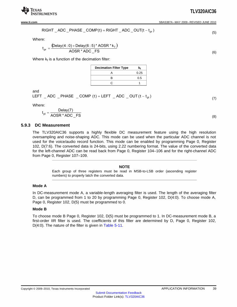
)tt(OUT_ADC_RIGHT)t(COMP_PHASE_ADC_RIGHT pr-=
( )
FS_ADC*AOSR
k*AOSR*)5:6(Delay)0:4(Delayt
f
pr
+=
)tt(OUT_ADC_LEFT)t(COMP_PHASE_ADC_LEFT pl-=
FS_ADC*AOSR
)7(Delaytpl =
TLV320AIC36
www.ti.com SBAS387A–MAY 2009–REVISED JUNE 2010
(5)
Where:
(6)
Where kf is a function of the decimation filter:
Decimation Filter Type kf
A 0.25
B 0.5
C 1
and
(7)
Where:
(8)
5.9.3 DC Measurement
The TLV320AIC36 supports a highly flexible DC measurement feature using the high resolutionoversampling and noise-shaping ADC. This mode can be used when the particular ADC channel is notused for the voice/audio record function. This mode can be enabled by programming Page 0, Register102, D(7:6). The converted data is 24-bits, using 2.22 numbering format. The value of the converted datafor the left-channel ADC can be read back from Page 0, Register 104–106 and for the right-channel ADCfrom Page 0, Register 107–109.
NOTEEach group of three registers must be read in MSB-to-LSB order (ascending registernumbers) to properly latch the converted data.
Mode A
In DC-measurement mode A, a variable-length averaging filter is used. The length of the averaging filterD, can be programmed from 1 to 20 by programming Page 0, Register 102, D(4:0). To choose mode A,Page 0, Register 102, D(5) must be programmed to 0.
Mode B
To choose mode B Page 0, Register 102, D(5) must be programmed to 1. In DC-measurement mode B, afirst-order IIR filter is used. The coefficients of this filter are determined by D, Page 0, Register 102,D(4:0). The nature of the filter is given in Table 5-11.
Copyright © 2009–2010, Texas Instruments Incorporated APPLICATION INFORMATION 39Submit Documentation Feedback
Product Folder Link(s): TLV320AIC36

TLV320AIC36
SBAS387A–MAY 2009–REVISED JUNE 2010 www.ti.com
Table 5-11. DC Measurement Bandwidth Settings
D:Page 0, Reg 102 , D(4:0) –3 dB BW (kHz) –0.5 dB BW (kHz)
1 688.44 236.5
2 275.97 96.334
3 127.4 44.579
4 61.505 21.532
5 30.248 10.59
6 15.004 5.253
7 7.472 2.616
8 3.729 1.305
9 1.862 652
10 931 326
11 465 163
12 232.6 81.5
13 116.3 40.7
14 58.1 20.3
15 29.1 10.2
16 14.54 5.09
17 7.25 2.54
18 3.63 1.27
19 1.8 0.635
20 0.908 0.3165
By programming Page 0, Reg 103, D(5) to 1, the averaging filter is periodically reset after 2^R number ofADC_MOD_CLK, where R is programmed in Page 0, Reg 103, D(4:0). When Page 0, Reg 103, D(5) is setto 1, the value of D should be less than the value of R. When Page 0, Reg 103, D(5) is programmed as 0the averaging filter is never reset.
40 APPLICATION INFORMATION Copyright © 2009–2010, Texas Instruments Incorporated
Submit Documentation FeedbackProduct Folder Link(s): TLV320AIC36

TLV320AIC36
www.ti.com SBAS387A–MAY 2009–REVISED JUNE 2010
5.10 ADC Setup
The following discussion is intended to guide a system designer through the steps necessary to configurethe TLV320AIC36 ADC.
Step 1
The system clock source (master clock) and the targeted ADC sampling frequency must be identified.
Depending on the targeted performance, the decimation filter type (A, B, or C) and OSR value can bedetermined.• Filter A with AOSR of 128 or 64 should be used for 48-kHz (or below) high-performance operation. An
AOSR of 64 can be also used for 96-kHz operation• Filter B with AOSR of 64 should be used for 96-kHz operations.• Filter C with AOSR of 32 should be used for 192-kHz operations
Based on the identified filter type and the required signal processing capabilities the appropriateprocessing block can be determined from the list of available processing blocks (PRB_R1 to PRB_R18)(see Table 5-4).
Based on the available master clock, the chosen OSR and the targeted sampling rate, the clock dividervalues NADC and MADC can be determined. If necessary the internal PLL will add a large degree offlexibility.
In summary, Codec_Clkin which is either derived directly from the system clock source or from the internalPLL, divided by MADC, NADC and AOSR, must be equal to the ADC sampling rate ADC_FS. TheClodec_Clkin clock signal is shared with the DAC clock generation block.
CODEC_CLKIN = NADC*MADC*AOSR*ADC_FS
To a large degree NADC and MADC can be chosen independently in the range of 1 to 128. In generalNADC should be as large as possible as long as the following condition can still be met:
MADC*AOSR/32 ≥ RC
RC is a function of the chosen processing block and is listed in the Table 5-4.
At this point the following device specific parameters are known:
PRB_Rx, AOSR, NADC, MADC, common mode setting
Additionally if the PLL is used the PLL parameters P, J, D, and R are determined as well.
Copyright © 2009–2010, Texas Instruments Incorporated APPLICATION INFORMATION 41Submit Documentation Feedback
Product Folder Link(s): TLV320AIC36

TLV320AIC36
SBAS387A–MAY 2009–REVISED JUNE 2010 www.ti.com
Step 2
Setting up the device through register programming:
The following list gives a sequence of items that must be executed between powering the device up andreading data from the device:
Define starting point: Initiate SW Reset
Program PMU Settings: Turn on charge pumpTurn on ADC and DAC LDO with current limit
Program clock setting:s Program PLL clock dividers P, J,D, R (if PLL is necessary)Power up PLL (if PLL is necessary)Program and power up NADCProgram and power up MADCProgram OSR valueProgram the processing block to be used
Program Codec Set word length, BCLK, WCLK I/O, mode type, for example I2S/DSPInterface:
Program Analog Blocks Program common mode voltagePower up ADCProgram common mode startup sequenceRoute inputs/common mode to ADCUnmute PGA and set gainsRelease LDO current limitUnmute digital volume control
See Section 5.20 for a detailed application example.
5.11 DAC
The TLV320AIC36 includes a stereo audio DAC supporting data rates from 8 to 192kHz. Each channel ofthe stereo audio DAC consists of a signal-processing engine with fixed processing blocks, aprogrammable miniDSP, a digital interpolation filter, multi-bit digital delta-sigma modulator, and an analogreconstruction filter. The DAC is designed to provide enhanced performance at low sampling rates throughincreased oversampling and image filtering, thereby keeping quantization noise generated within thedelta-sigma modulator and signal images strongly suppressed within the audio band to beyond 20kHz. Tohandle multiple input rates and optimize power dissipation and performance, the TLV320AIC36 allows thesystem designer to program the oversampling rates over a wide range from 1 to 1024 by configuring thePage 0, Reg 13, and Reg 14. The system designer can choose higher oversampling ratios for lower inputdata rates and lower oversampling ratios for higher input data rates.
The TLV320AIC36 DAC channel includes a built-in digital interpolation filter to generate oversampled datafor the sigma delta modulator. The interpolation filter can be chosen from three different types dependingon required frequency response, group delay and sampling rate.
42 APPLICATION INFORMATION Copyright © 2009–2010, Texas Instruments Incorporated
Submit Documentation FeedbackProduct Folder Link(s): TLV320AIC36

TLV320AIC36
www.ti.com SBAS387A–MAY 2009–REVISED JUNE 2010
5.11.1 Processing Blocks
The TLV320AIC36 implements signal processing capabilities and interpolation filtering using processingblocks. These fixed processing blocks give users the choice of how much and what type of signalprocessing they may use and which interpolation filter is applied.
The choice between these processing blocks is part of a strategy balancing power conservation and signalprocessing flexibility. Less signal processing capability will result in less power consumed by the device.The Table 5-12 gives an overview over all available processing blocks of the DAC channel and theirproperties. The Resource Class (RC) column gives an approximate indication of power consumption.Page 0, Register 60 is used to select one of the 25 processing blocks.
The signal processing blocks available are:• First-order IIR• Scalable number of biquad filters• 3D – Effect• Beep Generator
The processing blocks are tuned for common cases and can achieve high image rejection or low groupdelay in combination with various signal processing effects such as audio effects and frequency shaping.The available first-order IIR and biquad filters have fully user-programmable coefficients.
Table 5-12. Overview – DAC Predefined Processing Blocks
NumberProcessing Interpolation First-Order BeepChannel of DRC 3D RC ClassBlock No. Filter IIR Available GeneratorBiquads
PRB_P1 A Stereo No 3 No No No 8
PRB_P2 A Stereo Yes 6 Yes No No 12
PRB_P3 A Stereo Yes 6 No No No 10
PRB_P4 A Left No 3 No No No 4
PRB_P5 A Left Yes 6 Yes No No 6
PRB_P6 A Left Yes 6 No No No 6
PRB_P7 B Stereo Yes 0 No No No 6
PRB_P8 B Stereo No 4 Yes No No 8
PRB_P9 B Stereo No 4 No No No 8
PRB_P10 B Stereo Yes 6 Yes No No 10
PRB_P11 B Stereo Yes 6 No No No 8
PRB_P12 B Left Yes 0 No No No 3
PRB_P13 B Left No 4 Yes No No 4
PRB_P14 B Left No 4 No No No 4
PRB_P15 B Left Yes 6 Yes No No 6
PRB_P16 B Left Yes 6 No No No 4
PRB_P17 C Stereo Yes 0 No No No 3
PRB_P18 C Stereo Yes 4 Yes No No 6
PRB_P19 C Stereo Yes 4 No No No 4
PRB_P20 C Left Yes 0 No No No 2
PRB_P21 C Left Yes 4 Yes No No 3
PRB_P22 C Left Yes 4 No No No 2
PRB_P23 A Stereo No 2 No Yes No 8
PRB_P24 A Stereo Yes 5 Yes Yes No 12
PRB_P25 A Stereo Yes 5 Yes Yes Yes 12
Copyright © 2009–2010, Texas Instruments Incorporated APPLICATION INFORMATION 43Submit Documentation Feedback
Product Folder Link(s): TLV320AIC36

Interp.
Filter A
BiQuad
C
BiQuad
B
BiQuad
Ato
Modulator
Digital
Volume
Ctrl
from
Interface
´
Interp.
Filter
A,B
DRCHPF
BiQuad
F
BiQuad
E
BiQuad
D
BiQuad
C
BiQuad
B
BiQuad
AIIR to
Modulator
Digital
Volume
Ctrl
from
Interface
´
Interp.
Filter
A,B
BiQuad
F
BiQuad
E
BiQuad
D
BiQuad
C
BiQuad
B
BiQuad
AIIR to
Modulator
Digital
Volume
Ctrl
from
Interface
´
Interp.
Filter
B,C
IIR to
Modulator
Digital
Volume
Ctrl
from
Interface
´
Interp.
Filter B
DRCHPF
to
Modulator
Digital
Volume
Ctrl
BiQuad
D
BiQuad
C
BiQuad
B
BiQuad
Afrom
Interface
´
TLV320AIC36
SBAS387A–MAY 2009–REVISED JUNE 2010 www.ti.com
5.11.2 Processing Blocks – Details
5.11.2.1 Three Biquads, Filter A
Figure 5-18. Signal Chain for PRB_P1 and PRB_P4
5.11.2.2 Six Biquads, First-Order IIR, DRC, Filter A or B
Figure 5-19. Signal Chain for PRB_P2, PRB_P5, PRB_P10, and PRB_P15
5.11.2.3 Six Biquads, First-Order IIR, Filter A or B
Figure 5-20. Signal Chain for PRB_P3, PRB_P6, PRB_P11, and PRB_P16
5.11.2.4 IIR, Filter B or C
Figure 5-21. Signal Chain for PRB_P7, PRB_P12, PRB_P17, and PRB_P20
5.11.2.5 Four Biquads, DRC, Filter B
Figure 5-22. Signal Chain for PRB_P8 and PRB_P13
44 APPLICATION INFORMATION Copyright © 2009–2010, Texas Instruments Incorporated
Submit Documentation FeedbackProduct Folder Link(s): TLV320AIC36

Interp.
Filter B
BiQuad
D
BiQuad
C
BiQuad
B
BiQuad
Ato
Modulator
Digital
Volume
Ctrl
from
Interface
´
Interp.
Filter C
DRCHPF
IIR to
Modulator
Digital
Volume
Ctrl
BiQuad
D
BiQuad
C
BiQuad
B
BiQuad
A
from
Interface
´
Interp.
Filter C
BiQuad
D
BiQuad
C
BiQuad
B
BiQuad
AIIR to
modulator
Digital
Volume
Ctrl
from
Interface
´
BiQuad
AL
Interp.
Filter*
BiQuad
AR
3D
PGA
+
+
BiQuad
CR
BiQuad
BR
+
+
-
+
-
+
+
from
left
channel
interface
to
modulator
Digital
Volume
Ctrl
from
right
channel
interface
BiQuad
BL
BiQuad
CL
Interp.
Filter* to
modulator
Digital
Volume
Ctrl
TLV320AIC36
www.ti.com SBAS387A–MAY 2009–REVISED JUNE 2010
5.11.2.6 Four Biquads, Filter B
Figure 5-23. Signal Chain for PRB_P9 and PRB_P14
5.11.2.7 Four Biquads, First-Order IIR, DRC, Filter B
Figure 5-24. Signal Chain for PRB_P18 and PRB_P21
5.11.2.8 Four Biquads, First-Order IIR, Filter C
Figure 5-25. Signal Chain for PRB_P19 and PRB_P22
5.11.2.9 Two Biquads, 3D, Filter A
Figure 5-26. Signal Chain for PRB_P23
Copyright © 2009–2010, Texas Instruments Incorporated APPLICATION INFORMATION 45Submit Documentation Feedback
Product Folder Link(s): TLV320AIC36

BiQuad
AL
Interp.
Filter A
DRCHPF
BiQuad
FL
BiQuad
EL
BiQuad
AR
IIR
Left
3D
PGA
+
+
Interp.
Filter A
DRCHPF
BiQuad
FR
BiQuad
ER
BiQuad
DR
BiQuad
CR
BiQuad
BR
IIR
Right+
+
-
+
-
+
+
from
Left
Channel
Interface
to
Modulator
to
Modulator
Digital
Volume
Ctrl
Digital
Volume
Ctrl
from
Right
Channel
Interface
BiQuad
BL
BiQuad
CL
BiQuad
DL´
´
DRCHPF
3D
PGA
+
+
DRCHPF
+
+
–
+
–
+
+
From
Left-
Channel
Interface
To
Modulator
Digital
Volume
Ctrl
Biquad
BL
´Biquad
CL
Biquad
DL
Biquad
AL
Biquad
EL
Biquad
FL
Interp.
Filter A
Interp.
Filter A
Biquad
AR
From
Right-
Channel
Interface
Biquad
BR
Biquad
CR
Biquad
DR
Biquad
ER
Biquad
FR
To
Modulator
Digital
Volume
Ctrl
´
+
+
Beep
Gen.
Beep Volume Ctrl
Beep Volume Ctrl
´
´
IIR
Left
IIR
Right
TLV320AIC36
SBAS387A–MAY 2009–REVISED JUNE 2010 www.ti.com
5.11.2.10 5 Biquads, DRC, 3D, Filter A
Figure 5-27. Signal Chain for PRB_P24
5.11.2.11 Five Biquads, DRC, 3D, Beep Generator, Filter A
Figure 5-28. Signal Chain for PRB_P25
46 APPLICATION INFORMATION Copyright © 2009–2010, Texas Instruments Incorporated
Submit Documentation FeedbackProduct Folder Link(s): TLV320AIC36

1
1
15
1
10
zD2
zNN)z(H
-
-
-
+=
2
2
1
1
15
2
2
1
10
zDzD*22
zNzN*2N)z(H
--
--
--
++=
TLV320AIC36
www.ti.com SBAS387A–MAY 2009–REVISED JUNE 2010
5.11.3 User Programmable Filters
Depending on the selected processing block, different types and orders of digital filtering are available. Upto six biquad sections are available for specific processing blocks.
The coefficients of the available filters are arranged as sequentially-indexed coefficients in two banks. Ifadaptive filtering is chosen, the coefficient banks can be switched on-the-fly. For more details on adaptivefiltering please see Section 5.14.3.
The coefficients of these filters are each 16 bits wide, in twos complement, and occupy two consecutive8-bit registers in the register space. For default values please see the Register Map section.
5.11.3.1 First-Order IIR Section
The IIR is of first-order and its transfer function is given by
(9)
The frequency response for the first-order IIR Section with default coefficients is flat
Table 5-13. DAC IIR Filter Coefficients
Filter Filter Coefficient ADC Coefficient Left Channel ADC Coefficient RightChannel
N0 C65 (Pg 9, Reg 2 and 3) C68 (Pg 9, Reg 8 and 9)
First-order IIR N1 C66 (Pg 9, Reg 4 and 5) C69 (Pg 9, Reg 10 and 11)
D1 C67 (Pg 9, Reg 6 and 7) C70 (Pg 9, Reg 12 and 13)
5.11.3.2 Biquad Section
The transfer function of each biquad filters is given by:
(10)
Table 5-14. DAC Biquad Filter Coefficients
Filter Coefficient Left DAC Channel Right DAC Channel
BIQUAD A N0 C1 (Pg 8, Reg 2 and 3) C33 (Pg 8, Reg 66 and 67)
N1 C2 (Pg 8, Reg 4 and 5) C34 (Pg 8, Reg 68 and 69)
N2 C3 (Pg 8, Reg 6 and 7) C35 (Pg 8, Reg 70 and 71)
D1 C4 (Pg 8, Reg 8 and 9) C36 (Pg 8, Reg 72 and 73)
D2 C5 (Pg 8, Reg 10 and 11) C37 (Pg 8, Reg 74 and 75)
BIQUAD B N0 C6 (Pg 8, Reg 12 and 13) C38 (Pg 8, Reg 76 and 77)
N1 C7 (Pg 8, Reg 14 and 15) C39 (Pg 8, Reg 78 and 79)
N2 C8 (Pg 8, Reg 16 and 172) C40 (Pg 8, Reg 80 and 81)
D1 C9 (Pg 8, Reg 18 and 19) C41 (Pg 8, Reg 82 and 83)
D2 C10 (Pg 8, Reg 20 and 21) C42 (Pg 8, Reg 84 and 85)
BIQUAD C N0 C11 (Pg 8, Reg 22 and 23) C43 (Pg 8, Reg 86 and 87)
N1 C12 (Pg 8, Reg 24 and 25) C44 (Pg 8, Reg 88 and 89)
N2 C13 (Pg 8, Reg 26 and 27) C45 (Pg 8, Reg 90 and 91)
D1 C14 (Pg 8, Reg 28 and 29) C46 (Pg 8, Reg 92 and 93)
D2 C15 (Pg 8, Reg 30 and 31) C47 (Pg 8, Reg 94 and 95)
BIQUAD D N0 C16 (Pg 8, Reg 32 and 33) C48 (Pg 8, Reg 96 and 97)
N1 C17 (Pg 8, Reg 34 and 35) C49 (Pg 8, Reg 98 and 99)
Copyright © 2009–2010, Texas Instruments Incorporated APPLICATION INFORMATION 47Submit Documentation Feedback
Product Folder Link(s): TLV320AIC36
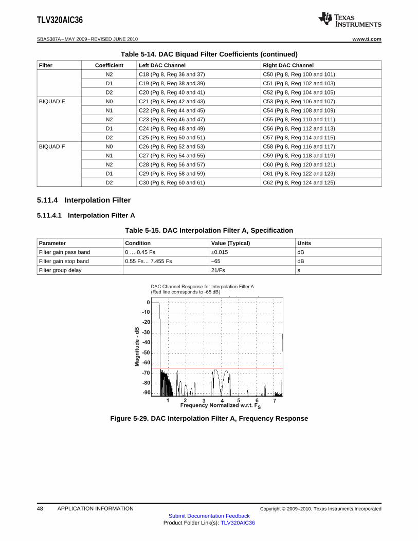
0
-10
-20
-30
-40
-50
-60
-70
-80
-90
1 3 4 5 6 72
Mag
nit
ud
e -
dB
Frequency Normalized w.r.t. FS
DAC Channel Response for Interpolation Filter A
(Red line corresponds to -65 dB)
TLV320AIC36
SBAS387A–MAY 2009–REVISED JUNE 2010 www.ti.com
Table 5-14. DAC Biquad Filter Coefficients (continued)
Filter Coefficient Left DAC Channel Right DAC Channel
N2 C18 (Pg 8, Reg 36 and 37) C50 (Pg 8, Reg 100 and 101)
D1 C19 (Pg 8, Reg 38 and 39) C51 (Pg 8, Reg 102 and 103)
D2 C20 (Pg 8, Reg 40 and 41) C52 (Pg 8, Reg 104 and 105)
BIQUAD E N0 C21 (Pg 8, Reg 42 and 43) C53 (Pg 8, Reg 106 and 107)
N1 C22 (Pg 8, Reg 44 and 45) C54 (Pg 8, Reg 108 and 109)
N2 C23 (Pg 8, Reg 46 and 47) C55 (Pg 8, Reg 110 and 111)
D1 C24 (Pg 8, Reg 48 and 49) C56 (Pg 8, Reg 112 and 113)
D2 C25 (Pg 8, Reg 50 and 51) C57 (Pg 8, Reg 114 and 115)
BIQUAD F N0 C26 (Pg 8, Reg 52 and 53) C58 (Pg 8, Reg 116 and 117)
N1 C27 (Pg 8, Reg 54 and 55) C59 (Pg 8, Reg 118 and 119)
N2 C28 (Pg 8, Reg 56 and 57) C60 (Pg 8, Reg 120 and 121)
D1 C29 (Pg 8, Reg 58 and 59) C61 (Pg 8, Reg 122 and 123)
D2 C30 (Pg 8, Reg 60 and 61) C62 (Pg 8, Reg 124 and 125)
5.11.4 Interpolation Filter
5.11.4.1 Interpolation Filter A
Table 5-15. DAC Interpolation Filter A, Specification
Parameter Condition Value (Typical) Units
Filter gain pass band 0 … 0.45 Fs ±0.015 dB
Filter gain stop band 0.55 Fs… 7.455 Fs –65 dB
Filter group delay 21/Fs s
Figure 5-29. DAC Interpolation Filter A, Frequency Response
48 APPLICATION INFORMATION Copyright © 2009–2010, Texas Instruments Incorporated
Submit Documentation FeedbackProduct Folder Link(s): TLV320AIC36
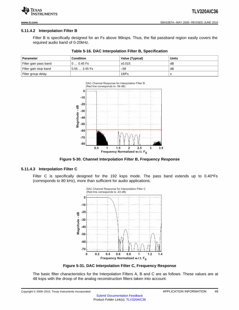
0
-10
-20
-30
-40
-50
-60
-70
-80
Mag
nit
ud
e -
dB
DAC Channel Response for Interpolation Filter B
(Red line corresponds to -58 dB)
0.5 1 1.5 2 2.5 3 3.5Frequency Normalized w.r.t. FS
0
-10
-20
-30
-40
-50
-60
-70
Mag
nit
ud
e -
dB
0 0.2 0.4 0.6 0.8 1 1.2 1.4
Frequency Normalized w.r.t. FS
DAC Channel Response for Interpolation Filter C
(Red line corresponds to -43 dB)
TLV320AIC36
www.ti.com SBAS387A–MAY 2009–REVISED JUNE 2010
5.11.4.2 Interpolation Filter B
Filter B is specifically designed for an Fs above 96ksps. Thus, the flat passband region easily covers therequired audio band of 0-20kHz.
Table 5-16. DAC Interpolation Filter B, Specification
Parameter Condition Value (Typical) Units
Filter gain pass band 0 … 0.45 Fs ±0.015 dB
Filter gain stop band 0.55 … 3.45 Fs –58 dB
Filter group delay 18/Fs s
Figure 5-30. Channel Interpolation Filter B, Frequency Response
5.11.4.3 Interpolation Filter C
Filter C is specifically designed for the 192 ksps mode. The pass band extends up to 0.40*Fs(corresponds to 80 kHz), more than sufficient for audio applications.
Figure 5-31. DAC Interpolation Filter C, Frequency Response
The basic filter characteristics for the Interpolation Filters A, B and C are as follows. These values are at48 ksps with the droop of the analog reconstruction filters taken into account.
Copyright © 2009–2010, Texas Instruments Incorporated APPLICATION INFORMATION 49Submit Documentation Feedback
Product Folder Link(s): TLV320AIC36
TLV320AIC36
SBAS387A–MAY 2009–REVISED JUNE 2010 www.ti.com
Table 5-17. DAC Interpolation Filter C, Specification
Parameter Condition Value (Typical) Units
Filter gain pass band 0 … 0.35 Fs ±0.03 dB
Filter gain stop band 0.60 … 1.4 Fs –43 dB
Filter group delay 13/Fs s
5.12 DAC Output Drivers
5.12.1 Analog Fully Differential Line Output Drivers
The TLV320AIC36 has two fully differential line output drivers, each capable of driving a 10kΩ differentialload. Each driver can connect to the left or the right DAC, the left or the right ADC PGA output, the left orright line input, or any combination of the six. The design includes extensive capability to adjust signallevels independently before any mixing occurs, beyond that already provided by the PGA gain and theDAC digital volume control. Note that since both left and right channel signals are routed to all outputdrivers, a mono mix of any of the stereo signals can easily be obtained by setting the volume controls ofboth left and right channel signals to –6 dB and mixing them. Undesired signals can also be disconnectedfrom the mix as well through register control.
The TLV320AIC36 includes an output level control on each output driver with limited gain adjustment from0 dB to +9 dB. The output driver circuitry in this device are designed to provide a low distortion outputwhile playing full-scale stereo DAC signals at a 0 dB gain setting. However, a higher amplitude output canbe obtained at the cost of increased signal distortion at the output. This output level control allows the userto make this tradeoff based on the requirements of the end equipment. Note that this output level controlis not intended to be used as a standard output volume control. It is expected to be used only sparingly forlevel setting, that is, adjustment of the full-scale output range of the device.
Each differential line output driver can be powered down independently of the others when it is not neededin the system. When placed into powerdown through register programming, the driver output pins will beplaced into a high-Z, high-impedance state.
The signal routing for the line level drivers is configured using Page 2, Registers 80 through 93
5.12.2 Analog High-Power Output Drivers
The TLV320AIC36 includes four single-ended high power output drivers arranged as two stereo pairs.These output drivers are capable of driving 0.89 Vrms each into a 16-Ω load if one pair is enabled or 0.5Vrms each into 16-Ω if both pairs are enabled. The volume control and mixing blocks for the high-poweroutput drivers are effectively identical to those of the line-level drivers. Note that each of these drivershave a output level control block like those included with the line output drivers, allowing gain adjustmentup to +9 dB on the output signal. As in the previous case, this output level adjustment is not intended tobe used as a standard volume control, but instead is included for additional full-scale output signal levelcontrol. In order to drive 0.89 Vrms for a full-scale DAC output into the load, the output level adjustmentmust be set to +2 dB.
The high power output drivers include additional circuitry to avoid artifacts on the audio output duringpower-on and power-off transient conditions. The power-up delay time for the high power output drivers isprogrammable over a wide range of time delays, from instantaneous up to 4-sec, using Page-2/Reg-42.
When these output drivers are powered down, they can be placed into a variety of output conditions basedon register programming. If lowest power operation is desired, then the outputs can be placed into atri-state condition, and all power to the output stage is removed. However, this generally results in theoutput nodes drifting to rest near the upper or lower analog supply, due to small leakage currents at thepins. This then results in a longer delay requirement to avoid output artifacts during driver power-on. Inorder to reduce this required power-on delay, the TLV320AIC36 includes an option for the output pins ofthe drivers to be weakly driven to the AGND level they would normally rest at when powered with nosignal applied.
50 APPLICATION INFORMATION Copyright © 2009–2010, Texas Instruments Incorporated
Submit Documentation FeedbackProduct Folder Link(s): TLV320AIC36
TLV320AIC36
www.ti.com SBAS387A–MAY 2009–REVISED JUNE 2010
The high power output drivers can also be programmed to power up first with the output level control in ahighly attenuated state, and then the output driver will automatically slowly reduce the output attenuationto reach the desired output level setting programmed.
The signal routing for the high power drivers is configured using Page 2, Registers 45 through 72.
5.12.3 Short-Circuit Output Protection
The TLV320AIC36 includes programmable short-circuit protection for the high power output drivers, formaximum flexibility in a given application. By default, if these output drivers are shorted, they willautomatically limit the maximum amount of current that can be sourced to or sunk from a load, therebyprotecting the device from an over-current condition. In this mode, the user can read Page-0/Reg-95 todetermine whether the part is in short-circuit protection or not, and then decide whether to program thedevice to power down the output drivers. However, the device includes further capability to automaticallypower down an output driver whenever it does into short-circuit protection, without requiring interventionfrom the user. In this case, the output driver will stay in a power down condition until the user specificallyprograms it to power down and then power back up again, to clear the short-circuit flag.
5.13 DAC Gain Setting
5.13.1 Digital Volume Control
The TLV320AIC36 signal processing blocks incorporate a digital volume control block that can control thevolume of the playback signal from +24 dB to –63.5 dB in steps of 0.5 dB. These can be controlled bywriting to Page 0, Register 65 and 66. The volume control of left and right channels by default can becontrolled independently, however by programming Page 0, Reg 64, D(1:0), they can be madeinterdependent. The volume changes are soft-stepped in steps of 0.5 dB to avoid audible artifacts duringgain change. The rate of soft-stepping can be controlled by programming Page 0, Reg 63, D(1:0) to eitherone step per frame (DAC_FS) or one step per 2 frames. The soft-stepping feature can also be entirelydisabled. During soft-stepping the value of the actual applied gain would differ from the programmed gainin register. The TLV320AIC36 gives a feedback to the user in form of register readable flag to indicate thatsoft-stepping is currently in progress. The flags for left and right channels can be read back by readingPage 0, Reg 37, D(2) and D(1) respectively. A value of 0 in these flags indicates a soft-stepping operationin progress, and a value of 1 indicates that soft-stepping has completed. A soft-stepping operation comesinto effect during a) power-up, when the volume control soft-steps from –63.5 dB to programmed gainvalue b) volume change by user when DAC is powered up and c) power-down, when the volume controlblock soft-steps to –63.5 dB before powering down the channel.
5.13.2 Dynamic Range Compression
Typical music signals are characterized by crest factors, the ratio of peak signal power to average signalpower, of 12 dB or more. In order to avoid audible distortions due to clipping of peak signals, the gain ofthe DAC channel must be adjusted so as not to cause hard clipping of peak signals. As a result, duringnominal periods, the applied gain is low, causing the perception that the signal is not loud enough. Toovercome this problem, the DRC in the TLV320AIC36 continuously monitors the output of the DAC DigitalVolume control to detect its power level with respect to 0 dB FS. When the power level is low, it increasesthe input signal gain to make it sound louder. At the same time, if a peaking signal is detected, itautonomously reduces the applied gain to avoid hard clipping. This results in sounds more pleasing to theear as well as sounding louder during nominal periods.
The DRC functionality in the TLV320AIC36 is implemented by a combination of Processing Blocks in theDAC channel as described in Section 5.11.2.
The DRC can be disabled by writing into Page 0, Reg 68, D(6:5).
Copyright © 2009–2010, Texas Instruments Incorporated APPLICATION INFORMATION 51Submit Documentation Feedback
Product Folder Link(s): TLV320AIC36

1
1
15
1
10
HPF
zD2
zNN)z(H
-
-
-
+=
1
1
15
1
10
LPF
zD2
zNN)z(H
-
-
-
+=
TLV320AIC36
SBAS387A–MAY 2009–REVISED JUNE 2010 www.ti.com
The DRC typically works on the filtered version of the input signal. The input signals have no audioinformation at DC and extremely low frequencies; however they can significantly influence the energyestimation function in DRC. Also most of the information about signal energy is concentrated in the lowfrequency region of the input signal.
To estimate the energy of the input signal, the signal is first fed the DRC high-pass filter, and then fed tothe DRC low-pass filter. These filters are implemented as first-order IIR filters given by
(11)
(12)
The coefficients for these filters are 16 bits wide in twos complement and are user programmable throughregister write as given in Table 5-18
Table 5-18. DRC HPF and LPF Coefficients
Coefficient Location
HPF N0 C71 Page 9, Register 14 and 15
HPF N1 C72 Page 9, Register 16 and 17
HPF D1 C73 Page 9, Register 18 and 19
LPF N0 C74 Page 9, Register 20 and 21
LPF N1 C75 Page 9, Register 22 and 23
LPF D1 C76 Page 9, Register 24 and 25
The default values of these coefficients implement a high-pass filter with a cut-off at 0.00166*DAC_FS,and a low-pass filter with a cutoff at 0.00033 * DAC_FS.
The output of the DRC high-pass filter is fed to the Processing Block selected for the DAC Channel. Theabsolute value of the DRC-LPF filter is used for energy estimation within the DRC.
The gain in the DAC Digital Volume Control is controlled by Page 0, Register 65 and 66. When the DRC isenabled, the applied gain is a function of the Digital Volume Control register setting and the output of theDRC.
The DRC parameters are described in sections that follow.
5.13.2.1 DRC Threshold
The DRC Threshold represents the level of the DAC playback signal at which the gain compressionbecomes active. The output of the digital volume control in the DAC is compared with the set threshold.The threshold value is programmable by writing to register Page 0, Register 68, D(4:2). The Thresholdvalue can be adjusted between –3 dBFS to –24 dBFS in steps of 3 dB. Keeping the DRC Threshold valuetoo high may not leave enough time for the DRC block to detect peaking signals, and can causeexcessive distortion at the outputs. Keeping the DRC Threshold value too low can limit the perceivedloudness of the output signal.
The recommended DRC-Threshold value is –24 dB.
When the output signal exceeds the set DRC Threshold, the interrupt flag bits at Page 0, Register 44,D(3:2) are updated. These flag bits are 'sticky' in nature, and are reset only after they are read back by theuser. The nonsticky versions of the interrupt flags are also available at Page 0, Register 46, D(3:2).
5.13.2.2 DRC Hysteresis
DRC Hysteresis is programmable by writing to Page 0, Register 68, D(1:0). It can be programmed tovalues between 0 dB and 3 dB in steps of 1 dB. It is a programmable window around the programmedDRC Threshold that must be exceeded for a disabled DRC to become enabled, or an enabled DRC to
52 APPLICATION INFORMATION Copyright © 2009–2010, Texas Instruments Incorporated
Submit Documentation FeedbackProduct Folder Link(s): TLV320AIC36

TLV320AIC36
www.ti.com SBAS387A–MAY 2009–REVISED JUNE 2010
become disabled. For example, if the DRC Threshold is set to –12 dBFS and DRC Hysteresis is set to 3dB, then if the gain compressions in the DRC is inactive, the output of the DAC Digital Volume Controlmust exceed –9 dBFS before gain compression due to the DRC is activated. Similarly, when the gaincompression in the DRC is active, the output of the DAC Digital Volume Control needs to fall below -15dBFS for gain compression in the DRC to be deactivated. The DRC Hysteresis feature prevents the rapidactivation and de-activation of gain compression in the DRC in cases when the output of DAC DigitalVolume Control rapidly fluctuates in a narrow region around the programmed DRC Threshold. Byprogramming the DRC Hysteresis as 0 dB, the hysteresis action is disabled.
The recommended value of DRC hysteresis is 3 dB.
5.13.2.3 DRC Hold
The DRC Hold is intended to slow the start of decay for a specified period of time in response to adecrease in energy level. To minimize audible artifacts, it is recommended to set the DRC Hold time to 0through programming Page 0, Register 69, D(6:3) = 0000.
5.13.2.4 DRC Attack Rate
When the output of the DAC Digital Volume Control exceeds the programmed DRC Threshold, the gainapplied in the DAC Digital Volume Control is progressively reduced to avoid the signal from saturating thechannel. This process of reducing the applied gain is called Attack. To avoid audible artifacts, the gain isreduced slowly with a rate equaling the Attack Rate programmable using Page 0, Register 70, D(7:4).Attack Rates can be programmed from 4 dB gain change per 1/DAC_FS to 1.2207e-5 dB gain change per1/DAC_FS.
Attack Rates should be programmed such that before the output of the DAC Digital Volume control canclip, the input signal should be sufficiently attenuated. High Attack Rates can cause audible artifacts, andtoo-slow Attack Rates may not be able to prevent the input signal from clipping.
The recommended value of DRC attack rate is 1.9531e-4 dB per 1/DAC_FS.
5.13.2.5 DRC Decay Rate
When the DRC detects a reduction in output signal swing beyond the programmed DRC Threshold, theDRC enters a Decay state, where the applied gain in Digital Volume Control is gradually increased toprogrammed values. To avoid audible artifacts, the gain is slowly increased with a rate equal to the DecayRate programmed through Page 0, Register 70, D(3:0). The Decay Rates can be programmed from1.5625e-3 dB per 1/DAC_FS to 4.7683e-7 dB per 1/DAC_FS. If the Decay Rates are programmed toohigh, then sudden gain changes can cause audible artifacts. However, if it is programmed too slow, thenthe output may be perceived as too low for a long time after the peak signal has passed.
The recommended Value of DRC Attack Rate is 2.4414e-5 dB per 1/DAC_FS.
5.13.2.6 Example Setup for DRC
• PGA Gain = 12 dB• Threshold = –24 dB• Hysteresis = 3 dB• Hold time = 0 ms• Attack Rate = 1.9531e-4 dB per 1/DAC_FS• Decay Rate = 2.4414e-5 dB per 1/DAC_FS
Copyright © 2009–2010, Texas Instruments Incorporated APPLICATION INFORMATION 53Submit Documentation Feedback
Product Folder Link(s): TLV320AIC36
TLV320AIC36
SBAS387A–MAY 2009–REVISED JUNE 2010 www.ti.com
Script#Go to Page 0w 30 00 00#DAC => 12 db gain leftw 30 41 18#DAC => 12 db gain rightw 30 42 18#DAC => DRC Enabled for both channels, Threshold = -24 db, Hysteresis = 3 dBw 30 44 7F#DRC Hold = 0 ms, Rate of Changes of Gain = 0.5 dB/Fs'w 30 45 00#Attack Rate = 1.9531e-4 dB/Frame , DRC Decay Rate =2.4414e-5 dB/Framew 30 46 B6#Go to Page 9w 30 00 09#DRC HPFw 30 0E 7F AB 00 80 7F 56#DRC LPFW 30 14 00 11 00 11 7F DE
5.14 DAC Special Functions
5.14.1 Beep Generation
A special function has also been included in the processing block PRB_P25 for generating a digitalsine-wave signal that is sent to the DAC. This is intended for generating key-click sounds for userfeedback. A default value for the sine-wave frequency, sine burst length, and signal magnitude is kept inthe Tone Generator Registers Page 0, Registers 71 through 79. The sine wave generator is very flexible,and is completely register programmable using nine registers of 8-bits each to provide many differentsounds.
Two registers are used for programming the 16-bit, twos complement, sine-wave coefficient (Page 0,Registers 76 and 77). Two other registers program the 16-bit, twos complement, cosine-wave coefficient(Page 0, Registers 78 and 79). This coefficient resolution allows virtually any frequency of sine wave in theaudio band to be generated up to DAC_FS/2.
Three registers are used to control the length of the sine burst waveform which are located on Page 0,Registers 73, 74, and 75. The resolution (bit) in the registers of the sine burst length is one sample period,so this allows great control on the overall time of the sine burst waveform. This 24-bit length timersupports 16,777,215 sample periods. (For example if DAC_FS is set at 48 kHz, and the registerscombined value equals 96000d (01770h), then the sine burst would last exactly two seconds.)
Two registers are used to independently control the Left sine-wave volume and the Right sine-wavevolume. The 6-bit digital volume control allows level control of 0 dB to –63 dB in one dB steps. Theleft-channel volume is controlled by writing to Page 0, Register 71, D(5:0). The right-channel volume iscontrolled by Page 0, Register 72, D(5:0). A master volume control for the left and right channel of thebeep generator can be set up using Page 0, Register 72, D(7:6). The default volume control setting is 0dB, the tone generator maximum-output level.
For playing back the sine wave, the DAC must be configured with regards to clock setup and routing. Thesine wave gets started by setting the Beep Generator Enable Bit (Page 1, Register 71, D(7)=1)). After thesine wave has played for its predefined time period this bit will automatically set back to 0. While the sinewave is playing, the parameters of the beep generator cannot be changed. To stop the sine wave while itis playing set the Beep Generator Enable Bit to 0.
54 APPLICATION INFORMATION Copyright © 2009–2010, Texas Instruments Incorporated
Submit Documentation FeedbackProduct Folder Link(s): TLV320AIC36

TLV320AIC36
www.ti.com SBAS387A–MAY 2009–REVISED JUNE 2010
5.14.2 Digital Auto Mute
The TLV320AIC36 also incorporates a special feature, in which the DAC channel is auto-muted when acontinuous stream of DC-input is detected. By default, this feature is disabled. It can be enabled by writinga non-000 value into Page 0, Register 64, D(6:4). The non-zero value controls the duration of continuousstream of DC-input before which the auto-mute feature takes effect. This feature is especially helpful foreliminating high-frequency-noise power being delivered into the load even during silent periods of speechor music.
5.14.3 Adaptive Filtering
When the DAC is running, the user-programmable filter coefficients are locked and cannot be accessedfor either read or write.
However the TLV320AIC36 offers an adaptive filter mode as well. Setting Register Page 8, Reg 1, D(2)=1will turn on double buffering of the coefficients. In this mode, filter coefficients can be updated through thehost, and activated without stopping and restarting the DAC. This enables advanced adaptive filteringapplications.
In the double-buffering scheme, all coefficients are stored in two buffers (Buffers A and B). When the DACis running and adaptive filtering mode is turned on, setting the control bit Page 8, Register 1, D(0)=1switches the coefficient buffers at the next start of a sampling period. This bit is set back to 0 after theswitch occurs. At the same time, the flag Page 8, Reg 1, D(1) toggles.
The flag in Page 8, Register 1, D(1) indicates which of the two buffers is actually in use.
Page 8, Register 1, D(1)=0: Buffer A is in use by the DAC engine, D(1)=1: Buffer B is in use.
While the device is running, coefficient updates are always made to the buffer not in use by the DAC,regardless to which buffer the coefficients have been written.
DAC Running Page 8, Reg 1, D(1) Coefficient Buffer in Use Writing To Will Update
No 0 None C1, Buffer A C1, Buffer A
No 0 None C1, Buffer B C1, Buffer B
Yes 0 Buffer A C1, Buffer A C1, Buffer B
Yes 0 Buffer A C1, Buffer B C1, Buffer B
Yes 1 Buffer B C1, Buffer A C1, Buffer A
Yes 1 Buffer B C1, Buffer B C1, Buffer A
The user programmable coefficients C1 to C70 are defined on Pages 8 and 9 for Buffer A and Pages 12and 13 for Buffer B.
Copyright © 2009–2010, Texas Instruments Incorporated APPLICATION INFORMATION 55Submit Documentation Feedback
Product Folder Link(s): TLV320AIC36
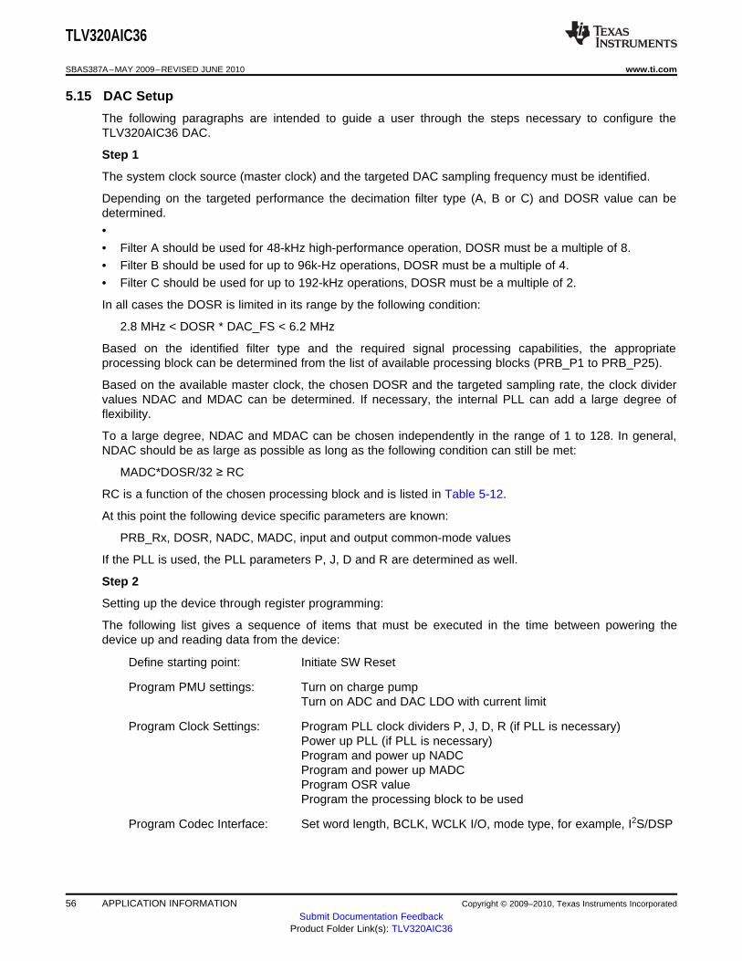
TLV320AIC36
SBAS387A–MAY 2009–REVISED JUNE 2010 www.ti.com
5.15 DAC Setup
The following paragraphs are intended to guide a user through the steps necessary to configure theTLV320AIC36 DAC.
Step 1
The system clock source (master clock) and the targeted DAC sampling frequency must be identified.
Depending on the targeted performance the decimation filter type (A, B or C) and DOSR value can bedetermined.•• Filter A should be used for 48-kHz high-performance operation, DOSR must be a multiple of 8.• Filter B should be used for up to 96k-Hz operations, DOSR must be a multiple of 4.• Filter C should be used for up to 192-kHz operations, DOSR must be a multiple of 2.
In all cases the DOSR is limited in its range by the following condition:
2.8 MHz < DOSR * DAC_FS < 6.2 MHz
Based on the identified filter type and the required signal processing capabilities, the appropriateprocessing block can be determined from the list of available processing blocks (PRB_P1 to PRB_P25).
Based on the available master clock, the chosen DOSR and the targeted sampling rate, the clock dividervalues NDAC and MDAC can be determined. If necessary, the internal PLL can add a large degree offlexibility.
To a large degree, NDAC and MDAC can be chosen independently in the range of 1 to 128. In general,NDAC should be as large as possible as long as the following condition can still be met:
MADC*DOSR/32 ≥ RC
RC is a function of the chosen processing block and is listed in Table 5-12.
At this point the following device specific parameters are known:
PRB_Rx, DOSR, NADC, MADC, input and output common-mode values
If the PLL is used, the PLL parameters P, J, D and R are determined as well.
Step 2
Setting up the device through register programming:
The following list gives a sequence of items that must be executed in the time between powering thedevice up and reading data from the device:
Define starting point: Initiate SW Reset
Program PMU settings: Turn on charge pumpTurn on ADC and DAC LDO with current limit
Program Clock Settings: Program PLL clock dividers P, J, D, R (if PLL is necessary)Power up PLL (if PLL is necessary)Program and power up NADCProgram and power up MADCProgram OSR valueProgram the processing block to be used
Program Codec Interface: Set word length, BCLK, WCLK I/O, mode type, for example, I2S/DSP
56 APPLICATION INFORMATION Copyright © 2009–2010, Texas Instruments Incorporated
Submit Documentation FeedbackProduct Folder Link(s): TLV320AIC36

TLV320AIC36
www.ti.com SBAS387A–MAY 2009–REVISED JUNE 2010
Program Analog Blocks Program headphone specific depop settingsPower up DACModulator startup sequenceSet Modulator taps for low noiseSet Dac driver current control for low powerRoute DAC/PGA/LINEIN to outputsRelease LDO current limitUnmute, set gain and power up outputs
To obtain optimum DAC audio quality, it is necessary to write the following sequence prior to enabling theDAC:# Modulator startup sequence for optimum DAC audio qualityw 30 00 fdw 30 0d 0dw 30 04 20w 30 0d 00
See Section 5.20 for a detailed application example.
5.16 Clock Generation and PLL
The TLV320AIC36 supports a wide range of options for generating clocks for the ADC and DAC sectionsas well as interface and other control blocks as shown in Figure 5-32. The clocks for ADC and DACrequire a source reference clock. This clock can be provided on a variety of device pins such as MCLK,BCLK or GPI pins. The source reference clock for the codec can be chosen by programming theCODEC_CLKIN value on Page 0, Register 4, D(1:0). The CODEC_CLKIN can then be routed throughhighly-flexible clock dividers see Figure 5-32 to generate the various clocks required for ADC, DAC andthe miniDSP sections. In the event that the desired audio or miniDSP clocks cannot be generated from thereference clocks on MCLK, BCLK or GPIO, the TLV320AIC36 also provides the option of using theon-chip PLL which supports a wide range of fractional multiplication values to generate the requiredclocks. Starting from CODEC_CLKIN the TLV320AIC36 provides several programmable clock dividers tohelp achieve a variety of sampling rates for ADC, DAC and clocks for the miniDSP.
Copyright © 2009–2010, Texas Instruments Incorporated APPLICATION INFORMATION 57Submit Documentation Feedback
Product Folder Link(s): TLV320AIC36
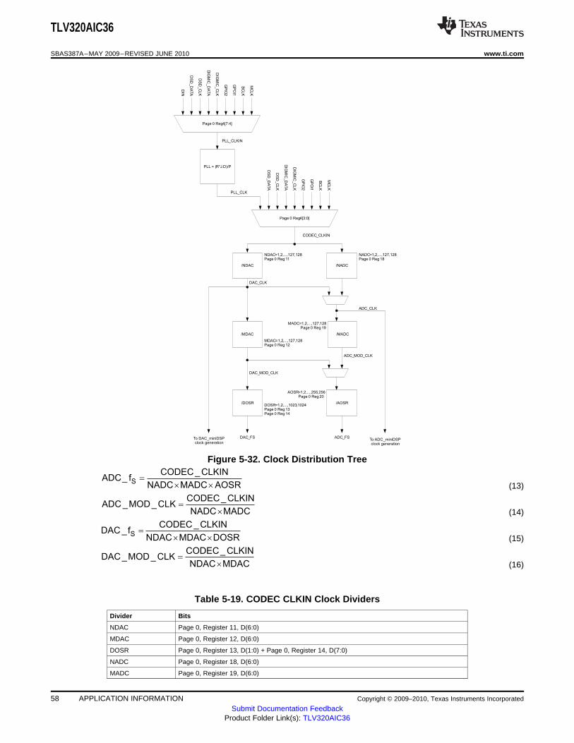
DIN
DS
D_D
ATA
DS
D_C
LK
DIG
MIC
_D
ATA
DIG
MIC
_C
LK
GP
IO2
GP
OI1
BC
LK
MC
LK
Page 0 Reg4[7:4]
PLL_CLKIN
PLL = (R*J.D)/P
DS
D_D
ATA
DS
D_C
LK
DIG
MIC
_D
ATA
DIG
MIC
_C
LK
GP
IO2
GP
OI1
BC
LK
MC
LK
Page 0 Reg4[3:0]
PLL_CLK
CODEC_CLKIN
/NDAC /NADC
NDAC=1,2,...,127,128Page 0 Reg 11
NADC=1,2,...,127,128Page 0 Reg 18
/MADC
/AOSR
/MDAC
/DOSR
MADC=1,2,...,127,128Page 0 Reg 19
ADC_CLK
ADC_MOD_CLK
ADC_FS
DAC_MOD_CLK
DAC_CLK
DAC_FS
AOSR=1,2,...,255,256Page 0 Reg 20
MDAC=1,2,...,127,128Page 0 Reg 12
DOSR=1,2,...,1023,1024Page 0 Reg 13Page 0 Reg 14
To DAC_miniDSPclock generation
To ADC_miniDSPclock generation
AOSRMADCNADC
CLKIN_CODECfS_ADC
´´=
MADCNADC
CLKIN_CODECCLK_MOD_ADC
´=
DOSRMDACNDAC
CLKIN_CODEC
´´fS_DAC =
MDACNDAC
CLKIN_CODECCLK_MOD_DAC
´=
TLV320AIC36
SBAS387A–MAY 2009–REVISED JUNE 2010 www.ti.com
Figure 5-32. Clock Distribution Tree
(13)
(14)
(15)
(16)
Table 5-19. CODEC CLKIN Clock Dividers
Divider Bits
NDAC Page 0, Register 11, D(6:0)
MDAC Page 0, Register 12, D(6:0)
DOSR Page 0, Register 13, D(1:0) + Page 0, Register 14, D(7:0)
NADC Page 0, Register 18, D(6:0)
MADC Page 0, Register 19, D(6:0)
58 APPLICATION INFORMATION Copyright © 2009–2010, Texas Instruments Incorporated
Submit Documentation FeedbackProduct Folder Link(s): TLV320AIC36

÷N
BCLK
DAC_CLK
ADC_MOD_CLKDAC_MOD_CLK
ADC_CLK
BDIV_CLKIN
N = 1,2,...,127,128
TLV320AIC36
www.ti.com SBAS387A–MAY 2009–REVISED JUNE 2010
Table 5-19. CODEC CLKIN Clock Dividers (continued)Divider Bits
AOSR Page 0, Register 20, D(7:0)
The DAC Modulator is clocked by DAC_MOD_CLK. For proper power-up operating of the DAC Channel,these clocks must be enabled by configuring the NDAC and MDAC clock dividers (Page 0, Register 11,D(7) =1 and Page 0, Register 12, D(7)=1). When the DAC channel is powered down, the device internallyinitiates a power-down sequence for proper shut-down. During this shut-down sequence, the NDAC andMDAC dividers must not be powered down, or else a proper low power shut-down may not take place.The user can read back the power-status flag Page 0, Register 37, D(7) and Page 0, Register 37, D(3).When both the flags indicate power-down, the MDAC divider may be powered down, followed by theNDAC divider.
The ADC modulator is clocked by ADC_MOD_CLK. For proper power-up of the ADC Channel, theseclocks are enabled by the NADC and MADC clock dividers (Page 0, Register 18, D(7) =1 and Page 0,Register 19, D(7)=1). When the ADC channel is powered down, the device internally initiates apower-down sequence for proper shut-down. During this shut-down sequence, the NADC and MADCdividers must not be powered down, or else a proper low power shut-down may not take place. The usercan read back the power-status flag Page 0, Register 36, D(6) and Page 0, Register 36, D(2). When boththe flags indicate power-down, the MADC divider may be powered down, followed by NADC divider.
When ADC_CLK is derived from the NDAC divider output, the NDAC must be kept powered up till thepower-down status flags for ADC do not indicate power-down. When the input to the AOSR clock divideris derived from DAC_MOD_CLK, then MDAC must be powered up when ADC_FS is needed ( that is,when WCLK is generated by TLV320AIC36 or AGC is enabled) and can be powered down only after theADC power-down flags indicate power-down status.
In general, all the root clock dividers should be powered down only after the child clock dividers have beenpowered down for proper operation.
The TLV320AIC36 also has options for routing some of the internal clocks to the output pins of the deviceto be used as general purpose clocks in the system. The feature is shown in Figure 5-33.
Figure 5-33. BCLK Output Options
In the mode when TLV320AIC36 is configured to drive the BCLK pin (Page 0, Register 25, D3=’1’) it canbe driven as divided value of BDIV_CLKIN. The division value can be programmed in Page 0, Register 28,D(6:0) from 1 to 128. The BDIV_CLKIN can itself be configured to be one of DAC_CLK, DAC_MOD_CLK,
Copyright © 2009–2010, Texas Instruments Incorporated APPLICATION INFORMATION 59Submit Documentation Feedback
Product Folder Link(s): TLV320AIC36
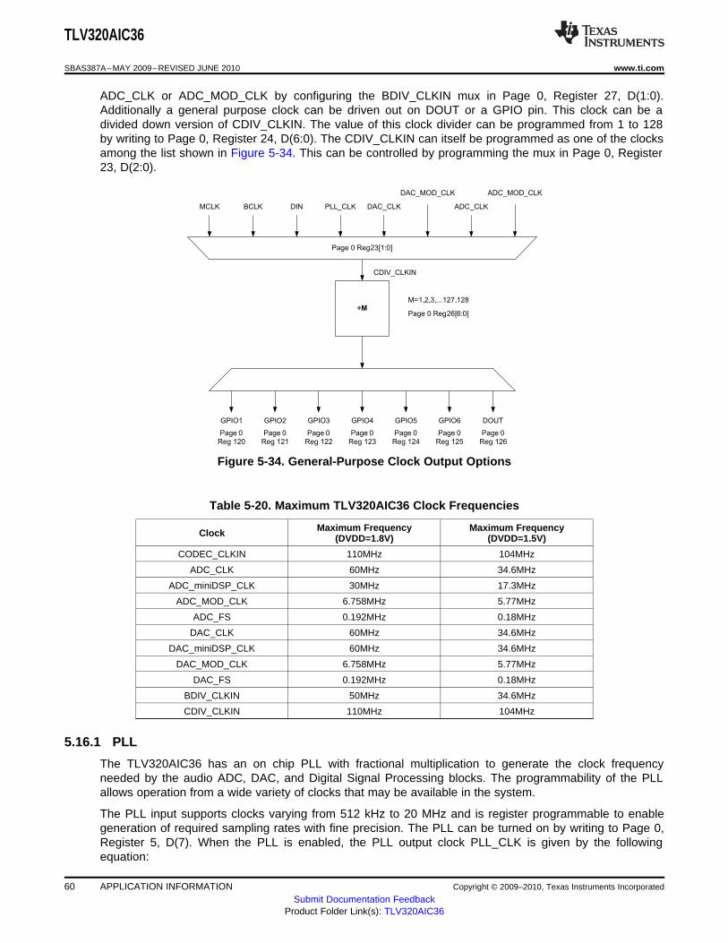
MCLK BCLK DIN PLL_CLK DAC_CLK
DAC_MOD_CLK
ADC_CLK
ADC_MOD_CLK
÷M
CDIV_CLKIN
GPIO1 GPIO2 GPIO3 GPIO4 GPIO5 GPIO6 DOUT
Page 0 Reg23[1:0]
M=1,2,3,...127,128
Page 0 Reg26[6:0]
Page 0
Reg 120
Page 0
Reg 121
Page 0
Reg 122
Page 0
Reg 123
Page 0
Reg 124
Page 0
Reg 125
Page 0
Reg 126
TLV320AIC36
SBAS387A–MAY 2009–REVISED JUNE 2010 www.ti.com
ADC_CLK or ADC_MOD_CLK by configuring the BDIV_CLKIN mux in Page 0, Register 27, D(1:0).Additionally a general purpose clock can be driven out on DOUT or a GPIO pin. This clock can be adivided down version of CDIV_CLKIN. The value of this clock divider can be programmed from 1 to 128by writing to Page 0, Register 24, D(6:0). The CDIV_CLKIN can itself be programmed as one of the clocksamong the list shown in Figure 5-34. This can be controlled by programming the mux in Page 0, Register23, D(2:0).
Figure 5-34. General-Purpose Clock Output Options
Table 5-20. Maximum TLV320AIC36 Clock Frequencies
Maximum Frequency Maximum FrequencyClock (DVDD=1.8V) (DVDD=1.5V)
CODEC_CLKIN 110MHz 104MHz
ADC_CLK 60MHz 34.6MHz
ADC_miniDSP_CLK 30MHz 17.3MHz
ADC_MOD_CLK 6.758MHz 5.77MHz
ADC_FS 0.192MHz 0.18MHz
DAC_CLK 60MHz 34.6MHz
DAC_miniDSP_CLK 60MHz 34.6MHz
DAC_MOD_CLK 6.758MHz 5.77MHz
DAC_FS 0.192MHz 0.18MHz
BDIV_CLKIN 50MHz 34.6MHz
CDIV_CLKIN 110MHz 104MHz
5.16.1 PLL
The TLV320AIC36 has an on chip PLL with fractional multiplication to generate the clock frequencyneeded by the audio ADC, DAC, and Digital Signal Processing blocks. The programmability of the PLLallows operation from a wide variety of clocks that may be available in the system.
The PLL input supports clocks varying from 512 kHz to 20 MHz and is register programmable to enablegeneration of required sampling rates with fine precision. The PLL can be turned on by writing to Page 0,Register 5, D(7). When the PLL is enabled, the PLL output clock PLL_CLK is given by the followingequation:
60 APPLICATION INFORMATION Copyright © 2009–2010, Texas Instruments Incorporated
Submit Documentation FeedbackProduct Folder Link(s): TLV320AIC36
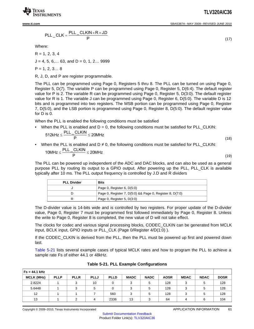
PLL _ CLKIN R J.DPLL _ CLK
P
´ ´=
MHz20P
CLKIN_PLLkHz512 ££
MHz20P
CLKIN_PLLMHz10 ££
TLV320AIC36
www.ti.com SBAS387A–MAY 2009–REVISED JUNE 2010
(17)
Where:
R = 1, 2, 3, 4
J = 4, 5, 6,… 63, and D = 0, 1, 2… 9999
P = 1, 2, 3… 8
R, J, D, and P are register programmable.
The PLL can be programmed using Page 0, Registers 5 thru 8. The PLL can be turned on using Page 0,Register 5, D(7). The variable P can be programmed using Page 0, Register 5, D(6:4). The default registervalue for P is 2. The variable R can be programmed using Page 0, Register 5, D(3:0). The default registervalue for R is 1. The variable J can be programmed using Page 0, Register 6, D(5:0). The variable D is 12bits and is programmed into two registers. The MSB portion can be programmed using Page 0, Register7, D(5:0), and the LSB portion is programmed using Page 0, Register 8, D(5:0). The default register valuefor D is 0.
When the PLL is enabled the following conditions must be satisfied• When the PLL is enabled and D = 0, the following conditions must be satisfied for PLL_CLKIN:
(18)
• When the PLL is enabled and D ≠ 0, the following conditions must be satisfied for PLL_CLKIN:
(19)
The PLL can be powered up independent of the ADC and DAC blocks, and can also be used as a generalpurpose PLL by routing its output to a GPIO output. After powering up the PLL, PLL_CLK is availabletypically after 10 ms. The PLL output frequency is controlled by J.D and R dividers
PLL Divider Bits
J Page 0, Register 6, D(5:0)
D Page 0, Register 7, D(5:0) && Page 0, Register 8, D(7:0)
R Page 0, Register 5, D(3:0)
The D-divider value is 14-bits wide and is controlled by two registers. For proper update of the D-dividervalue, Page 0, Register 7 must be programmed first followed immediately by Page 0, Register 8. Unlessthe write to Page 0, Register 8 is completed, the new value of D will not take effect.
The clocks for codec and various signal processing blocks, CODEC_CLKIN can be generated from MCLKinput, BCLK input, GPIO inputs or PLL_CLK (Page 0/Register 4/D(1:0) ).
If the CODEC_CLKIN is derived from the PLL, then the PLL must be powered up first and powered downlast.
Table 5-21 lists several example cases of typical MCLK rates and how to program the PLL to achieve asample rate Fs of either 44.1 or 48kHz.
Table 5-21. PLL Example Configurations
Fs = 44.1 kHz
MCLK (MHz) PLLP PLLR PLLJ PLLD MADC NADC AOSR MDAC NDAC DOSR
2.8224 1 3 10 0 3 5 128 3 5 128
5.6448 1 3 5 0 3 5 128 3 5 128
12 1 1 7 560 3 5 128 3 5 128
13 1 2 4 2336 13 3 64 4 6 104
Copyright © 2009–2010, Texas Instruments Incorporated APPLICATION INFORMATION 61Submit Documentation Feedback
Product Folder Link(s): TLV320AIC36
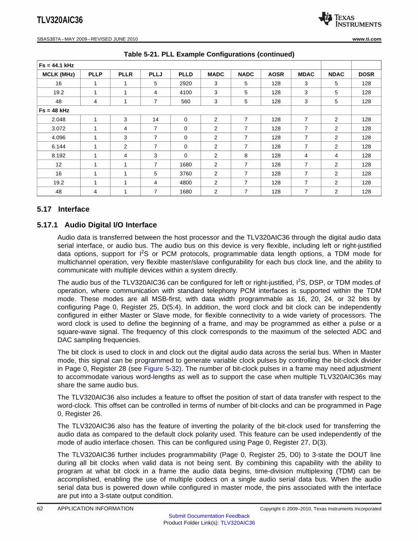
TLV320AIC36
SBAS387A–MAY 2009–REVISED JUNE 2010 www.ti.com
Table 5-21. PLL Example Configurations (continued)
Fs = 44.1 kHz
MCLK (MHz) PLLP PLLR PLLJ PLLD MADC NADC AOSR MDAC NDAC DOSR
16 1 1 5 2920 3 5 128 3 5 128
19.2 1 1 4 4100 3 5 128 3 5 128
48 4 1 7 560 3 5 128 3 5 128
Fs = 48 kHz
2.048 1 3 14 0 2 7 128 7 2 128
3.072 1 4 7 0 2 7 128 7 2 128
4.096 1 3 7 0 2 7 128 7 2 128
6.144 1 2 7 0 2 7 128 7 2 128
8.192 1 4 3 0 2 8 128 4 4 128
12 1 1 7 1680 2 7 128 7 2 128
16 1 1 5 3760 2 7 128 7 2 128
19.2 1 1 4 4800 2 7 128 7 2 128
48 4 1 7 1680 2 7 128 7 2 128
5.17 Interface
5.17.1 Audio Digital I/O Interface
Audio data is transferred between the host processor and the TLV320AIC36 through the digital audio dataserial interface, or audio bus. The audio bus on this device is very flexible, including left or right-justifieddata options, support for I2S or PCM protocols, programmable data length options, a TDM mode formultichannel operation, very flexible master/slave configurability for each bus clock line, and the ability tocommunicate with multiple devices within a system directly.
The audio bus of the TLV320AIC36 can be configured for left or right-justified, I2S, DSP, or TDM modes ofoperation, where communication with standard telephony PCM interfaces is supported within the TDMmode. These modes are all MSB-first, with data width programmable as 16, 20, 24, or 32 bits byconfiguring Page 0, Register 25, D(5:4). In addition, the word clock and bit clock can be independentlyconfigured in either Master or Slave mode, for flexible connectivity to a wide variety of processors. Theword clock is used to define the beginning of a frame, and may be programmed as either a pulse or asquare-wave signal. The frequency of this clock corresponds to the maximum of the selected ADC andDAC sampling frequencies.
The bit clock is used to clock in and clock out the digital audio data across the serial bus. When in Mastermode, this signal can be programmed to generate variable clock pulses by controlling the bit-clock dividerin Page 0, Register 28 (see Figure 5-32). The number of bit-clock pulses in a frame may need adjustmentto accommodate various word-lengths as well as to support the case when multiple TLV320AIC36s mayshare the same audio bus.
The TLV320AIC36 also includes a feature to offset the position of start of data transfer with respect to theword-clock. This offset can be controlled in terms of number of bit-clocks and can be programmed in Page0, Register 26.
The TLV320AIC36 also has the feature of inverting the polarity of the bit-clock used for transferring theaudio data as compared to the default clock polarity used. This feature can be used independently of themode of audio interface chosen. This can be configured using Page 0, Register 27, D(3).
The TLV320AIC36 further includes programmability (Page 0, Register 25, D0) to 3-state the DOUT lineduring all bit clocks when valid data is not being sent. By combining this capability with the ability toprogram at what bit clock in a frame the audio data begins, time-division multiplexing (TDM) can beaccomplished, enabling the use of multiple codecs on a single audio serial data bus. When the audioserial data bus is powered down while configured in master mode, the pins associated with the interfaceare put into a 3-state output condition.
62 APPLICATION INFORMATION Copyright © 2009–2010, Texas Instruments Incorporated
Submit Documentation FeedbackProduct Folder Link(s): TLV320AIC36

BCLK
WCLK
DIN/
DOUTn-1 n-2 1 00 n-1 n-2 1 0
LSBMSB
Left Channel Right Channel
n-3 2 2n-3
LSBMSB
1/fs
LD(n) LD(n+1)
WORD
CLOCK
BIT
CLOCK
DATA -
1
-
2
-
3
2 1 03 -
1
-
2
-
3
2 1 03 -
1
-
2
N N N N N N N N N
-
3
RD(n)
LEFT CHANNEL RIGHT CHANNEL
LD(n) = n'th sample of left channel data RD(n) = n'th sample of right channel data
TLV320AIC36
www.ti.com SBAS387A–MAY 2009–REVISED JUNE 2010
By default when the word-clocks and bit-clocks are generated by the TLV320AIC36, these clocks areactive only when the codec (ADC, DAC or both) are powered up within the device. This is done to savepower. However, it also supports a feature when both the word clocks and bit-clocks can be active evenwhen the codec in the device is powered down. This is useful when using the TDM mode with multiplecodecs on the same bus, or when word-clock or bit-clocks are used in the system as general-purposeclocks.
5.17.1.1 Right-Justified Mode
The Audio Interface of the TLV320AIC36 can be put into Right Justified Mode by programming Page 0,Register 25, D(7:6) = 10. In right-justified mode, the LSB of the left channel is valid on the rising edge ofthe bit clock preceding the falling edge of the word clock. Similarly, the LSB of the right channel is valid onthe rising edge of the bit clock preceding the rising edge of the word clock.
Figure 5-35. Timing Diagram for Right-Justified Mode
For Right-Justified mode, the number of bit-clocks per frame should be greater than twice theprogrammed word-length of the data.
5.17.1.2 Left-Justified Mode
The Audio Interface of the TLV320AIC36 can be put into Left Justified Mode by programming Page 0,Register 25, D(7:6) = 11. In left-justified mode, the MSB of the right channel is valid on the rising edge ofthe bit clock following the falling edge of the word clock. Similarly the MSB of the left channel is valid onthe rising edge of the bit clock following the rising edge of the word clock.
Figure 5-36. Timing Diagram for Left-Justified Mode
Copyright © 2009–2010, Texas Instruments Incorporated APPLICATION INFORMATION 63Submit Documentation Feedback
Product Folder Link(s): TLV320AIC36
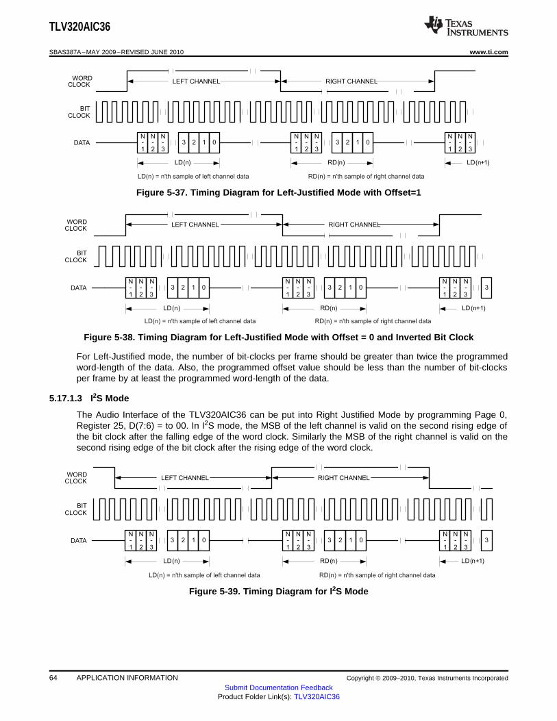
LD(n) LD(n+1)
WORD
CLOCK
BIT
CLOCK
DATA -
1
-
2
-
3
2 1 03 -
1
-
2
-
3
2 1 03 -
1
-
2
N N N N N N N N N-
3
RD(n)
LEFT CHANNEL RIGHT CHANNEL
LD(n) = n'th sample of left channel data RD(n) = n'th sample of right channel data
LD(n) LD(n+1)
WORD
CLOCK
BIT
CLOCK
DATA 3
N
-
1
N
-
2
N
-
3
2 1 03
N
-
1
N
-
2
N
-
3
2 1 03
N
-
1
N
-
2
N
-
3
RD(n)
LEFT CHANNEL RIGHT CHANNEL
LD(n) = n'th sample of left channel data RD(n) = n'th sample of right channel data
LD(n) LD(n+1)
WORD
CLOCK
BIT
CLOCK
DATA -
1
-
2
-
3
2 1 03 -
1
-
2
-
3
2 1 03 -
1
-
2
N N N N N N N N N
-
3
3
RD(n)
LEFT CHANNEL RIGHT CHANNEL
LD(n) = n'th sample of left channel data RD(n) = n'th sample of right channel data
TLV320AIC36
SBAS387A–MAY 2009–REVISED JUNE 2010 www.ti.com
Figure 5-37. Timing Diagram for Left-Justified Mode with Offset=1
Figure 5-38. Timing Diagram for Left-Justified Mode with Offset = 0 and Inverted Bit Clock
For Left-Justified mode, the number of bit-clocks per frame should be greater than twice the programmedword-length of the data. Also, the programmed offset value should be less than the number of bit-clocksper frame by at least the programmed word-length of the data.
5.17.1.3 I2S Mode
The Audio Interface of the TLV320AIC36 can be put into Right Justified Mode by programming Page 0,Register 25, D(7:6) = to 00. In I2S mode, the MSB of the left channel is valid on the second rising edge ofthe bit clock after the falling edge of the word clock. Similarly the MSB of the right channel is valid on thesecond rising edge of the bit clock after the rising edge of the word clock.
Figure 5-39. Timing Diagram for I2S Mode
64 APPLICATION INFORMATION Copyright © 2009–2010, Texas Instruments Incorporated
Submit Documentation FeedbackProduct Folder Link(s): TLV320AIC36

LD(n) LD (n+1)
WORD
CLOCK
BIT
CLOCK
DATA-
1
4 3 25 1 0 -
1
4 3 25 1 0N N N
-
1
5
RD(n)
LEFT CHANNEL RIGHT CHANNEL
LD(n) = n'th sample of left channel data RD(n) = n'th sample of right channel data
LD(n) LD(n+1)
WORD
CLOCK
BIT
CLOCK
DATA -
1
-
2
-
3
2 1 03 -
1
-
2
-
3
2 1 03 -
1
-
2
N N N N N N N N N
-
3
3
RD(n)
LEFT CHANNEL RIGHT CHANNEL
LD(n) = n'th sample of left channel data RD(n) = n'th sample of right channel data
LD(n) LD(n+1)
BIT
CLOCK
DATA -
1
-
2
-
3
2 1 03 -
1
-
2
-
3
03 2 1 -
1
-
2
N N N N N N N N N-
3
3
RD(n)
WORD
CLOCKLEFT CHANNEL RIGHT CHANNEL
LD(n) = n'th sample of left channel data RD(n) = n'th sample of right channel data
TLV320AIC36
www.ti.com SBAS387A–MAY 2009–REVISED JUNE 2010
Figure 5-40. Timing Diagram for I2S Mode With Offset = 2
Figure 5-41. Timing Diagram for I2S Mode With Offset = 0 and Bit Clock Invert
For I2S mode, the number of bit-clocks per channel should be greater than or equal to the programmedword-length of the data. Also the programmed offset value should be less than the number of bit-clocksper frame by at least the programmed word-length of the data.
5.17.1.4 DSP Mode
The Audio Interface of the TLV320AIC36 can be put into Right Justified Mode by programming Page 0,Register 25, D(7:6) = 01. In DSP mode, the falling edge of the word clock starts the data transfer with theleft channel data first and immediately followed by the right channel data. Each data bit is valid on thefalling edge of the bit clock.
Figure 5-42. Timing Diagram for DSP Mode
Copyright © 2009–2010, Texas Instruments Incorporated APPLICATION INFORMATION 65Submit Documentation Feedback
Product Folder Link(s): TLV320AIC36

LD(n) LD(n+1)
BIT
CLOCK
DATA -
1
-
2
-
3
2 1 03 -
1
-
2
-
3
03 2 1 -
1
-
2
N N N N N N N N N-
3
RD(n)
WORD
CLOCKLEFT CHANNEL RIGHT CHANNEL
LD(n) = n'th sample of left channel data RD(n) = n'th sample of right channel data
LD(n) LD(n+1)
BIT
CLOCK
DATA
N-
1
N-
2
N-
3
2 1 03N-
1
N-
2
N-
3
03 2 1N-
1
N-
2
N-
3
3
RD(n)
WORD
CLOCKLEFT CHANNEL RIGHT CHANNEL
TLV320AIC36
SBAS387A–MAY 2009–REVISED JUNE 2010 www.ti.com
Figure 5-43. Timing Diagram for DSP Mode With Offset = 1
Figure 5-44. Timing Diagram for DSP Mode With Offset = 1 and Bit Clock Inverted
For DSP mode, the number of bit-clocks per frame should be greater than twice the programmedword-length of the data. Also the programmed offset value should be less than the number of bit-clocksper frame by at least the programmed word-length of the data.
5.17.1.5 Secondary I2S
The audio serial interface on the TLV320AIC36 has an extensive I/O control to allow communication withtwo independent processors for audio data. Each processor can communicate with the device one at atime. This feature is enabled by register programming of the various pin selections.
Figure 5-45 illustrates possible audio interface routing.
66 APPLICATION INFORMATION Copyright © 2009–2010, Texas Instruments Incorporated
Submit Documentation FeedbackProduct Folder Link(s): TLV320AIC36
Primary
I2S
Processor
BCLK
S_BCLK
BCLK_OUT
Reg33[7]
0
1
Reg27[2]
and Reg25[3]
WCLK
S_WCLK
DAC_FS
Reg33[5:4]
00Reg27[2]
and Reg25[2]
ADC_FS01
10
DOUT
S_DIN
DOUT_INT
Reg33[1]
0
1
Reg126[3:1]
DIN
Audio
Digital
Serial
Interface
Core
0
1
BCLK_INT
BCLK
S_BCLK
Reg32[3]
0
1DAC_WCLK_INT
WCLK
S_WCLK
Reg32[2]
0
1
ADC_WCLK_INT
WCLK
ADC_WCLK
Reg32[1]
0
1
DIN_INT
DIN
S_DIN
Reg32[0]
Clock
Generation
Block
BCLK_OUT
ADC_FS
DAC_FS
DOUT_INT
Secondary
I2S
Processor
BCLK
WCLK
DOUT
DIN
BCLK
WCLK
DOUT
DIN
Register
Programmable
Pins
to S_BCLK,
S_WCLK,
ADC_WCLK,
and S_DIN
GPIO1
GPIO2
GPIO3
GPIO4
GPIO5
GPIO6
0
1
Reg32[4]
TLV320AIC36
www.ti.com SBAS387A–MAY 2009–REVISED JUNE 2010
Figure 5-45. Audio Serial Interface Multiplexing
5.17.2 I2C Control InterFACE
The TLV320AIC36 supports the I2C control protocol, and will respond to the I2C address of 0011000. I2Cis a two-wire, open-drain interface supporting multiple devices and masters on a single bus. Devices onthe I2C bus only drive the bus lines LOW by connecting them to ground; they never drive the bus linesHIGH. Instead, the bus wires are pulled HIGH by pullup resistors, so the bus wires are HIGH when nodevice is driving them LOW. This way, two devices cannot conflict; if two devices drive the bussimultaneously, there is no driver contention.
Communication on the I2C bus always takes place between two devices, one acting as the master and theother acting as the slave. Both masters and slaves can read and write, but slaves can only do so underthe direction of the master. Some I2C devices can act as masters or slaves, but the TLV320AIC36 canonly act as a slave device.
An I2C bus consists of two lines, SDA and SCL. SDA carries data, and the SCL signal provides the clock.All data is transmitted across the I2C bus in groups of 8 bits. To send a bit on the I2C bus, the SDA line isdriven to the appropriate level while SCL is LOW (a LOW on SDA indicates the bit is zero, while a HIGHindicates the bit is one).
Once the SDA line has settled, the SCL line is brought HIGH, then LOW. This pulse on the SCL lineclocks the SDA bit into the receiver’s shift register.
The I2C bus is bidirectional: the SDA line is used both for transmitting and receiving data. When a masterreads from a slave, the slave drives the data line; when a master sends to a slave, the master drives thedata line.
Most of the time the bus is idle, no communication is taking place, and both lines are HIGH. Whencommunication is taking place, the bus is active. Only master devices can start communication on the bus.Normally, the data line is only allowed to change state while the clock line is LOW. If the data line changesstate while the clock line is HIGH, it is either a START condition or its counterpart, a STOP condition. ASTART condition is when the clock line is HIGH and the data line goes from HIGH to LOW. A STOPcondition is when the clock line is HIGH and the data line goes from LOW to HIGH.
Copyright © 2009–2010, Texas Instruments Incorporated APPLICATION INFORMATION 67Submit Documentation Feedback
Product Folder Link(s): TLV320AIC36

DA(6) DA(0) RA(7) RA(0) D(7) D(0)
Start
(M)
7-bit Device Address
(M)
Write
(M)
Slave
Ack
(S)
8-bit Register Address
(M)
Slave
Ack
(S)
8-bit Register Data
(M)
Stop
(M)
Slave
Ack
(S)
SDA
SCL
(M) => SDA Controlled by Master
(S) => SDA Controlled by Slave
Start
(M)
7-bit Device Address
(M)
Write
(M)
Slave
Ack
(S)
8-bit Register Address
(M)
Slave
Ack
(S)
SDA
SCL
7-bit Device Address
(M)
Read
(M)
Slave
Ack
(S)
DA(6) DA(0) RA(7) RA(0) DA(6) DA(0) D(7) D(0)
8-bit Register Data
(S)
Stop
(M)
Master
No Ack
(M)
Repeat
Start
(M)
(M) => SDA Controlled by Master
(S) => SDA Controlled by Slave
TLV320AIC36
SBAS387A–MAY 2009–REVISED JUNE 2010 www.ti.com
After the master issues a START condition, it sends a byte that selects the slave device forcommunication. This byte is called the address byte. Each device on an I2C bus has a unique 7-bitaddress to which it responds. (Slaves can also have 10-bit addresses; see the I2C specification fordetails.) The master sends an address in the address byte, together with a bit that indicates whether itwishes to read from or write to the slave device.
Every byte transmitted on the I2C bus, whether it is address or data, is acknowledged with anacknowledge bit. When a master has finished sending a byte (eight data bits) to a slave, it stops drivingSDA and waits for the slave to acknowledge the byte. The slave acknowledges the byte by pulling SDALOW. The master then sends a clock pulse to clock the acknowledge bit. Similarly, when a master hasfinished reading a byte, it pulls SDA LOW to acknowledge this to the slave. It then sends a clock pulse toclock the bit. (Remember that the master always drives the clock line.)
A not-acknowledge is performed by simply leaving SDA HIGH during an acknowledge cycle. If a device isnot present on the bus, and the master attempts to address it, it will receive a not−acknowledge becauseno device is present at that address to pull the line LOW.
When a master has finished communicating with a slave, it may issue a STOP condition. When a STOPcondition is issued, the bus becomes idle again. A master may also issue another START condition. Whena START condition is issued while the bus is active, it is called a repeated START condition.
The TLV320AIC36 can also respond to and acknowledge a General Call, which consists of the masterissuing a command with a slave address byte of 00H. This feature is disabled by default, but can beenabled using Page 0, Register 34, Bit D(5).
Figure 5-46. I2C Write
Figure 5-47. I2C Read
In the case of an I2C register write, if the master does not issue a STOP condition, then the device entersauto-increment mode. So in the next eight clocks, the data on SDA is treated as data for the nextincremental register.
Similarly, in the case of an I2C register read, after the device has sent out the 8-bit data from theaddressed register, if the master issues a ACKNOWLEDGE, the slave takes over control of SDA bus andtransmit for the next eight clocks the data of the next incremental register.
68 APPLICATION INFORMATION Copyright © 2009–2010, Texas Instruments Incorporated
Submit Documentation FeedbackProduct Folder Link(s): TLV320AIC36

ADC VDD
LDO
DAC VDD
LDO
DAC VSS
LDO
Charge
Pump
Power
Management
Unit
Mic Bias &
Detect
ADC & PLL
DAC &
LINEOUT
AMPS
HP & REC
AMPS
Analog Core
TLV320AIC36
GND_REG
AVDD_REG
AVDD2
AVDD1
AVSS1
AVSS_REG
AVDD_CP
FC_POS
FC_NEG
GND_CP
AVDD_BIAS
GND_BIAS
AVDD_ADC
GND_ADC
AVDD_DAC
GND_DAC
AVSS_DAC
AVDD_HP
GND_HP
AVSS_HP
+2.5 V
A1, B2
B1, C2
D1, E2
C1, D2
A9
D7
G9
H9
A6
B7
B8
E8, E9
E7
F8, C9
J1
G1, G2
F3
F1, F2
E1, E3
10 mF
1 mF
1 mF
1 mF
1 mF
1 mF
1 mF
10 mF
1 mF
10 mF
10 mF
REF
LDO
BG
TLV320AIC36
www.ti.com SBAS387A–MAY 2009–REVISED JUNE 2010
5.18 Power Management Unit
The allowed voltage supply ranges for the TLV320AIC36 analog blocks are 1.4 V to 1.8 V and –1.4 V to–1.8V. To ease system-level design, a charge pump and three low-dropout regulators (LDOs) areintegrated to generate the appropriate analog voltage supplies from a single 2.1 to 2.8 V supply input. Onepositive LDO is used to generate a nominal +1.8 V supply for the input PGA and ADC section and anotherpositive LDO generates a nominal +1.65 V for the DAC and audio amplifier sections. A negative chargepump generates a negative voltage which is then regulated to a nominal -1.65 V using a negative LDO.Figure 5-48 shows suggested hookup from the PMU to the analog core.
Figure 5-48. Recommended Analog Power Supply Connections
Internal voltage references for the analog core are derived from the AVDD_ADC supply inputs. Even inplayback-only applications, the AVDD_ADC supply inputs must be powered to support the internalreferences.
5.18.1 Charge Pump
The charge pump uses a minimum 1-mF flying capacitor connected between FC_POS and FC_NEG.AVDD_CP is the positive (input) supply connection and AVSS_REG is the negative (output) connection. A1-mF smoothing capacitor is recommended on the AVSS_REG node, although a smaller value can beused at the expense of increased ripple on the input to the negative regulator.
Copyright © 2009–2010, Texas Instruments Incorporated APPLICATION INFORMATION 69Submit Documentation Feedback
Product Folder Link(s): TLV320AIC36

TLV320AIC36
SBAS387A–MAY 2009–REVISED JUNE 2010 www.ti.com
The charge pump is enabled by setting Page 2, Register 71, D0=1. By default the charge pump uses adivided version of BCLK as its clock, but setting Page 2, Register 71, D1=1 will cause it to use MCLKinstead. The frequency division is controlled by two registers: Page 2, Register 72 contains the number ofclock cycles that the charge pump clock is high (minus one), while Page 2, Register 73 contains thenumber of clock cycles the charge pump is low (minus one). As an example, if the default values of 11 areused in these two registers the charge pump clock frequency is BCLK/24.
The charge pump frequency should be programmed between 400 and 500 kHz. If no very high currentloads are being driven from the amplifier section, this frequency can be reduced to save power. Careshould be taken to keep the charge pump frequency above the audio range.
5.18.2 LDOs
The unregulated input for the two positive LDOs is AVDD_REG. AVDD1 is the output of the high-powerregulator meant to drive the DAC and output amplifiers; a minimum of 10mF (maximum 100mF)capacitance is required on this pin for LDO stability. The capacitance can be split between AVDD1,AVDD_DAC, and AVDD_HP as long as the trace resistance plus the capacitor ESR is less than 400mΩ.Similarly a minimum of 1mF (maximum 10mF) is required on AVDD2, the output of the low-power regulatorintended to supply the preamp and ADC section.
The input to the negative regulator is connected internally to the charge pump output. AVSS1 is the outputof the high-power regulator meant to drive the DAC and output amplifiers; a minimum of 10mF (maximum100mF) capacitance is required on this pin for LDO stability. The capacitance can be split between AVSS1,AVSS_DAC, and AVSS_HP as long as the trace resistance plus the capacitor ESR is less than 400mΩ.
The regulators are enabled by the lower 3 bits of Page 2, Register 74. The negative regulator should beenabled only after the charge pump is enabled, otherwise the charge pump may not start up properly.
By default, the regulators start up in a current-limited mode to prevent high inrush currents. The twohigh-power regulators (AVDD1 and AVSS1) are limited to 50 mA, while the low-power regulator (AVDD2)is limited to 5 mA. After the regulators have had time to power up, remove the current limit by clearing theleast-significant 3 bits of Page 2, Register 76.
Short circuit protection for the regulators may be disabled through Page 2, Register 77. The nominaloutput level of the regulators can be programmed through Page 2, Register 78.
5.18.3 Low Power Mode
In addition to the standard configuration, the PMU can be used in two alternative configurations to furtherreduce power consumption. These low power modes sacrifice some performance for power savings. Seesections 3.7 and 3.8 for typical performance electrical characteristics.
The first low power (LP) mode is capable of reducing power dissipation to 14mW for DAC to headphoneplayback. Max headphone output power is 20mW per channel. Referring to Figure 5-48, the changes are:
1. AVDD_REG supply should be reduced to 1.8V (1.65V min)
2. This 1.8V supply also drives AVDD_ADC. AVDD2 is not connected to AVDD_ADC, and the AVDDLDO is disabled.
3. Register settings (see Section 5.21): DAC VDD LDO=1.5V, DAC VSS LDO=1.5V, ADC VDD LDO =off, Bias current = low power setting, DACSP = PRB_P17, REC,LO,HP gain=-2dB.
The second ultra low power (ULP) mode is capable of reducing power dissipation to 10mW for DAC toheadphone playback. Max output power is 10mW. Maximum input voltage for the ADC is reduced by 6dB.
Referring to Figure 5-48, the changes are
1. AVDD_REG supply should be reduced to 1.5V (1.4V min)
2. The 1.5V supply also drives AVDD_ADC, AVDD_DAC, AVDD_HP, DVDD.
3. AVSS_REG is directly connected to AVSS_DAC and AVSS_HP.
4. DAC VDD LDO, DAC VSS LDO, ADC VDD LDO are not used, powered down and disconnected.
70 APPLICATION INFORMATION Copyright © 2009–2010, Texas Instruments Incorporated
Submit Documentation FeedbackProduct Folder Link(s): TLV320AIC36

AIC36
DETECT
EXT_MICBIAS
EXTMIC_P
EXTMIC_M
RBIAS
R1 R2 RN
AVDD
MIC BIAS AMP
AIC36
LF
OSC
DETECT
DIVIDER1
DETECT
DIVIDER2
DETECT
SAR ADC
DETECT WINDOW
COMPARATOR
SHORT PULSE
DETECT
DEBOUNCE
LONG PULSE
DETECT
DEBOUNCE
TLV320AIC36
www.ti.com SBAS387A–MAY 2009–REVISED JUNE 2010
5. 47 kΩ resistor is placed from FC_NEG to GND to speed charge pump startup.
6. Register settings (see Section 5.21): all LDOs=off, Bias current = low power setting. DACSP =PRB_P17, ADC CM=0.75V, ADC FS=0.83Vrms. REC,LO,HP gain=-5dB.
Referring to Table 5-20, adhere to the maximum clock frequencies listed for the ULP DVDD=1.5V mode.
5.19 Device Special Functions
5.19.1 Headset Detection
The DETECT input is used to monitor the external microphone bias for momentary connections to groundusing an external resistor and pushbutton. Multiple pushbuttons and resistors may be placed in parallel tosupport detection of unique button presses as shown in Figure 5-49.
Figure 5-49. Microphone Bias Detection External Circuit
Unique values of R1, R2, through RN in series with RBIAS form a resistor voltage divider which can besensed by the DETECT pin. This document details the AIC36 detect circuit and programming features.
5.19.1.1 Overview
Internally, the detect circuit consists of a low frequency oscillator, clock dividers, 5-bit SAR ADC, windowcomparator, and de-bounce functions as shown in Figure 5-50.
Figure 5-50. Detect Circuit Block Diagram
Copyright © 2009–2010, Texas Instruments Incorporated APPLICATION INFORMATION 71Submit Documentation Feedback
Product Folder Link(s): TLV320AIC36

PB1
(code = 4)
PB2
(code = 11)
PB3
(code = 17)
Code range
when no
buttons are
pressed
Threshold 1
(code = 7)
Threshold 2
(code = 14)
Threshold 3
(code = 23)
0
1
2
3
4
5
6
7
8
9
10
11
12
13
14
15
16
17
18
19
20
21
22
23
24
25
26
27
28
29
30
31
Window 0
Window 1
Window 2
Window 3
ADC CODE
TLV320AIC36
SBAS387A–MAY 2009–REVISED JUNE 2010 www.ti.com
5.19.1.2 Basic Operational Description
The detect circuit, once programmed, can provide either on-demand sampling of the detect input or triggeran AIC36 interrupt when used in continuous detection mode. This section provides details for the mainsub-sections of the detect circuit and provides programming examples to illustrate its operation.
First assume the EXT_MICBIAS circuit is enabled and programmed to the desired bias voltage. When nobuttons are pressed, the voltage at the DETECT pin is determined by the bias current of the microphoneand the bias resistor Rbias. If a button is pressed, the resistor associated with that button is put in parallelwith the microphone, causing the voltage at the DETECT pin to drop. If the EXT_MICBIAS circuit isdisabled, then the EXT_MICBIAS pin is temporarily connected to AVDD_BIAS for the duration of the ADCreading.
The 5-bit detect ADC has its input connected to the DETECT pin and its reference connected to theEXT_MICBIAS pin. Thus the output of the ADC is the DETECT pin voltage relative to the EXT_MICBIASvoltage. The state of the microphone and pushbuttons can be deduced from the ADC output. If the ADCoutput is zero, DETECT is shorted to ground; if it is full-scale then the microphone is unplugged. If theoutput is in between, then the microphone is plugged in and/or a button may be pressed, depending onthe particular ADC output value.
The detect ADC can provide a raw value corresponding to the voltage at the detect pin but it’s unsuitableas an interrupt source. To condition this raw detect value, an 8 window comparator is used to divide the32-level ADC output into as many as eight mapped windows. Using seven programmable thresholdregisters, the edges of up to 8 windows are defined within the code values of 0–31 of the ADC. Thesethreshold registers encode ranges of raw ADC values into a button press value which is then de-bouncedfor generating an interrupt.
As a windowing example, assume that three unique pushbuttons must be detected in an application.Based on resistor values selected for the voltage dividers, assume they correspond to raw ADC codes ofideally 4, 11, and 17. Thresholds 1, 2, and 3 can be set to 7, 14, and 23 as shown in Figure 5-51towindow the three values. A fourth code range is defined to describe the ADC values returned when nobutton is pressed. To properly map ADC codes into windows, threshold 1 must correspond to the edge ofthe lowest window, threshold 2 is the next highest window, and so on. Detect threshold registers 4 through7 should not be enabled in this case.
Figure 5-51. Example Threshold Settings
72 APPLICATION INFORMATION Copyright © 2009–2010, Texas Instruments Incorporated
Submit Documentation FeedbackProduct Folder Link(s): TLV320AIC36

TLV320AIC36
www.ti.com SBAS387A–MAY 2009–REVISED JUNE 2010
5.19.1.3 Sampling Rate and Debounce Period Control
The low frequency oscillator and detect dividers 1 and 2 provide clock generation for the circuit. Whenenabled, the LF oscillator provides a nominal frequency of 1MHz to detect divider 1, which in turn providesa clock source to detect divider 2. The detect divider 2 rate is the sampling rate of the ADC and the clocksource for the detect debouncers. Detect divider 1 is the clock source for the SAR ADC.
The short and long detect debouncers are programmed separately and can generate an interrupt afterdetecting a stable window value (0–7) for a minimum number of divider 2 periods. Because one windowwill always correspond to a no-buttons pressed ADC value, interrupts generated from this window areuseful for detecting button releases. The short and long debouncers are identical in function but can beprogrammed to different values.
5.19.1.4 Application Programming Example – Interrupt Driven
This example register initialization assumes four buttons with raw ADC values of 3, 9, 16, and 23 arerequired. Automatic button sampling will be enabled at a rate of 50 Hz and separate interrupts for shortand long pulses of 400 and 800 ms will be generated on INT1 and INT2 respectively. INT1 and INT2 willbe mapped to GPIO1 and GPIO2 respectively.w 30 00 01 # Change to page 1w 30 33 60 # Power up EXT_MICBIASw 30 00 02 # Change to page 2w 30 70 00 # Enable LF oscillator (1MHz nominal)w 30 15 C8 # Detect divider 1 set to 200 decimal (1MHz/200) = 5KHzw 30 16 64 # Detect divider 2 set to 100 decimal (5KHz/100) = 50Hzw 30 14 88 # Enable both detect dividersw 30 17 80 # Enable continuous detection modew 30 1C 86 # Set and enable threshold 1 to 6 (between 3 and 9)w 30 1D 8C # Set and enable threshold 2 to 12 (between 9 and 16)w 30 1E 94 # Set and enable threshold 3 to 20 (between 16 and 23)w 30 1F 99 # Set and enable threshold 4 to 25 (between 23 and open)w 30 20 00 # Disable threshold 5w 30 21 00 # Disable threshold 6w 30 22 00 # Disable threshold 7w 30 1A 14 # Set short pulse duration (1/50Hz) * 20 = 400msw 30 18 80 # Enable short pulse detectionw 30 1B 28 # Set long pulse duration (1/50Hz) * 40 = 800msw 30 19 80 # Enable long pulse detectionw 30 00 00 # Change to page 0w 30 34 01 # Enable short detect interrupt to INT1w 30 35 02 # Enable long detect interrupt to INT2w 30 78 14 # Map INT1 to GPIO1 pinw 30 79 20 # Map INT2 to GPIO2 pin
Upon GPIO1 interrupt, read Page 2, Register 0x18 for the short pushbutton value and write 0x01 to page0 Reg 0x32 to clear the interrupt.
Upon GPIO2 interrupt, read Page 2, Register 0x19 for the long pushbutton value and write 0x02 to page 0Reg 0x32 to clear the interrupt.
5.19.1.5 Application Programming Example – On-Demand Detect Sampling – Raw ADC
This example provides a fast, raw ADC sample of the detect pin. This feature is useful for determining theADC code for a corresponding resistor value. No windowing or de-bouncing is performed in this mode.w 30 00 01 # Change to page 1w 30 33 60 # Power up EXT_MICBIASw 30 00 02 # Change to page 2w 30 70 00 # Enable LF oscillator (1MHz nominal)w 30 15 01 # Detect divider 1 set to 1 decimal (1MHz/1) = 1MHzw 30 14 80 # Enable detect divider 1w 30 17 20 # Initiate on-demand ADC sample# Poll page 2 Reg 0x17, bit 5 for a 0 (1=in progress; 0=done)# When done, read page 2 Reg 0x17, bits 4-0 for raw ADC codew 30 70 01 # Disable LF oscillator
Copyright © 2009–2010, Texas Instruments Incorporated APPLICATION INFORMATION 73Submit Documentation Feedback
Product Folder Link(s): TLV320AIC36
LF
OSC
DETECT
DIVIDER 1
DETECT
DIVIDER 2
Page 2, Reg 112
Page 2, Reg 20
Page 2, Reg 21
Page 2, Reg 20
Page 2, Reg 21
Open Circuit
Detection
HPL PIN
HPR PIN
RECL PIN
RECR PIN
HOOK PIN
HPL STATUS
HPR STATUS
RECL STATUS
RECR STATUS
HOOK STATUS
HPL INTERRUPT
HPR INTERRUPT
RECL INTERRUPT
RECR INTERRUPT
HOOK INTERRUPT
Page 0, Reg 50
Page 0, Reg 51
TLV320AIC36
SBAS387A–MAY 2009–REVISED JUNE 2010 www.ti.com
5.19.1.6 Application Programming Example – On-Demand Detect Sampling – Windowed
This example provides a fast, windowed ADC sample of the detect pin. This feature is useful for softwareinitiated button detects. No de-bouncing is performed in this mode.# Perform these steps only at system initialization
w 30 00 01 # Change to page 1w 30 33 60 # Power up EXT_MICBIASw 30 00 02 # Change to page 2w 30 15 01 # Detect divider 1 set to 1 decimal (1MHz/1) = 1MHzw 30 16 01 # Detect divider 2 set to 1 decimal (1MHz/1) = 1MHz
# (Using the window values from the previous example)w 30 1C 86 # Set and enable threshold 1 to 6 (between 3 and 9)w 30 1D 8C # Set and enable threshold 2 to 12 (between 9 and 16)w 30 1E 94 # Set and enable threshold 3 to 20 (between 16 and 23)w 30 1F 99 # Set and enable threshold 4 to 25 (between 23 and open)w 30 20 00 # Disable threshold 5w 30 21 00 # Disable threshold 6w 30 22 00 # Disable threshold 7w 30 18 00 # Disable short pulse detection
# Perform these steps only at on-demand timew 30 70 00 # Enable LF oscillator (1MHz nominal)w 30 14 88 # Enable detect divider 1 and 2w 30 17 20 # Initiate on-demand ADC sample
# Poll page Reg 0x17, bit 5 for a 0 (1=in progress; 0=done)# When done, read page 2 Reg 0x18, bits 6-4 for window number
w 30 70 01 # Disable LF oscillator
5.19.2 Low-Impedance Detection
The TLV320AIC36 supports detection of low impedance (<50 ohm) to ground on the HPL, HPR, RECL,RECR, and HOOK pins. Detection can either be performed manually using an I2C register access orperiodically sampled to generate an interrupt.
Manual detection is performed by enabling manual detection using Page 2, Register 108 and reading backthe status register on Page 2, Register 109 on a per-pin basis. For power reasons, it is recommended thatthe enables for the manual detection in Register 108 are cleared after the status values are read fromRegister 108.
The periodic sampling rate uses the same LF oscillator and detect dividers as the headset detection seeFigure 5-52.
Figure 5-52. Periodic OC Detection Sampling
74 APPLICATION INFORMATION Copyright © 2009–2010, Texas Instruments Incorporated
Submit Documentation FeedbackProduct Folder Link(s): TLV320AIC36

TLV320AIC36
www.ti.com SBAS387A–MAY 2009–REVISED JUNE 2010
5.19.3 General-Purpose I/O
The TLV320AIC36 provides flexible I/O multiplexing to support digital microphone input, class-D amplifieroutput, interrupt output, and general purpose digital I/O options. Page 0 Registers 120 through 125 areused to control the GPIO1, GPIO2, GPIO4/DIGMIC_CLK, GPIO3/DIGMIC_DATA,GPIO6/BITSTREAM_CLK, and GPIO5/BITSTREAM_DATA pin functions.
5.19.4 Interrupts
The TLV320AIC36 can generate host interrupts originating from miniDSP, power threshold, LDO overcurrent, detect, and hook sources. Each source can be individually enabled and associated with twoseparate interrupt groups (INT1 and INT2) and routed to device pins. Each pin provides active high, activelow or open drain output capabilities.
The status of each interrupt source is available in a “sticky bit” and a real-time format. A sticky bit is astatus bit that is set by the interrupting source and remains set until cleared using an I2C register write.Real-time status bits provide a live read-back of the interrupting condition. Some interrupts can beprogrammed to assert based on rising, falling, or changes of state for additional user customization.
To associate an interrupt source with an interrupt group, the corresponding interrupt enable register bitmust be set. Multiple interrupt sources may be used for one interrupt group. If multiple enabled interruptsare asserted in an interrupt group, all sticky bits must be cleared before the device pin is de-asserted. Allinterrupts listed in Table 5-22can be selectively assigned to the INT1 or INT2 group.
Table 5-22. Interrupt Sources
Interrupt Source Type
Right DAC Signal Power is above Signal Threshold of DRC DAC engine
Left DAC Signal Power is above Signal Threshold of DRC DAC engine
ADC Barrel Shifter Output Overflow Flag ADC engine
Right ADC Overflow Flag ADC engine
Left ADC Overflow Flag ADC engine
DAC Barrel Shifter Output Overflow DAC engine
Right DAC Overflow DAC engine
Left DAC Overflow DAC engine
Right DAC Signal Power is above Signal Threshold of DRC DAC engine
Left DAC Signal Power is above Signal Threshold of DRC DAC engine
ADC MAC Engine Auxiliary Interrupt Port Output ADC engine
ADC MAC Engine Standard Interrupt Port Output ADC engine
Right ADC Signal Power Lesser than Noise Threshold for Right AGC. ADC engine
Left ADC Signal Power Greater than Noise Threshold for Left AGC. ADC engine
DAC MAC Engine Auxiliary Interrupt Port Output DAC engine
DAC MAC Engine Standard Interrupt Port Output DAC engine
Over current on VDD_ADC_LDO Power Control
Over current on VSS_DAC_LDO Power Control
Over current on VDD_DAC_LDO Power Control
Power good on VDD_ADC_LDO Power Control
Power good on VSS_DAC_LDO Power Control
Power good on VDD_DAC_LDO Power Control
Combined Rec amp/headphone short circuit Short Circuit
Left headphone open circuit detect Headphone detection
Right headphone open circuit detect Headphone detection
Left receiver open circuit detect Receiver detection
Right receiver open circuit detect Receiver detection
Copyright © 2009–2010, Texas Instruments Incorporated APPLICATION INFORMATION 75Submit Documentation Feedback
Product Folder Link(s): TLV320AIC36

TLV320AIC36
SBAS387A–MAY 2009–REVISED JUNE 2010 www.ti.com
Table 5-22. Interrupt Sources (continued)
Hook open circuit detect Hook detection
Microphone bias detected long pulse Headset Detection
Microphone bias detected short pulse Headset Detection
INT1 and INT2 interrupt groups may be routed to the GPIO1, GPIO2, GPIO3, GPIO4, GPIO5, or GPIO6pins with the active-state formats as described in the Page 0 Control Registers 120 - 125.
Interrupt sources not enabled for either the INT1 or INT2 group will still provide sticky bit and real-timestatus information accessible using the I2C interface but they will not assert device pins. This is useful formonitoring interrupt source status without using an actual interrupt pin.
5.20 Detailed Application Example################################################# Example script for the ADC and DAC data paths# Assumes Mclk(input)=11.2896 MHz, Wclk(input) =fs=44.1kHz, Bclk(input)=2.8224 MHz# I2S data, 24bits, BCLK, WCLk are inputs# mic1 and mic2 are fully differential inputs# HPR, HPL are single ended headphone outputs# LOR,LOL are fully differential line outputs############################################################
# software resetw 30 00 00w 30 01 01w 30 01 00
# PMU CODE############################################################# charge pump on, cpclk=MCLK (71=01) , cpclk/12 (72=73=0b)w 30 00 02w 30 71 01w 30 72 0bw 30 73 0b
# turn on ADC ,DAC LDO (74=00), no current limit (76=00),# short ckt protect, ADC=1.75V, LDO BGAP=on (77=00)# DAC=+-1.75 (78=33), +-1.65 (78=22), +-1.5 (78=11), +-1.4 (78=00)w 30 00 02w 30 74 00w 30 76 00w 30 77 00w 30 78 22
# CLOCK CODE############################################################# clocking settup, see fig. 5-33 clock dist tree# no pll: 04=00,05=00,0b=81,12=81# pll: 04=08,05=91,0b=88,12=88# CODEC_CLKIN=PLL_CLK, PLL_CLKIN=MCLK_PIN (04=08)w 30 00 00w 30 04 08
# PLL=R*J.D/P,# PLL on, P=1,R=1, (05=91)w 30 05 91
# PLL J.D (06=J, 07,08=D)w 30 06 08w 30 07 00w 30 08 00
# DAC CLOCK CODE############################################################# NDAC power up and div by 8 (0B=88), div by 16 (0B=90)w 30 0B 88# MDAC power up and div by 2 (0C=82)w 30 0C 82# DAC OSR=128 (0D, 0E=80), OSR=64 (0E=40)
76 APPLICATION INFORMATION Copyright © 2009–2010, Texas Instruments Incorporated
Submit Documentation FeedbackProduct Folder Link(s): TLV320AIC36

TLV320AIC36
www.ti.com SBAS387A–MAY 2009–REVISED JUNE 2010
w 30 0D 00w 30 0E 80# IDAC, DAC Mac instructions per FS, only used for custom filters#w 30 0F 40# DAC inter ratio for digital filters, only used for custom filters#w 30 10 08
# ADC CLOCK CODE############################################################# NADC power up and div by 8 (12=88)w 30 12 88# MADC power up and div by 2 (13=82)w 30 13 82# ADC OSR=128 (14=80),w 30 14 80# IADC, ADC MAC instructions per FS, only used for custom filters#w 30 15 5E# ADC dec ratio for digital filter =4, only used for custom filters#w 30 16 04
# CODEC INTERFACE, DIGITAL ADC,DAC CONTROLS, INCLUDES ANALOG DAC,ADC POWERUP############################################################# I2S, 24bit wordlength (19=2x) , 16bit (19=0x), BCLK, WCLK are outputs (19=xC), inputs (19=x0)w 30 19 20
# DAC filter engine 1w 30 3C 01# ADC filter engine 1w 30 3D 01
# Left, Right ADC not muted digital gain=0 dB (52=00), gain=-0.1 dB (52=11)w 30 52 00# ADCL, ADCR digital gain (7b signed 0.5 dB steps)w 30 53 00w 30 54 00
# L AGC, R AGC disabled, target=-5.5 dBw 30 56 00w 30 5E 00
# PRI_BCLK_OUT=internally generated BCLK, SEC_BCLK_OUT=Primary BCLK,# PRI_WCLK_OUT= ADC_FS clock, SEC_WCLK=Primary WCLK, PRI_DOUT=DOUT from CODECw 30 21 10# ADC filter output to I2S, I2S to DAC filter input, BCLK not inverted, BCLK WCLK active evenwhen CODEC is PDw 30 1B 06
# LADC,RADC powerup, DIG_MIC_INP, LDIG_MIC,RDIG_MIC disabled, soft-step disabledw 30 00 00w 30 51 C2# LDAC,RDAC powerup,soft-step disble, left data to LDAC, right data to RDAC (d6), L->R, R->L(ea), L->L, L->R (da)w 30 3F d6# Dac auto-mute disable, left,right dac not muted, left,right dac volume control independentw 30 40 00
# LDAC, RDAC digital gain 8 bit signed (0.5 dB steps) -6 dB (41=f4,42=f4)w 30 41 00w 30 42 00
# ANALOG ADC CODE#################################### Briefly connect internal CM to LEFT and RIGHT MIC PGA# for CM startup in differential modew 30 00 01w 30 34 00w 30 36 80w 30 37 00w 30 39 80
# connect mic1p,1m to pga leftp (34=20) leftm (36=20) 20k# connect mic2p,2m to pga rightp (37=20) rightm (39=20) 20k# connect extmic_p,m to pga leftp (34=08) leftm (36=08) 20k
Copyright © 2009–2010, Texas Instruments Incorporated APPLICATION INFORMATION 77Submit Documentation Feedback
Product Folder Link(s): TLV320AIC36

TLV320AIC36
SBAS387A–MAY 2009–REVISED JUNE 2010 www.ti.com
# connect lineinl to pgalp (34=80), cml to pgalm (36=80)# connect lineinr to pgarp (37=80), cmr to pgarm (39=80)w 30 00 01w 30 34 20w 30 36 20w 30 37 20w 30 39 20# all inputs float if not used (3A=00), all inputs are connected to CM if not used (3A=FF)w 30 3A 00# LADC,RADC analog PGA gain=0 dB (0.5 dB steps),w 30 3B 00w 30 3C 00# ADC CM=0.9V (0A=00), 0.75V (0A=40)w 30 0A 00# select LINE2L, LINE2R, 28=14 SE in bypass ampw 30 00 02w 30 28 14
# Modulator start-up sequencew 30 00 fdw 30 0d 0dw 30 04 20w 30 0d 00
# ANALOG DAC CODE#################################### dacl,dacr power up, short ckt protect output drivers enabled# c0=both dacs, 80=ldac, 40=rdacw 30 00 02w 30 25 c0w 30 26 02
# BCLK powerup, divide 4w 30 00 00w 30 1C 84
# pop reduction for DAC output driversw 30 00 02w 30 2A 34
# enable outputs and set gains# HPR 2D-33# HPL 34-3a# RECL 3b-41# RECR 42-48# LOL 50-56# LOR 57-5D
# disable ground sense for hpr, hpl (24=00)w 30 00 02w 30 24 00
#enable HPR gain=0,#connect to LINEL (2d) PGAL(2e) DACL (2f) LINER (30) PGAR (31) DACR (32), 80=0 dB f5=-78 dB,f6=mutew 30 00 02w 30 2f 80w 30 33 09
#enable HPL gain=0# connect to LINEL (34) PGAL (35) DACL (36) LINER (37) PGAR (38) DACR (39), 0 dBw 30 39 80w 30 3a 09
# enable recl gain=0# connect to LINE2L (3B) PGAL (3C) DACL (3D) LINE2R (3E) PGAR (3F) DACR (40)# a.0 0d=03 a.1 (comment out)w 30 00 02w 30 3d 80w 30 41 00# enable recr gain=0# connect to LINE2L (42) PGAL (43) DACL (44) LINE2R (45) PGAR (46) DACR (47)w 30 47 80
78 APPLICATION INFORMATION Copyright © 2009–2010, Texas Instruments Incorporated
Submit Documentation FeedbackProduct Folder Link(s): TLV320AIC36

TLV320AIC36
www.ti.com SBAS387A–MAY 2009–REVISED JUNE 2010
w 30 48 00
#enable LOL (09) gain=0#connect to LINE2L (50) PGAL (51) DACL (52) LINE2R (53) PGAR (54) DACR (55), 80=0 dB f5=-78 dBw 30 00 02w 30 52 80w 30 56 09#enable LOR gain=0#connect to LINE2L (57) PGAL (58) DACL (59) LINE2R (5a) PGAR (5b) DACR (5c), att=0 dBw 30 5c 80w 30 5D 09
# reduce hp,dac,lo,rec currents to lowest power statew 30 00 02w 30 7a 55
# set modulator taps for best performance (0,2,4,6,8,a or 0,1,2,3,4,5 or 1,1,1,1,1 or0,3,5,7,9,c)w 30 00 00w 30 72 30w 30 73 75w 30 74 c9
# dac current control 1.5x current (6B=40), 0.5x current (6B=80)w 30 00 02w 30 6B 00
5.21 Detailed Application Example – Low Power Modes############################################################# Example script for the ADC and DAC data paths - low and ultra low power modes# dac to hp only for lowest power# Assumes Mclk(input)=11.2896 MHz, Wclk(input) =fs=44.1kHz, Bclk(input)=2.8224 MHz# I2S data, 24bits, BCLK, WCLk are inputs# HPR, HPL are single ended headphone outputs## ultra low power mode (search ulp:)# low power (search lp:)# adc on (search adc on:)############################################################
# software resetw 30 00 00w 30 01 01w 30 01 00
# PMU CODE############################################################# charge pump on with slow clocks(71=00 disabled, 71=01 clk=BCLK, 72=73=0b Bclk/6)w 30 00 02w 30 72 7fw 30 73 7fw 30 71 01
# turn on ADC ,DAC LDO (74=00), no current limit (76=00),# short ckt protect, ADC=1.75V, LDO BGAP=on (77=00)# DAC=+-1.75 (78=33), +-1.65 (78=22), +-1.5 (78=11), +-1.4 (78=00)# ulp: 74=07 78=00, lp: 74=00 78=11, normal 74=00,78=22w 30 00 02w 30 74 00w 30 76 00w 30 77 00w 30 78 11# CLOCK CODE############################################################# clocking settup, see fig. 5-33 clock dist tree# no pll: 04=00,05=00,0b=81,12=81# pll: 04=08,05=91,0b=88,12=88# CODEC_CLKIN=PLL_CLK, PLL_CLKIN=MCLK_PIN (04=08)w 30 00 00w 30 04 00# PLL power up, P = 1 (divide), R=1 (mult)# PLL off 05 =00
Copyright © 2009–2010, Texas Instruments Incorporated APPLICATION INFORMATION 79Submit Documentation Feedback
Product Folder Link(s): TLV320AIC36
TLV320AIC36
SBAS387A–MAY 2009–REVISED JUNE 2010 www.ti.com
w 30 05 00
# PLL multiply 8.0000w 30 06 08w 30 07 00w 30 08 00
# DAC CLOCK CODE############################################################# NDAC power up and div by 1 (88) (max divide 80 =128, a0=32)w 30 0B 81# MDAC power up and div by 2 (82) (max divide 80=128)w 30 0C 82# DAC OSR=128 (0E=80)w 30 0D 00w 30 0E 80# DAC Mac instructions per FS=256 (40)w 30 0F 40# DAC inter ratio=8w 30 10 08
# ADC CLOCK CODE############################################################# NADC power up and div by 1w 30 12 81# MADC power up and div by 2 (82)w 30 13 82# ADC OSR=128w 30 14 80# ADC MAC instructions per FS=94w 30 15 5E# ADC dec ratio=4w 30 16 04
# CODEC INTERFACE, DIGITAL ADC,DAC CONTROLS, INCLUDES ANALOG DAC,ADC POWERUP############################################################# I2S, 24bit wordlength (2) , BCLK, WCLK are outputs (C), inputs (0)w 30 19 20
# DAC filter engine 1, 8x inter, 3 biquads (3c=01),# ulp: 3c=11, lp: 3c=11w 30 3C 11# ADC filter engine 1, 4x dec, 1st order IIRw 30 3D 01
# Left, Right ADC not muted digital gain=0dB (-0.1dB steps)# adc on: 52=00, adc off: 52=88w 30 52 88# ADCL, ADCR digital gain (7b signed 0.5dB steps)w 30 53 00w 30 54 00
# L AGC, R AGC disabled, target=-5.5dBw 30 56 00w 30 5E 00
# PRI_BCLK_OUT=internally generated BCLK, SEC_BCLK_OUT=Primary BCLK,# PRI_WCLK_OUT= ADC_FS clock, SEC_WCLK=Primary WCLK, PRI_DOUT=DOUT from CODECw 30 21 10# ADC filter output to I2S, I2S to DAC filter input, BCLK not inverted, BCLK WCLK active evenwhen CODEC is PDw 30 1B 06
# reduce hp,dac,lo,rec currents on pg2p0# ulp, lp: ( 7a=ff, reduce max, 7a=55, reduce by 1/2)w 30 00 02w 30 7a ff# dac current controlw 30 6B 80
# charge pump on (71=00 disabled, 71=01 clk=BCLK, 72=73=0b Bclk/6)w 30 00 02w 30 72 0b
80 APPLICATION INFORMATION Copyright © 2009–2010, Texas Instruments Incorporated
Submit Documentation FeedbackProduct Folder Link(s): TLV320AIC36

TLV320AIC36
www.ti.com SBAS387A–MAY 2009–REVISED JUNE 2010
w 30 73 0b
# LADC,RADC powerup, DIG_MIC_INP, LDIG_MIC,RDIG_MIC disabled, soft-step disabled# adc on: 51=c2, adc off: 51=02w 30 00 00w 30 51 02# LDAC,RDAC powerup,left data to LDAC, right data to RDAC, soft-step disble (d6), L->R, R->L(ea), L->L, L->R (da)w 30 3F d6# Dac auto-mute disable, left,right dac not muted, left,right dac volume control independentw 30 40 00
# Modulator start-up sequencew 30 00 fdw 30 0d 0dw 30 04 20w 30 0d 00
# LDAC, RDAC digital gain 8 bit signed (0.5dB steps) f4=-6dB# ulp 41=fc, f2=fc, lp: 41=00,42=00w 30 00 00w 30 41 fcw 30 42 fc
# ANALOG ADC CODE#################################### Briefly connect internal CM to LEFT and RIGHT MIC PGA# for CM startup in differential modew 30 00 01w 30 34 00w 30 36 80w 30 37 00w 30 39 80
# connect mic1p,1m to pga leftp (34=20) leftm (36=20) 20k# connect mic2p,2m to pga rightp (37=20) rightm (39=20) 20k# connect extmic_p,m to pga leftp (34=08) leftm (36=08) 20k# connect lineinl to pgalp 34=80, cml to pgalm 36=80# connect lineinr to pgarp 37=80, cmr to pgarm 39=80w 30 00 01w 30 34 20w 30 36 20w 30 37 20w 30 39 20# lineinr, lineinl (c0) to internal cm if adc is on (00) floatingw 30 3A 00# LADC,RADC PGA gain=0dB (0.5dB steps), CM=0.9V# ulp: 0A=40, lp: 0A=00w 30 3B 00w 30 3C 00w 30 0A 40w 30 00 02# select LINE2LP, LINE2RP, 28=14 SE in bypass ampw 30 00 02w 30 28 14
# ANALOG DAC CODE#################################### dacl,dacr power up, short ckt protect output drivers enabled# c0=both dacs, 80=ldac, 40=rdacw 30 00 02w 30 25 c0w 30 26 04# BCLK powerup, divide 4w 30 00 00w 30 1C 84
# pop reductionw 30 00 02w 30 2A 34
# modulator taps (2,4,6,8,a or 1,2,3,4,5 or 0,3,5,7,9,c)w 30 00 00
Copyright © 2009–2010, Texas Instruments Incorporated APPLICATION INFORMATION 81Submit Documentation Feedback
Product Folder Link(s): TLV320AIC36

TLV320AIC36
SBAS387A–MAY 2009–REVISED JUNE 2010 www.ti.com
w 30 72 30w 30 73 75w 30 74 c9
# dac to line out -3dB gainw 30 00 02#w 30 56 09#w 30 52 86#w 30 50 f6#w 30 5d 09#w 30 5c 86#w 30 5a f6
#enable HPR gain=-3dB,#connect to LINEL (2d) PGAL(2e) DACL (2f) LINER (30) PGAR (31) DACR (32), 80=0 dB f5=-78 dB,f6=mute# ulp 32=86, 36=86, lp: ,32=84, 36=84w 30 00 02w 30 24 00w 30 32 86w 30 33 09#enable HPL gain=-3dB# connect to LINEL (34) PGAL (35) DACL (36) LINER (37) PGAR (38) DACR (39), -3 dBw 30 36 86w 30 3a 09
#dac to rec ampsw 30 00 02#w 30 3d 86#w 30 41 09#w 30 47 86#w 30 48 09
82 APPLICATION INFORMATION Copyright © 2009–2010, Texas Instruments Incorporated
Submit Documentation FeedbackProduct Folder Link(s): TLV320AIC36

TLV320AIC36
www.ti.com SBAS387A–MAY 2009–REVISED JUNE 2010
6 REGISTER MAP
TLV320AIC36 contains 61 pages of 8-bit registers, each page can contain up to 128 registers. Theregister pages are divided up based on functional blocks for this device. Page 0 is the default “home”page after hardware reset.
6.1 Register Map Summary
Table 6-1. Summary of Register Map
PAGE NO. DESCRIPTION
0 Configuration for Serial Interface, Digital IO, Clocking, ADC and DAC miniDSP configuration etc. See Table 6-2.
1 Configuration for Analog PGA’s, ADC, and Analog Inputs. See Table 6-2.
2 Configuration for Analog Outputs, DAC, Output Drivers. See Table 6-2.
3 Reserved.
4-5 ADC Coefficients (0:127). See Table 6-2 and Table 6-3.
6-7 Reserved.
8-11 DAC Coefficient Buffer A (0:255). See Table 6-4 and Table 6-5.
12-15 DAC Coefficient Buffer B (0:255). See Table 6-5 and Table 6-6.
16-31 Reserved.
32-47 ADC miniDSP Instructions (0:511). See Table 6-7.
48-63 Reserved.
64-95 DAC miniDSP Instructions (0:1024). See Table 6-8.
96-255 Reserved.
6.2 Register Descriptions
6.2.1 Page 0 / Register 0: Page Select Register
READ/ RESETBIT DESCRIPTIONWRITE VALUE
D7–D0 R/W 0000 0000 Page Select Register0-255: Selects the Register Page for next read or write command.Refer Table "Summary of Memory Map" for details.
6.2.2 Page 0 / Register 1: Software Reset Register
READ/ RESETBIT DESCRIPTIONWRITE VALUE
D7–D1 R 0000 000 Reserved, Write only default values
D0 W 0 Asserts software reset - not self clearing.Must be re-written to 0 for normal operation.
6.2.3 Page 0 / Register 2: Reserved Register
READ/ RESETBIT DESCRIPTIONWRITE VALUE
D7–D0 R 0XXX 0XXX Reserved, Write only default values
Copyright © 2009–2010, Texas Instruments Incorporated REGISTER MAP 83Submit Documentation Feedback
Product Folder Link(s): TLV320AIC36
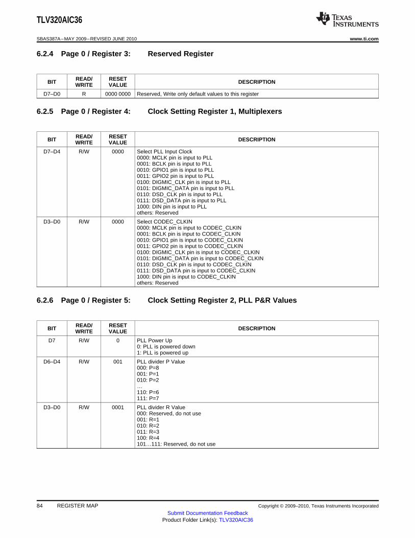
TLV320AIC36
SBAS387A–MAY 2009–REVISED JUNE 2010 www.ti.com
6.2.4 Page 0 / Register 3: Reserved Register
READ/ RESETBIT DESCRIPTIONWRITE VALUE
D7–D0 R 0000 0000 Reserved, Write only default values to this register
6.2.5 Page 0 / Register 4: Clock Setting Register 1, Multiplexers
READ/ RESETBIT DESCRIPTIONWRITE VALUE
D7–D4 R/W 0000 Select PLL Input Clock0000: MCLK pin is input to PLL0001: BCLK pin is input to PLL0010: GPIO1 pin is input to PLL0011: GPIO2 pin is input to PLL0100: DIGMIC_CLK pin is input to PLL0101: DIGMIC_DATA pin is input to PLL0110: DSD_CLK pin is input to PLL0111: DSD_DATA pin is input to PLL1000: DIN pin is input to PLLothers: Reserved
D3–D0 R/W 0000 Select CODEC_CLKIN0000: MCLK pin is input to CODEC_CLKIN0001: BCLK pin is input to CODEC_CLKIN0010: GPIO1 pin is input to CODEC_CLKIN0011: GPIO2 pin is input to CODEC_CLKIN0100: DIGMIC_CLK pin is input to CODEC_CLKIN0101: DIGMIC_DATA pin is input to CODEC_CLKIN0110: DSD_CLK pin is input to CODEC_CLKIN0111: DSD_DATA pin is input to CODEC_CLKIN1000: DIN pin is input to CODEC_CLKINothers: Reserved
6.2.6 Page 0 / Register 5: Clock Setting Register 2, PLL P&R Values
READ/ RESETBIT DESCRIPTIONWRITE VALUE
D7 R/W 0 PLL Power Up0: PLL is powered down1: PLL is powered up
D6–D4 R/W 001 PLL divider P Value000: P=8001: P=1010: P=2…110: P=6111: P=7
D3–D0 R/W 0001 PLL divider R Value000: Reserved, do not use001: R=1010: R=2011: R=3100: R=4101…111: Reserved, do not use
84 REGISTER MAP Copyright © 2009–2010, Texas Instruments Incorporated
Submit Documentation FeedbackProduct Folder Link(s): TLV320AIC36

TLV320AIC36
www.ti.com SBAS387A–MAY 2009–REVISED JUNE 2010
6.2.7 Page 0 / Register 6: Clock Setting Register 3, PLL J Values
READ/ RESETBIT DESCRIPTIONWRITE VALUE
D7–D6 R 00 Reserved. Write only default values any value other than default
D5–D0 R/W 00 0100 PLL divider J value00 0000…00 0011: Do not use00 0100: J=400 0101: J=5…11 1110: J=6211 1111: J=63
6.2.8 Page 0 / Register 7: Clock Setting Register 4, PLL D Values (MSB)
READ/ RESETBIT DESCRIPTIONWRITE VALUE
D7–D6 R 00 Reserved. Write only default values any value other than default
D5–D0 R/W 00 0000 PLL divider D value (MSB)PLL divider D value(MSB) & PLL divider D value(LSB)00 0000 0000 0000: D=000000 0000 0000 0001: D=0001…10 0111 0000 1110: D=999810 0111 0000 1111: D=999910 0111 0001 0000…11 1111 1111 1111: Do not useNote: This register will be updated only when the Page-0, Reg-8 is written immediately afterPage-0, Reg-7
6.2.9 Page 0 / Register 8: Clock Setting Register 5, PLL D Values (LSB)
READ/ RESETBIT DESCRIPTIONWRITE VALUE
D7–D0 R/W 0000 0000 PLL divider D value (LSB)PLL divider D value(MSB) & PLL divider D value(LSB)00 0000 0000 0000: D=000000 0000 0000 0001: D=0001…10 0111 0000 1110: D=999810 0111 0000 1111: D=999910 0111 0001 0000…11 1111 1111 1111: Do not useNote: Page-0, Reg-8 should be written immediately after Page-0, Reg-7
6.2.10 Page 0 / Register 9-10: Reserved Register
READ/ RESETBIT DESCRIPTIONWRITE VALUE
D7–D0 R 0000 0000 Reserved, Write only default values.
Copyright © 2009–2010, Texas Instruments Incorporated REGISTER MAP 85Submit Documentation Feedback
Product Folder Link(s): TLV320AIC36

TLV320AIC36
SBAS387A–MAY 2009–REVISED JUNE 2010 www.ti.com
6.2.11 Page 0 / Register 11: Clock Setting Register 6, NDAC Values
READ/ RESETBIT DESCRIPTIONWRITE VALUE
D7 R/W 0 NDAC Divider Power Control0: NDAC divider powered down1: NDAC divider powered up
D6–D0 R/W 000 0001 NDAC Value000 0000: NDAC=128000 0001: NDAC=1000 0010: NDAC=2…111 1110: NDAC=126111 1111: NDAC=127Note: Please check the clock frequency requirements in the Overview section
6.2.12 Page 0 / Register 12: Clock Setting Register 7, MDAC Values
READ/ RESETBIT DESCRIPTIONWRITE VALUE
D7 R/W 0 MDAC Divider Power Control0: MDAC divider powered down1: MDAC divider powered up
D6–D0 R/W 000 0001 MDAC Value000 0000: MDAC=128000 0001: MDAC=1000 0010: MDAC=2…111 1110: MDAC=126111 1111: MDAC=127Note: Please check the clock frequency requirements in the Overview section
6.2.13 Page 0 / Register 13: DAC OSR Setting Register 1, MSB Value
READ/ RESETBIT DESCRIPTIONWRITE VALUE
D7–D2 R 0000 00 Reserved. Write only default values
D1–D0 R/W 00 DAC OSR (DOSR) SettingDAC OSR(MSB) & DAC OSR(LSB)00 0000 0000: DOSR=102400 0000 0001: DOSR=100 0000 0010: DOSR=2…11 1111 1110: DOSR=102211 1111 1111: DOSR=1023Note: This register is updated when Page-0, Reg-14 is written to immediately after Page-0, Reg-13
86 REGISTER MAP Copyright © 2009–2010, Texas Instruments Incorporated
Submit Documentation FeedbackProduct Folder Link(s): TLV320AIC36

TLV320AIC36
www.ti.com SBAS387A–MAY 2009–REVISED JUNE 2010
6.2.14 Page 0 / Register 14: DAC OSR Setting Register 2, LSB Value
READ/ RESETBIT DESCRIPTIONWRITE VALUE
D7–D0 R/W 1000 0000 DAC OSR (DOSR) SettingDAC OSR(MSB) & DAC OSR(LSB)00 0000 0000: DOSR=102400 0000 0001: DOSR=100 0000 0010: DOSR=2…11 1111 1110: DOSR=102211 1111 1111: DOSR=1023Note: This register should be written immediately after Page-0, Reg-13
6.2.15 Page 0 / Register 15: DAC miniDSP Instruction Control Register 1
READ/ RESETBIT DESCRIPTIONWRITE VALUE
D7–D0 R/W 1000 0000 Use when DAC miniDSP is in use for signal processing (page 0,Reg 60)DAC miniDSP IDAC(7:0)1000 0000: DAC miniDSP IDAC = 10240000 0001: DAC miniDSP IDAC = 40000 0010: DAC miniDSP IDAC = 8……1111 1110: DAC miniDSP IDAC = 10121111 1111: DAC miniDSP IDAC = 1020Note: IDAC should be a integral multiple of INTERP ( Page-0, Reg-16)
6.2.16 Page 0 / Register 16: DAC miniDSP Interpolation Factor Setting Register
READ/ RESETBIT DESCRIPTIONWRITE VALUE
D7–D4 R 0000 Reserved. Write only default values
D3–D0 R/W 1000 DAC miniDSP interpolation factor setting.Used when DAC miniDSP is in use for signal processing (page 0,Reg 60)0000 : Interpolation factor in DAC miniDSP(INTERP) = 160001: Interpolation factor in DAC miniDSP(INTERP)= 10010: Interpolation factor in DAC miniDSP(INTERP) = 2…1110: Interpolation factor in DAC miniDSP(INTERP) = 141111: Interpolation factor in DAC miniDSP(INTERP) = 15
6.2.17 Page 0 / Register 17: Reserved Register
READ/ RESETBIT DESCRIPTIONWRITE VALUE
D7–D0 R 0000 0000 Reserved, Write only default values to this register
6.2.18 Page 0 / Register 18: Clock Setting Register 8, NADC Values
READ/ RESETBIT DESCRIPTIONWRITE VALUE
D7 R/W 0 NADC Clock Divider Power Control0: NADC divider powered down, ADC_CLK is same as DAC_CLK1: NADC divider powered up
Copyright © 2009–2010, Texas Instruments Incorporated REGISTER MAP 87Submit Documentation Feedback
Product Folder Link(s): TLV320AIC36

TLV320AIC36
SBAS387A–MAY 2009–REVISED JUNE 2010 www.ti.com
(continued)
READ/ RESETBIT DESCRIPTIONWRITE VALUE
D6–D0 R/W 000 0001 NADC Value000 0000: NADC=128000 0001: NADC=1…111 1110: NADC=126111 1111: NADC=127
6.2.19 Page 0 / Register 19: Clock Setting Register 9, MADC Values
READ/ RESETBIT DESCRIPTIONWRITE VALUE
D7 R/W 0 MADC Clock Divider Power Control0: MADC divider powered down, ADC_MOD_CLK is same as DAC_MOD_CLK1: MADC divider powered up
D6–D0 R/W 000 0001 MADC Value000 0000: MADC=128000 0001: MADC=1…111 1110: MADC=126111 1111: MADC=127
6.2.20 Page 0 / Register 20: ADC Oversampling (AOSR) Register
READ/ RESETBIT DESCRIPTIONWRITE VALUE
D7–D0 R/W 1000 0000 ADC Oversampling Value0000 0000: ADC AOSR = 2560000 0001: ADC AOSR = 10000 0010: ADC AOSR = 2...0010 0000: ADC AOSR=32 (Use with PRB_R13 to PRB_R18, ADC Filter Type C)...0100 0000: AOSR=64 (Use with PRB_R1 to PRB_R12, ADC Filter Type A or B)...1000 0000: AOSR=128 (Use with PRB_R1 to PRB_R6, ADC Filter Type A)...1111 1110: ADC AOSR = 2541111 1111: ADC AOSR = 255Note: If the ADC miniDSP will be used for signal processing ADC (Pg 0, Reg 61) AOSR should bean integral multiple of ADC DECIM factor.
6.2.21 Page 0 / Register 21: ADC miniDSP Instruction Control Register 1
READ/ RESETBIT DESCRIPTIONWRITE VALUE
D7–D0 R/W 1000 0000 ADC miniDSP IADC (7:0) setting. Use when ADC miniDSP is in use for signal processing (page0,Reg 61)0000 0000: Don't use (Reserved)0000 0001: ADC miniDSP IADC = 20000 0010: ADC miniDSP IADC = 4……1111 1110: ADC miniDSP IADC = 5081111 1111: ADC miniDSP IADC = 510Note: IADC should be a integral multiple of DECIM ( Page-0, Reg-22 )
88 REGISTER MAP Copyright © 2009–2010, Texas Instruments Incorporated
Submit Documentation FeedbackProduct Folder Link(s): TLV320AIC36

TLV320AIC36
www.ti.com SBAS387A–MAY 2009–REVISED JUNE 2010
6.2.22 Page 0 / Register 22: ADC miniDSP Decimation Factor Setting Register
READ/ RESETBIT DESCRIPTIONWRITE VALUE
D7–D4 R 0000 Reserved. Write only default values
D3–D0 R/W 0100 ADC miniDSP Decimation factor setting. Use when ADC miniDSP is in use for signal processing(page 0,Reg 61)0000: Decimation factor in ADC miniDSP = 160001: Decimation factor in ADC miniDSP = 10010: Decimation factor in ADC miniDSP = 2…1110: Decimation factor in ADC miniDSP = 141111: Decimation factor in ADC miniDSP = 15
6.2.23 Page 0 / Register 23: Clock Setting Register 9, Multiplexers
READ/ RESETBIT DESCRIPTIONWRITE VALUE
D7–D3 R 0000 0 Reserved. Write only default values
D2–D0 R/W 000 CDIV_CLKIN Clock Selection000: CDIV_CLKIN= MCLK001: CDIV_CLKIN= BCLK010: CDIV_CLKIN=DIN011: CDIV_CLKIN=PLL_CLK100: CDIV_CLKIN=DAC_CLK101: CDIV_CLKIN=DAC_MOD_CLK110: CDIV_CLKIN=ADC_CLK111: CDIV_CLKIN=ADC_MOD_CLK
6.2.24 Page 0 / Register 24: Clock Setting Register 10, CLKOUT M Divider Value
READ/ RESETBIT DESCRIPTIONWRITE VALUE
D7 R/W 0 CLKOUT M divider power control0: CLKOUT M divider powered down1: CLKOUT M divider powered up
D6–D0 R/W 000 0001 CLKOUT M divider value000 0000: CLKOUT M divider = 128000 0001: CLKOUT M divider = 1000 0010: CLKOUT M divider = 2…111 1110: CLKOUT M divider = 126111 1111: CLKOUT M divider = 127
6.2.25 Page 0 / Register 25: Audio Interface Setting Register 1
READ/ RESETBIT DESCRIPTIONWRITE VALUE
D7–D6 R/W 00 Audio Interface Selection00: Audio Interface = I2S01: Audio Interface = DSP10: Audio Interface = RJF11: Audio Interface = LJF
D5–D4 R/W 00 Audio Data Word length00: Data Word length = 16 bits01: Data Word length = 20 bits10: Data Word length = 24 bits11: Data Word length = 32 bits
Copyright © 2009–2010, Texas Instruments Incorporated REGISTER MAP 89Submit Documentation Feedback
Product Folder Link(s): TLV320AIC36

TLV320AIC36
SBAS387A–MAY 2009–REVISED JUNE 2010 www.ti.com
(continued)
READ/ RESETBIT DESCRIPTIONWRITE VALUE
D3 R/W 0 BCLK Direction Control0: BCLK is input to the device1: BCLK is output from the device
D2 R/W 0 WCLK Direction Control0: WCLK is input to the device1: WCLK is output from the device
D1 R 0 Reserved. Write only default value
D0 R/W 0 DOUT High Impendance Output Control0: DOUT will not be high impedance while Audio Interface is active1: DOUT will be high impedance after data has been transferred
6.2.26 Page 0 / Register 26: Audio Interface Setting Register 2, Data offset setting
READ/ RESETBIT DESCRIPTIONWRITE VALUE
D7–D0 R/W 0000 0000 Data Offset Value0000 0000: Data Offset = 0 BCLK's0000 0001: Data Offset = 1 BCLK's…1111 1110: Data Offset = 254 BCLK's1111 1111: Data Offset = 255 BCLK's
6.2.27 Page 0 / Register 27: Audio Interface Setting Register 3
READ/ RESETBIT DESCRIPTIONWRITE VALUE
D7–D6 R 00 Reserved. Write only default values
D5 R/W 0 Loopback control0: No Loopback1: Audio Data in is routed to Audio Data out
D4 R/W 0 Loopback control0: No Loopback1: Stereo ADC output is routed to Stereo DAC input
D3 R/W 0 Audio Bit Clock Polarity Control0: Default Bit Clock polarity1: Bit Clock is inverted with respect to default polarity
D2 R/W 0 Primary BCLK and Primary WCLK Power control0: Primary BCLK and Primary WCLK buffers are powered up when they are used in clockgeneration even when the codec is powered down1: Priamry BCLK and Primary WCLK buffers are powered down when the codec is powered down
D1–D0 R/W 00 BDIV_CLKIN Multiplexer Control00: BDIV_CLKIN = DAC_CLK01: BDIV_CLKIN = DAC_MOD_CLK10: BDIV_CLKIN = ADC_CLK11: BDIV_CLKIN = ADC_MOD_CLK
6.2.28 Page 0 / Register 28: Clock Setting Register 11, BCLK N Divider
READ/ RESETBIT DESCRIPTIONWRITE VALUE
D7 R/W 0 BCLK N Divider Power Control0: BCLK N divider powered down1: BCLK N divider powered up
90 REGISTER MAP Copyright © 2009–2010, Texas Instruments Incorporated
Submit Documentation FeedbackProduct Folder Link(s): TLV320AIC36

TLV320AIC36
www.ti.com SBAS387A–MAY 2009–REVISED JUNE 2010
(continued)
READ/ RESETBIT DESCRIPTIONWRITE VALUE
D6–D0 R/W 000 0001 BCLK N Divider value0000 0000: BCLK N divider = 1280000 0001: BCLK N divider = 1…1111 1110: BCLK N divider = 1261111 1111: BCLK N divider = 127
6.2.29 Page 0 / Register 29: Reserved Register
READ/ RESETBIT DESCRIPTIONWRITE VALUE
D7–D0 R 0000 0000 Reserved, Write only default values to this register
6.2.30 Page 0 / Register 30: Audio Interface Setting Register 4
READ/ RESETBIT DESCRIPTIONWRITE VALUE
D7–D6 R 00 Reserved. Write only default values
D5–D3 R/W 000 Secondary Bit Clock Multiplexer000: Secondary Bit Clock = GPIO1 pin001: Secondary Bit Clock = GPIO2 pin010: Secondary Bit Clock = DIGMIC_CLK pin011: Secondary Bit Clock = DIGMIC_DATA pin100: Secondary Bit Clock = DSD_CLK pin101: Secondary Bit Clock = DSD_DATA pin110: Secondary Bit Clock = SDOUT pin111: Reserved
D2–D0 R/W 000 Secondary Word Clock Multiplexer000: Secondary Word Clock = GPIO1 pin001: Secondary Word Clock = GPIO2 pin010: Secondary Word Clock = DIGMIC_CLK pin011: Secondary Word Clock = DIGMIC_DATA pin100: Secondary Word Clock = DSD_CLK pin101: Secondary Word Clock = DSD_DATA pin110: Secondary Word Clock = SDOUT pin111: Reserved
6.2.31 Page 0 / Register 31: Audio Interface Setting Register 5
READ/ RESETBIT DESCRIPTIONWRITE VALUE
D7–D6 R 00 Reserved. Write only default values
D5–D3 R/W 000 Secondary ADC_CLK Multiplexer000: Secondary ADC_CLK = GPIO1 pin001: Secondary ADC_CLK = GPIO2 pin010: Secondary ADC_CLK = DIGMIC_CLK pin011: Secondary ADC_CLK = DIGMIC_DATA pin100: Secondary ADC_CLK = DSD_CLK pin101: Secondary ADC_CLK = DSD_DATA pin110: Secondary ADC_CLK = SDOUT pin111: Reserved
Copyright © 2009–2010, Texas Instruments Incorporated REGISTER MAP 91Submit Documentation Feedback
Product Folder Link(s): TLV320AIC36

TLV320AIC36
SBAS387A–MAY 2009–REVISED JUNE 2010 www.ti.com
(continued)
READ/ RESETBIT DESCRIPTIONWRITE VALUE
D2–D0 R/W 000 Secondary DIN Multiplexer000: Secondary DIN = GPIO1 pin001: Secondary DIN = GPIO2 pin010: Secondary DIN = DIGMIC_CLK pin011: Secondary DIN = DIGMIC_DATA pin100: Secondary DIN = DSD_CLK pin101: Secondary DIN = DSD_DATA pin110: Secondary DIN = SDOUT pin111: Reserved
6.2.32 Page 0 / Register 32: Audio Interface Setting Register 6
READ/ RESETBIT DESCRIPTIONWRITE VALUE
D7–D5 R 000 Reserved. Write only default values
D4 R/W 0 Primary / Secondary Word Clock Control for DAC engine0: DAC engine uses WCLK for Audio Interface1: DAC engine uses internally generated DAC_CLK for Audio Interface
D3 R/W 0 Primary / Secondary Bit Clock Control Select0: Primary Bit Clock(BCLK) is used for Audio Interface and Clocking1: Secondary Bit Clock is used for Audio Interface and Clocking
D2 R/W 0 Primary / Secondary Word Clock Control0: Primary Word Clock(WCLK) is used for Audio Interface1: Secondary Word Clock is used for Audio Interface
D1 R/W 0 ADC Word Clock Control0: ADC Word Clock is same as DAC Word Clock1: ADC Word Clock is Secondary ADC Word Clock
D0 R/W 0 Audio Data In Control0: DIN is used for Audio Data In1: Secondary Data In is used for Audio Data In
6.2.33 Page 0 / Register 33: Audio Interface Setting Register 7
READ/ RESETBIT DESCRIPTIONWRITE VALUE
D7 R/W 0 BCLK Output Control0: BCLK Output = Generated Primary Bit Clock1: BCLK Output = Secondary Bit Clock Input
D6 R/W 0 Secondary Bit Clock Output Control0: Secondary Bit Clock = BCLK input1: Secondary Bit Clock = Generated Primary Bit Clock
D5–D4 R/W 00 WCLK Output Control00: WCLK Output = Generated DAC_FS01: WCLK Output = Generated ADC_FS10: WCLK Output = Secondary Word Clock Input11: Do not use
D3–D2 R/W 00 Secondary Word Clock Output Control00: Secondary Word Clock output = WCLK input01: Secondary Word Clock output = Generated DAC_FS10: Secondary Word Clock output = Generated ADC_FS11: Do not use
D1 R/W 0 Primary Data Out output control0: DOUT output = Data Output from Serial Interface1: DOUT output = Secondary Data Input (Loopback)
D0 R/W 0 Secondary Data Out output control0: Secondary Data Output = DIN input (Loopback)1: Secondary Data Output = Data output from Serial Interface
92 REGISTER MAP Copyright © 2009–2010, Texas Instruments Incorporated
Submit Documentation FeedbackProduct Folder Link(s): TLV320AIC36

TLV320AIC36
www.ti.com SBAS387A–MAY 2009–REVISED JUNE 2010
6.2.34 Page 0 / Register 34 - 35: Reserved Registers
READ/ RESETBIT DESCRIPTIONWRITE VALUE
D7–D0 R 0000 0000 Reserved, Write only default values to this register
6.2.35 Page 0 / Register 36: ADC Flag Register
READ/ RESETBIT DESCRIPTIONWRITE VALUE
D7 R 0 Left ADC PGA Status Flag0: Gain Applied in Left ADC PGA is not equal to Programmed Gain in Control Register1: Gain Applied in Left ADC PGA is equal to Programmed Gain in Control Register
D6 R 0 Left ADC Power Status Flag0: Left ADC Powered Down1: Left ADC Powered Up
D5 R 0 Left AGC Gain Status. This sticky flag will self clear on reading0: Gain in Left AGC is not saturated1: Gain in Left ADC is equal to maximum allowed gain in Left AGC
D4 R 0 Reserved. Write only default value
D3 R 0 Right ADC PGA Status Flag0: Gain Applied in Right ADC PGA is not equal to Programmed Gain in Control Register1: Gain Applied in Right ADC PGA is equal to Programmed Gain in Control Register
D2 R 0 Right ADC Power Status Flag0: Right ADC Powered Down1: Right ADC Powered Up
D1 R 0 Right AGC Gain Status. This sticky flag will self clear on reading0: Gain in Right AGC is not saturated1: Gain in Right ADC is equal to maximum allowed gain in Right AGC
D0 R 0 Reserved. Write only default value
6.2.36 Page 0 / Register 37: DAC Flag Register 1
READ/ RESETBIT DESCRIPTIONWRITE VALUE
D7 R 0 Left DAC Power Status Flag0: Left DAC Powered Down1: Left DAC Powered Up
D6–D4 R 000 Reserved. Write only default values
D3 R 0 Right DAC Power Status Flag0: Right DAC Powered Down1: Right DAC Powered Up
D2 R 0 Left DAC PGA Status Flag0: Gain applied in Left DAC PGA is not equal to Gain programmed in Control Register1: Gain applied in Left DAC PGA is equal to Gain programmed in Control Register
D1 R 0 Right DAC PGA Status Flag0: Gain applied in Right DAC PGA is not equal to Gain programmed in Control Register1: Gain applied in Right DAC PGA is equal to Gain programmed in Control Register
D0 R 0 Reserved. Write only default values
Copyright © 2009–2010, Texas Instruments Incorporated REGISTER MAP 93Submit Documentation Feedback
Product Folder Link(s): TLV320AIC36

TLV320AIC36
SBAS387A–MAY 2009–REVISED JUNE 2010 www.ti.com
6.2.37 Page 0 / Register 38: Sticky Flag Register 1
READ/ RESETBIT DESCRIPTIONWRITE VALUE
D7 R/W 0 Right Channel DRC, Signal Threshold Flag0: Signal Power is below Signal Threshold1: Signal Power exceeded Signal Threshold (will be cleared when the register is read)
D6 R/W 0 Left Channel DRC, Signal Threshold Flag0: Signal Power is below Signal Threshold1: Signal Power exceeded Signal Threshold (will be cleared when the register is read)
D5 R/W 0 ADC miniDSP Barrel Shifter Output Overflow Sticky Flag.Flag is reset on register reading
D4 R/W 0 Right ADC Overflow Status. This sticky flag will self clear on read0: No overflow in Right ADC1: Overflow has happened in Right ADC since last read of this register
D3 R/W 0 Left ADC Overflow Status. This sticky flag will self clear on read0: No overflow in Left ADC1: Overflow has happened in Left ADC since last read of this register
D2 R/W 0 DAC miniDSP Barrel Shifter Output Overflow Sticky Flag.Flag is reset on register reading
D1 R/W 0 Right DAC Overflow Status. This sticky flag will self clear on read0: No overflow in Right DAC1: Overflow has happened in Right DAC since last read of this register
D0 R/W 0 Left DAC Overflow Status. This sticky flag will self clear on read0: No overflow in Left DAC1: Overflow has happened in Left DAC since last read of this register
6.2.38 Page 0 / Register 39: Interrupt Flag Register 1
READ/ RESETBIT DESCRIPTIONWRITE VALUE
D7 R 0 Right Channel DRC, Signal Threshold Flag0: Signal Power is below Signal Threshold1: Signal Power exceeded Signal Threshold
D6 R 0 Left Channel DRC, Signal Threshold Flag0: Signal Power is below Signal Threshold1: Signal Power exceeded Signal Threshold
D5 R 0 ADC Barrel Shifter Output Overflow Flag0: no overflow1: overflow
D4 R 0 Right ADC Overflow Flag0: no overflow1: overflow
D3 R 0 Left ADC Overflow Flag0: no overflow1: overflow
D2 R 0 DAC Barrel Shifter Output Overflow Flag0: no overflow1: overflow
D1 R 0 Right DAC Overflow Flag0: no overflow1: overflow
D0 R 0 Left DAC Overflow Flag0: no overflow1: overflow
94 REGISTER MAP Copyright © 2009–2010, Texas Instruments Incorporated
Submit Documentation FeedbackProduct Folder Link(s): TLV320AIC36

TLV320AIC36
www.ti.com SBAS387A–MAY 2009–REVISED JUNE 2010
6.2.39 Page 0 / Register 40: Interrupt Enable Control Register 1 (INT1)
READ/ RESETBIT DESCRIPTIONWRITE VALUE
D7 R/W 0 Right DAC Signal Power is above Signal Threshold of DRC interrupt to INT10: disabled1: enabled
D6 R/W 0 Left DAC Signal Power is above Signal Threshold of DRC interrupt to INT10: disabled1: enabled
D5 R/W 0 ADC Barrel Shifter Output Overflow interrupt to INT10: disabled1: enabled
D4 R/W 0 Right ADC Overflow interrupt to INT10: disabled1: enabled
D3 R/W 0 Left ADC Overflow interrupt to INT10: disabled1: enabled
D2 R/W 0 DAC Barrel Shifter Output Overflow interrupt to INT10: disabled1: enabled
D1 R/W 0 Right DAC Overflow interrupt to INT10: disabled1: enabled
D0 R/W 0 Left DAC Overflow interrupt to INT10: disabled1: enabled
6.2.40 Page 0 / Register 41: Interrupt Enable Control Register 2 (INT2)
READ/ RESETBIT DESCRIPTIONWRITE VALUE
D7 R/W 0 Right DAC Signal Power is above Signal Threshold of DRC interrupt to INT10: disabled1: enabled
D6 R/W 0 Left DAC Signal Power is above Signal Threshold of DRC interrupt to INT20: disabled1: enabled
D5 R/W 0 ADC Barrel Shifter Output Overflow interrupt to INT20: disabled1: enabled
D4 R/W 0 Right ADC Overflow interrupt to INT20: disabled1: enabled
D3 R/W 0 Left ADC Overflow interrupt to INT20: disabled1: enabled
D2 R/W 0 DAC Barrel Shifter Output Overflow interrupt to INT20: disabled1: enabled
D1 R/W 0 Right DAC Overflow interrupt to INT20: disabled1: enabled
D0 R/W 0 Left DAC Overflow interrupt to INT20: disabled1: enabled
Copyright © 2009–2010, Texas Instruments Incorporated REGISTER MAP 95Submit Documentation Feedback
Product Folder Link(s): TLV320AIC36

TLV320AIC36
SBAS387A–MAY 2009–REVISED JUNE 2010 www.ti.com
6.2.41 Page 0 / Register 42: Sticky Flag Register 2
READ/ RESETBIT DESCRIPTIONWRITE VALUE
D7 R 0 Right ADC DC Measurement Data Available Flag0: Data not available1: Data available (will be cleared when the register is read)
D6 R 0 Left ADC DC Measurement Data Available Flag0: Data not available1: Data available (will be cleared when the register is read)
D5 R 0 ADC miniDSP Auxilliary Interrupt Port Output (will be cleaed when register is read)
D4 R 0 ADC miniDSP Standard Interrupt Port Output (will be cleaed when register is read)
D3 R 0 Right AGC Noise Threshold Flag0: Signal Power is greater than Noise Threshold1: Signal Power was lower than Noise Threshold (will be cleared when the register is read)
D2 R 0 Left AGC Noise Threshold Flag0: Signal Power is greater than Noise Threshold1: Signal Power was lower than Noise Threshold (will be cleared when the register is read)
D1 R 0 DAC miniDSP Auxilliary Interrupt Port Output (will be cleaed when register is read)
D0 R 0 DAC miniDSP Standard Interrupt Port Output (will be cleaed when register is read)
6.2.42 Page 0 / Register 43: Interrupt Flag Register 2
READ/ RESETBIT DESCRIPTIONWRITE VALUE
D7 0 0 Right ADC DC Measurement Data Available Flag0: Data not available1: Data available
D6 R 0 Left ADC DC Measurement Data Available Flag0: Data not available1: Data available
D5 R 0 ADC miniDSP Auxilliary Interrupt Port Output
D4 R 0 ADC miniDSP Standard Interrupt Port Output
D3 R 0 Right AGC Noise Threshold Flag0: Signal Power is greater than Noise Threshold1: Signal Power was lower than Noise Threshold
D2 R 0 Left AGC Noise Threshold Flag0: Signal Power is greater than Noise Threshold1: Signal Power was lower than Noise Threshold
D1 R 0 DAC miniDSP Auxilliary Interrupt Port Output
D0 R 0 DAC miniDSP Standard Interrupt Port Output
6.2.43 Page 0 / Register 44: Interrupt Enable Control Register 3 (INT1)
READ/ RESETBIT DESCRIPTIONWRITE VALUE
D7 R/W 0 Right DAC Signal Power is above Signal Threshold of DRC to INT10: disabled1: enabled
D6 R/W 0 Left DAC Signal Power is above Signal Threshold of DRC to INT10: disabled1: enabled
D5 R/W 0 ADC MAC Engine Auxilliary Interrupt to INT10: disabled1: enabled
96 REGISTER MAP Copyright © 2009–2010, Texas Instruments Incorporated
Submit Documentation FeedbackProduct Folder Link(s): TLV320AIC36

TLV320AIC36
www.ti.com SBAS387A–MAY 2009–REVISED JUNE 2010
(continued)
READ/ RESETBIT DESCRIPTIONWRITE VALUE
D4 R/W 0 ADC MAC Engine Standard Interrupt to INT10: disabled1: enabled
D3 R/W 0 Right ADC Signal Power Lesser than Noise Threshold for Right AGC to INT10: disabled1: enabled
D2 R/W 0 Left ADC Signal Power Lesser than Noise Threshold for Left AGC to INT10: disabled1: enabled
D1 R/W 0 DAC MAC Engine Auxilliary Interrupt to INT10: disabled1: enabled
D0 R/W 0 DAC MAC Engine Standard Interrupt to INT10: disabled1: enabled
6.2.44 Page 0 / Register 45: Interrupt Enable Control Register 4 (INT2)
READ/ RESETBIT DESCRIPTIONWRITE VALUE
D7 R/W 0 Right DAC Signal Power is above Signal Threshold of DRC to INT20: disabled1: enabled
D6 R/W 0 Left DAC Signal Power is above Signal Threshold of DRC to INT20: disabled1: enabled
D5 R/W 0 ADC MAC Engine Auxilliary Interrupt to INT20: disabled1: enabled
D4 R/W 0 ADC MAC Engine Standard Interrupt to INT20: disabled1: enabled
D3 R/W 0 Right ADC Signal Power Lesser than Noise Threshold for Right AGC to INT20: disabled1: enabled
D2 R/W 0 Left ADC Signal Power Lesser than Noise Threshold for Left AGC to INT20: disabled1: enabled
D1 R/W 0 DAC MAC Engine Auxilliary Interrupt to INT20: disabled1: enabled
D0 R/W 0 DAC MAC Engine Standard Interrupt to INT20: disabled1: enabled
6.2.45 Page 0 / Register 46: Sticky Flag Register 3
READ/ RESETBIT DESCRIPTIONWRITE VALUE
D7 R 0 Reserved. Write only default values
D6 R 0 Overcurrent on VDD_ADC_LDO interrupt0: no overcurrent condition1: overcurrent condition detected (will be cleared when the register is read)
Copyright © 2009–2010, Texas Instruments Incorporated REGISTER MAP 97Submit Documentation Feedback
Product Folder Link(s): TLV320AIC36
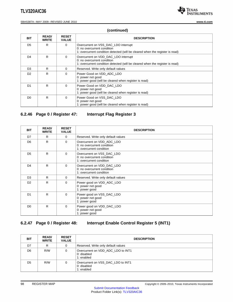
TLV320AIC36
SBAS387A–MAY 2009–REVISED JUNE 2010 www.ti.com
(continued)
READ/ RESETBIT DESCRIPTIONWRITE VALUE
D5 R 0 Overcurrent on VSS_DAC_LDO interrupt0: no overcurrent condition1: overcurrent condition detected (will be cleared when the register is read)
D4 R 0 Overcurrent on VDD_DAC_LDO interrupt0: no overcurrent condition1: overcurrent condition detected (will be cleared when the register is read)
D3 R 0 Reserved. Write only default values
D2 R 0 Power Good on VDD_ADC_LDO0: power not good1: power good (will be cleared when register is read)
D1 R 0 Power Good on VDD_DAC_LDO0: power not good1: power good (will be cleared when register is read)
D0 R 0 Power Good on VSS_DAC_LDO0: power not good1: power good (will be cleared when register is read)
6.2.46 Page 0 / Register 47: Interrupt Flag Register 3
READ/ RESETBIT DESCRIPTIONWRITE VALUE
D7 R 0 Reserved. Write only default values
D6 R 0 Overcurrent on VDD_ADC_LDO0: no overcurrent condition1: overcurrent condition
D5 R 0 Overcurrent on VSS_DAC_LDO0: no overcurrent condition1: overcurrent condition
D4 R 0 Overcurrent on VDD_DAC_LDO0: no overcurrent condition1: overcurrent condition
D3 R 0 Reserved. Write only default values
D2 R 0 Power good on VDD_ADC_LDO0: power not good1: power good
D1 R 0 Power good on VSS_DAC_LDO0: power not good1: power good
D0 R 0 Power good on VDD_DAC_LDO0: power not good1: power good
6.2.47 Page 0 / Register 48: Interrupt Enable Control Register 5 (INT1)
READ/ RESETBIT DESCRIPTIONWRITE VALUE
D7 R 0 Reserved. Write only default values
D6 R/W 0 Overcurrent on VDD_ADC_LDO to INT10: disabled1: enabled
D5 R/W 0 Overcurrent on VSS_DAC_LDO to INT10: disabled1: enabled
98 REGISTER MAP Copyright © 2009–2010, Texas Instruments Incorporated
Submit Documentation FeedbackProduct Folder Link(s): TLV320AIC36
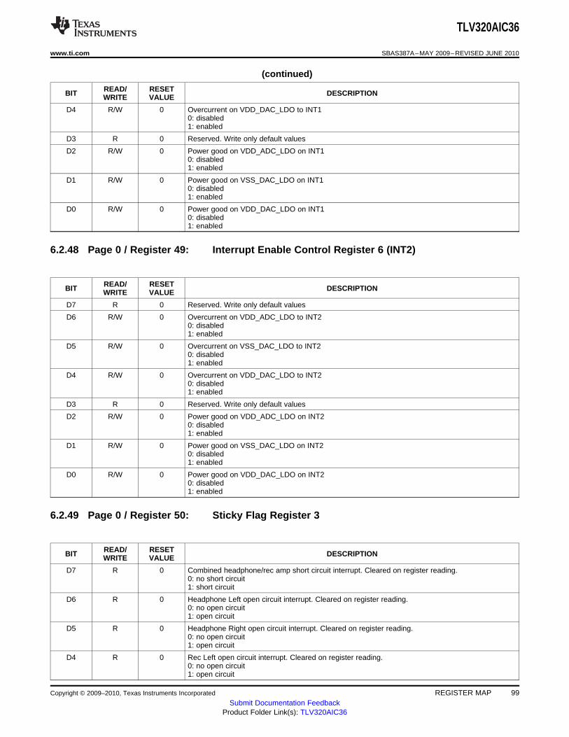
TLV320AIC36
www.ti.com SBAS387A–MAY 2009–REVISED JUNE 2010
(continued)
READ/ RESETBIT DESCRIPTIONWRITE VALUE
D4 R/W 0 Overcurrent on VDD_DAC_LDO to INT10: disabled1: enabled
D3 R 0 Reserved. Write only default values
D2 R/W 0 Power good on VDD_ADC_LDO on INT10: disabled1: enabled
D1 R/W 0 Power good on VSS_DAC_LDO on INT10: disabled1: enabled
D0 R/W 0 Power good on VDD_DAC_LDO on INT10: disabled1: enabled
6.2.48 Page 0 / Register 49: Interrupt Enable Control Register 6 (INT2)
READ/ RESETBIT DESCRIPTIONWRITE VALUE
D7 R 0 Reserved. Write only default values
D6 R/W 0 Overcurrent on VDD_ADC_LDO to INT20: disabled1: enabled
D5 R/W 0 Overcurrent on VSS_DAC_LDO to INT20: disabled1: enabled
D4 R/W 0 Overcurrent on VDD_DAC_LDO to INT20: disabled1: enabled
D3 R 0 Reserved. Write only default values
D2 R/W 0 Power good on VDD_ADC_LDO on INT20: disabled1: enabled
D1 R/W 0 Power good on VSS_DAC_LDO on INT20: disabled1: enabled
D0 R/W 0 Power good on VDD_DAC_LDO on INT20: disabled1: enabled
6.2.49 Page 0 / Register 50: Sticky Flag Register 3
READ/ RESETBIT DESCRIPTIONWRITE VALUE
D7 R 0 Combined headphone/rec amp short circuit interrupt. Cleared on register reading.0: no short circuit1: short circuit
D6 R 0 Headphone Left open circuit interrupt. Cleared on register reading.0: no open circuit1: open circuit
D5 R 0 Headphone Right open circuit interrupt. Cleared on register reading.0: no open circuit1: open circuit
D4 R 0 Rec Left open circuit interrupt. Cleared on register reading.0: no open circuit1: open circuit
Copyright © 2009–2010, Texas Instruments Incorporated REGISTER MAP 99Submit Documentation Feedback
Product Folder Link(s): TLV320AIC36

TLV320AIC36
SBAS387A–MAY 2009–REVISED JUNE 2010 www.ti.com
(continued)
READ/ RESETBIT DESCRIPTIONWRITE VALUE
D3 R 0 Rec Right open circuit interrupt. Cleared on register reading.0: no open circuit1: open circuit
D2 R 0 Hook Interrupt. Cleared on register reading.0: no interrupt1: interrupt
D1 R 0 Detect long pulse. Cleared on register reading.0: no long pulse detect1: long pulse detect
D0 R 0 Detect short pulse. Cleared on register reading.0: no short pulse detect1: short pulse detect
6.2.50 Page 0 / Register 51: Interrupt Flag Register 4
READ/ RESETBIT DESCRIPTIONWRITE VALUE
D7 R 0 Combined headphone/rec amp short circuit interrupt.0: no short circuit1: short circuit
D6 R 0 Headphone Left open circuit interrupt.0: no open circuit1: open circuit
D5 R 0 Headphone Right open circuit interrupt.0: no open circuit1: open circuit
D4 R 0 Rec Left open circuit interrupt.0: no open circuit1: open circuit
D3 R 0 Rec Right open circuit interrupt.0: no open circuit1: open circuit
D2 R 0 Hook Interrupt.0: no interrupt1: interrupt
D1 R 0 Detect long pulse.0: no long pulse detect1: long pulse detect
D0 R 0 Detect short pulse.0: no short pulse detect1: short pulse detect
6.2.51 Page 0 / Register 52: Interrupt Enable Control Register 7 (INT1)
READ/ RESETBIT DESCRIPTIONWRITE VALUE
D7 0 0 Combined headphone/rec amp short circuit interrupt for INT10: disabled1: enabled
D6 R/W 0 Headphone Left open circuit interrupt for INT10: disabled1: enabled
D5 R/W 0 Headphone Right open circuit interrupt for INT10: disabled1: enabled
100 REGISTER MAP Copyright © 2009–2010, Texas Instruments Incorporated
Submit Documentation FeedbackProduct Folder Link(s): TLV320AIC36
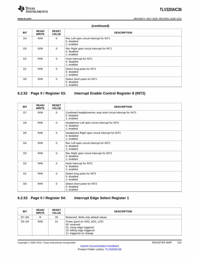
TLV320AIC36
www.ti.com SBAS387A–MAY 2009–REVISED JUNE 2010
(continued)
READ/ RESETBIT DESCRIPTIONWRITE VALUE
D4 R/W 0 Rec Left open circuit interrupt for INT10: disabled1: enabled
D3 R/W 0 Rec Right open circuit interrupt for INT10: disabled1: enabled
D2 R/W 0 Hook Interrupt for INT10: disabled1: enabled
D1 R/W 0 Detect long pulse for INT10: disabled1: enabled
D0 R/W 0 Detect short pulse for INT10: disabled1: enabled
6.2.52 Page 0 / Register 53: Interrupt Enable Control Register 8 (INT2)
READ/ RESETBIT DESCRIPTIONWRITE VALUE
D7 R/W 0 Combined headphone/rec amp short circuit interrupt for INT20: disabled1: enabled
D6 R/W 0 Headphone Left open circuit interrupt for INT20: disabled1: enabled
D5 R/W 0 Headphone Right open circuit interrupt for INT20: disabled1: enabled
D4 R/W 0 Rec Left open circuit interrupt for INT20: disabled1: enabled
D3 R/W 0 Rec Right open circuit interrupt for INT20: disabled1: enabled
D2 R/W 0 Hook Interrupt for INT20: disabled1: enabled
D1 R/W 0 Detect long pulse for INT20: disabled1: enabled
D0 R/W 0 Detect short pulse for INT20: disabled1: enabled
6.2.53 Page 0 / Register 54: Interrupt Edge Select Register 1
READ/ RESETBIT DESCRIPTIONWRITE VALUE
D7–D6 R 00 Reserved. Write only default values
D5–D4 R/W 01 Power good on VDD_ADC_LDO00: reserved01: rising edge triggered10: falling edge triggered11: triggered on change
Copyright © 2009–2010, Texas Instruments Incorporated REGISTER MAP 101Submit Documentation Feedback
Product Folder Link(s): TLV320AIC36

TLV320AIC36
SBAS387A–MAY 2009–REVISED JUNE 2010 www.ti.com
(continued)
READ/ RESETBIT DESCRIPTIONWRITE VALUE
D3–D2 R/W 01 Power good on VSS_DAC_LDO00: reserved01: rising edge triggered10: falling edge triggered11: triggered on change
D1–D0 R/W 01 Power good on VDD_DAC_LDO00: reserved01: rising edge triggered10: falling edge triggered11: triggered on change
6.2.54 Page 0 / Register 55: Interrupt Edge Select Register 2
READ/ RESETBIT DESCRIPTIONWRITE VALUE
D7–D6 R/W 01 Left HP over current00: reserved01: rising edge triggered10: falling edge triggered11: triggered on change
D5–D4 R/W 01 VDD_ADC_LDO overcurrent00: reserved01: rising edge triggered10: falling edge triggered11: triggered on change
D3–D2 R/W 01 VSS_DAC_LDO overcurrent00: reserved01: rising edge triggered10: falling edge triggered11: triggered on change
D1–D0 R/W 01 VDD_DAC_LDO overcurrent00: reserved01: rising edge triggered10: falling edge triggered11: triggered on change
6.2.55 Page 0 / Register 56: Interrupt Edge Select Register 3
READ/ RESETBIT DESCRIPTIONWRITE VALUE
D7–D6 R/W 01 Right HP over current00: reserved01: rising edge triggered10: falling edge triggered11: triggered on change
D5–D4 R/W 01 Left REC over current00: reserved01: rising edge triggered10: falling edge triggered11: triggered on change
D3–D2 R/W 01
D1–D0 R/W 01 Hook over current00: reserved01: rising edge triggered10: falling edge triggered11: triggered on change
102 REGISTER MAP Copyright © 2009–2010, Texas Instruments Incorporated
Submit Documentation FeedbackProduct Folder Link(s): TLV320AIC36
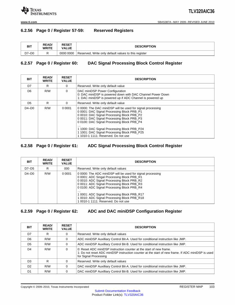
TLV320AIC36
www.ti.com SBAS387A–MAY 2009–REVISED JUNE 2010
6.2.56 Page 0 / Register 57-59: Reserved Registers
READ/ RESETBIT DESCRIPTIONWRITE VALUE
D7–D0 R 0000 0000 Reserved, Write only default values to this register
6.2.57 Page 0 / Register 60: DAC Signal Processing Block Control Register
READ/ RESETBIT DESCRIPTIONWRITE VALUE
D7 R 0 Reserved. Write only default value
D6 R/W 0 DAC miniDSP Power Configuration0: DAC miniDSP is powered down with DAC Channel Power Down1: DAC miniDSP is powered up if ADC Channel is powered up
D5 R 0 Reserved. Write only default value
D4–D0 R/W 0 0001 0 0000: The DAC miniDSP will be used for signal processing0 0001: DAC Signal Processing Block PRB_P10 0010: DAC Signal Processing Block PRB_P20 0011: DAC Signal Processing Block PRB_P30 0100: DAC Signal Processing Block PRB_P4…1 1000: DAC Signal Processing Block PRB_P241 1001: DAC Signal Processing Block PRB_P251 1010-1 1111: Reserved. Do not use
6.2.58 Page 0 / Register 61: ADC Signal Processing Block Control Register
READ/ RESETBIT DESCRIPTIONWRITE VALUE
D7–D5 R 000 Reserved. Write only default values
D4–D0 R/W 0 0001 0 0000: The ADC miniDSP will be used for signal processing0 0001: ADC Singal Processing Block PRB_R10 0010: ADC Signal Processing Block PRB_R20 0011: ADC Signal Processing Block PRB_R30 0100: ADC Signal Processing Block PRB_R4…1 0001: ADC Signal Processing Block PRB_R171 0010: ADC Signal Processing Block PRB_R181 0010-1 1111: Reserved. Do not use
6.2.59 Page 0 / Register 62: ADC and DAC miniDSP Configuration Register
READ/ RESETBIT DESCRIPTIONWRITE VALUE
D7 R 0 Reserved. Write only default values
D6 R/W 0 ADC miniDSP Auxilliary Control Bit-A. Used for conditional instruction like JMP.
D5 R/W 0 ADC miniDSP Auxilliary Control Bit-B. Used for conditional instruction like JMP.
D4 R/W 0 0: Reset ADC miniDSP instruction counter at the start of new frame.1: Do not reset ADC miniDSP instruction counter at the start of new frame. If ADC miniDSP is usedfor Signal Processing
D3 R 0 Reserved. Write only default values
D2 R/W 0 DAC miniDSP Auxilliary Control Bit-A. Used for conditional instruction like JMP.
D1 R/W 0 DAC miniDSP Auxilliary Control Bit-B. Used for conditional instruction like JMP.
Copyright © 2009–2010, Texas Instruments Incorporated REGISTER MAP 103Submit Documentation Feedback
Product Folder Link(s): TLV320AIC36
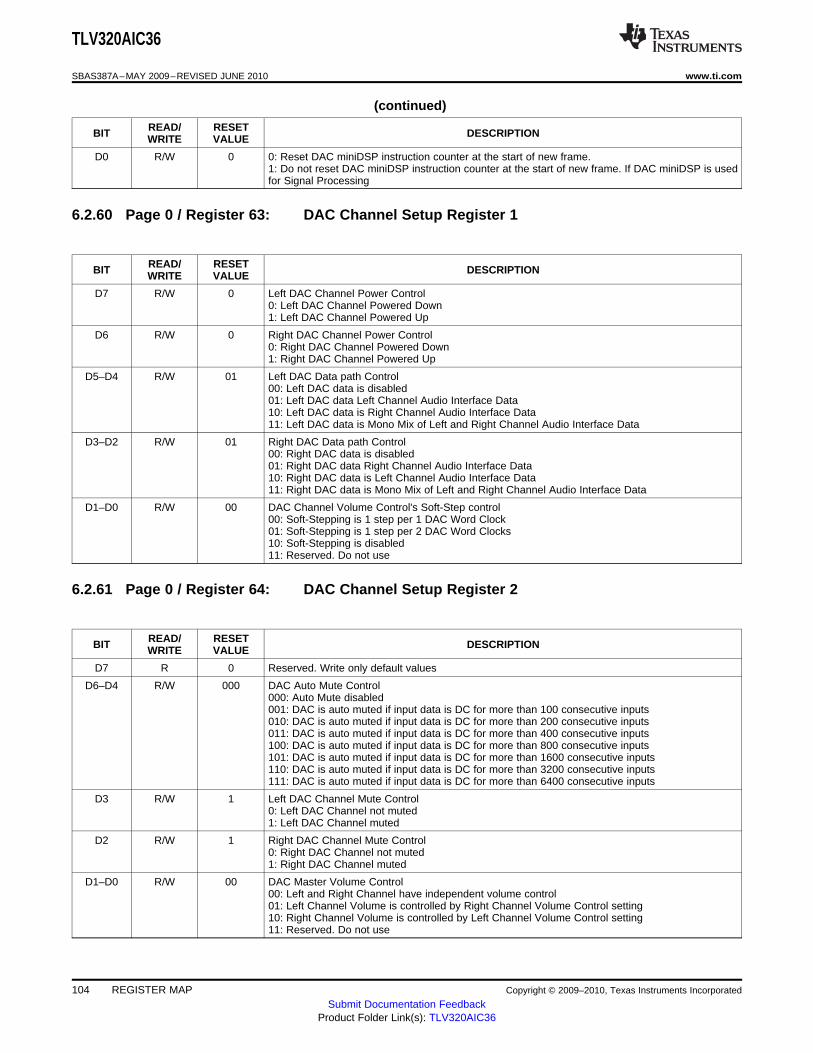
TLV320AIC36
SBAS387A–MAY 2009–REVISED JUNE 2010 www.ti.com
(continued)
READ/ RESETBIT DESCRIPTIONWRITE VALUE
D0 R/W 0 0: Reset DAC miniDSP instruction counter at the start of new frame.1: Do not reset DAC miniDSP instruction counter at the start of new frame. If DAC miniDSP is usedfor Signal Processing
6.2.60 Page 0 / Register 63: DAC Channel Setup Register 1
READ/ RESETBIT DESCRIPTIONWRITE VALUE
D7 R/W 0 Left DAC Channel Power Control0: Left DAC Channel Powered Down1: Left DAC Channel Powered Up
D6 R/W 0 Right DAC Channel Power Control0: Right DAC Channel Powered Down1: Right DAC Channel Powered Up
D5–D4 R/W 01 Left DAC Data path Control00: Left DAC data is disabled01: Left DAC data Left Channel Audio Interface Data10: Left DAC data is Right Channel Audio Interface Data11: Left DAC data is Mono Mix of Left and Right Channel Audio Interface Data
D3–D2 R/W 01 Right DAC Data path Control00: Right DAC data is disabled01: Right DAC data Right Channel Audio Interface Data10: Right DAC data is Left Channel Audio Interface Data11: Right DAC data is Mono Mix of Left and Right Channel Audio Interface Data
D1–D0 R/W 00 DAC Channel Volume Control's Soft-Step control00: Soft-Stepping is 1 step per 1 DAC Word Clock01: Soft-Stepping is 1 step per 2 DAC Word Clocks10: Soft-Stepping is disabled11: Reserved. Do not use
6.2.61 Page 0 / Register 64: DAC Channel Setup Register 2
READ/ RESETBIT DESCRIPTIONWRITE VALUE
D7 R 0 Reserved. Write only default values
D6–D4 R/W 000 DAC Auto Mute Control000: Auto Mute disabled001: DAC is auto muted if input data is DC for more than 100 consecutive inputs010: DAC is auto muted if input data is DC for more than 200 consecutive inputs011: DAC is auto muted if input data is DC for more than 400 consecutive inputs100: DAC is auto muted if input data is DC for more than 800 consecutive inputs101: DAC is auto muted if input data is DC for more than 1600 consecutive inputs110: DAC is auto muted if input data is DC for more than 3200 consecutive inputs111: DAC is auto muted if input data is DC for more than 6400 consecutive inputs
D3 R/W 1 Left DAC Channel Mute Control0: Left DAC Channel not muted1: Left DAC Channel muted
D2 R/W 1 Right DAC Channel Mute Control0: Right DAC Channel not muted1: Right DAC Channel muted
D1–D0 R/W 00 DAC Master Volume Control00: Left and Right Channel have independent volume control01: Left Channel Volume is controlled by Right Channel Volume Control setting10: Right Channel Volume is controlled by Left Channel Volume Control setting11: Reserved. Do not use
104 REGISTER MAP Copyright © 2009–2010, Texas Instruments Incorporated
Submit Documentation FeedbackProduct Folder Link(s): TLV320AIC36

TLV320AIC36
www.ti.com SBAS387A–MAY 2009–REVISED JUNE 2010
6.2.62 Page 0 / Register 65: Left DAC Channel Digital Volume Control Register
READ/ RESETBIT DESCRIPTIONWRITE VALUE
D7–D0 R/W 0000 0000 Left DAC Channel Digital Volume Control Setting0111 1111-0011 0001: Reserved. Do not use0011 0000: Digital Volume Control = +24 dB0010 1111: Digital Volume Control = +23.5 dB…0000 0001: Digital Volume Control = +0.5 dB0000 0000: Digital Volume Control = 0.0 dB1111 1111: Digital Volume Control = -0.5 dB...1000 0010: Digital Volume Control = -63 dB1000 0001: Digital Volume Control = -63.5 dB1000 0000: Reserved. Do not use
6.2.63 Page 0 / Register 66: Right DAC Channel Digital Volume Control Register
READ/ RESETBIT DESCRIPTIONWRITE VALUE
D7–D0 R/W 0000 0000 Right DAC Channel Digital Volume Control Setting0111 1111-0011 0001: Reserved. Do not use0011 0000: Digital Volume Control = +24 dB0010 1111: Digital Volume Control = +23.5 dB…0000 0001: Digital Volume Control = +0.5 dB0000 0000: Digital Volume Control = 0.0 dB1111 1111: Digital Volume Control = -0.5 dB...1000 0010: Digital Volume Control = -63 dB1000 0001: Digital Volume Control = -63.5 dB1000 0000: Reserved. Do not use
6.2.64 Page 0 / Register 67: Reserved Register
READ/ RESETBIT DESCRIPTIONWRITE VALUE
D7–D0 R 0000 0000 Reserved, Write only default values to this register
6.2.65 Page 0 / Register 68: DRC Control Register 1
READ/ RESETBIT DESCRIPTIONWRITE VALUE
D7 R 0 Reserved. Write only default value
D6 R/W 0 DRC Enable Control0: Left Channel DRC disabled1: Left Channel DRC enabled
D5 R/W 0 DRC Enable Control0: Right Channel DRC disabled1: Right Channel DRC enabled
Copyright © 2009–2010, Texas Instruments Incorporated REGISTER MAP 105Submit Documentation Feedback
Product Folder Link(s): TLV320AIC36
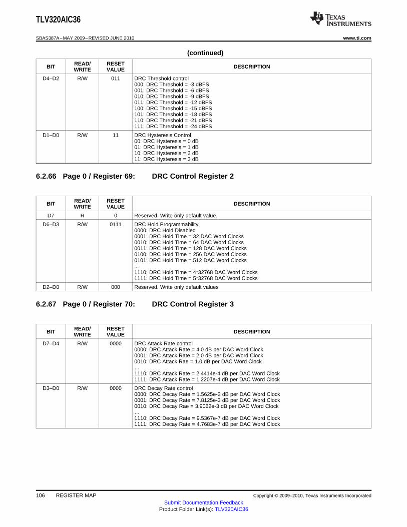
TLV320AIC36
SBAS387A–MAY 2009–REVISED JUNE 2010 www.ti.com
(continued)
READ/ RESETBIT DESCRIPTIONWRITE VALUE
D4–D2 R/W 011 DRC Threshold control000: DRC Threshold = -3 dBFS001: DRC Threshold = -6 dBFS010: DRC Threshold = -9 dBFS011: DRC Threshold = -12 dBFS100: DRC Threshold = -15 dBFS101: DRC Threshold = -18 dBFS110: DRC Threshold = -21 dBFS111: DRC Threshold = -24 dBFS
D1–D0 R/W 11 DRC Hysteresis Control00: DRC Hysteresis = 0 dB01: DRC Hysteresis = 1 dB10: DRC Hysteresis = 2 dB11: DRC Hysteresis = 3 dB
6.2.66 Page 0 / Register 69: DRC Control Register 2
READ/ RESETBIT DESCRIPTIONWRITE VALUE
D7 R 0 Reserved. Write only default value.
D6–D3 R/W 0111 DRC Hold Programmability0000: DRC Hold Disabled0001: DRC Hold Time = 32 DAC Word Clocks0010: DRC Hold Time = 64 DAC Word Clocks0011: DRC Hold Time = 128 DAC Word Clocks0100: DRC Hold Time = 256 DAC Word Clocks0101: DRC Hold Time = 512 DAC Word Clocks...1110: DRC Hold Time = 4*32768 DAC Word Clocks1111: DRC Hold Time = 5*32768 DAC Word Clocks
D2–D0 R/W 000 Reserved. Write only default values
6.2.67 Page 0 / Register 70: DRC Control Register 3
READ/ RESETBIT DESCRIPTIONWRITE VALUE
D7–D4 R/W 0000 DRC Attack Rate control0000: DRC Attack Rate = 4.0 dB per DAC Word Clock0001: DRC Attack Rate = 2.0 dB per DAC Word Clock0010: DRC Attack Rae = 1.0 dB per DAC Word Clock…1110: DRC Attack Rate = 2.4414e-4 dB per DAC Word Clock1111: DRC Attack Rate = 1.2207e-4 dB per DAC Word Clock
D3–D0 R/W 0000 DRC Decay Rate control0000: DRC Decay Rate = 1.5625e-2 dB per DAC Word Clock0001: DRC Decay Rate = 7.8125e-3 dB per DAC Word Clock0010: DRC Decay Rae = 3.9062e-3 dB per DAC Word Clock…1110: DRC Decay Rate = 9.5367e-7 dB per DAC Word Clock1111: DRC Decay Rate = 4.7683e-7 dB per DAC Word Clock
106 REGISTER MAP Copyright © 2009–2010, Texas Instruments Incorporated
Submit Documentation FeedbackProduct Folder Link(s): TLV320AIC36

TLV320AIC36
www.ti.com SBAS387A–MAY 2009–REVISED JUNE 2010
6.2.68 Page 0 / Register 71: Beep Generator Register 1
READ/ RESETBIT DESCRIPTIONWRITE VALUE
D7 R/W 0 0: Beep Generator Disabled1: Beep Generator Enabled. This bit will self clear after the beep has been generated.
D6 R 0 Reserved. Write only default value
D5–D0 R/W 00 0000 Left Channel Beep Volume Control00 0000: Left Channel Beep Volume = 0 dB00 0001: Left Channel Beep Volume = -1 dB…11 1110: Left Channel Beep Volume = -62 dB11 1111: Left Channel Beep Volume = -63 dB
6.2.69 Page 0 / Register 72: Beep Generator Register 2
READ/ RESETBIT DESCRIPTIONWRITE VALUE
D7–D6 R/W 00 Beep Generator Master Volume Control Setting00: Left and Right Channels have independent Volume Settings01: Left Channel Beep Volume is the same as programmed for Right Channel10: Right Channel Beep Volume is the same as programmed for Left Channel11: Reserved. Do not use
D5–D0 R/W 00 0000 Right Channel Beep Volume Control00 0000: Right Channel Beep Volume = 0 dB00 0001: Right Channel Beep Volume = -1 dB…11 1110: Right Channel Beep Volume = -62 dB11 1111: Right Channel Beep Volume = -63 dB
6.2.70 Page 0 / Register 73: Beep Generator Register 3
READ/ RESETBIT DESCRIPTIONWRITE VALUE
D7–D0 R/W 0000 0000 Programmed value is Beep Sample Length(23:16)
6.2.71 Page 0 / Register 74: Beep Generator Register 4
READ/ RESETBIT DESCRIPTIONWRITE VALUE
D7–D0 R/W 0000 0000 Programmed value is Beep Sample Length(15:8)
6.2.72 Page 0 / Register 75: Beep Generator Register 5
READ/ RESETBIT DESCRIPTIONWRITE VALUE
D7–D0 R/W 1110 1110 Programmed value is Beep Sample Length(7:0)
Copyright © 2009–2010, Texas Instruments Incorporated REGISTER MAP 107Submit Documentation Feedback
Product Folder Link(s): TLV320AIC36
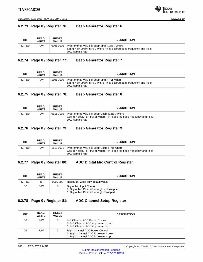
TLV320AIC36
SBAS387A–MAY 2009–REVISED JUNE 2010 www.ti.com
6.2.73 Page 0 / Register 76: Beep Generator Register 6
READ/ RESETBIT DESCRIPTIONWRITE VALUE
D7–D0 R/W 0001 0000 Programmed Value is Beep Sin(x)(15:8), whereSin(x) = sin(2*pi*Fin/Fs), where Fin is desired beep frequency and Fs isDAC sample rate
6.2.74 Page 0 / Register 77: Beep Generator Register 7
READ/ RESETBIT DESCRIPTIONWRITE VALUE
D7–D0 R/W 1101 1000 Programmed Value is Beep Sin(x)(7:0), whereSin(x) = sin(2*pi*Fin/Fs), where Fin is desired beep frequency and Fs isDAC sample rate
6.2.75 Page 0 / Register 78: Beep Generator Register 8
READ/ RESETBIT DESCRIPTIONWRITE VALUE
D7–D0 R/W 0111 1110 Programmed Value is Beep Cos(x)(15:8), whereCos(x) = cos(2*pi*Fin/Fs), where Fin is desired beep frequency and Fs isDAC sample rate
6.2.76 Page 0 / Register 79: Beep Generator Register 9
READ/ RESETBIT DESCRIPTIONWRITE VALUE
D7–D0 R/W 1110 0011 Programmed Value is Beep Cos(x)(7:0), whereCos(x) = cos(2*pi*Fin/Fs), where Fin is desired beep frequency and Fs isDAC sample rate
6.2.77 Page 0 / Register 80: ADC Digital Mic Control Register
READ/ RESETBIT DESCRIPTIONWRITE VALUE
D7–D1 R 0000 000 Reserved. Write only default value.
D0 R/W 0 Digital Mic Input Control0: Digital Mic Channel left/right not swapped1: Digital Mic Channel left/right swapped
6.2.78 Page 0 / Register 81: ADC Channel Setup Register
READ/ RESETBIT DESCRIPTIONWRITE VALUE
D7 R/W 0 Left Channel ADC Power Control0: Left Channel ADC is powered down1: Left Channel ADC is powered up
D6 R/W 0 Right Channel ADC Power Control0: Right Channel ADC is powered down1: Right Channel ADC is powered up
108 REGISTER MAP Copyright © 2009–2010, Texas Instruments Incorporated
Submit Documentation FeedbackProduct Folder Link(s): TLV320AIC36

TLV320AIC36
www.ti.com SBAS387A–MAY 2009–REVISED JUNE 2010
(continued)
READ/ RESETBIT DESCRIPTIONWRITE VALUE
D5–D4 R/W 00 Digital Microphone Input Configuration00: GPIO serves as Digital Microphone Input01: GPIO1 serves as Digital Microphone Input10: DIN serves as Digital Microphone Input11: Reserved. Do not use
D3 R/W 0 Left Channel Digital Microphone Power Control0: Left Channel ADC not configured for Digital Microphone1: Left Channel ADC configured for Digital Microphone
D2 R/W 0 Right Channel Digital Microphone Power Control0: Right Channel ADC not configured for Digital Microphone1: Right Channel ADC configured for Digital Microphone
D1–D0 R/W 00 ADC Volume Control Soft-Stepping Control00: ADC Volume Control changes by 1 gain step per ADC Word Clock01: ADC Volume Control changes by 1 gain step per two ADC Word Clocks10: ADC Volume Control Soft-Stepping disabled11: Reserved. Do not use
6.2.79 Page 0 / Register 82: ADC Fine Gain Adjust Register
READ/ RESETBIT DESCRIPTIONWRITE VALUE
D7 R/W 1 Left ADC Channel Mute Control0: Left ADC Channel Un-muted1: Left ADC Channel Muted
D6–D4 R/W 000 Left ADC Channel Fine Gain Adjust000: Left ADC Channel Fine Gain = 0 dB001: Left ADC Channel Fine Gain = -0.1 dB010: Left ADC Channel Fine Gain = -0.2 dB011: Left ADC Channel Fine Gain = -0.3 dB100: Left ADC Channel Fine Gain = -0.4 dB101-111: Reserved. Do not use
D3 R/W 1 Right ADC Channel Mute Control0: Right ADC Channel Un-muted1: Right ADC Channel Muted
D2–D0 R/W 000 Right ADC Channel Fine Gain Adjust000: Right ADC Channel Fine Gain = 0 dB001: Right ADC Channel Fine Gain = -0.1 dB010: Right ADC Channel Fine Gain = -0.2 dB011: Right ADC Channel Fine Gain = -0.3 dB100: Right ADC Channel Fine Gain = -0.4 dB101-111: Reserved. Do not use
6.2.80 Page 0 / Register 83: Left ADC Channel Volume Control Register
READ/ RESETBIT DESCRIPTIONWRITE VALUE
D7 R 0 Reserved. Write only default values
Copyright © 2009–2010, Texas Instruments Incorporated REGISTER MAP 109Submit Documentation Feedback
Product Folder Link(s): TLV320AIC36
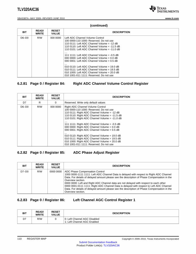
TLV320AIC36
SBAS387A–MAY 2009–REVISED JUNE 2010 www.ti.com
(continued)
READ/ RESETBIT DESCRIPTIONWRITE VALUE
D6–D0 R/W 000 0000 Left ADC Channel Volume Control100 0000-110 1000: Reserved. Do not use110 0111: Left ADC Channel Volume = -12 dB110 0110: Left ADC Channel Volume = -11.5 dB110 0101: Left ADC Channel Volume = -11.0 dB…111 1111: Left ADC Channel Volume = -0.5 dB000 0000: Left ADC Channel Volume = 0.0 dB000 0001: Left ADC Channel Volume = 0.5 dB...010 0110: Left ADC Channel Volume = 19.0 dB010 0111: Left ADC Channel Volume = 19.5 dB010 1000: Left ADC Channel Volume = 20.0 dB010 1001-011 1111: Reserved. Do not use
6.2.81 Page 0 / Register 84: Right ADC Channel Volume Control Register
READ/ RESETBIT DESCRIPTIONWRITE VALUE
D7 R 0 Reserved. Write only default values
D6–D0 R/W 000 0000 Right ADC Channel Volume Control100 0000-110 1000: Reserved. Do not use110 0111: Right ADC Channel Volume = -12 dB110 0110: Right ADC Channel Volume = -11.5 dB110 0101: Right ADC Channel Volume = -11.0 dB…111 1111: Right ADC Channel Volume = -0.5 dB000 0000: Right ADC Channel Volume = 0.0 dB000 0001: Right ADC Channel Volume = 0.5 dB...010 0110: Right ADC Channel Volume = 19.0 dB010 0111: Right ADC Channel Volume = 19.5 dB010 1000: Right ADC Channel Volume = 20.0 dB010 1001-011 1111: Reserved. Do not use
6.2.82 Page 0 / Register 85: ADC Phase Adjust Register
READ/ RESETBIT DESCRIPTIONWRITE VALUE
D7–D0 R/W 0000 0000 ADC Phase Compensation Control1000 0000-1111 1111: Left ADC Channel Data is delayed with respect to Right ADC ChannelData. For details of delayed amount please see the description of Phase Compensation in theOverview section.0000 0000: Left and Right ADC Channel data are not delayed with respect to each other0000 0001-0111 1111: Right ADC Channel Data is delayed with respect to Left ADC ChannelData. For details of delayed amount please see the description of Phase Compensation in theOverview section.
6.2.83 Page 0 / Register 86: Left Channel AGC Control Register 1
READ/ RESETBIT DESCRIPTIONWRITE VALUE
D7 R/W 0 0: Left Channel AGC Disabled1: Left Channel AGC Enabled
110 REGISTER MAP Copyright © 2009–2010, Texas Instruments Incorporated
Submit Documentation FeedbackProduct Folder Link(s): TLV320AIC36
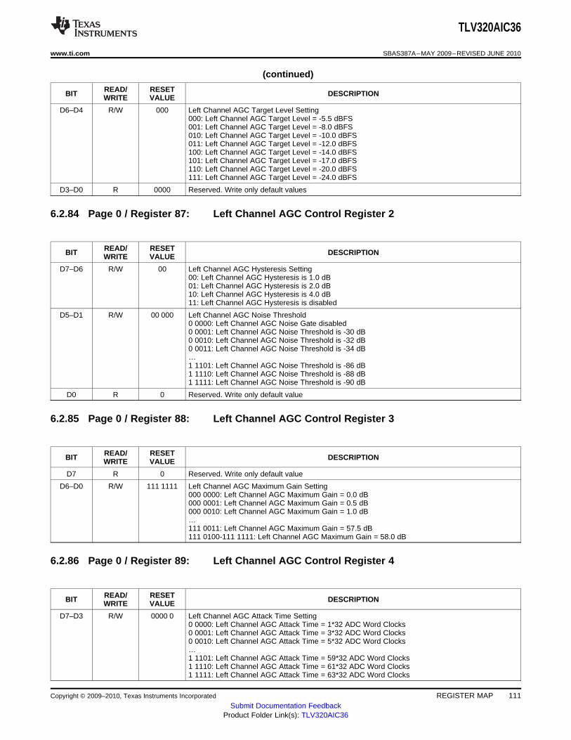
TLV320AIC36
www.ti.com SBAS387A–MAY 2009–REVISED JUNE 2010
(continued)
READ/ RESETBIT DESCRIPTIONWRITE VALUE
D6–D4 R/W 000 Left Channel AGC Target Level Setting000: Left Channel AGC Target Level = -5.5 dBFS001: Left Channel AGC Target Level = -8.0 dBFS010: Left Channel AGC Target Level = -10.0 dBFS011: Left Channel AGC Target Level = -12.0 dBFS100: Left Channel AGC Target Level = -14.0 dBFS101: Left Channel AGC Target Level = -17.0 dBFS110: Left Channel AGC Target Level = -20.0 dBFS111: Left Channel AGC Target Level = -24.0 dBFS
D3–D0 R 0000 Reserved. Write only default values
6.2.84 Page 0 / Register 87: Left Channel AGC Control Register 2
READ/ RESETBIT DESCRIPTIONWRITE VALUE
D7–D6 R/W 00 Left Channel AGC Hysteresis Setting00: Left Channel AGC Hysteresis is 1.0 dB01: Left Channel AGC Hysteresis is 2.0 dB10: Left Channel AGC Hysteresis is 4.0 dB11: Left Channel AGC Hysteresis is disabled
D5–D1 R/W 00 000 Left Channel AGC Noise Threshold0 0000: Left Channel AGC Noise Gate disabled0 0001: Left Channel AGC Noise Threshold is -30 dB0 0010: Left Channel AGC Noise Threshold is -32 dB0 0011: Left Channel AGC Noise Threshold is -34 dB…1 1101: Left Channel AGC Noise Threshold is -86 dB1 1110: Left Channel AGC Noise Threshold is -88 dB1 1111: Left Channel AGC Noise Threshold is -90 dB
D0 R 0 Reserved. Write only default value
6.2.85 Page 0 / Register 88: Left Channel AGC Control Register 3
READ/ RESETBIT DESCRIPTIONWRITE VALUE
D7 R 0 Reserved. Write only default value
D6–D0 R/W 111 1111 Left Channel AGC Maximum Gain Setting000 0000: Left Channel AGC Maximum Gain = 0.0 dB000 0001: Left Channel AGC Maximum Gain = 0.5 dB000 0010: Left Channel AGC Maximum Gain = 1.0 dB…111 0011: Left Channel AGC Maximum Gain = 57.5 dB111 0100-111 1111: Left Channel AGC Maximum Gain = 58.0 dB
6.2.86 Page 0 / Register 89: Left Channel AGC Control Register 4
READ/ RESETBIT DESCRIPTIONWRITE VALUE
D7–D3 R/W 0000 0 Left Channel AGC Attack Time Setting0 0000: Left Channel AGC Attack Time = 1*32 ADC Word Clocks0 0001: Left Channel AGC Attack Time = 3*32 ADC Word Clocks0 0010: Left Channel AGC Attack Time = 5*32 ADC Word Clocks…1 1101: Left Channel AGC Attack Time = 59*32 ADC Word Clocks1 1110: Left Channel AGC Attack Time = 61*32 ADC Word Clocks1 1111: Left Channel AGC Attack Time = 63*32 ADC Word Clocks
Copyright © 2009–2010, Texas Instruments Incorporated REGISTER MAP 111Submit Documentation Feedback
Product Folder Link(s): TLV320AIC36

TLV320AIC36
SBAS387A–MAY 2009–REVISED JUNE 2010 www.ti.com
(continued)
READ/ RESETBIT DESCRIPTIONWRITE VALUE
D2–D0 R/W 000 Left Channel AGC Attack Time Scale Factor Setting000: Scale Factor = 1001: Scale Factor = 2010: Scale Factor = 4…101: Scale Factor = 32110: Scale Factor = 64111: Scale Factor = 128
6.2.87 Page 0 / Register 90: Left Channel AGC Control Register 5
READ/ RESETBIT DESCRIPTIONWRITE VALUE
D7–D3 R/W 0000 0 Left Channel AGC Decay Time Setting0 0000: Left Channel AGC Decay Time = 1*512 ADC Word Clocks0 0001: Left Channel AGC Decay Time = 3*512 ADC Word Clocks0 0010: Left Channel AGC Decay Time = 5*512 ADC Word Clocks…1 1101: Left Channel AGC Decay Time = 59*512 ADC Word Clocks1 1110: Left Channel AGC Decay Time = 61*512 ADC Word Clocks1 1111: Left Channel AGC Decay Time = 63*512 ADC Word Clocks
D2–D0 R/W 000 Left Channel AGC Decay Time Scale Factor Setting000: Scale Factor = 1001: Scale Factor = 2010: Scale Factor = 4…101: Scale Factor = 32110: Scale Factor = 64111: Scale Factor = 128
6.2.88 Page 0 / Register 91: Left Channel AGC Control Register 6
READ/ RESETBIT DESCRIPTIONWRITE VALUE
D7–D5 R 000 Reserved. Write only default values
D4–D0 R/W 0 0000 Left Channel AGC Noise Debounce Time Setting0 0001: Left Channel AGC Noise Debounce Time = 00 0010: Left Channel AGC Noise Debounce Time = 4 ADC Word Clocks0 0011: Left Channel AGC Noise Debounce Time = 8 ADC Word Clocks…0 1010: Left Channel AGC Noise Debounce Time = 2048 ADC Word Clocks0 1011: Left Channel AGC Noise Debounce Time = 4096 ADC Word Clocks0 1100: Left Channel AGC Noise Debounce Time = 2*4096 ADC Word Clocks0 1101: Left Channel AGC Noise Debounce Time = 3*4096 ADC Word Clocks...1 1101: Left Channel AGC Noise Debounce Time = 19*4096 ADC Word Clocks1 1110: Left Channel AGC Noise Debounce Time = 20*4096 ADC Word Clocks1 1111: Left Channel AGC Noise Debounce Time = 21*4096 ADC Word Clocks
6.2.89 Page 0 / Register 92: Left Channel AGC Control Register 7
READ/ RESETBIT DESCRIPTIONWRITE VALUE
D7–D4 R 0000 Reserved. Write only default values
112 REGISTER MAP Copyright © 2009–2010, Texas Instruments Incorporated
Submit Documentation FeedbackProduct Folder Link(s): TLV320AIC36

TLV320AIC36
www.ti.com SBAS387A–MAY 2009–REVISED JUNE 2010
(continued)
READ/ RESETBIT DESCRIPTIONWRITE VALUE
D3–D0 R/W 0000 Left Channel AGC Signal Debounce Time Setting0001: Left Channel AGC Signal Debounce Time = 00010: Left Channel AGC Signal Debounce Time = 4 ADC Word Clocks0011: Left Channel AGC Signal Debounce Time = 8 ADC Word Clocks…1001: Left Channel AGC Signal Debounce Time = 1024 ADC Word Clocks1010: Left Channel AGC Signal Debounce Time = 2048 ADC Word Clocks1011: Left Channel AGC Signal Debounce Time = 2*2048 ADC Word Clocks1100: Left Channel AGC Signal Debounce Time = 3*2048 ADC Word Clocks1101: Left Channel AGC Signal Debounce Time = 4*2048 ADC Word Clocks1110: Left Channel AGC Signal Debounce Time = 5*2048 ADC Word Clocks1111: Left Channel AGC Signal Debounce Time = 6*2048 ADC Word Clocks
6.2.90 Page 0 / Register 93: Left Channel AGC Control Register 8
READ/ RESETBIT DESCRIPTIONWRITE VALUE
D7–D0 R 0000 0000 Left Channel AGC Gain Flag1111 0100: Left Channel AGC Gain = -12.0 dB1111 0101: Left Channel AGC Gain = -11.5 dB1111 0110: Left Channel AGC Gain = -11.0 dB…0000 0000: Left Channel AGC Gain = 0.0 dB…0111 0010: Left Channel AGC Gain = 57.0 dB0111 0011: Left Channel AGC Gain = 57.5 dB0111 0100: Left Channel AGC Gain = 58.0 dB
6.2.91 Page 0 / Register 94: Right Channel AGC Control Register 1
READ/ RESETBIT DESCRIPTIONWRITE VALUE
D7 R/W 0 0: Right Channel AGC Disabled1: Right Channel AGC Enabled
D6–D4 R/W 000 Right Channel AGC Target Level Setting000: Right Channel AGC Target Level = -5.5 dBFS001: Right Channel AGC Target Level = -8.0 dBFS010: Right Channel AGC Target Level = -10.0 dBFS011: Right Channel AGC Target Level = -12.0 dBFS100: Right Channel AGC Target Level = -14.0 dBFS101: Right Channel AGC Target Level = -17.0 dBFS110: Right Channel AGC Target Level = -20.0 dBFS111: Right Channel AGC Target Level = -24.0 dBFS
D3–D0 R 0000 Reserved. Write only default values
6.2.92 Page 0 / Register 95: Right Channel AGC Control Register 2
READ/ RESETBIT DESCRIPTIONWRITE VALUE
D7–D6 R/W 00 Right Channel AGC Hysteresis Setting00: Right Channel AGC Hysteresis is 1.0 dB01: Right Channel AGC Hysteresis is 2.0 dB10: Right Channel AGC Hysteresis is 4.0 dB11: Right Channel AGC Hysteresis is disabled
Copyright © 2009–2010, Texas Instruments Incorporated REGISTER MAP 113Submit Documentation Feedback
Product Folder Link(s): TLV320AIC36

TLV320AIC36
SBAS387A–MAY 2009–REVISED JUNE 2010 www.ti.com
(continued)
READ/ RESETBIT DESCRIPTIONWRITE VALUE
D5–D1 R/W 00 000 Right Channel AGC Noise Threshold0 0000: Right Channel AGC Noise Gate disabled0 0001: Right Channel AGC Noise Threshold is -30 dB0 0010: Right Channel AGC Noise Threshold is -32 dB0 0011: Right Channel AGC Noise Threshold is -34 dB…1 1101: Right Channel AGC Noise Threshold is -86 dB1 1110: Right Channel AGC Noise Threshold is -88 dB1 1111: Right Channel AGC Noise Threshold is -90 dB
D0 R 0 Reserved. Write only default value
6.2.93 Page 0 / Register 96: Right Channel AGC Control Register 3
READ/ RESETBIT DESCRIPTIONWRITE VALUE
D7 R 0 Reserved. Write only default value
D6–D0 R/W 111 1111 Right Channel AGC Maximum Gain Setting000 0000: Right Channel AGC Maximum Gain = 0.0 dB000 0001: Right Channel AGC Maximum Gain = 0.5 dB000 0010: Right Channel AGC Maximum Gain = 1.0 dB…111 0011: Right Channel AGC Maximum Gain = 57.5 dB111 0100-111 1111: Right Channel AGC Maximum Gain = 58.0 dB
6.2.94 Page 0 / Register 97: Right Channel AGC Control Register 4
READ/ RESETBIT DESCRIPTIONWRITE VALUE
D7–D3 R/W 00 000 Right Channel AGC Attack Time Setting0 0000: Right Channel AGC Attack Time = 1*32 ADC Word Clocks0 0001: Right Channel AGC Attack Time = 3*32 ADC Word Clocks0 0010: Right Channel AGC Attack Time = 5*32 ADC Word Clocks…1 1101: Right Channel AGC Attack Time = 59*32 ADC Word Clocks1 1110: Right Channel AGC Attack Time = 61*32 ADC Word Clocks1 1111: Right Channel AGC Attack Time = 63*32 ADC Word Clocks
D2–D0 R/W 000 Right Channel AGC Attack Time Scale Factor Setting000: Scale Factor = 1001: Scale Factor = 2010: Scale Factor = 4…101: Scale Factor = 32110: Scale Factor = 64111: Scale Factor = 128
114 REGISTER MAP Copyright © 2009–2010, Texas Instruments Incorporated
Submit Documentation FeedbackProduct Folder Link(s): TLV320AIC36
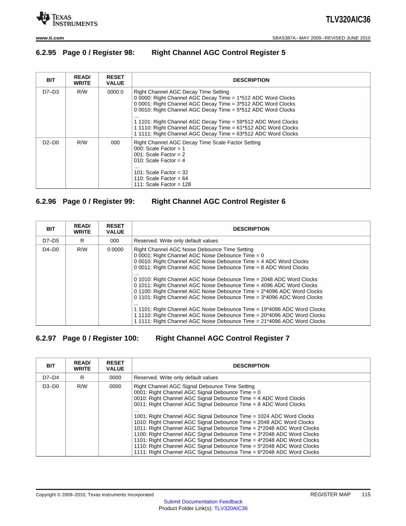
TLV320AIC36
www.ti.com SBAS387A–MAY 2009–REVISED JUNE 2010
6.2.95 Page 0 / Register 98: Right Channel AGC Control Register 5
READ/ RESETBIT DESCRIPTIONWRITE VALUE
D7–D3 R/W 0000 0 Right Channel AGC Decay Time Setting0 0000: Right Channel AGC Decay Time = 1*512 ADC Word Clocks0 0001: Right Channel AGC Decay Time = 3*512 ADC Word Clocks0 0010: Right Channel AGC Decay Time = 5*512 ADC Word Clocks…1 1101: Right Channel AGC Decay Time = 59*512 ADC Word Clocks1 1110: Right Channel AGC Decay Time = 61*512 ADC Word Clocks1 1111: Right Channel AGC Decay Time = 63*512 ADC Word Clocks
D2–D0 R/W 000 Right Channel AGC Decay Time Scale Factor Setting000: Scale Factor = 1001: Scale Factor = 2010: Scale Factor = 4…101: Scale Factor = 32110: Scale Factor = 64111: Scale Factor = 128
6.2.96 Page 0 / Register 99: Right Channel AGC Control Register 6
READ/ RESETBIT DESCRIPTIONWRITE VALUE
D7–D5 R 000 Reserved. Write only default values
D4–D0 R/W 0 0000 Right Channel AGC Noise Debounce Time Setting0 0001: Right Channel AGC Noise Debounce Time = 00 0010: Right Channel AGC Noise Debounce Time = 4 ADC Word Clocks0 0011: Right Channel AGC Noise Debounce Time = 8 ADC Word Clocks…0 1010: Right Channel AGC Noise Debounce Time = 2048 ADC Word Clocks0 1011: Right Channel AGC Noise Debounce Time = 4096 ADC Word Clocks0 1100: Right Channel AGC Noise Debounce Time = 2*4096 ADC Word Clocks0 1101: Right Channel AGC Noise Debounce Time = 3*4096 ADC Word Clocks...1 1101: Right Channel AGC Noise Debounce Time = 19*4096 ADC Word Clocks1 1110: Right Channel AGC Noise Debounce Time = 20*4096 ADC Word Clocks1 1111: Right Channel AGC Noise Debounce Time = 21*4096 ADC Word Clocks
6.2.97 Page 0 / Register 100: Right Channel AGC Control Register 7
READ/ RESETBIT DESCRIPTIONWRITE VALUE
D7–D4 R 0000 Reserved. Write only default values
D3–D0 R/W 0000 Right Channel AGC Signal Debounce Time Setting0001: Right Channel AGC Signal Debounce Time = 00010: Right Channel AGC Signal Debounce Time = 4 ADC Word Clocks0011: Right Channel AGC Signal Debounce Time = 8 ADC Word Clocks…1001: Right Channel AGC Signal Debounce Time = 1024 ADC Word Clocks1010: Right Channel AGC Signal Debounce Time = 2048 ADC Word Clocks1011: Right Channel AGC Signal Debounce Time = 2*2048 ADC Word Clocks1100: Right Channel AGC Signal Debounce Time = 3*2048 ADC Word Clocks1101: Right Channel AGC Signal Debounce Time = 4*2048 ADC Word Clocks1110: Right Channel AGC Signal Debounce Time = 5*2048 ADC Word Clocks1111: Right Channel AGC Signal Debounce Time = 6*2048 ADC Word Clocks
Copyright © 2009–2010, Texas Instruments Incorporated REGISTER MAP 115Submit Documentation Feedback
Product Folder Link(s): TLV320AIC36

TLV320AIC36
SBAS387A–MAY 2009–REVISED JUNE 2010 www.ti.com
6.2.98 Page 0 / Register 101: Right Channel AGC Control Register 8
READ/ RESETBIT DESCRIPTIONWRITE VALUE
D7–D0 R 0000 0000 Right Channel AGC Gain Flag1111 0100: Right Channel AGC Gain = -12.0 dB1111 0101: Right Channel AGC Gain = -11.5 dB1111 0110: Right Channel AGC Gain = -11.0 dB…0000 0000: Right Channel AGC Gain = 0.0 dB…0111 0010: Right Channel AGC Gain = 57.0 dB0111 0011: Right Channel AGC Gain = 57.5 dB0111 0100: Right Channel AGC Gain = 58.0 dB
6.2.99 Page 0 / Register 102: DC Measurement Register 1
READ/ RESETBIT DESCRIPTIONWRITE VALUE
D7 R/W 0 0: DC Measurement Mode disabled for Left ADC Channel1: DC Measurement Mode enabled for Left ADC Channel
D6 R/W 0 0: DC Measurement Mode disabled for Right ADC Channel1: DC Measurement Mode enabled for Right ADC Channel
D5 R/W 0 0: DC Measurement is done using First-Order moving average filter with averaging of 2^D1: DC Measurement is done with 1sr order Low-pass IIR filter with coefficients as a function of D
D4–D0 R/W 0 0000 DC Measurement D setting0 0000: Reserved. Do not use0 0001: DC Measurement D parameter = 10 0010: DC Measurement D parameter = 2..1 0011: DC Measurement D parameter = 191 0100: DC Measurement D parameter = 201 0101-1 1111: Reserved. Do not use
6.2.100 Page 0 / Register 103: DC Measurement Register 2
READ/ RESETBIT DESCRIPTIONWRITE VALUE
D7–D6 R 00 Reserved. Write only default values
D5 R/W 0 0: For IIR based DC measurement, measurement value is the instantaneous output of IIR filter1: For IIR based DC measurement, the measurement value is updated before periodic clearing ofIIR filter
D4–D0 R/W 0 0000 IIR based DC Measurement, averaging time setting0 0000: Infinite average is used0 0001: Averaging time is 2^1 ADC Modulator clocks0 0010: Averaging time is 2^2 ADC Modulator clocks…1 0011: Averaging time is 2^19 ADC Modulator clocks1 0100: Averaging time is 2^20 ADC Modulator clocks1 0101-1 1111: Reserved. Do not use
6.2.101 Page 0 / Register 104: Left Channel DC Measurement Output Register 1
READ/ RESETBIT DESCRIPTIONWRITE VALUE
D7–D0 R 0000 0000 Left Channel DC Measurement Output (23:16)
116 REGISTER MAP Copyright © 2009–2010, Texas Instruments Incorporated
Submit Documentation FeedbackProduct Folder Link(s): TLV320AIC36

TLV320AIC36
www.ti.com SBAS387A–MAY 2009–REVISED JUNE 2010
6.2.102 Page 0 / Register 105: Left Channel DC Measurement Output Register 2
READ/ RESETBIT DESCRIPTIONWRITE VALUE
D7–D0 R 0000 0000 Left Channel DC Measurement Output (15:8)
6.2.103 Page 0 / Register 106: Left Channel DC Measurement Output Register 3
READ/ RESETBIT DESCRIPTIONWRITE VALUE
D7–D0 R 0000 0000 Left Channel DC Measurement Output (7:0)
6.2.104 Page 0 / Register 107: Right Channel DC Measurement Output Register 1
READ/ RESETBIT DESCRIPTIONWRITE VALUE
D7–D0 R 0000 0000 Right Channel DC Measurement Output (23:16)
6.2.105 Page 0 / Register 108: Right Channel DC Measurement Output Register 2
READ/ RESETBIT DESCRIPTIONWRITE VALUE
D7–D0 R 0000 0000 Right Channel DC Measurement Output (15:8)
6.2.106 Page 0 / Register 109: Right Channel DC Measurement Output Register 3
READ/ RESETBIT DESCRIPTIONWRITE VALUE
D7–D0 R 0000 0000 Right Channel DC Measurement Output (7:0)
6.2.107 Page 0 / Register 110-113: Reserved Registers
READ/ RESETBIT DESCRIPTIONWRITE VALUE
D7–D0 R 0000 0000 Reserved. Write only default values
6.2.108 Page 0 / Register 114: Analog FIR Control Register 1
READ/ RESETBIT DESCRIPTIONWRITE VALUE
D7–D4 R/W 0001 Unit Delay Register for tap 1 in DAC AFIR.
D3–D0 R/W 0000 Unit Delay Register for tap 0 in DAC AFIR.
Copyright © 2009–2010, Texas Instruments Incorporated REGISTER MAP 117Submit Documentation Feedback
Product Folder Link(s): TLV320AIC36

TLV320AIC36
SBAS387A–MAY 2009–REVISED JUNE 2010 www.ti.com
6.2.109 Page 0 / Register 115: Analog FIR Control Register 2
READ/ RESETBIT DESCRIPTIONWRITE VALUE
D7–D4 R/W 0011 Unit Delay Register for tap 3 in DAC AFIR.
D3–D0 R/W 0010 Unit Delay Register for tap 2 in DAC AFIR.
6.2.110 Page 0 / Register 116: Analog FIR Control Register 3
READ/ RESETBIT DESCRIPTIONWRITE VALUE
D7–D4 R/W 0101 Unit Delay Register for tap 5 in DAC AFIR.
D3–D0 R/W 0100 Unit Delay Register for tap 4 in DAC AFIR.
6.2.111 Page 0 / Register 117-119: Reserved Registers
READ/ RESETBIT DESCRIPTIONWRITE VALUE
D7–D0 R 0000 0000 Reserved. Write only default values
6.2.112 Page 0 / Register 120: GPIO1 Control Register
READ/ RESETBIT DESCRIPTIONWRITE VALUE
D7–D6 R 00 Reserved. Write only default values
D5–D2 R/W 00 00 GPIO1 Control0000: GPIO1 input/output disabled0001: GPIO1 input is used for secondary BCLK, secondary WCLK, secondary DIN, secondaryADC_WCLK or seconday DIGMIC_DATA input0010: GPIO1 is general purpose input (GPI)0011: GPIO1 is general purpose output0100: GPIO1 output is CLKOUT0101: GPIO1 output is INT1 (active high)0110: GPIO1 output is inverted INT1 (active low)0111: GPIO1 output is INT1 (open drain)1000: GPIO1 output is INT2 (active high)1001: GPIO1 output is inverted INT2 (active low)1010: GPIO1 output is INT2 (open drain)1011: GPIO1 output is ADC_WCLK for Audio Interface1100: GPIO1 output is secondary bit-clock for Audio Interface1101: GPIO1 output is secondary word-clock for Audio Interface1110: GPIO1 output is clock for the digital microphone1111: Reserved
D1 R X GPIO1 Input Pin state as a GPI
D0 R/W 0 GPIO1 as general purpose output control0: GPIO1 pin is driven to '0' in general purpose output mode1: GPIO1 pin is driven to '1' in general purpose output mode
6.2.113 Page 0 / Register 121: GPIO2 Control Register
READ/ RESETBIT DESCRIPTIONWRITE VALUE
D7–D6 R 00 Reserved. Write only default values
118 REGISTER MAP Copyright © 2009–2010, Texas Instruments Incorporated
Submit Documentation FeedbackProduct Folder Link(s): TLV320AIC36
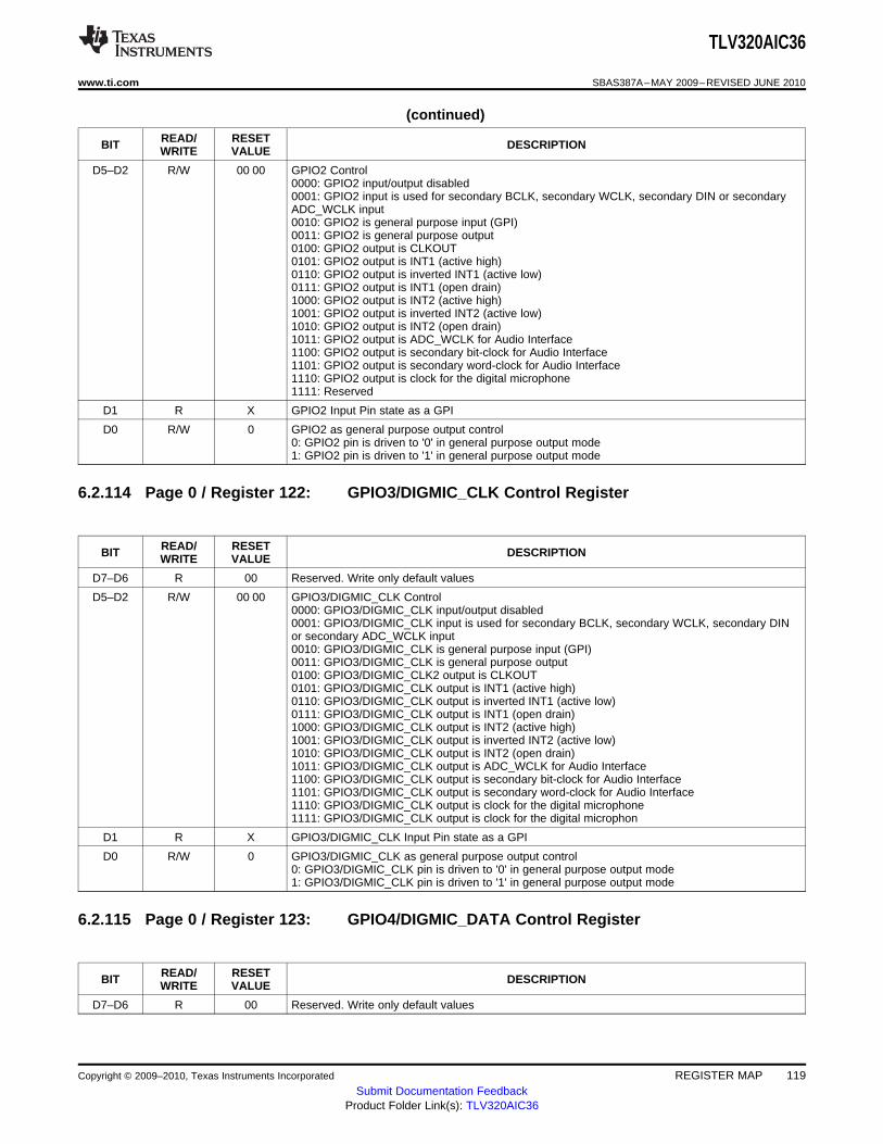
TLV320AIC36
www.ti.com SBAS387A–MAY 2009–REVISED JUNE 2010
(continued)
READ/ RESETBIT DESCRIPTIONWRITE VALUE
D5–D2 R/W 00 00 GPIO2 Control0000: GPIO2 input/output disabled0001: GPIO2 input is used for secondary BCLK, secondary WCLK, secondary DIN or secondaryADC_WCLK input0010: GPIO2 is general purpose input (GPI)0011: GPIO2 is general purpose output0100: GPIO2 output is CLKOUT0101: GPIO2 output is INT1 (active high)0110: GPIO2 output is inverted INT1 (active low)0111: GPIO2 output is INT1 (open drain)1000: GPIO2 output is INT2 (active high)1001: GPIO2 output is inverted INT2 (active low)1010: GPIO2 output is INT2 (open drain)1011: GPIO2 output is ADC_WCLK for Audio Interface1100: GPIO2 output is secondary bit-clock for Audio Interface1101: GPIO2 output is secondary word-clock for Audio Interface1110: GPIO2 output is clock for the digital microphone1111: Reserved
D1 R X GPIO2 Input Pin state as a GPI
D0 R/W 0 GPIO2 as general purpose output control0: GPIO2 pin is driven to '0' in general purpose output mode1: GPIO2 pin is driven to '1' in general purpose output mode
6.2.114 Page 0 / Register 122: GPIO3/DIGMIC_CLK Control Register
READ/ RESETBIT DESCRIPTIONWRITE VALUE
D7–D6 R 00 Reserved. Write only default values
D5–D2 R/W 00 00 GPIO3/DIGMIC_CLK Control0000: GPIO3/DIGMIC_CLK input/output disabled0001: GPIO3/DIGMIC_CLK input is used for secondary BCLK, secondary WCLK, secondary DINor secondary ADC_WCLK input0010: GPIO3/DIGMIC_CLK is general purpose input (GPI)0011: GPIO3/DIGMIC_CLK is general purpose output0100: GPIO3/DIGMIC_CLK2 output is CLKOUT0101: GPIO3/DIGMIC_CLK output is INT1 (active high)0110: GPIO3/DIGMIC_CLK output is inverted INT1 (active low)0111: GPIO3/DIGMIC_CLK output is INT1 (open drain)1000: GPIO3/DIGMIC_CLK output is INT2 (active high)1001: GPIO3/DIGMIC_CLK output is inverted INT2 (active low)1010: GPIO3/DIGMIC_CLK output is INT2 (open drain)1011: GPIO3/DIGMIC_CLK output is ADC_WCLK for Audio Interface1100: GPIO3/DIGMIC_CLK output is secondary bit-clock for Audio Interface1101: GPIO3/DIGMIC_CLK output is secondary word-clock for Audio Interface1110: GPIO3/DIGMIC_CLK output is clock for the digital microphone1111: GPIO3/DIGMIC_CLK output is clock for the digital microphon
D1 R X GPIO3/DIGMIC_CLK Input Pin state as a GPI
D0 R/W 0 GPIO3/DIGMIC_CLK as general purpose output control0: GPIO3/DIGMIC_CLK pin is driven to '0' in general purpose output mode1: GPIO3/DIGMIC_CLK pin is driven to '1' in general purpose output mode
6.2.115 Page 0 / Register 123: GPIO4/DIGMIC_DATA Control Register
READ/ RESETBIT DESCRIPTIONWRITE VALUE
D7–D6 R 00 Reserved. Write only default values
Copyright © 2009–2010, Texas Instruments Incorporated REGISTER MAP 119Submit Documentation Feedback
Product Folder Link(s): TLV320AIC36

TLV320AIC36
SBAS387A–MAY 2009–REVISED JUNE 2010 www.ti.com
(continued)
READ/ RESETBIT DESCRIPTIONWRITE VALUE
D5–D2 R/W 00 00 GPIO4/DIGMIC_DATA Control0000: GPIO4/DIGMIC_DATA input/output disabled0001: GPIO4/DIGMIC_DATA input is used for secondary BCLK, secondary WCLK, secondary DINor secondary ADC_WCLK input0010: GPIO4/DIGMIC_DATA is general purpose input (GPI)0011: GPIO4/DIGMIC_DATA is general purpose output0100: GPIO4/DIGMIC_DATA output is CLKOUT0101: GPIO4/DIGMIC_DATA output is INT1 (active high)0110: GPIO4/DIGMIC_DATA output is inverted INT1 (active low)0111: GPIO4/DIGMIC_DATA output is INT1 (open drain)1000: GPIO4/DIGMIC_DATA output is INT2 (active high)1001: GPIO4/DIGMIC_DATA output is inverted INT2 (active low)1010: GPIO4/DIGMIC_DATA output is INT2 (open drain)1011: GPIO4/DIGMIC_DATA output is ADC_WCLK for Audio Interface1100: GPIO4/DIGMIC_DATA output is secondary bit-clock for Audio Interface1101: GPIO4/DIGMIC_DATA output is secondary word-clock for Audio Interface1110: GPIO4/DIGMIC_DATA output is clock for the digital microphone1111: Reserved
D1 R X GPIO4/DIGMIC_DATA Input Pin state as a GPI
D0 R/W 0 GPIO4/DIGMIC_DATA as general purpose output control0: GPIO4/DIGMIC_DATA pin is driven to '0' in general purpose output mode1: GPIO4/DIGMIC_DATA pin is driven to '1' in general purpose output mode
6.2.116 Page 0 / Register 124: GPIO5/DSD_CLK Control Register
READ/ RESETBIT DESCRIPTIONWRITE VALUE
D7–D6 R 00 Reserved. Write only default values
D5–D2 R/W 00 00 GPIO5/DSD_CLK Control0000: GPIO5/DSD_CLK input/output disabled0001: GPIO5/DSD_CLK input is used for secondary BCLK, secondary WCLK, secondary DIN orsecondary ADC_WCLK input0010: GPIO5/DSD_CLK is general purpose input (GPI)0011: GPIO5/DSD_CLK is general purpose output0100: GPIO5/DSD_CLK output is CLKOUT0101: GPIO5/DSD_CLK output is INT1 (active high)0110: GPIO5/DSD_CLK output is inverted INT1 (active low)0111: GPIO5/DSD_CLK output is INT1 (open drain)1000: GPIO5/DSD_CLK output is INT2 (active high)1001: GPIO5/DSD_CLK output is inverted INT2 (active low)1010: GPIO5/DSD_CLK output is INT2 (open drain)1011: GPIO5/DSD_CLK output is ADC_WCLK for Audio Interface1100: GPIO5/DSD_CLK output is secondary bit-clock for Audio Interface1101: GPIO5/DSD_CLK output is secondary word-clock for Audio Interface1110: GPIO5/DSD_CLK output is clock for the digital microphone1111: GPIO5/DSD_CLK output is the DAC modulator clock (DSD_CLK)
D1 R X GPIO5/DSD_CLK Input Pin state as a GPI
D0 R/W 0 GPIO5/DSD_CLK as general purpose output control0: GPIO5/DSD_CLK pin is driven to '0' in general purpose output mode1: GPIO5/DSD_CLK pin is driven to '1' in general purpose output mode
6.2.117 Page 0 / Register 125: GPIO6/DSD_DATA Control Register
READ/ RESETBIT DESCRIPTIONWRITE VALUE
D7–D6 R 00 Reserved. Write only default values
120 REGISTER MAP Copyright © 2009–2010, Texas Instruments Incorporated
Submit Documentation FeedbackProduct Folder Link(s): TLV320AIC36
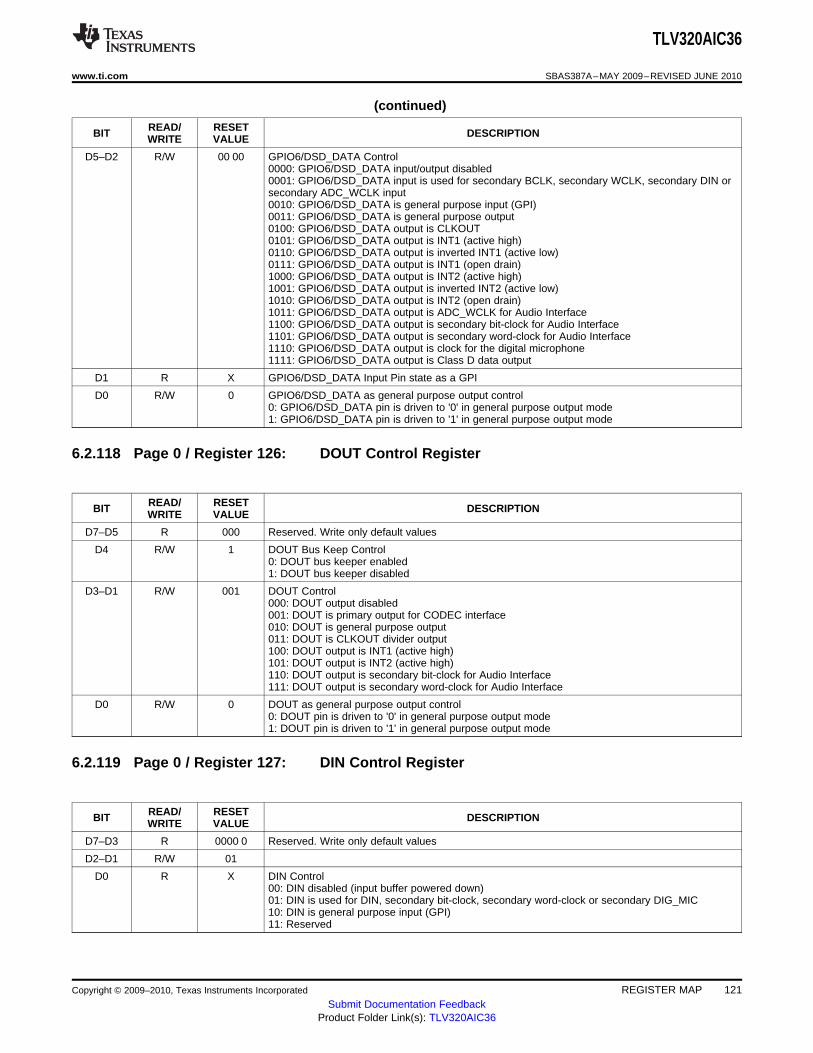
TLV320AIC36
www.ti.com SBAS387A–MAY 2009–REVISED JUNE 2010
(continued)
READ/ RESETBIT DESCRIPTIONWRITE VALUE
D5–D2 R/W 00 00 GPIO6/DSD_DATA Control0000: GPIO6/DSD_DATA input/output disabled0001: GPIO6/DSD_DATA input is used for secondary BCLK, secondary WCLK, secondary DIN orsecondary ADC_WCLK input0010: GPIO6/DSD_DATA is general purpose input (GPI)0011: GPIO6/DSD_DATA is general purpose output0100: GPIO6/DSD_DATA output is CLKOUT0101: GPIO6/DSD_DATA output is INT1 (active high)0110: GPIO6/DSD_DATA output is inverted INT1 (active low)0111: GPIO6/DSD_DATA output is INT1 (open drain)1000: GPIO6/DSD_DATA output is INT2 (active high)1001: GPIO6/DSD_DATA output is inverted INT2 (active low)1010: GPIO6/DSD_DATA output is INT2 (open drain)1011: GPIO6/DSD_DATA output is ADC_WCLK for Audio Interface1100: GPIO6/DSD_DATA output is secondary bit-clock for Audio Interface1101: GPIO6/DSD_DATA output is secondary word-clock for Audio Interface1110: GPIO6/DSD_DATA output is clock for the digital microphone1111: GPIO6/DSD_DATA output is Class D data output
D1 R X GPIO6/DSD_DATA Input Pin state as a GPI
D0 R/W 0 GPIO6/DSD_DATA as general purpose output control0: GPIO6/DSD_DATA pin is driven to '0' in general purpose output mode1: GPIO6/DSD_DATA pin is driven to '1' in general purpose output mode
6.2.118 Page 0 / Register 126: DOUT Control Register
READ/ RESETBIT DESCRIPTIONWRITE VALUE
D7–D5 R 000 Reserved. Write only default values
D4 R/W 1 DOUT Bus Keep Control0: DOUT bus keeper enabled1: DOUT bus keeper disabled
D3–D1 R/W 001 DOUT Control000: DOUT output disabled001: DOUT is primary output for CODEC interface010: DOUT is general purpose output011: DOUT is CLKOUT divider output100: DOUT output is INT1 (active high)101: DOUT output is INT2 (active high)110: DOUT output is secondary bit-clock for Audio Interface111: DOUT output is secondary word-clock for Audio Interface
D0 R/W 0 DOUT as general purpose output control0: DOUT pin is driven to '0' in general purpose output mode1: DOUT pin is driven to '1' in general purpose output mode
6.2.119 Page 0 / Register 127: DIN Control Register
READ/ RESETBIT DESCRIPTIONWRITE VALUE
D7–D3 R 0000 0 Reserved. Write only default values
D2–D1 R/W 01
D0 R X DIN Control00: DIN disabled (input buffer powered down)01: DIN is used for DIN, secondary bit-clock, secondary word-clock or secondary DIG_MIC10: DIN is general purpose input (GPI)11: Reserved
Copyright © 2009–2010, Texas Instruments Incorporated REGISTER MAP 121Submit Documentation Feedback
Product Folder Link(s): TLV320AIC36

TLV320AIC36
SBAS387A–MAY 2009–REVISED JUNE 2010 www.ti.com
6.2.120 Page 1 / Register 0: Page Select Register
READ/ RESETBIT DESCRIPTIONWRITE VALUE
D7–D0 R/W 0000 0000 Page Select Register0-255: Selects the Register Page for next read or write command.Refer Table "Summary of Memory Map" for details.
6.2.121 Page 1 / Register 1-2: Reserved Registers
READ/ RESETBIT DESCRIPTIONWRITE VALUE
D7–D0 R 0000 0000 Reserved, Write only default values
6.2.122 Page 1 / Register 3: Left Bitstream Mode Enable
READ/ RESETBIT DESCRIPTIONWRITE VALUE
D7 R/W 0 Left DAC Modulator Bitstream Mode Enable0: Left DAC modulator in normal mode1: Left DAC modulator in bitstream mode
D6–D0 R 000 0000 Reserved, Write only default values
6.2.123 Page 1 / Register 4: Right Bitstream Mode Enable
READ/ RESETBIT DESCRIPTIONWRITE VALUE
D7 R/W 0 Right DAC Modulator Bitstream Mode Enable0: Right DAC modulator in normal mode1: Right DAC modulator in bitstream mode
D6–D0 R 000 0000 Reserved, Write only default values
6.2.124 Page 1 / Register 5-9: Reserved Registers
READ/ RESETBIT DESCRIPTIONWRITE VALUE
D7–D0 R 0000 0000 Reserved, Write only default values
6.2.125 Page 1 / Register 10: ADC Channel Analog Configuration Register 1
READ/ RESETBIT DESCRIPTIONWRITE VALUE
D7 R 0 Reserved, Write only default values
D6 R/W 0 ADC Input Common Mode Select0: Set input common mode for ADC section to 0.9V1: Set input common mode for ADC section to 0.75V
D5–D0 R 00 0000 Reserved, Write only default values
122 REGISTER MAP Copyright © 2009–2010, Texas Instruments Incorporated
Submit Documentation FeedbackProduct Folder Link(s): TLV320AIC36
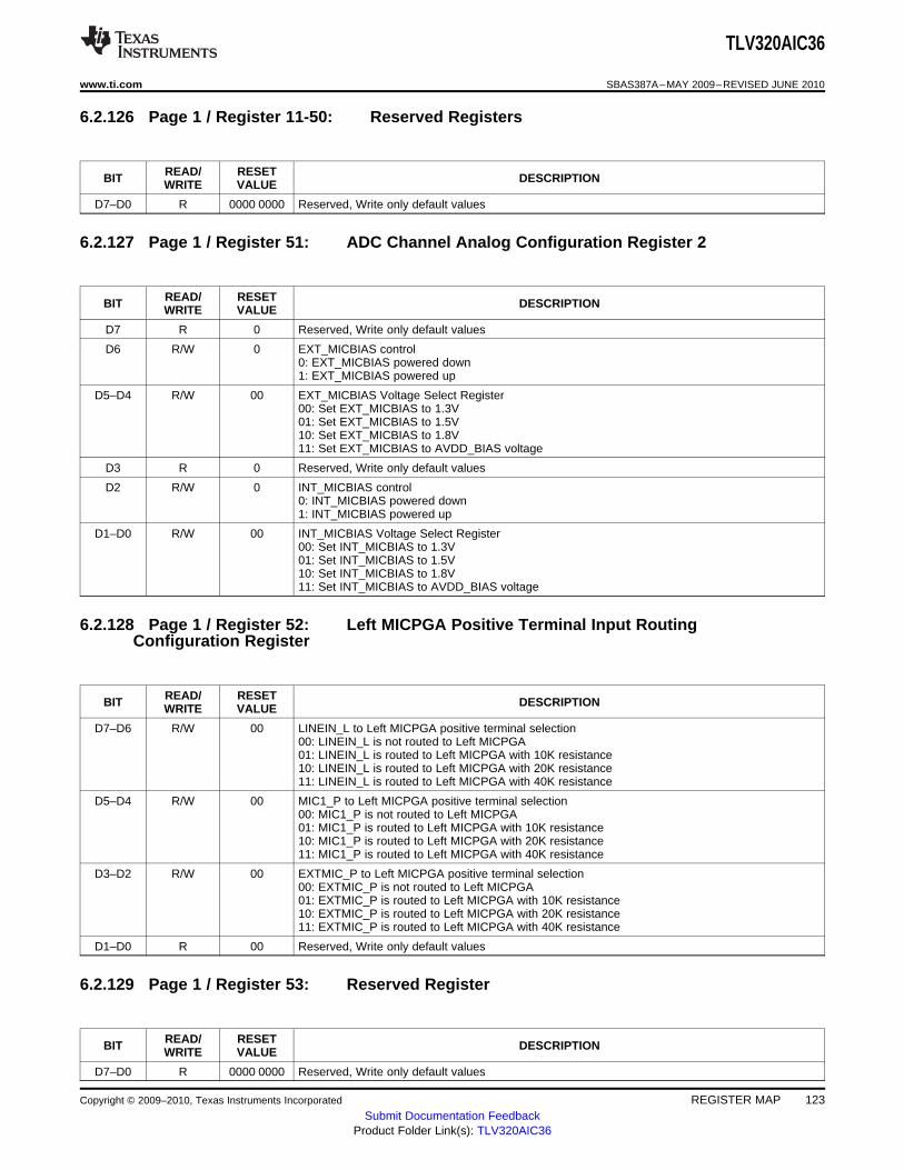
TLV320AIC36
www.ti.com SBAS387A–MAY 2009–REVISED JUNE 2010
6.2.126 Page 1 / Register 11-50: Reserved Registers
READ/ RESETBIT DESCRIPTIONWRITE VALUE
D7–D0 R 0000 0000 Reserved, Write only default values
6.2.127 Page 1 / Register 51: ADC Channel Analog Configuration Register 2
READ/ RESETBIT DESCRIPTIONWRITE VALUE
D7 R 0 Reserved, Write only default values
D6 R/W 0 EXT_MICBIAS control0: EXT_MICBIAS powered down1: EXT_MICBIAS powered up
D5–D4 R/W 00 EXT_MICBIAS Voltage Select Register00: Set EXT_MICBIAS to 1.3V01: Set EXT_MICBIAS to 1.5V10: Set EXT_MICBIAS to 1.8V11: Set EXT_MICBIAS to AVDD_BIAS voltage
D3 R 0 Reserved, Write only default values
D2 R/W 0 INT_MICBIAS control0: INT_MICBIAS powered down1: INT_MICBIAS powered up
D1–D0 R/W 00 INT_MICBIAS Voltage Select Register00: Set INT_MICBIAS to 1.3V01: Set INT_MICBIAS to 1.5V10: Set INT_MICBIAS to 1.8V11: Set INT_MICBIAS to AVDD_BIAS voltage
6.2.128 Page 1 / Register 52: Left MICPGA Positive Terminal Input RoutingConfiguration Register
READ/ RESETBIT DESCRIPTIONWRITE VALUE
D7–D6 R/W 00 LINEIN_L to Left MICPGA positive terminal selection00: LINEIN_L is not routed to Left MICPGA01: LINEIN_L is routed to Left MICPGA with 10K resistance10: LINEIN_L is routed to Left MICPGA with 20K resistance11: LINEIN_L is routed to Left MICPGA with 40K resistance
D5–D4 R/W 00 MIC1_P to Left MICPGA positive terminal selection00: MIC1_P is not routed to Left MICPGA01: MIC1_P is routed to Left MICPGA with 10K resistance10: MIC1_P is routed to Left MICPGA with 20K resistance11: MIC1_P is routed to Left MICPGA with 40K resistance
D3–D2 R/W 00 EXTMIC_P to Left MICPGA positive terminal selection00: EXTMIC_P is not routed to Left MICPGA01: EXTMIC_P is routed to Left MICPGA with 10K resistance10: EXTMIC_P is routed to Left MICPGA with 20K resistance11: EXTMIC_P is routed to Left MICPGA with 40K resistance
D1–D0 R 00 Reserved, Write only default values
6.2.129 Page 1 / Register 53: Reserved Register
READ/ RESETBIT DESCRIPTIONWRITE VALUE
D7–D0 R 0000 0000 Reserved, Write only default values
Copyright © 2009–2010, Texas Instruments Incorporated REGISTER MAP 123Submit Documentation Feedback
Product Folder Link(s): TLV320AIC36
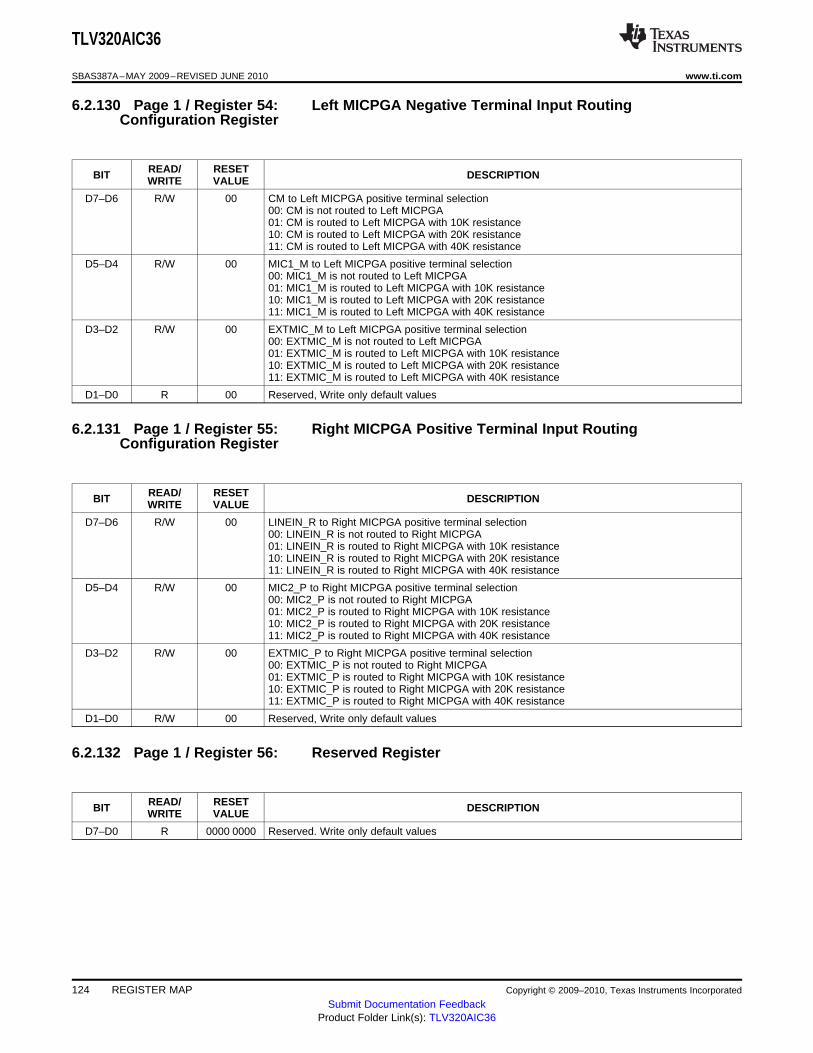
TLV320AIC36
SBAS387A–MAY 2009–REVISED JUNE 2010 www.ti.com
6.2.130 Page 1 / Register 54: Left MICPGA Negative Terminal Input RoutingConfiguration Register
READ/ RESETBIT DESCRIPTIONWRITE VALUE
D7–D6 R/W 00 CM to Left MICPGA positive terminal selection00: CM is not routed to Left MICPGA01: CM is routed to Left MICPGA with 10K resistance10: CM is routed to Left MICPGA with 20K resistance11: CM is routed to Left MICPGA with 40K resistance
D5–D4 R/W 00 MIC1_M to Left MICPGA positive terminal selection00: MIC1_M is not routed to Left MICPGA01: MIC1_M is routed to Left MICPGA with 10K resistance10: MIC1_M is routed to Left MICPGA with 20K resistance11: MIC1_M is routed to Left MICPGA with 40K resistance
D3–D2 R/W 00 EXTMIC_M to Left MICPGA positive terminal selection00: EXTMIC_M is not routed to Left MICPGA01: EXTMIC_M is routed to Left MICPGA with 10K resistance10: EXTMIC_M is routed to Left MICPGA with 20K resistance11: EXTMIC_M is routed to Left MICPGA with 40K resistance
D1–D0 R 00 Reserved, Write only default values
6.2.131 Page 1 / Register 55: Right MICPGA Positive Terminal Input RoutingConfiguration Register
READ/ RESETBIT DESCRIPTIONWRITE VALUE
D7–D6 R/W 00 LINEIN_R to Right MICPGA positive terminal selection00: LINEIN_R is not routed to Right MICPGA01: LINEIN_R is routed to Right MICPGA with 10K resistance10: LINEIN_R is routed to Right MICPGA with 20K resistance11: LINEIN_R is routed to Right MICPGA with 40K resistance
D5–D4 R/W 00 MIC2_P to Right MICPGA positive terminal selection00: MIC2_P is not routed to Right MICPGA01: MIC2_P is routed to Right MICPGA with 10K resistance10: MIC2_P is routed to Right MICPGA with 20K resistance11: MIC2_P is routed to Right MICPGA with 40K resistance
D3–D2 R/W 00 EXTMIC_P to Right MICPGA positive terminal selection00: EXTMIC_P is not routed to Right MICPGA01: EXTMIC_P is routed to Right MICPGA with 10K resistance10: EXTMIC_P is routed to Right MICPGA with 20K resistance11: EXTMIC_P is routed to Right MICPGA with 40K resistance
D1–D0 R/W 00 Reserved, Write only default values
6.2.132 Page 1 / Register 56: Reserved Register
READ/ RESETBIT DESCRIPTIONWRITE VALUE
D7–D0 R 0000 0000 Reserved. Write only default values
124 REGISTER MAP Copyright © 2009–2010, Texas Instruments Incorporated
Submit Documentation FeedbackProduct Folder Link(s): TLV320AIC36

TLV320AIC36
www.ti.com SBAS387A–MAY 2009–REVISED JUNE 2010
6.2.133 Page 1 / Register 57: Right MICPGA Negative Terminal Input RoutingConfiguration Register
READ/ RESETBIT DESCRIPTIONWRITE VALUE
D7–D6 R/W 00 CM to Right MICPGA positive terminal selection00: CM is not routed to Right MICPGA01: CM is routed to Right MICPGA with 10K resistance10: CM is routed to Right MICPGA with 20K resistance11: CM is routed to Right MICPGA with 40K resistance
D5–D4 R/W 00 MIC2_M to Right MICPGA positive terminal selection00: MIC2_M is not routed to Right MICPGA01: MIC2_M is routed to Right MICPGA with 10K resistance10: MIC2_M is routed to Right MICPGA with 20K resistance11: MIC2_M is routed to Right MICPGA with 40K resistance
D3–D2 R/W 00 EXTMIC_M to Right MICPGA positive terminal selection00: EXTMIC_M is not routed to Right MICPGA01: EXTMIC_M is routed to Right MICPGA with 10K resistance10: EXTMIC_M is routed to Right MICPGA with 20K resistance11: EXTMIC_M is routed to Right MICPGA with 40K resistance
D1–D0 R/W 00 Reserved, Write only default values
6.2.134 Page 1 / Register 58: CM settings for unused inputs Register
READ/ RESETBIT DESCRIPTIONWRITE VALUE
D7 R/W 0 LINEIN_L input setting when not used0: LINEIN_L input is floating when not used1: LINEIN_L input is weakly connected to CM when not used (if ADC L enabled)
D6 R/W 0 LINEIN_R input setting when not used0: LINEIN_R input is floating when not used1: LINEIN_R input is weakly connected to CM when not used (if ADC R is enabled)
D5 R/W 0 MIC1 input setting when not used0: MIC1 input is floating when not used1: MIC1 input is weakly connected to CM when not used (if ADC L is enabled)
D4 R/W 0 MIC2 input setting when not used0: MIC2 input is floating when not used1: MIC2 input is weakly connected to CM when not used (if ADC R is enabled)
D3 R/W 0 EXTMIC input setting when not used0: EXTMIC input is floating when not used1: EXTMIC input is weakly connected to CM when not used (if ADC L is enabled)
D2 R/W 0 EXTMIC input setting when not used Left ADC0: EXTMIC input is floating when not used1: EXTMIC input is weakly connected to CM when not used (if ADCR is enabled)
D1–D0 R 00 Reserved. Write only default values
6.2.135 Page 1 / Register 59: Left MICPGA Volume Control Register
READ/ RESETBIT DESCRIPTIONWRITE VALUE
D7 R/W 1 0: Left MICPGA Gain is enabled1: Left MICPGA Gain is set to 0 dB
Copyright © 2009–2010, Texas Instruments Incorporated REGISTER MAP 125Submit Documentation Feedback
Product Folder Link(s): TLV320AIC36

TLV320AIC36
SBAS387A–MAY 2009–REVISED JUNE 2010 www.ti.com
(continued)
READ/ RESETBIT DESCRIPTIONWRITE VALUE
D6–D0 R/W 000 0000 Left MICPGA Volume Control000 0000: Volume Control = 0.0 dB000 0001: Volume Control = 0.5 dB000 0010: Volume Control = 1.0 dB…101 1101: Volume Control = 46.5 dB101 1110: Volume Control = 47.0 dB101 1111: Volume Control = 47.5 dB110 0000-111 1111: Reserved. Do not use
6.2.136 Page 1 / Register 60: Right MICPGA Volume Control Register
READ/ RESETBIT DESCRIPTIONWRITE VALUE
D7 R/W 1 0: Right MICPGA Gain is enabled1: Right MICPGA Gain is set to 0 dB
D6–D0 R/W 000 0000 Right MICPGA Volume Control000 0000: Volume Control = 0.0 dB000 0001: Volume Control = 0.5 dB000 0010: Volume Control = 1.0 dB…101 1101: Volume Control = 46.5 dB101 1110: Volume Control = 47.0 dB101 1111: Volume Control = 47.5 dB110 0000-111 1111: Reserved. Do not use
6.2.137 Page 1 / Register 61: ADC Low Current Register
READ/ RESETBIT DESCRIPTIONWRITE VALUE
D7–D6 R/W 00 ADC ADMOD Driver Current Control0: Normal Current Consumption Mode1: Current consumption reduced by 40%2: Current consumption reduced by 65%3: Reserved
D5–D3 R/W 000 ADC ADMOD0: Normal Current Consumption ModeOthers: Current consumption reduced by TBD %
D2–D0 R/W 000 ADC REFBUF0: Normal Current Consumption ModeOthers: Current consumption reduced by TBD %
6.2.138 Page 1 / Register 62: ADC Analog Volume Control Flag Register
READ/ RESETBIT DESCRIPTIONWRITE VALUE
D7–D2 R 0000 00 Reserved. Write only default values
D1 R 0 Left Channel Analog Volume Control Flag0: Applied Volume is not equal to Programmed Volume1: Applied Volume is equal to Programmed Volume
D0 R 0 Right Channel Analog Volume Control Flag0: Applied Volume is not equal to Programmed Volume1: Applied Volume is equal to Programmed Volume
126 REGISTER MAP Copyright © 2009–2010, Texas Instruments Incorporated
Submit Documentation FeedbackProduct Folder Link(s): TLV320AIC36
TLV320AIC36
www.ti.com SBAS387A–MAY 2009–REVISED JUNE 2010
6.2.139 Page 1 / Register 63-127: Reserved Registers
READ/ RESETBIT DESCRIPTIONWRITE VALUE
D7–D0 R 0000 0000 Reserved. Write only default values
6.2.140 Page 2 / Register 0: Page Select Register
READ/ RESETBIT DESCRIPTIONWRITE VALUE
D7–D0 R/W 0000 0000 Page Select Register0-255: Selects the Register Page for next read or write command.Refer Table "Summary of Memory Map" for details.
6.2.141 Page 2 / Register 1-2: Reserved Registers
READ/ RESETBIT DESCRIPTIONWRITE VALUE
D7–D0 R 0000 0000 Reserved, Write only default values
6.2.142 Page 2 / Register 3: Power Control Overrides Register
READ/ RESETBIT DESCRIPTIONWRITE VALUE
D7–D6 R 00 Reserved, Write only default values
D5–D4 R/W 00 Oscillator Controls Override00: Use oscillator automatic power controls (oscillator powers on only when needed)01: Force oscillator to remain powered up (required when bits D1 or D0 in this register is set)10: Force oscillator to remain off (ignore oscillator automatic power controls)11: Reserved (do not use)
D3–D2 R 00 Reserved, Write only default values
D1 R/W 0 ADC automaic power sequencing clock control0: Allow automatic ADC power sequencing1: Force ADC power sequencing clock on (oscillator must also be running)
D0 R/W 0 DAC automaic power sequencing clock control0: Allow automatic DAC power sequencing1: Force DAC power sequencing clock on (oscillator must also be running)
6.2.143 Page 2 / Register 4-19: Reserved Registers
READ/ RESETBIT DESCRIPTIONWRITE VALUE
D7–D0 R 0000 0000 Reserved, Write only default values
Copyright © 2009–2010, Texas Instruments Incorporated REGISTER MAP 127Submit Documentation Feedback
Product Folder Link(s): TLV320AIC36

TLV320AIC36
SBAS387A–MAY 2009–REVISED JUNE 2010 www.ti.com
6.2.144 Page 2 / Register 20: Detect Divider Enable Register
READ/ RESETBIT DESCRIPTIONWRITE VALUE
D7 R/W 0 Detect Divider 1 Enable ControlFirst divider for the detect sampling rate. Uses the low power oscillator (nominal 1MHz).The output of this divider is cascaded to detect divider 2.0: Disables detect divider 11: Enables detect divider 1
D6–D4 R 00 Reserved, Write only default values
D3 R/W 0 Detect Divider 2 Enable ControlSecond divider for the detect sampling rate. Uses the output of detect divider 1 as an input clock.Detect inputs are sampled based on the output of this divider.0: Disables detect divider 21: Enables detect divider 2
D2–D0 R 000 Reserved, Write only default values
6.2.145 Page 2 / Register 21: Detect Divider 1 Count Register
READ/ RESETBIT DESCRIPTIONWRITE VALUE
D7–D0 R/W 0000 0000 Detect Divider 1 count value0: Divider 1 = 2561: Divider 1 = 12: Divider 1 = 2…255: Divider 1 = 255
6.2.146 Page 2 / Register 22: Detect Divider 2 Count Register
READ/ RESETBIT DESCRIPTIONWRITE VALUE
D7–D0 R/W 0000 0000 Detect Divider 2 count value0: Divider 2 = 2561: Divider 2 = 12: Divider 2 = 2…255: Divider 2 = 255
6.2.147 Page 2 / Register 23: Detect Control Register
READ/ RESETBIT DESCRIPTIONWRITE VALUE
D7 R/W 0 Continuous Detection Enable0: disable continuous detection1: enable continuous detection (used for interrupt driven detection)
D6 R 0 Reserved. Write only default values
D5 R/W 0 Software driven detect / detect status0: read-back detection complete, OK to read detect value1: read-back detection is in progress, detect value is not yet stable1: write with self-clear: software initiated manual detect
D4–D0 R 0 0000 Output of detect SAR ADC prior to windowing. Useful for reading detect pin value.
128 REGISTER MAP Copyright © 2009–2010, Texas Instruments Incorporated
Submit Documentation FeedbackProduct Folder Link(s): TLV320AIC36
TLV320AIC36
www.ti.com SBAS387A–MAY 2009–REVISED JUNE 2010
6.2.148 Page 2 / Register 24: Short Pulse Detect Control Register
READ/ RESETBIT DESCRIPTIONWRITE VALUE
D7 R/W 0 Short Pulse Detect Enable0: Short pulse detect disabled1: Short pulse detect enabled
D6–D4 R 000 Stores the most recent debounced window number for the short pulse detect.The read value will change when the detect SAR value stablizes in a new window for a minimumperiod of (1uS * detect divider 1 * detect divider 2 * short pulse period) seconds (assuming a 1MHznomimal LF oscillator rate)
D3 R 0 Reserved, Write only default values
D2–D0 R 000 Latched window value from bits D6-D4 of this register.The value is held when a short detect pulse interrupt is triggered and will remain held until theinterrupt is cleared.It is useful for determing the window number that triggered the interrupt event.
6.2.149 Page 2 / Register 25: Long Pulse Detect Control Register
READ/ RESETBIT DESCRIPTIONWRITE VALUE
D7 R/W 0 Long Pulse Detect Enable0: Long pulse detect disabled1: Long pulse detect enabled
D6–D4 R 000 Stores the most recent debounced window number for the long pulse detect.The read value will change when the detect SAR value stablizes in a new window for a minimumperiod of (1uS * detect divider 1 * detect divider 2 * long pulse period) seconds (assuming a 1MHznomimal LF oscillator rate)
D3 R 00 Reserved, Write only default values
D2–D0 R 000 Latched window value from bits D6-D4 of this register.The value is held when a long detect pulse interrupt is triggered and will remain held until theinterrupt is cleared.It is useful for determing the window number that triggered the interrupt event.
6.2.150 Page 2 / Register 26: Short Pulse Period Register
READ/ RESETBIT DESCRIPTIONWRITE VALUE
D7–D0 R/W 0000 0000 Used to calculate the minimum debounce period for the short pulse detect function.1uS * detect divider 1 * detect divider 2 * this register determines the minimum pushbutton periodthat will be detected.Shorter button presses will be discarded and will not trigger an interrupt.Assumes a nominal LF oscillator rate.
6.2.151 Page 2 / Register 27: Log Pulse Period Register
READ/ RESETBIT DESCRIPTIONWRITE VALUE
D7–D0 R/W 0000 0000 Used to calculate the minimum debounce period for the long pulse detect function.1uS * detect divider 1 * detect divider 2 * this register determines the minimum pushbutton periodthat will be detected.Shorter button presses will be discarded and will not trigger an interrupt.Assumes a nominal LF oscillator rate.
Copyright © 2009–2010, Texas Instruments Incorporated REGISTER MAP 129Submit Documentation Feedback
Product Folder Link(s): TLV320AIC36
TLV320AIC36
SBAS387A–MAY 2009–REVISED JUNE 2010 www.ti.com
6.2.152 Page 2 / Register 28: Detect Threshold 1 Control
READ/ RESETBIT DESCRIPTIONWRITE VALUE
D7 R/W 0 Detect Threshold Enable0: disabled1: enabledWhen enabled, the value in bits D4 - D0 of this register creates a window bounday for the raw 5-bitdetect converter.
D6–D5 R 00 Reserved, Write only default values
D4–D0 R/W 0 0000 Window boundary value separating windows 0 and 1
6.2.153 Page 2 / Register 29: Detect Threshold 2 Control
READ/ RESETBIT DESCRIPTIONWRITE VALUE
D7 R/W 0 Detect Threshold Enable0: disabled1: enabledWhen enabled, the value in bits D4 - D0 of this register creates a window bounday for the raw 5-bitdetect converter.
D6–D5 R 00 Reserved, Write only default values
D4–D0 R/W 0 0000 Window boundary value separating windows 1 and 2
6.2.154 Page 2 / Register 30: Detect Threshold 2 Control
READ/ RESETBIT DESCRIPTIONWRITE VALUE
D7 R/W 0 Detect Threshold Enable0: disabled1: enabledWhen enabled, the value in bits D4 - D0 of this register creates a window bounday for the raw 5-bitdetect converter.
D6–D5 R 00 Reserved, Write only default values
D4–D0 R/W 0 0000 Window boundary value separating windows 2 and 3
6.2.155 Page 2 / Register 31: Detect Threshold 4 Control
READ/ RESETBIT DESCRIPTIONWRITE VALUE
D7 R/W 0 Detect Threshold Enable0: disabled1: enabledWhen enabled, the value in bits D4 - D0 of this register creates a window bounday for the raw 5-bitdetect converter.
D6–D5 R 00 Reserved, Write only default values
D4–D0 R/W 0 0000 Window boundary value separating windows 3 and 4
130 REGISTER MAP Copyright © 2009–2010, Texas Instruments Incorporated
Submit Documentation FeedbackProduct Folder Link(s): TLV320AIC36

TLV320AIC36
www.ti.com SBAS387A–MAY 2009–REVISED JUNE 2010
6.2.156 Page 2 / Register 32: Detect Threshold 5 Control
READ/ RESETBIT DESCRIPTIONWRITE VALUE
D7 R/W 0 Detect Threshold Enable0: disabled1: enabledWhen enabled, the value in bits D4 - D0 of this register creates a window bounday for the raw 5-bitdetect converter.
D6–D5 R 00 Reserved, Write only default values
D4–D0 R/W 0 0000 Window boundary value separating windows 4 and 5
6.2.157 Page 2 / Register 33: Detect Threshold 6 Control
READ/ RESETBIT DESCRIPTIONWRITE VALUE
D7 R/W 0 Detect Threshold Enable0: disabled1: enabledWhen enabled, the value in bits D4 - D0 of this register creates a window bounday for the raw 5-bitdetect converter.
D6–D5 R 00 Reserved, Write only default values
D4–D0 R/W 0 0000 Window boundary value separating windows 5 and 6
6.2.158 Page 2 / Register 34: Detect Threshold 7 Control
READ/ RESETBIT DESCRIPTIONWRITE VALUE
D7 R/W 0 Detect Threshold Enable0: disabled1: enabledWhen enabled, the value in bits D4 - D0 of this register creates a window bounday for the raw 5-bitdetect converter.
D6–D5 R 00 Reserved, Write only default values
D4–D0 R/W 0 0000 Window boundary value separating windows 6 and 7
6.2.159 Page 2 / Register 35: MIC Bias Control Register
READ/ RESETBIT DESCRIPTIONWRITE VALUE
D7 R/W Mic Bias Control0: Mic bias turned on only when detect is reading pin voltage1: Mic bias always turned on
D6–D0 R 000 0000 Reserved, Write only default values
6.2.160 Page 2 / Register 36: HP Left/Right ground register
READ/ RESETBIT DESCRIPTIONWRITE VALUE
D7 R/W 0 HP Left/Right amp positive terminal ground register0: Positive terminal of amp connected to GND_HP pin (must be tied to external ground)1: Positive terminal of amp connected to HP_COM (can be tied to external resistor network forground noise cancelation)
Copyright © 2009–2010, Texas Instruments Incorporated REGISTER MAP 131Submit Documentation Feedback
Product Folder Link(s): TLV320AIC36
TLV320AIC36
SBAS387A–MAY 2009–REVISED JUNE 2010 www.ti.com
(continued)
READ/ RESETBIT DESCRIPTIONWRITE VALUE
D6–D0 R 000 0000 Reserved. Write only default values
6.2.161 Page 2 / Register 37: DAC Power up Register
READ/ RESETBIT DESCRIPTIONWRITE VALUE
D7 R/W 0 Left DAC Power Up register0: Left Dac is not powered up1: Left DAC is powered up
D6 R/W 0 Right DAC Power Up register0: Right Dac is not powered up1: Right DAC is powered up
D5–D0 R 00 0000 Reserved. Write only default values
6.2.162 Page 2 / Register 38: HP and REC output short circuit protection register
READ/ RESETBIT DESCRIPTIONWRITE VALUE
D7–D6 R 00 Reserved, Write only default values
D5–D3 R/W 000 Reserved, Write only default values
D2 W 0 Short circuit enable register0: Short circuit protection on HP and REC outputs is disabled1: Short circuit protection on HP and REC outputs is enabled
D1 R/W 0 Short circuit control register0: If short circuit protection is enabled, it will limit the max current to the load1: If short circuit protection is enabled, it will power down the output when a short is dectected
D0 R/W 0 Reserved, Write only default values
6.2.163 Page 2 / Register 39: Reserved Register
READ/ RESETBIT DESCRIPTIONWRITE VALUE
D7–D0 R 00 Reserved, Write only default values
6.2.164 Page 2 / Register 40: High Power Output Stage Control Register
READ/ RESETBIT DESCRIPTIONWRITE VALUE
D7–D6 R 00 Reserved, Write only default values
D5 R/W 0 LINEIN_L bypass control register0: LINEIN_L bypass is disabled1: LINEIN_L bypass is enabled
D4 R/W 0 Reserved, Write only default values
D3 R/W 0 LINEIN_R bypass control register0: LINEIN_R bypass is disabled1: LINEIN_R bypass is enabled
D2 R/W 0 Reserved, Write only default values
132 REGISTER MAP Copyright © 2009–2010, Texas Instruments Incorporated
Submit Documentation FeedbackProduct Folder Link(s): TLV320AIC36

TLV320AIC36
www.ti.com SBAS387A–MAY 2009–REVISED JUNE 2010
(continued)
READ/ RESETBIT DESCRIPTIONWRITE VALUE
D1–D0 R/W 00 Output soft-stepping control00: ADC soft-stepping at one step per FS01: ADC soft-stepping at one step per 2 Fs10: ADC soft-stepping disabled11: Reserved
6.2.165 Page 2 / Register 41: Reserved Register
READ/ RESETBIT DESCRIPTIONWRITE VALUE
D7–D0 R 0000 0000 Reserved, Write only default values
6.2.166 Page 2 / Register 42: Output Driver Pop Reduction Register
READ/ RESETBIT DESCRIPTIONWRITE VALUE
D7–D4 R/W 0000 Driver Power-on Time0000: Driver power-on time = 0 usec0001: Driver power-on time = 10 usec0010: Driver power-on time = 100 usec0011: Driver power-on time = 1 msec0100: Driver power-on time = 10 msec0101: Driver power-on time = 50 msec0110: Driver power-on time = 100 msec0111: Driver power-on time = 200 msec1000: Driver power-on time = 400 msec1001: Driver power-on time = 800 msec1010: Driver power-on time = 2 sec1011: Driver power-on time = 4 secOthers: Reserved
D3–D2 R/W 00 Driver Ramp-up Step Time00: Driver Ramp-up step time = 0 msec01: Driver Ramp-up step time = 1 msec10: Driver Ramp-up step time = 2 msec11: Driver Ramp-up step time = 4 msec
D1–D0 R 00 Reserved, Write only default values
6.2.167 Page 2 / Register 43-44: Reserved Registers
READ/ RESETBIT DESCRIPTIONWRITE VALUE
D7–D0 R 0000 0000 Reserved, Write only default values
6.2.168 Page 2 / Register 45: LINEIN_L to HPL Volume Control Register
READ/ RESETBIT DESCRIPTIONWRITE VALUE
D7 R/W 0 LINEIN_L to HPL Routing Control0: LINEIN_L is not routed to HPL1: LINEIN_L is routed to HPL
Copyright © 2009–2010, Texas Instruments Incorporated REGISTER MAP 133Submit Documentation Feedback
Product Folder Link(s): TLV320AIC36

TLV320AIC36
SBAS387A–MAY 2009–REVISED JUNE 2010 www.ti.com
(continued)
READ/ RESETBIT DESCRIPTIONWRITE VALUE
D6–D0 R/W 000 0000 000 0000: Volume Control = 0.0 dB000 0001: Volume Control = -0.5 dB000 0010: Volume Control = -1.0 dB000 0011: Volume Control = -1.5 dB000 0100: Volume Control = -2.0 dB000 0101: Volume Control = -2.5 dB000 0110: Volume Control = -3.0 dB000 0111: Volume Control = -3.5 dB000 1000: Volume Control = -4.0 dB000 1001: Volume Control = -4.5 dB000 1010: Volume Control = -5.0 dB000 1011: Volume Control = -5.5 dB000 1100: Volume Control = -6.0 dB000 1101: Volume Control = -6.5 dB000 1110: Volume Control = -7.0 dB000 1111: Volume Control = -7.5 dB001 0000: Volume Control = -8.0 dB001 0001: Volume Control = -8.5 dB001 0010: Volume Control = -9.0 dB001 0011: Volume Control = -9.5 dB001 0100: Volume Control = -10.0 dB001 0101: Volume Control = -10.5 dB001 0110: Volume Control = -11.0 dB001 0111: Volume Control = -11.5 dB001 1000: Volume Control = -12.0 dB001 1001: Volume Control = -12.5 dB001 1010: Volume Control = -13.0 dB001 1011: Volume Control = -13.5 dB001 1100: Volume Control = -14.0 dB001 1101: Volume Control = -14.5 dB001 1110: Volume Control = -15.0 dB001 1111: Volume Control = -15.5 dB010 0000: Volume Control = -16.0 dB010 0001: Volume Control = -16.5 dB010 0010: Volume Control = -17.0 dB010 0011: Volume Control = -17.5 dB010 0100: Volume Control = -18.0 dB010 0101: Volume Control = -18.6 dB010 0110: Volume Control = -19.1 dB010 0111: Volume Control = -19.6 dB010 1000: Volume Control = -20.1 dB010 1001: Volume Control = -20.6 dB010 1010: Volume Control = -21.1 dB010 1011: Volume Control = -21.6 dB010 1100: Volume Control = -22.1 dB010 1101: Volume Control = -22.6 dB010 1110: Volume Control = -23.1 dB010 1111: Volume Control = -23.6 dB011 0000: Volume Control = -24.1 dB011 0001: Volume Control = -24.6 dB011 0010: Volume Control = -25.1 dB011 0011: Volume Control = -25.6 dB011 0100: Volume Control = -26.1 dB011 0101: Volume Control = -26.6 dB011 0110: Volume Control = -27.1 dB011 0111: Volume Control = -27.6 dB011 1000: Volume Control = -28.1 dB011 1001: Volume Control = -28.6 dB011 1010: Volume Control = -29.1 dB011 1011: Volume Control = -29.6 dB011 1100: Volume Control = -30.1 dB011 1101: Volume Control = -30.6 dB011 1110: Volume Control = -31.1 dB011 1111: Volume Control = -31.6 dB100 0000: Volume Control = -32.1 dB100 0001: Volume Control = -32.6 dB100 0010: Volume Control = -33.1 dB100 0011: Volume Control = -33.6 dB
134 REGISTER MAP Copyright © 2009–2010, Texas Instruments Incorporated
Submit Documentation FeedbackProduct Folder Link(s): TLV320AIC36
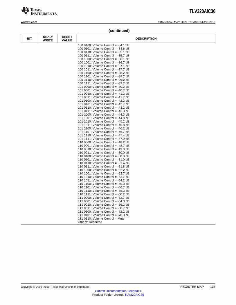
TLV320AIC36
www.ti.com SBAS387A–MAY 2009–REVISED JUNE 2010
(continued)
READ/ RESETBIT DESCRIPTIONWRITE VALUE
100 0100: Volume Control = -34.1 dB100 0101: Volume Control = -34.6 dB100 0110: Volume Control = -35.1 dB100 0111: Volume Control = -35.7 dB100 1000: Volume Control = -36.1 dB100 1001: Volume Control = -36.7 dB100 1010: Volume Control = -37.1 dB100 1011: Volume Control = -37.7 dB100 1100: Volume Control = -38.2 dB100 1101: Volume Control = -38.7 dB100 1110: Volume Control = -39.2 dB100 1111: Volume Control = -39.7 dB101 0000: Volume Control = -40.2 dB101 0001: Volume Control = -40.7 dB101 0010: Volume Control = -41.2 dB101 0011: Volume Control = -41.7 dB101 0100: Volume Control = -42.2 dB101 0101: Volume Control = -42.7 dB101 0110: Volume Control = -43.2 dB101 0111: Volume Control = -43.8 dB101 1000: Volume Control = -44.3 dB101 1001: Volume Control = -44.8 dB101 1010: Volume Control = -45.2 dB101 1011: Volume Control = -45.8 dB101 1100: Volume Control = -46.2 dB101 1101: Volume Control = -46.7 dB101 1110: Volume Control = -47.4 dB101 1111: Volume Control = -47.9 dB110 0000: Volume Control = -48.2 dB110 0001: Volume Control = -48.7 dB110 0010: Volume Control = -49.3 dB110 0011: Volume Control = -50.0 dB110 0100: Volume Control = -50.3 dB110 0101: Volume Control = -51.0 dB110 0110: Volume Control = -51.4 dB110 0111: Volume Control = -51.8 dB110 1000: Volume Control = -52.2 dB110 1001: Volume Control = -52.7 dB110 1010: Volume Control = -53.7 dB110 1011: Volume Control = -54.2 dB110 1100: Volume Control = -55.3 dB110 1101: Volume Control = -56.7 dB110 1110: Volume Control = -58.3 dB110 1111: Volume Control = -60.2 dB111 0000: Volume Control = -62.7 dB111 0001: Volume Control = -64.3 dB111 0010: Volume Control = -66.2 dB111 0011: Volume Control = -68.7 dB111 0100: Volume Control = -72.2 dB111 0101: Volume Control = -78.3 dB111 0110: Volume Control = MuteOthers: Reserved
Copyright © 2009–2010, Texas Instruments Incorporated REGISTER MAP 135Submit Documentation Feedback
Product Folder Link(s): TLV320AIC36

TLV320AIC36
SBAS387A–MAY 2009–REVISED JUNE 2010 www.ti.com
6.2.169 Page 2 / Register 46: PGA_L_L to HPL Volume Control Register
READ/ RESETBIT DESCRIPTIONWRITE VALUE
D7 R/W 0 PGA_L to HPL Routing Control0: PGA_L is not routed to HPL1: PGA_L is routed to HPL
D6–D0 R/W 000 0000 000 0000: Volume Control = 0.0 dB000 0001: Volume Control = -0.5 dB000 0010: Volume Control = -1.0 dB…intermediate values identical to Page2/Register 45/D6-D0…111 0011: Volume Control = -68.7 dB111 0100: Volume Control = -72.2 dB111 0101: Volume Control = -78.3 dB111 0110: Volume Control = MuteOthers: Reserved
6.2.170 Page 2 / Register 47: DAC_L to HPL Volume Control Register
READ/ RESETBIT DESCRIPTIONWRITE VALUE
D7 R/W 0 DAC_L to HPL Routing Control0: DAC_L is not routed to HPL1: DAC_L is routed to HPL
D6–D0 R/W 000 0000 000 0000: Volume Control = 0.0 dB000 0001: Volume Control = -0.5 dB000 0010: Volume Control = -1.0 dB…intermediate values identical to Page2/Register 45/D6-D0…111 0011: Volume Control = -68.7 dB111 0100: Volume Control = -72.2 dB111 0101: Volume Control = -78.3 dB111 0110: Volume Control = MuteOthers: Reserved
6.2.171 Page 2 / Register 48: LINEIN_R to HPL Volume Control Register
READ/ RESETBIT DESCRIPTIONWRITE VALUE
D7 R/W 0 LINEIN_R to HPL Routing Control0: LINEIN_R is not routed to HPL1: LINEIN_R is routed to HPL
D6–D0 R/W 000 0000 000 0000: Volume Control = 0.0 dB000 0001: Volume Control = -0.5 dB000 0010: Volume Control = -1.0 dB…intermediate values identical to Page2/Register 45/D6-D0…111 0011: Volume Control = -68.7 dB111 0100: Volume Control = -72.2 dB111 0101: Volume Control = -78.3 dB111 0110: Volume Control = MuteOthers: Reserved
136 REGISTER MAP Copyright © 2009–2010, Texas Instruments Incorporated
Submit Documentation FeedbackProduct Folder Link(s): TLV320AIC36

TLV320AIC36
www.ti.com SBAS387A–MAY 2009–REVISED JUNE 2010
6.2.172 Page 2 / Register 49: PGA_R to HPL Volume Control Register
READ/ RESETBIT DESCRIPTIONWRITE VALUE
D7 R/W 0 PGA_R to HPL Routing Control0: PGA_R is not routed to HPL1: PGA_R is routed to HPL
D6–D0 R/W 000 0000 000 0000: Volume Control = 0.0 dB000 0001: Volume Control = -0.5 dB000 0010: Volume Control = -1.0 dB…intermediate values identical to Page2/Register 45/D6-D0…111 0011: Volume Control = -68.7 dB111 0100: Volume Control = -72.2 dB111 0101: Volume Control = -78.3 dB111 0110: Volume Control = MuteOthers: Reserved
6.2.173 Page 2 / Register 50: DAC_R to HPL Volume Control Register
READ/ RESETBIT DESCRIPTIONWRITE VALUE
D7 R/W 0 DAC_R to HPL Routing Control0: DAC_R is not routed to HPL1: DAC_R is routed to HPL
D6–D0 R/W 000 0000 000 0000: Volume Control = 0.0 dB000 0001: Volume Control = -0.5 dB000 0010: Volume Control = -1.0 dB…intermediate values identical to Page2/Register 45/D6-D0…111 0011: Volume Control = -68.7 dB111 0100: Volume Control = -72.2 dB111 0101: Volume Control = -78.3 dB111 0110: Volume Control = MuteOthers: Reserved
6.2.174 Page 2 / Register 51: HPL Output Volume Control Register
READ/ RESETBIT DESCRIPTIONWRITE VALUE
D7–D4 R/W 0000 HPL Output Volume Control0000: Volume = 0 dB0001: Volume = 1 dB0010: Volume = 2 dB0011: Volume = 3 dB0100: Volume = 4 dB0101: Volume = 5 dB0110: Volume = 6 dB0111: Volume = 7 dB1000: Volume = 8 dB1001: Volume = 9 dBOthers: Reserved
D3 R/W 0 HPL Mute Control0: Muted1: Not Muted
D2 R/W 1 HPL Power-down Mode0: HPL is weakly driven to ground when powered down1: HPL is high-Z when powered down
Copyright © 2009–2010, Texas Instruments Incorporated REGISTER MAP 137Submit Documentation Feedback
Product Folder Link(s): TLV320AIC36
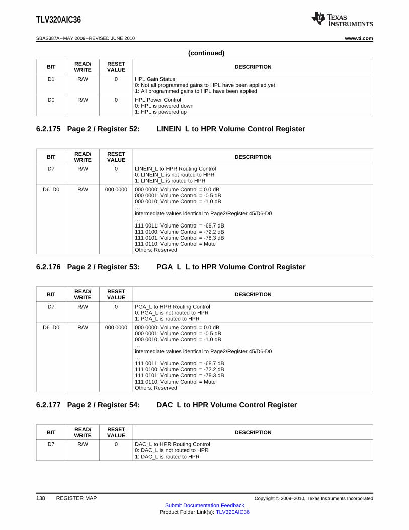
TLV320AIC36
SBAS387A–MAY 2009–REVISED JUNE 2010 www.ti.com
(continued)
READ/ RESETBIT DESCRIPTIONWRITE VALUE
D1 R/W 0 HPL Gain Status0: Not all programmed gains to HPL have been applied yet1: All programmed gains to HPL have been applied
D0 R/W 0 HPL Power Control0: HPL is powered down1: HPL is powered up
6.2.175 Page 2 / Register 52: LINEIN_L to HPR Volume Control Register
READ/ RESETBIT DESCRIPTIONWRITE VALUE
D7 R/W 0 LINEIN_L to HPR Routing Control0: LINEIN_L is not routed to HPR1: LINEIN_L is routed to HPR
D6–D0 R/W 000 0000 000 0000: Volume Control = 0.0 dB000 0001: Volume Control = -0.5 dB000 0010: Volume Control = -1.0 dB…intermediate values identical to Page2/Register 45/D6-D0…111 0011: Volume Control = -68.7 dB111 0100: Volume Control = -72.2 dB111 0101: Volume Control = -78.3 dB111 0110: Volume Control = MuteOthers: Reserved
6.2.176 Page 2 / Register 53: PGA_L_L to HPR Volume Control Register
READ/ RESETBIT DESCRIPTIONWRITE VALUE
D7 R/W 0 PGA_L to HPR Routing Control0: PGA_L is not routed to HPR1: PGA_L is routed to HPR
D6–D0 R/W 000 0000 000 0000: Volume Control = 0.0 dB000 0001: Volume Control = -0.5 dB000 0010: Volume Control = -1.0 dB…intermediate values identical to Page2/Register 45/D6-D0…111 0011: Volume Control = -68.7 dB111 0100: Volume Control = -72.2 dB111 0101: Volume Control = -78.3 dB111 0110: Volume Control = MuteOthers: Reserved
6.2.177 Page 2 / Register 54: DAC_L to HPR Volume Control Register
READ/ RESETBIT DESCRIPTIONWRITE VALUE
D7 R/W 0 DAC_L to HPR Routing Control0: DAC_L is not routed to HPR1: DAC_L is routed to HPR
138 REGISTER MAP Copyright © 2009–2010, Texas Instruments Incorporated
Submit Documentation FeedbackProduct Folder Link(s): TLV320AIC36
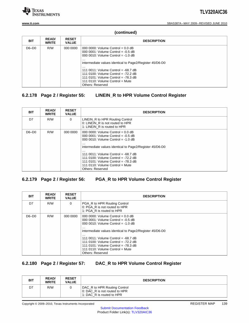
TLV320AIC36
www.ti.com SBAS387A–MAY 2009–REVISED JUNE 2010
(continued)
READ/ RESETBIT DESCRIPTIONWRITE VALUE
D6–D0 R/W 000 0000 000 0000: Volume Control = 0.0 dB000 0001: Volume Control = -0.5 dB000 0010: Volume Control = -1.0 dB…intermediate values identical to Page2/Register 45/D6-D0…111 0011: Volume Control = -68.7 dB111 0100: Volume Control = -72.2 dB111 0101: Volume Control = -78.3 dB111 0110: Volume Control = MuteOthers: Reserved
6.2.178 Page 2 / Register 55: LINEIN_R to HPR Volume Control Register
READ/ RESETBIT DESCRIPTIONWRITE VALUE
D7 R/W 0 LINEIN_R to HPR Routing Control0: LINEIN_R is not routed to HPR1: LINEIN_R is routed to HPR
D6–D0 R/W 000 0000 000 0000: Volume Control = 0.0 dB000 0001: Volume Control = -0.5 dB000 0010: Volume Control = -1.0 dB…intermediate values identical to Page2/Register 45/D6-D0…111 0011: Volume Control = -68.7 dB111 0100: Volume Control = -72.2 dB111 0101: Volume Control = -78.3 dB111 0110: Volume Control = MuteOthers: Reserved
6.2.179 Page 2 / Register 56: PGA_R to HPR Volume Control Register
READ/ RESETBIT DESCRIPTIONWRITE VALUE
D7 R/W 0 PGA_R to HPR Routing Control0: PGA_R is not routed to HPR1: PGA_R is routed to HPR
D6–D0 R/W 000 0000 000 0000: Volume Control = 0.0 dB000 0001: Volume Control = -0.5 dB000 0010: Volume Control = -1.0 dB…intermediate values identical to Page2/Register 45/D6-D0…111 0011: Volume Control = -68.7 dB111 0100: Volume Control = -72.2 dB111 0101: Volume Control = -78.3 dB111 0110: Volume Control = MuteOthers: Reserved
6.2.180 Page 2 / Register 57: DAC_R to HPR Volume Control Register
READ/ RESETBIT DESCRIPTIONWRITE VALUE
D7 R/W 0 DAC_R to HPR Routing Control0: DAC_R is not routed to HPR1: DAC_R is routed to HPR
Copyright © 2009–2010, Texas Instruments Incorporated REGISTER MAP 139Submit Documentation Feedback
Product Folder Link(s): TLV320AIC36
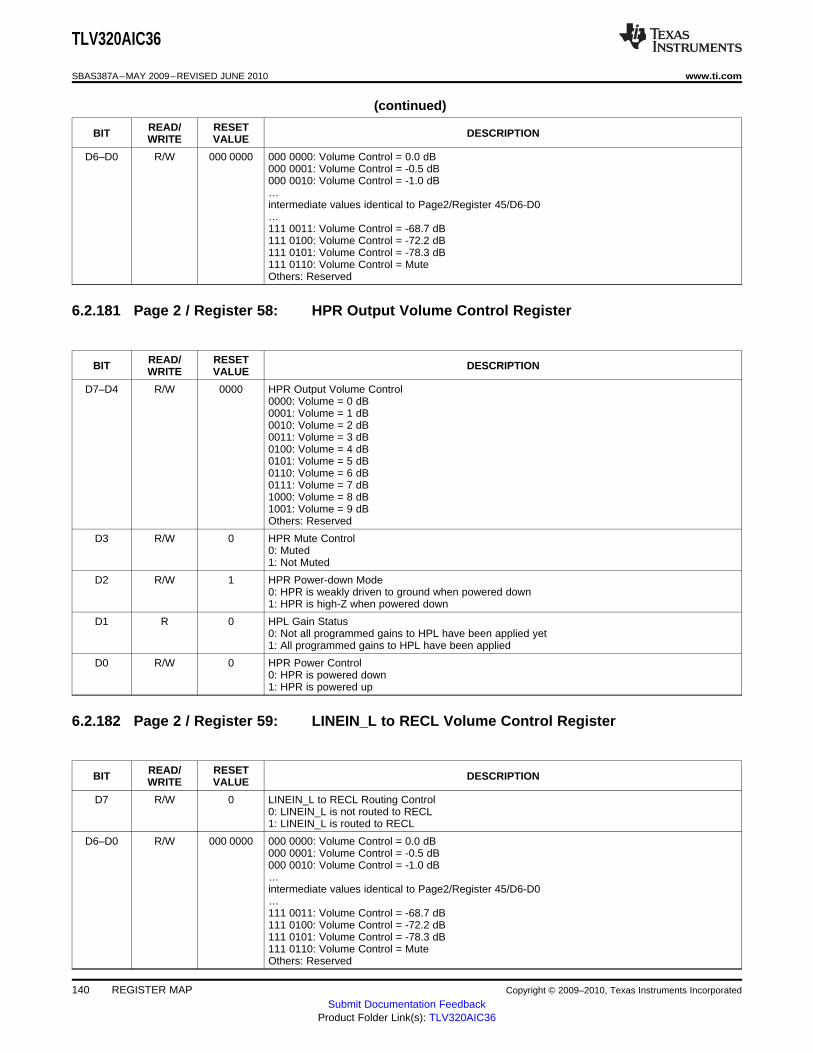
TLV320AIC36
SBAS387A–MAY 2009–REVISED JUNE 2010 www.ti.com
(continued)
READ/ RESETBIT DESCRIPTIONWRITE VALUE
D6–D0 R/W 000 0000 000 0000: Volume Control = 0.0 dB000 0001: Volume Control = -0.5 dB000 0010: Volume Control = -1.0 dB…intermediate values identical to Page2/Register 45/D6-D0…111 0011: Volume Control = -68.7 dB111 0100: Volume Control = -72.2 dB111 0101: Volume Control = -78.3 dB111 0110: Volume Control = MuteOthers: Reserved
6.2.181 Page 2 / Register 58: HPR Output Volume Control Register
READ/ RESETBIT DESCRIPTIONWRITE VALUE
D7–D4 R/W 0000 HPR Output Volume Control0000: Volume = 0 dB0001: Volume = 1 dB0010: Volume = 2 dB0011: Volume = 3 dB0100: Volume = 4 dB0101: Volume = 5 dB0110: Volume = 6 dB0111: Volume = 7 dB1000: Volume = 8 dB1001: Volume = 9 dBOthers: Reserved
D3 R/W 0 HPR Mute Control0: Muted1: Not Muted
D2 R/W 1 HPR Power-down Mode0: HPR is weakly driven to ground when powered down1: HPR is high-Z when powered down
D1 R 0 HPL Gain Status0: Not all programmed gains to HPL have been applied yet1: All programmed gains to HPL have been applied
D0 R/W 0 HPR Power Control0: HPR is powered down1: HPR is powered up
6.2.182 Page 2 / Register 59: LINEIN_L to RECL Volume Control Register
READ/ RESETBIT DESCRIPTIONWRITE VALUE
D7 R/W 0 LINEIN_L to RECL Routing Control0: LINEIN_L is not routed to RECL1: LINEIN_L is routed to RECL
D6–D0 R/W 000 0000 000 0000: Volume Control = 0.0 dB000 0001: Volume Control = -0.5 dB000 0010: Volume Control = -1.0 dB…intermediate values identical to Page2/Register 45/D6-D0…111 0011: Volume Control = -68.7 dB111 0100: Volume Control = -72.2 dB111 0101: Volume Control = -78.3 dB111 0110: Volume Control = MuteOthers: Reserved
140 REGISTER MAP Copyright © 2009–2010, Texas Instruments Incorporated
Submit Documentation FeedbackProduct Folder Link(s): TLV320AIC36

TLV320AIC36
www.ti.com SBAS387A–MAY 2009–REVISED JUNE 2010
6.2.183 Page 2 / Register 60: PGA_L to RECL Volume Control Register
READ/ RESETBIT DESCRIPTIONWRITE VALUE
D7 R/W 0 PGA_L to RECL Routing Control0: PGA_L is not routed to RECL1: PGA_L is routed to RECL
D6–D0 R/W 000 0000 000 0000: Volume Control = 0.0 dB000 0001: Volume Control = -0.5 dB000 0010: Volume Control = -1.0 dB…intermediate values identical to Page2/Register 45/D6-D0…111 0011: Volume Control = -68.7 dB111 0100: Volume Control = -72.2 dB111 0101: Volume Control = -78.3 dB111 0110: Volume Control = MuteOthers: Reserved
6.2.184 Page 2 / Register 61: DAC_L to RECL Volume Control Register
READ/ RESETBIT DESCRIPTIONWRITE VALUE
D7 R/W 0 DAC_L to RECL Routing Control0: DAC_L is not routed to RECL1: DAC_L is routed to RECL
D6–D0 R/W 000 0000 000 0000: Volume Control = 0.0 dB000 0001: Volume Control = -0.5 dB000 0010: Volume Control = -1.0 dB…intermediate values identical to Page2/Register 45/D6-D0…111 0011: Volume Control = -68.7 dB111 0100: Volume Control = -72.2 dB111 0101: Volume Control = -78.3 dB111 0110: Volume Control = MuteOthers: Reserved
6.2.185 Page 2 / Register 62: LINEIN_R to RECL Volume Control Register
READ/ RESETBIT DESCRIPTIONWRITE VALUE
D7 R/W 0 LINEIN_R to RECL Routing Control0: LINEIN_R is not routed to RECL1: LINEIN_R is routed to RECL
D6–D0 R/W 000 0000 000 0000: Volume Control = 0.0 dB000 0001: Volume Control = -0.5 dB000 0010: Volume Control = -1.0 dB…intermediate values identical to Page2/Register 45/D6-D0…111 0011: Volume Control = -68.7 dB111 0100: Volume Control = -72.2 dB111 0101: Volume Control = -78.3 dB111 0110: Volume Control = MuteOthers: Reserved
Copyright © 2009–2010, Texas Instruments Incorporated REGISTER MAP 141Submit Documentation Feedback
Product Folder Link(s): TLV320AIC36
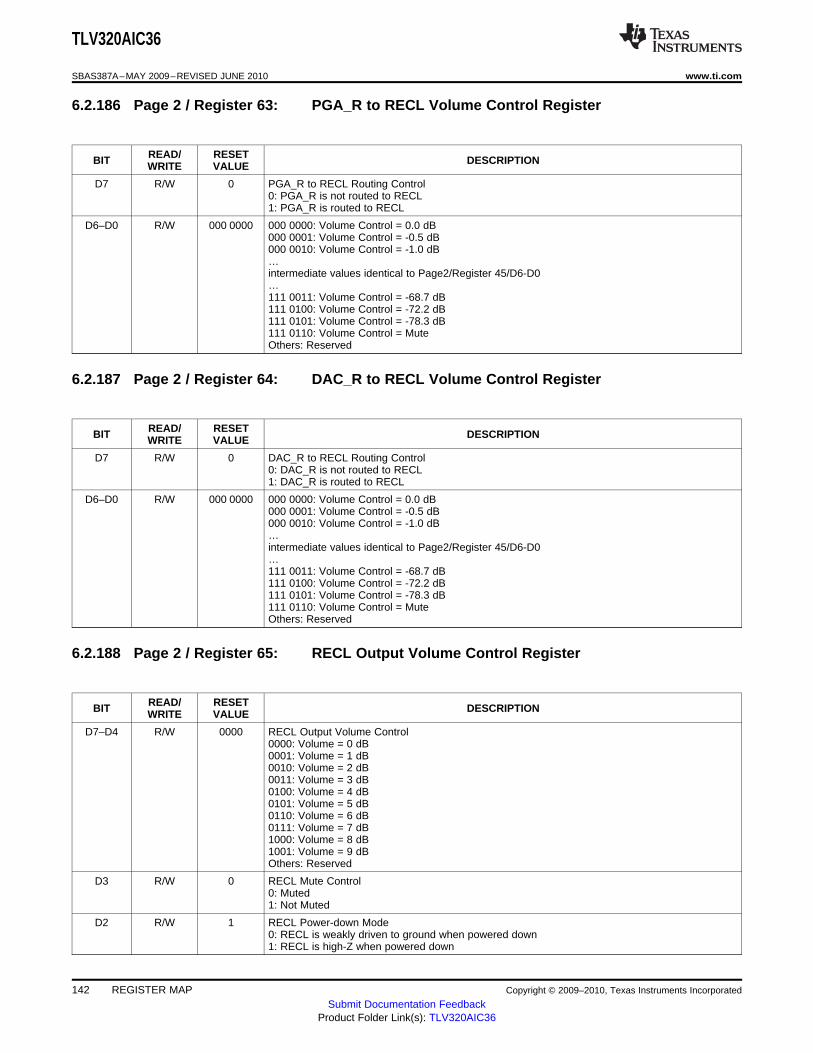
TLV320AIC36
SBAS387A–MAY 2009–REVISED JUNE 2010 www.ti.com
6.2.186 Page 2 / Register 63: PGA_R to RECL Volume Control Register
READ/ RESETBIT DESCRIPTIONWRITE VALUE
D7 R/W 0 PGA_R to RECL Routing Control0: PGA_R is not routed to RECL1: PGA_R is routed to RECL
D6–D0 R/W 000 0000 000 0000: Volume Control = 0.0 dB000 0001: Volume Control = -0.5 dB000 0010: Volume Control = -1.0 dB…intermediate values identical to Page2/Register 45/D6-D0…111 0011: Volume Control = -68.7 dB111 0100: Volume Control = -72.2 dB111 0101: Volume Control = -78.3 dB111 0110: Volume Control = MuteOthers: Reserved
6.2.187 Page 2 / Register 64: DAC_R to RECL Volume Control Register
READ/ RESETBIT DESCRIPTIONWRITE VALUE
D7 R/W 0 DAC_R to RECL Routing Control0: DAC_R is not routed to RECL1: DAC_R is routed to RECL
D6–D0 R/W 000 0000 000 0000: Volume Control = 0.0 dB000 0001: Volume Control = -0.5 dB000 0010: Volume Control = -1.0 dB…intermediate values identical to Page2/Register 45/D6-D0…111 0011: Volume Control = -68.7 dB111 0100: Volume Control = -72.2 dB111 0101: Volume Control = -78.3 dB111 0110: Volume Control = MuteOthers: Reserved
6.2.188 Page 2 / Register 65: RECL Output Volume Control Register
READ/ RESETBIT DESCRIPTIONWRITE VALUE
D7–D4 R/W 0000 RECL Output Volume Control0000: Volume = 0 dB0001: Volume = 1 dB0010: Volume = 2 dB0011: Volume = 3 dB0100: Volume = 4 dB0101: Volume = 5 dB0110: Volume = 6 dB0111: Volume = 7 dB1000: Volume = 8 dB1001: Volume = 9 dBOthers: Reserved
D3 R/W 0 RECL Mute Control0: Muted1: Not Muted
D2 R/W 1 RECL Power-down Mode0: RECL is weakly driven to ground when powered down1: RECL is high-Z when powered down
142 REGISTER MAP Copyright © 2009–2010, Texas Instruments Incorporated
Submit Documentation FeedbackProduct Folder Link(s): TLV320AIC36
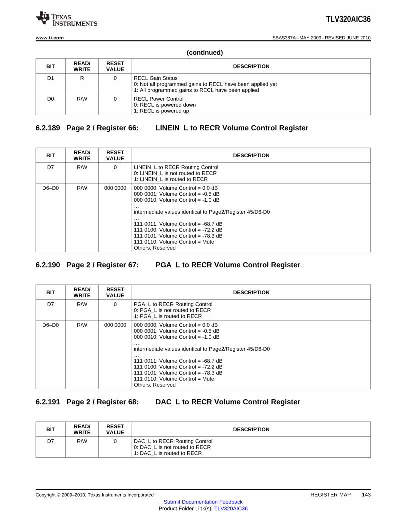
TLV320AIC36
www.ti.com SBAS387A–MAY 2009–REVISED JUNE 2010
(continued)
READ/ RESETBIT DESCRIPTIONWRITE VALUE
D1 R 0 RECL Gain Status0: Not all programmed gains to RECL have been applied yet1: All programmed gains to RECL have been applied
D0 R/W 0 RECL Power Control0: RECL is powered down1: RECL is powered up
6.2.189 Page 2 / Register 66: LINEIN_L to RECR Volume Control Register
READ/ RESETBIT DESCRIPTIONWRITE VALUE
D7 R/W 0 LINEIN_L to RECR Routing Control0: LINEIN_L is not routed to RECR1: LINEIN_L is routed to RECR
D6–D0 R/W 000 0000 000 0000: Volume Control = 0.0 dB000 0001: Volume Control = -0.5 dB000 0010: Volume Control = -1.0 dB…intermediate values identical to Page2/Register 45/D6-D0…111 0011: Volume Control = -68.7 dB111 0100: Volume Control = -72.2 dB111 0101: Volume Control = -78.3 dB111 0110: Volume Control = MuteOthers: Reserved
6.2.190 Page 2 / Register 67: PGA_L to RECR Volume Control Register
READ/ RESETBIT DESCRIPTIONWRITE VALUE
D7 R/W 0 PGA_L to RECR Routing Control0: PGA_L is not routed to RECR1: PGA_L is routed to RECR
D6–D0 R/W 000 0000 000 0000: Volume Control = 0.0 dB000 0001: Volume Control = -0.5 dB000 0010: Volume Control = -1.0 dB…intermediate values identical to Page2/Register 45/D6-D0…111 0011: Volume Control = -68.7 dB111 0100: Volume Control = -72.2 dB111 0101: Volume Control = -78.3 dB111 0110: Volume Control = MuteOthers: Reserved
6.2.191 Page 2 / Register 68: DAC_L to RECR Volume Control Register
READ/ RESETBIT DESCRIPTIONWRITE VALUE
D7 R/W 0 DAC_L to RECR Routing Control0: DAC_L is not routed to RECR1: DAC_L is routed to RECR
Copyright © 2009–2010, Texas Instruments Incorporated REGISTER MAP 143Submit Documentation Feedback
Product Folder Link(s): TLV320AIC36

TLV320AIC36
SBAS387A–MAY 2009–REVISED JUNE 2010 www.ti.com
(continued)
READ/ RESETBIT DESCRIPTIONWRITE VALUE
D6–D0 R/W 000 0000 000 0000: Volume Control = 0.0 dB000 0001: Volume Control = -0.5 dB000 0010: Volume Control = -1.0 dB…intermediate values identical to Page2/Register 45/D6-D0…111 0011: Volume Control = -68.7 dB111 0100: Volume Control = -72.2 dB111 0101: Volume Control = -78.3 dB111 0110: Volume Control = MuteOthers: Reserved
6.2.192 Page 2 / Register 69: LINEIN_R to RECR Volume Control Register
READ/ RESETBIT DESCRIPTIONWRITE VALUE
D7 R/W 0 LINEIN_R to RECR Routing Control0: LINEIN_R is not routed to RECR1: LINEIN_R is routed to RECR
D6–D0 R/W 000 0000 000 0000: Volume Control = 0.0 dB000 0001: Volume Control = -0.5 dB000 0010: Volume Control = -1.0 dB…intermediate values identical to Page2/Register 45/D6-D0…111 0011: Volume Control = -68.7 dB111 0100: Volume Control = -72.2 dB111 0101: Volume Control = -78.3 dB111 0110: Volume Control = MuteOthers: Reserved
6.2.193 Page 2 / Register 70: PGA_R to RECR Volume Control Register
READ/ RESETBIT DESCRIPTIONWRITE VALUE
D7 R/W 0 PGA_R to RECR Routing Control0: PGA_R is not routed to RECR1: PGA_R is routed to RECR
D6–D0 R/W 000 0000 000 0000: Volume Control = 0.0 dB000 0001: Volume Control = -0.5 dB000 0010: Volume Control = -1.0 dB…intermediate values identical to Page2/Register 45/D6-D0…111 0011: Volume Control = -68.7 dB111 0100: Volume Control = -72.2 dB111 0101: Volume Control = -78.3 dB111 0110: Volume Control = MuteOthers: Reserved
6.2.194 Page 2 / Register 71: DAC_R to RECR Volume Control Register
READ/ RESETBIT DESCRIPTIONWRITE VALUE
D7 R/W 0 DAC_R to RECR Routing Control0: DAC_R is not routed to RECR1: DAC_R is routed to RECR
144 REGISTER MAP Copyright © 2009–2010, Texas Instruments Incorporated
Submit Documentation FeedbackProduct Folder Link(s): TLV320AIC36
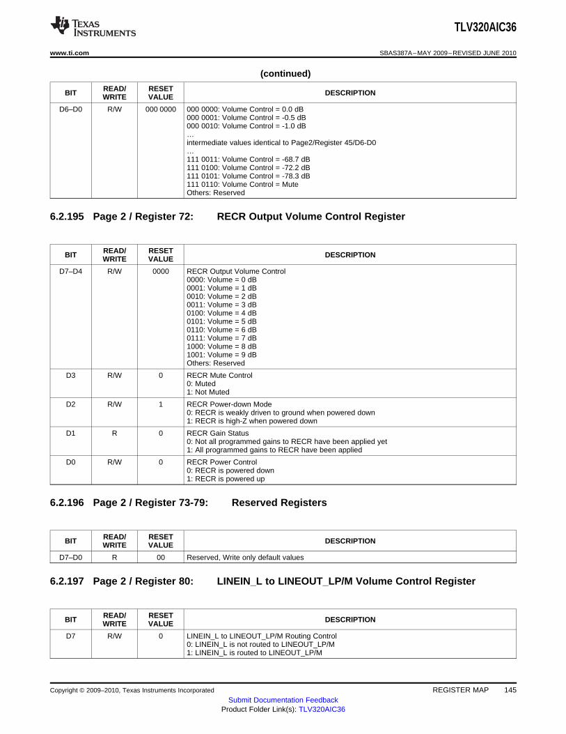
TLV320AIC36
www.ti.com SBAS387A–MAY 2009–REVISED JUNE 2010
(continued)
READ/ RESETBIT DESCRIPTIONWRITE VALUE
D6–D0 R/W 000 0000 000 0000: Volume Control = 0.0 dB000 0001: Volume Control = -0.5 dB000 0010: Volume Control = -1.0 dB…intermediate values identical to Page2/Register 45/D6-D0…111 0011: Volume Control = -68.7 dB111 0100: Volume Control = -72.2 dB111 0101: Volume Control = -78.3 dB111 0110: Volume Control = MuteOthers: Reserved
6.2.195 Page 2 / Register 72: RECR Output Volume Control Register
READ/ RESETBIT DESCRIPTIONWRITE VALUE
D7–D4 R/W 0000 RECR Output Volume Control0000: Volume = 0 dB0001: Volume = 1 dB0010: Volume = 2 dB0011: Volume = 3 dB0100: Volume = 4 dB0101: Volume = 5 dB0110: Volume = 6 dB0111: Volume = 7 dB1000: Volume = 8 dB1001: Volume = 9 dBOthers: Reserved
D3 R/W 0 RECR Mute Control0: Muted1: Not Muted
D2 R/W 1 RECR Power-down Mode0: RECR is weakly driven to ground when powered down1: RECR is high-Z when powered down
D1 R 0 RECR Gain Status0: Not all programmed gains to RECR have been applied yet1: All programmed gains to RECR have been applied
D0 R/W 0 RECR Power Control0: RECR is powered down1: RECR is powered up
6.2.196 Page 2 / Register 73-79: Reserved Registers
READ/ RESETBIT DESCRIPTIONWRITE VALUE
D7–D0 R 00 Reserved, Write only default values
6.2.197 Page 2 / Register 80: LINEIN_L to LINEOUT_LP/M Volume Control Register
READ/ RESETBIT DESCRIPTIONWRITE VALUE
D7 R/W 0 LINEIN_L to LINEOUT_LP/M Routing Control0: LINEIN_L is not routed to LINEOUT_LP/M1: LINEIN_L is routed to LINEOUT_LP/M
Copyright © 2009–2010, Texas Instruments Incorporated REGISTER MAP 145Submit Documentation Feedback
Product Folder Link(s): TLV320AIC36
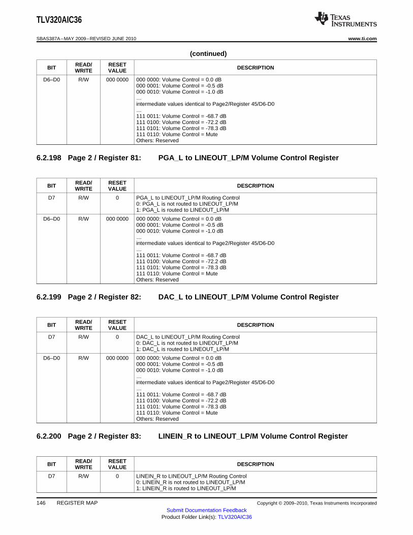
TLV320AIC36
SBAS387A–MAY 2009–REVISED JUNE 2010 www.ti.com
(continued)
READ/ RESETBIT DESCRIPTIONWRITE VALUE
D6–D0 R/W 000 0000 000 0000: Volume Control = 0.0 dB000 0001: Volume Control = -0.5 dB000 0010: Volume Control = -1.0 dB…intermediate values identical to Page2/Register 45/D6-D0…111 0011: Volume Control = -68.7 dB111 0100: Volume Control = -72.2 dB111 0101: Volume Control = -78.3 dB111 0110: Volume Control = MuteOthers: Reserved
6.2.198 Page 2 / Register 81: PGA_L to LINEOUT_LP/M Volume Control Register
READ/ RESETBIT DESCRIPTIONWRITE VALUE
D7 R/W 0 PGA_L to LINEOUT_LP/M Routing Control0: PGA_L is not routed to LINEOUT_LP/M1: PGA_L is routed to LINEOUT_LP/M
D6–D0 R/W 000 0000 000 0000: Volume Control = 0.0 dB000 0001: Volume Control = -0.5 dB000 0010: Volume Control = -1.0 dB…intermediate values identical to Page2/Register 45/D6-D0…111 0011: Volume Control = -68.7 dB111 0100: Volume Control = -72.2 dB111 0101: Volume Control = -78.3 dB111 0110: Volume Control = MuteOthers: Reserved
6.2.199 Page 2 / Register 82: DAC_L to LINEOUT_LP/M Volume Control Register
READ/ RESETBIT DESCRIPTIONWRITE VALUE
D7 R/W 0 DAC_L to LINEOUT_LP/M Routing Control0: DAC_L is not routed to LINEOUT_LP/M1: DAC_L is routed to LINEOUT_LP/M
D6–D0 R/W 000 0000 000 0000: Volume Control = 0.0 dB000 0001: Volume Control = -0.5 dB000 0010: Volume Control = -1.0 dB…intermediate values identical to Page2/Register 45/D6-D0…111 0011: Volume Control = -68.7 dB111 0100: Volume Control = -72.2 dB111 0101: Volume Control = -78.3 dB111 0110: Volume Control = MuteOthers: Reserved
6.2.200 Page 2 / Register 83: LINEIN_R to LINEOUT_LP/M Volume Control Register
READ/ RESETBIT DESCRIPTIONWRITE VALUE
D7 R/W 0 LINEIN_R to LINEOUT_LP/M Routing Control0: LINEIN_R is not routed to LINEOUT_LP/M1: LINEIN_R is routed to LINEOUT_LP/M
146 REGISTER MAP Copyright © 2009–2010, Texas Instruments Incorporated
Submit Documentation FeedbackProduct Folder Link(s): TLV320AIC36
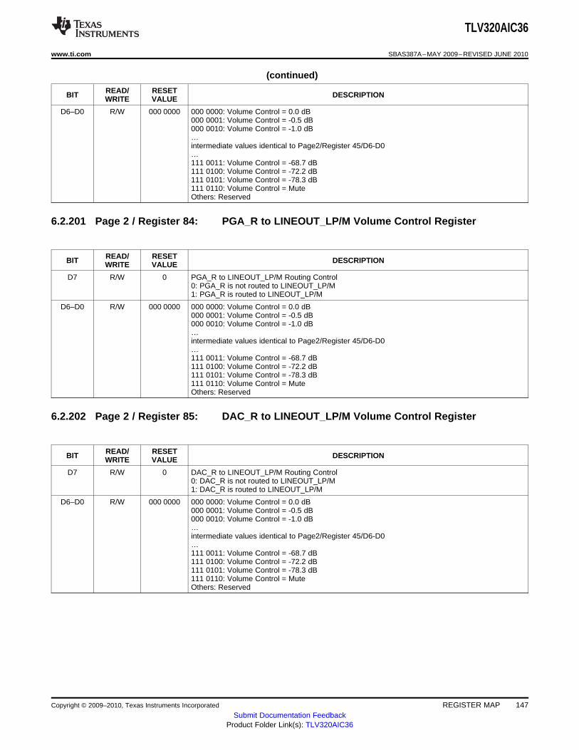
TLV320AIC36
www.ti.com SBAS387A–MAY 2009–REVISED JUNE 2010
(continued)
READ/ RESETBIT DESCRIPTIONWRITE VALUE
D6–D0 R/W 000 0000 000 0000: Volume Control = 0.0 dB000 0001: Volume Control = -0.5 dB000 0010: Volume Control = -1.0 dB…intermediate values identical to Page2/Register 45/D6-D0…111 0011: Volume Control = -68.7 dB111 0100: Volume Control = -72.2 dB111 0101: Volume Control = -78.3 dB111 0110: Volume Control = MuteOthers: Reserved
6.2.201 Page 2 / Register 84: PGA_R to LINEOUT_LP/M Volume Control Register
READ/ RESETBIT DESCRIPTIONWRITE VALUE
D7 R/W 0 PGA_R to LINEOUT_LP/M Routing Control0: PGA_R is not routed to LINEOUT_LP/M1: PGA_R is routed to LINEOUT_LP/M
D6–D0 R/W 000 0000 000 0000: Volume Control = 0.0 dB000 0001: Volume Control = -0.5 dB000 0010: Volume Control = -1.0 dB…intermediate values identical to Page2/Register 45/D6-D0…111 0011: Volume Control = -68.7 dB111 0100: Volume Control = -72.2 dB111 0101: Volume Control = -78.3 dB111 0110: Volume Control = MuteOthers: Reserved
6.2.202 Page 2 / Register 85: DAC_R to LINEOUT_LP/M Volume Control Register
READ/ RESETBIT DESCRIPTIONWRITE VALUE
D7 R/W 0 DAC_R to LINEOUT_LP/M Routing Control0: DAC_R is not routed to LINEOUT_LP/M1: DAC_R is routed to LINEOUT_LP/M
D6–D0 R/W 000 0000 000 0000: Volume Control = 0.0 dB000 0001: Volume Control = -0.5 dB000 0010: Volume Control = -1.0 dB…intermediate values identical to Page2/Register 45/D6-D0…111 0011: Volume Control = -68.7 dB111 0100: Volume Control = -72.2 dB111 0101: Volume Control = -78.3 dB111 0110: Volume Control = MuteOthers: Reserved
Copyright © 2009–2010, Texas Instruments Incorporated REGISTER MAP 147Submit Documentation Feedback
Product Folder Link(s): TLV320AIC36

TLV320AIC36
SBAS387A–MAY 2009–REVISED JUNE 2010 www.ti.com
6.2.203 Page 2 / Register 86: LINEOUT_LP/M Output Volume Control Register
READ/ RESETBIT DESCRIPTIONWRITE VALUE
D7–D4 R/W 0000 LINEOUT_LP/M Output Volume Control0000: Volume = 0 dB0001: Volume = 1 dB0010: Volume = 2 dB0011: Volume = 3 dB0100: Volume = 4 dB0101: Volume = 5 dB0110: Volume = 6 dB0111: Volume = 7 dB1000: Volume = 8 dB1001: Volume = 9 dBOthers: Reserved
D3 R/W 0 LINEOUT_LP/M Mute Control0: Muted1: Not Muted
D2 R 0 Reserved, Write only default value
D1 R 0 LINEOUT_LP/M Gain Status0: Not all programmed gains to LINEOUT_LP/M have been applied yet1: All programmed gains to LINEOUT_LP/M have been applied
D0 R/W 0 LINEOUT_LP/M Power Control0: LINEOUT_LP/M is powered down1: LINEOUT_LP/M is powered up
6.2.204 Page 2 / Register 87: LINEIN_L to LINEOUT_RP/M Volume Control Register
READ/ RESETBIT DESCRIPTIONWRITE VALUE
D7 R/W 0 LINEIN_L to LINEOUT_RP/M Routing Control0: LINEIN_L is not routed to LINEOUT_RP/M1: LINEIN_L is routed to LINEOUT_RP/M
D6–D0 R/W 000 0000 000 0000: Volume Control = 0.0 dB000 0001: Volume Control = -0.5 dB000 0010: Volume Control = -1.0 dB…intermediate values identical to Page2/Register 45/D6-D0…111 0011: Volume Control = -68.7 dB111 0100: Volume Control = -72.2 dB111 0101: Volume Control = -78.3 dB111 0110: Volume Control = MuteOthers: Reserved
6.2.205 Page 2 / Register 88: PGA_L to LINEOUT_RP/M Volume Control Register
READ/ RESETBIT DESCRIPTIONWRITE VALUE
D7 R/W 0 PGA_L to LINEOUT_RP/M Routing Control0: PGA_L is not routed to LINEOUT_RP/M1: PGA_L is routed to LINEOUT_RP/M
148 REGISTER MAP Copyright © 2009–2010, Texas Instruments Incorporated
Submit Documentation FeedbackProduct Folder Link(s): TLV320AIC36

TLV320AIC36
www.ti.com SBAS387A–MAY 2009–REVISED JUNE 2010
(continued)
READ/ RESETBIT DESCRIPTIONWRITE VALUE
D6–D0 R/W 000 0000 000 0000: Volume Control = 0.0 dB000 0001: Volume Control = -0.5 dB000 0010: Volume Control = -1.0 dB…intermediate values identical to Page2/Register 45/D6-D0…111 0011: Volume Control = -68.7 dB111 0100: Volume Control = -72.2 dB111 0101: Volume Control = -78.3 dB111 0110: Volume Control = MuteOthers: Reserved
6.2.206 Page 2 / Register 89: DAC_L to LINEOUT_RP/M Volume Control Register
READ/ RESETBIT DESCRIPTIONWRITE VALUE
D7 R/W 0 DAC_L to LINEOUT_RP/M Routing Control0: DAC_L is not routed to LINEOUT_RP/M1: DAC_L is routed to LINEOUT_RP/M
D6–D0 R/W 000 0000 000 0000: Volume Control = 0.0 dB000 0001: Volume Control = -0.5 dB000 0010: Volume Control = -1.0 dB…intermediate values identical to Page2/Register 45/D6-D0…111 0011: Volume Control = -68.7 dB111 0100: Volume Control = -72.2 dB111 0101: Volume Control = -78.3 dB111 0110: Volume Control = MuteOthers: Reserved
6.2.207 Page 2 / Register 90: LINEIN_R to LINEOUT_RP/M Volume Control Register
READ/ RESETBIT DESCRIPTIONWRITE VALUE
D7 R/W 0 LINEIN_R to LINEOUT_RP/M Routing Control0: LINEIN_R is not routed to LINEOUT_RP/M1: LINEIN_R is routed to LINEOUT_RP/M
D6–D0 R/W 000 0000 000 0000: Volume Control = 0.0 dB000 0001: Volume Control = -0.5 dB000 0010: Volume Control = -1.0 dB…intermediate values identical to Page2/Register 45/D6-D0…111 0011: Volume Control = -68.7 dB111 0100: Volume Control = -72.2 dB111 0101: Volume Control = -78.3 dB111 0110: Volume Control = MuteOthers: Reserved
6.2.208 Page 2 / Register 91: PGA_R to LINEOUT_RP/M Volume Control Register
READ/ RESETBIT DESCRIPTIONWRITE VALUE
D7 R/W 0 PGA_R to LINEOUT_RP/M Routing Control0: PGA_R is not routed to LINEOUT_RP/M1: PGA_R is routed to LINEOUT_RP/M
Copyright © 2009–2010, Texas Instruments Incorporated REGISTER MAP 149Submit Documentation Feedback
Product Folder Link(s): TLV320AIC36

TLV320AIC36
SBAS387A–MAY 2009–REVISED JUNE 2010 www.ti.com
(continued)
READ/ RESETBIT DESCRIPTIONWRITE VALUE
D6–D0 R/W 000 0000 000 0000: Volume Control = 0.0 dB000 0001: Volume Control = -0.5 dB000 0010: Volume Control = -1.0 dB…intermediate values identical to Page2/Register 45/D6-D0…111 0011: Volume Control = -68.7 dB111 0100: Volume Control = -72.2 dB111 0101: Volume Control = -78.3 dB111 0110: Volume Control = MuteOthers: Reserved
6.2.209 Page 2 / Register 92: DAC_R to LINEOUT_RP/M Volume Control Register
READ/ RESETBIT DESCRIPTIONWRITE VALUE
D7 R/W 0 DAC_R to LINEOUT_RP/M Routing Control0: DAC_R is not routed to LINEOUT_RP/M1: DAC_R is routed to LINEOUT_RP/M
D6–D0 R/W 000 0000 000 0000: Volume Control = 0.0 dB000 0001: Volume Control = -0.5 dB000 0010: Volume Control = -1.0 dB…intermediate values identical to Page2/Register 45/D6-D0…111 0011: Volume Control = -68.7 dB111 0100: Volume Control = -72.2 dB111 0101: Volume Control = -78.3 dB111 0110: Volume Control = MuteOthers: Reserved
6.2.210 Page 2 / Register 93: LINEOUT_RP/M Output Volume Control Register
READ/ RESETBIT DESCRIPTIONWRITE VALUE
D7–D4 R/W 0000 LINEOUT_RP/M Output Volume Control0000: Volume = 0 dB0001: Volume = 1 dB0010: Volume = 2 dB0011: Volume = 3 dB0100: Volume = 4 dB0101: Volume = 5 dB0110: Volume = 6 dB0111: Volume = 7 dB1000: Volume = 8 dB1001: Volume = 9 dBOthers: Reserved
D3 R/W 0 LINEOUT_RP/M Mute Control0: Muted1: Not Muted
D2 R/W 1 Reserved, Write only default value
D1 R 0 LINEOUT_RP/M Gain Status0: Not all programmed gains to LINEOUT_RP/M have been applied yet1: All programmed gains to LINEOUT_RP/M have been applied
D0 R/W 0 LINEOUT_RP/M Power Control0: LINEOUT_RP/M is powered down1: LINEOUT_RP/M is powered up
150 REGISTER MAP Copyright © 2009–2010, Texas Instruments Incorporated
Submit Documentation FeedbackProduct Folder Link(s): TLV320AIC36

TLV320AIC36
www.ti.com SBAS387A–MAY 2009–REVISED JUNE 2010
6.2.211 Page 2 / Register 94: Module Power Status Register
READ/ RESETBIT DESCRIPTIONWRITE VALUE
D7 R/W 0 Left DAC Power Status0: Left DAC not fully powered up1: Left DAC powered up
D6 R/W 0 Right DAC Power Status0: Right DAC not fully powered up1: Right DAC powered up
D5 R/W 0 Reserved
D4 R/W 0 LINEOUT_LP/M Power Status0: LINEOUT_LP/M not fully powered up1: LINEOUT_LP/M powered up
D3 R/W 0 LINEOUT_RP/M Power Status0: LINEOUT_RP/MC not fully powered up1: LINEOUT_RP/M powered up
D2 R/W 0 HPR Power Status0: HPR not fully powered up1: HPR powered up
D1 R/W 0 RECL Power Status0: RECL not fully powered up1: RECL powered up
D0 R 00 Reserved, Write only default values
6.2.212 Page 2 / Register 95-106: Reserved Registers
READ/ RESETBIT DESCRIPTIONWRITE VALUE
D7–D0 R 00 Reserved, Write only default values
6.2.213 Page 2 / Register 107: DAC Current Control Register
READ/ RESETBIT DESCRIPTIONWRITE VALUE
D7–D6 R/W 0 DAC Current Control Register00: Nominal DAC Current01: 1.5x Dac Current10: 0.5x Dac current
D5–D0 R 00 Reserved, Write only default values
6.2.214 Page 2 / Register 108: Open Circuit Manual Read Control Register
READ/ RESETBIT DESCRIPTIONWRITE VALUE
D7–D5 R 000 Reserved, Write only default values
D4 R/W 0 HPR Open Circuit Manual Read Control0: Disabled1: Enabled
D3 R/W 0 HPL Open Circuit Manual Read Control0: Disabled1: Enabled
Copyright © 2009–2010, Texas Instruments Incorporated REGISTER MAP 151Submit Documentation Feedback
Product Folder Link(s): TLV320AIC36
TLV320AIC36
SBAS387A–MAY 2009–REVISED JUNE 2010 www.ti.com
(continued)
READ/ RESETBIT DESCRIPTIONWRITE VALUE
D2 R/W 0 RECL Open Circuit Manual Read Control0: Disabled1: Enabled
D1 R/W 0 RECL Open Circuit Manual Read Control0: Disabled1: Enabled
D0 R/W 0 Hook Open Circuit Manual Read Control0: Disabled1: Enabled
6.2.215 Page 2 / Register 109: Open Circuit Raw Status Register
READ/ RESETBIT DESCRIPTIONWRITE VALUE
D7–D5 R 000 Reserved, Write only default values
D4 R 0 HPR Open Circuit Status0: shorted1: open
D3 R 0 HPL Open Circuit Status0: shorted1: open
D2 R 0 RECL Open Circuit Status0: shorted1: open
D1 R 0 RECR Open Circuit Status0: shorted1: open
D0 R 0 Hook Open Circuit Status0: shorted1: open
6.2.216 Page 2 / Register 110: Open Circuit Polling Enable Register
READ/ RESETBIT DESCRIPTIONWRITE VALUE
D7–D5 R 000 Reserved, Write only default values
D4 R/W 0 HPR Open Circuit Polling Enable0: disabled1: enabled
D3 R/W 0 HPL Open Circuit Polling Enable0: disabled1: enabled
D2 R/W 0 RECL Open Circuit Polling Enable0: disabled1: enabled
D1 R/W 0 RECR Open Circuit Polling Enable0: disabled1: enabled
D0 R/W 0 Hook Open Circuit Polling Enable0: disabled1: enabled
152 REGISTER MAP Copyright © 2009–2010, Texas Instruments Incorporated
Submit Documentation FeedbackProduct Folder Link(s): TLV320AIC36

TLV320AIC36
www.ti.com SBAS387A–MAY 2009–REVISED JUNE 2010
6.2.217 Page 2 / Register 111: Open Circuit Interrupt Direction Status Register
READ/ RESETBIT DESCRIPTIONWRITE VALUE
D7–D5 R 000 Reserved, Write only default values
D4 R 0 HPR Open Circuit Interrupt DirectionA change in the HPR open circuit value can trigger a host interrupt on a rising or falling edge. Usethis status bit to determine the direction of the interrupting event.0: falling edge1: rising edge
D3 R 0 HPL Open Circuit Interrupt DirectionA change in the HPL open circuit value can trigger a host interrupt on a rising or falling edge. Usethis status bit to determine the direction of the interrupting event.0: falling edge1: rising edge
D2 R 0 RECL Open Circuit Interrupt DirectionA change in the RECL open circuit value can trigger a host interrupt on a rising or falling edge. Usethis status bit to determine the direction of the interrupting event.0: falling edge1: rising edge
D1 R 0 RECR Open Circuit Interrupt DirectionA change in the RECR open circuit value can trigger a host interrupt on a rising or falling edge.Use this status bit to determine the direction of the interrupting event.0: falling edge1: rising edge
D0 R 0 Hook Open Circuit Interrupt DirectionA change in the Hook open circuit value can trigger a host interrupt on a rising or falling edge. Usethis status bit to determine the direction of the interrupting event.0: falling edge1: rising edge
6.2.218 Page 2 / Register 112: Low Power Oscillator Control Register
READ/ RESETBIT DESCRIPTIONWRITE VALUE
D7–D1 R 0000 000 Reserved, Write only default values
D0 R/W 1 Low Power Oscillator Control0: powered up1: powered down
6.2.219 Page 2 / Register 113: PMU Configuration Register 1
READ/ RESETBIT DESCRIPTIONWRITE VALUE
D7–D2 R 0000 00 Reserved, Write only default values
D1 R/W 0 Charge Pump Clock Select0: Charge pump uses MCLK1: Charge pump uses BCLK
D0 R/W 0 Charge Pump Enable0: Charge Pump Clock disabled1: Charge Pump Clock enabled
Copyright © 2009–2010, Texas Instruments Incorporated REGISTER MAP 153Submit Documentation Feedback
Product Folder Link(s): TLV320AIC36

TLV320AIC36
SBAS387A–MAY 2009–REVISED JUNE 2010 www.ti.com
6.2.220 Page 2 / Register 114: PMU Configuration Register 2
READ/ RESETBIT DESCRIPTIONWRITE VALUE
D7–D0 R/W 0000 1011 Number of charge clock high cycles - 1 (used to set duty cycle on CP)0000 0000: 1 cycle high0000 0001: 2 cycles high…1111 1111: 256 cycles high
6.2.221 Page 2 / Register 115: PMU Configuration Register 3
READ/ RESETBIT DESCRIPTIONWRITE VALUE
D7–D0 R/W 0000 1011 Number of charge clock low cycles - 1 (used to set duty cycle on CP)0000 0000: 1 cycle high0000 0001: 2 cycles high…1111 1111: 256 cycles high
6.2.222 Page 2 / Register 116: PMU Configuration Register 4
READ/ RESETBIT DESCRIPTIONWRITE VALUE
D7–D3 R 0000 0 Reserved, Write only default values
D2 R/W 1 ADC VDD LDO Powerdown0: ADC VDD LDO is in powerup1: ADC VDO LDO is in powerdown
D1 R/W 1 DAC VSS LDO Powerdown0: DAC VSS LDO is in powerup1: DAC VSS LDO is in powerdown
D0 R/W 1 DAC VDD LDO Powerdown0: DAC VDD LDO is in powerup1: DAC VDD LDO is in powerdown
6.2.223 Page 2 / Register 117: Reserved Register
READ/ RESETBIT DESCRIPTIONWRITE VALUE
D7–D0 R 0000 0000 Reserved, Write only default values
6.2.224 Page 2 / Register 118: PMU Configuration Register 5
READ/ RESETBIT DESCRIPTIONWRITE VALUE
D7–D3 R 0000 0 Reserved, Write only default values
D2 R/W 1 ADC VDD LDO current limit0: Don't current limit (set to Imax=30mA)1: Current limit (set to Imax=5mA)
D1 R/W 1 DAC VSS LDO current limit0: Don't current limit (set to Imax=-300mA)1: Current limit (set to Imax=-50mA)
154 REGISTER MAP Copyright © 2009–2010, Texas Instruments Incorporated
Submit Documentation FeedbackProduct Folder Link(s): TLV320AIC36
TLV320AIC36
www.ti.com SBAS387A–MAY 2009–REVISED JUNE 2010
(continued)
READ/ RESETBIT DESCRIPTIONWRITE VALUE
D0 R/W 1 DAC VDD LDO current limit0: Don't current limit (set to Imax=300mA)1: Current limit (set to Imax=50mA)
6.2.225 Page 2 / Register 119: PMU Configuration Register 6
READ/ RESETBIT DESCRIPTIONWRITE VALUE
D7 R/W 0 ADC VDD LDO open loop gain0: Lower open loop gain LDO1: High open loop gain LDO
D6–D4 R/W 000 ADC VDD LDO output voltage000: Set ADC VDD LDO to 1.75V001: Set ADC VDD LDO to 1.65V010: Set ADC VDD LDO to 1.5V011: Set ADC VDD LDO to 1.4V1xx: Reserved
D3 R/W 0 LDO Bandgap powerdown0: LDO Bandgap powered up1: LDO Bandgap powered down
D2 R/W 0 Short circuit protection for DAC VDD LDO0: Short circuit protection for DAC VDD LDO enabled1: Short circuit protection for DAC VDD LDO disabled (current limit, reg 118 also disabled)
D1 R/W 0 Short circuit protection for DAC VSS LDO0: Short circuit protection for DAC VSS LDO enabled1: Short circuit protection for DAC VSS LDO disabled (current limit, reg 118 also disabled)
D0 R/W 0 Short circuit protection for ADC VDD LDO0: Short circuit protection for ADC VDD LDO enabled1: Short circuit protection for ADC VDD LDO disabled (current limit, reg 118 also disabled)
6.2.226 Page 2 / Register 120: PMU Configuration Register 7
READ/ RESETBIT DESCRIPTIONWRITE VALUE
D7 R/W 0 DAC VDD LDO open loop gain0: Lower open loop gain LDO1: High open loop gain LDO
D6–D4 R/W 000 DAC VDD LDO output voltage000: Set DAC VDD LDO to 1.4V001: Set DAC VDD LDO to 1.5V010: Set DAC VDD LDO to 1.65V011: Set DAC VDD LDO to 1.75V1xx: Reserved
D3 R 0 Reserved, Write only default values
D2–D0 R/W 000 DAC VSS LDO output voltage000: Set DAC VSS LDO to -1.4V001: Set DAC VSS LDO to -1.5V010: Set DAC VSS LDO to -1.65V011: Set DAC VSS LDO to -1.75V1xx: Reserved
Copyright © 2009–2010, Texas Instruments Incorporated REGISTER MAP 155Submit Documentation Feedback
Product Folder Link(s): TLV320AIC36

TLV320AIC36
SBAS387A–MAY 2009–REVISED JUNE 2010 www.ti.com
6.2.227 Page 2 / Register 121: PMU Configuration Register 8
READ/ RESETBIT DESCRIPTIONWRITE VALUE
D7–D4 R 0000 Reserved, Write only default values
D3–D0 R/W 0111 TRIMPMU bits0000: Trim all LDO outputs +4.6%0100: Trim all LDO outputs .....0101: Trim all LDO outputs +1.4%0110: Trim all LDO outputs +0.7%0111: Trim all LDO outputs +0%1001: Trim all LDO outputs -0.8%1010: Trim all LDO outputs ....1111: Trim all LDO outputs -6.4%
6.2.228 Page 2 / Register 122: PMU Configuration Register 9
READ/ RESETBIT DESCRIPTIONWRITE VALUE
D7–D6 R/W 00 Headphone nominal current settings00: Nominal current01: 1/2 Nominal current (recommended setting for low power)10: 1/3 Nominal current11: 1/4 Nominal current (recommended for ultimate low power, performance degraded)
D5–D4 R/W 00 Rec nominal current settings00: Nominal current01: 1/2 Nominal current (recommended setting for low power)10: 1/3 Nominal current11: 1/4 Nominal current (recommended for ultimate low power, performance degraded)
D3–D2 R/W 00 Line out nominal current settings00: Nominal current01: 1/2 Nominal current (recommended setting for low power)10: 1/3 Nominal current11: 1/4 Nominal current (recommended for ultimate low power, performance degraded)
D1–D0 R/W 00 IV amp nominal current settings00: Nominal current01: 1/2 Nominal current (recommended setting for low power)10: 1/3 Nominal current11: 1/4 Nominal current (recommended for ultimate low power, performance degraded)
6.2.229 Page 2 / Register 123: PMU Configuration Register 10
READ/ RESETBIT DESCRIPTIONWRITE VALUE
D7–D2 R 0000 00 Reserved, Write only default values
D1–D0 R/W 00 DAC Bias Voltage Register00: Nominal Dac bias voltages01: Reduced Dac bias voltages for use with very low DAC VDD1x: Reserved
6.2.230 Page 2 / Register 124-127: Reserved Registers
READ/ RESETBIT DESCRIPTIONWRITE VALUE
D7–D0 R 0000 0000 Reserved, Write only default values
156 REGISTER MAP Copyright © 2009–2010, Texas Instruments Incorporated
Submit Documentation FeedbackProduct Folder Link(s): TLV320AIC36

TLV320AIC36
www.ti.com SBAS387A–MAY 2009–REVISED JUNE 2010
6.3 ADC Coefficients
Table 6-2. ADC Coefficients
Coef No Page No Base Register Base Register + 0 Base Register + 1
C1 4 2 Coef(15:8) Coef(7:0)
C2 4 4 Coef(15:8) Coef(7:0)
… … … … …
C63 4 126 Coef(15:8) Coef(7:0)
C65 5 2 Coef(15:8) Coef(7:0)
… … … … …
C127 5 126 Coef(15:8) Coef(7:0)
6.4 ADC Defaults
Table 6-3. Default Values of ADC Coefficients
ADC Coefficient Default Value at Reset
C1 0117H
C2 0117H
C3 7DD3H
C4 7FFFH
C5-C6 0000H
C7 7FFFH
C8-C11 0000H
C12 7FFFH
C13-C16 0000H
C17 7FFFH
C18-C21 0000H
C22 7FFFH
C23-C26 0000H
C27 7FFFH
C28-C35 0000H
C36 7FFFH
C37-C38 0000H
C39 7FFFH
C40-C43 0000H
C44 7FFFH
C45-C48 0000H
C49 7FFFH
C50-C53 0000H
C54 7FFFH
C55-C58 0000H
C59 7FFFH
C60-C63 0000H
C65-C127 0000H
Copyright © 2009–2010, Texas Instruments Incorporated REGISTER MAP 157Submit Documentation Feedback
Product Folder Link(s): TLV320AIC36

TLV320AIC36
SBAS387A–MAY 2009–REVISED JUNE 2010 www.ti.com
6.5 DAC Coefficients A+B
Table 6-4. DAC Coefficient Buffer-A Map
Coef No Page No Base Register Base Register + 0 Base Register + 1
C1 8 2 Coef(15:8) Coef(7:0)
C2 8 4 Coef(15:8) Coef(7:0)
… … … … …
C63 8 126 Coef(15:8) Coef(7:0)
C65 9 2 Coef(15:8) Coef(7:0)
… … … … …
C127 9 126 Coef(15:8) Coef(7:0)
C129 10 2 Coef(15:8) Coef(7:0)
… … … … …
C191 10 126 Coef(15:8) Coef(7:0)
C193 11 2 Coef(15:8) Coef(7:0)
… … … … …
C255 11 126 Coef(15:8) Coef(7:0)
Table 6-5. DAC Coefficient Buffer-B Map
Coef No Page No Base Register Base Register + 0 Base Register + 1
C1 12 2 Coef(15:8) Coef(7:0)
C2 12 4 Coef(15:8) Coef(7:0)
… … … … …
C63 12 126 Coef(15:8) Coef(7:0)
C65 13 2 Coef(15:8) Coef(7:0)
… … … … …
C127 13 126 Coef(15:8) Coef(7:0)
C129 14 2 Coef(15:8) Coef(7:0)
… … … … …
C191 14 126 Coef(15:8) Coef(7:0)
C193 15 2 Coef(15:8) Coef(7:0)
… … … … …
C255 15 126 Coef(15:8) Coef(7:0)
6.6 DAC Defaults
Table 6-6. Default Values of DAC Coefficients in Buffers A and B
DAC Coefficient Default Value at Reset
C1 7FFFH
C2-C5 0000H
C6 7FFFH
C7-C10 0000H
C11 7FFFH
C12-C15 0000H
C16 7FFFH
C17-C20 0000H
C21 7FFFH
C22-C25 0000H
158 REGISTER MAP Copyright © 2009–2010, Texas Instruments Incorporated
Submit Documentation FeedbackProduct Folder Link(s): TLV320AIC36

TLV320AIC36
www.ti.com SBAS387A–MAY 2009–REVISED JUNE 2010
Table 6-6. Default Values of DAC Coefficients in Buffers A and B (continued)
C26 7FFFH
C27-C32 0000H
C33 7FFFH
C34-C37 0000H
C38 7FFFH
C39-C42 0000H
C43 7FFFH
C44-C47 0000H
C48 7FFFH
C49-C52 0000H
C53 7FFFH
C54-C57 0000H
C58 7FFFH
C59-C63 0000H
C65 7FFFH
C56-C67 0000H
C68 7FFFH
C69-C70 0000H
C71 7FF7H
C72 8009H
C73 7FEDH
C74-C75 0011H
C76 7FDEH
C77-C255 0000H
6.7 ADC miniDSP Instructions
Table 6-7. ADC miniDSP Instruction Map
Instr No Page No Base Register Base Register + 0 Base Register + 1 Base Register + 2
0 32 2 0000 : Instr(19:16) Instr(15:8) Instr(7:0)
1 32 5 0000 : Instr(19:16) Instr(15:8) Instr(7:0)
… … … … … …
31 32 95 0000 : Instr(19:16) Instr(15:8) Instr(7:0)
32 33 2 0000 : Instr(19:16) Instr(15:8) Instr(7:0)
… … … … … …
63 33 95 0000 : Instr(19:16) Instr(15:8) Instr(7:0)
64 34 2 0000 : Instr(19:16) Instr(15:8) Instr(7:0)
… … … … … …
95 34 95 0000 : Instr(19:16) Instr(15:8) Instr(7:0)
96 35 2 0000 : Instr(19:16) Instr(15:8) Instr(7:0)
… … … … … …
127 35 95 0000 : Instr(19:16) Instr(15:8) Instr(7:0)
128 36 2 0000 : Instr(19:16) Instr(15:8) Instr(7:0)
… … … … … …
159 36 95 0000 : Instr(19:16) Instr(15:8) Instr(7:0)
160 37 2 0000 : Instr(19:16) Instr(15:8) Instr(7:0)
… … … … … …
191 37 95 0000 : Instr(19:16) Instr(15:8) Instr(7:0)
Copyright © 2009–2010, Texas Instruments Incorporated REGISTER MAP 159Submit Documentation Feedback
Product Folder Link(s): TLV320AIC36

TLV320AIC36
SBAS387A–MAY 2009–REVISED JUNE 2010 www.ti.com
Table 6-7. ADC miniDSP Instruction Map (continued)
192 38 2 0000 : Instr(19:16) Instr(15:8) Instr(7:0)
… … … … … …
223 38 95 0000 : Instr(19:16) Instr(15:8) Instr(7:0)
224 39 2 0000 : Instr(19:16) Instr(15:8) Instr(7:0)
… … … … … …
255 39 95 0000 : Instr(19:16) Instr(15:8) Instr(7:0)
256 40 2 0000 : Instr(19:16) Instr(15:8) Instr(7:0)
… … … … … …
287 40 95 0000 : Instr(19:16) Instr(15:8) Instr(7:0)
288 41 2 0000 : Instr(19:16) Instr(15:8) Instr(7:0)
… … … … … …
319 41 95 0000 : Instr(19:16) Instr(15:8) Instr(7:0)
320 42 2 0000 : Instr(19:16) Instr(15:8) Instr(7:0)
… … … … … …
351 42 95 0000 : Instr(19:16) Instr(15:8) Instr(7:0)
352 43 2 0000 : Instr(19:16) Instr(15:8) Instr(7:0)
… … … … … …
383 43 95 0000 : Instr(19:16) Instr(15:8) Instr(7:0)
384 44 2 0000 : Instr(19:16) Instr(15:8) Instr(7:0)
… … … … … …
415 44 95 0000 : Instr(19:16) Instr(15:8) Instr(7:0)
416 45 2 0000 : Instr(19:16) Instr(15:8) Instr(7:0)
… … … … … …
447 45 95 0000 : Instr(19:16) Instr(15:8) Instr(7:0)
448 46 2 0000 : Instr(19:16) Instr(15:8) Instr(7:0)
… … … … … …
479 46 95 0000 : Instr(19:16) Instr(15:8) Instr(7:0)
480 47 2 0000 : Instr(19:16) Instr(15:8) Instr(7:0)
… … … … … …
510 47 92 0000 : Instr(19:16) Instr(15:8) Instr(7:0)
511 47 95 0000 : Instr(19:16) Instr(15:8) Instr(7:0)
6.8 DAC miniDSP Instructions
Table 6-8. DAC miniDSP Instruction Map
Instr No Page No Base Register Base Register + 0 Base Register + 1 Base Register + 2
0 64 2 Instr(23:16) Instr(15:8) Instr(7:0)
1 64 5 Instr(23:16) Instr(15:8) Instr(7:0)
… … … … … …
31 64 95 Instr(23:16) Instr(15:8) Instr(7:0)
32 65 2 Instr(23:16) Instr(15:8) Instr(7:0)
… … … … … …
63 65 95 Instr(23:16) Instr(15:8) Instr(7:0)
64 66 2 Instr(23:16) Instr(15:8) Instr(7:0)
… … … … … …
95 66 95 Instr(23:16) Instr(15:8) Instr(7:0)
96 67 2 Instr(23:16) Instr(15:8) Instr(7:0)
… … … … … …
160 REGISTER MAP Copyright © 2009–2010, Texas Instruments Incorporated
Submit Documentation FeedbackProduct Folder Link(s): TLV320AIC36
TLV320AIC36
www.ti.com SBAS387A–MAY 2009–REVISED JUNE 2010
Table 6-8. DAC miniDSP Instruction Map (continued)
127 67 95 Instr(23:16) Instr(15:8) Instr(7:0)
128 68 2 Instr(23:16) Instr(15:8) Instr(7:0)
… … … … … …
159 68 95 Instr(23:16) Instr(15:8) Instr(7:0)
160 69 2 Instr(23:16) Instr(15:8) Instr(7:0)
… … … … … …
191 69 95 Instr(23:16) Instr(15:8) Instr(7:0)
192 70 2 Instr(23:16) Instr(15:8) Instr(7:0)
… … … … … …
223 70 95 Instr(23:16) Instr(15:8) Instr(7:0)
224 71 2 Instr(23:16) Instr(15:8) Instr(7:0)
… … … … … …
255 71 95 Instr(23:16) Instr(15:8) Instr(7:0)
256 72 2 Instr(23:16) Instr(15:8) Instr(7:0)
… … … … … …
287 72 95 Instr(23:16) Instr(15:8) Instr(7:0)
288 73 2 Instr(23:16) Instr(15:8) Instr(7:0)
… … … … … …
319 73 95 Instr(23:16) Instr(15:8) Instr(7:0)
320 74 2 Instr(23:16) Instr(15:8) Instr(7:0)
… … … … … …
351 74 95 Instr(23:16) Instr(15:8) Instr(7:0)
352 75 2 Instr(23:16) Instr(15:8) Instr(7:0)
… … … … … …
383 75 95 Instr(23:16) Instr(15:8) Instr(7:0)
384 76 2 Instr(23:16) Instr(15:8) Instr(7:0)
… … … … … …
415 76 95 Instr(23:16) Instr(15:8) Instr(7:0)
416 77 2 Instr(23:16) Instr(15:8) Instr(7:0)
… … … … … …
447 77 95 Instr(23:16) Instr(15:8) Instr(7:0)
448 78 2 Instr(23:16) Instr(15:8) Instr(7:0)
… … … … … …
479 78 95 Instr(23:16) Instr(15:8) Instr(7:0)
480 79 2 Instr(23:16) Instr(15:8) Instr(7:0)
… … … … … …
511 79 95 Instr(23:16) Instr(15:8) Instr(7:0)
512 80 2 Instr(23:16) Instr(15:8) Instr(7:0)
… … … … … …
543 80 95 Instr(23:16) Instr(15:8) Instr(7:0)
544 81 2 Instr(23:16) Instr(15:8) Instr(7:0)
… … … … … …
575 81 95 Instr(23:16) Instr(15:8) Instr(7:0)
576 82 2 Instr(23:16) Instr(15:8) Instr(7:0)
… … … … … …
607 82 95 Instr(23:16) Instr(15:8) Instr(7:0)
608 83 2 Instr(23:16) Instr(15:8) Instr(7:0)
… … … … … …
Copyright © 2009–2010, Texas Instruments Incorporated REGISTER MAP 161Submit Documentation Feedback
Product Folder Link(s): TLV320AIC36
TLV320AIC36
SBAS387A–MAY 2009–REVISED JUNE 2010 www.ti.com
Table 6-8. DAC miniDSP Instruction Map (continued)
639 83 95 Instr(23:16) Instr(15:8) Instr(7:0)
640 84 2 Instr(23:16) Instr(15:8) Instr(7:0)
… … … … … …
671 84 95 Instr(23:16) Instr(15:8) Instr(7:0)
672 85 2 Instr(23:16) Instr(15:8) Instr(7:0)
… … … … … …
703 85 95 Instr(23:16) Instr(15:8) Instr(7:0)
704 86 2 Instr(23:16) Instr(15:8) Instr(7:0)
… … … … … …
735 86 95 Instr(23:16) Instr(15:8) Instr(7:0)
736 87 2 Instr(23:16) Instr(15:8) Instr(7:0)
… … … … … …
767 87 95 Instr(23:16) Instr(15:8) Instr(7:0)
768 88 2 Instr(23:16) Instr(15:8) Instr(7:0)
… … … … … …
799 88 95 Instr(23:16) Instr(15:8) Instr(7:0)
800 89 2 Instr(23:16) Instr(15:8) Instr(7:0)
… … … … … …
831 89 95 Instr(23:16) Instr(15:8) Instr(7:0)
832 90 2 Instr(23:16) Instr(15:8) Instr(7:0)
… … … … … …
863 90 95 Instr(23:16) Instr(15:8) Instr(7:0)
864 91 2 Instr(23:16) Instr(15:8) Instr(7:0)
… … … … … …
895 91 95 Instr(23:16) Instr(15:8) Instr(7:0)
896 92 2 Instr(23:16) Instr(15:8) Instr(7:0)
… … … … … …
927 92 95 Instr(23:16) Instr(15:8) Instr(7:0)
928 93 2 Instr(23:16) Instr(15:8) Instr(7:0)
… … … … … …
959 93 95 Instr(23:16) Instr(15:8) Instr(7:0)
960 94 2 Instr(23:16) Instr(15:8) Instr(7:0)
… … … … … …
991 94 95 Instr(23:16) Instr(15:8) Instr(7:0)
992 95 2 Instr(23:16) Instr(15:8) Instr(7:0)
… … … … … …
1023 95 95 Instr(23:16) Instr(15:8) Instr(7:0)
162 REGISTER MAP Copyright © 2009–2010, Texas Instruments Incorporated
Submit Documentation FeedbackProduct Folder Link(s): TLV320AIC36

TLV320AIC36
www.ti.com SBAS387A–MAY 2009–REVISED JUNE 2010
Revision HistoryNOTE: Page numbers for previous revisions may differ from page numbers in the current version.
Changes from Original (May, 2009) to A Revision .......................................................................................................... Page
• Changed ESD rating for HOOK pin; moved from 1.5 kV to 1 kV .............................................................. 6
Copyright © 2009–2010, Texas Instruments Incorporated REGISTER MAP 163Submit Documentation Feedback
Product Folder Link(s): TLV320AIC36

PACKAGE OPTION ADDENDUM
www.ti.com 11-Apr-2013
Addendum-Page 1
PACKAGING INFORMATION
Orderable Device Status(1)
Package Type PackageDrawing
Pins PackageQty
Eco Plan(2)
Lead/Ball Finish MSL Peak Temp(3)
Op Temp (°C) Top-Side Markings(4)
Samples
TLV320AIC36IZQER ACTIVE BGAMICROSTAR
JUNIOR
ZQE 80 2500 Green (RoHS& no Sb/Br)
SNAGCU Level-3-260C-168 HR -40 to 85 AIC36
(1) The marketing status values are defined as follows:ACTIVE: Product device recommended for new designs.LIFEBUY: TI has announced that the device will be discontinued, and a lifetime-buy period is in effect.NRND: Not recommended for new designs. Device is in production to support existing customers, but TI does not recommend using this part in a new design.PREVIEW: Device has been announced but is not in production. Samples may or may not be available.OBSOLETE: TI has discontinued the production of the device.
(2) Eco Plan - The planned eco-friendly classification: Pb-Free (RoHS), Pb-Free (RoHS Exempt), or Green (RoHS & no Sb/Br) - please check http://www.ti.com/productcontent for the latest availabilityinformation and additional product content details.TBD: The Pb-Free/Green conversion plan has not been defined.Pb-Free (RoHS): TI's terms "Lead-Free" or "Pb-Free" mean semiconductor products that are compatible with the current RoHS requirements for all 6 substances, including the requirement thatlead not exceed 0.1% by weight in homogeneous materials. Where designed to be soldered at high temperatures, TI Pb-Free products are suitable for use in specified lead-free processes.Pb-Free (RoHS Exempt): This component has a RoHS exemption for either 1) lead-based flip-chip solder bumps used between the die and package, or 2) lead-based die adhesive used betweenthe die and leadframe. The component is otherwise considered Pb-Free (RoHS compatible) as defined above.Green (RoHS & no Sb/Br): TI defines "Green" to mean Pb-Free (RoHS compatible), and free of Bromine (Br) and Antimony (Sb) based flame retardants (Br or Sb do not exceed 0.1% by weightin homogeneous material)
(3) MSL, Peak Temp. -- The Moisture Sensitivity Level rating according to the JEDEC industry standard classifications, and peak solder temperature.
(4) Multiple Top-Side Markings will be inside parentheses. Only one Top-Side Marking contained in parentheses and separated by a "~" will appear on a device. If a line is indented then it is acontinuation of the previous line and the two combined represent the entire Top-Side Marking for that device.
Important Information and Disclaimer:The information provided on this page represents TI's knowledge and belief as of the date that it is provided. TI bases its knowledge and belief on informationprovided by third parties, and makes no representation or warranty as to the accuracy of such information. Efforts are underway to better integrate information from third parties. TI has taken andcontinues to take reasonable steps to provide representative and accurate information but may not have conducted destructive testing or chemical analysis on incoming materials and chemicals.TI and TI suppliers consider certain information to be proprietary, and thus CAS numbers and other limited information may not be available for release.
In no event shall TI's liability arising out of such information exceed the total purchase price of the TI part(s) at issue in this document sold by TI to Customer on an annual basis.

TAPE AND REEL INFORMATION
*All dimensions are nominal
Device PackageType
PackageDrawing
Pins SPQ ReelDiameter
(mm)
ReelWidth
W1 (mm)
A0(mm)
B0(mm)
K0(mm)
P1(mm)
W(mm)
Pin1Quadrant
TLV320AIC36IZQER BGA MI CROSTA
R JUNI OR
ZQE 80 2500 330.0 12.4 5.3 5.3 1.5 8.0 12.0 Q1
PACKAGE MATERIALS INFORMATION
www.ti.com 1-Nov-2016
Pack Materials-Page 1

*All dimensions are nominal
Device Package Type Package Drawing Pins SPQ Length (mm) Width (mm) Height (mm)
TLV320AIC36IZQER BGA MICROSTARJUNIOR
ZQE 80 2500 336.6 336.6 28.6
PACKAGE MATERIALS INFORMATION
www.ti.com 1-Nov-2016
Pack Materials-Page 2

IMPORTANT NOTICE
Texas Instruments Incorporated and its subsidiaries (TI) reserve the right to make corrections, enhancements, improvements and otherchanges to its semiconductor products and services per JESD46, latest issue, and to discontinue any product or service per JESD48, latestissue. Buyers should obtain the latest relevant information before placing orders and should verify that such information is current andcomplete. All semiconductor products (also referred to herein as “components”) are sold subject to TI’s terms and conditions of salesupplied at the time of order acknowledgment.TI warrants performance of its components to the specifications applicable at the time of sale, in accordance with the warranty in TI’s termsand conditions of sale of semiconductor products. Testing and other quality control techniques are used to the extent TI deems necessaryto support this warranty. Except where mandated by applicable law, testing of all parameters of each component is not necessarilyperformed.TI assumes no liability for applications assistance or the design of Buyers’ products. Buyers are responsible for their products andapplications using TI components. To minimize the risks associated with Buyers’ products and applications, Buyers should provideadequate design and operating safeguards.TI does not warrant or represent that any license, either express or implied, is granted under any patent right, copyright, mask work right, orother intellectual property right relating to any combination, machine, or process in which TI components or services are used. Informationpublished by TI regarding third-party products or services does not constitute a license to use such products or services or a warranty orendorsement thereof. Use of such information may require a license from a third party under the patents or other intellectual property of thethird party, or a license from TI under the patents or other intellectual property of TI.Reproduction of significant portions of TI information in TI data books or data sheets is permissible only if reproduction is without alterationand is accompanied by all associated warranties, conditions, limitations, and notices. TI is not responsible or liable for such altereddocumentation. Information of third parties may be subject to additional restrictions.Resale of TI components or services with statements different from or beyond the parameters stated by TI for that component or servicevoids all express and any implied warranties for the associated TI component or service and is an unfair and deceptive business practice.TI is not responsible or liable for any such statements.Buyer acknowledges and agrees that it is solely responsible for compliance with all legal, regulatory and safety-related requirementsconcerning its products, and any use of TI components in its applications, notwithstanding any applications-related information or supportthat may be provided by TI. Buyer represents and agrees that it has all the necessary expertise to create and implement safeguards whichanticipate dangerous consequences of failures, monitor failures and their consequences, lessen the likelihood of failures that might causeharm and take appropriate remedial actions. Buyer will fully indemnify TI and its representatives against any damages arising out of the useof any TI components in safety-critical applications.In some cases, TI components may be promoted specifically to facilitate safety-related applications. With such components, TI’s goal is tohelp enable customers to design and create their own end-product solutions that meet applicable functional safety standards andrequirements. Nonetheless, such components are subject to these terms.No TI components are authorized for use in FDA Class III (or similar life-critical medical equipment) unless authorized officers of the partieshave executed a special agreement specifically governing such use.Only those TI components which TI has specifically designated as military grade or “enhanced plastic” are designed and intended for use inmilitary/aerospace applications or environments. Buyer acknowledges and agrees that any military or aerospace use of TI componentswhich have not been so designated is solely at the Buyer's risk, and that Buyer is solely responsible for compliance with all legal andregulatory requirements in connection with such use.TI has specifically designated certain components as meeting ISO/TS16949 requirements, mainly for automotive use. In any case of use ofnon-designated products, TI will not be responsible for any failure to meet ISO/TS16949.
Products ApplicationsAudio www.ti.com/audio Automotive and Transportation www.ti.com/automotiveAmplifiers amplifier.ti.com Communications and Telecom www.ti.com/communicationsData Converters dataconverter.ti.com Computers and Peripherals www.ti.com/computersDLP® Products www.dlp.com Consumer Electronics www.ti.com/consumer-appsDSP dsp.ti.com Energy and Lighting www.ti.com/energyClocks and Timers www.ti.com/clocks Industrial www.ti.com/industrialInterface interface.ti.com Medical www.ti.com/medicalLogic logic.ti.com Security www.ti.com/securityPower Mgmt power.ti.com Space, Avionics and Defense www.ti.com/space-avionics-defenseMicrocontrollers microcontroller.ti.com Video and Imaging www.ti.com/videoRFID www.ti-rfid.comOMAP Applications Processors www.ti.com/omap TI E2E Community e2e.ti.comWireless Connectivity www.ti.com/wirelessconnectivity
Mailing Address: Texas Instruments, Post Office Box 655303, Dallas, Texas 75265Copyright © 2016, Texas Instruments Incorporated

Mouser Electronics
Authorized Distributor
Click to View Pricing, Inventory, Delivery & Lifecycle Information: Texas Instruments:
TLV320AIC36IZQER