The Effect of additive on performance and shelf-stability of HSX-1/PCBM photovoltaic devices
19
The Effect of additive on performance and shelf-stability of HSX-1/PCBM photovoltaic devices Weiwei Li, Yi Zhou, Viktor Andersson, Mattias Andersson, Yi Thomann, Clemens Veit, Kristofer Tvingstedt, Ruiping Qin, Zhishan Bo, Olle Inganäs, Uli Wuerfel and Fengling Zhang Linköping University Post Print N.B.: When citing this work, cite the original article. Original Publication: Weiwei Li, Yi Zhou, Viktor Andersson, Mattias Andersson, Yi Thomann, Clemens Veit, Kristofer Tvingstedt, Ruiping Qin, Zhishan Bo, Olle Inganäs, Uli Wuerfel and Fengling Zhang, The Effect of additive on performance and shelf-stability of HSX-1/PCBM photovoltaic devices, 2011, Organic electronics, (12), 9, 1544-1551. http://dx.doi.org/10.1016/j.orgel.2011.05.028 Copyright: Elsevier Science B.V., Amsterdam. http://www.elsevier.com/ Postprint available at: Linköping University Electronic Press http://urn.kb.se/resolve?urn=urn:nbn:se:liu:diva-69770
-
Upload
independent -
Category
Documents
-
view
0 -
download
0
Transcript of The Effect of additive on performance and shelf-stability of HSX-1/PCBM photovoltaic devices

The Effect of additive on performance and
shelf-stability of HSX-1/PCBM photovoltaic
devices
Weiwei Li, Yi Zhou, Viktor Andersson, Mattias Andersson, Yi Thomann, Clemens Veit,
Kristofer Tvingstedt, Ruiping Qin, Zhishan Bo, Olle Inganäs,
Uli Wuerfel and Fengling Zhang
Linköping University Post Print
N.B.: When citing this work, cite the original article.
Original Publication:
Weiwei Li, Yi Zhou, Viktor Andersson, Mattias Andersson, Yi Thomann, Clemens Veit,
Kristofer Tvingstedt, Ruiping Qin, Zhishan Bo, Olle Inganäs, Uli Wuerfel and Fengling
Zhang, The Effect of additive on performance and shelf-stability of HSX-1/PCBM
photovoltaic devices, 2011, Organic electronics, (12), 9, 1544-1551.
http://dx.doi.org/10.1016/j.orgel.2011.05.028
Copyright: Elsevier Science B.V., Amsterdam.
http://www.elsevier.com/
Postprint available at: Linköping University Electronic Press
http://urn.kb.se/resolve?urn=urn:nbn:se:liu:diva-69770

1
The Effect of Additive on Performance and Shelf-Stability of HSX-1/PCBM
Photovoltaic Devices
Weiwei Li,† Yi Zhou,
† B. Viktor Andersson,
† L. Mattias Andersson,
† Yi Thomann,
§* Clemens Veit,
§
Kristofer Tvingstedt,† Ruiping Qin,
‡ Zhishan Bo,
‡ Olle Inganäs,
† Uli Würfel,
§ and Fengling Zhang
†*
†Department of Physics, Chemistry and Biology (IFM), Linköping University, SE-581 83, Sweden
‡College of Chemistry, Beijing Normal University, Beijing 100875, China
§Freiburg Materials Research Centre, Stefan-Meier-Str.21, Freiburg 79104, Germany
§Fraunhofer Institute for Solar Energy Systems, Heidenhofstr. 2, 79104 Freiburg, Germany
*Corresponding author. Tel: +46 13281257; Fax: +46 13137568
E-mail address: [email protected] (F. L. Zhang)
Submitted to Organic Electronics as a regular paper.

2
Abstract How 1,8-diiodooctane (DIO) enhances performance of polymer solar cells based on polymer
HXS-1 and fullerene [6,6]-phenyl C71-butyric acid methyl ester (PC71BM) from 3.6% to 5.4% is
scrutinized with several techniques by comparing devices or blend films spin-coated from
dichlorobenzene (DCB) to those from DCB/DIO (97.5:2.5 v/v). Morphology of blend films is examined
with atomic force microscopy (AFM), transmission electron microscopy (TEM) and electron
tomography (3-D TEM), respectively. Charge generation and recombination is studied with
photoluminescence, and charge transport with field effect transistors. The morphology with domain size
in 10-20 nm and vertical elongated clusters formed in DIO system is supposed to facilitate charge
transport and minimize charge carrier recombination, which are the main reasons for enhancing power
conversion efficiency (PCE) from 3.6% (without DIO) to 5.4% (with DIO). Furthermore, a two year
inspection shows no significant impact of DIO on the shelf-stability of the solar cells. No visible
degradation in the second year indicates that the morphology of the active layers in the devices is
relatively stable after initial relaxation in the first year.
KEYWORDS. Organic solar cell; additive; morphology; shelf-stability; phase separation.
1. Introduction
Bulk heterojunction polymer solar cells (PSCs) with two interpenetrating components as electron
donor and acceptor have been intensively investigated for their potential applications [1]. To improve
the device performance, new polymers with preferred optoelectronic properties in the form of low
band-gap, have been synthesized in order to absorb more solar light [2-4]. Parallel with material
development, various fabrication techniques [1, 5, 6] and device structures have been extensively
explored [7-12]. In the past decade, much progress has been made on PSCs in terms of PCE [13-21]
with the highest reported value over 8 % [22]. Morphology of active layers in PSCs plays a critical role
in determining performance of PSCs because charge carrier generation, recombination and transport are
all influenced by spontaneously formed micro/nanostructure of the active layers during solution
processing [23-26]. Excitons are dissociated into electrons and holes under strong electric field or/and at

3
the interface between materials with different electron affinity, named donor and acceptor. The diffusion
length of excitons is only about 10 nm, which limits the distance between donor and acceptor. A fine
mixture of donor and acceptor with small domain size and a large interface is therefore expected to be
favorable for dissociating polymer Frenkel excitons. The intermolecular bound charge pairs, or charge
transfer (CT) states, which are assumed to be formed after the ultrafast splitting of the Frenkel exciton,
then needs to be dissociated as well. What determines the dissociation rate of this state, and the
generation rate of fully free carriers is currently debated, but it has been suggested that larger domains
appears to be beneficial [27, 28]. Furthermore, bi-continuous paths or continuous donor and acceptor
phases are needed for successfully transporting the free electrons and holes to the corresponding
electrodes, and prevent them from recombining (bimolecularly). Therefore, the optimum morphology of
the active layer is actually a trade-off between charge carrier generation and transport for
solution-processed PSCs. However, ideal morphology of the active layers, which strongly depends on
the solubility and miscibility of two components, can rarely be spontaneously formed during
solution-processing. Therefore some treatments, such as thermal treatments, mixed solvents or adding
suitable additives to solvents, are usually employed to tune the morphology of the active layers to
optimize performance of PSCs [23, 29-32]. For instances, significant morphology and performance
changes could be achieved by mixing two solvents in APFO-3:PCBM system [30]; the PCE of PSCs
based on PCPDTBT:PC71BM was doubled by adding high boiling point alkanethiols into
chlorobenzene (CB) [32, 33]. Recently, considerable improvement of PCEs in PSCs by tuning the
morphology of active layers with various additives has been demonstrated and becomes a more
attractive method due to its simplicity and production compatibility, compared with thermal treatment
[21, 34, 35]. DIO is a most commonly used additive, which has been proved enhancing PCE in PSCs
based on several different polymers. However, beyond morphology changes, how DIO enhances
performance in different polymer fullerene systems has not been fully understood, yet. To the best of
our knowledge, there is also no report regarding the impacts of DIO on device stability.

4
Following the demonstration of a PCE of 5.4% in the PSCs based on HXS-1 and PC71BM processed
from DCB/DIO in our previous short communication [36], in this paper, the impacts of DIO on
performance of PSCs are intensively investigated with the combination of several cutting edge methods.
The clear connection between the morphology of the active layer with the charge generation,
recombination and transport indicates that DIO improves PCE of PSCs through tuning the morphology
of the active layer with specific stoichiometry (1:2.5 w/w), to an appropriate domain size and favorable
vertical bulk interpenetrating distribution, which leads to a higher photocurrent (Jsc) and a fill factor
(FF). In addition, the stability of PSCs is essential for commercialization. Therefore, the impact of DIO
on shelf-stability is also studied in this paper.
2. Experimental
The device optimization was carried out in two labs. PSCs with the structure of
ITO/PEDOT:PSS/HXS-1:PC71BM/LiF/Al for investigation on DIO effects are mostly fabricated and
characterized at Linköping University using the same setup and procedure as described in reference
[37]. PSCs for shelf-stability study are fabricated and characterized at Freiburg Materials Research
Centre as illustrated in reference [36]. All active layers of PSCs and blend films for PL, morphology
study and transport measurement are spin-coated from either DCB or DCB/DIO (97.5:2.5, v/v). Detail
descriptions of mobility measurements can be found in reference [38]. PL spectra of all films are
recorded with a sensitive CCD Si array detector at wavelengths throughout the visible region and near
IR region to 1050 nm [39].
The topographies of the active layers are imaged with AFM, using a Dimension 3100 system (Digital
Instruments/Veeco) operating in tapping mode. Silicon cantilevers (NSG10) with a force constant of
5.5-22.5 N/m, a resonance frequency of 190-325 kHz, and a tip curvature radius of 10 nm are used.
TEM specimens are prepared by detaching a BHJ film from the substrate in deionized water. The film is
floating on the water surface, and is picked up with a copper grid. TEM images are obtained with a LEO
912 OMEGA (Zeiss) transmission electron microscopy operated at 30 kV under proper defocus

5
conditions. The defocus value of TEM is about 700 nm for 40000 X magnification, which corresponds
to the TEM images with 100 nm scale bar and 8 µm for 8000 X magnification, which corresponds to the
TEM images with 1 µm scale bar. Films for 3-D TEM are prepared by dissolution of the PEDOT:PSS
layer and transfer of the films to a copper grid, as in the TEM-measurements. 10 nm gold particles are
placed on the surface of the films and used for image alignment in the reconstruction process. Tilt series
are obtained using a FEI CM200 FEG microscope with a CCD with 24 m pixel size. Images are
obtained with one degree increment from -65° to 65° for the film without DIO and from -68° to 68° for
the film with DIO. Magnification and postmagnification are 20000 times and 1.531, respectively.
Underfocus is set to 2 m. Three-dimensional reconstructions are produced with filtered back projection
of the images, with software produced at Karolinska Institute (Stockholm, Sweden), and visualized with
bob [40].
3. Results and Discussion
3.1. The effect of additive on photovoltaic device performance
The external quantum efficiency (EQEs) of the two kinds of PSCs (without or with DIO) under
monochromatic light illumination and I-V characteristics under AM1.5 (100 mW/cm2) are recorded and
shown in Fig. 1(a) and 1(b), respectively. EQE of the DCB cell is similar in shape to that of the
DCB/DIO cell, but somewhat lower, which maybe caused by charge recombination and/or transport
indicated by field dependence of I-V curve shown in Fig. 1(b). For comparison, the device performance
parameters (Jsc, Voc, FF and PCE) of the two kinds of PSCs are summarized in Table 1. With DIO, Jsc is
increased from 8.3 mA/cm2 to 9.8 mA/cm
2 and FF from 0.51 to 0.69, which lead to an enhancement of
PCE from 3.6% to 5.4% (a higher PCE of 5.9% can be reached in diodes with a smaller active area of
about 4 mm2), though there is a small reduction of Voc from 0.85 V to 0.81 V. It is well known that Jsc of
PSCs is sensitive to many factors, but FF is mainly determined by transport property of active layers and
their contact with electrodes. A Voc drop, in this case by 40 mV, suggests that ordering [32, 41, 42] of
the active layer is induced by DIO, which is usually favorable for charge transport. Therefore, enlarged

6
Jsc and FF combine with decreased Voc imply that the following discussed morphology of the active
layer in DCB/DIO cells enables more efficient charge carrier transport to the electrodes than DCB cells.
3.2. The effect of additive on the morphology of the active layers
Three kinds of microscopes are employed to examine the morphology variation between films cast
from DCB and DCB/DIO. First, the topographies of pure HXS-1 films spin-coated from DCB and
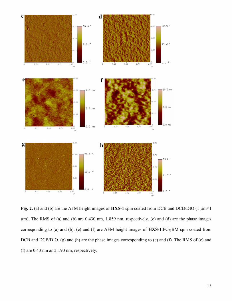
DCB/DIO are imaged with AFM where significantly different height images are observed (see Fig. 2(a)
and 2(b)). The HXS-1 film from DCB/DIO exhibits much rougher surface with larger aggregations than
in the film from DCB, This indicates that DIO can induce the formation of compact chain packing of
HXS-1 and crystallization in aggregation form. The corresponding phase image of the HXS-1 film from
DCB/DIO shown in Fig. 2(d) reveals fine fibril features contrasting with the featureless phase image of
the HXS-1 film from DCB (Fig. 2(c)). This is in accordance with the finding in our previous
communication [36]. HXS-1 is a planar polymer designed for facilitating polymer chain packing in
solid film, which is realized by adding DIO into DCB [36]. The topographies of blends
(HXS-1/PC71BM) spin-coated from DCB and DCB/DIO are also imaged with AFM. The roughness of
the blends cast from DCB/DIO increases also obviously in compare to that of the blends from DCB as
shown in Fig. 2(e) and Fig. 2(f). As seen in the phase image, pronounced nanophase separation in the
blend from DCB/DIO (Fig. 2(h)) and barely detectable phase separation of two components in the film
from DCB (Fig. 2(g)) are consistent with the morphology of the pure HXS-1 due to its semi-crystalline
property. This nanophase separation of HXS-1 and PC71BM may be a result of enhanced HXS-1
crystallization, which is again induced by DIO. The size of this feature is measured to be 10-25 nm.
To see the difference of bulk structures of two blends, the morphologies of blend films cast from two
solutions are evaluated with TEM. To show both overall view and detailed information of the films,
TEM images are recorded at two different scales, 1 µm (Fig. 3(a) and 3(c)) and 100 nm (Fig. 3(b) and
(d)). Some large features bigger than 150 nm are observable. TEM images show contrast based on
electron density in the thin film, so that the dark areas are assigned to the PC71BM-rich phase. This

7
image contrast is not caused by thickness difference because we know from AFM height image (Fig.
2e) that the film is very even and with a surface roughness being only 0.43 nm. Noticeably, the large
phase separation possesses very broad and diffused interface between mixed PC71BM-rich and
HXS-1-rich phases as seen in Fig. 3(a) and 3(b). Such large features with indistinguishable phase
interface can only be caused by inhomogeneous mixing of PC71BM and HXS-1 from the DCB only
solution and they would not influence PSC performance. On the other hand, more homogeneously
mixed blend with very fine structure from DCB/DIO can be distinguished in the overview image (Fig.
3c) and the zoomed image (Fig. 3d). This fine structure can also be seen in the film without PC71BM
(TEM not shown), which means that the fine structure is induced by HXS-1 crystallization. This is in
accordance with the AFM results. According the AFM phase images and TEM images, the thickness of
the HXS-1 crystalline lamellae could be determined to be about 10-20 nm. Thereafter, PC71BM must be
excluded from the HXS-1 crystal and reside between the lamellae, forcing a phase separation with the
same size as the crystalline structure. To be clearly stated, the phase separation between PC71BM and
HXS-1 is attributed to the unique crystallization of HXS-1 provoked by DIO. Another thing to be
noticed, the film thickness investigated with TEM are about 150-200 nm, which means that features of
10-20 nm size seen here are stacks through the whole film. Therefore it is somewhat difficult to clearly
separate the individual lamellae. Fortunately this problem can be solved with 3-D TEM investigation
shown below.
As the performance of PSCs depends on the vertical distribution of the two components in the active
layers and free charges are transported in this direction to the collecting electrodes, it is very interesting
to use a 3-D TEM to investigate the vertical distribution of HXS-1 and PC71BM. Electron tomography
reconstructions [43] are done on blend films cast from DCB and DCB/DIO (Fig. 4(a) and (b)), which
show cross section overviews of the two films (ca. 310 nm wide and 60 nm deep). These reconstructions
are low pass filtered at 10 nm [43]. In Fig. 4(c) and 4(d) the middle sections (ca 8 nm thick) in between
anode and cathode interfaces of the same reconstructions are displayed, where a low pass filtering at 5

8
nm has been used. Light regions correspond to well scattering domains and dark regions to less
scattering domains. The PC71BM is the more scattering material of the two [43]. Thus, the light
volumes are attributed to the PC71BM rich domains while the dark volumes are the polymer rich
domains. A coarser film structure in the film spin-coated from DCB/DIO is also found in these images
shown in Fig. 4(b) and 4(d). The film without DIO exhibits smaller domains, which are evenly spread
throughout the active layer (see Fig. 4(a) and 4(c)), while in the film with DIO the domains are larger
and more clustered together (see Fig. 4(b) and 4(d)). Moreover, Fig. 4b shows more vertical continuous
elongated clusters formed than that in Fig. 4a, which will facilitate charge carrier transport to collection
electrodes.
3.3. The effect of additive on charge generation
Both charge generation and recombination depend strongly on the morphology of active layers. It is
interesting to see how DIO influence these physical properties by comparing PL spectra under these two
specific morphologies. Deteriorating charge generation is expected in DCB/DIO cells because the
interface between HXS-1 and PC71BM is decreased due to increased domain size induced by DIO as
shown in Fig. 2, 3 and 4. To confirm that, the PL spectra of HXS-1:PC71BM films spin-coated from
DCB and DCB/DIO excited by a monochromatic light with a wavelength of 405 nm is recorded (Fig.
5). Pure HXS-1 films show emission in the range of 600-900 nm, with a peak located at 685 nm (Fig.
S2(B) in reference 36). The PC71BM film displays a relatively broad emission with a peak at 720 nm
and also a shoulder at 800 nm. As expected, two morphologies result in two different PL spectra. As
shown in Fig. 5, very weak emission in the region of 700 nm originated from pure HXS-1 and PC71BM
is observed in the blend film of HXS-1:PC71BM from DCB indicating efficient charge transfer [36].
However, as a consequence of increasing domain size and lowering the amount of donor-acceptor
interfaces by the addition of DIO, the emission peak at 710 nm dominates the PL of DCB/DIO films,
which can most probably be explained by the combined emission from HXS-1 and PC71BM due to
inefficient charge transfer since too big pure HXS-1 and PC71BM domains exist. So from a charge

9
transfer point of view, DIO does not introduce a positive impact.
3.4. The effect of additive on charge carrier recombination
As shown in Fig. 5, a new broad emission with a peak located at 930 nm emerges in blend films from
DCB, which is attributed to the recombination of interfacial charge transfer states (CTS) [39, 44-49].
There appears to be less CTS emission from DCB/DIO films (Fig. 5), where it can only be seen as in the
tail to the pure material emission. The reduced emission from the CTS in blend films from DCB/DIO
compared to the blend film from DCB is interesting. Radiative recombination of CTS is a competitor to
photocurrent generation in photovoltaic devices, so lower CTS emission is consistent with increased Jsc
in DCB/DIO solar cells. Therefore, from a CTS recombination point of view, DIO introduces a positive
impact, that is, decrease radiative recombination of CTS in DCB/DIO film, likely due to increasing
phase separation in the active layer. Similar results have also been reported recently [47-49].
3.5. The effect of additive on transport property
The electrical properties of solar cells are very sensitive to the morphology of the active layers. To
verify the different transport situations in the two kinds of PSCs, the Rs and the Rsh are evaluated and
listed in Table 1. Upon adding DIO, the Rs of the PSC decreases significantly from 19 Ω cm2 to 6 Ω cm
2,
which indicates that the geometry induced by DIO facilitates charge carrier transport in the active layer.
Meanwhile, four-fold enhanced Rsh of the DCB/DIO cell implies smaller leak current or less
recombination than that in DCB solar cells.
Hole and electron mobilities of the films from the two solutions are measured with FET and listed in
Table 2. The hole mobility (μh) and electron mobility (μe) of DCB films are 3×10⁻⁵
cm2 Vs
-1 and 1
×10-3
cm2 Vs
-1, respectively. There appear to be a change in mobilities in the DCB/DIO film, where μh
increases to 1×10⁻⁴
cm2 Vs
-1 and μe decreases to 6×10
-4 cm
2 Vs
-4, but this might be a measurement
related effect. FET measurements might not be entirely appropriate for this material vis-à-vis solar cell
performance due to the presence of ordering and spinodal decomposition [50], which may influence the
correlation between FET and solar cell structures in terms of mobility. In particular, there might be an

10
increase in PCBM concentration at the dielectric interface of the transistor in the DCB film compared to
the DCB/DIO film as can be seen in Fig. 4(a) and 4(b), which may be responsible for the measured
changes in mobility. Although an increase of the lower mobility agrees well with the increase in FF
observed with additive [21], the rather small hole mobility increase and the fact that neither hole or
electron mobility is particularly impressive, indicate that some other mechanism, e.g. enhanced charge
separation or decreased recombination, is the main reason for the increased FF. This would also be
consistent with the larger domains and the possible decrease in CTS emission seen in the films with
DIO. From free charge generation and extraction perspective, a favorable morphology is thus probably
more important than a high mobility in order to achieve a high FF.
3.6. The effect of DIO on the shelf-stability of the solar cells
To study the effect of additive on the shelf-stability of the solar cells, two substrates with 6 solar cells
on each cast from DCB and DCB/DIO were fabricated in Freiburg Materials Research Centre. These
cells are kept in a glove box filled with N2 and their I-V curves are recorded for two years with different
intervals in days, weeks and months after one day initial degradation. After two years, the average Jsc,
Voc, FF and PCE of 6 solar cells on the same substrate vs time are presented in the inset of Fig. 6
together with normalized corresponding performance parameters (Fig. 6). These 12 solar cells behave
similar, Voc increase, FF slightly decrease and Jsc clearly decrease, which result in an overall PCE
decrease with time no matter if it is with or without DIO. The PCE and Jsc decrease by 10% for solar
cells cast from DCB and 12% for those from DCB/DIO, respectively. The slightly difference (2%) in Jsc
and PCE degradation between two groups of solar cells is in experimental error. These results indicate
that DIO does not produce observable impact on the shelf-stability of solar cells. The major causes for
performance degradation of these solar cells can be bleaching or/and morphology changes due to
samples kept in the glove box filled with N2. Bleaching in this case may not play a big role because the
samples are only exposed to white light during I-V measurement. Therefore, the fact that degradation is
only observable in the 1st year and no obvious degradation in the 2
nd year indicates negligible

11
morphology variation after one year initial relaxation.
4. Conclusions
In conclusion, the performance enhancement in the solar cells based on HXS-1:PC71BM by additive
DIO is investigated with AFM, TEM, 3-D TEM, PL and FET. The observations from all these different
techniques are well consistent with each other and make a clear connection between solar cell
performance and morphology. The enhancement of Jsc from 8.3 mA/cm2 to 9.8 mA/cm
2 and FF from
0.51 to 0.69 by introducing DIO into DCB is attributed to the pronounced morphology changes of the
active layer induced by DIO. All of AFM, TEM and 3-D TEM images show big domains with sizes of
10-20 nm formed in the films of DCB/DIO. Specially, 3-D TEM images further demonstrate vertical
continuous elongated clusters formed in DCB/DIO films. Lower PL intensity of CTS emission in the
films from DCB/DIO than that from DCB, suggests that once excitons are dissociated at the interface
between HXS-1 and PC71BM in the active layers, large domains (detected with AFM, TEM and 3-D
TEM) are better at separating the holes and electrons in the two phases. All these results propose that
beneficial morphology with domain size in 10-20 nm for inefficient charge recombination and vertical
elongated clusters for assisting charge transport to the collecting electrodes in DCB/DIO films are the
main reasons for the enhanced Jsc of 9.8 mA/cm2, FF of 0.69 and PCE of 5.4%. The result of two year
shelf-stability measurement indicates that DIO has no pronounced impact on the shelf-stability of the
PSCs and the morphology is stable after one year initial relaxation.
Acknowledgement
Financial support by the NSF of China (20834006 and 50821062), and 863 Program (2008AA05Z425),
Swedish Energy Agency, Swedish Research Council (VR) and VINNOVA are gratefully
acknowledged. The collaboration between LiU and Fraunhofer ISE is also financed by Swedish Energy
Agency. Funding of C. Veit and U. Würfel by the German Federal Ministry of Education and Research
under the contract number 03SF0331 is gratefully acknowledged. We thank Dr. Sergej Masich at
Karolinska Institute for assistance with electron tomography.

12
References
[1] F. C. Krebs, Solar Energy Materials and Solar Cells 93 (2009) 394.
[2] O. Inganäs, F. L. Zhang, M. R. Andersson, Accounts of Chemical Research 42 (2009) 1731.
[3] Y. F. Li, Y. P. Zou, Advanced Materials 20 (2008) 2952.
[4] E. Bundgaard, F. C. Krebs, Solar Energy Materials and Solar Cells 91 (2007) 954.
[5] Y. H. Zhou, F. H. Li, S. Barrau, W. J. Tian, O. Inganas, F. L. Zhang, Solar Energy Materials and
Solar Cells 93 (2009) 497.
[6] F. C. Krebs, Solar Energy Materials and Solar Cells 93 (2009) 1636.
[7] Y. H. Zhou, F. L. Zhang, K. Tvingstedt, W. J. Tian, O. Inganäs, Applied Physics Letters 93
(2008) 033302.
[8] G. Dennler, M. C. Scharber, C. J. Brabec, Advanced Materials 21 (2009) 1323.
[9] A. M. Ballantyne, L. Chen, J. Dane, T. Hammant, F. M. Braun, M. Heeney, W. Duffy, I.
McCulloch, D. D. C. Bradley, J. Nelson, Advanced Functional Materials 18 (2008) 2373.
[10] J. Gilot, M. M. Wienk, R. A. J. Janssen, Advanced Materials 22 (2010) E67.
[11] S. Sista, Z. R. Hong, M. H. Park, Z. Xu, Y. Yang, Advanced Materials 22 (2010) E77.
[12] F. L. Zhang, M. Johansson, M. R. Andersson, J. C. Hummelen, O. Inganas, Advanced Materials
14 (2002) 662.
[13] F. Huang, K. S. Chen, H. L. Yip, S. K. Hau, O. Acton, Y. Zhang, J. D. Luo, A. K. Y. Jen, J. Am.
Chem. Soc. 131 (2009) 13886.
[14] Y. P. Zou, A. Najari, P. Berrouard, S. Beaupre, B. R. Aich, Y. Tao, M. Leclerc, J. Am. Chem.
Soc. 132 (2010) 5330.
[15] E. G. Wang, L. Wang, L. F. Lan, C. Luo, W. L. Zhuang, J. B. Peng, Y. Cao, Applied Physics
Letters 92 (2008) 033307.
[16] H. Y. Chen, J. H. Hou, S. Q. Zhang, Y. Y. Liang, G. W. Yang, Y. Yang, L. P. Yu, Y. Wu, G. Li,
Nature Photonics 3 (2009) 649.
[17] J. H. Hou, H. Y. Chen, S. Q. Zhang, R. I. Chen, Y. Yang, Y. Wu, G. Li, Journal of the American
Chemical Society 131 (2009) 15586.
[18] S. H. Park, A. Roy, S. Beaupré, S. Cho, N. Coates, J. S. Moon, D. Moses, M. Leclerc, K. Lee, A.
J. Heeger, Nature Photonics 3 (2009) 297.
[19] D. Kitazawa, N. Watanabe, S. Yamamoto, J. Tsukamoto, Appl. Phys. Lett. 95 (2009) 053701.
[20] S. H. Chan, Y. S. Hsiao, L. I. Hung, G. W. Hwang, H. L. Chen, C. Ting, C. P. Chen,
Macromolecules 43 (2010) 3399.
[21] Y. Y. Liang, Z. Xu, J. B. Xia, S. T. Tsai, Y. Wu, G. Li, C. Ray, L. P. Yu, Adv. Mater. 22 (2010)
E135.
[22] M. A. Green, K. Emery, Y. Hishikawa, W. Warta, Progress in Photovoltaics 19 (2011) 84.
[23] W. L. Ma, C. Y. Yang, X. Gong, K. Lee, A. J. Heeger, Advanced Functional Materials 15 (2005)
1617.
[24] G. Li, V. Shrotriya, J. S. Huang, Y. Yao, T. Moriarty, K. Emery, Y. Yang, Nature Materials 4
(2005) 864.
[25] S. S. van Bavel, M. Barenklau, G. de With, H. Hoppe, J. Loos, Adv. Funct. Mater. 20 (2010)
1458.
[26] V. D. Mihailetchi, H. X. Xie, B. de Boer, L. J. A. Koster, P. W. M. Blom, Advanced Functional
Materials 16 (2006) 699.
[27] T. M. Clarke, J. R. Durrant, Chemical Reviews 110 (2010) 6736.
[28] D. J. D. Moet, M. Lenes, M. Morana, H. Azimi, C. J. Brabec, P. W. M. Blom, Applied Physics
Letters 96 (2010).
[29] R. B. Aich, Y. P. Zou, M. Leclerc, Y. Tao, Organic Electronics 11 (2010) 1053.
[30] F. L. Zhang, K. G. Jespersen, C. Bjorstrom, M. Svensson, M. R. Andersson, V. Sundstrom, K.
Magnusson, E. Moons, A. Yartsev, O. Inganäs, Advanced Functional Materials 16 (2006) 667.
[31] H. W. Tang, G. H. Lu, L. G. Li, J. Li, Y. Z. Wang, X. N. Yang, J. Mater. Chem. 20 (2010) 683.

13
[32] J. Peet, J. Y. Kim, N. E. Coates, W. L. Ma, D. Moses, A. J. Heeger, G. C. Bazan, Nature
Materials 6 (2007) 497.
[33] J. Peet, C. Soci, R. C. Coffin, T. Q. Nguyen, A. Mikhailovsky, D. Moses, G. C. Bazan, Appl.
Phys. Lett. 89 (2006) 252105.
[34] J. S. Moon, C. J. Takacs, S. Cho, R. C. Coffin, H. Kim, G. C. Bazan, A. J. Heeger, Nano Letters
10 (2010) 4005.
[35] C. V. Hoven, X. D. Dang, R. C. Coffin, J. Peet, T. Q. Nguyen, G. C. Bazan, Advanced Materials
22 (2010) E63.
[36] R. P. Qin, W. W. Li, C. H. Li, C. Du, C. Veit, H. F. Schleiermacher, M. Andersson, Z. S. Bo, Z.
P. Liu, O. Inganäs, U. Wuerfel, F. L. Zhang, Journal of the American Chemical Society 131
(2009) 14612.
[37] W. W. Li, C. Du, F. H. Li, Y. Zhou, M. Fahlman, Z. S. Bo, F. L. Zhang, Chemistry of Materials
21 (2009) 5327.
[38] L. J. Lindgren, F. L. Zhang, M. Andersson, S. Barrau, S. Hellstrom, W. Mammo, E. Perzon, O.
Inganas, M. R. Andersson, Chemistry of Materials 21 (2009) 3491.
[39] Y. Zhou, K. Tvingstedt, F. L. Zhang, C. X. Du, W. X. Ni, M. Andersson, O. Inganäs, Advanced
Functional Materials 19 (2009) 3293.
[40] s. t. w. http://www.3tag.com/bobicol.html.
[41] J. K. Lee, W. L. Ma, C. J. Brabec, J. Yuen, J. S. Moon, J. Y. Kim, K. Lee, G. C. Bazan, A. J.
Heeger, Journal of the American Chemical Society 130 (2008) 3619.
[42] D. Di Nuzzo, A. Aguirre, M. Shahid, V. S. Gevaerts, S. C. J. Meskers, R. A. J. Janssen,
Advanced Materials 22 (2010) 4321.
[43] B. V. Andersson, A. Herland, S. Masich, O. Inganas, Nano Lett. 9 (2009) 853.
[44] K. Vandewal, K. Tvingstedt, A. Gadisa, O. Inganäs, J. V. Manca, Nature Materials 8 (2009) 904.
[45] I. Haeldermans, K. Vandewal, W. D. Oosterbaan, A. Gadisa, J. D'Haen, M. K. Van Bael, J. V.
Manca, J. Mullens, Applied Physics Letters 93 (2008).
[46] D. Veldman, O. Ipek, S. C. J. Meskers, J. Sweelssen, M. M. Koetse, S. C. Veenstra, J. M. Kroon,
S. S. van Bavel, J. Loos, R. A. J. Janssen, Journal of the American Chemical Society 130 (2008)
7721.
[47] K. Tvingstedt, K. Vandewal, A. Gadisa, F. L. Zhang, J. Manca, O. Inganäs, Journal of the
American Chemical Society 131 (2009) 11819.
[48] M. Hallermann, I. Kriegel, E. D. Como, J. M. Berger, E. V. Hauff, J. Feldmann, Advanced
Functional Materials 19 (2009) 3662.
[49] K. Tvingstedt, K. Vandewal, F. L. Zhang, O. Inganas, Journal of Physical Chemistry C 114
(2010) 21824.
[50] S. Nilsson, A. Bernasik, A. Budkowski, E. Moons, Macromolecules 40 (2007) 8291.

14
Figures and Tables
(a) (b)
300 400 500 600 700 8000
10
20
30
40
50
60
70
EQ
E (
%)
Wavelength (nm)
0,0 0,2 0,4 0,6 0,8 1,0
-10
-8
-6
-4
-2
0
Cu
rren
t d
en
sity
(m
A/c
m2)
Voltage (V)
Fig. 1. (a) The EQEs and (b) I-V characteristics of PSCs spin coated from DCB (open squares) and
DCB/DIO (filled circles) under AM 1.5 illuminations.
15
Fig. 2. (a) and (b) are the AFM height images of HXS-1 spin coated from DCB and DCB/DIO (1 µm×1
µm), The RMS of (a) and (b) are 0.430 nm, 1.859 nm, respectively. (c) and (d) are the phase images
corresponding to (a) and (b). (e) and (f) are AFM height images of HXS-1:PC71BM spin coated from
DCB and DCB/DIO. (g) and (h) are the phase images corresponding to (e) and (f). The RMS of (e) and
(f) are 0.43 nm and 1.90 nm, respectively.

16
(a) (b)
(c) (d)
Fig. 3. The TEM images of HXS-1/PC71BM spin-coated from DCB (a and b) and DCB/DIO (c and d).

17
Fig. 4. The cross section overviews of the two blend films cast from DCB (a) and DCB/DIO (b).
Image 4(c) and 4(d) are the middle sections (ca 8 nm thick) of the same reconstructions of 4(a) and 4(b).
650 700 750 800 850 900 950 10000
5
10
15
20
25
30
35
40
45
PL
(a.u
.)
Wavelength (nm)
Fig. 5. The PL spectra of HXS-1/PC71BM films spin coated from DCB (black squares) and DCB/DIO
(red circles). The excitation wavelength is 405 nm.

18
0 100 200 300 400 500 600 7000,0
0,2
0,4
0,6
0,8
1,0
0 100 200 300 400 500 600 7005
6
7
8
9
10
Js
c (m
A/c
m2
)
Day (d)
Js
c (
No
rm)
Day (d)
0 100 200 300 400 500 600 7000,0
0,2
0,4
0,6
0,8
1,0
1,2
0 100 200 300 400 500 600 7000,5
0,6
0,7
0,8
0,9
Vo
c (
V)
Day (d)
Vo
c(N
orm
)
Day (d)
0 100 200 300 400 500 600 7000,0
0,2
0,4
0,6
0,8
1,0
0 100 200 300 400 500 600 7000,3
0,4
0,5
0,6
0,7
FF
Day (d)
FF
(N
orm
)
Day (d)
0 100 200 300 400 500 600 7000,0
0,2
0,4
0,6
0,8
1,0
0 100 200 300 400 500 600 7000
1
2
3
4
5
PC
E (
%)
Day (d)
PC
E (
No
rm)
Day (d)
Fig. 6. Normalized and average (inset) performance parameters of HXS-1:PC71BM photovoltaic devices
spin-coated from DCB (opened squares) and DCB/DIO (filled circles)
Table 1. Parameters of HXS-1:PC71BM solar cells
Solvent Jsc [mA/cm2] Voc [V] FF PCE Rs [Ω cm
2] Rsh [Ω cm
2]
DCB 8.3 0.85 0.51 3.6% 19 485
DCB/DIO 9.8 0.81 0.69 5.4% 7 2110
Table 2. Hole and electron mobilities of the films from DCB and DCB/DIO
Solvent μh [cm2 Vs
-1] μe [cm
2 Vs
-1] μe /μh
DCB 3×10⁻⁵
1×10⁻³
33.3
DCB/DIO 1×10⁻⁴
6×10⁻⁴
6