An exploratory study of factors inhibiting the advancement of ...

S C H E M C O N - 2 0 1 4 1 | P a g e
10th
Annual Session of Students’ Chemical Engineering Congress (SCHEMCON – 2014)
Advancement in P3HT PCBM solar cells, the most
efficient Polymer Photovoltaic cell
P. Vijay*, 1
and Vedant Sumaria2.
1Department of Chemical Engineering, University of Petroleum and Energy Studies, Dehradun 248007 India
2Department of Power System Engineering, University of Petroleum and Energy Studies, Dehradun 248007 India
Abstract: Concern about global warming and
diminishing fossil fuel reserves have accelerated
searches for low cost sources of renewable energy.
Organic photovoltaic (OPV) cells are one such source.
They have couple of advantages over the conventional
semiconductors. Organic solar cells have the potential
to be low cost and efficient solar energy convertors, with
a promising energy balance. The applications of
thermoelectric polymers at low temperatures, especially
conducting polymers, have shown various advantages
such as easy and low cost of fabrication, light weight,
and flexibility. However efficiency remains quite low.
Thus efforts have been made to increase the efficiency
by varying the fabrication parameters. Poly (3-
hexythiophene) (P3HT) and 1-(3-methoxycarbonyl)
propyl-1-phenyl [6, 6] C61 (PCBM) are the most studied
polymer blend materials around the world for bulk
heterojunction structure of an organic solar cells
(OSCs). This research article is a survey on tremendous
literature published that exhibit solar cells based on
blends of P3HT and PCBM.
The basic structure of a P3HT: PCBM heterojunction
solar cell and accurate methods for measurement of the
power conversion efficiency (PCE) were also discussed.
Standard method using Air Mass 1.5 Global (1000Wm-
2, AM1.5G) solar spectrum is advised after finding
abnormalities in the PCE reported. It is noticed that
optimum thickness and area of every layer in the cell
structure is important. A detailed discussion on thermal
annealing and solvent annealing approaches to improve
device performance is presented. The effects of these
two approaches on improving polymer crystallinity,
light absorption in the polymer, carrier transport, and
blend film nano-morphology, etc. are summarized.
Polymer morphology has proven to be extremely
important in determining the optoelectronic properties
in polymer-based devices. We also investigate the effects
of polymer morphology too on the PCE of the cell.
Another important parameter affecting the efficiency
discussed is the Molecular weight ratio of P3HT and
PCBM blend active layer. Future directions and
challenges on polymer solar cell development are also
discussed
Keywords— P3HT: PCBM organic blend layer,
Polymer Photovoltaic, Organic solar cells, bulk
heterojunctions.
INTRODUCTION
With increasing energy demands, global warming
and diminishing fossil fuel reserves, it is important to
accelerate our research for a low cost source of
renewable energy. The sun deposits 173000 TW of
power onto the earth’s surface [1]
. The current power
consumption is about 13 TW and will probably
increase to 30 TW by 2050 [2]
. Conventional
photovoltaic have good power conversion efficiency
but it only contributes about 0.1% of the total
electricity [3]
. This is because of high costs of
fabrication, processing and installation of PV
systems. Thus it is important in the PV research to
produce economically viable for a better acceptance.
Today the goal in front of us is to produce PV system
with cost effective materials producing high
efficiency. After the traditional Silicon based solar
cells, there were many other alternate materials and
technologies used such as amorphous silicon (a-Si),
copper indium gallium arsenide (CIGS), Cadmium
Tellurium (CdTe) and many more [4]
.
Discovery in semiconducting (conjugated) polymers
gave a new path for research in organic electronics
and opened areas for using organic polymers in light
emitting diodes [5,6]
, thin film transistors [7-9]
, memory
devices [10,11]
, and solar cells [12,13]
. Photovoltaic cells
on organic materials are strong candidates because of
several important properties they have such as large
area, excellent mechanical flexibility, low production
costs, low specific weight, simple fabrication process
and easy tenability of chemical properties of the
organic material [12-15]
. There have been several
papers on Organic solar cells (OSCs) since their
discovery with . Among these OSCs the most
important and prominent materials in BHJs is poly(3-
hexylthiophene) and phenyl-C61-butyric acid methyl
Ester (P3HT:PCBM). It is important to know that the

S C H E M C O N - 2 0 1 4 2 | P a g e
10th
Annual Session of Students’ Chemical Engineering Congress (SCHEMCON – 2014)
efficiency varies at a wide range from a min of 0.1%
to a max of 8.4% recently by Heliatek (a company).
Thus there is a broad scope to work on. Most of the
PCEs ranged between 3-4%. The complexity in the
organic structure is the fact that studies on P3HT:
PCBM will continue in the future till it is replaced by
another better technology at this low cost.
Fig. 1: P3HT and PCBM Structure
The Power Conversion Efficiency (PCE) of an OPV
cell can be determined by the following factors: light
absorption by the acceptor/donor (A/D) interface,
transport of excitons to the interface layer, efficiency
of the hole/exciton breaking up into electron-hole
pairs at the interface, transport of holes across the
donating layer to the anodic electrode, transport of
electrons across the acceptor layer to the cathodic
electrode, surface roughness between the donor layer
and the anodic electrode, and surface roughness
between the contact between the acceptor layer and
the cathodic electrode. Thus PCE of OPV cells can
be modified by change in the donor, acceptor,
blocking material, PV cell structure, annealing, regio-
regularity, thickness of films, and area of the films [16-
23].
Fabrication parameters such as solvent
selection, annealing time, annealing temperature and
regioregularity of the active layer are most critical
factors in the film morphology. In this paper we have
focused on the recent advances in morphology
control which is the key parameter for a high PCE.
We also discuss the accurate methodology for finding
the power conversion efficiency of an OSC.
I. STRUCTURE OF A DONOR/ ACCEPTOR (P3HT:
PCBM) HETEROJUNCTION SOLAR CELLS
Fig. 2: Small-molecule donor–acceptor heterojunction solar cell
(PEDOT: poly (3, 4-ethylenedioxythiophene); PSS: poly (styrene
sulfonic acid); ITO: indium tin oxide).
Donor Acceptor layer is the P3HT: PCBM layer with
a weight ratio of 1:1. It is usually made in a solvent
such as 1,2-dichlorobenzene (DCB) and
chlorobenzene (CB). Most devices are built on
Indium Tin oxide (ITO) on glass sheets. ITO is
chosen as it is transparent and has a good electrical
conductivity. ITO resistivity is between 10-20 Ωm-2.
Interface layer uses usually PEDOT: PSS on the ITO
glass. This acts the hole ejection layer. 2, 9-
dimethyl-4,7-diphenyl-1,10-phenanthroline (BCP) is
also sometimes deposited by thermal evaporation as
a hole/exciton blocking layer on the P3HT:PCBM
blended layer under a fixed pressure for a fixed
thickness. After every deposition the cell is backed in
a glove box at different temperature and for different
time interval. Thus Pressure, temperature and
material, all are important to be précised in
fabrication.
II. ACCURATE MEASUREMENTS
Recording accurate PCE is very important and care
should be taken of that the efficiencies reported are
close to the theoretical limits of solar cells dictated by
physics [24, 25]
and in some cases even the
thermodynamic limits. There are standards which
have to be accepted. As a result of continuing
research efforts, the efficiencies of organic solar cells
are now fast approaching the levels where they could
be put into commercial applications. Significant
efforts have been made in the past to accurately

S C H E M C O N - 2 0 1 4 3 | P a g e
10th
Annual Session of Students’ Chemical Engineering Congress (SCHEMCON – 2014)
determine the efficiency of solar cells, and a standard
test method has been established [26-28]
. One of the
best works on standardizing the procedure was put in
by Prof. Y. Yang and coworkers. Some of the
important issues with respect to OSC devices were
discussed, such as spectral responsivity and its
behavior with light-bias intensity, dependence of the
device parameters on the incident-light intensity, and
calculation and application of spectral-mismatch
factor for efficiency correction [29]
. The note
“Reporting Solar-Cell Efficiency” published in 2008
in “Solar Energy Materials and Solar Cells” was
important which stated one of the standard method
using Air Mass 1.5 Global (1000Wm-2
, AM1.5G)
solar spectrum [30-32]
. It is advised that if the power
conversion efficiencies exceed 5%, journals usually
requires the measurement be traceable to an ISO/IEC
17025 certified laboratory specializing in solar cell
characterization (ISO is the International
Organization for Standardization) [33]
. Such labs
include, but are not limited to, the National
Renewable Energy Laboratory (NREL), Japanese
National Institute of Advanced Industrial Science and
Technology (AIST), Fraunhofer Institute für Solare
Energie Systeme (Fraunhofer- ISE), or Energy
Research Center of the Netherlands (ECN). Solar
power conversion efficiency is given by the product
of current density (J), open circuit voltage (Voc), and
fill factor (FF) divided by the incoming light’s power
density. The thermodynamic limit for a single
bandgap device under one sun at AM1.5 is
approximately 33%. We would also like the
researchers to keep in mind that the most common
error in efficiency measurements stems from
improper calibration of the solar simulator.
Researchers should consult the accepted standards
defined for solar simulators [34, 35]
.
III. EFFECT OF INTERFACE AND ACTIVE LAYER
THICKNESS AND AREA
The effects of interface and active layer have not
studied been sufficiently but it is important factor for
a higher PCE of the organic photovoltaic cells. Su-
Huwan Lee and coworkers studied the effect of the
interface layer, PEDOT: PSS and LIF, to improve the
PCE of the OPV cell. OPV devices were fabricated
with a sandwiched structure of varying E SS
and iF layer thic ness CE pea ed at a E
SS thic ness of 2000 rpm improving the CE by
about 41.5% with a maximum PCE of 6.648% (Refer
Fig.3). In addition to that the PCE peaked at a LiF
layer thic ness of 0 nm improving the CE by
209.2% (Refer Fig.4)[36]
.
Fig. 2: Variation of PCE and Jsc with interface layer thickness
(here, PEDOT: PSS) [36].
Fig. 3: Variation of PCE and Jsc with interface layer thickness
(here, LiF) [36].
Further R.H.Friend and coworkers investigated by
variation of PEDOT: PSS layer thickness between 25
and 150 nm, finding the optimum device

S C H E M C O N - 2 0 1 4 4 | P a g e
10th
Annual Session of Students’ Chemical Engineering Congress (SCHEMCON – 2014)
performance at 70nm [37]
. It is also important to note
that the surface topology became smoother at this
thic ness When researched we don’t find much
papers on this matter, thus encourage authors to work
on this field. Vishal. S et al [38]
described that that
there is no effect of thickness on the open circuit
voltage unlike Brabec et al [39]
which instead had
shown a variation. They found a variation of the
work function of the anode linearly influences the
VOC, with a scaling factor of 0.8. The authors
suggest that the work function of PEDOT is not
pinned to any of the energy levels in the active layer,
hence, the variation in VOC. It was previously
reported in [46, 47]
that the work function of the
cathode metal slightly affects the Voc of the PV cell.
Now we will discuss about the
effects of active layer on the PCE. Gang Li and
coworkers in 2005 demonstrated this by changing
active layer thickness and measuring the I-V curves.
It is found that the open circuit voltage remain
constant on varying the thickness of active layer
however the short circuit current and the power
conversion efficiency vary significantly. Highest
PCE of 4% was found for a thickness of 63nm [40]
. It
is uncommon for such small thickness of the active
layer as it goes up to 350 nm for better absorption
and thus short circuit current Jsc of OPV cells without
losing much in terms of bulk recombination. But
even thin film active layer leads to efficient cells due
good absorption coefficient and leads to favoring
percolation paths and enhanced charge transport [41,
42]. MD. S. Islam et al also demonstrated that there
was a significant rise in the absorption of light as the
thickness of the active layer increases [43]
. Similar
results were report by Moule [44]
and Kim [45]
.
Fig. 4: Short circuit current density and power conversion
efficiency as a function of active layer thickness [40].
Fig. 5: P L Quenching showing how absorption increases with
increase in the layer thickness of P3HT: PCBM [43].
Not only thickness of the films but are also affects
the efficiency of an organic cell. Mainly the area is
ranges from 5 to 15 mm2. However we find that
negligible work has been carried out in optimizing
the geometry, pixel dimensions and distribution. In
2007 D L Carroll and coworkers fabricated a small
active area (< 10 mm2), defined by the overlap of the
bottom ITO anode and top cathode, has been reported
to give rise a high Jsc values [48]
. Dhritman Gupta in
2008 published a paper especially on area dependent
efficiency of organic solar cells [49]
. The active area
ranged from 0.01 – 1 cm2. Measurements were done
on varying active layer area and varying illumination
values. In all the cases there was a drop in the Jsc for
flooded illumination. Under the restricted
illumination, the J-V characteristics for different area

S C H E M C O N - 2 0 1 4 5 | P a g e
10th
Annual Session of Students’ Chemical Engineering Congress (SCHEMCON – 2014)
devices are identical. Further Hisashi Kitami and his
coworkers show Jsc was decreased depending on the
active area, whereas VOC and FF are not affected [50]
.
S.Y. Park also demonstrated effects of cell size in
OSCs by introduction of metal subelectrodes [51]
. It is
demonstrated that the series resistance could be
reduced significantly by inserting metal subelectrodes
onto the ITO anode, yielding a PCE of 2.60.3% up to
the cell area of 4.08 cm2. Dang Gao too worked on
area dependency and used device sizes of 0.07, 0.20
and 0.50 cm2 [52]
. Table 1 shows us the results found
from which we conclude that there is no major
change in the open circuit voltage and fill factor on
variation of active area but PCE decreased with
increase in area.
IV. TABLE 1: SUMMARY OF FULLY ILLUMINATED
DEVICE CHARACTERISTICS. ALL DEVICES WERE
FABRICATED ON THE SAME SUBSTRATE [52].
Device
Area
(cm2)
Rs
(Ωcm2)
JSC
(mA/
cm2)
VOC
(V)
FF
(%)
PCE
(%)
Illuminati
on
Intensity
(mA/cm2)
0.07 2.86 8.20 0.58 65.92 3.14 100
0.20 6.27 8.45 0.58 62.00 3.04
0.50 10.76 7.42 0.58 59.31 2.55 90
Fig. 6: Variation in Jsc and Voc with different active areas for a
P3HTPCBM solar cell under flooded white light illumination of intensity80 mW/cm2. Devices were fabricated on two different
substrates with pixel sizes of 0.01, 0.04, and 0.09 cm2 (substrate
1). The schematic diagram of the different active area devices is depicted in the inset [49].
Fig. 7: The J-V characteristics of 0.25 cm2 device under flooded
and restricted collimated illumination using a calibrated 50
mW/cm2 Xe source. The device layout has been depicted in the inset [49].
V. EFFECT OF ANNEALING
Thermal annealing can play an important role in
improving the optoelectronic properties of a polymer
blend. Annealing processes in polymer solar cells can
be divided into two categories: thermal annealing

S C H E M C O N - 2 0 1 4 6 | P a g e
10th
Annual Session of Students’ Chemical Engineering Congress (SCHEMCON – 2014)
[53, 54] and solvent annealing
[55- 57]. Thermal annealing
can be applied either on the final device (post-
annealing) or on the polymer film only (pre-
annealing). Annealing temperature and time are the
most critical parameters in this approach. Berggren et
al. showed that thermal annealing can enhance
polymer crystallinity [58]
. Thermal annealing enables
the P3HT and PCBM nano domains sizes to be
increased up to optimized values corresponding to the
exciton diffusion lengths in each material, which
have recently been evaluated to be as low as 3 nm
and 30 nm in P3HT and PCBM, respectively [59]
.
Franz Padinger in 2003 treated P3HT: PCBM solar
cells post production with an applied external
potential higher than the open circuit voltage and
annealing temperature higher than the glass transition
temperature leading to an improved efficiency. Using
a temperature of 75 °C the optimum time for
annealing was found to be 5-6 minutes [60]
. Li et al in
2005 used AFM to show the active layer roughness
after annealing at different temperatures for 10
minutes. The surface becomes rougher as the
annealing temperature increases from 70°C to 110°C,
but on further annealing at 150°C the roughness
decreases. The broad hill like structures in the figure
9c shows that it is most rough [54]
. On further
investigation they find that the optimum condition of
annealing for best power conversion efficiency (here
4%) was 110°C for 10 minutes post production. This
is due to the fact that higher roughness at the
interface results in the presence of more defect sites
that can increase the exciton decomposition at the
interface, thereby increasing the charge generation [54]
.
Fig. 8: AFM height images of the surface of the active layer
consisting of P3HT:PCBM in (1:1 weight ratio) a) before annealing, and after annealing at b)70 °C, c)110 °C, and d)150 °C.
The annealing time for all the films was 10 min. The P3HT:
PCBM films were spin coated on top of PEDOT: PSS-coated ITO glass [54].
W. Ma et al used transmission electron microscopy
(TEM) images to study the interpenetrating networks.
It was observed that there is no distinct visibility of
the networks without annealing whereas on annealing
for 30 mins and 2hrs the morphology of the
interpenetrating Donor/Acceptor networks became
clearer and easily visible with typical feature of size
of 10nm. XRD results were also taken which told us
that annealing improved the crystallinity within the
face separated networks and thereby facilitates charge
transport to the electrode [53]
. The importance of
aluminum interface in annealing process that leads to
high efficiency was also shown.

S C H E M C O N - 2 0 1 4 7 | P a g e
10th
Annual Session of Students’ Chemical Engineering Congress (SCHEMCON – 2014)
Figure 9: TEM images of P3HT: PCBM film bulk morphology
before annealing a), after annealing at 150°C for 30 minutes
(b), and annealing at 150°C for 2 hrs. (c) [53].
Fig. 11: a) XRD spectra of P3HT: PCBM film drop-cast onto PEDOT/ ITO substrate with and without thermal annealing at
150°C for 30 minutes. The inset shows P3HT crystal structure. b)
XRD spectra obtained from complete solar cells (with Al electrode) before and after annealing [54].
In 2007 G. Li studied the effects of solvent annealing
and it was found that solvent annealing approach is
more pronounced at higher PCBM loadings. The
variation in VOC was partially explained by the longer
conjugation length and formation of a band structure
in well-organized RR-P3HT domains in solvent
annealed solar cells [56]
. Increase in crystallinity was
also supported by reports in literature [61-63]
. The
effect of annealing on the absorption profile is
characterized with UV–vis spectroscopy. Two
phenomena are generally observed as a result of
thermal annealing. Both a red-shift in peak
absorption and an increase in magnitude of
absorption are observed for a P3HT: PCBM blend [64]
. An absorption profile of an as-cast and annealed
P3HT: PCBM is displayed in Fig. 12.
Ma et al [53]
have undertaken a comprehensive study
of the process parameters of annealing temperature
and time for a P3HT: PCBM system. A comparative
study of J–V curves of devices with treated with
different annealing temperature is displayed in Fig.
13. From the curve we understand that on moderate
temperature annealing at 70°C leads to an
improvement in both the fill factor and JSC and it is
believed that the crystallinity of the active layer blend
improves. Thermal annealing at 150°C brought about
more improvement in the two device characteristics.
The Jsc increases to a value of 9.5mA/cm2, whilst the
fill factor increases from 30% in the as-cast sample to
68% in the sample annealed at 150°C. These
parameter changes concluded the reduction in series
resistance of the device [53]
. Yang et al in 2005
investigated the effect of annealing on the external
quantum efficiency and it was found that EQE
response for the annealed sample is better for a wide
spectral range [65]
. Kim et al [66]
investigated the effect
of the annealing sequence on both the film and
electronic characteristics of P3HT: PCBM solar cells.
Post annealing step was deemed to increase the
Fig. 10: UV–vis spectra for both pure P3HT and P3HT: PCBM blend films. Data for as cast (red) and thermally annealed at 1501C for 15 min (blue) [64].

S C H E M C O N - 2 0 1 4 8 | P a g e
10th
Annual Session of Students’ Chemical Engineering Congress (SCHEMCON – 2014)
interfacial area between the aluminum cathode and
the active layer. This improved contact lead to more
efficient charge collection. Additionally, a slight
increase in absorption was measured for the post
annealed device, which was due to an increase in
interfacial roughness between the active layer and
aluminum. The performance of the post-annealed was
better than both the untreated and pre-annealed
device, which suggests that the sequence of the
processing step is important, and that device post
annealing is crucial in obtaining efficient charge
carrier collection.
Fig. 12: Current–voltage characteristic curves of P3HT: PCBM solar cells with different treatments. Data is shown for three varying heat
treatments of (i) no thermal annealing (open squares), (ii) thermal annealing at 701C (open triangles) and (iii) thermal annealing at 150°C (filled
squares). The illumination intensity used was 80 mW/cm2 [53].
Fig. 13: EQE profile for pristine (blue) and thermally annealed at 120C for 60 min. (red) P3HT: PCBM devices [65].

S C H E M C O N - 2 0 1 4 9 | P a g e
10th
Annual Session of Students’ Chemical Engineering Congress (SCHEMCON – 2014)
Fig. 14: Current–voltage characteristic curves for (i) untreated (squares), (ii) pre-annealed (circles), (iii) pre- and post-annealed (triangles up) and
(iv) post-annealed [66].
J Jong and his coworkers later in 2009 worked on time
dependent morphology evolution by annealing process on
polymer: fullerene blend solar cells [67]
. Morphological
changes in P3HT: PCBM were evaluated under different
annealing conditions over a time scale relevant for PCBM
diffusion and aggregation. High-temperature thermal
annealing (150°C) was a strong condition, and room-
temperature solvent annealing was a relatively mild
condition. Here solvent annealing resulted in a more
favorable BHJ morphology than thermal annealing.
However, additional thermal annealing of the blend films
after the formation of the well-ordered morphology by an
optimized solvent annealing showed a relatively stable
morphology, an observation confirmed by TEM images,
selected-area electron diffraction (SAED) patterns, and
device performances. C-W Chu et al. also used annealing
for increasing the efficiency of the solar cells [68]
. There
was an enhancement of the JSC and FF of the solvent
annealed device with thermal treatment compared to the
fast-growth device without thermal treatment which is
attributed to increase absorption in red region and
improved charge transfer properties. In this
paper we see the use of grazing-incidence
x-ray diffraction (GIXRD) which
highlights that controlled film processing
can tune polymer nanostructure in RR-
P3HT/ fullerene blend films. In 2007 we
had an interesting change with the
annealing process. C-J Ko used microwave
annealing for Polymer photovoltaic [69]
. It was inferred
microwave irradiation could penetrate through the
glass/ITO/PEDOT: PSS layers and be absorbed directly by
the active layer during microwave annealing. No heating of
the microwave occurs at the anode and only heats the
active layer and cathode selectively. Thus microwave
irradiation is a selective heating (annealing) method for
improving the efficiency of OPV devices.
Solvent vapor annealing (SVA) can be
effectively used as a post processing technique to
manipulate the morphology of polymer- fullerene [69-74]
.
Thermal annealing can lead to degradation of conjugate
polymers and flexible substrates that are not stable at high
temperatures, and it can result in coarsening of the nano
scale phase segregation, which is unfavorable for exciton
diffusion to the BHJ interface, leading to exciton
recombination and lower power conversion efficiency [75,
76]. Eric Verploegen et al in 2012 used SVA for fabrication
of or high PCE polymer- fullerene solar cells [77]
. Using
grazing incidence X- ray scattering (GIXS) for morphology
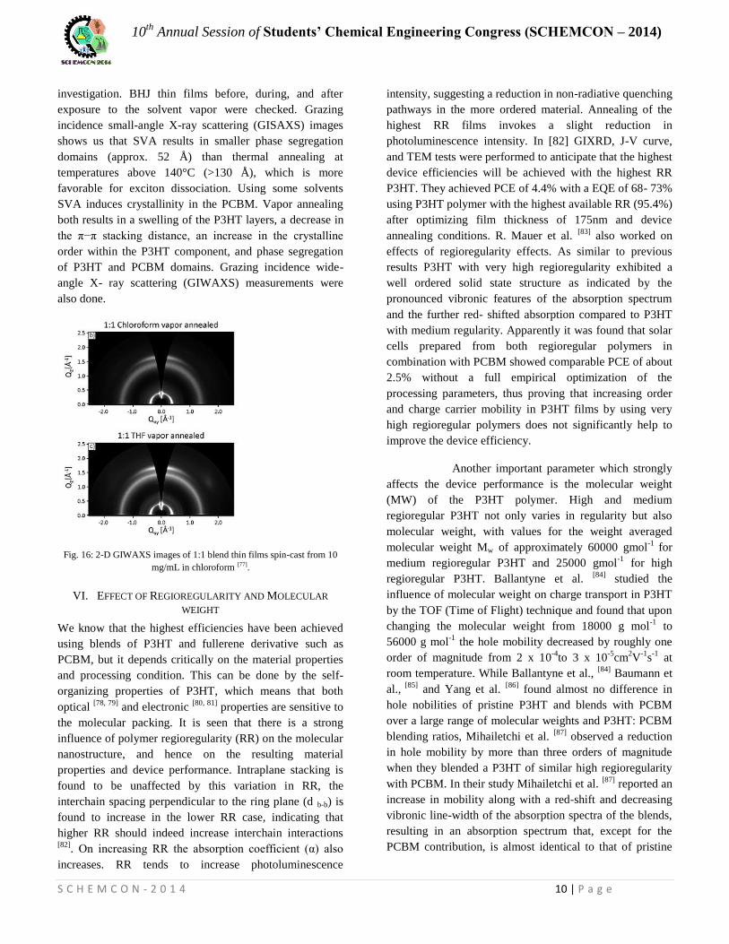
Fig 15 GISAXS of 1 1 3H − CBM blend thin films spin-cast from 10 mg/mL in chloroform
after different annealing conditions [77].
S C H E M C O N - 2 0 1 4 10 | P a g e
10th
Annual Session of Students’ Chemical Engineering Congress (SCHEMCON – 2014)
investigation. BHJ thin films before, during, and after
exposure to the solvent vapor were checked. Grazing
incidence small-angle X-ray scattering (GISAXS) images
shows us that SVA results in smaller phase segregation
domains (approx. 52 Å) than thermal annealing at
temperatures above 140°C (>130 Å), which is more
favorable for exciton dissociation. Using some solvents
SVA induces crystallinity in the PCBM. Vapor annealing
both results in a swelling of the P3HT layers, a decrease in
the π−π stac ing distance an increase in the crystalline
order within the P3HT component, and phase segregation
of P3HT and PCBM domains. Grazing incidence wide-
angle X- ray scattering (GIWAXS) measurements were
also done.
Fig. 16: 2-D GIWAXS images of 1:1 blend thin films spin-cast from 10
mg/mL in chloroform [77].
VI. EFFECT OF REGIOREGULARITY AND MOLECULAR
WEIGHT
We know that the highest efficiencies have been achieved
using blends of P3HT and fullerene derivative such as
PCBM, but it depends critically on the material properties
and processing condition. This can be done by the self-
organizing properties of P3HT, which means that both
optical [78, 79]
and electronic [80, 81]
properties are sensitive to
the molecular packing. It is seen that there is a strong
influence of polymer regioregularity (RR) on the molecular
nanostructure, and hence on the resulting material
properties and device performance. Intraplane stacking is
found to be unaffected by this variation in RR, the
interchain spacing perpendicular to the ring plane (d b-b) is
found to increase in the lower RR case, indicating that
higher RR should indeed increase interchain interactions [82]
. n increasing RR the absorption coefficient (α) also
increases. RR tends to increase photoluminescence
intensity, suggesting a reduction in non-radiative quenching
pathways in the more ordered material. Annealing of the
highest RR films invokes a slight reduction in
photoluminescence intensity. In [82] GIXRD, J-V curve,
and TEM tests were performed to anticipate that the highest
device efficiencies will be achieved with the highest RR
P3HT. They achieved PCE of 4.4% with a EQE of 68- 73%
using P3HT polymer with the highest available RR (95.4%)
after optimizing film thickness of 175nm and device
annealing conditions. R. Mauer et al. [83]
also worked on
effects of regioregularity effects. As similar to previous
results P3HT with very high regioregularity exhibited a
well ordered solid state structure as indicated by the
pronounced vibronic features of the absorption spectrum
and the further red- shifted absorption compared to P3HT
with medium regularity. Apparently it was found that solar
cells prepared from both regioregular polymers in
combination with PCBM showed comparable PCE of about
2.5% without a full empirical optimization of the
processing parameters, thus proving that increasing order
and charge carrier mobility in P3HT films by using very
high regioregular polymers does not significantly help to
improve the device efficiency.
Another important parameter which strongly
affects the device performance is the molecular weight
(MW) of the P3HT polymer. High and medium
regioregular P3HT not only varies in regularity but also
molecular weight, with values for the weight averaged
molecular weight Mw of approximately 60000 gmol-1
for
medium regioregular P3HT and 25000 gmol-1
for high
regioregular P3HT. Ballantyne et al. [84]
studied the
influence of molecular weight on charge transport in P3HT
by the TOF (Time of Flight) technique and found that upon
changing the molecular weight from 18000 g mol-1
to
56000 g mol-1
the hole mobility decreased by roughly one
order of magnitude from 2 x 10⁻⁴
to 3 x 10⁻⁵
cm2V
-1s
-1 at
room temperature. While Ballantyne et al., [84]
Baumann et
al., [85]
and Yang et al. [86]
found almost no difference in
hole nobilities of pristine P3HT and blends with PCBM
over a large range of molecular weights and P3HT: PCBM
blending ratios, Mihailetchi et al. [87]
observed a reduction
in hole mobility by more than three orders of magnitude
when they blended a P3HT of similar high regioregularity
with PCBM. In their study Mihailetchi et al. [87]
reported an
increase in mobility along with a red-shift and decreasing
vibronic line-width of the absorption spectra of the blends,
resulting in an absorption spectrum that, except for the
PCBM contribution, is almost identical to that of pristine

S C H E M C O N - 2 0 1 4 11 | P a g e
10th
Annual Session of Students’ Chemical Engineering Congress (SCHEMCON – 2014)
P3HT. Still due to the discrepancy in PCE, the effect of the
molecular weight on performance is not clearly displayed.
Weight ratio between the active layer
components, P3HT and PCBM, is also an important
parameter affecting the PCE of a cell. The P3HT: PCBM
power-conversion efficiency is governed by phase
separation between the two materials in the solid state. The
phase diagram clearly shows how the morphology is
affected by the composition ratio [88, 89]
. Anyhow, according
to numerous studies on ratio effects, it is generally advised
that P3HT: PCBM be used in a weight ratio between 1:0.8
and 1:1 (i.e., with a small excess of P3HT).
VII. RECENT PROGRESS IN HETEROJUNCTION P3HT:
PCBM SOLAR CELLS
When we look at the last two years, there has been a lot of
work on polymer blends of P3HT and PCBM solar cells.
There are many publications aimed at getting a better PCE
value with different various parameter changes. J. Krantz
investigated silver nanowire (Ag NW) as top electrodes in
semitransparent inverted organic solar cells. Performance
of P3HT: PCBM solar cells with Ag NW top electrode
layers is found to match very closely the performance of
reference devices based thermally evaporated, highly
reflective metal silver top electrodes. Overall, Ag NW top
electrodes are established as a serious alternate to TCO
base electrodes. Semitransparent devise with efficiencies of
over 2% are realized [90]
. PCE of P3HT: PCBM bulk
heterojunction organic solar cells were increased through
the addition of small amounts (1-10%) of metalloporphrin-
oligothiophene conjugates. Efficiency was enhanced up to
17% for the thiophene substituted Cu(II)- porphyrin,
pointing to an important effect of the metal center.
Effectiveness of porphyrins increased in the order free-
base Co< Zn< Ni< Cu [91]
eter Kohn’s work show that
crystallization which is intrinsic to most semi crystalline
polymers, followed by the enrichment, segregation, and
crystallization of PCBM provides an interdigitated
structure, which is conceptually ideal for excitonic solar
cells [92]
. D. Spoltore had shown us in his work, the mass
fraction ‘f’ of highly crystalline nanofibrillar 3H to the
total P3HT content in P3HT: PCBM solar cells are
consistently varied, controlling the temperature of Nano
fibers- P3HT casting dispersion. A systematic study of the
apparent recombination order, measured with a transient
photo voltage technique as a function of ‘f’ was presented
and a correlation order of the P3HT crystalline, and the trap
concentration in the band gap measured with an admittance
spectroscopy technique [93]
. C. Koidis et al. worked on to
study the effect of R2R printing and drying process on the
nanomorphology and nanostructure of the photoactive
P3HT: PCBM thin films printed on PEDOT: PSS
electrodes towards the fabrication of ITO free flexible
OPVs. Spectroscopic ellipsometry, atomic force
microscopy analysis, x- ray diffraction tests were done [94]
.
S. Ulum, Natalie Holmes and coworkers proved directly
the structural motif of P3HT: PCBM nano particulate
organic photovoltaic (NO- OPV) devices and had shown
how NP morphology determines device function. PCE of
1.3% was obtained. Nanoparticle structure proved with
synchrotron x- ray microscopy revealed a core- shell
structure with a PCBM rich core [95]
. Control over the
structure of donor/ acceptor blends is essential for the
development of solution processable OSCs. K H Lee and
coworkers used time-resolved Neutron Reflectometry (NR)
and in-situ annealing to investigate the nanoscale structure
and inter-diffusion of sequential spin-coated thin films of
P3HT: PCBM and correlated the evolving structure with
the device performance. Despite the complete intermixing
of PCBM and P3HT to form a structure resembling a bulk
heterojunction, essentially there was no improvement on
annealing at a temperature of 110°C [96]
.
S Khelifi et al. worked on the effect of light induced
degradation on electrical transport and charge extraction in
P3HT: PCBM OSCs. They gained a detailed insight into
the gradual degradation of P3HT: PCBM aged under
different illumination conditions. They applied numerous
advanced electrical characterization techniques and a
modeling software tool (SCAPS) to explain the failure
mechanism. TEM revealed a change in blend morphology
upon long illumination times manifested by phase
segregation in the blend [97]
. Kurniawan Foe and coworkers
fabricated P3HT and PCBM OPVs using TiOX interfacial
layer. It was found that TiOX layer coated at a spin speed of
3000 rpm improved the photon absorption of the active
layer. After 70 days of storage the JSC dropped by 16.2%,
FF dropped by 10.6% and PC by 25% whereas VOC
remained relatively stable [98]
. High precision production
process of a flexible P3HT: PCBM OPV modules with a
PCE above 3% and FF of 95% were fabricated by P. Kubis
et al. They combined the slot-die coating and high
resolution laser patterning. They even demonstrated
flexible modules showing identical performance to
optimized small scale lab devices. Devices withstood 1000s
of bending cycles [99]
. We also find an extensive review on
annealing effect on PCE of bulk heterojunction organic

S C H E M C O N - 2 0 1 4 12 | P a g e
10th
Annual Session of Students’ Chemical Engineering Congress (SCHEMCON – 2014)
solar cells. It focused on changes in the physical film
properties, the electronic performance of devices, as well as
the link between film structure and electronic performance
during a thermal annealing process [100]
.
VIII. CONCLUSION AND SCOPE OF STUDY
In summary, bulk heterojunction organic solar cells with
P3HT and PCBM polymer blend as active layer are still
quite promising. A major advantage is that their
morphology are relatively easy to optimize. Meanwhile,
flexibility, large area, light-weight, and the ability to
self-repair are all attractions for research. Changes in the
important fabrication parameters have brought about a
large difference since the invention. Thus there is a large
field to work on. The largest challenge remains is the low
power conversion efficiency mainly due to poor charge
mobility. Utilization of whole spectrum and a more
efficient use of UV energy are also possible points for
breakthrough.
References
[1] Archer, D., 2012. Global Warming: Understanding the Forecast.2nd ed. USA: JohnWiley & Sons.
[2] http://www.sc.doe.gov/bes/reports/files/SEU_rpt.pdf, Report of the Basic Energy Sciences Workshop on Solar Energy Utilization US-
DOE, April 18-21, 2005; (b) Energy Information Administration,
U.S Department of Energy, Overview, Annual Energy Outlook 2003.
[3] Fritts, C.E., Procedures American Association for the Advancement
of Science, Vol. 33, p. 97, 1883; also, American J. of Science, Vol. 26, p. 465, 1883.
[4] S. Hegedus and A. Luque, Handbook of Photovoltaic Science and
Engineering, ed. A. Luque and S. Hegedus, Wiley, West Sussex, p.1,
2003.
[5] C.W. Tang and S. VanSkyle, Appl. Phys. Lett. 51, p. 913, 1986.
[6] J. H. Burroughes, D.D.C Bradley, A.B. Holmes, Nature, Vol. 347, p.
539, 1990.
[7] G. Horowitz, X. Z. Peng, D. Fichou and F. Garnier, Solid state Commune, Vol. 72, p.381, 1989.
[8] H. Sirringhaus, P. J. Brown, R. H. Friend, M. M. Nielsen, K.
Bechgaard, B. M. W. Langeveld-Voss, A. J. H. Spiering, R. A. J. Janssen, E. W. Meijer, P. Herwig and D. M. de Leeuw, Nature, Vol.
401, p.685, 1999.
[9] Z. Bao, A. Dadablapur and A. J. Lovinger, Appl. Phys. Lett. 69, p.4108, 1995.
[10] L. Ma, J. Liu and Y. Yang, Appl. Phys. Lett. 80, p.2997, 2002.
[11] L. Ma, S. Pyo, J. Ouyang, Q. Xu and Y. Yang, Appl. Phys. Lett. 82,
p.1419, 2003.
[12] S. S. Sun and N. S. Sariciftci, Eds., Organic Photovoltaics: Mechanisms, Materials, and Devices, CRC Press, Boca Raton, Fla,
USA, 2005.
[13] C. J. Brabec, V. Dyakonov, J. Parisi and N. S. Sariciftci, Organic Photovoltaics: Concepts and Realization, Springer, Berlin Germany,
2003.
[14] W. Y. Wang, X. Z. Wang, Z. He, A. B. Djurisic, C. T. Yip, K. Y.
Cheung, H. Wang, C. S. K. Mak, and W. K. Chan, Nat. Mater., Vol.
6, p.521, 2007.
[15] W. Y. Wang, X. Z. Wang, Z. He, A. B. Djurisic, C. T. Yip, K. Y. Cheung, H. Wang, C. S. K. Mak, and W. K. Chan, J. Am. Chem.
Soc., Vol. 129, p.14372, 2007.
[16] J. Gilot, M. M. Wienk, and R. A. J. Janssen, Appl. Phys. Lett. 90, p.143512, 2007.
[17] 12. C. Zhang, S. W. Tong, C. Jiang, E. T. Kang, D. S. H. Chan, and
C. Zhu, Appl. Phys. Lett. 92, 083310, 2008.
[18] C. Zhang, S. W. Tong, C. Jiang, E. T. Kang, D. S. H. Chan, and C. Zhu, Appl. Phys. Lett. 93, 043307, 2008.
[19] P. Peumans, V. Bulovic, and S. R. Forrest, Appl. Phys. Lett. 76, 2650
2000.
[20] J. Y. Kim, K. Lee, N. E. Coates, D. Moses, T. Nguyen, M. Dante, and A. J. Heeger, Science, Vol. 13, p.222, 2007.
[21] Y. Divayana, B. J. Chen, X. W. Sun, and K. S. Sarma, Appl. Phys.
Lett. 88, 083508, 2006.
[22] J. H. Noh, S. H. Lee, S. Lee, and H. S. Jung, Electron. Mater. Lett. 4, p.71, 2008.
[23] M. Vogel, S. Doka, C. Breyer, M. C. L. Steiner, and K. Fostiropoulos, Appl. Phys. Lett. 89, 163501, 2006.
[24] T. Markvart, L.Castaner (Eds.), Solar Cells Materials, Manufacture
and Operation, Elsevier, Oxford, p. 58-67, 2005.
[25] M. Green, Third Generation Photovoltaics: Advanced Solar Energy Conversion, Springer, Berlin, 2006.
[26] K. Emery, C. Osterwald, Sol. Cells, Vol. 17, p.253, 1986.
[27] K. Emery, C. Osterwald, Current Topics in Photovoltaics, Vol.3,
Ch.4, Academia, London, 1988.
[28] K. Emery, Handbook of Photovoltaic Science and Engineering (Eds: A. Luque, S. Hegedus), Ch.16, Wiley, Chichester, UK, 2003.
[29] V. Shotriya, G. Li, Y. Yao, T. Moriarty, K. Emery, Y.Yang, Adv. Funct. Mater. Vol. 16, p.2016, 2006.
[30] ASTM Standard G173, Standard Tables for reference Solar Spectral
Irradiances: Direct Normal and Hemispherical on 37° Tilted Surface,
ASTM International, West Conshohocken, 2007.
[31] IEC Standard 60904-3, Photovoltaic Devices—Part 3: Measurement Principles for Terrestrial Photovoltaic (PV) Solar Devices with
Reference Spectral Irradiance Data, International Electro technical Commission, Geneva, Switzerland:/http://www.iec.chS, accessed on
12/14/2007.
[32] Web site for NRE ’s AM1 Standard Dataset:<http://rredc.nrel.gov/solar/spectra/am1.5/>, accessed on
12/14/2007.
[33] “Reporting solar cell efficiencies in Solar Energy Materials and
Solar Cells” Editorial Solar Energy Materials and Solar Cells Vol
92, p.371-373, 2008.
[34] ASTM Standard E 927, Standard Specification for Solar Simulation
for Photovoltaic Testing, ASTM International, West Conshohocken, PA, USA:/http://www.astm.orgS, accessed on 12/14/2007.
[35] IEC Standard 60904-9, Photovoltaic Devices—Part 9: Solar
Simulator Performance Requirements, International Electrotechnical Commission, Geneva, Switzerland: http://www.iec.chS, accessed on
12/14/2007.
[36] S. H. Lee, J. H. Kim, T. H. Shim and J-G Park, Elec. Mater. Lett. Vol.5, No.1, p.47-50, 2009.
[37] Bettina Friedel *, Panagiotis E. Keivanidis ,Thomas J. K.
Brenner , Agnese Abrusci ,Christopher R. McNeill , Richard H.

S C H E M C O N - 2 0 1 4 13 | P a g e
10th
Annual Session of Students’ Chemical Engineering Congress (SCHEMCON – 2014)
Friend and Neil C. Greenham, Macromolecules, Vol. 42, p. 6741-
6747, 2009.
[38] Vishal Shrotriya, Gang Li, Yan Yao, C-W Chu, Y. Yang, App. Phy.
Lett. 88, 073508, 2006.
[39] C. J. Brabec, Sol. Energy Mater. Sol. Cells, Vol. 83, p.273, 2004.
[40] G. Li, V. Shrotriya, Y. Yao, Y. Yang, J. App. Phy. Vol.98, 043704, 2005.
[41] Y. M. Nam, J. Huh, W. H. Jo, Sol. Energy Mater. Sol. Cells, Vol. 94,
p.1118, 2010.
[42] H. Hopper, S. Shokhovets, G. Gobsch, Phys. Status Solidi RRL- Rapid Res. Lett 1, R40, 2007.
[43] Md. Shahinul Islam, Md. Earul Islam, Abu Bakar Md. Ismail, Hartmut Baerwolf, Optics and Photonics Journal, Vol. 3, p.28-32,
2003.
[44] A. J. Moule, J. B. Bonekamp, and K. Meerholz, Journal of Applied
Physics, vol. 100, Article ID 094503, 2006.
[45] H. Kim, W. W. So, S. J. Moon, J. of the Korean Physical Society,
Vol. 48, p.441-445, 2006.
[46] V. D. Mihailetchi, L. J. A. Koster, and P. W. M. Blom, Appl. Phys. Lett. 85, p.970, 2004.
[47] V. D. Mihailetchi, P. W. M. Blom, J. C. Hummelen, and M. T.
Rispens, J. Appl. Phys. Vol. 94, 6849, 2004.
[48] D. L. Carroll, J. Jiu, M. Namboothiry, and K. Kim, Appl. Phys. Lett. 91, 266102, 2007.
[49] Dhritman Gupta, Manojit Bag, and K. S. Narayan, Appl. Phys. Lett.
93, 163301, 2008.
[50] H. Kitami, T. Sakai, T. Hishinuma, A. Sanda, H. Kusano, and M. Kitagawa, Sol. Energy Mater. And Sol. Cells, Vol. 95, Issue 1, p.
357-360, 2011.
[51] Sun-Young Park, Won-Ik Jeong, Do-Geun Kim, Jong-Kuk
Kim, Dong Chan Lim, Joo Hyun Kim, Jang-Joo Kim and Jae-Wook
Kang, Appl. Phys. Lett. 96, 173301, 2010.
[52] D. Gao, D. S. Seferos, Sol. Energy Mater. Sol. Cells, Vol. 9, p.3516-3519.
[53] W. Ma, C. Yang, A. J. Haeger, Adv. Funct. Mater, Vol. 15, p.1617,
2005.
[54] G. Li, V. Shrotriya, Y. Yao, J. Huang, Y. Yang, J. Appl. Phys. 98, 043704, 2005.
[55] G. Li, V. Shrotriya, Y. Yao, J. Huang, Y. Yang, J. Appl. Phys. 17,
3126, 2007.
[56] G. Li, V. Shrotriya, Y. Yao, J. Huang, Y. Yang, Adv. Funct. Mater. Vol. 17, p.1636, 2007.
[57] G. Li, V. Shrotriya, Y. Yao, T. Moriarty, K. Emery, Y. Yang, Nat. Mater. Vol. 4, p.864, 2005.
[58] M. Berggren, G. Gustafsson, O. Inganäs, M. R. Andersson, O.
Wennerström and T. Hjertberg, Appl. Phys. Lett. 65, p.1489, 1994.
[59] T. Ferenczi, J. Nelson, C. Belton, A. M. Ballantyne, M. Camboy- Quiles, F. M. Brann, D. D.C. Bradley, J. Phys. Condens. Matter,
Vol. 20, p.475203, 2008.
[60] Franz Padinger, Roman S. Rittberger, Niyazi S. Sacriciftci, Adv. Funct. Matter. Vol. 13, Issue No.1, 2003.
[61] Cai. W, Gong X, Cao Y, Sol. Energy Mater. Sol. Cells, Vol. 94, 114-
27, 2010.
[62] T. Guo, T. Wen, G. Pakhomov, X. Chin, S. Liou, P. Yeh, and C. Yang, Thin Solid Films, Vol. 516, 3138: 42, 2008.
[63] Lilian Chang, Hans W. A. Lademann, Jörg-Bernd Bonekamp, Klaus
Meerholz, Adam J. Moulé, Adv. Funct. Mater. Vol. 21, p.1701-8, 2011.
[64] Dante M, Peet J, Nguyen T Q, J. Phys. Chem. Vol. 112, p.7241-9,
2008.
[65] Yang X, Loos J, Veenstra S C, Verhees W J H, Wienk M M, Kroon
J M, Michels M A J, Janssen R A J, Nano Lett. Vol. 5, p.579-83, 2005.
[66] Kim H, So W-W, Moon S, J. Sol. Energy Mater. Sol. Cells, Vol. 91,
p.581-7, 2007.
[67] Hang Jo, S-S Kim, S-I Na, B-K Yu, D-Y Kim, Adv. Funct. Mater, Vol. 19, p.866-74, 2009.
[68] Chih- Wei Chu, Hoichang Yang, Wei- Jen Hou, Jinsong Huang,
Gang Li, and Y. Yang, Appl. Phys. Lett. 92, 103306, 2008.
[69] Chang L. L, H. W. Lademann, J. B. Bonekamp, K. Meerholz, A. J. Moule, Adv. Funct. Mater. Vol. 21, p.1779, 2011.
[70] Y. C. Chen, C. Y. Yu, Y. L. Fan, L. L. Hung, C. P. Chen, C. Ting,
Chem- Commun. Vol. 46, p.6503, 2010.
[71] S. Miller, G. Fanchini, Y. Y. Zin, C. Li, C. W. Chen, W. F. Su, M. J. Chowalla, J. Mater. Chem. Vol. 18, p.306, 2008.
[72] J. H. Park, J. S. Kim, J. H. Lee, W. H. Lee, K. Cho, J. Phys. Chem. C, Vol. 113, 17579, 2009.
[73] T. A. Bull, L. S.C. Pingree, S. A. Jenekhe, D. S. Ginger, C. K.
Luscombe, ACS. Nano, Vol.3, p.627, 2009.
[74] H.W. Tang, G.H. Lu, L.G. Li, J. Matter Chem., Vol. 20, p.683, 2010.
[75] H. Hoppe, N.S. Saricifci, J. Matter Chem., Vol. 16, p.45, 2006.
[76] J Savenije J E Kroeze X Yang and J oos, J. Adv. Funct. Matter, Vol. 15, p.1260, 2005.
[77] Eric Verploegen, Chad E. Miller, Kristin Schmidt, Zhenan Bao, and
Michael F. Toney, Chemistry of Materials, Vol. 24, p.3923- 3931,
2012.
[78] Peter J. Brown, D. Steve Thomas, Anna Köhler, Joanne S. Wilson,
Ji-Seon Kim, Catherine M. Ramsdale, Henning Sirringhaus, and
Richard H. Friend, Phy. Rev. B 67, 064203, 2003.
[79] Uladzimir Zhokhavets, Gerhard Gobsch, Harald Hoppe, N.Serdar, Synth. Met. Vol. 143, p.113- 117, 2004.
[80] H. Sirringhaus, P. J. Brown, R. H. Friend, M. M. Nielsen, K.
Bechgaard, B. M. W. Langeveld-Voss, A. J. H. Spiering, R. A. J. Janssen, E. W. Meijer, P. Herwig & D. M. de Leeuw, Nature, Vol.
401, p.685- 688, 1999.
[81] R. Joseph Kline, Michael D. McGehee, Ekaterina N. Kadnikova, Jinsong Liu, Jean M. J. Fréchet, and Michael F. Toney,
Macromolecules, Vol. 38, p.3312- 3319, 2005.
[82] Youngkyoo Kim, Steffan Cook, Sachetan M. Tuladhar, Stelios A. Choulis, Jenny Nelson, James R. Durrant, Donal D. C. Bradley,
Mark Giles, Iain McCulloch, Chang-Sik Ha and Moonhor Ree,
Nature Materials, Vol. 5, 2006.
[83] R. Mauer, Marcel Kastler, F. Laguai, Adv. Funct. Mater. Vol. 20, p.2085- 2092, 2010.
[84] Amy M. Ballantyne1, Lichun Chen, Justin Dane, Thomas Hammant,
Felix M. Braun, Martin Heeney, Warren Duffy, Iain McCulloch, Donal D. C. Bradley1and Jenny Nelson1, Adv. Funct. Mater, Vol.
18, p.2373, 2008.
[85] A. Baumann, J. Lormann, C.Deibel, V. Dyakonov, Appl. Phys Lett. 93, 2008.
[86] J.S. Huang, G. Li, Y. Yang, Appl. Phys. Lett. 87, 2008.
[87] V.D. Mihailetchi, H.X. Xie, B. Doer, L.J.A. Koster, P.W.M. Blom,
Adv. Funct. Mater, Vol. 16, p.699, 2006.
[88] Christian Müller, Toby A. M. Ferenczi, Mariano Campoy-Quiles,
Jarvist M. Frost, Donal D. C. Bradley, Paul Smith, Natalie Stingelin-
Stutzmann and Jenny Nelson, Adv. Mater, Vol. 20, p.3510, 2008.

S C H E M C O N - 2 0 1 4 14 | P a g e
10th
Annual Session of Students’ Chemical Engineering Congress (SCHEMCON – 2014)
[89] Jun Zhao, Ann Swinnen, Guy Van Assche, Jean Manca, Dirk
Vanderzande and Bruno Van Mele, J. Phys. Chem, Vol. 113, p.1587,
2009.
[90] J. Krantz, T. Stubhan, M. Richter, S. Spallek, I. Litzov, G. J. Matt, E. Spiecker, C. J. Brabec, Adv. Funct. Mater. Vol. 23, Issue 13, p.1711-
1717, 2013.
[91] Dani M. Lyons, Jurgen Kesters, Wouter Maes, Christopher W. Bielawski, Jonathan L. Sessler, Synthetic Metals, Vol. 178, p.56-61,
2013.
[92] Peter Kohn, Zhuxia Rong, Kai H. Scherer, Alessandro Sepe, Michael
Sommer, Peter Müller-Buschbaum, Richard H. Friend, Ullrich Steiner, and Sven Hüttner, Macromolecules, Vol. 46, Issue 10,
p.4002-4013, 2013.
[93] Donato Spoltore, Wibren D. Oosterbaan, Samira Khelifi, John N. Clifford, Aurelien Viterisi, Emilio Palomares, Marc Burgelman,
Laurence Lutsen, Dirk Vanderzande and Jean Manca, Adv. Energy
Mater. Vol. 3, Issue 4, p.466-471, 2013.
[94] C. Koidis, S. Logothetidis, S. Kassavetis, C. Kapnopoulos, P.G. Karagiannidis, D. Georgiou, A. Laskarakis, Solar Energy Mater and
Solar Cells, Vol. 112, p.36- 46, 2013.
[95] Syahrul Ulum, Natalie Holmes, Darmawati Darwis, Kerry Burke, A.L. David Kilcoyne, Xiaojing Zhou, Warwick Belcher, Paul
Dastoor, Solar Energy Mater and Solar Cells, Vol. 110, p.43- 48, 2013.
[96] K.H. Lee, J. Mater. Chem. Vol. 1, p.2593- 2598, 2013.
[97] S. Khelifi, E. Voroshazi, D. Spoltore, F. Piersimoni, S. Bertho, T.
Aernouts, J. Manca, J. Lauwaert, H. Vrielinck, and M. Burgelman, Solar Energy Mater and Solar Cells, Vol. 120, Part A, p.244- 252,
2014.
[98] Kurniawan Foe, Gon Namkoong, Matthew Samson, Enas M. Younes, Ilho Nam, and Tarek M. Abdel-Fattah, I. J. Photoenergy,
784724, 2014.
[99] M. M. Voigt, F. Machui, L. Lucera, G. Spyropoulos; P. Kubis, and
C. J. Brabec, Organic Electronics, 2014.
[100] X. Yang, A. Uddin. Renewable and Sustainable Energy Reviews 30, p.324- 336, 2014.
Copyright © 2022 FDOKUMEN