Semiconductor nanostructure-based photovoltaic solar cells
14
Semiconductor nanostructure-based photovoltaic solar cells Genqiang Zhang, a Scott Finefrock, a Daxin Liang, ab Gautam G. Yadav, a Haoran Yang, a Haiyu Fang a and Yue Wu * a Received 10th February 2011, Accepted 10th March 2011 DOI: 10.1039/c1nr10152h Substantial efforts have been devoted to design, synthesize, and integrate various semiconductor nanostructures for photovoltaic (PV) solar cells. In this article, we will review the recent progress in this exciting area and cover the material chemistry and physics related to all-inorganic nanostructure solar cells, hybrid inorganic nanostructure-conductive polymer composite solar cells, and dye-sensitized solar cells. The worldwide demand for energy is causing a dramatic envi- ronmental impact on the global climate due to the combustion of fossil fuels. In order to improve the sustainability of our society, photovoltaic solar cells, as a significant low-carbon energy source, have received tremendous attention recently. For over the past two decades, crystalline silicon based single junction solar cells, also known as first generation solar cells, have dominated the photovoltaic (PV) market with an efficiency of 25%, 1 quite close to the theoretical limit value of 31%. 2 Recently, thin film solar cells, also known as second generation solar cells, utilizing a much thinner absorbing layer have been considered as a possible solution to lower the solar cell cost compared with established silicon technology. Until now, the maximum efficiencies for second generation solar cells are 19.9% for the Cu(In, Ga)Se 2 (CIGS) system, 16.5% for the CdTe system, 15% for amorphous Si film. 3,4 The reasons for the lower efficiency in thin film solar cells are mainly the absorption of less of the solar spectrum due to the thinner cell and higher density of non-radiative recombination centers due to the poly- crystalline or amorphous features. 5 Among the various types of solar cells, semiconductor nanostructure-based PV devices are promising candidates for the third generation solar cells because a School of Chemical Engineering, Purdue University, West Lafayette, IN, 47907, USA. E-mail: [email protected]; Fax: +1 765-494-0805; Tel: +1 765-494-6028 b State Key Laboratory of Inorganic Synthesis and Preparative Chemistry, Jilin University, 2699 Qianjin Street, Changchun, 130012, PR China Genqiang Zhang Genqiang Zhang received BS degree in Materials Chemistry in 2004 and PhD degree in Condensed Matter Physics in 2009, both from University of Science and Technology of China supervised by Prof. Xiaoguang Li. After that he became a research associate in Chemical Engineering of Purdue University with Prof. Yue Wu. He is interested in the solution phase synthesis, property study and device applications of nanostructured thermoelectric materials and solar cells. Yue Wu Prof. Yue Wu received his bachelor degree in chemistry with best thesis award from University of Science and Tech- nology of China in 2001. Then, he went to Harvard University and studied for his doctoral degree under the supervision of Prof. Charles M. Lieber. He received his doctoral degree in June, 2006 and was awarded the Miller Fellowship from Univer- sity of California at Berkeley. At Berkeley, he worked with Prof. A. Paul Alivisatos for three years and joined School of Chemical Engineering at Purdue University as an assistant professor in August, 2009. Prof. Wu’s research interest is focusing on the broadly defined nanostructured materials for their potential applications in nanoscale devices and renewable energy-related field. 2430 | Nanoscale, 2011, 3, 2430–2443 This journal is ª The Royal Society of Chemistry 2011 Dynamic Article Links C < Nanoscale Cite this: Nanoscale, 2011, 3, 2430 www.rsc.org/nanoscale MINIREVIEW Published on 28 April 2011. Downloaded by University of California - Santa Barbara on 16/08/2015 01:10:54. View Article Online / Journal Homepage / Table of Contents for this issue
-
Upload
independent -
Category
Documents
-
view
1 -
download
0
Transcript of Semiconductor nanostructure-based photovoltaic solar cells

Dynamic Article LinksC<Nanoscale
Cite this: Nanoscale, 2011, 3, 2430
www.rsc.org/nanoscale MINIREVIEW
Publ
ishe
d on
28
Apr
il 20
11. D
ownl
oade
d by
Uni
vers
ity o
f C
alif
orni
a -
Sant
a B
arba
ra o
n 16
/08/
2015
01:
10:5
4.
View Article Online / Journal Homepage / Table of Contents for this issue
Semiconductor nanostructure-based photovoltaic solar cells
Genqiang Zhang,a Scott Finefrock,a Daxin Liang,ab Gautam G. Yadav,a Haoran Yang,a Haiyu Fanga
and Yue Wu*a
Received 10th February 2011, Accepted 10th March 2011
DOI: 10.1039/c1nr10152h
Substantial efforts have been devoted to design, synthesize, and integrate various semiconductor
nanostructures for photovoltaic (PV) solar cells. In this article, we will review the recent progress in this
exciting area and cover the material chemistry and physics related to all-inorganic nanostructure solar
cells, hybrid inorganic nanostructure-conductive polymer composite solar cells, and dye-sensitized
solar cells.
The worldwide demand for energy is causing a dramatic envi-
ronmental impact on the global climate due to the combustion of
fossil fuels. In order to improve the sustainability of our society,
photovoltaic solar cells, as a significant low-carbon energy
source, have received tremendous attention recently. For over
the past two decades, crystalline silicon based single junction
solar cells, also known as first generation solar cells, have
dominated the photovoltaic (PV) market with an efficiency of
aSchool of Chemical Engineering, Purdue University, West Lafayette, IN,47907, USA. E-mail: [email protected]; Fax: +1 765-494-0805; Tel: +1765-494-6028bState Key Laboratory of Inorganic Synthesis and Preparative Chemistry,Jilin University, 2699 Qianjin Street, Changchun, 130012, PR China
Genqiang Zhang
Genqiang Zhang received BS
degree in Materials Chemistry
in 2004 and PhD degree in
Condensed Matter Physics in
2009, both from University of
Science and Technology of
China supervised by Prof.
Xiaoguang Li. After that he
became a research associate in
Chemical Engineering of Purdue
University with Prof. Yue Wu.
He is interested in the solution
phase synthesis, property study
and device applications of
nanostructured thermoelectric
materials and solar cells.
2430 | Nanoscale, 2011, 3, 2430–2443
�25%,1 quite close to the theoretical limit value of �31%.2
Recently, thin film solar cells, also known as second generation
solar cells, utilizing a much thinner absorbing layer have been
considered as a possible solution to lower the solar cell cost
compared with established silicon technology. Until now, the
maximum efficiencies for second generation solar cells are
�19.9% for the Cu(In, Ga)Se2 (CIGS) system, �16.5% for the
CdTe system,�15% for amorphous Si film.3,4 The reasons for the
lower efficiency in thin film solar cells are mainly the absorption
of less of the solar spectrum due to the thinner cell and higher
density of non-radiative recombination centers due to the poly-
crystalline or amorphous features.5 Among the various types of
solar cells, semiconductor nanostructure-based PV devices are
promising candidates for the third generation solar cells because
Yue Wu
Prof. Yue Wu received his
bachelor degree in chemistry
with best thesis award from
University of Science and Tech-
nology of China in 2001. Then,
he went to Harvard University
and studied for his doctoral
degree under the supervision of
Prof. Charles M. Lieber. He
received his doctoral degree in
June, 2006 and was awarded the
Miller Fellowship from Univer-
sity of California at Berkeley.
At Berkeley, he worked with
Prof. A. Paul Alivisatos for
three years and joined School of
Chemical Engineering at Purdue University as an assistant
professor in August, 2009. Prof. Wu’s research interest is focusing
on the broadly defined nanostructured materials for their potential
applications in nanoscale devices and renewable energy-related
field.
This journal is ª The Royal Society of Chemistry 2011

Fig. 1 Well-defined CdSe nanocrystals with tunable aspect ratios, the
scale bar in (C) is for (A)–(C). Further details are described in ref. 14.
Reprinted with permission from American Association for the
Advancement of Science.
Publ
ishe
d on
28
Apr
il 20
11. D
ownl
oade
d by
Uni
vers
ity o
f C
alif
orni
a -
Sant
a B
arba
ra o
n 16
/08/
2015
01:
10:5
4.
View Article Online
they have several advantages over the traditional single crystal or
thin film solar cells including low temperature processing, scal-
ability, and low cost manufacturing. These benefits could be
capitalized upon if advanced synthesis methods and device
fabrication techniques are used to create devices with efficiency
comparable to single crystal and/or thin film solar cells. Many
semiconductor nanostructures have been demonstrated for
applications in photovoltaic devices, for example, cadmium
chalcogenides (CdTe, CdSe, CdS), lead chalcogenides (PbTe,
PbSe, PbS), I–III–VI2 material systems (CuInSe2 based semi-
conductors), zinc chalcogenides (ZeTe, ZnO), I2–VI semi-
conductors (Cu2O, Cu2S), iron pyrite (FeS2), etc.6–10 In this
review article, we give a comprehensive introduction to the
representative synthesis process, size and shape control, self-
assembly behavior and electrical characterization of those
promising nanostructures that have been built into PV devices in
the previous literatures.
1. The synthesis of semiconductor nanostructures forphotovoltaic devices
1.1. Nanocrystal synthesis
1.1.1. Thermal decomposition process. Thermal decomposi-
tion synthesis, which has been broadly applied to synthesize
semiconductor nanocrystals, generally involves reactions in an
organic solvent under air-free conditions using a Schlenk line. In
this method, the organometallic compounds or metal-surfactant
complexes usually act as the precursors and a subsequent hot
injection of precursor solution into organic solvent with
a surfactant is necessary to obtain high quality nanocrystals of
various materials, including semiconductor nanostructures for
photovoltaic devices. The thermal decomposition synthesis of
semiconductor nanocrystals was pioneered by Bawendi and
co-workers,11 who used dimethylcadmium (Me2Cd) as the
Cd source, bis(trimethylsilyl) [(TMS)2E] (E ¼ Te, Se, S) or
tri-n-octylphosphine tellurium (TOPTe) and TOPSe as the
chalcogen source and mixed phosphine/phosphine oxide solution
as the coordinating solvent. The rapid injection of precursor
solution into the hot solvent led to a short burst of homogeneous
nucleation and a subsequent slow growth process, which could
possibly be due to the sudden temperature drop associated with
the introduction of room temperature reagents, generated
monodisperse CdE nanocrystals. The obtained nanocrystals
could be well dispersed in organic solvents and fine tuning of
their diameters resulted in a notable quantum confinement effect.
This work provided a new rationale for the synthesis of high
quality semiconductor nanocrystals. Subsequently, Peng et al.
successfully obtained high quality CdE nanocrystals using the
more convenient and less harmful CdO as a precursor.12,13 Up to
date, various monodisperse nanocrystals have been synthesized
through the hot injection process based on the thermal decom-
position reaction. For example, shape controlled CdSe nano-
crystals with different aspect ratios have been achieved, which
greatly benefit the application of CdSe in PV devices.14–17 Fig. 1
gives the typical transmission electron microscopy (TEM) images
for CdSe nanocrystals with aspect ratios ranging from 1 to 10,
which were achieved by adjusting the initial monomer
This journal is ª The Royal Society of Chemistry 2011
concentrations.12 Through similar procedures, shape controlled
CdTe nanocrystals have also been synthesized.11,18–22
As a family of promising candidates for thin film PV appli-
cations, the synthesis of the copper indium diselenide (CIS) based
materials has long attracted intense interest.23–30 However, the
products synthesized through previously reported routes have
limitations in dispersion, impurities, difficult compositional and
structural control, etc. Fortunately, great progress has been
reached in some recent literatures through the thermal decom-
position routes.31–37 For example, the Hillhouse group developed
an effective solution synthesis of phase selective CuInSe2 nano-
crytals,31 in which the order of Se precursor injection into
oleylamine solution was varied in order to induce different
crystal structures in the final products. The results indicated that
sphalerite nanocrystals were obtained if Se precursor was added
into the solution of CuCl and InCl3 in oleylamine at 285 �C due
to abrupt supersaturation of the reaction mixture and a subse-
quent rapid nucleation and growth process, while pure chalco-
pyrite nanocrystals were obtained when the Se precursor was
injected along with other precursors at 130 �C, followed by
a higher temperature growth process. Fig. 2A and B show typical
TEM and high-resolution transmission electron microscopy
(HRTEM) images of the as-synthesized chalcopyrite CuInSe2nanocrystals, indicating the good crystallinity of the products. In
addition, CuInSe2 nanorings were formed (Fig. 2C and D)
through a secondary ligand during the nanocrystal growth by
dissolving the precursors in TOP and hot injection into oleyl-
amine. This method has also been extended to other CIS based
ternary and quaternary nanocrystals.32–34,36 In addition, Korgel
and co-workers reported the synthesis of monodisperse, solu-
tion-stable chalcopyrite CuInSe2 nanocrystals with trigonal
pyramidal morphology, as shown in Fig. 2E and F. The synthetic
procedure, which was similar to previous literatures, required the
following procedures: InCl3 and CuCl were first combined in
oleylamine under air-free conditions and heated to 130 �C, fol-lowed by the addition of selenourea at 100 �C. Then, the reactionmixture was heated up to 240 �C for nanocrystal growth. The
critical modification in this method was the use of selenourea as
the Se source, which decided the final shape of the products. The
trigonal pyramidal nanocrystals exhibited a well defined
arrangement on the TEM grid (Fig. 2E) and single crystal nature
according to microstructure analysis (Fig. 2F).
As a candidate material that contains both earth abundant
elements and environmentally friendly, copper(I) sulfide has been
well studied in PV devices since the 1960s.38–43 Cu2S nano-
structures with various morphologies, including nanoparticles,
nanodisks, nanorods/wires and hexagonal platelets have been
Nanoscale, 2011, 3, 2430–2443 | 2431

Fig. 2 Shape controlled synthesis of CuInSe2 nanocrystals: (A, C and E)
TEM images; (B, D and F) corresponding HRTEM analysis. Further
details are described in ref. 31 and 37. Reprinted with permission from
American Chemical Society.
Publ
ishe
d on
28
Apr
il 20
11. D
ownl
oade
d by
Uni
vers
ity o
f C
alif
orni
a -
Sant
a B
arba
ra o
n 16
/08/
2015
01:
10:5
4.
View Article Online
synthesized by different chemical routes. Using the thermal
decomposition method, shape and size controlled Cu2S nano-
crystals have also been achieved. For example, Cu2S nano-
crystals, nanorods and nanodisks with chain-like arrangement
were obtained by the Korgel group, as shown in Fig. 3.44–46 In
addition, size tunable Cu2S spherical nanocrystals have been
achieved by simply adjusting the reaction time.47
1.1.2. Nonaqueous sol–gel process. The conventional sol–gel
process has been widely adopted to synthesize oxide particles by
hydrolysis and condensation of precursors in acidic or basic
aqueous medium.48 Generally, the products obtained through
this method have limitations in size and shape control, broad size
distribution, etc., due to the polarity of H2O that is used as
Fig. 3 Typical TEM images of shape controlled synthesis of Cu2S
nanocrystals. Further details are described in ref. 46. Reprinted with
permission from American Chemical Society.
2432 | Nanoscale, 2011, 3, 2430–2443
a medium.49 The nonaqueous sol–gel process, which involves
only metal oxide precursors and organic solvents, has been well
developed for the synthesis of high quality metal oxide nano-
structures.50,51 For semiconductor oxide nanostructures that
could be used as solar cell building blocks, TiO2 spherical and
rod-shaped nanocrystals have been obtained using several
alternative routes with different organic solvents, precursors
under different growth mechanisms including aminolysis and
reactions with alcohols.52–58 In addition, various ZnO nano-
structures including spheres, hexagons and rod/wire-shaped
nanocrystals with controlled aspect ratios can also be obtained
through this method by adjustment of experimental parameters
such as precursor, solvent, reaction time, temperature, etc.59–67
1.1.3. Other available methods. Although the dominant
routes for the synthesis of high quality semiconductor nano-
crystals are the thermal decomposition based on hot injections
and the nonhydrolytic sol–gel process, there are a variety of
alternative routes including the hydro/solvothermal process,
polyol synthesis and the aqueous solution method, etc. Through
these methods, various semiconductor nanostructures that are
applicable in photovoltaic devices have been obtained. For
example, a general hydrothermal based strategy has been
developed to effectively synthesize the nanocrystals of CdSe, PbS
and CdS.68 Shape controlled PbTe nanostructures and PbSe
hollow spheres were obtained through an ethylene glycol based
polyol process with different experimental procedures.69,70
Furthermore, aqueous phase synthesis has been recently devel-
oped to obtain various semiconductor nanocrystals such as
CdTe, CdSe, CdS and their heterostuctures.71–75
1.2. One-dimensional nanostructure synthesis
One-dimensional (1D) nanowires and nanotubes represent
another group of building blocks for nanostructured photovol-
taic solar cells. Compared to the nanocrystal-based approach,
one significant advantage of these 1D nanostructures possess is
the more continuous electrical transport. Many demonstrations
of nanowire or nanotube based PV devices have been explored as
promising ways to improve the energy conversion efficiency.
Generally, there are two types of design approaches: one is based
on nanowire/nanotube arrays for large scale application and the
other is the single nanowire devices that have been considered as
a possible high efficiency, robust and integrated nanoscale power
source.76 Previous literatures have demonstrated that Si, GaN,
and ZnO nanowires and TiO2 nanotubes could be successfully
applied as building blocks in PV devices. In this section, we
introduce the current synthesis methods for these 1D nano-
structures and heterostructures.
1.2.1. Vapor-phase synthesis of nanowires. The vapor phase
deposition process is the dominant route for synthesizing Si and
GaN nanowires as well as their axially or radially modulated
nanowire heterostructures. Most of this nanowire growth is
based on the vapor–liquid–solid (VLS) mechanism and the
diameter of the nanowires is defined by the size of the liquid alloy
droplets formed by gas precursors and catalyst particles that
create a surface energy difference to favor the 1D growth.77–81
For example, the Lieber group obtained molecular-scale Si
This journal is ª The Royal Society of Chemistry 2011

Fig. 4 HRTEM images of Si nanowires with different diameters. The
scale bars are 5 nm. Further details are described in ref. 80. Reprinted
with permission from American Chemical Society. Fig. 5 (A) Schematic illustration and (B) SEM images in back-scattered
electron mode of p–i–n Si coaxial nanowires. The scale bars are 1 mm
(top) and 200 nm (bottom), respectively. Further details are described in
ref. 82. Reprinted with permission from Nature Publishing Group.
Fig. 6 (A) Schematic illustration of cross-sectional view for the GaN
based radial heterostructure nanowires. (B) Bright-field TEM cross-
sectional image, (C) normalized EDS line profiles and (D) dark-field
scanning TEM image of a GaN/InxGa1-xN/GaN/AlGaN CMS nano-
wire. Scale bars are 100 nm in (B) and 50 nm in (D). Further details are
described in ref. 84. Reprinted with permission from American Chemical
Society.
Publ
ishe
d on
28
Apr
il 20
11. D
ownl
oade
d by
Uni
vers
ity o
f C
alif
orni
a -
Sant
a B
arba
ra o
n 16
/08/
2015
01:
10:5
4.
View Article Online
nanowires with controlled diameters using silane in hydrogen as
reactant and various sizes of gold nanoclusters as catalyst.80
Fig. 4a–c give a typical HRTEM analysis of Si nanowires with
diameters of 13.2, 5.7 and 3.5 nm, respectively. One can see that
the nanowires are single crystals with no obvious amorphous
oxide layers.
In order to build Si-based solar cells, one needs to fabricate
a p-type/n-type (p–n) or p-type/intrinsic/n-type (p–i–n) junction
structure in axial or radial geometry. The previous success in the
area of controlled synthesis of Si nanowires has greatly benefited
the work on special architecture fabrication. In the growth of
coaxial (radial) nanowire heterostructures, the Lieber group
designed and successfully synthesized coaxial Si nanowires in
a p–i–n geometry, as shown in Fig. 5A and B.82 They first
fabricated p-type Si nanowires according to the previous litera-
tures, followed by the deposition of an intrinsic Si shell at
a higher temperature and lower pressure compared with p-type Si
core growth. It should be noted that phosphine was used as
a reactant in order to achieve n-type doping of the outer shell to
create a p–i–n junction. Recently, wide band gap III–V alloy
based coaxial nanowires have also been indicated as promising
candidates for single nanowire PV devices with large open circuit
voltage.83 Their synthesis has been achieved in previous litera-
tures by the Lieber group as shown in Fig. 6,84–86 in which both
the element line scanning result and dark-field TEM image
indicate the formation of GaN/InxGa1-xN/GaN/AlGaN multi-
shell structure.84
Besides the radial nanowire heterostructures, axial p–i–n Si
nanowire heterostructures have also been obtained by simply
switching dopant precursor gases at different stages of the
growth. Fig. 7 shows a typical Scanning Electron Microscopy
(SEM) image of an axially modulated p–i–n Si nanowire.87 In
addition, the SEM image of the nanowire after selective wet
etching, as shown in Fig. 7C, provides clear evidence to verify the
formation of an axial p–i–n nanostructure.87
1.2.2. Solution phase method. Recently, the solution phase
method has also been applied for synthesis of aligned Si nano-
wires which can be used in PV devices after further modifications.
Fig. 8 gives a typical SEM image and HRTEM characterization
of large scale Si nanowire arrays on silicon wafers that were
synthesized through a facile chemical etching technique based on
galvanic displacement reactions.88–91 In a typical synthesis, the
cleaned silicon wafers were immersed into an aqueous HF/silver
nitrate solution in a sealed vessel and treated at 50 �C for a set
amount of time.88 The synthetic conditions and procedures are
simple compared with those of vapor phase deposition and the
products appear as aligned nanowire arrays with a single
This journal is ª The Royal Society of Chemistry 2011
crystalline nature, as shown in Fig. 8. However, the obtained Si
nanowires need post-treatments, such as the removal of the Ag
and oxide layers generated during the synthesis and deposition of
n-type shell materials to form the p–n junction geometry for
application in photovoltaic devices.92
ZnO nanowire arrays can also be obtained through a solution
phase synthesis on an ITO substrate. In order to obtain aligned
ZnO nanowires, the substrate was first decorated with a ZnO
layer and then immersed in an aqueous solution containing
appropriated zinc nitrate hexahydrate, hexamethylenetetramine
and polyethyleneimine for about 30–60 min at 90 �C.93,94 The
products can be built into nanowire array photovoltaic devices
after decoration by Cu2O or TiO2 particles or shell layers.94,95
1.3. TiO2 nanotube synthesis
The outstanding performance of TiO2 nanoparticle dye-sensi-
tized solar cells has attracted great attention to the synthesis of
TiO2 nanotubes and nanotube arrays and a variety of effective
methods have been developed, such as porous alumina template
assisted deposition,96–99 organic precursor based sol–gel
process,100,101 hydrothermal reaction,102–104 etc. Among these
synthetic routes, the anodization of titanium process which was
first reported by Grimes and co-workers in 2001,105 has proven to
be the most successful strategy and was greatly modified to
Nanoscale, 2011, 3, 2430–2443 | 2433

Fig. 7 (A) Schematic illustration and (B) SEM image of axial p–i–n Si
nanowire; (C) SEM images of a p–i–n axial NW after selective wet
etching, the scale bars are 1 mm. Further details are described in ref. 87.
Reprinted with permission from American Chemical Society.
Fig. 9 (A and B) Typical SEM images of TiO2 nanotube arrays; (C)
digital images of transparent TiO2 nanotube array films with different
thicknesses; (D) TEM image of a single nanotube and the corresponding
SAED pattern. Further details are described in ref. 114. Reprinted with
permission from Nature Publishing Group.
Publ
ishe
d on
28
Apr
il 20
11. D
ownl
oade
d by
Uni
vers
ity o
f C
alif
orni
a -
Sant
a B
arba
ra o
n 16
/08/
2015
01:
10:5
4.
View Article Online
obtain high quality TiO2 nanotube arrays with remarkable
properties enabling their application in PV devices.106–114 The
growth of vertically aligned TiO2 nanotube arrays can be ach-
ieved on a fluorine doped tin oxide coated glass substrate,114 and
the length of the nanotube could reach 20 micrometres and the
pore diameter was about 95 nm with a wall thickness of about 10
nm, as shown in Fig. 9A and B. The images shown in Fig. 9C
indicate that the TiO2 nanotube array films are transparent,
which will allow photons to interact with the dye molecules more
efficiently. In addition, the selected area electron diffraction
(SAED) pattern proved that the products were single crystalline
with an anatase phase.
1.4. Nanocrystal assembly
The controlled assembly of the as-synthesized nanocrystals or
nanorods will be the prerequisite for their applications in various
nanodevices. There are several available techniques to assemble
nanostructures, including self-assembly by slow evaporation of
solvents,115–118 Langmuir–Blodgettry (LB),119 layer-by-layer
(LBL) deposition,120,121 etc. Bawendi and co-workers first carried
out the self-assembly of spherical CdSe nanocrystals in octane
and octanol to create a superlattice structure through selective
solvent evaporation under reduced pressure.115 There have been
many other reports on the study of self-assembly behavior of
semiconductor nanostructures.122–124 For example, Fig. 10A
gives the SEM image of self-assembled 3-D colloidal crystals of
Cu2S nanodisks and Fig. 10B gives the TEM image of self-
assembled 2-D layers of CdSe/CdS nanorods.46,123 In general,
self-assembly behavior requires high quality of nanocrystals or
nanorods, such as monodispersity, regular shape (spherical,
cubic, or regular rods), and small diameters. The LB technique
has been demonstrated as a low cost, high-throughput and easily
integrated method for controlled assembly of various
Fig. 8 (A) Typical SEM image of the aligned Si nanowire arrays and (B)
corresponding HRTEM analysis and ED pattern (the inset). Further
details are described in ref. 91. Reprinted with permission from Wiley.
2434 | Nanoscale, 2011, 3, 2430–2443
nanocrystals and nanowires. The assembly of nanocrystals
through this method is usually achieved in a water-filled trough
equipped with a mobile barrier and a pressure sensor. The
organic solution containing dispersed nanoparticles is spread
dropwise onto the water surface and self-organization is formed
at the high surface pressures when the nanocrystal solution was
pushed to form a close packed monolayer on the water surface.119
The LBL deposition method, which involves the repeated process
of dip-coating a thin layer of nanocrystals followed by chemical
treatment after each new layer, has been broadly applied to
fabricate nanostructured film based PV devices. Fig. 11 gives an
example of the morphology of PbSe nanocrystal film prepared by
LBL dip-coating process.
Fig. 10 (A) SEM image of self-assembled three dimensional colloidal
crystals of Cu2S nanodisks; (B) TEM image of self-assembled two
dimensional layers of CdSe/CdS nanorods, the scale bar is 50 nm. Further
details are described in ref. 46 and 123. Reprinted with permission from
American Chemical Society.
This journal is ª The Royal Society of Chemistry 2011

Fig. 11 SEM images of PbSe NC films prepared by layer-by-layer dip-
coating onto ITO substrates. (a) Plan view. The scale bar is 50 nm.
(b) Cross-section. The scale bars are 100 nm. Further details are described
in ref. 121. Reprinted with permission from American Chemical Society.
Publ
ishe
d on
28
Apr
il 20
11. D
ownl
oade
d by
Uni
vers
ity o
f C
alif
orni
a -
Sant
a B
arba
ra o
n 16
/08/
2015
01:
10:5
4.
View Article Online
2. Semiconductor nanostructure based solar cells
2.1. All inorganic nanocrystal based solar cells
Several semiconductor nanocrystals have been utilized as
building blocks for all inorganic nanocrystal solar cells. Gener-
ally, to fabricate a device, semiconductor nanocrystals dispersed
in a solvent were deposited on an appropriate substrate, such as
indium tin oxide (ITO) glass or a plastic substrate by spin-
casting, dip-coating, or other techniques to form a homogenous
nanocrystal film with high density. Various semiconductor
nanocrystals have been applied in the fabrication of photovoltaic
devices, including CdSe, CdS, PbSe, PbS, Cu2S, Cu(In, Ga)Se2,
Cu2ZnSnS4, etc.125–127 For example, the Alivisatos group built
PV devices based on a CdSe/CdTe bilayer film by spin casting
from CdSe and CdTe nanorod colloidal solutions.128 It was
proposed that the photovoltaic conversion of their device was
based on a donor–acceptor mechanism according to the energy
diagram of CdSe and CdTe shown in Fig. 12A, in which
photoexcitations experienced an energetic driving force for the
charge transfer process and the exciton will separate into elec-
trons and holes at the interface. A typical SEM image showed
Fig. 12 (A) An energy diagram of valence and conduction band levels
for CdTe and CdSe. (B) Typical SEM image of the nanocrystal film
through spin-casting process, the scale bar is 1 mm. (C) I–V characteristics
for the CdSe/CdTe nanorods based device in the dark (dotted) and under
simulated one-sun AM1.5G illumination (solid). Further details are
described in ref. 128. Reprinted with permission from American Asso-
ciation for the Advancement of Science.
This journal is ª The Royal Society of Chemistry 2011
that the formed film was homogenous and pinhole-free
(Fig. 12B). The I–V curve in the dark and in the light indicates
that the device showed strong photoresponse and diode rectifi-
cation behavior (Fig. 12C). The cell also exhibited a notable
photovoltaic effect: the short circuit current (Isc) and the open-
circuit voltage (Voc) were as high as 0.58 mA cm�2 and 0.41 V,
respectively. The post-annealing process and the top contact
electrode greatly influence the device properties and an AM1.5
power conversion efficiency of 2.9% has been achieved by
choosing a Ca 20 nm/Al 80 nm layer as the electrode.
Schottky junction based solar cells, which separate the pho-
togenerated carrier due to the energy barrier at the metal–semi-
conductor interface, have also been well studied recently in all
inorganic nanocrystal PV devices, especially on those based on
lead chalcogenides.33,129–134 For example, Nozik and co-workers
fabricated PbSe nanocrystal solar cells through a LBL technique
on ITO glass substrate as shown in Fig. 13A.120 In the fabrication
process, small molecules, such as 1,2-ethanedithiol (EDT), are
used to replace the long alkyl chain surfactants on the PbSe
nanocrystal surface to improve the charge transport, while the
electrons and holes were separated by a Schottky barrier at the
interface between the evaporated metal electrode and nano-
crystal film (Fig. 13B). Similar devices have also been fabricated
using PbS nanocrystal films.135 The external quantum efficiency
(EQE) of these devices resembles the absorption spectra in the
visible and near-infrared spectral regions and typically peak at
55–65% below 800 nm, as shown in Fig. 13C. In addition, the
results indicated that the Voc of the device strongly depended on
Fig. 13 (A) Cross-sectional SEM image of the PbSe nanocrystal based
device with a structure of ITO/NC film/metal contact, the scale bar is 100
nm. (B) Proposed equilibrium band diagram. (C) External quantum
efficiency (EQE) of a device with a 140 nm thick film. (D) The relation-
ship between Voc and nanocrystal particle sizes. (E) The dependence of
Voc with metal work function.113 Further details are described in ref. 120.
Reprinted with permission from American Chemical Society.
Nanoscale, 2011, 3, 2430–2443 | 2435

Fig. 15 (A) SEM images of the thermal treated CuInSe2 nanocrystal film
on Mo coated soda lime glass. (B) The I–V curve of the CuInSe2 based
photovoltaic device.24 Further details are described in ref. 31. Reprinted
with permission from American Chemical Society.
Publ
ishe
d on
28
Apr
il 20
11. D
ownl
oade
d by
Uni
vers
ity o
f C
alif
orni
a -
Sant
a B
arba
ra o
n 16
/08/
2015
01:
10:5
4.
View Article Online
the nanocrystal particle sizes and metal work functions; their
relationships are demonstrated in Fig. 13D and E.
Copper(I) sulfide with an indirect gap of 1.2 eV has been
broadly studied in thin film PV devices when combined with
CdS.38–42 The Alivisatos group has developed the PV devices
based on high quality Cu2S nanocrystals with an average size of
about 5.4 nm (Fig. 14A). The absorption spectrum shown in
Fig. 14B indicated that the Cu2S nanocrystals exhibited a wide
absorption up to about 1000 nm and the photoluminescence (PL)
characterization showed a single peak at 1.32 eV. Cu2S–CdS
bilayer photovoltaic devices have been fabricated by spin-casting
a 300 nm Cu2S layer and a 100 nm CdS layer on ITO glass
substrates. A typical I–V curve of the device (Fig. 14C) indicated
that theVoc and Isc of the solar cell can reach up to 0.6 V and 5.63
mA cm�2, respectively, corresponding to a power conversion
efficiency of 1.6% with a fill factor of 40%. Another important
feature was that the device can also be built on a flexible plastic
substrate, which only showed a slight decrease of efficiency
(�8%) even being bent to a curvature of 105 �C (Fig. 14D). This
feature may greatly expand the application of nanocrystals based
solar cells for flexible power generation in mobile devices.
I–III–VI2 compounds have been demonstrated as promising
candidates for high efficiency PV devices in thin film solar cells.136
Therefore, the I–III–VI2 and related nanocrystal based PV
devices have also attracted a lot of attention.31–34,36 For example,
the Hillhouse group recently fabricated PV devices based on
thermally sintered CuInSe2 nanocrystal films using CuInSe2nanocrystal ink through drop-casting (Fig. 15A), followed by
chemical bath deposition of a CdS layer and RF sputtering of 50
nm intrinsic ZnO and 300 nm ITO layers. The devices had
a power conversion efficiency and fill factor of 2.8% and 39%
respectively under standard AM1.5 illumination; the corre-
sponding I–V curve is shown in Fig. 15B. As a further develop-
ment in this group of PV devices, researchers have been trying to
Fig. 14 (A) TEM, high resolution TEM (top inset) image and (B) the
typical UV-vis absorption spectrum of the as-synthesized of Cu2S
nanocrystals. (C) I–V curve of the Cu2S–CdS nanocrystal based photo-
voltaic devices under zero (black) and standard illumination (red). (D)
The I–V curve of the Cu2S–CdS nanocrystal based photovoltaic device
on the plastic substrate under zero (black) and standard (red) illumina-
tion with a curvature of 105�, and I–V curve after released to flat (green).
Further details are described in ref. 133. Reprinted with permission from
American Chemical Society.
2436 | Nanoscale, 2011, 3, 2430–2443
find more cost-effective materials that possess efficiencies similar
to those of I–III–VI2 compounds. One of the key challenges is to
replace indium, which is the most expensive and least abundant
element in the formula. Cu2ZnSnS4 with a band gap and an
absorption coefficient both similar to those of Cu(In, Ga)Se2may fit the demands of high-efficiency and low cost, and the
fabrication of Cu2ZnSnS4 nanostructure-based PV devices has
been explored by the Hillhouse group recently as well.33
2.2. Polymer–nanocrystal hybrid solar cells
Hybrid solar cells are usually made from conjugated polymers
and inorganic semiconductor nanocrystal composites, which
possess the beneficial features of both materials and hold great
potential for large-scale cost-effective manufacturing. Typically,
the organic semiconducting polymers in hybrid devices are the
electron donors and hole-transport medium while the inorganic
nanocrystals usually act as the electron acceptors and electron-
transport medium. In previous literatures, various hybrid solar
cells have been studied and much progress has been achieved,
including devices that utilized polymer in conjunction with CdSe
nanocrystals14,137 and hyperbranched nanostructures,138 CdS
nanowires,139,140 PbSe, PbS nanoparticles,141–145 CuInS2, Si
nanocrystals146 and ZnO and TiO2 nanostructures.147,148 The
Alivisatos group demonstrated the CdSe nanocrystal/poly(3-
hexylthiophene) (P3HT) hybrid solar cells and systematically
studied the influence of nanocrystal diameter and length on
device efficiency.14 The device fabrication involved spin-casting
a solution of 90 wt% CdSe nanorods in P3HT onto an ITO glass
substrate coated with polystyrene sulfonic acid doped poly-
(3,4-ethylene dioxythiophene) (PEDOT:PSS) and aluminium as
the top contact. Fig. 16A lists the different EQEs of the devices
based on CdSe nanocrystals with different aspect ratios. It is very
clear that the EQE has notably enhanced by a factor of
approximately 3 when the aspect ratio of nanocrystals increased
from 1 to 10 and reached up to 55% in a device made from 7 nm
by 60 nm nanorods under 0.1 mW cm�2 illumination at 485 nm.14
The diameter of the nanocrystals also plays an important role on
the device efficiency as shown in Fig. 16B, in which the absorp-
tion edge of CdSe nanocrystal films was effectively tuned from
650 nm to 720 nmwhen the diameter increased from 3 to 7 nm. In
this device, a high power conversion efficiency of 6.9% has been
obtained under a 0.1 mW cm�2 illumination at 515 nm using the
blend containing 7 nm by 60 nm CdSe nanorods. In addition to
simple nanocrystals, the Alivisatos group also built hybrid solar
This journal is ª The Royal Society of Chemistry 2011

Fig. 16 External quantum efficiency of solar cell based 7 nm diameter
CdSe nanorods with lengths of 7, 30 and 60 nm respectively. (B)
Photocurrent spectra for two devices with 60 nm long nanorods with
diameters 7 and 3 nm.7 Further details are described in ref. 14. Reprinted
with permission from American Association for the Advancement of
Science.
Fig. 18 (A) External quantum efficiency as a function of wavelength for
all four devices based on P3OT layer with different thicknesses (Devices
A, B, C, D: 160, 115, 80 and 0 nm, respectively) and 160 nm PbS nano-
crystal layer. The inset shows the absorption spectrum of P3OT. (B)
Measured external quantum efficiency and calculated internal quantum
efficiency at the first 1260 nm and the onset of the third exciton peaks (720
nm).137 Further details are described in ref. 144. Reprinted with permis-
sion from American Institute of Physics.
Publ
ishe
d on
28
Apr
il 20
11. D
ownl
oade
d by
Uni
vers
ity o
f C
alif
orni
a -
Sant
a B
arba
ra o
n 16
/08/
2015
01:
10:5
4.
View Article Online
cells based on CdSe hyperbranched nanostructures with the
purpose of solving the unpredictable and irreproducible
morphology in the nanocomposite blend.138 The hyperbranched
CdSe nanostructures spontaneously formed a 3-D array on the
substrates and an improved power conversion efficiency of 2.18%
under a AM1.5 illumination has been demonstrated.138
Infrared nanocrystal based hybrid solar cells have also been
broadly characterized recently in order to generate photocurrent
using lower energy photons. McDonald et al. recently investi-
gated the infrared photovoltaic properties of a nanocomposite
where PbS nanocrystals were incorporated into the polymer
matrix of poly[2-methoxy-5-(2-ethylhexyloxy-pphenyleneviny-
lene)] (MEH-PPV).141 The obtained nanocomposites were then
deposited on a poly(p-phenylenevinylene) (PPV) coated ITO
glass substrate to form a sandwich structure device that showed
a photovoltaic effect with an internal quantum efficiency of
�0.0006% and an external quantum efficiency of �0.0008%, as
shown in Fig. 17. However, the efficiency under a �5 bias can be
enhanced to about 3%, which is about 500 times higher than
when under zero bias.141 They subsequently fabricated an
improved PbS nanocrystal based hybrid solar cell through a poly
(3-octylthiophene) (P3OT)-nanocrystal bi-layer structure on
a PEDOT:PSS coated ITO glass substrate.144 Fig. 18A gives the
curves of EQE as functions of wavelength for four devices with
different P3OT layer thicknesses (160, 115, 80, 0 nm) together
with a 160 nm PbS nanocrystal layer. The EQE was clearly
dependent on the P3OT layer thickness and reached to
Fig. 17 (A) Dark current and photocurrent curves near zero bias, the
inset is the proposed simplified band diagram depicting the relative
energy alignment after the magnesium electrode deposition. (B) Short-
circuit current (circles) and corresponding internal quantum efficiency
(squares) as a function of incident power. Inset: stability of the short-
circuit current as a function of time for a sample with much lower
photovoltaic response than in (A). Further details are described in ref.
141. Reprinted with permission from Nature Publishing Group.
This journal is ª The Royal Society of Chemistry 2011
a maximum value of about 1.8% at the wavelength of 720 nm,
with a calculated internal quantum efficiency of 11.3% when the
P3OT layer thickness was 115 nm (Fig. 18B). In addition to PbS
nanocrystals, PbSe nanocrystals have also been used in hybrid
solar cells.143 Xu and co-workers built hybrid solar cells
employing 6 nm PbSe nanocrystals blended with P3HT and
obtained an internal quantum efficiency of 21% and power
conversion efficiency of 0.14% under AM1.5 illumination.143
Bulk silicon has long been used in first generation solar cells.
Recently, silicon nanocrystal based hybrid solar cells have also
been investigated.146 The Kortshagen group built PV devices by
spin-coating Si nanocrystal/P3HT blended film with thickness of
about 100 nm onto ITO coated glass substrate with aluminium as
the top contact. The I–V curve of the hybrid solar cell in Fig. 19A
shows a power conversion efficiency of 1.15% and a fill factor of
about 46%. The Isc density and Voc of the device reach 3.3 mA
cm�2 and 0.75 eV, respectively. The data clearly showed that the
hybrid solar cell possesses enhanced properties compared with
those of the P3HT solar cell, as shown in the inset of Fig. 19A. In
addition, the incident photon-to-current conversion efficiency
(IPCE) of the device reaches as high as 26% near the wavelength
of 500 nm in Fig. 19B, but most of the collected current was
contributed by the P3HT absorption while the Si nanocrystal
absorption only boosted the IPCE above the wavelength of
500 nm.
Besides the traditional group V and compound semi-
conductors, nanostructured semiconducting oxides have also
been proposed as promising candidates for hybrid solar cells.
Until now, most of the researches have been focusing on ZnO
and TiO2 nanostructure based hybrid solar cells.149–156 Among
these nanostructures, the composites containing nanorod/wire
arrays have been considered a more interesting architecture for
Nanoscale, 2011, 3, 2430–2443 | 2437

Fig. 19 (A) I–V curves of a 35 wt% 3–5 nm Si nanocrystals/P3HT hybrid
solar cell and P3HT-only solar cell (the inset) under 100 mW cm�2 AM1.5
illumination. (B) Incident photon-to-current efficiency spectrum of a 35
wt% 3–5 nm Si NCs/P3HT solar cell. Further details are described in ref.
146. Reprinted with permission from American Chemical Society.
Publ
ishe
d on
28
Apr
il 20
11. D
ownl
oade
d by
Uni
vers
ity o
f C
alif
orni
a -
Sant
a B
arba
ra o
n 16
/08/
2015
01:
10:5
4.
View Article Online
solar cells due to the optimal effect of light trapping and more
continuous electrical transport.147 For example, NREL
researchers fabricated P3HT/ZnO rod based photovoltaic
devices and obtained a Isc of 2.2 mA cm�2, a Voc of about 0.44 V
and a fill factor of 56% with a power conversion efficiency of
0.53%.157 The Ravirajan and Peiro group built P3HT and
hydrothermally synthesized ZnO nanorod arrays based PV
devices and a power conversion efficiency of 0.2% was achieved
in their reports.158,159 Recently, the Yang group studied ZnO/
TiO2 core/shell nanorod array/P3HT based hybrid solar cells.147
In their study, they first fabricated ZnO nanorod arrays through
a two-step solution method on an ITO glass substrate followed
by the deposition of a TiO2 shell using an atomic layer deposition
(ALD) system.160 Fig. 20A gives the typical SEM image of the
ZnO/TiO2 core/shell nanorod array filled with P3HT with a TiO2
shell thickness of 7 nm and a total film thickness of about 600
Fig. 20 (A) Cross-sectional SEM image of a ZnO–TiO2 array grown on
silicon and then infiltrated with P3HT and annealed at 220 �C for 1 h.
(B) I–V curves of a ZnO–TiO2 nanorod/P3HT hybrid solar cells with
a 7 nm shell (circles) and a P3HT/TiO2 bilayer cell (triangles) in the dark
(open symbols) and under 100 mW cm�2 AM1.5 simulated illumination
(closed symbols). The inset is the external quantum efficiency of the
nanorod cell. Further details are described in ref. 147. Reprinted with
permission from American Chemical Society.
2438 | Nanoscale, 2011, 3, 2430–2443
nm. The I–V curves in Fig. 20B showed the Isc and Voc of the
device to be 0.77 mA cm�2 and 0.51 V, with a fill factor of about
51% and a power conversion efficiency of about 0.23%. The
external quantum efficiency shown in the inset of Fig. 20B is
about 8.5% at the P3HT absorption peak of 495 nm.147
2.3. TiO2 nanotube dye-sensitized solar cells
Dye-sensitized solar cells (DSCs) have been considered as the
most close-to-commercialization nanostructured PV devices due
to the advantages of high performance, shorter energy pay-back
time, lower sensitivity to light angle of incidence, insensitivity to
temperature changes, easy fabrication on rigid and flexible
substrate, etc.161 The efficiency of DSCs has been enhanced to
11.18% after the first report of a power conversion efficiency of
about 7.12%.162,163 In earlier literatures, the DSCs were fabri-
cated using a high-surface-area titania anatase nanoparticle film
on the transparent conducting oxide (TCO) glass as the photo-
anode, a monolayer of a light-absorbing chromophore, a plat-
inum coated-TCO glass counter-electrode, and an iodide
electrolyte. Recently, TiO2 nanotube array based DSCs have
received increasing interest because this kind of nanoarchitecture
has many features which could enhance efficiency. For example
the highly ordered structure could improve photogenerated
charge carrier lifetimes, the adjustable geometrical feature could
allow devices to achieve specific light absorption and propaga-
tion characteristics, and the oriented nature makes them attrac-
tive electron percolation pathways for vertical charge transfer
between interfaces, and so on.164 It has been reported that the
TiO2 nanotube array based solar cells possess higher charge-
collection and light-harvesting efficiencies due to the enhanced
light-scattering properties of nanotubes.165 In addition, the
Fig. 21 (A) Schematic illustration of TiO2 nanotube array based DSCs.
(B) I–V curves for the TiO2 nanotube array based device in the dark
(black squares) and under 1.5 AM illumination (red circles). Further
details are described in ref. 113. Reprinted with permission from Amer-
ican Chemical Society.
This journal is ª The Royal Society of Chemistry 2011
Publ
ishe
d on
28
Apr
il 20
11. D
ownl
oade
d by
Uni
vers
ity o
f C
alif
orni
a -
Sant
a B
arba
ra o
n 16
/08/
2015
01:
10:5
4.
View Article Online
electron diffusion length of the TiO2 nanotube could be at least
three times better than in previous nanoparticle film based
DSCs.166 All these features have undoubtedly stimulated the
research on TiO2 nanotube array based DSCs and significant
progress has been achieved in recent studies. For example, the
Durstock group fabricated PV devices using sol–gel template
synthesized TiO2 nanotube arrays as the working electrode
according to the architecture shown in Fig. 21A.113 Fig. 21B gives
the performance of the devices using TiO2 nanotubes with an
average outer diameter, length and wall thickness of 295 nm, 15.3
mm and 42 nm, respectively. As can be seen, the device exhibited
an Voc of about 0.61 V and a Isc density of 8.26 mA cm�2 with
a fill factor as high as 70%. The overall power conversion effi-
ciency of the device was calculated as about 3.5%. In addition,
their results indicate that the IPCE of the device exhibits a peak
of about 20% at a wavelength of 520 nm. The Grimes group has
fabricated several devices based on electrochemically synthesized
TiO2 nanotube arrays.106,109,110,114 In order to obtain high quality
TiO2 nanotube arrays, titanium films were first deposited on
glass substrates using magnetron sputtering, followed by an
electrochemical process involving electrolytes consisting of 2–4
vol% dimethylsulfoxide (DMSO) and 0–4 vol% water under
different voltages for controlled pore diameters and wall thick-
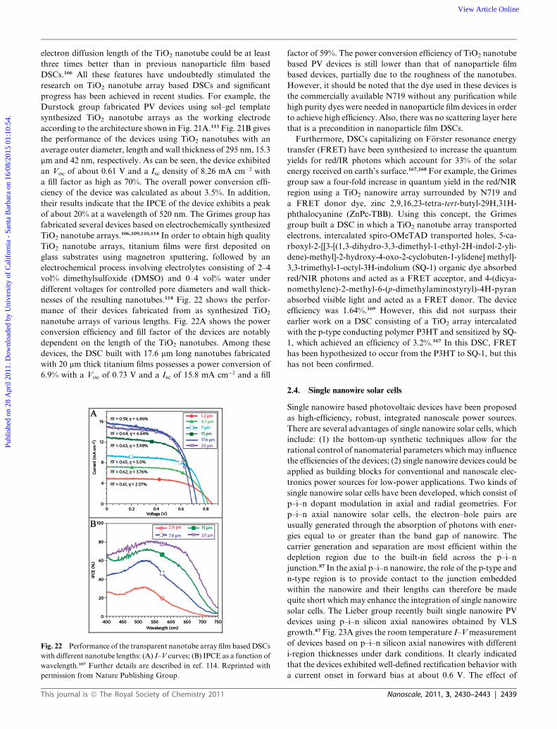
nesses of the resulting nanotubes.114 Fig. 22 shows the perfor-
mance of their devices fabricated from as synthesized TiO2
nanotube arrays of various lengths. Fig. 22A shows the power
conversion efficiency and fill factor of the devices are notably
dependent on the length of the TiO2 nanotubes. Among these
devices, the DSC built with 17.6 mm long nanotubes fabricated
with 20 mm thick titanium films possesses a power conversion of
6.9% with a Voc of 0.73 V and a Isc of 15.8 mA cm�2 and a fill
Fig. 22 Performance of the transparent nanotube array film basedDSCs
with different nanotube lengths: (A) I–V curves; (B) IPCE as a function of
wavelength.107 Further details are described in ref. 114. Reprinted with
permission from Nature Publishing Group.
This journal is ª The Royal Society of Chemistry 2011
factor of 59%. The power conversion efficiency of TiO2 nanotube
based PV devices is still lower than that of nanoparticle film
based devices, partially due to the roughness of the nanotubes.
However, it should be noted that the dye used in these devices is
the commercially available N719 without any purification while
high purity dyes were needed in nanoparticle film devices in order
to achieve high efficiency. Also, there was no scattering layer here
that is a precondition in nanoparticle film DSCs.
Furthermore, DSCs capitalizing on F€orster resonance energy
transfer (FRET) have been synthesized to increase the quantum
yields for red/IR photons which account for 33% of the solar
energy received on earth’s surface.167,168 For example, the Grimes
group saw a four-fold increase in quantum yield in the red/NIR
region using a TiO2 nanowire array surrounded by N719 and
a FRET donor dye, zinc 2,9,16,23-tetra-tert-butyl-29H,31H-
phthalocyanine (ZnPc-TBB). Using this concept, the Grimes
group built a DSC in which a TiO2 nanotube array transported
electrons, intercalated spiro-OMeTAD transported holes, 5-ca-
rboxyl-2-[[3-[(1,3-dihydro-3,3-dimethyl-1-ethyl-2H-indol-2-yli-
dene)-methyl]-2-hydroxy-4-oxo-2-cyclobuten-1-ylidene] methyl]-
3,3-trimethyl-1-octyl-3H-indolium (SQ-1) organic dye absorbed
red/NIR photons and acted as a FRET acceptor, and 4-(dicya-
nomethylene)-2-methyl-6-(p-dimethylaminostyryl)-4H-pyran
absorbed visible light and acted as a FRET donor. The device
efficiency was 1.64%.169 However, this did not surpass their
earlier work on a DSC consisting of a TiO2 array intercalated
with the p-type conducting polymer P3HT and sensitized by SQ-
1, which achieved an efficiency of 3.2%.167 In this DSC, FRET
has been hypothesized to occur from the P3HT to SQ-1, but this
has not been confirmed.
2.4. Single nanowire solar cells
Single nanowire based photovoltaic devices have been proposed
as high-efficiency, robust, integrated nanoscale power sources.
There are several advantages of single nanowire solar cells, which
include: (1) the bottom-up synthetic techniques allow for the
rational control of nanomaterial parameters which may influence
the efficiencies of the devices; (2) single nanowire devices could be
applied as building blocks for conventional and nanoscale elec-
tronics power sources for low-power applications. Two kinds of
single nanowire solar cells have been developed, which consist of
p–i–n dopant modulation in axial and radial geometries. For
p–i–n axial nanowire solar cells, the electron–hole pairs are
usually generated through the absorption of photons with ener-
gies equal to or greater than the band gap of nanowire. The
carrier generation and separation are most efficient within the
depletion region due to the built-in field across the p–i–n
junction.87 In the axial p–i–n nanowire, the role of the p-type and
n-type region is to provide contact to the junction embedded
within the nanowire and their lengths can therefore be made
quite short which may enhance the integration of single nanowire
solar cells. The Lieber group recently built single nanowire PV
devices using p–i–n silicon axial nanowires obtained by VLS
growth.87 Fig. 23A gives the room temperature I–Vmeasurement
of devices based on p–i–n silicon axial nanowires with different
i-region thicknesses under dark conditions. It clearly indicated
that the devices exhibited well-defined rectification behavior with
a current onset in forward bias at about 0.6 V. The effect of
Nanoscale, 2011, 3, 2430–2443 | 2439

Fig. 23 (A) Dark I–V characteristics of p–i–n silicon single nanowire
with different i-region lengths (red, green, and black curves correspond to
i-segment lengths of 0, 2, and 4 mm, respectively). (The inset is the SEM
image of single nanowire device with i-length of 2 mm; the scale bar is
4 mm.) (B) Light I–V curves for the i-length of 0, 2, and 4 mm devices in
panel (A); the illumination intensity was 100 mW cm�2, AM1.5G.
Further details are described in ref. 87. Reprinted with permission from
American Chemical Society.
Fig. 24 Typical SEM images of the radial modulated single nanowire
photovoltaic device, the scale bars are 100 nm (left), 200 nm (middle) and
1.5 mm (right). Further details are described in ref. 82. Reprinted with
permission from Nature Publishing Group.
Fig. 25 (A–C) characterization of the p–i–n coaxial silicon nanowire
photovoltaic devices: (A) I–V curves under dark and light; (B) Light I–V
curves for two different n-shell contact locations, the inset is the optical
microscopy image of the device, scale bar: 5 mm. (C) Isc and Jsc of the
devices as a function of device lengths; (D) light I–V curves of two silicon
coaxial nanowire devices individually and connected in series and in
parallel. Further details are described in ref. 82. Reprinted with permis-
sion from Nature Publishing Group.
Publ
ishe
d on
28
Apr
il 20
11. D
ownl
oade
d by
Uni
vers
ity o
f C
alif
orni
a -
Sant
a B
arba
ra o
n 16
/08/
2015
01:
10:5
4.
View Article Online
i-region thickness on photovoltaic properties of the devices is
shown in Fig. 23B, which indicates that the Voc and Isc for the
devices with an i-region of 0, 2 and 4 mm were 0.12 V and 3.5 pA,
0.24 V and 14 pA, and 0.29 V and 31.1 pA, respectively, and
clearly illustrates that a systematic improvement in both Voc and
Isc was achieved along with the increasing i-region lengths. The
fill factor for the 4 mm i-region device is about 51% and could
yield a maximum power output per nanowire of 4.6 pW The
power conversion efficiency was estimated to be about 0.5%
based on a device with projected active area of 4 mm i-region
under AM1.5 illumination, which is close to the value reported
for single Si nanowire with metal–semiconductor junctions.170
Compared to the p–i–n axially modulated single nanowire
cells, the p–i–n radially modulated nanowire photovoltaic
devices may possess different benefits. For example, in radially
modulated single nanowire devices, the carrier separation could
be reached in the radial direction versus the longer axial direction
and the carrier collection distance should be much smaller or
comparable to the minority carrier diffusion length, so the
photogenerated carriers should reach the p–i–n junction with
higher efficiency. The Lieber group exploited effective routes for
the fabrication of radially modulated single nanowire solar
cells.82 In order to obtain the devices, the core/shell silicon
nanowires were selectively etched using KOH solution to expose
the p-core in a lithographically defined region, followed by the
deposition of metal contacts on the p-core and the n-shell.
Typical SEM images of the architectures can be seen in Fig. 24.
The performance of the p–i–n coaxial silicon nanowire devices
under AM1.5G illumination is shown in Fig. 25A–C. The
representative I–V curves of the best device shown in Fig. 25A
indicate a Voc of 0.26 V and an Isc of 0.503 nA with a fill factor of
55.0%. In addition, the power output for the coaxial silicon single
nanowire device reaches 72 pW with excellent stability. The I–V
results recorded using contacts to different positions from the
p-core contact (Fig. 25B) exhibited the same photovoltaic
response, thus indicating that the n-shell is equipotential with
radial carrier separation occurring uniformly along the entire
length of the core/shell silicon nanowire device. The Lieber group
also studied the effect of nanowire length on device performance,
as shown in Fig. 25C. As can be seen, the Isc of the devices
2440 | Nanoscale, 2011, 3, 2430–2443
exhibits a linearly increasing behavior with increasing nanowire
lengths while Voc is essentially independent of the nanowire
length. The linear behavior of the Isc with nanowire lengths
suggests that the photogenerated carriers are collected uniformly
along the length of these radial nanostructures, and that scat-
tering of light by the metal contacts does not have a major
contribution on the observed photocurrent. The overall power
conversion efficiency reaches 3.4%, which is much higher
compared with that of axially modulated silicon nanowire solar
cells. In addition, they studied the performance of the inter-
connected devices in series and in parallel, as shown in Fig. 25D.
Notably, the Voc and Isc of the interconnected devices are
approximately the sum of the two, which may provide an effec-
tive route to enhanced power output for future scalable
applications.
Besides Si nanowire based devices, III–V related coaxial single
nanowire photovoltaic devices have also been successfully
fabricated and their performance was systematically studied by
Dong et al. The Voc and Isc of the device ranged from 1.0–2.0 V
and 0.39–0.059 mA cm�2 with varying composition of the
nanowire and the maximum power conversion efficiency reached
about 0.19%.83
This journal is ª The Royal Society of Chemistry 2011

Publ
ishe
d on
28
Apr
il 20
11. D
ownl
oade
d by
Uni
vers
ity o
f C
alif
orni
a -
Sant
a B
arba
ra o
n 16
/08/
2015
01:
10:5
4.
View Article Online
3. Conclusion
We have discussed the state of the art of various nanostructure
based solar cell devices, together with a brief introduction of
nanostructure synthesis and nanocrystal assembly methods. The
nanostructure based solar cells have achieved exciting progress
due to both the great advancement of nanostructure synthesis
methods and device fabrication techniques. In addition, there
have been many reports related to the optimization of device
performance by post-treatment. However, the most important
challenge regarding nanostructured solar cells is how to enhance
the conversion efficiency of the devices in order to reach the goal
of scalable applications and promising market foreground. It is
true that there are still difficulties in the development of nano-
structure based solar cells, particularly on how to take the full
advantage of the unique electrical and optical properties of the
nanostructures. Currently there are many studies on how to
improve the device efficiency by converting the nanostructured
film into microstructures using high temperature thermal
annealing or sintering. Such an approach, in our opinion, has no
obvious benefit because of the similar energy consumption
during device fabrication yet the PV devices fabricated in such
a way typically have much lower performance comparing to the
traditional thin film devices.
Acknowledgements
Yue Wu thanks the DuPont Young Faculty Award and the new
faculty start-up funding from Purdue University. Daxin Liang
thanks the fellowship support from the Chinese Scholar Council.
References
1 J. Zhao, A. Wang, M. Green and F. Ferrazza, Appl. Phys. Lett.,1998, 73, 1991.
2 W. Shockley and H. Queisser, J. Appl. Phys., 1961, 32, 510.3 X. Wu, J. C. Keane, R. G. Dhere, C. DeHart, D. S. Albin, A. Duda,T. A. Gessert, S. Asher, D. H. LKevi and P. Sheldon, Proceedings ofthe 17th European Photovoltaic Solar Energy Conference, 2001,p. 995.
4 U. Rau andH.W. Schock,Appl. Phys. A:Mater. Sci. Process., 1999,69, 131.
5 L. Tsakalakos, Mater. Sci. Eng., R, 2008, 62, 175.6 M. A. Green, K. Emery, D. L. King, S. Igari and W. Warta, Prog.Photovoltaics, 2001, 9, 287.
7 C. Wadia, A. P. Alivisatos and D. M. Kammen, Environ. Sci.Technol., 2009, 43, 2072.
8 H. W. Hillhouse and M. C. Beard, Curr. Opin. Colloid Interface Sci.,2009, 14, 245.
9 E. H. Sargent, Nat. Photonics, 2009, 3, 325.10 E. H. Sargent, Adv. Mater., 2008, 20, 3958.11 C. B. Murray, D. J. Norris and M. G. Bawendi, J. Am. Chem. Soc.,
1993, 115, 8706.12 Z. A. Peng and X. G. Peng, J. Am. Chem. Soc., 2001, 123, 183.13 X. G. Peng, L. Manna, W. D. Yang, J. Wickham, E. Scher,
A. Kadavanich and A. P. Alivisatos, Nature, 2000, 404, 59.14 W. Huynh, J. Dittmer and A. Alivisatos, Science, 2002, 295, 2425.15 L. Tsakalakos, Mater. Sci. Eng., R, 2008, 62, 175.16 S. Kumar and G. D. Scholes, Microchim. Acta, 2008, 160, 315.17 L.-s. Li, J. Hu, W. Yang and A. P. Alivisatos, Nano Lett., 2001, 1,
349.18 I. Gur, N. Fromer, M. Geier and A. Alivisatos, Science, 2005, 310,
462.19 L. Carbone, S. Kudera, E. Carlino, W. J. Parak, C. Giannini,
R. Cingolani and L. Manna, J. Am. Chem. Soc., 2006, 128, 748.20 W. W. Yu, Y. A. Wang and X. G. Peng, Chem. Mater., 2003, 15,
4300.
This journal is ª The Royal Society of Chemistry 2011
21 A. Fiore, R. Mastria, M. G. Lupo, G. Lanzani, C. Giannini,E. Carlino, G. Morello, M. De Giorgi, Y. Li, R. Cingolani andL. Manna, J. Am. Chem. Soc., 2009, 131, 2274.
22 L. Manna, D. J. Milliron, A. Meisel, E. C. Scher andA. P. Alivisatos, Nat. Mater., 2003, 2, 382.
23 B. Li, Y. Xie, J. X. Huang and Y. T. Qian, Adv. Mater., 1999, 11,1456.
24 Y. Jiang, Y. Wu, X. Mo, W. C. Yu, Y. Xie and Y. T. Qian, Inorg.Chem., 2000, 39, 2964.
25 Y. Jiang, Y. Qu, S. W. Yuan, B. Xie, S. Y. Zhang and Y. T. Qian, J.Mater. Res., 2001, 16, 2805.
26 Q. Li, Y. Ding, X. M. Liu and Y. T. Qian, Mater. Res. Bull., 2001,36, 2649.
27 J. P. Xiao, Y. Xie, R. Tang and Y. T. Qian, J. Solid State Chem.,2001, 161, 179.
28 J. P. Xiao, Y. Xie, Y. J. Xiong, R. Tang and Y. T. Qian, J. Mater.Chem., 2001, 11, 1417.
29 H. Grisaru, O. Palchik, A. Gedanken, V. Palchik, M. A. Slifkin andA. M. Weiss, Inorg. Chem., 2003, 42, 7148.
30 S.-H. Choi, E.-G. Kim and T. Hyeon, J. Am. Chem. Soc., 2006, 128,2520.
31 Q. Guo, S. J. Kim, M. Kar, W. N. Shafarman, R. W. Birkmire,E. A. Stach, R. Agrawal and H. W. Hillhouse, Nano Lett., 2008, 8,2982.
32 Q. Guo, G. M. Ford, H. W. Hillhouse and R. Agrawal, Nano Lett.,2009, 9, 3060.
33 Q. J. Guo, H. W. Hillhouse and R. Agrawal, J. Am. Chem. Soc.,2009, 131, 11672.
34 M. G. Panthani, V. Akhavan, B. Goodfellow, J. P. Schmidtke,L. Dunn, A. Dodabalapur, P. F. Barbara and B. A. Korgel, J.Am. Chem. Soc., 2008, 130, 16770.
35 B. Koo, R. N. Patel and B. A. Korgel, Chem. Mater., 2009, 21,1962.
36 C. Steinhagen,M. G. Panthani, V. Akhavan, B. Goodfellow, B. Kooand B. A. Korgel, J. Am. Chem. Soc., 2009, 131, 12554.
37 B. Koo, R. N. Patel and B. A. Korgel, J. Am. Chem. Soc., 2009, 131,3134.
38 A. Rothwarf and A. M. Barnett, IEEE Trans. Electron Devices,1977, 24, 381.
39 K. W. B€oer, J. Cryst. Growth, 1982, 59, 111.40 W. D. Gill and R. H. Bube, J. Appl. Phys., 1970, 41, 3731.41 A. L. Fahrenbr and R. H. Bube, J. Appl. Phys., 1974, 45, 1264.42 F. Pfisterer, Thin Solid Films, 2003, 431, 470.43 A. Rothwarf, Sol. Cells, 1980, 2, 115.44 A. E. Saunders, A. Ghezelbash, D. M. Smilgies, M. B. Sigman and
B. A. Korgel, Nano Lett., 2006, 6, 2959.45 T. H. Larsen, M. Sigman, A. Ghezelbash, R. C. Doty and
B. A. Korgel, J. Am. Chem. Soc., 2003, 125, 5638.46 M. B. Sigman, A. Ghezelbash, T. Hanrath, A. E. Saunders, F. Lee
and B. A. Korgel, J. Am. Chem. Soc., 2003, 125, 16050.47 S. Li, H. Z.Wang,W.W. Xu, H. L. Si, X. J. Tao, S. Y. Lou, Z. L. Du
and L. S. Li, J. Colloid Interface Sci., 2009, 330, 483.48 C. J. Brinker and G. W. Scherer, AcademicPress, Boston, 1990.49 J. Park, J. Joo, S. G. Kwon, Y. Jang and T. Hyeon, Angew. Chem.,
Int. Ed., 2007, 46, 4630.50 N. Pinna and M. Niederberger, Angew. Chem., Int. Ed., 2008, 47,
5292.51 Y.-w. Jun, J.-s. Choi and J. Cheon, Angew. Chem., Int. Ed., 2006, 45,
3414.52 H. Kominami, J. Kato, Y. Takada, Y. Doushi, B. Ohtani,
S. Nishimoto, M. Inoue, T. Inui and Y. Kera, Catal. Lett., 1997,46, 235.
53 C. Wang, Z. Deng and Y. D. Li, Inorg. Chem., 2001, 40, 5210.54 M. Niederberger, M. H. Bartl and G. D. Stucky, Chem. Mater.,
2002, 14, 4364.55 J. Wang, J. Polleux, J. Lim and B. Dunn, J. Phys. Chem. C, 2007,
111, 14925.56 G. Garnweitner, M. Antonietti and M. Niederberger, Chem.
Commun., 2005, 397.57 G. Li, L. Li, J. Boerio-Goates and B. F. Woodfield, J. Am. Chem.
Soc., 2005, 127, 8659.58 Z. Zhong, T.-P. Ang, J. Luo, H.-C. Gan and A. Gedanken, Chem.
Mater., 2005, 17, 6814.59 S. C. Goel, M. Y. Chiang, P. C. Gibbons and W. E. Buhro, Mater.
Res. Soc. Symp. Proc., 1992, 271, 3.
Nanoscale, 2011, 3, 2430–2443 | 2441

Publ
ishe
d on
28
Apr
il 20
11. D
ownl
oade
d by
Uni
vers
ity o
f C
alif
orni
a -
Sant
a B
arba
ra o
n 16
/08/
2015
01:
10:5
4.
View Article Online
60 D. Koziej, F. Fischer, N. Kranzlin, W. R. Caseri andM. Niederberger, ACS Appl. Mater. Interfaces, 2009, 1, 1097.
61 I. Bilecka, I. Djerdj and M. Niederberger, Chem. Commun., 2008,886.
62 N. Pinna, G. Garnweitner, M. Antonietti and M. Niederberger, J.Am. Chem. Soc., 2005, 127, 5608.
63 G. Clavel, M. G. Willinger, D. Zitoun and N. Pinna, Adv. Funct.Mater., 2007, 17, 3159.
64 M. M. Demir, R. Munoz-Espi, I. Lieberwirth and G. Wegner, J.Mater. Chem., 2006, 16, 2940.
65 S. K. N. Ayudhya, P. Tonto, O. Mekasuwandumrong,V. Pavarajarn and P. Praserthdam, Cryst. Growth Des., 2006, 6,2446.
66 L. S. Panchakarla, A. Govindaraj and C. N. R. Rao, J. Cluster Sci.,2007, 18, 660.
67 J. Buha, I. Djerdj and M. Niederberger, Cryst. Growth Des., 2007, 7,113.
68 X. Wang, J. Zhuang, Q. Peng and Y. D. Li, Nature, 2005, 437, 121.69 G. Q. Zhang, W. Wang, Q. X. Yu and X. G. Li, Chem. Mater., 2009,
21, 969.70 G. Zhang, X. Lu, W.Wang and X. Li, Chem. Mater., 2007, 19, 5207.71 L. Li, H. F. Qian and J. C. Ren, Chem. Commun., 2005, 528.72 Z. Y. Gu, L. Zou, Z. Fang, W. H. Zhu and X. H. Zhong,
Nanotechnology, 2008, 19, 135604.73 L. Zou, Z. Y. Gu, N. Zhang, Y. L. Zhang, Z. Fang, W. H. Zhu and
X. H. Zhong, J. Mater. Chem., 2008, 18, 2807.74 M. N. Kalasad, A. K. Rabinal and B. G. Mulimani, Langmuir, 2009,
25, 12729.75 W. C. Law, K. T. Yong, I. Roy, H. Ding, R. Hu, W. W. Zhao and
P. N. Prasad, Small, 2009, 5, 1302.76 B. Tian, T. J. Kempa andC.M. Lieber,Chem. Soc. Rev., 2009, 38, 16.77 M. Yazawa,M. Koguchi, A.Muto,M. Ozawa andK. Hiruma,Appl.
Phys. Lett., 1992, 61, 2051.78 J. Westwater, D. P. Gosain, S. Tomiya, S. Usui and H. Ruda, J. Vac.
Sci. Technol., B: Microelectron. Nanometer Struct.–Process., Meas.,Phenom., 1997, 15, 554.
79 A. M. Morales and C. M. Lieber, Science, 1998, 279, 208.80 Y.Wu, Y. Cui, L. Huynh, C. J. Barrelet, D. C. Bell and C.M. Lieber,
Nano Lett., 2004, 4, 433.81 G. Zheng, W. Lu, S. Jin and C. M. Lieber, Adv. Mater., 2004, 16,
1890.82 B. Z. Tian, X. L. Zheng, T. J. Kempa, Y. Fang, N. F. Yu, G. H. Yu,
J. L. Huang and C. M. Lieber, Nature, 2007, 449, 885.83 Y. J. Dong, B. Z. Tian, T. J. Kempa and C. M. Lieber, Nano Lett.,
2009, 9, 2183.84 F. Qian, S. Gradecak, Y. Li, C. Y. Wen and C. M. Lieber, Nano
Lett., 2005, 5, 2287.85 Y. Li, J. Xiang, F. Qian, S. Gradecak, Y. Wu, H. Yan, D. A. Blom
and C. M. Lieber, Nano Lett., 2006, 6, 1468.86 F. Qian and C. M. Lieber, 2007 Ieee Leos Annual Meeting
Conference Proceedings, 2007, vols 1 and 2, 831.87 T. J. Kempa, B. Z. Tian, D. R. Kim, J. S. Hu, X. L. Zheng and
C. M. Lieber, Nano Lett., 2008, 8, 3456.88 K. Q. Peng, Y. J. Yan, S. P. Gao and J. Zhu, Adv. Mater., 2002, 14,
1164.89 K. Q. Peng, J. J. Hu, Y. J. Yan, Y. Wu, H. Fang, Y. Xu, S. T. Lee
and J. Zhu, Adv. Funct. Mater., 2006, 16, 387.90 K. Q. Peng, Z. P. Huang and J. Zhu, Adv. Mater., 2004, 16, 73.91 K. Q. Peng, Y. Xu, Y. Wu, Y. J. Yan, S. T. Lee and J. Zhu, Small,
2005, 1, 1062.92 E. C. Garnett and P. D. Yang, J. Am. Chem. Soc., 2008, 130, 9224.93 L. Greene, M. Law, D. H. Tan, J. Goldberger and P. D. Yang,Nano
Lett., 2005, 5, 1231.94 B. D. Yuhas and P. D. Yang, J. Am. Chem. Soc., 2009, 131, 3756.95 L. E. Greene, M. Law, B. D. Yuhas and P. D. Yang, J. Phys. Chem.
C, 2007, 111, 18451.96 P. Hoyer, Langmuir, 1996, 12, 1411.97 B. B. Lakshmi, P. K. Dorhout and C. R. Martin, Chem. Mater.,
1997, 9, 9.98 H. Imai, Y. Takei, K. Shimizu, M. Matsuda and H. Hirashima, J.
Mater. Chem., 1999, 9, 9.99 A. Michailowski, D. AlMawlwai, G. S. Cheng and M. Moskovits,
Chem. Phys. Lett., 2001, 349, 1.100 J. H. Jung, H. Kobayashi, K. J. C. van Bommel, S. Shinkai and
T. Shimizu, Chem. Mater., 2002, 14, 1445.
2442 | Nanoscale, 2011, 3, 2430–2443
101 S. Kobayashi, N. Hamasaki, M. Suzuki, M. Kimura, H. Shirai andK. Hanabusa, J. Am. Chem. Soc., 2002, 124, 6550.
102 T. Kasuga, M. Hiramatsu, A. Hoson, T. Sekino and K. Niihara,Langmuir, 1998, 14, 3160.
103 Q. Chen, W. Z. Zhou, G. H. Du and L. H. Peng, Adv. Mater., 2002,14, 1208.
104 B. D. Yao, Y. F. Chan, X. Y. Zhang, W. F. Zhang, Z. Y. Yang andN. Wang, Appl. Phys. Lett., 2003, 82, 281.
105 D. Gong, C. A. Grimes, O. K. Varghese, W. Hu, R. S. Singh,Z. Chen and E. C. Dickey, J. Mater. Res., 2001, 16, 3331.
106 C. A. Grimes, J. Mater. Chem., 2007, 17, 1451.107 N. K. Allam, K. Shankar and C. A. Grimes, Adv. Mater., 2008, 20,
3942.108 W. Chanmanee, A. Watcharenwong, C. R. Chenthamarakshan,
P. Kajitvichyanukul, N. R. de Tacconi and K. Rajeshwar, J. Am.Chem. Soc., 2008, 130, 965.
109 X. J. Feng, K. Shankar, O. K. Varghese, M. Paulose, T. J. Latempaand C. A. Grimes, Nano Lett., 2008, 8, 3781.
110 K. Shankar, J. Bandara, M. Paulose, H. Wietasch, O. K. Varghese,G. K. Mor, T. J. LaTempa, M. Thelakkat and C. A. Grimes, NanoLett., 2008, 8, 1654.
111 Y. Yang, X. H. Wang and L. T. Li, J. Am. Ceram. Soc., 2008, 91,3086.
112 C. C. Chen, W. D. Jehng, L. L. Li and E. W. G. Diau, J.Electrochem. Soc., 2009, 156, C304.
113 T. S. Kang, A. P. Smith, B. E. Taylor and M. F. Durstock, NanoLett., 2009, 9, 601.
114 O. K. Varghese, M. Paulose and C. A. Grimes, Nat. Nanotechnol.,2009, 4, 592.
115 C. B. Murray, C. R. Kagan and M. G. Bawendi, Science, 1995, 270,1335.
116 C. P. Collier, T. Vossmeyer and J. R. Heath, Annu. Rev. Phys.Chem., 1998, 49, 371.
117 M. P. Pileni, J. Phys. Chem. B, 2001, 105, 3358.118 A. Wei, Chem. Commun., 2006, 1581.119 A. R. Tao, J. X. Huang and P. D. Yang, Acc. Chem. Res., 2008, 41,
1662.120 J. M. Luther, M. Law, M. C. Beard, Q. Song, M. O. Reese,
R. J. Ellingson and A. J. Nozik, Nano Lett., 2008, 8, 3488.121 J. Luther, M. Law, Q. Song, C. Perkins, M. Beard and A. Nozik,Acs
Nano, 2008, 2, 271.122 C. C. Kang, C. W. Lai, H. C. Peng, J. J. Shyue and P. T. Chou, Acs
Nano, 2008, 2, 750.123 L. Carbone, C. Nobile, M. De Giorgi, F. D. Sala, G. Morello,
P. Pompa, M. Hytch, E. Snoeck, A. Fiore, I. R. Franchini,M. Nadasan, A. F. Silvestre, L. Chiodo, S. Kudera, R. Cingolani,R. Krahne and L. Manna, Nano Lett., 2007, 7, 2942.
124 S. Ahmed and K. M. Ryan, Nano Lett., 2007, 7, 2480.125 N. Zhao, T. P. Osedach, L. Y. Chang, S. M. Geyer, D. Wanger,
M. T. Binda, A. C. Arango, M. G. Bawendi and V. Bulovic, ACSNano, 2010, 4, 3743.
126 L. H. Zhang, Y. Jia, S. S. Wang, Z. Li, C. Y. Ji, J. Q. Wei,H. W. Zhu, K. L. Wang, D. H. Wu, E. Z. Shi, Y. Fang andA. Y. Cao, Nano Lett., 2010, 10, 3583.
127 J. M. Luther, J. B. Gao, M. T. Lloyd, O. E. Semonin, M. C. Beardand A. J. Nozik, Adv. Mater., 2010, 22, 3704.
128 I. Gur, N. A. Fromer, M. L. Geier and A. P. Alivisatos, Science,2005, 310, 462.
129 G. I. Koleilat, L. Levina, H. Shukla, S. H. Myrskog, S. Hinds,A.G.Pattantyus-AbrahamandE.H. Sargent,AcsNano, 2008,2, 833.
130 E. J. D. Klem, D. D. MacNeil, L. Levina and E. H. Sargent, Adv.Mater., 2008, 20, 3433.
131 I. E. Anderson, A. J. Breeze, J. D. Olson, L. Yang, Y. Sahoo andS. A. Carter, Appl. Phys. Lett., 2009, 94, 063101.
132 K. Johnston, A. Pattantyus-Abraham, J. Clifford, S. Myrskog,D. MacNeil, L. Levina and E. Sargent, Appl. Phys. Lett., 2008, 92,151115.
133 Y. Wu, C. Wadia, W. L. Ma, B. Sadtler and A. P. Alivisatos, NanoLett., 2008, 8, 2551.
134 W. Ma, J. M. Luther, H. M. Zheng, Y. Wu and A. P. Alivisatos,Nano Lett., 2009, 9, 1699.
135 J. P. Clifford, K. W. Johnston, L. Levina and E. H. Sargent, Appl.Phys. Lett., 2007, 91, 253117.
136 I. Repins, M. A. Contreras, B. Egaas, C. DeHart, J. Scharf,C. L. Perkins, B. To and R. Noufi,Prog. Photovoltaics, 2008, 16, 235.
This journal is ª The Royal Society of Chemistry 2011

Publ
ishe
d on
28
Apr
il 20
11. D
ownl
oade
d by
Uni
vers
ity o
f C
alif
orni
a -
Sant
a B
arba
ra o
n 16
/08/
2015
01:
10:5
4.
View Article Online
137 K. Palaniappan, J. W. Murphy, N. Khanam, J. Horvath,H. Alshareef, M. Quevedo-Lopez, M. C. Biewer, S. Y. Park,M. J. Kim, B. E. Gnade and M. C. Stefan, Macromolecules, 2009,42, 3845.
138 I. Gur, N. A. Fromer, C. P. Chen, A. G. Kanaras andA. P. Alivisatos, Nano Lett., 2007, 7, 409.
139 J. C. Lee, W. Lee, S. H. Han, T. G. Kim and Y. M. Sung,Electrochem. Commun., 2009, 11, 231.
140 H. C. Liao, S. Y. Chen and D. M. Liu, Macromolecules, 2009, 42,6558.
141 S. McDonald, G. Konstantatos, S. Zhang, P. Cyr, E. Klem,L. Levina and E. Sargent, Nat. Mater., 2005, 4, 138.
142 S. Gunes, K. P. Fritz, H. Neugebauer, N. S. Sariciftci, S. Kumar andG. D. Scholes, in European Conference on Hybrid Organic Solar Cells(ECHOS 06), Paris, France, 2006, p. 420.
143 D. Cui, J. Xu, T. Zhu, G. Paradee, S. Ashok and M. Gerhold, Appl.Phys. Lett., 2006, 88, 183111.
144 A. Maria, P. W. Cyr, E. J. D. Klern, L. Levina and E. H. Sargent,Appl. Phys. Lett., 2005, 87, 213112.
145 S. Zhang, P. W. Cyr, S. A. McDonald, G. Konstantatos andE. H. Sargent, Appl. Phys. Lett., 2005, 87, 233101.
146 C. Y. Liu, Z. C. Holman and U. R. Kortshagen, Nano Lett., 2009, 9,449.
147 L. E. Greene, M. Law, B. D. Yuhas and P. Yang, J. Phys. Chem. C,2007, 111, 18451.
148 R. Kniprath, J. P. Rabe, J. T. McLeskey, D. Y. Wang andS. Kirstein, Thin Solid Films, 2009, 518, 295.
149 C. Y. Kwong, W. C. H. Choy, A. B. Djurisic, P. C. Chui, W. Chengand W. K. Chan, Nanotechnology, 2004, 15, 1156.
150 T.W. Zeng, Y. Y. Lin, H.H. Lo, C.W. Chen, C. H. Chen, S. C. Liou,H. Y. Huang and W. F. Su, Nanotechnology, 2006, 17, 5387.
151 L. H. Slooff, M. M. Wienk and J. M. Kroon, Thin Solid Films, 2004,451–52, 634.
152 P. A. van Hal, M. M. Wienk, J. M. Kroon, W. J. H. Verhees,L. H. Slooff, W. J. H. van Gennip, P. Jonkheijm andR. A. J. Janssen, Adv. Mater., 2003, 15, 118.
This journal is ª The Royal Society of Chemistry 2011
153 A. C. Arango, L. R. Johnson, V. N. Bliznyuk, Z. Schlesinger,S. A. Carter and H. H. Horhold, Adv. Mater., 2000, 12, 1689.
154 L. J. A. Koster, W. J. van Strien, W. J. E. Beek and P. W. M. Blom,Adv. Funct. Mater., 2007, 17, 1297.
155 W. J. E. Beek, L. H. Slooff, M. M. Wienk, J. M. Kroon andR. A. J. Janssen, Adv. Funct. Mater., 2005, 15, 1703.
156 W. J. E. Beek, M. M. Wienk and R. A. J. Janssen, J. Mater. Chem.,2005, 15, 2985.
157 D. C. Olson, J. Piris, R. T. Collins, S. E. Shaheen and D. S. Ginley,Thin Solid Films, 2006, 496, 26.
158 P. Ravirajan, A. M. Peiro, M. K. Nazeeruddin, M. Graetzel,D. D. C. Bradley, J. R. Durrant and J. Nelson, J. Phys. Chem. B,2006, 110, 7635.
159 A. M. Peiro, P. Ravirajan, K. Govender, D. S. Boyle, P. O’Brien,D. D. C. Bradley, J. Nelson and J. R. Durrant, J. Mater. Chem.,2006, 16, 2088.
160 L. E. Greene, M. Law, D. H. Tan, M. Montano, J. Goldberger,G. Somorjai and P. D. Yang, Nano Lett., 2005, 5, 1231.
161 M. Gratzel, Nature, 2001, 414, 338.162 B. O’Regan and M. A. Gratzel, Nature, 1991, 353, 737.163 M. K. Nazeeruddin, F. De Angelis, S. Fantacci, A. Selloni,
G. Viscardi, P. Liska, S. Ito, B. Takeru and M. G. Gratzel, J. Am.Chem. Soc., 2005, 127, 16835.
164 C. A. Grimes, J. Mater. Chem., 2007, 17, 1451.165 K. Zhu, N. R. Neale, A. Miedaner and A. J. Frank, Nano Lett.,
2007, 7, 69.166 J. R. Jennings, A. Ghicov, L. M. Peter, P. Schmuki and
A. B. Walker, J. Am. Chem. Soc., 2008, 130, 13364.167 G. K. Mor, S. Kim, M. Paulose, O. K. Varghese, K. Shankar,
J. Basham and C. A. Grimes, Nano Lett., 2009, 9, 4250.168 G. K. Mor, J. Basham, M. Paulose, S. Kim, O. K. Varghese,
A. Vaish, S. Yoriya and C. A. Grimes, Nano Lett., 2010, 10, 2387.169 K. Shankar, X. Feng and C. A. Grimes, ACS Nano, 2009, 3, 788.170 M. D. Kelzenberg, D. B. Turner-Evans, B. M. Kayes, M. A. Filler,
M. C. Putnam, N. S. Lewis and H. A. Atwater, Nano Lett., 2008, 8,710.
Nanoscale, 2011, 3, 2430–2443 | 2443