Synchronous 8-Bit Up/Down Counters datasheet (Rev. C)
22
5 6 7 8 9 10 11 25 24 23 22 21 20 19 4 3 2 1 28 12 13 14 15 16 Q B Q C Q D NC Q E Q F Q G B C D NC E F G A S1 S0 RCO CLK ENT GND NC NC ENP Q V H H 17 18 27 26 NC – No internal connection CC S0 S1 A B C D E F G H ENT GND V CC ENP Q A Q B Q C Q D Q E Q F Q G Q H CLK RCO 1 2 3 4 5 6 7 8 9 10 11 12 24 23 22 21 20 19 18 17 16 15 14 13 SN54AS867, SN54AS869 . . . JT PACKAGE SN74ALS867A, SN74ALS869, SN74AS867, SN74AS869 . . . DW OR NT PACKAGE (TOP VIEW) SN54AS867, SN54AS869 . . . FK PACKAGE (TOP VIEW) A Q SN54AS867, SN54AS869 SN74ALS867A, SN74ALS869, SN74AS867, SN74AS869 SYNCHRONOUS 8-BIT UP/DOWN COUNTERS SDAS115C – DECEMBER 1982 – REVISED JANUARY 1995 Copyright 1995, Texas Instruments Incorporated 1 POST OFFICE BOX 655303 • DALLAS, TEXAS 75265 • Fully Programmable With Synchronous Counting and Loading • SN74ALS867A and ′AS867 Have Asynchronous Clear; SN74ALS869 and ′AS869 Have Synchronous Clear • Fully Independent Clock Circuit Simplifies Use • Ripple-Carry Output for n-Bit Cascading • Package Options Include Plastic Small-Outline (DW) Packages, Ceramic Chip Carriers (FK), and Standard Plastic (NT) and Ceramic (JT) 300-mil DIPs description These synchronous, presettable, 8-bit up/down counters feature internal-carry look-ahead circuitry for cascading in high-speed counting applications. Synchronous operation is provided by having all flip-flops clocked simultaneously so that the outputs change coincidentally with each other when so instructed by the count-enable (ENP , ENT ) inputs and internal gating. This mode of operation eliminates the output counting spikes normally associated with asynchronous (ripple- clock) counters. A buffered clock (CLK) input triggers the eight flip-flops on the rising (positive- going) edge of the clock waveform. These counters are fully programmable; they may be preset to any number between 0 and 255. The load-input circuitry allows parallel loading of the cascaded counters. Because loading is synchronous, selecting the load mode disables the counter and causes the outputs to agree with the data inputs after the next clock pulse. The carry look-ahead circuitry provides for cascading counters for n-bit synchronous applications without additional gating. Two count-enable (ENP and ENT ) inputs and a ripple-carry (RCO ) output are instrumental in accomplishing this function. Both ENP and ENT must be low to count. The direction of the count is determined by the levels of the select (S0, S1) inputs as shown in the function table. ENT is fed forward to enable RCO . RCO thus enabled produces a low-level pulse while the count is zero (all outputs low) counting down or 255 counting up (all outputs high). This low-level overflow-carry pulse can be used to enable successive cascaded stages. Transitions at ENP and ENT are allowed regardless of the level of CLK. All inputs are diode clamped to minimize transmission-line effects, thereby simplifying system design. These counters feature a fully independent clock circuit. With the exception of the asynchronous clear on the SN74ALS867A and ′AS867, changes at S0 and S1 that modify the operating mode have no effect on the Q outputs until clocking occurs. For the ′AS867 and ′AS869, any time ENP and/or ENT is taken high, RCO either goes or remains high. For the SN74ALS867A and SN74ALS869, any time ENT is taken high, RCO either goes or remains high. The function of the counter (whether enabled, disabled, loading, or counting) is dictated solely by the conditions meeting the stable setup and hold times. PRODUCTION DATA information is current as of publication date. Products conform to specifications per the terms of Texas Instruments standard warranty. Production processing does not necessarily include testing of all parameters.
-
Upload
khangminh22 -
Category
Documents
-
view
0 -
download
0
Transcript of Synchronous 8-Bit Up/Down Counters datasheet (Rev. C)

5
6
7
8
9
10
11
25
24
23
22
21
20
19
4 3 2 1 28
12 13 14 15 16
QBQCQDNCQEQFQG
BCD
NCEFG
A S1
S0
RC
O
CLK
EN
TG
ND
NC
NC
EN
PQV
H H
17 18
27 26
NC – No internal connection
CC
S0S1ABCDEFGH
ENTGND
VCCENPQAQBQCQDQEQFQGQHCLKRCO
1
2
3
4
5
6
7
8
9
10
11
12
24
23
22
21
20
19
18
17
16
15
14
13
SN54AS867, SN54AS869 . . . JT PACKAGESN74ALS867A, SN74ALS869, SN74AS867,
SN74AS869 . . . DW OR NT PACKAGE(TOP VIEW)
SN54AS867, SN54AS869 . . . FK PACKAGE(TOP VIEW)
AQ
SN54AS867, SN54AS869 SN74ALS867A, SN74ALS869, SN74AS867, SN74AS869
SYNCHRONOUS 8-BIT UP/DOWN COUNTERS SDAS115C – DECEMBER 1982 – REVISED JANUARY 1995
Copyright 1995, Texas Instruments Incorporated
1POST OFFICE BOX 655303 • DALLAS, TEXAS 75265
• Fully Programmable With SynchronousCounting and Loading
• SN74ALS867A and ′AS867 HaveAsynchronous Clear; SN74ALS869 and′AS869 Have Synchronous Clear
• Fully Independent Clock CircuitSimplifies Use
• Ripple-Carry Output for n-Bit Cascading
• Package Options Include PlasticSmall-Outline (DW) Packages, CeramicChip Carriers (FK), and Standard Plastic(NT) and Ceramic (JT) 300-mil DIPs
description
These synchronous, presettable, 8-bit up/downcounters feature internal-carry look-aheadcircuitry for cascading in high-speed countingapplications. Synchronous operation is providedby having all flip-flops clocked simultaneously sothat the outputs change coincidentally with eachother when so instructed by the count-enable(ENP, ENT) inputs and internal gating. This modeof operation eliminates the output counting spikesnormally associated with asynchronous (ripple-clock) counters. A buffered clock (CLK) inputtriggers the eight flip-flops on the rising (positive-going) edge of the clock waveform.
These counters are fully programmable; they maybe preset to any number between 0 and 255. Theload-input circuitry allows parallel loading of thecascaded counters. Because loading issynchronous, selecting the load mode disablesthe counter and causes the outputs to agree withthe data inputs after the next clock pulse.
The carry look-ahead circuitry provides for cascading counters for n-bit synchronous applications withoutadditional gating. Two count-enable (ENP and ENT) inputs and a ripple-carry (RCO) output are instrumentalin accomplishing this function. Both ENP and ENT must be low to count. The direction of the count is determinedby the levels of the select (S0, S1) inputs as shown in the function table. ENT is fed forward to enable RCO. RCOthus enabled produces a low-level pulse while the count is zero (all outputs low) counting down or 255 countingup (all outputs high). This low-level overflow-carry pulse can be used to enable successive cascaded stages.Transitions at ENP and ENT are allowed regardless of the level of CLK. All inputs are diode clamped to minimizetransmission-line effects, thereby simplifying system design.
These counters feature a fully independent clock circuit. With the exception of the asynchronous clear on theSN74ALS867A and ′AS867, changes at S0 and S1 that modify the operating mode have no effect on the Qoutputs until clocking occurs. For the ′AS867 and ′AS869, any time ENP and/or ENT is taken high, RCO eithergoes or remains high. For the SN74ALS867A and SN74ALS869, any time ENT is taken high, RCO either goesor remains high. The function of the counter (whether enabled, disabled, loading, or counting) is dictated solelyby the conditions meeting the stable setup and hold times.
PRODUCTION DATA information is current as of publication date.Products conform to specifications per the terms of Texas Instrumentsstandard warranty. Production processing does not necessarily includetesting of all parameters.

SN54AS867, SN54AS869SN74ALS867A, SN74ALS869, SN74AS867, SN74AS869SYNCHRONOUS 8-BIT UP/DOWN COUNTERSSDAS115C – DECEMBER 1982 – REVISED JANUARY 1995
2 POST OFFICE BOX 655303 • DALLAS, TEXAS 75265
description (continued)
The SN54AS867 and SN54AS869 are characterized for operation over the full military temperature range of–55°C to 125°C. The SN74ALS867A, SN74ALS869, SN74AS867, and SN74AS869 are characterized foroperation from 0°C to 70°C.
FUNCTION TABLE
S1 S0 FUNCTION
L L Clear
L H Count down
H L Load
H H Count up

SN54AS867, SN54AS869 SN74ALS867A, SN74ALS869, SN74AS867, SN74AS869
SYNCHRONOUS 8-BIT UP/DOWN COUNTERS SDAS115C – DECEMBER 1982 – REVISED JANUARY 1995
3POST OFFICE BOX 655303 • DALLAS, TEXAS 75265
logic symbols †
ENT
ENP
CTRDIV 256
2,6D3
A4
B5
C6
D
22
21
20
19
01
S0M
03
3,4CT=255
0R
7E
8F
9G
10H
18
17
16
15
12
S1
G411
G523
14CLK
131,4CT=0 RCO
QA
QB
QC
QD
QE
QF
QG
QH
SN74ALS867A
ENT
ENP
CTRDIV 256
2,6D3
A4
B5
C6
D
22
21
20
19
01
S0M
03
3,4CT=255
0,6R
7E
8F
9G
10H
18
17
16
15
12
S1
G411
G523
14CLK
131,4CT=0 RCO
QA
QB
QC
QD
QE
QF
QG
QH
SN74ALS869
C6/1,4,5– /3,4,5+
C6/1,4,5– /3,4,5+
† These symbols are in accordance with ANSI/IEEE Std 91-1984 and IEC Publication 617-12.Pin numbers shown are for the DW, JT, and NT packages.

SN54AS867, SN54AS869SN74ALS867A, SN74ALS869, SN74AS867, SN74AS869SYNCHRONOUS 8-BIT UP/DOWN COUNTERSSDAS115C – DECEMBER 1982 – REVISED JANUARY 1995
4 POST OFFICE BOX 655303 • DALLAS, TEXAS 75265
logic symbols (continued) †
ENT
ENP
CTRDIV 256
2,6D3
A4
B5
C6
D
22
21
20
19
01
S0M
03
3,4,5CT=255
0R
7E
8F
9G
10H
18
17
16
15
12
S1
G411
G523
14CLK
131,4,5CT=0 RCO
QA
QB
QC
QD
QE
QF
QG
QH
′AS867
ENT
ENP
CTRDIV 256
2,6D3
A4
B5
C6
D
22
21
20
19
01
S0M
03
3,4,5CT=255
0,6R
7E
8F
9G
10H
18
17
16
15
12
S1
G411
G523
14CLK
131,4,5CT=0 RCO
QA
QB
QC
QD
QE
QF
QG
QH
′AS869
C6/1,4,5– /3,4,5+
C6/1,4,5– /3,4,5+
† These symbols are in accordance with ANSI/IEEE Std 91-1984 and IEC Publication 617-12.Pin numbers shown are for the DW, JT, and NT packages.

SN54AS867, SN54AS869 SN74ALS867A, SN74ALS869, SN74AS867, SN74AS869
SYNCHRONOUS 8-BIT UP/DOWN COUNTERS SDAS115C – DECEMBER 1982 – REVISED JANUARY 1995
5POST OFFICE BOX 655303 • DALLAS, TEXAS 75265
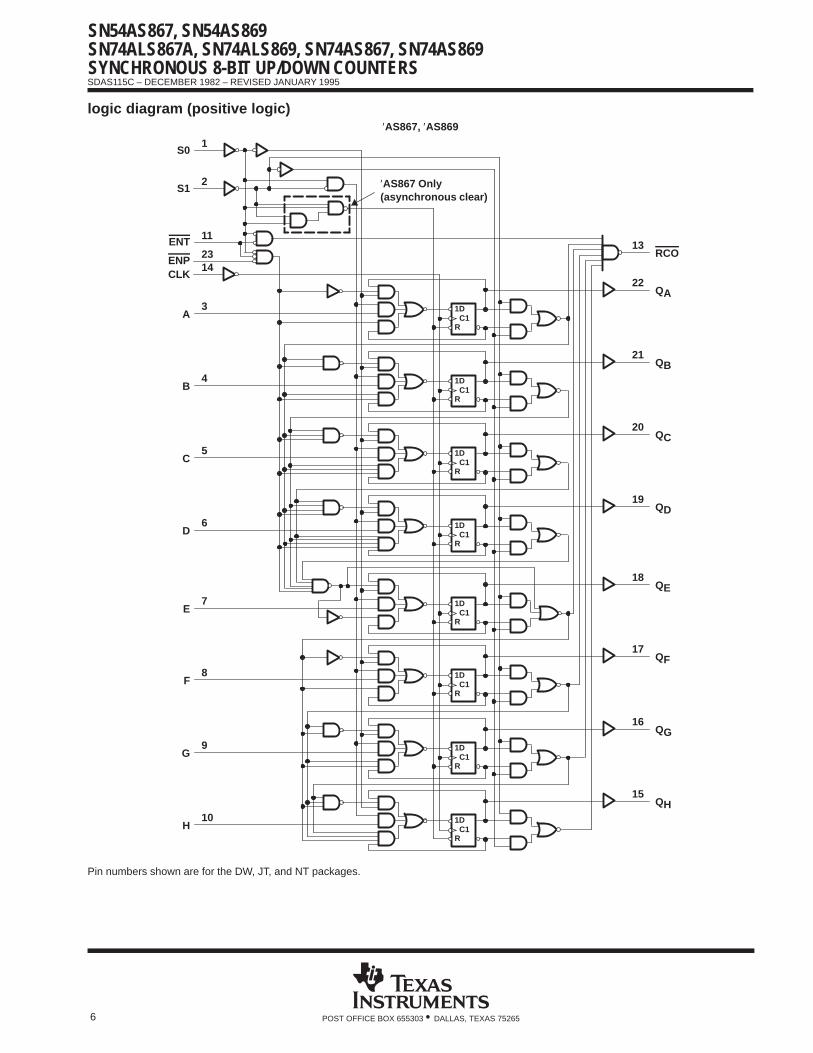
logic diagram (positive logic)
A
1D
RC1 22 QA
1412
23
3
B
1D
RC1 21 QB
4
C
1D
RC1 20 QC
5
D
1D
RC1 19 QD
6
E
1D
RC1 18 QE
7
ENP
S1S0
CLK
F
1D
RC1 17 QF
8
G
1D
RC1 16 QG
9
H
1D
RC1 15 QH
10
13RCO
ENT 11
SN74ALS867A Only(asynchronous clear)
SN74ALS867A, SN74ALS869
Pin numbers shown are for the DW, JT, and NT packages.
SN54AS867, SN54AS869SN74ALS867A, SN74ALS869, SN74AS867, SN74AS869SYNCHRONOUS 8-BIT UP/DOWN COUNTERSSDAS115C – DECEMBER 1982 – REVISED JANUARY 1995
6 POST OFFICE BOX 655303 • DALLAS, TEXAS 75265
logic diagram (positive logic)
1D
RC1A
ENP
S1
S0
CLK
ENT
QA
RCO
1
2
11
2314
3
13
22
1D
RC1B
QB4
21
1D
RC1C
QC5
20
1D
RC1D
QD6
19
1D
RC1E
QE7
18
′AS867 Only(asynchronous clear)
1D
RC1F
QF8
17
1D
RC1G
QG9
16
1D
RC1H
QH10
15
′AS867, ′AS869
Pin numbers shown are for the DW, JT, and NT packages.
SN54AS867, SN54AS869 SN74ALS867A, SN74ALS869, SN74AS867, SN74AS869
SYNCHRONOUS 8-BIT UP/DOWN COUNTERS SDAS115C – DECEMBER 1982 – REVISED JANUARY 1995
7POST OFFICE BOX 655303 • DALLAS, TEXAS 75265
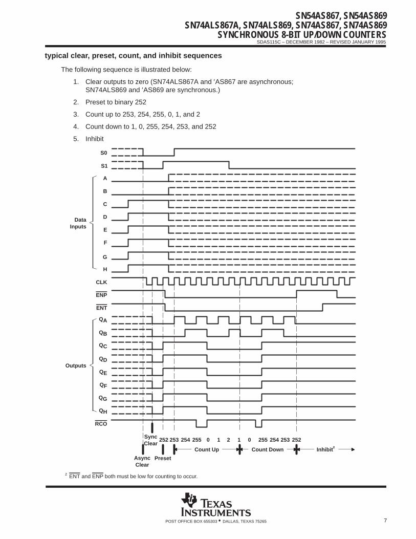
typical clear, preset, count, and inhibit sequences
The following sequence is illustrated below:
1. Clear outputs to zero (SN74ALS867A and ′AS867 are asynchronous;SN74ALS869 and ′AS869 are synchronous.)
2. Preset to binary 252
3. Count up to 253, 254, 255, 0, 1, and 2
4. Count down to 1, 0, 255, 254, 253, and 252
5. Inhibit
C
AsyncClear
D
E
F
CLK
ENP
ENT
QA
QB
QC
QD
RCO
DataInputs
OutputsQE
QF
QG
QH
Count Down
G
H
B
A
S1
S0
Preset
SyncClear
252 253 255254 255 254 253 2520 1 2 1 0
Count Up Inhibit †
† ENT and ENP both must be low for counting to occur.

SN54AS867, SN54AS869SN74ALS867A, SN74ALS869, SN74AS867, SN74AS869SYNCHRONOUS 8-BIT UP/DOWN COUNTERSSDAS115C – DECEMBER 1982 – REVISED JANUARY 1995
8 POST OFFICE BOX 655303 • DALLAS, TEXAS 75265
absolute maximum ratings over operating free-air temperature range (unless otherwise noted) †
Supply voltage, VCC 7 V. . . . . . . . . . . . . . . . . . . . . . . . . . . . . . . . . . . . . . . . . . . . . . . . . . . . . . . . . . . . . . . . . . . . . . . . Input voltage, VI 7 V. . . . . . . . . . . . . . . . . . . . . . . . . . . . . . . . . . . . . . . . . . . . . . . . . . . . . . . . . . . . . . . . . . . . . . . . . . . . Operating free-air temperature range, TA: SN74ALS867A 0°C to 70°C. . . . . . . . . . . . . . . . . . . . . . . . . . . . . . . . Storage temperature range –65°C to 150°C. . . . . . . . . . . . . . . . . . . . . . . . . . . . . . . . . . . . . . . . . . . . . . . . . . . . . . .
† Stresses beyond those listed under “absolute maximum ratings” may cause permanent damage to the device. These are stress ratings only, andfunctional operation of the device at these or any other conditions beyond those indicated under “recommended operating conditions” is notimplied. Exposure to absolute-maximum-rated conditions for extended periods may affect device reliability.
recommended operating conditions
SN74ALS867AUNIT
MIN NOM MAXUNIT
VCC Supply voltage 4.5 5 5.5 V
VIH High-level input voltage 2 V
VIL Low-level input voltage 0.8 V
IOH High-level output current –0.4 mA
IOL Low-level output current 8 mA
fclock Clock frequency 0 35 MHz
tw(clock) Pulse duration, CLK high or low 14 ns
tw(clear) Pulse duration of clear pulse, S0 and S1 low 10 ns
Data inputs A–H 10
ENP or ENT 15
tsu Setup time before CLK↑ S0 low and S1 high (load) 12 ns
S0 high and S1 low (count down) 12
S0 and S1 high (count up) 12
th Hold time after CLK↑S0 high after S1↑ or S1 high after S0↑ 3
nsth Hold time after CLK↑Data inputs A–H 0
ns
TA Operating free-air temperature 0 70 °C
electrical characteristics over recommended operating free-air temperature range (unlessotherwise noted)
PARAMETER TEST CONDITIONSSN74ALS867A
UNITPARAMETER TEST CONDITIONSMIN TYP‡ MAX
UNIT
VIK VCC = 4.5 V, II = –18 mA –1.2 V
VOH VCC = 4.5 V to 5.5 V, IOH = –0.4 mA VCC –2 V
VOL VCC = 4 5 VIOL = 4 mA 0.25 0.4
VVOL VCC = 4.5 VIOL = 8 mA 0.35 0.5
V
II VCC = 5.5 V, VI = 7 V 0.1 mA
IIH VCC = 5.5 V, VI = 2.7 V 20 µA
IIL VCC = 5.5 V, VI = 0.4 V –0.2 mA
IO§ VCC = 5.5 V, VO = 2.25 V –30 –112 mA
ICC VCC = 5.5 V 28 45 mA
‡ All typical values are at VCC = 5 V, TA = 25°C.§ The output conditions have been chosen to produce a current that closely approximates one half of the true short-circuit output current, IOS.
SN54AS867, SN54AS869 SN74ALS867A, SN74ALS869, SN74AS867, SN74AS869
SYNCHRONOUS 8-BIT UP/DOWN COUNTERS SDAS115C – DECEMBER 1982 – REVISED JANUARY 1995
9POST OFFICE BOX 655303 • DALLAS, TEXAS 75265
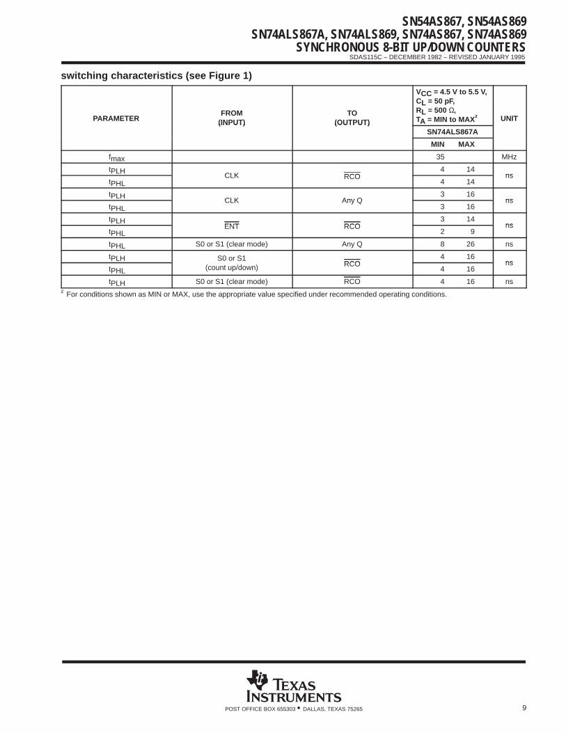
switching characteristics (see Figure 1)
PARAMETERFROM
(INPUT)TO
(OUTPUT)
VCC = 4.5 V to 5.5 V,CL = 50 pF,RL = 500 Ω,TA = MIN to MAX † UNIT(INPUT) (OUTPUT)
SN74ALS867A
MIN MAX
fmax 35 MHz
tPLHCLK RCO
4 14ns
tPHLCLK RCO
4 14ns
tPLHCLK Any Q
3 16ns
tPHLCLK Any Q
3 16ns
tPLHENT RCO
3 14ns
tPHLENT RCO
2 9ns
tPHL S0 or S1 (clear mode) Any Q 8 26 ns
tPLH S0 or S1RCO
4 16ns
tPHL (count up/down) RCO4 16
ns
tPLH S0 or S1 (clear mode) RCO 4 16 ns
† For conditions shown as MIN or MAX, use the appropriate value specified under recommended operating conditions.

SN54AS867, SN54AS869SN74ALS867A, SN74ALS869, SN74AS867, SN74AS869SYNCHRONOUS 8-BIT UP/DOWN COUNTERSSDAS115C – DECEMBER 1982 – REVISED JANUARY 1995
10 POST OFFICE BOX 655303 • DALLAS, TEXAS 75265
absolute maximum ratings over operating free-air temperature range (unless otherwise noted) †
Supply voltage, VCC 7 V. . . . . . . . . . . . . . . . . . . . . . . . . . . . . . . . . . . . . . . . . . . . . . . . . . . . . . . . . . . . . . . . . . . . . . . . Input voltage, VI 7 V. . . . . . . . . . . . . . . . . . . . . . . . . . . . . . . . . . . . . . . . . . . . . . . . . . . . . . . . . . . . . . . . . . . . . . . . . . . . Operating free-air temperature range, TA: SN74ALS869 0°C to 70°C. . . . . . . . . . . . . . . . . . . . . . . . . . . . . . . . . Storage temperature range –65°C to 150°C. . . . . . . . . . . . . . . . . . . . . . . . . . . . . . . . . . . . . . . . . . . . . . . . . . . . . . .
† Stresses beyond those listed under “absolute maximum ratings” may cause permanent damage to the device. These are stress ratings only, andfunctional operation of the device at these or any other conditions beyond those indicated under “recommended operating conditions” is notimplied. Exposure to absolute-maximum-rated conditions for extended periods may affect device reliability.
recommended operating conditions
SN74ALS869UNIT
MIN NOM MAXUNIT
VCC Supply voltage 4.5 5 5.5 V
VIH High-level input voltage 2 V
VIL Low-level input voltage 0.8 V
IOH High-level output current –0.4 mA
IOL Low-level output current 8 mA
fclock Clock frequency 0 35 MHz
tw(clock) Pulse duration, CLK high or low 14 ns
Data inputs A–H 10
ENP or ENT 15
t Set p time before CLK↑S0 and S1 low (clear) 13
nstsu Setup time before CLK↑S0 low and S1 high (load) 13
ns
S0 high and S1 low (count down) 13
S0 and S1 high (count up) 13
th Hold time after CLK↑S0 high after S1↑ or S1 high after S0↑ 3
nsth Hold time after CLK↑Data inputs A–H 0
ns
TA Operating free-air temperature 0 70 °C
electrical characteristics over recommended operating free-air temperature range (unlessotherwise noted)
PARAMETER TEST CONDITIONSSN74ALS869
UNITPARAMETER TEST CONDITIONSMIN TYP‡ MAX
UNIT
VIK VCC = 4.5 V, II = –18 mA –1.2 V
VOH VCC = 4.5 V to 5.5 V, IOH = –0.4 mA VCC –2 V
VOL VCC = 4 5 VIOL = 4 mA 0.25 0.4
VVOL VCC = 4.5 VIOL = 8 mA 0.35 0.5
V
II VCC = 5.5 V, VI = 7 V 0.1 mA
IIH VCC = 5.5 V, VI = 2.7 V 20 µA
IIL VCC = 5.5 V, VI = 0.4 V –0.2 mA
IO§ VCC = 5.5 V, VO = 2.25 V –30 –112 mA
ICC VCC = 5.5 V 28 45 mA
‡ All typical values are at VCC = 5 V, TA = 25°C.§ The output conditions have been chosen to produce a current that closely approximates one half of the true short-circuit output current, IOS.
SN54AS867, SN54AS869 SN74ALS867A, SN74ALS869, SN74AS867, SN74AS869
SYNCHRONOUS 8-BIT UP/DOWN COUNTERS SDAS115C – DECEMBER 1982 – REVISED JANUARY 1995
11POST OFFICE BOX 655303 • DALLAS, TEXAS 75265
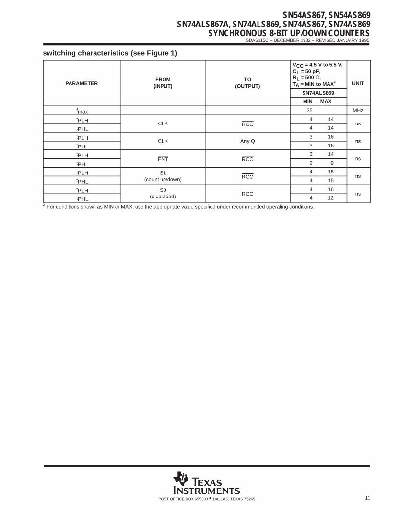
switching characteristics (see Figure 1)
PARAMETERFROM
(INPUT)TO
(OUTPUT)
VCC = 4.5 V to 5.5 V,CL = 50 pF,RL = 500 Ω,TA = MIN to MAX † UNIT(INPUT) (OUTPUT)
SN74ALS869
MIN MAX
fmax 35 MHz
tPLHCLK RCO
4 14ns
tPHLCLK RCO
4 14ns
tPLHCLK Any Q
3 16ns
tPHLCLK Any Q
3 16ns
tPLHENT RCO
3 14ns
tPHLENT RCO
2 9ns
tPLH S1RCO
4 15ns
tPHL (count up/down) RCO4 15
ns
tPLH S0RCO
4 16ns
tPHL (clear/load) RCO4 12
ns
† For conditions shown as MIN or MAX, use the appropriate value specified under recommended operating conditions.

SN54AS867, SN54AS869SN74ALS867A, SN74ALS869, SN74AS867, SN74AS869SYNCHRONOUS 8-BIT UP/DOWN COUNTERSSDAS115C – DECEMBER 1982 – REVISED JANUARY 1995
12 POST OFFICE BOX 655303 • DALLAS, TEXAS 75265
absolute maximum ratings over operating free-air temperature range (unless otherwise noted) †
Supply voltage, VCC 7 V. . . . . . . . . . . . . . . . . . . . . . . . . . . . . . . . . . . . . . . . . . . . . . . . . . . . . . . . . . . . . . . . . . . . . . . . Input voltage, VI 7 V. . . . . . . . . . . . . . . . . . . . . . . . . . . . . . . . . . . . . . . . . . . . . . . . . . . . . . . . . . . . . . . . . . . . . . . . . . . . Operating free-air temperature range, TA: SN54AS867 –55°C to 125°C. . . . . . . . . . . . . . . . . . . . . . . . . . . . . .
SN74AS867 0°C to 70°C. . . . . . . . . . . . . . . . . . . . . . . . . . . . . . . . . . Storage temperature range –65°C to 150°C. . . . . . . . . . . . . . . . . . . . . . . . . . . . . . . . . . . . . . . . . . . . . . . . . . . . . . .
† Stresses beyond those listed under “absolute maximum ratings” may cause permanent damage to the device. These are stress ratings only, andfunctional operation of the device at these or any other conditions beyond those indicated under “recommended operating conditions” is notimplied. Exposure to absolute-maximum-rated conditions for extended periods may affect device reliability.
recommended operating conditions
SN54AS867 SN74AS867UNIT
MIN NOM MAX MIN NOM MAXUNIT
VCC Supply voltage 4.5 5 5.5 4.5 5 5.5 V
VIH High-level input voltage 2 2 V
VIL Low-level input voltage 0.8 0.8 V
IOH High-level output current –2 –2 mA
IOL Low-level output current 20 20 mA
fclock* Clock frequency 0 40 0 50 MHz
tw(clock)* Pulse duration, CLK high or low 12.5 10 ns
tw(clear)* Pulse duration of clear pulse, S0 and S1 low 12.5 10 ns
Data inputs A–H 5 4
ENP or ENT 9 8
t * Set p time before CLK↑S0 low and S1 high (load) 11 10
nstsu* Setup time before CLK↑S0 and S1 low (clear) 11 10
ns
S0 high and S1 low (count down) 42 40
S0 and S1 high (count up) 42 40
th* Hold time after CLK↑ Data inputs A–H 0 0 ns
tskew*Skew time between S0 and S1(maximum to avoid inadvertent clear)
8 7 ns
TA Operating free-air temperature –55 125 0 70 °C
* On products compliant to MIL-STD-883, Class B, this parameter is based on characterization data but is not production tested.

SN54AS867, SN54AS869 SN74ALS867A, SN74ALS869, SN74AS867, SN74AS869
SYNCHRONOUS 8-BIT UP/DOWN COUNTERS SDAS115C – DECEMBER 1982 – REVISED JANUARY 1995
13POST OFFICE BOX 655303 • DALLAS, TEXAS 75265
electrical characteristics over recommended operating free-air temperature range (unlessotherwise noted)
PARAMETER TEST CONDITIONSSN54AS867 SN74AS867
UNITPARAMETER TEST CONDITIONSMIN TYP† MAX MIN TYP† MAX
UNIT
VIK VCC = 4.5 V, II = –18 mA –1.2 –1.2 V
VOH VCC = 4.5 V to 5.5 V, IOH = –2 mA VCC –2 VCC –2 V
VOLRCO
VCC = 4.5 V
IOL = 20 mA,VIL on ENT = 0.7 V
0.34 0.5VOL
Other outputsCC
IOL = 20 mA 0.34 0.5
II VCC = 5.5 V, VI = 7 V 0.1 0.1 mA
IIHENT
VCC = 5 5 V VI = 2 7 V40 40
µAIIHOther inputs
VCC = 5.5 V, VI = 2.7 V20 20
µA
IILENT
VCC = 5 5 V VI = 0 4 V–4 –4
mAIILOther inputs
VCC = 5.5 V, VI = 0.4 V–2 –2
mA
IO‡ VCC = 5.5 V, VO = 2.25 V –30 –112 –30 –112 mA
ICC VCC = 5.5 V 134 195 134 195 mA
† All typical values are at VCC = 5 V, TA = 25°C.‡ The output conditions have been chosen to produce a current that closely approximates one half of the true short-circuit output current, IOS.
switching characteristics (see Figure 1)
PARAMETERFROM
(INPUT)TO
(OUTPUT)
VCC = 4.5 V to 5.5 V,CL = 50 pF,RL = 500 Ω,TA = MIN to MAX § UNIT(INPUT) (OUTPUT)
SN54AS867 SN74AS867
MIN MAX MIN MAX
fmax* 40 50 MHz
tPLHCLK RCO
5 31 5 22ns
tPHLCLK RCO
6 19 6 16ns
tPLHCLK Any Q
3 12 3 11ns
tPHLCLK Any Q
4 16 4 15ns
tPLHENT RCO
3 19 3 10ns
tPHLENT RCO
5 21 5 17ns
tPLHENP RCO
5 16 5 14ns
tPHLENP RCO
5 21 5 17ns
tPHL Clear (S0 or S1 low) Any Q 7 23 7 21 ns
* On products compliant to MIL-STD-883, Class B, this parameter is based on characterization data but is not production tested.§ For conditions shown as MIN or MAX, use the appropriate value specified under recommended operating conditions.

SN54AS867, SN54AS869SN74ALS867A, SN74ALS869, SN74AS867, SN74AS869SYNCHRONOUS 8-BIT UP/DOWN COUNTERSSDAS115C – DECEMBER 1982 – REVISED JANUARY 1995
14 POST OFFICE BOX 655303 • DALLAS, TEXAS 75265
absolute maximum ratings over operating free-air temperature range (unless otherwise noted) †
Supply voltage, VCC 7 V. . . . . . . . . . . . . . . . . . . . . . . . . . . . . . . . . . . . . . . . . . . . . . . . . . . . . . . . . . . . . . . . . . . . . . . . Input voltage, VI 7 V. . . . . . . . . . . . . . . . . . . . . . . . . . . . . . . . . . . . . . . . . . . . . . . . . . . . . . . . . . . . . . . . . . . . . . . . . . . . Operating free-air temperature range, TA: SN54AS869 –55°C to 125°C. . . . . . . . . . . . . . . . . . . . . . . . . . . . . .
SN74AS869 0°C to 70°C. . . . . . . . . . . . . . . . . . . . . . . . . . . . . . . . . . Storage temperature range –65°C to 150°C. . . . . . . . . . . . . . . . . . . . . . . . . . . . . . . . . . . . . . . . . . . . . . . . . . . . . . .
† Stresses beyond those listed under “absolute maximum ratings” may cause permanent damage to the device. These are stress ratings only, andfunctional operation of the device at these or any other conditions beyond those indicated under “recommended operating conditions” is notimplied. Exposure to absolute-maximum-rated conditions for extended periods may affect device reliability.
recommended operating conditions
SN54AS869 SN74AS869UNIT
MIN NOM MAX MIN NOM MAXUNIT
VCC Supply voltage 4.5 5 5.5 4.5 5 5.5 V
VIH High-level input voltage 2 2 V
VIL Low-level input voltage 0.7 0.8 V
IOH High-level output current –2 –2 mA
IOL Low-level output current 20 20 mA
fclock* Clock frequency 40 45 MHz
tw(clock)* Pulse duration, CLK high or low 12.5 11 ns
Data inputs A–H 6 5
ENP or ENT 10 9
t * Set p time before CLK↑S0 low and S1 high (load) 13 11
nstsu* Setup time before CLK↑S0 and S1 low (clear) 13 11
ns
S0 high and S1 low (count down) 52 50
S0 and S1 high (count up) 52 50
th* Hold time after CLK↑ Data inputs A–H 0 0 ns
TA Operating free-air temperature –55 125 0 70 °C
* On products compliant to MIL-STD-883, Class B, this parameter is based on characterization data but is not production tested.
SN54AS867, SN54AS869 SN74ALS867A, SN74ALS869, SN74AS867, SN74AS869
SYNCHRONOUS 8-BIT UP/DOWN COUNTERS SDAS115C – DECEMBER 1982 – REVISED JANUARY 1995
15POST OFFICE BOX 655303 • DALLAS, TEXAS 75265
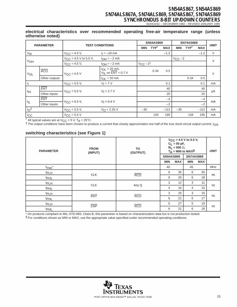
electrical characteristics over recommended operating free-air temperature range (unlessotherwise noted)
PARAMETER TEST CONDITIONSSN54AS869 SN74AS869
UNITPARAMETER TEST CONDITIONSMIN TYP† MAX MIN TYP† MAX
UNIT
VIK VCC = 4.5 V, II = –18 mA –1.2 –1.2 V
VOHVCC = 4.5 V to 5.5 V, IOH = –2 mA VCC –2
VVOHVCC = 4.5 V, IOH = –2 mA VCC –2*
V
VOLRCO
VCC = 4.5 V
IOL = 20 mA,VIL on ENT = 0.7 V
0.34 0.5VOL
Other outputsCC
IOL = 20 mA 0.34 0.5
II VCC = 5.5 V, VI = 7 V 0.1 0.1 mA
IIHENT
VCC = 5 5 V VI = 2 7 V40 40
µAIIHOther inputs
VCC = 5.5 V, VI = 2.7 V20 20
µA
IILENT
VCC = 5 5 V VI = 0 4 V–4 –4
mAIILOther inputs
VCC = 5.5 V, VI = 0.4 V–2 –2
mA
IO‡ VCC = 5.5 V, VO = 2.25 V –30 –112 –30 –112 mA
ICC VCC = 5.5 V 134 195 134 195 mA
† All typical values are at VCC = 5 V, TA = 25°C.‡ The output conditions have been chosen to produce a current that closely approximates one half of the true short-circuit output current, IOS.
switching characteristics (see Figure 1)
PARAMETERFROM
(INPUT)TO
(OUTPUT)
VCC = 4.5 V to 5.5 V,CL = 50 pF,RL = 500 Ω,TA = MIN to MAX § UNIT(INPUT) (OUTPUT)
SN54AS869 SN74AS869
MIN MAX MIN MAX
fmax* 40 45 MHz
tPLHCLK RCO
6 35 6 35ns
tPHLCLK RCO
6 20 6 18ns
tPLHCLK Any Q
3 12 3 11ns
tPHLCLK Any Q
4 16 4 15ns
tPLHENT RCO
3 25 3 15ns
tPHLENT RCO
6 21 6 17ns
tPLHENP RCO
5 27 5 19ns
tPHLENP RCO
6 21 6 18ns
* On products compliant to MIL-STD-883, Class B, this parameter is based on characterization data but is not production tested.§ For conditions shown as MIN or MAX, use the appropriate value specified under recommended operating conditions.

SN54AS867, SN54AS869SN74ALS867A, SN74ALS869, SN74AS867, SN74AS869SYNCHRONOUS 8-BIT UP/DOWN COUNTERSSDAS115C – DECEMBER 1982 – REVISED JANUARY 1995
16 POST OFFICE BOX 655303 • DALLAS, TEXAS 75265
PARAMETER MEASUREMENT INFORMATIONSERIES 54ALS/74ALS AND 54AS/74AS DEVICES
tPHZ
tPLZ
tPHLtPLH
0.3 V
tPZL
tPZH
tPLHtPHL
LOAD CIRCUITFOR 3-STATE OUTPUTS
From OutputUnder Test
Test Point
R1
S1
CL(see Note A)
7 V
1.3 V
1.3 V1.3 V
3.5 V
3.5 V
0.3 V
0.3 V
thtsu
VOLTAGE WAVEFORMSSETUP AND HOLD TIMES
TimingInput
DataInput
1.3 V 1.3 V3.5 V
3.5 V
0.3 V
0.3 V
High-LevelPulse
Low-LevelPulse
tw
VOLTAGE WAVEFORMSPULSE DURATIONS
Input
Out-of-PhaseOutput
(see Note C)
1.3 V 1.3 V
1.3 V1.3 V
1.3 V 1.3 V
1.3 V1.3 V
1.3 V
1.3 V
3.5 V
3.5 V
0.3 V
0.3 V
VOL
VOH
VOH
VOL
OutputControl
(low-levelenabling)
Waveform 1S1 Closed
(see Note B)
Waveform 2S1 Open
(see Note B)0 V
VOH
VOL
3.5 V
In-PhaseOutput
0.3 V
1.3 V 1.3 V
VOLTAGE WAVEFORMSPROPAGATION DELAY TIMES
VOLTAGE WAVEFORMSENABLE AND DISABLE TIMES, 3-STATE OUTPUTS
R2
VCC
RL
Test Point
From OutputUnder Test
CL(see Note A)
LOAD CIRCUITFOR OPEN-COLLECTOR OUTPUTS
LOAD CIRCUIT FOR BI-STATE
TOTEM-POLE OUTPUTS
From OutputUnder Test
Test Point
CL(see Note A)
RL
RL = R1 = R2
NOTES: A. CL includes probe and jig capacitance.B. Waveform 1 is for an output with internal conditions such that the output is low except when disabled by the output control.
Waveform 2 is for an output with internal conditions such that the output is high except when disabled by the output control.C. When measuring propagation delay items of 3-state outputs, switch S1 is open.D. All input pulses have the following characteristics: PRR ≤ 1 MHz, tr = tf = 2 ns, duty cycle = 50%.E. The outputs are measured one at a time with one transition per measurement.
Figure 1. Load Circuits and Voltage Waveforms

PACKAGE OPTION ADDENDUM
www.ti.com 13-Aug-2021
Addendum-Page 1
PACKAGING INFORMATION
Orderable Device Status(1)
Package Type PackageDrawing
Pins PackageQty
Eco Plan(2)
Lead finish/Ball material
(6)
MSL Peak Temp(3)
Op Temp (°C) Device Marking(4/5)
Samples
5962-8966801LA ACTIVE CDIP JT 24 1 Non-RoHS& Green
SNPB N / A for Pkg Type -55 to 125 5962-8966801LASNJ54AS867JT
SN54AS867JT ACTIVE CDIP JT 24 1 Non-RoHS& Green
SNPB N / A for Pkg Type -55 to 125 SN54AS867JT
SN54AS869JT ACTIVE CDIP JT 24 1 Non-RoHS& Green
SNPB N / A for Pkg Type -55 to 125 SN54AS869JT
SN74ALS867ADW ACTIVE SOIC DW 24 25 RoHS & Green NIPDAU Level-1-260C-UNLIM 0 to 70 ALS867A
SN74ALS869DW ACTIVE SOIC DW 24 25 RoHS & Green NIPDAU Level-1-260C-UNLIM 0 to 70 ALS869
SN74ALS869DWE4 ACTIVE SOIC DW 24 25 RoHS & Green NIPDAU Level-1-260C-UNLIM 0 to 70 ALS869
SN74AS867DW ACTIVE SOIC DW 24 25 RoHS & Green NIPDAU Level-1-260C-UNLIM 0 to 70 AS867
SN74AS869DW ACTIVE SOIC DW 24 25 RoHS & Green NIPDAU Level-1-260C-UNLIM 0 to 70 AS869
SNJ54AS867JT ACTIVE CDIP JT 24 1 Non-RoHS& Green
SNPB N / A for Pkg Type -55 to 125 5962-8966801LASNJ54AS867JT
SNJ54AS869JT ACTIVE CDIP JT 24 1 Non-RoHS& Green
SNPB N / A for Pkg Type -55 to 125 5962-8952601LASNJ54AS869JT
(1) The marketing status values are defined as follows:ACTIVE: Product device recommended for new designs.LIFEBUY: TI has announced that the device will be discontinued, and a lifetime-buy period is in effect.NRND: Not recommended for new designs. Device is in production to support existing customers, but TI does not recommend using this part in a new design.PREVIEW: Device has been announced but is not in production. Samples may or may not be available.OBSOLETE: TI has discontinued the production of the device.
(2) RoHS: TI defines "RoHS" to mean semiconductor products that are compliant with the current EU RoHS requirements for all 10 RoHS substances, including the requirement that RoHS substancedo not exceed 0.1% by weight in homogeneous materials. Where designed to be soldered at high temperatures, "RoHS" products are suitable for use in specified lead-free processes. TI mayreference these types of products as "Pb-Free".RoHS Exempt: TI defines "RoHS Exempt" to mean products that contain lead but are compliant with EU RoHS pursuant to a specific EU RoHS exemption.Green: TI defines "Green" to mean the content of Chlorine (Cl) and Bromine (Br) based flame retardants meet JS709B low halogen requirements of <=1000ppm threshold. Antimony trioxide basedflame retardants must also meet the <=1000ppm threshold requirement.
(3) MSL, Peak Temp. - The Moisture Sensitivity Level rating according to the JEDEC industry standard classifications, and peak solder temperature.
PACKAGE OPTION ADDENDUM
www.ti.com 13-Aug-2021
Addendum-Page 2
(4) There may be additional marking, which relates to the logo, the lot trace code information, or the environmental category on the device.
(5) Multiple Device Markings will be inside parentheses. Only one Device Marking contained in parentheses and separated by a "~" will appear on a device. If a line is indented then it is a continuationof the previous line and the two combined represent the entire Device Marking for that device.
(6) Lead finish/Ball material - Orderable Devices may have multiple material finish options. Finish options are separated by a vertical ruled line. Lead finish/Ball material values may wrap to twolines if the finish value exceeds the maximum column width.
Important Information and Disclaimer:The information provided on this page represents TI's knowledge and belief as of the date that it is provided. TI bases its knowledge and belief on informationprovided by third parties, and makes no representation or warranty as to the accuracy of such information. Efforts are underway to better integrate information from third parties. TI has taken andcontinues to take reasonable steps to provide representative and accurate information but may not have conducted destructive testing or chemical analysis on incoming materials and chemicals.TI and TI suppliers consider certain information to be proprietary, and thus CAS numbers and other limited information may not be available for release.
In no event shall TI's liability arising out of such information exceed the total purchase price of the TI part(s) at issue in this document sold by TI to Customer on an annual basis.
OTHER QUALIFIED VERSIONS OF SN54AS867, SN54AS869, SN74AS867, SN74AS869 :
• Catalog : SN74AS867, SN74AS869
• Military : SN54AS867, SN54AS869
NOTE: Qualified Version Definitions:
• Catalog - TI's standard catalog product
• Military - QML certified for Military and Defense Applications

TUBE
*All dimensions are nominal
Device Package Name Package Type Pins SPQ L (mm) W (mm) T (µm) B (mm)
SN74ALS867ADW DW SOIC 24 25 506.98 12.7 4826 6.6
SN74ALS869DW DW SOIC 24 25 506.98 12.7 4826 6.6
SN74ALS869DWE4 DW SOIC 24 25 506.98 12.7 4826 6.6
SN74AS867DW DW SOIC 24 25 506.98 12.7 4826 6.6
SN74AS869DW DW SOIC 24 25 506.98 12.7 4826 6.6
PACKAGE MATERIALS INFORMATION
www.ti.com 5-Jan-2022
Pack Materials-Page 1


MECHANICAL DATA
MCER004A – JANUARY 1995 – REVISED JANUARY 1997
POST OFFICE BOX 655303 • DALLAS, TEXAS 75265
JT (R-GDIP-T**) CERAMIC DUAL-IN-LINE24 LEADS SHOWN
4040110/C 08/96
B
0.200 (5,08) MAX
0.320 (8,13)0.290 (7,37)
0.130 (3,30) MIN
0.008 (0,20)0.014 (0,36)
Seating Plane
13
12
0.030 (0,76)0.070 (1,78)
0.015 (0,38) MIN
A
24
1
0.100 (2,54) MAX
0.023 (0,58)0.015 (0,38)
0.100 (2,54)
0°–15°
1.440
(37,08) 1.460
0.285
(7,39) 0.291
(36,58)
(7,24)
28PINS **
1.280
1.240
0.300
0.245
(7,62)
DIM
B MAX
A MAX
A MIN
B MIN(6,22)
24
(32,51)
(31,50)
NOTES: A. All linear dimensions are in inches (millimeters).B. This drawing is subject to change without notice.C. This package can be hermetically sealed with a ceramic lid using glass frit.D. Index point is provided on cap for terminal identification.E. Falls within MIL STD 1835 GDIP3-T24, GDIP4-T28, and JEDEC MO-058 AA, MO-058 AB

IMPORTANT NOTICE AND DISCLAIMERTI PROVIDES TECHNICAL AND RELIABILITY DATA (INCLUDING DATA SHEETS), DESIGN RESOURCES (INCLUDING REFERENCE DESIGNS), APPLICATION OR OTHER DESIGN ADVICE, WEB TOOLS, SAFETY INFORMATION, AND OTHER RESOURCES “AS IS” AND WITH ALL FAULTS, AND DISCLAIMS ALL WARRANTIES, EXPRESS AND IMPLIED, INCLUDING WITHOUT LIMITATION ANY IMPLIED WARRANTIES OF MERCHANTABILITY, FITNESS FOR A PARTICULAR PURPOSE OR NON-INFRINGEMENT OF THIRD PARTY INTELLECTUAL PROPERTY RIGHTS.These resources are intended for skilled developers designing with TI products. You are solely responsible for (1) selecting the appropriate TI products for your application, (2) designing, validating and testing your application, and (3) ensuring your application meets applicable standards, and any other safety, security, regulatory or other requirements.These resources are subject to change without notice. TI grants you permission to use these resources only for development of an application that uses the TI products described in the resource. Other reproduction and display of these resources is prohibited. No license is granted to any other TI intellectual property right or to any third party intellectual property right. TI disclaims responsibility for, and you will fully indemnify TI and its representatives against, any claims, damages, costs, losses, and liabilities arising out of your use of these resources.TI’s products are provided subject to TI’s Terms of Sale or other applicable terms available either on ti.com or provided in conjunction with such TI products. TI’s provision of these resources does not expand or otherwise alter TI’s applicable warranties or warranty disclaimers for TI products.TI objects to and rejects any additional or different terms you may have proposed. IMPORTANT NOTICE
Mailing Address: Texas Instruments, Post Office Box 655303, Dallas, Texas 75265Copyright © 2022, Texas Instruments Incorporated