
Investigation of optical properties of core–shell silicon nanowires
Upload
khangminh22Category
view
1download
0
i
STRUCTURE AND OPTICAL PROPERTIES
OF NATURAL LOW DIMENSIONAL,
SEMICONDUCTING, ORGANIC
INORGANIC HYBRIDS
Robert Shewan Black
A thesis submitted to the Faculty of Science,
University of the Witwatersrand, Johannesburg, in
fulfillment of the requirements for the degree of
Doctor of Philosophy
Johannesburg 2012

ii
Declaration
I declare that this thesis is my own, unaided work. It is being submitted for the Degree of
doctor of Philosophy in the University of the Witwatersrand, Johannesburg. It has not
been submitted before for any degree or examination in any other University.
__________________________________________
(Signature of Candidate)
_______________day of____________________2012
iii
Abstract
The aim of investigating the 2D PbX6 inorganic organic hybrids was to study octahedral distortions, short interlayer spacing’s, and the effect of functionalized aliphatic’s terminal halogen on idealizing or destabilizing the octahedral arrangements and their effect on the band gap of the single layer 2D hybrid systems. It was found that the PbX6 metal centred distortions do display some impact on the band gap, the greater the distortion experienced in the Ieq-Pb-Ieq cis bond angles, the wider the band gap, as we suspect a decrease in I antibonding character which lowers the top of the valence band. The terminal halogen interaction specifically in (BrC2)PbI4, clearly displayed some Br character at the bottom of the conduction band, which may further explain the reduction of the band gap of this compound. This in conjunction with the shorter interlayer spacing serve to stabilize more idealized bridging angles, as seen in both the lead iodide and bromide analogues. In the short interlayer spacing compounds large idealizations of the Pb-X-Pb bridging angles are observed however display a large metal centred octahedral distortions in order accommodate the spatial occupation of the lone pair on lead.
It was generally observed that the lead bromide hybrids appear to have a greater sensitivity to exciton lattice interactions, which give rise to red shifted emissions and absorptions with decreasing temperature. Structurally this behaviour is counterintuitive; because the structures increase in inorganic distortions with decreasing temperature and therefore a blue shift in the exciton absorption is expected. It should be noted that compounds displaying this phenomenon most, (C4, C6, C7)PbBr4 do display a large amount of structural disorder in their lower temperature phases.
In the 1D systems investigated further structure to property correlations were made. Optically it was found that unlike the corner-shared perovskite type 1D wires of [NH2C(I)=NH2]3PbI5 and [CH3SC(=NH2)NH2]3PbI5 the first exciton absorption of the octahedral face sharing wires of (A)PbI3 appear to be largely insensitive to the inorganic structural distortions experienced as a result of the low temperature phase transitions. In one instance however a low temperature phase transition did result in a polaron emission which was directly related to a discontinuity in the inorganic wires. More generally experimental links between the STE luminescence emissions and the inter-wire spacing, organic dielectric constant, and the density of the crystal, were shown to influence the STE lattice interactions to a greater degree. This effect is increased through a decrease in crystal density and organic dielectric constant, with an associated increase in the inter-wire spacing. Therefore as the exciton lattice interactions increase, a red shift in the STE emissions is observed.
In another series of systems strong and interactions were present in particularly two 1D charge transfer compounds. It was noted that the inorganic wires promote interactions between the organic templates as has also been established in literature. Structurally it was also observed that the CT transitions of these compounds begin to largely coincide with the STE emission arising from the inorganic wire. Even though the CT compounds structurally have strong interactions the current experiments do not ascertain to what degree this interaction assists in electron transport. It was also established that as intermolecular interactions are absent in previously published MV and Et compounds with the dominant CT interaction was the I…N interaction which functions over a large range
( ). This long distance is substantiated from the strong covalent character of the I…N interaction observed in IR experiments completed on (MV)Pb2I6. It was also observed in our compounds that the position of the LUMO of the organic cation relative to the valence band of the inorganic wires appears to be largely dependent on the N…I distance and largely independent of the electron accepting templates HOMO-LUMO gap.
The increased wire thickness observed in these compounds does appear to display a pronounced effect on the PL emissions as seen in three chain wide wires produced. The thicker chains begin to allow higher energy emission’s to occur i.e. the desired first exciton emission begins to become favored due to the relaxing of the wires spatial confinement on the electron-hole’s orbit. Further investigations are needed into even thicker chain wires, in order to ascertain the ideal size of the wire to obtain the desired high energy first exciton emission. To date the wire thickness that does give rise to the first exciton emission appears to still need at least six coordinated PbI6 octahedral units.

iv
Acknowledgments
I would firstly like to acknowledge my supervisor Prof. Dave Billing for giving me the wonderful
opportunities in attending 3 conferences, one local and two international. This definitely helped
shape my view of research and gave me many useful ideas and experiences. From a technical
point of view thanks for letting me break many an instrument on my initial learning curve, and
for the useful talks on diffraction both powder and single crystal. I would also like to thank him
for the many laughs and coffee sessions over the years, thanks for your friendship.
A special thanks Dr Manuel Fenandes for helping me with some ideas in solving the more
difficult crystal structures, keeping the APEX running, and for showing me how to fix many
instrumental issues. Also thanks for helping me to build a fully functional Linux machine - what
would Wits chemistry do without you? And lastly, thanks for all the many discussions on the
random but interesting topics over the years.
To Dr Rudolph Erasmus, a special thanks to you for the photoluminescence and UV-Vis optical
absorption measurements. Thanks for all of the useful discussions your knowledge and input is
greatly appreciated.
To Prof Demi Levendis thanks for the discussions on symmetry and the visits to Jan Boeyens. I
sincerely hope you manage to find your blue key.
To my office mates Matt and Roy, thanks for the good laughs and many random discussions,
many of which I’d prefer to forget.
A special thanks to my Dad, thanks for all the encouragement over the years and for the
opportunity to study in the first place. I aspire to be like you. I would also like extent thanks to
my mom and remaining family for all your support.
Most importantly I would like to thank my wife for all her encouragement to finish my thesis and
for standing by me since my first year at varsity. I know sometimes we do things to simply prove
others wrong. Thanks for helping me to stop caring what other people think. Your love and
support have been nothing short of spectacular. I love you dearly my angel.
To my Father in Heaven, you make all things clearer over time. My life in your hands. All things
for your Glory. To You my Dad and my wife I dedicate this thesis.

v
Posters and Presentations
Posters
Robert S. Black and David G. Billing, Structure and properties of selected organic-inorganic hybrid
perovskites namely R, S, And R&S,[C6H5C*(H)(CH3)NH3
+]2SnI4. Carmen Physical Chemistry
Symposium, V&A Waterfront, Cape Town, (2007). (Awarded poster prize)
Robert S. Black and David G. Billing, Structure and properties of selected organic-inorganic hybrid
perovskites namely R, S, And R&S,[C6H5C*(H)(CH3)NH3
+]2SnI4. Post graduate symposium,
University of the Witwatersrand. (2008)
Robert S. Black and David G. Billing, Structure and photoluminescence of chiral tin and lead
inorganic-organic hybrid perovskites. International Union of Crystallography (IUCr) 2008 Osaka
Japan. Acta Cryst. (2008) A64, C455-C456
Robert S. Black and David G. Billing, Structure and photoluminescence of chiral tin and lead
inorganic-organic hybrid perovskites. Post graduate symposium, University of the
Witwatersrand. (2009)
Robert S. Black, David G. Billing and Rudolph E. Erasmus, Structure and Optical Properties of
Natural 1D Quantum Wires. European Crystallographic Meeting (ECM) Darmstadt Germany.
(2010)
David G. Billing, Robert S. Black, Structure and Optical Properties of Natural 2D Quantum Wells.
European Crystallographic Meeting (ECM) Darmstadt Germany. (2010)
Presentations
Robert S. Black and David G. Billing, Structure and photoluminescence of tin and lead inorganic-
organic hybrid perovskites. SACI young chemists symposium, University of the Witwatersrand,
Chemistry Department. (2008)
Robert S. Black and David G. Billing, Structure and optical properties of natural low dimensional
semiconductors. Chem. Soc. Post graduate Colloquium, University of the Witwatersrand,
Chemistry Department. (2010)
Robert S. Black and David G. Billing, Structure and optical properties of natural low dimensional
semiconductors. Materials Physics Research Institute Centre of Excellence in Strong Materials

vi
(MPRI), University of the Witwatersrand, Physics Department. (2010) (Won student prize for
best talk in 2010)

vii
Preface
The thesis is comprised two distinct sections, namely the section A which comprises of the
background theory, literature survey, and experimental section, and section B which comprises
the results and discussions sections. The entire thesis is written in a uniform style, with the
exception of chapter 6. As chapter 6 was intended for non linear optical investigations, and
therefore it is written with its own theory and brief literature survey section.
The introduction and background theory section (chapter 1) was intended to establish a
foundation of the fundamentals of semiconductor devices. Chapter 2 follows on from this by
giving the background literature of low dimensional inorganic organic hybrids. The results
chapters (4-6) investigated SC-XRD, and optical property investigations of 44 different low
dimensional organic inorganic hybrids. Only 29 of the structures are new, however the other
structures investigated formed the basis of the optical investigations. It was the intention in this
work to correlate structure to optical property relationships, and therefore SC-XRD structural
determinations were either revisited or completed at multiple temperatures for most of the
compounds investigated. The previously published structures were revisited to ensure direct
optical to property correlations could be made without worry of polymorphism (as will be
established in the literature survey).
All of the relevant structure files as well as an electronic copy of this thesis are supplied on the
disc under the relevant chapter numbers.

viii
Table of Contents Page
Abstract iii
Acknowledgements iv
Posters and Presentations v
Preface vii
Table of contents viii
List of figures xii
List of tables xxii
List of schemes xxiv
Section A: Background Theory and Literature Survey
Chapter 1: Introduction and Theory ................................................................................................ 1
1.1 Introduction ............................................................................................................................ 1
1.2 Brillouin zones and reciprocal space ....................................................................................... 2
1.3 Energy bands in semiconducting solids .................................................................................. 5
1.4 Density of States (DOS) ........................................................................................................... 9
1.5 General properties of semiconductors ................................................................................. 13
1.5.1 Recombination processes .............................................................................................. 13
1.5.2 Carrier densities ............................................................................................................. 14
1.5.2 Carrier transport ............................................................................................................ 15
1.6 Optical processes and excitons in semiconductors .............................................................. 16
1.7 Confinement of excitons through dimensional reduction .................................................... 20
1.7.1 The 3D case ................................................................................................................... 21
1.7.2 The 2D case ................................................................................................................... 22
1.7.3 The 1D case ................................................................................................................... 23
1.7.4 The 0D case ................................................................................................................... 25
1.8 Aims ....................................................................................................................................... 26
1.9 Bibliography .......................................................................................................................... 27
Chapter 2: Literature Survey .......................................................................................................... 28
2.1 Introduction .......................................................................................................................... 28
2.2 3D organic inorganic hybrid perovskites ............................................................................... 28
2.2.1 Optical properties of 3D organic inorganic hybrid perovskites ..................................... 31

ix
2.2.2 Comparison of 3D and 2D electronic states .................................................................. 33
2.3 <100> 2D hybrid perovskites and their relative orientations............................................... 35
2.3.1 Size of the cation and the effect on the dimensionality and topology of the <100>
hybrids .................................................................................................................................... 38
2.3.2 <100>, <110> and <111> 2D orientations ..................................................................... 42
2.3.3 Group 14(IVA) <100> hybrids and the ns2 lone pair stereo chemical activity .............. 46
2.3.4 The effect of structural distortions on the stereo chemical activity of the ns2 lone pair
of <100> (A)2SnI4 hybrids ........................................................................................................ 49
2.3.5 Electrical transport of <100> and <110> tin iodide based hybrid perovskites ............. 53
2.3.6 The <110> orientation and the effect on the band gap of lead based hybrids ............ 55
2.4 Different motifs generated through varying the M/X and cation ratio’s ............................. 58
2.5 Optical properties and Photoluminescence of <100> 2D hybrids ........................................ 63
2.5.1 Optical properties of lead bromide and chloride 2D hybrids ........................................ 71
2.6 Phase changes of the <100> 2D hybrids ............................................................................... 78
2.6.1 Enthalpy and entropy energies from CnMX4 phase transitions .................................... 88
2.6.2 Unusual phase behavior of the short alkylammonium hybrids of (C3)MCl4 ................ 91
2.7 1D hybrids and their optical properties ............................................................................... 93
2.7.1 Charge transfer effects between wires and spacers ................................................... 103
2.8 Optical nonlinearity in organic inorganic hybrids ............................................................... 107
2.9 Electroluminescent devices and the use of chromophores in 2D hybrids ......................... 110
2.10 Summary and conclusions ................................................................................................ 113
Chapter 3: Experimental .............................................................................................................. 114
3.1 Synthesis ................................................................................................................................. 114
3.1.1 Slow cooling method ................................................................................................... 114
3.1.2 Slow evaporation method ........................................................................................... 115
3.1.3 Schemes of compounds investigated with relevant chapter numbers ....................... 116
3.2 Single Crystal X-ray diffraction (SC-XRD) ................................................................................ 120
3.2.1 References ................................................................................................................... 121
3.3 Powder X-ray diffraction (P-XRD) ........................................................................................... 122
3.3.1 References ................................................................................................................... 122
3.4 Photoluminescence ................................................................................................................ 123
3.5 UV-Vis ..................................................................................................................................... 123
3.6 Thermal analysis (DSC) ........................................................................................................... 124

x
3.7 Elemental analysis ................................................................................................................... 124
Section B: Results and Discussion
Chapter 4: The structure and optical properties of <100> 2D lead halide quantum wells........ 125
4.1 The Structure and Phase transitions of (CnH2n+1NH3)2PbBr4 where n = 4-7 ............................ 125
4.1.1 Introduction ................................................................................................................. 125
4.1.2 Results and Discussion ................................................................................................. 129
4.1.3 Thermal analysis studies of the (Cn)PbBr4 where n = 4-7 ............................................ 134
4.1.4 The structures and phases of (Cn)PbBr4 where n = 4-7 ............................................. 137
4.1.5 Conclusions .................................................................................................................. 142
4.2 The Structure and Phase transitions of (HOC2, BrC3, BrC4, BrC5)2PbBr4 ............................... 143
4.2.1 Introduction ................................................................................................................. 143
4.2.2 Results and Discussion ................................................................................................. 145
4.2.3 Thermal analysis .......................................................................................................... 146
4.2.4 The structure and phases of (HOC2, BrC3, BrC4, BrC5)2PbBr4 .................................... 150
4.2.5 Conclusions .................................................................................................................. 159
4.3 Optical properties of (CnH2nNH3)2PbX4 where n = 4-7, and (HOC2H4NH3)2PbX4, where X = Br
and I and (BrCnH2nNH3)2PbBr4 where n = 3-5 and (ICnH2NH3)2PbI4 where n = 2-6 and
(BrC2H4NH3)2PbI4. .......................................................................................................................... 160
4.3.1 Introduction ................................................................................................................. 160
4.3.2 Results and Discussion ................................................................................................. 164
4.3.3 Structural Summary of the lead iodide analogues...................................................... 165
4.3.4 Optical absorption and photoluminescence of (Cn)PbX4 and (ZCn)PbX4 .................... 169
4.3.5 Structure and optical property correlation of the lead iodide series .......................... 172
4.3.6 Lead halide substitution and the effect on the exciton absorption ........................... 181
4.3.7 Conclusions .................................................................................................................. 183
Chapter 5: Structure and optical properties of lead iodide quantum wires .............................. 185
5.1 The structures, phase transitions and optical properties of the natural 1D organic inorganic
quantum wire hybrids of (A)PbI3 .................................................................................................. 185
5.1.1 Introduction ................................................................................................................. 185
5.1.2 Results and Discussion ................................................................................................. 187
5.1.3 Powder diffraction investigations ................................................................................ 192
5.1.4 Thermal analysis studies (DSC) ................................................................................... 193
5.1.5 The structure and phase transitions of (Py)PbI3, (PD)PbI3, and (Az)PbI3 ..................... 195

xi
5.1.6 The structures of (Pyr)PbI3, [(n-But)4N]PbI3 and [(Et)3NH]PbI3 ................................... 202
5.1.7 Structural conclusions ................................................................................................. 203
5.1.8 Optical properties of compounds 1-6 ......................................................................... 206
5.1.9 Structure and optical property cconclusions .............................................................. 211
5.2 The structures and phases of the solvated 1D xDMF.(A)PbI3 compounds, where distortions of
the periodicity of the wire generates an alternative PL emission pathway ................................. 212
5.2.1 Introduction ................................................................................................................. 212
5.2.2 Results and Discussion ................................................................................................ 213
5.2.3 Photoluminescence and optical absorption ................................................................ 215
5.2.4 The variable temperature structures of (DPBD)Pb2I6 and (EPPA)PbI3 ......................... 217
5.2.5 Conclusions .................................................................................................................. 219
5.3 Structure and optical properties of thick chain 1D lead iodide wires, and the Charge transfer
effects between the wires and spacers ........................................................................................ 221
5.3.1 Introduction ................................................................................................................. 221
5.3.2 Results and Discussion ................................................................................................ 224
5.3.3 Powder Diffraction investigations ............................................................................... 231
5.3.4 Optical properties ....................................................................................................... 232
5.3.5 Conclusions ................................................................................................................. 237
Chapter 6: Chiral organic inorganic hybrid materials and their potential for NLO properties . 238
6.1 Theoretical background .......................................................................................................... 238
6.1.1 The physical origin of optical nonlinearities ................................................................ 238
6.1.2 Non-resonant nonlinearities ....................................................................................... 242
6.1.3 Resonant nonlinearities............................................................................................... 244
6.1.4 Phase matching and optical birefringence (briefly) .................................................... 246
6.1.5 Symmetry conditions for second order effects ........................................................... 247
6.1.6 Brief literature survey of NLO hybrid materials .......................................................... 248
6.2 Introduction ............................................................................................................................ 254
6.2.1 Results and discussion (2D) ......................................................................................... 255
6.2.2 Variable temperature photoluminescence of compounds 4-8 ................................... 266
6.2.3 Conclusions .................................................................................................................. 275
6.3 Structure and optical properties of the 1D compounds ........................................................ 276
6.3.1 Results an discussion (1D) ........................................................................................... 276
6.3.2 Crystal structures ........................................................................................................ 276

xii
6.3.3 Luminescence .............................................................................................................. 282
6.3.4 Conclusions 1D ............................................................................................................. 285
Chapter 7: Conclusion .................................................................................................................. 286
7.1 Concluding remarks ................................................................................................................ 286
7.2 Future work ............................................................................................................................. 289
Chapter 8: References .................................................................................................................. 290
Appendix ....................................................................................................................................... 298
Appendix A .................................................................................................................................... 298
Appendix B .................................................................................................................................... 304
Appendix C .................................................................................................................................... 308
List of figures Page
Figure 1.1: Brillouin Zone generation in a) a cubic Bravais lattice and b) in a hexagonal Bravais lattice. (This
image was reused under the GNU public licence from http://en.wikipedia.org/wiki/Brillouin_zone). 1
Figure 1.2: The First Brillouin Zone of a face centred cubic lattice where the labels in red represent the
critical points (points of high symmetry) and Γ is the zone centre (0, 0, 0). (This image was reused under the
GNU public licence from http://en.wikipedia.org/wiki/Brillouin_zone ). 5
Figure 1.3: a) The free electron model representation of an ϵ_k vs k diagram, i.e. with no periodic boundary
conditions included. b) A new ϵ_k vs k diagram with periodic boundary conditions included. What becomes
evident is that at the zone boundaries ±nπ/a for a linear system, band gaps begin to arise. Diagram obtained
from (Kittel C, 1996). 6
Figure 1.4: a) The variation potential energy of a conduction electron in a linear lattice a in a field of ion
cores. b) The probability density wavefunctions of the travelling waves |ψ(+)2| and |ψ(-)
2|. Where the
positive probability wavefunction piles up positive charge around the ion cores, and the negative probability
wavefunction piles up negative charge in the interstitial regions. (Diagram obtained from Kittel. C, 1996). 7
Figure 1.5: The first diagram displays the ϵ_k vs k diagram of the Kronig-Penney model where the band gaps
arise at the Brillouin zone boundaries ±nπ/a where n is an integer. The Black curves are the Kronig-Penney
model and the green curves are the free electron model. a) is the ϵ_k vs k diagram only b) is the ϵ_k vs k
diagram combined with the reduced zone diagram, and c) is the ϵ_k vs k diagram of the reduced zone
diagram only or the band structure diagram of the First Brillouin zone. (ref:
http://ecee.colorado.edu/~bart/book/welcome.htm Chapter 2) 8
Figure 1.6: The overlaid band structure of GaAs and Ge show the difference between a direct and indirect
band gap of a band structure. Where GaAs has a direct bad gap of Eg = 1.519eV at room temperature, and
Ge has an indirect band gap of 0.7437eV. 9
Figure 1.7: Density of states for bulk (3D blue), quantum well (2D red), quantum wire (1D green) and
quantum Dot (0D black) (Diagram obtained from: http://britneyspears.ac/physics/dos/dos.htm). Functions
are described in the text. 12
Figure 1.8: An exciton which is a bound electron hole pair. An illustration of a Mott-Wannier type exciton
with an effective Bohr radius equivalent to or greater than the unit cell dimensions. 16

xiii
Figure 1.9: Energy subbands generated from excitons with various quantum numbers n, the lowest excitons
energy level has the largest orbiting radius, binding energy, and lowest emission energy associated with n=1.
(Diagram obtained from Kittel. C, 1996). 17
Figure 1.10: a) Shows the excitonic absorption of very pure GaAs at 1.2K. From the absorption spectra, one is
able to experimentally observe three of the excitonic subband energy levels. b) Shows the temperature
effect on GaAs absorption spectrum. It is evident that the excitons absorption line only becomes evident at
lower temperatures. The dashed line shows the calculated band gap with decreasing temperature. (Diagrams
obtained from Fox M, 2008). 19
Figure 1.11: The eigenenergy of the bound states may be seen in the above plot. These eigenenergies show
that for d = 1 the odd (2p) and even (2s) parity n = 2 energy levels are fairly evenly spaced just below the
conduction band and converge to -ER* at x0 = 0. However what is observed is that as the wire length is
shortened (x0→0) the eigenenergy of the lowest energy state n = 1 diverges to negative infinity. This is where
the 1D model begins to break down, and or the wire is at the limit of being a wire, and should now be
treated as a quantum dot. (Diagram obtained from: Ogawa T, Kanemitsu Y., 1995). 24
Figure 1.12: A representation of the effect of the dielectric constant ratio of the wire and the barrier, and it’s
enhancement of the coulomb potential with increasing dielectric mismatch. The dashed line represents the
bare coulomb potential. Essentially one may say that the more negative the coulomb potential, the greater
the increase on the binding energy of the exciton. (Diagram obtained from: Ogawa T, Kanemitsu Y., 1995). 25
Figure 2.1: The perovskite structure (CaTiO3) which holds the general formula ABO3, however for the Organic
inorganic hybrid perovskites the formula is changed to AMX3 where A is the organic cation, M the metal, and
X is any halogen. 28
Figure 2.2: The low temperature absorption spectra both obtained from the reflectance and Kramers-
Kroning relationship. a) Displays the 5K absorption spectrum of (CH3NH3)PbBr3 obtained from (Tanaka K, et
al, 2003) b) Displays the 4.2K absorption spectrum of (CH3NH3)PbI3 obtained from (Hirasawa M, et al, 1994). 32
Figure 2.3: The UPS spectra and the calculated density of states, of a) The 3D Hybrid perovskite
(CH3NH3)PbI3, and b) the 2D hybrid perovskite (C4H9NH3)2PbI4 (Umebayashi T, et al, 2003). 33
Figure 2.4: a) The 3D structure of (CH3NH3)PbI3 and b) the 2D structure of (C4H9NH3)2PbI4 (Umebayashi T, et
al, 2003). 34
Figure 2.5: The results of the band structure calculations of a) (CH3NH3)PbI3 and b) (C4H9NH3)2PbI4. The
critical points in the first Brillouin zone of c) the cubic phase crystal structure of (CH3NH3)PbI3 , d) the
orthorhombic phase of (C4H9NH3)2PbI4 (Umebayashi T, et al, 2003). 35
Figure 2.6: As the R group increases in size the 3D perovskite motif is changed, as the octahedral vertically
separate. This separation may increase with increasing length of the R group. 36
Figure 2.7: a) Eclipsed arrangement of the <100> layers. b) Staggered arrangement of <100> layers. 37
Figure 2.8: The hydrogen bonding configurations observed in the <100> oriented 2D hybrids. a) The bridging
halide configuration i.e. two hydrogen bonds to the bridging halides and one hydrogen bond to the terminal
halogen. b) The terminal halogen configuration, where there is now one bridging halide hydrogen bond, and
two terminal halide hydrogen bonds. 37
Figure 2.9: The primary cyclic amine templates used to ascertain at which point the bulkiness of the template
forces a new templated motif. 38
Figure 2.10: The Lead iodide and Lead bromide series form the same basic motif with the cycloheptyl
ammonium template. a) The cycloheptyl ammonium cation with lead bromide, produces 1D double layer
corner sharing octahedral chains. b) The side view displays the chain motif which resembles the <110> 2D
layer motif (Billing D. G, and Lemmerer A, 2009). 39
Figure 2.11: The Lead Chloride cyloheptyl ammonium hybrid forming inorganic bilayers in the crystal may be
an intermediate dimension between 1D and 2D (Billing D. G, and Lemmerer A, 2009). 39
Figure 2.12: When the template ring size increases from cycloheptyl ammonium to the cylclooctyl
ammonium cation for lead Bromide, a new type of bilayer motif is formed as in the lead chloride cyloheptyl
ammonium case. The difference between them is observed when studying the bilayer topology. Instead of
only corner sharing octahedra as seen in the lead chloride case, some of the PbBr6 octahedra only have two
corner sharing halides instead of four. This motif alternates on the top and bottom edges as seen in the
picture above (Billing D. G, and Lemmerer A, 2009). 40

xiv
Figure 2.13: Lead Chloride with the cyclooctyl ammonium cation, which produced 2D layers unlike the
smaller cycloheptyl ammonium cation, however a very unexpected topology arises (Billing D. G, and
Lemmerer A, 2009). 40
Figure 2.14: The cyclooctyl ammonium template with lead iodide producing 1D single chain face sharing
octahedra (Billing D. G, and Lemmerer A, 2007). 41
Figure 2.15: 2D layered perovskite orientations. a) <100> oriented (R-NH3)2An-1MnX3n+1, b) <110> oriented (R-
NH3)2AnMnX3n+2, and c) <111> oriented (R-NH3)2An-1MnX3n+3 (Mitzi D. B, 2004). 43
Figure 2.16: Comparison of the two <110> oriented perovskites a) N-(3-aminopropyl)imidazole in PbBr b)
Methyl ammonium and Iodoformamidinium in SnI , the diagram reference from (Mitzi D. B, et al, 1998; Li Y,
et al 2006) respectively. 45
Figure 2.17: The <111> orientation i.e. (R-NHx)2An-1MnX3n+3, here we seen an example of the n = 1 case, which
gives rise to isolated SnCl6 octahedra, the ideal 0D case (Ben Ghozlen M. H, et al, 1981). 45
Figure 2.18: Luminescence emission of a) (C4H9NH3)2GeI4 b) (C4H9NH3)2SnI4 c) (C4H9NH3)2PbI4, figure adapted
from (Mitzi D. B, 1996). 48
Figure 2.19: Schematic of 2D perovskite sheets which shows the (a) undistorted lattice, (b) in-plane
distortion, (c) out-of-plane distortion, and (d) combined in- and out-of-plane distortion. The green box
highlights the unit cell that describes each lattice (Knutson J. L, et al, 2005). 50
Figure 2.20: Plot of the top of the valence band and the bottom of the conduction band upon in plane (solid
lines) and out of plane (dashed lines) distortions to the SnI42-
perovskite type lattice (Left). A plot of the band
structure of the 2D tin iodide hybrid peroveskite showing the relevant band contributions (Knutson J. L, et al,
2005). 51
Figure 2.21: Temperature (T) Vs Resistivity (ρ) of measurements of [NH2C(I)=NH2]2(CH3NH3)mSnmI3m+2 where
m = 1 generates corner sharing single 1D chain systems, and m = 2 generates the <110> 2D topology.
Furthermore measurements of (C4H9NH3)2(CH3NH3)n-1SnnI3n+1 are also displayed. For n = 1 the common <100>
topology is generated. (Mitzi D. B, et al, 1995a; Mitzi D. B, et al, 1994). 53
Figure 2.22: The schematic diagram of the melt processed organic inorganic field effect transistor OIFET,
based on a silicon substrate. The inset displays a magnified view of the orientation of the hybrid perovskite
with the kapton sheet on the top of the processed layer (Mitzi D. B, et al, 2002). 54
Figure 2.23: Temperature vs Resistivity (ρ) for IPy (2-I-pyridine), C4 (Butylamine), AEPi (C5H10NHC2H4NH3),
GABA (HOOCC3H6NH3), IC4 (I-C4H8NH3), TRA (HOOCC6H10CH2NH3), PEA (C6H5C2H4NH3), and C5di
(H3NC5H10NH3) in (A)2SnI4 hybrid perovskites. The discontinuity of C4 is the result of a phase change as the
sample is being cooled. Furthermore the resistivity measurement are sensitive to the preparation method,
hence great care should be taken when preparation and measurement take place (Takahashi Y, et al, 2007). 55
Figure 2.24: The charge transfer mechanism proposed by (Li Y, et al, 2006). The first absorption emission
diagram is for the API.2HBr crystal, the second is the new mechanism for the hybrid perovskite crystal. 56
Figure 2.25: The crystal packing of (2-(aminoethyl)isothiourea)PbBr4 viewed along the 001 axis a) where the
octahedra are largely distorted, and adopt a staggered arrangement, where as the (API)PbBr4 adopts an
eclipsed arrangement. b) Crystal packing view along 010 axis (Li Y, et al, 2008b). 57
Figure 2.26: The cystamine cations ability to template various lead iodide structural motifs with the general
formula PbnI(4n+2)(2n+2)-
(Mercier N, et al, 2009). 61
Figure 2.27: Important intermolecular interactions considered when growing hybrid materials. A and B
represent an addition or subtraction of an inorganic unit. An addition of a “solvent/(anionic and cationic
included)” molecule may give rise to a newly defined inorganic subunit (A and C). Intermolecular interactions
need to be considered in order to stabilize surface interactions between the inorganic interfaces, as well as
with other organic moieties present in the crystal (D and E) (Mercier N, 2009). 62
Figure 2.28: The Optical absorption for a) 3D (CH3NH3)PbI3, b) 2D (C9H19NH3)2PbI4, c) 1D (NH2C(I)=NH2)3PbI5
and d) 0D (CH3NH3)4PbI6.H2O crystals (Papavasilliou G. C, 1997). 64
Figure 2.29: Height of Inorganic layer = 6.36Å ; interlayer spacing c/2 = 21.25Å of (C10H21NH3)2PbI4 (Ishihara T,
et al, 1990). 67
Figure 2.30: Lattice constant c (o) and barrier width (∆) as a function of chain length of (CnH2n+1NH3)2PbI4
where the interlayer distance is c/2 (Ishihara T, et al, 1990). 67

xv
Figure 2.31: The calculated exciton binding energies for lead iodide. (Elleuch S, et al, 2010) Blue curve is the
increase in well thickness as the barrier is kept constant; conversely the red and black curves are constant
inorganic well thickness as a function of the barrier length i.e. εw/lb as lw is kept constant. 68
Figure 2.32: The optical absorption and photoluminescence emission of (C12H25NH3)2PbI4 a) displays the
inorganic distortion as a result of the phase change, the reason for the optical shift. B) optical absorption, c)
photoluminescence emission (Pradeesh K, et al, 2009b). 70
Figure 2.33: Optical density measurements of (RNH3)2Pb(BrxI4-x) and (RNH3)2Pb(ClxBr4-x) with x = 0, 1, 2, 3, 4,
displaying the optical shift with the change in halogen (Kitazawa N, 1997). 71
Figure 2.34: Photoluminescence of (C4)2PbBr4 displaying the biexciton emission generated from a pulsed
excitation source at 10K (Kato Y, et al, 2003) a) and the continuous wave excitation luminescence displaying
the excitonic fine structure at 1.5K (no biexciton emission is observed with CW excitation) (Ema K, et al,
2006). 74
Figure 2.35: The 1s exciton energy level has a fine structure which is split into three fine structure energy
levels. These are the purely triplet state Γ1-, the triplet dominant Γ2
- and the singlet dominant state Γ5
-. As
may be seen in a) Γ5- decays into Γ2
- and Γ1
- through a spin relaxation, as well as a spin flip decay b) as may
be seen in c) (Ema K, et al, 2006). 75
Figure 2.36:. The temperature dependant PL spectra for a) PhCH2NH3 displaying fine structure splitting at
low temperature. b) PhC4H8NH3 displaying very little fine structure splitting at low temperature (Kitazawa N,
et al, 2010b). 76
Figure 2.37: The geometric parameters assigned to the alkyl ammonium cation in order to describe the
relevant angles associated from phase change behavior. The angles are described in the text (Billing D. G,
Lemmerer A, 2007). 80
Figure 2.38: The two ammonium head group positions associated with the phase transformations. The green
parallelogram depicts two arrangements (a) the ammonium head resides within the obtuse angle of the
parallelogram and the hydrogen bonding configuration froms an equilateral triangle. The arrangement (b)
situates the ammonium head in the acute angle of the green parallelogram, and the hydrogen bonding
formation forms a right angled triangle. It is observed that the obtuse arrangement is associated with the
low temperature phase, and the acute arrangement with the higher temperature phases. The high
temperature disordered phases result in the ammonium group being in the centre of the parallelogram
(Billing D. G, Lemmerer A, 2007; 2008; Lemmerer A, 2007; Lemmerer A, Billing D. G, 2011). 81
Figure 2.39: The top image displays the multiple phase transitions of C10PbI4, which proceeds from the low
temperature monoclinic P phase to two middle orthorhombic P phases, and finally to the disordered
orthorhombic C state. The bottom image of C8PbI4 displays the same mechanism however with one less
orthorhombic P phase. Both compounds highest temperature phases display the aliphatic as disordered over
two position, i.e. illustrating the mechanism which suggest that the aliphatic undergoes a quasi-melting
transition before the entire compound melts at a higher temperature (Lemmerer A, 2007; Lemmerer A,
Billing D. G, 2011). 82
Figure 2.40: The high temperature phase of C10CdCl4 displaying the evidence of the disordered arrangement
of the decylammonium cation obtained from the electron density map (Kind R, et al, 1979). 83
Figure 2.41: The above diagrams are the two types of tilting experienced from the decylammonium cation
with C10MnCl4 and C10CdCl4 respectively (Ciajolo M. R, et al, 1976; Kind R, et al, 1979). 85
Figure 2.42: Chain length of CnPbI4 vs the quasi melting phase change enthalpy for the heating run. This
quasi-melting enthalpy generally increases in a linear fashion with increasing chain length. n = 6 (Billing D. G,
and Lemmerer A, 2007); n = 7-10 (Lemmerer A, 2007); n =12, 14, 16, 18 (Billing D. G, and Lemmerer A, 2007). 90
Figure 2.43: The DSC results from (Cn)CdCl4. The general graph represents a schematic of the DSC phase
transition runs, where the lines pointing up are the endotherms for the increasing temperature run, and the
lines pointing down are the exotherms for the decreasing temperature run. The insert in the top left is the
enthalpies for the quasi-melting transitions for increasing chain lengths (Shenk K. J and Chapuis G, 1988). 90
Figure 2.44: The C3CdCl4 disordered low temperature phase III and high temperature phase I (Chapuis, G,
1978). 92
Figure 2.45: The unit cell information for the phases of C3CdCl4 and the relevant phase transformation
temperatures (Chapuis, G, 1978; Doudin B, and Chapuis G, 1988). 92

xvi
Figure 2.46: The phase sequence of C3MnCl4 (Depmeier and Mason S. A, 1978; 1983; Harris, et al, 1994). 92
Figure 2.47: The room temperature structural diagram of (piperdimium)PbI3 displaying the face sharing
ocatahedral chains of lead iodide. 93
Figure 2.48: a) One photon absorption spectrum of (PD)PbI3 E⊥c, and b) E//c. c) The two photon absorption
spectrum of (PD)PbI3 displaying the odd parity absorbed exciton state (H). (Fukumoto T, et al, 2000) d)
Photoluminescence emission of (PD)PbI3 at 37K with the peak centred at 2.1eV (Nagami A, et al, 1996). 94
Figure 2.49: a) The PL emission as the hydrostatic pressure, b) a plot of the PL peak blue shift with an
increase in pressure, which is due to exciton phonon coupling increasing with increasing pressure (Fukumoto
T, et al, 2000). 95
Figure 2.50: The luminescence decay time vs 1/T a) and the plot of the luminescence integrated intensity vs
1/T b) (Akimoto I, et al, 2004). 96
Figure 2.51: Reflectivity measurement of (PD)PbBr3. The first exciton peak arises at 3.9eV. Band assignments
are explained in the text (Azuma J, et al, 2002a). 97
Figure 2.52: a) The contour map of the luminescence of (PD)PbBr3 with increasing temperature. The
temperature dependence of the luminescence may be seen in the luminescence intensity plot of b). The
mechanism of the emission may be seen in c) as the temperature increases, the V state flows into the R2
state through thermal transfer. The V state is generated from a free exciton, and the R state is generated
through the polaron formation (explained in text). Adapted from (Azuma J, et al, 2002a). 98
Figure 2.53: Calculated band structures and DOS of both (PD)PbX3 where X = I and Br. The notations for C.B,
A.B, N.B, B, are conduction band, antibonding, nonbonding, and bonding, respectively. 100
Figure 2.54: a) The optical absorption and photoluminescence of [NH2C(I)=NH2]3PbI5 respectively b) The
optical absorption and photoluminescence of [CH3SC(=NH2)NH2]3PbI5 respectively. The large shift in optical
absorption of the two compounds is due to the large distortions experienced in [CH3SC(=NH2)NH2]3PbI5
compared with the idealized wires in [NH2C(I)=NH2]3PbI5. 101
Figure 2.55: Optical absorption and photoluminescence spectra at 4K. Photoluminescence spectra at various
excitation wavelengths (Fujisawa J and Ishihara T, 2004). 103
Figure 2.56: Charge transfer mechanism for (MV)Pb2I6 as proposed by (Fujisawa J and Ishihara T, 2004),
details explained in the text. 104
Figure 2.57: Infrared spectra recorded for a) (MV)Cl, b) (MV)Cl2 c) (MV)I2, d) (MV)Pb2I6 (Fujisawa J, et al,
2007). 106
Figure 2.58: Schematic representation of the conformational change of the organic diamine in the
{[NH3(CH2)2SS(CH2)2NH3]PbI5}H30 hybrid system at 75oC (Mercier N, et al, 2006). 109
Figure 2.59: The use of the Chromophore 5,5’’’-bis(aminoethyl)-2,2’:5’,2’’:5’’,2’’’-quaterthiophene (AEQT)
with in (AEQT)PbX4, where X = Cl, Br, and I (Mitzi D. B, et al, 2001c). 111
Figure 2.60: (Top) Electroluminescent device of the chromophore hybrid (AEQT)PbCl4, (Bottom) the UV-Vis
absorption spectrum of (AEQT)PbCl4. The 331nm peak associated with the PbCl4 layers and the broad 400nm
peak with the AEQT dye (Mitzi D. B, et al, 2001c). 112
Figure 3.1: The Bruker Apex II single crystal diffractometer with Mo K radiation, with attached Oxford
cryostream cooler Series 700. 120
Figure 3.2: The Bruker D8 Advance powder diffractometer with the Vantec super-speed MIKROGAPTM
detector, and Cu Kα1, Kα2 spectral lines, as Kβ was suppressed using a Ni filter. 122
Figure 3.3: The experimental set up used for the photoluminescence measurements. The UV laser had to
pass outside the original optics, as the instrument was not UV optics capable. Hence a set of mirrors
redirected the beam to avoid the internal optics, and onto the sample to excite the compound in order to
measure the photoluminescence response. The sample is mounted in the cryostat and cooled down with
liquid nitrogen to 77K through a temperature controller. 123
Figure 4.1.1: The geometric parameters assigned to the alkyl ammonium cation in order to describe the
relevant angles associated from phase change behaviour. The angles are described in the text, adapted from
(Billing D. G, Lemmerer A, 2007). 129

xvii
Figure 4.1.2: The two ammonium head group positions associated with the phase transformations. The
green parallelogram depicts two arrangements (a) the ammonium head resides within the obtuse angle of
the parallelogram and the hydrogen bonding configuration forms an equilateral triangle. The arrangement
(b) situates the ammonium head in the acute angle of the green parallelogram, and the hydrogen bonding
formation forms a right angled triangle. It is observed that the obtuse arrangement is associated with the
low temperature phase, and the acute arrangement with the higher temperature phases. The high
temperature disordered phases result in the ammonium group being in the centre of the parallelogram.
(Billing D. G, Lemmerer A, 2007; 2008; Lemmerer A, 2007) 130
Figure 4.1.3: The DSC graphs displaying the reversible high temperature phase transitions for compounds 1
a), 2 b), 3 c), and 4 d). 135
Figure 4.1.4: The DSC thermal graphs for (C4)PbBr4 a) and (C6)PbBr4 b) run between 123K and 473K,
displaying the low temperature thermal stability of (C4)PbBr4, however b) displays all four phases present in
(C6)PbBr4, the additional two low temperature phases are evidenced here (Tabuchi Y, et al, 2000). 136
Figure 4.1.5: Chain length of (Cn)PbI4 Vs the quasi melting phase change enthalpy for the heating run. This
quasi-melting enthalpy generally increases in a linear fashion with increasing chain length. Values obtained
for n = 4-6 (Billing D. G, and Lemmerer A, 2007); n = 7-10 (Lemmerer A, 2007); n =12, 14, 16, 18 (Billing D. G,
and Lemmerer A, 2007). 137
Figure 4.1.6: Conformational change of the alkyl ammonium chain C5, from the gauche to anti-clinal,
between phase III and II. This conformational change and the increase in the alpha and phi tilts account for
the large increase of interlayer spacing between phase III and II. 138
Figure 4.1.7: The disordered phase II of (C4)PbBr4, a) a front view of the disordered C4 alkyl ammonium
chain where the dark shaded atoms represent the disordered component of the alky chain. The disordered
alkyl chains are both coplanar for the measurement of the ∠α tilt angle. b) The side view of the disordered
chain, displaying the low degree of distortion out of the alpha (blue) plane. 140
Figure 4.1.8: The disordered phase IV of (C6)PbBr4, a) a front view of the disordered C6 alkyl ammonium
chain with the where the dark shaded atoms represent the disordered component of the alky chain. b) The
side view of the disordered chain, displays the plane only passing through N1-C1-C2-C3, with atoms C4-C5-C6
tilting out of the alpha plane. 140
Figure 4.2.1: The DSC graphs displaying the reversible high temperature phase transitions for compounds 5
a), 6 b), 7 c), and 8 d). 147
Figure 4.2.2: The lead bromide octahedra, depicting the distortion angles around the lead atom. The Brap-Pb-
Brap and Xeq-Pb-Xeq angles which deviate significantly from 180o. The adjacent angles of the equatorial Xeq-
Pb-Xeq’s which deviate from 90o. And the bridging angle Pb-Br-Br which deviate from 180
o. 152
Figure 4.2.3: Phase III of (BrC4)PbBr4 displaying the all trans conformation of N1-C4, and the kink of the Br
atom out of the alpha plane of the alkyl ammonium chain. 154
Figure 4.2.4: The packing diagram of (HOC2)PbBr4 displaying the dimer between the layers, forming an
R2
2(10) hydrogen bonded ring. 157
Figure 4.3.1: a) The molecular orbital diagram of an isolated lead iodide PbI6 cluster (0D), displaying the anti-
bonding orbital’s of the π-antibonding Pb 6p – I 5p and the σ-antibonding Pb 6p – I 5s at the bottom of the
conduction band (BCB). The top of the valence band (TVB) is comprised of the Pb 6s – I5p σ-antibonding
(nonbonding) orbitals, below which are the nonbonding I 5p states. Further below are the π-bonding Pb 6p –
I 5p and the σ-bonding Pb 6p – I 5s orbitals in the bottom state. b) The 3D and 2D states are extrapolated
from the 0D case, where the 3D case remains similar to the 0D system. However the 2D system the I1 and I2
states split due to the two dimensional nature, where the (I1) π-antibonding Pb 6p – I 5p and the σ-
antibonding Pb 6p – I 5s show greater dispersion than the (I2) σ-antibonding Pb 6p – I 5s orbital. This is due
to the loss of π character as a result of the separation of the layers. The top of the valence band still remains
with mainly the Pb 6s, as well as the I 5p σ-antibonding orbital’s. (Umebayashi T, et al, 2003) 162
Figure 4.3.2: The photoluminescence (Blue) stokes shifted (26meV) from the exciton absorption peak (Red).
Both specta where measured at 77K, and were able to obtain the approximated binding energy for (IC6)PbI4
of (260meV). 171

xviii
Figure 4.3.3: The continuous excitation photo-luminescence emissions at 77K of (IC5)PbI4 (left) displaying the
multiple emission lines. The main peak (2.341eV) corresponds to the free exciton absorption at 77K, however
the small peak at 2.520eV (right) may be the direct band to band recombination, as the separation of the
main peak and the blue shifted emission are 179meV apart, however decay kinetics experiments would need
to be carried out to further ascertain the origin of the peak. The photoluminescence emission of (IC4)PbI4
(77K) also displays two emission peaks, where the main peak (2.531eV) corresponds to the free exciton
optical absorption peak at 77K. The pronounced but secondary peak (2.402eV) which is still present in the
293K spectra may be assigned as a deeply bound exciton trapped at an impurity centre (Ishihara T, et al,
1990). 172
Figure 4.3.4: A plot of the exciton absorption against the Br-Pb-Br bridging angle. The compounds are
coloured accordingly: red (BrC2), light red (HOC2), bright green (IC2), white (IC3), yellow (IC4), Light yellow
(IC5), orange (IC6), purple (C4), light orange (C5), olive green (C6), and light Blue (C7). 174
Figure 4.3.5: A plot of the exciton absorption against the interlayer spacing. The compounds are colored
accordingly: red (BrC2), light red (HOC2), bright green (IC2), white (IC3), yellow (IC4), Light yellow (IC5),
orange (IC6), purple (C4), light orange (C5), olive green (C6), and light Blue (C7). 175
Figure 4.3.6: Photoluminescence emission of a single crystal of (BrC2)PbI4 at 77K with a FWHM of the main
peak 15meV. The main peak is from the usual exciton recombination, the smaller peak is sample dependant,
and is hence assigned as a shallow bound exciton emission. (Sharp lines at ~1.8eV are plasma lines) 177
Figure 4.3.7: a) The total and partial density of states, of (BrC2)2PbI4 b) (IC2)2PbI4. The band structure plots of
(BrC2)2PbI4 c) and (IC2)2PbI4 d). The atomic contributions in the DOS are as follows: Blue Pb, Red I, Black Br,
Green N. 178
Figure 4.3.8: A plot of the exciton absorption against the Br-Pb-Br bridging angle. The compounds are
colored accordingly: red (HOC2), yellow (BrC3), orange (BrC4), Sky Blue (BrC5), purple (C4), light orange (C5),
green (C6), and light Blue (C7). 181
Figure 4.3.9: A plot of the exciton absorption against the interlayer spacing. The compounds are coloured
accordingly: red (HOC2), yellow (BrC3), orange (BrC4), Sky Blue (BrC5), purple (C4), light orange (C5), green
(C6), and light Blue (C7). 183
Figure 5.1.1: The rietveld refinement of the room temperature powder diffraction pattern of (Py)PbI3. Where
RBragg: 6.586 Rexp : 12.65, Rwp : 19.99, Rp : 15.62, GOF : 1.58 Rexp`: 18.65, Rwp`: 29.47, Rp` : 26.98, DW : 0.97. The
remaining PXRD patterns may be found in appendix B. 192
Figure 5.1.2: The DSC graphs displaying the reversible high temperature phase transitions for compounds 1
a), 2 b), 3 c), and 5 d). Compounds 3 and 6 displayed no thermal event within the measured temperature
range and their DSC graphs may be found in appendix B. 194
Figure 5.1.3: A plot of the unit cell volumes of compounds 1-6 against temperature (100-293K). Most of the
volumes were obtained from only unit cells indexed from SC-XRD experiments collected on between 50-250
reflections. All new phase’s volumes however, were obtained from full SC-XRD data sets which are included
in the graph. The experiment displays the relative thermal stability of compounds 4-6 despite the existence
of a minor phase change in 5. Gaps in the temperature range are due to the results from the DSC
experiments which showed no existence of a new phase in that temperature region. Compounds 1-3 show
the large unit cell volume changes as a result of the crystal systems changing with decreasing temperature. 195
Figure 5.1.4: The crystal packing viewed along (010) axis of the ordered Phase III of (Py)PbI3 (a) and the
disordered envelope conformation shown from the side and above (b, c), where the dark grey atoms
represent the disordered component. 196
Figure 5.1.5: The conformations of the cyclohexane type ring of pyrollidimium cation through the four phase
changes present in the compound (PD)PbI3. The most unfavoured twist chair conformation exists in the
higher temperature phases II and I, where the more idealized conformations of the twist boat and chair
conformer exist in the low temperature phases III and IV respectively. Note in phase III-I the nitrogen is
disordered over two positions, where in phase I the nitrogen is no longer disordered. 196
Figure 5.1.6: The conformations of the cycloheptane type ring of the azepanium cation through the four
phases of the compound (Az)PbI3. The low temperature phases IV and III are the most thermodynamically
favoured conformations, whereas the twist and bent transition states in phases II and I respectively, are the
least favoured conformers. 197

xix
Figure 5.1.7: Phase I of (PD)PbI3 disordered nitrogen’s hydrogen bonding between the adjacent wires (a). The
hydrogen bonding may be described by a hydrogen bonding interaction with the concave face generated by
the octahedral face sharing of adjacent octahedra. The ammonium cation displays an N-H...I H-bond
interaction with the edge and bottom of the concave face. The hydrogen bonding motif only alters in phase
IV (b), where the N-H...I H-bonds now also occur with the top of the concave face in addition to the edge and
bottom H-bonds. The H-bonds between the wires also become unsymmetrical in IV. 198
Figure 5.1.8: Disorder of [(Et3)NH]PbI3 shown in black 202
Figure 5.1.9: The space filling view of Phase II (a) void shown in orange, which decreases in volume in phase
III (b) as the C5-C6-C7-C8 torsion angle changes. 203
Figure 5.1.10: Optical absorption of (PD)PbI3 at room temperature (red) and 77K (blue). The first excition
peak at 3.324eV at room and displays a minor blue shift upon cooling to 3.397eV at 77K. The remaining
optical absorption of 1, 5, and 6, may be found in appendix B. 206
Figure 5.1.11: The optical absorption of (Az)PbI3 (a) and (Pyr)PbI3 (b), displaying the large substructure peak
at 2.7eV. 207
Figure 5.1.12: The photoluminescence emission from the self trapped exciton generated in from the 1D
photo-excited states of compounds 1-6. 207
Figure 5.1.13: The photoluminescence emission against the inter-wire spacing defined by the closet I…I
contact (a), and the organic dielectric constant against the photoluminescence emission (b). Orange [(n-
But)4N]PbI3, Light Blue [(Et)3NH]PbI3, Blue (Py)PbI3, Purple (Pyr)PbI3, Red (Az)PbI3, Green (PD)PbI3. 210
Figure 5.1.14: The STE emission against the crystal density. The decreasing crystal density increases exciton
lattice interactions. This sees an associated red shift of the STE emission. Orange [(n-But)4N]PbI3, Light Blue
[(Et)3NH]PbI3, Blue (Py)PbI3, Purple (Pyr)PbI3, Red (Az)PbI3, Green (PD)PbI3. 210
Figure 5.2.1: Photoluminescence spectra of (DPBD)Pb2I6 and (EPPA)PbI3 displaying the STE luminescence at
123K and 77K respectively. However at 77K (DPBD)Pb2I6 displays and additional emission blue shifted to the
STE emission. The excitation energy laser power where maintained at both 77K and 123K. 216
Figure 5.2.2: Optical absorption spectra of (DPBD)Pb2I6 and (EPPA)PbI3 at both room temperature and 77K 216
Figure 5.2.3: The hydrogen bonding and disorder (dark grey) of (EPPA)PbI3 viewed along the (100) axis. 217
Figure 5.2.4: The packing motif of phase I and II of (DPBD)Pb2I6 which shows the organic packing motif which
remains the same in both phases, however the unit cell volume has doubled from phase I to II. 218
Figure 5.2.5: Phase I and II of (DPBD)Pb2I6 the lead iodide wire viewed down the (100) direction in phase I,
shows the regularity of the wire, in phase II the unit cell origin shifts, and the lead atoms now arrange in a
wave like fashion in the (001) direction. This distortion has been attributed to the new PL emission at 77K. 218
Figure 5.3.1: The inorganic 1D “sheets” and the arrangement of the edge sharing lead iodide octahedra for
compounds 1-5. All five compounds display a similar surface topology on the “top” of the wire. Compounds 2
(b), 4 and 5 (d) display identical wire topologies as seen in b) and d) where the wire color represents the
compounds crystal color. In compound (1) a) the octahedra are offset from one another, unlike the
remaining compounds, and compound (3) c) displays the same topology as 2, 4, and 5, however has an
additional chain of lead iodide octahedra. 226
Figure 5.3.2: a) The packing diagram of 2.DMSO.(BP)Pb2I6 viewed along (100) axis. b) The packing diagram of
(EEDP)Pb2I6 viewed along the (100) axis. c) The packing diagram of 2DMSO.(PDP)Pb3I8 viewed along the (001)
axis. (The wire colors represent the crystal color). 227
Figure 5.3.3: a) The packing diagram of 4 (MDA)Pb2I6 viewed along (001) axis. b) The packing diagram of 5
(BD)Pb2I6 viewed along the (100) axis. 230
Figure 5.3.4: The rietveld refined P-XRD data of (PDP)Pb3I8 (3). RBragg 5.507, Rexp 12.80, Rwp 18.71, Rp 4.50,
GOF 1.46, Rexp` 19.53, Rwp` 28.55, Rp` 24.87, DW 1.05. 231
Figure 5.3.5: The optical absorption measurements for (PDP)Pb3I8 (a) and (BP)Pb2I6 (b) at both room
temperature and 77K. Both compounds display the distinct first exciton absorption peak at 3.21eV and
3.27eV for a) and b) respectively. However a substructure peak at 2.7eV is present in b) and the broad CT
absorption band from 2.0-2.8eV is present in a). 234
Figure 5.3.6: The 77K photoluminescence emission of (PDP)Pb3I8 (a), (BP)Pb2I6 and (EEDP)Pb2I6 (c). Emission
profiles are explained in the text. Plasma lines are present in all the spectra as we did not have the correct
band pass filter. 234
xx
Figure 5.3.7: Charge transfer mechanism between the wires and spacers. Included are the previously
investigated samples of (EV)Pb2I6 and (MV)Pb2I6 from which this mechanism is adapted from (Fujisawa J and
Ishihara T, 2004; Fujisawa J and Tajima N, 2005; Fujisawa J, et al, 2007). (not to scale) 235
Figure 6.1: a) A view of compound 1 along the 001 axis. The hydrogen bonding of the compound adopts the
acute right angled hydrogen bonding configuration within the void of the parallelogram formed between the
four metal iodide octahedral. We notice for this compound an elongation of the sides of the parallelogram
where the methyl group is positioned. This coincides with Sn-Ieq bond length elongations (methyl position)
and compressions (ammonium position) along the length of the obtuse angled side of the parallelogram. b)
The view of 1 in its space group P212121 along the 010 axis showing the staggered arrangement of the
inorganic layers. 258
Figure 6.2: The weak interactions present in compound 7 (left) are representative of compounds 1-3 and 6-8
and compound 5b (right) weak interactions, which is representative of compounds 4 and 5. π-π interactions
shown in green, σ-π interactions shown in light blue. 262
Figure 6.3: The variable temperature photoluminescence of (R&S-PhMetNH3)2PbI4. Two peaks are present at
low temperature, the main excitonic emission, and a shoulder peak which displays much greater
temperature dependence than the excitonic emission. The excitonic shift with temperature may be modeled
using the varshni model as described in the test, with a β value of 780 and an alpha value of 3.19 ×10⁻⁴
. The
FWHM of the main Eex peak has also been plotted against temperature and displays the expected liner
increase with temperature (although not shown here the shoulder peak displays a similar linear increase
with temperature). It should be noted that the main excitonic peak was fitted with a Gaussian peak profile
with a minor amount of lorentzian character, while the shoulder peak showed a more lorentzian peak
profile. 268
Figure 6.4: The variable temperature photoluminescence of (R-PhMetNH3)2PbI4. Two peaks are present at
low temperature, the main excitonic emission, and a shoulder peak which displays much greater
temperature dependence than the excitonic emission. The excitonic shift with temperature may be modeled
using the varshni model as described in the test, with a β value of 780 and an alpha value of 2.8 ×10⁻⁴
. The
FWHM has also been plotted against temperature and displays the expected liner increase with temperature
(although not shown here the shoulder peak displays the same linear increase with temperature). It should
be noted that the main excitonic peak was fitted with a Gaussian peak profile with a minor amount of
lorentzian character, while the shoulder peak showed a more lorentzian peak profile. 269
Figure 6.5: The variable temperature photoluminescence of (R-MeOPhMtNH3)2PbI4. Two peaks are present
at low temperature, the main excitonic emission, and a shoulder peak which displays much greater
temperature dependence than the excitonic emission. The excitonic shift with temperature may be modeled
using the varshni model as described in the test, with a β value of 500 and an alpha value of 2.94 ×10⁻⁴
. The
FWHM has also been plotted against temperature and displays the expected liner increase with
temperature. It should be noted that the main excitonic peak was fitted with a Gaussian peak profile with a
minor amount of lorentzian character, while the shoulder peak showed a more lorentzian peak profile. 270
Figure 6.6: The 1s exciton energy level has a fine structure which is split into three fine structure energy
levels. These are the purely triplet state Γ1-, the triplet dominant Γ2
- and the singlet dominant state Γ5
-. As
may be seen in a) Γ5- decays into Γ2
- and Γ1
- through a spin relaxation, as well as a spin flip decay b) as may
be seen in c). (Ema K, et al, 2006) 271
Figure 6.7: The energy difference between the main sharp excitonic peak, and the shoulder peak present in
the emission spectrum. The shoulder peak positions have been plotted for each compound 272
Figure 6.8: The variable temperature photoluminescence of (S-MeOPhMtNH3)2PbI4. Three peaks are present
at 100K, the main excitonic emission, the similar shoulder peak observed for the all of the 2D lead iodide
systems, and a higher energy shoulder peak visible in the temperature range 77-150K. In this compound the
Eex could not be empirically fitted with the Varshni model, however the FWHM plotted against temperature
displays the expected liner increase with temperature. It should be noted that the main excitonic peak was
fitted with a Gaussian peak profile with a minor amount of lorentzian character, while the shoulder peaks
showed a more lorentzian peak profile. 274

xxi
Figure 6.9: Compound 9 on the left with compound 11 on the right. As seen from the diagrams above we
notice the difference in the arrangement of the organic template relative to the inorganic metal halide’s face
sharing octahedral wires of compounds 9 and 11. In both compounds the wires propagate along the (100)
axis. We also notice that the hydrogen bonding motif between both compounds is almost identical. 280
Figure 6.10: The Variable temperature PL spectrum is of the R enantiomer 1D PbI3 wires, and follows a
similar increase in temperature as observed for the PbI3- wires shown in the diagram on the right. (Sharp
emission lines from the plasma lines from the laser, were present as we did not have the correct band pass
filter). Bad crystal quality lead to the exclusion of the luminescence data of the S enantiomer. 283
Figure 6.11: The characteristic STE luminescence emission found in the 1D SnI3 compounds. What is evident
from the temperature dependence experiments is that both the R and S enantiomer have similar STE shifts
as the temperature increases, however at 200K, the S enantiomer exhibits a large shift, whereas the R
enantiomer does not. The variable temperature PL is of (R)SnI3.on the left and (R)SnI3 on the right. (The sharp
lines are plasma lines due to the lack of a band pass filter in for the UV laser). 284
Figure A.1: (HOC2)PbI4 the optical absorption and photoluminescence. Please note as no band pass filter was
used, the plasma lines are still present in the PL spectra 298
Figure A.2: (BrC2)PbI4 the optical absorption and photoluminescence. Please note as no band pass filter was
used, the plasma lines are still present in the PL spectra 298
Figure A.3: (IC2)PbI4 the optical absorption and photoluminescence at 77K. Please note as no band pass filter
was used, the plasma lines are still present in the PL spectra. 298
Figure A.4: (IC3)PbI4 the optical absorption and photoluminescence at 77K. Please note as no band pass filter
was used, the plasma lines are still present in the PL spectra. 299
Figure A.5: (IC4)PbI4 the optical absorption and photoluminescence at 77K. Please note as no band pass filter
was used, the plasma lines are still present in the PL spectra. 299
Figure A.6: (IC5)PbI4 the optical absorption and photoluminescence at 77K. Please note as no band pass filter
was used, the plasma lines are still present in the PL spectra. 299
Figure A.7: (IC6)PbI4 the optical absorption and photoluminescence at 77K. Please note as no band pass filter
was used, the plasma lines are still present in the PL spectra. 300
Figure A.8: The optical absorption of (C4)PbI4 (left) and (C5)PbI4 (right) at 77K 300
Figure A.9: The optical absorption of (C6)PbI4 (left) and (C7)PbI4 (right) at 77K 300
Figure A.10: The optical absorption of (C4)PbBr4 (left) and (C5)PbBr4 (right) at 77K 301
Figure A.11: The optical absorption of (C6)PbBr4 (left) and (C7)PbBr4 (right) at 77K 301
Figure A.12: The optical absorption of (HOC2)PbBr4 (left) and (BrC3)PbBr4 (right) at 77K 301
Figure A.13: The optical absorption of (BrC4)PbBr4 (left) and (BrC5)PbBr4 (right) at 77K 302
Figure A.14: The DSC scans of (BrC2)PbI4 (left) and (HOC2)PbI4 (right) 302
Figure A.15: The DSC scans of (IC2)PbI4 (left) and (IC3)PbI4 (right) 302
Figure A.16: The DSC scans of (IC4)PbI4 (left) and (IC5)PbI4 (right) 303
Figure A.17: The DSC scans of (IC6)PbI4 303
Figure B.1: The DSC scans of (Pyr)PbI3 (left) and [(Et)3NH]PbI3 (right). The small peaks in (Pyr)PbI3 are sample
dependant. 304
Figure B.2: The powder diffraction pattern and rietveld refinement of (PD)PbI3 where RBragg: 3.635 Rexp :
17.41, Rwp : 19.77, Rp : 15.30, GOF : 1.14, Rexp`: 30.83, Rwp`: 35.01, Rp` : 31.85, DW : 1.56. Refined unit
cell parameters for C2221 a = 8.7083(23) Å, b = 18.4196(50) Å, c = 8.1241(22) Å, V = 1303.15(61) Å3,
refinement range: 5-60o 2θ 304
Figure B.3: The powder diffraction pattern and rietveld refinement of (Az)PbI3 where RBragg: 8.801 Rexp :
11.18, Rwp : 18.36, Rp : 14.37, GOF : 1.64, Rexp`: 16.20, Rwp`: 26.61, Rp` : 23.86, DW : 0.84. Refined unit
cell parameters for C2221 a = 8.75506(92) Å, b = 19.6060(21) Å, c = 8.20201(93) Å, V = 1407.89(26) Å3,
refinement range: 7-60o 2θ 304
Figure B.4: The powder diffraction pattern and rietveld refinement of (Pyr)PbI3 where RBragg: 3.502 Rexp :
7.52, Rwp : 11.71, Rp : 9.04, GOF : 1.56, Rexp`: 10.25, Rwp`: 15.95, Rp` : 13.24 DW : 0.92. Refined unit cell
parameters for Pnma a = 14.9702(11) Å, b = 8.09842(60) Å, c = 9.89108(74) Å, V = 1199.15(15) Å3, refinement
range: 8-60o 2θ 305

xxii
Figure B.5: The powder diffraction pattern and rietveld refinement of [(n-But)4N]PbI3 where RBragg: 5.735,
Rexp : 10.87, Rwp : 16.68, Rp : 13.01, GOF : 1.53, Rexp`: 17.11, Rwp`: 26.26, Rp` : 24.07, DW : 1.05. Refined
unit cell parameters for I-42d a = 24.5855(16) Å, b = 8.38275(63) Å, V = 5066.91(76) Å3, refinement range: 5-
60o 2θ 305
Figure B.6: The powder diffraction pattern and rietveld refinement of [(Et)3NH]PbI3 where RBragg: 5.868,
Rexp : 14.64, Rwp : 19.79, Rp : 15.90, GOF : 1.35, Rexp`: 24.64, Rwp`: 33.32, Rp` : 30.89, DW : 1.24. Refined
unit cell parameters for Pnma a = 18.4833(24) Å, b = 8.0652(11) Å, c = 20.3529(26) Å, V = 3034.01(69) Å3,
refinement range: 8-60o 2θ 305
Figure B.7: The optical absorption of (Py)PbI3 (left) and [(Et)3NH]PbI3 (right) at both 77K and room
temperature. 306
Figure B.8: The optical absorption of [(n-But)4N]PbI3¬ at both 77K and room temperature. 306
Figure B.9: The powder diffraction pattern and rietveld refinement of 2.DMSO(BP)Pb2I6 where RBragg :
6.004, Rexp : 11.52, Rwp : 15.53, Rp : 12.01, GOF : 1.35, Rexp`: 18.79, Rwp`: 25.33, Rp` : 22.19, DW : 1.24.
Refined unit cell parameters for P21212 a = 8.10947(49) Å, b = 23.6548(12) Å, c = 33.0516(16) Å, V =
6340.21(59) Å3, refinement range: 5-60
o 2θ. 306
Figure B.10: The powder diffraction pattern and rietveld refinement of 2H2O.(BD)Pb2I6 where RBragg : 2.318,
Rexp : 4.73, Rwp : 7.79, Rp : 6.12, GOF : 1.65, Rexp`: 13.63, Rwp`: 22.46, Rp` : 26.19, DW : 0.88. Refined unit
cell parameters for Fdd2 a = 25.3445(17)Å, b = 43.1408(27)Å, c = 4.53537(35) Å, V = 4958.88 (60) Å3,
refinement range: 5-60o 2θ. 307
Figure B.11: The powder diffraction pattern and rietveld refinement of (MDA)Pb2I6 where RBragg : 19.447,
Rexp : 2.71, Rwp : 12.13, Rp : 8.72, GOF : 4.48, Rexp`: 4.33, Rwp`: 19.41, Rp` : 16.46, DW : 0.26. Refined unit
cell parameters for P21/c a = 4.521(67)Å, b = 13.216(65)Å, c = 22.636(11)Å, V = 1352.76(46) Å3, refinement
range: 5-60o 2θ. 307
Figure B.12: The optical absorption of 2H2O.(BD)Pb2I6 (left) and (MDA)Pb2I6 (right) at both 77K and room
temperature. 307
Figure C.1: The DSC scans of (R-C6H5C*(H)CH3NH3)2SnI4 (left), (S-C6H5C*(H)CH3NH3)2SnI4 (right) and (R&S-
C6H5C*(H)CH3NH3)2SnI4 (bottom), compounds 1-3 respectively. 308
Figure C.2: The DSC scans of (R-MeOC6H4C*(H)CH3NH3)2PbI4 (left), (S-MeO-C6H4C*(H)CH3NH3)2PbI4 (right)
compounds 4-5 respectively. 308
Figure C.3: The DSC scans of (R-C6H5C*(H)CH3NH3)2PbI4 (left), (S-C6H5C*(H)CH3NH3)2PbI4 (right) and (R&S-
C6H5C*(H)CH3NH3)2PbI4 (bottom), compounds 6-8 respectively. 309
Figure C.4: The DSC scans of (R-C6H5C*(H)CH2CH3NH3)2PbI4 (left), (S-C6H5C*(H)CH2CH3NH3)2PbI4 (right),
compounds 9-10 respectively. 309
List of tables Page
Table 2.1: Crystal structure data for the Cubic (CH3NH3)PbX3 where X = Cl, Br, and I. 31
Table 2.2: The <100> orientation reported cases for Sn and Pb based hybrid perovskites with layers greater
than 1. 44
Table 2.3: The structures studied by (Knutson J. L, et al, 2005) (not all these materials have been fully
characterized crystallographically). 52
Table 2.4: All dimensions of lead and tin iodide shown as a I/M ratio, with the simplest MI formula unit
reported (Mercier N, et al, 2009). 59
Table 2.5: All dimensions of bismuth and antimony iodide shown as a I/M ratio, with the simplest MI formula
unit reported (Mercier N, et al, 2009). 59
Table 2.6: CSD search for lead iodide hybrids (Nov 2009). 60
Table 2.7: Table of lead iodide hybrids generated from the cystamine cation. 62
Table 2.8: The binding energies, optical absorption and Photoluminescence emissions at various
temperatures, of some PbI based hybrids. 65
Table 2.9: The binding energies, optical absorption and Photoluminescence emissions at various
temperatures, of some PbBr based hybrids. 73
Table 2.10: 2D lead chloride hybrids optical properties. 77
Table 2.11: Remaining lead halide crystal structures. 77

xxiii
Table 2.12: Summary of the multiple phases of the alkyl ammonium cadmium chloride hybrid perovskites. 86
Table 2.13: Summary of the multiple phase changes of all the alkyl ammonium Lead Iodide hybrids. 87
Table 2.14: Phase Change enthalpies for the various phase changes for the aliphatic (Cn)PbI4 hybrids. 89
Table 2.15: Reference of single chain 1D lead hybrids investigated structurally, and the few papers
investigating the optical and electronic properties. 102
Table 4.1.1: Crystallographic structural tables. Experiments were carried out with Mo Kα radiation using a
Bruker APEX-II CCD diffractometer 131
Table 4.1.2: The enthalpy measurements from the DSC experiment of the phase transitions. 136
Table 4.1.3: Summary of the important geometrical parameters for the multiple phases of the (Cn)PbBr4
series of compounds. 141
Table 4.1.4: The interlayer spacing and lattice constants for (Cn)PbBr4 where n =4-7, obtained through thin
film powder diffraction measurements. 142
Table 4.1.5: The lead bromide octahedral bond lengths and angles, displaying the distortions around metal
centre. 142
Table 4.2.1: The enthalpy measurements from the DSC experiment of the phase transitions of (HOC2)PbBr4
and (BrCn)PbBr4 where n = 3-5, and (Cn)PbBr4 where n = 4-7. 147
Table 4.2.2: Crystallographic structural tables Experiments were carried out with Mo Kα radiation using a
Bruker APEX-II CCD diffractometer. 148
Table 4.2.3: Important geometrical parameters associated with the phase transitions, and halogen bonding
interactions. 158
Table 4.2.4: Inorganic distortions of the bond lengths and angles for the respective compounds and their
phases. 159
Table 4.3.1: Important geometrical parameters of the (X-Cn)PbI4 series where X = I for n =2-6 and X = OH and
Br for n = 2. (This data is from our own structural (SC-XRD) experiments however the structures are reported
by (Mercier N, et al, 2004 (9); Sourisseau S, et al, 2007a 10-11; Lemmerer A, Billing D. G, 2010 9-15). 165
Table 4.3.2 The important geometrical parameters relating to the inorganic distortions for the Pb-I bond
distances (Å) and the relevant octahedral angles (o). 166
Table 4.3.3: Important geometrical parameters of (Cn)PbI4 where n = 4-7 (Values obtained exclusively from
Billing D. G and Lemmerer A, 2007 16-18; Lemmerer A, 2007 19) Only low temperature and phases close to
room temperature are quoted below, as our optical experiments did not investigate the high temperature
forms. 168
Table 4.3.4: The important geometrical parameters relating to the inorganic distortions for the Pb-I bond
distances (Å) and the relevant octahedral angles (o). 169
Table 4.3.5: The lead Iodide series summary of inorganic distortions, exciton optical absorptions, and
estimated binding energies from the low temperature optical absorption measurements. 180
Table 4.3.6: The lead Iodide series summary of inorganic distortions, exciton optical absorptions, and
estimated binding energies from the low temperature optical absorption measurements. 184
Table 5.1.1: Crystal structure data of compounds 1-6, and their respective phases. Furthermore structures at
both 173K and 293K are reported even if no phase transition was observed. Experiments were carried out
with Mo Kα radiation using a Bruker APEX-II CCD diffractometer. H-atom parameters were constrained. 189
Table 5.1.2: The enthalpy measurements of the phase transitions of compounds 1-3 and 5 for the heating
runs only. 194
Table 5.1.3: Summary of the ranges of inorganic bond angles and bond lengths experienced in each
compound. 201
Table 5.1.4: Summary of the ranges inorganic bond angles and bond lengths experienced in each compound. 204
Table 5.1.5: Hydrogen bonding tables of compounds 1-4, and 6. 206
Table 5.1.6 The optical absorption and photoluminescence emissions summarized with the most important
structural aspects of the compounds. 209
Table 5.2.1: The crystal structure data of the compound 1 and 2 completed at various temperatures.
Experiments were carried out with Mo Ka radiation. H-atom parameters were constrained. 213
Table 5.2.2: Summary of the inorganic bond lengths and bond angles. 219
Table 5.2.3: Table of hydrogen bonding interactions of compounds 1 and 2 at various temperatures. 220

xxiv
Table 5.3.1: Experiments were carried out at 173 K with Mo Kα radiation using a Bruker APEX-II CCD
diffractometer. Absorption corrections were completed using the Integration method, Bruker XPREP (Bruker,
2005). 225
Table 5.3.2: Summary of the inorganic bond length and angle distortions ranges for compounds 1-5. 227
Table 5.3.3: Hydrogen bonding interactions for compounds 1-5. 230
Table 6.1: Crystal structure data of compounds 1-5, and their respective phases. Structures at both 173K and
243K are reported even if no phase transition was observed. Experiments were carried out with Mo Kα
radiation using a CCD area detector diffractometer. Integration, Bruker XPREP (Bruker, 2005). H-atom
parameters were constrained. 256
Table 6.2: Summary of exitonic emissions, and the relevant structural parameters for compounds 1-3, which
are compared with literature (references cited in the table), adapted from (Knutson J. L, et al, 2005). 260
Table 6.3: Summary of excitonic emissions, and the relevant structural parameters for the lead iodide
compounds 4-8, which are compared with work completed in chapter 4. 261
Table 6.4: Relevant inorganic bond lengths and angles and crystallographic data. 263
Table 6.5: The hydrogen bonding table of compounds 1-5. 264
Table 6.6: The refined α and β values for the empirical parameters of Varshni’s model, for the 2D lead iodide
compounds. 267
Table 6.7: For all structures: orthorhombic, P212121, Z = 4. Experiments were carried out with Mo Kα
radiation using a CCD area detector disffractometer. Integration, Bruker XPREP (Bruker, 2005). Refinement
was completed with 0 restraints. H-atom parameters were constrained. The absolute structure was obtained
using Flack H D (1983), Acta Cryst. A39, 876-881. 278
Table 6.8: Some selected inorganic bond lengths and angles for comparison between the structures. The
labels have been rearranged for a direct comparison between each of the structures. 279
Table 6.9: Relevant organic torsion angles (o) for comparison between compounds. 281
Table 6.10: The hydrogen bonding table of compounds 9-12. 281
Table C1: Summary of the melting point temperatures of compounds 1-10 310
List of schemes Page
Scheme 4.1.1: A summary of the phase transitions and the relative phase transformation temperatures for
both heating and cooling runs for (Cn)PbBr4. Estimates of the phase transformation temperatures were
made for the transitions that occurred below the measuring capability of the differential scanning
calorimeter, which were examined via SC-XRD cooling experiments. 128
Scheme 4.2.1: A summary of the phase transitions and the relative phase transformation temperatures for
both heating and cooling runs for (BrCn)PbBr4 where n = 3-5 and (HOC2)PbBr4. Estimates of the phase
transformation temperatures were made for the transitions that occurred below the measuring capability of
the differential scanning calorimeter, which were examined via SC-XRD cooling experiments. 145
Scheme 4.2.2: The phases of (BrC3)PbBr4, moving from the disordered Phase IV, and increasing in order of
the aliphatic proceeding to the less disordered phase II, and finally the ordered phase I. The disordered
atoms have been shaded in dark grey to enhance clarity. 151
Scheme 4.2.3: The phases of (BrC5)PbBr4, moving from the ordered Phase III, to the disordered phase II. The
disordered atoms have been shaded in dark grey to enhance clarity. 156
Scheme 5.1.1: Polymeric schemes of the crystal structures of compounds 1-6. 188
Scheme 5.1.2: A summary of the phase transitions and the relative phase transformation temperatures for
both heating and cooling runs of the (A)PbI3 compounds. Estimates of the phase transformation
temperatures were made for the transitions that occurred below the measuring capability of the differential
scanning calorimeter, and were examined via VT-SC-XRD cooling experiments. 188
Scheme 5.2.1: The polymeric schemes of the crystal structures of 1 and 2 respectively. 213
Scheme 5.3.1: The polymeric schemes of the crystal structures of 1-5 respectively. 224
Scheme 6.1: The β tensor vector possibilities of neighbouring polarizable molecules (Giffard M, et al, 2005). 252
Scheme 6.2 Polymeric schemes of the chiral crystal structures and respective racemate structures of
compounds 1-8. 255

xxv
Scheme 6.3: The polymeric schemes of the 1D crystal structures of compounds 9-12. 277

1
Chapter 1: Introduction and Theory
1.1 Introduction
Semiconductors have been an area of great interest for almost the past two centuries with the
first reported case in 1833 by no other than Michael Faraday (Hirschfeld A. W, 2006). He
observed an increase of silver sulphides’ conductivity with increasing temperature which is most
unlike that observed for copper. Semiconductor physics has drastically progressed since then
with the full development of the theoretical background which includes the concept of
electronic bands in solids, the density of states of a solid, and the various physical properties one
may calculate using these functions. More recent developments have been the discovery of low
dimensional semiconductors such as quantum wells, wires and dots, which have shown
enhanced semiconducting properties especially in terms of highly efficient luminescence. These
systems have been the subject of intensive research over the past three decades (Wang X. L,
Voliotis V, 2006). To give an indication of how recent this field is, quantum dots were only
discovered in the early 80’s by Alexei Ekimov (Ekimov A. I, Onushchenko A. A, 1981) with the
term “quantum dot” only later being coined by Mark Reed (Reed M. A, et al, 1988). The body of
this thesis focuses particularly on the optical enhancements of natural low dimensional systems.
As is well established in solid state physics, when a semiconductor absorbs a photon with an
energy , it generates a coulomb correlated electron hole pair known as an exciton (or
charge carrier). In this chapter we discuss the enhancement one may achieve by manipulating
this particles property through dimensional reduction and quantum confinement. This is
achieved by establishing the basic theoretical background followed by a theoretical description
of excitonic and electronic states in low dimensional systems. This will establish a sound
theoretical basis for the practical investigations carried out in the results chapters of this thesis.
In terms of fabrication of quantum confined semiconductors (wells, wires and dots), various
methodologies have been employed. By far the most common technique used is the growth by
advanced epitaxial techniques in nanocrystals produced by chemical methods or by ion
implantation, or in nanodevices made by state of the art lithographic techniques (Wang X. L,
Voliotis V, 2006; Delerue C, Lannoo M, 2004). Alternate approaches have been used specifically
in the formation of quantum dots which are formed by generating, colloidal suspensions of the
semiconductor, growth of quantum dots from viral assembly (Lee S. W, et al, 2002) and various
electrochemical techniques.

2
In later chapters we expand the idea of the formation of crystalline quantum structures, through
organically templating the inorganic semiconductor component into the desired dimensional
motif. These motifs are grown through solution processing techniques. This branch of crystalline
compounds is formally known as organic inorganic hybrids. Hybrid structures such as these have
a distinct advantage over traditional fabrication techniques. The low dimensional structures are
readily formed and are generally grown at the lower size limit of the well, wire or dot, and are
easily solution processed into thin films. These compounds are therefore excellent candidates
for investigating the fundamental excitonic enhancements occurring at these levels.
The main focus of this thesis has therefore been on both the fabrication of the low dimensional
crystalline semiconductors (hybrids), and the measurement of their optical absorption and
luminescent responses. As the hybrid systems can form single crystals, their structures have
been fully characterized, with structure to optical property correlations being developed where
possible. In many cases the low dimensional structures were found to undergo phase transitions
because of the flexible nature of the organic template. As excitonic behaviour is largely studied
at low temperature, all of the low temperature phases of the structures were characterized, to
ensure that if any structure to optical property correlation was made, it would be correct
(chapters 4 and 5).
Chapter 6 was written differently from chapters 4 and 5, as the focus of the chapter was on
nonlinear optical properties. The results in that section began as an investigation into the use of
chiral templates to ensure the symmetry condition would be met for efficient second order non
linear effects to occur. A theoretical basis for NLO generation will therefore be covered in
chapter 6 as it forms a related but somewhat separate piece of work from the work completed
on dimensional reduction. It should be noted that most of the theory summarized in this chapter
comes from a handful of sources, therefore only a bibliography is given at the end of this chapter
as a separate reference list to the one in chapter 8.
1.2 Brillouin zones and reciprocal space
In order to describe the electronic structure of solids in low dimensional systems, we first need
to describe the most fundamental tool, in which the rest of these theories use to describe
themselves i.e. the crystal lattice, reciprocal space which is also known as space, and the First
Brillouin Zone (or Irreducible Brillouin Zone). As crystallographers work with reciprocal space
when obtaining a diffraction pattern, from either a single crystal or powder diffraction

3
techniques, the space description the spectroscopist uses should not be too difficult for them
to grasp.
Brillouin zones may be described as polyhedra in reciprocal space in crystalline materials. They
are geometrically equivalent to the Wigner-Seitz cells in real space. The first Brillouin zone (FBZ)
or the irreducible Brillouin zone boundaries correspond to intersecting Bragg planes which
uniquely describe the first Brillouin zone, and may be individually defined for each space group
(http://www.cryst.ehu.es/cryst/get_kvec.html). One may also crudely think of it as the
reciprocal lattice version of the asymmetric unit of the crystal structure in real space which
describes the remainder of the unit cell through symmetry. However, the question still remains
why is it necessary to describe the reciprocal lattice? Well, the crystal lattice in real space is used
to describe the periodic structure, while the reciprocal lattice is used to describe the periodic
structures interaction with waves. Obviously this point helps us realize why the reciprocal lattice
is so important, as the electronic structure of any periodic material is described using some form
of wave function. Furthermore the interaction of waves being reflected from planes in the
reciprocal lattice is what gives rise to a diffraction pattern of a crystal in real space.
To fully describe the first Brillouin zone one must describe the reciprocal lattice from a set of
wave vectors that yield plane waves with the specific Bravais lattice periodicity.
Mathematically one may say that belongs to the reciprocal lattice of a Bravais lattice with real
space lattice points of R provided that the relationship
*
Holds for any r, and all R in the Bravais lattice. In this equation
Where
;
;
.
Are the reciprocal lattice vectors and hkl are the miller indices, with
being the real space vectors. After defining these equations one can see that the periodicity of
the first Brillouin zone describes the entire reciprocal lattice from the periodic condition in *. For
a graphical explanation of the first Brillouin zone (FBZ) we look at figure 1.1 where we have a

4
diffraction pattern of a single crystal in a cubic crystal system (figure 1.1a). To generate the FBZ a
vector may be drawn from the centre diffraction spot to the nearest neighbour diffraction spot.
This vector is then bisected by a Bragg plane. Three more vectors are added, as they are equal in
magnitude to the first vector, since this is a cubic diffraction pattern which will describe four
nearest neighbour spots with the same condition. The other Bragg planes are then added that
meet the first criterion. This generates the first Brilloun zone for the cubic system. To generate
the second Brilloun zone the next nearest neighbour spot is then selected, the vector is then
bisected by the Bragg plane and then the next zone is completed as the first. The area between
the second zone and the first zone, describes the second Brillouin zone. The FBZ generation for a
hexagonal system follows the same principal and a graphical representation may be seen in
figure 1.1b.
A three dimensional representation of the FBZ for a FCC unit cell, as seen in figure 1.2 shows the
polyhedral nature of the zone. The labels in red are high symmetry positions known as critical
points. These critical points are important, as they are points of high symmetry in the (real
space) crystal lattice. A mapping of the path from the zone centre along the critical points into a
two dimensional plot of vs energy (obviously after some electronic computations), will give us
the band structure model of the material along that point path. This will be discussed in
greater detail in the next section.
Figure 1.1: Brillouin Zone generation in a) a cubic Bravais lattice and b) in a hexagonal Bravais lattice. (This image was
reused under the GNU public licence from http://en.wikipedia.org/wiki/Brillouin_zone).

5
Figure 1.2: The First Brillouin Zone of a face centred cubic lattice where the labels in red represent the critical points
(points of high symmetry) and is the zone centre (0, 0, 0). (This image was reused under the GNU public licence from
http://en.wikipedia.org/wiki/Brillouin_zone).
1.3 Energy Bands in semiconducting solids
When we consider an atom in the gas phase, we know that there are multiple energy levels
associated with the orbitals of the atom. However when these atoms crystallize in the solid
state, they are in close proximity to one another, and the wave functions associated with the
atoms electrons will overlap with its nearest neighbour. The solid state phase generates closely
separated energy levels (Pauli’s exclusion principle) which now form energy bands within the
solid. The energy bands develop the framework needed to study the energy band gap associated
with a semiconducting material.
The nearly free electron model is the first approximation that can be used to describe energy
bands in solids. This model gives good calculated values to magnetic susceptibility,
electrodynamics, heat capacity and thermal conductivity, especially in metals. However the free
electron model fails to describe the occurrence of positive values of the Hall coefficients, the
concept of conduction electrons in a metal to the valence electrons of free atoms and the
transport properties. The lack of the ability to describe conduction electrons in metals, gives us
the first indication that this model will be insufficient to describe semiconductors, semimetals
and insulators. It also fails to describe energy gaps which exist at the Brillouin zone boundaries
of these materials. The reason for this is that the free electron model uses a travelling wave
description of an electrons motion, and does not take into account the periodicity of the lattice.

6
The periodicity condition is important because, firstly the first Brillouin zone may describe the
entire reciprocal lattice through symmetry, and secondly, the FBZ boundary which is described
by the irreducible region of intersecting Bragg planes, has the condition of the diffraction of
waves at the zone boundary. This enables us to envisage the idea that a periodic function needs
to be included in the electron model to accurately describe the conduction electrons in a
periodic solid and the electron model in general.
Figure 1.3: a) The free electron model representation of an diagram, i.e. with no periodic boundary conditions
included. b) A new diagram with periodic boundary conditions included. What becomes evident is that at the
zone boundaries
for a linear system, band gaps begin to arise. Diagram obtained from (Kittel C, 1996).
The physical proof of this may be seen in a plot of the vs the free electron wave vector , and
compared with the plot of the vs the wavevector of a linear lattice of lattice constant (a)
where
. In the linear lattice the Bragg reflection condition is included
into the wavevector , and from this we see the energy gaps that arise at the Brillouin zone
boundary of
where is an integer (figure 1.3). The Bragg imposed condition on the
systems, becomes a standing wave, meaning that the original travelling wave is
reflected at the zone boundaries, to the right at
and to the left at
which produces the
standing wave. The standing wave, wave function now becomes
and
Where the + and – signs indicate if the wave has been reflected in the positive or negative
direction.
By taking the probability density of both newly generated wave functions, i.e. a plot of
and of against the potential energy , with ion cores situated along the linear lattice
where is the potential energy of an electron in a crystal at point i.e.

7
It is then observed that the function piles up electrons or negative charge at ion cores,
and the wavefunction concentrates electrons away from the ion cores (figure 1.4). This
is the real reason for the energy gap development, as one may see that the valence electrons are
centring around the ion cores, which is what should happen, and the other wavefunction centres
the electrons in the interstitial regions, i.e. the conduction electrons. This implies that the
difference of the two new wavefunctions will give rise to the band gap energy (Eg). The final
wave function that arises from this derivation is the Bloch function
Where has the period of the crystal lattice included.
Figure 1.4: a) The variation potential energy of a conduction electron in a linear lattice in a field of ion cores. b) The
probability density wavefunctions of the travelling waves and . Where the positive probability
wavefunction piles up positive charge around the ion cores, and the negative probability wavefunction piles up
negative charge in the interstitial regions. (Diagram obtained from Kittel C, 1996).

8
Figure 1.5: The first diagram displays the diagram of the Kronig-Penney model where the band gaps arise at
the Brillouin zone boundaries
where is an integer. The Black curves are the Kronig-Penney model and the green
curves are the free electron model. a) is the diagram only b) is the diagram combined with the
reduced zone diagram, and c) is the diagram of the reduced zone diagram only or the band structure diagram
of the First Brillouin zone. (ref: http://ecee.colorado.edu/~bart/book/welcome.htm Chapter 2)
A representation of how this new functions works is represented in the Kronig-Penney model for
a simple one dimensional periodic potential, which displays energy bands, as well as energy
band gaps.
Figure 1.5 displays how the band structure of a linear lattice is generated. As the full band
structure of a three dimensional lattice becomes rather complicated, the Kronig-Penny model
serves as a simplified version to explain the band structure of a solid. We notice that band gaps
are generated at the Brillouin zone boundaries
, where is an integer (Figure 1.5a) and the
Bragg reflection condition of the boundary holds. Because the periodic model uses standing
waves, the band structure may be generated by moving the standing waves of the bands into
the reduced zone (figure 1.5b). However band gaps are still evident at the zone boundaries,
which means the band diagram may be further reduced into the irreducible Brillouin zone or the
first Brillouin zone (figure 1.5c) which now shows us a clear picture of a direct gap
semiconductors band structure, with the valence band edge at and the conduction band
edge just less than .
a) c) b)

9
Figure 1.6: The overlaid band structure of GaAs and Ge show the difference between a direct and indirect band gap of
a band structure. Where GaAs has a direct bad gap of Eg = 1.519eV at room temperature, and Ge has an indirect band
gap of 0.7437eV.
Figure 1.6 shows a band structure diagram of GaAs and of Ge. We notice that GaAs has a direct
band gap as in figure 1.5 where Ge displays an indirect one. In a direct gap semiconductor a
photon is absorbed with which ejects an electron from the valence band directly into
the conduction band. In an indirect band gap semiconductor a photon is absorbed with ,
however the photon must also have a change in momentum in order for the electron to reach
the conduction band. This process is assisted through the absorption of a phonon. It should be
noted that indirect gap semiconductors tend to have very bad luminescence responses, as the
change in momentum of the photon tends to yield large energy losses, causing the
recombination to be inefficient, whereas a direct gap semiconductor is ideal for this process.
1.4 Density of States (DOS)
Another important concept in solid state physics used to describe materials electronic properties
is the concept of Density of States (DOS). The Density of States (DOS) of a crystalline material
may be described as the statistical contribution of each energy level or state that is available to
be occupied in a particular energy range. One may also think of it as the total electronic
contribution of every atoms electronic structure to the overall energy of the crystal. For
example, in a semiconductor, this means that one may see every atoms contribution to the
valence and conduction bands i.e. the total DOS of a crystal. Furthermore, one must consider the
fact that every electron in the crystal has a specific wavelength, and may propagate in one

10
direction, and the electron propagation be suppressed in another direction (confinement). The
suppression of electrons propagation in any given direction will give rise to certain states being
available for occupation, and certain energy states being unavailable for occupation. Moreover
multiple electrons may also have the same wavelength, giving rise to the electrons having the
same energy level/state, or being degenerate. It has been shown and will be shown here, that
the density of states is dependent on the dimensional limits of the material itself. Here we will
show the derivation of the DOS for a general material (3D), and then the density of states
dependency on dimensional reduction (2D, 1D, 0D). The Density of States may be calculated for
both Fermions (electrons, protons and neutrons) and Boson (phonon’s and photons) systems.
However we will restrict our description to the electronic model, and refer to properties that
may be calculated for both types of systems.
In order to calculate the density of states for an electronic system, one must use the free
electron model where we include the periodic boundary conditions. For the free electron model
we set
where and
;
;
where
are the limits of dimensions of the material in real space, and are integer
quantum numbers. Since the density of states is dependent on the volume of the material, we
then need to define both the real and -space volumes i.e. the volume of -space per state is
and the volume in real space is simply . If we wish to
obtain a new energy state, we increase the value of , which quantises the system since is an
integer. With this in mind the number of states contained in a three dimensional system may
then be described as
To calculate the number of states for lower dimensional states we then only need to consider
the area (2D) i.e. and the length, (1D) of the respective systems. The states can then
be written for the 2 dimensional and 1 dimensional cases as follows:
;
We now need to consider the number of states per real space unit volume ( ). This may be
described by assuming that the -space volume does not exceed the wavevector of magnitude
which will comprise a sphere of radius . Manipulating the three dimensional state
equation by assuming
we obtain where

11
Since we have a description for the number of states per real space unit volume, we can now
obtain the density of states in space where
. This derivation is important
because we wish to obtain the density of states of i.e
. This means we must
be able to differentiate all the terms in the energy expression. As mentioned previously,
which allows us to derive the three dimensional density of states as follows:
To obtain the 2D density of states we now take the area of a circle in space instead of a
sphere, i.e. and multiplying by to account for electron spin degeneracy.
Surprisingly after derivation we obtain an energy independent term for
This implies that as the top of the energy gap is reached there is a large amount of states
available. The density of states cannot be energy independent and must take into account the
other energy levels in the quantum well. The function then becomes like a staircase function i.e.
Where is the Heaviside function. This function equals one when is greater than
or equal to , and it equals zero when is less than . A graphical representation may be seen
in figure 1.7.
To then obtain the density of states for a one dimensional system through similar principals and
taking spin degeneracy into account we may obtain for a 1D system
However we must expand this term for energy levels greater than one, and now becomes

12
Where is the integer quantum number, and again is the Heaviside function with
the same conditions which applied to the two dimensional case. Because more than one
arrangement of confined states can be obtained in 1D and 0D cases, the quantum number must
be included. For 0D states quantization now occurs in all directions, and only discrete energy
levels exist within the quantum dot which may be described by a simple delta function. The
graphical representation of all of the dimensional states may be seen in figure 1.7. We do notice
the increase in the lowest energy states with decreasing dimensionality.
Figure 1.7: Density of states for bulk (3D blue), quantum well (2D red), quantum wire (1D green) and quantum Dot (0D
black) (Diagram obtained from: http://britneyspears.ac/physics/dos/dos.htm). Functions are described in the text.
The density of states may be further combined with various distribution functions at
thermal equilibrium to obtain various physical properties, such as the internal energy , the
density of particles , specific heat capacity , and thermal conductivity . Remembering that a
density of states may be generated for both Boson and Fermion particles, we will briefly discuss
the two common distribution functions, used to calculate these physical properties.
Firstly the Fermi-Dirac distribution is used for Fermion particles (electrons, protons, and
neutrons), which takes into account spin (obeys Pauli’s exclusion principle). The distribution
function may be described as follows:
where is the chemical potential
is the Boltzmann constant and is the temperature in Kelvin. The Fermi-Dirac distribution
function gives us insight into carrier concentrations and energy band gaps. The Bose-Einstein
distribution equation on the other hand is for Boson particles i.e. phonons and photons. Boson
particles do not have spin and or obey Pauli’s exclusion principle. The distribution equation is

13
similar to the Fermi-Dirac equation i.e.
. It is necessary for both
distribution functions for the calculation of the physical properties as both sets of particles are
strongly correlated with these properties.
1.5 General properties of semiconductors
In the previous sections we established the existence of electronic bands in metallic and
semiconducting systems, with an emphasis on the properties one may readily calculate. The
density of states has also shown the importance of spatial confinement on the electronic states
in a material, and by combining the density of states with the correct distribution function one
may readily describe the properties of bosons and or fermions of a particular material. In this
next section we wish to briefly highlight the general properties semiconductors are used for
before becoming more specific (optical processes) in the last two sections of this chapter.
1.5.1 Carrier generation and recombination processes.
We generally know that semiconductor devices produce charge carriers, this process occurs
when a semiconductor absorbs a photon , creating a positively charged hole in the
valence band with the electron now residing in the conduction band creating a coulomb
correlated electron hole pair, or a carrier (also known as an exciton, but in this section we are
discussing the transport of charge in a semiconductor). The energy of the photon must be
greater than the band gap energy so that the remaining excess energy is added to the electron
hole pair to give the particle kinetic energy.
A coulomb correlated electron hole pair may also be generated via two other methods. The first
method is known as the ionization process which occurs when a high energy beam of charged
particles (for example electrons) generates a large amount of electron hole pairs. A mechanism
similar to the method of the absorption of a photon except now, there are a greater amount of
carriers available. The absorbed charged particle will eventually loose its energy, and in turn will
stop producing carriers. Semiconducting materials which respond well to this process are used
as nuclear particle counters. The second method is known as the impact ionization process,
where an electron/hole pair with energy much larger or smaller than the band gap is accelerated
in an electric field. This produces excess kinetic energy, whereby the excess energy is transferred

14
to another electron in the valence band. The amount of energy transferred is usually enough to
then generate two more carriers. These two carriers still in the electric field will further produce
four more carriers via the same mechanism, a relationship. This process is known as the
avalanche effect. Both electrons and holes contribute to the avalanche effect.
Carrier generation may also occur through a carrier recombination processes. There are
different recombination processes that give rise to a photon, phonon or excess kinetic energy.
These processes consist of a radiative recombination or annihilation through a band to band
transition which give rise to a photon. There are also trap assisted radiative recombinations,
where an electron falls into a trap which is created at an energy level in between the band gap
energy, caused from a foreign atom or a structural defect or even a surface defect within the
semiconductor. The electron further drops from the trap energy level into the hole in the
valence band completing the recombination process with a lower energy photon being released
from this process i.e. the emission is red shifted. This process is also known as the Shockley-
Read-Hall (SRH) recombination. The last recombination process is known as an Auger
recombination, which occurs when an electron recombines with the hole from the band to band
transition, but instead of an immediate photon emission occurring, the energy is transferred to
another electron or hole, i.e. generating another carrier. This is different from the normal band
to band transition, because the final recombination rate of an Auger recombination is different
(slower) from direct band to band recombination. The non-radiative recombination processes
that also exist in semiconductors may occur via one or more phonon emissions, i.e. no photon
will be emitted.
1.5.2 Carrier Densities
Semiconductors properties may be altered in various ways, dimensional reduction being one of
them, but there is still the traditional approach to altering semiconductors intrinsic properties.
This is generally done through the addition of an impurity, otherwise known as doping. Doping
may occur through either the addition of a few impurity atoms or through the addition of a
stoichiometric amount of the impurity to enhance the general properties of the semiconductor.
An example of this may be seen in the case of the addition of Boron atoms to silicon, where only
a few Boron atoms substitute out silicon lattice atoms, thereby enhancing carrier
mobility/conductivity substantially (1 Boron atom to silicon atoms increases the conductivity
by at room temperature). The process of doping may occur through one of two

15
mechanisms, i.e. either adding an atom that when ionized in the crystal it donates an electron to
the conduction band thereby creating a donor energy level just below the conduction band
edge. This process is known as -doping. The second process is when an atom is added to the
lattice, which when ionized it is able to accept an electron at an energy level higher than that of
the valence band edge. This process is known as -doping. Doping is generally used to increase
electrical conductivity and mobility of the semiconductor through the addition of electrons ( )
or holes ( ). In both cases ( and doping) the band gap of the material is lowered. Doping with
an impurity atom generally substitutes one of the semiconducting atoms out of the crystal
lattice for itself, however the impurity atom may also sit within a void of the crystal, if the crystal
structure permits this kind of substitution (Perovskite based materials are a good example of
where this may occur).
1.5.3 Carrier transport
As semiconducting materials are also extensively used for their conducting capabilities, a
discussion of carrier transport will be briefly mentioned here. In semiconductors current is
generated because of the motion of free carriers. Because these carriers are charged, motion
may be induced from an electric field from an externally applied voltage. The transport
mechanism is known as carrier drift. Another transport mechanism also exists, which is known as
carrier diffusion. Carrier diffusion occurs in the semiconductor because there are regions that
exist inside the material of different carrier densities. Diffusion occurs from the motion of areas
of high density to low density. Furthermore carrier diffusion is also associated with thermal
energy and the collisions of particles (phonons, other carriers, defects, impurities, etc) in the
semiconductor. The measurement of the total current in the material is the sum of both drift
and diffusion current.
When a semiconductor is in an applied electric field, the charged carriers are accelerated due to
the electrostatic forces, and then reach a constant velocity, as thermal vibrations and lattice
impurities begin to collide with the carriers. When this constant velocity is reached it is called
the saturation velocity. Saturation velocity generally occurs in high electric fields. The ratio
between the applied electric field and carrier velocity is called the mobility of a semiconductor.
However it must be mentioned that semiconductors with high surface areas have lower carrier
mobility’s. This is due to the carriers being scattered by surface or interface scattering
mechanisms.

16
1.6 Optical processes and excitons in semiconductors.
Semiconductors have energy gaps which stop the free flow of electrons as in conducting
materials. Generally an absorption of either heat or light (in the form of photons) gives sufficient
energy for electrons to “make the leap” into the conduction band. This energy gap is very useful
because the energy associated to make this jump spans from deep infrared (semi-metals) to
deep UV wavelengths (insulators) regarding photon absorption and or photon emission. The
applications of these materials may immediately be envisaged (which has obviously spawned
current modern day technology). The deep infrared semiconductors may be used in IR-
detectors, and for thermal imaging devices. The wider gap materials are commonly used in
LED’s, colour displays, lasers, fibre optics, and various types of detectors.
Figure 1.8: An exciton which is a bound electron hole pair. An illustration of a Mott-Wannier type exciton with an
effective Bohr radius equivalent to or greater than the unit cell dimensions.
The process involved after an absorption of a photon with , will cause the electron to
leave the valence band, leaving behind a positively charged hole. With the electron now sitting
in the conduction band, this newly generated system becomes a bound electron hole pair where
the electron and hole have the same vector and are attracted to each other through columbic
forces. This new particle is known as an exciton (carrier in the previous section). Excitons
typically exist only in direct gap semiconductors, this is because the group velocity of an electron
in a band, given by
, implies that . This condition can only be met if the
gradient of the valence and conduction bands are the same at the relative point in the FBZ
where the transition occurs. The excitons generated through this process are electrically neutral,
e
h

17
and are able to transport energy without transporting any net charge. The electron and hole do
have parallel or anti-parallel spins which essentially means that relativistic effects and fine
structure are still associated with excitons as they are with electrons. Furthermore the columbic
attractive forces experienced between the electron and hole, makes excitons slightly more
stable than just an uncorrelated electron and hole, which gives excitons a lower stabilization
energy. This implies that excitons have energy sub-band levels that will exist below the
conduction band of a given semiconductor.
Excitons exist in two different forms. The first is the Mott-Wannier exciton, which has a large
exciton effective Bohr radius (figure 1.8) (hydrogenic Schrödinger wave function), with a
spatial movement much larger than that of the dimensions of the unit cell. It is also weakly
bound (i.e. a binding energy ranging from a few to ), which means a
recombination process can take place fairly easily although they are generally quite unstable.
The second type is the Frenkel exciton, which is a tightly bound electron hole pair (i.e. a
greater than ) generally localized on an atom or defect site. The alkali halide crystals are the
most well known examples that display Frenkel excitons. For all intensive purposes from here on
we will only deal with Wannier exciton systems as they form the basis of the optical
investigations in this thesis.
Figure 1.9: Energy subbands generated from excitons with various quantum numbers , the lowest excitons energy
level has the largest orbiting radius, binding energy, and lowest emission energy associated with . (Diagram
obtained from Kittel. C, 1996).
After a Wannier exciton has been generated in a semiconductor, they form energy levels which
exist as subbands below that of the conduction band as seen in figure 1.9 (excitonic fine
structure). The energy difference between the conduction band and the lowest energy exciton
band is known as the binding energy . In bulk semiconductors excitonic effects are generally
weak for Wannier excitons ( ), and are only visible at very low temperatures ( ).
The general rule is that the binding energy of the exciton for excitonic emissions to be

18
observable, where is the Boltzmann constant and is temperature in Kelvin. Excitonic
recombinations are advantageous because they give rise to sharp photoluminescence emission
lines. This is very useful for applications in lasers because a narrow band emission is obviously
advantageous for a focused beam line. One of the ways of enhancing excitonic effects in
semiconductors displaying Wannier excitons is by changing the dimensionality of the system. For
example changing structure from a 3 dimensional array into a 2D, 1D or 0D system, by
introducing an insulating barrier around the semiconductor has been shown to drastically
enhance these effects. However it must be said that the changing of the dimensionality must
happen on the nanometre scale, i.e. confining the effective excitonic radius , which is of the
order of a few unit cells. A more accurate dimensional reduction guide is to be in the order of
the de Broglie wave length for a specified material. Where where is Planks
constant, is the particle in questions mass, and is the particles speed. For example, for an
electron moving at with a rest mass of , has a de Broglie
wavelength of . Hence dimensional reduction needs to occur in this regime for
excitonic enhancements to occur for that specific material. Dimensional reduction plays a large
part in the confining of excitons, which will be discussed in detail in the last section. For example
the binding energy of an exciton of a 2D system will be four times as large than that of a 3D
system. However it has also been shown in 2D systems that the larger the dielectric difference
experienced between the quantum well and insulating barrier, far exceeds the enhancement of
binding energy seen by simply reducing the dimensionality from 3D to 2D (Hong X, et al, 1992).
Figure 1.9 displays the excitons fine structure, just below the conduction band of a
semiconductor. The binding energy of the subbands can be calculated, and we will show here for
a 3D compound with uniform dielectric constant as follows:
Where is the reduced mass of the electron and hole, is the electron rest mass, is the
materials dielectric constant, is the Rydberg constant and is the principal quantum
number. One should notice that an exciton may be treated as a hydrogenic system, i.e. make use
of the Bohr model. This model takes into account the centre of mass motion (the kinetic energy
of the system) and the relative motion, which determines the internal structure. Since this
system behaves as a hydrogenic system, we should also be able to calculate the radius of the
electron-hole orbit.

19
Where is the excitonic radius for a given principal quantum number , is the Bohr radius of
the hydrogen atom, and is the excitons effective Bohr radius for a given material. What
becomes evident from these two equations is that, as the quantum number is increased, the
binding energy decreases, with the excitonic Bohr radius increasing. Measurement of this
phenomenon has been observed in low temperature (1.2K) optical absorption experiments of
GaAs (figure 1.10a), where the multiple exciton energy levels are observed, and thus also can be
calculated as follows:
Where is the band gap, and the second term is the excitons binding energy for each principal
quantum number .
Figure 1.10: a) Shows the excitonic absorption of very pure GaAs at 1.2K. From the absorption spectra, one is able to
experimentally observe three of the excitonic subband energy levels. b) Shows the temperature effect on GaAs
absorption spectrum. It is evident that the excitons absorption line only becomes evident at lower temperatures. The
dashed line shows the calculated band gap with decreasing temperature. (Diagrams obtained from Fox M, 2008).
After an exciton is generated they tend to not be totally free to orbit the crystal, i.e. an ideally
free exciton. They generally tend to exist as self trapped excitons (STE), or quasi-free excitons
(QFE) states. STE’s and QFE’s are known to be intrinsic properties of a crystal, and do not exist
because of defects, dislocations, and impurities of the crystal. As mentioned previously a free
exciton, may be described as the electron and hole being dependant of the wavevector (for a
direct gap semiconductor ). Keeping this concept in mind, these particles may be
a) b)

20
defined as follows. A free exciton is delocalized and its energy is dependent on the wavevector
. A STE however is localized and it’s energy is not dependent on the wavevector . A STE may
have a lower energy state than that of a free exciton. A QFE is only different from a STE in the
fact that its energy is dependent on the wavevector ; however it is still localized as a STE. A QFE
may also exist in a lower energy state than that of a free exciton (STE’s the one’s we have in our
1D systems (chapter 5)). The reason these STE’s and QFE’s are generated, is simply because free
excitons couple with the phonon’s generated from the vibrational modes of the crystal, both
acoustic and optical phonons. The phonon contribution to the excitons state is able to add or
subtract an energy term, making the STE or QFE either a lower or higher energy state than that
of a free excitons energy state. Hence from this description we can ascertain that purely free
excitons will be less common than STE’s or QFE’s as every crystalline material will have some
phonon contribution that will arise from the natural modes of a given material (Singh J, Matsui
A, 1987).
Another particle that may arise in a crystal is when an electron and a phonon interact with one
another. In metals this effect may be seen in resistivity measurements, i.e. the higher the
temperature the higher the resistivity of the metal. The increase in resistivity occurs because of
an increase of electron phonon collisions causing electrons to lose energy. In the case of
semiconducting/insulating materials this particle becomes known as a polaron. A polaron has an
apparent increase in electron mass and is able to cause lattice deformations as it moves through
the crystal. Polarons have a larger deformation effect in ionic crystals than in covalent neutral
crystals because of the strong coulomb interaction between electrons and ions. However, they
may still be present in covalent crystals and their excited state may create an energy level
between the valence and conduction bands. To be able to distinguish a polaron from excitons
(STE’s, QFE’s and free excitons) in a crystal, measurement of their luminescence decay kinetics,
helps establish which particle is present, as both may occur simultaneously (Azuma J, et al,
2002a). Furthermore structurally the material may undergo a phase change to account for the
lattice deformation caused through the generation of the polaron (chapter 5.2).
1.7 Confinement of excitons through dimensional reduction
Now that we have discussed the density of states and dimensional reduction effect on the band
gap, and that we have laid the foundation of band theory in solids, the generation of excitons,
and further touched on the existence of excitonic subband energy levels. We need to embark on

21
the theoretical discussion of the confinement of Wannier excitons in low dimensional systems.
In any given material a Wannier exciton has three degrees of freedom, i.e. a centre of mass
motion, an electron hole relative motion and a spin configuration. The dimensionality of
excitonic systems is highly dependent on the ratio of the effective Bohr radius ( ) and the
geometrical confinement length. In the 3D case there are essentially no length limitations as
described by , , or of the exciton. The centre of mass motion of our system in this case is
well described by simply using a plane wave with a 3D wave vector. However in the lower
dimensional cases new descriptions need to be generated in order to accurately describe these
two parameters specifically i.e. the electron hole motion (binding energy) and the centre of
mass motion of the exciton. This is obviously because the excitons motion is now confined in
either one (2D), two (1D) or three (0D) dimensions and the plane wave wavevector needs to
change accordingly. In order to simplify this problem the effective mass approximation is used,
and exchange and spin orbit interactions will be neglected, therefore only the exciton spin
singlet will be used.
1.7.1 The 3D case
The descriptions in the 3D case of the total energy of the Wannier excitons is given by
where
is the kinetic energy of the centre of mass
motion and the
is the kinetic energy of the relative motion (binding energy). The
latter is the eigenvalue of the Schrodinger equation for the wavefunction
of an
relative motion i.e.
–
(◊)
With an index . Here, is equivalent to is the relative
coordinate of the pair, is the reduced mass of the pair and is the Laplacian for
the relative coordinate in 3 dimensions. With
Where is the unscreened Coulomb potential between an electron and a hole, and is
the dielectric constant of the medium. To further describe the bound states of the exciton, and
negative values of
(binding energy) a wavefunction needs to be generated for a three

22
dimensional system. Here we label eigenfunctions of (◊) with the quantum numbers
where as
where is the normalization constant,
is the effective Bohr
radius of a 3D exciton, and is the spherical harmonics of the orbital. Each bound state
is -fold degenerate except for the non-degenerate ground state and its energy
eigenvalue is independent of and , (remember describes the subshell and is the
specific orbital within the subshell, we have neglected spin in these descriptions) i.e., the
relative mass motion can be described as:
Where
is the effective Rydberg energy. For the i.e the binding energy of the
exciton
. From this description the 3D case excitonic effects are much weaker than
in lower dimensional cases.
1.7.2 The 2D case
In the two dimensional case the excitons motion is now confined in one direction, i.e. assuming
confinement of where <
. Each exciton now forms larger subbands in the
confinement potential. The electron and hole’s motion of the exciton is only in the plane
for the ideal 2D case (assuming obviously in a real case but for a simplistic
explanation we use this assumption), i.e. the Coulomb potential now becomes
Also the energy eigenvalues of the binding energy of
< 0 and the wave functions of the
bound states are characterized by two quantum numbers and , becomes
23
Where
and is the radius of the obit. From this it can be
seen that the binding energy from the lowest energy for the first exciton state, is
= 4
. Essentially the binding energy of the 2D case of the exciton
should be four times that of the 3D case by simply reducing the spatial dimension. Also the
effective Bohr radius for
reduces to
.
1.7.3 The 1D case
In the one dimensional case both parameters i.e. the centre of mass motion and the relative
motion of are possible only along one axis, we assume in our case. The description
becomes a little more tricky when describing bound states . This is because in the
lowest exciton state has a divergence of the binding energy and the violation of the non-
degeneracy theorem for other bound states. Loudon and Elliot assumed the Coulomb potential
to be
,
However as can be seen for the results in divergence from the singularity around the
origin. So in order to avoid the divergence, a regularized potential is added to obtain analytical
solutions. The Coulomb potential then becomes
Where has cut-off. The wavefunctions of the bound states then become
]
Where
,
is the normalization constant, is the gamma function,
and are fundamental solutions to the confluent hypergeometric equation. The energy
eigenvalue of the binding energy for
is determined by which satisfies the
additional constraints of:

24
(even parity state)
(odd parity state)
Parity in this case is referring to the shape of the exciton energy level, for example are
all even parity states, where as etc, are odd parity states. The energy of the bound states
can be seen in figure 1.11 below. As the lowest state becomes negatively infinite, i.e. the
binding energy diverges. When the bound states become doubly degenerate for
both the odd and even parities at finite energies
with .
Measurement of the exciton absorption may be done simply through the one photon
absorption process. However in order to measure the odd parity states Two Photon Absorption
(TPA) experiments would be need to be carried out for the energy sub band to be seen.
Figure 1.12 shows a representation of the effect of the dielectric constant ratio of the wire and
the barrier, and it’s enhancement of the coulomb potential with increasing dielectric mismatch.
These features suggest that the attractive force between the electron and the hole (binding
energy) in the 1D case is much more effective than that of the 2D and 3D cases.
Figure 1.11: The eigenenergy of the bound states may be seen in the above plot. These eigenenergies show that for
the odd and even parity energy levels are fairly evenly spaced just below the conduction
band and converge to at . However what is observed, is that as the wire length is shortened ( ) the
eigenenergy of the lowest energy state diverges to negative infinity. This is where the 1D model begins to
break down, and or the wire is at the limit of being a wire, and should now be treated as a quantum dot. (Diagram
obtained from: Ogawa T, Kanemitsu Y., 1995).

25
Figure 1.12: A representation of the effect of the dielectric constant ratio of the wire and the barrier, and it’s
enhancement of the coulomb potential with increasing dielectric mismatch. The dashed line represents the bare
coulomb potential. essentially one may say that the more negative the coulomb potential, the greater the increase on
the binding energy of the exciton. (Diagram obtained from: Ogawa T, Kanemitsu Y., 1995).
1.7.4 The 0D case
In the 0D case, the excitonic behaviour functions similar to that of the 3D case. However as in
the 1D case there are two limiting situations. These cases are governed by the ratio of the
characteristic length representing the system size to the effective Bohr radius
of the
exciton. The crossover between the two limiting cases is
.
The first case is where
, and is called the exciton confinement regime. In this case the
excitons character is conserved as in the 3D case, and the relative motion of the exciton is less
restricted by the boundary conditions, as in 2D and 1D cases, however the centre of mass
motion is still subject to quantum confinement effects and its kinetic energy does also suffer
some increase. Hence in this case the total relative motion energy (binding energy) is
given by:
Where
are the masses of the electron and hole and is an increasing
function of of order of unity. The term
corresponds to the dead layer. The centre of

26
mass motion in this case will effectively be static, because it will have to undergo a large
deformation of the orbit for it to reach the surface of the dot. Therefore if the Bohr radius
is small enough (as in Frenkel excitons) the dead layer correction is unnecessary.
The second case is where
and is called the individual particle confinement regime.
The electron and hole primarily occupy an individual lowest eigenstate in a confinement
potential that has little spatial correlation. Because the kinetic energy of the electron and hole
becomes high in comparison to the Coulomb energy, no exciton (bound state) is formed. The
squeezed wave function because of strong confinement becomes:
Where is the normalization constant is a spherical Bessel function of 0th order and
. Hence the total energy becomes:
The final term is for the resonant excitonic effect.
1.8 Aims
In the introduction to this thesis I wanted to establish a good foundation regarding the optical
and electronic properties of semiconductors, and how they may be manipulated and enhanced
through the process of dimensional reduction, both in the increase in exchange energy with
decreasing dimensionality, and with the enhancement of excitionic properties through the
process of quantum confinement. This in itself will form a good background for the reader to
understand the concepts of the rest of the thesis. In addition an introduction into the
importance of increasing the dielectric mismatch between the well/wire and the barrier and
how this process enhances the binding energy of the exciton (also to be covered in chapter 2). A
brief discussion of excitonic effects and their interactions with the crystals lattice was also dealt
with, as this is a core concept handled in chapter 5. And lastly excitonic fine structure is another
important topic to be touched upon in both chapters 4 and 6.
Ultimately the aims of the project was to study two dimensional and one dimensional organic
inorganic hybrid structures systematically in order to understand both the effects the organic

27
template has on the structure, and if we could correlate any structural influences directly to the
optical absorption and or emissions for those particular set of compounds.
1.9 Bibliography
Azuma J, Tanaka K, Kan’no K., J. Phys. Soc. Jpn., (2002) 71, 971-977
Bilboa Crystallographic server (http://www.cryst.ehu.es/cryst)
Fox. M. Optical Properties of Solids. (2008). Oxford University Press Inc., New York
Kittel. C. Introduction to Solid State Physics 7th
Ed., (1996). John Wiley & Sons, Inc.
Hirschfeld A. W, The electric life of Michael Faraday, Walker & company, (March 7 2006)
Hong X, Ishihara T, Nurmikko A. V, Phys. Rev. B. (1992) 45, 6961-6964.
Loudon R., Am. J. Phys. (1959) 27, 649; Elliot R. J, Loudon R., J. Phys. Chem. Solids., (1959) 8, 382; (1960) 15, 196.
Ogawa T, Kanemitsu Y., Optical Properties of Low-Dimensional Materials., World Scientific Publishing Co Pte Ltd., 1995
http://ecee.colorado.edu/~bart/book/welcome.htm (online book: Principles of Semiconducting devices last accessed:
22 June 2010)
http://www.doitpoms.ac.uk/tlplib/brillouin_zones/index.php
http://phycomp.technion.ac.il/~nika/brillouin_zones.html
http://en.wikipedia.org/wiki/Density_of_states
http://britneyspears.ac/physics/dos/dos.htm
Singh J, Matsui A. Phys. Rev. B, (1987) 36, 6094-6098
Singleton. J. Band Theory and Electronic Properties of Solids. (2008). Oxford University Press Inc., New York

28
Chapter 2: Literature Survey
2.1 Introduction
In this chapter we have covered the background literature regarding the origin of the organic
inorganic hybrid perovskite structure, the concept of dimensional reduction, and its impact on
the electronic properties of the material. A description of the two mechanisms that may be
employed conceptually to create low dimensional systems namely, the traditional method
developed from cutting various slices from the 3D perovskite motif, and the various inorganic
motif types that can arise through altering I/M ratio’s, organic weak interaction effects, and
solvent effects will be discussed. In later sections more attention has been focussed on the
excitonic behaviour in the 2D and 1D systems with discussions of the phase transitions that may
arise through temperature fluctuations, as this forms the basis for the results discussed in
chapters 4 and 5. Only a brief discussion on the literature on nonlinear optics of hybrid materials
is presented, as this topic’s background is developed more thoroughly in chapter 6. Lastly, a brief
summary of electroluminescent devices developed from hybrid organic inorganic systems
concludes this chapter, allowing us to see the applicability of the research for further device
development.
2.2 3D organic inorganic hybrid perovskites
Figure 2.1: The perovskite structure (CaTiO3) which holds the general formula ABO3, however for the Organic
inorganic hybrid perovskites the formula is changed to AMX3 where A is the organic cation, M the metal, and X is any
halogen.

29
The three dimensional organic inorganic halide hybrids are based on the traditional perovskite
structure with the general formula ABO3 as seen in figure 2.1. The 3D hybrids adopt the same
structure type but with the new general formula AMX3 where A is any monovalent cation,
generally Li, Na, K, Rb, Cs, or may be replaced by an organic ammonium cation of suitable size, M
is any M(II) metal and X = F, Cl, Br, or I. Many types of cations (A) may be incorporated into the
void that is formed in the centre of the perovskite structure. However the cation must fall within
the tolerance factor (t) in order to maintain the 3 dimensional perovskite structure type. To
generate an ideal cubic perovskite crystal structure the tolerance factor must be t = 1. In order
to accommodate larger cations the tolerance factor generally falls within the range
, with octahedral distortions occurring in order to accommodate the increase in cationic radii.
This means that 3D perovskite structures that fall within this tolerance range adopt lower crystal
symmetry to accommodate the distortions experienced in the structure (Mitzi, 1999).
The question then arises, how large can the cation A be, and still maintain the 3D perovskite
structure type? A simple equation may be constructed in order to describe the atomic radii and
all the constraints necessary to maintain the 3D structure type. To describe this equation let us
consider the perfect cubic perovskite structure where t = 1, and we assume all the atoms are
rigid spheres. The equation will then hold provided that each atom A, B and X’s atomic radii are
in contact, then . The use of this equation is illustrated when
considering the largest atomic radii case of the 3D organic inorganic hybrid perovskite with the
formula (A)PbI3. To maintain cubic symmetry, the value of may not be larger than . In the
organic inorganic systems the single bond length of C-N which is , should be the first
constraint taken into consideration when choosing an organic ammonium cation. The cationic
void parameter does severely limit our choice of organic cation suitable to template the 3D
structure. Nevertheless a suitable candidate is readily found with the first obvious organic
ammonium cation being methyl ammonium (CH3NH3)+. This cation is predominantly found in
most metal (II) halide 3D organic inorganic hybrids. Another suitable, marginally larger cation
has been found to be the formadimium (NH2CH=NH2) cation which was successfully
incorporated into the (NH2CH=NH2)SnI3 3D system (Mitzi D. B and Liang K, 1997). The unit cell
parameters have been reported to be larger than that of its methyl ammonium
counterpart. In terms of further property discussions purposes we will limit ourselves to the
(CH3NH3)PbX3 systems where X = Cl, Br, and I, as the 3D (A)SnI3 case will be dealt with in the
section on electrical transport.

30
As crystalline distortions or phase changes often occur as a result of the materials sensitivity to
temperature. This sensitivity more often than not results in the altering of the
physical/electronic properties of that material. Phase changes, specifically in the perovskite
cases, may result in an increase or decrease of the crystallographic symmetry. This may cause a
simple loss or gain of some form of crystallographic related physical properties, such as, non
linear optics (SHG specifically) and piezoelectricity (non centrosymmetric crystals only),
pyroelectricity, enantiomorphism and simple optical activity (Klapper H, Hann Th, 2002; Nye J,
1957). In other words a simple change in electronic dipole moment may result in a loss or gain of
a very useful property as a result of the phase change. A reversible phase change in itself may be
very useful as a temperature sensitive property on/off switch for crystallographic related
properties. However if it is not desirable for the material to undergo a phase change, it is still
then very useful to know the temperature stability range of that material for operational
purposes. It should be noted that a phase change occurring at either high or low temperature,
which falls outside the functional range of that material, should not deem the material unfit for
practical use.
Moreover, phase changes may also result as a distortion of the metal centres site symmetry (as
in the case for inorganic complexes). This generally has some effect on the electronic properties
of the material itself, i.e., either red or blue shifting the optical absorption spectrum, Jahn teller
distortions (well known in perovskites), drastically altering the magnetic properties (Meissner
effect), superconductivity, and the Peierls transition (Kittel C, 1996). This also highlights the
importance of knowing the thermal properties of any material under investigation.
When considering the structures of the 3D organic inorganic hybrids, one may routinely think
that these systems would be stable as a cubic crystal system. This is not the case as there are
three phases present for each of the halogenated (CH3NH3)PbX3 crystals, as reported by (Knop O,
et al, 1990). Table 1 summarizes the temperature dependant phases and their stability ranges
present for all three of the lead halogenated hybrids reported i.e. the Cl, Br, and I systems. Since
the methyl ammonium cation does not obey the site symmetry needed to maintain cubic
symmetry, only the high temperature phases are cubic, as the methyl ammonium cation
becomes isotropically disordered within the cationic void. Both NMR and nuclear quadrupole
resonance (NQR) spectroscopies have confirmed this for all the (CH3NH3)PbX3 cubic phases
(Knop O, et al, 1990).

31
Table 2.1: Crystal structure data for the Cubic (CH3NH3)PbX3 where X = Cl, Br, and I.
X Temperature
(K)
Crystal
System
Space
Group
a (Å) b (Å) c (Å) Z
Cl > 178.8 Cubic Pm3m 5.675 1
172.9-178.8 Tetragonal P4/mmm 5.656 5.63 1
<172.9 Orthorhombic P2221 5.673 5.628 11.182 2
Br >236.9 Cubic Pm3m 5.901(1) 1
155.1-236.9 Tetragonal I4/mcm 8.322(2) 11.832(7) 4
149.5-155.1 Tetragonal P4/mmm 5.894(2) 5.861(2) 1
<144.5 Orthorhombic Pna21 7.979(1) 8.580(2) 11.849(2) 4
I >327.4 Cubic Pm3m 6.3285(4) 1
162.2-327.4 Tetragonal I4/mcm 8.855(6) 12.659(8) 4
<162.2 Orthorhombic Pna21 8.861(2) 8.581(2) 12.620(3) 4
It should also be noted that, upon cooling the three different 3D hybrids, the methyl ammonium
cations disorder undergo a dynamic disorder cooling effect, which results in structural phase
changes. Upon cooling, the methyl ammonium cation becomes restricted, as the dynamical
disorder is frozen out, and the site symmetry may no longer be maintained. Therefore the
overall crystal symmetry is lowered from cubic to tetragonal. Further cooling results in greater
restrictions on the methyl ammonium cations disorder. The final phase change from tetragonal
to orthorhombic, is a result of the rotation restrictions now imposed on the C-N axis, as the
cation becomes completely “solidified”.
2.2.1 Optical properties of 3D organic-inorganic hybrid perovskites
As the (A)PbX3 structures behave as semiconductors, the optical absorption spectra of the 3D
systems are reported here as a comparison of firstly, the effect of halogen substitution on the
band gap, and secondly, to serve as a reference for comparison with the lower dimensional
organic inorganic hybrids (2D, 1D and 0D). As the 3D systems are not expected to have any
quantum confinement effects, which results in observable excitonic effects at room
temperature, the absorption spectra are reported at low temperature in order to thoroughly
observe the exciton peak. The band gap of (CH3NH3)PbI3 was obtained from the low temperature
reflectance spectrum which was transformed through the Kramers Kroning relationship to
obtain the absorption spectrum (Hirasawa M, et al, 1994). The absorption spectrum, as seen in
figure 2.2, shows a very sharp 1s exciton absorption peak (I) at . The binding energy of

32
the exciton was estimated to be , with an effective Bohr radius of and a reduced
mass of .
Figure 2.2: The low temperature absorption spectra both obtained from the reflectance and Kramers-Kroning
relationship. a) Displays the absorption spectrum of (CH3NH3)PbBr3 obtained from (Tanaka K, et al, 2003) b)
Displays the absorption spectrum of (CH3NH3)PbI3 obtained from (Hirasawa M, et al, 1994).
More recently the absorption spectrum for (CH3NH3)PbBr3 was obtained by (Tanaka K, et al,
2003) via the same method, where the sharp 1s exciton absorption band was observed at
which is strongly blue shifted by comparison with its lead iodide analogue. The binding
energy of the exciton is estimated at , with an effective exiton Bohr radius of and a
reduced mass of . The values quoted for (CH3NH3)PbI3 are the corrected values obtained
from (Tanaka K, et al, 2003), as they believed the samples from (Hirasawa M, et al, 1994) were ill
prepared when obtaining the magneto absorption spectra to determine the binding energy,
effective Bohr radius, and the reduced mass. However more importantly, is the observed blue
shift of the absorption spectrum with a substitution of the halogen from I to Br. This is also
observed in the 2D and 1D cases, and will be discussed in greater detail in later sections.

33
2.2.2 Comparison of 3D and 2D electronic states
Here we report the electronic structure of (CH3NH3)PbI3 and (C4H9NH3)2PbI4 as carried out by
(Umebayashi T, et al, 2003) and co-workers to further explore the effect of dimensional
reduction on the electronic structure, and the electronic orbital’s involved in the formation of
the valence and conduction bands. Both ultraviolet photoelectron spectroscopy (UPS) and
calculation (DFT) experiments were carried out to support one another’s findings. The UPS
spectra display’s the experimental valence band of both the 3D and 2D hybrids in (figure 2.3).
The first notable feature in the comparison of the spectra is that the 2D valence state has a
narrower band width than that of the 3D state. Furthermore the calculated DOS displays
broader peaks for the 3D with sharper and more localized peaks for the 2D hybrid. The
experimental UPS and calculated density of states (DOS) both confirm that the dimensional
reduction sharpens the density of states of the valence band. This feature is characteristic of the
dimensional reduction process for semiconductors. Furthermore the narrower valence bands
leads to an increase in the band gap, another expected feature of dimensional reduction. In
addition, the basis for the localization of the electronic states in the 2D hybrid is purely because
of the confinement of the DOS in the c axis (assuming the layers form in the ab plane). This is
further evidenced through the analysis of the band structure of both systems.
Figure 2.3: The UPS spectra and the calculated density of states, of a) The 3D Hybrid perovskite (CH3NH3)PbI3, and b)
the 2D hybrid perovskite (C4H9NH3)2PbI4 (Umebayashi T, et al, 2003).

34
Figure 2.4: a) The inorganic sets only of the 3D structure of (CH3NH3)PbI3 and b) the 2D structure of (C4H9NH3)2PbI4
(Umebayashi T, et al, 2003).
Figure 2.5: The results of the band structure calculations of a) (CH3NH3)PbI3 and b) (C4H9NH3)2PbI4. The critical points
in the first Brillouin zone of c) the cubic phase crystal structure of (CH3NH3)PbI3 , d) the orthorhombic phase of
(C4H9NH3)2PbI4 (Umebayashi T, et al, 2003).
The structures of (CH3NH3)PbI3 and (C4H9NH3)2PbI4 may be seen in figure 2.4 above. The
calculated band structures of both the 3D and 2D hybrids may be seen in figure 2.5 a) and b)
with the critical points in -space, for the generation of the band structure in the first Brillouin
zone seen in figure 2.5 c) and d). From the band structure plots the first important aspect to
scrutinize is the fact that the band dispersions in the vertical directions for the 2D crystal are

35
close to zero i.e. . The narrower 2D UPS spectra and the localization seen in the
2D DOS support this finding. These flat band structure bands, give a further justification for the
observance of sharper absorption/emission spectra expected for a 2D system, as the momentum
of the (electron) and (hole) have a flat band gradient giving rise to less
absorption/emission broadening. In addition to the higher reduced masses and binding energies
( for this 2D crystal) observed, the band structure plot also confirms a direct gap
transition at the critical point for the 3D hybrid, and for the 2D hybrid. Finally the bonding,
and anti-bonding states that contribute to the electronic structure are the Pb and I σ-
antibonding states which form the top of the valence band, and the Pb and I σ-
antibonding states contribute to the bottom of the conduction band, which was obtained from
the DOS calculations (Umebayashi T, et al, 2003).
2.3 <100> 2D hybrid perovskites and the relative orientations.
In the 2D layered hybrid perovskites, the hybrid layers may exist in various orientations. By far
the most common orientation that exists is the <100>. This orientation is principally formed
from a direct vertical separation of the octahedra of the 3D systems into single octahedral layers
(figure 2.6). The vertical separation occurs as a result of the use of a larger cation (purely
inorganic case K2NiF4) or a longer R group as seen in figure 2.6. In organic inorganic hybrid
perovskites a prerequisite for the formation of the <100> orientation, is the use of either a
primary amine or primary diamine (R-NH3)/(H3N-R-NH3) which allows the amine cation head to
be able to hydrogen bond within the voids created between the octahedral layers. This means
that there should be an extended arm (for example R-CH2CH2NH3) to allow enough space for the
layers to form. If the R group on the cation does become too bulky, then either 1D chains, or
some other motif will be generated (as will be discussed in later sections).

36
Figure 2.6: As the R group increases in size the 3D perovskite motif is changed, as the octahedra vertically separate.
This separation may increase with increasing length of the R group.
In the <100> orientation the inorganic layers may arrange in one of two orientations in the unit
cell. They may arrange in either an eclipsed orientation, where the layers form directly over one
another (figure 2.7 a), or the octahedral layers have slipped past one another and the axial
halide position of the bottom layers octahedra now aligns with the centres of the voids created
between the octahedral layers above it. This is known as the staggered arrangement (figure
2.7b). The eclipsed and staggered arrangements are also known as the monoclinic and
orthorhombic arrangements respectively. Furthermore both arrangements may exist in the
same hybrid at different temperatures, or phases. The monoclinic (eclipsed) phase is further
known as the distorted or low symmetry form, and the orthorhombic (staggered) phase is
known as the regular or high symmetry form (Mitzi D. B 1999). It should also be noted, an
important parameter when discussing the properties of these compounds is the interlayer
spacing. The interlayer spacing may be thought of as half the unit cell parameter, for example
where the layers form in the plane. The interlayer spacing is really a measure from a plane
through the metal centres from one layer to a plane through the metal centres of the adjacent
layer. This by definition is not the true interlayer spacing as the interlayer halogen to halogen
contacts between the each layer is the true interlayer spacing value. However for single sheet 2D
systems this is the simplest definition, and we will use it from here on out, unless otherwise
specified.

37
Figure 2.7: a) Eclipsed arrangement of the <100> layers. b) Staggered arrangement of <100> layers.
Figure 2.8: The hydrogen bonding configurations observed in the <100> oriented 2D hybrids. a) The bridging halide
configuration i.e. two hydrogen bonds to the bridging halides and one hydrogen bond to the terminal halogen. b) The
terminal halogen configuration, where there is now one bridging halide hydrogen bond, and two terminal halide
hydrogen bonds.
The <100> orientation has a further convention of how the primary amine may hydrogen bond
within the structure. The primary amine may hydrogen bond in one of two configurations, i.e.
the terminal halogen configuration, or the bridging halogen configuration (Mitzi D, B 1999). The
terminal halogen configuration may be defined as two terminal halogen hydrogen bonds which
are formed from two of the individual hydrogen’s on the ammonium cation, and one bridging
halide hydrogen bond to the remaining hydrogen on the ammonium group. The bridging
halogen configuration may be defined as two hydrogen bonds formed to the two bridging
halides from two of the individual hydrogen’s, and one terminal halide hydrogen bond to the
remaining individual hydrogen of the ammonium group. There are additional definitions to this
but will be further discussed in section 2.6

38
2.3.1 Size of the cation and the effect on the dimensionality and topology of <100> hybrids
A study of the effect of how bulky the R group may become, before forming an alternative motif
from the <100> layers was conducted by (Billing D. G, and Lemmerer A 2007; 2009) for the Lead
Iodide and Lead Bromide and chloride series respectively. The primary ammonium templates
used for this study where the primary cyclic ammonium groups, a series from cyclopropyl
ammonium to cyclooctyl ammonium cations as seen in figure 2.9. What was observed in the
Lead halogenated series was that the 2D <100> orientation was maintained from the cyclopropyl
ammonium through to the cyclohexyl ammonium rings. However when the larger rings of the
cycloheptyl ammonium template was used, different motifs were observed for all of the Lead
halogen hybrids. For the Lead iodide and bromide cases, 1D double layer corner sharing chains,
extending along the (100) direction, formed in preference to the <100> 2D layers as seen in
figure 2.10. The motif however does strongly resemble the <110> type motif rarely observed in
2D layered systems. It must also be noted that the lead iodide and bromide cycloheptyl
ammonium hybrids are not isostructural, they only adopt the same packing motif.
NH2 NH2
NH2NH2
NH2 NH2
Figure 2.9: The primary cyclic amine templates used to ascertain at which point the bulkiness of the template forces a
new templated motif.
The lead chloride cycloheptyl ammonium hybrid produced isolated bilayers, or one may broadly
think of it as “wave like ribbons” as the authors describe it (Billing D. G, and Lemmerer A, 2009).
These bilayers are not quite 1D or 2D and perhaps may be considered as an intermediate case
(figure 2.11). However the bilayers of the octahedra are still connected in a regular corner
sharing motif as seen in <100> 2D hybrids.

39
Figure 2.10: The Lead iodide and Lead bromide series form the same basic motif with the cycloheptyl ammonium
template. a) The cycloheptyl ammonium cation with lead bromide, produces 1D double layer corner sharing
octahedral chains. b) The side view displays the chain motif which resembles the <110> 2D layer motif (Billing D. G,
and Lemmerer A, 2009).
Figure 2.11: The Lead Chloride cycloheptyl ammonium hybrid forming inorganic bilayers in the crystal may be an
intermediate dimension between 1D and 2D (Billing D. G, and Lemmerer A, 2009).

40
Figure 2.12: When the template ring size increases from cycloheptyl ammonium to the cylclooctyl ammonium cation
for lead Bromide, a new type of bilayer motif is formed as in the lead chloride cyloheptyl ammonium case. The
difference between them is observed when studying the bilayer topology. Instead of only corner sharing octahedra as
seen in the lead chloride case, some of the PbBr6 octahedra only have two corner sharing halides instead of four. This
motif alternates on the top and bottom edges as seen in the picture above (Billing D. G, and Lemmerer A, 2009).
Figure 2.13: Lead Chloride with the cyclooctyl ammonium cation, which produced 2D layers unlike the smaller
cycloheptyl ammonium cation, however a very unexpected topology arises (Billing D. G, and Lemmerer A, 2009).
As the organic cation increases with the size of the ring from the cycloheptyl ammonium to the
cyclooctyl ammonium cation in the lead bromide hybrid, the hybrid forms bilayers, just like the
(C7)PbCl based hybrid, with the exception that the bilayers are no longer regular corner sharing
octahedra. The new bilayer topology may be seen in figure 2.12 where the PbBr6 octahedra now
only have two corner sharing halides instead of four along the top and bottom edges of the

41
bilayer. The centre two rows of the bilayers octahedra still adopt the regular corner sharing
motif type.
The final cyclooctyl ammonium lead chloride based hybrid, forms a completely unexpected fully
2D hybrid, with a complex layered topology as is seen in figure 2.13. This type of behaviour is
difficult to rationalize especially when trying to reliably predict what the template will produce
with respect to the inorganic motif. The final cyclooctyl ammonium lead iodide hybrid produces
a 1D single chain system consisting of face sharing octahedral hybrid as seen in figure 2.14
below. The Lead Iodide hybrid series appears to follow a more reliable dimensional reduction
scheme upon increasing the bulkiness of the cyclic ammonium template. In summary we note
that all three halogenated C3-C6 ring templated hybrids, form <100> 2D layers. Both lead iodide
and bromide form 1D <110> based chains with the C7 ring. And finally the lead iodide forms
single chain 1D hybrid with the cyclooctyl ammonium template where the lead bromide and
chloride systems appear to revert to a more 2D type motif.
Figure 2.14: The cyclooctyl ammonium template with lead iodide producing 1D single chain face sharing octahedra
(Billing D. G, and Lemmerer A, 2007).

42
2.3.2 <100>, <110> and <111> 2D orientations
We have discussed the origins of the <100> type orientations with the general formulae
(RNH3)2MX4 or (NH3RNH3)MX4 depending on whether the ammonium ion is either a mono- or di-
cation. These structures incorporate multilayered inorganic sheets, which are separated by the
(RNH3+) ammonium cations. However there are other orientations that may be deduced from
the basic 3D structure and separated into 2D layers similar to the <100> case. There are three
different orientations that the 2D layered perovskites may adopt, these being <100>, <110>, and
<111>. These orientations are defined as follows: at the terminating surface of the inorganic
layer the <100> has one halide (a corner), <110> has two halides (an edge), and the <111> has
three halides (a face) at the terminating surface (Mitzi D. B, 2001). If we look at figure 2.15 the
orientation reduction from the bulk 3D orientation may be seen. For each orientation given that
n = 1 in each case, 2D layers are produced only in the <100> orientation. In the <110>
orientation, corner sharing 1D chains are formed, and in the <111> isolated MX6 0D octahedral
are formed.
From figure 2.15 let us briefly redefine the <100> orientation. The general formula for <100>
single or multilayer oriented systems is (RNH3)2An-1MnX3n+1 (where A = CH3NH3 but may be any
other small cation). When n = 1, a single inorganic layer is encountered. As n increases so does
the thickness of the inorganic sheet (Figure 2.15a). Hence as n → ∞ the dimensionality → 3D.
The purpose of this process is to red shift the band gap and or increase the mobility of electrons
within the layers. We will discuss this process and its impact on the physical properties in a later
section. The <100> oriented systems have been extensively studied and the list of compounds
that adopt this orientation for n = 1 is very large. Table 2.2 only lists the compounds reported
previously for Sn and Pb <100> orientations for n > 1.

43
Figure 2.15: 2D layered perovskite orientations. a) <100> oriented (R-NH3)2An-1MnX3n+1, b) <110> oriented (R-
NH3)2AnMnX3n+2, and c) <111> oriented (R-NH3)2An-1MnX3n+3 (Mitzi D. B, 2004).
As already noted the <100> orientation is the most common motif type however the <110>
orientation is also encountered but is much less common. The <110> orientation as shown in
(figure 2.15b) has the general formula (R-NH3)2AnMnX3n+2 where A is a small organic cation with
the same criterion as in the 3D case i.e. the cation must fit inside a fully enclosed 3D cationic
void. To generate the n = 2 case a small organic cation is required however there does exist a
compound that makes use of a diamine that forms the <110> without the additional small amine
cation (C6H13N3)2Pb2Br4 (figure 2.16). Although this exception exists for the n = 2 case, for n > 2
cases, a second small cation of suitable size to fit inside the 3D cationic void must be readily
available, as the structure grows in 3D character.

44
Table 2.2: The <100> orientation reported cases for Sn and Pb based hybrid perovskites with layers greater than 1.
Metal Halide
First Amine layers Reference
Sn I C4H9NH3 2,3,4,5 Mitzi D. B, et al, 1994; 1995a,b
Pb I, Br, Cl
C4H9NH3 2 Papavassillou G. C, et al, 1993
Pb I C5H11NH3 2 Elleuch S, et al, 2010
Pb I C6H13NH3 2, 3, 4 Tanaka K and Kondo T, 2003
Pb I, Br, Cl
C8H17NH3 2 Papavassillou G. C, et al, 1993
Pb I C9H19NH3 2, 3, 4 Koutselas I. B, et al, 1996
Pb Br C9H19NH3 2 Koutselas I. B, et al, 1996
Pb,Sn(not Cl)
I, Br, Cl
C10H21NH3 2,{3(Pb I,Br)}
Papavassillou G. C, et al, 1993; 1995
Pb I CH3(CH2)11NH3 2 Barman S, and Vasudevan S, 2009
Pb I CH3(CH2)13NH3 2 Barman S, and Vasudevan S, 2009
Pb I CH3(CH2)15NH3 2 Barman S, and Vasudevan S, 2009
Pb I CH3(CH2)17NH3 2 Barman S, and Vasudevan S, 2009
Pb I C6H5C2H4NH3 2 Calabrese J, et al, 1991; Hong X, et al, 1992; Ishihara T, 1994; Kataoka T, et al, 1994
Pb Br C6H5C2H4NH3 2 Koutselas I. B, et al, 1996
Pb I HO2C(CH2)3NH3
2 Mercier N, et al, 2005
Pb I C4H3SCH2NH3 2 Zhu X. H, et al, 2002
Pb I I3.OC4H8NH2 2 Li H. H, et al, 2008
Pb Br H3CC6H4CH2NH3
3 Papavassiliou G. C, et al, 2001
Pb Br C6H13NH3 2, 3 Tabuchi Y, et al, 2000
Pb Br C4H9NH3 2 Tabuchi Y, et al, 2000
Pb Br C3H7NH3 2 Tabuchi Y, et al, 2000
Pb Br C2H5NH3 2 Tabuchi Y, et al, 2000
The <110> orientation has only been reported for a handful of systems and we will discuss a few
examples that have been found in literature. The tin iodide systems with the general formula
(NH2C(I)=NH2)2(CH3NH3)nSnnI3n+2 where the structures of n = 1-4 have been reported (Mitzi D. B,
et al, 1998). For the n = 1 case i.e. the 1D corner sharing hybrids case, the (NH2C(I)=NH2)3MI5 for
M = Sn and Pb, (Wang S, et al, 1995; Mitzi D. B, et al, 1998) and (NH3CSC(=NH2)NH3)PbI5
(Mousdis G. A, et al, 1998) have also been reported. For the n = 2 case, where the second small
A cation is replaced with a diamine, i.e. more correctly an imidizole in the compound
(C6H13N3)2Pb2Br4 (figure 2.16) or a 2-(aminoethyl)isothiourea to give the hybrid [2-
(aminoethyl)isothiourea]PbBr4. These two compounds were reported fairly recently, as showing
improved optical properties in comparison to those reported for the <100> orientations (Li Y, et
al, 2006; 2008b).

45
Figure 2.16: Comparison of the two <110> oriented perovskites a) N-(3-aminopropyl)imidazole in PbBr b) Methyl
ammonium and Iodoformamidinium in SnI , the diagram reference from (Mitzi D. B, et al, 1998; Li Y, et al 2006)
respectively.
Figure 2.17: The <111> orientation i.e. (R-NHx)2An-1MnX3n+3, here we seen an example of the n = 1 case, which gives
rise to isolated SnCl6 octahedra, the ideal 0D case (Ben Ghozlen M. H, et al, 1981).
The <111> orientation with the general formula (R-NHx)2An-1MnX3n+3 have also been synthesized
but are extremely rare (Mitzi D. B, 2001a). In the case where n = 1 for the <111> orientation,
simply isolated MX6 octahedra would be expected [the 0D case CH3NH3PbI6.2H20 (Vincent B. R,
et al, 1987)]. Essentially the n = 1 case gives us the ideal 0D hybrid. This system has been
reported for a SnCl6 case, as seen in figure 2.17. Unfortunately for this orientation and for the n
= 2 stiochiometry to be maintained i.e. (R-NHx)2AM2X9 the M oxidation state must be trivalent,

46
assuming A is a monovalent cation. Hence the compounds (CH3NH3)3Bi2Br9, [NH2(CH3)2]3Sb2Cl9,
and [NH(CH3)3]3Sb2Cl9 are three examples that fit into n = 2 <111> layers (Mitzi D. B, 2001a).
2.3.3 Group 14(IVA) <100> hybrids and the ns2 lone pair stereo chemical activity
With the various orientations of the 2D hybrid perovskites having now been defined, it is
important to discuss the validity of going through so much effort to attain these various
orientations. Therefore since the properties of the various orientations have only (to my
knowledge) been reported for the lead, tin and Ge systems, we will only discuss their properties
here. Although Bi and Sb hybrids may also fall in the <111> 2D class, they have by definition
been denied true <111> status and fall into a different structural motif class (Mitzi D. B, 2001a).
Before embarking on a discussion of the pros and cons of the various orientations, the electronic
structure of the extensively investigated <100> orientations should be reviewed. This will lay a
foundation for further discussion of the properties associated with the group (IV) organic
inorganic hybrid perovskites and their ability to be structurally tailored.
In the group 14 (IVA) metal halides, the metal cations which form 2D hybrid perovskites, exist in
a divalent state. This gives rise to a nonbonding lone pair that sits on the metal which should
result in the coordination geometry to be lowered from an octahedral arrangement to trigonal
or square pyramidal in order to account for the lone pairs spatial occupation on the metal
centre. However this is not the case as these metal halides readily form 2D hybrid perovskites
with corner sharing octahedra, with of course the correct choice of organic cation. The
nonbonding lone pair is important electronically, as the lone pair forms the top of the valence
band in the group 14 (IVA) metal semiconductors. The stereo chemical activity of the
nonbonding lone pair is important when tuning the band gap of the semiconductor. It is also
important to note that the stereo chemical activity of the lone pair in group 14 has been found
to increase in activity with the following trend, . The reason for this
may be attributed to the increase of covalent character between the metal and the halide ligand
(Mitzi D. B, 1996).
It should be brought to the readers attention that there are numerous reports of Pb and Sn (II)
halide 2D perovskites, however only passing mention is made of the Ge(II) organic inorganic
systems (Papavassiliou G. C, Koutselas I.B, 1995, Mitzi D. B, 1996). This is presumably because of

47
the decreasing stability of the group IVB Ge(II) oxidation state when moving up the group on the
periodic table. The 3D perovskite family of AGeX3 (A = Rb, Cs; X = Cl, Br, I) however have been
readily synthesized, and characterized structurally and electrically (Guen L et al, 1982; Thiele G,
et al, 1987). It was found that CsGeI3 is of particular interest because it displays metallic
character similar to some of the Sn(II) 3D derivatives (as will be discussed later).
Mitzi investigated three systems to ascertain the above mentioned stereo chemical activity
model, namely (C4H9NH3)2PbI4, (C4H9NH3)2SnI4 and (C4H9NH3)2GeI4 hybrid perovskites. The Pb and
Sn hybrids are basically isomorphous, and both metal halide systems crystallize in the
orthorhombic space group . The Pb systems unit cell parameters are ,
and , with the Sn unit cell parameters being
, and . The Ge compound crystallizes in the
space group , with the unit cell parameters similar to the Pb and Sn systems, with
, and , however it does not form an
isomorphous crystal structure to that of the Pb and Sn systems.
The crux of this investigation is observed from the structural investigation of the bond angles
and bond lengths of the metal halide octahedra. In the Ge-I case, the Ge-I bond lengths were
observed to be greatly distorted, with Ge-I equatorial bond lengths of ( and
) experiencing the greatest distortion whereas the axial Ge-I bond lengths of
( and ) were much less so. A similar range of Ge-I bond lengths were
observed in the rhombohedrally deformed room temperature perovskite structure of CsGeI3
(Thiele G, et al 1987). The 2D I-Ge-I bond angles also significantly deviated from 90o i.e. they
ranged from 81.18(6)o to 93.36(6)o. These bond lengths and angles establish the highly distorted
metal halide octahedra even with the use of a non bulky amine cation butylamine for GeI42-
hybrids.
The Pb and Sn systems displayed much smaller deviations in bond lengths in the MI6 octahedra
than that of Ge structure. Where the M-I equatorial bond lengths were observed to be
and for Sn-I and and for Pb-I which both display
increased bond length distortions from their respective 3D (CH3NH3)MI3 analogues (Mitzi D. B, et
al, 1995b; Knop O, et al, 1990). The axial bond lengths also showed only small deviations which
are for Sn-I and for Pb-I. The I-M-I bond angles displayed no deviation for
both Pb and Sn hybrids in the axial positions; however did display some deviation in the

48
equatorial positions which ranged from (86.97(4)o to 93.03(4)o for Sn and 86.32(5)o to 93.68(5)o
for Pb).
The bond angle that has been attributed to have the greatest impact on tuning the band gap for
each individual metal, and impact the stereo chemical activity of the lone pair is the M-I-M
bridging angle between the MI6 octahedra (Knutson J. L, et al, 2005). This angle is 166.27(8)o for
Ge, 159.61(5)o for Sn and 155.19(6)o for Pb. This trend counters our original hypothesis of the
increase of the lone pair’s stereochemical activity with increased metal centred distortions as we
proceed up the group. This relationship does however still hold, where the increase in the stereo
chemical activity of the lone pair increases as the covalent character of the ligand
increases . However as the lone pair is better spatially
accommodated as we proceed down the group the manifestation of an alternate distortion
mechanism through the M-I-M bridging angle becomes the greater influence on the lone pair
activity for the larger metals (Mitzi D. B, 1996).
Figure 2.18: Luminescence emission of a) (C4H9NH3)2GeI4 b) (C4H9NH3)2SnI4 c) (C4H9NH3)2PbI4, figure adapted from
(Mitzi D. B, 1996).
In figure 2.18 the luminescence emissions of these three compounds may be seen where the
emission blue shifts when proceeding down the group. To my knowledge this is the only
reported case of optical characterization of a 2D Ge based hybrid. This is largely due to all of

49
these compounds being sensitive to oxidation, and need to be synthesized in an inert
atmosphere. The stability of the compound toward degradation from oxidation follows the trend
, where Ge and Sn systems are only stable in air for a few miniutes, whereas Pb
is stable for much longer periods (Mitzi D. B, 1999). Mitzi also reported that the luminescence
peak intensity decreased in the following order while the peak
width increased and the peak shifted from to to respectively (Mitzi D. B,
1996).
2.3.4 The effect of structural distortions on the stereo chemical activity of the ns2 lone pair of
<100> (A)2SnI4 hybrids.
Knutson and co-workers (Knutson J. L, et al, 2005) studied 15 different tin iodide hybrid
perovskites (table 2.3) to explain the distortions observed within the tin iodide octahedra.
Extended Hückel tight binding band structure calculations were carried out to aid in the
investigation, as well as a comparison with structural data (unpublished). It has been proposed
(Mitzi D. B, 1999) that the shift in band gap may be largely correlated to the Sn-I-Sn bond angle
between octahedra, away from the ideal undistorted angle of 180o. There are four cases of
distortion that may occur within the layers. Firstly the undistorted, second in-plane distortion,
thirdly out-of-plane distortion, and fourthly a combination of in- and out-of plane distortions
(figure 2.19). To fully understand the affect that distortion has on the electronic structure, one
has to consider the orbital overlap, and the band structure. The orbital based analysis of the
electronic structure revealed that the main group halides dispersion will originate from σ*
interactions between the main group metal and the iodine p orbitals (Knutson J. L, et al, 2005).

50
Figure 2.19: Schematic of 2D perovskite sheets which shows the (a) undistorted lattice, (b) in-plane distortion, (c) out-
of-plane distortion, and (d) combined in- and out-of-plane distortion. The green box highlights the unit cell that
describes each lattice (Knutson J. L, et al, 2005).
In the Sn2+ oxidation state, the highest-occupied orbitals will be localized on the Sn 5s orbitals,
and thus, these orbitals are the origin of the top of the valence band of the extended lattice. The
lowest-unoccupied orbitals, localized on the Sn 5p orbitals, are the origin of the conduction
bands. In an octahedral SnI6 molecular fragment, both the Sn s and p orbitals will be destabilized
by the σ-antibonding interactions by the iodine 5p and 5s orbitals. However, in the infinite lattice
of the inorganic layers, the extent of the Sn-I antibonding interaction gives rise to the dispersion
of the band structure (Knutson J. L, et al, 2005).
The conduction bands derived from the Sn 5p orbitals show much more distinct directional
characteristics. The band derived from the Sn 5pz orbitals (in the axial direction) shows
effectively no dispersion in the 2D perovskite because when using an alkyl ammonium cation to
separate the tin iodide layers from one other, the π-type Sn-I interactions in the plane
perpendicular to the long unit cell edge no longer interact. Then each of the Sn px and py bands
display significant dispersions where strong antibonding with the iodine px and py orbitals occur,
and much weaker antibonding interactions with the Is orbitals are also possible (Knutson J. L, et
al, 2005).

51
Figure 2.20: Plot of the top of the valence band and the bottom of the conduction band upon in plane (solid lines) and
out of plane (dashed lines) distortions to the SnI42-
perovskite type lattice (Left). A plot of the band structure of the 2D
tin iodide hybrid peroveskite showing the relevant band contributions (Right) (Knutson J. L, et al, 2005).
In-plane distortions have a more drastic impact on the band gap than out-of-plane distortions.
Bending the Sn-I-Sn bond angle away from 180o, where maximal orbital overlap is achieved,
results in the loss of antibonding interactions between the Sn s orbitals and the I px and py
orbitals and in so doing lowering the top of the valence band. This means that the more the Sn-I-
Sn bond angle deviates from 180o, the larger the band gap becomes, as shown in (figure 2.20)
(Knutson J. L, et al, 2005). This in-plane distortion is in part responsible for the lowering of the
valence band (as mentioned), and raising the energy of the conduction band.
Out-of-plane distortions affect the Sn px orbitals from which the bottom of the conduction band
is largely unchanged by distortion. The axial Sn-I bond distances also distort and determine the
energy of the flat Sn pz band, however they have no direct impact on the band gap. The
hydrogen bonding to the axial iodides should have little impact on the band gap because the
hydrogen bonding does not contribute to either the valence or conduction bands. Deviations of

52
the equatorial Sn-I bond distances do have a modest impact on the materials band gap. The
shorter Sn-I distances result in the destabilization of the top of the valence band because of the
increased anti-bonding while the nonbonding crystal orbitals of the bottom of the conduction
band are not really affected by the variations of the Sn-I bond distances. This results in a red
shifted band gap.
Table 2.3: The structures studied by (Knutson J. L, et al, 2005) (not all these materials have been fully characterized
crystallographically).
Metal Halogen Amine Reference
Sn I 4-ClC6H5C2H4NH3+ i, iii, iv
Sn I 2-ClC6H5C2H4NH3+ i, iii, iv
Sn I 4-FC6H5C2H4NH3+ i, iii, iv
Sn I 3-FC6H5C2H4NH3+ i, iii, iv
Sn I 2-FC6H5C2H4NH3+ i, iii, iv
Sn I C6F5C2H4NH3+ i, v
Sn I C6F5C2H4NH3+ & 2-C10H7C2H4NH3
+ i, v
Sn I 2-BrC6H5C2H4NH3+ i, iii, iv
Sn I 2-(CF3)C6H5C2H4NH3+ I
Sn I C6H5C2H4NH3+ i, iii, viii
Sn I 2-C10H7C2H4NH3+ i, iv
Sn I 1-pyreneethylamine+ i, iv
Sn I C4H9NH3+ i, viii
Sn I C10H21NH3+ i, vi
Sn I (CH3)3N+CH2CH2NH3
+ i, ii
i) Knutson J. L, et al, 2005; ii) Xu Z, et al, 2003a; iii) Mitzi D. B, et al, 2001b ; iv) Xu Z, et al, 2003b; v) Xu Z, and Mitzi D.
B, 2003c ; vi) Xu Z, and Mitzi D. B, 2003d ; vii) Mitzi D. B, 1996 ; viii) Papavassiliou G. C, et al, 1994
Interlayer I…I contacts have shown enhanced interaction between the layers (Xu Z, et al, 2003)
when using a short dication. This apparently causes a substantial shift of the exciton state
associated with the band gap toward lower energy, compared with other SnI4 layered hybrids.
This narrower band gap appears to be associated with the interlayer I…I Van der Waals contacts.
The compound that has displayed this interaction is [(CH3)3NCH2CH2NH3]SnI4 (Xu Z, et al, 2003).

53
2.3.5 Electrical transport of <100> and <110> tin iodide based hybrid perovskites
Figure 2.21: Temperature (T) Vs Resistivity (ρ) of measurements of [NH2C(I)=NH2]2(CH3NH3)mSnmI3m+2 where m = 1
generates corner sharing single 1D chain systems, and m = 2 generates the <110> 2D topology. Furthermore
measurements of (C4H9NH3)2(CH3NH3)n-1SnnI3n+1 are also displayed. For n = 1 the common <100> topology is
generated. (Mitzi D. B, et al, 1995a; Mitzi D. B, et al, 1994).
The hybrid material that has shown the most promising electrical transport properties have
been the tin iodide based hybrids. As has been described in previous sections, there exists two
main topologies i.e. the <100> (C4H9NH3)2(CH3NH3)n-1SnnI3n+1 when n = 1 we obtain the common
2D single layer hybrid, and the <110> [NH2C(I)=NH2]2(CH3NH3)mSnmI3m+2 the less common 2D
topology is obtained for m = 2. As displayed above in figure 2.21 a plot of temperature vs
resistivity ρ has been done for both types of topologies for increasing n and m values
respectively. An important point to note is the band gap of the <110> for m = 2 case. Its band
gap was calculated using the relationship
. Taking the of both sides of the
equation and plotting 1/T vs ln(ρ) as seen in the top corner of figure 2.21 a straight line can be
achieved. The gradient of the curve gives us the band gap, of Eg = 0.33(5)eV. The band gap for
this topology is much lower than the lowest reported case for the n = 1 <100> systems Eg =
. However as n and m are increased to 3 the resistivity becomes comparable for both
systems. Furthermore the electrical transport makes a semiconductor to metal transition at n =
4 which corresponds to a well thickness of 25Å. For n and m = the systems become fully three
dimensional. The metallic transition occurs as a result of the dispersion of the Sn 5s hybridized
with the I 5p valence orbital’s, along the (111) direction in the cubic brillouin zone (special point

54
R) for the 3D SnI3(A) hybrid. The Sn 5s band slightly overlaps with the conduction Sn 5p band,
giving rise to the semiconductor to metal transition (Mitzi D. B, et al, 1994; Mitzi D. B, et al,
1995a).
This property has been exploited in the SnI family of 2D hybrids, and has given rise to a large
amount of literature published on the transport properties of (A)2SnI4 based hybrid perovskites.
In addition the (A)2SnI4 systems have been deemed worthy systems for use as thin film field
effect transistors (TFT’s) with field effect mobility’s of 0.62cm2/V.s for (C6H5C2H4NH3)2SnI4. Below
in figure 2.22 a device built by (Kagan C. R, et al, 1999) that displays the high FET mobility’s for
this compound. Further work has been completed by (Mitzi D. B, et al, 2002) to compare thin
film melt processing as an alternative to solution processing thin films, and the overall effect on
the mobility of the tin iodide hybrid perovskites.
Figure 2.22: The schematic diagram of the melt processed organic inorganic field effect transistor OIFET, based on a
silicon substrate. The inset displays a magnified view of the orientation of the hybrid perovskite with the kapton sheet
on the top of the processed layer (Mitzi D. B, et al, 2002).
More Recently Takahashi and co-workers (Takahashi Y, et al, 2007) have shown the tuneable
transport ability of the (A)2SnI4 hybirds, by merely tuning the band gap of the compound by
varying the A template. The resistivity measurements are spread over a wide range of values as

55
the template is altered. The results are displayed below in figure 2.23. A simple discovery was
made, that as the band gap of the material is decreased, the resistivity drastically decreases.
However the important aspect to consider is that even though the band gaps of these materials
are greater than 1eV, the resistivities of the compounds are still fairly low.
Figure 2.23: Temperature vs Resistivity (ρ) for IPy (2-I-pyridine), C4 (Butylamine), AEPi (C5H10NHC2H4NH3), GABA
(HOOCC3H6NH3), IC4 (I-C4H8NH3), TRA (HOOCC6H10CH2NH3), PEA (C6H5C2H4NH3), and C5di (H3NC5H10NH3) in (A)2SnI4
hybrid perovskites. The discontinuity of C4 is the result of a phase change as the sample is being cooled. Furthermore
the resistivity measurement are sensitive to the preparation method, hence great care should be taken when
preparation and measurement take place (Takahashi Y, et al, 2007).
2.3.6 The <110> orientation and the effect on the band gap of lead based hybrids
To my knowledge there have been only three reported cases of the 2D <110> orientations for Pb
and Sn hybrids. The first reported case is the [NH2C(I)=NH2]2(CH3NH3)2Sn2I8 (Mitzi D. B, et al,
1995a) which has been discussed in the previous section. The two other reported cases are the
lead bromide <110> systems of [N-(3-aminopropyl)imidazole]PbBr4 i.e. [(API)PbBr4] and the
highly distorted layers of [2-(aminoethyl)isothiourea]PbBr4 (Li Y, et al, 2006, 2008b). In the
imidazole <110> hybrid case, the cation was chosen for one of two reasons. Firstly, it was
probable that this template would arrange the inorganic component into the <110>

56
arrangement. And secondly, the imidazole ring is a good electron acceptor, in which a charge
transfer interaction may take place between the inorganic layers and the imidazole ring.
The crystal structure of (API)PbBr4 reveals that the important M-X-M bond angle (which has the
greatest effect on the stereo chemical activity of leads lone pair of electrons) was found to be
162.68o and 171.85o in the vertical and horizontal directions respectively. Furthermore the Pb-Br
bond lengths were quoted to range from 2.788 – 3.261Å which confirms the stereo chemical
activity of the lone pair (Li Y, et al, 2006). However a fairly complex photoluminescence emission
spectrum was obtained for (API)PbBr4, as a charge transfer interaction occurs between the
layers and the API ligand. The sharp excitonic emission expected from the inorganic layers is still
observed at , however it is accompanied by a broad emission at . This was
assigned to a charge transfer interaction occurring from the inorganic layers to the imidazole
electron acceptor rings. In the hybrids crystal structure, the imidazole rings of the API ligand in
the hybrid were observed to have a stacking distance of only 3.558Å. Since it is generally
considered that a stacking distance should range from 3.3 – 3.7Å, this short interaction
should give rise to an acceptor band, between the band gap of the inorganic component, for the
charge transfer interaction to occur. The charge transfer mechanism proposed by (Li Y, et al,
2006) may be seen below in figure 2.24.
Figure 2.24: The charge transfer mechanism proposed by (Li Y, et al, 2006). The first absorption emission diagram is
for the API.2HBr crystal, the second is the new mechanism for the hybrid perovskite crystal.

57
Figure 2.25: The crystal packing of (2-(aminoethyl)isothiourea)PbBr4 viewed along the 001 axis a) where the octahedra
are largely distorted, and adopt a staggered arrangement, whereas the (API)PbBr4 adopts an eclipsed arrangement. b)
Crystal packing view along 010 axis (Li Y, et al, 2008b).
The final <110> orientated 2D hybrid of [2-(aminoethyl)isothiourea]PbBr4 was reported fairly
recently (Li Y, et al, 2008b). The aim of using this new template was to suppress the charge
transfer interaction observed in the previous case. However a highly distorted inorganic <110>
layer was obtained, as seen in figure 2.25. The crystal structure reveals the Br-Pb-Br inter
octahedral bond angle to range from 144.23(2)o and 170.54(2)o in the vertical and horizontal
directions respectively. Furthermore the Pb-Br bond lengths range from 2.8440(6) – 3.1569(6)Å.
The vertical Pb-Br-Pb bond angle of 144.23(2)o is highly distorted in comparison with vertical Pb-
Br-Pb bond angle of 162.68o for (API)PbBr4. The Pb-Br bond lengths are less distorted than in the
(API)PbBr4 structure. As we know from the ns2 stereo chemical activity, as the Pb-Br-Pb bond
angle deviates from 180o the valence band drops in energy, causing an increase in the band gap.
This is observed in the [2-(aminoethyl)isothiourea]PbBr4 1s exciton photoluminescence emission
at , which is blue shifted, compared with (API)PbBr4 PL emission of (due to the
inorganic only).
There is only one significant advantage of the <110> orientation over the <100> orientation. This
may be seen in the red shifted band gap seen in both the SnI and PbBr based hybrid cases.
However large distortions of the inorganic layers make the band gap comparable with the band
gaps reported for other PbBr <100> hybrids (Tabuchi Y, et al, 2000). An advantage of the single
cation approach to synthesize the n = 2 <110> orientation, is that they may be readily solution
processed into thin films for electronluminescent type displays (Li Y, et al 2006, 2008b), whereas

58
the two cation approach as seen in the tin iodide based hybrids thin films are a greater challenge
to grow.
2.4 Different motifs generated through varying M/X and cation ratio’s
We have now discussed the perovskite type orientational generation of 2D, 1D, and 0D hybrids
from a dimensional reduction from the 3D perovskite various orientations. However there are
other ways to generate low dimensional systems and unusual structural motifs which follow a
different set of dimensional reduction rules. This has been discussed thoroughly in a recent
review article from (Mercier N, et al, 2009). The hypothesis stands on the idea of varying the
ratio of M/I to generate various clusters, ribbons, and layers, by altering the organic cation
interaction with the surface of the inorganic component (Table 2.4 and 2.5). This is achieved
through promoting intramolecular interactions such as hydrogen bonding, interactions,
weak Van der Waals interactions, S...S type interactions and lastly solvent influences (Mercier N,
et al, 2009). Bulky cations have also been used in order to study 1D hybrids and 0D clusters. The
extensively studied systems of Krautchield H, and co-workers, in the 90’s and early 2000’s have
yielded some pleasing results and form the basis of the literature.
Tables 2.4 and 2.5 display the results of the I/M ratios of Pb/SnI and Bi/SbI based hybrids with
the differing I/M ratios generating the various dimensions with Table 2.6 showing all the lead
iodide hybrids quoted from the CSD Nov 2009. There are many other reported lead iodide hybrid
cases, however their structure files don’t seem to reach the CSD. The other structures and their
properties will be discussed in later sections, specifically for the <100> 2D and 1D cases.
Referring to table 2.6 (Krautschield H, and Vielsack F, 1999) were the first authors who managed
to synthesize the 0D clusters of: Pb3I104-, Pb7I22
8-, and Pb10I288-. These clusters where synthesized
with the bulky diammonium group of [(Bu)3N(CH2)4N(Bu)3]2+. The cluster sizes where altered
through varying the I- stiochiometry (in the form of NaI), and the ratio of the solvents used for
crystallization. The solvent contribution for cluster and ribbon formation is as important as the I-
ratio added to the solution. This was observed in the large amount of solvent incorporated into
the crystal lattice of these structures (Krautschield H and Vielsack F, 1995; 1999).

59
Table 2.4: All dimensions of lead and tin iodide shown as a I/M ratio, with the simplest MI formula unit reported
(Mercier N, et al, 2009).
Dimensionality
I/M(II) Ratio 0D 1D 2D 3D
2.4 Pb5I12* Pb5/6I2"
2.44 Pb18I44
2.57 Pb7I18 Pb7I18
2.67 Pb6I16 Sn3I8
2.8 Pb10I28 Pb5I14
3 MI3* MI3* MI3*(p)
3.14 Pb7I22
3.2 Pb5I16 Pb5I16
3.33 Pb3I10 M3I10* M3I10*(1p)
3.5 Pb2I7*(1p)
3.6 Pb5I18
4 PbI4 MI4*(3p)
4.4 Pb5I22
4.5 Pb2I9 (p)
4.66 Pb3I14
5 MI5*
6 MI6
M = Pb and Sn; * structural isomers exist; “ Deficient” PbI2 Sheet; (p) perovskite network
Table 2.5: All dimensions of bismuth and antimony iodide shown as a I/M ratio, with the simplest MI formula unit
reported (Mercier N, et al, 2009).
Dimensionality
I/M(III) Ratio 0D 1D 2D
3.33 Sb3I10*
3.5 M8I28* M2I7
3.6 M5I18*
3.66 M6I22* Bi3I11
3.75 Bi8I30
3.8 Bi5I19
4 M4I16; M3I12* MI4
4.5 M2I9
5 M2I10 MI5*
6 BiI6 M2/3I4"
M = Bi and Sb; * structural isomers exist; “Deficient perovskite layer;

60
Table 2.6: CSD search for lead iodide hybrids (Nov 2009).
I/M ratio Amine I/M Dimensionallity Reference
2.4 (C24H20P1)+ Pb5I12 1D Krautscheid H, et al, 1996
2.4 (C26H58N2)2+ Pb10I24 1D Krautscheid H, et al, 2001
2.4 (C8H4I2S6)+ Pb5/6I2 2D Devic T, et al, 2003
2.44 (C16H36N1)+ Pb18I44 0D Krautscheid H, Vielsack F, 1995
2.57 (C23H52N2)2+ Pb7I18 2D Krautscheid H, Vielsack F, 1999
2.57 (C12H32N2)2+ Pb7I18 2D Zhang Z. J, et al, 2008
2.8 (C28H62N2)2+ Pb10I28 0D Krautscheid H, Vielsack F, 1999
3 (C6H13N4)+ PbI3 1D Miyamae H, et al, 1988
3 (C9H24N2)2+ Pb6I18 2D Krautscheid H, Vielsack F, 1997
3 (C12H14N2)2+ PbI3 1D Tang Z, Guloy A. M, 1999
3 (C12H30N2)2+ PbI3 2D Krautscheid H, et al, 2001
3 (C12H26N2)2+ PbI3 2D Krautscheid H, et al, 2001
3 (C8H4I2S6)+ PbI3 1D Devic T, et al, 2004
3 (C10H16N1)+ PbI3 1D Li H. H, et al, 2004
3 (C14H18N2)2+ PbI3 1D Huang C. C, et al, 2004
3 (C18H19N4)+ PbI3 1D Sarker K. K, et al, 2006
3 (C8H22N2)2+ Pb6I18 1D Li H. H, et al, 2007
3 (C8H17N1O1)2+ PbI3 1D Sun L. G, et al, 2009
3.14 (C28H62N2)2+ Pb7I22 0D Krautscheid H, Vielsack F, 1999
3.2 (C14H30N2)2+ Pb5I16 0D Krautscheid H, Vielsack F, 2000
3.2 (C4H14S2N2)2+ Pb5I16 3D Louvain N, Mercier N, 2008
3.33 (C8H22N2)2+ Pb3I10 1D Krautscheid H, Vielsack F, 1997
3.33 (C9H24N2)2+ Pb3I10 1D Krautscheid H, Vielsack F, 1997
3.33 (C11H28N2)2+ Pb3I10 0D Krautscheid H, Vielsack F, 1999
3.33 (C28H62N2)2+ Pb3I10 0D Krautscheid H, Vielsack F, 1999
3.33 (C6H18N2)2+ Pb3I10 1D Corradi A.B, et al, 1999
3.33 (C6H16N2)2+ Pb3I10 1D Corradi A. B, et al, 2001
3.33 (C8H11N2S1)+ Pb3I10 2D Raptopoulou C. P, et al, 2002
3.33 (C10H12N1S3)+ Pb3I10 1D Zhu X. H, et al, 2003
3.33 (C15H14N1O2S1)+ Pb3I10 1D Maxcy K. R, et al, 2003
3.33 (C5H16N2)2+ Pb3I10 1D Billing D. G, Lemmerer A, 2004
3.33 (C9H14N1)+ Pb3I10 2D Billing D. G, Lemmerer A, 2006a
3.5 (C8H22N2)2+ Pb2I7 2D Krautscheid H, et al, 1998
3.5 (C5H8N1S1)+ Pb2I7 2D (P) Zhu X. H, et al, 2002
3.5 (C4H10N1O2)+ Pb2I7 2D (P) Mercier N, 2005
3.6 (C3H10N1)+ Pb10I36 1D Billing D. G, Lemmerer A, 2006b
4 (C9H22N1)+ PbI4 2D (P) Nagapetyan S. S, et al, 1988
4 (C12H18N2S4)2+ PbI4 2D (P) Zhu X. H, et al 2003
4 (C8H16N1)+ PbI4 2D (P) Billing D. G, Lemmerer A, 2006c
4.4 (C4H14S2N2)2+ Pb5I22 1D Louvain N, el al, 2007
4.5 (C2H10N2)2+ Pb4I18 3D Zhang Z. J, et al, 2006
4.5 (C4H10N1O1)+ Pb2I9 2D (P) Li H. H, et al, 2008
4.67 (C4H14S2N2)2+ Pb3I14 1D Louvain N, el al, 2007
5 (C10H12N1S3)+ PbI5 1D Zhu X. H, et al, 2004

61
6 (C1H6N1)+ PbI6 0D Vincent B. R, el al, 1987
6 (C3H12N2)2+ PbI6 0D Billing D. G, Lemmerer A, 2006d
6 (C12H16N2)2+ PbI6 0D Zheng Y. Y, et al, 2007
6 (C4H14S2N2)2+ PbI6 0D Louvain N,et al, 2008
Another example of this phenomenon was reported by (Krautschield H and Vielsack F, 1995).
Again the use of a bulky ligand (Bu)4N+ produced two different products by simply adjusting the
NaI and solvent ratio’s to produce either the large Pb18I448- 0D cluster, or the 1D face sharing
octahedral chains of PbI3-. Both methods were easily optimized in order to obtain 100% yields to
generate their respective products. It was observed that as the NaI concentration was increased
and or was in excess, the PbI3- chains formed in complete preference over the large cluster
formation. Hence in order to produce the large clusters, a stoichiometric amount of NaI was
necessary. Furthermore the general trend as seen in table 2.4 (Mercier N, et al, 2009) and the
CSD data base search in table 2.6, show that bulky ligands favour low I/M ratio’s i.e. form large
clusters or bulky ribbons. This was also observed with the lowest I/M ratio of 2.4 with 1D PbI
ribbons of the quaternary phosphonium cation of (Ph)4P+ reported by (Krautscheid H, et al,
1996).
Figure 2.26: The cystamine cations ability to template various lead iodide structural motifs with the general formula
PbnI(4n+2)(2n+2)-
(Mercier N, et al, 2009).
Mercier and co-workers have found a different but similar trend using the cystamine
(H3N(CH2)2S2(CH2)2NH3) cation, as seen in the figure 2.26. A group of 1D motifs reduced from the
<100> type orientation, which incorporates either neutral H2O or I2, or the charged H3O+ or I- into
the hybrid crystal lattice in order to maintain a charge balance. The four compounds form 1D
sheets generated from the general formula PbnI(4n+2)(2n+2)- for n = 1, 2, 3 and 5. However the

62
cystamine cation also generates the traditional 2D <100> hybrid perovskite, which was reported
recently by (Lemmerer A, Billing D. G, 2010) and a pseudopolymorph of the n = 2 structure,
where the H3O+ cation is replaced with the I- anion. The overall formula changes in order to
accommodate the new charge; however the structural motif remains the same. The reported
structures formed by the cystamine cation generated with PbI are listed in table 2.7. What has
become apparent is the ability for the cystamine hybrids to generate pseudopolymorphs and
various inorganic motifs. Furthermore this observation has been attributed to the ability of the
cystamine cation to stabilize the various weak interactions needed to host various “solvent”
molecules because of the S-S bridges intermolecular stabilizing effect (Mercier N, 2009).
Table 2.7: Table of lead iodide hybrids generated from the cystamine cation.
Hybrid Formula Solvent Anion Dim I/M ratio Reference n value
(H3N(CH2)2S2(CH2)2NH3)2PbI5.I none I- 1D 5 Lemmerer A.
Billing D. G, 2010 2'
(H3N(CH2)2S2(CH2)2NH3)PbI5.(H3O) H3O none 1D 5 Mercier N, et al, 2006
2'*
(H3N(CH2)2S2(CH2)2NH3)2PbI4 none none 2D (P) 4 Lemmerer A. Billing D. G, 2010
(H3N(CH2)2S2(CH2)2NH3)PbI6·2H3O H3O none 0D 6 Louvain N, et al, 2008b
1
(H3N(CH2)2S2(CH2)2NH3)4Pb3I14.I2 none I2 1D 4.67 Louvain N, et al, 2007
3
(H3N(CH2)2S2(CH2)2NH3)6Pb5I22·4H2O H2O none 1D 4.4 Louvain N, et al, 2007
5"
(H3N(CH2)2S2(CH2)2NH3)6Pb5I22·2H2O H2O none 1D 4.4 Louvain N, et al, 2007
5"
‘ pseudopolymorphs, “pseudopolymorphs, *structural polymorph exists at high temperature
Figure 2.27: Important intermolecular interactions considered when growing hybrid materials. A and B represent an
addition or subtraction of an inorganic unit. An addition of a “solvent/(anionic and cationic included)” molecule may
give rise to a newly defined inorganic subunit (A and C). Intermolecular interactions need to be considered in order to
stabilize surface interactions between the inorganic interfaces, as well as with other organic moieties present in the
crystal (D and E) (Mercier N, 2009).
63
Mercier and co-workers have performed many other studies on the effect of the presence of the
sulphur atom in the cationic moiety (these structures are reported in table 2.7) and taken into
account the work established primarily by Krauschied, and put forward a mechanism for hybrid
formation as seen in figure 2.27. The diagram illustrates the interactions that need to be
considered in order to generate the various inorganic motifs that have been observed thus far.
Firstly cases A and B are the general 2D cases in which inorganic units may be added or
subtracted for the simple single layer 2D hybrid or the multilayer hybrid formation.
Incorporation of a “solvent/(anionic and cationic included)” molecule may give rise to a newly
defined inorganic subunit (A and C). Furthermore intermolecular interactions need to be
considered in order to stabilize surface interactions between the inorganic interfaces, as well as
with other organic moieties present in the crystal (D and E). A further example not included in
the mechanism above, is the incorporation of solvent into the hybrid, and still be able to
maintain the <100> 2D single layer motif. This was successfully accomplished by (Mitzi D. B, et al,
2002b) by investigating fluoroaryl type interactions with (PEA)2SnI4.(C6F6), and (F5-
PEA)2SnI4.(C6H6).
2.5 Optical properties and Photoluminescence of <100> 2D hybrids
Photoluminescence is a useful tool used when studying the electronic properties of
semiconducting materials. Generally highly efficient luminescence for device applications is
restricted to the Group (IV/V) metal halide hybrids. However the transition metal hybrids, which
are better known for their low dimensional magnetism, have also shown luminescent properties
in the Mn based hybrids. The aliphatic hybrids of (CnH2n+1NH3)2MnX4 for n = 1, 2 and 3, have
displayed a red emission for the octahedrally coordinated (MnCl6) systems which is a resultant
transition from 4T1 to 6A1 electronic state. Because Mn2+ is a 3d5 compound, it experiences a
strong crystal field splitting, giving rise to this transition. The luminescence emissions for n = 1, 2
and 3 have been reported at room temperature to be , and respectively
(Morita M, and Kaeyama M, 1981; Tsuboi T, et al, 1995). The MnI4 hybrids don’t form
octahedrally coordinated systems, but rather isolated tetrahedral complexes. This is due to the
weak crystal field and the weaker ligand field strength, and the larger I- anion over Cl-. A green
luminescence results from the tetrahedral coordinated MnI4 hybrid.
Although luminescence has been reported in the transition Mn hybrids, more efficient
luminescence for device application has really been restricted to the group (IV) metal (II) halides.

64
From the three metal halide systems (GeI, SnI and PbI) the lead hybrid has been shown to
display the narrowest and most intense luminescence emissions out of the group (IV) metal
halide hybrids. This is due to the lead hybrids ability to increase the excitons binding energy (Eb)
and oscillator strength compared to that of the tin and germanium iodide hybrids (Mitzi D. B,
1996). An example in which this phenomenon was demonstrated was for the Sn and Pb hybrids
of (C6H5C2H4HH3)2MI4, where the reported binding energies were 220meV and 160-190meV for
Pb and Sn hybrids respectively (Papavassiliou G. C, 1996).
Figure 2.28: The Optical absorption for a) 3D (CH3NH3)PbI3, b) 2D (C9H19NH3)2PbI4, c) 1D (NH2C(I)=NH2)3PbI5 and d) 0D
(CH3NH3)4PbI6.H2O crystals (Papavasilliou G. C, 1997).
As discussed in chapter 1, dimensional reduction results in two types of enhancements
experienced by a material. Firstly, is the widening of the band gap of the material as the
dimensionality is decreased (3D to 0D) as explained through the density of states calculations.
This may simply be observed by the colour of the crystal, which specifically for the lead iodide
systems, is observed to undergo a transition from black (3D) to colourless (0D) upon dimensional
reduction. Furthermore the absorption peaks at room temperature for the 3D (CH3NH3)PbI3, 2D
(C9H19NH3)2PbI4, 1D (NH2C(I)=NH2)3PbI5 and 0D (CH3NH3)4PbI6.H2O are , ,
and respectively further illustrating this phenomenon (Papavassiliou G. C, 1996) (figure
2.28).
The second enhancement that is observed is the increased exciton binding energy with the
decrease in dimensionality. A large increase in oscillator strength is also observed with the
decrease in dimensionality as displayed in the lead iodide hybrids ( per formula unit for
(C10H21NH3)2PbI4 compared to per formula unit for (CH3NH3)PbI3) (Ishihara T, 1994). These
enhancements are important as they result in highly efficient photoluminescence emissions at

65
room temperature. As discussed in the theory section, a decrease from 3D to 2D should result in
a fourfold increase in the excitons binding energy. The binding energy enhancement argument
becomes less trivial for the 1D and 0D cases, so we are just going to discuss the 2D cases here.
For the 3D to 2D case in lead Iodide the binding energy has been measured to be (as
three papers have reported different values which lie between , the average value
is simply quoted, (Ishihara T, 1994; Hirasawa M, et al, 1994; and Tanaka T, et al, 2003). For the
2D system (C6H5C2H4HH3)2PbI4 the binding energy was measured to be (Papavassiliou
G. C, 1996), which is consistent with the theoretical binding energy for a 2D system being four
times greater than the 3D analogue.
Table 2.8: The binding energies, optical absorption and Photoluminescence emissions at various temperatures, of
some PbI based hybrids.
Metal Halide
Amine Dimensionality Exciton OA (nm)
PL (nm) Binding energy
Reference
PbI4 C1 3D 753a, 759
c 753
a ~45meV
C4 2D 484d 490
d 300meV Ishihara T, et al, 1990
C6 2D 516a, 530
c, 361meV Tanaka K, Kondo T,
2003a H3NC6NH3 2D 483 150meV Papavassiliou G. C,
1997 C8 2D 484
d 490
d 380meV Ishihara T, et al, 1990
C9 2D 514a, 484
d 490
d 300meV Ishihara T, et al, 1990
C10 2D 512a, 484
d 517
a,
490d
370meV Ishihara T, et al, 1989
C12 2D 484d 490
d 300meV Ishihara T, et al, 1990
PEA 2D 517a, 527
e 520
b 220meV Ishihara T, et al, 1990
C9 2D (2L) 562-564a 181meV Papavassiliou G. C,
1997 C9 2D (4L) 630
a Papavassiliou G. C,
1997 C10 2D (2L) 556-564
a 575
a Papavassiliou G. C,
1997 C10 2D (3L) 600
a 612
a Papavassiliou G. C,
1997 C10 2D (4L) 632
a 652
a Papavassiliou G. C,
1997 PEA 2D (2L) 564
a, 576
e 574
a,
580b
170meV Hong X, et al, 1992
C5 2D (2L) 557a 569
a 230meV Elleuch S, et al, 2010
C4H3SCH2
NH3 2D (2L) 562
a Zhu X. H, et al, 2002
C6 2D (2L) 580 260meV Tanaka K, Kondo T, 2003a
C6 2D (3L) 614 150meV Tanaka K, Kondo T, 2003a
C6 2D (4L) 646 100meV Tanaka K, Kondo T, 2003a
PbI6 C1 0D 372a, 364
c 372
a 545meV Papavassiliou G. C,
1997 PbI4 4-F-PEA 528
a 530
a 540meV Dammak T, et al, 2009
Cn = aliphatic, PEA = phenylethyl ammonium, a = RT, b = LNT, c = 4.2K, d =2K, e = 10K

66
It should be noted that for the single layer 2D lead iodide hybrids, the binding energy has also
been shown to be much larger than (beyond for (C10H21NH3)2PbI4). It should
be noted that the binding energy of (C10H21NH3)2PbI4 is nearly eight times larger than that of its
three dimensional analogue. Hence dimensional reduction is not the only contributor to the
enhancement of the binding energy. As discussed in the theory section, the excitons binding
energy may be further enhanced from the reduction in the screening for excitons in the layers.
This occurs because the barrier (organic) has a much lower dielectric constant than that of the
well (inorganic) (Dielectric Confinement effect) (Tanaka K, et al, 2005; Ishihara T, et al, 1990;
Hong X, et al, 1992b). Hence the larger enhancement of the binding energy would be expected
for the aliphatics as they experience a lower dielectric constant from that observed for an
aromatic (C6H5C2H4NH2).
It has also been observed that an increase in well thickness decreases the excitons binding
energy (C6H5C2H4NH3)2(CH3NH3)Pb2I7 from of the single layered system
(Hong X, et al, 1992). An investigation into the effect of increase/decrease in interlayer spacing
has been investigated for CnH2n+1NH3 for and it was concluded that
this does not affect the binding energy much (fluctuation attributed to the
dielectric constant only) for (Ishihara T, et al, 1990).
To fully describe the binding energy dependence on the well and barrier (Elleuch S, et al, 2010),
we need to describe the definitions of well thickness and barrier lengths , which describes
the interlayer spacing. Furthermore the dielectric constants of the inorganic (well) and the
organic (barrier) are defined in order to calculate the overall dielectric constant of the hybrid
material as originally described by Ishihara T, et al, (1990).

67
Figure 2.29: Height of Inorganic layer = 6.36Å ; interlayer spacing c/2 = 21.25Å of (C10H21NH3)2PbI4 (Ishihara T, et al,
1990).
Figure 2.30: Lattice constant c (o) and barrier width (∆) as a function of chain length of (CnH2n+1NH3)2PbI4 where the
interlayer distance is c/2 (Ishihara T, et al, 1990).
Assuming that the c axis is the longest unit cell axis and the inorganic layers lie perpendicular to
this axis (in the plane), we will define the two geometrical parameters, (the barrier length)
and (the well length) that the binding energy is dependent upon. The well length is a
function of the height of the inorganic layer or the octahedra, which is generally from

68
apical iodine to apical iodine for a single layer (RNH3)2PbI4 2D hybrid perovskite. However the
well length must also include the ionic diameter of the apical halogen ions, i.e. ; therefore
and therefore the barrier length may be defined as a
difference of,
where c is the longest unit cell axis (figure 2.29 and 2.30).
Figure 2.31: The calculated exciton binding energies for lead iodide. (Elleuch S, et al, 2010) Blue curve is the increase
in well thickness as the barrier is kept constant; conversely the red and black curves are constant inorganic well
thickness as a function of the barrier length i.e.
as is kept constant.
The dielectric constant of the entire inorganic-organic hybrid also needs to be defined as the
binding energy is dependent on the dielectric constants of the well and barrier. Thus
where is the overall dielectric constant of the hybrid, is the
dielectric constant of the barrier (organic ammonium cation), and is the dielectric constant of
the well (inorganic layer). The parameters and are as previously defined. Recalling from the
theory section, for a 2D system the binding energy of an exciton is calculated from the energy
eigenvalues of the following equation:
.

69
Where
uses the overall dielectric constant of the hybrid material (please refer to the
theory section for further details). Hence the relationship of the binding energy verses well
thickness as defined by (Elleuch S, et al, 2010). In the calculations completed by (Elleuch S, et al,
2010 and references therein) they used the reduced excitonic mass of which is
obtained from band structure calculations, and the dielectric constant of PbI was obtained from
(Koutselas I. B, et al, 1996) of . As mentioned earlier, if there is no dielectric mismatch
i.e.
, then the excitons binding energy is only related to the quantum confinement
parameter i.e. for 3D PbI and should be at least for the 2D system.
However since there is always a dielectric mismatch, there will be an enhancement of the
excitonic binding energy.
Figure 2.31 above uses the ratio of
and
respectively as it varies the inorganic
well thickness (red and black curves) and the barrier layer thickness for
(blue curve). The two vertical dashed lines on the graph represent
one (red), and two (blue), inorganic layers respectively. In simplified terms, the graph shows that
as the dielectric constant of the barrier is increased, the binding energy is increased (with a
constant well thickness). If the barrier is held constant and the well thickness is increases, the
binding energy decreases accordingly (increasing 3D character of the material).
In a recent paper by (Dammak T et al, 2009), the authors measured the largest binding energy of
an exciton found in a single layered lead iodide hybrid perovskite thus far (table 2.8). The binding
energy was found to be , which implies this material would be a great candidate for an
electroluminescent device. The large increase in excitons binding energy was simply attributed
to the large dielectric mismatch between the barrier and the well. The amine cation was
however not an aliphatic, but 4-FPEA (4-F-Phenylethylammonium), whose dielectric constant
lies within the range , which is significantly reduced from the parent PEA
cation whose dielectric constant is . Clearly the large decrease in the dielectric
constant has been attributed to the presence of the fluorine atom on the PEA ring (Dammak T,
et al, 2009). The binding energy was calculated using the modified Arrhenius model using the
integrated intensities obtained from the variable temperature photoluminescence
measurements.

70
The ability to enhance dielectric confinement with the use of a more rigid organic amine, other
than an aliphatic is of great importance technologically, because the aliphatic chains are prone
to phase changes which result in reordering in the crystal packing and sometimes may result in a
thermochromic phase transition. Some phase changes observed result in the crystal itself to
completely shatter (Ishihara T, et al, 1990; Billing D. G, Lemmerer A, 2007b, 2008; Lemmerer A,
2011). However if the phase transition does not physically damage the crystal, one may observe
crystallographically the change in the distortions of the inorganic sheets. This property may be
exploited as a temperature tuneable optical device. Recently this was explored by (Pradeesh K,
et al, 2009b) for (C12H25NH3)2PbI4 investigating the high temperature phase change of
(C12H25NH3)2PbI4 at 60oC. The optical absorption and photoluminescence before and after the
phase change may be seen in figure 2.32.
Figure 2.32: The optical absorption and photoluminescence emission of (C12H25NH3)2PbI4 a) displays the inorganic
distortion as a result of the phase change, the reason for the optical shift. B) optical absorption, c) photoluminescence
emission (Pradeesh K, et al, 2009b).

71
2.5.1 Optical properties of Lead Bromide and Chloride 2D hybrids
We have discussed mainly the lead iodide family up to now, however the other halogenated 2D
lead hybrid perovskites have also been investigated. The substitution of the halogen from iodine
to bromine and or then chlorine in the 2D perovskite has the ability to significantly blue shift the
optical absorption and or photoluminescence observed. Hence a wide spectrum of colours may
be achieved, by a simple halogen substitution of the hybrid i.e. for the single
layer 2D hybrids. Work completed by (Kitazawa N, 1997) displays a fractional substitution of the
halogen in the single layer hybrids, by only varying Br and I and Br and Cl respectively. Sharp
photoluminescence emissions were also reported for these compounds despite the non-uniform
halogen occupation as seen in figure 2.33 (Kitazawa N, 1997; Kitazawa N, et al, 2004). A larger
list of fractional hybrids has been completed in a review by (Papavassilliou G. C, et al, 1999) as
well as more recent studies completed by (Dammak T, et al, 2009b).
Figure 2.33: Optical density measurements of (RNH3)2Pb(BrxI4-x) and (RNH3)2Pb(ClxBr4-x) with x = 0, 1, 2, 3, 4, displaying
the optical shift with the change in halogen (Kitazawa N, 1997).
The Lead Bromide compounds are understudied by comparison with the iodide analogues. This
is the case as the lead bromide hybrids were thought to display fundamentally similar optical
properties, only blue shifted relative to the iodide analogues. However after further
investigation, it was discovered that they display a more intricate emission spectra as seen for
the simple aliphatic type compounds (Kato Y, et al, 2003; Ema K, et al, 2006; Kitazawa N, et al,
2010). In addition, it should be noted that, there are very few crystal structures reported for the

72
<100> 2D lead bromide hybrids; however the compounds whose properties have been
investigated spectroscopically have confirmed the 2D structural motif through two methods.
Firstly the UV-Vis absorption spectra which displays the compounds absorption peak in the
expected absorption region, and secondly the unit cell and 2D interlayer spacing which are
estimated and or confirmed through thin film P-XRD (Kitazawa N, et al, 2010; Kitazawa N, et al,
2010b). A summary of the reported 2D lead bromide hybrids and the optical properties and
excitonic binding energies were reported may be seen in table 2.9.
Due to inconsistencies in the literature regarding the quoted values of the binding energies of
the excitons, it should be brought to the reader’s attention of the three methodologies
employed for the measurement of this parameter i.e. from low temperature (<10K) optical
absorption measurements, electro-absorption experiments, and activation energy
measurements obtained through variable temperature integrated luminescence intensity
measurements (Kitazawa N, et al, 2010). The activation energy experiments have been shown to
give the most reproducible and reliable results from the various publications investigating these
excitonic properties, however experiments performed by (Kitazawa N, et al, 2010b) displayed
the optical absorption method gave more realistic results when compared with the activation
energy approach also employed for that specific set of compounds.

73
Table 2.9: The binding energies, optical absorption and Photoluminescence emissions at various temperatures, of
some PbBr based hybrids.
Metal Halide
Amine Dimensionality Exciton OA (nm)
PL (nm) Binding energy Reference
PbBr3 C1 3D 532a 534
a 76meV Tanaka K, et al, 2003
PbBr C9 2D 393a Papavassiliou G. C, 1997
C10 2D 396a, 397
d Papavassiliou G. C, 1997
PEA 2D 402a, 406
a 290meV Papavassiliou G. C, 1997;
Kitazawa N, et al, 2005 PbBr6.2H2O C1 0D 312
a Papavassiliou G. C, 1997
PbBr C4 2D 3.03eV 330meV/430mev
Kitazawa N, et al, 2010; Tanaka K, et al, 2005c
C5 2D 3.06eV 290meV Kitazawa N, et al, 2010
C7 2D 3.09eV 280meV Kitazawa N, et al, 2010
C12 2D 3.19eV 310meV Kitazawa N, et al, 2010
C8 2D 3.20eV 240meV Kitazawa N, et al, 2009
C9 2D (2L) 430a Papavassiliou G. C, 1997
2D (3L) 450a Papavassiliou G. C, 1997
2D (4L) 472a Papavassiliou G. C, 1997
2D (5L) 490a Papavassiliou G. C, 1997
C10 2D (2L) 434a 442
a Papavassiliou G. C, 1997
2D (3L) 450a 456
a Papavassiliou G. C, 1997
2D (4L) 472a 482
a Papavassiliou G. C, 1997
C6 2D 395a Tabuchi Y, et al, 2000
C6 2D (2L) 431a Tabuchi Y, et al, 2000
C6 2D (3L) 450a Tabuchi Y, et al, 2000
C2 2D 402a Tabuchi Y, et al, 2000
C3 2D 390a Tabuchi Y, et al, 2000
C4 2D 390a; 405
a 430
a 330meV Tabuchi Y, et al, 2000;
Mitzi D. B, et al, 2001c; Kitazawa N, et al, 2010
C10 2D 390a Tabuchi Y, et al, 2000
* H3NC6NH
3 2D 380
a 402
a 180meV Dammak T, et al, 2007;
Papavassiliou G. C, et al, 1999
* PhCH2NH3 2D 397a,
3.08eVc
3.05eVc
Kitazawa N, et al, 2010b; Papavassiliou G. C, et al, 1999
PhC2H4NH
3 2D 3.06eV
c 3.06eV
c Kitazawa N, et al, 2010b
PhC3H6NH
3 2D 3.11eV
c 3.10eV
c Kitazawa N, et al, 2010b
PhC4H8NH
3 2D 3.13eV
c 3.08eV
c 230meV Kitazawa N, et al, 2010b
* CH3PhCH3
NH3 2D Multiple
linesc
3.176eVc
Makino H, et al, 2005; Papavassiliou G. C, et al, 2000
NMA 2D 380a Papavassiliou G. C, et al,
1999 * 2-AMP 2D 431
a 467
a Li Y. Y, et al, 2007
Cn = aliphatic, PEA = phenylethyl ammonium, a = RT, b = LNT, c = 4.2K, d = 2K, *single crystal structure reported, NMA
= Napthylmethylammonium, AMP = Aminomethylpyridine,

74
Figure 2.34: Photoluminescence of (C4)2PbBr4 displaying the biexciton emission generated from a pulsed excitation
source at 10K (Kato Y, et al, 2003) a) and the continuous wave excitation luminescence displaying the excitonic fine
structure at 1.5K (no biexciton emission is observed with CW excitation) (Ema K, et al, 2006).
It has been shown that the excitonic binding energy tends to increase as the halogen is changed
from I to Br. This may be specifically seen in the 3D (CH3NH3)PbX3 case where for
the I structure, and for the Br structure. In addition, the most studied 2D case
(PEA)2PbX4 illustrates this phenomenon as well, where and for the
I and Br cases respectively (refer to table 2.8 and 2.9 for references).
Recent investigations involving the lead bromide systems have revealed further detail into the
excitonic fine structure in the luminescence emissions. Figure 2.34 displays the luminescence
emissions of (C4)2PbBr4 for a pulsed excitation source at (figure 2.34a) in which a biexciton
emission is observed with the largest binding energy ( ) (Kato Y, et al, 2003) recorded for
a quantum well thus far. In addition to the biexcitonic peak in the pulsed excitation experiment,
excitonic fine structure was also observed. The fine structure was also observed in the
continuous wave excitation luminescence as seen in figure 2.34 b) (Ema K, et al, 2006). The
excitonic assignments are labels derived from the FBZ critical points in the direct gap of the band
structure. From previous sections we know that the 2D lead halide hybrids are direct gap
semiconductors. In the case of (C4)2PbBr4 the direct gap transition occurs at the FBZ critical point
.

75
Figure 2.35: The 1s exciton energy level has a fine structure which is split into three fine structure energy levels. These
are the purely triplet state , the triplet dominant
and the singlet dominant state . As may be seen in a)
decays into and
through a spin relaxation, as well as a spin flip decay b) as may be seen in c) (Ema K, et al,
2006).
From the luminescence emissions it is observed that the 1s exciton energy level has a fine
structure which is split into three fine structure energy levels, which are labelled accordingly.
These states are the purely triplet state , the triplet dominant
and the singlet
dominant . An aside, the
state has recently been shown to also display exciton polariton
coupling, however this is of less importance to the assignment of the fine structure (Tamaki R, et
al, 2008). The mechanism of the excitonic fine structure decay may be seen in figure 2.35 a) i.e.
decays into
and through a spin relaxation, as well as a spin flip decay figure 2.35 b).
The spin flip Raman experiments, as seen in fig 2.35 c) proved the spin flip decay mechanism and
hence the proposed mechanism in figure 2.35 a) and b) (Ema K, et al, 2006). Further
investigations into the longer chain length derivatives (C5, C7, C12) also displayed the excitonic
fine structure, however, it only became evident below 40K for C4, C5 and C7, and below 80K for
C12. It should be noted that C7 displays very little fine structure at low temperature in
comparison with its cousins. The luminescence emissions at these temperatures display
intersystem crossing between the singlet and triplet states upon cooling, and the varying of the

76
alkyl chain length appears to affect this process, however no real explanation as to why this
occurs was proposed in this paper (Kitazawa N, et al, 2010).
Figure 2.36:. The temperature dependant PL spectra for a) PhCH2NH3 displaying fine structure splitting at low
temperature. b) PhC4H8NH3 displaying very little fine structure splitting at low temperature (Kitazawa N, et al, 2010b).
Further investigation of the lead bromide 2D hybrids with the templates (PhCnH2nNH3) where n =
1, 2, 3, and 4 have been investigated to further ascertain the effect of the organic template on
the fine structure of the 2D excitons at low temperature (Kitazawa N, et al, 2010b). It was found
that the n = 4 analogue displayed very little fine structure splitting at low temperature whereas
the n = 1, 2 and 3 compounds displayed almost identical splitting (figure 2.36). The authors did
conclude that the triplet states are formed at the interface of the organic and inorganic
components. Moreover the triplet states have been shown to be dependant of the carbon chain
length (Kitazawa N, et al, 2010; 2010b). This in itself may be due to the fact that some organic
templates increase the crystallinity of the compound (i.e. grow better crystals), which has been
shown to have a direct impact on the increase of PL intensity the compound displays. It should
also be noted that the singlet and triplet states display different decay times, with the triplet
state invariably the slower of the two thus supporting the mechanism found in figure 2.35.
The lead chloride compounds are largely understudied when compared with their bromide and
Iodide analogues. Table 2.10 displays the electronic properties of the various lead chloride
layered hybrid perovskites reported.

77
Table 2.10: 2D lead chloride hybrids optical properties.
Metal Halide Amine Dimensionality exciton OA PL Binding energy Reference
PbCl * H3NC6NH3 2D 332 342 Papavassiliou G. C, 1997
N6AHMC 2D 329 Wu G, et al, 2009
NMA 2D 327 240-320 Papavassiliou G. C, et al, 1999
PbCl3 MeNH3 3D 397a 408a Papavassiliou G. C, 1997
PbCl4 C6 2D 332 342 230 Papavassiliou G. C, et al, 1999
C9 2D 330a Papavassiliou G. C, 1997
C10 2D 331a; 330d 336a Papavassiliou G. C, 1997
PEA 2D 330a; 340d 347b Papavassiliou G. C, 1997
Cn = aliphatic, PEA = phenylethyl ammonium, a = RT, b = LNT, c = 4.2K, d = 2K, *single crystal structure reported, NMA
= Napthylmethylammonium, N6AHMC = N-6aminohexymethylcabazole.
Table 2.11 displays, to my knowledge, the remaining list of lead hybrids, in which only the
structure has been investigated (1D compounds will be dealt with in later sections), with the
exception of (XC2H4NH3)PbI4 where X = I, Br, Cl, or OH, series of compounds which investigated
the halogen effect on the overall band gap of the compound. These compounds will be further
discussed in chapter 4 as they were a subject of great interest.
Table 2.11: Remaining lead halide crystal structures.
Lead Halide
Amine X/M Dimensionallity Reference
PbI C6H5C*(H)(CH3)(NH3) (R, S, and R&S')
4 2D (p) Billing D. G, Lemmerer A, CrystEngComm, (2006e) 8, 686; 'Billing D. G, Acta Crystallogr., Sect A: Found Crystallogr., (2002) E58, m669
PbI C6H5C*(H)(CH3)(NH3) (R, S)
3 1D Billing D. G, Lemmerer A, CrystEngComm, (2006e) 8, 686
PbBr C6H5C*(H)(CH3)(NH3) (R, S')
3 1D Billing D. G, Lemmerer A, CrystEngComm, (2006e) 8, 686; 'Billing D. G, Lemmerer A, Acta Cryst., (2003) E59, m381
PbBr C6H5C*(H)(CH3)(NH3) (R&S)
5 1D Billing D. G, Lemmerer A, CrystEngComm, (2006e) 8, 686
PbCl C6H5C*(H)(CH3)(NH3) (R)
3 1D Billing D. G, Lemmerer A, CrystEngComm, (2006e) 8, 686
PbCl C6H5C*(H)(CH3)(NH3) (R&S)
5 1D Billing D. G, Lemmerer A, CrystEngComm, (2006e) 8, 686
PbI C6H11C*H(CH3)(NH3) (R, S)
4.67 1D Lemmerer A, PhD Thesis, (2007)
PbBr C6H11C*H(CH3)(NH3) (R, S)
3 1D Lemmerer A, PhD Thesis, (2007)
PbBr C6H11C*H(CH3)(NH3) (R&S)
4 2D (p) Lemmerer A, PhD Thesis, (2007)
PbCl C6H11C*H(CH3)(NH3) (R, S, R&S)
4 2D (p) Lemmerer A, PhD Thesis, (2007)
PbI C3H5NH3 4 2D (p) Billing D. G and Lemmerer A, 2006f
PbI C4H7NH3 4 2D (p) Billing D. G and Lemmerer A, 2006f
PbI C5H9NH3 4 2D (p) Billing D. G and Lemmerer A, 2006f
PbI C6H11NH3 4 2D (p) Billing D. G and Lemmerer A, 2006f
PbI C7H13NH3 5 1D Billing D. G and Lemmerer A, 2006f
PbI C8H15NH3 3 1D Billing D. G and Lemmerer A, 2006f

78
PbBr C3H5NH3 4 2D (p) Billing D. G and Lemmerer A, 2009
PbBr C4H7NH3 4 2D (p) Billing D. G and Lemmerer A, 2009
PbBr C5H9NH3 4 2D (p) Billing D. G and Lemmerer A, 2009
PbBr C6H11NH3 4 2D (p) Billing D. G and Lemmerer A, 2009
PbBr C7H13NH3 5 1D Billing D. G and Lemmerer A, 2009
PbBr C8H15NH3 4.5 1D Billing D. G and Lemmerer A, 2009
PbCl C3H5NH3 4 2D (p) Billing D. G and Lemmerer A, 2009
PbCl C4H7NH3 4 2D (p) Billing D. G and Lemmerer A, 2009
PbCl C5H9NH3 4 2D (p) Billing D. G and Lemmerer A, 2009
PbCl C6H11NH3 4 1D Billing D. G and Lemmerer A, 2009
PbCl C7H13NH3 4.428 1D Billing D. G and Lemmerer A, 2009
PbCl C8H15NH3 3.636 1D Billing D. G and Lemmerer A, 2009
PbI ICnH2nNH3 (2', 3, 4, 5, 6)
4 2D (p) Lemmerer A and Billing D. G, 2010; 'Sourisseau S, et al, 2007a
PbI(Br') HOCnH2nNH3 (2' ", 3)
4 2D (p) Lemmerer A and Billing D. G, 2010; Mercier N, et al, 2004; "Sourisseau S, et al, 2007a
PbI BrC2H4NH3 4 2D (p) Lemmerer A and Billing D. G, 2010; 'Sourisseau S, et al, 2007a; "Sourisseau S, et al, 2007b
PbI H3NCnH2nNH3 (n = 4, 6, 8, 10, 12)
4 2D (p) Lemmerer A, PhD Thesis, (2007)
PbI H3NC5H10NH3 3.33 1D Billing D. G and Lemmerer A, 2004
PbI H3NC7H14NH3 4.67 1D Lemmerer A, PhD Thesis, 2007
PbBr H3NC4H8NH3 4 2D (p) Lemmerer A, PhD Thesis, 2007
PbBr H3NC2H4NH3 6 1D Lemmerer A, PhD Thesis, 2007
PbI H3NC10H6NH3 4 2D (p) Lemmerer A, PhD Thesis, 2007
PbI H3NPhCH2PhNH3
3 1D Lemmerer A, PhD Thesis, 2007
PbI CnH2n+1NH3 n = 4, 5, 6
4 2D (p) Billing D. G and Lemmerer A, 2007b
PbI CnH2n+1NH3 n = 7, 8, 9, 10
4 2D (p) Lemmerer A, PhD Thesis, 2007
PbI CnH2n+1NH3 n = 12, 14, 16, 18
4 2D (p) Billing D. G and Lemmerer A, 2008
PbI C10H7NH3 3 1D Billing D. G and Lemmerer A, 2006g
PbI PhC3H6NH3 3.33 2D Billing D. G and Lemmerer A, 2006a
PbI H3NCH(CH3)CH2
NH3 6 0D Billing D. G and Lemmerer A, 2006d
PbI C3H7NH3 3.6 2D Billing D. G and Lemmerer A, 2006b
PbI (CH3)3CNH3 3 1D Billing D. G and Lemmerer A, 2006h
PbI C6H7C2H4NH3 4 2D (p) Billing D. G and Lemmerer A, 2006c
PbI H3NPhNH3 4 1D Billing D. G and Lemmerer A, 2006i
PbI 3,5(CH3)2PhNH3 4 1D Billing D. G and Lemmerer A, 2006i
PbI C6H8N4 4 2D(p) Tang Z, et al, 2001
2.6 Phase changes of <100> 2D hybrids
Thermally induced structural phase transitions are an inherent physical property of many
materials. As the structure is cooled or heated the compound may either increase or decrease its

79
level of structural order or disorder respectively. This effect is dependent on one of a few
factors. Firstly, is the level of entropy of the system, for example, the decrease in entropy which
occurs from a gas to liquid to solid phases of an element or compound. The entropy inherently
increases with an increase in temperature which sees an increase in thermal vibrations and
atomic reordering which may now readily occur. Secondly are the electronic enhancements or
changes which may occur as a result of various structural distortions or change in symmetry, i.e.
centric to non-centric or polar rearrangements, as a result of a structural phase transition. This
particular aspect highlights the importance of investigating structural phase transitions in
material science.
Within the layered hybrid perovskite family, the solid state phase transitions occur through two
mechanisms. Firstly are the displacive phase transitions, i.e. associated with conformational
changes of the organic ammonium group. And secondly are the order-disorder phase transitions
along the longitudinal axis of the unit cell. These mechanisms are more pronounced in the more
flexible alkyl ammonium chains. Since they are so flexible, the (CnH2n+1NH3)2MX4 hybrids tend to
undergo multiple phase transitions within a certain temperature range. This behaviour
ultimately results in a quasi-melting transition of the alkyl chain at higher temperatures. This,
invariably final transition, only occurs after proceeding through a few solid state conformational
intermediates. The quasi-melting transition refers to only the alkyl chain melting, with the
overall compound still remaining in the solid state (Chanh N. B, et al, 1989). Through these solid
state intermediates, the inorganic layers also result in the general increase of interlayer spacing
as the rotational disordering increases (Barman, 2003).
The chain melting transition (quasi-melting) is the major transition observed, and is usually the
final transition that occurs upon heating. Furthermore this transition also displays the highest
enthalpy and entropy change for a transition (Billing D. G, Lemmerer A, 2007; 2008; Lemmerer A,
Billing D. G, 2011). An additional observation has been made regarding the alkyl chain length and
the phase transitions that they undergo in the hybrid perovskite. The order disorder type
transitions are the only phase transitions that occur when the organic ammonium chain length
has a value of , however both types of transitions occur when the chain lengths have
values of i.e. displacive and order disorder.
The organic conformational rearrangements may also change the inorganic layers orientation
between the eclipsed and staggered arrangements upon heating (i.e. the monoclinic and

80
orthorhombic phases) with an associated decrease in octahedral bond length and angle
distortions. In addition an idealization of the inter-octahedral bond angle (M-X-M) toward 180o
and an ironing out of the corrugations in the layers occur. The higher temperature phases
therefore exist in higher crystal symmetry systems. This phenomenon is well known and it has
been noted that the structural phase transitions change the crystal system from monoclinic to
orthorhombic and finally to tetragonal with increasing temperature (Mitzi D. B, 1999; Billing D.
G, Lemmerer A, 2007; 2008; Lemmerer A, 2007; Lemmerer A, Billing D. G, 2011).
Figure 2.37: The geometric parameters assigned to the alkyl ammonium cation in order to describe the relevant
angles associated from phase change behaviour. The angles are described in the text (Billing D. G, Lemmerer A, 2007).
In order to describe the mechanisms associated with the alkyl ammonium phase transitions,
certain geometrical parameters were introduced. (Dadin B and Chapuis G, 1990) were the first to
describe the necessary geometrical parameters to describe these relative angles associated with
the changes of the alkyl ammonium conformations, specifically of C3CuCl4, before and after a
phase change. (Billing D. G, Lemmerer A, 2007; 2008; Lemmerer A, 2007; Lemmerer A, Billing D.
G, 2011) further extended these definitions, to describe the phase changes observed in the
longer alkyl ammonium chain derivatives for (Cn)PbI4 hybrid perovskites where n = 4-10, 12, 14,
16, 18. As seen in figure 2.37 above, the tilt angle of the organic chain is defined as the angle
between the plane through the inorganic layers and the vector containing the first and last atom
of each chain. In the case of C4PbI4 the first atom is N1 and the last is C4. Another two important
geometrical parameters were used to describe the organics’ motion due to the phase change.
The angle, which may be defined as the torsion angle between the plane containing all of the
atoms of the alkyl chain, and the plane formed by the lead atoms of the inorganic layers i.e. the
vertical tilt of the organic chain. And finally the angle, which is the angle between a vector

81
containing atoms N-C and a plane through lead atoms of the inorganic layers i.e. the tilt of the
ammonium head.
Figure 2.38: The two ammonium head group positions associated with the phase transformations. The green
parallelogram depicts two arrangements (a) the ammonium head resides within the obtuse angle of the parallelogram
and the hydrogen bonding configuration forms an equilateral triangle. The arrangement (b) situates the ammonium
head in the acute angle of the green parallelogram, and the hydrogen bonding formation forms a right angled triangle.
It is observed that the obtuse arrangement is associated with the low temperature phase, and the acute arrangement
with the higher temperature phases. The high temperature disordered phases result in the ammonium group being in
the centre of the parallelogram (Billing D. G, Lemmerer A, 2007; 2008; Lemmerer A, 2007; Lemmerer A, Billing D. G,
2011).
In addition to the tilt angles, the position of the ammonium group’s hydrogen bonding
configuration is also altered after a phase transition. Hence the box which contains the
ammonium group is defined by the four equatorial (bridging) iodides and the four axial
(terminal) iodides. In projection the ammonium group is contained within the parallelogram
(figure 2.38 above) i.e. the void between the octahedra. The ammonium group may be found in
the proximity of either the acute or obtuse angle of the parallelogram which further gives rise to
the equilateral or right angles hydrogen bonding configuration respectively.

82
Figure 2.39: The top image displays the multiple phase transitions of C10PbI4, which proceeds from the low
temperature monoclinic P phase to two middle orthorhombic P phases, and finally to the disordered orthorhombic C
state. The bottom image of C8PbI4 displays the same mechanism however with one less orthorhombic P phase. Both
compounds highest temperature phases display the aliphatic as disordered over two position, i.e. illustrating the
mechanism which suggest that the aliphatic undergoes a quasi-melting transition before the entire compound melts
at a higher temperature (Lemmerer A, 2007; Lemmerer A, Billing D. G, 2011).

83
Figure 2.40: The high temperature phase of C10CdCl4 displaying the evidence of the disordered arrangement of the
decylammonium cation obtained from the electron density map (Kind R, et al, 1979).
In summary, the investigation of the CnPbI4 hybrid perovskites reveals that the high temperature
structures ammonium groups position adopts the acute angle in the parallelogram (figure
2.38b), whereas the lower temperature structures adopt the obtuse angled position, with the
according hydrogen bonding configuration. The disordered high temperature phases result in
the ammonium head group to now be situated in the centre of the parallelogram. Furthermore
the tilt of the chains is an angle that decreases after each phase transition, with increasing
temperature for the short chain derivatives, n = 4, 5, and 6, (Billing D. G, and Lemmerer A, 2007)
and increases with increasing temperature for the longer chain derivatives (n = 7-10, 12, 14, 16,
18) (Lemmerer A, 2007; Billing D. G, and Lemmerer A, 2008). This is due to the shorter chains
having fewer interactions with the chains from the opposite layer, however the longer chains are
further interdigitated and hence only the first five atoms are subject to a greater freedom of
motion. This may be clearly seen in the figure 2.39, where all the structures of the phases of
C10PbI4 are mapped with increasing temperature. Only the highest temperature phases’ organic
chain becomes disordered over two positions, and the chains themselves are now highly
contorted and no longer interdigitated. The lead iodide octahedra also become more idealized in
their geometry (Pb-I-Pb and corrugation angles) with each passing phase transition upon
heating. The low temperature phase of C10PbI4, proceeds from Monoclinic P to Orthorhombic P

84
(two middle phases) and finally the high temperature disordered Orthorhombic C phase. The
phase transition mechanism phenomenon is also observed in C8PbI4 (figure 2.39) and C9PbI4
(Lemmerer A, 2007; Lemmerer A, Billing D. G, 2011), however was first observed in C10CdCl4 as
seen in figure 2.40 (Kind R, et al, 1979).
Finally we should note the final two geometric parameters for the CnPbI4 hybrids of and
which describes the angle of the plane containing the alkyl ammonium chain with the inorganic
layer, and essentially the tilt of the ammonium group with the inorganic layer, respectively. The
angle of the plane of the alkyl ammonium chain with the inorganic layer, , has been found to
increase in size, with the angle limited to 90o, with increasing temperature, of each subsequent
phase. The tilt of the ammonium group angle with the inorganic layer , also increases in size
with increasing temperature, of each subsequent phase. For example C5PbI4 displays a angle
of 26.5o in phase III and moves to 65.7o in phase II. These two angles display this trend in all of
the CnPbI4 compounds investigated by Billing and Lemmerer.
Although the longer chain derivatives Cn = 12, 14, 16, 18, follow a similar phase change
mechanism to that of the chains Cn where n = 4-10, an exception to the mechanism lies with the
long chain aliphatics. This may be seen with the decreasing of the crystal symmetry with
increasing temperature, i.e. they all proceed from the Orthorhombic low temperature form to
the Monoclinic high temperature form. The inorganic octahedra still decrease in distortion with
the increase in temperature; however, it is the layers that now proceed from the staggered
arrangement in the low temperature phase to eclipsed arrangement in the higher temperature
phase. This process also results in the unit cell to halve and the interlayer spacing to decrease,
which is the opposite phase transformation behaviour observed in the shorter chain hybrid
derivatives. Unfortunately the higher temperature quasi melting phases were not determined
crystallographically due to the crystal shattering after this phase change. Hence the quasi
melting/disordered state can only be suspected in the final phase (Billing D. G, and Lemmerer A,
2008).
Although up to now we have only discussed the CnPbI analogues, the phenomenon of the
packing of the alkylammonium chains in an interdigitated fashion appears to be a unique feature
observed only in the lead iodide alkyl ammonium hybrids. For instance in the hybrids C10MnCl4
(Ciajolo M. R, et al, 1976) and C10CuCl4 (Kozelj M, et al, 1981), the alkyl ammonium chains pack
parallel all in one direction and experience a large tilting of +40o between the layers, instead of

85
interdigitating. C10CdCl4 (Kind R, et al, 1979) pack similarly however the chains on opposite sides
of the layers have opposite tilts of +40o and -40o and do not interdigitate. The reason attributed
to the lead Iodides ability to template the alkyl chains into an interdigitated arrangement (which
occurs from C4-C10, C12, C14, C16 and C18) is attributed to the separation of the metal centres
from one another. The larger the separation the more likely interdigitation is to occur (Billing D.
G, and Lemmerer A, 2008) (figure 2.41).
Figure 2.41: The above diagrams are the two types of tilting experienced from the decylammonium cation with
C10MnCl4 and C10CdCl respectively (Ciajolo M. R, et al, 1976; Kind R, et al, 1979).
A summary of the structures of CnCdCl4, the most well studied structures of the transition metal
hybrids, is displayed in table 2.12 below as a comparison with CnPbI4 structures (table 2.13).
Some of the phases only have unit cell data, obtained from powder diffraction studies, as certain
intermediate and high temperature phases proved difficult to obtain any structural information
due to diffuse scattering and incommensurate phases.

86
Table 2.12: Summary of the multiple phases of the alkyl ammonium cadmium chloride hybrid perovskites.
I II III IV V Reference
C8CdCl4 Orthorhombic T = 353 K a = 7.49(1) Å b = 7.58(1) Å c = 47.88(9) Å Z = 4 Amaa
Undetermined Monoclinic T = 243 K a = 7.41(2) Å b = 7.53(2) Å c = 45.34(20) Å β = 96.55(28)° Z = 4 P21/n
N/A N/A Chanh N. B, et al, 1983
C10CdCl4 Orthorhombic T = 318 K a = 7.460(2) Å b = 7.546(2) Å c = 54.64(2) Å Z = 4 Amaa
Orthorhombic T = 308 K a = 7.40(2) Å b = 7.54(2) Å c = 51.62(6) Å Z = 4 Pmnn
Monoclinic T = 294 K a = 7.354(1) Å b = 7.545(1) Å c = 51.620(3) Å β = 91.74(1)° Z = 4 P21/n
N/A N/A Kind R, et al, 1979; Ricard L, et al, 1984
C12CdCl4 Tetragonal T = 360 K a = 5.310(1) Å b = 5.310(1) Å c = 64.31(4) Å Z = 2
Orthorhombic T = 334 K a = 7.470(7) Å b = 7.553(7) Å c = 63.50(4) Å Z = 4 Amaa
Monoclinic T = 293 K a = 7.463(1) Å b = 7.523(1) Å c = 59.152(8) Å β = 96.54(2)° Z = 4 P21/n
N/A N/A Chanh N. B, et al, 1985
C14CdCl4 Orthorhombic T = N/A a = 7.46(1) Å b = 7.54(1) Å c = 35.77(6) Å Z = 2
Undetermined Monoclinic T = N/A a = 7.32(3) Å b = 7.45(2) Å c = 33.60(7) Å β = 92.2(2) Z = 2
Undetermined Triclinic T = 298 K a = 7.329(2) Å b = 7.482(1) Å c = 33.188(5) Å α = 98.19(1), β = 92.2(2), γ = 90.04(2) Z = 2 P1
Schenk K. J, and Chapuis G, 1988
C16CdCl4 Tetragonal T = 360 K a = 5.298(2) Å b = 5.298(2) Å c = 80.03(7) Å Z = 2
Orthorhombic T = 354 K a = 7.383(18) Å b = 7.641(15) Å c = 76.45(11) Å Z = 4
Orthorhombic T = 348 K a = 7.437(10) Å b = 7.590(10) Å c = 75.24(8) Å Z = 4
Monoclinic T = 293 K a = 7.384(5) Å b = 7.546(11) Å c = 73.58(3) Å β = 96.27(6)° Z = 4 P21/n
N/A Chanh N. B, et al, 1989

87
Table 2.13: Summary of the multiple phase changes of all the alkyl ammonium Lead Iodide hybrids.
I II III IV Reference
C4PbI4 Orthorhombic T = 293 K a = 8.8764 (1) Å b = 8.6925 (1) Å c = 27.6014 (5) Å Pbca
Orthorhombic T = 223 K a = 8.428 (8) Å b = 8.6295 (1) Å c = 21.6014(5) Å Pbca
N/A N/A Billing D. G, and Lemmerer A, 2007; Mitzi D. B, 1996
C5PbI4 Undetermined Orthorhombic T = 333 K a = 9.0078 (10) Å b = 8.7310 (10) Å c =29.956 (4) Å Pbca
Monoclinic T = 293 K a = 8.6716 (7) Å b = 8.9297 (6) Å c =14.8805 (13) Å β = 100.212 (2) P21/a
N/A Billing D. G, and Lemmerer A, 2007
C6PbI4 Tetragonal T = 378 K a = 8.7632 (3) Å b = a c = 34.0586 (19) Å
Orthorhombic T = 358 K a = 8.6606 (8) Å b = 8.8215 (8) Å c = 35.2423 (36) Å
Orthorhombic T = 293 K a = 8.9413 (2) Å b = 8.6874 (2) Å c = 32.7207 (10) Å Pbca
Monoclinic T = 173 K a = 8.643 (4) Å b = 8.845 (4) Å c = 16.052 (7) Å β = 91.985 (8) P21/a
Billing D. G, and Lemmerer A, 2007
C7PbI4 Orthorhombic T = 293 K a = 8.8549 (15) Å b = 8.6840 (19) Å c = 36.612 (13) Å Pbca
Orthorhombic T = 278 K a = 9.0126 (2) Å b = 8.7087 (2) Å c = 36.5612 (10) Å Pbca
Monoclinic T = 253 K a = 17.243 (9) Å b = 8.942 (4) Å c = 8.589 (4) Å β = 96.902 (11)
N/A Lemmerer A, 2007
C8PbI4 Orthorhombic T = 314 K a = 40.0276 (18) Å b = 8.7440 (3) Å c = 8.7436 (3) Å Cmca
Orthorhombic T = 293 K a = 8.9817 (4) Å b = 8.6886 (3) Å c = 37.4821 (18) Å Pbca
Monoclinic T = 173 K a = 18.738 (3) Å b = 8.9916 (10) Å c = 8.4542 (9) Å β = 96.301 (8) P21/c
N/A Lemmerer A, 2007
C9PbI4 Undetermined Orthorhombic T = 293 K a = 9.0232 (2) Å b = 8.7054 (2) Å c = 39.7578 (9) Å Pbca
Monoclinic T = 223 K a = 19.791 (3) Å b = 8.8401 (10) Å c = 8.7054 (11) Å β = 96.376 (9) P21/c
N/A Lemmerer A, 2007; Nagapetyan S. S, et al, 1988.
C10PbI4 Orthorhombic T = 343 K a = 47.479 (11) Å b = 8.7115 (19) Å c = 8.7152 (18) Å Cmca
Orthorhombic T = 293 K a = 8.9708 (2) Å b = 8.6733 (2) Å c = 42.5696 (12) Pbca
Orthorhombic T = 268 K a = 8.8314 (2) Å b = 8.4871 (2) Å c = 43.9491 (13) Å Pbca
Monoclinic T = 243 K a = 21.330 (9) Å b = 8.950 (4) Å c = 8.433 (3) Å β = 96.107 (10) P21/c
Lemmerer A, 2007 Ishihara T, et al, 1990.

88
I II III IV Reference
C12PbI4 Undetermined Monoclinic T = 319 K a = 8.6882 (6) Å b = 9.0031 (6) Å c = 23.8647 (16) Å β = 92.487 (2) P21/a
Orthorhombic T = 293 K a = 8.8645 (2) Å b = 8.5149 (1) Å c = 49.0253 (9) Å Pbca
N/A Billing D. G, and Lemmerer A, 2008; Ishihara T, et al, 1990.
C14PbI4 Undetermined Monoclinic T = 335 K a = 8.6774 (16) Å b = 9.0143 (19) Å c = 26.421 (6) Å β = 92.492 (13) P21/a
Orthorhombic T = 293 K a = 8.8474 (1) Å b = 8.5167 (1) Å c = 54.1561 (7) Å Pbca
N/A Billing D. G, and Lemmerer A, 2008
C16PbI4 Undetermined Monoclinic T = 335 K a = 8.673 (2) Å b = 9.012 (3) Å c = 28.846 (8) Å β = 91.816 (6) P21/a
Orthorhombic T = 293 K a = 8.8167 (1) Å b = 8.5222(1) Å c = 59.2906 (9) Å Pbca
N/A Billing D. G, and Lemmerer A, 2008
C18PbI4 Undetermined Monoclinic T = 348 K a = 8.6917 (9) Å b = 9.0456 (10) Å c = 31.424 (4) Å β = 91.586 (8) P21/a
Orthorhombic T = 293 K a = 8.7825 (1) Å b = 8.5401 (1) Å c = 64.4472 (11) Å Pbca
N/A Billing D. G, and Lemmerer A, 2008
2.6.1 Enthalpy and entropy energies from the CnMX4 phase transitions
The phase changes of the CnMX4 compounds have an associated energy of transformation given
by the enthalpy and entropy values which are readily acquired through thermal analysis
techniques, such as, differential scanning calorimetry (DSC). This enables one to determine the
magnitude of the phase change, from the scale of the enthalpy and the entropy values. Since the
most recent work in literature on the phase transitions of the aliphatic CnMX4 compounds has
been on the lead iodide hybrids, they will be discussed first followed by the background
information from the historical aliphatic transition metal hybrids.
Below, table 2.14 display’s the enthalpy values obtained for the heating and cooling runs from
the DSC experiments on all the CnPbI4 compounds (n = 4-10, 12, 14, 16, 18, with the references
at the bottom of the table). The table displays one prominent trend, which is specifically related
to the quasi melting phase transition for each compound. This enthalpy value is the highest
value in the series of phase transitions occurring in each compound. Furthermore this quasi
melting enthalpy value significantly increases as the chain length increases particularly from C8.
A plot of the chain length against quasi-melting enthalpy, as seen in figure 2.42, does show the
quasi melting enthalpy increase in a linear fashion with increasing chain length.

89
Table 2.14: Phase Change enthalpies for the various phase changes for the aliphatic (Cn)PbI4 hybrids.
Chain length T1 (K) H1/Kj.mol-1
T2 (K) H2/Kj.mol-1
T3 (K) H3/Kj.mol-1
Number of
Phases
n = 4 2
Heating 274 9.5
Cooling 256.2 12.5
n = 5 3
Heating 318.6 6 391.2 0.56
Cooling 315.4 7.8 390 0.71
n = 6 4
Heating 269-265 0.435 *354.9 *13.5 371.3 1.1
Cooling 257-251 0.539 *349.3 *12.7 367.2 1.2
n = 7 3
Heating 270.7 6.7 *285.8 *8.4 310.1 2.8
Cooling 251.6 8.9 *283.6 *8 309.1 2.8
n = 8 3
Heating 241 14.6 *311.2 *21.2
Cooling 235.6 15.1 *308.6 *20.8
n = 9 3
Heating 252.1 7.1 *314 *23.7
Cooling 240.9 7.8 *312.8 *22.9
n = 10 4
Heating 258.6 10.1 284 8.4 *337.21 *32.4
Cooling 249.1 8.2 276.6 9.6 *334.65 *28.8
n = 12 3
Heating 314.9 10.9 *349.7 *44.2
Cooling 32.9 9.2 *345.1 *41.9
n = 14 3
Heating 328.6 10.6 *360.1 *54.6
Cooling 320.9 9.6 *352.0 *51.7
n = 16 3
Heating 340 11.6 *369.1 *62.7
Cooling 332.4 10 *363.2 *61.7
n = 18 3
Heating 346.3 13.4 *373.3 *79.5
Cooling 340.8 12.1 *366.4 *75.9
n = 4-6 (Billing D. G, and Lemmerer A, 2007); n = 7-10 (Lemmerer A, 2007; 2011); n =12, 14, 16, 18 (Billing D. G, and
Lemmerer A, 2007). *Quasi-melting transitions

90
Figure 2.42: Chain length of CnPbI4 vs the quasi melting phase change enthalpy for the heating run. This quasi-melting
enthalpy generally increases in a linear fashion with increasing chain length. n = 6 (Billing D. G, and Lemmerer A,
2007); n = 7-10 (Lemmerer A, 2007); n =12, 14, 16, 18 (Billing D. G, and Lemmerer A, 2007).
Figure 2.43: The DSC results from (Cn)CdCl4. The general graph represents a schematic of the DSC phase transition
runs, where the lines pointing up are the endotherms for the increasing temperature run, and the lines pointing down
are the exotherms for the decreasing temperature run. The insert in the top left is the enthalpies for the quasi-melting
transitions for increasing chain lengths (Shenk K. J and Chapuis G, 1988).
0
10
20
30
40
50
60
70
80
90
5 6 7 8 9 10 11 12 13 14 15 16 17 18 19 20
Enth
alp
y Δ
H K
j/m
ol
Chain Length Cn

91
Although the transition metal hybrids display no interdigitation of the alkyl chains, as seen
previously in figure 2.41, in which the metal centre spacing has been shown (Nagapetyan, S. S,
et. al, 1988) to be the determining factor associated with this packing phenomenon, they display
similar phase transition behaviour due to the alkyl ammonium chains. As seen in figure 2.43, the
DSC results displayed show the same trend in the quasi-melting enthalpies with the increasing
chain length as in their CnPbI4 counterparts (Shenk K. J and Chapuis G, 1988). One other
important phenomenon mentioned by the authors (Shenk K. J and Chapuis G, 1988) concerning
the structure determination of C14CdCl4 and its high temperature phase. They comment that
the characterization of the structures of higher temperature phases were unsuccessful as the
Bragg peaks begin to disappear, and only diffuse scattering may be observed. It was also
observed that the longer chain derivatives exhibit the diffuse scattering phenomenon to a
greater extent, so much so that even the powder diffraction experiments yield almost no
diffraction peaks (Shenk K. J and Chapuis G, 1988).
2.6.2 Unusual phase behaviour of the short alkyl ammonium hybrids of (C3)MCl4
As previously mentioned the short alkyl ammonium chains only undergo order-disorder phase
transformations. However in the case of C3MCl4, where M = Mn, and Cd, one encounters
intermediate modulated or incommensurate phases which occur as the compound moves
through the phase transformations upon heating. An incommensurate modulated phase is a
structure that is no longer periodic, but quasi periodic, i.e. it gives rise to compressions and
rarefactions in the crystal which slightly distorts the periodicity of the material resulting in a
superstructure (definition adapted from the IUCr online dictionary).
In the C3CdCl4 case, there exists three phases. Firstly is the disordered low temperature
orthorhombic phase III (Chapuis, G, 1978), which displays a simple disorder of the C2 carbon
atom over two positions. The high temperature phase I (Chapuis, G, 1978) also displays a simple
disorder model; however the disorder model now includes C1 and C2. Phase II is an intermediate
modulated/incommensurate phase (Doudin B, and Chapuis G, 1988). This phase displays large
displacement amplitudes of the Cl and Cd atoms along the c-axis which is evidence of the
modulation occurring through the crystal (Doudin B, and Chapuis G, 1988).

92
Figure 2.44: The C3CdCl4 disordered low temperature phase III and high temperature phase I (Chapuis, G, 1978).
Figure 2.45: The unit cell information for the phases of C3CdCl4 and the relevant phase transformation temperatures
(Chapuis, G, 1978; Doudin B, and Chapuis G, 1988).
In the C3MnCl4 analogue the crystal displays six distinct phases over a wide temperature range.
These phases were investigated over a number of years due to the complexity of the phases
(Depmeier W and Mason S. A, 1978; 1983; Harris, et al, 1994). Phases V and III are
incommensurate with phase V being a supercell i.e. with the three fold increase of the b axis.
The remaining four phases are commensurate. Hence the sequence follows from (VI)
commensurate to (V) incommensurate to (IV) commensurate to (III) incommensurate to the final
two which are the commensurate high temperature phases. A recent review article of the
CnMCl4 hybrids where M = Mn, Cd, and Cu, with an overview of the modulated phases of
C3MnCl4 are further discussed by (Depmeier W, 2009)
Figure 2.46: The phase sequence of C3MnCl4 (Depmeier and Mason S. A, 1978; 1983; Harris, et al, 1994).

93
2.7 1D hybrids and their optical properties
A large amount of work has been completed on the <100> 2D hybrids, and the other various
structural orientations, including the 1D ribbons, chains, and the 0D clusters. It is necessary to
discuss the few papers covering the optical properties of the single chain 1D hybrids. The main
advantage of growing hybrids in lower dimensions is the ability to obtain the lower size limit of
the well, wire or dot, with greater ease, when compared to the traditional lithographic top down
approaches. An additional problem of fabricating the 1D wires from lithographic techniques is
obtaining well defined wire lengths, barriers with wire lattice mismatch problems and difficulties
in obtaining high quality multiple quantum wires for fundamental study (Wang X. L, Voliotis V,
2006).
Figure 2.47: The room temperature structural diagram of (piperdimium)PbI3 displaying the face sharing ocatahedral
chains of lead iodide.
The first 1D lead hybrid to be thoroughly studied was the single chain face sharing octahedral
wires of (piperdimium)PbI3 (referred to as (PD)PbI3 from here onwards) which was first reported
by (Gridnova G. V, et al, 1984; Nagami A, et al, 1996) structurally and then optically. Above in
figure 2.47 is the room temperature structural diagram of the 1D chains of (PD)PbI3. The initial
paper by Nagami and co workers sparked more papers to be published on similar compounds, as
the nature of the photoluminescence emission was originally not fully understood.

94
Figure 2.48: a) One photon absorption spectrum of (PD)PbI3 , and b) . c) The two photon absorption
spectrum of (PD)PbI3 displaying the odd parity absorbed exciton state (H). (Fukumoto T, et al, 2000) d)
Photoluminescence emission of (PD)PbI3 at with the peak centred at (Nagami A, et al, 1996).
The electronic structure of (PD)PbI3 was first investigated by (Nagami A, et al, 1996). They
observed that the first exciton absorption peak of the compound was at which is
larger than its <100> 2D analogues. This is purely because of the exchange energy associated
with the decrease of dimensionality. A substructure peak was also found at , which
disappears above and has not been assigned to this date. What was of greater interest
however was the photoluminescence emission of the 1D compound which was stokes
shifted from the absorption peak, i.e. the PL emission was at at 37K. Initial PL decay
kinetics studies suggested that the PL emission arises from a self trapped exciton (STE) state and
not from a separately trapped electron and hole. If this was the case the PL emission should then
decay with the relationship of , however this not the case. The PL emission also revealed the
anisotropic nature of the excitons recombination, as the relative intensities of the and
are different (figure 2.48 d).
Further work was then carried out by (Fukumoto T, et al, 2000) to investigate the low
dimensional nature of this material, i.e. to find the conduction band edge, as well as the excitons
binding energy. What was observed through the TPA (two photon absorption) experiments as
seen in figure 2.48 c) was that a new TPA absorption peak was observed at . This peak
was assigned as an exciton absorption with an odd parity envelope. The selection rules
associated with 1D excitons agree with these findings (Ogawa T, Kanemitsu Y, 1995). Since this
odd exciton peak should be much closer to the conduction band edge, the band gap was

95
estimated to be , with the binding energy estimated from the subtraction of the first
exciton and the exciton of odd parity, giving a binding energy value of . The large
binding energy observed is expected as a result of the Coulomb enhancement expected for 1D
structures.
Fukumoto T, et al, 2000 further investigated the STE luminescence under hydrostatic pressure.
This was done in order to study the exciton lattice interactions. The results are shown in figure
2.49. What was observed was that the exciton lattice relaxation energy decreases with
increasing pressure, i.e. the luminescence blue shifts at a rate of . The
luminescence peak also broadens as pressure increases; which was attributed to the hardening
of the crystal lattice (Fukumoto T, et al, 2000).
Figure 2.49: a) The PL emission as the hydrostatic pressure, b) a plot of the PL peak blue shift with an increase in
pressure, which is due to exciton phonon coupling increasing with increasing pressure (Fukumoto T, et al, 2000).

96
Figure 2.50: The luminescence decay time vs 1/T a) and the plot of the luminescence integrated intensity vs 1/T b)
(Akimoto I, et al, 2004).
As the origin of the luminescence emission became clearer, (Akimoto I, et al, 2004) revisited the
luminescence decay kinetics originally looked at by (Nagami A, et al, 1996) to better understand
the STE emission. The luminescence decay kinetics are displayed in figure 2.50. What was
observed was that the integrated luminescence intensity is almost constant from and
then decreases by nearly four orders of magnitude by . However the most intriguing
feature was the varying luminescence decay time constants from , where was
at and at . These varying decay time constants suggested that the photo excited STE
exists in a triplet state, with different radiative transition rates for the three triplet sub levels.
What the authors discovered was that there are two energy sub levels, a and a nearly doubly
degenerate energy level b. The energy level a is lower in energy than b, and has a slower
luminescence decay time constant than that of b. As the temperature is increased, there is a
thermally assisted phonon transition from a to b, and now the luminescence decays through the
faster energy sub-level b. There is a weighting function which the authors calculated as a
function of temperature for the STE energy sub-levels to give the overall decay times . This

97
was done in order to match the integrated luminescence intensities as a function of temperature
with (figure 2.50b)).
Figure 2.51: Reflectivity measurement of (PD)PbBr3. The first exciton peak arises at 3.9eV. Band assignments are
explained in the text (Azuma J, et al, 2002a).
Azuma J, et al, 2002a; 2002b investigated the valence band structures of (PD)PbI3 and of
(PD)PbBr3 as well as the optical properties of (PD)PbBr3, which gave further insights into the
nature of the optical emissions associated with the 1D nature of these compounds. As in the
(PD)PbI3 case the polarized reflectance spectra showed strong optical anisotropy where the
(parallel to the wires) has a much stronger oscillator strength than the reflectance
specta. This is caused from the 1D character of the compounds (Azuma J, et al, 2002a). As no
specific band assignments for the one photon absorption experiments were given in the (PD)PbI3
literature, (Azuma J, et al, 2002a) did the band assignments for (PD)PbBr3 using the Seitz model
for atomic Lead. From the reflectance spectra shown in figure 2.51 the first band is assigned as
the first exciton absorption peak at . The first transition that is expected for the Pb2+ ion is
the transition which is assigned as the A band at i.e. the 1S0 ground state to
the 3P1 excited multiplet transition. The B and C bands at and are the other excited
multiplet transitions to 3P2 (B band) and 3P3 (C band) respectively. As described already the first
peak at has also been assigned as the A exciton 1S0 3P1 transition. Hence the direct band
to band transition is expected to be between the A band and the A exciton peak. As seen in
figure 2.51 the reflectance spectrum has a small bump on the A band, indicated by the arrow
, which has been assigned as the direct band to band transition . This assignment is
confirmed through the luminescence excitation experiments performed by Azuma. An estimate
to the excitons binding energy may be made by a subtraction of the band to band transition and
the first exciton emission, hence , which is comparable with the (PD)PbI3 value of

98
(Fukumoto T, et al, 2000). The first exciton absorption of (PD)PbBr3 is higher
than that of (PD)PbI3, this phenomenon is also evident in the 2D and 3D cases. The red shift of
the band gap as we proceed down the group (Cl I) is due to the increase in covalent character
of the halogen bonding with the lead. The band assignments are expected to remain the same
for each of the halogenated systems, and should experience the same red shift as we proceed
down the group (Cl I) (Azuma J, et al, 2002a).
As already discussed in the (PD)PbI3 case (Nagami A, et al, 1996; Fukumoto T, et al, 2000;
Akimoto I, et al, 2004) the photo excited state is a relaxed state i.e. a self trapped state formed
from the free exciton state. These photo excited states have also been investigated for 1D
Peierls insulators (Kuroda N, et al, 1987; Tanino H, et al, 1988; Tomimoto S, et al, 1999) and have
shown multi-stability with regards to the ground state after the Pierels transition has occurred (A
Peierls transition is essentially a phase change of a material to a larger space group which in turn
has an associated folding of the FBZ which causes a periodic fluctuation of the electron density
i.e. zone folding (Kittel C, 1996)). However in the 1D band insulators of (A)PbI3 systems have
displayed instability in the photo excited states and not the ground states as is the case with the
Peierls transition. These unstable photo excited states are caused from the multi excited states
which relax into varying types of self trapped excitons, which in turn recombine to produce multi
wavelength luminescence bands (Azuma J, et al, 2002a).
Figure 2.52: a) The contour map of the luminescence of (PD)PbBr3 with increasing temperature. The temperature
dependence of the luminescence may be seen in the luminescence intensity plot of b). The mechanism of the
emission may be seen in c) as the temperature increases, the V state flows into the R2 state through thermal transfer.
The V state is generated from a free exciton, and the R state is generated through the polaron formation (explained in
text). Adapted from (Azuma J, et al, 2002a).

99
The photoluminescence of (PD)PbBr3 has more of a complicated emission spectrum than that of
its (PD)PbI3 analogue. At 19K (PD)PbBr3 displays two emission profiles, one at the violet
emission (V emission) and a second emission at the red emission (R emission). The decay
kinetics of the V emission display two exponential decay time constants as seen in (PD)PbI3
(Akimoto I, et al, 2004). This showed that the emission was from a triplet state STE with one
lower energy sub-band energy level with a fast decay time constant, and two nearly degenerate
higher energy sub-bands with a slower decay time constant (figure 2.52c). The V emission is
most efficiently generated when the luminescence excitation energy is around the first exciton
absorption band at . Hence the V emission appears to be directly generated from the free
exciton relaxation (Azuma J, et al, 2002a). The R emission however is best generated when the
luminescence excitation energy is around the band to band transition at . The R emission
has a non exponential time decay constant, which implies that it is not a STE emission. Hence R’s
photo excited state is suspected to be formed from an electron hole pair, which forms hole
polarons, which are situated on the halogen atoms, and electron polarons which are situated on
the lead atoms. These polarons may randomly move up and down the wire, and when the hole
polarons and electron polarons come into close contact they annihilate to produce the emission
R (Azuma J, et al, 2002a).
Azuma and co-workers further investigated the temperature dependence of the luminescence
emissions of (PD)PbBr3. The contour map displaying the temperature dependant luminescence
with the relative luminescence intensities of the two peaks at and are displayed in
figure 2.52a) and b) respectively. We notice the temperature increases the quantum efficiency
of the V emission which decreases with increasing temperature and the R emission increases
accordingly. This suggests that the V emission feeds the R emission through thermal population
as the temperature increases. The full mechanism for the absorption and emission processes is
displayed in (figure 2.52 c). As the self trapped excitons and polaron emissions do not appear in
the 2D, and 3D organic inorganic hybrids the STE emissions appear to be purely due to the 1D
character of the compound (Azuma J, et al, 2002a). It should also be noted that (PD)PbBr3 wires
are crystallographically disordered over two positions, and may be a structural cause for the
polaron pair generation.
The calculated DOS and band structures of (PD)PbI3 and (PD)PbBr3 were completed by (Azuma J,
et al, 2002b) using the LCAO to form the basis function approximation and extended Hückel
method for calculation. They also completed UPS and XPS measurements in order to correlate

100
the calculated and experimental band structures. The calculations and experiment were found
to be in good agreement with one another. From figure 2.53 the calculated DOS may be
observed for (PD)PbX3, where the bonding (B), non bonding (N.B), anti bonding (A.B), and the
conduction band (C.B) may be seen. Firstly the non bonding states of the halogen’s np orbitals
are shifted closer to the top of the valence band from Bromine to Iodine because of the increase
in covalent character of the halogen bonding with the lead. At the top of the valence band is the
Pb 6s anti bonding lone pair of electrons. The conduction bands of both halogenated compounds
appear in a similar energy region, as the vacant Pb 6p orbital’s have little influence in the
bonding of the structure. One final note is the broad band dispersion in the band structure of
the compound. This is purely due to the 1D nature of these compounds (Azuma J, et al, 2002b).
Figure 2.53: Calculated band structures and DOS of both (PD)PbX3 where X = I and Br. The notations for C.B, A.B, N.B,
B, are conduction band, antibonding, nonbonding, and bonding, respectively.
The octahedral edge sharing perovskite type 1D chains derived from the <110> orientation, have
also been investigated. The electronic structures investigated by (Tanaka K, et al, 2005b)
originally reported by (Wang S, et al, 1995) and (Mousdis G. A, et al, 1998) for [NH2C(I)=NH2]3PbI5
and [CH3SC(=NH2)NH2]3PbI5 respectively, have made opposing statements as to the origins of the
STE luminescence to their 1D face sharing counterparts (Nagami A, et al, 1996). In figure 2.54 the
optical absorption spectra and PL emissions at 5K may be seen. The absorption peak for
[NH2C(I)=NH2]3PbI5 is at and the peak for [CH3SC(=NH2)NH2]3PbI5 ~3.0eV. One of the
reasons for the large shift between the two compounds was attributed to the increased stereo

101
chemical activity of the lone pair on lead for the undistorted [NH2C(I)=NH2]3PbI5 octahedra.
However the Pb-I-Pb bond angles are essentially linear for [NH2C(I)=NH2]3PbI5 whereas
[CH3SC(=NH2)NH2]3PbI5 displays a zig-zag of 175o in this angle, which could not cause such a large
shift in the absorption spectrum. The large shift in the absorption band between
[NH2C(I)=NH2]3PbI5 and [CH3SC(=NH2)NH2]3PbI5 was therefore attributed to the large distortion of
the Pb-I bond lengths (down the length of the wire) which range from 3.04-3.88 Å for
[CH3SC(=NH2)NH2]3PbI5.
Figure 2.54: a) The optical absorption and photoluminescence of [NH2C(I)=NH2]3PbI5 respectively b) The optical
absorption and photoluminescence of [CH3SC(=NH2)NH2]3PbI5 respectively. The large shift in optical absorption of the
two compounds is due to the large distortions experienced in [CH3SC(=NH2)NH2]3PbI5 compared with the idealized
wires in [NH2C(I)=NH2]3PbI5.
As the luminescence emissions for both compounds are 1.57eV and 1.87eV, which are 1eV and
1.2eV stokes shifted away from the optical absorption peaks for [NH2C(I)=NH2]3PbI5 and
[CH3SC(=NH2)NH2]3PbI5 respectively. The exciton was now suggested to be Frenkel type with
strong 1D character (Tanaka K, et al, 2005b). This reasoning is flawed as the authors do not
consider the two photon absorption experiments (TPA) done on (PD)PbI3 (Fukumoto T, et al,
2000) (this paper is even cited by Tanka) and later work by (Azuma J, et al, 2002a; 2002b) on the
photo excited states of the 1D compounds of (PD)PbX3. Fukumoto and co-workers further
discuss the parity of the 1D Wannier exciton states obtained from the TPA experiments and

102
Table 2.15: Reference of single chain 1D lead hybrids investigated structurally, and the few papers investigating the
optical and electronic properties.
Metal halide
Cation Structure reported Property investigated
PbI C5H10NH2 Gridnova G. V, et al, 1984
Nagami A, et al, 1996; Fukumoto T, et al, 2000; Akimoto I, et al, 2004; Azuma J, et al, 2002b
PbBr C5H10NH2 Azuma J, et al, 2002a Azuma J, et al, 2002a; 2002b
PbI NH2CINH2 Wang S, et al, 1995 Koutselas I. B, et al, 1997; Tanaka K, et al, 2005b
PbI CH3SCNH2NH2 Mousdis G. A, et al, 1998 Tanaka K, et al, 2005b
PbI (But)4N Krautsheid H and Vielsack F, 1995
Koutselas I. B, et al, 1997;
PbI (MV) Tang Z and Guloy A. M, 1999
Tang Z and Guloy A. M, 1999; Fujisawa J and Ishihara T, 2004; Fujisawa J and Tajima N, 2005; Fujisawa J, et al, 2007
PbI (EtV) Pradeesh K, et al, 2010 Pradeesh K, et al, 2010
PbI EDT-TTF-I2 Devic T, et al, 2004 Devic T, et al, 2004
PbBr C6H11N2 Thirumurugan A and Rao C. N. R, 2008
C6H30N4 Thirumurugan A and Rao C. N. R, 2008
PbI NO2PhCH2NHPy Zhoa H. R, et al, 2010 Zhoa H. R, et al, 2010
BrPhCH2NHPy Zhoa H. R, et al, 2010 Zhoa H. R, et al, 2010
ClPhCH2NHPy Zhoa H. R, et al, 2010 Zhoa H. R, et al, 2010
FPhCH2NHPy Zhoa H. R, et al, 2010 Zhoa H. R, et al, 2010
PbBr C16H19N2 Papavassiliou G. C, et al, 2003
Papavassiliou G. C, et al, 2003
PbI C16H19N2 (DMSO)
Guloy A. M, et al, 2001 Guloy A. M, et al, 2001
PbI Methyl Blue Li M. T, et al, 2005 (charge transfer not investigated)
PbI Hexamine Miyamae H, et al, 1988
PbI C6H14N Elleuch S, et al, 2008 Elleuch S, et al, 2008
PbI C10H16N Li H. H, et al, 2004
PbI C14H18N2 Huang C. C, et al, 2004
PbI C18H19N4 Sarker K. K, et al, 2006
PbI C8H17NO Sun L. G, et al, 2009
PbI Me4N Contreras, J. G, et al, 1983
PbBr (PhCH2)4P Groger H, et al, 2001 PbI Ph4P Krautsheid H, et al, 1996
PbI Pr4N Krautsheid H and Vielsack F, 1999b
PbBr CH3C5H4NCH3
Raptopoulou C. P, et al, 2002 Raptopoulou C. P, et al, 2002
PbI Napthylmetylammonium
Papavassiliou G. C, et al, 1999 Papavassiliou G. C, et al, 1999
PbI Et4N Papavassiliou G. C and Koutselas I. B, 1995 Papavassiliou G. C and Koutselas I. B, 1995
PbBr Et4N Papavassiliou G. C and Koutselas I. B, 1995 Papavassiliou G. C and Koutselas I. B, 1995
PbI C10H7N(C4H9) Li H. H, et al, 2007 Li H. H, et al, 2007

103
further deduce the binding energy of the lowest exciton. Furthermore the papers reported on
(PD)PbX3 work is in good agreement with what is predicted theoretically about excitonic
behaviour in a 1D system (Ogawa T, Kanemitsu Y, 1995). Other 1D compounds like (PD)PbX3,
have been reported and are listed in the table 2.15.
2.7.1 Charge transfer effects between wires and spacers.
Optical and electronic interactions between the wires and spacers have been of little concern
while the nature of the STE luminescence was under investigation. The organic cations employed
thus far have had a small dielectric constant with a deep UV absorption band, therefore ensuring
the electronic interactions remain within the wires. However in the case where the organic
cation employed is able to readily accept or donate charge, a charge transfer interaction
between the wires and spacers may occur. The first reported case of a charge transfer
interaction in the 1D lead hybrids, used the redox active organic cation methyl viologen which
successfully grew the face sharing single chain octahedra similar to (PD)PbI3, to produce
(MV)Pb2I6 and was structurally characterized by (Tang Z and Guloy A. M, 1999).
Figure 2.55: Optical absorption and photoluminescence spectra at 4K. Photoluminescence spectra at various
excitation wavelengths (Fujisawa J and Ishihara T, 2004).
The optical properties of (MV)Pb2I6 were later investigated by (Fujisawa J and Ishihara T, 2004).
The reflectance spectra of (MV)Pb2I6, measured at , displayed two absorption bands, i.e. one
band with a strong oscillator strength at and a broad absorption band from ,
as seen in figure 2.55 I). The polarized reflectance spectrum of (perpendicular to the wire
direction) confirms the peak from the as the first exciton absorption peak (Fujisawa
J and Ishihara T, 2004), as observed for (PD)PbI3 case (Nagami A, et al, 1996; Fukumoto T, et al,
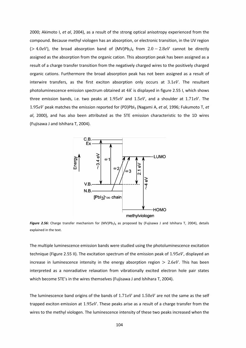
104
2000; Akimoto I, et al, 2004), as a result of the strong optical anisotropy experienced from the
compound. Because methyl viologen has an absorption, or electronic transition, in the UV region
( ), the broad absorption band of (MV)Pb2I6 from cannot be directly
assigned as the absorption from the organic cation. This absorption peak has been assigned as a
result of a charge transfer transition from the negatively charged wires to the positively charged
organic cations. Furthermore the broad absorption peak has not been assigned as a result of
interwire transfers, as the first exciton absorption only occurs at . The resultant
photoluminescence emission spectrum obtained at is displayed in figure 2.55 I, which shows
three emission bands, i.e. two peaks at and , and a shoulder at . The
peak matches the emission reported for (PD)PbI3 (Nagami A, et al, 1996; Fukumoto T, et
al, 2000), and has also been attributed as the STE emission characteristic to the 1D wires
(Fujisawa J and Ishihara T, 2004).
Figure 2.56: Charge transfer mechanism for (MV)Pb2I6 as proposed by (Fujisawa J and Ishihara T, 2004), details
explained in the text.
The multiple luminescence emission bands were studied using the photoluminescence excitation
technique (Figure 2.55 II). The excitation spectrum of the emission peak of , displayed an
increase in luminescence intensity in the energy absorption region . This has been
interpreted as a nonradiative relaxation from vibrationally excited electron hole pair states
which become STE’s in the wires themselves (Fujisawa J and Ishihara T, 2004).
The luminescence band origins of the bands of and are not the same as the self
trapped exciton emission at . These peaks arise as a result of a charge transfer from the
wires to the methyl viologen. The luminescence intensity of these two peaks increased when the

105
excitation energy for the emission process occurred within the visible region, (below the first
exciton absorption). This suggests that the charge transfer mechanism is a result of an electron
being transferred from the wires valence band, to the LUMO of the methyl viologen. The
emission peak at shows an absorption edge in the PLE spectrum (b) at (which is
stokes shifted from the emission) and the emission peak at displayed an absorption
edge at (stokes shifted ). These two PL emissions are attributed to polaron pairs
generated through lattice relaxation (Fujisawa J and Ishihara T, 2004). This is likely from the large
resultant stokes shifted emissions. Furthermore the difference in these two bands absorption
edges, suggest that there are two origins of the charge transfer to the LUMO of methyl viologen.
The differences in the PLE absorption edges of the two band emission bands ( and
) with a difference of , implies that the two charge transfer transitions occur from
the top of the valence band (the antibonding lone pair electrons of Pb 6s) and the valence bands
nonbonding electrons (I 5p electrons). This notion is confirmed through the electronic structure
calculations performed by (Azuma J, et al, 2002b). The calculations give the nonbonding
electrons band to be below the top of the valence band edge. The full mechanism
proposed for the charge transfer absorptions are displayed in Figure 2.56 (Fujisawa J and
Ishihara T, 2004). From figure 2.56 is the first exciton absorption, is the charge transfer
absorption for the emission, and is the charge transfer absorption for the
emission. Hence the onset of the charge transfer is from the valence band absorption
(PLE) experiments.
An aside note on 1D systems is that they are important materials in terms of electronic transport
properties. As we have already discussed, after the charge carriers (excitons/electron hole pairs)
are generated, they immediately relax into polarons through electron lattice interactions. The
polarons then behave like a soliton (single wave packet moving down the wire). These soliton
like polarons, display large carrier mobility even at room temperature ( ) (Fujisawa J
and Tajima N, 2005). Photoconductivity measurements were also completed on (MV)Pb2I6 by
(Fujisawa J and Tajima N, 2005) and displayed that the photoconductivity of this compound is
predominantly induced due to the charge transfer interaction from the wires to the spacers.
Furthermore the photoconductivity measurements have confirmed the energy transfer from the
valence band to the LUMO of methyl viologen to be (Fujisawa J and Tajima N, 2005).

106
Figure 2.57: Infrared spectra recorded for a) (MV)Cl, b) (MV)Cl2 c) (MV)I2, d) (MV)Pb2I6 (Fujisawa J, et al, 2007).
A final investigation of the vibrational (IR) spectra of (MV)Pb2I6 was completed by (Fujisawa J, et
al, 2007) in order to investigate any weak interactions present between the wires and spacers.
Infra Red spectra were collected for the following compounds: the radical compound MVCl, and
the two known charge transfer compounds of MVCl2 and MVI2 which were used as a comparison
with MVPb2I6. The reported IR spectra of all four compounds may be seen in figure 2.57. Since
the lead iodide wires phonon vibrations are only expected below 200cm-1 the IR spectra would
still result in useful weak interactions information. Although the molecular vibrations between
and are fairly similar the vibrational peaks around significantly shift
to the low energy side by and for MVI2 and MVPb2I6 respectively, compared with
MVCl2. In addition to the shift the oscillator strength of this peak for MVPb2I6 is twice that of the
other compounds, as well as having a increase of the vibrational energy compared with
MVCl2. This peak in the IR specta has been attributed to the molecular vibrations of the nitrogen
cations.
Hence the following conclusions have been made. Because of the peak shift and increase in
oscillator strength for the nitrogen cation in MVPb2I6 is observed, an increase in covalent
character between the nitrogen cation and the negatively charged lead iodide wires via the
charge transfer interaction is expected (Fujisawa J, et al, 2007).

107
More recently ethylviologen was incorporated with lead iodide and formed 1D
ribbons/coulombs (Pradeesh K, et al, 2010) in preference over the single face sharing octahedral
wires of (MV)Pb2I6. The first exciton absorption was also observed at for the ethylviologen
derivative, however the STE luminescence was blue shifted and was now observed at
with a shoulder at . The major difference in the photoluminescence spectrum
from that reported for MVPb2I6 (Fujisawa J and Ishihara T, 2004) was the emission peak at
for the ethylviologen lead iodide which was not assigned (Pradeesh K, et al, 2010). This
phenomenon will be further dealt with in chapter 5.3.
Lastly it is worth mentioning the use of an organic metal (etylenedithio-1,2-
diiodotertathiafluvalene) (EDT-TTF-I2) which has also been incorporated with lead iodide to form
1D face sharing octahedral wires of ((EDT-TTF-I2)2PbI3.H2O). This compound has shown improved
conductivity for an anionic type salt at ambient pressure (Devic T, et al, 2004). These authors
also reported a similar finding for other compounds (Devic T, et al, 2003). Other recent work by
(Zhao H, R, et al, 2010) has investigated the ferroelectric behaviour of some compounds like
(PD)PbI3, because of their inherent crystal polarizability due to the large optical anisotropy and
the 1D nature of these compounds.
2.8 Optical non-linearity in organic inorganic hybrids
A brief discussion on the nonlinear optical properties of hybrids will be discussed here as this
section is covered more in depth in chapter 6. As optical nonlinearity is a large field of study in
its own right the ability of low dimensional hybrids to be tailored for this purpose has shown
favourable results. Firstly a brief mention that second harmonic generation (SHG) is a
property of noncentrosymmetric crystals, and not dependant on the material under study.
However the material may increase the SHG response recorded due to an increase in
hyperpolarizability of the crystal (Nye J. F, 1957). Third harmonic generation (THG) is different
as it occurs in isotropic media, and or crystals with a centre of inversion, i.e. is suppressed in
the crystal and the non vanishing term now predominates (Fox M, 2008). Quantum wells in
general display good inherent resonant third order nonlinearity.
Compounds C10PbI4 and C6PbI4 2D quantum wells have been probed for resonant third order
non linearity’s (Calabrese J, et al, 1991; Xu C. Q, et al, 1991; Kondo T, et al, 1998) and more
recently for (PEA)2PbI4 (Shimizu M, et al, 2007). The of a highly oriented film

108
of C10PbI4 displayed a large (THG) three photon resonance at (considering the
). This was caused from the lowest energy exciton which is known to
have a large oscillator strength and sharp well defined emission profile. It was also surmised that
since both and follow the same transition rule, a
resonance enhancement due to the lowest energy exciton can also be expected for
for C10PbI4. Moreover the magnitude of the reaches a
very large value of at incoming beam , which is
comparable to the largest reported value of organic materials with one-dimensional structures.
The result was reported to be very promising suggesting that the lead halide quantum well
structures are very promising as nonlinear optical materials (Xu C. Q, et al, 1991). The
was also investigated for C6PbI4 where the nonlinear optical susceptibility
was recorded as also measured at the lowest exciton resonance (measured at
8K). Kondo T, et al, 1998 further commented that because the excitons are stable at room
temperature, large nonlinear optical responses are therefore also expected at room
temperature, and hence remain a class of materials with promising resonant nonlinear optical
potential.
More recently an investigation of these three compounds was completed in order to study the
effect of the dielectric confinement caused from the large dielectric mismatch between the well
and the barrier and discovered the exciton bleaching and blue shift are larger in the (C6)2PbI4
than in (PEA)2PbI4 (Shimizu M, et al, 2005), which is advantageous for practical application.
Traditionally only organic or inorganic compounds crystallising in noncentrosymmertic space
groups and have some degree of polarisablity, have been investigated for their SHG responses.
Hybrids are an alternative approach to finding NLO crystals with a large SHG response, as the
anionic nature of the hybrids should automatically increase the (hyper)polarizability of the
crystal, thereby giving larger SHG responses for hybrid type materials (Giffard M, et al, 2005).
In other studies the compound {[NH3(CH2)2SS(CH2)2NH3]PbI5}H30, which has been reported to
form 1D corner sharing chains, and crystallize in a chiral space group was shown to be a
good candidate for (SHG) investigation (Mercier N, et al, 2006). In addition, this compound
underwent a reversible phase change at 75oC. The high temperature form shifted into the space
group . The centre of inversion generated from the phase change then suppressed the
SHG response. The phase change occurred as a result of a conformational change in the organic

109
cation, which induced a mirror plane in the crystal above 75oC as seen in figure 2.58. Thus this
material was observed to behave as a Second Harmonic Generation (SHG) switch driven by
temperature. It was reported that even after temperature cycles the crystal remained intact,
and continued to oscillate with temperature between the chiral and non-chiral space groups
(Mercier N, et al, 2006). A similar investigation was also completed for a bismuth iodide hybrid
with the same disulphide cation, and reported the same chiral to nonchiral phase change upon
temperature increase (Bi W, et al, 2008).
Figure 2.58: Schematic representation of the conformational change of the organic diamine in the
{[NH3(CH2)2SS(CH2)2NH3]PbI5}H30 hybrid system at 75oC (Mercier N, et al, 2006).
The use of the highly efficient (SHG) organic cation (trans-4-[4-dimethylamino-styryl]-1-
methylpyridimium), DAMS+ has been reported to form 1D chains with lead iodide and dimethyl
sulphoxide i.e. (DAMS)PbI3.2DMSO which crystallized in the noncentrosymmetric space group
(Guloy A. M, et al, 2001). The thought process behind combining these two components was
firstly, to use the low dimensional nature of lead iodide to template (DAMS) into a polarized
configuration, and increasing its polarizability by creating a charge on the organic molecule.
Secondly the 1D wires are highly polarisable down one of the crystallographic directions, and
was hypothesized that this ability may further enhance the SHG response of the crystal. It was
then reported that (DAMS)PbI3.2DMSO crystal displayed a SHG response 15 times greater than
that of KTP (potassium tantalum phosphate) when probed at (Guloy A. M, et al, 2001).
However it was also reported that when the crystal was probed at , the SHG
response also displayed a luminescence peak at (Guloy A. M, et al, 2001). Since the
direct gap absorption from the wires should only occur around (Nagami A, et al, 1996)
the reported red luminescence response should be due to a charge transfer mechanism
occurring from the wires to the spacers or originate from the STE response as are experienced in
these wires. The excitation generated from the SHG response should be sufficient to
populate the LUMO of the organic cation with the electrons from the valence band of the wires,

110
and hence display a luminescence response at (however this was not reported in the
paper, but the red colour of the crystal, and the short intermolecular distances of of
DAMS molecules does suggest that this should be the case (Guloy A. M, et al, 2001)).
Other investigations of the halogen substituted (DAMS)PbBr3 SHG response was also reported
(Papavassiliou G. C, et al, 2003). This compound also displayed the red luminescence with the
SHG response. Interestingly the Bromide analogue crystallized in a centrosymmetric
space group and still displayed a large SHG response. This is thought to be due to the large
anisotropic effect of the 1D wires over the centre of inversion generated by the organic cation
(Papavassiliou G. C, et al, 2003). Other NLO studies on similar compounds have also been
completed by (Papavassiliou G. C, et al, 1999; 1999b; 2001; Goto T, et al, 2002). Furthermore
DAMS has been successfully investigated with the transition metal hybrids, and displayed large
SHG responses specifically with the Copper Iodide analogue (Cariati E, et al, 2001).
2.9 Electroluminescent devices and the use of chromophores in 2D hybrids
The first attempt at creating an electrolumincent device from a hybrid perovskite was with
(PEA)2PbI4 and (cyclohexylethylammonium)2PbI4 which was investigated by (Hong X, et al, 1992;
Era M, et al, 1994; 1995). They showed electroluminescence at LNT of 10 000 cd/m2 at 2A.cm-2
and 24V, however could not get any EL at room temperature. It was suggested that the rapid
drop off in EL efficiency was due to thermal quenching of the excitons. More recently however
(Pradeesh K, et al, 2009a) investigated a novel in situ-intercalation method to fabricate device
quality hybrid inorganic organic self assembled quantum wells of the unsaturated
cyclohexylethylamine (C6H9C2H4NH3)2PbI4. Pradeesh K, et al, 2009a showed promising results,
displaying in particular the increasing in room temperature photoluminescence intensity with
increasing film thickness.
Mitzi D. B, et al, 2001c, investigated the incorporation of a chromophore 5,5’’’-bis(aminoethyl)-
2,2’:5’,2’’:5’’,2’’’-quaterthiophene (AEQT) with lead halide to form 2D (AEQT)PbX4 where X = Cl,
Br, or I. The reason for incorporating AEQT into the perovskite layers, is that the chromophore
itself displays better room temperature electroluminescence than the semiconducting
perovskite layers on their own (PbX42-). So then why is it necessary to have the inorganic
component present in the system? The inorganic component adds thermal stability to the

111
organic compound (Mitzi D. B, et al, 2001c), and therefore the incorporation of the Dye (AEQT),
as seen in figure 2.59 (the crystal structure of (AEQT)PbBr4).
From the three halogenated 2D systems investigated the (AEQT)PbCl4 hybrid displayed a greater
room temperature electroluminescence efficiency (20-30 times) than that of its bromide and
iodide analogues. It was found that the wider the band gaps of the inorganic component the
greater the electroluminescence efficiency shown. This was further supported from the
investigations of an even wider band gap hybrid (AEQT)CdCl4 which displayed ever better EL
efficiency compared to (AEQT)PbCl4. Mitzi D. B, et al, 2001c suggested this phenomenon was
due to better carrier injection, transport and electron hole recombination in the wider band gap
systems. The UV-Vis spectrum of (AEQT)PbCl4 and the EL device manufactured from this material
may be seen in figure 2.60.
Figure 2.59: The use of the Chromophore 5,5’’’-bis(aminoethyl)-2,2’:5’,2’’:5’’,2’’’-quaterthiophene (AEQT) with in
(AEQT)PbX4, where X = Cl, Br, and I (Mitzi D. B, et al, 2001c).

112
Figure 2.60: (Top) Electroluminescent device of the chromophore hybrid (AEQT)PbCl4, (Bottom) the UV-Vis absorption
spectrum of (AEQT)PbCl4. The 331nm peak associated with the PbCl4 layers and the broad 400nm peak with the AEQT
dye (Mitzi D. B, et al, 2001c).
The other contributing papers to the above set of work should also be mentioned, namely
(Chondroudis K and Mitzi D. B, 1999), in their investigations in the electroluminescence from an
organic inorganic perovskite incorporating a quaterthiophene dye within lead halide perovskite
layers (PbX4)); design structure and optical properties of organic inorganic perovskites containing
an Oligothiophene chromophore (Mitzi D. B, et al, 1999b); the effect of thermal annealing on the
optical and morphological properties of (AETH)PbX4 (Chondroudis K, et al, 2000b); and the use of
ionic salt dyes as amorphous, thermally stable emitting layers in organic LED’s (Chondroudis K
and Mitzi D. B, 2000a).
Other more recent developments have investigated the incorporation of naphthalene into
organic inorganic hybrid quantum well materials and shown nearly perfect triplet-triplet energy

113
transfer from wannier excitons (Ema K, et al, 2008). Also an interesting development has been
the fabrication and characterization of organic inorganic perovskite films containing fullerene
derivatives (Kikuchi K, et al, 2005). Although device fabrication is not the focus of the work in
this thesis it is worth mentioning the other developments in this field. Various methodologies
have been employed in the light emitting diode (LED) and organic light emitting diode (OLED)
communities for their use of these materials for highly efficient displays. The review article on
Inorganic organic Hybrid structured LED’s (Gebauer T and Schmid G, 1999) give broader insights
into this field. Spin-Coating preparation of highly ordered photoluminescent films of layered PbI2
aminoalkyloxysilane perovskites have also shown promise for further development (Cheng Z. Y,
et al, 2005). And finally is the synthesis of liquid crystalline poly(1-pentyne)s and fabrication of
polyacetylene-perovskite hybrids (Hua J, et al, 2006) and functional perovskite hybrid of
polyacteylene ammonium lead bromide (Xu H, et al, 2006) for more robust device quality
operation.
2.10 Summary and Conclusions
In summary, in this chapter we have covered the origin of the organic inorganic hybrid
perovskites specifically from the three dimensional motif. The concept of dimensional reduction
and its impact on the electronic properties of the material was also illustrated. We have also
shown the two mechanisms that can be used to create low dimensional systems. Namely, the
traditional method developed from cutting various slices from the 3D peroviskite motif, and the
various inorganic motif types that can arise through altering I/M ratio’s, organic weak interaction
effects, and solvent effects. More attention has been focussed on the excitonic behaviour in the
2D and 1D systems with discussions of the phase transitions that may arise through temperature
fluctuations as this forms the basis for the results we discuss in chapters 4 and 5. We have only
briefly touched on the literature on the nonlinear optics of hybrid materials as this topic’s
background is developed more thoroughly in chapter 6. Lastly, a brief summary of
electroluminescent devices developed from hybrid organic inorganic systems allows us to see
the applicability of the research for further device development.

114
Chapter 3: Experimental
3. Experimental:
Herein we report the synthesis and characterization techniques used to prepare and analyze the
inorganic-organic hybrids investigated. The simple synthesis techniques will first be explained
followed by a description of the characterization techniques used.
3.1 Synthesis:
Two methodologies were employed in order to synthesize and grow single crystals of the hybrid
materials. They follow the general equations given below.
2D <100> layered Hybrids
Simple 1D Hybrids
3.1.1 Slow cooling method:
The slow cooling method was employed whereby a stoichiometric amount of PbX2 salt (generally
0.1g of the metal halide salt) (where X = I or Br) was added to a 10 or 20ml sample vial.
Stoichiometric amounts of RNH2 was then added followed by the addition of an excess amount
of either 47% aqueous Hydro-iodoic acid or 48% aqueous Hydro-Bromic acid depending on the
metal halide salt used. Approximately 2-8ml of acid was added depending on the solubility which
is largely governed by the ammonium cation. A precipitate usually formed, initial dissolution was
usually assisted by ultrasonication, which assisted in adequately dispersing the precipitate and
hence dissolution. The precipitate usually only dissolved after heating to 90oC, therefore the
sample vial was heated to 90oC and subsequently refluxed at this temperature for ~6hours (this
was a critical step for the alcohol based amines, as they substituted the alcohol for the halide,
compounds in chapter 4). The sample was then slow cooled in a controlled manner at a rate of
1-2oC/min to room temperature. If the crystals formed were not large enough or not of high
enough quality the heating cycle was repeated until suitably sized crystals of adequate quality
could be harvested for SC-XRD. It was generally found that the more saturated solutions
produced better crystals, and that complete dissolution of the precipitate at 90oC is crucial. The
following compounds were synthesized and crystals grown using this methodology. For the 2D
layered perovskites (where Cn = CnH2n+1NH3): (Cn)2PbBr4 where n =4-7; (XCn)2PbBr4 where X = OH
for n = 2 and Br for n = 3-5; (Cn)2PbI4 where n = 4-7; and the 1D chains in 5.3 of
(H3NPhCH2PhNH3)Pb2I6; and (H3NPhPhNH3)Pb2I6.2H2O.

115
3.1.2 Slow evaporation method:
In the case where the slow cooling method did not work or was not attempted due to reactivity
concerns, slow evaporation was used instead. Due to solubility issues and reactivity with the
solvent (DMF) or the organic cation, only a stoichiometric amount of the halide acid was added
to a MX2 + zRNH2 reaction mixture. A suitable organic solvent was used to dissolve the reaction
mixture. The dissolution of the reaction mixture was generally assisted by placing the sample vial
in an ultrasound bath. The dissolved mixture was then allowed to evaporate to grow suitably
sized crystals.
Dimethyl formamide (DMF) was used in the synthesis of the 1D chains of 5.1 and 5.2 as seen in
the schemes below.
Dimethyl sulphoxide (DMSO) was used for the following compounds: the 1D chains of (5.3)
DMSO.(4,4’-Bipyridine)Pb2I6; DMSO.( 4,4’-propane-1,3-dipyridine)Pb2I6 and (4,4’-(E)-ethene-1,2-
dipyridine) Pb2I6.
Acetonitrile was used for the following compounds: The 2D layered perovskites of
(BrC2H4NH3)2PbI4 and (HOC2H4NH3)2PbI4 in which slow evaporation was carried out at 4oC in
order to obtain the kinetic product. The 2D layered perovskites of (ICnH2nNH3)2PbI4 where n = 2-6
were first refluxed at 100oC for 1-2hours, then allowed to slowly evaporate. In order to obtain
the halogenated aliphatics (ICnH2nNH3)2PbI4 where n = 2-6, the respective alcohol starting
materials (HOCnH2nNH2) where n = 2-6, were used. The reflux step in the synthesis is necessary
to convert the alcohol group to the halogenated group.

116
3.1.3 Schemes of compounds investigated with relevant chapter numbers:
4.1 4.2

117
4.3

118
5.1
5.2
5.3

119
6.2
6.3

120
3.2 Single crystal X-ray diffraction (SC-XRD):
Figure 3.1: The Bruker Apex II single crystal diffractometer with Mo K radiation, with attached Oxford cryostream
cooler Series 700.
Intensity data were collected on a Bruker APEX II CCD area detector diffractometer with graphite
monochromated Mo K radiation (50kV, 30mA) using the APEX 2 (Bruker, 2005a) data collection
software. The collection method involved -scans of width 0.5 and 512x512 bit data frames.
Data reduction was carried out using the program SAINT+ (Bruker, 2005b) and face indexed
absorption corrections were made using XPREP (Bruker, 2005b).
The crystal structures were solved by direct methods using SHELXS (Sheldrick G. M, 2008) and
WinGX (Farrugia, 1999). Non-hydrogen atoms were first refined isotropically followed by
anisotropic refinement by full matrix least-squares calculations based on F2 using SHELXL
(Sheldrick G. M, 2008). Hydrogen atoms were first located in the difference map then positioned
geometrically and allowed to ride on their respective parent atoms. Diagrams and publication
material were generated using SHELXL, PLATON (Spek A. L, 2009) and ORTEP-3 (Farrugia L. J,
1997). Temperature was controlled using the Oxford cryostream cooler Series 700, with variable
temperature capabilities with a temperature range of (100-400K). Most of the hybrid materials,
data collections, were obtained at various temperatures. Specifically the hybrids of chapter 4.1;
4.2; and 5.1. The remaining structures were all collected at 173K for higher resolution, and 293K
to ascertain if the compounds underwent any further low temperature phase transitions unable
to be detected from the DSC experiments.

121
3.2.1 References:
Brandenburg K, Diamond version 3.1f. Crystal impact GbR Bonn, Germany. (1997)
Bruker, APEX2. Version 2.0-1. Bruker AXS Inc., Madison, Wisconsin, USA. (2005a)
Bruker, SAINT+. Version 6.0. (Includes XPREP and SADABS) Bruker AXS Inc., Madison, Wisconsin, USA. (2005b)
Bruker, SHELXTL. Version 5.1. (Includes XL, XS, XP and XSHELL) Bruker AXS Inc., Madison, Wisconsin, USA. (1999)
Farrugia L.J, J. Appl. Cryst., (1997) 30, 565
Farrugia L.J, J. Appl. Cryst., (1999) 32, 837
Sheldrick G. M, Acta. Cryst., (2008) A64, 112
Spek A. L, Acta. Cryst., (2009) D65, 148

122
3.3 Powder X-ray Diffraction (P-XRD):
Figure 3.2: The Bruker D8 Advance powder diffractometer with the Vantec super-speed MIKROGAPTM
detector, and
Cu Kα1, Kα2 spectral lines, as Kβ was suppressed using a Ni filter.
X-ray powder diffraction data were collected on a Bruker-AXS D8 ADVANCE diffractometer
equipped with a Cu tube and Ni-filter. The diffractometer was operated in the parallel beam
geometry with the data collected using a Vantec super-speed MIKROGAPTM detector. Each
sample was dispersed as a finely ground powder onto a zero-background silicon wafer sample
holder. All data collections were performed over the range 5◦ - 90◦ 2θ using a step size of 2θ =
0.01◦ and a counting time of 2 sec/step, and in reflection mode. Cell and rietveld refinements
were carried out using the TOPAS V4.2 package (Coelho A. A, 2000). Samples were also
measured on the Bruker-AXS D2 PHASER which is in the Bragg-Brentano geometry, with a Lynx-
eye detector. Similar scanning parameters used with the D8 ADVANCE were used to obtain
powder diffraction data.
3.3.1 References:
Coelho A. A, TOPAS v4.2: General Profile and Structure Analysis Software for Powder Diffraction Data Karslruhe. (2000)

123
3.4 Photoluminescence:
Figure 3.3: The experimental set up used for the photoluminescence measurements. The UV laser had to pass outside
the original optics, as the instrument was not UV optics capable. Hence a set of mirrors redirected the beam to avoid
the internal optics, and onto the sample to excite the compound in order to measure the photoluminescence
response. The sample is mounted in the cryostat and cooled down with liquid nitrogen to 77K through a temperature
controller.
Photoluminescence spectra were acquired with the multiline UV (333.6 – 363.8nm) of an argon
ion laser as the excitation source. Light emission was undertaken though the temperature
controlled Linkam (THMS350V) cryostat mounted onto the spectrograph stage of a Jobin-Yvon
T64000 Raman spectrometer. The power at the sample was kept very low (~0.20 mW) so as to
not cause sample degradation, whereas the laser-beam diameter at the sample was about 1 μm.
The samples were generally measured at both 77K and 293K.
3.5 UV-Vis:
For the UV–vis spectral analysis, a small portion of solvent containing the product was slow
evaporated off a circular sapphire disc (0.1X10mm) in order to deposit the crystals evenly on the
surface. The samples were inserted into a custom built nitrogen bath cryostat, where scans were
performed at 77K and room temperature. The scanned range was 200–800 nm, and carried out
using a Varian Cary 500 digital spectrophotometer.

124
3.6 Thermal analysis (DSC):
Differential Scanning Calorimetry (DSC) was used to determine the transition temperatures of
the phase transitions and their enthalpies under atmospheric conditions. All DSC experiments
were carried out on a Mettler Toledo 822e calorimeter, which was fitted with a cryostream in
order to cool to 213K. The temperature range of the instrument is from 213-773K. Our
measurements were performed from 213K-443K. This temperature range was sufficient to
monitor all the phase transitions of the hybrid materials under investigation. Measurements
were both heated and cooled through the above mentioned temperature range, at a heating
and cooling rate of 10K/min respectively. All the compounds reported in this project were
investigated for any thermal events in the above mentioned temperature range.
3.7 Elemental analysis:
Elemental analysis of the compounds in 5.1 and 5.2 were performed by the Institute of Soil,
Climate and Weather (Pretoria, South Africa). The instrument used was a Carlo Erba
Instruments, model NA 1500, Nitrogen/Carbon/Sulphur Analyser. The instrument was modified
to do CHN elemental analyses as well (Philpott, 2002).

125
Chapter 4: The structure and optical properties of <100> 2D lead halide
quantum wells
4.1 The Structure and Phase transitions of (CnH2n+1NH3)2PbBr4 where n = 4-7
4.1.1 Introduction:
The 2D layered aliphatic (CnH2n+1NH3)2PbX4 hybrid perovskite compounds, represented as
(Cn)PbX4 from here, have been thoroughly investigated over the years. The Lead Bromide 2D
hybrids are understudied by comparison with their iodide analogues. This is the case as the lead
bromide hybrids were thought to display fundamentally similar optical properties, only the band
gap was blue shifted relative to the iodide analogue (Papavassiliou G. C, 1997). The red shift of
the band gap experienced as we proceed down the group (Cl I) is due to the increase in
covalent character of the halogen bonding with the lead. The band assignments are expected to
remain the same for each of the halogenated systems, and should experience the same red shift
as we proceed down the group (Cl I) (Azuma J, et al, 2002a). However after further
investigation, it was discovered that the PbBr hybrids specifically, display a more intricate
emission spectra as seen for the simple aliphatic type compounds (Kato Y, et al, 2003; Ema K, et
al, 2006; Kitazawa N, et al, 2009; 2010).
It should be noted that there are very few crystal structures reported for the <100> type 2D lead
bromide hybrids. The crystal structures have been challenging to obtain through SC-XRD
techniques, largely due to diffuse scattering issues, and therefore other methodologies have
been employed to confirm the two dimensional nature of the lead bromide hybrids. Powder
diffraction studies have been employed to obtain the interlayer spacing of the hybrid, in
conjunction with optical absorption measurements to confirm the compounds two dimensional
nature (Lee S. J, et al, 2000; Tabuchi Y, et al, 2000; Kitazawa N, et al, 2010; 2010b). The alternate
methodologies have been employed as a result of the importance of investigating the optical
properties associated with these compounds.
Success with determining the crystal structures of the (Cn)PbI4 layered hybrids, where n = 4-10,
12, 14, 16, and 18, (Billing D. G, Lemmerer A, 2007; 2008; Lemmerer A, 2007; Lemmerer A, Billing
D. G, 2011; Nagapetyan S. S, et al, 1988; Ishihara T, et al, 1990; Mitzi D. B, 1996) have been
achieved. Furthermore the multiple phase transitions associated with the aliphatic templates
have been categorically investigated for each of the abovementioned systems by (Billing D. G,
Lemmerer A, 2007; 2008; Lemmerer A, 2007). The importance of the phase transitions on the
optical properties has been realized and investigated recently for (C12)PbI4 by (Pradeesh K, et al,

126
2009b). Simple conformational changes in the aliphatic have negligible impact on the band gap
of the hybrid (Ishihara T, et al, 1989; 1990) however, certain phase changes for example, upon
heating result in the inorganic layers decreasing the degree of distortion of the layers,
specifically the corrugation tilt Ψ and Pb-X-Pb bridging angles which move toward their ideal 0o
and 180o, respectively. These two parameters have been shown to have the largest impact on
the band gap of the material (Knutson J. L, et al, 2005). The red shift of the band gap, as these
angles move toward ideallity, is due to an increase of the stereochemical activity of lead’s lone
pair of electrons (Mitzi D. B, 1996; Knutson J. L, et al, 2005). Other phase transition mechanisms
present in these systems include the inorganic layers rearranging between the eclipsed and
staggered arrangements upon heating (i.e. the monoclinic and orthorhombic phases) with an
associated and correlated decrease in inorganic octahedral distortions. These high temperature
phases in conjunction with the decrease in overall distortions further lead to an increase in
crystal symmetry. This phenomenon is well known and noted that the structural phase
transitions change the crystal system from monoclinic to orthorhombic and finally to tetragonal
with increasing temperature (Mitzi D. B, 1999; Billing D. G, Lemmerer A, 2007; 2008; Lemmerer
A, 2007).
Billing and Lemmerer observed that the longer chain aliphatics n = 12, 14, 16 and 18, in (Cn)PbI4
hybrids display a decrease in crystal symmetry with increasing temperature, i.e. they move from
the orthorhombic low temperature (staggered layers) to a monoclinic (eclipsed layers) at high
temperature, however still observing the decrease in octahedral distortions with the increase in
temperature (Billing D. G, and Lemmerer A, 2009). They were also able to confirm the structural
details of the phase transformations with changing temperature of the (Cn)PbI4 series, and
confirm the similarity of the phase transformation mechanisms of the originally investigated
(Cn)MCl4 hybrids where M = Mn, Cu, Cd, but most comprehensively studied structurally in the
(Cn)CdCl4 hybrids (Chanh N. B, et al, 1983; 1985; 1989; Kind R, et al, 1979; Ricard L, et al, 1984;
Shenk K. J, and Chapuis G, 1988). Although the packing of the aliphatic chains in the transition
metal hybrids are non-interdigitated unlike the lead iodide hybrids where the chains pack in an
interdigitated fashion, the phase transformation mechanism proceed through a similar path. It
has been proposed that the reason for the chains to pack in an interdigitated fashion regards the
separation of the metal centres of the corner sharing octahedra from one another, i.e. the
farther away the metal centres are from one other the more likely the chains will interdigitate
(Nagapetyan S. S, et al, 1988).

127
Within the layered hybrid perovskites, the changes in the organic conformations result in the
solid state phase transitions to occur through one of two mechanisms. Firstly are the displacive
phase transitions, i.e. associated with conformational changes of the organic ammonium group.
And secondly is the order-disorder phase transition along the longitudinal axis of the unit cell.
Since the alkyl ammonium chains are so flexible the (CnH2n+1NH3)2MX4 hybrids undergo multiple
phase transitions. The phase transition progression ultimately results in a quasi-melting
transition of the organic chain at higher temperatures.
This, invariably final transition, only occurs after proceeding through a few solid state
conformational intermediates. These conformational intermediates proceed through the
following generally accepted mechanisms. The chains may exist in an all trans conformation or
kinks may arise within the chain. A kink consists of two gauche conformations of opposite signs,
separated by an odd number of all trans conformations. At higher temperatures the various
conformations become mobile. When two kinks of opposite sign meet each other they can
annihilate. Conversely kinks may form spontaneously in sections of the chain with the all trans
conformations. The combination of these conformational changes results in the quasi melting
transition to occur (Depmeier W, 2009; Kind R, 1980). The quasi melting transition also displays
the highest enthalpy and entropy change for a transition. In addition the quasi-melting transition
refers to only the alkyl chain melting, with the overall compound still remaining in the solid state
(Chanh N. B, et al, 1989). As the temperature increases and the alkyl ammonium hybrid moves
through the series of solid state intermediates, the inorganic layers result in an increase in
interlayer spacing as the rotational disordering of the chains increases (Barman S, et al, 2003).
An observation regarding the alkyl chain length and the phase transitions that they undergo was
made by (Mitzi D. B, 1999). The order disorder type transitions are the only phase transitions
that occur when the organic ammonium chain length is , however both types of
transitions occur when the chain length i.e. displacive and order disorder.
Incommensurate phases have also been observed, however only for (C3)MCl4 where M = Cd, Mn
and Cu hybrids. The Cd hybrid has three phases, a disorder and displacive phase III and I,
respectively, and an incommensurate phase II (Chapuis, G, 1978; Doudin B and Chapuis G, 1988).
The Mn hybrid has six phases and proceeds through commensurate and incommensurate phases
all the way to the last two high temperature commensurate phases (Depmeier W and Mason S.
A, 1978; 1983; Harris, et al, 1994; Depmeier W, 2009). Interestingly the (C3)PbI4 hybrid
investigated does not form a 2D layered hybrid perovskite but rather a 2D net type motif (Billing
D. G and Lemmerer A, 2006b). The importance of the presence of modulated phases in

128
semiconducting hybrids may influence the emission profile experienced for that compound. As
modulation, or even certain phase transitions may result in localized physical defects and or
promote exciton-phonon type coupling giving rise to sub-energy levels and split emission lines,
because. These split emission profiles at low temperature have been observed the 2D lead
bromide’s thus far, specifically in the aliphatics (Cn)PbBr4 (n = 4, 5, 7, 12) (Kitazawa N, et al,
2010), and n = 8 (Kitazawa N, et al, 2009), but also in (PhCnH2nNH3)PbBr4 where n = 1-4
(Kitazawa N and Watanabe Y, 2010b).
This is the underlying reason for the investigation into the well known aliphatic hybrids and their
phase transitions. Herein we discuss the crystal structures and the phase transitions of the lead
bromide (Cn)PbBr4 family, where n = 4-7, compounds 1-4 respectively, and the associated
mechanism as previously discussed by (Billing D. G, Lemmerer A, 2007) for the short chain
derivatives of (Cn)PbI4. Thermal analysis studies (DSC) have been previously reported on
(C4)PbBr4 and (C6)PbBr4, however no further structural studies, besides powder diffraction
investigations, were completed (Tabuchi Y, et al, 2000). A scheme summarising the phase
changes in the above mentioned compounds may be seen in scheme 4.1.1.
Scheme 4.1.1: A summary of the phase transitions and the relative phase transformation temperatures for both
heating and cooling runs for (Cn)PbBr4. Estimates of the phase transformation temperatures were made for the
transitions that occurred below the measuring capability of the differential scanning calorimeter, which were
examined via SC-XRD cooling experiments.
(C4H9NH3)2PbBr4 𝐼𝐼 ⇆387𝐾383𝐾 𝐼
(C5H11NH3)2PbBr4 𝐼𝐼𝐼 ⇆ (𝑏𝑒𝑡𝑤𝑒𝑒 173𝐾 𝑎 𝑑 213𝐾) 𝐼𝐼 ⇆303𝐾307.5𝐾 𝐼
(C6H13NH3)2PbBr4 𝐼𝑉 ⇆~183𝐾~183𝐾 𝐼𝐼𝐼 ⇆~213𝐾
~213𝐾 𝐼𝐼 ⇆300.6𝐾296.6𝐾 𝐼
(C7H15NH3)2PbBr4 𝐼𝐼𝐼 ⇆ (𝑏𝑒𝑡𝑤𝑒𝑒 173𝐾 𝑎 𝑑 213𝐾) 𝐼𝐼 ⇆292𝐾289.3𝐾 𝐼

129
4.1.2 Results and Discussion
In order to describe the mechanisms associated with a phase transition, certain geometrical
parameters were introduced. (Doudin B and Chapuis G, 1990) were the first to describe the
necessary geometrical parameters to describe these relative angles associated with the changes
of the alkyl ammonium conformations, specifically of (C3)CuCl4, before and after a phase
change. (Billing D. G, Lemmerer A, 2007; 2008; Lemmerer A, 2007, Lemmerer A, Billing D. G,
2011) further extended these definitions, to describe the phase changes observed in the longer
alkyl ammonium chain derivatives for (Cn)PbI4 hybrid perovskites where n = 4-10, 12, 14, 16, 18.
From figure 4.1.1, the tilt angle of the organic chain is measured by the angle between the
plane through the inorganic layers and the vector containing the first and last atom of each
chain. In the case of (C4)PbI4 the first atom is N1 and the last is C4 (Billing D. G, Lemmerer A,
2007). Another two important geometrical parameters were used to describe the organics
motion due to the phase change. The angle, which may be defined as the torsion angle
between the plane containing all of the atoms of the alkyl chain, and the plane formed by the
lead atoms of the inorganic layers i.e. the vertical tilt of the organic chain. And finally the
angle, which is the angle between a vector containing atoms N-C and a plane through lead atoms
of the inorganic layers i.e. the tilt of the ammonium head.
Figure 4.1.1: The geometric parameters assigned to the alkyl ammonium cation in order to describe the relevant
angles associated from phase change behaviour. The angles are described in the text, adapted from (Billing D. G,
Lemmerer A, 2007).
In addition to the alkyl ammoniums tilt angles, the position of the ammonium group’s hydrogen
bonding configuration may also be altered after a phase transition. Hence the “box” which
contains the ammonium group is defined by the four equatorial (bridging) halogens and the four
axial (terminal) halogens. In projection view of the layers, the ammonium group is contained

130
within the parallelogram (figure 4.1.2) i.e. the void between the octahedra. The ammonium
group may be found in the proximity of either the acute or obtuse angle of the parallelogram
which further gives rise to the equilateral or right angled hydrogen bonding configuration
respectively. The inorganic components also undergo distortions, in which the perovskite type
distortions were first described by (Hatch D. M, et al, 1989). Two main parameters are used to
describe the octahedral type distortions. Firstly is the bridging angle, Pb-Br-Pb which deviates
from 180o, between adjacent octahedra, this angle describes the horizontal tilt of the octahedra
in the plane of the lead atoms. This angle is of the greatest importance as it has the largest
impact on the stereo-chemical activity of lead’s lone pair (Mitzi D. B, 1996; Knutson J. L, et al,
2005). Secondly is the corrugation angle, Ψ tilt angle, or the vertical tilt of the octahedra, which
describes the deviation of the angle of the vector which passes through the axial halogens of the
octahedra, perpendicular to the plane of the lead atoms (deviation from 0o). In this study we
crystallized and structurally characterized the various phases of (Cn)2PbBr4 where n = 4 – 7. Table
4.1.1 summarizes the structural results.
Figure 4.1.2: The two ammonium head group positions associated with the phase transformations. The green
parallelogram depicts two arrangements (a) the ammonium head resides within the obtuse angle of the parallelogram
and the hydrogen bonding configuration forms an equilateral triangle. The arrangement (b) situates the ammonium
head in the acute angle of the green parallelogram, and the hydrogen bonding formation forms a right angled triangle.
It is observed that the obtuse arrangement is associated with the low temperature phase, and the acute arrangement
with the higher temperature phases. The high temperature disordered phases result in the ammonium group being in
the centre of the parallelogram. (Billing D. G, Lemmerer A, 2007; 2008; Lemmerer A, 2007)

131
Table 4.1.1: Crystallographic structural tables of (Cn)2PbBr4 where n = 4 – 7 which were completed in this study.
Experiments were carried out with Mo Kα radiation using a Bruker APEX-II CCD diffractometer.
1_II_173K 1_II_293K 1_I_378K 2_III_173K 2_II_223K
Crystal data
Chemical formula 2(C4H12N)·Br4Pb 2(C4H12N)·Br4Pb 2(C4H12N)·Br4Pb 2(C5H14N)·Br4Pb 2(C5H14N)·Br4Pb
Mr 675.12 675.12 675.12 703.17 703.17
Crystal system, space group Orthorhombic, Cmca
Orthorhombic, Cmca
Tetragonal, Monoclinic, P21/c Monoclinic, P21/c
Temperature (K) 173 293 378 173 223
a, b, c (Å) 27.4848 (12), 8.2745 (3), 8.1631
(3)
27.5868 (10), 8.3399 (3), 8.2187
(3)
5.8461 (9), 5.8461 (9), 28.941 (5)
14.4591 (12), 8.2742 (7), 8.3360
(7)
15.938 (11), 8.264 (4), 8.232 (5)
, , (°) 90, 90, 90 90, 90, 90 90, 90, 90 90, 95.109 (3), 90 90, 95.56 (3), 90
V (Å3) 1856.48 (13) 1890.89 (12) 989.1 (3) 993.34 (14) 1079.1 (11)
Z 4 4 2 2 2
(mm-1) 17.68 17.36 16.59 16.52 15.21
Crystal size (mm) 0.32 × 0.14 × 0.04 0.72 × 0.61 × 0.05 0.56 × 0.13 × 0.05 0.31 × 0.10 × 0.03 0.3 × 0.08 × 0.03
Data collection
Absorption correction Integration Bruker XPREP
(Bruker, 1999a)
Integration Bruker XPREP
(Bruker, 1999a)
– Integration Bruker XPREP
(Bruker, 1999a)
Integration Bruker XPREP
(Bruker, 1999a)
Tmin, Tmax 0.211, 0.793 0.032, 0.742 – 0.369, 0.936 0.092, 0.693
No. of measured, independent
and observed [I > 2(I)]
reflections
16463, 1155, 948 7726, 1165, 971 2211, 666, 444 7616, 2395, 1650 5970, 2526, 732
Rint 0.060 0.052 0.038 0.076 0.121
Refinement
R[F2 > 2(F2)], wR(F2), S 0.028, 0.072, 1.10
0.031, 0.075, 0.98
0.038, 0.111, 0.95
0.048, 0.111, 1.03
0.119, 0.272, 1.1
No. of reflections 1155 1165 666 2395 2526
No. of parameters 57 57 19 81 80
No. of restraints 4 4 0 0 84
H-atom treatment H-atom parameters
constrained
H-atom parameters
constrained
- H-atom parameters
constrained
H-atom parameters
constrained
w = 1/[2(Fo2) +
(0.0267P)2 +
25.902P] where P = (Fo
2 +
2Fc2)/3
w = 1/[2(Fo2) +
(0.0263P)2 +
26.5362P] where P = (Fo
2 +
2Fc2)/3
w = 1/[2(Fo2) +
(0.0696P)2]
where P = (Fo2 +
2Fc2)/3
w = 1/[2(Fo2) +
(0.0464P)2]
where P = (Fo2 +
2Fc2)/3
w = 1/[2(Fo2) +
(0.0585P)2 +
19.6478P] where P = (Fo
2 +
2Fc2)/3
0.001 0.014 0.001 0.001 0.023
max, min (e Å-3) 1.85, -1.14 1.23, -1.78 0.77, -0.36 4.06, -1.59 0.96, -0.72
Absolute structure – – - - -
Flack parameter – – - - -
3_IV_173K 3_III_208K 3_II_273K 3_I_313K 4_III_173K
Crystal data
Chemical formula 2(C6H16N)·Br4Pb 2(C6H16N)·Br4Pb 2(C6H16N)·Br4Pb 2(C6H16N)·Br4Pb 2(C7H18N)·Br4Pb
Mr 731.23 731.23 731.23 731.23 759.28
Crystal system, space group Monoclinic, P21/c Monoclinic, P21/c Orthorhombic,
Pbca
Tetragonal, Monoclinic, P21/c
Temperature (K) 173 208 273 313 173
a, b, c (Å) 16.6250 (8), 8.2298 (3), 8.3937
16.6562 (5), 8.2344 (2), 8.4195
34.758 (5), 8.2703 (12), 8.1998 (11)
5.5640 (16), 5.5640 (16),
18.879 (2), 8.1862 (8), 8.1829 (9)

132
(4) (2) 38.022 (15)
, , (°) 90, 104.636 (2),
90
90, 104.608 (2),
90
90, 90, 90 90, 90, 90 90, 102.200 (6),
90
V (Å3) 1111.16 (9) 1117.44 (5) 2357.1 (6) 1177.1 (7) 1236.1 (2)
Z 2 2 4 2 4
(mm-1) 14.78 14.69 13.93 13.95 26.58
Crystal size (mm) 0.41 × 0.05 × 0.01 0.41 × 0.05 × 0.01 0.30 × 0.08 × 0.01 0.30 × 0.21 × 0.05 0.3 × 0.25 × 0.06
Data collection
Absorption correction Multi-scan
Absorption corrections were
done using
SADABS as incorporated in the
Apex2 software
(Bruker, 2005)
Multi-scan
Absorption corrections were
done using
SADABS as incorporated in the
Apex2 software
(Bruker, 2005)
Integration
Bruker XPREP (Bruker, 1999a)
– Integration
Bruker XPREP (Bruker, 1999a)
Tmin, Tmax 0.540, 0.746 0.487, 0.746 - – 0.047, 0.299
No. of measured, independent
and observed [I > 2(I)]
reflections
10808, 2680, 2002 11128, 2691, 1922 20153, 2404, 808 1962, 1405, 997 9055, 2897, 1582
Rint 0.050 0.057 0.175 0.057 0.396
Refinement
R[F2 > 2(F2)], wR(F2), S 0.033, 0.102, 1.06
0.035, 0.087, 0.98
0.345, 0.780, 2.60
0.346, 0.672, 4.66
0.087, 0.252, 1.10
No. of reflections 2680 2691 2404 1405 2897
No. of parameters 154 152 48 6 37
No. of restraints 48 50 10 0 2
H-atom treatment H-atom parameters
constrained
H-atom parameters
constrained
– - -
w = 1/[2(Fo2) +
(0.0571P)2] where P = (Fo
2 +
2Fc2)/3
w = 1/[2(Fo2) +
(0.043P)2 + 0.1445P]
where P = (Fo2 +
2Fc2)/3
w = 1/[2(Fo2) +
(0.2P)2] where P = (Fo
2 +
2Fc2)/3
w = 1/[2(Fo2) +
(0.1P)2] where P = (Fo
2 +
2Fc2)/3
w = 1/[2(Fo2) +
(0.0822P)2 + 58.910P]
where P = (Fo2 +
2Fc2)/3
0.003 0.001 2.945 5.142 0.006
max, min (e Å-3) 1.45, -1.20 1.40, -0.81 14.26, -5.05 - 3.30, -2.93
Absolute structure - - – - -
Flack parameter - - – - -
4_II_223K
Crystal data
Chemical formula 2(C7H18N)·Br4Pb
Mr 759.28
Crystal system, space group Monoclinic, P21/c
Temperature (K) 223
a, b, c (Å) 19.1176 (5), 8.1950 (2), 8.1972 (2)
, , (°) 90, 102.373 (2), 90
V (Å3) 1254.42 (5)
Z 4
(mm-1) 26.19
Crystal size (mm) 0.28 × 0.28 × 0.06
Data collection
Absorption correction Integration
Bruker XPREP (Bruker, 1999a)
Tmin, Tmax -

133
No. of measured, independent
and observed [I > 2(I)]
reflections
10407, 3037, 2011
Rint 0.042
Refinement
R[F2 > 2(F2)], wR(F2), S 0.091, 0.293, 1.09
No. of reflections 3037
No. of parameters 54
No. of restraints 7
H-atom treatment -
w = 1/[2(Fo2) + (0.2P)2]
where P = (Fo2 + 2Fc
2)/3
< 0.001
max, min (e Å-3) 11.35, -2.51
Absolute structure -
Flack parameter -
Computer programs: Bruker APEX2, Bruker SAINT, SHELXS97 (Sheldrick, 2008), SHELXL97 (Sheldrick, 2008), Bruker
SHELXTL.
(Cn)PbBr4 n = 4-7.
The aliphatic series of (Cn)PbBr4, display a unique trend that is not observed in its (Cn)PbI4
counterparts. For n = 4 and 6, the alkyl ammonium chains are arranged in the disordered pre-
quasi melting arrangement in the low temperature (173K) form. Our DSC experiments have a
lower temperature measurement capability of 213K. However the DSC experiments carried out
by (Tabuchi Y, et al, 2000) on (C4)PbBr4 and (C6)PbBr4 were measured with a lower temperature
limit of 123K, which displayed no additional phase transitions at low temperature for (C4)PbBr4;
however (C6)PbBr4 displayed an additional two phase transitions (~213K and ~183K). The higher
temperature phases of both (C4)PbBr4 and (C6)PbBr4 show the alkyl chain being irresolvable in
the single crystal refinement although the inorganic layers were still able to be resolved
crystallographically. This same phenomenon is observed for all of the phases of the (C7)PbBr4
alkyl ammonium chain. However the inorganic component in phase III and II are well resolved
with relevant geometrical information able to be gleaned from the structural data. The main
cause for the inability to locate the alkyl chain in a phase, is a result of the Bragg diffraction
disappearing, with diffuse X-ray scattering predominating due to the large amount of disorder in
the alkyl chain (Schenk K. J, and Chapuis G, 1988). The alkyl chain (C5)PbBr4 was the exception,
as it displayed two well-resolved well-ordered phases III, and II, with only one irresolvable phase
I. The crystal structures of phase III and II for (C5)PbBr4 were determined and collected on the
same crystal. Only one phase transition exists for (C4)PbBr4 however the structures at 173K and
293K were collected, with only the unit cell being obtained for phase I. In (C6)PbBr4 the full

134
structures of phase IV and III were obtained, whereas only the inorganic component was well
resolved in the structure for phase II, with only the unit cell for phase I being obtained. For
(C7)PbBr4 we report the crystal structures of phase III and II however only the inorganic
component is well resolved. The high temperature phase I was unresolvable. A summary of the
important geometrical parameters of (Cn)PbBr4 structures are given in table 4.1.3-4.1.5.
4.1.3 Thermal analysis studies of the (Cn)PbBr4 where n = 4-7
The DSC experiments display thermal hysteresis in the reversibility of the phase changes. The
DSC graphs only display the final quasi-melting transition for each of the compounds. Hence only
the enthalpy measurements for the final transition could be determined. Table 4.1.2 displays the
summary of the phase transition temperatures, and enthalpies of the aliphatic compounds. The
DSC experiments completed by (Tabuchi Y, et al, 2000) shown in figure 4.1.4, display the thermal
stability of (C4)PbBr4, showing no further phase transitions below -60oC to -150oC (213-123K).
However (C6)PbBr4 displays an additional two phase transitions, one at ~223K and the second
one at ~193K. This gives further evidence of the existence of the four phases present in
(C6)PbBr4. No further comment on the enthalpies of these transitions were made by the
authors.
a) 1

135
Figure 4.1.3: The DSC graphs displaying the reversible high temperature phase transitions for compounds 1 a), 2 b), 3
c), and 4 d).
b) 2
c) 3
d) 4

136
Figure 4.1.4: The DSC thermal graphs for (C4)PbBr4 a) and (C6)PbBr4 b) run between 123K and 473K, displaying the
low temperature thermal stability of (C4)PbBr4, however b) displays all four phases present in (C6)PbBr4, the
additional two low temperature phases are evidenced here (Tabuchi Y, et al, 2000).
Table 4.1.2: The enthalpy measurements from the DSC experiment of the phase transitions.
Enthalpy of the Phase transitions for the Heating Runs only
Compound T1 ΔH1/KJ.mol-1
T2 ΔH2/KJ.mol-1
T3 ΔH3/KJ.mol-1
C4PbBr4 387K 8.73 N/A N/A N/A N/A
C5PbBr4 303K 6.08 173-123K ? N/A N/A
C6PbBr4 300.6K 6.75 ~213K ? ~183K ?
C7PbBr4 292K 4.5 173-123K ? N/A N/A
Table 4.1.2 displays the enthalpy values calculated from the heating run’s of the DSC
experiments. The labelled temperatures T1, T2, and T3 represent the phase transition
temperature from phase I to II, II to III, and III to IV, respectively. Only minor thermal hysteresis
is seen in all the compounds final phase transitions. Unfortunately, all the full crystal structures
obtained were all below the final phase change, and the low temperature phases were below
the measurement capabilities of our instrument, therefore no enthalpy values are reported for
T2 and below. It is assumed that the last phase change is the final quasi-melting transition, as
the enthalphy values are comparable with the short chain (Cn)PbI4 derivatives (Billing D. G, and
Lemmerer A, 2007). Below is a graph (figure 4.1.5) depicting the quasi-melting enthalpies as a
function of chain length for the (Cn)PbI4 hybrids. The irregularities of the change of the enthalpy
values of the short chain derivatives with increasing chain length, for the lead bromide hybrids,
are equally seen in the lead iodide derivatives as a function of increasing chain length. However
as the chain length reaches longer values (8) the quasi-melting enthalpy increases in a linear
fashion. This behaviour was also first observed in the (Cn)CdCl4 hybrids (Schenk K. J and Chapuis
G, 1988).

137
Figure 4.1.5: Chain length of (Cn)PbI4 Vs the quasi melting phase change enthalpy for the heating run. This quasi-
melting enthalpy generally increases in a linear fashion with increasing chain length. Values obtained from n = 4-6
(Billing D. G, and Lemmerer A, 2007); n = 7-10 (Lemmerer A, Billing D. G, 2011); n =12, 14, 16, 18 (Billing D. G, and
Lemmerer A, 2007).
4.1.4 The structures and phases of (Cn)PbBr4 where n = 4-7
The structures and phases of (C5)PbBr4
An increase in the interlayer spacing of (C5)PbBr4 between phase III and II is the only example in
which both structures, before and after the phase change for this (Cn)PbBr4 series was obtained.
Moreover (C5)PbBr4 displays the second largest increase in interlayer spacing of ~1.5Å between
two consecutive phases. This large increase has been attributed to a number of factors, namely
the torsion angle at the end of the alkyl chain i.e. C2-C3-C4-C5, which changes dramatically
between phase III and II, from 68(1)o and 142(5)o respectively. The end of the alkyl chain
essentially unfolds from the gauche conformation to the anti-clinal conformation. This
conformational change results in an increase of the overall chain length i.e. the distance
between N1 and the last atom in the chain C5, which is 5.5440(16)Å and 5.8981(7)Å for phase III
and II respectively. These two major changes further result in the alkyl chains altering from the
marginally interdigitated phase III to the non-interdigitated phase II as seen in figure 4.1.6. The
alpha tilt angle of the plane containing the chains also increases from 82.725(3)o to
88.187(23)o as well as the tilt of the chains which experiences an increase from 24.961(15)o
0
10
20
30
40
50
60
70
80
90
3 4 5 6 7 8 9 10 11 12 13 14 15 16 17 18 19 20
Enth
alp
y Δ
H K
j/m
ol
Chain Length (Cn)

138
to 31.801(56)o. However the position of the ammonium group remains in the obtuse and
equilateral configurations, with a small decrease in the tilt angle from phase III to II. The
hydrogen bonding distances however only experience minor changes. This in turn results in the
inorganic layers experiencing only a minor decrease in the corrugation Ψ tilt with an almost
negligible change in the Pb-Br-Pb bridging angle. There are also negligible changes in the
inorganic Pb-Br bond distances between phase III and II and the inorganic layers further remain
in the monoclinic eclipsed state after the phase change.
Figure 4.1.6: Conformational change of the alkyl ammonium chain C5, from the gauche to anti-clinal, between phase
III and II. This conformational change and the increase in the alpha and phi tilts account for the large increase of
interlayer spacing between phase III and II.
The structures and phases of (C4)PbBr4 and (C6)PbBr4.
The hybrids (C4)PbBr4 and (C6)PbBr4 both have two main similarities structurally. Firstly, is the
disordered axial bromide’s over two positions, and secondly, is the disordered alkyl ammonium
chain over two positions. Disorder experienced in the inorganic layer is not a commonly
reported phenomenon for hybrids, however the quaterthiophene dye hybrid, (AEQT)PbBr4 also
experiences both a disordered ammonium group, as well as the disordered bridging halogens,
over two positions (Mitzi D. B, et al, 1999b). The disordered axial bromides corrugation Ψ tilt
angle is identical for the two disordered axial Br atoms in the orthorhombic C cell of (C4)PbBr4,
Phase III Phase II

139
of 5.79(3)o. However the Ψ tilt angle in (C6)PbBr4, monoclinic P cell are 9.520(43)o and
20.583(29)o for phase IV, and changes marginally in phase III to 9.424(31)o and 20.651(29)o. The
Br axial disorder disappears in phase II in the now orthorhombic P cell for (C6)PbBr4 and the Ψ
tilt angle becomes comparable (6.498(2)o) with phase II of (C4)PbBr4 (5.79(3)o). Only minor alkyl
ammonium conformational changes are experienced from phase IV to III for (C6)PbBr4, with the
most notable being the tilt of the ammonium group decreasing from 62.582(8)o to
60.825(8)o, and a small increase in tilt angle. Only phases IV and III were fully resolved
structurally, however phase II and I still gave some important structural information relating to
the inorganic component. The interlayer spacing displays a large increase from phase III to II to I,
with a notable increase in the bridging Pb-Br-Pb angle from 155.774(25)o to 158.5(7)o for phase
III to II respectively. Furthermore the unit cell progression through the phases matches the
generally observed trend of the (eclipsed) monoclinic P phases IV and III to the (staggered)
orthorhombic P phase II and finally to the tetragonal high temperature phase I. (C4)PbBr4 also
obeys the generally observed trend, with the (staggered) orthorhombic C phase II which
transforms to the high temperature tetragonal phase I and also experiences a large increase in
interlayer spacing from phase II to I. The disordered (C4)PbBr4 alkyl ammonium chain effectively
resides within the alpha plane created to measure tilt angle (figure 4.1.7).
The hexyl ammonium chains first few atoms only reside within this plane, N1-C1-C2-C3, where
atoms C4-C5-C6, tilt out of the alpha plane. The torsion angle C1-C2-C3-C4 of 163(3)o for phase
IV displays the tilt of the chain out of the alpha plane. Where the respective A and B disordered
parts of (C4)PbBr4 exists in the all trans conformation, (C6)PbBr4 contains a kink (anti-clinal)
conformation in its respective disordered chains (figure 4.1.8). This torsion angle displays a
minor change between phases IV and III. These phases were all measured with the same crystal,
however the experiments were repeated on a different crystal to ensure the absence of a
crystallographic twinning. The best data from both experiments were combined and reported
here (for both compounds).

140
Figure 4.1.7: The disordered phase II of (C4)PbBr4, a) a front view of the disordered C4 alkyl ammonium chain where
the dark shaded atoms represent the disordered component of the alky chain. The disordered alkyl chains are both
coplanar for the measurement of the tilt angle. b) The side view of the disordered chain, displaying the low degree
of distortion out of the alpha (blue) plane.
Figure 4.1.8: The disordered phase IV of (C6)PbBr4, a) a front view of the disordered C6 alkyl ammonium chain with
the where the dark shaded atoms represent the disordered component of the alky chain. b) The side view of the
disordered chain, displays the plane only passing through N1-C1-C2-C3, with atoms C4-C5-C6 tilting out of the alpha
plane.
The phases of (C7)PbBr4
The quasi-melting enthalpy for (C7)PbBr4 is 4.5Kj/mol, which is the lowest enthalpy value
reported for the quasi-melting transition measured for this series of compounds. This trend is
mirrored in the (Cn)PbI4 analogues as seen from figure 4.1.5. For phase III and II the inorganic
component is well resolved, however the organic component was unable to be resolved
crystallographically. Phase III is in a monoclinic P (eclipsed) arrangement and remains in this

141
arrangement in phase II. It is suspected that the alkyl ammonium conformation and relative tilt
angles only change marginally as only a small interlayer spacing increase is observed. Only minor
inorganic bridging and corrugation Ψ tilt angle changes are observed from phase III to II. For the
final phase I, we were only able to glean the interlayer spacing, which matches the reported
value obtained through powder diffraction measurements completed by (Kitazawa N, et al,
2010). Table 4.1.4 displays the previously reported interlayer spacing of our series of
compounds. The room temperature powder diffraction experiments do confirm the phase
change from monoclinic to orthorhombic, as the lattice constant doubles, which is characteristic
of this change. This is also observed for (C5)PbBr4.
Table 4.1.3: Summary of the important geometrical parameters for the multiple phases of the (Cn)PbBr4 series of
compounds.
Geometric parameter
1, II 1*, I 2, III 2, II 3, IV 3, III 3*, II
3*, I 4*, III
4*, II 4*, I
Interlayer Spacing (Å)
13.7424(12)
14.470(5)
14.4591(12)
15.938(11)
16.6250(8) 16.6562(5) 17.374(5)
19.011(15)
18.879(2)
19.1176(5)
19.3987(12)
Bridging angle Pb-Br-Pb (
o)
153.40(3)
- 155.316(37)
153.046(92)
155.430(25)
155.774(25)
158.5(7)
- 151.57(8)
151.496(5)
-
Corrugation Ψ tilt (
o)
5.79(3)
- 10.436(18)
9.531(60)
20.583(38); 9.520(43)
20.651(29); 9.424(31)
6.498(2)
- 12.251(7)
12.573(6)
-
Tilt of Chains
(o)
27.507(2)
- 24.961(15)
31.801(56)
34.762(3) 34.582(2) - - - - -
Tilt of plane (
o)
89.796(2)
- 82.725(3)
88.187(23)
89.562(7) 89.811(7) - - - - -
Tilt of NH3 group (
o)
59.440(3)
- 67.513(5)
60.313(19)
62.582(8) 60.825(8) - - - - -
Position of ammonium group
acute - obtuse
obtuse
obtuse obtuse - - - - -
Hydrogen bonding configuration
Right Angled
- Equilateral
Equilateral
Equilateral Equilateral - - - - -
Non coplanar torsion angles (
o)
- C1-C2-C3-C4
C1-C2-C3-C4
C1A-C2A-C3A-C4A
C1A-C2A-C3A-C4A
- - - - -
- 164(1) 150(4) 163(3) 164(2) - - - - -
- C2-C3-C4-C5
C2-C3-C4-C5
C3A-C4A-C5A-C6A
C3A-C4A-C5A-C6A
- - - - -
- 68(1) 142(5) 176(3) 174(3) - - - - -
* Unit cells only/only inorganic resolvable in the crystal structure.

142
Table 4.1.4: The interlayer spacing and lattice constants for (Cn)PbBr4 where n =4-7, obtained through thin film
powder diffraction measurements.
Chain length Interlayer spacing(Å) Reference lattice constant (Å) Temperature
4 13.8 Tabuchi Y, et al, 2000 13.8 room Temp
5 16.45 Kitazawa N, et al, 2010 32.9 assumed room
6 18.02 Tabuchi Y, et al, 2000 18.02 room Temp
7 19.33 Kitazawa N, et al, 2010 38.66 assumed room
Table 4.1.5: The lead bromide octahedral bond lengths and angles, displaying the distortions around metal centre.
Compound
1 (II) 173K
1 (II) 293K
2 (III) 2 (II) 3 (IV) 3 (III) 3 (II) 4 (III) 4 (II)
Parameter C4 C4 C5 C5 C6 C6 C6 C7 C7
Pb-Breq 2.9818 (8)
3.0057 (9)
3.0028 (9)
2.998 (3)
3.004 (2) 3.0045 (6) 2.899 (14) 2.9831 (19)
2.9881 (14)
Pb-Breq 2.9901 (8)
2.9936 (8)
3.0088 (10)
2.999 (3)
3.0140 (6)
3.0180 (6) 3.027 (11) 2.987 (2) 2.9915 (13)
Pb-Breq 2.9818 (8)
3.0057 (9)
3.0028 (9)
2.998 (3)
3.004 (2) 3.0045 (6) 2.899 (14) 2.9831 (19)
2.9881 (14)
Pb-Breq 2.9901 (8)
2.9936 (8)
3.0088 (10)
2.999 (3)
3.0140 (6)
3.0180 (6) 3.027 (11) 2.987 (2) 2.9915 (13)
Pb-Brax
(X2) 3.0098
(11) 3.0055
(14) 3.0055
(11) 3.068
(8) 3.002
(2); 3.0013
(6)
3.001 (2); 3.005 (2)
2.96 (2) 2.986 (2) 2.990 (2)
Br-Pb-Br 90.739 (7)
90.787 (7)
90.442 (10)
90.23 (4)
91.077 (6)
91.218 (5) 91.00 (8) 90.040 (19)
90.001 (13)
Br-Pb-Br 89.261 (7)
89.213 (7)
89.558 (10)
89.77 (4)
88.923 (6)
88.782 (5) 89.00 (8) 89.960 (19)
89.999 (13)
Br-Pb-Br 90.739 (7)
90.787 (7)
90.442 (10)
90.23 (4)
91.077 (6)
91.218 (5) 91.00 (8) 90.040 (19)
90.001 (13)
Br-Pb-Br 89.261 (7)
89.213 (7)
89.558 (10)
89.77 (4)
88.923 (6)
88.782 (5) 89.00 (8) 89.960 (19)
89.999 (13)
Br-Pb-Brap 84.21 (2) 83.69 (2) 83.78 (3) 85.22 (14)
90.47 (4);
96.44 (4)
90.46 (4); 96.59 (4)
92.8 (6) 90.10 (8) 90.13 (6)
Br-Pb-Brap 89.72 (3) 89.67 (3) 89.74 (3) 89.57 (14)
89.53 (4);
83.56 (4)
89.54 (4); 83.41 (4)
87.2 (6) 89.90 (8) 89.87 (5)
Br-Pb-Brap 90.28 (3) 90.33 (3) 90.26 (3) 90.43 (14)
90.46 (4);
96.47 (4)
90.51 (4); 96.61 (4)
91.9 (6) 90.10 (8) 90.15 (7)
Br-Pb-Brap 95.79 (2) 96.31 (2) 96.22 (3) 94.78 (14)
89.54 (4);
83.53 (4)
89.49 (4); 83.39 (4)
88.1 (6) 89.90 (8) 89.85 (7)
Br-Pb-Br 180 180 180 180 180 180 180 180 180
Br-Pb-Br 180 180 180 180 180 180 180 180 180
Brap-Pb-Brap
180; 168.42
(4)
180; 167.38
(5)
180 180 180; 167.07
(3)
180; 166.78 (3)
180 180 180
Pb-Br-Pb 153.40 (3)
154.77 (4)
155.32 (4)
153.06 (10)
155.43 (3)
155.78 (3) 158.6 (7) 151.60 (8) 151.50 (6)
4.1.5 Conclusions
The large increase in interlayer spacing in (C5)PbI4, between phase III and II is attributed to the
conformational change at the end of the alkyl chain from gauche to anti-clinal, which results in a

143
geometrical increase of the chain length. In addition the increase and decrease of the and
tilt angles respectively, contribute to this increase. The disorder observed in the apical bromines
of (C6)PbBr4 disappears in phase II. The quasi-melting transitions of the alkyl chains occur at
lower temperatures than their Iodide analogues; however the enthalpies associated with this
phase transformation remain comparable. All four compounds follow the general increase in
symmetry through each respective phase transition upon heating. Both (C5)PbBr4 and (C6)PbBr4
have kinks in the alkyl chains, whereas (C4)PbBr4 exist in the all trans conformation, despite the
disorder of the alkyl chains. (C4-C6)PbBr4 all exhibit a tilt close to 90o in phase II and III, which
is geometrically characteristic of the pre-chain melting arrangement which is also observed in
the (Cn)PbI4 analogues. In the inorganic octahedra, axial compression of the apical halide is
almost insignificant by comparison with the (Cn)PbI4 hybrids. Furthermore the bridging angles
(Pb-Br-Pb) of all the phases are similar for each respective temperature phase, as well as over
the entire temperature and chain length range. Relatively small inorganic distortions are
experienced in the lower temperature phase transitions, this is a result of the alkyl chain
conformational changes occurring further up the chain, where the ammonium head’s position is
relatively unchanged, creating stability in the inorganic sheet, through the phase transformation.
The metal centred ocatahedra distortions also remain highly idealized, besides the disordered
phases of (C4)PbBr4 and (C6)PbBr4.
4.2 The Structure and Phase transitions of (HOC2, BrC3, BrC4, BrC5)2PbBr4
4.2.1 Introduction
Various functionalisations have been added to the organic ammonium template, in order to
further enhance the thermal stability, stereochemical control over crystal symmetry (Mercier N,
et al, 2005), and to fine tune the optical properties associated with the layered organic inorganic
hybrid perovskites (Mercier N, et al, 2004; Sourisseau S, et al, 2007a; 2007b). This has included
the use of the aliphatic diamines, however the rigidity this template places on the system, has
been shown to form other organic-inorganic motif types in preference to the layered perovskite
motif (Lemmerer A, 2007). Functionalizing the organic ammonium cation with an alcohol and or
carboxylic acid to provide further stability and control over the octahedral distortions have also
been employed (Mercier N, 2005; Mercier N, et al, 2004; Lemmerer A, Billing D. G, 2010).
Further examples of a diamine with a sulphide bridge (H3NC2H4SSC2H4NH3) have been
incorporated as a means of the disulphide bridge supplying additional weak interaction stability

144
into the crystal. However this disulphide bridge gives rise to no less than five structural isomers
(Mercier N, et al, 2006; Louvain N, et al, 2007; 2008b; Lemmerer A, Billing D. G, 2010). Only one
of which forms the layered hybrid perovskite structure (Lemmerer A, Billing D. G, 2010). In
particular functionalizing the organic cation with a halogen, specifically the halogenated
aliphatics (X-CnH2nNH3)2PbI4 where n = 2-6 and X = I and Br (for n = 2), has proved to enhance
certain aspects of the optical properties (Sourisseau S, et al, 2007a; 2007b) as well as providing
further weak interactions between the inorganic layers and the organic ammonium cation,
offering further thermal stability to the hybrid (as no structural phase transitions were reported,
appendix A), while maintaining a high insulating ability, and not too high a rigidity to form a
different structural motifs (Mercier N, et al, 2004; Lemmerer A, Billing D. G, 2010).
Further investigations into other halogenated and substitution position of aromatic hybrids,
specifically in the tin iodide hybrids of (2-Cl,Br,F-PEA)2SnI4 (Xu Z, et al, 2003c; d), (3 and 4-
PEA)2SnI4 (Mitzi D.B, 2001b) and other solvated variants (Mitzi D. B, et al, 2002b), have also been
investigated. Furthermore, thorough optical investigation on the compound (4-F-PEA)2PbI4
recently investigated by (Dammak T et al, 2009), measured the largest binding energy of an
exciton found in a single layered lead iodide hybrid perovskite thus far. The binding energy was
found to be 𝑒𝑉, which implies this material would be a great candidate for an
electroluminescent device. The large increase in the excitons binding energy was simply
attributed to the large dielectric mismatch between the barrier and the well. The halogenated
organic templates dielectric constant lies within the range , which is
significantly reduced from the parent PEA cation whose dielectric constant is . Clearly,
the large decrease in the dielectric constant has been attributed to the presence of the fluorine
atom on the PEA ring (Dammak T, et al, 2009).
Here we report the structures and phase transitions of the functionalized aliphatic hybrids of
(HOC2H4NH3)2PbBr4 and (X-CnH2nNH3)2PbBr4, where n = 3-5 and X = Br, compounds 5-8
respectively, in order to discuss firstly the structure and increased thermal stability of the phase
transition as compared with their simple aliphatic counterparts. And secondly, the structure and
optical property relationships which will be discussed further in the next section 4.3 of the
chapter. We discuss the multiple phase transitions present in all four compounds despite the
added stability of the alcohol and the terminal halogen on the end of the alkyl chain. Scheme
4.2.1 displays the phase transition summary of the compounds investigated.

145
Scheme 4.2.1: A summary of the phase transitions and the relative phase transformation temperatures for both
heating and cooling runs for (BrCn)PbBr4 where n = 3-5 and (HOC2)PbBr4. Estimates of the phase transformation
temperatures were made for the transitions that occurred below the measuring capability of the differential scanning
calorimeter, which were examined via SC-XRD cooling experiments.
4.2.2 Results and Discussion
The general geometrical parameters as described in the previous section, relating to the
hydrogen bonding configurations, and the relative tilts of the chains and planes will be used here
again to describe the geometrical parameters related to describing the phase transition
behaviour of these compounds. In addition we describe the organic halogen bonding
interactions present between the terminal halogen on the aliphatic chain, and the apical halogen
of the layers of the lead bromide octahedra. The nature of halogen bonding in general, is
through attractive and repulsive electrostatic interactions (Dumas J. M, et al, 1983; Lommerse J.
P, et al, 1996). This may be seen in the anisotropy of the organic halogen in the direction of the
C-X bonding axis. This weak interaction is able to generate an electron deficient region within
the region of the halogen atom, which further provides a maximum attractive electrostatic
interaction toward an electron rich region, or an available Lewis base, in this case the negatively
charged inorganic layers. The strength of an organic halogen (C-X) lewis base interaction, may
be measured by the distance of the X...B interaction. The shorter the distance the stronger the
halogen bond; however this should be coupled with an ideally linear C-X...B interaction angle.
The phase transformations observed in (BrCn)PbBr4, where n = 3-5, follow the general increase
of symmetry trend with increasing temperature. The low temperature monoclinic (eclipsed)
form is however only observed in the longer chain (BrC5)PbBr4 compound. Both (BrC3;
BrC5)PbBr4 undergo order-disorder phase transitions as well as displacive transitions. This is
observed through the increase in interlayer spacing with each successive phase change. Only the
final phase of (BrC3)PbBr4 and (BrC5)PbBr4 was undetermined, as phase I for (BrC3)PbBr4 was
beyond the heating capabilities of our instrument, and phase I of (BrC5)PbBr4 did not diffract
sufficiently well to allow for the measurement of any diffraction, as thermal diffuse scattering
(HOC2H4NH3)2PbBr4 𝐼𝐼𝐼 ⇆404.5𝐾381𝐾 𝐼𝐼 ⇆426𝐾
397𝐾 𝐼
(BrC3H6NH3)2PbBr4 𝐼𝑉 ⇆ (𝑏𝑒𝑡𝑤𝑒𝑒 173𝐾 𝑎 𝑑 213𝐾) 𝐼𝐼𝐼 ⇆375𝐾366.5𝐾 𝐼𝐼 ⇆412.5𝐾
408.6𝐾 𝐼
(BrC4H8NH3)2PbBr4 𝐼𝐼𝐼 ⇆352.6𝐾342.3𝐾 𝐼𝐼 ⇆367.5𝐾
365𝐾 𝐼
(BrC5H10NH3)2PbBr4 𝐼𝐼𝐼 ⇆ (𝑏𝑒𝑡𝑤𝑒𝑒 173𝐾 𝑎 𝑑 213𝐾) 𝐼𝐼 ⇆392.5𝐾388.2𝐾 𝐼

146
predominated. The compound (BrC4)PbBr4 is stable between 173K and room temperature,
phase III, in which the aliphatic chain is in an ordered state (structures at 173K and 293K confirm
this). The structure of phase II was unable to be obtained, however the unit cell dimensions and
a well resolved inorganic component were found for the high temperature phase I. Phase II and I
of (HOC2)PbBr4 were undetermined from our analysis as the phase transitions were beyond the
heating capabilities of our instrument.
4.2.3 Thermal analysis
The DSC experiments display thermal hysteresis in the reversibility of the phase changes. Figure
4.1.3 the DSC graphs only display the phase transitions in the measured temperature range of
213-443K. The enthalpy measurements and phase transition temperatures for the heating runs
only are reported below in table 4.2.1 for (BrCn)PbBr4 where n = 3-5 and (HOC2)PbBr4.
a) 5
b) 6

147
Figure 4.2.1: The DSC graphs displaying the reversible high temperature phase transitions for compounds 5 a), 6 b), 7
c), and 8 d).
Table 4.2.1: The enthalpy measurements from the DSC experiment of the phase transitions of (HOC2)PbBr4 and
(BrCn)PbBr4 where n = 3-5, and (Cn)PbBr4 where n = 4-7.
Enthalpy of the Phase transitions for the Heating Runs only
Compound T1 ΔH1/KJ.mol-1
T2 ΔH2/KJ.mol-1
T3 ΔH3/KJ.mol-1
C4PbBr4 387K 8.73 N/A N/A N/A N/A
C5PbBr4 303K 6.08 173-123K ? N/A N/A
C6PbBr4 300.6K 6.75 ~213K ? ~183K ?
C7PbBr4 292K 4.5 173-123K ? N/A N/A
HOC2PbBr4 426K 3.84 404.5K 12.55 N/A N/A
BrC3PbBr4 412.5K 9.48 375K 2.96 173-213K ?
BrC4PbBr4 367.5K 4.01 352.6K 24.35 N/A N/A
BrC5PbBr4 392.5K 29.27 173-213K ? N/A N/A
c) 7
d) 8

148
The enthalpy change from phase III to II of (BrC3)PbBr4 (T2 = 375K; 2.96Kj.mol-1) is an order
disorder phase transformation. The small enthalpy value is associated with a minor
conformational change as described in detail for the order disorder phase transformation of
(C2)CdCl4 (2.0Kj.mol-1) (Tello M. J, et al, 1977) and (Busico V, et al, 1979; Kind R, et al, 1979) for
the longer chain derivatives (Cn)MCl4 where M = Hg and Cd respectively. For T1 (9.48Kj.mol-1)
we may only speculate that this transition, is the quasi-melting transition as phase I’s structure
was not determined. For the compounds (BrC4)PbBr4 and (BrC5)PbBr4 the T2 and T1 values
respectively, have displayed remarkably high enthalpy values of 24.35Kj.mol-1 and 29.27Kj.mol-1
respectively for these phase transformations. This may explain the inability to obtain Phase II’s
structure for (BrC4)PbBr4, as this may be the quasi melting transition. However as Phase I of
(BrC5)PbBr4 was unable to be determined this is only speculative. Below in table 4.2.2 are the
structures and various phases of the compounds investigated in this study.
Table 4.2.2: Crystallographic structural tables of (BrCn)2PbBr4 where n = 3 – 5 and (HOC2)2PbBr4 which where
completed in this study. Experiments were carried out with Mo Kα radiation using a Bruker APEX-II CCD
diffractometer.
5_II_rt 5_II_173 6_II_390K 6_III_293K 6_IV_173K
Crystal data
Chemical formula Br4Pb·2(C2H8NO) Br4Pb·2(C2H8NO) Br4Pb·2(C3H9BrN) Br4Pb·2(C3H9BrN) 2(C3H9BrN)·Br4Pb
Mr 651.02 651.02 804.87 804.87 804.87
Crystal system, space group Orthorhombic,
Pbcn
Orthorhombic,
Pbcn
Orthorhombic,
Pbca
Orthorhombic,
Cmc21
Orthorhombic,
Cmc21
Temperature (K) 293 173 390 293 173
a, b, c (Å) 8.4523 (2), 8.6463
(2), 19.9071 (5)
8.4404 (1), 8.6068
(1), 19.8082 (3)
8.4084 (2), 8.2165
(2), 27.3662 (9)
27.2345 (6), 8.3588
(2), 8.1325 (2)
27.0655 (10),
8.4265 (3), 7.9674
(3)
, , (°) 90, 90, 90 90, 90, 90 90, 90, 90 90, 90, 90 90, 90, 90
V (Å3) 1454.83 (6) 1438.96 (3) 1890.67 (9) 1851.35 (8) 1817.10 (12)
Z 4 4 4 4 4
(mm-1) 22.56 22.81 21.58 22.04 22.46
Crystal size (mm) 0.95 × 0.42 × 0.09 0.26 × 0.26 × 0.03 0.70 × 0.46 × 0.09 0.82 × 0.49 × 0.07 0.30 × 0.27 × 0.03
Data collection
Absorption correction Integration
Bruker XPREP (Bruker, 1999a)
Integration
Bruker XPREP (Bruker, 1999a)
Integration
Bruker XPREP (Bruker, 1999a)
Integration
Bruker XPREP (Bruker, 1999a)
Integration
Bruker XPREP (Bruker, 1999a)
Tmin, Tmax 0.017, 0.241 0.035, 0.625 0.008, 0.334 0.006, 0.293 0.087, 0.648
No. of measured,
independent and observed [I
> 2(I)] reflections
26275, 1753, 1322 24169, 1738, 1505 18257, 2286, 1101 13350, 2276, 1961 10260, 2232, 1759
Rint 0.056 0.050 0.082 0.051 0.066
Refinement
R[F2 > 2(F2)], wR(F2), S 0.033, 0.085, 1.19 0.020, 0.051, 1.09 0.077, 0.173, 1.09 0.032, 0.073, 1.06 0.039, 0.102, 1.04
No. of reflections 1753 1738 2286 2276 2232
No. of parameters 63 63 70 80 103

149
No. of restraints 0 0 28 7 65
H-atom treatment H-atom parameters
constrained
H-atom parameters
constrained
H-atom parameters
constrained
H-atom parameters
constrained
H-atom parameters
constrained
w = 1/[2(Fo2) +
(0.0373P)2 + 3.4255P]
where P = (Fo2 +
2Fc2)/3
w = 1/[2(Fo2) +
(0.0229P)2 + 1.5268P]
where P = (Fo2 +
2Fc2)/3
w = 1/[2(Fo2) +
(0.0443P)2 + 35.5995P]
where P = (Fo2 +
2Fc2)/3
w = 1/[2(Fo2) +
(0.0364P)2] where P = (Fo
2 +
2Fc2)/3
w = 1/[2(Fo2) +
(0.0485P)2] where P = (Fo
2 +
2Fc2)/3
0.001 0.001 0.001 0.001 0.001
max, min (e Å-3) 1.35, -1.69 0.99, -1.08 0.92, -0.91 0.90, -1.17 1.48, -2.20
Absolute structure – – – Flack H D (1983), Acta Cryst. A39,
876-881
Flack H D (1983), Acta Cryst. A39,
876-881
Flack parameter – – – 0.005 (13) -0.007 (16)
7_III_173K 7_III_293K 7_I_380K 8_III_173K 8_III_293K
Crystal data
Chemical formula 2(C4H11BrN)·Br4Pb 2(C4H11BrN)·Br4Pb 2(C4H11BrN)·Br4Pb 2(C5H13BrN)·Br4Pb 2(C5H13BrN)·Br4Pb
Mr 832.93 832.93 832.93 860.98 860.98
Crystal system, space group Orthorhombic, Pbca
Orthorhombic, Pbca
Orthorhombic, Monoclinic, P21/c Orthorhombic, Pbca
Temperature (K) 173 293 380 173 293
a, b, c (Å) 8.2686 (2), 8.4437
(2), 27.7923 (6)
8.3133 (2), 8.4995
(3), 27.9491 (10)
8.192 (3), 32.939
(14), 8.182 (3)
15.902 (2), 8.4219
(11), 8.2012 (10)
8.452 (5), 8.197
(5), 32.589 (5)
, , (°) 90, 90, 90 90, 90, 90 90, 90, 90 90, 91.302 (6), 90 90, 90, 90
V (Å3) 1940.39 (8) 1974.85 (11) 2207.9 (14) 1098.1 (3) 2257.8 (19)
Z 4 4 - 2 4
(mm-1) 21.04 20.67 - 18.59 18.08
Crystal size (mm) 0.23 × 0.11 × 0.03 0.19 × 0.12 × 0.04 0.19 × 0.12 × 0.04 0.35 × 0.3 × 0.04 0.30 × 0.28 × 0.05
Data collection
Absorption correction Integration
Bruker XPREP (Bruker, 1999a)
Integration
Bruker XPREP (Bruker, 1999a)
- Integration
Bruker XPREP (Bruker, 1999a)
Integration
Bruker XPREP (Bruker, 1999a)
Tmin, Tmax 0.545, 1 0.069, 0.611 - 0.068, 0.605 0.021, 0.525
No. of measured,
independent and observed [I
> 2(I)] reflections
24092, 2339, 1699 11024, 2381, 1487 3562, 3315, 809 13326, 2649, 2162 28815, 2728, 1720
Rint 0.092 0.071 0.052 0.069 0.063
Refinement
R[F2 > 2(F2)], wR(F2), S 0.032, 0.066, 1.03 0.042, 0.095, 1.01 0.079, 0.265, 0.92 0.068, 0.212, 1.08 0.043, 0.094, 1.17
No. of reflections 2339 2381 3315 2649 2728
No. of parameters 80 80 56 91 108
No. of restraints 0 0 1 5 8
H-atom treatment H-atom parameters constrained
H-atom parameters constrained
- H-atom parameters constrained
H-atom parameters constrained
w = 1/[2(Fo2) +
(0.020P)2 +
2.3617P]
where P = (Fo2 +
2Fc2)/3
w = 1/[2(Fo2) +
(0.0418P)2]
where P = (Fo2 +
2Fc2)/3
w = 1/[2(Fo2) +
(0.1019P)2]
where P = (Fo2 +
2Fc2)/3
w = 1/[2(Fo2) +
(0.1243P)2 +
32.6847P]
where P = (Fo2 +
2Fc2)/3
w = 1/[2(Fo2) +
(0.0236P)2 +
11.607P]
where P = (Fo2 +
2Fc2)/3
< 0.001 < 0.001 0.318 < 0.001 < 0.001
max, min (e Å-3) 1.29, -1.11 0.79, -1.93 1.63, -0.86 7.48, -2.77 0.98, -0.73
Absolute structure – – - - –
Flack parameter – – - - –
Computer programs: Bruker APEX2, Bruker SAINT, SHELXS97 (Sheldrick, 2008), SHELXL97 (Sheldrick, 2008),

150
Bruker SHELXTL.
4.2.4 The structure and phases of (HOC2, BrC3, BrC4, BrC5)PbBr4
The three halogenated alkyl chain hybrids of (BrC3, BrC4, BrC5)PbBr4, show a similar phase
transition trend with increasing temperature. All three compounds’ higher temperature phases
form the orthorhombic staggered arrangements. However as the compounds cool down, only
(BrC5)PbBr4 undergoes a phase change to the monoclinic (eclipsed) phase. Both (BrC3)PbBr4 and
(BrC4)PbBr4 remain in the orthorhombic staggered phase at low temperature. The hybrid
(BrC4)PbBr4 does not undergo a low temperature phase change between 173K and 293K
(structures determined at these two temperatures support this). However (BrC3)PbBr4
undergoes two low temperature phase transitions but still remains in the orthorhombic unit cell.
Both low temperature phases IV and III of (BrC3)PbBr4 contain a disordered alkyl ammonium
chain in the non-centrosymmetric orthorhombic Cmc21, where phase II reverts to an ordered
orthorhombic Pbca state. The higher temperature phase II of (BrC5)PbBr4 however, is a
disordered orthorhombic Pbca phase whereas the low temperature phase III is a well ordered
monoclinic P21/c state. All the phases adopt the terminal halogen configuration where the
ammonium head resides in the acute and right-angled position in the “box” (Billing D. G,
Lemmerer A, 2007). Each structure and the differences in the respective phases will now be
discussed separately.

151
The structure and phases of (BrC3)PbBr4
Phase IV Phase III Phase II
Orthorhombic Orthorhombic Orthorhombic
Cmc21 Cmc21 Pbca
a = 27.0655(10) Å a = 27.2345(6) Å a = 8.4084(2) Å
b = 8.4265(3) Å b = 8.3588(2) Å b = 8.2165(2) Å
c = 7.9674(3) Å c = 7.9674(3) Å c = 27.3662(9) Å
T = 173K T = 293K T = 390K
Scheme 4.2.2: The phases of (BrC3)PbBr4, moving from the disordered Phase IV, and increasing in order of the
aliphatic proceeding to the less disordered phase II, and finally the ordered phase I. The disordered atoms have been
shaded in dark grey to enhance clarity.
The compound (BrC3)PbBr4 displays four distinct phases, although only phases IV-II were able to
be characterized, as phase I was beyond the heating capabilities of our instrument. The three
phases are depicted in scheme 4.2.2 above. In (BrC3)PbBr4 the terminal halogen behaves as an
anchor, as it halogen bonds to the opposite layer to the ammonium group which is hydrogen
bonded in the terminal halogen configuration. The C-Br...Br bonding angle is 171.4(4)o for phase
IV, and increases marginally to 171.6(4)o for phase III. However the main change occurs after the
transformation into phase II where the angle decreases to 166.8(9)o. The Br...Br halogen bonding
distance also decreases as the temperature increases, increases from 3.586(2)Å to 3.620(2)Å and
finally to 3.709(5)Å from phase IV to II respectively. Bromine has a Van der Waals radius of
1.85Å, and if two bromine atoms were just “touching” the bromine centres would be 3.7 Å
apart. Hence phase IV and III have relatively strong halogen bonds compared to phase II, as the
Br...Br halogen interatomic distances have considerable over lap and the C-Br...Br bond angle is
much closer to 180o. The change in relative interlayer spacing increase is minor from phase IV to
II. In phase IV and III the alkyl chain’s dynamic disorder exits in two potential wells, where the
disordered atoms with the label A, reside within the alpha plane, created to measure the tilt

152
angle, of the plane of the chains relative to the plane containing the lead atoms, as previously
described. The disordered atoms with the label B, form the non-coplanar atoms, which are
described through the torsion angle Br4-C1-C2B-C3B which is 67.733(1)o and 68.789(2)o for
phase IV and III respectively. This angle shows an increase between phase IV and III due to the
disappearance of disorder of the nitrogen atom. Phase II displays no disorder and now only the
coplanar atoms predominate with the chain residing in the all trans conformation. The disorder
of the nitrogen atom in phase IV still lead to both disordered ammonium groups to hydrogen
bond in the terminal halogen configuration, however, N1A sits closer to the bridging halides (Br2
and Br3) with a borderline bridging halogen configuration. This is a result of the bifurcated
hydrogen bond of N1A-H1A…Br2, Br3, and the closer proximity to the bridging halides than N1B.
However N1B displays the same bridging halogen bifurcated hydrogen bond N1B-H1F…Br2, Br3,
but weaker than its counterpart. In Phase III, the nitrogen disorder is quenched with the
nitrogen atom positioned closer to the apical halogens than the bridging halogens, i.e. it
resembles N1B from phase IV.
Figure 4.2.2: The lead bromide octahedra, depicting the distortion angles around the lead atom. The Brap-Pb-Brap and
Xeq-Pb-Xeq angles which deviate significantly from 1800. The adjacent angles of the equatorial Xeq-Pb-Xeq’s which
deviate from 90o. And the bridging angle Pb-Br-Br which deviate from 180
o.
In the (BrC3)PbBr4 layered hybrid the inorganic distortions are manifest in a slightly different
way from that of the longer chain counterparts. The first type of distortion is the well accepted
bridging Pb-Br-Pb angle and its effect on the stereochemical activity of leads lone pair. The
second distortion is seen in the corrugation tilt Ψ angles of the layers. Thirdly the distortion is
also generally seen in the axial compression of the Pb-X bond length, and in turn one sees an
elongation of the Pb-X bond lengths (axial increase or decrease of the Pb-X bond length has little

153
effect on the band structure as the Pb Pz orbital shows effectively no band dispersion as a result
of the separation of the inorganic layers from the 3D motif, however the compression or
elongation of the bridging halides does). However this effect is hardly seen in the PbBr hybrids.
Lastly is the overall geometry around the lead centre, i.e. does it maintain an ideal octahedral
geometry or distort considerably? This distortion is observed in the adjacent angles of the
equatorial cis Xap-Pb-Xeq and Xeq-Pb-Xeq angles respectively, and the expected linear trans bond
angles of Xap-Pb-Xap and Xeq-Pb-Xeq respectively (figure 4.2.2 above). These angles give a greater
indication as to the distortion around the metal centre to accommodate leads lone pair.
Although the lead iodide octahedra experience similar distortions, these angles are distorted to
a much lesser extent specifically seen comparatively with (IC3)PbI4, and that series of
compounds as reported by (Lemmerer A, Billing D. G, 2010). In phase IV the Pb atom sits on a
mirror plane, which includes the equatorial halogens. The Brap-Pb-Pbap is 169.00(6)o and the Xeq-
Pb-Xeq of 169.29(5)o, and 175.34(6)o respectively, with the adjacent angles of Brap-Pb-Xeq
84.54(3)o and 88.66(4)o respectively, and with Xeq-Pb-Xeq ranging 83.44(4)o -101.21(5)o
respectively. These bond angles are highly distorted considering the ideal angles are 180o and
90o respectively. The Pb-Br-Pb bridging angles are 140.92(7)0 and 157.29(6)0 which further depict
the large distortion of the octahedra and the large influence of the lone pair of electrons.
The lead atom and equatorial halogens still reside on a mirror plane in phase III. However after
the phase change all of the above mentioned angles display notable changes. Firstly reflected in
the Pb-Br-Pb bridging angle which becomes 144.66(6)o and 156.34(5)o respectively, with the
octahedral distortion decreasing as seen in the linear trans Brap-Pb-Brap and Breq-Pb-Breq angles of
168.41(4)o, 171.40(4)o and 176.93(5)o respectively. The large distortion experienced in phase IV
in the equatorial plane now move toward the ideal 90o angle in phase III, which now range
85.61(4)o - 97.30(4)o. Phase II undergoes greater octahedral idealizations, with the bridging angle
now 154.72(8)o and the linear Brap-Pb-Brap and Breq-Pb-Breq now 180o respectively. In addition the
equatorial cis angles Breq-Pb-Breq move close to 90o being 88.64(5)o, and 91.36(5)o respectively.
The corrugation Ψ tilt stays relatively the same through all three phases, with minor increases
upon heating.

154
The structure and phases of BrC4PbBr4
Figure 4.2.3: Phase III of (BrC4)PbBr4 displaying the all trans conformation of N1-C4, and the kink of the Br atom out of
the alpha plane of the alkyl ammonium chain.
Phase III of (BrC4)PbBr4 displays a reasonably strong halogen bonding interaction with a Br...Br
distance of 3.6063(8)Å with a C-Br…Br angle of 169.6(2)o. The alkyl chains conformation from
N1-C4, is all trans, however there exists a kink (syn-clinal) Br4-C4-C3-C2 of 67.321(6)o as seen in
figure 4.2.3. The tilts of the chains ( and ) resemble those found in the ordered phase III of
(BrC5)PbBr4. Furthermore the corrugation Ψ tilt and bridging angle (7.803(10)o and 156.19(2)o
respectively) also strongly resemble those of phase III of (BrC5)PbBr4. However (BrC4)PbBr4 does
display a large tilt of the ammonium group, leading to the N1-C1 bond angle to be
considerable within the apical halogen plane. Unfortunately phase II was not able to be
determined, however phase I did give a well resolved inorganic component. There is a large
increase in interlayer spacing from phase III to phase I ~2.57Å. We may speculate that this
increase may be caused by, firstly, the conformational change in the chain to all trans, and
secondly the and tilts of the chain to increase to ~90o and decrease to its lowest value
respectively. The inorganic layers further show a decrease in corrugation Ψ tilt angle from phase
III to I (from 7.803(10)o to 0O), with a minor decrease in Pb-Br-Br bridging angle (156.19(2)o to
152.6(4)o). However the decrease in bridging angle with increasing temperature is not a
commonly observed trend, usually Pb-X-Pb increases toward 180o. The octahedra themselves
experience minor distortions unlike phase IV of (BrC3)PbBr4. Where the trans angles Xap-Pb-Xap

155
and Xeq-Pb-Xeq are both linear, and only minor distortions of the cis angles of Brap-Pb-Xeq and Xeq-
Pb-Xeq of 83.43(2)o 89.48(2)o, and 88.79(2)o, 91.21(2)o, are experienced.
The structure and phases of (BrC5)PbBr4
The halogen bonding interaction of (BrC5)PbBr4 is seen in the angle C-Br...Br of 172.7(5)o for
phase III, which decreases to 169.7(4)o for phase II. The Br...Br halogen bonding distance
however decreases marginally as the temperature increases, from 3.843(3)Å to 3.833(2)Å from
phase III to II respectively. Both phase III and II have a much weaker halogen bonding interaction
compared to the phases of (BrC3)PbBr4, however phase III does have a marginally stronger
halogen bonding interaction as the C-Br...Br angle is closer to 180o than in phase II. In phase III
the alkyl chain, and the bromine atom exist in the all trans configuration. In phase II the alkyl
chain’s dynamic disorder exists in two potential wells, where the disordered atoms with the
label A, reside within the alpha plane, created to measure the tilt angle. The disordered
atoms with the label B, form the non-coplanar atoms, which are described through the torsion
angle N1-C1B-C2B-C3 which is 73.053(3)o which is the syn-clinal conformation. Unlike
(BrC3)PbBr4 the disorder of the chain of (BrC5)PbBr4 increases as the temperature increases. The
interlayer spacing also exhibits an increase from phase III to II by ~0.3Å as the disorder increases.
In addition the tilt of the chain decreases, and the tilt of the plane containing the chain
increases from 73.597(2)0 to 88.820(9)o and 88.726(10)o (accounting for the disorder). These
changes follow the general trend observed for the aliphatic metal 2D layered halide hybrids. The
inorganic layers are eclipsed at the low temperature phase III and staggered in phase II, and
experiences a decrease in corrugation Ψ tilt angle (from 7.915(3)o to 6.161(19)O), with a minor
decrease in Pb-Br-Br bridging angle (155.88(6)o to 155.12(3)o). The octahedra themselves only
experience minor distortions unlike (BrC3)PbBr4. Where the Xap-Pb-Xap and Xeq-Pb-Xeq are both
linear, with only minor distortions of the cis Brap-Pb-Xeq and Xeq-Pb-Xeq angles as seen in phase III
of (BrC4)PbBr4.

156
Phase III Phase II
Monoclinic Orthorhombic
P21/c Pbca
a = 15.902(2) Å a = 8.452(5) Å
b = 8.4219(11) Å b = 8.197(5) Å
c = 8.2012(10) Å c = 32.589(5) Å
β = 91.302(6) T = 293K
T = 173K
Scheme 4.2.3: The phases of (BrC5)PbBr4, moving from the ordered Phase III, to the disordered phase II. The
disordered atoms have been shaded in dark grey to enhance clarity.
The Structure of (HOC2)PbBr4
The room temperature structure of (HOC2)PbBr4 was previously reported by (Mercier N, et al,
2004). We briefly discuss the important structural features here for later comparison for the
optical experiments. As described by Mercier, the HOC2H4NH3 cation has two hydrogen bond
donors and one hydrogen bond acceptor. This cation forms a dimer between the layers, forming
a R22(10) hydrogen bonded ring as seen in Fig 4.2.4. This interaction causes further adhesion
between the layers themselves, which drastically decreases the interlayer spacing, to
9.9041(3)Å, with an interlayer Br…Br contact distance of only 4.632(1)Å. The ammonium’s
hydrogen bonding to the oxygen alters the usual hydrogen bonding configurations observed.
The inorganic tilt distortions are minimal, where the bridging angle Pb-Br-Pb of 171.951(15)o
which is the lowest reported in a lead bromide structure thus far. It also experiences a minor
corrugation Ψ tilt angle of 5.144(1)o. The small distortion in the bridging angle means a reduced
influence of the lone pair’s stereo chemical activity. However as observed in (BrC3)PbBr4 the

157
octahedral distortions are more pronounced. The Xap-Pb-Xap and Xeq-Pb-Xeq are no longer linear,
177.94(2)o and 174.83(2)o respectively, with only minor distortions of the adjacent cis angles
Brap-Pb-Xeq from 90o, however more notable distortions in the Xeq-Pb-Xeq cis angles ranging
83.74(2)o - 94.07(2)o which is comparable with phase II of (BrC4)PbBr4. The high temperature
phases were undetermined from our analysis as they exceeded the heating capability of our
instrument.
Figure 4.2.4: The packing diagram of (HOC2)PbBr4 displaying the dimer between the layers, forming an R2
2(10)
hydrogen bonded ring.

158
Table 4.2.3: Important geometrical parameters associated with the phase transitions, and halogen bonding
interactions.
Geometric parameter
5, II 6, IV 6, III 6, II 7, III 7*, II 7*, I 8, III 8, II
Interlayer Spacing (Å)
9.9041 (3)
13.5327 (10)
13.6172 (6) 13.6831 (9)
13.8961(6)
undetermin
ed
16.469
(19)
15.902 (2) 16.294 (5)
Bridging angle Pb-Br-Pb (
o) 171.95
1 (15)
140.92 (7);
157.29 (6) 144.66 (6); 156.34 (5) 154.72 (5) 156.19 (2)
152.6(4) 155.88 (6) 155.12 (3)
Corrugation Ψ tilt (
o)
5.144 (1)
5.500 (3) 5.797(23) 6.012 (5) 7.803 (10) - 7.915 (3) 6.161 (19)
Compression Pb-Br bond lengths
axial axial axial axial axial none axial
Conformation of the hydrocarbon chain
flat (A); bent (B)
flat (A); bent (B)
flat bent - flat flat (A); bent (B)
Non coplanar torsion angles (
o)
Br4-C1-C2B-C3B
(67.733(1))
Br4-C1-C2B-C3B
(68.789(2))
- Br3-C1-C2-C3
(67.321(6))
- - C2-C3-C4B-C5B
(73.053(3))
Interdigitation Br(4) Br(4) Br(4) C(1) C(2) C(2)
Tilt of Chains (
o)
27.192(3); 21.724(2)
23.820(8) 23.144(3) 26.460(4) - 28.869(8) 16.592(5)
Tilt of plane (
o)
84.942(3); 86.390(3)
86.587(2); 87.530(2)
86.354(5) 62.920(2) ex Br;
- 73.597(2) 88.820(9); 88.726(10
)
Tilt of NH3 group (
o)
60.064(9); 38.747(10
)
67.995(6); 29.055(12)
65.797(1) 73.291(3) - 65.209(7) 63.900(6); 30.295(11
)
Position of ammonium group
acute acute acute acute - acute acute
Hydrogen bonding configuration
Right angled
Right angled
Right angled
Right angled
- Right angled
Right angled
C-Br…Br (Å) 3.586(2) 3.620(2) 3.709(5) 3.6063(8) - 3.8430(3) 3.833(2)
C-Br…Br (o) 171.4(4) 171.6(4) 166.8(9) 169.6(2) 172.7(5) 169.7(4)
* Unit cells only/only inorganic resolvable in the crystal structure.

159
Table 4.2.4: Inorganic distortions of the bond lengths and angles for the respective compounds and their phases.
Compound
5 (II) 173K 5 (II) 293K
6 (IV) 6 (III) 6 (II) 7 (II) 173K
7 (II) 293K
8 (III) 8 (II)
Parameter
HOC2 HOC2 BrC3 BrC3 BrC3 BrC4 BrC4 BrC5 BrC5
Pb-Breq 3.0408 (3) 3.0149 (6)
3.0443 (17)
2.9807 (13)
3.0091 (17)
3.0148 (6) 3.0352 (8) 2.9960 (14)
3.0088 (16)
Pb-Breq 3.0015 (3) 3.0462 (6)
3.0658 (14)
2.9852 (17)
3.0150 (16)
3.0241 (6) 3.0261 (8) 3.0143 (14)
3.0198 (16)
Pb-Breq 3.0408 (3) 3.0149 (6)
2.974 (2) 3.0402 (14)
3.0091 (17)
3.0148 (6) 3.0352 (8) 2.9960 (14)
3.0088 (16)
Pb-Breq 3.0015 (3) 3.0462 (6)
2.9810 (17)
3.0710 (12)
3.0150 (16)
3.0241 (6) 3.0261 (8) 3.0143 (14)
3.0198 (16)
Pb-Brax (X2)
2.9824 (4) 2.9874 (8)
2.9797 (13)
2.9846 (9) 2.980 (2) 2.9852 (6) 2.9836 (10)
3.0019 (18)
2.9983 (11)
Br-Pb-Br 94.217 (15) 94.08 (3) 101.21 (6) 91.31 (2) 88.638 (14)
88.787 (5) 91.257 (6) 88.536 (14)
91.75 (4)
Br-Pb-Br 90.9150 (10)
91.093 (3)
84.84 (5) 97.29 (5) 91.362 (14)
91.213 (5) 88.743 (6) 91.464 (14)
88.25 (4)
Br-Pb-Br 90.915 (2) 83.74 (3) 83.446 (16)
85.781 (13)
88.638 (14)
88.787 (5) 91.257 (6) 88.536 (14)
91.75 (4)
Br-Pb-Br 83.955 (14) 91.093 (3)
90.50 (3) 85.61 (4) 91.362 (14)
91.213 (5) 88.743 (6) 91.464 (14)
88.25 (4)
Br-Pb-Brap 91.118 (10) 89.85 (2) 90.22 (4) 84.21 (2) 85.94 (7) 90.515 (16)
90.90 (2) 89.54 (5) 88.81 (3)
Br-Pb-Brap 89.892 (10) 91.55 (2) 95.50 (3) 89.29 (3) 94.06 (7) 89.485 (16)
89.10 (2) 90.46 (5) 91.19 (3)
Br-Pb-Brap 89.121 (10) 89.76 (2) 88.67 (4) 89.84 (3) 91.23 (7) 83.425 (17)
96.40 (3) 95.46 (5) 85.38 (3)
Br-Pb-Brap 89.776 (10) 88.71 (2) 84.54 (3) 95.79 (2) 88.77 (7) 96.575 (17)
83.60 (3) 84.54 (5) 94.62 (3)
Br-Pb-Br 174.863 (14)
174.83 (3)
168.29 (5) 176.93 (5) 180 180 180 180 180
Br-Pb-Br 174.863 (14)
174.83 (3)
175.34 (6) 171.40 (4) 180 180 180 180 180
Brap-Pb-Brap
178.517 (15)
177.94 (3)
169.00 (6) 168.41 (4) 180 180 180 180 180
Pb-Br-Pb 171.952 (15)
171.80 (3)
157.29 (6) 156.34 (5) 154.72 (8) 156.19 (2) 157.48 (4) 155.88 (6) 155.12 (3)
Pb-Br-Pb - - 140.92 (7) 144.66 (6) - - - - -
4.2.5 Conclusions
In the (BrC3)PbBr4 layered hybrid the inorganic distortions manifest in a slightly different way
from that of the longer chain derivatives. With the combination of the strong halogen bonding
interaction and the disordered aliphatic in Phase IV and III, and the general high inorganic
distortion trend for low temperature phases results in an increased octahedral distortion
experienced in phase IV and III of (BrC3)PbBr4. Theses distortions are highly reduced in phase II.
At low temperature the metal centred octahedral distortions are large, as a result there is an
increase of the stereochemical activity of the lone pair on the metal centre (Mitzi D. B, 1996),
also partially due to the decreased covalent character of the Br-Pb bond (bond length) compared
to the lead iodide counterpart. Conversely, the trend of the order disorder phases are observed
in (BrC3)PbBr4 where the low temperature phase IV is the most disordered, and increases in
order through each progressive phase to become the ordered phase II. In addition the halogen

160
bonding interaction decreases with increasing temperature. The octahedral distortions decrease
in (BrC4)PbBr4 however are still comparatively large, and also experiences a fairly strong Br...Br,
halogen bonding interaction. The halogen bonding interaction becomes much weaker in
(BrC5)PbBr4, and now experiences a highly reduced distortion of the metal centres octahedra.
The phase transformations of (BrC5)PbBr4 proceed in the expected way of the disordered
(monoclinic) low temperature phase III to the ordered (orthorhombic) phase II. Essentially one
may say that the strength of the halogen bonding interaction decreases as temperature
increases, and with increasing chain length. In addition the octahedral distortion increases with
increasing halogen bonding strength. This is reiterated in (HOC2)PbBr4, where the short
interlayer spacing results in some metal centred octahedral distortions, however drastically
decreasing the Pb-Br-Pb bridging angles distortion. Table 4.2.4 displays the bond lengths and
angles of the inorganic octahedra in order to readily compare the distortions experienced in the
different compounds and their respective phases. Axial compression is more predominant in the
(XCn)PbBr4 compounds than its aliphatic counterparts; however it is still very small in
comparison with the iodide derivatives. Lastly the halogen bonding interaction has drastically
increased the thermal stability of the lead bromide hybrids, as the quasi-melting temperatures
are drastically increased by halogen bonding interaction, compared with the simple aliphatic
(Cn)PbBr4 compounds.
4.3 Optical properties of (CnH2nNH3)2PbX4 where n = 4-7, and (HOC2H4NH3)2PbX4, where X = Br
and I and (BrCnH2nNH3)2PbBr4 where n = 3-5 and (ICnH2NH3)2PbI4 where n = 2-6 and
(BrC2H4NH3)2PbI4.
4.3.1 Introduction
The distortions of the inorganic layer have been attributed to the arrangement of the hydrogen
bonding between the inorganic layers and the position of the ammonium head within the void
or the “box”. This conclusion arose through the study of the thermochromic phase transitions of
(Cn)MX4 hybrids, where the ammonium head alters from the acute to obtuse positions, and or
vice versa, through thermal cycling. This interaction appears to have the largest impact on the
bridging angle (M-X-M) of the layers and hence was dubbed the main cause for the distortions
(Willet R. D, et al, 1974; Ishihara T, et al, 1989; Billing D. G, Lemmerer A, 2007; 2008; Lemmerer
A, 2007). This was further confirmed by our studies in 4.1 and 4.2. Therefore employing other
functionalizations on the (RNH3) ammonium R group to anchor and or create greater octahedral
idealization through weak interactions have also been attempted in order to create greater

161
stabilizations (thermal and structural idealizations) within the inorganic layers. This has included
the use of the aliphatic diamines, however the rigidity this template places on the system, has
been shown to form other organic-inorganic motif types in preference to the layered perovskite
motif (Lemmerer A, 2007). Less rigid templates have been successfully used to achieve greater
stability with the use of an alcohol, carboxylic acid and a halogen terminally substituted at the
end of an aliphatic chain (Mercier N, et al, 2004; 2005; Sourisseau S, et al, 2007a; Lemmerer A,
Billing D. G, 2010).
As these other weak interactions have been employed in order to create various inorganic
stabilizations within the layers, the authors (Knutson J. L, et al, 2005) have completed a series of
extended Hükel tight binding band structure calculations for the tin iodide hybrids, in order to
explain the distortions of the inorganic octahedra and the impact on the band gap of the
material. They investigated the undistorted 2D (A)2SnI4 lattice, the in-plane only distortions, (the
M-X-M distortions only), out of plane distortions (corrugations) and the combination of the in
and out of plane distortions. Their key findings will be described here as we attempt to further
investigate these parameters experimentally for the lead halogenated compounds. In the
undistorted tin iodide lattice, the anti-bonding interactions from the I px and py bands are the
main cause for the significant dispersion in the Sn px and py bands in the conduction band. The
Sn pz band does not significantly contribute to the bottom of the conduction band and it shows
no dispersion because of the separation of the layers in the vertical direction. When the in-plane
distortions do occur, it results in the loss of anti-bonding interaction from the I px and py band,
which results in a lowering of the top of the valence band, or the Sn 5s band, which ultimately
results in the band gap to increase. Furthermore the loss of anti-bonding interaction between Sn
p and I p orbital’s as a result of larger in plane distortions lowers the top of the conduction band,
however it is the bottom of the conduction band which results in the band gap to be altered. In
addition the in-plane distortions do break the overall symmetry, and hence the degeneracy of
the Sn px and py bands of the crystal which causes a large amount of anti-bonding interactions
between the Sn p and the hybrid I s/p orbital in the bottom of the conduction band are
disturbed. The extent to which the I s/p hybrid orbital is mixed into the bottom of the
conduction band is directly proportional to the M-X-M bonding angles deviation from 180o. This
mixing increases and raises the bottom of the conduction band as the distortion of the M-X-M
bonding angle deviation from 180o. These two main factors are the main reason for the
increasing band gap, i.e. the decreasing and increasing of the valence and conduction bands
respectively due to the loss of antibonding interactions with I p orbital’s, and the increased
mixing of the hybrid I s/p orbital’s. The exclusively out of plane distortions also influence the top

162
of the valence band (Sn 5s orbital’s) which are stabilized by the out plane distortions. The
stabilizations of the valence band caused from the out of plane distortions are only half of that
caused through the in-plane distortions however the calculations only distorted one Sn-I-Sn
bond angle px where py was still idealized as creating only out of plane distortions requires the
M-Xy-M angle to remain idealized. Furthermore it has also been suggested that that a distortion
mechanism that yields mainly the out-of plane distortions, should support the smallest band
gaps (Knutson J. L, et al, 2005). Lastly the shorter Sn-I bonding distances in the equatorial bonds
result in the destabilization of the top of the valence band, due to the increase in Sn-I anti-
bonding, which raises the top of the valence band (reducing the band gap), however has no
effect on the conduction band. Hence axial bond compression in the MX6 octahedra does affect
the band gap as it creates elongations in the equatorial M-X bond lengths.
Figure 4.3.1: a) The molecular orbital diagram of an isolated lead iodide PbI6 cluster (0D), displaying the anti-bonding
orbital’s of the π-antibonding Pb 6p – I 5p and the σ-antibonding Pb 6p – I 5s at the bottom of the conduction band
(BCB). The top of the valence band (TVB) is comprised of the Pb 6s – I5p σ-antibonding (nonbonding) orbitals, below
which are the nonbonding I 5p states. Further below are the π-bonding Pb 6p – I 5p and the σ-bonding Pb 6p – I 5s
orbitals in the bottom state. b) The 3D and 2D states are extrapolated from the 0D case, where the 3D case remains
similar to the 0D system. However the 2D system the I1 and I2 states split due to the two dimensional nature, where
the (I1) π-antibonding Pb 6p – I 5p and the σ-antibonding Pb 6p – I 5s show greater dispersion than the (I2) σ-
antibonding Pb 6p – I 5s orbital. This is due to the loss of π character as a result of the separation of the layers. The
top of the valence band still remains with mainly the Pb 6s, as well as the I 5p σ-antibonding orbital’s (Umebayashi T,
et al, 2003).
In addition to the work completed by Knutson and co-workers, calculations obtained of the 3D
(CH3NH3)PbI3 and 2D (C4)PbI4 hybrid perovskite compounds, where the electronic band structure
and DOS were investigated (Umebayashi T, et al, 2003). Their calculations for the lead iodide
hybrids also agree with the band assignments allocated for 2D tin iodide compounds. Figure
4.3.1 displays the molecular orbital bonding diagram of a lead iodide PbI6 cluster, a zero

163
dimensional case in a) and the extrapolation into the 3D and 2D systems in b). This diagram
enables us to picture the band structure arguments given by Knutson and co-workers. The lack
of dispersion of the Pb-pz hybrid σ-antibonding orbital (I2) only may be seen from the reduction
of dimensionality from 3D to 2D, where the hybrid Pb px and py orbital’s display the much larger
dispersion (I1), as a result of the π-antibonding interaction still being present.
Substitution of the metal centre of the group IV metals, of (C4H9NH3)2MI4 where M = Ge, Sn and
Pb were investigated in order to ascertain the impact the ns2 lone pair has on the inter and intra
octahedral geometry and distortions experienced in order to accommodate the lone pair on the
metal centre (Mitzi D. B, 1996). Larger metal centred octahedral distortions were experienced in
the following order Pb < Sn < Ge, which was mainly attributed to the increase in covalent
character between the metal and the halogen. However the M-I-M bridging angle between the
MI6 octahedra where 166.27(8)o, 159.61(5)o, and 155.19(6)o for Ge, Sn and Pb respectively,
which displays an alternate manifestation of a distortion mechanism through the M-I-M bridging
angle, which becomes apparent as we move down the group. However the distortions around
the metal centre have been said to display the greater impact on the lone pair’s stereo chemical
activity. Furthermore, although the bridging angle of the germanium compound is closer to 180o
the layers themselves were shown to display larger corrugations than its Sn and Pb counterparts
(Mitzi D. B, 1996).
In addition, although these calculations generally do not take into account the influence of the
organic cation, they do give a healthy background to the predominant effects associated with
chains and altering of the band structure. The organic cation may greatly enhance the excitons
binding energy, creating much greater excitonic stability for highly efficient luminescence
emissions at room temperature (Hong X, et al, 1992). However the low dielectric constants of
the alkyl ammonium cations have one drawback as the chains are prone to phase transitions due
to their high flexibility. Never the less it does make them great candidates for study, as we may
have greater control over the influence attributed by the organic as they only have simple or no
functionalizations, and we are able to obtain optical data from more than one phase, which adds
to the data points we have, which we are able to explain more readily. The distortions
mechanisms due to phase transitions of the inorganic components have been described in the
previous sections (and references cited therein), in this section however we attempt to
rationalize the optical properties with the structural aspects where possible, such as the in and
out of plane distortions, the metal centred octahedral distortions themselves, the influence of
the terminal halogen on the band structure, and finally the issue of short interlayer spacing.

164
Herein we report the optical properties of the structures of 4.1 and 4.2 and the optics and
structural summary of the Iodide analogues (XCn)PbI4 where n = 2-6 and X = I, (ZCn)PbI4 where n
= 2 and Z = OH and Br, and (Cn)PbI4 where n = 4-7 as the structures have been previously
reported (Lemmerer A, Billing D. G, 2010; Mercier N, et al, 2004; Sourisseau S, et al, 2007a;
Billing D. G, Lemmerer A, 2007).
4.3.2 Results and discussion
The important structural aspects of the lead iodide series of compounds will be briefly
summarised and discussed here as they have been previously published. Furthermore the
(Cn)PbI4 series where n =4-7, structures and phase behaviour has been previously published by
(Billing D. G, Lemmerer A, 2007; Lemmerer A, 2007) and the optical properties of the aliphatic
(Cn)PbI4 have also been extensively investigated, where the general optical and luminescence
properties were investigated by (Hong X, et al, 1989; Ishihara T, et al, 1990), dielectric
confinement/image charge effect (Hong X, et al, 1992b; Tanaka K, et al, 2005; Shimizu M, 2005)
and magneto optical properties of the excitons (Xu C.Q, et al, 1991; Kataoka T, et al, 1993) for
the lead iodide compounds. The lead bromide aliphatics have been investigated for their optical
properties (Tabauchi, et al, 2000) biexciton generation (Kato Y, et al, 2003), exciton polariton
interactions (Tamaki R, et al, 2008) and the excitonic fine structure displayed (Ema K, et al, 2006;
Kitazawa N, et al, 2009; 2010; 2010b). However herein we wish to highlight the important
inorganic and structural distortions that occur, and to further correlate a direct structure to
optical property relationship, as this has not been previously reported (with the exception of
(C12)PbI4 by Pradeesh K, et al, 2009b). In addition the aliphatic lead iodide series serves as a
literature benchmark for the optical properties on which we are reporting.

165
4.3.3 Structural summary of the lead iodide analogues
The (ZCn)PbI4 series where Z = I for n = 2-6, and where Z = OH and Br for n = 2.
Table 4.3.1: Important geometrical parameters of the (X-Cn)PbI4 series where X = I for n =2-6 and X = OH and Br for n
= 2. (This data is from our own structural (SC-XRD) experiments however the structures previously reported by
(Mercier N, et al, 2004 (9); Sourisseau S, et al, 2007a 10-11; Lemmerer A, Billing D. G, 2010 9-15).
Geometric parameter 9 (HOC2)
10 (BrC2) 11 (IC2) 12 (IC3) 13 (IC4) 14 (IC5) 15 (IC6)
Interlayer Spacing (Å) 10.1370 (2)
10.3086(6) 12.5683(3) 13.9916(14)
15.3616(3)
16.272(4) 15.9526(5)
Bridging angle Pb-I-Pb (o) 159.09 (1)
174.38(2); 176.92(2)
147.242 (15) 148.633 (13)
147.051 (9)
154.39 (4) 161.076 (16)
Corrugation Ψ tilt (o) 13.30(1) 2.08(1) 15.31(1) 12.70(1) 12.06(1) 5.64(2) 9.94(1)
Compression Pb-I bond lengths
Axial Axial Axial Axial - Bridging Axial
Conformation of the hydrocarbon chain
Bent Bent
Flat Bent Flat Flat Bent
Non coplanar torsion angles (o)
N1-C1-C2-O1 59.7(3)
Br1-C1-C2-N1 68.9(6)
- C1-C2-C3-I1 73.3(6)
- - C1-C2-C3-C4 68.9 (9); C4-C5-C6-I2 67.7(9)
Interdigitation - - I1 C3 C4 C4 C4
Tilt of Chains (o) - - 36.075(6) 19.775(5) 31.090(3) 31.191(8) 25.373(4)
Tilt of plane (o) - - 60.608(2) 63.954(3)* 77.861(2) 68.829(2) 33.938(4)^
Tilt of NH3 group (o) - - 29.197(3) 25.596(3) 26.282(2) 64.125(7) 55.610(4)
Position of ammonium group
- - Obtuse Obtuse Obtuse Acute Acute
Hydrogen bonding configuration
- - Equilateral Equilateral Equilateral Right-angled
Right-angled
C-X…I (Å) - 3.6715(7) 3.8276(7) 3.8038(6) 3.9313(4) 3.840(2) 3.8700(7)
C-X…I (o) - 160.8(2) 176.4(2) 167.3(2) 163.1(1) 177.5(4) 161.3(2)
Interlayer I…I (Å) 4.2204 (3)
4.8892(6) 6.6694(7) 7.928(1) 9.2300(4) 9.907(3) 10.7170(7)
*excluding the terminal iodine. ^plane only contains N1-C1-C2-C3
Table 4.3.1 displays the important structural aspects of compounds 9-15 for easy comparison.
Included are the tilts of the chains and the position of the ammonium group and the
relative hydrogen bonding configuration, with more importantly the short interlayer contacts, as
well as the terminal halogen bonding interactions, as described for the lead bromide analogues
in 4.1 and 4.2. Table 4.3.2 show the inorganic octahedral distortions, for the Pb-I bond lengths in
the axial and equatorial directions, as well as the I-Pb-I cis bond angles which deviate from 90o in
the axial and equatorial directions respectively. Furthermore the trans I-Pb-I bond angles, which
may display deviation from 180o of the axial to axial, and equatorial to equatorial bond angles
also give further indications to the distortions in the octahedra. Lastly the bridging angle is also
quoted for the overall comparison of the inorganic distortions. From both of these tables, what
becomes immediately apparent, are how the Pb-I bond lengths (3.193Å average bond length,
averaged over all the structures) between structures. Specifically the large axial compression

166
experienced in all the structures with the exception of (IC4)PbI4 and (IC5)PbI4, where (IC4)PbI4
displays an axial bond length comparable with two of the bridging halides, and (IC5)PbI4 which
shows a bridging compression where the axial bond length is elongated. However the hybrid
(BrC2)PbI4 displays the largest Pb-I bond distance distortions, where the Pb-Iax is 3.1590(4)Å and
Pb-Ieq range from (3.0854(6)-3.3612(6)Å). The cis I-Pb-I bond angles also experience a fairly large
distortion for each compound. However the compounds (HOC2)PbI4, (BrC2)PbI4 and (IC2)PbI4
only experience a minor cis I-Pb-Iax angled distortion whereas (IC3-IC6)PbI4 observe the larger
bond angle distortions ranging from 84-95o.
Table 4.3.2 The important geometrical parameters relating to the inorganic distortions for the Pb-I bond distances (Å)
and the relevant octahedral angles (o).
Compound 9 10 11 12 13 14 15
Parameter HOC2 BrC2 IC2 IC3 IC4 IC5 IC6
Pb-Ieq 3.2199 (2) 3.0854 (6) 3.2104 (4) 3.1997 (4) 3.1840 (3) 3.1788 (11) 3.2318 (4)
Pb-Ieq 3.2199 (2) 3.3612 (6) 3.2141 (4) 3.2196 (4) 3.1973 (2) 3.1823 (11) 3.2475 (4)
Pb-Ieq 3.2273 (2) 3.1689 (6) 3.2104 (4) 3.1997 (4) 3.1840 (3) 3.1788 (11) 3.2318 (4)
Pb-Ieq 3.2273 (2) 3.2829 (6) 3.2141 (4) 3.2196 (4) 3.1973 (2) 3.1823 (11) 3.2475 (4)
Pb-Iax (X2) 3.1736 (2) 3.1590 (4) 3.1687 (5) 3.1714 (5) 3.1844 (3) 3.2081 (12) 3.1703 (4)
I-Pb-I 89.049 (2) 94.573 (17) 93.157 (5) 89.582 (10) 86.852 (3) 88.472 (17) 92.749 (3)
I-Pb-I 90.951 (2) 91.934 (16) 86.843 (5) 90.418 (10) 93.148 (3) 91.528 (17) 87.251 (3)
I-Pb-I 90.951 (2) 82.445 (15) 93.157 (5) 92.271 (10) 93.148 (3) 88.472 (17) 92.749 (3)
I-Pb-I 89.049 (2) 91.048 (16) 86.843 (5) 87.729 (10) 86.852 (3) 91.528 (17) 87.251 (3)
I-Pb-Iap 90.278 (5) 88.919 (9) 88.604 (11) 95.041 (8) 88.344 (7) 90.50 (3) 88.913 (12)
I-Pb-Iap 89.722 (5) 88.310 (9) 91.396 (11) 84.959 (8) 94.073 (7) 89.50 (3) 91.087 (12)
I-Pb-Iap 87.589 (5) 91.802 (9) 90.366 (12) 95.041 (8) 85.927 (7) 85.38 (3) 84.914 (12)
I-Pb-Iap 92.411 (5) 91.276 (9) 89.634 (12) 84.959 (8) 91.656 (7) 94.62 (3) 95.086 (12)
I-Pb-I 180 174.38 (2) 180 180 180 180 180
I-Pb-I 180 173.493 (11) 180 180 180 180 180
Iap-Pb-Iap 180 175.831 (18) 180 180 180 180 180
Pb-I-Pb 159.092 (8) 176.92 (2) 147.242 (15) 148.633 (13) 147.051 (9) 154.39 (4) 161.076 (16)
Pb-I-Pb - 174.38 (2) - - - -
More importantly are the Ieq-Pb-Ieq cis angles which display a slightly smaller distortion range
than I-Pb-Iax however the only notable distortions are experienced in (BrC2)PbI4, (IC2)PbI4 and
(IC4)PbI4 which range (82.445(15)-94.573(17)o); (86.843(5)-93.157(5)) and (86.852(3)-93.148(3)o)
respectively. Most notably the (BrC2)PbI4 hybrid experiences the largest distortion, which
translates into the deviation of the trans I-Pb-I bond angles from 180o. This is the only structure
that displays a deviation from 180o out of the entire lead iodide series investigated. Although the

167
(BrC2)PbI4 hybrid displays the largest metal centred octahedral distortions, it displays the
smallest bridging angle deviation, where the Pb-I-Pb angles are 174.38(2)o; 176.92(2)o
respectively. This is the lowest reported bridging angle of a single layered 2D hybrid to date with
the exception of the (2,2’-biimidazolium)PbI4 which has a bridging angle of 173.687(17)o and also
experiences trans I-Pb-I bond angle distortions (Tang Z, et al, 2001). In addition (BrC2)PbI4 also
displays only a minor corrugation tilt angle of 2.08(1)o. Only the compounds (HOC2)PbI4 and
(IC6)PbI4 display a bridging angle closer to 180o however still experience a fair deviation from
180o of 159.092(8)o and 161.076(16)o respectively. In addition these two compounds also
experience a larger corrugation tilt than (BrC2)PbI4 of 13.30(1)o and 9.94(1)o for (HOC2)PbI4 and
(IC6)PbI4 respectively. The compound (IC5)PbI4 displays the next most idealized bridging angle,
of 154.39(4)o, however out of this series, (IC5)PbI4 shows a much smaller corrugation tilt angle of
5.64(2)o. The compounds (IC2-IC4)PbI4 all experience large distortions of the bridging angle of
147.051(9)o, 148.633(13)o and 147.242(15)o respectively, and the larger corrugation angles of
12.06(1)o, 12.70(1) and 15.31(1)o respectively. The corrugation tilt increases as the chain length
decreases, which also results in the strength of the terminal halogen bonding interaction to
increase. The halogen bonding interaction is defined by the linearity by the C-X...X bonding
angle, and by the overlap of the X...X van der Waals radii (Dumas J. M, et al, 1983; Lommerse J.
P, et al, 1996). The I...I van der Waals distance for the atoms to be “touching” is 3.96Å, and the
Br...I interaction vdW distance is 3.83Å. Hence (IC2)PbI4 displays a stronger halogen bonding
interaction, (3.8276(7)Å; 176.4(2)o) in comparison with (IC3)PbI4 (3.8038(6)Å; 167.3(2)o) and
(IC4)PbI4 (3.9313(4); 163.1(1)o). Compound (IC5)PbI4 also displays a strong halogen bonding
interaction (3.840(2)Å; 177.5(4)o) which may explain the decreased corrugation angle compared
with (IC6)PbI4 which displays a weaker halogen bonding interaction (3.8700(7)Å; 161.3(2)o).
However (IC6)PbI4, has a smaller interlayer spacing than (IC5)PbI4 ((IC5)PbI4 has an all trans
conformation), where the (IC6)PbI4’s chain displays two gauche kinks, which results in the chain
to have a much smaller , and tilt angles which should result in larger layer corrugations
tilts due to increased penetration of the N1-C1 bond into the void of the octahedra, as well as
resulting in a shorter interlayer spacing. Compounds (IC2, IC3, IC4)PbI4 display the largest cis I-
Pb-I bond angle distortions out of (XCn)PbI4 series. Compound (IC4)PbI4 manifests the distortions
in both the axial and equatorial I-Pb-I cis angles, (IC2)PbI4 only displays the larger distortions in
the equatorial cis I-Pb-I angles, and (IC3)PbI4 only manifests it’s distortion in the axial cis angles.

168
The (Cn)PbI4 series where n = 4-7.
Table 4.3.3: Important geometrical parameters of (Cn)PbI4 where n = 4-7 (Values obtained exclusively from Billing D. G
and Lemmerer A, 2007 16-18; Lemmerer A, 2007 19) Only low temperature and phases close to room temperature
are quoted below, as our optical experiments did not investigate the high temperature forms.
Geometric parameter
16 (C4) (II) (223K)
16 (C4) (I) (293K)
17 (C5) (III) (173K)
17 (C5) (III)* (293K)
17 (C5) (II) (333K)
18 (C6) (IV) (173K)
18 (C6) (III) (293K)
19 (C7) (III) (253K)
19 (C7) (I) (293K)
Interlayer Spacing (Å) 13.117 (5)
13.8007(5)
14.784 (3)
14.881 (1)
14.978(4) 16.052(7)
16.351(1)
17.243(9) 18.306(13)
Bridging angle Pb-I-Pb (o)
149.24 (10)
155.07 (5)
150.22 (2)
153.68 (3)
159.01 (11)
155.13(3)
155.65(5)
149.61(10)
154.96(16)
Corrugation Ψ tilt (o) 12.92 (4)
5.78 (2) 12.83 (1)
12.59 (2)
7.30(7) 5.68(2) 5.85(3) 13.60(5) 5.75(1)
Compression Pb-I bond lengths
Axial Bridging
Axial Axial Bridging Bridging Bridging Axial Bridging
Conformation of the hydrocarbon chain
Flat Flat
Flat Flat Bent Flat Flat Bent Bent
Non coplanar torsion angles (o)
- - - - C1-C2-C3-C4 138(9); C2-C3-C4-C5 89(8)
- - C1-C2-C3-C4 98(5)
C2-C3-C4-C5 118(11); C4-C5-C6-C7 112(11)
Interdigitation C4 C4 C4 C4 C4 C3 C4 C4 C4
Tilt of Chains (o) 39.8(5) 29.2(3) 30.8(1) 29.0(2) 19.2(1) 32.6(2) 21.1(3) 16.7(5) 7.88(7)
Tilt of plane (o) 55.9(1) 88.4(7) 67.5(3) 70.2(8) 87.4(1) 75.1(5) 89.7(7) 88.3(8) 84.34(8)
Tilt of NH3 group
(o)
33.2(2) 62.7(6) 27.6(5) 26.5(1) 65.7(1) 66.0(8) 66.9(1) 30.8(2) 46.52(3)
Position of ammonium group
Obtuse Acute Obtuse Obtuse Acute Acute Acute Obtuse Acute
Hydrogen bonding configuration
Equilateral
Right-Angled
Equilateral
Equilateral
Right-angled
Right-angled
Right-angled
Equilateral Right-angled
As the aliphatic compounds undergo multiple phase transitions, here we only report on the
room temperature (293K) and the low temperature forms of this series, as these structures have
been used for the optical experiments. Tables 4.3.3 and 4.3.4 summarize the important
geometrical parameters of these compounds. All of the low temperature forms of this series
display the greatest inorganic distortions, with the exception of phase IV of (C6)PbI4. Compounds
(C4)PbI4, (C5)PbI4 and (C7)PbI4 all display a highly distorted bridging angle of 149.24(10)o,
150.22(2)o and 149.71(11)o respectively, as well as all experiencing axial compression
accompanying the equatorial bond elongations. The room temperature phases of (C4)PbI4 and
(C7)PbI4 however show bridging compression where the room temperature phase of (C5)PbI4
still maintains, axial compression, however the 333K phase also reverts to the bridging
compression. All of the room temperature phases of these compounds, bridging angles move
closer toward the idealized 180o however still maintain a fairly large distortion of 155.08(2)o;
153.68(3)o, 155.65(5)o and 154.99(12)o for (C4-C7)PbI4 respectively. The low temperature phase
of (C6)PbI4 however does maintain a more idealized bridging angle of 155.11(3)o and also

169
experiences bridging compression in both phases. The cis I-Pb-I bond angle distortions
experienced in these compounds are more pronounced in the low temperature phases than in
the room temperature ones. However only (C5)PbI4 and (C7)PbI4 display greater equatorial cis
bond angle distortions ranging (84.535(17)o-95.465(17)o) and (85.71(4)o-94.29(4)o) respectively,
and (C6)PbI4 displayed the largest axial cis I-Pb-I bond angle distortions ranging (85.39(3)o-
94.61(3)o). The trans I-Pb-I bond angles all maintain a 180o bonding angles for all of the (C4-
C7)PbI4 phases reported here.
Table 4.3.4: The important geometrical parameters relating to the inorganic distortions for the Pb-I bond distances (Å)
and the relevant octahedral angles (o).
Compound
16 (II) 223K
16 (I) 293K
17 (III) 173K
17 (II) 293K
17 (I) 333K
18 (IV) 173K
18 (III) 293K
17 (III) 253K
17 (I) 293K
Parameter C4 C4 C5 C5 C5 C6 C6 C7 C7
Pb-Ieq 3.190 (2)
3.1781 (5) 3.1923 (7) 3.1940 (6)
3.188 (2) 3.1608 (13)
3.1835 (11)
3.206 (3) 3.174 (2)
Pb-Ieq 3.199 (2)
3.1836 (5) 3.2052 (7) 3.1975 (6)
3.191 (2) 3.1712 (13)
3.1932 (11)
3.216 (3) 3.178 (3)
Pb-Ieq 3.190 (2)
3.1781 (5) 3.1923 (7) 3.1940 (6)
3.188 (2) 3.1608 (13)
3.1835 (11)
3.206 (3) 3.174 (2)
Pb-Ieq 3.199 (2)
3.1836 (5) 3.2052 (7) 3.1975 (6)
3.191 (2) 3.1712 (13)
3.1932 (11)
3.216 (3) 3.178 (3)
Pb-Iax (X2)
3.170(3) 3.2029 (7) 3.1743 (9) 3.1720 (8)
3.200 (4) 3.2069 (17)
3.2062 (15)
3.202 (4) 3.214 (9)
I-Pb-I 88.52 (3)
91.256 (4) 95.465 (17)
93.399 (8)
92.095 (19)
88.70 (3) 91.695 (9) 85.71 (4) 91.27 (3)
I-Pb-I 91.48 (3)
88.744 (4) 84.535 (17)
86.601 (8)
87.91 (2) 91.30 (3) 88.305 (9) 94.29 (4) 88.73 (3)
I-Pb-I 88.52 (3)
91.256 (4) 95.465 (17)
93.399 (8)
92.095 (19)
88.70 (3) 91.695 (9) 85.71 (4) 91.27 (3)
I-Pb-I 91.48 (3)
88.744 (4) 84.535 (17)
86.601 (8)
87.91 (2) 91.30 (3) 88.305 (9) 94.29 (4) 88.73 (3)
I-Pb-Iap 86.15 (7)
91.077 (18)
89.177 (16)
92.01 (2) 92.76 (9) 90.22 (3) 88.50 (4) 91.92 (8) 92.86 (17)
I-Pb-Iap 93.85 (7)
88.922 (18)
90.823 (16)
87.99 (2) 87.24 (9) 89.78 (3) 93.64 (4) 88.08 (8) 88.64 (18)
I-Pb-Iap 90.26 (7)
93.576 (19)
92.585 (17)
90.16 (2) 87.77 (10)
85.39 (3) 86.36 (4) 94.29 (4) 91.36 (18)
I-Pb-Iap 89.74 (7)
86.424 (19)
87.415 (17)
89.84 (2) 92.23 (10)
94.61 (3) 91.50 (4) 85.71 (4) 87.14 (17)
I-Pb-I 180 180 180 180 180 180 180 180 180
I-Pb-I 180 180 180 180 180 180 180 180 180
Iap-Pb-Iap 180 180 180 180 180 180 180 180 180
Pb-I-Pb 149.24 (10)
155.08 (2) 150.22 (2) 153.68 (3)
159.01 (11)
155.11 (3) 155.65 (5) 149.71 (11)
154.99 (12)
4.3.4 Optical absorption and photoluminescence of (Cn)PbX4 and (ZCn)PbX4 compounds
The optical absorption and continuous wave excitation photoluminescence emissions of all of
the investigated compounds were measured at both 77K and 293K. This was done in order to
ascertain if any phase transitions relating to major inorganic distortions had occurred, as the
minor intermediate conformational changes in the aliphatic chains do not result in any major

170
inorganic distortions. Photoluminescence emissions were however only obtained on compounds
(ZC2)PbI4 and (ICn)PbI4 where Z = HO and Br, and n = 2-6. This was to investigate the possibility
of charge transfer interactions between the alkyl terminal halogen and the inorganic layers. A
broad stokes shifted PL emission relative to the free exciton emission of the compounds was
observed for all of the (ICn)PbI4 compounds, however this peak was shown to be largely sample
dependant, as it shifted in both photon emission energy and intensity after measuring different
crystals of the same compound. The higher quality crystals PL spectra displayed this emission at
much lower intensities, and hence this emission is assigned as an emission derived from a crystal
lattice defect. The assignment is further supported from the PL emissions observed in (BrC2)PbI4
where the initial sample investigated displayed a broad stokes shifted emission relative to the
free exciton emission, however this emission vanished when a higher crystal quality crystal used
for a full SC-XRD data collection was then also used for the PL experiment. Furthermore the UV-
Vis optical absorption experiments did not yield any further support for charge transfer
interaction in any of the above mentioned compounds. Although as seen in figure 4.3.2 the
optical absorption does display two minor peaks between 1.95-2.05eV, however these peaks
were common to all of the lead halide compounds measured in the entire series, even after
background correction, and hence these peaks cannot be directly assigned as anything. The
compound (IC6)PbI4 free exciton emission is stokes shifted by 26meV from the optical
absorption which supports the assignment of the PL band as a free exciton. The shorter chain
(XCn)PbI4 derivatives displayed minor or no stokes shift from the optical absorption. From the
band assignments of the optical absorption experiments of the (Cn)PbI4 (Ishihara T, et al, 1989;
1990), the approximate binding energies of the compounds were obtained from the 77K optical
absorption measurements. The difference between the free exciton absorption and the first
band, as seen in figure 4.3.2, gives a good approximation to the exciton binding energy . The
values obtained from our experiments were in good agreement for the previously published
values obtained for the (Cn)PbX4 compounds and within range of all the chain aliphatic’s shown
in table 4.3.5 and 4.3.6 at the end of the chapter, for the lead iodide and lead bromide series
respectively where the optical absorption and structural distortions are also displayed. The
functionalized aliphatic’s display a binding energy slightly larger but comparable to the
(PEA)PbX4 compounds for the Br (290meV) (Papavassiliou G. C, 1997; Kitazawa N, et al, 2005)
and I (220meV) (Ishihara T, et al, 1990) compound respectively.

171
`
Figure 4.3.2: The photoluminescence (Blue) stokes shifted (26meV) from the exciton absorption peak (Red). Both
specta were measured at 77K, and were able to obtain the approximated binding energy for (IC6)PbI4 of (260meV).
The fine excitonic structure of the luminescence emissions found in (C4)PbBr4 using a continuous
wave excitation source (Ema K, et al, 2006) as in our experiments, found multiple emission lines
in the emission spectrum, however the emission lines were only separated by a few tenths of
meV. Multiple emission lines are also observed in the luminescence emission spectra of some of
the hybrids in this series, but we will discuss only (IC5)PbI4 and (IC4)PbI4. The PL spectra are seen
in figure 4.3.3, where (IC5)PbI4 displays the multiple emission lines. The main peak corresponds
to the free exciton absorption in the optical absorption measurements. The shoulder on the
peak may be a shallow bound exciton (Ishihara T, et al, 1990) or part of the excitonic fine
structure (Ema K, et al, 2006), however further experimentation would be needed in order to
ascertain the origin of this peak. In addition the small peak 2.520eV may be due to a direct band
to band transition, as the difference between the free exciton emission and this peak is 179meV
which is comparable with the binding energy. However further investigations would also be
needed to further ascertain the origin of the peak. Lastly the PL emission spectrum of (IC4)PbI4
displays two emission lines, where the main peak at 2.531eV corresponds to the free exciton
absorption peak, however the second peak at 2.402eV is assigned as a deeply bound exciton at
an impurity centre as the peak shape and intensity was shown to be sample dependant. The
optical absorption and PL emissions of the entire series may be found in appendix A, where the
multiple emission lines found in their spectra correspond to the assignments described here.

172
Figure 4.3.3: The continuous excitation photo-luminescence emissions at 77K of (IC5)PbI4 (left) displaying the multiple
emission lines. The main peak (2.341eV) corresponds to the free exciton absorption at 77K, however the small peak at
2.520eV (right) may be the direct band to band recombination, as the separation of the main peak and the blue
shifted emission are 179meV apart, however decay kinetics experiments would need to be carried out to further
ascertain the origin of the peak. The photoluminescence emission of (IC4)PbI4 (77K) also displays two emission peaks,
where the main peak (2.531eV) corresponds to the free exciton optical absorption peak at 77K. The pronounced but
secondary peak (2.402eV) which is still present in the 293K spectra may be assigned as a deeply bound exciton
trapped at an impurity centre (Ishihara T, et al, 1990).
4.3.5 Structure and optical property correlation of the lead iodide series
In figure 4.3.4 a plot of the first exciton absorption against the bridging angle (Pb-I-Pb) may be
seen. The general trend displays the largely distorted bridging angles with a much higher
absorption energy, than the almost idealized bridging angles of (BrC2)PbI4. This trend follows the
curve observed for the calculated and experimental tin iodide analogues (Knutson J. L, et al,
2005). We wish to rationalize the outliers on this scatter plot in terms of the observed structural
distortions within the layers. Firstly the highly distorted bridging angled compounds all with
similar exciton absorptions give us some insight as to why the larger bridging angle of (C5)PbI4’s
low temperature phase (150.22(2)o) gives slightly larger exciton absorption (2.545eV) to the

173
most distorted bridging angle compound of (IC4)PbI4 (147.05(9)o) of (2.530eV) which is a 15meV
difference. Although this angle change may appear small, consider (HOC2)PbI4 with a bridging
angle of 159.092(8)o with an exciton absorption of 2.269eV compared with a ~4o change in
bridging angle of RT C4 (155.07(5)o) 2.317eV. This is a difference of 48meV red shifted. In
addition the Pb-I bond length bridging compression experienced in (C4)PbI4, should lead to a
further red shift as a result of the increased Pb-I anti bonding interaction which raises the top of
the valence band, while (HOC2)PbI4 experiences an axial compression (resulting in equatorial
bond elongations) resulting in a blue shift, as a consequence of the loss of Pb-I antibonding
interaction.
In addition the corrugation angles of (HOC2)PbI4 and RT (C4)PbI4 are 13.30(1)o and 5.78(2)o
respectively. Hence the difference between the bridging angles should result in a larger
separation of the respective exciton absorptions if only the bridging angle is considered.
Furthermore both RT (C4)PbI4 and (HOC2)PbI4 display similar equatorial cis I-Pb-I bond
distortions. Consequently this red shift caused through an increased bridging angle of (C5)PbI4
should also be observed between exciton absorptions of (IC4)PbI4 and (C5)PbI4 respectively.
Similarly, both compounds experience similar bond length distortions of (0.0073 and 0.015) as
well as both compounds displaying similar corrugation tilt angles of 12.06(1)o and 12.83(1)o for
(IC4)PbI4 and (C5)PbI4 respectively. However (IC4)PbI4 does display marginally shorter equatorial
bond lengths (3.1840(3)Å; 3.1973(2)Å) than C5 (3.1923(7)Å; 3.2052(7)Å) which should increase
the σ-antibondng Pb-I interaction which will marginally raise the top of the valence band, which
contributes to an increase in the band gap; the converse will apply for (C5)PbI4. However the cis
Ieq-Pb-Ieq bond angles display larger distortion angles for (C5)PbI4 (95.465(17)o; 84.535(17)o) than
for (IC4)PbI4 (93.148(3)o; 86.852(3)o). Hence a combination of increased antibonding in the
equatorial bond lengths of (IC4)PbI4 causing a marginal red shift, and the greater metal centred
octahedral distortions and the equatorial Pb-Ieq bond length elongations of (C5)PbI4 blue shifting
the exciton absorption, should account for (C5)PbI4 displaying a marginally larger band gap than
(IC4)PbI4, despite the larger bridging angle.

174
Figure 4.3.4: A plot of the exciton absorption against the Br-Pb-Br bridging angle. The compounds are coloured
accordingly: red (BrC2), light red (HOC2), bright green (IC2), white (IC3), yellow (IC4), Light yellow (IC5), orange (IC6),
purple (C4), light orange (C5), olive green (C6), and light Blue (C7).
The low temperature form of (C7)PbI4 also displays comparable cis Ieq-Pb-Ieq bond angle
distortions (85.71(4)o, 94.29(4)o), Pb-Ieq bond lengths (3.206(3)Å, 3.216(3)Å), and a comparable
bridging and corrugation angle (149.61(10)o; 13.60(5)o) with an exciton absorption of 2.543eV, to
(C5)PbI4. This correlation further supports the idea that the larger cis Ieq-Pb-Ieq bond angle
distortions decrease σ-antibonding interactions from the I 5p orbital’s resulting in less repulsion
of the Pb 6s2 lone pair, which may lower the top of the valence band, which offset the higher
bridging angles of (C5)PbI4 and (C7)PbI4 compared with (IC4)PbI4, to give larger (marginally) band
gaps. The compounds (IC3)PbI4 and LT (C4)PbI4 have comparable exciton absorptions to
(IC4)PbI4, as they experience similar bond Pb-Ieq lengths and Ieq-Pb-Ieq bond angle distortions, as
well as similar corrugation and bridging angles, which further supports this hypothesis.
One general trend should be highlighted of the inorganic distortions, found from the multiple
phases of the (Cn)PbI4 compounds previously published (Billing D. G, Lemmerer A, 2007;
Lemmerer A, 2007). Firstly the room temperature phases display more idealized structures,
where (C4-C7)PbI4 show similar inorganic distortions with highly comparative inorganic bond
angles and bond lengths as well as exciton absorptions. In addition, as the compounds undergo
their low temperature phase transitions, the compounds display highly distorted inorganic bond
angles and bond lengths, with the exception of (C6)PbI4, whose inorganic component only
2.1
2.15
2.2
2.25
2.3
2.35
2.4
2.45
2.5
2.55
2.6
140 142.5 145 147.5 150 152.5 155 157.5 160 162.5 165 167.5 170 172.5 175 177.5 180
Exci
ton
ab
sorp
tio
n (
eV)
I-Pb-I (o)
Pb-I-Pb Vs exciton absorption

175
undergoes minor distortions from the room temperature form. Importantly the corrugation tilt
angles further increase in distortion, namely from ~5o at 293K to 12.5o at 173K. Furthermore the
room temperature forms generally show much larger interlayer spacing’s with the exception of
(C4)PbI4 as it displays a larger interlayer spacing at low temperature than at room temperature.
The comparison of interlayer spacing and exciton absorption of the lead iodide series may be
seen in figure 4.3.5.
In the scatter plot of figure 4.3.4 an outlier is found at 161.076(16)o, the bridging angle of
(IC6)PbI4. The outlier is a result of the higher exciton absorption energy experienced for (IC6)PbI4
than expected for that particular bridging angle. As a comparison, both compounds (IC6)PbI4 and
(HOC2)PbI4 display similar bridging angles of 161.076(16)o and 159.092(8)o respectively, however
experience a large difference in exciton absorption energy of 84meV (2.353eV and 2.269eV
respectively). Unfortunately there is no obvious explanation as to why (IC6)PbI4 displays such a
large blue shift in comparison to (HOC2)PbI4, as both compounds experience highly comparable
bond length and bond angle distortions with one another. Specifically both compounds observed
a large axial compression resulting in the largest Pb-Ieq bond length elongations experienced in
this series of compounds (3.2318(4)Å; 3.2475(4)Å) and (3.2199(2)Å; 3.2273(2)Å) for (IC6)PbI4 and
(HOC2)PbI4 respectively. This may explain why (IC6)PbI4 displays a blue shift, but then why does
(HOC2)PbI4 not exhibit the same behaviour?
Figure 4.3.5: A plot of the exciton absorption against the interlayer spacing. The compounds are colored accordingly:
red (BrC2), light red (HOC2), bright green (IC2), white (IC3), yellow (IC4), Light yellow (IC5), orange (IC6), purple (C4),
light orange (C5), olive green (C6), and light Blue (C7).
2.1
2.15
2.2
2.25
2.3
2.35
2.4
2.45
2.5
2.55
2.6
8 9 10 11 12 13 14 15 16 17 18 19
Exct
ion
ab
sorp
tio
n (
eV)
Interlayer spacing (Å)
(PbI) Interlayer spacing Vs exciton absorption

176
There are several factors influencing the exciton absorption in a 2D layered hybrid, which have
been discussed in the literature. Firstly is the concept of the short interlayer spacing being
responsible for red shifts experienced in the hybrids due to the increase of 3 dimensional
character of the hybrid (Tabuchi Y, et al, 2000). The authors suggested that the small separation
of the layers does not give enough distance to neglect the percolation of the electronic wave
function. However this is not entirely the case as the luminescence emission for (HOC2)PbI4 is
intense and sharp (fwhm of 15 meV of the main peak), at 77K, with weaker but still visible
emissions at 293K, which still illustrates the strong 2D character of this compound as a result of
the smaller band dispersion from dimensional reduction (Umebayashi T, et al, 2003). The peak
width of the emission of (HOC2)PbI4 is comparable with the longer chain deriviatives (Table
4.3.5). Furthermore the (HOC2)PbI4 compound lies very close to the trend line of the other
experimentally observed exciton absorptions verses the Pb-I-Pb bridging angle, and the one
calculated by Knutson and co-workers for the tin iodide hybrids. Another possible reason for the
increased exciton energies may be due to the cation penetration of the ammonium head.
However the hydrogen bonding, must strongly influence the bridging halides, as the axial halides
only contain the I pz orbital’s which have very little influence on the valence or conduction
bands. Hence a fair amount of corrugation tilt is needed for significant bridging hydrogen
bonding to take place. (IC6)PbI4 does experience a fairly large cation penetration; however it is
difficult to assign a value to the increase in exciton absorption it would experience. In addition
the room temperature (C7)PbI4 and (IC5)PbI4 also experience a large cation penetration,
however they do not experience the large exciton shifts as (IC6)PbI4 does, and therefore I am
reluctant to cite this as the reason for (IC6)PbI4’s increased exciton absorption. The halogen
bonding interaction may also influence the exciton absorption energy, however, as the I...I
interaction occurs with the I pz orbital this cannot be directly assigned as the reason based on
the current data. In addition as (IC6)PbI4 optical absorption at 293K and 77K are very similar, an
unforeseen phase transition below 173K cannot be envisaged. Hence further studies into
(IC6)PbI4’s optical properties are needed.
Finally the compound (BrC2)PbI4 with the most ideal bridging angle of (174.38(2)o, 176.92(2)o)
displays the lowest exciton absorption energy, in this series. As in the (2,2’-biimidazolium)PbI4
compound which has a bridging angle of 173.687(17)o (Tang Z, et al, 2001), both compounds
required additional weak interactions to create such an idealized bridging angle. In the
biimidazolium compounds additional hydrogen bond donors are available in the rigid template
in order to force the idealizations of the inorganic layers. However in the (BrC2)PbI4 case, a much
weaker halogen bonding interaction was still robust enough to create the idealizations within

177
the layers. Although the bridging angle is now almost linear, a certain amount of space is still
needed for the lone pair on the lead atom, and thus both of these compounds, experience much
larger metal centred octahedral distortion than the remaining lead iodide series discussed here,
in order to accommodate the lone pair. In addition the halogen bonding interaction between the
axial iodine and bromine was found to undergo a solid state reaction at higher temperatures, in
this reaction the bromine and bridging iodine effectively trade places, and the Iodine is then
placed on the alkyl chain and the bromine gets intercalated through a suspected two step
mechanism into the equatorial positions in the layers (Sourisseau S, et al, 2007). This raised two
immediate questions, firstly, is there a charge transfer interaction that occurs between the
layers and the alkyl bromine atom? Secondly what are the orbital contributions from the
bromine atom into the band structure and the density of states and where do they lie? The
photoluminescence emission spectrum as seen in figure 4.3.6 displays no immediate evidence
that a charge transfer interaction has taken place, as no broad secondary peaks arise. The
luminescence emission of the main peak has a fwhm of 15meV at 77K which is comparable with
the other longer chain compounds in this series. Furthermore it also shows a sharp weaker
secondary peak, which is a sample dependant emission, whose intensity largely decreased in the
room temperature emission spectrum, and is assigned as a shallow bound exciton in the lattice
(Ishihara T, et al, 1990). The stronger main peak, is the free exciton emission characteristic of the
2D nature of the lead iodide hybrid and corresponds to the optical absorption measurements.
Figure 4.3.6: Photoluminescence emission of a single crystal of (BrC2)PbI4 at 77K with a FWHM of the main peak
15meV. The main peak is from the usual exciton recombination, the smaller peak is sample dependant, and is hence
assigned as a shallow bound exciton emission. (Sharp lines at ~1.8eV are plasma lines)

178
Electronic structure calculations were further done for (BrC2)PbI4 and (IC2)PbI4 for comparison.
The methodology behind the DFT calculations was as follows. A structure optimization was first
completed on both (BrC2)PbI4 and (IC2)PbI4, which gave a good agreement with our
experimental results, where the calculated unit cell parameters for the orthorhombic system of
(BrC2)PbI4 were a = 12.965 Å, b = 20.8885 Å, c = 6.4839 Å
Figure 4.3.7: a) The total and partial density of states, of (BrC2)2PbI4 b) (IC2)2PbI4. The band structure plots of
(BrC2)2PbI4 c) and (IC2)2PbI4 d). The atomic contributions in the DOS are as follows: Blue Pb, Red I, Black Br, Green N.
0
0.2
0.4
0.6
0.8
1.0
-2 0 2 4
0
1
2
3
4
-2 0 2 4
0
1
2
3
4
-2 0 2 4
0
2
4
6
8
10
-2 0 2 4
0
2
4
6
8
10
-2 0 2 4
0
0.5
1.0
1.5
2.0
-2 0 2 4
Total DOS Total DOS
P orbitals P orbitals
S orbitals S orbitals
(eV)
a) b)
c) d)
(eV) (eV)

179
and the experimental cell parameters were a = 12.8669(3) Å, b = 20.6712(6) Å, c = 6.4440(1) Å
respectively. The calculated cell volume was 2.4% larger than the experimentally observed cell
volume. For IC2 the calculated monoclinic unit cell parameters where a = 12.60125 Å, b =
8.89252 Å, c = 8.65653 Å, β = 97.80790o and the experimental unit cell were a = 12.5683(3) Å, b
= 8.7743(2) Å, c = 8.6592(2) Å, β = 97.957(2)o respectively. The calculated unit cell volume was
1.6% larger than the experimental results. Furthermore the Pb-I bond lengths were 0.68%, and
0.57% larger than the experimental values for (BrC2)PbI4 and (IC2)PbI4 respectively. Importantly
the halogen bonding weak interactions of Br...I distance was 0.46% longer than the
experimental, and the I...I interaction was 0.03% shorter than the experimental value.
As the structurally optimized results were satisfactory, we then continued with the electronic
structure calculations, in order to obtain the (density of states) DOS and the band structure
calculations along high symmetry lines. The DOS plots (figure 4.3.7) for both compounds display
the partial density of states contributions from the relative atomic p and s orbital contributions
respectively. The lead’s orbital contributions are shown in blue, where the Pb 6s character may
be readily seen at the top of the valence band in both compounds. The Iodine orbital
contribution shown in red, displays the large amount of p orbital contribution in the valence
band with both significant s and p antibonding character in the conduction band. In the less
distorted (BrC2)PbI4 compound shows a large amount of I 5p character at the top of the valence
band, however in (IC2)PbI4 the decrease in antibonding I 5p character, results in the a large
amount of this contribution to move toward lower energies, and away from the top of the
valence band, and hence widening the band gap as there is now less repulsion with the Pb 6s2
band and the band is lowered. The bottom of the conduction band in (BrC2)PbI4 displays the
essentially degenerate Pb px and py band, with the Pb pz contribution at a higher energy. The
DOS of (IC2)PbI4, displays a split the degeneracy of the pseudo 1D Pb px and py bands due to the
large amount of distortion in the inorganic layers, and the loss of symmetry which is readily seen
at the bottom of the conduction band. The band structure plot of (BrC2)PbI4 does display the
slightly split degeneracy of the Pb px and py bands, at the bottom of the conduction band, but
then display the usual dispersion of the band as the we move away from the direct gap at point
3, along the in plane high symmetry lines. No dispersion is seen for the movement in the vertical
direction, along the Pb pz band, due to the 2D nature of the compound and hence the hybrid I
5p/Pb pz band shows little dispersion at 5eV as expected. However the new unexpected band at
the bottom of the conduction band which shows little dispersion in any direction needs further
clarification. The partial density of states reveals this band to belong to Br with both p and s
character. The fact that the band shows little dispersion indicates the spatial confinement of the

180
band further confirming the contribution of this band to be from the organic bromine atom. In
addition the Br atom behaves as an n-doping atom with the band structure, however further
experiments would be required in order to confirm this. The “n-doping” character in addition to
the highly idealized bridging angle further explains the highly reduced band gap of (BrC2)PbI4,
and the observance of the solid state reaction this compound undergoes at elevated
temperatures.
Table 4.3.5: The lead Iodide series summary of inorganic distortions, exciton optical absorptions, and estimated
binding energies from the low temperature optical absorption measurements.
Cation Exciton energy
(nm, eV)
Pb-I-Pb in-/out of plane
distortion
eq/axial (Å)
(averaged)
Distortion of PbI6
octahedra (a)
Cation penetratio
n (Å) (b)
Binding energy (meV)
FWHM Of PL
emission
C4 (77K) 490, 2.53 149.24 15.40/12.92
3.195/3.170
0.0107 0.5323 300 (3001)
C4 (RT) 535, 2.32 155.07 12.47/5.78 3.181/3.203
0.0114 0.5893
C5 (77K) 487, 2.55 150.22 14.86/12.83
3.199/3.174
0.0105 0.5775 320
C5 (RT) 511, 2.43 153.68 13.17/12.59
3.196/3.172
0.0088 0.5915
C6 (77K) 526.5, 2.35 155.13 12.47/5.68 3.166/3.207
0.0226 0.6035 330(3612)
C6 (RT) 536, 2.31 155.65 12.19/5.85 3.188/3.206
0.0076 0.6256
C7 (77K) 487.5, 2.54 149.61 15.17/13.60
3.211/3.202
0.0150 0.4889 330
C7 (RT) 527, 2.35 154.99 12.51/5.75 3.176/3.214
0.0183 0.7432 -
HOC2 (77K) 545, 2.28 159.09 10.44/13.30
3.224/3.174
0.0269 0.3625 - 15meV
BrC2 (77K) 565, 2.19 174.38 2.86/2.08 3.244/3.159
0.0763 -0.3655 - 15meV
IC2 (77K) 507, 2.44 147.24 16.37/15.31
3.212/3.169
0.0209 0.4508 - 20meV
IC3 (77K) 504, 2.46 148.62 15.73/12.70
3.210/3.169
0.0183 0.4858 270 14meV
IC4 (77K) 500, 2.48 147.05 16.51/12.06
3.191/3.184
0.0073 0.4885 250 18meV
IC5 (77K) 527, 2.35 154.26 12.81/5.64 3.181/3.208
0.0133 0.5991 250 27meV
IC6 (77K) 522, 2.38 161.08 9.49/9.94 3.240/3.170
0.0387 0.6309 260 17meV
[1] Ishihara T, et al, 1990 [2] Tanaka K, Kondo T, 2003a. (a) Bond length distortion is defined as ∑ abs(di - <d>)/6,
where di is the summation over the six Pb-I distances and <d> represents the average bond length. (b) Cation
penetration is defined by the distance between the planes of the N atoms of the cation and the planes of the axial I
atoms of the perovskite sheet.

181
4.3.6 Lead halide substitution and the effect on the exciton absorption.
Figure 4.3.8: A plot of the exciton absorption against the Br-Pb-Br bridging angle. The compounds are colored
accordingly: red (HOC2), yellow (BrC3), orange (BrC4), Sky Blue (BrC5), purple (C4), light orange (C5), green (C6), and
light Blue (C7).
As has already been established, the blue shift in the optical absorption from lead iodide to the
lead bromide is due to the decrease in covalent character of the Pb-X bond. Furthermore the
bridging angle correlation with the lead iodide series is also expected. In the scatter plot (figure
4.3.8) of the lead bromide analogues’ bridging angles against exciton absorption energies, we
see the direct correlation of the increase in distortion on the increase in exciton absorption
energies as in the lead iodide series. The distortions of the lead bromide octahedra measured by
the Pb-Br bond lengths deviation from the average Pb-Br bond length show much smaller
distortions than its lead iodide counterparts. In general the lead bromide series does display
more idealized octahedra than the lead iodide compounds. However the short chain derivatives
of (HOC2)PbBr4 and (BrC3)PbBr4 display much larger cis/trans Br-Pb-Br bond angle distortions
than its respective iodide analogues. The immediate outliers in the scatter plot may be seen with
(BrC5)PbBr4, (C7)PbBr4 and (HOC2)PbBr4 where there exists a vertical separation of exciton
absorption energies with a minor change in bridging angle. In all three cases the higher energy
exciton absorption are from the room temperature experiment. Although all three compounds
follow the general trend there is unfortunately no further structural evidence at 77K to
2.8
2.85
2.9
2.95
3
3.05
3.1
3.15
3.2
3.25
3.3
140 142.5 145 147.5 150 152.5 155 157.5 160 162.5 165 167.5 170 172.5 175 177.5 180
Exci
ton
ab
sorp
tio
n (
eV)
Br-Pb-Br (o)
Br-Pb-Br Vs exciton absorption

182
substantiate if a new low temperature phase occurs at that temperature, more over it may
suggest that the exciton has a greater temperature dependence, and some other exciton-lattice
interactions may be occurring. The variable temperature photoluminescence experiments
carried out by (Kitazawa N, et al, 2010) also displayed a stokes shifted emission with decreasing
temperature, of (C4,C6,C7)PbBr4. This stokes shift is also observed on the scatter plot with the
phases of (C6)PbBr4 (green) compound, however it manifests as a large blue shift as the bridging
angle increases from the low temperature to the room temperature phase. This same
phenomenon is observed in (C4)PbBr4 (purple). Furthermore the increase in bridging angle with
no decrease in exciton absorption observed for (BrC4)PbBr4 cannot be readily rationalized from a
structure and property correlation as no phase transition occurs, however normal thermal
contractions do occur on cooling, and hence the decreased in bridging angle observed in the low
temperature crystal structure. These stokes shifts of the absorption observed with decreasing
temperature is counterintuitive to the structurally observed parameters. This is less evident in
the lead iodide analogues with the exception of (IC6)PbI4 which obeys the trend observed in the
bromide analogues. The only two compounds in the lead bromide series that do follow the
increase in exciton absorption energy with a decrease in the Pb-Br-Pb bridging angle, are
(BrC3)PbBr4 and (C5)PbBr4. We do suspect that the large amount of disorder in the aliphatic and
inorganic components of (C4, C6, C7)PbBr4 at low temperature may directly influence the
interaction of the exciton with the lattice, however further experiments to correlate this would
need to be carried out. Figure 4.3.9 does also illustrate another trend, which shows an increase
in interlayer spacing observed between low and room temperature phases, accompanied by an
increase in exciton optical absorption energy.

183
Figure 4.3.9: A plot of the exciton absorption against the interlayer spacing. The compounds are coloured accordingly:
red (HOC2), yellow (BrC3), orange (BrC4), Sky Blue (BrC5), purple (C4), light orange (C5), green (C6), and light Blue
(C7).
4.3.7 Conclusions
The metal centred distortions do display some impact on the band gap, the greater the
distortion experienced in the Ieq-Pb-Ieq cis bond angles, the wider the band gap, as we suspect a
decrease in I 5p antibonding character which lowers the top of the valence band. The terminal
halogen interaction specifically in (BrC2)PbI4, clearly displayed some Br 4p/s character at the
bottom of the conduction band, which may further explain the reduction of the band gap of this
compound. This, in conjunction with the shorter interlayer spacing serve to stabilize more
idealized bridging angles, as seen in both the lead iodide and bromide analogues. In addition, the
short interlayer spacing compounds show large idealizations of the Pb-X-Pb bridging angle
however display a large metal centred octahedral distortion in order accommodate the spatial
occupation of the lone pair on lead, in both the bromide and iodide analogues. The lead bromide
analogues appear to have a greater sensitivity to exciton lattice interactions, which give rise to
red shifted emissions and absorptions with decreasing temperature. Structurally this behaviour
is counterintuitive; as the structures increase in inorganic distortions as a temperature decrease
a blue shift in the exciton absorption is expected. However the compounds displaying this
2.8
2.85
2.9
2.95
3
3.05
3.1
3.15
3.2
3.25
3.3
8 9 10 11 12 13 14 15 16 17 18 19 20
Exci
ton
ab
sorp
tio
n (
eV)
Interlayer spacing (Å)
(PbBr) Interlayer spacing Vs exciton absorption

184
phenomenon the most, (C4, C6, C7)PbBr4 do display a large amount of structural disorder in
their lower temperature phases.
Table 4.3.6: The lead Iodide series summary of inorganic distortions, exciton optical absorptions, and estimated
binding energies from the low temperature optical absorption measurements.
Cation Exciton energy (nm, eV)
Pb-Br-Pb
in-/out of plane distortion
eq/axial (Å) (averaged)
Distortion of PbBr6 octahedra (Pb-Br)
Cation penetration
(Å)
Binding energy (meV)
C4 (77K)
409, 3.03 153.4
13.29/5.79 2.986/3.01 0.013 0.518 350 (3301/4302)
C4 (RT)
406, 3.05 154.77
12.59/6.31 2.999/3.006 0.006 0.513
C5 (77K)
402, 3.08 155.32
12.33/10.44 3.006/3.006 0.005 0.525 320 (2901)
C5 (RT)
398, 3.12 153.06
13.48/9.53 2.998/3.068 0.024 0.032
C6 (77K)
405,3.06 155.43
12.26/20.58(9.52)
3.009/3.002 0.006 0.588/0.547 270
C6 (RT)
398, 3.12 158.5
10.50/6.50 2.963/2.963 0.056 Undetermined
C7 (77K)
403, 3.07 151.57
14.19/12.25 2.985/2.986 0.016 Undetermined
350 (2801)
C7 (RT)
397, 3.12 151.5
14.26/12.57 2.990/2.990 0.011 Undetermined
HOC2 (77K)
430, 2.88 171.95
4.00/5.14 3.021/2.982 0.020 0.177 -
HOC2 (RT)
439, 2.82 171.8
4.08/5.62 3.031/2.987 0.024 0.182
BrC3 (77K)
383, 3.24 140.92
19.52/5.50 3.016/2.980 0.033 0.149/0.620 330
BrC3 (RT)
395, 3.14 144.66
17.66/5.78 3.019/2.985 0.030 0.415
BrC4 (77K)
412, 3.01 156.19
11.89/7.80 3.019/2.985 0.018 0.429 340
BrC4 (RT)
412, 3.01 157.48
11.28/8.04 3.031/2.984 0.026 0.425
BrC5 (77K)
414, 2.99 155.88
12.10/7.92 3.005/3.002 0.006 0.577 280
BrC5 (RT)
409, 3.03 155.12
12.46/6.16 3.014/3.002 0.010 0.534
[1] Kitazawa N, et al, 2010 [2] Tanaka K, et al, 2005c. (a) Bond length distortion is defined as ∑ abs(di - <d>)/6, where di
is the summation over the six Pb-I distances and <d> represents the average bond length. (b) Cation penetration is
defined by the distance between the planes of the N atoms of the cation and the planes of the axial I atoms of the
perovskite sheet.

185
Chapter 5: Structure and optical properties of lead iodide quantum wires
5.1 The structures, phase transitions and optical properties of the natural 1D organic inorganic
quantum wire hybrids of (A)PbI3
5.1.1 Introduction
Through the mechanism of dimensional reduction of the tin and lead organic inorganic metal
halide hybrids, preferential 1D wire formation may be generated through the correct choice of a
bulky organic ammonium template and synthesized with an excess of aqueous halide acid
(Mercier N, et al, 2009). The formation of the 1D band insulators of the face sharing octahedral
wires of (A)PbX3 have shown unstable photo-excited states which relax into self trapped excitons
(STE’s) and display a large broad stokes shifted photoluminescence emissions of (Nagami
A, et al, 1996; Fukumoto T, et al, 2000; Azuma J, et al, 2002a; Akimoto I, et al, 2004). This
phenomenon has led these compounds to be of great fundamental interest as to the excited
state dynamics of the wires, and the compounds inherent electronic properties. Electronic
structure investigations have been reported for (piperdimium)PbX3, from here (PD)PbX3, for
both the bromide and iodide analogues. The calculations revealed the expected bonding,
nonbonding, and anti-bonding orbital’s pertaining to the valence and conduction bands, and the
wide band gaps associated with these 1D band insulators. Moreover, the resultant band
structure calculations also displayed a lack of band dispersion. This further supported the UPS
and XPS experimental findings as to the strong 1D nature of these compounds (Azuma J, et al,
2002b; Tanaka K, et al, 2005b). It should be noted that the emission spectra of the (PD)PbBr3
compound has been shown to only display the expected triplet state STE emission at much lower
temperatures than its (PD)PbI3 analogue. A distinct polaron based emission dominates at higher
temperatures (Azuma J, et al, 2002a). Although the emission origin was investigated and the
luminescence decay kinetic mechanisms ascertained, questions relating to the structural
dynamics of the compound while undergoing the temperature cycles still remains unclear.
Emissions related to defects of the lattice or inorganic type distortions caused from the phase
transitions may influence the instability of the photo-excited states, which give rise to alternate
emission pathways.
Very few studies have been reported on the structural aspects of the 1D compounds which
include a direct structure to property relationship description. The exception lies with the work
completed on the corner-shared perovskite type 1D wires of [NH2C(I)=NH2]3PbI5 and
[CH3SC(=NH2)NH2]3PbI5 where the structures were reported by (Wang S, et al, 1995 and Mousdis
G. A, et al, 1998) respectively, and the structure to optical property correlation was reported by

186
(Tanaka K, et al, 2005b). Tanaka discovered a large energy difference between the optical
absorption of the first exciton peak of the two compounds. A minor structural correlation with
the Pb-I-Pb bridging angle distortion was established as the stereo chemical activity of lead’s
lone pair is most influenced by the bridging angle in the 2D <100> orientation (Knutson J. L, et al,
2005). Much larger distortions of the respective trans Pb-Ieq bond length elongations and
compressions ( and ) along the length of the wire, were observed in the
[CH3SC(=NH2)NH2]3PbI5 structure (Tanaka K, et al, 2005b). This distortion resulted in a large blue
shift relative to [NH2C(I)=NH2]3PbI5 optical absorption. The structural distortions impact on the
first exciton absorption shifts were also manifest in the respective PL STE emissions.
Optical property investigations are generally completed at low temperature ( ) in order to
observe the exciton emission as in most semiconductors the excitonic binding energy is small
and is only observed at room temperature if the binding energy is . The structures of the
1D band insulators in particular are generally only determined at room temperature, with the 1D
band insulators STE emission having a strong electron lattice interaction which largely
suppresses the PL emission at room temperature despite the large binding ( ) energy
(Fukumoto T, et al, 2000). This does, to some degree, make it difficult to make direct structure to
optical property correlations at room temperature as structural phase transitions may occur on
heating or cooling of the crystal. This prompted a thorough investigation into the 1D band
insulators structures and their thermal tendencies toward phase transitions in a series of (A)PbI3
compounds. In addition correlations between the structures their respective optical properties
have been attempted.
Of the six compounds investigated in this section, the room temperature structures of (PD)PbI3
and [(But)4N]PbI3 have been previously reported by (Gridnova G. V, et al, 1984; Krautschied and
Vielsack, 1995) respectively. Additionally, the room temperature optical absorption
measurements of [(But)4N]PbI3 were previously reported by (Koutselas I. B, et al, 1997). These
two compounds have been revisited via both variable temperature structure determination as
well as optical absorption and PL measurements. The optical properties of (PD)PbI3 have been
thoroughly investigated (Nagami A, et al, 1996; Fukumoto T, et al, 2000; Azuma J, et al, 2002a;
Akimoto I, et al, 2004) and shall be used as the bench mark for the remaining optical property
experiments carried out on this series of compounds. Further attempts to correlate the
contributions of the organic component on the optical absorption and STE emissions have also
been empirically investigated.

187
5.1.2 Results and discussion
The alkyl ammonium templates of the layered (CnH2nNH3)2MX4 hybrid perovskites have displayed
a propensity to undergo phase transitions due to the flexibility of the alkyl chain. The
conformational rearrangements of the alkyl chain may result in thermochromic phase transitions
occuring (specifically in the lead iodide analogues), if the hydrogen bonding positions altered
from acute to obtuse positions within the defined “box” or parallelogram (Billing D. G, and
Lemmerer A, 2007). The flexibility of the organic templates of the 1D compounds investigated,
specifically of the first three compounds which have cyclic aliphatic templates, i.e. pyrrolidine,
piperidine, and azepane, denonted (Py)PbI3, (PD)PbI3 and (Az)PbI3, compounds 1-3 respectively,
display multiple phase transitions on cooling. The next 1D compound investigated used the rigid
template of pyridine, denoted (Pyr)PbI3, 4 which suppressed any organic based phase transition
behaviour. It was also used to ascertain if any inorganic based phase transitions would occur.
Finally the last two 1D structures used the quaternary and tertiary ammonium aliphatics, of
tetrabutylammonium, and triethylamine, denoted 5 [(n-But)4N]PbI3 and 6 [(Et)3NH]PbI3
respectively. Compounds 1-3, and 5 undergo phase transitions upon cooling, however all the
compounds’ structures were determined at both 293K and 173K in addition to the other phases
present for standardized structural comparisons. Additionally, unit cell measurements were
carried out at 20K intervals on all of the compounds down to 100K (the limit of the cooling
device) to ensure no additional phases were present, for direct structure to property
correlations. A summary of the phase transitions present in all of the compounds investigated
(scheme 5.1.1) may be seen in scheme 5.1.2 below.

188
Scheme 5.1.1: The chemical diagrams of the crystal structures of compounds 1-6. The compounds follow the number
sequence from left to right.
(C4H8NH2)PbI3
(C5H10NH2)PbI3
(C6H12NH2)PbI3
(C5H5NH)PbI3 No phase change observed between –
[(n-But)4N]PbI3
[(Et)3NH]PbI3 No phase change observed between –
Scheme 5.1.2: A summary of the phase transitions and the relative phase transformation temperatures for both
heating and cooling runs of the (A)PbI3 compounds. Estimates of the phase transformation temperatures were made
for the transitions that occurred below the measuring capability of the differential scanning calorimeter, and were
examined via VT-SC-XRD cooling experiments.
1 2 3 4
5
6

189
Table 5.1.1: The experimental crystal structure data of compounds 1-6, and their respective phases. Structures at
both 173K and 293K are reported even if no phase transition was observed. Experiments were carried out with Mo Kα
radiation using a Bruker APEX-II CCD diffractometer. H-atom parameters were constrained.
1_III 1_II 2_IV 2_III 2_II
Crystal data
Chemical formula I3Pb·C4H10N C4H10N·I3Pb C5H12N·I3Pb C5H12N·I3Pb C5H12N·I3Pb
Mr 660.02 660.02 674.05 674.05 674.05
Crystal system, space group Orthorhombic, Pnma
Hexagonal, P63/m Monoclinic, P21/c Orthorhombic, C2221
Orthorhombic, C2221
Temperature (K) 173 293 173 252 273
a, b, c (Å) 16.1474 (4),
8.0870 (2), 8.9569 (2)
16.0374 (3),
16.0374 (3), 8.0767 (2)
19.316 (2), 8.2486
(7), 17.4130 (15)
8.6537 (5),
18.1219 (11), 8.2071 (9)
8.6769 (7),
18.3267 (16), 8.1629 (7)
, , (°) 90, 90, 90 90, 90, 120 90, 116.717 (4), 90
90, 90, 90 90, 90, 90
V (Å3) 1169.63 (5) 1799.00 (7) 2478.3 (4) 1287.05 (18) 1298.06 (19)
Z 4 6 8 4 4
(mm-1) 22.29 21.73 21.04 20.26 20.08
Crystal size (mm) 0.12 × 0.05 × 0.05 0.69 × 0.09 × 0.08 0.56 × 0.08 × 0.06 0.30 × 0.08 × 0.04 0.26 × 0.07 × 0.04
Data collection
Absorption correction Integration Bruker XPREP
(Bruker, 2005)
Integration Bruker XPREP
(Bruker, 2005)
Integration Bruker XPREP
(Bruker, 2005)
Integration Bruker XPREP
(Bruker, 2005)
Integration Bruker XPREP
(Bruker, 2005)
Tmin, Tmax 0.174, 0.427 0.179, 0.844 0.235, 0.746 0.268, 0.849 0.214, 0.717
No. of measured, independent
and observed [I > 2(I)]
reflections
15380, 1513, 1323
23995, 1556, 914 18302, 5978, 4709 6355, 1553, 1025 4418, 1576, 1018
Rint 0.049 0.050 0.058 0.061 0.044
Refinement
R[F2 > 2(F2)], wR(F2), S 0.023, 0.052, 1.07
0.059, 0.200, 1.08 0.063, 0.179, 1.08
0.058, 0.120, 1.07
0.040, 0.079, 1.00
No. of reflections 1513 1556 5978 1553 1576
No. of parameters 49 69 177 45 40
No. of restraints 0 45 9 7 0
w = 1/[2(Fo2) +
(0.0242P)2 +
2.1793P]
where P = (Fo2 +
2Fc2)/3
w = 1/[2(Fo2) +
(0.0819P)2 +
41.0983P]
where P = (Fo2 +
2Fc2)/3
w = 1/[2(Fo2) +
(0.0878P)2 +
92.1911P]
where P = (Fo2 +
2Fc2)/3
w = 1/[2(Fo2) +
(0.P)2 +
100.4405P]
where P = (Fo2 +
2Fc2)/3
w = 1/[2(Fo2) +
(0.0257P)2 +
3.2483P]
where P = (Fo2 +
2Fc2)/3
max, min (e Å-3) 1.19, -1.25 4.64, -3.74 4.27, -4.29 5.03, -3.07 0.85, -1.10
Absolute structure - - - Flack H D (1983),
Acta Cryst. A39, 876-881
Flack H D (1983),
Acta Cryst. A39, 876-881
Flack parameter - - - 0.52 (5) 0.47 (4)
2_I 3_IV 3_III 3_II 3_I
Crystal data
Chemical formula C5H12N·I3Pb I6Pb2·3(C6H14N)·I3Pb C6H14N·I3Pb C6H14N·I3Pb C6H14N·I3Pb
Mr 674.05 2064.22 688.07 688.07 688.07
Crystal system, space group Orthorhombic, C2221
Monoclinic, P21/n Monoclinic, P21/n Orthorhombic, C2221
Orthorhombic, C2221
Temperature (K) 293 173 203 263 293
a, b, c (Å) 8.7050 (3),
18.4332 (7), 8.1359 (4)
16.0387 (6), 8.2494
(3), 30.4561 (11)
10.5885 (4),
8.2362 (2), 16.1736 (4)
8.7092 (4),
19.5158 (8), 8.2160 (4)
8.7474 (3),
19.5951 (7), 8.1982 (3)

190
, , (°) 90, 90, 90 90, 93.879 (1), 90 90, 102.477 (1),
90
90, 90, 90 90, 90, 90
V (Å3) 1305.49 (9) 4020.4 (3) 1377.17 (7) 1396.45 (11) 1405.22 (9)
Z 4 4 4 4 4
(mm-1) 19.97 19.46 18.93 18.67 18.56
Crystal size (mm) 0.22 × 0.1 × 0.04 0.49 × 0.08 × 0.08 0.27 × 0.06 × 0.04 0.27 × 0.05 ×
0.03
0.23 × 0.08 × 0.05
Data collection
Absorption correction Integration
Bruker XPREP
(Bruker, 2005)
Integration
Bruker XPREP
(Bruker, 2005)
Integration
Bruker XPREP
(Bruker, 2005)
Integration
Bruker XPREP
(Bruker, 2005)
Integration
Bruker XPREP
(Bruker, 2005)
Tmin, Tmax 0.097, 0.502 0.251, 0.746 0.080, 0.518 0.166, 0.659 0.124, 0.631
No. of measured, independent
and observed [I > 2(I)]
reflections
4744, 1586, 1177 31735, 7886, 6474 24269, 3314,
2447
4329, 1695, 1129 13414, 1707,
1139
Rint 0.042 0.051 0.054 0.037 0.050
Refinement
R[F2 > 2(F2)], wR(F2), S 0.033, 0.075, 1.07
0.054, 0.109, 1.20 0.059, 0.165, 1.08
0.045, 0.102, 1.04
0.029, 0.068, 1.03
No. of reflections 1586 7886 3314 1695 1707
No. of parameters 52 298 147 40 54
No. of restraints 17 0 82 7 17
w = 1/[2(Fo2) +
(0.0248P)2 +
0.9682P]
where P = (Fo2 +
2Fc2)/3
w = 1/[2(Fo2) +
(0.0051P)2 +
194.659P]
where P = (Fo2 +
2Fc2)/3
w = 1/[2(Fo2) +
(0.0659P)2 +
43.8386P]
where P = (Fo2 +
2Fc2)/3
w = 1/[2(Fo2) +
(0.0257P)2 +
22.9129P]
where P = (Fo2 +
2Fc2)/3
w = 1/[2(Fo2) +
(0.0247P)2 +
3.2751P]
where P = (Fo2 +
2Fc2)/3
max, min (e Å-3) 0.98, -1.15 2.59, -4.45 7.78, -2.83 1.71, -1.74 0.89, -0.85
Absolute structure Flack H D (1983),
Acta Cryst. A39, 876-881
- - Flack H D (1983),
Acta Cryst. A39, 876-881
Flack H D (1983),
Acta Cryst. A39, 876-881
Flack parameter 0.49 (6) - - 0.47 (5) 0.44 (5)
4_I_173K 4_I_293K 5_II 5_I 6_I_173K
Crystal data
Chemical formula I3Pb·C5H6N I3Pb·C5H6N C16H36N·I3Pb C16H36N·I3Pb C6H16N·I3Pb
Mr 668 668 830.35 830.35 690.09
Crystal system, space group Orthorhombic, Pnma
Orthorhombic, Pnma
Tetragonal, I¯4 Tetragonal, I¯42d Orthorhombic, Pnma
Temperature (K) 173 293 173 288 173
a, b, c (Å) 14.9083 (5), 8.0796 (3), 9.7255
(3)
14.975 (1), 8.1071 (5), 9.9080 (7)
24.3279 (4), 24.3279 (4),
8.3560 (2)
24.5813 (17), 24.5813 (17),
8.3859 (7)
18.3989 (5), 8.0101 (2),
20.1371 (5)
, , (°) 90, 90, 90 90, 90, 90 90, 90, 90 90, 90, 90 90, 90, 90
V (Å3) 1171.47 (7) 1202.87 (14) 4945.47 (17) 5067.1 (7) 2967.75 (13)
Z 4 4 8 8 8
(mm-1) 22.25 21.67 10.57 10.31 17.57
Crystal size (mm) 0.25 × 0.06 × 0.06 0.97 × 0.06 × 0.05 0.46 × 0.16 × 0.06 0.45 × 0.08 × 0.05 0.43 × 0.04 × 0.02
Data collection
Absorption correction Integration Bruker XPREP
(Bruker, 2005)
Integration Bruker XPREP
(Bruker, 2005)
Integration Bruker XPREP
(Bruker, 2005)
Integration Bruker XPREP
(Bruker, 2005)
Multi-scan Absorption
corrections were done using
SADABS as
incorporated in the Apex2 software

191
(Bruker, 2005)
Tmin, Tmax 0.324, 0.746 0.282, 0.887 0.044, 0.641 0.516, 1.000 0.351, 0.746
No. of measured, independent
and observed [I > 2(I)]
reflections
14043, 1517, 1214 7635, 1547, 1200 44355, 5953, 5273 11425, 3064, 1615 37534, 3844, 2463
Rint 0.051 0.035 0.045 0.063 0.095
Refinement
R[F2 > 2(F2)], wR(F2), S 0.034, 0.084,
1.07
0.028, 0.066,
1.13
0.024, 0.043,
1.02
0.052, 0.102,
1.00
0.056, 0.113,
1.14
No. of reflections 1517 1547 5953 3064 3844
No. of parameters 56 49 192 98 136
No. of restraints 6 0 18 53 70
w = 1/[2(Fo2) +
(0.0464P)2 + 3.7155P]
where P = (Fo2 +
2Fc2)/3
w = 1/[2(Fo2) +
(0.0284P)2 + 0.735P]
where P = (Fo2 +
2Fc2)/3
w = 1/[2(Fo2) +
(0.0176P)2] where P = (Fo
2 +
2Fc2)/3
w = 1/[2(Fo2) +
(0.0376P)2] where P = (Fo
2 +
2Fc2)/3
w = 1/[2(Fo2) +
(0.0185P)2 + 47.1678P]
where P = (Fo2 +
2Fc2)/3
max, min (e Å-3) 3.30, -1.04 0.75, -1.48 0.59, -0.54 0.55, -0.96 1.31, -2.48
Absolute structure - - Flack H D (1983),
Acta Cryst. A39,
876-881
Flack H D (1983),
Acta Cryst. A39,
876-881
-
Flack parameter - - 0.012 (17) 0.00 (5) -
6_I_293K
Crystal data
Chemical formula C6H16N·I3Pb
Mr 690.09
Crystal system, space group Orthorhombic, Pnma
Temperature (K) 293
a, b, c (Å) 18.4877 (5), 8.0700 (2), 20.3607 (5)
, , (°) 90, 90, 90
V (Å3) 3037.73 (13)
Z 8
(mm-1) 17.17
Crystal size (mm) 0.43 × 0.04 × 0.02
Data collection
Absorption correction Multi-scan Absorption corrections were done using SADABS as incorporated in the Apex2 software (Bruker,
2005)
Tmin, Tmax 0.338, 0.746
No. of measured, independent
and observed [I > 2(I)]
reflections
57253, 3932, 2083
Rint 0.105
Refinement
R[F2 > 2(F2)], wR(F2), S 0.045, 0.114, 1.01
No. of reflections 3932
No. of parameters 125
No. of restraints 94
w = 1/[2(Fo2) + (0.0362P)2 + 21.143P]
where P = (Fo2 + 2Fc
2)/3
max, min (e Å-3) 1.09, -1.27
Absolute structure -

192
Flack parameter -
Computer programs: Bruker (2005) APEX2, Bruker (2005) SAINT, SHELXS97 (Sheldrick, 2008), SHELXL97 (Sheldrick,
2008), Bruker (2005) SHELXTL.
5.1.3 Powder Diffraction investigations
Figure 5.1.1: The rietveld refinement of the room temperature powder diffraction pattern of (Py)PbI3. Where RBragg: 6.586 Rexp : 12.65, Rwp : 19.99, Rp : 15.62, GOF : 1.58 Rexp`: 18.65, Rwp`: 29.47, Rp` : 26.98, DW : 0.97. The remaining PXRD patterns can be found in appendix B.
Before any optical property investigations were undertaken, powder x-ray diffraction (PXRD)
studies were completed in order to ascertain if the bulk sample was representative of the room
temperature single crystal structures. Phase identification and rietveld refinement were carried
out on the sample using the Pseudo Voigt TCHZ analytical peak profile function. The refinement
was carried out with the use of the room temperature single crystal structure data obtained
from our SC-XRD experiments. All of the PXRD patterns displayed certain levels of preferred
orientation, as the crystal habit is very plate like. Therefore spherical harmonics function of
order 4-8 was used to correct for this. From the difference plot and the R factors quoted above
(figure 5.1.1), the refinement gave satisfactory results indicating that the bulk and single crystal
phases were the same. The remaining five compounds rietveld refined room temperature PXRD
patterns can be found in appendix B, along with their respective R factors and refined unit cell
parameters. Although all the PXRD patterns were collected from 5-90o 2θ the refinement was
restricted to the range of 8-60o 2θ as to reduce the amount of background parameters used, and
due to the distinct lack of low angle peaks despite the longer scan times. For refinement the 2θ
low angle limit changed from sample to sample, where the high angle limit remained at 60o for

193
every sample. The remaining instrumental experimental details may be found in chapter 3. The
refined unit cell parameters for compound 1 were found to be and
, for the hexagonal unit cell with the space group
P63/m. The SC-XRD unit cell parameters were and ,
respectively. As both lead atoms reside on special positions their atomic
positions in the asymmetric unit were not refined. Furthermore, due to the large difference in
the electron densities of the lead iodide octahedra and the organic component the thermal
parameter Beq and organic atomic positions were also not refined. This was the case for all six
compounds.
5.1.4 Thermal analysis studies (DSC)
The DSC experiments carried out display thermal hysteresis with respect to the reversibility of
the phase changes observed. The high temperature forms I of (Py)PbI3 and [(n-But)4N]PbI3 were
not obtained due to [(n-But)4N]PbI3 phase I being beyond the heating capabilities of our
instrument, and secondly, our interest lay with the lower temperature forms and their impact on
the optical properties of the compounds. The phase transitions observed in 1-3 were a result of
the conformational changes of the unsaturated cycloalkyl ammonium rings. Due to the lower
temperature limit of the DSC instrument (-60oC) the low temperature which phase transitions
which showed the largest impact on the crystal system enthalpies were not able to be obtained,
however were further monitored through VT-SC-XRD and plots of the unit cell volumes against
temperature may be seen in figure 5.1.3. Although very large changes in the unit cell volume are
seen in compounds 1, 2 and 3, the enthalpy change of these phases are only seen in (Py)PbI3 and
(PD)PbI3 which are and respectively. In compound 2 the peak
integration to obtain the enthalpy values for the phase between II to III and III to IV was less
accurate for the individual peaks, as the peaks were overlapped, hence the enthalpy value for
both transitions were obtained. The enthalpy of the phase change from II to I of [(n-But)4N]PbI3
was which is consistent with the values of a quasi-melting enthalpy displayed in
the 2D aliphatic compounds of (C4-7)PbI4 (Billng D. G, Lemmerer A, 2007). The enthalpy changes
for all the phase transitions within the measured temperature range of the DSC experiments are
reported in table 5.1.2.

194
Figure 5.1.2: The DSC graphs displaying the reversible high temperature phase transitions for compounds 1 a), 2 b), 3
c), and 5 d). Compounds 3 and 6 displayed no thermal event within the measured temperature range and their DSC
graphs may be found in appendix B.
Table 5.1.2: The enthalpy measurements of the phase transitions of compounds 1-3 and 5 for the heating runs only.
Compound T1 (K) ΔH1 (Kj.mol-1) T2 (K) ΔH2 (Kj.mol-1) T3 (K) ΔH3 (Kj.mol-1) ΔH2&3 (Kj.mol-1)
(Py)PbI3 344.5 0.11 262.2 2.11 - - -
(PD)PbI3 284.4 0.2 259.2 0.65 255.3 1.86 5.16
(Az)PbI3 276.5 0.2 ~213 ? ~183 ? -
[(n-But)4N]PbI3 410.8 9.89 173-213 ? - - -
a) b)
d) c)

195
Figure 5.1.3: A plot of the unit cell volumes of compounds 1-6 against temperature (100-293K). Most of the volumes
were obtained from only unit cells indexed from SC-XRD experiments collected on between 50-250 reflections. All
new phase’s volumes however, were obtained from full SC-XRD data sets which are included in the graph. The
experiment displays the relative thermal stability of compounds 4-6 despite the existence of a minor phase change in
5. Gaps in the temperature range are due to the results from the DSC experiments which showed no existence of a
new phase in that temperature region. Compounds 1-3 show the large unit cell volume changes as a result of the
crystal systems changing with decreasing temperature.
5.1.5 The structure and phase transitions of (Py)PbI3, (PD)PbI3 and (Az)PbI3
There are various conformations possible for each of the ring types and we summarize them
here before proceeding. The conformation of the pyrrolidimium cation (C5 ring) may only exist
in two conformation types, the envelope and the half chair conformation (Pitzer K. S and Donath
W. E, 1959) where the envelope conformer is the most energetically favoured. The piperdimium
and azepanium rings (C6 and C7 rings) may exist in four and six conformations respectively.
Where the cyclohexane ring type may exist in the twist chair, boat, twist boat and chair
conformations, which are in order of increasing energetic stability (Shachse H, 1890; 1892; 1893;
Mohr E, 1918; 1922; Gill G, et al, 2005). The cycloheptane ring type conformations may exist in
the boat, twist boat, chair, twist chair, bent transition state, and the twist transition state
conformers respectively. Where the twist and bent transition states are the least favoured
conformations energetically, whereas the twist chair and twist boat conformations are the most
favoured, however only mildly favoured over the chair and boat conformations (Bocian D. F, et
al, 1975).

196
Figure 5.1.4: The crystal packing viewed along (010) axis of the ordered Phase III of (Py)PbI3 (a) and the disordered
envelope conformation shown from the side and above (b, c), where the dark grey atoms represent the disordered
component.
Phase IV Phase III Phase II Phase I Chair conformation Twist boat conformation Twist chair conformation Twist chair conformation
Monoclinic Orthorhombic Orthorhombic Orthorhombic P21/c C2221 C2221 C2221
a = 19.316(2) Å a = 8.6537(5) Å a = 8.6769(7) Å a = 8.7050(3) Å
b = 8.2486(7) Å b = 18.1219(11) Å b = 18.3267(16) Å b = 18.4332(7) Å c = 17.4130(15) Å c = 8.2071(9) Å c = 8.1629(7) Å c = 8.1359(4) Å β = 116.717(4)
o V = 1287.05 Å
3 V = 1298.06 Å
3 V = 1305.49 Å
3
V = 2478.21 Å3
T = 252K T = 273K T = 293K
T = 173K
Figure 5.1.5: The conformations of the cyclohexane type ring of pyrollidimium cation through the four phase changes
present in the compound (PD)PbI3. The most unfavoured twist chair conformation exists in the higher temperature
phases II and I, where the more idealized conformations of the twist boat and chair conformer exist in the low
temperature phases III and IV respectively. Note in phase III-I the nitrogen is disordered over two positions, where in
phase I the nitrogen is no longer disordered.
As in the 2D (CnH2nNH3)MX4 hybrids, the cyclo-ammonium rings undergo phase changes that
result in order disorder transitions (Mitzi D. B, 1999). This type of transition was observed
between phase II and III of compounds 1 and 3, respectively. Although six conformations are
a) b) c)

197
possible in the azepanium ring of (Az)PbI3, only four conformational arrangements appear in the
four phases of the measured temperature range, where the lowest temperature phase exists in
the most favoured conformation. Additionally, only three of the four conformational
arrangements of the piperdimium ring in (PD)PbI3 are present whilst the boat conformation is
not observed.
Phase IV Phase III Phase II Phase I Twist chair conformation Disordered twist chair and
twist boat conformation Twist transition state Bent transition state
Monoclinic Monoclinic Orthorhombic Orthorhombic P21/n P21/n C2221 C2221
a = 16.0387(6) Å a = 10.5885(4) Å a = 8.7092(4) Å a = 8.7474(3) Å
b = 8.2494(3) Å b = 8.2362(2) Å b = 19.5158(8) Å b = 19.5951(7) Å c = 30.4561(11) Å c = 16.1736(4) Å c = 8.2160(4) Å c = 8.1982(3) Å β= 93.8790(10)
o β = 102.4770(10)
o V = 1396.45 Å
3 V = 1405.22 Å
3
V = 4020.4 Å3 V = 1377.17 Å
3 T = 263K T = 293K
T = 173K T = 203K
Figure 5.1.6: The conformations of the cycloheptane type ring of the azepanium cation through the four phases of the
compound (Az)PbI3. The low temperature phases IV and III are the most thermodynamically favoured conformations,
whereas the twist and bent transition states in phases II and I respectively, are the least favoured conformers.
(Py)PbI3 displayed three phases where we suspect the high temperature phase to display the
half chair conformation as the lower temperature phases display the disordered envelope and
ordered envelope conformations which are more energetically favoured. It is interesting to note
that only certain conformational changes resulted in phase transitions that showed a strong
impact on the crystal system and the unit cell volume as seen in (figure 5.1.3). In (PD)PbI3 the
unit cell volume doubles from phase III to IV, in addition a decrease in symmetry from
orthorhombic C2221 to monoclinic P21/c was observed. From phase I of (Az)PbI3 to phase IV the
unit cell volume was observed to increase almost four fold, in addition to the decrease in crystal
symmetry from orthorhombic C2221 to monoclinic P21/n. Conversely, the compound (Py)PbI3

198
also displayed a decrease in crystal symmetry on cooling, which transformed from the hexagonal
P63/m phase II to the orthorhombic Pnma, however phase III displayed a volume decrease of
66% from that of phase II. This is the expected behaviour in the quenching of dynamical disorder
in crystal structures.
Figure 5.1.7: Phase I of (PD)PbI3 disordered nitrogen’s hydrogen bonding between the adjacent wires (a). The
hydrogen bonding may be described by a hydrogen bonding interaction with the concave face generated by the
octahedral face sharing of adjacent octahedra. The ammonium cation displays an N-H...I H-bond interaction with the
edge and bottom of the concave face. The hydrogen bonding motif only alters in phase IV (b), where the N-H...I H-
bonds now also occur with the top of the concave face in addition to the edge and bottom H-bonds. The H-bonds
between the wires also become unsymmetrical in IV.
Figures 5.1.4; 5.1.5; and 5.1.6 display the conformational changes of the rings of 1-3 through
their respective phases. Interestingly, the largest unit cell changes to occur upon cooling are due
to all three rings types adopting their most energetically favoured conformation, i.e. being the
chair and twist chair conformation for the C6 and C7 rings, and the ordered envelope
conformation of the C5 ring.
The cyclopentane ring of the pyrollidimium cations, pack in a disordered envelope conformation
in phase II, where the site occupancy factors were fixed to 50% due to the N1 atom lying on a
mirror plane passing through the C3A-C3B’ bond, resulting in only half of the molecule to be in
the asymmetric unit. In phase III an ordered envelope conformation now exists as the symmetry
induced dynamical disorder has been quenched (figure 5.1.4). As the conformational
arrangement remains the same in both phases the enthalpy associated with the quenching of
the disorder was measured to be which is within the range reported for the
a) b)

199
quenching of the dynamical disorder found in C2CdCl4 (Tello M. J, et al, 1977). In the disordered
phase II both of the face sharing octahedral wires generated in the asymmetric unit contain a 63
rotation axis which passes through the centre of the wire. In addition both Pb1 and Pb2 of the
two separate wires reside on special positions, with the respective I1, I2 and I3 all falling on a
mirror plane. The high symmetry of the crystal is a result of the generally idealized bond lengths
and angles of the lead iodide octahedra (table 5.1.3). The idealized inorganic octahedra are
maintained in the lower temperature Pnma form of phase III.
The conformational changes of the C6 ring type of the pyrollidimium cation changing through
their respective phases may be seen in figure 5.1.5. Phase I and II display the ring in the twist
chair conformation where the nitrogen is disordered over two positions (the site occupancy
factor was fixed to 50% as the disorder is symmetry induced). Little appears to have changed
between these two phases, however a decrease in the torsion angle C2-C3-C3’-C2’ (a twofold
rotation axis runs through the centre of the molecule) from 64(3)o to 47(4)o and a marginal
decrease in the N-H...I hydrogen bonding distances are observed (table 5.1.4). The hydrogen
bonding of the ammonium cation to the wires may be described through the interaction of the
H-bonding with the concave face created between two face shared lead iodide octahedra (figure
5.1.7). We define the top and bottom of the face by the way the ring penetrates from “above”
between the two adjacent wires. Therefore the top and bottom of the face are defined with this
point of reference. Phases I-III display a nitrogen disordered over two positions due to the ring
lying on a twofold rotation axis which passes through the centre of the (N1/C1-N1’/C1’ and C3-
C3’) bonds. The disorder arisen through symmetry ensures the nitrogen’s hydrogen bonding
interactions between adjacent wires are equivalent. In phase IV the conformation of the ring
adopts the marginally distorted chair conformation, where the ring itself rearranges marginally
relative to the concave face of the wire. The nitrogen cation becomes the apical point of the
chair conformation, and the twofold rotation symmetry seen in phase III is now broken. The
hydrogen bonding of phase I and IV may be seen in figure 5.1.7, where phase I’s nitrogen
disorder creates an equivalent cohesive hydrogen bonding interaction between the adjacent
wires (inter wire spacing I…I contacts of ). Considering the concave face, the N-H...I
bonds to the edge as well as the bottom of the face. The hydrogen bonding motif alters in phase
IV, where now the N-H...I bonds also occur with the top of the concave face in addition to the
edge and bottom. In phase IV the Pb-I bond distances in the top of the concave face display large
Pb-I bond elongations, where the Pb1-I2 (N1-H1B...I2 3.11 Å) and Pb2-I4 (N2-H2C...I4 ),
bond distances become and respectively. These bond elongations in turn
cause a Pb-I compression of the trans Pb-I bond length, leading to a wide range of Pb-I bond

200
distances from . In addition the metal centred octahedral distortions
seen in the trans I-Pb-I and cis bonds angles range between 167.66(6)-177.44(5)o and 81.21(5)-
97.06(5)o for phase IV, and between 179.35(14)-179.89(10)o and 83.21(6)-96.87(6)o for phase I.
These bond angles do increase in distortion progressively from phase I to IV, however the Pb-I
bond distances make an abrupt change from phase III to IV. A combination of a longer inter-wire
spacing ( phase IV phase I) caused from the larger spatial occupation of
the chair conformation, and increased hydrogen bonding interactions with the concave face
appear to be responsible for the larger inorganic distortions observed in phase IV. In addition,
we attribute the idealization of the ring conformation and its effect on the inorganic distortions,
the cause of the decrease in symmetry of the crystal, and hence the large increase in unit cell
volume from phase III to IV. However there is one more argument thought to be responsible for
the increase in distortions experienced in the low temperature forms of both (Az)PbI3 and
(PD)PbI3. However we need to discuss (Az)PbI3 compound first.
A similar phase transition mechanism is present involving the conformations of the Azepanium
ring and the PbI3- wires in the case of the (PD)PbI3 compound. However the nitrogen atom does
not exhibit disorder in the higher temperature phases. Phase I and II also pack in the space group
C2221 as for the respective phases of (PD)PbI3. Similarly a twofold rotation axis passes through
the centre of the azepanium cation with the nitrogen atom lying on the twofold rotation axis
which also passes through the centre of the molecule and the C1-C1’ bond. The conformations
of the cation through the phases may be seen in figure 5.1.6 where they proceed from the high
temperature bent transition state, to the twist transition state, the disordered twist chair and
twist boat conformation, and finally to the twist chair conformation in phase IV. Phase III and IV
of (Az)PbI3 are similar to the respective phases in (PD)PbI3, regarding the inorganic distortions
which arise in the Pb-I bond lengths and I-Pb-I bond angles. The symmetrical hydrogen bonding
between the adjacent wires seen in phase I and II (N1-H1C/D...I1/I1’ and N1-
H1C/D...I1/I1’ for phase I and II respectively) is a result of the nitrogen atoms central
position between the two adjacent wires and the N1 atom resting on a twofold rotation axis.
The N-H...I interactions are to the bottom of the concave face in both phases. In phase III, the
nitrogen becomes disordered over two positions, however maintains the hydrogen bonding
interaction between the adjacent wires. Each respective nitrogen hydrogen bonds to both the
top and bottom of each concave face, however the N1A and N1B hydrogen bonding interactions
are no longer equivalent (N1A-H1E...I3 , N1A-H1F...I2 ; N1B-H1G...I3 , N1B-
H1H...I1 ). In phase IV the hydrogen bonding motif alters significantly. There is a large
decrease in symmetry, where three full azepanium cations are present in the asymmetric unit.

201
Two different hydrogen bonding motifs arise in this phase. Firstly the N1 hydrogen bonds to
adjacent wires, i.e. to the top and bottom of one concave face (N1-H1D...I2, I3), and the bottom
of the other (N1-H1C...I6). And secondly the N2 and N3 atoms only hydrogen bond on one face
of one wire, where the H-bond forms to the bottom and the edge of the face respectively. The
Pb2-I2 (N1-H1D...I2 ) and the Pb3-I9 (N2-H2C...I9 ) bond distances are distorted to
and respectively, and the trans axial compression experienced are
and respectively. It should be noted that the Pb-I bond distances in all
the phases of compound 1-3 with the exception of phase IV of compound 2 and phase IV and III
of 3, display Pb-I bond lengths within range (table 5.1.4). In addition the I-Pb-I
trans angles of the octahedra are only idealized in phase III of compound 1, however the
distortion experienced in the other phases are all > 177o with the exceptions of phase IV and III
of 2 and 3 respectively.
Table 5.1.3: Summary of the ranges of inorganic bond angles and bond lengths experienced in each compound.
Compound
1 III 1 II 2 IV 2 III 2 II 2 I 3 IV 3 III 3 II 3 I
Pb-I (Å) 3.2161 (4) -
3.2407 (4)
3.244 (2)
3.045 (2) -
3.507(2)
3.154 (3) - 3.299 (3)
3.197 (2) - 3.258
(2)
3.214 (4) - 3.2442 (7)
3.0991 (12) -
3.3914 (12)
3.1555 (13) -
3.3329 (11)
3.186 (4) - 3.256 (4)
3.198 (3) - 3.2522 (5)
I-Pb-I (o) 83.026 (11) -
96.974 (11)
84.85 (5) -
96.62 (9)
81.21 (5) - 97.06
(5)
84.25 (5) - 98.05 (6)
82.70 (4) - 96.22
(5)
83.21 (6) - 96.87 (6)
82.99 (3) - 104.10 (3)
81.98 (3) - 101.24 (4)
82.06 (7) - 97.76 (8)
82.43 (4) - 97.58 (5)
Ieq-Pb-Ieq (o)
180 177.74 (12) -180
167.66(6) - 177.44
(5)
176.82 (12) -
179.96 (8)
178.43 (9) -
179.84 (8)
179.35 (14) -
179.89 (10)
170.50 (3) - 178.20
(4)
174.89 (3) - 176.49
(4)
178.85 (19) -
179.74 (9)
178.98 (12) -
179.99 (7)
Pb-I-Pb (o) 77.199 (11) -
77.897 (11)
76.98 (6) -
77.67 (6)
77.31(5) - 80.07
(4)
78.56 (4) - 78.94 (3)
78.02 (2) - 78.434
(18)
77.652 (19) -
78.195 (12)
77.39(3) - 79.97 (3)
78.58 (2) - 79.47 (3)
78.29 (2) - 79.23 (2)
79.007 (13) -
78.130 (16)
Inter wire spacing I…I (Å)
4.5446(7)
4.629(8) 4.404(3) 4.274(2) 4.249(1) 4.2690(8) 4.654(2) 4.283(2) 4.300(1) 4.3330(8)
Therefore as the C6 and C7 ring types of 2 and 3 obtain their ideal conformation upon cooling, a
general decrease in crystal symmetry occurs. In phase I and II of both (PD)PbI3 and (Az)PbI3 the
rings are symmetrically hydrogen bonded between adjacent wires. This in turn sees regularized
Pb-I bond distances. In phase III of (Az)PbI3 the disordered cation still maintains an adjacent
hydrogen bonding interaction between the wires, however the hydrogen bonding interactions
are no longer equivalent, and Pb-I bond distance deviations begin to arise. In phase IV of both
(PD)PbI3 and (Az)PbI3 the hydrogen bonding interactions now lack the symmetry of the hydrogen
bonding interactions of phase I and II, and form unsymmetrical hydrogen bonding interactions
with the wires. This results in the greatest Pb-I bond distance and I-Pb-I bond angle distortions.

202
Figure 5.1.8: Disorder of [(Et3)NH]PbI3
shown in black
5.1.6 Structures of (Pyr)PbI3, [(n-But)4N]PbI3 and [(Et)3NH]PbI3
As in the higher temperature phases of (PD)PbI3 and (Az)PbI3
the rigid pyridinium cation displays a disordered nitrogen atom
due the mirror plane which passes through the centre of the
N1/C1-N1’/C1’ and C3-C3’ bonds of the pyridinium cation. This
also creates a symmetrical disordered hydrogen bonding
interaction as found in compounds 2 and 3. Small Pb-I bond
length elongations occur where the N1-H1...I3 ) H-bond
interaction occurs, where the Pb-I bond lengths range
. The rigidity of the template
does create a thermally stable structure, as no phase
transitions are observed in the 100-443K range (figure 5.1.3).
The compound [(Et)3NH]PbI3 also does not display any phase
transitions in the 100-443K temperature range despite the flexible ethyl arms. However the
template itself is disordered. With two templates in the asymmetric unit, both nitrogen atoms
reside on a mirror plane which passes through the N1-C2 and N2-C6 atoms respectively.
Therefore the CH2 atoms of C1 and C5 are disordered through the mirror plane (fixed site
occupancy factor of 50%) (figure 5.1.8). The ethyl arm of C7 and C8 (N2) generate the final ethyl
arm through the mirror plane. However the C3 C4A/B ethyl arm (N1) is further disordered in the
C4A/B methyl (refined site occupancy of C4A 62%) which disorders over two positions. The
mirror plane translates this disorder to the final ethyl arm. The methyl disorder is not visible at
room temperature.
Compound 5 [(n-But)4N)]PbI3 is the only compound in this series to have no clearly identifiable
hydrogen bonding interactions. The crystal is stabilized only through the ionic interaction
between the negatively charged wires, and the positively charge quaternary ammonium cation.
The flexible butyl arms of the cation make the compound susceptible to phase transitions. In this
respect, a decrease in symmetry was observed in the low temperature structure, where phase
III’s tetragonal space group was found to be I-4 and the room temperature phase II’s space
group was determined to be I-42d. In phase II the nitrogen cation sits on a special position,
where only two of the four butyl arms are in the asymmetric unit. The atoms C1-C2-C3-C4, exist
in the all trans conformation where C5-C6-C7-C8 displays a gauche kink of 58(3)o. The symmetry
of the crystal dictates the trans butyl arms to be in identical conformations. In addition the
gauche kink creates enough space for a solvent molecule to reside between the adjacent
cations, with a void volume of ( ) (Spek A. L, 2009). Upon cooling, the phase transition

203
results in the conformations of the butyl arm to alter, where two of the butyl arms trans to each
other C1-C2-C3-C4 and C9-C10-C11-C12 respectively, remain with the all trans conformation as
in phase II. However C5-C6-C7-C8 torsion angle becomes 157(1)0 and C13-C14-C15-C16 remains
close to phase II’s torsion angle of 61(1)o. The change in the torsion angle of C5-C6-C7-C8 results
in the butyl arm to extent into the void between the cations, and hence the void volume now
decreases to as seen in figure 5.1.9. The inorganic bond lengths and angles remained
reasonably similar between the two phases, only the inter-wire spacing decreased from
to from phase II to III respectively.
Figure 5.1.9: The space filling view of Phase II (a) void shown in orange, which decreases in volume in phase III (b) as
the C5-C6-C7-C8 torsion angle changes.
Table 5.1.4: Summary of inorganic bond angles and bond length ranges experienced in each compound.
Compound 4 I 173K 4 I 293K 5 III 5 II 6 I 173K 6 I 293K
Pb-I (Å) 3.2090 (6) - 3.2637 (6)
3.2204 (5) - 3.2663 (5)
3.2222 (6) - 3.3092 (6)
3.2294 (10) - 3.2757 (10)
3.2077 (10) - 3.2577 (10)
3.2167 (10) - 3.2647 (10)
I-Pb-I (o) 84.471 (16) - 95.529 (16)
84.279 (14) - 95.721 (14)
82.298 (17) - 97.122 (11)
81.69 (2) - 98.83 (4)
83.88 (3) - 95.60 (3)
83.47 (3) - 95.59 (3)
Ieq-Pb-Ieq (o) 180 180 178.85 (2) - 179.75 (2)
179.22 (3) - 179.86 (2)
177.12 (3) - 179.05 (3)
177.03 (3) - 179.15 (2)
Pb-I-Pb (o) 76.472 (16) - 78.019 (17)
76.706 (14) - 78.006 (15)
79.174 (8) - 80.824 (10)
79.64 (3) - 80.263 (18)
75.05 (3) - 78.80 (3)
75.56 (3) - 79.01 (3)
Inter wire spacing I…I (Å)
4.239(1) 4.324(1) 7.7804(6) 8.043(1) 5.011(2) 5.111(2)
5.1.7 Structural conclusions
The lead iodide octahedral wires are largely stable with respect to the distortions of bond angles
and bond lengths caused from phase transitions. The relative stability of the wires regardless of
the presence of hydrogen bonding further supports their independence and stability. As the
wires are formed from the use of either secondary, tertiary or quaternary amines in this study,
a) b)

204
the hydrogen bonding that does occur, is highly symmetrical, with the wires themselves
supporting disordered nitrogen atoms to form this type of interaction. However when the
symmetry of the hydrogen bonding does decrease and the hydrogen bonding interactions are no
longer equivalent, mainly Pb-I bond length elongations and compressions are observed. In
addition the conformations of the heterocyclic rings through the phase transitions are strongly
correlated with the relative energies of the isolated conformers themselves, i.e. they observe
the predicted energetically favoured conformations though the phases.
Table 5.1.5: Hydrogen bonding tables of compounds 1-4, and 6.
D—H···A D—H (Å) H···A (Å) D···A (Å) D—H···A (°)
1 III
N1—H1A···I2i 0.92 2.77 3.660 (8) 163.4
N1—H1B···I3 0.92 2.74 3.572 (8) 150.6
1 II
N1—H1A···I3ii 0.90 2.81 3.44 (4) 128.4
N1—H1B···I1iii 0.90 3.16 3.99 (4) 153.9
2 IV
N1—H1A···I2iv 0.90 3.15 3.85 (2) 136.2
N1—H1A···I3v 0.90 3.25 3.89 (3) 130.3
N1—H1A···I1iv 0.90 3.28 3.80 (3) 119.7
N1—H1B···I2vi 0.90 3.11 3.85 (2) 140.8
N1—H1B···I3vii 0.90 3.23 3.92 (3) 135.1
N2—H2C···I4viii 0.90 3.12 3.74 (2) 128.4
N2—H2C···I5ix 0.90 3.27 3.87 (2) 126.7
N2—H2D···I6ix 0.90 2.87 3.71 (3) 156.0
2 III
N1—H1B···I2x 0.9 3.17 4.0596 (3) 169.2
2 II
N1—H1A···I1xi 0.9 3.2 3.9096 (9) 137.1
N1—H1B···I1x 0.9 3.31 3.9693 (10) 131.7
2 I
N1—H1A···I2xii 0.970 3.233 4.0007 (10) 137.39
N1—H1A···I2xiii 0.970 3.408 4.038 (4) 124.58
N1—H1B···I2x 0.970 3.296 4.100 (4) 141.53
N1—H1B···I2xiv 0.970 3.436 4.0900 (12) 126.65
3 IV
N1—H1C···I6i 0.92 2.96 3.765 (16) 146.9
N1—H1D···I2 0.92 2.8 3.649 (16) 154.1
N1—H1D···I3 0.92 3.25 3.693 (14) 111.7

205
N2—H2C···I9xv 0.92 2.91 3.733 (14) 150.2
N2—H2D···I7xv 0.92 2.88 3.663 (13) 143.8
N3—H3C···I4xvi 0.92 2.84 3.703 (14) 157.1
N3—H3D···I1xvii 0.92 2.8 3.531 (13) 137.6
3 III
N1B—H1G···I3 0.91 3.01 3.82 (3) 148.6
N1B—H1H···I1xxiii 0.91 2.76 3.48 (3) 136.5
N1A—H1E···I3xxiv 0.91 2.98 3.84 (4) 157.6
N1A—H1F···I2xxiv 0.91 2.82 3.55 (4) 139
3 II
N1—H1D···I1 0.9 3.01 3.821 (16) 151.4
N1—H1C···I1xviii 0.9 3.01 3.821 (16) 151.4
3 I
N1—H1D···I1xix 0.9 3.03 3.855 (11) 153
N1—H1C···I1xx 0.9 3.03 3.855 (11) 153
4 I 173K
N1—H1···I3 0.88 3.14 3.8533 (4) 139.3
4 I 293K
N1—H1···I2xxi 0.86 3.18 3.8825 (4) 139.9
6 I 173K
N1—H1···I5xvii 0.93 2.74 3.666 (19) 175.5
N2—H2···I1xxii 0.93 3.14 4.05 (3) 167
6 I 293K
N1—H1···I5xv 0.91 2.72 3.627 (18) 177.8
N2—H2···I4xv 0.91 3.05 3.96 (4) 179.5
Symmetry code(s): (i) -x+1, -y, -z; (ii) x-y, x-1, -z+2; (iii) -x+y, -x, z; (iv) x, y+1, z-1; (v) -x+1, y+1/2, -z+1/2; (vi) -x+1, -y+1, -z+1; (vii) x, -
y+3/2, z-1/2; (viii) -x+2, -y+1, -z+2; (ix) x, y-1, z; (x) x-1/2, y-1/2, z; (xi) -x+5/2, y-1/2, -z+1/2; (xii) -x+1/2, -y+3/2, z+1/2; (xiii) -x+1/2, y-
1/2, -z-1/2; (xiv) x-1/2, -y+3/2, -z; (xv) x, y+1, z; (xvi) x-1, y+1, z; (xvii) x-1, y, z; (xviii) -x+1, y, -z+1/2; (xix) x-1/2, y+1/2, z; (xx) -x+1/2,
y+1/2, -z+3/2; (xxi) -x+1/2, -y, z-1/2; (xxii) -x+3/2, -y+1, z+1/2; (xxiii) -x+1, -y, -z+1; (xxiv) x-1/2, -y+1/2, z-1/2.

206
5.1.8 Optical properties of compounds 1-6
Optical Absorption Experiments
Figure 5.1.10: Optical absorption of (PD)PbI3 at room temperature (red) and (blue). The first excition peak at
at room and displays a minor blue shift upon cooling to at . The remaining optical absorption of
1, 5, and 6, may be found in appendix B.
For all of the compounds investigated the UV-Vis optical absorption experiments were collected
at both room temperature and , using a cold bath cryostat. The first exciton absorption of
(PD)PbI3 was readily seen at at in figure 5.1.10. From the absorption
measurements, a substructure peak at became apparent at , which is not visible in
the room temperature spectrum. The first exciton absorption band assignment is in good
agreement with the previously reported value (Nagami A, et al, 1996; Fukumoto T, et al, 2000).
In addition the substructure peak at was also observed by (Nagami A, et al, 1996;
Fukumoto T, et al, 2000) however was not assigned to a specific transition. Furthermore the
peak does not appear to be a sample dependant phenomenon. Much stronger substructure
peaks were observed in both the room temperature and absorption spectra of (Az)PbI3 and
(Pyr)PbI3. The substructure absorption peak was observed at in both compounds and
may be seen in figure 5.1.11. As the optical absorption of the pyridine transition is only
observed at , the peak of 4 cannot be ascribed as a direct transition from pyridine or the
organic component in general. As this substructure peak is also present for 3 the peak cannot be
due to a charge transfer interaction as the azepanium cation would be unable to accept any
charge at such low energy from the wires as it is a saturated heterocyclic compound. Therefore

207
further investigations would need to be carried out in order to ascertain the origin of this
absorption peak.
Figure 5.1.11: The optical absorption of (Az)PbI3 (a) and (Pyr)PbI3 (b), displaying the large substructure peak at 2.7eV.
Photoluminescence experiments
Figure 5.1.12: The photoluminescence emission from the self trapped exciton generated from the 1D photo-excited
states of compounds 1-6.
The photoluminescence emission of (PD)PbI3 was assigned as a self trapped excition, as the large
stokes shift ( ) and broad PL emission profile ( ) supporting the assignment
as a STE emission (Nagami A, et al, 1996; Fukumoto T, et al, 2000). The remaining compounds
a) b)

208
emission profiles correlate with the assignments for (PD)PbI3, and are also assigned as STE
emissions. The photoluminescence emission of compounds 1-6 may be seen in figure 5.1.12,
where the PL emission energy varies quite considerably between the compounds which range
from . From a kinetics standpoint the PL decay time constants have been
reported to be exponential, which further supports the assignment of the emissions as a STE
rather than a Frenkel exciton. Furthermore the STE has been shown to exist in a triplet exciton
state, which displays two different decay time constants in the recombination processes. The
triplet excition is separated into a single lower energy sub-band with slower time decay
constant, and a doubly degenerate sub-band at a higher energy level with a faster decay time
constant. At low temperatures ( ) the singlet state is the dominant emission, however as the
temperature increases, phonon assisted transitions into the doubly degenerate sub-band with
the faster decay time constant becomes dominant (Akimoto I, et al, 2004). In addition the STE
luminescence intensity decreases by four orders of magnitude from 70K to 300K which gives
evidence of a large exciton lattice coupling interaction. It has also been shown that the 1D
compounds have large excitonic binding energies ( ) which should allow for strong room
temperature emissions. The strong exciton lattice coupling was confirmed from investigations of
(PD)PbI3 under hydrostatic pressure, where the PL emission blue shifts with increasing pressure.
The STE emission was also reported to display strong exciton lattice coupling even at ambient
pressure. The hardening of the crystal due to the increasing pressure was shown to decrease the
exciton lattice interaction, hence the blue shift in the emission observed (Fukumoto T, et al,
2000).
Structure to Property correlation
Table 5.1.6 summarizes the important geometrical and optical aspects for compounds 1-6. The
structures of 1-6 have been investigated in the temperature range of . The lowest
temperature full crystal structure determination was obtained at for all of the
compounds. A reasonable assumption that no further structural phase transitions take place
below 173K was made as the conformations of the compounds were in their lowest energy
states, and was further supported through the lack of any observable unit cell changes between
(figure 5.1.3). Therefore the crystal structures obtained at are used as a good
approximation for the correlation of the geometrical parameters with the optical experiments
completed at . In this series investigated the structures of (PD)PbI3 and (Az)PbI3,
displayed the largest inorganic structural distortions displayed in the Pb-I bond lengths and Ieq-
Pb-Ieq bond angles. However only marginal shifts in the first exciton absorption energy’s
between room temperature and are observed, where a blue shift of and ,

209
for (PD)PbI3 and (Az)PbI3, are observed between phase I and IV respectively. However negligible
inorganic distortions occur in (Pyr)PbI3 as no phase transitions occur upon cooling, and yet a blue
shift of was experienced between room temperature and . Therefore the observed
optical absorption shifts due to temperature cannot be assigned to the structural distortions
observable in the wires. However the relative PL emission shifts of the compounds do appear to
be quantifiable, as the STE emission has been shown to display changes with increasing pressure
which was attributed to the exciton lattice coupling interaction (Fukumoto T, et al, 2000). A
correlation of the inter-wire spacing, and the organic dielectric constant, against the STE
emission was investigated as seen in figure 5.1.13.
Table 5.1.6 The optical absorption and photoluminescence emissions summarized with the most important structural
aspects of the compounds.
Compound OA (eV)
PL (eV) (77K)
Inter Wire spacing
(Å)
Organic Dielectric constant
Phase Structure Temp (K)
Stokes Shift (eV)
Crystal density ρ (g/cm
3)
(Py)PbI3 3.054 4.629(8) 2.082 II 293 3.655
(Py)PbI3 3.123 1.931 4.5446(7) 2.082 III 173 1.192 3.748
(PD)PbI3 3.324 4.2690(8) 2.108 I 293 3.252
(PD)PbI3 3.397 2.075 4.404(3) 2.108 IV 173 1.322 3.613
(Az)PbI3 3.212 4.3330(8) 2.149 I 293 3.252
(Az)PbI3 3.271 2.030 4.654(2) 2.149 IV 173 1.241 3.41
(Pyr)PbI3 3.306 4.324(1) 2.277 I 293 3.689
(Pyr)PbI3 3.397 1.941 4.239(1) 2.277 I 173 1.456 3.788
[(n-But)4N]PbI3
3.271 8.043(1) 1.963’ II 293 2.177
[(n-But)4N]PbI3
3.351 1.843 7.7804(6) 1.963’ III 173 1.508 2.23
[(Et)3NH]PbI3 3.204 5.111(2) 1.960 I 293 3.018
[(Et)3NH]PbI3 3.237 1.730 5.011(2) 1.960 I 173 1.507 3.089
*The optical absorption measurements were carried out at room temperature and respectively. The low
temperature structures ( ) where used and compared with the OA and PL measurements. 5.1.4 Established
no additional phases were present down to . ‘The dielectric constant was taken from (n-But)4NOH.

210
Figure 5.1.13: The photoluminescence emission against the inter-wire spacing defined by the closet I…I contact (a),
and the organic dielectric constant against the photoluminescence emission (b). Orange [(n-But)4N]PbI3, Light Blue
[(Et)3NH]PbI3, Blue (Py)PbI3, Purple (Pyr)PbI3, Red (Az)PbI3, Green (PD)PbI3.
Figure 5.1.14: The STE emission against the crystal density. The decreasing crystal density increases exciton lattice
interactions. This sees an associated red shift of the STE emission. Orange [(n-But)4N]PbI3, Light Blue [(Et)3NH]PbI3,
Blue (Py)PbI3, Purple (Pyr)PbI3, Red (Az)PbI3, Green (PD)PbI3.
It was observed that as the inter-wire spacing increases as the STE emission energy generally
decreases (red shifts). In addition the lowest dielectric constants of the cations which display the
largest inter-wire spacing are directly related to the lowest energy STE emission. To correlate to
some degree the “hardness” of the crystal, a plot of the crystal density against the STE emission
also yielded an interesting correlation. We know that a direct correlation between the refractive
index and the density of various materials are not directly related. However, as the heavy
a) b)

211
elements are the same throughout the series, and simple organic cations have been used, the
correlation may be used as a point of reference in this case. Furthermore the bulk and shear
modulus of crystals are related to the density of a material for measurement of the pressure and
shears wave through the crystal. Therefore the plot of the STE emission against
was
completed as seen figure 5.1.14. Again, the general trend observed supports the correlations of
the same materials found in figure 5.1.13, which relates the STE emission which red shifts with
decreasing crystal density. Therefore with some degree of certainty we may say that the STE
emission is red shifted due to the increase in exciton-lattice interactions, which increase with
increasing inter-wire spacing, decreasing organic dielectric constant, and decreasing crystal
density. The experiments correlating exciton lattice coupling with increasing pressure (Fukumoto
T, et al, 2000) indirectly supports the hypothesis of increasing crystal density decreasing exciton
lattice coupling, as increasing pressure decreases the volume of the material, and therefore
increases the materials density. In all three of the plots, (Az)PbI3 and (PD)PbI3 are to some
degree outliers. The large phase transitions observed in 2 and 3 may impact the way in which
the STE interacts with the lattice, however further investigations would be needed in order to
ascertain the underlying reasons for this.
5.1.9 Structure and optical property conclusions
Unlike the corner-shared perovskite type 1D wires of [NH2C(I)=NH2]3PbI5 and
[CH3SC(=NH2)NH2]3PbI5 the first exciton absorption of the octahedral face sharing wires of (A)PbI3
appear to be largely insensitive to the inorganic structural distortions experienced as a result of
the low temperature phase transitions. However links between the STE luminescence emissions
the inter-wire spacing, organic dielectric constant, and the density of the crystal, have been
shown to influence the exciton lattice interactions. The exciton lattice interactions are increased
from a decrease in crystal density, organic dielectric constant, and an associated increase in the
inter-wire spacing. Therefore as the exciton lattice interactions increase, a red shift in the STE
emission will be observed.

212
5.2 The structures and phases of the solvated 1D xDMF.(A)PbI3 compounds, where distortions
of the periodicity of the wire generates an alternative PL emission pathway.
5.2.1 Introduction
As established in the previous section (5.1), the distortions experienced in the face sharing
octahedral wires of (A)PbI3 relating to the Pb-I bond lengths and Ieq-Pb-Ieq bond angles, display
almost no correlation to the shifts observed in the optical properties of the compound. The
predominant effects on the PL shifts experienced in the STE emissions were however related to
fluctuations in exciton lattice interactions. This was primarily due to the variations caused from
the organic dielectric constant, crystal density, and inter-wire spacing.
Variations in the inorganic motif types (0D clusters, 1D ribbons/sheets, 2D nets) may occur when
more complex organic templates are utilized in addition to multi-solvent crystallization
techniques (Mercier N, et al, 2009 and references cited therein). However if an excess of the
halide acid is used during the synthesis, even the complex organic cations produce single chain
face sharing octahedral wires, where solvent inclusion into the lattice adds the remaining
stabilization required for the crystal to pack in this motif type (Krautschield H, et al, 1996; 1997;
1998; 1999; 2000; 2001; Guloy A. M, et al, 2001). Due to the low solubility of the reaction
mixtures of 1D compounds dimethyl formamide (DMF) and dimethyl sulphoxide (DMSO) are the
common solvents for producing the low order dimensional inorganic motifs where these
solvents are often incorporated into the lattice of the compound. Therefore the predictability of
producing the face sharing octahedral wires has led to the use of the more complex organic
templates for the added templating effect the 1D wires have on the hyperpolarizability of non-
linear optically susceptible organic compounds for (SHG) (Guloy A. M, et al, 2001; Giffard M, et
al, 2005; Papavassiliou G. C, et al, 1999; 1999b; 2001; 2003; Goto T, et al, 2002) ferroelectric
behavior of polar chiral 1D compounds due to the optical anisotropy the wires provide within
the crystal (Zhao H, R, et al, 2010) and organic molecules with metallic conductivity have also
been incorporated into a face sharing octahedral wire systems of lead iodide, in order to further
improve the conductivity of the template by promoting interactions between adjacent
organic molecules (Devic T, et al, 2004). Moreover charge transfer effects between the wires and
spacers have also been investigated (Tang Z and Guloy A. M, 1999; Fujisawa J and Ishihara T,
2004; Fujisawa J, et al, 2007; Pradeesh K, et al, 2010), for improved carrier mobility along the
wires (Fujisawa J and Tajima N, 2005). Transition metal complexes have also been incorporated
into 1D lead iodide wire systems in order to further investigate the magnetic properties of the
crystals (Zhang Z. J, et al, 2006b). Recently various functionalized pyridine based templates have

213
also been employed in order to create coordinated templates to lead and still create 1D wires.
Investigations of the optical and electronic properties showed the coordinated wires displayed
reduced and indirect band gaps (Li H. H, et al, 2010; Zhu H. G, 1999).
Most of these systems have used the inorganic wires as templates to preferentially arrange the
organic molecules to induce a desired property. Herein we wished to investigate functionalized
pyridine based templates with increased hydrogen bonding donor sites in order to study their
influence on the electronic and physiochemical properties. Both templates produced face
sharing octahedral wires in which the additional hydrogen bond donors created further
stabilizations for solvent inclusion into the crystal. However, we also encountered a low
temperature phase transition which gives rise to a new photoluminescence emission peak,
which will also be briefly described here.
5.2.2 Results and discussion
Scheme 5.2.1: The chemical diagrams of the crystal structures of 1 and 2 respectively.
Table 5.2.1: The crystal structure data of the compound 1 and 2 completed at various temperatures. Experiments
were carried out with Mo Ka radiation. H-atom parameters were constrained.
1_I_293K 1_I_173K 1_II_100K 1_II_30K 2_I_293K
Crystal data
Chemical
formula
'C14H18N2O2·2(I3Pb)·4(C3
H7NO)'
C14H18N2O2·2(I3Pb)·4(C
3H7NO)
C14H18N2O2·I6Pb2·4(C3
H7NO)
C14H18N2O2·I6Pb2·4(C3
H7NO)
C8H8NO2·I3Pb·C3
H7NO
Mr 1714.47 1714.47 1714.47 1714.47 811.14
Crystal
system,
space group
Triclinic, P¯1 Triclinic, P¯1 Triclinic, P¯1 Triclinic, P¯1 Monoclinic, P21/c
Temperature (K)
291 173 100 30 293
a, b, c (Å) 7.9012 (4), 12.5473 (5), 13.5221 (6)
7.8741 (2), 12.5100 (2), 13.2024 (3)
12.9494 (14), 13.0905 (14), 15.6888 (17)
12.9441 (17), 13.0454 (16), 15.676 (2)
8.6325 (11), 29.845 (4), 8.0038
(12)
, , (°) 68.929 (2), 82.261 (2),
74.381 (2)
69.273 (1), 82.358 (1),
75.037 (1)
97.621 (2), 111.250
(2), 104.991 (2)
97.904 (4), 111.339
(4), 104.669 (4)
90, 98.108 (5), 90
V (Å3) 1203.67 (9) 1173.84 (4) 2317.4 (4) 2306.4 (5) 2041.5 (5)
Z 1 1 2 2 4
(mm-1) 10.87 11.15 11.29 11.34 12.81
Crystal 0.35 × 0.23 × 0.08 0.60 × 0.17 × 0.13 0.34 × 0.08 × 0.04 0.25 × 0.10 × 0.10 0.32 × 0.07 × 0.05
1 2

214
size (mm)
Data collection
Diffractometer
Bruker APEX-II CCD diffractometer
Bruker APEX-II CCD diffractometer
'CCD area detector 3-circle
diffractometer'
'CCD area detector 3-circle
diffractometer'
Bruker APEX-II CCD
diffractometer
Absorption
correction
Integration
Bruker XPREP (Bruker,
2005)
Multi-scan
Absorption corrections were done using
SADABS as incorporated
in the Apex2 software (Bruker, 2005)
Integration
SADABS2008/1 -
Bruker AXS area detector scaling and
absorption correction
Multi-scan
SADABS - Bruker
Nonius area detector scaling and absorption
correction - V2.10
Integration
Bruker XPREP
(Bruker, 2005)
Tmin, Tmax 0.072, 0.434 0.246, 0.746 0.107, 0.644 0.407, 1.000 0.170, 0.779
No. of
measured, independen
t and
observed [I
> 2(I)]
reflections
27361, 5812, 4589 23420, 5112, 4553 50204, 13009, 10278 18505, 8801, 7623 21343, 4947,
2218
Rint 0.030 0.036 0.046 0.035 0.106
Refinement
R[F2 >
2(F2)], wR(F2), S
0.023, 0.057, 1.02 0.026, 0.064, 1.07 0.030, 0.054, 1.02 0.033, 0.085, 1.06 0.054, 0.112,
0.99
No. of reflections
5812 5112 13009 8801 4947
No. of parameters
217 217 430 424 179
No. of restraints
0 0 0 0 28
w = 1/[2(Fo2) +
(0.024P)2 + 0.8831P]
where P = (Fo2 + 2Fc
2)/3
w = 1/[2(Fo2) +
(0.0217P)2 + 3.9767P]
where P = (Fo2 + 2Fc
2)/3
w = 1/[2(Fo2) +
(0.0158P)2 + 1.0765P]
where P = (Fo2 +
2Fc2)/3
w = 1/[2(Fo2) +
(0.0342P)2 + 4.8849P]
where P = (Fo2 +
2Fc2)/3
w = 1/[2(Fo2) +
(0.0335P)2]
where P = (Fo2 +
2Fc2)/3
max, min
(e Å-3)
0.80, -0.54 1.44, -1.67 0.93, -1.21 1.51, -1.83 1.51, -1.07
2_I_173K
Crystal data
Chemical formula C8H8NO2·I3Pb·C3H7NO
Mr 811.14
Crystal system, space group Monoclinic, P21/c
Temperature (K) 173
a, b, c (Å) 8.5288 (2), 29.3961 (8), 7.9683 (2)
, , (°) 90, 98.878 (2), 90
V (Å3) 1973.83 (9)
Z 4
(mm-1) 13.25
Crystal size (mm) 0.31 × 0.08 × 0.04
Data collection
Diffractometer Bruker APEX-II CCD diffractometer
Absorption correction Integration Bruker XPREP (Bruker, 2005)
Tmin, Tmax 0.194, 0.770
No. of measured, independent
and observed [I > 2(I)]
20262, 4775, 2910

215
reflections
Rint 0.082
Refinement
R[F2 > 2(F2)], wR(F2), S 0.044, 0.085, 1.01
No. of reflections 4775
No. of parameters 185
No. of restraints 46
w = 1/[2(Fo2) + (0.0242P)2 + 4.3742P]
where P = (Fo2 + 2Fc
2)/3
max, min (e Å-3) 1.49, -1.48
Computer programs: Bruker APEX2, SMART V5.049 (Bruker, 1999), Bruker SAINT, SAINT v6.45A (Bruker, 2003),
SHELXS97 (Sheldrick, 2008), SHELXL97 (Sheldrick, 2008), SHELXL97 (Sheldrick, 1997).
5.2.3 Photoluminescence and optical absorption
The multiple temperature single crystal structure determinations of the solvated 4.DMF.(2,3-
di(pyridin-4-yl)butane-2,3-diol)Pb2I6 , (DPBD)Pb2I6 from here and DMF.(2(E)-3-(pyridine-3-
yl)prop-2-enoic acid)PbI3, (EPPA)PbI3 from here, were investigated at both room temperature
and (table 5.2.1). No phase transitions were observed in this temperature range as the
structures were essentially the same for each compound. The low temperature ( )
photoluminescence emissions of (DPBD)PbI3 however revealed an additional blue shifted
Gaussian shaped emission ( ; ) next to the STE luminescence emission
( ; ) (figure 5.2.1). This prompted further structural investigations at
and , as the PL emission at displayed the expected STE emission ( ;
) with no additional peaks. Furthermore the relative intensities of the STE
emission at had decreased in intensity from the spectra (experimental set up and
laser power were the same for both temperatures). The curiosity as to whether the new
emission was due to a structural distortion was indeed enough reason for further low
temperature structural investigations.
The PL emission spectra of (EPPA)PbI3 displayed the STE emission at ( ; ),
however also displayed an additional weak blue shifted emission at . This peak is thought
to be lattice defect related, as the (EPPA)PbI3 crystals decomposed at room temperature
(~30min) when not stored in the crystallization mother liquor. Therefore special precautions for
both the PL and optical absorptions measurements were taken. After mounting the (EPPA)PbI3
crystals into the low temperature LINKAM cryostat for PL measurements, the samples were
cooled quickly to to ensure the sample longevity. The optical absorption measurements

216
were completed in a custom built low temperature bath cryostat, which was kept under a
moderate vacuum from a turbo molecular pump (10-5 torr). The samples were kept “wet” while
mounting in order to ensure the longevity of the samples. In addition the room temperature
spectra were obtained while the vacuum in the cryostat was pumping down. As DMF was
included in the lattice the absorption spectra of the “wet” samples was thought to be accounted
for. After the room temperature measurements were collected and the correct vacuum was
obtained, the samples were cooled rapidly for measurement of the 77K spectra. As seen in
figure 5.2.2, both samples display a substructure peak at ( ) and ( ) which is more
resolved at for (DPBD)Pb2I6 and (EPPA)PbI3 respectively. Therefore the first exciton
absorption peaks were assigned as ( ) and ( ) for (DPBD)Pb2I6 and (EPPA)PbI3
respectively.
Figure 5.2.1: Photoluminescence spectra of (DPBD)Pb2I6 and (EPPA)PbI3 displaying the STE luminescence at and
respectively. However at (DPBD)Pb2I6 displays and additional emission blue shifted to the STE emission. The
excitation energy laser power were maintained at both and .
Figure 5.2.2: Optical absorption spectra of (DPBD)Pb2I6 and (EPPA)PbI3 at both room temperature and .

217
5.2.4 The variable temperature structures of (DPBD)Pb2I6 and (EPPA)PbI3
The structures of (DPBD)Pb2I6 and (EPPA)PbI3 both have
additional hydrogen bond donors, however only (EPPA)PbI3
hydrogen bonds to the lead iodide wires. The nitrogen is in
the 3 position of the pyridine ring which forms a hydrogen
bond to the bottom of the concave face generated between
the adjacent face sharing octahedra, where the wires
propagate along the (001) axis. In addition the N-H…I
interaction is bifurcated to the same position of the adjacent
wire (N1-H1A…I1 and N1-H1A…I3 ( and )
respectively). This directly relates to the short inter-wire
spacing observed (I…I ). The inorganic bond
lengths and angle ranges may be seen in table 5.2.2. The
alcohol of the carboxylic acid group, additionally hydrogen
bonds to the carbonyl of DMF (O2-H2A…O3 ( )), and hence a ratio of one solvent molecule
per EPPA molecule are found in the crystal. The list of hydrogen bonding interactions may be
found in table 5.2.3. Interestingly, despite the double bond of C6A/B-C7A/B, the atoms are
disordered over two positions (shown in dark grey fig 5.2.3) where the final site occupancy
factors were 0.492(18) for the A/B components. In addition, the delocalization of electrons
through the carbonyl, double bond and the pyridine ring should result in the planarity of the
(EPPA) molecule. However the O1-C8-C7B-C6B torsion angle of 164(2)o displays the deviation
from planarity. This may be due to the strain induced by the O2-H2A…O3 hydrogen bond to DMF
(figure 5.2.3).
Phase I (173K) and II (100K) of (DPBD)Pb2I6 may be seen in figure 5.2.4. a) and b) respectively.
The (DPBD) template has four hydrogen bond donors on the molecule. The nitrogen of the
pyridine ring is on the 4 position unlike (EPPA)PbI3. The (DPBD) template therefore forms no
hydrogen bonding interactions with the lead iodide wires. However does experience I…
interactions with the pyridine ring of N1…I1 and C1…I1 of and
respectively (phase I). In addition the N1…I1 interaction should also be strongly columbic as the
iodine’s are negatively charged, and the nitrogen positively charged. As in (EPPA)PbI3 the alcohol
groups hydrogen bond with the carbonyls of the DMF solvent. However the nitrogen’s also
hydrogen bond to the carbonyls of the DMF solvent (table 5.2.3), and therefore four DMF
solvent molecules are present for every one DPBD molecule. Upon cooling, the phase transition
Figure 5.2.3: The hydrogen bonding
and disorder (dark grey) of (EPPA)PbI3
viewed along the (100) axis.

218
results in the unit cell volume to double. The packing motif of the organic component remains
almost identical, with the exception of the pyridine rings of molecule to no longer arrange
parallel with one another, but are now tilted by 10.601(2)o. Additionally the N2…I2 and C12…I2
interactions contract to and respectively.
Figure 5.2.4: The packing motif of phase I and II of (DPBD)Pb2I6 which shows the organic packing motif which remains
the same in both phases, however the unit cell volume has doubled from phase I to II.
Figure 5.2.5: Phase I and II of (DPBD)Pb2I6 the lead iodide wire viewed down the (100) direction in phase I, shows the
regularity of the wire, in phase II the unit cell origin shifts, and the lead atoms now arrange in a wave like fashion in
the (001) direction. This distortion has been attributed to the new PL emission at .
Moreover, an increase in the inter-wire spacing is experienced, from to
, from phase I ( ) to phase II ( ). The Pb-I bond lengths, and I-Pb-I and Pb-I-
Pb bond angles only marginally change between the phases (table 5.2.2). However the Ieq-Pb-Ieq
angles distort significantly from 180o in phase II. As these distortions have been shown to display
I II
II I

219
a very minor impact on the optical properties (chapter 5.1), these distortions cannot be
attributed to the new PL emission peak found at . Interestingly, as seen in figure 5.2.5 where
the wires are viewed along their respective axis, the lead centers all line up (collinear) in phase I
however in phase II the lead centers appear like a wave propagating along the wire. This wave
created the periodic discontinuity, and therefore resulted in the unit cell volume to double.
Therefore we attribute the new blue shifted emission in the PL spectra to this distortion. As
polarons are known to create lattice distortions as they move through the crystal lattice, we
suspect this new emission to be due to polaron generation in the wires. However further
luminescence decay kinetics experiments would need to be performed in order to confirm this.
5.2.5 Conclusions
For the first time in case of the face sharing lead halide 1D hybrids, we have found a direct
structural influence of the inorganic wires and their impact on the PL emissions. It was noted
that the distortions present along the wires is a result of the lead centers arranging like a wave
propagating along the wire. We now know that this causes the blue shifted emission.
Furthermore we assign the emission to be polaron in nature as polarons are able to create
lattice distortions within a structure. However further investigations into the decay kinetics of
the emission would need to be carried out to further establish the character of the particle. A
large red shifted polaron emission (relative to the STE emission) was reported for (PD)PbBr3
(Azuma J,et al, 2002a). Although no direct property to structure correlation was made, we
suspect that the polaron emission found in this compound is due to the disordered wires found
in the crystals (Azuma J, et al, 2002b).
Table 5.2.2: Summary of the inorganic bond lengths and bond angles.
Compound 1 I 293K 1 I 173K 1 I 100K 1 I 30K 2 I 293K 2 I 173K
Pb-I (Å) 3.2165 (3) - 3.2541 (3)
3.2056 (3) - 3.2439 (4)
3.1910(3) - 3.2699(4)
3.1869 (5) - 3.2672 (6)
3.1722 (12) - 3.2894 (12)
3.1544 (8) - 3.2821 (8)
I-Pb-I (o) 85.437 (9) -
94.563 (9) 85.721 (10) - 94.279 (10)
83.075 (11) - 96.925 (11)
82.791 (15) - 97.209 (15)
83.60 (3) - 96.61 (3)
83.734 (19) - 96.75 (2)
Ieq-Pb-Ieq (o) 180 180 174.500 (9) -
180 173.906 (14) -
180 176.47 (4) - 179.56 (3)
176.20 (3) - 179.49 (2)
Pb-I-Pb (o) 74.960 (8) -
75.580 (7) 74.98(1) - 75.55(1)
74.017 (10) - 75.684 (11)
74.007 (14) - 75.654 (15)
76.30 (2) - 76.62 (2)
75.947 (16) - 76.679 (16)
Lead centres (
o)
180 180 173.48(1)-180 172.72(1)-180 179.61(2) 179.86(1)
Inter wire spacing I…I (Å)
7.6381(6) 7.5831(6) 8.728(1) 8.688(1) 4.276(1) 4.2046(9)

220
Table 5.2.3: Table of hydrogen bonding interactions of compounds 1 and 2 at various temperatures.
D—H···A D—H (Å) H···A (Å) D···A (Å) D—H···A (°)
1_I_293K
N1—H1···O3i 0.86 1.87 2.707 (5) 164.4
O1—H1B···O2i 0.82 1.84 2.660 (5) 172.9
1_I_173K
N1—H1···O3ii 0.88 1.83 2.694 (6) 165.6
O1—H1B···O2iii 0.84 1.82 2.654 (10) 171
1_II_100K
N1—H1···O6 0.88 1.81 2.673 (5) 164.5
N2—H2A···O3 0.88 1.84 2.697 (5) 165.4
O1—H1B···O5 0.84 1.83 2.654 (4) 167.3
O2—H2B···O4 0.84 1.85 2.689 (4) 172
1_II_30K
N1—H1···O6 0.88 1.81 2.672 (8) 164
N2—H2A···O3 0.88 1.83 2.691 (8) 163.8
O1—H1B···O5 0.84 1.84 2.660 (7) 164.4
O2—H2B···O4 0.84 1.86 2.690 (7) 171.7
2_I_293K
N1—H1A···I1 0.86 3 3.751 (13) 147.1
N1—H1A···I3iii 0.86 3.23 3.797 (13) 125.9
O2—H2A···O3iv 0.82 2 2.58 (2) 127.4
2_I_173K
N1—H1A···I1 0.86 2.97 3.716 (9) 146.7
N1—H1A···I3iii 0.86 3.16 3.732 (9) 126.2
O2—H2A···O3iv 0.82 1.81 2.549 (13) 148.6
Symmetry code(s): (i) x+1, y, z; (ii) -x, -y+1, -z+1; (iii) x-1, y, z; (iv) -x+1, -y, -z;

221
5.3 Structure and optical properties of thick chain 1D lead iodide wires, and the Charge
transfer effects between the wires and spacers.
5.3.1 Introduction
Complex organic templates have been incorporated into various 1D wire systems in order to
enhance the property of the organic component, such as hyperpolarizability for nonlinear optics
(Guloy A. M, et al, 2001; Papavassiliou G. C, et al, 1999; 1999b; 2001; 2003; Goto T, et al, 2002;
Cariati E, et al, 2001), metallic conductivity (Devic T, et al, 2003; 2004) and ferroelectric behavior
(Zhao H, R, et al, 2010). Charge transfer interactions between wires and spacers, and spacer-
spacer interactions have also been investigated in order to understand the nature of the
electronic transitions and electrical conductivity displayed in these 1D quantum wire systems
(Tang Z and Guloy A. M, 1999; Fujisawa J and Ishihara T, 2004; Fujisawa J and Tajima N, 2005;
Fujisawa J, et al, 2007; Pradeesh K, et al, 2010). Most of the fundamental investigations into the
1D organic inorganic CT hybrids have used Methyl viologen (MV) as the common di-cation due to
its inherent electron accepting, and redox behavior (Tang Z and Guloy A. M, 1999). Historically
the behavior of MV has led to extensive studies into its biological, electrochemical,
photochemical, and conductive properties in various environments. Additionally, it is well known
that methyl viologen undergoes a photo induced colour change which is due to the
photocatalysed electron transfer from the counter ion (Cl, Br, I, etc) to the viologen dication (Xu
G, et al, 2007). This colour change has mainly been shown in liquid crystal systems, with only one
recent report of a 1D (MV)Bi2Cl8 hybrid single crystal. The single crystal system displayed a
photochromic phase transition under UV irradiation, which was shown to be reversible upon
heating in air (130oC) (Xu G, et al, 2007). The (MV)Bi2Cl8 compound was yellow prior to the
photochromic transition, and becomes black after irradiation, due to the formation of the MV+.
radical cation. The two crystalline phases displayed comparatively little difference between
them and questions arose as to where the MV radical originated. Structurally the MV molecules
themselves, only showed a shortest inter ring separation distance of , which largely
eliminated the possibility of an electron transfer occurring between MV molecules themselves.
With a shortest Cl…N distance of , which is substantially shorter than the needed
for an electron transfer interaction, the electron donation was attributed to the Bi2Cl8 wires
through a type interaction which is a well established mechanism for these compounds
(Xu G, et al, 2007, and references cited therein). Further confirmation as to the presence of the
radical was confirmed when the compound was heated in an argon atmosphere and the

222
reversible transition was inhibited. The reversible transition mechanism is facilitated through
oxygen (O2) radical surface absorption for radical back donation to reform the yellow complex.
Other charge transfer investigations between wires and spacers that have been thoroughly
studied for the single chain face sharing octahedral wires of lead iodide and methyl viologen
(MV)Pb2I6. The structure was first reported by (Tang Z and Guloy A. M, 1999) with the
subsequent optical property investigations carried out by (Fujisawa J and Ishihara T, 2004;
Fujisawa J and Tajima N, 2005; Fujisawa J, et al, 2007). The authors collectively ascertained the
mechanisms of the charge transfer transitions, which occurred from the top of the valence band
(the antibonding lone pair from Pb 6s) and the non-bonding electron band (the nonbonding
electrons from I 5p) of the PbI3- wires to the LUMO of MV. The low temperature ( )
absorption experiments revealed a strong absorption band at 3.1eV which was assigned as the
first exciton absorption, and a broad absorption band from which was attributed to
the charge transfer from the negatively charged PbI3- wires to the MV2+ dication. The red color of
the crystal was attributed to the broad CT absorption band. Photoconductivity measurements
were also completed on (MV)Pb2I6 by Fujisawa J and Tajima N, 2005 and displayed that the
photoconductivity of this compound is predominantly induced due to the charge transfer
interaction from the wires to the spacers.
The photoluminescence emission spectra of (MV)Pb2I6 at revealed the usual STE
luminescence emission at (the nonradiative relaxation from vibrationally excited electron
hole pair states which become STE’s in the wires themselves (Fujisawa J and Ishihara T, 2004)),
however it also displayed an additional strong emission peak at with a shoulder at .
The origin of the latter peaks were further investigated through photoluminescence excitation
spectroscopy. These two peaks showed absorption edges arising at and
respectively. This confirmed the two emissions to be from the intermediary band arising from
the LUMO of MV2+, however also revealed the source of the electrons for the CT interactions
occurrence. This is due to the difference of the absorption edges from the PLE experiments of
the two peaks which is . The energy difference is approximately the same as the energy
difference from the top of the valence band (Pb 6s) and the non-bonding electrons band arising
from the I 5p orbital’s, obtained from experiments and calculations performed on specifically
(PD)PbI3 (Azuma J, et al, 2002a; 2002b).
Further investigations into charge transfer interactions of various templates with the wires of
thicker chain derivatives have not been thoroughly explored with possibly the exception of the
recently reported case of ethylviologen (EV) and lead iodide (Pradeesh K, et al, 2010). The use of

223
ethylviologen with lead iodide also produced 1D wires except they no longer formed single chain
face sharing lead iodide octahedra, but formed columns of face and edge sharing octahedra,
containing six coordinated lead iodide centers (Pradeesh K, et al, 2010). The compound formed a
similar CT type complex, with a similar absorption spectrum as (MV)Pb2I6. The first exciton
absorption showed a marginal blue shift to when compared with the (MV)Pb2I6 with the
broad CT absorption band observed between . The PL emission spectrum however
revealed three distinct emission bands, with strong emissions observed at , and ,
containing a shoulder at . The newly observed PL peak at was suggested to be the
desired first exciton emission, with the red shifted PL emissions due to the CT emissions
(Pradeesh K, et al, 2010).
Two distinct advances were made from this discovery. Firstly, a lead iodide wire thickness at
which a first exciton emission arises in preference to the STE emission has been established. And
secondly, the CT interaction has been shown to be largely similar to the MV compound, which
established the relative independence of the CT emission from an STE type emission.
As the origins of the CT and STE type luminescence emissions have been well established, a
semi-empirical investigation was needed in order to ascertain the effect of different templates
of similar design to MV and EV would have on growing wires of various thickness with an
analysis of the respective CT, first exciton emissions and absorption spectra, as predicting crystal
structures and their properties in these compounds remains a challenge. Both electron
accepting and non-electron accepting templates were used for the comparative study to further
establish and compare the optical character. The electron accepting templates are 4,4’-
bypyridine (BP) (1), and 4,4’-(E)-ethene-1,2-dipyridine (EEDP) (2), and the non CT templates of
4,4’-propane-1,3-dipyridine (PDP) (3), 4,4’-methylene dianalynium (MDA) (4), and benzidine (BD)
(5) as seen in scheme 5.3.1 below. The first three templates were synthesized in DMSO with lead
iodide, where both (BP) and (PDP) incorporated DMSO into the lattice, however (EEDP) did not.
The two templates of BD and MDA only produced wires with lead iodide when grown in a
supersaturated solution with 47% aqueous hydroiodoic acid. The (BD) crystal incorporated water
into the lattice however (MDA) did not. It should also be noted that the first three compounds
are pyridine based cations, where 4 and 5 are both aniline base cations.

224
5.3.2 Results and Discussion
Scheme 5.3.1: The chemical diagrams of the crystal structures of 1-5 respectively.
1
3
4 5
2

225
The structures of 2DMSO.(BP)Pb2I6 (1), (EEDP)Pb2I6 (2), 2DMSO.(PDP)Pb3I8 (3), 2H2O.(BD)Pb2I6
(4) and (MDA)Pb2I6 (5).
Table 5.3.1: These experiments were carried out at with Mo Ka radiation using a Bruker APEX-II CCD
diffractometer. Absorption corrections were completed using the Integration method, Bruker XPREP (Bruker, 2005).
(1) (2) (3) (4) (5)
Crystal data
Chemical formula I6Pb2·C10H10N2·2(C2
H6OS) C12H12N2·2(I3Pb) I8Pb3·C13H16N2·2(C2
H6OS) C13H16N2·2(I3Pb) C12H14N2·2(I3Pb)·2(
H2O)
Mr 1490.24 1360.02 1993.3 1376.06 1398.06
Crystal system,
space group
Orthorhombic, Pbca Triclinic, P¯1 Orthorhombic,
P21212
Orthorhombic, Fdd2 Monoclinic, P21/c
a, b, c (Å) 8.0590 (2), 23.4644
(5), 32.9245 (6)
4.5156 (1), 11.1910
(3), 12.3922 (3)
11.830 (2), 36.177
(6), 4.5977 (8)
25.3060 (4), 42.8881
(6), 4.5113 (1)
4.4970 (4), 13.1656
(12), 22.658 (2)
, , (°) 90, 90, 90 72.079 (2), 81.961
(2), 88.598 (2)
90, 90, 90 90, 90, 90 90, 90, 90
V (Å3) 6226.0 (2) 589.88 (2) 1967.7 (6) 4896.23 (15) 1341.5 (2)
Z 8 1 2 8 2
(mm-1) 16.9 22.1 19.20 21.30 19.45
Crystal size (mm) 0.22 × 0.02 × 0.02 0.13 × 0.08 × 0.06 0.60 × 0.05 × 0.03 0.33 × 0.05 × 0.03 0.25 × 0.05 × 0.03
Data collection
Tmin, Tmax 0.483, 0.746 0.264, 0.505 0.381, 0.746 0.063, 0.444 0.206, 0.749
No. of measured,
independent and
observed [I > 2(I)]
reflections
52740, 7517, 4615 4164, 2310, 1944 10692, 4711, 3860 14462, 2898, 2687 12352, 2750, 1879
Rint 0.121 0.022 0.043 0.031 0.127
Refinement
R[F2 > 2(F2)],
wR(F2), S
0.043, 0.073, 1.00 0.026, 0.053, 1 0.046, 0.094, 1.05 0.019, 0.032, 0.89 0.061, 0.132, 1.03
No. of reflections 7517 2310 4711 2898 2750
No. of parameters 257 104 169 107 65
No. of restraints 0 0 0 1 4
H-atom treatment H-atom parameters
constrained
H-atom parameters
constrained
H-atom parameters
constrained
H-atom parameters
constrained
H atoms treated by a
mixture of independent and
constrained
refinement
w = 1/[2(Fo2) +
(0.0159P)2] where P = (Fo
2 +
2Fc2)/3
w = 1/[2(Fo2) +
(0.0218P)2] where P = (Fo
2 +
2Fc2)/3
' w = 1/[2(Fo2) +
(0.0336P)2 + 10.5196P]
where P = (Fo2 +
2Fc2)/3'
w = 1/[2(Fo2) +
(0.P)2] where P = (Fo
2 +
2Fc2)/3
w = 1/[2(Fo2) +
(0.0602P)2 + 0.0258P]
where P = (Fo2 +
2Fc2)/3
max, min (e Å-3) 1.21, -1.42 0.89, -0.86 1.92, -2.05 0.87, -0.59 1.69, -2.83
Absolute structure – – Flack H D (1983),
Acta Cryst. A39,
876-881
Flack H D (1983),
Acta Cryst. A39,
876-881
–
Flack parameter – – 0.391 (9) 0.019 (4) –
Computer programs: Bruker APEX2, Bruker SAINT, SHELXS97 (Sheldrick, 2008), SHELXL97 (Sheldrick, 2008), Bruker SHELXTL.

226
Figure 5.3.1: The inorganic 1D “sheets” and the arrangement of the edge sharing lead iodide octahedra for
compounds 1-5. All five compounds display a similar surface topology on the “top” of the wire. Compounds 2 (b), 4
and 5 (d) display identical wire topologies as seen in b) and d) where the wire color represents the compounds crystal
color. In compound (1) a) the octahedra are offset from one another, unlike the remaining compounds, and
compound (3) c) displays the same topology as 2, 4, and 5, however has an additional chain of lead iodide octahedra.
Wire Topology
For the compounds under investigation, data collection and structural information may be found
in table 5.3.1. (BP)Pb2I6 (1) crystallizes in the space group Pbca, (EEDP)Pb2I6 (2) in P-1, (PDP)Pb3I8
(3) in the non-centro-symmetric space group P21212, (MDA)Pb2I6 (4) in the non-centro symmetric
space group Fdd2, and (BD)Pb2I6 (5) in P21/c. Despite the similarity of the templates used there
are three different inorganic motif arrangements that arise (figure 5.3.1). Unlike the 1D sheet
like motif of corner-sharing lead iodide octahedra discussed by (Mercier N, et al, 2009) the lead
iodide octahedra form single layer flat 1D sheets through octahedral edge sharing (figure 5.3.1).
If we consider the wires as rectangular tubes of 1D sheets propagating along one of the
crystallographic axes, we may define the top and bottom of the wire from the short dimension,
the sides or edges of the rectangle as the medium dimension (thickness), and the length of the
wire as the direction the wire propagates through the crystal lattice. Therefore compounds 1, 2,
4 and 5, display a thickness of two edge sharing lead iodide octahedra, where the top of the wire
is terminated by an octahedral face and the topology along the length of the wire generates
equilateral triangle holes penetrating the wire from above and below (figure 5.3.1). The edges of
the wires are also terminated by the face of the octahedra. Compounds 2, 4 and 5 display
identical wire topologies as seen in figure 5.3.1 b) and d) as every PbI6 units lead centre’s arrange
in a collinear fashion down the length of the wire. The only difference is the wire color which
represents the compounds crystal color. In compound (1) a) the octahedra are offset from one
a) b) c) d)

227
another where only every second PbI6 unit are collinear and forms a zizag pattern down the
length of the wire. Compound (3) figure 5.3.1 c) displays the same topology as 2, 4, and 5,
however has an additional chain of lead iodide octahedra, which increases the thickness of the
wire.
Figure 5.3.2: a) The packing diagram of 2.DMSO.(BP)Pb2I6 viewed along (100) axis. b) The packing diagram of
(EEDP)Pb2I6 viewed along the (100) axis. c) The packing diagram of 2DMSO.(PDP)Pb3I8 viewed along the (001) axis.
(The wire colors represent the crystal color).
Table 5.3.2: Summary of the inorganic bond length and angle distortions ranges for compounds 1-5.
Compound 1 2 3 4 5
Pb-I (Å) 3.0207 (8) - 3.5224 (8)
3.0040 (6) - 3.2835 (5)
2.9951 (12) - 3.509 (11)
3.0405 (4) - 3.4051 (4)
3.0986 (15) - 3.3417 (16)
I-Pb-I (o) 81.48 (2) - 109.69 (2)
87.270 (13) - 91.907 (14)
87.27 (4) - 99.29 (3)
87.925 (10) - 93.155 (11)
85.50 (4) - 93.61 (5)
Ieq-Pb-Ieq (o) 164.03 (2) - 179.44 (2)
177.335 (15) - 178.487 (17)
166.25 (3) - 178.82 (3)
176.786 (11) - 178.919 (12)
174.82 (6) - 176.90 (5)
Pb-I-Pb (o) 92.547 (18) - 99.35 (2)
87.270 (13) - 90.455 (13)
91.55 (2) - 95.43 (3)
88.945 (10) - 91.644 (9)
88.37 (4) - 94.50 (4)
Lead centers (o) > 176.299(12), collinear
collinear 178.904(10), collinear
collinear collinear
Inter wire spacing I…I (Å)
6.137(1) 4.1600(8) 6.699(2) 3.9818(8) 4.645(2)
a) b)
c)

228
Intermolecular interactions (pyridine based templates)
The packing arrangements of compounds 1-3 may be found in figure 5.3.2, where DMSO solvent
molecules are included in the lattice of 1 and 3. The presence of the solvent defers the hydrogen
bonding interactions from the ammonium group and the iodine’s of the wires to itself. Whereas
in 2, no solvent is present in the lattice, and N-H…I interactions are present from the EEDP
dication between adjacent wires (table 5.3.3). This does result in a much shorter inter-wire
spacing observed in 2 (I…I ) whereas 1 and 3 display larger inter-wire spacing’s of
and respectively. Moreover, in compounds 1 and 2 the conjugated
cations of BP and EEDP experience a templating effect from the wires which promote
interactions between adjacent molecules, which is commonly observed in similar molecular
archetypes. As the BP molecules do not hydrogen bond to the iodides, a bifurcated hydrogen
bond is present between the carbonyl and sulphur atoms of DMSO, which occurs at both ends of
the BP molecule. This interaction does cause the BP molecules to not align exactly parallel with
one another. This was observed when comparing the relatively strong interaction
distances of N1…C8 ( ), and C5…N1 ( ) at the opposite ends of the molecule
and may be seen in the tilt angle of the BP molecules away from the parallel arrangement
4.707(95)o.
In compound 2 the EEDP molecule’s also display relatively strong interactions of N1…C1
( ) and C6…C4 ( ) respectively, which are the interactions with Py…Py rings
and the ethylene bridge with the pyridine ring (only half the molecule is in the asymmetric unit).
As compound 2 has no solvent included in the lattice, the EEDP molecules remain parallel with
one another. In addition, it is noted that there are also interactions present, in addition to
the N-H…I hydrogen bonds experienced. This may be seen specifically with the N…I interactions
of ( , ) and ( ) for 1 and 2 respectively. Both compounds also
display C…I interactions ranging ( ) and ( ), for
1 and 2 respectively. These N…I interactions are comparable with the reported values in
(MV)Pb2I6 of (Tang Z and Guloy A. M, 1999), suggesting both electron transfer
mechanisms may be present in 1 and 2, namely, wire to spacer, and spacer to spacer. As has
been previously established for the CT interactions observed in (MV)Bi2Cl8, for the electron
transfer interaction to take place from I to N the I…N distance should be as this is the
longest distance observed for a charge transfer interaction in viologen metal halide compounds
(Xu G, et al, 2007, references cited therein). However this may not be entirely accurate as these
(I…N) interactions are considerably shorter than that observed for (EtV)Pb2I6 of

229
(Pradeesh K, et al, 2010) which still displays charge transfer behavior, and suggests that the wire
to spacer electron transfer distance may have a longer range than originally anticipated.
In compound 1 the main inorganic distortions experienced in the wire are due to the steric
interaction of the two DMSO molecules with the edge of the wire. These distortions are
experienced in the trans Ieq-Pb-Ieq bond angle of (I4-Pb2-I3) 164.03 (2)o and the cis I-Pb-I bond
angle of (I6-Pb2-I3) 109.69(2)o which are both large deviations from the ideal 180o and 90o
respectively. In addition the largest Pb-I bond length compression and elongations are on the
same lead atom, where the distortions are Pb2-I6 where I6 is away
from S2, and the Pb-I trans bond elongation experienced is large for Pb2-I2
respectively. In compound 2 the inorganic distortions experienced are minor and correlate to
what is expected to compensate for the spatial occupation of the 6s2 lone pair of electrons on
lead. The largest Pb-I bond length compression ( ) occurs where the N1-H...I4
interaction occurs (table 5.3.3) with the largest bond elongation occurring with the trans Pb-I
bond ( ). No substantial destabilization of the band structure is expected from the
Pb-I compressions and elongations are expected for 1 as these bond distortions have been
shown to have little impact in shifting of the first exciton absorption band (5.1).
In compound 3 the (PDP) molecule resides on a twofold rotation which passes through the
central C7 atom of the propane bridge. The pyridine ring is offset at an angle of 123(2)o (C7-C6-
C3-C2) which is primarily due to the hydrogen bonding interaction with the disordered DMSO
molecule, where the methyl atoms of DMSO are not disordered however the oxygen and
sulphur atoms are disordered over two positions (SOF : 0.63/0.37 between atoms labelled A and
B respectively). The N-H...A interactions are bifurcated between the disordered oxygen, and
disordered sulphur atoms resulting in no hydrogen bonding interactions to occur with the
inorganic wires. However there are weak interactions specifically with N...I ( )
and C...I ( ) respectively, with much stronger interactions of
and respectively. As in compound 1 the main inorganic distortions in the
wires are created from DMSO’s steric interaction with the edge of the wires. The methyl groups
of DMSO weakly interact with I4 and I3 ( and respectively) which are
adjacent (cis) iodine’s on the Pb2 atom. The corresponding I4-Pb2-I3 bond angle distorts to
99.29(3)o which is the most distorted cis I-Pb-I bond angle in the wires. In addition I3-Pb2-I1
trans angle also experiences a large distortion of 166.25(3)o, with bond length distortions of Pb2-
I4 experiencing the largest Pb-I bond compression ( ) and in turn it’s trans Pb-I

230
bond length the greatest elongation to . These distortions are comparable with those
seen in compound 1.
Figure 5.3.3: a) The packing diagram of 4 (MDA)Pb2I6 viewed along (001) axis. b) The packing diagram of 5 (BD)Pb2I6
viewed along the (100) axis.
Intermolecular interactions (aniline based templates)
Compound 4 and 5 are both non electron accepting templates and both display mostly
unremarkable intermolecular interactions. This can be seen in the lack of inorganic distortions as
summarized in table 5.3.2, where 5 does display a larger Ieq-Pb-Ieq distortion away from 180o due
to the presence of the water molecule at the edge of the wire. The benzidine template does
pack cofacial with the other benzidine molecules, down the length of the wire (100) which are
spaced from one another, again due to the water molecule forming a hydrogen
bonding chain with the ammonium groups of adjacent benzidine molecules, and therefore the
intermolecular spacing is increased to accommodate for this. In compound 4 as in 3 the absence
of a solvent molecule allows the rings to have shorter and stronger intermolecular
distances which range from . The packing diagrams of both compounds
may be seen in figure 5.3.3 above and hydrogen bonding interactions in table 5.3.3.
Table 5.3.3: Hydrogen bonding interactions for compounds 1-5.
D—H···A D—H (Å) H···A (Å) D···A (Å) D—H···A (°)
(1)
N1—H1A···O1 0.88 1.67 2.525 (11) 162.5
N1—H1A···S1 0.88 2.8 3.659 (8) 166.1
N2—H2A···O2 0.88 1.74 2.617 (10) 173.3
N2—H2A···S2 0.88 2.86 3.690 (8) 158.5
(2)
N1—H1···I4i 0.88 2.85 3.593 (6) 143.8
N1—H1···I2i 0.88 3.29 3.885 (6) 126.7
(3)
a) b)

231
N1—H1A···O1A 0.86 1.78 2.62 (2) 163.2
N1—H1A···O1B 0.86 1.85 2.67 (3) 157.3
N1—H1A···S1A 0.86 2.82 3.669 (14) 167.5
N1—H1A···S1B 0.86 2.82 3.678 (16) 171.4
(4)
N1—H1B···I1ii 0.89 2.77 3.594 (4) 154
N1—H1C···I3iii 0.89 2.72 3.498 (5) 146
(5)
O1W—H1W···I1iv 0.96 2.62 3.580 (13) 179.4 (12)
O1W—H2W···I2v 0.96 (12) 2.78 (13) 3.684 (16) 158 (8)
N1—H1A···O1Wiv 0.89 1.93 2.74 (3) 150.6
N1—H1B···I1iv 0.89 3.03 3.65 (2) 127.9
N1—H1C···O1Wvi 0.89 2.01 2.85 (3) 156.4
N1—H1B···I1vii 0.89 3.08 3.79(2) 137(1)
Symmetry code(s): (i) -x-1, -y+1, -z+1; (ii) x+1/4, -y+1/4, z+1/4; (iii) x+1/4, -y+1/4, z+5/4; (iv) -x+1, y-1/2, -z+1/2; (v)
x+1, y, z; (vi) -x, y-1/2, -z+1/2; (vii) –x, -1/2 + y, 1/2 – z.
5.3.3 Powder diffraction investigations
Figure 5.3.4: The rietveld refined P-XRD data of (PDP)Pb3I8 (3). RBragg 5.507, Rexp 12.80, Rwp 18.71, Rp 4.50, GOF 1.46,
Rexp` 19.53, Rwp` 28.55, Rp` 24.87, DW 1.05.
Compounds 1 and 3, 4 and 5 room temperature powder diffraction patterns displayed the same
phase though out the bulk as the single crystal structure. Compound 2 did not and hence
no further optical absorption experiments were run on it, however the low temperature PL was
obtained on the same crystal used for the SC-XRD data collection. Figure 5.3.4 shows the rietveld
refined P-XRD data of compound 1. Compound 3, 4 and 5 may be found in appendix B with their
respective R factors and refined unit cell parameters. The phase identification and rietveld

232
refinements were carried out on the sample using the Pseudo Voigt_TCHZ analytical peak profile
function. The refinements were carried out with the use of the temperature single crystal
structure data obtained from our SC-XRD experiments. Both of the PXRD patterns displayed
varying levels of preferred orientation, as the crystal habit was plate like. Therefore a spherical
harmonics function of order 4-8 was used to correct for this. From the difference plot and the R
factors quoted above (figure 5.3.3), the refinement gave satisfactory results that the bulk and
single crystal phases were the same. Although all the PXRD patterns were collected from 5-90o
2θ the refinement was ranged from 5-60o 2θ due to the distinct lack of high angle peaks despite
the longer scan times. The remaining instrumental experimental details/configurations may be
found in chapter 3. The refined unit cell parameters for compound 1 were found to be
, , , for the
orthorhombic unit cell with the space group P21212. The SC-XRD unit parameters were
, , , respectively. All
the inorganic atomic positions were refined, however due to the large difference in the electron
densities of the lead iodide octahedra and the organic component the thermal parameter Beq
and organic atomic positions were not refined. The same procedure was followed for the
remaining compounds.
5.3.4 Optical Properties
The optical properties of (PDP)Pb3I8 will be discussed first as, the (PDP) molecule was not
susceptible to charge transfer interactions between the wires and spacers. The wires of
(PDP)Pb3I8 consist of three PbI6 octahedral units wide and only one octahedral unit high. The first
exciton absorption peak was found at with a substructure peak observed at as
seen in Figure 5.3.5 a). The first exciton absorption peak is in the characteristic position observed
for the single chain (A)PbI3 compounds (5.1; 5.2) however the substructure peak is not and may
be due to the non-uniform wire thickness, as the wire thickness ratio is 1:3. This may impact the
absorption edge due to the anisotropic nature of the wires, from that observed for 1:1 wires of
(PD)PbI3 (Nagami A, et al, 1996). The altering of the wire dimensions from square to rectangular
has been shown to alter the optical absorption profiles in GaAs quantum wires, however the
dimensions of the wires were much larger ( ) (Ogawa T and Kanemitsu Y, 1998)
than the wire dimension observed in these compounds ( ). Low temperature
polarization dependant absorption/reflectance spectra would be needed to further clarify this
assignment. The room temperature optical absorption spectra obtained on the six lead iodide
octahedral thick wires with a 3:2 packing thickness of (EV)Pb2I6 may have be masked the true

233
nature of the absorption of the wires due to the charge transfers broad absorption band
between (Pradeesh K, et al, 2010). However this compound still displayed the
characteristic first exciton absorption peak at . Additionally the PL emission displayed a
strong emission band at and another strong emission and shoulder at and
respectively. The emission at is thought to be due to the first exciton emission,
stokes shifted from the absorption band. As previous optical studies on (PD)PbI3 and
[NH2C(I)=NH2]3PbI5 and [CH3SC(=NH2)NH2]3PbI5 have been at the lower size limit of the wires, the
STE emission was more favorable than the desired first exciton emission (Nagami A, et al, 1996;
Fukumoto T, et al, 2000; Azuma J, et al, 2002a; Akimoto I, et al, 2004; Wang S, et al, 1995;
Mousdis G. A, et al, 1998 and Tanaka K, et al, 2005b). Therefore the size dimension of the wire
that allows the expected first exciton emission and suppresses the STE emission has been found
with the lower energy emission peaks of (EV)Pb2I6 assigned to the charge transfer emissions. The
1D sheets of (PDP)Pb3I8 (figure 5.36a) also displayed two distinct PL emissions at , which
gave rise to a large asymmetric emission peak profile, where the asymmetric tail was found on
the blue side of the main emission band. Using a Gaussian peak profile fitting function, the two
overlapping peaks positions were assigned. The peak centered at displayed a of
which is consistent with an STE emission as assigned for (PD)PbI3 (Nagami A, et al, 1996;
chapter 5.1, 5.2). The second peak was a broad peak centered at with a FWHM of
540meV. We suspect this peak may be due to the anisotropic (rectangular) shape of the wire,
which is beginning to allow higher energy emissions to occur as the spatial confinement of the
electron and hole begins to relax (Ogawa T and Kanemitsu Y, 1998). Although the dimensions of
the GaAs wires do not obtain the low size limit as in the hybrids, and do not display an STE
emission, different wire thickness ratio’s have been shown to alter the photoluminescence
emission profiles (Ogawa T and Kanemitsu Y, 1998). Further investigations into the band
assignments are needed to confirm our hypothesis.

234
Figure 5.3.5: The optical absorption measurements for (PDP)Pb3I8 (a) and (BP)Pb2I6 (b) at both room temperature and
. Both compounds display the distinct first exciton absorption peak at and for a) and b)
respectively. However a substructure peak at is present in b) and the broad CT absorption band from
is present in a).
Figure 5.3.6: The photoluminescence emission of (PDP)Pb3I8 (a), (BP)Pb2I6 and (EEDP)Pb2I6 (c). Emission profiles
are explained in the text. Plasma lines are present in all the spectra as we did not have the correct band pass filter.
The optical absorption spectra of (BP)Pb2I6 (figure 5.3.5 b) revealed the strong first exciton
absorption peak at , with the broad charge transfer band from , where the

235
initial peak maximum occurs at . This absorption peak is assigned to the generation of the
BP+. radical cation. The peak maximum also reveals the energy level of the LUMO band above
the top of the (Pb 6s) valence band of the lead iodide wires. Furthermore the PL emission
spectra also displayed an asymmetric emission peak, however it was not as pronounced as the
(PDP)Pb3I8 PL emission. Using a Gaussian peak profile fitting function, three Gaussian peaks were
fit for the emission. One peak was centered at ( ), and the other main
peak at ( ), with a small shoulder at . Once again the peak at
should be the STE emission as the correlates with previously assigned emissions.
However the higher energy emission at should be the STE with the peak at and
the shoulder at from the charge transfer interactions. This is consistent with what is
observed with both the MV and ET assignments. Our assignments are somewhat speculative and
low temperature ( ) PL spectra are needed to confirm if these peaks are indeed present.
(EEDP)Pb2I6 displayed an even more Gaussian shaped emission, however displayed two similar
size peaks overlapping at ( ) which we assign as the STE peak and a peak
centered at ( ) which we suspect to be from the charge transfer
emissions.
Figure 5.3.7: Charge transfer mechanism between the wires and spacers. Included are the previously investigated
samples of (EV)Pb2I6 and (MV)Pb2I6 from which this mechanism is adapted from (Fujisawa J and Ishihara T, 2004;
Fujisawa J and Tajima N, 2005; Fujisawa J, et al, 2007). (not to scale)
ω = 2.1-2.2eV
HOMO (MV) Eg = 4.0eV
Exciton sub-band
Valence band
LUMO (BP, MV)
HOMO (EV) Eg = 3.75eV
HOMO (EEDP) Eg = 4.02eV
HOMO (PDP) Eg = 6.05eV
3.27eV (PDP)Pb2I6
3.21eV (BP)Pb2I6
3.19eV (EV)Pb2I6
3.1eV (MV)Pb2I6
3.06eV (MDA)Pb2I6
3.03eV (BD)Pb2I6
I 5p non bonding electrons
Pb 6p Conduction band
HOMO (BP) Eg = 4.93eV
LUMO (PDP) Eg = 6.05eV
LUMO (EV) Eg = 3.75eV ω = 2.4eV

236
The peak assignments of our CT compounds are based upon the assignments of the charge
transfer absorptions and emissions of (MV)Pb2I6 (Fujisawa J and Ishihara T, 2004; Fujisawa J and
Tajima N, 2005; Fujisawa J, et al, 2007). The mechanism of the CT interactions from the wires to
the spacers may be seen in figure 5.3.7. We calculated the HOMO-LUMO gaps for BP, EEDP and
PDP, on the isolated molecules, using the DFT and LCAO approach. In addition we used the
hybrid exchange correlation potential B3-LYP with a medium sized basis set of 6-31-G*. The
HOMO-LUMO gap for BP was ( ), EEDP ( ) and PDP ( ) respectively, where
MV and ET have been reported to be and (Pradeesh K, et al, 2010) respectively.
Interestingly despite the varying wire thickness the first exciton absorptions of all the
compounds 1-3 and the previously reported MV and EV are similar, as seen in figure 5.3.7. In
addition despite the large difference in organic HOMO-LUMO gaps, (BP) and (MV) display similar
CT absorptions energies of and respectively, whereas for EV the CT absorption
energy of is larger.
The similar CT energy experienced in MV and BP may be due to the similar N…I distances
experienced in both compounds and respectively, whereas ET N…I
interaction was as far as , and hence the higher energy of adsorption. It was shown by
(Fujisawa J, et al, 2007) that the CT transfer between the iodine in the PbI3- wires and the
nitrogen in MV is a very strong interaction as the IR spectrum of this compound showed a large
increase in oscillator strength for the expected N…I interaction when compared with the CT MV
halogen salts. The IR band of the N…X interactions, oscillator strength increased with the
substitution of the halogen atom from chlorine to Iodine and then almost doubled in strength
when observed in (MV)Pb2I6. The IR band also progressed to lower wave numbers through the
halogen substitution progression. It was stated that this interaction showed a large increase in
covalent character and therefore a strong CT interaction is expected. This strong covalent
character may allow for a CT interaction to take place at much longer distances than originally
thought.
These principles have been shown in organic conductor materials such as the oligiohetrocycles.
The charge transfer process rely’s mainly on two weak interactions, the first being the electron
acceptor distance and orientation relative to the inorganic nano-wire, and secondly the CT
interactions that may be transferred between the organic spacers themselves, which are also
highly dependent on the molecular orientation and intermolecular spacing which promotes
maximum intermolecular orbital overlap for electron transport. Charge transfer between the
organic moieties has been shown to be highly dependent on the solid state molecular

237
arrangement, such as cofacial, herringbone, and tilted (Hutchison G. R, et al, 2005). The
molecules in principle transfer charge when the molecules are arranged in the parallel (cofacial)
stacking arrangement, and are within a certain intermolecular distance of one another. The
modeling of heterocyclic dimmers showed that observable ionization energy was detectable up
to reaching an ionization energy (binding energy) minimum between – . It was
further shown that increasing the tilt angles between the molecules increased the
intermolecular orbital overlap which was favorable for intermolecular charge transfer (Hutchison
G. R, et al, 2005). It was further stated that the cofacial distances were dependent on the
number of heterocyclic units in the molecule, i.e. the more units in the molecule the further
apart the molecules could be and still maintain a stable CT interaction.
5.3.5 Conclusions
The effect of the DMSO solvent on the inorganic distortions experienced has been investigated,
although it appears to largely not affect the position of the first exciton absorption edge. Strong
and interactions are present in both compounds 1 and 2, where the wires also
promote interactions between the organic templates. The wire thickness appears to
display a pronounced effect on the PL emission as seen in compound 3, as it begins to allow
higher energy emission’s occur as the desired first exciton emission begins to become favored
due to the relaxing of the wires special confinement on the electron-hole’s orbit. Further
investigations are needed into the thicker chain wires, to ascertain the ideal size of the wire to
obtain the desired first exciton emission however the wire thickness that does give rise to the
first exciton emission appears to still need at least six coordinated PbI6 octahedral units as seen
with the ethyl viologen compound. In compounds 1 and 2 the CT transitions begin to largely
coincide with the STE emission arising from the inorganic wire. Even though 1 and 2 have strong
interactions the current experiments do not ascertain to what degree this interaction
assists in the electron transport. As intermolecular interactions are absent in MV and Et
the dominant CT interaction does show that the I…N distance functions over a large range
( ). This distance is supported from the strong covalent character of the I…N interaction
observed in (MV)Pb2I6. Additionally the position of the LUMO of the organic cation relative to
the valence band of the inorganic wires appears to be largely dependent on the N…I distance
and largely independent of the electron accepting templates HOMO-LUMO gap. Further
experimentation into the conductivity of 1 and 2 are needed to establish the degree to which
interactions improve electron transport through the crystal.

238
Chapter 6: Chiral Organic inorganic hybrid materials and their potential
use for NLO applications
6.1 Theoretical background
The results in this section began as an investigation into the use of chiral templates to ensure the
symmetry condition would be met for efficient second order non linear effects to occur. As the
project progressed we began to appreciate the fundamentals of excitonic behavior in quantum
wells and wires. The work in this chapter is therefore presented in light of the understanding
gained through the course of the project. I also wished to collate in this chapter the things I had
learnt about non-linear optics (in general) in the hope that if future work was to continue then a
theoretical background would have been established. The following textbooks served as the
source material from which the theoretical discussion was constructed: Fox M, Optical
Properties of Solids, 2008, Kittel C, Introduction to Solid State Physics 7th Ed, John Wiley & Sons,
(1996), and Singleton J, Band Theory and Electronic Properties of Solids, Oxford University Press,
(2008).
6.1.1 The physical origin of optical nonlinearities.
In a nonlinear optical medium, optical nonlinearities may only arise from a fairly strong electric
field source such as a laser. This is due to the electric field that binds an electron to an atom
which is typically around – . The relationship between the intensity of a light
beam and its electric field is given by the equation below:
Where is the intensity of the incoming beam of light, the speed of light is the electric
permittivity of free space, is the refractive index of the material, and is the electric field that
binds the electron to the atom. Assuming that the electric field strength is as specified above;
the intensity of the incoming beam needed to create a non-linear effect would be of the order of
. These types of intensities can only be achieved with very powerful lasers; however
in reality optical non-linearities can be achieved at much lower intensity levels. Why is this true?
It is because we can produce a sizeable macroscopic result by simply adding together all of the
very small nonlinear effects from a very large number of atoms. This obviously will only work if
the all nonlinear contributions from all of the atoms in the system are in phase with each other.
This is known as phase matching (to be described later).

239
The microscopic non-linearity’s can be explained in terms of the frequency of the incoming
beam, i.e. whether it is close to one of the natural transition frequencies of the atoms
(molecules) or not. If it is, then we are considering resonant nonlinear effects. If the frequency is
not close to the natural transition frequency, the nonlinear effect may be described by non-
resonant nonlinearities. Non-resonant nonlinearities can be explained by the classical oscillator
model by introducing anharmonic terms in the description of the motion of an electron from the
atom with the incoming beam of light, whereas the resonant nonlinearities must be described
through the use quantum models.
To describe the more common non-resonant nonlinearity effects one must first describe the
effect of the simple dipole oscillator model for an atom in an externally polarized electric field .
This model may be used to describe the frequency dependence of the refractive index and
absorption coefficient. This will provide a simple explanation for the dispersion of the refractive
index in optical materials, and subsequent nonlinear activity.
The electric field of the light wave induces forced oscillations of the atomic dipoles through the
driving forces exerted on the electrons of the atom. In the atomic oscillator model we do assume
that the mass of the nucleus is much greater than that of the electron which allows
us to largely ignore the motion of the nucleus. The displacement of the electrons may then be
described from the equation of motion:
Where is the damping rate, is the magnitude of the electric charge of the electron, is the
electric field of the light wave, and is the natural resonant frequency of the oscillator. The
terms on the left hand side of the equation represent the acceleration, the damping and the
restoring force respectively. The damping term is modeled by a frictional force which is
proportional to the velocity and impedes the motion. The right hand side of the equation is the
driving force due to the AC electric field of the light wave.
To further describe the interaction of the atom with the light wave an equation for must then
be derived, to describe the frequency dependence, amplitude and the phase of the incoming
light beam and its subsequent time dependence, this may be seen below:

240
Where is the amplitude of the wave, is the phase of the light, and is the frequency of the
wave. To then find solutions to the equation of motion above, we must then look for solutions of
the following from:
Where and are the amplitude and phase of the oscillations respectively. The above two
equations may then be substituted into the equation of motion to find solutions for
This can then be solved for by eliminating the term.
We may now use this expression to give the resonant contribution to the macroscopic
polarization (dipole moment per unit volume) of the medium. Therefore if is the number of
atoms per unit volume, the resonant polarization may be given by:
Where is the time varying dipole moment for an atom.
We may then substitute the values of in for the term giving:
This equation then gives us an indication that the magnitude of the dipole is very small unless
the frequencies are close to resonance with the natural frequency of the oscillator.
To begin to relate this to the nonlinear effect we must understand that the materials properties
are related to and may be described through the real and imaginary parts of the dielectric
constant . The dielectric constant is derived from the polarization of the medium according
to the following equation:
In linear optics it is assumed that depends linearly on the electric field of the light wave, and
so may be described as

241
Where is the electric susceptibility tensor. Through the combination of the above two
equations a relationship between the dielectric constant and the electric susceptibility may be
derived:
In non-linear optics the relationship between and is more general than that described for a
linear system. We consider a system where the nonlinear medium is parallel to the polarization
of the electric field so that we do not need to consider the vector nature of and . The
polarization of is split into the linear and non linear responses .
The relationship to now describe the nonlinear electric susceptibility may be described as
follows
Then as in the linear expression the equations may be related to the dielectric constant
This dielectric relationship is important to describe as it shows that the dielectric constant is
dependent on the electric field through the nonlinear susceptibilities. In addition, since the
optical power is proportional to this means that is also dependent on the optical power.
Therefore the properties such as the refractive index and the absorption coefficient become
power dependant in nonlinear materials.
It should also be noted that since nonlinear crystals are not always cubic crystal systems it is
important to define the nonlinear response (the direction in which the electric field is applied)
through the various well defined crystal axes. For instance two optical fields could be applied in
different directions and then generate a third nonlinear polarization in a resultant direction.
This may be described by the power series above. For example in the second order term
two electric polarizations are allowed . The terms can be directly related to the
Cartesian coordinates of the crystal and .

242
6.1.2 Non-resonant nonlinearities
Now that we’ve established the foundation of the polarization of the incoming electic field and
its impact on the electric susceptibility of the crystals of various orders, we may begin to
describe the first case of non-linearity in crystals namely non-resonant non-linear effects. As we
described above, we may calculate the response of a medium to electromagnetic waves by
assuming that it consists of oscillators with characteristic resonant frequencies. Furthermore it is
generally assumed that the electrons are bound to atoms by harmonic restoring forces such that
the displacement induced by the driving field of light is linear. However, as with most systems
this will only be true for small displacements. When the displacements are larger due to the
driving field of light being larger (due to a laser), the displacements will be large and hence we
may no longer assume that the displacement varies linearly with the driving field.
We can therefore describe non-resonant non-linearity by assuming that an electron in an atom
is bound in an anharmonic potential well of the form:
Where is the natural resonant frequency and corresponds to the equilibrium position
of the electron. It is assumed that
which will justify the use of the power
series, and that the harmonic term dominates for small displacements.
As described for the simple harmonic oscillator’s equation of motion, we must be able to define
the restoring force for displacements of the electrons from the equilibrium position which is
given by (only concentrating on the second order effects):
The relationship between and can be made by finding an approximate solution to the
equation of motion of the electron which will be driven by an AC electric field at a frequency .
We now insert the restoring force as described above into the equation of motion defined for
the harmonic oscillator:
Where is the usual damping term is obviously the driving field of the electromagnetic wave,
which is assumed to have the following time and frequency dependence:

243
It can be readily shown that the term leads to a response at frequency , in addition to the
one at . The electron displacements time dependence may then be written as:
Where the term c.c. stands for complex conjugate, and we also assume that the nonlinear term
is small so that . I will not go through the full derivation of these two terms, but merely
quote them to show their dependence on both and .
As previously shown for the harmonic oscillator dramatically increases as the frequency
approaches the fundamental frequency of the crystal. This is known as this term is the linear
response of the system and the polarization at frequency may be described by:
The polarization at frequency may then be described with the incorporation of the term:
Now in the case where we are considering the polarization at frequency is generated by
nonlinear conversion of the driving field at frequency , can also be described in terms
of the electric susceptibility
And thus may then be described as a final result of the non-resonant nonlinearity (full
derivation not given)

244
This final result shows that the second-order non-resonant nonlinear susceptibility is directly
proportional to the term, the anharmonic term from the equation of motion. It should be
noted that this equation is reasonably successful in predicting the dispersion of in a large
number of crystals. This has been found empirically to be due to the anharmonic constant not
varying by much from material to material.
6.1.3 Resonant nonlinearities
The off-resonant nonlinear effects discussed in the previous section are known as virtual
processes. This means that there are no real transitions that take place because the photon
energy does not coincide with any of the transition frequencies of the atoms. In the case of
resonant nonlinearity’s the laser frequency is in resonance with an atomic transition of the
medium. In this case the atoms may now absorb photons and make transitions to the transition
states as the wave propagates through the medium.
The absorption rate may be determined from the matrix element of the transition, and the
density of states according to Fermi’s golden rule (giving the transition rate between energy
levels 1 and 2 in terms of the matrix element ) as seen below:
This equation allows us to determine the absorption coefficient for a particular material at a
particular frequency. However this does assume that the intensity of light on the sample is still
small. If the intensity increases it will be found that the absorption coefficient becomes intensity
dependent. Ultimately we know that the absorption coefficient is related to the dielectric
constant, and therefore the dielectric constant is related to intensity. This implies that we are
dealing with an optical nonlinearity.
To assess the absorption rate we must consider the three processes which occur when a laser
propagates through the medium at the crystals resonant frequency . The first two
processes are the absorption of a photon from and the spontaneous emission from
level 2 to level 1. There is also a third emission type called the stimulated emission from level 2
to 1. The Einstein A coefficients are able to describe the spontaneous emission process
sufficiently, whereas Einstein’s B coefficients’ describe the absorption rate and the interrelated
stimulated emission rate. If we consider that absorption is from level 1 to 2 and the stimulated
emission is obviously then from level 2 to 1. We also then must assume that there are atoms

245
per unit volume in level 1 and atoms per unit volume in level 2. The total number of atoms
per unit volume will then be described as .
When the laser propagates through the medium at its resonant frequency, photons are
absorbed, however are also added to the beam through the stimulated emission process. At low
power the amount of photons added are generally not considered as there is almost a negligible
effect, however when the laser power is higher, one must then consider the stimulated emission
process, as the absorption transitions into the upper level will be substantial, and therefore also
giving rise to a significant stimulated emission rate, which reduces the mediums overall
absorption coefficient. To illustrate this concept one must consider an incremental beam slice of
thickness passing through an area of a cylinder. The number of photons absorbed per unit
time may be described through
Where is the Einstein coefficient and is the energy density of the beam at position . The
stimulated emission may similarly be described
Therefore the total number of photons per unit time is then given by
This equation describes the net absorption rate. However to adequately relate this to the
intensity of the incoming beam we must consider the intensity of the beam at position to be
, where the reduction in intensity as the beam propagates through the medium as the
incremental slice . It can therefore be said
We can further simplify this equation and relate it to the refractive index of the crystal and
assuming that the two coefficients are equal, we then obtain:
This shows that the absorption coefficient is proportional to the population difference between
the lower and upper energy levels. The decrease of the absorption with the laser power may be
characterized through the introduction of the saturation intensity term . The absorption

246
coefficient is found experimentally to depend on the intensity according to the following
relationship:
Where is the absorption measured in the linear regime when . A medium which
illustrated the behavior as outlined in the above equation is called a saturable absorber.
Obviously the saturation intensity measured for a particular absorption line for a medium will
also depend on the detailed rate constants for the transitions of the atoms, however at low
intensity levels the above equations may be expanded to obtain:
This form of the equation shows that absorption decreases linearly with . In addition, we know
that is proportional to the imaginary part of and is proportional to (as described in the
first equation). Therefore varies in proportion to and as we know of the nonlinear
relationship between these two quantities making this equivalent to a process. Hence
resonant nonlinearities are third order processes. This description of absorption related to
intensity is based on the discrete energy levels of atoms. In a material with inter-band
absorption it is better to base the approach based on Pauli’s exclusion principle. For further
derivation using this approach see (Fox M, 2008), we merely used this expression to adequately
describe resonant non-linearity’s.
6.1.4 Phase matching and optical birefringence (briefly)
As will be described later with chromophore systems, nonlinear effects are generally small, and
therefore a long length of nonlinear medium is needed to obtain useful nonlinear conversion
efficiency. In addition, to then obtain a quantifiable result all of the nonlinear waves generated
in the medium must be identical, so that as the wave fields are added together, and they do so
coherently. When this condition has been achieved, we are in the regime known as phase
matching. Due to the multiple frequencies being generated in a nonlinear crystal phase matching
becomes a problem if the incident beam only propagates through the crystal parallel to the
extraordinary axis. This is because the refractive index will be different for the incident beam
as it is for the frequency doubled beam , and therefore both beams exit the crystal out of
phase from one another, causing destructive interference. If our non-linear crystal is biaxial, the

247
crystal may be oriented at an angle, that the refractive indices of the ordinary and extraordinary
axes, cause the incident beam, and the frequency doubled beam to exit the crystal in phase so
that ultimately the condition is met.
6.1.5 Symmetry conditions for second order effects
It should be noted that there is an additional constraint for second order non-linear optical
process to occur. We must consider the systems crystal symmetry (or just symmetry in the case
of polymer systems). I will not rigorously cover this section, but will describe the necessity of a
noncentrosymmetric system to satisfy the condition for second order nonlinear effects to occur.
In the simplest case, we consider a centrosymmetric crystal. Suppose a nonlinear polarization is
generated in the crystal by using a single applied field . The components of is described
below, with the consideration of a reversal in the direction of the electric field.
Since the crystal has inversion symmetry, we know that from Neumann’s principle that we must
get the same physical result by keeping the field in the original direction and inverting the
crystal. In terms of the coordinate axes of the inverted crystal, all of the components of and
change sign. Therefore for the inverted crystal we have:
The only way for this condition to be valid is for the for all permutations of .
Therefore we must conclude that second order nonlinear susceptibility of centrosymmetric
crystals is zero. The same conclusion may be drawn in analysing the anharmonic potential of the
harmonic oscillator for a centrosymmetric system the following condition should also be met
. This implies that the physical properties of the crystal cannot alter on inverting
the crystal. This means that the anharmonic term , and therefore the will also equal
zero (from our earlier proof).

248
6.1.6 Brief literature survey of NLO hybrid materials
As we have now covered the background theory for nonlinear optics, we now describe some of
the composite materials which are being currently researched for nlo susceptibility. To recap our
theoretical findings, we now know that in the field of non-linear optics, a non-linear optical
response of a material is induced by the charge displacement generated by an externally applied
field. In the applied oscillatory field, electrons will oscillate at the applied frequency. At low field
strengths the magnitude of the induced polarization is proportional to the applied field; however
at high field strengths (when using lasers as an excitation source) the polarization will no longer
be linear (Nye J. F, 1957). Industrially non-linear optical systems have been confined to inorganic
non-centrosymmetric single crystals. Attempts over the past few decades has been on finding
organic (chromophores), polymer composites and hybrid organic inorganic systems which would
be able to surpass the performance of these inorganic systems in terms of optical response and
robustness for practical application. We will first describe here the physical components
necessary for NLO generation in these systems with our theoretical background in mind, and the
parameters in which one may enhance, and or alter to give the desired response, specifically on
a molecular and then a macroscopic or crystal level. As we have already covered the theory of
non-linear optics I thought it pertinent to string together some practical examples from a very
diverse and current field which highlights some of the research endeavors in the non-linear
optical field.
In the case of organic chromophore molecules, we first consider the isolated molecule and its
molecular dipole moment which may be represented by the power series, as seen below:
Where is the applied electric field, is the permanent dipole moment of the molecule, is
the linear polarizability, and and are the molecule’s first and second hyperpolarizability
factors, respectively (Innocenzi P and Lebeau B, 2005; Verbiest T, et al, 1997).
As shown on the macroscopic scale already the above equation strongly resembles the
macroscopic materials dipole moment, which may also be described by a power series:
where is any permanent polarization of the material. A molecule will experience a non-linear
response if its hyperpolarizability factors ( and ) are non zero. This may in turn allow the
nonlinear terms and to be non-vanishing in the crystal, and therefore allow for the

249
crystal to have a non-linear response. However, in a macroscopic system to generate a non-
vanishing value, the space group of the crystal (material) must be non-centrosymmetric
(polar) as previously described. Therefore the polarisable molecules must pack in a non-
centrosymmetric crystal system (or arrangement in the case of polymers) for second order
effects to occur. However, it should be noted that second-order effects may occur in the
absence of a polarizable molecule; nevertheless molecular polarizability does substantially aid
the second-order response from the crystal. Therefore second order effects may be described by
and values, which may manifest through second harmonic generation (SHG), the Pockels
effect, optical rectification, non-degenerate three wave mixing, and parametric oscillation.
Several applications may be based on these effects, such as: self-frequency doubling lasers, light
sources which are tunable by optical parametric oscillators (OPO) and optical switching at high
temperatures. Third order non-linear effects described by and are responsible for the dc-
Kerr effect, third harmonic generation (THG), self focusing, optical limiting, stimulated Brillouin
scattering and Raman scattering (Innocenzi P, and Lebeau B, 2005, Fox M, 2008).
To establish the factors influencing the component of an isolated molecule in an applied
electric field , its value may be described as follows:
where being the energy difference of the charge transfer between the ground and excited
state, the energy of the incident photon, the difference in the dipole moments of the
ground and excited states and the transition dipole moment between the ground and
excited states. It is clear from this equation that the hyperpolarizability will be enhanced when
the fundamental excitation frequency and or the doubled frequency are close to the
molecules charge transfer absorption band. In addition, is an inherent property of the
molecule, and is the relevant parameter in comparing the potential nonlinearity’s of different
molecules (Verbiest T, et al, 1997).
In the generation of second order effects, a subtle interplay exists between tuning of the
hyperpolarizability of a molecule, whilst attempting to ensure that the molecule itself will
crystallize in a non-centrosymmetric space group. Research for materials possessing strong
hyperpolarizabilities and thus strong non-linear optical responses has given rise to numerous

250
sets of work (Giffard M, et al, 2005; references cited therein). Most of the work has however
been focused on the inorganic compounds, KTP (Potassium Titanyl Phosphate) or neutral organic
molecular compounds such as Urea and POM (3-methyl-4-nitropyrine-1 oxide). Reports of
organic inorganic systems are less common, but have been growing in literature more recently
(Bi W, et al, 2008; Cariati E, et al, 2001; Goto T, et al, 2002; Guloy A. M, et al, 2001; Mercier N, et
al, 2006; Papavassiliou G. C, et al, 1999; 1999b; 2001; 2003).
The macroscopic non-linear properties may be directly related to the molecular nonlinearity by
local field factors, density of the molecules (chromophores) and an appropriate coordinate
transformation. In addition to these factors the non-centrosymmetry requirement must be met
for second order effects to occur on a macroscopic level. Several other requirements need to be
met for a material to be of use in practical applications, such as phase matching possibilities (for
SHG specifically), mechanical strength, thermal stability, and environmental stability (Verbiest T,
et al, 1997). Due to chromophores high hyperpolarizabilities they have been incorporated in a
variety of ways to generate macroscopic NLO properties. Probably one of the most widely used
techniques is the incorporation of dipolar chromophores into a polymer host. This occurs
through the simple dissolution of the respective chromophore and polymer (guest host
scenario), covalently bonding the chromophore to the polymer backbone (side chain polymers)
or by incorporating the chromophores into the backbone of the polymer, (main chain polymers).
To then generate a noncentrosymmetric system for nlo effects to occur, the polymer and
chromophores need to be poled, which is prepared though heating the polymer to its glass
transition temperature in order to allow the material to become rubbery and amenable to
deformation. A strong orienting electric field is subsequently applied to the field to polarize the
chromophores. The material is then allowed to cool in the applied field freezing it in a polarized
arrangement. Since the chromophores are oriented by their static dipole moment, the materials
macroscopic nonlinearity is proportional to the chromophores value. The advantage of this
method is the solution processability of these polymer systems into thin films which is
compatible for use in the semiconducting industry (Verbiest T, et al, 1997). The only
disadvantage with this approach is the thermodynamically unstable solid state system. Over
time the chromophores in the polymer relax and the material loses its polarization and becomes
centrosymmetric and subsequently losses its NLO ability (Burland D. M, et al, 1994; Marks T. J
and Ratner M. A, 1995). Crosslinking and using polymers with a high glass transition
temperatures have also been attempted to hinder the relaxation process. The poled polymer
approach has matured sufficiently to be of use in the electro-optic market. However the
development of polymer systems for SHG applications has been less successful, mainly due to

251
absorption losses, phase matching problems, and low non-linearity’s (Innocenzi P, and Lebeau
B).
Another approach has been to arrange NLO chromophores into Langmuir-Blodgett films. The
advantage of this process is its ability to better align the dipole moments of the chromophores
as well as having a higher chromophore density. However, the disadvantage of the LB films is the
low optical quality of the films due to micro domain formation; the films are extremely fragile
and have a low consistency in NLO response over time. However, some very good responses
from these films have shown cause for further research. A related approach is the generation of
self assembled super-lattices by covalently bonding different layers of the superlattice, thereby
solving the problem of fragile films. Since each layer of the superlattice involves a chemical
reaction. The question still remains as to its ability to generate sufficiently thick layers with the
desired optical quality.
The last “hybrid” approach is the generation of single crystals. Single crystals themselves solve
many of the abovementioned problems, such as phase matching which is achieved through
optical birefringence type I and II (critical and non-critical phase matching), providing a high
degree of ordering, a large concentration of chromophores per unit volume, as well as a stable
structure. However, the inherent problem with single crystals is the fabrication of high quality
crystals which is often a painstaking and a time consuming procedure. Moreover, is the problem
of crystallizing the non-linear chromophores, and or the necessary elements, into a non-
centrosymmetric spacegroup.
Recently Giffard M, et al, 2005 attempted to solve the noncentrosymmetric crystallization
problem through the co-crystallization of anionic thiolate molecules and related anionic species
with either of the chiral cationic amines of (1R, 2S)-ephedrine or (R)-α-methylbenzyl amine. It is
expected from theoretical models that, with a comparable noncentrosymmetric structure,
organic anions will possess much higher intrinsic polarizabilities than neutral molecules. After
calculating the high theoretical polarizabilities of the anions having narrowed down the potential
anionic molecular candidates the experimental hurdle arose with the crystallization step.
Although crystallization in the noncentrosymmetric space group was no longer an issue
(Situation 1, scheme 6.1), two other situations could arise with respect to the alignment of the
anions tensor, which can be represented by the vector situation as seen in scheme 6.1 below.
Situation 3 is the most desirable, where the neighbouring molecules tensor is almost fully
aligned with itself. However, situation 2 is also symmetry allowed where almost complete
cancellation of the neighbouring molecules tensor can occur. In such cases the NLO response

252
practically, will lead to a very small, if any, observable second order NLO effect (Giffard M, et al,
2005).
An additional question arose as to why there was a lack of NLO response from thiolate anions
that crystallized in situation 3 however still suffered from a reduced response from the prediced
values. Giffard postulated that the further reduction in nlo response was due to the incomplete
dissociation of the (acidic) S-H hydrogen bond to the (basic) N-H, alternatively this effect could
be explained from the presence of a hydrogen bonding interaction from the cationic amine to
the anionic thiolate reducing the anionic charge to a partial value.
Scheme 6.1: The tensor vector possibilities of neighbouring polarizable molecules (Giffard M, et al, 2005).
Further developments in this field have made use of the highly efficient chromophore (SHG)
organic cation (trans-4-[4-dimethylamino-styryl]-1-methylpyridimium), DAMS+ which has been
reported to form 1D chains with lead iodide and dimethyl sulphoxide i.e. (DAMS)PbI3.2DMSO
which crystallized in the noncentrosymmetric space group (Guloy A. M, et al, 2001). Due to
the ability of the lead halide systems to readily form 1D wires in the presence of a bulky cation
and excess halide acid, it was thought that the use of the low dimensional nature of lead iodide
would template (DAMS) into a polarized configuration. Moreover the 1D wires themselves are
highly polarisable down one of the crystallographic directions, and it was hypothesized that this
ability may further enhance the SHG response of the crystal. Subsequent experimentation
showed that the (DAMS)PbI3.2DMSO crystal displayed a SHG response 15 times greater than
that of KTP (potassium tantalum phosphate) when probed at (Guloy A. M, et al, 2001).
However it was also reported that when the crystal was probed at , the SHG
response also displayed a luminescence peak at (Guloy A. M, et al, 2001). Since the
direct gap absorption from the wires should only occur around (Nagami A, et al, 1996)
the reported red luminescence response should be due to a charge transfer mechanism

253
occurring from the wires to the spacers or originate from the STE response as are experienced in
these wires (Fujisawa J and Tajima N, 2005). The excitation generated from the SHG
response should be sufficient to populate the LUMO of the organic cation with the electrons
from the valence band of the wires, and hence display a luminescence response at
(however this was not reported in the paper, but the red colour of the crystal, and the short
intermolecular distances of of DAMS molecules does suggest that this should be the case
(Guloy A. M, et al, 2001)). Other investigations of the halogen substituted (DAMS)PbBr3 SHG
response was also reported (Papavassiliou G. C, et al, 2003). This compound also displayed the
red luminescence with the SHG response. Interestingly the Bromide analogue
crystallized in a centrosymmetric space group and still displayed a large SHG response
(value not quoted). This is thought to be due to the large anisotropic effect of the 1D wires over
the centre of inversion generated by the organic cation (Papavassiliou G. C, et al, 2003).
Lastly (C10)PbI4 and (C6)PbI4 2D quantum wells have been probed for resonant third order non
linearity’s (Xu C. Q, et al, 1991; Kondo T, et al, 1998). The of a highly oriented
film of (C10)PbI4 displayed a large (THG) three photon resonance at (considering the
). This was caused from the lowest energy exciton which is known to
have a large oscillator strength and sharp well defined emission profile. It was also surmised that
since both and follow the same transition rule, a
resonance enhancement due to the lowest energy exciton can also be expected for
for (C10)PbI4. Moreover the magnitude of the reaches a
very large value of at incoming beam , which is
comparable to the largest reported value of organic materials with one-dimensional structures.
The result was reported to be very promising suggesting that the lead halide quantum well
structures are very promising as nonlinear optical materials (Xu C. Q, et al, 1991). The
was also investigated for (C6)PbI4 where the nonlinear optical susceptibility
was recorded as also measured at the lowest exciton resonance (measured at
). Kondo T, et al, 1998 further commented that because the excitons are stable at room
temperature, large nonlinear optical responses are therefore also expected at room
temperature, and hence remain a class of materials with promising resonant nonlinear optical
potential.
6.2 Introduction:
Our studies have focused on the synthesis, crystallization, structural investigations, as well as
temperature dependent luminescence responses of the 1D and 2D noncentrosymmeric metal

254
iodide systems. This work was initial explorative test work in order to assess the validity for
further investigations into the NLO properties of these materials. Therefore this work is
presented in light of the potential properties that these materials posses for future work to
potentially continue. This after a theoretical basis and brief literature survey has now been
established for the generation of optical nonlinearities (second or third order) in crystalline and
or polymeric hybrid materials.
In order to generate the noncentrosymmetric crystal systems needed for second order effects to
occur, we used chiral amine templates, much like Giffard M, et al, 2005, to produce 12 different
compounds. The templates investigated were all similar, and were only marginally modified to
promote secondary interactions, to alter crystal symmetry, and perhaps alter the inorganic’s
dimensionality. In addition, we investigated both enantiomer amines, as well as their racemates,
however not all of the racemate crystal structures formed. The following templates produced
eight 2D <100> single layer quantum wells (scheme 6.2): R, S, R&S - PhMetNH3 producing (A)2MI4
where M = Sn (1-3) and Pb (7-8) where the Pb structures have been previously published by
(Billing D. G, 2002; Billing D. G, Lemmerer A, 2006e). And R, S - MeOPhMetNH3 which we were
only able produce the lead compounds (A)2PbI4 (4 and 5). The remaining enantiomer templates
(R, S - PhEtNH3) produced four 1D ribbons, (A)MI3 where M = Sn and Pb compounds 9 - 12
respectively. Both sets of 1D systems displayed the characteristic self trapped exciton (STE)
emission known for these systems (Chapter 5, Nagami A, et al, 1996; Fukumoto T, et al, 2000;
Azuma J, et al, 2002a; Akimoto I, et al, 2004; Tanaka K, et al, 2005b; Wang S, et al, 1995;
Mousdis G. A, et al, 1998).
One of the core ideas behind the analysis of these compounds was to characterize each
compounds crystal structure to assess possible structure to optical property relationships; this
was achieved through investigating the luminescence emission’s temperature dependence. This
in itself had a threefold purpose, firstly, we could ascertain if the main excitionic emission
behaved as expected, and may be mapped according to Varshni’s model which illustrates a band
gap decrease in a material with increasing temperature (Damak T, et al, 2009; Cheng C, Yan H,
2009; Gilliland G. D, 1997). Secondly, the of the emission peaks which would give an
indication of the exciton lattice coupling contribution with temperature (Damak T, et al, 2009; Li
T, et al, 1992). Any secondary peaks present in the emission could then be classed using the
above two techniques, and an initial assessment of an emission being part of the excitonic fine
structure (Ema K, et al, 2006), or as being an impurity based emission, where the exciton is
trapped at an impurity/defect centre before radiatively recombining (Ishihara T, et al, 1990;

255
Hong X, et al, 1992; Kitazawa N, et al, 2010; Kitazawa N, Watanabe Y, 2010b). We measured the
luminescence responses of both enantiomer crystals in all cases, which assisted in the final
assignment of which emissions were sample dependant, and which emissions are inherent
properties of the crystalline material.
Here we present the previously unknown crystal structures of compounds 1-5 along with the
structures of the previously published compounds 6-8 used for structural comparison. An initial
structure to optical property comparison with the 2D systems will be completed, as well as a
brief structural description and discussion. This is followed by a discussion of the variable
temperature photoluminescence of the 2D lead compounds only. Due to the nature of the
emissions from the 1D compounds their structure and optical properties will be discussed
together as a separate section at the end of this chapter.
6.2.1 Results and discussion (2D)
Scheme 6.2 Polymeric schemes of the chiral crystal structures and respective racemate structures of compounds 1-8.
1 2 3
4 5
8 6 7

256
Table 6.1: Crystal structure data of compounds 1-5, and their respective phases. Structures at both and
are reported even if no phase transition was observed. Experiments were carried out with Mo Kα radiation using a
CCD area detector diffractometer. Integration, Bruker XPREP (Bruker, 2005). H-atom parameters were constrained.
1(a) 1(b) 2(a) 2(b) 3(a)
Crystal data
Chemical formula 2(R-C8H12N)·I4Sn 2(R-C8H12N)·I4Sn 2(S-C8H12N)·I4Sn 2(S-C8H12N)·I4Sn 2(C8H12N)·I4Sn
Mr 870.66 870.66 870.66 870.66 870.66
Crystal system, space group Orthorhombic, P212121
Orthorhombic, P212121
Orthorhombic, P212121
Orthorhombic, P212121
Orthorhombic, Pnma
Temperature (K) 173 243 173 243 173
a, b, c (Å) 8.8448 (4), 9.2821
(4), 28.5464 (13)
8.9069 (14),
9.3572 (14), 28.730 (4)
8.8549 (3), 9.2789
(2), 28.5401 (9)
8.922 (2), 9.369
(2), 28.769 (8)
8.7324 (2),
28.5705 (8), 9.3481 (3)
, , (°) 90, 90, 90 90, 90, 90 90, 90, 90 90, 90, 90 90, 90, 90
V (Å3) 2343.61 (18) 2394.4 (6) 2344.96 (12) 2404.7 (11) 2332.25 (11)
Z 4 4 4 4 4
(mm-1) 6.36 6.23 6.36 6.20 6.39
Crystal size (mm) 0.44 × 0.09 × 0.01 0.74 × 0.36 × 0.04 0.43 × 0.06 ×
0.004
0.62 × 0.22 × 0.02 0.33 × 0.05 × 0.04
Data collection
Tmin, Tmax 0.235, 0.831 0.090, 0.781 0.242, 0.778 0.084, 0.779 0.378, 0.804
No. of measured, independent
and observed [I > 2(I)]
reflections
22578, 5665, 4308 25593, 5787, 4841 21582, 5655, 3742 14971, 5804, 3837 20878, 2873, 2107
Rint 0.073 0.109 0.076 0.102 0.074
Refinement
R[F2 > 2(F2)], wR(F2), S 0.033, 0.061,
0.91
0.032, 0.077,
1.09
0.036, 0.054,
0.83
0.050, 0.119,
0.96
0.028, 0.048,
0.88
No. of reflections 5665 5787 5655 5804 2873
No. of parameters 210 208 208 208 109
No. of restraints 0 0 0 0 0
max, min (e Å-3) 0.92, -0.82 0.69, -1.53 0.89, -1.18 1.31, -1.69 1.32, -1.36
Absolute structure Flack H D (1983), Acta Cryst. A39,
876-881
Flack H D (1983), Acta Cryst. A39,
876-881
Flack H D (1983), Acta Cryst. A39,
876-881
Flack H D (1983), Acta Cryst. A39,
876-881
–
Flack parameter 0.02 (5) -0.01 (4) -0.09 (5) 0.01 (8) –
Computer programs: Bruker APEX2, Bruker SMART, Bruker SAINT, SHELXS97 (Sheldrick, 2008), SHELXL97 (Sheldrick,
2008).

257
3(b) 4(a) 4(b) 5(a) 5(b)
Crystal data
Chemical formula 2(C8H12N)·I4Sn I4Pb·2(R-C9H14NO)
I4Pb·2(R-C9H14NO)
I4Pb·2(S-C9H14NO)
I4Pb·2(S-C9H14NO)
Mr 870.66 1019.21 1019.21 1019.21 1019.21
Crystal system, space group Orthorhombic,
Pnma
Monoclinic, P21 Monoclinic, P21 Monoclinic, P21 Monoclinic, P21
Temperature (K) 243 173 243 173 243
a, b, c (Å) 8.8187 (19), 28.783 (6), 9.436
(2)
9.1530 (5), 8.7172 (5), 17.2804 (10)
9.1530 (5), 8.7172 (5), 17.2804 (10)
9.1250 (2), 8.6968 (2), 17.2301 (4)
9.1600 (2), 8.7185 (2), 17.2832 (4)
, , (°) 90, 90, 90 90, 103.481 (3),
90
90, 103.481 (3),
90
90, 103.407 (1),
90
90, 103.467 (1),
90
V (Å3) 2395.2 (9) 1340.79 (13) 1340.79 (13) 1330.09 (5) 1342.31 (5)
Z 4 2 2 2 2
(mm-1) 6.22 10.91 10.91 11.00 10.90
Crystal size (mm) 0.44 × 0.14 × 0.1 0.76 × 0.09 × 0.07 0.75 × 0.1 × 0.07 0.37 × 0.08 × 0.03 0.37 × 0.08 × 0.03
Data collection
Tmin, Tmax 0.212, 0.550 0.044, 0.520 0.045, 0.511 0.106, 0.720 0.107, 0.736
No. of measured, independent
and observed [I > 2(I)] reflections
10421, 2944, 2156 12959, 5430, 5273 14931, 6255, 5822 19985, 6174, 5690 15883, 6273, 5556
Rint 0.083 0.026 0.043 0.029 0.030
Refinement
R[F2 > 2(F2)], wR(F2), S 0.039, 0.095, 1.05
0.037, 0.094, 1.10
0.043, 0.110, 1.04
0.019, 0.032, 0.84
0.024, 0.043, 0.90
No. of reflections 2944 5430 6255 6174 6273
No. of parameters 109 251 251 251 250
No. of restraints 0 1 1 1 1
max, min (e Å-3) 1.10, -1.47 6.54, -1.90 4.93, -2.56 1.19, -0.63 1.64, -0.51
Absolute structure – Flack H D (1983), Acta Cryst. A39,
876-881
Flack H D (1983), Acta Cryst. A39,
876-881
Flack H D (1983), Acta Cryst. A39,
876-881
Flack H D (1983), Acta Cryst. A39,
876-881
Flack parameter – 0.084 (8) 0.133 (7) 0.005 (3) 0.009 (4)
Computer programs: Bruker APEX2, Bruker SMART, Bruker SAINT, SHELXS97 (Sheldrick, 2008), SHELXL97 (Sheldrick,
2008).
As has been well established in literature, and mentioned in chapter four, the parameters which
influence the structural arrangements of the inorganic layers and which affects the electronic
properties of the compound the most will briefly be redefined here for clarity. The 2D <100>
orientated hybrids inorganic layers may adopt one of two arrangements within the crystal
structure. The metal atom may be arranged directly over one another in each adjacent layer
(eclipsed conformation), or they may be offset from one another giving the staggered
arrangement. The position of the ammonium group’s hydrogen bonding configuration may also
be defined by the “box” which contains the ammonium group which is defined by the four
equatorial (bridging) halogens and the four axial (terminal) halogens (Mitzi D. B, 1999; Billing D.

258
G, Lemmerer A, 2007). In projection view of the layers, the ammonium group is contained within
the parallelogram (Figure 6.1) i.e. the void between the octahedra. The ammonium group may
be found in the proximity of either the acute or obtuse angle of the parallelogram which further
gives rise to the equilateral or right angled hydrogen bonding configuration respectively. The
inorganic components undergo distortions depending on the position of the organic ammonium
group within the parallelograms void.
Figure 6.1: a) A view of compound 1 along the 001 axis. The hydrogen bonding of the compound adopts the acute
right angled hydrogen bonding configuration within the void of the parallelogram formed between the four metal
iodide octahedral. We notice for this compound an elongation of the sides of the parallelogram where the methyl
group is positioned. This coincides with Sn-Ieq bond length elongations (methyl position) and compressions
(ammonium position) along the length of the obtuse angled side of the parallelogram. b) The view of 1 in its space
group P212121 along the 010 axis showing the staggered arrangement of the inorganic layers.
Two main parameters are used to describe the octahedral type distortions. Firstly is the bridging
angle, M-I-M which deviates from 180o, between adjacent octahedra, this angle describes the
horizontal tilt of the octahedra in the plane of the metal atoms (in plane distortion). This angle
has been shown to have the largest impact on the stereo-chemical activity of lead/tin’s lone pair,
and thus the band gap of the material (Mitzi D. B, 1996; Knutson J. L, et al, 2005). Secondly is the
corrugation angle, Ψ tilt angle (out of plane distortion), other wise known as the vertical tilt of
the octahedra, which describes the deviation of the angle of the vector which passes through
the axial halogens of the octahedra, perpendicular to the plane of the lead atoms (deviation

259
from 0o). These values have been summarized in tables 6.2 and 6.3 for lead and tin, and are
compared with previously published compounds.
It should be noted that the enantiomer crystals having the R handed template 1, 4 and 6 are
isomorphous with 2, 5 and 7 respectively, but have the opposite handedness S. Within the
asymmetric unit of the crystal all of the chiral crystals have two full cations in the asymmetric
unit, whereas in the racemate compounds only one full cation molecule is found in the
asymmetric unit. The bond lengths and angles of the R handed crystals are therefore similar to
those in their respective S handed crystals. Compounds 1-5 were structurally investigated at
both and . This was because the tin compounds could not be studied at room
temperature because of their oxidation/decomposition in air and hence the highest temperature
that a stable nitrogen cryostream flow would reduce crystal decomposition was thought to be
. In addition, we wished to ensure no low temperature phase transitions occurred upon
cooling. Our DSC experiments showed no phase transitions occurred from room temperature to
, (Appendix C).
Figure 6.1 shows a view of compound 1 along the 001 axis. The hydrogen bonding of the
compound adopts the acute right angled hydrogen bonding configuration within the void of the
parallelogram formed between the four metal iodide octahedral. This hydrogen bonding motif is
adopted in all of the eight compounds studied, with a bifurcated hydrogen bond to the two
bridging (axial) halogens (longer hydrogen bonds), and two separate hydrogen bonds to the two
terminal (axial) halogens (shorter hydrogen bonds). The hydrogen bonding table may be found in
table 6.5. We notice for compound 1 (and the remaining tin compounds) an elongation of the
sides of the parallelogram where the methyl group is positioned. This coincides with Sn-Ieq bond
length elongations (methyl position) and compressions (ammonium position) along the length of
the obtuse angled side of the parallelogram. The Sn-I bond length elongations are very large
resulting in bond lengths of and for compound 1b and 2b, which also results in
the opposite Sn-Ieq compressions of and . Table 6.2 illustrates the structurally
important parameters that influence the optical properties of the compounds (a decrease in
temperature does show a decrease in octahedral distortion as seen in structures 1a and 2a). We
also notice the optical results for compounds 1-3 have a largely red shifted room temperature PL
emission of ( ) in comparison with the other reported compounds.

260
Table 6.2: Summary of exitonic emissions, and the relevant structural parameters for compounds 1-3, which are
compared with literature (references cited in the table), adapted from (Knutson J. L, et al, 2005).
Cation OA exciton energy eV RT
PL RT
Sn-I-Sn (o)
In and out of plane
distortion
eq/ax Sn-I bond length
Distortion of SnI6
octahedon
Cation penetration
Reference
R-PhMetNH3
716, 1.73
4
153 13.3/4.31 3.296/3.150 0.247 0.504 This work
S-PhMetNH3
709, 1.75
153 13.4/4.28 3.297/3.151 0.247 0.507 This work
R&S-PhMetNH3
706, 1.75
8
153.3
14.0/4.36 3.286/3.153 0.238 0.453 This work
C4 2.04, 607 625, 1.98
6
159.3
19.4/6.4 3.136/3.160 0.011 0.76 Mitzi D. B, 1996
C10 2.13, 583 603, 2.05
8
155.7
16.7/11.2 3.138/3.152 0.007 0.52 Xu, Z, Mitzi D. B, 2003d
PEA 2.093, 593
620, 2.00
2
156.5
23.5/<1 3.136 / 3.161
0.012 0.57 Papavassillou
4-ClPEA 2.02, 615 157 22.9/<1 3.139/3.176 0.017 0.58 Mitzi D. B, et al, 2001b; Xu Z, et al,
2003b 4-FPEA 2.04, 609 156.
4 23.7/<1 3.135/3.181 0.020 0.56 Mitzi D. B, et al,
2001b; Xu Z, et al, 2003b
NEA 2.06, 602 156.6
23.4/<1 3.152/3.204 0.023 0.58 Xu Z, et al, 2003b
3-FPEA 2.07, 599 154.2
25.8/<1 3.136/3.207 0.033 0.57 Mitzi D. B, et al, 2001b; Xu Z, et al,
2003b N5FPEA 2.11, 588 154.
5 25.5/<1 3.161/3.184 0.020 0.51 Xu Z, Mitzi D. B,
2003c 2-FPEA 2.11, 588 153.
3 26.7/<1 3.149/3.178 0.013 0.47 Mitzi D. B, et al,
2001b; Xu Z, et al, 2003b
2-ClPEA 2.12, 586 154.8
25.2/<1 3.169/3.156 0.006 0.48 Mitzi D. B, et al, 2001b; Xu Z, et al,
2003b 5FPEA 2.17, 572 152.
4 27.6/<1 3.169/3.173 0.041 0.46 Xu Z, Mitzi D. B,
2003c 2-BrPEA 2.23, 557 148.
7 25.1/11.3 3.145/3.155 0.005 0.37 Mitzi D. B, et al,
2001b; Xu Z, et al, 2003b
2-CF3PEA 2.23, 556 149.6
23.2/12.3 3.147/3.162 0.007 0.4 Knutson J. L, et al, 2005
1-PYREA 2.28, 545 144.1
28.5/12.3 3.124/3.170 0.020 0.28 Xu Z, Mitzi D. B, 2003c
TMAEA 1.97, 630 166.9
0.8/11.8 3.162/3.127 0.015 0.99/-1.22 Xu Z, et al, 2003a
PEA: Phenylethyl amine; NEA: 2-Napthalenethylamine; N5FPEA: A mixture of 2-Napthalenethylamine and
pentafluorophenylethylamine; 5FPEA: pentafluorophenylethylamine; 1-PYREA: 1-Pyreneethylamine; TMAEA: 2-
Trimethylammonioethylamine; XPEA: halogen substituted onto the respective position on the Phenylethyl amine ring.
If we continue to compare compounds 1-3 with the previously published compounds, we notice
that most of the parameters investigated such as the in and out of plane distortions, the Sn-I-Sn
bridging angle and cation penetration, are all within the range of the other compounds shown in
table 6.2. The factor that affects the band gap the most has been shown to be the Sn-I-Sn

261
bridging angle, i.e. the closer this angle is to 180o the more red shifted the band gap (Xu Z, et al,
2003a).
Table 6.3: Summary of excitonic emissions, and the relevant structural parameters for the lead iodide compounds 4-8,
which are compared with work completed in chapter 4.
Cation Exciton energy
(nm, eV)
Pb-I-Pb (average
d)
in-/out of plane
distortion
eq/axial (Å)
(averaged)
Distortion of PbI6 octahedr
a (a)
Cation penetratio
n (Å) (b)
Binding energy (meV)
FWHM Of PL
emission
E0,ex (eV)
C4 (77K) 490, 2.53 149.24 15.40/12.92
3.195/3.170
0.0107 0.5323 300 (3001)
C4 (RT) 535, 2.32 155.07 12.47/5.78
3.181/3.203
0.0114 0.5893
C5 (77K) 487, 2.55 150.22 14.86/12.83
3.199/3.174
0.0105 0.5775 320
C5 (RT) 511, 2.43 153.68 13.17/12.59
3.196/3.172
0.0088 0.5915
C6 (77K) 526.5, 2.35
155.13 12.47/5.68
3.166/3.207
0.0226 0.6035 330(3612)
C6 (RT) 536, 2.31 155.65 12.19/5.85
3.188/3.206
0.0076 0.6256
C7 (77K) 487.5, 2.54
149.61 15.17/13.60
3.211/3.202
0.015 0.4889 330
C7 (RT) 527, 2.35 154.99 12.51/5.75
3.176/3.214
0.0183 0.7432 -
HOC2 (77K) 545, 2.28 159.09 10.44/13.30
3.224/3.174
0.0269 0.3625 - 15meV
BrC2 (77K) 565, 2.19 174.38 2.86/2.08 3.244/3.159
0.0763 -0.3655 - 15meV
IC2 (77K) 507, 2.44 147.24 16.37/15.31
3.212/3.169
0.0209 0.4508 - 20meV
IC3 (77K) 504, 2.46 148.62 15.73/12.70
3.210/3.169
0.0183 0.4858 270 14meV
IC4 (77K) 500, 2.48 147.05 16.51/12.06
3.191/3.184
0.0073 0.4885 250 18meV
IC5 (77K) 527, 2.35 154.26 12.81/5.64
3.181/3.208
0.0133 0.5991 250 27meV
IC6 (77K) 522, 2.38 161.08 9.49/9.94 3.240/3.170
0.0387 0.6309 260 17meV
R-PhMetNH3 (77K) 506,
2.452 153.60
11.80 (14.61)/5.
39 3.292/3.1
92 0.067 0.49 - 32.7meV
2.4412
S-PhMetNH3 (77K) 508,
2.444
153.56 11.76 (14.69)/6.
02 3.286/3.1
83 0.070
0.5055
- 22.6meV
R&S-PhMetNH3 (77K)
512, 2.425 155.43
12.29/8.70
3.292/3.190 0.051 0.473 - 45.9meV
2.4242
R-MeOPhMetNH3 (77K)
501, 2.477
152.14 12.46 (15.41)/1
4.17
3.257/3.192
0.039 0.453 - 19meV
S-MeOPhMetNH3 (77K)
500, 2.481
152.16 12.40 (15.45)/1
4.14
3.248/3.184
0.039 0.459 - 13.9meV
TMAEA produces the most ideal bridging angle of 166.90 with a respective excitonic absorption
of ( ). The compounds 1 and 2 display an averaged bridging angle of 153o with the
racemic compound 3 displaying an averaged bridging angle of 153.3o. We do notice that the
octahedral distortion factor for these three compounds 0.247 (1&2) and 0.238 (3) are largely

262
distorted in comparison with the most distorted previously published structure (0.04). Therefore
we can attribute the large red shift to the large equatorial Sn-I bond length distortions found in
1-3. Knutson J. L, et al, 2005 did show that equatorial Sn-I bond distortions effect the Sn Px and
Py orbital’s at the top of the valence band. The shorter Sn-I distances result in the destabilization
of the top of the valence band because of the increased anti-bonding while the nonbonding
crystal orbital’s of the bottom of the conduction band are not really affected by the variations of
the Sn-I bond distances. This results in a red shifted band gap.
Figure 6.2: The weak interactions present in compound 7 (left) are representative of compounds 1-3 and 6-8 and
compound 5b (right) weak interactions, which is representative of compounds 4 and 5. interactions shown in
green, interactions shown in light blue.
The large octahedral distortion experienced in the SnI6 octahedra however does not translate to
the previously published lead iodide compounds (6-8) (Billing D. G, 2002; Billing D. G, Lemmerer
A, 2006e) and the new structures of 4 and 5 containing the same functionality at the cationic
end of the organic template as 1-3 6-8, as seen from the bond lengths and angles tables of
Tables 6.3 and 6.4. It should be noted that the racemic compound 3 does display marginally less
distorted octahedra than its enatiomerically pure counterparts 1 and 2, however experiences a
marginally increased distortion in the bridging angle, and in and out of plane distortions. This
same trend is observed with compound 8 showing a greater octahedral distortion than its
enantiomer counterparts 6 and 7. Nevertheless the racemic compounds overall are not that
dissimilar from the enantiomerically pure compounds hence the similar optical emissions
experienced. The most significant difference between the enatiomerically pure compounds 1
and 2 and the racemate compound 3 is the centrosymmetric orthorhombic space group Pnma
where 1 and 2 crystallize in the chiral space group P212121. Interestingly the lead iodide

263
racemate compound crystallizes in the monoclinic space group P21/a, where compounds 6 and 7
also crystallize in the chiral orthorhombic space group P212121 much like 1 and 2. The
centrosymmetric monoclinic unit cell of compound 8 causes the inorganic layers to now arrange
in the eclipsed conformation, whereas compounds 1-3, 6 and 7’s orthorhombic unit cells arrange
in the staggered arrangement as previously mentioned.
Table 6.4: Relevant inorganic bond lengths and angles and crystallographic data.
Compound
1a 1b 2a 2b 3a 3b 4a 4b 5a 5b 6 7 8
Chirality
R R S S R&S R&S R R S S R S R&S
Space group
P212121 P21212
1 P21212
1 P21212
1 Pnma Pnma P21 P21 P21 P21 P21212
1 P21212
1 P21/a
a (Å) 8.448 (4)
8.9069 (14)
8.8549 (3)
8.922 (2)
8.7324 (2)
8.8187 (19)
9.1530 (5)
9.1530 (5)
9.2150 (2)
9.1600 (2)
8.868 (5)
8.8531 (17)
8.7935 (11)
b (Å) 9.2821 (4)
9.3572 (14)
9.2789 (2)
9.369 (2)
28.5705 (8)
28.783 (6)
8.7172 (5)
8.7172 (5)
8.6968 (2)
8.7185 (2)
9.247 (5)
9.2312 (18)
9.3913 (11)
c (Å) 28.5464 (13)
28.730 (4)
28.5401 (9)
28.769 (8)
9.3481 (3)
9.436 (2)
17.2804 (10)
17.2804 (10)
17.2301 (4)
17.2832 (4)
28.729 (5)
28.650 (6)
14.6428 (18)
β (o) - - - - - - 103.481 (3)
103.481 (3)
103.4070 (10)
103.4670 (10)
- - -
Vol (Å3)
2343.61
2394.46
2344.96
2404.81
2332.25
2395.13
1340.79
1340.79
1330.09
1342.31
2355.85
2341.41
1190.52
Temp (K)
173 243 173 243 173 243 173 243 173 243 173 173 293
M-Ieq 2.9502(5)
2.9612 (6)
2.9521 (5)
2.9669 (10)
2.9376 (6)
2.9525 (10)
3.2654 (8)
3.2625 (9)
3.2620 (3)
3.2655 (5)
3.190 (2)
3.1807 (7)
3.2609 (4)
M-Ieq 2.9975 (5)
3.0090 (5)
2.9977 (5)
3.0122 (10)
3.0098 (6)
3.0259 (10)
3.2716 (7)
3.2680 (8)
3.2775 (3)
3.2691 (4)
3.344 (2)
3.3403 (7)
3.3226 (4)
M-Ieq 3.6821 (5)
3.7207 (6)
3.6845 (5)
3.729 (1)
3.6584 (6)
3.705 (1)
3.2047 (9)
3.2003 (9)
3.1957 (4)
3.2005 (5)
3.346 (2)
3.3440 (1)
3.2609 (4)
M-Ieq 3.5525 (5)
3.5829 (6)
3.5541 (5)
3.586 (1)
3.5395 (6)
3.580 (1)
3.2865 (7)
3.2858 (8)
3.2574 (4)
3.2889 (4)
3.346 (2)
3.2797 (7)
3.3226 (4)
M-Iax 3.1425 (11)
3.1564 (9)
3.1427 (15)
3.1610 (19)
3.1531 (3)
3.1710 (8)
3.2135 (6)
3.2048 (7)
3.2074 (3)
3.2087 (4)
3.212 (1)
3.200 (1)
3.1896 (5)
M-Iax 3.1574 (11)
3.1722 (9)
3.1577 (15)
3.1754 (19)
3.1531 (3)
3.1710 (8)
3.1707 (6)
3.1646 (7)
3.1609 (3)
3.1628 (4)
3.171 (1)
3.166 (1)
3.1896 (5)
I-M-I 177.63 (2)
177.51 (2)
177.54 (3)
177.49 (3)
176.25 (2)
176.53 (3)
175.43 (2)
175.53 (3)
178.221 (13)
178.264 (15)
177.94 (2)
177.93 (2)
180.00(1)
I-M-I 177.43 (2)
177.54 (2)
177.53 (3)
177.63 (3)
178.77 (2)
178.54 (3)
178.28 (3)
178.32 (3)
175.295 (10)
175.366 (14)
175.07 (2)
174.90 (2)
180.00(1)
Iax-M-Iax
171.347 (15)
171.315 (13)
171.350 (16)
171.29 (3)
171.322 (18)
171.27 (3)
167.03 (2)
166.93 (2)
166.928 (8)
166.810 (11)
167.72 (3)
167.48 (3)
180.00(1)
M-I-M 153.39 (2)
153.10 (2)
153.27 (3)
153.07 (3)
152.02 (2)
152.58 (3)
149.17 (3)
149.64 (3)
149.106 (13)
149.512 (16)
156.41 (3)
156.62 (2)
155.43 (1)
M-I-M 152.67 (2)
153.59 (2)
152.70 (2)
153.52 (3)
154.55 (2)
154.59 (2)
155.09 (3)
155.44 (3)
155.194 (13)
155.504 (15)
150.78 (3)
150.62 (2)
155.43 (1)
The modification of the C6H5C*HCH3NH3 cation to include a OMe group in the para position,
reduces the 2D inorganic organics’ crystal symmetry in compounds 4 and 5 to a chiral monoclinic
space group P21 and experience eclipsed inorganic layers like the monoclinic racemic compound
8. The introduction of the additional functionality also decreased the presence of the weak
interactions ranging from present between the rings of 1-3, and 6-8, as seen
in figure 6.2. Compounds 4 and 5 only posses the weak interactions which are present in
all eight compounds ranging from . Compounds 4 and 5 also experience a marginal

264
decrease in octahedral distortion when compared with 6 and 7, otherwise the compounds bond
lengths and angles are similar with 6-8.
Table 6.5: The hydrogen bonding table of compounds 1-5.
D—H···A D—H (Å) H···A (Å) D···A (Å) D—H···A (°)
1a
N1—H1A···I1 0.91 3.08 3.745 (7) 131.4
N1—H1A···I3i 0.91 3.23 3.842 (7) 126.6
N1—H1B···I2 0.91 2.68 3.521 (8) 153.7
N1—H1C···I4i 0.91 2.79 3.643 (8) 157.5
N2—H2A···I3 0.91 2.9 3.658 (8) 142.1
N2—H2B···I2 0.91 2.74 3.523 (9) 144.6
N2—H2C···I4ii 0.91 2.91 3.715 (8) 148.6
N2—H2A···I1ii 0.91 3.28 3.717 (8) 112.1
1b
N1—H1A···I3iii 0.9 3.28 3.910 (5) 129
N1—H1A···I4 0.9 3.14 3.782 (5) 130
N1—H1B···I2 0.9 2.68 3.531 (5) 157.2
N1—H1C···I1iii 0.9 2.84 3.689 (6) 158.7
N2—H2A···I2iv 0.9 2.84 3.542 (6) 135.8
N2—H2B···I1v 0.9 3.01 3.751 (6) 140.6
N2—H2B···I4v 0.9 3.2 3.741 (5) 120.8
N2—H2C···I3iv 0.9 2.86 3.666 (5) 149.3
2a
N1—H1A···I1 0.89 3.09 3.735 (8) 131.4
N1—H1A···I4vi 0.89 3.24 3.848 (9) 127.3
N1—H1B···I3vi 0.89 2.83 3.671 (8) 158.7
N1—H1C···I2 0.89 2.69 3.519 (9) 155.5
N2—H2A···I2 0.89 2.81 3.507 (9) 136.3
N2—H2B···I4 0.89 2.85 3.645 (9) 149
N2—H2B···I1 0.89 3.32 3.736 (9) 111.1
N2—H2C···I3vii 0.89 2.99 3.723 (9) 141.4
N2—H2C···I1vii 0.89 3.2 3.725 (9) 120.1
2b
N1—H1A···I2 0.9 3.11 3.773 (11) 132
N1—H1A···I3vi 0.9 3.28 3.887 (11) 126.7
N1—H1B···I4vi 0.9 2.85 3.704 (11) 158.2
N2—H16A···I3viii 0.9 2.91 3.677 (12) 144.2
N2—H16B···I4ix 0.9 2.96 3.749 (12) 147.9
N2—H16B···I2ix 0.9 3.29 3.754 (11) 114.3
N2—H16C···I1viii 0.9 2.77 3.532 (11) 143.1
3a
N1—H1A···I1 0.89 2.78 3.594 (4) 152.9
N1—H1B···I2 0.89 3 3.695 (4) 136.2
N1—H1B···I3x 0.89 3.28 3.818 (4) 121.1
N1—H1C···I1x 0.89 2.78 3.614 (3) 157.4

265
3b
N1—H1A···I2 0.90 3.08 3.724 (5) 129.8
N1—H1A···I1xi 0.90 3.24 3.854 (6) 127.1
N1—H1B···I3 0.90 2.78 3.629 (6) 158.7
N1—H1C···I3xi 0.90 2.79 3.656 (5) 161.1
4a
N1—H1A···I5xii 0.91 2.77 3.629 (9) 157.7
N1—H1B···I3xiii 0.91 3.14 3.809 (7) 132.2
N1—H1B···I2 0.91 3.11 3.738 (8) 128.1
N1—H1C···I4 0.91 2.68 3.533 (8) 156.1
N2—H2A···I3xiv 0.91 3.11 3.706 (9) 125.3
N2—H2A···I2xv 0.91 3.08 3.772 (9) 133.8
N2—H2B···I4xvi 0.91 2.62 3.491 (10) 159.5
N2—H2C···I5xv 0.91 2.83 3.702 (9) 160.6
4b
N1—H1A···I5xii 0.89 2.78 3.619 (9) 158.7
N1—H1B···I3xiii 0.89 3.12 3.820 (9) 137.4
N1—H1B···I2 0.89 3.19 3.761 (9) 123.7
N1—H1C···I4 0.89 2.69 3.542 (10) 160.1
N2—H2A···I3xiv 0.89 3.05 3.722 (11) 134.2
N2—H2A···I2xv 0.89 3.18 3.770 (10) 125.6
N2—H2B···I4xvi 0.89 2.68 3.510 (11) 156.2
N2—H2C···I5xv 0.89 2.87 3.691 (11) 155
5a
N1—H1A···I4xv 0.91 2.66 3.517 (3) 156.2
N1—H1B···I3xv 0.91 3.11 3.741 (3) 128.6
N1—H1B···I2xvii 0.91 3.14 3.809 (3) 132.1
N1—H1C···I5xvii 0.91 2.77 3.629 (4) 157.2
N2—H2A···I5 0.91 2.86 3.693 (3) 153.4
N2—H2B···I4xviii 0.91 2.65 3.489 (4) 154
N2—H2C···I2xviii 0.91 2.97 3.688 (3) 137
N2—H2C···I3 0.91 3.18 3.749 (3) 122.2
5b
N1—H1A···I4xix 0.89 2.68 3.520 (4) 157.5
N1—H1B···I2xix 0.89 3.13 3.752 (5) 128.4
N1—H1B···I3xx 0.89 3.18 3.839 (5) 132.7
N1—H1C···I5xxi 0.89 2.8 3.641 (5) 158
N2—H2A···I5 0.89 2.92 3.710 (5) 149.6
N2—H2B···I4xxii 0.89 2.7 3.506 (5) 150.8
N2—H2C···I3xiii 0.89 2.95 3.700 (6) 142.5
N2—H2C···I2 0.89 3.27 3.765 (5) 117.4
Symmetry code(s): (i) x+1/2, -y+3/2, -z; (ii) x-1/2, -y+3/2, -z; (iii) x-1/2, -y+1/2, -z+2; (iv) -x+2, y+1/2, -z+3/2; (v) -x+3/2, -y+1, z-1/2; (vi)
x+1/2, -y+3/2, -z+2; (vii) x-1/2, -y+3/2, -z+2; (viii) -x, y-1/2, -z+3/2; (ix) -x+1/2, -y+1, z-1/2; (x) x+1/2, y, -z+3/2; (xi) x-1/2, y, -z+3/2; (xii)
-x+2, y-1/2, -z+1; (xiii) x-1, y, z; (xiv) x-2, y, z-1; (xv) x-1, y, z-1; (xvi) -x+1, y-1/2, -z; (xvii) -x+1, y+1/2, -z+1; (xviii) -x+2, y+1/2, -z+2; (xix)
x+1, y, z+1; (xx) x, y, z+1; (xxi) -x+2, y+1/2, -z+1; (xxii) -x+1, y+1/2, -z.

266
6.2.2 Variable temperature photoluminescence of compounds 4-8:
Before describing the photoluminescence data we need to describe Varshni’s empirical model.
This enables us to map the band gap drift with temperature, in our case the excitonic emission,
which is described by the equation below (Damak T, et al, 2009; Cheng C, Yan H, 2009; Gilliland
G. D, 1997):
Where is the exciton energy gap, is the excitonic energy gap at , is responsible for
the linear shift of , and the value is near the Debye temperature of the material.
Ultimately is of the order of , and the Debye temperature ranges anywhere from
for elements across the periodic table (Singleton J, 2008). Although is not exactly
the Debye temperature, it is necessary to understand the origin of it, which is described by the
following functional relationship:
Where is the speed of sound through the medium, is planks constant, is Boltzmann’s
constant, is the number of atoms present in the unit cell, and is the volume of the unit cell.
It should be noted that this is a simple expression for a cubic system, which is to simply illustrate
the relationship of the materials physical properties to the Debye temperature. The Debye
temperature is unique to each material, and is largely used in the description of electron phonon
relationships. This relationship allows us to see that the Varshni model is material dependant
(Singleton J, 2008, Fox M, 2008). In four of the five lead iodide compounds investigated, the
main exitonic emission peak, follow Varshni’s model within the measured temperature range
(the details will be described later) (figure 6.3 – 6.5). The empirical fitting parameters of and
may be seen in table 6.6. A quadratic polynomial was fit to the experimental data, in order to
obtain the value for the fitting of Varshni’s model. Reasonable fits to the experimental data
were found with comparable and values, with those obtained for the similar (F-PEA)2PbI4
compound investigated by (Damak T, et al, 2009). It should also be noted that deviations from
Varshni’s model which lead to S-shaped temperature variations from the model are indicative of
exciton localization on defects or impurities within the crystal lattice (Damak T, et al, 2009). In
addition, it should be noted that the variation of the values specifically for such similar

267
compounds (table 6.6), does show the empirical nature of this model, and indicates secondary
effects are at play.
Table 6.6: The refined and values for the empirical parameters of Varshni’s model, for the 2D lead iodide
compounds.
Compound ((A)2PbI4) Comment Reference
R-PhMtNH3 (77K) 2.80E-04 780 This work
S-PhMtNH3 (77K) - - Impurity/defect not mapped This work
R&S-PhMtNH3 (77K) 3.19E-04 780 This work
R-MeOPhMtNH3 (77K) 2.94E-04 500 This work
S-MeOPhMtNH3 (77K) 3.26E-04 500 This work
F-PhC2H4NH3 8.00E-04 858 Damak T, et al, 2009
In addition to the description required to map the drift in exciton emission with increasing
temperature, we wished to understand the emissions broadening with temperature. To
understand this phenomenon we must consider the exciton-phonon coupling, which we
described for the 1D system in chapter 5.1. Exciton–phonon interactions are known to increase
the PL line width, and may be described through the following relationship (Damak T, et al,
2009; Li T, et al, 1992):
Where is the line width at , is the coupling strength of acoustic phonons to the
excitons via deformation potential and piezoelectric interactions. The term is the parameter
describing the interaction between the polar optical phonons of energy and the excitons.
From the above equation we notice that the linear contribution to the PL linewidth broadening
is predominantly due to the acoustical phonon contribution. From all of the experiments
conducted on the 2D systems (figure 6.3-6.5; 6.8), we notice a linear increase in linewidth with
increasing temperature within the measured temperature range (77K-293K).
We therefore must assign the increase in linewidth as due to the acoustical phonon
contribution, however further experimentation would need to be completed to fully quantify
this contribution. Moreover, the second term should not be neglected, the contribution of the
optical phonon’s should be very low due to the vibrations of Pb-I modes to be in the
area. This does imply that the energy contribution from
, within our measured
temperature range. As stated from Damak T, et al, 2009 this relationship should then lead to a

268
“quasilinear asymptotic contribution” to the PL line broadening with increasing temperature. It
should also be noted that CdTe/Cd1-xZnxTe strained single layer quantum wells also display a
similar linewidth increases with temperature within the above mentioned temperature range,
however as the temperature continues to decrease, the linewidth becomes constant at
temperatures less than (Li T, et al, 1992).
Figure 6.3: The variable temperature photoluminescence of (R&S-PhMetNH3)2PbI4. Two peaks are present at low
temperature, the main excitonic emission, and a shoulder peak which displays much greater temperature dependence
than the excitonic emission. The excitonic shift with temperature may be modeled using the varshni model as
described in the test, with a value of 780 and an alpha value of . The FWHM of the main Eex peak has
also been plotted against temperature and displays the expected liner increase with temperature (although not
shown here the shoulder peak displays a similar linear increase with temperature). It should be noted that the main
excitonic peak was fitted with a Gaussian peak profile with a minor amount of lorentzian character, while the shoulder
peak showed a more lorentzian peak profile.
0
1000
2000
3000
4000
5000
6000
2 2.1 2.2 2.3 2.4 2.5 2.6
Inte
nsi
ty (
a.u
)
Photon energy (eV)
77K 100K 125K 150K 200K 250K 293K
2.2
2.25
2.3
2.35
2.4
2.45
0 50 100 150 200 250 300 350
(eV
)
Temperature (K)
Eex peak
Shoulder peak
2.395
2.4
2.405
2.41
2.415
2.42
2.425
2.43
0 50 100 150 200 250 300 350
Eex
(eV
)
Temperature (K)
Eex (calc)
Eex Exp
Poly. (Eex Exp)
0
10
20
30
40
50
60
70
80
90
100
110
0 50 100 150 200 250 300 350
FWH
M (m
eV)
Temperature (K)
FWHM Eex peak
Linear (FWHM Eex peak)

269
It should be noted that although the of the main excitonic emission is linear between
each compound the straight line fits are however different from compound to compound
suggesting that this parameter is to some degree sample dependant (as we will now explain).
Figure 6.4: The variable temperature photoluminescence of (R-PhMetNH3)2PbI4. Two peaks are present at low
temperature, the main excitonic emission, and a shoulder peak which displays much greater temperature dependence
than the excitonic emission. The excitonic shift with temperature may be modeled using the varshni model as
described in the test, with a value of 780 and an alpha value of . The FWHM has also been plotted
against temperature and displays the expected liner increase with temperature (although not shown here the
shoulder peak displays the same linear increase with temperature). It should be noted that the main excitonic peak
was fitted with a Gaussian peak profile with a minor amount of lorentzian character, while the shoulder peak showed
a more lorentzian peak profile.
0
2000
4000
6000
8000
10000
12000
14000
2 2.1 2.2 2.3 2.4 2.5 2.6
Inte
nsi
ty (
a.u
)
Temperature (K)
77K 100K 125K 150K 200K 250K 293K
2.2
2.25
2.3
2.35
2.4
2.45
0 50 100 150 200 250 300 350
(eV
) Temperature (K)
Eex peak
Shoulder peak
2.415
2.42
2.425
2.43
2.435
2.44
2.445
2.45
0 50 100 150 200 250 300 350
(eV
)
Temperature (K)
Eex (exp)
Eex (model)
Poly. (Eex (exp) )
0
20
40
60
80
100
120
0 50 100 150 200 250 300 350
(meV
)
Temperature (K)
FWHM Eex
Linear (FWHM Eex)

270
Figure 6.5: The variable temperature photoluminescence of (R-MeOPhMtNH3)2PbI4. Two peaks are present at low
temperature, the main excitonic emission, and a shoulder peak which displays much greater temperature dependence
than the excitonic emission. The excitonic shift with temperature may be modeled using the Varshni model as
described in the test, with a value of 500 and an alpha value of . The FWHM has also been plotted
against temperature and displays the expected liner increase with temperature. It should be noted that the main
excitonic peak was fitted with a Gaussian peak profile with a minor amount of lorentzian character, while the shoulder
peak showed a more lorentzian peak profile.
Fine structure or defect/impurity luminescence?
We have successfully established that the main excitonic emission follows the expected behavior
reported in the literature for similar compounds. However the question still remains as to the
origin of the shoulder peak prevalent in the five 2D lead iodide compounds emission profiles.
Would it not be reasonable to attribute this shoulder peak, with comparable energy differences
between the main excitionic peak for each structure (figure 6.7), is due to the excitonic fine
structure inherent for lead iodide 2D quantum wells? Or is it? We look to the theoretical
descriptions found in literature to help ascertain the origin of this peak.
0
2000
4000
6000
8000
10000
12000
14000
16000
2.2 2.3 2.4 2.5 2.6
Inte
nsi
ty (
a.u
)
Temperature (K)
77K 100K 125K 150K 173K 225K
2.25
2.3
2.35
2.4
2.45
2.5
0 50 100 150 200 250 300 350
(eV
)
Temperature (K)
Ex peak
Shoulder peak
2.44
2.445
2.45
2.455
2.46
2.465
2.47
2.475
2.48
2.485
0 50 100 150 200 250 300 350
(eV
)
Temperature (K)
Eex, exp
Ex, model
0
10
20
30
40
50
60
70
80
90
100
0 50 100 150 200 250 300 350
(meV
)
Temperature (K)
FWHM Eex
Linear (FWHM Eex )

271
Figure 6.6: The 1s exciton energy level has a fine structure which is split into three fine structure energy levels. These
are the purely triplet state , the triplet dominant
and the singlet dominant state . As may be seen in a)
decays into and
through a spin relaxation, as well as a spin flip decay b) as may be seen in c). (Ema K, et al,
2006)
Recently (Ema K, et al, 2006) investigated the luminescence fine structure of (C4)2PbBr4 where
the 1s exciton energy level displayed an exitonic fine structure split into three energy levels.
These states have been described as the purely triplet , the triplet dominant
and the singlet
dominant states. In this compound the
state has recently been shown to also display
exciton polariton coupling, however this is of less importance to the assignment of the fine
structure (Tamaki R, et al, 2008). The mechanism of the excitonic fine structure decay may be
seen in figure 6.6 a) i.e. the singlet dominant decays into
and through a spin
relaxation process, as well as a spin flip decay (figure 6.6 b)). The main excitonic emission has
been shown to be the triplet dominant emission line and to some degree the
state. This is
due to the different time decays of the respective emission lines. The state has a much
stronger emission however was shown to have a decay time of the order of picoseconds
whereas the and
states have decay times on the order of nano-seconds. The spin state
relaxes into the triplet dominant state hence the slower decay kinetics and therefore
becoming the dominant emission line.
Ema K, et al, 2006 performed further experiments in order to ascertain if the energy
dependence of the fine structure emissions through resonant PL and SFRS experiments. They
showed that the state is energy dependant, i.e. it may shift it’s emission line depending on
the photon energy input, whereas the and
states were largely independent of the
variance of input photon energy, due to their dependence on the spin relaxation of the state.
Further variable temperature PL investigations into the longer chain length derivatives (C5, C7,
C12) of PbBr4 also displayed the excitonic fine structure described by Ema K, et al, 2006,

272
however, it only becomes evident below 40K for C4, C5 and C7, and below 80K for C12. In
addition it should be noted that C7 displayed very little fine structure at low temperature in
comparison with the shorter chain derivatives. The luminescence emissions at these
temperatures displayed the characteristic intersystem (spin relaxation) crossing between the
singlet and triplet states upon cooling, where the varying of the alkyl chain length appears to
affect this process, however no real explanation as to why this occurred was proposed (Kitazawa
N, et al, 2010).
Figure 6.7: The energy difference between the main sharp excitonic peak, and the shoulder peak present in the
emission spectrum. The shoulder peak positions have been plotted for each compound.
Further investigation of the lead bromide 2D hybrids with the templates (PhCnH2nNH3) where n =
1, 2, 3, and 4 investigated the effect of the organic template on the fine structure of the 2D
excitons at low temperature (Kitazawa N, et al, 2010b). It was found that the n = 4 analogue
displayed very little fine structure splitting at low temperature whereas the n = 1, 2 and 3
compounds displayed almost identical splitting. The authors concluded that the triplet states are
formed at the interface of the organic and inorganic components. It was also proposed that the
triplet states have been shown to be dependant of the carbon chain length (Kitazawa N, et al,
2010; 2010b). This in itself may be due to the fact that some organic templates increase the
crystallinity of the compound (i.e. grow better crystals), which has been shown to have a direct
impact on the increase of PL intensity the compound displays. Lastly Kitazawa N, 2010b also
found that the energy difference between the singlet and triplet states of (PhC1NH3)2PbBr4 at
is of the order of , which becomes evident below .
Although further experimentation is needed to ascertain the origin of the shoulder peak in our
lead iodide compounds the data and literature does suggest that the decreasing emission energy
0
25
50
75
100
125
150
175
200
225
250
0 50 100 150 200 250 300 350
Ener
gy
(meV
)
Temperature (K)
R-PhMN
S-PhMN
R&S-PhMN
R-MOPhMN
S-MOPhMN

273
dependence with increasing temperature implies a thermal population of this state with
increasing temperature, in similar fashion to the main excitonic emission (Varshni model).
Furthermore the shoulder peak can be polynomially least squares fit just as the main excitonic
emission. Therefore, initially one could suggest that the main exitonic emission is due to the
triplet dominant emission whereas the low energy shoulder peak should be due to the purely
triplet state .
This is in contrast to the initial suggestions from Ishihara T, et al, 1990, who investigated the low
temperature PL ( ) of (Cn)2PbI4 where n = 4, 6, 8, 9, 10, 12. Only the compound C10PbI4 was
investigated under variable temperature conditions, and Ishihara suggested that the shoulder
peaks origin (similar position to the currently investigated compounds) is simply to be due to an
impurity/defect centre and may be written off as a sample dependent phenomenon. The
“impurity” band of C10PbI4 only becomes visible at , however this is due to an the exitonic
energy shift and , which is due to two consecutive phase transitions in that
temperature range (Lemmerer A, Billing D. G, 2011). Our latest data suggests that both
mechanisms (fine structure and impurity) may be at play.
There is validity to both fine structure and impurity/arguments as we may see from figure 6.7
above, that the energy difference’s between the main excitonic and shoulder peak is fairly
consistent between R-PhMN, and R&S-PhMN supporting the fine structure argument. However
the enantiomer crystals of R-MOPhMN and S-PhMN supports the shoulder peak having impurity
band characteristics, as these two crystals should be mathematically identical in their VT-PL
emissions with their enantiomer counterparts. The impurity/fine structure argument is further
supported by the VT-Luminescence of S-PhMN shown in figure 6.8.

274
Figure 6.8: The variable temperature photoluminescence of (S-MeOPhMtNH3)2PbI4. Three peaks are present at 100K,
the main excitonic emission, the similar shoulder peak observed for the all of the 2D lead iodide systems, and a higher
energy shoulder peak visible in the temperature range 77-150K. In this compound the Eex could not be empirically
fitted with the Varshni model, however the FWHM plotted against temperature displays the expected liner increase
with temperature. It should be noted that the main excitonic peak was fitted with a Gaussian peak profile with a
minor amount of lorentzian character, while the shoulder peaks showed a more lorentzian peak profile.
At the emission profile of (S-MeOPhMtNH3)2PbI4 shows the main emission line at (2.452eV)
with a higher energy shoulder at with an energy difference of . At the
emergence of the Stokes shifted emission arises at . With increasing temperature we
notice that the higher energy shoulder merges with the main band at . This correlates with
a minor shift of the main excitonic peak at , and a marginal increase in the of the
peak. Unfortunately this anomaly does cause the emission line plot against temperature to
be unable to be fit with the Varshni model. Nevertheless the plot with temperature is
similar to the one observed for the R enantiomer crystal.
The collective experimental findings and the data from (S-MeOPhMtNH3)2PbI4 suggests that
there is fine structure present from the excitonic emissions observed. The observation of the
0
2000
4000
6000
8000
10000
12000
14000
2.1 2.2 2.3 2.4 2.5 2.6
Inte
nsi
ty (
a.u
)
Temperature (K)
77K 100K 125K 150K 200K 250K 293K
2.2
2.25
2.3
2.35
2.4
2.45
2.5
2.55
0 50 100 150 200 250 300 350
(eV
)
Temperature (K)
Eex peak
Shoulder peak 1
Shoulder peak 2
2.425
2.43
2.435
2.44
2.445
2.45
2.455
2.46
0 50 100 150 200 250 300 350
(eV
)
Temperature (K)
Eex, exp
0
20
40
60
80
100
120
140
0 50 100 150 200 250 300 350
(meV
)
Temperature (K)
FWHM Eex (meV)
Linear (FWHM Eex (meV))

275
higher energy may be sample dependant, meaning that an increase crystal quality will allow
for this emission to be adequately observed. This was also shown by indirectly by Ema K, et al,
2006 findings of the emission energy being dependant on the input photon energy. The lower
energy bands and
states presence appears to be less sample dependent, however, as seen
from the oscillations of their emission profiles with temperature, these states are still
susceptible to coupling to any lattice defects present in the crystal which is also supported by
the increasing with increasing temperature. This would give rise to the varying peak
emission energy’s with temperature, between the mathematically identical enantiomer
compounds.
6.2.3 Conclusions:
The main excitonic peaks for most of the compounds are temperature dependant according to
Varshni’s model. The shoulder peak, present is however also temperature dependant
(decreasing energy with increasing temperature) indicating thermal population with increasing
temperature. This in conjunction with the low temperature emissions of all of the compounds
suggest an excitonic fine structure is present, with the main emission being the triplet
dominant and the shoulder peak being the purely triplet
states respectively. As found in
literature the excitonic fine structure emissions may be sample dependant, in particular with
regards to the crystalinity of the compound. The fact that there is variation in the shoulder
emission position between the mathematically identical enantiomer crystals also suggests that
these emissions are sample dependant; however the temperature dependence supports the fine
structure assignment. Therefore the collective experimental findings do suggest that there is fine
structure present from the excitonic emissions; however this may vary with lattice distortions
present in the crystal. This would give rise to the varying peak emission energy’s with
temperature, between the mathematically identical enantiomer compounds.
Structurally we have observed that the 8 compounds are not dissimilar from one another, this
also manifests itself in the similar optical emissions observed. We have also found that the tin
iodide compound’s equatorial Sn-I bond lengths are highly distorted giving rise to a large red
shifted room temperature photoluminescence emission. To our knowledge this is the largest red
shifted single layer <100> 2D tin iodide hybrid published to date.

276
6.3 Structure and Optical properties of the 1D compounds
6.3.1 Results and discussion (1D)
As established in chapter 5.1, the distortions experienced in the single chain face sharing
octahedral wires of (A)PbI3 relating to the Pb-I bond lengths and Ieq-Pb-Ieq bond angles, display
almost no correlation to the shifts observed in the optical properties of the compound. The
predominant effects on the PL shifts experienced from the Stokes shifted ( ) STE emissions
from the unsaturated organic ammonium templates 1D lead iodide wires, were however only
related to fluctuations from exciton lattice interactions. This was primarily due to the variations
caused from the interrelated properties of the organic dielectric constant, crystal density, and
inter-wire spacing.
Then in chapter 5.2 for the first time in the face sharing lead halide 1D hybrids we found a direct
structural influence of the inorganic wires and their impact on the PL emissions. The low
temperature phase change of the material observed at caused a distortion within the
wires which resulted in the lead atom centers to arrange as a wave propagating along the wire,
whereas the higher temperature phase displayed undistorted wires which have the lead centers
arranging in a co-linear fashion. It was therefore surmised that the blue shifted emission
observed at in addition to the STE emission was due to the creation of a polaron which has
the ability to create lattice distortions in a crystal. However, further investigations into the decay
kinetics of the emission would need to be carried out to further establish the character of the
particle. A large red shifted polaron emission (relative to the STE emission) was reported for
(PD)PbBr3 (Azuma J, et al, 2002a). Although no direct property to structure correlation was
made, we also suspect that the polaron emission found in this compound was due to the
disordered wires found in the crystals (Azuma J, et al, 2002b).
6.3.2 Crystal structures
In the final four 1D compounds synthesized we used the enantiomer template (R, S –
C6H5C*(H)(C2H5)NH3) where the * represents the stereogenic centre of the template. The
template produced four 1D ribbons with the general formula (A)MI3 where M = Sn and Pb
compounds 9 - 12 respectively. The molecular diagrams may be seen in scheme 6.3, and the
crystal structures experimental data may be found in table 6.7.

277
Scheme 6.3: The polymeric schemes of the 1D crystal structures of compounds 9-12.
From table 6.7 we notice that all four compounds crystallize in the chiral orthorhombic space
group P212121. We know that the chiral enantiomer crystals of lead and of tin respectively, are
essentially isomorphous with one another with the exception of the handedness of the crystal.
At first glance one would also expect the Sn and Pb crystals to be isomorphous with one
another; however this is not the case. Firstly, we notice the unit cell axes of the Sn (11, 12)
analogue are closer to a tetragonal arrangement than the lead compounds (9, 10). Secondly we
notice the (100) axis of compounds 11 and 12 are elongated from in 9 and 10 to
which is fairly significant for such similar compounds.
9 10
11 12

278
Table 6.7: For all structures: orthorhombic, P212121, Z = 4. Experiments were carried out with Mo Kα radiation using a
CCD area detector diffractometer. Integration, Bruker XPREP (Bruker, 2005). Refinement was completed with 0
restraints. H-atom parameters were constrained. The absolute structure was obtained using Flack H D (1983), Acta
Cryst. A39, 876-881.
9 10 11 12a 12b
Crystal data
Chemical formula C9H14N·I3Pb C9H14N·I3Pb C9H14N·I3Sn C9H14N·I3Sn C9H14N·I3Sn
Chirality R S R R S
Mr 724.1 724.1 635.6 635.6 635.6
Temperature (K) 173 173 173 173 200
a, b, c (Å) 8.1016 (4), 8.7482 (4), 21.6782 (13)
8.0789 (2), 8.7214 (2), 21.6044 (6)
8.5832 (8), 8.583, 20.318 (2)
8.6135 (7), 8.614, 20.359 (2)
8.5472 (3), 8.6718 (3), 20.3785 (6)
, , (°) 90, 90, 90 90, 90, 90 90, 90, 90 90, 90, 90 90, 90, 90
V (Å3) 1536.43 (14) 1522.23 (7) 1496.9 (2) 1510.5 (2) 1510.45 (9)
(mm-1) 16.98 17.14 7.87 7.79 7.79
Crystal size (mm) 0.32 × 0.16 × 0.09 0.38 × 0.21 × 0.16 0.51 × 0.10 × 0.04 0.86 × 0.12 × 0.06 0.55 × 0.09 × 0.07
Data collection
Tmin, Tmax 0.084, 0.251 0.013, 0.086 0.132, 0.593 0.110, 0.519 0.076, 0.545
No. of measured, independent
and observed [I > 2(I)]
reflections
19537, 3652, 3510 28323, 3684, 3584 42456, 3611, 3554 9299, 3621, 3544 17865, 3647, 3439
Rint 0.109 0.109 0.079 0.098 0.154
Refinement
R[F2 > 2(F2)], wR(F2), S 0.029, 0.069,
1.08
0.035, 0.090,
1.14
0.026, 0.063,
1.03
0.045, 0.121,
0.82
0.040, 0.091,
1.00
No. of reflections 3652 3684 3611 3621 3647
No. of parameters 127 127 127 128 128
max, min (e Å-3) 0.80, -2.51 1.57, -3.60 1.47, -1.16 1.40, -2.28 1.44, -1.66
Flack parameter 0.005 (5) 0.006 (6) 0.00 (5) 0.13 (8) 0.05 (6)
Computer programs: Bruker APEX2, Bruker SAINT, SHELXS97 (Sheldrick, 2008), SHELXL97 (Sheldrick, 2008).
Let us first consider the molecular arrangement of the organic template relative to the inorganic
wires, which we can observe in figure 6.9 before describing this anomaly. From figure 6.9 we
notice the conformation of the ethyl chain, which may be described by the torsion angle from
the ring through to the ethyl arm C6-C7-C8-C9 which is 59.8 (9)o for compound 9 with the
comparative torsion angle (C5-C7-C8-C9) 175.1 (5)o in 11. A better description of the ethyl chains
conformation may be described by the conformation of the four atom alkyl chain of N1-C7-C8-
C9 which is 176.5 (7)o displaying the all trans (anti) conformation of the template in 9 where this
angle is 61.5 (6)o in 11 showing the gauche conformation of the alkyl chain (comparative torsion
angles may be found in Table 6.9). The top two images in figure 6.9 display the embodiment of
this conformational difference by the ethyl arm pointing out of the plane containing the

279
inorganic wires in compound 9 where the ethyl arm points down into the plane of the wires in
compound 11.
Table 6.8: Some selected inorganic bond lengths and angles for comparison between the structures. The labels have
been rearranged for a direct comparison between each of the structures.
Compound 9 10 11 12a 12b
M-I (1) (Å) 3.1495 (6) 3.1400 (7) 3.0944 (5) 3.1039 (7) 3.1078 (7)
M-I (1) (Å) 3.3031 (6) 3.2920 (7) 3.2852 (5) 3.1041 (7) 3.2898 (7)
M-I (2) (Å) 3.0838 (5) 3.0734 (7) 2.9469 (5) 2.9564 (7) 2.9584 (7)
M-I (2) (Å) 3.4283 (5) 3.4194 (6) 3.5581 (5) 3.5710 (8) 3.5621 (7)
M-I (3) (Å) 3.2215 (5) 3.2119 (6) 2.9391 (5) 2.9467 (8) 2.9364 (7)
M-I (3) (Å) 3.2331 (5) 3.2236 (6) 3.6490 (5) 3.6600 (8) 3.6494 (7)
M-I(1)-M (o) 77.895 (12) 77.930 (13) 84.66 (1) 84.68 (2) 83.93 (2)
M-I(2)-M (o) 76.889 (10) 76.899 (12) 82.14 (1) 82.14 (2) 81.48 (2)
M-I(3)-M (o) 77.906 (10) 77.920 (12) 80.66 (1) 80.73 (2) 80.27 (2)
I1-M-I1 (o) 169.974 (16) 170.03 (2) 172.18 (2) 172.17 (2) 172.34 (2)
I2-M-I2 (o) 170.463 (14) 170.438 (18) 165.40 (1) 165.38 (2) 165.67 (2)
I3-M-I3 (o) 174.203 (13) 174.214 (17) 159.21 (1) 159.21 (2) 159.20 (2)
M…M (Å) 4.0579 (4) 4.0465 (4) 4.2982 (6) 4.3113 (8) 4.2789 (7)
Interwire Spacing (I…I) (Å) 4.2378 (6) 4.2250 (8) 4.2104 (5) 4.2266 (7) 4.2556 (6)
More importantly we notice that in compound 11, the octahedral face where the ethyl arm
points into the plane containing the wires, displays a large Sn-I elongation drastically distorting
the shape of tin iodides octahedra. The highly distorted apical Sn-I bond length corresponding to
the position from where the organic template is “inserted” into the plane containing the wires is
, and equatorial Sn-I bond length that is then adjacent to the organic template is
distorted to , creating the distorted octahedral face we observe. In compound 9
there is one elongated Pb-I bond length which corresponds to the equatorial
position of the ocathedra which is adjacent to the organic template. The apical Sn-I’s bond
length distortion also result in a substantial deviation of the I-Sn-I bond angle from 180o with the
resultant angle being 159.21 (1)o. The comparable angle in 9 is 169.974 (16)o. Ultimately the
elongation of octahedral face of the tin compound 11 is the reason we observe an elongation in
the (100) axis from in 9 and 10 to in 11 and 12 respectively.

280
Figure 6.9: Compound 9 on the left with compound 11 on the right. As seen from the diagrams above we notice the
difference in the arrangement of the organic template relative to the inorganic metal halide’s face sharing octahedral
wires of compounds 9 and 11. In both compounds the wires propagate along the (100) axis. We also notice that the
hydrogen bonding motif between both compounds is almost identical.
The last difference between compounds 9 and 11 may be seen in orientation of the phenyl rings
in the tin compound (11), which are essentially parallel with one another, whereas in the Pb
compound (9) they are tilted. This tilt may be described by the torsion angle between the ring
and the nitrogen atom for 9 (C5-C6-C7-N1) which is 42.6(10)o and for 11 (C4-C5-C7-N1) being
58.9 (7)o, the ideal being 60o. Despite the differences in the conformational arrangement of the
rings and the ethyl arm, the hydrogen bonding motifs of 9 and 11 are almost identical (figure
6.9), with hydrogen bonds from the primary ammonium group to the iodine’s of adjacent wires.

281
This does give rise to the short inter-wire spacing observed for both compounds ( ) as seen
for the 1D wires described in 5.1 and 5.2. The relevant hydrogen bonding interactions may be
found in Table 6.10 below.
Table 6.9: Relevant organic torsion angles (o) for comparison between compounds.
9 10 11 12a 12b C5—C6—
C7—N1
42.6 (10) C5—C6—C7—N1
-42.2 (13) C4—C5—
C7—N1
58.9 (7) C5—C6—
C7—N1
-58.5 (10) C1—C6—
C7—N1
-59.4 (9)
N1—C7—
C8—C9
176.5 (7) C9—C8—C7—N1
-177.3 (9) N1—C7—
C8—C9
61.5 (6) N1—C7—
C8—C9
-61.8 (10) N1—C7—
C8—C9
-63.5 (8)
C6—C7—
C8—C9
-59.8 (9) C9—C8—C7—C6
60.1 (11) C5—C7—
C8—C9
-175.1 (5) C6—C7—
C8—C9
175.5 (8) C6—C7—
C8—C9
175.8 (7)
Table 6.10: The hydrogen bonding table of compounds 9-12.
D—H···A D—H (Å) H···A (Å) D···A (Å) D—H···A (°)
9
N1—H1A···I3i 0.89 2.99 3.653 (7) 132.2
N1—H1A···I2ii 0.89 3.17 3.854 (7) 135.9
N1—H1B···I2iii 0.89 2.91 3.745 (6) 156.8
N1—H1B···I3iv 0.89 3.12 3.578 (6) 114
N1—H1C···I1v 0.89 3 3.837 (6) 157.4
10
N1—H1A···I1vi 0.89 2.98 3.644 (8) 132.7
N1—H1A···I2vii 0.89 3.16 3.847 (8) 136
N1—H1B···I3viii 0.89 2.99 3.825 (8) 157.9
N1—H1C···I2ix 0.89 2.9 3.728 (8) 156.1
N1—H1C···I1x 0.89 3.1 3.562 (8) 114.4
11
N1—H1A···I2 0.89 2.88 3.681 (5) 149.9
N1—H1A···I1viii 0.89 3.09 3.623 (5) 120.5
N1—H1B···I3viii 0.89 2.88 3.754 (5) 168
N1—H1C···I1xi 0.89 3.05 3.761 (5) 138.4
N1—H1C···I2xii 0.89 3.17 3.787 (5) 128.5
12a
N1—H1A···I3viii 0.89 2.89 3.687 (8) 150.4
N1—H1A···I1 0.89 3.11 3.638 (8) 120
N1—H1B···I1vi 0.89 3.07 3.775 (7) 138.1
N1—H1B···I3xiii 0.89 3.19 3.809 (7) 128.8
N1—H1C···I2 0.89 2.9 3.774 (8) 167.3
12b
N1—H1A···I2xiv 0.91 2.86 3.685 (7) 151.1
N1—H1A···I1xv 0.91 3.1 3.621 (7) 117.9
N1—H1B···I1xvi 0.91 3.08 3.785 (7) 135.3

282
N1—H1B···I2xvii 0.91 3.16 3.810 (7) 130.4
N1—H1C···I3xv 0.91 2.91 3.797 (7) 164.7
Symmetry code(s): (i) -x+1/2, -y+1, z+1/2; (ii) -x+1/2, -y, z+1/2; (iii) -x+1, y+1/2, -z+1/2; (iv) -x+1, y-1/2, -z+1/2; (v) -x, y-
1/2, -z+1/2; (vi) x+1/2, -y+3/2, -z; (vii) x+1/2, -y+1/2, -z; (viii) x, y-1, z; (ix) x+1, y, z; (x) x+1, y-1, z; (xi) x-1/2, -y+1/2, -
z+2; (xii) x-1/2, -y-1/2, -z+2; (xiii) x+1/2, -y+5/2, -z; (xiv) x, y+1, z-1; (xv) x, y, z-1; (xvi) x-1/2, -y+3/2, -z+1; (xvii) x-1/2, -
y+1/2, -z+1.
6.3.3 Luminescence
To briefly recap from chapter 5.1 and 5.2, the origin of the photoluminescence emission of
(PD)PbI3 was assigned as a self trapped excition, as the large stokes shift (1.3eV) and broad PL
emission profile ( ) supporting the assignment as a STE emission (Nagami A, et
al, 1996; Fukumoto T, et al, 2000). Compounds 9-12 PL emission profiles as in chapter 5.1 and
5.2 correlate with the assignment for that given for (PD)PbI3, and are therefore also assigned as
STE emissions. The STE emissions from a kinetics standpoint PL decay time constants have been
reported to be exponential. This further supports the assignment of the emissions as a STE
rather than a frenkel exciton. Moreover the STE has been shown to exist in a triplet exciton
state, which displays two different decay time constants in the recombination processes. The
triplet excition is separated into a single lower energy sub-band with slower time decay
constant, and a doubly degenerate sub-band at a higher energy level with a faster decay time
constant. At low temperatures (5K) the singlet state is the dominant emission, however as the
temperature increases, phonon assisted transitions into the doubly degenerate sub-band with
the faster decay time constant becomes dominant (Akimoto I, et al, 2004). In addition, it should
be noted that the STE luminescence intensity decreases by four orders of magnitude from
to which gives evidence of a large exciton lattice coupling interaction. It has also been
shown that the 1D compounds have large excitonic binding energies ( ) which should
allow for strong room temperature emissions, however the strong exciton lattice coupling (STE
emission) suppresses this in reality. The strong exciton lattice coupling was confirmed from
investigations of (PD)PbI3 under hydrostatic pressure, where the PL emission blue shifts with
increasing pressure. The STE emission was also reported to display strong exciton lattice
coupling even at ambient pressure. The hardening of the crystal due to the increasing pressure
was shown to decrease the exciton lattice interaction, hence the blue shift in the emission
observed (Fukumoto T, et al, 2000).

283
Figure 6.10: The Variable temperature PL spectrum is of the R enantiomer 1D PbI3 wires, and follows a similar increase
in temperature as observed for the PbI3- wires shown in the diagram on the right. (Sharp emission lines from the
plasma lines from the laser, were present as we did not have the correct band pass filter). Bad crystal quality lead to
the exclusion of the luminescence data of the S enantiomer.
Initially what we wished to investigate was the temperature dependence of the STE emission
and attempt to correlate any anomalies observed to structural changes. The Variable
temperature photoluminescence emission of 9 may be seen in figure 6.10, in which we observe
a gradual increase in the photon energy emission, with increasing temperature. We also notice
the large decrease in the emission intensity with increasing temperature, as the room
temperature emission was no longer visible at consistent laser power. The emission of 9 at
was found to be which is in range of the compounds investigated in 5.1 and 5.2. The
increase in the emission energy with increasing temperature is once again inevitably due to an
increase in the exciton lattice interaction with increasing temperature, which was also found to
be true for the 2D case but is much less pronounced. We also are well aware of the strong
exciton lattice interactions that are present for these systems (Fukumoto T, et al, 2000; Akimoto
I, et al, 2004). The same temperature trend is observed for the lower energy emissions of
compounds 11 and 12.
0
10000
20000
30000
40000
50000
60000
70000
1.4 1.6 1.8 2 2.2 2.4
Inte
nsi
ty (
a.u
)
Photon energy (eV)
77K
100K
150K
200K
1.8
1.85
1.9
1.95
2
0 50 100 150 200 250 300
(eV
)
Temperature (K)
STE peak

284
Figure 6.11: The characteristic STE luminescence emission found in the 1D SnI3 compounds. What is evident from the
temperature dependence experiments is that both the R and S enantiomer have similar STE shifts as the temperature
increases, however at 200K, the S enantiomer exhibits a large shift, whereas the R enantiomer does not. The variable
temperature PL is of (R)SnI3.on the left and (R)SnI3 on the right. (The sharp lines are plasma lines due to the lack of a
band pass filter in for the UV laser).
In the tin compounds the emission of 11 and 12 were found to be and
respectively. To my knowledge this the first report of the photoluminescence of SnI3- wires in
literature. The PL shift from to from the lead to tin system respectively is
obviously expected to due to the band gap shift. We observe the same STE emission shift in the
PbBr3- wires which are blue shifted with respect to the PbI3
- wires due to the band gap increase
(Nagami A, et al, 1996; Azuma J, et al, 2002a; b). From the VT PL of 11 displays a good emission
profile at , which broadens with increasing temperature, in the expected manner.
Compound 12 also displays a good emission profile at ; however we also notice a blue
shifted shoulder at the base of the main emission. As the temperature increases this blue shifted
shoulder increases in intensity where at the main emission blue shifts to merge with the
shoulder emission. What we found to be interesting was the main emission red shifts back
1.6
1.65
1.7
1.75
1.8
1.85
1.9
0 50 100 150 200 250 300
(eV
)
Temperature (K)
S- STE
R- STE
0
10000
20000
30000
40000
50000
60000
70000
1.3 1.5 1.7 1.9 2.1 2.3 2.5
Inte
nsi
ty (
a.u
)
Photon energy (eV)
77K
100K
150K
200K
0
10000
20000
30000
40000
50000
60000
70000
1.3 1.5 1.7 1.9 2.1 2.3 2.5
Inte
nsi
ty (
a.u
)
Photon energy (eV)
77K
100K
150K
200K
250K

285
to its expected position. We noticed under the microscope a wave front moving through the
crystal upon heating and cooling through . The emission was shown to be repeatable and
reversible upon heating and cooling cycles and after performing the collection at multiple
times. It was suspected that the shift was due to an intermediate phase transition caused by the
presence of an impurity in the crystal, as this anomaly was not observed in its enantiomer
counterpart. A SC-XRD data collection on a suitable crystal from the same crystallization batch
was then performed at 200K compound 12b. There were minor structural differences between
compounds 12a and 12b however; there was not enough evidence to suggest that the PL
luminescence shift at was due to a structural distortion within the wires as observed in
chapter 5.2. We therefore must assign this shift in emission to the presence of an impurity
present on the crystal, which is thermally activated (Gilliland G. D, 1996).
6.3.4 Conclusions 1D:
In conclusion, we have successfully crystallized and characterized two (four) chiral hybrid
systems for potential SHG applications. We do however notice in both the 1D and 2D systems,
crystal quality is of the utmost importance, and that lattice distortions or the presence of
impurities will drastically alter the expected emission profile. As previously mentioned single
crystals themselves solve many of the macroscopic problems, such as phase matching which is
achieved through optical birefringence type I and II (critical and non-critical phase matching),
providing a high degree of ordering, as well as a stable structure. The negatively highly
polarizable 1D wires (Zhoa H. R, et al, 2010) further ensure a large optical anisotropy down one
of the crystallographic axis. The use of the chiral template has ensured the 1D hybrid systems
have potential for further SHG investigations.

286
Chapter 7: Conclusion
7.1 Concluding remarks
The synthesis, SC-XRD, and optical property investigations were carried out on 44 distinct low
dimensional organic inorganic hybrids. Only 29 of the structures have not been previously
reported, however these all formed the basis of the optical investigations. Below we will
summarize the important findings of each chapter.
Chapter 4 investigated the structural phase transitions of the 2D <100> lead bromide hybrids of
both the simple aliphatics and halogenated aliphatics. These were subsequently compared with
the previously published lead iodide analogues which had also been structurally characterized.
This formed the basis for the optical investigations of both the lead iodide and bromide systems.
The aim of chapter 4 was to investigate octahedral distortions, short interlayer spacings, and the
effect of the aliphatic’s terminal halogen on idealizing or destabilizing the octahedral
arrangements and their effect on the band gap. It was found that the PbX6 metal centred
distortions do display some impact on the band gap, the greater the distortion experienced in
the Ieq-Pb-Ieq cis bond angles, the wider the band gap, as we suspect a decrease in I
antibonding character which lowers the top of the valence band. The terminal halogen
interaction specifically in (BrC2)PbI4, clearly displayed some Br character at the bottom of
the conduction band, which may further explain the reduction of the band gap of this
compound. This in conjunction with the shorter interlayer spacing serve to stabilize more
idealized bridging angles, as seen in both the lead iodide and bromide analogues. In addition the
short interlayer spacing compounds show large idealizations of the Pb-X-Pb bridging angle
however display a large metal centred octahedral distortions in order accommodate the spatial
occupation of the lone pair on lead, in both the bromide and iodide analogues. The lead bromide
analogues appear to have a greater sensitivity to exciton lattice interactions, which give rise to
red shifted emissions and absorptions with decreasing temperature. Structurally this behaviour
is counterintuitive; as the structures increase in inorganic distortions with a temperature
decrease with a blue shift in the exciton absorption is expected. It should be noted that
compounds displaying this phenomenon most, (C4, C6, C7)PbBr4 do display a large amount of
structural disorder in their lower temperature phases.
In chapter 5.1 we first investigated the single chain face sharing lead iodide octahedra with
various simple secondary, tertiary and quaternary ammonium templates. The aim was to
investigate if structural phase transitions displayed any impact on the first exciton absorption. It

287
was found the lead iodide octahedral wires are largely stable with respect to the distortions of
bond angles and bond lengths caused from phase transitions. In addition it was found that the
relative stability of the wires independent of the presence of hydrogen bonding further
supported their independence the templates behaviour. The hydrogen bonding that did occur is
highly symmetrical, and the wires themselves support disordered nitrogen atoms to form this
type of interaction. However when the symmetry of the hydrogen bonding did decrease and the
hydrogen bonding interactions are no longer equivalent, then mainly Pb-I bond length
elongations and compressions were observed. In addition the conformations of the heterocyclic
rings through the phase transitions are strongly correlated with the relative energies of the
isolated conformers themselves, i.e. they observe the predicted energetically favoured
conformations though the phases.
Optically it was found that unlike the corner-shared perovskite type 1D wires of
[NH2C(I)=NH2]3PbI5 and [CH3SC(=NH2)NH2]3PbI5 the first exciton absorption of the octahedral face
sharing wires of (A)PbI3 appear to be largely insensitive to the inorganic structural distortions
experienced as a result of the low temperature phase transitions. However links between the
STE luminescence emissions and the inter-wire spacing, organic dielectric constant, and the
density of the crystal, have been shown to influence the exciton lattice interactions. This effect is
increased through a decrease in crystal density and organic dielectric constant, with an
associated increase in the inter-wire spacing. Therefore as the exciton lattice interactions
increase, a red shift in the STE emissions is observed.
In the following section 5.2 we did observe a direct structural influence of the single chain face
sharing octahedral wires and on the STE PL emissions. As the distortion present in the wires is a
result of the lead centers arranging like a wave propagating along the wire. We suspect the
observed blue shifted emission is due to a polaron which creates lattice distortions. Further
investigations into the decay kinetics of the emission would need to be carried out to further
establish the character of the particle. A large red shifted polaron emission (relative to the STE
emission) was reported for (PD)PbBr3 (Azuma J,et al, 2002a). Although no direct property to
structure correlation was made, we suspect that the polaron emission found in this compound is
due to the disordered wires found in the crystals (Azuma J, et al, 2002b).
In section 5.3 the effect of the DMSO solvent on the inorganic distortions was investigated,
although this appears to largely not affect the position of the first exciton absorption edge as
was found in chapter 5.1. Strong and interactions were present in both charge

288
transfer compounds. It was noted that the wires promote interactions between the
organic templates as has also been established in literature. The increased wire thickness does
appear to display a pronounced effect on the PL emission as seen in three chain wide wire. The
thicker chain begins to allow higher energy emission’s to occur i.e. the desired first exciton
emission begins to become favored due to the relaxing of the wires spatial confinement on the
electron-hole’s orbit. Further investigations are needed into even thicker chain wires, in order to
ascertain the ideal size of the wire to obtain the desired first exciton emission. However the wire
thickness that does give rise to the first exciton emission appears to still need at least six
coordinated PbI6 octahedral units as seen with the ethyl viologen compound.
It was also noted that in compounds 1 and 2 the CT transitions begin to largely coincide with the
STE emission arising from the inorganic wire. Even though 1 and 2 have strong
interactions the current experiments do not ascertain to what degree this interaction assists in
electron transport. As intermolecular interactions are absent in MV and Et the dominant
CT interaction does show that the I…N distance function over a large range ( ). This long
distance is substantiated from the strong covalent character of the I…N interaction observed in
IR experiments completed on (MV)Pb2I6. It was also observed that the position of the LUMO of
the organic cation relative to the valence band of the inorganic wires appears to be largely
dependent on the N…I distance and largely independent of the electron accepting templates
HOMO-LUMO gap.
In the study of the chiral 2D <100> lead iodide systems (section 6.2) it was observed that the
main excitonic peaks’ temperature dependence observed Varshni’s empirical model. The
shoulder peak luminescence emission was also observed to be temperature dependent
(decreasing energy with increasing temperature) indicating thermal population of this energy
level with increasing temperature. This in conjunction with the low temperature emissions of all
of the compounds suggest an excitonic fine structure is present, with the main emission being
the triplet dominant and the shoulder peak being the purely triplet
state. As found in
literature the excitonic fine structure emissions may be sample dependent, in particular with
regards to the crystalinity of the compound. The fact that there is variation in the shoulder
emission position between the enantiomerically related crystals also suggests that these
emissions are sample dependent; however the temperature dependence supports the fine
structure assignment. Therefore the collective experimental findings do suggest that there is fine
structure present from the excitonic emissions; however this may vary with lattice distortions

289
present in the crystal. This would give rise to the varying peak emission energies with
temperature, between the enantiomerically related compounds.
Structurally we observed that the eight compounds reported in this section are not dissimilar
from one another, this also manifests itself in the similar optical emissions observed. We have
also found that the tin iodide compound’s equatorial Sn-I bond lengths are highly distorted
giving rise to a large red shifted room temperature photoluminescence emission. To our
knowledge this is the largest red shifted single layer <100> 2D tin iodide hybrid reported to date.
In section 6.3 we successfully crystallized and characterized four chiral hybrid systems for
potential SHG applications. We do however notice in both the 1D and 2D systems, crystal quality
is of the utmost importance, and that lattice distortions or the presence of impurities will
drastically alter the expected emission profile. As previously mentioned single crystals
themselves solve many of the macroscopic problems, such as phase matching which is achieved
through optical birefringence type I and II (critical and non-critical phase matching), providing a
high degree of ordering, as well as a stable structure. The negatively charged highly polarizable
1D wires (Zhoa H. R, et al, 2010) further ensure a large optical anisotropy down one of the
crystallographic axis. The use of the chiral template has ensured the 1D hybrid systems have
potential for further SHG investigations.
7.2 Future work
It is imperative to understand the fundamentals of solid state (semiconductors) systems before
one can make use of these devices industrially. There are immense opportunities in
crystallographic solid state physics for the design and study of fundamental systems which could
be later made use of in the industrial market.

290
Chapter 8: References
A
Akimoto I, Sakai M, Kan’no K, Journal of Luminescence, (2004) 108, 31
Azuma J, Tanaka K, Kan’no K, J. Phys. Soc. Jpn., (2002a) 71, 971
Azuma J, Tanaka K, Kamada M, Kan’no K, J. Phys. Soc. Jpn., (2002b) 71, 2730
B
Barman S, Venkatamaran N. V, Vasudevan S,Shesadri R, J. Phys. Chem. B, (2003) 107, 1875
Barman S, Vasudevan S, J. Phys. Chem. C, (2009) 113, 15698
Ben Ghozlen M. H, Daoud A, Bats J. W, Acta Cryst., (1981) B37, 1415
Bi W, Louvain N, Mercier N, Luc J, Rau I, Kajzar F, Sahraoui B, Adv. Mater., (2008) 20, 1013
Billing D. G, Acta Cryst., (2002) E58, m669
Billing D. G, Lemmerer A, Acta Cryst., (2003) E59, m381
Billing D. G, Lemmerer A, Acta Cryst., (2004) C60, m224
Billing D. G, Lemmerer A, Acta Cryst., (2006a) C62, m174
Billing D. G, Lemmerer A, Acta Cryst., (2006b) C62, m238
Billing D. G, Lemmerer A, Acta Cryst., (2006c) C62, m269
Billing D. G, Lemmerer A, Acta Cryst., (2006d) E62, m1103
Billing D. G, Lemmerer A, CrystEngComm, (2006e) 8, 686
Billing D. G, Lemmerer A, CrystEngComm, (2006f) 9, 236
Billing D. G, Lemmerer A, Acta. Cryst., (2006g) E62, m904
Billing D. G, Lemmerer A, Acta. Cryst., (2006h) C62, m264
Billing D. G, Lemmerer A, Acta. Cryst., (2006i) C62, m597
Billing D. G, Lemmerer A, CrystEngComm, (2007) 9, 236
Billing D. G, Lemmerer A, Acta. Cryst., (2007b) B63, 735
Billing D. G, Lemmerer A, New. J. Chem., (2008) 32, 1736
Billing D. G, Lemmerer A, CrystEngComm, (2009) 11, 1549
Bocain D. F, Pickett H. M, Rounds T. C, Strauss H. L, J. Am. Chem. Soc., (1975) 97, 687
Burland D. M, Miller R. D, Walsh C. A, Chem. Rev., (1994) 94, 31
Busico V, Saleno V, Vacatello M, Gazz.Chim. Ital., (1979) 109, 581
C
Caijolo M. R, Corradini P, Pavone V, Gazz. Chim. Ital., (1976) 106, 807
Calabrese J, Jones N. L, Harlow R. L, Herron N, Thorn D. L, Wang Y, J. Am. Chem. Soc., (1991) 113, 2328
Cariati E, Ugo R, Cariati F, Roberto D, Masciocchi N, Galli S, Sironi A, Adv. Mater., (2001) 13, 1665
Chanh N. B, Haget Y, Hauw C, Meresse A, Ricard L, Rey-Lafon L, J. Phys. Chem. Solids., (1983) 44, 589
Chanh N. B, Hauw C, Meresse A, Rey-Lafon L, Ricard L, J. Phys. Chem. Solids., (1985) 46, 1413
Chanh N. B, Houstry J. R, Meresse A, Ricard L, Rey-Lafon L, J. Phys. Chem. Solids., (1989) 50, 829
Chapuis G, Acta Cryst., (1978) B34, 1506
Cheng C, Yan H, Physica E, (2009) 41, 828
Cheng Z. Y, Shi B. L, Gao B. X, Pang M. L, Wang S. Y, Han Y. C, Lin J, Eur. J. Inorg. Chem., (2005) 218

291
Chondroudis K, Mitzi D. B, Chem. Mater., (1999) 11, 3028
Chondroudis K, Mitzi D. B, Appl. Phys. Lett., (2000a) 76, 58
Chondroudis K, Mitzi D. B, Brock P, Chem. Mater., (2000b) 12, 169
Contreras J. G, Seguel G. V, Ungerer B, Maier W. F, Hollander F. J, J. Mol. Struct. 102, 295
Corradi A. B, Ferrari A. M, Pellacani G. C, Saccani A, Sandrolini F, Sgarabotto P, Inorg.Chem., (1999) 38,716
Corradi A. B, Ferrari A. M, Righi L, Sgarabotto P, Inorg.Chem., (2001) 40, 218
D
Dammak T, Fourati N, Boughzala H, Mlayah A, Abid Y, Journal of Luminescence., (2007) 127, 404
Dammak T, Koubaa M, Boukheddaden K, Bougzhala H, Mlayah A, Abid Y, J. Phys. Chem. C, (2009) 113, 19305
Dammak T, Elleuch S, Bougzhala H, Mlayah A, Chtourou R, Abid Y, Journal of Luminescence, (2009b) 129, 893
Delerue C, Lannoo M, Nanostructures Theory and modelling, Springer, (2004) 47
Depmeier W, Mason S. A, Acta. Cryst., (1978) B34, 920
Depmeier W, Mason S. A, Solid State Comm., (1983) 46, 409
Depmeier W, Zietschrift Fur Kristalloraphie, (2009) 224, 287
Devic T, Evain M, Moelo Y, Canadell E, Aubin-Senzier P, Fourmigue M, Batail P, J. Am. Chem. Soc., (2003) 125, 3295
Devic T, Canadell E, Aubin-Senzier P, Batail P, J. Mater. Chem., (2004) 14, 135
Dobrzycki L, Wozniak K, Journal of Molecular Structure., (2009) 921, 18
Doudin B, Chapuis G, Acta. Cryst., (1988) B44, 495
Doudin B, Chapuis G, Acta. Cryst., (1990) B46, 175
Dumas J. M, Gomel L, Guerin M, Molecular interactions involving organic halides. The chemistry of functional groups,
Supplement D; Wiley New York., (1983), 985-1020
E
Elleuch S, Abid Y, Damak T, Mlayah A, Boughzala H, Journal of Raman Spectroscopy, (2008) 39, 786
Elleuch S, Damak T, Abid Y, Mlayah A, Boughzala H, Journal of Luminescence, (2010) 130, 531
Ekimov A. I, Onushchenko A. A, JETP Lett., (1981) 34, 345
Ema K, Umeda K, Toda M, Yajima C, Arai Y, Kunugita H, Wolverson D, Davies J. J, Phys. Rev. B., (2006) 73, 241310
Ema K, Inomata M, Kato Y, Kunugita H, Era M, Phys. Rev. Lett., (2008) 100, 257401
Era M, Morimoto S, Tsutsi T, Saito S, Appl. Phys. Lett., (1994) 65, 676
Era M, Morimoto S, Tsutsi T, Saito S, Synth. Metals., (1995) 71, 2013
F
Fox. M. Optical Properties of Solids. (2008). Oxford University Press Inc., New York
Fukumoto T, Hirasawa M, Ishihara T, Journal of Luminescence, (2000) 87-89, 497
Fujisawa J, Ishihara T, Phys. Rev. B., (2004) 70, 113203
Fujisawa J, Tajima N, Phys. Rev. B., (2005) 72, 125201
Fujisawa J, Tajima N, Tamaki K, Shimomura M, Ishihara T, J. Phys. Chem. C., (2007) 111, 1146
G
Gebauer T, Schmid G, Z. Anorg. Allg. Chem., (1999) 625, 1124

292
Giffard M, Mercier N, Mabon G, Nguyen Phu X, Sylla M, Delhaes P, Soscun H, Castellano O, Hernandez J, Rodriguez L,
Marcano A, Yartsev V, Microelectronics Journal, (2005) 36, 933
Gill G, Pawar D. M, Noe E. A, J. Org. Chem., (2005) 70, 10726
Gilliland G. D, Material Science and Engineering, (1997) R18, 99
Goto T, Ohishima N, Mousdis G. A, Papavassiliou, Nonlin. Opt., (2002) 29, 379
Gröger H, Lode C, Vollmer H, Krautscheid H, Lebekin S, Z. Anorg. Allg. Chem., (2002) 628, 57
Geun L, Palvadeau P, Spiesser M, Tournoux M, Rev. Chim. Miner., (1982) 19, 1
Guloy A. M, Tang Z, Miranda P. B, Srdanov V. I, Adv. Mater., (2001), 13, 833
H
Harris P, Larsen F. K, Lebech B, Achiwa N, Acta. Cryst., (1994) B50, 676
Hatch D. M, Stokes , Aleksandrov
Hirasawa M, Ishihara T, Goto T, J. Phys. Soc. Jpn, (1994) 63, 3870
Hong X, Ishihara T, Nurmikko A. V, Solid State Commun., (1992) 84, 657
Hong X, Ishihara T, Nurmikko A. V, Phys. Rev. B., (1992) 45, 6961
Hua J, Lam J. W. Y, Li Z, Qin A, Sun J, Dong Y, Dong Y, Tang B. Z, Journal of Polymer Science: Part A: Polymer Chemistry.,
(2006) 44, 3538
Huang C. C, Li H. H, Chen Z. R, Chen J. H, Ren Y. G, Ni Z. X, Jiegou Huaxue(Chin.J.Struct.Chem.), (2004) 23, 1013
I
Innocenzi P, Lebeau B, J. Mater. Chem., (2005) 15, 3821
Ishihara T, Takahasi J, Goto T, Solid State Commun., (1989) 69, 933
Ishihara T, Takahasi J, Goto T, Phys. Rev. B., (1990) 42, 11099
Ishihara T, J. Lumin., (1994) 60–61, 269
K
Kagan C. R, Mitzi D. B, Dimitrakopoulos C. D, Science, (1999) 286, 945
Kataoka T, Kondo T, Ito R, Sasaki S, Uchida K, Miura N, Phys. Rev. B., (1993) 47, 2010
Kataoka T, Kondo T, Ito R, Sasaki S, Uchida K, Miura N, Physica B, (1994) 201, 423
Kato Y, Ichii D, Ohashi K, Kunugita H, Ema K, Tanaka K, Takahasi T, Kondo T, Solid State Communications., (2003) 128,
15
Kikuchi K, Takeoka Y, Rikukawa M, Sanui K, Colloids and Surfaces A : Physicochem. Eng. Aspects., (2005) 267-258, 199
Kind R, Plesko S, Arend H, Blinc R, Zeks B, Seliger J, Lozar B, Slak J, Levstik A, Filipic C, Zagar V, Lahajnar G, Milla F,
Chapuis G, J. Chem. Phys., (1979) 71, 2118
Kind R, Ferroelectrics, (1980) 24, 81
Kitazawa N, Materials Science and Engineering B, (1997) B49, 233
Kitazawa N, Enomoto K, Aono M, Watanabe Y, Journal of Materials Science, (2004) 39, 749
Kitazawa N, Watanabe Y, Surface & Coatings Technology., (2005) 198, 9
Kitazawa N, Yaemponga D, Aono M, Watanabe Y, Journal of Luminescence, (2009) 129, 1036
Kitazawa N, Aono M, Watanabe Y, Thin Solid Films, (2010) 518, 3199
Kitazawa N, Watanabe Y, J. Phys. Chem. Solids., (2010b) 71, 797
Kittel C, Introduction to Solid State Physics 7th
Ed, John Wiley & Sons, (1996)

293
Klapper H, Hahn Th, International Tables of Crystallography, 2002, Kluwer Academic Publishers
Dodrecht/Boston/London, Vol A, 804-807
Knop O, Wasylishen R. E, White M. A, Cameron T. S, Van Oort M. J. M, Can. J. Chem, (1990) 68, 412
Knutson J. L, Martin J. D, Mitzi D. B, Inorg. Chem., (2005) 44, 4699
Kondo T, Iwamoto S, Hayase S, Tanaka K, Ishi J, Mizuno M, Ema K, Ito R, Solid State Communications., (1998), 105, 503
Koutselas I. B, Ducasse L, Papavassiliou G. C, J. Phys.: Condens. Matter, (1996) 8, 1217.
Koutselas I. B, Mitzi D. B, Papavassiliou G. C, Papaioannou G. J, Krautscheid H, Synthetic Metals, (1997) 86, 2171.
Kozelj M, Rutar V, Zupancic I, Blinc R, Arend H, Kind R, Chapuis G, J. Chem. Phys., (1981) 74, 4123
Krautschied H, Veilsack F, Angew. Chem., Int. Ed. Engl., (1995) 34, 2035
Krautscheid H, Lekieffre J. F, Besinger J, Z.Anorg.Allg.Chem., (1996) 622, 1781
Krautscheid H, Vielsack F, Z.Anorg.Allg.Chem., (1997) 623, 259
Krautscheid H, Vielsack F, Klaassen N, Z. Anorg. Allg. Chem., (1998) 624, 807
Krautschield H, Veilsack F, J. Chem. Soc., Dalton Trans., (1999) 2731
Krautscheid H, Vielsack F, Z.Anorg.Allg.Chem., (1999b) 625, 562
Krautscheid H, Vielsack F, Z.Anorg.Allg.Chem., (2000) 626, 3
Krautscheid H, Lode C, Vielsack F, Vollmer H, J.Chem.Soc., Dalton Trans., (2001) 1099
Kuroda N, Sakai M, Nishina Y, Tanaka M, Kurita S, Phys. Rev. Lett., (1987) 58, 2122
L
Lee S. J, Kim G. Y,Oh E, J, Kim K. H, Yo C. H, Bull. Kor. Chem.Soc., (2000) 21, 317
Lee S. W, Mao C, Flynn C. E, Belcher A. M, Science, (2002) 296, 892
Lemmerer A, Phase Transitions and Structural Motifs of Inorganic-Organic lead Halide Hybrids, PhD Thesis, 2007
Lemmerer A. Billing D. G, CrystEngComm, (2010) 12, 1290
Lemmerer A. Billing D. G, Dalton. Trans., (2011) DOI: 10.1039/c0dt01805h
Li T, Lozykowski H. J, Reno J. L, Phys. Rev. B., (1992) 46, 6961
Li H. H, Chen Z. R, Huang C. C, Lian Z. X, Chen J. H, Wuji Huaxue Xuebao(Chin.)(Chin.J.Inorg.Chem.), (2004) 20, 703
Li M. T, Liao Q. L, Fu X. C, Wang C. G, Acta. Cryst., (2005) E61, m1396
Li H. H, Chen Z. R, Guo L. Q, Ding K. N, Li J. Q, Huang C. C, Cai Z. L, Aust.J.Chem., (2007) 60, 595
Li H. H, Chen Z. R, Huang, C. C, Lian Z. X, Chen J H, Wuji Huaxue Xuebao(Chin.)(Chin.J.Inorg.Chem.) (2004) 20, 703
Li H. H, Chen Z, Cheng L. C, Liu J. B, Chen X. B, Li J. Q, Cryst. Growth Des., (2008) 8, 4355
Li H. H, Zheng Q. S, Cheng Z. R, Dong H. J, Wu Y. L, Wang M, Journal of Molecular Structure., (2010) 982, 28
Li Y.Y, Lin C. K, Zheng G. L, Cheng Z. Y, You H, Wang W. D, Lin J, Chem. Mater., (2006) 18, 3463
Li Y. Y, Zheng G, Lin C, Lin J, Solid State Sciences, (2007) 9, 855
Li Y.Y, Zheng G. L, Lin C, Lin J, Crystal Growth and Design, (2008a) 8, 1990
Li Y.Y, Zheng G. L, Lin J, European Journal of Inorganic Chemistry, (2008b) 10, 1689
Lommerse J. P, Stone A. J, Taylor R, Allen F. H, J. Am. Chem. Soc., (1996) 118, 3108
Louvain N, Bi W, Mercier N, Buzare J. Y, Legein C, Corbel G, Dalton Trans., (2007) 965
Louvain N, Mercier N, Solid State Sciences, (2008a) 10, 1269
Louvain N, Mercier N, Luc J, Sahraoui B, Eur.J.Inorg.Chem., (2008b) 3592
M
Makino H, Goto T, Yao T, Mousdis G. A, Papavassilliou G. C, Journal of Luminescence., (2005) 112, 54

294
Marks T. J, Ratner M. A, Angew Chemie., Int. Ed. Engl., (1995) 34, 155
Maxcy K. R, Willett R. D, Mitzi D. B, Afzali A, Acta Cryst., (2003) 59, m364
Mitzi D. B, Field C. A, Harrison W. T. A, Guloy A. M, Nature, (1994) 369, 467
Mitzi D. B, Wang S, Field C. A, Chess C. A, Guloy A. M, Science, (1995a) 267, 1473
Mitzi D. B, Field C. A, Schlesinger Z, Laibowitz R. B, J. Solid State Chem., (1995b) 114, 159
Mitzi D. B, Chem. Mater. (1996) 8, 791
Mitzi D. B and Liang K, J. Solid State Chem, (1997) 134, 376
Mitzi D. B, Liang K, Wang S, Inorg. Chem., (1998) 37, 321
Mitzi D. B, Prog. Inorg. Chem, (1999) 48, 1
Mitzi D. B, Chondroudis K, Kagan C. R, Inorg. Chem., (1999b) 38, 6248
Mitzi D. B, J. Chem. Soc., Dalton Trans., (2001a) 1
Mitzi D. B, Dimitrakopoulos C. D., Kosbar, L. L, Chem. Mater., (2001b) 13, 3728
Mitzi D. B, Chondroudis K, Kagan C. R, IBM Res. Dev., (2001c) 45, 29
Mitzi D. B, Dimitrakopoulos C. D, Rosner J, Medeiros D. R, Xu Z, Noyan C, Adv. Mater., (2002) 14, 1772
Mitzi D. B, Medeiros D. R, Malenfant P. R. L, Inorg.Chem., (2002b)
Mitzi D. B, J. Mater. Chem., (2004) 14, 2355
Miyamae H, Nishikawa H, Hagimoto K, Hihara G, Nagata M, Chem. Lett., (1988) 1907
Mercier N, Pioroux S, Riou A, Batail P, Inorg. Chem., (2004) 43, 8631
Mercier N, CrysEngComm, (2005) 7, 429
Mercier N, Barres A. L, Giffard I. R, Kajzar F, Sahroui B, Angew. Chem. Int. Ed., (2006) 45, 2100
Mercier N, Louvain N, Wenhua B, CrystEngComm, (2009) 11, 720
E. Mohr, J. Prakt. Chem., (1918) 98, 315
E. Mohr, Chem. Ber., (1922) 55, 230
Morita M, Kameyama M, Journal of Luminescence, (1981) 24/25, 79
Mousdis G. A, Goinis V, Papavassiliou G. C, Raptopoulou C. P, Terzis A, J. Chem. Mater., (1998) 8, 2259
N
Nagapetyan S. S, Dolzhenko Y. L, Arakelova E. R, Koshkin V. M, Struchkov Y. T, Shklover V. E,
Zh.Neorg.Khim.(Russ.)(Russ.J.Inorg.Chem.), (1988) 33, 2806
Nye J. F, Physical Properties of Crystals, 1957, Oxford at Carendon Press, 235-273
O
Ogawa T, Kanemitsu Y., Optical Properties of Low-Dimensional Materials., World Scientific Publishing Co Pte Ltd., 1995
Ogawa T, Kanemitsu Y., Optical Properties of Low-Dimensional Materials Volume 2., World Scientific Publishing Co Pte
Ltd., 1998
P
Papavassiliou G.C, Patsis A. P, Lagouvardos D J, Koutselas I. B, Synth. Met., (1993) 55-57, 3889.
Papavassiliou, G. C, Koutselas I. B, Terzis A, Whangbo M. H, Solid State Commun., (1994) 91, 695
Papavassiliou G.C, Koutselas I. B, Synth. Met., (1995) 71, 1713.
Papavassiliou G. C. Mol. Cryst. Liq. Cryst. Sci. Technol., Sect. A, (1996) 286, 553
Papavassiliou G. C, Prog. Solid. St. Chem., (1997) 25, 125

295
Papavassiliou G. C, Mousdis G. A, Koutselas, Adv. Mater. Opt. Electron., (1999) 9, 265
Papavassiliou G. C, Mousdis G. A, Raptopoulou C. P, Terzis A, Z.Naturforsch., (1999b) 54b, 1405
Papavassiliou G. C, Mousdis G. A, Raptopoulou C. P, Terzis A, Z.Naturforsch., (2000) 55b, 536
Papavassiliou G. C, Mousdis G. A, Koutselas, Synth. Met., (2001) 121, 1339
Papavassiliou G. C, Mousdis G. A, Terzis A, Raptopoulou C. P, Z. Naturforsch., (2003) 58b, 815
Perez-Jimenez A. J, J. Phys. Chem. B., (2005) 109, 10052
Philpott, M. F. (2002). Conversion of a N/C/S Analyser for High Precision CHN Determination on Samples of 1 Milligram
or Less, Poster Presentation, Analytika 2002, Stellenbosch.
Pitzer K. S, Donath W. E, J. Am. Chem. Soc., (1959) 81, 3213
Pradeesh K, Baumberg J. J, Prakash G. V, Appl. Phys. Lett., (2009a) 95, 033309
Pradeesh K, Baumberg J. J, Prakash G. V, Appl. Phys. Lett., (2009b) 95, 173305
Pradeesh K, Agarwal M, Rao K. K, Prakash G. V, Solid State Sciences., (2010) 12, 95
R
Raptopoulou C. P, Terzis A, Mousdis G. A, Papavassiliou G. C, Z.Naturforsch., (2002) 57b, 645
Reed M. A, Randall J. N, Aggarwal R. J, Matyi R. J, Moore T. M, Wetsel A. E, Phys. Rev. Lett., (1988) 60, 535
Ricard L, Rey-Lafon M, Biran C, J. Phys. Chem., (1984) 88, 5614
S
Sarker K K, Jana A. D, Mostafa G, Wu J. S, Lu T H, Sinha C, Inorg.Chim.Acta, (2006) 359, 4377
Schenk K. J, Chapuis G, J. Phys. Chem., (1988) 92, 7141
Sachse H, Chem. Ber, (1890) 23, 1363
Sachse H, Z. Physik. Chem, (1892) 10, 203
Sachse H, Z. Physik. Chem., (1893) 11, 185
Shimizu M, Fujisawa J, Ishi-Hayase J, Phys. Rev. B., (2005) 71, 205306
Shimizu M, Fujisawa J, Ishihara T, Journal of Luminescence., (2007) 122-123, 485
Singleton J, Band Theory and Electronic Properties of Solids, Oxford University Press, (2008)
Sourisseau S, Louvain N, Bi W, Mercier N, Rondeau D, Boucher F, Buzare J. Y, Legien C, Chem. Mater., (2007a) 19, 600
Sourisseau S, Louvain N, Bi W, Mercier N, Rondeau D, Boucher F, Buzare J. Y, Legien C, Inorg. Chem., (2007b) 46, 6148
Sun L. G, Chen Z. R, Li J. S, Li H. H, Ou M. R, Li J. Q, Jiegou Huaxue (Chin.J.Struct.Chem.), (2009) 28, 301
T
Tabuchi Y, Asai K, Rikukawa M, Sanui K, Ishigure K, Journal of Physics and Chemistry of Solids, (2000) 61, 837
Takahashi Y, Obara R, Nakagawa K, Nakano M, Tokita J, Inabe T, Chem. Mater, (2007) 19, 6312
Tamaki R, Arai Y, Ichikawa D, Inoue M, Kunugita H, Ema K, Journal of Luminescence, (2008) 128, 842
Tanaka K, Kondo T, Science and Technology of Advanced Materials, (2003a) 4, 599
Tanaka K, Takahasi T, Ban T, Kondo T, Uchida K, Miura N, Solid State Communications, (2003b) 127, 619
Tanaka K, Takahasi T, Kondo T, Umebayashi T, Asai K, Ema K, Phys. Rev. B., (2005) 71, 045312
Tanaka K, Ozawa R, Umebayashi T, Asai K, Ema K, Kondo T, Physica E., (2005b) 25, 378
Tanaka K, Takahashi T, Kondo K, Umeda K, Ema K, Umebayashi T, Asai K, Uchida K, Miura N, Jpn. J. Appl. Phys., (2005c)
44, 5923
Tang Z, Guloy A. M, J. Am. Chem. Soc., (1999) 121, 452

296
Tang Z, Guloy A. M, J. Mater. Chem., (2001) 11, 479
Tanino H, Ruhle W. W, Takahashi K, Phys. Rev. B., (1988) 38, 12716
Tello M. J, Arriandiaga M. A, Fernandez J, Solid State Commun., (1977) 24, 299
Thiele G, Rotter H. W, Schmidt K. D, Z. Anorg. Allg. Chem., (1987) 545, 148
Thirumurugan A, Rao C. N. R, Crystal Growth and Design, (2008) 8, 1640
Tomimoto S, Saito S, Suemoto T, Sakata K, Takeda J, Kurita S, Phys. Rev. B., (1999) 60, 7961
Tsuboi T, Matasubara A, Kato K, Iio K, Henderson B, Phys. Status Solidi B, (1995) 188, K35
U
Umebayashi T, Asai K, Kondo T, Nako A, Phys. Rev. B, (2003) 67, 155405
V
Verbiest T, Houbrechts S, Kauranen M, Clays K, Persoons A, J. Mater. Chem., (1997) 7, 2175
Vincent B. R, Robertson K. N, Cameron T. S, Knop O, Can. J. Chem., (1987) 65, 1042
W
Wang S, Mitzi D. B, Field C. A, Guloy A, J. Am. Chem. Soc., (1995) 117, 5297
Wang X. L, Voliotis V, Journal of Applied Physics, (2006) 99, 121301
Wu G, Cheng S, Deng M, Zheng Y, Chen H, Wang M, Synthetic Metals, (2009) 159, 2425
X
Xu C. Q, Kondo T, Sakakura H, Kumata K, Takahashi Y, Ito R, Solid State Communications, (1991) 79, 245
Xu C. Q, Sakakura H, Kondo T, Takeyama S, Miura N, Takahashi Y, Kumata K, Ito R, Solid State Communications,
(1991b) 79, 249
Xu H, Sun J, Qin A, Hua J, Li Z, Dong, Y, Xu H, Yuan W, Ma Y, Wang M, Tang B. Z, J. Phys. Chem. B., (2006) 110, 21701
Xu Z, Mitzi D. B, Medeiros D. R, Inorg. Chem., (2003a) 42, 1400
Xu Z, Mitzi D. B, Dimitrakopoulos C. D, Maxcy K. R, Inorg.Chem., (2003b) 42, 2031
Xu Z, Mitzi D. B, Chem. Mater., (2003c) 15, 3632
Xu Z, Mitzi D. B, Inorg. Chem., (2003d) 42, 6589
Xu G, Guo G. C, Wang M. S, Zhang Z. J, Chen W. T, Huang J. S, Angew. Chem. Int. Ed., (2007) 46, 3249
Z
Zhang Z. J, Guo G. C, Xu G, Fu M. L, Zou J. P, Huang J. S, Inorg.Chem., (2006) 45, 10028
Zhang Z. J, Xiang S. C, Zhang Y. F, Wu A. Q, Cai L. Z, Guo G. C, Huang J. S, Inorg. Chem., (2006b) 45, 1972
Zhang Z. J, Xiang S. C, Guo G. C, Xu G, Wang M. S, Zou J. P, Guo S. P, Huang J. S, Angew.Chem.,Int.Ed., (2008) 47, 4149
Zhao H. R, Li D. P, Ren X. M, Song Y, Jin W. Q, J. Am. Chem. Soc., (2010) 132, 18
Zheng Y. Y, Wu G, Chen H. Z, Wang M, Acta Crystallogr.,Sect.E:Struct.Rep.Online, (2007) 63, m504
Zhu H. G, Xu Y, Yu Z, Wu Q. J, Fun H. K, You X. Z, Polyhedron, (1999) 18, 3491
Zhu X. H, Mercier N, Riou A, Blanchard P, Frere P, Chem.Commun., (2002) 2160
Zhu X. H, Mercier N, Frere P, Blanchard P, Roncali J, Allain M, Pasquier C, Riou A, Inorg. Chem., (2003) 42, 5330
Zhu X. H, Mercier N, Allain M, Frere P, Blanchard P, Roncali J, Riou A, Journal of Solid State Chemistry, (2004) 177,
1067

297
Zyss J, Nicoud J. F, Current opinion in Solid State and Materials Science, (1996) 1, 533

298
Appendix A
4.3 Optical absorption and photoluminescence.
Figure A.1: (HOC2)PbI4 the optical absorption and photoluminescence. Please note as no band pass filter was used,
the plasma lines are still present in the PL spectra
Figure A.2: (BrC2)PbI4 the optical absorption and photoluminescence. Please note as no band pass filter was used, the
plasma lines are still present in the PL spectra
Figure A.3: (IC2)PbI4 the optical absorption and photoluminescence at 77K. Please note as no band pass filter was
used, the plasma lines are still present in the PL spectra.

299
Figure A.4: (IC3)PbI4 the optical absorption and photoluminescence at 77K. Please note as no band pass filter was
used, the plasma lines are still present in the PL spectra.
Figure A.5: (IC4)PbI4 the optical absorption and photoluminescence at 77K. Please note as no band pass filter was
used, the plasma lines are still present in the PL spectra.
Figure A.6: (IC5)PbI4 the optical absorption and photoluminescence at 77K. Please note as no band pass filter was
used, the plasma lines are still present in the PL spectra.

300
Figure A.7: (IC6)PbI4 the optical absorption and photoluminescence at 77K. Please note as no band pass filter was
used, the plasma lines are still present in the PL spectra.
Figure A.8: The optical absorption of (C4)PbI4 (left) and (C5)PbI4 (right) at 77K
Figure A.9: The optical absorption of (C6)PbI4 (left) and (C7)PbI4 (right) at 77K

301
Figure A.10: The optical absorption of (C4)PbBr4 (left) and (C5)PbBr4 (right) at 77K
Figure A.11: The optical absorption of (C6)PbBr4 (left) and (C7)PbBr4 (right) at 77K
Figure A.12: The optical absorption of (HOC2)PbBr4 (left) and (BrC3)PbBr4 (right) at 77K

302
Figure A.13: The optical absorption of (BrC4)PbBr4 (left) and (BrC5)PbBr4 (right) at 77K
4.3 Thermal analysis (DSC) on (XCn)PbI4 where n = 2-6 and X = I and (ZC2)PbI4 where Z = HO
and Br.
Figure A.14: The DSC scans of (BrC2)PbI4 (left) and (HOC2)PbI4 (right)
Figure A.15: The DSC scans of (IC2)PbI4 (left) and (IC3)PbI4 (right)

303
Figure A.16: The DSC scans of (IC4)PbI4 (left) and (IC5)PbI4 (right)
Figure A.17: The DSC scans of (IC6)PbI4

304
Appendix B
5.1 Thermal analysis (DSC) on (Pyr)PbI3 and [(Et)3NH]PbI3
Figure B.1: The DSC scans of (Pyr)PbI3 (left) and [(Et)3NH]PbI3 (right). The small peaks in (Pyr)PbI3 are sample
dependant.
Figure B.2: The powder diffraction pattern and rietveld refinement of (PD)PbI3 where RBragg: 3.635 Rexp : 17.41, Rwp : 19.77, Rp : 15.30, GOF : 1.14, Rexp`: 30.83, Rwp`: 35.01, Rp` : 31.85, DW : 1.56. Refined unit cell parameters for C2221 a = 8.7083(23) Å, b = 18.4196(50) Å, c = 8.1241(22) Å, V = 1303.15(61) Å
3, refinement range: 5-60
o 2θ
Figure B.3: The powder diffraction pattern and rietveld refinement of (Az)PbI3 where RBragg: 8.801 Rexp : 11.18, Rwp : 18.36, Rp : 14.37, GOF : 1.64, Rexp`: 16.20, Rwp`: 26.61, Rp` : 23.86, DW : 0.84. Refined unit cell parameters for C2221 a = 8.75506(92) Å, b = 19.6060(21) Å, c = 8.20201(93) Å, V = 1407.89(26) Å
3, refinement range: 7-60
o 2θ

305
Figure B.4: The powder diffraction pattern and rietveld refinement of (Pyr)PbI3 where RBragg: 3.502 Rexp : 7.52, Rwp : 11.71, Rp : 9.04, GOF : 1.56, Rexp`: 10.25, Rwp`: 15.95, Rp` : 13.24 DW : 0.92. Refined unit cell parameters for Pnma a = 14.9702(11) Å, b = 8.09842(60) Å, c = 9.89108(74) Å, V = 1199.15(15) Å
3, refinement range: 8-60
o 2θ
Figure B.5: The powder diffraction pattern and rietveld refinement of [(n-But)4N]PbI3 where RBragg: 5.735, Rexp : 10.87, Rwp : 16.68, Rp : 13.01, GOF : 1.53, Rexp`: 17.11, Rwp`: 26.26, Rp` : 24.07, DW : 1.05. Refined unit cell parameters for I-42d a = 24.5855(16) Å, b = 8.38275(63) Å, V = 5066.91(76) Å
3, refinement range: 5-60
o 2θ
Figure B.6: The powder diffraction pattern and rietveld refinement of [(Et)3NH]PbI3 where RBragg: 5.868, Rexp : 14.64,
Rwp : 19.79, Rp : 15.90, GOF : 1.35, Rexp`: 24.64, Rwp`: 33.32, Rp` : 30.89, DW : 1.24. Refined unit cell parameters for
Pnma a = 18.4833(24) Å, b = 8.0652(11) Å, c = 20.3529(26) Å, V = 3034.01(69) Å3, refinement range: 8-60
o 2θ

306
Figure B.7: The optical absorption of (Py)PbI3 (left) and [(Et)3NH]PbI3 (right) at both 77K and room temperature.
Figure B.8: The optical absorption of [(n-But)4N]PbI3 at both 77K and room temperature.
Figure B.9: The powder diffraction pattern and rietveld refinement of 2.DMSO(BP)Pb2I6 where RBragg : 6.004, Rexp : 11.52, Rwp : 15.53, Rp : 12.01, GOF : 1.35, Rexp`: 18.79, Rwp`: 25.33, Rp` : 22.19, DW : 1.24. Refined unit cell parameters for P21212 a = 8.10947(49) Å, b = 23.6548(12) Å, c = 33.0516(16) Å, V = 6340.21(59) Å
3, refinement range:
5-60o 2θ.

307
Figure B.10: The powder diffraction pattern and rietveld refinement of 2H2O.(BD)Pb2I6 where RBragg : 2.318, Rexp : 4.73,
Rwp : 7.79, Rp : 6.12, GOF : 1.65, Rexp`: 13.63, Rwp`: 22.46, Rp` : 26.19, DW : 0.88. Refined unit cell parameters for Fdd2 a
= 25.3445(17)Å, b = 43.1408(27)Å, c = 4.53537(35) Å, V = 4958.88 (60) Å3, refinement range: 5-60
o 2θ.
Figure B.11: The powder diffraction pattern and rietveld refinement of (MDA)Pb2I6 where RBragg : 19.447, Rexp : 2.71,
Rwp : 12.13, Rp : 8.72, GOF : 4.48, Rexp`: 4.33, Rwp`: 19.41, Rp` : 16.46, DW : 0.26. Refined unit cell parameters for P21/c a
= 4.521(67)Å, b = 13.216(65)Å, c = 22.636(11)Å, V = 1352.76(46) Å3, refinement range: 5-60
o 2θ.
Figure B.12: The optical absorption of 2H2O.(BD)Pb2I6 (left) and (MDA)Pb2I6 (right) at both 77K and room temperature.

308
Appendix C
6.2 and 6.3 Thermal analysis (DSC) of compound 1-10
Figure C.1: The DSC scans of (R-C6H5C*(H)CH3NH3)2SnI4 (left), (S-C6H5C*(H)CH3NH3)2SnI4 (right) and (R&S-
C6H5C*(H)CH3NH3)2SnI4 (bottom), compounds 1-3 respectively.
Figure C.2: The DSC scans of (R-MeOC6H4C*(H)CH3NH3)2PbI4 (left), (S-MeO-C6H4C*(H)CH3NH3)2PbI4 (right) compounds
4-5 respectively.
-10
-5
0
5
10
15
290 310 330 350 370 390 410 430 450 470 490 510 530
Hea
tflo
w (m
W)
Temperature (K)
(S-C6H5C*(H)CH3NH3)2SnI4

309
Figure C.3: The DSC scans of (R-C6H5C*(H)CH3NH3)2PbI4 (left), (S-C6H5C*(H)CH3NH3)2PbI4 (right) and (R&S-
C6H5C*(H)CH3NH3)2PbI4 (bottom), compounds 6-8 respectively.
Figure C.4: The DSC scans of (R-C6H5C*(H)CH2CH3NH3)2PbI4 (left), (S-C6H5C*(H)CH2CH3NH3)2PbI4 (right), compounds 9-
10 respectively.

310
Table C1: Summary of the melting point temperatures of compounds 1-10
Compound Measured temperature range (K) Phase transition Melting point (K)
1 298-533 No 420.82
2 298-533 No 419.48
3 298-533 No 430.51
4 213-491 No 476.33
5 213-491 No 478.33
6 213-491 No 443.5
7 213-491 No 443.83
8 213-491 No 460.17
9 213-442 No -
10 213-442 No -
11 N/A N/A N/A
12 N/A N/A N/A
Copyright © 2022 FDOKUMEN