Optical properties, Core-level spectroscopy, GW and BSE
88
Optical properties, Core-level spectroscopy, GW and BSE Peter Blaha Institute of Materials Chemistry TU Wien Xavier Rocquefelte University of Rennes
-
Upload
khangminh22 -
Category
Documents
-
view
2 -
download
0
Transcript of Optical properties, Core-level spectroscopy, GW and BSE

Optical properties, Core-level spectroscopy, GW and BSE
Peter BlahaInstitute of Materials Chemistry
TU WienXavier Rocquefelte
University of Rennes

1 – MULTIPLE FACETS OF COLOURED MATTER
2 – ELECTRONIC STRUCTURE OF A SOLID
3 – UNDERSTANDING OF COLORS FROM BANDS
4 – LIGHT‐MATTER INTERACTION
5 – OPTICAL PROPERTIES: WHICH TREATMENT?
6 – ILLUSTRATIONS
Modelling the Optical Properties of Inorganic Materials

1 – MULTIPLE FACETS OF COLOURED MATTER
DiffusionAbsorption
Coloring and pigments
Sky and clouds Others diffusingSystems …
Intermediate cases
Photons in interactionwith matter
Light‐Matter interaction

Zone ofinterferences
RefractioncolorsRainbow
Diffractioncolors
Interferentialcolor
Waves intransparentmedium
DiffusionAbsorptionLight‐Matter interaction
Coloring and pigments
Sky and clouds Others diffusingSystems …
Intermediate cases
Photons in interactionwith matter
1 – MULTIPLE FACETS OF COLOURED MATTER

Zone ofinterferences
RefractioncolorsRainbow
Diffractioncolors
Interferentialcolor
Waves intransparentmedium
DiffusionAbsorptionLight‐Matter interaction
Coloring and pigments
Sky and clouds Others diffusingSystems …
Intermediate cases
Photons in interactionwith matter
Eye
Brain Colored shadowCriteria colorsharmony
Colorimetry Color mixing
Light‐Matter interactionRetinal
in interactionwith photons
Nervoussignal
1 – MULTIPLE FACETS OF COLOURED MATTER

Interaction between the electromagnetic field and matter
Physical color
Diffusion et interferencesDispersion / Reflection et Refraction / Scattering
Transparent matter
1 – MULTIPLE FACETS OF COLOURED MATTER

Interaction between the electromagnetic field and matter
Physical color Chemical color
Diffusion et interferencesDispersion / Reflection et Refraction / Scattering
AbsorptionEnergy dissipation
Transparent matter Opaque matter
1 – MULTIPLE FACETS OF COLOURED MATTER

Chemical colors
AbsorptionEnergy dissipation
Opaque Matter
Acceptor electron levels Dissipative absorption
h
VB
CB
Gap
VB
CB
VB
CBUV
IR0
E (eV)
1.65
3.26
Chemical color « Inelastic diffusion »
From insulator to semiconductor to metal systems
1 – MULTIPLE FACETS OF COLOURED MATTER
2 – ELECTRONIC STRUCTURE OF A SOLID
p
s
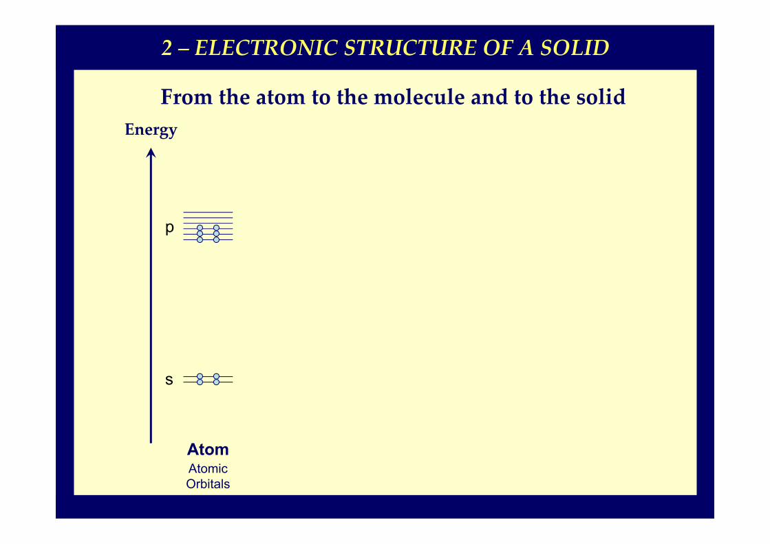
From the atom to the molecule and to the solidEnergy
AtomAtomicOrbitals
p
s
*LCAO : Linear Combination of Atomic Orbitals
MoleculeLCAO*
MolecularOrbitals
From the atom to the molecule and to the solid
AtomAtomicOrbitals
Energy
2 – ELECTRONIC STRUCTURE OF A SOLID

SolidDispersion
Eg
CB
BV
ConductionBand
ValenceBand
BandGap
Bloch Orbitals= Bands
p
s
*LCAO : Linear Combination of Atomic Orbitals
MoleculeLCAO*
MolecularOrbitals
AtomAtomicOrbitals
Energy
From the atom to the molecule and to the solid
2 – ELECTRONIC STRUCTURE OF A SOLID

h
BV
CB
UV
IR
E (eV)
0
1
2
3
4
5
6
h
VB
UV
IR
E (eV)
0
1
2
3
4
5
6 Color of a SC* with 1 gap
*SC : Semiconductor
3 – UNDERSTANDING OF COLORS FROM BANDS
GAP
Abso
rptio
n (a
.u.)
Energy (eV)0 1 2 3 4 5 6
Transmittedlight
Color of thecompound

BV
CB
BV
CB
VB VB
Gap
0 1 2 3 4 5 6
hUV
IR
E (eV)
0
1
2
3
4
5
6
hUV
IR
E (eV)
0
1
2
3
4
5
6
Color of thecompound
Color of a SC* with 1 gap
Abso
rptio
n (a
.u.)
Energy (eV)
Transmittedlight
*SC : Semiconductor
3 – UNDERSTANDING OF COLORS FROM BANDS

BV
CB
BV
CB
BV
CB
VB VB VB
BI
Abso
rptio
n (a
.u.)
Energy (eV)0 1 2 3 4 5 6
No transmittedlight
*SC : Semiconductor
hUV
IR
E (eV)
0
1
2
3
4
5
6
hUV
IR
E (eV)
0
1
2
3
4
5
6
Color of thecompound
Color of a SC* with 1 gap
3 – UNDERSTANDING OF COLORS FROM BANDS

0 1 2 3 4 5 6BV
CB
VB
TransmittedLight
Energy (eV)
Abso
rptio
n (a
.u.)
EnergyColor of a SC* with several gaps
*SC : Semiconductor
3 – UNDERSTANDING OF COLORS FROM BANDS

*SC : Semi‐conducteur – BI : Bande interdite
0 1 2 3 4 5 6Energy (eV)
Abso
rptio
n (a
.u.)Transmitted
Light
BV
CB
VB
EnergyColor of a SC* with several gaps
3 – UNDERSTANDING OF COLORS FROM BANDS

Powder sample of TiO2 (rutile)
Charge transfercolor
TiO2
3 – UNDERSTANDING OF COLORS FROM BANDS

‐10
0
10
Energy (eV)
‐5
5
2 O2‐ (2p6)
Ti4+ (3d0)
“t2g”
“eg”
Eg 3 eV
TiO2
O Ti
Powder sample of TiO2 (rutile)
Charge transfercolor
3 – UNDERSTANDING OF COLORS FROM BANDS

‐10
0
10
Energy (eV)
‐5
5
2 O2‐ (2p6)
Ti4+ (3d0)
“t2g”
“eg”
Eg 3 eV
TiO2
O Ti
Absorption (a.u.)
Energy (eV)0 1 2 3 4 5 6
UV
Charge transfercolor
3 – UNDERSTANDING OF COLORS FROM BANDS

‐10
0
10
Energy (eV)
‐5
5
2 O2‐ (2p6)
Ti4+ (3d0)
“t2g”
“eg”
h> 3 eV
TiO2
Absorption (a.u.)
Energy (eV)0 1 2 3 4 5 6
UV
O Ti
Charge transfercolor
3 – UNDERSTANDING OF COLORS FROM BANDS

TiCl3in solution
6 O2‐ (2p6)
Ti3+ (3d1)“t2g”
“eg”
h> 3 eV
h 2,5 eV
Ti[H2O]3+
d‐d transition color
3 – UNDERSTANDING OF COLORS FROM BANDS

Ti[H2O]3+
6 O2‐ (2p6)
Ti4+ (3d1)“t2g”
“eg”
h> 3 eV
h 2,5 eV
Absorption (a.u.)
Energy (eV)0 1 2 3 4 5 6
UV
Rq. : For dn with n > 1 Interelectronic correlations must be taken into accountTanabe‐Sugano diagrams(spectroscopic terms)
d‐d transition color
3 – UNDERSTANDING OF COLORS FROM BANDS

Ti[H2O]3+
6 O2‐ (2p6)
Ti4+ (3d1)“t2g”
“eg”
h> 3 eV
h 2,5 eV
Absorption (a.u.)
Energy (eV)0 1 2 3 4 5 6
UV
Rq. : For dn with n > 1 Interelectronic correlations must be taken into accountTanabe‐Sugano diagrams(spectroscopic terms)
d‐d transition color
3 – UNDERSTANDING OF COLORS FROM BANDS

Aluminecorindon(Al2O3)
BV
CB
VB
EnergieAbsorption (a.u.)
Energy (eV)0 1 2 3 4 9
UV
10 11 12
3 – UNDERSTANDING OF COLORS FROM BANDS

Aluminecorindon(Al2O3)
Syntheticrubis
(Al2O3:1%Cr3+)
+ 1% Cr3+
Absorption (a.u.)
Energy (eV)0 1 2 3 4 9
UV
10 11
Absorption (a.u.)
Energy (eV)0 1 2 3 4
3 – UNDERSTANDING OF COLORS FROM BANDS

Impurity (d‐d) color
Rubis (Al2O3:1%Cr3+)
Cr3+ : electronic conf. d3 Interelectronic correlations must be taken into accountTanabe‐Sugano diagrams(spectroscopic terms)
3 – UNDERSTANDING OF COLORS FROM BANDS

Multiplicity of spin
Cr3+ : elect. conf. d3
2S+1X
Energy
4F0
4P
2G
2F
No CF*
Rubis (Al2O3:1%Cr3+)
Free ion: we define the spectroscopic terms :
4Fml +2 +1 0 ‐1 ‐2
L = +3
S = 3/2
*CF : Cristal Field
Impurity (d‐d) color
3 – UNDERSTANDING OF COLORS FROM BANDS

Energy
4F0
4P
2G
2F
2E2T1
2T2
4A2 (t23e0)
4T2 (t22e1)
4T1 (t21e2)
2A1
No CF* With CF*
Rubis (Al2O3:1%Cr3+)
Degeneracy lifting due to the octahedralcrystal field effect created by the ligands
Cr3+ : conf. eq d3
t23
e0
t22
e1
t21
e2
Excited States
Fundamental state
Impurity (d‐d) color
*CF : Cristal Field
3 – UNDERSTANDING OF COLORS FROM BANDS

Energy
4F0
4P
2G
2F
2E2T1
2T2
2A1
No CF* With CF**CC : Champ Cristallin
Rubis (Al2O3:1%Cr3+)
Energy (eV)0 1 2 3 4 5
Red color+
Slightly blue
Abs. (a.u.)
4A2 (t23e0)
4T2 (t22e1)
4T1 (t21e2)
Impurity (d‐d) color
Cr3+ : electronic conf. d3 Interelectronic correlations must be taken into accountTanabe‐Sugano diagrams(spectroscopic terms)
3 – UNDERSTANDING OF COLORS FROM BANDS

nvac. = 1
v = c/n
c
Example of a prism
Physical color « Elastic diffusion »
n : index of refraction
Propagation speed is changed
4 – LIGHT‐MATTER INTERACTION

nvac. = 1
v = c/n
c
Elastic diffusion mechanismat the atomic level
Succession of absorption and emission
: Inductive dipole moment Receiver‐transmitter antenna
Physical color « Elastic diffusion »
4 – LIGHT‐MATTER INTERACTION
Example of a prism
n : index of refraction
Propagation speed is changed

Example of a prism
Oscillating field
Without applied field
Electronic density
re .Dipole moment
nvac. = 1
v = c/n
c
Physical color « Elastic diffusion »
Elastic diffusion mechanismat the electronic level
Succession of absorption and emission
: Inductive dipole moment Receiver‐transmitter antenna
Oscillating Electric Field polarize
4 – LIGHT‐MATTER INTERACTION

0 5 10 15 200.0
0.5
1.0
1.5
2.0
Energy (eV)0 5 10 15 20
0.0
0.5
1.0
1.5
Energy (eV)
n k
Diffusion Absorption
Kramers‐Kronig
Complex index of refraction: N = n + i k
4 – LIGHT‐MATTER INTERACTION

0 5 10 15 200.0
1.0
2.0
3.0
4.0
Energy (eV)0 5 10 15 20
0.0
1.0
2.0
1.5
4.0
Energy (eV)
1 2Complex dielectric function: = 1 + i 2
1 = n2 – k2
2 = 2nk
0 5 10 15 200.0
0.5
1.0
1.5
2.0
Energy (eV)0 5 10 15 20
0.0
0.5
1.0
1.5
Energy (eV)
n k
Diffusion Absorption
Kramers‐Kronig
Complex index of refraction: N = n + i k
4 – LIGHT‐MATTER INTERACTION

0 5 10 15 200.0
1.0
2.0
3.0
4.0
Energy (eV)
0 5 10 15 200.0
0.5
1.0
1.5
2.0
Energy (eV)
n
1
Diffusion in the case of a prism
n(blue) > n(red)
0 5
1.5
2.0
4 – LIGHT‐MATTER INTERACTION

0 5 10 15 200.0
0.5
1.0
1.5
2.0
(eV)
nk
0 5 10 15 200.0
0.5
1.0
1.5
2.0
(eV)
nk
Index of vacuum
0 5 10 15 200.0
0.5
1.0
1.5
2.0
(eV)
nk
0 5 10 15 200.0
0.5
1.0
1.5
2.0
(eV)
nk
No Absorption
Index of refraction : n = 1
« Spring »
Answer to an appliedelectric fied
« An atom »
« Vacuum »
n
k
n
k
Without applied electric field
Energy
Energy
4 – LIGHT‐MATTER INTERACTION

0 5 10 15 200.0
0.5
1.0
1.5
2.0nk
0 5 10 15 200.0
0.5
1.0
1.5
2.0nk« Insulator »n
k
Potentiel électrostatique des noyaux
Electrons liés
Electrostatic Potentialof the nuclei
0 5 10 15 200.0
0.5
1.0
1.5
2.0
nk
0 5 10 15 200.0
0.5
1.0
1.5
2.0
nk« Semi‐conductor »
k
n
« Insulator »« Semi‐conductor »
(eV)( )Energy (eV)( )Energy
Bounded electrons
« Interior‐sprungMattress »
4 – LIGHT‐MATTER INTERACTION

« Metal »
Collective answer ofan optical excitation
Electrostatic Potentialof the nuclei
Conduction electron
0 5 10 15 200.0
0.5
1.0
1.5
2.0
(eV)
nk
0 5 10 15 200.0
0.5
1.0
1.5
2.0
(eV)
nk
n
k
« Springboard »
Energy
4 – LIGHT‐MATTER INTERACTION

0 5 10 15 200.0
0.5
1.0
1.5
2.0
Energy (eV)
nk
Index of vacuum
Vacuum
0 5 10 15 200.0
0.5
1.0
1.5
2.0
Energy (eV)
nk
0 5 10 15 200.0
0.5
1.0
1.5
2.0
Energy (eV)
nk
0 5 10 15 200.0
0.5
1.0
1.5
2.0
Energy (eV)
nk
Insulator Semi‐conductor Metal
Electron more and more free
Absorption band is displaced towards low energies
Directly related to the oscillator strength
4 – LIGHT‐MATTER INTERACTION

5 – OPTICAL PROPERTIES: WHICH TREATMENT?
Band structure
VB
CB
Eg
1
The different steps to calculate the optical properties:

Imaginary part of the dielectric function: 2
Dipolartransitions
2
Band structure
VB
CB
Eg
1
The different steps to calculate the optical properties:
5 – OPTICAL PROPERTIES: WHICH TREATMENT?

Real part of the dielectric
function : 1
Kramers-Krönigtransformation3
Imaginary part of the dielectric function: 2
Dipolartransitions
2
Band structure
VB
CB
Eg
1
The different steps to calculate the optical properties:
5 – OPTICAL PROPERTIES: WHICH TREATMENT?

4
1 = n2 – k2
2 = 2nk
Determination pfn = f(E) & k = f(E)
Real part of the dielectric
function : 1
Kramers-Krönigtransformation3
Imaginary part of the dielectric function: 2
Dipolartransitions
2
Band structure
VB
CB
Eg
1
The different steps to calculate the optical properties:
5 – OPTICAL PROPERTIES: WHICH TREATMENT?

0 5 10
BiVO4-mono atom 0 size 0.70
Γ A Z M L V Γ
E F
Ener
gy (
eV)
0.0
1.0
2.0
3.0
4.0
5.0
6.0
7.0
8.0
-1.0
-2.0
-3.0
-4.0
-5.0
-6.0
Ener
gy (e
V)
0 2 4 6 8 10 12 140
5
10
Energy (eV)
2
Band structure DOS
Gap 2.3 eV
Band structure calculation1 Determination of 22
Gap 2.3 eV
Optical properties of m-BiVO4 and z-BiVO4 phases
Example of BiVO4
5 – OPTICAL PROPERTIES: WHICH TREATMENT?

Determination of 13 4 Determination ofn = f(E) & k = f(E)
0
1
2
3
4
0
1
2
3
kn
Energy (eV)0 2 4 6 8 10 12 14
0
5
10
21
-5
0
5
10
Energy (eV)0 2 4 6 8 10 12 14
Example of BiVO4
5 – OPTICAL PROPERTIES: WHICH TREATMENT?

Journées communications – 15/01/09
5 – OPTICAL PROPERTIES SIMULATION IN WIEN2k
Interband contributions(based on IPA*)
Intraband contributions(using a Drude‐like term)
EF EF
In WIEN2k, two types of contributions to the dielectric function( = 1 + i.2) could be estimated:
h h
Dielectric tensor / Optical conductivity / Refractive index / Reflectivity / Absorption coefficient / Loss function (EELS)
*IPA: Independant Particle Approximation

Journées communications – 15/01/09
5 – OPTICAL PROPERTIES SIMULATION IN WIEN2k
Interband contributions(based on IPA*)
EF
In WIEN2k, two types of contributions to the dielectric function( = 1 + i.2) could be estimated:
h h
*IPA: Independant Particle Approximation
Sum over all valence and conduction bands
Im(ij())

Journées communications – 15/01/09
5 – INTERPRETATION: Intraband transitions (for metals)
Plasma frequency: (longitudinal oscillations of the electron gas)
Intraband contributions(using a Drude‐like term)
EF
In WIEN2k, two types of contributions to the dielectric function( = 1 + i.2) could be estimated:

Journées communications – 15/01/09
5 – OPTICAL PROPERTIES SIMULATION IN WIEN2kOptical functions:

Journées communications – 15/01/09
5 – OPTICAL PROPERTIES SIMULATION IN WIEN2k
Symmetry of the dielectric tensor
cubic
monoclinic (, = 90°) orthorhombic
tetragonal, hexagonal
triclinic

Journées communications – 15/01/09
5 – OPTICAL PROPERTIES SIMULATION IN WIEN2k
Convergence with k‐mesh (expl.: Al)

Journées communications – 15/01/09
5 – OPTICS IN WIEN2k
x joint Im ij() (case.joint)
x kram Re ij(), other optical funct.
opticplot
5
6
7

Journées communications – 15/01/09
5 – SOME ADDITIONAL DETAILS

Journées communications – 15/01/09
5 – OPTICAL PROPERTIES SIMULATION IN WIEN2k
The band gap problem Necessity to go beyond DFT
Energy Energy
Electro‐affinity: N+1(N+1) = ‐AIonization energy: N(N) = ‐I
Eg = N+1(N+1) – N(N) = I – A
Energy
Eg = N+1(N) – N(N)
Eg = N+1(2N) – N(2N) + N+1(2N+1) – N+1(2N)
NN‐1
N+1
NN‐1
N+1
NN‐1
N+1
Eg = g + xc
g
with xc : Scissor Operator / GW / hybrid…

5 – OPTICAL PROPERTIES SIMULATION IN WIEN2k
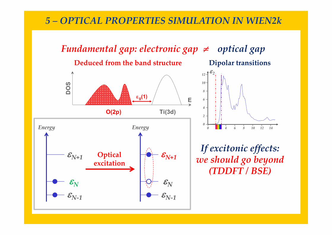
Fundamental gap: electronic gap optical gapDeduced from the band structure Dipolar transitions
E
O(2p) Ti(3d)
DO
S
g(1)
2
0 2 4 6 8 10 12 140
2
4
6
8
10
12
5 – OPTICAL PROPERTIES SIMULATION IN WIEN2k
If excitonic effects: we should go beyond(TDDFT / BSE)
Fundamental gap: electronic gap optical gapDeduced from the band structure Dipolar transitions
E
O(2p) Ti(3d)
DO
S
g(1)
2
0 2 4 6 8 10 12 140
2
4
6
8
10
12
Energy Energy
NN‐1
N+1
NN‐1
N+1Opticalexcitation

‐30
‐20
‐10
0
10
Energy (eV)
EF
3p Ti
2s O
2p O
3d Ti
Example of the rutile phase
Atomicstructure
Electronicstructure
Dielectricfunction
Journées communications – 15/01/09
6 – ILLUSTRATIONS: TiO2 series

‐30
‐20
‐10
0
10
Energy (eV)
EF
3p Ti
2s O
2p O
3d Ti
0 5 10 15 20 25 300
2
4
6
8
10
12
14
Energie (eV)
2EELS experiments
Journées communications – 15/01/09
Example of the rutile phase
Atomicstructure
Electronicstructure
Dielectricfunction
6 – ILLUSTRATIONS: TiO2 series

‐30
‐20
‐10
0
10
Energy (eV)
EF
3p Ti
2s O
2p O
3d Ti
0 5 10 15 20 25 300
2
4
6
8
10
12
14
Energie (eV)
2EELS experimentsDFT simulation
Journées communications – 15/01/09
Example of the rutile phase
Atomicstructure
Electronicstructure
Dielectricfunction
GGA (PBE)+ gap correction of 0.6 eV
6 – ILLUSTRATIONS: TiO2 series

Journées communications – 15/01/09
6 – ILLUSTRATIONS: TiO2 series
Program flowSCF cycle converged potentialx kgen denser k‐mesh
x lapw1 Kohn‐Sham states for the denser k‐mesh and higher Emax
x lapw2 ‐fermi Fermi distribution
x optic momentum matrix elements (dipolar transitions)
x joint dielectric tensor components: 2
x kram Kramers‐Krönig transformation: 2 1 Optical constants / broadening / scissors operator

Journées communications – 15/01/09
6 – ILLUSTRATIONS: TiO2 series
TiO2-RUT.inop2000 1 number of k‐points, first k‐point ‐5.0 5.0 Emin, Emax in Ry for matrix elements2 number of choices (columns in *outmat)1 Re xx3 Re zzOFF write unsymmetrized matrix elements to file?
Choices:1......Re <x><x>2......Re <y><y>3......Re <z><z>4......Re <x><y>5......Re <x><z>6......Re <y><z>7......Im <x><y>8......Im <x><z>

Journées communications – 15/01/09
6 – ILLUSTRATIONS: TiO2 series
TiO2-RUT.injoint1 261 LOWER AND UPPER BANDINDEX0.0000 0.00100 10.0000 EMIN DE EMAX FOR ENERGYGRID IN rydeV output units eV / ryd / cm‐14 SWITCH 2 NUMBER OF COLUMNS0.1 0.1 0.3 BROADENING (FOR DRUDE MODEL ‐ switch 6,7 ‐ONLY)
SWITCH:
0...JOINTDOS FOR EACH BAND COMBINATION 1...JOINTDOS AS SUM OVER ALL BAND COMBINATIONS2...DOS FOR EACH BAND 3...DOS AS SUM OVER ALL BANDS4...Im(EPSILON) 5...Im(EPSILON) for each band combination6...INTRABAND contributions7...INTRABAND contributions including band analysis
TiO2-RUT.inkram0.1 Gamma: broadening of interband spectrum0.6 energy shift (scissors operator)0 add intraband contributions? yes/no: 1/012.60 plasma frequencies (from joint, opt 6)0.20 Gammas for Drude terms

Journées communications – 15/01/09
6 – ILLUSTRATIONS: TiO2 series
Files generated by:x optic TiO2-RUT.symmat
TiO2-RUT.mommat
x joint TiO2-RUT.joint
x kram TiO2-RUT.epsilon
TiO2-RUT.sigmak
TiO2-RUT.refraction
TiO2-RUT.absorption
TiO2-RUT.eloss

I(є2) V
1.8
1.9
2.0
2.1
2.2
2.3
2.4
2.5
2.6
2.7
2.8
2.9
3.0
1500 2000 2500 3000 3500 4000 4500
CdTe
CdSe
CdS
ZnTe
ZnSe
ZnS
ZnO
1.8
1.9
2.0
2.1
2.2
2.3
2.4
2.5
2.6
2.7
2.8
2.9
3.0
52 54 56 58 60 62 64 66 68
Blende structure Wurtzite structure
CdTe
CdSe
CdS
ZnTe
ZnSe
ZnS
ZnO
I(є2)
Refractive index (n)
0 5 10 15 20 250
10
20
30
40
50
2
Energy (eV)
EELS exp.DFT calc.(gap correction)
ZnO Blende ZnS
ZnSe
ZnTe
0 1 2 3 4 5 6 7 8 9 10 11 12 13 14 15 16 17 18 19 200.0
0.5
1.0
1.5
2.0
2.5
3.0
3.5
4.0
0.0 0.5 1.0 1.5 2.0 2.5 3.0 3.5 4.0 4.51.61.82.02.22.42.62.83.03.23.43.63.84.04.24.4
Ref
ract
ive
inde
x
Photon Energy (eV)
Ref
ract
ive
inde
x (n
)
Energy (eV)
nCdO 1.95
ZnOZnS
ZnSeZnTe
ZnS
6 –ILLUSTRATIONS: MQ series (M = Zn, Cd & Q = O, S, Se, Te)
Refractive index (n)
Refractive index (n)

7 – Some limitations of DFT simulation of optical properties
‐ Kohn‐Sham eigenstates interpreted as excited states
‐ Independent‐particle approximation (no e‐—h+ interaction)
‐ LDA/GGA are not exact
Use of a scissors operator
Use of Bethe‐Salpeter Equation (BSE) – Time‐dependent DFT
Use of hybrid DFT, effective potentialsUse of DFT+U, LDA+DMFT, GW…

Core level spectroscopy XES, XAS, EELS, XPS
Dipole transitions between core and valence (conduction band or continuum) states

Fermi’s “golden rule”
Time dependent perturbation theory: EM-radiation with energy polarisation and direction of propagation k acts on the momentum p of the electron
tiEtiE eeHtH 0ˆ)(ˆ
The transition probability W from state i to f is then given by Fermi’s “golden rule” :
EEEEwithEfpkeefW ifNixki
fif )()(ˆ 2
W: proportional to the square of the transition matrix element
Number of states E-conservationwith energy E
,
).()(k
txkiekeE

momentum (= dipole) matrix elements:
momentum of photons << momentum of e-; momentum conservation e- cannot change its momentum
...1 xkie rki
dipole quadrupole … approximation
1rkie
1-3% error (even for keV X-rays), but:EELS (electron energy loss spectr.) may violatedipole approximation (selection rules!!)
e-,k
e-,k’
ififif frfefpfefHf ˆˆˆ
selection rules: ℓ±1

XES (X-ray emission spectroscopy)
knock out a core e-
valence e- fills core hole
measure the emitted X-ray
XES gives the ℓ±1 partial DOS of the valence bands of the specific atom (with core state ℓ)
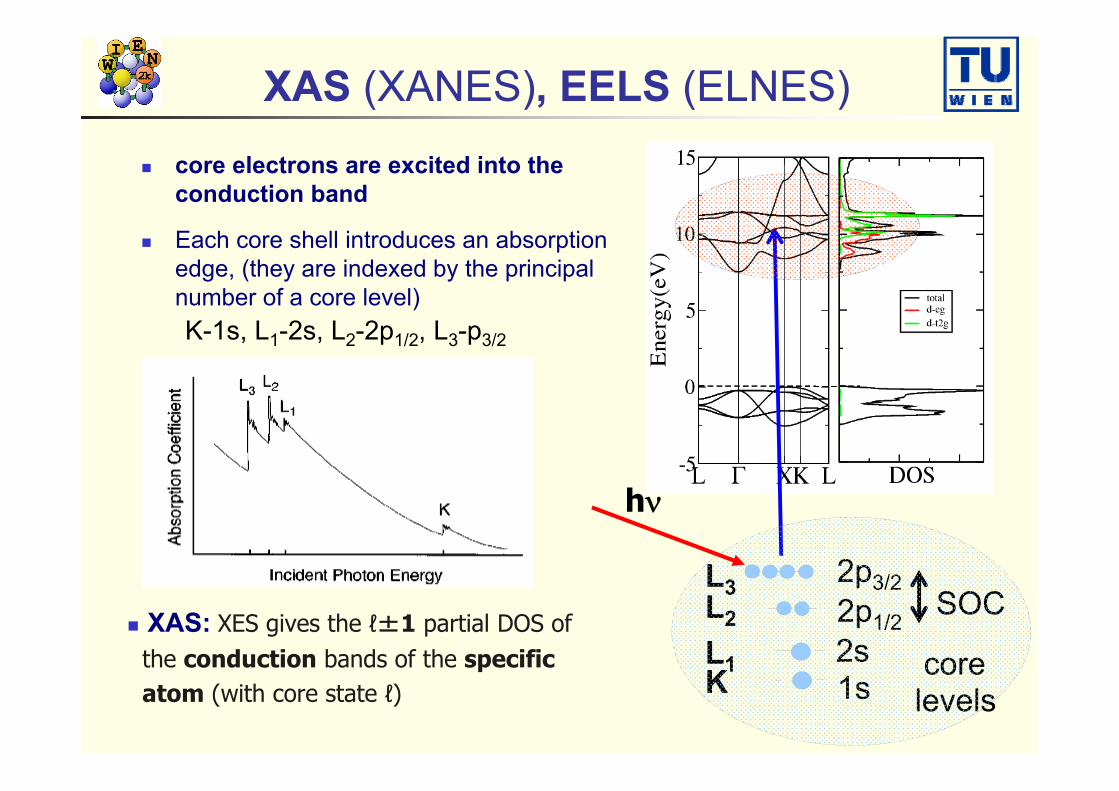
XAS (XANES), EELS (ELNES) core electrons are excited into the
conduction band
Each core shell introduces an absorption edge, (they are indexed by the principal number of a core level)
core levels
2p1/2
2p3/2SOC
2s1sK
L1
L3L2
K-1s, L1-2s, L2-2p1/2, L3-p3/2
XAS: XES gives the ℓ±1 partial DOS of the conduction bands of the specific atom (with core state ℓ)
h

Difference between EELS and XAS

XAS vs. EELS: theory
transition described by Fermis “golden rule” between initial (core) and final (conduction-band) state and the e- or photon
double differential cross section:E - conservation
single diff. cross section
momentum transfer q polarization vector e

dipole approximation
core-valence spectroscopies give informationon the local DOS (because of <core|r|val>) of angular momentum character ℓ ± 1
(TELNES3 can also handle non-dipole transitions + relativistic corrections)

“Final state rule”:
“Final state” determines the spectrum:•Absorption spectroscopy:
Final state has a “hole” in core state, but additional e- in conduction band. Core-hole has large effect on the spectrum
• electron – hole interaction, “excitonic effects”
• Emission spectroscopy:Final state has filled core, but valence hole.This is usually well screened, thus one “sees” the groundstate.
.
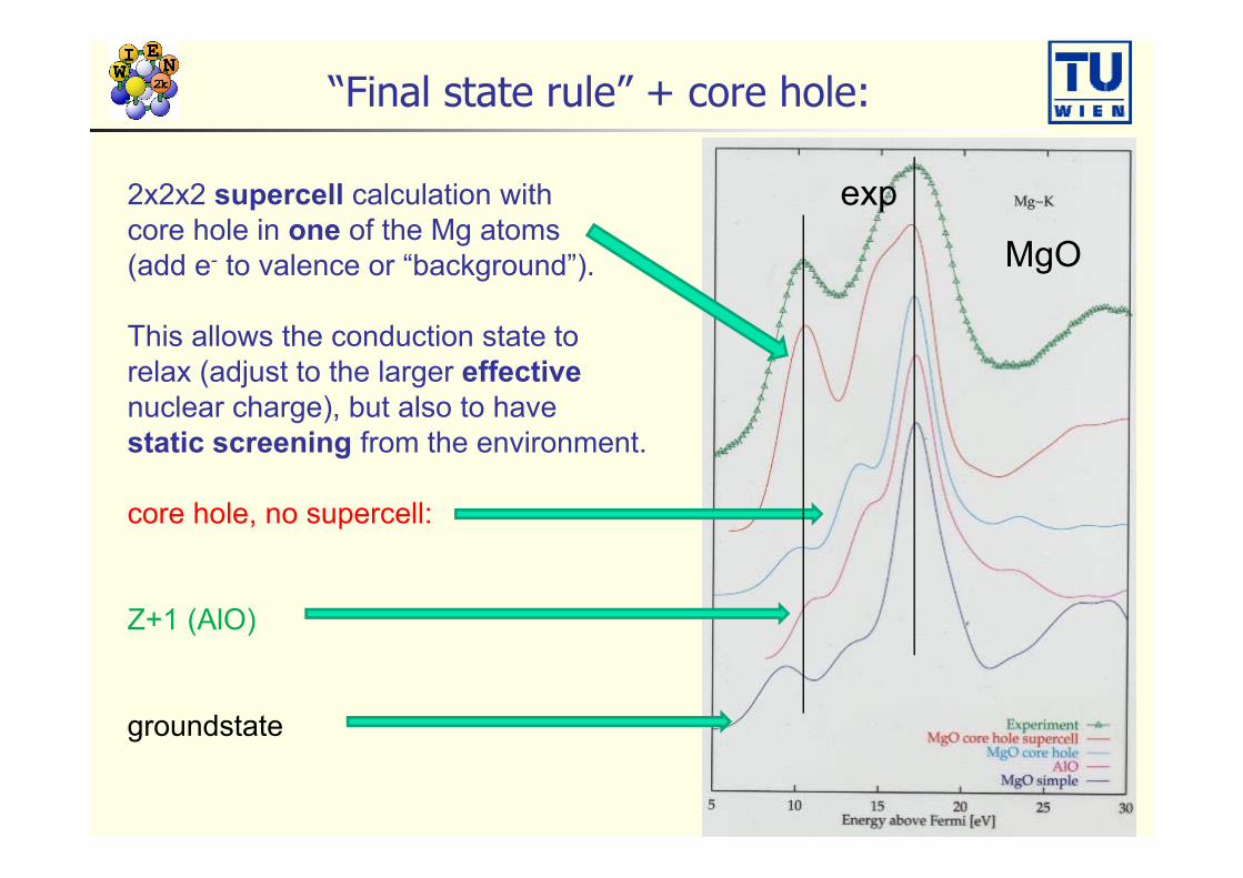
“Final state rule” + core hole:
2x2x2 supercell calculation with core hole in one of the Mg atoms(add e- to valence or “background”).
This allows the conduction state torelax (adjust to the larger effectivenuclear charge), but also to have static screening from the environment.
core hole, no supercell:
Z+1 (AlO)
groundstate
MgO
exp

Core hole calculations in WIEN2k
label core-hole atom „Mg1“
edit case.inc and case.in2 (inm)
(needs case.inxs)

EELS in WIEN2k
supercell calculations as for XAS TELNES3 task in w2web

When IPA fails: Electron – hole interactions
when the e- is not ionized, but stays in the solid:
excitonic effects Frenkel (localized) and Wannier (delocalized) excitons
independent particle approx.

importance of excitons (BSE):

L2,3 spectra: failure of the single particle approach
In particular early 3d TM-compounds show a non-standard L2/L3 branching ratio (1:2) sometimes a completely different lineshape (TiO2) „wrong“ SOC or CF splittings
rutile TiO2 CaF2
exp.exp.
soc
core-hole calc.
ground state calc.
L3 L2
CF

fully relativistic electron-hole interaction (BSE)
Bethe-Salpeter-equation: L(12;1’2’) solving a 2-particle (e- - h) equation of
large dimension ( Nv Nc Nk ~ 100000)
)'()'()',()()('
)'()()',()'()('
)(2
''*
''*33
'''
''*
''*33
'''
''',,
rrrrvrrrdrdH
rrrrWrrrdrdH
EEHHHHH
kckvckvkx
kcvckv
kckvckvkdir
kcvckv
kkvvcckckvdiag
xdirdiageh
eigenvalue difference between hole (v) and electron(c) state
attractive screened static Coulomb interaction W; W~-1
e-h exchange with bare Coulomb potential v

Ca-L23 edge in CaF2
“ground-state” DOS
“core-hole” calc.(ratio 2:1)
BSE for L2 and L3 separately
experiment
BSE with p1/2 and p3/2 together
BSE without direct term Hehdir
BSE without exchange term Hehx

L2,3 edge for Ca in CaF2
Decomposition of є2 into the excitation from p1/2 and p3/2 statescross terms suppress the L3 branch and enhance L2
L3 L2

XPS, core-level shifts
Ionizationpotential of core-e-, IP= Etot(N) – Etot(N-1) gives information on charge state of the atom
core-eigenvalues i (with respect to EF) are NOT a good approximation: i=dE/dn Janak’s theorem
Slater’s “transition state”: core-eigenvalues i for half occupancy
-SCF-calculation with and without core-hole: Etot(N) – Etot(N-1) always use supercells to reduce hole-hole interaction
C,N 1s exp.(eV) i -SCF
TiC 281.5 264.7 281.9
Ti4C4 281.5 263.3 281.1
TiN 397.0 377.5 397.1
E
En
N-1 N
secant ~ tangent at N-½

Band gap problem, independent particle approx.
better local potentials: TB-mBJmany-body perturbation theory: GW approach
shift of conduction bands: scissors operator
Electron-affinityIonization energy
Band gap

GW (MBPT on one page)
Self-energy
Green’s function G:
screened coulomb interaction W:
GW: screened HF approximation + calculation of “quasiparticle energies”:
describes propagation of e-,h+
from r1r2 with time ()

GW and BSE are available upon request (see „unsupported software page“ at wien2k.at
Both calculations are EXTREMELY expensive Hardware: at least 128 cores with infiniband