Optical properties of point defects in hexagonal boron nitride
139
HAL Id: tel-02986321 https://tel.archives-ouvertes.fr/tel-02986321v2 Submitted on 3 Nov 2020 HAL is a multi-disciplinary open access archive for the deposit and dissemination of sci- entific research documents, whether they are pub- lished or not. The documents may come from teaching and research institutions in France or abroad, or from public or private research centers. L’archive ouverte pluridisciplinaire HAL, est destinée au dépôt et à la diffusion de documents scientifiques de niveau recherche, publiés ou non, émanant des établissements d’enseignement et de recherche français ou étrangers, des laboratoires publics ou privés. Optical properties of point defects in hexagonal boron nitride Thomas Pelini To cite this version: Thomas Pelini. Optical properties of point defects in hexagonal boron nitride. Physics [physics]. Université Montpellier, 2019. English. NNT : 2019MONTS139. tel-02986321v2
-
Upload
khangminh22 -
Category
Documents
-
view
1 -
download
0
Transcript of Optical properties of point defects in hexagonal boron nitride

HAL Id: tel-02986321https://tel.archives-ouvertes.fr/tel-02986321v2
Submitted on 3 Nov 2020
HAL is a multi-disciplinary open accessarchive for the deposit and dissemination of sci-entific research documents, whether they are pub-lished or not. The documents may come fromteaching and research institutions in France orabroad, or from public or private research centers.
L’archive ouverte pluridisciplinaire HAL, estdestinée au dépôt et à la diffusion de documentsscientifiques de niveau recherche, publiés ou non,émanant des établissements d’enseignement et derecherche français ou étrangers, des laboratoirespublics ou privés.
Optical properties of point defects in hexagonal boronnitride
Thomas Pelini
To cite this version:Thomas Pelini. Optical properties of point defects in hexagonal boron nitride. Physics [physics].Université Montpellier, 2019. English. �NNT : 2019MONTS139�. �tel-02986321v2�

RAPPORT DE GESTION
2015
THÈSE POUR OBTENIR LE GRADE DE DOCTEUR
DE L’UNIVERSITÉ DE MONTPELLIER
En Physique
École doctorale I2S - Information, Structures, Systèmes
Unité de recherche UMR 5221
Présentée par Thomas PELINI
Le 20 décembre 2019
Sous la direction de Guillaume CASSABOIS
et Vincent JACQUES
Devant le jury composé de
Christophe CHAUBET, Professeur des Universités, L2C-Montpellier
Jean-Sébastien LAURET, Directeur de recherche, LAC-Paris
Abdelkarim OUERGHI, Directeur de recherche, C2N-Paris
Alberto ZOBELLI, Professeur des Universités, LPS-Paris
Clément FAUGERAS, Directeur de recherche, LNCMI-Grenoble
Vincent JACQUES, Directeur de recherche, L2C-Montpellier
Guillaume CASSABOIS, Professeur des Universités, L2C-Montpellier
Président du jury
Rapporteur
Rapporteur
Examinateur
Examinateur
Co-directeur de thèse
Directeur de thèse
Optical propert ies of point defects in hexagonal boron
nitr ide

À mon grand-père,
Mes parents, ma soeur.


Remerciements
Le travail de recherche présenté dans ce manuscrit a été élaboré au sein de l’équipeNQPO au laboratoire Charles Coulomb à Montpellier, dont je remercie le directeurdu laboratoire Pierre LEFEBVRE de m’avoir accueilli, et également tout le personneladministratif compétent sur qui j’ai pu compter ces trois années. Merci à BéatriceTOMBERLI, particulièrement pour mon installation dans l’équipe, à Jean-ChristopheART pour sa gestion impeccable de toutes les missions que j’ai effectuées, StéphanieMARTEGOUTES pour les nombreuses commandes qui furent nécessaires à la con-struction du microscope, et enfin Christelle EVE et Régine PAUZAT ainsi que PatrickEJARQUE dont je garderai le souvenir de son goût pour la poésie. Je remercie aussispécialement Lucyna FIRLEJ qui a su gérer les urgences de fin de thèse.
Mes remerciements vont en premier lieu à mes directeurs de thèse Vincent JACQUESet Guillaume CASSABOIS, pour m’avoir donné l’opportunité de travailler sur ce sujetet dans cette équipe, grandissante au fil de ma thèse, dans cette belle ville du Sud oùle soleil trouve rarement refuge derrière un nuage. Si mon projet de thèse a été menéà bien, je le dois en grande partie à eux, qui ont tout fait pour que l’on puisse toujoursavancer malgré les embûches techniques qui ont parsemé l’élaboration du microscopeconfocal dans l’UV. Je vous remercie chaleureusement pour votre encadrement empreintd’une disponibilité sans failles. Merci pour votre rigueur scientifique et remarques per-tinentes ainsi que la richesse des discussions que l’on a pu avoir, cela a guidé mes pasjusqu’à la rédaction de mon manuscrit, et j’emporte précieusement ces apprentissagespour la suite de mon parcours. J’ai eu un plaisir ineffable à travailler dans l’équipe avectous les autres étudiants et postdoc, et je sais que l’intelligence sociale que vous avezpour doser confiance, détente et sérieux y est pour beaucoup. Je veux aussi remercier àcet égard Isabelle PHILIP ainsi que Bernard GIL, à qui je dois aussi énormément pourma recherche et son aide dans les derniers instants.
Au cours de mon doctorat, j’ai passé un temps considérable en salle de manip, etsi j’ai acquis des méthodes rigoureuses en alignement optique, je le dois en partie àAnais DREAU qui m’a enseigné les secrets des techniques expérimentales, et ce avecune précision chirurgicale. Ce fut un réel plaisir de travailler avec elle, dans le noirdes salles d’optiques. Nous avons eu l’occasion de tester en amont la faisabilité de lamicroscopie confocale dans l’UV dans la salle de manip de Christelle BRIMONT etThierry GUILLET, que je remercie, et à cette occasion j’ai largement profité de sonsens poussé de la planification et sa persévérance, indispensables outils lorsque le sujetde recherche revêtait un tel caractère exploratoire. Je me souviendrai avec amusement
3

de sa tendance à personnifier les éléments de manip (Alphonse, Basil. . . ), que je luiemprunterai d’ailleurs peut-être.
Pierre VALVIN, merci de m’avoir laissé squatter ton bureau du bas de l’époque.Je crois que c’est là que nos discussions passionnées sur la musique et le piano ontpremièrement émergé. C’était les balbutiements d’un long et exaltant chemin que l’ona parcouru ensemble, au cours duquel tu as eu la patience et le souci pédagogique deme transmettre tes connaissances techniques pointues sur bon nombre d’outils expéri-mentaux, des connaissances que je porterai avec moi par la suite. Laissant de côté lesinnombrables embûches en cours de route que l’on a surmontées ensemble, je garde enmémoire la première image sur le spectro, puis le premier scan en micro PL UV, etenfin la première image hyperspectrale: quelle accomplissement, quelle joie!
Enfin, cette expérience de recherche n’aurait pas été la même sans le bain ambiantde thésards. Cela a renforcé le sentiment d’apprentissage collectif lorsqu’on se posaitentre nous les questions que l’on n’osait pas poser aux chefs, et m’a donné l’opportunitéd’enseigner à mon tour les techniques et connaissances apprises. J’ai débuté dansl’équipe en stage de M2 avec deux autres doctorants, Saddem CHOUAIEB et WalidREDJEM, merci à vous pour tous les bons moments passés ensemble et l’entraide,jusqu’aux derniers jours de rédaction avec l’incontournable pause ping-pong. À mesdébuts, j’ai aussi été accompagné par le fameux Luis Javier MARTINEZ RODRIGUEZ,Waseem AKHTAR, Isabell GROSS, Clément BEAUFILS et Phuong VUONG à qui jesouhaite bonne continuation dans les positions académiques ou bien dans le privé qu’ilsont trouvé. Dans cette équipe multiculturelle, je me dois de remercier une triplettede Libanaises à savoir Rana TANOS, Angela HAYKAL et Christine ELIAS pour leurextrême bonne humeur déjà, et leur généreuse cuisine qu’elles n’ont jamais hésité àpartager avec nous. Christine, sans qui les décibels dans la salle de manip n’auraient ja-mais atteint ces plafonds: notre collaboration de thésard a été haute en couleur, surtoutdans l’UV! Puis il y a les anciens nouveaux, Alrik DURAND et Florentin FABRE, et lesnouveaux tous frais Yoann BARON et Maxime ROLLO à qui je souhaite bon couragepour la suite de votre thèse dans cette famille NQPO. Mention spéciale pour Alrik, àqui je dois mon parcours initiatique avec python, ce geek.
Pour avoir accepté d’être rapporteur de ce travail de thèse, je remercie Jean-SébastienLAURET ainsi qu’Abdelkarim OUERGHI. Merci également à Clément FAUGERAS etAlberto ZOBELLI pour avoir été examinateur à mon jury de thèse. Je souhaite re-mercier plus amplement Alberto, qui m’a accueilli dans son équipe au Laboratoire dePhysique des Solides à Orsay à plusieurs reprises, et qui m’a donné l’occasion de prati-quer la microscopie électronique. Ça a été un plaisir de collaborer avec toi.
Tout au long de ces trois années, j’ai eu la chance de pouvoir enseigner à l’Universitédes Sciences de Montpellier, je remercie pour cela Christophe CHAUBET à la directiondes enseignements en Physique. Cela a été un exercice riche qui m’a beaucoup apporté,à l’occasion duquel j’ai pu collaborer sur le plan pédagogique avec d’autres enseignants-chercheurs, dont Christophe bien sûr et aussi Laetitia DOYENNETTE que je remerciepour m’avoir laissée une marge d’initiative dans l’UE concernée; mais également avec
4
d’autres doctorants comme Adrien DELGARD et Chahine ABBAS.
Je tiens enfin à remercier Christian L’HENORET à l’atelier de mécanique qui a étéd’une aide précieuse, sur le plan technique mais aussi temporel, pour la conception etréalisation des nombreuses pièces mécaniques nécessaires à la construction du micro-scope et aussi de m’avoir initié à quelques basiques en mécanique, et je veux soulignerici l’importance d’un atelier de mécanique au sein du laboratoire. Merci également auxélectroniciens Rémi JELINEK et Yves TREIGUER pour leur aide. Je voudrais aussiremercier Christophe CONSEJO, ingénieur de recherche au laboratoire, pour m’avoirdépanné plusieurs fois et aidé avec enthousiasme.
Mes derniers remerciements vont à Julie, dont le soutien inconditionnel dans lesdernières semaines d’écriture a été vital pour moi. Ta confiance en moi a été d’unegrande aide dans les moments difficiles.
Bien sûr je me serais régalé à exploiter un peu plus cet outil de spectroscopie quej’ai monté, mais il me faut y renoncer, et aller vers d’autres aventures, expériences,recherches. Si je laisse à Montpellier une équipe passionnée et passionnante, j’emporteavec moi son souvenir impérissable.
5

6

Contents
Contents i
Introduction 1
1 Hexagonal Boron Nitride 51.1 Origins . . . . . . . . . . . . . . . . . . . . . . . . . . . . . . . . . . . . 5
1.1.1 Boron nitride powder in the industry . . . . . . . . . . . . . . . 51.1.2 Hexagonal boron nitride in the semiconductor industry . . . . . 7
1.2 Structural properties . . . . . . . . . . . . . . . . . . . . . . . . . . . . 91.3 Electronic band structure . . . . . . . . . . . . . . . . . . . . . . . . . 131.4 Photoluminescence of hBN . . . . . . . . . . . . . . . . . . . . . . . . . 14
1.4.1 Band edge exciton emissions . . . . . . . . . . . . . . . . . . . . 151.4.2 Exciton recombination at stacking faults . . . . . . . . . . . . . 171.4.3 PL from deep defects . . . . . . . . . . . . . . . . . . . . . . . . 18
1.5 Conclusion . . . . . . . . . . . . . . . . . . . . . . . . . . . . . . . . . . 22
2 Single defects emitting in the visible range 252.1 Experimental setup . . . . . . . . . . . . . . . . . . . . . . . . . . . . . 252.2 Sample and typical results . . . . . . . . . . . . . . . . . . . . . . . . . 26
2.2.1 Sample . . . . . . . . . . . . . . . . . . . . . . . . . . . . . . . . 262.2.2 Confocal maps of photoluminescence, dipole-like emission and
photostability . . . . . . . . . . . . . . . . . . . . . . . . . . . . 272.2.3 Photoluminescence properties . . . . . . . . . . . . . . . . . . . 29
2.3 Statistics of photon emission . . . . . . . . . . . . . . . . . . . . . . . . 322.3.1 The second-order correlation function . . . . . . . . . . . . . . . 332.3.2 Experimental setup: HBT interferometer . . . . . . . . . . . . . 342.3.3 Discussion on the experimental procedures to access time-photon
correlation . . . . . . . . . . . . . . . . . . . . . . . . . . . . . . 362.4 Experimental results for the second-order correlation function . . . . . 38
2.4.1 Theoretical model for the photodynamics: the three-level system 392.4.2 Derivation of g(2)(τ) for a three-level system . . . . . . . . . . . 402.4.3 Procedure for fitting . . . . . . . . . . . . . . . . . . . . . . . . 42
2.5 Photophysical properties of individual defects . . . . . . . . . . . . . . 432.5.1 Expression of r21 and r31 with a, λ1 and λ2 . . . . . . . . . . . . 432.5.2 Power-dependent measurements of g(2)(τ) . . . . . . . . . . . . 442.5.3 Brightness of the source . . . . . . . . . . . . . . . . . . . . . . 47
i

Contents
2.6 Conclusion . . . . . . . . . . . . . . . . . . . . . . . . . . . . . . . . . . 48
3 Deep defects emitting in the UV range 513.1 New levels in carbon-doped hBN crystals . . . . . . . . . . . . . . . . . 51
3.1.1 Description of the experiments . . . . . . . . . . . . . . . . . . . 513.1.2 Samples characteristics . . . . . . . . . . . . . . . . . . . . . . . 533.1.3 Shallow-level emissions . . . . . . . . . . . . . . . . . . . . . . . 563.1.4 Deep-level emissions . . . . . . . . . . . . . . . . . . . . . . . . 59
3.2 Confocal microscope at 266 nm / 4.66 eV . . . . . . . . . . . . . . . . . 633.2.1 General overview of the experimental setup . . . . . . . . . . . . 633.2.2 What are the challenges to build a confocal setup in the UV? . 683.2.3 Optimization of the optical excitation . . . . . . . . . . . . . . . 693.2.4 Mitigation of chromatic aberrations . . . . . . . . . . . . . . . . 723.2.5 Performances of the microscope . . . . . . . . . . . . . . . . . . 76
3.3 Probing deep defects at a sub-micrometer scale in PL . . . . . . . . . . 793.3.1 The UV1-3 lines . . . . . . . . . . . . . . . . . . . . . . . . . . . 793.3.2 Investigations of the 4.1 eV defect origin . . . . . . . . . . . . . 863.3.3 Search for isolated emitters at 4.1 eV . . . . . . . . . . . . . . . 92
3.4 Conclusion . . . . . . . . . . . . . . . . . . . . . . . . . . . . . . . . . . 97
Conclusion 99
A Classical and quantum light, mathematical derivation of the second-order correlation function 103A.1 Classical light versus quantum light . . . . . . . . . . . . . . . . . . . . 103
A.1.1 Classification in terms of intensity fluctuation and correlation . 103A.1.2 The second-order correlation function: g(2)(τ) . . . . . . . . . . 104
A.2 Derivation of fundamental properties of g(2)(τ) . . . . . . . . . . . . . . 106A.2.1 The classical case . . . . . . . . . . . . . . . . . . . . . . . . . . 106A.2.2 The quantum case . . . . . . . . . . . . . . . . . . . . . . . . . 107
B Effect of the IRF on the histogram of photon correlations 109B.1 Position of the problem . . . . . . . . . . . . . . . . . . . . . . . . . . . 109B.2 Convolution of g(2)(τ) and the IRF . . . . . . . . . . . . . . . . . . . . 111
Bibliography 129
ii

Introduction
The understanding of the laws operating at the microscopic scale, originating fromthe first quantum revolution of the twentieth century, has allowed the emergence of
new technologies and instrumental tools. Among them, we can cite the first realizationof a solid-state Laser in 1960 by T. Maiman with a crystal of ruby [1], or the inventionof the scanning tunneling microscope (STM) by G. Binnig and H. Rohrer at IBM inZurich in 1981 [2]. These "tools" are now essential and participate in the elaboration ofnew nanotechnologies based on the manipulation and measurement of individual quan-tum systems. These new quantum devices, as part of the second quantum revolution,exploit the quantum logic and its counter intuitive aspects like quantum superpositionand entanglement.
Single-photon sources formed by individual deep defects in wide bandgap semicon-ductors, also known as artificial atoms, are one of those emerging quantum systems.Electronic spins associated with these atomically small systems are at the heart of abroad range of emerging applications, from quantum information science, to the devel-opment of ultrasensitive quantum sensors. In this regard, the nitrogen-vacancy (NV)defect in diamond [3] has attracted considerable interest and led in particular to theelaboration of quantum protocols [4] and to highly sensitive magnetic field sensors [5],thanks to its spin-dependent photoluminescence. Single-photon emitters have also beenfound in silicon carbide (SiC) [6, 7], and more recently in our team in pure silicon withthe G center (cf. thesis of W. Redjem).
In that context, hexagonal boron nitride (hBN), a lamellar material with a widebandgap of ∼ 6 eV, is a promising platform for hosting single deep defects. The lamellarstructure of this material offers an appealing alternative to standard cubic semiconduc-tors because electrons and spins can be confined in a single atomic plane, thus offeringenormous potential to engineer quantum functionalities. hBN has been used in theindustry for more than seventy decades now, but has only recently attracted attentionin the field of semiconductors, with the first synthesis of large monocrystals in 2004 byWatanabe and Taniguchi [8].
In the field of 2D materials, graphene has led to a colossal theoretical and exper-imental development that is now transferable to other 2D crystals. There is a largevariety of candidates that are mechanically, thermally and electronically stable in am-bient conditions [9, 10]. Among them, a promising family of materials, other than theatomically thin hBN and graphene, is the family of transition metal dichalcogenides(TMDC), which are ultrathin material composed of 3 atomic layers like MoS2 or WSe2.
1

Introduction
The interest in hBN arises from the possibility to combine different 2D materials intoan heterostructure exhibiting new optical, electrical and magnetic properties differentfrom the stand-alone bulk counterparts [10, 11], opening up the scope of possibilitiesin terms of opto-electronic devices [12]. The prospect of manufacturing such designednano-architecture — known as van der Waals heterostructures — by stacking differentlayered crystals on top of each other via exfoliation or in situ epitaxial techniques, haslaunched a new era of material science at the beginning of this decade. A proof ofconcept for such an heterostructure was realized in 2012 with a superlattice of bi-layersof graphene and hBN stacked upon each other in sequence [13]. Besides, hBN presentsa great affinity with graphene, as it is the best dielectric substrate for it [14], and is alsoused to enhance optical and electrical properties of TMDC materials by encapsulation[15, 16]. In the field of crystal growth, the research to obtain hBN crystals of increas-ing size and quality is very active, with recent papers reporting wafer-scale growth ofsingle-crystals [17, 18].
In that context, it is essential to understand the structural, electronic and opticalproperties of hBN on the one hand, and to investigate its point defects for quantumtechnologies on the other. This manuscript deals with the spectroscopy of point defectsin hBN.
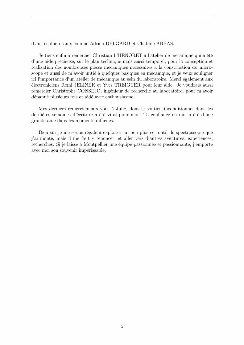
Over the first chapter of this thesis, we present the fundamentals of hBN. We re-view the most-updated comprehension of the structural and electronic properties of thematerial. In particular, we present how the boron and nitrogen atoms are arrangedin an honeycomb structure with sp2 orbitals configurations and describe the electronicband structure resulting thereof, in the bulk and the monolayer. Then, we present thecharacteristics of the bulk hBN photoluminescence at the energies of the bandgap andnear-bandgap, showing the important coupling of the exciton with optical phonons. Atlast, we review the current knowledge relative to deep defects in hBN, emitting fromthe near-infrared to near-UV range.
Chapter two is dedicated to the study of single localized defects emitting at around600 nm in a high-purity hBN crystal. We report on a highly efficient single-photonsource, among the highest reported to date in solid-state systems. We study its pho-todynamics with photon correlations measurements, as well as its photoluminescenceproperties in regard to the phonon modes in the hBN lattice.
In the third and last chapter, we explore deep defects emitting in the ultravio-let range. First, we study shallow and deep levels in carbon-doped hBN samples bycombining macro-photoluminescence and reflectance setup. We show the existence ofnew optically-active transitions and discuss the implication of carbon in these levels.The second section of this chapter is dedicated to the presentation of a new micro-photoluminescence confocal microscope operating at 266 nm under cryogenic environ-ment. The design and performances of the optical system are described. In the thirdsection, using this new setup, we go further into the examination of the deep levels,analyzing the relation between them and with the known point-defect at 4.1 eV. We usenew crystals with isotopically-purified carbon doping as a strategy to investigate thelong-standing question concerning the chemical origin of the 4.1 eV defect. Throughthis attempt, we bring to light the spatial dependence of the optical features for thisspecific emitter. Last but not least, we present our work dedicated to isolate the emis-
2

Introduction
sion of a single 4.1 eV defect. We study the photoluminescence of thin undoped flakes,pre-characterized with an electron microscope, that contain a low density of emitters,and inspect in particular their photostability in these thin crystals.
Finally, we end this manuscript with a general conclusion and discussions.
3

Introduction
4

Chapter 1
Hexagonal Boron Nitride
1.1 Origins
The boron nitride is a binary chemical compound of the III-V family. It was first dis-covered and prepared by the English chemist W. H. Balmain in 1842 [19] by using
molten boric acid and potassium cyanide, but unfortunately this new compound wasunstable and required many attempts to obtain a stable boron nitride. The compoundappeared as a white powder as a residue of the chemical protocol after dehydration.The optical microscope revealed a structure made of flakes easily slipping over eachother and thus separable, and enabled to notice a random distribution in both size andshape, although a qualitative study on the orientation of the normales to the break-ing faces indicates the existence of orientated bundles typical of the hexagonal crystalstructure and to a lesser extent to the rhomboidal one. The Fig 1.1 illustrates thesetwo macroscopic properties.
Figure 1.1Left: the BN white powder. Right: optical micrograph of BN flakes.
1.1.1 Boron nitride powder in the industry
For nearly a hundred years studies on boron nitride remained in laboratory scale be-cause of the technical difficulties of different production techniques and high cost of thematerial which is obtained with these synthetic methods. We have to wait for the onset
5

Chapter 1. Hexagonal Boron Nitride
of the modern development of crystal growth technology, dating from the Second WorldWar, which was boosted mainly by the demand for crystals for electronics, optics, andscientific instrumentation, for the growth technologies to be raised to a very high andadvanced level to fulfill the increasing demands in crystal size and quality. Indeed, inthe 1950s the Carborundum, the Union Carbide and the Norton Abrasives companiesmanaged to prepare purified boron nitride powder [20] on an industrial scale for com-mercial applications with sophisticated hot pressing techniques [21].
The interests for this material in industry can be justified with these four propertiesamong others:
• It is chemically inert,
• Its melting point is very high (2967 ◦C at ambient pressure [22–24]), making itfirst-class refractory material,
• The ease of sliding between adjacent crystalline planes (0001) in hexagonal formmakes it a perfect solid-state lubricant up to 900 ◦C, better than graphite or MoS2
that are burnt away at lower temperatures,
• It is attractive for the cosmetic industry for its quality whiteness, preferred to thekaolin, the silica or the alumina powder.
Besides this nascent interest in the industry, the newly available BN powder alsoencourages new fundamental studies. In 1956, Larach and Shrader used purified BNpowders (particle size of approximately 100 nm) from the Carborundum Companyand the Norton Company to perform various types of measurements with the aim ofelucidating the emission spectrum in the UV to VIS range and determining the bandgapof the material by reflectivity technique [25]. Photoluminescence at low temperature andcathodoluminescence in the UV show a complex and broad spectrum with a multitudeof peaks between 300 and 500 nm whose relative intensity change with excitation energybut positions remain stable, while the reflectivity measurement for wavelengths from220 to 320 nm fails to show a bandgap absorption. Among others, we can also cite theremarkable studies from Katzir et al. [26] in 1975 on hot-pressed boron nitride (HPBN)obtained with powder of the Carborundum company. With UV light, they measure theexcitation spectrum of the electron paramagnetic resonance (EPR) signal from the one-and three- boron centers (OBC, TBC), and find a maximum EPR amplitude for theenergy of 4.1 eV or ∼ 3000Å [Fig 1.2(a)]. Assisted by quantum chemical calculation,they establish a model in which a carbon impurity introduces an energy level 4.1 eVbelow the conduction band. Upon excitation, electron excited from this level passthrough the conduction band and fall into traps like the nitrogen vacancy, thus forminga TBC center. Later in 1981, Kuzuba et al. [27] study the characteristics of electron-phonon coupling for vibronic transitions in typical defects, ascribed to carbon acceptorat nitrogen site (CN) and nitrogen-site vacancy (VN). In the absorption spectrum [Fig1.2(b)] associated with CN , the zero-phonon line (ZPL) is identified at 4.095 eV and thespectral features at higher absorption energies are assigned to specific phonon modes.
6

1.1 Origins
POINT DE FECTS IN HEXAGONAL BORON NITRIDE. I. . . . 2373
(o)
U
D
~~ 0.5—O~CLEUKQ4J
2500'IAtavelength (0 )
TBCOBC
+ Tm =700'KOTrn =380 K
aTrn = l00'K
5500
In the search for other thermally bleachablecenters we performed measurements at low tem-peratures. The samples were y irradiated at VV'K, and EPR measurements were carried out atthe same temperature, but no new EPR centerswere found.
B. Glow-curve measurements' Useful information can be gained by combinedEPR and glow-curve measurements. 6' ~ The for-mer can help to establish the chemical nature ofthe defect and the symmetry of the charge distribu-tion, while the latter may be used to determinethe energy of the trapping level.Our measurements were carried out on grade
HP samples which had been exposed to ionizingradiation (uv, x rays, or y rays). Some of the re-sults on the thermoluminescence and the thermallystimulated current measurements of samples ex-cited by x rays at room temperature were reportedelsewhere. Two glow peaks at 380 and at 700 Kwere observed, and are shown in Fig. 3(b). Theactivation energies of the two peaks were deter-mined by the "initial-rise" method, and found tobe 0. V + 0. 1 and 1.0 + 0. 1 eV for the 380 and 700 'Kpeaks, respectively. Using uv light for the exci-tation we were able to measure the excitation spec-
FIG. 2. (a) Excitation spectrum of the EPR signals asmeasured at 300'K. (b) Excitation spectrum of thethermoluminescence {TI.) peaks at 100, 380' and 700'K.
affected mainly by green light (5500 + 100 A) andthe three-boron-center signals, by blue light (4500+100 A). We have not succeeded in measuring thedetailed spectrum of optical bleaching.Compression-annealed pyrolytic boron nitride
resembles a single crystal in many respects, whichis one of the reasons why Moore and Singer choseit for studies of the anisotropy of the three-boroncenters. We carried out similar measurementson one-boron centers in CAPBN, and measured theanisotropy of the g factor and of the hyperfinesplitting ~ between the two central EPR lines.The sample was rotated about an axis in the planeof the boron nitride hexagons (perpendicular to thec axis), thus varying the angle 8 between the c axisand the external magnetic field H„. The depen-dence of ~ on 6 is shown in Fig. 4. It was foundthat AH(8) fits the expression AH= a+b cos 86 witha = 116.5+ 3.0G and b = 28. 0 + 3.0 G. No changein ~(8) was detected when the sample was rotatedabout the c axis, with c perpendicular to Hd, . Themeasured value of g= 2. 002+Q. 003 was found toremain constant, within the experimental error,when 8 was varied.
l 0
C3
~ 0.5aCLECLCL~ 0.0
I I I I I I 1 l 1 I
(a)
400 600 800
~ I5-
O
~IOC3I—
5U
I I I I I I
/
' gain x IOO
gain x I 000
TL--——TSC
(b)
400 600T(.K)
800
FIG. 3. (a) Isochronal annealing curves of the EPRspectra of the OBC and the TBC of hot-pressed boronnitride. (b) Thermoluminescence and thermally stimu-lated currents of the same samples as in (a).
T. Kuzuba et al.lEiectron-phonon interactions in hBN 341
PRL -S meV PRL i~ | D ~ 63 I~ ~ m
TO ~155 LO / 8~z 42 LO ~174 LO-I-PRL ; ~ 7
< PHOTON ENERGY (eV) Fig. 1. The absorption spectrum (E/c ) of the hBN single crystal at 2 K in the energy range between 4.08 and 4.54 eV. ,a~rrows indicate approximate positions of dominant sub- structures due to coupling with particular phonons. PRL means pseudo-rigid-layer phonons. LO and TO denote lon- gitudinal and transverse optical phonons of intralayer modes, respectively. D is an unspecified kind of phonon.
PRL separated from the zero-phonon line by 8 meV on the high energy side. The energy of 8 meV is considerably smaller than the energy difference between the zero-phonon line and each of the other peaks located in the higher- energy region. According to the model in the previous section, low-frequency pseudo-rigid- layer modes can participate in the vibronic tran- sition. There are two types of rigid-layer lattice phonons in the crystal. One is the transverse or shear type whose zone-center mode (E~) has an energy of 6.6 meV [1]. However, it is another type of rigid-layer mode, the longitudinal type, that is more likely to participate in the pseudo- rigid-layer modes, since the displacement in the longitudinal type of rigid-layer mode results in the change of potential energy through the change of the interlayer distance. The longi- tudinal modes whose zone-center modes are A~ in the LA branch and B2s in the LO branch can be regarded as consisting of a single branch in an extended zone scheme as shown in fig. 2. During vibronic transitions, the center-of-mass of the ith layer containing the defect is at rest and the two layers adjacent to the /th layer displace in opposite directions, according to the con- sideration on the site symmetry of the defect. Consequently, in the expansion of such a dis- tortion, the pseudo-rigid-layer phonons patti-
cipating in the vibronic transitions have con- siderable Fourier amplitudes near the symmetry point A on the zone boundary (kz = it~co), where kz is the z component of the wavevector and Co a dimension of the unit cell.
Here, we point out that there is another con- dition necessary for pseudo-rigid-layer phonons to be observed. If the lifetime ~- of an excited electronic state is shorter than the period T of such a low-frequency vibration as the pseudo- rigid-layer vibration in the crystal, the low- frequency vibration cannot participate in vibronic transitions. As for the vibronic tran- sitions in CN, the high efficiency of the associated luminescence [6] means that the lifetime of the relevant excited state is determined by a radia- tive process and much longer than T : 0.5 ps. Indeed, the pseudo-rigid-layer modes participate in the transitions. On the other hand, it is opposite for the vibronic transitions in VN as dealt with in the following.
Fig. 3 shows the absorption spectrum ascribed to VN of the crystal at 2 K in the range from 2.44 to 3.24 eV. The energy positions of maximum intensities in their dominant part are close to the reported values for similar bands in diffuse reflectance spectra on powder samples which were ascribed to optical transitions of the elec- trons localized in V~ [4, 6]. In fig. 3 the main absorption bands appear periodically in the ap- proximate energy separation of about 176 meV, which shows the dominant participation of in- tralayer phonons. The lineshapes of these main
kx< 0
(r) 4
intralayermodes
z B2g !
/ ~ L . . . . . . . . . . J-*kz - ;.~ Co Co (A)
rigid-layer modes
Fig. 2. Low-frequency part of schematic phonon dispersions. Broken fines represent the extended zone and the dispersion curve there. The relevant TA modes do not mean true three-dimensional modes but quasi-two-dimensional modes confined mostly to a couple of layers.
(a) (b)
Figure 1.2(a) Excitation spectrum of the EPR signals of OBC and TBC, in HPBN as measured at 300 K[26]. (b) The absorption spectrum (E⊥c) of the hBN single crystal at 2K in the energy rangebetween 4.08 and 4.54 eV. Arrows indicate approximate positions of dominant sub-structuresdue to coupling with particular phonons [27].
1.1.2 Hexagonal boron nitride in the semiconductor industry
The semiconductor industry has only recently grown significant interests about thismaterial with the successful growth of macroscopic monocrystals of hexagonal boronnitride, a technical achievement from Takashi Taniguchi and Kenji Watanabe at NIMSlaboratory in Japan in 2004 [8]. They report on the growth of a pure hBN singlecrystal under high-pressure (5 GPa) and high-temperature (1750 ◦C) conditions, for asample size of few cubic millimeters. Since then, miscellaneous advanced applicationsof this "new" material have flourished on a worldwide scale. Quite a major part ofthese applications is based on the integration of hBN in van der Waals heterostructurearchitectures. In addition to the already mentioned properties of hBN, the excellentelectrical insulation (large breakdown voltage > 0.4 V/nm [28]) and thermal conduc-tion (20 W/mK [29]) are of particular interest for the semiconductor-based devices. Itwould be tedious to give an exhaustive description of the field of applications, we ratherprovide the reader with five seminal and recent papers we think give a relevant viewof the wealth of applications [illustrations on Fig 1.3]. In Ref. [30], Hu et al. demon-strate that monolayers of hBN are highly permeable to thermal protons under ambientconditions thus unveiling the potential of hBN in many hydrogen-based technologies asan atomically thin membrane. Geim and Grigorieva [10] review the emerging researcharea related to van der Waals heterostructure (assembling of atomic planes of differ-ent crystals in a chosen sequence) in which hBN is most likely to play an importantrole due to its 2D geometry, along with graphene and transition metal dichalcogenides(TMDC). Beyond its use as a good dielectric substrate (the best for graphene [14]) orencapsulating layer, hBN is a natural hyperbolic material in the mid-IR range due thestrong anisotropy of its permittivity tensor resulting from the intrinsic anisotropy ofits 3D structure. It outperforms man-made hyperbolic materials, as discussed in Ref.[31] in the context of optoelectronics and photonics applications of 2D semiconductors,
7

Chapter 1. Hexagonal Boron Nitride
while the more recent article from Caldwell et al. [32] presents the particular interestof hBN for this polaritonic property complemented with other valuable aspects likebright single-photon source and strong bandgap UV emission. The majority of thesescientific developments are made possible by the continuously improved growth processof Takashi Taniguchi and Kenji Watanabe in Japan and their collaboration all over theworld, as related in Ref. [33].
NATURE PHOTONICS | VOL 10 | APRIL 2016 | www.nature.com/naturephotonics 203
FOCUS | COMMENTARY
measured dispersion exhibited hyperbolic-dependence17,18. This strong confinement of radiation arises from the anisotropy in the permittivity tensor in boron nitride, whose in-plane and out-of-plane components have a different sign. These peculiar materials are known as hyperbolic materials and before these experiments on boron nitride hyperbolic materials were mainly fabricated artificially with nanofabrication techniques. Boron nitride is a natural hyperbolic material that outperforms man-made hyperbolic materials, which tend to suffer from high losses yielding short propagation lengths and broadband resonances. Moreover, while man-made hyperbolic materials have shown confinement values of only λ/12 (where λ is the wavelength of the incident light) with poor quality factors, Q, of ~5, boron nitride nanocones have recently shown strongly three-dimensionally confined ‘hyperbolic polaritons’ (confinements of up to λ/86) and exhibit high Q (up to 283)19. Therefore, these phonon–polariton modes
in boron nitride can have a strong impact in nanophotonics to confine radiation to a very small length scale (subdiffraction limit), which eventually can result in new imaging applications in the mid-IR part of the spectrum20.
Black phosphorus Despite the youth of this 2D material (the first works on atomically thin black phosphorus were reported just two years ago in 201421,22), the number of studies on black phosphorus is growing rapidly. The surge of interest can be due to the combination of several factors: it shows one of the highest charge-carrier mobilities reported for 2D semiconductors (typically 100–1,000 cm2 V–1 s–1), its bandgap spans a wide range of the electromagnetic spectrum (from mid-IR to visible) and it shows exotic in-plane anisotropy (most 2D semiconductors have a marked anisotropy between the in-plane and out-of-plane directions but are typically isotropic within the basal plane).
Regarding the in-plane anisotropy of black phosphorus, unlike in graphite (where carbon atoms bond with three neighbouring atoms through sp2-hybridized orbitals), in black phosphorus each phosphorus atom bonds to three neighbouring atoms through sp3-hybridized orbitals, causing the phosphorus atoms to be arranged in a puckered honeycomb lattice formation23. This structure is the seed of an anisotropic band structure that leads to highly anisotropic electrical, thermal, mechanical and optical properties. This is in striking contrast with graphene, boron nitride or Mo- and W-based transition metal dichalcogenides that do not present noticeable in-plane anisotropy. Concerning its anisotropic optical properties, black phosphorus has shown a marked linear dichroism23, the optical absorption depends on the relative orientation between its lattice and incident linearly polarized light. The dichroism has strong implications for its Raman spectra, plasmonic and screening effects
Wavelength (nm)
0.00 0.25 0.50 1.00 2.00 4.00 8.00
156.25312.56251,2502,5005,000∞
2D se
mic
ondu
ctor
s
Energy (eV)
Graphene, silicene,arsenene, stanene
Black phosphorusMo- and W-dichalcogenides
MoSe2-like structure
Ge- and Sn-monochalcogenides
SnS-like structure In2Se3
InSe- and Ga-monochalcogenidesInSe-like structure
Sn-dichalcogenides SnS2-like structure
Re-dichalcogenidesReSe2-like structure
Ti-, Zn- andHf-trichalcogenides
TiS3-like structureBoron nitride
Figure 1 | Comparison of the bandgap values for different 2D semiconductor materials families studied so far. The crystal structure is also displayed to highlight the similarities and differences between the different families. The grey horizontal bars indicate the range of bandgap values that can be spanned by changing the number of layers, straining or alloying. This broad bandgap range spanned by all these 2D semiconductors can be exploited in a wide variety of photonics and optoelectronics applications, such as thermal imaging (to detect wavelengths longer than 1,200 nm), fibre optics communication (employing wavelengths in the 1,200–1,550 nm range), photovoltaics (which requires semiconductors that absorb in the 700–1,000 nm range), and displays and light-emitting diodes (requiring semiconductors that emit photons in the 390–700 nm range).
© 2016 Macmillan Publishers Limited. All rights reserved
PERSPECTIVEdoi:10.1038/nature12385
Van der Waals heterostructuresA. K. Geim1,2 & I. V. Grigorieva1
Research on graphene and other two-dimensional atomic crystals is intense and is likely to remain one of the leadingtopics in condensed matter physics and materials science for many years. Looking beyond this field, isolated atomicplanes can also be reassembled into designer heterostructures made layer by layer in a precisely chosen sequence. Thefirst, already remarkably complex, such heterostructures (often referred to as ‘van der Waals’) have recently beenfabricated and investigated, revealing unusual properties and new phenomena. Here we review this emergingresearch area and identify possible future directions. With steady improvement in fabrication techniques and usinggraphene’s springboard, van der Waals heterostructures should develop into a large field of their own.
G raphene research has evolved into a vast field with approxi-mately ten thousand papers now being published every yearon a wide range of graphene-related topics. Each topic is covered
by many reviews. It is probably fair to say that research on ‘simplegraphene’ has already passed its zenith. Indeed, the focus has shiftedfrom studying graphene itself to the use of the material in applications1
and as a versatile platform for investigation of various phenomena.Nonetheless, the fundamental science of graphene remains far frombeing exhausted (especially in terms of many-body physics) and, asthe quality of graphene devices continues to improve2–5, more break-throughs are expected, although at a slower pace.
Because most of the ‘low-hanging graphene fruits’ have already beenharvested, researchers have now started paying more attention to othertwo-dimensional (2D) atomic crystals6 such as isolated monolayers andfew-layer crystals of hexagonal boron nitride (hBN), molybdenumdisulphide (MoS2), other dichalcogenides and layered oxides. Duringthe first five years of the graphene boom, there appeared only a few
experimental papers on 2D crystals other than graphene, whereas thelast two years have already seen many reviews (for example, refs 7–11).This research promises to reach the same intensity as that on graphene,especially if the electronic quality of 2D crystals such as MoS2 (refs 12, 13)can be improved by a factor of ten to a hundred.
In parallel with the efforts on graphene-like materials, anotherresearch field has recently emerged and has been gaining strength overthe past two years. It deals with heterostructures and devices made bystacking different 2D crystals on top of each other. The basic principle issimple: take, for example, a monolayer, put it on top of another mono-layer or few-layer crystal, add another 2D crystal and so on. The resultingstack represents an artificial material assembled in a chosen sequence—asin building with Lego—with blocks defined with one-atomic-plane pre-cision (Fig. 1). Strong covalent bonds provide in-plane stability of 2Dcrystals, whereas relatively weak, van-der-Waals-like forces are sufficientto keep the stack together. The possibility of making multilayer vander Waals heterostructures has been demonstrated experimentally only
1School of Physics and Astronomy, University of Manchester, Manchester M13 9PL, UK. 2 Centre for Mesoscience and Nanotechnology, University of Manchester, Manchester M13 9PL, UK.
Graphene
hBN
MoS2
WSe2
Fluorographene
Figure 1 | Building van der Waalsheterostructures. If one considers2D crystals to be analogous to Legoblocks (right panel), the constructionof a huge variety of layered structuresbecomes possible. Conceptually, thisatomic-scale Lego resemblesmolecular beam epitaxy but employsdifferent ‘construction’ rules and adistinct set of materials.
2 5 J U L Y 2 0 1 3 | V O L 4 9 9 | N A T U R E | 4 1 9
Macmillan Publishers Limited. All rights reserved©2013
in photonics, including IR nanophotonics, quantum optics, nonlinear optics and UV optoelectronics, and in sample growth and moiré heterostructures.
Infrared nanophotonicsThe field of nanophotonics focuses on confining and manipulating light at the nanoscale. In the visible spectral domain, this can be achieved with polaritons supported with noble metals or even using materials featuring a high index of refraction, as the free-space wavelengths are only on the order of a few hundred nanometres. However, in the IR, experimental access to nanoscale confinement is significantly more complicated owing to the long free-space wavelengths28. Thus, practi-cal IR nanophotonics demands alternative methods for compressing the free-space wavelengths. This can be achieved through the use of polaritons, quasi-particles comprising a free-space photon and a coherently oscil-lating charge, which enable the diffraction limit to be surpassed29,30. Among 2D materials, a broad range of hybrid light–matter polaritons have been identified, including surface plasmon polaritons and surface phonon polaritons, which are the most prevalent31,32.
Hyperbolic properties of hBN. That hBN is naturally a hyperbolic material (BOX 2) was one of the most intrigu ing findings in 2D-material-based IR nanophoto nics11,12,33. As in nanoelectronic applications, in nanophoto nics, hBN was originally used as the ideal substrate for graphene-based plasmonic devices9,34 owing to its crys-tal structure, which closely matches that of graphene (~1.8% lattice constant mismatch). Specifically, encapsu-lating graphene between two slabs of hBN increases the graphene plasmon lifetime by a factor of 5, up to 500 fs (REFS9,35). However, after 2014, when the natural hyper-bolic behaviour of hBN was demonstrated11,12 (BOX 1),
research into the IR nanophotonic opportunities afforded by hBN itself began in earnest.
In hBN, polaritons can be stimulated by coupling IR photons with the polar lattice of the hBN crystal, form-ing hybrid modes referred to as phonon polaritons30. Because of its highly anisotropic crystal structure, hBN exhibits two separate branches of optic phonons within the phonon dispersion, one arising from the in-plane and one from the out-of-plane lattice vibrations (BOX 1). The transverse optic (TO) phonons are IR active and exhibit extraordinary oscillator strength, which pro-vides prominent absorption resonances. These TO phonons, along with the large crystal anisotropy, result in a highly birefringent IR dielectric function11,12,22. Furthermore, the polar nature of the bonds in hBN breaks the degeneracy of the longitudinal optic (LO) and TO phonon frequencies, causing a spectral split-ting; the region between these frequencies is commonly referred to as the Reststrahlen band30,33,36. It is within this band that the permittivity becomes negative (FIG. 2a) and surface phonon polaritons can be supported.
Specifically, for hBN, there are two Reststrahlen bands (lower Reststrahlen, 12.1–13.2 µm and upper Reststrahlen, 6.2–7.3 µm) and both are hyperbolic11,12. Hyperbolicity (BOX 2) is an extreme form of birefringence, with the property that the dielectric function is not merely dif-ferent along orthogonal crystal axes but is negative along certain crystal directions and positive along others37. The presence of both type I and type II hyperbolic response in hBN is intriguing because, for the first time, it provides experimental access to hyperbolic modes of both types within the same material system and geometry. The inver-sion of the sign of the real part of the dielectric function along the out-of-plane and in-plane directions between these two bands results in the inversion of the sign of the polariton dispersion curves within the two Reststrahlen
Infrared nanophotonics Single-photon emitters
van der Waals heterostructures Ultraviolet emitters
Fig. 1 | Overview of hBN-based applications. Hexagonal boron nitride (hBN) was initially identified as an ideal substrate for van der Waals heterostructures, especially for graphene. However, further investigations have demonstrated that this material has exciting properties for nanophotonics in the IR , owing to its ability to support hyperbolic polaritons in its natural state. At the same time, crystallographic defects have been identified as extremely bright single-photon emitters. Finally , despite having an indirect bandgap, hBN offers strong UV emission.
NATURE REVIEWS | MATERIALS
REV IEWS
VOLUME 4 | AUGUST 2019 | 553
Van der Waals heterostructures. Geim, Nature 499, 419 (2013)
Proton transport through one-atom-thick crystals. Hu, Nature 516, 227 (2014)
Why all the fuss about 2D semiconductors. Castellanos-Gomez, Nature Photonics 10, 202 (2016)
Photonics with hexagonal boron nitride. Caldwell, Nature Reviews Materials 4, 552 (2019)
The smell of acrid metal fills the air as Takashi Taniguchi reaches into the core of one of the world’s most powerful hydraulic presses. This seven-metre-tall machine can squeeze carbon into diamonds — but they aren’t on its menu today. Instead,
Taniguchi and his colleague Kenji Watanabe are using it to grow some of the most desired gems in the world of physics.
For the past eight days, two steel anvils have been crushing a powdery mix of compounds inside the press at temperatures of more than 1,500 °C and up to 40,000 times atmospheric pressure. Now, Taniguchi has opened the machine and cooling water is dribbling from its innards. He plucks out the dripping prize, a 7-centimetre-wide cylinder, and starts chip-ping at its outer layers with a knife to get rid of the waste metal that had helped to regulate the pressures and temperatures. “The last steps are like cooking,” he says, focusing intently on his tools. Eventually, he reveals a molybdenum capsule not much bigger than a thimble. He puts it in a vice and grasps it with a wrench the size of his forearm. With one twist, the capsule fractures and releases a burst of excess powder into the air. Still embedded inside the capsule are glimmering, clear, millimetre-sized crystals known as hexagonal boron nitride (hBN).
Materials laboratories all over the world want what Taniguchi and Watanabe are making here at the Extreme Technology Laboratory, a building on the leafy campus of the National Institute of Materials Science (NIMS) in Tsukuba, outside Tokyo. For the past decade, the Japanese pair have been the world’s premier creators and suppliers of ultra-pure hBN, which they post to hundreds of research groups at no charge.
They’ve sacrificed much of their own research and almost all their press’s running time to this task. But in doing so, they have accelerated one of the most exciting research fields in materials science: the study of
THE CRYSTAL KINGS Two researchers in Japan supply the world’s physicists with a gem that has accelerated graphene’s electronics boom.
B Y M A R K Z A S T R O W
Takashi Taniguchi with his crystal-making hydraulic press at the National Institute of Materials Science in Tsukuba, Japan.
PH
OTO
GR
APH
S B
Y M
ARK
ZAS
TRO
W
2 2 A U G U S T 2 0 1 9 | V O L 5 7 2 | N A T U R E | 4 2 9ǟɥƐƎƏƙ
ɥ�/1(-%#1
ɥ��341#
ɥ�(,(3#"ƥ
ɥ�++
ɥ1(%'32
ɥ1#2#15#"ƥ
0
50
100
150
200
Num
ber
of p
aper
s
1985 1990 1995 2000 2005 2010 2015
TaniguchiWatanabeBoth
Paper co-authors
CRYSTALS IN DEMANDTakashi Taniguchi and Kenji Watanabe have co-authored hundreds of papers by supplying crystals of hexagonal boron nitride (hBN) to physics laboratories around the world.
First report that high-quality graphene electronic devices can be made using hBN substrates.
electronic behaviour in 2D materials such as graphene, single-atom-thick sheets of carbon. These systems are thrilling physicists with fundamental insights into some of the quantum world’s most exotic electronic effects, and might one day lead to applications in quantum computing and super-conductivity — electricity conducted without resistance.
It’s easy to make graphene itself, by using sticky tape to flake carbon layers from pencil lead (graphite). But to study the complex electronic properties of this material, researchers need to place it on an exceptional surface — a perfectly flat, protective support that won’t interfere with gra-phene’s fast-travelling electrons. That’s where hBN comes in as a transpar-ent under-layer, or substrate. “As far as we’ve investigated, that is the most ideal substrate for hosting graphene or other 2D devices,” says Cory Dean, a condensed-matter physicist at Columbia University in New York City who was part of the team that first worked out how to pair hBN and gra-phene. “It just protects graphene from the environment in a beautiful way.”
When a flake of hBN comes into contact with graphene, it can also act like cling film, making it possible to precisely pull up the carbon sheet and place it back down. That allows researchers to create devices by stacking multiple layers of 2D materials, like a sandwich (see ‘Graphene sandwich’).
Since last year, for instance, materials scientists have been buzzing about the finding that simply by misaligning two sheets of graphene by precisely 1.1 ° — a ‘magic angle’ — the material can become a super-conductor at very low temperatures1,2. And in July, researchers reported signs of superconductivity when three sheets of graphene are stacked atop each other — no twisting needed3. These research studies, like hun-dreds of others, all used slivers of Taniguchi and Watanabe’s hBN to pro-tect their samples. “We are just involved,” Taniguchi says modestly. “It is a sort of by-product for us.” Dean is more effusive about the pair’s hBN: “It’s really the unsung hero of the process,” he says. “It’s everywhere.”
Neither Taniguchi nor Watanabe is a graphene researcher, and they had no idea that their gems would become so desirable. The researchers now have several patents related to their hBN-making process, but say they don’t expect to be able to commercialize it — at the moment, only research groups need the highest-purity crystals. There is a sizeable perk, however. Because the pair are credited with authorship on studies using their crys-tals, they have become among the world’s most-published researchers. Together, Taniguchi and Watanabe appeared as authors on 180 papers last year — and, since 2011, they have co-authored 52 papers in Science
and Nature, making them the most prolific researchers in these journals over the past 8 years (see ‘Crystals in demand’).
Their crystal empire might not last forever: Taniguchi is edging towards retirement age, and other research groups are trying to make high-quality hBN, which could help improve the supply and speed up research. But for now, physicists are somewhat reluctant to test unproven samples when they know the NIMS ones work so well, says Philip Kim, a leading condensed-matter physicist at Harvard University in Cambridge, Massa-chusetts. “Why Watanabe and Taniguchi? Because their crystal is the best.”
UNDER PRESSUREThe massive hydraulic press lives in a cavernous industrial space at the Tsukuba laboratory, which is filled with the continuous hum of machinery and light that streams in from high windows, casting dusty rays across the equipment below. The machine was built between 1982 and 1984, when the laboratory was a part of the National Institute for Research in Inorganic Materials (NIRIM), one of NIMS’ forerunners. Taniguchi arrived five years later, after leaving a postdoctoral position at the Tokyo Institute of Technology. The press was originally designed to make diamonds, but in the 1990s, Japan’s government embarked on a research programme dubbed ‘Beyond Diamond’ to find the next big thing in ultra-hard materials, potentially for cutting substances or for use in semiconductors.
One of the programme’s leading candidates was boron nitride in its cubic crystal form (cBN) — a dense structure in which boron and nitrogen atoms are arrayed like the carbon atoms in diamond. Tanigu-chi initially focused on growing ultra-pure cBN in the press — but his group couldn’t eliminate impurities, stray bits of carbon and oxygen that intruded when the samples were being prepared, and so the crystals came out with an unwanted dull, brownish cast. As a by-product, however, the process produced clear hBN, in which layers of hexagonally arrayed atoms slide easily over each other, analogous to the carbon layers in graphite.
Watanabe, a materials scientist and spectroscopist, joined NIRIM in 1994, just as the Beyond Diamond programme was starting. He spent a few years studying the optical properties of diamonds. But amid an institute-wide push for cross-disciplinary collaboration in 2001, Tani-guchi knocked on Watanabe’s door and invited him to take a look at his cBN crystals.
The two researchers have contrasting styles. Taniguchi is known for his parties, blasts the music of Queen through the lab as he runs the press late at night and, even at the age of 60, still plays soccer with his colleagues at lunchtime. Watanabe, three years younger, is soft-spoken, detail-oriented and prefers tennis. But the scientists worked well together and published their first paper4 on cBN crystals in 2002.
A year later, Watanabe, complaining about the quality of the cBN Taniguchi was passing to him, took a look at a box of discards from the press. The hBN crystals caught his attention, and he decided to examine their properties. Taniguchi was sceptical: “I said, ‘This is hBN — the boring stuff!’” Watanabe, however, discovered something new: the hBN luminesced under ultraviolet light — unlike the diamond or cBN he had been looking at for years. “It was the most exciting moment of my career,” he says — a finding that left him buzzing for weeks afterwards. The pair reported that result in May 2004, proposing that hBN could be a promising crystal for UV lasers5.
Later that year, a preprint began circulating from physicist Andre Geim and his team at the University of Manchester, UK6. They had successfully isolated single-atom layers of graphene, kicking off the craze for atomically thin 2D materials. The frenzy of activity was some-thing Taniguchi and Watanabe observed with curiosity. “We had no idea about 2D materials,” says Taniguchi. But half a decade later, 2D materials researchers would find out about them.
AN EYE-POPPING DISCOVERYIn 2009, the graphene field was running into a problem. In theory, the material was remarkable, but researchers were struggling to realize its full potential. The problem seemed to be that graphene, being a single atom thick, conforms to the shape of whatever surface it is placed on.
SOU
RC
E: S
CO
PU
S/N
ATU
RE
4 3 0 | N A T U R E | V O L 5 7 2 | 2 2 A U G U S T 2 0 1 9
FEATURENEWS
ǟɥƐƎƏƙ
ɥ�/1(-%#1
ɥ��341#
ɥ�(,(3#"ƥ
ɥ�++
ɥ1(%'32
ɥ1#2#15#"ƥ ǟ
ɥƐƎƏƙ
ɥ�/1(-%#1
ɥ��341#
ɥ�(,(3#"ƥ
ɥ�++
ɥ1(%'32
ɥ1#2#15#"ƥ
Meet the crystal growers who sparked a revolution in graphene electronics. Zastrow, Nature 572, 429 (2019)
Figure 1.3Hexagonal boron nitride as a macroscopic monocrystal, in its 2D and 3D forms, present arich diversity of applications spanning the fields of nanophotonics, van der Waals heterostruc-ture engineering, single-photon sources as well as technological niches like hydrogen-basedtechnologies.
Among the numerous applications of hBN, we are going to focus specifically onthe aspect related to single defects hosted in a solid-state matrix, as a road to engineersingle-photon sources. Prior to this, we want to take some time to describe the structuraland electronic properties of the material in order to better draw the landscape of itspotential for the researcher in terms of opto-electronic performances as well as thedifficulties one shall face in the pursuit of their quantitative determination.
8

1.2 Structural properties
1.2 Structural properties
To go beyond the simple observation of the macroscopic crystalline forms through opti-cal microscope, the first experiment to do is X-ray diffraction (XRD). We have to waitthe works of R. S. Pease in 1952 [34] on BN powder to dissipate all ambiguities aboutthe crystallographic structure of BN. The structure proposed is a stacking of regularhexagons composed of alternating atoms of bore and nitrogen. Along the senary axis1,the atoms B and N periodically alternate one upon the other, as indicated above onFig 1.4.
Figure 1.4Hexagonal boron nitride structure in the AA′ configuration.
The primitive cell is therefore of hexagonal symmetry, with cell parameters a =1.446Å and c = 6.661Å at 300 K. Also according to Pease, the thermal expansioncoefficient is negative within the plane and positive along the senary axis. The stackingsequence suggested by Pease is often noted AA′, where A represents an hexagon ofbasis B3N3 and A′ the same hexagon in the adjacent plane but rotated by 60◦ alongthe senary axis of the crystal. It is worth noting here that the B and N atoms of alayer constitute an affine plane in the mathematical sense, similarly to the graphene,and unlike the ’monolayer’ of a transition metal chalcogenide which are an arrangementof one atomic plane of the electro-positively charged transition metal capped with twoplanes of the chalcogen anion (three atomic planes), or the ’monolayer’ of a III-VIcompound which has two planes of chalcogen encasing two planes of gallium or indium(four atomic planes).
We have asked Arie Van der Lee from IEM in Montpellier, to reproduce the Peaseexperiment while using this time a monocrystal of hBN, with the modern technicaltools for computer handling and processing of X-ray spectra [35]. The results of theexperiments are presented hereinafter in Fig 1.5. The left image shows the reciprocalspace computed via the spectrum of the diffraction spots of the beams, and the rightimage displays the electronic clouds corresponding to two successive reticular planesalong the axis 〈001〉 in the AA′ stacking configuration, obtained with a modified Fouriertransform.
1Symmetry axis along which a crystal gets the same spatial position back six times during a 360◦
rotation.
9

Chapter 1. Hexagonal Boron Nitride
Figure S7 : MEM derived electron density for the structure of h-BN – projection along the c-
axis (top) and side view (bottom).
could be indexed by the Duisenberg algorithm to the correct unit cell for h-BN using a default
tolerance of 0.125 reciprocal lattice units (rlu). Increasing the tolerance to 0.25 rlu increased
the success rate to 83.78%. The 992 non-indexed reflection in the default Duisenberg run
were then submitted to a new indexing run and then the non-indexed reflections again once
more, so that finally about 80% of the reflections were indexed with a 0.15 rlu tolerance. In
this way two new h-BN unit cells were found, but rotated by multiples of approximately 60°,
thus excluding any non-merohedral twinning for this hexagonal Bravais lattice, and thus
ruling out the intrinsic source of orientation disorder mentioned above.
Indeed, a view of the reciprocal lattice where the spots are collapsed to the central unit
cells show that there is massive clustering around the nodes of the h-BN lattice (Fig.S6, left).
This becomes even clearer when one half of the lowest intensity reflections is omitted from
the collapsed reciprocal space view (Fig.S6, right); the reflections that do not fit at all, have in
general the lowest intensity. The approximately 20% remaining non-indexed reflections could
not be indexed again using the h-BN unit cell, which shows that they correspond most
probably to a number of very tiny h-BN crystals in arbitrary orientations at the edges of the
main individual, and thus confirming the extrinsic origin of orientation disorder in our
sample.
Figure S6: collapsed view of reciprocal space. Left: unfiltered reflections; right: intensity-
filtered reflections – approximately one half of the lowest-intensity reflections are not shown.
(a) (b)
Figure 1.5(a) Collapsed view of reciprocal space of hBN. (b) Electron density in a side view of two-layerhBN – derived from the maximum entropy method [35].
At this stage, it is possible to represent the crystalline stacking of BN and thecrystallographic axes of the primitive cell τ1 and τ2 with (τ1, τ2) = 60◦, as well as thevectors of the reciprocal lattice R1 and R2 with (R1, R2) = 120◦, which are used tobuild the first Brillouin zone. For the purpose of clarity, we represent these parameterson a monolayer of hBN, Fig 1.6(a), thus neglecting the stacking along the c axis. Thefull representation is however represented in Fig 1.6(b). For calculations, orthogonalrepresentation makes the work easier, we thus include the direct basis (x, y, z) and thereciprocal basis (kx, ky, kz) which are usually defined as indicated on the figure. Lastbut not least, the high symmetry points M, M′, K, K′ of the reciprocal lattice are alsoincluded because they are important to describe the band structure.
pelini
K
L
AΓ
z, kz
x, kx
y, kyM
M M
K
(a) (b)
ΓK
M
K
τ1τ2
M
x, kx
y, ky
R1R2
BN
pelini
H
Figure 1.6(a) Crystallographic axes and first Brillouin zone in the monolayer representation. (b) FirstBrillouin zone in 3D.
Let us make a small digression here. If we look at the atomic lines along the directionx, we observe alternating line of B or N depending on the ordinate y. If we were to con-sider the graphene, this alternation would not exist. Now if we look at the direction y,we not only notice an alternation of B and N atoms along the same lines but also of short
10

1.2 Structural properties
and long atomic distances. This is found in graphene as well. Behind these simple geo-metrical considerations there is an important result of the group theory: these elementsof geometry account for the positive gap at the M point of the Brillouin zone in hBNand graphene, along with a zero gap at the K point for graphene and open gap for hBN.
The hexagonal symmetry of the material is a consequence of the anisotropy of achemical bond leading to the hybridization of type sp2. Indeed, as in graphite andgraphene, the covalent bonds in hBN are formed through the hybridization sp2. Hy-bridization is a concept of valence bond theory in chemistry and consists, for an atom,of the mixing of its orbitals s and p with different weights in order to form new hybridorbitals that account for the observed structure of molecules. In the particular caseof hexagonal atomic layer, the 2s orbital is combined with two 2p orbitals of B and Natoms. The top part of Fig 1.7 represents the new orbital geometry resulting from thehybridization between orbitals px,y and s. The sp2 orbitals form σ bonds between B andN atoms along the plane of the layer, whereas the orbitals pz are directed perpendicularto the nodal plane of the σ bonds, that is to say to the plane of the layer, and are goingto participate in the interaction with the adjacent planes by forming π bonds.
+ + + +
π
π
σ
s px pysp2
pz
sp2
Figure 1.7Representation of the new hybrid atomic orbitals obtained by mixing two p orbitals with thes orbital. The sp2 orbitals make an angle of 120◦ between them and lie in a shared plane. Onthe bottom, illustration with two atoms of carbon of the formation of σ bond in the nodalplane (sp2 orbitals) and π bond (pz orbitals). Adapted from [36].
One consequence of this specific type of bonding is a weak lattice energy. Chemi-cal bonds are strong in the plane (0001) and much more weak along the c axis. Thisanisotropy also affects the rigidity tensor, the measured value for the elastic modulusperpendicular to the c-axis direction [100] is c11 = 788.4 GPa and for the elastic mod-ulus along the c-axis direction [001] c33 = 24.5 GPa, giving an in-plane/out-of-planeelastic modulus ratio of c11/c33 ∼ 32 [37]. The elastic anisotropy of hBN is remarkablyhigh, and this has to be compared with much lower values reported in other layeredmaterials in which the layers are also weakly bound by van der Waals interactions. Asfor the component of type c12 (related to in plane [100] TA phonons), value of 170 GPais calculated, and the theoretical values of c13 (non pure [110] direction TA phonons)
11

Chapter 1. Hexagonal Boron Nitride
16
Figure 1: Schematics of the 5 high-symmetry stackings in bilayer h-BN as sorted by
interlayer rotation and shift. In the top half of the figure, the rotationally aligned stacking
configurations, AA and AB, are shown. AA is formed by stacking B to B and N to N in
two aligned layers. AB is formed by translating one layer by a single bond length (1.4
Å)20 to stack N to B as shown by the red arrow. In the bottom half of the figure, the
rotationally anti-aligned stacking configurations, AA', AB1', and AB2', are shown. AA' is
formed by stacking two anti-aligned layers B to N and N to B. AB1' is formed by
translating one layer such that the layers stack B to B while AB2' is formed by translating
one layer such that they stack N to N.
Figure 1.8Schematics of the 5 high-symmetry stackings in bilayer hBN as sorted by interlayer rotationand shift [38].
and c44 (out-of-plane [001] direction TA phonons) are predicted to be very small in theorder of 2.3 GPa to 3 GPa [39]. These small values of c13 and c44 demonstrate how theadjacent reticular planes can easily slip over each other, thus breaking the AA′ stack-ing. Therefore, hBN can exist under different coherent stacking orders, close to AA′,all based on the sp2 orbitals and with similar lattice energies [38], as represented on Fig1.8. There are all obtained from AA′ by interlayer shift or rotation or both.
Boron nitride can also be obtained in rhombohedral form [Fig 1.9], close to thehexagonal structure [40, 41], as well as under different crystal structures resulting fromhybridization sp3 like the cubic and wurtzitic form (cf the thesis of Vuong [42] formore information). The cubic phase is a superhard material and crystals are small and
Figure 1.9Comparison between crystal structures of hexagonal (left) and rhombohedral (right) boronnitride.
impure so we don’t have particular interest in them [43]. The wurtzitic phase is quiteunstable, but a recent study indicates the possibility to stabilize it under high pressure[44]. It is too soon to think about using w-BN in scalable application for informationtechnology, and it will most likely remain the same in the future.
12

1.3 Electronic band structure
1.3 Electronic band structure
The bulk hBN is of hexagonal symmetry and has a centro-symmetric inversion of typeD6h, whereas the monolayer is non-centro-symmetric of type D3h. The periodic stackingAA′ requires to include two monolayers in the primitive cell and it induces a center ofinversion at the exact barycenter of the two layers. This enhances the number of sym-metry operations by introducing an axis of rotation-inversion of the 6th order. In orderto construct the band structure of the bulk hBN, in the framework of the tight bindingtheory, one can begin with the Hamiltonian matrix representing the monolayer bandstructure, before diagonalization, and carefully build linear combinations of bondingand antibonding molecular orbitals by considering the properties of symmetry. Thedouble matrix obtained by that means can then be diagonalized [45]. The justificationfor this method lies in the fact that D3h is a subgroup of D6h. The reader is invitedto refer to the thesis of Vuong [42] Chapter I Section 2 for a more detailed discussionabout the symmetries and the methodology to build the electronic band structure ofthe bulk from the coupling of two layers along the c axis. Here, we simply show theband structure in the monolayer case [Fig 1.10(a)] and the bulk case [Fig 1.10(b)] ofhBN obtained by modern techniques. EXCITON ENERGY-MOMENTUM MAP OF HEXAGONAL . . . PHYSICAL REVIEW B 92, 165122 (2015)
Γ
Α
Ener
gy (e
V)
ΓK M L A H K
σ σ
σ
π
(a) (b)10
0
-10
-20
σ π
ππ
π
π
FIG. 2. (Color online) (a) GW band structure of h-BN in the(b) first Brillouin zone with the irreducible part delimited by yellowlines and shaded.
M (redshift of 1.5 eV) than for q at A (redshift of 0.4 eV), i.e.,along the direction perpendicular to the BN layers, implyingan anisotropic effect of the e-h interaction [40]. This is evidentfrom the comparison of the BSE spectra with the GW-RPAresults, obtained starting from the GW band structure andneglecting the e-h attraction W in the exciton HamiltonianHexc. At variance with [19], where the shift was inferredfrom the adjustment of the calculations to the experimentalspectra, the anisotropic redshift of the spectra is here thedirect outcome of the BSE calculations that result in very goodagreement with NRIXS. Our simulations of the experimentalspectra, being free from any adjustable parameters, allow usto additionally observe that excitonic effects also induce animportant redistribution of the spectral weight towards lowerenergies with respect to the noninteracting e-h picture.
At q = M the two main peaks are located at ∼8 and ∼12 eV.At the K point, the first peak at ∼6–7 eV appears as a shoulderof the second one. In both cases the 12 eV peak originatesfrom nonvertical (i.e., k → k′ = k + q) π -π∗ transitions thatdisperse isotropically as a function of in-plane q, shifting theenergy of the peak from 9 eV at q → 0 to 12 eV in both "K
4 6 8 10 12Energy (eV)
S(q
,)
1.68 (K)
2.00
2.50 (M’)
3.00
EXPGW-RPABSE
FIG. 3. (Color online) Dynamic structure factor for q along the"K direction calculated in the GW-RPA and from the solution of theBSE compared to the NRIXS data from Ref. [19]. The q = 2.5 A− 1
is the M ′ point (see text).
and "M directions. The first peak, instead, is due to a peculiarproperty of the hexagonal Brillouin zone [see Fig. 4(a)]. Forq = M it derives from vertical e-h transitions between k pointsbelonging to the ML line in the band structure (see Fig. 2)(analogous, for q = K , is the HK line). These are the samevertical π -π∗ transitions with large JDOS that are at the originof the tightly bound exciton in the spectra at q → 0 [27,38].The same strong excitonic effects are hence appearing also atq = M and K as a spectral shape redistribution that similarlystrongly enhances the first peak in the spectrum. They createa new shoulder at q = K (entirely absent in GW-RPA) and atq = M they make the first peak become more intense than thesecond one, in contrast to the GW-RPA results.
Having clarified the diverse role of excitonic effects atvarious q, we are ready to discuss what happens along the"K direction, where for q > 2.0 A− 1 a peak appears in theNRIXS spectra at ∼7 eV that was unexplained in Ref. [19].The spectra that we have calculated for different momentumtransfers along "K demonstrate that the BSE is actually ableto reproduce the 7 eV peak that is measured in the NRIXSexperiment [19] (see Fig. 3). Moreover they show that the peakhas indeed an excitonic character as it is completely absentin the GW-RPA calculations. In order to better understandthe origin of this excitonic peak one has to note that it hasthe largest intensity at q = 2.5 A− 1. This momentum transferalong the "K direction is, in fact, another M point, whichis located at the boundary of the third Brillouin zone andwhich we call M ′ [see Fig. 4(a)]. We can also immediatelyrecognize why excitonic effects are again particularly strongat this momentum transfer M ′. The exciton eigenvalues Eλ(q)and eigenvectors Aλ(q) at M ′ must be the same as at theM point in the first Brillouin zone since the two points justdiffer by a reciprocal-lattice vector G. However, the oscillatorstrengths ρn(q) are generally different at different q and thisexplains why the spectra at M and M ′ do not entirely overlap.In particular, at q = M ′ there is a prominent peak at 7 eVemerging from a featureless plateau at higher energy, whileat q = M a double-peak structure was observed in the sameenergy range.
We have therefore found that the solution of the BSE,when the screening of the Coulomb interaction is explicitlycalculated at the RPA level rather than obtained from modeldielectric functions [19,41–43], is able to reproduce andexplain the NRIXS data. This is confirmed by the directcomparison between the calculated and experimental spectra(see Appendix). The agreement is excellent in all consideredcases. Moreover, having understood that strong excitoniceffects for the peak at 7 eV should be expected wheneverπ -π∗ transitions give rise to an intense JDOS, we can forecastother “hot spots” with large intensity in the dynamic structurefactor, beyond what has been experimentally detected in[19]. In Fig. 4(a) we thus plot a color map of S(q,ω) for afixed ω = 7 eV and for all q spanning the first three qz = 0Brillouin zones. In this manner we can easily identify two otherremarkable points along the "M direction, located betweenq = M and the vertex of the hexagon q = "′, which differsfrom the " point by a reciprocal-lattice vector G.
In order to confirm these predictions and assess the wholetheoretical map of S(q,ω) that has been obtained fromthe BSE calculations, we compare the theoretical results to
165122-3
Ener
gy (e
V)
(b)
M-2
M-1
K-2
K-1
KM
-2Γ
�Γ
0
10
5
-5
-10
(a)
-10
0
10
-20�Γ �ΓK KM L A H
Figure 1.10Calculated electronic band structure of 2D [46] (a) and 3D [47] (b) hBN. The electronic gapis direct in 2D at the K point of the Brillouin zone, while in 3D it is indirect with an upwardtransition from K to M.
In the case of the monolayer, the valence band in green on Fig 1.10(a) results fromthe bonding linear combinations of the pz states of the bore and nitrogen while theconduction band (red) results from antibonding combinations. The "−" indicates thatthese molecular orbitals change sign under the symmetry operator σh that correspondsto the inversion symmetry relatively to the σ-bonds plane. We note that the maximumof the valence band and the minimum of the conduction band are vertically aligned atthe K point of the Brillouin zone.
For the bulk case, we observe that the number of bands doubles. It is a consequenceof the necessity to take two monolayers in the primitive cell, as discussed above, whichdouble the number of atoms in it (from 2 to 4). Therefore there is two times moreelectronic orbitals that interact to give two times more electronic bands. Yet, the most
13

Chapter 1. Hexagonal Boron Nitride
important change is the movement of the conduction band minimum from K to M in theBrillouin zone, as a consequence of the inter-plane interaction. Moreover, the maximumof the valence band moves slightly from K toward T (middle of the Γ−K path).
From these considerations on the theoretical band structure, we can state that thesemiconductor BN has an indirect fundamental gap in k-space between a conductionband in M and a valence band near K, like indicated by the magenta arrow. The valueof this indirect bandgap is ∼ 6 eV. Kolesko et al. have calculated that increasing theinter-reticular distance minimizes the coupling between layers thus returning to thesituation found in the monolayer, that is to say a configuration with a direct gap in K[48].
In the past few years, it has been experimentally demonstrated that 2D semicon-ductors like the transition metal dichalcogenides (MoS2, MoSe2, WS2, WSe2, MoTe2)experience an indirect to direct bandgap transition when thinned to a monolayer [49–52]. Recently, in our team, using sample grown by molecular beam epitaxy (MBE) onHOPG, we have demonstrated the same crossover in monolayer hBN through macro-photoluminescence and reflectivity measurements [53], thus confirming the theoreticalpredictions [48, 54]. Now that we have pictured the electronic structure of the hBN, wecan review the light emission properties in view of this analysis.
1.4 Photoluminescence of hBN
Point defects Stacking faults
Exci
ton
pelin
i
Figure 1.11Spectrum of bulk hBN at 10K with an excitation at 6.3 eV recorded from 1.5 eV up to 6 eV.Three colored areas represent the features of the spectrum corresponding to excitonic bandgapemission, stacking faults recombination, and point defects emission, from high to low energies.
14

1.4 Photoluminescence of hBN
In Fig 1.11 above is reported a logarithm plot of the PL intensity typically recordedon bulk BN samples at low temperature using the 192 nm quadrupled radiation of aTi-Sa laser. From the current understanding of the luminescent properties of hBN, thePL features can be split into three parts corresponding to specific origins for the opticalemission: in the deep UV region we have the emission related to bandgap excitons(blue) and the exciton recombination at stacking faults (red), and in the moderate UVdown to near-IR energies are the point defect related emissions (green).
1.4.1 Band edge exciton emissions
In the deep UV range, that is to say in the 6 eV to 5 eV range, one can distinguishtwo sub-regions. We focus here on the sub-region from 6 eV to 5.65 eV. We find aseries of documented lines corresponding to the phonon-assisted intrinsic recombination[55], that are submitted to strict selection rules linked to the configuration of the PLexperiment [35]. The energy spectrum of these lines is a complementary experimentalevidence that definitively consolidate the indirect nature of the bandgap of hBN. At5.955 eV, a very weak PL contribution iX (PL spectrum of Fig 1.12) can be detected.This forbidden recombination corresponds to the indirect exciton and indicates thevalue of the indirect excitonic band gap of hBN.
3.2. The polarization of the photoluminescence of BN 48
Figure 3.3: Photoluminescence spectrum of BN (right side) [11] plotted at the same scaleas the phonon dispersion relations (left side) [39]. The energy of photoluminescence line
iX is taken as the zero for the two plots.
line is found to be 20, 60, 90, 160 and 190 meV, respectively. This displays an excellent
matching with phonon energies at the T point of the phonon dispersion curves, giving
an experimental proof for the indirect nature of the bandgap of BN. We remark that he
larger the phonon energy, the larger the energy detuning with the indirect bandgap at
around 5.95 eV, and thus the lower the energy of the phonon replicas.
In the PL spectrum, besides the observation of the phonon replicas, we also measure a
series of lower energy companion replicas that involve several phonons, corresponding
to complementary multiple energy relaxation processes as we shall demonstrate later in
this chapter.
3.2 The polarization of the photoluminescence of BN
3.2.1 The impact of the phonon symmetries on the optical response in a real
BN crystal
The method for measuring a polarization-resolved PL was described in detail in chapter
2 in two specific cases, for two experimental configurations that will lead to different
Γ
T
K′�
M
K Phonon band-structure PL spectrum
PL intensity
Ener
gy (e
V)
Figure 1.12Photoluminescence spectra of BN (right side) plotted at the same scale as the phonon disper-sion relation (left side) [56]. The energy of the photoluminescence line iX at 5.955 eV coincideswith the zero phonon-energy.
These phonon-assisted recombination lines are all completed by a series of lower en-ergy companions corresponding to a complementary energy relaxation process involvinginelastic Raman scattering via the emission of one E2g (on-axis atomic vibrations) Ra-man active phonon and overtones [57]; the process is illustrated on Fig 1.13(b).
15

Chapter 1. Hexagonal Boron Nitride
OVERTONES OF INTERLAYER SHEAR MODES IN THE . . . PHYSICAL REVIEW B 95, 045207 (2017)
FIG. 2. Schematic representations, in the single-particle pictureof the electronic band structure, of the phonon-assisted recombinationprocesses of the XLO3(T ) line (left part), and of the XLO3(T )+2E2g
one(right part). Inset: top view of the first Brillouin zone with highsymmetry points. The green arrows correspond to the LO3(T ) phononin the middle of the Brillouin zone, and the red arrows to the low-energy interlayer shear phonons of E2g symmetry.
C. Interpretation of the fine structure of the phonon replicas
We present in this section our theoretical model describingthe fine structure, and more generally the whole line profileof the phonon replicas. Our interpretation is based on theexistence of phonon replicas associated with phonon overtonesinvolving up to six low-energy zone-center phonons in additionto the phonon at the T point. While the latter is required for mo-mentum conservation in the phonon-assisted recombinationprocess in hBN (Fig. 2, left), the formers are on the contraryzone-center phonons which do not modify the momentumbalance, and which can thus contribute in high-order processes(Fig. 2, right). These low-energy Raman-active phonons ofE2g symmetry are specific to layered compounds since theycorrespond to the shear rigid motion between adjacent layers,with a characteristic energy of about 6–7 meV [8].
More specifically, our model relies on the superposition ofphonon-assisted emission lines Xµ+nE2g
with n ! 6, whereone photon is emitted together with the emission of onephonon µ in the middle of the Brillouin zone [with µ =LO3(T ), or T O2/T O3(T ), or LA/LO1(T ), or T A/T O1(T ),or ZA/ZO1(T )] and n interlayer shear phonons E2g ofenergy !.
We first discuss the emission spectrum Hµ,n(E) for agiven line Xµ+nE2g
. Under the assumption of a full thermalequilibrium and nondegenerate conditions (the exciton distri-bution can be well approximated by a Boltzmann distributionwith a temperature T ), the relationship between the transitionprobabilities of emission (Wem) and absorption (Wabs) at thesame energy can be quantitatively expressed as Wem(E) ∝Wabs(E) exp(−E/kBT ) [10,11]. Recombination assisted byphonon emission being the inverse process of photon absorp-tion assisted by phonon absorption, the emission spectrumHµ,n(E) is given by:
Hµ,n(E) = ρ(E − δµ,n)fµ(E − δµ,n)e− E−δµ,nkB T (1)
where δµ,n = EiX − Eµ − n! (with EiX the indirect excitonenergy), ρ is the joint density of states [5], and fµ the functiondescribing the wave-vector dependence of the electron-phononmatrix element which is calculated in the SupplementalMaterial of Ref. [4]. Note that in Ref. [4], we were interestedin the absorption assisted by phonon emission occurring at themirror energy EiX + Eµ + n!, which has the same spectraldependence as the absorption assisted by phonon absorptionbut occurring at EiX − Eµ − n! [5,12].
The joint density of states ρ is given by:
ρ(x) = $(x)!
2Mn
!2
" 32 √
x (2)
with x an energy, $ the step function, and Mn the excitoniceffective mass [5]. The function fµ describing the wave-vectordependence of the electron-phonon matrix element is givenby [4]:
fµ(x) = 1#4 + a2
#kT + x
!vµg
$2$4 (3)
with a the excitonic Bohr radius, kT the phonon wave vectorin the middle of the Brillouin zone, and v
µg the group velocity
of the µ phonon branch around T points.We further stress that the joint density of states ρ is identical
for all phonon replicas, whereas the fµ function depends on thephonon nature through the group velocity v
µg , thus accounting
for the cutoff of the exciton-phonon matrix element for wavevectors higher than 1/a. As a matter of fact, the lower v
µg
the larger the energy variation of the exciton-phonon matrixelement. This effect is at the heart of the varying visibility ofthe fine structure of the replicas as a function of the phonontype, v
µg being the only varying quantity from one type of
replica to another in the theoretical fit displayed in Fig. 1.For the sake of clarity, we proceed below by increasing
complexity by considering:(1) case (i) displayed in Fig. 3(a): no additional broadening
compared to the analytical expression given by Eq. (1) for thephonon-assisted emission spectrum,
(2) case (ii) displayed in Fig. 3(b): a fixed Gaussianbroadening independent of the index n of the overtone,
(3) case (iii) displayed in Fig. 3(c): a Gaussian cumulativebroadening which corresponds to the fit displayed in Fig. 1,
(4) case (iv) displayed in Fig. 3(d): a Lorentzian cumulativebroadening for comparison.
For all the calculated profiles displayed in Fig. 3, we takea = 3 A [4], kT = %K/2 = 0.87 10−10 m−1, and v
µg = 0.43,
1.1, 1.3, 0.18, 0.57 in units of 104 m.s−1 for µ = ZA/ZO1(T ),T A/T O1(T ), LA/LO1(T ), T O2/T O3(T ), and LO3(T ),respectively, which correspond to the calculated values of thephonon group velocity in the middle of the Brillouin zonein Ref. [8], also displayed in Table I. For the Boltzmanndistribution in Eq.(1), we take for T an effective electronictemperature of 50 K, following our analysis of the incompletethermalization of the excitonic gas with the lattice at a sampletemperature of 10 K [4].
Note that, in Fig. 3, we only display the PL spectrum ofthe XLO3(T ) and XT O2/T O3(T ) phonon replicas (spanning the5.72–5.82 eV spectral domain) where the high visibility of the
045207-3
T. Q. P. VUONG et al. PHYSICAL REVIEW B 95, 045207 (2017)
measurements of the low-energy interlayer shear mode inhBN.
II. PHOTOLUMINESCENCE SPECTROSCOPY
A. Experiments
Our experiments consist of photoluminescence (PL) spec-troscopy in bulk hBN. Our sample is a commercial hBNcrystal from HQ Graphene. In our experimental setup, thesample is held on the cold finger of a closed-cycle cryostatfor temperature-dependent measurements from 10 K to roomtemperature. We perform two-photon excitation spectroscopy,and the excitation beam is provided by the second harmonicof a Ti:Sa oscillator, tuned at 408 nm in resonance with thesharp peak in the two-photon excitation spectrum [4]. The spotdiameter is of the order of 100 µm, with a power of 50 mW.An achromatic optical system couples the emitted signal to ourdetection system, composed of a f = 500 mm Czerny-Turnermonochromator, equipped with a 1800 grooves/mm gratingblazed at 250 nm, and with a back-illuminated charge-coupleddevice (CCD) camera (Andor Newton 920), with a quantumefficiency of 50% at 210 nm. The integration time is of 15 s. Weuse a band-pass filter around 200 nm with a low transmissionat 400 nm in front of the spectrometer for complete laser straylight rejection.
B. Results
In Fig. 1, we display the PL spectrum of bulk hBN above5.7 eV (below 218 nm), at 10 K. In this spectral region,the PL signal corresponds to the intrinsic phonon-assistedemission with five phonon replicas having maxima at 5.76,5.79, 5.86, 5.89, and 5.93 eV. These lines display an energyspacing exactly matching the splitting of the different phonon
5.70 5.75 5.80 5.85 5.90 5.950.0
0.5
1.0
NormalizedPL
intensity
Energy (eV)
XTA/TO1 (T)XLA/LO1 (T)
XTO2 /TO3 (T)
XLO3 (T)
XZA/ZO1 (T)
(x400)
216 214 212 210Wavelength (nm)
FIG. 1. Photoluminescence spectrum in bulk hBN in the deepultraviolet under two-photon excitation at 3.03 eV, at 10 K. Exper-imental data (symbols), theoretical fit (red line). Xµ stands for thereplica involving the phonon mode µ in the middle of the Brillouinzone around T points.
TABLE I. The columns indicate the energy of the PL line,the corresponding energy detuning with the indirect exciton iX
(evaluated in Ref. [4]), the phonon energy at T points calculatedin Ref. [8], the corresponding phonon type, and the group velocity vg
at T points calculated in Ref. [8].
Line Detuning Calculated phonon Phonon Group velocity(eV) (meV) energy (meV) type (µ) vg (104 m s−1)
5.93 22 20/21.7 ZA/ZO1(T) 0.435.89 64 64.6/65.1 TA/TO1(T) 1.15.86 95 94.4/94.3 LA/LO1(T) 1.35.79 162 162.6/162.7 TO2/TO3(T) 0.185.76 188 185.4 LO3(T) 0.57
branches in the middle of the Brillouin zone (around T points)since radiative recombination in hBN must be assisted by theemission of phonons of wave-vector MK in order to fulfillmomentum conservation [4,6].
In Refs. [4,6], the five phonon replicas at 5.76, 5.79, 5.86,5.89, and 5.93 eV had been labeled LO, TO, LA, TA, and ZA,respectively, following the study of the vibrational propertiesin hBN reported in Ref. [7]. The more detailed study of thehBN phonon dispersion performed in Ref. [8] calls for a moreprecise labeling of the phonon replicas. Since several opticaland acoustic phonon branches lying very close in energy occurin the phonon dispersion, both phonon types can be in principleinvolved in the phonon-assisted recombination processes. Aconsistent labeling scheme for all longitudinal and transverseoptical phonons is given in Ref. [8].
On the basis of Ref. [8], we provide in Table I anupdated labeling of the phonon replicas. For each line, wedisplay the energy of the phonon replica in the PL spectrum,the corresponding energy detuning with the indirect excitoniX (evaluated in Ref. [4]), the phonon energy at T pointscalculated in Ref. [8], the corresponding phonon type (thelatter giving the subscript of the phonon replicas, as shownin Fig. 1), and the group velocity vg at T points calculatedin Ref. [8]. Note that, in Fig. 1, the signal intensity of theXZA/ZO1(T ) phonon replica is the smallest one because of theselection rules controlling radiative recombination assisted byphonon emission in hBN. Indeed, the ZA/ZO1 phonon replicais forbidden by symmetry in our experimental geometry, wherethe emission wave vector is parallel to the c axis [4,9].
Besides the varying magnitude of the different lines, wenevertheless observe the same multiplet structure for eachphonon replica. We see a sharp and intense line of full widthat half maximum (FWHM) of about 4 meV and secondarymaxima of lower intensity, red-shifted by approximately7 meV. The visibility of the fine structure is the largest for thephonon replicas at 5.76 and 5.79 eV while hardly observablefor the other ones, except for XZA/ZO1(T ). We will see belowthat it is directly related to the group velocity of the phononmodes, which is taken into account in our theoretical fitdisplayed by solid line in Fig. 1, showing a fair agreementwith our experimental data and providing the first quantitativeinterpretation of the fine structure of the phonon replicas, asdetailed below.
045207-2
(a) (b)
Figure 1.13(a) Photoluminescence spectrum in bulk hBN in the deep ultraviolet under two-photon excita-tion at 3.03 eV, at 10 K. Experimental data (symbols), theoretical fit (red line). Xµ stands forthe replica involving the phonon mode µ in the middle of the Brillouin zone around T points.(b) Schematic representations, in the single-particle picture of the electronic band structure, ofthe phonon-assisted recombination processes of the LO3 line (left part), and of the LO3+2E2g
one (right part).
It is worth noting that the shape of the peaks in this series of phonon lines are notof the Lorentzian-shape kind, but they are instead fitted using Gaussian functions [Fig1.13(a)] with a broadening parameter identically proportional through the whole seriesto the phonon group velocity at the middle of the Brillouin zone, as a third evidence ofthe about K-M configuration of the fundamental indirect bandgap.
Interestingly, when increasing the temperature the line-width of these phonon-assisted lines do not broaden according to a Bose-Einstein distribution (Bose-Einsteindistributions probe the temperature-dependent population of the phonon bath), like itis traditionally found for semiconductors but follow a
√T trend [58] as suggested by
Toyozawa in a seminal paper in 1958 [59]. The Gaussian shape of the PL lines and
source available today. The diamond and ZnO crystals, aswell as the experimental CL set-up, are described inSupplemental Material I [19]. The intensity calibrationof the CL detection system relies on a deuterium lamp witha calibrated spectral irradiance (LOT Oriel 30 W) used as ameasurement standard within the 200–400 nm wavelengthrange. Once corrected for the spectral response of the setup,absolute CL intensities are obtained. The light emissionpower is assessed through a careful evaluation of optical,geometrical, and sample parameters. The full LE measure-ment procedure, including the absorbed power determina-tion, is detailed in Supplemental Material I. Note that, theuncertainty related to the absolute LE measurements in thedeep UV by CL (!50%) is higher than when usingintegrating spheres in the visible range.Prior to any quantitative analysis, an overview of the
low temperature CL signal is given in the UV range(200–400 nm) for h-BN, diamond, and ZnO single crystals[Fig. 1(a)]. The luminescence of ZnO is dominated by asharp peak at 3.37 eV, corresponding to the recombinationsof neutral-donor bound excitons [34]. In contrast, the lumi-nescence occurs from free excitons in diamond and h-BN.In diamond, it presents a series of lines detected around5.25 eV coming from phonon-assisted (TA, TO, LO)
recombinations of indirect free excitons [35,36].Similarly, the UV spectrum of h-BN displays a series ofsharp lines with a maximum at 5.795 eV, recently attributedto recombinations of indirect free excitons [9]. Note that, inboth samples, the luminescence from deep defects is almostundetectable, allowing a proper analysis of the intrinsicexcitonic features.The luminescence efficiencies were measured at increas-
ing accelerating voltages (3–30 kV). In CL, high-energyincident electrons undergo a successive series of elastic andinelastic scattering events in the crystal before beingcompletely stopped. The penetration depth of electronsRp then increases with the electron beam energy Vfollowing the empirical relationship of Kanaya et al.[37], RpðμmÞ ¼ C:VðkVÞ1.67, where C is a material-de-pendent parameter.Figure 1(b) presents the luminescence efficiencies plot-
ted as a function of the penetration depth. While at high Rp,the LE saturates in all cases, and one observes a significantluminescence quenching at low excitation depths. In sp3
semiconductors such as ZnO or diamond, dangling bondsending crystal surfaces are known to introduce nonradiativerecombination channels that lower the radiative efficiency.In 2D crystals with sp2hybridization, dangling bonds arenot expected, but the surface effects still remain poorlyknown. Possible explanations relying on contaminated ordefective surface [38] or Auger effects [39] can be invokedto account for this result.At high penetration depths, the luminescence efficiency
reaches a constant value called the internal quantum yield(QY), which is characteristic of the bulk crystal. Generallynoted η, it corresponds to the fraction of excitons thatrecombines radiatively inside the crystal. While the LEmost often depends on the crystal orientation, surfaceterminations, and contaminations, the internal quantumyield remains a reference parameter of the bulk material.As expected, the direct band-gap ZnO crystal is found to
be highly radiative with a QY larger than 50%, in goodagreement with previous PL analysis [40]. Conversely, theinternal quantum yield of diamond remains close to 0.1%,more than two orders of magnitude lower than in ZnO.Indirect excitons formed in diamond require the simulta-neous emission of a phonon to recombine radiatively,which inevitably lowers the probability of such a process.In the case of h-BN, the LE also saturates at highpenetration depths but it reaches an∼50% internal quantumyield, comparable to that of a direct semiconductor such asZnO. Such a high QY value from phonon-assisted recom-binations of indirect excitons far exceeds what is com-monly observed for indirect semiconductors. It indicatesthat the nonradiative channels present in the crystal areefficiently bypassed by faster radiative recombinations (afew hundred picoseconds according to the literature [41]).We then performed temperature-dependence measure-
ments of the luminescence efficiency. Figure 2 first presents
0 2 4 6 8 100.01
0.1
1
10
100
3
(a)
(b)
.5 4.0 4.5 5.0 5.5 6.0
Lum
ines
cenc
eef
ficie
ncy
(%)
Nor
m.C
Lin
t.
400 350 300 250 200
FIG. 1. (a) Cathodoluminescence spectra of h-BN, diamond,and ZnO recorded in the 200–400 nm range at 10 K. For clarity,the excitonic spectra of ZnO and diamond are upshifted. Allspectra are corrected from the spectral response of the detectionsystem. (b) Luminescence efficiencies of ZnO, h-BN, anddiamond plotted as a function of electron penetration depth.Accelerating voltages from 3 to 30 kV. T ¼ 10 K. The incidentpower Vi is kept constant to avoid nonlinear effects: 1 μW,6 μW, and 0.4μW for h-BN, diamond, and ZnO, respectively.
PHYSICAL REVIEW LETTERS 122, 067401 (2019)
067401-2
Figure 1.14(a) Cathodoluminescence spectra oh hBN, diamond and ZnO at 10K. (b) Luminescence ef-ficiencies of ZnO, hBN, and diamond plotted as a function of electron penetration depth.(Borrowed from [60])
16

1.4 Photoluminescence of hBN
the√T dependence of their width both indicate a regime of strong-electron phonon
interaction, in hBN. This is inferred by two recent first principle calculations [61, 62]which not only explain our experimental result and our identification, but also bringquantitative understanding of the high internal quantum efficiency (IQE) of intrinsiclight-emission measured by Schué et al. in hBN [60] (cf. Fig 1.14), the strong IQE thatlured Watanabe et al. and led them to suggest a direct band gap configuration [8].
1.4.2 Exciton recombination at stacking faults
In the 5.65 to 5 eV energy range, displayed on Fig 1.15(a) [63], roughly co-exist differ-ent extrinsic recombination processes: an impurity-related transition at 5.56 eV (D2),attributed to an optical transition in a boron-nitride divacancy (VBN), and anothertransition near 5.25 eV (D6) that is now attributed to a nitrogen vacancy rather thanto a donor-acceptor pair (DAP) recombination as suggested before. Starting at 5.6 eVa series of bands are detected split by 147 meV which correspond to phonon overtonesafter the emission of the middle zone phonon LO(T)/TO(T), the complementary emis-sion of a TO(K-K′) phonon due to an efficient valley-orbit interaction process. Theseprocesses are illustrated in Fig 1.15(b). Calculation of the selection rules for overtoneemission was published by Michel Hulin [64] and our measurement nicely fits with hispredictions.
G. CASSABOIS, P. VALVIN, AND B. GIL PHYSICAL REVIEW B 93, 035207 (2016)
FIG. 1. (a) Normalized photoluminescence (PL) signal intensityin bulk hBN at 10 K, for an excitation at 6.3 eV (black diamonds),and fit (solid red line). The dashed gray line indicates the backgroundsignal intensity used in the fit, corresponding to the featureless defectsemission in multiwalled boron nitride nanotubes (Ref. [14]). The D2
and D6 lines are attributed to the boron-nitride divacancy (VBN ).Right inset: energy shift En divided by the replica index n versusn. Left inset: zoom of the PL spectrum around 5.8 eV. (b) Emissionspectrum of the XLO(T )/TO(T ) line at 5.76 eV (black diamonds), andthree replicas used in the fit in (a), obtained by a rigid energy shift ofE1 (blue diamonds), E2 (green diamonds), and E3 (red diamonds).
5.86 eV (Fig. 1, left inset). The fine structure observed foreach replica remains an open question, zone-folding effectsin multilayer segments of different thicknesses being onepossible explanation [13]. Finally, we highlight that, in thephonon-assisted recombination process, the Xµ denominationof each replica (where µ is a phonon mode) can also beinterpreted as referring to a virtual state, which lies at theenergy of the emitted photon.
We now switch to the lower-energy part of the emissionspectrum below 5.7 eV [Fig. 1(a)], which was identified asrelated to hBN defects by spatially-resolved cathodolumi-nescence measurements [8–11]. In contrast to the 5.76-eVemission line displaying a homogeneous spatial distributionof the emission intensity in hBN crystallites [8,9] and in few-layer hBN flakes [10,11], the defect-related emission bandsbelow 5.7 eV display strong localization near dislocations andboundaries in cathodoluminescence measurements [8–11],with a striking spatial anti-correlation with the 5.76-eV PLline, as recently characterized with nanometric resolutionin a transmission electron microscope [11]. Moreover, theemission spectrum below 5.7 eV exhibits various peaks at5.62, 5.56, 5.47, and 5.3 eV, the so-called D lines [12], someof which may be attributed to phonon replicas on the basisof their regular spacing in the PL spectrum [8,14] but withpuzzling variations of the emission intensity from one sampleto another [15].
In the following, we show that the phonon cascade fromthe indirect exciton is not limited to one-phonon processes
leading to the XLA(T )/TA(T ) and XLO(T )/TO(T ) lines, and that two-, three- and four-phonon-assisted recombination lines show upin the defect-related emission band around 5.5 eV. However, incontrast to the 5.86- and 5.76-eV lines associated to the virtualexcitonic states XLA(T )/TA(T ) and XLO(T )/TO(T ), respectively, thephonon replicas in the D series are related to real electronicstates provided by the structural defects. In other words, ifthe presence of defects or impurities in hBN leads to a broademission spectrum between 5.1 and 5.7 eV, most of the Dlines correspond to resonances of the phonon-assisted carrierrelaxation rate.
III. INTERVALLEY SCATTERING
Our interpretation emanates from the full reconstruction ofthe PL spectrum [solid red line in Fig. 1(a)], going beyondthe simple evaluation of the energy position of the differentpeaks, which is routinely performed in the literature. For thatpurpose we have developed a fitting procedure based on thefollowing different elements: (i) the XLO(T )/TO(T ) band and itsreplica shifted by an energy En where n is the replica index[as displayed in Fig. 1(b)] and multiplied by a factor an, (ii) anemission background [dashed gray line, Fig. 1(a)] accountingfor the featureless defects emission observed in multiwalledboron nitride nanotubes [14], and (iii) two additional lineslabeled D2 and D6, whose origin is not related to resonancesof the phonon-assisted relaxation, but possibly to the boron-nitride divacancy (VBN ) as later discussed in the text. Althoughthe phonon replicas of the XLO(T )/TO(T ) band are obtained by arigid shift, thus neglecting line-broadening and smoothing ofthe XLO(T )/TO(T ) fine structures in these higher-order processes,we reach in Fig. 1(a) a striking fair agreement with theexperimental data. The solid red line in Fig. 1(a) is obtained bytaking a1 = 1.6, a2 = 16.5, and a3 = 1.5, and two Gaussianlines with a central energy of 5.27 and 5.56 eV and a full widthat half maximum of 83 ± 6 and 27 ± 2 meV for the D6 and D2lines, respectively. From the ratio En/n of the energy shift andreplica index plotted in the right inset of Fig. 1(a), we concludethat the phonons implied in the cascade from the XLO(T )/TO(T )virtual state have an energy of 147 ± 3 meV. Such an energycan be unambiguously assigned to the optical phonon of theTO branch at the K point of the Brillouin zone [16].
The implication of this particular mode in the phononcascade stems from the symmetry properties of the hexagonalBrillouin zone of hBN. More specifically, in the reciprocalspace, the !K distance does not only correspond to thedistance from the center of the Brillouin zone to a K point, butalso to the distance between adjacent K points (!K=K ′K ,where K ′ corresponds to an adjacent valley such that M is themiddle of [KK ′], as sketched in Fig. 2, inset). Denoting q thetotal wave vector carried by the emitted phonons, q is given by(i) M K for the XLO(T )/TO(T ) and XLA(T )/TA(T ) lines [2] (Fig. 2,left), and for higher-order processes, q is constant but decom-posed into (ii) M K ′ + K ′ K for the 5.62-eV line involvingone TO(K) optical phonon, (iii) M K + K K ′ + K ′ K for the5.47-eV line involving two TO(K) optical phonons (Fig. 2,right), and (iv) M K ′ + K ′ K + K K ′ + K ′ K for the 5.32-eVline involving three TO(K) optical phonons. As a matterof fact, the phonon replicas observed in the defect-relatedemission band are the fingerprint for intervalley scattering
035207-2
INTERVALLEY SCATTERING IN HEXAGONAL BORON NITRIDE PHYSICAL REVIEW B 93, 035207 (2016)
Γ
FIG. 2. Schematic representations, in the single-particle pictureof the electronic band structure, of the phonon-assisted recombinationprocesses of the XLO(T )/TO(T ) line at 5.76 eV (left part), and of the!XLO(T )/TO(T )+2TO(K) line at 5.47 eV (right part). Inset: top view of thefirst Brillouin zone with high-symmetry points. The green arrowscorrespond to the LO(T ) or TO(T ) phonons in the middle of theBrillouin zone, and the red arrows to the TO(K) phonons.
of carriers in hBN by emission of zone-edge TO(K) opticalphonons.
Such a phenomenology is typical of indirect band-gapsemiconductors such as germanium or silicon, where themany-valley picture of the band structure opens phonon-assisted scattering channels between the different valleys ofthe conduction band [17,18]. In the current case of bulk hBN,our measurements allow us to determine both the nature of thephonon and its wave vector. As far as the former is concerned,the explanation comes from the magnitude of the electron-phonon interaction, which is larger for optical phonons than foracoustic phonons [19]. In the specific case of direct band-gapcrystals with inversion symmetry [20], phonon overtones areallowed only at high-symmetry points in the Brillouin zone,and for phonons belonging to degenerate representations andhaving different polarizations. In particular, overtones arealways forbidden for longitudinal phonons, thus only leavingthe possibility of transverse phonons. Since bulk hBN hasinversion symmetry, and under the rough assumption that thesymmetry of the XLO(T )/TO(T ) virtual state is similar to the oneof the fundamental exciton in direct band-gap semiconductors,one may expect only transverse optical phonons at K points toassist intervalley scattering, since the representations in hBNare degenerate at K points but not at M points. This is preciselythe phenomenology observed in carbon nanotubes having asimilar hexagonal structure, and for which inter-K valley scat-tering involve transverse optical phonon at K points [21,22]. Ingraphene also, the presence of the so-called D band in Ramanspectra arises from a double-resonance configuration betweenadjacent K valleys involving TO phonons at K points [23].We eventually point out the need for a proper group symmetryanalysis of multiphonon overtones in bulk hBN, which isbeyond the scope of this work, but still required for reaching acomprehensive understanding of high-order phonon scatteringprocesses in this material.
TABLE I. The first column indicates the energy of the mainemission lines in bulk hBN, the second one the standard labelingfound in the literature, and the last column the nature of the phononreplica involving either virtual excitonic states (Xµ), or real ones (!Xµ)due to the presence of defects in hBN. Boron-nitride divacancy (VBN).
E (eV) Label Origin
5.86 S1,2 XLA(T )/TA(T )
5.76 S3,4 XLO(T )/TO(T )
5.62 D1 !XLO(T )/TO(T )+1TO(K)
5.56 D2 VBN
5.47 D3,4 !XLO(T )/TO(T )+2TO(K)
5.32 D5 !XLO(T )/TO(T )+3TO(K)
5.27 D6 VBN
In Table I, we summarize our identification of the differentemission lines in bulk hBN, which were simply called S andD series so far. The lines at 5.62 and 5.47 eV usually calledD1 and D3,4 correspond to the phonon-assisted recombinationlines !XLO(T )/TO(T )+1TO(K) and !XLO(T )/TO(T )+2TO(K), involvingan optical phonon in order to reach the XLO(T )/TO(T ) virtualexcitonic state, plus 1 and 2 TO(K) phonons, respectively.Note that, for the phonon replicas emerging in the defect-related emission band, we use the !Xµ modified notation inorder to highlight the fact that, in this case, real electronicstates lie at the energy of the emitted photon in contrast to theXLO(T )/TO(T ) phonon replica. As far as the !XLO(T )/TO(T )+3TO(K)line is concerned, it appears to partly overlap with the donor-acceptor pair recombination line discussed in Refs. [24,25].The multicomponent nature of the emission band around5.3 eV can also be observed in other studies such as Ref. [10],where the donor-acceptor pair line clearly emerges at 5.27 eVin agreement with the value used in our fitting procedure forthe D6 line.
IV. BORON NITRIDE DIVACANCY
We now comment on the D2 emission at 5.56 eV, whichorigin remains unclear, and that we tentatively attribute,together with the D6 line (previously identified as a donor-acceptor pair transition [24]), to the optical transitions in aboron-nitride divacancy (VBN) [26]. In Figs. 3(a) and 3(b),we display the temperature dependence of the PL spectrumfrom cryogenic to room temperature. All emission linesprogressively broaden on raising the temperature, so that,at 290 K, the different transitions barely emerge upon thebroad defect-related emission band [Fig. 3(b)]. However, wecan notice that the D2 emission is already hardly observableabove 200 K, indicating a more pronounced variation withtemperature and explaining its absence in studies performedat 150 K or above [11]. In order to quantitatively characterizethis effect, we have analyzed the temperature dependence ofeach emission line, and in Fig. 3(c) we have plotted (on alog-log scale) the data in the three cases indicated by verticaldashed lines in Figs. 3(a) and 3(b), and corresponding toXLO(T )/TO(T ) (5.76 eV), D2 (5.56 eV), and !XLO(T )/TO(T )+2TO(K)(5.47 eV). The D2 band shows a completely different behaviorcompared to the other PL lines. Although the XLO(T )/TO(T )
and !XLO(T )/TO(T )+2TO(K) lines display some minor differences
035207-3
(a) (b)
(ii)
(i)
D6: VN
D2: VBN
Figure 1.15(a)(i) Normalized PL signal intensity in bulk hBN at 10 K, for an excitation at 6.3 eV (blackdiamonds), and fit (solid red line). The dashed gray line indicates the background signalintensity used in the fit, corresponding to the featureless defects emission in multiwalled boronnitride nanotubes ([65]). Inset: energy shift En divided by the replica index n versus n.(a)(ii) Emission spectrum of the XLO(T )/TO(T ) line at 5.76 eV (black diamonds), and threereplicas used in the fit in (a)(i), obtained by a rigid energy shift of E1 (blue diamonds), E2
(green diamonds), and E3 (red diamonds). (b) Schematic representations, in the single-particlepicture of the electronic band structure, of the phonon-assisted recombination processes of theXLO(T )/TO(T ) line at 5.76 eV (left part), and of the XLO(T )/TO(T ) + 2TO(K) line at 5.47eV (right part). (Adapted from [63])
One can legitimately be surprised regarding the intensity of these PL lines, dueto complementary valley orbit scattering process, with respect to the near band edge
17

Chapter 1. Hexagonal Boron Nitride
intrinsic phonon-assisted recombination. In fact as demonstrated by Bourrellier et al.[66] [Fig 1.16], the density of states required to explain this intensity is brought by thestacking faults existing in the BN crystal. The energy conservation process selects thead hoc stacking faults and these lines are not observed in the absence of stacking faults,as observable in panels (d, e, f) of Fig 1.16 where the intensity of the 5.30, 5.46 and5.62 eV emission is high along the lines interpreted as folds, and drops outside of theselines.
58 Excitons and Stacking Faults in h-BN
5.46 eV
5.62 eV
5.75 eV
5.86 eV
500 nm
a
500 nm
A
B C
b
Inte
nsity
(arb
. uni
ts) overall spectrum
fit5.30 eV5.46 eV5.62 eV5.75 eV5.86 eV
Inte
nsity
(arb
. uni
ts)
Energy (eV)
ABC
5.0 5.5 6.0 6.5
c
5.30 eV
d e
h
f g
Figure 4.3: a Bright field and b dark field images of an individual BN flake. cOverall emission spectrum of the flake and individual spectra taken at specificprobe positions indicated in panel b. d-h Emission maps for each individual emis-sion peak. Intensity is normalized independently within each individual map.
58 Excitons and Stacking Faults in h-BN
5.46 eV
5.62 eV
5.75 eV
5.86 eV
500 nm
a
500 nm
A
B C
b
Inte
nsity
(arb
. uni
ts) overall spectrum
fit5.30 eV5.46 eV5.62 eV5.75 eV5.86 eV
Inte
nsity
(arb
. uni
ts)
Energy (eV)
ABC
5.0 5.5 6.0 6.5
c
5.30 eV
d e
h
f g
Figure 4.3: a Bright field and b dark field images of an individual BN flake. cOverall emission spectrum of the flake and individual spectra taken at specificprobe positions indicated in panel b. d-h Emission maps for each individual emis-sion peak. Intensity is normalized independently within each individual map.homogeneous in a h-BN crystallite whereas additional peaks
present some spatial localization.6,15,16 However, researchconducted in the last ten years has not yet been able tocorrelate the optical properties of h-BN with the microscopicstructure of defects. Here we address this fundamental questionby adopting a theoretical and experimental approach combiningfew nanometer resolved cathodoluminescence techniques17
with high resolution transmission electron microscopy imagesand state of the art quantum mechanical simulations. We showhow additional excitonic emissions are associated with changesin the layer stacking order and how these structures can appearat local layers folds.
■ RESULTS AND DISCUSSIONh-BN flakes with an average lateral size of about 2−3 μm andthickness from a few nanometers down to the monolayer wereobtained by chemical exfoliation through ultrasonication inisopropanol. Luminescence within individual h-BN flakes wasinvestigated at a nanometric resolution through cathodolumi-nescence hyperspectral imaging. Individual particles werescanned by a 1 nm electron probe in a scanning transmissionelectron microscope (STEM) and a full emission spectrum inthe 3.0−6.0 eV energy range was acquired at each probeposition together with a bright field and a high angle annulardark field image, HAADF (a full emission spectrum is shown inSupporting Information, Figure 1). In this work we will focus onexcitonic emissions in the 5.3−5.9 eV energy range, the mostinteresting spectral region for optical applications,7 leaving tofuture discussion additional emissions appearing occasionally inthe middle of the band gap.In Figure 1a,b we present bright field and HAADF images
synchronously acquired with a hyperspectral image (9 × 10⁴
sequential spectra obtained while scanning the sample). A seriesof five emission lines at 5.30, 5.46, 5.62, 5.75, and 5.86 eV areclearly visible in the overall cathodoluminescence spectrum ofthe nanoparticle (Figure 1c). These energies correspond to
previously reported values for h-BN crystals and multiwalledBN nanotubes.6,18 Photoluminescence experiments conductedat different temperatures show finer structures for temperaturesbelow 50 K.18 These additional features are smeared at highertemperature and thus are not visible through our experimentalset up operating at about 150 K.The three example spectra presented in Figure 1c show the
strong inhomogeneities in the peak’s relative intensitiesoccurring at different probe positions. In order to extract thespectral weight of individual emission lines, a multi-Lorentzianfitting routine has been applied to each spectrum of thespectrum image. Whereas peak energies were free parameters ofthe fitting procedure, no relevant energy shifts were detectedacross individual and between different flakes. Intensity mapsderived from this analysis are shown in Figure 1d−h. Each maphas been normalized independently on the basis of the mostintense pixel. It should be mentioned however that peaks at 5.62and 5.86 eV are systematically significantly weaker than otheremission lines and this behavior can not be attributed solely todetection efficiency differences.A detailed analysis of intensity maps demonstrates strong
inhomogeneities occurring at lines crossing the flakes. The freeexcitonic emission at 5.75 eV and the two emission peaks at5.62 and 5.86 eV are distributed all across the particle.Contrarily, the two emission peaks at 5.30 and 5.46 eV aremostly localized at the lines. All emission maps are clearly notcorrelated one with another and thus all five emission featuresshould be considered independent. This behavior is stronglyvisible in very thin h-BN flakes where individual emission linescan be easily spatially separated (Figure 2). In extended regionsof these few layer flakes solely occurs the 5.75 eV emission linecharacteristic of perfect h-BN crystals.Lines visible in CL maps appear also clearly in HAADF and
bright field images and thus they are associated with localstructural changes (Figures 1a,b and 2a). Furthermore, theyoccur mostly in pairs separated by few up to hundred of
Figure 1. (a) Bright field and (b) dark field images of an individual BN flake. (c) Overall emission spectrum of the flake and individual spectra taken atspecific probe positions indicated in panel b. (d−h) Emission maps for individual emission peak. Intensity is normalized independently within eachindividual map.
ACS Photonics Article
dx.doi.org/10.1021/ph500141j | ACS Photonics 2014, 1, 857−862858
a b c
d e f g h
Figure 1.16(a) Bright field and (b) dark field images of an individual BN flake. (c) Overall emissionspectrum of the flake and individual spectra taken at specific probe positions indicated in panel(b). (d-h) Emission maps for individual emission peak. Intensity is normalized independentlywithin each individual map. (Borrowed from [66])
1.4.3 PL from deep defects
Moderate UV range
In the moderate UV range, that is to say in the 5 eV to 3.3 eV range, one detect broadPL bands that are attributed to point defects when the crystal departs from perfection:vacancies, di-vacancies, anti-sites, combination of them. Regarding the defects givinga PL band, there is no unambiguous understanding for now. Interestingly, a series ofsharp lines are detected at 4.1 eV and at energies below. Our attention was initiallycapture by their properties, Bourrellier et al. have performed cathodoluminescencemeasurement at 150 K and evidenced spatially localized zero-phonon assisted emissionand phonon-assisted overtones [Fig 1.17(b,c,d)], as well as single-photon source behaviorwhen excited by an electron beam [Fig 1.17(a)] [67].
Vuong et al. have done a preliminary investigation of the temperature-dependentlight-matter interaction for ensembles of such color centers under light excitation [68]
18

1.4 Photoluminescence of hBNBright UV Single Photon Emission at Point Defects in h‑BNRomain Bourrellier, Sophie Meuret, Anna Tararan, Odile Stephan, Mathieu Kociak, Luiz H. G. Tizei,and Alberto Zobelli*
Laboratoire de Physique des Solides, Univ. Paris-Sud, CNRS UMR 8502, F-91405, Orsay, France
ABSTRACT: To date, quantum sources in the ultraviolet(UV) spectral region have been obtained only in semi-conductor quantum dots. Color centers in wide bandgapmaterials may represent a more effective alternative. However,the quest for UV quantum emitters in bulk crystals faces thedifficulty of combining an efficient UV excitation/detectionoptical setup with the capability of addressing individual colorcenters in potentially highly defective materials. In this workwe overcome this limit by employing an original experimentalsetup coupling cathodoluminescence within a scanningtransmission electron microscope to a Hanbury−Brown−Twiss intensity interferometer. We identify a new extremelybright UV single photon emitter (4.1 eV) in hexagonal boronnitride. Hyperspectral cathodoluminescence maps show a high spatial localization of the emission (∼80 nm) and a typical zero-phonon line plus phonon replica spectroscopic signature, indicating a point defect origin, most likely carbon substitutional atnitrogen sites. An additional nonsingle-photon broad emission may appear in the same spectral region, which can be attributed tointrinsic defects related to electron irradiation.KEYWORDS: Boron nitride, point defects, single photon source, ultraviolet, cathodoluminescence,scanning transmission electron microscopy
Optics with individual photons are playing a key role in theroute toward future quantum computing and informa-
tion-processing technologies. For useful applications, single-photon emitter (SPE) systems must be stable over a long time,easy to set up, and preferably composed of a cheap material.Therefore, there is an active research area focused on findingnew SPEs, with different emission wavelengths and largeremission rates, and possibly excited by means other than alaser,1 such as an electrical current (electroluminescence)2 orfast electrons (cathodoluminescence, CL).3
Thus, far, semiconductor quantum dots and color centers indiamond and silicon carbide4,5 have offered a solid-stateplatform for optically stable, room-temperature single quantumemitters in the visible range. In recent years low-dimensionallayered semiconductors have appeared as new promisingoptical materials, and very recently single-photon sourceshave been described in transition metal dichalcogenides6−10
and hexagonal boron nitride (h-BN).11−14
Quantum communication is usually performed by sending(single) photons down optical fibers, but free-space links havebeen identified as a viable alternative.15,16 The UV spectralrange presents the advantage of a very limited solar illuminationbackground, permitting optical communication in daylight.17
Up to now only sparse reports of UV-SPE have been made,mainly due to technical difficulties in growing wide bandgapnanostructures with SPE character. UV single-photon sourcesoperating at 200 K have been obtained using GaN and InGaNquantum dots,18−20 but the synthesis of this class of
nanostructures remains challenging, and room-temperatureefficiency remains low with the recent exception of GaN dotsin AlN nanowires.21 High-energy single-photon sources can inprinciple be obtained also through photon upconversiontechniques,22 but their application to the UV spectral rangehas not yet been reported.Color centers in wide bandgap materials may represent a
more accessible route toward room temperature UV-SPEs.Recently, h-BN has emerged as a promising candidate foroptoelectronic applications due to its strong UV emissions,which are stable at room temperature.23−25 Whereas high-quality crystals have a luminescence dominated by a sharp 5.75eV line,26 stacking faults induce additional high-energy excitonsin the 5.4−6.2 eV energy range.27 Furthermore, very recently itemerged that phonons play a key role in defining the de-excitation channels for both bulk and stacking-fault-boundexcitons.28,29 Additional strong features in the UV spectralregion have been associated with extrinsic defects,30 but thequantum nature of these emissions has not been explored sofar.Indeed, the quest for UV quantum emitters in bulk crystals
faces the difficulty of combining an efficient UV excitation/detection optical setup with the capability of addressingindividual color centers in potentially highly defective materials.
Received: April 1, 2016Revised: June 9, 2016Published: June 14, 2016
Letter
pubs.acs.org/NanoLett
© 2016 American Chemical Society 4317 DOI: 10.1021/acs.nanolett.6b01368Nano Lett. 2016, 16, 4317−4321
Dow
nloa
ded
via
UN
IV M
ON
TPEL
LIER
on
Janu
ary
21, 2
019
at 0
9:08
:53
(UTC
). Se
e ht
tps:/
/pub
s.acs
.org
/shar
ingg
uide
lines
for o
ptio
ns o
n ho
w to
legi
timat
ely
shar
e pu
blish
ed a
rticl
es.
94 Emission Related to Point Defects in h-BN
Figure 5.5: a dark field images of an homogenous area of an individual BN flake.b individual spectra taken at specific probe positions indicated in panel a. c-fEmission maps for individual emission peak. Intensity is normalized indepen-dently within each individual map.
(a)
(b) (c) (d)
Figure 1.17Cathodoluminescence spectrum of chemically exfoliated hBN flake suspended on a TEM grid(a-left) and normalized second-order correlation function (a-right) recorded on the emissionspot in the white dotted square. (b,c,d) CL intensity maps of the peaks at 3.73, 3.91, and 4.09eV, showing a perfect spatial match and therefore a unique origin [67].
and Koronski et al. have studied its localization by comparing the pressure dependenceof the emitted light with the intrinsic behavior of the indirect bandgap of hBN [69].The results obtained for the temperature study are shown on Fig 1.18(b), where theexamination through a non-perturbative approach of the temperature dependence ofthe acoustic phonon sideband of the ZPL provides a value for the spatial extensionof the defect σ ≈ 2Å, longer than the B-N bond length but shorter than the inter-layer distance in hBN. A peak-to-peak correspondence between the PL spectrum andthe phonon density of states (phonon DOS) is presented on Fig 1.18(a), showing thephonon modes participating in the phonon-assisted emission of the defect at 4.1 eV. Allthese experiments plead in favor of a very localized level which in addition the densitycan be probed by tuning the growth protocol (doping, substrate, post processing treat-ment, irradiation). This is a good motivation for building an experimental platformof microscopy operating near 4 eV to probe single photon source emission by opticalmeans rather than by cathodoluminescence.
Near-UV to near-IR
In the near UV to visible range, that is to say in the 3.6 eV to 2 eV range, there arealso a lot of signatures of defects.
In 2005, optoelectronic experiments have revealed that some defects in single crys-tals of hBN give rise to photoactive states within the BN bandgap at energy 3.6 eV[71]. The optical absorption and photoconductivity spectra in visible and UV region are
19

Chapter 1. Hexagonal Boron Nitride
atop the broad emission background, as shown in the insetof Fig. 1 displaying an enlargement around 3.9 eV. Incontrast to previous studies focusing on this multiplet ofpeaks in hBN and concluding to the existence of phononreplicas in a point defect [22,25,28], we resolve here thecomplete vibronic spectrum by means of high-spectralresolution in PL experiments in hBN single crystals at10 K. We first demonstrate the presence of a previouslyunresolved zero-phonon line (ZPL) in the emission spec-trum, lying at 4.1 eV with a full width at half maximum(FWHM) as narrow as 2 meV (Fig. 1). Such a value is ofthe order of the linewidth measured in single quantum dotsin state-of-the-art AlGaN-based samples for single photonsources in the UV range [29,30]. The fact that we observesimilar values by means of ensemble measurements is astrong indication for the well-defined, excellent structuralproperties of this UV color center. However, in Fig. 1 thePL signal of the color center appears to be superimposed onthe broad emission background, approximately at itsmaximum intensity, making difficult a further investigationof the color center optical properties, at least in thisconfiguration where we perform above band gap excitationat 6.3 eV.We thus switch to below band gap excitation in order to
suppress the 4-eV broad emission background, followingthe excitation spectroscopy measurements performedbelow 4.75 eV and reported in Ref. [25]. In Fig. 2, wedisplay, on a semilog scale, the PL signal intensity (solidred line) as a function of the energy detuning with the4.1-eV energy of the ZPL. In this background-free con-figuration, we observe that the vibronic spectrum does notonly consist in a low-energy sideband with a maximum
intensity for a 10 meV redshift, and that secondary maximaare observable at −40 and −70 meV energy detunings.Moreover, the PL signal intensity decreases to the noiselevel for a detuning of −145 meV, which coincides withthe phonon gap in hBN [31,32]. For larger detunings, thePL signal intensity increases with a steep rise to a relativemaximum at −155 meV, followed by a broader line until−180 meV, and finally a sharp asymmetric line at−200 meV, i.e., the absolute maximum of the opticalphonon energy in hBN, corresponding to zone-centerlongitudinal optical [LOðΓÞ] phonons.In light of the vibronic spectrum inspection correlating
with specific energies of the phonon band structure in hBN,we further compare the PL spectrum of our UV color centerwith the phonon density of states in hBN [31] (blue dottedline in Fig. 2). We first observe that the peaks at −40, −70,−155, and −180 meV all correspond to extrema of thephonon density of states in different high-symmetry pointsof the Brillouin zone, and related to ZAðKÞ, ZOðKÞ,TOðMÞ=LOðKÞ, and LOðTÞ phonons, respectively. Inthe case of zone-edge phonons, the electron-phononinteraction via the deformation potential is known to beweakly dependent on the phonon wave vector k [33],whereas at the zone center, the deformation potential andthe piezoelectric coupling scale like
ffiffiffik
pand 1=
ffiffiffik
p,
respectively, while the Fröhlich interaction varies like1=k. Such a weak k dependence of the deformationpotential at the zone edge is well documented in thecontext of intervalley scattering in indirect and direct bandgap semiconductors [34–36]. As a matter of fact, theefficiency of the corresponding phonon assisted
FIG. 1. Photoluminescence spectrum in bulk hBN at 10 K(solid red line) on a 2.5-eV energy range, for an excitation at6.3 eV. The vertical dotted blue line indicates the hBN band gap at5.95 eV. The green (red) shaded area corresponds to the emissionof point defects (stacking faults). Inset: enlargement around3.9 eV.
FIG. 2. Photoluminescence signal intensity at 10 K (solid redline), on a semilog scale, for an excitation at 4.6 eV, as a functionof the energy detuning with the zero-phonon line of the colorcenter emitting at 4.1 eV (Fig. 1), compared to the phonon densityof states in hBN (blue dotted line) from Ref. [31]. Inset:enlargement of the PL spectrum around −200 meV.
PRL 117, 097402 (2016) P HY S I CA L R EV I EW LE T T ER Sweek ending
26 AUGUST 2016
097402-2
recombination will mainly reflect the phonon density ofstates, provided that first-order processes involving onlyone phonon are dominant in the optical response. Theone-by-one identification of the phonon sideband peakswith the extrema of the phonon density of states (Fig. 2)indicates that we are, at low temperature, in the regimewhere one-phonon scattering processes dominate. Thisinterpretation is further supported by the striking observa-tion of a pronounced dip in the vibronic spectrum (down toour noise level) exactly in the 5 meV spectral range of thephonon gap in hBN (green dashed area in Fig. 2). To thebest of our knowledge, it is the first evidence of such asuppression of the phonon sideband in the spectral regionof a phonon gap, in point defects and more generally insemiconductor nanostructures.In contrast to phonons at the boundaries of the Brillouin
zone, zone-center phonons couple to electrons throughstrongly k dependent interactions [33]. In the case of opticalphonons, the Fröhlich interaction scales like the inverse ofthe phonon wave vector, resulting in a divergence of theelectron-phonon matrix element for zone-center longi-tudinal optical phonons. This singularity accounts for theintense phonon sideband at −200 meV (Fig. 2), despite thevanishing density of states at the energy of the LOðΓÞphonons in hBN. Interestingly, the usual negative curvatureof the LO phonon branch around Γ is expected to result in atail of the LOðΓÞ sideband towards smaller energy detun-ings, which has never been observed so far. The asym-metric line profile around −200 meV in Fig. 2 (inset)provides a textbook example for this effect.As far as zone-center acoustic phonons are concerned,
we present below a quantitative interpretation of the low-energy vibronic spectrum, which will allow us to extractestimations of the defect size and deformation potential,and to reproduce the temperature-dependent measurementsup to room temperature, displayed in Fig. 3. Phononassisted optical processes in point defects were describedin the early years of solid-state physics, in particular in thepioneering study of Huang and Rhys [37]. In this paper, theauthors analyzed the optical absorption of F centres on thebasis of the Franck-Condon principle. A description to allorders in the electron-phonon interaction was later devel-oped by Duke and Mahan within a Green functionformalism [38], with a renewed interest in the context ofsemiconductor quantum dots and nanocrystals. In order tointerpret time-resolved experiments of the coherentnonlinear response in semiconductor quantum dots,Krummheuer et al. calculated the time-dependent polari-zation after pulsed excitation, and they derived an analyti-cal expression of the nonperturbative optical response forthe coupling to phonons [39]. Such a nonperturbativeapproach takes into account the coupling terms to allorders in the exciton-phonon interaction, thus accountingfor the radiative recombination assisted by the emission ofany phonon number. This aspect is particularly important
on increasing the temperature where the phonon sidebandsare no longer limited to the one-phonon processes, whichusually dominate at low temperature [39,40], so that anonperturbative approach becomes mandatory at hightemperature.In the framework of this theoretical approach, we have
calculated the emission spectrum of the 4.1-eV color centerin hBN in order to quantitatively account for our PLmeasurements (Fig. 3). More specifically, we have com-puted the sidebands arising from the coupling to acousticphonons. Close to the zone center, the deformation poten-tial interaction is allowed only for longitudinal acoustic(LA) phonons, while piezoelectric coupling is allowed forboth LA and TA phonons [39]. hBN being centrosym-metric and thus nonpiezoelectric, the only remainingcoupling is the deformation potential for LA phonons.The emission spectrum is thus obtained by taking theFourier transform of the time-dependent linear susceptibil-ity χðtÞ given by [39]
χðtÞ ¼ exp!X
k
jγkj2ðe−iωðkÞt− nðkÞje−iωðkÞt− 1j2 − 1Þ";
ð1Þ
where ωðkÞ is the energy of a LA phonon of wavevector k, nðkÞ is the corresponding Bose-Einstein phononoccupation factor, and γk is a dimensionless couplingstrength (see Ref. [41] for more details on the model).Importantly, we have taken into account the anisotropicsound dispersion in hBN resulting from the peculiarcrystalline properties of this lamellar compound, so that
(a) (b)
FIG. 3. (a) Photoluminescence spectrum of the 4.1-eV colorcenter in hBN, for an excitation at 4.6 eV, from 10 to 300 K. Inset:fraction of the emission in the ZPL as a function of temperature.(b) Calculations of the longitudinal acoustic phonon sidebands,from 10 to 300 K, with a deformation potential D ¼ 11 eV and apoint defect extension σ ¼ 2 Å.
PRL 117, 097402 (2016) P HY S I CA L R EV I EW LE T T ER Sweek ending
26 AUGUST 2016
097402-3
(a) (b)
Figure 1.18(a) Photoluminescence signal intensity at 10K (solid red line), on a semilog scale, for anexcitation at 4.6 eV, as a function of the energy detuning with the zero-phonon line of thecolor center emitting at 4.1 eV, compared to the phonon density of states in hBN (blue dottedline) from [70]. (b) Photoluminescence spectrum of the 4.1 eV color center in hBN, for anexcitation at 4.6 eV, from 10 to 300K [68].
characterized by a steep rise at an energy threshold 3.6 eV. The shoulder at 3.6 eV in-dicating the presence of a donor or acceptor-like defect level within the band gap whichtraps free carriers that are photo-ionized by the excitation. Another study on photoin-duced doping in heterostructures of graphene and boron nitride [72] have brought tolight a strong photoinduced modulation doping effect in G/BN heterostructures withdata supporting acceptor-like defects in hBN at 2.6 eV.
R. Bourrellier reported spectral lines between 2.1 and 2.3 eV [73], assigned to iso-lated defects that were generated under the electron beam irradiation. However, thesedefects exhibit emission instability under the electron beam as they are created andsubsequently bleached over few scans like illustrated on the cathodoluminescence rasterscans of Fig 1.19.
Deep defect related emissions at 3.03 and 3.77 eV have also been observed in time-resolved photoluminescence [74].
Heretofore, the studies on defects in the visible range have been limited to spatiallyaveraged defect behavior. The investigation of individual defects at the nanoscale wasfirst performed by Crommie et al. [75] in 2015. They showed for the first time individ-ual/localized defects in bulk hBN in the visible range [75]. For that, they have used aSTM microscope that had long been used for probing single atom or very small struc-ture [76, 77]. However, it had never been used before with a bulk insulator material.To circumvent this issue the crystal was capped with a monolayer of graphene (whichcan be seen on Fig 1.20(a)), and they exploited the atomically thin nature of graphene
20
1.4 Photoluminescence of hBN
Point defects as single photon emitter sources 101
allowed thus to conclude on the quantum nature of this emission
500 nm
a
c
b
d
e
Figure 5.8: a Filtered image corresponding to the first time this area is scanned.b Fileted image corresponding the the second scanning time where the emissionspot is created in the white circle . c Filtered image where it is clearly seen that theemission spot is stable under the third scanning time of the area. d Filtered imagecorresponding to the fourth scanning time where the emission spot start to bedestroyed. e Filtered image of the fifth scan where the emission spot is completelydestroyed.
exited state and not to illumination. The time to acquire an autocorrelation function withan acceptable signal over noise ratio is thus mostly associated to the system investigatedand in only a minor part to the instrumentation.
a b c d e
500 nm
Figure 1.19A CL filtered image is recorded on a area and present no localized emission (a). At the endof the second scan an emission spot is observed (white circle) (b). The emission spot is stableduring the third scan (c) and then is destroyed through the fourth scan (d). Scan (e) showsthat the spot has definitely disappeared [67].
to allow the visualization of defect phenomena in the underlying bulk boron nitride.The STM was used in spectroscopy mode (dI/dV, which reflects the probed materiallocal density of states) in order to probe the charge state of the defects [Fig 1.20(b)].Distance-dependent measurement of dI/dV was performed on different types of defectsand allowed the assignment of bright and dark types of state. Ring defects were alsoidentified and in this case they could measure the defect energy level with respect tothe Dirac point energy of graphene and thus, knowing the energy position of the Diracpoint respectively to the conduction band edge of BN, assess the energy position of thedefect in the BN gap. Interestingly, they find that the energy level accounting for thisdefect lies ∼ 4 eV below the conduction band, similarly to the findings of Katzir et al.[26] presented in the beginning of this chapter 1.1.1, thus suggesting that the ring defectarises from a carbon impurity. Another important result is the possibility to alter in areversible way the charge state of the defects or even neutralizing and ionizing them byapplying an important electric potential above them with the tip of the STM.
ring radius from dI/dVmaps taken at the same location as Fig. 3a,b,but with differentVs andVg configurations. Although the precise ringradius depends on the sharpness of the STM tip3, the qualitativebehaviour shown in Fig. 3c is typical of the vast majority of ringdefects observed here. In general, for fixedVs, the ring radius increaseswith decreasing Vg until a critical backgate voltage (Vc = 6 ± 1 V) isreached, whereupon the ring vanishes.
We now discuss the origin of the ‘dot’ and ‘ring’ defects observedin our dI/dV maps. Three general scenarios are possible: (1) adsor-bates bound to the surface of graphene; (2) adsorbates trapped at theinterface between the graphene and BN; and (3) intrinsic defectswithin the insulating BN substrate. Our data imply that (3) is thecorrect scenario, for the following reasons. First we rule out scenario(1), because weakly bound adsorbates would have a higher heightprofile than the topographically small features observed19,21
(Supplementary Section 3) and would also probably get sweptaway by the STM tip when it is brought close enough to observethe graphene honeycomb structure20. Strongly bound adsorbatesin scenario (1) would also probably have taller height profiles as
seen for other graphene adsorbates (Supplementary Section 3)and should disrupt the graphene honeycomb lattice22 (which wasnot observed). Also, strongly bound adsorbates should lead tochanges in the graphene spectroscopy due to the formation of loca-lized bonding states22, which are not seen. Scenario (2) can be ruledout because an adsorbate trapped beneath graphene would cause abump in graphene at least an order of magnitude larger than theΔz < 0.1 Å feature observed here. We would also expect a trappedadsorbate to locally delaminate the graphene from the BN substrate,thus disrupting the moiré pattern, which is not seen.
Scenario (3)—intrinsic charged BN defects—is thus the mostlikely explanation for the defects observed here. Polycrystalline BNhas been shown to host several varieties of charged defects, asseen from electron paramagnetic resonance23 and luminescenceexperiments24,25, as well as theoretical investigations26. In thosestudies the most abundantly reported defects were nitrogenvacancies, which were shown to act as donors, and carbon impur-ities substituted at nitrogen sites, which were shown to act asacceptors. Secondary ion mass spectroscopy studies of high-puritysingle-crystal BN synthesized at high pressure and temperaturehave also identified oxygen and carbon impurities13. A comparisonbetween optoelectronic experiments14,15 on new, high-purity single-crystal BN and recent theoretical work27 shows that the nature of thedefects in the new, high-purity BN crystals is consistent with obser-vations of carbon impurities and nitrogen vacancies in previouspolycrystalline studies (although the influence of oxygen impuritiesremains ambiguous). Such defects, when ionized, could induce thebright and dark dots observed in graphene/BN via a graphenescreening response28 (Figs 1 and 2). The fact that these defects areembedded in the BN explains why the dots have such a small topo-graphic deflection, as well as why the graphene lattice and moirépattern are not disrupted, and also why no new states arise in thegraphene spectroscopy21,22. Variations in the intensity of brightand dark defects are explained by BN defects lying at differentdepths relative to the top graphene layer.
It is possible to extract quantitative information regarding theelectronic configuration of BN defects from the STM dI/dV signalmeasured from the graphene capping layer. This can be achievedfor the ring defects by analysing the gate (Vg) and bias (Vs) depen-dent ring radius, shown in Fig. 3c. Similar rings have been observedin other systems and have been attributed to the charging of anadsorbate or defect3,21,29,30. Because the ring in Fig. 3 is highlyresponsive to the presence of the STM tip and displays no chargehysteresis, we expect that it lies in the topmost BN layer and isstrongly coupled to the graphene electronic structure. The STMtip is capacitively coupled to the graphene directly above thedefect through the equation |e|δn = C(r)Vtip , where δn is the localchange in graphene electron density, C(r) is a capacitance (perarea) that increases with decreasing lateral tip–defect distance r,
130 pm
0 pm
High
Low
a b
20 nm 20 nm
Topography dI/dV
Figure 1 | STM topography and corresponding dI/dV map for a graphene/BN device. a, STM topographic image of a clean graphene/BN area. b, A dI/dVmap (I = 0.4 nA, Vs = −0.25 V) acquired simultaneously with aexhibits various new features: bright dots, a dark dot and a ring.
dI/dV
5 nm5 nm
dI/dV
Bright-dot defect Dark-dot defect
1.0 nm2.4 nm5.2 nm14 nm
1.9 nm3.9 nm5.1 nm6.2 nm
Near
Far Near
Far
a b
c d3
Low
High
1dI/d
V (a
.u.)
−0.4 0.0 0.4Sample bias (V)
3
1dI/d
V (a
.u.)
−0.4 0.0 0.4Sample bias (V)
Figure 2 | dI/dV maps and spatially dependent dI/dV spectroscopydetermining the defect charge state. a,b, dI/dV maps (I= 0.4 nA,Vs = −0.3 V, Vg = 5 V) for bright- and dark-dot defects. c, dI/dV spectroscopy(initial tunnelling parameters: I=0.4 nA, Vs = −0.5 V, Vg = 20 V) measuredon graphene at different lateral distances from the centre of the bright dotin a. d, Same as in c, but for the dark dot in b. Distance-dependent dI/dVspectroscopy reveals that aand b represent positively and negatively chargeddefects in BN, respectively.
LETTERS NATURE NANOTECHNOLOGY DOI: 10.1038/NNANO.2015.188
NATURE NANOTECHNOLOGY | VOL 10 | NOVEMBER 2015 | www.nature.com/naturenanotechnology950
© 2015 Macmillan Publishers Limited. All rights reserved
(a) (b)
Figure 1.20STM topography (a) and corresponding dI/dV map (b) for a single layer of graphene depositedon top of a BN crystal. On (b) can be seen bright and dark dots as well as a ring [75].
The photodynamics of single emitters in the visible were first studied in early 2016
21

Chapter 1. Hexagonal Boron Nitride
by Tran et al. [78] in multi and monolayer hBN crystals. Single emission centersare isolated in PL maps via a scanning confocal microscope [Fig 1.21(a)] operating at532 nm and room temperature. In the multilayer case the zero-phonon line at 1.99eV (623 nm) is clearly accompanied by two phonon replica at 1.83 and 1.79 eV (680and 693 nm, respectively), not visible in the monolayer [Fig 1.21(b)]. The uniquenessof the localized luminescent center is evidenced by the recording of the second-ordercorrelation function in both the multi and monolayer cases [Fig 1.21(c)]. The defect isclaimed to be photostable in the multilayer case, and is very bright with a saturationintensity of few thousands of kilocounts per second. The defect emission is studied witha three-level model which provides a radiative lifetime of 3 ns and a metastable lifetimeof 22 ns. Density functional theory (DFT) calculations directed the authors to assignthe chemical origin of the emission to the NBVN center.
Nitrogen
a b
c d
Boron
1.2
1,367.5 cm−1
1,366.6 cm−11,365.1 cm−1
1.0
0.8
0.6
0.4
0.2
0.0
Nor
mal
ized
inte
nsity
(a.u
.)
1,4001,3901,3801,3701,3601,3501,3401,330Raman shift (cm−1)
Bulk hBNFew-layer hBNMonolayer hBN
50 nm−1
1010
1120
[0001]
⟨1010⟩
Figure 1 | Structural characterization of hBN. a, Schematic illustration of a hBN monolayer. b, TEM image of the corner of a single hBN sheet. Inset: hBNlattice. c, Corresponding SAED pattern. d, Raman scattering spectra of monolayer, multilayer and bulk hBN (blue, green and red squares, respectively) on asilicon substrate. Solid lines are Lorentzian fits to the experimental data.
1.0b ca
d e
0.8
0.6
0.4
0.2
0.0 0.4 0.80.8 µm 0.0
Fluo
resc
ence
inte
nsity
750700650600Wavelength (nm)
Multilayer hBNMonolayer hBN
2.5
2.0
1.5
1.0
0.5
0.0
g2(τ
)
−80 −60 −40 −20 0 20 40 60 80Delay time (ns)
Few-layer hBNMonolayer hBN
1.0
0.8
0.6
0.4
0.2
0.0
Nor
mal
ized
inte
nsity
(a.u
.)
700680660640620Wavelength (nm)
624.0623.0
Spectrometer
Lens
DM
FSMObj.
Sample
Laser
xyz stage
Figure 2 | Optical characterization of single-photon emitters in hBN. a, Scanning confocal map of a multilayer hBN sample showing bright luminescentspots, some of which correspond to emission from single defects. b, Room-temperature photoluminescence spectra of a defect centre in hBN monolayer(blue trace) and multilayer (red trace). c, Schematic illustration of the confocal photoluminescence set-up (DM, dichroic mirror; FSM, fast steering mirror;Obj, objective lens). d, Photoluminescence spectrum taken at 77 K of a defect centre in multilayer hBN. Inset: the zero phonon line. e, Antibunching curvesfrom an individual defect centre in hBN monolayer (blue open circles) and multilayer (red open circles), corresponding to the spectra shown in b. The g2(τ)curves were acquired using an excitation power of 300 µW and an acquisition time of 10 s, and are normalized and offset vertically for clarity. Solid blue andred lines are fits obtained using equation (1).
LETTERS NATURE NANOTECHNOLOGY DOI: 10.1038/NNANO.2015.242
NATURE NANOTECHNOLOGY | VOL 11 | JANUARY 2016 | www.nature.com/naturenanotechnology38
© 2016 Macmillan Publishers Limited. All rights reserved
(a) (b)
(c)
Figure 1.21(a) Scanning confocal map of a multilayer hBN sample. (b) Room-temperature photolumines-cence spectra of a defect center in hBN monolayer (blue trace) and multilayer (red trace). (c)Antibunching curves from an individual defect center in hBN monolayer (blue open circles)and multilayer (red open circles) [78].
1.5 Conclusion
We have first presented the structural properties of the layered material hBN as well asits electronic band structure. The atoms are tightly bound within a layer that interactweakly with the surrounding layers by van der Waals forces. In the bulk form, it is anindirect bandgap semiconductor with an indirect excitonic transition at EiX = 5.955eV. Recently in our team, we have shown that hBN undergoes indirect to direct gap
22

1.5 Conclusion
transition when thinned to a monolayer, thus following the trend observed in other2D-like materials.
Based on previous studies carried out in our laboratory, we have then presented andexplained the intrinsic optical properties in the deep UV part of the PL spectrum ofthe bulk hBN, namely the exciton band edge emission and exciton recombination atstacking faults. As far as the former is concerned, the recombination of the indirectexciton is strongly assisted by phonon emission at the middle of the Brillouin zone(T), each of which additionally possesses a multiplet structure in the spectrum, dueto overtones of the interlayer shear mode, specific to layered material. For the latter,multiple K-K′ intervalley scattering with transverse optical phonons as well as finaldensity of state provided by stacking faults in the crystal account for three of the peaksobserved and their high intensity, while extrinsic origins, namely nitrogen vacancy andboron-nitrogen divacancy are supposedly responsible for the two others (D2, D6). Thisregion of the spectrum is thus quite well understood, with experimental studies agreeingwith theoretical one.
We have presented in the last part the emission related to point defects in hBN.Optically active defects are found over a large range of energies, from ∼ 2 eV to ∼ 4 eV.The properties of the defect at 4.1 eV has been studied in ensemble and its electronic-vibronic interaction is understood. Recently, cathodoluminescence in a STEM micro-scope have evidenced for the first time emission from such a single center, demonstrat-ing the uniqueness of this defect. Under both photon and electron excitation, the colorcenter exhibits a strong photostability. However under the electron beam, a broadbackground emission is created at the same energy, thus precluding the classical anal-ysis of the photo-dynamics of the center. As for the emitters in the visible to near-IRrange, they have been similarly evidenced in both photon and electron microscope, butmanifest less stable behaviors, with photo-bleaching reported. Of particular interest,emitters around 2 eV present single-photon statistics, both in multi- and mono-layerhBN, indicating that the defect should lies within the atomic plane. Last but not least,the experimental proof that the charge state of defects at the surface of hBN crystalcan be reversibly manipulated from "on" to "off" states is of great interest for the de-velopment of quantum nanotechnologies that requires electrical manipulation of singledefects. Lastly, the knowledge on the origins of the defects, both in UV and visible tonear-IR range, are however limited at this point.
In summary, the presence of isolated single color centers in hBN, a 2D materialalready exhibiting unique properties due to its large bandgap in the deep UV and itshighly anisotropic structure, hold much promises in the view of elaborating hybridquantum systems, potentially coupled to other 2D materials, integrating single colorcenters emitting from the near-IR to near-UV range.
23

Chapter 1. Hexagonal Boron Nitride
24

Chapter 2
Single defects emitting in the visible range
In this chapter, I present the research carried out on isolated emitters in hexagonalboron nitride (hBN) by means of a scanning confocal microscope operating in the
visible range at room temperature. Single point defects embedded in a solid-statematrix, acting as quantum source of light, are of great interest for quantum technologyand sensor applications. Here, the photophysical properties of single-photon emittersare analyzed and their photodynamic behaviors studied through photon correlationmeasurements. The work accomplished in this chapter have led to the publication ofan article in Phys. Rev. B in 2016 [79]. As explained in the first chapter of this thesis,at the time of this publication, the research activity on single defects in hBN was onlydawning, with only one article reporting on the isolation of individual defects emittingin the visible range [78]. Since this seminal paper, an intense research activity hasbeen devoted to the study of single-photon source in hBN, leading to a large numberof publications [80–86].
2.1 Experimental setup
HBT interferometer
Spectrometer
Dichroic MirrorBeam Splitter
LASER 532 nm Scanning setup
Beam Splitter
Mirror
Obj
ecti
ve
APD2
APD1
Samplestage
Pinhole50 µm
XYZ - platform
Filter
FilterFocal plane
Pinhole
Sample
Detector
λ/2
Lens
θ
Figure 2.1Scheme of the experimental setup. Inset: illustration of how the pinhole permits to filter thelight in the axial dimension.
25

Chapter 2. Single defects emitting in the visible range
A scheme of the experimental setup is presented on Fig 2.1. We use a scanning confocalmicroscope operating under ambient conditions (300 K, 1 atm). Optical illuminationis carried out at the wavelength λ = 532 nm originating from the second harmonic of aNd:YAG laser. The laser beam is focused onto the sample with a high numerical aper-ture (NA=1.35) oil-immersion microscope objective (Olympus) providing an excitationspot size in the order of 300 × 300 nm2. The objective is mounted on xyz-piezoelectricplatform. The photoluminescence (PL) response of the sample is collected by the sameobjective and spectrally filtered from the remaining excitation laser with a razor-edgelong-pass filter at 532 nm (Semrock, LP03-532RU). The collected PL is then focusedinto a 50-nm-diameter pinhole conjugated with the focal plane of the objective. Thispermits to spatially filter the light in the axial dimension by selecting only beam rayscoming from the focal plane (cf. inset of Fig 2.1), therefore improving the signal-to-noiseratio (SNR) of the collection system. Finally the PL is directed either to a spectrom-eter (Ocean Optics, QE Pro-FL) or to silicon avalanche photodiodes (Perkin Elmer,AQR-14) operating in the single-photon counting regime. The single-atom nature ofthe emitters was verified by measuring the second-order correlation function g(2) usingtwo avalanche photodiodes, APD1 and APD2, mounted in a HBT configuration. Toavoid optical crosstalk between APDs, an interference phenomenon due to the backwardemission of an infrared photon after a detection event, an additional filter is placed infront of APD2. The overall detection efficiency ζ of the experimental setup, expressedas the product of the collection efficiency (∝ NA) by the optical transmission of theoptics and by the quantum efficiency of the photodetectors (65% at 650 nm), is esti-mated to ζ ∼ 1%. A half-wave plate λ/2 set on a rotation mount positioned before thedichroic mirror enables the control of the excitation polarization.
2.2 Sample and typical results
2.2.1 Sample
XRD on a hBN single crystal aligned along the (001) plane
(001)
(002)
2� (coupled 2� /� ) WL=1.54060θ θ θ
Cou
nts
(b)(a)
Inte
nsity
(a.u
)
V (cm-1)
hBN singlecrystal
Raman 785 nm (RT)(c)
Figure 2.2(a) Microscope image of a high-purity hBN crystal, as received from the commercial distributor.(b) X-ray diffraction showing a crystal orientation in the (001) plane, and (c) Raman spectrumdisplaying a peak at 1365 cm−1 [28].
26

2.2 Sample and typical results
The hBN crystal utilized in the study presented in this chapter is a high-purity hBNmonocrystal from the company HQ Graphene [28], with a size of about 1 mm, as shownon Fig 2.2(a). Both X-ray diffraction (XRD) and Raman spectroscopy are indeed veryclean, and show a crystal highly oriented in the (001) plane, as well as a Raman peakcentered at 1365 cm−1 [Fig 2.2(a),(b)], as expected for a good crystallinity [87]. Thesample is placed onto the sample holder and a drop of immersion oil is deposited on itbefore approaching the microscope objective until contact.
2.2.2 Confocal maps of photoluminescence, dipole-like emissionand photostability
Map of photoluminescence
Typically, the confocal microscope was used to scan between 5 and 15 µm below thesurface of the hBN crystal in order to avoid background PL from contamination at thesurface. Fig 2.3 displays a confocal image obtained with the confocal setup on a surfaceof 12 × 12 µm2 with a pixel size of 50 nm2. Several localized hot spots (yellow/orange)emitting photons above the background are discernible. Depending on the defect, thebackground represents from 5 to 50% of the signal. We notice that the density of hotspots is quite high. To study a single spot and make sure the defect is well isolatedfrom other emitting centers, a more resolved confocal scan is performed in a narrowerregion around a particular spot, as presented in Fig 2.3.
2 µm
200 nm
Figure 2.3Typical scan obtained with the confocal microscope. The brighter dots (in yellow/orange)indicate intense local emission of light.
27

Chapter 2. Single defects emitting in the visible range
Polarization investigation
To understand whether the localized emission spot consists of a single dipole or mul-tiple dipoles, we performed excitation and emission polarization measurements. Theexcitation polarization measurement [Fig 2.4(a)] consists in recording the PL intensityemitted by the sample for different directions of the incident beam polarization θexc,which is changed by a half-wave plate λ/2 that rotates the fixed polarization θ0 of thelaser. After correction of the background, the PL intensity for each angle is plotted on apolar-projection diagram [Fig 2.4(b)]. This plot reflects the polarization dependence ofthe absorption of the emitter. For the emission polarization measurement [Fig 2.4(c)],the sample is illuminated at the maximum of absorption and the PL is recorded foronly one emission polarization θem, filtered by a polarizer. The data are plotted in Fig2.4(d), and correspond to the angular diagram of emission. The diagrams reflect a well-defined dipole-like character for the defect isolated in Fig 2.3. The corresponding fitsare obtained using a cos2(θ) fitting function, and yield an excitation and emission po-larization visibility of 89 and 78%, respectively; this is characteristic of a single linearlypolarized dipole transition.
θθexc
λ/2
Laser
SAMPLE
θ0
APD
θ
Polarizer
SAMPLE
θem
(b)
(d)
(a)
(c)
Figure 2.4Schematic of the setup to perform excitation (a) and emission (c) polarization measurement,and corresponding angular diagrams for the excitation (b) and emission (d). The markerscorrespond to the data while the solid lines are fitting with a cos2(θ) function.
28

2.2 Sample and typical results
Photostability of the defects
Considering the use of single defects for quantum technology, one property of paramountimportance is the photostability over time. The isolated defect presented in Fig 2.3 ex-hibits a very stable emission over time, corresponding to the PL time trace shown onFig 2.5(d). However, this is not the majority of cases and the other typical PL timetraces recorded at low laser power from individual defects hosted in the crystal arerepresented on Fig 2.5. On each diagram, the continuous black line represents theoscillating PL evaluated on the vertical axis in kilocounts (kcnts) versus the time inseconds on the horizontal axis. The time binning is 10 ms and the laser power used is10 µW (measured right before entering the objective of the microscope). Most defectsexhibit a pronounced blinking behavior, as it is often observed for solid-state emittersat room temperature like quantum dots [88], dye molecules [89] and deep defects inwide-bandgap materials [90]. The switching rate between the "on" and "off" statesvaries significantly from one emitter to another [Fig 2.5(a)-(c)], which suggests that theblinking dynamics are strongly linked to the local environment of the defect. This isconsistent with the fact that 2D crystals are greatly exposed to the external environ-ment. Such a blinking could originate from optically-induced charge state conversionmediated by a charge exchange with other defects acting as electron donors or accep-tors and could be tempered by encapsulating the defect and annealing the crystal toreduce the charge traps [91]. Permanent photobleaching, in other words the irreversibleconversion of an optically-active defect into a non-fluorescent entity, was also observedafter few minutes of optical illumination for most emitters. However, around 5% of theemitters exhibit a perfect photostability over time [Fig 2.5(d)], even under high laserexcitation power, as observed for few types of defects in diamond and SiC at room tem-perature [92]. This ratio might be improved through annealing procedures and chemicalmodifications of the sample surface [93]. On average, one stable defect could be foundin each 50 × 50 µm2 scan of the sample.
2.2.3 Photoluminescence properties
Vibronic spectrum of the defects
We now present in Fig 2.6(a)-(b) the typical emission spectra recorded at room temper-ature from individual emitters. On the vertical axis is represented the PL intensity inlinear scale and on the horizontal axes the detection energy in eV (bottom) and wave-length in nm (top). On both spectra, three distinct peaks are observed with decreasingintensities from higher to lower energies. We identify the most-right peaks with thezero-phonon line (ZPL) of the defect and the low energy peaks with phonon replica.Each spectrum was fitted with a multi-Gaussian function to extract the spectral fea-tures. Two families of spectra with similar overall structure are identified: a first familywith ZPL energy at 1.97 ± 0.02 eV (629 nm) and width FWHM ∼ 90 meV [Fig 2.6(a)],a second family with a ZPL energy at 2.08 ± 0.01 eV (596 nm) and width FWHM ∼ 70meV [Fig 2.6(b)]. These average values and standard deviations are obtained from thestatistics performed over 13 single defects, presented in Fig 2.6(c). We stress that nocorrelation could be found between the spectrum and the photostability of the defect.
We note a characteristic energy detuning of 150 ± 10 meV between the phonon
29

Chapter 2. Single defects emitting in the visible range
RAPID COMMUNICATIONS
L. J. MARTINEZ et al. PHYSICAL REVIEW B 94, 121405(R) (2016)
λ = 532 nm, which allows one to probe deep defects withenergy levels far within the band gap of hBN. The excitationlaser was focused onto the sample with a high numericalaperture oil-immersion microscope objective (NA = 1.35)mounted on an xyz-piezoelectric scanner. The resulting laserspot size on the sample is on the order of ∼300×300 nm2.The PL response of the hBN crystal was collected by thesame objective and spectrally filtered from the remainingexcitation laser with a razor-edge long-pass filter at 532 nm(Semrock, LP03-532RU). The collected PL was then focusedin a 50-µm-diameter pinhole and finally directed either toa spectrometer (Ocean Optics, QE Pro-FL) or to siliconavalanche photodiodes operating in the single-photon countingregime (Perkin Elmer, AQR-14). The overall detection effi-ciency of the experimental setup is on the order of ηd ∼ 1%.A typical PL raster scan of the sample is shown in Fig. 1(b),revealing bright diffraction-limited spots, which correspond tothe emission from deep defects hosted in the hBN matrix.
The single-atom nature of the emitters was verified bymeasuring the second-order correlation function g(2)(τ ) usingtwo avalanche photodiodes, D1 and D2, mounted in a HanburyBrown and Twiss (HBT) configuration. Such a detectionscheme is commonly used in a “start-stop ” mode to recordthe histogram of time intervals K(τ ) between two consecutivesingle-photon detections. Once properly normalized to aPoissonian light source, the recorded histogram is equivalentto the second-order correlation function g(2)(τ ) provided thatτ ≪ R−1, where R is the photon detection rate [24,25]. Westress that significant deviations from this equivalence havebeen experimentally evidenced as soon as τ ! 100 ns forR ∼ 105 s−1 [26]. The start-stop method is thus limited tocorrelation measurements at very short time scales.
In order to record the g(2)(τ ) function without any temporalrestrictions, the HBT setup was rather used to measure J (τ ),defined as the number of photons detected at time τ providedthat a photon is detected at time t = 0. To this end, aphoton detection event on detector D1 was used to triggerthe acquisition of a PL time trace on detector D2 using alarge-range time-to-digital converter (FastComtec, P7889).After N repetitions of the measurement, the resulting timetrace J (τ ) is directly linked to the second-order correlationfunction through g(2)(τ ) = J (τ )/(NwR2), where w is the bintime and R2 is the photon detection rate on detector D2.Experimentally, an electronic delay τd was introduced in orderto obtain the full profile of the g(2)(τ ) function at short timescale.
Figure 1(c) shows a typical g(2)(τ ) measurement recordedover five temporal decades from an isolated PL spot of thehBN crystal. The anticorrelation effect observed at short timescale, g2(τd) ≈0.25 < 0.5, is the signature of single photonemission from an individual defect. The deviation from anideal anticorrelation [g2(τd) = 0] cannot be explained by aresidual background PL from the host matrix owing to thehigh value of the signal-to-background ratio (>20) [27]. Itrather results from the instrumental response function (IRF)of the detection setup, which is mainly fixed by the time jitterof the single-photon detectors [see inset in Fig. 1(c)] [28]. Thecorrelation function also reveals photon bunching g(2)(τ ) > 1,which indicates that optical cycles involve a nonradiativerelaxation path through a long-lived metastable level. Mod-
On
Off
On
30
20
10
0403020100
40
20
0403020100
Off
On
Time [s]
Time [s]
Time [s]
PL
[x10
3 cn
ts/s
](a)
(b)
(c)40
20
0403020100
Time [s]
(d)
Off
On
PL
[x10
3 cn
ts/s
]P
L [x
103
cnts
/s]
PL
[x10
3 cn
ts/s
]
40
0403020100
FIG. 2. (a)–(d) Typical PL time traces recorded from differentindividual defects in a high-purity hBN crystal. The switching ratebetween the on and off states varies significantly from one emitter toanother. The laser excitation power is set to P = 10 µW. Bin size:10 ms.
eling the defect as a three-level system [see Fig. 4(a)], thesecond-order correlation function can be expressed as [29]
g(2)(τ ) = 1 −(1 + a)e−λ1|τ−τd| + ae−λ2|τ−τd|, (1)
where a is the photon bunching amplitude and λ1 (respectively,λ2) is the decay rate of the anticorrelation (respectively,bunching) effect [30]. As shown in Fig. 1(c), the experimentaldata are well fitted by the convolution of Eq. (1) with theindependently measured IRF of the detection setup. A detailedanalysis of the dynamics of optical cycles by means of photoncorrelation measurements is given in the last section of thisRapid Communication.
An important property of any individual defect actingas a single photon source is its photostability over time.Representative PL time traces recorded at low laser powerfrom individual defects hosted in hBN are shown in Fig. 2.Most defects exhibit a pronounced blinking behavior, as oftenobserved for solid-state emitters at room temperature such asquantum dots [31], dye molecules [32], and deep defects inwide-band-gap materials [33–36]. The switching rate betweenthe on and off states varies significantly from one emitter toanother [Figs. 2(a)–2(c)], which suggests that the blinkingdynamics are strongly linked to the local environment of the
121405-2
Figure 2.5Typical PL time traces recorded from different individual defects in a high purity hBN crystal.Horizontal axis represents time in second and vertical axis the number of counts per secondon one APD. The laser excitation power is tuned to P = 10 µW. Bin size: 10 ms. (a) displaysa very unstable behavior, it is called a blinking defect. (b) shows a bleaching behavior and(c) is an intermediate state. (d) is a stable defect with a relatively small standard deviationaround the mean value of counting rate. The "on" and "off" horizontal dashed lines are guideline to indicate the photo-active and the photo-inert behavior of the emitter.
30

2.2 Sample and typical results
RAPID COMMUNICATIONS
EFFICIENT SINGLE PHOTON EMISSION FROM A HIGH- . . . PHYSICAL REVIEW B 94, 121405(R) (2016)
(b)
Delay [ns]
g(2
)(τ
)
150 meV 160 meV
Energy [eV]
2.22.01.81.61.41.2
Energy [eV]
Delay [ns]
g(2
)(τ
)
150 meV 150 meV
PL
inte
nsity
[arb
. uni
ts]
(a)
Energy detuning [meV]
2.22.01.81.61.41.2
(d)
(c)
Occ
urre
nce
Energy [eV]
4
3
2
1
2.22.12.01.91.8
2.08 ± 0.01 eV1.97 ± 0.02 eV
Occ
urre
nce
10
8
6
4
2
0-200 -150 -100 -50 0
-1
0
1
Phonon DO
S
-200 -150 -100 -50 0
ZO(K)
TO(M),LO(K)
ZA(K)
1.5
1.0
0.5
0.03020100
1.5
1.0
0.5
0.03020100
PL
inte
nsity
[arb
. uni
ts]
FIG. 3. (a), (b) PL spectra recorded from individual defects in hBN at room temperature under green laser illumination. The solid linesare data fitting with Gaussian functions. The insets show the corresponding second-order correlation function g(2)(τ ). The spectrum shown in(a) [respectively, (b)] corresponds to the PL time trace shown Fig. 2(b) [respectively, Fig. 2(d)]. (c) Histogram of the ZPL energy for a set of13 single defects. Two families of defects can be observed with ZPL energies at 1.97 ± 0.02 eV and 2.08 ± 0.01 eV. (d) Bottom: Histogramof the energy detuning between phonon replica. The solid line is a guide for the eye. Top: phonon density of states (DOS) in hBN extractedfrom Ref. [39].
defect. Such a blinking could originate from optically inducedcharge state conversion mediated by a charge exchange withother defects acting as electron donors/acceptors. Permanentphotobleaching, i.e., the irreversible conversion of an opticallyactive defect into a nonfluorescent entity, was also observedafter a few minutes of optical illumination for most emitters.However, we stress that around 5% of the emitters exhibit aperfect photostability over time [Fig. 2(d)], even under highlaser excitation power, as observed for a few types of defects indiamond and SiC at room temperature [37,38]. This ratio mightbe improved through annealing procedures and/or chemicalmodifications of the sample surface [35,36]. On average, onestable defect could be found in each 50 × 50 µm2 scan of thesample.
Typical emission spectra recorded at room temperaturefrom individual emitters are shown in Figs. 3(a) and 3(b).We identify two families of spectra with zero-phonon line(ZPL) energies at 1.97 ± 0.02 eV (629 nm) and 2.08 ± 0.01 eV(596 nm) [Fig. 3(c)]. No correlation could be found betweenthe spectrum and the photostability of the defect. The overallstructure of the spectra is very similar for the two families,including well-resolved phonon replica with a characteristicenergy detuning of 150 ± 10 meV [Fig. 3(d)] between consec-utive replicas. A similar energy spacing was recently reported
in the case of single defects in multilayer hBN flakes [19–21].In fact, this value fairly matches an extremum of the phonondensity of states in bulk hBN linked to transverse (TO) andlongitudinal (LO) optical phonons at the K and M points ofthe Brillouin zone [Fig. 3(d)] [39]. Our defects being linkedto deep levels with a transition energy much smaller thanthe 6-eV band gap of hBN, we expect an extension of theelectronic wave function comparable to, or smaller than thelattice parameter of the hBN matrix [40]. As a consequence,the defect wave function in k space is spread over the wholeBrillouin zone with a significant coupling to the zone-edgephonons, e.g., at the K and M points. Since the interaction withoptical phonons is much more efficient than with acoustic ones[23], we interpret the systematic 150-meV-energy detuning ofthe phonon replica as resulting from a dominant coupling tothe zone-edge optical phonons of highest density of states[see Fig. 3(d)].
Individual defects in wide-band-gap materials can often befound in various charge states having very different opticalproperties. A well-known example is the nitrogen-vacancy(NV) defect in diamond, whose ZPL energy is shifted by≈200 meV depending on the charge state NV0/NV− of thedefect [41,42], and becomes even optically inactive in itspositively charged state NV+ [43,44]. Using a STM, it was
121405-3
Phonon DOS
Energy detuning (meV)
Occ
uren
ce
RAPID COMMUNICATIONS
EFFICIENT SINGLE PHOTON EMISSION FROM A HIGH- . . . PHYSICAL REVIEW B 94, 121405(R) (2016)
(b)
Delay [ns]
g(2
)(τ
)
150 meV 160 meV
Energy [eV]
2.22.01.81.61.41.2
Energy [eV]
Delay [ns]
g(2
)(τ
)
150 meV 150 meV
PL
inte
nsity
[arb
. uni
ts]
(a)
Energy detuning [meV]
2.22.01.81.61.41.2
(d)
(c)
Occ
urre
nce
Energy [eV]
4
3
2
1
2.22.12.01.91.8
2.08 ± 0.01 eV1.97 ± 0.02 eV
Occ
urre
nce
10
8
6
4
2
0-200 -150 -100 -50 0
-1
0
1
Phonon DO
S
-200 -150 -100 -50 0
ZO(K)
TO(M),LO(K)
ZA(K)
1.5
1.0
0.5
0.03020100
1.5
1.0
0.5
0.03020100
PL
inte
nsity
[arb
. uni
ts]
FIG. 3. (a), (b) PL spectra recorded from individual defects in hBN at room temperature under green laser illumination. The solid linesare data fitting with Gaussian functions. The insets show the corresponding second-order correlation function g(2)(τ ). The spectrum shown in(a) [respectively, (b)] corresponds to the PL time trace shown Fig. 2(b) [respectively, Fig. 2(d)]. (c) Histogram of the ZPL energy for a set of13 single defects. Two families of defects can be observed with ZPL energies at 1.97 ± 0.02 eV and 2.08 ± 0.01 eV. (d) Bottom: Histogramof the energy detuning between phonon replica. The solid line is a guide for the eye. Top: phonon density of states (DOS) in hBN extractedfrom Ref. [39].
defect. Such a blinking could originate from optically inducedcharge state conversion mediated by a charge exchange withother defects acting as electron donors/acceptors. Permanentphotobleaching, i.e., the irreversible conversion of an opticallyactive defect into a nonfluorescent entity, was also observedafter a few minutes of optical illumination for most emitters.However, we stress that around 5% of the emitters exhibit aperfect photostability over time [Fig. 2(d)], even under highlaser excitation power, as observed for a few types of defects indiamond and SiC at room temperature [37,38]. This ratio mightbe improved through annealing procedures and/or chemicalmodifications of the sample surface [35,36]. On average, onestable defect could be found in each 50 × 50 µm2 scan of thesample.
Typical emission spectra recorded at room temperaturefrom individual emitters are shown in Figs. 3(a) and 3(b).We identify two families of spectra with zero-phonon line(ZPL) energies at 1.97 ± 0.02 eV (629 nm) and 2.08 ± 0.01 eV(596 nm) [Fig. 3(c)]. No correlation could be found betweenthe spectrum and the photostability of the defect. The overallstructure of the spectra is very similar for the two families,including well-resolved phonon replica with a characteristicenergy detuning of 150 ± 10 meV [Fig. 3(d)] between consec-utive replicas. A similar energy spacing was recently reported
in the case of single defects in multilayer hBN flakes [19–21].In fact, this value fairly matches an extremum of the phonondensity of states in bulk hBN linked to transverse (TO) andlongitudinal (LO) optical phonons at the K and M points ofthe Brillouin zone [Fig. 3(d)] [39]. Our defects being linkedto deep levels with a transition energy much smaller thanthe 6-eV band gap of hBN, we expect an extension of theelectronic wave function comparable to, or smaller than thelattice parameter of the hBN matrix [40]. As a consequence,the defect wave function in k space is spread over the wholeBrillouin zone with a significant coupling to the zone-edgephonons, e.g., at the K and M points. Since the interaction withoptical phonons is much more efficient than with acoustic ones[23], we interpret the systematic 150-meV-energy detuning ofthe phonon replica as resulting from a dominant coupling tothe zone-edge optical phonons of highest density of states[see Fig. 3(d)].
Individual defects in wide-band-gap materials can often befound in various charge states having very different opticalproperties. A well-known example is the nitrogen-vacancy(NV) defect in diamond, whose ZPL energy is shifted by≈200 meV depending on the charge state NV0/NV− of thedefect [41,42], and becomes even optically inactive in itspositively charged state NV+ [43,44]. Using a STM, it was
121405-3
Energy (eV)
Occ
uren
ce
1.97 � 0.02 eV± 2.08 � 0.01 eV±
150 meV
170 meV
150 meV
150 meV
150 meV
(a)
(b)
(c)
(d)
Figure 2.6(a, b) PL spectra recorded from individual defects in hBN at room temperature under greenlaser illumination at 532 nm. The filled circles are experimental data while the solid lines aredata fitting with multiple-Gaussian functions. (c) Histogram of the ZPL energy for a set of13 single defects. (d) Bottom: Histogram of the energy detuning between the ZPL and thephonon replica. Top: phonon density of states (DOS) in hBN extracted from [70].
replica. A similar energy spacing was also reported in the case of single defects inmultilayer hBN fakes [83, 94]. In fact, this value fairly matches an extremum of thephonon density of states in bulk hBN linked to transverse (TO) and longitudinal (LO)optical phonons at the K and M points of the Brillouin zone [Fig 2.6(d)] [70]. Ourdefects being linked to deep levels with a transition energy much smaller than the 6eV bandgap of hBN, we expect an extension of the electronic wavefunction comparableto, or smaller than the lattice parameter of the hBN matrix [95]. As a consequence,the defect wavefunction in k-space is spread over the whole Brillouin zone with a sig-
31

Chapter 2. Single defects emitting in the visible range
nificant coupling to the zone-edge phonons, like at the K and M points (meaning highk-momentum). Since the interaction with optical phonons is much more efficient thanwith acoustic ones [63], we interpret the systematic 150 meV-energy detuning of thephonon replicas as resulting from a dominant coupling to the zone-edge optical phononsof highest density of states Fig 2.6(d).
Different charge states
Individual defects in wide-bandgap materials can often be found in various charge stateshaving very different optical properties. A well-known example is the NV defect indiamond, whose ZPL energy is shifted by ' 200 meV depending of the charge stateNV0/NV− of the defect [96, 97], and becomes even optically inactive in its positively-charged state NV+ [98, 99]. As discussed in the first Chapter Section 1.4.3, by usingscanning tunneling microscopy (STM), it was shown that individual defects in hBN canalso be found in positive, negative and neutral charge states [75]. Active charge statemanipulation was even demonstrated by tuning the Fermi energy level with respectto the defect charge transition level by locally applying an electric field with a STMtip [100]. According to these considerations, we tentatively attribute the two groupsof spectra shown in Fig 2.6 to different charge states of the same defect, while thesmall variation of the ZPL energy in each group (± 20 meV) might result from localvariations of the strain in the hBN matrix. It has actually been demonstrated thatstrain control allows spectral tunability of hBN single emitters over 6 meV, for a familyof defects emitting around 2 eV [85]. Optically-induced charge state conversion towardsa dark-state might also play an important role in the blinking/bleaching dynamics ofthe defect.
Summary
To sum up, through spatially-resolved PL maps on bulk hBN crystal, we have shownthe existence of point-like defects with single-dipole-type emission. In the PL map, thedensity of bright spots is quite high but the defects featuring a stable optical behaviorrepresent only 5% of them. However, when it is the case, the defect is highly stable andreliable, even after few days or more. These defects form two families of spectra whoseZPL are shifted by ∼ 100 meV, and exhibit vibronic features arising from couplingwith optical phonons (TO(M), LO(K)) at the edge of the Brillouin zone. We willnow present the investigation on the single nature of these emitters, which requires toperform photon correlation measurements.
2.3 Statistics of photon emission
This section is dedicated to the presentation of the theoretical and experimental toolsused to probe the photodynamics of the emitting centers detected in the confocal scans.
32

2.3 Statistics of photon emission
2.3.1 The second-order correlation function
The second-order correlation function g(2)(τ) (also referred to as the correlationfunction), is by far the most common quantity employed for determining the quality ofa single-photon source as well as its properties. It is a measurement of the correlationin intensity of the light source, and is expressed as follows:
g(2)(τ) =〈I(t)I(t+ τ)〉〈I(t)〉〈I(t+ τ)〉 , (2.1)
where 〈·〉 denotes statistical averaging over time. I(t) is the electric field intensity attime t. To give a practical meaning to this function, we can think of it as answeringthe question: if I detect a photon at time t what is the probability to detect anotherphoton at time t+ τ? More precisely, it informs us on the degree of correlation betweenthe number of photons detected at time t and at time t+ τ .
A very important value is the value at τ = 0τ = 0τ = 0, which is linked to the probabilityof emitting two photons simultaneously. For a classical source of light, that is to saywith a classical electromagnetic field, Eq 2.1 provides the two following fundamentalrelations [101]:
g(2)(τ) < g(2)(0) , (2.2)
g(2)(0) ≥ 1 . (2.3)
These two relations intrinsically define the regime of classical emission, and the viola-tion of any of them is sufficient to claim that the light is of quantum nature.
In contrast, in the case of a quantum source of light, that is to say by consideringthe quantum electromagnetic field decomposed into annihilator and creator operators,one can finds with eq. 2.1 the important relation:
g(2)(0) = 1− 1
N, (2.4)
where N represents the number of emitters participating in the emission process. Inparticular, we see that if g(2)(0) < 0.5 then N < 2, in other words N = 1 and we are inpresence of a single-photon source. If 0.5 ≤ g(2)(0) < 1 it means that there are severalemitters. In resume, the essential criterion is:
g(2)(0) < 0.5 =⇒ Single-photon source (2.5)
These concepts and results are important for the interpretation of our measurements.The reader not accustomed to them may refer to Appendix A where we discuss thedifferent types of light on the basis of the statistics of emission of the source, and derivethe fundamental properties of the second-order correlation function for the cases ofclassical and quantum electromagnetic fields.
33

Chapter 2. Single defects emitting in the visible range
2.3.2 Experimental setup: HBT interferometer
To obtain the g(2)(τ) function, an optical interferometer is mounted, as originally de-signed by Robert Hanbury Brown and Richard Q. Twiss in 1956 for use in radio astron-omy [102, 103]. In the following it is simply called HBT interferometer. Fig 2.7 depictsa scheme of the HBT setup. The incident light is split into two distinct paths by abeam splitter (BS), both paths leading the photons to two independent single-photondetectors (D1 and D2), and some form of timing or coincidence electronics counter. Inorder to access the value of g(2)(τ) close to τ = 0, the time-counting accuracy of thedetectors and electronics used must be excellent, in the order of hundreds of picosecondsor less.
Detector 1
Detector 2Beam splitter
From sample
Coincidence counteror time tagger
Figure 2.7HBT interferometer. The incident photons are separated in two paths by a beam splitterand sent to two discrete single-photon detectors, connected to a time tagger or a coincidencecounter.
The fact that the photons are recorded on two distinct detectors without making theminterfere beforehand, is responsible for the loss of information about the phase. Conse-quently, the HBT interferometer is only about intensity correlation.
Working principle
To record the g(2)(τ) function, the principle is to build the histogram of time intervalscorresponding to the delay between the detection of a photon on D1 and a successiveone on D2. For that, we have at our disposal an acquisition card that is able to dotwo things: time tag all photon arrivals during a certain interval and store the dataon memory (to be post-processed), or directly compute and register the time delaybetween two successive detections on D1 and D2. The two methods, upon appropriatenormalization and in the correct conditions (cf. discussion in 2.3.3), yield an accuraterepresentation of the second-order correlation function.
We see that in the case of a single-photon source, only one photon at a time isincident on BS, consequently there is no way for both detectors D1 and D2 to detect a
34

2.3 Statistics of photon emission
photon simultaneously because a single photon state can not be divided in two separatedpaths, thus g(2)(0) = 0.
Time accuracy limitations
Even though the single-photon detectors are ultra-fast counting devices, their elec-tronics suffer the need to recover after the detection of a photon. This "deadtime"is inevitable and Perkin-Elmer gives a value of 40 ns for each APD. The value of thedeadtime is always well beyond the dynamic range we aim at probing to unveil or not aphenomenon of antibunching, irrespective of the type of detector employed. It explainswhy it would be impossible to probe the short time correlation with only one detector,which would be blind during the deadtime after a first photon detection. The issue iscircumvented by using two detectors: D1 starts the timer and then D2 starts to recordquasi-instantly. Another limitation in our measurements is the minimum bin time ofthe histogram recorder, which was w = 200 ps. However this value is generally smallenough to record the dynamics of the emission. The limitation of any HBT interfer-ometer is actually set by the time accuracy of the detector, called the time jitter of theelectronics, which fundamentally limits the capability to probe the short time delay.It is measured by recording the instrument response function (IRF) of the setup. A
Kcou
nts/
s
Time (ns)
FWHM = 0.880 ns
Figure 2.8Instrument response function (IRF) of the detection setup. 50 ps laser pulses are sent toprobe the temporal broadening induced by the electronics of the detectors. Red circle are datawhereas the solid blue line is a gaussian fit to the data. FWHM = 880 ps.
short laser pulse of known width is sent through the detection setup, and the diagramof photon arrivals is reconstructed with the detector events. The pulse width need tobe much shorter than the IRF. The IRF profile was obtained by using 50 ps laser pulses(attenuated to protect the detectors) and the result of the acquisition is shown on Fig2.8: it displays a profile that corresponds to the convoluted Gaussian response of bothAPDs. Thus a Gaussian function is employed for fitting the data and the FWHM is ob-tained from the standard deviation σ of the function by: FWHM = 2
√2 ln 2σ ≈ 2.355σ,
35

Chapter 2. Single defects emitting in the visible range
which gives FWHM = 880 ps. This is the average time response of the system.
To illustrate the limitations, let us take an example. Let a photon event happenon D1 at t = 0, the histogram recording goes off with D2 quasi-instantly and D1 isblind for ∆tdeadtime = 40 ns. A photon hits the detector D2 at t+τ which triggers thecoincidence counter to register a time delay event at τ . Due to the time jitter, thedetection system is incapable of distinguishing between values of τ smaller than 880ps, it will thus consider than the two events were simultaneous. Otherwise, the finitewidth of the IRF leads to an uncertainty around the zero time delay. We shall see laterthe consequences in the analysis of the data.
2.3.3 Discussion on the experimental procedures to access time-photon correlation
In order to probe the statistical fluctuations in intensity of the source, different exper-imental techniques have been developed, historically for single-molecule experiments[104, 105]. The specificity of the methods are due to the difference of probing two dif-ferent quantities K(τ)K(τ)K(τ) and J(τ)J(τ)J(τ) [106, 107] that are both suitable to represent g(2)(τ) intheir respective conditions of validity. K(τ) is the probability to detect the first photonat time τ given an initial detection at τ = 0. This distribution is commonly recordedusing a "start-stop" experimental scheme (described below). On the other hand, J(τ)is the probability to record a photon at time τ provided that there was a photon atτ = 0. In other words, the latter quantity represents the number of photons detectedat time τ , independent of whether there was a detection event in between τ = 0 and τ .The second-order correlation function g(2)(τ) is proportional to J(τ) [106]:
g(2)(τ) ∝ J(τ) . (2.6)
Hence, J(τ) is the correct quantity to measure. The discrepancy between the twohistograms is well illustrated on Fig 2.9, extracted from the article of Fleury et al.[107]. We see that for an emitting single-photon source with a detection rate R ∼105 s−1, the histogram K(τ) departs from the J(τ) histogram for time delays exceeding100 ns. If the emitting rate of the source is higher, then the discrepancy happens ateven shorter time.
Short-time scale: the "start-stop" method
By far, the most common method to measure the g(2)(τ) is the "start-stop" method[105, 108]. The histogram K(τ) of time interval between two-photon pair are recordedby triggering the start of the histogram with a detection event on D1 and subsequentlystopping it with a photon detection on D2. The measurement is repeated a large numberof times. This method is suitable only to probe the short-time scale, or more preciselyit is accurate for τ � R−1, where R is the detection rate. Indeed, in this condition, thecorrelations are properly measured because it is rather unlikely to have more than onephoton in the time interval R−1, thus K(τ) matches J(τ) for τ � R−1. This conditionis respected especially as the detection efficiency ζ is small. If one attempt to recordthe correlation at longer time scale with the "start-stop" method, an artificial decreaseof correlation will be observed.
36

2.3 Statistics of photon emission
VOLUME 84, NUMBER 6 P HY S I CA L R EV I EW LE T T ER S 7 FEBRUARY 2000
FIG. 1. Histograms of interphoton times measured for mole-cule M1 at several laser intensities IL in MW!cm2 as indicated.The full lines represent fits to an exponential law.
To probe fluctuations on longer time scales ".tdead#, theevolution of the photon rate is recorded as a time trace ofphoton numbers within a finite time bin from which g"2#
can be calculated using standard techniques [8,17].To extract the short time scale information from our
data, interphoton times were determined between a firstphoton recorded in one channel and the consecutive photondetected in the other channel. To exclude any influencefrom the SPAD dead time, only those pairs were includedin the analysis for which both photodiodes were ready fordetection at the arrival time of the first photon (typically90% of all photons). Histograms of interphoton timesfor molecule M1 are shown in Fig. 1. They show dipsat the electronic delay time tdelay ! 48 ns which are dueto photon antibunching in the fluorescence light emittedby the molecule. This effect arises because the molecule,after emission of a photon, is prepared in the ground stateS0 and has to be excited again before a second photoncan be emitted. Photon antibunching is a clear signatureof a nonclassical radiation field. It has been reported forsingle particles under various conditions [2,4]. Here, weobserve this effect for the first time at room temperaturewithout having to accumulate signals of many individualmolecules [9–11]. The dips follow an exponential lawexp"2ajt 2 tdelayj#. Extrapolation to zero laser intensityIL can be applied to determine the fluorescence decay ratea $ k21 , IL ! 0.To extract the longer time scale information from the
stream of photons, the recorded arrival times of bothchannels were merged into bins of 0.5 ms length inorder to create a fluorescence time trace. From this timetrace g"2#"t# $ 1 1 Ce2bt was calculated (see Fig. 2).It shows photon bunching behavior due to intersystemcrossing [17]. Photon bunching can be characterized by adecay rate b associated with the triplet relaxation rate k31and a contrast C . We note that b increases strongly withthe laser intensity while the contrast varies only weakly(as discussed below).
FIG. 2. g"2#"t# obtained for molecule M1. The wiggly lines arethe experimental data for several laser intensities in MW!cm2
as indicated. The smooth lines are fits to an exponential law.
For a more elegant analysis that covers all time scales,the two pieces of information from short start-stop timehistograms and long time autocorrelation functions shouldbe combined. This can be achieved using a method thatwas discussed by Reynaud [19]. We have adapted thismethod to the case of single-molecule fluorescence includ-ing background contributions. The method is based on twoconjugated quantities denoted by K and J , where K"t# isthe probability density that the next photon is recorded attime t provided that there was a photon at t ! 0. K isidentical to the histograms of interphoton times recordedin our experiment. J"t# is the number density of photonsat time t provided that there was a photon at t ! 0, thus
IJ"t# ! %I"t#I"t 1 t#&. (2)
From Eqs. (1) and (2) the relation J ! Ig"2# is evident.In the presence of background we write for the averagephoton rate
I ! Im 1 Ib , (3)
FIG. 3. Histograms K and J. The wiggly K is the normalizedhistogram of the experimental interphoton times determined formolecule M2 at an excitation intensity of 450 kW!cm2. Thewiggly J was calculated using FFT. The smooth J is a fit andthe smooth K is the corresponding prediction.
1149
J(τ)
K(τ)
τ (s)
Freq
uenc
y [1
05 s-
1 ]
Figure 2.9Histograms K(τ) and J(τ). The wiggly K(τ) is the normalized histogram of the experimentalinterphoton times measured on a molecule. The wiggly J(τ) was calculated using FFT. Thesmooth J(τ) is a fit and the smooth K(τ) is the corresponding prediction [107].
No time scale restriction
In order to analyze the correlations of the light source without restriction to the short-time scale, we rather proceed by triggering the measurement with a photon detectionon D1 and then by recording the time trace of photon arrivals on D2 during a timeinterval ∆t in the order of few hundreds of µs to ms. The resulting histogram providesunnormalized J(τ) after N repetitions. The missing photon detections consequentialto the deadtime of D2 that occurs during ∆t are statistically filled by the high numberof repetitions N ∼ 105. The acquisition card used in the experiment is a multiple-eventtime digitizer (FastComtec, P7889) with a large single sweep time range permitting totake data of up to 83 days with a time resolution of 100 ps.
Experimentally, an electronic delay τd is introduced in order to obtain the full profileof the g(2)(τ) function at short time scale. It is usually achieved by physically lengthen-ing the electronic cable of D2 (the STOP), but recent acquisition cards directly provideelectronic delays. In this way, if two photons are emitted together, their collection willproduce a count in the histogram at the binwidth corresponding to the delay τd.
Normalization of the histogram
Once acquired, the histogram of photon correlation must be properly normalized. Thenormalization should be such as if the emitting source would be of poissonian type, thenormalized histogram would be flat at a value of 1. This normalization is essential fora correct analysis of the histogram representing g(2)(τ).
37

Chapter 2. Single defects emitting in the visible range
To find the proper quantity to normalize J(τ), let us suppose that we have a poisso-nian distribution. After acquisition, each channel of the histogram is filled by approxi-mately the same number of counts n so that the histogram looks flat. The normalizationwould then only consist in dividing by n. The histogram is composed of p channels oftime width w. The integration time is ∆t and is repeated N times. We note NT thetotal number of counts in the histogram and R the average count rate on the detector.We have:
NT = R∆tN = R(p× w)N . (2.7)
And n = NT/p, so we obtain for n:
n =RpwN
p= RwN . (2.8)
The second-order correlation function is thus finally obtained by dividing J(τ) by n:
g(2)(τ) =J(τ)
N wR. (2.9)
2.4 Experimental results for the second-order corre-lation function
Fig 2.10 shows a very large scale measurement of the function g(2)(τ) over five temporaldecades from an isolated PL spot of the hBN crystal. The data are normalized accordingto the procedure explained in Section 2.3.3. The data are represented in semi-log scale.The emitter was excited with a laser power P = 150 µW and the histogram was recordedwith bin time of 200 ps. Measuring such a broad g(2)(τ) is a performance that requires alarge-range time-to-digital converter acquisition card. Usually, second-order correlationfunctions are taken separately for short time — with K(τ) — and long time — withJ(τ). We recall that the electronic delay τd represents the delay for a pair of photonsemitted simultaneously.
One can first notice the antibunching occurring at τd. According to the criteriongiven by Eq (2.5), the value g(2)(τd) ≈ 0.25 < 0.5 is a clear signature of single-photonemission from an individual defect. Nonetheless, it does not fall to 0. A first reason toexplain this observation could be the background light originating from the host matrixitself around the defect. However, owing to a high signal-to-noise ratio (SNR > 20), thispossibility is dismissed [109]. As a matter of fact, it rather results from the electronicjitter of the detectors which is taken into account in the IRF of the detection setup[inset of Fig 2.10], as discussed above in Section 2.3.2.
The correlation function also reveals a large photon bunching g(2)(τ) > 1, revealingthat the single photons are grouped by packet over a certain timescale. The bunchingstarts shortly after τd and lasts for a very long time until τ ∼ 2× 10⁴ ns. We witnesshere the importance of normalizing with a poissonian distribution. Indeed, a short-timemeasurement would have displayed the bunching around τd as a flat poissonian-likedistribution and the normalization with the value of the falsely flat part would haveprovided a smaller value of g(2)(τd). This error can lead to wrong conclusions about the
38

2.4 Experimental results for the second-order correlation function
Figure 2.10g(2)(τ) function recorded from a PL spot for a laser excitation power P = 150 µW and a binwidth w = 200 ps and displayed on a log x-scale. Black dots are experimental data and thesolid red line is data fitting using a three-level model while including the IRF of the detectionsetup, see next section. τd ≈ 20 ns is the electronic delay.
nature of the source.
Starting from this g(2)(τ) acquisition, the purpose is now to elaborate a model thataccounts for the observed features. The simplest model one can think of is the two-level system — ground and excited state — which readily explains the antibunchingphenomenon: after the emission of a first photon, the system is in his ground state andis unable to remit a second photon immediately. However, the bunching effect can notbe described by this model, therefore indicating that another state has to be added toour basic two-level system. Moreover, owing to the very slow decay of g(2)(τ) after τd toreach the value 1, we can already tell that the third level is a long-lived metastable state.Thus, in the following, the defect emission will be modeled by a three-level system, andthe different transition rates determined in order to study the photodynamics of theemitter.
2.4.1 Theoretical model for the photodynamics: the three-levelsystem
Fig 2.11 depicts the three-level system chosen to model the defect emission. The systemis initially in its ground state (1). Under radiative excitation it goes in the excited state(2) with a transition rate r12. Then, it can either be radiatively desexcited to (1) witha rate r21, or get trapped into the metastable state (3) at rate r23, from which it goesback to the ground state (1) with a rate r31.
39

Chapter 2. Single defects emitting in the visible range
r21r12
r23
r31
Excited state (2)
Ground state (1)
Metastable state (3)
Figure 2.11Schematic energy scheme showing the ground (1) state, excited singlet state (2), andmetastable triplet state (3), and the various transition rates between the states.
2.4.2 Derivation of g(2)(τ) for a three-level system
We now to give an expression of the second-order correlation function for the three-level system. For that, we translate the time-averaging of the intensity I(t) of theelectric field in Eq (2.1) in terms of detection probability. It can be shown [110] that ameaningful expression for g(2)(τ) is:
g(2)(τ) =P12(t, t+ τ)
P1(t) × P2(t+ τ), (2.10)
where P12(t, t + τ) refers to the joint probability of finding a photon on detector D1at time t and then one photon on detector D2 at time t + τ , and Pi(ti) to the simpleprobability of finding a photon on detector Di at time ti. In the case of identicaldetectors, the index 1 and 2 can be omitted. Remembering the theory of probability,for two events A and B we have:
P (A | B) =P (A ∩B)
P (B), (2.11)
where P (A | B) is the conditional probability of A given B. We can reformulate 2.10as:
g(2)(τ) =P (t+ τ | t)
P (t), (2.12)
with P (t+ τ | t) the probability to detect a photon at t+ τ providing that one photonhas been detected at t, and P (t) the probability to detect a photon at time t. We shallnow evaluate these probabilities for a single emitter.
The detection of one photon at time t is equivalent to the projection of the systemin its ground state. Thus, the probability to emit a second photon at t+ τ is ruled bythe evolution dynamics of the excited state population. Hence:
P (t+ τ | t) = P (τ | 0) = ζr21p2(τ) , (2.13)
with pi(t) the population of state i at time t and ζ corresponds to the total efficiencyof our detection setup. We have p1(0) = 1, p2(0) = 0. The probability of detection at
40

2.4 Experimental results for the second-order correlation function
any time P (t) is going to be proportional to the steady-state probability p2(∞) of thesystem to be in the excited state:
P (t) = ζr21p2(∞) . (2.14)
And we get for g(2)(τ):
g(2)(τ) =p2(τ)
p2(∞). (2.15)
An important remark is that the detection efficiency ζ of the setup does not impactour capability to construct g(2)(τ). Now considering the three-level defect system shownin Fig 2.11, we write the rate equations for the occupation probabilities pi of the groundstate, excited state and metastable state in a matrix form:
∂t
p1p2p3
=
−r12 r21 r31r12 −(r21 + r23) 00 r23 −r31
×p1p2p3
. (2.16)
We make the approximation of low transition rates to and from the metastable state(3) compared with the excited state to ground state decay rate:
(r23, r31)� r21 , (2.17)
which means that we assume a slow population dynamic compared with the lifetime ofthe excited state (2). This is justified in regards of the long time scale at which thebunching occurs. We obtain [111, 112]:
g(2)(τ) = 1− (1 + a) exp(−λ1τ) + a exp(−λ2τ) , (2.18)
with a, λ1 and λ2 defined as:
a =r12r23
r31(r12 + r21),
λ1 = r12 + r21 ,
λ2 = r31 +r12r23r12 + r21
.
(2.19)
From the expression (2.18) of the fitting function, it is clear that a stands for the photonbunching amplitude, λ1 for the decay rate of the antibunching, and λ2 for the decayrate of the bunching effect.
Interestingly, the expression obtained for g(2)(τ) evaluated at zero delay yields:g(2)(0) = 0, which does not correspond to the g(2)(τ) measured on Fig 2.10. Thisstems from the fact that the IRF of the detection system has not been taken into ac-count in the derivation of the g(2)(τ) function for the three-level model. The fit in redof the experimental histogram performed on Fig 2.10 is actually the convolution of theexpression (2.18) with the IRF. The fitting procedure is explained in details below.
Also, limτ→∞
g(2)(τ) = 1, which expresses a total loss of correlation for times muchgreater than [λ1]
−1 and [λ2]−1 and thus a return to a poissonian statistics. This behavior
41

Chapter 2. Single defects emitting in the visible range
was expected because in the model no physical processes happen at larger time scalethan the antibunching and bunching phenomena.
2.4.3 Procedure for fitting
According to the model established, the dynamics of emission is ruled by three photo-physic parameters a, λ1 and λ2. In order to determine their value and get insights intothe dynamics, we need to fit the experimental histograms. Generally, the fitting pro-cess is split between short-time and long-time scale approximations of the correlationfunction.
Short-time approximation of g(2)(τ)
The short-time scale is defined for τ � λ−12 . In this case, formula 2.18 reads:
g(2)(τ) ' (1 + a)(1− exp(−λ1τ)) . (2.20)
From this function we extracted, for the g(2)(τ) of Fig 2.10 taken at P = 150 µW: abunching amplitude a = 0.6, and the parameter λ1 = 0.51 ns−1.
Long-time approximation of g(2)(τ)
The long-time scale is defined for τ � λ−11 . In this case, formula 2.18 reads:
g(2)(τ) ' 1 + a exp(−λ2τ) . (2.21)
From this function we extracted, for the g(2)(τ) of Fig 2.10 taken at P = 150 µW, theparameter λ2 = 0.14 µs−1. Strikingly, there are three orders of magnitude of differencebetween λ−11 and λ−12 associated with the excited state (2) and the metastable state (3),respectively. This is an indication that the system can be trapped into the metastablelevel and stay for a much longer time than the radiative recombination between states(2) and (1).
Including the IRF
As discussed above, the full fitting function (2.18), or its short-time scale approximation(2.20), reaches 0 at zero delay, unlike the experimental histogram, and this arises fromthe IRF. To include the effect of the electronic jitter, a convolution between the fittingfunction and the IRF has to be applied. As the IRF has very small temporal width(FWHM = 880 ps) compared with the timescale at which happen the bunching inthe correlation function, it is appropriate to use the short-time scale approximationfor g(2)(τ) in the convolution product and then fit the data only for the antibunching.However, on Fig 2.10, the full convolution with the total expression of g(2)(τ) has beencomputed, and the function is obtained through the resolution of:
g(2)IRF (τ) =
∫ +∞
−∞
1
σ√
2πexp
(−(τ − τ ′)2
2σ2
)g(2)(τ ′)dτ ′ , (2.22)
42

2.5 Photophysical properties of individual defects
where σ is the standard deviation of the IRF measured previously (Section 2.3.2) andgiven by σ ≈ FWHM/2.355, with FWHM = 880 ps. In the fit procedure, σ is a fixedparameter, determined experimentally. And g(2)(τ ′) is expressed with the electronicdelay τd:
g(2)(τ ′) = 1− (1 + a) exp(−λ1|τ ′ − τd|) + a exp(−λ2|τ ′ − τd|) . (2.23)
The derivation of the analytical function g(2)IRF (τ) is done in Appendix B. The result,shown on Fig 2.10, presents a perfect fitting of g(2)IRF with the experimental points. Thefact that the sole convolution with the IRF is enough to fit the data without correctingfor the background means that the single-photon source is very pure, the discrepancywith the theoretical value g(2)(τd) = 0 arising, in a large proportion, from the fact thatthe IRF has a FWHM in the same order of time to that of the radiative dynamics.
2.5 Photophysical properties of individual defects
All the data in this section have been analyzed using the data analysis software IgorPro [113] which is very convenient to compute complex fitting procedure, and providea good flexibility in the handling of constraints for the fitting parameters.
For an isolated quantum emitter, the dynamics of excitation is dependent on theexcitation power. Indeed, the power density at the defect position determines thedensity of modes of the electromagnetic field, which influences the population of thedifferent quantum states of the system, thus the dynamics of transition through themodification of the decay rates rij. Let us first determine the radiative lifetime throughthe determination of r21, then the metastable state lifetime by determining r31.
2.5.1 Expression of r21 and r31 with a, λ1 and λ2
Decay rate r21
The fitting parameter λ1 is the contribution of two terms: λ1 = r12 + r21 (2.19). r12 isrelated to the pumping rate and r21 has a dependence in the excitation power. In thelimit of extremely weak pump power r12 → 0 and r21 is the spontaneous decay rateof the emitter. The radiative lifetime τ1 = r−121 (P = 0) of a single quantum emitter canthen be inferred by extrapolating the value of the parameter λ1 for vanishing pumppower. This is done by recording the histogram of time correlation at different laserpower, extracting the parameter λ1 for each measurement, and building the diagram ofλ1 versus power. The expression of λ1 as a function of P reads:
λ1 = αP + r21 . (2.24)
However, due to a short radiative lifetime, at increasing excitation power the anti-bunching becomes narrower than the IRF, thus strongly limiting the precision of thismethod for determining the radiative lifetime.
43

Chapter 2. Single defects emitting in the visible range
Decay rate r31
It is fruitful to notice that:
λ2 = r31 +r12r23r12 + r21
= r31
(1 +
r12r23r31(r12 + r21)
)= r31(1 + a) , (2.25)
hence:
r31 =λ2
1 + a. (2.26)
We can then readily estimate the transition rate from the metastable state to the groundstate from the fit. We can similarly study the power dependence of r31 through thedetermination of λ2 at different excitation power.
2.5.2 Power-dependent measurements of g(2)(τ)
Fig 2.12 displays two histograms of photon correlations, for time delay up to 4× 10⁴ ns= 40 µs and bin width 0.2 ns, with P/Psat = 0.05 (bottom) and P/Psat = 2 (top), wherePsat is the saturation power determined and discussed later in Section 2.5.3. Each setof data is normalized according to equation (2.9) and fitted using the function g
(2)IRF
from Eq (2.22). The bunching amplitude (related to the parameter a) is higher at highexcitation power compared with low excitation power. It is an indication that uponrising the excitation pump, more population goes into the metastable state. The otherdifference is the delay value at which the histograms reach 1 (related to λ2). It looksshorter in the case of intense pump power.
This contrast in the histogram for two opposite regimes of excitation indicates amodification in the recombination dynamics of the metastable state and the excitedstate, driven by the pumping power.
Radiative lifetime
As discussed in Section 2.5.1, the measurement of the radiative lifetime could, in prin-ciple, be performed with measuring λ1 for varying laser power. But here, the time-scaleof the antibunching is in the order of the temporal width of the IRF, which precludethe use of this method.
The lifetime of the excited level was rather estimated through time-resolved PLmeasurements under pulsed laser excitation. This method is more accurate to determinethe radiative lifetime of the emitter because the system evolves freely after excitation,without interacting with an electromagnetic field. A 50 ps laser pulse brings the systemin the excited state at t = 0 and we observe the system in a free evolution, so it canreturn to the ground state by emitting a photon after a certain period. After a timefixed by the repetition rate of the pulsed laser, a second pulse is emitted and we get asecond photon emitted after a second time period. Repeating this experience, we get thePL diagram over time [Fig 2.13(b)]. The PL collected is proportional to the populationof the excited state. At t = 0 the process of emission of one photon is dependent onthe radiative and non-radiative processes, in other words to the direct transition from(2) to (1) and to the trapping transition from (2) to (3). The PL decay is well fitted
44

2.5 Photophysical properties of individual defects
0
1
2
3
Delay [ns]
g(2
)(τ
)g(2
)(τ
)
P
Psat= 0.05
P
Psat= 2
Bin width : 0.2 ns
Delay (ns)
(a)
(b)
Figure 2.12Second-order correlation function g(2)(τ) recorded for P/Psat = 0.05 (a) and P/Psat = 2 (b),for very long time delays and a bin width of the histogram of 0.2 ns. The data (black dots)are fitted using the full convoluted function of Eq (2.22) (red solid lines).
by a single exponential function ∝ exp−Γt where Γ = γr + γnr with γr = r21 andγnr = r23, leading to a value Γ = 3.1 ns. Now we recall that to obtain the expressionof the correlation function in the three-level model, we have made the approximationof low transition rates to and from the metastable state compared with the excited toground state rate, consequently r23 � r21 and we get for the lifetime of the excitedlevel:
r−121 ∼ Γ = 3.1± 0.1 ns . (2.27)
This value is in good agreement with the one measured in hBN flakes for individualdefects showing similar spectral properties [80, 94].
Fig 2.13(a) shows the distribution of the radiative lifetime for an ensemble of 21single defects. It seems that the distribution is bi-modal, but considering the smallnumber of points, it is difficult to conclude on the existence of two families, moreoverno correlation between one category of lifetime and photostability or spectrum familyhas been observed.
45
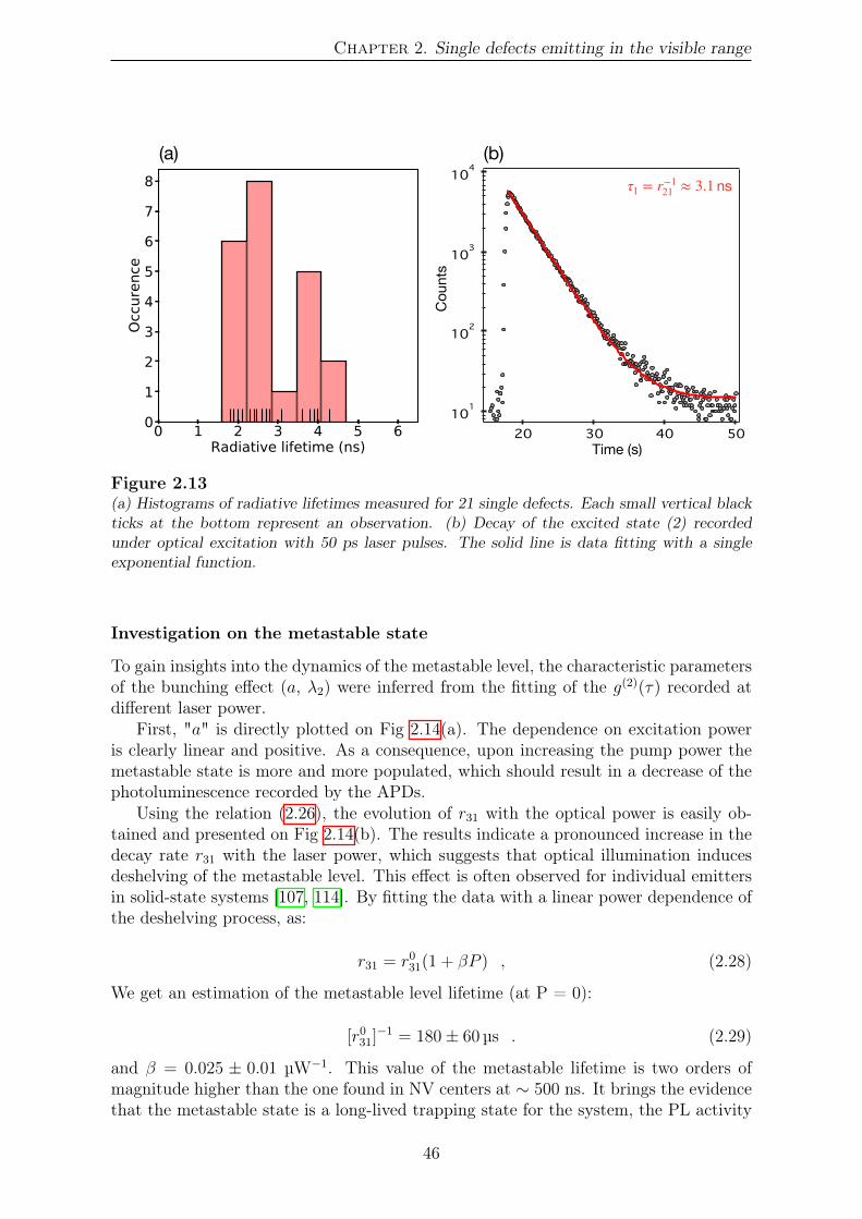
Chapter 2. Single defects emitting in the visible rangeRAPID COMMUNICATIONS
L. J. MARTINEZ et al. PHYSICAL REVIEW B 94, 121405(R) (2016)
Cou
nts
Time [ns](1)
(3)
(2)
r23
r31
r 12
r 21 r−1
21 = 3.1 ns
(a) (b) (c)
PL[x
106 c
nts/
s]
(d)
Optical power [µW]
r 31
[µs−1
]
10
10
10
10
50403020
0.12
0.08
0.04
0.003002001000
Optical power [µW]
4
2
0
10 10 10 10
PL[
10 c
nts/
s]
Time [s]
FIG. 4. (a) Three-level model including a radiative transition between the ground (1) and excited (2) levels, and a nonradiative decaythrough a metastable level (3). The coefficient rij denotes the transition rate from level (i) to level (j ). (b) PL decay recorded under opticalexcitation with 50-ps laser pulses. The solid line is data fitting with a single exponential function. (c) Decay rate of the metastable state r31 as afunction of the laser excitation power. The solid line is data fitting with a linear function (see main text). (d) PL saturation curve of the defect.The red solid line is data fitting with a saturation function (see main text). The inset shows a PL time trace recorded for a laser excitation powerP = 400 µW. We note that short blinking events start to be observed for such laser power above the saturation of the transition. All thesemeasurements are performed on the same individual defect.
recently shown that individual defects in hBN can also befound in positive, negative, and neutral charge states. Activecharge state manipulation was even demonstrated by tuning theFermi energy level with respect to the defect’s charge transitionlevel by locally applying an electric field with a STM tip [18].We tentatively attribute the two groups of spectra shown inFig. 3 to different charge states of the same defect, while thesmall variation of the ZPL energy in each group (±20 meV)might result from variations of the strain in the hBN matrix.Optically induced charge state conversion towards a dark statemight also play an important role in the blinking/bleachingdynamics of the defect.
We now investigate the dynamics of optical cycles for astable defect showing a PL spectrum similar to the one shownin Fig. 3(b). The defect is modeled as a three-level system[Fig. 4(a)]. The lifetime of the excited level was first measuredthrough time-resolved PL measurements using a pulsed laserexcitation with a 50-ps pulse duration and a 10-MHz repetitionrate (PicoQuant, LDH-P-FA-530B). As shown in Fig. 4(b), thePL decay is well fitted by a single exponential function, leadingto a lifetime of the excited level r−1
21 = 3.1 ± 0.1 ns. Thisvalue is in good agreement with the ones recently measuredin hBN flakes for individual defects showing similar spectralproperties [19,20]. To gain insights into the dynamics of themetastable level, the characteristic parameters of the bunch-ing effect (a,λ2) were inferred from g(2)(τ ) measurementsrecorded at different laser excitation powers P [see Eq. (1)].Using a three-level model, the relaxation rate of the metastablelevel r31 is then simply given by [29]
r31 = λ2
1 + a. (2)
As shown in Fig. 4(c), our results indicate a pronouncedincrease in r31 with the laser power, which suggests thatoptical illumination induces deshelving of the metastablelevel. This effect, which is often observed for individualemitters in solid-state systems, can be modeled by a
linear power dependence of the deshelving processr31 = r0
31(1 + βP) [26,28]. By fitting the data with thisequation, we obtain an estimate of the metastable levellifetime [r0
31]−1 = 210 ± 80 µs and β = 0.09 ± 0.04 µW−1.The PL rate R was finally measured as a function
of P [Fig. 4(d)]. Data fitting with a simple saturationfunction R = R∞/(1 + P/Psat) leads to a saturation powerPsat = 310 ± 20 µW and an emission rate at saturationR∞ = 3.9 ± 0.1×10⁶ counts s−1, corresponding to one ofthe brightest single photon sources reported to date. Forcomparison, the emission rate at saturation is ∼20 times largerthan the one obtained from a single NV defect in diamondwith the same confocal microscope. Such high counting ratesindicate that the short excited-level lifetime results from astrong radiative oscillator strength with near-unit quantumefficiency rather than PL quenching involving fast nonradiativedecay processes (r23 ≪ r21).
To summarize, we have isolated individual defects in acommercial high-purity hBN crystal, leading to a robustsingle photon source with up to ∼4×10⁶ counts s−1 un-der ambient conditions. The analysis of the photophysicalproperties of the defect provides important information forunderstanding its structure using ab initio calculations [45].These results pave the road towards applications of hBN, andmore generally van der Waals heterostructures, in photonic-based quantum information science [46] and optoelectronics[17].
We thank M. Kociak, A. Zobelli, J.-F. Roch, and I. Robert-Philip for fruitful discussions. This work was financiallysupported by the network GaNeX (ANR-11-LABX-0014).GaNeX belongs to the publicly funded Investissement d’Avenirprogram managed by the French ANR agency. The authorsacknowledge support from Ecole Normale Superieure deCachan, Conicyt-Fondecyt (Grant No. 1141185), Conicyt-PCHA Doctoral program (Grant No. 2013-21130747), andPMI PUC 1203.
121405-4
Time (s)C
ount
s
(a) (b)τ1 = r−121 ≈ 3.1 ns
Figure 2.13(a) Histograms of radiative lifetimes measured for 21 single defects. Each small vertical blackticks at the bottom represent an observation. (b) Decay of the excited state (2) recordedunder optical excitation with 50 ps laser pulses. The solid line is data fitting with a singleexponential function.
Investigation on the metastable state
To gain insights into the dynamics of the metastable level, the characteristic parametersof the bunching effect (a, λ2) were inferred from the fitting of the g(2)(τ) recorded atdifferent laser power.
First, "a" is directly plotted on Fig 2.14(a). The dependence on excitation poweris clearly linear and positive. As a consequence, upon increasing the pump power themetastable state is more and more populated, which should result in a decrease of thephotoluminescence recorded by the APDs.
Using the relation (2.26), the evolution of r31 with the optical power is easily ob-tained and presented on Fig 2.14(b). The results indicate a pronounced increase in thedecay rate r31 with the laser power, which suggests that optical illumination inducesdeshelving of the metastable level. This effect is often observed for individual emittersin solid-state systems [107, 114]. By fitting the data with a linear power dependence ofthe deshelving process, as:
r31 = r031(1 + βP ) , (2.28)
We get an estimation of the metastable level lifetime (at P = 0):
[r031]−1 = 180± 60 µs . (2.29)
and β = 0.025 ± 0.01 µW−1. This value of the metastable lifetime is two orders ofmagnitude higher than the one found in NV centers at ∼ 500 ns. It brings the evidencethat the metastable state is a long-lived trapping state for the system, the PL activity
46

2.5 Photophysical properties of individual defects
(a) (b)
a (µs-
1 )r 3
1
Optical power (µW) Optical power (µW)
r21r12
r23
r31
VB
CB(c)
?
Figure 2.14(a) Parameter "a" as a function of the optical power. (b) Decay rate r31 of the metastablestate as a function of the optical power. The red solid lines are data fitting with a linearfunction. (c) Schematic of possible processes occurring at high pumping rate.
is stopped during the occupation of this state where the center can stay for about 105
times longer compared to the radiative excited state (in the nanosecond order).In terms of quantum efficiency of the single-photon source, it is quite fortunate that,
although the non-radiative state is more populated with higher optical power, the decayrate from level (3) to ground state (1) increases with the excitation power, acting as acounter effect of the limitation induced by the trapping in the metastable state. Thephysical processes at stake in the deshelving mechanism are not well understood. OnFig 2.14(c), we depict the situation of the defect inside the gap. One possibility is thepromotion of the electron in level (3) to the conduction band (black arrow), leading to anon-radiative recombination of the exciton with the valence band, or a radiative one butat wavelengths not recorded by the APDs. Also, the defect can couple to other defectsor transit towards a different charge state, opening a channel for faster transition tothe ground state (1).
Let us now see the efficiency of the single-photon source by evaluating the emissionrate at saturation.
2.5.3 Brightness of the source
Estimating the brightness of the source is important to compare it with other single-photon emitters. The PL rate R was measured as a function of the optical power P[Fig 2.15]. The horizontal axis is displayed in log-scale. Data fitting with a simplesaturation function R = R∞/(1 + Psat/P ) leads to a saturation power Psat = 310 ± 20µW and an emission rate at saturation:
R∞ = 3.9± 0.1× 10⁶counts/s , (2.30)
similar to what is reported by other studies for the same type of defects [85, 94]. Itcorresponds to one of the brightest single photon source reported to date. For com-
47

Chapter 2. Single defects emitting in the visible rangeRAPID COMMUNICATIONS
L. J. MARTINEZ et al. PHYSICAL REVIEW B 94, 121405(R) (2016)
Cou
nts
Time [ns](1)
(3)
(2)
r23
r31
r 12
r 21 r−1
21 = 3.1 ns
(a) (b) (c)
PL[x
106 c
nts/
s]
(d)
Optical power [µW]
r 31
[µs−1
]
10
10
10
10
50403020
0.12
0.08
0.04
0.003002001000
Optical power [µW]
4
2
0
10 10 10 10
PL[
10 c
nts/
s]
Time [s]
FIG. 4. (a) Three-level model including a radiative transition between the ground (1) and excited (2) levels, and a nonradiative decaythrough a metastable level (3). The coefficient rij denotes the transition rate from level (i) to level (j ). (b) PL decay recorded under opticalexcitation with 50-ps laser pulses. The solid line is data fitting with a single exponential function. (c) Decay rate of the metastable state r31 as afunction of the laser excitation power. The solid line is data fitting with a linear function (see main text). (d) PL saturation curve of the defect.The red solid line is data fitting with a saturation function (see main text). The inset shows a PL time trace recorded for a laser excitation powerP = 400 µW. We note that short blinking events start to be observed for such laser power above the saturation of the transition. All thesemeasurements are performed on the same individual defect.
recently shown that individual defects in hBN can also befound in positive, negative, and neutral charge states. Activecharge state manipulation was even demonstrated by tuning theFermi energy level with respect to the defect’s charge transitionlevel by locally applying an electric field with a STM tip [18].We tentatively attribute the two groups of spectra shown inFig. 3 to different charge states of the same defect, while thesmall variation of the ZPL energy in each group (±20 meV)might result from variations of the strain in the hBN matrix.Optically induced charge state conversion towards a dark statemight also play an important role in the blinking/bleachingdynamics of the defect.
We now investigate the dynamics of optical cycles for astable defect showing a PL spectrum similar to the one shownin Fig. 3(b). The defect is modeled as a three-level system[Fig. 4(a)]. The lifetime of the excited level was first measuredthrough time-resolved PL measurements using a pulsed laserexcitation with a 50-ps pulse duration and a 10-MHz repetitionrate (PicoQuant, LDH-P-FA-530B). As shown in Fig. 4(b), thePL decay is well fitted by a single exponential function, leadingto a lifetime of the excited level r−1
21 = 3.1 ± 0.1 ns. Thisvalue is in good agreement with the ones recently measuredin hBN flakes for individual defects showing similar spectralproperties [19,20]. To gain insights into the dynamics of themetastable level, the characteristic parameters of the bunch-ing effect (a,λ2) were inferred from g(2)(τ ) measurementsrecorded at different laser excitation powers P [see Eq. (1)].Using a three-level model, the relaxation rate of the metastablelevel r31 is then simply given by [29]
r31 = λ2
1 + a. (2)
As shown in Fig. 4(c), our results indicate a pronouncedincrease in r31 with the laser power, which suggests thatoptical illumination induces deshelving of the metastablelevel. This effect, which is often observed for individualemitters in solid-state systems, can be modeled by a
linear power dependence of the deshelving processr31 = r0
31(1 + βP) [26,28]. By fitting the data with thisequation, we obtain an estimate of the metastable levellifetime [r0
31]−1 = 210 ± 80 µs and β = 0.09 ± 0.04 µW−1.The PL rate R was finally measured as a function
of P [Fig. 4(d)]. Data fitting with a simple saturationfunction R = R∞/(1 + P/Psat) leads to a saturation powerPsat = 310 ± 20 µW and an emission rate at saturationR∞ = 3.9 ± 0.1×10⁶ counts s−1, corresponding to one ofthe brightest single photon sources reported to date. Forcomparison, the emission rate at saturation is ∼20 times largerthan the one obtained from a single NV defect in diamondwith the same confocal microscope. Such high counting ratesindicate that the short excited-level lifetime results from astrong radiative oscillator strength with near-unit quantumefficiency rather than PL quenching involving fast nonradiativedecay processes (r23 ≪ r21).
To summarize, we have isolated individual defects in acommercial high-purity hBN crystal, leading to a robustsingle photon source with up to ∼4×10⁶ counts s−1 un-der ambient conditions. The analysis of the photophysicalproperties of the defect provides important information forunderstanding its structure using ab initio calculations [45].These results pave the road towards applications of hBN, andmore generally van der Waals heterostructures, in photonic-based quantum information science [46] and optoelectronics[17].
We thank M. Kociak, A. Zobelli, J.-F. Roch, and I. Robert-Philip for fruitful discussions. This work was financiallysupported by the network GaNeX (ANR-11-LABX-0014).GaNeX belongs to the publicly funded Investissement d’Avenirprogram managed by the French ANR agency. The authorsacknowledge support from Ecole Normale Superieure deCachan, Conicyt-Fondecyt (Grant No. 1141185), Conicyt-PCHA Doctoral program (Grant No. 2013-21130747), andPMI PUC 1203.
121405-4
Optical power (µW)
PL [1
06 c
nts/
s]Time (s)
PL [1
06 c
nts/
s]
Figure 2.15PL saturation curve of the defect. Inset: PL time trace recorded for a laser excitation powerP = 400 µW performed on the same individual defect. The solid red line is the fit proposedin the main text. The dashed blue line shows the intensity at saturation for the NV center indiamond. The inset shows the stability of the emission at around 0.5 mW.
parison, the emission rate at saturation is ∼ 20 times larger than the one obtainedfrom a single nitrogen-vacancy defect in diamond with the same confocal microscope.Such high counting rates indicate that the short excited-level lifetime results from astrong radiative oscillator strength with near-unit quantum efficiency rather than PLquenching involving fast non-radiative decay processes (r23 � r21). Indeed, for thefamily of defects emitting at 596 nm (2.08 eV), the quantum efficiency (QE) has beenexperimentally measured at 87 % [115], which is among the highest QE recorded for asolid-state single-photon emitter.
2.6 Conclusion
In this work, we have studied a class of single defects in the wide bandgap semiconductorhBN on the angle of spectral measurement and photon statistics emission. Our approachhas consisted in exciting the surface of a high-purity hBN monocrystal (HQ Graphene)by means of a single mode laser at 532 nm and a confocal microscope working in ambientconditions, and performing correlation measurements of emitted photons with a coupleof APDs installed in the HBT configuration. The analysis performed with the help ofthe three-level system have brought insights into the dynamics of the quantum emitter.
Main important results consist in:
• A very bright single-photon source reaching 4× 10⁶ counts/s at saturation power
48

2.6 Conclusion
310 µW, resulting from a strong radiative oscillator strength, with excellent photo-stability. These defects have been proved to maintain their stability in a monolayerof hBN [82].
• Two families of defects exhibiting very similar spectrum, with ZPL at 1.97 eV and2.08 eV, and phonon replica of constant energy shift 150 meV. These families maybe considered as different charge states of the defect and the 150 meV detuning ofphonon replica results from a dominant coupling to the zone-edge optical phononsof highest density of state.
• A dynamic of optical cycles marked by a long-lived non-radiative metastable stateof ∼ 200 µs. It appears to be very power dependent with a steep increase of ther31 decay rate with increasing excitation power, suggesting a deshelving of thislevel by the laser.
This analysis of the photophysical properties of the defect provides important infor-mation for understanding its structure using ab-initio calculations. These results pavethe road towards applications of hBN, and more generally van der Waals heterostruc-tures, in photonic-based quantum information science and optoelectronics.
We mention that we have not found optically-detected magnetic resonance (ODMR)in this hBN sample for this specific defect. However, more recent studies report on themagnetic-field dependent emission from single-photon source at room temperature foran emitting wavelength at ∼ 725 nm (1.7 eV) [86], and the first ODMR measured onsingle defect in hBN [116].
Concerning the chemical nature of these defects, recent calculations [117–119] sug-gest a carbon impurity substituting for a boron coupled to a nitrogen vacancy (CBVN)or a nitrogen anti-site defect coupled to a nitrogen vacancy (NBVN). However, elec-tronic structure calculations in 2D materials remain challenging and uncertainty persistsregarding the nature of the defects.
49

Chapter 2. Single defects emitting in the visible range
50

Chapter 3
Deep defects emitting in the UV range
In Chapter I, we have presented the properties of luminescence of hexagonal boronnitride originating from point defects in the near ultraviolet, especially the deep de-
fect emission at 4.1 eV. To date, there is no definitive understanding for this emission,although it was already observed in 1981 [120] with time-dependent photolumines-cence experiments on hBN powder of poor quality compared with the current availablecrystals. As for other defects in different materials, the diversity in the experimentalapproaches is necessary to unveil the nature of such color centers. The specificity andoriginality of this defect lie in the fact that it emits in the UV, which explains at thesame time the experimental difficulty to study it. In this chapter, we present an origi-nal study that makes use of isotopic purification in material doping to investigate theinfluence of carbon into the luminescence properties of hBN in the UV. We combinemacro-photoluminescence and reflectance measurements to study new defects appear-ing in our carbon-doped samples, as presented in the first section of this chapter. Asfar as the detection of single emitters is concerned, the high concentration of the 4.1eV defect usually recorded in bulk crystals led us to two developments. First, to builda photoluminescence confocal microscope operating at 266 nm (4.66 eV), presentedin the second section. Secondly, to combine the characterization by cathodolumines-cence of thin crystals with characterization by the micro-photoluminescence confocalmicroscope. We also used this new microscope to probe the spatial fluctuations at asub-micrometer scale of the deep level emission in the UV. These two last investigationsare the subject of the last section.
3.1 New levels in carbon-doped hBN crystals
In this section, we will present the results obtained by studying carbon-doped hBN crys-tals grown by precipitation method by means of two distinct spectroscopy techniques:photoluminescence and reflectivity. The measurements presented in this section arespatially resolved at a scale of tens of micrometers to millimeters. Considering theusual density of defects in the crystals, we thus probe ensembles of defects here.
3.1.1 Description of the experiments
The complementary approaches of photoluminescence and reflectivity
The microscopic processes involved in photoluminescence and reflectivity are of distinctnature. The photoluminescence is the result of carrier relaxation and thermalization
51

Chapter 3. Deep defects emitting in the UV range
processes after the system was put in an excited state, thus out of equilibrium. Itis a particularly efficient technique to analyze semiconductors shallow levels and alsodeep levels when the radiative recombination process is intense enough [121]. Yet,the interpretation of the processes responsible for lines in the emission spectrum cansometimes be complex, therefore we complement our measurements with reflectance. Inreflectance spectroscopy, we probe a material close to its thermodynamic equilibrium,that is to say the reflected signal intensity for a given excitation wavelength providesinformation about the dielectric constant of the material, and thus about the oscillatorstrength of the optical transitions. We will be using these two kinds of spectroscopyin order to gain better understanding of the underlying processes responsible for thefeatures observed in our optical measurements. We will now present the experimentalsetup for these two techniques.
Macro photoluminescence setup
5
PhotoluminescenceReflectance
Resolution 10 meV
2w3w
4w
CCD
1800
g/
mm
8K
M
M
𝝀 = 193 nm
Integration time : 5 mins
P
𝝀 = 180 - 320 nm
PM
M
Deu
teriu
m
Lam
p
2400
g/m
m8K
M
M
Monolayer Boron [email protected] IWUMD 2019
Ti-Salaser
Experimental setup in DUV
N2environment
� 195 nmλ =
Figure 3.1Scheme of the macro-photoluminescence setup. A Ti:Sa oscillator is quadrupled through twosuccessive wave-mixing units, and sent onto the sample inside the cryostat. An achromaticoptical system couples the emitted light to a spectrometer equipped with a camera optimizedfor deep UV.
We present on Fig 3.1 a scheme of the macro-photoluminescence setup. A cw mode-locked Ti:Sa oscillator with a repetition rate of 82 MHz is sent onto two successive wave-mixing devices: the first one provides the third harmonic signal that is subsequentlymixed in the second unit with the first harmonic signal and tuned to give the fourthharmonic at a wavelength of 195 nm (6.35 eV) with a power of 30 µW. A prism (P) isused to further separate the fourth harmonic from the other components, and a planarmirror (M) directs the beam toward the sample hold on a cold finger of a closed-cyclecryostat (temperature control from 8 K to room temperature). The spot diameter ison the order of 50 µm. An achromatic optical system couples the emitted signal to the
52
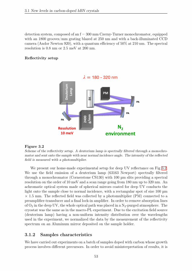
3.1 New levels in carbon-doped hBN crystals
detection system, composed of an f = 300 mm Czerny-Turner monochromator, equippedwith an 1800 grooves/mm grating blazed at 250 nm and with a back-illuminated CCDcamera (Andor Newton 920), with a quantum efficiency of 50% at 210 nm. The spectralresolution is 0.8 nm or 2.5 meV at 200 nm.
Reflectivity setup
5
PhotoluminescenceReflectance
Resolution 10 meV
2w3w
4w
CCD
1800
g/
mm
8K
M
M
𝝀 = 193 nm
Integration time : 5 mins
P
𝝀 = 180 - 320 nm
PM
M
Deu
teriu
m
Lam
p
2400
g/m
m8K
M
M
Monolayer Boron [email protected] IWUMD 2019
Ti-Salaser
Experimental setup in DUV
N2environment
PA
PA
PA
� 180 - 320 nmλ =
Figure 3.2Scheme of the reflectivity setup. A deuterium lamp is spectrally filtered through a monochro-mator and sent onto the sample with near normal incidence angle. The intensity of the reflectedfield is measured with a photomultiplier.
We present our home-made experimental setup for deep UV reflectance on Fig 3.2.We use the field emission of a deuterium lamp (63163 Newport) spectrally filteredthrough a monochromator (Cornerstone CS130) with 100 µm slits providing a spectralresolution on the order of 10 meV and a scan range going from 180 nm up to 320 nm. Anachromatic optical system made of spherical mirrors coated for deep UV conducts thelight onto the sample close to normal incidence, with a rectangular spot of size 100 µm× 1.5 mm. The reflected field was collected by a photomultiplier (PM) connected to apreamplifier-transducer and a final lock-in amplifier. In order to remove absorption linesof O2 in the deep UV, the whole optical path was placed in a N2-purged atmosphere. Thecryostat was the same as in the macro-PL experiment. Due to the excitation field source(deuterium lamp) having a non-uniform intensity distribution over the wavelengthsused in the experiment, we normalized the data by the measurement of the reflectivityspectrum on an Aluminum mirror deposited on the sample holder.
3.1.2 Samples characteristics
We have carried out experiments on a batch of samples doped with carbon whose growthprocess involves different precursors. In order to avoid misinterpretation of results, it is
53

Chapter 3. Deep defects emitting in the UV range
important to present the growth protocol as well as the potential effects of the differentprecursors on the PL spectra.
Synthesis of the crystals
The team of James H. Edgar in Kansas State University provided us with carbon-dopedhBN single crystals grown from a molten metal solution at atmospheric pressure with amodified version of the growth procedure described in references [17, 122]. Three metalswere used: nickel, iron, and chromium. Nickel and iron are good solvents for boron,with maximum solubilities of 18.5 at.% and 17 at.%, respectively. Chromium is goodfor dissolving nitrogen. Mixing of both metallic solvents forms a eutectic (at 1345 ◦Cfor Ni and Cr). The boron source for all samples was either a commercial hBN powderor hot pressed boron nitride (HPBN), nominally fabricated from the same commercialpowder. The carbon source was graphite powder, with the natural distribution ofcarbon isotopes, except for sample C40, which used 13C enriched graphite. We presentthe samples and their specificities on Table 3.1.
Table 3.1Growth parameters of the carbon-doped hBN crystals precipitated from a molten metal solu-tion in a high-temperature furnace. HPBN denotes hot pressed boron nitride.
Sample name Graphite quantity BN quantity Solvents Cooling rate Atmosphere
C20 1.5 g graphite powder 0.5 g BN powder 10 g Fe + 10 g Cr 4 ◦C/h H2 + N2
C22 1.5 g graphite powder 0.5 g BN powder 10 g Ni + 10 g Cr 4 ◦C/h H2 + N2
C27 graphite piece HPBN 17 g Fe + 17 g Cr 4 ◦C/h H2 + N2
C33 2.0 g graphite powder 1.0 g BN powder 20 g Ni + 20 g Cr 0.5 ◦C/h CO + N2
C40 0.75 g 13C powder BN pressed boat 10 g Ni + 10 g Cr 0.5 ◦C/h CO + N2
More specifically, the carbon-doped hBN crystals were precipitated from the moltenmetal solution in a high-temperature single-zone furnace. For growing the crystals ofTable 3.1, the precursor powders with compositions listed in the second through fourthcolumns were loaded in either an alumina or a HPBN ceramic crucible, and transferredinto the furnace. The furnace was evacuated and purged with the atmospheric gaseslisted in the sixth column multiple times to remove all residual oxygen. For growingpure hBN crystals, a small amount of hydrogen is typically added with the flowingnitrogen to reduce and remove any oxides from the source materials. However, to avoidexcessive etching of the graphite source for growing these carbon-doped hBN crystals,carbon monoxide was used instead of hydrogen, as it reacts with and removes oxygen,but not carbon. The precursor powders were heated up to 1550 ◦C to form liquid phaseand held at this temperature for 24 h to thoroughly dissolve the carbon, boron, andnitrogen into the molten metal solution. The crystals were then grown by cooling thesystem to 1300 ◦C at rates of 4 or 0.5 ◦C/h, as listed in the fifth column. During crystalgrowth, the atmospheric gases were continuously flowed to the system at a rate of 125sccm, and the system was kept at 850 torr. After crystal growth, the system was thenquenched to room temperature at 50 ◦C/h.
54

3.1 New levels in carbon-doped hBN crystals
3.5 4 4.5 5 5.5 6Energy (eV)
PL in
tens
ity
C 20
C 22
HPBN
D2D6
Figure 3.3Macro-PL spectrum at 8 K (semilog scale), with an excitation energy of 6.35 eV, in bulk hBNsynthesized either with iron (C22) or nickel (C20), and the hBN powder used as a precursor,here in the form of HPBN.
Iron versus nickel as solvent
As alluded to earlier, the solubility of boron is higher in nickel than iron while theresidual amount of carbon impurities in our Fe is smaller than in our Ni. To determinewhether these parameters play a role in the crystals structural properties, we performphotoluminescence measurements over a wide range of energy.
We begin by comparing the 8 K PL features in the spectral range between 3.5and 6 eV [Fig 3.3], recorded in cases of samples C20 (Fe-Cr solvent) and C22 (Ni-Crsolvent), and of the BN powder used as a precursor, here in the form of HPBN. ThePL spectrum of the BN precursor displays emission lines near 4 eV (shaded region inFig 3.3). These lines are also found in the PL spectra of C20 and C22. The lines forma more or less documented series, depending on the growth run, with in general thedetection of a strong feature at 4.1 eV. We emphasize that these sharp lines were neverrecorded in the case of samples grown using the protocol of [123], which revealed theoptical performances of monoisotopically boron-purified BN samples [124]. For thesegrowths, elemental boron-10 and boron-11 as well as N2 were used instead of a BNpowder. PL intensities have been plotted logarithmically in Fig 3.3. The PL spectrumbelow 5 eV corresponds to the recombination lines arising from deep levels. There is thewell-known zero-phonon line (ZPL) at 4.1 eV with its accompanying phonon replicasat lower energies [68, 125]. Because of the heavy carbon-doping in our hBN crystals,the PL intensity of the 4.1 eV line is comparable to that of the stacking faults around5.5 eV, in contrast to the peak observed in powder samples, if it is seen at all. This isin agreement with similar studies reported in [125] that led those authors to relate the4.1 eV line to carbon/oxygen impurities. In Fig 3.3, the PL line shape is not influenced
55
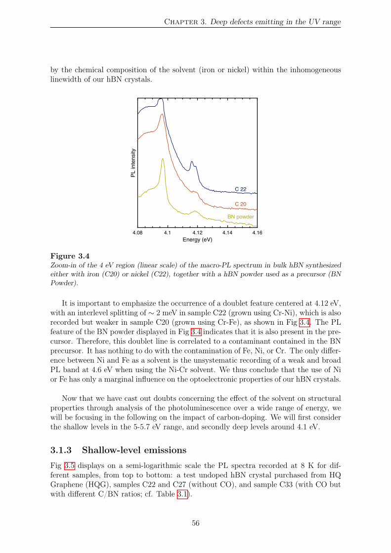
Chapter 3. Deep defects emitting in the UV range
by the chemical composition of the solvent (iron or nickel) within the inhomogeneouslinewidth of our hBN crystals.
4.08 4.1 4.12 4.14 4.16Energy (eV)
PL in
tens
ity
C 20
C 22
BN powder
Figure 3.4Zoom-in of the 4 eV region (linear scale) of the macro-PL spectrum in bulk hBN synthesizedeither with iron (C20) or nickel (C22), together with a hBN powder used as a precursor (BNPowder).
It is important to emphasize the occurrence of a doublet feature centered at 4.12 eV,with an interlevel splitting of ∼ 2 meV in sample C22 (grown using Cr-Ni), which is alsorecorded but weaker in sample C20 (grown using Cr-Fe), as shown in Fig 3.4. The PLfeature of the BN powder displayed in Fig 3.4 indicates that it is also present in the pre-cursor. Therefore, this doublet line is correlated to a contaminant contained in the BNprecursor. It has nothing to do with the contamination of Fe, Ni, or Cr. The only differ-ence between Ni and Fe as a solvent is the unsystematic recording of a weak and broadPL band at 4.6 eV when using the Ni-Cr solvent. We thus conclude that the use of Nior Fe has only a marginal influence on the optoelectronic properties of our hBN crystals.
Now that we have cast out doubts concerning the effect of the solvent on structuralproperties through analysis of the photoluminescence over a wide range of energy, wewill be focusing in the following on the impact of carbon-doping. We will first considerthe shallow levels in the 5-5.7 eV range, and secondly deep levels around 4.1 eV.
3.1.3 Shallow-level emissions
Fig 3.5 displays on a semi-logarithmic scale the PL spectra recorded at 8 K for dif-ferent samples, from top to bottom: a test undoped hBN crystal purchased from HQGraphene (HQG), samples C22 and C27 (without CO), and sample C33 (with CO butwith different C/BN ratios; cf. Table 3.1).
56

3.1 New levels in carbon-doped hBN crystals
5 5.2 5.4 5.6 5.8 6Energy (eV)
102
103
104
105
106
107
108
PL In
tens
ityHQG
C22
C33
C27
T=8K
Figure 3.5PL spectra recorded at 8 K in bulk hBN crystals for energies ranging between 5 and 6 eV(semilog scale). Spectra are vertically shifted for clarity. Growth conditions are given in TableI. HQG stands for a test undoped hBN crystal purchased from HQ Graphene.
The 5.7–6 eV energy range corresponds to the intrinsic part of the emission spectrum.This series of lines corresponds to the well-defined phonon-assisted optical transitionstypical of indirect-bandgap semiconductors, and here, of the hexagonal BN stacking,with their specific spectral distribution that we have reviewed in Chapter 1 Section1.4.1. Zooming in on each of these phonon-assisted recombination lines reveals a sim-ilar low-energy fine structure, due to the emission of phonon overtones involving thelow-frequency Raman-active mode at the zone center [57].
Below the energy of the LO-assisted recombination (5.75 eV) starts the spectralrange of defect-related emission, discussed in Chapter 1 Section 1.4.2. From 5.7 eVdown to 5 eV, there is a series of discrete lines split from each other by about 147 meV.Transverse optical phonons at the K point of the Brillouin zone assist inter-K valleyscattering, producing a series of discrete recombination bands because the stackingfaults in bulk hBN [65, 66] provide a density of final electronic states in Fermi’s goldenrule, and shape the envelope of the PL spectrum [63]. Two distinct lines, labelled D2
and D6 in the initial paper of Cassabois et al. [63] and noted on Fig 3.3, are alsodetected. They were tentatively attributed to the BN divacancy following [126].
The PL spectrum is almost identical for the first three samples (HQG, C22, andC27). In contrast, in the heavily doped C33 sample, the PL spectrum presents lessdefined features. The sharp and detailed series of phonon-assisted recombination linesabove 5.7 eV is strongly broadened and hardly observable, and the defect-related emis-sion lines are also broadened. More importantly, we note an apparent blue shift of themost intense line to 5.52 eV in C33, shifting from 5.47 eV in the other samples.
The higher carbon concentration in C33 may affect the crystal quality and result
57

Chapter 3. Deep defects emitting in the UV range
in a decrease of the intensity of the intrinsic recombination lines together with a largerinhomogeneous broadening, which would contribute to washing out the series of phononreplicas above 5.7 eV. As a matter of fact, this may also impact the defect-related emis-sion lines, but we note a distortion of the peak around 5.5 eV. In HQG, C22, and C27,the energy of the maximum is 5.47 eV with a high-energy shoulder at 5.5 eV [Fig 3.5],whereas we observe a broader asymmetric line in C33 with a maximum at 5.52 eV, anenergy that corresponds to a minimum of the PL spectrum in HQG, C22, and C27.Finally, a secondary maximum appears at 5.37 eV in C33, as a high-energy shoulder ofthe 5.3 eV band, again at an energy where the PL spectrum of HQG, C22, and C27displays a minimum. These observations suggest the existence of new transitions in theoptical response of heavily carbon-doped hBN crystals.
Figure 3.6PL (solid lines) and reflectance (dotted lines) spectra on linear scales, recorded in a testundoped hBN crystal (HQG, black lines) and a heavily carbon-doped one (C33, green lines)at 10 K. Note the coincidences between the reflectance minima and the PL maxima in sampleC33.
To test this hypothesis, we compare in Fig 3.6 the PL and reflectance spectra (onlinear scales) recorded in HQG and C33. For HQG, the reflectivity (dotted black line)displays smooth variations with a rather flat spectrum in the spectral domain wherethe PL spectrum (solid black line) is on the contrary very rich with many lines due tointervalley scattering into excitonic states bound to stacking faults, as explained above.Such a difference between the spectra is fully consistent with the distinct nature ofthe microscopic processes involved in PL and reflectivity. Indeed, as explained in thebeginning of this chapter, the reflectivity probes a material in its thermodynamic equi-librium whereas PL results from carrier relaxation and thermalization. The presence of
58

3.1 New levels in carbon-doped hBN crystals
many defect-related lines around 5.5 eV, in the PL spectrum but not in the reflectanceone, is a genuine signature of relaxation effects with resonances of intervalley scattering,further supporting the interpretation initially proposed in [63].
In contrast, the heavy carbon-doping in C33 not only modifies the PL spectrum(solid green line) but also the reflectance one (dotted green line). Strikingly, there arepronounced reflectance oscillations, in resonance with the new emission lines at 5.37 and5.52 eV. This observation confirms the existence of new optical transitions associatedwith heavy carbon-doping in hBN crystals. The incorporation of carbon during thegrowth process produces complementary states with a high enough density and oscilla-tor strength of their optical transition to significantly change the dielectric constant inthe 5.3–5.6 eV energy region.
Following [126], we tentatively attribute the lines at 5.37 and 5.52 eV to an excitonbound to the defect formed by a carbon substituting for a nitrogen (CN). In [126], theoptical absorption spectrum of hBN calculated by the Bethe-Salpeter equation predictedthat native point defects or impurities induce novel optical transitions close to the bandgap, corresponding to defect bound excitons. The heavy carbon-doping in C33 makesthe CN -bound exciton a strong candidate for the 5.37 and 5.52 eV lines.
3.1.4 Deep-level emissions
In this section we focus on the lower energy part of the spectrum presented in Fig 3.3,especially on the shaded region corresponding to the emission of the well studied defectat 4.1 eV. We discuss the presence of new spectral lines at higher energies between 4.1and 4.2 eV.
3.5 3.6 3.7 3.8 3.9 4 4.1 4.2Energy (eV)
102
103
104
105
106
107
PL In
tens
ity
C22
C27
C33
LO( )LO( )
Figure 3.7Full set of the PL spectra (semilog scale) of carbon-doped hBN samples in the 3.5-4.25 eVrange. The spectra are vertically shifted for clarity. The horizontal bars have a 200 meVwidth, corresponding to the LO(Γ) phonon energy.
59

Chapter 3. Deep defects emitting in the UV range
We display on Fig 3.7 the PL spectra of three samples in the 3.5-4.25 eV spectralrange. Emission from the 4.1 eV deep level is always recorded with its sharp ZPL,phonon sidebands and prominent optical phonon replicas at 3.9 and 3.7 eV [68, 127].A new line at 4.12 eV (called UV1) is observed with a doublet fine-structure splitting.In sample C27, there are additional weak lines at 4.14 and 4.16 eV (called UV2 andUV3, respectively), all three of these lines being much more intense in the heavilycarbon-doped C33 sample. We also note that all of these lines broaden when increasingthe amount of carbon involved in the growth protocol, which likely prevents us fromobserving any fine-structure splitting, if any, for UV2 and UV3. Finally, phonon replicasof UV1, UV2, and UV3 are detected, readily observed and red-shifted by 200 meV(LO(Γ) phonon) and 400 meV (2LO(Γ) phonons) from their ZPL.
The first indication that UV1-3 do not share the same microscopic origin as the 4.1eV deep level comes from the vibronic part of their PL spectrum. The experimentaldata recorded in C33 are plotted on a linear scale in Fig 3.8 in order to better resolvethe different line shapes of UV1-3 compared to the 4.1 eV line. At low temperature (8K, top spectrum), we can distinguish the ZPL and the low-energy sideband in the emis-sion spectrum of the 4.1 eV defect as described in Chapter 1 Section 1.4.3, although thecarbon-doping leads to broadening of the ZPL. On the contrary, for UV1-3 no phononsideband is observed and each of the UV1-3 lines can be fairly fitted to a symmetricprofile, with a Gaussian function. Moreover, upon raising the temperature, the FWHMof UV1-3 increases from 6 meV at 8 K to 9 meV at 120 K. Such a temperature depen-dence contrasts with the phenomenology presented in Section 1.4.3 Fig 1.18, where weobserved a 5.5 meV broadening in the 8-120 K range for the 4.1 eV defect [68], furthersuggesting a different microscopic structure in UV1-3 compared to the 4.1 eV defect.
4.05 4.1 4.15 4.2Energy (eV)
PL In
tens
ity [
arb.
uni
ts]
8 K20 K40 K80 K120 K220 K290 K
Figure 3.8Temperature-dependent PL measurements (linear scale) in the heavily carbon-doped hBNsample C33, in the 4.05 to 4.2 eV range. The spectra are vertically shifted for clarity.
Furthermore, looking at the PL signal intensity as a function of temperature, we do
60

3.1 New levels in carbon-doped hBN crystals
not record any cross-talk between the lines, with a constant intensity ratio among theset of optical transitions in the 3.8-4.2 eV range. This observation indicates the absenceof interlevel crossing in the relaxation dynamics, either because the spatial separationof the defects is larger than the carrier diffusion length, or because they are formedin distinct mesoscopic domains due to the local fluctuations of the growth conditionsduring the synthesis of the hBN crystals.
We performed reflectivity measurements in this region of the spectrum in order toaccess the oscillator strength of the optical transitions observed. Results are shown onFig 3.9, where we compare the PL and reflectance spectra recorded at 8 K in sampleC33. The reflectivity signal exhibits a marked peak at 4.1 eV, testifying to a substantialoscillator strength. Because of the mirror symmetry between phonon-assisted absorp-tion and phonon-assisted emission, we record a series of blue-shifted minima that arethe high-energy analogs of the phonon replicas detected in the PL spectrum, with aninterlevel spacing of 200 meV as discussed above. Note that the ZPL is broader inreflectance than in PL, thus smearing out the fine structure of the phonon replicas inreflectivity.
3.6 3.8 4 4.2 4.4 4.6Energy (eV)
0
1
2
3
4
5
PL In
tens
ity [x
104 c
ount
s]
1
1.5
2
2.5
3
3.5
Ref
lect
ivity
[%]
LO( )LO( )
LO( )LO( )
Figure 3.9PL (green dashed line) and reflectivity (purple solid line) spectrum on linear scales, recordedat 8 K for sample C33 in the 4 eV region. The horizontal bars have a 200 meV width,corresponding to the LO(Γ) phonon energy. They are displayed in red for the red-shiftedphonon-assisted emission (below 4.1 eV), and in blue for the blue-shifted phonon-assistedabsorption (above 4.1 eV).
Surprisingly, nothing is detected for the UV1-3 deep levels in reflectivity. Althoughthe PL lines of UV1-3 and the 4.1 eV defect are of comparable intensities in this sample,no reflectance minima are seen at the energies of the new carbon-related PL lines. This
61
Chapter 3. Deep defects emitting in the UV range
effect may come from either a smaller oscillator strength or a lower density of the UV1-3 point defects. In both cases, the interpretation of the high PL signal intensity fromUV1-3 implies a more efficient carrier relaxation in these novel carbon-related pointdefects.
Summary
By means of macro-PL and reflectivity experiments, we have probed the emission spec-trum of different carbon-doped crystals of hBN in the deep UV (5 eV to 6 eV) and thenear-UV (∼ 4 eV).
In the deep UV, namely in the part of the spectrum corresponding to exciton recom-bination assisted by inter-K valley scattering, we bring the evidence of new energy leveltransitions at 5.37 and 5.52 eV which are not observed in moderately doped samples.They have sufficient oscillator strength and are present in density high enough to mod-ify the dielectric constant in the energy region 5.3-5.6 eV, as witnessed in reflectivity.We attribute the new level transitions to an exciton bound to a CN impurity.
In the near-UV region around 4.1 eV, we reveal the existence of additional opticaltransitions at 4.12 eV (UV1), 4.14 eV (UV2), and 4.16 eV (UV3), to which carbon dop-ing induces a strong increase in their PL signal intensity. These spectral lines are notdocumented in the literature. In contrast of the two levels introduced at higher energiesin the spectrum, the reflectance spectra show no correlated features for the UV1-3 lines,indicating either a low density or weak oscillator strength. In the former case, recallingthat the excitation spot is large and thus the signal is averaged over many locations,probing the sample at a smaller scale would enable to investigate the spatial variationsof these deep levels and help to gain further insight into them.
To that end, we shall now present the µ-PL confocal setup operating in the UVrange, built during my thesis. Additionally to the gain in spatial resolution, the betterspectral resolution of our confocal microscope will also help in revealing subtle detailsin the spectrum, if any. Besides, the sub-bandgap excitation energy at 4.66 eV (266nm), is not only closer to the energy transition of the UV1-3 levels, but also allows thesuppression of the 4-eV broad emission background [127], thus enhancing the visibilityin this region of the spectrum.
62

3.2 Confocal microscope at 266 nm / 4.66 eV
3.2 Confocal microscope at 266 nm / 4.66 eV
3.2.1 General overview of the experimental setup
Sample
3-axis piezo platformCollection pinhole
Excitation pinhole
Dichroic mirror
Laser
Spectrometer
Cryostat
Single photon detection
Widefield imaging
� plateλ/2
PBSplanar
spherical
parabolic
KeyMirrors: Other:
beam splitter
filter
magnetic mount
Optical shutter
Objective
P1
P4
S1
P3
P2
S2DB
Pa
L1 L2
L3
L4
F1
F2
BS
Figure 3.10Functional sketch of the confocal microscope.
We have built a confocal microscope in the ultraviolet range that works at cryogenictemperature and is coupled through an achromatic and geometrical aberration-freeoptical system with a spectrometer and a HBT interferometer (cf. Chapter 2) to assessthe uniqueness of the point defect emitters. A scheme of the overall setup is shown onFig 3.10, while a more detailed drawing for the cryostat and widefield imaging systemis presented on Fig 3.11.
Laser source
The excitation source is a diode pumped continuous wave solid state laser (FQCW266-10, CRYLAS GmbH company). The optical emission results from a quadrupled Nd:YAGlaser (λ=1064 nm) thus providing an emission wavelength at 266 nm or 4.66 eV. Themode of the emitted light is a single longitudinal mode TEM00, with a deviation froma gaussian beam shape characterized by a factor M2 < 1.3, linearly vertically polarizedand with a linewidth of less than 300kHz around 266 nm. A combination of a half-wave plate (λ/2) and a polarized beam-splitter (PBS) allows the regulation of the laserpower. The beam is enlarged a first time by a couple of lenses of different focal length(L1, L2).
63

Chapter 3. Deep defects emitting in the UV range
Spatial filtering
To obtain optimal performances, a pinhole diaphragm in the excitation path is usedto improve the selectivity of the illumination in the sample field by spatially filteringthe illumination beam. Another advantage of this pinhole is that it creates a pointsource for the excitation that is stable and remains immobile throughout measurementand alignment, the changes in pointing direction of the laser source producing only amodification of the laser intensity. In this purpose, a pinhole of 25 µm is placed in theconjugated focal plane of a lens L3 (f=89.5 mm) and L4 (f=136 mm). The telecentricsystem formed by (L3, L4) provides a second enlargement of the beam. The focal lengthof L3 was chosen long enough in order to avoid spherical aberrations with high anglesof diffraction which would introduce distortion of the spot and losses of energy. Thelens L3 is installed on a XY translation stage with micrometer control of the positionand on a Z linear translation stage in order to finely optimize the coupling with thefixed confocal pinhole. We reach a coupling of 86%.
Beam walking and dichroic mirror
The excitation beam is then sent onto two planar mirrors (P2, P3) mounted on kine-matic mounts with adjustable angles and in a 45◦/45◦ configuration, for beam walking.This couple of mirrors allows to make the beam parallel and centered with respect tothe entrance pupil of the objective.
A dichroic mirror (Di01-R266 Semrock) is placed at an incident angle of 45◦. It hasa reflection coefficient of 94% for λ = 266 nm and a transmission coefficient of 90%above λ = 277 nm. DB on Fig 3.10 indicates an iris diaphragm that enables to controlthe beam diameter before the objective.
Microscope objective in a close-cycle cryostat
The microscope objective we use is a refractive objective with an effective focal lengthEFL = 5 mm at 266 nm and numerical aperture NA = 0.5 (LMU-40X-UVB, Thorlabs).The cryostat installed in the experiment is an helium close-cycle cryostat (OptiDrymodel) from MyCryoFirm. It has a large vacuum chamber with a cold gold-coated plateat 4 K at the bottom, on which lies the sample holder along with all the opto-mechanicaldevices (sample positioners, scanners), the probe and heater for temperature control (cf.Fig 3.11). This chamber possesses an upper turret, removable for samples installationand/or indoor optics adjustment. An in-house made mechanical piece was designed tohold a planar mirror at 45◦ on top of this turret, thus changing the propagation of lightfrom horizontal to vertical direction, directing the beam towards the top window of thecryostat.
One fundamental aspect of our setup is the position of the objective inside thechamber of the cryostat. Indeed, in the UV range, aberrations introduced when a coneof light crosses a glass window are huge. In order to avoid any change of refractiveindex between the objective and the sample, the microscope objective was fixed insidethe chamber to the top wall, like illustrated on Fig 3.11. However, in the cryostat, thewalls are not cooled down, only the cold plate is connected to the cooling system. Itmeans that the objective is at room temperature. This is why we need a thermal shield
64

3.2 Confocal microscope at 266 nm / 4.66 eV
Beam splitter
45° mirror
Cryostat Vacuum chamber
Z stepper
X stepperY stepper
Regulation bloc
XYZ scanner
Sample holder
θ
ϕ
θ
ϕ
θ
ϕ
CCD
Magnification 35x
Flip-mirror
Aluminium wires
Copper wires
4 K
300 K
50 KInfrared shield
Dichroic mirror
Laser
Photoluminescence
Laser filter
Mounted LED
Widefield imaging system
Objective
P2P3
Figure 3.11Drawing of the excitation part with the cryostat chamber and the widefield imaging system.
at 50 K between the objective and the sample holder, to protect the sample from theblack body radiation at 300 K of the objective.
Scanning system
In the design of our confocal setup, the laser source and the objective are fixed, and weperform raster scans by recording the PL signal intensity for different positions of thesample by moving the sample. It requires a precise control of the position, the movingfrequency and the repetition rate of the scanning stage. Moreover, the nanopositionerswork under cryogenic temperature and vacuum. We use two types of positioners: threeunidirectional steppers (2 ANPx101 & ANPz101 Attocube) to position roughly thesample and explore different regions, and one XYZ scanner (ANSxyz100 Attocube) toperform the scans. The steppers have a travel range of 5 mm at both high and low tem-perature whereas the scanner travel range is 50×50×24 µm3 at 300 K and 30×30×15µm3 at 4 K. Both types of positioners are connected to their suitable controller. Thescanner is controlled through an acquisition card with analog outputs (NI PCIe-6323)connected to the controller (Thorlabs MDT693B-3 channel) while the steppers are con-trolled independently through their own controller (Attocube ANC 300).
65

Chapter 3. Deep defects emitting in the UV range
Confocal collection
The photoluminescence of the sample is collected by the same objective and collimatedtowards the collection path. The light is first transmitted by the dichroic mirror, andthen goes through a filter F1, an ultrasteep long-pass edge filter (RazorEdge Semrock)with an optical density OD = 5 at 266 nm, to remove the remaining laser light inten-sity. The confocality of the microscope is ensured by the collection pinhole positionedin the common focal plane of two spherical mirrors S1 and S2 (f=250 mm). In this con-figuration, the light is therefore re-collimated by the second spherical mirror S2, andsubsequently separated by a 50/50 beam splitter: one half is directed toward a coupleof single-photon detectors and is filtered by the band-pass filter F2 300-340 nm withOD > 5 outside the band (FF02-320/40 Semrock), and a second half toward a planarmirror P4 that directs the light to a 24◦ off-axis parabolic mirror Pa (f=209 mm). Thislast mirror focuses the photoluminescence at the entrance slit of the spectrometer.
The diameter of the pinhole in collection, which fully determines the ability of thesystem to select one optical slice in the axial direction of the sample, has to be properlychosen. The choice is usually made so that the back projected image of the pinhole inthe focal plane of the objective is equal or smaller than the excitation spot. If we neglectaberrations, the excitation spot size is given by the Airy disk radius calculated withthe photoluminescence wavelength because we are considering the diffraction patterncaused by the light emitted from a point source in the sample. Thus, we apply theAbbe formula with λPL = 300 nm (emission wavelength of the 4.1 eV defect) and theresulting Airy disk radius rAiry equates to:
rAiry = 0.61× λPLNA
= 0.61× 300nm0.5
≈ 366nm . (3.1)
We finally obtain the size of the pinhole by applying the magnification factor related tothe focal length of the objective and mirror S1: fS1
fobjective× 2 × rAiry = 250mm/5mm ×
2× 366nm ≈ 37 µm. Conventional sizes of pinhole being multiple of 10 µm, the choicewas made to favor confocal stringency and work with a 30 µm wide confocal pinhole(80% of the Airy disk).
Two channels for PL detection
After the confocal selection, we have two different ways of detecting the photolumines-cence signal.
In the case of the reflection on the beam splitter BS [Fig 3.10], we use hybridphotomultiplier tubes (PMA Series PicoQuant) in photon-counting mode. The PMAhave a 6 mm wide detection area, work for photon wavelengths between 220 and 650 nm,have a transit time spread of 50 ps, which is the ultimate time resolution achievable, andcan handle count rate up to 10 MHz. The dark counts are under 100 counts/s. For rasterscans of PL, only one of the detectors was used. However, to perform time-correlatedsingle photon counting (TCSPC) measurements, we used both detectors mounted inthe configuration of Hanbury Brown and Twiss (HBT) interferometer. The PMA areconnected to a single-photon counting acquisition card (PicoQuant TH260).
66
3.2 Confocal microscope at 266 nm / 4.66 eV
In the second case of transmission by BS, we use a spectrometer that has a f=500mm Czerny-Turner system (Shamrock 500i B2) equipped with a turret containing threegratings with different groove density and blazed at different wavelengths. The oneproviding the best resolution has 1800 grooves/mm and is blazed at 250 nm: it providesa spectral resolution of 0.02 nm or 0.3 meV at 300 nm. The spectrometer is coupled to aback-illuminated UV-enhanced camera (Andor Newton DU940P BU2) with a quantumefficiency of 60% at 300 nm. The camera active pixel area is composed of 2048×512pixels of 13.5×13.5 µm2. The advantage of using the spectrometer is to resolve the PLspectrum. We can spectrally filter the PL maps over a given spectral range, a type ofanalysis usually called SPIM. This will be further explained and illustrated in section3.2.5. The time needed for such an acquisition is however much longer than the onewith mono-channel photon detectors.
Optical inspection with the widefield imaging system
An additional mirror placed on a magnetic mount ahead of the collection path is usedto couple the objective with the widefield imaging setup. A close-up of this part isrepresented on Fig 3.11.
In order to visualize the sample surface under visible light and with an appropri-ate magnification, we set up a widefield microscope using a mounted LED (ThorlabsMCWHL5) which emits a cold light at 6500 K with a central wavelength at 430 nm.The image is formed on a CCD camera (Thorlabs DCC1545M) by a UV-coated lens.The magnification obtained is 35× which provides a spatial extent of 45 µm wide and70 µm high.
Computer control of the experiment
The experimental setup features a number of instruments that need to be controlledby a central unit for data acquisition. From shining a laser on a sample to obtain aSPIM image, there is a number of steps that goes from the development of an interfacewith a central unit, computer programs for data acquisition, data analysis and datavisualization. I present below the programs that I have coded during my thesis.
There were two main programs to develop for the data acquisition. The first con-cerns the acquisition of raster scans of photoluminescence. One very inconvenient pointis that the PMA, made to detect single photons, send low negative amplitude pulses (-75mV) with extreme short time resolution (700 ps) which make them undetectable by theacquisition card of the scanners (NI PCIe-6323). In consequence, the instruments havebeen synchronized for scan acquisition using the acquisition card PicoQuant-TH260,suitable for the signal sent by the PMs, with the NI card. The program has been codedin Labview with the DLL from Attocube and PicoQuant. The second program is theone used for SPIM acquisition. It requires to control in a synchronous manner thescanners and the spectrometer with the camera. Again the chosen interface is Labviewbecause previous programs were already developed in that language.
A secondary program has been coded in Labview for control of the Attocube step-pers. Regarding the spectrometer, native program from Andor (Andor Solis) has been
67

Chapter 3. Deep defects emitting in the UV range
extensively used for alignment and sample exploration especially for its numerous op-tions in image mode. Temperature control has been conducted directly through thecontroller Cryo.Con 24C. Laser emitting power was always set to 8 mW for stabilityand effective used power was selected by a couple of a half-wave plate and a polarizedbeam splitter. The direction of the half-wave plate was controlled from the computerthrough a motorized rotation stage.
Concerning the data visualization and analysis, I have coded programs exclu-sively in Python programming language [128], working mainly with Numpy and Scipylibraries for data processing and analysis, Panda for data manipulation and Matplotlibfor data visualization.
3.2.2 What are the challenges to build a confocal setup in theUV?
The many challenges to build such a confocal setup in the ultraviolet range stem fromthe optical aberrations, both spherical and chromatic, in the excitation as well as inthe collection part of the optical system.
Indeed, materials used to build optics (lenses, mirrors, windows, beam splitters)become very dispersive media for the light in the UV. This is the reason why we installedthe microscope objective inside the cryostat chamber, as explained earlier. Yet, thisdoes not solve all issues related to spherical aberrations. The refractive objective weuse in our system is significantly sensitive to spherical aberrations in that the focusingof the excitation beam into a small excitation spot in the sample field is remarkablydependent on the diameter DB of the beam. While it is common to fully illuminatethe entrance aperture of the objective to reach the best spatial resolution, here we needto assess the optimum value of DB that minimizes the impact of spherical aberrations.We carefully deal with this issue in section 3.2.3.
Another consequence of optics becoming highly dispersive in the UV is that, whilethe excitation part deals with a monochromatic beam and for which we can use lensesto focus and re-collimate the light, the situation in collection is significantly differentbecause the emitted light from our sample has a large spectral width that expandstypically from 300 nm to 340 nm. In this regard, chromatic aberrations are a crit-ical issue, and totally preclude the use of refractive optics for the collection of thephotoluminescence. To get rid of this type of aberration we have used reflective op-tics such as concave and parabolic mirrors. We shall discuss the practical aspects ofthose in section 3.2.4. The microscope objective, made of a series of lenses, and usedboth for excitation and collection, suffers the same chromatic aberrations, particularlywhen it is question of focusing the laser light and collecting the PL light from the samefocal point. This issue demands particular attention and will be tackled in section 3.2.4.
Besides, another necessity in the UV range is to work with UV-adapted opticalcomponents. The lenses L1-4 (LA-UV, Thorlabs) are made of UV grade fused silicaoffering a high transmission coefficient in the UV and low thermal expansion, and arecoated with an anti-reflection layer, decreasing the reflection to 0.5%. The mirrors P1-
68
3.2 Confocal microscope at 266 nm / 4.66 eV
3 (NB1-K04, Thorlabs) are Nd:YAG laser line mirrors, perfectly adapted to our lasersource, offering a high damage threshold to withstand the high-intensity beam in theexcitation part. The reflection coefficient is greater than 99.75%. In the collection part,the mirrors S1-2 are UV-enhanced aluminum concave mirror (10DC500AL.2, Newport)with a reflection coefficient R > 90% for wavelength between 250 nm and 600 nm. P4 isalso a UV-enhanced aluminum mirror (PF10-03-F01, Thorlabs) with R > 90% between250 and 450 nm. Finally, the parabolic mirror Pa is made of bare aluminum (EdmundOptics) and is 40mm×40mm large. It has been specially coated for UV. Its reflectivityreaches 85% in the range 250 nm - 700 nm. These coatings are expensive, and sensitiveto oxidization. Moreover they are less tolerant in angle of incidence which adds to theconstraints, however they are of paramount importance when signals to be detected arevery weak. Finally,
3.2.3 Optimization of the optical excitation
In this section, we deal with the impact of the excitation beam diameter on the spatialresolution. To obtain the smallest spot of excitation with a microscope objective, oneusually illuminates the full entrance aperture of the objective, and we understand itwell from basic knowledge on microscope resolution and Fraunhofer diffraction. How-ever, due to importance of refraction phenomenon at 266 nm, spherical aberrations areoccurring through the objective lenses and enlarge the excitation spot by modifyingthe distribution of intensity in the sample field. Thereby, the resolution given by theclassical Abbe formula r0 = 0.61× λ
NAis not applicable here.
In order to curb this detrimental effect, we control the entrance beam diameter DB
by placing an iris diaphragm on the excitation path before the top mirror of the cryostat(cf. Fig 3.10). By narrowing the beam we suppress the outer light rays on the pupil,thus diminishing spherical aberration effects. Yet, when the objective entrance pupilis not completely filled, the effective numerical aperture NA decreases and so does thediffraction-limited resolution (Airy disk radius increases). Therefore, one must find anoptimum value for the resolution.
Simulation with an optical design software
We have used Zemax to numerically simulate the effect of DB on the excitation spotsize. Zemax is a professional optical design program [129] used to design and analyzeimaging systems as well as illumination systems. It works by ray tracing-modelingthe propagation of rays through an optical system. It can model the effect of opticalelements (here, the objective) and produce standard analysis diagrams such as spotdiagrams.
Fig 3.12(a) presents the dependence of the spot size with DB. We have two elementsin the figure. First is the case without spherical aberrations, represented by the solidorange curve. In this case the excitation spot radius is only limited by diffraction,it is the Airy disk radius. Second is the case with taking spherical aberrations intoconsideration, represented by the blue dots. In this case, the excitation spot radiusdeparts from the ideal case because aberrations through the objective tend to deviatethe peripheral rays, thus enlarging the spot. Therefore we need to redefine the spotradius. A consistent way of doing that is to consider, in the spot diagram, the radius
69

Chapter 3. Deep defects emitting in the UV range
of the circle enclosing 84% of the total luminous intensity, a criterion chosen to beidentical to that of the definition of the Airy disk (cf. Fig 3.13 for more details). Theprocedure for this redefined spot also performs an optimization along the axial direction(the so-called "refocused spot"), as a consequence the effective focal length changes alittle bit during this process, however over the all range of DB values in this figure, thevariation of the focal length is less than 1 µm. DB ranges from 1.5 mm to 5 mm, theactual pupil diameter of the objective.
Diffraction-limited
With spherical aberrations
Spot radius : 0.506 µm Pupil diameter : 3.8 mm
∼ 6
DB = 2 mm
∼ 5 ∼ 4 ∼ 7
DB = 3.8 mmDB = 3 mm DB = 4.5 mm
(a)
(b)
Figure 3.12(a) Simulated diagram, using Zemax, of the excitation spot radius in the focal plane of theobjective depending on the beam diameter (DB). The solid orange line represents the casewithout taking spherical aberrations into consideration (Airy disk), and the blue dots withspherical aberrations throughout the objective (refocused spot, see main text). (b) Experi-mental investigation of the effect of the beam diameter for DB = 2, 3, 3.8 and 4.5 mm. Theupper panels are the images at zero order on the CCD camera of the spectrometer withoutthe confocal pinhole in collection. The lower panels are a cross-section of the intensity profilewith a Lorentzian fit, the FWHM in pixels is indicated by the orange arrows.
One can see that the Airy disk size (solid line) varies in a monotonous way withthe beam diameter. This is well understood from Fraunhofer diffraction: the more
70

3.2 Confocal microscope at 266 nm / 4.66 eV
the incident beam illuminates the objective entrance aperture, the more the effectivenumerical aperture increases, the smaller the excitation spot. It reaches the value of325 nm when DB = 5 mm, as expected.
In contrast, the refocused spot (blue dots) behaves in two distinct ways. For valuesof DB less than 3.5 mm we are still in the Gauss conditions and the aberration effects arenot visible, it follows the orange curve. Then, spherical aberrations become prominentand it rises significantly. Thereby, there is an optimum value of the beam diameter toobtain the smallest excitation spot. The optimum is found for DB = 3.8 mm, whichprovides a resolution of reff0 = 500 nm at the sample surface.
Experimental results
Fig 3.12(b) provides the experimental data when changing DB. The upper panels showthe images at zero order of the excitation spot onto the CCD of the spectrometer forseveral values of DB, with the collection pinhole removed (otherwise we would image itinstead of the excitation spot). The lower panels display a cross-section of the inten-sity profile with a Lorentzian fit. We note a good agreement with the simulation, theFWHM of the spot intensity decreases steadily until reaching a minimal value of ∼ 4pixels for DB = 3.8 ± 0.1 mm, and then rises rapidly to 7 pixels when reaching DB =4.5 mm.
To bring more details on the procedure for defining the refocused spot radius, wepresent in Fig 3.13(a) the radial cumulative distribution of the intensity of the spotdiagram in the focal plane of the objective, for DB = 3.8 mm (blue) and DB = 4.4 mm(red), and for the two cases with (dotted lines) and without (solid lines) spherical aber-rations. For a given value of the radial distance, the curve indicates the percentage ofthe luminous energy contained in a circle of this radius. This is schematically illustratedin Fig 3.13(b) for a spot with aberrations, in purple. In the case of diffraction-limitedresolution (not represented), the spot intensity follows the well-known Airy pattern1,whose radial distribution is recalled in the inset of Fig 3.13(b), where the Airy radiusis simply defined by the distance from the center of the spot to the first zero of thedistribution, and where the area between the two zeros represents 84% of the totalintensity. In the spot diagram, however, we see that the spot is not included in theAiry disk because of aberrations, and we thus have determined the new radius formingthe refocused spot (dotted line) that does contain 84% of the total luminous intensity.
In Fig 3.13(a), for DB = 3.8 mm (blue), corresponding to the optimum value de-termined above, we clearly see that the intersections of the solid and dotted lines withthe 84% threshold give similar radii, as seen in Fig 3.12(a) where the blue dot is only80 nm above the orange curve. For DB = 4.4 mm, the solid line indicates a smallerAiry disk radius as expected (because NA increases) but, in contrast of the precedentcase, the intersection of the dotted line with the threshold at 84% gives a much largerrefocused spot radius, in agreement with the fourth CCD image of Fig 3.12(b). Spher-ical aberrations tend to distribute more luminous energy in the secondary oscillationsof the Airy pattern.
1For the common case of circular objective aperture, it involves the Bessel function of the first kindand order.
71

Chapter 3. Deep defects emitting in the UV range
84% of intensity
Radial intensity profile
of the Airy pattern
Airy disk radius
Schematic representation of refocused spot and Airy disk
Radial distance
Airy diskRefocused spot
(a) (b)
Figure 3.13(a) Radial cumulative distribution of the luminous energy with (dotted lines) and without(solid lines) spherical aberrations, with DB = 3.8 mm (blue) and DB = 4.4 mm (red). (b)Illustration of a spot diagram in the focal plane of the objective. The dotted circle correspondsto the refocused spot radius encircling 84% of the total intensity distribution in purple. Inset:recall of the intensity distribution of the Airy pattern.
As said previously, the focus of the spot is slightly modified by the aberrations effect.We stress that between DB = 5 m, that is to say the completely illuminated objectiveaperture, and DB = 3.8 mm, the optimum beam diameter for the resolution, the axialshift calculated with Zemax is ∼ 400 nm. It is not insignificant compared to the axialextension of the spot (∼ 2 µm), therefore the iris diaphragm controlling DB should beinstalled at the beginning of the alignment to optimize the confocal tuning.
3.2.4 Mitigation of chromatic aberrations
In this section we shall tackled the issue of chromatic aberrations occurring through themicroscope objective, and then examine the collection system composed exclusively ofmirrors.
Correction for the chromatism of the objective
The wavelength of the laser beam is λexc = 266 nm, while the typical emission wave-length is around λem = 300 nm. The refractive indices of materials, lenses are madeof, vary more rapidly in the ultraviolet range compared to the visible range. It meansthat the effective focal length of the objective can be quite different for these two wave-lengths.
To assess the necessity to compensate for chromatic aberrations in the objective, letus evaluate the change in focal length. To do so, we simulate the path of optical rayswith Zemax. The program calculates that the focal length of the objective for266 nm is 11 µm shorter than the focal length at 300 nm. To know whetheror not this change in focal length has to be taken into account in the alignment, it isrelevant to estimate the axial extension (along z) of the confocal spot. Assuming that
72

3.2 Confocal microscope at 266 nm / 4.66 eV
the focused laser beam operates in the TEM00 mode and is directed along the z axis,the confocal volume is an oblate ellipsoid, which is an ellipse rotated around its longeraxis. Similarly to the lateral resolution, the axial resolution is defined as the distancefrom the center of the 3D diffraction pattern to the first axial minimum (in object spacedimensions). This definition is the axial equivalent of the Rayleigh Criterion, and reads:
rz =1× λ
n−√n2 −NA2
≈ 2nλ
NA2, (3.2)
where n is the index of refraction of the medium between the objective and the sample.The approximation that is done above simply results from a limited series expansion ofthe square root at the first order by factorizing by n, and stays true for value of NAless or equal to 0.5.
For our setup, the medium is the air n = 1 and the formula (3.2) yields an axialresolution of rz = 2 ∗ 0.266/0.52 ∼ 2 µm. This result confirms that we need to compen-sate for the chromatic aberrations of the objective. Indeed, the center of the spot isdisplaced by 11 µm between excitation (λexc) and collection (λem) wavelengths which ismore than 5 times the longitudinal extension rz of the confocal volume.
SAMPLE
266n
m
266n
m
300nm
300n
mFocal length300 nm
OBJECTIVE
SAMPLE
OBJECTIVE
266n
m
L3L4Z translation
Focal length 300 nm
Δ = f300 − f266 = 11
Dich
roic
Mirror
µmΔ
SAMPLE
266n
m
300nm
266n
m300nmFocal length
266 nm
OBJECTIVE
OBJECTIVE
266n
m
L3Telecentric system
Focal length 266 nm
L4Z translation
Dich
roic
Mirror
SAMPLE
(a)
(b) (d)
(c)
Telecentric system
Figure 3.14Scheme of the steps to compensate for chromatic aberrations of the objective. (a) Representsthe inadequate situation where the laser beam is simply collimated at the entrance aperture,corresponding to lenses (L3, L4) of the telecentric system sharing a common focal plane (b).(d) Shows how the position of L4 influences the divergence of the gaussian beam and thus thevertical position of the excitation spot. (c) Is the final sought configuration.
73

Chapter 3. Deep defects emitting in the UV range
Fig 3.14 represents how to correct the chromatic aberrations of the refractive objec-tive. Fig 3.14(a) shows the situation as it is just by focusing the collimated laser beam.The photoluminescense coming out of the sample diverges after the objective becausethe sample is placed at a closer distance than the focus at 300 nm. The divergence ofthe photoluminescence is very detrimental for the system. Indeed, after the objectivethe light goes through the glass window and different wavelengths (from 300 nm to340 nm) will be further angularly dispersed, and will later have their foci at differentdistances even with an achromatic collection system. This situation corresponds to theexperimental configuration where the distance between the two lenses (L3, L4) is thesum of their respective focal length for λexc, as represented in Fig 3.14(b).
The goal here is to bring the focus of the laser for λexc at a distance corresponding tothe focal length of the objective for λem. In this situation, the PL will exit the objectivecollimated.
The technique consists in using the telecentric system formed by (L3, L4) placedbefore the dichroic mirror. In Fig 3.14(b) the laser beam is collimated. But if onebrings L4 closer to L3, as in Fig 3.14(d), geometrical optics stipulates that the beamwill be divergent. It follows that the beam will be focused farther after the objective.We note ∆ the downward axial displacement of the excitation spot. At the same time,one needs to adjust the vertical position of the sample (with the steppers) in order tokeep the excitation spot at the sample surface. The correct alignment is obtained when∆ = 11 µm, that is to say when the focus of the laser matches that of the wavelengthλem. This final situation is represented in Fig 3.14(c), where the excitation occurs witha divergent beam on the objective entrance pupil and the PL exits in a collimatedbeam. Experimentally, we have used a sample containing polar quantum dots (QDs),consisting of 10 monolayers of Al0.2Ga0.8N, with an emission peak at 300 nm. The QDsare strongly localized in depth (few nanometers), allowing for a sharp alignment.
Achromatic collection system
We want to use this microscope to carry out studies on crystals emitting typically inthe region 300 nm to 340 nm. The spectral width is large, and we have already stressedhow dispersive the media can be at these wavelengths. Thus, having an aberration freesystem in collection is an essential prerequisite to preserve the resolution achieved inexcitation. This is crucial both for the spatial and spectral resolution.
Therefore we only use mirrors in the collection path. With mirrors, chromatic aber-rations are eliminated. However, in the case of concave mirrors (S1, S2), we must payattention to the spherical aberrations that inherently occur when the light hit the mir-rors with a non-zero incident angle. Since we need non-zero angle in the configurationof the experiment to set up the confocal filtering with the pinhole as well as to guide thelight until the spectrometer, or towards the PMA detectors, it is necessary to determinewhich geometrical configuration of the mirrors allows an aberration-free optical system.We have performed optical simulation, using the software Zemax, to evaluate the limitangle of incidence on the concave mirrors (S1, S2) above which the effect of sphericalaberrations deteriorate the resolution. In the simulation, the beam diameter is 5 mm(the entrance pupil diameter of the objective) and the wavelength 302 nm (ZPL of the4.1 eV defect). Spot diagrams are shown on Fig 3.15 for α angles, between incident
74

3.2 Confocal microscope at 266 nm / 4.66 eV
100
µm
100
µm
Airy disk Airy disk
Spot diagram Airy radius: 18.42 µmGEO radius: 14.758 µm
Spot diagram Airy radius: 18.42 µmGEO radius: 25.854 µm
� = 12°α � = 16°α
Figure 3.15Spot diagrams in the focal plane of mirror S1, for angles between incident and reflected lightat S1 surface of α = 12◦ (left), 16◦ (right). Airy and geometrical (GEO) radii are given. Thelatter pertains to the calculated beam rays.
and reflected light, of 12◦ and 16◦. The Airy disk radius is 18.4 µm in both cases. It isclear that under 12◦ the aberrations introduce negligible effects, the geometrical radius(GEO) of the projected spot being smaller than the Airy radius, while above 16◦ theyenlarge the spot beyond the diffraction-limited disk with a GEO radius 40% larger thanthe Airy one. It sets an upper limit of the angle for the experimental configuration. Wechose to work with α = 10◦ to preserve an aberration-free collection.
In contrast, due to the constraints in the configuration of our setup, the focusing ofthe beam at the entrance of the spectrometer was made with an off-axis parabolic mirror(OAP) Pa (cf. Fig 3.10). An OAP is simply a side section of a parent parabolic mirror,as shown on Fig 3.16. However, unlike a centered parabolic mirror, an OAP mirror hasan advantage in that it allows more interactive space around the focal point withoutdisrupting the beam. Note that it is important to keep the incident beam parallel tothe optical axis of the OAP, angular deviations producing comatic aberrations.
We use in our setup an OAP with 24◦ off-axis angle, enabling to work with highangles without introducing spherical aberrations.
75

Chapter 3. Deep defects emitting in the UV range
15°
Focal point
Central Ray Axis
15°-OAP
45°
Focal point
Central Ray Axis
45°-OAP
Parent parabolic mirror
Figure 3.16Drawing of 15◦ and 45◦ off-axis parabolic mirrors (OAP). Parabolic mirrors are free of sphericalaberrations.
3.2.5 Performances of the microscope
We aim here at illustrating the different performances of the confocal microscope ob-tained with a crystal of hexagonal boron nitride (hBN).
Experimental conditions
The cryostat chamber is pumped down to 10−4 mbar before cooling down. Between 100and 150 K the pump valve is closed because cryopumping becomes more efficient thatthe turbo pump itself. We start working when reaching a temperature of about 5 Kgiven by a temperature sensor located on the regulation bloc just beneath the sampleholder. At this temperature the pressure is usually measured at 2.5× 10⁻⁸ mbar.
Raster scan of PL with the PMA
Fig 3.17(a) presents a raster scan of photoluminescence recorded with the PMA detec-tors on a hBN flake over 20×20 µm2 area. The step size is 100 nm in both directions,and acquisition time per pixel is 50 ms. We observe a localized bright spot of emis-sion (white square). A closeup scan is performed on the delimited region around thisspot and shown on Fig 3.17(b). We evaluate the FWHM on this spot by plotting thecross-section of the intensity profile on Fig 3.17(c). A Gaussian fit to the experimentaldata (blue triangles) yields FWHM = 550 nm, indicated by the orange arrows. Thisis a proof of concept for the achievement of the spatial resolution of our UV confocalsetup. We are able to witness spatial features of less than 550 nm.
76

3.2 Confocal microscope at 266 nm / 4.66 eV
550 nm
(a) (b)
(c)
Figure 3.17(a) Raster scan of photoluminescence recorded with the PMA detectors on a region of 20×20µm2. (b) Second scan with more pixel resolution on the white square of (a). (c) Verticalintensity profile of the scan along the vertical line indicated by the orange arrows on (b).
SPIM images
With the spectrometer and the CCD camera in detection, we have the possibility torecord one spectrum at every position of the scanners during the raster scan. Thisacquisition mode produces a 3D data set known as spectral image or shortly SPIM.Practically, these images are constructed by synchronizing the acquisition of the spec-trometer and CCD with the piezoelectric scanners. A region of interest is determinedon the sample, the spatial step size is usually chosen as 1/3 or 1/2 of the lateral spatialresolution and the spectrum acquisition time for each point is fixed relatively to theSNR, usually 0.5 to 5 s is necessary. The spectrum also needs to be recorded at leastthree times in order to remove spikes, originating from high energy particles, with astatistical treatment. The time needed to record a SPIM image is typically in the orderof 10 to 25 hours depending on the size of the region of interest, the desired step size,the time of acquisition per spectrum and the reading speed of the CCD (varies the CCDnoise).
The data processing of SPIM images allows the analysis of the correlation betweenspectral features and spatial localization, thus giving information on the impact ofparticular morphological elements at the surface on the spectral emission. Fig 3.18(b)shows the results of such an acquisition on bulk hBN at 4 K during 15 hours. The SPIMis acquired over the 30×30 µm2 region indicated by the blue square of the widefieldmicrograph Fig 3.18(a). The similarity between the two images indicates that thePL varies with surface morphology along the parallel lines. The SPIM is spectrallyintegrated between 302.49 and 302.80 nm (or 4.0946 and 4.0988 eV), that is to sayaround the ZPL of the 4.1 eV defect, and the step size in each direction is 200 nm. Thespectrum of Fig 3.18(c) is taken at the pixel position indicated by the yellow squareon the SPIM. We note the narrow ZPL, more visible in the inset. A Gaussian fit ofthe data points is calculated and provides FWHM = 0.87 meV, corresponding to the
77

Chapter 3. Deep defects emitting in the UV range
FWHM = 0.87 meV
(a) (b)
(c)
Figure 3.18(a) Widefield image of a region of the hBN crystal. The blue square indicates a region of30×30 µm2 on which is performed the SPIM acquisition (b). (c) is the spectrum extractedfrom the yellow pixel on (b). Inset: zoom on the ZPL of the emission and Gaussian fit (orangedotted line).
spectral resolution of our setup limited by the width of the slits of the spectrometerwhich were closed to 20 µm (this is the minimum width and the one used for SPIMacquisition).
78
3.3 Probing deep defects at a sub-micrometer scale in PL
3.3 Probing deep defects at a sub-micrometer scale inPL
In this section, we present the studies carried out with the confocal microscope inthe UV range, described in Section 3.2. We first investigate the new transitions
unveiled in macro PL and reflectivity, and then focus on the 4.1 eV line with the aimof investigating the involvement of carbon in the structure of the defect. Finally I willpresent the search for single emitters at 4.1 eV in very thin flakes of hBN.
The spectrometer is set with the grating 1800 grooves/mm blazed at 250 nm, pro-viding a spectral resolution of 0.02 nm or 0.3 meV at 300 nm (cf. Section 3.2.1). Inthis configuration, the full spectrum range is 27 nm (353 meV) around 310 nm (4 eV).
3.3.1 The UV1-3 lines
a
1
2
34
5
3 µmPL
inte
nsity
4.10 4.15
Coun
ts p
er se
cond
b1
4.10 4.15
c2
4.10 4.15Energy (eV)
d3
4.10 4.15
e4
4.10 4.15100
101
102
103
104
f5
Figure 3.19(a) Spatial variations of the PL signal intensity recorded by an UV scanning confocal micro-scope in sample C27, at 10 K, for an excitation power of 0.35 mW. The PL signal is integratedfrom 4.112 to 4.175 eV, with a 5 s integration time per acquisition point. (b)-(f) PL spectrumon a log scale recorded at the five different locations indicated by circles in (a).
We present here the measurements by our UV scanning confocal micro-PL setuprelated to the new transitions above 4.1 eV. We first studied the spatial variations ofthe UV1-3 PL signal intensity in sample C27, at 10 K. Carbon-doping in this hBNcrystal is moderate to minimize broadening of the PL lines (cf. Table 3.1). In Fig3.19(a), the PL map is plotted after integration of the signal intensity from 4.112 to4.175 eV in order to better visualize the presence of the novel carbon-related UV1-3
79

Chapter 3. Deep defects emitting in the UV range
lines. With this color code related to a spectral range excluding the 4.1 eV defect, westress that the regions appearing dark correspond to a large PL intensity of ∼ 5× 10³
counts per second for the 4.1 eV ZPL. In terms of the intensity of the UV1-3 lines,sample C27 is thus more or less homogeneously dim except for very bright domains.The 4.1 eV defect is also rather uniform and intense with a local increase in some brightregions of Fig 3.19(a), as detailed below.
The PL spectra of five representative regions are provided in the lower panels (b)-(f) of the figure. In the homogeneous part of the sample (circle 1), only the 4.1 eVline is detected with a sharp ZPL and the low-energy acoustic phonon sideband Fig3.19(b). We note the high signal-to-noise ratio with a dynamical range of three decadesbetween the maximum of the ZPL at 4.1 eV and the noise level at higher energy. Sucha precision is important in view of claiming the contribution of the novel carbon-relatedUV1-3 lines is negligible within our signal-to-noise ratio.
Circles 2, 3, and 4 are located in the bright white regions. As expected, we observethat the UV1-3 lines have a PL signal intensity always lower than the 4.1 eV defect, inagreement with the macro-PL measurements presented in Fig 3.7. Our spatially resolvedPL measurements reveal the striking absence of spatial correlation between the UV1-3lines: all three are detected at point 2, only UV1 at point 3, UV1 and UV3 at point 4,and UV1 and UV2 at point 5. We thus conclude that the novel emission lines relatedto carbon-doping in hBN do not come from the same defect, rather they originate fromthree independent defects. This is crucial information and a key indication that one hasto look for three novel microscopic configurations in order to account for the micro-PLmeasurements in Fig 3.19.
Eventually, we point out the doublet structure of UV1, which is much better resolvedin Fig 3.19 than in Fig 3.4. Thanks to the low carbon doping and correspondingly nar-row defect lines, as well as the spatial resolution of our microscope, the spectra recordedin positions 3 and 4 show that UV1 is a doublet with a splitting of 2.7 meV and a FWHMof 1.7 meV for the two components. No well-defined fine structure for UV2 and UV3 isdetected in sample C27.
We now show the similar measurements performed on the heavily carbon-dopedsample C33 in identical conditions to those of Fig 3.19. We first notice the increasedinhomogeneity with many domains giving a large PL signal intensity for the UV1-3lines. Moreover, there is a significant broadening with a typical FWHM of the orderof ∼ 10 meV compared to 1.7 meV measured in Fig 3.19(d) and (e). Nevertheless, the4.1 eV defect maintains a narrow ZPL as seen in Fig 3.20(c) and (e), not only wherethe UV1-3 lines are hardly observable, but also in locations where they are intense[Fig 3.20(f)] or even dominate the PL spectrum [Fig 3.20(b),(d)]. This phenomenologysuggests that the UV1-3 defects are not only independent from each other but alsouncorrelated to the 4.1 eV deep level. Besides, all three additional lines present nochange when varying the polarization angle of the excitation laser.
We can also notice on Fig 3.20(c) the unusual shape of the ZPL peak, with a doubletstructure. Actually, in the region surrounding spot 2 in Fig 3.20(a), we find a secondpeak in the ZPL structure. We recorded 11 spectra on a ∼ 2 µm long horizontal lineshown in Fig 3.21.
From bottom to top, we see the emergence of a second peak at lower energy, with a
80

3.3 Probing deep defects at a sub-micrometer scale in PL
a
1
2
3
4 5
3 µm
PL in
tens
ity
4.10 4.15
Coun
ts p
er se
cond
b1
4.10 4.15
c2
4.10 4.15Energy (eV)
d3
4.10 4.15
e4
4.10 4.15100
101
102
103
104
105f5
Figure 3.20(a) Spatial variations of the PL signal intensity recorded by an UV scanning confocal micro-scope in the heavily carbon-doped sample C33, at 10 K, for an excitation power of 0.35 mW.The PL signal is integrated from 4.112 to 4.175 eV, and there is a 2.5 s integration time peracquisition point. (b)-(f) PL spectrum on a log scale recorded at the five different locationsindicated by circles in (a).
splitting of 1.5 meV in the spectrum 6 where the two peaks have the same intensity, andthen its progressive disappearance. No similar structure at the LO(Γ) phonon replicaat 3.898 eV was discernible because of the broader profile of the phonon replica (∼ 5meV instead of ∼ 1 meV for the ZPL). However the phonon replica does red-shift by0.7 meV from 1 (3.8981 eV) to 6 (3.8974 eV) where the doublet structure exhibits amaximum of contrast, and then return to its initial value by blue-shifting from 8 (3.8974eV) to 11 (3.8981 eV). The FWHM of the replica also constantly increases from 1 (4.6meV) to 11 (6.3 meV) following the trend of the ZPL doublet splitting illustrated bythe gray lines on Fig 3.21. We don’t know if this doublet structure emerges from anintrinsic phenomena or from the spatial variation of the emission. In the latter case,giving the ∼ 500 nm excitation spot diameter, it would be an indicator of the sub-µmscale at which the ZPL position varies. This will be further investigated in the nextsection 3.3.2.
Doublet structure of the UV1-3 lines
We have discussed above the doublet structure of the UV1 line in C27. We present belowon Fig 3.22 a spectrum showing a well-resolved fine structure for the three lines UV1-3,recorded on sample C40 doped with 13C (cf. Table 3.1) at 4 K. PL maps integrated inthe range 3.83-4.18 eV (ZPL + UV1-3) and 4.11-4.17 eV (UV1-3) are shown on Figs
81
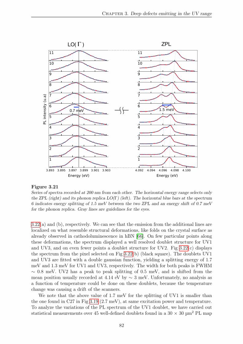
Chapter 3. Deep defects emitting in the UV range
LO( � )Γ ZPL
0.7 meV
Figure 3.21Series of spectra recorded at 200 nm from each other. The horizontal energy range selects onlythe ZPL (right) and its phonon replica LO(Γ) (left). The horizontal blue bars at the spectrum6 indicates energy splitting of 1.5 meV between the two ZPL and an energy shift of 0.7 meVfor the phonon replica. Gray lines are guidelines for the eyes.
3.22(a) and (b), respectively. We can see that the emission from the additional lines arelocalized on what resemble structural deformations, like folds on the crystal surface asalready observed in cathodoluminescence in hBN [66]. On few particular points alongthese deformations, the spectrum displayed a well resolved doublet structure for UV1and UV3, and on even fewer points a doublet structure for UV2. Fig 3.22(c) displaysthe spectrum from the pixel selected on Fig 3.22(b) (black square). The doublets UV1and UV3 are fitted with a double gaussian function, yielding a splitting energy of 1.7meV and 1.3 meV for UV1 and UV3, respectively. The width for both peaks is FWHM∼ 0.8 meV. UV2 has a peak to peak splitting of 0.5 meV, and is shifted from themean position usually recorded at 4.14 eV by ∼ 3 meV. Unfortunately, no analysis asa function of temperature could be done on these doublets, because the temperaturechange was causing a drift of the scanners.
We note that the above value of 1.7 meV for the splitting of UV1 is smaller thanthe one found in C27 in Fig 3.19 (2.7 meV), at same excitation power and temperature.To analyze the variations of the PL spectrum of the UV1 doublet, we have carried outstatistical measurements over 45 well-defined doublets found in a 30 × 30 µm2 PL map
82

3.3 Probing deep defects at a sub-micrometer scale in PL
Y (µ
m)
X (µm)
Full range(a)
X (µm)
Y (µ
m)
Integrated over UV1-3(b)1.7 meV
0.5 meV
1.3 meV
UV1
UV2
UV3
(c)
UV1β
UV1α
Figure 3.22PL intensity map of sample C40 at 4 K integrated over the full spectrum (from 296 to 323 nm)(a) and over the UV1-3 lines (b), for an excitation power of 0.35 mW. (c) Spectrum recordedat the pixel position indicated by the black square on (b). The solid orange and green line arethe double gaussian fits for UV1 and UV3, respectively.
of sample C27. The low and high energy components of the doublet are called UV1αand UV1β, as illustrated on Fig 3.22(c). The statistical analysis of the distribution ofpeak position and width for UV1α/β as well as the spitting values (∆E) is presented inTable 3.2.
Table 3.2Statistical analysis of the doublet UV1 over 45 spectra recorded on sample C27 at 4K andexcitation power 0.35 mW. In the analysis, UV1α/β are independently fitted with a Lorentzianfunction and linear background.
UV1α UV1β Splitting UV1Feature Position (nm) Position (eV) FWHM (meV) Position (nm) Position (eV) FWHM (meV) ∆E (meV)
mean 301.06 4.1183 1.5 300.86 4.1211 1.4 2.8std 0.01 0.0002 0.5 0.02 0.0002 0.3 0.1min 301.02 4.1180 0.8 300.82 4.1206 0.9 2.4max 301.07 4.1188 3.2 300.89 4.1215 2.1 3.1
The mean value for the splitting of UV1 is ∆E = 2.8 meV, while the width of eachcomponent is ∼ 1.5 meV. These values indicate that the characteristics of the doubletUV1 in sample C27 are significantly different from the one in sample C40 discussedabove. Indeed, the splitting ∆E = 1.7 meV in C40 (cf. Fig 3.22(c)) is 30% smallerthan the minimum value found in C27, and the width of UV1α/β in Fig 3.22(c) is 50%lower than in C27. Giving the different compounds stoichiometry used in the growth
83
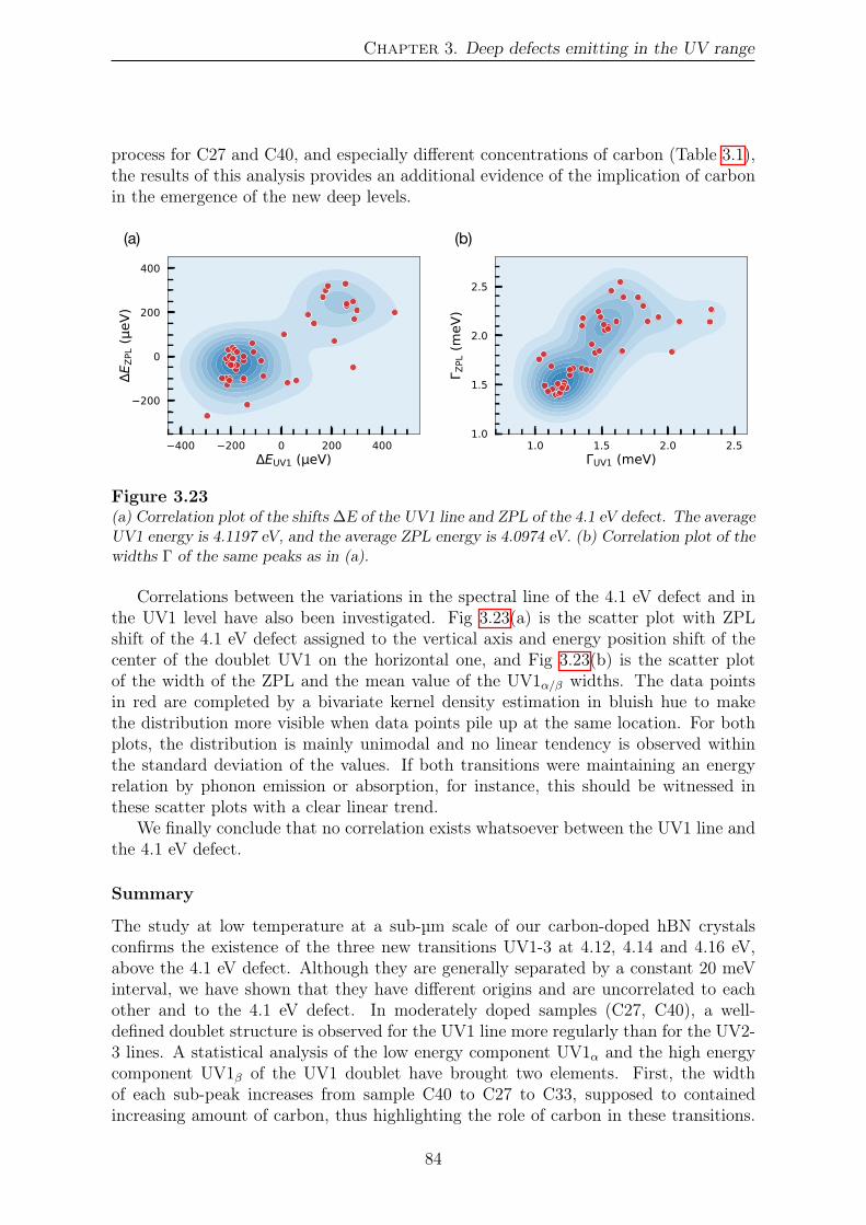
Chapter 3. Deep defects emitting in the UV range
process for C27 and C40, and especially different concentrations of carbon (Table 3.1),the results of this analysis provides an additional evidence of the implication of carbonin the emergence of the new deep levels.
(a) (b)
Figure 3.23(a) Correlation plot of the shifts ∆E of the UV1 line and ZPL of the 4.1 eV defect. The averageUV1 energy is 4.1197 eV, and the average ZPL energy is 4.0974 eV. (b) Correlation plot of thewidths Γ of the same peaks as in (a).
Correlations between the variations in the spectral line of the 4.1 eV defect and inthe UV1 level have also been investigated. Fig 3.23(a) is the scatter plot with ZPLshift of the 4.1 eV defect assigned to the vertical axis and energy position shift of thecenter of the doublet UV1 on the horizontal one, and Fig 3.23(b) is the scatter plotof the width of the ZPL and the mean value of the UV1α/β widths. The data pointsin red are completed by a bivariate kernel density estimation in bluish hue to makethe distribution more visible when data points pile up at the same location. For bothplots, the distribution is mainly unimodal and no linear tendency is observed withinthe standard deviation of the values. If both transitions were maintaining an energyrelation by phonon emission or absorption, for instance, this should be witnessed inthese scatter plots with a clear linear trend.
We finally conclude that no correlation exists whatsoever between the UV1 line andthe 4.1 eV defect.
Summary
The study at low temperature at a sub-µm scale of our carbon-doped hBN crystalsconfirms the existence of the three new transitions UV1-3 at 4.12, 4.14 and 4.16 eV,above the 4.1 eV defect. Although they are generally separated by a constant 20 meVinterval, we have shown that they have different origins and are uncorrelated to eachother and to the 4.1 eV defect. In moderately doped samples (C27, C40), a well-defined doublet structure is observed for the UV1 line more regularly than for the UV2-3 lines. A statistical analysis of the low energy component UV1α and the high energycomponent UV1β of the UV1 doublet have brought two elements. First, the widthof each sub-peak increases from sample C40 to C27 to C33, supposed to containedincreasing amount of carbon, thus highlighting the role of carbon in these transitions.
84
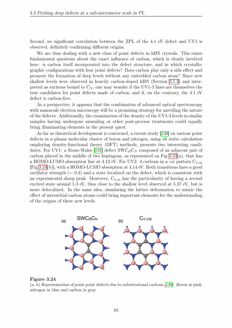
3.3 Probing deep defects at a sub-micrometer scale in PL
Second, no significant correlation between the ZPL of the 4.1 eV defect and UV1 isobserved, definitely confirming different origins.
We are thus dealing with a new class of point defects in hBN crystals. This raisesfundamental questions about the exact influence of carbon, which is clearly involvedhere: is carbon itself incorporated into the defect structure, and in which crystallo-graphic configurations with four point defects? Does carbon play only a side effect andpromote the formation of deep levels without any embedded carbon atom? Since newshallow levels were observed in heavily carbon-doped hBN (Section 3.1.3) and inter-preted as excitons bound to CN , one may wonder if the UV1-3 lines are themselves thetrue candidates for point defects made of carbon, and if, on the contrary, the 4.1 eVdefect is carbon-free.
As a perspective, it appears that the combination of advanced optical spectroscopywith nanoscale electron microscopy will be a promising strategy for unveiling the natureof the defects. Additionally, the examination of the density of the UV1-3 levels in similarsamples having undergone annealing or other post-process treatments could equallybring illuminating elements in the present quest.
As far as theoretical development is concerned, a recent study [130] on various pointdefects in a planar molecular cluster of boron and nitrogen, using ab initio calculationemploying density-functional theory (DFT) methods, presents two interesting candi-dates. For UV1: a Stone-Wales [131] defect SWCBCN composed of an adjacent pair ofcarbon placed in the middle of two heptagons, as represented on Fig 3.24(a), that hasa HOMO-LUMO absorption line at 4.12 eV. For UV2: 4 carbons in a cis pattern C4 cis
[Fig 3.24(b)], with a HOMO-LUMO absorption at 4.14 eV. Both transitions have a goodoscillator strength (∼ 0.3) and a state localized on the defect, which is consistent withan experimental sharp peak. Moreover, C4 cis has the particularity of having a secondexcited state around 5.3 eV, thus close to the shallow level observed at 5.37 eV, but ismore delocalized. In the same idea, simulating the lattice deformation to mimic theeffect of interstitial carbon atoms could bring important elements for the understandingof the origins of these new levels.
Although this study focuses on carbon impurities, some tests have been performed for analogous oxygen defects ON, OB, OBON (both spin
singlet and triplet), and OB(BN)1ON (singlet case) defects, since oxygen has been named in Ref. [14] as an alternative contamination (in place of
carbon) for h-BN layers in the electron microscopy study.
(A) CB (B) CN (C) CB (BN) 1CN (D) CB (BN) 2CN
(E) CB (BN) 4CN (F) CB CN (G) (CB CN )2 (H) (CB CN )2 sep.
(I) (CB CN )3 (J) C4 cis (K) C4 trans (L) C6
(M) C10 (N) VB (O) VN (P) SWCB CN
(Q) CHB (R) CHN (S) VN NB (T) OB
(U) ON (V) VB CB (W) VN CN (X) OB (BN) 1ON
F IGURE 2 Defects considered in this study for the h-BN monolayer
KORONA AND CHOJECKI 5 of 19
C4 CIS(b)
Although this study focuses on carbon impurities, some tests have been performed for analogous oxygen defects ON, OB, OBON (both spin
singlet and triplet), and OB(BN)1ON (singlet case) defects, since oxygen has been named in Ref. [14] as an alternative contamination (in place of
carbon) for h-BN layers in the electron microscopy study.
(A) CB (B) CN (C) CB (BN) 1CN (D) CB (BN) 2CN
(E) CB (BN) 4CN (F) CB CN (G) (CB CN )2 (H) (CB CN )2 sep.
(I) (CB CN )3 (J) C4 cis (K) C4 trans (L) C6
(M) C10 (N) VB (O) VN (P) SWCB CN
(Q) CHB (R) CHN (S) VN NB (T) OB
(U) ON (V) VB CB (W) VN CN (X) OB (BN) 1ON
F IGURE 2 Defects considered in this study for the h-BN monolayer
KORONA AND CHOJECKI 5 of 19
SWCBCN(a)
Figure 3.24(a, b) Representation of point point defects due to substitutional carbons [130]. Boron in pink,nitrogen in blue and carbon in gray.
85

Chapter 3. Deep defects emitting in the UV range
3.3.2 Investigations of the 4.1 eV defect origin
Despite an active research activity, the chemical origin of the emission at 4.1 eV in hBNis still debated. Carbon is often considered to be involved as a substitutional atomfor boron or nitrogen [67, 125, 127], and recent theoretical works using large finite-sizemolecular cluster with TD-DFT suggests multiple neighboring carbon substitutions likeCBCN or C4cis/trans rather than simple substitution [130], in agreement with the obser-vation via an electronic microscope showing that C atoms are only seen to substitutefor B-N pairs and not for isolated vacancy [132]. CBCN is also strongly supportedby first-principles calculations based on hybrid density functionals that account forthe experimentally observed ZPL position, radiative life and Huang-Rhys factor [133].Some have also suggested donor-to-acceptor pair (DAP) transition between a shallowVN donor and a deep CN acceptor [134], while others have cited oxygen as potentiallyresponsible for the emission [125] or VBON complex [135]. In contrast, no correlationbetween impurity concentration (C, O) and deep level emission intensity at 4.1 eV hasbeen measured in a recent study where the authors performed trace impurity analy-sis [136]. They rather suggested the intrinsic defect boron-vacancy (VB), similarly tothe theoretical work of Attaccalite et al. [126]. Moreover, CN has been excluded onthe basis of density functional theory with a hybrid functional [137]. In summary, it isnot overstated to say that the origin of the emission at 4.1 eV remains highly conflicting.
In this controversial context, we use isotopic purification, a powerful tool in semicon-ductor physics enabling the fabrication of chemically and isotopically pure crystals andcrystals doped with isotopically pure impurities [138]. We have carried out experimentson hBN crystal grown with isotopically controlled carbon doping in order to furthertest if carbon is a constituent of the defect emitting at 4.1 eV. More specifically, wehave performed high-resolution measurements of the energy of the ZPL in hBN crys-tals doped either with 13C (sample C40, Table 3.1) or with natC (sample C27, Table3.1), meaning the natural mixture of 99% in 12C and 1% in 13C, thus close to pure 12Cdoping.
The justification for this study on isotopic controlled doping is the fact that for pointdefects the isotopic selectivity of the atoms forming the defect can shift the zero-phononline. Several mechanisms may explain this isotopic shift, such as a modification of theconfinement or the electron-phonon interaction [138]. Quantitatively, the energy shiftsare very small. For instance, the boron-bound exciton in silicon presents an isotopicshift of the order of 1 µeV when switching from 10B to 11B [138], but it can be muchlarger as for G-centers in silicon with an isotopic shift of ∼ 15 µeV between 12C and 13Cdoping [139], or even ∼ 600 µeV between 28Si and 30Si for the SiV center in diamond[140].
In the case of hBN doped either with natC or 13C, the search for an isotopic shiftof the 4.1 eV line requires high-spectral resolution measurements. Moreover, one hasto pay attention to possible variations of the ZPL energy within a given sample beforecomparing natC- and 13C-doped hBN in order to exclude any artifact due to a shift notcoming from the isotopically controlled doping.
Following this reasoning, we will first study the spatial variations of the energy andlinewidth of the ZPL in sample C40, and secondly compare the statistical analysis of
86

3.3 Probing deep defects at a sub-micrometer scale in PL
our data recorded in natC- and 13C-doped hBN crystals (C27 and C40, respectively).
Spatial inhomogeneityScan name : « SPI_C40_004K_350uW_3x0.3s_30x30um_1800gr_slit20_310nm_231118d »
I am doing the same for a new are : scan name : « SPI_C40_004K_350uW_3x1s_30x30um_1800gr_slit20_310nm_241118a.dat »
1
2
3
ZPL 123
(a) (c)(b)
Figure 3.25(a) Micrograph taken with the optical microscope. (b) PL scan recorded in the region identifiedby the blue square in (a). (c) The spectrum around the ZPL of the 4.1 eV defect taken at thelocations indicated by the colored squares in (b).
On the surface of sample C40, we find a region exhibiting both good apparent crys-tallinity and structural deformations (stacking faults) with the widefield microscope(described in Section 3.2.1), as shown on the micrograph of Fig 3.25(a). On the regionindicated by the 30 × 30 µm2 blue square, we recorded a map of the PL intensity at 10K with our UV scanning confocal micro-PL setup [Fig 3.25(b)], here sharply integratedaround the ZPL of the 4.1 eV defect (4.0946-4.0988 eV). The image shows a slowlydecreasing intensity from bottom to top. We explain that with the variation of thecrystal axial position in the depth of field of our confocal microscope, thus decreasingthe excitation density from bottom to top. This is even more visible in the top rightcorner that corresponds to the stacking fault region, with higher contrast of intensity.For each of the 150 × 150 positions, we acquired the PL spectrum over an integrationtime of 3 s, resulting in a total acquisition of 27 h for the full scan. Three pixels areselected on the scan and their respective spectrum around the ZPL is displayed on Fig3.25(c). Apart from different intensities, we note that they all have a different ZPLposition, distributed around the vertical dotted line, and different width. The shiftbetween the most separated peaks (blue and green) is ∼ 0.56 meV. In order to betteranalyze the spatial shift of the ZPL position along with the width of the peak, the ZPLof each of the 150 × 150 spectra was then fitted with a Gaussian function. With ∼ 5× 10³ counts at the maximum of the ZPL, the standard deviation for the estimationof the ZPL energy and width was 6 and 10 µeV, respectively. Fig 3.26 displays theanalysis of the set of data.
In Fig 3.26(a) we show the spatial energy shift ∆E of the ZPL relative to the averagevalue of 4.09683 eV in this region. The variations of the ZPL full width at half-maximum
87

Chapter 3. Deep defects emitting in the UV range
Figure 3.26Upper panels: spatial variations of the shift ∆E (a) and broadening Γ (b) of the ZPL in a 30 ×30 µm2 region of sample C40 at 10 K. The energy shift is calculated relatively to the averageZPL energy at 4.09684 eV. Black dotted lines are guidelines for the eyes. Lower panels: fulldistribution of the ZPL shift ∆E (a) and broadening Γ (b). Vertical solid lines indicate themean of the distribution while dotted lines indicates the interval chosen for plotting the spatialvariations.
Γ are plotted in Fig 3.26(b). The first finding is that the fluctuations of the ZPL energyover the 30 × 30 µm2 scanned region have an amplitude as large as 1 meV (see thefull distribution on lower panel of the figure). These fluctuations contribute to theinhomogeneous broadening of the 4.1 eV line. With an average FWHM on the order of1.2 meV [Fig 3.26(b)], the ± 0.2 meV variations of the ZPL energy are consistent withthe 1.9 meV value of the ZPL width previously reported by macro-PL measurementsin [68], but here we notably demonstrate the sub-µm scale at which the ZPL energyvaries.
Interestingly, the ZPL shifts appear spatially correlated with the ZPL broadening.Indeed, where the ZPL position is red-shifted in (a) (redder) it is also broadened in (b)(also redder). Although there is not a one-to-one correlation, the overall pattern is thesame in Figs 3.26(a) and (b), with lines of different orientations in close analogy to theluminescence maps recorded by cathodoluminescence [66]. We interpret these lines asfolds or extended defects in the lamellar structure of our hBN crystal, a point of viewsupported by the widefield micrograph of Fig 3.25(a).
The spatial correlation of the ZPL shift and broadening suggests they correspondto the real and imaginary parts of the same perturbation. This common origin is fur-ther supported by a similar magnitude (in the 0.1 meV range here), and this variationpresumably originate from mechanical strain related to the stacking faults in hBN.
88

3.3 Probing deep defects at a sub-micrometer scale in PL
We present in Fig 3.27 the same analysis done in a 30 × 30 µm2 region of sampleC27 at 10 K, with 75 × 75 spectra recorded. The average ZPL energy is 4.09702 eV.We note a greater heterogeneity in this region of sample C27 compared with the onepresented for sample C40, with a maximum amplitude for ∆E of 1.8 meV, and for Γ of3 meV. Strikingly, the tendency discussed above for the correlation of the ZPL shift andbroadening, tend to reverse in these images: blue-shifted areas of the ZPL [Fig 3.27(a)]matching broader ZPL areas [Fig 3.27(b)]. Again, this is no perfect correlation.
From a structural point of view, the images in Fig 3.27 present no straight lines asin Fig 3.26 that we attributed to folds arising from stacking faults in the crystal. Thesestraight lines make easier the interpretation of strain-induced variations. In contrast,the shapes observed in Fig 3.27 suggest disparate aggregation of carbons during thegrowth process, which could influence, directly or indirectly, the spectral features of thedefects. However, we lack of experimental characterization concerning the distributionof carbons throughout the crystal, whether it is homogeneously distributed or not, thusthe previous statement has to be taken only as an attempt of interpretation.
Figure 3.27Upper panels: spatial variations of the shift ∆E (a) and broadening Γ (b) of the ZPL in a30 × 30 µm2 region of sample C27 at 10 K. The energy shift is calculated relatively to theaverage ZPL energy at 4.09702 eV. Lower panels: full distribution of the ZPL shift ∆E (a)and broadening Γ (b). Vertical solid lines indicate the mean of the distribution while dottedlines indicates the interval chosen for plotting the spatial variations.
Over the same area of sample C40 Fig 3.26, we could acquire the data set with thespectrometer tuned at the wavelength of the Raman-active mode at ∼ 1370 cm−1 (170meV). The maps, shown on Fig 3.28, are featureless except for the wave pattern thatwe attribute to an artifact during the hours-long scanning time. There are random
89
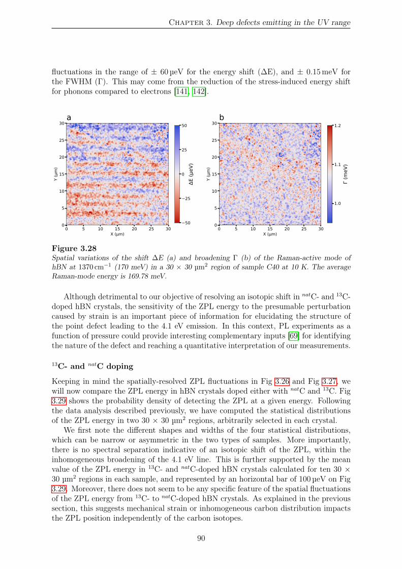
Chapter 3. Deep defects emitting in the UV range
fluctuations in the range of ± 60 µeV for the energy shift (∆E), and ± 0.15 meV forthe FWHM (Γ). This may come from the reduction of the stress-induced energy shiftfor phonons compared to electrons [141, 142].
0 5 10 15 20 25 30X (µm)
0
5
10
15
20
25
30
Y (µ
m)
a
0 5 10 15 20 25 30X (µm)
0
5
10
15
20
25
30
Y (µ
m)
b
50
25
0
25
50
E (µ
eV)
1.0
1.1
1.2
(meV
)
Figure 3.28Spatial variations of the shift ∆E (a) and broadening Γ (b) of the Raman-active mode ofhBN at 1370 cm−1 (170 meV) in a 30 × 30 µm2 region of sample C40 at 10 K. The averageRaman-mode energy is 169.78 meV.
Although detrimental to our objective of resolving an isotopic shift in natC- and 13C-doped hBN crystals, the sensitivity of the ZPL energy to the presumable perturbationcaused by strain is an important piece of information for elucidating the structure ofthe point defect leading to the 4.1 eV emission. In this context, PL experiments as afunction of pressure could provide interesting complementary inputs [69] for identifyingthe nature of the defect and reaching a quantitative interpretation of our measurements.
13C- and natC doping
Keeping in mind the spatially-resolved ZPL fluctuations in Fig 3.26 and Fig 3.27, wewill now compare the ZPL energy in hBN crystals doped either with natC and 13C. Fig3.29 shows the probability density of detecting the ZPL at a given energy. Followingthe data analysis described previously, we have computed the statistical distributionsof the ZPL energy in two 30 × 30 µm2 regions, arbitrarily selected in each crystal.
We first note the different shapes and widths of the four statistical distributions,which can be narrow or asymmetric in the two types of samples. More importantly,there is no spectral separation indicative of an isotopic shift of the ZPL, within theinhomogeneous broadening of the 4.1 eV line. This is further supported by the meanvalue of the ZPL energy in 13C- and natC-doped hBN crystals calculated for ten 30 ×30 µm2 regions in each sample, and represented by an horizontal bar of 100 µeV on Fig3.29. Moreover, there does not seem to be any specific feature of the spatial fluctuationsof the ZPL energy from 13C- to natC-doped hBN crystals. As explained in the previoussection, this suggests mechanical strain or inhomogeneous carbon distribution impactsthe ZPL position independently of the carbon isotopes.
90

3.3 Probing deep defects at a sub-micrometer scale in PL
4.0966 4.0968 4.0970 4.0972 4.0974ZPL energy (eV)
0
Pro
babi
lity
dens
ity
natC-doped h-BN13C-doped h-BN
Figure 3.29Statistical analysis of the ZPL energy in natC- and 13C-doped hBN crystals: the normalizedprobability density of the ZPL energy is plotted for four 30 × 30 µm2 regions: two in a 13C-doped crystal (C40, red data), two in a natC-doped crystal (C27, blue data). The 100 µeVlarge horizontal bar indicates the difference of the mean values of the ZPL energy in 13C- andnatC-doped hBN crystals, the mean values being calculated for a total of ten 30 × 30 µm2
regions.
Summary
Thanks to our spectral resolution, spatial resolution, and the high signal-to-noise (SNR)and signal-to-background (SNB) of the spectral line corresponding to the ZPL of the4.1 eV defect in bulk hBN, we could draw maps illustrating the spatial variations of theshift and broadening of the ZPL, demonstrating that the spatial fluctuations of the ZPLis in a sub-µm scale. These maps show interesting features with localized correlationsof the two parameters along specific structural deformation, that we interpret as foldsarising from stacking faults in the crystal. At this extended defects, stress is mostlikely responsible for the observed variations of both ∆E and Γ. Notably, the maximumamplitude for the energy shift is in the order of 1 meV, with typical variations happeningat the scale of 0.1 meV. Unfortunately, the statistical study on 13C- and natC-doped hBNcrystals of the ZPL energy shift presents similar variations in both type of samples. Wethus conclude that there is either no isotopic shift, or a finite one but smaller than theinhomogeneous broadening. Isotopic selectivity in carbon-doping has not brought anyproof to confirm or infirm the presence of carbon in the structure of the defect emittingat 4.1 eV. However, we hope that the quantitative measurements presented here will be
91

Chapter 3. Deep defects emitting in the UV range
useful for testing various models in future calculations.
3.3.3 Search for isolated emitters at 4.1 eV
In this section, we present the investigations we conducted to isolate the emission ofa single point defect at 4.1 eV using the micro-PL confocal setup operating at 266nm (4.66 eV). This study is motivated by the little knowledge concerning the photo-dynamics of this deep defect in hBN. Museur et al. [127] measured by time-resolvedPL experiments a radiative decay for the luminescence originating from ensembles ofdefects of ∼ 1.1 ns, confirming an early study from 1981 [120]. This fast decay waslater also measured by Meuret et al. [143] from the bunching peak decay curve in theautocorrelation function of the cathodoluminescence intensity. More recently, Bourrel-lier et al. [67] reported the first detection of the emission from a single 4.1 eV defectby cathodoluminescence in a STEM2 microscope (cf. Chapter 1 Section 1.4.3), andby recording the second-order correlation function they could extract the lifetime of asingle emitter from the antibunching yielding a value of 2.5 ns. However, under elec-tron irradiation the broadband emission around 4 eV, originating from intrinsic defects,rises and decreases the signal-to-background ratio, ultimately limiting the signal-to-noise ratio [67]. It has been demonstrated that under an excitation energy of ∼ 5.2 eVthis broadband emission is quenched in photoluminescence experiments [127]. In ourexperiment, photo-excitation operates at energy below this threshold. Moreover, theradiative recombination at point defects inside the bandgap in a cathodoluminescenceexperiment (with electrons carrying energy in the order of tens of thousands electron-volts) is a complex phenomenon to analyze because it often involves several processesof desexcitation, while in photoluminescence experiment we operate close to resonancewith the level transition, enabling the study of the photodynamics in similar conditionsin which a single-photon source would be used in applications.
Combining photon microscopy with electron microscopy
During my thesis, I had the opportunity to do several visits at the LPS3 in Paris inthe team of Alberto Zobelli and Mathieu Kociak, specialists in electron microscopy andespecially in cathodoluminescence (CL). The purpose was to use the STEM microscopeoperating at 150 K, and try to find isolated emitters at 4.1 eV and record the signalof CL simultaneously with performing electron energy loss spectroscopy (EELS). Bymeasuring the energy loss experienced by the incident electrons during their interactionwith the matter, EELS provides information on the chemical bonding, optical andelectronic properties, and especially on the chemical composition of the specimen. Asdiscussed previously, carbon is one favorite candidate for the origin of the point defect,thus we used samples from NIMS in Japan, highly doped with carbon, giving a yellowhue to the crystal. Unfortunately the sample were contaminated by another source ofcarbon, making the analysis of the EELS spectrum insignificant.
However, in another attempt of combining the powerful tool of electron- and photon-microscope, Alberto Zobelli and Steffi Woo pre-characterized thin flakes of hBN with
2Scanning transmission electron microscope.3Laboratoire de Physique des Solides, Orsay - France.
92

3.3 Probing deep defects at a sub-micrometer scale in PL
the STEM microscope and sent them to us. We will present first the characterizationdone with the STEM-CL microscope and secondly the study with our PL microscope.
Samples and pre-characterization
An undoped single crystal of hBN from Taniguchi and Watanabe (NIMS) was liquid-phase exfoliated in isopropanol for 15 min; 3 drops of hBN dispersion was placed ontoa 300-mesh copper TEM grids with lacey carbon support. In the annular dark field(ADF) image of Fig 3.30(a) we can see flakes supported by the lacey carbon grid. Thetransparency of the flake in the bright field (BF) image Fig 3.30(b) is an indicatorof the small thickness in the order of tens of nanometers. Having thin flakes is anessential element in the purpose of isolating a single emitter. CL measurements were
5
VG:181123-hBNi40b-GridA-Flake#1
Sameflake,justrotatedtheimagetogettheadjacentregion
A
4.1eVCLmap
4.1map
BFimage
ADFimage
Measuredregionofflakeis~20–30nmthick
Manyisolated4.1eVcentres,mostare200–500nmapart
CLspectrumimagingwasdoneinthered-boxedareasinthelow-magimagesoftheflakes
SummedCLspectrafromthered-boxedregionintheCLmap
4.1
CLmapgeneratedfromintegratedwavelengthwindowbelow
4
Low-magSTEMimagesofthegridcentre
A
B
A
B
ADFimage
BFimage
BFimage
BFimage
5
VG:181123-hBNi40b-GridA-Flake#1
Sameflake,justrotatedtheimagetogettheadjacentregion
A
4.1eVCLmap
4.1map
BFimage
ADFimage
Measuredregionofflakeis~20–30nmthick
Manyisolated4.1eVcentres,mostare200–500nmapart
CLspectrumimagingwasdoneinthered-boxedareasinthelow-magimagesoftheflakes
SummedCLspectrafromthered-boxedregionintheCLmap
4.1
CLmapgeneratedfromintegratedwavelengthwindowbelow
(a) (b) (c)
(d)
10 µm 2 µm
5
VG:181123-hBNi40b-GridA-Flake#1
Sameflake,justrotatedtheimagetogettheadjacentregion
A
4.1eVCLmap
4.1map
BFimage
ADFimage
Measuredregionofflakeis~20–30nmthick
Manyisolated4.1eVcentres,mostare200–500nmapart
CLspectrumimagingwasdoneinthered-boxedareasinthelow-magimagesoftheflakes
SummedCLspectrafromthered-boxedregionintheCLmap
4.1
CLmapgeneratedfromintegratedwavelengthwindowbelow
500 nm
Figure 3.30Annular dark field (ADF) image of flakes deposited on a TEM grid (a), closeup of a flake inbright field (BF) imaging mode (b), filtered CL map on a small region (c) corresponding tothe signal intensity integrated over the wavelength range inside the rectangular box of the CLspectrum (d).
done at 60 kV and with nitrogen cooling (150 K) in random scan mode for spectrumimaging [144]. Fig 3.30(c) is a CL map performed on the red square of the BF imageand integrated on a spectral range encompassing the 4.1 eV defect and its two phononreplica, as illustrated by the black rectangle in the CL spectrum of Fig 3.30(d). Thespectrum is obtained by averaging the signal over the red-boxed region of Fig 3.30(c).The red square on the CL map is ∼ 700 nm large and presents a structured emissiondistribution with a more or less isolated spot on the bottom left.
Basically, the pre-characterization was meant to produce a cartography of the iso-lated deep emitters at 4.1 eV on the flakes that could potentially be resolved and studiedwith our PL microscope. We will now present the results of our measurements.
93

Chapter 3. Deep defects emitting in the UV range
Images with the UV confocal microscope: emission at the borders of theflakes
The TEM grid was installed in our cryostat and fixed to the sample holder with silverpaint. The silver paint has a strong broad emission from 330 nm to longer wavelengthswhen excited with our laser at 266 nm, this fact precluded to study most of the areascharacterized by STEM-CL, thus we only studied the flakes lying on the copper struc-ture of the grid.
Flake
CopperSilver paint
(a)ZPL
2LO( � )ΓLO( � )Γ
(b)
coun
ts p
er s
econ
d
PL intensity
24h after
1
(c)
2
(d)
Figure 3.31(a) Raster scan of PL on a flake lying on the copper structure. (b) Spectrum 1 is acquired atthe brightest pixel of the circle in (c) and spectrum 2 at the brightest pixel of the circle in (d).The filtered PL image (c) was recorded just after (a), and (d) was recorded 24 hours after (c).The PL signal is integrated between 300 and 340 nm. The vertical upward shifts of the flakebetween the three scans is due to a drift of the steppers.
On Fig 3.31(a) we present a raster scan of PL recorded with the photomultipliers at4 K on a region of a flake lying on the copper (delimited by the white dotted lines). Wefirst notice a spatially-inhomogeneous emission, with high PL signal from the border ofthe flake presenting a maximum signal-to-background ratio of ∼ 10 and region wherethere is no emission from the deep defect, which was never observed in bulk material(Section 3.3.1). The fact that the signal is more intense on the border is actually ageneral observation in our measurements. There are several ways of interpreting that:either the PL collection efficiency is higher on the border because the light can freely
94

3.3 Probing deep defects at a sub-micrometer scale in PL
propagates out of the crystal and be collected, or this is the result of intrinsic phenom-ena, which may be related to polarization direction or stacking order at the border, ordangling bonds providing electrostatic potentials for impurity and thus promoting theformation of defects, enhancing the emission intensity.
After this first scan, we recorded a PL image with a pixel size of 100 × 100 nm2,presented on Fig 3.31(c) after integration of the PL signal between 300 and 340 nmso as to include the ZPL and the two LO(Γ) phonon replicas of the 4.1 eV defect.Strikingly, there is an important loss of emission on the bottom border of the flake. Wefocus our attention on the bright spot indicated by the green circle. The spectrum ofthe emission at the brightest pixel in this circle is shown on Fig 3.31(b) (1, orange).Strikingly, the profile is very different from what is usually recorded in bulk crystal,with a first phonon replica more intense than the ZPL, and a broadening ten timesgreater with FWHM = 10 meV instead of ∼ 1 meV. We also note the appearance ofa broad background raising underneath the defect emission. Last but not least, theoverall profile is red-shifted compared with usual measurement performed at 4 K (theZPL is at 305 instead of 302 nm). In fact, the PL spectrum is similar to the CLspectrum of Fig 3.30(d) recorded at 150 K in the STEM microscope. One hypothesisis that the flake, in this configuration where it is suspended over the lacey carbon grid,may not be fully thermalized with the copper structure lying on the sample holder, thusred-shifting the emission and broadening the line. However, in macro-PL experimentno such dependence on temperature is observed, as it was discussed in Section 1.4.3.Thus, this could be a behavior specific to low number of emitters, or due to the modifiedcoupling to phonon in very thin flakes of hBN.
We now look at the third PL image [Fig 3.31(d)] recorded at the exact same con-ditions and with same parameters, but 24h after Fig 3.31(c). Remarkably, there is animportant decline in the intensity of the bright region. Indeed, as evidenced on the bluespectrum of Fig 3.31(b) from the same brightest pixel, the intensity for the ZPL hasdecreased by a factor 2 but the integrated area undergoes a much more severe decrease.This phenomenon is not specific to this flake but was generally observed on those few-tens-of-nanometers-thick flakes.
To sum up, the emission originating from point defects emitting at 4.1 eV decreasesbetween successive scans, especially when the emission takes place at the borders of thecrystal. This unveils a phenomenon of bleaching for the 4.1 eV deep defect under laserexcitation in these chemically exfoliated flakes. Besides, this conclusion lead us to favoran intrinsic cause for the emission at the borders, because several scans on the sameregion result in the quenching of the emission.
Emission from localized centers inside the flakes
In certain cases however, we could find isolated emitters within a flake exhibiting stableemission over time. The XY PL scan of Fig 3.32(a), performed with the bandpass filter300-340 nm, displays a bright localized emission at X = 6.5 µm and Y = 10 µm, overa more or less dim area. This spot is well localized and has a more or less roundedshape with SNR ∼ 26, as shows the closeup scan of Fig 3.32(b). The intensity profileof the vertical cross-section is presented on Fig 3.32(d). A Gaussian fit to this profileyields a width of FWHM = 550 nm, which indicates that the size of the spot is limited
95

Chapter 3. Deep defects emitting in the UV range
by the lateral resolution of the confocal microscope (Section 3.2.3). Fig 3.32(c) is aXZ scan in-depth of the thin flake, showing a spot extension in Z of ∼ 1.5 µm, whichcorresponds to the axial resolution of the confocal setup (Section 3.2.4). Motivated bythese observations, we have recorded the g(2) function on this emitter. Despite hours ofintegration time with a tracking system, we did not observe a dip at the zero delay ofthe second-order correlation function, suggesting the emission originates from multiplepoint defects.
XY
XZ
XY(a) (b)
(c)
550 nm
X (µm)
(d)
Figure 3.32XY PL scan on a flake (a) and a zoom on the bright spot indicated by the square (b) comple-mented by a XZ scan in depth (c). Temperature is 4 K, excitation power 0.3 mW. (d) Intensityprofile of the vertical cross-section on (b) at X = 6.5 µm.
Summary
In bulk material, the emission at 4.1 eV is ubiquitous, indicating a high density ofemitters. Here, we make use of a STEM-CL microscope to characterize thin flakes ofhBN, obtained by liquid phase exfoliation of a monocrystal, as a preliminary to ensurethat it is possible to find localized emissions in regions in the order of ∼ 500 nm, thatis to say small enough for being resolved with the UV confocal setup.
In theses samples, as a general observation, there is a pronounced emission at theborders of the flakes, that we attribute to intrinsic causes, structural deformationsfavoring the formation of defects. This observation has also been reported for singledefects around 600 nm in hBN flakes of similar size, where the authors always observethe emission at flake edges [145]. However, the PL mapping of the same region at
96

3.4 Conclusion
different time brings evidence of PL quenching in these areas, suggesting that the 4.1 eVdefect is subjected to bleaching phenomenon, as most defects are. Interestingly, no suchbehavior is witnessed in bulk material, which may be due to more stable configuration.In this case, concerning the origin of the defect, it would rather be in favor of interstitialimpurity, or impurity complexes, because there would be no reason for a substitutionalatom to be less stable in thin layers compared to bulk for a lamellar material. However,recent calculations [137], using density functional theory with a hybrid functional, showthat the formation energy of interstitial carbon is very high, and greater than thatof substitutional carbon impurities (CN , CB). Moreover it predicts a low migrationbarrier (below 1 eV), finally suggesting that the interstitial carbon impurities wouldeither diffuse out of the sample or migrate until getting annihilated by a vacancy toform CN or CB. Giving that this migration barrier energy (1 eV) is largely providedwith an electron beam, and that the defect at 4.1 eV is observed to be immobile duringelectron scan, we can rule out the hypothesis of interstitial carbon atoms, and speak infavor of substitutional ones.
Despite the unstable emission at the borders, we manage to find isolated spots, awayfrom the borders, with sizes limited by our spatial resolution, that is to say ∼ 500 nm2.These bright spots manifest stable emission over time, although we could not detectan antibunching in the measurements of the g(2) function, indicating that the spots arenot single-photon sources.
We finally note the uncommon profile in the spectrum of the emitter in these sam-ples. Maybe the thermalization in the configuration for this specific measurements(TEM grid on sample holder) has to be incriminated, and another test with a differentconfiguration could bring a answer. For example, flakes deposited on SiO2 substratethat we could directly stick on the sample holder, although in that case the characteri-zation by STEM-CL would not be possible, but using the same procedure for exfoliationand deposition on the substrate should produce similar flakes with similar low densityof emitters at 4.1 eV.
3.4 Conclusion
In this chapter, the optical properties in the UV of hBN crystals have been investigatedby means of photoluminescence (samples from Kansas State University and NIMS) andreflectivity measurements (Kansas State University).
First, in samples grown by precipitation techniques at normal pressure, we haveshown that the incorporation of carbon in the growth process is associated with theemergence of new optical transitions in the optical spectrum. We summarize the ob-servations in two parts, first for the shallow levels and secondly for the deep levels:
• For the sample presenting the highest concentration of carbon, shallow levels areobserved at 5.37 and 5.52 eV, in the deep UV region. The reflectivity spectrum inthis region, that provides information on the dielectric constant of the material,suggests that the oscillator strength and density of these shallow levels has tobe substantial as correlated peaks for these transitions are noted. The attributethese new shallow transition to an exciton bound to a CN impurity.
97

Chapter 3. Deep defects emitting in the UV range
• For all samples doped with carbon, new deep levels emerge at 4.12, 4.14 and 4.16eV (named UV1, UV2 and UV3, respectively), and are more prominent in theheavily carbon-doped one. These levels produce no modification of the dielectricconstant of the material, and this observation is consistent with the moderate tolow density of theses lines witnessed in the spatially-resolved PL maps obtainedwith the UV confocal microscope. With this same microscope, spectra takenwith high spectral resolution point out the existence of a sub-structure in theselines, consisting of the splitting of each of them. Through the examination of thespectrally-filtered micro-PL maps taken on different samples and the comparisonof the localization of the UV1-3 lines and the 4.1 eV defect, we argue that thesedeeps transition are uncorrelated to each other and to the point defect at 4.1 eV.This statement is further confirmed with a statistical analysis of the correlationbetween the doublet structure of UV1 and the spectral features of the 4.1 eVemitter.
Secondly, we focused on the 4.1 eV defect. The analysis of spatially-resolved PLmaps of the point defect reveals that the energy and width of the ZPL vary at a sub-micrometer scale, while presenting correlation in their variations along specific linesinterpreted as folds arising from stacking faults in the crystal lattice. According to thisobservation, we suggest that strain induces both the ZPL and width modification. In asecond part, photoluminescence of 13C-doped and 12C-doped samples are compared inan attempt of discerning a modification of the ZPL energy of the 4.1 eV defect depend-ing of the carbon isotope used in the growth process. We report that there is either noisotopic shift, or a finite one but smaller than the inhomogeneous broadening observedin both samples.
Lastly, we tried to isolate the emission from a single point defect at 4.1 eV in thinflakes obtained from undoped monocrystals of hBN (NIMS). Here, we used cathodolu-minescence performed in a STEM microscope to make sure that the density of emitterswas low enough for a single emitter to be isolated with the spatial resolution of ourconfocal microscope. Isolated spots are observed within the flake, emitting photolumi-nescence well above the background (SNR ∼ 26) and exhibiting good photostability.However, these spots are not associated with single emitters because the second-ordercorrelation function g(2)(τ) manifest no antibunching feature in the conditions of theexperiment.
At the borders of the flakes, the emission is generally stronger but unstable: bleach-ing along the borders happens over several subsequent scans. One explanation, still tobe investigated, may be related to the dipole direction of the emitter. Indeed, if thedefect has a polarization axis out of plane, at the border the laser polarization maybecomes more aligned with the dipole direction of the defect because the crystal latticebends in these regions.
98

Conclusion
During this thesis, the optical properties of point defects in hexagonal boron nitridehave been studied.
First, a confocal microscope operating with a green laser at 532 nm in ambientconditions allowed us to study an individual emitter acting as a room temperaturesingle-photon source in the visible. We have identified two families of isolated emit-ters on the basis of their photoluminescence spectra. Apart from the energy shift oftheir spectrum, the two families present similar behavior, with in particular excellentphotostability and well defined dipole-like emission. The originality of our approachconsisted in analyzing the photodynamics of the emitters over five temporal decades,which brought to light the existence of a long-lived metastable state. Yet, we find ahigh quantum efficiency of the radiative transition with one of the most intense sourceof quantum light in a solid-state platform (∼ 4× 10⁶ counts/s). This study definitelyopens up the perspective of applications with hBN in the world of photonics science.Interestingly, the intrinsic structure of hBN allows for an easier integration of its pho-tonic capacity in heterostructure composed of others similarly thin semiconductors.
Secondly, the exploration of the optical response in a higher energy range, from 3.5to 6 eV, have brought evidence for the existence of shallow and deep levels in carbon-doped crystals. In particular, novel transitions in the deep UV appear at 5.37 and 5.52eV with high enough oscillator strength to modify the dielectric constant in this energyregion, as demonstrated by reflectivity. These transitions are only observed in the caseof high carbon doping. On the basis of theoretical absorption spectra including the ef-fects of point defects and impurities we attribute these newcomers to an exciton trappedby a CN impurity. In the near-UV, we have observed three novel lines at around 4.12eV (UV1), 4.14 eV (UV2), and 4.16 eV (UV3). Although the intensity of these deeplevels seems to increase with carbon doping, even exceeding the intensity of the 4.1 eVdefect in the case of highly doped crystals, we observe no structure in the reflectivityspectra, which suggests either a low density or a weak oscillator strength of these levels.
A confocal microscope at 266 nm with sub-micrometer spatial resolution operatingat cryogenic temperature has been built. In the UV, the aberrations have drastic effectsand pushed us to design an original setup with adapted optics and elaborate protocolsto align it. The unique performances of this new microscope have been used to furtherexplore the properties of the point defects emitting in the UV.
99

Conclusion
By acquiring spatially and spectrally-resolved PL map, we examine the localizationof the UV1-3 lines. We attest that the deep levels are scarce in moderately dopedsamples, and become more frequent upon increasing doping. The UV1-3 lines presentan intriguing ∼ 20 meV energy spacing, and have a similar coupling to optical phononLO(T/Γ) as the 4.1 eV defect. We prove that there are not only independent of eachother, but also of the 4.1 eV defect. Therefore, we are in presence of a new class of pointdefects in hexagonal boron nitride. This raises fundamental questions about the roleof carbon into these new levels, which is undoubtedly involved here. Is carbon impliedonly during the growth process by promoting the formation of the defects, or is it partof the final crystallographic configuration?
Then, we questioned the implication of carbon in the 4.1 eV defect. Nearly no varia-tions of the photoluminescence profile and ZPL features are observed through the seriesof carbon-doped samples. We tackled this long-standing question from another anglewith two types of sample: a first one doped with purified 13C powder, and a second onewith 12C powder. The different isotope composition in the two crystals was expectedto induce a statistical shift in ZPL energy. At the end, no definitive statement can bemade, because there is no spectral separation indicative of an isotopic shift of the ZPL,within the inhomogeneous broadening of the 4.1 eV line. Nonetheless, we show impor-tant results concerning this last point: correlation of the energy shift and broadeningof the 4.1 eV defect ZPL are observed along specific lines on the sample, interpreted asfolds of the crystal lattice originating from stacking faults. The correlation along theselines are attributed to stress-induced effects.
Finally, we have used electron microscopy to help find isolated defects in thin flakesof undoped hBN crystals. The purpose was to map the areas in cathodoluminescencewhere the density of emitters at 4.1 eV was low enough to permit the collection ofphotoluminescence from a single defect. We report on the observation of very local-ized PL emission in the flakes, within the spatial resolution of our confocal microscope.It presents a high signal-to-noise ratio (∼ 26) and very stable emission (hours, days).However, no antibunching is measured in the histogram of photon correlations measure-ment. In that respect, further investigations with improved experimental configurationwill certainly allows a better thermalization with the cold plate as well as easier in-spection of the flakes. Another finding in these very thin flakes is that the emission ispredominantly located at the borders and bleaches over several scans, unlike what isseen in bulk material.
As far as the confocal microscope is concerned, significant improvements could beachieved with the installation of a new microscope objective made of reflective optics,like a Cassegrain telescope, and with a higher numerical aperture. The former allowsfor a full aberration-free collection system, cancels the need for chromatic correction inexcitation and also enlarges the spectral bandwidth in collection. The latter allows fora better spatial resolution and collection efficiency of the PL, thus harboring the hopeof detecting an individual emitter in the UV in hBN.
Concerning the 4.1 eV defect, temperature-dependent measurements, polarizationin emission and especially ODMR measurements remain to be done at the scale oflocalized emitter as observed in thin flakes. ODMR would enable to probe the spinstates of the point defect, providing important information in the search of its origin,
100

Conclusion
and potentially revealing interesting spin configuration for quantum applications. Theprospect of having individual defects acting as single-photon source or with controllablespin states confined to a single layer is desirable for device fabrication, as it can im-prove ultimate control over emitter placement and coupling to photonic and plasmoniccavities.
Besides, in a near future, it is also planned to update all the optics towards deepUV excitation at 200 nm, thus above the bandgap of hBN. This will open up a scope ofpossibilities, particularly for the study of excitonic emission by spatially-resolved mapof PL performed on few layers to monolayer samples.
101

Conclusion
102

Appendix AClassical and quantum light, mathematical
derivation of the second-order correlation function
A.1 Classical light versus quantum light
In the nature exist different physical processes to emit light. One can think of thesimplest examples like a fire or a star, or recent invention like the laser, or even more
specific source like the photoluminescence coming from the excitation of a single sus-pended molecule. The physics of these various sources of light are now well understood,and it is customary to make the distinction between classical source and non-classical,or quantum, source of light. Classical light corresponds to electromagnetic field thatcan be described by classical physics, it includes thermal light emitted from a blackbodysource (fire, star), and coherent light (laser). While quantum light corresponds to emis-sion of photons whose behavior requires the quantum theory to be properly described.It includes squeezed states, general photon-number (or Fock) states, and specificallysingle-photon states.
A.1.1 Classification in terms of intensity fluctuation and corre-lation
An efficient way to identify the type of light is to examine how the photons are dis-tributed in time by the source. By looking at this distribution, the statistic of emissionof the source, we are able to determine what kind of source has emitted the photons.
The statistic of emission refers to the intensity fluctuation over time, which dependson the emission process. The most basic type of process is the Poissonian process1. Itcan be illustrated with an experiment into which the occurrence of an event (emissionof a photon) does not influence the occurrence probability of another event, that is tosay the events are independent. In terms of correlation, there is no correlation in theintensity of the source, it means that the source present very little intensity fluctuation,in other words it is a stable source of photons, or a coherent source, which is the moststable source of light in classical optics. The laser falls into that category. However, itis remarkably easier to have unstable sources, and in this case the intensity fluctuationis greater, with a tendency to emit multiple photons at a time. This phenomenon iscalled "bunching" and in most cases the process is said to be super-Poissonian. Theintensity correlation is positive. Thermal sources of light fall into that category.
1From the name of the French physicist and mathematician Siméon Denis Poisson, 1781-1840.
103

Appendix A. Classical and quantum light, mathematical derivation of thesecond-order correlation function
Both of the above types of processes are the classical processes of emission. A thirdone, the sub-Poissonian process, represents a quieter than perfectly coherent process.It can therefore only be described by quantum optics, and the observation of sub-Poissonian statistics is inevitably a clear signature of quantum nature of light [146].The observation of sub-Poissonian statistics very often occurs concomitantly with ananti-bunching behavior, that is to say the photons are never emitted by groups.
To helps illustrate the differences, we show on Fig A.1 the three cases. From bottomto top, the blue photons (a) follow a bunched type of statistic, the red photons (b)represent a random-type or coherent-type of light, and the green photons (c) the anti-bunched type of light.
c
b
a
Figure A.1Illustration of the different statistics of emission for a source. τc represents a typical intervalto evaluate the photon emission fluctuation. (a), (b), (c) represent the bunched type, coherenttype and anti-bunched type, respectively.
Although we have associated sub-Poissonian process with anti-bunching, it is worthnoting that both are distinct effects, and sub-Poissonian statistics can display bunchingeffect, as carefully demonstrated and discussed by Zou and Mandel [146].
The case of a single emitter
A single emitter in a solid-state matrix is a case of quantum source. This can beeasily understood from the fact that after a first photon emitted, the emitter is in itsground state and is unable to emit a second photon for some time following the primalemission. It is noteworthy that this physical fact is also responsible for the limitationof the single-photon source emission rate.
A.1.2 The second-order correlation function: g(2)(τ)
Now that we have explained and illustrated in terms of photon statistics the meaningof a quantum source of light versus a classical source of light, it is time to introduce themathematical function g(2)(τ), namely the second-order correlation function (alsoreferred to as the correlation function). It is by far the most common quantity employedfor determining the quality of a single-photon source as well as its properties. To givea practical meaning to this function, we can think of it as answering the question: ifI detect a photon at time t what is the probability to detect another photon at time
104

A.1 Classical light versus quantum light
t+ τ? More precisely, it informs us on the degree of correlation between the number ofphotons detected at time t and at time t+ τ .
A very important value is the value at τ = 0τ = 0τ = 0, which is linked to the probabilityof emitting two photons simultaneously. If we come back to the time distribution ofphotons presented on Fig A.1, we can assign the three types of statistics to three intervalof values of g(2)(τ = 0):
(a) bunched light: g(2)(τ = 0) > 1
(b) coherent light: g(2)(τ = 0) = 1
(c) anti-bunched light: g(2)(τ = 0) < 1
(A.1)
A resume of the different types of statistics of emission and photons grouping be-havior is represented on Fig A.2. In particular, Fig A.2(b) highlights the importanceof correctly normalizing g(2)(τ): if such a source is bunched over a much longer timescale than the anti-bunching (so that the bunching peak looks flat over the measureddelay range), then a source may appear to have sub-Poissonian statistics, when in factg(2)(τ = 0) > 1.
(a) (b)
Figure A.2(a) Diagrams showing the relationships among bunching, anti-bunching, sub-, super- andPoissonian photon statistics. Plotted are three ideal sources: a chaotic, thermal-like source(solid black curve), a coherent source (dotted black curve), and a single-photon source (solidgray curve). τc is the coherence time of the bunched and anti-bunched sources. (b) Illustrationof how a source could be anti-bunched without exhibiting sub-Poissonian photon statistics.[Figure extracted from [147]]
105

Appendix A. Classical and quantum light, mathematical derivation of thesecond-order correlation function
A.2 Derivation of fundamental properties of g(2)(τ )
It can be shown that a meaningful expression for g(2)(τ) is [110]:
g(2)(τ) =P12(t, t+ τ)
P1(t) × P2(t+ τ), (A.2)
where P12(t, t + τ) refers to the joint probability of finding a photon on detector D1at time t and then one photon on detector D2 at time t + τ , and Pi(ti) to the simpleprobability of finding a photon on detector Di at time ti. In order to highlight thedifference between the classical and quantum case, it is nonetheless necessary to expressg(2)(τ) in his rigorous mathematical form.
A.2.1 The classical case
In classical optics, the temporal correlation of the intensity variable between two timet and t+ τ takes the form:
g(2)(τ) =〈E∗(t)E∗(t+ τ)E(t+ τ)E(t)〉√
〈|E(t)|2〉〈|E(t+ τ)|2〉=〈I(t)I(t+ τ)〉〈I(t)〉〈I(t+ τ)〉 , (A.3)
where 〈·〉 denotes statistical average over time. I(t) = E∗(t)E(t) is the electric fieldintensity at time t, with the superscript ∗ indicating the complex conjugate. Let usderive some interesting properties from the expression (A.3).
The Cauchy–Schwarz inequality implies:
〈I(t)I(t+ τ)〉 ≤√〈I(t)2〉〈I(t+ τ)2〉 . (A.4)
Moreover, for a stationary process of emission: 〈I(t1)2〉 = 〈I(t2)
2〉 ∀ (t1, t2). Therefore,we obtain the inequality:
〈I(t)I(t+ τ)〉 ≤ 〈I(t)2〉 , (A.5)
and dividing by 〈I(t)〉2, we finally have:
g(2)(τ) ≤ g(2)(0) . (A.6)
This important inequality shows that for the classical correlation function the maxi-mum is reached at τ = 0. It translates the tendency of photons to come by packets(bunching phenomenon) in classical source of light.
Also, using the subsequent inequality:
〈(I(t)− 〈I(t)〉)2〉 ≥ 0 ⇔ 〈I(t)2〉 ≥ 〈I(t)〉2 , (A.7)
we obtain for τ = 0:
g(2)(0) ≥ 1 . (A.8)
106

A.2 Derivation of fundamental properties of g(2)(τ)
The classical second-order correlation function is necessarily greater than 1 at timeτ = 0. It is worth noting that the value g(2)(0) = 1 is representative of the absenceof correlation between two simultaneous detections. A positive correlation would be avalue greater than 1. With that being said, it is now evident that "negative correla-tion" with value smaller than 1, or more properly anti-correlation, is not a permittedphenomenon for classical source of light.
A.2.2 The quantum case
In the Glauber formalism of quantum optics, Eq (A.3) becomes for a given mode of theelectromagnetic field [101, 148]:
g(2)(τ) =〈E−(t)E−(t+ τ)E+(t+ τ)E+(t)〉〈E−(t)E+(t)〉 × 〈E−(t+ τ)E+(t+ τ)〉 , (A.9)
where E+/− are the field operators defined by the annihilation a and creation a† quan-tum operators. The process of emission is still considered to be stationary. The equation(A.9) can be rewritten as:
g(2)(τ) =〈a†(t)a†(t+ τ)a(t+ τ)a(t)〉
〈a†(t)a(t)〉2. (A.10)
It is tempting to try to express g(2)(τ) in terms of the time-dependent number operatorn(t) = a†(t)a(t). However, because a and a† do not commute, the normally orderedoperators in this expression cannot be rearranged like in Eq (A.3). Nonetheless, in thespecial case of τ = 0 and by using the commutation relation [a, a†] = 1, it is possibleto write:
g(2)(0) =〈n(n− 1)〉〈n〉2
. (A.11)
where 〈n〉 is the mean number of photon in the mode considered. Finally, by using thenotation µ ≡ 〈n〉 and (∆n)2 ≡ 〈n2〉 − 〈n〉2 for the variance of the photon statistics:
g(2)(0) = 1 +(∆n)2 − µ
µ2. (A.12)
Thus g(2) is a measure of the relative magnitude of the mean and the variance ofthe photon statistics. The relation (A.12) is an algebraic illustration of the discussionin Section A.1.1. Indeed, for a poissonian source the mean and variance are equal:µ = (∆n)2 and thus g(2)(0) = 1. For a source that exhibits a super-Poissonian statistics,the variance in photon number is larger than the mean and g(2)(0) > 1. Finally, inthe case of a sub-Poissonian photon source, the variance is smaller than the mean,as a result g(2)(0) < 1. As we have demonstrated with relation (A.8), classical lightfields are constrained to g(2)(0) ≥ 1, and this is why sub-Poissonian statistics, in otherwords an anti-correlated photon distribution, can only be described by a quantizedelectromagnetic field.
107

Appendix A. Classical and quantum light, mathematical derivation of thesecond-order correlation function
The case of a single emitter
In the particular case of a single emitter with discrete energy levels, the emission ofa photon can be represented by a pure single-photon Fock state |Ψ〉 = |1〉, for whichwe know that the variance is null: (∆n)2 = 0. The formula (A.12) then reads:
g(2)(0) = 1− 1
µ. (A.13)
This formula is the experimental cornerstone of the search for a single quantum emitter.Indeed, once properly normalized, the g(2)(τ) function at τ = 0 can be divided in twocategories depending on the value of µ:
g(2)(0) < 0.5 =⇒ µ < 2 =⇒ single emitter (A.14)
g(2)(0) ≥ 0.5 =⇒ µ ≥ 2 =⇒ multiple emitters (A.15)
The relation (A.13) can be used to estimate the number of emitters under the excita-tion spot, assuming that the emitters are of same nature and emit light in the sameproportion.
Conclusion
In conclusion, we have derived the classical and quantum expression of the second-ordercorrelation function which provide a set of tools to experimentally evaluate a source oflight. Indeed, based on the value at zero delay of the histogram representing g(2)(τ),we can distinguish between classical light and quantum light, and in the latter casebetween a single-emitter emission and multiple-emitters emission.
108

Appendix BEffect of the IRF on the histogram of photon
correlations
B.1 Position of the problem
In Section 2.4.2, we have established the following expression for the second-ordercorrelation function in the case of a three-level model:
g(2)(τ) = 1− (1 + a) exp (−λ1τ) + a exp (−λ2τ) . (B.1)
At τ = 0 the function gives a zero value, expressing the fact that for a single quantumemitter the photons are perfectly anti-correlated. Fig B.1 shows a long-time scalerecording of g(2)(τ) and the corresponding fit using the function of Eq (B.1). We observea discrepancy between data and fit at zero delay (here the zero delay is represented byτd = 12 ns, the electronic delay added experimentally in order to record the value ofg(2)(τ) for negative delay).
This difference can be explained by PL background with poissonian distributionthat originates from the environment of the defect and thus decreases the purity ofthe single-photon source. However, in the case of high signal-to-background ratio, it isusually due to the instrument response function (IRF) of the detection setup. Indeed,when the emission dynamics of the quantum system probed by the photon correlationmeasurements has a radiative lifetime in the order of the width of the IRF, the value atzero delay will never reached 0, no matter how large is the signal-to-background ratio.In order to assess the purity of the quantum light source, the fitting function of thehistogram has to take into consideration the IRF. The measurement of the IRF of thesetup is described in Section 2.3.2. Its profile is of Gaussian type with FWHM = 0.880ns, or σ = FWHM/(2
√2 ln 2) ≈ 0.374 ns. The gaussian function is expressed as follows:
IRF(t) =1
σ√
2πexp (− t2
2σ2) . (B.2)
To account for the IRF in the fitting procedure of the histogram of photon correla-tions, one should calculate the convolution of g(2)(τ) of Eq (B.1) with the IRF of Eq(B.2). With the electronic delay τd, negative delays are also recorded thus absolutevalue must be taken for the variable τ . We calculate below the convoluted functionwith τd = 0 for simplicity, and reintroduce it at the end.
109

Appendix B. Effect of the IRF on the histogram of photon correlations
10 1 100 101 102 103 104
Delay (ns)0
0.5
1
Norm
alize
d hi
stog
ram
g(2)( )
Figure B.1g(2)(τ) curve fitting using Eq (B.1) without taking the IRF of the detection setup into account.Grey circle are experimental data and blue solid line is the fit.
10 1 100 101 102 103 104
Delay (ns)0
0.5
1
Norm
alize
d hi
stog
ram
g(2)IRF( )
Figure B.2g(2)(τ) curve fitting using Eq (B.17) with taking the IRF of the detection setup into account.Grey circle are experimental data and red solid line is the fit.
110

B.2 Convolution of g(2)(τ) and the IRF
B.2 Convolution of g(2)(τ ) and the IRF
Using the notation introduced in Eq (2.22) Section 2.4.3, we have:
g(2)IRF (τ) =
[g(2) ∗ IRF
](τ) , (B.3)
=
∫ +∞
−∞dτ ′
1
σ√
2πe−
(τ−τ ′)2
2σ2 ×[1− (1 + a)e−λ1|τ
′| + ae−λ2|τ′|]
. (B.4)
Then, we obtain the three terms:
g(2)IRF (τ) =
1
σ√
2π
∫ +∞
−∞dτ ′e−
(τ−τ ′)2
2σ2 +1 + a
σ√
2π
∫ +∞
−∞dτ ′e−
(τ−τ ′)2
2σ2 × e−λ1|τ ′|
+a
σ√
2π
∫ +∞
−∞dτ ′e−
(τ−τ ′)2
2σ2 × e−λ2|τ ′| . (B.5)
The first term of Eq (B.5) is a simple normalized Gaussian integral, thus:
1
σ√
2π
∫ +∞
−∞dτ ′e−
(τ−τ ′)2
2σ2 = 1 . (B.6)
The two other terms of Eq (B.5) are similar and we detail below the calculation for thefirst one, with the constant factor in front of the integral left aside:
∫ +∞
−∞dτ ′e−
(τ−τ ′)2
2σ2 × e−λ1|τ ′| =∫ 0
−∞dτ ′e−
(τ−τ ′)2
2σ2 × e−λ1(−τ ′)︸ ︷︷ ︸(I)
+
∫ +∞
0
dτ ′e−(τ−τ ′)2
2σ2 × e−λ1τ ′︸ ︷︷ ︸(II)
(B.7)We first treat the term (I) of Eq (B.7):
(I) =
∫ 0
−∞dτ ′e−
(τ−τ ′)2
2σ2 × e−λ1(−τ ′) , (B.8)
=
∫ +∞
0
dτ ′e−(τ+τ ′)2
2σ2 × e−λ1τ ′ , (B.9)
=
∫ +∞
τ
dτ ′e−τ ′22σ2 × e−λ1τ ′ × eλ1τ , (B.10)
= eλ1τ∫ +∞
τ
dτ ′e−1
2σ2[(τ ′+λ1σ2)2−λ21σ4] , (B.11)
= eλ1τeλ21σ
2
2
∫ +∞
τ
dτ ′e−(τ ′+λ1σ
2
σ√2
)2
, (B.12)
= eλ1τeλ21σ
2
2 σ√
2
∫ +∞
τ+λ1σ2
σ√2
dτ ′e−τ′2
, (B.13)
(I) = eλ1τeλ21σ
2
2σ√
2π
2× Erfc
(τ + λ1σ
2
σ√
2
). (B.14)
111

Appendix B. Effect of the IRF on the histogram of photon correlations
Where Erfc(x) is the complementary function of the Erf(x) function:
Erfc(x) = 1− Erf(x) = 1− 2√π
∫ x
0
e−t2
dt =2√π
∫ +∞
x
e−t2
dt . (B.15)
We note that the term (II) of Eq (B.7) is similar to Eq (B.9) with only τ changed to−τ in the exponential function. Using the same variable substitutions, we find for term(II):
(II) = e−λ1τeλ21σ
2
2σ√
2π
2× Erfc
(−τ + λ1σ2
σ√
2
). (B.16)
The second term of Eq (B.5) is finally obtained by multiplying [(I) + (II)] by theconstant factor 1+a
σ√2π. The third term is similar with only λ1 changed in λ2.
The fitting function g(2)IRF (τ), reintroducing the electronic delay τd, finally reads:
g(2)IRF (τ) = 1− (1 + a)
2eλ21σ
2
2
[Erfc
(τ − τd + λ1σ
2
σ√
2
)eλ1(τ−τd)
+ Erfc(−(τ − τd) + λ1σ
2
σ√
2
)e−λ1(τ−τd)
]+a
2eλ22σ
2
2
[Erfc
(τ − τd + λ2σ
2
σ√
2
)eλ2(τ−τd) + Erfc
(−(τ − τd) + λ2σ2
σ√
2
)e−λ2(τ−τd)
].
(B.17)
Using the above function to fit the histogram of photon correlations, with σ fixed by theexperimental measurement of the IRF, we get a very good match with the histogramat zero delay, as illustrated on Fig B.2. The small gap between the fitting function andthe histogram at zero delay attests that the single-photon source is very pure, and thatthe deviation to g(2)(0) = 0 is mainly due to the IRF of the detection setup.
112
Bibliography
[1] T. H. Maiman. “Optical and Microwave-Optical Experiments in Ruby”. In: Phys-ical Review Letters 4.11 (June 1, 1960), pp. 564–566. doi: 10.1103/PhysRevLett.4.564. url: https://link.aps.org/doi/10.1103/PhysRevLett.4.564.
[2] G. Binnig and H. Rohrer. “Scanning tunneling microscopy”. In: Surface Sci-ence 126.1 (Mar. 2, 1983), pp. 236–244. issn: 0039-6028. doi: 10.1016/0039-6028(83)90716-1. url: http://www.sciencedirect.com/science/article/pii/0039602883907161.
[3] Christian Kurtsiefer, Sonja Mayer, Patrick Zarda, and Harald Weinfurter. “Sta-ble Solid-State Source of Single Photons”. In: Physical Review Letters 85.2 (July 10,2000), pp. 290–293. doi: 10.1103/PhysRevLett.85.290. url: https://link.aps.org/doi/10.1103/PhysRevLett.85.290.
[4] W. Pfaff, B. J. Hensen, H. Bernien, S. B. van Dam, M. S. Blok, T. H. Taminiau,M. J. Tiggelman, R. N. Schouten, M. Markham, D. J. Twitchen, and R. Han-son. “Unconditional quantum teleportation between distant solid-state quantumbits”. In: Science 345.6196 (Aug. 1, 2014), pp. 532–535. issn: 0036-8075, 1095-9203. doi: 10.1126/science.1253512. url: https://science.sciencemag.org/content/345/6196/532.
[5] L. Rondin, J.-P. Tetienne, T. Hingant, J.-F. Roch, P. Maletinsky, and V. Jacques.“Magnetometry with nitrogen-vacancy defects in diamond”. In: Reports on Progressin Physics 77.5 (May 2014), p. 056503. issn: 0034-4885. doi: 10.1088/0034-4885/77/5/056503. url: https://doi.org/10.1088%2F0034-4885%2F77%2F5%2F056503.
[6] S. Castelletto, B. C. Johnson, V. Ivády, N. Stavrias, T. Umeda, A. Gali, andT. Ohshima. “A silicon carbide room-temperature single-photon source”. In: Na-ture Materials 13.2 (Feb. 2014), pp. 151–156. issn: 1476-4660. doi: 10.1038/nmat3806. url: https://www.nature.com/articles/nmat3806.
[7] A. Lohrmann, S. Castelletto, J. R. Klein, T. Ohshima, M. Bosi, M. Negri,D. W. M. Lau, B. C. Gibson, S. Prawer, J. C. McCallum, and B. C. John-son. “Activation and control of visible single defects in 4H-, 6H-, and 3C-SiC byoxidation”. In: Applied Physics Letters 108.2 (Jan. 11, 2016), p. 021107. issn:0003-6951. doi: 10.1063/1.4939906. url: https://aip.scitation.org/doi/abs/10.1063/1.4939906.
113

Bibliography
[8] Kenji Watanabe, Takashi Taniguchi, and Hisao Kanda. “Direct-bandgap prop-erties and evidence for ultraviolet lasing of hexagonal boron nitride single crys-tal”. In: Nature Materials 3.6 (June 2004), pp. 404–409. issn: 1476-4660. doi:10.1038/nmat1134. url: https://www.nature.com/articles/nmat1134.
[9] Dinh Loc Duong, Seok Joon Yun, and Young Hee Lee. “van der Waals Lay-ered Materials: Opportunities and Challenges”. In: ACS Nano 11.12 (Dec. 26,2017), pp. 11803–11830. issn: 1936-0851. doi: 10.1021/acsnano.7b07436. url:https://doi.org/10.1021/acsnano.7b07436.
[10] A. K. Geim and I. V. Grigorieva. “Van der Waals heterostructures”. In: Nature499.7459 (July 2013), pp. 419–425. issn: 1476-4687. doi: 10.1038/nature12385.url: https://www.nature.com/articles/nature12385.
[11] Bettina V. Lotsch. “Vertical 2D Heterostructures”. In: Annual Review of Materi-als Research 45.1 (2015), pp. 85–109. doi: 10.1146/annurev-matsci-070214-020934. url: https://doi.org/10.1146/annurev-matsci-070214-020934.
[12] Hyunseob Lim, Seong In Yoon, Gwangwoo Kim, A-Rang Jang, and Hyeon SukShin. “Stacking of Two-Dimensional Materials in Lateral and Vertical Direc-tions”. In: Chemistry of Materials 26.17 (Sept. 9, 2014), pp. 4891–4903. issn:0897-4756. doi: 10 . 1021 / cm502170q. url: https : / / doi . org / 10 . 1021 /cm502170q.
[13] S. J. Haigh, A. Gholinia, R. Jalil, S. Romani, L. Britnell, D. C. Elias, K. S.Novoselov, L. A. Ponomarenko, A. K. Geim, and R. Gorbachev. “Cross-sectionalimaging of individual layers and buried interfaces of graphene-based heterostruc-tures and superlattices”. In: Nature Materials 11.9 (Sept. 2012), pp. 764–767.issn: 1476-4660. doi: 10.1038/nmat3386. url: https://www.nature.com/articles/nmat3386.
[14] C. R. Dean, A. F. Young, I. Meric, C. Lee, L. Wang, S. Sorgenfrei, K. Watanabe,T. Taniguchi, P. Kim, K. L. Shepard, and J. Hone. “Boron nitride substrates forhigh-quality graphene electronics”. In: Nature Nanotechnology 5.10 (Oct. 2010),pp. 722–726. issn: 1748-3395. doi: 10.1038/nnano.2010.172. url: https://www.nature.com/articles/nnano.2010.172.
[15] Giovanni Scuri, You Zhou, Alexander A. High, Dominik S. Wild, Chi Shu, Kristi-aan De Greve, Luis A. Jauregui, Takashi Taniguchi, Kenji Watanabe, Philip Kim,Mikhail D. Lukin, and Hongkun Park. “Large Excitonic Reflectivity of MonolayerMoSe2 Encapsulated in Hexagonal Boron Nitride”. In: Physical Review Letters120.3 (Jan. 18, 2018), p. 037402. doi: 10.1103/PhysRevLett.120.037402. url:https://link.aps.org/doi/10.1103/PhysRevLett.120.037402.
[16] Tianhua Ren and Kian Ping Loh. “On-chip integrated photonic circuits based ontwo-dimensional materials and hexagonal boron nitride as the optical confine-ment layer”. In: Journal of Applied Physics 125.23 (June 20, 2019), p. 230901.issn: 0021-8979. doi: 10.1063/1.5096195. url: https://aip.scitation.org/doi/full/10.1063/1.5096195.
114
Bibliography
[17] Song Liu, Rui He, Zhipeng Ye, Xiaozhang Du, Jingyu Lin, Hongxing Jiang,Bin Liu, and James H. Edgar. “Large-Scale Growth of High-Quality HexagonalBoron Nitride Crystals at Atmospheric Pressure from an Fe–Cr Flux”. In: CrystalGrowth & Design 17.9 (Sept. 6, 2017), pp. 4932–4935. issn: 1528-7483. doi: 10.1021/acs.cgd.7b00871. url: https://doi.org/10.1021/acs.cgd.7b00871.
[18] Joo Song Lee, Soo Ho Choi, Seok Joon Yun, Yong In Kim, Stephen Boandoh,Ji-Hoon Park, Bong Gyu Shin, Hayoung Ko, Seung Hee Lee, Young-Min Kim,Young Hee Lee, Ki Kang Kim, and Soo Min Kim. “Wafer-scale single-crystalhexagonal boron nitride film via self-collimated grain formation”. In: Science362.6416 (Nov. 16, 2018), pp. 817–821. issn: 0036-8075, 1095-9203. doi: 10.1126/science.aau2132. url: https://science.sciencemag.org/content/362/6416/817.
[19] W. H. Balmain. “XLVI. Observations on the formation of compounds of boronand silicon with nitrogen and certain metals”. In: The London, Edinburgh, andDublin Philosophical Magazine and Journal of Science 21.138 (Oct. 1, 1842),pp. 270–277. issn: 1941-5966. doi: 10.1080/14786444208621545. url: https://doi.org/10.1080/14786444208621545.
[20] Carborundum Company | Encyclopedia.com. url: https://www.encyclopedia.com/books/politics-and-business-magazines/carborundum-company.
[21] Sedat Alkoy, Cetin Toy, Turgay Gönül, and Adnan Tekin. “Crystallization be-havior and characterization of turbostratic boron nitride”. In: Journal of theEuropean Ceramic Society 17.12 (Jan. 1, 1997), pp. 1415–1422. issn: 0955-2219.doi: 10.1016/S0955-2219(97)00040-X. url: http://www.sciencedirect.com/science/article/pii/S095522199700040X.
[22] R. H. Wentorf. “Condensed Systems at High Pressures and Temperatures”. In:The Journal of Physical Chemistry 63.11 (Nov. 1959), pp. 1934–1940. issn: 0022-3654, 1541-5740. doi: 10.1021/j150581a033. url: https://pubs.acs.org/doi/abs/10.1021/j150581a033.
[23] F. P. Bundy and R. H. Wentorf. “Direct Transformation of Hexagonal BoronNitride to Denser Forms”. In: The Journal of Chemical Physics 38.5 (Mar. 1,1963), pp. 1144–1149. issn: 0021-9606. doi: 10.1063/1.1733815. url: https://aip.scitation.org/doi/abs/10.1063/1.1733815.
[24] Vladimir L. Solozhenko. “Boron nitride phase diagram. State of the art”. In: HighPressure Research 13.4 (Mar. 1, 1995), pp. 199–214. issn: 0895-7959. doi: 10.1080/08957959508200884. url: https://doi.org/10.1080/08957959508200884.
[25] Simon Larach and Ross E. Shrader. “Multiband Luminescence in Boron Nitride”.In: Physical Review 104.1 (Oct. 1, 1956), pp. 68–73. issn: 0031-899X. doi: 10.1103/PhysRev.104.68. url: https://link.aps.org/doi/10.1103/PhysRev.104.68.
[26] A. Katzir, J. T. Suss, A. Zunger, and A. Halperin. “Point defects in hexagonalboron nitride. I. EPR, thermoluminescence, and thermally-stimulated-currentmeasurements”. In: Physical Review B 11.6 (Mar. 15, 1975), pp. 2370–2377. doi:10.1103/PhysRevB.11.2370. url: https://link.aps.org/doi/10.1103/PhysRevB.11.2370.
115
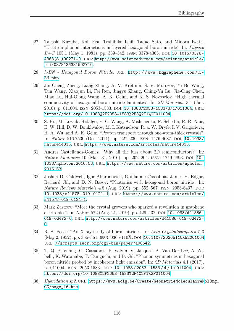
Bibliography
[27] Takashi Kuzuba, Koh Era, Toshihiko Ishii, Tadao Sato, and Minoru Iwata.“Electron-phonon interactions in layered hexagonal boron nitride”. In: PhysicaB+C 105.1 (May 1, 1981), pp. 339–342. issn: 0378-4363. doi: 10.1016/0378-4363(81)90271-0. url: http://www.sciencedirect.com/science/article/pii/0378436381902710.
[28] h-BN - Hexagonal Boron Nitride. url: http : / / www . hqgraphene . com / h -BN.php.
[29] Jin-Cheng Zheng, Liang Zhang, A. V. Kretinin, S. V. Morozov, Yi Bo Wang,Tun Wang, Xiaojun Li, Fei Ren, Jingyu Zhang, Ching-Yu Lu, Jia-Cing Chen,Miao Lu, Hui-Qiong Wang, A. K. Geim, and K. S. Novoselov. “High thermalconductivity of hexagonal boron nitride laminates”. In: 2D Materials 3.1 (Jan.2016), p. 011004. issn: 2053-1583. doi: 10.1088/2053-1583/3/1/011004. url:https://doi.org/10.1088%2F2053-1583%2F3%2F1%2F011004.
[30] S. Hu, M. Lozada-Hidalgo, F. C. Wang, A. Mishchenko, F. Schedin, R. R. Nair,E. W. Hill, D. W. Boukhvalov, M. I. Katsnelson, R. a. W. Dryfe, I. V. Grigorieva,H. A. Wu, and A. K. Geim. “Proton transport through one-atom-thick crystals”.In: Nature 516.7530 (Dec. 2014), pp. 227–230. issn: 1476-4687. doi: 10.1038/nature14015. url: https://www.nature.com/articles/nature14015.
[31] Andres Castellanos-Gomez. “Why all the fuss about 2D semiconductors?” In:Nature Photonics 10 (Mar. 31, 2016), pp. 202–204. issn: 1749-4893. doi: 10.1038/nphoton.2016.53. url: https://www.nature.com/articles/nphoton.2016.53.
[32] Joshua D. Caldwell, Igor Aharonovich, Guillaume Cassabois, James H. Edgar,Bernard Gil, and D. N. Basov. “Photonics with hexagonal boron nitride”. In:Nature Reviews Materials 4.8 (Aug. 2019), pp. 552–567. issn: 2058-8437. doi:10.1038/s41578-019-0124-1. url: https://www.nature.com/articles/s41578-019-0124-1.
[33] Mark Zastrow. “Meet the crystal growers who sparked a revolution in grapheneelectronics”. In: Nature 572 (Aug. 21, 2019), pp. 429–432. doi: 10.1038/d41586-019-02472-0. url: http://www.nature.com/articles/d41586-019-02472-0.
[34] R. S. Pease. “An X-ray study of boron nitride”. In: Acta Crystallographica 5.3(May 2, 1952), pp. 356–361. issn: 0365-110X. doi: 10.1107/S0365110X52001064.url: //scripts.iucr.org/cgi-bin/paper?a00642.
[35] T. Q. P. Vuong, G. Cassabois, P. Valvin, V. Jacques, A. Van Der Lee, A. Zo-belli, K. Watanabe, T. Taniguchi, and B. Gil. “Phonon symmetries in hexagonalboron nitride probed by incoherent light emission”. In: 2D Materials 4.1 (2017),p. 011004. issn: 2053-1583. doi: 10 . 1088 / 2053 - 1583 / 4 / 1 / 011004. url:https://doi.org/10.1088%2F2053-1583%2F4%2F1%2F011004.
[36] Hybridation sp2. url: https://www.aclg.be/Create/GeometrieMoleculaireMolOrg_CG/page_16.htm.
116

Bibliography
[37] R. J. Jiménez-Riobóo, L. Artús, R. Cuscó, T. Taniguchi, G. Cassabois, and B.Gil. “In- and out-of-plane longitudinal acoustic-wave velocities and elastic moduliin h-BN from Brillouin scattering measurements”. In: Applied Physics Letters112.5 (Jan. 29, 2018), p. 051905. issn: 0003-6951. doi: 10.1063/1.5019629.url: https://aip.scitation.org/doi/10.1063/1.5019629.
[38] S. Matt Gilbert, Thang Pham, Mehmet Dogan, Sehoon Oh, Brian Shevitski,Gabe Schumm, Stanley Liu, Peter Ercius, Shaul Aloni, Marvin L. Cohen, andAlex Zettl. “Alternative stacking sequences in hexagonal boron nitride”. In: 2DMaterials 6.2 (Mar. 2019), p. 021006. issn: 2053-1583. doi: 10.1088/2053-1583/ab0e24. url: https://doi.org/10.1088%2F2053-1583%2Fab0e24.
[39] Alexey Bosak, Jorge Serrano, Michael Krisch, Kenji Watanabe, Takashi Taniguchi,and Hisao Kanda. “Elasticity of hexagonal boron nitride: Inelastic x-ray scatter-ing measurements”. In: Physical Review B 73.4 (Jan. 19, 2006), p. 041402. doi:10.1103/PhysRevB.73.041402. url: https://link.aps.org/doi/10.1103/PhysRevB.73.041402.
[40] M. Chubarov, H. Pedersen, H. Högberg, Zs Czigany, and A. Henry. “Chemicalvapour deposition of epitaxial rhombohedral BN thin films on SiC substrates”. In:CrystEngComm 16.24 (2014), pp. 5430–5436. doi: 10.1039/C4CE00381K. url:https://pubs.rsc.org/en/content/articlelanding/2014/ce/c4ce00381k.
[41] Linfeng Ye, Feng Liang, Lei Zhao, Xuan He, Wei Fang, Hui Chen, Xin Wang,Jinfeng Wu, and Shihua An. “Catalyzed synthesis of rhombohedral boron ni-tride in sodium chloride molten salt”. In: Ceramics International 42.10 (Aug. 1,2016), pp. 11626–11633. issn: 0272-8842. doi: 10.1016/j.ceramint.2016.04.062. url: http://www.sciencedirect.com/science/article/pii/S0272884216304564.
[42] Phuong Vuong. “Optical spectroscopy of boron nitride heterostructures”. thesis.Montpellier, Oct. 24, 2018. url: http://www.theses.fr/2018MONTS075.
[43] D. A. Evans, A. G. McGlynn, B. M. Towlson, M. Gunn, D. Jones, T. E. Jenk-ins, R. Winter, and N. R. J. Poolton. “Determination of the optical band-gapenergy of cubic and hexagonal boron nitride using luminescence excitation spec-troscopy”. In: Journal of Physics: Condensed Matter 20.7 (Jan. 2008), p. 075233.issn: 0953-8984. doi: 10.1088/0953-8984/20/7/075233. url: https://doi.org/10.1088%2F0953-8984%2F20%2F7%2F075233.
[44] A. Segura, R. Cuscó, T. Taniguchi, K. Watanabe, G. Cassabois, B. Gil, and L.Artús. “Nonreversible Transition from the Hexagonal to Wurtzite Phase of BoronNitride under High Pressure: Optical Properties of the Wurtzite Phase”. In: TheJournal of Physical Chemistry C 123.33 (Aug. 22, 2019), pp. 20167–20173. issn:1932-7447. doi: 10.1021/acs.jpcc.9b06163. url: https://doi.org/10.1021/acs.jpcc.9b06163.
[45] E. Doni and G. Pastori Parravicini. “Energy bands and optical properties ofhexagonal boron nitride and graphite”. In: Il Nuovo Cimento B (1965-1970)64.1 (Nov. 1, 1969), pp. 117–144. issn: 1826-9877. doi: 10.1007/BF02710286.url: https://doi.org/10.1007/BF02710286.
117

Bibliography
[46] Pere Miró, Martha Audiffred, and Thomas Heine. “An atlas of two-dimensionalmaterials”. In: Chemical Society Reviews 43.18 (Aug. 18, 2014), pp. 6537–6554.issn: 1460-4744. doi: 10.1039/C4CS00102H. url: https://pubs.rsc.org/en/content/articlelanding/2014/cs/c4cs00102h.
[47] Giorgia Fugallo, Matteo Aramini, Jaakko Koskelo, Kenji Watanabe, TakashiTaniguchi, Mikko Hakala, Simo Huotari, Matteo Gatti, and Francesco Sottile.“Exciton energy-momentum map of hexagonal boron nitride”. In: Physical Re-view B 92.16 (Oct. 21, 2015), p. 165122. doi: 10.1103/PhysRevB.92.165122.url: https://link.aps.org/doi/10.1103/PhysRevB.92.165122.
[48] Jaakko Koskelo, Giorgia Fugallo, Mikko Hakala, Matteo Gatti, Francesco Sottile,and Pierluigi Cudazzo. “Excitons in van der Waals materials: From monolayerto bulk hexagonal boron nitride”. In: Physical Review B 95.3 (Jan. 17, 2017),p. 035125. doi: 10.1103/PhysRevB.95.035125. url: https://link.aps.org/doi/10.1103/PhysRevB.95.035125.
[49] Kin Fai Mak, Changgu Lee, James Hone, Jie Shan, and Tony F. Heinz. “Atomi-cally Thin MoS2: A New Direct-Gap Semiconductor”. In: Physical Review Letters105.13 (Sept. 24, 2010), p. 136805. doi: 10.1103/PhysRevLett.105.136805.url: https://link.aps.org/doi/10.1103/PhysRevLett.105.136805.
[50] Weijie Zhao, Zohreh Ghorannevis, Leiqiang Chu, Minglin Toh, Christian Kloc,Ping-Heng Tan, and Goki Eda. “Evolution of Electronic Structure in AtomicallyThin Sheets of WS2 and WSe2”. In: ACS Nano 7.1 (Jan. 22, 2013), pp. 791–797.issn: 1936-0851. doi: 10.1021/nn305275h. url: https://doi.org/10.1021/nn305275h.
[51] Yi Zhang, Tay-Rong Chang, Bo Zhou, Yong-Tao Cui, Hao Yan, Zhongkai Liu,Felix Schmitt, James Lee, Rob Moore, Yulin Chen, Hsin Lin, Horng-Tay Jeng,Sung-Kwan Mo, Zahid Hussain, Arun Bansil, and Zhi-Xun Shen. “Direct ob-servation of the transition from indirect to direct bandgap in atomically thinepitaxial MoSe2”. In: Nature Nanotechnology 9.2 (Feb. 2014), pp. 111–115. issn:1748-3395. doi: 10.1038/nnano.2013.277. url: https://www.nature.com/articles/nnano.2013.277.
[52] Ignacio Gutiérrez Lezama, Ashish Arora, Alberto Ubaldini, Céline Barreteau,Enrico Giannini, Marek Potemski, and Alberto F. Morpurgo. “Indirect-to-DirectBand Gap Crossover in Few-Layer MoTe2”. In: Nano Letters 15.4 (Apr. 8, 2015),pp. 2336–2342. issn: 1530-6984. doi: 10.1021/nl5045007. url: https://doi.org/10.1021/nl5045007.
[53] C. Elias, P. Valvin, T. Pelini, A. Summerfield, C. J. Mellor, T. S. Cheng, L. Eaves,C. T. Foxon, P. H. Beton, S. V. Novikov, B. Gil, and G. Cassabois. “Direct band-gap crossover in epitaxial monolayer boron nitride”. In: Nature Communications10.1 (June 14, 2019), p. 2639. issn: 2041-1723. doi: 10.1038/s41467-019-10610-5. url: https://www.nature.com/articles/s41467-019-10610-5.
118
Bibliography
[54] Fulvio Paleari, Thomas Galvani, Hakim Amara, François Ducastelle, AlejandroMolina-Sánchez, and Ludger Wirtz. “Excitons in few-layer hexagonal boron ni-tride: Davydov splitting and surface localization”. In: 2D Materials 5.4 (Aug. 14,2018), p. 045017. issn: 2053-1583. doi: 10.1088/2053- 1583/aad586. url:http://stacks.iop.org/2053- 1583/5/i=4/a=045017?key=crossref.d4ed3c3461abd8c6f845f8038fdbe2ec.
[55] G. Cassabois, P. Valvin, and B. Gil. “Hexagonal boron nitride is an indirectbandgap semiconductor”. In: Nature Photonics 10.4 (Apr. 2016), pp. 262–266.issn: 1749-4885, 1749-4893. doi: 10.1038/nphoton.2015.277. url: http://www.nature.com/articles/nphoton.2015.277.
[56] Ramon Cuscó, Bernard Gil, Guillaume Cassabois, and Luis Artús. “Temperaturedependence of Raman-active phonons and anharmonic interactions in layeredhexagonal BN”. In: Physical Review B 94.15 (Oct. 20, 2016), p. 155435. doi:10.1103/PhysRevB.94.155435. url: https://link.aps.org/doi/10.1103/PhysRevB.94.155435.
[57] T. Q. P. Vuong, G. Cassabois, P. Valvin, V. Jacques, R. Cuscó, L. Artús, andB. Gil. “Overtones of interlayer shear modes in the phonon-assisted emissionspectrum of hexagonal boron nitride”. In: Physical Review B 95.4 (Jan. 17, 2017),p. 045207. doi: 10.1103/PhysRevB.95.045207. url: https://link.aps.org/doi/10.1103/PhysRevB.95.045207.
[58] T. Q. P. Vuong, G. Cassabois, P. Valvin, S. Liu, J. H. Edgar, and B. Gil.“Exciton-phonon interaction in the strong-coupling regime in hexagonal boronnitride”. In: Physical Review B 95.20 (May 26, 2017), p. 201202. doi: 10.1103/PhysRevB.95.201202. url: https://link.aps.org/doi/10.1103/PhysRevB.95.201202.
[59] Yutaka Toyozawa. “Theory of Line-Shapes of the Exciton Absorption Bands”. In:Progress of Theoretical Physics 20.1 (July 1, 1958), pp. 53–81. issn: 0033-068X.doi: 10.1143/PTP.20.53. url: https://academic.oup.com/ptp/article/20/1/53/1937228.
[60] Léonard Schué, Lorenzo Sponza, Alexandre Plaud, Hakima Bensalah, KenjiWatanabe, Takashi Taniguchi, François Ducastelle, Annick Loiseau, and JulienBarjon. “Bright Luminescence from Indirect and Strongly Bound Excitons inh-BN”. In: Physical Review Letters 122.6 (Feb. 12, 2019), p. 067401. doi: 10.1103/PhysRevLett.122.067401. url: https://link.aps.org/doi/10.1103/PhysRevLett.122.067401.
[61] E. Cannuccia, B. Monserrat, and C. Attaccalite. “Theory of phonon-assistedluminescence in solids: Application to hexagonal boron nitride”. In: PhysicalReview B 99.8 (Feb. 8, 2019), p. 081109. doi: 10.1103/PhysRevB.99.081109.url: https://link.aps.org/doi/10.1103/PhysRevB.99.081109.
[62] Fulvio Paleari, Henrique P. C. Miranda, Alejandro Molina-Sánchez, and LudgerWirtz. “Exciton-Phonon Coupling in the Ultraviolet Absorption and EmissionSpectra of Bulk Hexagonal Boron Nitride”. In: Physical Review Letters 122.18(May 7, 2019), p. 187401. doi: 10 . 1103 / PhysRevLett . 122 . 187401. url:https://link.aps.org/doi/10.1103/PhysRevLett.122.187401.
119

Bibliography
[63] G. Cassabois, P. Valvin, and B. Gil. “Intervalley scattering in hexagonal boronnitride”. In: Physical Review B 93.3 (Jan. 28, 2016), p. 035207. doi: 10.1103/PhysRevB.93.035207. url: https://link.aps.org/doi/10.1103/PhysRevB.93.035207.
[64] M. Hulin. “Selection Rules for Two-Phonon Absorption Processes”. In: physicastatus solidi (b) 21.2 (1967), pp. 607–618. issn: 1521-3951. doi: 10.1002/pssb.19670210219. url: https://onlinelibrary.wiley.com/doi/abs/10.1002/pssb.19670210219.
[65] P. Jaffrennou, J. Barjon, T. Schmid, L. Museur, A. Kanaev, J.-S. Lauret, C. Y.Zhi, C. Tang, Y. Bando, D. Golberg, B. Attal-Tretout, F. Ducastelle, and A.Loiseau. “Near-band-edge recombinations in multiwalled boron nitride nanotubes:Cathodoluminescence and photoluminescence spectroscopy measurements”. In:Physical Review B 77.23 (June 16, 2008), p. 235422. doi: 10.1103/PhysRevB.77.235422. url: https://link.aps.org/doi/10.1103/PhysRevB.77.235422.
[66] Romain Bourrellier, Michele Amato, Luiz Henrique Galvão Tizei, Christine Gior-getti, Alexandre Gloter, Malcolm I. Heggie, Katia March, Odile Stéphan, LuciaReining, Mathieu Kociak, and Alberto Zobelli. “Nanometric Resolved Lumines-cence in h-BN Flakes: Excitons and Stacking Order”. In: ACS Photonics 1.9(Sept. 17, 2014), pp. 857–862. doi: 10.1021/ph500141j. url: https://doi.org/10.1021/ph500141j.
[67] Romain Bourrellier, Sophie Meuret, Anna Tararan, Odile Stéphan, Mathieu Ko-ciak, Luiz H. G. Tizei, and Alberto Zobelli. “Bright UV Single Photon Emissionat Point Defects in h-BN”. In: Nano Letters 16.7 (July 13, 2016), pp. 4317–4321. issn: 1530-6984. doi: 10.1021/acs.nanolett.6b01368. url: https://doi.org/10.1021/acs.nanolett.6b01368.
[68] T. Q. P. Vuong, G. Cassabois, P. Valvin, A. Ouerghi, Y. Chassagneux, C. Voisin,and B. Gil. “Phonon-Photon Mapping in a Color Center in Hexagonal BoronNitride”. In: Physical Review Letters 117.9 (Aug. 25, 2016), p. 097402. doi:10.1103/PhysRevLett.117.097402. url: https://link.aps.org/doi/10.1103/PhysRevLett.117.097402.
[69] Kamil Koronski, Agata Kaminska, Nikolai D. Zhigadlo, Christine Elias, Guil-laume Cassabois, and Bernard Gil. “Spontaneous emission of color centers at4eV in hexagonal boron nitride under hydrostatic pressure”. In: Superlatticesand Microstructures 131 (July 1, 2019), pp. 1–7. issn: 0749-6036. doi: 10 .1016/j.spmi.2019.05.018. url: http://www.sciencedirect.com/science/article/pii/S0749603619308043.
[70] G. Kern, G. Kresse, and J. Hafner. “Ab initio calculation of the lattice dynamicsand phase diagram of boron nitride”. In: Physical Review B 59.13 (Apr. 1, 1999),pp. 8551–8559. doi: 10.1103/PhysRevB.59.8551. url: https://link.aps.org/doi/10.1103/PhysRevB.59.8551.
120

Bibliography
[71] Z. Remes, M. Nesladek, K. Haenen, K. Watanabe, and T. Taniguchi. “The opti-cal absorption and photoconductivity spectra of hexagonal boron nitride singlecrystals”. In: physica status solidi (a) 202.11 (2005), pp. 2229–2233. issn: 1862-6319. doi: 10.1002/pssa.200561902. url: https://onlinelibrary.wiley.com/doi/abs/10.1002/pssa.200561902.
[72] L. Ju, J. Velasco Jr, E. Huang, S. Kahn, C. Nosiglia, Hsin-Zon Tsai, W. Yang,T. Taniguchi, K. Watanabe, Y. Zhang, G. Zhang, M. Crommie, A. Zettl, and F.Wang. “Photoinduced doping in heterostructures of graphene and boron nitride”.In: Nature Nanotechnology 9.5 (May 2014), pp. 348–352. issn: 1748-3395. doi:10.1038/nnano.2014.60. url: https://www.nature.com/articles/nnano.2014.60.
[73] Romain Bourrellier. “Luminescence at Defects in h-BN : Excitons at StackingFaults and Single Photon Emitters”. thesis. Paris 11, Oct. 28, 2014. url: http://www.theses.fr/2014PA112285.
[74] A.K. Dąbrowska, K. Pakuła, R. Bożek, J.G. Rousset, D. Ziółkowska, K. Gołasa,K.P. Korona, A. Wysmołek, and R. Stępniewski. “Structural and Optical Prop-erties of Boron Nitride Grown by MOVPE”. In: Acta Physica Polonica A 129.1(Jan. 2016), A–129–A–131. issn: 0587-4246, 1898-794X. doi: 10.12693/APhysPolA.129.A-129. url: http://przyrbwn.icm.edu.pl/APP/PDF/129/a129z1ap32.pdf.
[75] Dillon Wong, Jairo Velasco Jr, Long Ju, Juwon Lee, Salman Kahn, Hsin-ZonTsai, Chad Germany, Takashi Taniguchi, Kenji Watanabe, Alex Zettl, FengWang, and Michael F. Crommie. “Characterization and manipulation of indi-vidual defects in insulating hexagonal boron nitride using scanning tunnellingmicroscopy”. In: Nature Nanotechnology 10.11 (Nov. 2015), pp. 949–953. issn:1748-3395. doi: 10.1038/nnano.2015.188. url: https://www.nature.com/articles/nnano.2015.188.
[76] R. M. Feenstra, J. M. Woodall, and G. D. Pettit. “Observation of bulk defectsby scanning tunneling microscopy and spectroscopy: Arsenic antisite defects inGaAs”. In: Physical Review Letters 71.8 (Aug. 23, 1993), pp. 1176–1179. doi:10.1103/PhysRevLett.71.1176. url: https://link.aps.org/doi/10.1103/PhysRevLett.71.1176.
[77] K. Teichmann, M. Wenderoth, S. Loth, R. G. Ulbrich, J. K. Garleff, A. P.Wijnheijmer, and P. M. Koenraad. “Controlled Charge Switching on a SingleDonor with a Scanning Tunneling Microscope”. In: Physical Review Letters 101.7(Aug. 15, 2008), p. 076103. doi: 10.1103/PhysRevLett.101.076103. url:https://link.aps.org/doi/10.1103/PhysRevLett.101.076103.
[78] Toan Trong Tran, Kerem Bray, Michael J. Ford, Milos Toth, and Igor Aharonovich.“Quantum emission from hexagonal boron nitride monolayers”. In: Nature Nan-otechnology 11.1 (Jan. 2016), pp. 37–41. issn: 1748-3395. doi: 10.1038/nnano.2015.242. url: https://www.nature.com/articles/nnano.2015.242.
121

Bibliography
[79] L. J. Martínez, T. Pelini, V. Waselowski, J. R. Maze, B. Gil, G. Cassabois, andV. Jacques. “Efficient single photon emission from a high-purity hexagonal boronnitride crystal”. In: Physical Review B 94.12 (Sept. 22, 2016), p. 121405. doi:10.1103/PhysRevB.94.121405. url: https://link.aps.org/doi/10.1103/PhysRevB.94.121405.
[80] Toan Trong Tran, Christopher Elbadawi, Daniel Totonjian, Charlene J. Lobo,Gabriele Grosso, Hyowon Moon, Dirk R. Englund, Michael J. Ford, Igor Aharonovich,and Milos Toth. “Robust Multicolor Single Photon Emission from Point Defectsin Hexagonal Boron Nitride”. In: ACS Nano 10.8 (Aug. 23, 2016), pp. 7331–7338.issn: 1936-0851. doi: 10.1021/acsnano.6b03602. url: https://doi.org/10.1021/acsnano.6b03602.
[81] Zav Shotan, Harishankar Jayakumar, Christopher R. Considine, Mažena Mack-oit, Helmut Fedder, Jörg Wrachtrup, Audrius Alkauskas, Marcus W. Doherty,Vinod M. Menon, and Carlos A. Meriles. “Photoinduced Modification of Single-Photon Emitters in Hexagonal Boron Nitride”. In: ACS Photonics 3.12 (Dec. 21,2016), pp. 2490–2496. doi: 10.1021/acsphotonics.6b00736. url: https://doi.org/10.1021/acsphotonics.6b00736.
[82] Nathan Chejanovsky, Mohammad Rezai, Federico Paolucci, Youngwook Kim,Torsten Rendler, Wafa Rouabeh, Felipe Fávaro de Oliveira, Patrick Herlinger,Andrej Denisenko, Sen Yang, Ilja Gerhardt, Amit Finkler, Jurgen H. Smet, andJörg Wrachtrup. “Structural Attributes and Photodynamics of Visible SpectrumQuantum Emitters in Hexagonal Boron Nitride”. In: Nano Letters 16.11 (Nov. 9,2016), pp. 7037–7045. issn: 1530-6984. doi: 10.1021/acs.nanolett.6b03268.url: https://doi.org/10.1021/acs.nanolett.6b03268.
[83] Nicholas R. Jungwirth, Brian Calderon, Yanxin Ji, Michael G. Spencer, MichaelE. Flatté, and Gregory D. Fuchs. “Temperature Dependence of Wavelength Se-lectable Zero-Phonon Emission from Single Defects in Hexagonal Boron Nitride”.In: Nano Letters 16.10 (Oct. 12, 2016), pp. 6052–6057. issn: 1530-6984. doi:10.1021/acs.nanolett.6b01987. url: https://doi.org/10.1021/acs.nanolett.6b01987.
[84] Annemarie L. Exarhos, David A. Hopper, Richard R. Grote, Audrius Alkauskas,and Lee C. Bassett. “Optical Signatures of Quantum Emitters in SuspendedHexagonal Boron Nitride”. In: ACS Nano 11.3 (Mar. 28, 2017), pp. 3328–3336.issn: 1936-0851. doi: 10.1021/acsnano.7b00665. url: https://doi.org/10.1021/acsnano.7b00665.
[85] Gabriele Grosso, Hyowon Moon, Benjamin Lienhard, Sajid Ali, Dmitri K. Efe-tov, Marco M. Furchi, Pablo Jarillo-Herrero, Michael J. Ford, Igor Aharonovich,and Dirk Englund. “Tunable and high-purity room temperature single-photonemission from atomic defects in hexagonal boron nitride”. In: Nature Communi-cations 8.1 (Sept. 26, 2017), pp. 1–8. issn: 2041-1723. doi: 10.1038/s41467-017-00810-2. url: https://www.nature.com/articles/s41467-017-00810-2.
122

Bibliography
[86] Annemarie L. Exarhos, David A. Hopper, Raj N. Patel, Marcus W. Doherty,and Lee C. Bassett. “Magnetic-field-dependent quantum emission in hexagonalboron nitride at room temperature”. In: Nature Communications 10.1 (Jan. 15,2019), p. 222. issn: 2041-1723. doi: 10.1038/s41467- 018- 08185- 8. url:https://www.nature.com/articles/s41467-018-08185-8.
[87] S. Reich, A. C. Ferrari, R. Arenal, A. Loiseau, I. Bello, and J. Robertson. “Res-onant Raman scattering in cubic and hexagonal boron nitride”. In: PhysicalReview B 71.20 (May 4, 2005), p. 205201. doi: 10.1103/PhysRevB.71.205201.url: https://link.aps.org/doi/10.1103/PhysRevB.71.205201.
[88] M. Nirmal, B. O. Dabbousi, M. G. Bawendi, J. J. Macklin, J. K. Trautman, T. D.Harris, and L. E. Brus. “Fluorescence intermittency in single cadmium selenidenanocrystals”. In: Nature 383.6603 (Oct. 1996), pp. 802–804. issn: 1476-4687.doi: 10.1038/383802a0. url: https://www.nature.com/articles/383802a0.
[89] Robert M. Dickson, Andrew B. Cubitt, Roger Y. Tsien, and W. E. Moerner.“On/off blinking and switching behaviour of single molecules of green fluorescentprotein”. In: Nature 388.6640 (July 1997), pp. 355–358. issn: 1476-4687. doi:10.1038/41048. url: https://www.nature.com/articles/41048.
[90] Sumin Choi, Brett C. Johnson, Stefania Castelletto, Cuong Ton-That, MatthewR. Phillips, and Igor Aharonovich. “Single photon emission from ZnO nanoparti-cles”. In: Applied Physics Letters 104.26 (June 30, 2014), p. 261101. issn: 0003-6951. doi: 10.1063/1.4872268. url: https://aip.scitation.org/doi/full/10.1063/1.4872268.
[91] Jean Comtet, Evgenii Glushkov, Vytautas Navikas, Jiandong Feng, Vitaliy Babenko,Stephan Hofmann, Kenji Watanabe, Takashi Taniguchi, and Aleksandra Rade-novic. “Wide-Field Spectral Super-Resolution Mapping of Optically Active De-fects in Hexagonal Boron Nitride”. In: Nano Letters 19.4 (Apr. 10, 2019), pp. 2516–2523. issn: 1530-6984. doi: 10.1021/acs.nanolett.9b00178. url: https://doi.org/10.1021/acs.nanolett.9b00178.
[92] I. Aharonovich, S. Castelletto, D. A. Simpson, C.-H. Su, A. D. Greentree, andS. Prawer. “Diamond-based single-photon emitters”. In: Reports on Progress inPhysics 74.7 (June 2011), p. 076501. issn: 0034-4885. doi: 10.1088/0034-4885/74/7/076501. url: https://doi.org/10.1088%2F0034-4885%2F74%2F7%2F076501.
[93] C. Bradac, T. Gaebel, N. Naidoo, M. J. Sellars, J. Twamley, L. J. Brown, A. S.Barnard, T. Plakhotnik, A. V. Zvyagin, and J. R. Rabeau. “Observation and con-trol of blinking nitrogen-vacancy centres in discrete nanodiamonds”. In: NatureNanotechnology 5.5 (May 2010), pp. 345–349. issn: 1748-3395. doi: 10.1038/nnano.2010.56. url: https://www.nature.com/articles/nnano.2010.56.
[94] Toan Trong Tran, Cameron Zachreson, Amanuel Michael Berhane, Kerem Bray,Russell Guy Sandstrom, Lu Hua Li, Takashi Taniguchi, Kenji Watanabe, IgorAharonovich, and Milos Toth. “Quantum Emission from Defects in Single-CrystallineHexagonal Boron Nitride”. In: Physical Review Applied 5.3 (Mar. 10, 2016),p. 034005. doi: 10.1103/PhysRevApplied.5.034005. url: https://link.aps.org/doi/10.1103/PhysRevApplied.5.034005.
123
Bibliography
[95] M. Jaros and S. F. Ross. “Calculations of impurity states in semiconductors:I”. In: Journal of Physics C: Solid State Physics 6.10 (May 1973), pp. 1753–1762. issn: 0022-3719. doi: 10.1088/0022- 3719/6/10/010. url: https://doi.org/10.1088%2F0022-3719%2F6%2F10%2F010.
[96] L. Rondin, G. Dantelle, A. Slablab, F. Grosshans, F. Treussart, P. Bergonzo,S. Perruchas, T. Gacoin, M. Chaigneau, H.-C. Chang, V. Jacques, and J.-F.Roch. “Surface-induced charge state conversion of nitrogen-vacancy defects innanodiamonds”. In: Physical Review B 82.11 (Sept. 28, 2010), p. 115449. doi:10.1103/PhysRevB.82.115449. url: https://link.aps.org/doi/10.1103/PhysRevB.82.115449.
[97] M. V. Hauf, B. Grotz, B. Naydenov, M. Dankerl, S. Pezzagna, J. Meijer, F.Jelezko, J. Wrachtrup, M. Stutzmann, F. Reinhard, and J. A. Garrido. “Chemicalcontrol of the charge state of nitrogen-vacancy centers in diamond”. In: PhysicalReview B 83.8 (Feb. 14, 2011), p. 081304. doi: 10.1103/PhysRevB.83.081304.url: https://link.aps.org/doi/10.1103/PhysRevB.83.081304.
[98] Bernhard Grotz, Moritz V. Hauf, Markus Dankerl, Boris Naydenov, SébastienPezzagna, Jan Meijer, Fedor Jelezko, JörgWrachtrup, Martin Stutzmann, Friede-mann Reinhard, and Jose A. Garrido. “Charge state manipulation of qubits indiamond”. In: Nature Communications 3 (Mar. 6, 2012), p. 729. issn: 2041-1723. doi: 10.1038/ncomms1729. url: https://www.nature.com/articles/ncomms1729.
[99] C. Schreyvogel, V. Polyakov, R. Wunderlich, J. Meijer, and C. E. Nebel. “Activecharge state control of single NV centres in diamond by in-plane Al-Schottkyjunctions”. In: Scientific Reports 5 (July 16, 2015), p. 12160. issn: 2045-2322.doi: 10 . 1038 / srep12160. url: https : / / www . nature . com / articles /srep12160.
[100] Mandy L. Y. Sin, Vincent Gau, Joseph C. Liao, David A. Haake, and Pak KinWong. “Active Manipulation of Quantum Dots using AC Electrokinetics”. In:The Journal of Physical Chemistry C 113.16 (Apr. 23, 2009), pp. 6561–6565.issn: 1932-7447. doi: 10.1021/jp9004423. url: https://doi.org/10.1021/jp9004423.
[101] Rodney Loudon. The Quantum Theory of Light. Google-Books-ID: AEkfajgql-doC. OUP Oxford, Sept. 7, 2000. 454 pp. isbn: 978-0-19-158978-2.
[102] R. Hanbury Brown and R. Q. Twiss. “LXXIV. A new type of interferometer foruse in radio astronomy”. In: The London, Edinburgh, and Dublin PhilosophicalMagazine and Journal of Science 45.366 (July 1, 1954), pp. 663–682. issn: 1941-5982. doi: 10.1080/14786440708520475. url: https://doi.org/10.1080/14786440708520475.
[103] R. Hanbury Brown and R. Q. Twiss. “A Test of a New Type of Stellar Interfer-ometer on Sirius”. In: Nature 178.4541 (Nov. 1956), pp. 1046–1048. issn: 1476-4687. doi: 10.1038/1781046a0. url: https://www.nature.com/articles/1781046a0.
124

Bibliography
[104] Gerhard Rempe, Herbert Walther, and Norbert Klein. “Observation of quan-tum collapse and revival in a one-atom maser”. In: Physical Review Letters 58.4(Jan. 26, 1987), pp. 353–356. doi: 10.1103/PhysRevLett.58.353. url: https://link.aps.org/doi/10.1103/PhysRevLett.58.353.
[105] Th. Basché, W. E. Moerner, M. Orrit, and H. Talon. “Photon antibunching inthe fluorescence of a single dye molecule trapped in a solid”. In: Physical ReviewLetters 69.10 (Sept. 7, 1992), pp. 1516–1519. doi: 10.1103/PhysRevLett.69.1516. url: https://link.aps.org/doi/10.1103/PhysRevLett.69.1516.
[106] Serge Reynaud. “La fluorescence de résonance : Etude par la méthode de l’atomehabillé”. In: Annales de Physique 8 (1983), pp. 315–370. issn: 0003-4169, 1286-4838. doi: 10.1051/anphys/198308080315. url: https://www.annphys.org/articles/anphys/abs/1983/01/anphys19830808p315/anphys19830808p315.html.
[107] L. Fleury, J.-M. Segura, G. Zumofen, B. Hecht, and U. P. Wild. “NonclassicalPhoton Statistics in Single-Molecule Fluorescence at Room Temperature”. In:Physical Review Letters 84.6 (Feb. 7, 2000), pp. 1148–1151. issn: 0031-9007,1079-7114. doi: 10.1103/PhysRevLett.84.1148. url: https://link.aps.org/doi/10.1103/PhysRevLett.84.1148.
[108] Frank Diedrich and Herbert Walther. “Nonclassical radiation of a single storedion”. In: Physical Review Letters 58.3 (Jan. 19, 1987), pp. 203–206. doi: 10.1103/PhysRevLett.58.203. url: https://link.aps.org/doi/10.1103/PhysRevLett.58.203.
[109] A. Beveratos, S. Kühn, R. Brouri, T. Gacoin, J.-P. Poizat, and P. Grangier.“Room temperature stable single-photon source”. In: The European PhysicalJournal D - Atomic, Molecular, Optical and Plasma Physics 18.2 (Feb. 1, 2002),pp. 191–196. issn: 1434-6079. doi: 10.1140/epjd/e20020023. url: https://doi.org/10.1140/epjd/e20020023.
[110] Alexios Beveratos. “Sources à boîtes quantiques semiconductrices pour la nanopho-tonique et l’information quantique aux longueurs d’onde des télécommunica-tions”. PhD thesis. Feb. 14, 2005. url: http://www.theses.fr/076117308.
[111] S. C. Kitson, P. Jonsson, J. G. Rarity, and P. R. Tapster. “Intensity fluctuationspectroscopy of small numbers of dye molecules in a microcavity”. In: PhysicalReview A 58.1 (July 1, 1998), pp. 620–627. doi: 10.1103/PhysRevA.58.620.url: https://link.aps.org/doi/10.1103/PhysRevA.58.620.
[112] Martin Berthel, Oriane Mollet, Géraldine Dantelle, Thierry Gacoin, Serge Huant,and Aurélien Drezet. “Photophysics of single nitrogen-vacancy centers in dia-mond nanocrystals”. In: Physical Review B 91.3 (Jan. 14, 2015), p. 035308. doi:10.1103/PhysRevB.91.035308. url: https://link.aps.org/doi/10.1103/PhysRevB.91.035308.
[113] Igor Pro from WaveMetrics | Igor Pro by WaveMetrics. url: https://www.wavemetrics.com/.
125

Bibliography
[114] E. Wu, Vincent Jacques, Heping Zeng, Philippe Grangier, François Treussart,and Jean-François Roch. “Narrow-band single-photon emission in the near in-frared for quantum key distribution”. In: Optics Express 14.3 (Feb. 6, 2006),pp. 1296–1303. issn: 1094-4087. doi: 10.1364/OE.14.001296. url: https://www.osapublishing.org/oe/abstract.cfm?uri=oe-14-3-1296.
[115] Niko Nikolay, Noah Mendelson, Ersan Özelci, Bernd Sontheimer, Florian Böhm,Günter Kewes, Milos Toth, Igor Aharonovich, and Oliver Benson. “Direct Mea-surement of Quantum Efficiency of Single Photon Emitters in Hexagonal BoronNitride”. In: arXiv:1904.08531 [cond-mat, physics:physics] (Apr. 17, 2019). arXiv:1904.08531. url: http://arxiv.org/abs/1904.08531.
[116] Nathan Chejanovsky, Amlan Mukherjee, Youngwook Kim, Andrej Denisenko,Amit Finkler, Takashi Taniguchi, Kenji Watanabe, Durga Bhaktavatsala RaoDasari, Jurgen H Smet, and Jörg Wrachtrup. “Single spin resonance in a vander Waals embedded paramagnetic defect”. In: arXiv:1901.05952 [cond-mat] (),p. 22.
[117] Sherif Abdulkader Tawfik, Sajid Ali, Marco Fronzi, Mehran Kianinia, ToanTrong Tran, Catherine Stampfl, Igor Aharonovich, Milos Toth, and Michael J.Ford. “First-principles investigation of quantum emission from hBN defects”.In: Nanoscale 9.36 (Sept. 21, 2017), pp. 13575–13582. issn: 2040-3372. doi: 10.1039/C7NR04270A. url: https://pubs.rsc.org/en/content/articlelanding/2017/nr/c7nr04270a.
[118] Feng Wu, Andrew Galatas, Ravishankar Sundararaman, Dario Rocca, and YuanPing. “First-principles engineering of charged defects for two-dimensional quan-tum technologies”. In: Physical Review Materials 1.7 (Dec. 6, 2017), p. 071001.doi: 10.1103/PhysRevMaterials.1.071001. url: https://link.aps.org/doi/10.1103/PhysRevMaterials.1.071001.
[119] Mehdi Abdi, Jyh-Pin Chou, Adam Gali, and Martin B. Plenio. “Color Centersin Hexagonal Boron Nitride Monolayers: A Group Theory and Ab Initio Anal-ysis”. In: ACS Photonics 5.5 (May 16, 2018), pp. 1967–1976. doi: 10.1021/acsphotonics.7b01442. url: https://doi.org/10.1021/acsphotonics.7b01442.
[120] Koh Era, Fujio Minami, and Takashi Kuzuba. “Fast luminescence from carbon-related defects of hexagonal boron nitride”. In: Journal of Luminescence 24-25(Nov. 1, 1981), pp. 71–74. issn: 0022-2313. doi: 10.1016/0022- 2313(81)90223- 4. url: http://www.sciencedirect.com/science/article/pii/0022231381902234.
[121] P. J. Dean. “Photoluminescence as a diagnostic of semiconductors”. In: Progressin Crystal Growth and Characterization. Special Issue on Characterization 5.1(Jan. 1, 1982), pp. 89–174. issn: 0146-3535. doi: 10.1016/0146- 3535(82)90010- 7. url: http://www.sciencedirect.com/science/article/pii/0146353582900107.
126

Bibliography
[122] T. B. Hoffman, B. Clubine, Y. Zhang, K. Snow, and J. H. Edgar. “Optimizationof Ni–Cr flux growth for hexagonal boron nitride single crystals”. In: Journal ofCrystal Growth. The 19th American Conference on Crystal Growth and Epitaxyin conjunction with The 16th US Biennial Workshop on Organometallic VaporPhase Epitaxy 393 (May 1, 2014), pp. 114–118. issn: 0022-0248. doi: 10.1016/j.jcrysgro.2013.09.030. url: http://www.sciencedirect.com/science/article/pii/S0022024813006313.
[123] Song Liu, Rui He, Lianjie Xue, Jiahan Li, Bin Liu, and James H. Edgar. “SingleCrystal Growth of Millimeter-Sized Monoisotopic Hexagonal Boron Nitride”. In:Chemistry of Materials 30.18 (Sept. 25, 2018), pp. 6222–6225. issn: 0897-4756.doi: 10.1021/acs.chemmater.8b02589. url: https://doi.org/10.1021/acs.chemmater.8b02589.
[124] T. Q. P. Vuong, S. Liu, A. Van der Lee, R. Cuscó, L. Artús, T. Michel, P.Valvin, J. H. Edgar, G. Cassabois, and B. Gil. “Isotope engineering of van derWaals interactions in hexagonal boron nitride”. In: Nature Materials 17.2 (Feb.2018), pp. 152–158. issn: 1476-4660. doi: 10.1038/nmat5048. url: https://www.nature.com/articles/nmat5048.
[125] Takashi Taniguchi and Kenji Watanabe. “Synthesis of high-purity boron ni-tride single crystals under high pressure by using Ba–BN solvent”. In: Journalof Crystal Growth 303.2 (May 15, 2007), pp. 525–529. issn: 0022-0248. doi:10.1016/j.jcrysgro.2006.12.061. url: https://www.sciencedirect.com/science/article/pii/S0022024807000486.
[126] C. Attaccalite, M. Bockstedte, A. Marini, A. Rubio, and L. Wirtz. “Coupling ofexcitons and defect states in boron-nitride nanostructures”. In: Physical ReviewB 83.14 (Apr. 29, 2011), p. 144115. doi: 10.1103/PhysRevB.83.144115. url:https://link.aps.org/doi/10.1103/PhysRevB.83.144115.
[127] Luc Museur, Eduard Feldbach, and Andrei Kanaev. “Defect-related photolu-minescence of hexagonal boron nitride”. In: Physical Review B 78.15 (Oct. 16,2008), p. 155204. doi: 10.1103/PhysRevB.78.155204. url: https://link.aps.org/doi/10.1103/PhysRevB.78.155204.
[128] Welcome to Python.org. Python.org. url: https://www.python.org/.
[129] Leading Optical Product Design Software for Engineering Teams - Zemax. url:https://www.zemax.com/.
[130] Tatiana Korona and Michał Chojecki. “Exploring point defects in hexagonalboron-nitrogen monolayers”. In: International Journal of Quantum Chemistry119.14 (2019), e25925. issn: 1097-461X. doi: 10.1002/qua.25925. url: https://onlinelibrary.wiley.com/doi/abs/10.1002/qua.25925.
[131] A. J. Stone and D. J. Wales. “Theoretical studies of icosahedral C60 and somerelated species”. In: Chemical Physics Letters 128.5 (Aug. 1, 1986), pp. 501–503. issn: 0009-2614. doi: 10.1016/0009- 2614(86)80661- 3. url: http://www.sciencedirect.com/science/article/pii/0009261486806613.
127

Bibliography
[132] Ondrej L. Krivanek, Matthew F. Chisholm, Valeria Nicolosi, Timothy J. Penny-cook, George J. Corbin, Niklas Dellby, Matthew F. Murfitt, Christopher S. Own,Zoltan S. Szilagyi, Mark P. Oxley, Sokrates T. Pantelides, and Stephen J. Pen-nycook. “Atom-by-atom structural and chemical analysis by annular dark-fieldelectron microscopy”. In: Nature 464.7288 (Mar. 2010), pp. 571–574. issn: 1476-4687. doi: 10.1038/nature08879. url: https://www.nature.com/articles/nature08879.
[133] Mazena Mackoit-Sinkeviciene, Marek Maciaszek, Chris G. Van de Walle, andAudrius Alkauskas. “Carbon dimer defect as a source of the 4.1 eV luminescencein hexagonal boron nitride”. In: arXiv:1907.02303 [cond-mat] (July 4, 2019).arXiv: 1907.02303. url: http://arxiv.org/abs/1907.02303.
[134] X. Z. Du, J. Li, J. Y. Lin, and H. X. Jiang. “The origin of deep-level impu-rity transitions in hexagonal boron nitride”. In: Applied Physics Letters 106.2(Jan. 12, 2015), p. 021110. issn: 0003-6951. doi: 10.1063/1.4905908. url:https://aip.scitation.org/doi/abs/10.1063/1.4905908.
[135] Shigefusa F. Chichibu, Youichi Ishikawa, Hiroko Kominami, and Kazuhiko Hara.“Nearly temperature-independent ultraviolet light emission intensity of indirectexcitons in hexagonal BN microcrystals”. In: Journal of Applied Physics 123.6(Feb. 9, 2018), p. 065104. issn: 0021-8979. doi: 10.1063/1.5021788. url:https://aip.scitation.org/doi/10.1063/1.5021788.
[136] Emi Tsushima, Takuya Tsujimura, and Takashi Uchino. “Enhancement of thedeep-level emission and its chemical origin in hexagonal boron nitride”. In: Ap-plied Physics Letters 113.3 (July 16, 2018), p. 031903. issn: 0003-6951. doi:10.1063/1.5038168. url: https://aip.scitation.org/doi/10.1063/1.5038168.
[137] L. Weston, D. Wickramaratne, M. Mackoit, A. Alkauskas, and C. G. Van deWalle. “Native point defects and impurities in hexagonal boron nitride”. In: Phys-ical Review B 97.21 (June 18, 2018), p. 214104. doi: 10.1103/PhysRevB.97.214104. url: https://link.aps.org/doi/10.1103/PhysRevB.97.214104.
[138] Manuel Cardona and M. L. W. Thewalt. “Isotope effects on the optical spectra ofsemiconductors”. In: Reviews of Modern Physics 77.4 (Nov. 7, 2005), pp. 1173–1224. doi: 10.1103/RevModPhys.77.1173. url: https://link.aps.org/doi/10.1103/RevModPhys.77.1173.
[139] C. Chartrand, L. Bergeron, K. J. Morse, H. Riemann, N. V. Abrosimov, P.Becker, H.-J. Pohl, S. Simmons, and M. L. W. Thewalt. “Highly enriched 28Sireveals remarkable optical linewidths and fine structure for well-known damagecenters”. In: Physical Review B 98.19 (Nov. 5, 2018), p. 195201. doi: 10.1103/PhysRevB.98.195201. url: https://link.aps.org/doi/10.1103/PhysRevB.98.195201.
[140] Andreas Dietrich, Kay D Jahnke, Jan M Binder, Tokuyuki Teraji, Junichi Isoya,Lachlan J Rogers, and Fedor Jelezko. “Isotopically varying spectral features ofsilicon-vacancy in diamond”. In: New Journal of Physics 16.11 (Nov. 11, 2014),p. 113019. issn: 1367-2630. doi: 10.1088/1367-2630/16/11/113019. url:
128

Bibliography
http://stacks.iop.org/1367-2630/16/i=11/a=113019?key=crossref.82aa49b97773b65bb6774d744bd5a404.
[141] Hisamitsu Akamaru, Akifumi Onodera, Tadashi Endo, and Osamu Mishima.“Pressure dependence of the optical-absorption edge of AlN and graphite-typeBN”. In: Journal of Physics and Chemistry of Solids 63.5 (May 1, 2002), pp. 887–894. issn: 0022-3697. doi: 10.1016/S0022- 3697(01)00244- X. url: http://www.sciencedirect.com/science/article/pii/S002236970100244X.
[142] A. Segura, R. Cuscó, T. Taniguchi, K. Watanabe, G. Cassabois, B. Gil, andL. Artús. “High-Pressure Softening of the Out-of-Plane A2u(Transverse-Optic)Mode of Hexagonal Boron Nitride Induced by Dynamical Buckling”. In: TheJournal of Physical Chemistry C 123.28 (July 18, 2019), pp. 17491–17497. issn:1932-7447. doi: 10.1021/acs.jpcc.9b04582. url: https://doi.org/10.1021/acs.jpcc.9b04582.
[143] S. Meuret, L. H. G. Tizei, T. Cazimajou, R. Bourrellier, H. C. Chang, F.Treussart, and M. Kociak. “Photon Bunching in Cathodoluminescence”. In: Phys-ical Review Letters 114.19 (May 11, 2015), p. 197401. doi: 10.1103/PhysRevLett.114.197401. url: https://link.aps.org/doi/10.1103/PhysRevLett.114.197401.
[144] Alberto Zobelli, Steffi Y. Woo, Luiz H. G. Tizei, Nathalie Brun, Anna Tararan,Xiaoyan Li, Odile Stéphan, Mathieu Kociak, and Marcel Tencé. “Spatial andspectral dynamics in STEM hyperspectral imaging using random scan patterns”.In: arXiv:1909.07842 [cond-mat, physics:physics] (Sept. 17, 2019). arXiv: 1909.07842. url: http://arxiv.org/abs/1909.07842.
[145] Sumin Choi, Toan Trong Tran, Christopher Elbadawi, Charlene Lobo, XuewenWang, Saulius Juodkazis, Gediminas Seniutinas, Milos Toth, and Igor Aharonovich.“Engineering and Localization of Quantum Emitters in Large Hexagonal BoronNitride Layers”. In: ACS Applied Materials & Interfaces 8.43 (Nov. 2, 2016),pp. 29642–29648. issn: 1944-8244. doi: 10.1021/acsami.6b09875. url: https://doi.org/10.1021/acsami.6b09875.
[146] X. T. Zou and L. Mandel. “Photon-antibunching and sub-Poissonian photonstatistics”. In: Physical Review A 41.1 (Jan. 1, 1990), pp. 475–476. doi: 10.1103/PhysRevA.41.475. url: https://link.aps.org/doi/10.1103/PhysRevA.41.475.
[147] A. Migdall, S. V. Polyakov, J. Fan, J. C. Bienfang. Single-Photon Generationand Detection: Physics and Applications. Vol. 45. Experimental methods in thephysical sciences. Google-Books-ID: gERMqvh2OjAC. Academic Press, Nov. 29,2013. 593 pp. isbn: 978-0-12-387696-6.
[148] Cécile DeWitt-Morette, A Blandin, and Claude Cohen-Tannoudji. Optique etélectronique quantiques: quantum optics and electronics : lectures delivered at LesHouches during the 1964 session of the Summer School of Theoretical PhysicsUniversity of Grenoble. OCLC: 1103630647. New York: Gordon and Breach,1965.
129