Carbon nanomaterials as antibacterial and antiviral alternatives
Upload
independentCategory
view
5download
0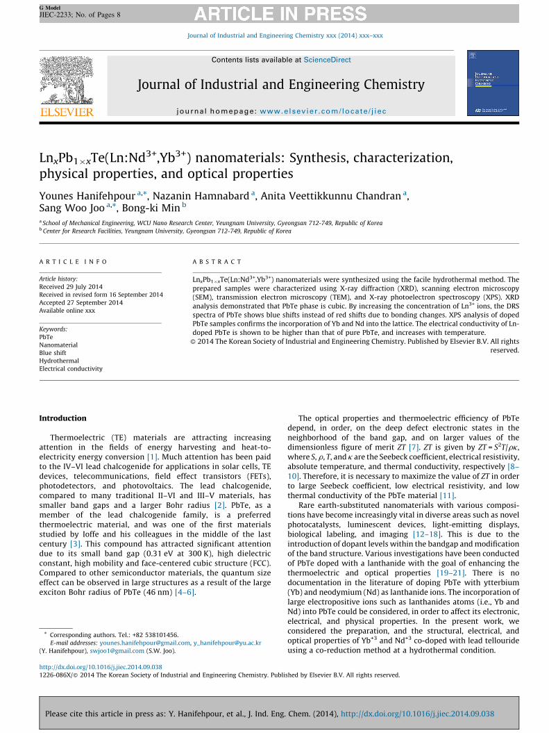
Journal of Industrial and Engineering Chemistry xxx (2014) xxx–xxx
G Model
JIEC-2233; No. of Pages 8
LnxPb1�xTe(Ln:Nd3+,Yb3+) nanomaterials: Synthesis, characterization,physical properties, and optical properties
Younes Hanifehpour a,*, Nazanin Hamnabard a, Anita Veettikkunnu Chandran a,Sang Woo Joo a,*, Bong-ki Min b
a School of Mechanical Engineering, WCU Nano Research Center, Yeungnam University, Gyeongsan 712-749, Republic of Koreab Center for Research Facilities, Yeungnam University, Gyeongsan 712-749, Republic of Korea
A R T I C L E I N F O
Article history:
Received 29 July 2014
Received in revised form 16 September 2014
Accepted 27 September 2014
Available online xxx
Keywords:
PbTe
Nanomaterial
Blue shift
Hydrothermal
Electrical conductivity
A B S T R A C T
LnxPb1�xTe(Ln:Nd3+,Yb3+) nanomaterials were synthesized using the facile hydrothermal method. The
prepared samples were characterized using X-ray diffraction (XRD), scanning electron microscopy
(SEM), transmission electron microscopy (TEM), and X-ray photoelectron spectroscopy (XPS). XRD
analysis demonstrated that PbTe phase is cubic. By increasing the concentration of Ln3+ ions, the DRS
spectra of PbTe shows blue shifts instead of red shifts due to bonding changes. XPS analysis of doped
PbTe samples confirms the incorporation of Yb and Nd into the lattice. The electrical conductivity of Ln-
doped PbTe is shown to be higher than that of pure PbTe, and increases with temperature.
� 2014 The Korean Society of Industrial and Engineering Chemistry. Published by Elsevier B.V. All rights
reserved.
Contents lists available at ScienceDirect
Journal of Industrial and Engineering Chemistry
jou r n al h o mep ag e: w ww .e lsev ier . co m / loc ate / j iec
Introduction
Thermoelectric (TE) materials are attracting increasingattention in the fields of energy harvesting and heat-to-electricity energy conversion [1]. Much attention has been paidto the IV–VI lead chalcogenide for applications in solar cells, TEdevices, telecommunications, field effect transistors (FETs),photodetectors, and photovoltaics. The lead chalcogenide,compared to many traditional II–VI and III–V materials, hassmaller band gaps and a larger Bohr radius [2]. PbTe, as amember of the lead chalcogenide family, is a preferredthermoelectric material, and was one of the first materialsstudied by Ioffe and his colleagues in the middle of the lastcentury [3]. This compound has attracted significant attentiondue to its small band gap (0.31 eV at 300 K), high dielectricconstant, high mobility and face-centered cubic structure (FCC).Compared to other semiconductor materials, the quantum sizeeffect can be observed in large structures as a result of the largeexciton Bohr radius of PbTe (46 nm) [4–6].
* Corresponding authors. Tel.: +82 538101456.
E-mail addresses: [email protected], [email protected]
(Y. Hanifehpour), [email protected] (S.W. Joo).
Please cite this article in press as: Y. Hanifehpour, et al., J. Ind. Eng.
http://dx.doi.org/10.1016/j.jiec.2014.09.038
1226-086X/� 2014 The Korean Society of Industrial and Engineering Chemistry. Publis
The optical properties and thermoelectric efficiency of PbTedepend, in order, on the deep defect electronic states in theneighborhood of the band gap, and on larger values of thedimensionless figure of merit ZT [7]. ZT is given by ZT = S2T/rk,where S, r, T, and k are the Seebeck coefficient, electrical resistivity,absolute temperature, and thermal conductivity, respectively [8–10]. Therefore, it is necessary to maximize the value of ZT in orderto large Seebeck coefficient, low electrical resistivity, and lowthermal conductivity of the PbTe material [11].
Rare earth-substituted nanomaterials with various composi-tions have become increasingly vital in diverse areas such as novelphotocatalysts, luminescent devices, light-emitting displays,biological labeling, and imaging [12–18]. This is due to theintroduction of dopant levels within the bandgap and modificationof the band structure. Various investigations have been conductedof PbTe doped with a lanthanide with the goal of enhancing thethermoelectric and optical properties [19–21]. There is nodocumentation in the literature of doping PbTe with ytterbium(Yb) and neodymium (Nd) as lanthanide ions. The incorporation oflarge electropositive ions such as lanthanides atoms (i.e., Yb andNd) into PbTe could be considered, in order to affect its electronic,electrical, and physical properties. In the present work, weconsidered the preparation, and the structural, electrical, andoptical properties of Yb+3 and Nd+3 co-doped with lead tellourideusing a co-reduction method at a hydrothermal condition.
Chem. (2014), http://dx.doi.org/10.1016/j.jiec.2014.09.038
hed by Elsevier B.V. All rights reserved.
807060504030202θ/degree
Intensity
X=0.1
X=0.08
X=0.06
X=0.04
X=0.02
X=0
420331400
222311
220200
111 422
Fig. 2. XRD pattern of as-prepared PbTe and Yb-doped PbTe nanoparticles.
80706050403020
2θ/Degree
Intensity
X=0.1
X=0.08
X=0.06
X=0.04
X=0.02
X=0
420
331
400222
311
220200
111
422
Fig. 1. XRD pattern of prepared PbTe and Nd-doped PbTe nanoparticles.
Y. Hanifehpour et al. / Journal of Industrial and Engineering Chemistry xxx (2014) xxx–xxx2
G Model
JIEC-2233; No. of Pages 8
Experimental details
Materials
All chemicals used in this study were of analytical grade andwere used without further purification. Lead (II) nitrate (Pb(NO3)2
Fig. 3. (a) Structure of rock salt-type NaCl of the host lattice PbTe. For example, N
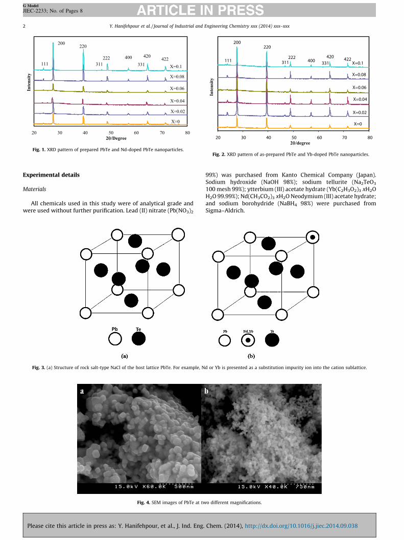
Fig. 4. SEM images of PbTe at tw
Please cite this article in press as: Y. Hanifehpour, et al., J. Ind. Eng.
99%) was purchased from Kanto Chemical Company (Japan).Sodium hydroxide (NaOH 98%); sodium tellurite (Na2TeO3
100 mesh 99%); ytterbium (III) acetate hydrate (Yb(C2H3O2)3�xH2OH2O 99.99%); Nd(CH3CO2)3�xH2O Neodymium (III) acetate hydrate;and sodium borohydride (NaBH4 98%) were purchased fromSigma–Aldrich.
d or Yb is presented as a substitution impurity ion into the cation sublattice.
o different magnifications.
Chem. (2014), http://dx.doi.org/10.1016/j.jiec.2014.09.038
Y. Hanifehpour et al. / Journal of Industrial and Engineering Chemistry xxx (2014) xxx–xxx 3
G Model
JIEC-2233; No. of Pages 8
Synthesis of PbTe, Yb, and Nd-doped PbTe samples
PbTe, Yb, and Nd-doped PbTe nanoparticles were prepared withvariable Yb and Nd mole fractions (0–10 mol%). In a typicalexperiment, stoichiometric Na2TeO3 powders (1 mmol), Pb(NO3)2
(1 mmol), Nd(CH3CO2)3 (1 mmol), Yb(CH3CO2)3 (1 mmol), and
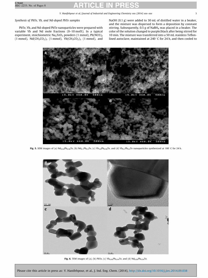
Fig. 5. SEM images of (a) Nd0.04Pb0.98Te, (b) Nd0.1Pb0.9Te, (c) Yb.04Pb0.98T
Fig. 6. TEM images of (a), (b) PbTe, (c) Y
Please cite this article in press as: Y. Hanifehpour, et al., J. Ind. Eng.
NaOH (0.1 g) were added to 30 mL of distilled water in a beaker,and the mixture was dispersed to form a deposition by constantstirring. Subsequently, 0.5 g of NaBH4 was placed in a beaker. Thecolor of the solution changed to purple/black after being stirred for10 min. The mixture was transferred into a 50 mL stainless Teflon-lined autoclave, maintained at 240 8C for 24 h, and then cooled to
e, and (d) Yb0.1Pb0.9Te nanoparticles synthesized at 180 8C for 24 h.
b0.06Pb0.94Te, and (d) Nd0.06Pb0.94Te.
Chem. (2014), http://dx.doi.org/10.1016/j.jiec.2014.09.038
Y. Hanifehpour et al. / Journal of Industrial and Engineering Chemistry xxx (2014) xxx–xxx4
G Model
JIEC-2233; No. of Pages 8
room temperature naturally. The final product was washed withdistilled water and absolute alcohol several times to removeresidual impurities, and then dried at 40 8C for 24 h. The final blackpowders were thus obtained.
1.1. Characterization instruments
The X-ray diffraction (XRD) diffraction patterns of the obtainedproducts were recorded on a diffractometer (D8 Advance, Bruker,Germany) with monochromatic high intensity Cu Ka radiation(l = 1.5406 A), an accelerating voltage of 40 kV, and an emissioncurrent of 30 mA. A scanning electron microscope (SEM) (S-4200,
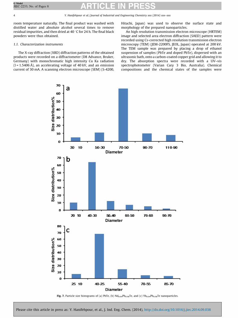
Fig. 7. Particle size histograms of (a) PbTe, (b) Nd0.0
Please cite this article in press as: Y. Hanifehpour, et al., J. Ind. Eng.
Hitachi, Japan) was used to observe the surface state andmorphology of the prepared nanoparticles.
An high resolution transmission electron microscope (HRTEM)image and selected area electron diffraction (SAED) pattern wererecorded using Cs-corrected high resolution transmission electronmicroscopy (TEM) (JEM-2200FS, JEOL, Japan) operated at 200 kV.The TEM sample was prepared by placing a drop of ethanolsuspension of samples (PbTe and doped PbTe), dispersed with anultrasonic bath, onto a carbon-coated copper grid and allowing it todry. The absorption spectra were recorded with a UV–visspectrophotometer (Varian Cary 3 Bio, Australia). Chemicalcompositions and the chemical states of the samples were
4Pb0.98Te, and (c) Yb0.04Pb0.98Te nanoparticles.
Chem. (2014), http://dx.doi.org/10.1016/j.jiec.2014.09.038
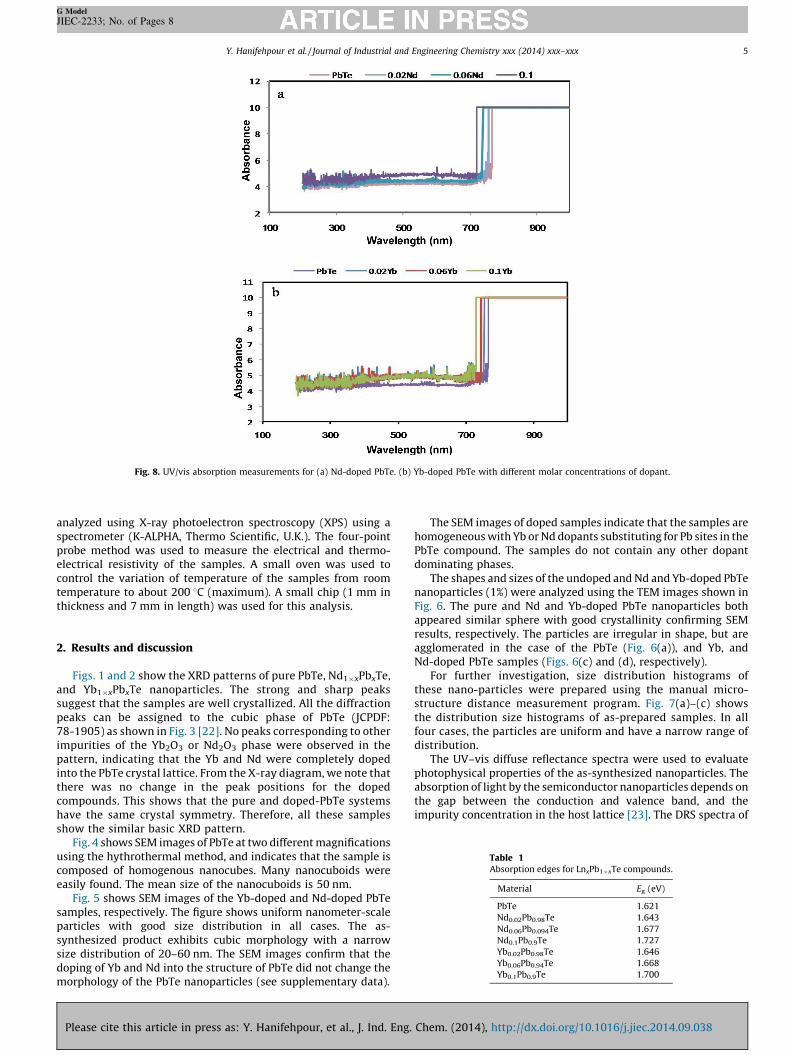
Fig. 8. UV/vis absorption measurements for (a) Nd-doped PbTe. (b) Yb-doped PbTe with different molar concentrations of dopant.
Table 1Absorption edges for LnxPb1�xTe compounds.
Material Eg (eV)
PbTe 1.621
Nd0.02Pb0.98Te 1.643
Nd0.06Pb0.094Te 1.677
Nd0.1Pb0.9Te 1.727
Yb0.02Pb0.98Te 1.646
Yb0.06Pb0.94Te 1.668
Yb0.1Pb0.9Te 1.700
Y. Hanifehpour et al. / Journal of Industrial and Engineering Chemistry xxx (2014) xxx–xxx 5
G Model
JIEC-2233; No. of Pages 8
analyzed using X-ray photoelectron spectroscopy (XPS) using aspectrometer (K-ALPHA, Thermo Scientific, U.K.). The four-pointprobe method was used to measure the electrical and thermo-electrical resistivity of the samples. A small oven was used tocontrol the variation of temperature of the samples from roomtemperature to about 200 8C (maximum). A small chip (1 mm inthickness and 7 mm in length) was used for this analysis.
2. Results and discussion
Figs. 1 and 2 show the XRD patterns of pure PbTe, Nd1�xPbxTe,and Yb1�xPbxTe nanoparticles. The strong and sharp peakssuggest that the samples are well crystallized. All the diffractionpeaks can be assigned to the cubic phase of PbTe (JCPDF:78-1905) as shown in Fig. 3 [22]. No peaks corresponding to otherimpurities of the Yb2O3 or Nd2O3 phase were observed in thepattern, indicating that the Yb and Nd were completely dopedinto the PbTe crystal lattice. From the X-ray diagram, we note thatthere was no change in the peak positions for the dopedcompounds. This shows that the pure and doped-PbTe systemshave the same crystal symmetry. Therefore, all these samplesshow the similar basic XRD pattern.
Fig. 4 shows SEM images of PbTe at two different magnificationsusing the hythrothermal method, and indicates that the sample iscomposed of homogenous nanocubes. Many nanocuboids wereeasily found. The mean size of the nanocuboids is 50 nm.
Fig. 5 shows SEM images of the Yb-doped and Nd-doped PbTesamples, respectively. The figure shows uniform nanometer-scaleparticles with good size distribution in all cases. The as-synthesized product exhibits cubic morphology with a narrowsize distribution of 20–60 nm. The SEM images confirm that thedoping of Yb and Nd into the structure of PbTe did not change themorphology of the PbTe nanoparticles (see supplementary data).
Please cite this article in press as: Y. Hanifehpour, et al., J. Ind. Eng.
The SEM images of doped samples indicate that the samples arehomogeneous with Yb or Nd dopants substituting for Pb sites in thePbTe compound. The samples do not contain any other dopantdominating phases.
The shapes and sizes of the undoped and Nd and Yb-doped PbTenanoparticles (1%) were analyzed using the TEM images shown inFig. 6. The pure and Nd and Yb-doped PbTe nanoparticles bothappeared similar sphere with good crystallinity confirming SEMresults, respectively. The particles are irregular in shape, but areagglomerated in the case of the PbTe (Fig. 6(a)), and Yb, andNd-doped PbTe samples (Figs. 6(c) and (d), respectively).
For further investigation, size distribution histograms ofthese nano-particles were prepared using the manual micro-structure distance measurement program. Fig. 7(a)–(c) showsthe distribution size histograms of as-prepared samples. In allfour cases, the particles are uniform and have a narrow range ofdistribution.
The UV–vis diffuse reflectance spectra were used to evaluatephotophysical properties of the as-synthesized nanoparticles. Theabsorption of light by the semiconductor nanoparticles depends onthe gap between the conduction and valence band, and theimpurity concentration in the host lattice [23]. The DRS spectra of
Chem. (2014), http://dx.doi.org/10.1016/j.jiec.2014.09.038
Y. Hanifehpour et al. / Journal of Industrial and Engineering Chemistry xxx (2014) xxx–xxx6
G Model
JIEC-2233; No. of Pages 8
pure PbTe, Nd-doped PbTe, and Yb-doped PbTe are illustrated inFig. 8(a) and (b).
The reflectance characteristics of the doped PbTe sample werequite similar to that of the undoped sample. We note that all
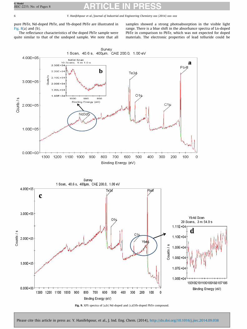
Fig. 9. XPS spectra of (a,b) Nd-doped a
Please cite this article in press as: Y. Hanifehpour, et al., J. Ind. Eng.
samples showed a strong photoabsorption in the visible lightrange. There is a blue shift in the absorbance spectra of Ln-dopedPbTe in comparison to PbTe, which was not expected for dopedmaterials. The electronic properties of lead telluride could be
nd (c,d)Yb-doped PbTe compound.
Chem. (2014), http://dx.doi.org/10.1016/j.jiec.2014.09.038
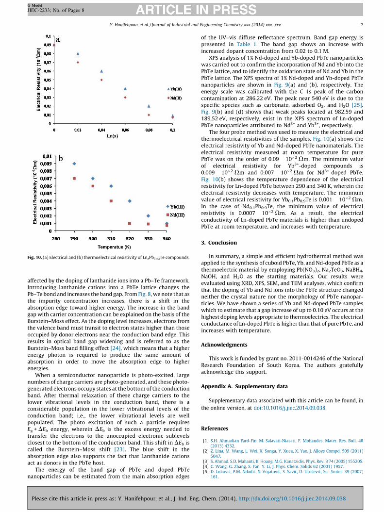
Fig. 10. (a) Electrical and (b) thermoelectrical resistivity of LnxPb1�xTe compounds.
Y. Hanifehpour et al. / Journal of Industrial and Engineering Chemistry xxx (2014) xxx–xxx 7
G Model
JIEC-2233; No. of Pages 8
affected by the doping of lanthanide ions into a Pb–Te framework.Introducing lanthanide cations into a PbTe lattice changes thePb–Te bond and increases the band gap. From Fig. 8, we note that asthe impurity concentration increases, there is a shift in theabsorption edge toward higher energy. The increase in the bandgap with carrier concentration can be explained on the basis of theBurstein–Moss effect. As the doping level increases, electrons fromthe valence band must transit to electron states higher than thoseoccupied by donor electrons near the conduction band edge. Thisresults in optical band gap widening and is referred to as theBurstein–Moss band filling effect [24], which means that a higherenergy photon is required to produce the same amount ofabsorption in order to move the absorption edge to higherenergies.
When a semiconductor nanoparticle is photo-excited, largenumbers of charge carriers are photo-generated, and these photo-generated electrons occupy states at the bottom of the conductionband. After thermal relaxation of these charge carriers to thelower vibrational levels in the conduction band, there is aconsiderable population in the lower vibrational levels of theconduction band; i.e., the lower vibrational levels are wellpopulated. The photo excitation of such a particle requiresEg + DEb energy, wherein DEb is the excess energy needed totransfer the electrons to the unoccupied electronic sublevelsclosest to the bottom of the conduction band. This shift in DEb iscalled the Burstein–Moss shift [23]. The blue shift in theabsorption edge also supports the fact that Lanthanide cationsact as donors in the PbTe host.
The energy of the band gap of PbTe and doped PbTenanoparticles can be estimated from the main absorption edges
Please cite this article in press as: Y. Hanifehpour, et al., J. Ind. Eng.
of the UV–vis diffuse reflectance spectrum. Band gap energy ispresented in Table 1. The band gap shows an increase withincreased dopant concentration from 0.02 to 0.1 M.
XPS analysis of 1% Nd-doped and Yb-doped PbTe nanoparticleswas carried out to confirm the incorporation of Nd and Yb into thePbTe lattice, and to identify the oxidation state of Nd and Yb in thePbTe lattice. The XPS spectra of 1% Nd-doped and Yb-doped PbTenanoparticles are shown in Fig. 9(a) and (b), respectively. Theenergy scale was calibrated with the C 1s peak of the carboncontamination at 286.22 eV. The peak near 540 eV is due to thespecific species such as carbonate, adsorbed O2, and H2O [25].Fig. 9(b) and (d) shows that weak peaks located at 982.59 and189.52 eV, respectively, exist in the XPS spectrum of Ln-dopedPbTe nanoparticles attributed to Nd3+ and Yb3+, respectively.
The four probe method was used to measure the electrical andthermoelectrical resistivities of the samples. Fig. 10(a) shows theelectrical resistivity of Yb and Nd-doped PbTe nanomaterials. Theelectrical resistivity measured at room temperature for purePbTe was on the order of 0.09 � 10�2 Vm. The minimum valueof electrical resistivity for Yb3+-doped compounds is0.009 � 10�2 Vm and 0.007 � 10�2 Vm for Nd3+-doped PbTe.Fig. 10(b) shows the temperature dependence of the electricalresistivity for Ln-doped PbTe between 290 and 340 K, wherein theelectrical resistivity decreases with temperature. The minimumvalue of electrical resistivity for Yb0.1Pb0.9Te is 0.001 � 10�2 Vm.In the case of Nd0.1Pb0.9Te, the minimum value of electricalresistivity is 0.0007 � 10�2 Vm. As a result, the electricalconductivity of Ln-doped PbTe materials is higher than undopedPbTe at room temperature, and increases with temperature.
3. Conclusion
In summary, a simple and efficient hydrothermal method wasapplied to the synthesis of cuboid PbTe, Yb, and Nd-doped PbTe as athermoelectric material by employing Pb(NO3)2, Na2TeO3, NaBH4,NaOH, and H2O as the starting materials. Our results wereevaluated using XRD, XPS, SEM, and TEM analyses, which confirmthat the doping of Yb and Nd ions into the PbTe structure changedneither the crystal nature nor the morphology of PbTe nanopar-ticles. We have shown a series of Yb and Nd-doped PbTe sampleswhich to estimate that a gap increase of up to 0.10 eV occurs at thehighest doping levels appropriate to thermoelectrics. The electricalconductance of Ln-doped PbTe is higher than that of pure PbTe, andincreases with temperature.
Acknowledgments
This work is funded by grant no. 2011-0014246 of the NationalResearch Foundation of South Korea. The authors gratefullyacknowledge this support.
Appendix A. Supplementary data
Supplementary data associated with this article can be found, in
the online version, at doi:10.1016/j.jiec.2014.09.038.
References
[1] S.H. Ahmadian Fard-Fin, M. Salavati-Niasari, F. Mohandes, Mater. Res. Bull. 48(2013) 4332.
[2] Z. Lina, M. Wang, L. Wei, X. Songa, Y. Xuea, X. Yao, J. Alloys Compd. 509 (2011)5047.
[3] S. Ahmad, S.D. Mahanti, K. Hoang, M.G. Kanatzidis, Phys. Rev. B 74 (2005) 155205.[4] C. Wang, G. Zhang, S. Fan, Y. Li, J. Phys. Chem. Solids 62 (2001) 1957.[5] D. Lukovic, P.M. Nikolic, S. Vujatovic, S. Savic, D. Urosevic, Sci. Sinter. 39 (2007)
161.
Chem. (2014), http://dx.doi.org/10.1016/j.jiec.2014.09.038

Y. Hanifehpour et al. / Journal of Industrial and Engineering Chemistry xxx (2014) xxx–xxx8
G Model
JIEC-2233; No. of Pages 8
[6] Y. Pan, H. Bai, L. Pan, M.C. Tamargo, M. Sohel, J.R. Lombardi, J.Mater.Chem., 22(2012) 23593–23601.
[7] Z. Zong, H. Wang, L. Kong, Nanoscale Res. Lett. 8 (2013) 191.[8] M.V. Nikolic, K.M. Paraskevopoulos, T. Ivetic, T.T. Zorba, S.S. Vujatovic, E. Pavlidou,
et al. J. Mater. Sci. 45 (2010) 5910.[9] L. Xu, Y. Zheng, J.C. Zheng, Phys. Rev. B 82 (2010) 195102.
[10] A.I. Artamkin, A.E. Kozhanov, M. Arciszewska, W.D. Dobrowolski, T. Story, E.I.Slynko, et al. Acta Phys. Pol. A 106 (2004) 223.
[11] G.J. Snyder, E.S. Toberer, J. Nat. Mater. 7 (2008) 105.[12] Y. Hanifehpour, S.W. Joo, B.K. Min, Nanoscale Res. Lett. 8 (2013) 141.[13] A. Alemi, A. Klein, G. Meyer, M. Dolatyari, A. Babalou, Z. Anorg. Allg. Chem. 637
(2011) 87.[14] A. Alemi, Y. Hanifehpour, S.W. Joo, B. Min, A. Colloids Surfaces, Physicochem. Eng.
Asp. 390 (2011) 142.[15] A. Alemi, Y. Hanifehpour, S.W. Joo, A. Khandar, A. Morsali, B. Min, Physica B 407
(2012) 38.
Please cite this article in press as: Y. Hanifehpour, et al., J. Ind. Eng.
[16] A. Khataee, A. Khataee, M. Fathinia, Y. Hanifehpour, S.W. Joo, Ind. Eng. Chem. Res.52 (2013) 13357.
[17] A. Khataee, S. Fathinia, M. Fathinia, Y. Hanifehpour, S.W. Joo, B. Soltani,Curr. Nanosci. 9 (2013) 780.
[18] A. Khataee, Y. Hanifehpour, M. Safarpour, M. Hosseini, Sci. Adv. Mater. 5 (2013) 1.[19] N. Haldolaarachchige, A.B. Karki1, W. Adam Phelan, Y.M. Xiong, R. Jin, J.Y. Chan,
et al. J. Appl. Phys. 109 (2011) 103712.[20] G.A. Akhmedova, D.Sh. Abdinov, J. Inorg. Mater. 45 (2009) 854.[21] Z. Dashevsky, S. Shusterman, M.P. Dariel, I.J. Drabkin, Appl. Phys. 92 (2002) 1424.[22] Z.K. Zlatanov, Mater. Chem. Phys. 103 (2007) 470.[23] K. Nouneh, K.J. Plucinski, M. Bakasse, I.V. Kity, J. Mater. Sci. 42 (2007) 6847.[24] G. Sharma, P. Chawla, S.P. Lochab, N. Singh, Bull. Mater. Sci. 34 (2011) 673.[25] D.T. Kim, K.S. Yu, W.T. Kim, C.D. Kim, H.L. Park, J. Mater. Sci. Lett. 11 (1992)
886.
Chem. (2014), http://dx.doi.org/10.1016/j.jiec.2014.09.038
Copyright © 2022 FDOKUMEN