Nanoarchitecture and Global warming New Revolution for Nanomaterials
Upload
khangminh22Category
view
1download
0
1Scientific RepoRts | 7: 13057 | DOI:10.1038/s41598-017-12741-5
www.nature.com/scientificreports
Fast identification of the conduction-type of nanomaterials by field emission techniqueXun Yang, Haibo Gan, Yan Tian, Luxi Peng, Ningsheng Xu, Jun Chen, Huanjun Chen , Shaozhi Deng, Shi-Dong Liang & Fei Liu
There are more or less dopants or defects existing in nanomaterials, so they usually have different conduct-types even for the same substrate. Therefore, fast identification of the conduction-type of nanomaterials is very essential for their practical application in functional nanodevices. Here we use the field emission (FE) technique to research nanomaterials and establish a generalized Schottky-Nordheim (SN) model, in which an important parameter λ (the image potential factor) is first introduced to describe the effective image potential. By regarding λ as the criterion, their energy-band structure can be identified: (a) λ = 1: metal; (b) 0.5 < λ < 1: n-type semiconductor; (c) 0 < λ < 0.5: p-type semiconductor. Moreover, this method can be utilized to qualitatively evaluate the doping-degree for a given semiconductor. We test numerically and experimentally a group of nanomaterial emitters and all results agree with our theoretical results very well, which suggests that our method based on FE measurements should be an ideal and powerful tool to fast ascertain the conduction-type of nanomaterials.
With the rapid development of IT industry, more and more device integration is intensively demanded, which inversely drives the scientists and researchers all over the world to explore new approaches to break through the size limit of traditional semiconductor devices. Under this circumstance, nanodevices have been believed as the necessary choices for meeting their increase requirements. Quasi one-dimensional nanomaterials (nanowires, nanorods, etc.) are the ideal building blocks for fabrication of nanodevices because of their dis-tinctive and excellent properties, such as Si nanowires1–4 and ZnO nanowires5–7. Up to date, various prepara-tion methods8–13 have been developed to synthesize different nanomaterials, but there inevitably exist some impurity dopants or defects in their formation process. As a result, nanomaterials by different preparation ways usually exhibit diverse conduction-type in comparison with their perfect single crystal counterparts. Therefore, accurately differentiating the conduction-type of nanomaterials is of great significance for nanode-vices because their conduction-type directly determines their application area (photovoltaic, memory, switch-ing or electron-source devices).
As known to all, there are two commonly-used methods for identification of the conduction type of bulk or thin film materials, which are respectively the hot and cold probe method and Hall effect method14. The former utilizes the thermoelectric effect of bulk materials while the working mechanism of the latter is based on the cal-culation of the steady electric potential difference between the top and down surface of the sample resulting from the carrier charges under electromagnetic field. But for nanomaterials, integrating them into field effect transistor (FET) and measuring their working behaviors is the only known method to identify their conduction-type to our knowledge 15,16. Although this method has a nice measurement accuracy, the fabrication process of FET nanode-vices is quite complicated and the yield of nanodevices with nice working performances is usually rather low. So finding an easy and accurate method to differentiate the conduction-type of nanomaterials becomes a challenging issue for all the researchers.
In this paper, we will apply the simple FE techniques to identify the conduction-type of quasi one-dimensional nanomaterials. Based on the FE experiments, we further establish a generalized Schottky-Nordheim (SN) field
State Key Laboratory of Optoelectronic Materials and Technologies, Guangdong Province Key Laboratory of Display Material and Technology, School of Electronics and Information Technology, Sun Yat-sen University, Guangzhou, 510275, P. R. China. Xun Yang and Haibo Gan contributed equally to this work. Correspondence and requests for materials should be addressed to S.D. (email: [email protected]) or S.-D.L. (email: [email protected]) or F.L. (email: [email protected])
Received: 10 August 2017
Accepted: 18 September 2017
Published: xx xx xxxx
OPEN

www.nature.com/scientificreports/
2Scientific RepoRts | 7: 13057 | DOI:10.1038/s41598-017-12741-5
emission model, in which an important factor will be first introduced to describe the effective image potential in Sec. II. Also, we will present a programmed scheme to fit the J-E curves and the slope of FN plots by introducing several parameters, by which the connection between the important factor and the energy-band structure of nanomaterials can be obtained in Sec. III. The numerical and experimental testing will be presented in Sec. IV. Finally, we give some detailed discussions and conclusions.
Generalized Schottky-Nordheim modelThe current-voltage (I-V) curve plays a crucial role in understanding the basic physics of field electron emission. The first theoretical field emission (FE) model was proposed by Fowler-Nordheim (FN) based on Sommerfeld model with some approximations, which was widely used in analyzing the FE behaviors of metallic emitters. Subsequently, it was further modified by Schottky-Nordheim (SN), in which the image potential is taken into account according to electrodynamics17. It is known that both of FN and SN models are assumed that the emitters are metallic. However, recently many new-type nanomaterials are applied in FE process. The schematic diagram of quasi one-dimensional nanomaterials during FE measurements is provided in Fig. 1(a). In FE process, the electrons emit from the cathode sample surface at negatively biased. The emergence of image potential at boundary will lower the surface barrier height, which results that the electron emission is easy to occur at applied field, as seen in Fig. 1(b). Commonly, the energy-band struc-tures of nanomaterials are quite different from those of metals. As a result, the image potential effects will differ with the energy-band structures of nanomaterials because their electric conductivity is various in the band diagram.
In order to analyze the FE behaviors from nanomaterials, we first introduce a parameter λ (0 < λ < 1) to generalize the SN model, in which λ is defined as the image potential factor. So the current density JGSN can be rewritten as
Figure 1. (a) The schematic diagram of field emission measurement. (b) The generalized Schottky-Nordheim (SN) model.

www.nature.com/scientificreports/
3Scientific RepoRts | 7: 13057 | DOI:10.1038/s41598-017-12741-5
τΦ
ν Φ Θ
λΦ
λΦ
λΦ Φ
λΦ
λΦ
λΦ
Φ
λ λ λ π
λ λ λ π
=
−
= + −
×
−
− +
×+ −
+ −
Φ Φ Φ
Φ Φ Φ
−
−
( )( )( )
J a F exp bF
T
a cF cF ln cF F exp
cF cF ln cF bF
ln k T d
ln k T d
( )
1 19
118
1 16
1 /
sin 1 / (1)
GSN F F GSN
cF cF cFB F
cF cF cFB F
22 3/2
2 2 2
2 2
2 2 2
3/2
19
118
19
118
2 2 2
2 2 2
where “a” is the parameter related to the emission area, b = 6.83(eV)−3/2(V)(nm) is the field emission constant, Φ is the surface work function of emitters, T is the nanostructured emitter’s temperature and F is the effective electric field fallen between the cathode and the anode. F can be obtained by the expression of F = βE, in which E is the applied electric field and β is the field enhancement factor. Also, νF and τF are two correction factors that come from the image potential effects:
ν λΦ
λΦ
λΦ
= − +
cF cF cF1 16
ln(2a)F 2 2 2
τ λΦ
λΦ
λΦ
= + −
cF cF cF1 19
118
ln(2b)F 2 2 2
where =πε
c e4
3
0. In addition, ΘGSN(T) describes the finite temperature effect, which can be expressed as:
Θτ π
τ π=T k T d
k T d( ) /
sin( / ) (3)GSNF B F
F B F
where kB is the Boltzmann constant, = Φ−( )d gF e eF
11/2 and =g 2e
m
h
2 e2
are also the constants.
It should be remarked in the generalized SN model that λ is introduced to describe different effective image potential effect from various nanomaterials. When λ=0, the model is simplified as the classical FN model. And the model becomes the idealized SN model when λ=1. Figure 1(a) shows the schematic diagram of quasi one-dimensional nanomaterials during FE measurements. The interface barrier between cathode nanomaterials and vacuum at negatively biased is given in Fig. 1(b) according to the generalized SN model. As found in Fig. 1(b), the image potential factor λ is 1 for metallic nanomaterials, which is easy to understand because the ideal SN model just aims at metal. So the mirror charges should be equal to the surface charges for metallic nanomateri-als, which corresponds to the case of λ=1. If nanomaterials belong to semiconductors, the mirror charges will vary with their dielectric constant or electric conductivity, unequal to the surface charges. In this situation, λ ranges from 0 to 1, which should qualitatively reflect the change of the effective mirror charges for different quasi one-dimensional nanomaterials.
In general, it can be believed that the metallic emitters contribute a perfect image potential effect in FE pro-cess, namely λ=1, corresponding that the mirror charges should be equal to the surface charges. For semiconduc-tor emitters, the major carriers of the n-type semiconductors are electrons in the bottom of the conduction-band while the major carriers of the p-type semiconductors are holes in the top of the valence-band by doping. In this situation, the mirror charges will vary with their dielectric constant or electric conductivity, unequal to the sur-face charges. So λ ranges from 0 to 1, which should qualitatively reflect the change of the effective mirror charges for different quasi one-dimensional nanomaterials. In addition, the electrons in the n-type semiconductors emit from the bottom of the conduction band, which should induce the image potential effect a little less than that of metals. In contrast with n-type semiconductors, the contribution of the holes to the image potential in the p-type semiconductors is far less than that of the n-type of semiconductors because the valence-band electrons have to go across the energy-band before they become the free electrons involving in the transportation. Thus, the values of λ also reveal the characteristic of the energy-band structures of nanostructured emitters and reflect the magnitude of the image potential at interface between vacuum and nanomaterials’ surface. Therefore, if we can find out the relationship between the values of λ and the I-V curves of field emission, the conduction-types of nanostructured emitters from field emission can be indeed identified.
On the other hand, the slope of the FN plots has been used to analyze the behaviors of the I-V curves for FN and SN models in our earlier work18. Based on Eqs (1)–(3), the slope (SGSN) of the FN plots in the generalized SN model can be worked out:

www.nature.com/scientificreports/
4Scientific RepoRts | 7: 13057 | DOI:10.1038/s41598-017-12741-5
ΦΦ
Φλ
Φλ
Φηλ λ
Φη λ
Φη
=∂
∂= − +
−
+ +
− − −
−SF
JF
b b c F c F
c F F c F GG
c F
ln3
112
ln
29
118 tan
118 (4)
GSNGSN
FNFN
1 23/2
3/2
2 2
22
2 2
where = τ πG k Td
F B
F and η =
τ
− λ
Φ( )In1 c F
F
2 . It is found in Eq. (4) that the slopes of FN plots are quite different and depend on the effective electric field and temperature in our generalized SN model. These different behaviors of the slopes of FN plots also provide us another guideline to identify the conduction-type of nanostructured emit-ters according to the hints of the slope behaviors of the FN plots. Compared with the classical FN or SN models, the slope of the FN plots for the generalized SN model is dependent on the image potential factor λ, which prom-ises us a way to understand the material properties of the nanostructured emitters.
We established the connection between λ and the J-E curves of field emission by combination of the general-ized SN model and the slope of FN plots techniques. The basic idea of this scheme is that we use the experimental J-E curves from different nanomaterial emitters to fit the formula in Eq. (1) to obtain the λ values and subse-quently calculate the slopes of the FN plots to ascertain the connection between λ and the conduction-types of emitter materials.
For given nanostructured emitters, their work function can be easily measured by UPS or KPFM techniques. So in the fitting process of the J-E curves, only four parameters need to be considered according to Eq. (1), which are respectively a, β, T and λ. In fact, we constrain the a and β within a practical and reasonable region to turn out λ, and then we investigate the slope of FN plots by these parameters and the J-E curves. Different λ values and slopes of FN plots can reveal different nanomaterials’ properties.
The nonlinear fitting method with the Levenberg Marquardt iteration algorithm is utilized in the data-fitting of the J-E curves19, which is a standard approach used to solve the nonlinear least squares problems implemented by OriginPro 2016 software (version: Sr2 b9.3.2.303).
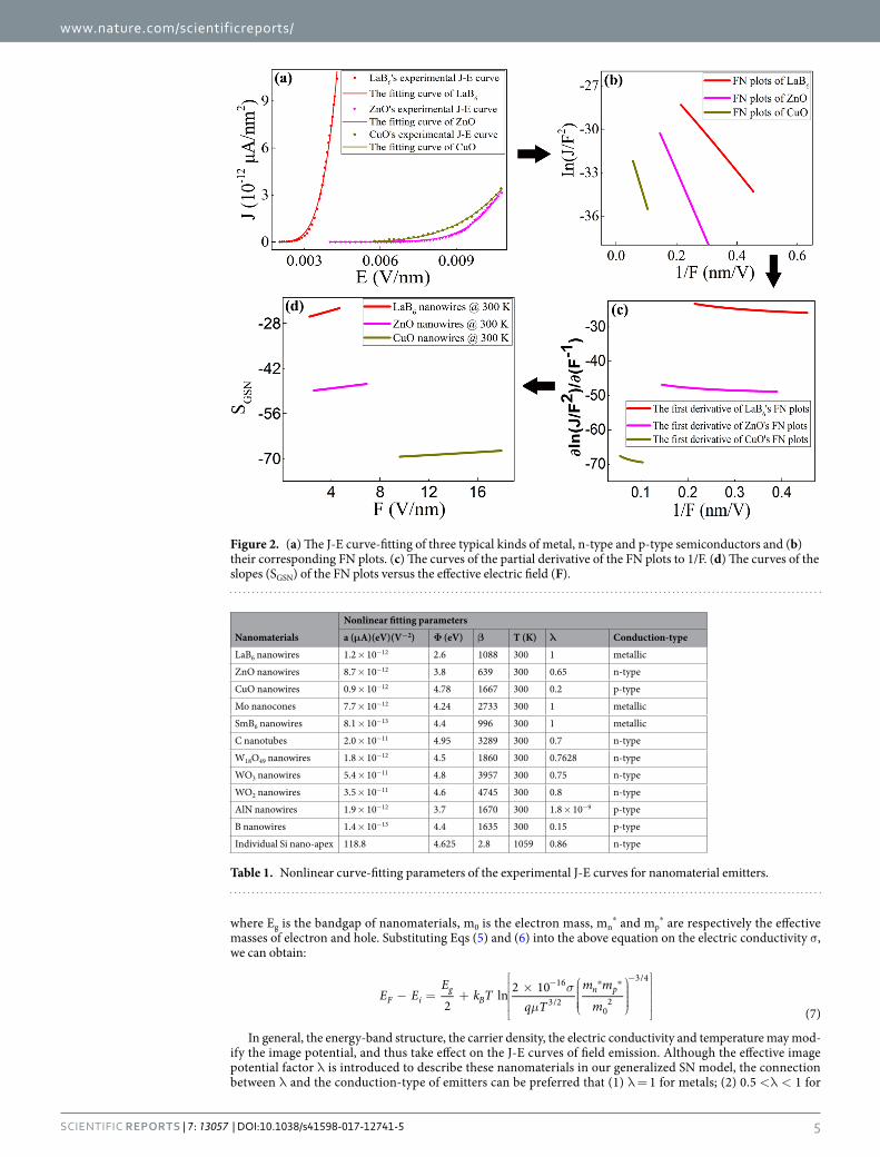
Connection between λ and I-V curvesBased on our generalized SN model, we fit the experimental J-E curve data from three typical kinds of emitter materials, which are respectively metal (LaB6), n-type (ZnO) and p-type (CuO) semiconductors. They are all nanowire materials, whose conduction properties actually have been confirmed by the traditional FET technique. The experimental curves of FE current density of these three types of nanomaterials versus the applied electric field are shown in Fig. 2(a), in which the matching degree of these three fitting curves to the generalized SN equation (Eq. (1)) is over 0.99. Table 1 lists the curve-fitting parameters to further compare their image potential in FE process.
Figure 2(b) shows the corresponding FN plots. As observed in Fig. 2(b), the FN plots of these three typical nanowires all exhibit a little deviation from linearity, which suggest that they may obey the generalized SN model. And the curves of the partial derivative of the FN plots to 1/F are shown in Fig. 2(c), in which one can see that these three nanomaterials have different variation tendency. It should attribute to their different effective image potential. It is found in Fig. 2(d) that the curves of the FN plots’ slope (SGSN) versus the effective electric field (F) have a different variance tendency for various nanomaterials with different conduction-type. In addition, the slope (SGSN) of the FN plots is found to increase linearly with the effective electric field (F) for these three typical nanowires. As seen in Table 1, the image potential factor (λ) is 1 for metallic LaB6 nanowires and 0.65 for n-type ZnO nanowires, which is far larger than p-type CuO nanowires (λ = 0.2). It suggests that the image potential factor (λ) may be regarded as the key criterion for identifying the conduction-type of nanomaterials.
To better comprehend the physical nature of the image potential factor (λ), the energy-band diagram of the nanostructured emitters is shown in Fig. 3. The doping concentration or the relative Fermi level position (EF-Ei) of nanomaterials may be mainly responsible for the magnitude of the image potential factor (λ), in which EF and Ei respectively refer to the actual Fermi level and intrinsic Fermi level. As depicted in the above illustrations, λ depends on the surface charges having an intense relationship with the electric conductivity, and thus it should be determined by the major carrier density (n or p) or (EF-Ei).
Based on the semiconductor physics, the electric conductivity (σ) of nanomaterials can be worked out by the equation of σ = nqμ or σ = pqμ20. In these expressions, μ is the mobility of major carriers in semiconductors and q stands for elementary charge. According to the classical band theory, EF is just above Ei for n-type semiconduc-tors whereas EF is lower than Ei for p-type semiconductors, as seen in Fig. 3. The major carrier density (n or p) can be deduced by the Fermi distribution law:
=
−
n n exp (5)i
E Ek TF i
B
where kB is the Boltzmann’s constant, T is the temperature and ni is the intrinsic carrier density. Based on the semiconductor physics, ni can be expressed as:
= . ×
−
⁎ ⁎
nm m
mT exp4 82 10
(6)i
n pEk T15
02
3/43/2 2
g
B
www.nature.com/scientificreports/
5Scientific RepoRts | 7: 13057 | DOI:10.1038/s41598-017-12741-5
where Eg is the bandgap of nanomaterials, m0 is the electron mass, mn* and mp
* are respectively the effective masses of electron and hole. Substituting Eqs (5) and (6) into the above equation on the electric conductivity σ, we can obtain:
σµ
− = +
×
− −⁎ ⁎
E EE
k Tq T
m m
m2ln 2 10
(7)F i
gB
n p16
3/20
2
3/4
In general, the energy-band structure, the carrier density, the electric conductivity and temperature may mod-ify the image potential, and thus take effect on the J-E curves of field emission. Although the effective image potential factor λ is introduced to describe these nanomaterials in our generalized SN model, the connection between λ and the conduction-type of emitters can be preferred that (1) λ = 1 for metals; (2) 0.5 <λ < 1 for
Figure 2. (a) The J-E curve-fitting of three typical kinds of metal, n-type and p-type semiconductors and (b) their corresponding FN plots. (c) The curves of the partial derivative of the FN plots to 1/F. (d) The curves of the slopes (SGSN) of the FN plots versus the effective electric field (F).
Nanomaterials
Nonlinear fitting parameters
a (μA)(eV)(V−2) Φ (eV) β T (K) λ Conduction-type
LaB6 nanowires 1.2 × 10⁻¹² 2.6 1088 300 1 metallic
ZnO nanowires 8.7 × 10⁻¹² 3.8 639 300 0.65 n-type
CuO nanowires 0.9 × 10⁻¹² 4.78 1667 300 0.2 p-type
Mo nanocones 7.7 × 10⁻¹² 4.24 2733 300 1 metallic
SmB6 nanowires 8.1 × 10⁻¹³ 4.4 996 300 1 metallic
C nanotubes 2.0 × 10⁻¹¹ 4.95 3289 300 0.7 n-type
W18O49 nanowires 1.8 × 10⁻¹² 4.5 1860 300 0.7628 n-type
WO3 nanowires 5.4 × 10⁻¹¹ 4.8 3957 300 0.75 n-type
WO2 nanowires 3.5 × 10⁻¹¹ 4.6 4745 300 0.8 n-type
AlN nanowires 1.9 × 10⁻¹² 3.7 1670 300 1.8 × 10⁻⁹ p-type
B nanowires 1.4 × 10⁻¹³ 4.4 1635 300 0.15 p-type
Individual Si nano-apex 118.8 4.625 2.8 1059 0.86 n-type
Table 1. Nonlinear curve-fitting parameters of the experimental J-E curves for nanomaterial emitters.

www.nature.com/scientificreports/
6Scientific RepoRts | 7: 13057 | DOI:10.1038/s41598-017-12741-5
n-type semiconductors; (3) 0 < λ < 0.5 for p-type semiconductors. Therefore, the relationship between the J-E curves and the conduction-type of emitter in FE process can be easily revealed by this simple way instead of fab-ricating complicated FET nanodevices. Moreover, this connection should have another application, which is to comprehend the FE mechanism and analyze the doping degree of the nanomaterials when we know what material the emitters belong to.
Based on the above-mentioned analysis, our identification method of the conduction-type of nanomaterials can be summarized into three standard steps:
(1) Fitting the J-E data based on the generalized SN model presented in the above section; (2) Calculating the slope of FN plots based on the parameters obtained by the fitting data in the first step; (3) Obtaining the λ values and drawing the curve of the slope (SGSN) of FN plots to λ for different quasi one-di-
mensional nanomaterials.
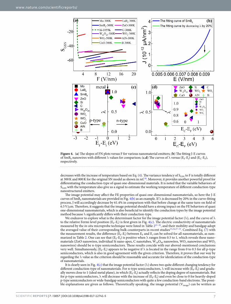
Furthermore, we investigate a group of samples to testify the as-obtained λ criterion based on this method. The samples include Mo nanocones, SmB6 nanowires, individual Si nano-apex, C nanotubes, W18O49 nanowires, WO3 nanowires, WO2 nanowires, AlN nanowires and B nanowires. All of them are prepared by our group, and their fabrication techniques can be found in the Supporting information. The nonlinear curve-fitting and calcu-lation process of these experimental J-E data is just the same as the aforementioned three quasi one-dimensional nanomaterials (LaB6 nanowires, ZnO nanowires and CuO nanowires), as found in Figs S1 and S2 in Supporting Information. Before the measurements, the conduction-type of these nine kinds of nanomaterials remain unknown to us. The SGSN-F curves of these nine quasi one-dimensional nanomaterials are shown in Fig. S2(c). As observed in Fig. 4(a), the slopes (SGSN) of FN plots versus the electric field (F) are found to be different for these nanomaterials. Based on the generalized SN model, the parameters can be solved, as summarized in Table 1. According to the criterion of the aforementioned image potential factor (λ), it can be concluded that Mo nanocones and SmB6 nanowires are metallic because the λ values are equal to 1; Individual Si nano-apex, C nanotubes, W18O49 nanowires, WO3 nanowires and WO2 nanowires can be ascertained to be n-type semicon-ductors in that their λ value ranges from 0.5 to 1; Likewise, AlN nanowires and B nanowires should belong to p-type semiconductors since their λ values locate at the range from 0 to 0.5. The conduction-type of these nine quasi one-dimensional nanomaterials differentiated by the image potential method is in good consistent with those by traditional FET method, which proves that our method is accurate and suitable for determination of the conduction-type of quasi one-dimensional nanomaterials.
It is also found that there are three kinds of behaviors of the slopes (SGSN) of FN plots with F. One is seen to remain almost unchanged for AlN, B and CuO nanowires; The second is observed to increase linearly with F for Mo nanocones, SmB6 nanowires, C nanotubes, W18O49 nanowires, WO3 nanowires and WO2 nanowires. The third exhibits a very sharp negative slope with F for individual Si nano-apex. It should be noted that all the temperatures of nanomaterials during FE process are 300 K except individual Si nano-apex (T = 1059 K), which can be illustrated as follows. The FE properties of nanowire films can be believed to be room-temperature measurements by transparent anode way because the nanowires contact well with the substrate and can rapidly conduct the heat to the external circumstance, in which the Joule heat at nanowire films can be neglected. But for the individual Si nano-apex prepared by EBL technique, a native oxide layer usually formed on the surface of Si substrate, which inevitably leads to a large interface resistance between individual Si nano-apex and Si substrate. This high interface resistance produces Joule heat in FE process without a nice channel to timely dissipate the heat to external circumstance during in-situ microprobe measurements. Under this circumstance, it results that the temperature of an individual Si nano-apex reaches over 1000 K, which coincides with our experimental observa-tions very well21. Therefore, it is reasonable that the fitting temperature T is adopted to 1059 K for individual Si nano-apex. Moreover, it can be identified that Si nano-apex belongs to the n-type semiconductor because SGSN
Figure 3. The energy-band diagram of metal, n-type and p-type semiconductors, in which the work function (Φ), electron affinity (χ), bandgap (Eg) and the positions of the Fermi levels are respectively figured out.
www.nature.com/scientificreports/
7Scientific RepoRts | 7: 13057 | DOI:10.1038/s41598-017-12741-5
decreases with the increase of temperature based on Eq. (4). The variance tendency of SGSN to F is totally different at 300 K and 800 K for the original SN model as shown in ref.18. Moreover, it provides another powerful proof for differentiating the conduction-type of quasi one-dimensional materials. It is noted that the variable behaviors of SGSN with the temperature also give us a signal to estimate the working temperature of different conduction-type nanostructured emitters.
The image potential may affect the FE properties of quasi one-dimensional nanomaterials, so here the J-E curves of SmB6 nanomaterials are provided in Fig. 4(b) as an example. If λ is decreased by 20% in the curve-fitting process, J will accordingly decrease by 61.4% in comparison with that before change at the same turn-on field of 6.5 V/μm. Therefore, it suggests that the image potential should have a strong impact on the FE behaviors of quasi one-dimensional nanomaterials, which is also beneficial to identify the conduction types by the image potential method because λ significantly differs with their conduction-type.
We endeavor to explore what is the determinant factor for the image potential factor (λ), and the curve of λ to the relative Fermi level position (EF-Ei) is first given in Fig. 4(c). The electric conductivity of nanomaterials measured by the in-situ microprobe technique were listed in Table 221–26, and their mobility and bandgap adopt the averaged value of their corresponding bulk counterparts in recent studies15,24,27–33. Combined Eq. (7) with the measurement results, the difference (EF-Ei) between EF and Ei can be solved for all nanomaterials, as sum-marized in Table 2. One can see that (EF-Ei) is positive when λ ranges from 0.5 to 1, which reveals these nano-materials (ZnO nanowires, individual Si nano-apex, C nanotubes, W18O49 nanowires, WO3 nanowires and WO2 nanowires) should be n-type semiconductors. These results concide with our aboved-mentioned conclusions very well. Simultaneously, (EF-Ei) appears to be negative if λ is located in the range from 0 to 0.5 for all p-type semiconductors, which is also in good agreement with the given criterion. Therefore, it proves that our way by regarding the λ value as the criterion should be reasonable and accurate for idenficiation of the conduction-type of nanomaterials.
It is clearly seen in Fig. 4(c) that the image potential factor (λ) shows two quite different changing tendency for different conduction-type of nanomaterials. For n-type semiconductors, λ will increase with (EF-Ei) and gradu-ally moves close to 1 (ideal metal plane), in which (EF-Ei) actually reflects the doping degree of nanomaterials. But for p-type semiconductors, λ will decrease with the increase of (EF-Ei) and even be close to 0 for heavily-doped p-type semiconductors or wide-bandgap semiconductors with quite a few conduction-band electrons. The possi-ble explanations are given as follows. Theoretically speaking, the image potential (Vimage) can be written as
Figure 4. (a) The slopes of FN plots versus F for various nanomaterial emitters; (b) The fitting J-E curves of SmB6 nanowires with different λ values for comparison; (c,d) The curves of λ versus (EF-Ei) and (EC-EF), respectively.

www.nature.com/scientificreports/
8Scientific RepoRts | 7: 13057 | DOI:10.1038/s41598-017-12741-5
= −πε
Vimagee
x16
2
0, in which “e” represents the mirror charges at vacuum side and x stands for the distance between
surface charges and cathode surface. As a result, the magnitude of the image potential (Vimage) depends on the mirror charges at vacuum side. As explained in aforementioned descriptions, the intrinsic nature of λ directly reflects the image potential (Vimage) at interface as well as reveals the contribution of the effective image charges to Vimage, which has an intense relationship with the conduction-type of nanomaterials. So it can be understood that Vimage should be determined by (EF-Ei) or (EC-EF) as found in Fig. 4, which also conforms to Eqs (5)–(7). In this situation, the λ values increase with the increase of (EF-Ei) for the same n-type semiconductors and close to 1 for ideal metal, which implies the behaviors of n-type semiconductors become more and more closer to those of metal with the increase of λ. Unlike n-type semiconductors, the hole density of valence-band turns larger with the increase of (EF-Ei) for p-type semiconductors. Accordingly, the conduction-band electron density decreases with the increase of (EF-Ei), which suggests that p-type semiconductors gradually deviate far way from ideal metal. Consequently, λ turns smaller and smaller with the increase of (EF-Ei) and is even close to zero (tiny conduction-band electrons) for p-type semiconductors, which suggests that the doping degree of p-type semicon-ductors increases with the decrease of λ. So it is reasonable that there exists different variance tendency of λ for n-type and p-type semiconductors with (EF-Ei). Most of all, qualitatively identification of the doping degree becomes possible by comparing their λ values for the same semiconductor nanomaterials.
The relationship between λ and the difference (EC-EF) between EC and EF is also discussed in Fig. 4(d). One can see in Fig. 4(d) that λ will increase with the decrease of (EC-EF) for all semiconductor nanomaterials. The possible explanations are given as follows. Theoretically speaking, the conduction-band electron concentration (n) of semiconductor can be written as = − −( )n N expC
EC EFKT , in which NC represents the effective density of states
(DOS) of the conduction-band. Therefore, the conduction-band electron density (n) will turn larger with the decrease of (EC-EF) based on the aforementioned equation for conduction-band electron density. Under this cir-cumstance, the image potential Vimage will accordingly increase with (EC-EF), which leads to the increase of λ value. So it is well understood that λ should exhibit the identical variance tendency whether for n- or p-type quasi one-dimensional nanomaterials. It comes to a conclusion that the conduction-band electron density (n) of quasi one-dimensional nanomaterials should be the determinant factor for λ in comparison with other parameters because it overall considers the contribution of the bandgap (Eg) and the doping degree of the semiconductor. This method may be expanded to the identification of the conduction-type or the doping degree of other two-dimensional nanostructures or bulk materials, and the relevant researches are still undergoing.
ConclusionsIn summary, we have developed a simple FE technique to fast identify the conduction types of nanomaterials. Furthermore, we established the generalized Schottky-Nordheim (SN) model and introduce the image potential factor (λ) to describe the effective image potential in FE process. By our method, the relationship between λ and the energy-band structure of the nanomaterial emitters can be obtained: (a) λ = 1: metal; (b) 0.5 < λ < 1: n-type semiconductor; (c) 0 < λ < 0.5: p-type semiconductor. This criterion provides us a simple and effective way to identify the conduction types of the nanomaterial emitters and understand the physical mechanism of field emis-sion. We test a group of nanomaterial emitters, and all results agree with both our theoretical predictions and other measurement results by FET technique. In contrast with the conventional hot and cold probe or Hall effect methods, our method is not only more convenient and effective but also can qualitatively determine the doping degree for the same semiconductor nanomaterials. Therefore, our method based on the FE technique should be a powerful tool to identify the conduction-type of nanomaterials and may shed new light on other two- or three-dimensional materials.
ExperimentalSynthesis methods of twelve kinds of quasi one-dimensional nanomaterials. In our work, twelve kinds of quasi one-dimensional nanomaterials (Mo, LaB6, SmB6, ZnO, Si, C, W18O49, WO3, WO2, CuO, AlN and
Nanomaterials
Physical parameters
Bandgap (eV) Conductivity (Ω−1cm−1) Mobility (cm2V−1s−1) EF–Ei (eV) EC-EF (eV) λ Conduction-type
LaB6 nanowires 0 1.43 × 10⁴ 32 0 — 1 metallic
ZnO nanowires 3.37 7.13 × 10⁻² 200 1.458 0.227 0.65 n-type
CuO nanowires 1.36 3.92 × 10⁻⁴ 70 −0.345 1.025 0.2 p-type
Mo nanocones 0 3.44 × 10⁴ 5 0 — 1 metallic
SmB6 nanowires 0 3.8 × 10³ 20 0 — 1 metallic
C nanotubes 5.47 3.24 2000 2.485 0.25 0.7 n-type
W18O49 nanowires 2.6 14.3 16.2 1.275 0.025 0.7628 n-type
WO3 nanowires 3 9.7 16.2 1.465 0.035 0.75 n-type
WO2 nanowires 3 20.6 16.2 1.484 0.016 0.8 n-type
AlN nanowires 6.28 2.7 × 10⁻⁴ 14 −2.750 5.89 1.8 × 10⁻⁹ p-type
B nanowires 1.56 1.66 × 10⁻² 4000 −0.368 1.148 0.15 p-type
Individual Si nano-apex 1.124 200 1450 0.320 0.242 0.86 n-type
Table 2. Physical parameters of nanomaterial emitters.

www.nature.com/scientificreports/
9Scientific RepoRts | 7: 13057 | DOI:10.1038/s41598-017-12741-5
B) prepared by our laboratory were randomly chosen as the research goals. Nearly all of these nanomaterials were grown by chemical vapor deposition method22,34–36 except Mo nanocones25 (physical vapor deposition) and Si nano-apex21 (electron beam lithography). Moreover, these one-dimensional nanomaterials were found to have identical morphology and uniformly distributed all over the substrate, which can eliminate the effect of nonu-niformity on the physical property measurements and further assures the accuracy of the experimental results.
Physical property measurements of quasi one-dimensional nanomaterials. FE measurements on quasi one-dimensional nanomaterial thin film were carried out in our field emission analysis system, and the measurements on individual nanomaterials were performed in our modified SEM system, as described in our recent works23. The schematic diagram of nanomaterials during FE measurements is provided in Fig. 1(a). The base pressure of the measurement chamber is lower than 5 × 10⁻⁵ Pa, and the distance between cathode and anode ranges from 100 to 500 μm except individual Si nano-apex (100 nm). UPS (Thermo Fisher Scientific, ESCALAB 250) and Kelvin probe force microscopy (KPFM, Omicron VT-AFM) techniques were respectively used to measure the work function of ZnO37, CuO38 and B39 nanowires while other one-dimensional nanomate-rials adopted the work function of their corresponding bulk counterparts24,35,39–41. Their electric conductivity was also obtained by our modified in-situ microprobe measurement technique.
References 1. Cui, Y. & Lieber, C. M. Functional nanoscale electronic devices assembled using silicon nanowire building blocks. Science 291,
851–853 (2001). 2. Goldberger, J., Hochbaum, A. I., Fan, R. & Yang, P. Silicon vertically integrated nanowire field effect transistors. Nano Lett. 6,
973–977 (2006). 3. Kempa, T. J. et al. Single and tandem axial pin nanowire photovoltaic devices. Nano Lett. 8, 3456–3460 (2008). 4. Tian, B. et al. Coaxial silicon nanowires as solar cells and nanoelectronic power sources. Nature 449, 885–889 (2007). 5. Jeong, M. C., Oh, B. Y., Ham, M. H. & Myoung, J. M. Electroluminescence from ZnO nanowires in n-Zn O film/ZnO nanowire
array/p-Ga N film heterojunction light-emitting diodes. Appl. Phys. Lett. 88, 202105 (2006). 6. Wang, J. X. et al. Hydrothermally grown oriented ZnO nanorod arrays for gas sensing applications. Nanotechnology 17, 4995 (2006). 7. Wang, X., Song, J., Liu, J. & Wang, Z. L. Direct-current nanogenerator driven by ultrasonic waves. Science 316, 102–105 (2007). 8. Albuschies, J. et al. High-density silicon nanowire growth from self-assembled Au nanoparticles. Microelectron. Eng. 83, 1530–1533
(2006). 9. An, S. J., Chae, J. H., Yi, G. C. & Park, G. H. Enhanced light output of GaN-based light-emitting diodes with ZnO nanorod arrays.
Appl. Phys. Lett. 92, 121108 (2008). 10. Feng, S., Yu, D., Zhang, H., Bai, Z. & Ding, Y. The growth mechanism of silicon nanowires and their quantum confinement effect. J.
Cryst. Growth 209, 513–517 (2000). 11. Joo, J., Chow, B. Y., Prakash, M., Boyden, E. S. & Jacobson, J. M. Face-selective electrostatic control of hydrothermal zinc oxide
nanowire synthesis. Nat. Mater. 10, 596–601 (2011). 12. Morales, A. M. & Lieber, C. M. A laser ablation method for the synthesis of crystalline semiconductor nanowires. Science 279,
208–211 (1998). 13. Wang, X., Summers, C. J. & Wang, Z. L. Large-scale hexagonal-patterned growth of aligned ZnO nanorods for nano-optoelectronics
and nanosensor arrays. Nano Lett. 4, 423–426 (2004). 14. Klitzing, K. V., Dorda, G. & Pepper, M. New method for high-accuracy determination of the fine-structure constant based on
quantized Hall resistance. Phy. Rev. Lett. 45, 494–497 (1980). 15. Liao, L. et al. Multifunctional CuO nanowire devices: p-type field effect transistors and CO gas sensors. Nanotechnology 20, 085203
(2009). 16. Zheng, G., Lu, W., Jin, S. & Lieber, C. M. Synthesis and fabrication of high-performance n-type silicon nanowire transistors. Adv.
Mater 16, 1890–1893 (2004). 17. S. D. Liang, Quantum tunneling and field electron emission theories, World Scientific, Charpter 12, P. 157–172 (2013). 18. S. D. Liang, in 28th International VacuumNanoelectronics Conference, Guangzhou, edited by S. Deng (Sun Yat-Sen University,
Guangzhou, 2015), 54-55 (2015). 19. H. Gavin, the Levenberg-Marquardt method for nonlinear least squares curve-fitting problem, http://peope.duke.edu/~hpgavin/
ce281/lm.pdf. Department of Civil and Environmental Engineering, Duke University, (2011). 20. E. K. Liu, B. S. Zhu and J. S. Luo, Semiconductor physics, National Defense Industry Press, Chap. 4, P. 110 (2003). 21. Huang, Y. et al. Field-induced crystalline-to-amorphous phase transformation on the Si nano-apex and the achieving of highly
reliable Si nano-cathodes. Sci. Rep. 5, 10631 (2015). 22. Liu, F. et al. Growth of large-scale boron nanowire patterns with identical base-up mode and in situ field emission studies of
individual boron nanowire. Small 10, 685–693 (2014). 23. Liu, F. et al. A catalyzed-growth route to directly form micropatterned WO2 and WO3 nanowire arrays with excellent field emission
behaviors at low temperature. Crys. Growth. Des. 10, 5193–5199 (2010). 24. Liu, F. et al. Controlled synthesis of ultra-long AlN nanowires in different densities and in situ investigation of the physical properties
of an individual AlN nanowire. Nanoscale 3, 610–618 (2011). 25. Shen, Y. et al. A Mo nanoscrew formed by crystalline Mo grains with high conductivity and excellent field emission properties.
Nanoscale 6, 4659–4668 (2014). 26. Xiao, M. Z. et al. J. Appl. Phys. 106, 1–7 (2009). 27. Liu, F. et al. Fabrication of vertically aligned single-crystalline boron nanowire arrays and investigation of their field-emission
behavior. Adv. Mater. 20, 2609–2615 (2008). 28. Davis, R. F. III-V nitrides for electronic and optoelectronic applications. In Proceedings of the IEEE 79, 702–712 (1991). 29. Rawal, S. B., Bera, S. & Lee, W. I. Visible-light photocatalytic properties of W18O49/TiO2 and WO3/TiO2 heterocomposites. Catal.
lett. 142, 1482–1488 (2012). 30. Bai, X., Wang, E. G., Gao, P. & Wang, Z. L. Measuring the work function at a nanobelt tip and at a nanoparticle surface. Nano Lett. 3,
1147–1150 (2003). 31. Kauer, E. Optical and electrical properties of LaB6. Phys.Lett. 7, 171–173 (1963). 32. Nickerson, J. C. et al. Physical properties of SmB6. Phys. Rev. B 3, 2030–2042 (1971). 33. Gordillo, G., Grizalez, M. & Hernandez, L. C. Structural and electrical properties of DC sputtered molybdenum films. Sol. Energy
Mater. Sol. Cells 51, 327–337 (1998). 34. Lin, Z. et al. Thermal-enhanced field emission from CuO nanowires due to defect-induced localized states. AIP Adv. 5, 107229
(2015).

www.nature.com/scientificreports/
1 0Scientific RepoRts | 7: 13057 | DOI:10.1038/s41598-017-12741-5
35. Liu, F. et al. A novel lift-off method for fabricating patterned and vertically-aligned W18O49 nanowire arrays with good field emission performance. Nanoscale 3, 1850–1854 (2011).
36. Zhang, Z. et al. Controllable preparation of 1-D and dendritic ZnO nanowires and their large area field-emission properties. J. Alloy. Compd 690, 304–314 (2017).
37. Zhang, Z. et al. Thermo-enhanced field emission from ZnO nanowires: Role of defects and application in a diode flat panel X-ray source. Appl. Surf. Sci. 399, 337–345 (2017).
38. Song, X. & Chen, J. Non-crystallization and enhancement of field emission of cupric oxide nanowires induced by low-energy Ar ion bombardment. Appl. Surf. Sci. 329, 94–103 (2015).
39. Berchmans, L. J., Visuvasam, A., Angappan, S., Subramanian, C. & Suri, A. K. Electrosynthesis of samarium hexaboride using tetra borate melt. Ionics. 16, 833–838 (2010).
40. Shiraishi, M. & Ata, M. Work function of carbon nanotubes. Carbon 39, 1913–1917 (2001). 41. Xu, J. et al. Fabrication of vertically aligned single-crystalline lanthanum hexaboride nanowire arrays and investigation of their field
emission. NPG Asia Mater. 5, e53 (2013).
AcknowledgementsThe authors are very thankful for the support of the National Key Basic Research Program of China (grant No. 2013CB933601), National Project for the Development of Key Scientific Apparatus of China (2013YQ12034506), the Fundamental Research Funds for the Central Universities of China, the Science and Technology Department of Guangdong Province and the Education Department of Guangdong Province as well as the financial support of the Natural Science Foundation of Guangdong Province (No. 2016A030313313).
Author ContributionsX.Y. wrote the main manuscript. H.G., L.P. and Y.T. carried out the properties measurement of the sample. F.L. and S.L. established the generalized SN model, N.X., S.D., J.C. and H.C. gave the helpful discussion and polished this paper.
Additional InformationSupplementary information accompanies this paper at https://doi.org/10.1038/s41598-017-12741-5.Competing Interests: The authors declare that they have no competing interests.Publisher's note: Springer Nature remains neutral with regard to jurisdictional claims in published maps and institutional affiliations.
Open Access This article is licensed under a Creative Commons Attribution 4.0 International License, which permits use, sharing, adaptation, distribution and reproduction in any medium or
format, as long as you give appropriate credit to the original author(s) and the source, provide a link to the Cre-ative Commons license, and indicate if changes were made. The images or other third party material in this article are included in the article’s Creative Commons license, unless indicated otherwise in a credit line to the material. If material is not included in the article’s Creative Commons license and your intended use is not per-mitted by statutory regulation or exceeds the permitted use, you will need to obtain permission directly from the copyright holder. To view a copy of this license, visit http://creativecommons.org/licenses/by/4.0/. © The Author(s) 2017
Copyright © 2022 FDOKUMEN