Investigation of space charge injection, conduction and ...
94
Investigation of space charge injection, conduction and trapping mechanisms in polymeric HVDC mini-cables Dennis van der Born June 24, 2011
-
Upload
khangminh22 -
Category
Documents
-
view
0 -
download
0
Transcript of Investigation of space charge injection, conduction and ...

Investigation of space charge injection, conduction and trapping
mechanisms in polymeric HVDC mini-cables
Dennis van der Born
June 24, 2011

Abstract
Polymeric insulation materials have not been used in HVDC cable systems until recently. Themain cause of this being the tendency of polymers to deplete accumulated charge very slowly.Research into the dynamics of space charge trapping, injection and conduction in polymerscan reveal important information from which new materials can be designed. Solutions canbe found in polymers other than the well-known XLPE or introducing additives into XLPEbased materials.
This thesis investigates the space charge accumulation dynamics of mini cable models consist-ing of several different XLPE based insulation materials and PE based semiconductive layers.The main difference between the materials being the type and concentration of additives.
The influence of the semiconductor-insulation interfaces on the space charge accumulationthreshold is investigated with the help of polarization characteristics obtained from spacecharge measurements conducted with the PEA method for cable geometry objects. Fur-thermore the apparent trap-controlled mobility of the charge carriers and the depths of thecharge traps in the materials are evaluated using depolarization characteristics which are alsoobtained with the same PEA method.
Extra measurements on thin plaque samples of both the semiconductive layers and the insu-lation materials, such as conduction current measurements and frequency domain dielectricspectroscopy, are used to obtain more information on the space charge accumulation dynamicsof the mini cable samples.
i

Contents
Abstract i
1 Introduction 11.1 General . . . . . . . . . . . . . . . . . . . . . . . . . . . . . . . . . . . . . . . 11.2 Space Charge . . . . . . . . . . . . . . . . . . . . . . . . . . . . . . . . . . . . 21.3 Aim of the thesis . . . . . . . . . . . . . . . . . . . . . . . . . . . . . . . . . . 31.4 Outline of the thesis . . . . . . . . . . . . . . . . . . . . . . . . . . . . . . . . 3
2 Experimental methods 52.1 Test specimens . . . . . . . . . . . . . . . . . . . . . . . . . . . . . . . . . . . 5
2.1.1 Mini cables . . . . . . . . . . . . . . . . . . . . . . . . . . . . . . . . . 52.1.2 Thin plaques . . . . . . . . . . . . . . . . . . . . . . . . . . . . . . . . 6
2.2 Pulsed Electroacoustic method . . . . . . . . . . . . . . . . . . . . . . . . . . 72.2.1 General PEA . . . . . . . . . . . . . . . . . . . . . . . . . . . . . . . . 72.2.2 Cable geometry PEA . . . . . . . . . . . . . . . . . . . . . . . . . . . . 122.2.3 Test setup, equipment and procedure . . . . . . . . . . . . . . . . . . . 17
2.3 Conduction current measurements . . . . . . . . . . . . . . . . . . . . . . . . 222.3.1 Thin plaque conduction current setup . . . . . . . . . . . . . . . . . . 222.3.2 Mini cable conduction current setup . . . . . . . . . . . . . . . . . . . 24
2.4 Frequency domain dielectric spectroscopy . . . . . . . . . . . . . . . . . . . . 252.4.1 Measurement equipment and procedure . . . . . . . . . . . . . . . . . 26
3 Theoretical Background 293.1 Space Charge accumulation . . . . . . . . . . . . . . . . . . . . . . . . . . . . 29
3.1.1 Macroscopic view . . . . . . . . . . . . . . . . . . . . . . . . . . . . . . 293.1.2 Microscopic view . . . . . . . . . . . . . . . . . . . . . . . . . . . . . . 31
3.2 Space Charge accumulation threshold . . . . . . . . . . . . . . . . . . . . . . 343.3 Apparent trap controlled mobility and trap depth . . . . . . . . . . . . . . . . 36
3.3.1 Apparent mobility estimation . . . . . . . . . . . . . . . . . . . . . . . 373.3.2 Trap depth estimation . . . . . . . . . . . . . . . . . . . . . . . . . . . 38
3.4 Charge packets at high electric fields . . . . . . . . . . . . . . . . . . . . . . . 403.5 Conduction current . . . . . . . . . . . . . . . . . . . . . . . . . . . . . . . . . 43
3.5.1 Thin plaque conductivity . . . . . . . . . . . . . . . . . . . . . . . . . 433.5.2 J-E Characteristics . . . . . . . . . . . . . . . . . . . . . . . . . . . . . 43
3.6 Dielectric polarization and relaxation . . . . . . . . . . . . . . . . . . . . . . . 45
ii

Contents iii
4 Experimental results and analysis 474.1 Space charge accumulation threshold . . . . . . . . . . . . . . . . . . . . . . . 47
4.1.1 Cable 11544-4 . . . . . . . . . . . . . . . . . . . . . . . . . . . . . . . . 474.1.2 Cable 11544-1 . . . . . . . . . . . . . . . . . . . . . . . . . . . . . . . . 514.1.3 Cable 11543-3 . . . . . . . . . . . . . . . . . . . . . . . . . . . . . . . . 534.1.4 Cable 11543-4 . . . . . . . . . . . . . . . . . . . . . . . . . . . . . . . . 544.1.5 Conclusions and discussion . . . . . . . . . . . . . . . . . . . . . . . . 55
4.2 Apparent mobility and trap depth results . . . . . . . . . . . . . . . . . . . . 614.3 Conduction current results . . . . . . . . . . . . . . . . . . . . . . . . . . . . . 62
4.3.1 Conductivity results of the semicon plaques . . . . . . . . . . . . . . . 634.3.2 Conduction current setup for mini cables . . . . . . . . . . . . . . . . 64
4.4 Dielectric spectroscopy results . . . . . . . . . . . . . . . . . . . . . . . . . . . 64
5 Conclusions and Recommendations 695.1 Conclusions . . . . . . . . . . . . . . . . . . . . . . . . . . . . . . . . . . . . . 695.2 Recommendations for future research . . . . . . . . . . . . . . . . . . . . . . . 71
A Deconvolution and attenuation and dispersion correction 73A.1 Deconvolution . . . . . . . . . . . . . . . . . . . . . . . . . . . . . . . . . . . . 73A.2 Deconvolution in MATLAB . . . . . . . . . . . . . . . . . . . . . . . . . . . . 74A.3 Attenuation and dispersion correction . . . . . . . . . . . . . . . . . . . . . . 75A.4 Attenuation and dispersion correction in MATLAB . . . . . . . . . . . . . . . 78
B Divergence correction and Calibration 80B.1 Divergence correction . . . . . . . . . . . . . . . . . . . . . . . . . . . . . . . 80B.2 Calibration . . . . . . . . . . . . . . . . . . . . . . . . . . . . . . . . . . . . . 80
C Calculation of average space charge density 82C.1 Voltage-on measurements . . . . . . . . . . . . . . . . . . . . . . . . . . . . . 82C.2 Voltage-off Measurements . . . . . . . . . . . . . . . . . . . . . . . . . . . . . 83
D Calculation of apparent mobility and trap depths 84
Acknowledgements 90

Chapter 1
Introduction
1.1 General
High Voltage DC (HVDC) cable systems have been in use in the power grid in Europe sincethe nineteen fifties. One of the first commercial DC cable system to be installed in Europewas the HVDC link between Gotland and the mainland of Sweden which was built in 1954and had a maximum power capacity of 10-20MW.
In the past, DC systems were only applied when AC transmission was not possible. DC cablesystems need two DC-AC converter stations at both cable ends. These converter stationswere very expensive and could increase the costs of the entire project too much. In the pastfew decades the converter technology matured and the costs of building converter stationsdropped accordingly.
The use of HVDC poses some important technical advantages over HVAC. Undersea cablesare used to connect power grids over long distances. In the Netherlands two cable systemshave been installed which connect the grid Dutch grid either to Norway(NorNed, 600km) orGreat-Britain(BritNed, 250km). When building such a system undersea cables have to beused because the use of overhead wires is not possible. The use of AC power cables is also notan option because the capacitive losses are too high at AC for distances longer than 30-50km.Furthermore, dielectric losses also introduce an extra loss component. When HVDC is usedthese capacitive losses are not present leaving only the resistive losses. Although a DC leakagecurrent flows between the inner conductor and outer sheath the losses related to this currentare very small.
With the use of HVDC remote power plants can be connected to the power grid via longdistance DC cables. Furthermore, renewable energy sources, which do not deliver a constantpower output, can affect the power quality of the grid. Connecting these source via a HVDClink to the grid can remove this problem.
HVDC links can connect power grids which are not synchronised. Furthermore, power gridswhich have different voltages and/or frequencies can be connected with a DC connection.The stability of the grid can also be increased because the HVDC system is not susceptibleto load changes. In the event of severe load changes, which would cause parts of the AC tobecome unsynchronised and seperated, an HVDC link is not affected and will remain able to
1

Chapter 1. Introduction 2
deliver power eventually stabilizing the network.
Nowadays the construction of new overhead lines is not accepted by the public because ofthe ongoing discussion on the hazard of magnetic fields to the human health and the visualpollution caused by overheadlines. Therefore underground cables are installed which aremuch more expensive than overhead lines. Using DC could partly cut the costs because fewerconductors are needed(no three phase system) which can also have a smaller diameter thanfor AC due to the absence of the skin effect.
1.2 Space Charge
The cost of building a new hvdc connection is still relatively high. These high costs are causedby the fact that paper-oil or mass impregnated cable systems are still used in HVDC links.The use of cables systems with polymeric insulation would severely cut the costs of an HVDCconnection. The extrusion process involved in the production of polymeric cables is muchsimpler, quicker and cheaper than the production of mass impregnated or paper-oil cables.
The use of polymeric cables shows more advantages over paper-oil and mass impregnatedcables: no oil is used, making repairs and fitting new joints is much easier, higher operatingtemperatures are possible and polymeric cables show a larger mechanical rigidity resulting inthe use of a thinner cable armor(resulting in lower costs and lower weight).
Because of these advantages polymeric cables have been used in HVAC system for quite sometime. However, in HVDC systems polymeric cables have not been used until recently becausepaper-oil cables showed much higher service reliability. The reason for this is explained inthis section.
An important property of HVDC insulation materials is the tendency to accumulate spacecharge. Section 3.1 describes the processes causing the accumulation of space charge in amaterial. Space charges present in a material give rise to an electric field Eρ according togauss’ law shown in equation 1.1.
∇ · εEρ = ρ (1.1)
Where ε is the permittivity of the corresponding material and ρ is the space charge densityinside the material. If it is assumed that the space charge is not influenced by the appliedelectric field E0 the total electric field in the material can be represented by equation 1.2.The total electric field is thus determined by both the applied electric field and the electricfield induced by the space charges present in the material.
Etot = E0 + Eρ (1.2)
In AC transmission the direction of the electric field inverts periodically causing the flow ofcharge also to invert its direction. This inversion happens too quickly for charges to buildup in the materials normally used in AC cables. The efect of space charge can thus beneglected for AC systems. In DC systems however, the direction of the electric field alwaysremains the same causing the direction of the charge flow also to remain the same. Due tothese circumstances space charge can build up under DC field. The combination of both the

Chapter 1. Introduction 3
applied field and the space charge induced field can locally cause large enhancements in thetotal electric field.
Charges present in the insulation can be depleted by removing the voltage from the conductorand short-circuiting the conductor to earth. This depletion is not instantaneous, it takes timefor the charges to deplete from the material. The time period for charge depletion can beas long as several weeks. The main difference between polymeric insulation and paper-oilinsulation can be found in the charge depletion time. Polymeric cables tend to hold theaccumulated charge much longer than paper-oil cables.
The disadvantage of this becomes clear when looking at the situation in which the voltagepolarity on the conductor is inverted, which is a common practice in DC systems. When thetotal amount of accumulated charge is still present in the cable the total field in the insulationwill be the sum of the space charge field and the applied field, which has changed direction.The maximum electric field is in this case usually present at the inner conductor and can beas high as twice the maximum applied field.
It has become clear that polymeric cables still perform worse than paper-oil cables in thecase of space charge properties, which is the main reason that polymeric cables are still notin widespread use for HVDC systems. However, Siemens and ABB are using voltage sourceconverters(VSC) for DC to AC conversion, which makes full control of the output voltagesand currents possible. In this case voltage inversions are not necessary which makes the use ofcurrent polymeric cable technology possible. These systems are called HVDC PLUS(Siemens)and HVDC Light(ABB).
Ongoing research in the field of space charge dynamics continues to improve the space chargecharacteristics of polymeric materials. At this moment polymeric HVDC cables for ratedvoltages up to 150 kV are already in use.
1.3 Aim of the thesis
The aim of the research presented in this thesis is to investigate the space charge accumula-tion behavior of a selected set of mini cable samples which contain experimental polymericmaterials with several different additives. The space charge accumulation behavior is in-vestigated with the determination of the space charge accumulation thresholds, the apparenttrap-controlled mobility of the charge carriers in the material and the trap depths found in thematerial. These parameters are considered to be markers for the quality of the semiconductor-insulator combinations of polymeric cables.
The test techniques used in this work include: space charge measurements with the PEAmethod, conduction current measurements and frequency domain dielectric spectroscopy.
1.4 Outline of the thesis
In chapter 2 the experimental test setups used in this work are described including the basicworking principle of the test setups. The test samples are also described in this chapter.Chapter 3 contains the background theory of space charge accumulation, the significance

Chapter 1. Introduction 4
of the space charge accumulation threshold, the theory of the estimation of trap-controlledmobility and trap depths, the theory on charge packet dynamics, the significance of performingconduction current measurements and the basic theory of dielectric relaxation.
Chapter 4 contains the results of the measurements including the acquired space chargethresholds, the conductivity of the semiconductive layers of the cables, the determined ap-parent trap-controlled mobility and trap depths and the measured complex permittivity andloss factor tan(δ) of the insulation materials. The discussion on the measurement results isalso contained in this chapter. Chapter 5 contains some conclusions and observations on theexperimental results. Some recommendations on the future research including space chargemeasurements at negative polarity, investigation into charge packet dynamics and time do-main dielectric spectroscopy are also contained in this chapter.

Chapter 2
Experimental methods
This chapter gives a description of the used test specimens, test techniques and measurementset-ups. Section 2.1 contains a description of the test specimens. This description includesthe dimensions, used materials and the pre-treatment of the specimens.
Section 2.2 describes the Pulsed Electro-Acoustic method of space charge measurements.Section 2.3 contains a description of the conduction current measurements used to determineelectric field-conduction current characteristics. Section 2.4 gives a description of the dielectricspectroscopy set-up used to determine the complex permittivity of a material.
2.1 Test specimens
Two types of test specimens are used in this work. Thin plaque samples of the insulationmaterial and the semi conductive layers are used for conduction current and dielectric spec-troscopy measurements. Small models of real cables called mini cables in this thesis areused for cable geometry space charge and conduction current measurements. Section 2.1.1describes the mini cables while section 2.1.2 describes the thin plaques.
2.1.1 Mini cables
The cables used in this thesis for cable geometry space charge and conduction current mea-surements are a small size model of real HVDC power cables. A normal sized cable would notbe practical in terms of production costs and the large amount of space such a cable wouldrequire in a measurement set-up. Furthermore the cables are used for research of materialcombinations in stead of testing of cable designs.
The cables all consist of a solid copper inner conductor, an inner and outer semiconductivelayer and an XLPE based insulation layer. The mini cables all lack the presence of an outershield. The outer semicon layer is thus also the outer layer of the cable. The dimensions ofthe cables are presented in figure 2.1.
Four cables with different types of semiconductive layers and insulation materials were usedin this work. To create four different cables two types of insulation material and two differentsemiconductive materials were used. The two types of insulation material are designatedinsulation I and insulation II. Insulation I and II are both XLPE based but have different
5

Chapter 2. Experimental methods 6
Figure 2.1: Cable dimensions. The conductive screen is not included in the cables.
additives thus creating two different XLPE compositions. Insulation I consists of crosslinkedpolyethylene with less than 0.5% charge trapping agent added. Insulation II also consists ofcrosslinked polyethylene but has less than 1% carbon black added.
The two different types of semiconductive material are designated as semicon C and semiconD. Semicon C is an ethylene copolymer with polar comonomer which has a “low” concentrationof added carbon black. Semicon D is also an ethylene copolymer with polar comonomer buthas a “high” concentration of carbon black. Note that low and high are between quotationmarks because the terms high and low are in this case relative to each other. In table 2.1 thefour cables are listed with their designations and insulation and semicon type.
Cable designation Insulation type Semiconductive layers
11543-3 Insulation I Semicon C11543-4 Insulation I Semicon D11544-4 Insulation II Semicon C11544-1 Insulation II Semicon D
Table 2.1: Cable types
The mini cables are produced by The Dow Chemical Company. The cables are extruded andcrosslinked. After the crosslinking procedure the cables were preconditioned at 60 C in avacuum oven for 5 days to expel crosslinking by-products which have an adverse effect onspace charge behavior.
The mini cables were already used in a project prior to this thesis for space charge measure-ments. Because of this, some space charge is still present in the bulk and insulator-semiconinterface of the cables. Therefore, before using a mini cable in this work the cable was firstpreconditioned in an oven at 80 C for 3 days to deplete the remaining charge.
2.1.2 Thin plaques
Two types of thin plaque samples are used in this work: samples consisting of the samesemiconductive material as the semiconductive layers in the mini cables and samples consistingof the same dielectric materials as the insulation layers in the mini cables.

Chapter 2. Experimental methods 7
Each semicon sample is a square of 20x20 cm and has a thickness of approximately 0.6 mm.Note that the thickness is approximate because the thickness of the plaques is not uniformacross the area of the plaques. The variation of thickness is in the order of 0.05 mm.
Because the material used to produce the plaques is from the same lot used to producethe mini cables the properties(variation in conductivity, dispersion etc.) of the plaques areassumed to be the same as the properties of the semiconductive layers in the mini cables.There are two types of semiconductive materials used in the mini cables thus there are alsotwo types of semiconductive plaques. The designation is the same as used for the minicablesso the plaques are also designated semicon C and semicon D.
Each insulation sample has a circular shape with a diameter of 40 mm and has a thickness of0.4 mm. Two types of insulation material are used for he mini cables, thus there are also twotypes of insulation plaques. The insulation plaques are also designated insulation I and II.
2.2 Pulsed Electroacoustic method
There are several techniques to measure the space charge distribution inside dielectrics. Inthis work the pulsed electroacoustic method(PEA) is used for the space charge measurements.Section 2.2.1 describes the principle of operation of the PEA method in general. The PEAmethod for cable geometry objects is somewhat different from the PEA method on plaques.The differences are described in section 2.2.2. The test equipment in the set-up used in thiswork and the test procedures are described in section 2.2.3.
2.2.1 General PEA
In this thesis the PEA method for cable geometry specimens is used. The PEA methodfor flat specimens however is more suitable to explain the basic principle behind the PEAmethod[1–4]. Figure 2.2 is a schematic representation of a PEA setup for flat specimens.
Figure 2.2: Schematic representation of PEA setup[1]

Chapter 2. Experimental methods 8
In the PEA setup a material specimen is placed between two electrodes. The specimenis assumed to be free of space charge. A DC electric field is applied on the specimen byapplying a high DC voltage(U0) between the HV and earth electrode. The DC field causesthe formation of surface charges on the electrodes and space charge in the material.
During a measurement a short high voltage pulse (Up(t)) is applied between the electrodes viadecoupling capacitor C. The applied pulse causes an electrostatic force F of short durationon the charges in the material and on the electrodes as shown in equation 2.1. Because ofthis force the charges move slightly which causes acoustic waves with pressure p to form atthe location of the charges(2.2). The acoustic waves will then travel through the material andearth electrode to a piezoelectric sensor. The sensor placed at the end of the earth electrodedetects the acoustic waves resulting in a small voltage signal as shown in equation 2.4.
F = qEp = ρbAEp (2.1)
p = ρbEp (2.2)
A = sample cross section (2.3)
b = v∆t [m]
∆t = pulse width [s]
v = speed of sound [m/s]
u = kp = kρbEp (2.4)
u = Kρ
The amplitude of the signal is proportional to the density of the space charge. Furthermore,the sign of the signal is dependent on the polarity of the charges. Positive charges will beconverted to a positive voltage and negative charges will cause a negative voltage at the sensoroutput. Figure 2.3 shows such a voltage signal with respect to the charges shown in figure2.2.
Note that the earth electrode is thicker than the HV electrode. Because the earth electrodeis thick the electrode acts as a delay block for the acoustic waves. Because of the delay theacoustic waves arrive later at the sensor than the disturbance created by the HV pulse. Thereason for this is to prevent electromagnetic interference from the applied HV pulse occurringat the sensor location when the acoustic waves arrive.
Reflections of acoustic waves at the sensor can cause interference which distorts the signal.Therefore a material with the same acoustic impedance as the sensor in combination with anabsorber is placed behind the sensor to absorb the acoustic waves passing the sensor. Notethat the acoustic waves do not only travel in the direction of the earth electrode. The waveswill also travel to the HV electrode where the waves are reflected. However these reflectedwaves will arrive later than the waves traveling directly to the earth electrode and will notdistort the desired signal.

Chapter 2. Experimental methods 9
Figure 2.3: PEA voltage signal resulting from the situation shown in figure 2.2
Processing of the detected signal
The voltage signal at the sensor output is not directly related to the space charge distribution.To acquire the space charge profile of the specimen several processing steps are needed. Theseprocessing steps, which will be explained in the rest of this section, are shown in figure 2.4.
Figure 2.4: Processing steps in general PEA
Deconvolution
Because the voltage signal at the sensor is too small to measure with an oscilloscope directlythe signal is fed into an amplifier. The amplifier-sensor system however behaves as a high-pass filter causing the resulting signal to be distorted[5]. The high-pass filter characteristicusually causes overshoot in the signal which can be incorrectly interpreted as space charge asshown on the left side of figure 2.5. To correct the voltage signal a deconvolution techniqueis used based on the deconvolution technique of Jeroense[2]. An in depth description of thedeconvolution technique used in this work is contained in appendix A.
Attenuation and dispersion
Acoustic waves travelling through a lossy and dispersive medium like XLPE are attenuatedand dispersed. Due to the attenuation in a lossy medium the amplitude of the pressure pulsedecreases while travelling through the medium. The attenuation is frequency dependentcausing the high frequency components of the pulse to be more attenuated than the low

Chapter 2. Experimental methods 10
Figure 2.5: Left: Voltage signal with distortion from high-pass characteristic, Right: Corrected volt-age signal
frequency components. Due to this effect the pressure pulse is also wider than the originalpulse(at the location of the space charge).
Dispersion of an acoustic wave travelling through a dispersive medium causes a change ofshape of the original pulse. This is caused by the fact that the speed of sound in a mediumis frequency dependent. Figure 2.6 shows a representation of a lossy and dispersive mediumwith three acoustic waves originating at different positions in the material(charge locations).Note that acoustic waves which travel a longer distance through the material will be moreattenuated and distorted.
Figure 2.6: Attenuation and dispersion of acoustic waves originating from different space chargelocations[1]
Due to these effects the acoustic signal detected by the sensor is not directly related to thespace charge distribution. Thus the measured voltage signal at the scope also needs to becorrected for the attenuation and dispersion in the material. The method used to correct thesignal is described in depth in Appendix A[6].

Chapter 2. Experimental methods 11
Calibration
After the corrections presented in the previous sections the signal is still a voltage signalvatts (t)[mV ]. The space charge distribution ρ(x)[C/m3] still has to be determined from thevoltage signal. The determination is done by a calibration procedure based on the knowncharge distribution at the earth electrode which will be explained in this section.
The relation between the measured voltage signal at the output of the sensor and the chargedistribution in the sample is defined by a factorK as described in equation 2.4. The calibrationprocedure will however be applied on the processed signal(after deconvolution and attenuationand dispersion correction). The factor in equation 2.4 will then be designated Kcal which isthe calibration factor as shown in equation 2.5.
vatts (x) = Kcalρ(x) (2.5)
To calculate the calibration factor Kcal a known charge distribution is needed. The signalwithout space charge can provide a known charge distribution which in this case correspondsto the earth electrode surface charge. The applied voltage is known therefore the chargedistribution at the earth electrode can be calculated.
With the known applied voltage the electric field at the earth electrode can be calculatedaccording to equation 2.6.
Ee =V
d(2.6)
With the applied electric field at the earth electrode(which is the same as anywhere in thesample) the electrode surface charge density can be calculated with equation 2.7 in which εis the permittivity of the sample.
σe = εEe (2.7)
With the electrode surface charge density the calibration factor Kcal is calculated with equa-tion 2.8.
Kcal =
∫ x2x1vatts (x) dx
σe(2.8)
The integral in eqaution 2.8 represents the surface of the earth electrode in the voltage signalvatts . The points x1 and x2 are the start and the end of the earth electrode in vatts respectively.
Figure 2.7 contains a schematic representation of the earth electrode surface in the voltagesignal. The surface representing the integral in equation 2.8 is highlighted with a light bluecolor. The surface covered by the integral is related to the surface charge density at the earthelectrode because integrating the space charge density along the length of the sample wouldresult in the surface charge density.
With the now known calibration factor Kcal the space charge profile can be obtained accordingto equation 2.9.
ρ(x) =vatts (x)
Kcal(2.9)

Chapter 2. Experimental methods 12
Figure 2.7: Voltage signal with earth electrode surface highlighted in light blue
The electric field profile E(x) can be calculated from the space charge distribution withequation 2.10.
E(x) =1
ε
∫ d
0ρ(x) dx (2.10)
From the electric field profile the voltage distribution across the sample V (x) can be obtainedwith equation 2.11
V (x) = −∫ d
0E(x) dx (2.11)
When the calculated voltage distribution is correct the calibration procedure is also correct.Note that this check also applies for the attenuation and dispersion correction. Furthermorethe voltage signal used for the calibration procedure should be free of space charge. Thevoltage distribution in a sample with space charge is different and can not be calculatedbeforehand.
2.2.2 Cable geometry PEA
In this work space charge measurements were conducted on mini cables. The PEA method forcable geometry objects has some differences with respect to the thin plaque PEA method[1, 7–9]. The differences and similarities are explained in this section.
As explained in section 2.1.1 each mini cable consists of a solid copper inner conductor, aninner and outer semiconductive layer and an XLPE based insulation layer. Each cable is as-sumed to be free of space charge. The DC electric field is applied between the inner conductorand outer semiconductive layer by applying a high DC voltage on the inner conductor. Theelectric field causes space charge to form inside the insulation layer.
The PEA setup for cables also has an earth electrode which is in contact with the outersemicon layer of the mini cable. Two types of earth electrode can be used for cables. The

Chapter 2. Experimental methods 13
first type is a curved electrode which fits the outer semicon layer of the cable. The piezoelectricsensor and absorber are in this case also curved. The second type is a flat earth electrodewith a flat sensor and absorber. In this thesis the flat configuration is used which is shownschematically in figure 2.8. The cable is pressed down onto the earth electrode with the spring
Figure 2.8: Schematic representation of PEA flat earth electrode and cable cross section[1]
system and holder as shown in figure 2.8 to ensure a good acoustic contact between the earthelectrode and outer semicon. Furthermore a thin film of silicon oil is applied on the earthelectrode before pressing down the cable to further ensure the quality of the acoustic contact.The acoustic impedance of the semicon layers is very similar to the acoustic impedance of theinsulation layer therefore no reflections of acoustic waves at the semicon-insulation interfacewill occur.
The flat earth electrode is used in this setup because of the fact that a curved electrode hastwo main disadvantages. It is difficult to achieve a good fit of the outer semicon layer inthe curvature of the earth electrode. A good acoustic contact is therefore difficult to obtain.Furthermore only one cable size can be used with such an electrode, the setup could thereforenot be used on other cables without changing the entire electrode and sensor combination.In the flat electrode configuration these disadvantages are not present.
However the flat electrode configuration also has a disadvantage. Because of the narrowcontact between electrode and semicon the piezoelectric sensor is also narrow with respect tothe curved configuration. Because of this the sensor has a low capacitance which can causedistortion when an amplifier with low imput impedance is used(in the order of 50 Ω)[1, 5].Of course the use of an amplifier with a high imput impedance(in this case 1.5 kΩ) can solvethis problem. The noise level of such amplifiers is however much higher[5].
Pulse voltage
The pulse voltage applied on the specimen in the thin sample PEA is of course also presentin the cable PEA method. There are however multiple possibilities for applying the pulsevoltage across the cable insulation[1]. Firstly, the pulse voltage can be applied on the innerconductor along with the DC voltage. This method is principally the same as with the thinplaque PEA. As with the thin plaque PEA a decoupling capacitor in series with the pulsegenerator is in this case needed to apply both the pulse and DC voltage simultaneously. There

Chapter 2. Experimental methods 14
are however some constraints in using this method. The decoupling capacitor should be ableto withstand the DC voltage and have a much larger capacitance than the cable resultingin a large component. Furthermore if the cable is longer than the wavelength of the voltagepulse the pulse could be distorted while propagating through the cable and be reflected atthe terminations.
Secondly, the pulse voltage can be applied between the PEA cell(earth electrode) and earth.The constraints of applying the pulse voltage on the inner conductor are not present here.No decoupling capacitor is needed because the cable itself acts as a decoupling capacitor.Furthermore there will be no reflections and distortion of the pulse at the measurementlocation. The main disadvantage of this configuration is the fact that the PEA cell is at thesame potential as the pulse voltage. The measurement equipment can thus not be directlyconnected to the PEA cell.
Thirdly, the pulse voltage can be applied on the outer semicon of the cable with the use ofa pulse electrode wrapped around the cable with copper tape. This type of configuration isused in this thesis. Figure 2.9 shows a schematic representation of the PEA setup with a pulseelectrode wrapped around the outer semicon layer. In this configuration the same advantages
Figure 2.9: Schematic representation of PEA cable setup with wrapped copper electrode
apply as with the configuration where the pulse is applied between the PEA cell and earth.The pulse voltage is in this configuration applied between earth and the pulse electrode. ThePEA cell is thus at earth potential. The measurement equipment can therefore be directlyconnected to the PEA cell. Note that this configuration can also be used on cables with anouter conductive screen. The screen is in that case interrupted at the location of the PEAcell and the pulse is applied on both sides of the interrupted screen[1].

Chapter 2. Experimental methods 15
Processing of the detected signal
The measured voltage signal is also in this PEA setup not directly related to the spacecharge distribution. The processings steps needed to acquire the space charge profile ofthe sample are almost the same as for the thin plaque PEA described in the last section.The deconvolution and attenuation and dispersion correction can be implemented for cablegeometry PEA directly.
However, due to the cylindrical shape of cables the electric field inside is divergent. Thepulsed field will therefore also be divergent causing the resulting voltage signal to be distorted.Furtermore the acoustic waves travelling through the insulation are also divergent due to thecylindrical shape giving rise to another error. The output signal has to be corrected for bothforms of divergence to obtain the correct space charge distribution.
The calibration of the signal is basically the same as the calibration for flat samples. Theelectric field calculations are however different because of the cylindrical shape. The processingsteps for cable PEA are shown in figure 2.10.
Figure 2.10: Processing steps in cable geometry PEA
Divergence correction
The output signal has to be corrected for the divergence of both the pulse field and theacoustic waves. The correction procedure is described in this section[1, 8].
The electric field distribution Ep(r) inside the cable due to the pulse voltage Up is describedin equation 2.12.
Ep(r) =Up
r ln(routrin
) (2.12)
As can be seen from equation 2.12 the electric field inside the cable insulation is inhomo-geneous as opposed to the electric field in a thin plaque sample(parallel plate construction).The amplitude of the pressure wave originating from the space charge location is a function ofthe pulsed electric field(equation 2.2). Because the pulse field is a function of radial positionr in the insulation the resulting signal will also be dependent on the position of the spacecharge. To correct the output signal for the divergence in the pulse field a correction factorKg,pulse is defined according to equation 2.13.
Kg,pulse =p(rout)
p(r)=e(rout)
e(r)=
r
rout(2.13)
Chapter 2. Experimental methods 16
The term p(rout) corresponds to the pressure wave resulting from a fixed charge at the outerradius of the cable insulation rout. The term p(r) corresponds the pressure wave resultingfrom the same amount of charge at an arbitrary radius r in the insulation.
The cable is assumed to be very long with respect to the insulation thickness and the insulationmaterial is assumed to be homogeneous in the axial direction. The space charge distributiononly changes in the radial direction inside a cylindrical object. The acoustic waves are there-fore only dependent on the position in the radial direction resulting in a one-dimensionalrepresentation in cylindrical coordinates as shown in equation 2.14.
1
ν2∂2p(t, r)
∂t2=∂2p(t, r)
∂r2+
1
r
∂p(t, r)
∂r(2.14)
The term ν represents the acoustic velocity inside the insulation. The solution of the partialdifferential equation in 2.14 is given in equation 2.15.
p(t, r) =A√r
exp
[iω
ν(r − νt)
](2.15)
The term A is a constant determined by the boundary conditions of the partial differentialequation and ω is the angular velocity of the acoustic wave. According to equation 2.15the amplitude of an acoustic wave in radial direction decreases with increasing radius. Theacoustic wave detected by the sensor is thus smaller than the acoustic wave at the spacecharge location.
To correct for the divergence in the acoustic waves a correction factor Kg,wave is definedaccording to equation 2.16.
Kg,wave =p(r, t)
p(rout, t+ ∆t)=
p(r, t)
p(r, t)√
rrout
=
√routr
(2.16)
The function p(r, t) represents the acoustic wave originating from a charge at radius r. Thefunction p(rout, t + ∆t) represents the same acoustic wave at the outer radius rout aftertravelling through the insulation.
Both electric field and acoustic wave divergences can be contained in one correction factorcalled the geometrical correction factor Kg which is defined in equation 2.17.
Kg = Kg,pulseKg,wave =
√r
rout(2.17)
The radius r corresponds to the location of the space charge. The voltage signal correctedfor the electric field and acoustic divergence can be calculated from the deconvoluted signalwith equation 2.18.
vdivs (t) = Kg vdecons (2.18)
Note that the attenuation and dispersion correction will in this case be applied on vdivs (t)in stead of vdecons (t). The divergence correction procedure is implemented in MATLAB. Thecorresponding MATLAB code is contained in appendix B.

Chapter 2. Experimental methods 17
Calibration
The calibration procedure for cable geometry PEA is basically the same as for the thinplaque PEA described in section 2.2.1. The calculation of the surface charge density at theearth electrode is however different. The surface charge density at the earth electrode σe iscalculated with equation 2.7. As can be seen from equation 2.7 the electric field at the earthelectrode is needed. The calculation of the electric field in cylindrical objects is of coursedifferent from the calculation of the electric field in parallel plate structures. Equation 2.19represents the electric field at the outer radius of a cable where the earth electrode is located.The applied voltage corresponds to V .
Ee(rout) =V
rout ln(routrin
) (2.19)
The calculation of the electric field distribution from the obtained radial space charge dis-tribution ρ(r)is also different. The electric field in the cable is calculated with Equation2.20.
E(r) =1
rε
∫ rout
rin
rρ(r) dr (2.20)
Furthermore, the voltage distribution can be calculated with equation 2.21 which is basicallythe same as for parallel plate structures.
V (r) = −∫ rout
rin
E(r) dr (2.21)
The same checks apply here as for the thin plaque PEA calibration procedure mentioned insection 2.2.1. The calibration procedure for cable PEA is implemented in MATLAB. Thecorresponding MATLAB code is contained in appendix B.
2.2.3 Test setup, equipment and procedure
The test setup used in this work can be divided in two parts. The PEA part and the heatingpart. The PEA part is the setup mentioned in section 2.2.2 and shown in figure 2.9.
The high DC voltage Udc is applied to the conductor via a series resistor Rdc to limit the max-imum current drawn from the DC supply and to decouple the power supply. The resistanceof Rdc is 30 MΩ.
As explained in section 2.2.2 the voltage pulse is applied on the outer semiconductive layervia an electrode wrapped with copper tape around the cable(figure 2.9). The pulse is createdwith a small HVDC power supply connected to a switching device which switches the high DCvoltage. The output of the switching device is then connected to the wrapped pulse electrode.The amplitude of the pulse is between 3.5 and 4 kV. The pulse has a rise time of 10 ns andthe pulse width ∆t is 80 ns resulting in a spatial resulation of 165µm.
The cable which connects the pulse generator (HVDC supply and switch box) to the pulseelectrode has a characteristic impedance of 50 Ω. The cable is therefore terminated with a50 Ω resistor Rpulse between the conductor and earth. Furthermore, stray inductances Ls are

Chapter 2. Experimental methods 18
present at the test cable (every wire has a stray inductance). The short rise time and narrowpulse width in combination with the stray inductances may cause the generation of fly-backvoltages[1](like ignition coils used with petrol engines). These fly-back voltages will distortthe shape of the pulse(oscillations).
The outer semiconductive layer also has a finite resistance between the pulse electrode andthe earth electrode which can cause a mismatch in the termination of the pulse cable(creatingmore distortion). These two effects can be dampened by using a series resistor Rd betweenthe termination of the pulse cable and the pulse electrode. An equivalent circuit drawing ofthe connection of the pulse cable to the pulse electrode and test cable is shown in figure 2.11.
Figure 2.11: Circuit diagram representation of pulse voltage connection
The amplifier used in the PEA setup to amplify the output signal of the sensor has aninput impedance of 1.5 kΩ because of the low sensor capacitance mentioned in section 2.2.2.The gain of the amplifier is 70 dB and the bandwidth ranges from 0.1 to 100 MHz. Thepiezoelectric sensor used in this setup consists of a PVDF foil of 0.025 mm thickness. PVDFis an abbreviation of polyvinylidene fluoride which is a piezoelectric polymer.
Heating
The space charge measurements in this work are conducted at different temperatures. In thiscase temperatures of 20 C, 40 C and 60 C are desired. The cable thus has to be heated witha heating system. The cable could be heated inside an oven, creating isothermal conditionswithin the cable insulation.
However in this work normal operating conditions are simulated. In normal operation acable is heated by resistive losses in the conductor caused by the current flowing through theconductor. Because the cable is heated from the inside a temperature gradient will arise inthe insulation. The temperature at the outer semicon layer is thus lower than the conductortemperature.
To simulate these temperature conditions the cable is heated by an inductive heating system.A large current transformer is used in which the secondary consists of the test cable connectedin a loop(figure 2.12). Both ends of the cable are therefore connected to each other andthe HVDC supply. A current can then flow through the loop. The primary of the currenttransformer is connected to a variable autotransformer to regulate the current flowing through

Chapter 2. Experimental methods 19
the primary. The current through the test cable can thus also be regulated which results intemperature control of the conductor.
Figure 2.12: Schematic representation of PEA cable setup including heating system
The actual temperature of the cable has to be measured at different locations because of thetemperature gradient. Temperature sensors should therefore be placed on the inner conductorand on the outside of the cable. However the conductor of the test cable is at high voltageduring a test. Temperature sensors can thus not be placed at the inner conductor.
To overcome this problem a dummy cable is used which is layed in a loop like the test cable(creating a second secondary winding). The dummy cable is not connected to high voltage,thus temperature sensors can be placed at the inner conductor of the dummy cable. Becausethe temperatures are measured at the inner conductor and the outside of the dummy cable thecurrent flowing through both the dummy and test cable should be equal. The temperatureat the outside of the test cable is also measured to compare both the dummy and test cabletemperatures.
The currents flowing through both the dummy and test loops are also measured to makesure that both currents are equal. To measure the currents two rogowski coils are used incombination with two ammeters. A rogowski coil is shown in figure 2.12. Note that figure2.12 represents only the test cable. The current flowing through a specific loop can also beadjusted by changing the size of the loop. In this way the two currents can be equalized. Thedevices used in the test setup are listed in table 2.2.
Measurement procedure
Space charge measurements can be performed in two ways. A voltage-on and a voltage-offmeasurement. In a voltage-on measurement the high DC voltage is applied on the cableconductor during the entire test. This method is taken as an example in section 2.2.

Chapter 2. Experimental methods 20
Device Make and Model Explanation
Oscilloscope Lecroy Waverunner 6050 Scope used to measure and storethe output voltage of the sensor
HVDC pulse supply Fug HCN 35-20000 HVDC supply to feed the switchbox
Switch Box Ricardo (TU Delft) Self-built switchbox to generatepulse from HVDC input
HVDC power supply Sorensen 1101 Power Supply of HVDC appliedon cable conductor
Variable autotransformer General Radio W20HM Transformer to control currentin test and dummy cables
Current Transformer De Drie Electronics Transformer used to induce cur-rents in test and dummy cables
Temp. measurement device RS 1314 Device used to readout tempera-ture measured with thermocou-ples
Rogowski coil AEG Coil used to measure currentflowing in a cable
Table 2.2: Devices used in test setup
As explained in section 2.2.1 the DC electric field, which is continuously applied, causesaccumulation of space charge in the insulation. The process of charge accumulation cantherefore be recorded with a voltage-on measurement. The charge accumulation process isalso called polarization. In this work voltage-on tests are used to record the accumulationof space charge at different DC field strengths and temperatures. Section 3.1 describes thetheoretical background on space charge accumulation.
Each voltage-on test in this thesis has a duration of 2 hours. Thus, space charge accumu-lates during 2 hours. The space charge profile of a voltage-on measurement obtained afterprocessing of the voltage signal is displayed on the right side of figure 2.13.
Figure 2.13: Left: Space charge profile of voltage-off test, Right: Space charge profile of voltage-ontest

Chapter 2. Experimental methods 21
When the DC voltage on the conductor is removed and the conductor is connected to earththe space charge present in the insulation will start to deplete. This process is called thedepolarization of the test object. When the space charge signal is recorded without the highDC voltage on the conductor a voltage-off measurement is performed. The electrode surfacecharges are in this case not present in the signal. Only the space charge and the inducedmirror charges at the electrodes are present as shown on the left side of figure 2.13.
The voltage-off tests are used in this work to record the depolarization process of the cables.The duration of the voltage-off tests is 3 hours. The space charge thus depletes during 3hours. Note that before a depolarization characteristic can be measured the cable first has tobe polarized which also takes 3 hours. After polarization the conductor is connected to earth.
The traces shown in figure 2.13 correspond to the space charge profile at a given point intime. A full poling or depoling test consists of hundreds of these traces depending on the sizeof the time step between two traces. Furthermore in this research only the accumulation ordepletion of the average space charge in the insulation is desired. From each trace the averagespace charge density is calculated with equation 2.22.
ρavg =1
rout − rin
∫ rout
rin
|ρ(r)|dr (2.22)
The calculation of the average space charge density in the cables from the space charge profilesis implemented in MATLAB. The corresponding matlab code is contained in appendix C. Anexample of a polarization characteristic with average space charge density values is given infigure 2.14
Figure 2.14: Polarization characteristic with average charge density of a cable

Chapter 2. Experimental methods 22
Accuracy of the measurements
The accuracy of the space charge measurements is limited by two main factors[1, 2]. Firstly,the calibration procedure is subjected to a systematic error caused by the uncertainty of theDC calibration voltage, the dimensions of the test cable, the speed of sound in the insulationand the area beneath the peak of the earth electrode in the voltage signal. The systematicerror is found to be about 12% according to[1]. Secondly, noise present in the output signalis a source of statistical error. The noise level is already reduced by a factor 32 by saving theaverage of 1000 sweeps. The statistical error caused by the noise in the signal is about 3%.
The voltage pulse firing at the pulse electrode is a source of electromagnetic disturbance inthe output signal. This disturbance is however constant in time. By saving the space chargeprofile before applying the high DC voltage and subtracting this signal from the results thisdisturbance can be removed. The total uncertainty of the measurements is thus about 15%.
2.3 Conduction current measurements
Two conduction current measurement setups are used in this work. A setup for thin plaquesand a setup for mini cables. Section 2.3.1 describes the conduction current setup for thinplaques and section 2.3.2 describes the setup for mini cables.
2.3.1 Thin plaque conduction current setup
In a conduction current measurement a flat specimen is put between two electrodes in aparallel plate configuration as shown in figure 2.15. When a high DC voltage is applied acrossthe sample a small polarization current will start to flow due to the polarization processes inthe material. The polarization current decreases over time until the polarization processes arefinished. The current will then reach a final steady state value which is called the conductioncurrent.
Figure 2.15: Schematic representation of thin plaque conduction current setup
The small polarization and conduction currents are measured with an electrometer which isactually a very sensitive ammeter(in the order of 1 fA). The electrometer is connected to a

Chapter 2. Experimental methods 23
computer with the GPIB(IEEE-488) interface to store the measured data. To protect theelectrometer from overcurrents and overvoltages caused by for example a breakdown in thespecimen a large resistance Rdc is connected in series with the HVDC supply. The value ofRdc is in this case 660 MΩ.
When performing a conduction current test only the current through the specimen is tobe measured. However currents can also flow from the HV electrode to the measurementelectrode over the surface of the sample due to the surface conductivity of the sample. Thesecurrents will distort the measurement. Guarding electrodes which are connected to earth areused to remove these surface currents. The surface currents will then flow to earth in steadof the measurement electrode.
The entire setup is placed inside an EMC shielded cage because of the sensitivity of themeasurements. Any electromagnetic disturbance could distort the measurement.
Measurement procedure
The conduction current measurements are performed on the semiconductive plaques describedin section 2.1.2. The purpose of conducting these measurements is to determine the conduc-tivity σ of the semiconductive materials. The conductivity of a material can be calculatedaccording to equation 2.23.
σ =JssE0
(2.23)
The term Jss corresponds to the steady state conduction current density flowing through thesample. The applied electric field is designated E0. The steady state conduction current whichis reached after the polarization processes are finished is measured with the electrometer ata known applied field strength. The current density can then be calculated by dividing themeasured current by the area of the measurement electrode Ael(equation 2.24).
Jss =IssAel
(2.24)
Iss = limt→∞
i(t)
Because the conductivity of the semiconductive materials is relatively high(in the order of10−12 S/m) the steady state value of the current is reached in a few minutes. When aninsulator like XLPE(σ = 10−17S/m) would be tested the time until the steady state is reachedwould be approximately 24 hours at field strengths higher than 10 kV/mm. The equipmentused in this test setup is listed in table 2.3.
Accuracy of the measurements
The accuracy of the conduction current measurements is limited by two main factors. Firstly,the uncertainty in the applied DC voltage and the dimensions of the test object causes anerror of about 10% in the measurements[10]. Secondly, noise present in the measured currentcauses a statistical error of about 2%. The total measurement error is thus about 12%.

Chapter 2. Experimental methods 24
Device Make and Model Description
Electrometer Keithly 617 Device used to measure the cur-rent through the test sample
HVDC supply Heinzinger 40kV 15 mA HVDC supply to apply electricfield across test sample
Table 2.3: Devices used in test setup
2.3.2 Mini cable conduction current setup
The conduction current measurements on cables are basically the same as the flat samplemeasurements[11]. Figure 2.16 is a schematic representation of the conduction current setupfor mini cables. In this setup the high DC voltage is applied on the inner conductor. The
Figure 2.16: Schematic representation of mini cable conduction current setup
polarization current will then start to flow from the inner conductor to the measurementelectrode at the location of the measurement electrode. The polarization current and conse-quently the conduction current are measured with an electrometer which is connected to themeasurement electrode. The measurement electrode is in this setup a copper tape wrappedtightly around the outer semicon layer.
The length l of the measurement electrode is fixed at 20 cm to obtain a fixed electrodearea(Equation 2.25). The conduction current density can then be calculated according toequation 2.24.
Ael = 2πrl (2.25)

Chapter 2. Experimental methods 25
The electrometer is in this setup also connected to a computer with the GPIB interface(IEEE488) to store the measurement data. The protection resistance Rdc is connected between theHVDC supply and the cable conductor. The value of the resistance is 660 MΩ.
The guarding electrodes are also present in this setup to prevent surface currents from reachingthe measurement electrode and distorting the measurement. The guarding electrodes arewrapped around the insulation layer with the same copper tape used for the measurementelectrode.
Measurement procedure
The cable type conduction current measurements are conducted on the mini cables describedin section 2.1.1. The main purpose of these measurements is to obtain the conduction currentdensity versus applied electric field(J-E) characteristic of each mini cable. The steady stateconduction current is reached, as explained in section 2.3.1, after the polarization processesare finished.
The time in which the steady state is reached varies between 24 and 48 hours depending onthe applied field strength. Each conduction current measurement thus takes up to 48 hours.When a J vs. E characteristic containing 8 data points is required a total of 312 hours orroughly three workweeks would be needed to complete such a characteristic(3 data points atlow field strengths and 5 data points at high fields are assumed).
Because the J-E characteristics are required at different temperatures the cable has to beheated up. Furthermore the conductivity of a cable at different temperatures is required inother research. The use of an oven for heating purposes is therefore required to ensure anisotropic temperature distribution(a temperature gradient implies a conductivity gradient).Furthermore using the same heating method as used in the cable PEA setup is unfeasiblebecause the large cable loop and current transformer then need to be placed inside the EMCshielded cage which are normally fairly small. The equipment used in this test setup is listedin table 2.4.
Device Make and Model Description
Electrometer Keithly 617 Device used to measure the cur-rent through the test sample
HVDC supply Fug HCN 35-35000 HVDC supply to apply electricfield across test sample
Table 2.4: Devices used in test setup
2.4 Frequency domain dielectric spectroscopy
The relative permittivity εr of XLPE is defined to be 2.3. This value suggests that thepermittivity is a fixed real value. However the permittivity of a material is determined bythe polarization processes present in the material which are frequency dependent. Processeslike orientational(rotation of dipoles), ionic and electronic polarization all contribute to whatis called the relative complex permittivity ε(ω) = ε′ − iε′′.

Chapter 2. Experimental methods 26
The frequency characteristic of the permittivity of a material can be measured with a dielectricspectrometer. The relative complex permittivity of a material can be calculated from thecomplex impedance which is measured with a dielectric spectrometer. Figure 2.17 representsthe measuring circuit for complex impedance measurements.
Figure 2.17: Circuit diagram of complex impedance measurement
The AC voltage U with frequency f is applied to the test specimen. The test specimen isplaced between the electrodes(parallel plate). The resistor R is included in the circuit toconvert the current flowing through the sample to a voltage. Both the amplitude and thephase of the voltage across and the current through the sample are measured with the twophase sensitive voltmeters. The complex impedance Z can be calculated from these measuredvalues with equation 2.26.
Z =U
I(2.26)
From the sample capacitance C calculated from the complex impedance the relative complexpermittivity ε(ω) can then be calculated with equation 2.27. Edge effects at the ends of theparallel plates are neglected. The standard parallel plate capacitance formula can then beused.
ε(ω) = ε′ − iε′′ = Cd
ε0A(2.27)
2.4.1 Measurement equipment and procedure
The dielectric spectrometer used in this work to measure the frequency characteristic of thecomplex permittivity is made by Novocontrol. The measurement system is modular andcontains the equipment listed in table 2.5.
The automatic temperature control system is depicted schematically in figure 2.18. Liquidnitrogen is contained in the Dewar vessel. An evaporator is also present inside the vessel toregulate the nitrogen gas flow to the sample cell in the cryostat depending on the desired

Chapter 2. Experimental methods 27
Device Specifications
Impedance Analyzer Frequency range from 3 · 10−6 Hz up to 20 · 106 Hz,impedance range from 10−2 Ω up to 1014 Ω and sen-sitivity tan δ = 10−5
Cryostat Temperature range from −160 C up to 400 C, thesensitivity is limited to 0.01 K
Table 2.5: Equipment contained in Novocontrol system
temperature. The evaporator regulates the nitrogen flow by building up a certain amount ofpressure inside the Dewar. Both temperature and pressure inside the Dewar are measuredby channel 1 and 2 respectively. An additional gas heater heats up the gas flow to further
Figure 2.18: Schematic representation of temperature control system including cryostat[10]
increase the temperature of the nitrogen gas again depending on the temperature setting.Channels 3 and 4 measure the temperatures of the gas and sample respectively. The vacuumpump and gauge are present to maintain a low vacuum (< 1 · 10−5bar). The low vacuummaintains the thermal isolation of the cryostat.
Measurement procedure
The dielectric spectroscopy tests were performed on two thin plaques consisting of the twoinsulation materials used in the mini cables(insulations I and II). Each dielectric spectroscopytest has a duration of approximately 5 hours. Frequencies between 10−2 Hz and 106 Hz wereused in these measurements. Furthermore the temperature ranged from −40 C to 120 C.The applied voltage was set at 1 V.

Chapter 2. Experimental methods 28
Note that the maximum frequency which can be used in the measurement is limited atapproximately 3 · 106Hz. This limit is caused by the fact that the impedance of the samplemay reach a value in the same order as the inductive impedance of the BNC cables connectingthe sample cell to the analyzer[10].

Chapter 3
Theoretical Background
In this chapter the background theory of the measurements is explained. Section 3.1 containsa description of space charge accumulation in general. The threshold electric field present inspace charge accumulation is described in section 3.2. Section 3.3 describes the theory behindthe estimation of apparent trap-controlled mobility and trap depth values and distributionwith the use of depolarization characteristics.
Space charge behavior at high electric field strengths related to the generation and movementof charge packets is described in section 3.4. Section 3.5 contains the background theory onconduction current measurements. Both flat sample and cable type conduction current mea-surements are included. The theory on frequency domain dielectric spectroscopy is describedin section 3.6.
3.1 Space Charge accumulation
The formation of space charges in solid dielectrics can be analyzed from two main viewpoints:the macroscopic and the microscopic view[12]. The first part of this section describes themacroscopic view and the second part describes the microscopic view. This work emphasizesmore on the microscopic view.
3.1.1 Macroscopic view
The main statement in the macroscopic view is the fact that space charge accumulation occursonly when the total current density J through a region of space is divergent. A divergencein total current density means that the flow of charged particles into a region of space is notequal to the flow of charged particles out of that region in space. Because there is a differencebetween incoming and outgoing charge a net amount of charge builds up inside that region.
A divergence in the current density J can be found at several locations and conditions: at anelectrode-dielectric interface, at a dielectric-dielectric interface, in the case of a temperaturegradient and in the case of an inhomogeneity.
29

Chapter 3. Theoretical Background 30
Electrode-dielectric interface
The buildup of space charge at an electrode-dielectric interface is defined by the difference∆Jint between two charge flows. The flow through the interface Jinj(E, T ) which is defined bythe charge injection and extraction processes and the flow through the dielectric Jtrans(E, T )which is defined by the conduction or transport processes in the bulk material. Note that bothflows are dependent on electric field and temperature. Equation 3.1 represents the differencementioned above.
Jinj(E, T )− Jtrans(E, T ) = ∆Jint(E, T ) (3.1)
Three different situations can occur at electrode-dielectric interfaces which will be describedin the next part of this section.
Firstly, the injection current Jinj could be equal to the transport current Jtrans. In this casethe difference is zero hence there is no buildup of space charge. The injection current is inthis case just enough to replace the electrons transported away from the interface.
Secondly, the injection current could be larger than the transport current. Negative (homo)charges will in this case accumulate at the cathode interface. However the electric fieldstrength will drop as the amount of negative is building up. Due to the drop in electric fieldstrength the injection current density will also decrease until a steady state is reached inwhich again the injection and transport current densities are equal. Note that at the anodethe same process can take place. In this case the extraction current of electrons is larger thanthe transport current supplying the elctrons to the interface resulting in a positive (homo)charge.
Thirdly, the injection current could be smaller than the transport current. In this case moreelectrons are transported away from the cathode interface than the injection current cansupply. A positive (hetero) charge will build up at the electrode interface causing a localincrease in electric field strength. Due to this increase the injection current will rise until asteady state is reached again in which both currents are equal. Note that this process canalso exist at the anode where the extraction current of electrons is smaller than the transportcurrent supplying electrons to the interface resulting in a negative (hetero) charge.
Dielectric-dielectric interface
When crossing an interface between two different dielectrics both the permittivity ε andthe conductivity σ jump to another value. The difference in conductivity between the twodielectrics results in a change in current density (J = σE. Because of the different currentdensities charge accumulates at the interface(total current density is divergent). Furthermorethe difference in permittivity results in a difference in field strength E across the boundaryaccording to equation 3.2. The difference in field strength then results in again a differencein current density and thus charge accumulates at the boundary.
En2 =ε1ε2En1 (3.2)
In general space charge accumulates at every boundary where the quotient εσ changes. Note
that there is a situation in which both permittivity and conductivity change across a boundary

Chapter 3. Theoretical Background 31
but the quotient does not. In that case no charge should accumulate.(equation 3.3)
ε1σ1
=ε2σ2
(3.3)
ε1 =σ1ε2σ2
J1 = σ1En1
J2 = σ2En2 =σ2ε1ε2
En1 = σ1En1
J1 = J2
The analysis given above can also be represented by the Maxwell capacitor and correspondingMaxwell-Wagner theory[13].
Temperature gradient
The transport current density in the bulk material is temperature dependent. A temperaturegradient in the material therefore causes a difference in transport current density leading tospace charge accumulation. Note that this effect can also be explained by the fact that theconductivity is temperature dependent. The conductivity thus changes along the temperaturegradient and the quotient ε
σ also changes resulting in space charge accumulation[13].
Inhomogeneity
Material inhomogeneity is found in most types of insulation materials. Many insulationmaterials contain fillers which have a different conductivity and permittivity than the hostmaterial resulting in a large amount of boundaries in the material. Space charge will accu-mulate at those boundaries. Furthermore polymeric insulation materials like polyethyleneconsist of parts which are nicely ordered also called crystalline parts and parts which aredisordered also called amorphous parts. The conductivity of the amorphous parts is higherthan the crystalline parts. Space charge will therefore accumulate at the boundaries betweenthe crystalline and amorphous parts in polymers.
3.1.2 Microscopic view
In the microscopic view of space charge physics three different mechanisms are important:trapping, injection and conduction of space charge. Trapping is the fastening of charges ata fixed location in the insulation material, injection is the emission or extraction of chargesat the electrodes and conduction is the transportation of charges through the bulk material.The three mechanisms mentioned above are discussed in the next three sections.
Trapping
In the explanation of charge trapping it is assumed that the band model of Niels Bohr isknown to the reader. A charge trap is a potential well in which a charge carrier(electron, holeor ion) can be captured.
Charge traps are caused by defects in a material. Every insulating material contains de-fects because no insulating material is perfectly homogeneous. Most traps are formed in theamorphous parts of insulating polymers.

Chapter 3. Theoretical Background 32
Incompletely bound atoms present in defects in the crystal lattice, which are mostly presentin amorphous parts, can cause the formation of dangling bonds[10]. A dangling bond is anunsatisfied valence on an atom within a crystal lattice which means that there are not enoughelectrons available in the covalent bonds to completely fill the valence(outermost) shell of theatom. Also the existance of an excess electron in the valence shell of an atom in a crystallattice is considered a dangling bond.
Dangling bonds can be satisfied by the acceptance of an electron from the lattice or thedonation of an electron to the lattice. Dangling bonds therefore behave as allowed energystates within the band gap(band model). These allowed energy states in the band gap arecalled trapping sites which is the same as traps.
Traps for electrons are called acceptors and traps for holes are called donors. Electrons orholes travelling from the valence band to the conduction band may get trapped in such anenergy state.
A charge carrier which is trapped in a potential well can leave the trap when a sufficientamount of thermal energy is acquired from lattice vibrations. The amount of energy neededto escape from a certain trap is called the trap depth. The amount of time a charge carrierresides in a charge trap is determined by the trap depth: the deeper the trap the longer thetime a charge carrier will spend inside the trap(the chance of acquiring enough thermal energyis smaller for deeper traps).
Another type of charge trap called a self-trap[13] is also present in polymers. The electric fieldof a free electron can locally change the structure of the polymer molecular chain creatinga local drop in potential(potential well). The electron thus traps itself. The main differencebetween this type of trap and donors or acceptors is the absence of a counter charge. Dueto this absence of a counter charge space charge is formed inside the material. Self-traps areusually deep. Charge remains in such traps for many hours or even days.
Charge traps can be located in the vicinity of physical or chemical defects. Physical defectsare mostly present at the ends of molecular chains. These defects are responsible for shal-low charge traps. Chemical defects are caused by additives like anti-oxidants(to counteractthermal aging), residues like crosslinking by-products and other impurities created duringproduction. Chemical defects are usually responsible for deep traps. Additives can thus havea large effect on the space charge behavior of a material.
Injection
In polyethylene materials the injection and conduction of charges is mainly performed byelectrons[13]. Charge emission from the electrodes into the dielectric is dictated by the injec-tion of electrons at the cathode and the extraction of electrons at the anode.
Before being injected from the electrode into the dielectric electrons first have to overcome apotential barrier(figure 3.1). The energy W required to pass the potential barrier is definedto be φ − χ according to figure 3.1. The terms φ and χ are the work function of the metaland the electron affinity of the insulator respectively.

Chapter 3. Theoretical Background 33
Figure 3.1: Potential barrier at interface between electrode and insulator
Two injection processes can be defined: the Schottky process and the Fowler-Nordheimprocess[12–14]. In the Schottky process, which is valid for field strengths up to 100 kV/mm,an applied electric field reduces the potential barrier making it possible for electrons to travelacross the barrier. The injection current density dictated by the Schottky process is dependenton both temperature T and electric field E(equation 3.4).
J = AT 2 exp
[−φ− e
√eE/4πε0εrkT
](3.4)
The Fowler-Nordheim process is valid for field strengths above a few 100 kV/mm. In this caseelectrons will tunnel through the barrier which is very narrow because of the high electricfield strength. Because these field strengths are not reached in this work the Fowler-Nordheimprocess is not considered.
Conduction
The band gap of an insulator is very wide (> 2eV) according to the band model. Due to sucha wide band gap very few electrons gain enough energy to travel directly from the valenceband to the conduction band. The conduction band of an insulator thus contains almost noelectrons resulting in a very low conductivity.
The crystalline regions in PE are perfect insulators with a conductivity of less than 10−20 S/m[13].The conduction present in polyethylene thus takes place in the amorphous regions where mostmaterial defects are present. Most charge carriers travelling through the amorphous parts aretrapped in a charge trap and released again after a certain amount of time. Charge carriersthus move from trap to trap.
The time a charge carrier spends inside a trap is as already explained in this section dependenton trap depth. For example an electron which is present in a trap with a depth of 1eV willstay trapped for approximately 1 hour. The velocity at which charge carriers move from trapto trap is about 105 m/s. Charge carriers thus spend most of the time inside traps in steadof moving from trap to trap. The conductivity of PE is therefore dependent on the density

Chapter 3. Theoretical Background 34
and depth of the traps present in the material. This conduction mechanism is also called traplimited conduction which is shown schematically in figure 3.2.
Figure 3.2: Schematic representation of trap limited conduction[10]
Although an applied electric field cannot move trapped charge carriers directly, the applicationof an electric field can decrease the potential barrier present at a potential well. The energyneeded to escape from the trap is in this case smaller which results in increased conductivity.This process is called the Poole-Frenkel effect[12, 14]. The conduction current density dictatedby this effect is presented in equation 3.5.
J = σ0E exp
[−eφ− β
√E
2kT
](3.5)
Another conduction mechanism called resonance tunneling can be defined[12, 13]. Accordingto quantum mechanics a finite probability exists that a charge carrier is present at the otherside of the potential barrier between two traps. This probability is of course very small.However when the distance between two traps is very small (< 1nm) this probability is notzero and an electron can sometimes appear on the other side of the barrier. This process iscalled tunneling because it seems that the electron digs a ”tunnel” through the barrier.
3.2 Space Charge accumulation threshold
In literature the existence of an electric field threshold(or several thresholds) for electricalaging in dc insulation is considered[15–17]. When a cable(or other insulation system) isoperated below this threshold the cable would not age electrically resulting in a very longlifetime and high reliability. To obtain a long lifetime and high reliability cables would haveto be designed for operation below threshold. Note that in this case it is assumed that noother non-electrical aging processes are stronger than the electrical aging processes.

Chapter 3. Theoretical Background 35
Finding the electrical degradation threshold of a material would thus be advantageous for thedesign of insulation systems. However two main problems arise in finding such a threshold[17].
Firstly, determining the threshold with life tests at different electric field strengths would bevirtually impossible because the lifetime of a material subjected to DC fields close to thresholdis extremely long(> 50 years). A life test for threshold estimation would therefore take toomuch time. Short-term alternatives thus need to be found for indirect threshold estimation.
Secondly, multiple electrical aging processes with distinct threshold fields can be detectedunder dc stress(threshold for tree formation, threshold for partial discharge inception etc.).Knowledge on which electrical aging process is relevant for the estimation of the degradationthreshold would thus be needed to develop a proper short-term test.
Space Charge
Space charge accumulation has shown to only occur above a certain value of applied electricfield strength. This value is called the space charge accumulation threshold. The electricaldegradation of an insulator under DC stress is found to begin above the space charge accu-mulation threshold[16, 17]. An indirect estimation of the electrical degradation threshold cantherefore be acquired by finding the electric field above which space charge starts to accumu-late. The space charge accumulation threshold field is also called the ”lowest” degradationthreshold because it is the lowest field strength above which aging processes are initiated.
The space charge accumulation threshold can be derived with two measurement methods:conduction current measurements and space charge measurements. The derivation of thespace charge accumulation threshold of a material with conduction current measurements isdescribed in section 3.5 whereas the derivation of the threshold with space charge measure-ments is described in this section.
To find the charge accumulation threshold with space charge measurements an electric field-space charge density(E-ρ) characteristic is needed. An example of such a characteristic isshown in figure 3.3.
The E-ρ characteristic is created by conducting several voltage-on measurements as describedin section 2.2.3. The average charge density ρavg at the end of the 2h poling time is takenand plotted againgst the applied poling field. In this research eight poling tests at differentfield strengths are conducted to create a E-ρ characteristic.
Note that it is not possible to start a new poling test directly after the last one becausethe accumulated charge might still be present in the cable insulation. A relaxation time ofanother 2 hours is used before starting a new measurement effectively prolonging the testduration to 4 hours.
The threshold electric field Eth,sc is the point in the plot above which the average accumulatedspace charge density starts to rise with increasing field strength. Also the slope of the graphabove threshold can be an important parameter giving information on the rate of chargeaccumulation and thus the behavior of a material at fields above threshold.

Chapter 3. Theoretical Background 36
Figure 3.3: Electric field-space charge density plot[10]
Temperature dependency
The E-ρ characteristics are determined at three different temperatures(20 C, 40 C and 60 C)to investigate the temperature dependancy of the charge accumulation threshold. In priorresearch the threshold field has shown to decrease when the temperature is raised[18]. Fur-thermore the space charge density in the insulation after 2 hours of poling at a fixed polingfield is temperature dependent according to measurements conducted in [18]. From the spacecharge density values at different temperatures for a fixed applied field an Arrhenius typetemperature dependency can be found with corresponding activation energy[18].
3.3 Apparent trap controlled mobility and trap depth
The presence of space charges in an insulation material is known to cause field enhancementsand increased electrical aging as explained in chapter 1. However DC operation consistsnot only of applying a steady state DC voltage. The voltage can be switched off or eveninverted(pole reversing). A good DC insulator should therefore not only accumulate limitedamounts of charge during poling but should also deplete charge as quicky as possible afterturn-off or during inversion. Fast depletion of charges could prevent or limit the formation ofheterocharges near the electrodes resulting in high field amplification.
Thorough investigation of charge transport quantities in a dielectric can thus give a goodinsight in the charge dynamics and field enhancement of the dielectric. Two particularlyinteresting quantities with respect to transport mechanisms are the trap depth distributionand charge carrier mobilities inside a material[19, 20]. Note that these quantities also seemto be sensitive to material degradation: a decrease in mobility and an increase in trap depthhas been found for electrically and/or thermally aged PE based materials[19].

Chapter 3. Theoretical Background 37
Physical quantities such as charge carrier mobility and trap depth distribution cannot becalculated directly. However an estimate of the apparent mobility and trap depth can beobtained with the use of PEA depolarization characteristics[19, 20]. Section 3.3.1 describesthe estimation of apparent mobility while the trap depth estimation is described in section3.3.2.
3.3.1 Apparent mobility estimation
The estimation of apparent mobility is based on depolarization characteristics which aredescribed in section 2.2.3. An example of a depolarization characteristic is given in figure 3.4.
Figure 3.4: Depolarization characteristic of a cable
The data points each correspond to the average charge density in the cable insulation at apoint in time calculated with equation 2.22. As can be seen from figure 3.4 the charge presentin the insulation decreases over time during depolarization. The charge is either depleted fromthe material via the electrodes giving rise to a current in the measurement circuit or the chargeis recombined with opposite charges in the material. If it is assumed that recombination canbe neglected the charge depletes from the specimen within a time period related to the depthsof the charge traps, where charge was trapped during polarization, and to the transit timebetween the traps.

Chapter 3. Theoretical Background 38
It is assumed that the transit time is negligible with respect to the time spent within traps(traplimited conduction, section 3.1.2). The apparent mobility and trap depth calculations(section3.3.2) can therefore be performed with the appropriate processing of the depolarization char-acteristics. Because the apparent mobility calculated with the depolarization characteristic isassumed to be dependent only on the time charges spend within traps this type of mobilityis called apparent trap-controlled mobility.
Two main considerations should be taken into account when the trap-controlled mobility isderived from depolarization characteristics. Firstly, space charge values are only recordedafter a delay of 0.1 to 2 seconds. This time lag is caused by the fact that the HVDC supplystill has to discharge after turning down the voltage. Furthermore the oscilloscope also has aninitialization time because the scope is averaging over 1000 sweeps to suppress noise. Becausethe first part from 0 to 0.1 seconds of the depolarization process is not recorded the derivationof the mobility of the free or shallow trapped charges is not possible.
Secondly, the depolarization characteristics contain average values of space charge density.No distinction is made between negative and positive charges. It is therefore assumed thatthe space charge distribution in the insulation is essentially unipolar.
The relation derived for the calculation of apparent trap controlled mobility is given in equa-tion 3.6. The derivation of this equation can be found in[19].
µ(t) =2ε
q2(t)
dq(t)
dt(3.6)
The mobility equation is heavily approximated[19]. However, the equation is quite easy toimplement in software. Once the depolarization characteristic is acquired the mobility can becalculated easily. Furthermore the goal of this work is to acquire information on the depletionof charge from the insulation which is a useful quantity for material characterization not theacquisition of the exact mobility values. Equation 3.6 is implemented in MATLAB. Thecorresponding MATLAB code can be found in appendix D.
3.3.2 Trap depth estimation
The model used for the evalution of trap depth is proposed by[20]. Three different situationswith respect to the model will be discussed: the equilibrium situation in which no net chargeis present, the situation at applied electric field in which charge is accumulating and thesituation in which the electric field is removed and the material is discharging.
Equilibrium
In the model an arbitrary number m of trap levels is assumed to exist in a material. Eachtrap level has a fixed number density N(i) of trapping sites. In an uncharged material notall trapping sites are unoccupied. Charges are continuously moving between trap levels. Thenumber density of occupied traps in an arbitrary level i is denoted n(i).
The movement of charges will be explained with the following example: A charge which istrapped in a trap at level i is promoted to the top level 1 by thermal excitation from which

Chapter 3. Theoretical Background 39
it falls back down again to any of the lower levels. The charge exchange rate at the top levelcan be calculated with equation 3.7.
dn1dt
= n2(t)N1 − n1(t)
N1ν exp
[U2 − U1
kT
]− n1(t)
N2 − n2(t)N2
ν (3.7)
+Promotion from level i to 1
−Degradation from level 1 to i
The term ν defined as ν = kT/h is called the attempt frequency, h is the Planck constant,U2 − U1 is the activation energy between levels 2 and 1 and (Ni − ni(t))/Ni is the relativeavailable trapping site density at level i. The first part of equation 3.7 corresponds to the rateof promotion from level 2 to level 1 whereas the second part corresponds to the degradationrate from level 1 to level 2.
In the equilibrium situation, where no charge is building up, the promotion and degradationrates to and from level 1 are equal. The exchange rate dn1/dt is thus equal to zero inequilibrium. Note that level 1 corresponds to the energy state of the free charges.
Charging
At applied electric field charges are injected at the electrodes and will occupy empty trappingsites in the material. An equilibrium situation is again reached but in this case with a higheramount of charge due to the extra occupied traps. Due to the applied electric field a currentwill flow through the external circuit. This charge flow can be described by the equation n1Gwhere G is equal to µeE and µ is the mobility of the charges in level 1. Note that in thisequation the charge flow is assumed to consist only of drift currents. Diffusion is thus nottaken into account.
The charge exchange rate at level 1 is still determined by equation 3.7 with n1G subtractedfrom the left term dn1/dt assuming that the trap depth is not influenced by the electricfield. At high electric fields this assumption is not valid and the energy levels have to becorrected(poole-frenkel effect, section 3.1.2).
Discharging
When the electrodes are short-circuited and the sample is discharging a discharge current willflow through the external circuit. The discharge current can be described in a way similarto equation 3.7. In this case the charges which are promoted to level 1 are assumed to beextracted from the material immediately. The charges in level 1 are thus not able to degradeto a lower level.
The number density of trapped charges in level 1 is now assumed to be zero n1(t) = 0 becauselevel 1 will be completely empty according to the assumption above. The degradation termsand the term corresponding to the relative available trapping sites in level 1 are therefore

Chapter 3. Theoretical Background 40
omitted from equation 3.7 resulting in equation 3.8.
dn1dt
=dn
dt= n2(t)ν exp
[U ′2 − U ′1kT
](3.8)
+promotion from level 3
+promotion from level i
=m∑i=2
ni(t)ν exp
[U ′i − U ′1kT
]From this equation the total number density of charges trapped in the material at time t canbe described by equation 3.9.
ntot(t) =m∑i=2
ni(t) =m∑i=2
ai exp(−bit) (3.9)
ai = ni(0)
bi = ν exp
(∆U ′ikT
)∆U ′i = U ′i − U ′1
Note that the energies U and ∆Ui are in this case denoted U ′ and ∆U ′i . The reason for this isthat the local electric field present in the materials decreases the energy barrier for detrappingeffectively resulting in lower measured values for the trap levels. ∆U ′i represents the energybarrier for charge detrapping which is decreased by the electric field.
The corresponding unaffected trap depth ∆Ui could be derived by subtracting a term basedon the Poole-Frenkel law from ∆U ′i [20]. However, according to [20] the effectiveness of suchcorrections is questionable. Therefore, the analysis is limited to ∆U ′i values.
Equation 3.9 can be applied directly to the depolarization characteristic. The characteristicis divided in an appropriate amount of segments each corresponding to a trap level. The seg-mentation is based on the difference in steepness between different parts of the characteristic.Note that although equation 3.9 defines the total number density of charges ntot(t) it can bedirectly applied on the average charge density qavg(t). The calculation of the trap depths isimplemented in MATLAB. The corresponding code is contained in appendix D.
3.4 Charge packets at high electric fields
Space charge behavior in polymers at high DC electric fields is presumably related to thegeneration and movement of fast charge packets in the material[21]. Charge packets in generalare known to be activated by high DC electric fields. The threshold field for the formation ofcharge packets(charge packet inception) depends on the type and condition of the material.Contaminants present in a material generally decrease the charge packet inception field [21].
The mobility of these packets is typically in the range of 10−14 to 10−12 m2V−1s−1 whichis comparable to typical values of apparent trap-controlled mobility[19, 20]. Because of therelatively low mobility these packets are called “slow” charge packets.

Chapter 3. Theoretical Background 41
Charge packets are considered as an important aging factor. The relatively large amountsof charge moving through the material can locally cause high electric field enhancements.Furthermore observations show that charge packets can even accelerate breakdown processesin the insulation[21]. The process of “slow” charge packet generation has been described inseveral proposed theories which consist of different viewpoints. At this time no theory is ableto describe all possible situations with respect to “slow” charge packets.
Another effect which is described in [21] is the fast occurence of hetero charge formationat the electrodes(faster than a fraction of a second to a few seconds). In [21] space chargemeasurements on mini cables reveal that large amounts of hetero charge accumulates at bothsemicon layers.
In the work of Fabiani faster and more accurate equipment is used than is available in thiswork. These fast measurements show that charge accumulates within a few seconds or even afraction of a second after voltage application. The process of hetero charge accumulation canbe correlated to injection[21]. Hetero charge accumulates at the counter electrode when thecharge trapping rate is low with respect to the transit time between traps and the extractionrate is low with respect to the rate of arrival of charge carriers at the counter electrode. Thusa region of hetero charge will be building up at the counter electrode which will grow widerover time while no significant charge is present in the bulk.
The measurements conducted in the work of Fabiani show that both negative and positivecharge packets travel between the anode and cathode as shown in figure 3.5. Each chargepacket contains only a small amount of charge (100 - 130 pC). However, because of the highrepetition rate of charge packet injection a reasonably large amount of hetero charge is alreadypresent at the electrodes after a few seconds.
Figure 3.5: Charge packets moving between the electrodes in the first second after the start ofpolarization[21]
The accumulation of hetero charges at the electrodes only seems to occur at test specimenswhich have a semicon layer between insulation and metal electrode. Furthermore only inrelatively thick specimens this accumulation is present. When measuring on a thin sample

Chapter 3. Theoretical Background 42
with a semiconductive layer present at only one electrode hetero charge accumulates onlyat the electrode with semicon layer. It seems that semiconductive material somehow blocksthe extraction of injected hetero charge at the counter electrode. Accumulation of heterocharge in a material under high dc electric field can thus be observed at the partially-blockingelectrode.
More information on charge packet dynamics can be obtained from the time in which a chargepacket travels across the insulation thickness. As can be seen in figure 3.5 the time in whicha packet travels from the anode to the electrode(or vice versa) is very short(less than 0.5 s).This is surprisingly fast when it is considered that the overall conductivity of XLPE is verylow. Furthermore, the negative charge packets always seem to be faster than the positivecharged packets[21].
The charge packet dynamics can be represented by the average mobility µ of the positive andnegative charge packets. The average mobility can be roughly calculated with equation 3.10.
µ =ν
Emean(3.10)
The term ν represents the velocity of the packet and Emean corresponds to the mean appliedelectric field in the specimen. The mobilities of the fast charge packets calculated withequation 3.10 in the work of Fabiani are in the order of 10−10 to 10−11V2/ms. The mobilitiesof the fast charge packets are clearly much larger(2-3 orders of magnitude) than the mobilitiesof the slow charge packets. Furthermore, the mobility of negative charge packets is larger thanthe mobility of positive charge packets. The mobility also increases with rising temperature.
Including the mobility of charge packets described by equation 3.10 two main definitions ofmobility are mentioned in this work thusfar. The trap-controlled mobility corresponds to theconduction of charges trapped in deep trapping sites and the charge packet mobility describesthe conduction of fast charge packets travelling across the insulation. A third representation ofcharge carrier mobility can be defined which represents the shallow trapped and free charges.This type of mobility is called the Space Charge Limited Conduction(SCLC) mobility whichwill be described in section 3.5.
Ultra fast charge pulses
New research on the fast formation of heterocharges at the semicon layers in mini cables hasrevealed some new properties regarding fast charge packets, which are now called ultra-fastcharge pulses[22]. It has been found that the total charge per pulse is almost constant as afunction of electric field and temperature.
The charge of a pulse can be seen as some kind of quantum of charge which is dependenton the type of material. The value of this quantum of charge is about 3 · 10−9 C for positivepulses in XLPE, 1.5 · 10−9 C for negative pulses in XLPE, and approximately 0.6 · 10−9 C to0.3 · 10−9 C for nanostructured epoxy. Furthermore, the pulse charge varies with an increasein the percentage of nano-additive which indicates that mechanical properties of materialsmay play a fundamental role in the formation of charge pulses.
It has also been observed that the shape of each charge pulse does not change while travelling
Chapter 3. Theoretical Background 43
through the material(no high frequency components are lost), even for a distance larger than1 mm.
From the properties mentioned above it can be speculated that charge pulses propagate likecharged solitary waves(meaning that they behave like solitons) instead of independent chargepackets. (A soliton is a wave packet or pulse which maintains it shape while travelling atconstand speed[23])
3.5 Conduction current
The conduction current measurements conducted in this work are applied to both thin plaqueand mini cable samples as described in section 2.3. The purpose of conduction current mea-surements on the semiconductive thin plaques is to determine the conductivity of the semi-conductive layers of the mini cables. The reason for this is explained in section 3.5.1. Theconduction current measurements on mini cables are performed to find the J-E characteristicof each mini cable. The theory behind the J-E characteristics is explained in section 3.5.2.
3.5.1 Thin plaque conductivity
As explained in section 2.1.1 the two different semicon types consist of a “high” and a “low”concentration of carbon black. The influence of the carbon black concentration on the spacecharge dynamics of the mini cables is investigated in this work. When the conductivity ofthe semiconductive layers is known the influence of semicon conductivity on the space chargedynamics could also be evaluated.
3.5.2 J-E Characteristics
The space charge accumulation threshold described in section 3.2 can also be determinedwith conduction current measurements. In order to find the threshold a steady-state J-Echaracteristic is needed which is shown in figure 3.6.
A conduction current density-electric field characteristic can be created by performing severalconduction current measurements at several different applied field strengths and plotting thecurrent density against the applied electric field as explained in section 2.3.2.
Although space charge is not measured directly in this method the threshold shown in figure3.6 is related to the space charge accumulation threshold[16]. When no space charge is presentin the insulation the electric field will be uniform and the J-E characteristic will follow Ohm’slaw (J = σE) which is a linear relation. This can be seen from the J-E characteristic whichhas a slope of approximately one below the threshold in a double logarithmic scale.
At field strengths above the space charge accumulation threshold trapped and mobile chargeswill influence the electric field and thus also the J-E relation. In the double logarithmic scalethe characteristic will follow a power law above threshold resulting in a straight line withslope ≥ 2. This situation is called space charge limited conduction(SCLC).

Chapter 3. Theoretical Background 44
Figure 3.6: Conduction current density-electric field (J-E) characteristic[10]
Note that the supra-linear relationship above threshold can also be described by the fact thatcarrier mobility is enhanced by the space charges occupying trapping sites. This enhancementis caused by the fact that there are less traps available for free carriers to be trapped in.
Mobility
With the J-E characteristics a third type of mobility called SCLC mobility can be derived.The equation for the calculation of the SCLC mobility is shown in equation 3.11 and can beapplied to the steady-state conduction current measurements[19].
µ =8Jd3
9V 2ε(3.11)
Because this type of mobility is applied to the steady-state conduction current measurementsthe mobility will give information on the free and shallow trapped charges. The SCLC mobilityis thus not time dependent as opposed to the trap controlled mobility which is related to theprogressive emptying of increasingly deeper charge traps.
Temperature dependency
Just as with the space charge measurements the threshold field decreases with increasingtemperature. The temperature dependency of the threshold can again be investigated. Fur-thermore, the conductivity of a material is expected to show an Arrhenius type temperaturedependancy which is shown in equation 3.12 [11].
σ(T ) = A exp
[−BT
](3.12)
The terms A and B are arbitrary constants. When the Arrhenius type temperature depen-dancy has been found the activation energy of the underlying process can be derived.

Chapter 3. Theoretical Background 45
3.6 Dielectric polarization and relaxation
As explained in section 2.4 the permittivity ε of a material is dependent on the polarizationprocesses present in the material. Because these processes are frequency dependent the per-mittivity is also freqnuency dependent resulting in what is known as the relative complexpermittivity shown in equation 3.13.
ε(ω) = ε′(ω)− iε′′(ω) (3.13)
The term ε′(ω) is the real part of the complex permittivity and represents the energy stored ineach period of polarization(assuming periodic voltage waveform). The term ε′′(ω) representsthe energy dissipated in each period which is known as dielectric absorption.
Another term which represents the relative losses in a dielectric is tan δ. This term is definedby the ratio of the real and imaginary parts of the complex permittivity tan δ = ε′′/ε′. Notethat for the testing of insulation materials on dielectric losses(related to thermal breakdown)tan δ can also be measured with a schering bridge. However, the frequency of the appliedvoltage is in that case limited to 50 Hz.
The complex permittivity ε(ω) is not only dependent on frequency, it is also dependenton temperature. Several direct relations between the complex permittivity,temperature andfrequency are proposed in literature[10]. Debye was the first to find such a relation which isshown in equation 3.14.
ε(ω, T )− ε∞ =εs − ε∞
1 + iωτ(T )(3.14)
The term ε∞ represents the permittivity at ω → ∞, εs represents the permittivity at ω = 0and τ(T ) is the relaxation time. The real and imaginary parts of the complex permittivitycan be derived from Debye’s equation resulting in equation 3.15.
ε′(ω, T )− ε∞ =εs − ε∞
1 + ω2τ2(T )(3.15)
ε′′(ω, T ) = (εs − ε∞)iω
1 + ω2τ2(T )
The main problem involving Debye’s law is the fact that it represents only one relaxationtime constant. This means that the law can only be applied on gases and liquids with a lowmolecular content which can be seen as one polar group. When such a relation is to be foundfor polymers some modifications to Debye’s law are desired.
Havriliak and Negami presented a relation which is applicable to polymers by incorporatingmultiple relaxation times which can be characterized by two different relaxation processescalled α−relaxation and β−relaxation. The relation is shown in equation 3.16.
ε(ω, T )− ε∞ =εs − ε∞
1 + [iωτ(T )]βα(3.16)
As already mentioned the permittivity shows several different relaxation processes with cor-responding relaxation parameters. The most pronounced relaxation process is α−relaxation.

Chapter 3. Theoretical Background 46
α−relaxation processes are generally associated with temperatures above the glass transi-tion temperature Tg[24]. The glass transition temperature is the temperature above which apolymer changes from a rigid state to a more rubber-like state.
α−relaxation is characterized by a large narrow loss peak which will shift to higher frequenciesat increasing temperature. This type of relaxation is thought to be related to the cooperativemotion of polar segments of the main molecular chain.
β−relaxation is characterized by a wide loss peak extending up to several decades in thefrequency spectrum. Also in this case the loss peak shifts to higher frequencies at increasingtemperature. β−relaxation is generally associated with temperatures below the glass transi-tion temperature. This type of relaxation is thought to be related to the motion of side-chainsof the main molecular chain or again to the motion of polar segments of the main molecularchain.
The temperature dependancy of α-relaxation is shown to be non-Arrhenius while β-relaxationdoes show an Arrhenius type temperature dependancy. Because of this difference the natureof observed relaxations can be identified by careful observation[24].
Both relaxation processes are not seperated by a fixed distance in the frequency spectrum.In some situations these two relaxation peaks may overlap making it very difficult to differ-entiate between the two seperate relaxation peaks. Figure 3.7 shows the effect of overlappingrelaxation peaks.
Figure 3.7: Schematic representation of ε′′(ω) and the contributions of both relaxation peaks in thefrequency domain[10]

Chapter 4
Experimental results and analysis
In this chapter the results of the measurements are described. Section 4.1 contains the re-sults of the space charge polarization measurements including the values of the accumulationthresholds. In section 4.2 the results of the apparent trap-controlled mobility and trap depthevaluation are described. The results of the conduction current measuremenst on both semi-conductive thin plaques and mini cables are presented in section 4.3. Section 4.4 describes theresults of the dielectric spectroscopy measurements conducted on the thin insulation samples.
4.1 Space charge accumulation threshold
In this work space charge measurements are conducted on 4 different mini cables as explainedin section 2.1.1. Three ρ-E characteristics at temperatures of 20 C, 40 C and 60 C are ob-tained for each cable resulting in a total of 12 ρ-E characteristics. In the first four subsectionsthe results of each individual cable will be discussed. The discussion and general conclusionson this topic are contained in section 4.1.5.
4.1.1 Cable 11544-4
The first cable which was tested in the PEA setup is the cable with designation 11544-4. Thiscable consists of insulation type II(with added carbon) and semicon type C(“low” carboncontent). The ρ-E characteristic at 20 C is displayed in figure 4.1. Note that each data pointin the characteristic corresponds to the average space charge density at the end of a 2 hourdepolarization measurement(section 3.2).
The ρ-E characteristic at 20 C was obtained without using the heating system because theambient temperature in the lab is on average 20 C(a maximum deviation of +2 or -2 degreeshas been noticed). Thus no temperature gradient is present in the cable insulation.
The threshold field is found to be 8 kV/mm. From this point on the average space chargestarts to increase. Extra measurements at electric fields close to the threshold were conductedto confirm the threshold value. The value of the threshold field is found to be comparable tovalues presented in literature[25].
The data points at field strengths of 30 kV/mm and 60 kV/mm are obtained from measure-ments conducted on this cable in an earlier project. The space charge density at 30 kV/mm
47

Chapter 4. Experimental results and analysis 48
Figure 4.1: ρ vs. E characteristic of cable 11544-4 at 20 C
seems to correspond nicely with the measurements conducted in this work. However, the spacecharge density at 60 kV/mm is much higher than expected from the fitting line. Furthermore,the end value of the average space charge density was present almost instantaneously and alarge amount of positive charge was noticed at the earth electrode after voltage turn-off(figure2.13).
Further investigation in literature revealed that this kind of space charge behavior could becaused by the existance of fast moving charge packets. The proposed theory on charge packetsis contained in section 3.4. Because of the fact that the underlying process corresponding tothe space charge density value at 60 kV/mm is apparently different, the data point is notincluded in the fitting line.
The ρ-E characteristics at 40 C and 60 C are shown in figure 4.2 and 4.3 respectively. Toobtain the threshold characteristics at temperatures above ambient the heating system de-scribed in section 2.2.3 is used. Due to the use of this type of heating the temperaturedistribution inside the insulation is non-isothermal resulting in a conductivity gradient. Asexplained in section 3.1.1 this conductivity gradient leads to space charge formation. Twodifferent processes are thus present at these conditions: space charge formation due to a con-ductivity gradient and increased space charge formation due to the increased thermal energyof the charge carriers.

Chapter 4. Experimental results and analysis 49
Figure 4.2: ρ vs. E characteristic of cable 11544-4 at 40 C
The electric field thresholds at 40 C and 60 C are found to be 6 kV/mm and 4.5 kV/mm re-spectively. The threshold value clearly drops with increasing temperature as expected(Section3.2).
In the ρ-E characteristic at 60 C the lines above threshold at 20 C and 40 C are alsoindicated by the green and magenta lines respectively. From this it can be seen that theslope of the line above threshold is decreasing at rising temperatures. This means that therise in space charge accumulation rate for increasing field strengths also decreases at highertemperatures. The lines of the three different ρ-E characteristics could therefore intersectresulting in a situation in which, for a certain field strength above this intersection, the totalspace charge density is higher at low temperatures than at high temperatures which is theopposite of what is expected. The values of the slope b at 20 C, 40 C and 60 C are 1.7 · 10−3,1.1 · 10−3 and 8.7 · 10−4 respectively.
The cause of this behavior could be found in the temperature dependancy of the chargedetrapping and extraction rates. The charge injection current at the electrodes has a positivetemperature dependancy according to Schottky’s law(section 3.1.2) causing a decrease in thespace charge accumulation threshold at increasing temperatures. However, charge detrappingis also known to have a positive temperature dependancy because of the increase in the thermalenergies of the trapped charges resulting in a higher number of charges which are able to leavethe trapping sites(section 3.1.2).
If it is assumed that the charge extraction rate at the counter electrode also increases with anincrease in temperature or that the extraction rate is much higher than the charge detrapping

Chapter 4. Experimental results and analysis 50
Figure 4.3: ρ vs. E characteristic of cable 11544-4 at 60 C including the lines above threshold at20 C(green) and 40 C(magenta)
rate the combination of the extraction and detrapping rates also has a positive temperaturedependancy.
With both injection and extraction of charges from the material(including detrapping) havinga positive temperature dependancy it can be stated that a possible cause of the decreasingcharge accumulation rate is the fact that the total charge extraction rate including detrappingincreases faster with increasing temperature than the injection rate.
Note that in the ρ-E characteristic at 60 C the value of the average space charge densityat 30 kV/mm is much higher than expected. This could also be explained by the existanceof fast moving charge packets which furthermore implies that the inception field of chargepacket generation is also temperature dependent.
Temperature dependancy of threshold field
The behavior of the threshold field as a function of temperature is also investigated. Thethreshold field shows an exponential temperature dependancy which is depicted in figure 4.4.The exponential temperature dependancy can be described by equation 4.1.
Ethreshold = A exp
[B
T
](4.1)
For this cable the values of A and B are 0.071 and 1385 respectively. The value of B canbe seen as a representation of the temperature dependancy of the space charge accumulationthreshold of a cable.

Chapter 4. Experimental results and analysis 51
Figure 4.4: Temperature dependancy of threshold field for cable 11544-4
As explained in section 3.2 the value of the average space charge density at a fixed polingvoltage is temperature dependent. In literature this value at different temperatures is used toobtain an Arrhenius type temperature dependancy with corresponding activation energy[18].The activation energy can give more information on the underlying thermally activated pro-cess. However, as already explained the value of the average space charge density for a fixedpoling voltage does not always show a positive temperature dependancy. The usefulness oftrying to obtain an Arrhenius type temperature dependancy with this method is questionable.
4.1.2 Cable 11544-1
The second cable tested in the PEA setup is the cable with designation 11544-1. This cableconsists of insulation type II(with added carbon) and semicon type D(“high” carbon content).The ρ-E characteristic at 20 C is shown in figure 4.5.
The space charge accumulation threshold at 20 C is found to be 4 kV/mm which is a dramaticdecrease with respect to the cable with designation 11544-4. The only difference betweenthe two cables is the type of semiconductive material which has either a “high” or a “low”carbon content. Clearly the type of semiconductive layer has a large influence on the spacecharge accumulation threshold. This could infer that charge injection mechanisms have alarger influence on the space charge accumulation threshold than trapping and conductionmechanisms inside the bulk material.

Chapter 4. Experimental results and analysis 52
Figure 4.5: ρ vs. E characteristic of cable 11544-1 at 20 C
The ρ vs. E characteristics at 40 C and 60 C are shown in figures 4.6 and 4.7 respectively.
The space charge accumulation thresholds at 40 C and 60 C are found to be 3 kV/mmand 2.3 kV/mm respectively. The threshold again decreases with increasing temperature.Furthermore the threshold values of cable 11544-1 seem to be half the values of cable 11544-4 which could be related to the concentrations of carbon black in the two semiconductivematerials.
Also in the results of this cable it can be seen that the slope of the graphs above thresholddecreases with increasing temperature. The values of the slope b at 20 C, 40 C and 60 C arein this case 1.0 · 10−3, 8.8 · 10−4 and 7.7 · 10−4 respectively. The slope at 20 C is in this caseclearly smaller than for cable 11544-4. The difference in slope at 40 C and 60 C is howevermuch smaller. Furthermore the decrease in slope between 40 C and 60 C is comparable forboth cable types.
Temperature dependancy of threshold field
The threshold field for this cable also shows an exponential temperature dependancy whichis shown in figure 4.8. For this cable the values of A and B in equation 4.1 are 0.041 and1343 respectively. The values of B for both cables 11544-4 and 11544-1 are actually verysimilar. The temperature behavior of the field threshold is thus not dependent on the typeof semiconductive material.

Chapter 4. Experimental results and analysis 53
Figure 4.6: ρ vs. E characteristic of cable 11544-1 at 40 C
4.1.3 Cable 11543-3
The third cable tested in the PEA setup is the cable with designation 11543-3. This cableconsists of insulation type I(with added styrenic charge trapping agent) and semicon typeC(“low” carbon content). The ρ-E characteristics at 20 C, 40 C and 60 C are shown infigures 4.9, 4.10 and 4.11 respectively.
The space charge accumulation thresholds at 20 C, 40 C and 60 C are 7.3 kV/mm, 6 kV/mmand 4.5 kV/mm respectively. The threshold values are the same as the threshold values foundfor cable 11544-4 except for the threshold at 20 C which is somewhat lower. This is asurprising result as it was expected that the values would be entirely different due to thedifference in insulation material.
The type of semiconductive material used for the semicon layers in the cables designated11544-4 and 11543-3 is both type C. This correspondence suggests that the space chargeaccumulation threshold is only dependent on the type of semicon used in the semiconduc-tive layers. Note that the lower threshold value at 20 C could be caused by measurementinaccuracy. Further discussion on this observation is contained in section 4.1.5.
Another interesting property of the ρ vs. E characteristics is the fact that the slope of thegraphs above threshold is much less steep than the slope of the graphs of cables 11544-4 and11544-1 at 40 C and 60 C. The values of the slope b at 20 C, 40 C and 60 C are 2 · 10−3,5.3 · 10−4 and 3.3 · 10−4 respectively. Furthermore, the decrease in the slope of the graphat increasing temperature is larger for this cable than for cables 11544-4 and 11544-1 which

Chapter 4. Experimental results and analysis 54
Figure 4.7: ρ vs. E characteristic of cable 11544-1 at 60 C including the lines above threshold at20 C(green) and 40 C(magenta)
suggests a stronger temperature dependency of the charge detrapping and extraction ratesfor this cable.
The temperature dependancy of the threshold field is approximately the same as for cable11544-4 assuming that the threshold at 20 C is inaccurate.
4.1.4 Cable 11543-4
The fourth cable which was tested in the PEA setup is the cable with designation 11543-4. This cable consists of insulation type I(with added styrenic charge trapping agent) andsemicon type D(with “high” carbon content). The ρ vs. E characteristics at 20 C, 40 C and60 C are displayed in figures 4.12, 4.13 and 4.14 respectively.
The space charge accumulation threshold at 20 C is found to be 4 kV/mm while the thresholdsat 40 C and 60 C are both equal to 3 kV/mm. It should be noted that the average spacecharge values at very low field strengths are less accurate because of the fact that the signalis relative small with respect to the distortion. The combination of this with the fact that theaverage space charge rises relatively slowly with increasing field strength at 60 C makes thedetermination of the threshold difficult. A very small increase of average space charge at lowfield strengths could be diminished by the limited accuracy resulting in a higher threshold inthe ρ-E characteristic. However, results in literature also show equal threshold fields at 40 Cand 60 C[18]. Thus the cause of this effect can be either technical or physical.
The threshold values found for this cable are equal to the threshold values found for cable
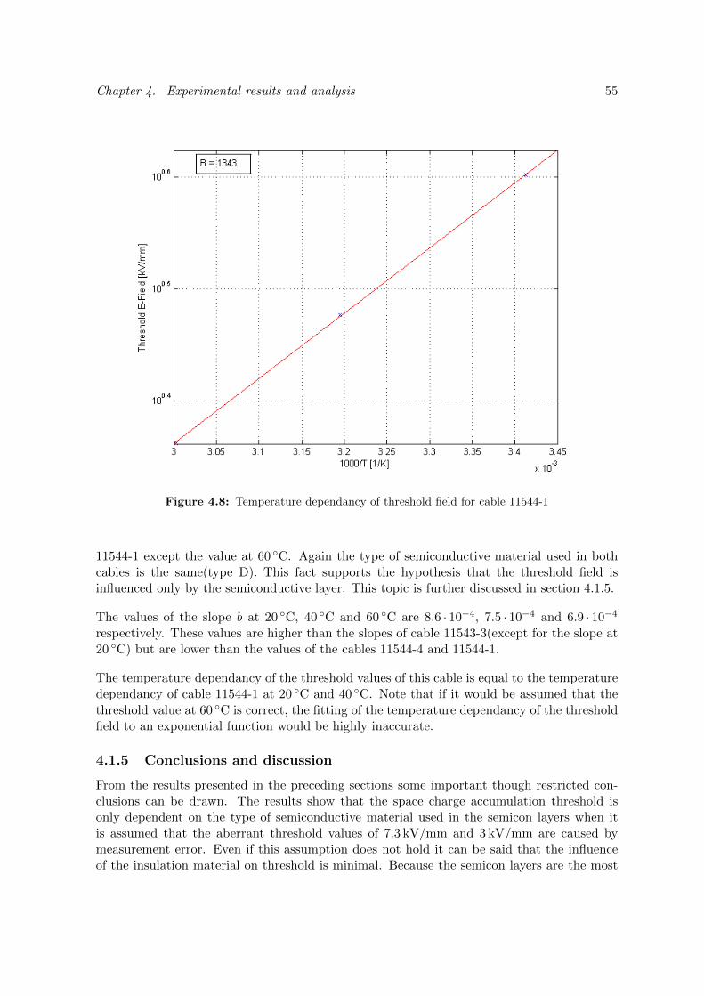
Chapter 4. Experimental results and analysis 55
Figure 4.8: Temperature dependancy of threshold field for cable 11544-1
11544-1 except the value at 60 C. Again the type of semiconductive material used in bothcables is the same(type D). This fact supports the hypothesis that the threshold field isinfluenced only by the semiconductive layer. This topic is further discussed in section 4.1.5.
The values of the slope b at 20 C, 40 C and 60 C are 8.6 · 10−4, 7.5 · 10−4 and 6.9 · 10−4
respectively. These values are higher than the slopes of cable 11543-3(except for the slope at20 C) but are lower than the values of the cables 11544-4 and 11544-1.
The temperature dependancy of the threshold values of this cable is equal to the temperaturedependancy of cable 11544-1 at 20 C and 40 C. Note that if it would be assumed that thethreshold value at 60 C is correct, the fitting of the temperature dependancy of the thresholdfield to an exponential function would be highly inaccurate.
4.1.5 Conclusions and discussion
From the results presented in the preceding sections some important though restricted con-clusions can be drawn. The results show that the space charge accumulation threshold isonly dependent on the type of semiconductive material used in the semicon layers when itis assumed that the aberrant threshold values of 7.3 kV/mm and 3 kV/mm are caused bymeasurement error. Even if this assumption does not hold it can be said that the influenceof the insulation material on threshold is minimal. Because the semicon layers are the most

Chapter 4. Experimental results and analysis 56
Figure 4.9: ρ vs. E characteristic of cable 11543-3 at 20 C
Figure 4.10: ρ vs. E characteristic of cable 11543-3 at 40 C

Chapter 4. Experimental results and analysis 57
Figure 4.11: ρ vs. E characteristic of cable 11543-3 at 60 including the lines above threshold at20 C(green) and 40 C(magenta)C
important factor in the determination of the space charge accumulation threshold it can bestated that the threshold fields are determined by charge injection processes.
The main difference between both types of semicon(type C and D) is the concentration ofcarbon black. From the results it can be concluded that a high concentration of carbon blackin the semicon layers results in a low threshold field and vice versa. If the semicon materialwith a high concentration of carbon black shows to have a high conductivity and the semiconwith a low concentration shows a low conductivity the previous statement also holds for theconductivity in stead of the concentrations. The results of conductivity measurements onboth semicon types, contained in section 4.3, should reveal if this is correct.
The difference in the temperature dependancy of the threshold field between cables 11544-1 and 11544-4 is minimal according to the results. The temperature dependancy of thethreshold field of the cables 11543-3 and 11543-4 are equal to the temperature dependancyof the cables 11544-4 and 11544-1 respectively(neglecting the aberrent threshold values). Intotal it can be said that the temperature dependancy is not influenced by either the carboncontent in the semicon layers or the type and concentration of additives in the insulation.A more general conclusion on this is that the temperature dependancy of the threshold fieldcould be determined only by the basic molecular structure of the materials which is in thiswork the same for both the semicon materials and the insulation materials.
The slope of the ρ-E characteristics above threshold is shown to be decreasing at increasingtemperature. This could be caused by the fact that the charge detrapping and extraction
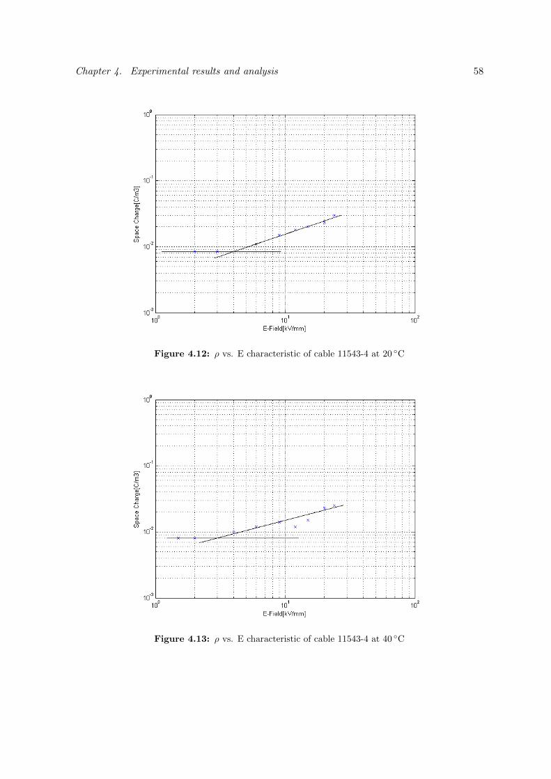
Chapter 4. Experimental results and analysis 58
Figure 4.12: ρ vs. E characteristic of cable 11543-4 at 20 C
Figure 4.13: ρ vs. E characteristic of cable 11543-4 at 40 C

Chapter 4. Experimental results and analysis 59
Figure 4.14: ρ vs. E characteristic of cable 11543-4 at 60 C including the lines above threshold at20 C(green) and 40 C(magenta)
rate under applied field shows a larger positive temperature dependancy than the injectionrate. Of course the rate of charge detrapping and extraction is lower than the injection rateabove threshold because otherwise there would be no charge build up.
The slope of the ρ-E characteristics at 40 C and 60 C is less steep for cables 11543-3 and11543-4 than for the cables with designation 11544-4 and 11544-1. This could mean thatthe electric field dependancy of the charge extraction and detrapping rate of the cables withdesignation 11543-3 and 11543-4 is larger than for the cables with designation 11544-4 and11544-1 at 40 C and 60 C. A more general proposition is that the charge detrapping rateof insulation material I exhibits a larger electric field dependancy than insulation material IIat 40 C and 60 C. The results of the apparent mobility and trap depth could support orinvalidate this proposition. These results are contained in section 4.2.
In figures 4.15 and 4.16 the influence of the semiconductive material and the insulation ma-terial on both the threshold field and the slope at 40 C is displayed.
Note that at 20 C the slopes of the ρ-E characteristics of the cables with designations 11544-4and 11543-3 are quite steep (1.7 · 10−3 and 2.0 · 10−3). These cables both have semicon typeC as semiconductive layer. The cables with semicon type D show much smaller values forthe slope b, which are much closer to the values of the slope at higher temperatures. Thereason for this could be that at room temperature the charge extraction rate at the electrodesis the limiting factor while at higher temperatures charge detrapping is the most importantmechanism.

Chapter 4. Experimental results and analysis 60
Figure 4.15: The influence of the semicon and insulation on the threshold field
Figure 4.16: The influence of the semicon and insulation on the slope

Chapter 4. Experimental results and analysis 61
Note that the conclusions and propositions contained in this section only apply to these fourtypes of mini cables.
4.2 Apparent mobility and trap depth results
The depolarization characteristics were originally planned to be conducted at ambient temper-ature and at field strengths of both 30 kV/mm and 60 kV/mm. However two main problemsarose when measuring at these conditions. Firstly, when starting a depolarization measure-ment (i.e. turning off the voltage) after the cable had been polarizing at 30 kV/mm the chargepresent in the cables was relatively low. Only when the charge had been accumulating at afield of 60 kV/mm a relatively large amount of charge remained after voltage turn-off. Notethat this situation is above the proposed charge packet inception field.
Secondly, the charge present in the cables did not show any significant decrease at roomtemperature within the 3 hours depolarization time. When a good comparison of the ap-parent trap-controlled mobility and trap depths is desired far longer depolarization times arerequired(i.e. weeks).
Because of these problems the depolarization characteristics obtained at a temperature of65 C after poling at 60 kV/mm are used. Note that the depolarization characteristics at65 C after poling at 30 kV/mm were also considered. However, in this case the depolarizationcharacteristic shows much more scatter and the decrease in charge is also relatively low.
The apparent trap-controlled mobilities of the four test cables are shown in figure 4.17. The
Figure 4.17: Apparent trap-controlled mobility
value of the trap-controlled mobility at the end of the 3 hour depolarization time for cable
Chapter 4. Experimental results and analysis 62
11543-3 is 3.6 · 10−15 m2/V s. Cables 11543-3, 11544-4 and 11544-1 show a trap-controlledmobility of 2.6 · 10−15 m2/V s, 5.8 · 10−16 m2/V s and 4.4 · 10−16 m2/V s respectively. Thesevalues are comparable to values found in literature[19, 20].
From 200 s after the start of the depolarization process the mobility of the cables with insu-lation type I is higher than the mobility of the cables with insulation type II. This fact canalso be deduced from the depolarization characteristics in which the cables with insulation Ideplete charge faster than the cables with insulation II.
Insulation material I clearly shows an advantage over insulation material II. Especially whenfield inversion or voltage turn-off would occur in operation conditions. The addition of chargetrapping agents in the XLPE based insulation thus gives better results than the additionof carbon black with respect to the mobility. It should be noted that the charge trappingagent was added to create more shallow traps not deep traps. The carbon black was addedto increase the overal conductivity of XLPE.
The difference in mobility between the cables with the same insulation material is very smallwith respect to the difference in mobility between the two insulation materials. This sug-gests that the apparent trap-controlled mobility and thus the charge detrapping rate is onlydetermined by the type of insulation material. The detrapping of charges can thus only beinfluenced by changing the type and concentration of additives in the material.
Trap depth evaluation
From the same depolarization characteristics the apparent trap depths are evaluated. Thedepolarization characteristic is divided in five segments from which the individual trap depthsare calculated. Therefore five trap levels are present in the model for each cable. Using moretrap levels did not give more significant information on the trap levels. The trap depths ofthe four test cables are shown in figure 4.18.
The trap depth values of the deepest traps of the cables with designations 11544-4 and11544-1 are both 1.20 eV. The cables with designations 11543-3 and 11543-4 show to havea maximum trap depth of 1.16 eV and 1.17 eV respectively. The traps depth values in thiswork are however higher than values found in literature[20].
The values of the deepest traps of the cables with the same semiconductive material areequal or almost equal which corresponds with the results of the apparent mobility evaluation.Insulation material II thus seems to contain deeper traps than insulation I resulting in theconfirmation of the fact that insulation I should contain more shallow traps. The trap depththus also seems to be determined only by the the type and concentration of additives presentinsulation material.
4.3 Conduction current results
In this section the results of conduction current measurements are described and discussed.The results of the conductivity measurements on the semiconductive plaques are described

Chapter 4. Experimental results and analysis 63
Figure 4.18: Apparent trap depth values
in section 4.3.1. Unfortunately it was not possible to run conduction current measurementson the mini cables before the end of this work. Thus there are no measurement results. Thereason for this and the work that has been done on the setup is described in section 4.3.2.
4.3.1 Conductivity results of the semicon plaques
On each type of semicon plaque two conduction current measurements are performed atapplied field strengths of 1 kV/mm and 2 kV/mm. Thus in total 4 measurement results areobtained.
The conductivity σc1 of the plaque consisting of semicon type C(“low” carbon content) atan applied field strength of 1 kV/mm was found to be 1.48 · 10−12 S/m. At 2 kV/mm theconductivity σc2 is 1.45 · 10−12 S/m. The conductivities σd1 and σd2 of the plaque consistingof semicon D(“high” carbon content) at field strengths of 1 kV/mm and 2 kV/mm are foundto be 1.62 · 10−12 S/m and 1.53 · 10−12 S/m respectively.
The measurements were conducted at two different field strengths because the conductivity isnot always constant with respect to the applied electric field. Furthermore, some fluctuationsmay occur in the conduction current measurements due to external influences or movement ofthe measurement cables. The average conductivity is thus calculated from the conductivityvalues at both field strengths. The average conductivities of semicon type C and D are1.47 · 10−12 S/m and 1.58 · 10−12 S/m respectively.
The conductivity of semicon type D is clearly higher than the conductivity of semicon typeC. This implies that the semicon with a high carbon content has a higher conductivity than

Chapter 4. Experimental results and analysis 64
the semicon with a low carbon content. With these results it can be stated that the spacecharge accumulation threshold in the 4 tested mini cables could be dependent only on theconductivity of the semiconductive layer. Note that this can only apply for semiconductivematerials with the same basic molecular structure as used in these mini cables.
4.3.2 Conduction current setup for mini cables
Because conduction current measurements on mini cables are desired a conduction currentsetup suitable for mini cables is needed. Unfortunately such a setup was not available in thehigh voltage lab. Therefore the setup had to be built.
The knowledge available to build a new setup was limited. A schematic representation of asimilar setup including some test results was found in literature[11]. Furthermore, the con-duction current setup for thin plaques also gave valuable information. However no technicaldetails were available. The setup, including the oven, HVDC supply, electrometer, protectioncircuitry, GPIB interface and the computer is working at the moment of writing this section.A few test measurements were performed to correct the settings of the electrometer and tocheck the connections to the electrometer.
4.4 Dielectric spectroscopy results
The dielectric spectroscopy measurements are conducted on two thin plaques consisting ofeither insulation material I or II. Each test sample is tested in one temperature run consistingof two parts. The first part runs from −40 C up to 80 C in steps of 40 C and the secondpart runs from 90 C up to 120 C in steps of 10 C.
For each sample the real part of the complex permittivity ε′(ω), the imaginary part of thecomplex permittivity ε′′(ω) and the loss factor tan(δ) are measured. The ε′(ω), ε′′(ω) andtan(δ) of insulation type I are displayed in figure 4.19, 4.20 and 4.21 respectively. Furthermore,the ε′(ω), ε′′(ω) and tan(δ) of insulation type II are shown in figure 4.22, 4.23 and 4.24respectively.
Although the frequency domain spectroscopy uses an AC test voltage the results are still usefulfor materials used in DC applications. The frequency range of interest is in this case the lowfrequency spectrum below approximately 1 Hz. In this part of the spectrum contributions ofboth dc conductivity and in some cases low frequency dispersion(LFD) can be found[26].
From the graphs of the tan(δ) and the imaginary component of the complex permittivity ε′′
of both insulation types it can be seen that the losses increase at lower frequencies. Thisis caused by the finite dc conductivity of the insulation materials. The comparison of bothmaterials on the basis of these graphs reveals that the losses in insulation I are larger thanin insulation II which suggests that the dc conductivity of insulation I is larger than the dcconductivity of insulation II. This fact only holds for temperatures of 40 C and higher.
The losses are larger at higher temperatures because of the rise in conductivity. At very lowtemperature (−40 C and 0 C) almost no conductivity is present in both materials. Note that
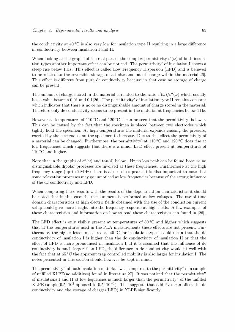
Chapter 4. Experimental results and analysis 65
the conductivity at 40 C is also very low for insulation type II resulting in a large differencein conductivity between insulation I and II.
When looking at the graphs of the real part of the complex permittivity ε′(ω) of both insula-tion types another important effect can be noticed. The permittivity’ of insulation I shows asteep rise below 1 Hz. This effect is called Low Frequency Dispersion (LFD) and is believedto be related to the reversible storage of a finite amount of charge within the material[26].This effect is different from pure dc conductivity because in that case no storage of chargecan be present.
The amount of charge stored in the material is related to the ratio ε′(ω)/ε′′(ω) which usuallyhas a value between 0.01 and 0.1[26]. The permittivity’ of insulation type II remains constantwhich indicates that there is no or no distinguishable amount of charge stored in the material.Therefore only dc conductivity seems to be present in the material at frequencies below 1 Hz.
However at temperatures of 110 C and 120 C it can be seen that the permittivity’ is lower.This can be caused by the fact that the specimen is placed between two electrodes whichtightly hold the specimen. At high temperatures the material expands causing the pressure,exerted by the electrodes, on the specimen to increase. Due to this effect the permittivity ofa material can be changed. Furthermore, the permittivity’ at 110 C and 120 C does rise atlow frequencies which suggests that there is a minor LFD effect present at temperatures of110 C and higher.
Note that in the graphs of ε′′(ω) and tan(δ) below 1 Hz no loss peak can be found because nodistinguishable dipolar processes are involved at these frequencies. Furthermore at the highfrequency range (up to 2 MHz) there is also no loss peak. It is also important to note thatsome relaxation processes may go unnoticed at low frequencies because of the strong influenceof the dc conductivity and LFD.
When comparing these results with the results of the depolarization characteristics it shouldbe noted that in this case the measurement is performed at low voltages. The use of timedomain characteristics at high electric fields obtained with the use of the conduction currentsetup could give more insight into the frequency response at high fields. A few examples ofthose characteristics and information on how to read those characteristics can found in [26].
The LFD effect is only visibly present at temperatures of 80 C and higher which suggeststhat at the temperatures used in the PEA measurements these effects are not present. Fur-thermore, the higher losses measured at 40 C for insulation type I could mean that the dcconductivity of insulation I is higher than the dc conductivity of insulation II or that theeffect of LFD is more pronounced in insulation I. If it is assumed that the influence of dcconductivity is much larger than LFD, the difference in dc conductivity would fit well withthe fact that at 65 C the apparent trap controlled mobility is also larger for insulation I. Thenotes presented in this section should however be kept in mind.
The permittivity” of both insulation materials was compared to the permittivity” of a sampleof unfilled XLPE(no additives) found in literature[27]. It was noticed that the permittivity”of insulations I and II at low fequencies is much larger than the permittivity” of the unfilledXLPE sample(0.5 · 102 opposed to 0.5 · 10−1). This suggests that additives can affect the dcconductivity and the storage of charges(LFD) in XLPE significantly.

Chapter 4. Experimental results and analysis 66
Figure 4.19: Real part of complex permittivity ε′(ω) of insulation I
Figure 4.20: Imaginary part of complex permittivity ε′′(ω) of insulation I
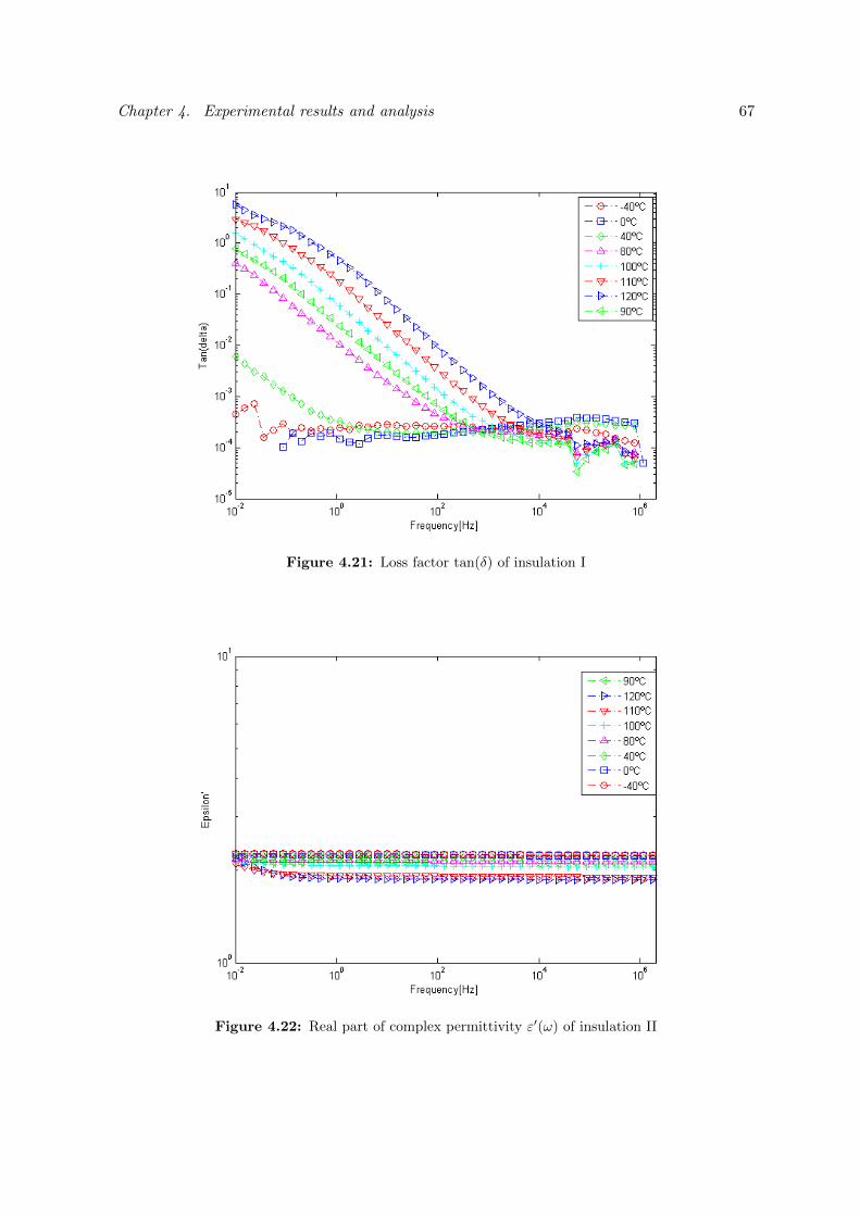
Chapter 4. Experimental results and analysis 67
Figure 4.21: Loss factor tan(δ) of insulation I
Figure 4.22: Real part of complex permittivity ε′(ω) of insulation II

Chapter 4. Experimental results and analysis 68
Figure 4.23: Imaginary part of complex permittivity ε′′(ω) of insulation II
Figure 4.24: Loss factor tan(δ) of insulation II

Chapter 5
Conclusions and Recommendations
The aim of this thesis was to investigate in depth the dynamics of space charge accumula-tion of a selected set of mini cables. This is accomplished by the determination of the spacecharge accumulation threshold field, the apparent mobility of the charge carriers and the trapdepths in the insulation and the frequency domain characteristics of the insulation materials.Several test techniques were used in the determination of these parameters: space chargemeasurements with the use of the PEA method , frequency domain dielectric spectroscopyand conduction current measurements. Section 5.1 contains the main findings on the ex-perimental observations summarized in a number of conclusions. Section 5.2 contains somerecommendations for future research.
5.1 Conclusions
Space charge accumulation threshold
The space charge accumulation threshold measurements have shown that the value of thethreshold field of the four minicables is dependent only on the type of semiconductive materialused in the outer and inner semicon layers. The space charge accumulation threshold is thuspresumably only dependent on charge injection processes.
The difference between the two semicon materials is the concentration of carbon black. Thesemiconductive material which shows the lowest threshold also has the highest concentrationof carbon black and the semicon material which shows the highest threshold has the lowestconcentration of carbon black. Thus the threshold field shows a negative dependancy on theconcentration of carbon black in the semiconductive layers.
Following the statement above the conductivity of the semiconductive materials was deter-mined in the conduction current setup for thin plaques. Results show that the conductivityof the semiconductive materials is positively dependent on the concentration of carbon black.Connecting this statement with the threshold results obtained from the PEA measurementssuggests that the mini cables which have semicon layers with a relatively high conductivityexhibit a lower threshold than the cables which have semicon layers with a low conductivity.This means that the threshold shows a negative dependancy with respect to the conductivityof the semicon layers.
69

Chapter 5. Conclusions and Recommendations 70
The temperature dependancy of the threshold field has shown to be approximately equal forall four mini cables. This suggests that the temperature dependancy of the threshold is notdetermined by the additives used in both the semicon and the insulation materials.
Not only the threshold field was an important parameter found in the ρ-E characteristics. Theslope in the ρ-E characteristics has shown to be decreasing for an increase in temperature.This is believed to be caused by the fact that the charge extraction and/or detrapping ratehas a larger positive temperature dependency than the charge injection rate. Furthermore,results have shown that the cables with insulation type I show to have a slope which is lesssteep than the slopes obtained for the cables with insulation type II at 40 C and 60 C. Thisfact suggests that, if the slope is determined by the charge extraction and/or detrapping rate,the detrapping rate in insulation I is larger than the detrapping rate in insulation II at 40 Cand 60 C.
Because the threshold field seems to correspond only to injection processes the influence of thetemperature gradient on the threshold field is believed to be negligible(there is no temperaturegradient at the electrodes). Note that there are no measurement results with a homogeneoustemperature distribution available for comparison. Furthermore the space charge which ispresent due to the conductivity gradient could be removed by the processing.
Apparent trap-controlled mobility and trap depth
Calculations of the apparent trap-controlled mobility of the charge carriers from the depolar-ization characteristics show that the cables with insulation type I have a higher mobility thanthe cables with insulation type II. This makes insulation type I the more favourable materialfor dc operation where voltage inversion and voltage turn-off occur frequently.
The results also show that the mobility is almost only dependent on the type of insulationmaterial(there are small differences in conductivity between different semicon types). Thisstatement suggests that the apparent trap-controlled mobility is only dependent on chargedetrapping not on charge extraction at the electrodes.
Trap depth calculations have shown that insulation type II has deeper traps than insulationtype I. The charge trapping agents present in insulation type I seem to create more shallowtraps.
Because the depolarization characteristics are only dependent on the detrapping of charges inthe insulation the calculated trap depths are only dependent on the type of insulation material.This suggests that calculating the trap depths with the use of depolarization characteristicsis a valid approach.
Frequency domain spectroscopy
The results of the spectroscopy measurements show that the dc conductivity of insulationmaterial I is larger than the dc conductivity of insulation material II. This coincides with thedepolarization measurements which shows a higher mobility for insulation type I.
At temperatures of 80 C and higher a low frequency dispersion effect is present in the per-mittivity’ characteristic of insulation I suggesting that a build up of charge is present in the

Chapter 5. Conclusions and Recommendations 71
material at very low frequencies. This effect is not present in the characteristic of insulationtype II. Below 80 C this effect is not present thus the significance of this observation for thecharacterization of the cables is questionable.
General conclusions
In general it can be observed that for this type of mini cables the space charge accumulationthreshold can be changed by changing the amount of carbon black(and thus changing theconductivity) in the semiconductive layers. The apparent mobility and trap depths couldbe influenced by changing the type and/or the concentration of additives in the insulation.These two properties seem to be independent resulting in the fact that the design of suchcables can be split up in two independent parts(i.e. the semicon layer and the insulation).
It is important to note that the results and conclusions presented in this work are not directlyapplicable to other cable systems and base materials.
The combination of semicon C and insulation type I seems to deliver on average the bestresults. The threshold values corresponding to semicon C are the highest of the two types.Furthermore, the trap-controlled mobility of the insulation is also the highest resulting inthe highest depolarization rate and the insulation also has the lowest trap depths of thetwo insulation types. The slope of the ρ-E characteristics at 40 C and 60 C are also muchless steep than the slopes of the other semicon-insulation combinations. The cable withdesignation 11543-3 thus seems to be the most suitable cable for dc applications.
5.2 Recommendations for future research
Materials which have not yet been tested
This work is part of another project in which four more mini cables are scheduled to betested. These cable all consist of the same insulation materials as the cables used in this work.However, two other semicon types than the ones that are used in this work are present in thesemiconductive layers of those 4 cables. These semicon types include a type which consistsof a polyethylene copolymer with polar comonomer which has a “medium” concentrationof added carbon black and a type which consists of a copolymer blend of reduced polarity.Based on the results in this work the cables with the semicon type with “medium” carboncontent are expected to show threshold values between the values found for semicon C andD. Furthermore, the semicon type which has reduced polarity could reveal if the polarity ofthe semicon layers has a significant influence on threshold and injection processes.
Space charge measurements at negative polarity
Polarization measurements at negative polarity can reveal different injection properties. Fur-thermore, the contributions of electrons and holes to the conduction and injection processescan be investigated. Depolarization measurements could also reveal the contribution of elec-trons and holes to the trap-controlled mobility and trap depths.

Chapter 5. Conclusions and Recommendations 72
Conduction current measurements
Running conduction current tests on all eight cables can reveal if the threshold between linearand supra-linear conduction is equal to the space charge accumulation threshold. Furthermorethe SCLC mobility(corresponding to free and shallow trapped charges) can be defined andcompared with the trap-controlled mobility(corresponding to deeply trapped charges).
Dielectric spectroscopy on semicon-insulator combinations
In the dielectric spectroscopy measurements two thin plaques each consisting of either in-sulation type I or type II are used. To investigate the frequency domain characteristics ofthe semicon-insulator combinations, insulation plaques with a semiconductive layer can beproduced.
Furthermore, as explained in section 4.4 time domain spectroscopy can also be used to evaluatethe complex permittivity of each sample at high field strengths. This could reveal moreinformation on the frequency response around normal working conditions with respect toapplied field. Time domain spectroscopy can also be used on the mini cable samples removingthe need to produce special semicon-insulator plaques.
Charge packet investigation
As explained in sections 3.4 and 4.1 the behavior of the space charge accumulation at veryhigh field strengths(> 60kV/mm) could be related to the presence of fast charge packets.Performing space charge measurements at high fields can give information on the charge packetinception field for different temperatures and semicon-insulation interfaces. Furthermore, veryfast measurements can reveal information on the apparent charge packet mobility as definedin section 3.4. Note that for such measurements a fast acquisition system is needed which isat this moment not available in the HV lab.

Appendix A
Deconvolution and attenuation anddispersion correction
A.1 Deconvolution
The high-pass characteristic of the sensor-amplifier system can be seen as a transfer functionH(f). The resulting signal vs(t) will then be a function of the original signal vorgs (t) and thetransfer function as shown in equation A.1.
vs(t) = F−1 [V orgs (f) ∗H(f)] (A.1)
F−1 = inverse fourier transform
V orgs (f) = the original voltage signal in frequency domain
From the measured signal vs(t) the original signal has to be obtained by the deconvolutiontechnique. The deconvolved signal is never exactly the same as the original signal thus thedeconvolved signal is designated vdecons (t). To obtain the original signal the output signalvs(t) should be divided by the system response H(f) as shown in equation A.2.
vorgs (t) = F−1[Vs(f)
H(f)
](A.2)
The system response is however unknown. The simple equation given above is thus notdirectly applicable. The system response has to be approximated which is done in the de-convolution technique. The deconvolution technique is schematically represented in figureA.1. The signal vs−el represents the earth electrode and bulk material part of the outputsignal vs(t). The signal outside that interval is zero. The signal designated vs−el−id is theideal signal from the electrode charge. Ideal means without the response of the sensor andsensor-amplifier system. In this case the ideal signal is represented by a pulse which hasapproximately the same width as the earth electrode in vs(t) and has a height of one(whichis usually much larger than the height of the electrode signal in vs(t)).
The ideal signal is divided by the output signal vs−el which should result directly in 1H(f) .
However the result of this division contains high frequency components which will distort thedeconvoluted signal vdecons (t). Therefore a low pass gaussian type filter with transfer functionG(f) is used to remove or attenuate these components. After multiplication with G(f) the
73

Appendix A. Deconvolution and attenuation and dispersion correction 74
Figure A.1: Schematic drawing of deconvolution technique
signal represents 1H(f) which is an approximation. With the approximated transfer function
the deconvoluted signal vdecons (t) can be directly calculated from the output signal vs(t) withequation A.2.
The ideal electrode signal has height one in stead of the actual voltage because of the factthat the signal has not yet been calibrated. Because of this the resulting deconvoluted voltagesignal will not have the correct value. To correct this difference the maximum value of thedeconvoluted signal vdecons (t) is divided by the maximum value of the output signal vs(t) whichresults in a size factor. The deconvoluted signal is then divided by this factor to acquire thecorrect signal as shown in equation A.3.
Ksize =max(|vdecons (t)|)max(|vs(t)|)
(A.3)
vdecons (t) =vdecons (t)
Ksize
Note that the deconvolution can only work correctly when the signal is free of space charge.When there is space charge present the ideal signal could not be flat outside the electroderegion. The deconvolution method described in this section is implemented in MATLAB. Thecorresponding MATLAB code is contained in section A.2.
A.2 Deconvolution in MATLAB
1 plot (mmatrice(:,1)); %First trace after voltage turn−on = calibration trace

Appendix A. Deconvolution and attenuation and dispersion correction 75
2 grid on;3 disp('click start and end point of EARTH ELECTRODE and start point of HV ELECTRODE');4 [qq, zz]=ginput(3);5 aa=round(qq(1)); %start point of earth electrode6 bb=round(qq(2)); %end point of earth electrode7 cc=round(qq(3)); %start point of hv electrode8
9 y1=zeros(5001,1);10 y1(aa:cc,1)=mmatrice(aa:cc,1);11
12 vin=zeros(5001,1);13 vin(aa+30:bb−30,1)=1;14 g=input('gaussian filter= ');15 for i=1:500116 ex(i)=exp(−(g*(i)).ˆ2);17 end18 EX=fft(ex);19
20 f=−100000:+40:100000;21 vin1=vin;22 Vin1=fft(vin1);23 Y1=fft(y1);24 for i=1:500125 H(i)=(Vin1(i)/Y1(i))*EX(i)*EX(i);26 end27 Z=fft(mmatrice(:,1));28 for i=1:500129 X(i)=Z(i)*H(i);30 end31 x=−ifft(X);32
33 dimfact=max(abs((real(x))))/max(abs(mmatrice(:,1)));34 finalsignal=real(x)/dimfact;35 plot(finalsignal,'r');36 hold on;37 plot(mmatrice(:,1),'b');38 grid on;39 hold off;40 tt=input('OK? 1=si 0=no ');41 %Applying deconvolution to all traces
A.3 Attenuation and dispersion correction
A planar acoustic wave travelling through an ideal medium can be described in the frequencydomain by equation A.4.
p(x, ω) = P0(ω) exp(−iβω) (A.4)
P0 is the acoustic wave with angular frequency ω at x = 0. The acoustic wave travels withvelocity ν which is related to the phase coefficent β via ν = βω. An acoustic wave travellingthrough a lossy and dispersive medium can be described in the frequency domain by equationA.5.
p(x, ω) = P0(ω) exp(−α(ω)x) exp(−iβ(ω)x) (A.5)
The frequency dependent coefficient α(ω) takes into account the attenuation of the acousticwave while the coefficient β(ω) takes into account the dispersion of the acoustic wave. Both

Appendix A. Deconvolution and attenuation and dispersion correction 76
attenuation and dispersion coefficients can be defined as a function G(x, ω) described inequation A.6.
G(x, ω) =p(x, ω)
p(0, ω)= exp(−α(ω)x) exp(−iβ(ω)x) (A.6)
To calculate the coefficients α(ω) and β(ω) two known acoustic waves at two different locationsin the sample are needed. In this thesis the acoustic wave generated at the HV electrode p(d, ω)and the acoustic wave at the sensor location p(0, ω) are used. Using these two acoustic wavesthe function in equation A.6 will be different(equation A.7).
G(d, ω) =p(d, ω)
p(0, ω)= exp(−α(ω)d) exp(−iβ(ω)d) (A.7)
When the function G(d, ω) has been found the coefficients α(ω) and β(ω) can be calculated.With the calculated coefficients the function G(x, ω) can be defined. The original acousticwave at any location inside the sample can then be calculated from the acoustic wave at thesensor(equation A.8).
p(x, t) = F−1[p(0, ω)G(x, ω)] (A.8)
Note that the acoustic wave p(0, t) is the acoustic wave at the sensor location after havingtravelled through the sample. The acoustic wave p(x, 0) is the acoustic wave before travellingthrough the sample.
To be able to implement this procedure the original signal at the HV electrode correspondingto p(d, ω) should be known. If the sample is free of space charge the signal at the HV electrodeis directly related to the electrode charge. When a known voltage is applied across the samplethis signal can be calculated.
The recovered signal calculated from the detected signal with function G(x, ω) at the sensoris however not exactly the same as the original signal. This is caused by the fact that somehigh frequency components in the waveform are completely attenuated and can thus not beretrieved from the detected signal[1].
Some problems may arise when using G(d, ω) to calculate the coefficients α(ω) and β(ω).The calculation of G(d, ω) is defined as a ratio of two functions(equation A.7). When thedenominator contains zeros the division is impossible. Furthermore the method presented herehas a higher amplification for the high frequency components than for the low frequency part.Noise present in the detected signal, which usually contains much high frequency components,will be amplified as well.
To overcome these problems the functions α(ω) and β(ω) are approximated in stead of cal-culated with equation A.7. The coefficients are assumed to be defined by equations A.9 andA.10.
α(ω) = A+ aω2 (A.9)
β(ω) = bω (A.10)

Appendix A. Deconvolution and attenuation and dispersion correction 77
Equations A.9 and A.10 are based on the assumption that the original and the detectedwaveform can be described as a gaussian function[1].The original and detected waveform canbe described by the gaussian functions in equations A.11 and A.12 respectively.
y1(t) = −A1 exp(−a1(t− τ1)2) (A.11)
y2(t) = −A2 exp(−a2(t− τ2)2) (A.12)
Equations A.13 and A.14 represent the gaussian functions y1(t) and y2(t) transformed to thefrequency domain.
Y1(ω) = A1
√π
a1exp
[−iτ1ω −
ω2
4a1
](A.13)
Y2(ω) = A2
√π
a2exp
[−iτ2ω −
ω2
4a2
](A.14)
The function G(d, ω) will then be defined according to equation A.15.
G(d, ω) =Y1Y2
=A1
A2
√a2a1
exp
[−iω(τ1 − τ2)−
ω2
4
(1
a1− 1
a2
)]= exp(−d(A+aω2)) exp(−ibdω)
(A.15)
When the terms A, a and b are defined according to equations A.16, A.17 and A.18 thecoefficients α(ω) and β(ω) can be written as equation A.9 and A.10.
A = −1
dln
(A1
A2
√a2a1
)(A.16)
a =1
4d
(1
a1− 1
a2
)(A.17)
b =1
d(τ1 − τ2) (A.18)
The values of the terms a, A and b are dependent on the type of bulk material used in thespecimen. Because the values of these terms are not exactly known an approximation of thevalues is used. With these values the coefficients α(ω) and β(ω) are determined according toequations A.9 and A.10.
The output signal obtained from the deconvolution technique is a voltage signal vdecons (t).Therefore the function G(ω) is calculated with the coefficients according to equation A.19 inwhich ∆t is the time difference between the peak of the earth electrode and the peak of theHV electrode in the signal. This time difference corresponds to the distance d between theelectrodes.(which is the same as the thickness of the sample)
G(ω) = exp(−α(ω)(∆t)) exp(−iβ(ω)(∆t)) (A.19)
The voltage signal corrected for attenuation and dispersion is then obtained using equationA.20.
vatts (t) = F−1[G(ω)V decon
s (ω)]
(A.20)
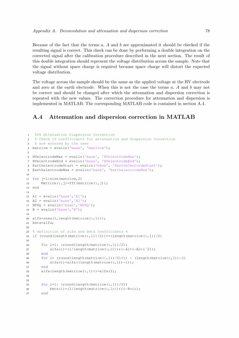
Appendix A. Deconvolution and attenuation and dispersion correction 78
Because of the fact that the terms a, A and b are approximated it should be checked if theresulting signal is correct. This check can be done by performing a double integration on thecorrected signal after the calibration procedure described in the next section. The result ofthis double integration should represent the voltage distribution across the sample. Note thatthe signal without space charge is required because space charge will distort the expectedvoltage distribution.
The voltage across the sample should be the same as the applied voltage at the HV electrodeand zero at the earth electrode. When this is not the case the terms a, A and b may notbe correct and should be changed after which the attenuation and dispersion correction isrepeated with the new values. The correction procedure for attenuation and dispersion isimplemented in MATLAB. The corresponding MATLAB code is contained in section A.4.
A.4 Attenuation and dispersion correction in MATLAB
1 %%% Attenuation Dispersion Correction2 % Check if coefficients for attenuation and dispersion correction3 % are entered by the user4 matrice = evalin('base', 'matrice');5
6 HVelectrodeMax = evalin('base', 'HVelectrodeMax');7 HVelectrodeEnd = evalin('base', 'HVelectrodeEnd');8 EarthelectrodeStart = evalin('base', 'EarthelectrodeStart');9 EarthelectrodeMax = evalin('base', 'EarthelectrodeMax');
10
11 for j=1:size(matrice,2)12 Matrice(:,j)=fft(matrice(:,j));13 end14
15 A1 = evalin('base','A1');16 A2 = evalin('base','A2');17 NFRQ = evalin('base','NFRQ');18 B = evalin('base','B');19
20 alfa=ones(1,length(matrice(:,1)));21 beta=alfa;22
23 % definition of alfa and beta coefficients %24 if (round(length(matrice(:,1))/2))==(length(matrice(:,1))/2)25
26 for i=1: (round(length(matrice(:,1))/2))27 alfa(i)=(1/length(matrice(:,1)))*(−A1+(−A2*iˆ2));28 end29 for i= (round(length(matrice(:,1))/2)+1) : (length(matrice(:,1))−1)30 alfa(i)=alfa((length(matrice(:,1))−i));31 end32 alfa(length(matrice(:,1)))=alfa(1);33
34
35 for i=1: (round(length(matrice(:,1))/2))36 beta(i)=(1/length(matrice(:,1)))*((−B*i));37 end

Appendix A. Deconvolution and attenuation and dispersion correction 79
38 for i= (round(length(matrice(:,1))/2)+1) : (length(matrice(:,1))−1)39 beta(i)=beta((length(matrice(:,1))−i));40 end41 beta(length(matrice(:,1)))=beta(1);42
43 end44
45 if (round(length(matrice(:,1))/2))˜=(length(matrice(:,1))/2)46
47 for i=1: ((floor(length(matrice(:,1))/2))+1)48 alfa(i)=(1/(length(matrice(:,1))))*(−A1−A2*iˆ2);49 end50 for i= (round(length(matrice(:,1))/2)+1) : (length(matrice(:,1))−1)51 alfa(i)=alfa((length(matrice(:,1))−i));52 end53 alfa(length(matrice(:,1)))=alfa(1);54
55
56 for i=1: ((floor(length(matrice(:,1))/2))+1)57 beta(i)=(1/(length(matrice(:,1))))*((−B*i));58 end59 for i= (round(length(matrice(:,1))/2)+1) : (length(matrice(:,1))−1)60 beta(i)=beta((length(matrice(:,1))−i));61 end62 beta(length(matrice(:,1)))=beta(1);63
64 end65
66 for i = NFRQ:(length(alfa)−NFRQ)67 alfa(i)=alfa(NFRQ);68 beta(i)=beta(NFRQ);69 end70
71 G = exp((−alfa*(−HVelectrodeMax(1)+EarthelectrodeMax(1)))−sqrt(−1)*72 beta*(−HVelectrodeMax(1)+EarthelectrodeMax(1)));73
74 [n,m] = size(matrice);75 Temp = ones(n,m);76
77 for j = 1:size(matrice,2)78 Temp(:,j)=(G.*Matrice(:,j)')';79 end80
81
82 for j=1:size(matrice,2)83 temp(:,j)=(real(ifft(Temp(:,j))));84 end85
86 [A,B] = butter(1,0.015,'low');87 temp = filter(A,B,temp);88
89 plot(matrice(:,1), 'r');90 plot(temp(:,1));

Appendix B
Divergence correction andCalibration
B.1 Divergence correction
1 HVelectrodeMax=round(ginput(1));2 HVelectrodeEnd=round(ginput(1));3 EarthelectrodeStart=round(ginput(1));4 EarthelectrodeMax=round(ginput(1));5
6 % Sample milimeter distance per data point in trace matrice7 mmperpoint insulation = (Ro − Ri) / (EarthelectrodeMax(1)−HVelectrodeMax(1));8
9 % acoustic correction10 matrice(1:HVelectrodeEnd,:) = 1.13 * matrice(1:HVelectrodeEnd,:);11
12 %divergence correction%13 for i = 1:size(matrice,2)14 for j = 1:length(matrice)15 matrice(j,i) = matrice(j,i) / (sqrt(Ro/(Ri−(HVelectrodeMax(1)−j)*16 mmperpoint insulation)));17 end18 end
B.2 Calibration
1 % Calibration mV −> C/mˆ32 Eoutercond = (V/Ro) * ( 1 / log (Ro/Ri));3
4 Calfactor = 1/((−sum(matrice(EarthelectrodeStart:length(matrice(:,1)),1))5 *mmperpoint insulation*1e−3)/(epsilon*8.85e−12*Eoutercond*1e6));6
7 matrice = matrice*Calfactor;8
9 assignin('base', 'SpaceCharge', matrice);10
11 Field = SpaceCharge;
80

Appendix B. Divergence correction and Calibration 81
12
13 % Calculate Electric Field14 for i = 1:size(SpaceCharge,2)15 Field(:,i)=(1/(epsilon*8.85e−12))*cumsum(SpaceCharge(:,i))16 *mmperpoint insulation*0.001;17 end18
19 assignin('base', 'EField', Field);20
21 voltage = Field;22 % Voltage23 for i = 1:size(Field,2)24 voltage(:,i) = mmperpoint insulation*0.001*(cumsum(Field(:,i)));25 end26 voltage = V*1000−voltage;27
28 voltage data = voltage;29
30 space charge data = SpaceCharge;31
32 electric field data = Field;

Appendix C
Calculation of average space chargedensity
C.1 Voltage-on measurements
1 %loading processed traces2 traces = input('Name of the .mat file: ','s');3 load(traces)4 clear traces5
6 a = size(space charge data(:,1));7 b = size(space charge data(1,:));8 calibrationtrace = space charge data(:,1);9 plot((calibrationtrace/2), 'linewidth', 2);
10 fprintf(1,'\nLocate Electrode−to−Sample zero crossing: to the 1/Left 2/Right. ')11 sample start = round( ginput(1) );12 sample end = round( ginput(1) );13 close;14 %Subtacting first trace(calibration trace) from mesaurement data15 space charge data1 = zeros(a(1),b(2)−1);16 for i = 2:b(2)17 space charge data1(:,i−1) = −space charge data(:,1)18 + space charge data(:,i);19 end20 %taking the absolute value of the resulting traces21 absolute spacecharge = abs(space charge data1(sample start(1):sample end(1),:));22
23 %calculating the average value over the insulation width24 for i = 1:size(space charge data1,2)25
26 average spacecharge(i) = sum( absolute spacecharge(:,i) )27 /(sample end(1) − sample start(1) );28 end29 %Saving results30 trace = input('Name of output file: ','s');31
32 save(trace,'average spacecharge')
82

Appendix C. Calculation of average space charge density 83
C.2 Voltage-off Measurements
1 %loading processed traces2 traces = input('Name of the .mat file: ','s');3 load(traces)4 clear traces5
6 b = size(space charge data(1,:));7 space charge data = space charge data(:,2:b(2));8 calibrationtrace = space charge data(:,1);9 plot(calibrationtrace);
10 grid on;11 fprintf(1,'\nLocate Electrode−to−Sample zero crossing: to the 1/Left 2/Right. ')12 sample start = round( ginput(1) );13 sample end = round( ginput(1) );14 close;15
16 %taking the absolute value of resulting traces17 absolute spacecharge = space charge data( sample start(1):sample end(1),:);18 %calculating the average value over the insulation width19 for i = 1:size(space charge data1,2)20 average spacecharge(i) = sum( absolute spacecharge(:,i) )21 /(sample end(1) − sample start(1) );22 end23
24 trace = input('Name of output file: ','s');25
26 save(trace,'average spacecharge')

Appendix D
Calculation of apparent mobilityand trap depths
1 traces = input('Name of the result .mat file: ','s');2 load(traces)3 clear traces4
5 average spacecharge = average spacecharge';6 time index = 10800/length(average spacecharge);7 t = [1:time index:10800]';8 plot(t,average spacecharge,'x')9 hold on
10 %fit a function on the DP characteristic11 dpmodel = fit(t,average spacecharge,'power2');12 plot(dpmodel,'r')13 %make a vector from the cfit function dpmodel14 t100 = 1:100:10800';15 q = feval(dpmodel,t100);16 plot(t100, q, 'g');17
18 %calculate derivative of q19 q dev = differentiate(dpmodel,t100);20
21 %calculate square of q22 q sq = q.*q;23
24 %calculate apparent mobility mu25 epsilon nul = 8.85e−12;26 epsilon xlpe = 2.3;27 mu = abs((2*epsilon nul*epsilon xlpe./q sq).*q dev);28 figure(2)29 plot(t100,mu)30
31 klaar = 0;32 while klaar == 033 klaar = input('Are the results OK? [yes = 1/ no = 0] ');34 end35
36 close all37 clear klaar
84

Appendix D. Calculation of apparent mobility and trap depths 85
38 %definition of segments of DP curve39 plot(t100,q)40 grid on41 fprintf(1,'\nLocate segment boundaries in DP curve. ')42 bound1 = round( ginput(1)/100 );43 bound2 = round( ginput(1)/100 );44 bound3 = round( ginput(1)/100 );45 bound4 = round( ginput(1)/100 );46 bound5 = round( ginput(1)/100 );47 close;48 %create segments of DP curve49 q1 = q(1:bound1);50 t1 = t100(1:bound1)';51 q2 = q(bound1:bound2);52 t2 = t100(bound1:bound2)';53 q3 = q(bound2:bound3);54 t3 = t100(bound2:bound3)';55 q4 = q(bound3:bound4);56 t4 = t100(bound3:bound4)';57 q5 = q(bound4:bound5);58 t5 = t100(bound4:bound5)';59 %plot segments60 plot(t1,q1)61 hold on62 grid on63 plot(t2,q2,'r')64 plot(t3,q3,'g')65 plot(t4,q4,'y')66 plot(t5,q5,'c')67 klaar = 0;68 while klaar == 069 klaar = input('Are the results segments OK? [yes = 1/ no = 0]: ');70 end71 close72 clear klaar73 %calculate exponential fit on segments74 trapmodel1 = fit(t1,q1,'Exp1');75 trapmodel2 = fit(t2,q2,'Exp1');76 trapmodel3 = fit(t3,q3,'Exp1');77 trapmodel4 = fit(t4,q4,'Exp1');78 trapmodel5 = fit(t5,q5,'Exp1');79
80 %plot the fitted segment functions81
82 plot(t100,q)83 hold on84 grid on85 plot(trapmodel1)86 plot(trapmodel2)87 plot(trapmodel3)88 plot(trapmodel4)89 plot(trapmodel5)90
91
92 klaar = 0;93 while klaar == 094 klaar = input('Are the fitting functions OK? [yes = 1/ no = 0]: ');

Appendix D. Calculation of apparent mobility and trap depths 86
95 end96 clear klaar97 %extract the coefficient values of the fits98 coeff1 = coeffvalues(trapmodel1);99 coeff2 = coeffvalues(trapmodel2);
100 coeff3 = coeffvalues(trapmodel3);101 coeff4 = coeffvalues(trapmodel4);102 coeff5 = coeffvalues(trapmodel5);103
104 b1 = −1*coeff1(2);105 b2 = −1*coeff2(2);106 b3 = −1*coeff3(2);107 b4 = −1*coeff4(2);108 b5 = −1*coeff5(2);109
110 % calculation of trap depth111 T = input('Temperature of test object: ');112 k = 1.38e−23;113 h = 6.63e−34;114 nu = k*T/h;115
116 depth1 = abs((log(b1/nu)*k*T)/1.6e−19);117 depth2 = abs((log(b2/nu)*k*T)/1.6e−19);118 depth3 = abs((log(b3/nu)*k*T)/1.6e−19);119 depth4 = abs((log(b4/nu)*k*T)/1.6e−19);120 depth5 = abs((log(b5/nu)*k*T)/1.6e−19);121
122 trace = input('Name of output file: ', 's');123 save(trace, 'depth1', 'depth2', 'depth3', 'depth4', 'depth5',124 'bound1', 'bound2', 'bound3', 'bound4', 'bound5', 'mu', 't100', 'q')

Bibliography
[1] R. Bodega, “Space charge accumulation in polymeric high voltage dc cable systems,”Ph.D. dissertation, Delft University of Technology, 2006.
[2] M. J. P. Jeroense, “Charges and discharges in hvdc cables,” Ph.D. dissertation, DelftUniversity of Technology, 1997.
[3] T. Maeno, T. Futami, H. Kushibe, T. Takada, and C. M. Cooke, “Measurement of spatialcharge distribution in thick dielectrics using the pulsed electroacoustic method,” IEEETransactions on Electrical Insulation, vol. 23, no. 3, pp. 433–439, 1988.
[4] Y. Li, M. Yasuda, and T. Takada, “Pulsed electroacoustic method for measurement ofcharge accumulation in solid dielectrics,” IEEE Transactions on Dielectrics and ElectricalInsulation, vol. 1, no. 2, pp. 188–195, 1994.
[5] P. H. F. Morshuis and M. J. P. Jeroense, “Space charge measurements on impregnatedpaper: a review of the pea method and a discussion of results,” Electrical InsulationMagazine, IEEE, vol. 13, no. 3, pp. 26–35, 1997.
[6] Y. Li, K. Murata, Y. Tanaka, T. Takada, and M. Aihara, “Space charge distribution mea-surement in lossy dielectric materials by pulsed electroacoustic method,” Proceedings ofthe 4th International Conference on Properties and Applications of Dielectric Materials,vol. 2, pp. 725–728, 1994.
[7] R. Bodega, P. H. F. Morshuis, U. H. Nilsson, G. Perego, and J. J. Smit, “Charging andpolarization phenomena in xlpe-epr coaxial interfaces,” Proceedings of 2005 InternationalSymposium on Electrical Insulating Materials, vol. 1, pp. 107–110, 2005.
[8] M. Fu and G. Chen, “Space charge measurement in polymer insulated power cablesusing flat ground electrode pea system,” Science, Measurement and Technology, IEEProceedings, vol. 150, no. 2, pp. 89 – 96, 2003.
[9] G. Perego, F. Peruzzotti, G. C. Montanari, F. Palmeiri, and G. de Robertis, “Investi-gating the effect of additives for high-voltage polymeric dc cables through space chargemeasurements on cables and films,” 2001 Annual Report Conference on Electrical Insu-lation and Dielectric Phenomena, pp. 456–459, 2001.
[10] B. Alijagic-Jonuz, “Dielectric properties and space charge dynamics of polymeric highvoltage dc insulating materials,” Ph.D. dissertation, Delft University of Technology, 2007.
87

Bibliography 88
[11] R. Bodega, G. C. Montanari, and P. H. F. Morshuis, “Conduction current measurementson xlpe and epr insulation,” 2004 Annual Report Conference on Electrical Insulation andDielectric Phenomena, pp. 101–104, 2004.
[12] P. H. F. Morshuis, “Lecture notes: High voltage dc,” 2010, delft University of Technology.
[13] F. H. Kreuger, Industrial high DC voltage. Delft University Press, 1995.
[14] L. A. Dissado and J. C. Fothergill, Electrical degradation and breakdown in polymers.Peter Peregrinus Ltd., 1992.
[15] L. A. Dissado, C. Laurent, G. C. Montanari, and P. H. F. Morshuis, “Demonstratinga threshold for trapped space charge accumulation in solid dielectrics under dc field,”IEEE Transactions on Dielectrics and Electrical Insulation, vol. 12, no. 3, pp. 612–620,2005.
[16] G. C. Montanari, “The electrical degradation threshold of polyethylene investigated byspace charge and conduction current measurements,” IEEE Transactions on Dielectricsand Electrical Insulation, vol. 7, no. 3, pp. 309–315, 2000.
[17] J. L. Auge, C. Laurent, D. Fabiani, and G. C. Montanari, “Investigating dc polyethy-lene threshold by space charge, current and electroluminescence measurements,” IEEETransactions on Dielectrics and Electrical Insulation, vol. 7, no. 6, pp. 797–803, 2000.
[18] G. C. Montanari, G. Mazzanti, F. Palmeiri, G. Perego, and S. Serra, “Dependance ofspace-charge trapping threshold on temperature in polymeric dc cables,” Proceedings ofthe 2001 IEEE 7th International Conference on Solid Dielectrics, pp. 81–84, 2001.
[19] G. Mazzanti, G. C. Montanari, F. Palmeiri, and J. Alison, “Apparent trap-controlledmobility evaluation in insulating polymers through depolarization characteristics derivedby space charge measurements,” Journal of Applied Physics, vol. 94, no. 9, pp. 5997–6004,2003.
[20] G. Mazzanti, G. C. Montanari, and J. M. Alison, “A space-charge based method for theestimation of apparent mobility and trap depth as markers for insulation degradation-theoretical basis and experimental validation,” IEEE Transactions on Dielectrics andElectrical Insulation, vol. 10, no. 2, pp. 187–197, 2003.
[21] D. Fabiani, G. C. Montanari, L. A. Dissado, C. Laurent, and G. Teyssedre, “Fast and slowcharge packets in polymeric materials under dc stress,” IEEE Transactions on Dielectricsand Electrical Insulation, vol. 16, no. 1, pp. 241–250, 2009.
[22] G. C. Montanari, “Bringing an insulation to failure: the role of space charge,” IEEETransactions on Dielectrics and Electrical Insulation, vol. 18, no. 2, pp. 339–364, 2011.
[23] G. I. Stegeman and M. Segev, “Optical spatial solitons and their interactions: Univer-sality and diversity,” Science, vol. 286, pp. 1518–1523, 1999.
[24] B. Lennon, “Dielectric relaxation analysis to assess the integrity of high voltage dc cablesof the mass impregnated type,” Master’s thesis, Delft University of Technology, 2009.

Bibliography 89
[25] D. Fabiani, G. C. Montanari, C. Laurent, G. Teyssedre, R. Bodega, L. A. Dissado,A. Campus, and U. H. Nilsson, “Polymeric hvdc cable design and space charge accu-mulation. part 1: Insulation/semicon interface,” IEEE Electrical Insulation Magazine,vol. 23, no. 6, pp. 11–19, 2007.
[26] A. K. Jonscher, “Dielectric relaxation in solids,” Journal of Physics D: Applied Physics,vol. 32, no. 14, pp. 57–70, 1999.
[27] T. Tanaka, A. Bulinski, J. Castellon, M. Frechette, S. Gubanski, J. Kindersberger,G. C. Montanari, M. Nagao, P. Morshuis, Y. Tanaka, S. Pelissou, A. Vaughan, Y. Ohki,C. Reed, S. Sutton, and S. Han, “Dielectric properties of xlpe/sio2 nanocomposites basedon cigre wg d1.24 cooperative test results,” 2011, unpublished article on nanocomposites.

Acknowledgements
I would like to express my gratitude to Barry Lennon for helping me with the measurementsand the processing of the data in the beginning of this project. He was always available tohelp me with problems or the interpretation of the results.
Furthermore I would like to thank dr.ir. Morshuis for reading my thesis chapters and forgiving me inspiration.
Also, I would like to thank the staff of the HV-lab including mr. Termorshuizen and ing. vanNes for helping me with the construction of the new conduction current setup and for helpingme with the problems I encountered on the PEA setup.
I also like to thank Mr. van der Graaf for creating a pleasant atmosphere in the lab and fortransporting the new Siemens cage to the HV-lab. Finally, my thanks goes to mr. Andritschfor helping me with the conduction current measurements on the semicon plaques and thedielectric spectroscopy measurements. To all mentioned here and to the rest of the staff: Iwish you good luck in your future adventures.
90