TN 19: Gradient Elution In Ion Chromatography - Thermo Fisher

Smart Surface for Elution of Protein−Protein Bound Particles:Nanonewton Dielectrophoretic Forces Using Atomic Layer DepositedOxidesSam Emaminejad,*,†,‡,§ Mehdi Javanmard,*,†,§ Robert W. Dutton,‡ and Ronald W. Davis†
†Stanford Genome Technology Center, Stanford, California 94304, United States‡Department of Electrical Engineering, Stanford University, Stanford, California 94304, United States
ABSTRACT: By increasing the strength of the negativedielectrophoresis force, we demonstrated a significantlyimproved electrokinetic actuation and switching microsystemthat can be used to elute specifically bound beads from thesurface. In this work using atomic layer deposition wedeposited a pinhole free nanometer-scale thin film oxide as aprotective layer to prevent electrodes from corrosion, whenapplying high voltages (>20 Vpp) at the electrodes. Then, by exciting the electrodes at high frequency, we capacitively coupled theelectrodes to the buffer in order to avoid electric field degradation and, hence, reduction in dielectrophoresis force due to thepresence of the insulating oxide layer. To illustrate the functionality of our system, we demonstrated 100% detachment of anti-IgG and IgG bound beads (which is on the same order of magnitude in strength as typical antibody−antigen interactions) fromthe surface, upon applying the improved negative dielectrophoresis force. The significantly enhanced switching performancepresented in this work shows orders of magnitude of improvement in on-to-off ratio and switching response time, without anyneed for chemical eluting agents, as compared to the previous work. The promising results from this work vindicates that thefunctionality of this singleplexed platform can be extended to perform a multiplexed bead-based assay where in a single channelan array of proteins are patterned each targeting a different antigen or protein.
The monitoring of genetic and protein biomarkers is ofutmost necessity to complete the demands of personal-
ized healthcare.1−8 Protein biomarkers have the potential to bemore powerful than genetic biomarkers as the expressed geneproducts that result from several layers of regulation built into acell’s machinery. However, protein biomarkers currently havelimited utility in the clinical setting due to various limitations ofcurrent proteomic technologies.9−11 One of the most pertinentproblems limiting the utility of proteomic technologies in theclinical setting is the low throughput nature of these assays,especially since single biomarkers often prove to have lowspecificity.12 In addition to protein biomarker detection, thequantification of protein−protein interactions is of utmostimportance in studying various inter- and intracellularmolecular pathways and also in drug screening (small moleculeprotein−protein interaction inhibitors).13−22 At present, themost routinely used protein assay to analyze clinical samples isthat of ELISA, which is performed in a 96 well plate, thus notsuited for high-throughput multiplexing. In the researchlaboratory setting, fluorescence based techniques such asprotein/antibody array technology and also mass spectrometryhave demonstrated utility in high-throughput proteomicanalysis. While high in throughput, the disadvantage of thetwo mentioned techniques is the high cost associated with theinstrumentation. Mass spectrometry requires expensive appa-ratus and has high maintenance costs as well. Microarraytechnology requires expensive fluorescent detection apparatus,including an excitation laser, a photodetector, scanning
apparatus, resulting in a bulky optical setup.23−27 The bulkinessresults from the challenge of imaging fluorescence signal over arelatively wide area (greater than 1 cm2) which necessitateseither the whole surface to be scanned or a wide field imagesensor. Various efforts are being made in developingminiaturized wide field optical cell imaging systems whichhave proved successful in particular work done by Ozcan etal.;28−37 however, a solution which would not require wide fieldanalysis where detection at a single point would suffice wouldresult in significantly lower cost. In order to achieve thiseffectively while keeping costs low and minimizing the footprintof the device, one would require an automated method foractuating either fluids or bioparticles preferably without anyphysically moving parts, thus making electronic bioactuationthe ideal solution. To this end, we set out to develop anelectronically actuated smart surface. Figure 1 shows aschematic of the electrokinetically actuated bead based assaywe envision. In the case of analyzing protein−proteininteractions, we pattern an array of receptor proteins along asingle channel, where below each element of our array, we havea pair of addressable interdigitated electrodes. The channel isthen loaded with beads which have the protein of interestconjugated to the bead surface. After a series of wash steps toremove the unbound and loosely bound beads, the number of
Received: October 1, 2012Accepted: November 26, 2012Published: November 26, 2012
Article
pubs.acs.org/ac
© 2012 American Chemical Society 10793 dx.doi.org/10.1021/ac302857z | Anal. Chem. 2012, 84, 10793−10801

beads binding to each element of the array will depend on thestrength of the protein−protein interactions between theprotein on the bead and that on the surface of the channel.In addition to the drag force being applied to the beads(resulting from the pressure driven flow), an electrokineticforce is applied to the beads at each element of the arraysequentially to detach the beads from each region one by one.The detached beads will then be transported with the flowdownstream where they can be quantified. The advantage ofthis type of approach is that the cost decreases significantly dueto the need for detection only at a single point, rather thanacross the whole array of proteins.Given that the beads are held down on the surface via
protein−protein interactions, which can typically be on theorder of nanonewtons of force,38 a relatively strong method ofbead actuation is necessary. Optical tweezers have previouslybeen shown to provide on the order of 0.1−100 pN of force.39
Magnetic tweezers have also shown the capability to achieve 1fN to 100 pN of force.39 Both optical and magnetic tweezershave advantages of their own, such as matrix independence, butare more bulky than electrokinetic based techniques likenegative dielectrophoresis which boasts the advantage of ease ofintegration and miniaturization with microfluidics; however,similar to optical and magnetic tweezers, conventional DEPprovides on the order of 10 pN of force,40,41 due to the fact thatbare electrodes begin to corrode beyond low thresholdvoltages. Relatively thick layers of oxide have been shown toallow higher voltages to be applied; however, with thickeroxides, the voltage drop is primarily across the oxide rather thanthe bulk solution.42
Previously, with the aid of negative dielectrophoresis (nDEP)force in conjunction with shear force, and at an optimal sodiumhydroxide concentration (NaOH), we demonstrated a switch-like functionality to elute specifically bound beads from thesurface. The nDEP force was established by applying ac voltageat the interdigitated electrode pair. The role of the NaOH (atan optimal concentration) was to sufficiently weaken thebinding such that the nDEP force would be able to push thespecifically bound beads off the surface, yet not too weak, sobeads would remain firmly bound to the surface at the flow rateof operation when nDEP was off. While the use of NaOHallowed for establishing the switching functionality of nDEP asa proof of concept, its use is not desirable for the purpose of
performing multiplexed assay along a single channel. In themultiplexed setting, the optimal NaOH concentration for eachinteraction may be different and there may be no overlap of thepractical range of NaOH concentrations for all interactions. Forinstance, the lowest NaOH concentration needed to helpnDEP with detaching the bound beads for one interaction mayalready be too strong for another interaction along the arrayand may undesirably result in detachment of those bound beadswith nDEP off. To resolve this issue and eliminate the need forNaOH, we have to significantly increase the nDEP force. Theincrease in the strength of the nDEP force would enhance theswitching performance of the device. In the previous work, arather low switching on-to-off ratio of 3.6 was achieved (90%and 25% detachment when nDEP was on and off, respectively),while it took a rather long time of about 4 min to detach themajority of the beads (response time). The improved switchshould have significantly shorter response time and higherproportional detachment of beads when “on” (due to theincrease in nDEP force) and lower proportional detachmentwhen “off” (mainly due to elimination of NaOH, the weaklybound beads no longer detach from the surface at the flow rateof operation with nDEP off).The most effective way of improving the DEP force in our
context is through increasing the gradient of the electric field,which can be achieved by increasing the applied voltage at theelectrodes. However, upon applying high voltages (greater than20 Vpp), the electrodes corrode due to onset of electrochemicalreactions at the interface of the electrodes and the solutionbuffer. To resolve the corrosion issue, for this work, we plannedon depositing a thin layer of oxide using atomic layerdeposition (ALD) to effectively create a physical barrierbetween the electrodes and the solution buffer in order toprevent corrosive electrochemical reactions. Deposition of thinfilm oxide layer on the electrodes imposes four majorchallenges. First, as a part of the device fabrication procedure,a microfluidic channel embedded in PDMS (polydimethylsilox-ane) often needs to be covalently bonded (using oxygen plasmatreatment) to the surface of the glass chip on which the metalelectrodes are patterned. However, the deposition of the oxidelayer modifies the surface of the chip, and hence, the bonding ofPDMS to the oxide-deposited glass chip is no longerguaranteed and the bonding of PDMS to a number of differentoxide films needed to be investigated. The second challenge isdegradation of the electric field in the solution buffer and hencereduction in the dielectrophoresis force, as a result of theundesired voltage drop across the insulating deposited oxide.To compensate for the voltage drop across the oxide film, onemay simply increase the applied voltage at the electrodes, butthat leads to the third challenge, the oxide breakdown of thedeposited thin oxide film upon application of high voltages. Asa result, to address the latter two challenges, a careful circuitanalysis was required to systematically identify the relevantparameters and the trade-offs involved in our proposed system,as discussed in the following section. A fourth challenge exists,and that is the need for a pinhole free insulative film in order toprevent corrosion. With techniques like plasma enhancedchemical vapor deposition, this is impossible with films lessthan 50 nm in thickness. This necessitates the use of atomiclayer deposition to achieve pinhole free films with thicknessesbelow 20 nm.
Figure 1. Bead-based multiplexed assay. Each element of an array inthe capture region is immobilized with a different protein eachtargeting a specific protein that is coated on the micrometer-sizedbeads. Unbound beads are washed out of the channel. Specificallybound beads on each element of the array are eluted one-by-one fromthe array and are quantified downstream as they pass through. Here,applying voltage V1 turns nDEP on, resulting in elution of specificallybound beads from the surface of the 1st set of interdigitated electrodes.
Analytical Chemistry Article
dx.doi.org/10.1021/ac302857z | Anal. Chem. 2012, 84, 10793−1080110794
■ THEORETICAL BACKGROUND
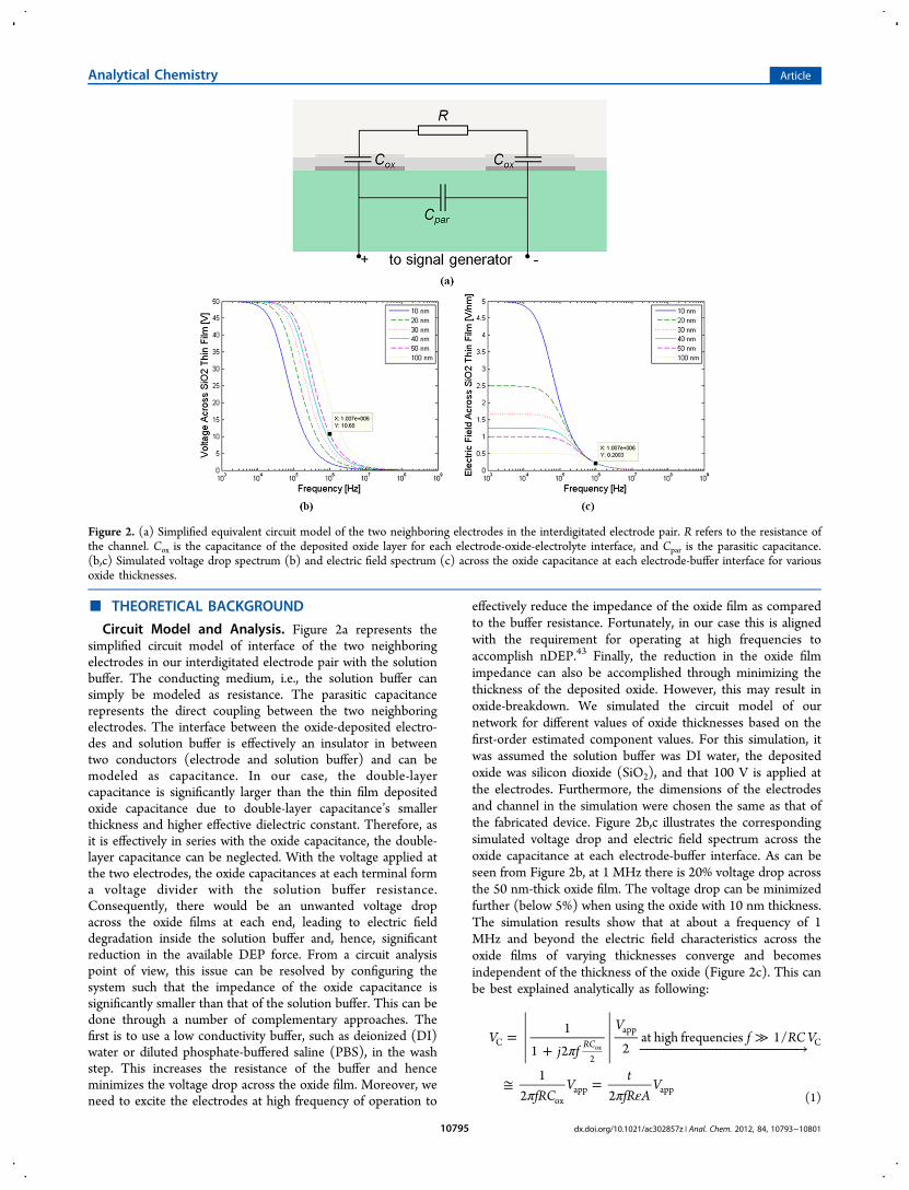
Circuit Model and Analysis. Figure 2a represents thesimplified circuit model of interface of the two neighboringelectrodes in our interdigitated electrode pair with the solutionbuffer. The conducting medium, i.e., the solution buffer cansimply be modeled as resistance. The parasitic capacitancerepresents the direct coupling between the two neighboringelectrodes. The interface between the oxide-deposited electro-des and solution buffer is effectively an insulator in betweentwo conductors (electrode and solution buffer) and can bemodeled as capacitance. In our case, the double-layercapacitance is significantly larger than the thin film depositedoxide capacitance due to double-layer capacitance’s smallerthickness and higher effective dielectric constant. Therefore, asit is effectively in series with the oxide capacitance, the double-layer capacitance can be neglected. With the voltage applied atthe two electrodes, the oxide capacitances at each terminal forma voltage divider with the solution buffer resistance.Consequently, there would be an unwanted voltage dropacross the oxide films at each end, leading to electric fielddegradation inside the solution buffer and, hence, significantreduction in the available DEP force. From a circuit analysispoint of view, this issue can be resolved by configuring thesystem such that the impedance of the oxide capacitance issignificantly smaller than that of the solution buffer. This can bedone through a number of complementary approaches. Thefirst is to use a low conductivity buffer, such as deionized (DI)water or diluted phosphate-buffered saline (PBS), in the washstep. This increases the resistance of the buffer and henceminimizes the voltage drop across the oxide film. Moreover, weneed to excite the electrodes at high frequency of operation to
effectively reduce the impedance of the oxide film as comparedto the buffer resistance. Fortunately, in our case this is alignedwith the requirement for operating at high frequencies toaccomplish nDEP.43 Finally, the reduction in the oxide filmimpedance can also be accomplished through minimizing thethickness of the deposited oxide. However, this may result inoxide-breakdown. We simulated the circuit model of ournetwork for different values of oxide thicknesses based on thefirst-order estimated component values. For this simulation, itwas assumed the solution buffer was DI water, the depositedoxide was silicon dioxide (SiO2), and that 100 V is applied atthe electrodes. Furthermore, the dimensions of the electrodesand channel in the simulation were chosen the same as that ofthe fabricated device. Figure 2b,c illustrates the correspondingsimulated voltage drop and electric field spectrum across theoxide capacitance at each electrode-buffer interface. As can beseen from Figure 2b, at 1 MHz there is 20% voltage drop acrossthe 50 nm-thick oxide film. The voltage drop can be minimizedfurther (below 5%) when using the oxide with 10 nm thickness.The simulation results show that at about a frequency of 1MHz and beyond the electric field characteristics across theoxide films of varying thicknesses converge and becomesindependent of the thickness of the oxide (Figure 2c). This canbe best explained analytically as following:
π
π π ε
=+
≫⎯ →⎯⎯⎯⎯⎯⎯⎯⎯⎯⎯⎯⎯⎯⎯⎯⎯⎯⎯⎯⎯⎯⎯⎯⎯⎯⎯⎯⎯⎯⎯⎯⎯⎯⎯⎯⎯⎯⎯⎯⎯
≅ =
Vj f
Vf RC V
fRCV
tfR A
V
1
1 2 2at high frequencies 1/
12 2
RCC
2
appC
oxapp app
ox
(1)
Figure 2. (a) Simplified equivalent circuit model of the two neighboring electrodes in the interdigitated electrode pair. R refers to the resistance ofthe channel. Cox is the capacitance of the deposited oxide layer for each electrode-oxide-electrolyte interface, and Cpar is the parasitic capacitance.(b,c) Simulated voltage drop spectrum (b) and electric field spectrum (c) across the oxide capacitance at each electrode-buffer interface for variousoxide thicknesses.
Analytical Chemistry Article
dx.doi.org/10.1021/ac302857z | Anal. Chem. 2012, 84, 10793−1080110795

where VC is the voltage drop across the oxide capacitance Cox ateach end of the electrode, R is the resistance of the solutionbuffer between the two neighboring electrodes, and Vapp is theapplied voltage with the excitation frequency f. Here, the oxidecapacitance Cox to the first order can be modeled as a parallelplate capacitance, with permittivity ε, thickness t, and area A(equal to the area bound by the width of the channel and anelectrode). Therefore, the electric field EC across the oxide athigh frequencies becomes
π ε= ≅E
Vt fR A
V1
2CC
app(2)
As can be seen from eq 2, once operating at sufficiently highfrequencies (primarily to minimize the undesired voltage dropacross the oxide), EC becomes independent of the thickness ofthe oxide. Hence, oxide-breakdown would not directly set thelower limit on the required thickness. According to oursimulation results, at 1 MHz, the electric field across the oxidewould be 0.2 V/nm which is well below the ALD SiO2
breakdown field of 1 V/nm.44
Relevant Forces. As discussed in the previous work,43 inaddition to the DEP force, the particles that are bound to thesurface experience gravitational force and the hydrodynamicdrag force. Moreover, for our improved DEP platform, sincethe applied voltage is increased the electro-thermal effects maybecome apparent.The gravitational (sedimentation) force that acts on the
particle is governed by the following equation:
π ρ ρ= −F r g43
( )SED3
b m (3)
where g is the gravitation constant, ρb is the bead density, ρm isthe medium density, and r is the particle radius. For a 2.8 μmdiameter polystyrene-magnetic bead, this comes to approx-imately 10 fN, which is orders of magnitude smaller than theother forces in our system.The hydrodynamic drag force on a bead attached to the
surface of the channel can be approximated with the followingequation:45
π η=F rk v6DRAG f (4)
where r is the bead radius, k is a nondimensional factoraccounting for wall effects (k ≈ 1.7), η is the dynamic mediumviscosity, and vf is the fluid velocity. On the basis of the resultsfrom our previous work on quantification of biomolecularinteractions,46 flow rates ranging from 10 nL/min to 10 μL/min provide drag forces between 0.2 pN and 200 pN on a 2.8μm diameter bead.In our high voltage system, the other relevant force is the
electrothermal body force acting on the fluid. This electro-thermal effect is due to spatial variations in the electric field thatcauses nonuniform Joule heating and spatially varyingpermittivity and conductivity fields in the fluid. In the presenceof an externally applied electric field, this results in Coulomband dielectric body forces and induces microscale fluid motion.Following the approach presented by Meinhart andcolleagues,47 the temperature profile of the system wassimulated using COMSOL (COMSOL, Stockholm, Sweden)and the fluid velocity field resulting from the electrothermal
Figure 3. (a) Impedance spectrum (measured vs curve-fitted model) between the two neighboring electrodes in the interdigitated electrode pair.(b,c) Characterized vs simulated voltage drop spectrum (b) and electric field spectrum (c) across the deposited 10-nm SiO2 layer on the electrodes.
Analytical Chemistry Article
dx.doi.org/10.1021/ac302857z | Anal. Chem. 2012, 84, 10793−1080110796

effect was determined. On the basis of our simulation results,for our electrode and microfluidic channel configurations with alow-conductive buffer solution and applied voltage of 50−100Vpp, the equivalent hydrodynamic drag force exerted on thebeads due to induced fluid motion was on the order of 6−60pN.Dielectrophoresis is a force applied to particles in a
nonuniform electric field as a result of differences inpolarizability of the particle and the fluid medium. The firstorder time-average DEP force acting on a dielectric sphere isgiven by
πε ε= ∇| |F r f E2 Re{ }DEP 0 m3
CM RMS2
(5)
where εm is the relative permittivity of the surroundingmedium, r is the particle radius, and ERMS is the root-mean-square value of the electric field. f CM in the above equation isthe Clausius-Massotti factor which is related to the effectivepolarizability of the particle with respect to that of the mediumand is of the form
ε ε
ε ε=
* − ** + *f
2CMp m
p m (6)
where εp* and εm* are the relative complex permittivities of theparticle and the medium, respectively.The sign of the real part of the Clausius-Massotti factor
determines whether the particle is attracted to (positive DEP)or repelled from (nDEP) a region of high electric field strength.On the basis of our previous results,43 in order to achieve DEPin its negative form for the medium conductivity range ofinterest we need to operate at the frequencies of above 1 MHz.This is aligned with the frequency requirement imposed by ourcircuit analysis. As one of the pioneers of the field, Voldman etal. through comparison of results from modeling andmeasurements demonstrated subpiconewton forces in dielec-trophoresis-based single-particle traps.48 According to our workand previous work shown in the literature, using micrometersized interdigitated electrodes, it is possible to provide DEPforces ranging from 0.1 to 10 pN when applying 1−10 Vpp atthe electrodes.45 A typical antigen−antibody interaction isroughly on the order of 400 pN. As FDEP is proportional to thesquare of the applied voltage, in this work by increasing thecapability of applying higher voltages at the electrodes we wereable to increase the DEP significantly beyond this value tocomfortably detach the bound beads from the surface.
■ RESULTS AND DISCUSSIONSApplying the standard oxygen plasma treatment process at thePDMS bonding step was only successful for the SiO2 coatedfilm. It formed a strong bond with the same order of magnitudein strength as PDMS-glass bonding which is amenable tomicrofluidic pressure driven applications. The same treatmentprocesses did not result in a strong bond for the cases of theAl2O3 and HfO2 coated thin films. At this step since weachieved a well-sealed and practical device with the pinhole-freeSiO2 coated chip (no outside channel leakage at the flow ratesof interest and beyond), we proceeded with our experimentsusing the SiO2-coated devices.To validate the developed circuit model of the device, we
measured the impedance spectrum between the twointerdigitated electrodes. Deionized (DI) water with measuredconductivity of 1.2 mS/m was used as the solution buffer.
Figure 3a illustrates the measured impedance spectrumbetween the two interdigitated electrodes. In this graph, thecurve-fitted spectrum based on the equivalent circuit model isalso overlaid. The close agreement between the two graphs notonly supports our developed circuit model for the device butalso allows us to characterize and extract the resistance value ofthe buffer as well as the oxide and parasitic capacitance values.Upon validation of the circuit model, the characterized valuesfrom the measured impedance spectrum were used to plot thevoltage drop and the electric field characteristic across thedeposited oxide film for the frequency range of interest. Figure3b,c illustrate these characteristics as well as the correspondingoriginally simulated voltage drop and electric field spectrum,based on our first-order estimate of the resistance andcapacitance values. As can be seen from these figures, oursimulation and measurement results are close. The slightdeviation between them in fact implies that the simulationresults originally led us to a more conservative conclusion byprojecting a higher voltage drop for a given frequency. On thebasis of the above results, and the available margin in designspace specifications, we can also conclude that using a moreconductive solution such as diluted PBS as our buffer wouldstill be practical when demonstrating the improved switchingcapability of nDEP (as we will see shortly).Next, we characterized the voltage tolerance of the fabricated
device by increasing the applied voltage in small steps andscanning the impedance spectrum at each point to see whetheror not the device parameters have stayed the same orsignificantly changed due to oxide breakdown or otherundesired irreversible effects. Our voltage tolerance character-ization process indicated that our device can practically provideup to 100 Vpp of voltage which practically provides nDEP onthe order of nanoNewtons above the oxide. As was visuallyevident and confirmed through comparison of impedancespectra of the device captured at each incremental voltage step,there was no sign of damage and the device parameters stayedthe same. However, increasing the applied voltage to 120 Vppresulted in bubble formation. We speculate that the bubbleformation can be attributed to the generated heat in thechannel resulting in outgassing or evaporation phenomena,with temperature approaching the boiling point (Figure 4). To
Figure 4. Upper bound on the voltage tolerance of the improved DEPdevice is limited by the bubble formation inside the channel due to thegenerated heat. The device integrity was preserved throughout theabove procedure.
Analytical Chemistry Article
dx.doi.org/10.1021/ac302857z | Anal. Chem. 2012, 84, 10793−1080110797
ensure that the device integrity was preserved after the bubbleformation, the channel was flushed and filled with buffer. Then,by capturing the impedance spectrum we verified that thedevice parameters stayed the same. We repeated the sameprocedure for three other devices to verify the bubble formationat high voltages (about 120 Vpp), while subsequently validatingthe preserved device integrity after flushing and filling thechannel. It is worth noting that here we demonstrated a designwhere about 100 Vpp of voltage is effectively dropped across thebuffer with minimal voltage and field degradation across thedeposited oxide. This implies voltage tolerance improvement ofa factor of 5 is achieved, resulting in 25-fold stronger nDEP forthe same interdigitated electrode configuration. Moreover, withour fabricated device, the upper bound on the electrode’svoltage tolerance is no longer imposed by fabricationlimitations (such as electrode corrosion in previous work orother irreversible phenomena such as possible oxide break-down, etc.) but in fact is restricted by physical phenomenaaffecting the buffer.Once the circuit model and voltage tolerance of the device
were characterized, we demonstrated the core functionality ofthe device. We first flushed the channel with diluted PBS toeliminate the air bubbles. Next, the prepared sample beads wereinjected into the channel by directly pipetting them into theinlet port. The beads were allowed to settle for 15 min so thatthey had sufficient time to bind to the surface. Negativepressure was applied to the syringe, which was connected to the
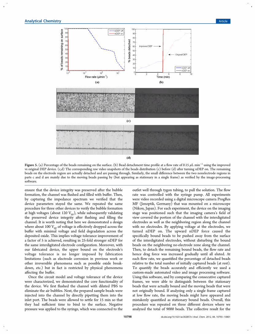
outlet well through tygon tubing, to pull the solution. The flowrate was controlled with the syringe pump. All experimentswere video recorded using a digital microscope camera ProgResMF (Jenoptik, Germany) that was mounted on a microscope(Nikon, Japan). For each experiment, the device on the imagingstage was positioned such that the imaging camera’s field ofview covered the portion of the channel with the interdigitatedelectrodes as well as the neighboring region along the channelwith no electrodes. By applying voltage at the electrodes, weturned nDEP on. The upward nDEP force caused thespecifically bound beads to be pushed away from the surfaceof the interdigitated electrodes, without disturbing the boundbeads on the neighboring no-electrode zone along the channel.Then, to detach the remaining bound beads, the flow rate andhence drag force was increased gradually until all eluted. Ateach flow rate, we quantified the percentage of detached beadsrelative to the total number of initially captured beads (at rest).To quantify the beads accurately and efficiently we used acustom-made automated video and image processing software.Using this software, and by comparing the consecutive capturedframes, we were able to distinguish between the stationarybeads that were actually bound and the moving beads that werenot originally bound. If analyzing only a single frame capturedat low flow rate, the moving beads might have appeared andmistakenly quantified as stationary bound beads. Overall, thisprocedure was repeated on three different devices where weanalyzed the total of 9000 beads. The collective result for the
Figure 5. (a) Percentage of the beads remaining on the surface. (b) Bead detachment time profile at a flow rate of 0.15 μL min−1 using the improvedvs original DEP device. (c,d) The corresponding raw video snapshots of the beads distribution (c) before (d) after turning nDEP on. The remainingbeads on the electrode region are actually detached and are passing through. Similarly, the small difference between the two nonelectrode regions inparts c and d are mainly due to the moving beads passing by (but appearing as stationary in a single frame) as verified by the image-processingsoftware.
Analytical Chemistry Article
dx.doi.org/10.1021/ac302857z | Anal. Chem. 2012, 84, 10793−1080110798

anti-IgG and IgG interaction is shown in Figure 5a for the casesof nDEP-off (the regions outside the interdigitated electrodes)and nDEP-on (applying 50 Vpp at 1 MHz). Upon turningnDEP on, almost all (99.8%) of the bound beads on theinterdigitated electrodes region got eluted without disturbingthe bound beads on the neighboring no-electrode zone alongthe channel. The remaining bound beads outside theinterdigitated electrodes region (represented as nDEP-offcurve in Figure 5a) got detached as we increased the flowrate gradually. For this case, no beads got detached up to 0.15μL min−1, and the flow rate had to be increased to 0.33 μLmin−1, 2.40 μL min−1, and 15.1 μL min−1 (equivalent dragforces of about 7 pN, 50 pN, and 300 pN) in order to remove10%, 50%, and 90% of the bound beads respectively.Finally, we further demonstrated our device’s much
improved functionality as a switch. The relevant performancemeasures in our context are ideally zero-switching responsetime upon turning the switch on, and 0 and 100% beaddetachment when the switch is off and on, respectively. In thisexperiment, after sample and surface chemistry preparation andallowing for the injected beads to settle and bind to the surface,the flow rate was set to 0.15 μL min−1 and allowed to run for atotal of 10 min. The nDEP was turned on at the end of the fifthminute. Figure 5b illustrates the bead detachment time profilefor this process as well as the detachment profile for theprevious work with nonimproved DEP device. As can be seenfrom this figure, at 0.15 μL min−1, a very small fraction of beads(about 0.3%) beads got detached in the first 5 min while nDEPwas off. At the end of the fifth minute, once the nDEP wasturned on and as expected 99.8% of beads immediately goteluted, resulting in achieving an on-to-off ratio of 333 which isabout 2 orders of magnitude improvement in this performancemeasure as compared to the previous work, where the on-to-offratio of 3.6 was demonstrated. Moreover, the elution of beadstook place almost instantly, unlike the previous work where ittook at least 4 min to detach the majority (90%) of beads.Specifically, upon applying the nDEP and within one frame ofthe captured video (with frame-capture interval of 0.4 s), thebeads were fully detached. This shows improvement inswitching response time of at least 600-fold. Representativecaptured snapshots from the video recorded experiment areshown by Figure 5c,d.Together our results demonstrate that by improving the
strength of nDEP we successfully developed a robustmicrofluidic switch to elute specifically bound beads. Theenhanced nDEP switch not only eliminated the need for elutingagents but also shows about 2 orders of magnitude ofimprovement in the switching on-to-off ratio as well as atleast 600-fold reduction in the switching response time. Havingachieved an electrokinetic switch capable of eluting 100% ofimmunobound beads instantaneously, future efforts will befocused on implementation of a high throughput multiplexingsystem by fabricating an array of electrode pairs along a singlechannel and integrating a bead detector downstream. Inaddition to this we will use this device to quantify and comparevarious protein−protein interactions and also validate newprotein biomarkers in biological samples.
■ METHODSFabrication. The microchannel with 200 μm width, 50 μm
height, and 1 cm length was fabricated in PDMS. The mastermold for the microchannel was patterned onto a siliconsubstrate using SU-8 photoresist. PDMS (10:1 prepolymer/
curing agent) was poured onto the master mold and allowed tocure at 80 °C overnight. Once the PDMS channel was formed,it was peeled off from the mold. Then, two holes of diameter 3mm were punched, one at each end, to create the channel’sinlet and outlet ports.To fabricate the electrodes, standard evaporation and lift-off
processing techniques were used. An array of interdigitated Au/Cr electrode pair was fabricated on a glass substrate withelectrode width and spacing of 7 μm each. Then, we usedatomic layer deposition (ALD) Fiji F202 system fromCambridge Nanotech to deposit a 10 nm oxide film on thesurface of the device. For this purpose, with the waferstransferred to the reaction chamber, high purity Ar was used asa carrier gas. Through a repeated cycle, pulses of tris-[dimethylamino]silane and O2 plasma were generated, for aduration of 0.3 and 20 s (at 300 W), respectively, resulting in aneffective deposition rate of 0.7 Å/cycle at 200 °C. Next, weselectively oxide-etched (dry etched) the surface to expose andaccess the electrical bonding pads. The oxide-depositedelectrode chip and the PDMS microchannel were then alignedand bonded together after standard oxygen plasma treatment.49
All three available oxide films (SiO2, Al2O3, and HfO2) wereused on different devices to test for PDMS bonding using ourstandard plasma treatment process.
Sample Preparation and Surface Chemistry. Todemonstrate the switch-like functionality in eluting specificallybound beads from the surface, we chose anti-IgG and IgGinteractions that are in the same order of magnitude in strengthas typical antibody−antigen interactions. For this purpose, 2.8μm-diameter goat antimouse IgG covered beads (initially in0.5% w/v suspension) were used. A volume of 250 μL of thissolution was washed with PBS (containing 1% BSA and 0.05%Tween) and resuspended in 50 μL of 30×-diluted PBS.To prepare the channel surface for this interaction, mouse
IgG (originally 2 mg/mL, diluted by ×100) was pipetted intothe channel and incubated for 20 min so that the IgG moleculesbecame physically adsorbed on the channel surface. This wasfollowed by introducing 1 mg/mL bovine serum albumin(BSA) in the channel to eliminate nonspecific binding. Thechannel was then flushed and filled with diluted PBS. As acontrol experiment to test for binding specificity, on a separatechip, the above steps were performed minus the addition ofmouse IgG, thus minimizing attachment of beads due tononspecific binding.
Experiment Setup. We used an impedance spectroscope(Zurich Instruments HF2IS, Switzerland) and a transimpe-dance amplifier (Zurich Instruments HF2TA, Switzerland) tocapture the impedance spectrum of the device in order tovalidate and characterize the equivalent circuit model. Thisimpedance spectroscope was also used as a signal generator inconjunction with a high voltage 50 V/V amplifier (Trek2100HF) to excite the electrodes with a sine wave at 2 MHz.Furthermore, a syringe pump (Harvard Apparatus) was used tocontrol the flow rate through the device.
■ CONCLUSIONSIn conclusion, we have achieved two significant results in thispaper. First and foremost, using ALD to fabricate a pinhole freethin film layer, we have demonstrated the ability to generatenanoNewton DEP forces. The pinhole free thin film preventscorrosion, but at the same time because of the film thickness(<20 nm) and also the high frequency applied, the electric fieldfully couples capacitively to the bulk electrolyte rather than
Analytical Chemistry Article
dx.doi.org/10.1021/ac302857z | Anal. Chem. 2012, 84, 10793−1080110799

being localized primarily across the film also resulting in filmbreakdown. The fact that we have the ability to apply DEPforces on this order of magnitude opens up the possibility of abroad range of applications. Examples include actuation of cellsat higher flow rates during cell sorting and other various cellhandling applications which up until now where DEP waslimited in utility because of its relatively weak nature.In addition to the several order of magnitude improvement
in DEP, for the first time, we have demonstrated the ability toinstantaneously detach specific protein−protein bound beadsusing electronic actuation without the need for any specialbuffer modification. The conditions we applied resulted in100% bead detachment in the case where DEP was applied,whereas no bead detachment occurs where DEP was off. Thislocalized electronic actuator will open up many possibilities forperforming rapid and inexpensive multiplexed protein bio-marker detection. The ability to inexpensively detect proteinbiomarkers in high throughput will undoubtedly have a largeimpact on clinical medicine by equipping clinicians with thetools necessary to provide more complete personalizedhealthcare.
■ AUTHOR INFORMATIONCorresponding Author*E-mail: [email protected] (S.E.); [email protected](M.J.).Author Contributions§S.E. and M.J. contributed equally. All authors contributed tothe manuscript preparation. S. Emaminejad and M. Javanmardset up the simulation platform, fabricated the microfluidicdevices, and performed the experiments.NotesThe authors declare no competing financial interest.
■ ACKNOWLEDGMENTSThe authors would like to thank M. Bendernagel for hersignificant contribution in quantifying and verifying theexperiment results through developing an automated imageprocessing software which will also be utilized for the futureextension of the project. Furthermore, the authors would like tothank J. Provine for the training, expertise, and help with atomiclayer deposition. This work was supported by the NationalInstitutes of Health through Grant PO1HG000205 and NaturalSciences and Engineering Research Council of CanadaScholarship through graduate tuition support.
■ REFERENCES(1) Hamburg, M. A.; Collins, F. S. N. Engl. J. Med. 2010, 363 (4),301−304.(2) Harvey, A.; Brand, A.; Holgate, S. T.; Kristiansen, L. V.; Lehrach,H.; Palotie, A.; Prainsack, B. New Biotechnol. 2012, 29 (6), 625−633.(3) Wei, D. Q.; Chen, Q. Curr. Drug Metab. 2012, 13 (7), 951−951.(4) Souied, E. H.; Leveziel, N. Am. J. Ophthalmol. 2012, 154 (3),427−428.(5) Iacobuzio-Donahue, C. A. J. Gastrointest. Surg. 2012, 16 (9),1651−1652.(6) Sadeghi, S.; Gilardi, G. FEBS J. 2012, 279, 345−345.(7) O’Brien, C. P. Alcohol.: Clin. Exp. Res. 2012, 36, 12a−12a.(8) Burckart, G. J.; Green, D. J. Pediatr. Transplant. 2012, 16 (6),530−532.(9) Garbis, S.; Lubec, G.; Fountoulakis, M. J. Chromatogr., A 2005,1077 (1), 1−18.(10) Ray, S.; Reddy, P. J.; Jain, R.; Gollapalli, K.; Moiyadi, A.;Srivastava, S. Proteomics 2011, 11 (11), 2139−2161.
(11) Yarmush, M. L.; Jayaraman, A. Annu. Rev. Biomed. Eng. 2002, 4,349−373.(12) MacBeath, G. Nat. Genet. 2002, 32, 526−532.(13) Schweitzer, B.; Predki, P.; Snyder, M. Proteomics 2003, 3 (11),2190−2199.(14) Price, J. V.; Tangsombatvisit, S.; Xu, G. Y.; Yu, J. T.; Levy, D.;Baechler, E. C.; Gozani, O.; Varma, M.; Utz, P. J.; Liu, C. L. Nat. Med.2012, 18 (9), 1434−U190.(15) Gemovic, B.; Perovic, V.; Glisic, S.; Veljkovic, N. FEBS J. 2012,279, 295−295.(16) Lalli, D.; De Pablo, R.; Del Conte, R.; Turano, P. FEBS J. 2012,279, 437−437.(17) Mamitsuka, H. Wiley Interdiscip. Rev.: Data Min. KnowledgeDiscovery 2012, 2 (5), 400−410.(18) Takayama, Y.; Clore, G. M. J. Biol. Chem. 2012, 287 (32),26962−26970.(19) Pierrot, C.; Freville, A.; Olivier, C.; Souplet, V.; Khalife, J. Curr.Pharm. Des. 2012, 18 (24), 3522−3530.(20) Smith, M. C.; Gestwicki, J. E. Expert Rev. Mol. Med. 2012, 14.(21) Chen, C.; Zhao, J. F.; Huang, Q.; Wang, R. S.; Zhang, X. S. BMCSyst. Biol. 2012, 6.(22) Salimi-Moosavi, H.; Rathanaswami, P.; Rajendran, S.; Toupikov,M.; Hill, J. Anal. Biochem. 2012, 426 (2), 134−141.(23) Iwamoto, S.; Iwamoto, A. T.; Cha, J.; Clark, T.; Lu, M.; Breen,C.; Bhawan, J.; Falanga, V. Am. J. Dermatopathol. 2009, 31 (3), 218−222.(24) Satterfield, M. B.; Lippa, K.; Lu, Z. Q.; Salit, M. L. J. Res. Natl.Inst. Stand. Technol. 2008, 113 (3), 157−174.(25) Microarray scanner. Scientist 2005, 19, (16), 30-31.(26) Shi, L. M.; Tong, W. D.; Su, Z. Q.; Han, T.; Han, J.; Puri, R. K.;Fang, H.; Frueh, F. W.; Goodsaid, F. M.; Guo, L.; Branham, W. S.;Chen, J. J.; Xu, Z. A.; Harris, S. C.; Hong, H. X.; Xie, Q.; Perkins, R.G.; Fuscoe, J. C. BMC Bioinf. 2005, 6.(27) Sinclair, M. B.; Timlin, J. A.; Haaland, D. M.; Werner-Washburne, M. Appl. Opt. 2004, 43 (10), 2079−2088.(28) Biener, G.; Greenbaum, A.; Isikman, S. O.; Lee, K.; Tseng, D.;Ozcan, A. Lab Chip 2011, 11 (16), 2738−2743.(29) Bishara, W.; Isikman, S. O.; Ozcan, A. Ann. Biomed. Eng. 2012,40 (2), 251−262.(30) Bishara, W.; Zhu, H. Y.; Ozcan, A. Opt. Express 2010, 18 (26),27499−27510.(31) Coskun, A. F.; Sencan, I.; Su, T. W.; Ozcan, A., LensfreeFluorescent On-Chip Imaging of Transgenic Caenorhabditis elegansOver an Ultra-Wide Field-of-View. PLoS One 2011, 6, (1).(32) Isikman, S. O.; Bishara, W.; Mavandadi, S.; Yu, F. W.; Feng, S.;Lau, R.; Ozcan, A. Proc. Natl. Acad. Sci. U.S.A. 2011, 108 (18), 7296−7301.(33) Isikman, S. O.; Bishara, W.; Mudanyali, O.; Sencan, I.; Su, T.W.; Tseng, D. K.; Yaglidere, O.; Sikora, U.; Ozcan, A. IEEE J. Sel. Top.Quantum Electron. 2012, 18 (3), 1059−1072.(34) Isikman, S. O.; Bishara, W.; Zhu, H. Y.; Ozcan, A., OptofluidicTomography on a Chip. Appl. Phys. Lett. 2011, 98, (16).(35) Isikman, S. O.; Greenbaum, A.; Lee, M.; Bishara, W.; Mudanyali,O.; Su, T. W.; Ozcan, A. Anal. Cell. Pathol. 2012, 35 (4), 229−247.(36) Tseng, D.; Mudanyali, O.; Oztoprak, C.; Isikman, S. O.; Sencan,I.; Yaglidere, O.; Ozcan, A. Lab Chip 2010, 10 (14), 1787−1792.(37) Zhu, H. Y.; Mavandadi, S.; Coskun, A. F.; Yaglidere, O.; Ozcan,A. Anal. Chem. 2011, 83 (17), 6641−6647.(38) Javanmard, M.; Babrzadeh, F.; Davis, R. W., Microfluidic forcespectroscopy for characterization of biomolecular interactions withpiconewton resolution. Appl. Phys. Lett. 2010, 97, (17).(39) Neuman, K. C.; Nagy, A. Nat. Methods 2008, 5 (6), 491−505.(40) Auerswald, J.; Widmer, D.; de Rooij, N. F.; Sigrist, A.; Staubli,T.; Stokli, T.; Knapp, H. F. Electrophoresis 2005, 26 (19), 3697−3705.(41) Li, H. B.; Zheng, Y. N.; Akin, D.; Bashir, R. J. Microelectromech.Syst. 2005, 14 (1), 103−112.(42) Park, I. S.; Eom, K.; Son, J.; Chang, W. J.; Park, K.; Kwon, T.;Yoon, D. S.; Bashir, R.; Lee, S. W. ACS Nano 2012, 6 (10), 8665−73.
Analytical Chemistry Article
dx.doi.org/10.1021/ac302857z | Anal. Chem. 2012, 84, 10793−1080110800

(43) Javanmard, M.; Emaminejad, S.; Dutton, R. W.; Davis, R. W.Anal. Chem. 2012, 84 (3), 1432−1438.(44) Seok-Jun, W.; Sungin, S.; Myung Soo, H.; Hyeong Joon, K.Electron Device Lett., IEEE 2010, 31 (8), 857−859.(45) Li, H.; Yanan, Z.; Akin, D.; Bashir, R. J. Microelectromech. Syst.2005, 14 (1), 103−112.(46) Javanmard, M.; Babrzadeh, F.; Davis, R. W. Appl. Phys. Lett.2010, 97, 173704.(47) Meinhart, C.; Wang, D.; Turner, K. Biomed. Microdevices 2003, 5(2), 139−145.(48) Voldman, J.; Braff, R. A.; Toner, M.; Gray, M. L.; Schmidt, M. A.Biophys. J. 2001, 80 (1), 531−542.(49) McDonald, J. C.; Duffy, D. C.; Anderson, J. R.; Chiu, D. T.; Wu,H.; Schueller, O. J. A.; Whitesides, G. M. Electrophoresis 2000, 21 (1),27−40.
Analytical Chemistry Article
dx.doi.org/10.1021/ac302857z | Anal. Chem. 2012, 84, 10793−1080110801
Copyright © 2022 FDOKUMEN