Single-nanopore investigations with ion conductance microscopy
8
CHEN ET AL . VOL. 5 ’ NO. 10 ’ 8404–8411 ’ 2011 www.acsnano.org 8404 September 19, 2011 C 2011 American Chemical Society Single-Nanopore Investigations with Ion Conductance Microscopy Chiao-Chen Chen, Yi Zhou, and Lane A. Baker * Department of Chemistry, Indiana University, 800 E. Kirkwood Avenue, Bloomington, Indiana 47405, United States A s the size of a pore shrinks, new physical properties can be observed due to the high surface areavolume relationship. 1 Particularly at the nanoscale, the electrical double layer, 25 surface con- ductivities, 68 and geometric asymmetry 9,10 can result in new properties not observed at larger scales. Studies of transport at these small scales;particularly at the level of single nanopores;are fertile ground to develop deeper knowledge of the fun- damentals of physical and biophysical processes. 1113 Further, applications of nano- pores in the venues of chemical separa- tions 1417 and sensor development 1822 promise advances in fields as diverse as genetic sequencing 2327 and fuel cells. 2832 Thus, new tools to study nanopores and nanoscale transport may find significant impact in the realm of both fundamental and applied sciences. Previous applications of scanning probe microscopies to the study of nanopores have demonstrated uti- lity in determination of conductivity path- ways and measurement of local concent- rations or conductivities in the vicinity of the nanopore. 3339 Herein, we describe a mod- ified three-electrode ion conductance mi- croscope and demonstrate measurement of the properties of a single pore. With this configuration, the currentvoltage proper- ties of individual pores can be interrogated while scanning or at fixed positions. Mea- surements of the conductance properties of a single cylindrical pore and a single conical pore are demonstrated. Scanning ion conductance microscopy (SICM) scans the surface of a sample with a nanometer scale pipet (nanopipet), often to collect topographic information in a non- invasive fashion. 4045 In SICM, the position of the pipet is controlled by carefully moni- toring a small gap between the sample and pipet. The resistance of this gap (termed an access resistance) is a strong function of tipsample separation and provides a method for feedback. 4650 In addition to feedback control, under certain imaging con- ditions or scanning modes, ion currents from the pipet can also be monitored directly to characterize properties of the sample. 41,5154 Here, membranes with single pores (cylindrical and conical in shape) have been prepared via the track-etch method. 55 A modified scanning ion conductance micro- scope with an additional electrode that serves to drive ions through this single pore is employed to examine nanopore conduc- tivity. We find that for the case of a single pore this three-electrode system results in a predictable interaction between the elec- trode of the SICM and the working electrode of the nanopore. Advantages of this three- electrode configuration over a more con- ventional two-electrode SICM include inde- pendent control of the cross-membrane potential and enhanced contrast in the mea- surement of nanopore conductance. (A de- tailed description of the experimental ad- vantages is provided in the Supporting Information.) Further, through careful con- trol of pipet position (relative to the mem- brane pore) and control of the working electrode potential, the currentvoltage re- sponse for the pore in the membrane can be measured with the pipet. Nanopipets were also capable of “dipping into” membrane pores, to operate within the pore itself. 56 * Address correspondence to [email protected]. Received for review August 19, 2011 and accepted September 17, 2011. Published online 10.1021/nn203205s ABSTRACT A three-electrode scanning ion conductance microscope (SICM) was used to investigate the local currentvoltage properties of a single nanopore. In this experimental configuration, the response measured is a function of changes in the resistances involved in the pathways of ion migration. Single-nanopore membranes utilized in this study were prepared with an epoxy painting procedure to isolate a single nanopore from a track-etch multipore membrane. Currentvoltage responses measured with the SICM probe in the vicinity of a single nanopore were investigated in detail and agreed well with equivalent circuit models proposed in this study. With this modified SICM, the currentvoltage responses characterized for the case of a single cylindrical pore and a single conical pore exhibit distinct conductance properties that originate from the geometry of nanopores. KEYWORDS: microscopy . nanopore . conductance . membrane and ion transport ARTICLE
Transcript of Single-nanopore investigations with ion conductance microscopy

CHEN ET AL . VOL. 5 ’ NO. 10 ’ 8404–8411 ’ 2011
www.acsnano.org
8404
September 19, 2011
C 2011 American Chemical Society
Single-Nanopore Investigations withIon Conductance MicroscopyChiao-Chen Chen, Yi Zhou, and Lane A. Baker*
Department of Chemistry, Indiana University, 800 E. Kirkwood Avenue, Bloomington, Indiana 47405, United States
As the size of a pore shrinks, newphysical properties can be observeddue to the high surface area�volume
relationship.1 Particularly at the nanoscale,the electrical double layer,2�5 surface con-ductivities,6�8 and geometric asymmetry9,10
can result in new properties not observedat larger scales. Studies of transport atthese small scales;particularly at the levelof single nanopores;are fertile groundto develop deeper knowledge of the fun-damentals of physical and biophysicalprocesses.11�13 Further, applications of nano-pores in the venues of chemical separa-tions14�17 and sensor development18�22
promise advances in fields as diverse asgenetic sequencing23�27 and fuel cells.28�32
Thus, new tools to study nanopores andnanoscale transport may find significantimpact in the realm of both fundamentaland applied sciences. Previous applicationsof scanning probe microscopies to thestudy of nanopores have demonstrated uti-lity in determination of conductivity path-ways and measurement of local concent-rations or conductivities in the vicinity of thenanopore.33�39 Herein, we describe a mod-ified three-electrode ion conductance mi-croscope and demonstratemeasurement ofthe properties of a single pore. With thisconfiguration, the current�voltage proper-ties of individual pores can be interrogatedwhile scanning or at fixed positions. Mea-surements of the conductance properties ofa single cylindrical pore and a single conicalpore are demonstrated.Scanning ion conductance microscopy
(SICM) scans the surface of a sample with ananometer scale pipet (nanopipet), often tocollect topographic information in a non-invasive fashion.40�45 In SICM, the positionof the pipet is controlled by carefully moni-toring a small gap between the sample andpipet. The resistance of this gap (termedan access resistance) is a strong functionof tip�sample separation and provides amethod for feedback.46�50 In addition to
feedback control, under certain imaging con-ditions or scanning modes, ion currents fromthe pipet can also be monitored directly tocharacterize properties of the sample.41,51�54
Here, membranes with single pores(cylindrical and conical in shape) have beenprepared via the track-etch method.55 Amodified scanning ion conductance micro-scope with an additional electrode thatserves to drive ions through this single poreis employed to examine nanopore conduc-tivity. We find that for the case of a singlepore this three-electrode system results in apredictable interaction between the elec-trode of the SICMand theworking electrodeof the nanopore. Advantages of this three-electrode configuration over a more con-ventional two-electrode SICM include inde-pendent control of the cross-membranepotential and enhanced contrast in themea-surement of nanopore conductance. (A de-tailed description of the experimental ad-vantages is provided in the SupportingInformation.) Further, through careful con-trol of pipet position (relative to the mem-brane pore) and control of the workingelectrode potential, the current�voltage re-sponse for the pore in the membrane can bemeasured with the pipet. Nanopipets werealso capable of “dipping into” membranepores, to operate within the pore itself.56
* Address correspondence [email protected].
Received for review August 19, 2011and accepted September 17, 2011.
Published online10.1021/nn203205s
ABSTRACT A three-electrode scanning ion conductance microscope (SICM) was used to
investigate the local current�voltage properties of a single nanopore. In this experimental
configuration, the response measured is a function of changes in the resistances involved in the
pathways of ion migration. Single-nanopore membranes utilized in this study were prepared with an
epoxy painting procedure to isolate a single nanopore from a track-etch multipore membrane.
Current�voltage responses measured with the SICM probe in the vicinity of a single nanopore were
investigated in detail and agreed well with equivalent circuit models proposed in this study. With
this modified SICM, the current�voltage responses characterized for the case of a single cylindrical
pore and a single conical pore exhibit distinct conductance properties that originate from the
geometry of nanopores.
KEYWORDS: microscopy . nanopore . conductance . membrane and ion transport
ARTIC
LE

CHEN ET AL . VOL. 5 ’ NO. 10 ’ 8404–8411 ’ 2011
www.acsnano.org
8405
Amodel electrical circuit is proposed that predicts theobserved response. Additional finite element simulationsfurther confirm the proposed mechanism. The responsefor a cylindrical pore is described in detail, and measure-ment of a conical nanopore with rectified current flowis demonstrated. These preliminary results demonstratethat this three-electrode SICM provides a platform tocharacterize individual nanopores independent of otherstructures involved in the same system. Ultimately, thistoolwill provide amethod tomonitor nanopores inmorecomplex biological and sensing environments.
RESULTS AND DISCUSSION
Current�Voltage Responses Measured with Modified SICM.Single nanopores were isolated, and optical and elec-tron micrographs of one such pore are shown inFigure 1. Effects of cross-membrane potentials on thetopography and current images measured by SICMfor single-nanopore membranes were recorded withdistance-modulated (ac) feedback. Themodified three-electrode SICM employed (Figure 2) allows for inde-pendent potential control of the working electrode(WE) and pipet electrode (PE), as referenced to a com-mon reference electrode (RE). For all experiments re-ported in this study, the PE was held atþ0.1 V and theRE served as ground. Topography and the correspond-ing current images obtained with three different work-ing electrode potentials (þ0.3, 0, and �0.3 V) areshown in Figure 3. Comparison of these three currentimages reveals that when the nanopipet scans over apore, a negative working electrode potential (�0.3 Vapplied here) increases the potential drop across thePE and thus produces an increase in the pipet current.This results in an enhancement (greater current) of theion current image that is obtained by plotting thechanges in pipet current (ΔI) in x�y coordinates, asshown in Figure 3c. In contrast, when the WE was heldat þ0.3 V, the magnitude of the current image (ΔI)reduced to negative values (Figure 3d), as a result ofreduction in the pipet currents due to the decrease ofthe voltage drop across the PE.
To better investigate the effect of the migrationcurrents on the pipette currents under various working
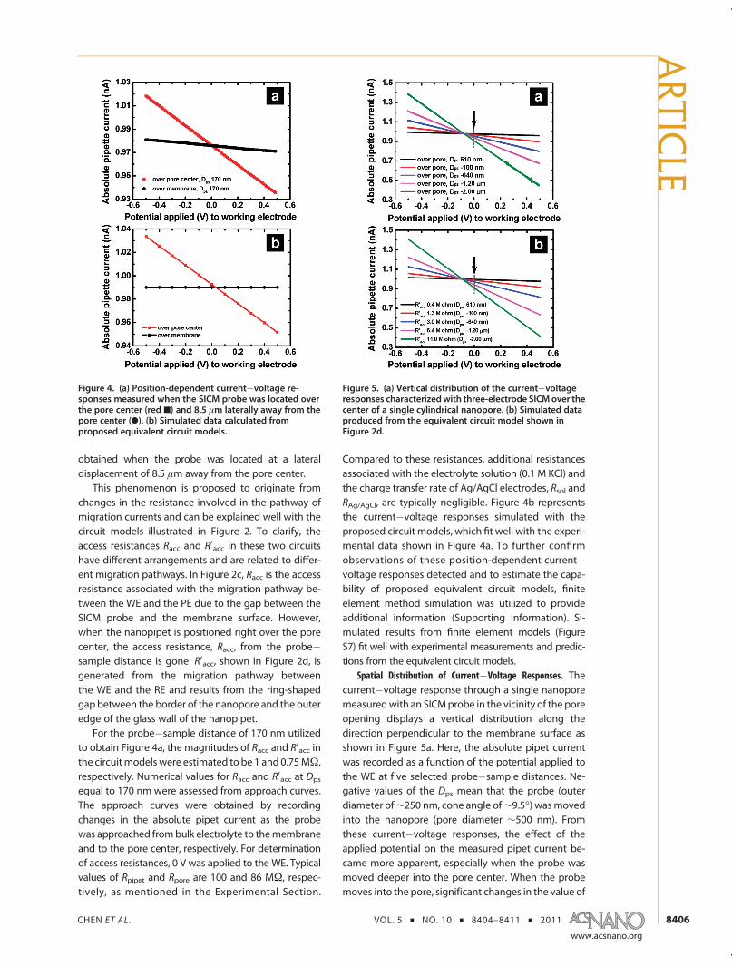
electrode potentials, instead of scanning the pipet,which can complicate the interpretation of recordedsignals,51,52 ion currents were measured with the SICMprobe at defined locations with the pipet in a fixedposition. Figure 4a represents the relationship betweenthe working electrode potential and currents measuredat a vertical probe�sample distance (Dps) of 170 nm.Here the probe is laterally positioned right over(Figure 4a, red 9) and far away (Figure 4a, b) from thecenter of a single nanopore as a function of the potentialapplied to theWE.When the SICMprobewaspositionedover the pore center, the slope of the current�voltageresponsemeasured was about 10 times larger than that
Figure 1. Optical (a) and SEM (b, c) images of a represen-tative prepared single cylindrical poremembrane. The largeoval shape observed in the optical image (a) indicates theboundary of the epoxy painting, inside of which the mem-brane can be exposed to electrolyte from both sides. Whitedashed circles on (a, b) indicate the locations of the isolatednanopores on the membrane. The pore diameter of theisolated cylindrical pore (c) shownherewas characterized as542 nm.
Figure 2. Schematic (a, b) of the relative positions of anSICM probe to a single pore membrane mounted on aperfusion cell. When the SICM probe is away from the porecenter (a), the corresponding equivalent circuit (c) involvesan access resistance, Racc, generated from the probe�sampleseparation. In contrast, when the SICM is positioned over thepore center (b), another access resistance, R0acc, results fromthe gap between the borders of the nanopore and the outeredge of the glass wall of the nanopipet and is present in theequivalent circuit (d). PE: pipet electrode, RE: referenceelectrode, and WE: working electrode.
Figure 3. Topography (a) and the corresponding currentimages (b, c, d) of an isolated single nanopore measuredwith the three-electrode SICM described here. Images cor-respond to (b) 0 V, (c) �0.3 V, and (d) þ0.3 V applied to theworking electrode (WE). Scale bar: 1 μm.
ARTIC
LE
CHEN ET AL . VOL. 5 ’ NO. 10 ’ 8404–8411 ’ 2011
www.acsnano.org
8406
obtained when the probe was located at a lateraldisplacement of 8.5 μm away from the pore center.
This phenomenon is proposed to originate fromchanges in the resistance involved in the pathway ofmigration currents and can be explained well with thecircuit models illustrated in Figure 2. To clarify, theaccess resistances Racc and R0acc in these two circuitshave different arrangements and are related to differ-ent migration pathways. In Figure 2c, Racc is the accessresistance associated with the migration pathway be-tween the WE and the PE due to the gap between theSICM probe and the membrane surface. However,when the nanopipet is positioned right over the porecenter, the access resistance, Racc, from the probe�sample distance is gone. R0acc, shown in Figure 2d, isgenerated from the migration pathway betweenthe WE and the RE and results from the ring-shapedgap between the border of the nanopore and the outeredge of the glass wall of the nanopipet.
For the probe�sample distance of 170 nm utilizedto obtain Figure 4a, the magnitudes of Racc and R0acc inthe circuit models were estimated to be 1 and 0.75MΩ,respectively. Numerical values for Racc and R0acc at Dps
equal to 170 nm were assessed from approach curves.The approach curves were obtained by recordingchanges in the absolute pipet current as the probewas approached frombulk electrolyte to themembraneand to the pore center, respectively. For determinationof access resistances, 0 V was applied to the WE. Typicalvalues of Rpipet and Rpore are 100 and 86 MΩ, respec-tively, as mentioned in the Experimental Section.
Compared to these resistances, additional resistancesassociated with the electrolyte solution (0.1 M KCl) andthe charge transfer rate of Ag/AgCl electrodes, Rsol andRAg/AgCl, are typically negligible. Figure 4b representsthe current�voltage responses simulated with theproposed circuit models, which fit well with the experi-mental data shown in Figure 4a. To further confirmobservations of these position-dependent current�voltage responses detected and to estimate the capa-bility of proposed equivalent circuit models, finiteelement method simulation was utilized to provideadditional information (Supporting Information). Si-mulated results from finite element models (FigureS7) fit well with experimental measurements and predic-tions from the equivalent circuit models.
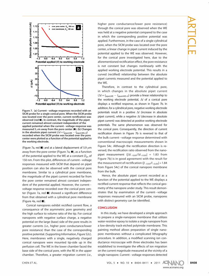
Spatial Distribution of Current�Voltage Responses. Thecurrent�voltage response through a single nanoporemeasuredwith an SICMprobe in the vicinity of the poreopening displays a vertical distribution along thedirection perpendicular to the membrane surface asshown in Figure 5a. Here, the absolute pipet currentwas recorded as a function of the potential applied tothe WE at five selected probe�sample distances. Ne-gative values of the Dps mean that the probe (outerdiameter of∼250 nm, cone angle of∼9.5�) wasmovedinto the nanopore (pore diameter ∼500 nm). Fromthese current�voltage responses, the effect of theapplied potential on the measured pipet current be-came more apparent, especially when the probe wasmoved deeper into the pore center. When the probemoves into the pore, significant changes in the value of
Figure 4. (a) Position-dependent current�voltage re-sponses measured when the SICM probe was located overthe pore center (red 9) and 8.5 μm laterally away from thepore center (b). (b) Simulated data calculated fromproposed equivalent circuit models.
Figure 5. (a) Vertical distribution of the current�voltageresponses characterizedwith three-electrode SICMover thecenter of a single cylindrical nanopore. (b) Simulated dataproduced from the equivalent circuit model shown inFigure 2d.
ARTIC
LE

CHEN ET AL . VOL. 5 ’ NO. 10 ’ 8404–8411 ’ 2011
www.acsnano.org
8407
the access resistance, R0acc, are observed. This is likelya consequence of enhanced interactions betweenthe charged walls of the pipet and the pore, similarto so-called “squeezing effects” observed in nanoporestudies.40,57 A more direct evidence for the increase ofR0acc can be realized from the decrease in the absolutepipet current with the reduction of the probe�sampledistance when the working electrode was maintainedat 0 V (marked with black arrow in Figure 5a).
This vertical distribution of the current�voltageresponses can be reproduced with the circuit modelshown in Figure 2d, which describes the active com-ponents (resistors and capacitors) involved in thesystem when the nanopipet is positioned over thepore center. Numerical values of R0acc utilized in thecircuit model that correspond to various probe�sample distances were estimated on the basis of ap-proach curves as described previously. Simulated datafrom the circuit model are illustrated in Figure 5b,where the current�voltage response of the greatestslope was obtained with the largest R0acc and related tothat recorded with the most negative Dps shown inFigure 5a. In contrast, when the probe�sample separa-tion is large (Dps = 610 nm), the pipet current remainedrelatively constant independent of the potential ap-plied to the WE due to the small access resistance(R0acc = 0.4 MΩ).
In addition to vertical distribution, current�voltageresponses measured with an SICM probe at a constantprobe�sample distance also demonstrate depen-dence on lateral displacement from the pore center.Selected current�voltage (I�V) responses recordedfrom 0 to 8.55 μm away from the pore center atDps = 170 nm demonstrate a lateral distribution shownin Figure 6a. With consideration of the geometry of theSICMprobe (i.d.≈ 60 nm, o.d.≈ 250 nm) and the singlenanopore (∼500 nm in diameter), the probe openingand the pore opening are completely overlapped (i.e.,Racc that results from the small probe�sample gapdoes not exist) at lateral displacements from 0 to0.18 μm, and thus the behavior of I�V responsesrecorded are dominated by the access resistance, R0acc,in the circuit model shown in Figure 2d (indicated asgroup 1 in Figure 6a). Responses measured at lateraldisplacements larger than 0.33 μm (classified as group3 in Figure 6a) show similar and more gradual slopes.The behavior of these I�V responses can be explainedwith the circuit model illustrated in Figure 2c. Sincethe SICM probe was far from the single nanopore,the access resistance, Racc, depends on the nano-scale probe�sample gap only. For the current�voltageresponse recorded at the lateral displacement of0.33 μm (group 2 in Figure 6a), the tip opening of theSICM probe was moved away from the pore openingwhile the nanopipet still partially overlapped the singlenanopore. Consequently, both Racc and R0acc affectedthe magnitude of pipet currents measured and thus
resulted in an I�V relationship located between the twoextreme conditions in which the current�voltage res-ponses were governed by only Racc or R0acc, respectively.
From the I�V responses recorded when the SICMprobe was moved laterally away from the porecenter, line profiles of the current magnitude mea-sured at various applied potentials can be recon-structed. Figure 6b illustrates the reconstructed lineprofiles of the pipet current measured at five repre-sentative applied potentials. Potential applied to theWE results in the greatest changes in current magni-tude when the nanopipet was located at the centerof the single pore. In contrast, the magnitude of thecurrents measured was fairly constant under a givenapplied potential when the SICM probe was away fromthe pore center.
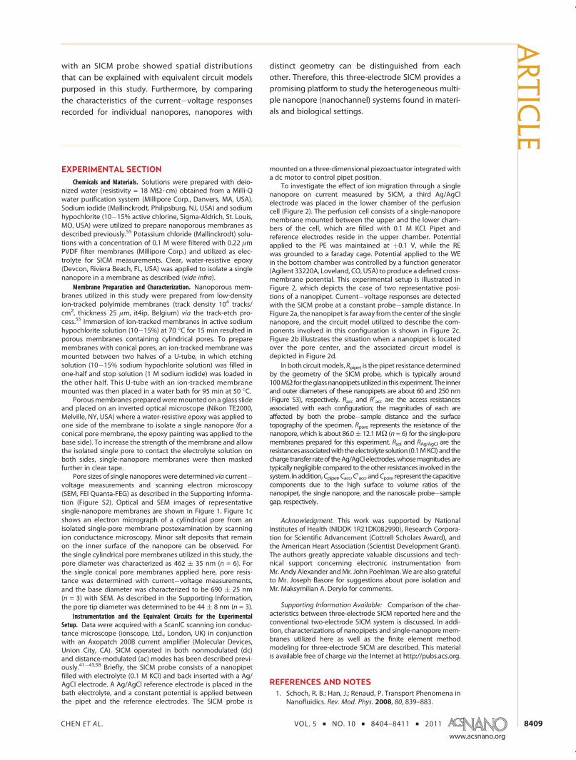
Characterization of Pore Geometry. In addition to thecase of a single cylindrical pore examined in theexperiments discussed above, the current�voltageresponse through a single conical pore was character-ized with this three-electrode SICM as well. The singleconical pore membrane was prepared by the epoxypainting method described in the Experimental Sec-tion, and a conical pore with a base diameter of 690(25 nm (n = 3) and a tip diameter of 44 ( 8 nm (n = 3)was isolated for this experiment. The single conicalpore membrane was mounted tip-side up on theperfusion cell in which the SICM probe was allowedto access the tip side of the conical pore.
Figure 7a shows pipet currents, measured overthe center of the tip opening of the conical pore
Figure 6. (a) Current�voltage responses measured with anSICMprobe (Dps = 170nm) at different lateral displacementsfrom the pore center. (b) Line profiles of the currentmagnitude measured at various applied potentials recon-structed from current�voltage responses recorded at dif-ferent lateral displacements.
ARTIC
LE
CHEN ET AL . VOL. 5 ’ NO. 10 ’ 8404–8411 ’ 2011
www.acsnano.org
8408
(Figure 7a, red 9) and at a lateral displacement of 5.9 μmaway from the pore center (Figure 7a, b), as a functionof the potential applied to the WE at a constant Dps of150 nm. From this plot, differences of current�voltageresponses measured with SICM that depend on pipetposition can also be observed with the conical poremembrane. Similar to a cylindrical pore membrane,the magnitude of the pipet current recorded far fromthe pore center remained almost constant indepen-dent of the potential applied. However, the current�voltage response recorded over the conical pore cen-ter (Figure 7a, red 9) showed a significant differencefrom that obtained with a cylindrical pore membrane(Figure 4a, red 9).
Conical nanopores exhibit rectified current flow, aconsequence of the asymmetric pore geometry andthe high surface to volume ratio of the tip. For conicalnanopores with negative surface charge, a negativepotential on the large (base) side of the pore results ingreater currents (i.e., higher pore conductance/lowerpore resistance) than the case of the correspondingpositive potential. (Supporting Information, Figure S2c).Here, membranes with a single, negatively chargedconical nanopore were mounted tip-side up in theperfusion cell. The WE in the lower chamber faced thebase side of the conical pore, with the RE in the upperchamber. Therefore, a greater migration current (i.e.,
higher pore conductance/lower pore resistance)through the conical pore was observed when the WEwas held at a negative potential compared to the casein which the corresponding positive potential wasapplied. Furthermore, in the case of a single cylindricalpore, when the SICM probe was located over the porecenter, a linear change in pipet current induced by thepotential applied to the WE was observed. However,for the conical pore investigated here, due to theaforementioned rectification effect, the pore resistanceis not constant but changes nonlinearly with theapplied working electrode potential. This results in acurved (rectified) relationship between the absolutepipet currents measured and the potential applied tothe WE.
Therefore, in contrast to the cylindrical pore,in which changes in the absolute pipet current(ΔI = Ipipet,WE � Ipipet,WE=0) provide a linear relationship tothe working electrode potential, ΔI of a conical poredisplays a rectified response, as shown in Figure 7b. Inaddition, for a cylindrical pore, negativeworking electrodepotentials result in a positive ΔI (increase in absolutepipet current), while a negative ΔI (decrease in absolutepipet current) was detected at positive working electrodepotentials. The same phenomenon was observed forthe conical pore. Consequently, the direction of currentrectification shown in Figure 7b is reversed to that ofthe bulk current�voltage response determined withconventional macroscopic measurements shown inFigure S4c. Although the rectification direction is re-versed, the rectification ratio observed from the nano-pipet measurement (|ΔI�0.6V/ΔIþ0.6V| = 1.83 fromFigure 7b) is in good agreement with the result forthe measurement of rectification (|I�0.6V/Iþ0.6V| = 1.84from Figure S4c) of the conical nanopore membranefrom the bulk.
Hence, the absolute pipet current recorded as afunction of the potential applied to the WE displays arectified current response that reflects the conical geo-metry of the nanopore under study. This result demon-strates that by examination of the current�voltageresponses measured with an SICM probe, nanoporeswith distinct geometry can be identified.
CONCLUSION
In this study, we have developed a simple approachto prepare a single-nanopore membrane that utilizeswater-resistive epoxy to isolate a single nanopore froma low-density track-etched polyimide membrane. Thispainting method allows preparation of single nano-pore membranes without a complicated lithographyprocedure. In addition, a modified scanning ion con-ductance microscope with three electrodes has beenestablished to investigate the effects of ion migrationon the current magnitude measured at the vicinity of asingle nanopore. Current�voltage responses detected
Figure 7. (a) Current�voltage responses recorded with anSICM probe for a single conical pore. When the SICM probewas located over the pore center, current rectification wasobserved (red 9). In contrast, the magnitude of the pipetcurrent remained almost constant independent of theapplied potential when the current�voltage response wasmeasured 5 μm away from the pore center (b). (b) Changesin the absolute pipet current (ΔI = Ipipet,WE � Ipipet,WE=0)recorded when the SICM probe was located over the porecenter were plotted as a function of the potential applied tothe working electrode.
ARTIC
LE
CHEN ET AL . VOL. 5 ’ NO. 10 ’ 8404–8411 ’ 2011
www.acsnano.org
8409
with an SICM probe showed spatial distributionsthat can be explained with equivalent circuit modelspurposed in this study. Furthermore, by comparingthe characteristics of the current�voltage responsesrecorded for individual nanopores, nanopores with
distinct geometry can be distinguished from eachother. Therefore, this three-electrode SICM provides apromising platform to study the heterogeneous multi-ple nanopore (nanochannel) systems found in materi-als and biological settings.
EXPERIMENTAL SECTION
Chemicals and Materials. Solutions were prepared with deio-nized water (resistivity = 18 MΩ 3 cm) obtained from a Milli-Qwater purification system (Millipore Corp., Danvers, MA, USA).Sodium iodide (Mallinckrodt, Philipsburg, NJ, USA) and sodiumhypochlorite (10�15% active chlorine, Sigma-Aldrich, St. Louis,MO, USA) were utilized to prepare nanoporous membranes asdescribed previously.55 Potassium chloride (Mallinckrodt) solu-tions with a concentration of 0.1 M were filtered with 0.22 μmPVDF filter membranes (Millipore Corp.) and utilized as elec-trolyte for SICM measurements. Clear, water-resistive epoxy(Devcon, Riviera Beach, FL, USA) was applied to isolate a singlenanopore in a membrane as described (vide infra).
Membrane Preparation and Characterization. Nanoporous mem-branes utilized in this study were prepared from low-densityion-tracked polyimide membranes (track density 104 tracks/cm2, thickness 25 μm, it4ip, Belgium) via the track-etch pro-cess.55 Immersion of ion-tracked membranes in active sodiumhypochlorite solution (10�15%) at 70 �C for 15 min resulted inporous membranes containing cylindrical pores. To preparemembranes with conical pores, an ion-tracked membrane wasmounted between two halves of a U-tube, in which etchingsolution (10�15% sodium hypochlorite solution) was filled inone-half and stop solution (1 M sodium iodide) was loaded inthe other half. This U-tube with an ion-tracked membranemounted was then placed in a water bath for 95 min at 50 �C.
Porousmembranes preparedweremounted on a glass slideand placed on an inverted optical microscope (Nikon TE2000,Melville, NY, USA) where a water-resistive epoxy was applied toone side of the membrane to isolate a single nanopore (for aconical pore membrane, the epoxy painting was applied to thebase side). To increase the strength of the membrane and allowthe isolated single pore to contact the electrolyte solution onboth sides, single-nanopore membranes were then maskedfurther in clear tape.
Pore sizes of single nanoporeswere determined via current�voltage measurements and scanning electron microscopy(SEM, FEI Quanta-FEG) as described in the Supporting Informa-tion (Figure S2). Optical and SEM images of representativesingle-nanopore membranes are shown in Figure 1. Figure 1cshows an electron micrograph of a cylindrical pore from anisolated single-pore membrane postexamination by scanningion conductance microscopy. Minor salt deposits that remainon the inner surface of the nanopore can be observed. Forthe single cylindrical pore membranes utilized in this study, thepore diameter was characterized as 462 ( 35 nm (n = 6). Forthe single conical pore membranes applied here, pore resis-tance was determined with current�voltage measurements,and the base diameter was characterized to be 690 ( 25 nm(n = 3) with SEM. As described in the Supporting Information,the pore tip diameter was determined to be 44 ( 8 nm (n = 3).
Instrumentation and the Equivalent Circuits for the ExperimentalSetup. Data were acquired with a ScanIC scanning ion conduc-tance microscope (ionscope, Ltd., London, UK) in conjunctionwith an Axopatch 200B current amplifier (Molecular Devices,Union City, CA). SICM operated in both nonmodulated (dc)and distance-modulated (ac) modes has been described previ-ously.41�43,58 Briefly, the SICM probe consists of a nanopipetfilled with electrolyte (0.1 M KCl) and back inserted with a Ag/AgCl electrode. A Ag/AgCl reference electrode is placed in thebath electrolyte, and a constant potential is applied betweenthe pipet and the reference electrodes. The SICM probe is
mounted on a three-dimensional piezoactuator integrated witha dc motor to control pipet position.
To investigate the effect of ion migration through a singlenanopore on current measured by SICM, a third Ag/AgClelectrode was placed in the lower chamber of the perfusioncell (Figure 2). The perfusion cell consists of a single-nanoporemembrane mounted between the upper and the lower cham-bers of the cell, which are filled with 0.1 M KCl. Pipet andreference electrodes reside in the upper chamber. Potentialapplied to the PE was maintained at þ0.1 V, while the REwas grounded to a faraday cage. Potential applied to the WEin the bottom chamber was controlled by a function generator(Agilent 33220A, Loveland, CO, USA) to produce a defined cross-membrane potential. This experimental setup is illustrated inFigure 2, which depicts the case of two representative posi-tions of a nanopipet. Current�voltage responses are detectedwith the SICM probe at a constant probe�sample distance. InFigure 2a, the nanopipet is far away from the center of the singlenanopore, and the circuit model utilized to describe the com-ponents involved in this configuration is shown in Figure 2c.Figure 2b illustrates the situation when a nanopipet is locatedover the pore center, and the associated circuit model isdepicted in Figure 2d.
In both circuitmodels,Rpipet is the pipet resistance determinedby the geometry of the SICM probe, which is typically around100MΩ for theglassnanopipetsutilized in this experiment. The innerand outer diameters of these nanopipets are about 60 and 250 nm(Figure S3), respectively. Racc and R0acc are the access resistancesassociated with each configuration; the magnitudes of each areaffected by both the probe�sample distance and the surfacetopography of the specimen. Rpore represents the resistance of thenanopore, which is about 86.0( 12.1 MΩ (n = 6) for the single-poremembranes prepared for this experiment. Rsol and RAg/AgCl are theresistancesassociatedwiththeelectrolyte solution (0.1MKCl) andthecharge transfer rateof theAg/AgClelectrodes,whosemagnitudesaretypically negligible compared to the other resistances involved in thesystem. Inaddition,Cpipet,Cacc,C0acc, andCpore represent thecapacitivecomponents due to the high surface to volume ratios of thenanopipet, the single nanopore, and the nanoscale probe�samplegap, respectively.
Acknowledgment. This work was supported by NationalInstitutes of Health (NIDDK 1R21DK082990), Research Corpora-tion for Scientific Advancement (Cottrell Scholars Award), andthe American Heart Association (Scientist Development Grant).The authors greatly appreciate valuable discussions and tech-nical support concerning electronic instrumentation fromMr. Andy Alexander andMr. John Poehlman. We are also gratefulto Mr. Joseph Basore for suggestions about pore isolation andMr. Maksymilian A. Derylo for comments.
Supporting Information Available: Comparison of the char-acteristics between three-electrode SICM reported here and theconventional two-electrode SICM system is discussed. In addi-tion, characterizations of nanopipets and single-nanopore mem-branes utilized here as well as the finite element methodmodeling for three-electrode SICM are described. This materialis available free of charge via the Internet at http://pubs.acs.org.
REFERENCES AND NOTES1. Schoch, R. B.; Han, J.; Renaud, P. Transport Phenomena in
Nanofluidics. Rev. Mod. Phys. 2008, 80, 839–883.
ARTIC
LE
CHEN ET AL . VOL. 5 ’ NO. 10 ’ 8404–8411 ’ 2011
www.acsnano.org
8410
2. Dutta, P.; Beskok, A. Analytical Solution of CombinedElectroosmotic/Pressure Driven Flows in Two-Dimen-sional Straight Channels: Finite Debye Layer Effects. Anal.Chem. 2001, 73, 1979–1986.
3. Pu, Q.; Yun, J.; Temkin, H.; Liu, S. Ion-Enrichment and Ion-Depletion Effect of Nanochannel Structures. Nano Lett.2004, 4, 1099–1103.
4. Pennathur, S.; Santiago, J. G. Electrokinetic Transport inNanochannels. 1. Theory. Anal. Chem. 2005, 77, 6772–6781.
5. Pennathur, S.; Santiago, J. G. Electrokinetic Transportin Nanochannels. 2. Experiments. Anal. Chem. 2005, 77,6782–6789.
6. van der Heyden, F. H. J.; Stein, D.; Dekker, C. StreamingCurrents in a Single Nanofluidic Channel. Phys. Rev. Lett.2005, 95, 116104.
7. Nguyen, G.; Vlassiouk, I.; Siwy, Z. S., Comparison of Bipolarand Unipolar Ionic Diodes. Nanotechnology 2010, 21.
8. Plecis, A.; Nanteuil, C. m.; Haghiri-Gosnet, A.-M.; Chen, Y.Electropreconcentration with Charge-Selective Nano-channels. Anal. Chem. 2008, 80, 9542–9550.
9. Kubeil, C.; Bund, A. The Role of Nanopore Geometry for theRectification of Ionic Currents. J. Phys. Chem. C 2011, 115,7866–7873.
10. Cheng, L. J.; Guo, L. J. Nanofluidic Diodes. Chem. Soc. Rev.2010, 39, 923–938.
11. Duan, C. H.; Majumdar, A. Anomalous Ion Transport in2-nm Hydrophilic Nanochannels. Nat. Nanotechnol. 2010,5, 848–852.
12. Hou, X.; Guo, W.; Jiang, L. Biomimetic Smart Nanoporesand Nanochannels. Chem. Soc. Rev. 2011, 40, 2385–2401.
13. Hou, X.; Yang, F.; Li, L.; Song, Y. L.; Jiang, L.; Zhu, D. B. ABiomimetic Asymmetric Responsive Single Nanochannel.J. Am. Chem. Soc. 2010, 132, 11736–11742.
14. Han, J.; Craighead, H. G. Separation of LongDNAMoleculesin a Microfabricated Entropic Trap Array. Science 2000,288, 1026–1029.
15. Kuo, T. C.; Cannon, D. M.; Chen, Y. N.; Tulock, J. J.; Shannon,M. A.; Sweedler, J. V.; Bohn, P. W. Gateable NanofluidicInterconnects for Multilayered Microfluidic SeparationSystems. Anal. Chem. 2003, 75, 1861–1867.
16. Garcia, A. L.; Ista, L. K.; Petsev, D. N.; O'Brien, M. J.; Bisong, P.;Mammoli, A. A.; Brueck, S. R. J.; Lopez, G. P. ElectrokineticMolecular Separation in Nanoscale Fluidic Channels. LabChip 2005, 5, 1271–1276.
17. Fu, J. P.; Schoch, R. B.; Stevens, A. L.; Tannenbaum, S. R.;Han, J. Y. A Patterned Anisotropic Nanofluidic SievingStructure for Continuous-Flow Separation of DNA andProteins. Nat. Nanotechnol. 2007, 2, 121–128.
18. Fu, Y. Q.; Tokuhisa, H.; Baker, L. A. Nanopore DNA SensorsBased on Dendrimer-Modified Nanopipettes. Chem. Com-mun. 2009, 4877–4879.
19. Sa, N. Y.; Fu, Y. Q.; Baker, L. A. Reversible Cobalt Ion Bindingto Imidazole-Modified Nanopipettes. Anal. Chem. 2010,82, 9963–9966.
20. Umehara, S.; Karhanek, M.; Davis, R. W.; Pourmand, N.Label-Free Biosensing with Functionalized NanopipetteProbes. Proc. Natl. Acad. Sci. U. S. A. 2009, 106, 4611–4616.
21. Actis, P.; Mak, A.; Pourmand, N. Functionalized Nanopip-ettes: Toward Label-Free, Single Cell Biosensors. Bioanal.Rev. 2010, 1, 177–185.
22. Ali, M.; Yameen, B.; Neumann, R.; Ensinger, W.; Knoll, W.;Azzaroni, O. Biosensing and Supramolecular Bioconjuga-tion in Single Conical Polymer Nanochannels. Facile Incor-poration of Biorecognition Elements into NanoconfinedGeometries. J. Am. Chem. Soc. 2008, 130, 16351–16357.
23. Kawano, R.; Schibel, A. E. P.; Cauley, C.; White, H. S. Con-trolling the Translocation of Single-StrandedDNA throughalpha-Hemolysin Ion Channels Using Viscosity. Langmuir2009, 25, 1233–1237.
24. Cockroft, S. L.; Chu, J.; Amorin, M.; Ghadiri, M. R. A Single-Molecule Nanopore Device Detects DNA Polymerase Ac-tivity with Single-Nucleotide Resolution. J. Am. Chem. Soc.2008, 130, 818–820.
25. Ashkenasy, N.; Sanchez-Quesada, J.; Bayley, H.; Ghadiri,M. R. Recognizing a Single Base in an Individual DNA
Strand: A Step toward DNA Sequencing in Nanopores.Angew. Chem., Int. Ed. 2005, 44, 1401–1404.
26. Ma, L.; Cockroft, S. L. Biological Nanopores for Single-Molecule Biophysics. ChemBioChem 2010, 11, 25–34.
27. Schibel, A. E. P.; An, N.; Jin, Q.; Fleming, A. M.; Burrows, C. J.;White, H. S. Nanopore Detection of 8-Oxo-7,8-dihydro-20-deoxyguanosine in Immobilized Single-Stranded DNA viaAdduct Formation to the DNA Damage Site. J. Am. Chem.Soc. 2010, 132, 17992–17995.
28. Vichi, F. M.; Colomer, M. T.; Anderson, M. A. NanoporeCeramic Membranes as Novel Electrolytes for ProtonExchange Membranes. Electrochem. Solid State 1999, 2,313–316.
29. Pereira, F.; Vallé, K.; Belleville, P.; Morin, A.; Lambert, S.;Sanchez, C. AdvancedMesostructured Hybrid Silica NafionMembranes for High-Performance PEM Fuel Cell. Chem.Mater. 2008, 20, 1710–1718.
30. Ioroi, T.; Kuraoka, K.; Yasuda, K.; Yazawa, T.; Miyazaki, Y.Surface-Modified Nanopore Glass Membrane as Electro-lyte for DMFCs. Electrochem. Solid State 2004, 7, A394–A396.
31. Liu, S. R.; Pu, Q. S.; Gao, L.; Korzeniewski, C.; Matzke, C. FromNanochannel-Induced Proton Conduction Enhancementto a Nanochannel-Based Fuel Cell. Nano Lett. 2005, 5,1389–1393.
32. Bussian, D. A.; O'Dea, J. R.; Metiu, H.; Buratto, S. K. Nano-scale Current Imaging of the Conducting Channels inProton Exchange Membrane Fuel Cells. Nano Lett. 2007,7, 227–232.
33. Bath, B. D.; Lee, R. D.; White, H. S.; Scott, E. R. ImagingMolecular Transport in Porous Membranes. Observationand Analysis of Electroosmotic Flow in Individual PoresUsing the Scanning Electrochemical Microscope. Anal.Chem. 1998, 70, 1047–1058.
34. Bath, B. D.; White, H. S.; Scott, E. R. Electrically FacilitatedMolecular Transport. Analysis of the Relative Contribu-tions of Diffusion, Migration, and Electroosmosis to SoluteTransport in an Ion-Exchange Membrane. Anal. Chem.2000, 72, 433–442.
35. Ervin, E. N.; White, H. S.; Baker, L. A. Alternating Current Impe-dance Imaging of Membrane Pores Using Scanning Electro-chemical Microscopy. Anal. Chem. 2005, 77, 5564–5569.
36. Ervin, E. N.; White, H. S.; Baker, L. A.; Martin, C. R. AlternatingCurrent Impedance Imaging of High-Resistance Mem-brane Pores Using a Scanning Electrochemical Micro-scope. Application of Membrane Electrical Shunts toIncrease Measurement Sensitivity and Image Contrast.Anal. Chem. 2006, 78, 6535–6541.
37. Gardner, C. E.; Unwin, P. R.; Macpherson, J. V. Correlation ofMembrane Structure and Transport Activity Using Com-bined Scanning Electrochemical-Atomic Force Micro-scopy. Electrochem. Commun. 2005, 7, 612–618.
38. Uitto, O. D.; White, H. S. Scanning Electrochemical Micro-scopy of Membrane Transport in the Reverse ImagingMode. Anal. Chem. 2001, 73, 533–539.
39. Uitto, O. D.; White, H. S.; Aoki, K. Diffusive-ConvectiveTransport into a Porous Membrane. A Comparison ofTheory and Experiment Using Scanning ElectrochemicalMicroscopy Operated in Reverse Imaging Mode. Anal.Chem. 2002, 74, 4577–4582.
40. Bocker, M.; Muschter, S.; Schmitt, E. K.; Steinem, C.; Schaffer,T. E. Imaging and Patterning of Pore-Suspending Mem-branes with Scanning Ion Conductance Microscopy. Lang-muir 2009, 25, 3022–3028.
41. Hansma, P. K.; Drake, B.; Marti, O.; Gould, S. A. C.; Prater, C. B.The Scanning Ion-Conductance Microsope. Science 1989,243, 641–643.
42. Korchev, Y. E.; Bashford, C. L.; Milovanovic, M.; Vodyanoy, I.;Lab, M. J. Scanning Ion Conductance Microscopy of LivingCells. Biophys. J. 1997, 73, 653–658.
43. Shevchuk, A. I.; Gorelik, J.; Harding, S. E.; Lab,M. J.; Klenerman,D.; Korchev, Y. E. Simultaneous Measurement of Ca2þ andCellular Dynamics: Combined Scanning Ion Conductanceand Optical Microscopy to Study Contracting Cardiac Myo-cytes. Biophys. J. 2001, 81, 1759–1764.
ARTIC
LE

CHEN ET AL . VOL. 5 ’ NO. 10 ’ 8404–8411 ’ 2011
www.acsnano.org
8411
44. Novak, P.; Li, C.; Shevchuk, A. I.; Stepanyan, R.; Caldwell, M.;Hughes, S.; Smart, T. G.; Gorelik, J.; Ostanin, V. P.; Lab, M. J.;et al. Nanoscale Live-Cell Imaging Using Hopping ProbeIon Conductance Microscopy. Nat. Methods 2009, 6, 279–281.
45. Takahashi, Y.; Murakami, Y.; Nagamine, K.; Shiku, H.; Aoyagi,S.; Yasukawa, T.; Kanzaki, M.; Matsue, T. Topographic Ima-ging of Convoluted Surface of Live Cells by Scanning IonConductance Microscopy in a Standing Approach Mode.Phys. Chem. Chem. Phys. 2010, 12, 10012–10017.
46. Adenle, O. A.; Fitzgerald, W. J. Simulating Scanning IonConductance Microscopy Using a Monte Carlo Approach.Scanning 2006, 28, 79–80.
47. Edwards, M. A.; Williams, C. G.; Whitworth, A. L.; Unwin, P. R.Scanning Ion Conductance Microscopy: A Model for Ex-perimentally Realistic Conditions and Image Interpreta-tion. Anal. Chem. 2009, 81, 4482–4492.
48. Nitz, H.; Kamp, J.; Fuchs, H. A Combined Scanning Ion-Conductance and Shear-Force Microscope. Probe Microsc.1998, 1, 187–200.
49. Rheinlaender, J.; Schäffer, T. E. Image Formation, Resolu-tion, and Height Measurement in Scanning Ion Conduc-tance Microscopy. J. Appl. Phys. 2009, 105, 094905.
50. Rheinlaender, J.; Schäffer, T. E. Scanning Ion ConductanceMicroscopy. In Scanning Probe Microscopy of FunctionalMaterials: Nanoscale Imaging and Spectroscopy, 1st ed.;Kalinin, S. V.; Gruverman, A., Eds.; Spinger: New York, NY,2011; pp 433�460.
51. Chen, C. C.; Derylo, M. A.; Baker, L. A. Measurement of IonCurrents through Porous Membranes with Scanning IonConductance Microscopy. Anal. Chem. 2009, 81, 4742–4751.
52. Chen, C. C.; Baker, L. A. Effects of Pipette Modulation andImaging Distances on Ion Currents Measured with Scan-ning Ion Conductance Microscopy (SICM). Analyst 2011,136, 90–97.
53. Ebejer, N.; Schnippering, M.; Colburn, A. W.; Edwards, M. A.;Unwin, P. R. Localized High Resolution Electrochemistryand Multifunctional Imaging: Scanning ElectrochemicalCell Microscopy. Anal. Chem. 2010, 82, 9141–9145.
54. Lai, S. C. S.; Dudin, P. V.; Macpherson, J. V.; Unwin, P. R.Visualizing Zeptomole (Electro)Catalysis at Single Nano-particles within an Ensemble. J. Am. Chem. Soc. 2011, 133,10744–10747.
55. Fleischer, R. L.; Price, P. B.; Walker, R. M. Nuclear Tracks inSolids; University of California Press: Berkeley, CA, 1975.
56. Siwy, Z.; Gu, Y.; Spohr, H. A.; Baur, D.; Wolf-Reber, A.; Spohr,R.; Apel, P.; Korchev, Y. E. Rectification and Voltage Gatingof Ion Currents in a Nanofabricated Pore. Europhys. Lett.2002, 60, 349–355.
57. Davenport, M.; Rodriguez, A.; Shea, K. J.; Siwy, Z. S. Squeez-ing Ionic Liquids through Nanopores. Nano Lett. 2009, 9,2125–2128.
58. Korchev, Y. E.; Milovanovic, M.; Bashford, C. L.; Bennett,D. C.; Sviderskaya, E. V.; Vodyanoy, I.; Lab, M. J. SpecializedScanning Ion-Conductance Microscope for Imaging ofLiving Cells. J. Microsc. (Oxford, U. K.) 1997, 188, 17–23.
ARTIC
LE