Liquid atomic force microscopy: solvation forces, molecular order, and squeeze-out
Upload
uni-saarlandCategory
view
0download
0
Ultramicroscopy 97 (2003) 103–112
Recent advances in magnetic force microscopy
M.R. Koblischka*, U. Hartmann
Institute of Experimental Physics, University of Saarbr .ucken, P.O. Box 151150, Saarbr .ucken D-66041, Germany
Received 8 July 2002; received in revised form 13 January 2003
Abstract
During the past ten years magnetic force microscopy (MFM) has become probably the most powerful general-
purpose method for magnetic imaging. MFM can be applied under various environmental conditions and requires only
little sample preparation. Basic research on magnetic materials as well as the mentioned industrial applications create
an increasing demand for high-resolution magnetic imaging methods. This contribution will review some new concepts
which have been realized in the field of advanced probe preparation, based on electron beam methods in order to
improve the spatial resolution beyond 100 nm. It is shown that the advanced probes allow high-resolution imaging of
magnetic fine structures within thin film permalloy elements exhibiting a complicated cooperative magnetization
reversal process. These investigations are of importance for various concepts underlying modern magnetic data storage
developments. Furthermore, we present some developments of MFM to suit the needs of the magnetic recording
industry.
r 2003 Elsevier Science B.V. All rights reserved.
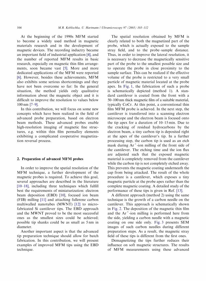
1. Introduction
Magnetic force microscopy (MFM) is a straight-forward special mode of operation of the non-contact scanning force microscope. Shortly afterthe invention of the atomic force microscope it wasrecognized that detection of magnetic interactionson a local scale was possible by equipping the forcemicroscope with a ferromagnetic probe, whichthen could be raster-scanned across any ferromag-netic sample. The near-field magneto–static inter-action for a typical probe–sample configurationturns out to be fairly strong and largely indepen-dent of surface contamination. Consequently,
MFM is quite easy to perform and applicableunder various environmental conditions, in mostcases even without requiring any special samplepreparation procedure.MFM is an important analytical tool whenever
the near-surface stray-field variation of a magneticsample is of interest. This is certainly the case forthe development and application of magneticrecording components. It is thus not surprisingthat MFM was first demonstrated on a micro-fabricated magnetic recording head [1]. A bigbreakthrough occurred when it was demonstratedthat, even individual inter-domain boundaries [2]and in some cases part of their internal finestructure [3] could be analyzed at high spatialresolution of about 100 nm, which can be achievedin a routine way. This resolution is comparable tothat so far only obtained by electron microscope-based instrumentation.
ARTICLE IN PRESS
*Corresponding author.
E-mail address: [email protected]
(M.R. Koblischka).
0304-3991/03/$ - see front matter r 2003 Elsevier Science B.V. All rights reserved.
doi:10.1016/S0304-3991(03)00034-2
At the beginning of the 1990s MFM startedto become a widely used method in magneticmaterials research and in the development ofmagnetic devices. The recording inductry becamean important field of industrial application [4], andthe number of reported MFM results in basicresearch, especially on magnetic thin film arrange-ments, soon became vast [5]. More and morededicated applications of the MFM were reported[6]. However, besides these achievements, MFMalso exhibits some serious shortcomings and theyhave not been overcome so far: In the generalsituation, the method yields only qualitativeinformation about the magnetic object and it isdifficult to improve the resolution to values below100 nm [7–9].In this contribution, we will focus on some new
concepts which have been realized in the field ofadvanced probe preparation, based on electronbeam methods. These advanced probes enablehigh-resolution imaging of magnetic fine struc-tures, e.g. within thin film permalloy elementsexhibiting a complicated cooperative magnetiza-tion reversal process.
2. Preparation of advanced MFM probes
In order to improve the spatial resolution of theMFM technique, a further development of themagnetic probes is required. To achieve this goal,several approaches are described in the literature[10–18], including three techniques which fulfillbest the requirements of miniaturization: electronbeam deposition (EBD) [10], focused ion beam(FIB) milling [11] and attaching fullerene carbonmultiwalled nanotubes (MWNT) [12] to micro-fabricated Si cantilever tips. The EBD approachand the MWNT proved to be the most successfulones as the smallest sizes could be achieved;possible tip shanks could be as small as 5 nm indiameter.Another important aspect is that the advanced
tip preparation technique should allow for batchfabrication. In this contribution, we will presentexamples of improved MFM tips using the EBDtechnique.
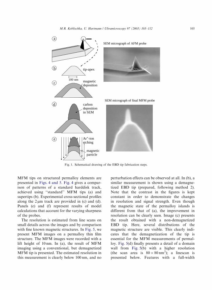
The spatial resolution obtained by MFM isclearly related to both the magnetized part of theprobe, which is actually exposed to the samplestray field, and to the probe–sample distance.Thus, in order to improve the lateral resolution, itis necessary to decrease the magnetically sensitivepart of the probe to the smallest possible size andto operate the probe in close proximity to thesample surface. This can be realized if the effectivevolume of the probe is restricted to a very smallparticle of magnetic material located at the probeapex. In Fig. 1, the fabrication of such a probeis schematically depicted (method 1). A stan-dard cantilever is coated from the front with a50–100nm thick magnetic film of a suitable material,typically CoCr. At this point, a conventional thinfilm MFM probe is achieved. In the next step, thecantilever is transferred into a scanning electronmicroscope and the electron beam is focused ontothe tip apex for a duration of 10–15min. Due tothe cracking of residual hydrocarbons by theelectron beam, a tiny carbon tip is deposited rightat the apex of the cantilever’s tip. In a furtherprocessing step, the carbon tip is used as an etchmask during Ar+-ion milling of the front side ofthe cantilever. The etching time and the ion fluxare adjusted such that the exposed magneticmaterial is completely removed from the cantileverwhile the carbon tip is not completely etched away.This prevents the magnetic coating underneath thecap from being attacked. The result of the wholeprocedure is a cantilever, which exposes a tinymagnetic particle at the probe apex rather than thecomplete magnetic coating. A detailed study of theperformance of these tips is given in Ref. [13].A different approach (method 2) using the same
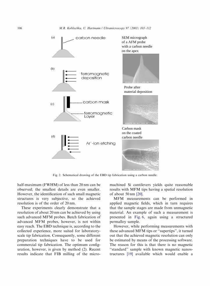
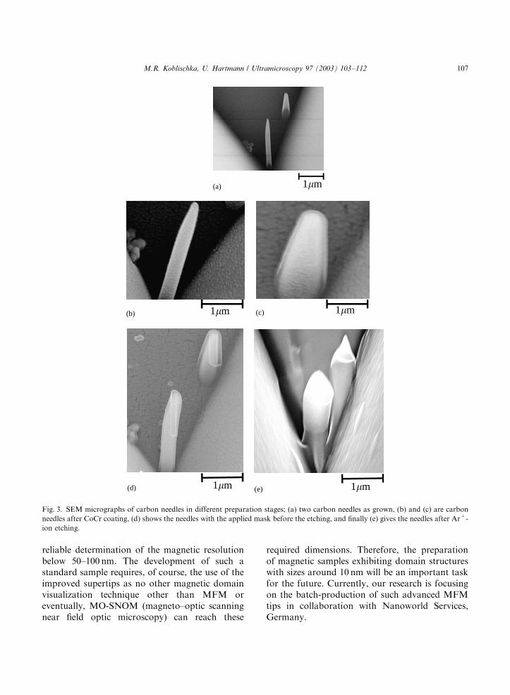
technique is the growth of a carbon needle on thecantilever. This approach is schematically shownin Fig. 2. The deposition of the magnetic thin filmand the Ar+-ion milling is performed here fromthe side, yielding a carbon needle with a magneticcoating on one side only. Fig. 3 presents SEMimages of such carbon needles during differentpreparation steps. As a result, the magnetic strayfield of these tips is different from the first ones.Demagnetizing the tips further reduces their
influence on soft magnetic structures. The resultsof MFM measurements using these advanced
ARTICLE IN PRESS
M.R. Koblischka, U. Hartmann / Ultramicroscopy 97 (2003) 103–112104
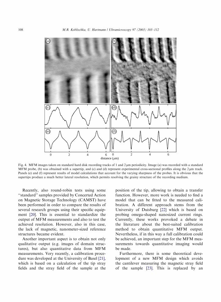
MFM tips on structured permalloy elements arepresented in Figs. 4 and 5. Fig. 4 gives a compar-ison of patterns of a standard harddisk track,achieved using ‘‘standard’’ MFM tips (a) andsupertips (b). Experimental cross-sectional profilesalong the 2 mm track are provided in (c) and (d).Panels (e) and (f) represent results of modelcalculations that account for the varying sharpnessof the probes.The resolution is estimated from line scans on
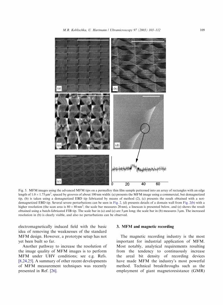
small details across the images and by comparisonwith fine known magnetic structures. In Fig. 5, wepresent MFM images on a permalloy thin filmstructure. The MFM images were recorded with alift height of 10 nm. In (a), the result of MFMimaging using a conventional, but demagnetizedMFM tip is presented. The estimated resolution inthis measurement is clearly below 100 nm, and no
perturbation effects can be observed at all. In (b), asimilar measurement is shown using a demagne-tized EBD tip (prepared, following method 2).Note that the contrast in the figures is keptconstant in order to demonstrate the changesin resolution and signal strength. Even thoughthe magnetic state of the permalloy islands isdifferent from that of (a), the improvement inresolution can be clearly seen. Image (c) presentsthe result obtained with a non-demagnetizedEBD tip. Here, several distributions of themagnetic structure are visible. This clearly indi-cates that the demagnetization of the tip isessential for the MFM measurements of permal-loy. Fig. 5(d) finally presents a detail of a domainwall from Fig. 5(b) with a higher resolution(the scan area is 80� 80 nm2); a linescan ispresented below. Features with a full-width
ARTICLE IN PRESS
tip-apex
magneticdeposition
carbondepositionin SEM
Ar -ionetching
+
magneticparticle
100 nm
a
b
c
d
e
SEM micrograph of AFM probe
SEM micrograph of final MFM probe
Fig. 1. Schematical drawing of the EBD tip fabrication steps.
M.R. Koblischka, U. Hartmann / Ultramicroscopy 97 (2003) 103–112 105
half-maximum (FWHM) of less than 20 nm can beobserved; the smallest details are even smaller.However, the identification of such small magneticstructures is very subjective, so the achievedresolution is of the order of 20 nm.These experiments clearly demonstrate that a
resolution of about 20 nm can be achieved by usingsuch advanced MFM probes. Batch fabrication ofadvanced MFM probes, however, is not withineasy reach. The EBD technique is, according to thecollected experience, more suited for laboratory-scale tip fabrication. Consequently, some differentpreparation techniques have to be used forcommercial tip fabrication. The optimum config-uration, however, is given by method (2). Recentresults indicate that FIB milling of the micro-
machined Si cantilevers yields quite reasonableresults with MFM tips having a spatial resolutionof about 50 nm [20].MFM measurements can be performed in
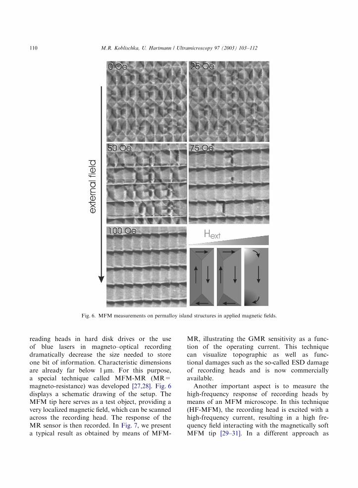
applied magnetic fields, which in turn requiresthat the sample stages are made from unmagneticmaterial. An example of such a measurement ispresented in Fig. 6, again using a structuredpermalloy sample.However, while performing measurements with
these advanced MFM tips or ‘‘supertips’’, it turnedout that the achieved magnetic resolution can onlybe estimated by means of the processing software.The reason for this is that there is no magnetic‘‘standard’’ sample with known magnetic nanos-tructures [19] available which would enable a
ARTICLE IN PRESS
SEM micrographof a AFM probewith a carbon needleon the apex
Probe aftermaterial deposition
Carbon maskon the coatedcarbon needle
(a)
(b)
(c)
(d)
Fig. 2. Schematical drawing of the EBD tip fabrication using a carbon needle.
M.R. Koblischka, U. Hartmann / Ultramicroscopy 97 (2003) 103–112106
reliable determination of the magnetic resolutionbelow 50–100 nm. The development of such astandard sample requires, of course, the use of theimproved supertips as no other magnetic domainvisualization technique other than MFM oreventually, MO-SNOM (magneto–optic scanningnear field optic microscopy) can reach these
required dimensions. Therefore, the preparationof magnetic samples exhibiting domain structureswith sizes around 10 nm will be an important taskfor the future. Currently, our research is focusingon the batch-production of such advanced MFMtips in collaboration with Nanoworld Services,Germany.
ARTICLE IN PRESS
(a)
(b) (c)
(d) (e)
1�m
1�m 1�m
1�m 1�m
Fig. 3. SEM micrographs of carbon needles in different preparation stages; (a) two carbon needles as grown, (b) and (c) are carbon
needles after CoCr coating, (d) shows the needles with the applied mask before the etching, and finally (e) gives the needles after Ar+-
ion etching.
M.R. Koblischka, U. Hartmann / Ultramicroscopy 97 (2003) 103–112 107
Recently, also round-robin tests using some‘‘standard’’ samples provided by Concerted Actionon Magnetic Storage Technology (CAMST) havebeen performed in order to compare the results ofseveral research groups using their specific equip-ment [20]. This is essential to standardize theoutput of MFM measurements and also to test theachieved resolution. However, also in this case,the lack of magnetic, nanometer-sized referencestructures became evident.Another important aspect is to obtain not only
qualitative output (e.g. images of domain struc-tures), but also quantitative data from MFMmeasurements. Very recently, a calibration proce-dure was developed at the University of Basel [21],which is based on a calculation of the tip strayfields and the stray field of the sample at the
position of the tip, allowing to obtain a transferfunction. However, more work is needed to find amodel that can be fitted to the measured cali-bration. A different approach stems from theUniversity of Duisburg [22] which is based onprobing omega-shaped nanosized current rings.Currently, these works provoked a debate inthe literature about the best-suited calibrationmethod to obtain quantitative MFM output.Nevertheless, if in this way a full calibration couldbe achieved, an important step for the MFM mea-surements towards quantitative imaging wouldbe made.Furthermore, there is some theoretical deve-
lopment of a new MFM design which avoidsthe cantilever measuring the magnetic stray fieldof the sample [23]. This is replaced by an
ARTICLE IN PRESS
(a) (b)
(c) (d)
(f)(e)
0 2 4 6 0 2 4 6distance (�m)
Fig. 4. MFM images taken on standard hard disk recording tracks of 1 and 2mm periodicity. Image (a) was recorded with a standard
MFM probe, (b) was obtained with a supertip, and (c) and (d) represent experimental cross-sectional profiles along the 2mm track.
Panels (e) and (f) represent results of model calculations that account for the varying sharpness of the probes. It is obvious that the
supertips produce a much better lateral resolution, which permits resolving the grainy structure of the recording medium.
M.R. Koblischka, U. Hartmann / Ultramicroscopy 97 (2003) 103–112108
electromagnetically induced field with the basicidea of removing the weaknesses of the standardMFM design. However, a prototype setup has notyet been built so far.Another pathway to increase the resolution of
the image quality of MFM images is to performMFM under UHV conditions; see e.g. Refs.[8,24,25]. A summary of other recent developmentsof MFM measurement techniques was recentlypresented in Ref. [26].
3. MFM and magnetic recording
The magnetic recording industry is the mostimportant for industrial application of MFM.Most notably, analytical requirements resultingfrom the tendency to continuously increasethe areal bit density of recording deviceshave made MFM the industry’s most powerfulmethod. Technical breakthroughs such as theemployment of giant magnetoresistance (GMR)
ARTICLE IN PRESS
Fig. 5. MFM images using the advanced MFM tips on a permalloy thin film sample patterned into an array of rectangles with an edge
length of 1.0� 1.75mm2, spaced by grooves of about 100 nm width: (a) presents the MFM image using a commercial, but demagnetized
tip, (b) is taken using a demagnetized EBD tip fabricated by means of method (2), (c) presents the result obtained with a not-
demagnetized EBD tip. Several severe perturbations can be seen in Fig. 2, (d) presents details of a domain wall from Fig. 2(b) with a
higher resolution (the scan area is 80� 80 nm2; the scale bar measures 20 nm), a linescan is presented below, and (e) shows the result
obtained using a batch-fabricated FIB tip. The scale bar in (a) and (c) are 5mm long; the scale bar in (b) measures 3mm. The increasedresolution in (b) is clearly visible, and also no perturbations can be observed.
M.R. Koblischka, U. Hartmann / Ultramicroscopy 97 (2003) 103–112 109
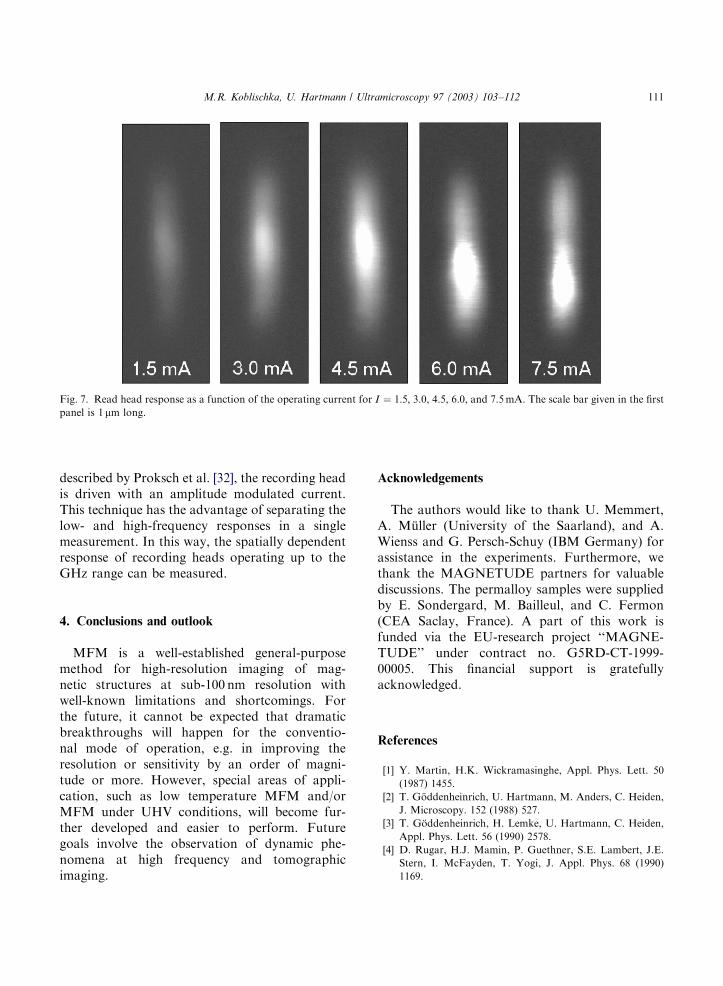
reading heads in hard disk drives or the useof blue lasers in magneto–optical recordingdramatically decrease the size needed to storeone bit of information. Characteristic dimensionsare already far below 1 mm. For this purpose,a special technique called MFM-MR (MR=magneto-resistance) was developed [27,28]. Fig. 6displays a schematic drawing of the setup. TheMFM tip here serves as a test object, providing avery localized magnetic field, which can be scannedacross the recording head. The response of theMR sensor is then recorded. In Fig. 7, we presenta typical result as obtained by means of MFM-
MR, illustrating the GMR sensitivity as a func-tion of the operating current. This techniquecan visualize topographic as well as func-tional damages such as the so-called ESD damageof recording heads and is now commerciallyavailable.Another important aspect is to measure the
high-frequency response of recording heads bymeans of an MFM microscope. In this technique(HF-MFM), the recording head is excited with ahigh-frequency current, resulting in a high fre-quency field interacting with the magnetically softMFM tip [29–31]. In a different approach as
ARTICLE IN PRESS
Fig. 6. MFM measurements on permalloy island structures in applied magnetic fields.
M.R. Koblischka, U. Hartmann / Ultramicroscopy 97 (2003) 103–112110
described by Proksch et al. [32], the recording headis driven with an amplitude modulated current.This technique has the advantage of separating thelow- and high-frequency responses in a singlemeasurement. In this way, the spatially dependentresponse of recording heads operating up to theGHz range can be measured.
4. Conclusions and outlook
MFM is a well-established general-purposemethod for high-resolution imaging of mag-netic structures at sub-100 nm resolution withwell-known limitations and shortcomings. Forthe future, it cannot be expected that dramaticbreakthroughs will happen for the conventio-nal mode of operation, e.g. in improving theresolution or sensitivity by an order of magni-tude or more. However, special areas of appli-cation, such as low temperature MFM and/orMFM under UHV conditions, will become fur-ther developed and easier to perform. Futuregoals involve the observation of dynamic phe-nomena at high frequency and tomographicimaging.
Acknowledgements
The authors would like to thank U. Memmert,A. M .uller (University of the Saarland), and A.Wienss and G. Persch-Schuy (IBM Germany) forassistance in the experiments. Furthermore, wethank the MAGNETUDE partners for valuablediscussions. The permalloy samples were suppliedby E. Sondergard, M. Bailleul, and C. Fermon(CEA Saclay, France). A part of this work isfunded via the EU-research project ‘‘MAGNE-TUDE’’ under contract no. G5RD-CT-1999-00005. This financial support is gratefullyacknowledged.
References
[1] Y. Martin, H.K. Wickramasinghe, Appl. Phys. Lett. 50
(1987) 1455.
[2] T. G .oddenheinrich, U. Hartmann, M. Anders, C. Heiden,
J. Microscopy. 152 (1988) 527.
[3] T. G .oddenheinrich, H. Lemke, U. Hartmann, C. Heiden,
Appl. Phys. Lett. 56 (1990) 2578.
[4] D. Rugar, H.J. Mamin, P. Guethner, S.E. Lambert, J.E.
Stern, I. McFayden, T. Yogi, J. Appl. Phys. 68 (1990)
1169.
ARTICLE IN PRESS
Fig. 7. Read head response as a function of the operating current for I ¼ 1:5; 3.0, 4.5, 6.0, and 7.5mA. The scale bar given in the firstpanel is 1mm long.
M.R. Koblischka, U. Hartmann / Ultramicroscopy 97 (2003) 103–112 111
[5] P. Gr .utter, H.J. Mamin, D. Rugar, In: R. Wiesendanger,
H.J. G .untherodt (Eds.), Scanning Tunneling Microscopy
II. Springer, Heidelberg, p. 151.
[6] A. Moser, H.J. Hug, I. Parashikov, B. Stiefel, O. Fritz,
Phys. Rev. Lett. 74 (1995) 1847.
[7] A. Wadas, In: S. Amelinckx, D. van Dyck, J. van
Landhuyt, G. van Tendeloo (Eds.), Handbook of Micro-
scopy. Methods II, Wiley-VCH, Weinheim, p. 845.
[8] U. Hartmann, Annu. Rev. Mater. Sci. 29 (1999) 53.
[9] H.K. Wickramasinghe, Acta Mater. 48 (2000) 347.
[10] Y. Akama, E. Nishimura, A. Sakai, H. Murakami, J. Vac.
Sci. Technol. A 8 (1990) 429;
R. Jumpertz, P. Leinenbach, A.W.A. van der Hart,
J. Schelten, Microelectron. Eng. 35 (1997) 325.
[11] M.J. Vasile, D. Grigg, J.E. Griffith, E. Fitzgerald,
P.E. Russell, J. Vac. Sci. Technol. B 9 (1991) 3569.
[12] H. Dai, J.H. Hafner, A.G. Rinzler, D.T. Colbert,
R.E. Smalley, Nature 384 (1996) 147.
[13] U. Memmert, A.N. M .uller, U. Hartmann, Meas. Sci.
Technol. 11 (2000) 1342;
P. Leinenbach, U. Memmert, J. Schelten, U. Hartmann,
Appl. Surf. Sci. 144-145 (1999) 492.
[14] G.P. Heydon, W.M. Rainforth, M.R.J. Gibbs, H.A.
Davies, J.E.L. Bishop, J.W. Tucker, S. Huo, G. Pan,
D.J. Mapps, W.W. Clegg, J. Magn. Magn. Mater. 214
(2000) 225.
[15] L. Folks, M.E. Best, P.M. Rice, B.D. Terris, D. Weller,
J.N. Chapman, Appl. Phys. Lett. 76 (2000) 909.
[16] G.D. Skidmore, E. Dan Dahlberg, Appl. Phys. Lett. 71
(1997) 3293.
[17] S.H. Liou, IEEE Trans. Magn. 35 (1999) 3989.
[18] S.H. Liou, Y.D. Yao, J. Magn. Magn. Mater. 190 (1998) 130.
[19] A. Hubert, R. Sch.afer, Magnetic Domains, Springer,
Heidelberg, 1998.
[20] L. Abelmann, S. Porthun, M. Haast, C. Lodder, A. Moser,
M.E. Best, P.J.A. van Schendel, B. Stiefel, H.J. Hug,
G.P. Heydon, A. Farley, S.R. Hoon, T. Pfaffelhuber,
R. Proksch, K. Babcock, J. Magn. Magn. Mater. 190
(1998) 135.
[21] P.J.A. van Schendel, H.J. Hug, B. Stiefel, S. Martin,
H.-J. G .untherodt, J. Appl. Phys. 88 (2000) 435.
[22] J. Lohau, S. Kirsch, A. Carl, E.F. Wassermann, Appl.
Phys. Lett. 76 (2000) 3094;
J. Lohau, S. Kirsch, A. Carl, E.F. Wassermann, Appl.
Phys. Lett. 78 (2001) 2020.
[23] J.F.C. Windmill, W.W. Clegg, IEEE Trans. Magn. 36
(2000) 2984.
[24] M. Bode, M. Dreyer, M. Getzlaff, M. Kleiber, A. Wadas,
R. Wiesendanger, J. Phys.: Condens. Matter 11 (1999)
9387.
[25] U. Memmert, P. Leinenbach, J. L .osch, U. Hartmann,
J. Magn. Magn. Mater. 190 (1998) 124.
[26] K. Babcock, R. Proksch, Editorial of MFM-10 conference,
J. Magn. Magn. Mater. 190 (1998) xi–xv.
[27] G. Persch, Ch. Born, H. Engelmann, K. K .ohler, B. Utesch,
Scanning 15 (1993) 283.
[28] F. Krause, Ph.D. Thesis, University of the Saarland,
Saarbruecken, Germany 1998.
[29] K. Wago, K. Sueoka, F. Sai, IEEE Trans. Magn. 27 (1991)
5178.
[30] M. Abe, Y. Tanaka, J. Appl. Phys. 89 (2001) 6766.
[31] M. Abe, Y. Tanaka, IEEE Trans. Magn. 38 (2002) 45.
[32] R. Proksch, P. Neilson, S. Austvold, J.J. Schmidt, Appl.
Phys. Lett. 74 (1999) 1308.
ARTICLE IN PRESS
M.R. Koblischka, U. Hartmann / Ultramicroscopy 97 (2003) 103–112112
Copyright © 2022 FDOKUMEN