Imaging fibroblast cells using atomic force microscopy (AFM)
Upload
independentCategory
view
0download
0
Nanoscale
COMMUNICATION
Publ
ishe
d on
05
July
201
3. D
ownl
oade
d by
Uni
vers
ite P
aul S
abat
ier
on 1
6/04
/201
4 12
:20:
04.
View Article OnlineView Journal | View Issue
aLaboratoire de Chimie de Coordination, CN
31077 Toulouse, France. E-mail: g
[email protected] de Ciencias, Universidad Nacion
D.F., Mexico
† Electronic supplementary informationmovies of the spin transition and SEM10.1039/c3nr03030j
Cite this: Nanoscale, 2013, 5, 7762
Received 12th June 2013Accepted 2nd July 2013
DOI: 10.1039/c3nr03030j
www.rsc.org/nanoscale
7762 | Nanoscale, 2013, 5, 7762–776
Atomic force microscopy and near-field optical imagingof a spin transition†
Manuel Lopes,a Carlos M. Quintero,a Edna M. Hernandez,a Vıctor Velazquez,b
Carlos Bartual-Murgui,a William Nicolazzi,a Lionel Salmon,a Gabor Molnar*a
and Azzedine Bousseksou*a
We report on atomic forcemicroscopy (AFM) and near-field scanning
optical microscopy (NSOM) investigations of single crystals of the
spin crossover complex {Fe(pyrazine)[Pt(CN)4]} across the first-order
thermal spin transition. We demonstrate for the first time that the
change in spin state can be probed with sub-micrometer spatial
resolution through various topographic features extracted fromAFM
data. This original approach based on surface topography analysis
should be easy to implement to any phase change material exhibit-
ing sizeable electron–lattice coupling. In addition, AFM images
revealed specific topographic features in the crystals, which were
correlated with the spatiotemporal evolution of the transition
observed by far-field and near-field optical microscopies.
1 Introduction
Macroscopic solid–solid phase transitions encompass a varietyof mechanisms at different length scales ranging from pointdefects to extended domains. To investigate the underlyingmicroscopic phenomena such as nucleation, phase boundarymotion or percolation there is a need for in situ, non-invasiveand high spatial resolution imaging techniques. Among these,scanning probe microscopy (SPM) methods have receivedincreasing attention over the past decade. For example, SPMwas extensively used to study the domain structure of ferro-electric1,2 and ferromagnetic3,4 materials or phase transitions inso matter.5 In fact, SPM covers a vast family of techniquesallowing for the investigation of mechanical,6 electrical,7
magnetic4 or optical8 properties of matter through phase tran-sition; each method coming with its own specic challenges,
RS & Universite de Toulouse (UPS, INP),
[email protected]; azzedine.
al Autonoma de Mexico, 04510 Mexico,
(ESI) available: Far-eld and near-eldimages of the NSOM tip. See DOI:
7
related either to the instrumentation or to the image interpre-tation. On the other hand, SPM topography investigations havebeen explored to a rather small extent in this context,2,9 eventhough they represent an interesting alternative as they are veryeasy to implement and are applicable, a priori, to any phasetransition involving lattice degrees of freedom.
In this communication, we report on a variable-temperaturecombined AFM topographic–NSOM study of a single crystal of aspin crossover (SCO) compound. These transition metalcomplexes are well known to display bistability of their highspin (HS) and low spin (LS) electronic congurations.10,11 Inaddition, several SCO solids exhibit rst-order spin transitiondue to the strong elastic interactions between the complexes inthe bulk material. The spatiotemporal dynamics of thesecooperative spin transitions have been investigated onlyrecently using far-eld optical microscopy methods – inconjunction with thermal or light excitation.12–17 These studiesrevealed a multiscale transition process, following a nucleationand growth mechanism, where the main control parameter isthe accommodation strain. Spatially localized events, related toeither intrinsic or extrinsic defects, were found to play a key rolein the spatiotemporal dynamics of these transitions. However,these localized phenomena remain oen impossible to detectwith far-eld techniques and call for the use of SPM techniques.To this aim one can use NSOM owing to the striking change ofoptical properties upon SCO. On the other hand, the strongelectron–lattice coupling suggests that AFM topographicimaging can also be a very efficient tool to follow spintransition.
For this challenging SPM study we have selected singlecrystals of the SCO complex {FeII(pyrazine)[PtII(CN)4]} (1). Thetetragonal (P4/mmm) structure of this porous metal–organicframework is comprised of {Fe[Pt(CN4)]}N layers, which arepillared by the ligand pyrazine (Fig. 1a). This compoundreceived much attention over the past few years for itsremarkable properties. It exhibits room temperature spintransition between the HS (S ¼ 2) and LS (S ¼ 0) states,accompanied by a spectacular change of optical and mass
This journal is ª The Royal Society of Chemistry 2013

Fig. 1 (a) Crystallographic structure of the metal–organic framework Fe(pyr-azine)[Pt(CN)4]. (b) Far-field optical reflectivity image of the crystal C1 used forAFM measurements. (c) Normalized reflectivity (far-field, l ¼ 543 nm) as a func-tion of temperature in the cooling (closed symbols) and heating (open symbols)branches for the area indicated by the dashed square in the image of the crystal.The dotted lines were inserted to guide the eye.
Communication Nanoscale
Publ
ishe
d on
05
July
201
3. D
ownl
oade
d by
Uni
vers
ite P
aul S
abat
ier
on 1
6/04
/201
4 12
:20:
04.
View Article Online
densities, which can be triggered by a temperature change,18
application of pressure,19 a nanosecond laser pulse20 or theadsorption of gas/vapor molecules.21 In addition, these prop-erties were shown to be easily adjustable by using differentligands and/or guest molecules in the coordination network.22
2 Results and discussion
Single crystals of 1 were synthesized using a slow diffusionmethod. The samples were enclosed and dehydrated in a sealedchamber under a N2 atmosphere and their AFM/NSOM imageswere acquired at different temperatures using a NanonicsMV2000 scanning probe microscope (for details of samplesynthesis, experiment and data treatment see Section 4). Thepronounced thermochromism of these crystals allowed us tocarry out a preliminary far-eld imaging of the spin transitionby means of optical reectivity measurements through thermalcycles between 255 K and 305 K. Fig. 1b shows an optical brighteld microscopy image of one of these crystals (C1). The squarein the image indicates a region of interest of ca. 8 � 8 mm2 thatwe selected and followed during a thermal cycle. When the
This journal is ª The Royal Society of Chemistry 2013
average value of the reected light intensity in this area isplotted as a function of temperature (Fig. 1c), we observe adecrease in the reectivity (l ¼ 543 nm) when going from thehigh temperature (HS) to the low temperature (LS) state, due tothe signicantly higher absorption coefficient of the latter inthis spectral region.20 The obtained transition curve reveals thatthe SCO takes place in that zone with a 14 K hysteresis centeredat 273 K. Nevertheless, aer a closer examination of the imagesacquired during the thermal cycle (Video SI1a and b†), a seriesof localized subtle variations in the reectance of this area isdepicted. These movies provide clear evidence that – in contrastto what was previously reported for other SCO complexes13,17 –in this sample the SCO does not exhibit a well-dened singlenucleation site and directional phase boundary motion. Fromthese measurements, it is clear that the spatiotemporaldynamics of the SCO in these crystals are more complex, whichbecomes challenging to be studied solely by far-eld micros-copy techniques. In order to better understand such complexphenomena, a higher spatial resolution detection of the SCO ata sub-micrometric scale becomes necessary. Scanning probetechniques such as AFM or NSOM appear naturally well suitedto overcome this limitation.
To this aim, we performed on the same zone of C1 an AFMtopographic study at different temperatures to characterize itssurface upon SCO. Fig. 2a shows a 3D representation of an AFMscan of the area under study. This image reveals a surfacetopography similar to that of a rippled sheet, which is in perfectagreement with the laminar arrangement observed in opticalmicroscopy (Fig. 1b). From the AFM scans obtained during thethermal cycle, we have extracted the average ripple height andplotted it as a function of temperature (Fig. 2b).
The main novelty here is the detection of the spin-statetransition and the associated thermal hysteresis loop throughthe variation of the surface topography when the crystalundergoes the HS to LS (270 K) and LS to HS (285 K) transitions.At rst glance, these observations seem somewhat surprisingsince it is well known that the volume of the crystal lattice ofcomplex 1 contracts by approximately 13% upon HS to LStransition,20 which contradicts the apparent height increasedetected with AFM for the same transition. However, tounderstand our observations, it is necessary to consider thatduring a HS to LS transition, the contraction of the crystal leadsto the opening of ‘line faults’ between the ripples of the crystal.Thus, in the LS form of the crystal, the AFM tip has more spaceto probe deeper the sample topography and as a result, theapparent height increase observed in the cartographies corre-sponds, in fact, to an increase of the (surface average) pene-tration depth of the tip inside the sample (see Fig. 2e). Thethermal variation observed in Fig. 2b reects primarily thevariations related to the ripples. To get a more comprehensivepicture of the surface topography changes of our crystal, weltered each AFM image using 2D fast Fourier transformation,FFT (see Fig. 2a). This way we can obtain a cartography corre-sponding either to the high spatial frequencies (lamellae) or tothe low spatial frequencies (ripples). Then, we can plot theroughness average (i.e. the arithmetic mean deviation of theheight) of each of these cartographies as a function of
Nanoscale, 2013, 5, 7762–7767 | 7763
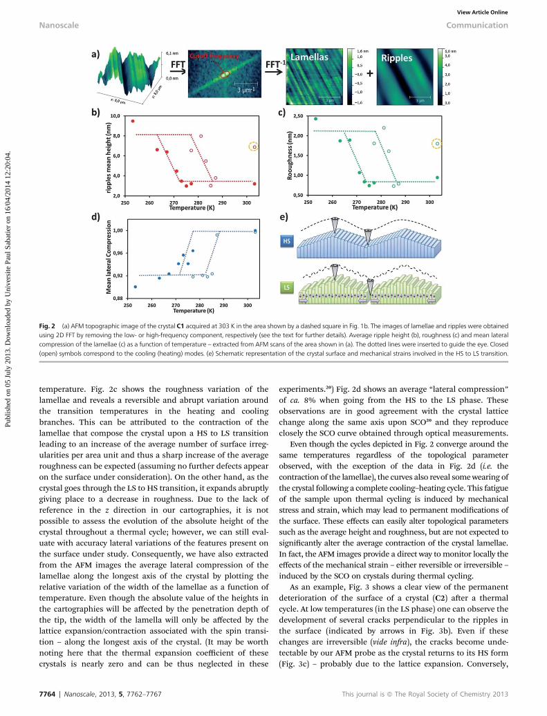
Fig. 2 (a) AFM topographic image of the crystal C1 acquired at 303 K in the area shown by a dashed square in Fig. 1b. The images of lamellae and ripples were obtainedusing 2D FFT by removing the low- or high-frequency component, respectively (see the text for further details). Average ripple height (b), roughness (c) and mean lateralcompression of the lamellae (c) as a function of temperature – extracted from AFM scans of the area shown in (a). The dotted lines were inserted to guide the eye. Closed(open) symbols correspond to the cooling (heating) modes. (e) Schematic representation of the crystal surface and mechanical strains involved in the HS to LS transition.
Nanoscale Communication
Publ
ishe
d on
05
July
201
3. D
ownl
oade
d by
Uni
vers
ite P
aul S
abat
ier
on 1
6/04
/201
4 12
:20:
04.
View Article Online
temperature. Fig. 2c shows the roughness variation of thelamellae and reveals a reversible and abrupt variation aroundthe transition temperatures in the heating and coolingbranches. This can be attributed to the contraction of thelamellae that compose the crystal upon a HS to LS transitionleading to an increase of the average number of surface irreg-ularities per area unit and thus a sharp increase of the averageroughness can be expected (assuming no further defects appearon the surface under consideration). On the other hand, as thecrystal goes through the LS to HS transition, it expands abruptlygiving place to a decrease in roughness. Due to the lack ofreference in the z direction in our cartographies, it is notpossible to assess the evolution of the absolute height of thecrystal throughout a thermal cycle; however, we can still eval-uate with accuracy lateral variations of the features present onthe surface under study. Consequently, we have also extractedfrom the AFM images the average lateral compression of thelamellae along the longest axis of the crystal by plotting therelative variation of the width of the lamellae as a function oftemperature. Even though the absolute value of the heights inthe cartographies will be affected by the penetration depth ofthe tip, the width of the lamella will only be affected by thelattice expansion/contraction associated with the spin transi-tion – along the longest axis of the crystal. (It may be worthnoting here that the thermal expansion coefficient of thesecrystals is nearly zero and can be thus neglected in these
7764 | Nanoscale, 2013, 5, 7762–7767
experiments.20) Fig. 2d shows an average “lateral compression”of ca. 8% when going from the HS to the LS phase. Theseobservations are in good agreement with the crystal latticechange along the same axis upon SCO20 and they reproduceclosely the SCO curve obtained through optical measurements.
Even though the cycles depicted in Fig. 2 converge around thesame temperatures regardless of the topological parameterobserved, with the exception of the data in Fig. 2d (i.e. thecontraction of the lamellae), the curves also reveal somewearing ofthe crystal following a complete cooling–heating cycle. This fatigueof the sample upon thermal cycling is induced by mechanicalstress and strain, which may lead to permanent modications ofthe surface. These effects can easily alter topological parameterssuch as the average height and roughness, but are not expected tosignicantly alter the average contraction of the crystal lamellae.In fact, the AFM images provide a direct way to monitor locally theeffects of the mechanical strain – either reversible or irreversible –induced by the SCO on crystals during thermal cycling.
As an example, Fig. 3 shows a clear view of the permanentdeterioration of the surface of a crystal (C2) aer a thermalcycle. At low temperatures (in the LS phase) one can observe thedevelopment of several cracks perpendicular to the ripples inthe surface (indicated by arrows in Fig. 3b). Even if thesechanges are irreversible (vide infra), the cracks become unde-tectable by our AFM probe as the crystal returns to its HS form(Fig. 3c) – probably due to the lattice expansion. Conversely,
This journal is ª The Royal Society of Chemistry 2013

Fig. 3 AFM topographic images of the crystal C2 at the beginning of the thermal cycle (a), at the end of the cooling branch (b) and at the end of the thermal cycle (c).The dashed circle indicates the area that underwent irreversible deterioration upon the thermal cycle.
Communication Nanoscale
Publ
ishe
d on
05
July
201
3. D
ownl
oade
d by
Uni
vers
ite P
aul S
abat
ier
on 1
6/04
/201
4 12
:20:
04.
View Article Online
Fig. 3b and c reveal a region of the crystal (indicated by a circle)which undergoes irreversible damage with the detachment of asurface layer. These effects are not always perceptible with far-eld techniques albeit they play a key role both in the nucle-ation as well as in the propagation of the daughter phase alongthe crystal.14 Hence, AFM may provide crucial information forthe better understanding of the interplay between such defectsand dynamic cooperative phenomena in SCO materials.
Subsequent far-eld imaging (Videos SI2a and b†) across theheating and cooling transitions performed on crystal C2 reveals arather complex spatiotemporal evolution of the spin transition inthe crystal with multiple phase boundaries and different
Fig. 4 AFM topographic images (a) and the corresponding NSOM images (b) of tdifferent temperatures at the zone indicated by the dashed rectangle in (a). (d) Temblue circle in the AFM images (a) and (c). (e) NSOM intensity normalized as a function(b). The dashed lines were inserted to guide the eye. Closed (open) symbols corresp
This journal is ª The Royal Society of Chemistry 2013
propagation directions. The LS phase nucleates chiey in theupper part of the crystal and propagates downwards along a ‘linefault’ (indicated by a dashed line in Fig. 3a) dividing the crystalinto two parts. The right-hand part is easily transformed into theLS form upon cooling, while on the le there is no transitionexcept a small area (circled in Fig. 3c). In addition, a darkboundary between the two phases is clearly observed in the far-eld images. To obtain more detailed information on thephenomena occurring at the interface of the two parts, we haveperformed another AFM study on this crystal as a function oftemperature. Fig. 4 displays the AFM cartographies recorded at293 K (LS) and 353 K (HS). One can recognize clearly the
he crystal C2 at 293 K and 253 K. (c) High resolution 3D topographic images atperature dependence of the step height corresponding to area 1 indicated by theof temperature extracted from area 2 and area 3 indicated in the NSOM image inond to the cooling (heating) modes.
Nanoscale, 2013, 5, 7762–7767 | 7765

Nanoscale Communication
Publ
ishe
d on
05
July
201
3. D
ownl
oade
d by
Uni
vers
ite P
aul S
abat
ier
on 1
6/04
/201
4 12
:20:
04.
View Article Online
boundary area between the two different structural domains(indicated by a dashed line in Fig. 4a). In addition, we observedalso a topography anomaly localized at the boundary of thedomains. To explore this region (localized by a dashed rectanglein Fig. 4a, see also Video SI3†), we acquired several high resolu-tion AFM images between 313 K and 253 K. As shown in Fig. 4c, avery localized and reversible deformation – in the form of a 6 nmdeep cavity – occurs in this area of the crystal during the thermalcycle. Themean step height analysis of this cavity as a function ofthe temperature reveals that the magnitude of this deformationfollows closely the spin transition curve of the crystal (Fig. 4d).The spin transition observed in this small region by AFM is veryobvious, in contrast to the far-eld microscopy images, high-lighting the need for such high resolution techniques.
A very useful feature of AFM topographic measurements isthat they can be carried out simultaneously with other scanningprobemodes (electric, magnetic, optical, etc.) in a straightforwardmanner. This way one can obtain complementary spatiallyresolved information on different material properties as well. Toillustrate this point, Fig. 4b displays the NSOM (l ¼ 532 nm)cartographies recorded at the same time as the AFM mapsreported in Fig. 4a. By comparing the NSOM and AFM images,the ‘line fault’ of the crystal (indicated by yellow arrows) is clearlyperceptible in both types of images, unlike our observations infar-eld optical microscopy. The evolution of the NSOM signal asa function of temperature allowed us to monitor the temperaturedependence of the reectance changes with a sub-wavelengthlateral resolution (<250 nm) at different zones of the crystal. Thecurves displayed in Fig. 4e conrm that the right-hand part (area2) of the crystal (with respect to the fault) undergoes a spintransition whereas there is no change in the le-hand part (area3) of the crystal. The hysteresis in these NSOM observations is inclose agreement with the results of far-eldmicroscopy and AFM.One shall note that the contrast of the NSOM cartographies israther different to that obtained from far-eld microscopy(Videos SI2a and b†). Surprisingly, we observe that the reectivitysignal on the right-hand side of the ‘line fault’ is always moreintense than on the le-hand side regardless of the temperature.We tentatively attribute this difference to a structural or chemicalchange in the crystal, which occurred during the thermal cycles.Indeed, during the rst cycle the “as-synthesized” crystalexhibited a spin transition in the whole volume (Videos SI4a andb†), but aer a few cycles the le-part of the crystal did not transitanymore. Hence, the different contrast in NSOM may be anindication of this change. Moreover, with the NSOMwe were ableto detect a few defects perpendicular to the lamellae (possiblycracks, highlighted by yellow arrows in Fig. 4b) even in the HSstate, where the conventional AFM was unable to detect them.The possible explanation for this observation is that on heatingthe cracks do not completely close up inside the crystal and theywill thus scatter light, which is observable by NSOM through thedecrease of the reected light signal.
3 Conclusions
To the best of our knowledge this is the rst report on theobservation of a spin state transition using scanning probe
7766 | Nanoscale, 2013, 5, 7762–7767
microscopy methods. We have shown the usefulness of bothNSOM and AFM topographic imaging in recording the thermalspin transition curves with high spatial resolution. These near-eld spin transition curves were found to be in excellent agree-ment with those obtained by conventional far-eld imaging, butprovide, in addition, microscopic details, which are not visible inthe latter. While NSOM probes directly the change of the elec-tronic structure, AFM imaging relies on the strong electron-–lattice coupling in these materials. Our work thus highlights thepossibility of using AFM topography measurements to probeelectronic transitions with high spatial resolution. The maininterest of this approach is the very straightforward instrumen-tation and image analysis. In addition, the possibility ofobserving minute surface topography details was also shown tobe critical in the interpretation of the spatiotemporal dynamicsof the transition, observed by complementary far-eld opticalmicroscopy techniques. Overall, these scanning probe observa-tions will undoubtedly lead to a deeper understanding ofphenomena such as phase co-existence, boundary motion or theonset of the transition. Finally let us also note that the recentdevelopment of continuous and nano-patterned thin lms23,24 aswell as nanoparticles25,26 of 1 provides also an appealing scopefor using SPM both for the detection and the activation oftransition – in a highly localized manner.
4 Experimental section
Single crystals of 1 were prepared by slow diffusion in 10 mL H-tubes. A methanol–water (1 : 1) solution (2 mL) containing amixture of Fe(BF4)2$6H2O (0.05 mmol, 16.8 mg) and pyrazine(0.05 mmol, 4 mg) was poured into one side of the H-tube. Theother side contained a water solution (2 mL) of K2[Pt(CN)4]$3H2O (0.05 mmol, 18 mg). Finally, the vessel was lled with amethanol–water solution and sealed to avoid evaporation and/or oxidation of the iron(II) ion. Aer several weeks small, thin,square-shaped yellow single crystals of 1 were obtained. TheSPM experiments were performed on the crystals with acommercial Nanonics Multiview 2000 system. Prior tomeasurements the crystals were dehydrated at 150 �C for 30min. SPM images were acquired in tapping-mode using tuningfork detection. The temperature of the sample was varied from253 K to 303 K – in a dry N2 atmosphere – using a Peltier stage.Topographical images were obtained with glass probes. ForNSOM imaging we used fused silica ber tips, coated with thinlms of Cr and Au (exit aperture diameter �200 nm, seeFig. SI5†). The 532 nm light of a frequency-doubled Nd:YAGlaser (6 mW) was injected into the ber through an objective.The scanning stage was enclosed in a sealed chamber andpositioned underneath an Olympus BX51 optical microscope.The reected light was collected with a long working distanceMitutoyo objective (20� magnication, numerical apertureNA ¼ 0.42) and the NSOM signal was recorded using a photo-multiplier detector (MP942, Perkin Elmer) through a bandpasslter (532 nm). For far-eld optical imaging the crystals wereilluminated using a halogen lamp through a bandpass lter(543 nm) and the images of the crystals were recorded inreection mode using a charge-coupled device (Clara, Andor
This journal is ª The Royal Society of Chemistry 2013

Communication Nanoscale
Publ
ishe
d on
05
July
201
3. D
ownl
oade
d by
Uni
vers
ite P
aul S
abat
ier
on 1
6/04
/201
4 12
:20:
04.
View Article Online
Technology). AFM and NSOM images have been treated with theGwyddion soware.27 The polynomial background was removedfor each AFM image. Spatial (x/y) dris of the crystals in thedifferent images (AFM, NSOM, and far-eld) produced by thetemperature variation were removed with an alignment routinebased on 2D cross-correlation.28
Acknowledgements
This work was supported by the Agence Nationale de laRecherche (ANR-2010-BLAN-7161). EMH is grateful to theCONACYT for a PhD grant. ML acknowledges a postdoctoralgrant from PRES Toulouse (project BISTABLE).
Notes and references
1 E. Soergel, Appl. Phys. B, 2005, 81, 729.2 J. Munoz Saldana, G. Schneider and L. Eng, Surf. Sci., 2001,480, L402.
3 P. Kolb, D. Romero, H. Drew, A. Sushkov, S. Ogale andY. Moritomo, Nano Lett., 2007, 7, 1449.
4 G. Bochi, H. Hug, D. Paul, B. Stiefel, A. Moser, I. Parashikov,H. Guntherodt and R. Ohandley, Phys. Rev. Lett., 1995, 75, 1839.
5 A. Alessandrini, H. Seeger, T. Caramaschi and P. Facci,Biophys. J., 2012, 38, 103.
6 K. A. Melzak, A. Mateescu, J. L. Toca-Herrera and U. Jonas,Langmuir, 2012, 28, 12871.
7 M. Fath, S. Freisem, A. Menovsky, J. Aarts and J. Mydosh,Science, 1999, 285, 1540.
8 M.M.Qazilbash,M. Brehm, B.-G. Chae, P.-C.Ho,G.O. Andreev,B.-J. Kim, S. J. Yun, A. V. Balatsky, M. B. Maple, F. Keilmann,H.-T. Kim and D. N. Basov, Science, 2007, 318, 1750.
9 W. Fan, J. Cao, J. Seidel, Y. Gu, J. W. Yim, C. Barrett, K. M. Yu,J. Ji, R. Ramesh, L. Q. Chen and J. Wu, Phys. Rev. B: Condens.Matter Mater. Phys., 2011, 83, 235102.
10 P. Gutlich, A. Hauser and H. Spiering, Angew. Chem., Int. Ed.,1994, 33, 2024.
11 A. Bousseksou, G. Molnar, L. Salmon and W. Nicolazzi,Chem. Soc. Rev., 2011, 40, 3313.
12 S. Bedoui, G. Molnar, S. Bonnet, C. Quintero, H. Shepherd,W. Nicolazzi, L. Salmon and A. Bousseksou, Chem. Phys.Lett., 2010, 499, 94.
This journal is ª The Royal Society of Chemistry 2013
13 S. Bedoui, M. Lopes, S. Zeng, S. Bonnet, W. Nicolazzi,G. Molnar and A. Bousseksou, Phys. Rev. Lett., 2012, 109,135702.
14 S. Bedoui, M. Lopes, S. Zheng, S. Bonnet, G. Molnar andA. Bousseksou, Adv. Mater., 2012, 24, 2475.
15 C. Chong, A. Slimani, F. Varret, K. Boukheddaden, E. Collet,J. Ameline, R. Bronisz and A. Hauser, Chem. Phys. Lett., 2011,504, 29.
16 A. Slimani, F. Varret, K. Boukheddaden, C. Chong,H. Mishra, J. Haasnoot and S. Pillet, Phys. Rev. B: Condens.Matter Mater. Phys., 2011, 84, 094442.
17 A. Slimani, F. Varret, K. Boukheddaden, D. Garrot,H. Oubouchou and S. Kaizaki, Phys. Rev. Lett., 2013, 110,087208.
18 V. Niel, J. Martinez-Agudo, M. Munoz, A. Gaspar andJ. A. Real, Inorg. Chem., 2001, 40, 3838.
19 G. Molnar, V. Niel, J. A. Real, L. Dubrovinsky, A. Bousseksouand J. J. McGarvey, J. Phys. Chem. B, 2003, 107, 3149.
20 S. Cobo, D. Ostrovskii, S. Bonhommeau, L. Vendier,G. Molnar, L. Salmon, K. Tanaka and A. Bousseksou, J. Am.Chem. Soc., 2008, 130, 9019.
21 M. Ohba, K. Yoneda, G. Agusti, M. Munoz, A. Gaspar,J. A. Real, M. Yamasaki, H. Ando, Y. Nakao, S. Sakaki andS. Kitagawa, Angew. Chem., Int. Ed., 2009, 48, 4767.
22 C. Bartual-Murgui, N. Ortega-Villar, H. Shepherd, M. Mu~noz,L. Salmon, G. Molnar, A. Bousseksou and J. A. Real, J. Mater.Chem., 2011, 21, 7217.
23 S. Cobo, G. Molnar, J. A. Real and A. Bousseksou, Angew.Chem., Int. Ed., 2006, 45, 5786.
24 G. Molnar, S. Cobo, J. A. Real, F. Carcenac, E. Daran, C. Vieuand A. Bousseksou, Adv. Mater., 2007, 19, 2163.
25 J. Larionova, L. Salmon, Y. Guari, A. Tokarev, K. Molvinger,G. Molnar and A. Bousseksou, Angew. Chem., Int. Ed., 2008,47, 8236.
26 Y. Raza, F. Volatron, S. Moldovan, O. Ersen, V. Huc,C. Martini, F. Brisset, A. Gloter, O. Stephan, A. Bousseksou,L. Catala and T. Mallah, Chem. Commun., 2011, 47,11501.
27 D. Necas and P. Klapetek, Cent. Eur. J. Phys., 2012, 10, 181.28 C. M. Quintero, I. A. Gural'skiy, L. Salmon, C. Bergaud,
G. Molnar and A. Bousseksou, J. Mater. Chem., 2012, 22,3745.
Nanoscale, 2013, 5, 7762–7767 | 7767
Copyright © 2022 FDOKUMEN