
Suppression of spin polarization in graphene nanoribbons by edge defects and impurities
INTRODUCTION
The solar-cell industry has grown rapidly in re-cent years. The photovoltaic (PV) energy productionin 2001 exceeded 300 MW and is expected to exceed500 MW/yr by 2005. Silicon continues to have aprominent place in the PV energy market, withabout 80% share of the current PV production. Amajor factor in the rapid growth in PV energy pro-duction is a steady decline of production costs, re-sulting from increasing solar-cell efficiencies. ThePV community has established pathways to bringdown PV energy costs close to that of conventionalenergy. In the case of Si-based PV, the cost of thestarting wafers has a strong influence on the finalcost of $/W. Traditionally, higher-cost, higher-qualitywafers yield higher efficiencies. A great deal of efforthas gone into balancing efficiency against wafercost. This focus resulted in the following approachfollowed by the PV industry: start with low-cost Siwafers that contain high concentrations of impuri-ties and defects and develop suitable techniques forsolar-cell processing that can mitigate the influenceof defects and impurities. Adherence to this ap-proach has promoted new ways of growing Si andunique ways of device processing.
The photovoltaic silicon (PV-Si) industry has de-veloped low-cost techniques for growing single-crys-talline and multicrystalline (MC) wafers. Typically,single-crystal ingots are grown by a Czochralski
(Cz)-type process, and mc-Si is either cast or pro-duced in ribbon form. Because the substrate costmust be kept low, the PV industry employs a host ofcost-cutting measures, which include low-qualitypolycrystalline feedstock, a lower degree of cleanli-ness and control in the crystal-growth process, and ahigh crystal-growth rate. These cost-cutting meas-ures compromise the crystallinity as well as thechemical purity of the material. Concomitantly, PV-Si has high concentrations of impurities and de-fects.1
A major goal in solar-cell fabrication is to be ableto design process schedules that can minimize thedeleterious effects of the impurities and defects orpassivate them.2–4 Such processing invokes exten-sive manipulation of impurity and defect interac-tions during device processing. A good process de-sign will promote only those interactions that leadto improved material quality as a by-product of thedevice fabrication. Much of the research in solar-cellprocessing has focused on understanding such inter-actions and converting them in low-cost processingtechniques. This paper reviews the basic behavior ofimpurities and defects in Si. We show that impurity-defect interactions play an important role in deter-mining the performance of Si-PV devices, and it isnecessary to know such interactions to designprocesses that can mitigate their detrimental effectson the device performance. Recent advances in theseprocessing approaches promise commercial solarcells with .18% efficiencies.
Journal of ELECTRONIC MATERIALS, Vol. 31, No. 10, 2002 Special Issue Paper
Silicon Solar-Cell Processing for Minimizing the Influence ofImpurities and Defects
BHUSHAN SOPORI
National Renewable Energy Laboratory, Golden, CO 80401; e-mail: [email protected]
Commercial Si solar cells are fabricated on low-cost wafers that contain highconcentrations of impurities and defects. To achieve high device efficiency, cell-fabrication processing must include steps that can remove as-grown impuri-ties and defects as much as possible and passivate the remaining. However, tomaintain the cost effectiveness, these processes must be included as a part of atypical cell-fabrication sequence without increasing the number of processsteps. This paper discusses various solar-cell processing approaches for mini-mizing deleterious effects of impurities and defects to yield high efficiency.
Key words: Silicon, defects, solar cells, impurities
(Received May 1, 2002; accepted July 18, 2002)
972
Silicon Solar-Cell Processing for Minimizing the Influenceof Impurities and Defects 973
IMPURITIES AND DEFECTS IN PV-SIThe Si-PV manufacturers use low-grade feedstock
consisting of pot scrap, off-spec, and remelt, withmuch of this being rejected material from the micro-electronic industry. The impurities present in thefeedstock are carried into the melt and into thegrown crystal dictated by the segregation coeffi-cients. Hence, in general, the PV-starting materialhas a high-impurity content. Typically, these sub-strates contain C or O in near-saturation levels,transition metals (TMs) in the range of 1012–1014
cm23, and a host of other impurities, such as Ti andVa.
Because of their high concentrations, impuritiescan precipitate at preferred sites, such as extendeddefects, grain boundaries, and defect clusters. Thechemical structure of such precipitates can be quitecomplex. For example, micro x-ray analyses haveshown that some precipitates are predominantlymetallic but have significant amounts of O or C as-sociated with them. This may indicate that metalprecipitates are silicides, carbides, and oxides. Onthe other hand, this may mean that metal precipita-tion is a secondary process that takes place in theproximity of pre-existing oxygen/carbon precipi-tates. Such a phenomenon may occur as a localstress-relaxation mechanism.
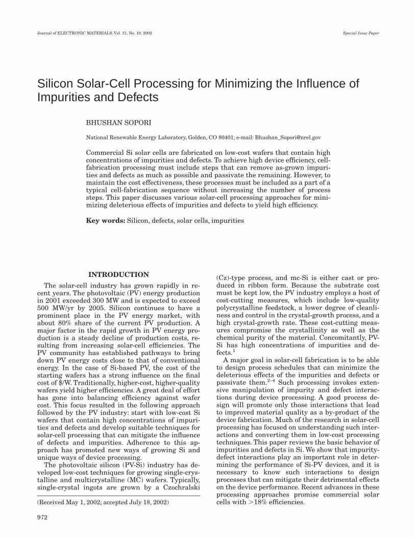
The single-crystal Cz ingots for PV are pulled atgrowth rates that can be many times faster thanthat of the conventional growth for microelectronics.These fast cooling rates are accompanied by exces-sive thermal stresses that lead to the generation ofdefects. Consequently, the single-crystal material isexpected to have high concentrations of quenched-in, nonequilibrium point defects. In some cases, aportion of the ingot may acquire a high density ofcrystal defects (primarily dislocations) and even losethe crystallinity and become MC. The mc-Si sub-strates typically consist of very large grains, typi-cally a few millimeters to several centimeters insize, with a small grain-boundary area producingonly a small effect on the device performance. Thedominant intragrain defect is dislocation. High-quality mc-Si substrates have a tendency to formclusters of defects. Figure 1 is a map of a typical 4.25in. 3 4.25 in. commercial, MC PV-Si wafer. Thewafer has an average defect density of about 105
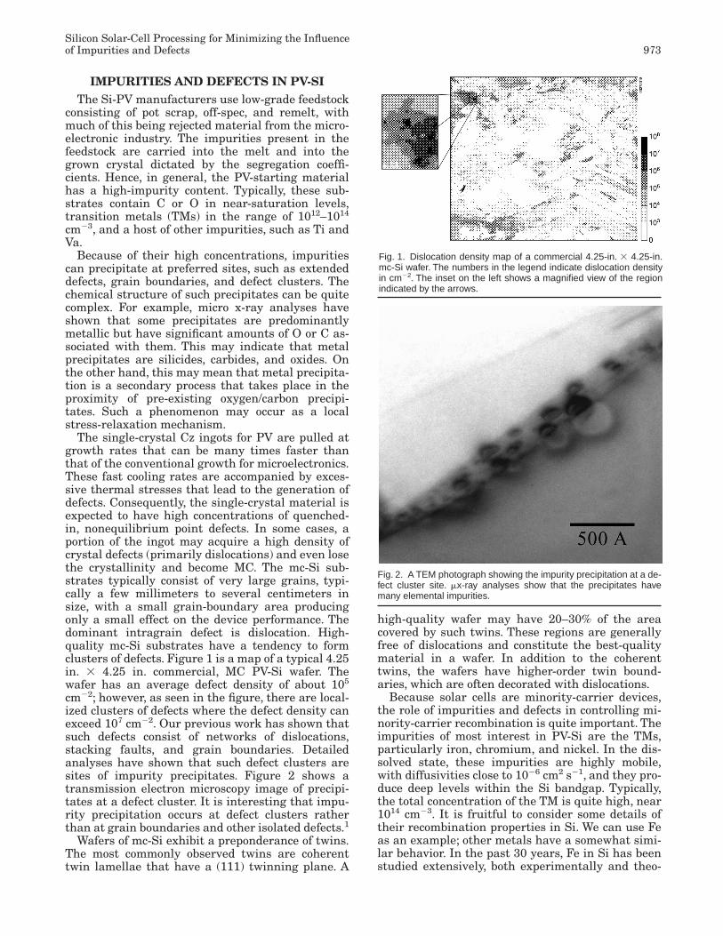
cm22; however, as seen in the figure, there are local-ized clusters of defects where the defect density canexceed 107 cm22. Our previous work has shown thatsuch defects consist of networks of dislocations,stacking faults, and grain boundaries. Detailedanalyses have shown that such defect clusters aresites of impurity precipitates. Figure 2 shows atransmission electron microscopy image of precipi-tates at a defect cluster. It is interesting that impu-rity precipitation occurs at defect clusters ratherthan at grain boundaries and other isolated defects.1
Wafers of mc-Si exhibit a preponderance of twins.The most commonly observed twins are coherenttwin lamellae that have a (111) twinning plane. A
high-quality wafer may have 20–30% of the areacovered by such twins. These regions are generallyfree of dislocations and constitute the best-qualitymaterial in a wafer. In addition to the coherenttwins, the wafers have higher-order twin bound-aries, which are often decorated with dislocations.
Because solar cells are minority-carrier devices,the role of impurities and defects in controlling mi-nority-carrier recombination is quite important. Theimpurities of most interest in PV-Si are the TMs,particularly iron, chromium, and nickel. In the dis-solved state, these impurities are highly mobile,with diffusivities close to 1026 cm2 s21, and they pro-duce deep levels within the Si bandgap. Typically,the total concentration of the TM is quite high, near1014 cm23. It is fruitful to consider some details oftheir recombination properties in Si. We can use Feas an example; other metals have a somewhat simi-lar behavior. In the past 30 years, Fe in Si has beenstudied extensively, both experimentally and theo-
Fig. 1. Dislocation density map of a commercial 4.25-in. 3 4.25-in.mc-Si wafer. The numbers in the legend indicate dislocation densityin cm22. The inset on the left shows a magnified view of the regionindicated by the arrows.
Fig. 2. A TEM photograph showing the impurity precipitation at a de-fect cluster site. mx-ray analyses show that the precipitates havemany elemental impurities.
974 Sopori
retically.5,6 Iron exists in Si in two forms: as an in-terstitial and as a complex with other defects. Atroom temperature, the interstitial iron (Fei) intro-duces a donor level at ET < EV 1 (0.375 6 0.015) eV.The hole-capture cross section of interstitial ironcan be written as (in cm22):
where kB stands for the Boltzmann constant, and Tis the temperature. The electron-capture cross sec-tion of Fe at room temperature was measured as sn 5 4 3 10214 cm22. Because of near-midgap en-ergy and a large capture cross section, it is expectedthat Fe will produce high recombination or a low mi-nority-carrier lifetime (t).
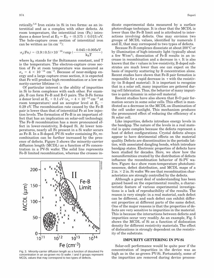
Of particular interest is the ability of impuritiesin Si to form complexes with each other. For exam-ple, B can form Fe-B and B-O pairs. The B-Fe formsa donor level at Ev 1 0.1 eV (sn 5 4 3 10213 cm22 atroom temperature) and an acceptor level at Ec 20.29 eV. The recombination rate caused by the Fe-Bpair is lower than that of interstitial Fe at low injec-tion levels. The formation of Fe-B is an important ef-fect that has an implication on solar-cell technology.The Fe-B recombination has a more pronounced ef-fect in lower-resistivity, B-doped Si. At lower tem-peratures, nearly all Fe present in a Si wafer occursas Fe-B. In a B-doped, PV-Si wafer containing Fe, re-combination can be further increased by the pres-ence of defects. Figure 3 shows the minority-carrierdiffusion length (MCDL) as a function of Fe concen-tration in a PV-Si wafer. The solid line representsFe-B limited recombination, whereas the crosses in-
sp(Fei) 5 (3.960.5)3102163exp (20.04560.005eV
kBT)
dicate experimental data measured by a surfacephotovoltage technique. It is clear that the MCDL islower than the Fe-B limit and is attributed to inter-actions involving defects. One may envision twogroups of MCDL values, identified by numerals Iand II, that may correspond to two types of defects.
Because Fe-B complexes dissociate at about 200°C orby illumination of high-intensity light (typically abouta few W/cm2), dissociation of Fe-B results in an in-crease in recombination and a decrease in t. It is alsoknown that the t values in low-resistivity, B-doped sub-strates are much lower than one can expect on thebasis of impurity scattering by B concentration alone.Recent studies have shown that Fe-B pair formation isresponsible for a rapid decrease in t with the resistiv-ity (in B-doped material). It is important to recognizethat in a solar cell, many impurities are gettered dur-ing cell fabrication. Thus, the behavior of many impuri-ties is quite dynamic in solar-cell material.
Recent studies have also shown that B-O pair for-mation occurs in some solar cells. This effect is man-ifested as a decrease in the MCDL on illumination ofthe cell under sunlight. This mechanism producesthe pronounced effect of reducing the efficiency of aSi solar cell.
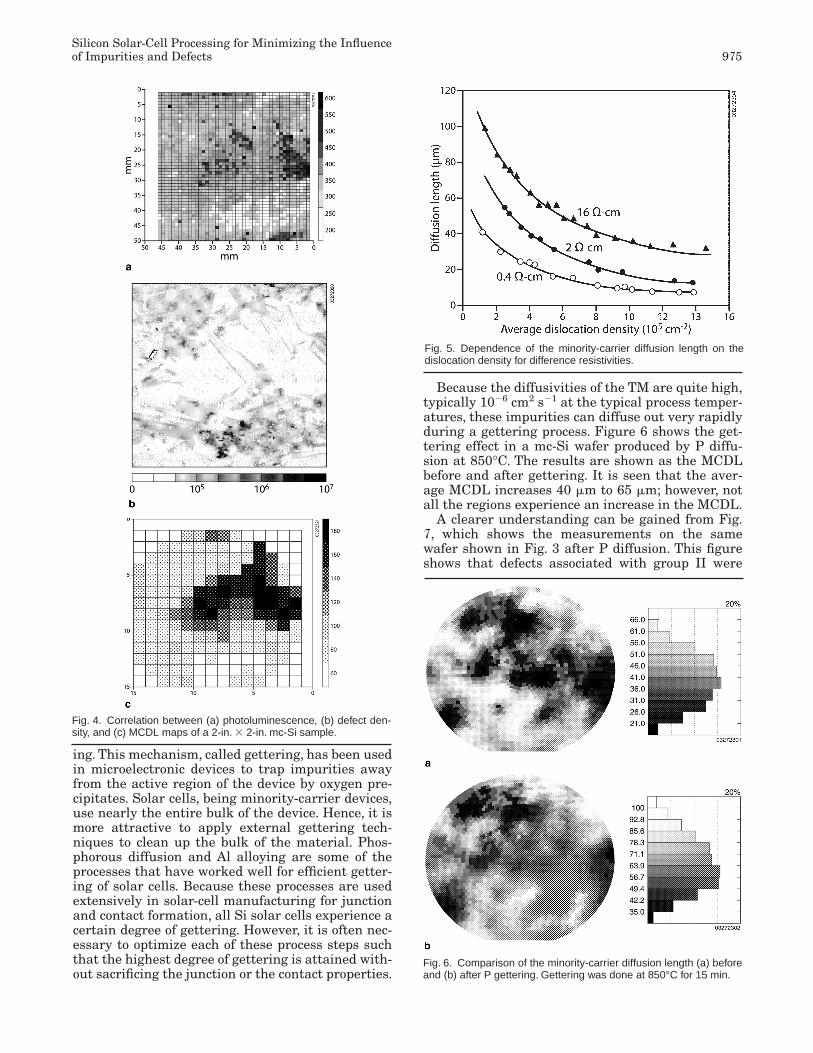
Like impurities, defects introduce energy levels inthe bandgap. The nature of the levels in a real mate-rial is quite complex because the defects represent ahost of defect configurations. Crystal defects alwaysappear to have detrimental effects on the materialquality. Defects are discontinuities in the periodic lat-tice, with associated dangling bonds, which introducebandgap states. Electronic properties of defects havebeen studied for decades. Here, we show how thenonuniformities created by the distribution of defectsinfluence the recombination behavior of Si-PV wa-fers. Figure 4a-c show room-temperature photolumi-nescence, defect distribution, and MCDL maps of a 2 in. 3 2 in. Si wafer. We see that recombination char-acteristics are strongly controlled by the defects.
Although a great deal of understanding has beengained based on the experimental results, a charac-teristic feature of various experimental investiga-tions is a lack of reproducibility of the results. Thereason is very simple: in a real material, each defectcan be different, and each defect can exhibit differ-ent properties at different parts of the same defect.One of the major reasons is that the properties of de-fects are very sensitive to impurities in the material.This is because the interactions between defects andimpurities occur very readily. As an example, Fig. 5shows the MCDL of Si as a function of dislocationdensity for different resistivity materials. The effectof dislocations is strongly dependent on the resistiv-ity of the substrate.
IMPURITY GETTERING IN PV-Si
Solar-cell performance would be quite poor if theconcentration of impurities in the device was ashigh as in the as-grown PV-Si. Fortunately, some ofthe impurities are removed during device process-
Fig. 3. Minority-carrier diffusion length as a function of dissolved Feconcentration in an as-grown mc-Si wafer. I and II groups representMCDL values that may correspond to two types of defects.
Silicon Solar-Cell Processing for Minimizing the Influenceof Impurities and Defects 975
Because the diffusivities of the TM are quite high,typically 1026 cm2 s21 at the typical process temper-atures, these impurities can diffuse out very rapidlyduring a gettering process. Figure 6 shows the get-tering effect in a mc-Si wafer produced by P diffu-sion at 850°C. The results are shown as the MCDLbefore and after gettering. It is seen that the aver-age MCDL increases 40 mm to 65 mm; however, notall the regions experience an increase in the MCDL.
A clearer understanding can be gained from Fig.7, which shows the measurements on the samewafer shown in Fig. 3 after P diffusion. This figureshows that defects associated with group II were
ing. This mechanism, called gettering, has been usedin microelectronic devices to trap impurities awayfrom the active region of the device by oxygen pre-cipitates. Solar cells, being minority-carrier devices,use nearly the entire bulk of the device. Hence, it ismore attractive to apply external gettering tech-niques to clean up the bulk of the material. Phos-phorous diffusion and Al alloying are some of theprocesses that have worked well for efficient getter-ing of solar cells. Because these processes are usedextensively in solar-cell manufacturing for junctionand contact formation, all Si solar cells experience acertain degree of gettering. However, it is often nec-essary to optimize each of these process steps suchthat the highest degree of gettering is attained with-out sacrificing the junction or the contact properties.
Fig. 4. Correlation between (a) photoluminescence, (b) defect den-sity, and (c) MCDL maps of a 2-in. 3 2-in. mc-Si sample.
Fig. 5. Dependence of the minority-carrier diffusion length on thedislocation density for difference resistivities.
Fig. 6. Comparison of the minority-carrier diffusion length (a) beforeand (b) after P gettering. Gettering was done at 850°C for 15 min.
976 Sopori
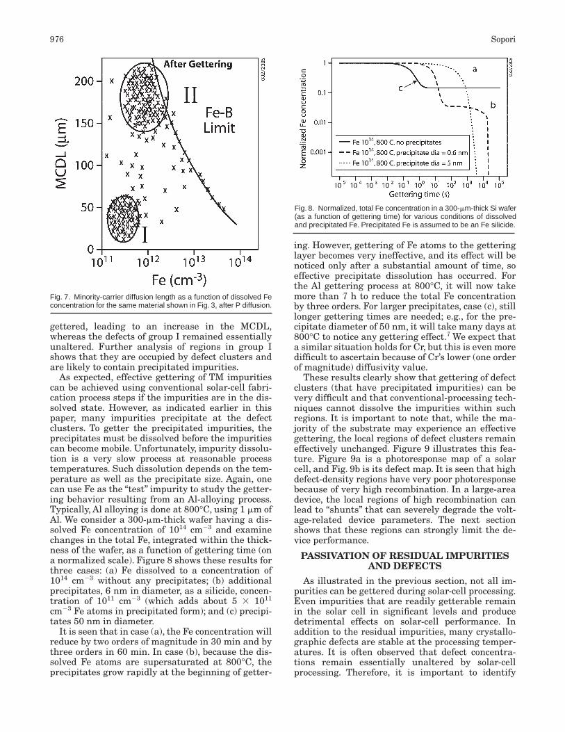
gettered, leading to an increase in the MCDL,whereas the defects of group I remained essentiallyunaltered. Further analysis of regions in group Ishows that they are occupied by defect clusters andare likely to contain precipitated impurities.
As expected, effective gettering of TM impuritiescan be achieved using conventional solar-cell fabri-cation process steps if the impurities are in the dis-solved state. However, as indicated earlier in thispaper, many impurities precipitate at the defectclusters. To getter the precipitated impurities, theprecipitates must be dissolved before the impuritiescan become mobile. Unfortunately, impurity dissolu-tion is a very slow process at reasonable processtemperatures. Such dissolution depends on the tem-perature as well as the precipitate size. Again, onecan use Fe as the “test” impurity to study the getter-ing behavior resulting from an Al-alloying process.Typically, Al alloying is done at 800°C, using 1 mm ofAl. We consider a 300-mm-thick wafer having a dis-solved Fe concentration of 1014 cm23 and examinechanges in the total Fe, integrated within the thick-ness of the wafer, as a function of gettering time (ona normalized scale). Figure 8 shows these results forthree cases: (a) Fe dissolved to a concentration of1014 cm23 without any precipitates; (b) additionalprecipitates, 6 nm in diameter, as a silicide, concen-tration of 1011 cm23 (which adds about 5 3 1011
cm23 Fe atoms in precipitated form); and (c) precipi-tates 50 nm in diameter.
It is seen that in case (a), the Fe concentration willreduce by two orders of magnitude in 30 min and bythree orders in 60 min. In case (b), because the dis-solved Fe atoms are supersaturated at 800°C, theprecipitates grow rapidly at the beginning of getter-
ing. However, gettering of Fe atoms to the getteringlayer becomes very ineffective, and its effect will benoticed only after a substantial amount of time, soeffective precipitate dissolution has occurred. Forthe Al gettering process at 800°C, it will now takemore than 7 h to reduce the total Fe concentrationby three orders. For larger precipitates, case (c), stilllonger gettering times are needed; e.g., for the pre-cipitate diameter of 50 nm, it will take many days at800°C to notice any gettering effect.7 We expect thata similar situation holds for Cr, but this is even moredifficult to ascertain because of Cr’s lower (one orderof magnitude) diffusivity value.
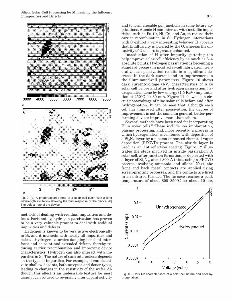
These results clearly show that gettering of defectclusters (that have precipitated impurities) can bevery difficult and that conventional-processing tech-niques cannot dissolve the impurities within suchregions. It is important to note that, while the ma-jority of the substrate may experience an effectivegettering, the local regions of defect clusters remaineffectively unchanged. Figure 9 illustrates this fea-ture. Figure 9a is a photoresponse map of a solarcell, and Fig. 9b is its defect map. It is seen that highdefect-density regions have very poor photoresponsebecause of very high recombination. In a large-areadevice, the local regions of high recombination canlead to “shunts” that can severely degrade the volt-age-related device parameters. The next sectionshows that these regions can strongly limit the de-vice performance.
PASSIVATION OF RESIDUAL IMPURITIESAND DEFECTS
As illustrated in the previous section, not all im-purities can be gettered during solar-cell processing.Even impurities that are readily getterable remainin the solar cell in significant levels and producedetrimental effects on solar-cell performance. In addition to the residual impurities, many crystallo-graphic defects are stable at the processing temper-atures. It is often observed that defect concentra-tions remain essentially unaltered by solar-cellprocessing. Therefore, it is important to identify
Fig. 7. Minority-carrier diffusion length as a function of dissolved Feconcentration for the same material shown in Fig. 3, after P diffusion.
Fig. 8. Normalized, total Fe concentration in a 300-mm-thick Si wafer(as a function of gettering time) for various conditions of dissolvedand precipitated Fe. Precipitated Fe is assumed to be an Fe silicide.
Silicon Solar-Cell Processing for Minimizing the Influenceof Impurities and Defects 977
methods of dealing with residual impurities and de-fects. Fortunately, hydrogen passivation has provento be a very valuable process to deal with residualimpurities and defects.
Hydrogen is known to be very active electronicallyin Si, and it interacts with nearly all impurities anddefects. Hydrogen saturates dangling bonds at inter-faces and at point and extended defects, thereby re-ducing carrier recombination and improving devicecharacteristics. Hydrogen can also interact with im-purities in Si. The nature of such interactions dependson the type of impurities. For example, it can deacti-vate shallow dopants, both acceptor and donor types,leading to changes in the resistivity of the wafer. Al-though this effect is an undesirable feature for mostcases, it can be used to reversibly alter dopant activity
and to form erasable p/n junctions in some future ap-plications. Atomic H can interact with metallic impu-rities, such as Fe, Cr, Ni, Cu, and Au, to reduce theircarrier recombination in Si. Hydrogen interactionswith O exhibit a very interesting behavior. It appearsthat H diffusivity is lowered by the O, whereas the dif-fusivity of O donors is greatly enhanced.
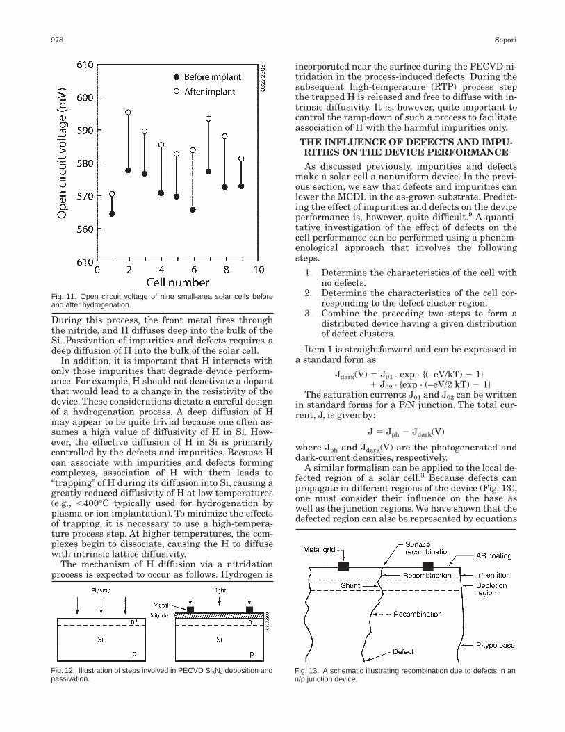
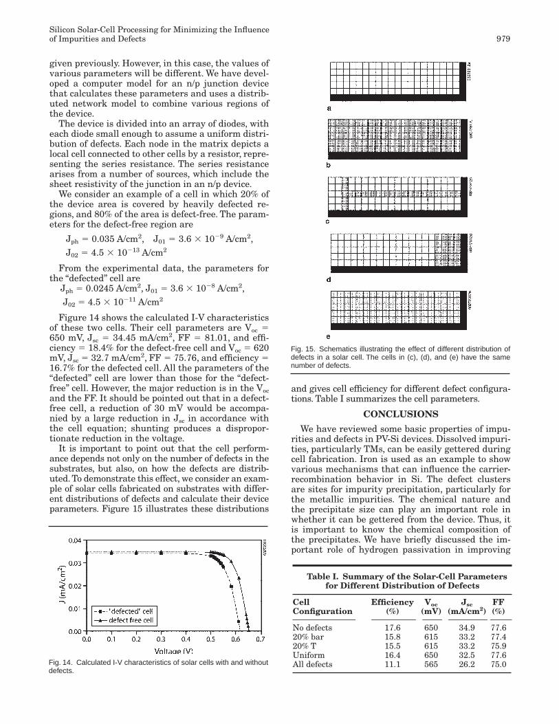
Introduction of H after impurity gettering canhelp improve solar-cell efficiency by as much as 3–4absolute points. Hydrogen passivation is becoming astandard process in most solar-cell fabrication. Gen-erally, such passivation results in a significant de-crease in the dark current and an improvement inthe illuminated-cell parameters. Figure 10 showsdark current-voltage (I-V) characteristics of a Sisolar cell before and after hydrogen passivation; hy-drogenation done by low-energy (1.5 KeV) implanta-tion at 250°C for 30 min. Figure 11 shows open-cir-cuit photovoltage of nine solar cells before and afterhydrogenation. It can be seen that although eachcell has improved after passivation, the degree ofimprovement is not the same. In general, better-per-forming devices improve more than others.
Several methods have been used for incorporatingH in solar cells.8 These include ion implantation,plasma processing, and, more recently, a process inwhich hydrogenation is combined with deposition ofa Si3N4 layer by a plasma-enhanced chemical vapordeposition (PECVD) process. The nitride layer isused as an antireflection coating. Figure 12 illus-trates the steps involved in nitride passivation. Asolar cell, after junction formation, is deposited witha layer of Si3N4, about 800-Å thick, using a PECVDprocess involving ammonia and silane. Next, thefront and back metal contacts are applied usingscreen-printing processes, and the contacts are firedin an infrared furnace. The furnace reaches a peaktemperature of about 800–850°C for about 10 sec.
Fig. 9. (a) A photoresponse map of a solar cell taken with a longwavelength excitation showing the bulk response of the device. (b)The defect map of the device.
Fig. 10. Dark I-V characteristics of a solar cell before and after hy-drogenation.
978 Sopori
Fig. 13. A schematic illustrating recombination due to defects in ann/p junction device.
During this process, the front metal fires throughthe nitride, and H diffuses deep into the bulk of theSi. Passivation of impurities and defects requires adeep diffusion of H into the bulk of the solar cell.
In addition, it is important that H interacts withonly those impurities that degrade device perform-ance. For example, H should not deactivate a dopantthat would lead to a change in the resistivity of thedevice. These considerations dictate a careful designof a hydrogenation process. A deep diffusion of Hmay appear to be quite trivial because one often as-sumes a high value of diffusivity of H in Si. How-ever, the effective diffusion of H in Si is primarilycontrolled by the defects and impurities. Because Hcan associate with impurities and defects formingcomplexes, association of H with them leads to“trapping” of H during its diffusion into Si, causing agreatly reduced diffusivity of H at low temperatures(e.g., ,400°C typically used for hydrogenation byplasma or ion implantation). To minimize the effectsof trapping, it is necessary to use a high-tempera-ture process step. At higher temperatures, the com-plexes begin to dissociate, causing the H to diffusewith intrinsic lattice diffusivity.
The mechanism of H diffusion via a nitridationprocess is expected to occur as follows. Hydrogen is
incorporated near the surface during the PECVD ni-tridation in the process-induced defects. During thesubsequent high-temperature (RTP) process stepthe trapped H is released and free to diffuse with in-trinsic diffusivity. It is, however, quite important tocontrol the ramp-down of such a process to facilitateassociation of H with the harmful impurities only.
THE INFLUENCE OF DEFECTS AND IMPU-RITIES ON THE DEVICE PERFORMANCEAs discussed previously, impurities and defects
make a solar cell a nonuniform device. In the previ-ous section, we saw that defects and impurities canlower the MCDL in the as-grown substrate. Predict-ing the effect of impurities and defects on the deviceperformance is, however, quite difficult.9 A quanti-tative investigation of the effect of defects on thecell performance can be performed using a phenom-enological approach that involves the followingsteps.
1. Determine the characteristics of the cell withno defects.
2. Determine the characteristics of the cell cor-responding to the defect cluster region.
3. Combine the preceding two steps to form adistributed device having a given distributionof defect clusters.
Item 1 is straightforward and can be expressed ina standard form as
The saturation currents J01 and J02 can be writtenin standard forms for a P/N junction. The total cur-rent, J, is given by:
J 5 Jph 2 Jdark(V)
where Jph and Jdark(V) are the photogenerated anddark-current densities, respectively.
A similar formalism can be applied to the local de-fected region of a solar cell.3 Because defects canpropagate in different regions of the device (Fig. 13),one must consider their influence on the base aswell as the junction regions. We have shown that thedefected region can also be represented by equations
1 J02 · {exp · (–eV/2 kT) 2 1} Jdark(V) 5 J01 · exp · {(–eV/kT) 2 1}
Fig. 11. Open circuit voltage of nine small-area solar cells beforeand after hydrogenation.
Fig. 12. Illustration of steps involved in PECVD Si3N4 deposition andpassivation.
Silicon Solar-Cell Processing for Minimizing the Influenceof Impurities and Defects 979
given previously. However, in this case, the values ofvarious parameters will be different. We have devel-oped a computer model for an n/p junction devicethat calculates these parameters and uses a distrib-uted network model to combine various regions ofthe device.
The device is divided into an array of diodes, witheach diode small enough to assume a uniform distri-bution of defects. Each node in the matrix depicts alocal cell connected to other cells by a resistor, repre-senting the series resistance. The series resistancearises from a number of sources, which include thesheet resistivity of the junction in an n/p device.
We consider an example of a cell in which 20% ofthe device area is covered by heavily defected re-gions, and 80% of the area is defect-free. The param-eters for the defect-free region are
Jph 5 0.035 A/cm2, J01 5 3.6 3 1029 A/cm2,
J02 5 4.5 3 10213 A/cm2
From the experimental data, the parameters forthe “defected” cell are
Jph 5 0.0245 A/cm2, J01 5 3.6 3 1028 A/cm2,
J02 5 4.5 3 10211 A/cm2
Figure 14 shows the calculated I-V characteristicsof these two cells. Their cell parameters are Voc 5650 mV, Jsc 5 34.45 mA/cm2, FF 5 81.01, and effi-ciency 5 18.4% for the defect-free cell and Voc 5 620mV, Jsc 5 32.7 mA/cm2, FF 5 75.76, and efficiency 516.7% for the defected cell. All the parameters of the“defected” cell are lower than those for the “defect-free” cell. However, the major reduction is in the Vocand the FF. It should be pointed out that in a defect-free cell, a reduction of 30 mV would be accompa-nied by a large reduction in Jsc in accordance withthe cell equation; shunting produces a dispropor-tionate reduction in the voltage.
It is important to point out that the cell perform-ance depends not only on the number of defects in thesubstrates, but also, on how the defects are distrib-uted. To demonstrate this effect, we consider an exam-ple of solar cells fabricated on substrates with differ-ent distributions of defects and calculate their deviceparameters. Figure 15 illustrates these distributions
Fig. 14. Calculated I-V characteristics of solar cells with and withoutdefects.
Fig. 15. Schematics illustrating the effect of different distribution ofdefects in a solar cell. The cells in (c), (d), and (e) have the samenumber of defects.
and gives cell efficiency for different defect configura-tions. Table I summarizes the cell parameters.
CONCLUSIONS
We have reviewed some basic properties of impu-rities and defects in PV-Si devices. Dissolved impuri-ties, particularly TMs, can be easily gettered duringcell fabrication. Iron is used as an example to showvarious mechanisms that can influence the carrier-recombination behavior in Si. The defect clustersare sites for impurity precipitation, particularly forthe metallic impurities. The chemical nature andthe precipitate size can play an important role inwhether it can be gettered from the device. Thus, itis important to know the chemical composition ofthe precipitates. We have briefly discussed the im-portant role of hydrogen passivation in improving
Table I. Summary of the Solar-Cell Parametersfor Different Distribution of Defects
Cell Efficiency Voc Jsc FFConfiguration (%) (mV) (mA/cm2) (%)
No defects 17.6 650 34.9 77.620% bar 15.8 615 33.2 77.420% T 15.5 615 33.2 75.9Uniform 16.4 650 32.5 77.6All defects 11.1 565 26.2 75.0
980 Sopori
solar-cell performance. Examples are given to showhow defects and impurities can influence solar-cellperformance. Modeling results are presented toshow that both the number and the distribution ofdefects play an important role in the performance ofa solar cell.
ACKNOWLEDGEMENTS
This work was supported by the U.S. Departmentof Energy under Contract No. DE-AC36-99GO10337.
REFERENCES1. B. Sopori, Proc. ICDS-19, ed. G. Davies and M.H. Nazare
(Aedermannsdorf, Switzerland: Trans Tech Publications,1997), pp. 527–534.
2. B.L. Sopori, L. Jastrzebski, T.Y. Tan, and S. Narayanan,Proc. 12th PVSEC (1994), pp. 1003–1007.
3. B.L. Sopori, W. Chen, K. Nemire, J. Gee, and S. Ostapenko,Proc. 2nd World Conf. Photovoltaic Solar Energy Conver-sion (1998), pp. 152–155.
4. B.L. Sopori, X. Deng, J.P. Benner, A. Rohatgi, P. Sana, S.K.Estreicher, Y.K. Park, and M.A. Roberson, Solar EnergyMater. Solar Cells 41/42, 159 (1996).
5. A.A. Istratov, H. Hieslmair, and E.R. Weber, Appl. Phys.A69, 13 (1999).
6. B.L. Sopori, ed., Proc. 9th Workshop Crystalline SiliconSolar Cell Materials Processes, (Golden, CO: National Re-newable Energy Laboratory) NREL/BK-520-26941.
7. B.L. Sopori, W. Chen, T.Y. Tan, and P. Plekhanov, “NCPVPhotovoltaics Program Review,” AIP Conf. Proc., Woodbury,NY, ed. M. Al-Jassim, J. Thornton, and J. Gee (AIP, 1998),vol. 462, p. 341.
8. B. Sopori, Y. Zhang, and N.M. Ravindra, J. Electron. Mater.30, 8. 1616 (2001).
9. J.G. Fossum and F.A. Lindholm, IEEE Trans. ED-27, 692(1980).
Copyright © 2022 FDOKUMEN