Minimizing total power by simultaneous Vdd/Vth assignment
13
IEEE TRANSACTIONS ON COMPUTER-AIDED DESIGN OF INTEGRATED CIRCUITS AND SYSTEMS, VOL. 23, NO. 5, MAY 2004 665 Minimizing Total Power by Simultaneous Assignment Ashish Srivastava, Student Member, IEEE, and Dennis Sylvester, Member, IEEE Abstract—In this paper, we investigate the effectiveness of simul- taneous multiple supply and threshold voltage assignment in mini- mizing the total power static dynamic in generic digital CMOS designs. Achievable power reductions under varying conditions are investigated, including static-power limited designs and sub-1-V processes. Rules-of-thumb are developed for optimal ’s and ’s to be used in future designs. These models show the optimal second to be approximately half the nominal while the potential total power savings is significantly greater than previ- ously anticipated (60%–65%). We describe the impact of level con- version delays and also demonstrate that the scaling properties of multivoltage systems are very good, particularly when considering impending device scaling advancements. Index Terms—Dual supply voltage, level conversion, power optimization. I. INTRODUCTION P OWER consumption has become a top priority in high- performance circuit design today. From a dynamic power perspective, supply-voltage reduction is the most effective tech- nique to limiting power, due to its quadratic dependency. How- ever, the delay increase with reducing can seriously degrade the throughput of the circuit. Similarly, an increase in pro- vides exponential improvements in static power, again at the ex- pense of speed. To counter this loss in performance, dual [1], [2] and dual [3]–[5] techniques have been proposed. These approaches assign gates on critical paths to operate at the higher or lower and the more common noncritical portions of the cir- cuit are set to operate at lower or higher , reducing the total power consumption without degrading performance (which is held fixed as a constraint). These techniques have been successfully implemented in large-scale designs, particu- larly dual , but most of the existing work focuses on one of these techniques in isolation as opposed to jointly. Also, as the contribution of static power to the total power (defined as the sum of static and dynamic power components) grows, a need to minimize the total power as opposed to either dynamic or static power alone becomes evident. For example, a recent Intel paper states that leakage power makes up approximately 15% of the total power consumption for functional units of the Manuscript received September 19, 2002; revised April 14, 2003 and September 2, 2003. This work was supported in part by the MARCO/DARPA Gigascale Silicon Research Center and in part by the Semiconductor Research Corporation. This paper was recommended by Associate Editor M. Pedram. The authors are with the Department of Electrical Engineering and Com- puter Science, University of Michigan, Ann Arbor, MI 48109 USA (e-mail: [email protected]). Digital Object Identifier 10.1109/TCAD.2004.826551 Pentium 4 [6]. Power-reduction techniques clearly must target both static and dynamic components to be most effective. In [7], the authors show that carefully reducing in multi- sys- tems can offset the traditional delay penalties at low- with lessened static-power consequences (due to the reduced and levels). Taking this approach, total power minimiza- tion becomes the only practical goal since dynamic power can be continually reduced through lowered values. The rise in static power under this circumstance will eventually outweigh the shrinking dynamic power component. Additionally, in dual or multi- designs, the effect of drain- induced barrier-lowering (DIBL) causes the effective of lower gates to increase. This results in larger delay penal- ties at lower supply voltages, reducing the number of gates that can be set to low , thus limiting the achievable improve- ment in dynamic power. This effect further points to the use of several thresholds in conjunction with a multi- design. We refer to the use of dual and values together in the same design as dual in this paper (and multi- for cases with more than two supply or threshold voltages, as in Section VII), while the term dual implies a single is used for all gates. 1 Previous work [8] estimates the optimal and values to be used in multivoltage systems to maximize either dynamic or static power savings, respectively. The paper does not address the advantages of combining multiple supply and threshold volt- ages to reduce the total power of the design. They confirm ear- lier work [9] claiming that, in a dual system, the optimal lower is 60–70% of the original . In general, [9] and [10] have found optimized dual- systems to provide typical dynamic power reductions of 40%–45%. In this paper, we make several key improvements over pre- vious work in exploring the multi- design space. 1) We minimize total power consumption, defined as the sum of static and dynamic components. 2) We simultaneously optimize and to achieve this goal. 3) We consider DIBL, which strongly limits the achievable power reduction in a multi- , single design environment. We also develop rules-of-thumb to estimate the optimal and to be used in future designs. These expressions are functions of an important weighting factor that denotes 1 By single , we refer to a single threshold adjust implant for each de- vice type (N and P)—due to DIBL effects, devices running at different ’s will experience somewhat different effective threshold voltages even under these conditions. To avoid this confusion, we reference both and values to in this paper unless otherwise noted. 0278-0070/04$20.00 © 2004 IEEE
-
Upload
independent -
Category
Documents
-
view
3 -
download
0
Transcript of Minimizing total power by simultaneous Vdd/Vth assignment
IEEE TRANSACTIONS ON COMPUTER-AIDED DESIGN OF INTEGRATED CIRCUITS AND SYSTEMS, VOL. 23, NO. 5, MAY 2004 665
Minimizing Total Power by SimultaneousVdd=Vth Assignment
Ashish Srivastava, Student Member, IEEE, and Dennis Sylvester, Member, IEEE
Abstract—In this paper, we investigate the effectiveness of simul-taneous multiple supply and threshold voltage assignment in mini-mizing the total power (static+dynamic) in generic digital CMOSdesigns. Achievable power reductions under varying conditions areinvestigated, including static-power limited designs and sub-1-Vprocesses. Rules-of-thumb are developed for optimal Vdd’s andVth’s to be used in future designs. These models show the optimalsecond Vdd to be approximately half the nominal Vdd while thepotential total power savings is significantly greater than previ-ously anticipated (60%–65%). We describe the impact of level con-version delays and also demonstrate that the scaling properties ofmultivoltage systems are very good, particularly when consideringimpending device scaling advancements.
Index Terms—Dual supply voltage, level conversion, poweroptimization.
I. INTRODUCTION
POWER consumption has become a top priority in high-performance circuit design today. From a dynamic power
perspective, supply-voltage reduction is the most effective tech-nique to limiting power, due to its quadratic dependency. How-ever, the delay increase with reducing can seriously degradethe throughput of the circuit. Similarly, an increase in pro-vides exponential improvements in static power, again at the ex-pense of speed.
To counter this loss in performance, dual [1], [2] and dual[3]–[5] techniques have been proposed. These approaches
assign gates on critical paths to operate at the higher orlower and the more common noncritical portions of the cir-cuit are set to operate at lower or higher , reducingthe total power consumption without degrading performance(which is held fixed as a constraint). These techniques havebeen successfully implemented in large-scale designs, particu-larly dual , but most of the existing work focuses on oneof these techniques in isolation as opposed to jointly. Also, asthe contribution of static power to the total power (defined asthe sum of static and dynamic power components) grows, aneed to minimize the total power as opposed to either dynamicor static power alone becomes evident. For example, a recentIntel paper states that leakage power makes up approximately15% of the total power consumption for functional units of the
Manuscript received September 19, 2002; revised April 14, 2003 andSeptember 2, 2003. This work was supported in part by the MARCO/DARPAGigascale Silicon Research Center and in part by the Semiconductor ResearchCorporation. This paper was recommended by Associate Editor M. Pedram.
The authors are with the Department of Electrical Engineering and Com-puter Science, University of Michigan, Ann Arbor, MI 48109 USA (e-mail:[email protected]).
Digital Object Identifier 10.1109/TCAD.2004.826551
Pentium 4 [6]. Power-reduction techniques clearly must targetboth static and dynamic components to be most effective. In [7],the authors show that carefully reducing in multi- sys-tems can offset the traditional delay penalties at low- withlessened static-power consequences (due to the reducedand levels). Taking this approach, total power minimiza-tion becomes the only practical goal since dynamic power canbe continually reduced through lowered values. The rise instatic power under this circumstance will eventually outweighthe shrinking dynamic power component.
Additionally, in dual or multi- designs, the effect of drain-induced barrier-lowering (DIBL) causes the effective oflower gates to increase. This results in larger delay penal-ties at lower supply voltages, reducing the number of gates thatcan be set to low , thus limiting the achievable improve-ment in dynamic power. This effect further points to the use ofseveral thresholds in conjunction with a multi- design. Werefer to the use of dual and values together in the samedesign as dual in this paper (and multi- forcases with more than two supply or threshold voltages, as inSection VII), while the term dual implies a single isused for all gates.1
Previous work [8] estimates the optimal and valuesto be used in multivoltage systems to maximize either dynamicor static power savings, respectively. The paper does not addressthe advantages of combining multiple supply and threshold volt-ages to reduce the total power of the design. They confirm ear-lier work [9] claiming that, in a dual system, the optimallower is 60–70% of the original . In general, [9] and[10] have found optimized dual- systems to provide typicaldynamic power reductions of 40%–45%.
In this paper, we make several key improvements over pre-vious work in exploring the multi- design space.
1) We minimize total power consumption, defined as thesum of static and dynamic components.
2) We simultaneously optimize and to achieve thisgoal.
3) We consider DIBL, which strongly limits the achievablepower reduction in a multi- , single designenvironment.
We also develop rules-of-thumb to estimate the optimaland to be used in future designs. These expressions arefunctions of an important weighting factor that denotes
1By single V , we refer to a single threshold adjust implant for each de-vice type (N and P)—due to DIBL effects, devices running at different V ’swill experience somewhat different effective threshold voltages even under theseconditions. To avoid this confusion, we reference both V and V valuesto V in this paper unless otherwise noted.
0278-0070/04$20.00 © 2004 IEEE
666 IEEE TRANSACTIONS ON COMPUTER-AIDED DESIGN OF INTEGRATED CIRCUITS AND SYSTEMS, VOL. 23, NO. 5, MAY 2004
the degree to which a design is static-power limited. We thenmake a number of observations regarding the scaling propertiesof dual systems, particularly with respect to futuredevice-scaling scenarios. We also extend our analysis byexamining the sensitivity of the results to certain assumptions,including the role of level-conversion-delay penalties and thediscretized nature of capacitance along a path. We also describea key tradeoff between power reduction and critical-pathproliferation that may limit the extent to which slack maybe exploited in light of rising process variability in futuretechnologies.
II. POWER-OPTIMIZATION FRAMEWORK
This section develops a high-level framework and sets up theobjective function and constraints to optimize power dissipationin a multi- system. To estimate the power improvementobtained by applying multiple ’s and ’s, we perform apath-based analysis of a generic logic network. To simplify theproblem we assume node- and edge-disjoint paths. We also as-sume that it is possible to apply a combination of ’s and
’s to any fraction of the total path capacitance. This is equiv-alent to stating that extended clustered voltage scaling (ECVS)is used, which allows for asynchronous-level conversion any-where along a path [9]. While we do not explicitly consider over-head due to level conversion in most of this paper, we describelater the impact of delay penalties associated with performinglevel conversion. We also discuss the impact of discretizing thetotal path capacitance in Section VIII.
Consider and to be the supply and threshold voltagesin a single system. If is the total path capacitanceof a path, then the total dynamic-power dissipation is simplyexpressed as
(1)
where is the frequency of operation. Considering the samepath implemented in an n- - design, we define s(other than , which is the total path capacitance), as thecapacitances operating at a supply voltage and thresholdvoltage . If we define the capacitance to be the capac-itance operating at a supply voltage , it can be expressed as
for (2)
The total dynamic-power dissipation can now be expressed as
(3)
The first term in (3) corresponds to the capacitance operating atand is obtained by subtracting the sum of the capacitances
operating at voltages other than from the total path capaci-tance . Now the ratio of the dynamic-power dissipation tothe original design, obtained by dividing (3) by (2), can be ex-pressed as
Gain (4)
The static power can be expressed similarly. If is the totaldevice width (both PMOS and NMOS) and is the de-vice width (both PMOS and NMOS) at power supply andthreshold voltage , then the gain in static power is given by
Gain
(5)
where S is the subthreshold swing (typically given in units ofmV/decade). The reduction in static power in low- devicesis due to: 1) DIBL; 2) the lower itself; and 3) other com-plex device-related phenomena, such as the relationship amongdoping, , and S [11].2 Specifically, DIBL acts to reduceleakage in lower devices since the amount of drain bias,which creates a large drain/substrate depletion region and leadsto a reduced , is limited. The typical model for this is linearwith (set to as is the case in MOS devices leaking in ageneric logic gate)
(6)
In this model, is the DIBL coefficient and is typically inthe range of 60–110 mV/V. is the nominal long-channelthreshold voltage in the absence of DIBL. Since intypical leakage scenarios, a reduction in for a given devicedesign leads directly to a rise in and an exponentiallysmaller . This is captured in (5) by considering to be afunction of the at which the gate is operating.
While our results use (5) to reflect the relationship betweenand , experiments using a linear term rather
than quadratic to represent static power gains showed onlyminor changes in the overall power reductions and optimal
values. The change in delay when the powersupply or is changed is estimated using the alpha-powerlaw model [13]
(7)
To obtain the minimum power dissipation condition we note thatat the minima
(8)
(9)
where is the dynamic power dissipation, is the staticpower dissipation, and represents a design variable such as
or . Let be the dynamic power in the initial designand be the static power consumption of the initial design. If
2As an example, a long-channel device in a modern technology (large L tosuppress DIBL effects) demonstrates a linear reduction in I with V con-tributing to the quadratic term in (5). This effect is not properly captured intraditional I expressions [12].
SRIVASTAVA AND SYLVESTER: MINIMIZING TOTAL POWER BY SIMULTANEOUS ASSIGNMENT 667
we try to minimize a weighted sum of the gains, where the gainsare as expressed in (4) and (5), we obtain
(10)
(11)
Now, (11) can be expressed as
(12)
In comparing (12) with (9), we infer that if we minimize aweighted sum of the gains in power and define the weightingfactor as the ratio of dynamic and static power at the initialdesign point (i.e., ), we minimize the total powerdissipation as well.
As shown in [8], the capacitance and transistor width alonga path are largely proportional to the path’s delay. Hence, theratios of widths in (5) can be replaced by ratios of capacitance.At this point, the problem of power minimization for given volt-ages and thresholds can be formulated as a linear programming(LP) problem with the ratios of capacitances as the variables.For each point in the space (e.g., for and
, we have the and design spaces),which corresponds to a particular value for the s and
s, the problem is formulated and the ratios of capacitancecorresponding to different path delays are obtained as a solutionof the LP problem. The ratios of capacitance are then integratedover the path-delay distribution to obtain the total capacitanceoperating at each combination of and . Again, we de-fine the weighting factor as the ratio of the dynamic to staticpower in the original single design (e.g.,implies that 10/11 of the total initial power was dynamic). Asdescribed above, total power minimization is achieved by mini-mizing a weighted sum of the static and dynamic power. Hence,the goal of total power reduction can now be expressed as
Maximize Gain Gain (13a)
(13b)
where is the original path delay normalized to the critical pathdelay. Equation (13b) is then obtained by multiplying the delaycontributed by the fraction of capacitance by the factor
, which reflects the increase in delay. This increasein delay is added to the original path delay to obtain the finaldelay of the path. The constraint forces the final delay of eachpath to be less than the critical delay of the network which, beingnormalized, is equal to one and, thus, we maintain the operatingfrequency of . Since the paths are independent of each other,minimizing the power dissipation on each of the paths will leadto the minimum power of the complete logic network. Since weuse only to weight the occurrence of paths with a particulardelay, any generic can be used within our framework to esti-mate the achievable power dissipation reduction using multiplesupply and threshold voltages. Note that impacts the opti-mization procedure through the constraint (13b) although it does
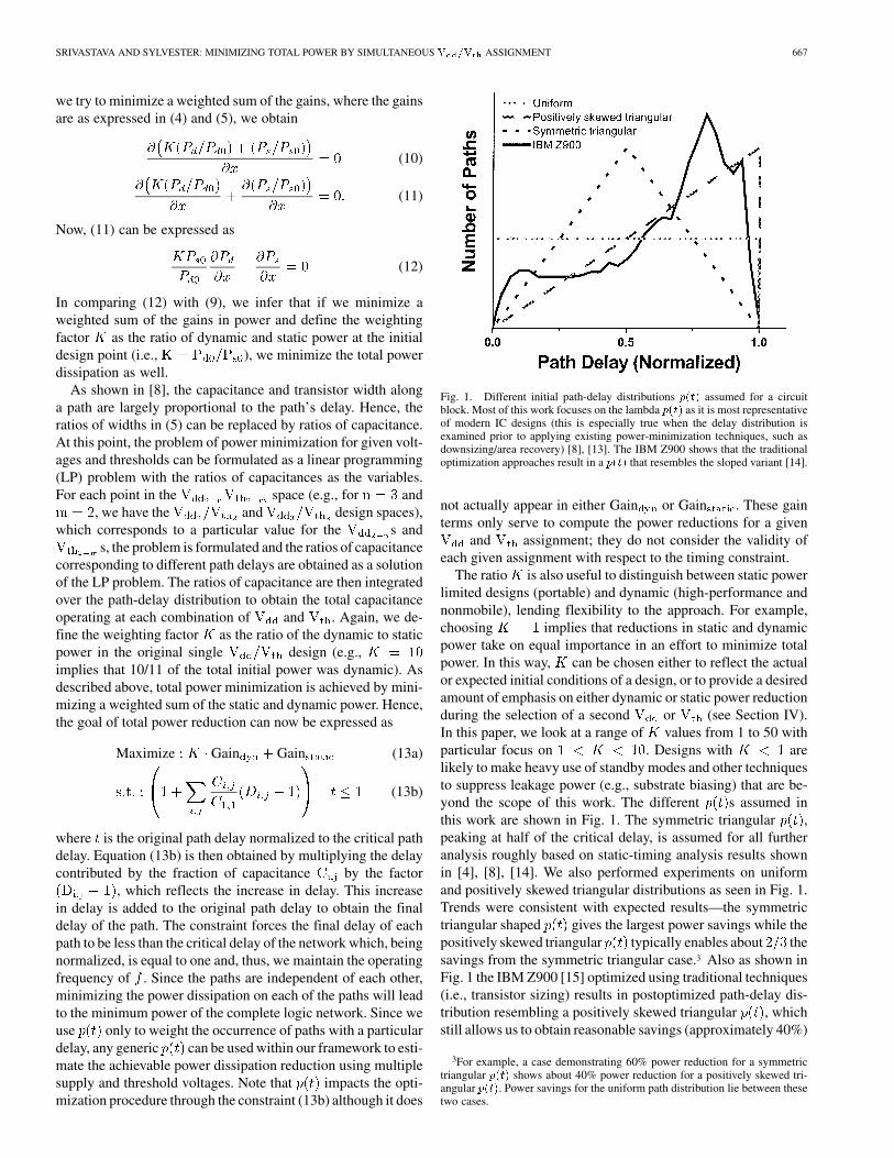
Fig. 1. Different initial path-delay distributions p(t) assumed for a circuitblock. Most of this work focuses on the lambda p(t) as it is most representativeof modern IC designs (this is especially true when the delay distribution isexamined prior to applying existing power-minimization techniques, such asdownsizing/area recovery) [8], [13]. The IBM Z900 shows that the traditionaloptimization approaches result in a p(t) that resembles the sloped variant [14].
not actually appear in either Gain or Gain . These gainterms only serve to compute the power reductions for a given
and assignment; they do not consider the validity ofeach given assignment with respect to the timing constraint.
The ratio is also useful to distinguish between static powerlimited designs (portable) and dynamic (high-performance andnonmobile), lending flexibility to the approach. For example,choosing implies that reductions in static and dynamicpower take on equal importance in an effort to minimize totalpower. In this way, can be chosen either to reflect the actualor expected initial conditions of a design, or to provide a desiredamount of emphasis on either dynamic or static power reductionduring the selection of a second or (see Section IV).In this paper, we look at a range of values from 1 to 50 withparticular focus on . Designs with arelikely to make heavy use of standby modes and other techniquesto suppress leakage power (e.g., substrate biasing) that are be-yond the scope of this work. The different s assumed inthis work are shown in Fig. 1. The symmetric triangular ,peaking at half of the critical delay, is assumed for all furtheranalysis roughly based on static-timing analysis results shownin [4], [8], [14]. We also performed experiments on uniformand positively skewed triangular distributions as seen in Fig. 1.Trends were consistent with expected results—the symmetrictriangular shaped gives the largest power savings while thepositively skewed triangular typically enables about thesavings from the symmetric triangular case.3 Also as shown inFig. 1 the IBM Z900 [15] optimized using traditional techniques(i.e., transistor sizing) results in postoptimized path-delay dis-tribution resembling a positively skewed triangular , whichstill allows us to obtain reasonable savings (approximately 40%)
3For example, a case demonstrating 60% power reduction for a symmetrictriangular p(t) shows about 40% power reduction for a positively skewed tri-angular p(t). Power savings for the uniform path distribution lie between thesetwo cases.

668 IEEE TRANSACTIONS ON COMPUTER-AIDED DESIGN OF INTEGRATED CIRCUITS AND SYSTEMS, VOL. 23, NO. 5, MAY 2004
TABLE ICOMPARISON OF LP FORMULATION FINAL PATH TIMING AND POWER SAVINGS RATIOS WITH SPICE
using dual techniques, though ideally we would like todo a simultaneous optimization of all the design variables avail-able. We emphasize that the exact form of used is not thecentral point of this paper—the framework and resulting trendsand guidelines for optimal values are the primary con-tribution. In general, the high-level approach outlined in thissection is similar to that of [8] with the key differences beingthe presence of both and as variables, the considera-tion of total power consumption, the use of the weighting factor
, modeling of the relationship between and , and theinclusion of DIBL effects.
The LP formulation was verified by comparing to SPICEruns using an industrial 0.13- m technology. Technology pa-rameters used in the formulation were extracted from SPICEsimulations. Complete SPICE verification is infeasible sincethe number of simulations required would be enormous (e.g.,hundreds of paths, each with dozens of gates, would have tobe simulated at limitless permutations of and whilesweeping the mappings of these gates to the combi-nations). Instead, several discrete points were selected on thepath-delay distribution (e.g., 50% or 70% of critical path delay)and these particular paths were used as the test cases. To verifythe correctness of the values obtained from the LP formula-tion, we used the capacitance ratios from the solution of the LPproblem and compared the timing and power dissipation pre-dicted by the models used in the LP formulation with resultsobtained using SPICE. The simulations were performed by im-plementing a path as a chain of 100 identical inverters. A largenumber of inverters were used to provide sufficient granularityto map the capacitance ratios obtained through the LP formu-lation to the inverter chain. Inverters in the chain are then as-signed to the required combination of and with high
gates followed by low gates (thus avoiding level con-version). Table I compares the numbers obtained using the LPformulation to SPICE. The high and low are 1.2 and 0.6 V,respectively, and the design has an initial value of 13 (foundfrom SPICE). Since the numbers agree very closely for all se-lected path delays, the final results for the entire circuit (ob-tained by a summation of the results over all paths) are expectedto match with those found using exhaustive SPICE simulationsover all paths in the circuit.
III. COMPARISON OF DUAL WITH DUAL
In this section, we compare the use of dual , assuminga single value is available, to the cominbed use of bothdual- and dual- . In the dual approach, thesecond threshold voltage is used to both: 1) reduce static power
Fig. 2. Dual V =V shows larger total power reduction than dualV =single V throughout the range of K values with power improvementsranging from 15%–45%.
and 2) to provide speed improvements in logic gates that run atlowered supply voltages. As a result, we expect this approachto greatly outperform the dual system. Both approachesto reducing power dissipation were applied to a design using a
of 0.9 V and V.Results in Fig. 2 demonstrate that the power reduction ob-
tained by applying dual is consistently much largerthan the optimal dual design. In this and several subsequentplots, we show the minimum achievable power for various con-figurations normalized to the power of an initial singledesign. It is also seen in Fig. 2 that the advantage offered bythe second threshold voltage is smallest (around 10%–20%)for lower values. This is because the dual tech-nique is predicated on using a lower second threshold voltageto allow cells to be run at a lower power supply while main-taining good drive capability. However, at small values thestatic power is comparable to dynamic power and a likely in-crease in static power due to the lower is less acceptableas a tradeoff. Modern high-performance designs tend to exhibit
values in the range of 2–20 [6]; the dual approachdelivers 15%–30% lower power than dual alone over thisrange. This effect is also seen in Fig. 3 which shows the valueof the optimized second power supply voltage, (note theconvergence at low values where is more constrained),for the same and as in Fig. 2. At higher , a muchlower voltage supply can be used to achieve considerable dy-namic power savings at the cost of static power, which consti-
SRIVASTAVA AND SYLVESTER: MINIMIZING TOTAL POWER BY SIMULTANEOUS ASSIGNMENT 669
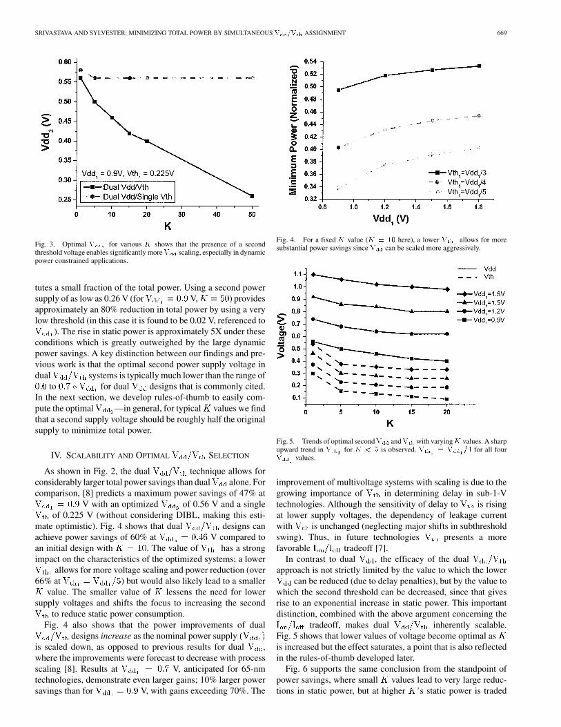
Fig. 3. Optimal V for various K shows that the presence of a secondthreshold voltage enables significantly moreV scaling, especially in dynamicpower constrained applications.
tutes a small fraction of the total power. Using a second powersupply of as low as 0.26 V (for V, ) providesapproximately an 80% reduction in total power by using a verylow threshold (in this case it is found to be 0.02 V, referenced to
). The rise in static power is approximately 5X under theseconditions which is greatly outweighed by the large dynamicpower savings. A key distinction between our findings and pre-vious work is that the optimal second power supply voltage indual systems is typically much lower than the range of
to for dual designs that is commonly cited.In the next section, we develop rules-of-thumb to easily com-pute the optimal —in general, for typical values we findthat a second supply voltage should be roughly half the originalsupply to minimize total power.
IV. SCALABILITY AND OPTIMAL SELECTION
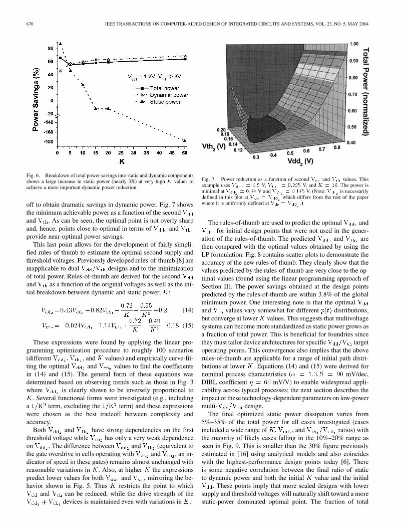
As shown in Fig. 2, the dual technique allows forconsiderably larger total power savings than dual alone. Forcomparison, [8] predicts a maximum power savings of 47% at
V with an optimized of 0.56 V and a singleof 0.225 V (without considering DIBL, making this esti-
mate optimistic). Fig. 4 shows that dual designs canachieve power savings of 60% at V compared toan initial design with . The value of has a strongimpact on the characteristics of the optimized systems; a lower
allows for more voltage scaling and power reduction (over66% at ) but would also likely lead to a smaller
value. The smaller value of lessens the need for lowersupply voltages and shifts the focus to increasing the second
to reduce static power consumption.Fig. 4 also shows that the power improvements of dual
designs increase as the nominal power supplyis scaled down, as opposed to previous results for dual ,where the improvements were forecast to decrease with processscaling [8]. Results at V, anticipated for 65-nmtechnologies, demonstrate even larger gains; 10% larger powersavings than for V, with gains exceeding 70%. The
Fig. 4. For a fixed K value (K = 10 here), a lower V allows for moresubstantial power savings since V can be scaled more aggressively.
Fig. 5. Trends of optimal secondV andV with varyingK values. A sharpupward trend in V for K < 5 is observed. V = V =4 for all fourV values.
improvement of multivoltage systems with scaling is due to thegrowing importance of in determining delay in sub-1-Vtechnologies. Although the sensitivity of delay to is risingat lower supply voltages, the dependency of leakage currentwith is unchanged (neglecting major shifts in subthresholdswing). Thus, in future technologies presents a morefavorable tradeoff [7].
In contrast to dual , the efficacy of the dualapproach is not strictly limited by the value to which the lower
can be reduced (due to delay penalties), but by the value towhich the second threshold can be decreased, since that givesrise to an exponential increase in static power. This importantdistinction, combined with the above argument concerning the
tradeoff, makes dual inherently scalable.Fig. 5 shows that lower values of voltage become optimal asis increased but the effect saturates, a point that is also reflectedin the rules-of-thumb developed later.
Fig. 6 supports the same conclusion from the standpoint ofpower savings, where small values lead to very large reduc-tions in static power, but at higher ’s static power is traded
670 IEEE TRANSACTIONS ON COMPUTER-AIDED DESIGN OF INTEGRATED CIRCUITS AND SYSTEMS, VOL. 23, NO. 5, MAY 2004
Fig. 6. Breakdown of total power savings into static and dynamic componentsshows a large increase in static power (nearly 3X) at very high K values toachieve a more important dynamic power reduction.
off to obtain dramatic savings in dynamic power. Fig. 7 showsthe minimum achievable power as a function of the secondand . As can be seen, the optimal point is not overly sharpand, hence, points close to optimal in terms of andprovide near-optimal power savings.
This last point allows for the development of fairly simpli-fied rules-of-thumb to estimate the optimal second supply andthreshold voltages. Previously developed rules-of-thumb [8] areinapplicable to dual designs and to the minimizationof total power. Rules-of-thumb are derived for the secondand as a function of the original voltages as well as the ini-tial breakdown between dynamic and static power,
(14)
(15)
These expressions were found by applying the linear pro-gramming optimization procedure to roughly 100 scenarios(different , and values) and empirically curve-fit-ting the optimal and values to find the coefficientsin (14) and (15). The general form of these equations wasdetermined based on observing trends such as those in Fig. 3where is clearly shown to be inversely proportional to
. Several functional forms were investigated (e.g., includinga term, excluding the term) and these expressionswere chosen as the best tradeoff between complexity andaccuracy.
Both and have strong dependencies on the firstthreshold voltage while has only a very weak dependenceon . The difference between and (equivalent tothe gate overdrive in cells operating with and , an in-dicator of speed in these gates) remains almost unchanged withreasonable variations in . Also, at higher the expressionspredict lower values for both and mirroring the be-havior shown in Fig. 5. Thus restricts the point to which
and can be reduced, while the drive strength of thedevices is maintained even with variations in .
Fig. 7. Power reduction as a function of second V and V values. Thisexample uses V = 0:9 V, V = 0:225 V, and K = 10. The power isminimal at V = 0:44 V and V = 0:145 V. (Note: V is necessarilydefined in this plot at V = V which differs from the rest of the paperwhere it is uniformly defined at V = V :)
The rules-of-thumb are used to predict the optimal andfor initial design points that were not used in the gener-
ation of the rules-of-thumb. The predicted and arethen compared with the optimal values obtained by using theLP formulation. Fig. 8 contains scatter plots to demonstrate theaccuracy of the new rules-of-thumb. They clearly show that thevalues predicted by the rules-of-thumb are very close to the op-timal values (found using the linear programming approach ofSection II). The power savings obtained at the design pointspredicted by the rules-of-thumb are within 3.8% of the globalminimum power. One interesting note is that the optimaland values vary somewhat for different distributions,but converge at lower values. This suggests that multivoltagesystems can become more standardized as static power grows asa fraction of total power. This is beneficial for foundries sincethey must tailor device architectures for specific targetoperating points. This convergence also implies that the aboverules-of-thumb are applicable for a range of initial path distri-butions at lower . Equations (14) and (15) were derived fornominal process characteristics ( mV/dec,DIBL coefficient mV/V) to enable widespread appli-cability across typical processes; the next section describes theimpact of these technology-dependent parameters on low-powermulti- design.
The final optimized static power dissipation varies from5%–35% of the total power for all cases investigated (casesincluded a wide range of , and ratios) withthe majority of likely cases falling in the 10%–20% range asseen in Fig. 9. This is smaller than the 30% figure previouslyestimated in [16] using analytical models and also coincideswith the highest-performance design points today [6]. Thereis some negative correlation between the final ratio of staticto dynamic power and both the initial value and the initial
. These points imply that more scaled designs with lowersupply and threshold voltages will naturally shift toward a morestatic-power dominated optimal point. The fraction of total
SRIVASTAVA AND SYLVESTER: MINIMIZING TOTAL POWER BY SIMULTANEOUS ASSIGNMENT 671
Fig. 8. Newly derived rules-of-thumb for (a) optimal V and (b) V (b) show very high correlation coefficients (>0:99) and small errors, compared to thevalues found using the linear programming environment.
Fig. 9. Percentage of power due to leakage in postoptimized designstypically lies in the range of 10%–20% and is insensitive to initial path-delaydistribution. Cases use V = f0:9; 1; 2; 1:5; 1:8g;V =V =f0:2;0:25;0:33;0:5g, and K = f1;5; 10;15;20;50g.
optimized power due to leakage is uniform across the threeshapes we examined, indicating that the optimal static powerratio is not a function of the initial path delay distribution.
V. IMPACT OF DEVICE-SCALING SCENARIOS
To estimate the performance of dual for futureprocess generations we study the effect of the variation ofimportant device parameters in light of future IC fabricationadvancements. The key device parameters are the DIBL coef-ficient (referred to as ), the velocity saturation index , andsubthreshold swing (S).
Typical values for today are in the range of 60–110 mV/Vand it is a continual challenge for device engineers to prevent
Fig. 10. Inclusion of DIBL leads to smaller achievable power gains,particularly in single-V designs. In this case, we useK = 10;V = 0:9V,and V = 0:225 V.
from rising. Although the difference between the two powersupplies in dual designs will drop with voltage scaling,the threshold voltages also reduce so the impact can be ex-pected to remain roughly constant. One possible improvementis double-gated MOSFET structures. These devices show supe-rior DIBL characteristics that would improve the power-delaytradeoff. As seen in Fig. 10, the consideration of DIBL effectsleads to smaller achievable power gains (conditions for Fig. 10are V, and V). Properselection of a second value can successfully suppress thiseffect, shown by the reduced slope of the dual curvein Fig. 10 compared to dual . Other sections of this paperuse a default value of mV/V.
672 IEEE TRANSACTIONS ON COMPUTER-AIDED DESIGN OF INTEGRATED CIRCUITS AND SYSTEMS, VOL. 23, NO. 5, MAY 2004
Fig. 11. Future devices may be more heavily velocity saturated, translatinginto much greater achievable power savings (10%–20%).
The velocity saturation index exhibits the strongest im-pact on power savings, shown in Fig. 11 and also by its impacton the range of optimized values. The optimal pointin the dual design space for wasfound to range between V, V, and
V, V. Two possible reasons areforeseeable for a shift in values: 1) slowed voltage scaling re-sulting in enhanced velocity saturation (for example, the 2001ITRS calls for a doubling of from the 130- to 45–nmnodes [17]) and 2) strained-silicon channel MOSFETs that useadvanced fabrication techniques to yield higher mobility forboth electrons and holes. By improving mobility, devices willsaturate earlier which is equivalent to a smaller parameter.In either of these two cases, devices that are more velocity satu-rated clearly lend themselves to significant voltage scaling sincetheir drain current (and switching speed) depends less heavilyon voltage drive. Thus, although for the past several technolo-gies has effectively remained constant ( due to constantfield scaling) [18], reasonable scaling scenarios point to the in-creasing benefit of voltage scaling to save power in the future.
Fully depleted silicon-on-insulator (FD-SOI) devices exhibitvery good turn-off characteristics, demonstrated by low Svalues. As seen in Table II, the effect of a smaller S is to reducethe gains achieved by multi- systems in referenceto the original power consumption. However, this analysis ismisleading since the initial design itself will exhibit reducedstatic power consumption (for the same speed). This is truesince a reduction in S will cause an exponential drop infor a MOSFET running at any given and . Thus,the net effect of incorporating FD-SOI will be to reducetotal power due to initial design superiority. In this case,multi- techniques are actually less effective than inthe current bulk CMOS paradigm. Another way the adoptionof SOI technologies (both partially depleted and FD) willimpact power reduction techniques is to place more emphasison voltage scaling, as opposed to device sizing. This occurssince a larger fraction of the total capacitance along a path willbe interconnect-related, rendering device sizing less effective.
TABLE IISENSITIVITY OF OPTIMIZED DUAL V =V SYSTEMS TO S. ALTHOUGH A
LARGER S SEEMS BENEFICIAL IN THESE RESULTS, THIS DOES NOT CONSIDER
THE POOR I =I RATIO EXHIBITED BY DEVICES WITH LARGE S. RESULTS
ARE GIVEN FOR V = 0:9 V, V = 0:225 V, AND K = 10
This is exacerbated by the slow adoption of low-k dielectricmaterials for back-end processes due to fabrication difficulties.4
In general, the underlying device technology as characterizedby parameters such as S, , and , can have a strong impacton the overall power reduction enabled by multi- .However, with a few exceptions, the optimal values of and
themselves do not change substantially with reasonablevariations of these device parameters. This indicates that therules-of-thumb in (14) and (15) should remain accurate bothwithin technology nodes (e.g., from company to company) andwhen considering process scaling.
VI. LEVEL CONVERTERS AND CRITICAL-PATH DENSITY
One of the difficulties in implementing multi- designs isthe need for level converters (LCs). Whenever a low cellfans out to a high cell, the voltage must first be up-con-verted to avoid excessive leakage since the PMOS is otherwiseunable to fully turn off. There are two basic approaches to incor-porating level conversion: 1) clustered-voltage scaling (CVS)which only allows level conversion at the flip-flops [1] and 2)extended-CVS (ECVS), where asynchronous-LCs are used toallow any gate along a path to be assigned to low providedthere is sufficient slack [9]. ECVS does not place topologicalconstraints on low assignment and can, thus, theoreticallyachieve larger power reductions. Since in our approach we as-sume that any fraction of the capacitance can be set to lowwe inherently make an assumption that ECVS is being used.
There are two forms of overhead incurred by LCs: 1) delaypenalties that partially consume the available slack and reducethe potential power savings and 2) power consumption of theLCs themselves that were not present in a single design.We do not explicitly consider the latter effect, which was foundto be 8% in a design from [9]. To incorporate the effect of delaypenalties caused by level conversion, we first identify the pathswhere asynchronous or synchronous LCs are required. Fig. 12
4The slow adoption of low-k materials is best reflected by the marked increasein projected effective dielectric permittivity from the 2000 ITRS (=1:6–2:2 in2005) to the 2001 ITRS (=2:6–3:1 in 2005).
SRIVASTAVA AND SYLVESTER: MINIMIZING TOTAL POWER BY SIMULTANEOUS ASSIGNMENT 673
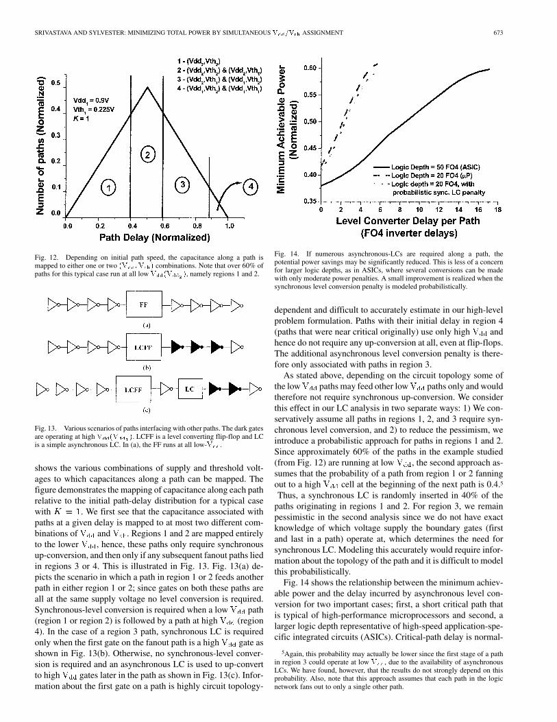
Fig. 12. Depending on initial path speed, the capacitance along a path ismapped to either one or two (V ;V ) combinations. Note that over 60% ofpaths for this typical case run at all low V (V ), namely regions 1 and 2.
Fig. 13. Various scenarios of paths interfacing with other paths. The dark gatesare operating at high V (V ). LCFF is a level converting flip-flop and LCis a simple asynchronous LC. In (a), the FF runs at all low-V .
shows the various combinations of supply and threshold volt-ages to which capacitances along a path can be mapped. Thefigure demonstrates the mapping of capacitance along each pathrelative to the initial path-delay distribution for a typical casewith . We first see that the capacitance associated withpaths at a given delay is mapped to at most two different com-binations of and . Regions 1 and 2 are mapped entirelyto the lower , hence, these paths only require synchronousup-conversion, and then only if any subsequent fanout paths liedin regions 3 or 4. This is illustrated in Fig. 13. Fig. 13(a) de-picts the scenario in which a path in region 1 or 2 feeds anotherpath in either region 1 or 2; since gates on both these paths areall at the same supply voltage no level conversion is required.Synchronous-level conversion is required when a low path(region 1 or region 2) is followed by a path at high (region4). In the case of a region 3 path, synchronous LC is requiredonly when the first gate on the fanout path is a high gate asshown in Fig. 13(b). Otherwise, no synchronous-level conver-sion is required and an asynchronous LC is used to up-convertto high gates later in the path as shown in Fig. 13(c). Infor-mation about the first gate on a path is highly circuit topology-
Fig. 14. If numerous asynchronous-LCs are required along a path, thepotential power savings may be significantly reduced. This is less of a concernfor larger logic depths, as in ASICs, where several conversions can be madewith only moderate power penalties. A small improvement is realized when thesynchronous level conversion penalty is modeled probabilistically.
dependent and difficult to accurately estimate in our high-levelproblem formulation. Paths with their initial delay in region 4(paths that were near critical originally) use only high andhence do not require any up-conversion at all, even at flip-flops.The additional asynchronous level conversion penalty is there-fore only associated with paths in region 3.
As stated above, depending on the circuit topology some ofthe low paths may feed other low paths only and wouldtherefore not require synchronous up-conversion. We considerthis effect in our LC analysis in two separate ways: 1) We con-servatively assume all paths in regions 1, 2, and 3 require syn-chronous level conversion, and 2) to reduce the pessimism, weintroduce a probabilistic approach for paths in regions 1 and 2.Since approximately 60% of the paths in the example studied(from Fig. 12) are running at low , the second approach as-sumes that the probability of a path from region 1 or 2 fanningout to a high cell at the beginning of the next path is 0.4.5
Thus, a synchronous LC is randomly inserted in 40% of thepaths originating in regions 1 and 2. For region 3, we remainpessimistic in the second analysis since we do not have exactknowledge of which voltage supply the boundary gates (firstand last in a path) operate at, which determines the need forsynchronous LC. Modeling this accurately would require infor-mation about the topology of the path and it is difficult to modelthis probabilistically.
Fig. 14 shows the relationship between the minimum achiev-able power and the delay incurred by asynchronous level con-version for two important cases; first, a short critical path thatis typical of high-performance microprocessors and second, alarger logic depth representative of high-speed application-spe-cific integrated circuits (ASICs). Critical-path delay is normal-
5Again, this probability may actually be lower since the first stage of a pathin region 3 could operate at low V , due to the availability of asynchronousLCs. We have found, however, that the results do not strongly depend on thisprobability. Also, note that this approach assumes that each path in the logicnetwork fans out to only a single other path.

674 IEEE TRANSACTIONS ON COMPUTER-AIDED DESIGN OF INTEGRATED CIRCUITS AND SYSTEMS, VOL. 23, NO. 5, MAY 2004
ized to a fanout of four inverter delay (FO4), a commonly usedmetric for the speed of a given technology and, hence, is tech-nology-independent [19].6 Even when no asynchronous-levelconversion is required, synchronous-level conversion incurs afixed-delay penalty over a standard low- flip-flop (conser-vatively assumed to be 2 FO4 delays [20]), resulting in a largerrelative penalty for shallow logic depths. The LC-delay penaltyeffectively restricts the number of asynchronous conversionsthat can be performed on a path and, hence, our results in pre-vious sections are upper bounds on the achievable power im-provement. Fig. 14 shows the LC penalty to saturate when theconversion delay becomes a large fraction of the total path delay.The saturation is a result of the fact that paths in region 3 (as inFig. 12) can no longer be mapped to low due to the pro-hibitive level conversion overhead. Under a pessimistic assump-tion that an asynchronous LC delay is equal to 2.5 FO4 delays[21], the ASIC-based example in Fig. 14 can use two LCs perpath with a 15% rise in the achievable power compared to thecase with no asynchronous LCs. If LCs are used more heavilythan this, their contributed power consumption may begin tooutweigh the power reduction they are supposedly enabling. In-telligent algorithms, such as those proposed in [9], consider thisby comparing the enabled power savings of an inserted asyn-chronous LC to its own power overhead. In general, the asyn-chronous LC delay penalties are substantial for very shallowlogic depths, but reasonable for high-performance ASICs. Theprobabilistic approach to assessing the synchronous-LC penaltyfor paths in regions 1 and 2 yields a small expected improve-ment in power % for the microprocessor case with two LCsper path.
Modern CMOS processes stretch processing equipment totheir limits (subwavelength lithography is a good example),resulting in considerable uncertainty in key physical parame-ters and greatly complicating timing analysis. In this context,designs with a large fraction of paths operating at or near thecritical path delay are more likely to produce timing failuresafter fabrication. Such designs can be considered to have ahigh critical path density. As power reduction techniques suchas multi- , dual- , and sizing all result in more criticalpaths, we analyzed the relationship between the achievedpower savings and critical path density for both the traditionaldual and dual approaches. We define a criticalpath as one having a delay within 5% of the timing constraint.Fig. 15 shows that the dual technique achieves thesame power reduction as dual with 40% fewer criticalpaths, simplifying timing verification. Alternatively, at aconstant critical path density, dual provides 11%lower power than dual .
VII. MULTI-
In this section, we briefly compare multi- designswith dual . Table III compares the power savingsprovided by triple and dual to
6A typical 0.13-�m foundry technology has a 40-ps FO4 delay. The logicdepths in this section correspond to a 1.25 GHz microprocessor and 500-MHzASIC in such a process.
Fig. 15. Dual V =V provides a better power/criticality tradeoff than dualV . For the same power savings, there are significantly fewer critical paths,which eases the design and timing verification processes.
TABLE IIICOMPARISON OF MULTISUPPLY AND THRESHOLD-VOLTAGE TECHNIQUES WITH
DUAL V =V SHOWS NEARLY SATURATED IMPROVEMENTS. THE RESULTS
ARE FOR A 0.9-V DESIGN WITH V = 0:225 V AND K = 10
dual . The improvements provided by the additionalthreshold voltage are quite small % lower power relative tothe dual design. A triple approach isjust 10% better than dual . These results agree with[8], which showed saturated improvement with an increasingnumber of power supplies and threshold voltages in multi-or multi- designs. Since we expect additional thresholdvoltages to be most advantageous in static-power-constraineddesigns, we examined the dual techniquewith . The additional power savings compared to dual
is again found to be small: the minimum normalizedpower is 0.33 for triple compared to 0.36 fordual . In general, the advantage afforded by a thirdthreshold or supply voltage is even smaller in multidesigns than seen in [8] due to the fact that dualprovides more substantial power reductions compared to dual
or dual alone. Triple processes have additionalfabrication costs due to the extra implant steps and tripledesigns extend the place and routing difficulties of dualand also have higher level conversion penalties. Since thepower savings compared to dual designs are limited,the overhead associated with these techniques appears to beexcessive.
SRIVASTAVA AND SYLVESTER: MINIMIZING TOTAL POWER BY SIMULTANEOUS ASSIGNMENT 675
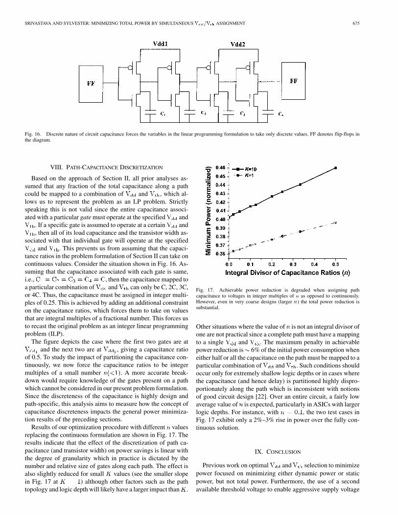
Fig. 16. Discrete nature of circuit capacitance forces the variables in the linear programming formulation to take only discrete values. FF denotes flip-flops inthe diagram.
VIII. PATH-CAPACITANCE DISCRETIZATION
Based on the approach of Section II, all prior analyses as-sumed that any fraction of the total capacitance along a pathcould be mapped to a combination of and , which al-lows us to represent the problem as an LP problem. Strictlyspeaking this is not valid since the entire capacitance associ-ated with a particular gate must operate at the specified and
. If a specific gate is assumed to operate at a certain and, then all of its load capacitance and the transistor width as-
sociated with that individual gate will operate at the specifiedand . This prevents us from assuming that the capaci-
tance ratios in the problem formulation of Section II can take oncontinuous values. Consider the situation shown in Fig. 16. As-suming that the capacitance associated with each gate is same,i.e., , then the capacitance mapped toa particular combination of and can only be C, 2C, 3C,or 4C. Thus, the capacitance must be assigned in integer multi-ples of 0.25. This is achieved by adding an additional constrainton the capacitance ratios, which forces them to take on valuesthat are integral multiples of a fractional number. This forces usto recast the original problem as an integer linear programmingproblem (ILP).
The figure depicts the case where the first two gates are atand the next two are at , giving a capacitance ratio
of 0.5. To study the impact of partitioning the capacitance con-tinuously, we now force the capacitance ratios to be integermultiples of a small number . A more accurate break-down would require knowledge of the gates present on a pathwhich cannot be considered in our present problem formulation.Since the discreteness of the capacitance is highly design andpath-specific, this analysis aims to measure how the concept ofcapacitance discreteness impacts the general power minimiza-tion results of the preceding sections.
Results of our optimization procedure with different valuesreplacing the continuous formulation are shown in Fig. 17. Theresults indicate that the effect of the discretization of path ca-pacitance (and transistor width) on power savings is linear withthe degree of granularity which in practice is dictated by thenumber and relative size of gates along each path. The effect isalso slightly reduced for small values (see the smaller slopein Fig. 17 at ) although other factors such as the pathtopology and logic depth will likely have a larger impact than .
Fig. 17. Achievable power reduction is degraded when assigning pathcapacitance to voltages in integer multiples of n as opposed to continuously.However, even in very coarse designs (larger n) the total power reduction issubstantial.
Other situations where the value of is not an integral divisor ofone are not practical since a complete path must have a mappingto a single and . The maximum penalty in achievablepower reduction is 6% of the initial power consumption wheneither half or all the capacitance on the path must be mapped to aparticular combination of and . Such conditions shouldoccur only for extremely shallow logic depths or in cases wherethe capacitance (and hence delay) is partitioned highly dispro-portionately along the path which is inconsistent with notionsof good circuit design [22]. Over an entire circuit, a fairly lowaverage value of is expected, particularly in ASICs with largerlogic depths. For instance, with , the two test cases inFig. 17 exhibit only a 2%–3% rise in power over the fully con-tinuous solution.
IX. CONCLUSION
Previous work on optimal and selection to minimizepower focused on minimizing either dynamic power or staticpower, but not total power. Furthermore, the use of a secondavailable threshold voltage to enable aggressive supply voltage
676 IEEE TRANSACTIONS ON COMPUTER-AIDED DESIGN OF INTEGRATED CIRCUITS AND SYSTEMS, VOL. 23, NO. 5, MAY 2004
scaling has not been quantified. This work addresses the simul-taneous assignment of and in multivoltage systems tominimize total power consumption, considering DIBL effects.Our results indicate that the total power reduction achievable inmodern and future integrated circuits is on the order of 60–65%using the dual technique. When considering the dis-crete nature of path capacitance (i.e., we cannot assign arbi-trarily small amounts of capacitance to a lower ), the powersavings drops slightly toward 55%–60% for typical cases. Wederive rules-of-thumb to guide selection of the optimal second
and as a function of initial voltages as well as a keyweighting factor, , that drives the optimization primarily to-ward either static or dynamic power reduction. An importantfinding is that the optimal second in multi- systems isapproximately 50% of the higher supply voltage which is con-trasted with 60–70% of for single designs as previ-ously found. An implication of this finding is that LC structuresmust be capable of converting over a larger relative range—thisseems feasible provided the LCs themselves take advantage ofmultiple threshold voltages. The gate overdrive was found to befairly independent of the value of , suggesting that the initialratio of dynamic to static power serves only to shift the values ofthe optimal second supply and threshold voltage and the amountof shift is the same for both. The total power using dualis 15–45% lower than dual for . Given thatmost high-performance designs today already rely on dual-processes to limit standby power, there is no additional cost forthis savings. Since a dual approach is very successfulat trading off slack for power reduction, additional supply orthreshold voltages beyond this (e.g., a third ) provide onlyminimal power improvements.
We then analyze the impact of various device scaling sce-narios on multivoltage systems. In particular, continued aggres-sive channel length scaling and new device structures such asstrained-Si channels point to increasingly velocity saturated de-vices that are ideal for voltage scaling. The inclusion of levelconversion delay penalties illustrates the tradeoff between allo-cating available slack to level conversion and achievable powerreductions. Typically, 1–2 asynchronous level conversions perpath are tolerable in designs with larger logic depths ( FO4delays) with % power penalty. Additionally, we highlightthe relationship between power savings and critical path den-sity—this is important since a rapidly increasing number of crit-ical paths combined with rising process variability increasesdesign times and emphasizes a need for improved statisticaltiming analysis tools. Dual offers better control of theslack-power tradeoff compared to dual . In future designsthat are both power and variability-constrained, the design spaceof Fig. 15 may become a crucial one.
REFERENCES
[1] K. Usami and M. Horowitz, “Clustered voltage scaling technique forlow-power design,” in Proc. Int. Symp. Low-Power Electron. Design,1995, pp. 3–8.
[2] C. Chen, A. Srivastava, and M. Sarrafzadeh, “On gate level power op-timization using dual-supply voltages,” IEEE Trans. VLSI Syst., vol. 9,pp. 616–629, Oct. 2001.
[3] N. Rohrer et al., “A 480 MHz RISC microprocessor in a 0.12 �m LeffCMOS technology with copper interconnects,” in Proc. Int. Solid-StateCircuits Conf., 1998, pp. 240–241.
[4] S. Sirichotiyakul et al., “Stand-by power minimization through simul-taneous threshold voltage selection and circuit sizing,” in Proc. DesignAutomation Conf., 1999, pp. 436–441.
[5] Q. Wang and S. Vrudhula, “Algorithms for minimizing standby powerin deep submicron, dual-V CMOS circuits,” IEEE Trans. Computer-Aided Design, vol. 21, pp. 306–318, Mar. 2002.
[6] S. Tang et al., “A leakage-tolerant dynamic register file using leakagebypass with stack forcing (LBSF) and source follower NMOS (SFN)techniques,” in Proc. IEEE Symp. VLSI Circuits, 2002, pp. 320–321.
[7] D. Sylvester and H. Kaul, “Future performance challenges in nanometerdesign,” in Proc. Design Automation Conf., 2001, pp. 3–8.
[8] M. Hamada, Y. Ootaguro, and T. Kuroda, “Utilizing surplus timing forpower reduction,” in Proc. Custom Integrated Circuits Conf., 2001, pp.89–92.
[9] K. Usami et al., “Automated low-power technique exploiting multiplesupply voltage applied to a media processor,” IEEE J. Solid-State Cir-cuits, vol. 33, pp. 463–472, Mar. 1998.
[10] M. Hamada et al., “A top-down low power design technique using clus-tered voltage scaling with variable supply-voltage scheme,” in Proc.Custom Integrated Circuits Conf., 1998, pp. 495–498.
[11] R. K. Krishnamurthy et al., “Dual supply voltage clocking for 5-GHz130-nm integer execution core,” in Proc. IEEE Int. Symp. VLSI Circuits,2002, pp. 128–129.
[12] A. Chandrakasan, W. J. Bowhill, and F. Fox, Design of High-Perfor-mance Microprocessor Circuits. Piscataway, NJ: IEEE Press, 2001.
[13] T. Sakurai and A. R. Newton, “Alpha-power law MOSFET model andits application to CMOS inverter delay and other formulas,” IEEE J.Solid-State Circuits, vol. 25, pp. 584–593, Apr. 1990.
[14] J. D. Warnock et al., “The circuit and physical design of the POWER4microprocessor,” IBM J. Res. Develop., vol. 46, pp. 27–52, 2002.
[15] B. Curran et al., “A 1.1 GHz first 64 b generation Z900 microprocessor,”in Proc. Int. Solid-State Circuits Conf., 2001, pp. 238–239.
[16] K. Nose and T. Sakurai, “Optimization of V and V for low-powerand high-speed applications,” in Proc. Asia-South Pacific Design Au-tomation Conf., 2000, pp. 469–474.
[17] International Technology Roadmap for Semiconductors, SemiconductorIndustry Association, 2001.
[18] K. Chen and C. Hu, “Performance andV scaling in deep submicrom-eter CMOS,” IEEE J. Solid-State Circuits, vol. 33, pp. 1586–1589, Oct.1998.
[19] R. Ho, K. W. Mai, and M. Horowitz, “The future of wires,” Proc. IEEE,vol. 89, pp. 490–504, Apr. 2001.
[20] M. R. Bai and D. Sylvester, “Analysis and design of level-convertingflip-flops for dual-V =V integrated circuits,” in Proc. IEEE Int.Symp. System-on-Chip, 2003, pp. 151–154.
[21] S. H. Kulkarni and D. Sylvester, “New level converters and level con-verting logic circuits for multi-VDD low power design,” in Proc. IEEESystem-on-Chip (SOC) Conf., 2003, pp. 169–172.
[22] I. Sutherland, B. Sproull, and D. Harris, Logical Effort. San Francisco,CA: Morgan Kaufmann, 1999.
Ashish Srivastava (S’00) received the B.Tech. de-gree in electrical engineering from the Indian Insti-tute of Technology, Kanpur, India, in 2001 and theM.S. degree in electrical engineering in 2003 fromthe University of Michigan, Ann Arbor, where he iscurrently pursuing the Ph.D. degree.
In the summer of 2003, he was with the Tech-nology Computer-Aided Design Division, IntelCorporation, Hillsboro, OR, where he was aGraduate Intern. His research interests includeoptimization and statistical analysis for high-perfor-
mance very large scale integrated design.

SRIVASTAVA AND SYLVESTER: MINIMIZING TOTAL POWER BY SIMULTANEOUS ASSIGNMENT 677
Dennis Sylvester (S’96–M’97) received the B.S.degree in electrical engineering (summa cum laude)from the University of Michigan, Ann Arbor, in1995 and the M.S. and Ph.D. degrees in electricalengineering from University of California, Berkeley,in 1997 and 1999, respectively.
He was with Hewlett-Packard Laboratories, PaloAlto, CA, from 1996 to 1998. After working as aSenior Research and Development Engineer in theAdvanced Technology Group of Synopsys, MountainView, CA, he is now an Assistant Professor of Elec-
trical Engineering at the University of Michigan. In addition, he helps to definethe circuit and physical design roadmap as a member of the International Tech-nology Roadmap for Semiconductors (ITRS), U.S. Design Technology WorkingGroup. He has published numerous papers in his field of research, which in-cludes the modeling, characterization, and analysis of on-chip interconnect, low-power circuit design and design automation techniques, and variability-awarecircuit approaches.
Dr. Sylvester is a member of the ACM, American Society of Engineering Ed-ucation, and Eta Kappa Nu. He is on the technical program committee of severaldesign automation and circuit design conferences and served as general chair forthe 2003 ACM/IEEE System-Level Interconnect Prediction (SLIP) Workshop.He was awarded the 2000 David J. Sakrison Memorial Prize for his dissertationresearch as the most outstanding research in the Department of Electrical Engi-neering and Computer Science, University of California, Berkeley. He receiveda National Scientific Foundation CAREER Award, the 2000 Beatrice WinnerAward at the ISSCC, two outstanding research presentation awards from theSemiconductor Research Corporation, and a Best Student Paper Award at the1997 International Semiconductor Device Research Symposium. He is the re-cipient of the 2003 ACM SIGDA Outstanding New Faculty Award and also the2003 Ruth and Joel Spira Outstanding Teaching Award in the Michigan Collegeof Engineering.