Self-Consistent Technique for Extracting Density of States in Amorphous InGaZnO Thin Film...
6
Self-Consistent Technique for Extracting Density of States in Amorphous InGaZnO Thin Film Transistors Jun-Hyun Park, Kichan Jeon, Sangwon Lee, Sangwook Kim, * Sunil Kim, Ihun Song, Jaechul Park, z Youngsoo Park, Chang Jung Kim, Dong Myong Kim, and Dae Hwan Kim z School of Electrical Engineering, Kookmin University, Seongbuk, Seoul 136-702, Korea The self-consistent technique for extracting density of states DOS: g E in an amorphous indium gallium zinc oxide a-IGZO thin film transistor is proposed and demonstrated. The key parameters are the g E of the a-IGZO active layer and the intrinsic channel mobility ch . While the energy level E is scanned by the photon energy and gate-to-source voltage V GS sweep, its density is extracted from an optical response of capacitance–voltage characteristics. Using the V GS -dependent ch as another boundary condition, a linearly mapped DOS assuming a linear relation between V GS and E is translated into a final DOS by fully considering a nonlinear relation between V GS and E. The final DOS is finally extracted and verified by finding the self-consistent solution satisfying both the linearly mapped DOS and the measured V GS dependence of ch with the numerical iteration of a DOS-based ch model. The extracted final DOS parameters are N TA = 1.73 10 17 cm -3 eV -1 , N DA = 3.5 10 15 cm -3 eV -1 , kT TA = 0.023 eV, kT DGA = 1.2 eV, and E O = 1.7 eV with the formula of exponential tail states and Gaussian deep states. © 2010 The Electrochemical Society. DOI: 10.1149/1.3273203 All rights reserved. Manuscript submitted August 12, 2009; revised manuscript received November 9, 2009. Published January 4, 2010. This was Paper 774 presented at the San Francisco, California, Meeting of the Society, May 24–29, 2009. Recently, multicomponent amorphous oxide semiconductor- based thin film transistors TFTsi.e., amorphous InGaZnO a- IGZO, a-InZnO, and a-GaZnO have been under active research and development because of their room-temperature fabrication pro- cess, low cost, higher mobility than those of covalent semiconductor TFTs, and compatibility with transparent and rollable electronics applications. The density of states DOS, g E is a critical param- eter playing a significant role in the electrical property of a-IGZO. However, the extraction of g E in the a-IGZO TFTs has been rarely investigated or recently studied by some groups. 1-3 Also very re- cently, we proposed the a-IGZO DOS extraction method based on an optical response of capacitance–voltage C-V curve 4 assuming a linear relation between the gate-to-source voltage V GS and energy level E. In this work, the self-consistent g E extraction technique, including a complicated nonlinear relation between E and V GS , is proposed by combining an optical response of the C-V curve and the V GS -dependent intrinsic channel mobility ch . The integrated IGZO TFTs have the most commonly used back- channel-etch staggered bottom gate structure for active matrix liquid crystal displays and/or active matrix organic light emitting diode displays. Devices are fabricated as follows: On a thermally grown SiO 2 /Si substrate, the first sputtered deposition at room temperature and the patterning of molybdenum Mo gate are followed by plasma-enhanced chemical vapor deposition PECVD deposition of a 100 nm thick SiO 2 at 300°C T GI = 100 nm. A 70 nm thick active layer In 2 O 3 :Ga 2 O 3 :ZnO = 2:2:1 atom % is then sputtered by the radio frequency rf magnetron sputtering at room tempera- ture in a mixed atmosphere of Ar /O 2 100:1 at sccm and wet etched with diluted HF T IGZO = 70 nm. For the source/drain S/D pat- tern, Mo is sputtered at room temperature and then patterned by dry etching. After N 2 O plasma treatment on the channel surface of the IGZO active layer, a SiO 2 passivation layer without a vacuum break is continuously deposited at 150°C by PECVD, and finally, all the samples W/L /L OV = 200 /50 /10 m were annealed at 250°C for 1 h in the furnace. The fabricated IGZO layer is verified to have an amorphous phase by XRD and transmission electron microscopy TEM views and shows the nature of an n-type amorphous oxide semiconductor. Figure 1 shows the device schematic, XRD pattern, and TEM image. Model Parameter Extraction Method To extract and validate g E, including the complicated nonlinear relation between the V GS and the surface potential S eventually E, the critical model parameters ch and g E assuming the linear relation between S and V GS should be extracted from the mea- sured data. The extraction of ch plays a significant role in confirming the validity of g E of a-IGZO TFT because we can consider that the ch is related to the electrons moving on the condition of a specific potential distribution. The extraction of ch is started from the ac- quisition of a total on-resistance R T and an intrinsic channel resis- tance R ch of TFTs. The drain-to-source current I DS in the linear region is given by I DS FE C ox W L V GS - V T V DS A 1 where FE , C ox , V T , and V DS are the field-effect mobility, gate oxide capacitance per unit area, threshold voltage, and drain-to-source voltage, respectively. R T and parasitic resistance R P are defined in the following equation 5 R T = lim V DS →0 V DS I DS constant V GS = R ch + R P = r ch L + R P 2 where r ch is the intrinsic channel resistance per unit channel length. R P includes both the contact resistance R C and the S/D spreading resistance R S and R D , as shown in Fig. 2. By using the basic transistor equation from the gradual channel approximation like the crystalline semiconductor, we can determine r ch . The r ch is represented as r ch = 1 ch C ox WV GS - V T m 3 By substituting Eq. 3 with Eq. 2, we obtain R T = R P + L ch C OX V GS - V T = R P + R ch 4 Then, based on a transmission line model TLM method, the r ch V GS can be extracted from the slope of the R T - L plot with various V GS . The R T is measured from the linear region of the output characteristics I DS -V DS of TFTs. In our case, various L’s L = 2, 6, 10, 30, and 50 m under a fixed W W = 200 m were utilized * Electrochemical Society Active Member. z E-mail: [email protected]; [email protected] Journal of The Electrochemical Society, 157 3 H272-H277 2010 0013-4651/2010/1573/H272/6/$28.00 © The Electrochemical Society H272 Downloaded 04 Jan 2010 to 222.111.165.128. Redistribution subject to ECS license or copyright; see http://www.ecsdl.org/terms_use.jsp
-
Upload
independent -
Category
Documents
-
view
1 -
download
0
Transcript of Self-Consistent Technique for Extracting Density of States in Amorphous InGaZnO Thin Film...
Journal of The Electrochemical Society, 157 �3� H272-H277 �2010�H272
D
Self-Consistent Technique for Extracting Density of Statesin Amorphous InGaZnO Thin Film TransistorsJun-Hyun Park, Kichan Jeon, Sangwon Lee, Sangwook Kim,* Sunil Kim,Ihun Song, Jaechul Park,z Youngsoo Park, Chang Jung Kim,Dong Myong Kim, and Dae Hwan Kimz
School of Electrical Engineering, Kookmin University, Seongbuk, Seoul 136-702, Korea
The self-consistent technique for extracting density of states �DOS: g�E�� in an amorphous indium gallium zinc oxide �a-IGZO�thin film transistor is proposed and demonstrated. The key parameters are the g�E� of the a-IGZO active layer and the intrinsicchannel mobility ��ch�. While the energy level �E� is scanned by the photon energy and gate-to-source voltage �VGS� sweep, itsdensity is extracted from an optical response of capacitance–voltage characteristics. Using the VGS-dependent �ch as anotherboundary condition, a linearly mapped DOS assuming a linear relation between VGS and E is translated into a final DOS by fullyconsidering a nonlinear relation between VGS and E. The final DOS is finally extracted and verified by finding the self-consistentsolution satisfying both the linearly mapped DOS and the measured VGS dependence of �ch with the numerical iteration of aDOS-based �ch model. The extracted final DOS parameters are NTA = 1.73 � 1017 cm−3 eV−1, NDA = 3.5 � 1015 cm−3 eV−1,kTTA = 0.023 eV, kTDGA = 1.2 eV, and EO = 1.7 eV with the formula of exponential tail states and Gaussian deep states.© 2010 The Electrochemical Society. �DOI: 10.1149/1.3273203� All rights reserved.
Manuscript submitted August 12, 2009; revised manuscript received November 9, 2009. Published January 4, 2010. This wasPaper 774 presented at the San Francisco, California, Meeting of the Society, May 24–29, 2009.
0013-4651/2010/157�3�/H272/6/$28.00 © The Electrochemical Society
Recently, multicomponent amorphous oxide semiconductor-based thin film transistors �TFTs� �i.e., amorphous InGaZnO �a-IGZO�, a-InZnO, and a-GaZnO� have been under active researchand development because of their room-temperature fabrication pro-cess, low cost, higher mobility than those of covalent semiconductorTFTs, and compatibility with transparent and rollable electronicsapplications. The density of states �DOS, g�E�� is a critical param-eter playing a significant role in the electrical property of a-IGZO.However, the extraction of g�E� in the a-IGZO TFTs has been rarelyinvestigated or recently studied by some groups.1-3 Also very re-cently, we proposed the a-IGZO DOS extraction method based on anoptical response of capacitance–voltage �C-V� curve4 assuming alinear relation between the gate-to-source voltage VGS and energylevel E. In this work, the self-consistent g�E� extraction technique,including a complicated nonlinear relation between E and VGS, isproposed by combining an optical response of the C-V curve and theVGS-dependent intrinsic channel mobility ��ch�.
The integrated IGZO TFTs have the most commonly used back-channel-etch staggered bottom gate structure for active matrix liquidcrystal displays and/or active matrix organic light emitting diodedisplays. Devices are fabricated as follows: On a thermally grownSiO2/Si substrate, the first sputtered deposition at room temperatureand the patterning of molybdenum �Mo� gate are followed byplasma-enhanced chemical vapor deposition �PECVD� deposition ofa 100 nm thick SiO2 at 300°C �TGI = 100 nm�. A 70 nm thickactive layer �In2O3:Ga2O3:ZnO = 2:2:1 atom %� is then sputteredby the radio frequency �rf� magnetron sputtering at room tempera-ture in a mixed atmosphere of Ar/O2 �100:1 at sccm� and wet etchedwith diluted HF �TIGZO = 70 nm�. For the source/drain �S/D� pat-tern, Mo is sputtered at room temperature and then patterned by dryetching. After N2O plasma treatment on the channel surface of theIGZO active layer, a SiO2 passivation layer without a vacuum breakis continuously deposited at 150°C by PECVD, and finally, all thesamples �W/L/LOV = 200/50/10 �m� were annealed at 250°C for 1h in the furnace. The fabricated IGZO layer is verified to have anamorphous phase by XRD and transmission electron microscopy�TEM� views and shows the nature of an n-type amorphous oxidesemiconductor. Figure 1 shows the device schematic, XRD pattern,and TEM image.
* Electrochemical Society Active Member.z E-mail: [email protected]; [email protected]
ownloaded 04 Jan 2010 to 222.111.165.128. Redistribution subject to E
Model Parameter Extraction Method
To extract and validate g�E�, including the complicated nonlinearrelation between the VGS and the surface potential �S �eventually E�,the critical model parameters ��ch and g�E� assuming the linearrelation between �S and VGS� should be extracted from the mea-sured data.
The extraction of �ch plays a significant role in confirming thevalidity of g�E� of a-IGZO TFT because we can consider that the�ch is related to the electrons moving on the condition of a specificpotential distribution. The extraction of �ch is started from the ac-quisition of a total on-resistance �RT� and an intrinsic channel resis-tance �Rch� of TFTs. The drain-to-source current �IDS� in the linearregion is given by
IDS � �FECoxW
L�VGS − VT� � VDS �A� �1�
where �FE, Cox, VT, and VDS are the field-effect mobility, gate oxidecapacitance per unit area, threshold voltage, and drain-to-sourcevoltage, respectively. RT and parasitic resistance �RP� are defined inthe following equation5
RT = limVDS→0
� � VDS
� IDS�
constant VGS
= Rch + RP = rchL + RP ��� �2�
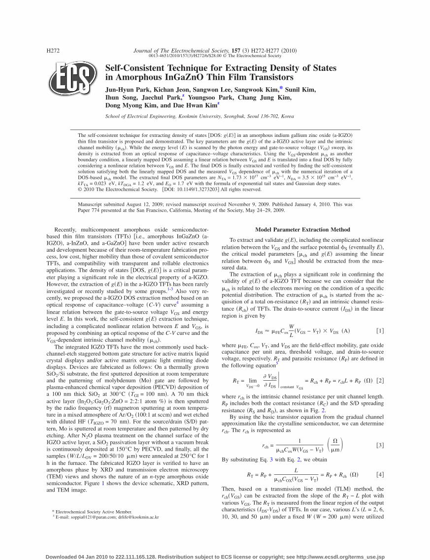
where rch is the intrinsic channel resistance per unit channel length.RP includes both the contact resistance �RC� and the S/D spreadingresistance �RS and RD�, as shown in Fig. 2.
By using the basic transistor equation from the gradual channelapproximation like the crystalline semiconductor, we can determinerch. The rch is represented as
rch =1
�chCoxW�VGS − VT� � �
�m� �3�
By substituting Eq. 3 with Eq. 2, we obtain
RT = RP +L
�chCOX�VGS − VT�= RP + Rch ��� �4�
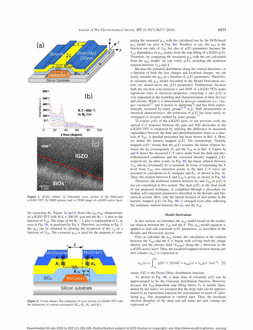
Then, based on a transmission line model �TLM� method, therch�VGS� can be extracted from the slope of the RT − L plot withvarious VGS. The RT is measured from the linear region of the outputcharacteristics �IDS-VDS� of TFTs. In our case, various L’s �L = 2, 6,10, 30, and 50 �m� under a fixed W �W = 200 �m� were utilized
CS license or copyright; see http://www.ecsdl.org/terms_use.jsp
H273Journal of The Electrochemical Society, 157 �3� H272-H277 �2010� H273
D
for extracting RT. Figure 3a and b shows the IDS-VDS characteristicof a-IGZO TFT with W/L = 200/50 �m and the RT − L plot as thefunction of VGS. The slope of the RT − L plot is independent of L, asseen in Fig. 3b, as predicted by Eq. 4. Therefore, according to Eq. 3,the �ch can be obtained by plotting the reciprocal of the rch as afunction of VGS. The extracted �ch is used for the purpose of com-
Figure 1. �Color online� �a� Schematic cross section of the fabricateda-IGZO TFT, �b� XRD pattern, and �c� TEM image of a-IGZO active layer.
Figure 2. �Color online� The schematic of cross section of a-IGZO TFT withthe definitions of various resistances �R , R , R , and R �.
ch C S Downloaded 04 Jan 2010 to 222.111.165.128. Redistribution subject to E
paring the measured �ch with the calculated one by the DOS-based�ch model �as seen in Fig. 6a�. Needless to say, the �ch is thefunction not only of VGS but also of g�E� parameters because theVGS dependence of �ch results from the trap filling of a-IGZO g�E�.Therefore, by comparing the measured �ch with the one calculatedfrom the �ch model, we can verify g�E�, including the nonlinearrelation between VGS and E.
Because the potential distribution along the vertical direction x isa function of both the free charges and localized charges, we caneasily consider the �ch as a function of g�E� parameters. Therefore,to calculate the �ch model described in the Model Derivation sec-tion, we should know the g�E� parameters. Furthermore, becauseboth the electron concentration n and DOS of a-IGZO TFTs makesignificant roles in electrical properties, extracting n and g�E� isvery important in the modeling and characterization of their devicesand circuits. While n is determined by process conditions �i.e., oxy-gen vacancies6,7 and rf power in sputtering8� and has been experi-mentally extracted by many groups6-10 �e.g., Hall measurement orelectrical characteristics�, the extraction of g�E� has been rarely in-vestigated or recently studied by some groups.1-3
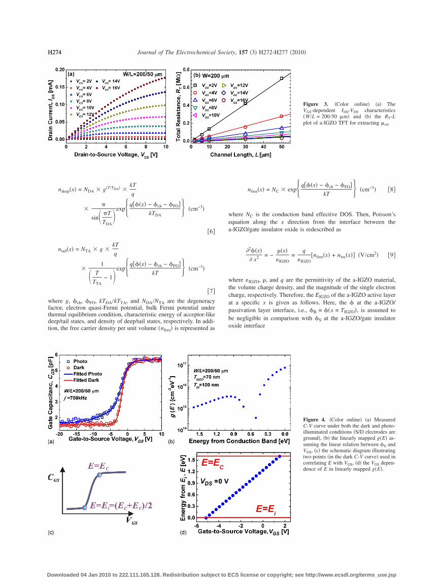
To extract g�E� of the a-IGZO layer, in our previous work theoptical C-V response between the gate and S/D electrodes in thea-IGZO TFT is employed by utilizing the difference in measuredcapacitance between the dark and photoilluminated states as a func-tion of VGS. A detailed procedure has been shown in Ref. 4. Here,we define the linearly mapped g�E�. The terminology “linearlymapped g�E�” means that the g�E� assumes the linear relation be-tween the �S �consequently E� and the VGS as in Ref. 4. Figure 4aand b shows the measured C-V curve under both the dark and pho-toilluminated conditions and the extracted linearly mapped g�E�,respectively. In other words, in Fig. 4b, the linear relation betweenVGS and �S �eventually E� is assumed. In terms of translating the Elevel from VGS, two transition points in the dark C-V curve areassumed to correspond to Ei �midgap� and EC, as shown in Fig. 4c.Then, the relation between E and VGS is given, as shown in Fig. 4d.
Therefore, the nonlinear relation between �S and VGS in g�E� isnot yet considered in this section. The final g�E�, as the final resultof our proposed technique, is completed through a procedure forfinding self-consistent parameters described in the Results and Dis-cussion section. Here, only the lateral location of data points in thelinearly mapped g�E� �in Fig. 4b� is changed even after reflectingthe nonlinear relation between the �S and the VGS.
Model Derivation
In this section, we introduce the �ch model based on the nonlin-ear relation between the VGS and the E. This �ch model equation isapplied to find self-consistent g�E� parameters, as described in theResults and Discussion section.
First, to calculate the �ch model, the calculation of the relationbetween the VGS and the E is begun with solving both the chargedensity and the electric field �EIGZO� along the x direction in thea-IGZO active layer. Then, the localized trapped electron density perunit volume �nloc� is expressed as
nloc�x� = EV
EC
g�E� � f�E�dE = ndeep�x� + ntail�x� �cm−3� �5�
where f�E� is the Fermi–Dirac distribution function.As shown in Fig. 4b, a deep state of extracted g�E� can be
approximated to be the Gaussian distribution function. However,because the VGS-dependent trap filling above VT is mainly deter-mined by tail states, we assumed that the deep state can be approxi-mated to an exponential function for convenience in terms of calcu-lating �ch. Our assumption is verified later. Then, the localizedelectron densities of the deep and tail states per unit volume areexpressed as11
CS license or copyright; see http://www.ecsdl.org/terms_use.jsp
H274 Journal of The Electrochemical Society, 157 �3� H272-H277 �2010�H274
D
ndeep�x� = NDA � g�T/TDA� �kT
q
��
sin� �T
TDA� expq���x� − �ch − �FO�
kTDA� �cm−3�
�6�
ntail�x� = NTA � g �kT
q
�1
� T
TTA− 1� expq���x� − �ch − �FO�
kT� �cm−3�
�7�
where g, �ch, �FO, kTDA/kTTA, and NDA/NTA are the degeneracyfactor, electron quasi-Fermi potential, bulk Fermi potential underthermal equilibrium condition, characteristic energy of acceptor-likedeep/tail states, and density of deep/tail states, respectively. In addi-tion, the free carrier density per unit volume �nfree� is represented as
ownloaded 04 Jan 2010 to 222.111.165.128. Redistribution subject to E
nfree�x� = NC � expq���x� − �ch − �FO�kT
� �cm−3� �8�
where NC is the conduction band effective DOS. Then, Poisson’sequation along the x direction from the interface between thea-IGZO/gate insulator oxide is redescribed as
�2��x�� x2 = −
��x��IGZO
=q
�IGZO�nfree�x� + nloc�x�� �V/cm2� �9�
where �IGZO, �, and q are the permittivity of the a-IGZO material,the volume charge density, and the magnitude of the single electroncharge, respectively. Therefore, the EIGZO of the a-IGZO active layerat a specific x is given as follows. Here, the � at the a-IGZO/passivation layer interface, i.e., �B = ��x = TIGZO�, is assumed tobe negligible in comparison with �S at the a-IGZO/gate insulatoroxide interface
Figure 3. �Color online� �a� TheVGS-dependent IDS-VDS characteristics�W/L = 200/50 �m� and �b� the RT-Lplot of a-IGZO TFT for extracting �ch.
Figure 4. �Color online� �a� MeasuredC-V curve under both the dark and photo-illuminated conditions �S/D electrodes areground�, �b� the linearly mapped g�E� as-suming the linear relation between �S andVGS, �c� the schematic diagram illustratingtwo points �in the dark C-V curve� used incorrelating E with VGS, �d� the VGS depen-dence of E in linearly mapped g�E�.
CS license or copyright; see http://www.ecsdl.org/terms_use.jsp
H275Journal of The Electrochemical Society, 157 �3� H272-H277 �2010� H275
D
EIGZO = �2��x=TIGZO�
��x�q
�IGZO�nloc�x� + nfree�x��d��x� � V
cm��10�
To calculate the nonlinear relation between VGS and E, we applyGauss law to the interface of the a-IGZO/gate insulator oxide. Whenwe apply Eq. 10, the continuity of dielectric displacement across theinterface between the a-IGZO/gate insulator oxide gives
VGS = VFB + �S +Qinduced
Cox= VFB + �S +
�IGZOEIGZO��S�Cox
�V�
�11�
where Qinduced and VFB are the VGS-dependent field-induced chargeper unit area within the entire a-IGZO active layer and flatbandvoltage, respectively. Because the EIGZO is a function of g�E�, onecan infer that the final g�E� parameters �NTA, NDA, kTTA, and kTDA�should be known to completely calculate the nonlinear relation be-tween the �S and the VGS. Therefore, the relation between the VGSand the �S should be calculated by self-consistent numerical itera-tions. The kTTA and kTDA �characteristic energy of the tail/deep� aresignificantly changed by employing the nonlinear relation betweenthe VGS and the �S, while NTA and NDA �tail/deep state density�would be nearly unchanged even after applying that nonlinear rela-tion. Therefore, kTTA and kTDA are such unknown variables in thelinearly mapped g�E�. However, because the �ch is a function ofboth the g�E� and VGS, we can use the �ch model as another bound-ary condition to extract the final g�E� parameters, kTTA and kTDA.
Here, based on the nonlinear relation between the VGS and �S inEq. 11, the DOS-based �ch model is calculated. In contrast to field-effect mobility �FE, the �ch is the intrinsic parameter connected onlywith the Rch. Thus, the VGS-dependent �ch is the most suitable pa-rameter for verifying the intrinsic properties of the a-IGZO activematerial, i.e., DOS, g�E�. Because the ��x� is a function of both freeand localized charges, we can easily infer that the �ch is also modu-lated by those charges. In detail, the �ch, as in hydrogenated amor-phous silicon �a-Si:H� TFT, is expressed as the function of the con-duction band mobility �band, the free charge density per unit areaQfree, and the localized trapped charge density per unit area Qloc asfollows12
�ch���x�� = �band �Qfree���x��
Qinduced���x��= �band
�Qfree���x��
Qfree���x�� + Qloc���x��� cm2
V s� �12�
where Qfree and Qloc are represented as
Qfree���x�� = qx
x=TIGZO
nfree�x�dx = qx
x=TIGZO
NC
� expq���x� − �ch − �FO�kT
�dx � C
cm2� �13�
Qloc���x�� = qx
x=TIGZO
nloc�x�dx = qx
x=TIGZOEV
EC
g�E�
� f�E�dEdx �C/cm2� �14�
Inasmuch as the energy band bending would be calculated based onthe total Qloc from x to the back interface of the a-IGZO/passivationlayer, Qfree���x�� and Qloc���x�� can be derived by integratingnfree�x� and nloc�x� from x to the end of the active layer �x= TIGZO� throughout the entire a-IGZO active layer.
By unifying Eq. 5, 8, 10, and 12-14, �ch�x� can be calculated asthe model equation consisting of DOS parameters. Consequently,the � of free electrons at the surface channel is given by � �x
ch chownloaded 04 Jan 2010 to 222.111.165.128. Redistribution subject to E
= 0� = �ch���x = 0�� = �ch��S�. Then, �ch��S� can be translatedinto �ch�VGS� by using Eq. 11. Therefore, it can be directly com-pared with the measured �ch�VGS�.
Results and Discussion
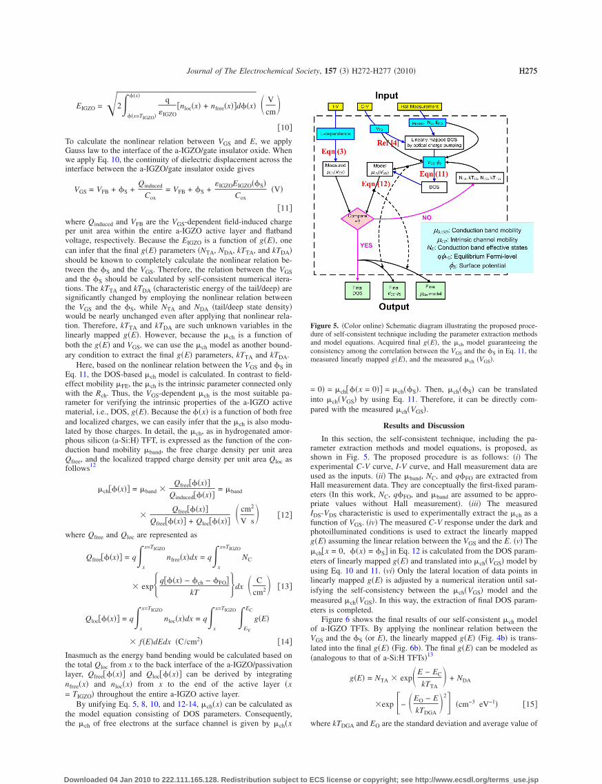
In this section, the self-consistent technique, including the pa-rameter extraction methods and model equations, is proposed, asshown in Fig. 5. The proposed procedure is as follows: �i� Theexperimental C-V curve, I-V curve, and Hall measurement data areused as the inputs. �ii� The �band, NC, and q�FO are extracted fromHall measurement data. They are conceptually the first-fixed param-eters �In this work, NC, q�FO, and �band are assumed to be appro-priate values without Hall measurement�. �iii� The measuredIDS-VDS characteristic is used to experimentally extract the �ch as afunction of VGS. �iv� The measured C-V response under the dark andphotoilluminated conditions is used to extract the linearly mappedg�E� assuming the linear relation between the VGS and the E. �v� The�ch�x = 0, ��x� = �S� in Eq. 12 is calculated from the DOS param-eters of linearly mapped g�E� and translated into �ch�VGS� model byusing Eq. 10 and 11. �vi� Only the lateral location of data points inlinearly mapped g�E� is adjusted by a numerical iteration until sat-isfying the self-consistency between the �ch�VGS� model and themeasured �ch�VGS�. In this way, the extraction of final DOS param-eters is completed.
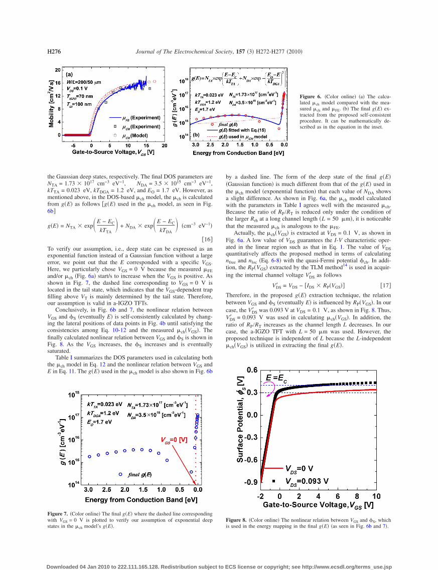
Figure 6 shows the final results of our self-consistent �ch modelof a-IGZO TFTs. By applying the nonlinear relation between theVGS and the �S �or E�, the linearly mapped g�E� �Fig. 4b� is trans-lated into the final g�E� �Fig. 6b�. The final g�E� can be modeled as�analogous to that of a-Si:H TFTs�13
g�E� = NTA � exp�E − EC
kTTA� + NDA
�exp − �EO − E
kTDGA�2� �cm−3 eV−1� �15�
where kT and E are the standard deviation and average value of
Figure 5. �Color online� Schematic diagram illustrating the proposed proce-dure of self-consistent technique including the parameter extraction methodsand model equations. Acquired final g�E�, the �ch model guaranteeing theconsistency among the correlation between the VGS and the �S in Eq. 11, themeasured linearly mapped g�E�, and the measured �ch �VGS�.
DGA O
CS license or copyright; see http://www.ecsdl.org/terms_use.jsp
H276 Journal of The Electrochemical Society, 157 �3� H272-H277 �2010�H276
D
the Gaussian deep states, respectively. The final DOS parameters areNTA = 1.73 � 1017 cm−3 eV−1, NDA = 3.5 � 1015 cm−3 eV−1,kTTA = 0.023 eV, kTDGA = 1.2 eV, and EO = 1.7 eV. However, asmentioned above, in the DOS-based �ch model, the �ch is calculatedfrom g�E� as follows �g�E� used in the �ch model, as seen in Fig.6b�
g�E� = NTA � exp�E − EC
kTTA� + NDA � exp�E − EC
kTDA� �cm−3 eV−1�
�16�To verify our assumption, i.e., deep state can be expressed as anexponential function instead of a Gaussian function without a largeerror, we point out that the E corresponded with a specific VGS.Here, we particularly chose VGS = 0 V because the measured �FEand/or �ch �Fig. 6a� start/s to increase when the VGS is positive. Asshown in Fig. 7, the dashed line corresponding to VGS = 0 V islocated in the tail state, which indicates that the VGS-dependent trapfilling above VT is mainly determined by the tail state. Therefore,our assumption is valid in a-IGZO TFTs.
Conclusively, in Fig. 6b and 7, the nonlinear relation betweenVGS and �S �eventually E� is self-consistently calculated by chang-ing the lateral positions of data points in Fig. 4b until satisfying theconsistencies among Eq. 10-12 and the measured �ch�VGS�. Thefinally calculated nonlinear relation between VGS and �S is shown inFig. 8. As the VGS increases, the �S increases and is eventuallysaturated.
Table I summarizes the DOS parameters used in calculating boththe �ch model in Eq. 12 and the nonlinear relation between VGS andE in Eq. 11. The g�E� used in the �ch model is also shown in Fig. 6b
Figure 7. �Color online� The final g�E� where the dashed line correspondingwith VGS = 0 V is plotted to verify our assumption of exponential deepstates in the � model’s g�E�.
chownloaded 04 Jan 2010 to 222.111.165.128. Redistribution subject to E
by a dashed line. The form of the deep state of the final g�E��Gaussian function� is much different from that of the g�E� used inthe �ch model �exponential function� that each value of NDA showsa slight difference. As shown in Fig. 6a, the �ch model calculatedwith the parameters in Table I agrees well with the measured �ch.Because the ratio of RP/RT is reduced only under the condition ofthe larger Rrh at a long channel length �L = 50 �m�, it is noticeablethat the measured �ch is analogous to the �FE.
Actually, the �ch�VGS� is extracted at VDS = 0.1 V, as shown inFig. 6a. A low value of VDS guarantees the I-V characteristic oper-ated in the linear region such as that in Eq. 1. The value of VDSquantitatively affects the proposed method in terms of calculatingnfree and nloc �Eq. 6-8� with the quasi-Fermi potential �ch. In addi-tion, the RP�VGS� extracted by the TLM method14 is used in acquir-ing the internal channel voltage VDS� as follows
VDS� = VDS − �IDS � RP�VGS�� �17�
Therefore, in the proposed g�E� extraction technique, the relationbetween VGS and �S �eventually E� is influenced by RP�VGS�. In ourcase, the VDS� was 0.093 V at VDS = 0.1 V, as shown in Fig. 8. Thus,VDS� = 0.093 V was used in calculating �ch�VGS�. In addition, theratio of RP/RT increases as the channel length L decreases. In ourcase, the a-IGZO TFT with L = 50 �m was used. However, theproposed technique is independent of L because the L-independent�ch�VGS� is utilized in extracting the final g�E�.
Figure 6. �Color online� �a� The calcu-lated �ch model compared with the mea-sured �ch and �FE. �b� The final g�E� ex-tracted from the proposed self-consistentprocedure. It can be mathematically de-scribed as in the equation in the inset.
Figure 8. �Color online� The nonlinear relation between VGS and �S, whichis used in the energy mapping in the final g�E� �as seen in Fig. 6b and 7�.
CS license or copyright; see http://www.ecsdl.org/terms_use.jsp
H277Journal of The Electrochemical Society, 157 �3� H272-H277 �2010� H277
D
Compared with the case of a-Si:H TFT, the tail and deep statedensities at EC �NTA and NDA� of the a-IGZO TFT are so muchlower. Furthermore, kTTA = 23 meV is much lower than a roomtemperature thermal energy 25 meV, which indicates that the Fermilevel EF easily moves up to near the EC with the increase in VGS. Itis consistent that the �ch of the a-IGZO TFT is much higher thanthat of the a-Si:H TFT. Consequently, high performance of thea-IGZO TFT, i.e., bandlike conduction, relies on the low NTA andkTTA.
Conclusion
A previously proposed g�E� extraction method based on an op-tical response of the C-V curve in a-IGZO TFTs is improved byfully considering the nonlinear relation between the E and the VGS.By finding the solution satisfying both the linearly mapped DOS andthe measured VGS dependence of �ch with the numerical iteration,the self-consistent technique for extracting the DOS of a-IGZOTFTs is proposed and verified by comparing the measured �ch andthe calculated one from the DOS-based �ch model. Our results showthat the proposed technique and the �ch model are very useful forthe device design and modeling of a-IGZO TFTs as a representativeof multicomponent amorphous oxide semiconductor TFTs.
Acknowledgments
This work was supported by the Korea Science and Engineering
Table I. DOS parameters used to calculate the �ch model.
Parameter Value Parameter
NC�cm−3� 4 � 1018 NTA�cm−3 eV−1�NDA�cm−3 eV−1� 2.3 � 1015 kTTA�eV�kTDA�eV� 3 q�FO�eV�
Foundation �KOSEF� grant funded by the Korean government
ownloaded 04 Jan 2010 to 222.111.165.128. Redistribution subject to E
�MEST� �no. 2009-0080344�. CAD software was supported by Sil-vaco and IC Design Education Center �IDEC�.
Kookmin University assisted in meeting the publication costs of this ar-ticle.
References1. M. Kimura, T. Nakanishi, K. Nomura, T. Kamiya, and H. Hosono, Appl. Phys.
Lett., 92, 133512 �2008�.2. C.-S. Chuang, T.-C. Fung, B. G. Mullins, K. Nomura, T. Kamiya, H.-P. Shieh, H.
Hosono, and J. Kanicki, SID Int. Symp. Digest Tech. Papers, 39, 1215 �2008�.3. C. Chen, K. Abe, H. Kumomi, and J. Kanicki, IEEE Trans. Electron Devices, 56,
1177 �2009�.4. J.-H. Park, K. Jeon, S. Lee, S. Kim, S. Kim, I. Song, C. J. Kim, J. Park, Y. Park, D.
M. Kim, et al., IEEE Electron Device Lett., 29, 1292 �2008�.5. S. Luan and G. W. Neudeck, J. Appl. Phys., 72, 766 �1992�.6. Y. Orikasa, N. Hayashi, and S. Muranaka, J. Appl. Phys., 103, 113703 �2008�.7. A. Suresh, P. Gollakota, P. Wellenius, A. Dhawan, and J. F. Muth, Thin Solid Films,
516, 1326 �2008�.8. E. Fortunato, A. Pimentel, A. Gonçalves, A. Marques, and R. Martins, Thin Solid
Films, 502, 104 �2006�.9. K. Nomura, H. Ohta, A. Takagi, T. Kamiya, M. Hirano, and H. Hosono, Nature
(London), 432, 488 �2004�.10. K. Saji, M. Jayaraj, K. Nomura, T. Kamiya, and H. Hosono, J. Electrochem. Soc.,
155, H390 �2008�.11. Y. Liu, R. Yao, B. Li, and W.-L. Deng, J. Disp. Technol., 4, 180 �2008�.12. M. Shur and M. Hack, J. Appl. Phys., 55, 3831 �1984�.13. C. R. Kagan and P. Andry, Thin-Film Transistors, pp. 77–78, CRC, New York
�2003�.14. H.-J. Chung, J. H. Jeong, T. K. Ahn, H. J. Lee, M. Kim, K. Jun, J.-S. Park, J. K.
Jeong, Y.-G. Mo, and H. D. Kim, Electrochem. Solid-State Lett., 11, H51 �2008�.
Value Parameter Value
1.73 � 1017 �band�cm2/V s� 18.70.023 �IGZO 11.5 �Ref. 15�0.3 VFB�V� �3
15. J. Zaumseil, K. W. Baldwin, and J. A. Rogers, J. Appl. Phys., 93, 6117 �2003�.
CS license or copyright; see http://www.ecsdl.org/terms_use.jsp